1
MODEL DG535
Digital Delay / Pulse Generator
1290-D Reamwood Avenue
Sunnyvale, CA 94089 U.S.A.
Phone: (408) 744-9040, Fax: (408) 744-9049
Copyright © 1994, 1997, 2000
All Rights Reserved
Revision 2.5
11/2000
DG535 DIGITAL DELAY / PULSE GENERATOR
OPERATION AND SERVICE MANUAL
Table of Contents
CONDENSED INFORMATION
Safety and Preparation for Use
Quick-Start Instructions
DG535 Specifications
Abridged GPIB Command List
Error Status Byte Definition
Instrument Status Byte Definition
v
vi
vii
viii
ix
ix
GUIDE TO OPERATION
Introduction
1
Front Panel Features
Power Button
Liquid Crystal Display
Menu Keys
Data Entry Keys
Trigger Status LED's
Delay Outputs
Pulse Outputs
Option 06 - Trigger Inhibit Input
1
1
1
1
1
1
1
2
2
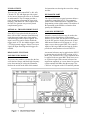
Rear Panel Features
Power Entry Module
IEEE-488 Standard Port
10.000 MHz Reference
Option 02 - ±35 Volt Rear Panel Outputs
Front Panel Programming
Trigger Menu
Trigger Submenus
Trigger Tricks
Delay Menus
Output Menus
AB and CD Outputs
GPIB Menus
Store and Recall Menus
2
2
2
2
3
3
4
4
4
5
5
6
6
7
ACCURACY, DRIFT, AND JITTER
Accuracy
Timebase Drift
Jitter
Channel to Channel Interaction
7
8
8
8
i
Time Delay vs Repetition
9
GPIB PROGRAMMING
Detailed Command List
Initialization Commands
Status Commands
Error Status Byte Definition
Instrument Status Byte Definition
Display Control Commands
Delay and Output Commands
Delays
Output Control
Trigger Commands
Store and Recall Commands
10
10
10
10
11
12
14
14
14
15
16
TROUBLESHOOTING
LCD Contrast
Cold-Boot
Quick Test
Output Levels
Jitter
GPIB Problems
17
17
17
17
17
18
CALIBRATION
Required Equipment
Calibration Procedure
Trigger Threshold Calibration
Optional 1 ppm Internal Timebase Calibration
Output Amplitude Calibration
Calibration Menus
Output Offset Calibration
Jitter Calibration
Jitter Cal Factor
Delay Cal Factor
19
19
19
19
20
20
21
21
21
21
CIRCUIT DESCRIPTION
Microprocessor System
IEEE-488 Interface
Keypad and LED Indicators
LCD Display
Output Ports on the Top PCB
Output Ports on the Bottom PCB
Port Address Decoding
Input Ports
Digital to Analog Converter
Timebase
22
22
22
22
22
22
23
23
24
24
ii
Frequency Synthesizer
Line Trigger
Trigger Selection
Trigger Circuits
Trigger Sequence
Overview of the Delay Channels
Jitter Compensation
Jitter Precharge and Sample & Hold
Kickpulse
The T0 Delay
Channel A's Digital Delay
Analog Delays
Reset Cycle and Status Bits
Output Drivers
Offset Control
Impedance Control
Gate Output Drivers
Power Supplies
Rear Panel Output Drivers
24
24
24
25
25
25
26
26
27
27
27
27
28
28
28
29
29
29
30
PARTS LISTS
Top PCB
Bottom PCB
Front PCB
Optional Outputs PC Board
Miscellaneous and Chassis Assembly
32
32
37
37
38
PC LAYOUT
Top PCB
Bottom PCB
Front PCB
Optional Outputs PCB
39
40
41
41
FAST TRANSITION-TIME MODULES
42
SCHEMATIC DIAGRAMS
45
Top PCB
Sheet #1 Microprocessor System, GPIB and Digital I/O
Sheet #2 Slow Counter/Timers
Sheet #3 Trigger Status and Reset Sequence
Sheet #4 Rate Generators
Sheet #5 Power Supply and Dropout Detection
Sheet #6 System Connectors and Polarity Control
Bottom PCB
Sheet #1 Trigger Circuit and Gated 80 MHz
iii
Sheet #2 10 MHz Reference and 80 MHz PLL
Sheet #3 Jitter Compensation
Sheet #4 ECL Counters and Resync Circuits
Sheet #5 T0 Analog Delay and Output Driver
Sheet #6 A Analog Delay and Output Driver
Sheet #7 B Analog Delay and Output Driver
Sheet #8 C Analog Delay and Output Driver
Sheet #9 D Analog Delay and Output Driver
Sheet #10 AB & CD Gate Output Drivers
Sheet #11 Digital to Analog Converter and Multiplexer
Sheet #12 Power Regulators
Front PCB
Optional Outputs PCB
Table of Figures
Figure - 1 DG535 Rear Panel
Figure - 2 DG535 Front Panel
Figure - 3 Maximum Error vs. Time Delay
Figure - 4 Apparent (Peak To Peak) Jitter and RMS Jitter
Figure - 5 RMS Jitter
Figure - 6 DG535 Block Diagram
Figure - 7 DG535 Timing Diagram
Figure - 8 Top PC Layout
Figure - 9 Bottom PC Layout
Figure - 10Front PC Layout
Figure - 11Optional Outputs PC Layout
Figure - 12Fast Transition-Time Modules
Figure - 13Fast 2 Volt Output Step
iv
Page - 2
Page - 3
Page - 6
Page - 7
Page - 8
Page - 30
Page - 31
Page - 39
Page - 40
Page - 41
Page - 41
Page - 42
Page - 44
SAFETY AND PREPARATION FOR USE
******CAUTION******
line voltage can be seen through the slot that is
just above thefuse holder. Push the fuse holder
back in, and install the correct fuse. Slide the
window to the left, and replace the line cord.
This instrument may be damaged if it is
operated with the LINE VOLTAGE
SELECTOR set for the wrong ac line voltage
or if the wrong fuse is installed.
LINE CORD
LINE VOLTAGE SELECTION
The DG535 uses a three wire power cord for
connection to the power source and to a
protective ground. The exposed metal parts of
the instrument are connected to the outlet
ground: to protect against electrical shock,
always use an outlet which has a properly
connected protective ground.
The DG535 operates from a 100V, 120V,
220V or 240V (50 or 60 Hz) ac power source.
Before applying a power source, verify that
the line voltage selector card (located in the
rear panel power entry module) is in the
correct position. The selected voltage may be
seen through the clear window by viewing the
power entry module from below.
To avoid shock or injury do not remove
product covers or panels. Do not operate the
product without all covers and panels in place.
To change the line voltage selection, remove
the line cord, slide the window to the right,
and pull the "fuse pull" lever out. Verify that
the correct fuse is installed for the ac line
voltage: 1 Amp for 100 or 120V, and 1/2 Amp
for 220 or 240V. Pull out the line voltage
selector card with a pair of needle nose pliers,
and insert it with the correct line voltage
facing the bottom of the instrument and
towards the line cord. Verify that the correct
CONNECTION TO OTHER
INSTRUMENTS
All front panel BNC shields are connected to
the chassis ground and to the power outlet
ground via the power cord. Do not apply any
voltage to either the shields or to the outputs.
The outputs are not protected against
connection to any potential other than ground.
v
QUICK START INSTRUCTIONS
(1) Make certain that the correct line voltage is selected on the rear panel.
(2) Press the power button "in" to turn on the unit.
(3) Press the RECALL Menu key, the "0" digit, and the EXC key in sequence to
recall default settings.
(4) Press the left cursor key (<) twice to select internal trigger.
(5) Trigger the oscilloscope on the rising edge of T0's output, and display A's
output on the 1µs/div scale.
(6) Press the DELAY Menu key and use the cursor keys to change the A delay
from 0.0 seconds.
(7) If you ever change the OUTPUT Menu, be sure to specify the correct
load impedance.
(8) If you have problems, read the detailed descriptions and troubleshooting
sections that follow.
vi
DG535 SPECIFICATIONS
DELAYS
Channels
Range
Resolution
Accuracy
Timebase
Four independent delay outputs : A, B, C and D
0 to 999.999,999,999,995 seconds
5 ps
1500 ps + timebase error x delay
Standard: 25 ppm crystal oscillator
Optional: 1ppm TCXO (Opt. 03)
External: user provides 10.0 MHz reference
Ext Trig to any output: 60 ps + delay x 10-8
T0 to any output: 50 ps + delay x 10-8
Ext Trig to T0 output : 85 ns
RMS Jitter
Trig Delay
INTERNAL RATE GENERATOR
Rate
Resolution
Accuracy
Jitter
Settling
Burst Mode
Single shot, .001 Hz to 1.000 MHz, or Line
0.001 Hz below 10 Hz, otherwise 4 digits
Same as timebase
1:10,000
<2 seconds for any rate change
2 to 32766 pulses per burst at integer multiples
(4 to 32767) of the trigger period
INPUTS
External Trigger
Rate: dc to 1/(1 µs + longest delay)
Threshold: ±2.56 Vdc
Slope: Trigger on rising or falling edge
Impedance: 1 MΩ + 40 pF or 50Ω
TTL front panel trigger inhibit input.
Option 06
OUTPUTS
T0, A, B, C, D, AB, -AB, CD and -CD
Load
50Ω or high impedance
Risetime
2 to 3 ns (typical)
Slew Rate
1 Volt/ ns
Overshoot
<100mV + 10% of pulse amplitude
Levels
TTL: 0 to 4 Vdc, normal or inverted
ECL: -1.8 to -.8 Vdc, normal or inverted
NIM: -.8 to 0 Vdc, normal or inverted
VAR: Adjustable offset and amplitude
between -3 and +4 Vdc with 4V
maximum step size
Accuracy
50 mV + 3% of pulse amplitude
Option 02
Rear panel T0, A, B, C, D outputs for 1µs
pulses, amplitudes typically x8 of corresponding front
outputs at 1kHz rep. rate. Output level is reduced by
2V/mA of additional average output current.
COMPUTER INTERFACE
IEEE488 Standard GPIB
SH1, AH1, T6, TE0, L4, LEO, SR1, RL1, PP0, DC1, DT1, C0 and E1.
256 characters are remembered in the command buffer.
All instrument functions and settings may be controlled over the
interface bus.
GENERAL Dimensions:
14" x 8.5" x 4.75"
Weight: 10 lbs
Power: 70 Watts from 100, 120, 220, or 240 Vac
Warranty: One year parts and labor on materials and workmanship.
vii
ABRIDGED COMMAND LIST
INITIALIZATION
CL
Clear instrument
GT{i}{,j}{,k} Specify one to three ASCII codes which will terminate each response from the DG535
STATUS
ES
ES i
IS
IS i
SM {i}
DISPLAY
DL {i,j,k}
CS {i}
SC {i}
MC i
IC i
DS string
DS
DELAYS
DT i{,j,t}
OUTPUTS
TZ i{,j}
Returns the Error Status byte
Returns bit i of the Error Status Byte
Returns the Instrument Status byte
Returns bit i of the Instrument Status Byte
Set Status Mask for service request to i.
Select Display Line to menu i, submenu j, line k.
Set Cursor Mode (i=0) or Number mode (i=1)
Move cursor to column i= 0 to 19
Move cursor left (i=0) or right (i=1)
Increment (i=1) or decrement (i=0) the digit at the current cursor location.
Display a string of 1-20 characters. Do not use spaces (use_underline_instead) or
semicolons.
Clear Display String
Delay Time of channel i is set to t seconds relative to channel j. Example:
DT 3,2,1.2E-6 will set B=A+000.000,001,200,000 seconds
OM i{,j}
OA i{,v}
OO i{,v}
OP i{,j}
Set the Termination Impedance (Z). Output i is configured to drive a 50Ω load (j=0)
or a high-Z load (j=1)
Set Output i to Mode j where j=0,3 for TTL, NIM, ECL, or VARiable.
Output amplitude of output i is set to v Volts if in the VARiable mode
Output Offset of output i is set to v Volts if in the VARiable mode
Output Polarity of channel i is inverted (j=0) or normal (j=1) for TTL, ECL or NIM.
TRIGGER
TM {i}
TR i{,f}
TZ 0{,j}
TL {v}
TS {i}
SS
BC {i}
BP {i}
Set Trigger Mode to Int, Ext, SS or Burst (i=0,1,2,3)
Set Int Trigger Rate (i=0) or Burst Trigger Rate (i=1) to f Hz.
Set Trigger input impedance to 50Ω (i=0) or to high impedance (j=1)
Set External Trigger Level to v Volts.
Trigger Slope set to falling (i=0) or Rising Edge (i=1)
Single-Shot trigger if Trigger Mode = 2
Burst Count of i (2 to 32766) pulses per burst
Burst period of i (4 to 32766) triggers per burst
STORE and RECALL
ST i
Store all instrument settings to location i=1 to 9
RC i
Recall all settings from location i=1 to 9 Default settings may be recalled from location 0.
viii
ERROR STATUS BYTE
INSTRUMENT STATUS BYTE
Bit Description
Bit Description
7
6
5
4
3
2
1
0
7
6
5
4
3
2
1
0
Always zero
Recalled data was corrupt
Delay range error
Delay linkage error
Wrong mode for the command
Value is outside allowed range
Wrong number of parameters
Unrecognized command
Memory contents corrupted
Service request
Always zero
Trigger rate too high
80MHz PLL is unlocked
Trigger has occurred
Busy with timing cycle
Command error detected
NOTES
In all of the commands listed here, i, j and k
are integer values and f, t and v may be
integer, floating point or exponential notation.
Optional parameters are enclosed in curly
brackets. If optional parameters are omitted
then the current value of those parameters will
be sent back to the GPIB controller. For
example, the command "TM 3" sets the
Trigger Mode to mode 3 while the command
"TM" will return the response "3".
The Delay and Output commands use integer
codes which are assigned to each front panel
BNC. The table for these assignment is given
below.
Also, blanks are ignored, case is ignored,
multiple commands may be sent on one line if
separated by semicolons. All responses are
terminated by a carriage return and a line feed.
The line feed is sent with an EOI.
ix
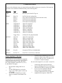
Integer
Assignment
0
1
2
3
4
5
6
7
Trigger Input
T0 Output
A Output
B Output
AB and -AB Outputs
C Output
D Output
CD and -CD Outputs
GPIB allows the user to see data received via
the GPIB and to set the GPIB address
STORE and RECALL provide a convenient
method to save all of the instrument
settings.
GUIDE TO OPERATION
INTRODUCTION
The DG535 Digital Delay and Pulse Generator
can provide four precisely timed logic
transitions, or two precisely controlled pulses.
The four digitally controlled time intervals may
be programmed from the front panel or via the
GPIB. Front panel BNC's provide high slew rate
outputs at TTL, NIM, ECL or continuously
adjustable levels. The outputs may be set to
drive either 50Ω or high impedance loads.
Detailed descriptions of each of these menus will be
given.
DATA ENTRY KEYS
Sixteen keys are used to enter and modify data.
There are three modes of operation for this keypad:
the mode is indicated by the three LED's in the
center of the panel. The cursor mode (< >) allows
individual digits to be modified in a fashion similar
to the operation of thumbwheel switches. The
numeric mode (NUM) allows the data to be entered
as a numeric string. The remote mode (REM) lets
the GPIB controller lock-out front panel operation.
The key beneath the Mode LED's allows the user to
change the keypad mode, if not locked-out by the
GPIB controller.
The high accuracy (1 ppm), precision (5 ps),
wide range (0 to 1000 s), and low jitter (50 ps
rms) recommend the DG535 as the solution to
many difficult timing problems in science and
industry.
FRONT PANEL OPERATION SUMMARY
POWER BUTTON
TRIGGER STATUS
The unit is turned on by depressing the POWER
button. All instrument settings are stored in
nonvolatile RAM, and so the settings are not
affected by turning the power on and off. The
model, firmware version, and serial numbers for
the unit will be displayed briefly when the
power is first applied.
Five LED's are used to indicate the trigger status.
The TRIG LED blinks each time the unit is
triggered, the BUSY LED is on whenever a timing
cycle is in progress, the RATE LED is lit if a trigger
is received while BUSY. The INT LED indicates
that the internal rate generator is the trigger source,
and the 50Ω LED is on when the EXT TRIG input
is terminated in 50Ω. The EXT TRIG BNC is the
input for external triggers.
LIQUID CRYSTAL DISPLAY
The 20 character LCD is the user interface for
all front panel programming operations. The
wide viewing angle LCD is backlit by an
electroluminescent panel for convenient
operation in low light level conditions. When
the keypad is in the cursor mode, the contrast of
the LCD may be adjusted for optimum viewing
by the two right most keys on the front panel.
DELAY OUTPUTS
There are five delay output BNC's: T0, A, B, C and
D. T0 marks the start of the timing interval and is
most useful when an internal trigger source has been
selected. The logic transitions at the outputs of A, B,
C and D may be set from 0 to 1000s in 5 ps
increments with respect to T0. The outputs may be
programmed for TTL, NIM, ECL or adjustable
output levels, and can drive 50Ω or high impedance
loads. The polarity of each output may be set to
provide a rising or a falling edge when the channel
times out. The outputs will remain asserted until 800
ns after the longest delay.
MENU KEYS
Six Menu Keys select the function to be
programmed. Most menu items are selfexplanatory:
TRIG defines the trigger source
DELAY is used to adjust the four digital
delays
OUTPUT sets the output pulse levels
1
for instructions on selecting the correct line voltage
and fuse.
PULSE OUTPUTS
There are four, pulse output BNC's: AB, -AB,
CD and -CD. The AB output provides a pulse
for the interval between the time set for channel
A and channel B. The CD output provides a
pulse for the interval between the time set for
channel C and channel D. These outputs allow
the DG535 to generate two precisely timed
complementary pulses.
IEEE-488 STD PORT
The 24 pin IEEE-488 rear panel connector allows a
computer to control the DG535. The command
syntax for the GPIB transactions is detailed in the
programming section of this manual. The address of
the instrument on the GPIB is set from the front
panel by the GPIB menu.
OPTION 06 - TRIGGER INHIBIT INPUT
10.000 MHz REFERENCE
If the DG535 was ordered with the option 06,
there will be a BNC connector located directly
under the power button on the front panel to
which the trigger inhibit input is applied. This
input is active low and is used to disable the
trigger mode. A TTL low inhibits triggers while
a TTL high permits triggers. If there is no input
signal, the input floats high and all triggers are
enabled.
Internal or external references may be used as the
timebase for the digital delays. If the internal
timebase is to be used, the rear panel switch should
be in the INT position. In this position, the 10.000
MHz internal timebase will be appear as a 1V p-p
square wave at the rear panel BNC. This output is
capable of driving a 50Ω load, and may be used to
provide the same timebase to several DG535's.
An external reference may be applied to the DG535
by placing the switch in the EXT position. A 10.0
MHz, ±1%, reference with a 1 Vp-p amplitude must
be applied to the rear panel BNC which now serves
as a reference input. If the external reference has
insufficient amplitude, or is more than a few percent
off the nominal 10.0 MHz, then the message "Ext
Clk Error" will appear on the LCD until the problem
REAR PANEL FUNCTIONS
POWER ENTRY MODULE
The power entry module is used to fuse the line,
select the line voltage, and block high frequency
noise from entering or exiting the instrument.
Refer to the section at the front of this manual
2
most important current factor. In this case, the
average current is given by:
is remedied.
To use the timebase in one DG535 as the
timebase for several DG535's, set the switch on
the "master unit" to the INT position. Use coax
cables to daisychain the 10.000 MHz output
from the "master unit" to the other DG535's
whose switches are all set to the EXT position.
Use a 50Ω terminator to terminate the 50Ω line
at the last unit on the daisychain.
I = 2Vtƒ / Z
where, V is the pulse step size, t is the length of the
cable in time (5 ns/meter for RG-58), ƒ is the pulse
repetition rate, and Z is the cable's characteristic
impedance (50Ω for RG-58).
FRONT PANEL PROGRAMMING
OPTION 02 - ±32 Volt Rear Panel Outputs
Pressing a new menu key will take you to the "top"
menu for that item. Each successive press of the
same menu key will take you to the "next" submenu
for that item. The power-up menu will be the same
menu that was displayed when the unit was last
turned off.
If the DG535 was ordered with the option 02,
there will be five rear panel BNC's to provide
amplified outputs for T0, A, B, C and D. These
outputs have nominal adjustable output
amplitudes from -32 to +32 Volts. The pulse
width is approximately 1 µs, and the leading
edge has a transition time of 2 to 3 ns. The
outputs are designed to drive 50Ω loads,
however, if the cable is terminated into a high
impedance load, the pulse amplitude will double
(up to 64 Volts) for a duration equal to the
round trip cable delay. The amplitude of the
output pulse is reduced by 2 Volts per mA of
average output current: the average output
current is only 0.7 mA for a 32 Volt output into
50Ω at a 1 kHz repetition rate. For high
impedance terminations, charging and
discharging of the cable capacitance may be the
The Keypad mode (cursor or numeric) will be the
same as it was the last time the menu item was
accessed. Some menu items only allow one type of
keypad mode, for example, the GPIB address may
only be entered in the numeric mode.
In the cursor mode, only the keys with arrows are
active. The keys with the green arrows are used to
modify the displayed value (up/down) or to move
the cursor (left/right). The two keys with grey
arrows are used to adjust the LCD display contrast.
3
and digits more than three places beyond the
decimal point will be truncated.
In the numeric mode, the entire keypad is active.
Data may be entered as a floating point number
or in exponential notation. Entered data may be
edited by using the BSP (backspace) key.
Backspacing past the left edge of the screen will
cancel the command. The entered data is
actually used when the EXC (Execute) key is
pressed. Selecting another menu item will have
the same affect as pressing the EXC key.
The External trigger mode has three submenus to
specify the threshold, slope and termination
impedance of the external trigger input. Each
submenu is selected by pressing the TRIG key. The
Threshold may be entered as a floating point number
or may be modified in the cursor mode. The Slope
may be selected by using the cursor (up/down) keys,
as can the Trigger termination impedance. The
threshold, slope, and termination impedance shown
in the example menus would be appropriate for
triggering on the rising edge of a TTL Pulse.
Error messages will appear on the LCD to
indicate improper commands. For example, an
attempt to decrement a delay below zero will
generate the error message "Delay Range Error".
The error message may be cleared from the
LCD by pressing any key.
The Single-Shot trigger mode has only one
submenu. If SS is selected by the cursor, pressing
the TRIG menu key will display "Single Shot
(EXC)." Now each press of the execute key will
trigger the timing cycle.
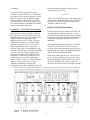
TRIGGER MENU
The "top" line on the trigger menu is:
The Burst mode has three submenus to specify
trigger rate, number of pulses per burst, and number
of periods between the start of each burst of pulses.
All of the items may be entered in the numeric
mode, or modified in the cursor mode. The Rate
may be entered in floating point or exponential
notation, and may be specified to four digits of
precision. For the entries shown in the above menu
example, there would be 10 pulses per burst, each
pulse separated by 100 µs, and a new burst of pulses
would start every 20 periods, i.e. every 2 ms.
Int Ext SS Bur Line
The cursor, underlines one of the five modes in
the list to indicate Internal, External, SingleShot, Burst, or Line trigger. The left and right
cursor keys may be used to change the mode.
Subsequent menus, which are different for each
trigger mode, are selected by pressing the TRIG
menu key again.
TRIGGER SUBMENUS
Mode
Menu Example
Int
Rate =10000.000Hz
Ext
Threshold =+1.00V
Slope(±) = +
Trigger Term = HighZ
SS
Single-Shot (Exc)
Bur
Rate =10000.000Hz
Pulses/Burst
10
Periods/Burst 20
The Line trigger mode has no submenus. The unit
will be triggered on a zero crossing of the power line
at the line frequency. The line trigger is also
synchronized to the internal 80 MHz timebase, so
that the timing jitter of the delay outputs in this
trigger mode will be very low (typically 25 ps rms).
TRIGGER TRICKS
Line
There are several techniques that may be used to
extend the versatility of the DG535's trigger modes.
The Jitter of the delay outputs will be reduced by
about a factor of two (to less than 25 ps rms) if the
unit is triggered synchronously with the 10 MHz
time base. This is done automatically if the Line
Trigger is selected. You may also want to arrange
your external trigger so that it is synchronous with
the 10 MHz output on the rear panel (if the internal
time base is being used).
(No submenu)
The Internal trigger mode has only one submenu
to set the trigger rate. The rate may be entered in
the numeric mode or modified in the cursor
mode. Only four digits of precision are allowed,
4
allowed, as B is linked to channel A in the second
menu.
It is often desirable to trigger the unit at a submultiple of the trigger source. Suppose you wish
to trigger a laser at 10 Hz synchronously with
the zero crossing of the power line. In this case
you would select the Line Trigger, and set
channel D's delay to 95 ms. Once triggered, the
DG535 will ignore other triggers until all
channels have timed out, hence every sixth Line
trigger (at 60 Hz) will cause a new timing cycle.
The RATE error LED on the front panel will be
illuminated to indicate that triggers occurred
while the unit was busy. Trigger rates up to
100 MHz can be used, with the unit ignoring all
triggers until all channels have timed out, as in
the above case.
Delay can be scrolled by first selecting the delay
menu, positioning the cursor under the digit to be
incremented. Depress the #5 and either the up or
down keys simultaneously. The step rate will be
approximately 4 Hz, and may vary during a scan.
OUTPUT MENUS
The output menus are used to specify the load
impedances, pulse output amplitudes, offsets, and
polarities for each of the front panel BNC's. The
cursor (left/right) keys are used in the "top" line of
the OUTPUT menu to select which output is to be
programmed. Successive presses of the OUTPUT
key will access each menu line for the selected
output, finally returning to the "top" line.
DELAY MENUS
There are four delay menus to specify the delays
for channels A, B, C and D. Each delay may be
entered in floating point or exponential notation
or may be modified in the keypad cursor mode.
The maximum time delay is
999.999,999,999,995 seconds, which may be set
with a resolution of 5 ps.
The menu items for the T0, A, B, C and D output
are virtually identical. An example of these menus
is given here for channel A's output:
A:load= High Z
A:TTL NIM ECL VAR
A:Inverted Normal (if TTL, NIM or ECL is
selected)
A:Amplitude = +1.00V (if VARiable is selected)
A:Offset = 0.50V (if VARiable is selected)
Example Delay Menus
A=T0+0.123456789125
B=A+0.001000000000
C=T0+123.456789123455
D=C+0.000000010000
The first line in this submenu specifies the load
impedance. The cursor (up/down) keys are used to
select between High Z and 50Ω loads. This is a very
important step in setting up the output: the wrong
choice will cause the output to have half the
expected amplitude, or to misbehave entirely.
Any delay channel may be "linked" to another
channel. Two examples of this are shown in the
above sample menus. While A is referenced to
T0, channel B's delay is set to A's delay plus
0.001 seconds. Linking provides a convenient
method to specify a pulse output (AB) as a pulse
start time and width rather than start and stop
times. Now, if channel A's delay is modified, B's
delay moves with it, so that the pulse width
stays at 0.001 seconds. With the above settings,
the CD output will produce a very accurate 10
ns pulse despite the very long delay which is
specified for channel C.
The cursor (left/right) keys are used in the second
submenu to select either standard logic levels for the
output, or continuously variable offsets and
amplitudes. If either the TTL, NIM or ECL logic
levels are selected, the next submenu is used to
specify the polarity of the output pulse: the
"Normal" polarity will provide a rising edge at the
output at the set time: "Inverted" polarity will
provide a falling edge.
To change the linkage, the cursor is positioned
beneath the character just to the right of the
equal sign, and the cursor up/down keys are
used to select from the available links. Not all
links are available, for example, in the above
menus linking channel A to channel B is not
If VAR (variable) is selected in the second
submenu, then subsequent submenus allow the pulse
amplitude and offset to be set. Both numbers may be
entered as floating point numbers or may be
modified by the cursor keys. The minimum
5
amplitude is 100 mV, the maximum amplitude
is 4.00 VDC, and outputs outside the range of -3
to +4 VDC are not allowed.
GPIB MENUS
There are three menus which are accessed by the
GPIB key. They are:
AB and CD OUTPUTS
Data:_______________
GPIB Address: 15
Service RQST: (EXC)
The menus for the AB and CD outputs are
similar to the other outputs. Example menus for
the AB output are shown on the following page:
The first menu displays the last 15 characters of data
that have been received over the GPIB. 256
characters are retained in memory and may be
viewed by scrolling the display window with the
cursor keys. Spaces and control codes will not be
displayed, however special characters for carriage
returns and line feeds will be displayed. This feature
is very useful when debugging computer programs
that control the DG535.
AB&-AB Loads = High Z
AB: TTL NIM ECL VAR
AB:Amplitude = +1.00V (if VARiable is
selected)
AB:Offset= +0.50V (if VARiable is selected)
The cursor (up/down) keys select the load
impedance for both the AB and -AB outputs. It
is very important that if a 50Ω load is specified,
that a 50Ω load be present on BOTH the AB
and the -AB output BNC's.
The GPIB address may be set in the second menu.
The keypad is automatically placed in the numeric
mode for this menu item. Any address from 1 to 30
may be entered: the default address for this
instrument is 15.
The cursor (left/right) keys select the logic
levels for the AB and -AB outputs. If TTL, NIM
or ECL is selected, then no further submenus are
needed to specify the outputs: both the
"Normal" and "Inverted" logic levels are
available at separate front panel BNC's. If VAR
is selected, then the next two submenus are used
to set the amplitude and offset of the outputs.
The third menu allows the user to generate a service
request by pressing the EXC button (lower right on
the front panel). A service request is used to attract
the attention of the GPIB controller.
6
which detract from this ideal performance, are
discussed here.
STORE and RECALL MENUS
There are ten storage locations from which
setup data may be recalled. One of these
locations, number 0, contains default setup data,
the other nine locations contain setup
information that was stored by the user. Because
the information is stored in nonvolatile RAM, it
will be available for recall even if the instrument
is turned off.
ACCURACY
The error in the time delay between any two outputs
is less than (1500 ps [500 ps typical] + Timebase
error x Time between Outputs). (This specification
is exclusive of time shifts due to slew rates at the
outputs, i.e., it should be measured with both
outputs set for the same logic levels driving the
same loads). The timebase error depends on the
timebase being used:
All of the instrument's settings are stored, even
those which are not currently active: for
example, the external trigger threshold is saved
even though the instrument is operating on
internal trigger.
Standard
Option 03
External
Operating data is stored by pressing the STORE
key, one digit (1-9) to specify the storage
location, and the EXC (execute) key. Mistakes
may be edited with the BSP (backspace) key.
<25 ppm 0-50 °C
<1 ppm
0-50 °C
Source spec + 0.0002ppm
Using the typical error figure, for a time delay of 1.0
ms, this table implies an absolute error of ±25 ns,
±1.5 ns and ±0.5 ns respectively for the standard,
optional and external timebases (assuming a 0.01
ppm external source specification). If A=100.000µs
and B=100.01µs, the error with respect to T0 will be
±2.6 ns with the standard timebase, however the
accuracy of A with respect to B will be ±500 ps.
Instrument settings are recalled from storage by
pressing the RECALL key, one digit (0-9), and
the EXC (execute) key. If the stored data has
been corrupted since it was saved, the error
message "Recall Error" will be displayed. The
error message can be removed by pressing any
key. A defective Lithium battery or very noisy
ac line voltages will cause "Recall Errors".
A graph showing the maximum time error as a
function time delay is shown in Figure 3. The four
curves show the time error for the standard,
optional, 0.01 ppm external, and ideal external
timebases. The excess error for time delays longer
than 1 second on the "ideal external source " curve
is due to drift in the analog jitter compensation
circuits.
ACCURACY, DRIFT, AND JITTER
Each of the delay channels, A, B, C and D, may
be programmed to time out from 0 to 1000
seconds with a resolution of 5 ps. The factors,
7
Figure 4 shows the shape of the Gaussian
distribution and the relations between the rms jitter
and the peak-to-peak jitter.
TIMEBASE DRIFT
The drift of the timebase over several hours is
substantially less (x10 to x100 less) than the
absolute timebase error. The major factor in the
timebase drift is the instrument's temperature:
after the instrument has warmed up, the
timebase drift is about 0.5 ppm/°C for the
standard timebase, and about 0.05 ppm/°C for
the optional timebase. The drift between several
DG535's which are used in the same experiment
may be eliminated by daisychaining the
reference output from one DG535 to the
reference input on the other DG535's.
The rms jitter, σ, is a function of the delay setting.
The jitter is about 50 ps rms for delays less than100
µs. For short delays, the peak-to-peak jitter
measured on an oscilloscope is about four times the
rms jitter. For long delays, the observed jitter
measured on an oscilloscope is
primarily due to the jitter of the oscilloscope's
horizontal (timebase) deflection circuits. For a good
300 MHz oscilloscope, the rms jitter is typically (25
ps + 10 ppm of the time base).
JITTER
The rms jitterm, as a function of time delay, is
shown in Figure 5 for a Tektronix 2465
oscilloscope, the DG535 using an internal timebase,
and for a DG535 with an ideal external source. The
jitter for time delays longer than 10 seconds, using
the ideal external source, is due to the drift of the
analog jitter compensation circuits in the DG535. It
can be seen from this figure that the Tek 2465 scope
would show an apparent jitter of 1 ns rms at 100 µs
even though the DG535's jitter is only 50 ps rms.
Various noise sources in the DG535 modulate
the time delay for the outputs causing "jitter".
Some of these noise sources are common to all
of the channels, others are independent. The
distribution of the pulses around the desired
time can be approximated by a Gaussian (or
"normal") distribution:
CHANNEL to CHANNEL INTERACTION
where,
p(t)= probability of pulse occurring at time t
T = set time for the output (mean value)
σ = standard deviation of the distribution
There is a small interaction (pulling) between
channels A and B and between channels C and D
when these channels are set within 10 ns of each
8
other. The pulling of one channel by the other is
typically less than 100 ps.
TIME DELAY vs REPETITION RATE
The time delay for any channel may change by
200 ps as the pulse repetition rate is changed
from single shot to the maximum rate of 1/(1 µs
+ longest delay). The burst mode of triggering
is, effectively, a rapid change of the pulse
repetition rate.
9
GPIB:
GPIB PROGRAMMING
DETAILED COMMAND LIST
In all of the commands listed here, i, j and k are
integer values and f, t and v may be integer,
floating point or exponential notation. Optional
parameters are enclosed in curly brackets. In
general, if optional parameters are omitted then
the current value of those parameters will be
sent back to the GPIB controller. For example,
the command "TM 3" sets the Trigger Mode to
mode 3 while the command "TM" will return
the response "3".
GT{i}{,j}{,k}
Specify one to three ASCII codes, which will
terminate each response from the DG535. The
default terminator for any response from the DG535
is a carriage return and a line feed. The line feed is
accompanied by an EOI. Example: to change the
terminator to line feed only, the command would be
"GT 10" (the ASCII code for line feed is 10
decimal). The EOI is always sent with the last
character of the terminator sequence.
Command errors will be reported in the Error
Status Byte. The controller should verify that
the Error Status Byte is zero after each
command is sent: a nonzero value indicates a
programming problem. When an error is
detected, all of the pending commands in the
communication buffer are cancelled.
STATUS COMMANDS
ES
Returns the Error Status byte. The error status byte
definition is given below. Example: if a command
was sent to the DG535 with too many parameters,
bit 1 would be set. If the ES command is used to
read the error status, and no other errors had
occurred, the value "2" would be returned. All bits
in the Error Status byte are latched and so will
remain set until the "ES" command is executed. All
bits are reset to zero after the "ES" command is
executed.
Also, blanks are ignored, case is ignored,
multiple commands may be sent on one line if
separated by semicolons. All responses are
terminated by a carriage return and line feed.
The line feed is sent with an EOI.
INITIALIZATION COMMANDS
ES i
Returns bit i of the Error Status Byte. Example: the
command "ES 5" can be used to check for a delay
range error. If a delay range error had occurred since
the last ES or ES 5 commands had been sent, then a
"1" would be returned, otherwise the value "0"
would be returned. This command also resets the
error bit that is being checked.
CL
Clear instrument. The communication buffers
are cleared and the default settings are recalled.
The instrument default settings are:
Trig:
Internal:
Burst Mode:
External:
Delays:
Outputs:
The GPIB address is not
affected, but the terminator is
returned to its default value of a
carriage return and a line feed with
an EOI.
Trigger mode set to
Single-Shot (ie. triggers
are off)
The default trigger rate is
10,000 Hz
Trigger rate = 10,000Hz, 10
pulses per burst and 20
periods per burst.
+1VDC, positive slope,
high impedance
termination.
All delays, A, B, C and D
are linked to T0 and set to
zero.
All outputs are set to drive
high impedance loads to
TTL levels.
ERROR STATUS BYTE DEFINITION
Bit Description
7
6
5
4
3
2
1
0
10
Always zero
Recalled data was corrupt
Delay range error
Delay linkage error
Wrong mode for the command
Value is outside allowed range
Wrong number of parameters
Unrecognized command
command to test one bit of the Instrument Status
byte.)
Bit 6: This bit is set if the RC (recall stored
settings) command finds that the stored values
have been corrupted. A checksum is done on the
settings when they are stored, and if the
computed checksum on recall does not match,
then the command is aborted and this error bit is
set.
IS i
Returns bit i of the Instrument Status Byte.
Example: the command "IS 4" will test bit 4, the
"trigger rate too high" bit. The value "1" will be
returned if a trigger rate error occurred since the last
time the "IS" or "IS 4" command was sent. If no
error had occurred, then the value "0" will be
returned.
Bit 5: This bit is set if an attempt is made to set
a delay to a value below zero or above
999.999,999,999,995 seconds. Because the
delay channels may be linked to each other,
changing a delay to an allowed value may cause
another delay to exceed the allowed range of
values.
INSTRUMENT STATUS BYTE DEFINITION
Bit Description
7
6
5
4
3
2
1
0
Bit 4: This bit is set if an attempt is made to link
delays in an illogical fashion. For example
A=B+1.000 and B=A+2.000 is a condition
which clearly cannot be satisfied.
Bit 3: This bit is set if the instrument is not in
the correct mode for the command that was sent.
For example, if the instrument set to trigger on
the internal rate generator, the SS (single shot)
command will be ignored and cause bit 3 to be
set.
Memory contents corrupted
Service request
Always zero
Trigger rate too high
80MHz PLL is unlocked
Trigger has occurred
Busy with timing cycle
Command error detected
Bit 7: This bit is set if the instrument settings were
corrupted since the last time power was removed.
The processor computes a checksum of RAM
contents, which contain the instrument settings,
when a power supply dropout is detected. The
checksum is again computed on power-up. If the
checksums do not match, then the default settings
are used (see CL command for default settings) and
the message "Memory Failure" is displayed. A
defective Lithium battery or very noisy ac line
voltages may cause "Memory Failures" to occur.
Bit 2: This bit is set if the value of a parameter
exceeds the allowed range for that parameter.
For example, if the command "TL 20.0" is sent,
the command will be ignored and bit 2 will be
set (because the trigger level may only be set
between ±2.56VDC).
Bit 1: This bit is set if too many or too few
parameters are sent with a command.
Bit 6: This bit is set if the unit is currently
requesting service of the GPIB controller. A service
request may be generated by a variety of conditions
as specified by the service request mask. This bit
allows the controller to see if this instrument was
the one that asserted the service request line on the
GPIB.
Bit 0: This bit is set if the command is
completely unrecognized.
IS
Returns the Instrument Status byte. The
definition of the instrument status byte is given
below. Example: if the trigger rate to the DG535
is too high, bit 4 of the instrument status byte
will be set. Sending the command "IS" will
return the value "16" (if no other bits have been
set). All of the bits in the instrument status byte,
except for the BUSY bit, are latched, ie., if a
trigger rate error is detected at any time, that bit
will stay set until the "IS" command is sent. All
bits, except the BUSY bit, will be reset to 0 after
the "IS" command is executed. (See the IS i
Bit 4: This bit is set if the trigger rate is too fast. The
instrument requires one microsecond after the last
delay has finished to reset all the delay channels. If a
trigger comes during this time, then the front panel
RATE LED will be turned on and bit 4 will be set.
Bit 3: This bit is set if a gross error is detected in the
80MHz PLL. This can happen if the rear panel
switch is set to EXT reference, and the applied
11
SM {i}
Set Status Mask for service request to i. The service
request status mask is used to specify which
Instrument Status bits will generate a GPIB service
request. For example, if the command "SM 16" is
sent, then a service request will be generated if the
"trigger rate too high" bit is set. When a service
request is generated, the corresponding bit in the
Service Request Mask is turned off. This will
prevent an uncontrolled stream of service requests
from being generated by the DG535. To re-enable
the service request, the controller must again set the
service request mask with the "SM i" command.
10.0MHz reference is too small or more than a
fewpercent off the nominal 10.0MHz. If this
occurs, the LCD will display the message "Ext
Clk Error".
Bit 2: This bit is set whenever a trigger occurs
that starts a delay cycle. Triggers, which occur
during a delay cycle, do not set this bit, rather
they will set bit 4, the rate error bit.
Bit 1: This bit is set if the unit is currently busy
with a timing cycle. Unlike all of the other
status bits, it is not latched (rather it reflects the
current status of the unit) and it is not reset
when read by the IS command (it is reset when
the unit finishes the current timing cycle.)
CS {i}
Set Cursor Mode (i=0) or Number mode (i=1). The
unit must be in the cursor mode (CS 0) for the SC,
MC, or IC commands to work. Note that certain
menu items allow only one type of cursor mode. For
example, there is no numeric mode for the menu
item, which selects between TTL, NIM, ECL and
VAR outputs, and there is no cursor mode in the
STORE and RECALL Menus. Selecting an
Bit 0: This bit is set if a command error is
detected. If this bit is set, the controller should
read the Error Status Byte to determine the exact
nature of the command error. Command errors
can originate from either the GPIB or from front
panel interactions.
DISPLAY CONTROL COMMAND
DL {i, j, k}
Select Display to show menu i, submenu j, line k. The menu, submenu, and line number designations are
given in the table below:
DISPLAY LINE SELECT TABLE
i j k
Display Example
Comment
000
Int Ext Ss Bur Line
Trigger Mode Menu
010
020
021
022
Rate =1234000.123Hz
Threshold = +1.23V
Slope(±) = +
Trigger Term = 50Ω
Internal Trigger Rate
External Trigger Menu
030
Single Shot (EXC)
Single Shot Trigger
040
041
042
Rate =1234000.000Hz
Pulses/Burst
12345
Periods/Burst 12345
Burst Trigger Menu
100
101
102
103
A = T+123.456789123450
B = A- 0.123456789125
C = B+ 23.456789123455
D = T+ 0.000000000005
Delay Menus
12
i j k
Display Example
Comment
200
T0 A B AB C D CD
Output Menu Select
210
211
212
213
214
T0: Load = 50Ω
T0: TTL NIM ECL VAR
T0: Amplitude = +1.23
T0: Offset = -2.00
T0: Inverted Normal
T0 Output Control Menus
220
221
222
223
224
A: Load = 50Ω
A: TTL NIM ECL VAR
A: Amplitude = +1.23
A: Offset = -2.00
A: Inverted Normal
230
231
232
233
234
B: Load = 50Ω
B: TTL NIM ECL VAR
B: Amplitude =+1.23
B: Offset = -2.00
B: Inverted Normal
240
241
242
243
AB & -AB Loads = 50Ω
AB: TTL NIM ECL VAR
AB: Amplitude = +1.23
AB: Offset = -2.43
AB output control menu
250
251
252
253
254
C: Load = 50Ω
C: TTL NIM ECL VAR
C: Amplitude = +1.23
C: Offset = -2.00
C: Inverted Normal
C Output Control Menus
260
261
262
263
264
D: Load = 50Ω
D: TTL NIM ECL VAR
D: Amplitude = +1.23
D: Offset = -2.00
D: Inverted Normal
270
271
272
273
CD & -CD Loads = 50Ω
CD: TTL NIM ECL VAR
CD: Amplitude = +1.23
CD: Offset = -2.43
CD output control menu
300
301
302
Data: GPIB Strings
GPIB Address = 15
Service RQST (EXC)
GPIB Menu
400
500
Store
Recall
Store Menu
Recall Menu
(Only if VAR selected)
(Only if VAR selected)
(For TTL, NIM, and ECL)
A Output Control Menus
(Only if VAR selected)
(Only if VAR selected)
(For TTL, NIM, and ECL)
B Output Control Menus
(Only if VAR selected)
(Only if VAR selected)
(For TTL, NIM, and ECL)
(Only if VAR selected)
(Only if VAR selected)
(For TTL, NIM, and ECL)
D Output Control Menus
(Only if VAR selected)
(Only if VAR selected)
(For TTL, NIM, and ECL)
13
Integer
0
1
2
3
4
5
6
7
incorrect cursor mode will have no effect: the
error will not be reported in the error status
byte.
SC {i}
Move cursor to column i= 0 to 19. This
command allows the controller to position the
cursor under a particular digit (usually in a
DELAY menu) so that the digit may be
incremented or decremented by the "IC"
command. A request to position the cursor in a
non-allowed location (for example, under the
decimal point in a time delay menu) will result
in a "value outside of allowed range" error,
setting bit 2 in the Error Status byte.
Assignment
Trigger Input
T0 Output
A Output
B Output
AB and -AB Outputs
C Output
D Output
CD and -CD Outputs
DELAYS
DT i{,j,t}
Delay Time of channel i is set to t seconds relative
to channel j. Example: DT 3,2,1.2E-6 will set
B=A+0.000,001,200,000 seconds. The command
DT 2,1,10.5 will set A=T0+10.500000000000
seconds. Setting delays shorter than 0 or longer than
999.999,999,999,995 seconds will set bit 2 of the
Error Status Byte.
MC i
Move cursor left (i=0) or right (i=1). This
command allows the cursor to be moved relative
to its present position.
IC i
Increment (i=1) or decrement (i=0) the digit at
the current cursor location. This command is
used to change a displayed parameter in a
manner analogous to operating a thumbwheel
switch.
A "Delay Linkage Error", bit 4 of the Error Status
Byte, is caused by an attempt to totally disconnect a
time reference from T0. For example the commands
DT 2,3,1.5 ; DT 3,2,2.5 attempt to reference A to B
and B to A so that neither is referenced to T0. This
command sequence would generate a "Delay
Linkage Error".
DS string
Display a string of 1 to 20 characters. This
command allows the controller to display a
message on the DG535's liquid crystal display.
As with all data that is sent to the DG535,
spaces will be stripped from the transmitted
data, so the program should use the underline
character to_separate_words. Also, do not use
semicolons, as they are reserved characters
which allow several characters to be sent on the
same line.
An efficient method to change a delay is to position
the cursor under a digit (using the SC command) and
then increment/decrement the digit (using the IC
command).
OUTPUT CONTROL
TZ i{,j}
Set the Termination Impedance. Output i is
configured to drive a 50Ω load (j=0) or a high-Z
load (j=1). (If i=0, this command is used to set the
impedance of the external trigger input: see the
Trigger control section). Example: "TZ 4,1" will
configure both the AB and -AB outputs to drive high
impedance loads. The command "TZ 4" will then
return the response "1", indicating that the AB and AB outputs are configured to drive high impedance
loads.
If the "DS" command is sent without a string,
then the display will be cleared and the menu
item which was displayed before the "DS string"
command was used will be displayed.
DELAY AND OUTPUT COMMANDS
The Delay and Output commands use integer
codes, which are assigned to each front panel
BNC. The table for these assignment is given
below.
OM i{,j}
Set Output i to Mode j where j=0-3 for TTL, NIM,
ECL, or VARiable. This command sets the logic
level of the front panel outputs. If TTL, NIM or
14
ECL is selected, the polarity of the logic output
is specified by the "OP" command. If the
VARiable output mode is selected, then the
output amplitude and offsets may be set with the
"OA" and "OO" commands. Example: the
command "OM 6,0" selects TTL levels (0 to
4VDC) for the D output.
TRIGGER COMMANDS
TM {i}
Set Trigger Mode to Int, Ext, SS or Bur (i=0,1,2,3).
This command selects between Internal, External,
Single-Shot, or Burst trigger modes. Other trigger
commands are then used to completely specify the
trigger conditions: TR will set the internal trigger
rate, TL and TS set the trigger level and trigger
slope for external triggers, SS is used to execute a
single shot if in the SS mode, and BC and BP set the
burst count and burst period for the burst mode. The
TR, TL, TS, BC, and BP commands may be
executed at any time, regardless of the trigger mode.
Example: The command "TM 0" selects the internal
rate generator as the trigger source.
OA i{,v}
Amplitude of output i is set to v Volts if in the
VARiable mode. This command is used to set
the amplitude, i.e. the size of the step, at an
output BNC. The maximum step size is limited
to ±4 Volts: the minimum step size is ±0.1VDC.
The specified step size must not cause the
output level (including the programmed offset)
to exceed +4V or -3V. Example: the command
sequence "OM 5,3; OO 5,0 ; OA 5,4.0" will
select the VARiable mode for output C, zero its
offset (see below) and set its amplitude to
4.0VDC. Note the importance of setting the
offset: if the offset was set to a level greater
than zero, the command "OA 5,4.0" would
generate an error because the programmed offset
plus amplitude would exceed the +4VDC
maximum.
TR i{,f}
Set Internal Trigger Rate (i=0) or Burst Trigger Rate
(i=1) to f Hz. The frequency may be any value
between 0.001 Hz and 1.000MHz. The precision is
0.001Hz below 10Hz, or 4 digits if above 10Hz.
Other digits will be truncated. The internal rate
generator will settle to the programmed value within
2 seconds after the command is executed: significant
departures from the programmed value may be
expected during the 2 second settling period. (A
simple way to disable triggers during this settling
time is to select the single-shot trigger mode, i.e.
"TM 2".) Example: the commands "TM 0; TR
0,100.2" will select the internal trigger mode and set
the trigger frequency to 100.2Hz.
OO i{,v}
Output Offset of output i is set to v Volts if in
the VARiable mode. This command is used to
set the offset of an output when in the VARiable
mode. For pulses which have a rising edge
output, the offset is the voltage between the
lowest output level and ground, and so a TTL
signal has zero offset and +4VDC amplitude,
while an ECL signal has -1.8VDC offset and a
+1VDC amplitude. To invert the polarity of the
pulse, i.e. for a falling edge output, a TTL
output is described as a +4VDC offset an a 4VDC amplitude pulse, and an inverted ECL
pulse is described by a -0.8VDC offset with a 1.0VDC amplitude.
TL {v}
Set External Trigger Level to v Volts. This
command sets the threshold voltage for external
triggers. To completely specify the external trigger,
the TS (trigger slope) command must also be used.
Example: "TM 1; TL 1.00; TS 1" specify the
external trigger mode, with the trigger level at
1.00VDC, with a positive slope. These values would
be appropriate for triggering on the rising edge of a
TTL logic pulse. (Also see the TZ 0{,j} command
which sets the input impedance for external
triggers.)
OP i{,j}
Output Polarity of channel i is inverted (j=0) or
normal (j=1) for TTL, ECL or NIM outputs.
This command sets the polarity of logic pulses
at the BNC outputs. In all cases, normal polarity
means that the output will provide a rising edge
at the specified time. Example: the command
sequence "OM 5,2; OP 5,0" will set the C output
for an inverted ECL output, i.e., the output goes
from -0.8VDC to -1.8VDC when the channel
times out.
TS {i}
Trigger Slope set to falling (i=0) or Rising Edge
(i=1). This command selects the slope condition for
external triggers. It is used with the TM, TL and TZ
commands to specify the conditions for an external
trigger. Example: the command "TM 1; TL -1.2; TS
1; TZ 0,0" specify the external trigger mode, a
trigger level of -1.2VDC, a positive trigger slope,
15
and a trigger input impedance of 50Ω to ground.
These trigger conditions would be appropriate
for triggering on the rising edge of an ECL logic
pulse (if it is able to drive a 50Ω load to
ground.)
at least one larger than the Burst Count. Example:
the command "TM 3; TR 1,1E5; BC 100; BP 101"
sets the burst mode of operation with a trigger rate
of 100KHz. There will be 100 pulses in each burst,
one trigger will be skipped, and a new burst of
pulses will start.
TZ 0{,j}
Set the input impedance of the external trigger
input to 50Ω (j=0) or high impedance (j=1).
Example: the command "TZ 0,1" will set the
input impedance to 1 MΩ, the command "TZ
0,0" will set the input impedance to 50Ω.
STORE and RECALL COMMANDS
ST i
Store all instrument settings to location i=1 to 9.
This command allows nine complete setups to be
stored in the instrument's nonvolatile RAM. All of
the instrument's settings are stored, even those that
are not currently active: for example, the trigger
level for external triggers will be stored even though
the instrument may be operating on internal trigger.
Example: the command "ST 3" will save all the
instrument settings to the third storage location.
SS
Single-Shot trigger if Trigger Mode = 2. Each
time this command is issued, a new delay cycle
will be initiated (if one is not already in
progress) provided that the single shot trigger
mode has been selected. Example: the
commands "TM 2; SS; SS; SS" will place the
instrument in the single-shot mode and trigger it
three times.
RC i
Recall all settings from location i=1 to 9. Default
settings may be recalled from location 0. (See the
CL command for the values of the default settings
that are recalled from location 0.) Example: the
command "RC 3" will recall all of the instrument
settings which were last stored by the ST command
to location 3. The display will show the menu item
that was active when the ST 3 command was
executed. It is possible that the memory contents
of the stored settings were corrupted between the
time they were stored and when they were recalled.
If this happens, the message "Recall Error" will be
displayed on the LCD and bit 6 of the Error Status
byte will be set. Example: The command sequence
"RC 3; ES 6" would recall location 3 and check bit 6
of the Error Status byte. If a "1" is returned by the
"ES 6" command, then the stored values were found
to be corrupted, and so the instrument setting will
not be changed. Memory contents may be lost if the
Lithium battery is defective or if large line transients
occur.
BC {i}
Burst Count of i (2 to 32766) pulses per burst.
This command is used to specify the number of
pulses, which will be in each burst of pulses
when in the burst mode. The Trigger Rate and
Burst Period commands are also used to
completely specify the burst mode of operation.
Example: the command sequence "TM 3; TR
1,1000; BC 4; BP 10" selects the burst mode,
sets the trigger rate to 1000Hz, and specifies 4
pulses per burst. Each burst is separated by 10
triggers, so that a new burst will start every
10ms.
BP {i}
Burst Period of i (4 to 32766) triggers per burst.
This command specifies the number of triggers
between the start of each burst of pulses when in
the burst mode. The burst period must always be
16
will blink once each time the "EXC" key is pressed.
Now press the left arrow key (the "4" key) twice to
select the Internal trigger source. The default trigger
rate is 10 kHz, so the TRIG and BUSY LED's will
now glow steadily. Trigger an oscilloscope on the
rising edge of the T0 output, and use the scope to
look at the output from channel A on the 1µs per
division scale.
TROUBLESHOOTING
To start, make sure that the power entry module
on the rear panel is set for ac line voltage in
your area, and that the correct fuse is installed.
The programmed voltage may be seen through a
window when the power entry module is viewed
from the bottom of the unit. Verify that the line
cord is plugged all the way into the power entry
module, and that the power button on the front
panel is pressed "in".
The default time delays are all zero. Press the
DELAY Menu Key to show the A delay setting.
Use the left/right cursor keys to position the cursor
beneath the 1µs digit (seventh from the right). Use
the up cursor key to increment the delay in 1µs
increments. The rising edge of the A output will
move 1µs later each time the "up" cursor key is
pressed. The RATE error LED will come on if the
delay setting exceeds 99µs, as the trigger period is
100µs (10kHz) and 1µs is required for the reset
cycle. If channel A is set for a longer delay than any
of the other channels, its pulse will have a constant
pulse width of about 800ns.
When the ac power is applied, you should be
able to hear the fan: the unit will not function
properly if the fan is not operating or if the side
or bottom vent holes are blocked.
Set the rear panel switch "down" to select the
INT timebase. If this switch is "up", and a
reference is not applied, then the error message
"Ext Clk Error" will appear on the LCD.
LCD CONTRAST
OUTPUT LEVELS
If there are no characters on the LCD, or the
contrast is very poor, adjust the contrast with the
two right most keys (the ones with the gray
up/down arrows). The up arrow will increase the
contrast, the down arrow will decrease the
contrast when the keypad is in the cursor mode.
If an output has only half of the programmed
amplitude, then it is very likely that a high
impedance load was specified in the OUTPUT
Menu, but a 50Ω load is attached. If an output
behaves very erratically, then it is very likely that a
50Ω load was specified, but a high impedance load
is attached. The pulse outputs, AB and CD, will
misbehave if a 50Ω load is specified for these
outputs, but a 50Ω load is attached to only one side
of the pair (i.e., to the AB output but not to the -AB
output).
COLD BOOT
If the instrument turns on, but is completely
unresponsive to the keyboard, then the RAM
contents may have been corrupted causing the
instrument to "hang". To remedy this situation,
turn the unit off, then hold down the BSP
(backspace) key down and turn the unit back on
again. This procedure initializes the RAM. User
calibration parameters will be overwritten by the
factory calibration parameters and GPIB address
will be set to 15.
JITTER
The most common causes of excess jitter are (1)
incorrect external trigger threshold setting, (2) noise
or amplitude fluctuations on the trigger input, (3)
insufficient or excessive trigger amplitude, (4)
blocked or stalled cooling fan, or (5) triggering at
too high a rate. The instrument is specified to have
a jitter of 50ps + 0.01ppm of the delay (rms).
The
peak-to-peak jitter, as seen on an oscilloscope, is
approximately four times the rms jitter, hence one
would expect to see about 200ps peak-to-peak on an
oscilloscope for short delays.
QUICK TEST
Unplug all cables from the unit and recall the
"default" settings by pressing the "RECALL"
menu key, the "0" key, and the "EXC" key in
sequence. The trigger menu will appear on the
LCD with the cursor under "Ss" for single shot.
Press "TRIG" to select this mode. To trigger the
unit once, press the "EXC" key. The TRIG and
BUSY LED's on the left side of the instrument
17
goes to the REMote state, which disables all of the
keys except the keyboard mode key, which allows
the user to leave the REMote state.
GPIB PROBLEMS
The first requirement for GPIB operation is to
properly attach GPIB cable and to specify the
correct address for the instrument. The default
GPIB address is 15, but any address between 1
and 30 may be set from the front panel. To
check the GPIB address, press the GPIB menu
key twice. A new GPIB address may be entered
by keying in the number and pressing the EXC
key.
The program can prevent users from using the
keyboard by asserting the Local-Lockout state
(LLO).
Different GPIB controllers expect different "string
terminators" to finish each response from an
instrument. The default GPIB terminator for the
DG535 is a carriage return and a linefeed with an
EOI. The "GT" command may be used to change
the GPIB terminator if your controller requires a
different one.
The DG535 will respond to commands only if it
is addressed and the Remote Enable line (REN)
is asserted. When this happens, the front panel
18
CALIBRATION
CALIBRATION PROCEDURE
There are hundreds of bytes of calibration data
in ROM which are determined when the
instrument is calibrated at the factory. Most of
these calibration bytes will never need to be
adjusted: they correct for unit-to-unit variations,
which will not change with aging. Other
calibration bytes may need to be adjusted to recalibrate the instrument.
Start by setting the instrument to the default settings
with a RECALL 0 EXC. This will set the trigger
mode to Single shot, the delays to zero, the output
levels to TTL, normal polarity, and configure the
output drivers for high impedance loads.
You should recall the factory calibration values. If
you are going to do only a partial calibration you
may wish to write down calibration values that have
been recently entered so that they may reentered
without redoing the calibration. To recall the factory
calibration values hold down the BSP key and press
the RECALL key. The message "Rcl Fact Cal
(EXC)" will appear. Now press the EXC button to
recall the factory calibration parameters.
All of the calibration bytes are stored in ROM,
however, those which may need to be adjusted
are also stored in nonvolatile RAM. The RAM
bytes are the values that are used in the
operation of the instrument. These bytes are
transferred from ROM to RAM when (1) the
unit is first calibrated, (2) if the RAM data is
found to be corrupted, or (3) by a request to
"Recall Factory Cal" in the calibration menu.
Only the bytes that are stored in RAM may be
modified by the end user in the calibration
procedure.
Trigger Threshold Calibration
The trigger threshold calibration is required only if
the Ext Trigger input was damaged, and the input
JFET transistor, Q114, has been replaced. This
calibration adjusts the input offset for the trigger
input to cancel variations in the gate-to-source
voltage between JFETs.
The procedure for the adjustment of these
calibration bytes is detailed here. The
calibration bytes are used to minimize jitter,
adjust the full-scale analog delays to 12.50ns,
adjust the offsets and amplitudes of the output
drivers, adjust the trigger threshold offset, and
to set the optional TCXO time base to exactly
10MHz.
___
___
___
Any part, or all, of the calibration procedure
may be done. If only an adjustment of the
timebase is desired there is no need to do the
entire calibration procedure. If your calibration
attempt only makes things worse, you have the
option of recalling the factory calibration
constants to restore the RAM values to their
factory settings.
___
Recall default instrument settings by
RECALL 0 EXC.
Select Ext trigger and set the Trigger Input
to 50 Ω ( leave the Threshold = +1.00 VDC,
Slope = + )
Apply a 10 KHz 0 to +1.00 VDC pulse to
the Ext Trigger Input.
Adjust the Trig Threshold value ( the last
item in the BSP-GPIB Menu ) so that the
TRIG LED blinks intermittently.
Optional 1 ppm Internal Timebase Calibration
This procedure should be done only if the /03
optional 1ppm TCXO oscillator is installed (refer to
the rear panel serial number tag). There is no
adjustment for the standard 25ppm time base.
REQUIRED EQUIPMENT
A 300MHz scope with 500ps/div timescale such
as a Tektronix 2465. A frequency counter with a
timebase better than 0.1ppm such as an HP
5384A with option 004 (ovenize timebase) to
calibrate the optional 1ppm TCXO. A pulse
generator to provide adjustable amplitude fast
risetime (less than 5ns) pulses such as an SRS
DG535. You will also need several 50Ω coax
cables and about ten 50Ω terminators.
___
___
___
19
Set the rear panel 10.000 MHz source
switch to the INT position.
Attach a frequency counter to the 10.0 MHz
reference output BNC. This output can
provide a 1V p-p output into a 50Ω load.
Press the STORE Menu Key and adjust the
value to set the reference frequency to
10.000000 MHz ± 1Hz. This calibrates the
internal time base to 0.1ppm.
CALIBRATION MENUS
To access the calibration menus you must hold down the BSP key then press a menu key. Each menu key
is used to access a different calibration factor per the following table:
Menu Key
Name
Function
TRIG
Jitter Cal
Minimize jitter from Ext Trig to A
DELAY
Delay T0
Delay A
Delay B
Delay C
Delay D
Set T0's full scale analog delay
Set A's full scale analog delay (do not alter this value)
Set B's full scale analog delay
Set C's full scale analog delay
Set D's full scale analog delay
GPIB
Amplitude T0
Amplitude A
Amplitude B
Amplitude AB
Amplitude C
Amplitude D
Amplitude CD
Adjust T0's amplitude
Adjust A's amplitude
Adjust B's amplitude
Adjust AB's amplitude
Adjust C's amplitude
Adjust D's amplitude
Adjust CD's amplitude
Trigger Thres
Calibrate Ext Trig Input threshold
OUTPUT
Offset T0
Offset A
Offset B
Offset AB
Offset -AB
Offset C
Offset D
Offset CD
Offset -CD
Adjust T0's output offset
Adjust A's output offset
Adjust B's output offset
Adjust AB's output offset
Adjust -AB's output offset
Adjust C's output offset
Adjust D's output offset
Adjust CD's output offset
Adjust -CD's output offset
STORE
Freq Cal
Set optional TCXO to 10.000000 MHz
RECALL
Rcl Fact Cal
Press EXC to recall factory calibration
___
Output Amplitude Calibration
This procedure is used to calibrate the amplitude
of the front panel output drivers. You will adjust
calibration values to get a -0.800 VDC pulse
into a high impedance load on the T0, A, B, C,
D, AB and the CD outputs.
___
___
___
Use the OUTPUT Menu key to set all the
outputs for High-Z loads, NIM logic levels.
(between 0 and -0.8 VDC.) Do this for T0,
A, B, AB, C, D and CD outputs.
For each of the outputs T0, A, B, AB, C, D and CD:
___
Recall default settings: RECALL 0
EXC
Use the TRIG Menu key to select Int
trigger. Press TRIG again to set the rate
to 100 KHz.
Use the DELAY Menu key to set the
delays for channel B and channel D to
5 µs.
___
___
20
Connect the output to the oscilloscope
input (1 MΩ input, 200 mV/div sensitivity ).
Hold down the BSP key and press the GPIB
key to access the amplitude calibration
factor for the corresponding channel.
Use the Up/Down cursor keys to adjust the
amplitude of the output to -0.800 VDC.
This procedure is used to calibrate the offset of
the front panel output drivers. You will adjust
calibration values to get zero offset into a high
impedance load on the T0, A, B, AB, -AB, C, D,
CD and the -CD outputs.
The jitter from the External Trigger input to any
output (T0, A, B, C or D) should be less than 50 ps
rms. On a non-intensified fast oscilloscope triggered
at 10 KHz, a 50 ps rms jitter will appear as about
200 ps peak-to-peak jitter. Careful attention to
trigger levels and termination impedances is
required to observe this small jitter.
___
DG535 settings:
Output Offset Calibration
___
___
___
Recall default settings: RECALL 0
EXC
Use the TRIG Menu key to select Int
trigger. Press TRIG again to set the rate
to 100 KHz.
Use the DELAY Menu key to set the
delays for channel B and channel D to 5
µs.
Use the OUTPUT Menu key to set all
the outputs for High-Z loads, NIM logic
levels (between 0 and -0.8 VDC). Do
this for T0, A, B, AB, C, D and CD
outputs.
___
___
___
___
Scope settings:
___
___
For each of the outputs T0, A, B, AB, -AB, C,
D, CD and -CD:
___
___
___
Recall default settings with RECALL 0
EXC
Select Ext trigger: +1.00 V threshold,
+ slope, 50 Ω Term
Set Delay A = 100 ns, B, C, D to 1 µs
Connect the A output to the oscilloscope's
CH 2 input
___
___
___
___
Connect the output to the oscilloscope
input (1 MΩ input, 200 mV/div
sensitivity ).
Hold down the BSP key and press the
OUTPUT key to access the Offset
calibration value for the corresponding
channel.
Use the Up/Down cursor keys to adjust
the offset of the output ( i.e. the top of
the -0.800 V pulse ) to zero.
___
CH 1 and CH 2 inputs both terminated into
50 Ω
Trigger on CH 1 with trigger threshold set
to +1.00 V
500 mV/div sensitivity on both channels.
Main timebase set for 50 ns/div
Delayed timebase set for 5 ns/div
Center CH 2 trace and horizontal expand
x10 to 500 ps/div
Change CH 2 sensitivity to 200 mV/div
Jitter Cal Factor
___
___
Jitter Calibration
This procedure is used to minimize the timing
jitter of all the outputs with respect to an
external trigger. Apply a fast risetime ( <3 ns )
+2 V pulse with a 10 KHz repetition rate to
External Trigger input of the DG535 under test.
The same pulse should also go to the CH 1 input
of the oscilloscope. A good way to do this is to
use the T0 output from another DG535, which
has been set to drive a 50 Ω load to TTL levels.
Place a tee directly on this output, with one
cable to the DG535 under test, and the other
cable to the oscilloscope. Both cables should be
terminated into 50 Ω. With this arrangement the
T0 output sees a 25 Ω load, and so the pulse
amplitude will be 2 V.
Hold down the BSP key and press the TRIG
key to access the Jitter Cal factor.
Adjust the Jitter Cal factor to minimize the
jitter from the External trigger to the A
delay output.
Delay Cal Factors
For each of the channels T0, B, C and D (not A):
___
___
___
___
21
Set the delay for the selected channel to
100 ns, all other delays to 1 µs. ( Skip this
step for T0 )
Connect the selected delay to the CH 2
input of the oscilloscope.
Hold down the BSP key and press the
DELAY key to access the delay factor for
the corresponding delay output.
Adjust the delay factor to minimize the jitter
between the External trigger and the delay
output