1
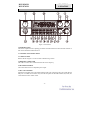
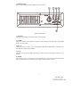
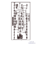
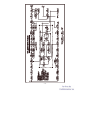
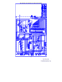
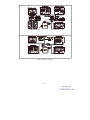
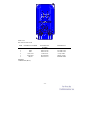
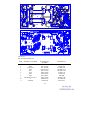
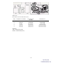
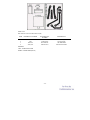
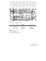
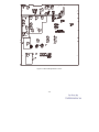
RCI-2950 DX
RCI-2970 DX
TABLE OF
CONTENTS
CHAPTER 1
PAGE
SPECIFICATIONS
1.0
General . . . . . . . . . . . . . . . . . . . . . . . . . . . . . . . . . . . . . . . . . . . . . . . .
1.1
Transmitter . . . . . . . . . . . . . . . . . . . . . . . . . . . . . . . . . . . . . . . . . . . . .
1.2
Receiver . . . . . . . . . . . . . . . . . . . . . . . . . . . . . . . . . . . . . . . . . . . . . . .
2
2
2
CHAPTER 2
INTRODUCTION
2.0
Introduction . . . . . . . . . . . . . . . . . . . . . . . . . . . . . . . . . . . . . . . . . . . .
2.1
Features . . . . . . . . . . . . . . . . . . . . . . . . . . . . . . . . . . . . . . . . . . . . . . .
3
3
CHAPTER 3
OPERATION
3.0
Introduction . . . . . . . . . . . . . . . . . . . . . . . . . . . . . . . . . . . . . . . . . . . .
3.1
Control & Connections . . . . . . . . . . . . . . . . . . . . . . . . . . . . . . . . . . . .
3.2
Microphone . . . . . . . . . . . . . . . . . . . . . . . . . . . . . . . . . . . . . . . . . . . .
3.3
Operation . . . . . . . . . . . . . . . . . . . . . . . . . . . . . . . . . . . . . . . . . . . . . .
4
4
8
8
CHAPTER 4
PROGRAMMING
4.0
Introduction . . . . . . . . . . . . . . . . . . . . . . . . . . . . . . . . . . . . . . . . . . . .
4.1
Frequency Selection . . . . . . . . . . . . . . . . . . . . . . . . . . . . . . . . . . . . . .
4.2
Frequency Scanning . . . . . . . . . . . . . . . . . . . . . . . . . . . . . . . . . . . . . .
4.3
Offset Frequency Operation . . . . . . . . . . . . . . . . . . . . . . . . . . . . . . . .
11
11
11
13
CHAPTER 5
CIRCUIT DESCRIPTION
5.0
Introduction . . . . . . . . . . . . . . . . . . . . . . . . . . . . . . . . . . . . . . . . . . . .
5.1
PLL Circuit . . . . . . . . . . . . . . . . . . . . . . . . . . . . . . . . . . . . . . . . . . . . .
5.2
Receiver Circuit . . . . . . . . . . . . . . . . . . . . . . . . . . . . . . . . . . . . . . . . .
5.3
Transmitter Modulation Circuit . . . . . . . . . . . . . . . . . . . . . . . . . . . . .
5.4
Transmitter Amplifier Circuit . . . . . . . . . . . . . . . . . . . . . . . . . . . . . . .
14
14
14
14
14
CHAPTER 6
ALIGNMENT
6.0
Required Test Equipment . . . . . . . . . . . . . . . . . . . . . . . . . . . . . . . . . .
6.1
Alignment Procedures . . . . . . . . . . . . . . . . . . . . . . . . . . . . . . . . . . . .
18
18
CHAPTER 7
MAINTENANCE
7.0
Precautions . . . . . . . . . . . . . . . . . . . . . . . . . . . . . . . . . . . . . . . . . . . . .
7.1
Periodic Inspection . . . . . . . . . . . . . . . . . . . . . . . . . . . . . . . . . . . . . . .
7.2
Fuse Replacement . . . . . . . . . . . . . . . . . . . . . . . . . . . . . . . . . . . . . . . .
22
22
22
CHAPTER 8
DIAGRAMS AND PART LIST
8.0
PCB Layout & Part List . . . . . . . . . . . . . . . . . . . . . . . . . . . . . . . . . . .
-1-
23
RCI-2950 DX
RCI-2970 DX
CHAPTER 1
SPECIFICATIONS
1.0 GENERAL
Model
Frequency Range
Tuning Steps
Emission Modes
Frequency Control
Frequency Tolerance
Frequency Stability
Operating Temperature Range
Microphone
Meter Function
Input Voltage
Antenna Connector
Dimensions For : RCI-2950 DX
RCI-2970 DX
Weight For : RCI-2950 DX
RCI-2970 DX
RCI-2950 DX / RCI-2970 DX
12 meter : 24.8900 ~ 24.9900 MHz
10 meter : 28.0000 ~ 29.6900 MHz
100 Hz, 1 KHz, 10 KHz, 100 KHz, 1 MHz
AM(A3)/FM(F3)/LSB,USB(A3J)/CW(A1)
Phase-Lock-Loop (PLL) synthesizer
± 0.005 %
± 0.001 %
0°C to +40°C
400 ohm, Dynamic PTT
RF Output, RX Receive Signal Strength, SWR
Calibration and SWR
13.8V DC
UHF SO239
7-3/4”(W) x 10-3/4”(L) x 2-3/8”(H)
7-3/4”(W) x 10-3/4”(L) x 3-7/8”(H)
4 lb. 3 oz.
7 lb. 6 oz.
1.1 TRANSMITTER
RF Power Output (RCI-2950DX)
RF Power Output (RCI-2970DX)
RF Transmit Modes
Modulation
Spurious Emissions
Carrier Suppression
Antenna Impedance
AM/FM/CW : 10 W ; SSB : 25 W PEP
AM/FM/CW : 50 W ; SSB : 150 W PEP
AM/FM/SSB/CW
A3E/16F3/J3E/A1A
-50 dB
-50 dB
50 Ohms
1.2 RECEIVER
Sensitivity For 10dB S/N (AM; CW/SSB)
Sensitivity for 12dB S/N (FM)
Image Rejection Ratio
Automatic Gain Control (AGC) Figure Of Merit
Audio Output Power
Built-in Speaker
External Speaker (Not Supplied)
< 0.5µV; < 0.15µ V
< 0.25µV
-65 dB
SSB/CW/AM : 80 dB for 50 mV for 10 dB Change in
Audio Output
2.5 W @ 10% THD
8 Ohms, 5 Watts.
8 Ohms; 5 Watts.
(SPECIFICATIONS SUBJECT TO CHANGE WITHOUT NOTICE)
-2-
RCI-2950 DX
RCI-2970 DX
CHAPTER 2
INTRODUCTION
2.0 INTRODUCTION
The Ranger RCI-2950 DX / RCI-2970 DX is a solid-state, fully synthesized Amateur 10 and 12 meter
dual band mobile transceiver with full band coverage from 28.0000 MHz to 29.6999 MHz and 24.8900
MHz to 24.9900 MHz and all mode operation, including: AM, FM, USB, LSB, CW and PA modes.
The 10 most commonly used frequencies can be pre-programmed by the user for easy channel access.
2.1 RCI-2950 DX / RCI-2970 DX FEATURES
• 25 Watts PEP of Output Power (RCI-2950 DX)
• 150 Watts PEP of Output Power (RCI-2970 DX)
• Full Band Coverage
• All Mode Operation
• Brightness Control
• CTCSS Encoder/Decoder (Optional)
• Repeater/Offset Switch
• Programmable Frequencies
• Built-in Dual VFO
• RIT (RX Incremental Tuning)
• Squelch
• Noise Blanker
• RF Gain Control
• RF Power Output Selector
• External Speaker Connection
• PA Mode
• LCD Display
• Multi-Function LCD Meter
-3-
RCI-2950 DX
RCI-2970 DX
CHAPTER 3
OPERATION
Figure 3-1 Front Panel
3.0 INTRODUCTION
This section explains the basic operating procedures for the RCI-2950 DX / RCI-2970 DX Amateur 10
and 12 meter dual band mobile transceiver.
3.1 CONTROL AND CONNECTIONS
3.1.1 FRONT PANEL
Refer to the above Figure 3-1 for the location of the following controls.
1. FREQUENCY SELECTOR
This control is used to select a desired transmit and receive frequency.
2. RF POWER CONTROL
This control allows the user to adjust RF power output.
3. MIC GAIN CONTROL
Adjusts the microphone gain in the transmit and PA modes. This controls the gain to the extent that full
talk power is available several inches away from the microphone. In the Public Address (PA) mode, the
control functions as the volume control.
-4-
4. ON/OFF VOLUME CONTROL
This knob controls the volume and the power to the radio. To turn the radio on, rotate knob clockwise.
Turning the knob further will increase the volume of the receiver.
5. SQUELCH CONTROL
This switch is used to eliminate background noise being heard through the receiver which can be
disturbing when no transmissions are being received. To use this feature, turn the switch fully
counterclockwise and then turn clockwise slowly until the background noise is just eliminate. Further
clockwise rotation will increase the threshold level, which a signal must overcome in order to be heard.
Only strong signals will be heard at a maximum clockwise setting.
6. RF GAIN CONTROL
This control is used to reduce the gain of the RF amplifier under strong signal conditions.
7. CLARIFIER CONTROL
Allows tuning of the receive frequency above or below the assigned frequency by up to 500 Hz.
Although this control is intended primarily to tune in SSB/CW signals, it may be used to optimize
AM/FM signals.
8. MODE (FM/AM/USB/LSB/CW/PA) SWITCH
This switch allows you to select one of the following operating modes: FM/AM/USB/LSB/CW/PA.
9. NB/ANL BUTTON (NB/ANL)
In the NB/ANL position, the RF Noise Blanker and Aotumatic Noise Limiter in the audio circuits are
also activated. The Noise Blanker is very effective in eliminating repetitive impulse noise such as
ignition interference.
10. ROGER BEEP BUTTON (R.BEEP)
In the Roger Beep position, the radio transmits an audio tone at the end of your transmission to indicate
that transmission has ended. As a courtesy to others, use the Roger Beep only when necessary.
11. SPLIT BUTTON (SPLIT)
This control activates the offset frequency function. It causes the transmit frequency to be offset either
above or below the receive frequency by a user programmable amount to allow operation of an FM
Repeater.
12. PROGRAM BUTTON (PRG)
This button is used to program operating or scanning frequencies into memory. See the OPERATION
section of the manual for further details.
13. MANUAL BUTTON (MAN)
This is used to return the unit to manual mode.
14. SHIFT BUTTON (SHF)
This is used to select 100 Hz, 1 KHz, 10 KHz, 100 KHz or 1 MHz frequency steps.
15. DIM BUTTON (DIM)
This button adjusts the display backlighting in four different steps to best match the ambient light.
-5-
16. SWR BUTTON (SWR)
This control is used to check SWR.
17. SCAN BUTTON (SCAN)
This is used to scan frequencies in each band segment. The OPERATION segment of this manual
provides detailed information on using the SCAN control.
18. MEMORY BUTTON (MEM)
This button is used to program memory channels. Detailed information on how to use this control is
provided in the OPERATION section of this manual.
19. ENTER BUTTON (ENT)
This is used to program frequencies in memory. See the OPERATION section of this manual for more
information on using this control.
20. LOCK BUTTON (LOCK)
This button is used to lock a selected frequency. Press it to activate the switch. In this position, it
disables the Frequency Selector Control, up/down buttons on the front control panel and remote
up/down buttons on the microphone. Repressing the switch will unlock the frequency.
21. UP/DOWN SELECTOR (στ)
These buttons are used in conjunction with the shift key to move the frequency upward or downward to
select a desired frequency.
22. METER
This meter indicates received signal strength, transmitter RF output power and SWR level.
23. LCD DISPLAY
The LCD displays the frequency selected, functions and memory channel.
24. MIC JACK
Accepts 6 pin female connector with a type Philmore T616C or Calrad 30445 style connector.
-6-
3.1.2 REAR PANEL
Figure 3-2 represents the location of the following connections:
Figure 3-2 Rear Panel
1. ANTENNA
This jack accepts 50 ohms coaxial cable with a PL-259 type plug.
2. CW KEY
This jack is for Morse code operation, To operate, connect a CW key to this jack and place the MODE
switch in the CW position.
3. EXT. SP.
This jack accepts 4 to 8 ohms, 5 watts external speaker. When the external speaker is connected to this
jack, the built-in speaker will be disabled.
4. PA. SP.
This jack is for PA operation. Before operating, you must first connect a PA speaker (8 ohms, 5 W) to
this jack.
5. POWER
This connector accepts 13.8V DC power cable with built-in fuse. The power cord provided with the
radio has a black and red wire. The black goes to negative and the red goes to positive.
-7-
3.2 MICROPHONE
1. PTT SWITCH
The receiver and transmitter are controlled by the push-to-talk switch on the microphone. Press the
switch and the transmitter is activated, release switch to receive. When transmitting, hold the
microphone two inches from the mouth and speak clearly in a normal voice.
2. REMOTE UP/DOWN SWITCH
An operating frequency can be incremented or decremented simply by pushing either of these buttons.
3.3 OPERATION
3.3.1 CHANNEL SELECTION
Frequency selection for the RCI-2950 DX / RCI-2970 DX is simple. Select a desired operating
frequency by rotating the Frequency Selector, or using the (σ) Up and (τ) Down buttons on the front
panel or the microphone. Press the LOCK button to lock into the selected frequency. This will disable
the Frequency Selector and the up/down buttons on the front panel and the microphone. Repressing the
LOCK button unlocks the frequency. Use the SHF button to step frequency in either 100 Hz, 1 KHz, 10
KHz, 100 KHz or 1 MHz increment when you select a band segment. The frequency step is indicated by
a small triangle directly under the corresponding digit on the frequency display.
3.3.2 MODE SELECTION
To select an operating mode on your RCI-2950 DX / RCI-2970 DX, simply rotate the MODE selector
and place it in the desired operating mode position.
FM/AM/USB or LSB modes are for your voice communications. In the CW position, you can transmit
CW if you have connected an external key to the accessory jack provided on the back of the radio. In the
PA position, the transceiver can be used as a Public Address system. Before operating in PA mode, you
must first connect a PA speaker (8 ohms, 5 Watts) to the jack located on the rear panel.
3.3.3 RF POWER CONTROL
This feature allows the adjustment of the RF output power continuously for the RCI-2950 DX (AM 1W
to 10W; SSB: 10W to 25W), and (AM: 8W to 50W; SSB: 18W to 100W) for the RCI-2970 DX.
3.3.4 RECEIVE SCANNING
Receive scanning allows you to find active frequencies in the entire band segment. To begin scanning,
slowly turn the Squelch control clockwise until the receiver noise disappears. Press the Scan button. The
unit should start scanning from the lower to the higher frequencies. Pressing the Scan button again will
change the direction of scanning. Each time you press the Scan button, “SCAN+” or “SCAN-” will
displayed on the LCD display. The radio will stop on any active frequency for the entire duration of the
transmission. When the transmission stops, the RCI-2950 DX / RCI-2970 DX will wait approximately 2
seconds before it resumes scanning. If you want to deactivate Scan mode while it is scanning, press the
MAN (manual) button or turn the Squelch control counterclockwise until you hear the receiver noise.
The Manual button will disable Scan function.
-8-
3.3.5 SPLIT FUNCTION
This function enables you to offset the transmit and receive frequencies for FM repeater operation. The
transmitter frequency can offset either higher or lower than the receive frequency. To split frequencies,
press the MAN button and the Split button to select either +/- split frequency. If the + split is selected,
the transmit frequency will be higher than the receive frequency. If - split is selected, the transmit
frequency will be lower than the receive frequency.
3.3.6 MEMORY FUNCTION
The RCI-2950 DX / RCI-2970 DX can store up to 10 most frequently used frequencies (from 0 to 9). To
program a frequency into memory, follow the procedure described below:
(1) Press the MAN button.
(2) Press the PRG button.
(3) Press the MEM button (“MEMORY” and “0” should appear on the left-hand side of the LCD
display). Pressing the MEM button will advance the channel number from “0” to “9”.
(4) Select the desired frequency you wish to store in memory.
(5) Press the ENT button.
(6) Repeat the same procedure to program other memory channels.
3.3.7 MEMORY CHANNEL SCANNING
You can scan and select any of these 10 preset frequencies by following the procedure described below:
(1) Press the MAN button.
(2) Press the MEM button.
(3) Slowly turn the Squelch knob clockwise until the receiver noise disappears.
(4) Press the Scan button. The unit will scan from lower to higher frequencies. When you press the
button again, it will scan from higher to lower frequencies.
(5) To stop scanning a certain channel, press the MAN button, or turn the Squelch knob
counterclockwise until you hear the receiver noise.
3.3.8 METER
The meter built into your RCI-2950 DX / RCI-2970 DX on the left hand side of the LCD display
provides the following information:
1. S/RF METER
In transmit mode, it provides a visual indication of transmit output power and received signal strength
on the receive mode.
2. SWR METER
-9-
In order to achieve maximum radiated power, it is important that your antenna be in good condition,
properly adjusted and matched to your transceiver. The built-in SWR (Standing Wave Ratio) meter
allows you to measure your antenna condition. To operate this function, connect your antenna to the
transceiver antenna connector, set the mode switch to AM and adjust the MIC GAIN to minimum.
Select a frequency near the middle of the band you plan to use most. Activate the SWR function and
press the PTT button on the microphone. A bar on the meter is an indication of the antenna matching. If
there is no bar, it indicates that your antenna system is perfectly matched. The fewer bars, the better
matched. If several bars appear, your antenna needs adjusting.
3.3.9 CTCSS - OPTIONAL
The RCI-2950 DX / RCI-2970 DX can operate with CTCSS frequencies for accessing repeaters, with an
optional CTCSS (Continuous Tone Coded Squelch System) encoding device installed.
3.3.10 PROCEDURE TO RECEIVE
(1) Be sure that power source, microphone and antenna are connected to the proper connectors before
going to the next step.
(2) Turn unit on by running VOL knob clockwise on transceiver.
(3) Set the VOL to a comfortable listening level.
(4) Set the MODE switch to the desired mode.
(5) Listen to the background noise from the speaker. Turn the SQ knob slowly clockwise until the noise
just disappears. The SQ is now properly adjusted. The receiver will remain quiet until a signal is
actually received. Do not advance the control too far or some of weaker signals will not be heard.
(6) Set the CHANNEL selector switch to the desired channel.
(7) Set the RF GAIN control fully clockwise for maximum receive gain.
(8) Adjust the CLARIFIER control to clarify the SSB signals or to optimize AM/FM signals.
3.3.11 PROCEDURE TO TRANSMIT
(1) Select the desired channel of transmission
(2) Set the MIC GAIN control fully clockwise.
(3) If the channel is clear, depress the push-to-talk switch on the microphone and speak in a normal
voice.
- 10 -
RCI-2950 DX
RCI-2970 DX
CHAPTER 4
PROGRAMMING
4.0 INTRODUCTION
This section explains the basic programming procedures for the RCI-2950 DX / RCI-2970 DX Amateur
10 and 12 meter dual band mobile transceiver.
4.1 FREQUENCY SELECTION
Frequency selection in the RCI-2950 DX / RCI-2970 DX can be accomplished using anyone of the
three following methods:
(1) The first method of frequency selection is through the use of the SHF (Shift) key and the (σ) Up
and (τ) Down arrows. To accomplish this, press the SHF button until the cursor arrow is positioned
under the digit of the frequency that is to be changed, then use the (σ) Up arrow to increase the
number. If a decrease in frequency is desired, press the (τ) Down arrow. Perform the steps described
above for each digit of the frequency until the desired frequency is displayed in the LCD display
window.
(2) The second method of frequency selection is accomplished using the SHF button and the frequency
select knob located above the microphone jack. Use the SHF button in the manner described above
to select the digit to be changed. Proceed to rotate the frequency select knob clockwise to increase
the frequency. Rotate the frequency select knob counterclockwise to decrease the frequency.
(3) The third method of selecting the operating frequency of the radio is through the use of the SHF
button and the Channel (σ) Up and (τ) Down buttons located on the microphone. Frequency
selection by this method is accomplished in the same manner as with the (σ) Up and (τ) Down
arrows on the keypad. The only difference is that the Channel Up and Down buttons on the
microphone are used.
4.2 FREQUENCY SCANNING
Frequency scanning can be achieved using one of two methods: the first method involves the scanning
of pre-programmed memory channels. The second method permits the user to scan all frequencies
between a pre-set upper and lower scan limit.
4.2.1 ALL FREQUENCY SCANNING
To allow all Frequency Scanning, one must first program the upper and lower scanning limits. The scan
limits are simply the highest and lowest frequencies that will be scanned. To program these limits,
perform the following steps:
(1) Press the PRG (Program) key.
(2) Press the SCAN key (“PRG SCAN+” should appear in the lower right corner of the display
window).
(3) Using the SHF key and the (σ) Up and (τ) Down arrows, select the upper scan limit, then press
ENT.
- 11 -
(4) Press the SCAN key again (“SCAN-” should appear in the display window).
(5) Using the SHF key and (σ) Up and (τ) Down arrows, select the lower scan limit, then press ENT.
The upper and lower scan limits have now been programmed. To activate the scan feature, return the
radio to manual operation and press the SCAN button. If the display shows “SCAN+”, the radio will
scan from the lower limit to the upper limit. If “SCAN-” is displayed, the unit will scan from the upper
limit to the lower limit. To change from SCAN+ to SCAN- or vice versa, press SCAN.
NOTE
When programmed, the upper and lower scan limits will
also act as the upper and lower operating limits of the
radio. The radio now cannot be programmed to operate
above or below the scan limits.
4.2.2 MEMORY SCANNING
The RCI-2950 DX / RCI-2970 DX has 10 non-volatile (i.e. memory resident) memory locations which
can be programmed with any available frequency within the operating band of the radio. The scan
function of the unit can be programmed to scan these memory channels. The radio will then scan only
those memory channels which have been programmed. The first step in utilizing the memory scan
function is to program the desired frequencies into the radio memory. This can be accomplished by
performing the following steps:
(1) With the radio operating in the manual mode, press the PRG (Program) key.
(2) Press the MEM (Memory) key. “PRG” should be displayed in the lower right-hand corner of the
LCD display window. In the upper left portion of the display, “MEMORY” should be displayed.
Directly below MEMORY, a number between 0 and 9 will be displayed. This number represents
the memory location currently being displayed. Pressing the MEM key will increase the memory
counter to the next memory location and the contents of that memory location will be displayed.
(3) Using the SHF key and the (σ) Up and (τ) Down arrows, enter the frequency to be stored in the
memory location displayed. After the desired frequency has been entered, press ENT.
(4) Repeat steps (2) and (3) for all the memory locations to be programmed.
(5) After all desired memory locations have been programmed with frequencies, return the unit to the
manual mode of operation by pressing the MAN key.
(6) To initiate memory scanning, press MEM and then press SCAN. As previously discussed, the
display will show “SCAN+” or “SCAN-” to indicate whether the radio is scanning from the lowest
or the highest memory location or vice versa.
(7) To return the radio to normal (non-scanning) operation, press the MAN key.
4.3 OFFSET FREQUENCY OPERATION
- 12 -
The RCI-2950 DX / RCI-2970 DX has an offset or split frequency feature that will permit the radio to
be operated in a half-duplex mode. This will allow the user to talk on FM repeaters operating in the 10
and 12 Meter bands.
NOTE
The FM repeaters may require a subaudible (CTCSS) tone
be transmitted to gain access to the repeater. The RCI2950/2970 DX is not factory equipped with a CTCSS
encoder/decoder.
The split frequency function offsets the transmitter frequency either above or below the receive
frequency by a user programmable amount. In the following example, programming of a 100 KHz offset
will be described. Before attempting to program the offset frequency, ensure that the radio is operating in
the manual mode by pressing the MAN key.
(1) Press the PRG (Program) key.
(2) Press the SPLIT key. The LCD display window will display “00000” with “PRG” and “SPLIT”
being displayed in the lower left-hand corner.
(3) Using the SHF key and the (σ) Up and (τ) Down arrows as described earlier, program the display to
read “010000”.
(4) Press ENT. A 100 KHz offset has now been programmed into the radio.
(5) Return the radio to manual operation by pressing the MAN key.
(6) Using the SHF key and the (σ) Up and (τ) Down arrows as described previously, set the radio for
the desired receive frequency.
(7) Press SPLIT. In the lower right corner of the display, either “SPLIT+” or “SPLIT-” will be
displayed. If SPLIT+ is displayed, the transmitter will be offset 100 KHz above the receive
frequency when keyed. If SPLIT- is displayed, the transmitter will be offset 100 KHz below the
receive frequency.
NOTE
When the transmitter is keyed, the frequency display will
change to show the frequency being transmitted.
(8) To return the radio to simplex operation (i.e., same transmit and receive frequency), press the MAN
key.
- 13 -
CHAPTER 5
CIRCUIT
DESCRIPTION
RCI-2950 DX
RCI-2970 DX
5.0 INTRODUCTION
This section explains the technical theory of operation for the RCI-2950 DX / RCI-2970 DX mobile
transceiver.
5.1 PLL CIRCUIT
The Phase Lock Loop (PLL) circuit is responsible for developing the receiver’s first local oscillator
signal and the transmitter’s exciter signal. The PLL circuit consists primarily of IC2, IC3, Q29, Q32,
Q33, Q34, Q36, Q37, Q38 and L16. The PLL circuit is programmed by the rotary channel switch GPS0688. The switch allows IC (U601) on CPU P.C.B to communicate the correct binary data information
to the programmable divider inside of IC2. IC2 then controls the VCO (Voltage Controlled Oscillator) to
oscillate on the correct frequency. This signal is fed either into the receiver’s first mixer (for receive
operation) or the transmitter’s mixer (for transmit operation).
5.2 RECEIVER CIRCUIT
The incoming receives signal come into the radio via the antenna and into the front-end pre-amp
consisting of Q19. The RF signal is fed into the mixer circuit of the Q20 and Q21. The signal is then
filtered by L8, L9 and L10 then into the AM/FM IF section of the receiver (depending on the mode of
operation). The signal is then detected by either the AM detector FM detector and then fed to the audio
amplifier section of the receiver and finally out to the speaker.
5.3 TRANSMITTER MODULATION CIRCUIT
(1) The transmitter modulation circuit modulates the low-level RF signal from the PLL exciter circuit
with the user’s audio voice signal from the microphone. The audio from the microphone is then
amplified and fed into the balanced modulator circuit.
(2) If the transceiver is in the AM mode, the AF power amplifier modulates the last RF amplifier which
produces a true amplitude modulated RF signal.
(3) If the transceiver is in the FM mode, the audio signal is not mixed with 10.6975MHz oscillator but
instead phase modulates the basic exciter signal from the PLL circuit in the TX mixer.
(4) If the transceiver is in the SSB mode, the audio signal is mixed with 10.6975MHz oscillator in IC5.
5.4 TRANSMITTER AMPLIFIER CIRCUIT
The transmitter takes the basic exciter signal from the TX mixer and amplifies it through a series of
amplifiers consisting of Q64, Q63, Q62, Q61, Q60 and the EPA010010A amplifier (only for RCI-2970
DX) where it is sent out to the antenna connector.
- 14 -
- 15 -
- 16 -
RCI-2950 DX / RCI-2970 DX CPU CIRCUIT DIAGRAM
- 17 -
RCI-2950 DX
RCI-2970 DX
CHAPTER 6
ALIGNMENT
6.0 REQUIRED TEST EQUIPMENT
• DC Power Supply (13.8VDC, 20A)
‚ RF Wattmeter (100W)
ƒ Multimeter
„ Automatic Modulation Meter
… Audio Signal Generator
† Frequency Counter (100 MHz)
‡ RF Signal Generator (100 MHz)
ˆ Automatic Distortion Meter
‰ Oscilloscope (50 MHz)
Š Sinad Meter
6.1 ALIGNMENT PROCEDURES
This transceiver has been aligned at the factory and does not require any adjustments at installation. The
required test equipment listed are used for the test setup or alignment shown in Figure 6-1 Transmitter
Test Setup and Figure 6-2 Receiver Test Setup. These test setups are used in part or total during the
following adjustments and refer to Page 44 for adjustment location.
6.1.1 PLL ALIGNMENT
ITEM
U.U.T. SETTING
ADJUST
POINT
L14
MEASUREMENT
PLL 2
VCO Voltage
Set radio to 24.890 MHz, AM RX mode.
Frequency setting at 29.699 MHz.
Connect Multimeter to TP10.
PLL 1
VCO Voltage
Set radio to 24.890 MHz, AM RX mode.
Frequency setting at 32.000 MHz.
Connect Multimeter to TP11.
L13
1.0 VDC ± 0.1
≤ 6.5 VDC
AM Frequency
Set radio to AM RX mode.
Set Clarifier Control to 12 o’clock.
Connect Frequency Counter to TP16.
VC2
10.1000 MHz ± 10
Hz
TX Frequency
Set radio to AM TX mode.
Connect Frequency Counter to TP16.
VR8
10.1000 MHz ± 10
Hz
VCO Output
Set radio to 28.000 MHz, AM RX mode.
Connect Oscilloscope to TP3.
L17
Maximum Output
38.6950 MHz @ TP3
AM OSC
Set radio to AM TX mode. Mod off.
Connect Frequency Counter to TP5.
L18
10.6950 MHz ± 10
Hz
USB OSC
Set radio to USB TX mode. Mod off.
Short TP6 to ground.
Connect Frequency Counter to TP5.
L20
10.6975 MHz ± 10
Hz
LSB OSC
Set radio to LSB TX mode. Mod off.
Connect Frequency Counter to TP5.
L19
10.6925 MHz ± 10
Hz
6.1.2 TRANSMITTER ALIGNMENT
- 18 -
1.0 VDC ± 0.1
≤ 4.5 VDC
RCI-2970DX LEVELS ARE SHOWN IN [].
ITEM
U.U.T. SETTING
TX Power
Set radio to 28.000 MHz, AM TX mode.
Modulation off.
Set radio to 28.000 MHz, USB TX mode.
AF signal 30mV, 1 KHz to microphone.
Connect Oscilloscope to TP17.
Set RF PWR Fully Clockwise.
Set Clarifier Control to 12 o’clock.
Set radio to 24.890 MHz & 29.699 MHz.
ADJUST
MEASUREMENT
POINT
L18,L37,L35, Maximum Output.
L34
L35,L34
Maximum Output and
Balance.
AM APC
Set radio to AM TX mode.
Connect Multimeter to TP8
VR15
6 VDC
SSB APC
Set radio to USB TX mode.
Connect Multimeter to TP8
VR18
12.5 VDC
BIAS Current
Set radio to USB TX mode.
Modulation off.
Connect current meter to TP7(+) and TP9(-)
Connect current meter to TP7(+) and TP8(-)
AM TX Power
Set radio to 28.000 MHz, AM TX mode.
Modulation off.
Connect “short PCB” to TP7 and TP9.
Set RF PWR Fully Counter Clockwise.
Connect RF Power Meter to antenna jack.
VR13
10 mA
VR12 + VR11 (50 mA + 50 mA) =
100 mA
VR15
10W [50W]
VR19
1W [8W]
RF Power Meter Set radio to 28.000 MHz, AM TX mode.
Set RF Power Fully Clockwise.
VR10
Level Meter Indicator
SSB ALC
Set radio to USB TX mode.
AF signal 30 mV, 1 KHz to microphone.
VR14
25W [150W, PEP]
SSB Carrier
Balance
Set radio to USB TX mode.
AF signal 30 mV, 1 KHz to microphone.
Connect Oscilloscope to antenna jack.
VR7
Spurious Emission to
minimum.
CW TX
Set radio to 28.000 MHz, CW TX mode.
Plug in CW Key.
Disconnect the Mic Jack.
Connect AC Voltmeter to EXT SP.
VR9
200mV (Sine Wave)
VR17
90%
4 KHz
AM Modulation Set radio to 28.000 MHz, AM TX mode.
FM Modulation Set radio to 28.000 MHz, FM TX mode.
AF signal 30 mV, 1 KHz to microphone.
Set Mic Gain Fully Clockwise.
6.1.3 RECEIVER ALIGNMENT
- 19 -
ITEM
SETTINGS
AM Sensitivity Set radio to 28.000 MHz, AM RX mode.
Set Clarifier Control to 12 o’clock.
Set RF Gain Fully Clockwise.
Set SQ Fully Counter Clockwise.
Set NB/ANL/OFF switch to OFF position.
Set VOL Control at 2 o’clock.
Connect RF SG to antenna jack
Frequency 28.000 MHz, 1uV. Mod 30%.
Set radio to 24.890 MHz, AM RX mode.
RF SG setting 24.890 MHz.
Set radio to 29.699 MHz, AM RX mode.
RF SG setting 29.699 MHz.
ADJUST
MEASUREMENT
POINT
L5,6,7,8,9,10 Audio Output > 2V
,2,3
S/N > 10 dB
L5,L6, L7
Balance between
24.890 and 29.699
MHz
USB Sensitivity Set radio to USB RX mode.
Set VOL Control Fully Clockwise.
RF SG setting 28.001 MHz, 0.5uV. Mod off.
L11, L12
Audio Output > 2V
S/N > 10 dB
LSB Sensitivity Set radio to LSB RX mode.
Set VOL Control Fully Clockwise.
RF SG setting 27.999 MHz, 0.5uV. Mod off.
L11, L12
Audio Output > 2V
S/N > 10 dB
FM Distortion
Set radio to 28.000 MHz, FM RX mode.
L4
Set MODE switch to FM mode.
RF SG setting 28.000 MHz, 1mV. Mod 3KHz.
Audio Output > 3V
Distortion < 10%
NB Adjust
Set radio to 28.000 MHz, AM RX mode.
L1
RF SG setting 28.000 MHz, 100uV. Mod off.
Set NB/ANL/OFF switch to NB/ANL position.
Connect Voltmeter to TP1.
DC Voltage to max.
> 2V
AM Squelch
Set radio to 28.000 MHz, AM RX mode.
Set SQ Control Fully Clockwise.
RF SG setting 28.000 MHz, 1mV. Mod 30%.
VR4 Slowly
Adjust very slowly
until squelch just
open.
SSB Squelch
Set radio to USB RX mode.
Set SQ Control Fully Clockwise.
RF SG setting 28.001 MHz, 1mV. Mod off.
VR3 Slowly
Adjust very slowly
until squelch just
open.
AM S/RF Meter Set radio to 28.000 MHz, AM RX mode.
VR1
AM S-Meter
RF SG setting 28.000 MHz, 100uV. Mod 30%.
“6 bar” on the Level
Meter Indicator.
SSB S-Meter
“6 bar” on the Level
Meter Indicator.
Set radio to USB RX mode.
RF SG setting 28.001 MHz, 100uV. Mod off.
VR2
Figure 6-1 Transmitter test setup
- 20 -
Figure 6-2 Receiver test setup
- 21 -
RCI-2950 DX
RCI-2970 DX
CHAPTER 7
MAINTENANCE
7.0 PRECAUTIONS
The inherent quality of the solid-state components used in this transceiver will provide many years of
continuous use. Taking the following precautions will prevent damage to the transceiver.
(1) Never key the transmitter unless an antenna or suitable dummy load is connected to the antenna
receptacle.
(2) Ensure that the input voltage does not exceed 16 VDC or fall below 11 VDC.
(3) During alignment, do not transmit for more than 10 seconds at a time. Transmitting over long
periods can cause heat built-up and cause transmitter damage.
7.1 PERIODIC INSPECTION
This unit is aligned at the factory to deliver maximum performance. However, continued performance
cannot be expected without periodic inspection and maintenance. Important points to be checked
regularly are as follows;
Check Item
Whip antenna
(option)
Coaxial cable
Coaxial & power
plug connections
Battery connection
Ground terminal
Action
If cracked or broken, replace it.
If sheath is cracked, seal with
vinyl tape. If immersed with
water, install new coaxial cable.
If loosened, reconnect. If
corroded, clean contacts.
If corroded, clean power
terminals.
If corroded, clean terminal.
7.2 FUSE REPLACEMENT
To protect the equipment from serious damage, a fuse is provided on the power supply lines. The fuse
protect against overvoltage / reverse polarity or internal fault of the equipment. If the fuse has blown,
first find out the cause of the trouble before replacing it. A fuse rated for more than 7A for RCI-2950
DX and 20A for RCI-2970 DX should not be used, since it may permanently damage the equipment.
Damage due to overfusing is not covered by the warranty.
- 22 -
CHAPTER 8
DIAGRAMS &
PARTS LIST
RCI-2950 DX
RCI-2970 DX
8.0 GENERAL
Information on most electrical and mechanical parts is included in the parts list. The reference
designators are in alphanumeric order.
8.1 ORDERING REPLACEMENT PARTS
Parts orders should be referred to the parts department at:
• Ranger Communications, Inc.
401 W. 35TH ST.
NATIONAL CITY, CA 91950-7909
Tel: (619) 426-6440
Fax: (619) 426-3788
- 23 -
PART LIST:
RCI-2950 DX / RCI-2970 DX CH SW P.C.B
ITEM
1
2
3
4
REFERENCE NUMBER
PCB CONN/S 3PIN
(COPPER SIDE)
CH SW P.C.B
CH SW P.C.B
RANGER PART
NUMBER
EPT295090A
CC0501037L
DESCRIPTION
EWRT32051S
EX07N41216
ROTARY SW
PCB CONN/S 3PIN
REMARK:
COPPER SIDE (BLUE)
- 24 -
CH SW P.C.B
0.01µF 50WV
PART LIST:
RCI-2950 DX SWR P.C.B
ITEM
REFERENCE NUMBER
1
2
3
4
5
6
R402
R401
C401,C402
D401,D402
JP2,JP3
RANGER PART
NUMBER
EPT360041Z
RCP141014Z
RCP141214Z
CC0501037L
ED1N00060P
WX01070710
REMARK:
COPPER SIDE (BLUE)
- 25 -
DESCRIPTION
SWR P.C.B
100 OHM 1/4W
120 OHM 1/4W
0.01µF 50WV
DIODE 1N60P
JUMPER WIRE
PART LIST:
RCI-2970 DX POWER P.C.B
ITEM
REFERENCE NUMBER
1
2
3
4
5
6
7
8
9
10
11
R904
R905,R906
R902
R911
L902
R903
R910
BETWEEN C901 & G
T
COPPER
RANGER PART
NUMBER
EPA010010A
RCU141094Z
RCU142204Z
RCM141024A
RCP121034Z
RCP101004Z
RCP202204Z
RE10300069
RCP141024Z
RFP202214Z
CC0502204L
- 26 -
DESCRIPTION
POWER P.C.B
1 OHM 1/4W
22 OHM 1/4W
1K OHM 1/2 W
10K OHM 1/2W
10 OHM 1W
22 OHM 2W
10K OHM
1K OHM 1/4W
220 OHM 2W
22PF 50WV
ITEM
REFERENCE NUMBER
12
13
C902,C903
C906,C926,C932,C934,
C937
C905,C920,C921,C923x2
,
C924x2,C925,C935,C939
,C941,T901-T902x2,
C927,C928,C930,C931,
C933,C940,C929
C901
C918
C916
C917
C908,C910,C936
C945
C909
C919
C922
C938
TR903
TR901,TR902
D903,D904
D901,D902
L903,L904
L901
T901
T902
R901
J901,J902
RL901
J903,J904
J905,J906
14
15
16
17
18
19
20
21
22
23
24
25
26
27
28
29
30
31
32
33
34
35
36
37
RANGER PART
NUMBER
CC0503915L
CC0501037L
DESCRIPTION
CC0501047L
0.1µF 50WV
CC0508204A
CD3006804Z
CD3001514Z
CD5001018Z
CD3001814Z
CD5005614Z
CD5008214Z
CX0071037Z
CE0162277Z
CE0352277Z
T2SD02531Z
T2SC02290Z
ED1N04148Z
ED1N04001Z
ECSPG18069
ECBAD18553
ECRFZ10096
ECRFZ10097
RE10200046
EX07N41226
EX05N40825
GZZZ50062Z
GZZZ50011Z
82PF 50WV
68PF 300WV
150PF 300WV
100PF 500WV
180PF 300WV
560PF 500WV
820PF 500WV
HV DISC/C 0.01Uf
220µF 16WV
220µF 16WV
TR 2SD2531
TR 2SC2290
DIODE 1N4148
DIODE 1N4001
SPRING COIL
BEAD COIL
RF COIL
RF COIL
S/F/R IK OHM
PCB CONN/S 2PIN
RELAY
V TYPE JACK
C PIN
REMARK:
TOP: COMPONENT SIDE (WHITE)
BOTTOM: COPPER SIDE (WHITE)
- 27 -
390PF 50WV
0.01µF 50WV
PART LIST:
RCI-2950 DX / RCI-2970 DX VR P.C.B (A)
ITEM
REFERENCE NUMBER
1
2
3
4
5
6
C501,C505
RF/MIC
VOL/SQ
J501,J505
J502-J504
RANGER PART
NUMBER
EPT295050Z
CC0501027L
RV10203451
RV50303453
EX07N41226
EX07N41216
REMARK:
LEFT: COMPONENT SIDE
RIGHT: COPPER SIDE (BLUE)
- 28 -
DESCRIPTION
VR P.C.B (A)
0.001µF 50WV
VR 1KA-5KB
VR 50KB-50KA
PCB CONN/S 2PIN
PCB CONN/S 3PIN
PART LIST:
RCI-2950 DX / RCI-2970 DX VR P.C.B (B)
ITEM
REFERENCE NUMBER
1
2
3
4
C601
RF/CAL
J601,J602
RANGER PART
NUMBER
EPT295060Z
CC0501027L
RV10203456
EX07N41216
REMARK:
LEFT: COMPONENT SIDE
RIGHT: COPPER SIDE (BLUE)
- 29 -
DESCRIPTION
VR P.C.B (B)
0.001µF 50WV
VR 1KB-20KB
PCB CONN/S 3PIN
PART LIST:
RCI-2950 DX / RCI-2970 DX MIC P.C.B
ITEM
REFERENCE NUMBER
1
2
3
4
5
C701-C703
J702,J703
J701
MIC P.C.B
RANGER PART
NUMBER
EPT295070Z
CCM501025T
EX07N48152
EX07N48244
EX06N41111
REMARK:
LEFT: COMPONENET SIDE (BLUE)
MIDDLE: COMPONENT SIDE
RIGHT: COPPER SIDE (BLUE)
- 30 -
DESCRIPTION
MIC P.C.B
0.001µF 50WV
PCB CONN/S 2PIN
PCB CONN/S 3PIN
MIC JACK
PART LIST:
RCI-2950 DX / RCI-2970 DX BAND P.C.B
ITEM
REFERENCE NUMBER
1
2
3
4
5
BAND P.C.B
J402
J401
J403
RANGER PART
NUMBER
EPT295090Z
EWRT32053S
EX07N41216
EX07N41261
WX01070706
REMARK:
LEFT: COMPONENT SIDE
RIGHT: COPPER SIDE (BLUE)
- 31 -
DESCRIPTION
BAND P.C.B
ROTARY SW
PCB CONN/S 3PIN
PCB CONN/S 7PIN
JUMPER WIRE
PART LIST:
RCI-2950 DX / RCI-2970 DX KEY SW P.C.B
ITEM
REFERENCE NUMBER
1
2
3
4
5
R701-R708
KEY SW P.C.B x 14pc
D701-D708
KEY SW P.C.B x 2pc
RANGER PART
NUMBER
EPT295031Z
RCP161524Z
EWPS33042X
EX01N40064
EX07N48441
REMARK:
TOP: COMPONENT SIDE
MIDDLE: COPPER SIDE (BLUE)
BOTTOM: COMPONENT SIDE (BLUE)
- 32 -
DESCRIPTION
KEY SW P.C.B
1.5K OHM 1/16W
TACT SW
LED (WHITE)
PCB CONN/S 6PIN
- 33 -
PART LIST:
RCI-2950 DX / RCI-2970 DX CPU P.C.B
ITEM
1
2
3
4
5
6
7
8
9
10
11
12
13
14
15
16
17
18
19
20
21
22
23
24
25
26
27
28
29
30
31
32
33
34
35
36
37
38
39
40
REFERENCE NUMBER
C604
R606
R604
DISPLAY
X601
BZ601
CN602,CN608
CN603-CN605,CN610
CN601
CN606,CN607
JP601,JP602
SHORT2
SK601,SK602
CPU P.C.B
C606
C601
C607
C608,C609
C610-C617,C605
C602,C603
COPPER SIDE
R607
R605
R610,R601,R603,R611,
R627,R631
R616,R618,R620,R623,
R624
R629
R609,R612,R613,R628
R615,R617,R619,R621,
R622,R625,R626
R614
R630
R608
R602
U601
U602
U604,U605
U606
Q602,Q604
Q601,Q603,Q605-Q607
D601,D602
RANGER PART
NUMBER
DESCRIPTION
EPT295042Z
CE0102277Z
RCU128204Z
RCU121214Z
EX03N40460
EX14N46510
EX14N46511
EX07N41226
EX07N41216
EX07N41250
EX07N41266
EX07N48440
EX07N48151
EX07N48772
EX01N40119
CK1560AB4A
CK1330AB4A
CK1224AB7R
CK1102AB7L
CK1104AB7L
CK5105AB7R
RCY011014Z
RCY014724Z
RCY018224Z
RCY011034Z
CPU P.C.B
220µF 10WV
82 OHM 2W
120 OHM 2W
LCD DISPLAY
CERAMIC RESONATOR
BUZZER
PCB CONN/S 2PIN
PCB CONN/S 3PIN
PCB CONN/S 4PIN
PCB CONN/S 6PIN
PCB CONN/H 4PIN
PCB CONN/H SHORT PIN
PCB CONN/H 6PIN
LED BACK LIGHT
56PF 50WV
33PF 50WV
0.22µF 50WV
0.001µF 50WV
0.1µF 50WV
1µF 50WV
100 OHM 0.1W
4.7K OHM 0.1W
8.2K OHM 0.1W
10K OHM 0.1W
RCY012734Z
27K OHM 0.1W
RCY013334Z
RCY014734Z
RCY015634Z
33K OHM 0.1W
47K OHM0.1W
56K OHM 0.1W
RCY011044Z
RCY011544Z
RCY014744Z
RCY011054Z
YNRG6950SP
YNMA08005M
YNR004094B
YNEX93L46P
TY2SD0999Z
TY2SC2712G
EDSS00355Y
100K OHM 0.1W
150K OHM 0.1W
470K OHM 0.1W
1M OHM 0.1W
IC HD404818G07FS
IC AN8005M-E2
IC BU4094BF
IC P93L46
TR 2SD999
TR 2SC2712GR
DIODE ISS355
REMARK:
TOP: COMPONENT SIDE
MIDDLE: COMPONENT SIDE (BLUE)
BOTTOM: COPPER SIDE (BLUE)
- 34 -
RCI-2950 DX / RCI-2970 DX MAIN PCB.
REMARK:
SMD COMPONENT SIDE (BLUE)
- 35 -
RCI-2950 DX / RCI-2970 DX MAIN PCB
REMARK:
COMPONENT SIDE (BLUE)
- 36 -
RCI-2950 DX / RCI-2970 DX MAIN PCB
REMARK:
COPPER SIDE (WHITE)
- 37 -
R46
R7,34,62,63,99,132,
175,198,229,234,319
,200
R45
R12,44,48,49,51,53,
76,77,106,109,114,
169,176,195,197,232
,238,284,285,295,
303,312,125,156
R183
R21,47,59,84,147,
151,210,218,111
R54,55,183,185,189
R15,37,196,219
R102
R108,161,133
R208
C236,248,249,61
C208,211,218
C68,69,88,95,121,
253,86
C108
C1,57,108,142,148,
155,247
C98,117
C51
C150,133
C44
C19,30,120,136,89
C243,300
C115
C8
C4,79,114,139,160,
212,301,COPPER SIDE
C143
C101
C242
C35,237,131
C39
C11,14
C227
C60,62
C29
C206
C291
C119
C18,118,135
C134
C202,205
C17
C203
C20,100
C227,228,289,290
C256
C48,64,85,104,124,
288,182,210,229,230
,231,239,245,246,
257,287,304,326,112
,122,146,152,225,
271,275,278,282,285
,285,286,295,302,
156,279,280,111,307
,309,310,311,312,
313,320
C2,3,6,9,15,21,22,
25,33,34,37,59,6567,73,76,87,92,96,
97,105,106,324,116,
123,132,141,70,325,
145,149,153,158,159
,175,176,177,193,
196,197,201,207,224
,226,232,234,235,
238,240,250,251,254
,255,268,292,297299,303,190,281,38,
82,99,71,403
C7,31,36,55,58,83,
93,107,267,138,150,
178,181,191,192,204
,259,265,266
PART LIST
RCI-2950 DX MAIN PCB
REFERENCE
NUMBER
R315,317,318,321,
328
R277
R179
R272,273
R246
R293
R115,226,281
R227,231
R11,105
R3,5,8,32,36,78,81,
97,144,145,172,177,
182,186,286,289,143
,154,158
R35,104,276,280,136
,253
R23
R166,171,190,130
R33,103
R6,10,16,279,282,
306
R148,170,202,250,
259,304,24,262,404
R146,167,263,292
R4,50,90,96,224
R74
R19,22,64,67,71,75,
82,101,117,122,127,
149,150,152,174,178
,192,199,207,213,
225,233,244,249,255
,257,258,266,267,
268,269,271,287,294
,297,307,308,322,
326,116,134,329,96,
D99
R91,205
R56,89,100,220,221,
237,260,278,283,299
,79,80
R235,247
R27,30,70,73,95,209
,214,254,288,302,
310,311,320,403
R9,25,31
R18,28,66,113,184,
204,230,298,305
R52,58
R29,38,86,206,211,
212,215,216,256,261
,277,327,72,139,104
,141,142,159,162,
163
R67,94,201,290,291
R14,42,43,69,85
R92,300
R1,13,17,39,40,41,
57,65,68,88,118-121
,123,126,157,164,
165,168,173,187,188
,194,217,223,228,
137,239,240-243,153
,248,251,252,296,
301,309,313,20,83,
124,128,131,265,323
,324,160,135,330,
138
R191
R193
R93,110,222,236,155
R2,264
RANGER
PART NO.
EPT695010Z
RCY010004Z
DESCRIPTION
MAIN P.C.B
0Ω 0.1W
RCY014794Z
RCY011004Z
RCY012204Z
RCY013304Z
RCY011504Z
RCY014704Z
RCY015604Z
RCY016804Z
RCY011014Z
4.7Ω 0.1W
10Ω 0.1W
22Ω 0.1W
33Ω 0.1W
15Ω 0.1W
47Ω 0.1W
56Ω 0.1W
68Ω 0.1W
100Ω 0.1W
RCY011514Z
150Ω 0.1W
RCY011814Z
RCY012214Z
RCY012714Z
RCY013314Z
180Ω
220Ω
270Ω
330Ω
0.1W
0.1W
0.1W
0.1W
RCY014714Z
470Ω 0.1W
RCY015614Z
RCY016814Z
RCY018214Z
RCY011024Z
560Ω 0.1W
680Ω 0.1W
820Ω 0.1W
1KΩ 0.1W
RCY011224Z
RCY011524Z
1.2KΩ 0.1W
1.5KΩ 0.1W
RCY011824Z
RCY012224Z
1.8KΩ 0.1W
2.2KΩ 0.1W
RCY012724Z
RCY013324Z
2.7KΩ 0.1W
3.3KΩ 0.1W
RCY013924Z
RCY014724Z
3.9KΩ 0.1W
4.7KΩ 0.1W
RCY015624Z
RCY016824Z
RCY018224Z
RCY011034Z
5.6KΩ 0.1W
6.8KΩ 0.1W
8.2KΩ 0.1W
10KΩ 0.1W
RCY011234Z
RCY011534Z
RCY012234Z
RCY013334Z
12KΩ
15KΩ
22KΩ
33KΩ
0.1W
0.1W
0.1W
0.1W
- 38 -
RCY013934Z
RCY014734Z
39KΩ 0.1W
47KΩ 0.1W
RCY018234Z
RCY011044Z
82KΩ 0.1W
100KΩ 0.1W
RCY011844Z
RCY012244Z
180KΩ 0.1W
220KΩ 0.1W
RCY012744Z
RCY014744Z
RCY018244Z
RCY011054Z
RCY011554Z
CK1010AB1A
CK1030AB1A
CK1050AB1A
270KΩ 0.1W
470KΩ 0.1W
820KΩ 0.1W
1MΩ 0.1W
1.5MΩ 0.1W
1PF 50WV
3PF 50WV
5PF 50WV
CK1080AB2A
CK1100AB2A
8PF 50WV
10PF 50WV
CK1150AB4A
CK1180AB4A
CK1220AB4A
CK1270AB4A
CK1330AB4A
CK1470AB4A
CK1680AB4A
CK1820AB4A
CK1101AB5A
15PF 50WV
18PF 50WV
22PF 50WV
27PF 50WV
33PF 50WV
47PF 50WV
68PF 50WV
82PF 50WV
100PF 50WV
CK1121AB5A
CK1151AB5A
CK1181AB5A
CK1221AB5A
CK1271AB5A
CK1331AB5A
CK1391AB5A
CK1471AB5A
CK1561AB5A
CK1390AB4D
CK1100AB2G
CK1330AB4G
CK1680AB4G
CK1101AB5G
CK1151AB5G
CK1271AB5G
CK1331AB5G
CK1391AB5G
CK1561AB5G
CK1103AB7A
CK2104AB7R
120PF 50WV
150PF 50WV
180PF 50WV
220PF 50WV
270PF 50WV
330PF 50WV
390PF 50WV
470PF 50WV
560PF 50WV
39PF 50WV
10PF 50WV
33PF 50WV
68PF 50WV
100PF 50WV
150PF 50WV
270PF 50WV
330PF 50V
390PF 50V
560PF 50WV
0.01µF 50WV
0.1µF 25WV
CK1103AB6U
0.01µF 50WV
CK1102AB7L
0.001µF 50WV
C5,16,23,26,41,56,
74,75,77,78,81,157,
162,170,199,258,262
,272,273,274,277,
283,284,296,80
C10
C144
C47,49,165,174,110,
127
C171
C12
CK1473AB7R
0.047µF 50WV
CK2474AB7R
CK5475AA7R
CK1223AB6U
0.47µF 25WV
4.7µF 16WV
0.022µF 50WV
CK1153AB6U
CK1222AB7R
CK2224AB7R
CK5225AA7R
CK5105AB7R
0.15µF 50WV
0.0022µF
50WV
0.0047µF
50WV
0.22µF 25WV
2.2µF 16WV
1µF 16WV
CTY161046Z
CTY162246Z
CTY161056Z
0.1µF 16WV
0.22µF 16WV
1µF 16WV
CTY162256Z
CTY164756Z
YNMA08005M
2.2µF 16WV
4.7µF 16WV
IC
AN8005M-E2
IC NJM324M
IC NJM4558M
IC NJM3404M
IC
MC145162D
TR2SC3356
TR 2SB798DL
TR
2SC2712GR
C40,50,53,54,172,
173,241,184
C186
C169,264,233
C32,84,126,151,179,
180,194,195,306,94
C130,322
C163
C164,167,213,109,
125,137,147
C129,321
C189,140,323,46
IC4
CK1472AB6U
IC1
IC6
IC3
IC2
YNJR00324M
YNJR04558M
YNJR03404A
YNMC45162D
Q19
Q47,49,67
Q3,5,6,8,15,18,30,
35,40,43,44,45,48,
50,53,55,57,65,68,
69,71,28,401
Q7,41
Q1,2,9,10,11,12,13,
14,19,22,23,25,29,
32,33,34,36,37,38,
58,59,64,24
Q73,74
Q16,17,26,27,52,54,
56,70,72,76
Q42,46
Q20,21
D1,11,COPPER SIDE
D82
D2-10,12-17,23-33,
35-41,48,49-52,5463,67,69-77,83-85,
87,100-104,110,111,
20,80,81,403,R295
D89,90,109,94
D78,79,86,88
D21,42,44,45,46,47
D22,107,95,96,97,
108
D34
TY2SC3356Z
TY2SB0798Z
TY2SC2712G
TY2SA1298Y
TY2SC2714Z
TR 2SA1298Y
TR 2SC2714
TYTN2510N8
TYZRN1403Z
TR TN2510N8
TR RN1403
TYZRN2403Z
FY2SK0302Z
EDSS00226Y
EDSS00314Y
EDSS00355Y
TR RN2403
F.E.T
DIODE ISS226
DIODE 1SS314
DIODE 1SS355
ED1N04148Y
EDSS00184Y
ED1V00217Y
ED1V00231Y
DIODE
DIODE
DIODE
DIODE
EDHM0198SY
DIODE
HSM198S
DIODE RLS135
DIODE MA28T
DIODE MA28W
DIODE
RLR4004
ZENER DIODE
ZENER DIODE
ZENER DIODE
T/C
CHOKE COIL
CHOKE COIL
CHOKE COIL
PCB DC B+
150Ω 1/2W
10KΩ 1/2W
5PF 50WV
18PF 50WV
47PF 50WV
82PF 50WV
120PF 50WV
180PF 50WV
D18,19
D65,98
D53,66
D105,106
EDRS00135Y
EDMA0028TY
EDMA0028WY
EDRL04004X
D64
D68
D112
VC2
L22
L15
L16
TP7-TP9
R274,275
R270
C217
C214
C222
C209
C215
C216
EDZD05519Y
EDZD05759Y
EDZD05569Y
CV038100AY
YCCHK16240
YCCHK16181
YCCHK16241
EPT120060Z
RCP121514Z
RCP121034Z
CC0500501A
CC0501804L
CC0504704A
CC0508204A
CC0501215A
CC0501815A
1N4148
1SS184
1SV217
1SV231
- 39 -
C221,223
C220
C219
C13,24,27,28,52,63,
72,102,103,128,168,
200,308
C90,188,198
C42,43,45,154,183,
261
C166,260
C161,185,COPPER
SIDE
C269,270
FL1
CC0503915G
CC1001037L
CD3005614Z
CE0251067Z
390PF 50WV
0.01µF 100WV
560PF 300WV
10µF 25WV
CE0252267Z
CE0254767Z
22µF 25WV
47µF 25WV
CE0161077Z
CE0163377Z
100µF 16WV
330µF 16WV
CE0251087Z
EFCFW455HT
FL2
EFCFE107MX
FL3
EFX8106952
X1
X2
X3
IC5
IC9
Q63
D91,92,93
L2,3
L20
L18,19
L1,11
L5
L38
L9,10
L12
L34
L35
L13,14,17
L37
L6
L7
L8
L4
L503
L27,28,31
T1
L24,23
L25
L29
L26
L33
L32
VR8,9,13,17,19
VR14,15
VR1,2,7,16,18
VR10
VR3,4
VR11,12
CW,EXT SP,PA
J10
J3
J25
J12,14,19
J27
J3,16,23
J18,28
TP1,3,5,10,11,12,13
,15,16,17
TP7,8,9
COPPER SIDE
L30,36
L504
SP
90Z(J402)-42Z
(CN603),42Z(CN604)90A,42Z(CN610)-70Z
(J701)
J23-42Z(CN607)
J3-42Z(CN606)
J19-50Z(J505)
J25-50Z(J502/503)
J18-42Z(J602/608)
J14-50Z(J501)
EYCAB10240
EYBAB10100
EYBAE10697
ENMA00612Z
ENSM06130Z
T2SC02538Z
ED1N04148Z
ECIFT12002
ECIFT12013
ECIFT12016
ECIFT12252
ECIFT12253
ECIFT12255
ECIFT12256
ECIFT12257
ECIFT12559
ECIFT12560
ECIFT12264
ECIFT12265
ECIFT12290
ECIFT12440
ECIFT12492
ECIFT12526
ECCHK16000
ECCHK16070
ECCHK16004
ECSPG18003
ECSPG18077
ECSPG18090
ECSPG18365
ECBAD18526
ECRFZ10048
RE10200041
RE50200042
RE10300031
RE10400043
RE50400087
RE10100074
EX06N41045
EX07N41227
EX07N41330
EX07N48222
EX07N48223
EX07N48224
EX07N48331
EX07N48350
EX07N48612
1000µF 25WV
CERAMIC
FILTER
CERAMIC
FILTER
CRYSTAL
FILTER
CRYSTAL
CRYSTAL
CRYSTAL
IC AN-612
IC TDA6130
TR 2SC2538
DIODE 1N4148
I.F.T
I.F.T.
I.F.T.
I.F.T.
I.F.T.
I.F.T.
I.F.T.
I.F.T.
I.F.T.
I.F.T.
I.F.T.
I.F.T.
I.F.T.
I.F.T.
I.F.T.
I.F.T.
CHOKE COIL
CHOKE COIL
CHOKE COIL
SPRING COIL
SPRING COIL
SPRING COIL
SPRING COIL
BEAD COIL
RF COIL
S/F/R 1KΩ
S/F/R 5KΩ
S/F/R 10KΩ
S/F/R 100KΩ
S/F/R 500KΩ
S/F/R 100Ω
EAR JACK
PCB CONN/S
PCB CONN/S
PCB CONN/S
PCB CONN/S
PCB CONN/S
PCB CONN/S
PCB CONN/S
PCB CONN/S
XZZZ90006Z
WM0003000Z
WX01070710
WH0007005Z
EX07N48041
EX07N48393
PCB STOPPER
LEAD WIRE
JUMPER WIRE
LEAD WIRE
WIRE CONN/H
PCB CONN/H
EX07N49038
EX07N49039
EX07N49040
EX07N49041
EX07N49042
EX07N49043
WIRE
WIRE
WIRE
WIRE
WIRE
WIRE
CONN/H
CONN/H
CONN/H
CONN/H
CONN/H
CONN/H
J16-50ZJ504)60Z(J601)
J28-60Z(J602)
J12-42Z(J601)
J10-42Z(CN605)70Z(J702/703)
J27-90Z(J401)
C259,260
DCx2
IC7
Q66
Q62
Q60,61
Q51
EX07N49044
WIRE CONN/H
EX07N49108
EX07N49109
EX07N49110
WIRE CONN/H
WIRE CONN/H
WIRE CONN/H
EX07N49115
CC0501036S
CC0501037L
ENTA07222A
T2SB00754Y
T2SC02166C
T2SC02312C
T2SA01869Z
WIRE CONN/H
0.01µF 50WV
0.01µF 50WV
IC TA7222AP
TR 2SB754Y
TR 2SC2166C
TR 2SC2312C
TR 2SA1869
RCI-2950 DX MISC. PART
REFERENCE
NUMBER
C259,260
-
EX04N40620
PT29500100
PT2950031A
-
PT2950051B
PT2950060B
PT2950071B
PT2950080B
PT2950090A
PT2950100A
MT2970020A
-
MT2950031A
MT2950011P
BAND
UO DOWN
VR
VR
UP DOWN
VR
VR
SP
-
MT3600080T
MT3600090T
MT3600100T
MT2970050X
ML1200110X
BT6300041A
QT2950010A
GZZZ50000Z
XZZZ90232Z
XZZZ90206Z
XZZZ90342Z
XZZZ90098Z
XZZZ90005Z
LZZ062052A
LZZZ62068Z
LZZZ61472Z
-
LZZZ61351Z
LZZZ61515Z
LZZZ61516Z
LZZZ61528A
-
LZZZ61529A
BEEP
FRONT PANEL
SET CHASSIS, LCD
& CPU PCB
MAIN PCB
SPEAKER
POWER PCB
SHIELD COVER
-
- 40 -
RANGER
PART NO.
ES200820MC
CC0201036S
EX02N40210
WA0012185A
EX06N41036
LZZZ61538A
JS033006MN
JS053006MN
JS053006TN
JS053008MN
JS053010MN
JS055006MN
JS013006MN
JS052606MN
JS013004MN
JS015010WH
JS013508TH
JW315510CN
-
JW324008CN
-
XZZZ90188Z
DESCRIPTION
SPEAKER
C/C 0.01UF
FUSE 16V 7A
DC CORD
TERMINAL
CONN
MIC ASSY
FRONY PANEL
REFRACTOR
PLATE
KNOB(VR)
KNOB(SW)
INNER KNOB
OUTER KNOB
LCD WINDOW
SH. PLATE
BOTTOM
HOUSING
TOP HOUSING
FRONT
CHASSIS
D SPRING A
D SPRING B
D SPRING D
SET PLATE
MIC PLATE
RUBBER KEY
CLAMP
METER STOPPER
SPONGE
NYLON SPACERS
SOLDER PLATE
FOAM
REG. CARD
SERV. CARD
WARRANTY
LABEL
ATTACH LABEL
CAU. LABEL
CAU. LABEL
WARRANTY
LABEL
WARRANTY
LABEL
LABEL
SET SCREW
SET SCREW
SET SCREW
SET SCREW
SET SCREW
SET SCREW
SET SCREW
SET SCREW
SET SCREW
SET SCREW
SET SCREW
OUT-TOOTH
WASHER
IN-TOOTH
WASHER
FIBER WASHER
R7,34,62,63,99,132,
175,198,229,234,319
,200
R26,107,112,181
R45
R12,44,48,49,51,53,
76,77,106,109,114,
169,176,195,197,232
,238,284,285,
303,312,125,156
R21,47,59,84,147,
151,210,218,111
R54,55,185,189
R15,37,196,219
R102
R108,161,133
R208
C236,248,249,61
C208,218
C68,69,88,95,121,
253,86
C108
C1,57,142,148,
155,247
C98,117
C51
C150,133
C44
C19,30,120,136,89
C243,300
C212
C115
C8
C4,79,114,139,160,
301,COPPER SIDE
C143
C101
C242
C35,237,131
C39
C11,14
C60,62,228
C29
C206
C291
C119
C18,118,135
C134
C202,205
C17
C203
C20,100
C227,228,289,290,
C256
C48,64,85,104,124,
288,182,210,229,230
,231,239,245,246,
257,287,326,112,122
,146,152,225,304,
271,275,278,282,285
,285,286,295,302,
156,279,280,111,307
,309,310,311,312,
313,320,263
C2,3,6,9,15,21,22,
25,33,34,37,59,6567,73,76,87,92,96,
97,105,106,324,116,
123,132,141,70,325,
145,149,153,158,159
,175,176,177,193,
196,197,201,207,224
,226,232,234,235,
238,240,250,251,254
,255,268,292,297299,303,190,281,38,
82,99,71,403
C7,31,36,55,58,83,
93,107,267,138,150,
178,181,191,192,204
,259,265,266
PART LIST
RCI-2970 DX MAIN PCB
REFERENCE
NUMBER
R315,317,318,321,
328
R179
R272,273
R246
R293
R115,226,281
R227,231
R11,105
R3,5,8,32,36,78,81,
97,144,145,172,177,
182,186,286,289,143
,154,158
R35,104,276,280,136
,253
R23
R166,171,190,130
R33,103
R6,10,16,279,282,
306
R148,170,202,250,
259,304,24,262,404
R146,167,263,292
R4,50,90,96,224
R74
R19,22,64,67,71,75,
82,101,117,122,127,
149,150,152,174,178
,192,199,207,213,
225,233,244,249,255
,257,258,266,267,
268,269,271,287,294
,297,307,308,322,
326,116,134,329,96,
D99
R91,205
R56,89,100,220,221,
,260,278,283,299,79
,80
R235,247
R27,30,70,73,95,209
,214,254,288,302,
310,311,320,403
R9,25,31
R18,28,66,113,184,
204,230,298,305
R52,58
R29,38,86,206,211,
212,215,216,256,261
,327,139,104,141,14
2,159,162,
163
R67,94,201,290,291
R14,42,43,69,85
R92,300
R1,13,17,39,40,41,
57,65,68,88,118-121
,123,126,157,164,
165,168,173,187,188
,194,217,223,228,
137,239,240-243,153
,248,251,252,296,
301,309,313,20,83,
124,128,131,265,323
,324,160,135,330,
138,C403
R191,138
R193
R93,110,222,236,155
R2,264
R46
RANGER
PART NO.
EPT695010Z
RCY010004Z
DESCRIPTION
MAIN P.C.B
0Ω 0.1W
RCY011004Z
RCY012204Z
RCY013304Z
RCY011504Z
RCY014704Z
RCY015604Z
RCY016804Z
RCY011014Z
10Ω 0.1W
22Ω 0.1W
33Ω 0.1W
15Ω 0.1W
47Ω 0.1W
56Ω 0.1W
68Ω 0.1W
100Ω 0.1W
RCY011514Z
150Ω 0.1W
RCY011814Z
RCY012214Z
RCY012714Z
RCY013314Z
180Ω
220Ω
270Ω
330Ω
RCY014714Z
470Ω 0.1W
RCY015614Z
RCY016814Z
RCY018214Z
RCY011024Z
560Ω 0.1W
680Ω 0.1W
820Ω 0.1W
1KΩ 0.1W
RCY011224Z
RCY011524Z
1.2KΩ 0.1W
1.5KΩ 0.1W
RCY011824Z
RCY012224Z
1.8KΩ 0.1W
2.2KΩ 0.1W
RCY012724Z
RCY013324Z
2.7KΩ 0.1W
3.3KΩ 0.1W
RCY013924Z
RCY014724Z
3.9KΩ 0.1W
4.7KΩ 0.1W
RCY015624Z
RCY016824Z
RCY018224Z
RCY011034Z
5.6KΩ 0.1W
6.8KΩ 0.1W
8.2KΩ 0.1W
10KΩ 0.1W
RCY011234Z
RCY011534Z
RCY012234Z
RCY013334Z
RCY013934Z
12KΩ
15KΩ
22KΩ
33KΩ
39KΩ
0.1W
0.1W
0.1W
0.1W
0.1W
0.1W
0.1W
0.1W
0.1W
- 41 -
RCY014734Z
47KΩ 0.1W
RCY016834Z
RCY018234Z
RCY011044Z
68KΩ 0.1W
82KΩ 0.1W
100KΩ 0.1W
RCY012244Z
220KΩ 0.1W
RCY012744Z
RCY014744Z
RCY018244Z
RCY011054Z
RCY011554Z
CK1010AB1A
CK1030AB1A
CK1050AB1A
270KΩ 0.1W
470KΩ 0.1W
820KΩ 0.1W
1MΩ 0.1W
1.5MΩ 0.1W
1PF 50WV
3PF 50WV
5PF 50WV
CK1O8OAB2A
CK1100AB2A
8PF 5OWV
10PF 50WV
CK1150AB4A
CK1180AB4A
CK1220AB4A
CK1270AB4A
CK1330AB4A
CK1470AB4A
CK1560AB4A
CK1680AB4A
CK1820AB4A
CK1101AB5A
15PF 50WV
18PF 50WV
22PF 50WV
27PF 50WV
33PF 50WV
47PF 50WV
56PF 50WV
68PF 50WV
82PF 50WV
100PF 50WV
CK1121AB5A
CK1151AB5A
CK1181AB5A
CK1221AB5A
CK1271AB5A
CK1331AB5A
CK1471AB5A
CK1561AB5A
CK1390AB4D
CK1100AB2G
CK1330AB4G
CK1680AB4G
CK1101AB5G
CK1151AB5G
CK1271AB5G
CK1331AB5G
CK1391AB5G
CK1561AB5G
CK1103AB7A
CK2104AB7R
120PF 50WV
150PF 50WV
180PF 50WV
220PF 50WV
270PF 50WV
330PF 50WV
470PF 50WV
560PF 50WV
39PF 50WV
10PF 50WV
33PF 50WV
68PF 50WV
100PF 50WV
150PF 50WV
270PF 50WV
330PF 50WV
390PF 50WV
560PF 50WV
0.01µF 50WV
0.1µF 25WV
CK1103AB6U
0.01µF 50WV
CK1102AB7L
0.001µF 50WV
C5,16,23,26,41,56,
74,75,77,78,81,157,
162,170,199,258,262
,272,273,274,277,
283,284,296,80
C10
C144
C47,49,165,174,110,
127
C171
C12
CK1473AB7R
0.047µF 50WV
CK2474AB7R
CK5475AA7R
CK1223AB6U
0.47µF 25WV
4.7µF 16WV
0.022µF 50WV
CK1153AB6U
CK1222AB7R
0.15µF 50WV
0.0022µF
50WV
0.0047µF
50WV
0.22µF 25WV
2.2µF 16WV
1µF 16WV
C40,50,53,54,172,
173,241,184
C186
C169,264,233
C32,84,126,151,179,
180,194,195,306,94,
256
C130,322
C163
C164,167,213,109,
125,137,147
C129,321
C189,140,323,46
IC4
CK1472AB6U
IC1
IC6
IC3
IC2
Q19
Q47,49,67
Q3,5,6,8,15,18,30,
35,40,43,44,45,48,
50,53,55,57,65,68,
69,71,28,401
Q7,41
Q1,2,9,10,11,12,13,
14,19,22,23,25,29,
32,33,34,36,37,38,
58,59,64,24
Q73,74
Q16,17,26,27,52,54,
56,70
Q42,46
Q20,21
D1,11,COPPER SIDE
D82
D2-10,12-17,23-33,
35-41,48,49-52,5463,67,69-77,83-85,
87,99-104,110,111,
20,80,81,403,R295
D89,90,109,94
D78,79,86,88
D21,42,44,45,46,47
D22,107,95,96,97,
108
D34
D18,19
D65,98
D53,66
D105,106
EDRS00135Y
EDMA0028TY
EDMA0028WY
EDRL04004X
D64
D68
D112
VC2
L22
L15
L16
TP7-TP9
R274,275
R270
C217
C214
C222
C209
C215
C216
EDZD05519Y
EDZD05759Y
EDZD05569Y
CV038100AY
YCCHK16240
YCCHK16181
YCCHK16241
EPT120060Z
RCP121514Z
RCP121034Z
CC0500501A
CC0501804L
CC0504704A
CC0508204A
CC0501215A
CC0501815A
CK2224AB7R
CK5225AA7R
CK5105AB7R
CTY161046Z
CTY162246Z
CTY161056Z
0.1µF 16WV
0.22µF 16WV
1µF 16WV
CTY162256Z
CTY164756Z
YNMA08005M
YNJR00324M
YNJR04558M
YNJR03404A
YNMC45162D
TY2SC3356Z
TY2SB0798Z
TY2SC2712G
2.2µF 16WV
4.7µF 16WV
IC
AN8005M-E2
IC NJM324M
IC NJM4558M
IC NJM3404M
IC MC145162D
TR 2SC3356
TR 2SB798DL
TR 2SC2712GR
TY2SA1298Y
TY2SC2714Z
TR 2SA1298Y
TR 2SC2714
TYTN2510N8
TYZRN1403Z
TR TN2510N8
TR RN1403
TYZRN2403Z
FY2SK0302Z
EDSS00226Y
EDSS00314Y
EDSS00355Y
TR RN2403
F.E.T
DIODE ISS226
DIODE 1SS314
DIODE 1SS355
ED1N04148Y
EDSS00184Y
ED1V00217Y
ED1V00231Y
DIODE
DIODE
DIODE
DIODE
EDHM0198SY
DIODE
HSM198S
DIODE RLS135
DIODE MA28T
DIODE MA28W
DIODE
RLR4004
ZENER DIODE
ZENER DIODE
ZENER DIODE
T/C
CHOKE COIL
CHOKE COIL
CHOKE COIL
PCB DC B+
150Ω 1/2W
10KΩ 1/2W
5PF 50WV
18PF 50WV
47PF 50WV
82PF 50WV
120PF 50WV
180PF 50WV
1N4148
1SS184
1SV217
1SV231
- 42 -
C221,223
C220
C219
C13,24,27,28,52,63,
72,102,103,128,168,
200,308
C90,188,198
C42,43,45,154,183,
261
C166,260
C161,185,COPPER
SIDE
C269,270
FL1
CC0503915G
CC1001037L
CD3005614Z
CE0251067Z
390PF 50WV
0.01µF 100WV
560PF 300WV
10µF 25WV
CE0252267Z
CE0254767Z
22µF 25WV
47µF 25WV
CE0161077Z
CE0163377Z
100µF 16WV
330µF 16WV
CE0251087Z
EFCFW455HT
FL2
EFCFE107MX
FL3
EFX8106952
X1
X2
X3
IC5
IC9
Q63
D91,92,93
L2,3
L20
L18,19
L1,11
L5
L38
L9,10
L12
L34
L35
L13,14,17
L37
L6
L7
EYCAB10240
EYBAB10100
EYBAE10697
ENMA00612Z
ENSM06130Z
T2SC02538Z
ED1N04148Z
ECIFT12002
ECIFT12013
ECIFT12016
ECIFT12252
ECIFT12253
ECIFT12255
ECIFT12256
ECIFT12257
ECIFT12559
ECIFT12560
ECIFT12264
ECIFT12265
ECIFT12290
ECIFT12440
1000µF 25WV
CERAMIC
FILTER
CERAMIC
FILTER
CRYSTAL
FILTER
CRYSTAL
CRYSTAL
CRYSTAL
IC AN-612
IC TDA6130
TR 2SC2538
DIODE 1N4148
I.F.T
I.F.T.
I.F.T.
I.F.T.
I.F.T.
I.F.T.
I.F.T.
I.F.T.
I.F.T.
I.F.T.
I.F.T.
I.F.T.
I.F.T.
I.F.T.
L8
L4
L27,28,31
T1
L23,24
L25
L29
L26
L33
L32
VR8,9,13,17,19
VR14,15
VR1,2,7,16,18
VR10
VR3,4
VR11,12
CW,EXT SP,PA
J10
J3
J25
J12,14,19
J27
J3,16,23
J18,28
TP1,3,5,10,11,12,13
,15,16,17
TP7,8,9
COPPER SIDE
MAIN-(TC41036)
MAIN-(TC41036)
L30,36
SP
90Z(J402)-42Z
(CN603),42Z(CN604)90A,42Z(CN610)-70Z
(J701)
J23-42Z(CN607)
J3-42Z(CN606)
J19-50Z(J505)
J25-50Z(J502/503)
J18-42Z(J602/608)
J14-50Z(J501)
ECIFT12492
ECIFT12526
ECCHK16070
ECCHK16004
ECSPG18003
ECSPG18077
ECSPG18090
ECSPG18365
ECBAD18526
ECRFZ10048
RE10200041
RE50200042
RE10300031
RE10400043
RE50400087
RE10100074
EX06N41045
EX07N41227
EX07N41330
EX07N48222
EX07N48223
EX07N48224
EX07N48331
EX07N48350
EX07N48612
I.F.T.
I.F.T.
CHOKE COIL
CHOKE COIL
SPRING COIL
SPRING COIL
SPRING COIL
SPRING COIL
BEAD COIL
RF COIL
S/F/R 1KΩ
S/F/R 5KΩ
S/F/R 10KΩ
S/F/R 100KΩ
S/F/R 500KΩ
S/F/R 100Ω
EAR JACK
PCB CONN/S
PCB CONN/S
PCB CONN/S
PCB CONN/S
PCB CONN/S
PCB CONN/S
PCB CONN/S
PCB CONN/S
XZZZ90006Z
WM0003000Z
WL0012004Z
WL0212004Z
WX01070710
EX07N48041
EX07N48393
PCB STOPPER
LEAD WIRE
LEAD WIRE
LEAD WIRE
JUMPER WIRE
WIRE CONN/H
PCB CONN/H
EX07N49038
EX07N49039
EX07N49040
EX07N49041
EX07N49042
EX07N49043
WIRE
WIRE
WIRE
WIRE
WIRE
WIRE
CONN/H
CONN/H
CONN/H
CONN/H
CONN/H
CONN/H
J16-50ZJ504)60Z(J601)
J28-60Z(J602)
J12-42Z(J601)
J10-42Z(CN605)70Z(J702/703)
J27-90Z(J401)
C259,260
DCx2
IC7
Q66
Q62
Q60
Q51
Q60,62
EX07N49044
WIRE CONN/H
EX07N49108
EX07N49109
EX07N49110
WIRE CONN/H
WIRE CONN/H
WIRE CONN/H
EX07N49115
CC0501036S
CC0501037L
ENTA07222A
T2SB00754Y
T2SC02166C
T2SC02312C
T2SA01869Z
EDMV00001Y
RCI-2970 DX MISC. PART
REFERENCE
NUMBER
C259,260
-
WIRE CONN/H
0.01µF 50WV
0.01µF 50WV
IC TA7222AP
TR 2SB754Y
TR 2SC2166C
TR 2SC2312C
TR 2SA1869
DIODE MV-1Y
-
EX04N40620
PT29500100
PT2950031A
-
PT2950051B
PT2950060B
PT2950071B
PT2950080B
PT2950090A
PT2950100A
MT2970020A
-
MT2950031A
MT2950011P
BAND
UO DOWN
VR
VR
UP DOWN
VR
VR
SP
-
MT3600080T
MT3600090T
MT3600100T
MT2970050X
ML1200110X
BT6300041A
QT2950010A
GZZZ50000Z
XZZZ90232Z
XZZZ90206Z
XZZZ90342Z
XZZZ90098Z
XZZZ90005Z
LZZ062052A
LZZZ62068Z
LZZZ61472Z
-
LZZZ61351Z
LZZZ61515Z
LZZZ61516Z
LZZZ61528A
-
LZZZ61529A
BEEP
FRONT PANEL
SET CHASSIS, LCD
& CPU PCB
MAIN PCB
SPEAKER
POWER PCB
SHIELD COVER
-
- 43 -
RANGER
PART NO.
ES200820MC
CC0201036S
EX02N40210
WA0012185A
EX06N41036
LZZZ61538A
JS033006MN
JS053006MN
JS053006TN
JS053008MN
JS053010MN
JS055006MN
JS013006MN
JS052606MN
JS013004MN
JS015010WH
JS013508TH
JW315510CN
-
JW324008CN
-
XZZZ90188Z
DESCRIPTION
SPEAKER
C/C 0.01UF
FUSE 16V 7A
DC CORD
TERMINAL
CONN
MIC ASSY
FRONY PANEL
REFRACTOR
PLATE
KNOB(VR)
KNOB(SW)
INNER KNOB
OUTER KNOB
LCD WINDOW
SH. PLATE
BOTTOM
HOUSING
TOP HOUSING
FRONT
CHASSIS
D SPRING A
D SPRING B
D SPRING D
SET PLATE
MIC PLATE
RUBBER KEY
CLAMP
METER STOPPER
SPONGE
NYLON SPACERS
SOLDER PLATE
FOAM
REG. CARD
SERV. CARD
WARRANTY
LABEL
ATTACH LABEL
CAU. LABEL
CAU. LABEL
WARRANTY
LABEL
WARRANTY
LABEL
LABEL
SET SCREW
SET SCREW
SET SCREW
SET SCREW
SET SCREW
SET SCREW
SET SCREW
SET SCREW
SET SCREW
SET SCREW
SET SCREW
OUT-TOOTH
WASHER
IN-TOOTH
WASHER
FIBER WASHER
Figure 6-3 Main PCB Adjustment Location
- 44 -