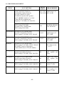
1
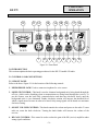
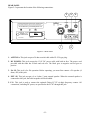
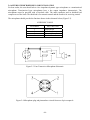
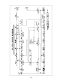
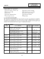
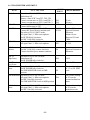
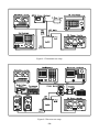
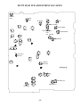
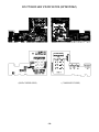
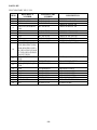
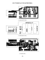
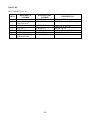
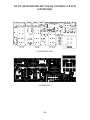
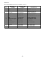
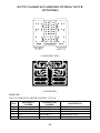
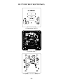
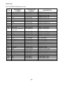
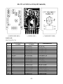
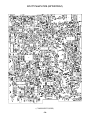
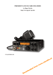
CB Radio Model DX 979 Service Manual Copyright Reserved TABLE OF CONTENTS DX 979 PAGE CHAPTER 1 SPECIFICATIONS 1.0 General . . . . . . . . . . . . . . . . . . . . . . . . . . . . . . . . . . . . . . . . . . . . . . . . . . . . . . . . . . . . . . . . 1.1 Transmitter . . . . . . . . . . . . . . . . . . . . . . . . . . . . . . . . . . . . . . . . . . . . . . . . . . . . . . . . . . . . . 1.2 Receiver . . . . . . . . . . . . . . . . . . . . . . . . . . . . . . . . . . . . . . . . . . . . . . . . . . . . . . . . . . . . . . . 2 2 2 CHAPTER 2 OPERATION 2.0 Introduction . . . . . . . . . . . . . . . . . . . . . . . . . . . . . . . . . . . . . . . . . . . . . . . . . . . . . . . . . . . . 2.1 Control & Connections . . . . . . . . . . . . . . . . . . . . . . . . . . . . . . . . . . . . . . . . . . . . . . . . . . . 2.2 Microphone . . . . . . . . . . . . . . . . . . . . . . . . . . . . . . . . . . . . . . . . . . . . . . . . . . . . . . . . . . … 2.3 Operation . . . . . . . . . . . . . . . . . . . . . . . . . . . . . . . . . . . . . . . . . . . . . . . . . . . . . . . . . . . . … 2.4 Alternate Microphones And Installation . . . . . . . . . . . . . . . . . . . . . . . . . . . . . . . . . . . . . 3 3 7 7 8 CHAPTER 3 CIRCUIT DESCRIPTION 3.0 Introduction . . . . . . . . . . . . . . . . . . . . . . . . . . . . . . . . . . . . . . . . . . . . . . . . . . . . . . . . . . . . 3.1 PLL Circuit . . . . . . . . . . . . . . . . . . . . . . . . . . . . . . . . . . . . . . . . . . . . . . . . . . . . . . . . . . . .. 3.2 Receiver Circuit . . . . . . . . . . . . . . . . . . . . . . . . . . . . . . . . . . . . . . . . . . . . . . . . . . . . . . . . . 3.3 Transmitter Modulation Circuit . . . . . . . . . . . . . . . . . . . . . . . . . . . . . . . . . . . . . . . . . . . … 3.4 Transmitter Amplifier Circuit . . . . . . . . . . . . . . . . . . . . . . . . . . . . . . . . . . . . . . . . . . . . . 9 9 9 9 9 CHAPTER 4 ALIGNMENT 4.0 Required Test Equipment . . . . . . . . . . . . . . . . . . . . . . . . . . . . . . . . . . . . . . . . . . . . . . . … 4.1 Alignment Procedures . . . . . . . . . . . . . . . . . . . . . . . . . . . . . . . . . . . . . . . . . . . . . . . . . . . . 11 11 CHAPTER 5 MAINTENANCE 5.0 5.1 5.2 Precautions . . . . . . . . . . . . . . . . . . . . . . . . . . . . . . . . . . . . . . . . . . . . . . . . . . . . . . . . . . . . . Periodic Inspection . . . . . . . . . . . . . . . . . . . . . . . . . . . . . . . . . . . . . . . . . . . . . . . . . . . . . .. Fuse Replacement . . . . . . . . . . . . . . . . . . . . . . . . . . . . . . . . . . . . . . . . . . . . . . . . . . . . . . . 16 16 16 CHAPTER 6 DIAGRAMS AND PARTS LIST 6.0 PCB Layout & Parts List . . . . . . . . . . . . . . . . . . . . . . . . . . . . . . . . . . . . . . . . . . . . . . . . . . -1- 17 CHAPTER 1 SPECIFICATIONS DX 979 1.0 GENERAL Model Channels Frequency Range Emission Modes Frequency Control Frequency Tolerance Frequency Stability Operating Temperature Range Microphone Input Voltage Antenna Connector Dimensions Weight DX 979 40 26.965 – 27.405 MHz AM/USB/LSB Phase Lock Loop (PLL) synthesizer 0.005 % 0.001 % -30°C to +50°C Dynamic PTT, 500 Ω 13.8V DC UHF; SO239 7 1/4”(W) x 9”(D) x 2 1/4”(H) 3.5 lbs. 1.1 TRANSMITTER RF Power Output RF Transmit Modes Modulation Spurious Emissions Carrier Suppression Audio Frequency Response Antenna Impedance Output Indicators AM: 4W; USB/LSB: 12W PEP AM/SSB High and Low level Class B, Amplitude Modulation: AM and SSB. - 60dB - 60dB 300 to 2500 Hz 50 Ohms Meter shows incoming signal strength, RF output power, SWR and AM Modulation level. Transmit LED glows red when transmitter is in operation. 1.2 RECEIVER Sensitivity For 10dB S/N (AM/ SSB) IF Frequency Image Rejection Adjacent Channel Selectivity RF Gain Control Automatic Gain Control (AGC) Figure Of Merit Squelch Noise Blanker Audio Output Power Audio Frequency Response Built-in Speaker External Speaker (Not Supplied) AM: < 0.5 uV ; USB/LSB: < 0.25 uV AM: 10.695 MHz 1st IF, 455 KHz 2nd IF - 50dB - 60dB 45dB adjustable for optimum signal reception 100mV for 10dB Change in Audio Output Adjustable; threshold less than 0.5µV RF type 2.5W @ 10% THD 300 to 2500 Hz 8 Ohms, 4 Watts 8 Ohms, 4 Watts (SPECIFICATIONS SUBJECT TO CHANGE WITHOUT NOTICE) -2- CHAPTER 2 OPERATION DX 979 10 11 12 13 TALKBACK S 1 7 5 3 +20 80 PWR 0 SWR 1 1 6 3 1.5 2 12 +40 1 00 % 20 MOD 15 18 3 M AX 16 17 18 CLARIFIER SWR 9 60 40 14 NB/ANL USB dB RX/TX +6 0 MOD OFF CB PWR VOL DX 979 MIC SQ AM PA LSB SWR RF DIM PWR OFF 1 2 3 4 5 6 7 8 9 Figure 2-1 Front Panel 2.0 INTRODUCTION This section explains the basic operating procedures for the DX 979 mobile CB radio. 2.1 CONTROLS AND CONNECTIONS 2.1.1 FRONT PANEL Refer to the above Figure 2-1 for the location of the following controls. 1. MICROPHONE JACK: Used to connect microphone for voice source. 2. SQUELCH CONTROL: This knob is used to eliminate background noise being heard through the receiver, which can be disturbing when no transmissions are being heard through the receiver. To use this feature, turn the knob fully counterclockwise and then turn clockwise slowly until the background noise is just eliminated. Further clockwise rotation will increase the threshold level which a signal must overcome in order to be heard. Only strong signals will be heard at a maximum clockwise setting. 3. ON/OFF VOLUME CONTROL: This knob controls the volume and power to the radio. To turn radio on, rotate the knob clockwise. Turning the knob further will increase the volume of the receiver. 4. RF GAIN CONTROL: This control is used to reduce the gain of the RF (receive) amplifier under strong signal conditions. -3- 5. MIC GAIN CONTROL: Adjusts the microphone gain in the transmit and PA modes. This controls the gain to the extent that full talk power is available several inches away from the microphone. In the Public Address (PA) mode, the control functions as the volume control. 6. RF POWER CONTROL: This control allows the user to adjust RF power output. 7. DIMMER CONTROL: This knob controls the level of brightness for the faceplate lettering, meter lamp and channel display. 8. SWR LED: This LED lights red when your SWR is higher than about 3:1. This is not an exact indicator of 3:1 SWR, but it is an indication that you should check your SWR reading. 9. CHANNEL SELECTOR: This control is used to select the desired transmit and receive channel. 10. FRONT PANEL METER: The front panel meter allows the user to monitor incoming signal strength, RF output power, SWR level and AM modulation level. 11. ILLUMINATED FACE PLATE: All faceplate lettering will fully illuminate to allow the user easy viewing at night. This unique, solid state, backlight is designed to maximize night vision while minimizing eye fatigue. Therefore, it is ideal for switch and control recognition day or night. 12. TALKBACK CONTROL: Adjust this knob for desired volume of Talkback. This is used to monitor your own voice. For example, you could use this feature to compare different microphones. 13. CLARIFIER CONTROL: Allows tuning of the receive frequency above or below the channel frequency by up to 1.0KHz. Although this control is intended primarily to tune in SSB signals, it may be used to optimize AM signals. 14. SWR/MOD/PWR SWITCH: This switch controls the function of the meter during the transmit mode. In the “SWR” position, the meter indicates the Standing Wave Ratio (SWR) of your antenna. There are no adjustments because the SWR circuit in this radio calibrates itself automatically. When the switch is in the “MOD” position, the green scale on the meter indicates your percentage of modulation in the AM mode only. They are most accurate when testing at maximum power output. When this switch is in “PWR” position, the meter indicates your power output. 15. NB-ANL/CB/PA SWITCH: When the switch is in the NB/ANL position, the Noise Blanker (NB) and Automatic Noise Limiter (ANL) circuits are activated. The Noise Blanker is very effective in eliminating repetitive impulse noise such as ignition interference. In the CB position, the PA function is disabled and the radio will transmit and receive on the speaker that is connected. In the PA position, the radio acts as public address amplifier. Your voice will come out of the speaker that is plugged into the PA. SP. jack on the rear panel. The radio does not operate when you are in the PA mode. 16. MODE SWITCH: This control allows you to select one of the following operating modes: AM/USB/LSB. 17. RX/TX LED: This LED is green during receive and red during transmit. 18. CHANNEL DISPLAY: The channel display indicates the current selected channel. -4- REAR PANEL Figure 2-2 represents the location of the following connections: 3 5 PA SP. This device complies with part 15 of the FCC Rules. Operation is subject to the condition that this device does not cause harmful interference. 4 EXT SP. ANT Service Manual at www.GalaxyRadios.com F.C. MODEL NO. : DX 979 AM/SSB 40 CH CB TRANSCEIVER FCC ID : MEE − DX − 979 DATE OF MFG.: SERIAL NO. : - DC 13.8V + 1 2 Figure 2-2 Rear Panel 1. ANTENNA: This jack accepts a 50 ohm coaxial cable with a PL-259 type plug. 2. DC POWER: This jack accepts the 13.8V DC power cable with built-in fuse. The power cord provided with the radio has a black and red wire. The black goes to negative and red goes to positive. 3. PA SP: This jack is for PA operation. Before operating, you must first connect a PA speaker (8 ohms, 4W) to this jack. 4. EXT. SP: This jack accepts a 4 to 8 ohm, 5 watt external speaker. When the external speaker is connected to this jack, the built-in speaker will be disabled. 5. F.C.: This jack is used to connect the optional Galaxy FC347 six-digit frequency counter. All connections, including DC power, are provided to the FC347 through this jack. -5- 2.1.3 FREQUENCY CHART CHANNEL CHANNEL FREQUENCY (MHz) CHANNEL CHANNEL FREQUENCY (MHz) 1 26.965 21 27.215 2 26.975 22 27.225 3 26.985 23 27.255 4 27.005 24 27.235 5 27.015 25 27.245 6 27.025 26 27.265 7 27.035 27 27.275 8 27.055 28 27.285 9 27.065 29 27.295 10 27.075 30 27.305 11 27.085 31 27.315 12 27.105 32 27.325 13 27.115 33 27.335 14 27.125 34 27.345 15 27.135 35 27.355 16 27.155 36 27.365 17 27.165 37 27.375 18 27.175 38 27.385 19 27.185 39 27.395 20 27.205 40 27.405 -6- 2.2 MICROPHONE The receiver and transmitter are controlled by the push-to-talk switch on the microphone. Press the switch and the transmitter is activated, release the switch to receive. When transmitting, hold the microphone two inches from your mouth and speak clearly in a normal voice. The radio comes complete with a low impedance (500 ohm) dynamic microphone. 2.3 OPERATION 2.3.1 PROCEDURE TO RECEIVE 1. Be sure that the power source, microphone and antenna are connected to the proper connectors before going to the next step. 2. Press the POWER switch to apply power to the radio. 3. Set the VOL to a comfortable listening level. 4. Set the MODE switch to the desired mode. 5. Listen to the background noise from the speaker. Turn the SQUELCH knob slowly clockwise until the noise just disappears. The SQUELCH is now properly adjusted. The receiver will remain quiet until a signal is actually received. Do not advance the control too far or some of weaker signals will not be heard. 6. Set the CHANNEL selector switch to the desired channel. 7. Set the RF GAIN control fully clockwise for maximum RF gain. 8. Adjust the CLARIFIER control to clarify the SSB signals or to optimize AM signals. 2.3.2 PROCEDURE TO TRANSMIT 1. Select the desired channel of transmission 2. Set the MIC GAIN control fully clockwise. 3. If the channel is clear, depress the push-to-talk switch on the microphone and speak in a normal voice. -7- 2.4 ALTERNATE MICROPHONES AND INSTALLATION For best results, the user should select a low impedance dynamic type microphone or a transistorized microphone. Transistorized type microphones have a low output impedance characteristic. The microphones must be provided with a four-lead cable. The audio conductor and its shielded lead comprise two of the leads. The third lead is for transmit control and the fourth is for receiving control. The microphone should provide the functions shown in the schematic below (Figure 2-3). 4 WIRE MIC CABLE Pin Number 1 2 3 4 Mic Cable Lead Audio Shield Audio Lead Transmit Control Receive Control Figure 2-3 Your Transceiver Microphone Schematic Figure 2-4 Microphone plug and pin numbers viewed from rear of pin receptacle. -8- CHAPTER 3 CIRCUIT DESCRIPTION DX 979 3.0 INTRODUCTION This section explains the technical theory of operation for the DX 979 mobile CB radio. 3.1 PLL CIRCUIT The Phase Lock Loop (PLL) circuit is responsible for developing the receiver’s first local oscillator signal and the transmitter’s exciter signal. The PLL circuit consists primarily of IC2, IC3, Q25, Q29 and Q28. The PLL circuit is programmed by the rotary channel switch GPS-668. The GPS-668 communicates the correct binary data information to the programmable divider inside of IC3. IC3 then controls the VCO (Voltage Controlled Oscillator) to oscillate on the correct frequency. This signal is fed either into the receiver’s first mixer (for receive operation) or the transmitter’s mixer (for transmit operation). 3.2 RECEIVER CIRCUIT The incoming RF signal comes into the radio via the antenna and into the front-end pre-amp, Q17. The RF signal is fed into the mixer circuit of Q18/Q19 and then into the AM IF section of the receiver. The signal is then detected by the AM detector and then fed to the audio amplifier section of the receiver and finally out to the speaker. 3.3 TRANSMITTER MODULATION CIRCUIT (1) The transmitter modulation circuit modulates the low-level RF signal from the PLL exciter circuit with the user’s audio voice signal from the microphone. The audio from the microphone is then amplified and fed into the transmit amplifier circuit. (2) If the transceiver is in the AM mode, the AF power amplifier modulates the last RF amplifier, which produces a true amplitude modulated RF signal. (3) If the transceiver is in the SSB mode, the audio signal is mixed with the 10.6975MHz oscillator in IC6. 3.4 TRANSMITTER AMPLIFIER CIRCUIT The transmitter takes the basic exciter signal from IC9 of the TX mixer and amplifies it through a series of amplifiers consisting of Q52, Q51, Q49 and Q47 where it is sent out to the antenna connector. -9- - 10 - CHAPTER 4 ALIGNMENT DX 979 4.0 REQUIRED TEST EQUIPMENT c DC Power Supply (13.8VDC, 10A) d RF Wattmeter (10W) e Multi-meter f Automatic Modulation Meter g Audio Signal Generator h Frequency Counter (100 MHz) i RF Signal Generator (100 MHz) j Automatic Distortion Meter k Oscilloscope (50 MHz) l Sinad Meter 4.1 ALIGNMENT PROCEDURES This transceiver has been aligned at the factory and does not require any adjustments at installation. The required test equipment listed are used for the test setup or alignment shown in Figure 4-1 Transmitter Test Setup and Figure 4-2 Receiver Test Setup. These test setups are used in part or total during the following adjustments. Refer to page 15 for adjustment locations. 4.1.1 PLL ALIGNMENT ITEM VCO U.U.T. SETTING ADJUST POINT MEASUREMENT Disconnect ‘short PCB’ from TP7, TP8 and TP9. Set radio to CH 1 AM RX mode. Connect Multi-meter to TP2. L14 2.5 VDC ± 0.1 Set CLARIFIER Control to 12 o’clock. Connect Oscilloscope to TP3. Connect Frequency Counter to IC3 Pin 8. L15 VC1 Adjust for max. AM Frequency Set radio to CH 19 AM RX mode. Connect Frequency Counter to TP3. L20 16.4900MHz ± 20Hz USB Frequency Set radio to CH 19 USB RX mode. Connect Frequency Counter to TP3. L21 16.4925MHz ± 20Hz LSB Frequency Set radio to CH 19 LSB RX mode. Connect Frequency Counter to TP3. L22 16.4875MHz ± 20Hz TX Offset Frequency Set radio to CH 19 LSB TX mode. Connect Frequency Counter to TP3. VR7 16.4875MHz ± 20Hz AM OSC Set radio to CH 19 AM TX mode. Connect Frequency Counter to TP5. L23 10.6950MHz ± 10Hz USB OSC LSB OSC Set radio to CH 19 USB TX mode. Connect Frequency Counter to TP5. Set VR6 fully clockwise Set radio to CH 19 LSB TX mode.Connect Frequency Counter to TP5. Set VR6 back to mid position when finished. - 11 - 10.2400MHz ± 20Hz 10.6925MHz ± 10Hz L24 10.6975MHz ± 10Hz L25 4.1.2 TRANSMITTER ALIGNMENT ITEM U.U.T. SETTING Set radio to CH 19 USB TX mode. Modulation Off. Remove “short PCB” from TP7, TP8, TP9. Connect current meter to TP7(+) and TP9 (-) Connect current meter to TP7(+) and TP8 (-) SSB APC Set radio to CH 19 USB RX mode. Connect Multi-meter to TP7. SSB TX Power Connect “short PCB” to TP7 and TP9. Connect RF Power Meter to antenna jack. Set radio to CH 19 USB TX mode. AF signal 30mV, 1 KHz to microphone. Set RF PWR fully clockwise. Set MIC GAIN fully clockwise. SSB ALC Set radio to CH 19 USB TX mode. AF signal 30mV, 1 KHz to microphone. ADJUST POINT MEASUREMENT BIAS Current SSB Carrier Balance Set radio to CH 19 USB TX mode. Set MIC GAIN fully counter-clockwise. Connect Oscilloscope to antenna connector. AM TX High Power Set radio to CH 19 AM TX mode. Modulation Off. Set RF POWER fully clockwise. Set RF POWER fully counterclockwise. AM TX Low Power RF Power Meter VR12 VR10 VR17 50 mA 100 mA 12.5 VDC L40,L42, L43,L44 MAX > 12W Spurious Emission Minimum. Balance Power Between CH1 and CH40. VR13 11.5 W VR6 Spurious Emission to Minimum. VR14 3.8 W VR18 0.3W±0.2W Set radio to CH 19 AM TX mode. Set RF POWER fully clockwise. Set SWR/MOD/PWR Switch to PWR VR9 position. AM Modulation Set radio to CH 19 AM TX mode. AF signal 30mV, 1 KHz to microphone. VR16 Set MIC Gain fully clockwise. Set SWR/MOD/PWR Switch to MOD position For a needle reading of “4” on TX PWR scale. AM Modulation Set radio to CH 19 AM TX mode. Meter AF signal 30mV, 1 KHz to microphone. Set MIC Gain fully clockwise. For a needle reading of 95% on the modulation scale. - 12 - VR15 For a needle reading of 95% on the external modulation meter. 4.1.3 RECEIVER ALIGNMENT ITEM U.U.T. SETTING AM Sensitivity Set radio to CH 19 AM RX mode. Set RF GAIN Fully Clockwise. Set SQ Fully Counter Clockwise. Set VOL Control at 2 o’clock. Set NB/ANL switch to OFF position. Set CLARIFIER Control to 12 o’clock. Connect RF SG to antenna jack Frequency 27.185 MHz, 1uV. Mod 30%. Set radio to CH 40 AM RX mode. RF SG setting 27.405 MHz. Set radio to CH 1 AM RX mode. RF SG setting 26.965 MHz. ADJUST POINT MEASUREMENT L2,L3,L5,L6, Audio Output > 2V L7,L8,L9,L10 S/N > 10 dB. L5,L6 For Balance Between CH 1 and CH 40. USB Sensitivity Set radio to CH19 USB RX mode. Set VOL Control Fully Clockwise. RF SG setting 27.186 MHz, 0.5uV. Mod off. L11,L12 Audio Output > 2V S/N > 10dB. LSB Sensitivity Set radio to CH19 LSB RX mode. Set VOL Control Fully Clockwise. RF SG setting 27.184 MHz, 0.5uV. Mod off. L11,L12 Audio Output > 2V S/N >10dB. NB Adjust Set radio to CH 18 AM RX mode RF SG setting 27.185 MHz, 1000uV. Mod off. L1 Set NB/OFF switch to ON position. Connect Multi-meter to TP1 (D2 cathode). DC Voltage to max. ( > 2.0V ) AM Squelch Set radio to CH 19 AM RX mode. Set SQ Control Fully Clockwise. VR4 RF SG setting 27.185 MHz, 20mV. Mod 30%. Adjust very slowly until squelch just closes. SSB Squelch Set radio to CH 19 USB RX mode. Set SQ Control Fully Clockwise. RF SG setting 27.186 MHz, 20 mV. Mod off. VR3 Adjust very slowly until squelch just closes AM S-Meter Set radio to CH 19 AM RX mode. RF SG setting 27.185 MHz, 100uV. Mod 30%. VR1 For a reading of “9” on the “S” scale. SSB S-Meter Set radio to CH 19 USB RX mode. RF SG setting 27.186 MHz, 100uV. Mod off. - 13 - VR2 For a reading of “9” on the “S” scale Figure 4-1 Transmitter test setup Figure 4-2 Receiver test setup - 14 - DX 979 MAIN PCB ADJUSTMENT LOCATION DRIVER BIAS FINAL BIAS ALC RF METER APC AM LOW POWER AM MOD AM LOWAM POWER MOD AM HI POWER AM MOD METER SSB AM S-METER AM S-METER SSB 10.240 MHz ADJUST CARRIER BALANCE SSB SQUELCH AM SQUELCH TX OFFSET - 15 - CHAPTER 5 MAINTENANCE DX 979 5.0 PRECAUTIONS The inherent quality of the solid-state components used in this transceiver will provide many years of continuous use. Taking the following precautions will prevent damage to the transceiver. (i) Never key the transmitter unless an antenna or suitable dummy load is connected to the antenna receptacle. (ii) Ensure that the input voltage does not exceed 16 VDC or fall below 11. (iii) Transmitting over long periods can cause heat built-up and cause transmitter damage. 5.1 PERIODIC INSPECTION This unit is aligned at the factory to deliver maximum performance. However, continued performance cannot be expected without periodic inspection and maintenance. Important points to be checked regularly are as follows; Check Item Whip antenna (option) Coaxial cable Action If cracked or broken, replace it. If sheath is cracked or immersed in water, install new coaxial cable. Coaxial & power If loosened, reconnect. If plug connections corroded, clean contacts. Battery connection If corroded, clean power terminals. Ground terminal If corroded, clean terminal. 5.2 FUSE REPLACEMENT To protect the equipment from serious damage, a fuse is provided on the power supply lines. The fuse protects against over voltage / reverse polarity or internal fault of the equipment. If the fuse has blown, first find out the cause of the trouble before replacing it. A fuse rated for more than the transceiver requirement should not be used, since it may permanently damage the equipment. Damage due to over fusing is not covered by the warranty. - 16 - CHAPTER 6 DIAGRAMS & PARTS LIST DX 979 6.0 GENERAL Information on most electrical and mechanical parts is included in the parts list. The reference designators are in alphanumeric order. - 17 - DX 979 ROTARY SWITCH PCB (EPT092920Z) (SMD-COPPER SIDE) ( COMPONENT SIDE ) - 18 - PART LIST: DX 979 ROTARY SW. P.C.B ITEM 1 2 3 4 5 6 7 8 9 10 11 12 13 14 15 16 17 18 19 20 REFERENCE NUMBER R207,R210,R218 R201 R202,R203,R204,R205, R206 R215 R221 R214 R220 C201,C202 D201,D202,D203,D204, D205,D206,D207,D208, D209,D210,D211,D212, D13,D214,D215,D216,D 217,D218,D219,D220,D 226,D227,D228 D221,D222,D223,D224, D225 Q207 Q201,Q202,Q203,Q204, Q206 Q205 J201,J206 J203 J202 J204 ROTARY SW J205 RANGER PART NUMBER EPT092920Z RCY010004Z RCY013314Z RCY016814Z ROTARY SW PCB CHIP/F/R 0.0 Ω 0.1W CHIP/F/R 330 Ω 0.1W CHIP/F/R 680 Ω 0.1W RCY014724Z RCY016824Z RCY012234Z RCY016834Z CK1104AB5X EDSS00355Y CHIP/F/R 4.7K Ω 0.1W CHIP/F/R 6.8K Ω 0.1W CHIP/F/R 22K Ω 0.1W CHIP/F/R 68K Ω 0.1W CHIP/C 0.1uF 50WV DIODE (S.M.D.) 1SS355 EDSS00181Y DIODE (S.M.D.) 1SS181-TE85L TY2SC2712G TYZRN1403Z TR 2SC2712GR-TE85L TR RN1403-TE85L TYZRN2403Z EX07N48223 EX07N48350 EX07N48222 EX07N48209 EWRT32059S WX01070710 TR RN2403-TE85L PCB CONN/S 2 PIN PCB CONN/S 3 PIN PCB CONN/S 5 PIN PCB CONN/S 10 PIN ROTARY SW GPS-0668 JUMPER WIRE - 19 - DESCRIPTION DX 979 DISPLAY PCB (EPT092930Z) ( COMPONENT SIDE ) ( COMPONENT SIDE ) ( COPPER SIDE ) - 20 - PART LIST: DX 979 DISPLAY P.C.B ITEM 1 2 3 4 5 6 7 REFERENCE NUMBER R301,R302,R303,R304, R305,R306,R307 R308 D301,D302 LED201,LED202 DISPLAY HI/OFF/LO,NB/CB/PA, SWR/MOD/PWR RANGER PART NUMBER EPT092930Z RCY016814Z DISPLAY PCB CHIP/F/R 680 Ω 0.1W RCY011024Z EDSS00355Y EX01Y40114 EX03N40419 EWSL31027K CHIP/F/R 1K Ω 0.1W DIODE 1SS355 LED LAMPS KM-23ESGC LED DISPLAY TX-566 SLIDE SW. 3N - 21 - DESCRIPTION DX 979 (DIM-PWR/MIC-RF/VOL-SQ CONTROL) VR PCB (EPT092940Z) ( COMPONENT SIDE ) ( COPPER SIDE ) - 22 - PART LIST: DX 979 DIM-PWR/MIC-RF/VOL-SQ CONTROL, VR P.C.B ITEM 1 2 3 4 5 6 7 8 9 10 11 12 13 14 15 16 17 18 REFERENCE NUMBER R402 R401 C401,C402 C403,C404 VR404 L402 L401 Q902 (VR401)VOL-SQ-OFF MIC-RF DIM-PWR J401,J408,J410,J411, J403,J405,J413 J406,J414 J407 J402 J409 RANGER PART NUMBER EPT092940Z RCY016824Z RCY011034Z CK1102AB5X CK1103AB5X RE102Y0128 YCTLI5653C YCBAD18581 TYDTA124EA RV50303522 RV10203524 RV50203539 EX07N48223 EX07N48350 EX07W48824 EX07N41216 EX07N48222 EX07W48826 - 23 - DESCRIPTION VR PCB CHIP/F/R 6.8K Ω 0.1W CHIP/F/R 10K Ω 0.1W CHIP/C .001uF 50VW CHIP/C .01uF 50VW CHIP/F/R 1K (TMC3KJ) CHOKE COIL 5.6uH BEAD FERRITE COIL WB-403025 T/R DTA124EUAT106 V/R 50KB/50KA W/SW V/R 1KB/1KA VR 5KB/5KB PCB CONN/S 2PIN PCB CONN/S 3PIN PCB CONN/S 3PIN PCB CONN/S 3PIN PCB CONN/S 5PIN PCB CONN/S 5PIN DX 979 (TALKBACK/CLARIFIER CONTROL) VR PCB (EPT092950Z) ( COMPONENT SIDE ) ( COPPER SIDE ) PART LIST: DX 979 TALKBACK/CLARIFIER CONTROL, VR P.C.B ITEM 1 2 3 4 5 REFERENCE NUMBER VR501 (CLARIFIER) VR502 (TALKBACK) J501 J503 RANGER PART NUMBER EPT092950Z RV10203528 RV20203558 EX07N48331 EX07N48350 - 24 - DESCRIPTION TB PCB VR 1KB VR 20KB/SW PCB CONN/S 6 PIN PCB CONN/S 3 PIN DX 979 METER PCB (EPT092961Z) ( COMPONENT SIDE ) ( COPPER SIDE ) ( COPPER SIDE-SMD ) - 25 - PART LIST: DX 979 METER PCB (Dimmer Circuit) ITEM 1 2 3 4 5 6 7 8 9 10 11 12 13 14 15 16 17 18 19 20 21 22 23 24 25 26 27 28 29 30 REFERENCE NUMBER R603 R606,R607 R610 R605 R604,R611 R601 R602 R609 C602,C609 C601,C607,C608,C610, C612,C620 C619,613,614,615,616 C621 C617 C605,611 C622 C603,C606 C604,C618 IC601 D601 D602 Q601,602 Q603 L602 L601 LAMP EL(SH3024) J603 J601 J602 RANGER PART NUMBER EPT092961Z RCY011504Z RCY144704Z RCY011024Z RCY013324Z RCY011034Z RCY011234Z RCY014734Z RCY011844Z CK1103AB5X CK1104AB5X METER PCB CHIP/F/R 15 Ω 0.1W CHIP/F/R 47 Ω 1/4W CHIP/F/R 1KΩ 0.1W CHIP/F/R 3.3KΩ 0.1W CHIP/F/R 10KΩ 0.1W CHIP/F/R 12KΩ 0.1W CHIP/F/R 47KΩ 0.1W CHIP/F/R 180KΩ 0.1W CHIP/C 0.01uF 50WV CHIP/C 0.1uF 50WV CK5105AB7R CK1473AB5X CK2474AB7R CK5475AA7R CTY161066A CEY164767Z CEY251077Z YNSN8144BV EDZD05519Y ED1N04148Y TY2SC2712G TYDTC124EA YCTLI2274E YCTLI4774E EX02N40230 EX07N49373 EX07N48223 EX07N48350 EX07N48222 CHIP/C 1uF 16WV CHIP/C 0.047uF 50WV CHIP/C 0.47uF 25WV CHIP/C 4.7uF 16WV T/C 10uF 16WV E/C 47uF 16WV E/C 100uF 25WV I.C. SM8144BV ZENER DIODE RLZ5.1BT6-11 DIODE 1N4148 T/R 2SC2712GR T/R DTC124EUAT106 CHOKE COIL 220uH CHOKE COIL 470uH LAMP 0.05 12V PCB CONN/S 3 PIN PCB CONN/S 2 PIN PCB CONN/S 3 PIN PCB CONN/S 5 PIN - 26 - DESCRIPTION DX 979 ANTENNA PCB (EPT360042Z) (COPPER SIDE-SMD ) ( COPPER SIDE ) ( COMPONENT SIDE ) PART LIST: DX 979 ANT P.C.B ITEM 1 2 3 4 5 6 7 8 9 10 11 12 13 14 15 16 17 18 19 REFERENCE NUMBER R9 R1 R3,R4 R2 R5,R11 R10,R12 R7,C5 C7 C6 C3,C4 C1,C2 Q1 D3 D1,D2 D4 L1 VR1 JP1 RANGER PART NUMBER EPT360042Z RCY010004Z RCY014714Z RCY011014Z RCY013314Z RCY011024Z RCY012224Z RCY011034Z CK1059AB1A CK1030AB1A CK2104AB7R CK1103AB7L TY2SC2712G EDSS00355Y EDHM0198SY EDMA0028TY ECRFZ10053 RE10300009 WX01070715 - 27 - DESCRIPTION ANT P.C.B 0 OHM 0.1W 470 OHM 0.1W 100 OHM 0.1W 330 OHM 0.1W 1K OHM 0.1W 2.2K OHM 0.1W 10K OHM 0.1W 0.5PF 50WV 3PF 50WV 0.1uF 25WV 0.001uF 50WV TR 2SC2712GR DIODE 1SS355 DIODE HSM198S DIODE MA28T RF COIL C3RH0610 S/F/R 10K OHM JUMPER WIRE DX 979 MAIN PCB (EPT092913Z) ( COMPONENTS SIDE ) - 28 - DX 979 MAIN PCB (EPT092913Z) ( COPPER SIDE ) - 29 - PART LIST DX 979 MAIN PCB REFERENCE NUMBER RANGER PART NO. EPT092913Z EPT120060A R19,305,258(B239) RCP160004Z R246 RCP161004Z R267 RCP161504Z 241 RCP162204Z R133,213,253,282,113 RCP164704Z R130,215,220,249 RCP165604Z R11,101 RCP166804Z R5,8,30,33,76,81,174,260,263 RCP161014Z ,3,95,169 R32,100,245 RCP161514Z R23 RCP161814Z R140,163,177,259(B239) RCP162214Z R31,99 RCP162714Z R6,10,16,24,248,254,300,299 RCP163314Z R188,268,293,154,155,156, RCP164714Z 250,280 R266 RCP165614Z R4,50,209,89,94 RCP166814Z R74 RCP168214Z R62,64,67,72,115,116,118, RCP161024Z 122,123,136-138,160,164, 179,186,189,205,206,214, 303,232,237,238,261,269,291, 292,295,98,166,167,320, R192,88 RCP161224Z R132,207,233,247, RCP161524Z 255,273,251,79,80,54,87,97 R226 RCP161824Z R20,27,71,75,134, RCP162224Z 162,283,313,93,114,197,279 R9,25,28,121 RCP162724Z R18,22,66,73,128, RCP163324Z 191,219,274,73,252,60,110, 171 R52,57 RCP163924Z R26,84,165,190,195,196,131 RCP164724Z R264,265,83,92 RCP165624Z R14,40,41,70,82,312 RCP166824Z R275,90 RCP168224Z R1,13,17,65,68,159,161,175, RCP161034Z 181,202,210,216,227-231,272, 276,296,297,262,56,86,173 R178,310,153 RCP161234Z R180 RCP161534Z R187,208,91,109 RCP162234Z R2,309,311 RCP163334Z R46 RCP163934Z R7,29,61,63,185,218,126,157, RCP164734Z 222,224,96,150 R21,105,107 RCP166834Z R45 RCP168234Z R12,42,43,44,51,53,104,108, RCP161044Z 112,182,184,221,225,278 R47,117,135,139,194 RCP162244Z R49,55,176,170,172 RCP162744Z R15,111,183 RCP164744Z R48 RCP168244Z R106 RCP161054Z R193 RCP161554Z R124 RCP161064Z R244 RCP141514Z R239 RCP121034Z C8 CC0508204L C4 CC0501015L DESCRIPTION MAIN PCB DCB+ PCB 0 Ω 1/16W 10 Ω 1/16W 150 Ω 1/16W 220 Ω 1/16W 47 Ω 1/16W 56 Ω 1/16W 68 Ω 1/16W 100 Ω 1/16W 150 Ω 1/16W 180 Ω 1/16W 220 Ω 1/16W 270 Ω 1/16W 330 Ω 1/16W 470 Ω 1/16W 560 Ω 1/16W 680 Ω 1/16W 820 Ω 1/16W 1K Ω 1/16W 1.2K Ω 1/16W 1.5K Ω 1/16W 1.8K Ω 1/16W 2.2K Ω 1/16W 2.7K Ω 1/16W 3.3K Ω 1/16W 3.9K Ω 1/16W 4.7K Ω 1/16W 5.6K Ω 1/16W 6.8K Ω 1/16W 8.2K Ω 1/16W 10K Ω 1/16W 12K Ω 1/16W 15K Ω 1/16W 22K Ω 1/16W 33K Ω 1/16W 39K Ω 1/16W 47K Ω 1/16W 68K Ω 1/16W 82K Ω 1/16W 100K Ω 1/16W 220K Ω 1/16W 270K Ω 1/16W 470K Ω 1/16W 820K Ω 1/16W 1M Ω 1/16W 1.5M Ω 1/16W 10M Ω 1/16W 150 Ω 1/4W 10K Ω 1/2W 82PF 50WV 100PF 50WV - 30 - C137 C31,136 C11,14 C23 C52,197 C225 C218 C61,62,90,79,190 C108,147,1,49 C84,89 C43,76 C54,55 C119,279,226,287 C195 C202,224 C88,116,117 C191,150 C194,192 C196,222,295 C139,141 C140 C130 C281 C282 C220 C86 C201,203 C210 C74,85 C199 C7,47,50,95,99,110,118,120, 174,183, 244,245,100, 246 C81,173,193,206,207, 236, 213,234,250,256,259,272, 249,302,270,177,215, 292,40, 171,235,211,291 C5,18,48,65,87,92, 96,102,105,106,257,151,160, 233,240,251,253,258,260,261, 263,20,217,68,72,143,266 C32,42,45,46,221,162,163, 164 C155 C200 C2,3,6,9,15,16,17,19,51,57, 58,60,109,114,133,138,161, 205,219,229,230,232,247, 265,267,269,271,278 ,285, 298,188,63,66,69,73,127, 134,135,142,145,146,241, 305,306,307,308,309,310, 311,312,131,262,216 C154 C97,149 C98,180,299,300 C178,296 C237,78 C184 C39,185 C176 CC0501515L CC0502715L CC0503315L CC0505615L CC0500101A CC0500201A CC0500301A CC0500501A CC0501004A CC0501504A CC0501804A CC0502204A CC0503304A CC0503904A CC0504704A CC0506804A CC0501015A CC0501515A CC0501815A CC0503904D CC0501515D CC0502004G CC0501015G CC0501815G CC0502215G CC0502715G CC0503915G CC0504715G CC0505615G CD3005614Z CC0501027L 150PF 50WV 270PF 50WV 330PF 50WV 560PF 50WV 1PF 50WV 2PF 50WV 3PF 50WV 5PF 50WV 10PF 50WV 15PF 50WV 18PF 50WV 22PF 50WV 33PF 50WV 39PF 50WV 47PF 50WV 68PF 50WV 100PF 50WV 150PF 50WV 150PF 50WV 39PF 50WV 150PF 50WV 20PF 50WV 100PF 50WV 180PF 50WV 220PF 50WV 270PF 50WV 390PF 50WV 470PF 50WV 560PF 50WV 560P 300WV 0.001UF 50WV CC0501047L 0.1UF 50WV CC0504737L 0.047UF 50WV CC0504727L 0.0047UF 50WV 0.022UF 50WV 0.01UF 100WV 0.01UF 50WV C34 C12 CM0504735Z CM0502225Z C198 C10 C67,75,153,157,170,186,187 C159,214,242 C103,182 C13,21,22,44,82,115,158,275, CE0501047Z CE0504747Z CE0501057Z CE0502257Z CE0504757Z CE0251067Z CC0502237L CC1001037L CC0501037L CT0162246Z CT0161046Z CT0162256Z CM0501045Z CM0501024Z CM0501035Z CM0502235Z CM0504725Z 0.22UF 16WV 0.1UF 16WV 2.2UF 16WV 0.1UF 50WV 0.001UF 50WV 0.01UF 50WV 0.022UF 50WV 0.0047UF 50WV 0.047UF 50WV 0.0022UF 50WV 0.1UF 50WV 0.47UF 50WV 1UF 50WV 2.2UF 50WV 4.7UF 50WV 10UF 25WV 276,132,239 VC1 CV038200AZ C80,181 C37,175,33,144,38 C156,238,293,107 C252 C152,179 C91 C243,248 C35 FL3 FL1 FL2 X1 X3 X4 IC6 IC1 IC3 IC7 IC9(B239) VCO Q8,17,20 Q51 Q52,53 Q36 Q24,43 Q60 Q30,33,62 Q1,2,9,10,11,25,28,29,46,27,2 1,22,50 Q3,4,5,7,16,31,35,39,40,42, 44,53,57,13,15,34,56 Q6,38 Q55 Q18,19 D3-5,7,9,10,13,14,20,21,95, 96,32-35,37,53,60-65,69, 75-81,88,89,102,106,107, 141,50,108,97,82,155,6,15, 24,25,26,27,36,38,50,52,54, 5,56,57,85,86,87,90,92,93, 8,115,28, 29,51,68,114 D1,2,11,12,30,31 D110 D109 D16,17 D49 D59,72 D71,145,156,103 D70 D73 L2,3 L6 L20,21,22 CE0252267Z CE0254767Z CE0161077Z CE0162277Z CE0163377Z CE0104777Z CE0251087Z CEM254767Z EFX8106952 EFCFW455HT EFCFE107MX EYCAB10240 EYBAA15480 EYBAE10697 ENMA00612Z ENSS00324Z ENRG871999 ENRO04558Z ENRCI6130Z ENNOHIC07A T2SC01674L T2SC02538Z T2SC01906Z TDTC0124ES TDTC0114ES TDTA0124ES T2SA01282E T2SC01675L TRIMMER/C 20P (CV38D2001) 22UF 25WV 47UF 25WV 100UF 16WV 220UF 16WV 330UF 16WV 470UF 10WV 1000UF 25WV 47UF 25WV 10.695MHZ CFW-455HT SFE10.7MX 10.240MHZ 15.480 MHZ 10.6975MHZ 1 AN-612 LM324 RCI-8719A BA4558 RCI-6130 UHIC07A 2SC1674L 2SC2538 2SC1906 DTC124ES DTC114ES DTA124ES 2SA1282AE 2SC1675L T2SC00945P 2SC945P T2SA00733P T2SA01869Z FMOJ00310Z ED1NM4148Z 2SA733P 2SA1869 F.E.T J310 1N4148 L25 ECIFT12013 L23,24 ECIFT12016 L1,11 L44 L9,10 L12 L15 L40 L14 L43 C306(L43 PIN4&6) L5 L7,42 L8 ECIFT12252 ECIFT12255 ECIFT12256 ECIFT12257 ECIFT12258 ECIFT12262 ECIFT12263 ECIFT12265 CK1820AA4A ECIFT12253 ECIFT12440 ECIFT12492 ED1N00060P ED1N04003Z ED1N04007Z EDSS00053Z EDSV00251Z EDMA00027W EDMA00027T EDZD05519Z EDZD05759Z ECIFT12002 ECIFT12290 ECIFT12012 1N60P 1N4003 1N4007 1SS53 SVC-251SPA MA27W-A MA27T-A 5.1V 0.5W 7.5V 0.5W 7MC-7172ABW I.F.T. I.F.T. 113CN-6514X I.F.T. 113CN-6485Z I.F.T. 113CN-6344Z I.F.T. I.F.T. I.F.T. I.F.T. I.F.T. I.F.T. I.F.T. I.F.T. 82PF 50WV I.F.T. I.F.T. I.F.T. - -311- L48 L503 L26,27,46 T1 L33,37 L47 L16 L28,30 L29 L31 L35 L38 L39 L41,13 VR10 ECCHK16096 ECCHK16000 ECCHK16003 ECCHK16004 ECCHK16070 ECCHK16176 ECCHK16246 ECSPG18003 ECSPG18075 ECSPG18365 ECSPG18001 ECRFZ10048 ECBAD18506 ECBAD18526 RE10100074 VR16,12,7,18 RE10200041 VR14,13 RE50200042 VR1,2,6,15,17 RE10300031 VR9 RE10400043 VR4,3 J9,MIC/IP JP5,14,15,16,17,18,30,35, 36,37,39,55,63,68,69,75,76,85 ,87,88,91,92,99,100,102,103 , 104,108,109 110,114,120,124,125,126,129, 131,133,136,148,19,153,13,11 2,127 JP31,41,43,46,79,80,81,82,84, 97,106,155,156,6 JP25,57,58,71,96,116,117, 122,123,130,142,119,3,70,113 ,141 JP22,24,29,107,134,135,132 JP11,20,38,40,42,83,94,98,4, 128 JP7,10,26,27,44,61,62,65,72, 73,74,78,89,95,114,115,118, 138,150,149,151,152,66,67,77 ,105,146,147,33,64 JP8,21,51,139,86 JP12,52,140 JP23,48,111,137,144,154,34, 145,8 JP32,45,93 JP1,47,49,50,54,56,58,90, 121,143 J7,17,22,25,31,34 J6,11,18,32 J21 J3,5,20 J1,14 J33 SP(J16) J12 TP2,3,5 TP7,8,9 PA,EXP SP L503 L504 RE50400087 WX01070702 WX01070705 470UH 0.47UH 470UH 1.1MH EI-19 22UH 4.7UH 22UH SPRING COIL SPRING COIL SPRING COIL SPRING COIL 25 UH BEAD COIL BEAD COIL S/F/R 100 Ω (KVSF6-637A) S/F/R 1K VM6CK S/F/R 5K VM6CK S/F/R 10K VM6CK S/F/R 100K VM6CK S/F/R 500K Ω JUMPER JUMP WIRE WX01070706 JUMP WIRE WX01070707 JUMP WIRE WX01070708 WX01070709 JUMP WIRE JUMP WIRE WX01070710 JUMP WIRE WX01070711 WX01070712 WX01070713 JUMP WIRE JUMP WIRE JUMP WIRE WX01070714 WX01070715 JUMP WIRE JUMP WIRE EX07N48223 EX07N48350 EX07N48490 EX07N48222 EX07N48331 EX07N48209 EX07N41330 EX07N41227 EX07N48612 XZZZ90006Z EX06N41045 WX0012015A WH0007005Z P/C/S 2P P/C/S 3P P/C/S 4P P/C/S 5P P/C/S 6P P/C/S 10P P/C/S 2P P/C/S 3P 1PIN L=11.8 EAR JACK TUBE LEAD WIRE DX 979 SCHEMATIC DIAGRAM (CONTROL PCB) DX 979 SCHEMATIC DIAGRAM (MAIN PCB) DX 979 EXPLODE DRAWING DX 979 MECHANICAL PART UPDATES & CORRECTIONS Any updates or corrections to this Service Manual will be included in the Tech Support section of our website at www.GalaxyRadios.com. Two Year Warranty This new Galaxy radio is covered by a two year limited warranty. Here are the details. • All of our Galaxy radio model numbers begin with the letters “DX” and are covered by our Limited Two Year Parts and Labor Warranty. • “Limited” means that we will repair problems caused by factory defects or normal use at no charge. Work performed by qualified technicians which did not cause any damage to the radio will not void the warranty and will be left intact. Problems caused by unqualified technicians or operator abuse can also be repaired, but there will be a charge. • The warranty period begins when the radio is first purchased. However, in the event that the dated sales receipt has been lost or the radio was purchased used, our radios are still covered for 26 months from the date of manufacture based on the serial number. Our warranty comes with the radio and remains valid even if you sell the radio to someone else. Refurbished radios are distinguised from new radios by using the letter “R” as the first character of the serial number. There are no off-site “Factory Authorized” service centers for Galaxy “DX” models. All warranty work must be done at our facility. For maximum convenience, these radios may be shipped directly to us for repair after obtaining a Repair Authorization Number (RAN). This RAN may be obtained from our website or by calling our Service Department at 760-480-8800 between 10:00 AM and 4:00 PM Pacific Time. The RAN must be written below your return address on the outside of the shipping box. Boxes, which arrive without an RAN, will be refused, and the shipping company will return the unopened box to you. Be sure to have a pen and paper ready along with the serial number of your radio before calling. We will give you the RAN and our shipping address over the phone. When you send your radio, please include a copy of the sales receipt and a note with a detailed description of the symptoms, especially if they are intermittent. This will help our technicians locate the problem so we don’t waste time sending the radio back and forth. If possible, please include a daytime phone number in case our technicians have any questions. Do not send your bracket, power cord or microphone unless we ask you for these items during our phone conversation. You are responsible for getting the radio safely to us. (We suggest using United Parcel Service - UPS.) You must pay to ship the radio to us, and we will pay to ship the radio back to you. Since we use UPS and they do not deliver to Post Offices boxes, please provide us with a street address for the return of your radio. Be sure to print clearly. We appreciate your choosing a Galaxy radio and we will make every effort to get you back on the air as soon as possible. Be sure to visit our web site at: www.GalaxyRadios.com. ATS979010A July, 2003