1
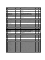
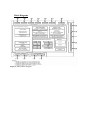
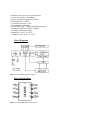
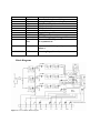
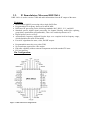
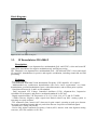
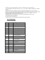
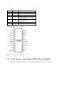
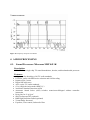
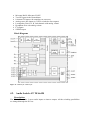
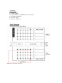
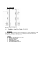
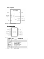
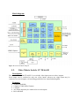
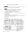
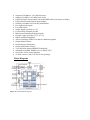
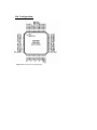
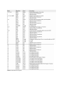
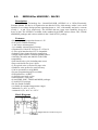
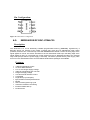
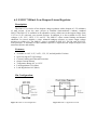
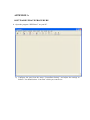
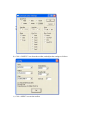
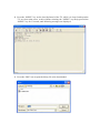
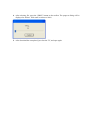
Service Manual 32" Chassis 17MB26 1. INTRODUCTION Analog front end consist of a main tuner, a pip tuner and IF decoders. The PLL tuners supply the IF signals and SAW filters are used for filtering and impedance matching between demodulator ICs and tuners. The main IF signal is demodulated by demodulator (DRX3961A) and the pip IF signal is demodulated by (TDA9885T). At the outputs of the demodulators, CVBS and QSS signals are obtained. The main tuner CVBS, pip tuner CVBS, FAV CVBS, Scart1 CVBS, SVHS_Y, Scart2 CVBS/Y, DMP CVBS, IDTV/Scart3 CVBS/Y signals are applied to the video matrix switch (TEA6415). The outputs of the switch are main CVBS to video processor; pip CVBS to video decoder, scart1_out CVBS to scart1, scart2_out CVBS to scart2, scart3_out CVBS to scart3. The video decoder IC (VPC3230) decodes to CVBS signal for the pip picture. The source for the pip picture can be CVBS from the video matrix switch, SVHS, Scart1, Scart2, Scart3 and DMP. The output of the decoder is 8 bits ITU601_PIP signal connected to video processor IC SVP LX66. SVP-LX66 can support up to 1920x1080p panel. It consists of OSD, teletext, scaler, deinterlacer, 8/10-bit dual LVDS transmitter and HDMI blocks. The inputs to SVP LX66 are Scart2 RGB/DMP RGB, SC2/SC3 Chroma/SVHS Chroma, Scart1 RGB, main CVBS from video matrix switch, YPbPr, ITU601_PIP, HDMI, ITU601_IDTV, PC RGB. The output is the 8bits LVDS signal to the panel.The SVP LX66 uses a DDR RAM (EM6A9320) for faster processing. The main controller IC is M16C-M30620SPGP. The I/O assignments are as follows: NAME TYPE 1 HDMI_HPLG OUT 2 HDMI_HPLG2 OUT 3 4 5 6 HDMI_CEC HDMI_DTC HDMI_DTC2 HDMI_DDC_WP IN (*) IN IN OUT 7 SCDT IN (*) DESCRIPTION Port Pin P1.4 76 P8.0 22 P1.5 P8.6 P8.7 P9.4 75 11 10 3 P8.4 18 HDMI RELATED HotPlug output for HDMI-1 source device HotPlug output for HDMI-2 source device CEC input from HDMI cable HDMI detection for first input HDMI detection for second input HDMI NVM write protect control for service Sync Change Detection for HDMI POWER / PANEL RELATED 8 PROTECT 9 STBY / CPU_GO 10 BLIGHT / PDP_GO 11 DISP_EN 12 BLIGHT_LVL 13 PANEL_VCC IN OUT OUT Indicates the power supply status Controls the power supply on or off Controls the backlight P1.7 P1.3 P1.2 73 77 78 OUT PWM OUT OUT Controls the display enable or disable Controls the backlight level Controls the power supply of the panel P1.1 P7.6 P1.0 79 24 80 P7.2 P7.3 P10.7 P10.6 P10.5 28 27 89 90 91 IDTV UART receive IDTV UART transmit IDTV status change notification TVLink interrupt input / data output P6.2 P6.3 P6.1 P1.6 36 35 37 74 Controls DMP module P6.0 38 P8.1 P8.3 P9.2 P9.3 21 19 5 4 P8.2 P9.0 P9.1 P9.7 P10.1 P10.2 20 7 6 100 95 94 SERIAL DATA COMMUNICATION 14 15 16 17 18 SDA SCL E2_SDA E2_SCL E2_WP IN/OUT OUT IN/OUT OUT OUT I2C serial data line I2C clock line I2C serial data line for E2PROM I2C clock line for E2PROM Controls the write protection of the E2PROM EXTENTION MODULES RELATED 19 20 21 22 IDTV_RX IDTV_TX IDTV_IRQ TVLINK 23 DMP_CTRL IN OUT OUT IN (*) / OUT OUT VIDEO RELATED 24 25 26 27 LX_RST LX_INT RGB_SW_1 RGB_SW_2 OUT IN (*) OUT OUT 28 29 30 31 32 33 IR LED_1 LED_2 MUTE_AMP SC1_PIN8 SC2_PIN8 IN (*) OUT OUT OUT ADC IN ADC IN Resets the LX66 video processor Interrupt notification from LX66 RGB switch control 1 RGB switch control 2 APPLICATION Remote control interrupt input LED control 1 LED control 2 Mutes the audio amplifier Scart 1 pin8 input measurement Scart 2 pin8 input measurement 34 35 36 37 38 SC3_PIN8 KEYB SWU_RX SWU_TX RY_BY ADC IN ADC IN IN OUT IN 39 41 42 43 44 45 LG_1/IRQPDP CHROMA_SW DRX_RST VGA_STBY SERV_DTC AC_INFO IN OUT OUT IN IN IN Scart 3 pin8 input measurement Keyboard input UART receive for software upgrade UART transmit for software upgrade Ready/Busy indication from external flash Interrupt Request from Plasma Display Chroma Switch for SVHS DRX reset PC VGA standby detection Service socket detection Alternate Current Information P10.3 P10.0 P7.1 P7.0 P5.1 93 97 29 30 45 P7.4 P7.5 P9.6 P9.5 P7.7 P8.5 26 25 1 2 23 18 Table 1: Microcontroller I/O Assignments The PC Audio L/R, DMP Audio L/R, IDTV/SC3 Audio L/R, YPbPr Audio L/R, Scart2 Audio L/R signals are switched via audio switch TEA6420. The outputs of the switch are two L/R audio signals. MSP4411K is used for audio processing and it covers the sound processing of all analog TV-standards worldwide, as well as the NICAM digital sound standard. Audio outputs are connected to SC1/2/3 connector, audio line out, headphone, Speaker, subwoofer and S/PDIF connectors. The inputs to the MSP441K are two audio signals from audio switch, FAV_Audio_L/R, SC1_Audio_L/R, QSS signals from main and pip tuners, Tuner2 mono signal and HDMI I2S signal. The AD8190 is a DVI/HDMI switch featuring equalized TMDS inputs and preemphasized TMDS outputs, ideal for systems with long cable runs between sources and sinks of video data. A disable feature sets the outputs to a high impedance state, reducing the power dissipation. The primary function of the AD8190 is to switch one of two HDMI single-link sources to one output. Each HDMI source consists of four differential high-speed channels and four general purpose control lines. The switched HDMI signal is sent to the video processor IC. 2. CONTROLLER 2.1. Microcontroller: Renesas M16C M30620SPGP General Description: The M16C/62P Group (M16C/62P, M16C/62PT) of single-chip microcomputers are built using the high performance silicon gate CMOS process using a M16C/60 Series CPU core and are packaged in a 80-pin, 100-pin and 128-pin plastic molded QFP. These single-chip microcomputers operate using sophisticated instructions featuring a high level of instruction efficiency. With 1M bytes of address space, they are capable of executing instructions at high speed. In addition, this microcomputer contains a multiplier and DMAC which combined with fast instruction processing capability, makes it suitable for control of various OA, communication, and industrial equipment which requires highspeed arithmetic/logic operations. General Features: Main features of M16C are: • 16-bit Multifunction Timer (Timer A and B): 11 channels • UART/Clock Synchronous Serial Interface: 3 channels • Clock Synchronous Serial Interface: 2 channels • 10-bit A/D Converter: 26 channels • 8-bit D/A Converter: 2 channels • DMAC: 2 channels • CRC Calculation Circuit • Watchdog Timer • Clock Generation Circuits: Main Clock Generation Circuit, Sub Clock Generation Circuit, On-chip Oscillator, PLL Synthesizer • Oscillation Stop Detection Function • Voltage Detection Circuit (Option) (Except for T Version and V Version) • Interrupts: 29 internal factors, 8 external factors, 4 software factors • Data Flash: 4KB (Flash Memory Version only) Block Diagram: Figure 1: M16C Block Diagram Pin Configuration: Figure 2: M16C Pin Configuration Table 2: M16C Pin Descriptions 2.2. Flash IC SST39VF088 General Description: The SST39VF088 device is a 1M x8 CMOS Multi-Purpose Flash (MPF) manufactured with SST’s proprietary, high performance CMOS SuperFlash technology. The split-gate cell design and thick-oxide tunneling injector attain better reliability and manufacturability compared with alternate approaches. The SST39VF088 writes (Program or Erase) with a 2.7-3.6V power supply. It conforms to JEDEC standard pinouts for x8 memories. Featuring high performance Byte-Program, the SST39VF088 device provides a typical Byte-Program time of 14 µsec. The devices use Toggle Bit or Data# Polling to indicate the completion of Program operation. To protect against inadvertent write, they have onchip hardware and Software Data Protection schemes. Designed, manufactured, and tested for a wide spectrum of applications, these devices are offered with a guaranteed endurance of 10,000 cycles. Data retention is rated at greater than 100 years.The SST39VF088 device is suited for applications that require convenient and economical updating of program, configuration, or data memory. For all system applications, they significantly improve performance and reliability, while lowering power consumption. They inherently use less energy during Erase and Program than alternative flash technologies. The total energy consumed is a function of the applied voltage, current, and time of application. Since for any given voltage range, the SuperFlash technology uses less current to program and has a shorter erase time, the total energy consumed during any Erase or Program operation is less than alternative flash technologies. They also improve flexibility while lowering the cost for program, data, and configuration storage applications. The SuperFlash technology provides fixed Erase and Program times, independent of the number of Erase/Program cycles that have occurred. Therefore the system software or hardware does not have to be modified or de-rated as is necessary with alternative flash technologies, whose Erase and Program times increase with accumulated Erase/Program cycles. To meet high density, surface mount requirements, the SST39VF088 is offered in 48-lead TSOP packaging. See below figure for pin assignments. General Features: • Organized as 1M x8 • Single Voltage Read and Write Operations – 2.7-3.6V • Superior Reliability – Endurance: 100,000 Cycles (typical) – Greater than 100 years Data Retention • Low Power Consumption (typical values at 5 MHz) – Active Current: 12 mA (typical) – Standby Current: 4 µA (typical) • Sector-Erase Capability – Uniform 4 KByte sectors • Block-Erase Capability – Uniform 64 KByte blocks • Fast Read Access Time: – 70 and 90 ns • Latched Address and Data • Fast Erase and Byte-Program – Sector-Erase Time: 18 ms (typical) – Block-Erase Time: 18 ms (typical) – Chip-Erase Time: 70 ms (typical) – Byte-Program Time: 14 µs (typical) – Chip Rewrite Time: 15 seconds (typical) • Automatic Write Timing – Internal VPP Generation • End-of-Write Detection – Toggle Bit – Data# Polling • CMOS I/O Compatibility • JEDEC Standard – Flash EEPROM Pinouts and command sets • Packages Available – 48-lead TSOP (12mm x 20mm) Pin Configuration: Figure 3: Flash IC Pin Configuration Table 3:Flash IC Pin Descriptions 2.3. 32K I2C Serial EEPROM: 24LC32A General Description: The Microchip Technology Inc. 24AA32A/24LC32A (24XX32A*) is a 32 Kbit Electrically Erasable PROM.The device is organized as four blocks of 8K x 8-bit memory with a 2-wire serial interface. Low-voltage design permits operation down to 1.8V, with standby and active currents of only 1 A and 1 mA, respectively. It has been developed for advanced, lowpower applications such as personal communications or data acquisition. The 24XX32A also has a page write capability for up to 32 bytes of data. Functional address lines allow up to eight devices on the same bus, for up to 256 Kbits address space. The 24XX32A is available in the standard 8-pin PDIP, surface mount SOIC, TSSOP and MSOP packages. General Features: • Single supply with operation down to 1.8V • Low-power CMOS technology - 1 mA active current typical - 1 A standby current (max.) (I-temp) • Organized as 4 blocks of 8K bits (32K bit) • 2-wire serial interface bus, I2C™ compatible • Cascadable for up to eight devices • Schmitt Trigger inputs for noise suppression • Output slope control to eliminate ground bounce • 100 kHz (<2.5V) and 400 kHz (≥2.5V) compatibility • Self-timed write cycle (including auto-erase) • Page write buffer for up to 32 bytes • 2 ms typical write cycle time for page write • Hardware write-protect for entire memory • Can be operated as a serial ROM • Factory programming (QTP) available • ESD protection > 4,000V • 1,000,000 erase/write cycles • Data retention > 200 years • 8-lead PDIP, SOIC, TSSOP and MSOP packages • Standard and Pb-free finishes available • Available temperature ranges: - Industrial (I): -40°C to +85°C - Automotive (E): -40°C to +125°C Block Diagram: Figure 4: Serial EEPROM Block Diagram Pin Configuration: Figure 5: Serial EEPROM Pin Configuration 3. TUNING AND IF DECODING 3.1. Tuner The tuners used in the design are combined VHF, UHF tuners suitable for CCIR systems B/G, H, L, L’, I/I’, and D/K. The tuning is available through the digitally controlled I2C bus (PLL). Below you will find info on one of the tuners in use. Description: The UV1316MK4 tuner belongs to the UV1300 family of third generation WSP tuners, which are designed to meet a wide range of TV applications. It is a full band tuner suitable for CCIR systems B/G, H, L, L’, I and I’. The low IF output impedance is designed for direct drive of a wide variety of SAW filters with sufficient suppression of triple. Features: Member of UV1300 MK4 family of small-sized UHF/VHF tuners • Systems CCIR: B/G, H, L, L’, I and I’; OIRT: D/K • Digitally-controlled (PLL) tuning via I2C-bus • Fast 400kHz I2C bus protocol compatible with 3.3V and 5V micro controllers • Off-air, S-cable and hyperband channels from 48.25 MHz to 863.25MHz inclusive • World standardized mechanical dimensions and pinning. Horizontal mounting is optionally available • Various connector types available • EURO content available. Pin Configuration: Pin 1 2 3 4 5 6 7 8 9 10 Symbol AGC TU AS SCL SDA N.C. Vs ADC Vst I.F out 2 / d.n.c Description Automatic Gain Control Voltage Tuning Voltage Monitor(Output) I2C Bus Address Select I2C Bus Serial Clock I2C Bus Serial Data Not Connected Supply Voltage +5V ADC Input Fixed Tuning Supply Voltage +32V Symmetrical I.F output 2 / Do not connect for asymmetrical 11 I.F out 1 Asymmetrical I.F Output / Symmetrical I.F output 1 M1,M2,M3,M4 GND Mounting Tags (Ground) Table 4: UV1316 MK4 Pin Descriptions Block Diagram: Figure 6: UV1316 MK4 Block Diagram 3.2. IF Demodulator: Micronas DRX3961A DRX 3961A is used to extract CVBS and audio information from the IF output of the tuner. • • • • Features: • Multistandard QSS IF processing with a single SAW filter Programmable IF frequency between 30 and 60 MHz DSP-based IF processing for the following standards: B/G, D/K, I, L/L’, and M/N Standard specific digital signal processing for channel filtering, audio/video splitting, group delay equalization (programmable), video AGC and delayed tuner AGC Digital picture carrier recovery Automatically frequency-adjusted Nyquist slope over complete lock-in frequency range, which eliminates the need of fine tuning Fast AGC algorithms for tuner, video, and SIF outputs • • • • Programmable tuner take-over point (TOP) No sound traps required for video output FM radio capability without external components and with standard TV tuner I2C bus interface • • Pin Configuration: Figure 7: DRX 3961A Pin Configurations Block Diagram: Figure 8: DRX 3961A Block Diagram 3.3. IF Demodulator:TDA9886T Description: The TDA9886T is an alignment-free multistandard (PAL and NTSC) vision and sound IF signal PLL demodulator for negative modulation only and FM processing. The TDA9886 is an alignment-free multistandard (PAL, SECAM and NTSC) vision and sound IF signal PLL demodulator for positive and negative modulation, including sound AM and FM processing. Features: · 5 V supply voltage · Gain controlled wide-band Vision Intermediate Frequency (VIF) amplifier, AC-coupled · Multistandard true synchronous demodulation with active carrier regeneration: very linear demodulation, good intermodulation figures, reduced harmonics, and excellent pulse response · Gated phase detector for L and L-accent standard · Fully integrated VIF Voltage Controlled Oscillator (VCO), alignment-free, frequencies switchable for all negative and positive modulated standards via I2C-bus · Digital acquisition help, VIF frequencies of 33.4, 33.9,38.0, 38.9, 45.75, and 58.75 MHz · 4 MHz reference frequency input: signal from Phase-Locked Loop (PLL) tuning system or operating as crystal oscillator · VIF Automatic Gain Control (AGC) detector for gain control, operating as peak sync detector for negative modulated signals and as a peak white detector for positive modulated signals · External AGC setting via pin OP1 · Precise fully digital Automatic Frequency Control (AFC) detector with 4-bit digital-to-analog converter, AFC bits readable via I2C-bus · TakeOver Point (TOP) adjustable via I2C-bus or alternatively with potentiometer · Fully integrated sound carrier trap for 4.5, 5.5, 6.0, and 6.5 MHz, controlled by FM-PLL oscillator · Sound IF (SIF) input for single reference Quasi Split Sound(QSS) mode, PLL controlled · SIF-AGC for gain controlled SIF amplifier, single reference QSS mixer able to operate in high performance single reference QSS mode and in intercarrier mode, switchable via I2C-bus · AM demodulator without extra reference circuit · Alignment-free selective FM-PLL demodulator with high linearity and low noise · Four selectable I2C-bus addresses · I2C-bus control for all functions · I2C-bus transceiver with pin programmable Module Address(MAD) Pin Configuration: Symbol Pin Description VIF1 1 VIF differential input 1 VIF2 2 VIF differential input 2 n.c. - not connected OP1 3 output port 1; open-collector FMPLL 4 FM-PLL for loop filter DEEM 5 de-emphasis output for capacitor AFD 6 AF decoupling input for capacitor DGND 7 digital ground n.c. - not connected AUD TOP 8 9 SDA 10 SCL SIOMAD 11 12 audio output tuner AGC TakeOver Point (TOP) for resistor adjustment I2C-bus data input and output I2C-bus clock input sound intercarrier output and MAD select with resistor n.c. - not connected n.c. 13 not connected n.c. - TAGC 14 REF 15 VAGC 16 n.c. CVBS n.c. 17 not connected tuner AGC output 4 MHz crystal or reference signal input VIF-AGC for capacitor not connected composite video output - not connected AGND 18 analog ground VPLL 19 VIF-PLL for loop filter VP 20 supply voltage AFC 21 AFC output OP2 22 output port 2; open-collector n.c. SIF1 23 not connected SIF2 24 n.c. - not connected n.c. - not connected SIF differential input 1 and MAD select with resistor SIF differential input 2 and MAD select with resistor Table 5: TDA9886T Pin Descriptions Figure 9: TDA9886T Pin Configurations 3.4. SAW (Surface Acoustic Wave) Filter: Epcos X6966M X6966M is a bandpass IF filter at fc = 36.125 MHz with tinned CuFe alloy terminals. Figure 10: Frequency Response of X6966M 4. AUDIO PROCESSING 4.1. Sound Processor: Micronas MSP 4411K Description: MSP 4411K is a single-chip TV sound demodulator, decoder, and baseband audio processor. • • • • • • • • • • • • • Features: Alignment-free decoding of all TV audio standards US BTSC audio with DBX noise reduction and SAP decoding Japanese EIA-J stereo Digital NICAM stereo All 2-carrier TV Audio standards (Very) High deviation modes HDEV2, 3 Automatic Standard Detection (ASD) Automatic Sound Select (ASS) switches mono/stereo/bilingual without controller interaction Delay line for “Lip Sync” SRS TruSurround XT (optional) BBE High Definition Sound (optional) Virtual Dolby Surround Equalizer, Tone control, Subwoofer filter • • • • • • • • Micronas BASS, Micronas VOICE Two SIF inputs to the Demodulator 8-channel I2S inputs with sampling rate converter Analog stereo line inputs (to A/D or switched to line outputs) Loudspeaker D/A for L, R, Sub channels with analog volume Headphone D/A with analog volume I2S outputs S/PDIF output Block Diagram: Figure 11: MSP44xyK / MSP46xyK 4.2. Audio Switch: ST TEA6420 Description: The TEA6420 switches 5 stereo audio inputs on 4stereo outputs. All the switching possibilities are changed through the I2C bus. • • • • • • Features: 5 stereo inputs 4 stereo ouputs Gain Control (0/2/4/6dB/Mute) for each output Serial Bus Controlled Very low Noise Very low Distortion Block Diagram: Figure 12: TEA6420 Block Diagram Pin Connections: Figure 13: TEA 6420 Pin Configuration 4.3. Headphone Amplifier: Philips TDA1308 Description: The TDA1308 is an integrated class AB stereo headphone driver contained in an SO8 or a DIP8 plastic package. The device is fabricated in a 1 mm CMOS process and has been primarily developed for portable digital audio applications. Features: • • • • • Operating temperature range: -40 to +85 C No switch ON/OFF clicks Short-circuit resistant signal-to-noise ratio: 110 dB total harmonic distortion: 0.001 % Block Diagram: Figure 14: TDA1308 Block Diagram Pin Configuration: Figure 15: TDA1308 Pin Configuration Table 6: TDA1308 Pin Descriptions 5. VIDEO PROCESSING 5.1. Video Processor: TRIDENT SVP LX66 Description: The SVPTMLX66 video processor is a highly integrated system-on-a-chip device, targeting the converging HDTV-ready and PC-ready LCD TV, PDP TV, and DLP TV applications where high precision processing of video and data are the requirements. SVP LX66 has a total of four video input ports : one analog port, one HDMI port, and two digital ports: PortA and PortB. LVDS output is either dual or single pixel mode. • • • • • • • • • • • • • • • • Features: Integrated HDMi Receiver with HDCP up to 135 MHz. Integrated 6th Generation Motion and Edge Adaptive De-interlacing Integrated ADC PC Auto Tune Built-in dual 8/10-bit LVDS Transmitter Vertical Keystone for Projector Advanced 6th generation cubic-4 image scaling engine. Horizontal and vertical mirror image inversion DNR-Digital Temporal and Spatial Noise Reduction Filter Advanced Chroma Processing Dynamic Contrast Function Green Color Stretch, blue color stretch, skin color enhancement Integrated 6th Generation Motion Adaptive 3D Digital Comb Video Decoder with Programmable Filter Inverse Color Space Conversion Trident Proprietary LCD-BRITETM Technology for LCD Overdrive Interlaced and Progressive Scan Refresh Block diagram: Figure 16: SVP LX66 Block Diagram 5.2. Video Matrix Switch: ST TEA6415 Description: The main function of the TEA6415C is to switch 8 video input sources on the 6 outputs. Each output can be switched to only one of the inputs, whereas any single input may be connected to several outputs. All switching possibilities are controlled through the • • • • • Features: 20 MHz bandwidth 8 inputs (CVBS, RGB, Chroma) 6 outputs Any single input may be connected to several outputs Bus controlled • • • 6.5 dB gain between any input and output -55 dB crosstalk at 5 MHz Full ESD protection Pin Configuration: Figure 17: TEA 6415C Pin Configurations Block Diagram: Figure 18: TEA 6415C Block Diagram 5.3. Video Decoder: Micronas VPC3230D Description: The VPC 323xD is a high-quality, single-chip video front-end, which is targeted for 4:3 and 16:9, 50/60-Hz and 100/120 Hz TV sets. VPC3230D is used for PIP applications. • • • • • • • • • • • • Features: adaptive 4H comb filter Y/C separator with adjustable vertical peaking multi-standard color decoder PAL/NTSC/SECAM including all substandards four CVBS, one S-VHS input, one CVBS output two RGB/YCrCb component inputs, one Fast Blank (FB) input integrated A/D converters and associated clamp and AGC circuits multi-standard sync processing linear horizontal scaling (0.25 ... 4), as well as non-linear horizontal scaling ‘Panoramavision’ PAL+ preprocessing line-locked clock, data and sync, or 656-output interface peaking, contrast, brightness, color saturation and tint for RGB/YCrCb and CVBS/S-VHS high-quality soft mixer controlled by Fast Blank I2C-bus interface Block Diagram: Figure 19: VPC3230D Block Diagram 5.4. Video RGB Switch: Pericom PI5V330 Description: The PI5V330A is a true bidirectional Quad 2-channel multiplexer/demultiplexer that is recommended for both RGB and composite video switching applications. • • • • Features: Wide bandwidth: 400 MHz (typical) Low On-Resistance: 5Ω (typical) Low crosstalk at 10 MHz: –56dB Ultra-low quiescent power (0.1µA typical) Pin Configurations: Figure 20: PI5V330 Pin Configurations Table 7: PI5V330 Pin Descriptions Block Diagram: Figure 21: PI5V330 Block Diagram 6. HDMI BLOCK 6.1. HDMI Switch: AD8190 Description: The AD8190 is an HDMI/DVI switch featuring equalized TMDS inputs and pre-emphasized TMDS outputs, ideal for systems with long cable runs. Outputs can be set to a high impedance state to reduce the power dissipation and/or allow the construction of larger arrays using the wireOR technique. The AD8190 is provided in a space saving, 56-lead, LFCSP, surface-mount, Pb-free, plastic package and is specified to operate over the −40°C to +85°C temperature range. • • • Features: Two inputs, one output HDMI/DVI links Enables HDMI 1.2a-compliant receiver Four TMDS channels per link • • • • • • • • • • • • • • • • • • • • Supports 250 Mbps to 1.65 Gbps data rates Supports 25 MHz to 165 MHz pixel clocks Equalized inputs for operation with long HDMI cables (20 meters at 1080p) Fully buffered unidirectional inputs/outputs Globally switchable 50 Ω on-chip terminations Pre-emphasized outputs Low added jitter Single-supply operation (3.3 V) Four auxiliary channels per link Bidirectional unbuffered inputs/outputs Flexible supply operation (3.3 V to 5 V) HDCP standard compatible Allows switching of DDC bus and two additional signals Output disable feature Reduced power dissipation Output termination removal Two AD8190s support HDMI/DVI dual-link Standards compliant: HDMI receiver, HDCP, DVI Serial (I2C slave) control interface 56-lead, 8 mm x 8 mm, LFCSP, Pb-free package Block Diagram: Figure 22: AD8190 Block Diagram Pin Configuration: Figure 23: AD8190 Pin Configurations Table 8: AD8190 Pin Descriptions 6.2. EEPROM for HDMI DDC: 24LC02 Description: The Microchip Technology Inc. 24AA02/24LC02B (24XX02*) is a 2 Kbit Electrically Erasable PROM. The device is organized as one block of 256 x 8-bit memory with a 2-wire serial interface. Low-voltage design permits operation down to 1.8V, with standby and active currents of only 1 A and 1 mA, respectively. The 24XX02 also has a page write capability for up to 8 bytes of data. The 24XX02 is available in the standard 8-pin PDIP, surface mount OIC, TSSOP and MSOP packages and is also available in the 5-lead SOT-23 package. Features: • Single supply with operation down to 1.8V • Low-power CMOS technology - 1 mA active current typical - 1µA standby current typical (I-temp) • Organized as 1 block of 256 bytes (1 x 256 x 8) • 2-wire serial interface bus, I2C™ compatible • Schmitt Trigger inputs for noise suppression • Output slope control to eliminate ground bounce • 100 kHz (24AA02) and 400 kHz (24LC02B) compatibility • Self-timed write cycle (including auto-erase) • Page write buffer for up to 8 bytes • 2 ms typical write cycle time for page write • Hardware write-protect for entire memory • Can be operated as a serial ROM • Factory programming (QTP) available • ESD protection > 4,000V • 1,000,000 erase/write cycles • Data retention > 200 years • 8-lead PDIP, SOIC, TSSOP and MSOP packages • 5-lead SOT-23 package • Pb-free finish available • Available for extended temperature ranges: - Industrial (I): -40°C to +85°C - Automotive (E): -40°C to +125°C Block Diagram: Figure 24: 24LC02 Block Diagram Pin Configuration: Figure 25: 24LC02 Pin Configuration 6.3. EEPROM FOR PC DDC: ST24LC21 Description: The ST24LC21 is a 1K bit electrically erasable programmable memory (EEPROM), organized by 8 Bits.This device can operate in two modes: Transmit Only mode and I2C bidirectional mode. When powered, the device is in Transmit Only mode with EEPROM data clocked out from the rising edge of the signal applied on VCLK. The device will switch to the I2C bidirectional mode upon the falling edge of the signal applied on SCL pin. The ST24LC21 cannot switch from the I2C bidirectional mode to the Transmit Only mode (except when the power supply is removed). The device operates with a power supply value as low as 2.5V. Both Plastic Dual-in-Line and Plastic Small Outline packages are available. Features: • • • • • • • • • • • • • • 1 Mıllıon Erase/Wrıte Cycles 40 Years Data Retentıon 2.5v To 5.5v Sıngle Supply Voltage 400k Hz Compatıbılıty Over The Full Range Of Supply Voltage Two Wıre Serıal Interface I2c Bus Compatıble Page Wrıte (Up To 8 Bytes) Byte, Random And Sequentıal Read Modes Self Tımed Programmıng Cycle Automatıc Address Incrementıng Enhanced Esd/Latch Up Performances Pin Configuration: Figure 26. 24LC21 pin configuration 7.REGULATOR ICS 6.4. LM317 Description: The LM117/LM217/LM317 are monolithic integrated circuit in TO-220, TO-220FP, TO-3 and D2PAK packages intended for use as positive adjustable voltage regulators. They are designed to supply more than 1.5A of load current with an output voltage adjustable over a 1.2 to 37V range. The nominal output voltage is selected by means of only a resistive divider, making the device exceptionally easy to use and eliminating the stocking of many fixed regulators. Features: • • • • • Output voltage range:1.2 to 37V Output current in excess of 1.5A 0.1% line and load regulation Floating operation fro high voltages Complete series of protections: Current limiting, thermal shutdown and SOA control Pin Configuration: Figure 27: LM317 Pin Configuration Figure 28: LM317 Application Circuit 6.5. LM1117 800mA Low-Dropout Linear Regulator Description: The LM1117 is a series of low dropout voltage regulators with a dropout of 1.2V at 800mA of load current. It has the same pin-out as National Semiconductor’s industry standard LM317.The LM1117 is available in an adjustable version, which can set the output voltage from 1.25V to 13.8V with only two external resistors. In addition, it is also available in five fixed voltages, 1.8V, 2.5V, 2.85V, 3.3V, and 5V. The LM1117 offers current limiting and thermal shutdown. Its circuit includes a zener trimmed bandgap reference to assure output voltage accuracy to within ±1%. The LM1117 series is available in SOT-223, TO-220, and TO-252 DPAK packages. A minimum of 10µF tantalum capacitor is required at the output to improve the transient response and stability. Features: • • • • • • • Available in 1.8V, 2.5V, 2.85V, 3.3V, 5V, and Adjustable Versions Space Saving SOT-223 Package Current Limiting and Thermal Protection Output Current 800mA Temperature Range 0°C to 125°C Line Regulation 0.2% (Max) Load Regulation 0.4% (Max) Pin Configuration: Figure 29: LM1117 Pin Configuration Figure 30: LM1117 Application Circuit 6.5. IDT74LVC14A HEX Schmittrigger Inverter Description: This IC is used to detect the PC standby.The LVC14A Hex Schmitt-trigger inverter is built using advanced dual metal CMOS technology. This device contains six independent inverters and performs the Boolean function Y = A. Inputs can be driven from either 3.3V or 5V devices. This feature allows the use of this device as a translator in a mixed 3.3V/5V supply system. The LVC14A has been designed with a ±24mA output driver. This driver is capable of driving a moderate to heavy load while maintaining speed performance. Features: • • • • • • • • • • • • 0.5 MICRON CMOS Technology ESD > 2000V per MIL-STD-883, Method 3015; 200V using machine model (C = 200pF, R = 0) 1.27mm pitch SOIC, 0.65mm pitch SSOP and 0.65mm pitch TSSOP packages Extended commercial range of – 40°C to +85°C VCC = 3.3V ±0.3V, Normal Range VCC = 2.3V to 3.6V, Extended Range CMOS power levels (0.4µW typ. static) Rail-to-Rail output swing for increased noise margin All inputs, outputs and I/O are 5 Volt tolerant Supports hot insertion Pin Configuration: Table 9: IDT74LVC14A Pin Description Figure 31: IDT74LVC14A Pin Configuration APPENDIX A SOFTWARE UPDATE PROCEDURE 1. Open the program “ISPWriter3” on your PC. a) Configure the port from the menu “CommPort>Setting”, and adjust the settings as follows. You should select “Com Port” which you want to use. b) c) d) b) Click “CONFIG” icon from the toolbar, and adjust the settings as follows. c) Click “OPEN” icon on the toolbar. 2. Press the “MENU” key on the local keyboard of the TV, while it is closed, and open the TV set from main power switch without releasing the “MENU” key.Keep pressed the “MENU” key for 3 seconds, until following messages are displayed. 3. Press the “BIN” icon to open the binary file to be downloaded. 4. After selecting file, press the “PROG” button on the toolbar. The progress dialog will be displayed as follows. Wait until it reaches to 100%. 5. After download has completed, just close the TV, and open again. APPENDIX B 12. SERVICE MENU SETTINGS To enter the service menu, first enter the MENU by pressing “MENU” button and then press the digits 1, 4, 6 and 1 respectively. 12.1. Picture Adjust • Source => All possible sources given with the chasis as a list. • Mode => Three items as a list; NATURAL, DYNAMIC, CINEMA • Colour Temp => Three items as a list; COOL, NORMAL, WARM • Contrast => Slider Bar. Changing value between 0 to 63. Default is 63. • Brightness => Slider Bar. Changing value between 0 to 63. Default is 32. • Sharpness => Slider Bar. Changing value between 0 to 31. Default is 22. • Colour => Slider Bar. Changing value between 0 to 99. Default is 70. • R => Slider Bar. Changing value between 0 to 31. Default is 31. • G => Slider Bar. Changing value between 0 to 31. Default is 31. • B => Slider Bar. Changing value between 0 to 31. Default is 31. • Backlight => Slider Bar. Changing value between 0 to 255. Default is 30. In this menu preset values for each Mode (Contrast, Brightness, Sharpness, Colour values for each Mode-NATURAL, DYNAMIC, CINEMA) and for each Colour Temp. (R, G, B values for each Colour Temp- COOL, NORMAL, WARM) are determined for each source. SOUND1 • Menu Subwoofer => If ON, Subwoofer option is available in TV set, and the item is visible in sound menu, else Subwoofer is not available. Default is ON. • Subwoofer Level (dB) => This value is gain value of Subwoofer output in dB. -30...12. Default is 0. • Subwoofer Corner Freq. (x10Hz) => Last low frequency value that is amplified. 5...40. Default is 22. • Menu Equalizer => If ON, visible in sound menu, else invisible.Default is ON. • Menu Headphone => If ON, visible in sound menu, else invisible. Default is ON. • Menu Effect => If ON, visible in sound menu, else invisible. Default is ON. • Menu Wide Sound => If ON, visible in sound menu, else invisible. Default is ON. • Menu Dynamic Bass => If ON, visible in sound menu, else invisible. Default is ON. • Menu Virtual Dolby => If ON, visible in sound menu, else invisible. Default is ON. • Carrier Mute => If ON, in the absence of an FM carrier the output is muted,else not. Default is ON. • Virtual Dolby Text => Active if VIRTUAL DOLBY is ON. According to the selection; seen in sound menu as 3D PANORAMA or VIRTUAL DOLBY. Default is 3DS. SOUND 2 • AVL => AVL is controlled from this menu by service user, ON/OFF. Default is ON. • Menu AVL => If ON, AVL item is visible in sound menu, and AVL can be controlled from sound menu by normal user, else AVL is invisible to normal user. Default is ON. • FM PRESCALE AVL ON => If AVL ON, set value in this item is used as prescale value for the related standard. 0...127. Default is 15. • NICAM PRESCALE AVL ON => If AVL ON, set value in this item is used as prescale value for the related standard. 0...127. Default is 34. • SCART PRESCALE AVL ON => If AVL ON, set value in this item is used as prescale value for scart outputs. 0...127. Default is 15. • SCART VOLUME AVL ON => If AVL ON, set value in this item is used as volume value for scart1 and scart2. 0...127. Default is 122. • FM PRESCALE AVL OFF => If AVL OFF, set value in this item is used as prescale value for the related standard. 0...127. Default is 15. • NICAM PRESCALE AVL OFF => If AVL OFF, set value in this item is used as prescale value for the related standard. 0...127. Default is 34. • SCART PRESCALE AVL OFF => If AVL OFF, set value in this item is used as prescale value for scart outputs. 0...127. Default is 15. • SCART VOLUME AVL OFF => If AVL OFF, set value in this item is used as volume value for scart1 and scart2. 0...127. Default is 122. • I2S prescale=> set value in this item is used as prescale value for HDMI outputs 0..255. Default is 5. 12.4. Options • Burn-In Mode => If ON, When TV is powered ON Green, Blue, Red is displayed in sequence until Menu button is pressed. Default is OFF. • FIRST APS => If ON, “First APS” menu is displayed when the TV is switched on with the factory default settings. Default is OFF. • APS Volume => After First APS function finishes, the volume of the TV is that value. Default is 15. • AGC (dB) => Tuner AGC value. Default is 8. • Power-Up Mode => Mode defines the TV set power on state. Default is standby. Stand-by : When TV is ON set is in stand-by mode Normal : When TV is ON set is in normal mode Last State: When TV is ON set is in Last State mode • Factory Reset => OK to activate. When OK is pressed on this item, factory defaults loaded. •Enter Flash Mode=> • Reset Eeprom => Initialize default settings. • Remote select=> 0=RC1546 1=RC1549/1602/1082/1055 2=RC1062 3=RC1072 4=RC1558 5=RC1061 6=RC1071 7=RC1110 8=RK18 Default is 2. TV Norm • BG => If ON, this standart is supported, else not supported. Default is ON. • DK => If ON, this standart is supported, else not supported. Default is ON. •I => If ON, this standart is supported, else not supported. Default is ON. •L => If ON, this standart is supported, else not supported. Default is ON. • LP => If ON, this standart is supported, else not supported. Default is ON. • M => If ON, this standart is supported, else not supported. Default is ON. 12.6. Features • PIP/PAP => If ON enables the PIP/PAP. Default is ON. • Blue Background => If ON, Blue Background is visible in Feature Menu else not. Default is ON. • Menu Transparency => If ON, Menu Transparency is visible in Feature Menu else not. Default is ON. • Menu Timeout => If ON, Menu Timeout is visible in Feature Menu else not. Default is OFF. • Backlight => If ON, Backlight is visible in Feature Menu else not. Default is OFF. • Dynamic WB => Dynamic White Balance. Default is ON. • Zoom Mode Blank=> If ON, displays blank while changing the zoom mode else not. Default is OFF. • Dynamic Menu=>If ON, the features covered by some patents will be used, else not. 12.7. Teletext • TOP TXT => If ON, Top Text feature is available else not. Default is ON. • Fast TXT => If ON, Fast Text feature is available else not. Default is ON. • Teletext Language => Teletext Language may be controlled from this menu by service user . • Menu Teletext Language => If ON, Teletext Language item is visible in Feature Menu, and Teletext Language can be controlled from Feature Menu by normal user, else Teletext Language is invisible to normal user. Default is ON. • Check Data=>Used to check the teletext data.No service usage. 12.8. Source • TV • SC1 • SC2 • SC2 SVHS • SC3 • SC3 SVHS • YPBPR • FAV • SVHS • HDMI • HDMI2 • PC This menu is related with the options of the chassis. These items may be ON or OFF. If ON, the source is available in TV set, and the item is visible in source menu, else the source may be available but invisible to user. Menu Languages 1 & 2 The language options for the Language item in Feature menu can be set ON or OFF from this menu. English, German, French, Turkish, Spanish, Danish, Swedish, Dutch, Italian, Greek, Portuguese, Norwegian Finnish, Polish, Czech, Hungarian, Russian, Slovak, Slovenian, Rumanian, Bulgarian, Croatian, Serbian, Hebrew 12.9. Tuner options •Main tuner=> The main tuner used in the TV is selected. •PIP tuner=> The pip tuner used in the TV is selected. HOTEL MENU SETTINGS To enter the hotel menu, first enter the MENU by pressing “MENU” button and then press the digits 7, 9, 3 and 5 respectively. • Hotel mode => If ON, hotel menu settings will be valid, else not. • Startup position => The selected source will be active when the TV is on. • Volume Level=> The set value will be the volume level when the TV is on and cannot be changed from the menu by the user. • Front Key => ??? •Osd Menu => Determines the visibility of menus to the user according to the selection: Enable/Disable Install Menu/Disable All Menus •Autosave => Update Last Data/Not Stored