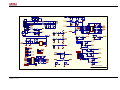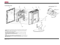
1
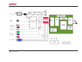
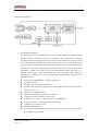
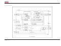
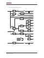
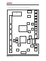
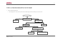
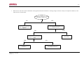
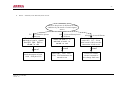
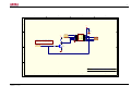
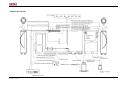
LCT TV
Service Manual
-2 -
Model: LCT-20CHST
Chassis: LS-07
Model No.: LCT-20CHST
Version: 1.0
-3 -
CONTENTS
SPECIFICATION AND FEATURE ......................................................................................................... 4
THE FUNCTION INTRODUCTION LS07 CHASSIS LCD TV’S MAIN ............................................. 9
SIGNAL PROCESSING FLOWCHART............................................................................................... 22
SPARE PART LIST AND EASY DAMAGE PART LIST ..................................................................... 34
FACTORY MODE ................................................................................................................................. 36
CIRCUIT DIAGRAM ............................................................................................................................ 37
WIRING DIAGRAM ............................................................................................................................. 47
EXPLODED VIEW................................................................................................................................ 48
PART LIST ............................................................................................................................................. 49
Model No.: LCT-20CHST
Version: 1.0
-4 -
SPECIFICATION AND FEATURE
1.
The Technical Specification of F Series Europe LCD TV:
a.
TM150F7E:
Max display format: 1024*768(XGA)
Audio power output: 2*2.0W
Voltage: DC12V
Power adapter voltage: AC 100~240W,50/60HZ
Power adapter Model number: FSP048-1AD101C
b.
W170F7E:
Max display format: 1280*768(WXGA)
Audio power output: 2*2.0W
AC input voltage of inside power Mold piece: AC 100~240V, 50/60HZ
The unit sets: AC power Switch.
c.
TM201F7E:
Max display format: 640*480(VGA)
Audio power output :2*2.0W
AC input voltage of inside power mold piece: AC 100~240V, 50/60HZ
The unit sets: AC power Switch.
2.
Main feature
a.
RF input , CATV function
Can receive 470MHZ CATV Programs, can store 100 programs
(Program number display 0~99);
b.
AV Audio and AV Video input
In scart mode, the system can automatically activate scart checking function to identify
signal input modes (CVBS or RGB) and input signal character (16:9 or 4:3); Capable to
receive PAL, NTSC, SECAM color systems; Very convenient to watch VCR (video cassette
recorder), Pickup Camera and other Disc’s programs.
c.
YPbPr input
Can receive high definition YPbPr component video signal from such as DVD Conveniently .
Support format: 480I, 480P, 576I, 576P, 720P (50/60HZ), 1080I (50/60HZ), 1080P
(50/60HZ);
d.
VGA input
As the Terminal display Equipments of computer, it can connect with computer conveniently.
It can connect with Computer audio card by its own Audio connection line ,so you can listen
the audio information from computer.
Model No.: LCT-20CHST
Version: 1.0
-5 -
e.
Program lock and child lock function
The function of program lock can lock the programs, input password and modification, the
function of child lock can lock the keys.
f.
Timer function
You can set turn on and turn off on time, and power off in 15 min automatically if no signal
input. Automatically enter into save energy mode by itself if no signal in PC condition, it can
be awaken if signal inputs.
g.
Blue screen mute noise
In condition of TV, AV, RGB and YPbPr, gentle blue screen will be displayed if no signal
input.
h.
Chinese/English menu
Adopt the design of Convenient and Simple graphic menu, you can operate menu more
conveniently and more intuition.
i.
Save energy function (power management mode)
When TV is used as PC display terminal, and PC has no output signal . The TV will be power
off in about 30 Seconds automatically, and enter into standby condition. press down
Power/P+/P-/ Number key of Remote control or the PC signal appearance again, the TV will
be on automatically.
j.
Plug and play
The TV works as the terminal Equipments of computer, need not equip install software,it is
real Plug-and-Play.
k.
Automatic correct
By its automatic correct function, the LCD TV can bring you the best view.
l.
No Flicker, no radiation, green environment protection
The LCD TV can bring you high quality view, and avoid radiation, protect your eyes and look
after your health.
m. Because of it’s advanced power management mode, the TV can realize standby and recall on
function.
n.
ACI function (Auto channel Installation).
o.
Stereo and digital accompanying sound processing.
Auto identify and demodulate IGR, and decode NICAM digital accompanying sound.
p.
Zoom image function
Support follow zoom function: Full screen mode, 4:3 mode (16:9 TFT), 16:9 (4: 3 TFT),
Movie mode, Sub-title movie mode.
q.
Light weight, small dimension, low power consumption
Model No.: LCT-20CHST
Version: 1.0
-6 -
r.
Advanced picture quality Strengthen function
Dynamic skin color Correct: Improve distort color in picture make it Near to real color.
Black level Extension: blacken the more black area of picture. Raise the contrast in Dark
Background.
Color Edge correct: Increase the Steep of color signal edge make the edge of color Transition
more clearly.
Brightness edge correct: increase the steep of Brightness signal edge make the edge of picture
is more clearly.
3.
s.
Super fine and inner fairness TFT
t.
10-page teletext storage
u.
Dynamic comb filter
v.
Headphones output
Electric circuit of the TV
The Europe LS07 chassis LCD TV is composed of Steady voltage circuit、inverter Circuit, RF
circuit, video Strengthen circuit, video Processing circuit, Power Enlarge circuit, VGA circuit,
system control circuit and key control circuit. The block diagraph of circuit Constitute is below:
Model No.: LCT-20CHST
Version: 1.0
-7 -
Model No.: LCT-20CHST
Version: 1.0
-8 -
4.
PCB Module introduction
The Constitute of the PCB is easier than LP03 chassis, all the Signal Processing are in Main board.
a.
Main board Module
Main board Module is the main part of Signal Processing in LCD TV. The input signal is
converted into uniform digital signal, which can be identified by LCM by system control
circuit. Main board module contain two parts of signal processing Module: Philips UOC3
process analog audio and video circuit mainly, MST518 process VGA circuit, signal Format
transform system control circuit mainly. The front module can convert the video IF signal and
audio IF signal from tuner into RGB analog signal and audio signal, this part is named analog
audio and video decoding process. The RGB color from UOC is received by MST518 and
accomplishes A/D conversion, output suitable digital color signal to drive circuit of TFT. 8051
Processor inside UOC is responsible for co-operation the each part of works in system, and
Respond to user operation, which is operated on Control panel (key-press panel Module).
b.
Key board Module
It is composed of 7 function keys the user can operate the LCD TV conveniently by using this
Module.
c.
Remote control receiving board Module
It is composed of a work indicator light and a remote receive head. The user use the remote
control box by this module can operate the LCD TV conveniently and know the LCD TV
work condition.
d.
Earphone output board module
It is composed of a earphone outlet, user can Listen to by earphone conveniently.
e.
Inverter board module (include inverter circuit)
The function of the inverter is supply power to light tube in TFT and lighten the back lamp
Unit of TFT module, so the user can see the image on TFT.
Model No.: LCT-20CHST
Version: 1.0
-9 -
THE FUNCTION INTRODUCTION LS07 CHASSIS LCD
TV’S MAIN IC
1.
The main IC of LS07 chassis
Number
Name
1
A1
2
U8, U21
3
2.
Model
Main function
TAF5-E2I21RW2
RF tuner
TDA1517AWT
Audio amplifier
U3
MST518
AD converter and format change
4
U2
UOC(TDA15021H)
Video decode and MCU control
5
Q9
Si2311DS
MOS switch
6
U11, U12
IRF7316
MOS switch
7
U19
NTMS10P02
MOS switch
8
U23
LM2596-5.0
Liner voltage IC
9
U1
24LC21A
EEPROM (save display parameter
10
U4
24LC32A
EEPROM(save user control information)
11
U6, U20
PI5V330A
Video switch
information)
The function introduction of main IC
a.
MST518 high integration chip
MST518 is a high performance, high integration image processor which is designed for LCD,
it can support SXGA format (1280*1024).it integrates a group of AD converter, high quality
format transform system, OSD generator, output clock generator, multiple format output
display interface (support TTL, LVDS, RSDS)
MST518 feature:
Have high quality Expand transform and compress transform, can output XGA format
signal
Integrated LVDS circuit inside
8 bit high quality ADC inside
Double VGA input, Software switch
Support ITU-656 format signal input
Support H/V sync, composite sync, green composite sync input, and detect
automatically by itself
Programmable 10 bit Gamma correct, the brightness and contrast is adjustable
8 color, 256 Character OSD
Built-in DDC circuit inside
Low standby power
Support TTL, double LVDS signal output, Software switch
Model No.: LCT-20CHST
Version: 1.0
-10 -
MST518 pin function:
And CPU interface
Pin
Pin name
Pin function
33
HWRESET
Hardware reset,high voltage enable
82
CS
Chip select signal of three-wire serial bus
83
SDA
data signal of three-wire serial bus
84
SCL
clock signal of three-wire serial bus
85
INT
interrupt
98-91
AD [7:0]
Parallel bus,the chassis is not used
125
BUSTYPE
Bus type select
38
HSYNC0
Analog Horizontal sync signal input channel 0
39
VSYNC0
Analog vertical sync signal input channel 0
40
HSYNC1
Analog Horizontal sync signal input channel 1
41
VSYNC1
Analog vertical sync signal input channel 1
78
RMID
Scaler internal reference voltage
79
REFP
internal ADC decouple +
80
REFM
internal ADC decouple -
75
RIN0
Analog red signal input channel 0
74
RIN0M
Analog red signal input channel 0 regrounding voltage
73
SOGIN0
Green sync signal input channel 0
72
GIN0
Analog green signal input channel 0
71
GIN0M
Analog green signal input channel 0 regrounding
Analog Interface
voltage
70
BIN0
Analog blue signal input channel 0
69
BIN0M
Analog blue signal input channel 0 regrounding voltage
66
RIN1M
Analog red signal input channel 1 regrounding voltage
65
RIN1
Analog red signal input channel 1
64
GIN1M
Analog green signal input channel 1 regrounding
voltage
63
GIN1
Analog green signal input channel 1
62
SOGIN1
Green sync signal input channel 1
61
BIN1M
Analog blue signal input channel 1 regrounding voltage
60
BIN1
Analog blue signal input channel 1
55
REXT
Outside connect 390Ω with 3.3V
Model No.: LCT-20CHST
Version: 1.0
-11 -
LCD Interface
145
OCLK
Clock output
146
LDE
Enable signal
144
LVSYNC
Vertical sync output
143
LHSYNC
Horizontal sync output
138
LVA0M
LVDS output 0-
137
LVA0P
LVDS ouput 0+
136
LVA1M
LVDS output 1-
135
LVA1P
LVDS ouput 1+
134
LVA2M
LVDS ouput 2-
133
LVA2P
LVDS output 2+
128
LVA3M
LVDS output 3-
127
LVA3P
LVDS ouput 3+
132
LVACKM
LVDS clock signal ouput-
131
LVACKP
LVDS clock signal ouput +
26-23,18-15
RB[7:0]
TTL red signal channel
14-11, 8-5
GB[7:0]
TTL green signal channel
4,3,154,153,150-147
BB[7:0]
TTL blue signal channel
87
GOUT1/PWM1
PWM output 1
86
GOUT0/PWM0
PWM output 0
2
BYPASS
Outside connect filter capacitor
29
DDC_DAT
Analog interface DDC data
30
DDC_CLK
Analog interface DDC clock
31
DDCROM_CLK
DDC ROM clock
32
DDCROM_DAT
DDC ROM data
34
XIN
Crystal oscillator signal input
35
XOUT
Crystal oscillator signal output
48, 54, 58, 77
AVDD
A/D convert power supply
56
AVDD_PLL
PLL power supply
36
AVDD_MPLL
MPLL power supply
VDDP
Digital signal output power supply
VDDC
Digital circuit power supply
GND
Digital circuit ground
GPIO Interface
Power Pins
10, 22, 88, 99, 111,
129, 139, 151
19, 102, 114, 142
1, 9, 20, 21, 37, 42,
45, 51, 57, 59, 76,
81, 89, 100, 101,
112, 113, 130, 140,
141, 152
Model No.: LCT-20CHST
Version: 1.0
-12 -
MST518 inner diagraph:
b.
TDA15021H introduction:
The third-generator super integrated circuit UOC III which designed by Philips company
recently integrates with video decode, 2D comb filter, high quality audio transacting
technique, suitable with the European teletext technique and suitable with US closed caption
and V-chip function compatible with single series IC. The series of UOC III have high
integrity, besides completing the Processing of all small signals (IF signal demodulation,
video decode, H/V signal, sound DSP), and integrate all the MCU function. It has many
Advantages, example: the compact circuit, good performance, simple craft and etc. It
matched with company’s high performance price ratio and high product efficiency
demanding. It is suitable for 4:3 or 16:9, 50/60HZ and A100/120HZ TV system, the main
characteristic below:
Multi-system IF demodulation、analog video decode
Comb filter internal
NICAM, stereo auto identify and decode
SCART input channel source auto identify (RGB, CVBS), SCART image input format
identify (4:3, 16: 9)
Support 4:3, 16:9 display format
TOP/FLOF TELETEXT (10 page) receive display
Channel auto install ACI function (can preset)
4 CVBS or 3 Y/C input, 1 CVBS output, 2 YcrCb/2 RGB input
4 AV audio input, 1 AV adjustable audio volume output
Volume auto level control circuit
Global FM demodulation
Picture quality enhancement of dynamic peak value control, skin color correct, Gamma
correct, Black level extension.
Model No.: LCT-20CHST
Version: 1.0
-13 -
Can turn down horizon and vertical scan part output H/V sync signal to Scaler
128K Flash Memory inside, support program on line
Automatic Y/C signal identify
TDA15021H pin function:
Pin
Pin name
Pin function
1
VSSP2
Grounding
2
VSSC4
Grounding
3
VDDC4
+1.8V
4
VDDA3
+3.3V
5
VREF_POS_LSL
+3.3V
6
VREF_NEG_LSL+HPL
0V
7
VREF_POS_LSR+HPR
+3.3V
8
VREF_NEG_HPL+HPR
0V
9
VREF_POS_HPR
+3.3V
10
XTALIN
Crystal oscillator input
11
XTALOUT
Crystal oscillator output
12
VSSA1
Grounding
13
VGUARD/SWIO
Protecting voltage input or I/O
14
DECDIG
DECDIG signal input
15
VP1
+5V
16
PH2LF
The second grade horizontal phase lock filter
17
PH1LF
The first grade horizontal phase lock filter
18
GND1
Grounding
19
SECPLL
SECAM PLL decouple
20
DECBG
Inside reference voltage decouple
21
EWD/AVL
VDD5A voltage input
22
VDRB
Tv vertical sync signal output
23
VDRA
Vertical sync output
24
VIFIN1
VIFinput 1
25
VIFIN2
VIFinput 2
26
VSC
Outside connect vertical ramp capacity
27
IREF
Recurrent input
28
GNDIF
IF grounding
29
SIFIN1
SIF input 1
30
SIFIN2
SIF input 2
31
AGCOUT
Tuner RF AGC control voltage output
Model No.: LCT-20CHST
Version: 1.0
-14 -
32
EHTO
Over voltage protection input
33
SSIF
MUTE control signal input
34
AUDIOIN5L
Av left track signal input
35
AUDIOIN5R
Av right track signal input
36
AUDOUTSL
SCART/CINCH left track output
37
AUDOUTSR
SCART/CINCH right track output
38
DECSDEM
Track demodulator decouple
39
QSSO
De emphasis capacitor
40
GND2
Grounding
41
PLLIF
IF_PLL filter
42
SIFAGC
Sound intermediate frequency auto gain control
43
IFVO
IF demodulation video output
44
FMRO
Fm broadcast output
45
VCC8V
The supply voltage of Sound switch
46
AGC2SIF
The second sound intermediate frequency auto gain
control
47
VP2
+5V
48
IFVO
The video output of Choose channel
49
AUDIOIN4L
HD signal left track audio output
50
AUDIOIN4R
HD signal right track audio output
51
CVBS4/Y4
S-video luminance signal input
52
C4
S-video chroma signal input
53
AUDIOIN2L
PC signal left track audio input
54
AUDIOIN2R
PC signal right track audio input
55
CVBS2/Y2
AV CVBS signal input
56
AUDIOIN3L
Inside DVD module left track audio input
57
AUDIOIN3R
Inside DVD module right track audio input
58
CVBS3/Y3
Inside DVD module brightness signal input
59
C2/C3
Inside DVD module chroma signal input
60
AUDOUTLSL
Main channel left track output
61
AUDOUTLSR
Main channel right track output
62
AUDOUTHPL
Earphone channel left track output
63
AUDOUTHPR
Earphone channel right track output
64
CVBS/PIP
CVBS/PIP output
65
SVM
Scan modulate output
66
FBISO
Flyback input/sandcastle output or composite H/V
timing output
67
HOUT
Model No.: LCT-20CHST
Version: 1.0
Horizontal sync signal output
-15 -
68
VSScomb
Grounding
69
VDDcomb
+5V
70
VIN
V signal input
71
UIN
U signal input
72
YIN
Y signal input
73
YSYNC
Y signal input for Sync separate
74
YOUT
Y signal output
75
UOUT
U signal output
76
VOUT
V signal output
77
INSSW3
RGB/YpbPr insert identify signal input
78
R/PrIN3
R/Pr signal input
79
G/YIN3
G/Y signal input
80
B/PbIN3
B/Pb signal input
81
GND3
Grounding
82
VP3
+5V
83
BCLIN
Beam current limiter input
84
BLKIN
Black current input
85
RO
R basic color signal input
86
GO
G basic color signal output
87
BO
B basic color signal output
88
VDD3
+3.3V
89
VREFAD_NEG
0V
90
VREFAD_POS
+3.3V
91
VREFAD
Audio ADC re.voltage
92
GNDA
Grounding
93
VDDA
+1.8V
94
VDD3A
+3.3V
95
VSSADC
Grounding
96
VADC
+1.8V
97
INT0
Remote control signal input
98
P10/INT1
DPF clock line
99
P11/T0
DPFdata line
100
VDDC2
+1.8V
101
VSSC2
Grounding
102
P04/12SWS
MST reset signal
103
P03/12SCLK
HD Pc select control signal
104
P02/12SDO2
Power Amplifier standby control signal
105
P01/12SDO1
TV_DPF select control signal
Model No.: LCT-20CHST
Version: 1.0
-16 -
106
P00/12SDII/O
Turn on control signal
107
P13/T1
MST chip select signal
108
P16/SCL
UOCI2C bus clock line
109
P17/SDA
UOCI2C bus data line
110
VDDP
+3.3V
111
P20/TPWM
Red indicator light control signal
112
P21/PWM0
Green indicator light control signal
113
P22/PWM1
TFT power supply control signal
114
P23/PWM2
Inside DVD module power supply control signal
115
P30/ADC0
Reserve IO port
116
P31/ADC1
Earphone insert identify signal input
117
VDDC1
+1.8V
118
VDD18
+1.8V
119
P32/ADC2
DVD key-press signal input
120
P33/ADC3
TV key-press signal input
121
VSSC
Grounding
122
P24/PWM3
Background control signal output
123
P25/PWM4
SAW filter control signal
124
VDDC3
+1.8V
125
VSSC3
Grounding
126
P12/INT2
MST interrupt signal input
127
P14/RX
MST data line
128
P15/TX
MST clock line
Model No.: LCT-20CHST
Version: 1.0
-17 -
TDA15021H inside block diagram
Model No.: LCT-20CHST
Version: 1.0
-18 -
c.
TDA9178 introduction
TDA9178 is a analog signal processor with standard YUV input and output interface .It provid
three main process function: luminance vector, color vector and spectrum process. It can finish
comprehensive picture improving function independently. The characteristics of the TDA9178 are
below:
Luminance Transient Improvement (LTI), Colour Transient Improvement (CTI)
Variable gamma control
Self-suitable black level extend control
Skin color correction, green intensity ,blue extend
Noise measurement and reduced noise process founction
Line Width Control (LWC)
TDA9178 PIN DESCRIPTION:
Pin
Pin name
Function
1
Sand castle input
Sand castle input
2
Not connected
Grounding
3
ADC input 1
A/D convertor input 1
4
ADC input 2
A/D convertor input 2
5
ADC input 3
A/D convertor input 3
6
Luminance input
Y input
7
Address selection input
I2C address choose input port
8
U signal input
U input
9
V signal input
V input
10
Test pin
Grounding
11
Serial clock input (I2C-bus)
I2C bus clock signal
12
Not connected
Not connected
13
Not connected
Not connected
14
Serial data input/output (I2C-bus)
I2C bus data signal
15
Decoupling digital supply
Connect decouple capacitor external
16
V signal output
V signal output
17
U signal output
U signal output
18
Ground
Ground
19
Luminance output
Y signal input
20
Supply voltage
Supply power
21
SCAVEM output
Scan velocity modulate output
23
Not connected
Grounding
24
Not connected
Grounding
Model No.: LCT-20CHST
Version: 1.0
-19 -
TDA9178 inside block diagram:
Model No.: LCT-20CHST
Version: 1.0
-20 -
d.
TDA1517AWT brief:
The TDA1517ATW is a double channel class-AB power amplifier contained in a plastic heat
sink thin shrink small outline package (HTSSOP20). The device is primarily developed for
multimedia applications.
•
Outside circuit is simple
•
Mute, standby is controllable
•
Temperature protect circuit
•
Low noise switch
•
Constant gain
TDA1517 PIN DESCRIPTION:
Pin
Pin name
function
3
Non-inverting input
Audio input
5
Supply voltage ripple rejection
Bias circuit filter
Output
Audio output
12, 13
N.C.
Not connected
15, 16
Supply voltage
+12V power supply
17
Mode select switch
Work mode select
18
Inverting input
Reverse input terminal (connect capacitor to
8, 9
ground )
1, 2, 4, 6, 7, 10,
11, 14, 19, 20
Model No.: LCT-20CHST
Version: 1.0
GND
Ground
-21 -
TDA1517 inside block diagram:
Model No.: LCT-20CHST
Version: 1.0
-22 -
SIGNAL PROCESSING FLOWCHART
This chapter mainly introduces analog signals process, video intensify process, TV system control
process, TV supply system of the Europe LCD TV.
1.
Analog signals process
a.
IF/RF process
Completed by TAF5-E2I21RW2 RF tuner, output IF signal.
The Function of RF tuner is below:
Pin
2.
Symbol
Function
1
AGC
Auto gain control voltage
2
TU
The TV do not connect
3
ADD
Ground
4
SCL
I2C bus(clock )
5
SDA
I2C bus(data )
6
BM
+5V power supply
7
BM
+5V power supply
8
NC
Not connected
9
BTL
+32V power supply,form 0~32V tune voltage
10
NC
Not connected
11
IF
IF signal output
Image and sound process
UOC chip receives the IF signal separated from SAW, detect and decode. Output RGB color
analog signals from the 85, 86, 87 pin respectively. Output the main channel L, R audio signal
from 60, 61 pin. Output earphone channel L, R audio signal from 62, 63 pin. Additional, Part
number U7, TDA9178 complete the enhancement of quality of the picture, by the output 74, 75,
76 pin Of UOC and the input 70, 71, 72 pin, combined with UOC to form a loop circuit.
Further, AV, S-Video, YC signal of inside DVD (some types of TV have not) is also decoded
inside of UOC chip, switch internal UOC with TV input and output a RGB color analog signal,
send it to back-end process.
Model No.: LCT-20CHST
Version: 1.0
-23 -
3.
Digital signal process
The analog RGB signal output from UOC and RGB signal output from DFP are switched and
selected by a PI5V330A, input it into the 65, 63, 60 pin Of MST518. The RGB signal output from
computer and HD-YpbPr signal are switched and selected by another PI5V330A, input into the 75,
72, 70? of MST518. This two channel RGB signal are switched inside MST518, then AD
converter, video format transition, at last output digital color signal, which is suitable for TFT
drive circuit. MST518 process the pixels ratio converting of input video signal, the image auto
optimization process, then process memory buffer, scaler, chroma matrix circuit, chroma look-up
table, chroma space gain, etc. Output corresponding standard physical resolution digital color
signal and corresponding sync, clock signal to TFT, control the TFT to display image correctly.
4.
TV power supply system:
a.
The supply power system of the main IC is below:
12V:the unit main power supply
+34V:RF tuner tune voltage
VCC5: stable and constant +5V power supply
VCC5A: +5V power supply software can turn off
V3_3D:UOC digital part supply power supply
V1_8V1:UOC digital part constant supply power supply
V1_8V2:UOC digital part power supply can be turned off
V2_5M:MST518 digital core supply power supply
V3_3M:MST518 supply power supply
Model No.: LCT-20CHST
Version: 1.0
-24 -
b.
The constitute and distributing of the TV
U8
LM25965.0
12V
L3
VCC5
C188
U18
+32V
Double
voltage
7805
VCC5A
PWRON
TO INVERTER
12Va
U17
TO TDA9178
7808
VPO
Fi l t er
VAD
Fi l t er
U14
LM1084_3 V3_3M
. 3V
PWRON
IRF7316
VCC5_SW
U11
U13
NCP1117
12V
U23
LM25965.0
Model No.: LCT-20CHST
Version: 1.0
V3_3D
VDPLL
Filter
U15
LM1117_2 V2.5M
. 5V
VCC5
VPLL
Fi l t er
VDD
Filter
U22
V1_8V1
NPC1117D
V3_3M
FB39
VCC5
12V
FB40
FB41
L6
Q9
NTMS10
P02R
V1_8V2
U19
NTMS10
P02R
VLCD
TO DPF OR DVD
C294
-25 -
5.
The main element in main board and location of socket and definition
10
25
A
11
12
8
13
14
K
15
7
16
17
6
L
18
19
5
20
4
21
E
22
23
3
24
2
1
Model No.: LCT-20CHST
Version: 1.0
-26 -
Socket definition
Number
Name
1
JP1
Connect object
Connect socket
Function description
+12V, +12V, GNG, GND(use when inside
power supply plank, JP2 not use )
2
JP2
Connect adapter
+12V, GND, GND(use when outside
connect adapter,JP1not use)
3
J8
Connect outside VGA audio input
4
J1
Connect outside VGA input
5
J3
Connect outside HD-YpbPr input
6
J4
Connect outside HD audio input
7
J2
Connect outside SCART signal
input
8
J20
Connect outside AV input
9
J9
Connect inside DVD signal input
10
J21
Connect inside DVD signal input
11
J7
Connect inside DVD K panel
Look circuit diagram,the second pin is
3.3V
12
J12
Connect earphone output panel
13
J14
Connect speaker
14
J13
Connect speaker
15
J6
Connect TV K panel
Look circuit diagram, the second pin is
3.3V
16
J5
Connect remote control
17
J11
UOC debug socket
18
J10
DPF digital photo-frame signal input
19
J17
Connect display screen(TTL
Look circuit diagram, the fifth pin is 3.3V
AU 20”, 15”
screen)
20
J16
Connect display screen(LVDS
SAMSUNG 15”, 17”
screen)
21
J22
Connect display screen(TTL
LG 20”, 17”
screen)
22
J15
MST518 debug socket
23
J19
Supply DVD or DPF power
Look circuit diagram, the first, second,
third pin are 3.3V
24
J18
Connect inverter
+12V, +12V, poor light switch, GND,
DND, GND
Model No.: LCT-20CHST
Version: 1.0
-27 -
Explain of Main element
No.
Name
Element
Function description
A
A1
RF tuner TAF5-E2I21RW2
RF input, IF output
B
U2
UOC(TDA15021H)
Video decode and MCU control
C
U3
MST518
AD converter and format transition
D
U20
PI5V330A
Video switch on/off
E
U6
PI5V330A
Video switch on/off
F
U11
IRF7316
MOS switch
G
U9
LM2596-5.0
Linear voltage IC
H
U23
LM2596-5.0
Linear voltage IC
I
U19
NTMS10P02
MOS switch
J
U21
TDA1517AWT
Audio power amplifier
K
U8
TDA1517AWT
Audio power amplifier
L
U4
24LC32A
EEPROM(store user control information)
M
Q9
Si2311DS
MOS switch
N
U12
IRF7316
MOS switch
O
U1
24LC21A
EEPROM(store display parameter information)
Model No.: LCT-20CHST
Version: 1.0
-28 -
TYPICAL TROUBLESHOOTING FLOWCHART
1.
Typical troubleshooting flowchart
a.
Not anything (haven’t sound , haven’t picture, haven’t indicator light), and not respond key-press, remote control.
N o an sw er,n o k ey
p ress,n o rem o te co n tro l
NO
YES
Is o u tsid e ad ap ter(o r in sid e)
o u tp u t 1 2 V n o rm al?
T h e co n n ectio n o f
M ain b o ard an d k ey
p ress ,rem o te p lan e is
reliab le o r n o t?
M en d o r ch an g e
ad ap ter
YES
R eset th e co n n ect
lin es
Is U 1 3、 U 2 2 o u tp u t
p o rt v o ltag e n o rm al?
NO
YES
C h eck each su p p ly p o w er p in s
v o ltag e o f U 1 3 、 U 2 2 o u tp u t to
U 2 are reliab le o r n o t?
C h eck U 1 3、 U 2 2
O u tsid e circu it
YES
C h an g e U 2
Model No.: LCT-20CHST
Version: 1.0
NO
O n e p in h as n o v o ltag e
1 、 ch eck o u tsid e p arts o f an
ap p aratu s o f su p p ly p o w er p in .
2 、 ch eck th e jo in tin g is O K o r
n o t.
-29 -
b.
Have sound no picture, indicator light work normally
indicator light work,but black screen
when pressing down the power supply
key
Observe back lamp is on or off
YES
NO
U13、U22 output voltage
is normal or not?
NO
YES
Check each supply power pin voltage
which output from U13、U22 to U2 is
normal or not?
Check U13、U22
Outside circuit
YES
Change U2
Model No.: LCT-20CHST
Version: 1.0
Cheeck inverter supply
power voltage and
connect line
One pin no voltage
1、check supply power pin outside
parts of an apparatus
2、check the jointing is OK or not
-30 -
c.
White screen: The reason of the troubleshoot is the signal electrode electrode haven’t working voltage. The TFT is always in transparent condition, so the
whole screen is in white raster.
VLCD of screen socketJ16(J17、J22) in
main board is normal or not?
YES
NO
Check Q25、U19、FB39、
FB40、FB41, ect parts of an
apparatus
Check the jointing of screen socket in main
board is OK or not?
NO
YES
Switch signal source,use the
oscillograph to check the signal input
or not
YES
Check PCB copper aluminium
connect line
Model No.: LCT-20CHST
Version: 1.0
Patch jointing
NO
Check U2 outside circuit is normal or
not ,change the fault ones.
-31 -
d.
Picture abnormal, color abnormal, short of color
Observe the picture is different in one
condition by the mode of switch signal
source
TV、AV condition picture
different
Check U20 and i t ’ s
out si de ci r cui t , check
t he Q12、Q14、Q15 i s
nor mal or not
normal
Check the output of 85th、
86th、87th pin of U2
Model No.: LCT-20CHST
Version: 1.0
HD、VGAcondition picture
different
Check U6 and i t ’ s
out si de ci r cui t i s
nor mal or not
normal
Check FB1、FB2、FB3、
FB4、FB5 inductance are
normal or not
all appear picture different
Check the jointing of screen
socket J16、J17、J22 in
main board is OK or not,the
connection is OK or not
normal
Check U2 outside
circuit is normal or
not,change fault ones
-32 -
2.
The example of service
Example 1: Can’t turn on the TV
Troubleshoot phenomenon: After connect power supply and turn on the power supply , the
“AKIRA” logo will not appear on screen. Press the key or use the remote control, the TV has no
reflect, no display and black screen.
The process of maintenance: remove the plug of adapter output, measure adapter output voltage is
+12V,the adapter works normally. Check the connection with key-press panel、remote control
panel and mainboard. If it is ok, the problem must be MCU not work. First check supply power of
U2 chip. Connect power supply, then measure the voltage of the 2, 4 pin of U13NTMS10P02 is
0.2V, and over-heat, the reason must be short circuit of power supply backend. You should remove
the plug quickly. Otherwise the chip must be bad. Use the multimeter to measure, confirm it is
short circuit to ground. The places, which connect U2 with 3.3V voltage are so many, you should
disconnect and measure it one by one. When you disconnect the C68, if it is normal, C68
grounding Short circuit.
Example 2: No picture in VGA mode
Troubleshooting phenomenon: in TV/AV mode, the image and sound is ok, PC (in VGA mode) is
no picture, but have state icon.
The process of maintenance: first check the signal source, signal socket, plug are ok or not.
Because during switch the mode, the image display normally in non-PC mode, it is proved that the
backend image public processing channel is ok, namely U3MST518 and backend image signal
processing circuit work normally. In PC mode, measure the arbitrary pin of 4, 7, 12 pin, image
date terminal of U6P15V330A by oscillograph there are no waveform, change U6P15V330A and
the Troubleshooting phenomenon disappear.
Example 3: No picture in VGA mode and the “signal beyond boundary” is appeared on screen.
Troubleshooting phenomenon: no picture in VGA mode and the “signal beyond bound” is
appeared on screen in TV/AV mode, image, sound is ok.
The process of maintenance: first check the signal output from the signal source is not standard or
beyond the resolution, which is supported by TFT except of the two cases, the phenomenon
comes from the TFT display. Under general circumstance it is caused by the abnormal of the
horizon sync impulse, vertical sync impulse of VGA signal. Inspect the 38th, 39th pin of U3 by
oscillograph. Find the magnitude of horizon sync impulse is below the normal, measure the
waveform of 13th pin of VGA J1. If it is ok, so maybe resistance of the R23 will be large, measure
the resistance of R23 is 10K Ω, but the rating resistance is 1K Ω, so it is obvious that the
magnitude of horizon sync impulse is attenuated too large caused by value of couple resistance
R23 become large. So the pixel clock inside of the MST518 can not vibrate, result in the A/D
converter of MST518 internal can not work normally. So appear no picture in VGA mode and
“signal beyond boundary” on TFT screen.
Model No.: LCT-20CHST
Version: 1.0
-33 -
Example 4: Can control TV by remote control, but can not control TV by key-press panel
Troubleshooting phenomenon: image、sound is ok under any source, use remote control to operate each
function is ok, but can not control by using the key-press panel, failure completely.
The process of maintenance: first check the socket of J6 on mainboard, the solder and touch of
connector are ok or not. if it is ok, check the key-press panel ,measure each resistance, find R1 open
circuit, change it .
Example 5: The image is ok after turn on the TV, but left speaker has no sound output
Troubleshooting phenomenon: the image is normal in TV mode, but the left speaker has no sound
output, using remote control to operate, each function is ok. Use AV, PC audio input, is still no sound
output.
The process of maintenance: measure the waveform from 60th pin of UOC by oscillograph, according
to signal flow chat, measure R227、R157、U8、C130 one by one, and observe the waveform is ok or not,
find the back end of C130 have not waveform, change C130 and troubleshooting disappear.
Model No.: LCT-20CHST
Version: 1.0
-34 -
SPARE PART LISTS AND EASY DAMAGE PART LIST
Spare part lists:
TM150F7E:
Material name
Type (module NO.)
Material code
JUJ6.690.033-2
8669000332J
Remote control panel groupware
JUJ6.694.016
8669400160J
Key-press panel groupware
JUJ6.694.017
8669400170J
JUJ6.695.002
8669500020J
LTM150XH-L06
68219601565
Main board groupware
Remark
Earphone panel
groupware
TFT
Samsung
INVERTER panel groupware
Dynamoelectric speaker
Remote control
Power supply adapter
INV15-474
59324104740
Y2898-01-5W-4Ω
56231105042
KLC5A(JUL2.018.351)
8201803510L
FSP084-1CD02C
67128084025
screen use
W170F7E:
Material name
Type (module No.)
Material code
Main board groupware
JUJ6.690.033-1
8669000331J
Main board groupware
JUJ6.690.033-6
8669000336J
Remote panel groupware
JUJ6.694.016
8669400160J
Key-press panel groupware
JUJ6.694.015
8669400150J
JUJ6.695.002
8669500020J
TFT
LTM170W1-L01
68219601701
TFT
LC171W03
68211710305
Remark
Earphone panel
groupware
Samsung
INVERTER panel groupware
INV17-4505
59324125010
screen use
LG screen
INVERTER panel groupware
Dynamoelectric speaker
Remote control
Inner power supply module
Model No.: LCT-20CHST
Version: 1.0
INV17-6506
59324165060
Y2898-01-5W-4Ω
56231105042
KLC5A(JUL2.018.351)
8201803510L
FSP084-1CD02C
67128084025
use
-35 -
TM201F7E:
Material name
Type (module No.)
Material code
Main board groupware
JUJ6.690.033
8669000330J
Main board groupware
JUJ6.690.033-5
8669000335J
Remote panel groupware
JUJ6.694.016
8669400160J
Key-press panel groupware
JUJ6.694.015
8669400150J
Remark
Samsung
Earphone panel groupware
JUJ6.695.002
8669500020J
screen use
TFT
A201SN01
68219020110
LG screen use
TFT
LC201V02
68212010235
INVERTER panel groupware
INV18-605D
59324106054
INVERTER panel groupware
INV20-606A(D)
59324126061
Samsung
Dynamoelectric speaker
Y38106-01-5W-4Ω
56231105043
screen use
Remote control
KLC5A(JUL2.018.351)
8201803510L
LG screen use
Samsung
Inner power supply module
Model No.: LCT-20CHST
Version: 1.0
FSP084-1CD02C
67128084025
screen use
-36 -
FACTORY MODE
The method of Entering into factory mode:
Turn down the volume to 0, press down the key of “mute” in remote control, then press the key of
“menu” in remote control. press CH+ and CH- choose the items which need to adjust.
The method of exiting from factory mode:
Press the
again.
in remote control, after exiting from the factory mode, you should turn on the TV
Now the introduction of the modes which are often used is below, the others are design parameter
mode, not permit to modify.
M6
The fast key is the key of “language”
IFPL
Adjust the scale of picture and sound the IF signal
M6
The fast key is the key of “language”
TOP
Tune AGC voltage
M13
The fast key is the key of “DVD”
DVD
The switch of DVD source
DPF
The switch of DPF source
M17
LOGO
LOGO display or not
BLUEBACK
Blue screen switch
M24
AUTO
Auto revise
M25
The fast key is the key of “title”
INIT
Initialization program
M28
The fast key is the key of “0”
IIC BUS OPEN
Open bus
Model No.: LCT-20CHST
Version: 1.0
-37 -
CIRCUIT DIAGRAM
1
2
3
4
6
5
03_TUNER
03_TUNER
IF_OUT
+34V
SCL_UOC
SDA_UOC
AGC
D
D
04_UOCIII TDA15021H
04_UOCIII TDA15021H
AV_CVBSIN
Y_OUT
U_OUT
V_OUT
TV_R
TV_G
TV_B
TV_HSYNC
SANDC
AGC
M_LOUT
M_ROUT
HP_LOUT
HP_ROUT
TV_IR
LED_GREEN
LED_RED
TV_KEY_DEC
IF_OUT
SDA_UOC
SCL_UOC
PC_AUD_LIN
V_IN
U_IN
Y_IN
HD_PC_SW
CSZ_MST
SDA_MST
SCL_MST
RST_MST
ASTB
SCL_DPF
AV_AUD_LIN
AV_AUD_RIN
HD_AUD_LIN
HD_AUD_RIN
SDA_DPF
PC_AUD_RIN
SCL_UOC
SDA_UOC
ON_PANEL
ON_BACKLITE
DVD_KEY_DEC
HP_IDENT
INT_MST
TV_DPF_SW
PWRON
DVD_C2IN
DVD_Y2IN
DVD_AUD_LIN
DVD_AUD_RIN
EN_DPF_DVD
MUTE
TV_VSYNC
SVIDEO_Y1IN
SVIDEO_C1IN
02_SCART_PC_HD
02_SCART_PC_HD
HD_AUD_LIN SC_CVBSOUT
SC_AUD_ROUT
G_RIN
SC_AUD_LOUT
G_GIN
SCART_B_IN
G_BIN
SCART_G_IN
SCART_R_IN
SC_AUD_RIN
SC_AUD_LIN
STAT_AV
FBLIN
SC_CVBSIN
HD_AUD_RIN
PC_AUD_LIN
PC_AUD_RIN
PR_IN
PB_IN
HD_Y_IN
TV_IR
LED_RED
LED_GREEN
HD_Y_IN
PB_IN
PR_IN
HD_PC_SW
SOGIN1
PC_RIN
PC_GIN
PC_BIN
PC_HS
PC_VS
PC_HSIN
PC_VSIN
HD_PC_SW
DVD_C2IN
DVD_Y2IN
DVD_AUD_LIN
DVD_AUD_RIN
PC_RIN
PC_GIN
PC_BIN
PC_VS
PC_HS
UPDATE_CON
VGA_SDA
VGA_SCL
DDC_SDA
DDC_SCL
TV_KEY_DEC
DVD_KEY_DEC
SDA_UOC
SCL_UOC
C
B
06_MST518
06_MST518
05_TV_DPF_MUX
05_TV_DPF_MUX
SANDC
V_IN
V_OUT
Y_IN
U_OUT
U_IN
Y_OUT
SDA_UOC
SCL_UOC
TV_HSYNC
TV_DPF_VSIN
TV_DPF_HSIN
TV_B
TV_R
TV_G
DPF_RIN
DPF_GIN
DPF_BIN
TV_DPF_SW
TV_DPF_SW
DPF_RIN
DPF_GIN
DPF_BIN
TV_VSYNC
07_Panel
07_Panel
BB[0..7]
PCLK
PHSYNC
RB[0..7]
PVSYNC
GB[0..7]
PDEN
RX0+
RX0RXCLKRXCLK+
RX1RX1+
RX2RX2+
RX3RX3+
C
08_Sound Amplifier
08_Sound Amplifier
HP_ROUT
HP_LOUT
HP_IDENT
M_LOUT
M_ROUT
ASTB
MUTE
B
09_Power Supply
09_Power Supply
+34V
PWRON
ON_PANEL
ON_BACKLITE
EN_DPF_DVD
SDA_DPF
SCL_DPF
10_VGA_UPDATE
10_VGA_UPDATE
UPDATE_CON
VGA_SCL
VGA_SDA
DDC_SDA
DDC_SCL
SCL_UOC
SDA_UOC
A
TV_DPF_RIN
TV_DPF_GIN
TV_DPF_BIN
TV_DPF_HSIN
TV_DPF_VSIN
PC_HSIN
PC_VSIN
TV_DPF_BINM
TV_DPF_BIN
TV_DPF_GINM
TV_DPF_GIN
TV_DPF_RINM
TV_DPF_RIN
SOGIN1
G_RIN
G_GIN
G_BIN
G_RM
G_GM
G_BM
SDA_MST
SCL_MST
CSZ_MST
RST_MST
INT_MST
RB[0..7]
GB[0..7]
BB[0..7]
PCLK
PDEN
PHSYNC
PVSYNC
RX0+
RX0RXCLKRXCLK+
RX1RX1+
RX2RX2+
RX3RX3+
TV_DPF_RINM
TV_DPF_GINM
TV_DPF_BINM
G_RM
G_GM
G_BM
SDA_MST
SCL_MST
CSZ_MST
RST_MST
VLCD
A
Title
LS07-EU-LCDTV
1208.DDB
1
Model No.: LCT-20CHST
Version: 1.0
2
3
4
5
6
-38 -
2
2
2
VCC5
3
12Va
3
R220
100
3
D3
BAV99
BAV99
BAV99
1
D2
1
1
17
C199
D1
R221
R222
4.7K
4.7K
J1
Q18
Q13
6
1
11
7
2
12
8
3
13
9
4
14
10
5
15
VRIN
ECBP2012M700T
FB3
VGIN
ECBP2012M700T
FB2
VGA_SDA
SC_AUD_LOUT
PC_GIN
C137
C198
10uF16V
R224
6.8K
6.8K
R225
ECBP2012M700T
FB1
VBIN
2N3904
2N3904
PC_RIN
R223
R226
1K
PC_BIN
C8
VGA_V
UPDATE_CON
R1
C1
R2
C2
R3
C3
75
12pF
75
12pF
75
12pF
R9
R10
SC_AUD_ROUT
VGA_SCL
VCC5A
16
R22
PC_VS
ECBP2012M801T
1K
C12
R7
220
PC_VS
R11
SCART_G_IN
R12
100
R13
100
VCC5A
10K
C71
47uF16V
2
2
ECBP2012M801T
C13
Y
PC_HS
1
2.2K
ECBP2012M700T
1
3
5
7
9
11
13
15
17
19
21
R40 C11
47K 100pF
47K 100pF
R65
10K
SC_AUD_RIN
R75
10K
R39
10K
SC_AUD_LIN
STAT_AV
R62
100
R64
R79 R31
SCART
75
75
75
FBLIN
100
R36
R37
C17
75
75
100pF
SC_CVBSIN
C18 R38
3.3K
100pF
C138
100pF
75
VCC5
2
VGA_V
J4A
AV-1-2K
BAV70
1
VCC5A
J4B
AV-1-2K
1
R32
3
10K
VGA_PWR
J3B
R45
10K
15K
15K
FB52
3
3
D7
BAV99
1
1
7
BAV99
6
5
DDC_SCL
DDC_SDA
VCLK
NC1
NC2
NC3
SCL
SDA
GND
J3C
FB53
C14
ECBP2012M700T
10uF16V
R217
75
V3_3D
R29
3
2
1
PR_IN
47K
10
75
1
U16A
J9
14
2
PC_HS
3
PC_HSIN
DVD_KEY_DEC
ECB2012M800T
FB38
U6
HD_Y_IN
PC_GIN
PB_IN
PC_BIN
HD_PC_SW
5
6
S1B
S2B
VCC
DA
DB
14
13
S1C
S2C
DC
11
10
S1D
S2D
DD
1
15
IN
/EN
GND
16
VCC5A
74LVC126A
C120
0.1uF
C125
C121
10uF16V
0.1uF
4
U16B
4
R152
100 C124
47nF
7
R153
100 C122
47nF
12
R154
100 C123
47nF
R155
390 C133
1nF
G_RIN
5
ECI2012M2R2KT
C184
PC_VS
6
DVD_Y2IN
C185
R55
270pF
270pF
75
R25
10K
DVD_AUD_LIN
R44
47K
C135
100pF
PC_VSIN
G_GIN
G_BIN
74LVC126A
13
U16D
10
R27
10K
U16C
DVD_AUD_RIN
R46
47K
SOGIN1
C146
100pF
12
0: Select YPbPr
1: Select PC
FB25
1
2
3
4
5
6
7
8
9
10
11
12
CON12
9
8
330pF
DVD Signal Input
47K
S1A
S2A
DVD_C2IN
C183
330pF
HD_PC_SW
2
3
ECI2012M2R2KT
V3_3M
CON3
PR_IN
PC_RIN
PC_AUD_RIN
C23
100pF
SCL_UOC
CON4
7
3
2
1
10K
R50
Use for WISP and WIC32
R20
C22
100pF
C182
TV_KEY_DEC
V3_3D
PC_AUD_LIN
R54
47K
R26
10K
SDA_UOC
VCC5
R16
CON3
J7
R52
3
6
J6
10K
FB21
4
3
2
1
C16
100pF
GCC02-0085
J11
CON5
HD_AUD_RIN
R35
47K
R180
22K
PR
V3_3D
TV_IR
LED_GREEN
LED_RED
R51
VCC5A
C20
0.1uF
4
AV-1-3
5
4
3
2
1
10K
R53
47K
1
2
3
R33
R48
10K
10uF16V
R218
75
8
24LC21A
J5
C21
J8
VCC
2
C15
PB_IN
ECBP2012M700T
U1
D8
HD_AUD_LIN
R34
47K
100pF
2
AV-1-3
5
2
2
R43
4
PB
R41 Option
R42
R179
22K
3
5
D6
11
9
8
PI5V330A
74LVC126A
74LVC126A
Title
_EU_for_
Model No.: LCT-20CHST
Version: 1.0
2
4
6
8
10
12
14
16
18
20
22
2
4
6
8
10
12
14
16
18
20
22
R78 C10
1
1
BAV99
C7
J2
R56
10K
10uF16V
R219
4
R24
C136C6
R92
Q8
2SA1162
HD_Y_IN
33pF
AV-1-3
D4
SC_CVBSOUT
C24
FB51
100pF
3
J3A
1K
100pF
3
R23
75
100pF
R178
22K
C12,C13 option (open for better phase)
FB4
100
R8
VCC5
PC_HS
100pF
1
3
5
7
9
11
13
15
17
19
21
330
330
SCART_B_IN
SCART_R_IN
220pF
R21
C9
100pF
FB5
BAV99
10uF16V
1K
1-788624-2/AMP
D5
C233
0.1uF
100uF16V
LS07-EU-CONNECTORS
-39 -
1
2
3
4
6
5
D
D
TAF5-E2I21RW2
PAD
PAD
PAD
PAD
IF-OUT
NC
BTL
NC
VCC5A
FB32
R49
R105
R109
4.7K
L2
0
11
10
9
+5V
SDA
+5V
8
7
6
ADD
TU
SCL
5
4
3
2
1
AGC
PHILIPS
12
13
14
15
ECI2012KR56KB
A1
10
C224
22nF
ECI2012K220T
C227
100uF16V
IFGND
C209
IF_OUT
C
C204
C
10nF
Q1
2SC388
10nF
C221
R47
100
SCL_UOC
SCL_UOC
R60
47
SDA_UOC
R61
47
R41
3.3K
10nF
R110
100
IFGND
SDA_UOC
L5
+34V
ECI2012K220T
VCC5A
C242
R112
AGC
AGC
10K
R113
FB35
10K
C147
ECB2012M800T
C240
C241
C148
47uF16V
47uF16V
0.1uF
D11
C244
4.7uF/50V
0.1uF
uPC574
B
0.1uF
D10
IN4148
R111
B
C239
22uF16V
68K
A
A
LS07-EU-TUNER
1
Model No.: LCT-20CHST
Version: 1.0
2
3
4
5
-40 -
1
2
4
3
U2B
SCART_G_IN
0.1uF
0.1uF
79
C139
SCART_B_IN
R167
FBLIN
0.1uF
C29
C26
U_IN
R63
Y_OUT
0.1uF
0
70
71
0.1uF
Y_IN
80
77
100
V_IN
D
78
C30
0.1uF
72
C31
0.1uF
73
VCC5A
R3/Pr
YOUT
UOUT/INSSW2
VOUT/SWO1
G3/Y
B3/Pb
CVBSO/PIP
FBLIN
V/R2/Pr
ROUT
GOUT
BOUT
U/B2/Pb
BCLIN
Y/G2/Y
BLKIN
SVM
FBISO
YSYNC
74
75
76
Y_OUT
V1_8V1
Y_OUT
U_OUT
V_OUT
U2A
FB8
64
C36
R67
R68
R69
85
86
87
83
C33
100
100
100
C39
0.1uF
TV_R
TV_G
TV_B
15
VDD5A_1
47uF16V
18
FB9
C37
C34
C40
VREF
0.1uF
R70
R71
100
27K
47uF16V
40
PC_AUD_LIN
PC_AUD_RIN
DVD_AUD_LIN
DVD_AUD_RIN
UOC_VIFIN2
25
UOC_SIF1
29
UOC_SIF2
30
C61
C57 2.2uF
C246
C245 2.2uF
53
54
56
57
21
19
2.2uF
2.2uF
VDD5A_1
R73
47K
C58
C
HD_AUD_LIN
HD_AUD_RIN
C55
SC_AUD_LIN
SC_AUD_RIN
2.2uF
49
50
2.2uF
C60
2.2uF
34
35
33
2.2uF
MUTE
4.7K
23
22
20
TV_VSYNC
C53
C54
R76
C89
10uF16V
39K
R91
12K
C86
330nF
100K
R94
VIFIN2
SIFAGC
SIF1
AGC2SIF
1K
AUDIO2_INL
AUDIO2_INR
AUDIO3_INL
AUDIO3_INR
EWD/AVI
SECPLL
AUDIO4_INL
AUDIO4_INR
AUDIO5_INL
AUDIO5_INR
SSIF
VDRA
VDRB
DECBG
EHT
GNDIF
C91
4.7uF
38
C92
3.3nF
39
91
13
C87
C90
47uF16V
0.1uF
AUDOUTSR
AUDIO_OUT_LSL
AUDIO_OUT_HPR
INT0
P00/I2SDI1/0
P01/I2SDO1
P02/I2SDO2
P03/I2SCLK
P04/I2SWS
P10/INT1
P11/T0
P12/INT2
P13/T1
P14/RX
P15/TX
P16/SCL
P17/SDA
PH1LF
PH2LF
P20/TPWM
P21/PWM0
P22/PWM1
P23/PWM2
P24/PWM3
P25/PWM4
6.8nF
B
AUDOUTSL
AUDIO_OUT_HPL
32
28
16
R72
41
R77
680
C35
AGC
VCOMB
C44
10uF16V
DECSDEM
QSSO
REFAD
P30/ADC0
P31/ADC1
P32/ADC2
P33/ADC3
VGUARD
V3_3D
GNDA3
1
FB13
390 C64
42
C62
1uF/50V
46
C63
1uF/50V
680nF
4
C67
C75
89
C46
C51
0.1uF
0.1uF
68
0.1uF
100uF16V
VADC
96
FB18
60
61
R80
62
100
63
97
R81
R82
100
100
106
105
104
103
102
R114
R229
R230
R231
R232
100
100
100
100
100
R212
R213
98
99
126
107
127
128
108
109
R233
HP_LOUT
C82
220nF
GNDA
VSSADC
0.1uF
95
V1_8V2
111
112
113
114
122
123
R97
R100
R234
R96
R235
R236
100
100
100
100
100
100
100
100
100
115
116
119
120
R237
R101
R238
R95
100
100
100
100
C80
220nF
0.1uF
92
110
0.1uF
C73
C77
10uF16V
0.1uF
VDDP
VDDC
VDD3A
3
C81
C70
V1_8DIG
C74
118
VDD18
VSSC
C78
5
0.1uF
VREF_SDAC1
0.1uF
10uF16V
V3_3D
6
VCC5
C85
C94
C96
0.1uF
C84
100uF16V
0.1uF
2
45
VDD5A_2
GREF_SDAC1
7
FB20
V8SWTCH
V3_3D
FB56
0.1uF
FB16
C
FB17
94
V1_8V1
VREF_SDAC2
DECDIG
14
DECDIG
C97
XIN
100uF16V 0.1uF
8
LED_RED
LED_GREEN
ON_PANEL
EN_DPF_DVD
ON_BACKLITE
10
Y1
GREF_SDAC2
XOUT
9
11
VREF_SDAC3
C99
TDA15021H_1
24.576M
33pF
STAT_AV
HP_IDENT
DVD_KEY_DEC
TV_KEY_DEC
C101
33pF
B
Select Y2 - Saronix 9922 520 20264
VIN
3.3K
3.3K
3.3K
3.3K
VCC5
K3953M
T1
C83
220nF
FB15
SCL_UOC
SDA_UOC
TDA15021H_2
93
V1_8V1
SCL_DPF
SDA_DPF
INT_MST
CSZ_MST
SDA_MST
SCL_MST
SAW_SW
VDDA
C76
10uF16V
C69
47
47
VDD3
GNDAUD
PWRON
TV_DPF_SW
ASTB
HD_PC_SW
RST_MST
10K
10K
88
C72
0.1uF
TV_IR
R103
R104
R98
R99
C68
HP_ROUT
R214
R215
R216
100
FB19
FB14
100
100
V1_8V2
C79
12
37
VCC5A
FB12
69
VSSCOMB
VDD3A
V3_3D
100 10uF16V C140
SC_AUD_LOUT
100
R169
10uF16V C141
SC_AUD_ROUT
R227
100
M_LOUT
R228
100
M_ROUT
D
10
GNDA
0.1uF
R168
V3_3D
R211
90
VCC5
36
C52
100uF16V
0.1uF
10nF
SIF2
IREF
VSC
17
IFGND
C88
1uF/50V
PLLIF
27
26
0.1uF
R93
VIFIN1
AUDIO_OUT_LSR
C59
C56
R74
220nF
VSS_REF
VDD5A_3
81
SVO/CVBSI
31
43
44
C49
680nF
220nF
GNDA2
82
C41
0.1uF
AGC
IFVO
FMRO
C48
680nF
4
24
UOC_VIFIN1
C38
TV_HSYNC
R115
R83
R84
R85
R86
R87
R88
R89
R90
48
VCC5A
67
3.3K
3.3K
3.3K
3.3K
3.3K
3.3K
3.3K
3.3K
3.3K
1K
2.7K
R210
R116
R117
R170
SC_CVBSOUT
HOUT
C47
0.1uF
SANDC
3.3K
3.3K
3.3K
DVD_C2IN
R66
CVBS2/Y2
CVBS3/Y3
CVBS4/Y4
C2/C3
C4
101
121
125
C45
220pF C98
C149
55
58
51
C150 0.1uF 59
52
VDD5A_2
C43
124
100
117
1nF
R183
R107
R102
R106
SC_CVBSIN
DVD_Y2IN
0.1uF
VSSC
VSSC
VSSC
GNDA1
47
VDD5A_2
4.7uF/50V
84
65
66
VDDC
VDDC
VDDC
0.1uF
FB10
C32
0.1uF
VDD5A_1
C42
V3_3D
U22
GND
C4
OUT 4
C5
SCART_R_IN
V1_8V1
NCP1117DT18RK
UOC_VIFIN1
5
UOC_VIFIN2
SAW
2
1
4
2
1
IF_OUT
3
FB42
C100
C247
C151
C248
C152
0.1uF
100uF16V
0.1uF
100uF16V
0.1uF
VCC5
U4
SCL_UOC
SDA_UOC
3
R118
R120
2.2K
D9
1K
VCC5A
IFGND
1
4
6
5
3
2
1
SCL VCC
SDA
A2
A1 GND
A0 WP
8
C95
4
7
0.1uF
24LC32A
2.2K
2
5
10nF
Q26
R129
DECDIG
10K
C107
C106
220nF
47uF16V
R126
Q7
V1_8V2
2N3904
A
10K
IFGND
SAW_SW
Title
2N3904
IFGND
IFGND
1
Q9
Si2311DS
UOC_SIF2
IFGND
Model No.: LCT-20CHST
Version: 1.0
10K
3
C103
R243
VCC5
0
SAW
R119
FB50
UOC_SIF1
IFGND
FB43
A
R246
K9656M
T2
BA792
VCC5
R125
10K
IFGND
2
3
U_for_M
LS07-EU-UOCIII TAD12021H
-41 -
2
4
3
4
1
C154
0.1uF
10uF16V
0.1uF
12Va
D
C112
DPF_BIN
C113
C114
C115
0.1uF
100uF16V
0.1uF
D
16
100uF16V
2
3
ECBP2012M700T
FB11
5
6
R4
C93
12pF
75
R5
R6
C102
12pF
75
14
13
C105
12pF
75
11
10
DA
S1B
S2B
DB
S1C
S2C
R57
100 C234
47nF
R58
100 C235
47nF
12
R59
100 C236
47nF
TV_DPF_RIN
TV_DPF_GIN
U7
DC
S1D
S2D
TV_DPF_BIN
VCC
6
Y_OUT
DD
IN
/EN
4
7
9
9
V_OUT
UIN
YOU
VIN
UOUT
PI5V330A
VOUT
1
SANDC
20
YIN
8
U_OUT
8
1
15
S1A
S2A
VCC
U20
ECBP2012M700T
FB7
GND
DPF_RIN
DPF_GIN
ECBP2012M700T
FB6
MC78M08CDT
FB23
3
C249
1
C153
U17
OUT
IN
ECB2012M800T
2
FB37
GND 4
VCC5A
19
Y_IN
17
U_IN
16
V_IN
SC
C119
14
SDA_UOC
VCC5A
SDA
11
SCL_UOC
FB44
DECDIG
SCL
ECB2012M800T
C
R130
4.7K
C238
C237
10uF16V
0.1uF
0: Select TV
TV_DPF_SW
R145
R146
R147
1: Select DPF
100
100
100
3
4
5
ADCEXT1
ADCEXT2
ADCEXT3
ADR
TP
VEE
NC
NC
NC
15
7
10
18
2
23
24
0.1uF
C
Q12
TDA9178T
10uF16V
2N3904
R134
75
FB45
ECI2012M2R2KT
DPF Signal Input
C250
22pF
R131
10K
R133
470
C253
C254
470pF
470pF
V3_3M
J10
R239
13
12
11
10
9
8
7
6
5
4
3
2
1
75
R137
4.7K
1
U10A
14
C108
FB54
R140
DPF_VSIN
1K
2
3
R122
75
R121
75
TV_DPF_VSIN
DPF_HSIN
ECBP2012M801T
C264
220pF
7
TV_R
DPF_BIN
R132
74LVC126A
10K
DPF_GIN
C264,C265 option (open for better phase)
DPF_RIN
10
CON13
U10C
Q14
TV_G
C116
10uF16V
FB55
2N3904 R142
75
B
C251
R138
10K
R141
470
22pF
FB46
ECBP2012M801T
ECI2012M2R2KT
C255
C256
470pF
470pF
R149
C265
R182
R240
1K
9
8
TV_DPF_HSIN
B
33pF
2.2K
74LVC126A
V3_3M
75
4
U10B
R14
10K
TV_VSYNC
5
6
74LVC126A
R139
4.7K
R15
TV_DPF_SW
3.3K
Q2
2N3904
13
Q15
TV_B
C117
U10D
10uF16V
2N3904 R151
75
C252
R148
10K
22pF
R150
470
FB47
ECI2012M2R2KT
C257
C258
470pF
470pF
TV_HSYNC
R241
12
11
74LVC126A
75
A
A
Title
1
Model No.: LCT-20CHST
Version: 1.0
2
3
LS07-EU-MUX/AUDIO AMP/TDA9178
U_for_MP_
-42 -
2
3
VPO
4
5
V3_3M
U3
65
66
63
64
62
60
61
40
41
TV_DPF_RIN
TV_DPF_RINM
TV_DPF_GIN
TV_DPF_GINM
TV_DPF_BIN
TV_DPF_BINM
TV_DPF_HSIN
TV_DPF_VSIN
C
C143
0.1uF
C263
0.1uF
C142
0.1uF
R123
0
Option: C263 and R123
VAD
CSZ_MST
SCL_MST
SDA_MST
RST_MST
INT_MST
R175
390
R124
10K
B
6
5
4
3
2
1
REFP
RMID
REFM
91
92
93
94
95
96
97
98
J15
CSZ_MST
SCL_MST
SDA_MST
RST_MST
RIN1
RIN1M
GIN1
GIN1M
SOGIN1
BIN1
BIN1M
HSYNC1
VSYNC1
80
55
VDDC
VDDC
VDDC
VDDC
RA0/LVACKP
RA1/LVACKM
RA2/LVA2P
RA3/LVA2M
RA4/LVA1P
RA5/LVA1M
RA6/LVA0P
RA7/LVA0M
GA0
GA1
GA2
GA3
GA4
GA5
GA6/LVA3P
GA7/LVA3M
BA0
BA1
BA2
BA3
BA4
BA5
BA6
BA7
RIN0
RIN0M
GIN0
GIN0M
SOGIN0
BIN0
BIN0M
HSYNC0
VSYNC0
DDC_CLK
DDC_DAT
79
78
125
82
84
83
33
85
VDDP
VDDP
VDDP
VDDP
VDDP
VDDP
VDDP
VDDP
AVDD
AVDD
AVDD
AVDD
AVDD_MPLL
AVDD_PLL
75
74
72
71
73
70
69
38
39
30
29
MST518
OCLK/LVBCKP
LDE/LVBCKM
LHS/LVB3P
LVS/LVB3M
REXT
RB0
RB1
RB2
RB3
RB4
RB5
RB6
RB7
GB0
GB1
GB2
GB3
GB4
GB5
GB6
GB7
BB0/LVB2P
BB1/LVB2M
BB2/LVB1P
BB3/LVB1M
BB4/LVB0P
BB5/LVB0M
BB6
BB7
BUSTYPE
ALE/CSZ
RDZ/MST_SCL
WRZ/MST_SDA
HWRESETZ
INT
AD0
AD1
AD2
AD3
AD4
AD5
AD6
AD7
VCC5
CON6
31
32
Only for Debug
C144
DDCROM_CLK
DDCROM_DAT
86
87
PWM0
PWM1
34
XIN
22pF
VPO
FB26
D
G_RIN
G_RM
G_GIN
G_GM
SOGIN1
G_BIN
G_BM
PC_HSIN
PC_VSIN
6
VDD
102
114
142
19
VDPLL
VPLL
48
54
58
77
36
56
VAD
88
99
111
129
139
151
10
22
1
D
ECBP2012M801T
131
132
133
134
135
136
137
138
115
116
117
118
119
120
127
128
103
104
105
106
107
108
109
110
RA0
RXCLK+
RXCLKRX2+
RX2RX1+
RX1RX0+
RX0-
RA1
RA2
RA3
RA4
RA5
RA6
RA7
10uF16V
V2_5M
0.1uF0.1uF0.1uF0.1uF0.1uF 0.1uF0.1uF0.1uF
VDD
ECBP2012M801T
GA6
GA7
C170
10uF16V
RX3+
RX3-
V3_3M
VAD
C
ECBP2012M801T
PCLK
PDEN
PHSYNC
PVSYNC
RB0
RB[0..7]
RB1
GB[0..7]
RB2
BB[0..7]
RB3
C175
10uF16V
RB[0..7]
GB[0..7]
BB[0..7]
V3_3M
VPLL
FB28
RB4
RB5
RB6
ECBP2012M801T
RB7
C178
10uF16V
GB1
0.1uF
GB2
GB3
GB4
GB5
GB6
GB7
V3_3M
BB0
VDPLL
FB29
BB1
B
BB2
BB3
ECBP2012M801T
BB4
C180
10uF16V
BB6
R187
C156
R189
GND
GND
GND
GND
R188
C157
TV_DPF_GINM
R190
100
47nF
C158
R191
TV_DPF_BINM
100
47nF
C159
47nF
G_RM
C160
47nF
G_GM
C161
47nF
G_BM
130
140
141
152
1
9
20
21
37
42
45
51
57
59
76
81
89
100
101
112
113
0.1uF
100
47nF
100
100
C262
0.1uF
BB7
XOUT
BYPASS
C181
BB5
R186
GND
GND
GND
GND
GND
GND
GND
GND
GND
GND
GND
GND
GND
GND
GND
GND
GND
2
C179
GB0
100
35
22pF
C176 C177 C260 C261
0.1uF0.1uF0.1uF0.1uF
TV_DPF_RINM
C145
C171 C172 C173 C174
0.1uF0.1uF0.1uF0.1uF
FB27
Y2
14.318MHZ
C163 C164 C165 C166 C167 C168 C169 C259
FB30
145
146
143
144
15
16
17
18
23
24
25
26
5
6
7
8
11
12
13
14
147
148
149
150
153
154
3
4
C162
A
A
Title
LS07-EU-MST518
1
Model No.: LCT-20CHST
Version: 1.0
2
3
4
5
41208.DDB
6
-43 -
1
2
3
4
5
6
VLCD
J22
J16
D
RX0RX0+
RA7
RA6
RX1RX1+
RA5
RA4
RA3
RX2RX2+
RA2
RXCLKRXCLK+
RA1
RA0
RX3RX3+
GA7
GA6
R143
1
2
3
4
5
6
7
8
9
10
11
12
13
14
15
16
17
18
19
20
DP13-40DP-1.25V
VLCD
1
2
3
4
5
6
7
8
9
10
11
12
13
14
15
16
17
18
19
20
21
22
23
24
25
26
27
28
29
30
31
32
33
34
35
36
37
38
39
40
VCC
VCC
GND
GND
RxE0RxE0+
GND
RxE1RxE1+
GND
RxE2RxE2+
GND
RxECRxEC+
GND
RxE3RxE3+
GND
GND
D
PDEO
0
DF14-20P-1.25H
J17
1
2
3
4
5
6
7
8
9
10
11
12
13
14
15
16
17
18
19
20
21
22
23
24
25
26
27
28
29
30
31
32
33
34
35
36
37
38
39
40
41
42
43
44
45
46
47
48
49
50
33pF 33pF 33pF 33pF
C
R127
R128
R135
R136
PHSYNC
PVSYNC
PDEN
PCLK
33
33
33
33
PHSO
PVSO
RBO0
PDEO
RBO1
PCLKO
RBO2
RBO3
RB[0..7]
RB[0..7]
GB[0..7]
GB[0..7]
BB[0..7]
BB[0..7]
CN1
33pF
CN2
33pF
CN3
33pF
RBO4
RBO5
RBO6
RBO7
RB0
RN1
RB1
RB2
RB3
RB4
RN2
RB5
RB6
RB7
GB0
RN3
GB1
GB2
GB3
GB4
B
RN4
GB5
GB6
GB7
BB0
RN5
BB1
BB2
BB3
BB4
BB5
BB6
BB7
RN6
1
2
3
4
1
2
3
4
1
2
3
4
1
2
3
4
1
2
3
4
1
2
3
4
8
7
6
5
8
7
6
5
8
7
6
5
8
7
6
5
8
7
6
5
8
7
6
5
FH12-50S-0.5SH
R
C279 C278 C277 C276
33 OHM
BBO0
33 OHM
BBO1
GBO0
BBO2
GBO1
BBO3
GBO2
BBO4
GBO3
BBO5
33 OHM
BBO6
GBO4
BBO7
GBO5
GBO0
GBO6
GBO1
GBO7
GBO2
33 OHM
GBO3
BBO0
GBO4
BBO1
GBO5
BBO2
GBO6
BBO3
GBO7
33 OHM
33 OHM
RBO0
BBO4
RBO1
BBO5
RBO2
BBO6
RBO3
BBO7
RBO4
RBO5
PCLKO
RBO6
RBO7
PDEO
PVSO
CN4
33pF
CN5
33pF
CN6
33pF
PHSO
VLCD
BBO[0..7]
GBO[0..7]
NC
NC
GND
GND
B0
B1
B2
B3
GND
B4
B5
B6
B7
GND
G0
G1
G2
G3
GND
G4
G5
G6
G7
GND
R0
R1
R2
R3
GND
R4
R5
R6
R7
GND
DCLK
GND
DE
GND
VSYNC
HSYNC
GND
VCC
VCC
VCC
VCC
GND
GND
NC
NC
NC
C
B
L
A
A
RBO[0..7]
Title
LS07-EU-15" 17" 20" LCD Panel
1
Model No.: LCT-20CHST
Version: 1.0
2
3
4
5
41208.DDB
6
-44 -
1
2
3
4
6
5
VCC5A
FB22
ECB2012M102T
D
C109
D
C110
22uF16V
0.1uF
R201
VCC5
8
15K
U5A
3
C104
R197
2
C295
100uF16V
TDA1308
4
R177
3.3K
1
2
3
4
5
6
HP_IDENT
R108
3.3K
C268
680pF
4.7nF
R158
1.5K
R157
2.2K
M_LOUT
12V
CON6
15K
C126
220nF
C127
R161
R30
10K
10K
U5B
HP_LOUT
470nF
5
+
6
-
5.6K
ASTB
4
10
11
SGND
PGND
PGND
C132
470uF25V
To L_SPK
15
16
8
9
12
13
1
2
6
7
14
19
20
PGND
C130
470uF16V
J13
1
2
2 HEA
PGND
C
2N3904
4.7K
TDA1308
VDD
VDD
OUT1A
OUT1B
OUT2A
OUT2B
NC
NC
NC
NC
NC
NC
NC
IN2MODE
SVRR
Q27
R245
C118
7
IN1+
100uF16V
C128
47uF16V
R198
3
220nF 18
17
5
C66
C
C267
C129
0.1uF
U8
J12
R199
470nF
12V
ECB2012M800T
-
5.6K
C229
FB24
To Headphone
C111
1
HP_ROUT
470nF
R176
1K
+
TDA1517AWT
R162
100uF16V
8.2K
R181
3.3K
C269
680pF
FB48
PGND
Q16
R156
FB59
MUTE
12V
4.7K
ECB2012M800T
2N3904
C19
0.1uF
U21
12V
D16
IN4148
C27
220nF
3
IN1+
VDD
VDD
OUT1A
OUT1B
OUT2A
OUT2B
NC
NC
NC
NC
NC
NC
NC
R164
B
12V
C293
R144
Q3
220uF16V
R163
C28
22K
100K
IN2MODE
SVRR
100uF16V
M_ROUT
220
220nF 18
17
5
2SA1162
R165
Q5
33K
2N3904
R160
2.2K
R159
1.5K
C296
4.7nF
C25
4
10
11
SGND
PGND
PGND
C50
470uF25V
To R_SPK
15
16
8
9
12
13
1
2
6
7
14
19
20
J14
PGND
C131
470uF16V
1
2 HEA
PGND
TDA1517AWT
FB60
PGND
A
A
Title
1
Model No.: LCT-20CHST
Version: 1.0
B
2
2
3
4
5 41208.DDB
LS07-EU-Sound Amplifier and Headphone
6
-45 -
1
2
1
3
C191
470uF16V
0.1uF
Feedback
1
Vin
1uF/50V
1uF/50V
C190
C189
C134
C292
0.1uF
L6
68uH
4
J19
2
output
GND
1000uF16V
1N5824
C196
ON/OFF
C188
Power Supply to DPF or DVD
D13
BAV99
TEM2011
D12
3
5
C192
2
0.1uF 470uF25V
4PIN_POWER
VCC5
PW_DPF_DVD
D17
C193
D14
C243
1000uF16V
1N5824
0.1uF
C197
3
BAV99
SDA_DPF
SCL_DPF
1uF/50V
1uF/50V
1
2
3
4
5
6
7
8
C294
0.1uF 470uF25V
3
output
U23
LM2596-5.0
12V
L4
12
C187
GND
C186
Vin
ON/OFF
D
Feedback
1
+12V
+12V
GND
GND
12Va
L3
68uH
4
5
U9
LM2596-5.0
12V
JP1
4
3
D
12
CON8
12V
JP2
C194
D15
C195
3
1
BAV99
VCC5
R192
R166
EN_DPF_DVD
2
3
R28
10K
1uF/50V
1uF/50V
2
Q4
3.3K
+34V
2N3904
2.2K
FB31
4
12V
C
U18
OUT
V3_3M
GND 4
U14
LM1084-3.3V
IN
VCC5_SW
GND
V3_3D
OUT 4
U13
NCP1117DT33RK
VIN
VIN
VCC5
GND
C
OUT 4
4
4
DAP
VCC5A
MC7805CD2T
U12B
C201
C202
C203
C205
0.1uF
100uF16V
0.1uF
220uF16V
0.1uF
C206
C207
C208
C210
C211
0.1uF
100uF16V
0.1uF
220uF16V
0.1uF
6
5
3
3
2
1
1
R19
RY21-2W-6.8
R193
C212
C213
C214
C215
0.1uF
470uF25V
0.1uF
0.1uF
C216
IRF7316
10K
0.1uF
PWRON R200
C217
C218
0.1uF
100uF16V
4
C200
2
3
1
2
3
FB33
10K
Q21
4
2N3904
12V
12Va
IRF7316
SAMSUNG 15"17" : +3.3V
V2_5M
FB36
AU 20": +5V
VCC5
LG 17" 20": +12V
12V
1
2
V3_3M
3
0.1uF
4
C219
U15
LM1117-2.5V
GND
VIN
6
5
OUT 4
U11B
3
B
B
R195
PWRON
PWRON
R194
C220
C222
C223
C225
C226
0.1uF
100uF16V
0.1uF
100uF16V
0.1uF
10K
! Stuff one of FB39,FB40,FB41 for different Panel
FB39
Q20
10K
FB40
FB41
2N3904
ECBC2012M800TECBC2012M800T
ECBC2012M800T
U19
1
2
3
4
VCC5
C230
R207
VCC5_SW
U11A
1
Q24
8
7
J18
C228
0.1uF
R203
2
To Inverter
IRF7316
10K
8
7
6
5
D
D
D
D
VLCD
R204
2N3904
1
2
3
4
5
6
2.2K
C232
100uF16V
10K
ON_BACKLITE
Q25
ON_PANEL
R206
3.3K
2N3904
R196
3.3K
CON6
R242
0
A
R202
10K
A
Q22
2N3904
Title
1
Model No.: LCT-20CHST
Version: 1.0
VLCD
NTMS10P02R
C231
0.1uF
12V
VCC5
0.1uF
S
S
S
G
2
3
r_MP_2004
LS07-EU-POWER SUPPLY
4
-46 -
1
2
3
4
D
D
VCC5
C65
0.1uF
U24
SDA_UOC
VCC5
DDC_SDA
VGA_SDA
R17
10k
C
1
2
3
4
5
6
7
IN1
OUT1
OUT2
IN2
CON2
CON3
GND
VCC
CON1
CON4
IN4
OUT4
OUT3
IN3
14
13
12
11
10
9
8
SCL_UOC
DDC_SCL
VGA_SCL
C
UPDATE CON= +5V, VGA CONNECT WITH UOC
MC14016BDR2
UPDATE CON= 0V,
VGA CONNECT WITH DDC
R18
Q6
UPDATE_CON
4.7k
2N3904
B
B
Title
A
1
Model No.: LCT-20CHST
Version: 1.0
2
3
041208.DDB
LS07-EU-VGA PORT UPDATE PROGRAM
4
A
-47 -
WIRING DIAGRAM
Model No.: LCT-20CHST
Version: 1.0
-48 -
EXPLODED VIEW
The wiring connection diagram of
power supply socket
Put on
pyrocondensation
Umber
Blue
Yellow/ green
Wiring horness
1. Connect each wiring horness and plug with cord according to final wiring connection
diagram.
2. The assembly position of each wiring horness and plug with card are confirmed by
technologist and fix then at proper location.
3. The paste location of certificate and breakable label is confirmed by technologist
make sure the consistency of location.
4. Suspending panel is covered by protective film.
5. Paste insulative board onto transition assembly, then install built-in power supply
module.
6. Check if each bottom could mark, if so, protect the four corners of the front frame with
blue adhesive tape. The method is confirmed by technologist.
Make sure the side with mark "O" should be forward the display panel then installing the
power supply switch.
Model No.: LCT-20CHST
Version: 1.0
-49 -
PART LIST
NO
PART NAME
1
Chassis assembly
2
Front frame assembly
3
Front frame assembly
4
Back cover assembly
5
Base assembly
10
Tapping screw 3x10
11
Tapping screw 3x8
12
Tapping screw 3x6
13
Screw assembly M3x8
14
Screw assembly M4x6
15
Clip (RJ050)
Model No.: LCT-20CHST
Version: 1.0