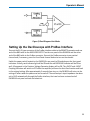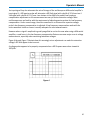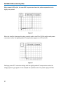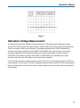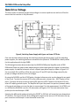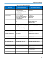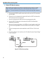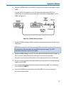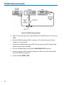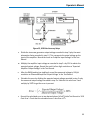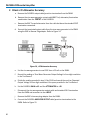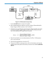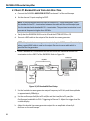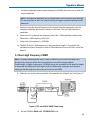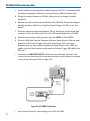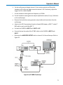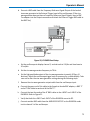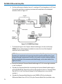
1
Operator’s
Manual
DA1855A
Differential Amplifier
DA1855A Differential Amplifier
Operator’s Manual
August, 2015
© 2015 Teledyne LeCroy, Inc. All rights reserved.
Unauthorized duplication of Teledyne LeCroy documentation materials other than for internal sales
and distribution purposes is strictly prohibited. However, clients are encouraged to distribute and
duplicate Teledyne LeCroy documentation for their own internal educational purposes.
Teledyne LeCroy is a registered trademark of Teledyne LeCroy, Inc. Windows is a registered
trademark of Microsoft Corporation. Other product or brand names are trademarks or requested
trademarks of their respective holders. Information in this publication supersedes all earlier
versions. Specifications are subject to change without notice.
926255-00
August, 2015
Operator’s Manual
Table of Contents
Safety Instructions ................................................................................................................... 1
Symbols .............................................................................................................................. 1
Precautions ......................................................................................................................... 1
Operating Environment ....................................................................................................... 2
Cooling................................................................................................................................ 2
Cleaning.............................................................................................................................. 2
Calibration........................................................................................................................... 3
Power.................................................................................................................................. 3
Specifications........................................................................................................................... 4
Nominal Characteristics ...................................................................................................... 4
Warranted Characteristics .................................................................................................. 6
Typical Characteristics ........................................................................................................ 7
Physical Characteristics ...................................................................................................... 8
Overview ................................................................................................................................... 9
Model Description ............................................................................................................. 10
Rack Mount Versions ........................................................................................................ 10
Power Cable Option .......................................................................................................... 10
Standard Accessories ....................................................................................................... 10
Optional Accessories ........................................................................................................ 11
Operation ................................................................................................................................ 11
General Information .......................................................................................................... 11
Dynamic Range ................................................................................................................ 11
Front Panel ....................................................................................................................... 12
Rear Panel ........................................................................................................................ 17
Instrument Settings ........................................................................................................... 20
General Operating Information ............................................................................................. 24
Power Connection ............................................................................................................ 24
Comparator Mode ............................................................................................................. 24
Differential Mode ............................................................................................................... 24
Setting Up the Oscilloscope with ProBus Interface ........................................................... 25
Setting up the Oscilloscope without ProBus Interface....................................................... 30
Determining the Proper Offset Mode ................................................................................ 35
Avoiding Common Problems ............................................................................................ 35
Care and Maintenance ........................................................................................................... 38
Cleaning............................................................................................................................ 38
Calibration Interval ............................................................................................................ 38
Service Strategy ............................................................................................................... 38
Troubleshooting ................................................................................................................ 38
Returns ............................................................................................................................. 38
i
DA1855A Differential Amplifier
Applications............................................................................................................................ 39
Voltage Measurements ..................................................................................................... 39
Measuring Current ............................................................................................................ 39
Effects of Probes on Saturation Voltage Measurements ................................................... 40
Saturation Voltage Measurement...................................................................................... 43
Gate Drive Voltage............................................................................................................ 44
Upper and Lower Gate Drive ............................................................................................ 45
Avoiding Measurement Errors........................................................................................... 45
Remote Control Commands .................................................................................................. 46
Command List ................................................................................................................... 46
Gain Control Mode ............................................................................................................ 47
Attenuation ........................................................................................................................ 47
Auto-Zero .......................................................................................................................... 48
Bandwidth Limit................................................................................................................. 48
Coupling ............................................................................................................................ 49
Gain .................................................................................................................................. 50
Offset ................................................................................................................................ 51
Input-Resistance ............................................................................................................... 52
Probe Attenuation ............................................................................................................. 53
Precision Voltage Generator ............................................................................................. 54
Volt / DIV ........................................................................................................................... 55
Performance Verification....................................................................................................... 56
Test Equipment Required ................................................................................................. 56
Preliminary Procedure ...................................................................................................... 58
Functional Check .............................................................................................................. 59
Verification Procedure ....................................................................................................... 60
Performance Verification Test Record .............................................................................. 77
Reference ................................................................................................................................ 80
Differential Mode and Common Mode .............................................................................. 80
Differential Mode Range and Common Mode Range ....................................................... 80
Common Mode Rejection Ratio ........................................................................................ 80
Certifications ..................................................................................................................... 82
Returning a Product .......................................................................................................... 85
Teledyne LeCroy Service Centers .................................................................................... 86
Warranty ........................................................................................................................... 87
ii
Operator’s Manual
Safety Instructions
This section contains instructions that must be observed to keep this oscilloscope accessory
operating in a correct and safe condition. You are required to follow generally accepted safety
procedures in addition to the precautions specified in this section. The overall safety of any system
incorporating this accessory is the responsibility of the assembler of the system.
Symbols
These symbols appear on the instrument's front or rear panels and in its documentation to alert you
to important safety considerations.
CAUTION of potential damage to instrument, or WARNING of potential bodily injury.
Attend to the accompanying information to protect against personal injury or damage. Do
not proceed until conditions are fully understood and met.
High voltage. Risk of electric shock.
Measurement ground connection.
Safety (protective) ground connection.
Alternating Current.
Power On; connected to AC mains.
Power Off; disconnected from AC mains.
Precautions
• Use proper power cord. Use only the power cord shipped with this instrument and certified
for the country of use.
• Maintain ground. This product is grounded through the power cord grounding conductor. To
avoid electric shock, connect only to a grounded mating outlet.
• Connect and disconnect properly. Do not connect/disconnect probes or test leads while they
are connected to a voltage source.
• Observe all terminal ratings. Do not apply a voltage to any input that exceeds the maximum
rating of that input. Refer to the specifications for maximum input ratings.
• Use only within operational environment listed. Do not use in wet or explosive atmospheres.
• Use indoors only.
1
DA1855A Differential Amplifier
• Keep product surfaces clean and dry.
• Do not block the cooling vents. Leave a minimum six-inch (15 cm) gap around the sides and
back between the instrument and the nearest object. The feet provide adequate bottom
clearance. Keep the underside clear of papers and other objects.
• Do not remove the covers or inside parts. Refer all maintenance to qualified service
personnel.
• Do not operate with suspected failures. Do not use the product if any part is damaged.
Obviously incorrect measurement behaviors (such as failure to calibrate) might indicate
impairment due to hazardous live electrical quantities. Cease operation immediately and
sequester the instrument from inadvertent use.
Operating Environment
Temperature: 0 to 50 °C.
Humidity: Maximum relative humidity 80 % for temperatures up to 31 °C decreasing linearly to 50 %
relative humidity at 50 °C.
Altitude: Up to 2,000 m (6,562 ft).
Cooling
The instrument relies on forced air cooling with internal fans and vents. Take care to avoid
restricting the airflow to any part of the amplifier. Around the sides and rear, leave a minimum of 15
cm (6 inches) between the instrument and the nearest object. At the bottom, the amplifier feet (up
or down) provide adequate clearance.
CAUTION. Do not block vents. Always keep the area beneath the amplifier clear of paper and
other items.
The instrument also has internal fan control circuitry that regulates the fan speed based on the
ambient temperature. This is performed automatically after start-up.
Cleaning
Clean only the exterior of the amplfier using a damp, soft cloth. Do not use harsh chemicals or
abrasive elements. Under no circumstances submerge the instrument or allow moisture to
penetrate it. Avoid electric shock by unplugging the power cord from the AC outlet before cleaning.
CAUTION. Do not attempt to clean internal parts. Refer to qualified service personnel.
2
Operator’s Manual
Calibration
The amplifier is calibrated at the factory prior to being shipped. The recommended calibration
interval is one year. Calibration should be performed by qualified personnel only. Schedule an
annual factory calibration as part of your regular maintenance. Extended warranty, calibration, and
upgrade plans are available for purchase. Contact your Teledyne LeCroy sales representative or
[email protected] to purchase a service plan.
Power
AC Power Source
100 to 240 VAC (±10%) at 50/60 Hz (± 10%).
Manual voltage selection is not required because the instrument automatically adapts to line
voltage.
Power Consumption
DA1855A: 28 Watts (39 VA)
DA1855A-PR2: 56 Watts (78 VA)
Power and Ground Connections
The amplifier is provided with a 10A/250V 18AWG rated grounded cord set containing a molded
three-terminal polarized plug and a standard IEC320 (Type C13) connector for making line voltage
and safety ground connections.
The AC inlet ground is connected directly to the frame of the instrument. For adequate protection
again electric shock, connect to a mating outlet with a safety ground contact.
WARNING. Interrupting the protective conductor inside or outside the device, or
disconnecting the safety ground terminal, creates a hazardous situation. Intentional
interruption is prohibited.
Power On/Off
The Power On/Off switch on the back of the amplifier controls the operational state of the device.
Press the side of the switch closest to either On or Off.
3
DA1855A Differential Amplifier
Specifications
These specifications are valid for instruments when the following conditions have been met:
•
The instrument is being operated from a power source, which meets the line voltage and
frequency specifications.
•
The instrument has been operating for at least 20 minutes in an environment, which is
within the operating environmental specifications.
•
The instrument has been calibrated within the last 12 months. Calibration was performed in
a controlled environment of 25° C ± 5° C.
Nominal Characteristics
Nominal characteristics describe parameters and attributes which are guaranteed by design, but do
not have associated tolerances.
General
Input Configuration
True Differential, + and – Inputs Precision Voltage Generator
can be selected as – input source in VCOMP mode.
Offset Capability
The Precision Voltage Generator can be used to provide true
differential offset.
+Input Coupling Selections
–Input Coupling Selection
Input Connectors
Maximum Input Voltage
Output Configuration
AC, Off (Precharge), DC, VCOMP
BNC (+Input incorporates Probe Attenuation Coding sensing
connector)
Withstand up to ± 200 Vp continuous. Automatic input
disconnect with manual reset.
Single ended, Ground referenced
Output Impedance
50 Ω
Intended Output Load
50 Ω
Output Connector
BNC
Amplifier Gain
X1 or X10
Input Attenuation
÷1 or ÷10
Bandwidth Limit Filters
(Low Pass)
Bandwidth Limit Filter Characteristics
4
AC, Off (Precharge), DC
100 kHz, 1 MHz, 20 MHz or
None (full bandwidth)
3-pole Bessel, 18 dB/octave
Operator’s Manual
General, continued
Auto Zero
Effective Gain Indicator
Amplifier initiates an automatic balance cycle, when either gain
button is depressed, to remove output offset drift
Indicators show the effective system gain or attenuation, factoring
Probe Attenuation, Attenuator and gain settings. (Probe must have
coding connectors. ÷1, ÷10, ÷100 and ÷1000 probes are
recognized)
Dynamic Ranges
Maximum Differential Mode Range
1
X10 Gain, ÷1 Attenuator
± 50 mV
X1 Gain, ÷1 Attenuator
± 0.5 V
X10 Gain, ÷10 Attenuator
± 0.5 V
X1 Gain, ÷10 Attenuator
1
1
1
±5V
Maximum Input Slew Rate
÷1 Attenuator
± 0.15 V/μsec
÷10 Attenuator
± 1.5 V/μsec
Maximum Common Mode Range
1
÷1 Attenuator
± 15.5 V
÷10 Attenuator
± 155 V
1
Differential Offset Range (VDIFF mode referred to input)
1
X10 Gain, ÷1 Attenuator
±1V
X1 Gain, ÷1 Attenuator
± 10 V
X10 Gain, ÷10 Attenuator
± 10 V
X1 Gain, ÷10 Attenuator
± 100 V
1
1
1
Comparison Offset Range (VCOMP mode, referred to input)
1
÷1 Attenuator
± 15.5 V
÷10 Attenuator
± 155 V
1
1. Voltages are referred to the amplifier input connector. Multiply by probe attenuation factor to obtain value referred to
probe input (e.g. ± 50 mV becomes ± 0.5 V at the probe tip when using a ÷10probe.)
5
DA1855A Differential Amplifier
Precision Voltage Generator
Output Range
± 15.5 V
Output Impedance
≈ 10 Ω
Resolution
100 μV
Control
Individual increment and decrement digits
carry over to the next decade
Reference Type
Oven stabilized buried zener diode
Output Routing
Can be applied to –Input and available at
rear panel BNC connector
Power Requirements
Line Voltage Range
Line frequency Range
90 - 264 VAC
45 - 66 Hz
Warranted Characteristics
Warranted characteristics describe parameters which have guaranteed performance. Unless
otherwise noted, tests are provided on page 60, Performance Verification, for all warranted
specifications.
Gain Accuracy
Bandwidth (-3 dB) x1 Gain
Rise Time
Common Mode Rejection
> 100 MHz
< 3.5 nsec (Calculated from bandwidth)
x1 or x10, ÷1 attenuation
70 Hz
≥50,000:1 (94 dB)
100 kHz
≥50,000:1 (94 dB)
10 MHz
≥316:1 (50 dB)
Precision Voltage Generator
6
± 1% + uncertainty of termination resistance
+/- 0.05% of reading +/- 500uV accuracy
(15° C to 45° C)
Operator’s Manual
Typical Characteristics
Typical characteristics describe parameters, which do not have guaranteed performance. Tests for
typical characteristics are not provided in the Performance Verification Procedure.
Input Resistance
÷1 Attenuator
1 MΩ or 100 MΩ 1 MΩ only when used with
attenuating probe
÷10 Attenuator
1 MΩ
Input Capacitance
20 pF
AC Input Coupling Capacitance
0.1 μF
÷10 Attenuator Accuracy
0.05%
Bandwidth, x10 Gain
Common Mode Rejection Ratio
Input Noise
Overdrive recovery
Output Zero
1
Input Leakage Current
100 MHz
Refer to Figure 22
Refer to Figure 23
(With DXC100A probe, 100 Ω between tip and
ground)
In X10 gain, settles within 1 mV referred to input
within 100 nsec from 4 V input (8000% overdrive)
≤ 2 mV referred to input
<10 pA (0° C to 45° C)
Differential Offset Accuracy
X10 Gain, ÷1 Attenuator
0.1% + 50 μV
X1 Gain, ÷1 Attenuator
0.1% + 500 μV
X10 Gain, ÷10 Attenuator
X1 Gain, ÷10 Attenuator
Precision Voltage Generator
2
2
0.15% + 500 μV
2
2
0.15% + 5 mV
<75 μV/°C
Temperature Coefficient (power consumption)
DA1855A
≈ 28 W, ≈ 39 VA
DA1855A-PR2
≈ 56 W, ≈ 78 VA
1
Output Zero is the output voltage from zero with zero Volt applied between inputs. This specification is valid within 30
minutes from last Autozero cycle, and when the differential amplifier is operating in an environment with stable ambient
temperature.
2
Voltages are referred to the amplifier input connector. Multiply by probe attenuation factor to obtain value refer to
probe input. (e.g. 0.1% + 50 μV becomes 0.1% + 500 μV at the probe tip when using a ÷10 probe.)
7
DA1855A Differential Amplifier
Physical Characteristics
Height
Width
Depth
Weight
Shipping Weight
8
DA1855A
7.29 cm (2.87 inch)
DA1855A-PR2
8.75 cm (3.4 inch)
DA1855A
21.2 cm (8.36 inch)
DA1855A-PR2
43.9 cm (17.3 inch)
DA1855A
23.2 cm (9.12 inch)
DA1855A-PR2
42.5 cm (16.7 inch)
DA1855A
2.15 kg (4 lbs 12 oz.)
DA1855A-PR2
9.5 kg (21 lbs)
DA1855A
3.12 kg (6 lbs 14 oz.)
DA1855A-PR2
11.3 kg (25 lbs)
Operator’s Manual
Overview
The DA1855A is a stand-alone high performance 100 MHz differential amplifier. It is intended to act
as signal conditioning preamplifier for oscilloscopes, spectrum analyzers and other instruments,
providing differential measurement capability to instruments having only a single-ended input.
When used with a DA1855A, high quality oscilloscopes can obtain common mode rejection and
overdrive recovery performance that was previously unobtainable in any product.
When used with a Teledyne LeCroy oscilloscope equipped with ProBus interface, the DA1855A can
be controlled through the oscilloscope user interface or remote commands.
When used with non ProBus oscilloscopes, the DA1855A settings can be controlled directly through
the front panel controls.
Amplifier gain may be set to 1 or 10. A built-in input attenuator may be separately set to attenuate
signals by a factor of 10, allowing gains of 10, 1, or 0.1 and common mode dynamic range of ± 15.5 V
(÷1) or ± 155 V (÷10). Optional probes increase the maximum input signal and common mode ranges
in proportion to their attenuation ratio, but not exceeding their maximum input voltage rating.
Effective gain of the DA1855A, including probe attenuation, amplifier gain and attenuator settings, is
automatically displayed.
The DA1855A has a bandwidth of 100 MHz, but any one of the three 3-pole bandwidth limit filters
may be selected to reduce bandwidth to 20 MHz, 1 MHz or 100 kHz to limit noise above the
frequency of interest.
The DA1855A output is limited at ± 500 mV so that the oscilloscope is not overdriven by large inputs.
This allows an oscilloscope to directly measure the settling of D/A converters with 14 bit (60ppm)
precision.
The DA1855A features a built-in Precision Voltage Generator (PVG) that can be set to any voltage
between ± 15.5 Volt (± 10 Volt in Differential Offset mode) with 5-1/2 digit resolution. Each digit of
the voltage generator output can be individually incremented or decremented. Positive or negative
polarity can be selected. The PVG’s output can be selected as an input to the inverting (–) input of
the amplifier for operation as a differential comparator or applied internally as a true differential
offset voltage. The voltage is also available to be used externally through a rear panel connector.
To maintain the amplifier’s high Common Mode Rejection performance, special differential probes
such as the Teledyne LeCroy model DXC series are recommended and are available as optional
accessories.
9
DA1855A Differential Amplifier
Model Description
The DA1855A series is comprised of 2 models which differ in physical configuration. Both contain
the same 100 MHz differential amplifier which provides high common mode rejection, extremely
fast overdrive recovery, selectable ÷1 or ÷10 attenuation, selectable X1 or X10 gain, a 5-1/2 digit
Precision Voltage Generator (PVG), selectable upper bandwidth limiting filters, an effective gain
display, and ± 500 mV output swing limiting. The PVG is provides a calibrated reference for
Differential Offset or Comparison modes. The PVG reference voltage is also available through a BNC
connector on the rear panel.
DA1855A:
Single channel unit packaged in a convenient desk top housing.
DA1855A-PR2:
Two independent model DA1855A amplifiers packaged in one housing with one
line power input connection. The housing is intended for desk top use, where it
can be placed under an oscilloscope.
Rack Mount Versions
Rack mounted versions available for models:
•
DA1855A-RM: Single channel rack mounted version.
•
DA1855A-PR2-RM: Dual channel rack mounted version.
Power Cable Option
(One must be specified at time of order)
•
Option – P01: 120 V North America / Japan
•
Option – P02: United Kingdom
•
Option – P03: Universal Europe
•
Option – P04: Australia / New Zealand
•
Option – P05: Switzerland
Standard Accessories
Each DA1855A Differential Amplifier is packaged for shipment with the following items:
10
•
Power cable, as specified by power cable option.
•
ProBus interface cable with BNC signal cable. (-PR2 models include 2 ProBus cables)
•
Certificate of Calibration traceable to NIST (United States National Institute of Standards and
Technology)
•
Operator’s Manual, which includes a Performance verification Procedure.
Operator’s Manual
Optional Accessories
•
Service Manual, containing adjustments, repair and replacement part information P/N:
DA1855A-SM-E.
•
DXC100A, ÷10 / ÷100 Passive Differential Probe.
•
DXC200, ÷1 Passive Differential Probe.
•
DXC5100, ÷100 2.5 K Passive Differential Probe Pair
•
DA101, External ÷10 Attenuator.
Operation
General Information
The DA1855A has been designed to be used with oscilloscopes equipped with a ProBus interface.
Connecting the Differential Amplifier to the oscilloscope through the ProBus interface will
automatically control all the required settings from the oscilloscope and will lock-out the DA1855A
front panel controls. All front panel controls are now accessible through the oscilloscope user
interface. The DA1855A user interface can be viewed from the Channel setup dialog for the channel
to which it is connected. The DA1855A front panel controls will operate manually when the
Differential Amplifier is connected to an oscilloscope not provided with a ProBus interface.
NOTE: Removing the ProBus interface cable with the differential amplifier still powered up, requires
the DA1855A to be turned OFF and ON to access the front panel controls.
Dynamic Range
The basic amplifier dynamic range in X1 Gain and ÷1 Attenuation is ± 0.500 V. Changing the gain and
or attenuation will affect both the Differential Mode and Common Mode ranges.
The Differential Mode range is scaled by both gain and attenuation, while the Common Mode range
is scaled by attenuation only.
Gain
Atten*
Differential
Mode*
Common Mode*
1
÷1
± 0.5 V
± 15.5 V
1
÷10
± 5.0 V
± 155 V
10
÷1
± 50 mV
± 15.5 V
10
÷10
± 0.5 V
± 155 V
* Attenuation, Common Mode and Differential Mode ranges are scaled with external probe attenuation. A ÷10
probe will increase all these values by a factor of 10.
11
DA1855A Differential Amplifier
Front Panel
Input Connectors
Signals applied to the +INPUT and the –INPUT are connected either directly to the DA1855A
amplifier’s inputs or to the input attenuators. Maximum input voltage is ±200 Vp
A signal connected to the +INPUT will remain its polarity at the output connector. A signal
connected to the –INPUT will be inverted in polarity.
Attenuators
The input attenuators are passive networks which divide each signal by ten.
In ÷1 mode the front panel input connectors are directly connected to the DA1855A amplifier's
differential inputs.
In ÷10 mode each front panel input connector is connected to a passive 1 MΩ attenuator. The
attenuator output is connected to the DA1855A amplifier's corresponding differential input. The
signal at each input is attenuated by a factor of ten.
Gain
The DA1855A amplifier gain (amplification) is selectable between X1 and X10. The amplified signal
appears at the rear panel AMPLIFIER OUTPUT connector.
Gain will affect the differential mode output signal by amplifying the signal difference between the
+INPUT and the –INPUT, but will not affect the common mode signal, the signal common to the
+INPUT and them –INPUT.
Output Termination
Proper gain is obtained when the DA1855A drives a 50 Ω load such as an oscilloscope with input
impedance set to 50 Ω. Automatic 50 Ω termination is obtained when the DA1855A is connected to
a Teledyne LeCroy oscilloscope through the ProBus interface.
An instrument with only a 1 MΩ input impedance available should have a 50 Ω coaxial termination
placed on its input connector. The DA1855A is then connected to the oscilloscope through the
coaxial termination.
Input Resistance
When the input ATTENUATOR is set to ÷1 and no attenuating probe is connected, the input
resistance can be increased from 1 MΩ to 100 MΩ. This is advantageous when measuring high
impedance circuits or when AC coupling is needed with a very low frequency cut off. When the input
ATTENUATOR is set to ÷10 or an attenuating probe with read out capability is attached, 1 MΩ (1M)
input resistance is automatically selected.
12
Operator’s Manual
Unbalanced source impedances can have an adverse effect on common mode rejection. For
example, a differential source with impedances of 1000 and 2000 Ω, each loaded with 1 MΩ will
have a common mode rejection ratio (CMRR) of 1000 to 1. The common mode rejection ratio can be
improved to 100,000 to 1 by using 100 MΩ input resistance.
Auto Zero
Auto Zero is a feature invoked from the Channel setup dialog when the amplifier is connected via
the ProBus interface. If the Differential Amplifier is not connected through a ProBus interface, push
either the X1 or X10 button, even if a different gain is not selected. Auto Zero momentarily sets the
input coupling to OFF and determines the offset necessary to set the output at 0 Volt. During this
process the front panel input signal to the amplifier is interrupted. When the Auto Zero cycle is
completed, the input coupling returns to its previous state. Auto Zero usually takes less than one
second to complete. This feature allows you to DC balance the DA1855A simply by pushing the GAIN
button which is already illuminated. When changing gains, the Auto Zero feature is automatically
invoked, adjusting the amplifier’s DC balance.
+ Input Coupling (AC – OFF – DC)
In OFF mode, the input connector is disconnected from the amplifier input, and the amplifier input
is connected to ground. The AC coupling capacitor is connected between the +INPUT and ground
through 1 MΩ resistor, independent of the INPUT RESISTANCE setting. In this mode, the AC coupling
capacitor is quickly charged to the average DC input voltage. OFF mode is also referred to as
precharge mode. Precharge is particularly useful prior to selecting AC coupling when the input
voltage has a DC component in excess of 19 V. The DA1855A input coupling is set to OFF and
connected to the circuit under test. When the +INPUT is changed from OFF to AC mode, the
coupling capacitor is already charged, and the trace properly centered on the oscilloscope screen.
Additionally, the risk of tripping the input overload detector and automatically disconnecting the
input is eliminated.
In the AC mode, the +INPUT is connected through an AC coupling capacitor to the amplifier input or
the input attenuator. The coupling capacitor retains its charge when the input is switched to DC,
making it possible to return to the same circuit without the precharge time. But this also makes it
possible to discharge the coupling capacitor into another circuit under test if its DC voltage differs by
more than approximately 19 V from the voltage on the coupling capacitor.
NOTE: The discharge current from the AC coupling capacitor is limited to about 70 mA. In some
situations this could damage sensitive circuits. To avoid the inrush current transient, it is therefore
recommended that the +INPUT coupling first be changed to the OFF (precharge) when measuring a
new circuit point. This will safely recharge the AC coupling capacitor in less than 0.3 seconds.
DC and low frequencies are attenuated by the AC coupling capacitor and the input resistance. With
the ATTENUATOR set to ÷10, or set to ÷1 with the INPUT RESISTANCE set to 1 MΩ, the low
frequency cut off (-3dB point) is approximately 1.6 Hz. When the input attenuator is set to ÷1, the
13
DA1855A Differential Amplifier
INPUT RESISTANCE may be set to 100 MΩ, and the –3 dB point is 0.016 Hz. This extremely low
frequency cut off is useful for observing low frequency noise riding on larger DC voltages.
In the DC mode, the +INPUT connector is connected to the amplifier either directly or through the
input attenuator, and the AC and DC attenuation are the same.
- Input Coupling (AC–OFF – DC – VCOMP)
The –INPUT has the same coupling modes as the +INPUT plus one additional option, VCOMP
(comparison voltage).
The DA1855A contains a precision DC voltage source which is controlled by the oscilloscope OFFSET
control. (When the amplifier is used stand alone, without ProBus interface to a Teledyne LeCroy
oscilloscope, the voltage is controlled by the push buttons above and below the front panel
numerical display.) This voltage source is called the Precision Voltage Generator (PVG).
The DA1855A's amplifier subtracts the voltage applied to its inverting input from the voltage applied
to its non-inverting input. The DA1855A output is therefore zero whenever these two voltages are
equal. For this reason, the voltage applied to the inverting input is called a comparison voltage,
VCOMP. Stated another way, the value of the horizontal center line in the oscilloscope graticule is
the voltage read in the PVG display. Each graticule line above or below the center line will add or
subtract the Volts/div value from the PVG setting.
VCOMP can be used to make precise measurements of large signals by comparing the accurately
known VCOMP with the unknown signal. It can also be used to measure the actual voltage at any
point of a waveform.
Since the amplifier’s gain and input attenuator are individually selectable, the comparison range can
be changed from ± 15.500 V to ± 155.000 V by changing the ATTENUATION from ÷1 to ÷10, while
the overall gain can still be set either to 1 or 0.1 by selecting either X10 or X1 GAIN.
NOTE: While in VCOMP mode, the amplifier is configured for single ended measurements. The –INPUT
connector is not usable when VCOMP is selected. The input signal applied to the + INPUT is referenced
to ground offset by the value set by the Precision Voltage Generator. Large calibrated offsets can be
obtained while making differential measurements by using VDIFF mode.
Precision Voltage Generator
The PVG generates the voltage which is used in the VCOMP and VDIFF modes and appears at the rear
panel OFFSET VOLTAGE (PVG) output connector for use as a reference voltage.
The Precision Voltage Generator (PVG) output range is ± 15.500 Volt. The PVG is never attenuated
by the input attenuator. Attenuation of the +INPUT signal by the ÷10 input attenuator will cause the
PVG to null out an input voltage up to ± 155.00 Volt which is ten times larger than the actual PVG
voltage.
The increase in common mode voltage range also applies when using attenuating probes.
14
Operator’s Manual
When the DA1855A is used with attenuating probes that feature readout, the PVG display is
changed to indicate the voltage at the +INPUT probe tip which will bring the amplifier output to
zero.
When connected to a Teledyne LeCroy oscilloscope via the ProBus interface, the oscilloscope
OFFSET control increments or decrements the PVG’s output voltage and the offset value will be
shown on the six PVG front panel indicators. The new offset value will also be displayed on the
oscilloscope’s screen for a few seconds after a change has been made.
When connected to an oscilloscope not provided with a ProBus interface, the PVG can be accessed
by means of push buttons. Above each digit is a push button which increments the corresponding
digit by one when pushed. When held, the digit continues to increment, eventually incrementing the
next higher digit.
Similarly, below each digit is a push button which decrements the corresponding digit.
The ± button above the left-most digit changes the PVG output polarity. The ZERO button below the
left-most digit sets the output to zero and invokes the PVG's Auto Zero function. PVG absolute
mode: DA1855 PVG increment and decrement buttons always function to increment or decrement
the voltage display respectively. When decrementing from a positive voltage, the display always
stops at zero. To obtain negative voltages, the ±± button must be pushed, and the increment button
is used to increase the magnitude of the negative voltage. This operation is natural if simply setting
a voltage, but unnatural if moving a displayed oscilloscope waveform. This is known as the PVG
absolute mode, and the only mode available in the original DA1855, (non “A” model). The DA1855A
retains the option of operating in this same manner as well as supporting PVG roll through zero
mode.
NOTE: When the DA1855A is controlled remotely through a Teledyne LeCroy oscilloscope, neither
PVG absolute or PVG roll through zero modes apply. When operated remotely, the PVG value is
controlled with the use of the OFFSET knob on the oscilloscope, when in effect, operates in the roll
through mode.
PVG roll through zero mode: The DA1855A increment buttons are oscilloscope waveform related by
factory default. The increment buttons move a displayed oscilloscope waveform upward and the
decrement buttons move the waveform downward independent of the PVG polarity. Decrements
from a positive voltage will roll smoothly through zero. This is known as roll through zero mode.
Toggle PVG modes: To change from roll through zero to absolute mode of operation hold the PVG
ZERO button and press the ± button. Change back to the roll through zero mode by repeating the
same operation.
15
DA1855A Differential Amplifier
Differential Offset
VDIFF (differential offset voltage) is an instrument mode rather than a type of input coupling. The VDIFF
mode allows the PVG to inject a calibrated offset signal into the DA1855A while still using both
inputs for full differential operation. This mode can be used as a position control to move the trace
on the oscilloscope screen in preference to using the oscilloscope's position or offset control. The
oscilloscope's position and offset controls should always be set to zero so that the DA1855A's
dynamic range is properly centered. (This is done automatically when using a Teledyne LeCroy
oscilloscope with ProBus interface.) When the oscilloscope is set to greater sensitivities (lower
Volts/Div settings), the Differential offset provides much greater range than the conventional
position control. For example, at 50 mV/div, the VDIFF mode provides up to ± 200 divisions of range.
Operation of the DA1855A using the VDIFF function is the same as VCOMP except for the following:
•
The –INPUT remains active, allowing full use of the DA1855A as a differential amplifier.
•
The maximum range of the PVG is ±10.000 Volt in X1 GAIN and ±1.0000 Volt in X10 GAIN.
The effects of the ÷10 input ATTENUATOR and probe attenuation are the same as when
using VCOMP, i.e., any input attenuation multiplies the effective offset.
The DA1855A's PVG display is changed to indicate the voltage that, if applied between the +INPUT
and –INPUT, would bring the amplifier output to zero. When the DA1855A is used with attenuating
probes which feature readout, the PVG display is scaled to include the effect of probe attenuation.
Effective Gain
Six indicators (LEDs) across the top of the DA1855A front panel show the total gain from the
instrument input to output. Logic within the amplifier includes the gain, internal attenuation, and
probe attenuation factors (when readout encoded probes are used) to determine the effective gain.
When the X1 light is ON, the overall amplifier voltage gain (amplification) is unity. Similarly, X10
indicates an overall amplification of ten times, ÷10 Indicates the voltage amplification is 0.1, etc.
The DA1855A communicates the effective gain information to the Teledyne LeCroy oscilloscope
when the ProBus interface is used. This corrects the scale factor of the displayed waveforms, cursors
and measurements.
When Teledyne LeCroy DXC series or other readout encoded probes are used, the effective gain
includes the probe’s attenuator factor.
BW Limit
16
FULL
The DA1855A amplifier's full bandwidth, over 100MHz, is passed to the
oscilloscope, spectrum analyzer or digitizer. Frequency response and
transient response are essentially independent of the oscilloscope’s input
impedance.
20 MHz
A 20MHz three pole (18dB/octave) filter allows the DA1855A to reduce
extraneous noise. This filter is a passive LC design and is intended to drive a
Operator’s Manual
50 Ω load. Without the load, the filter's frequency response and transient
response are altered.
1 MHz
The 1MHz filter is of the same design as the 20 MHz filter, and the same
remarks apply.
100 kHz
The 100kHz filter is an active filter with a 50 Ω output impedance. Transient
and frequency response are independent of the load impedance.
Overload
When a signal, which could damage the DA1855A, has been applied to either input connector, the
DA1855A protects itself by disconnecting the signal. The input coupling mode changes to OFF, and
the OVERLOAD light is turned on.
To reset the amplifier to normal operation, remove the offending input, press any of the input
coupling modes (AC, OFF, or DC). The Overload light will turn off indicating the amplifier is reset.
When the ATTENUATOR is set to ÷1, an input signal of approximately ±19 Volt will activate the
overload protection circuit. Fast transients will draw up to about 70 mA of input current for a brief
period before the input coupling relay acts to disconnect the input.
CAUTION. Inputs in excess of 250 Volt may cause permanent damage to the DA1855A.
The input is not disconnected when the ATTENUATOR is set to ÷10. The input attenuator can
withstand up to 200 Volt continuous input.
Rear Panel
Power
Normal instrument operation is obtained with the power switch in the 1 (ON) position. The
instrument can be used immediately, however it requires a 30 minute warm up period to reach
specified performance. Prior to reaching operating temperature, the amplifier offset will drift and
the output from the Precision Voltage Generator may not be within specification. In high humidity
environments the time to stabilize may be much longer. In high humidity environments or when
warm-up time inhibits power switch left in the 1 (ON) position.
Power Up Indicator
Upon turn-on, the model number and firmware version are briefly displayed in the PVG readout. For
example, 1855.12 indicates that the instrument is a model DA1855A and the firmware version is 1.2.
17
DA1855A Differential Amplifier
Precision Voltage Generator Offset Voltage
The rear panel OFFSET VOLTAGE BNC (PVG) output connector, is a monitor of the Precision Voltage
Generator (PVG). The voltage present on this connector is the same voltage as that applied to the –
INPUT when the –INPUT coupling is set to VCOMP or internally to the DA1855A when VDIFF is
selected. The OFFSET VOLTAGE output can be used to monitor the PVG with a digital Voltmeter
(DVM). A low pass filter between the PVG output and the –INPUT removes radio frequency
interference (RFI) from the signal. This filter does not attenuate the PVG signal.
The PVG output is not attenuated by the input attenuator or probes, whereas the input signal is.
Therefore the effective range of VCOMP is increased by a factor of 10 when the ÷10 ATTENUATOR is
selected or a ÷10 attenuating probe is used to attenuate the input signal. The PVG numerical display
reflects the attenuator setting and probe attenuation when the probe is readout encoded. As an
example, if there are no probes attached, the ÷10 ATTENUATOR is selected and the display is set to
read –155.000, the PVG output will actually be –15.5 Volt.
The decimal in the display will be in the correct location to indicate the voltage at the PVG output
when no probes are attached and ÷1 ATTENUATOR and X1 GAIN are selected.
The OFFSET VOLTAGE BNC (PVG) output also presents the same voltage used internally for
differential offset when VDIFF is selected. Because the PVG is applied to the amplifier to create a true
differential offset, the relationship between VDIFF and the voltage at the OFFSET VOLTAGE BNC (PVG)
output (changes with the amplifier gain selection according to the following table:
The maximum VDIFF is multiplied by any probe attenuation factor. The DA1855A front panel displays
the correct offset referred to the instrument input.
Table 1, VDIFF Range for Different Gain and Attenuator Settings
Gain
Attenuation Max.
VDIFF
X1
÷1
± 10 V
X1
÷10
± 100 V
X10
÷1
±1V
X10
÷10
± 10 V
When using readout encoded probes which the DA1855A senses, the PVG readout calculates the
effective differential offset at the probe tip. Of course, both probes must have the same attenuation
factor.
In the VCOMP mode, the maximum OFFSET VOLTAGE input is limited by the DA1855A common mode
dynamic range. In the VDIFF mode it is limited by the dynamic range of the internal VDIFF amplifier.
18
Operator’s Manual
Table 2 and Table 3 will help the operator stay within the maximum input voltage limits and
understand the relationship between the actual voltage applied and the effective voltage. Effective
voltage is always referred to the input of the DA1855A or the probe tip if a probe is used. When
using probes, the maximum effective voltage range may be limited by the maximum voltage rating
of the probe.
Table 2, Effective Offset Range with ÷11 Probe
Front Panel
Effective Offset
Settings
Range
Gain
Attenuation
VCOMP
VDIFF
X1
÷1
± 15.5 V
± 10 V
X1
÷10
± 155 V
± 100 V
X10
x10
÷1
÷10
± 15.5 V
± 155 V
±1V
± 10 V
NOTE: The effective voltage is always increased by the attenuator. It therefore follows that any
probe will increase the effective voltage of both VCOMP and VDIFF by its attenuation factor. For
example, a probe with a 100X attenuation factor will increase the effective full scale range by 100.
Table 3, Effective Offset Range with ÷100 Probe
Gain
X1
X1
X10
x10
Front Panel
Effective Offset
Settings
Range with ÷100 Probe
Attenuation
÷1
÷10
÷1
÷10
VCOMP
± 1.55 kV
± 15.5 kV
± 1.55 kV
± 15.5 kV
VDIFF
± 1 kV
± 10 kV
± 100 V
± 1 kV
Although the full scale range may be 10 kV or 15.5 kV, most probes have a much lower maximum
input voltage rating which must not be exceeded.
Amplifier Output
The AMPLIFIER OUTPUT BNC is intended to be used with an oscilloscope, spectrum analyzer or
instrument having a 50 Ω input resistance. The amplifier’s output impedance is 50 Ω. Without the 50
Ω load, the amplifier gain will be uncalibrated and will be approximately twice the amount indicated
on the front panel. Proper operation of the 1 MHz or 20 MHz bandwidth limit filters requires an
output load impedance of 50 Ω.
19
DA1855A Differential Amplifier
Remote Operation
A REMOTE connector on the rear panel of the DA1855A allows total control of the instrument
through a Teledyne LeCroy oscilloscope when connected to ProBus using the supplied cable. All of
the instrument functions can be controlled through the oscilloscope user interface.
Remote control is also possible using commands sent through the IEEE-488 bus or through RS-232
connected to the oscilloscope. The DA1855A cannot be remotely controlled without a Teledyne
LeCroy oscilloscope. See page 46 for a description of the Remote Commands.
When the ProBus cable is installed, the buttons on the front panel of the differential amplifier are
disabled.
NOTE: Remote operation requires software version 6.6.0.5 or higher.
Probe Coding Input
This jack is to be used with Teledyne LeCroy DXC series probes to detect the probe attenuation
factor. Other manufacturer’s probes with standard probe coding capability will be properly decoded
through the DA1855A's front panel +INPUT BNC connector.
Instrument Settings
The DA1855A output is intended to connect directly to the input of an oscilloscope, or other
instrument, but it is important to observe some rules so that the DA1855A delivers its specified
performance.
CAUTION. A properly terminated differential amplifier can deliver an output voltage of ±0.5
Volt. The output is DC coupled and will follow any DC component applied to the input. Some
instruments such as spectrum analyzers could be damaged from overload or DC components.
Retained Settings
All front panel settings, including Precision Voltage Generator (PVG) settings are retained when the
instrument is turned off. The DA1855A return to the same state they were in when power was
removed.
20
Operator’s Manual
When used without ProBus interface, the instrument can be set to factory default settings by
pressing the VCOMP and VDIFF buttons simultaneously.
Gain
Attenuation
X1
÷10
+ Input Coupling
Off
– Input Coupling
Off
Bandwidth Limit
Full
PVG Voltage
+00.000 V
VCOMP
Off
VDIFF
Off
Input Resistance
PVG Mode
1 MΩ
Roll through zero
Table 4. Factory Default Settings
Sensitivity, Position and Offset
Oscilloscopes are designed to maintain their accuracy for that portion of a signal that is displayed
on-screen. When the signal is large enough to drive the display off-screen, the oscilloscope’s
amplifier must limit the signal in a non-linear mode. Oscilloscopes are designed so that no matter
how the sensitivity, position and offset controls are set, the operator cannot view this distorted
portion of the signal.
When used with a Teledyne LeCroy oscilloscope, the setup is automatic to prevent you from
entering a mode which could result in displaying a distorted signal resulting from overload.
When used with instruments lacking ProBus interface, the instrument’s gain and position controls
should be properly set to avoid displaying the non-linear portion of the DA1855A's output signal
when it is in overdrive. This can be accomplished by observing the following rules:
•
Turn the oscilloscope input coupling to “OFF” or “GND”, set the oscilloscope position
control to center screen, and do not change it! If the oscilloscope has an OFFSET control, it
too should be set to zero. Return the oscilloscope’s input coupling to “DC”. Subsequently
adjust the trace position on the oscilloscope screen using the DA1855A PVG and VDIFF mode
or VCOMP input. This assures that the oscilloscope is set to the center of the DA1855A's
dynamic range.
•
Set the oscilloscope deflection factor to no greater than 100mV/div. The most useful range
for the oscilloscope deflection factors will be between 1mV/div and 100mV/div. Using a
scale factor of 200 mV/Div will allow the nonlinear portion of the DA1855A's output to be
viewed on screen.
21
DA1855A Differential Amplifier
More sensitive settings (e.g. 100µV/div) available on some oscilloscopes can be used, but their
usefulness may be limited by noise, particularly with the DA1855A FULL bandwidth limit selection
and without averaging. With the oscilloscope set to 100µV/div and the DA1855A in the X10 GAIN
mode, the overall scale factor will be 10µV/div.
In the X10 GAIN mode, the DA1855A has lower noise than many oscilloscopes, so it is preferable to
use the /DA1855A X10 GAIN mode and a lower oscilloscope scale factor. For example, to obtain the
best noise performance at 1mV/div, set the DA1855A to X10 mode and the oscilloscope to 10mV/div
rather than the use X1 mode and 1mV/div. This also maximizes the bandwidth, as some
oscilloscopes give up some bandwidth at their most sensitive settings. Some oscilloscopes give up
bits of resolution to obtain 1mV or 2 mV/div sensitivity. The loss of resolution can be avoided by
using this technique. Any oscilloscope bandwidth limit setting may be used so long as the unlimited
signal does not exceed full screen before invoking bandwidth limit.
Probes and Differential Amplifiers
When using a differential amplifier it is very important to understand the role probes play in the
overall measurement system performance. Probes not only make attachment to the circuit under
test more convenient, ÷10 and ÷100 attenuating probes also extend the common mode range of the
differential amplifier. For example, the DA1855A amplifiers have a common mode range of ±15.5
volts when their internal attenuators are set to ÷1 and 155 volts when set to ÷10. The addition of a
probe with an attenuation factor of ten will extend the common mode range to 1550 volts or the
rating of the probe, whichever is less.
There is a trade-off, however. The Common Mode Rejection Ratio (CMRR) capability of even highly
matched differential probe pairs is seldom as good that of the amplifier. In order to preserve as
much of the amplifier’s performance as possible at the probe tips, it is important to use probes that
are designed for differential performance. Attempting to use normal ÷10 or ÷100 attenuating
oscilloscope probes, even high quality probes, will result in very poor CMRR performance. Nominally
matching ÷1 probes however, will provide excellent common mode rejection and are
recommended.
For applications which do not require additional attenuation, ÷1probes present relative high
capacitive loading to the circuit under test, limiting their usefulness to low frequency
measurements.
When making differential measurements, accurate probe compensation is much more important
than in single-ended measurements. Most probes depend on the accuracy of the oscilloscope’s 1
MΩ input resistor to determine the accuracy of the probe’s attenuation factor. Two probes with a
1% accuracy specification can yield a CMRR as low as 50 to 1 at DC while the amplifier CMRR may be
higher than 100,000 to 1. At high frequencies, the CMRR will be worse.
A differential probe pair must allow for matching at DC as well as over their useful frequency range.
Changing the compensation of a differentially matched probe set without following the proper
22
Operator’s Manual
compensation procedure can result in a significant decrease in the CMRR capability of any
differential probe pair.
It is a good practice to compensate a probe pair for a given amplifier and then leave the probe pair
and amplifier together as a system. Similarly, it is important that, once compensated for given
amplifier, each probe always be used on the same input (one probe always on the +INPUT and the
other always on the –INPUT).
DXC100A Differential Probe Pair
The DXC100A is a high performance matched passive differential probe pair designed for use with
Teledyne LeCroy DA1855A series differential amplifiers. The probe pair consists of two well matched
individual probes that share a common compensation box to allow the attenuation factor on both
probes to be simultaneously switched between ÷10 and ÷100. When used with the DA1855A
Differential Amplifier, the probe’s attenuation factor is automatically incorporated into the effective
gain display and the decimal properly located in the Precision Voltage Generator (PVG) display.
Probe Grounding
The DXC100A Probe Pair is supplied with accessories that allow for three methods of connecting
probe grounds.
In most cases, when the common mode portion of the signal consists mainly of low frequencies (1
MHz and below), the probe ground leads should not be connected to the ground of the circuit under
test. They should be connected to each other. This minimizes the effects of ground loop currents.
The signal corruption caused by not having the probes connected to the ground of the circuit under
test will be common to both inputs and will be rejected by the differential amplifier.
However, when working in an environment with high RF ambient noise, it is best to connect the
probe ground leads to a good RF ground near the point where the signal is being measured.
The best way to determine which probe grounding technique should be used is to try both methods
and use the one that gives the least corruption of the differential signal.
When adjusting the compensation and probe CMRR, the use of probe tip to BNC adapters is
required. They provide the best performance of the three grounding method.
23
DA1855A Differential Amplifier
General Operating Information
This section will help you become familiar with the operation of the DA1855A and how it interfaces
with an oscilloscope. To carry out the following exercises, you will need an oscilloscope and a
general purpose function generator.
Power Connection
Check to make sure the power switch located on the rear panel is in the OFF position. Connect the
power cable to an appropriate power source. The DA1855A will operate on a 50 or 60 Hz AC power
source with a nominal voltage range from 100 V to 240 V.
Comparator Mode
The DA1855 becomes a differential comparator when the internal Precision Voltage generator (PVG)
output is selected as the amplifier’s inverting (–) input. The – Input is disconnected form the
amplifier and does not serve any purpose in the V COMP mode. In this mode the DA1855A can be used
to very accurately measure relatively small signals riding on large DC components.
Figure 1, Block Diagram VCOMP Mode
Differential Mode
The DA1855A built-in Precision Voltage Generator can be used to generate a true differential offset
while still allowing both inputs to be used as differential inputs. This mode facilitates making
measurements such as changes to a transistor’s base to emitter voltage caused by variations in
temperature. Used in this mode, the voltage generator can be set to a value that will zero out the
static value of the junction’s ON voltage. the DA1855A’s differential measurement capability will
reject any dynamic signal common to both sides of the junction and the oscilloscope is left to
measure only the changes in the junction voltage.
24
Operator’s Manual
Figure 2, Block Diagram VDIFF Mode.
Setting Up the Oscilloscope with ProBus Interface
Connect the RJ-45 type connector of the ProBus interface cable to the REMOTE connector and one
end of the BNC cable to the AMPLIFIER OUTPUT on the rear panel of the DA1855A and the other
end of the BNC cable to the ProBus connector. Connect the ProBus connector to any vertical
channel and, if necessary, press the Front Panel channel button to turn on the channel.
Switch the power switch located on the DA1855A’s rear panel to ON and observe the front panel
indicators. Initially, each indicator light will be ON and the red OVERLOAD indicator will be ON as
well. All segments in the Precision Voltage Generator display will be ON. The +INPUT and –INPUT
Coupling Indicators will switch to OFF while the amplifier performs the Auto Zero function and back
to the original setting. After approximately 3 seconds from turn on, the DA1855A will return to the
settings in effect when the power was last turned off. The oscilloscope’s input impedance has been
set to 50 Ω automatically through the ProBus interface, the trace has been centered and all
DA1855A front panel controls are locked out.
25
DA1855A Differential Amplifier
Make these settings:
PVG Mode
OFF
+Coupling
DC
–Coupling
Grounded (OFF)
DA1855A (Atten/Gain)
List Select: Upper BWL
Auto
Full BWL
List Select: Gain
X1
List Select: Atten
÷10
List Select: Input R
1 MΩ
Attenuator and Gain Operation
Connect the function generator output to the +INPUT BNC connector and apply a sine wave of 50
kHz and 1.0 Vp-p amplitude. If necessary, set the oscilloscope scale factor to 0.50 V/div. The signal
on the oscilloscope should be 2 divisions peak to peak. Adjust the oscilloscope’s time per division
and trigger to display at least two complete cycles of the waveform.
Set the DA1855A Atten/Gain to Manual. In the List Select menu, select Atten and in the Value menu
select /1. The waveform’s magnitude on the oscilloscope’s display will increase by a factor of 10, to
50 mV/div, the waveform will extend and extend off the top and bottom of the screen. The X1 light
will be lighted in the EFFECTIVE GAIN front panel display. Reduce the function generator’s output
until the oscilloscope’s display is again 2 divisions peak to peak.
Set the gain to X10. Observe the following changes: The +INPUT’s DC light will momentarily go out
and its OFF light will be lighted before returning to their previous states. This momentary change is
the result of the DA1855A automatically adjusting its DC Balance. The X10 light will be lighted in the
EFFECTIVE GAIN display and the display on the oscilloscope will again extend off screen. The overall
sensitivity of the DA1855A and the oscilloscope is now 5mV/div.
26
Operator’s Manual
Comparison Voltage Operation (VCOMP)
Set the DA1855A as follows:
PVG Mode
OFF
+Coupling
DC
–Coupling
Grounded (OFF)
DA1855A (Atten/Gain)
List Select: Upper BWL
List Select: Gain
List Select: Atten
List Select: Input R 1
Manual
FULL BWL
X10
÷1
MΩ
Set the Function generator’s output to 50 kHz and 100 mVp-p sine wave and the output connected
to the DA1855’s +INPUT.
Set the oscilloscope to 5 mV/div. Under these conditions, the display on the oscilloscope will extend
off the top and bottom of the screen.
In the PVG Mode menu switch to VCOMP. This internally applies the Precision Voltage Generator’s
output to the –INPUT. The OFF light on the DA1855A’s front panel goes out and the –Coupling menu
on the user interface disappears (the –INPUT connector is disabled).
The positive and negative peaks of the waveform displayed on the oscilloscope are (respectively) 10
divisions above and below the display center line. Rotate the OFFSET knob on the oscilloscope until
the positive peak of the waveform appears in the oscilloscope’s display. Continue adjusting the
OFFSET knob until the peak of the waveform is at the centerline of the oscilloscope’s display. The
number in the Precision Voltage Generator display is the waveform’s positive peak voltage.
Rotate the OFFSET knob clockwise until the negative peak of the signal is now at or near the
oscilloscope’s display centerline. By adjusting the OFFSET knob, the negative peak can be positioned
to the oscilloscope’s display centerline. Now the number in the Precision Voltage Generator’s
display is the waveform’s negative peak voltage.
Change the oscilloscope’s sensitivity from 5 mV/div to 1 mV/div. Select Auto Zero in the List Select
menu and push the button next to Auto Zero window to cause the DA1855A to adjust its DC
balance.
Change the OFFSET control to again place the negative peak of the waveform at the oscilloscope’s
center screen. Note that the Precision Voltage Generator’s display represents the negative peak
voltage of the waveform with greater resolution.
Return the oscilloscope’s sensitivity to 50 mV/div and select OFF or in the PVG Menu. The Precision
Voltage Generator will retain its setting and the display on the oscilloscope will be centered about
27
DA1855A Differential Amplifier
the centerline. Following are a few observations on using the DA1855A comparison voltage mode
(VCOMP):
•
The negative input and its AC, OFF and DC coupling are disabled. Instead of being a
differential amplifier, the DA1855A becomes a differential comparator. It compares the
voltage present at the +INPUT with the output of the Precision Voltage Generator and when
they are equal, the output of the DA1855A is zero volts.
•
The value displayed by the Precision Voltage Generator indicates a waveform’s voltage, with
respect to ground, as it passes through the oscilloscope display’s centerline. By using the
DA1855A in the comparison voltage mode and the oscilloscope in a high sensitivity setting,
highly accurate voltage measurements can be made.
Differential Offset Operation (VDIFF)
Set the DA1855A up as follows through the oscilloscope user interface:
PVG Mode
VCOMP
+Coupling
DC
DA1855A (Atten/Gain)
List Select: Upper BWL
List Select: Gain
List Select: Atten
List Select Input R
Manual
FULL BWL
X10
÷1
1MΩ
Leaving the OFFSET control set as in the previous example, the DA1855A front panel indicators
should be lit as follows:
+INPUT
DC
–INPUT
VCOMP
BW LIMIT
FULL
GAIN
ATTENUATOR ÷
INPUT RESISTANCE
PVG
28
X10
÷1
1MΩ
+0.0500
COMPARISON or
DIFFERENTIAL
COMPARISON
EFFECTIVE GAIN
X10
Operator’s Manual
Set the Function generator’s output to 50 kHz and 100 mVp-p sine wave and the output connected
to the DA1855’s +INPUT.
Set the oscilloscope to 5 mV/div and time/div adjusted to display 2 to 3 cycles.
Externally trigger the oscilloscope by connecting a cable from the function generator’s output (same
signal as is applied to the DA1855A's +INPUT) or from the Trigger Signal out on the oscilloscope.
Under these conditions, the negative peak of the display on the oscilloscope should be very near
center screen. Adjust the OFFSET knob on the oscilloscope until the negative peak is at center
screen.
Select VDIFF in the PVG Mode window. This internally applies the output of the Precision Voltage
Generator to a point within the DA1855A's amplifier that facilitates a true differential offset. The
VCOMP light went out and the OFF light was lighted. In the line under the Precision Voltage Generator
display (COMPARISON or DIFFERENTIAL OFFSET ), the COMPARISON light went out and the
DIFFERENTIAL light was lighted. This indicates that the Precision Voltage Generator will now be
applied as a differential offset rather than as a comparison voltage as in the previous exercise. Both
the +INPUT and the –INPUT inputs are now enabled, even though the –INPUT OFF light is still ON.
The positive and negative peaks of the waveform displayed on the oscilloscope are (respectively) 10
divisions above and below the display center line. Rotate the OFFSET knob above the VOLTS/DIV
knob on the oscilloscope until the positive peak of the waveform appears in the oscilloscope’s
display. Continue adjusting the oscilloscope’s OFFSET knob until the peak of the waveform is at the
centerline of the oscilloscope’s display. The number in the Precision Voltage Generator display is the
waveform’s positive peak voltage.
Rotate the OFFSET knob clockwise until the negative peak of the signal is now at or near the
oscilloscope’s display centerline. By adjusting the OFFSET knob, the negative peak can be positioned
to the oscilloscope’s display centerline. Now the number in the Precision Voltage Generator’s
display is the waveform’s negative peak voltage.
Change the oscilloscope’s sensitivity from 5 mV/div to 1 mV/div. Select Auto Zero in the List Select
menu and push the button next to Auto Zero window to cause the DA1855A to adjust its DC
balance.
Change the OFFSET control to again place the negative peak of the waveform at the oscilloscope’s
center screen. Note that the Precision Voltage Generator’s display represents the negative peak
voltage of the waveform with greater resolution.
Return the oscilloscope’s sensitivity to 50mV/div and select OFF in the PVG Menu. The Precision
Voltage Generator will retain its setting and the display on the oscilloscope will be centered about
the centerline.
29
DA1855A Differential Amplifier
Following are a few observations on using the differential offset mode (VDIFF) of the DA1855A:
•
Both the positive and negative inputs (AC, OFF and DC) are enabled and the DA1855A
remains a true differential amplifier.
•
The value displayed by the Precision Voltage Generator indicates a waveform’s differential
voltage, with respect to the –INPUT, as it passes through the oscilloscope display’s center
line.
•
By using the DA1855A in the differential offset mode and the oscilloscope in a high
sensitivity setting, high resolution voltage measurements can be made.
•
The Precision Voltage Generator can be used as a position control which allows the
DA1855A to operate in its most linear region.
Setting up the Oscilloscope without ProBus Interface
Connect a 50 Ω coaxial cable between the AMPLIFIER OUTPUT BNC on the DA1855A rear panel and
the oscilloscope’s input connector. If the oscilloscope has 1 MΩ and 50 Ω input capability, select 50
Ω. If the oscilloscope has only a 1 MΩ input, terminate the coaxial cable at the oscilloscope’s input
with a 50 Ω feed through terminator. It is important that the DA1855A be terminated by 50 Ω.
Set the oscilloscope vertical scale factor to 50mV/div. Set the oscilloscope’s input coupling to GND
or OFF and position the trace to center screen. Do not move the oscilloscope position setting after
this initial set-up. Change the oscilloscope input coupling to DC.
Change the power switch located on the DA1855A's rear panel to 1 (ON) and observe the DA1855A's
front panel indicators. Initially, each indicator light will be ON and the red OVERLOAD indicator will
be ON as well. All segments in the Precision Voltage Generator display will be ON. After
approximately 3 seconds, the DA1855A will return to the settings in effect when the power was last
turned off.
Set the DA1855A as follows:
+INPUT
DC
–INPUT
OFF
BW LIMIT
GAIN
ATTENUATOR
INPUT RESISTANCE
PVG
30
FULL
X1
÷10
1MΩ
+00.000
COMPARISON or
DIFFERENTIAL
COMPARISON
EFFECTIVE GAIN
÷10
Operator’s Manual
Attenuator and Gain Operation
Connect the function generator output to the +INPUT BNC connector and apply a sine wave of 50
kHz and 1.0 Vp-p amplitude. The signal on the oscilloscope should be 2 divisions peak to peak
amplitude. Adjust the oscilloscope’s time per division and trigger to display at least two complete
cycles of the waveform.
Press the ÷1 ATTENUATOR button on non-ProBus operated systems or selecting Atten in the List
Select menu and setting the attenuation to /1 in systems with ProBus interface. The waveform’s
magnitude on the oscilloscope’s display will increase by a factor of 10 and extend off the top and
bottom of the screen.
The X1 light will be lighted in the EFFECTIVE GAIN display. Reduce the function generator’s output
until the oscilloscope’s display is again 2 divisions peak to peak. The overall sensitivity of the
DA1855A and the oscilloscope is now 50 mV/div.
Now press the X10 GAIN button. Observe the following changes: The +INPUT’s DC light will
momentarily go out and its OFF light will be lighted before returning to their previous states. This
momentary change is the result of the DA1855A automatically adjusting its DC Balance. The X10
light will be lighted in the EFFECTIVE GAIN display and the display on the oscilloscope will again
extend off screen. The overall sensitivity of the DA1855A and the oscilloscope is now 5 mV/div.
Comparison Voltage Operation (VCOMP)
Leave the DA1855A set up as in the previous exercise or set as follows:
+INPUT
DC
–INPUT
OFF
BW LIMIT
GAIN
ATTENUATOR ÷
INPUT RESISTANCE
PVG
FULL
X10
÷1
1MΩ
+00.00
COMPARISON or
DIFFERENTIAL
COMPARISON
EFFECTIVE GAIN
X10
Set the Function generator’s output to 50 kHz and 100 mVp-p sine wave and the output connected
to the DA1855’s +INPUT.
Set the oscilloscope to 50 mV/div (equivalent to 5 mV/div with DA1855A set at X10 GAIN) and
time/div adjusted for 2 to 3 cycles.
Under these conditions, the display on the oscilloscope will extend off the top and bottom of the
screen.
31
DA1855A Differential Amplifier
Press the –INPUT’s VCOMP button. This internally applies the Precision Voltage Generator’s output to
the DA1855A's –INPUT and the OFF light goes out (the –INPUT connector is disabled).
The positive and negative peaks of the waveform displayed on the oscilloscope are (respectively) 10
divisions above and below the display center line. Push the button above the digit that is two places
right of the decimal (10 mV) in the Precision Voltage Generator (PVG) until the positive peak of the
waveform appears in the oscilloscope’s display. Continue incrementing and decrementing Precision
Voltage Generator’s digits until the peak of the waveform is at the centerline of the oscilloscope’s
display. The number in the Precision Voltage Generator display is the waveform’s positive peak
voltage.
Press the ± button in the Precision Voltage Generator. Observe that the negative peak of the signal
is now at or near the oscilloscope’s display centerline. By incrementing and decrementing the digits,
the negative peak can be positioned to the oscilloscope’s display centerline. At this point the
number in the Precision Voltage Generator’s display is the waveform’s negative peak voltage.
Change the oscilloscope’s sensitivity from 50mV/div to 10mV/div. Overall sensitivity, including the
DA1855A, is now 1mV/div. Temporarily change the oscilloscope’s input coupling from DC to GND (or
OFF) and re-center the trace to center screen using the oscilloscope’s position control. Return its
input coupling to DC. Now press the X10 button on the DA1855A to invoke its auto zero function.
(Note that pressing the gain button that is already selected causes the DA1855A to adjust its DC
balance, but does not change its gain.)
Change the Precision Voltage Generator’s reading to again place the negative peak of the waveform
at the oscilloscope’s center screen. Note that the Precision Voltage Generator’s display represents
the negative peak voltage of the waveform with greater resolution.
Return the oscilloscope’s sensitivity to 50 mV/div and press the DA1855A's –INPUT OFF (or AC or
DC) button. The Precision Voltage Generator will retain its setting and the display on the
oscilloscope will be centered about the centerline. Press the VCOMP button on the –INPUT again and
observe that the Precision Voltage Generator’s output is again connected to the –INPUT of the
DA1855A.
Following are a few observations on using the DA1855A comparison voltage mode (VCOMP):
32
•
The negative input and its AC, OFF and DC coupling are disabled. Instead of being a
differential amplifier, the DA1855A becomes a differential comparator. It compares the
voltage present at the +INPUT with the output of the Precision Voltage Generator and when
they are equal, the output of the DA1855A is zero volts.
•
The value displayed by the Precision Voltage Generator indicates a waveform’s voltage, with
respect to ground, as it passes through the oscilloscope display’s centerline. It is very
important that the oscilloscope’s trace be positioned to center screen if an accurate
measurement is to be made using this method.
Operator’s Manual
•
By using the DA1855A in the comparison voltage mode and the oscilloscope in a high
sensitivity setting, highly accurate voltage measurements can be made.
•
The Precision Voltage Generator can be used as a position control which allows the
DA1855A to operate in its linear region.
Differential Offset Operation (VDIFF)
Leave the DA1855A set up as in the previous exercise or set it up as follows:
+INPUT
DC
–INPUT
VCOMP
BW LIMIT
FULL
GAIN
ATTENUATOR ÷
INPUT RESISTANCE
PVG
X10
÷1
1MΩ
+0.0500
COMPARISON or
DIFFERENTIAL
COMPARISON
EFFECTIVE GAIN
X10
Set the Function generator’s output to 50 kHz and 100 mVp-p sine wave and the output connected
to the DA1855A’s +INPUT.
Set the oscilloscope to 50 mV/div (equivalent to 5 mV/div with DA1855A set at X10 GAIN) and
time/div adjusted for 2 to 3 cycles.
Externally trigger the oscilloscope by connecting a cable from the function generator’s output (same
signal as is applied to the DA1855A's +INPUT) or from the Trigger Signal out on the Function
generator to the External trigger input of the oscilloscope.
Under these conditions, the negative peak of the display on the oscilloscope should be very near
center screen. Adjust the value in the Precision Voltage Generator until the negative peak is at
center screen.
Press the VDIFF button. This internally applies the output of the Precision Voltage Generator to a
point within the DA1855A's amplifier that facilitates a true differential offset. The VCOMP light went
out and the OFF light was lighted. In the line under the Precision Voltage Generator display
(COMPARISON or DIFFERENTIAL OFFSET), the COMPARISON light went out and the DIFFERENTIAL
light was lighted. This indicates that the Precision Voltage Generator will now be applied as a
differential offset rather than as a comparison voltage as in the previous exercise. Both the +INPUT
and the –INPUT inputs are now enabled.
33
DA1855A Differential Amplifier
The positive and negative peaks of the waveform displayed on the oscilloscope are 10 divisions
above and below (respectively) the center line of the display. Push the button above the digit that is
two places right of the decimal (10mV) in the Precision Voltage Generator until the positive peak of
the waveform appears in the oscilloscope’s display. Continue incrementing and decrementing the
digits in the Precision Voltage Generator until the peak of the waveform is at the center line of the
oscilloscope’s display. The number in the Precision Voltage Generator display is the value of the
waveform’s positive peak voltage.
Press the ± button in the Precision Voltage Generator. Observe that the negative peak of the signal
is now at or near the oscilloscope display’s center line. By incrementing and decrementing the digits,
the negative peak can be positioned to the oscilloscope display’s center line. Now the number in the
Precision Voltage Generator’s display is the value of the waveform’s negative peak voltage.
Change the oscilloscope’s sensitivity from 50 mV/div to 10 mV/ div. Overall sensitivity, including the
DA1855A, is now 1 mV/div. Temporarily change the oscilloscope’s input coupling from DC to GND
(or OFF) and re-center the trace to center screen using the oscilloscope’s position control. Return its
input coupling to DC. Now press the X10 button on the DA1855A to invoke its Auto balance function.
(Note that pressing the gain button that is already selected causes the DA1855A to adjust its DC
balance, but does not change its gain.)
Change the Precision Voltage Generator’s reading to again place the negative peak of the waveform
at the oscilloscope’s centerline. Note that the Precision Voltage Generator’s display more accurately
represents the negative peak voltage of the waveform.
Return the oscilloscope’s sensitivity to 50 mV/div and again press the DA1855A's VDIFF button. The
VDIFF light will go out and the display on the oscilloscope will be centered about the center line.
Notice that the PVG retains its setting, but the output of the PVG is not applied to the amplifier.
Press the VDIFF button again and observe that the Precision Voltage Generator’s output is reapplied
internally to the DA1855A amplifier.
Following are a few observations on using the differential offset mode (VDIFF) of the DA1855A:
34
•
Both the positive and negative inputs (AC, OFF and DC) are enabled and the DA1855A
remains a true differential amplifier.
•
The value displayed by the Precision Voltage Generator indicates a waveform’s differential
voltage, with respect to the –INPUT, as it passes through the oscilloscope display’s center
line. It is very important that the oscilloscope’s trace be positioned to center screen if an
accurate measurement is to be made using this method.
•
By using the DA1855A in the differential offset mode and the oscilloscope in a high
sensitivity setting, high resolution voltage measurements can be made. The –INPUT is the
reference for these measurements.
•
The Precision Voltage Generator can be used as a position control which allows the
DA1855A to operate in its most linear region.
Operator’s Manual
Determining the Proper Offset Mode
The operation of the Comparison (VCOMP ) and Differential Offset modes (VDIFF) are quite similar. The
Comparison mode is easier to understand and has a wider range, 15.5 Volt vs. 10.0 Volt. The
Differential Offset mode provides offset operation while allowing the DA1855A to function as a true
differential amplifier.
For most applications, the Differential Offset (VDIFF) mode has advantages over the Comparison
(VCOMP) mode. When using the Comparison mode, the Precision Voltage Generator’s output is
subtracted from the +INPUT. Except for the PVG’s offset, operation is the same as a standard singleended oscilloscope...only one DA1855A input is available. In the Differential Offset mode, the
DA1855A functions as a differential amplifier…both
+INPUT and –INPUT function. This allows the operator to choose a measurement reference point
other than ground. Even in ground referenced measurements, signal degradation can be reduced by
using the –INPUT probe to select a ground reference point with the least noise. This method is
especially useful in eliminating hum and noise from ground loops.
There is one instance in which the Differential Offset (VDIFF) mode might result in more noise.
Magnetic pick-up is proportional to the area between the probes. If twisting the probe leads
together is not sufficient to reduce magnetic pick-up, the Comparison Offset (VCOMP ) mode may be
preferable.
The Differential Offset (VDIFF) mode is usually the mode of choice if the wider range or higher
accuracy of the Comparison (VCOMP) mode is not needed.
Avoiding Common Problems
There are a few situations the operator of either the DA1855Ashould is aware of to avoid some
potential measurement traps.
Exceeding the Common Mode Range
The DA1855A Differential Amplifiers have the largest common mode range available for this type of
amplifier and are very good at measuring small differences between two large signals. However,
care still must be taken not to allow a large common mode signal to exceed the available common
mode range.
Unlike the differential mode signal, which is viewed on the oscilloscope, the common mode signal is
normally rejected. Thus, you may not notice exceeding the common mode signal range.
The maximum common mode range is ± 15.5 Volt when a signal is applied directly (÷1 ATTENUATOR
and no probes) to theDA1855A's + and – INPUTs.
Attenuating the input signal extends the common mode range by the same factor as the
attenuation. Pressing the ÷10 ATTENUATOR button increases the common mode range to±155 Volt,
and using a probe with a ÷10 attenuation factor will too. The effect of the internal ÷10 ATTENUATOR
35
DA1855A Differential Amplifier
and the attenuation factor of probes is multiplied just as the signal is attenuated. As an example,
using the amplifier’s ÷10
ATTENUATOR with a probe having a ÷100 attenuation factor (total attenuation of ÷1000) results in a
common mode range of15, 500 Volt. In this case, the probe’s maximum voltage rating probably
limits the maximum common mode input voltage.
The gain setting of the amplifier has no effect on common mode range; it is the same in X10 GAIN as
it is in X1.
When making measurements on circuits that are power line referenced, be sure to use enough total
attenuation to keep the peak voltage at the amplifier input below 15.5 Volt. The power line voltage
in North America and Japan can exceed 170 Vp and therefore at least a total attenuation of ÷100
should be used. Line voltages in some other countries are larger but their peak voltages do not
exceed the 1550 Volt common mode range that a ÷100 attenuation factor provides.
Using the Oscilloscope POSITION control
(DOES NOT APPLY WHEN USING A TELEDYNE LECROY OSCILLOSCOPE WITH PROBUS INTERFACE)
When operating the DA1855A with a scope, it is very important to set the oscilloscope’s position
and/or offset control to center screen, for several reasons.
First, the linear portion of the DA1855A's ± 500 mV output range is centered around zero volts. As
the DA1855A begins to exceed its limits, the output signal will be distorted. Moving the
oscilloscope’s position control way from center screen can allow these distortions to appear on the
oscilloscope’s screen where they may be mistaken for part of the displayed signal.
Second, proper operation of the DA1855A's Precision Voltage Generator (PVG) depends on the
operator knowing the location of zero volts on the display. The readout in the PVG is designed to
display the voltage of the signal as it crosses the centerline of the oscilloscope screen. If the
oscilloscope’s position or offset control has been moved, incorrect readings could result.
Using scale factors greater than 100 mV/Div
(DOES NOT APPLY WHEN USING A TELEDYNE LECROY OSCILLOSCOPE WITH PROBUS INTERFACE)
“I know the input to the DA1855A is a sine wave, but I am seeing a square wave on the
oscilloscope.” This comment is the result of setting the oscilloscope Volt/Div to something greater
than 100 mV/div. If the oscilloscope sensitivity is set to 200mV/div, the DA1855A will limit at 2½
divisions above and below center screen (zero volt point if the oscilloscope’s position control is
properly set). Thus, a sine wave large enough to overdrive the DA1855A will appear as a square
wave on the oscilloscope.
The DA1855A is designed to cleanly limit the output signal to± 500 mV. The DA1855A goes into limit
when its output reaches ± 500 mV and is designed to recover very quickly once its input signal level
decreases sufficiently to allow the amplifier to return to its linear range. The DA1855A will recover
from overdrive to its full accuracy much more quickly than most oscilloscopes. Keeping the
36
Operator’s Manual
oscilloscope’s position at center screen and using oscilloscope sensitivities between 100 mV/div and
2 mV/div (or the oscilloscope’s most sensitive setting) will insure good signal integrity. When the
displayed signal contains mostly low frequency components, the operator can use the oscilloscopes
100 mV/div setting to allow large signals to be completely shown on screen.
Failure to Terminate the Amplifier into 50 Ω
(DOES NOT APPLY WHEN USING A TELEDYNE LECROY OSCILLOSCOPE WITH PROBUS INTERFACE)
“All the signals displayed on my oscilloscope seem to be twice as large as they should be.” This
comment results from not having the output of the DA1855A properly terminated into 50 Ω. When
interfaced using ProBus to a Teledyne LeCroy oscilloscope, you do not need to be concerned about
the termination resistance, as the oscilloscope sets the termination mode automatically.
The DA1855A output impedance is 50 Ω. The cable connecting the DA1855A to the oscilloscope or
spectrum analyzer should be 50 Ω and be terminated with a 50 Ω load. If the termination at the end
of the connecting coaxial cable is missing, the amplifier will not be properly terminated.
In addition to the error in scale factor, operating the DA1855Awith the output unterminated may
result in poor high frequency, linearity and transient response. Proper operation of the 1 MHz and
20 MHz bandwidth limit filters also require 50 Ω termination.
Poor Overdrive Recovery
The DA1855A output is limited at ± 500 mVp-p to prevent the amplifier from being overdriven by
large inputs. Poor recovery may still occur when the oscilloscope vertical scale is set to too high a
sensitivity, causing the oscilloscope to be overdriven rather than the DA1855A amplifier. Care must
be taken to set the vertical sensitivity such that the oscilloscope is not being overdriven.
37
DA1855A Differential Amplifier
Care and Maintenance
Cleaning
Clean only the exterior of the amplifier using a soft cloth moistened with water or isopropyl alcohol.
Using abrasive agents, strong detergents or other solvents may damage the exterior of the amplifier.
Calibration Interval
The recommended calibration interval is one year. Adjustment should only be performed by
qualified personnel. A Performance Verification procedure is included in this manual.
Service Strategy
Defective amplifiers must be returned to a LeCroy service facility for diagnosis and exchange. A
defective amplifier under warranty will be replaced with a factory refurbished one. An amplifier that
is not under warranty can be exchanged for a factory refurbished unit. A modest fee is charged for
this service. A defective amplifier must be returned in order to receive credit for the amplifier core.
Calibration adjustments require the use of specialized signal sources which are not commercially
available. Amplifiers which do not pass the performance verification must be returned to the factory
for service.
Troubleshooting
If the amplifier is not operating properly the problem may be the way in which it is used. Before
assuming the amplifier is defective, perform the Functional Test as described in the Performance
Verification procedure.
Returns
See Returning a Product on page 85 for instructions on returning an amplifier for repair if you
determine it is malfunctioning after performing the Functional Test procedure.
38
Operator’s Manual
Applications
Some parts of a power supply operation, such as saturation voltage, upper gate drive, loop response
etc., have been difficult to perform without the proper accessories to expand the measurement
capabilities of oscilloscopes. To obtain accurate voltage and current waveforms is a necessity before
any waveform analysis can occur.
Voltage Measurements
A significant limitation in power supply characterization is that many of the signals of interest are
referenced to voltages other than ground. Several techniques have been tried to overcome this
measurement limitation.
The most frequently used — and probably the worst one – is floating the oscilloscope by
disconnecting the ground wire in the power-line cable. This allows the chassis of the oscilloscope to
float to the potential to which the probe ground lead is connected. The most obvious danger is
electrical shock. When an oscilloscope is floated to hazardous voltages, accidental contact with any
metal component of the oscilloscope chassis can seriously injure or even kill the operator.
Another problem when floating a scope is the inability to externally trigger the oscilloscope, or the
waveform distortion that may occur when high slew rates appear on the ground lead. Another
technique used for measuring voltages not referenced to ground is quasi-differential, or channel A
minus Channel B. Even though this technique is safe, the oscilloscope is still grounded, it is still
limited to measurements where the differential mode (signal of interest) is approximately the same
amplitude or larger than the common mode signal (signal being rejected). A major problem however
is the limited CMRR (Common Mode Rejection Ratio) caused by gain mismatches between the two
input channels.
The best solution for measuring voltages that are not referenced to ground is to use a differential
amplifier. The DA1855 is ideally suited for these measurements.
Measuring Current
Current can be measured either by using a shunt resistor or by using a current probe. Adding a shunt
resistor requires cutting the current carrying conductor. Shunt resistors will add a resistance to the
circuit that can affect the operation. It is difficult to obtain accurate resistors with low resistance and
low inductance values necessary to measure large dynamic currents.
Current probes overcome these problems. Some models have a jaw that can be opened to install
around conductors without the need to cut them. They come in two different types, AC and DC. The
DC types can measure from DC to higher frequencies with relative flat frequency response. AC
current probes have both a low frequency and a high frequency response. Many AC current probes
have a low frequency cut-off of 40 Hz or higher, eliminating the ability to measure power at line
frequencies
39
DA1855A Differential Amplifier
Effects of Probes on Saturation Voltage Measurements
To measure switching’s device saturation voltage while the device is operating in circuits requires
the combination of several capabilities in the measurement system.
First because the measurements are not ground referenced, thus differential voltage measurements
are needed. The amplifier must also be able to quickly recover from overdrive and the amplifier as
well as the probes must have very low high frequency aberrations.
Figure 3, Saturation Voltage
The most obvious problem with this measurement is the signal’s wide dynamic range. The voltage
across the device can be several hundred Volt when the device is off and then drop to less than a
Volt as the device turns on (Figure 3).
To measure the saturation voltage of a device to 100 mV accuracy when the OFF voltage is 400 Volt
requires 250 ppm measurement capability. To accurately view the device’s approximately 1 Volt ONvoltage with an oscilloscope, the vertical sensitivity must be set to 200 to 500 mV/div. Almost all of
the signal will be off-screen. Also this voltage change occurs in a fraction of a microsecond. This
means that the oscilloscope must be able to accurately display sub-1 Volt signal less than a
microsecond after being overdriven by several hundred divisions. It is obvious that the oscilloscope
input or an input preamplifier such as the DA1855A needs to recover and therefore that a probe
with high frequency performance is required.
To overcome the overdrive problem is to use a specially designed fast clipping circuit to limit the
magnitude of the signal at the oscilloscope’s input to a value within the linear range and to turn ON
and OFF fast enough so not to compromise the measurement integrity. Another solution is to use a
differential pre-amplifier specifically designed to recover from being overdriven and to cleanly clip
the signal so the oscilloscope is not overdriven. Of equal importance to the amplifier’s overdrive
recovery performance is the oscilloscope or differential amplifier’s probe performance. Probes play
an important role in device ON voltage measurements. They attenuate the voltage’s magnitude as
well as provide a convenient way of connecting to the device under test. in addition to attenuating
40
Operator’s Manual
the input signal they also attenuate the rate of change of the oscilloscope or differential amplifier’s
input signal. A ÷100 passive probe will attenuate a 400 Volt signal with a dv/dt of 10 V/nsec to a 4
Volt signal with a dv/dt of 0.1 V/nsec. Less obvious is the effect of a probe’s low frequency
compensation adjustment on the measurement accuracy of device saturation voltage. Most
oscilloscope users are familiar with the requirement of adjusting passive probes for low frequency
compensation. Under normal usage, the entire waveform is on screen when a passive voltage
probe’s low frequency compensation is adjusted. A low frequency compensation made with the
entire waveform visible on screen is usually adequate for most measurements.
However when a signal’s amplitude is greatly magnified as can be the case when using a differential
amplifier, a small error in the low frequency compensation flatness can cause major error in voltage
measurements, especially when measuring saturation voltages.
Figure 4 through Figure 7 illustrate how this seemingly minor adjustment can make the saturation
voltage’s DC level appear to be incorrect.
A voltage probe appears to be properly compensated on a 400 V square wave when viewed at
100V/div.
Figure 4
41
DA1855A Differential Amplifier
When viewed at 500 m/div, the same 400 V square wave shows the probe compensation to be
slightly over peaked.
Figure 5
When the time/div is decreased to value normally used to view 20 to 150 kHz switch mode power
conversion circuits, the slightly peaked LF compensation appears as a DC level shift.
Figure 6
Viewing a power FET’s saturation voltage with the slightly peaked LF compensation makes the
voltage appear to go negative. In this example the repetition rate of the power supply is 60 kHz.
42
Operator’s Manual
Figure 7
Saturation Voltage Measurement
To measure the saturation voltage of a power device in a flyback type switching power supply,
connect the +INPUT probe to the drain and the –INPUT probe to the source of the switching device.
There is no need to ‘float’ the oscilloscope. The probe connected to the –INPUT becomes the
reference lead (same as black lead on a DMM). The DA1855A will reject the power line portion
(common mode part) of the signal and allows us to see the actual signal of interest. Set the
VOLTS/DIV to 50 mV/div and adjust the OFFSET to read 00.000 on the DA1855A front panel
indicator. Press the Auto Zero button to auto balance the amplifier.
The start of the saturation voltage measures close to 0.0 Volt since the switching device is OFF and
ramps up due to the increase in current through the primary of the transformer. If this starting point
does not come close to the 0 Volt line, then it could indicate an incorrect low frequency adjustment
of the probes.
43
DA1855A Differential Amplifier
Gate Drive Voltage
The main reason to measure the gate drive voltage is to assure rapid turn-on and turn-off and to
assure that the transistor is fully saturated.
Figure 8, Switching Power Supply with Upper and Lower FET Drive.
Care must be taken when acquiring the switching’s device gate drive signal. In off-line switching
power supplies, the switching devices are elevated to line potential. The DA1855A is ideally suited
for this application with its high CMRR.
The following discussion demonstrates how the DA1855A Differential Amplifier and a XC100
Differential Probe are used to make measurements such as upper gate drive signal on a switching
power supply. A simplified schematic of such a flyback type power supply is shown in Figure 8. In
this circuit both Q1 and Q2 are ON at the same time. D1 and D2 limit the voltage caused by the
primary’s leakage reactance to the rail voltages.
By using the DA1855A and the XC100 probe, the signal reference point can be changed to any point
in the circuit. To select the source of Q2 as the reference point, connect the – INPUT probe to that
point. To acquire the drain to source signal of Q2 place the +INPUT probe on the drain of Q2 and
select DC coupling on both inputs. The amplifier will reject the power line portion (common mode)
of the signal and allows us to see the drain to source signal. For this measurement, the XC100 is set
to ÷100 and the DA1855A is set for ÷10 attenuation and a gain of X1. The total attenuation from
probe tip to the oscilloscope is 1000.
Selecting the differential mode and setting the OFFSET to 245 Volt, will move the trace down about
2½ divisions. This means that the drain voltage with respect to the source is 245 Volt when the top
part crosses the oscilloscope’s screen horizontal center line.
44
Operator’s Manual
Rejecting the AC line voltage was no real challenge, but rejecting the drain to source signal is a real
measure of system ability. The drain to source voltage rises over 245 Volt when the FET turns OFF.
The maximum rate of rise of this signal is about 15 V/nsec followed by a ring at the bottom of the
waveform. It will be necessary to adequately reject this signal if upper gate signal is the be
measured accurately.
Upper and Lower Gate Drive
To examine the gate drive signal on the upper FET’s Q1, the –INPUT probe will be connected to the
source of Q1 and the +INPUT probe to the gate of Q1. The XC100 probes are set for an attenuation
of ÷100 and the DA1855A for an attenuation of ÷1 and a gain of X1. The EFFECTIVE GAIN indicator
should read an overall gain of ÷100. To make room for other traces, the OFFSET control on the
oscilloscope was set to –5.0 Volt, moving the trace up one division.
The same procedure is repeated for Q2 gate drive where the OFFSET is set to +15 V to move the
trace down by 3 divisions. By setting mVOLT/DIV to a more sensitive setting, small details of these
signals can be examined.
Avoiding Measurement Errors
The math capabilities in modern digital oscilloscopes can save time and effort. Both scalar
measurements and waveform math provide direct answers for measurements that used to require
considerable computation and analysis. Common causes of erroneous results are:
•
Errors in conditioning the input signal, such as clipping or bandwidth limiting.
•
Limitation in the acquisition process, such as sample rate, resolution and record length.
•
Limitation in the computational algorithms.
The most common source of error in power measurements results from the time delay (skew)
between the voltage and current waveforms. The propagation delay through the current probe and
the voltage probe plus differential amplifier are almost never equal. To eliminate resulting error in
power waveforms, it is necessary to deskew the input signals. Some oscilloscopes have a deskew
function that can be used to shift the time reference of one of the waveforms relative to the other.
Another error to be concerned with is the phase shift in the probes or instrument. As the rise time
of the input signal approaches the rise time of the current probe or amplifier, the phase shift will
create an amplitude error in the power waveform.
45
DA1855A Differential Amplifier
Remote Control Commands
When attached to a Teledyne LeCroy oscilloscope equipped with ProBus interface, the DA1855A
Amplifier can be remotely controlled along with the other oscilloscope functions. The control
interface can be either the RS-232 or IEEE-488 (GPIB) bus. The commands which control the
amplifier are described below. The text for the command descriptions is formatted in a style
consistent with the oscilloscope command descriptions contained in the Teledyne LeCroy Digital
Oscilloscopes Remote Control Manual supplied with the oscilloscope. Please refer to this manual for
additional information on the remote control buses and the conventions used in the command
descriptions.
Many of the commands begin with the “PRx:” prefix, where “x” is the channel which the DA1855A
amplifier is connected to. These commands are similar to the channel commands which use the
prefix “Cx:”. The difference being that the “PRx:” form refers to the probe tip, whereas the “Cx:”
form refers to the oscilloscope input connector. For example, “PRx:VDIV” sets the Volts per
division at the probe tip, while “Cx:VDIV” sets the Volts per division at the BNC input connector,
without factoring the gain or attenuation factor of DA1855A amplifier and attached probes. The
“PRx:” form of these commands are only active when the DA1855A amplifier is connected to the
selected channel. An error will result when an DA1855A specific command is sent to the oscilloscope
without a differential probe attached to the selected channel.
Command List
PRx:ATTENUATION
Selects the input attenuation of the amplifier.
PRx:AUTOZERO
Initiates an auto zero cycle in the amplifier.
PRx:BWL
Selects the upper bandwidth limit.
PRx:COUPLING
Selects the input coupling of the + and – inputs.
PRx:GAIN
Selects the gain of the amplifier
PRx:OFFSET
Selects the Precision Voltage Generator voltage.
PRx:PINPUTR
Selects the input resistance of both inputs.
PRx:PROBEATTENUATION? Reports the attenuation of the passive probe attached to the
amplifier
PRx:PVGMODE
Selects the Precision Voltage Generator Offset mode.
PRx:VDIV
Selects the vertical scale factor of the
probe/amplifier/oscilloscope system.
46
Operator’s Manual
Gain Control Mode
The DA1855A amplifiers have two modes for setting the amplifier gain and attenuation; Auto and
Manual. (Refer to Gain Control Modes on page 47, Operation, for more information.) The gain
control mode can be selected in the DA1855A control menu through the oscilloscope front panel, or
through remote control by sending the commands which correspond tot the gain mode.
Sending the PRx:ATTEN or PRx:GAIN commands will set the DA1855A amplifier to Manual gain
control mode.
Sending the PRx:VDIV command will set the DA1855A amplifier to Auto gain control mode.
Attenuation
PRx:ATTENUATION,PRx:ATTEN
Command/Query
Description
The PRx:ATTENUATION command sets the attenuation of the differential
amplifier, including the factor of any passive probe attached to the input.
The command will also switch the Atten/ Gain control mode to Manual if it
was to Auto mode. The valid arguments with no probe attached is 1 or 10
when the input resistance is set 1 MΩ, or only 1 when the input resistance is
set to 100 MΩ. The valid arguments must be scaled by the attenuation
factor of any passive probe which is attached to the amplifier.
The PRx:ATTENUATION? query returns the attenuation of the differential
amplifier, including the attached probe connected to the specified channel.
Command Syntax
<channel>:ATTeNuation<attenuation> <channel>:={PR1,
PR2, PR3, PR4} <channel>:={1,10*}when input resistance is set
to 1 MΩ or {1*} when the input resistance is set to 100 MΩ.
* Attenuation arguments must be scaled by the attenuation of any passive
probe which is attached to the differential amplifier inputs.
Query Syntax
<channel>:ATTeNuation?
Response Format
<channel>:ATTN<attenuation>
Example
The following command sets the attenuation of the differential amplifier
connected to channel 1 to ÷100 when a ÷10 probe is attached:
CMD$=”PR1:ATTN 100”:CALL IBWRT(SCOPE%,CMD$)
47
DA1855A Differential Amplifier
Auto-Zero
PRx:AUTOZERO, PRx:AZ
Command
Description
The PRx:AUTOZERO command initiates an auto zero cycle of the
differential amplifier to remove any offset drift from the output.
The amplifier inputs will be disabled for a fraction of a second during the
autozero cycle.
Command Syntax
<channel>:AutoZero <channel>:={PR1, PR2, PR3, PR4}
Example
The following command initiates an auto zero in the DA1855A
Differential Probe attached to channel 1:
CMD$=”PR1:AZ”:CALL IBWRT(SCOPE%,CMD$)
Bandwidth Limit
PRx:BANDWIDTH_LIMIT, PRx:BWL
Command/Query
Description
The PRx:BWL command sets the upper (HF) -3 dB bandwidth limits of the
DA1855A. The arguments are in Hertz.
The PRx:BWL? query returns the upper bandwidth limit setting for the
differential amplifier connected to the specified channel.
Command Syntax
<channel>:BWL<upper bandwidth> <channel>:={PR1,
PR2, PR3, PR4}
<upper bandwidth>:={FULL, 100K, 1M or 20M}
Query Syntax
<channel>:BWL?
Response Format
<channel>:BWL <upper bandwidth>
Example
The following command sets the upper bandwidth of the DA1855A
connected to channel 1 to 100 kHz.
CMD$=”PR1:BWL 100K”: CALL IBWRT(SCOPE%,CMD$)
48
Operator’s Manual
Coupling
PRx:COUPLING, PRx:CPL
Command/query
Description
The PRx:COUPLING command sets the input coupling for the + and –
inputs of the differential amplifier. The valid arguments are AC, Ground and
DC.
The PRx:COUPLING? query returns the input coupling setting of the + and
– inputs of the differential amplifier connected to the specified channel.
The – input coupling is ignored when PVG Mode is set to VCOMP. Likewise,
the – input coupling argument is not returned from a query when PVG
Mode is set to VCOMP.
Command Syntax
<channel>:CouPLing<+coupling>|,<–coupling}|
<channel>:={PR1, PR2, PR3, PR4}
<+coupling>:={AC, DC or GND}
<–coupling>:={AC, DC or GND} (ignored when PVG Mode is set to
VCOMP)
Query Syntax
<channel>:CouPLing?
Response Format
<channel>:CPL<+coupling>,<–coupling>
Example
The following command sets the + input coupling to DC and the – input
coupling to ground for the differential amplifier connected to channel 2.
CMD$=:”PR2:CPL DC,GND”: CALL IBWRT(SCOPE%,CMD$)
49
DA1855A Differential Amplifier
Gain
PRx:GAIN,PRx:GAI
Command/Query
Description
The PRx:GAIN command sets the differential amplifier gain. The
command will also switch the Atten/Gain control mode to Manual if it was
in Auto. The valid arguments are 1 and 10.
The PRx:GAIN? query returns the gain of the differential amplifier
connected to the selected channel.
Command Syntax
<channel>:GAIn<gain> <channel>:={PR1, PR2, PR3,
PR4} <gain>:={1, 10}
Query Syntax
<channel>:GAIn?
Response Format
<channel>:GAIn<gain>
Example
The following commend sets the gain of the differential amplifier connected
to channel 1 to X10:
CMD$=”PR1:GAI 10”: CALL IBWRT(SCOPE%,CMD$)
50
Operator’s Manual
Offset
PRx:OFFSET, PRx:OFST
Command/Query
Description
The PRx:OFFSET command sets the Precision Voltage Generator (PVG)
value of the DA1855A Differential Amplifier connected to the specified input
channel. The oscilloscope channel offset is always set to 0 Volt.
The maximum range and resolution is determined by the effective gain of
the differential amplifier. Refer to page 19, Table 2, Effective Offset Range
with ÷11 Probe and Table 3, Effective Offset Range with ÷100 Probe for the
list of available ranges.
Note: The attenuation of any external probe is factored into the effective
gain. Changing or removing the probe from the differential amplifier may
change the maximum range.
If an out-of-range value is entered, the differential amplifier will set the PVG
to the closest valid value and the VAB bit (bit 2) in the STB register will be
set.
The PRx:OFFSET? query returns the offset voltage of the differential
probe connected to the specified channel.
Command Syntax
<channel>: OFfSeT<voltage> <channel>:={PR1, PR2,
PR3, PR4} <voltage>: = See Table 2, Effective Offset Range with
÷11 Probe and Table 3, Effective Offset Range with ÷100 Probe for valid
ranges.
Query Syntax
<channel>:OFfSeT?
Response Format
Example
<channel>:OFST<voltage>
The following command sets the PVG voltage of the differential amplifier
connected to channel 1 to 6.38 Volt:
CMD$=”PR1:OFST 6.38”: CALL IBWRT(SCOPE%,CMD$)
51
DA1855A Differential Amplifier
Input-Resistance
PRx:PINPUTR,PRx:PINR
Command/Query
Description
The PRx:PINPUTR command sets the input resistance for both inputs of
the differential amplifier. The valid arguments are 1M or 100M when the
differential amplifier input attenuation is set to ÷1 and an attenuating probe
is not being used. When an attenuating probe is attached to the differential
amplifier, or the internal attenuation is set to ÷10, only 1M may be selected.
The units of the arguments are Ohm.
The PRx:PINPUTR? query returns the input resistance setting for the
differential amplifier connected to the specified channel.
Command Syntax
<channel>:PINputR<input resistance> <channel>:{PR1,
PR2, PR3, PR4}
<input resistance>:={1M or 100M} when the internal
attenuation is ÷1, without attenuating probe, or ={1M} when the internal
attenuation is ÷10 or an attenuating probe is used.
Query Syntax <channel>:PINputR?
Response Format
<channel>:PINR<input resistance>
Example
The following command sets the input resistance of the differential
amplifier connected to channel1 to 1 MΩ.
CMD$=”PR1:PINR 1M”:CALL IBWRT(SCOPE%,CMD$)
52
Operator’s Manual
Probe Attenuation
PRx:PROBEATTENUATION?,PRxPATTN?
Query
Description
The PRx:PROBEATTENUATION? query returns the attenuation value of
the probe connected to the input of the DA1855A. Only probes which
support probe code sensing will be correctly reported. Attenuation values of
1, 10, 100 or 1000 are sensed and can be reported. Probes which do not
support probe code sensing will be reported having an attenuation of 1.
Query Syntax
<channel>:PATTeNuation?
Response Format
<channel>:PATTN<attenuation> <channel>:={PR1, PR2,
PR3, PR4} <attenuation>:={1, 10, 100, 1000}
Example
The following query reads the attenuation of the probe connected to the
differential amplifier which is connected to channel 1:
CMD$=”PR1:PATTN?”: CALL IBWRT(SCOPE%,CMD$): CALL
IBRD(SCOPE%<RSP$):PRINT RSP$
Response message with a ÷100 probe attached:
ATTN 100
53
DA1855A Differential Amplifier
Precision Voltage Generator
PRx:PVGMODE,PRx:PVGM
Command Query
Description
The PRx:PVGMODE command sets the operating mode of the Precision
Voltage Generator (PVG) of the differential amplifier. The valid arguments
are VCOMP, VDIFF and OFF.
The PRx:PVGMODE? query returns the operating mode of the Precision
Voltage Generator (PVG) of the differential amplifier connected to the
specified channel.
Command Syntax
<channel>:PVGMode<mode> <channel>:={PR1, PR2, PR3,
PR4} <mode>:={VCOMP, VDIFF or OFF}
Query Syntax
<channel>:PVGMode?
Response Format
<channel>:PVGM<mode>
Example
The following command sets the PVG operating mode of the differential
amplifier connected to channel 3 to VDIFF:
CMD$=”PR3:PVGM VDIFF”:CALL IBWRT(SCOPE%<CMD$)
54
Operator’s Manual
Volt / DIV
PRx:VOLT_DIV,PRx:VDIV
Command/Query
Description
When used with the "PRx" argument for channel number, the VOLT/DIV
command sets the vertical sensitivity at the probe tip. The effective gain of
the differential amplifier, including any attenuating passive probes, is
factored into the vertical sensitivity. The command will also set the
Atten/Gain control mode to Auto if it was set to Manual mode.
The valid range of arguments is effected by the presence of an attenuating
probe on the input. If an out-of-range value is entered, the oscilloscope will
set the vertical sensitivity to the closest valid value and set the VAB bit (bit
2) in the STB register.
The PRx:VOLT_DIV? query returns the vertical sensitivity at the probe
input of the specified channel.
Command Syntax
<channel>:Volt_DIV<sensitivity> <channel>:={PR1,
PR2, PR3, PR4} <sensitivity>:
See page 11, Operation, for valid arguments.
Query Syntax
Response Format
Example
<channel>:Volt_DIV?
<channel>:VDIV <sensitivity>
The following command sets the vertical sensitivity at the probe tip of the
differential amplifier connected to channel 3 to 2 Volt/ div:
CMD$=”PR3:VDIV 2”:CALL IBWRT(SCOPE%,CMD$)
55
DA1855A Differential Amplifier
Performance Verification
This procedure can be used to verify the warranted characteristics of the DA1855A Differential
Amplifier.
The recommended calibration interval for this Differential Amplifiers is one year. The complete
performance verification procedure should be performed as the first step of annual calibration. Test
results can be recorded on a photocopy of the Test Record provided in Appendix A.
Performance verification can be completed without removing the instrument covers or exposing you
to hazardous voltages. Adjustment should only be attempted if a parameter measured in the
Performance Verification Procedure is outside of the specification limits.
Adjustment should only be performed by qualified personnel. Removing the covers from the
instrument may alter critical compensation adjustments, requiring the instrument to be
recalibrated. Re-establishing these adjustments requires the use of special calibration fixtures.
Therefore, never remove the covers. The Adjustment Procedure is contained in the Service Manual.
Test Equipment Required
The following table lists the test equipment and accessories, or their equivalents, which are required
for performance verification of the DA1855A.
This procedure has been developed to minimize the number of parameters required to be calibrated
in the test instrumentation.
Only the parameters listed in boldface in the Minimum Requirements column must be calibrated to
the accuracy indicated. Because the input and output connector types may vary on different brands
and models of test instruments, additional adapters or cables may be required.
56
Operator’s Manual
Table 5, List of required Equipment
Description
Minimum Requirements
Test Equipment Examples
Wide Band Oscilloscope
500 MHz bandwidth 2 mV 200mv scale factors
1 ns - 10 μs sweep speed 2%
vertical accuracy
50 Ω termination
Teledyne LeCroy LT374 series
oscilloscope
Digital Multimeter
DC: 0.01% accuracy
AC: 0.2% accuracy to measure
200 mV and 2 V rms @ 1 kHz
6½ digit resolution
HP 34401A
Fluke 8842A-09
Keithley 2001
Oscillator/Function Generator
Sine Wave output 20 Vp-p at 70
Hz
Stanford Research Model DS340
Hewlett Packard 33120A
Leader LAG-120B
Leveled Sine Wave Generator
Relative output level accurate to
0.5 dB flatness from 1 – 100 MHz
and 50 kHz.
Output adjustable to 2 Vp-p
Tegam SG503 with TM series
mainframe and 012-0482-00 output
cable
Terminator, in-line, BNC
50 Ω ± 2% coaxial termination
ITT Pomona 4119-50
AIM 27-9008
Terminator, precision, BNC
50 Ω ± 0.05%
Teledyne LeCroy TERM-CF01
Attenuator, BNC
50 Ω ± 2%, ÷10 (20 dB)
ITT Pomona 4108-20dB
AIM 279300-20
BNC coaxial cable, (3 ea)
Male-male BNC, 50 Ω, 36”
ITT Pomona 5697-36
BNC coaxial cable, (2 ea)
Male-male BNC, 50Ω, 4"-6"
Pasternack Enterprises PE3067-5
BNC ’Y’ connector
Male to dual female, BNC
AIM 27-9294
BNC Tee connector
Male to dual female, BNC
AIM 27-8140
ITT Pomona 3285
BNC adapter
Female to female
AIM 25-7430
ITT Pomona 3283
Banana Plug adapter
BNC female to dual banana plug
ITT Pomona 1269
57
DA1855A Differential Amplifier
Preliminary Procedure
1. Connect the DA1855A Differential Amplifier to an AC power source within the range listed in
the Nominal Characteristics in the Specification section.
2. Allow at least 20 minutes warm-up time for the DA1855A and test equipment before
performing the Verification Procedure.
3. Turn on the other test equipment and allow these to warm up for the time recommended
by the manufacturer.
4. While the instruments are reaching operating temperature, make a photocopy of the
Performance Verification test record (located at the end of this section), and fill in the
necessary data.
The warranted characteristics of the DA1855A Differential Amplifiers are valid at any temperature
within the Environmental Characteristics listed in Specifications. However, some of the other test
equipment used to verify the performance may have environmental limitations required to meet
the accuracy requirements needed for the procedure. Be sure that the ambient conditions meet the
requirements of all the test instruments used in the procedure.
NOTE: When the oscilloscope input is connected to the DA1855A AMPLIFIER OUTPUT, the
oscilloscope input impedance must be set to DC 50∧ unless otherwise stated. Use a 50∧ inline
termination when using an oscilloscope without an internal 50∧ termination. Position the
oscilloscope display to center screen. Unless otherwise noted, the oscilloscope position and offset
must remain at zero for the duration of the verification procedure.
This procedure is written assuming local control of the DA1855A Differential Amplifier. When using a
Teledyne LeCroy oscilloscope, do not use the ProBus cable.
Prior to performing the verification, set the DA1855A as follows:
GAIN
X1
ATTENUATOR
÷1
INPUT RESISTANCE
1M
+INPUT
OFF
–INPUT
OFF
VCOMP
OFF
VDIFF
OFF
BANDWIDTH LIMIT
58
FULL
PVG
ZERO
OFFSET
ZERO
Operator’s Manual
Functional Check
The functional check will verify the basic operation of the Differential Amplifier functions.
It is recommended that the Functional Check be performed prior to the Performance Verification
Procedure to assure that all other non-warranted functions perform as specified.
To perform the functional check:
•
Select channel 1 of the oscilloscope and set the input coupling to DC 50 Ω , vertical scale to
100 mV/div, timebase to 10 μsec/div and adjust the trace to screen center.
•
Connect the output of the function generator with a BNC cable to channel 1 of the
oscilloscope and set the output to square wave and the amplitude to 300 mV (3 div on
screen).
•
Remove the function generator output cable from the oscilloscope.
1. ProBus operation
a. Connect the ProBus and the BNC cables to the output of the DA1855A and to channel 1
of the oscilloscope.
b. Verify that channel 1 is selected and that the DA1855 is being recognized by showing
DA1855A on the screen’s menu.
2. Coupling
a. Connect the 300 mV output voltage of the square wave generator to the +INPUT of the
DA1855A.
b. Verify that the trace is a single line centered on the screen.
c. Press the DC button on the +INPUT of the DA1855A. and verify that the trace has moved
either up or down depending on the polarity of the signal and that DC is highlighted on
the screen’s menu.
d. Press the AC button on the +INPUT and verify that the input signal is centered on screen
and AC is highlighted on the screen’s menu.
e. Disconnect the function generator’s output signal from the +INPUT and connect it to the
–INPUT.
f.
Verify the performance of steps 2-b through 2-d for the – input.
59
DA1855A Differential Amplifier
3. Bandwidth Limiting
a. Press the 10 MHz BW Limit button on the front panel of the DA1855A and verify that
the slope of the trace’s leading and trailing edge has decreased.
b. Press the resp. 1 MHz and 100 kHz BW Limit buttons and verify that in each case that
the slope of the leading and trailing edges decreases.
c. Return to maximum bandwidth by pressing the FULL BW Limit button.
4. X10 Gain and ÷10 Attenuator
a. Press the ÷10 attenuator button and verify that the signal on screen has reduced by
about a factor of 10.
b. Press the X10 Gain button and verify that the signal on screen is again about 3 division.
c. Remove all cables, accessories and return all setting of the DA1855A as shown in the
table in the Preliminary Procedure.
Verification Procedure
1. Check X1 Gain Accuracy
a. Set the DA1855A +INPUT to DC.
b. Connect the Sine Wave Generator output via a 50 Ω BNC coaxial cable and a
standard 50 Ω termination to a female BNC to banana plug adapter.
c. Set the DMM to measure AC Volts.
d. Connect the banana plug adapter to the DMM.
e. Set the sine wave generator to 70 Hz and the output amplitude to read 200 mVrms
± 5 mV on the DMM.
f.
Record the DMM reading to 100 μV resolution in the Test Report as ‘Sine Wave
Generator Output Voltage’.
g. Disconnect the sine wave generator output cable with the 50 Ω termination from
the BNC to banana plug adapter on the DMM.
h. Connect this cable with the standard 50 Ω termination to the +INPUT of the
DA1855A.
i.
60
Remove the banana plug adapter from the DMM and connect the DA1855A
AMPLIFIER OUTPUT connector via another coaxial cable and the precision 50 Ω
termination to the DMM. See Figure 9.
Operator’s Manual
Figure 9, X1 Gail Accuracy
j.
Press the X1 GAIN button to remove any residual DC offset from the input. (A DC
component may interfere with the RMS computation in some DMMs.)
k. After the DMM has stabilized, record the reading to 100 μV resolution as ‘Amplifier
Output Voltage’ in the Test Record.
l.
Divide the measured amplifier output voltage from step 1-k by the sine wave
generator output voltage (amplifier input voltage) in step 1-f. Subtract the ratio
from 1.0 and multiply the result by 100% to get the error in percent.
m. Record the result to two decimal places (± 0.xx %) as ‘X1 Gain Error’ in the Test
Record.
n. Check that the calculated X1 Gain error is less than ± 1.0%.
61
DA1855A Differential Amplifier
2. Check X10 Gain Accuracy
NOTE: Because most DMMs do not provide the required accuracy on lower AC voltage
ranges, the check for X10 Gain Accuracy uses a ratio technique with an external ÷10
attenuator. The actual attenuation of the attenuator is determined using higher amplitude
signals.
a. Disconnect the DA1855A amplifier output cable and the precision 50 Ω termination
from the DMM.
b. Disconnect the sine wave generator output cable from the +INPUT and remove the
50 Ω termination from the coaxial cable.
c. Connect one female end of a BNC Tee to the sine wave generator cable.
d. Connect a 50 Ω ÷10 attenuator to the male end of the BNC Tee followed by a
standard 50 Ω termination.
e. Reconnect the banana plug adapter to the DMM and connect another coaxial cable
from the banana plug adapter to the other female end of the BNC Tee. See Figure
10.
f.
Set the sine wave generator output amplitude to read 2.00 Vrms ± 50 mV on the
DMM.
g. Record the reading to 1 mV resolution as the ‘Sine Wave Generator Output Voltage’
in the Test Record.
Figure 10, X10 Gain Accuracy Setup.
62
Operator’s Manual
h. Remove the DMM cable from the BNC Tee and from the banana plug adapter on the
DMM.
i.
Connect the 50 Ω termination end of the termination/attenuator/ BNC Tee
combination on the sine wave generator cable to the Banana Plug adapter on the
DMM. See Figure 11.
Figure 11, X10 Gain Accuracy Setup.
j.
Record the DMM reading to 100 μV resolution as ‘Attenuator Output Voltage’ in the
Test Record.
NOTE: This reading should be approximately 200 mV. If it is not, verify that the inline attenuator and termination are installed in the correct order. The 50 Ω
termination should be closest to the DMM.
k. Divide the DMM reading in step 2-j into the output amplitude measured in step 2-g.
This is the exact attenuation of the attenuator-termination combination.
l.
Record the result as ‘Exact Attenuation’ to four digit resolution in the Test Record.
m. Disconnect the termination/attenuator/BNC Tee combination from the Banana Plug
adapter on the DMM.
n. Connect the terminated end of the termination/attenuator/ BNC Tee combination
to the DA1855A +INPUT.
o. Connect the DMM to the free female end of the BNC Tee connector using the
previously removed cable.
63
DA1855A Differential Amplifier
Figure 12 X10 Gain Accuracy Setup
p. Adjust the sine wave generator output amplitude to read200 mVrms ± 50 mV on the
DMM.
q. Record the DMM reading to 100 μV resolution as ‘Sine Wave Generator Output
Voltage’ in the Test Record.
r.
Disconnect the DMM cable from the BNC Tee and remove the BNC to banana plug
adapter from the cable and DMM.
s. Connect the DMM cable to the DA1855A AMPLIFIER OUTPUT connector.
t.
Insert the precision 50 Ω termination between the other end of this cable and the
input of the DMM. See Figure 13.
u. Set the DA1855A GAIN to X10.
64
Operator’s Manual
Figure 13, X10 Gain Accuracy Setup
v. Divide the sine wave generator output voltage recorded in step 2-q by the exact
attenuation factor recorded in step 2-l. This represents the actual voltage on the
input of the amplifier. Record the result as ‘Amplifier Input Voltage’ in the Test
Record.
w. Multiply the amplifier input voltage as recorded in step 2-v by 10.0 to obtain the
expected output voltage. Record the result to four digit resolution as ‘Expected
Amplifier Output Voltage’ in the Test Record.
x. After the DMM reading has stabilized, record the measured voltage to 100 μV
resolution as ‘Measured Amplifier Output Voltage’ in the Test Record.
y. Calculate the error by dividing the expected output voltage recorded in step 2-w by
the measured output voltage recorded in step 2-x. Subtract this ratio from 1 and
multiply by 100% to get the error in percent.
z. Record the calculated error to two decimal places (±0.xx%) inthe Test Record as ‘X10
Gain Error’. Check that the calculated error is less than ± 1%
65
DA1855A Differential Amplifier
3. Check ÷10 Attenuator Accuracy
a. Remove the DA1855A output cable/precision termination from the DMM.
b. Remove the sine wave generator output cable/BNC Tee/ attenuator/termination
combination from the +INPUT of the DA1855A.
c. Remove the BNC Tee and attenuator from the cable but leave the standard 50 Ω
termination connected.
d. Connect the terminated output cable from the sine wave generator to the DMM
using the BNC to Banana Plug adapter. Refer to Figure 14.
Figure 14, ÷10 Attenuator Accuracy
e. Set the sine wave generator to read 2.00 Vrms ± 50 mV on the DMM.
f.
Record the reading as ‘Sine Wave Generator Output Voltage’ to four digit resolution
in the Test Record.
g. Divide the reading recorded in step 3-f by 10.00 and record the result as ‘Expected
Output Voltage’ to four digit resolution in the space provided in the Test Record.
h. Set the DA1855A GAIN to X1 and the ATTENUATOR to ÷10.
i.
Disconnect the sine wave generator output cable and standard 50 Ω termination
from the DMM and reconnect to the +INPUT.
j.
Remove the BNC to banana plug adapter from the DMM.
k. Connect the DA1855A AMPLIFIER OUTPUT cable/precision termination to the
DMM. Refer to Figure 15.
66
Operator’s Manual
Figure 15, ÷10 Attenuator Accuracy Setup.
l.
Press the X1 GAIN button to autozero the amplifier.
m. After the DMM reading has stabilized, record the reading as ‘Measured Amplifier
Output Voltage’ to 100 μV resolution in the Test Record.
n. Calculate the error by dividing the expected output voltage recorded in step 3-g by
the measured amplifier output voltage recorded in step 3-m. Subtract this ratio
from 1 and multiply by 100% to get the error in percent.
o. Record the calculated error to two decimal places (± 0.xx%) as ‘÷10 Attenuation
Error’ in the Test Record.
p. Check that the calculated error is less than ± 1%.
q. Disconnect the DMM, sine wave generator, cables and terminations, but leave the
amplifier output cable (without termination) connected to the DA1855A AMPLIFIER
OUTPUT.
67
DA1855A Differential Amplifier
4. Check X1 Bandwidth and Calculate Rise Time
a. Connect the DA1855A AMPLIFIER OUTPUT to channel 1 of the oscilloscope.
b. Set the channel 1 input coupling to 50 Ω.
NOTE: If the oscilloscope does not have an internal 50 ∧ input termination, insert
the standard inline 50 ∧ termination between the cable and the oscilloscope input.
Use the standard wide bandwidth 50 ∧ termination. The precision termination is not
accurate at frequencies higher than 100 kHz.
c. Verify that the DA1855A GAIN is set to X1 and the ATTENUATOR to ÷10.
d. Connect a BNC cable to the output of the leveled sine wave generator.
NOTE: Many leveled sine wave generators, including the SG503, are calibrated only
when a special BNC cable is used on its output. Be sure to use a cable which is
specified for the generator.
e. Insert a standard 50 Ω termination on the free end of the cable and connect the
termination to the +INPUT of the DA1855A. Refer to Figure 16.
Figure 16, X1 Bandwidth Check Setup
f.
Set the leveled sine wave generator output frequency to 50 kHz, and the amplitude
to approximately 300mVp-p.
g. Set the oscilloscope Volt/div to 50 mV/div and the time/div to 20 μsec/div.
Oscilloscope bandwidth to FULL. Triggering to Channel 1. Adjust the trigger level for
a stable display.
h. Adjust the leveled sine wave generator output for an amplitude of exactly 6
divisions on the oscilloscope.
68
Operator’s Manual
i.
Set the sine wave generator output frequency to 50 MHz. Be careful not to alter the
output amplitude.
NOTE: The displayed waveform will be compressed in time to form a solid rectangle.
It is not necessary to alter the time/div setting as long as the peak amplitude can be
measured.
j.
Slowly increase the output frequency of the leveled sine wave generator until the
displayed amplitude decreases to exactly 4.2 divisions. This is a 3 dB reduction in
amplitude.
k. Record in the Test Record the frequency where the –3 dB amplitude is obtained as
‘Measured –3 dB Frequency at X1 Gain’.
l.
Check that the frequency is > 100 MHz.
m. Divide 0.35 by the –3 dB frequency (in Hz) recorded in step 4-k. The result is the
calculated rise time. Record the result as ‘Calculated Rise Time at X1 Gain’ in the Test
Record.
5. Check High Frequency CMRR
NOTE: Common Mode Rejection Ratio, CMRR, is defined as the Differential Mode Gain
divided by the Common Mode Gain (normalized inverse of the Common Mode
Feedthrough). At higher frequencies (>10 MHz) where the bandwidth of the amplifier begins
to attenuate the differential mode signal, both the differential mode gain and common
mode gain feedthrough must be measured to derive the CMRR.
a. Make the set-up the same as used for the bandwidth test (Steps 4 a-e). See Figure 17.
Figure 17, X1 and X10 HF CMRR Check Setup.
b. Set the DA1855A GAIN to X1, ATTENUATOR to ÷1.
69
DA1855A Differential Amplifier
c. Set the leveled sine wave generator output frequency to 50 kHz. If necessary adjust
the output amplitude for a display of exactly 6 divisions (300 mV) peak to peak.
d. Change the output frequency to 10 MHz, taking care not to change the output
amplitude.
e. Measure the peak to peak output amplitude of the DA1855A. Record the reading to
two digit resolution (xx0 mV) as ‘Amplifier Output Voltage at 10 MHz’ in the Test
Record.
f.
Divide the measured output amplitude by 300 mV. Record the answer to two digit
resolution (0.xx) in the Test record. This is the ‘Differential Mode Gain at 10 MHz’.
g. Remove the leveled sine wave generator from the +INPUT of the DA1855A.
h. Connect a BNC cable from the Frequency Reference Signal Output of the sine wave
generator to the External Trigger Input of the oscilloscope. (If the sine wave
generator does not have a Frequency Reference Signal Output, insert a BNC Tee
adapter into the Output connector and attach the External Trigger BNC cable to the
BNC Tee.)
i.
Disconnect the AMPLIFIER OUTPUT cable from the oscilloscope’s channel 1 and
connect the terminated end of the sine wave generator output cable to the channel
1 input of the oscilloscope. Refer to Figure 18.
Figure 18, HF CMRR Check Setup
j.
70
Verify that the channel 1 input coupling is set to DC and 1MΩ.
Operator’s Manual
k. Set the oscilloscope to display channel 1, the vertical sensitivity to 500mV/div,
timebase to 50 ns/div and trigger source to external ÷10. If necessary, adjust the
trigger level for a stable display.
l.
Set the leveled sine wave generator frequency to 10 MHz.
m. Set the leveled sine wave generator output amplitude to exactly 2 Vp-p. (4 divisions
on the oscilloscope).
n. Remove the leveled sine wave generator output cable and termination from the
oscilloscope.
o. Attach to the 50 Ω termination a female to female BNC adapter, a BNC ‘Y’ and a 6”
BNC cable to each end of the BNC ‘Y’.
p. Set both the DA1855A +INPUT and –INPUT to DC.
q. Connect the two free ends of the 6” BNC cables to the DA1855A +INPUT and –
INPUT.
r.
Reconnect the AMPLIFIER OUTPUT cable to channel 1 of the oscilloscope. Refer to
Figure 19.
Figure 19, HF CMRR Check Setup
71
DA1855A Differential Amplifier
s. Verify that the oscilloscope is set to display channel 1 and the\ input coupling to DC
and 50Ω.
t.
Increase the channel 1 vertical sensitivity to maximum.
u. Verify that the oscilloscope is triggered on the Frequency Reference Signal Output of
the sine wave generator.
v. Measure the peak to peak amplitude. The displayed signal is the Common Mode
Feedthrough. (Use the oscilloscope ZOOM function and averaging if needed to
increase the size of the displayed waveform and to reduce noise.
NOTE: The amplitude of the Common Mode Feedthrough should be very small. If
the output waveform appears to be 1 Volt square wave, check that both of the
DA1855A inputs are set to DC.
w. Record the Common Mode Feedthrough amplitude to two digit resolution in the
Test Record as ‘Common Mode Feedthrough at 10 MHz’.
x. Calculate the Common Mode Gain by dividing the Common Mode Feedthrough (in
mV) by 2,000 mV.
y. Record the result to two significant places as ‘Common Mode Gain at 10 MHz’ in the
Test Record. (Keep all of the leading zero’s or use scientific notation.)
z. Calculate the Common Mode Rejection Ratio (CMRR) at 10 MHz by dividing the
Differential Mode Gain at 10 MHz as recorded in step 5-f by the Common Mode
Gain recorded in step 5-y.
aa. Record the result to two significant places as ‘Common Mode Rejection Ratio at 10
MHz’ in the Test Record. (Keep all of the trailing zero’s).
bb. Check that the CMRR at 10 MHz is greater than 316:1 (50 dB)
cc. Disassemble setup by removing all cable, adapters, etc. from the instruments.
6. Check Low Frequency CMRR.
NOTE: The attenuation of the DA1855A at 70 Hz and 100 kHz is so insignificant that the
Differential Mode Gain can be assumed to be unity (1.0). However, the high value of the
CMRR specification requires the zoom and averaging function to boost the level of the
common mode feedthrough to an amplitude where it can be measured.
a. Connect a BNC cable from the output of the high amplitude sine wave generator to
the channel 1 input of the oscilloscope. Do not terminate the cable into 50 Ω, and
verify that channel 1 coupling is set to DC and 1MΩ.
72
Operator’s Manual
b. Connect a BNC cable from the Frequency Reference Signal Output of the leveled
sine wave generator to the External Trigger Input of the oscilloscope. (If the sine
wave generator does not have a Frequency Reference Signal Output, insert a BNC
Tee adapter into the Output connector and attach the External Trigger BNC cable to
the BNC Tee.)
Figure 20, LF CMRR Check Setup
c. Set the oscilloscope to display channel 1, vertical scale to 5 V/div and time base to
10 ms/div.
d. Set the sine wave generator frequency to 70 Hz.
e. Set the high amplitude output of the sine wave generator to exactly 20 Vp-p (4
divisions). Adjust the oscilloscope trigger level as necessary for a stable display. Take
care not to alter the sine wave generator settings during the following steps.
f.
Remove the sine wave generator output cable from the oscilloscope input.
g. Connect the open end of this cable to the female to female BNC adapter, a BNC ‘Y”
and a 6” BNC cable to each end of the BNC ‘Y”.
h. Connect the two free ends of the 6” BNC cables to the +INPUT and –INPUT of the
DA1855A. Refer to Figure 21.
i.
Verify that both the +INPUT and –INPUT of the DA1855A are set to DC.
j.
Connect another BNC cable from the AMPLIFIER OUTPUT on the DA1855A under
test to channel 1 of the oscilloscope.
73
DA1855A Differential Amplifier
k. Set the oscilloscope to display channel 1, coupling to DC and impedance to 50 Ω and
the vertical sensitivity as necessary to measure the amplitude of the displayed
waveform. Refer to Figure 21
Figure 21, LF CMRR Check Setup
l.
The displayed signal is the Common Mode Feedthrough. (Use the oscilloscope
ZOOM function and averaging if needed to increase the size of the displayed
waveform and to reduce noise.)
NOTE: This measurement needs to be made very carefully. The signal is only several
hundred μV in amplitude and measuring the peak to peak amplitude of this signal,
using oscilloscope measurement functions, may cause erroneous reading. Measure
only the amplitude of the common mode feedthrough, not the total value of the
signal plus noise.
m. Record the displayed ‘Common Mode Feedthrough at 70 Hz’ to two digit resolution
in the Test Record.
n. Calculate the Common Mode Gain by dividing the Common Mode Feedthrough (in
μV) by 20,000,000 μV. Record the result to two significant places as ’Common Mode
Gain at70 Hz’ in the Test Record. (Keep all of the leading zeros or use scientific
notation.)
o. Calculate the Common Mode Rejection ratio (CMRR) at70 Hz by dividing the
Differential Mode Gain at 70 Hz (1.0) by the Common Mode Gain (recorded in step
74
Operator’s Manual
6-p). Record the result as ‘Common Mode Rejection Ratio at 70 Hz’ to two
significant places in the Test Record. (Keep all of the trailing zeros.)
p. Check that the CMRR at 70 Hz is greater than 50,000:1(94 dB).
q. Remove the sine wave generator output cable from theDA1855A’s + input.
Reconnect the cable to the channel 1input of the oscilloscope.
r.
Set the oscilloscope to display channel 1, The coupling to DC and 1 MΩ, the vertical
scale to 5 V/div and the horizontal scale to 5 μs/div. If necessary, adjust the trigger
level for a stable display.
s. Set sine wave generator to 100 kHz.
t.
Adjust the output amplitude of the sine wave generator to20 Vp-p (4 divisions).
Readjust the oscilloscope trigger level of necessary to maintain a stable display.
u. Remove the sine wave generator output cable and reconnect it to the female to
female BNC adapter and cables attached to the DA1855A inputs. Refer to Figure 21.
v. Connect the DA1855A output to channel 1 of the oscilloscope
w. Set the oscilloscope to display channel 1, input coupling to DC and 50Ω and the
vertical scale as necessary to measure the amplitude of the displayed signal. The
displayed signal is the Common Mode Feedthrough.(Use the oscilloscope ZOOM
function and averaging if needed to increase the size of the displayed waveform and
to reduce noise.)
NOTE: This measurement needs to be made very carefully. The signal is only several
hundred μV in amplitude and measuring the peak to peak amplitude of this signal,
using oscilloscope measurement functions, may cause erroneous reading. Measure
only the amplitude of the common mode feedthrough, not the total value of the
signal plus noise.
x. Record the displayed amplitude as ‘Common Mode Feedthrough at 100 kHz’ to two
digits resolution in the Test Record.
y. Calculate the Common Mode Gain by dividing the Common Mode Feedthrough (in
μV) by 20,000,000 μV. Record the result as ‘Common Mode Gain at 100 kHz’ to two
significant places in the Test Record. (Keep all of the leading zeros or use scientific
notation.)
z. Calculate the Common Mode Rejection Ratio (CMRR) at
aa. 100 kHz by dividing the Differential Mode gain at 70 Hz (1.0)by the Common Mode
Gain recorded in step 6-bb. Record the result as ‘Common Mode Rejection Ratio at
100 kHz’ to two significant places in the Test Record. (Keep all of the trailing zeros.)
75
DA1855A Differential Amplifier
bb. Check that the CMRR at 100 kHz is greater than 50,000:1(94 dB).
cc. Remove all cables, terminations and adapters from the instruments.
7. Check the Precision Voltage Generator Accuracy
a. Connect a BNC cable from the DA1855A OFFSET VOLTAGE output connector on the
rear panel of the DA1855A to the DMM input. Do not use a 50 Ω termination.
b. Push the PVG ZERO button, located at the lower left side of the Precision Voltage
Generator display.
c. Set the DMM to DC Volts on the most sensitive range. After the display has
stabilized record the reading as ‘PVG Zero Output Voltage’ in the Test Record.
d. Check that the measured 0.0000 V output is within ± 0.5 mV.
e. Set the DMM range to read 15.5 V.
f.
Press and hold MSB increment button (button to right of ± button) until the display
reads +15.500V. (If necessary, press the ± button once to invert the polarity.)
g. After the DMM display has stabilized record the reading as PVG Output Voltage at
15.5 V’ in the Test Record with 100 μV resolution.
h. CHECK — That the measured output is within15.4917 to 15.5082 V.
i.
Press the ± button to change the output voltage to –15.5000 V.
j.
After the DMM display has stabilized record the reading as ‘PVG Output Voltage at –
15.5 V’ in the Test Record with 100 μV resolution.
k. Check that the measured output is within –15.4917 to –15.5082 V.
l.
Disconnect DMM and all cables from amplifier.
This completes the Performance Verification Procedure. File the test results as required to support
your internal calibration procedures.
76
Operator’s Manual
Performance Verification Test Record
This record can be used to record the results of measurements made during the performance
verification of the DA1855A Differential Amplifier. Photocopy this page and record the results on the
copy. File the completed record as required by applicable internal quality procedures.
The section in the test record corresponds to the parameters tested in the performance verification
procedure. The numbers preceding the individual data records correspond to the steps in the
procedure that require the recording of data. Results to be recorded in the column labeled "Test
Result" are the actual specification limit check. The test limits are included in all of these steps.
Other measurements and the results of intermediate calculations that support the limit check are to
be recorded in the column labeled "Intermediate Results".
Permission is granted to reproduce these pages for the purpose of recording test results.
Serial Number:
DA1855A
Asset/Tracking Number:
Date:
Technician:
Equipment Used
MODEL
SERIAL NUMBER
CALIBRATION
DUE DATE
OSCILLOSCOPE
PREAMPLIFIER
DIGITAL MULTIMETER
LEVELED SINE WAVE
GENERATOR
HIGH AMPLITUDE SINE
1
WAVE GENERATOR
N/A
1 The high amplitude sine wave generator is used in this Performance Verification Procedure for making relative
measurements. The output of this generator is measured with a DMM or oscilloscope in this procedure. Thus, the
generator is not required to be calibrated.
77
DA1855A Differential Amplifier
DA1855A Test Record
Step
Description
Intermediate data
Test Result
X1 Gain Accuracy
1-f
Sine Wave Generator Output Voltage
_____________ V
1-k
Amplifier Output Voltage
_____________ V
1-m
X1 Gain Error (Test limit ≤ 1%)
_____________%
X10 gain Accuracy
2-g
Sine Wave Generator Output Voltage
_____________ V
2-j
Attenuator Output Voltage
_____________ V
2-l
Exact Attenuation
_____________
2-q
Sine Wave Generator Output Voltage
_____________ V
2-v
Amplifier Input Voltage
_____________ V
2-w
Expected Amplifier Output Voltage
_____________ V
2-x
Measured Amplifier Output Voltage
_____________ V
2-z X10 Gain Error (Test limit ≤ 1%)
_____________%
÷10 Attenuator Accuracy
3-f
Sine Wave Generator Output Voltage
_____________ V
3-g
Expected Output Voltage
_____________ V
3-m
Measured Amplifier Output Voltage
_____________ V
3-o
÷10 Attenuation Error (Test limit ≤± 1.0%)
____________%
X1 Bandwidth and Calculated Rise Time
4-k
Measured -3 dB Frequency at X1 Gain
(Test limit: > 50 MHz)
__________ MHz
4-m
Calculated Rise Time at X1Gain
(Test limit: < 7 nsec)
__________ nsec
78
Operator’s Manual
High Frequency CMRR
Step
Description
Intermediate data
5-e
Amplifier Output Voltage at 10 MHz
_____________ V
5-f
Differential Mode Gain at
10 MHz
___________
5-w
Common Mode Feedthrough at 10 MHz
___________
5-y
Common Mode Gain at
10 MHz
___________
5-aa
Common Mode Rejection Ratio at 10 MHz (Test limit: ≥ 1000:1)
Test Result
__________:1
Low Frequency CMRR
6-m
Common Mode Feedthrough at 70 Hz
_____________ V
6-n
Common Mode Gain at
70 Hz
___________
6-o
Common Mode Rejection Ratio at 70 Hz (Test limit:≥ 50,000:1)
6-x
Common Mode Feedthrough at 100 kHz
_____________ V
6-y
Common Mode Gain at
100 kHz
_____________ V
6-z
Common Mode Rejection Ratio at 100 KHz (Test limit ≥ 50,000:1
__________:1
__________:1
Precision Voltage Generator Accuracy
7-c
PVG Zero Output Voltage (Test limit: 0.05% of reading + 500 μV)
__________ V
7-g
PVG Output Voltage at +15.5 V (Test limit: 0.05% of reading + 500 μV)
__________ V
7-j
PVG Output Voltage at –15.5 V (Test limit: 0.05% of reading + 500 μV)
__________ V
79
DA1855A Differential Amplifier
Reference
Differential Mode and Common Mode
Differential amplifiers amplify the voltage difference which appears between the + input and –
input. This voltage is referred to as the Differential Mode or Normal Mode voltage. The voltage
component which is referenced to earth and is identical on both inputs is rejected by the amplifier.
This voltage is referred to as the Common Mode voltage and can be expressed as:
Differential Mode Range and Common Mode Range
Differential Mode range is the maximum signal which can be applied between the + and – inputs
without overloading the amplifier, which otherwise would result in clipping or distorting the
waveform measured by the oscilloscope.
The Common Mode Range is the maximum voltage with respect to earth ground which can be
applied to either input. Exceeding the common mode range can result in unpredictable
measurements. Because the Common Mode signal is normally rejected and not displayed on the
oscilloscope, you must be careful to avoid accidentally exceeding the common mode range.
Common Mode Rejection Ratio
The ideal differential amplifier would amplify only the differential mode voltage component and
reject all of the common mode voltage component. Real differential amplifiers are not perfect and a
small portion of the common mode voltage component appears at the output. Common Mode
Rejection Ratio (CMRR) is the measure of how much the amplifier rejects the common mode voltage
component. CMRR is equal to the differential mode gain (or normal gain) divided by the common
mode gain. Common mode gain is equal to the output voltage divided by the input voltage when
both inputs are driven by only the common mode signal. CMRR can be expressed as a ratio (e.g.
10000:1) or implicitly in dB (e.g. 80 dB). Higher numbers indicate greater rejection (better
performance).
The first order term which determines the CMRR is the relative gain matching between the + and –
input paths. To obtain high CMRR values, the input attenuators in a differential amplifier are
precisely matched to each other. The matching includes the DC attenuation as well as the
capacitance which determines the AC attenuation. As the frequency of the common mode
component increases, the effects of stray parasitic capacitance and inductance in determining the
AC component becomes more pronounced. The CMRR becomes smaller as the frequency increases.
Hence the CMRR is usually specified in a graph of CMRR versus common mode frequency.
80
Operator’s Manual
The common mode frequency in these graphs is assumed to be sinusoidal. In real life applications,
the common mode signal is seldom a pure sine wave. Signals with pulse wave shapes contain
frequency components much higher than the repetition rate may suggests. As such, it is very
difficult to predict actual performance in the application for CMRR versus frequency graphs. The
practical application of these graphs is to compare the relative common mode rejection
performance between different amplifiers.
Figure 22, Typical CMRR
Figure 23, Noise Density
(Referred to the input)
81
DA1855A Differential Amplifier
Certifications
EMC Compliance
EC DECLARATION OF CONFORMITY - EMC
The amplifier meets intent of EC Directive 2004/108/EC for Electromagnetic Compatibility.
Compliance was demonstrated to the following specifications as listed in the Official Journal of the
European Communities:
EN 61326-1:2013, EN 61326-2-1:2013 EMC requirements for electrical equipment for measurement,
control, and laboratory use. 1
Electromagnetic Emissions:
EN 55011:2010, Radiated and Conducted Emissions Group 1, Class A 2 3
Electromagnetic Immunity:
EN 61000-4-2:2009 Electrostatic Discharge, 4 kV contact, 8 kV air, 4 kV vertical/horizontal
coupling planes 4
EN 61000-4-3/A2:2010 RF Radiated Electromagnetic Field, 3 V/m, 80-1000 MHz;
3 V/m, 1400 MHz - 2 GHz; 1 V/m, 2 GHz - 2.7 GHz
EN 61000-4-4/A1:2010 Electrical Fast Transient/Burst, 1 kV on power supply lines, 0.5 kV on I/O
signal data and control lines 4
EN 61000-4-5:2006 Power Line Surge, 1 kV AC Mains, L-N, L-PE, N-PE 4
EN 61000-4-6:2009 RF Conducted Electromagnetic Field, 3 Vrms, 0.15 MHz - 80 MHz
EN 61000-4-11:2004 Mains Dips and Interruptions, 0%/1 cycle, 70%/25 cycles, 0%/250 cycles 4 5
1 To ensure compliance with all applicable EMC standards, high quality shielded interface cables should be used.
2 Emissions which exceed the levels required by this standard may occur when the oscilloscope is connected to a test object.
3 This product is intended for use in nonresidential areas only. Use in residential areas may cause electromagnetic interference.
4 Meets Performance Criteria “B” limits of the respective standard: during the disturbance, product undergoes a temporary degradation
or loss of function or performance which is self-recoverable.
5 Performance Criteria “C” applied for 70%/25 cycle voltage dips and 0%/250 cycle voltage interruption test levels per EN61000-4-11.
European Contact:
Teledyne LeCroy Europe GmbH
Im Breitspiel 11c
D-69126 Heidelberg
Germany
Tel: (49) 6221 82700
82
Operator’s Manual
AUSTRALIA & NEW ZEALAND DECLARATION OF CONFORMITY – EMC
Amplifier complies with the EMC provision of the Radio Communications Act per the following
standards, in accordance with requirements imposed by Australian Communication and Media
Authority (ACMA):
EN 55011:2010 Radiated and Conducted Emissions, Group 1, Class A, in accordance with
EN61326-1:2013 and EN61326-2-1:2013
Australia / New Zealand Contacts:
RS Components Pty Ltd.
Suite 326 The Parade West
Kent Town, South Australia 5067
RS Components Ltd.
Unit 30 & 31 Warehouse World
761 Great South Road
Penrose, Auckland, New Zealand
Safety Compliance
EC DECLARATION OF CONFORMITY – LOW VOLTAGE
The amplifier meets intent of EC Directive 2006/95/EC for Product Safety. Compliance was
demonstrated to the following specifications as listed in the Official Journal of the European
Communities:
EN 61010-1:2010 Safety requirements for electrical equipment for measurement, control, and
laboratory use – Part 1: General requirements
EN 61010-2:030:2010 Safety requirements for electrical equipment for measurement, control, and
laboratory use – Part 2-030: Particular requirements for testing and measuring circuits
The design of the amplifier has been verified to conform to the following limits put forth by these
standards:
•
Measurement Category II: equipment intended to be supplied from the building wiring with
a nominal supply voltage up to 300V.
•
Measurement Category 0: amplifier measurement terminals that are not intended to be
directly connected to the MAINS supply.
•
Pollution Degree 2: operating environment where normally only dry, non-conductive
pollution occurs. Temporary conductivity caused by condensation should be expected.
•
Protection Class I: grounded equipment in which protection against electric shock is
achieved by Basic Insulation and a connection to the protective ground conductor in the
building wiring.
83
DA1855A Differential Amplifier
Environmental Compliance
END-OF-LIFE HANDLING
The product is marked with this symbol to indicate that it complies with the
applicable European Union requirements to Directives 2002/96/EC and 2006/66/EC
on Waste Electrical and Electronic Equipment (WEEE) and Batteries.
The product is subject to disposal and recycling regulations that vary by country and
region. Many countries prohibit the disposal of waste electronic equipment in
standard waste receptacles. For more information about proper disposal and
recycling of your Teledyne LeCroy product, please visit teledynelecroy.com/recycle.
RESTRICTION OF HAZARDOUS SUBSTANCES (ROHS)
This product and its accessories conform to the 2011/65/EU RoHS2 Directive, as it is classified as
Industrial Monitoring and Control Equipment (per Article 3, Paragraph 24) and is exempt from RoHS
compliance until 22 July 2017 (per Article 4, Paragraph 3)
ISO Certification
Manufactured under an ISO 9000 Registered Quality Management System.
84
Operator’s Manual
Returning a Product
Contact your local Teledyne LeCroy sales representative to find out where to return the product. All
returned products should be identified by model number and serial number. Provide your name and
contact number and if possible describe the defect or failure. In case of products returned to the
factory, a Return Authorization Number (RAN) must be used. Contact your nearest Teledyne LeCroy
office, or the New York Customer Care Center, to receive a RAN.
Return shipment should be prepaid. Teledyne LeCroy cannot accept COD or Collect Return
shipments. We recommend air-freighting.
1. Contact your local Teledyne LeCroy sales or service representative to obtain a Return
Authorization Number.
2. Remove all accessories from the probe. Do not include the manual.
3. Pack the probe in its case, surrounded by the original packing material (or equivalent) and
box.
4. Label the case with a tag containing:
• The RAN
•
Name and address of the owner
•
Probe model and serial number
•
Description of failure
5. Package the probe case in a cardboard shipping box with adequate padding to avoid
damage in transit.
6. Mark the outside of the box with the shipping address given to you by the Teledyne LeCroy
representative; be sure to add the following:
• ATTN: <RAN assigned by the Teledyne LeCroy representative>
•
FRAGILE
7. Insure the item for the replacement cost of the probe.
8. If returning a probe to a different country, also:
• Mark shipment returned for service as a “Return of US manufactured goods for
warranty repair/recalibration.”
•
If there is a cost involved in the service, put the service cost in the value column and
the replacement value in the body of the invoice marked “For insurance purposes
only.”
•
Be very specific as to the reason for shipment. Duties may have to be paid on the
value of the service.
85
DA1855A Differential Amplifier
Teledyne LeCroy Service Centers
Our regional service centers are:
World Wide Corporate Office
Teledyne LeCroy
700 Chestnut Ridge Road
Chestnut Ridge, NY, 10977, USA
teledynelecroy.com
Sales and Service:
Ph: 800-553-2769 / 845-425-2000
FAX: 845-578-5985
[email protected]
Support:
Ph: 800-553-2769
[email protected]
US Protocol Solutions Group
Teledyne LeCroy
3385 Scott Boulevard
Santa Clara, CA, 95054, USA
teledynelecroy.com
Sales and Service:
Ph: 800-909-7211 / 408-727-6600
FAX: 408-727-0800
[email protected]
Support:
Ph: 800-909-7112 / 408-653-1260
[email protected]
European Headquarters
Teledyne LeCroy SA
4, Rue Moïse Marcinhes
Case postale 3411217 Meyrin 1
Geneva, Switzerland
teledynelecroy.com/Europe
Ph: + 41 22 719 2111
FAX: + 41 22 719 2230
[email protected]
86
China
LeCroy Corporation Beijing
Rm. 2001, Unit A, Horizon Plaza
No. 6, Zhichun Road, Haidian Dist.
Beijing 100088, China
www.lecroy.com.cn
Sales:
Ph: 86-10-82800318/0319/0320
FAX:86-10-82800316
[email protected]
Service:
Rm. 2002
Ph: 86-10-82800245
[email protected]
Korea
Teledyne LeCroy Korea
10th fl. 333 Yeongdong-daero
Gangnam-gu
Seoul 135-280, Korea
teledynelecroy.com/korea
Ph: ++ 82 2 3452 0400
FAX: ++ 82 2 3452 0490
Japan
Teledyne LeCroy Japan
3F, Houbunshafuchu Bldg.
3-11-5, Midori-cho, Fuchu-Shi
Tokyo 183-0006, Japan
teledynelecroy.com/japan
Ph: + 81-42-402-9400
FAX: + 81-42-402-9586
For a complete list of offices by country,
including our sales & distribution partners, visit:
teledynelecroy.com/support/contact
Operator’s Manual
Warranty
Teledyne LeCroy warrants this oscilloscope accessory for normal use and operation within
specification for a period of one year from the date of shipment. Spare parts, replacement parts and
repairs are warranted for 90 days.
In exercising its warranty, Teledyne LeCroy, at its option, will either repair or replace any assembly
returned within its warranty period to the Customer Service Department or an authorized service
center. However, this will be done only if the product is determined by Teledyne LeCroy’s
examination to be defective due to workmanship or materials, and the defect is not caused by
misuse, neglect, accident, abnormal conditions of operation, or damage resulting from attempted
repair or modifications by a non-authorized service facility.
The customer will be responsible for the transportation and insurance charges for the return of
products to the service facility. Teledyne LeCroy will return all products under warranty with
transportation charges prepaid.
This warranty replaces all other warranties, expressed or implied, including but not limited to any
implied warranty of merchantability, fitness or adequacy for any particular purposes or use.
Teledyne LeCroy shall not be liable for any special, incidental, or consequential damages, whether in
contract or otherwise.
87
DA1855A Differential Amplifier
88
926255-00
August, 2015