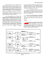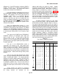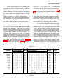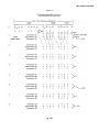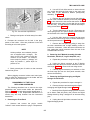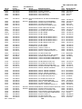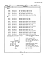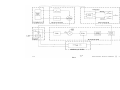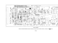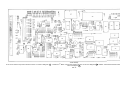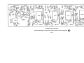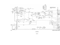
1
TM 11-6625-2759-14 & P TECHNICAL MANUAL OPERATOR’S, ORGANIZATIONAL, DIRECT SUPPORT, AND GENERAL SUPPORT MAINTENANCE MANUAL INCLUDING REPAIR PARTS AND SPECIAL TOOLS LISTS SPECTRUM ANALYZER PL-1391/U (TEKTRONIX MODEL 7L5) (NSN 6625-01-015-6587) HEADQUARTERS, DEPARTMENT OF THE ARMY DECEMBER 1978 WARNING DANGEROUS VOLTAGES exist in this equipment. Be extremely careful when working on the power supply circuit or the AC line connections during line power operation. Serious injury or DEATH may result from contact with these points. DON’T TAKE CHANCES! TM 11-6625-2759-14 & P This manual contains copywrite material reproduced by permission of the Tektronix Company. TECHNICAL MANUAL HEADQUARTERS DEPARTMENT OF THE ARMY NO. 11-6625-2759-14 & P WASHINGTON, DC, 6December 1978 OPERATOR’S, ORGANIZATIONAL, DIRECT SUPPORT, AND GENERAL SUPPORT MAINTENANCE MANUAL INCLUDING REPAIR PARTS AND SPECIAL TOOLS LISTS SPECTRUM ANALYZER PL-1391/U (TEKTRONIX MODEL 7L5) (NSN 6625-01-015-6587) REPORTING OF ERRORS You can improve this manual by recommending improvements using DA Form 2028-2 located in the back of the manual. Simply tear out the self- addressed form, fill it out as shown on the sample, fold it where shown, and drop it in the mail. If there are no blank DA Forms 2028-2 in the back of the manual, use the standard DA Form 2028 (Recommended Changes to Publications and Blank Forms) and forward to the Commander, US Army Communications and Electronics Materiel Readiness Command, ATTN: DRSEL-ME-MQ, Fort Monmouth, NJ 07703. In either case a reply will be furnished direct to you. NOTE This manual is an authentication of the manufacturer’s commercial literature which, through usage, has been found to cover the data required to operate and maintain this equipment. Since the manual was not prepared in accordance with military specifications and AR 310-3, the format has not been structured to consider levels of maintenance. i PART I TM 11-6625-2759-14 & P TABLE OF CONTENTS Section 0 INTRODUCTION Section 1 General Information Introduction Description Specification Frequency Characteristics Input Characteristics Amplitude Characteristics Sweep Characteristics Output Connectors Environmental Characteristics Physical Characteristics Accessories and Options Section 2 1-1 1-1 1-1 1-1 1-2 1-2 1-3 1-3 1-4 1-4 1-4 Installation Initial Inspection Installation Repackaging Section 3 PAGE 0-1 2-1 2-1 2-1 Operating Instructions Introduction Functional Block Description Front Panel Controls and Connectors Calibrating the 7L5 to the Oscilloscope Mainframe Operational Checkout Preliminary Preparation Operational Check of Readout Characters Dynamic Range Accuracy Reference Level Accuracy Input Buffer Residual (Incidental) FM Residual Response Sensitivity Check Resolution Bandwidth Accuracy, Amplitude Deviation and Shape Factor Using the Analyzer Impedance Matching Signal Application Edge Noise Frequency Measurement Technique Max Span Operation Resolution and Resolution Bandwidth Digital Storage Applications for Spectrum Analyzers 3-1 3-1 3-3 3-7 3-8 3-8 3-8 3-10 3-11 3-12 3-12 3-12 3-13 3-13 3-14 3-14 3-14 3-14 3-15 3-15 3-15 3-15 3-15 TM 11-6625-2759-14 & P SECTION 0 INTRODUCTION 0-1. SCOPE This manual describes Spectrum Analyzer PL1391/U and provides instructions for operation (Part I) and maintenance (Part II). Throughout this manual the PL-1391/U is referred to as the Tekronix Model 7L5. c. Discrepancy in Shipment Report (DISREP) (SF 361). Fill out and forward Discrepancy in Shipment Report (DISREP) (SF 361) as prescribed in AR 5538/NAVSUPINST 4610.33B/AFR 75-18/MCO P4610.19C and DLAR 4500.15. 0-2. INDEXES OF PUBLICATIONS 0-4. REPORTING EQUIPMENT IMPROVEMENT RECOMMENDATIONS (EIR) a. DA Pam 310-4. Refer to the latest issue of DA Pam 310-4 to determine whether there are new editions, changes, or additional publications pertaining to the equipment. EIR’s will be prepared using SF Form 368, Quality Deficiency Report. Instructions for preparing EIR’s are provided in TM 38-750, The Army Maintenance Management System. EIR’s should be mailed direct to Commander, US Army Communications and Electronics Materiel Readiness Command, ATTN: DRSEL-ME-MQ, Fort Monmouth, NJ 07703. A reply will be furnished direct to you. b. DA Pam 310-7. Refer to the DA Pam 310-7 to determine whether there are modification work orders (MWO’s) pertaining to the equipment. 0-3. FORMS AND RECORDS 0-5. ADMINISTRATIVE STORAGE a. Reports of Maintenance and Unsatisfactory Equipment. Maintenance forms, records, and reports which are to be used by maintenance personnel at all maintenance levels are listed in and prescribed by TM 38-750. b. Report of Packaging and Handling Deficiencies. Fill out and forward DD Form 6 (Packaging Improvement Report) as prescribed in AR 70058/NAVSUPINST 4030.29/AFR 71-13Imco P4030.29A and DLAR 4145.8. For information concerning storage, refer to section 2. 0-6. DESTRUCTION OF ARMY ELECTRONICS MATERIEL Destruction of Army electronics materiel to prevent enemy use shall be in accordance with TM 750-244-2. 0-1 TM 11-6625-2759-14 & P Fig. 1-1. 7L5 Spectrum Analyzer. 1-0 TM 11-6625-2759-14 & P SECTION 1. SPECIFICATION Introduction Frequency Characteristics To effectively use the 7L5 Spectrum Analyzer, the operation and capabilities of the instrument must be known This instruction manual covers general operating information about the instrument. Service information, such as circuit description and calibration are contained in the Service manual. Range Input Frequency: 10 Hz through 5 0 MHz. Dot Frequency: 0 Hz through 4999.75 kHz. Description Accuracy -6 20àC to 30°C: +(5 Hz + 2 x 10 of dot readout). The 7L5 is a 5 MHz spectrum analyzer with digital storage. Frequency stability is within 5 Hz/hr and center frequency (dot) can be read with six digit accuracy immediately after turn-on. There is no need to fine tune the display Complex measurements and analysis can be made with relative ease. Built-in micro-processing circuits decode control settings, process frequency and reference level information, and optimize sweep time and resolution for the selected frequency span. -5 0°C to 50°C: ±(20 Hz + 10 of dot readout). Drift 5 Hz/hour or less. Residual (Incidental) FM The 7L5 with 80 dB or more of spurious free dynamic range, provides the ability to measure wide relative amplitudes. Nanovolt sensitivity provides very low-level signal and noise measurements. 50 Hz/div to 2 kHz/div: 1 Hz (p-p) or less. 5 kHz/div to 500 kHz/div. 40 Hz (p-p) or less. The 7L5 display is fully calibrated in dBm, dBV, or volts/div The reference level can be accurately set to 1 dB increments. A front panel input buffer control increases front-end immunity to intermodulation distortion while maintaining a constant reference level. To accommodate a wide variety of impedance sources, the 7L5 uses quick disconnect plug-in input impedance modules of 50 Ò, 75 Ò, 600 Ò, 1 MÒ/28 pF and customized units to meet special requirements. Resolution Bandwidth Accuracy 30 kHz--30 Hz: Within 20% of selected resolution (6 dB down). 10 Hz: Within 100 Hz ±20 Hz (70 dB down). The COUPLED setting electronically selects the best resolution bandwidth for each setting of the FREQUENCY SPAN/DIV control. Digital storage allows any 7000-Series mainframe, with crt readout, to present clean, easy to photograph, displays. A smooth integrated display provides an accurate analysis of most displays. Two complete displays can be held in memory for comparison Two modes select either the conventional peak display or a digitally averaged display. Shape Factor 30 kHz-3 kHz 5:1 or better (60:6 dB ratio). 1 kHz-10 Hz: 10:1 or better (60:6 dB ratio). Amplitude Deviation 30 kHz-100 Hz: 0.5 dB or less. ELECTRICAL CHARACTERISTICS 30 kHz-10 Hz: 2.0 dB or less. The following electrical characteristics apply when the 7L5 Spectrum Analyzer, in combination with a Plug-In Module, are normally installed in a 7000-Series oscilloscope and after a warm-up of ten minutes or more. 1-1 TM 11-6625-2759-14 & P Input Characteristics Resolution Bandwidth 10 Hz 30 Hz 100 Hz 300 Hz 1 kHz 3 kHz 10 kHz 30 kHz CAUTION The application of a dc voltage to the INPUT of the L1 or L2 Plug-In Modules may cause permanent damage to the mixer circuit. Input Impedance (Nominal): L1 L2 L3 50Ò 75Ò Selectable (50Ò, 600Ò, and 1 MÒ/28 pF). Equivalent Input Noise (equal to or better than) L1 L2 L3 -135 dBm -135 dBm -148 dBV -133 dBm -133 dBm -146 dBV -130 dBm -130 dBm -143 dBV -125 dBm -125 dBm -138 dBV -120 dBm -120 dBm -133 dBV -115 dBm -115 dBm -128 dBV -110 dBm -110 dBm -123 dBV -105 dBm -105 dBm -118 dBV NOTE Input Power (maximum Input level for reference levels of 0 dBm or greater): Sensitivity is degraded an additional 8 dB when the INPUT BUFFER is on; e.g., at 3 kHz, the equivalent input noise would be -107 dBm instead of -115 dBm. Noise level will increase by approximately 10 dB when operation Is In video peak mode,. L1 21 dBm or 2.5 V rms L2 21 dBm or 3.07 V rms L3 21 dBm-input terminated 50Ò or 600Ò; 100 V (peak ac + dc) Input 1 MÒ/28 pF. Intermodulation Distortion Input Power (maximum input level for reference levels below 0 dBm): Intermodulation products from two on-screen signals, within any frequency span are >75 dB down for third order products and at least 72 dB down for second order products. L1 +10 dBm L2 +10 dBm L3 +10 dBm--input terminated 50Ò or 600Ò, and 100 V (peak ac + dc) with input of 1 MÒ3/28 pF. Second and third order intermodulation products from two on-screen -53 dBV or less signals within any frequency span are at least 80 dB down. Amplitude Characteristics With the INPUT BUFFER switch on, the second and third order intermodulation products, for any two onscreen signals, within any frequency span, are at least 80 dB down. NOTE If digital storage is used, an additional quantization error of 0.5% of full screen should be added to the amplitude characteristics. Display Flatness Residual Response Peak to peak deviation, over any selected frequency span: Quantization error must be added (see Note under Amplitude Characteristics) if digital storage is used. Internally generated spurious signals are -130 dBm or less referred to the input (harmonics of the calibrator are -125 dB) with L1 or L2 plug-in module and 143 dBV with the L3 plug-in module. L1 L2 L3 0.5 dB; 0.5 dB; 0.5 dB Sensitivity Reference Level The following tabulation of equivalent input noise for each resolution bandwidth is measured with; the INPUT BUFFER off, the VIDEO PEAK/AVG at max cw, and the TIME/DIV set to 10 seconds. Refers to top graticule line in Log mode. Calibrated in 1 dB and 10 dB steps for the L1 and L2 modules and 1 dB/2 dB and 10 dB for L3 plug-in module. 1-2 TM 11-6625-2759-14 & P Range Log 2 dB/Div Log L1 -128 dBm to +21 dBm -70 dBm 10 dB/Div to +21 dBm L2 -128 dBm/ 139 dBV to +21 dBm/ +10 dBV -70 dBm/ -81 dBV to +21 dBm/ +10 dBV Time per div is selectable from 10 s/Div to 0.1 ms/Div in 1-2-5 sequence. An AUTO position permits automatic selection of optimum time/div for the selected resolution and span/div settings. L3 -128 dBm to +21 dBm (50Ò), -139 dBm to +10dBm (600Ò), -141 dBV to +8 dBV (Hi Z) -70 dBm to +21 dBm (50Ò), Sweep rate accuracy is within 5% of the rate selected. Triggering Provides two triggering sources, INT (internal) and LINE, in addition to a FREE-RUN position. -81 dBm to +10 dBm (600 Ò), -83 dBV to +8 dBV (Hi Z) When INT is selected, ac coupled signal components from the mainframe Trigger Source (left or right vertical amplifiers) are used. Incremental Accuracy When calibrated at -40 dBV in Log mode. When LINE is selected, ac coupled sample of mainframe line voltage is used. L1, L2 and L3: Within 0.2 dB/dB with cumulative error of 0.25 dB/10 dB. Three triggering modes are; NORM (normal), SGL SWP/READY (single sweep), and MNL SWEEP (manual sweep). Lin Mode Range: 20 nV/Div to 200 mV/Div within 5% in 1-2-5 sequence. Trigger level is >1.0 div of internal signal for both NORM and SGL SWP modes over the approximate frequency range of 30 Hz to 500 kHz. NOTE A >sign is displayed adjacent to the reference level readout when the reference level is not calibrated due to an incompatible selection of controls. Output Connectors Video Out Display Dynamic Range/Accuracy Front-panel pin jack connector supplies the video (vertical) output signal at an amplitude of 50 mV/div +5% (about the crt vertical center) with source impedance of 1 kÒ. Log 10 dB/DIV Mode: Dynamic window is 80 dB. Accuracy is within 0.05 dB/dB to 2 dB maximum. Log 2 dB/DIV Mode: Dynamic window is 16 dB. Accuracy is within 0.1 dB/dB to 1 d,B maximum. Horiz Out Sweep Characteristics A front-panel pin jack connectorsupplies horizontal output signal (negative-going sawtooth that varies from 0.0 V dc to approximately -6 V dc with a source impedance of 5 kÒ. Frequency Span Provides calibrated frequency spans from 50 Hz/div to max (500 kHz/div), within 4%, in 1-2-5 sequence. Calibrator Horizontal linearity is within 4% over the entire 10 div display. Front panel BNC connector supplies a calibrated 500 kHz squarewave output signal (derived from the analyzer’s time base). Output amplitude is within +0.15 dB of -40 dBV into impedance of the plug-in module. A 0-Hz/Div position is provided for time domain operation. Sweep Rate 1-3 TM 11-6625-2759-14 & P ENVIRONMENTAL CHARACTERISTICS Optional Accessories Plug-in Module, 50 ohm Plug-in Module, 75 ohm Plug-in Module 50 Ò 600Ò & 1 MÒ/28 pF Probe (10X) Attenuator, step. 50 ohm Attenuator, step, 75 ohm The 7L5 Spectrum Analyzer will meet the foregoing electrical characteristics within the environmental limits of a 7000-Series oscilloscope. Complete details on environmental test procedures including failure criteria etc., can be obtained from a local Tektronix Field Office or representative. PHYSICAL CHARACTERISTICS Net weight (instrument only), 8 pounds, 12 ounces. L2 L3 P6105 (see L3 Manual) 2701 2703 OPTIONS ACCESSORIES AND OPTIONS Standard Accessories Graticule, Spectrum Analyzer Filter, light amber Manual, Operating Manual, Service L1 7L5 Option 21 -(Log Display) 7L5 Option 25--(Tracking Generator) 7L5 Option 28--(Readout) 7L5 Option 30-(Option 21/25) 7L5 Option 31 -(Option 21/28) 7L5 Option 32-(Option 25/28) 7L5 Option 33--(Options 21/25/28) Tektronix Part No. 377-1159-02 (7000-Series) 378-0684-00 070-1734-00 070-2184-00 1-4 TM 11-6625-2759-14 & P SECTION 2. INSTALLATION Include complete instrument serial description of the service required. Initial Inspection This instrument was inspected both mechanically and electrically before shipment. It should be free of mars or scratches and electrically meet or exceed all specifications. Inspect the instrument for physical damage and check the electrical performance by the Operational Check procedure provided within these instructions. This procedure will verify that the instrument is operating correctly and it will satisfy most receiving or incoming inspection requirements. If all instrument specifications are to be verified, refer to the Service Instructions for the 7L5. number and Save and re-use the container your instrument was shipped in. If the original packaging is not available or is unfit for use, repackage as follows: 1. Obtain a shipping container of heavy corrugated cardboard or wood with inside dimensions six inches or greater than the instrument dimensions. This will allow room for cushioning. Refer to Table 2-1 for carton test strength requirements. 2. Wrap the instrument in heavy paper or polyethylene sheeting to protect the instrument finish. Protect the front panel with urethane foam or cardboard strips. If there is physical damage or performance deficiency, contact your local Tektronix Field Office or representative 3 Cushion the instrument on all sides by packing dunnage or urethane foam between the carton and the instrument, allowing three inches on all sides. Installation To install the 7L5, align the upper and lower guide rails with those in the receiving compartments of the mainframe. Slide the instrument along the rails into the mainframe When the electrical connectors at the rear of the 7L5 make contact, apply firm, steady pressure to the front panel until the rear connectors are engaged and the front panel is approximately flush with the oscilloscope front panel. To remove the 7L5, pull the release latch labeled 7L5, at the lower left of the front panel, and remove the instrument. 4. Seal the shipping carton with shipping tape or an industrial stapler. Gross Weight (lb) 0-10 10-30 30-120 120-140 140-160 REPACKAGING FOR SHIPMENT If your Tektronix instrument is to be shipped to a Tektronix Service Center for service or replacement, attach a tag showing; owner (with address) and the name of an individual, at your firm, that can be contacted. TABLE 2-1 Carton Test Strength (lb) 200 275 375 500 600 If you have any questions, contact your local Tektronix Field Office or representative. 2-1 TM 11-6625-2759-14 & P SECTION 3. OPERATING INSTRUCTIONS according to the settings of front panel DOT Introduction FREQUENCY and FREQUENCY SPAN/DIV controls. This section contains; a simplified block diagram The 10 7 MHz IF is processed through bandpass description, function of the front panel controls and filters and amplifiers and then mixed with the output from connectors, an operational check-out and familiarization a 10.450 oscillator, to down-convert the 10.7 MHz to an procedure, and a section devoted to the use and IF of 250 kHz Gain of the 250 kHz amplifier is controlled application of the instrument. Service information is by the reference level logic circuit which establishes the contained in the Service Instruction manual. amount of attenuation in the plug-in module and gain for the 250 kHz IF and Log amplifiers. The reference level is FUNCTIONAL BLOCK DESCRIPTION selectable in 1 dB and 10 dB steps. Functional Block Description The 250 kHz IF signal is processed through the variable resolution filter circuits for bandwidth selections The 7L5 is a swept front end spectrum analyzer of 10 Hz to 30 kHz. The signal is again amplified, with selectable front-end plug-in modules that permit the detected, and the video is sent through amplifier circuits user to obtain calibrated display for a number of different that provide the 10 dB/dlv, 2 dB/dlv, and linear gain Impedances (i.e., 50 ohm, 600 ohm, etc.). The plug-in characteristics. module contains; selectable attenuation, the first mixer, and an Input buffer selector that trades attenuation for IF The video signal is then fed to the display gain. Signal attenuation in the plug-in and gain of the IF processing circuits where the signal is either stored and processing chain are controlled by a reference level logic displayed, or, if the storage mode is not selected, the circuit in the 7L5 which provides calibrated settings in 1 signal is passed directly through the vertical output dB or 10 dB steps over a range of approximately 146 dB amplifier to the mainframe circuit. If either or both the (depending on the plug-in module). A simplified block DISPLAY A or DISPLAY B latches are enabled, the diagram is shown in Fig. 3-1. signal is converted to digital data, stored in A or B memory, then converted back to analog data and The input signal to the 7L5 is mixed with the processed through the output amplifiers to the mainframe frequency of the main oscillator and the IF of 10.7 MHz is The vertical information is digitized and stored at 512 fed to and amplified by the 10.7 MHz IF amplifier. Since horizontal address locations across the screen. the 7L5 input frequency range is O to 5 MHz, the main Therefore, the horizontal sweep information is converted oscillator is tuned and swept from 10.7 to 15.7 MHz. The to digital data for storage, then converted back to an frequency of the main oscillator is controlled by two analog signal for display The horizontal sweep ramp is secondary (A and B) oscillators that use a synthesizer processed the same as the vertical signal. The vertical technique to tune and phase lock their frequencies. The (video) information can be averaged or peak detected. sweep frequency control circuit drives the oscillators 3-1 TM 11-6625-2759-14 & P Fig. 3-1. Functional block diagram. 3-2 TM 11-6625-2759-14 & P FRONT PANEL CONTROLS AND CONNECTORS DOT MKR Used to horizontally position the frequency dot. The displayed frequency readout characters enumerate the actual frequency of the dot. When the DOT MKR control is in its detent position (fully ccw), the frequency dot and the selected frequency are on the vertical center line of the graticule. The 7L5 can be operated in a start sweep mode when the frequency dot is positioned to the left vertical graticule line. The DOT MKR control is disabled when the FREQUENCY SPAN/DIV switch is at MAX. REFERENCE LEVEL Sets the full screen signal amplitude level (dBm, dBV) required at the INPUT to the plug-in module. This level is relevant to the input impedance of the plug-in module. Reference level is associated to the top graticule line of the display area and signal level is relative to this reference. The reference level range depends on the plug-in module, however, in the 2 dB/Div mode it covers 149 dB, in the 10 dB/Div mode the range is 90 dB and in the Lin mode 20 nV/div to 200 mV/div. The control has two speeds or stepping increments; pulled out, each increment is 10 dB, pushed in each increment is 1 dB or in some cases (dependent on the plug-in module) 2 dB. VAR The VAR (variable) control provides 8 dB or more gain adjustment between each calibrated reference level step. A<symbol is displayed on the crt, preceding the reference level readout, whenever the reference level is not calibrated (VAR is not in its detent position). Pushing any front panel pushbutton switch activates a bistable electronic circuit to change its output state. When in the active state, the plastic pushbutton is illuminated. Pressing the pushbutton a second time changes the output of the circuit to the inactive state and extinguishes the illuminated button. Front panel controls also include two special photo-optic switch assemblies, the FREQUENCY SPAN/’DIV-RESOLUTION switch and the TIME/DIV switch. Designed especially for the 7L5, each assembly is a mechanical/photo-electric, digital switch, that provides a TTL compatible five-bit binary output. The reliability of these switches has been demonstrated and with normal use they should last the life of the instrument. Dismantling or field repair of these switches is discouraged since their proper operation requires precision alignment of their internal components. If either switch assembly is damaged or suspected of malfunction, it should be replaced as an assembly. The following describes the function of the front panel selectors for the 7L5. A layout of the front panel is shown in Fig. 3-2. DOT FREQUENCY FINE TUNING Changes the dot (marker) frequency in coarse (10 kHz) or fine (250 Hz) steps over the input frequency range of 0 Hz to 5 MHz. The frequency of the dot marker is displayed on the crt readout in the upper right set of characters. Dot frequency will not extend beyond the 7L5 frequency range, even if the control is rotated. When power is applied, dot frequency starts at 0.000. Selects coarse or fine incrementation for the DOT FREQUENCY control. When the FINE TUNING switch is activated (illuminated), each rotational click of the DOT FREQUENCY control changes the dot frequency in increments of 250 Hz. When the FINE TUNING switch is inactive (extinguished), each rotational click of the DOT FREQUENCY control changes the dot frequency in increments of 10 kHz. INPUT BUFFER The active (illuminated) state of this pushbutton switch inserts 8 dB of signal attenuation at the input of the first mixer and adds 8 dB of vertical gain (after the variable resolution filters). When used, it reduces intermodulation distortion caused by excessive input signal amplitude. Because of its increased gain, the noise figure is increased 8 dB when this switch is activated. 3-3 TM 11-6625-2759-14 & P Fig. 3-2.A. 7L5 front panel controls and connectors. 3-4 TM 11-6625-2759-14&P Fig. 3-2B. 7LS-L1 plug-in front panel control and connectors. @ 3-5 TM 11-6625-2759-14&P LOG 10 dB/DIV The illuminated condition of this pushbutton selects a logarithmic display of 10 dB/div with a dynamic range of 80 dB. LOG 2 dB/DIV The illuminated condition of this pushbutton selects a logarithmic display of 2 dB/div with a dynamic range of 16 dB LIN The illuminated condition of this pushbutton selects a linear display. Signal amplitude is a linear function of input level. FREQUENCY SPAN/DIV Selects frequency spans from 50 Hz/div to 500 kHz/div (MAX position). A 0 Hz position provides time domain display with a bandpass dependent on the setting of the RESOLUTION selector. In the 0 Hz position the frequency dot is not displayed and when in the MAX position the frequency dot position is controlled by the DOT FREQUENCY control. RESOLUTION Selects resolution bandwidths of 10 Hz to 30 kHz in a 1-3 sequence. A COUPLED position electronically selects the best compatible resolution bandwidth setting for the FREQUENCY SPAN/DIV selection. TIME/DIV Selects the analyzer’s sweep rate. Sweep rates are 10 s/div to 0.1 ms/div in a 5-2-1 sequence. An AUTO position electronically programs sweep rate so the display remains calibrated for the selected frequency span and resolution bandwidth settings. UNCAL TRIGGERING Two trigger sources (Line and Internal) plus a Free Run mode can be selected. In the Free Run mode (FREE RUN button activated) the sweep free runs and will not sync with any trigger signal. When the LINE pushbutton is activated (illuminated) the sweep is triggered by the line voltage to the mainframe. The INT pushbutton selects ac coupled signal components from the mainframe Trigger Source (left or right vertical). Three trigger modes are provided: NORM (normal), SGL SWP/READY (single sweep/ready) and MNL SWEEP (manually controlled sweep). When the NORM button is activated, the sweep is triggered from the source selected; or, if the trigger is not present, the sweep automatically runs in about 10-second intervals to provide a baseline display. When the SGL SWP/READY button is activated, the, sweep runs with the next trigger or in about 10 seconds if trigger is not present. In time domain operation (FREQ SPAN/DIV at 0 Hz) pushing the button activates the sweep ready state. The button lights to indicate the trigger circuit is armed and ready. The sweep will run with the arrival of a trigger. The button remains illuminated until the sweep has completed its run. This provides a ready indication of the sweep state when photographing a display. When the display is uncalibrated because the FREQUENCY SPAN/DIV, RESOLUTION, and TIME/DIV switch settings are incompatible, this indicator lights and a > symbol is displayed on the crt as a prefix to the reference level readout characters. @ 3-6 LEVEL/SLOPEMNL SWP A dual function control. As a level slope/control, it adjusts the level of the trigger threshold on either a positive or negative slope. As a manual sweep control, it positions the crt beam anywhere along the Xaxis. Maximum ccw corresponds to a beam location at the left graticule edge. DIGITAL STORAGE SAVE A: Activating the SAVE A pushbutton dedicates one half of the digital storage memory to preserve the binary equivalent of the existing waveform amplitude at 256 X-axis locations. The A memory is inhibited from further update until SAVE A is deactivated (extinguished). TM 11-6625-2759-14&P DISPLAY A/B: When DISPLAY A or DISPLAY B is selected, the corresponding pushbutton switch is illuminated and the contents of memory A or memory B is displayed. With SAVE A off, all memory locations are displayed contiguously. With SAVE A on, DISPLAY A and DISPLAY B are selected. The con- tents of both memories are interlaced and displayed. proper setting each time the 7L5 is installed in an oscilloscope. PEAK AVERAGE/BASELINE CLIPPER: A dual function control. When digital storage is off, this control operates as a conventional baseline clipper, i.e., as the control is rotated ccw, more of the vertical display is progressively blanked or clipped over the last 1/3 turn of the control. When digital storage is on, the PEAK AVERAGE control sets the level at which the vertical display is either peak detected or digitally averaged. Video signals above the level set by the PEAK AVERAGE control (and denoted by a horizontal cursor) are peak detected and stored. Video signals below the level set by the PEAK AVERAGE control are digitally averaged and stored. LOG CAL The AMPL CAL control is adjusted during the initial calibration to calibrate the full screen reference level. This control is used to compensate for gain differences in the RF and IF portions of the instrument. The AMPL CAL control should be adjusted or checked for proper setting each time a plug-in module is installed in the 7L5. HORIZ POS Positions the display or baseline on the crt X-axis. VERT POS Positions the display or baseline on the crt Y-axis. dBm/dBV Located on the plug-in module front panel, the dBm/dBV control selects the reference level scale factor; decibels with respect to one milliwatt or decibels with respect to one volt. Calibrating the 7L5 to the Oscilloscope Mainframe 1. Install or verify the presence of a plug-in module (see Optional Accessories, Section 1) 2. Select oscilloscope Vertical Mode, Horizontal Mode and Trigger Source (Right or Left) corresponding with plug-in compartments occupied by the spectrum analyzer. Turn on the mainframe power and allow a 10 minute warm-up period. MAX HOLD: Enables the digital storage memory to store the maximum signal levels within the period the circuit is active (button illuminated). This maximum signal can then be saved and compared with future signals for drift or amplitude variations. SWP CAL AMPL CAL (L1 Plug-In Module) 3. Set the front panel controls as follows: DOT MKR FREQUENCY SPAN/DIV RESOLUTION VAR BASELINE CLIPPER LOG 10 dB/DIV REFERENCE LEVEL INPUT BUFFER FREE RUN NORM SAVE A off MAX HOLD dBm/dBV Adjusted during the operational check to calibrate the sweep. This adjustment compensates for differences in deflection sensitivity between mainframe oscilloscopes. The SWP CAL control should be adjusted or checked for proper setting each time the 7L5 is installed in an oscilloscope. Adjusted during the operational check to calibrate the 2 dB/div and the 10 dB/div displays. This adjustment is used to compensate for differences in vertical gain between mainframe oscilloscopes. The LOG CAL control should be adjusted or checked for TIME/DIV @ 3-7 max ccw (detent position) MAX (500 kHz) COUPLED max ccw (detent position) max cw on -40 dBV off on on off dBV (plug-in module switch) AUTO TM 11-6625-2759-14&P 4. Connect the CALIBRATOR signal to the INPUT connector on the plug-in module with a short length of coaxial cable. Adjust the SWP CAL and the HORIZ POSITION controls to align the second and tenth vertical signals with the second and tenth vertical graticule lines counting from the left edge. OPERATIONAL CHECKOUT Introduction This is an operational checkout procedure intended to satisfy most customer’s receiving inspection requirements and to provide instrument familiarization for the new user We recommend using this checkout as part of the users routine maintenance program and a preliminary check before performing the Performance Check portion of the Service Instruction manual. 5. Set the FREQUENCY SPAN/DIV to 2 kHz, Display Mode 2 dB/div, and DISPLAY A and B on. Adjust the VERT POSITION control to place the display baseline on the bottom horizontal graticule line. 6. Set RESOLUTION control to 3 kHz and DOT FREQUENCY to 500.00 kHz. The front panel CALIBRATOR output is an accurate signal source and is used in the following procedures to verify operational status of the instrument. Calibrator frequency accuracy may be verified by applying it to an accurate digital counter. 7. Select the LOG 10 dB/DIV pushbutton and adjust the LOG CAL control for a full screen (8 division) display. Some procedures require a step attenuator and two short lengths of coaxial cable. To verify the absolute reference level specifications, the attenuator accuracy must be calibrated or verified at some specific frequency, to within 0.03 dB/dB with a cumulative error not to exceed 0.1 dB for any change up to 10 dB. Incremental accuracy can be verified and a good indication of the absolute reference level accuracy can be obtained by using two Tektronix Step Attenuators, such as the 2701 (see Optional Accessories, Section 1). These attenuators provide a good indication of operation even though their accuracy specifications are not within the limits described. 8. Select the LOG 2 dB/DIV pushbutton and adjust the AMPL CAL (on plug-in module) for a full screen display. 9. Repeat steps 7 and 8 until the displayed waveforms are 8 vertical divisions in both log amplifier settings. (Refer to Fig. 3-3, Log Amplifier Calibration Composite Waveform.) If desired, check linearity of the 10 dB/div display by increasing the REFERENCE LEVEL in 10 dB steps. Adjust LOG CAL slightly to correct any non- linearity. 1. Preliminary Preparation Preset the front panel controls and selectors as described under Calibrating the 7L5 to the Oscilloscope Mainframe and perform the calibration procedure as previously described. 2. Operational Check of Readout Characters With the 7L5 installed and operating in a 7000Series mainframe, perform the following steps to check the readout operation. Dot Frequency Readout a. Verify that the dot frequency readout is 0.00 kHz after initial turn-on. (Readout characters for the dot frequency are located near the top edge of the crt and can be identified by the suffix characters kHz). Fig. 3-3. Log amplifier calibration composite waveform. b. With the FINE TUNING pushbutton not illuminated (inactive), verify that the DOT FREQUENCY control changes the value of the readout characters in 10 kHz increments. @ 3-8 TM 11-6625-2759-14&P c. Rotating DOT FREQUENCY control cw should increase the readout and ccw rotation should decrease the readout. Time/Div Readout I. Set the FREQUECNY SPAN/DIV switch to 0. Rotate the TIME/DIV control to each of its positions and verify that its front panel designations correspond to the crt readout characters. (Readout characters for the sweep time per division are located near the bottom right edge of the crt and can be identified by the suffix character S when the FREQUENCY SPAN/DIV is set to 0.) d. Activate the FINE TUNING pushbutton and verify that the DOT FREQUENCY control changes the value of the readout characters in 250 Hz increments. e. Verify that continuous cw rotation of the DOT FREQUENCY control causes no change of the readout characters after an indicated 4999.75 kHz. Frequency Span/Div Readout NOTE m. Set TIME/DIV control to AUTO and the RESOLUTION control to COUPLED. Rotate the FREQUENCY SPAN/DIV control to each of Its positions and verify that the readout characters correspond with the front panel designations and change In accordance with the readout listed in Table 3-1. (Readout characters for frequency span per division setting occupy the same crt position as the time per division readout characters. They are located near the bottom edge of the crt and except for the 0 span setting, can be identified by the suffix characters Hz.) Following a change of the DOT FREQUENCY control, the first click in the opposite direction will have no effect. Reference Level Readout (L1 Plug-In Module) f. Select the LOG 2 dB/DIV mode and set the dBm/dBV switch (on the plug-in module) to dBm. Verify that the indicated value of the reference level changes by 13 dB (e.g., -40 dBV = -27 dBm). Reference level readout characters are located near the top edge of the crt and can be identified by the suffix characters dBm or dBV. TABLE 3-1 FREQUENCY SPAN/DIV g. With the UNCAL light off, rotate the VAR (variable) control and verify that a < symbol (not calibrated) prefixes the reference level readout. Rotate the VAR control to its maximum ccw (detent) position and verify that the < symbol is no longer displayed. h. Pull the REFERENCE LEVEL control out to its coarse position and verify that the value of the reference level readout changes in 10 dB steps. Push the REFERENCE LEVEL control in to its fine position and verify that the value of the reference level readout changes in 1 dB steps. i. Verify, that rotation of the REFERENCE LEVEL control beyond the reference level limits of; -128 dBm (-141 dBV), In the 1 dB/step position, or; -70 dBm (83 dBV) in the 10 dB/step position-for the one extremeand +21 dBm (8 dBV) for the other extreme remains constant. (These extremes are applicable only for 50 Ò plug-in modules.) control settings FREQUENCY SPAN/DIV readout 0 50 (Hz) 1 kHz .2 kHz .5 kHz 1 kHz 2 kHz 5 kHz 10 kHz 20 kHz 50 kHz .1 MHz .2 MHz MAX 10 ms 50 Hz 100 Hz 200 Hz 500 Hz 1 kHz 2 kHz 5 kHz 10 kHz 20 kHz 50 kHz 100 kHz 200 kHz 500 kHz Resolution Readout n. Rotate the RESOLUTION control to each of its: positions and verify that the readout characters correspond with the front panel designations. (Readout characters for the resolution function are located near the bottom edge of the crt and can be identified by the suffix characters Hz.) J. With the REFERENCE LEVEL control at max ccw position, select the LIN mode and verify that the readout changes to 200 mV. k. Rotate the REFERENCE LEVEL cw and verify that the readout changes from mV to ÎV to nV in a 2-1-5 sequence. Verify that continuous cw rotation of the REFERENCE LEVEL control causes no change of the corresponding readout characters beyond 20 nV. @ 3-9 TM 11-6625-2759-14&P o. With the RESOLUTION control in the COUPLED position, rotate the FREQUENCY SPAN/DIV to each of its positions and verify that the RESOLUTION readout characters change in accord with Table 3-2. NOTE The full dynamic range of the Log 10 dB/div and the Log 2 dB/div is not measured in the following paragraphs. If the log amplifiers include a negative error, full range verification would require signal level measurement below the display baseline. Since this is not possible, the following steps verify 78 of the 80 dB range and 15 dB of the 16 dB range for the two log amplifier selections. TABLE 3-2 FREQUENCY SPAN/DIV control settings RESOLUTION MAX (500 kHz) 200 kHz 100 kHz 50 kHz 20 kHz 10 kHz 5 kHz 2 kHz 1 kHz .5 kHz 2 kHz .1 kHz 50 (Hz) 0 30 kHz 30 kHz 30 kHz 10 kHz 3 kHz 3 kHz 1 kHz 300 Hz 300 Hz 100 Hz 30 Hz 30 Hz 10 Hz 30 kHz readout LOG 10 dB/DIV (Dynamic window is 80 dB, accuracy is ±0.05 dB/dB to 2 dB maximum) a. DOT FREQUENCY RESOLUTION FREQUENCY SPAN/DIV TIME/DIV REFERENCE LEVEL dBm/dBV (L1 Plug-in) 500.00 kHz COUPLED 0.1 kHz AUTO -40 dBV dBV b. Apply the CALIBRATOR signal through external attenuator(s), such as Tektronix, 2701 (for 50 Ò)-see Optional Accessories in Section 1-to the INPUT connector. Select the LOG 10 dB/DIV pushbutton. Vertical Amplifier Mode Readout p. Select the 10 dB/DIV pushbutton switch and verify that the readout characters for the vertical amplifier mode indicate 10 dB/ Readout characters for the vertical amplifier mode are located near the lower edge of the crt and for the log positions, can be identified by the suffix symbol /. c. Increase external attenuation in 10 dB steps to 70 dB and verify that each step decreases the displayed f signal level 10 dB ±0.5 dB. q. Select the 2 dB/DIV mode and verify that the readout characters indicate 2 dB/. d. Increase external attenuation by 8 dB (for a total of 78 dB) and verify that the total overall decrease in signal amplitude is 78 dB ±2 0 dB. r. Push the LIN pushbutton and verify an absense of readout characters for vertical amplifier mode. LOG 2 dB/DIV (Dynamic window is 16 dB, accuracy is ±0.01 dB/dB to ±1 dB maximum) Uncalibrated Readout e. Set the external attenuators to 0 dB. Set the FRE- QUENCY SPAN/DIV to 50 Hz, RESOLUTION to 30 Hz and select the 2 dB/DIV pushbutton. s. Set the RESOLUTION control to COUPLED and the FREQUENCY SPAN/DIV control to MAX. Rotate the TIME/DIV cw until the UNCAL light is illuminated. Verify that a > symbol prefixes the referenced level readout characters. Rotate the TIME/DIV ccw until the UNCAL light is extinguished Verify that the > symbol is no longer displayed 3. Set the 7L5 controls as follows: f. Add 15 dB attenuation, with the external 1 dB step attenuator, in 2 dB and 1 dB increments. Verify that the signal level change, is within 0.1 dB/dB of added attenuation to a maximum of 1.0 dB deviation over the 15 dB range. Dynamic Range LIN Linearity g. Select the LIN pushbutton and adjust the REFERENCE LEVEL control for a crt readout of 500 pV/ (per division). @ 3-10 TM 11-6625-2759-14&P h. Add 10 dB of external attenuation. Adjust the VAR control for a signal display amplitude of 8 divisions. i. Add 6 dB of external attenuation. Verify that the signal amplitude decreases to 4.0 ±0.2 division (±5%) or half amplitude. c. Change the REFERENCE LEVEL control to -30 dBm. Increase the external attenuation 1 dB (3 dB total) and verify that the signal peak is within 0.2 dB of the reference point established in step b. d. Rotate the REFERENCE LEVEL control to 31 dBm. Increase the external attenuation another 1 dB (4 dB total) and verify that the signal peak is within 0.25 dB of the reference point. j. Add an additional 6 dB of external attenuation and verify that the display amplitude decreases to 2.0 ±0.1 division. e. Readjust the VERT POSITION control, as required, to establish a new graticule reference point for the signal peak. VARiable Control Range k. Insert 10 dB of external attenuation. Select the 2 dB/DIV pushbutton and rotate the VAR control fully cw. Adjust the REFERENCE LEVEL to set the displayed signal amplitude to a vertical reference point near full screen. f. Pull the REFERENCE LEVEL control out to the 10 dB/step position and set it for a crt readout of -41 dBm. Increase the external attenuation 10 dB (14 dB total) and verify that the signal level is within 0.25 dB of the reference point established in step e. I. Rotate the VAR control fully ccw (detent position). Verify that the signal amplitude decreases at least 4.0 divisions. Decrease external attenuation to return the signal amplitude to the reference point and verify that the required change was 8 dB or more. g. Check the Reference Level accuracy for the remaining range by following the settings listed in Table 3-3 and noting the error. 4. Reference Level Accuracy (within 0.2 dB/dB with a cumulative error not to exceed 0.25 dB for any change up to 10 dB) Reference Level External Attenuation (dBm) (dB) Allowable Limits (dB) -41 -51 -61 -71 -81 -91 -101 -111 -121 14 24 34 44 54 64 74 84 94 0.25 0.50 0 75 1.00 1.25 1.50 1.75 2.00 2.25 TABLE 3-3 The external attenuator accuracy requirements to perform this step, have been described in the Introduction to this Operational Check procedure. Reference level increments are 1 dB and 10 dB steps. Circuitry of the 7L5 provides 1, 2, 4, 8, and 16 dB gain steps. These steps, or combinations of the steps, provide the reference level range. This procedure checks the accuracy of each gain cell and thus the overall accuracy. The accuracy of the V/Div mode will be within that specified if the Log mode reference level is within limits. A few check points may be performed as listed in Table 3-4 to spot check Lin mode operation. This procedure uses a 50 0 plug-in module (L1): g. Set the external attenuator to 0 dB. Select the LIN pushbutton and adjust the REFERENCE LEVEL control for a crt readout of 10 mV. a. Switch the dBm/dBV selector (on the plugin module) to dBm and set the 7L5 controls as follows: REFERENCE LEVEL RESOLUTION FREQEUNCY SPAN/DIV TIME/DIV LIN Accuracy h. Set the external attenuator and the REFERENCE LEVEL control to the positions listed in Table 3-4. Check that the measured signal amplitudes are in accordance with those listed in Table 3-4. -29 dBm 3 kHz 1 kHz AUTO b. Set the external attenuation to 2 dB and adjust the REFERENCE LEVEL for a readout of -29 dBm. Adjust the VERT POSITION control slightly, as required to establish a graticule reference point for the signal peak. @ 3-11 TM 11-6625-2759-14&P TABLE 3-4 c. Set the RESOLUTION control to 300 Hz, the FREQUENCY SPAN/DIV to 5 kHz, and the REFERENCE LEVEL to -62 dBm. Adjust the MNL control to place the trace dot halfway up one side of the displayed 300 Hz filter waveform, near center screen. Verify that maximum vertical jitter of the trace dot does not exceed 1.2 division (40 Hz) Attenuator Setting (dB) Voltage Input Reference Level Volts/DIV Signal Amplitude in Div’s ±5% 0 10 mV 2 mV 5 20 1 mV 0.2 mV 5 40 100 ÎV 20 ÎV 5 7. Residual Response (Plug-in module dependent. Internally generated spurious signals are down 130 dB or more with the L1 Plug-In Module) 60 10 ÎV 2 ÎV 5 NOTE 80 1.0 ÎV 200 nV 5 Each 7L5 Spectrum Analyzer is carefully tested at the factory to ensure that all internally generated spurious responses are below-130 dBm. Thorough verification of this specification would take several days. A procedure to check the full frequency range (to - 110 dBm) and to spot check 100 kHz of the total frequency range, to -130 dBm is given in the following steps. The 100 kHz frequency range chosen is 300 through 400 kHz. The procedure can also be used to spot check any 200 kHz span within the 0-5 MHz capability of the instrument. a. Terminate the input connector with a resistive load that equals the characteristic input impedance of the plug- in module. Set the 7L5 front panel controls as follows: DOT FREQUENCY 500.00 kHz RESOLUTION 300 Hz FREQUENCY SPAN/DIV 100 kHz TIME/DIV AUTO LOG 10 dB/DIV On REFERENCE LEVEL -70 dBm INPUT BUFFER. Off BASELINE CLIPPER max cw DIGITAL STORAGE DISPLAY A/B SAVE A Off MAX HOLD Off 5. Input Buffer (Operational check only) a. Apply the CALIBRATOR signal to the INPUT on the plug-in module. Set the 7L5 front panel controls as follows: DOT FREQUENCY 500.00 kHz RESOLUTION 3 kHz FREQUENCY SPAN/DIV 1 kHz TIME/DIV AUTO INPUT BUFFER Off LOG 2 dB/DIV On b. Establish a signal amplitude of 7 divisions with the REFERENCE LEVEL control c. Switch the INPUT BUFFER on and verify that the display amplitude does not change more than 1 dB (.05 div). d. Change the RESOLUTION to 10 kHz and check amplitude change of the calibrator signal with the INPUT BUFFER on and off. 6. Residual (Incidental) FM (Incidental FM is <1 Hz, 50 Hz/div to 2 Hz/div and <40 kHz, 5 kHz/div to 500 kHz/div) a. With the CALIBRATOR signal applied to the INPUT of the plug-in module, set the 7L5 front panel controls as follows: DOT FREQUENCY 500.00 kHz REFERENCE LEVEL -57 dBM RESOLUTION COUPLED FREQUENCY SPAN/DIV 50 (Hz) TIME/DIV AUTO LOG 2 dB/DIV On INPUT BUFFER Off DIGITAL STORAGE Off b. Press the SGL SWP pushbutton twice to initiate a sweep. (Additional sweeps are initialiated each time the SGL SWP pushbutton is pressed.) Observe the display for spurious response (spurs). Verify that, except for the O Hz response, the amplitude of any observed spur is -110 dBm (40 dB below -70 dBm). c. Sequentially reset the DOT FREQUENCY control to 1500 00 kHz, 2500.00 kHz, 3500.00 kHz, and 4500.00 kHz and repeat step b at each frequency setting. d. Set the DOT FREQUENCY control to 305.00 kHz, the RESOLUTION to 30 Hz, and the FREQUENCY SPAN/DIV to 1 kHz. b. Select the MNL SWP pushbutton and adjust the MNL SWP control to place the trace dot halfway up one side of the displayed 10 Hz filter waveform, near center screen. Verify that incidental FM (short term, peak to peak movement of trace dot) is less than 1.0 vertical division (1 Hz). @ 3-12 TM 11-6625-2759-14&P e. With TRIGGER SOURCE in FREE RUN, select the SGL SWP pushbutton and observe the display for spurs. Verify that the amplitude of any observed spurious response is at least 130 dB below 0 dBm. (Press SGL SWP again as required for observation.) f. Increase the dot frequency in 10 kHz increments and repeat step e until the display is scanned from 305.00 kHz to a dot frequency of 395.00 kHz. NOTE To measure the amplitude of a spur, carefully reset DO T FREQUENCY to place and keep the spur within one division of center screen. Continue to reduce the frequency span per division with each sweep until maximum amplitude of the spur has been determined. 8. Sensitivity Check (Sensitivity is plug-in module dependent) NOTE c. Measure the average noise level by adjusting the AVERAGE LEVEL cursor above the noise peaks and noting the noise level. d. Check the average noise level for each resolution bandwidth listed as per Table 3-5. TABLE 3-5 RESOLUTION Average Noise Level 30 kHz 10 kHz 3 kHz 1 kHz 300 Hz 100 Hz 30 Hz 10 Hz -105 dBm or less (35 dB below reference) -110dBm or less (40 dB below reference) -115 dBm or less (45 dB below reference) -120 dBm or less (50 dB below reference) -125 dBm or less (55dB below reference) -130 dBm or less (60dB below reference) -133 dBm or less (63 dB below reference) -135 dBm or less (65 dB below reference) e. connector. The sensitivity for the 7L5 Spectrum Analyzer is specified with an L1 or L2 Plug-In Module using the equivalent input noise method. Sensitivity specifications and test procedures for other plug-in modules are described in the Instruction manual for the respective plug-in module. Remove the termination from the INPUT 9. Resolution Bandwidth Accuracy, Amplitude Deviation, and Shape Factor Bandwidth accuracy; within 20% except 10 Hz position which is 100 Hz ±20 Hz, 70 dB down. Shape factor; 5:1 or better (30 kHz-3 kHz) and 10’1 or better (1 kHz-10 Hz). Amplitude deviation; less than 0 5 dB (30 kHz-100 kHz) and less than 2.0 dB (30 kHz-10 Hz). The 7L5’s internal reference level, as indicated by the display readout, is used as the reference in the following procedure. The accuracy of the reference level readout may be verified using external test equipment and the procedure provided in the Service Instructions. a. Apply the CALIBRATOR signal to the INPUT on the plug-in module and set the front panel controls as follows: DOT FREQUENCY 500.00 kHz RESOLUTION 30 kHz TIME/DIV AUTO DIGITAL STORAGE DISPLAY A/DISPLAY B DISPLAY MODE LOG 2 dB/DIV a. Set the front panel controls as follows: DOT FREQUENCY 1000.00 kHz RESOLUTION 30 kHz FREQUENCY SPAN/DIV.1 kHz TIME/DIV 10 s LOG 10 dB/DIV On REFERENCE LEVEL -70 dBm INPUT BUFFER Off DIGITAL STORAGE DISPLAY A/DISPLAY B TRIGGERING FREE RUN and NORM b. Adjust the REFERENCE LEVEL and FREQUENCY SPAN/DIV controls to establish a signal response that is 7 divisions high and about3 divisions wide at half amplitude. c. Switch the RESOLUTION from 30 kHz to 100 Hz and reset the FREQUENCY SPAN/DIV as required so the signal amplitude deviation over the 30 kHz to 100 Hz resolution range can be observed. d. Total deviation over the range should not exceed 0.5 dB. b. Terminate the INPUT in its characteristic impedance (50 0 for the L1) to prevent outside noise from entering and cluttering the display. @ 3-13 TM 11-6625-2759-14&P e. Switch the RESOLUTION through the 30 kHz to 10 Ht range and check that the amplitude deviation does not exceed 2 0 dB n. Measure the bandwidth 70 dB down by using the DOT MKR to position the display across a reference point as previously described Bandwidth must equal 100 Hz ±20 Hz (70 dB down) q f. Return the RESOLUTION selector to 30 kHz, the FREQUENCY SPAN/DIV control to 10 kHz, and adjust the REFERENCE LEVEL control for a signal amplitude of 7 divisions o. Return the RESOLUTION selector to 30 kHz, the FREQUENCY SPAN/DIV to 10 kHz and measure the bandwidth 60 dB down using the procedure previously described. g. Measure the bandwidth at the 6 dB down point by using the DOT FREQUENCY control to shift the signal across a graticule reference line and noting the frequency difference from one side to the other. p. Check the shape factor (60.6 dB ratio) by measuring the 60 dB bandwidth for all RESOLUTION settings and compare this with the previous -6 dB bandwidth readings noted in steps g though I. Shape factor for RESOLUTION setting from 30 kHz to 3 kHz must equal 5:1 or better Shape factor for RESOLUTION settings from 1 kHz to 10 Hz must equal 10:1 or better. h. Bandwidth must equal the RESOLUTION setting ±20 percent or 30 kHz ±6 kHz. i. Repeat this procedure to check the -6 dB bandwidth of each RESOLUTION setting from 30 kHz through 3 kHz Verify that the bandwidth of each position is within 20 percent Note these measurements for future use when measuring the shape factor. USING THE ANALYZER Impedance Matching Input impedance of the 7L5 Spectrum Analyzer is determined by the plug-in module (L1, L2, L3, etc.). Impedance mismatch between a signal source and the module's input connector causes reflections or standing waves in the interconnecting transmission line and results in signal amplitude errors of the display and an overall degraded performance of the analyzer To minimize the probability of an impedance mismatch, the signal source and transmission lines, fastened to the Input connector, should have the same impedance as the plug-in module. Use cables of minimum length, and good quality. Amplitude error due to plug-in swr will be improved by turning on the 7L5's INPUT BUFFER j. Set the RESOLUTION selector to 1 kHz, the FREQUENCY SPAN/DIV to 1 kHz or less, and adjust the REFERENCE LEVEL for a signal amplitude of 7 divisions. k. Use the DOT MKR to adjust the signal position so the -6 dB bandwidth can be measured in graticule divisions. Convert the number of divisions to frequency by noting the setting of the FREQUENCY SPAN/DIV selector Resolution bandwidth must equal the RESOLUTION setting ±20 percent. I. Repeat this procedure to check the resolution bandwidth for RESOLUTION settings from 1 kHz through 30 Hz Bandwidth must equal the RESOLUTION setting ±20 percent. Signal Application High amplitude signals (above +21 dBm or 2.5 V rms) will overload and damage the mixer circuit and should not be applied to the input connector (See the plug-in instruction manual for maximum allowable input power ) Signals of unknown amplitude should be routed through a attenuator If spurious or multitone intermodulation signals are present on the display, or, if saturation of the mixer is suspected, the 7L5 INPUT BUFFER will add 8 dB of attenuation in series with the input signal. If the displayed signals show little or no change with the buffer on, the intermodulation or spurious signals are not generated by the spectrum analyzer. m. Switch to the 10 dB/DIV display mode Set the RESOLUTION selector to 10 Hz, the FREQUENCY SPAN/DIV to 50 Hz, and adjust the REFERENCE LEVEL for a signal amplitude of 8 divisions. @ 3-14 TM 11-6625-2759-14&P Edge Noise When using the digital storage mode, some applications may leave display remnants at the edges of the crt. This condition is an unavoidable result of the storage memory being wider than the crt screen and not a malfunction. Edge noise is removed as follows: 1) Disconnect any signal from the INPUT connector. 2) With digital storage on the FREQUENCY SPAN/DIV set to other than MAX, rotate DOT MKR control to max cw position 3) After one sweep has occurred, to extend the baseline, rotate the DOT MKR control max ccw to the detent position. 4) Wait one sweep to clear the left edge then apply the input signal. Bandwidth determines both the noise level and resolution capability of the analyzer. As bandwidth decreases, both sensitivity and signal-to-noise ratio improve. Maximum sensitivity is obtained when resoltuion bandwidth is narrow (10-30 Hz). For most applications, the analyzer should be used with the RESOLUTION control set to COUPLED and the TIME/DIV switch set to AUTO. These autoranged positions provide the best sweep rate and resolution bandwidth for each setting of the FREQUENCY SPAN/DIV switch. When the analyzer is used to make amplitude measurements, especially in digital storage mode, the COUPLED and AUTO positions of these controls ensures maximum accuracy. Frequency Measurement Technique Digital Storage Use Frequency measurement should be made on the second or subsequent sweeps after the DOT FREQUENCY has been changed. (Oscillator stabilization time is 1 second or less.) When using digital storage, the best measurement accuracy is obtained by setting the following controls as follows; (see Fig. 3-2, Front Panel Controls.) Following a change of the DOT FREQUENCY control, the first click in the opposite direction will have no effect. This is due to the electronic coupling within the DOT FREQUENCY control assembly. 1. VIDEO PEAK/VIDEO AVERAGE: Adjust to place the cursor at a point midway between maximum signal amplitude and baseline noise. Max Span Operation 2. DISPLAY A/ DISPLAY B Press both pushbuttons to activate storage operation When the 7L5 is operated with the FREQUENCY SPAN/DIV control set to MAX (500 kHz), optimum instrument performance will be ensured by setting the RESOLUTION to 30 kHz or COUPLED position. The COUPLED position will maintain a desired ratio of 20:1 or less between the frequency span per division and the resolution bandwidth. 3. RESOLUTION Set to COUPLED position. 4. TIME/DIV Set to AUTO position or a position that is compatible with the setting of FREQUENCY SPAN/DIV control (UNCAL light not illuminated). Resolution, Resolution Bandwidth Applications for Spectrum Analyzers The, term resolution represents an instrument’s ability to display adjacent signal responses discretely. A measure of resolution is the frequency separation in hertz of responses which merge with a 3 dB notch. Displayed resolution is a function of spectrum analyzer bandwidth, horizontal sweep rate and frequency span. Resolution is also affected by incidental (residual) FM. Applications for spectrum analyzers such as the 7L5 include; measuring intermodulation products, radiation interference, modulation percentage, absolute and relative signal level measurements, bandpass characteristics, etc. Numerous application notes on spectrum analyzer measurements are available from your local Tektronix Field Office or representative, including assistance for specific measurement applications you may desire. Resolution bandwidth, as defined for the 7L5, is the width in hertz between 6 dB down image points, on the curve of the analyzer’s displayed response, to a cw input signal. @ 3-15 TM 11-6625-2759-14&P PART II TABLE OF CONTENTS Page Section Section Section Section 1 2 3 4 GENERAL INFORMATION Introduction and Description .......................................................................................... Manual Organization ...................................................................................................... Electrical Characteristics ................................................................................................ Frequency ............................................................................................................... Input ........................................................................................................................ Amplitude ................................................................................................................ Sweep ..................................................................................................................... Output Connectors .................................................................................................. Environmental Characteristics ....................................................................................... Physical Characteristics ................................................................................................. Accessories and Options ............................................................................................... Installation ...................................................................................................................... Repackaging for Shipment ............................................................................................. 1-1 1-2 1-2 1-2 1-3 1-3 1-4 1-4 1-5 1-5 1-5 1-5 1-6 CIRCUIT DESCRIPTION Block Diagrams .............................................................................................................. IF Processing Chain ............................................................................................... Sweep Control and Frequency Reference .............................................................. Frequency Control Circuits .................................................................................... Readout .................................................................................................................. Display Processing ................................................................................................. Detailed Circuit Description ............................................................................................ Sweep Control ........................................................................................................ Trigger Logic and Sweep Control ........................................................................... Frequency Span and Readout ................................................................................ Tune Reference- N Loops....................................................................................... A&B Oscillator and Control ..................................................................................... 1st LO/1st LO Lock ........................................................................................................ Reference Level, Readout, and Timeslot ................................................................ Readout and Timeslot Decode ............................................................................... IF Processing Chain ............................................................................................... Variable Resolution ................................................................................................. 10 kHz & 30 kHz Filters and Post VR Amplifier ...................................................... Log/Lin Amplifier ..................................................................................................... Detector and Video Amplifier .................................................................................. Display Processing ........................................................................................................ Horizontal and Vertical Display Processing ............................................................ Average Calculator ................................................................................................. Digital Storage ........................................................................................................ 2-1 2-1 2-2 2-3 2-5 2-6 2-7 2-7 2-11 2-13 2-13 2-14 2-15 2-15 2-18 2-19 2-20 2-22 2-22 2-22 2-23 2-23 2-24 2-25 PERFORMANCE CHECK Introduction .................................................................................................................... Equipment Required or Recommended ......................................................................... 1. Sweep Triggering ............................................................................................... 2. Dot Frequency Range and Accuracy ................................................................. 3. Display Flatness ................................................................................................ 4. Frequency Span Accuracy & Linearity ............................................................... 5. Sweep Rate Accuracy........................................................................................ 6. Intermodulation Distortion .................................................................................. 7. Display Frequency Stability................................................................................ 3-1 3-1 3-2 3-2 3-3 3-4 3-5 3-6 3-7 CALIBRATION PROCEDURE Complete or Partial Calibration ...................................................................................... History Information ......................................................................................................... Interaction. ..................................................................................................................... Equipment Required ...................................................................................................... Short Form Procedure and Record ................................................................................ Preliminary Procedure ................................................................................................... 1. Check/Adjust the Reference Oscillator Frequency ................................................... 2. Check/Adjust the Calibrator Output Level ................................................................. 4-1 4-1 4-1 4-2 4-2 4-3 4 -6 4-6 TM 11-6625-27S9-14&P Page 3. Frequency Span/Div Calibration ........................................................................ 4. Sweep Timing .................................................................................................... 5. 1st LO and 1st LO Phase Lock Calibration ........................................................ 6. Function IF Calibration ....................................................................................... 7. Calibrate the 250 kHz, 2nd Mixer, and 10.7 MHz Input Filter ............................ 8. Variable Resolution Calibration ......................................................................... 9. Digital Storage Calibration ................................................................................. Calibration Test Equipment Replacement Chart ..................................................... Section MAINTENANCE Introduction .................................................................................................................... Preventive Maintenance................................................................................................. Cleaning ......................................................................................................................... Lubrication ..................................................................................................................... Visual Inspection ............................................................................................................ Transistor and Integrated Circuit Checks ....................................................................... Troubleshooting ............................................................................................................. Troubleshooting Aids .............................................................................................. Finding Faulty Semiconductors .............................................................................. General Troubleshooting Techniques ............................................................................ Corrective Maintenance ................................................................................................. Disassembly of the 7L5 and Replacing Assemblies ...................................................... Removing the Front Panel ............................................................................................. Removing the IF Module Assembly ............................................................................... Removing the Sweep Board .......................................................................................... Removing the RF Module .............................................................................................. Reassembling the 7L5 .......................................................................................................... 4-7 4-9 4-10 4-11 4-12 4-13 4-16 4-19 5 5-1 5-1 5-1 5-2 5-2 5-2 5-2 5-2 5-3 5-5 5-5 5-7 5-7 5-7 5-8 5-9 5-9 Section 6 OPTION INFORMATION Section 7 REPLACEABLE ELECTRICAL PARTS ......................................................................... Part Number-NSN Index ................................................................................................ Section 8 DIAGRAMS AND CIRCUIT BOARD ILLUSTRATIONS Section 9 REPLACEMENT MECHANICAL PARTS AND EXPLODED DRAWINGS Section 10 DIFFERENCE DATA SHEETS ...................................................................................... 10-1 Appendix A. References..................................................................................................................... A-1 Appendix B. Operator’s, Organizational, Direct Support, and General Support Maintenance Repair Parts and Special Tools List ......................................................... B-1 Maintenance Allocation Chart ........................................................................................ C-1 Appendix C. 7-1 7-42 TM 11-6625-2759-14&P SECTION 1. GENERAL INFORMATION To accommodate a wide variety of impedance sources, the 7L5 uses quick disconnect plug-in input impedance modules of 50 Ò, 75 Ò, 600 0, 1 MÒ/28 pF and customized units to meet special requirements. INTRODUCTION AND DESCRIPTION To effectively use the 7L5 Spectrum Analyzer, the operation and capabilities of the instrument must be known. This instruction manual covers general service information for the instrument. It contains the specification, test and calibration procedure, circuit description, and maintenance procedure for the 7L5. When the 7L5’s digital storage capability is employed, one or two complete displays can be held in memory for subsequent viewing, comparison, or graphic reproduction. This capability converts a nonstorage, 7000-Series oscilloscope display into a stored display. The small dot size (of the conventional oscilloscope) used with the 7L5 enhances the resolution of low amplitude signals and other fine details that are often lost with a variable persistence oscilloscope. In storage mode, the vertical display may be bisected by an averaging threshold, above which video peak detection occurs (prior to storage) and below which video signal averaging occurs (prior to storage). Denoted by a cursor, the averaging threshold is continuously adjustable with a front panel control. The storage circuitry includes a maximum hold capability. This feature allows monitoring of signals that may change with time to provide a graphic record of amplitude/frequency excursion. The 7L5 is a 5 MHz spectrum analyzer with digital storage. Frequency stability is within 5 Hz/hr and center frequency (dot) can be read with six digit accuracy immediately after turn-on; therefore there is no need to fine tune the display. Complex measurements and analysis can be made with relative ease. Built-in microprocessing circuits decode control settings, process frequency and reference level information, and optimize sweep time and resolution for the selected frequency span. At turn-on, the 7L5 is preset to a reference level of +17 dBm (50 Ò input) and center frequency of 00.0 kHz. This provides input attenuation to protect the front-end circuitry and a marker to verify correct operation. The 7L5 with 80 dB or more of spurious free dynamic range provides the ability to measure wide relative amplitudes. Nanovolt sensitivity provides very low-level signal and noise requirements. The 7L5 display is fully calibrated in dBm, dBV, or volts/div. The reference level can be accurately set in 1 dB increments. The following service instructions are for personnel qualified to service electronic circuits. Personnel not familiar with electrical circuit operation should not perform any service other than that contained in the Operating Instuction manual. A front panel input buffer control increases frontend immunity to intermodulation distortion while maintaining a constant reference level. @ 1-1 TM 11-6625-2759-14&P Section 8-Diagrams: Functional block diagrams and detailed circuit schematics are provided. Located adjacent to the diagram (usually on the back of the preceding diagram) are pictorial layout drawings that show subassembly and component locations. Integrated circuit diagrams, waveforms and voltage data for troubleshooting or circuit analysis are also provided adjacent to or on the diagram. MANUAL ORGANIZATION AND CONTENT The abbreviations, graphic symbols, and logic symbology used in the text and diagrams of this manual are in accord with and based on ANSI Y1.1-1972, ANSI Y 32.3-1975, and ANSI Y32.14-1973 (American National Standard Institute, 345 East 47 Street; New York, N.Y. 10017). Change information is contained on insert pages at the back of the manual. Original pages are identified by the symbol @ and revised pages are identified by a revision date in the lower inside corner of the page. If the serial number of your instrument is lower than the one on the title page, the manual contains revisions that may not apply to your instrument. History information, applicable to previous products, with the updated data, is integrated when the page or diagram is revised. The following describes the sections and information provided in this manual. Section 9-Replaceable Mechanical Parts, Exploded Drawings and Accessories: Provides information necessary to order replaceable parts. The Replaceable Parts list is cross-referenced to the Replaceable Electrical Parts list. The exploded drawing identifies assemblies and mechanical components. Section 1-General Information: Contains the instrument description and specification. ELECTRICAL CHARACTERISTICS Change Information: Provides updating information in the form of inserts for the manual. These inserts are later incorporated into the manual text and diagrams when the manual is reprinted. The following electrical characteristics apply when the 7L5 Spectrum Analyzer, in combination with a Plug-In Module, are normally installed in a 7000-Series oscilloscope and after a warm-up of ten minutes or more. Section 2-Circuit Description: Provides basic and general circuit theory. This information may be useful when servicing or operating the instrument. Section 3-Performance Check: Procedure.; to verify that the instrument is performing within its specified limits. Frequency Characteristics Section 4-Calibration Procedure: Test equipment setup and adjustment procedures required to calibrate the instrument. Input Frequency: 10 Hz through 5.0 MHz. Section 5-Maintenance: Describes routine and corrective maintenance procedures with detailed instructions for replacing assemblies, sub-assemblies, or individual components. An exploded drawing is part of Section 9. Troubleshooting procedures plus general information that may aid in servicing the instrument are also provided. Accuracy Range Dot Frequency: 0 Hz through 4999.75 kHz. -6 20°C to 30° C: ±(5 Hz + 2 x 10 of dot readout). -5 0°C to 50°C: +(20 Hz + 10 of dot readout). Drift Section 6-Options Information: Describes options to the instrument or directs the reader to where the options are documented. 5 Hz/hour or less. Residual (Incidental) FM Section 7-Replaceable Electrical Parts: Provides information necessary to order replaceable parts and assemblies. 50 Hz/div to 2 kHz/div: 1 Hz (p-p) or less. 5 kHz/div to 500 kHz/div: 40 Hz (p-p) or less. @ 1-2 TM 11-6625-2759-14&P Resolution Bandwidth Amplitude Characteristics Accuracy NOTE 30 kHz--30 Hz: Within 20% of selected resolution (6 dB down). If digital storage is used, an additional quantization error of 0.5% of full screen should be added to the amplitude characteristics. 10 Hz Within 100 Hz ±20 Hz (70 dB down). Residual Response The COUPLED setting electronically selects the best resolution bandwidth for each setting of the FREQUENCY SPAN/DIV control. Internally generated spurious signals are -130 dBm or less referred to the input (harmonics of the calibrator are -125 dBm) with L1 or L2 plug-in module and -143 dBV with the L3 plug-in module. Shape Factor 30 kHz-3 kHz. 5:1 or better (60:6 dB ratio). Sensitivity 1 kHz-10 Hz: 10:1 or better (60:6 dB ratio). The following tabulation of equivalent input noise for each resolution bandwidth is measured with, the INPUT BUFFER off, the VIDEO PEAK/AVG at max cw, and the TIME/DIV set to 10 seconds. Amplitude Deviation 30 kHz-100 Hz: 0.5 dB or less. 30 kHz-10 Hz: 2.0 dB or less. Input Characteristics Resolution Bandwidth Equivalent Input Noise (equal to or better than) L1 L2 L3 CAUTION 10 Hz 30 Hz 100 Hz 300 Hz 1 kHz 3 kHz 10 kHz 30 kHz The application of a dc voltage to the INPUT of the L1 or L2 Plug-In Modules may cause permanent damage to the mixer circuit. Input Impedance (Nominal): L1 L2 L3 50 Ò 75 Ò Selectable (50 Ò, 600 Ò, and 1 MÒ/28 -135 dBm -133 dBm -130 dBm -125 dBm -120 dBm -115 dBm -110 dBm -105 dBm -135 dBm -133 dBm -130 dBm -125 dBm -120 dBm -115 dBm -110 dBm -105 dBm -148 dBV -146 dBV -143 dBV -138 dBV -133 dBV -128 dBV -123 dBV -118 dBV NOTE pF). Sensitivity is degraded an additional 8 dB when the INPUT BUFFER is on; e.g.. at 3 kHz, the equivalent input noise would be -107 dBm instead of -115 dBm. Noise level will increase by approximately 10 dB when operation is in video peak mode. Input Power (maximum input level for reference levels of 0 dBm or greater): L1 21 dBm or 2.5 V rms L2 21 dBm or 3.07 V rms L3 21 dBm-input terminated 50 Ò or 600 Ò; 100 V (peak ac + dc) input 1 MÒ/28 pF. Intermodulation Distortion Intermodulation products from two on-screen signals, within any frequency span are Ú75 dB down for third order products and at least 72 dB down for second order products. Input Power (maximum input level for reference levels below 0 dBm): L1 +10 dBm L2 +10 dBm L3 +10 dBm--input terminated 50 Ò or 600 Ò, and 100 V (peak ac + dc) with input of 1 MÒ/28 pF. Second and third order intermodulation products from two on-screen -53 dBV or less signals within any frequency span are at least 80 dB down. @ 1-3 TM 11-6625-2759-14&P With the INPUT BUFFER switch on, the third order Intermodulation products, for any two on-screen signals, within any frequency span, are at least 80 dB down. Display Dynamic Range/Accuracy Log 10 dB/Div Mode’ Dynamic window is 80 dB. Accuracy is within 0.05 dB/dB to 2 dB maximum. Log 2 dB/Div Mode Dynamic window is 16 dB. Accuracy is within 0 1 dB/dB to 1 dB maximum. Display Flatness Peak to peak deviation, over any selected frequency span: Quantization error must be added (see Note under Amplitude Characteristics) if digital storage is used. Sweep Characteristics Frequency Span. Provides calibrated frequency spans from 50 Hz/div to maximum (500 kHz/div), within 4%, in 12-5 sequence. L1 0.5 dB; L2 0.5 dB; L3 0.5 dB; Reference Level Horizontal linearity is within 4% over the entire 10 div display. Refers to top graticule line in Log mode. Calibrated in 1 dB and 10 dB steps for the L1 and L2 modules and 1 dB/2 dB and 10 dB for L3 plug-in module. Range Log 2 dB/Div L1 L2 L3 -128 dBm to -21 dBm -128 dBm/ 139 dBV to -128 dBm to +21 dBm (50 Ò), -139 dBm to +10dBm (600 Ò), -141 dBV to +8 dBV (Hi Z) -70 dBm to +21 dBm (50 Ò), -81 dBm to +10dBm (600 Ò), -83 dBV to +8 dBV (Hi Z) +21 dBm/ +10 dBV Log 10 dB/Div -70 dBm to +21 dBm -70 dBm/ -81 dBV to +21 dBm/ +10 dBV A 0-Hz/Div position is provided for time domain operation Sweep Rate. Time per div is selectable from 10 s/Div to 0.1 ms/Div in a 1-2-5 sequence. An AUTO position permits automatic selection of optimum time/div for the selected resolution and span/div. Sweep rate accuracy is within 5% of the rate selected. Triggering Provides two triggering sources, INT (internal) and LINE, in addition to a FREE-RUN position. When INT is selected, ac coupled signal components from the mainframe Trigger Source (left or right vertical amplifiers) are used. When LINE is selected, ac coupled sample of mainframe line voltage is used. Three triggering modes are; NORM (normal), SGL SWP/READY (single sweep), and MNL SWEEP (manual sweep) Incremental Accuracy Trigger level is Ú1.0 div of internal signal for both NORM and SGL SWP modes over the approximate frequency range of 30 Hz to 500 kHz. When calibrated at -40 dBV in Log mode: L1, L2 and L3 Within 0 2 dB/dB with cumulative error of 0.25 dB/10 dB Output Connectors Lin Mode Range. 20 mV/Div to 200 mV/Div within 5% in 1-2-5 sequence. NOTE A >sign is displayed adjacent to the reference level readout when the reference level is not calibrated due to an incompatible selection of controls. Video Out. Front-panel pin jack connector supplies the video (vertical) output signal at an amplitude of 50 mV/div ±5% (about the crt vertical center) with source impedance of 1 kÒ. Horiz Out. A front-panel pin jack connector supplies horizontal output signal (negative-going sawtooth that varies from 0.0 V dc to approximately -6 V dc with a source impedance of 5 kÒ. @ 1-4 TM 11-6625-2759-14&P Calibrator. Front panel BNC connector supplies a calibrated 500 kHz squarewave output signal (derived from the analyzer’s time base). Output amplitude is within ±0.15 dB of -40 dBV into impedance of the plug-in module. INSTALLATION Initial Inspection This instrument was inspected both mechanically and electrically before shipment. It should be free of mars or scratches and electrically meet or exceed the specification. Inspect the instrument for physical damage and check the electrical performance by the Operational Check procedure provided within the Operators Instruction Manual. This procedure will verify that the instrument is operating correctly and it will satisfy most receiving or incoming inspection requirements. If the instrument specification is to be verified, refer to the Performance Check procedure in this manual. Environmental Characteristics The 7L5 Spectrum Analyzer will meet the foregoing electrical characteristics within the environmental limits of a 7000-Series oscilloscope. Complete details on environmental test procedures including failure criteria etc., can be obtained from a local Tektronix Field Office or representative. Physical Characteristics Net weight (instrument only): 8 pounds, 12 ounces. ACCESSORIES AND OPTIONS If there is physical damage or performance deficiency, contact your local Tektronix Field Office or representative. Refer to the Replaceable Mechanical Parts List for a complete listing of the standard and optional accessories. Options Installation 7L5 Option 21 -(Log Display) 7L5 Option 25-(Tracking Generator) 7L5 Option 28-(Readout) 7L5 Option 30-(Option 21/25) 7L5 Option 31 -(Option 21/28) 7L5 Option 32-(Option 25/28) 7L5 Option 33-(Options 21/25/28) Install in a 7000-Series mainframe and after a 10 minute or more warm-up check performance. To calibrate or service the 7L5, connect it to the 7000-Series mainframe interface through flexible plug-in extenders (see Equipment Required; Calibration section). @ 1-5 TM 11-6625-2759-14&P 3. Cushion the instrument on all sides by packing dunnage or urethane foam between the carton and the instrument, allowing three inches on all sides. REPACKAGING FOR SHIPMENT If your Tektronix instrument is to be shipped to a Tektronix Service Center for service or replacement attach a tag showing; owner (with address) and the name of an individual at your firm that can be contacted. Include complete instrument serial number and a description of the service required. 4. Seal the shipping carton with shipping tape or an industrial stapler. TABLE 1-1 Save and re-use the package your instrument was shipped in. If the original packaging is not available or is unfit for use, repackage as follows: 1. Obtain a shipping container of heavy corrugated cardboard or wood with inside dimensions at least six inches greater than the instrument dimensions. This will allow room for cushioning. Refer to Table 1-1 for carton test strength requirements. Gross Weight (lb) Carton Test Strength (lb) 0-10 10-30 30-120 120-140 140-160 200 275 375 500 600 If you have any questions, contact your local Tektronix Field Office or representative. 2. Wrap the instrument in heavy paper or polyethylene sheeting to protect the instrument finish. Protect the front panel with urethane foam or cardboard strips. @ 1-6 TM 11-6625-2759-14&P SECTION 2. CIRCUIT DESCRIPTION The video signal is then fed to the display processing circuits where the signal is either stored and displayed, or if the storage mode is not selected, the signal is passed directly through the vertical output amplifier to the mainframe circuit. If either or both the DISPLAY A or DISPLAY B latches are enabled, the signal is converted to digital data, stored in A or B memory, then converted back to analog data and processed through the output amplifiers to the circuit. The vertical information is digitized and stored at 512 horizontal address locations across the screen. Therefore, the horizontal sweep information is converted to digital data for storage, then converted back to an analog signal for display. The horizontal sweep ramp is processed the same as the vertical signal. The vertical (video) information can be averaged or peak detected. Introduction The 7L5 is a swept front-end spectrum analyzer with selectable front-end plug-in modules that permit the user to obtain a calibrated display for a number of different impedance (i.e., 50 ohm, 600 ohm, etc.). The plug-in module contains: selectable attenuation, the first mixer, input low-pass filter, and an input buffer selector that trades noise figure for IM performance. Signal attenuation in the plug-in and gain of the IF processing chain are controlled by a reference level logic circuit in the 7L5 which provides calibrated settings in 1 dB or 10 dB steps over a range of 149 dB. Functional Block Diagram The input signal to the 7L5 is mixed with the frequency of the main oscillator and fed to the IF at 10.7 MHz and amplified by the 10.7 MHz IF amplifier. Since the7L5 input frequency range is O to 5 MHz, the main oscillator is tuned and swept from 10.7 to 15.7 MHz. The frequency of the main oscillator is controlled by two secondary (A and B) oscillators that use a synthesizer technique to tune and phase lock their frequencies. The sweep frequency control circuit drives the oscillators according to the settings of front panel DOT FREQUENCY and FREQUENCY SPAN/DIV controls. IF Processing Chain 1 b This block diagram shows more detail of the circuitry involved with processing the IF signal from the 1st mixer. Signal loss through the 1st mixer is about 9 dB. The IF output of 10.7 MHz passes through an input and 30 kHz filter to Improve flatness, then a 30 kHz crystal filter shapes the response to the band pass characteristics of the Instrument. A -40 dBm signal Is required at this point for full screen deflection. The signal at 10.7 MHz Is processed through a band- pass filter and amplifier, then mixed with the output from a 10.450 oscillator to down-convert the 10.7 MHz to an IF of 250 kHz. Gain of the 250 kHz amplifier is controlled by the reference level logic circuit which establishes the amount of attenuation in the plug-in module and gain for the 250 kHz IF and Log amplifiers. The reference level is selectable in 1 dB and 10 dB steps. Signal level is increased 20 dB by the 10.7 MHz IF amplifier; it is then fed through the 300 kHz bandpass filter to the 2nd mixer. The 2nd LO frequency of 10.450 MHz mixing with 10.7 MHz produces an IF of 250 kHz which is fed through a 500 kHz lowpass filter to the 250 kHz amplifier. The loss through the 350 kHz and 500 kHz filters plus the 2nd mixer is about 10 dB; thus a -30 dBm signal level is required at the input of the 250 kHz amplifier to obtain full screen deflection. The 250 kHz IF signal is processed through the variable resolution filter circuits for bandwidth selections of 10 Hz to 30 kHz. The signal is again amplified, detected, and the video is sent through amplifier circuits that provide the 10 dB/div, 2 dB/div, and linear gain characteristics. @ 2-1 TM 11-6625-2759-14&P The 2nd LO frequency is controlled by a phase lock loop which uses 50 kHz and 100 kHz submultiples of a master 10 MHz crystal controlled oscillator to drive 500 kHz and 100 kHz reference frequencies. The gain of the 250 kHz IF amplifier is controlled by the decoded output from the reference level counter. The reference level counter in turn, is controlled by the front panel REFERENCE LEVEL control. Gain of the amplifier is adjustable in 1, 2, 4, 8, and two 16 dB steps. The attenuators, in the plug-in module are 4 dB, 8 dB, and 32 dB. Combinations of attenuators and IF gain are selected by the reference level counter and provide gain changes of 1 dB or 10 dB steps, depending on the position of the REFERENCE LEVEL control. The crossover point (no attenuation and unity gain through the amplifier) is -30 dBm. resolution that is not appropriate for the FREQUENCY SPAN selected, the ROM activates a CAL light to invalidate the reference level reading and the readout presents a < symbol in front of the reference level readout. The output signal from the Resolution Filters is fed through a Post VR Amplifier then a Log/Lin amplifier. The response amplitude level is now either Log 10, Log 2, or Linear depending on the setting of the log/lin latches. These latches are activated by front panel momentary contact pushbuttons. Log 10 control is also fed to the IF Gain and RF Attenuation Decoder. The IF is then detected and the output video signal fed to another Log/Lin amplifier for gain adjustment between the Log/Lin displays. Part of the output is fed to U2005 to provide push-pull trigger signals (+ and -) to the main- frame and video signals to the VIDEO OUT jack on the front panel. The main video signal is fed to the display processing circuits where it is processed either through amplifiers to the mainframe for display, or, if the 7L5 is operating in the store mode, the signal is stored in memory, and then displayed as the memory is refreshed or updated. The REFERENCE LEVEL control is a printed circuit switch that outputs a two bit binary code that repeats every four times. The code indicates the direction the control is rotated and an IC determines whether the count is up or down. The output code of the control, clocks a counter which provides the reference level required to drive the readout. Analog currents are provided by a ROM which is reading the output of the counter. When the REFERENCE LEVEL control is pulled out, for 10 dB steps, the counter counts in tens instead of digits. When LIN mode is selected or the dBm/dBV switch on the plug-in module is changed, the readout changes the Reference Level Counter so the crt reference level readout is in Volts/Div or dBV. The value of the constant to the counter depends on the input impedance of the plug-in module. This establishes a calibration reference level commensurate with the respective input impedance of the "L" plug-in module. Sweep Control and Frequency Reference 1 a The Sweep Control circuit uses an IC that features; sweep gating, bright baseline, holdoff timing, automatic free run, lockout, single sweep and single sweep ready light control. The gate signal drives the sweep generator which in turn sends a sweep through the Manual Sweep switch to the Display Processing and circuitry related to the sweep for the A and B oscillators. Inputs to the sweep control IC include triggering source and mode signals. Trigger modes are set by latches that are actuated by front panel momentary contact pushbutton switches. The inputs to the IF Gain and RF Attenuation Decoding block are the output from the Reference Level Counter and the Log 10 or Log 2 switch latches. The output supplies four gain change lines to the IF amplifier and the attenuator codes for the plug-in module. An invalid code is fed back to stop the counter when the reference level reaches a lower limit. When SGL SWP is selected, the sweep is locked out until the SGL SWP button is pushed again. The circuit is now armed and the sweep will run if the trigger source is FREE RUN or when a trigger signal arrives. A built in delay of approximately 10 seconds allows the sweep to run if no trigger arrives (not in 0 Hz span). This keeps the memory capacitors for phase lock loop, of the A and B oscillators, refreshed. The output of the 250 kHz IF is fed to the Variable Resolution Filter. Bandwidths of 10 Hz to 3 kHz are selected by one filter block and 10 kHz and 30 kHz bandwidths by a second block. Signal routing through the filters, is controlled by the resolution code which in turn may be controlled by the RESOLUTION control. For automatic or coupled operation, a ROM selects the appropriate resolution bandwidth so the bandwidth and frequency span are compatible. If the operator selects a When MNL SWP is selected the Sweep Generator is used as a 100 second timer to refresh the memory capacitors. The Sweep Control allows the Sweep Generator to free run; however, the Manual Sweep switch now selects the voltage output of the LEVEL/SLOPE control for the Sweep Horizontal signal. @ 2-2 TM 11-6625-2759-14&P When the sweep mode is NORM, sweep operation is conventional. The LEVEL/SLOPE control selects the triggering level and slope unless the mode is MNL SWP. It then becomes a manual sweep control. The time shared dot position is therefore, derived from an equivalent sweep voltage of zero. Frequency of the dot position is displayed by the crt readout. Accurate frequency measurements can be performed by tuning any desired segment of the display under the frequency dot and read out on the crt. In most cases readout accuracy is <1% of the display span or within ±50 Hz. The sweep generator contains an end of sweep comparator that outputs a pulse which is fed back to the sweep control IC to terminate the output gate and inhibit the sweep. The end of sweep pulse is OR’d with an output line from the phase lock logic circuit, which goes high at the end of the gate pulse period and holds this state until the sweep control circuit has stabilized about (50 ms) then it pulls the Ready line low. The state of the I and Sense lines, from the dot frequency control and phase lock loop circuit must also be correct before the phase lock logic circuit will permit the sweep control and sweep generator to start another sweep. Sweep lockout, by the dot frequency and phase lock loop circuits, is ignored when the Frequency Span/Div is ZERO. In all frequency span positions except MAX span, the frequency dot is at the center or start of the display. In MAX span the center frequency of the span is 2.5 MHz. The frequency dot moves across the display as the center frequency is tuned. The frequency readout accuracy of the dot remains constant. A simplified block diagram of the Frequency Reference circuitry is shown in Fig. 2-1. The frequency to be measured (fm), is fed to the 1st mixer in the plug-in module, where it is mixed with the output from the 1st LO. The output IF of 10.700 MHz is fed to the 2nd mixer where it is mixed with 10.45 MHz from the 2nd LO and converted down to a 250 kHz IF. The 2nd LO frequency is referenced to 500 kHz, a submultiple of a 10 MHz Master Oscillator. The sweep rate is controlled by the TIME/DIV selector unless AUTO position is selected. When AUTO is selected, sweep rate is controlled by a ROM which looks at the FREQUENCY SPAN/DIV and RESOLUTION selections to determine the sweep rate. The RESOLUTION and FREQUENCY SPAN/DIV selectors are both printed circuit switches that feed their output into ROMs. The ROMs then control the frequency span and resolution bandwidth of the instrument and provide readout data to the circuit. The RESOLUTION selector has a COUPLED position where a ROM determines the optimum resolution for the selected FREQUENCY SPAN/DIV. In the manual positions of the RESOLUTION and TIME/DIV selectors, the uncal comparator monitors the sweep rate versus resolution bandwidth and Frequency Span/Div setting. It lights an UNCAL indicator when the display is not calibrated. At the same time a > symbol precedes the Reference Level readout to indicate that the readout is not calibrated. Frequency Control Circuits As previously described, two divide by "N" (N. and N2) control loops, with their oscillators, determine the frequency of the 1st LO. A 11.1 MHz to 16 MHz, "A" oscillator mixes with the frequency of the 1st LO (10.7 to 15.7 MHz). The difference is compared with the 40th sub-harmonic of a 12 to 16 MHz "B" oscillator in a ∆f/∆∅ detector. Any difference produces an error voltage that is fed back though a summing amplifier to pull the 1st LO into a locked mode with both A and B oscillators. The frequency of both secondary (A and B) oscillators is controlled by ÷N loops. The value N is determined by the DOT frequency control. This control tunes the A oscillator in 100 kHz increments and the B oscillator in 10 kHz steps. (100 kHz and 10 kHz increments originate from the 10 MHz master oscillator.) The frequency of the B oscillator is divided down by 40 so the frequency into the comparator steps in 250 Hz increments. If the DOT frequency is 0 Hz, the frequencies of the A and B oscillator are 11.1 MHz and 16.0 MHz. The input to the phase lock comparator (∆f/∆∅ detector) from the ÷40 source is 400 kHz (16 MHz - 40). The difference frequency out of the A oscillator and the 1st LO mixer must also be 400 kHz for the system to lock. Since the A and B oscillators are Frequency Reference The center frequency of th span is programmed into .N counters which are part of a frequency and phase lock synthesizer loop. Two of these -N control loops set and lock the frequency of two secondary (A & B) oscillators which are part of a third loop that controls the 1st LO frequency. The 1st LO center frequency, therefore, is dependent on the programmed data in the -. N counters. The frequency span of the 1st LO depends on the ramp amplitude out of the sweep attenuator circuits. During retrace time, the secondary oscillators are locked to the center frequency. During lock the sweep reduces to a voltage of zero. @ 2-3 TM 11-6625-2759-14&P referenced to the same reference (10 MHz master oscillator) the 1st LO is locked to 10.7 MHz (11.1 MHz400 kHz). Frequency’ changes to either A or B oscillators require a change in the value of "N" that is loaded into up/down counters for the respective control loops. The DOT FREQUENCY will tune either the B oscillator in 10 kHz steps or the A oscillator in 100 kHz steps. The frequency of the 1st LO (and the dot) can therefore be tuned in 250 Hz or 100 kHz steps depending on which latch is enabled. A more detailed block diagram of the Frequency Reference circuit is provided by the Sweep Control and Frequency Reference Block Diagram (1a) in the Diagrams section. T The 10 MHz of the crystal oscillator or Master Oscillator frequency is divided down to 100 kHz and 500 kHz by two counters. 100 kHz is fed to one input of a phase comparator for the A oscillator loop. It is also divided down to 10 kHz for application to one input of a phase comparator for the B oscillator loop. The output voltages of the comparators are applied through logic circuitry to memory capacitors in each oscillator loop. The logic circuitry gates the comparator reference voltage to this memory circuit during retrace or the Lock portion of the sweep cycle. This charge or reference voltage on the memory capacitor is summed with the sweep ramp from the frequency span (Sweep Control) circuit. The resultant voltage is applied through amplifiers to the A or B oscillator to control their frequencies. The A oscillator output is mixed with the 1st LO frequency and the difference frequency applied to one input of a phase comparator and loop filter. The other input, to the phase comparator, is the 40 sub-frequency of the B oscillator. Any difference between the two frequencies prodices an error voltage which Is applied to the 1st LO to correct and control the 1st LO frequency. The oscillator frequencies can be expressed as: f st f f (1 LO = (A OSC) – (B OSC). Fig. 2-1. Frequency reference block diagram @ 2-4 40 TM 11-6625-2759-14&P Output frequencies of the A oscillator and B oscillator are fed back to A ÷ N and B ÷ N circuits. The value "N" assumes depends on the setting of the dot frequency control circuit. For example, a frequency of 16 MHz out of the A oscillator requires an "N" factor of 160 to divide 16 MHz down to 100 kHz, so the frequency into the phase comparator equals the 100 kHz at the other input to the comparator. As the dot frequency is changed, the "N" factor into either the A ÷ N or B ÷ N circuit changes to increase or decrease the A or B oscillator frequency. Since the 1st LO is slaved to these oscillators, its frequency must also change. The Frequency Span/Div circuit determines the amount the A or B oscillator frequency is swept. The sweep horizontal voltage is applied through an attenuator and binary switch to a summing point, either in the A memory or B memory reference voltage line. The FREQUENCY SPAN/DIV selector sets the amount of sweep attenuation and thus the frequency span. The output of the SPAN/DIV selector is also fed to a ROM which looks at the selected span and chooses one of three sweep outputs from the binary controlled switch. These ramps are used for different span/div frequencies (50 Hz to 2 kHz, for the B oscillator frequency loop, 5 kHz to 200 kHz and 500 kHz or MAX span for the A oscillator loop). Since the loop sensitivity of the two oscillator loops differ by a factor of 100, the attenuator settings are used twice to cover the full range (50 Hz to 500 kHz) of the FREQUENCY SPAN/DIV. When the FREQUENCY SPAN/DIV is not in the MAX span position, the MAX switch closes to allow a dot marker voltage to be summed in with the A oscillator control loop so the dot can be positioned along the left portion of the 5 MHz display. A turn-on circuit (on the left side of the diagram) forces a free run and normal selection of the trigger circuits, a dot frequency of 000, reference level of +17 dBm, and Display A, Display B store modes when power is applied. Readout A block diagram of the Readout circuits is shown in Fig. 2-2. Along the left side are the front panel selectors. The DOT FREQUENCY control drives a TEKTRONIX IC which provides the column data for the top horizontal readout location on the crt. Current for the Hz and kHz readout is supplied by a resistor matrix. Row data also comes from a fixed resistor matrix. Fig. 2-2. Function block of readout circuits. @ 2-5 TM 11-6625-2759-14&P The REFERENCE LEVEL drives U2235 which provides column data current for the top right vertical readout position. The output of the U2235 is influenced by the setting of the dBm/dBV selector and the offset set by the input impedance of the plug-in module and the reference level selected. The LIN switch latch changes the row data so the readout is in nV,,ÎV, and mV instead of dBm or dBV. (The column data is also changed so the correct numbers are read out.) The address is derived from the horizontal sweep ramp. This is a 10 volt negative-going ramp centered around the Dot frequency The ramp is offset (up to plus or minus 10 volts) as the dot frequency is tuned so the sweep ramp range can run from 10 V to +10 V (-10 V to O V at one end and 0 V to +10 V at the other). The sweep is converted, by the horizontal A/D converter, to address data for memory. Memory consists of a 4096 (512 x 8) bit RAM and a 1024 (1024 x 1 ) bit overflow or offset RAM. The 4096 bit RAM has 512 horizontal access lines Memory is divided into an A and B section with 256 lines assigned to each. Address locations are determined by the LSB (least significant bit) of the horizontal address word. Since the LSB of this word alternates with any count, the A and B locations in memory are adjacent with the odd bit assigned to A memory and the even bit to B memory sections. The FREQUENCY SPAN/DIV drives ROM U800 which provides the column data for the bottom A horizontal position Row data is from a fixed resistor matrix. If zero span is selected, it reads in time/division. The RESOLUTION selector drives a resistor matrix that provides both column and row data to the bottom right vertical part of the display. The column data also gets the 10 dB, 2 dB, or; if LIN mode is selected, that portion of the display is a space. The horizontal address is a 10 bit word The first 9 9 bits (2 ) are derived from the sweep ramp and stored in the first RAM. The tenth bit (MSB) is stored in the overflow or offset RAM This tenth bit signifies the offset (to the right or left of center screen) of a given address and since the offset can be up to ±10 V, a 20 volt ramp capability is provided. Display Processing Block Diagram 1 c The video signal from the IF processing chain is fed through switch U735B to an A/D converter. The digital data from the converter is then placed in memory. It is read from memory and displayed at the command of Display A and Display B selectors. Before the vertical data is placed in memory, it may be either averaged or peak detected. Vertical data is placed at an address in memory derived from the sweep horizontal waveform. How the address is derived will be described later. At the slower sweep speeds, there are numerous words of vertical data for each horizontal address location. These numerous words of vertical data are averaged, by the average calculator, so with a 10 second sweep rate, up to 20,000 words are averaged at a horizontal address. At the 2 ms sweep rate, only four words would be averaged. Referring to the lower left side of the diagram, the 1st LO tune voltage ramp is fed to an absolute value circuit, which looks at the ramp excursion. If the ramp exceeds certain limits, the output from the comparator is an overspan signal which opens the video path through switch U735B A dc level is placed on the line to provide a baseline for the display. Unless overspan is detected, the video signal is fed to display switch U735C and the vertical analog-to-digital (A/D) converter. The video information is converted to an 8 bit data word that appears in serial form on the Data Out line. The clock for this converter is 1 MHz, derived from the 10 MHz master oscillator, so the vertical data bits are 1 pus apart. Since there are 8 bits per word plus a sync pulse, each word takes 9 us or the word rate is 111 kHz. The vertical data out, in serial form, then goes to an average calculator where it is either averaged or peak detected. The output (on the Math line) is then stored at some address in memory. At the end of an 8 bit vertical word a sync pulse is sent out on the EOC (end of conversion) line to the display control timing block and through the synchronizer to the average calculator. When the sweep horizontal signal has traversed far enough to generate a new horizontal address, the EOC starts a three cycle sequence that writes a vertical word in memory at that address. This process requires 27 Îs (3 x’9 Îs). The rest of the time is utilized in the display mode to read from memory. At the beginning of the three cycle process the first cycle generates Start Divide to the average calculator. The average circuit divides the accumulated vertical data by the number of words during’ that period, and the resultant or quotent is gated into memory on the Math line, when the second cycle or Write Cycle arrives. Write Cycle signal is generated only when Valid is present. Valid is not present during retrace or when the dot frequency is changing @ 2-6 TM 11-6625-2759-14&P The output of the horizontal display generator consists of readout addresses to memory and a synthesized horizontal sweep ramp for the Store horizontal line. Therefore, as the vertical data is read from memory, a corresponding change occurs in the horizontal sweep voltage so the vertical data written in memory is duplicated and displayed appropriately when it is read out. Data is stored in memory at the rate set by the Time/Div selector; however, it is read from memory at a constant rate. logic also provides blanking and unblanking to the Z axis by blanking just before the dot transition and unblanking during dot presentation. It also blanks during the transition back to normal vertical and horizontal positioning. Data into Z axis and dot logic are Zero Span, Display Valid, and the mainframe data such as Channel and Mode information. Peak/Average reference level originates with the PEAK/AVERAGE front panel control. This reference is compared with an analog signal out of the vertical analog- to-digital converter. If the vertical signal exceeds the reference level set by the control, the average calculator selects peak value. Signals below this reference are averaged. The control functions as a Peak/Average selector only in the Store mode. Division between average and peak display is indicated by a cursor on screen. In the non- store mode the control operates as a baseline clipper. Vertical information below the level set by the control is blanked. If Display A is selected, the LSB for the address out of the horizontal display generator remains a 1. The counter counts in odd number sequence so only data in A section of memory is read. If Display B is selected, then the counter counts in even number sequence and data in B memory, is read out. If Display A and Display B are selected then the LSB for the address alternates and data is read first from A then from B memory. If Save A is selected, A memory is not updated during Write Cycle. If Display A is selected along with Save A, then the data stored in A, when Save A was pushed, is read out. This completes the block diagram description for the 7L5 circuitry. Vertical data out of memory goes to the vertical display generator on the Memory Data line. It is converted to analog data then processed to the display circuits. A timing signal, from the vertical analog to digital converter block, controls when data is read from memory. Data can only be read during the Read Cycle. When either Display A or Display B is selected, the display control block sends a Store signal to both the vertical and horizontal display switches (U735A, U375C). Both switches then select only data from the vertical display generator and the synthesized sweep, from the horizontal display generator for the vertical and horizontal output stages. DETAILED CIRCUIT DESCRIPTION Sweep Control 3 4 5 This portion of the circuit description covers the Auto Sweep, Frequency Span and its Readout, and Trigger circuits. Diagrams 3 through 6 cover these circuits. The Auto Sweep circuit sets the sweep rate according to the TIME/DIV selections; or, if the TIME/DIV selector is set to the AUTO position, the circuit automatically adjusts the sweep rate as a function of the FREQUENCY SPAN/DIV and RESOLUTION selector settings. If the RESOLUTION is at the COUPLED position, with the TIME/DIV at AUTO, the sweep rate and resolution are automatically computed as a function of the selected frequency span to keep the display calibrated When the sweep rate is not compatible to the resolution and frequency span, the circuit activates a front panel UNCAL indicator. The inverted sweep containing dot marker position is summed with the "dot position" when 0735 is on, at the input to the horizontal output stage. The summation of minus sweep with dot position plus "dot position" is minus sweep. This is amplified by the output amplifier and applied to the crt deflection plates. When 0735 is off, only the "dot position" is applied to the output amplifier and the crt deflection plates. The dot is therefore displayed independent of sweep. Sweep horizontal is also applied through a separate amplifier to the front panel HORIZ OUT jack and pin A3 of the mainframe interface. The TIME/DIV selector assembly outputs a 5 bit address, as shown in the truth table. Four bits of this address are fed to one side of four section multiplexer U525. The B inputs to the multiplexer are selected when the Select (pin 1) line is high, so the TIME/DIV assembly output is switched through to the sweep generator circuit The Z axis and dot logic block determine when the dot is to be displayed. An output called Dot is fed to multiplexer switches in the vertical and horizontal lines. This low disconnects the vertical and horizontal drive to the mainframe and positions the dot appropriately. The @ 2-7 TM 11-6625-2759-14&P (Diagram 6). If the AUTO position is selected, U530D is enabled. This pulls pin 1 of U525 low and switches the multiplexer to its A inputs. The sweep rate is now a function of the address out of ROM U515. address table within the symbol for U695. Voltage reference for the selected timing resistor is the output of operational amplifier U690A. When 0680 is turned on, timing voltage Is increased by a factor of two which increases the sweep speed proportionately. Table 2-1 lists the Time/Div selections with the output addresses and the corresponding addresses for U695, Q680 gate, and pin 9 of U680C. For example; 50 ms connects timing resistor R694, connects timing capacitor C712B, and turns off Q680 to add R686 as part of R, (input resistor) for operational amplifier U680A. The output address of ROM U515 is a function of the FREQUENCY SPAN/DIV and RESOLUTION control settings. This address is also fed to the B inputs of comparator U540 where it is compared with the TIME/DIV setting. If the code from the TIME/DIV selector is less than the code out of ROM U515, the output of comparator U540 goes high and, when inverted by U520E, pulls the Uncal line low to activate the UNCAL light and generate a (>) symbol as a prefex to the reference level readout. The Miller integrator is gated on by the +Gate signal into the base of Q705. This gate switches Q700 off and allows the Miller integrator output to ramp up. The output of the sweep generator is fed to one input of comparator U575A whose output switches high when the Input ramp reaches the reference level, set by the divider network on the other input of the comparator or about 8.9 volts. This Sweep Inhibit signal is fed back to the sweep control IC to terminate the sweep gate. Unless Manual sweep has been selected, the sweep ramp is also fed through multiplexer U680B to operational amplifier U685A. Gain of U685A is about 1.2 producing an output ramp of approximately 10.4 volt. This ramp is fed to the frequency span attenuator circuit, containing R660-U665, and to the horizontal sweep processing circuit. TABLE 2-1 Truth Table for TIME/DIV Selections When the RESOLUTION selector is in the COUPLED position, ROM U515 selects resolution that is compatible for the frequency span selected. The CMOS outputs for the FREQUENCY SPAN/DIV assembly are converted to TTL by the buffers (U510A, B, D, E, and F) to accommodate ROM (U650) in the Frequency Span circuit. The outputs of the TIME/DIV and FREQUENCY SPAN/DIV selectors, are Darlington pairs which pull down to about 1.0 volt. The low state is offset two junctions below ground, by CR64 and CR66 through R512, to -15 V; so a logic low at the output is about ground potential. Logic high is pulled up through resistors in resistor pack R60. TIME/DIV STST ST ST ST 5 4 3 2 1 The arm of the RESOLUTION switch is connected to the collector of 070. With resistor pack R60A in the circuit, the transistor is saturated and ground return is furnished to the switch. With the resistor pack removed the base of the transistor Is connected to the remote program line and the output is dependent on the external program. Diodes CR74 through CR76 provide isolation. ms .1 0 .2 0 . 5 0 1 0 2 0 5 0 10 0 20 0 50 0 sec .1 0 .2 0 .5 0 1 1 2 1 3 1 10 1 AUTO1 There are five lines that determine the sweep speed; four from multiplexer U525 and the fifth from the output of NAND gate U535C. The sweep generator (Diagram 6) consists of Miller integrator U700 with timing capacitors C712A and C712B. Capacitor C712B is switched into the timing circuit when the input line to pin 9 of multiplexer, (U80C) is low. C712 is in the circuit for sweep rates of 10 ms or slower. When the level at pin 9 is high, the switch opens, and C712B is out of the timing circuit. Timing resistors are selected by multiplexer U695.Control lines A, B, and C (pins 11, 10, and 9) select the timing resistors as indicated by the @ 2-8 SWEEP CONTROL U695 Q680 A B C GATE U680C-9 0 0 0 0 0 0 1 1 1 0 0 0 1 1 1 0 0 0 0 0 1 0 0 1 0 0 1 0 1 1 0 1 1 0 1 1 0 0 0 0 0 0 0 0 0 0 0 0 1 1 1 0 0 0 1 1 0 1 1 0 1 1 0 1 0 0 1 0 0 1 0 0 1 1 1 1 1 1 0 0 0 1 1 1 0 0 0 0 1 1 1 1 0 0 0 1 1 0 0 1 0 0 1 0 1 0 1 1 0 1 1 0 0 0 0 0 1 1 1 1 1 1 1 1 0 0 0 1 1 1 1 0 1 1 0 1 0 1 0 0 1 0 0 1 1 0 0 0 0 0 0 0 0 TM 11-6625-2759-14&P Holdoff timing capacitors, for the sweep control IC (U580 on Diagram 5), are C728 and C726. When the logic input (pin 11) to multiplexer U680A is low, C726 parallels C728 to increase the time constant. The other output of U680A (pin 13) drives the base of the transistor in U585C to provide intensity limiting to the mainframe at the slower sweep speeds (below 10 ms/div). At faster speeds, the input line is high and pin 13 is grounded, so U585C is biased off to remove intensity limiting. In manual mode or, when operating with spans other than 0 Hz, the low state into U595D turns U585C on to provide intensity limiting. Intensity limiting is therefore provided for manual sweep operation, sweep rates below 10 ms/div, and 0 Hz span operation. output line. For example; with a FREQUENCY SPAN/DIV of 50 kHz, input lines A and B to U670 are low. Address 00 (into U670) switches the sweep output of U665 to pin 12 of U670 to drive the B oscillator. Table 2-4 lists the sweep for each SPAN/DIV setting. The table bypasses ROMs U510 and U650. The Max Span Dot Position adjustment (R655) offsets the dc level of the memory voltage so a voltage of 0 corresponds to center screen (2.5 MHz). It also offsets the dc level of the 1st LO tune voltage so a center frequency of 2.5 MHz corresponds to 0 V at the output (pin 3) of U675B for centering the overspan clipping. The 1st LO tune voltage is a positive-going ramp, centered around some dc level set by the DOT FREQUENCY control. The amplitude of this sweep voltage depends on the setting of the FREQUENCY SPAN/DIV selector. U675A, U575C, and U575A limit the excursion of the waveform. U675B, a non-inverting amplifier, drives the negative Input of operational amplifier U675A. As the sweep ramp crosses its center point, diode CR660 dis- connects and the polarity of the input signal to the comparator U575C reverses. The input waveform to pin 7 of U575C Is therefore V shaped. This input is referenced (by a voltage divider) to about 4.5 volts. If either excursion of the V shaped waveform exceeds this reference, a positive output signal Is produced which represents an overspan. This overspan voltage is fed to a multiplexer (U735B), in the video processing chain, and the output of Multiplexer U665 selects the attenuation ratio for the 10.4 volt sweep ramp through resistor pack R660. The attenuation address (in at A, B, and C of U665) determines the attenuation. The sweep out of U665 is then fed through multiplexer U670 to one of four output lines. Three of these (1A,1 B, and #2) drive the A and B oscillators which establish the frequency span. The fourth line Is for optional use if desired. the address within the IC symbols indicate the sweep ramp path through R660 and U670. For example; when the Input address to U685 Is 110, pin 2 of U865 is connected to the output, The sweep Is attenuated through R660 by the combination of the 4,00 k and 1,33 k resistors. Table 2-2 and 2-3 show the Input and output data for ROM U650 and multiplexers U665 and U670. Table 2-2 shows the Data Out of U650 with the corresponding sweep FREQ SPAN/DIV MAX SPAN 200 kHz 100 kHz 50 kHz 20 kHz 10 kHz 5 kHz 2 kHz 1 kHz .5 kHz .2 kHz .1 kHz 50 Hz 0 Hz TABLE 2-2 Input and Output Data for U650 (8223 ROM) INPUT OCTAL DATA ADDRESS(BINARY) EQUIV OUTPUT(BINARY) B7 B6 B5 B4 B3 B2 B1 B0 A4 A3 A2 A1 A0 1 1 0 1 1 33 1 1 0 1 0 1 0 . 1 1 1 1 1 37 0 0 1 1 0 1 0 1 1 1 1 1 0 36 1 0 0 1 0 1 0 1 1 1 0 0 1 31 1 0 1 1 0 1 0 1 1 1 1 0 1 35 0 0 1 1 0 1 0 1 1 1 1 0 0 34 1 0 0 1 0 1 0 1 1 0 0 1 1 23 1 0 1 1 0 1 0 1 1 0 1 1 1 27 0 1 1 1 0 1 1 0 1 0 1 1 0 26 1 1 0 1 0 1 1 0 1 0 0 0 1 21 1 1 1 1 0 1 1 0 1 0 1 0 1 25 0 1 1 1 0 1 1 0 1 0 1 0 0 24 1 1 0 1 0 1 1 0 0 1 0 1 1 13 1 1 1 1 0 1 1 0 0 0 1 0 0 04 1 0 1 0 1 1 1 1 B A Control Control Line U670 Line U670 @ 2-9 OCTAL EOUIV SWP 325 065 225 265 065 225 265 166 326 366 166 326 366 257 1A 1B 1B 1B 1B 1B 1B #2 #2 #2 #2 #2 #2 0 TM 11-6625-2759-14&P the detector is disconnected from the vertical output amplifier. The vertical display now becomes a dc voltage which produces a trace at the bottom of the screen. In non- store mode the overspan portion is blanked. always represents readout frequency. The dc level, set by the DOT MKR control (R50) feeds three of the inputs for the bottom half of U670. If the control address to U670 (from ROM U650) is anything except 10, the dc level of the DOT MKR control is switched through U670 to the input of operational amplifier U685B. Address code 10 occurs only when the FREQUENCY SPAN/DIV selector is in MAX span position. The offset voltage now comes from the synthesizer memory circuits. The dc output of U685B sets the input dc level of the sweep amplifier U685A to provide offset to the Sweep Horizontal ramp. The lower half of multiplexer U670 provides a dc offset to the sweep ramp. In the MAX span position, the DOT FREQUENCY control moves the dot (readout) frequency across the screen. In other SPAN/DIV positions, the dot is at center screen unless it is moved by the DOT MKR control. The dot always TABLE 2-3 Input Data to the Frequency Span "ROMS" FREQ SPAN/DIV MAX .2 MHz .1 MHz 50 kHz 20 kHz 10 kHz 5 kHz 2 kHz 1 kHz .5 kHz .2 kHz .1 kHz 50 Hz 0 Hz FREQ SPAN/DIV SWITCH TC TJ TB TK TD 0 0 0 0 0 0 0 0 1 0 0 0 0 1 1 0 0 1 0 0 0 0 1 1 0 0 0 1 1 1 0 1 0 0 0 0 1 0 1 0 0 1 0 1 1 0 1 1 0 0 0 1 1 1 0 0 1 1 1 1 1 0 0 0 0 1 1 1 1 1 A8 1 1 1 0 0 0 1 1 1 0 0 0 1 0 A7 1 1 1 1 1 1 0 0 0 0 0 0 1 0 U515 INPUTS A6 A5 1 1 1 1 1 0 1 1 1 1 1 0 1 1 1 1 1 0 1 1 1 1 1 0 0 1 0 0 A4 0 1 1 0 1 1 0 1 1 0 1 1 0 1 A4 1 1 1 1 1 1 1 1 1 1 1 1 0 0 A3 1 1 1 1 1 1 0 0 0 0 0 0 1 0 U650 INPUTS A2 A1 0 1 1 1 1 1 0 0 1 0 1 0 0 1 1 1 1 1 0 0 1 0 1 0 0 1 1 0 A0 1 1 0 1 1 0 1 1 0 1 1 0 1 0 TABLE 2-4 Input and Output Data for FREQ SPAN Multiplexers, Bypassing U510 and U650 FREQ SPAN/DIV MAX .2 MHz .1 MHz 50 kHz 20 kHz 10 kHz 5 kHz 2 kHz 1 kHz .5 kHz .2 kHz .1 kHz 50 Hz 0 Hz FREQ SPAN/DIV SWITCH TC TJ TB TK TD (FS5) (FS4) (FS3) (FS2) (FS1) 0 0 0 0 0 0 0 0 1 0 0 0 0 1 1 0 0 1 0 0 0 0 1 1 0 0 0 1 1 1 0 1 0 0 0 0 1 0 1 0 0 1 0 1 1 0 1 1 0 0 0 1 1 1 0 0 1 1 1 1 1 0 0 0 0 1 1 1 1 1 @ 2-10 U670 B 1 0 0 0 0 0 0 1 1 1 1 1 1 0 A 0 0 0 0 0 0 0 1 1 1 1 1 1 1 U665 SWP 1A 1B 1B 1B 1B 1B 1B #2 #2 #2 #2 #2 #2 0 C 0 0 0 1 1 1 0 0 0 1 1 1 0 1 B 1 0 0 1 0 0 1 0 0 1 0 0 1 0 A 1 0 1 0 0 1 0 0 1 0 0 1 0 0 TM 11-6625-2759-14&P Trigger Logic and Sweep Control < Sweep and holdoff timing are controlled by IC U580. This IC provides triggered, single sweep, and free run operation. Trigger signals (+ Trigger In, -Trigger In, and Line) from the mainframe, are processed through U600 (which contains a comparator and gate) to the trigger input (pin 4) of U580. The triggering mode (Int, Line, and Free Run) is selected when the respective line to the trigger logic circuit is pulled low by the output of front panel latches. These latches are activated by front panel momentary contact switches. Sweep mode (Normal, Manual, or Single Sweep) is also set when their respective lines are pulled low. Other inputs to this circuit include; Zero Span logic line, which goes low only when FREQUENCY SPAN/DIV is at the 0 Hz position, Sense Bus, which clocks either at the 100 kHz or the 10 kHz rate until the synthesizer completes its lock up, and I line, which goes low when the dot frequency is changed so that the frequency loops must relock to the new center frequency. Fig. 2-3 is a timing diagram illustrating the sequence of events that start with the sweep inhibit pulse into pin 1 of U580. The sweep inhibit pulse terminates the gate output. A holdoff pulse is asserted out of inverter U565A to the input of U575B. The output of U575B is inverted by U565E, and gated through U570A to maintain sweep inhibit. Holdoff timing (pin 11, U580) is set by circuitry on Diagram 6. At the time sweep inhibit is generated, the output of U560A goes low to generate Lock Pulse. Since the Zero Span line at pin 5 of U560B is held low for frequency domain displays, Lock Pulse is gated through U560B to trigger one-shot multivibrator U590B. The Q output of U590B now provides Trigger Inhibit for sweep control IC U580. This output is also fed back through U560A to maintain Lock Pulse. Fig. 2-3. Timing diagram of trigger logic events. Trigger Inhibit and Lock Cycle are initiated either when the center frequency changes or at the end of sweep. When Lock Pulse and Trigger Inhibit terminate, the positive-going edge of Lock Pulse triggers one-shot multivibrator U590A. The output from U590A is inverted (U565B) and applied to "NAND" gate U570A. Since there is no negative Gate at this time, the resultant high out of U570A maintains Sweep Inhibit (at pin 1 of U580) to keep the sweep locked out. The duration of this period is either 500 ms or 40 ms depending on the state of Q591. 0591 is switched off to increase the time constant when a high out of ROM U535B (Diagram 3) is applied to the base. This occurs for the 10 Hz or 30 Hz resolution selections. The Sweep Inhibit period is therefore extended 500 ms or 50 ms (depending on the resolution) before the sweep control IC U580 will accept another trigger. This provides time for pulses that may be generated in the variable resolution filters to decay. When Lock Pulse is asserted, the Sense Bus begins to clock pulses in (at 100 kHz or 10 kHz rate, depending on the Span/Div setting) until the synthesizer locks. This clock pulse keeps U590B in an unstable state until the synthesizer locks up. The time constant (R593 and C593) for U560B maintains this state for an additional 50 ms. Trigger Inhibit is then terminated and U580 is ready for a trigger. The sweep, however, is still held off by Sweep Inhibit at pin 1. U565D and U565C use a common pull-up resistor (R840F) so the output of either affects the other. They operate as a NOR gate. Therefore, a low is maintained at pin 4 of U560B when U590B is in its triggered state. Bright Baseline Automatic is initiated about 10 s after end of sweep if no trigger arrives to trigger U580. The IC switches to automatic or free run operation when the Bright Baseline Timing input (pin 12, U580) charges high after Lock Pulse terminates. Charge time is set by R610 and C616. @ 2-11 TM 11-6625-2759-14&P Zero Span line goes high in 0 Hz span and The circuit is now a gain of one amplifier and CR630 is inhibits gate U560B and sets Lock Pulse low. One-shot back-biased so the dc (reference) level to the +Trigger In U590B is now triggered by line into pin 11 and the Q line (pin 2 of U600) ramps down with the output level of output is gated through U560A to assert Lock Pulse and U605A. The voltage ramps up at the junction of CR630, inhibit Bright Baseline Automatic operation. Therefore, in R624, CR623 from 0.6 to about 5.6 volts, then back to time domain mode (O span). a trigger signal or free run 0.6 volt as the LEVEL control is rotated, with 5.6 volts triggering mode is required to trigger the IC. In this mode representing the center position of the control. A voltage there is no need to recharge the capacitors in the divider (R638, R640) offsets the output ramp of U605A synthesizer. The Ready line goes low at the end of so the Slope input (pin 5) of U580 switches the IC trigger Holdoff. This is fed back through U575B, U570B, slope from + to - when the output of U605A switches U565E, and U570A to terminate Sweep Inhibit U580 is from +14 volts to +5 volts. When U580 is triggering on now ready for a trigger. Again, when dot frequency is the negative slope, the reference voltage to the changed, I is asserted to trigger both U590A and U590B. comparator U600A (pin 2) ramps positive as the LEVEL The output pulse from U590B is the trigger inhibit signal control is rotated from a full ccw position to its mid point. that delays sweep start for about 50 ms. The circuit does The triggering then switches to +slope and the reference not terminate sweep but inhibits the start of the next voltage ramps toward 0 volt as the LEVEL control is sweep rotated clockwise. Trigger logic consists of latches, a comparator, When selected, the Mnl line is pulled low to latch and switching gates, that select, trigger source, and the output of NOR gate U595A high. The sweep control trigger slope circuits. The trigger signals (+Trigger and IC now free runs and the charge on the memory Trigger) are ac coupled to one side of a comparator (one capacitors for the synthesizer is maintained. The sweep section of U600) then gated through one of the two for the horizontal deflection circuit, as previously "NAND" gates to the Trigger input of U580. Pushing the described, is now the output from U605B. This output front panel INT trigger source switch, pulls the Int line varies as the LEVEL/SLOPE-MNL SWP control is low. This low, applied to gates U555A and U555D, rotated. produces a high out that is fed to both inputs of gate Pressing the front panel SGL SWP button U555B and latches the output low. This low inhibits activates N9 w line and the outputs of U550A and "NAND" gate U600(D) so the output of comparator U550B switch high. This high, fed back to the inputs (pins U600(B) is not gated through. This allows a ’- or -Trigger 9 and 11) of U550C, latch the output of this gate and pin signal from the mainframe to be gated through UBOO(C) 6 of U580 low. If the sweep is running, when SGL SWP to sweep control IC, U580. mode is set, the sweep will finish its run up and stop. If When Line trigger is selected, the Line state the SGL SWP button is again pushed, a positive pulse is goes low and the high out of U555B and U555D latches produced at the Single Sweep input of U580, and resets the output of U555A low. This inhibits the gate U600(C) or arms the internal trigger circuit. The sweep will now so only Line trigger is fed through the comparator run when U580 is triggered. This positive reset pulse is U600(B) and NAND gate U600(D) to U580 generated when the junction of R845G and R622 are In Free Run mode, the low on Free Run line pulled low by the momentary contact of the front panel inhibits both NAND gates of U600. The output of U595A SGL SWP pushbutton. The low is coupled through C622 goes high to enable free run operation. to one input of the gate U550C. The outputs of the latch The LEVEL/SLOPE control selects both and the Single Sweep input of U580 pulses high and triggering level and slope, for the sweep modes, and arms the trigger circuit within the IC. functions as a manual sweep control for the MNL mode. If the sweep is running because of single sweep It functions as a level/slope control as follows: The range operation and the SGL SWP button is pushed, the sweep of the control is O to +15 volts As the control is rotated is terminated at that point. The trigger circuit is reset. through its range a ramp of approximately 10 volts is This is produced when the positive pulse out of U550C is generated out of U605B. This ramp is offset (about -4 coupled through R629 and C629 to pin 5 of U575B. The output of U575B then asserts Sweep Inhibit and Lock volts) by a voltage divider (R632, R636) so the voltage at Pulse cycle. the input to U605A, with the LEVEL control fully ccw, is Returning to the single sweep latch U550C and about -4 volts. The output of U605A is about +15 V since its low output state when SGL SWP has been selected; CR638 is back biased. The comparator becomes an the low on Ready line (from U580) enables NAND gate inverter when the input ramp (at pin 2) reaches 0 volts U570C and the output of inverter U570D lights the front When operating as a comparator the output is about +14 panel READY indicator. The high output of U570C also volts. When it becomes an inverter, the Output drops to turns U585E on to supply current to the mainframe about 4 5 volts and ramps down to 0 volt as the input interface connector A10. Remote SGL SWP Reset Is voltage is increased. When U605A switches, the diode provided through the Interface connection B15. CR638 is forward biased and closes the feedback loop through R634 to the input. @ 2-12 TM 11-6625-2759-1.4&P Normal trigger mode is asserted by pulling the Norm line low. This latches the output of U550A low and the output of U550C and U550B switch high to cancel free run or single sweep operation. The low output of U550A is fed back on the Norm line to light the front panel indicator. Sweep lockout (from the mainframe) is fed in on pin B8. When this line is high, the sweep control IC is locked out This occurs during dual time-base operation or when the Reset button (for a variable persistence storage oscilloscope) is pushed. When the Reset button is pushed, it retraces the sweep. The upper right corner of Diagram 5 contains blanking and sweep gating functions. Sweep Gate output from emitter follower Q585B provides alternate time-base trigger and unblanks A sweep for the mainframe. Q570 is turned off when digital storage is used. Unblanking from the storage circuitry is applied through U585D to U585B. During non-store operation, transistor Q575 couples the blanking and unblanking gates (out of U560C) to the Z axis logic circuit. In store mode, the active state of Store line pulls the base of both Q575 and Q520 low and turns both transistors off. The Valid line provides vertical line validity information to the digital storage circuitry. In the lower left corner of the diagram is power on circuit that sets the trigger latches, digital storage latches, and input buffer, when power is turned on. During the period C621 is charging to -15 volts, Q621 is on to pull Free Run and Norm, lines low. This gates the output of U555C high and the resultant RPRP (power up) line sets the digital storage latches (for Display A, Display B, not Max hold or Save A) the tuning to coarse, and switches the Input Buffer off. Frequency Span and Readout 4 This circuit provides row and column current for the frequency span and time/division readout that appears in the lower right section of the crt screen. Data from the FREQUENCY SPAN and TI ME/DIV photo-optic selectors, plus logic data from Zero Span and MNL swp, is fed to ROM U800. The output of the ROM is column current for the Freq Span (kHz) or Time/Div (s, ms, Îs) readout. U790 selects its input data from the FREQUENCY SPAN/DIV switch for all span positions. When it is set to 0 Hz, the data comes from the TIME/DIV selector. The control line for this device is the B input (pin 4). When this line is low, the X inputs are gated through and when the line is high (Zero Span line high) the device gates the Y inputs through. The output at Z3 is Y3 or X3. The BCD data out of U790 is decoded by U795. Its output drives the W (word) inputs to U800. The ROM (U800) provides column current for the lower right of the mainframe readout character matrix. Row current for the respective time slot (TS) comes from a resistor matrix(R814, R818, R820, R822). A ROM in U830 (Diagram 8)supplies the column current for the dot frequency readout. @ 2-13 Tune Reference ÷.N Loops 8 9 10 The A and B oscillators are frequency swept during trace time and locked to a center frequency during retrace time. The lock frequency depends on the setting of the front panel DOT FREQUENCY control. This number, times the reference frequency, sets the oscillator frequency for the loop. Referring to the A oscillator (11.1 to 16 MHz) tune reference loop, (Diagram 8) the following events occur during a lock operation: A digital number "N" is loaded into the counter (U160, U165). The oscillator frequency is counted down from this digital number in increments of 100 kHz (LSB). The output of the counter is then compared by the phase-detector (U175A, U175B) against a 100 kHz reference. Any differential in phase or frequency, generates an error voltage. This error is gated through U180 if Clock Pulse and CW are low. The error voltage charges an integrator and memory capacitor (C180) and is applied through a summing amplifier (U185) to the oscillator to pull it into a lock state. For example: If the value of "N" is 12.4 MHz, the BCD counter counts down from 400 kHz then borrows from the binary counter and cycles back through its full count of 1000 kHz until the binary counter has counted down from 12.0 MHz to 0. An output pulse from the binary counter occurs after the 12.4 MHz count-down is fed back to reset the counters. This process repeats until lock pulse goes away. The operation of the Tune Reference (B ÷ N) loop for the B (16 to 12 MHz) oscillator, is similar to the A ÷ N loop except its input frequency is N X 10 kHz. The 10 kHz frequency increments are counted down by a ÷ 40 counter (U205, U210, U215) so the 1st LO loop shifts in 250 Hz steps. The output memory voltage of this integrator also feeds through a summing amplifier, to ramp or smooth the abrupt 100 kHz steps from the N X 100 kHz loop, before it is applied to the sweep shaper for the B oscillator. The logic gate for the phase lock loop functions as a switch that gates the error signal, from the phase detector, to the integrator or memory. Controlling signal levels for the logic gate are Lock Pulse and CW line. A cw decoder (U650 on Diagram 6) selects which line (CW-, CW2) of the two gates is activated (pulled low). The Lock Pulse line is a common bus to both gates, from the sweep circuit (Diagram 5) which is pulled low during retrace time. When Lock Pulse is asserted, the error signal from the phase detector is gated through the CW selected gate to charge the integrator and feed a voltage back, through summing amplifiers, to the oscillator. As the oscillator pulls toward the programmed center frequency and phase lock condition, a lock sense (Sense Bus) signal is sent tot he sweep circuit to signify that the oscillator is in a lock mode. The circuit is now ready to sweep the oscillator through this center frequency. TM 11-6625-2759-14&P During sweep time, Lock Pulse goes high to disconnect the intergrator from the phase detector. The oscillator sweeps through the center frequency voltage, stored in memory, and the display chops between the sweep and the center frequency dot reference. This dot represents the programmed center frequency that was set into the - N loops and the frequency readout on the crt. Since the dot is in center screen or sweep start and the oscillators are swept through the center frequency, any signal under the displayed dot is at center frequency and the dot frequency is read out on the crt display. CAUTION It is IMPORTANT that this point be kept clean (fingerprints or any dirt may contribute to leakage). Leakage from all sources must be kept low (≈ <2 pA). If U185 should become reverse biased, the junction may break down and introduce leakage. The instrument will appear to work correctly except in the storage mode. NAND gates U170A and U170B ensure that the JK flip- flops, U175A and U175B, and the counters are not preset until the input oscillator frequency has completed 1/2 cycle. In MAX span, the sweep center (about 2.5 MHz) is established by an analog voltage. The position of the frequency dot depends on the center frequency memory voltage, therefore, as the DOT FREQUENCY is tuned, the memory voltage changes and the dot moves across the display Accuracy of the dot remains constant. A 17 bit counter U830 is clocked by the X,Y output from the DOT FREQUENCY switch. As the front panel knob is rotated, the output sequences through the digital table shown within the control symbol. The count, up or down, is determined by an exclusive OR gate in U830. The counter in U830, can be loaded some "N" number (N serial in) however, when instrument power comes up, a warmup circuit (Diagram 5) pulls this line and Load low. This presets the counter to 0 and the "N" output to 0. TS1 (pin 21) resets the shift register and is also the Serial Clock input. The sum of the time slots (1 through 7) select the appropriate column current. I (pin 5) is asserted when DOT FREQUENCY is changed and is applied to the trigger circuit. Referring back to Diagram 8 (Tune Reference A ÷N); if A oscillator is phase locked, the output of the -N counters clocks the JK flip-flop U175A at precisely the same time that the JK flip-flop U175B is clocked by the 100 kHz reference. The output of the comparator is gated through U180 when Lock Pulse or CW is asserted. Output pins 11 and 13 are connected across two diodes in CR178 which connect to memory capacitor C180. U180 disconnects input pins 4 and 6 from output pins 3 and 5 unless either CW or Lock Pulse is asserted. Output pins 11 and 13 are disconnected from input pins 12and9 unless pin 15is low. When lock condition exists, the simultaneous output from the comparator is gated through to turn both diodes on together and no change occurs to the charge on C180. If the DOT FREQUENCY is changed, the counter output is not synchronized with the 100 kHz reference and the output of one flip-flop preceeds the other so the charge on the memory capacitor is changed as a function of the time (phase) shift of the two outputs. This change is applied through U185 to the A oscillator circuit as a correction voltage to pull the frequency into a lock mode. The B ÷ N Tune Reference circuit (Diagram 9) is basically the same as the A ÷ N circuit. These counters count up. A BCD-to-binary decoder, (U195), is used for the counter U210. The 100 kHz reference is divided down to 10 kHz to provide the 10 kHz clock for U194A. A and B Oscillator and Control 7 This circuit contains the secondary (A and B) oscillators, the ÷40 counter for the B ÷ N loop, and the shapers for the oscillator sweep voltage. An exponential sweep from the shapers is applied to Varactor diodes CR172 and CR262 to linearize the oscillator frequency output. Shorting straps P122, P124, or P262, P260, are added or .removed to compensate for characteristic differences in the Varactor diodes and the inductors. The output sinewave from the oscillators is amplified and squared by two IC line receivers (U145, U260). When CW 1 line is high, both sampling gates in U180 are open, ignoring the state of Lock Pulse. At this time, however, CW 2 for the B ÷ N Tune Reference (Diagram 10) is low, so the 10 kHz Sense Bus line is turned on. When the sampling gates are open, both diodes of CR178 are back-biased. The memory capacitor C180 must maintain its charge for at least 100 seconds so it is important that the capacitor and components around it have a very low leakage. C180 has a resistance of about 5 X 10¹² ohms. The sampling diodes are selected for a leakage less than 1 pA and the differential amplifier U185 has a leakage of about 0.1 pA. The common point of the diodes is an isolation point. @ 2-14 TM 11-6625-2759-14&P The A output of U260 is divided down by 40 through counters U270, U265A, and U265B. Their output is fed to the 1st LO lock circuit. The B output clocks the B + N circuit. The output of U145 drives the A-N and the 1st LO lock circuit. across temperature compensating diodes CR2027 and CR2033. This voltage sets the center of the tune ramp voltage to the 1st LO. Sweep Gain adjustment R2025 adjusts the slope of the tune ramp voltage. The negative-going sweep voltage, from the Freq Span Attenuator, ’is on line 1A for Max Span, line 1B for 5 kHz/Div to 200 kHz/Div, and #2 swp for 2 kHz/Div to 50 Hz/Div spans. Sweep for the A oscillator (Max Span to 5 kHz/Div) is summed with A memory voltage at the input to operational amplifier U335. The output waveform is a positive-going ramp that drives the shaper circuit (U345 and U340). Its output waveform is shaped to produce a linear frequency shift out of the oscillator. Sweep for the B oscillator (2 kHz/Div to 50 Hz/Div) is inverted by U305A then summed with the B memory voltage at the input of summing amplifier U310. U310 and U325 shape the sweep voltage to drive the B oscillator. The -11 volt Adjust (R365) sets the output of the operational amplifier to about 4.22 volts. This is Vcc for the two shaper IC’s U325, U340. R365 also sets the current output of emitter follower 0365 which supplies the charge current for the shapers. The A Gain and B Gain adjustments (R345, R325) set the sweep amplitude and the frequency span of the oscillators. 1st LO/1st LO Lock 10 The oscillator output frequency is transformercoupled through T2048 to push-pull amplifier 02060 and Q2065. The amplifier drives T2060 to provide singleended output for the plug-in module and the feedback through P2060 to the mixer U225. Voltage regulator U2035 provides 5.1 V to the oscillator and the reference voltage for operational amplifier U2030B. Reference Level, Readout, and Timeslot 11 and 12 Reference level, dynamic range, display mode, and crt readout of the amplitude characteristics are controlled by TEKTRONIX IC U2235. The REFERENCE LEVEL control outputs a two bit word to the control IC. The IC outputs a decoded word to a ROM which programs the signal attenuation through the plug-in module and establishes the gain for the IF video and amplifier stages in the 7L5. Front panel pushbuttons activate the vertical control IC U2235 and changes the output address data to the gain ROM U2265 to establish display mode and dynamic range. Column current, for the reference level readout, is supplied by the IC U2235. The row and column current circuitry for the top left and bottom left crt readout is shown in Diagram 12. The 1st LO frequency is mixed with the A oscillator frequency in a double-balanced mixer (U225). The output is then fed through a 1 MHz low-pass filter (to remove the fundamental frequencies and upper sidebands) to a phase/frequency detector. The phase/frequency detector U230A, charge pump U230B, and operational amplifier 0230, U230C, comprise the phase comparator that is described in the block diagram description. Any difference in frequency between the A oscillator and the 1st LO is compared with the 40th subharmonic of the B oscillator in U230A and U230B and any phase lock error voltage is applied through amplifiers U230A, U230C to the 1st LO to correct its phase/frequency shift. The two bit word output of the REFERENCE LEVEL control drives the X,Y inputs to U2235. The IC decodes the direction and quantitization information from the word input and the decoded word drives the up/down counter that outputs an 8-bit BCD word to the ROM, U2265. The counter output is summed in an adder which drives a readout ROM to provide column current data for the readout circuit. Offset current from the plug-in module, offsets the dBm/dBV readout to correlate with the plug-in module input impedance. The offset bit comes into offset pins as indicated at the top of the IC block symbol. The dBm/dBV switch, in the plug-in module, asserts a low for dBV and enables the gate U2225D. The output of the NOR gate drives pin 5 of U2235, plus two lines (one through inverter U2225A) for the plug-in module which establishes the offset data for the vertical control IC U2235. The oscillator (U2050) frequency is a function of voltage to Varicap diode CR2032. This voltage is the summation of; the phase lock error voltage, the pre-tune or main oscillator tune voltage (A oscillator plus 1/40th B oscillator frequency), and an offset voltage plus temperature compensation. The main oscillator tune voltage ramp (at pin WA) is added to an offset voltage out of U2030B at the +input of U2030A. The amount of offset is set by R2015 and the voltage @ 2-15 TM 11-6625-2759-14&P The state of the 10 dB/2 dB line is set by the REFERENCE LEVEL control. When pulled out, the line goes high and selects 10 dB steps; pushed in, the line goes low and selects either 2 dB or 1 dB steps depending on the state of the line into pin 16 of U2235. The line to pin 16 is hard-wired in the plug-in module for one state or the other. An oscillator (U2230A, U2230B) provides a 500 z clock to synchronize the switching information into the X,Y inputs. When Lin mode is selected, a low is asserted at pin 9 of gate U2230C. The gate is synchronized to the 500 Hz oscillator by the flip-flop U2230C and D. When the output is high, the reference level is offset so the readout provides a scale factor in V/Div. When power is applied, the initial reference level is +17 dBm for 50 0 plug-in modules. Q2310 ensures that the -15 V supply for the IC is delayed by the charge time for C2310, until the +5 V supply comes on. The BCD output of U2235 is an 8-bit word. The 1 bit drives the 1 dB line and asserts 1 dB of gain change in the IF when low. Bits 2 through 80 drive the ROM U2265, which controls the gain and attenuation in the IF and plug- in module. The cross-over point of the reference level (point with no attenuation or gain data out of the ROM) is -30 dBm. Below this point, gain cells are added and above -30 dBm, attenuation is inserted in the signal path. Near the cross-over point, combinations of gain and attenuation are programmed (i.e., -31 dBm would require 4 dB attenuation and 3 dB of gain). The -30 dBm reference level has a BCD value of 108 (80, 20, and 8) out of U2235. The LSD (least significant digit) of the word (A, of U2265) generates a value of 1, the next 2, 4, etc; to the MSD (most significant digit) of the word (A,) which is 128. Therefore; -30 dBm generates 84 (64 for A7, 16 for A,, 4 for A3). This input address of 84 produces a binary output word, from the ROM, of 11111011 (see Table 2-5). B4 output is inverted by U2245C to assert a low into the upper three NOR gates in U2250, inverted again through U2245D to assert a high into the lower three NOR gates in U2250. The upper gates of U2270 drive the gain cell lines, the lower gates the attenuators in the plug-in module. The 4, 16 and 32 dB lines are never used for gain and attenuation at the same time. B1 and B2 drive the X10 and X100 gain lines for the Log/Lin amplifier. Therefore, with the -30 dBm binary word, no gain cells or attenuators are enabled. The highest sensitivity for Log 2 dB mode, using the 50 Ω plug-in module, is -128 dBm. This is 98 dB below the crossover point so the BCD output from U2235 is 10 dBm (108 to 198) thus only A4, into the ROM, is high or a 1. The output address from the ROM is therefore 00101000 (see Table 2- 5) so the attenuator gates (U2250) are inhibited and the gain gates are enabled. This provides 16 dB plus 16 dB plus 4 dB (36 dB total) of gain. The low state of B1 and2 (U2265) provide an additional 60 dB of gain. This, with the -30 dBm, provides a reference level of -126 dBm. When the 2 and 10 bits are different, the bonding option output goes high. This produces an additional 2 dB of gain and -128 dBm reference level. When the counter tries to step beyond the reference level range the input to Inhibit goes high. This forces a count up to the reference level limit. For example: The BCD for -129 dBm is one less than -128 dBm, so A8 (8 bit) and A1 (1 bit) are high. This address of 4 into the ROM generates an address of 11110100 at the output. The B4 low state inverted by U2245C, inverted again by U2245D, asserts a low into NOR gate U2320C. The other input to the gate (from Log 10 dB switch) is high for the 2 dB/Div mode. U2320C is an open collector IC with its pull-up resistor connected to the output of U2225C. The output of U2225C will be high when either input is low, depending on the B. and B2 state of U2265. The output high from the gates therefore invalidates the reference level and the counter returns to a count that provides -128 dBm reference level. The most sensitive position for the Log 10 dB/Div mode does not use the X10 or X100 lines; however, -71 dBm causes the B. output to go high which asserts inhibit. When switching from 2 dB/Div to 10 dB/Div, with a reference level below -71 dBm, inhibit is asserted until the counter counts up to a reference level of -70 dBm then both B1 and B2 go high to terminate inhibit. At the positive dBm end (+21 dBm) the counter for U2235 stops at 21 dBm. When the Input Buffer is asserted, the input address to the ROM (A8 of U2265) is increased by a factor of 128. The output address increases so that B6 goes low and 8 dB attenuation is asserted. The Input Buffer line also asserts a high (through the IF Mother board pin 21 of P1010) to one of the filter amplifiers and increases gain 8 dB. @ 2-16 TM 11-6625-2759-14&P TABLE 2-5 Vertical Control ROM U2265 Program 0-4 5-7 8-9 10-11 12 13--15 16 17--18 19 20 21--23 24--27 28 29--31 32 33--34 35 38 37--39 40--41 42--43 44 45--47 48 49--50 51 52 53-55 56--57 58--59 60 61--63 64 65-66 67--68 69--71 72-73 74-75 76 77--79 80 81--82 83--84 85--86 11110100 11110010 00101000 00111000 10101100 11110010 10101100 10111100 10101000 00111101 11110010 00101001 10101101 11110010 10101101 10111101 10101001 00111110 11110010 00101010 00111010 10101110 11110010 10101110 10111110 10101010 00111111 11110010 00101011 00111011 10101111 11110010 10101111 10111111 10101011 11110010 10111011 11101111 11111111 11110010 11111111 11101011 11111011 11110010 87 88-89 90-91 92 93--95 96 97--98 99--100 101--103 104-105 106--107 108 109--111 112--114 115--116 117--119 120-121 122--123 124 125--127 128--131 132 133-135 128--137 138-139 140 141--143 144 145--146 147 148 149--151 152-153 154-155 156 157--159 160 161-162 163 164 165--167 168--169 170--171 11110010 11100011 11010011 11000011 11110010 11000011 10110011 10100011 11110010 10010011 10000011 01110011 11110010 01100011 01010011 11110010 01000011 00110011 00100011 00000011 11010100 11110100 11110010 00001000 00011000 10001100 11110010 10001100 10011100 10001000 00011101 11110010 00001001 00011001 10001101 11110010 10001101 10011101 10001001 00011110 11110010 00001010 00011010 @ 2-17 172 173-175 176 177-178 179 180 181--183 184--185 186--187 188 189--191 192 193--194 195-196 197--199 200--201 202--203 204 205--206 207 208 209--210 211--212 213--215 216--217 218--219 220 221--223 224 225-226 227--228 229--231 232--233 234--235 236 237--239 240 241--242 243--244 245--247 248--249 250--251 252--255 10001110 11110010 10001110 10011110 10001010 00011111 11110010 00001011 00011011 10001111 11110010 10001111 10011111 10001011 11110010 10011011 11001111 11011111 11110010 11110010 11011111 11001011 11011011 11110010 11000011 10110011 10100011 11110010 10100011 10010011 10000011 11110010 01110011 01100011 01010011 11110010 01010011 01000011 00110011 11110010 00100011 00010011 00000011 TM 11-6625-2759-1.4&P The Column Data (1) current for TS 2 writes either a < or > symbol. The current for this readout symbol is controlled by two FET’s (02345, Q2350). When the Variable control is out of its CAL detent the Var line is high. Q2350 is biased off so column current (through R2352) generates a < symbol (voltage to R2352 is offset by CR2356 so resistor value is less than 75 k for 200 ÎA current). When Uncal is asserted, 02345 is biased on and supplies current through R2342 to TS 2 to generate the> symbol. If the VAR control is out of the CAL detent and Uncal is asserted, the current is greater than 1 mA. Current greater than 1 mA generates > symbol. The bottom left section of the crt is a function of Row (2) Column Data (2) currents. Resistor matrix in R3000, in combination with the currents generated by the state of BW 1, BW 2, and BW 3 lines, set the currents for TS 10, 9, 8, 7, 6 (resolution). Time slots 1-5 Column Data (2) current is a function of the display mode lines to Q2320, Q2330. If the resolution bandwidth selection is 3 kHz, BW 1 and BW 3 lines are high (1) and BW 2 line is low (0). This biases Q2370, Q2365, and Q2355 off so row current set by R2366, and column current set by R2364, generate K for TS 8. Two units of column current are added (by R2360) to two units from R3000 to TS 6 to generate 3. Since Q2360 is on, TS 7 is a skip; therefore, 3 kHz would appear in the readout. Readout and Timeslot Decode: 12 This circuit pertains to the row and column current for the top and bottom left section of crt readouts. The top left reads reference level in dBm, dBV, or V/Div for Lin mode. If appropriate, reference level readout is preceded by a - sign for dBm or dBV readout. This may be preceded by a < or > symbol when the reference level is variable or not calibrated. The bottom left section reads resolution bandwidth in Hz or kHz, preceded by either 10 dB/ or 2 dB/ depending on the display mode. Row (2) and Column Data (2) currents drive the bottom left readout and Row (1) and Column Data (1) currents drive the top left readout. Row (1) current for TS 10, 9, 8, 7, 3, 2, 1; row current (2) for TS 10, 9, 5, 4, 3; and Column Data (2) current for TS 10, 6, are set by the resistor matrix in R3000. Row (1) is asserted at pins 5 and 11, Row (2) at pin 13, and Column Data (2) current at pin 10. Column Data (1) current source, for all but TS 1 and 2, is the vertical control IC U2235 (Reference Level diagram). TS 3 column current source is pin 2 of U2235, with a dc offset set by 6.2 V Zener VR2292. TS 4-10 column current source is pin 3 of U2235 offset by VR2294. Table 2-6 shows row current and the characters generated with different column currents for all the time slots. TABLE 26 Row Current and Characters (for Reference Level, Display Mode, and Resolution Bandwidth) TOP LEFT BOTTOM LEFT Column (1) Row (1) Character Column (2) Row (2) Character TS 1 2 3 4 5 200pA/1 mA 600 ÎA/NC 6 *400 ÎA 100 ÎA 100 ÎA ----- No Symbol </>/SKP -/SKP 0--9 0--9 --- 0—9 200 ÎA/NC NC NC NC NC 200 ÎA/ 400ÎA NC 100 ÎA/ NC NC 400 ÎA 400 ÎA 100 ÎA 1/SKP 2/0 d/SKP B/SKP /or SKP NC/ 1/3 NC 0/SKP NC/300 ÎA O/K 7 600 ÎA/NC 400 ÎA d/SKP 8 700 ÎA/NC 400 ÎA B/SKP 300 ÎA M/w/n/SKP 500 ÎA 400 ÎA H 400 ÎA V/SKP 400 ÎA 500 ÎA Z 100 ÎA/200 ÎA 9 10 300 ÎA/NC 200 ÎA/NC 600 ÎA *In TS1 Row (1) current Is switched depending on LIN or LOG readout. @ 2-18 TM 11-6625-2759-1.4&P Column current for TS 1-5 is a function of the resistor matrix consisting of R2320, R2322, R2324, R2330, and FET Q2320; or, R2332, R2334, R2336, R2338, R2348, and FET Q2330. Q2330 or Q2320 are switched on when Log 10 or Log 2 state is asserted. The 2nd LO (U1500A) is a 10.450 MHz crystalcontrolled oscillator, phase-locked to the 10 MHz master oscillator. The output of the 10.450 MHz oscillator drives a push-pull amplifier (01500, 01505) and the D input (through U1500B) of a flip-flop U1510B. The flip-flop is triggered by a 500 kHz clock signal which is derived from the 10 MHz master oscillator. The 10 MHz is counted down to 500 kHz and 100 kHz by U395. 10.500 MHz is the 21st harmonic of 500 kHz so when the 2nd LO is phase-locked, the output of U1510B will be 50 kHz. The 100 kHz is divided down to 50 kHz by U1510A and then the two 50 kHz signals out of U1510A and U1510B are applied to a phase detector U1535. Any error in phase or frequency produces a voltage out of U1535 which changes the capacitance of Varactor diode CR1504 and pulls the 2nd LO frequency into a locked mode with the master oscillator. When Log 2 display mode is selected, U2320D latches U2320A output low. This low turns 02320 on. The outputs of U2320D and U2320B latch high so Q2320 is switched off. This generates 2 dB/ for TS 2-5. When Log 10 display mode is selected, TS 1 and 2 change to generate 10 for 10 dB/ readout. When Lin mode is selected, 02325 is switched on to provide additional Row (1) current to change the reference level readout to V/Div scale factor. IF Processing Chain 13 through 18 Because pin 14 of the phase detector U1535 is the input to an internal amplifier in the IC, an external amplifier Q1530 is used to raise the 50 kHz reference signal out of U1510A to a comparable level for the phase detector within U1535. As previously described in the block description, the "L" plug-in modules provide various input impedance selections such as; 50 Ω, 75 Ω, 600 Ω, and 1 MΩ. They contain relay actuated attenuators (4, 8, 16, 32 dB), a low- pass filter, some contain an amplifier (e.g., L3) and the 1st mixer. The output from the mixer is 10.7 MHz IF. The 500 kHz calibrator output level is automatically adjusted so it is a 10 mVor -40 dBV signal source for the different input impedance selections of the plug-in module. This 10 mV is not the peak-to-peak value of the square wave output signal from the counter U395, but 10 mV as indicated by the spectrum analyzer. The peak- to-peak value would be 2.2 X 10 mV or 22.2 mV. The output voltage of the calibrator is a function of Q395 collector current through R394. This current, in turn, is a function of the voltage across R395. When the 500 kHz square-wave signal out of counter U395 is high, CR390 opens and the emitter current for Q395 is the current through R390. When the 500 kHz square-wave is low, CR390 turns on and diverts some of the current through R396. The amount diverted is proportional to the voltage across R396. Referring to Ref Cal/ 10.7 MHz IF/ 2nd Mixer 2nd LO, Diagram 13, the 10.7 MHz IF from the plug-in module is applied through an input filter (A1000A2), and a 30 kHz bandpass filter (FL 1300) to an IF amplifier 01305 and 01325. The input filter is a matching network between the plug-in module mixer and the 30 kHz crystal filter. The crystal filter (FL 1300) has an insertion loss of about 3 dB and the amplifier a gain of 21 dB. The 2nd mixer input level, for full screen deflection, with no IF gain steps on, is about -20 dBm. The mixer, a double-balanced type, combines the 10.7 MHz IF and 10.450 MHz from the 2nd LO for a 250 kHz IF. C1600 and C1604 are in parallel with the secondary and primary of T1600, T1602. Both capactors affect filter tuning and are adjusted for flat (30 kHz) bandpass characteristics. The mixer diodes are matched. The low-pass filter, between the mixer output and the 250 kHz IF amplifier, terminates the output of the mixer so only the difference frequency of 250 kHz is transmitted to the 2nd IF amplifier. The output voltage of U750 sets the current through R396. For high impedance (1 MΩ) plug-in modules, pin P of J530 is open and the output of the amplifier is set by the Hi Z adjustment (R892) to about 4.65 volts. When a low impedance unit Is used, pin P of J530 is either grounded (50Ω) or very close to ground (75Ω has 2.05Ω). The amplifier gain raises the output voltage to about -9 volts and the current through R396 increases to maintain a constant 10 mV output across R394 and the low impedance (50Ω) load. @ 2-19 TM 11-6625-2759-14&P The 50 n Input Cal Level adjustment Rs95, calibrates the output level for a 50Ω load. It is used to compensate for differences between the emitter-base Junction of 0395 and the diode Junction for CR390. The 2nd stage consists of U14008 and the feedback loop through U1410A. A low state on pin 10 of U1410A connects pin 2 to 15 so the gain of the stage Is unity. Switching pin 10 to a high increases the gain of the stage to 16 dB. The IF for the 2nd mixer is applied through a Balum transformer T1400, to the 250 kHz IF amplifier (Diagram 14). Signal ground for the amplifier (denoted by the special ground symbol) is isolated from chassis ground to reduce ground loops. The 250 kHz IF amplifier consists of four stages that provide 46 dB of gain steps plus at least 8 dB of variable gain. If the reference level is set to -29 dBm the output from this amplifier, for full screen deflection, is approximately 200 mV peak-topeak, unless the INPUT BUFFER is on. The 1st stage is a non-inverting operational amplifier (U1400C) with the feedback resistance a function of a photo-resistor IC, U1435. The resistance of U1435 is controlled by current drive from Q1420, which is con- trolled by the output level of a differential amplifier U1415. The negative input to U1415 is connected through a switch (U1410C) to either pin 12 or 13, depending on the state of the 1 dB line into pin 11. When pin 11 is high, the switch connects pin 13 to 14 and the drive to the negative Input of U1415 is a function of the VARiable (Reference Level) control. When pin 11 is pulled low by the 1 dB line the switch connects pin 12 to 14 and the gain of the stage increases a calibrated 1 dB. It is still a function of the VARiable control. Reference level for the differential amplifier IS set by the plug-In module front panel AMPL CAL adjustment. The center arm of the VAR potentiometer (R45) connects to 045. When the front panel disable Is asserted, this line goes to ground which is the same as turning the VAR control fully ccw to the ground end. It also removes the > symbol that prefixes the Reference Level readout. Pin DN connects through interface boards to the plug-in module for additional gain compensation, if required in future plug-in modules. The 3rd stage consists of U1400D and the feedback loop-through multiplexer U1450. The input data to A,B,C I of the multiplexer selects resistance combinations in R1455 to provide gain steps of 2 dB to 14 dB. For example; if input to pin A goes high, then pin 14 connects to pin 3. Rf for the operational amplifier is 1.007 k, Ri is 3.859 k for a gain of 2 dB. If A and B go high, pin 2 is connected to pin 3 and the gain is 12 dB. The 4th stage consists of U1400A and the feedback loop through U1410B. Gain of this stage is either unity (pin 9 of U1410B low) or 16 dB (pin 9 high). If the Reference Level is set for -29 dBm, the output from this amplifier for full screen deflection is approximately 200 mV peak-to- peak when the INPUT BUFFER is not on. Variable Resolution 15 The variable resolution circuit consists of four amplifier stages, each containing a crystal filter with variable bandwidth from 10 Hz to 3 kHz. Automatic bandwidth variation, as a function of span, is a feature of each stage. Gain compensation maintains a constant output level as the bandwidth changes. The signal level at TP1800 is about 2 V peak-to-peak for full screen display in 10 dB/div mode. The lst stage consists of an operational amplifier driving the Input of a crystal filter. Gain Is about 14 dB. T1860 provides about a 4:1 current gain to drive the crystal in narrow bandwidth mode. Resonant frequency of the circuit is 250 kHz. Adjustment C1666, in series with the crystal, sets the resonant frequency of the crystal. Adjustment C1660 neutralizes the effects of crystal parallel capacitance and is adjusted for response symmetry at 20 dB down. The dc output voltage U1400C is connected to the +input of the differential amplifier U1415 to control the gain set by U1435 for the stage. A parallel resonant circuit, at the output of the crystal, consisting of L1680, C1660, plus stray circuit capacitance to ground, is tuned to a center frequency of 250 kHz. The Q of the circuit determines the 3 kHz bandwidth response. R1680 sets circuit Q. It is adjusted so the bandwidth of this stage (at 1.2 dB down) is about 3 kHz when the resolution bandwidth is set for maximum. The output load for the Gain Offset from the plug-in module is a dc level shift that changes the reference level scale factor from dBm to dBV or vice versa. @ 2-20 TM 11-6625-2759-14&P crystal and consequently the bandwidth of the filter is determined by the shunt load of the photo-resistor-LED IC U1690 in series with gain adjustment R1685 The resistance of this photo-resistor determines the actual operating bandwidth of the stage. Resistance varies from about 200 k at maximum bandwidth to about 250 0 for minimum bandwidth. The resistance of the photoresistor is a function of the current through its LED, which in turn is set by the front panel RESOLUTION control or the automatic resolution circuit. As previously explained in the function block description, 10 kHz and 30 kHz resolution circuits bypass this circuit. They are shown in Diagram 16. When either is selected, the output of U1000 or U1002 goes high, which, activates the respective 10 kHz or30 kHz bandpass filters. With 10 kHz or 30 kHz resolution, the input to an OR gate (composed of CR1812, CR1813) goes high. This turns Q1813 on and 01810 off. Current source for the output amplifier 01830 and the -15 V 4, -15 V5 power supplies is Q1810 so, this effectively turns off all stages except the input amplifier to the VR circuit. As the resolution bandwidth decreases, the load on the crystal filter decreases the output voltage by an amount that is proportional to the current through Q1690 and R1685. This generates a compensating current out of Q1680 that is summed with the output current of Q1670 to maintain a constant input drive current for the second operational amplifier stage Q1710, Q1720 Gain from the 1st to the 2nd stage is determined by the ratio of R1728 to R1674, so the drive level to the next crystal is a 2 V peak-to- peak signal for full screen deflection in the 10 dB/Div mode. Q1765 is switched off when the Input Buffer switch (on the plug-in module) is turned on. The gain of this stage is, then increased 8 dB to offset the added 8 dB of attenuation through the plug-in module. As previously stated, the bandwidth is controlled by changing the current through the LED’s for the photoresistor IC’s. The resistor part of the IC forms one leg of a bridge circuit. The LED is driven by the output from an operational amplifier across the leg of the bridge (see Fig. 2-4). Q1690 is the voltage source for the bridge. The multiplexer, U1700, selects the resistance for the one leg in accordance to the input binary code from the front panel RESOLUTION switch. Any unbalance across the bridge produces an output from U1680 to increase or decrease the current through the LED. This, in turn, changes the resistance in the IC and balances the bridge. The multiplexer U1700 selects resistance values for bandwidths from 10 Hz through 1 kHz. When 3 kHz is selected the current through the LED is shut off, the bandwidth is determined by the resistance of R1680 (3 kHz BW Adj). Transistor Q1830 provides the isolation between the VR circuit and the post VR amplifier. It provides gain compensation. The output is normalized, by R1835, at approximately 1 V peak-to-peak for a full screen display at 10 dB/div. Fig. 2-4. Simplified diagram of the resolution circuit for the 1st stage. @ 2-21 TM 11-6625-2759-14&P signals levels to shunt the input resistance (R1076, R1090B) with about 200 Q/pair Gain of the stage is 20 dB As the signal level increases, the gain decreases at an exponential rate until Q1080 clamps and the first break point of the log gain slope is reached. The gain now equals 10 dB. A further increase in signal decreases the gain until Q1090A clamps and the second break point of the gain slope is reached The gain is now unity. This continues .to decrease until the third break point is reached when Q1090C clamps and the gain is reduced to -10 dB. 10 kHz and 30 kHz Filters and Post VR Amplifier 16 When 10 kHz or 30 kHz resolution is selected, the 10 kHz or 30 kHz line (pins EP, EN) goes high (-15 V to O V) This high, switches either Q1890and Q1900 (30 kHz) or Q1855 and Q1880 (10 kHz) on, and connects the 250 kHz IF signal from T1666-6 through either the 10 kHz filter (C1856/L1856 through C1878/L1878) or, through 01900 to the amplifier 01910 and the 30 kHz filter. A low on the 30 kHz line switches 01890 and 01900 off and Q1895 on, to bypass the stray rf signal to ground through C1896. A low on the 10 kHz line switches Q1855 and 01880 off and Q1850 on, to bypass rf signals to ground through C1859. The stages limit sequentially starting with the last stage. In the 10 dB/Div mode, the log-shaping arrays for the four stages are activated by pulling Log 10 line (pin 24 of J1010) low. The Lin line (pin 23 of J1010) is high. In the 2 dB/Div mode only the last log-shaping array is activated because both the Log 10 and the Lin lines are high. The high on Lin line is inverted by U1002D and pulls pin FF low. Gain of either the 10 kHz amplifier (Q1800) or the 30 kHz amplifier (Q1900) is a function of their collector load, which consists of R1888, R1914, and (when Q1885 is on), P1887. When the INPUT BUFFER is switched on, the output of U1002A goes low. This turns Q1885 off and removes R1887 as part of the collector load, thus, increasing the gain of the 10 kHz or 30 kHz amplifiers to offset the 8 dB loss through the front end attenuators. In the LIN mode, all of the log-shaping arrays are disabled because the Log 10 line is high and the Lin line is pulled low. This low on the Lin line produces a high at pin FF which switches 01170 on, to increase the gain of the last stage about 24 dB. This gain offsets the loss through the 1st stage and sets the nearest dBm/dBV deflection factor value to the equivalent mV/Div factor for the LIN mode. Log/Lin Amplifier 17 This circuit provides an 80 dB dynamic window for the 10 dB/Div display, 16 dB window for the 2 dB/Div display, or a linear display for Lin mode. It consists of an input amplifier and four similar amplifier stages that provide linear or logarithmic gain characteristics. The non-linear or log gain characteristic (for the 10 dB/Div or 2 dB/Div mode) is produced by a gain-shaping transistordiode array consisting of transistor-diode pairs connected across the Input resistance to the current summing point of an operational amplifier. As the signal level increases, the gain-shaping array decreases the amplifier gain at an exponential rate. In addition to the gain-shaping network, the gain of the first three stages (in the LIN or 2 dB/Div mode) can be increased in 20 dB increments by switching a FET transistor on, to shunt the input resistance of the operational amplifier with a 20 dB gain setting resistance. Gain of the first three stages is switched in 20 dB increments (in the LIN and 2 dB/Div modes). Gain switching logic comes in on the X10 and X100 (pins 3 and 20 of P1010) lines. A truth table is shown on the diagram for the three gain cells. Detector and Video Amplifier 18 The signal from the function (log-Lin) amplifier is coupled to the detector circuit through a low Q singlepole filter network with a resonant frequency of 250 kHz (L1220-C1222). This filter narrows the noise bandwidth from the Log/Lin amplifier. A precision detector, consisting of an operational amplifier and a diode feedback circuit, converts the IF signal to video. Input series resistors R1220, R1224, convert the input signal voltage to a current at the input summing point of the operational amplifier. The ac feedback for the amplifier is through the diode-resistor network CR1252-R1250, or CR1240-R1242. The dc feedback path is through R1241 and R1240. The first non-linear amplifier stage is an operational amplifier consisting of U1090E and Q01115 with a gain- shaping network across the input resistance (R1076, R1090B) to the current summing point of the amplifier. The log-shaping circuit is an array of three transistor- diode pairs (Q1080-Q1085, Q1090A-Q1090B, Q1090C- Q1090D) connected so the input signal level, to one pair (set by R1080, R1090E, R1090G), is 10 dB below the other. The transistor-diode pairs (current limiters) are conducting at low input signals @ 2-22 TM 11-6625-2759-14&P The output of the detector is a signal with negative- going peaks which is applied through a lowpass filter (C1254, L1254, C1256) with a pass-band of 15 kHz. The filter averages the video signal and further reduces the IF component. The signal is then amplified by U1050A, U1050B, and applied to operational amplifier U2210. When Store line is low (true) the video data on the Store Vertline (from digital storage) is applied through U735C to the operational amplifier U750B. When the Store line is high (false) U735C switches and connects the Vertical Out signal from U735B to the input of U750B. Log Cal (R95) is part of the input resistance to the operational amplifier U750B and is adjusted to compensate for gain differences between 7000-Series mainframes. The amplifier U2210 allows only a negative swing at the output, therefore, this stage establishes the display baseline. The level of the signal above the baseline is set by Volts/Div Cal R2205 which is set so a 10 dB change at the input of the Log amplifier produces 1 volt of change at the output of U2210. 02225 is switched off to provide the X5 gain required for the 2 dB/Div mode so the output of U2210 is 1 volt change for 2 dB change at the input. The baseline for the LIN mode is set with R2235. The baseline for the two log modes is then set with R2215 and R2225. The gain of U750B is about 0.5. Its output is clamped at 0 V so the signal amplitude out, varies between 0 and about + 4 volts. If Dot line is high (false) Q765 is on and the output of U750B is connected to the input of operational amplifier U730D. The dc level of the VERT POSITION (R755) control, summed with the vertical signal at the input to U730D, provides display positioning. The output of U730D then drives an inverting amplifier U630C and provides the negativegoing portion for a push-pull vertical output signal to the mainframe. The Vertical Out signal of U2210 is applied through the front panel to the vertical display processing circuits and to amplifiers U2205A, U2205B. These amplifiers provide the Video signal to the front panel VIDEO OUT jack and the internal triggering circuits of the mainframe. DISPLAY PROCESSING This portion of the description deals with Horizontal and Vertical Display Processing, the Average Calculator, Digital Storage, and Z Axis Logic and Dot Switching (Diagrams 19, 20, 21, and 22). Before reading this portion, review the display processing block diagram description. Horizontal and Vertical Display Processing 19 This circuit processes, the vertical and horizontal data from either the digital storage circuit or the vertical out signal from the video output amplifier, and the sweep ramp from the sweep generator (Diagram 17). The Dot position- ing is also summed with both the vertical and horizontal information. Horizontal sweep is provided to the front panel HORIZ OUT jack J98. The sweep ramp from the sweep generator (Diagram 6) is applied through R731 to one input of U735A and out, on the Swp Horiz line (pin HF), to the digital storage circuit. U735A selects either Store Horiz (synthesized sweep from digital storage circuit) when Store line is true or the analog sweep ramp at pin 3 when Store is false. The selected sweep is then applied through FET 0735 (when Dot is false) to input of U730A and a current summing point at the input to U690B. The output of U690B drives the A sweep for the mainframe and provides a 0 to -6 volt ramp for the front panel HORIZ OUT jack. The selected sweep (Store Horiz or Swp Horiz) is amplified by U730A and its output provides the + Horizontal sweep. The ramp is inverted by U730B to provide the negative-going sweep ramp for the mainframe. Gain of U730A is adjusted by Swp Cal (R750) to compensate for mainframe differences in sensitivity. When Dot line goes low (about -7 volt) 0765 and Q735 are switched off. Dot position information (from U685B, Diagram 6) is now applied to the input of operational amplifier U730A. The vertical dc level is supplied from the VERT POSITION control. The sweep ramp also contains Dot information. The polarity of the dot position information (from U685B) nulls the dot position information riding on the sweep horizontal and the sweep to the HORIZ OUT jack. When the Dot is displayed the sweep horizontal plus dot information is switched off and only dot position information from U685B is applied through R734 to the null point of amplifier U730A. The video portion, on the Vertical Out line, is a 0 to -8 volt signal that is applied through R735 to the digital storage circuit on the Swp Vert line, and through U735B to one input of switch U735C. If an overspan occurs, pin 10of U735B is pulled low and switches the common output (pin 15) of U735B to a dc level set by CR737R840. This dc level provides a baseline reference for the display. @ 2-23 TM 11-6625-2759-14&P U4130. (Initially the 8 bit word out of U4035 is added to 0.) The sum (AIB1, A2B2, etc.) is r latched, on the positive excursion or end of Sync Pulse, to the output of the latches U4145, U4150, where it is summed in U4010 and U4045 with the next 8 bit word out of U4035. This accumulation process continues for one horizontal window (512 increments per sweep). Average Calculator 20 An average or quotient is the summation of words of vertical data (numerator) divided by the number of words taken (denominator). The Average Calculator circuit accumulates data from the vertical A/D converter and divides this by the number of words taken within an averaging period. At the slow sweep rates as many as 216 words can be accumulated and averaged. Start Divide, out of level shift amplifier U4085B, triggers a one shot multivibrator U4160A. The 0 output (at pin 6) then parallel loads the accumulated numerator data into 8 bit shift registers (U4140, U4030, U4025). These three registers provide 24 bit capacity. The Q output of U4160A also loads the accumulated word count into the denominator shift registers U4020, U4015. The accumulator for vertical data (numerator) is located in the upper portion of the diagram. The number of words (denominator) are counted by two IC’s (U4125, U4120) in the lower left portion. The dividing process (accumulated data divided by the number of words) is performed by circuitry comprising three shift registers (U4100, U4000, U4105), two adders (U4005, U4010) and the NAND gate U4110B. The Average Calculator circuit also includes; a peak detector (U4065, U4060, U4075A, U4075C, U4070A, U4155A), a Max Hold (U4170, U4175, U4055C, U4055D, U4075D, U4155C), and a 3 to 4 MHz oscillator (U4080B). At the termination of the pulse out of U4160A the positive excursion from Q triggers a second one-shot multivibrator U4160B. The output of this one-shot resets the latches (U4145, U4150) and counters (U4135, U4130, U4125, U4120) in the numerator and denominator accumulator circuits. The Q output clears the denominator register (U4100) in the divide circuit. At the beginning of Start Divide the data in the counters is loaded into shift registers. As soon as one-shot U4160A times out, the latches and counters are reset. They are now ready to start accumulating new data while the old data in the numerator accumulator is divided by the accumulated word count in the denominator. Three lines (Start Divide, Memory Data, and Write Cycle) from the digital storage circuit go through level shifters (U4085B, U4080A, U4085A) to raise the logic level to a high of +15 volts. The shift registers for the vertical data are clocked by Sync Clock. The counter for the denominator (number of words) is clocked by Sync Pulse. Sync Clock is generated by AND’ing EOC (positive pulse every 9 /s) with 1 MHz clock. It is a 1 /is clock with every 9th pulse missing. Sync Pulse is generated by AND’ing EOC with 1 MHz In NAND gate U4180C. It is the missing pulse from Sync Clock which occurs every 9 us and is essentially the same as EOC. When U4100 is cleared, pin 13 goes low. This switches the multiplexer (U4115) to the A inputs (1A, 2A, 4A). A free running 3 to 3.5 MHz oscillator (U4080B) provides a justify left clock signal. The clock shifts the accumulated word count in the numerator and denominator registers to the left (right on the diagram) until the MSB of the denominator (or 1) arrives at pin 13 of U4100. A high at the select input to multiplexer U4115 switches the fast clock off and 2Q (pin 7) of U4115 connects to Sync Clock input at 2B-1 (pin 6). The denominator accumulator is a synchronous 16 bit counter (U4125, U4120) that accumulates the number of sync pulses within an averaging period. It is reset by the leading edge of Start Divide. Shift register U4100 now holds the justified denominator word until cleared again by the output of one-shot U4160B. Write Cycle enables NAND gate U4110C and Sync Clock pulses are gated to input 2 B or U4115. These clock signals out of 2Q (pin 7) shift the data in the numerator registers and clocks the vertical information into the dividing circuit to perform the division. Numerator data, in serial form on the Data Out line, is clocked by Sync Clock (1 MHz) into the shift register U4035. This 8 bit word appears at the input of two 4 bit adders (U4040, U4045) where it is summed with the previous summation in latches U4145, U4150. The LSB’s of the two words are summed in U4040 while the MSB’s are summed in U4045. The carry (or 9th bit) is entered into overflow counters U4135, @ 2-24 The divider consists of 4 bit adders (U4005 and U4010) shift registers (U4000 and U4105) and NAND gate U411 OB. Division is performed by adding the complement of the binary numbers for the numerator to the divisor (denominator) in a parallel serial fashion, with the quotient being the carry out of the adder (division by the complementary method). Table 2-7 illustrates the process using 25 (1101) and 5 (101) as the numerator and denominator. Before the number is justified, pin 5 of U4020 has the MSB of the number 101, and pin 13 of U4140 has the MSB of the numerator 11001. Since the denominator is moved 21 counts to position in U4100, the MSB of the numerator would move to Q2 of the shift register U4000. The 0 line in Table 2-7 denotes the initial state for the division process. When the quotient (output of U4110B) is 0 (low) a shift function is performed by the registers (U4000, U4105) for the numerator. When the quotient is a 1 (high) the registers parallel offset load the present summation. TM 11-6625-2759-14&P The output of the peak detector is applied to another multiplexer consisting of U4050B, U4055A, U4110A, and U4055B. The D flip-flop U4050B is set by a high on pin 8 or reset by the clock input when Write Cycle ends When the Peak/Average line is high, the Q output of U4050B is high and data from the peak detector is gated through U4055A, and U4055B to another multiplexer When the Peak/Average line goes low, the multiplexer selects the output from the averaging circuit. The comparator (U4576B, Diagram 21) that drives the Peak/Average line uses pull-up resistor R4129 (pin 10 U4155D) During Write Cycle the output of U4155D is low, therefore, the state of U4150B cannot change while data is written in memory. The output of the NOR gate U4055B is applied to another peak detector where it is compared, if Max Hold Is enabled, with the data in memory (on the Memory Data line). The peak of the two is then gated through U4075D to the Math Out line. Data in memory is read during Start Divide which occurs one cycle or 9 Îs before Write Cycle. The data on Memory Data line is delayed this 9 Îs by processing it through a D flip-flop (U4050A) and shift register (U4070B) Memory data is shifted out of U4070B by the next Sync Clock pulse and it is then compared by the peak detector (consisting of U4170A and B, U4175A and B, and U4055D and C) to the data from U4055B The peak (from memory if Max Hold is enabled or data from U4055B) is then gated through U4075D onto the Math line Operation of this detector is the same as the peak or average detector described previously. The output from this circuit is an 8 bit serial word representing the average vertical value for that particular address. The output is applied to gating circuits and gated to the Math line for the storage circuits. The peak detector consists of a multiplexer circuit (U4060A, U4075A-B-C) and gates (U4065A through C). The circuit detects and selects the peak value from two data lines, either data on the Data Out line or data that is contained in an 8 bit register U4070A depending which is the higher. The selected data is then gated back into the register for the next comparison and to another multiplexer (U4050B, U4055A, U4110A) that selects the peak or average data value from the averaging circuit. The peak or average is selected by the setting of the Peak/Average cursor. The output signal goes to Digital Storage circuit on the Math Out line. Digital Storage 21 Write Cycle sets flip-flop U4060A to enable U4075C. Data will now pass through into U4070A for one cycle. This establishes an initial data value in register U4070A for comparison with new data so the peak can be selected. At the end of Write Cycle, the positive 1 Îs EOC pulse clears both flip-flops and Q goes high. This high enables U4075A and U4075C so data in shift register U4070A and data on the Data Out line can be compared. The high bit sets either U4060A or U4060B and inhibits the least word from passing into register U4070A. At the end of the word, the flip-flops (U4060A, U4060B) are preset by EOC and the stored word in U4070A is again compared with the word on Data Out line. @ 2-25 The description for this circuit is grouped into the following main sub-sections; derivation of the conversion clock pulses, vertical acquisition, horizontal acquisition, memory, vertical display, and horizontal display The digital storage circuit digitizes vertical and horizontal analog signals, writes the information at a horizontal address in memory, then at a different rate, reads data from memory and converts this back to analog information for the display processing circuit. A display control circuit selects the sequence of display The first two sweeps consist of data from memory, the third the cursor. TM 11-6625-2759-14&P TABLE 2-7 DIVISION PROCESS FOR 25 ÷ 5 IN AVERAGE CALCULATOR @ 2-26 TM 11-6625-2759-14&P The master clock for acquisition, storage, and display process, is 1 MHz (1 us), derived from a 2 MHz sub-frequency of the master 10 MHz oscillator. The 2 MHz frequency comes in at pin YA and is divided down to 1 MHz by U4510A. The vertical A/D converter, U4504, U4506, is clocked by 1 MHz signal. Every 9th pulse (9 Îs), EOC is sent out to trigger the flip-flop U4510B which generates a true EOC and Clock Enable. EOC is gated, in the Average Calculator with a 1 MHz clock signal to generate Sync Pulse and Sync Clock. Sync Pulse is coincident with EOC and Sync Clock occurs at 1 Îs intervals with +he 9th pulse missing (see Fig. 2-5). converted 8 bit word produces an output current out of D/A converter U4504 equal to the current through R4528. On the 9th clock the word is loaded into the register, U4506, and EOC triggers the D flip-flop U4510B as described previously. The converted digital word then goes out on Data Out line during the next conversion cycle. Horizontal information comes in on the Sweep Horiz line (pin HF) as a 10 volt ramp, offset between a maximum and minimum value of +10 V and -10 V, depending on the dot frequency position. The 10 volt sweep ramp is digitized by a continuous or ramping A/D converter (resistor ladder U4560) and two comparators (U4564A, U4564B). The sweep horizontal signal comes in pin HF to a node point of two comparators, offset from each other about 20 mV. This sweep ramp is summed with the output from the D/A converter whose output is opposite in polarity and slope. If the sweep voltage exceeds the converter output by 20 mV, U4564A switches high; or, if the converter output is the most positive, U4564B output switches high. When the two ramps are within 20 mV of each other the output of the comparators is low and the counter holds a constant value. The direction (up/down) of the count is determined by which comparator output is high. The 20 mV window between the two comparators keeps them from toggling. Vertical information on the Sweep Vert line (pin GH) is fed through buffer amplifier U4522B to an A/D converter consisting of; a successive approximator U4506, digitally controlled current generator U4504, and comparator U4508A. The converted data goes out on the Data Out line to the Average Calculator diagram where it is averaged or peak detected and comes back through U4578A into memory on the Math line. Video signal into buffer amplifier U4522B produces a current through R4528 and R4529 that is proportional to the signal amplitude at pin HG. This current produces a positive voltage at the input to comparator U4508A and its output switches high. The successive approximator U4506 counts up until the Fig. 2-5. Timing sequence of conversion pulses. @ 2-27 TM 11-6625-2759-14&P The D/A converter (resistor ladder U4560) output is a 0 to +5 volt stairstep ramp applied to a gain-of-two amplifier and offset an amount equal to the offset of the incoming Sweep Horizontal ramp at pin HF. If all the bits into the D/A converter U4560 are 1 (high), the output is +5 volts. This +5 volts at the + Input to U4540A generates an output current through R4585, R4582, and R4572 proportional to the offset and amplitude between the Input Sweep Horizontal and the +5 volt out of the converter. The common input to the comparators U4564A and U4564B is the node or 0 volt, therefore, since the resistance of R4572 is twice that of R4582 and R4586, a +5 volt output is offset by -10 volts at pin HF. When only the MSB of the word is 1, the converter output is +2.5 volts. The output of U4540A is 0 volt (current through R4588 equals current of R4586). The sweep horizontal input voltage at pin HF is, therefore, 0 volt. When the output of the converter is 0 volt, the output of U4540A is -5 volts so the input voltage at pin HF is +10 volts. The counter output is a 10 bit word with the LSB for the horizontal address at pin 3 of U4562 and the MSB at pin 2 of U4580. 512 of the 1024 bits (discrete locations) are used to cover the screen width, the remaining 512 bits are divided so 256 locations are on either side of the screen. Since the frequency dot can be moved across the display (screen) and it always represents 0 volt and location 512, the distribution of the 512 locations within the screen width is in accordance to the dot position. If the dot is at the left edge of the screen, location 511 is at the right edge and 512 and 0 are at the left edge. Moving the dot to center screen distributes the locations so 255 locations are either side of location 512. Moving the dot to the right edge shifts location 1 to the left edge and location 511 to the right edge. increment requires three 9,us periods, a total of 15 ms (512 X 27,us) minimum is required for each horizontal sweep or2 ms/div or slower Is required to acquire with digital storage. During retrace time the output of U4564B switches high and enables the NAND gate U4566D so Sync Clock pulses can ripple the counter down in a short period. When Start Divide is asserted, the horizontal address is latched into U4584, U4586, and U4564B; then during Write Cycle the vertical data on Math line is written in memory at that horizontal address. Memory consists of two RAM’s U4598 and U4596. The vertical memory (U4598) is a serial memory operated by a 3 bit counter U4558A. The counter is run by Sync Clock and its output 3 bit word shifts data in and out of memory. The horizontal RAM is U4596. The offset data bit (MSB of the horizontal address that signifies the dot position) is fed into the RAM on the Left/Right line. The LSB of the horizontal address, into pin 5 of U4598, selects the section (A or B) for writing or reading the vertical data in memory. One mode of store operation updates each section of memory every cycle, the other mode, when Save A is asserted, saves data stored in A section and updates only the B section. When Save A line is high, U4514C is inhibited so the input to pin 5 of U4598 (memory) is held low during Write Cycle and prevents data from being written in A memory. The Save A line is switched high when the front panel SAVE A button is pushed. This switches the latch U10A, setting Q output high. When the button is again pushed, the latch switches back and the output goes low to inhibit Save A mode. The MSB for the horizontal address is the offset data that determines the dot location on the display, The remaining 9 bits provide the address in memory and 512 discrete locations across the screen. Each location or step is 1/512th of the 10 volt sweep ramp or about 20 mV. This is the hysteresis window for comparators U4564A and U4564B. When the horizontal acquisition counter needs to count up (during the sweep ramp period for Sweep Horizontal) the output of comparator U4564A goes high. This enables flip-flop U4530B so Sync Pulse clocks U45308 to assert Start Divide (see Fig. 2-6). The next Sync Pulse clocks U4530A and Write Cycle is asserted during which data is written into memory. At the end of Start Divide and Write Cycle the horizontal acquisition counter counts up. The screen then refreshes until the next horizontal count occurs. Since each horizontal @ 2-28 Fig. 2-6. Sequence of events for horizontal increment. TM 11-6625-2759-14&P Memory is ready to be read after Write Cycle when U4530A is reset and Q goes high or EOC (Hold B) is asserted. Data is clocked into register U4550 (part of the vertical output D/A converter) for one sync pulse period (9 Îs), allowed to stabilize for 8 Îs, then a sample and hold circuit is gated on and the analog output of U4548 is sampled and stored on C4553. The sample of new data is, inverted and summed with a sample of present or old data from the output of an integrator. The difference or summation is then integrated to become the new signal position. The horizontal output circuit consists of an 8 bit counter (U4590), two latches (U4572, U4568), a D/A converter (U4570), and display control circuitry above the horizontal display circuit. The counter is clocked by the output from the display logic circuit which is programmed by front panel Display Mode push buttons (DISPLAY A, DISPLAY B, and SAVE A). During read cycle (Q output of U4530B low) the output of the display counter (U4590) is connected through U4588A and U4592A to drive the memory RAM. With the counter at some horizontal address, the vertical output sequence is executed then U4590 is clocked through U4588B or U4592B (depending on the display mode) and another vertical output sequence is executed. If the signal from the D/A converter was applied to the vertical output without the integration process, the display would be a series of dots. The integrator is used to integrate from dot A to dot B position. When Hold B line goes high the horizontal address for one word of data is clocked through the latches U4568, U4572, to the D/A converter U4570. Over the period of one sweep (512 increments) the output of U4570 is a +5 volt stairstep ramp which is smoothed and amplified by U4546A, U4540B. The output signal of U4540B is a negative going 10 volt sweep for the display processing circuits on Diagram 19. EOC out of U4506 clocks a divide-by-two flip-flop (U4554A) to produce an output pulse with a time period of 9ps. During the time WCQ1 line and the Q output of U4554A are high (data is not being written into memory) the gate U4534A is enabled and Sync Clock (1 us pulses) clocks data into U4550. During the next Sync Pulse period, data in the register U4550 is converted to analog information and EOC is gated through U4566C to the select input of multiplexers U4544A and U4544B. The capacitor C4553 now charges to the new data (voltage output from buffer amplifier U4546B) through U4544A. Coincident with the sample taken by C4553, C4561 is charged through U4544B to the present or old data out of integrator amplifier U4525B. The new data on C4553 is applied through buffer amplifier U4524A and inverter U4524B to the input of integrator U4525B where it is summed with the non-inverted sample on C4561. The voltage differential between the updated and current voltage seen by the integrator is proportional tothe analog voltage change out of U4548. The output of the integrator is then applied through mulitplexer U4544C to the vertical output amplifier. Each integration takes 18 /s then a new sample is taken and the process repeats. Multiplexer U4554C is driven by a ring counter, consisting of U4558B and U4556C (above the horizontal output amplifier). The countercounts0, 1,2; 0, 1,2; etc. On the count of 2 (10) the multiplexer U4454C selects the cursor input (pin 13). Sequence of the display is B, A, cursor; so the cursor is displayed every third sweep. @ 2-29 There are four basic modes of store operation; Display A, Display B, Display both A and B, and Save A with either/or both Display A Display B. The LSB determines which section data is read out of or into memory. A LSB of 1 reads or writes in the A section and 0 of the B section. When Save A is selected, data in A memory is not updated during the Write Cycle because the LSB into the RAM is 0. Only B memory is updated. The display when either Display A or Display B is selected is 512 increments of data from the memory selected for two sweeps followed by the cursor (line between the average and peak detected video). Both sections of memory are updated during the respective Write Cycle. When both Display A and Display B are selected, each of the two display sweeps is an interlaced 512 increment combination of A and B data. The LSB into the RAM switches between 1 and 0 as the sweep runs. Again, the third sweep displays the cursor. When Save A is selected along with Display A Display B, one sweep displays A memory the next B memory followed by the cursor. The cycle then repeats. The A section of memory is not updated during Write Cycle. TM 11-6625-2759-14&P The display process of data out of memory is a function of front panel latches (U10A, U10B, U20A, U20B). The output state of these latches establishes the operational mode of the Display Control circuitry and determines which memory (A or B) will be displayed. Pushing a front panel display button activates a latch so its output switches. If the output goes high, it turns on an LED which illuminates the respective push button to indicate the mode asserted. The output of the latch is applied through gating circuits to set the mode of the display control flip-flop U4554B. The Q output of U4554B is fed through gates (U4566B, U4532B) and forces the LSB for memory (when Save A is selected) to inhibit writing in A memory. When Display A and Display B are selected the high on both lines enables the gates U4516A, U4516B, so their output is gated through U4516C, U4516D, as a high to the J and K inputs of flip-flop U4554B. This state also enables U4534B which enables the tri-state device U4592B and inhibits U4588B. The display counter (U4590) is now clocked by the output of U4554B. The Q output also becomes the LSB for memory during Read Cycle and since it is toggling, the information out of memory will consist of 256 bits of A data interlaced with 256 bits of B data. The Q output of U4554B is the LSB for the D/A converter (resistor ladder) U4570. data in A memory is displayed. When Display B is selected, only the K input of U4554B goes high and Q output remains low which selects data in B memory. In both cases the display counter (U4590) is clocked by Hold B signal which is gated through U4588B. When Save A is selected, with either Display A or Display B, the output of U4554B is the same as described previously for these two modes; however, when Save A is selected, with Display A and Display B, both inputs to the flip-flop go low. The LSB (A) of the ring counter (U4558B, U4555C) is fed back to a three input NAND gate U4515B. The ring counter counts in sequence as shown in Table 2-8. When the LSB (A) goes low (state 0), U4514B is enabled so U4554B is reset and data in B memory is displayed. After 256 display points, the LSB goes high (state 1) and the output of U4514B goes low. This triggers one-shot multivibrator U4538A which sets the flip-flop U4554B and, data in A memory is displayed. In state 2, U4544C allows cursor data to be displayed as previously described. TABLE 2-8 Sequence of counter U4558B, U4556C B/A STATE 00 0 01 1 10 2 When Display A is selected, only the J input of U4554B goes high and the output remains constant. Only @ 2-30 TM 11-6625-2759-14&P SECTION 3. PERFORMANCE CHECK TABLE 3-1 Equipment List Specified Recommended Characteristics Type/Model Vertical SensitivTektronix 7A18 ity, 5 mV to 5 V; Plug-in Amplifier bandwidth, >500 kHz. Introduction Because specifications for amplitude and frequency measurement characteristics of this instrument are tighter than the specifications of typical test equipment, these procedures describe only an operational check. If the user desires to verify these characteristics, the accuracy of the measurement standard is the responsibility of the user and must exceed the specifications of the instrument. Assistance on how to verify these characteristics can be obtained from your local Tektronix Field Office. Equipment/ Fixture Dual Trace Vertical Amplifier Plug-In Unit for 7000Series Oscilloscope Low Frequency Range, 1 HzSignal 5 MHz; output Generator accuracy, within (2 required) 0.05 dB; expanded scale on output monitor; output impedance; 50, 75, and 600 ohms. Frequency Short term Counter stability, 1 7 part in 10 . The performance check is intended to verify that the 7L5 Spectrum Analyzer will meet the specifications listed in Section 1 of this manual. It is recommended that the performance check be included as part of the user routine maintenance program. An operational check out procedure is provided in the Operators Instruction manual. This procedure should be included as part of the overall instrument maintenance check. The following procedures check the 7L5 sweep triggering frequency range, display flatness, resolution bandwidth, sweep rate, intermodulation distortion, and frequency drift. It does not include internal adjustments or checks. If the instrument fails to meet a specified performance requirement, the adjustment procedure for the related circuit will be found in the Calibration Procedure, Section 4. Time Mark Generator Equipment Required or Recommended Test equipment as listed in Table 3-1 is recommended for this portion of the performance check. Test equipment characteristics are the minimum required for accurate checks. Characteristics of substitute equipment must meet or exceed those listed in Table 31. Stable Signal Generator 50Ò Step Attenuator Two 10X (20 dB) Attenuators @ 3-1 Hewlett-Packard 654A Tektronix 7D14 (7000-Series) or Digital Counter DC501, DC502 (TM500-Series) TG501 (TM500-Series Outputs, 1 s, to 1 Îs; accuracy, 0.001%. Range, 400 kHzHewlett-Packard 5 MHz; short 8640B term stability, 7 1 part in 10 . 1 and 10 dB steps; Tektronix 2701 range, 1-79 dB; accuracy, +0.1 dB, -0.5 dB. BNC connectors, Tektronix Part 50 Ò for L1 No. 011-0059-02 Plug-In Module. TM 11-6625-2759-14&P 1. Sweep Triggering a. Connect the test setup per Fig. 3-1. i. Select the trigger mode MNL SWP. Verify that the MNL SWP control can move the trace over approximately the same range as the normal sweep. b. On the mainframe oscilloscope, select the Left Vertical Mode and the Left Vertical Trigger Source. 2. Dot Frequency Range and Accuracy a. Connect test setup per Fig. 3-2. Set triggering to NORM and FREE RUN and set the other front panel controls as follows: c. On the 7L5, set the Digital Storage to off, FREQUENCY SPAN/DIV to 0, and select the NORM and FREE RUN triggering switches. d. Set the low frequency signal generator to 30 Hz at an output level of 1.5 vertical divisions on the crt graticule. DOT FREQUENCY RESOLUTION FREQUENCY SPAN/DIV TIME/DIV LOG 2 dB/DIV REFERENCE LEVEL Mainframe Vertical Mode Mainframe Trigger Source e. Select the INT trigger source and rotate the LEVEL/SLOPE control until a stable, triggered display of the 30 Hz signal is obtained. f. Set the low frequency signal generator to 500 kHz and repeat step e. g. Select the LINE trigger source. Apply an ac voltage through a 10X probe to the input of the vertical plug-in amplifier (e.g., 7A18). Verify a stable triggered display. 500.00 kHz COUPLED 50 (Hz) AUTO On -20 dBm Right Right Vert b. Set signal generator to 500 kHz and adjust the output amplitude for a 6 division display (approximately -24 dBm) on the analyzer crt. Carefully adjust the signal generator frequency to place the displayed signal under the frequency dot. Use the digital counter to verify that signal output frequency is 500.00 kHz +6 Hz. h. Select the FREE RUN and SGL SWP triggering switches. Verify that a sweep is initiated. Fig. 3-1. Sweep triggering test equipment setup. @ 3-2 TM 11-6625-2759-14&P c. Set the signal generator to the following test frequencies and repeat step b for each frequency setting. Verify the dot frequency accuracy for each of the listed test frequencies. Test Frequency, kHz 1,000.00 1,500.00 2,000.00 2,500.00 3,000.00 3,500.00 4,000.00 4,500.00 4,999.75 3. b. Set the signal generator frequency to 500 kHz and adjust its output level for a displayed 6 division signal amplitude reference on the analyzer crt graticule. Note the output level of the signal generator as indicated on the output level monitor meter. Tolerance ±7 Hz ±8 Hz ±9 Hz ±10 Hz ±11 Hz ±12 Hz ±13 Hz ±14 Hz ±15 Hz c. Slowly adjust the signal generator frequency so the displayed signal moves across the full width of the graticule. Monitor the signal output level and adjust as required, to maintain a constant output. Verify that the displayed signal amplitude remains within 0.5 dB of the 6 division reference as the frequency is moved through the 1 MHz frequency range. d. Set DOT FREQUENCY to 1500.00 kHz and repeat step c. Display Flatness e. Set DOT FREQUENCY to 2500.00 kHz and repeat step c. a. Connect test setup per Fig. 3-2. Set the front panel controls as follows: DOT FREQUENCY RESOLUTION FREQUENCY SPAN/DIV TIME/DIV LOG 2 dB/DIV REFERENCE LEVEL DIGITAL STORAGE f. Set DOT FREQUENCY to 3500.00 kHz and repeat step c. 500.00 kHz COUPLED 100 kHz AUTO On -20 dBm Off g. Set DOT FREQUENCY to 4500.00 kHz and repeat step c. Fig. 3-2. Dot frequency range and display flatness test setup. @ 3-3 TM 11-6625-2759-14&P that the marker behind the 2nd graticule line from the left edge is coincident, then the marker behind the 10th graticule line, at the right edge, must be within 0.2 division or 1.0 minor division.) 4. Frequency Span Accuracy and Linearity a. Connect the CALIBRATOR signal to the INPUT connector and set the front panel controls as follows: DOT FREQUENCY RESOLUTION FREQUENCY SPAN/DIV TIME/DIV REFERENCE LEVEL Display Mode e. Set the FREQUENCY SPAN/DIV to 100 kHz and apply 10 Is markers to the INPUT connector. Verify one (100 kHz) marker per division, ±2 percent, over the full graticule width. 0.00 kHz 30 kHz MAX AUTO -30 dBm LOG 10 dB/DIV f. Apply markers and set the FREQUENCY SPAN/DIV control in accordance with Table 3-2. Verify frequency span accuracy by noting the markers per division for each setting. Adjust the RESOLUTION control as required to optimize display amplitude. b. Verify that the crt display includes ten CALIBRATOR signals, excluding the signal at the left edge of the graticule. Verify linearity by ensuring that each signal is coincident with a vertical graticule line, within 5 percent (±0.25 division), over the 10 division display. TABLE 3-2 FREQUENCY SPAN/ Marker Gen. DIV Setting Setting 200 kHz 5 Îs 100 kHz 10 Îs 50 kHz 10 Îs 20 kHz 50 Îs 10 kHz .1 ms 5 kHz .1 ms 2 kHz .5 ms 1 kHz 1 ms .5 kHz 1 ms .2 kHz 5 ms .1 kHz 10 ms 50 Hz 10 ms c. Connect the test setup in accordance with Fig. 3-3 and set front panel controls as follows: DOT FREQUENCY FREQUENCY SPAN/DIV RESOLUTION REFERENCE LEVEL DOT MKR 4000.00 kHz 200 kHz 10 kHz +10 dBm or as required Max cw (dot to left edge of graticule) d. Apply 5 us markers to the INPUT and verify one, (200 kHz) marker per division, ±2 percent, over the full graticule width. (i.e., If the controls are adjusted so Fig. 3-3. Frequency span accuracy and linearity test equipment setup. @ 3-4 1 Marker/±2% 1 div 1 div 2 div 1 div 1 div 2 div 1 div 1 div 2 div 1 div 1 div 2 div TM 11-6625-2759-14&P 5. Sweep Rate Accuracy e. Set TIME DIV switch to each position listed in Table 3-3 and repeat step d. a. Connect test setup per Fig. 3-4. Set the 7L5 front panel controls as follows: FREQUENCY SPAN/DIV TIME/DIV TRIGGERING 0 .1 ms INT and NORM 7L5 TIME/DIV .1 ms .2 ms .5 ms 1.0 ms 5.0 ms 10.0 ms 20.0 ms 50.0 ms .1 s .2 s .5s 1.0 s 2.0 s 5.0 s 10.0s b. On the oscilloscope mainframe, select Left Vertical Mode and Left Vertical Trigger Source. c. On the marker generator, select 0.1 ms markers. Adjust Volts/Div switch on vertical plug-in amplifier as required for a stable display on the crt. d. Adjust 7L5 HORIZ POSITION as required, to align markers with the vertical graticule lines. Verify that the displayed markers per division are in accordance with Table 3-3 and within 5 percent of their respective graticule line, i.e., with the first marker on the left graticule line, the last marker should be within 0.5 division of the right graticule line. Fig. 3-4. Sweep rate test equipment setup. @ 3-5 TABLE 3-3 Marker Generator .1 ms 1 ms 1 ms 10 ms 10 ms 10 ms .1 s .1 s .1 s 1s 1s 1s 1s 5s 5s Displayed Markers/Div 1/1 1/5 1/2 1/5 1/2 1/1 1/5 1/2 1/1 1/5 1/2 1/1 2/1 1/1 2/1 TM 11-6625-2759-14&P 6. Intermodulatlon Distortion a. Connect test setup in accordance with Fig. 35. Set the 7L5 front panel controls as follows: DOT FREQUENCY RESOLUTION FREQUENCY SPAN/DIV TIME/DIV LOG 10 dB/DIV REFERENCE LEVEL INPUT BUFFER DIGITAL STORAGE BASELINE CLIPPER f. Increase the external attenuation to reduce the input signal level by 10 dB. Set REFERENCE LEVEL to 40 dBm, Repeat step e to verify that third order IM products are at least 8 divisions below the reference level. 2500.00 kHz 3 kHz 5 kHz .2 s On -30 dBm Off DISPLAY A/B Max cw g. Reset signal generator No. 1 output frequency to 10.0 kHz and adjust its output signal level to--40 dBm (full screen). Wait 20 seconds and verify that the second order IM products (2 divisions from the signal generator No. 2 display) are 8 divisions (80 dB) below the reference level. b. Adjust the output level of the signal generator No.1 to approximately -20 dBm. Adjust its output frequency to 2495.0 kHz so that the displayed signal appears one division to the left of center screen, h. Remove 10 dB of external attenuation to Increase both Input signal levels, Set the REFERENCE LEVEL control to -30 dBm. Walt 20 seconds and verify that the second order IM products (2 divisions from signal generator No. 2 display) are at least 7.2 divisions (72 dB) below the reference level. c. Adjust the output level of signal generator No. 2 to approximately -20 dBm. Adjust its output frequency to 2505.0 kHz so that its displayed signal appears one division to the right of center screen. d. Change the RESOLUTION to 300 Hz and adjust the signal generators output level so both signals are full screen (-30 dBm reference). i. Set the INPUT BUFFER pushbutton to on. Wait 20 seconds and verify that the second order IM products are at least 8 divisions (80 dB) below the reference level. e. Reset the TIME/DIV to 2.0 s. Wait 20 seconds and verify that the third order intermodulation product, (3 divisions from center screen) is at least 7.5 divisions (75 dB) below the reference level. j. Reset signal generator No. 1 frequency to 2495.0 kHz. Wait 20 seconds and verify that the third order IM products are at least 8 divisions below the reference. Fig. 3-5. Intermodulation distortion test equipment setup. @ 3-6 TM 11-6625-2759-14&P 7. d. With a displayed waveform similar to Fig. 36A, adjust the reference level slightly, as required, to establish a 6:1 slope on the linear portion of the waveform. Displayed Frequency Stability a. Connect the test setup in accordance with Fig. 3-2 using a stable signal generator; (A frequency should be equal to or less than 0.5 Hz/hour). e. Carefully adjust the DOT MKR control to establish a center screen reference (vertical and horizontal) for the trailing edge of the waveform (Fig. 36B). b. Adjust a stable signal source for an output frequency of 500 kHz at an output level of approxmately20 dBm. f. Activate the SAVE A and MAX HOLD pushbuttons. c. Set the 7L5 front panel controls as follows: DOT FREQUENCY RESOLUTION FREQUENCY SPAN/DIV TIME/DIV REFERENCE LEVEL DIGITAL STORAGE Display Mode 500.00 kHz 100 Hz 50 (Hz) .1 s -27 dBm DISPLAY A/B LOG 2 dB/DIV g. After one hour, verify that any change in the displayed waveform is not more than 5 Hz. That is, any change in the displayed signal frequency, as indicated by horizontal and vertical separation between the display A "reference" waveform and the display B waveform, should be less than 0.6 vertical division (0.1 horizontal division). Refer to Fig. 3-7. This completes the Performance Check and verifies that the 7L5 will perform within the specifications described in Section 1. Fig. 3-7. Frequency stability test waveform interpolation. Fig. 3-6. Frequency stability test response setup. @ 3-7 TM 11-6625-2759-14&P SECTION 4. CALIBRATION PROCEDURE CAUTION STATIC DISCHARGE CAN DAMAGE MANY SEMICONDUCTOR COMPONENTS USED IN THIS INSTRUMENT. Many semiconductor components, especially MOS types can be damaged by static discharge. Damage may not be catastrophic, therefore, not immediately apparent. It usually appears as a "weakening" of the semiconductor characteristics. Devices that are particularly susceptible are: MOS, CMOS, J FET’s, and high impedance OP amps. Damage can be significantly reduced by observing the following precautions. 1. Handle static sensitive components or circuit assemblies at or on a static free surface. Work station areas should contain a static free bench cover or work plane such as, conductive polyethylene sheeting and a grounding wrist strap. The work plane should be connected to earth ground. 2. All test equipment, accessories, and soldering tools should be connected to earth ground. 3. Minimize handling by keeping the components in their original containers until ready for use. Minimize the removal and installation of semiconductors from their circuit boards. 4. Hold the IC devices by their body rather than the terminals. 5. Use containers made of conductive material or filled with conductive material for storage and transportation. Avoid using ordinary plastic containers. Any static sensitive part or assembly (circuit board) that is to be returned to Tektronix, Inc.; should be packaged in its original container or one with anti-static packaging material. This section provides calibration adjustment procedures and internal checks. Performing the complete procedure will recalibrate the instrument to its specifications. After calibration, the instrument performance should be verified by performing the Performance Check. Verify performance after a recalibration. History Information The instrument and manual are periodically evaluated and updated. If modifications require changes in the calibration procedure, history information applicable to earlier instruments is included, as a deviation within a step or as a subpart to a step. The limits, tolerances, and waveform illustrations in this procedure are aids to calibrate the instrument and not intended as performance specifications. Interaction Complete or Partial Calibration Adjustments that interact with other circuits are noted and reference made to the affected circuit. Because the circuits are very stable, recalibration is usually necessary only after a component has been replaced or the instrument has been operating for a number of hours. We advise checking the performance and recalibrate only those circuits that do not meet specifications. Turn to the desired step within this procedure and prepare the instrument for calibration by referring to the preceding setup and control instructions, then adjust or calibrate as directed. Equipment Required Equipment for calibration includes the equipment listed for the Performance Check plus the following additional equipment. 1. Digital Voltmeter: 0.1% accuracy, 100 V range. Tektronix DC501 of the TM500-Series. The instrument should be cleaned and inspected, as outlined in the Maintenance section, before performing a complete calibration. Perform the checks and adjustments in sequence for a complete calibration. 2. Two (2) Plug-In Extenders: Tektronix Part No. 067-0616-00. @ 4-1 TM 11-6625-2759-14&P 3. Shorting strap or jumper; Jumper lead approximately 4 inches long with square pin connector and miniature alligator clip (see Fig. 4-19). 16.6to 16.7 volts, between DOT frequencies of 00.00 and 4999.75 kHz. 4. Four (4) 10 kÒ swamping resistor straps: See Fig. 4-16 for construction details. d. Adjust the B Gain with R325 for a voltage difference, at pin ND, of 18.0 volts between DOT frequencies of 00.75 and 100.00 kHz. 5. Adjusting (tuning) tool for rf coils on the Variable Resolution assemblies: Ferroxcube Corp. Saugerties, New York. Part No. 991-0368-00. 4. Sweep Timing Page 4-9 In the 0 span mode adjust the sweep timing with R685 for a calibrated sweep. (Use 10 ms/Div and 10 ms markers.) 6. Non-metallic tuning screwdriver: 1/8 inch blade, JFD Production Tool 7104-5. 7. 50 Ò feedthrough termination: Tektronix Part No. 011-0099-00. 5. 1st LO and 1st LO Phase Lock CalibraPage 4-10 tion a. With P246 connected from pins 2 to 3, adjust R255 for a voltage of 1.4 V at P246. Return P246 to pins 1 and 2. Short Form Procedure and Record The following abridged procedure provides a calibration record and an index to help locate adjustment steps. b. With SPAN/DIV at MAX, adjust the Sweep Offset with R2015 for a voltage of 3.2 V at pin PB. 7L5 Serial No. c. Adjust the Sweep Gain with R2025 for minimum signal amplitude at pin PB. Peak to peak signal amplitude should not exceed 1 volt. Calibration Date Calibrator 1. Check/Adjust the Reference Oscillator Frequency d. Repeat these steps because of interaction. Page 4-6 6. Function IF Calibration Calibrate the CALIBRATOR frequency to 500 kHz ±1 Hz or the crystal oscillator frequency to 10 MHz ±20 Hz. 2. Calibrate the Calibrator Output Level a. Calibrate the Volts/Div with R2205 for 1 V/10 dB signal level change at pin 6 of U2210. Page 4-6 b. With no signal applied and in LIN mode, adjust the Baseline Offset, with R2235, for 0 volt at pin 6 of U2210. a. Use a calibrated reference signal of 10 mV, into a Hi Z plug-in module, to establish a reference amplitude then adjust the CALIBRATOR output with R892 to this reference. c. With the CALIBRATOR signal applied, adjust the REFERENCE LEVEL for -8 V at pin 6 of U2210, then adjust the 2 dB Offset with R2215 so the voltage at pin 6, for the 2 dB mode, is the same as it was in the LIN mode. Output level for the three display modes should match. b. Use a calibrated reference signal of 10 mV, into a Lo Z plug-in module, to establish a reference amplitude then adjust the CALIBRATOR output with R895 to this reference. 3. Calibrate Span/Div a. Adjust the base voltage of Q365 to +11.0 volts with R365. d. Calibrate the 2 dB Log and Lin 20 dB, 40 dB, and 60 dB gain with R1065, R1115, and Rl145 respectively. For the L1 and L2 Plug-In Modules, these 20 dB gain stages are switched in at REFERENCE LEVELS of -70 to -71 dBm (20 dB gain), -90 to -91 dBm (40 dB gain) and -110 to -111 dBm (60 dB gain). Page 4-7 b. Adjust the MAX span dot position with R655. c. Adjust the A Memory Gain with R345 for a voltage difference, at pin MH, of @ 4-2 Page 4-11 TM 11-6625-2759-14&P 7. Calibrate the 250 kHz IF, 2nd Mixer, and 10.7 MHz Input Filter Page 4-13 kHz, SPAN/DIV at MAX, and RESOLUTIONCOUPLED, TIME/DIV 0.2 s, Display Mode 10 dB/DIV and DIGITAL STORAGE on, apply the CALIBRATOR signal to the IN-PUT and adjust the Horizontal Equalization with R4585 in a ccw direction until the display remains stored. With the CALIBRATOR signal applied, peak L1200, L1400, C1606, C1600, and C1042. 8. Variable Resolution Amplifier Calibration Page 4-13 a. With three of the four stages swamped, adjust the response of each for symmetry, bandwidth, and amplitude. Each stage is adjusted by repeating this procedure for the 1st stage: b. Increase the sweep rate and adjust the Horizontal Offset with R4570 to place the 500 kHz marker under the DOT. c . Adjust the Horizontal Gain with R4625 so the store and non-store position of the 4500 kHz marker Is the same. 1. Adjust C1660 for symmetry 20 dB down, C1684 for symmetry 2 dB down and finalize with L1680. d. With a SPAN/DIV of 10 kHz, adjust the Vertical Gain with R4565 so the amplitude of the stored display and the nonstore display are the same. 2. Adjust the bandwidth 1.5 dB down with R1680. b. After the response of all stages has been calibrated, set the bandwidth for the 1 kHz to 30 Hz RESOLUTION positions with R1700 (1 kHz) R1702 (300 Hz) R1704 (100 Hz) and R1706 (30 Hz). e. Check the operation of DISPLAY A and SAVE A, then DISPLAY B and MAX HOLD. Preliminary Procedure c. Set the 10 Hz bandwidth with R1708 so the bandwidth 70 dB down is 100 Hz. NOTE Instrument calibration should be performed at a temperature equal to the ambient operating temperature that is normally within +200 C to +300 C after a warmup period (with power on) of at least 10 minutes to allow the instrument to stabilize. d. Calibrate and equalize the gain as follows: 1. Short the input to all but one of the gain setting circuits (operational amplifier and photo-resistor-LED (ICs). 1. Check the front panel controls and selectors for smooth operation and proper indexing. 2. Adjust the 10 Hz gain for the stage that is shorted, (R1685-1st stage, R1735- 2nd stage, R1795-3rd stage, and R1825- 4th stage) so there is minimum shift in signal amplitude as the RESOLUTION is switched from 10 Hz to 3 kHz. 2. Remove the 7L5 from the mainframe and reconnect it to the mainframe interface through the flexible plug-in extender cables. Connect the 7L5 to the center two compartments if a four hole mainframe is used. Remove the four screws that hold the IF module assembly in place (see Fig. 4-1D). This will allow the assembly to swing out and down for access to internal adjustments. e. Remove all shorting straps, center the front panel AMPL CAL adjustment, then, with -40 dBV CALIBRATOR signal applied and the REFERENCE LEVEL at -40 dBV, calibrate the 30 kHz and 10 kHz gain with R1905 and R1885. Now calibrate the gain for the 10 Hz to 3 kHz resolution bandwidth setting with R1835. 9. Digital Storage Calibration a. 3. Turn the power ON and allow the instrument circuits to stabilize before making any adjustments. NOTE Fig. 4-1 is a series of four photographs that show the location of the major circuit boards and assemblies, that are referred to in this procedure. Page 4-16 With a DOT frequency of 500 @ 4-3 TM 11-6625-2759-14&P Fig. 4-1A & B. Location of the major circuit boards and assemblies for the 7L5. @ 4-4 TM11-6625-2759-14&P Fig. 4-1C & D. Location of the major circuit boards and assemblies for the 7L5. @ 4-5 TM11-6625-2759-14&P 6. Set the crystal frequency, with the adjustment illustrated in Fig. 4-2, so the calibrator frequency is within specifications. 1. Check/Adjust the Reference Oscillator Frequency Two procedures are given to check and adjust the reference oscillator frequency. The 1st procedure re- quires a four plug-in compartment mainframe and a vertical amplifier unit to amplify the 500 kHz Calibrator signal so it will drive a counter. The 2nd procedure is an alternate procedure that can be used with three plug-in compartment mainframes. a. Using a four plug-in mainframe and vertical amplifier unit: b. Using mainframe: a three plug-in compartment 1. Remove the rf screen cover over the honeycomb reference module containing the reference oscillator circuit board. Plug the 7L5, through extender cables, into the right vertical and horizontal compartments, and a counter (e.g., 7D14) into the left vertical compartment. compartment 1. Plug the 7L5, through extender cables, into the center two compartments of the mainframe, a vertical amplifier unit (e.g., 7A16) in the left vertical compartment, and a counter (e.g., 7D14) In the right horizontal compartment. 2. Connect a 1X probe from the Input of the counter to the output of the crystal reference oscillator at P390 (Fig. 4-3). Note the frequency. 3. Calibrate the reference oscillator frequency to 10.0000 MHz ±20 Hz with the crystal adjustment illustrated in Fig. 4-2. 2. Connect the CALIBRATOR output to the Input of the vertical amplifier. Set the vertical sensitivity to 10 mV/Div, Input coupling to ac, and bandwidth to 20 MHz or less to reduce noise above 500 kHz. 2. Check/Adjust the Calibrator Output Level The output of the Calibrator is -40 dBV at 500 kHz. Low and High Level adjustments calibrate the output current for low impedance (50 n) and high impedance (1 MÒ) plug-in modules. This calibration can be performed by using a low impedance and high impedance plug-in module or any plug-in module with pin B13 of J2219 or pin P of J530 shorted to ground for low impedance calibration and pin B13 of J2210 open for high impedance calibration. The output level of the calibrator is calibrated to a reference level set by a calibrated signal source. A high impedance rms differential .voltmeter, with an accuracy of 1% or better, is used to set the reference level of the signal source. 3. Switch the mainframe Vertical Mode to Alt or Chop, Horizontal Mode to Chop, and B Trigger Source to Left Vertical. 4. Set the counter Input selector to Trig Source and the Measurement Interval to 10 s. 5. After a 5 minute warmup period, check the calibrator frequency. Frequency should measure 500 kHz ±1 Hz (499.999 to 500.001). Fig. 4-3. Test point location for the 10 MHz Crystal Oscillator. Fig. 4-2. Calibration adjustment locations for the Reference Oscillator and Calibrator. @ 4-6 TM11-6625-2759-14&P a. Remove the plug-in module and place insulating tape (e.g., Scotch tape) over pins A13-B13, A14-B14, A15- B15 of the interface connector (Fig. 4-4), then re-insert the plug-in module in its compartment. h. Apply the unterminated signal to the INPUT of the plug-in module for the 7L5 and adjust the REFERENCE LEVEL so the signal amplitude is again at some graticule reference point. b. Apply a 500 kHz signal from a signal source with a variable output adjustment to an accurate (within 1%) differential voltmeter and set the output of the signal generator for 10 mV rms. i. Remove the reference signal from the INPUT and apply the CALIBRATOR signal to the INPUT. j. Use a shorting strap to short pin B13 of J2210 (Fig. 4-5) to ground. (Pin B13 and pin 13 of the decoupling circuit board are connected together.) c. Now apply the calibrated 10 mV signal through an unterminated cable to the INPUT of the Lseries plug-in module. k. With pin B13 shorted, adjust the calibrator output with R895 (Fig. 4-2) until it equals the reference level of the signal source. d. Set the 7L5 FREQUENCY SPAN/DIV to 2 kHz, RESOLUTION to 30 k, Display Mode for 2 dB/Div, and adjust the REFERENCE LEVEL so the signal amplitude is at center screen or some reference level. I. Remove the shorting strap and recheck the calibrator signal level for high impedance input. If R892 must be readjusted, recalibrate the signal source for high impedance and repeat the above procedure for high impedance and low impedance calibration. These two adjustments interact. e. Disconnect the reference signal and apply the 7L5 CALIBRATOR signal to the INPUT. f. Calibrate the output level of the Calibrator to the reference level, by adjusting R892 (Fig. 4-2). m. Remove the insulation from the plug-in connector and re-insert the plug-in module into the 7L5 compartment. g. Now calibrate the signal source to 10 mV, into 50 ohm load, by applying the signal through a 50 ohm (within 1%) feedthrough termination to the differential voltmeter and adjust the generator output to 10 mV. 3. Frequency Span/Div (Reference Module & Sweep) Calibration a. Remove the rf screen cover over the honeycomb assembly. Set the FREQUENCY SPAN/DIV to 0, the DOT FREQUENCY to 2500.00 kHz, and turn the DOT MKR control fully ccw to its detent position. Fig. 4-4. Plug-in module connector partially Insulated so the HI Z calibrator level can be adjusted. Fig. 4-5. Location of B13 on J2210. @ 4-7 TM11-6625-2759-14&P Fig. 4-6. Test point and adjustment locations for the A & B Oscillator Control. b. Connect a DVM (digital voltmeter) to the base of Q365 (A and B Oscillator Control 7) and adjust R365 (Fig. 4-6) for a reading of 11.00 volts. NOTE If any frequency determining component (such as Varactor diode CR122) has been replaced, or the marker dot cannot be centered with adjustment R655, the following procedure should be used. c. Change the FREQUENCY SPAN/DIV to 5 kHz. Position the marker dot to the center line of the graticule with the HORIZ POSITION control. d. Set the FREQUENCY SPAN/DIV to MAX. Adjust the Max Span Dot Position with R655 (Fig. 4-7) to center the marker dot on the graticule. 1. Adjust R655 (Fig. 4-8) for 0 V at pin RJ (Fig. 4-6) then add or remove jumpers P122 and/or P124 (Tektronix Part No. 131-1493-00) so the DOT is close to, but not to the right of, center screen (high frequency side). 2. Now adjust R655 to center the marker dot on the crt graticule. e. Set the DOT FREQUENCY to 00.00 kHz and connect the DVM to pin MH (A Memory) of the A and B Oscillator Control (Fig. 4-6). Note the voltage. f. Change the DOT FREQUENCY to 4999.75 kHz and note the new voltage reading. g. Adjust the A Memory Gain with R345 (Fig. 4-6) until the voltage difference between step e and f is 16.6 to 16.; volts. NOTE The following step is usually necessary only if some frequency-determining component such as diode CR260, has been replaced. Fig. 4-7. Location of Dot Position and Sweep Timing adjustments and test points. @ 4-8 TM11-6625-2759-14&P Fig. 4-8. Location of A & B Oscillator frequency determining jumpers. h. Set the DOT FREQUENCY to 50.00 kHz then check the voltage at pin ND of the A and B Oscillator Control (Fig. 4-6). If the voltage is more than ±1.5 V, remove or add jumpers P260 and P262 (Fig. 4-8) to decrease the voltage below ±1.5 V. p. Adjust the DOT position, with R655 (Fig. 47) so it is aligned to the 2500 kHz marker. q. Adjust the front panel SWP CAL and HORIZ POSITION so the sweep span is calibrated to the 500 kHz and 4500 kHz Calibrator markers. i. Set the DOT FREQUENCY to 99.75 kHz. Measure the voltage at pin ND of the A and B Oscillator Control assembly (Fig. 4-6). Note this voltage. r. Tune the DOT FREQUENCY through its full range. Start at the left edge and check for tuning smoothness and accuracy as the DOT aligns behind successive graticule lines for every 500 kHz of dot frequency. Alignment accuracy should be within ±10 kHz. j. Change the DOT FREQUENCY to 100.00 kHz. Measure and note the new voltage at pin ND. k. Adjust the B Gain with R325 (Fig. 4-6) until the voltage difference at pin ND, between the two DOT FREQUENCY settings (steps i and j), is 18.0 volts. 4. Sweep Timing NOTE I. Set the FREQUENCY SPAN/DIV to 500 kHz. Apply the CALIBRATOR signal to the INPUT and adjust the Reference Level (approximately -30 dBm) to display 1 marker/division. The front panel SWP CAL and the SPAN/DIV calibration must be made before the sweep timing is calibrated. m. Check the span accuracy at 99.75 kHz and 100.00 kHz. If the accuracy percentage is positive at 99.75 and negative at 100.00 kHz (e.g., +1% and 3%),R325 can be adjusted to balance the error at each setting, thus keeping the span accuracy within the specification of 4%. a. Apply 10 ms markers from the time mark generator to the left amplifier plug-in unit. Set the mainframe Vertical Mode and Trigger Source selectors to Left so the amplifier output is displayed. n. Set the FREQUENCY SPAN/DIV to any position other than MAX and adjust the HORIZ POSITION to center the marker dot on screen. b. Set the 7L5 TIME/DIV to 10 ms, FREQUENCY SPAN/DIV to 0, DIGITAL STORAGE off, TRIGGERING SOURCE to INT, and MODE to NORM. Adjust the Triggering LEVEL control for a triggered display. o. Set the FREQUENCY SPAN/DIV to MAX and the DOT FREQUENCY to 2500.00 kHz. Apply the CALIBRATOR signal to the INPUT. c. Position the display with the HORIZ POSITION control and adjust R685 (Fig. 4-7) for 1 marker/division. @ 4-9 TM11-6625-2759-14&P d. Check other TIME/DIV settings for accuracy, using appropriate time marker input. Accuracy should equal or exceed 5% of the TIME/DIV selection. e. 5. 1st LO and 1st LO Phase Lock Calibration (Diagram 10 ) a. With the vertical amplifier unit (e.g., 7A18) in the left vertical compartment of the 7L5 mainframe, switch the Vertical Mode to Chop so both the 7L5 and amplifier displays can be observed. Return the TIME/DIV to 100 ms. b. Set the amplifier Volts/Div to 1 V, the 7L5 DIGITAL STORAGE off, and the TIME/DIV to 10 ms. c. Ground the Input of the amplifier and position the trace to the center graticule line then switch the amplifier input coupling to DC so dc voltage can be measured. d. Connect P246 (Fig. 4-9) from pin 2 to 3 then use the dc coupled amplifier to measure the dc voltage on P246. Adjust R255 (Fig. 4-9) for a voltage of 1.4 V. Reconnect jumper P246 from pin 1 to 2. Fig. 4-9. Location of 1st LO Phase Lock test points and adjustments. e. Connect the In put of the vertical amplifier through a test probe to pin PB (Fig. 4-9) on the 1st LO Lock board. With the FREQUENCY SPAN/DIV at MAX position, adjust the Sweep Offset, with R2015 (Fig. 410), for a voltage of 3.2 V at pin PB. Fig. 4-10. Location of 1st LO adjustments. @ 4-10 TM11-6625-2759-14&P f. Now adjust the Sweep Gain, with R2025 (Fig. 4-10), for minimum signal amplitude as illustrated in Fig. 4-11. Repeat the Sweep Offset and Sweep Gain adjustments until minimum peak-to-peak signal amplitude is obtained with a dc level, at pin PB, of 3 2 V. b. Connect the Input of a vertical amplifier plug-in unit (e.g., 7A18) through a 10X probe to pin 6 of U2210on the Vertical Control board (Fig. 4-12 and Diagram 18). c. Set the Volts/Div (vertical sensitivity) of the amplifier unit to 1 V, the Input Coupling to dc, and the 7000-Series mainframe Vertical Mode and Trigger Source switches to display the output of the vertical amplifier unit. NOTE The 1st LO frequency must be nearly correct to obtain the proper waveform from the 1st LO lock. If this waveform cannot be obtained, set the FREQUENCY SPAN/DIV to MAX, Display Mode to 10 dB/DIV, and RESOLUTION to 30 kHz. Note the position of the 0 Hz start spur. Now, adjust R2015 and R2025 (Fig. 4-10) to position the 0 Hz start spur under the first graticule line. If the lock is working, there should be a slight hesitation as the 0 Hz start spur Is tuned past the fit graticule line. Once the 0 Hz start spur Is In the correct position, a usable waveform should be obtained from the 1st LO lock. d. Set the DOT FREQUENCY to 500.00 kHz, the RESOLUTION to 30 k, the FREQUENCY SPAN/DIV to 0, and the Display Mode to 10 dB/DIV. Adjust the REFERENCE LEVEL and VAR controls to set the voltage, at pin 6 of U2210, at a graticule reference line. NOTE Reference level should be =30 dBm or more to minimize noise, e. While switching the step attenuator In 10 dB steps, to change the input signal level 10 dB, adjust Volts/Div Cal R2205 (Fig. 4-12) for a corresponding 1.0 V change (at pin 6) per 10 dB change of signal level. Return the step attenuator to 0 dB. g. Return the TIME/DIV to 100 ms or slower and switch DIGITAL STORAGE (DISPLAY A) on. 6. Function IF Calibration a. Apply the CALIBRATOR signal through a 10 dB step attenuator to the INPUT of the plug-in module. f. Select the LIN mode with a reference level of 1 mV/Div or higher, disconnect the CALIBRATOR signal from the INPUT and adjust Baseline Offset R2235 (Fig. 4-12) for 0 volt at pin 6 of U2210. Position this 0 V reference level at the top graticule line with the Vertical Position control. NOTE The step attenuator impedance must match the input impedance of the Lseries plug-in module. g. Reconnect the CALIBRATOR signal to the INPUT and adjust the REFERENCE LEVEL controls for an output level of -8 volts at pin 6 of U2210. Fig. 4-11. Typical response at pin PB when adjusting Sweep Offset and Gain. Fig. 4-12. Location of Vertical Control board test points and adjustments. @ 4-11 TM11-6625-2759-14&P 1. With the REFERENCE LEVEL at -51 dBm, add external attenuation (approximately 40 dB) with the step attenuator until the display level is at the top graticule line. h. With the REFERENCE LEVEL set as directed in step f, switch the Display Mode to 2 dB/DIV and adjust 2 dB Offset R2215 (Fig. 4-12) so the output level at pin 6 is -8 volts. The output level of U2210, for all three modes, should match. 2. Add 20 dB of external attenuation and increase the 7L5 REFERENCE LEVEL or amplifier gain 20 dB (-71 dBm). NOTE 3. Adjust the 20 dB Gain, with R1065 (Fig. 4-13), so the signal level equals the reference level (established in step 1). The display level may vary between display modes due to the mainframe sensitivity. This can be corrected with the front panel LOG CAL and AMPL adjustments. 4. Add an additional 20 dB of external attenuation and increase the 7L5 REFERENCE LEVEL to -91 dBm. i. Disconnect the 10X probe from pin 6 of U2210. Switch the mainframe Vertical Mode and Trigger Source selectors to display the 7L5 output. Switch the Display Mode to 2 dB/DIV and adjust the REFERENCE LEVEL controls (at or near -50 dBm) to position the display at the top graticule line. 5. Adjust the 40 dB Gain with R1115 (Fig. 4-13) so the display level equals the reference level. 6. Repeat the procedure to calibrate the 60 dB Gain with R1145 (Fig. 4-13). j. Calibrate the 2 dB Log and Lin 20 dB, 40 dB, and 60 dB gain stages as follows: 7. Calibrate the 250 kHz IF, 2nd Mixer, and 10.7 MHz Input Filter NOTE For L1 and L2 plug-in modules, these 20 dB gain stages are switched in at REFERENCE LEVELS of -70 to -71 dBm (20 dB Gain), -90 to -91 dBm (40 dB Gain), and -110 to -111 dBm (60 dB Gain). a. Remove both rf screen covers over the IF processing honeycomb and the Variable Resolution honeycomb assembly. Fig. 4-13. Test points and adjustments on the Log/Lln Amplifier board. @ 4-12 TM11-6625-2759-14&P b. --- Apply the CALIBRATOR signal to the INPUT of the plug-in module. Set the DOT FREQUENCY to 500.00 kHz, Display Mode for 2 dB/DIV, DIGITAL STORAGE off, FREQUENCY SPAN/DIV at 0, RESOLUTION 30 kHz, and TIME/DIV to 2 ms. d. ---Set the RESOLUTION to 30 kHz, FREQUENCY SPAN/DIV to 10 kHz, and adjust L1916, L1918 (Fig. 4-15) for symmetry and maximum amplitude around the DOT frequency. c. --- Adjust L1200 (Fig. 4-13), L1400, C1604, C1600, and C1042 (Fig. 4-14) for maximum response to the 500 kHz Calibrator signal. e. ---Return the FREQUENCY SPAN/DIV to 0, tune the crystal filter center frequency to 250 kHz with adjustments C1666, C1726, C1766, and C1806 (Fig. 415). Tune for maximum response amplitude as the RESOLUTION is decreased towards 10 Hz. 8. Variable Resolution Calibration a. --- With the front panel controls set as directed in step 7, adjust L1916, and L1918 (Fig. 4-15) for maximum response. b. --- Change the RESOLUTION to 10 kHz and adjust L1856, L1860, L1864, L1870, and L1872 (Fig. 415) for maximum response. f. ----Adjust the response of each VR stage for response symmetry, amplitude, and bandwidth as follows: c. --- Change the FREQUENCY SPAN/DIV to 5 kHz and adjust the10 kHz filter response with L1856,L1860,L1864, L1870, and L1872 for maximum amplitude and symmetry around the DOT frequency. Bandwidth (6 dB down) should be 10 kHz ±20%. ------1. Set the FREQUENCY SPAN/DIV to 5 kHz, RESOLUTION to 3 kHz, and Display Mode to 10 dB/DIV. ------2. Adjust the REFERENCE LEVEL for an on-screen display so the shape and bandwidth (20 dB down) can be observed. Figure 4-14. Test points and adjustments on the 250 kHz IF Amplifier, 10.8 MHz Input Filter and 2nd Mixer. @ 4-13 TM11-6625-2759-14&P Fig. 4-15.A. Test points and adjustments on the Variable Resolution Board. Figure 4-15.B. Test points and adjustments on the Variable Resolution board. @ 4-14 TM11-6625-2759-14&P ------9. Trim the response bandwidth and symmetry, if necessary, by spreading the adjustment over all four stages, or repeat the above procedure until the response is satisfactory. ----- 3. Install 10 kÒ swamping resistors (Fig. across TP1720-TP1725, TP1760-TP1765, and TP TP1805 (Fig. 4-15). ----- 4. Adjust the response symmetry and center frequency of the 1st stage with C1660, C1664, and (Fig. 4-15) as follows’ g. ---Calibrate the resolution bandwidth (6 dB down) for the 1 kHz to 30 Hz RESOLUTION positions by decreasing the resolution bandwidth and FREQUENCY SPAN/DIV settings sequentially and adjusting the respective bandwidth with R1700 (1 kHz), R1702 (300 Hz), R1704 (100 Hz), and R1706 (30 Hz). See Fig. 4-18 for adjustment locations. ----a. Adjust for symmetry, 20 dB down, with C1660 (Fig. 4-17A) ----b. Adjust for symmetry 2 dB down and response flatness with C1664 then finalize with L1680. Change the Display Mode to 2 dB/DIV and reduce the FREQUENCY SPAN/DIV to observe the response symmetry. The sweep rate must be slow enough to maintain optimum response amplitude as the resolution bandwidth is adjusted. The response must be symmetrical about the DOT (see Fig. 4-17B). ----- 5. Adjust R1680 (Fig. bandwidth (1 down) of 3 kHz ±20%. 4-15) for ----- 6. Install a swamping resistor across TF1660-TP1665 and remove the swamping resistor across the 2nd stage (TP1720-TP1725). ----- 7. Repeat the procedure to align and calibrate the response for the 2nd stage (adjustments C1720, C1724, L1730, and R1730). ----- 8. Repeat the procedure to align and calibrate the 3rd and 4th stages, then remove the swamping resistors and check the overall response symmetry and bandwidth. Because of stray capacitance effect, lift the connector on the TP for the gate of the FET or remove the swamping resistors completely before checking the overall response. Figure 4-17. Typical responses of a VR stage with all stages swamped. Figure 4-16. Suggested construction of a 10 kÒ swamping resistor calibration fixture. @ 4-15 TM11-6625-2759-14&P ------3. Adjust the 1st stage 10 Hz Gain with R1685 (Fig. 4-15) for minimum signal level shift as the RESOLUTION is switched between 3 kHz and 10 Hz positions. ------4. Remove the shorting strap from TP1790 and adjust R1735 (Fig. 4-15) for minimum signal level shift between the 3 kHz and 10 Hz positions of RESOLUTION. ------5. Remove the shorting strap from TP1795 and adjust the3rd stage 10 Hz gain with R1785 for minimum signal level shift between the 3 kHz and 10 Hz RESOLUTION settings. ------6. Remove the shorting strap from TP1820 and adjust R1825 for minimum signal level shift between the 3 kHz and 10 Hz RESOLUTION settings. Fig. 4-18. Bandwidth adjustments for Variable Resolution Amplifier. NOTE ------7. Center the AMPL CAL adjustment, on the front panel of the L-Series plug-in module, then with 40 dBV Calibrator signal applied and the REFERENCE LEVEL at -40 dBV, set the RESOLUTION to 30 kHz and adjust the 30 kHz gain with R1905 (Fig. 4-15) for a full screen (8 div) display. Switch the RESOLUTION to 10 kHz and adjust the 10 kHz gain with R1885 (Fig. 4-15) for full screen display. Switch the RESOLUTION to 3 kHz or less and adjust the 10 Hz to 3 kHz gain with R1835 for full screen display. Switch the DIGITAL STORAGE on and reduce the sweep rate to calibrate the narrow resolution settings. h. --- Switch the RESOLUTION to 10 Hz. Adjust the 10 bandwidth with R1708 (Fig. 4-18) so the bandwidth, 70 down, is 100 Hz ±20 Hz. i. ---- Calibrate and equalize the VR gain as follows: ------8. Replace the rf screen cover over the VR assembly. Check the response shape for a RESOLUTION of 3 kHz. Correct any shift of the response shape and center frequency with adjustments C1664, C1724, C1764, and C1804. C1664 will have the most significant effect on the response. Try to spread the adjustment evenly over the four stages. ----- 1. Install a shorting strap (Fig. 4-19) from TP1790, TP1795, and TP1820 (Fig. 4-15), to chassis ground. ----- 2. Set the RESOLUTION to 3 kHz, FREQUENCY SPAN/DIV to 0, and the REFERENCE LEVEL -40 dBV. Adjust the signal amplitude with the front panel AMPL CAL, on the plug-in module, for an onscreen signal reference level (approximately 9. Digital Storage Calibration a. ---Preparation: Turn the power off. Remove the Digital Averaging board to gain access to the adjustments on the Digital Storage board. Place the Digital Averaging board alongside or on top of the instrument with a piece of insulation material, such as a sheet of paper, between the ,back of the board and the instrument (Fig. 4-20). This will prevent accidentally grounding the exposed solder points on the circuit board Figure 4-19. Suggested construction for a shorting strap calibration fixture. @ 4-16 TM11-6625-2759-14&P Fig. 4-20. Digital Storage test points and adjustments. b. --- Set the DOT FREQUENCY to 500.0 kHz, QUENCY SPAN/DIV to MAX, RESOLUTION COUI TIME/DIV .2 s, Display Mode 10 dB/DIV, and switch the DIGITAL STORAGE on. e. ---Increase the sweep rate to 10 ms or 5 ms, then adjust the Horizontal Offset with R4570 (Fig. 4-20) to place the stored 500 kHz marker under the frequency DOT. Check accuracy by switching the DIGITAL STORAGE off and on. The marker location for the nonstore and stored displays should be the same. c. --- Apply the CALIBRATOR signal to the INPUT and adjust the REFERENCE LEVEL to display the 500 kHz markers. d. --- Adjust R4585 (Fig. 4-20) slowly ccw, from a fully cw position, until all of the display (include the display edges) remain stored at the end of sweep. Turn R4585 slightly past this point to assure stability. f. ----Adjust the Horizontal Gain, with R4625 (Fig. 4-20), so the stored 4500 kHz marker is aligned with the non- store marker. Check the accuracy by switching the DIGITAL STORAGE off and on. g. ---Change the FREQUENCY SPAN/DIV to 10 k and adjust the REFERENCE LEVEL so the signal amplitude is 7 divisions. @ 4-17 TM11-6625-2759-14&P h. --- Adjust the storage Vertical Gain, with R4565 (Fig.4-20) so the amplitude of the stored display and the n store display are the same. I. ----Switch DISPLAY A and SAVE A off, adjust the REFERENCE LEVEL so the signal amplitude Is approximately half screen (0 dBV). i. ---- Switch the FREQUENCY SPAN/DIV to MAX and recheck to ensure that the display is not erasing at the of sweep. m. --With DISPLAY B on, switch MAX HOLD on and change the REFERENCE LEVEL to increase the signal amplitude. Note that the stored display increases amplitude. j. ---- Turn the DIGITAL STORAGE off, the FREQUENCY SPAN/DIV to 50 k and RESOLUTION to 30 k. n. ---Now change the REFERENCE LEVEL to decrease the signal amplitude and note that the stored display does not change. k. --- Switch DISPLAY A, SAVE A on. Change the FREQUENCY SPAN/DIV to 20 k, then switch DISPLAY B on and note that both stored displays (A and B) are displayed. This completes the calibration procedure for the 7L5 Spectrum Analyzer. @ 4-18 TM11-6625-2759-14&P CALIBRATION TEST EQUIPMENT REPLACEMENT Calibration Test Equipment Chart This chart compares TM 500 product performance to that of older Tektronix equipment Only those characteristics where significant specification differences occur, are listed. In some cases the new Instrument may not be a total functional replacement. Additional support Instrumentation may be needed or a change In calibration procedure may be necessary. Comparison of Main Characteristics DM 501 replaces 7D13 PG 501 replaces PG 502 replaces Risetime less than 3.5 ns into Ò. 5 V output pulse, 3.5 ns Risetime. Risetime less than 3.5 ns, 8 ns Pretrigger Pulse delay ±5 V output. Does not have Paired, Burst, Gated, or Delayed pulse mode, ±5 V dc Offset. Has ±5 V output. 107108 111 - 5 V output Risetime less than 1 ns; 10 ns Pretrigger pulse delay ±5 V output Does not have Paired, Burst, Gated, Delayed & Undelayed pulse mode; Has +5 V output. Does not have Paired or Delayed pulse Has 108 111 - 2101 Paired and Delayed pulse; 10 V output. PG 506 - Positive-going trigger output signal at least 1 V, High Amplitude output, 60 V. 106 - PG 506 - Does not have chopped feature. 0502-1 - Positive and Negative-going trigger output signal, 50 ns and 1 V, High Amplitude output, 100 V Comparator output can be alternately chopped to a reference voltage. SG 503 SG 503 SG 503 - Amplitude range 5 mV to 5.5 V p-p. Frequency range 250 kHz to 250 MHz Frequency range 250 kHz to 250 MHz 190B - Amplitude range 40 mV to 10V p-p 191 - Frequency range 350 kHz to 110 MHz 0532-01 Frequency range 3350 kHz to 100 MHz. 107 108 111 PG 501 PG 501 PG 501 - 114 115 PG 501 PG 501 - 107 108 111 PG 502 PG 502 - 114 115 PG 502 PG 502 - 2101 PG 502 ±5 V output. PG 506 replaces 106 067-0502-01 SG 503 replaces 190 190A, 190B 191 067-0532-01 TG 501 replaces 180, 180A 181 184 2901 TG 501 - Marker outputs, 5 sec to 1 ns. Sinewave available at 5, 2, and 1 ns. Trigger output slaved to marker output from 5 sec through 100 ns. One time-mark can be generated at a time. TG 501 Marker outputs, 5 sec to 1 ns. Sinewave available at 5, 2, and 1 ns.TG 501 Marker outputs, 5 sec to 1 ns. Sinewave available at 5, 2. and 1 ns. Trigger output slaved to marker output from 5 sec through 100 ns. One time-mark can be generated at time. TG 501 - Marker outputs, 5 sec to 1 ns. Sinewave available at 5, 2, and 1 ns. Trigger output - slaved to marker output from 5 sec through 100 ns. One time-mark can be generated at a time. 114 115 - 114 115 - Risetime less than 3.0 ns into 50 Ò. 10 V output pulse, 1 ns Risetime Risetime 0 5 ns, 30 to 250 ns Pretrigger pulse delay. ±10 V output Short proof output Paired, Burst, Gated and Delayed pulse mode, 10 V output Short-proof output. 10 V output Risetime 0 5 ns, 30 to 250 ns Pretrigger pulse delay. 10 V output. Short proof output Paired, Burst, Gated, Delayed & Undelayed pulse mode, ±10 V output Short-proof output 180A - Marker outputs, 5 sec to 1 Îs. Sinewave available at 20, 10, and 2 ns. Trigger pulses 1, 10, 100 Hz; 1, 10, and 100 kHz. Multiple time-marks can be generated simultaneously. 181 Marker outputs, 1, 10, 100, 1000, and 10,000 ,s, plus 10 ns sinewave. 184 - Marker outputs, 5 sec to 2 ns Sinewave available at 50, 20, 10, 5, and 2 ns. Separate trigger pulses of 1 and .1 sec; 10, 1, .1 ms; 10 and 1 Îs. Marker amplifier provides positive or negative time marks of 25 V min. Marker intervals of 1 and .1 ms; 10and 1 Îs. 2901 - Marker outputs, 5 sec to 0.1 Îs. Sinewave available to 50, 10, and 5 ns. Separate trigger pulses, from 5 sec to 0.1 Îs. Multiple time-marks ca be generated simultaneously. NOTE: All TM 500 generator outputs are short-proof. All TM 500 plug-in Instruments require TM 500-Serles Power Module. REV. A, OCT 1975 4-19 TM11-6625-2759-14&P SECTION 5. MAINTENANCE ------5. Use containers made of conductive material or filled with conductive material for storage and transportation. Avoid using ordinary plastic containers. Any static sensitive part or assembly (circuit board) that is to be returned to Tektronix, Inc.; should be packaged in its original container or one with anti-static packaging material. Introduction This section describes procedures for reducing or preventing instrument malfunction plus troubleshooting and corrective maintenance. Preventive maintenance proves instrument reliability. Should the instrument function properly, corrective measures should be immediately; otherwise, additional problems may develop within the instrument. PREVENTIVE MAINTENANCE Preventive maintenance consists of cleaning, visual inspection, performance check, and if needed, a recalibration. The preventive maintenance schedule that is established for the instrument should be based on the environment in which the instrument is operated and the amount of use. Under average conditions (laboratory situation) a preventive maintenance check should be performed every 1000 hours of instrument operation. CAUTION STATIC DISCHARGE CAN DAMAGE MANY SEMICONDUCTOR COMPONENTS USED IN THIS INSTRUMENT. Many semiconductor components, especially, MOS types can be damaged by static discharge. Damage may not be catastrophic, therefore, immediately apparent. It usually appears at "weakening" of the semiconductor characteristic Devices that are particularly susceptible are: Me CMOS, J FET’s, and high impedance OP am Damage can be significantly reduced by observing the following precautions. Cleaning Clean the instrument often enough to prevent dust or dirt from accumulating in or on it. Dirt acts as a thermal insulating blanket and prevents efficient heat dissipation. It also provides high resistance electrical leakage paths between conductors or components in a humid environment. 1. --- Handle static sensitive components or circuit assemblies at or on a static free surface. Work station areas should contain a static free bench cover or work plane such as, conductive polyethylene sheeting and a grounding wrist strap. The work plane should be connected to earth ground. Exterior. Clean the dust from the outside of the instrument by wiping or brushing the surface with a soft cloth or brush. The brush will remove dust from around the front panel selector buttons Hardened dirt may be removed with a cloth dampened in water that contains a mild detergent. Abrasive cleaners should not be used. 2. --- All test equipment, accessories, and soldering tools should be connected to earth ground. 3. --- Minimize handling by keeping the components in their original containers until ready for use. Minimize the removal and installation of semiconductors from their circuit boards. Interior. Normally the interior of the instrument will not require cleaning unless it has been left out of the oscilloscope plug-in compartment and uncovered for an extended period of time. Clean the interior by loosening accumulated dust with a dry soft brush, then blow the loosened dirt away with low pressure air (high velocity air can damage some components). If the circuit board assemblies need cleaning, remove the circuit board by referring to the instructions under Corrective Maintenance in this section. Hardened dirt or grease may be removed with a cotton tipped applicator dampened with a solution of mild detergent in water. Do not leave detergent on critical memory components. Abrasive cleaners should not be used. 4. --- Hold the IC devices by their body rather than the terminals. @ 5-1 TM11-6625-2759-14&P After cleaning, allow the interior to thoroughly before applying power to the instrument nent numbers Refer to the Replaceable Electrical Parts list section for a complete description of each component and assembly Those portions of the circuit that are on circuit boards are enclosed with a black border line with the name and assembly number shown on the border CAUTION Do not allow water to get inside any enclosed assembly or components, such as the photo-optic switch assemblies, memory capacitors, potentiometers, etc. Instructions for removing assemblies for maintenance are provided in the Corrective Maintenance section. Do not clean any plastic materials with organic cleaning solvents such as benzene, toluene, xylene, acetone or similar compounds because they may damage the plastic. NOTE Corrections and modifications to the manual and instrument are described on inserts bound into the rear of the manual. Check this section for manual instrument changes and corrections. Circuit Board Illustrations. Electrical components, connectors, and test points are identified on circuit board illustrations located on the inside fold of the corresponding circuit diagram or the back of the preceding diagram. This allows cross-reference between the diagram and the circuit board, and shows the physical location of components. Lubrication No assemblies or components in this instrument require lubrication. Wire Color Code. Color-coded wires are used to aid circuit tracing. Power supply dc voltage leads have either a red background for positive voltage or a violet background for negative voltage Signal wires and coaxial cables use an identifying one-band or two-band color code. Visual Inspection After cleaning, carefully check the instrument for such defects as defective connections, damaged parts, and improperly seated transistors and integrated circuits. The remedy for most visible defects is obvious, however heat-damaged parts are discovered, try to determine cause of overheating before the damaged part is replaced otherwise the damage may be repeated. Connectors: (Movable and Fixed). Multiple Terminal (Harmonica) Connector Holders: The multi-connector holder is keyed with a triangle; one on the holder and one on the circuit board. When a connection is made perpendicular to a circuit board surface, the orientation of the triangle and the slot numbers on the connector holder are determined by the direction of the nomenclature marking (see Fig 5-1). All harmonica connectors are identified on the schematic and board with the prefix “P”. Transistor and Integrated Circuit Checks Periodic checks of the transistors and integrated circuits-are not recommended. The best measure performance is the actual operation of the component the circuit. Performance of these components thoroughly checked during the performance check recalibration, and any substandard transistors or integrated circuits will usually be detected at that time. TROUBLESHOOTING The following are a few aids and suggestions that may assist in locating a problem. After athe defective assembly or component has been located, refer to the Correct Maintenance part of this section for removal and replacement instructions. Troubleshooting Aids Diagrams. Circuit diagrams are given on foldout pages in the Diagrams section of the manual. The circuit number and electrical value of each component is shown on the diagrams (see the first tab page for definition of the reference symbology used to identify components in each circuit). Each main circuit is assigned a series of come Fig. 5-1. Multipin (harmonica) circuit board connectors. @ 5-2 TM11-6625-2759-14&P Square-pin and Edge Connectors: Interface connectors between circuit boards are identified with alphabetic letters. Interface connectors to the mainframe use an alpha prefix for the left (A) or right (B) side followed by a numeral (e.g., B17, A6). Transistor and Integrated Circuit Electrode Configuration. Lead identification for the transistors is shown in Fig. 5-4. IC pin-out diagrams are shown, when necessary, on the back of the adjoining pullout schematic diagram. Capacitor Marking. The capacitance value of common disc capacitors and some electrolytics are marked in microfarads on the side of the component body. The white ceramic capacitors are color-coded in picofarads. Tantalum capacitors are color-coded as shown in Fig. 5-2. Finding Faulty Semiconductors Semiconductor failures account for the majority of electronic equipment failures. Most semiconductor devices (transistors and IC’s) are socket-mounted. Substitution is often the most practical means for checking their performance. The following guidelines should be followed when substituting these components: Diode Code. The cathode of each glass-encased diode is indicated by a stripe, a series of stripes, or a dot. Some diodes have a diode symbol printed on one side. Fig. 5-3 illustrates diodes types and polarity markings that are used in this instrument. a. ---First determine that circuit voltages are safe for the substituted component so the replacement will not be damaged. b. ---Use only good components for substitution. c. ---Turn the power off before a component is substituted and maintain a static-free environment (see CAUTION under IC Checks). Fig. 5-2. Color code for some tantalum capacitors. Figure 5-3. Diode Polarity markings. @ 5-3 TM11-6625-2759-14&P Fig. 5-4. Electrode configuration for semiconductor components. d. --- Be sure the component (transistor or IC) is insert properly in the socket (see Fig. 5-4 or the manufacture data sheet). e. --- After the operational check, return the good components to their original sockets to reduce calibration time and run-in period. Diode Checks. Most diodes can be checked in the circuit by taking measurements across the diode and comparing these with voltages listed on the diagram. Forward-to-back resistance ratios can usually be taken by referring to the schematic and pulling appropriate transistors and pin connectors to remove low resistance loops around the diode. NOTE CAUTION If a substitute is not available, check the transistor with a dynamic tester such as the Tektronix Type 576 Curve Tracer or 5CTIN Curve Tracer for the 5000Series mainframe. Static-type testers, such as an ohmmeter, can be used to check the resistance ratio across some semiconductor junctions if no other method is available. Use the high resistance ranges (R X 1 k or higher) so the external test current is limited to less than 6 mA. If uncertain, measure the external test current with an ammeter. Resistance ratios across base-to-emitter or base-to-collector junctions usually run 100:1 or higher. The ratio is measured by connecting the meter leads across the terminals, noting the reading, then reversing the leads and noting the second reading. Do not use an ohmmeter scale with a high external current to check the diode junction. Integrated Circuit (IC) Checks. Integrated circuits are most easily checked by direct replacement. When substitution is impossible, check input and output signal states as described in the Circuit Description and on the diagram. Lead configuration and data for the IC’s, used in this instrument, are provided on the inside fold of the schematic or the back of the previous schematic. CAUTION To avoid possible damage from static changes, handle all IC’s in accordance with the instructions as previously described at the beginning of this section. @ 5-4 TM11-6625-2753-14&P Check calibration and performance after a faulty component has been replaced. 5. By successive electrical checks, locate the problem. At this time an oscilloscope is a valuable test item for evaluating circuit performance. If applicable, check the calibration adjustments. Before changing an adjustment, note its position so it can be returned to the original setting. This will facilitate recalibration after the trouble has been located and repaired. If the above procedure fails to locate the trouble, a detailed analysis must be performed. The Circuit Description section describes the operational theory of circuit and may aid to further evaluate the problem 6. Determine the extent of the repair needed; if complex, we recommend contacting your local Tektronix Field Office or representative. If the damage is minor, such as a component replacement, see the Parts List for replacement information. Removal and replacement procedures of the assemblies and sub-assemblies are described under Corrective Maintenance. General Troubleshooting Techniques The following procedure is recommended to isolate a problem and expedite repairs. 1. Ensure that the malfunction exists in the instrument. Check the operation of associated equipment and operating procedure for the 7L5 (see Operating Instructions). CORRECTIVE MAINTENANCE Corrective maintenance consists of component replacement and instrument repair. Special techniques and procedures required to replace components in this instrument are described here. 2. Determine and evaluate all trouble symptoms. Try to isolate the problem to a circuit or assembly. The block diagram in the Diagrams section can aid in signal tracing and circuit isolation. It and the diagrams show the signal levels required (at various points) to produce full screen deflection. Obtaining Replacement Parts Most electrical and mechanical parts are available through your local Tektronix Field Office or representative. The Parts List section contains information on how to order these replacement parts. Many standard electronic components can be obtained locally in less time than that required to order from Tektronix, Inc. It is best to duplicate the original component as closely as possible. Parts orientation and lead dress should be duplicated because orientation may affect circuit interaction. CAUTION Exercise extreme care when placing meter leads probes for voltage or waveform measurements. An inadvertent movement of the leads or probe in a high density area or section with limited access could cause a short circuit and produce transient voltages which can destroy many components. If a component you have ordered has been replaced with a new or improved part, your local Field Office or representative will contact you concerning the change in the part number. After repair, the circuits may need recalibration. 3. Make an educated guess as to the nature of the problem, such as component failure or calibration, an functional area most likely at fault. Parts Repair and Exchange Program Tektronix repair centers provide replacement or repair service on major assemblies as well as the unit. Return the instrument or assembly to your local Field Office for this service. 4. Visually inspect the area or the assembly for defects as broken or loose connections, improperly seated components, overheated or burned components, chafed insulation, etc. Repair or replace all obvious defects. In the case of overheated components, try to determine the cause of the overheated condition correct before applying power. Refer to Repackaging For Shipment instructions (in Section 1) before shipping the instrument. @ 5-5 TM11-6625-2753-14&P Soldering Technique Replacing Square-pin for the Multi-pin Connectors and Circuit Boards CAUTION Disconnect the instrument from its power source before replacing or soldering components. NOTE A pin replacement kit (including necessary tools, instructions, and replacement pins) is available from Tektronix, Inc. Order Tektronix Part No. 040-0542- 00. Because it is easy to damage the plating in the holes that the component is soldered to, we recommend cutting the old component free and leaving some length to solder the new component leads to. If the leads are pulled through, use caution when pulling through the plated hole. Excessive heat or bent lea damage the plating. Use a 15 watt pencil-type iron, straighten the leads on the back side of the board, then when the solder melts, gently pull the soldered through the hole. A desoldering tool should be used to remove the old solder. It is important not to damage or disturb the ferrule when removing the old stub of a broken pin. The ferrule is pressed into the circuit board and provides a base for soldering the pin connector. If the broken stub is long enough, grasp it with needle-nose pliers, apply heat with a small soldering iron to the pin base of the ferrule, and pull the old pin out. If the broken stub is too short to grasp with pliers, use a small dowel (0.028 inch diameter) to push the pin out. Use a pair of diagonal cutters to remove the ferrule from the new pin, and then insert the pin into the old ferrule and solder to both sides of the ferrule. Transistor and Integrated Circuit Replacement Transistors and IC’s should not be replaced unless they are actually defective. When removed from their sockets during routine maintenance, return them to their original sockets. Unnecessary replacement or switching semiconductor devices may affect the instrument adjustment. When an active device is replaced, check the operation of the circuit affected. The pin sockets on the circuit boards are soldered to the rear of the board. Unsolder the pin, then straighten the tabs on the socket and remove it from the hole in the circuit board. Place the new socket in the circuit board hole and press the tabs down against the board. Solder the tabs of the socket to the circuit board; be careful not to get solder into the socket. CAUTION NOTE The POWER switch must be turned off be removing or replacing semiconductors and observe static discharge caution at the beginning of section. The spring tension of the pin sockets ensures a good connection between the circuit board and the pin. This spring tension can be destroyed by using the pin sockets as a connecting point for spring-loaded probe tips, alligator clips, etc. Replacement semiconductors should be of the c type or a direct replacement. Fig. 5-4 shows the configuration of the semiconductors used in this instrument. Interconnecting placement An extracting tool should be used to remove the 14pin integrated circuits to prevent damage to the pins. This tool is available from Tektronix, Inc. Order Tektronix Part No. 003-0619-00. If an extracting tool is not available, use care to avoid damaging the pins. Pull slowly and evenly ends of the IC. Try to avoid having one end of the IC disengaged from the socket before the other end Cable and Pin Connector Re- The interconnecting cable assemblies are factory assembled. They consist of machine installed pin connectors mounted in plastic holders. The plastic holders are easily replaced as individual items, but if the connectors are faulty the entire cable should be replaced. It is possible for the pin connectors to become dislodged from the plastic holders. If this happens, the connector can be reinstalled as follows (see Fig. 5-5). 5-6 TM11-6625-2753-14&P b. Use a 0.05 inch Allen wrench to loosen the two set- screws that hold the front panel to the upper and lower wall of the Reference Module (honeycomb) assembly. See Fig. 5-6A. c. Remove the two flat-head screws that hold the top rail of the IF Module assembly to the front panel (Fig. 5- 6A), then remove the two screws that secure the top rail to the back (rear) panel (on the right side as viewed from the rear). This will allow the IF Module assembly to swing out and down (Fig. 5-6C). d. Turn the instrument on its side. Disconnect the return spring for the 7L5 "pull to release" knob located on the underside of the instrument (Fig. 5-6B). Fig. 5-5. Pin connector replacement. 1. Bend grooved portion of holder away from cable shown. e. Use the Allen wrench to loosen the set-screw that holds the bottom hinge of the IF Module assembly to the front panel extrusion (Fig. 5-6B). 2. Re-insert the connector into its hole in the plugportion of the holder. Wires are positioned in the hold according to color-code system. f. Remove the front panel by pulling it away from the other assemblies with a slight wobbling motion to loosen the connectors. When the board connectors are free, unplug the coaxial connector from the rear of the CALIBRATOR connector. NOTE Holder positions are numbered (number one is identified with a triangle). The wires are EIA color coded to match the numbers on the holder. For example, brown stripe for position 1 (triange), red stripe for position 2, yellow stripe for position 4, etc. 2. Removing the IF Module Assembly (Variable Resolution, 250 kHz, IF, Log/Lin Amplifier, etc.) a. Repeat the procedure in steps la through 1e. b. Unplug the ribbon connector at the IF Module mother board and the three coaxial connectors near the rear hinge (Fig. 5-6C). Remove the rear hinge screw. 3. Bend grooved part of holder so that connector inserted into groove. c. Carefully slip the assembly out and back, to free the front hinge pin from the front panel extrusion, then remove the assembly. When plugging connector holders onto board pins, sure to match the triangle mark on the holder with the triangle mark on the circuit board. 3. Removing the Digital Averaging and Digital Storage Circuit Boards a. Repeat the procedure for steps la through 1c. DISASSEMBLY OF THE 7L5 and REPLACING ASSEMBLIES b. Remove the three screws through the Digital Averaging and Digital Storage boards (Fig. 5-6C). The following describes how to remove the major assemblies and circuit boards within the instrument. Refer to Fig. 4-1 for board and assembly identification. T exploded drawing in the Replaceable Mechanical Pa section may also help illustrate how the instrument assembled. c. Carefully lift the Digital Averaging board out as far as its ribbon cable will permit, then remove the Digital Storage board by lifting it straight off its interconnecting pins. d. Unplug the multi-pin ribbon connector from the Digital Averaging board. 1. Removing the Front Panel a. Unscrew and remove the plug-in module "release” knob located below the plug-in compartment. 5-7 TM11-6625-2753-14&P 4. Removing the Sweep Board NOTE a. Remove the Digital Averaging and Digital Storage boards, then the front panel as previously described. To apply power to the Sweep board for servicing, re- install the front panel assembly and reconnect the coaxial cable to the CALIBRATOR connector. Plug the 7L5 through a flexible extender cable into the mainframe vertical and horizontal connectors. Turn the power on. b. Unplug and remove the Sweep board. Fig. 5-6. 7L5 circuit board and assembly identification and location of holding setscrews. @ 5-8 TM11-6625-2753-14&P 5. Removing the RF Module (Vertical Control Board and 1st LO Assembly) 7. Removing the Reference Module a. Remove the Digital Averaging and Digital Storage circuit boards then remove the Front Panel assembly a. Remove the front panel, IF Module, Digital Averaging and Storage board, Sweep board, RF Module, and Transverse Interface board (steps 1 through 6). b. Use a pair of needle-nose pliers to reach through the opening in the rear panel and disconnect the coaxial connector to the 1st LO Module (Fig. 5-6D). Now connect the coaxial connector for the cable from the IF Module Assembly to the semi-rigid coaxial cable for 1st LO Module. b. Remove the Reference Module mounting screws (Fig. 5-6C) and coaxial cables. REASSEMBLING THE 7L5 Reassembly is, in general, the reverse of disassembly. The following steps are intended only as a brief guide. c. Remove the two screws that hold the module to back panel (Fig. 5-6D). d. Remove the assembly by pulling it straight out free (nearly) the Vertical Control board edge connector then raise the assembly slightly while pressing down the rear (through the cut-out in the rear panel) to clear two coaxial connectors at the rear of the 1st LO Mod Once the assembly is disengaged, unplug the wire cable to free it entirely. Note the location and orientation of cable connectors to aid in reassembly. 1. Reconnect the two cables (coaxial and wire) from the RF Module assembly. It may be necessary to temporarily remove the Transverse Interface circuit board assembly to gain access to the connectors. 2. Re-install the Transverse Interface circuit board assembly and replace the three screws that hold it to the back panel. 6. Removing the Transverse Interface Circuit Bo a. Remove the RF Module assembly and the IF Module assembly. 3. Re-install the RF Module assembly. Replace the two screws that hold it to the back panel. b. Remove the three screws that hold the board to the posts on the rear panel (Fig. 5-6D). 4. Align the interconnect pins and receptacles between the Sweep board and the Digital Storage board, then gently press the board in place. Secure the Digital boards by installing the three mounting screws. c. Remove the board by pulling straight out from its connector. CAUTION Avoid damaging the flexible interface circuit board that is attached from the Transferse Interface board to the rear interface plug-in connector. Before reinstalling the board, check cable dress behind the board. This will facilitate connection later. 5. Re-install the front panel assembly reconnect the CALIBRATOR coaxial connector. and 6. Re-install the hinged IF Module assembly and reconnect the three coaxial connectors. 7. Replace the RF Module latch rod, the plug-in (7L5) knob spring, and tighten the three Allen screws that were loosened to remove the front panel. @ 5-9 TM11-6625-2759-14&P SECTION 6. OPTION INFORMATION Options for the 7L5, such as Options 21, 25, 28, 30, 31, etc. are documented in a supplemental manual. This manual is included with the 7L5 Operating and Service manual if your instrument is so equipped. 6-1 TM11-6625-2759-14&P SECTION 7. REPLACEABLE ELECTRICAL PARTS PARTS ORDERING INFORMATION Replacement parts are available from or through your local Tektronix, Inc. Field Office or representative Changes to Tektronix instruments are sometimes made to accommodate Improved components as they become available, and to give you the benefit of the latest circuit improvements developed in our engineering department. It is therefore important, when ordering parts, to include the following information in your order Part number, instrument type or number, serial number, and modification number if applicable If a part you have ordered has been replaced with a new or Improved part, your local Tektronix, Inc Field Office or representative will contact you concerning any change in part number Change information, if any, is located at the rear of this manual. SPECIAL NOTES AND SYMBOLS X000 Part first added at this serial number 00X Part removed after this serial number ITEM NAME In the Parts List, an Item Name is separated from the description by a colon (:). Because of space limitations, an Item Name may sometimes appear as incomplete For further Item Name identification, the U S. Federal Cataloging Handbook H6-1 can be utilized where possible. ABBREVIATIONS ACTR ASSY CAP CER CKT COMP CONN ELCTLT ELEC INCAND LED NONWIR ACTUATOR ASSEMBLY CAPACITOR CERAMIC CIRCUIT COMPOSITION CONNECTOR ELECTROLYTIC ELECTRICAL INCANDESCENT LIGHT EMITTING DIODE NON WIREWOUND @ 7-1 PLSTC QTZ RECP RES RF SEL SEMICOND SENS VAR WW XFMR XTAL PLASTIC QUARTZ RECEPTACLE RESISTOR RADIO FREQUENCY SELECTED SEMICONDUCTOR SENSITIVE VARIABLE WIREWOUND TRANSFORMER CRYSTAL TM11-6625-2759-14&P CROSS INDEX MFR. CODE NUMBER TO MANUFACTURER MFR.CODE MANUFACTURER ADDRESS 00779 AMP, INC. P. O. BOX 3608 00853 SANGAMO ELECTRIC CO., S. CAROLINA P. O. BOX 128 DIV. 01121 ALLEN-BRADLEY CO. 1201 2ND ST. SOUTH 01295 TEXAS INSTRUMENTS, INC., SEMICONDUCTOR GROUP P. O. BOX 5012 02735 RCA CORP., SOLID STATE DIVISION ROUTE 202 04222 AVX CERAMIC CORP. P. O. BOX 867 04713 MOTOROLA, INC., SEMICONDUCTOR PRODUCTS DIV. 5005 E. MCDOWELL RD. 07263 FAIRCHILD SEMICONDUCTOR, A DIV. OF FAIRCHILD CAMERA AND INSTRUMENT 464 ELLIS ST. CORP. 07910 TELEDYNE SEMICONDUCTOR 12515 CHADRON AVE. 08806 GENERAL ELECTRIC CO., MINIATURE LAMP PRODUCTS DEPT. NELA PK. 09023 CORNELL-DUBILIER ELECTRONIC DIVISION FEDERAL PACIFIC ELECTRIC CO. 2652 DALRYMPLE ST. 10389 CHICAGO SWITCH, INC. 2035 WABANSIA AVE. 12040 NATIONAL SEMICONDUCTOR CORP. COMMERCE DRIVE 12697 CLAROSTAT MFG. CO., INC. LOWER WASHINGTON ST. 13715 FAIRCHILD SEMICONDUCTOR, A DIV. OF FAIRCHILD CAMERA AND INSTRUMENT CORP. 4300 REDWOOD HWY. 14329 WELLS ELECTRONICS, INC. 1701 SOUTH MAIN ST. 15818 TELEDYNE SEMICONDUCTOR 1300 TERRA BELLA AVE. 17856 SILICONIX, INC. 2201 LAURELWOOD RD. 18178 VACTEC, INC. 2423 NORTHLINE INDUSTRIAL BLVD. 18324 SIGNETICS CORP. 811 E. ARQUES 22229 SOLITRON DEVICES, INC., DIODES, INTEGRATED CIRCUITS AND CMOS 8808 BALBOA AVE. 24355 ANALOG DEVICES INC. P. 0. BOX 280 27014 NATIONAL SEMICONDUCTOR CORP. 2900 SAN YSIDRO WAY 27802 VECTRON LABORATORIES INC. 121 WATER ST. 28480 HEWLETT-PACKARD CO., CORPORATE HQ. 1501 PAGE MILL RD. 32997 BOURNS, INC., TRIMPOT PRODUCTS DIV. 1200 COLUMBIA AVE. 34371 HARRIS SEMICONDUCTOR, DIV. OF HARRIS-INTERTYPE CORP. P. O. BOX 883 56289 SPRAGUE ELECTRIC CO. NORTH ADAMS, MA 01247 71279 CAMBRIDGE THERMIONIC CORP. 445 CONCORD AVE. 72136 ELECTRO MOTIVE CORP., SUB OF INTERNATIONAL ELECTRONICS CORP. SOUTH PARK AND JOHN STREETS 72982 ERIE TECHNOLOGICAL PRODUCTS, INC. 644 W. 12TH ST. 73138 BECKMAN INSTRUMENTS, INC., HELIPOT 2500 HARBOR BLVD. DIV. 75042 TRW ELECTRONIC COMPONENTS, IRC FIXED RESISTORS, PHILADELPHIA DIVISION 401 N. BROAD ST. MILLER, J. W., DIV. 19070 RTEYES AVE. 76493 BELL INDUSTRIES, INC., 78488 STACKPOLE CARBON CO. 80009 TEKTRONIX, INC. P. O. BOX 500 80294 BOURNS, INC., INSTRUMENT DIV. 6135 MAGNOLIA AVE. 81483 INTERNATIONAL RECTIFIER CORP. 9220 SUNSET BLVD. 84411 TRW ELECTRONIC COMPONENTS, TRW CAPACITOR S 112 W. FIRST ST. 86684 RCA CORP., ELECTRONIC COMPONENTS 415 S. 5TH ST. 90201 MALLORY CAPACITOR CO., DIV. OF P. R. MALLORY CO., INC. 3029 E. WASHINGTON ST. 91418 RADIO MATERIALS CO. 4242 W. BRYN MAWR 91637 DALE ELECTRONICS, INC. P. 0. BOX 609 @ 7-2 CITY,STATE,ZIP HARRISBURG, PA 17105 PICKENS, SC 29671 MILWAUKEE, WI 53204 DALLAS, TX 75222 SOMERVILLE, NY 08876 MURTLE BEACH, SC 29577 PHOENIX, AZ 85036 MOUNTAIN VIEW, CA 94042 HAWTHORNE, CA 90250 CLEVELAND, OH 44112 SANFORD, NC 27330 CHICAGO, IL 60647 DANBURY, CT 06810 DOVER, NH 03820 SAN RAFAEL, CA 94903 SOUTH BEND, IN 46613 MOUNTAIN VIEW, CA 94040 SANTA CLARA, CA 95054 MARYLANDHEIGHTS, MO 63043 SUNNYVALE, CA 94086 SAN DIEGO, CA 92123 NORWOOD, MA 02062 SANTA CLARA, CA 95051 NORWALK, CT 06854 PALO ALTO, CA 94304 RIVERSIDE, CA 92507 MELBOURNE, FL 32901 CAMBRIDGE, MA 02138 WILLIMANTIC, CT 06226 ERIE, PA 16512 FULLERTON, CA 92634 PHILADELPHIA, PA 19108 COMPTON, CA 90224 ST. MARYS, PA 15857 BEAVERTON, OR 97077 RIVERSIDE, CA 92506 LOS ANGELES, CA 90069 OGALLALA, NB 69153 HARRISON, NJ 07029 INDIANAPOLIS, IN 46206 CHICAGO, IL 60646 COLUMBUS, NB 68601 TM11-6625-2759-14&P Tektronix Ckt No. Part No A1 614-0559-00 AA1 670-3587-00 A1A21 260-1693-00 A1A21 260-1693-01 Serial/Model No. Eff Dscont B010100 B030523 B030524 A1A32 A1A32 A100 A100A1 260-1694-00 260-1694-01 644-0448-00 670-3578-00 A100A2 A100A3 A100A4 A100A5 A100A6 A100A6 A100A7 670-3579-00 670-3580-00 670-3581-00 670-3582-00 670-3583-00 670-3583-01 670-3584-00 A100A8 670-3585-00 B010100 B020259 A100AB 670-3585-01 B020260 A500 A1000 A1000A1 A1000A2 670-3586-00 644-0449-00 670-3590-00 670-3591-00 B010100 B029999 A1000A2 A1000A3 A1000A4 A1000A5 A1000A6 A1000A7 A1000A8 A8A1 670-3591-01 670-3592-00 670-3594-00 670-3595-00 670-3912-00 670-3914-00 672-0486-00 670-3593-00 A1000 A8A2 A2000 A2000A1 A2000 A1A1 A2000 A1A2 A2000A2 A2000 A2A1 A2000 A2A2 A3000A1 B010100 B030523 B030524 B010100 B020259 8020260 B030000 Mfr Name & Description Code Mfr Part Number FRONT PANEL ASSY 80009 614-0559-00 CKT CARD ASSY:FRONT PANEL 80009 670-3587-00 FREQ SPAN/DIV AND RESOLUTION SEL ASSY 80009 260-1693-00 FREQ SPAN/DIV AND RESOLUTION SEL ASSY 80009 260-1693-01 TIME/DIV SELECTOR ASSY 80009 260-1694-00 TIME/DIV SELECTOR ASSY 80009 260-1694-01 REFERENCE MODULE 80009 644-0448-00 CKT CARD ASSY:FREQUENCY REFERENCE MOTHER BD 80009 670-3578-00 CKT CARD ASSY:"A" OSCILLATOR 80009 670-3579-00 CKT CARD ASSY:A/N 80009 670-3580-00 CKT CARD ASSY:TUNE REFERENCE B/N 80009 670-3581-00 CKT CARD ASSY:1ST LO LOCK 80009 670-3582-00 CKT CARD ASSY:"BW OSCILLATOR 80009 670-3583-00 CKT CARD ASSY:"B" OSCILLATOR 80009 670-3583-01 CXT CARD ASSY:"A" AND "B" OSCILLATOR CONTROL 80009 670-3584-00 CKT CARD ASSY:REF OSCILLATOR AND CALIBRATOR 80009 670-3585-00 CKT CARD ASSY:REF OSCILLATOR AND CALIBRATOR 80009 670-3585-01 CKT CARD ASSY:SUEEP 80009 670-3586-00 IF MODULE ASSY 80009 644-0449-00 CKT CARD ASSY:IF MOTHER 80009 670-3590-00 CKT CARD ASSY:10.7 MHZ IF INPUT FILTER 80009 670-3591-00 CKT CARD ASSY:10.7 MHZ IF INPUT FILTER 80009 670-3591-01 CKT CARD ASSY:LOG LIN AMPLIFIER 80009 670-3592-00 CKT CARD ASSY:10.7 MHZ AMPLIFIER 80009 670-3594-00 CKT CARD ASSY:250 KHZ AMPLIFIER 80009 670-3595-00 CKT CARD ASSY:2ND LO 80009 670-3912-00 CKT CARD ASSY:2ND MIXER 80009 670-3914-00 VARIABLE RESOLUTION ASSY 80009 672-0486-00 CKT CARD ASSY:VARIABLE RESOLUTION 80009 670-3953-00 670-3425-10 644-0451-00 644-0450-00 CKT CARD ASSY:CRYSTAL HOLDER RF MODULE ASSY 1ST LO MODULE ABBY 80009 80009 80009 670-3425-10 644-0451-00 644-0450-00 670-3597-00 CKT CARD ASSY: 1ST LO 80009 670-3597-00 670-3598-00 CKT CARD ASSY:1ST LO MOTHER 80009 670-3598-00 670-4194-00 CKT CARD ASSY:DCPL "A" 80009 670-4194-00 670-4195-00 670-3588-00 A4000 670-3929-00 A4500 670-3928-01 A4500 670-3928-02 A4500 670-3928-03 C3 283-0028-01 C11 283-0028-00 C102 281-0752-00 C104 281-0752-00 C106 281-0752-00 1 Furnished as a unit with S64. 2 Furnithed as a unit with 866. CKT CARD ASSY:DCPL "B CKT CARD ASSY:TRANSVERSE VERT INTERFACE CKT CARD ASSY:DIGITAL AVERAGING B010100 B020259 CKT CARD ASSY:DIGITAL STORAGE B020260 B030322 CKT CARD ASSY:DIGITAL STORAGE B030323 CKT CARD ASSY:DIGITAL STORAGE CAP.,FXD,CER DT:0.0022UF, 20%,50V CAP.,FXD,CER DI:0.0022UF, 20%,50V CAP.,FXD,CER DI:0.00175WUF,10A CAP.,FXD,CER DS:0.00175UF,10A CAP.,FXD,CER DI:0.00175UF,10A REV. A JUNE 1977 7-3 80009 670-4195-00 80009 80009 80009 80009 80009 56289 56289 72982 72982 72982 670-3588-00 670-3929-00 670-3928-01 670-3928-02 670-3928-03 19C606 19C606 1214-007 1214-007 1214-007 TM11-6625-2759-14&P Ckt No. C124 C126 C127 C128 C129 Tektronix Part No 290-0535-00 283-0204-00 283-0180-00 283-0111-00 283-0111-00 Serial/Model No. Eff Dscont C132 C137 C142 C154 C156 283-0249-00 281-0617-00 283-0204-00 283-0204-00 290-0574-00 CAP., FXD, CER DI:0.068UF, 10%, 50V CAP., FXD, CER DI:15PF, 10%, 200V CAP., FXD, CER DI:0.01UF, 20%, 50V CAP., FXD, CER DI:0.01UF, 20%, 50V CAP., FXD, ELCTLT:47UF, 10%, 20V 72982 72982 72982 72982 56289 8131N075WR5683K 374-001C0G0150K 8121N058651103M 8121N058651103M 196D476X9020 C158 C160 C162 C166 C172 283-0204-00 290-0532-00 290-0776-00 290-0526-00 290-0526-00 CAP., FXD, CER DI:0.01UF, 20%, 50V CAP., FXD, ELCTLT 150UF, 20%, 6V CAP., FXD, ELCTLT:22UF, +50-10%, 10V CAP., FXD, ELCTLT:6.8UF, 20%, 6V CAP., FXD, ELCTLT:6.BUF, 20%, 6V 72982 90201 8121N058651103M TDC157M006CL 90201 90201 TDC685M006EL TDC685M006EL C178 C179 C180 C182 C184 283-0359-00 290-0574-00 285-1118-00 283-0114-00 290-0574-00 CAP., FXD, CER DI:1000PF, 10%, 200V CAP., FXD, EL4CTLT:47UF, 10%, 20V CAP., FXD, PLSTC: 0.5UF, 10%, 20CV CAP., FXD, CER DI:0.0015UF, 5%, 200V CAP., FXD, ELCTLT:47UF, 10%, 20V 72982 56289 84411 72982 56289 8131M200A102K 196D476X9020 TEK135A50492 805-509B152J 196D476X9020 C186 C190 C198 C201 C204 290-0574-00 290-0535-00 290-0535-00 290-0574-00 283-0360-00 CAP., FXD, ELCTLT: 47UF, 10%, 20V CAP., FXD, ELCTLT:33UF, 20%, 10V CAP., FXD, ELCTLT:33UF, 20%, 10V CAP., FXD, ELCTLT:47UF, 10%, 20V CAP., FXD, CER DI:3300PF, 10%, 20V 56289 56289 56289 56289 196D476X9020 196D336X0010KA1 196D336X0010KA1 196D476X9020 C210 C212 C214 C216 C218 283-0070-00 285-1125-00 290-0574-00 290-0776-00 290-0776-00 CAP., FXD, CER DI:30PF, 10%, 50V CAP., FXD, PLSTC:0.5UF, 20%, 50V CAP., FXD, ELCTLT:47UF, 10%, 20V CAP., FXD, ELCTLT:22UF, +50-10%, 10V CAP., FXD, ELCTLT: 22UF, +50-10%, 10V 72982 80009 56289 8121-060C0G0300K 285-1124-00 196D476X9020 C219 C220 C222 C224 C226 290-0574-00 290-0527-00 290-0527-00 290-0527-00 283-0204-00 CAP., FXD, ELCTLT:47UF, 10%, 20V CAP., FXD, ELCTLT: 15UF, 20%, 20V CAP., FXD, ELCTLT 15UF, 20%, 20V CAP., FXD, ELCTLT: 15UF, 20%, 20V CAP., FXD, CER DI:0.01UF, 20%, 50V 56289 90201 90201 90201 72982 196D476X9020 TDC156M020NLF TDC156M020NLF TDC156M020NLF 8121N058651103H C227 C228 C230 C232 C236 283-0204-00 283-0204-00 283-0114-00 283-0204-00 283-0640-00 CAP., FXD, CER DI:0.01UF, 20%, 50V CAP., FXD, CER DI:0.01UF, 20%, 50V CAP., FXD, CER DI:0.0015UF, 51, 200V CAP., FXD, CER DI:0.01UF, 20%, 500V CAP., FXD, MICA D:160PF, 1%, 100V 72982 72982 72982 72982 00853 8121N058651103M 8121N058651103M 805-509B152J 8121N058651103M D151E161F0 C237 C238 C240 C242 C244 -283-0687-00 283-0640-00 283-0204-00 283-0111-00 283-0111-00 CAP., FXD, MICA D:560PF, 2%, 300V CAP., FXD, MICA D:160PF, 1%, 100V CAP., FXD, CER DI:0.01UF, 20%, 50V CAP., FXD, CER DI:0.1UF, 20%, 50V CAP., FXD, CER DI:0.1UF, 20%, 50V 72136 00853 72982 72982 72982 DM15E561G0300 D151E161F0 8121N58651103M 8131N075651104M 8131N075651104M C248 C252 C253 C256 C258 C259 C260 C261 C262 283-0087-00 283-0239-00 283-0204-00 283-0111-00 290-0574-00 290-0535-00 283-0204-00 290-0726-00 283-0198-00 CAP., FXD, CER DI:300PF, 5%, 1000V CAP., FXD, CER DI:0.022UF, 10%, 50V CAP., FXD, CER DI:0.01UF, 20%, 50V CAP., FXD, CER DI:0.1UF, 20%, 50V CAP., FXD, ELCTLT:47UF, 10%, 20V CAP., FXD, ELCTLT: 33UF, 20%, 10V CAP., FXD, CER DI:0.01UF, 20%, 50V CAP., FXD, ELCTLT:220UF, 20%, 10V CAP., FXD, CER DI:0.22UF, 20%, 50V 56289 72982 72982 72982 56289 56289 72982 56289 72982 403637 8131N075WR5223K 8121N058651103M 8131N075651104M 196D476X9020 196D336X0010YA1 8121N058651103M 196D227X0010TE3 8131N075 E224M XB020260 Name & Description CAP., FXD, ELCTLT:33UF, 20%, 10V CAP., FXD, CER DI: 0.01UF, 20%, 50V CAP., FXD, CER DI:5600PF, 20%, 200V CAP., FXD, CER DI:0.1UF, 20%, 50V CAP., FXD, CER DI:0.1UF, 20%, 50V Mfr Code 56289 72982 72982 72982 72982 Mfr Part Number 196D336X0010KA1 8121N058651103M 8121N204651562M 8131N075651104M 8131N075651104M @ 7-4 TM11-6625-2759-14&P Ckt No. C252 C253 C256 C258 C259 Tektronix Part No 283-0239-00 283-0204-00 283-0111-00 290-0574-00 290-0535-30 Serial/Model No. Eff Dscont Mfr Code 72982 72982 72982 90201 56289 Mfr Part Number 8131N075C223K 8121N075Z5U0103M 8121-N088Z5U104M TDC476K020CL 196D336X0010KA1 C259 C260 C261 C262 C264 290-0527-00 283-0204-00 290-072600 283-0198-00 283-0204-00 B030529 CAP., FXD, ELCTLT:15UF, 200%, 20V CAP., PXD, CER DI:0.0lUF, 20%, 50V CAP., FXD, ELCTLT:220UF, 20%, 10V CAP., FXD, CER DI:0.22UF, 20%, 50V CAP., FXD, CER DI:0.01UF, 20, 50V 90201 72982 56289 72982 72982 T0C156M020FL 8121N075Z5U0103M 196D227X0010TE3 8131N075 E224M 8121N075Z5U0103M C270 C272 C273 C274 C276 283-0180-00 283-0204-00 283-0191-00 290-0574-00 283-0249-00 CAP., FXD, CER DI:5600PF, 20%, 200V CAP., FXD, CER DI:0.10UF, 20%, 50V CAP., FXD, CER DI:0.022UF, 200, 50V CAP., FXD, ELCTLT:47UF, 10, 20V CAP., FXD, CER DI:0.068UF, 10%, 50V 72982 72982 72982 90201 72982 8121N204 E 562M 8121N075Z5U0103M 8121N075Z5U0223M TDC476K020CL 8131N075 C 683K C278 C290 C292 C293 C294 281-0617-00 290-0517-00 290-0517-00 290-0574-00 283-0204-00 CAP., FXD, CER DI:15PF, 101, 200V CAP., FXD, ELCTLT:6.8UF, 20%, 35V CAP., FXD, ELCTLT:6.8UF, 20%, 35V CAP., FXD, ELCTLT:47UF, 100, 2 W CAP., FXD, CER DI:0.0U1F, 20%, 50V 72982 56289 56289 90201 72982 374-001C0G0150K 196D685X0035KA1 196D685X0035KA1 TDC476K020CL 8121N075Z5U0103M C296 C297 C310 C326 C330 283-0204-00 290-0574-00 283-0070-00 290-0517-00 283-0111-00 CAP., FXD, CER DI:0.01UF, 20%, 50V CAP., FXD, ELCTLT:47UW, 10%, 20V CAP., FXD, CER DI:30PF, 10%, 50V CAP., FXD, ELCTLT:6.8UF, 20f, 35V CAP., FXD, CER DI:0.1UF, 20%, 50V 72982 90201 72982 56289 72982 8121N075Z5U0103M TDC476K020CL 8121-060C0G0300K 196D685X0035KA1 8121-N088Z5U104M C334 C340 C348 C350 C352 283-0070-00 283-0070-00 290-0517-00 283-0000-00 283-0000-00 CAP., FXD, CER DI:30PP, 10, 5WV 72982 CAP., FXD, CER DI:30PF, 10%, 5Wv 72982 CAP., FXD, ELCTLT:6.8UF, 20%, 35V 56289 CAP., FXD, CER DI:0.001UF, +100-0%, 500V CAP., FXD, CER DI:0.001UP, +100-0%, 500V 8121-060C0G0300K 8121-060C0G0300K 196D685X0035KA1 72982 831-516E102P 72982 831-516E102P C354 C356 C372 C376 283-0000-00 283-0000-00 290-0488-00 290-0248-01 CAP., FXD, CER DI:0.001UF, +100-0%, 500W72982 CAP., FXD, ELCTLT:47UF, 10%, 20V 90201 CAP., FXD, ELCTLT:2.2UF, 10%, 20V 90201 CAP., FXD, ELCTLT:150UF, 20%, 15V 56289 831-516E102P TDC476K020CL TAE225020P1A 150D157X0015S2 C382 C386 C392 C394 C404 283-0167-00 283-0167-00 283-0167-00 283-0339-00 283-0203-00 CAP., FXD, CER DI:0.1UF, 10*, 100V CAP., FXD, CER DI:0.lUF, 10%, 10WV CAP., FXD, CER DI:0.1UF, 10%, 100V CAP., FXD, CER DI:0.22UF.10%, 50V CAP., FXD, CER DI:0.47UF, 20%, 50V 72982 72982 72982 72982 72982 81314147 C 104K 81314147 C 104K 81314147 C 104K 8131N075W5R224K 8131N075 E474M C408 C514 C516 C518 C569 283-0203-00 283-0032-00 283-0032-00 283-0032-00 283-0154-00 CAP., FXD, CER DI:0.47UF, 20%, 50V CAP., FXD, CER DI:470PF, 5%, 500V CAP., FXD, CER DI:470PF, 5%, 500V CAP., FXD, CER DI:470PF, 5%, 500V CAP., FXD, CER DI:.22PF, 5%, 50V 72982 72982 72982 72982 72982 8131N075 E474M 831-500Z5D471J 831-500Z5D471J 831-500z5D471J 8111B061C0G220J C576 C580 C582 C588 C589 283-0204-00 290-0536-00 290-0536-00 283-0177-00 290-0526-00 CAP., FXD, CER DI:0.01UF, 20%, 50V CAP., FXD, ELCILT:10UF, 20%, 25V CAP., FXD, ELCTLT:10UF, 20%, 25V CAP., FXD, CER DI: 1UF, +80-20%, 25V CAP., FXD, ELCTLT:6.8UF, 20%, 6V 72982 90201 90201 72982 90201 8121N075ZSU0103M TDC106M025FL TDC106M025FL 8131N039 E 105Z TDC685M006EL C592 C593 C610 283-0191-00 290-0524-00 283-0201-00 CAP., FXD, CER DI:0.022UF, 20%, 50V CAP., FXD, ELCTLT:4.7UF, 20%, 10V CAP., FXD, CER DI:27PF, 100, 200V 72982 90201 72982 8121N075Z5U0223M TDC475M010EL 8101B210X7R0270K B001010 XB020260 Name & Description CAP., FXD, CER DI:0.022UF, 10%, 50V CAP., FXD, CER DI:0.01UF, 20%, 50V CAP., FXD, CER DI:0.1UF, 20%, 50V CAP., FXD, ELCTLT:47UF, 100, 20V B030528 CAP., FXD, ELCTLT:33UF, 20o%, 10V REV. A JUNE 1977 7-5 TM11-6625-2759-14&P Ckt No. C676 C710 C712A C724 Tektronix Part No 283-0111-00 283-0201-00 295-0178-00 283-0191-00 Serial/Model No. Eff Dscont C726 C728 C758 C772 C784 283-0198-00 283-0176-00 283-0177-00 283-0111-00 283-0111-00 CAP., FXD, CER DI:0.22UF, 20%, 50V CAP., FXD, CER D1:0.0022UF, 20%, 50V CAP., FXD, CER DI:1UF, +80-20%, 25V CAP., FXD, CER DI:0.1UF, 20%, 50V CAP., FXD, CER DI:0.1UF, 20%, 50V 72982 72982 72982 72982 72982 8131N075651224M 8121M050W5R222M 8131N039651105Z 8131N075651104M 8131N075651104M C786 C788 C790 C830 C832 283-0111-00 283-0111-00 283-0003-00 283-0103-00 283-0103-00 CAP., FXD, CER DI:0.1UF, 20%, 50V CAP., FXD, CER DI:0.lUF, 20%, 50V CAP., FXD, CER DI:0.01UF, +80-20%, 150V CAP., FXD, CER DI:180PF, 5%, 500V CAP., FXD, CER DI:180PF, 5%, 500V 72982 72982 72982 56289 56289 8131N075651104M 8131N075651104M 855-547E103z 40C638 40C638 C840 CB41 C860 C880 C1002 283-0065-00 283-0198-00 283-0640-00 283-0111-00 283-0111-00 CAP., FXD;CER DI:0.001UF, 5%, 100V CAP., FXD, CER DI:0.22UF, 20, 50V CAP., FXD, MICA D:160PF, 1., 100V CAP., FXD, CER DI:0.lUF, 20%, 50V CAP., FXD, CER DI:0.1UF, 20%, 50V 72982 72982 00853 72982 72982 805-505B102J 8131N075651224M D151E161F0 8131N075651104M 8131N075651104M C1010 C1012 C1014 C1016 C1018 281-0752-00 283-0154-00 281-0752-00 283-0154-00 281-0752-00 CAP., FXD, CER DI:1750PF CAP., FXD, CER DI:22PF, 5%, 50V CAP., FXD, CER DI:1750PF CAP., FXD, CER DI:22PF, 5%, 50V CAP., FXD, CER DI:1750PF 80009 72982 80009 72982 80009 281-0752-00 8111A058C0G2200J 281-0752-00 811IA058C0G220J 281-0752-00 C1040 C1042 C1050 C1052 C1053 283-0706-00 281-0167-00 283-0111-00 283-0111-00 283-0111-00 CAP., FXD, MICA D:91PF, +/-1PF, 500V CAP., VAR, CER DI:9-45PF, 200V CAP., FXD, CER DI:0.1UF, 20%, 50V CAP., FXD, CER DI:0.1UF, 20%, 50V CAP., FXD, CER DI:0.lUF, 20%, 50V 00853 72982 72982 72982 72982 D15-5E910F0 538-011-0 9-45 8131N075651104M 8131N075651104M 8131N075651104M C1054 C1056 C1o05 C1059 CI060 283-0111-00 283-0111-00 283-0111-00 203-0111-00 283-0000-00 CAP., FXD, CER DI:0.lUF, 20%, 50V CAP., FXD, CZR Dls0.1UF, 20%, 50V CAP., FXD, CER DI:0.lUF, 20%, 50V CAP., FXD, CER DII0.lUF, 20%, 50V CAP., FXD, CZR Di0.00lUF, +100-0%, 50V 72982 72982 72982 72982 72982 8131N075651104M 8131N075651104M 8131N075651104M 8131N075651104M 831-5162102P C1074 C1088 C1102 C1104 C1110 283-0204-00 283-0111-00 281-0509-00 283-0111-00 283-0000-00 CAP., FXD, CZR DlI0.01UP, 20, 500V CAP., FXD, CER DlI0.1UF, 20%, 50V CAP., FXD, CER DI:15PF, +/-1.5PF, 500V CAP., FXD, CER DI:0.1UF, 20%, 50V CAP., FXD, CER DI:0.001UF, +100-0o, 500V 72982 72982 72982 72982 72982 8121N058651103M 8131N075651104M 301-000C0G0150K 8131N075651104M 831-516E102P C1128 C1132 C1134 C1140 C1158 283-0111-00 281-0509-00 283-0111-00 283-0000-00 283-0111-00 CAP., FXD, CER DI:0.1UF, 20%, 50V 72982 CAP., FXD, CER DI:15PF, +/-1.5PF, 500V 72982 CAP., FXD, CER DI:0.lUF, 20%, 50V 72982 CAP., FXD, CER DI:0.001UF, +100-0%, 500V72982 CAP., FXD, CER DI:0.lUF, 20%, 50V 72982 8131N075651104N 301-000C0G0150K 8131N075651104M 831-516E102P 8131N075651104M C1164 C1169 C1170 C1182 C1184 283-0111-00 283-0111-00 283-0000-00 281-0509-00 283-0111-00 CAP., FXD, CER DI:0.1UF, 20%, 50V 72982 CAP., FXD, CER DI:0.1UF, 20%, 50V 72982 CAP., FXD, CER DI:0.001UF, +100-0%, 500V72982 CAP., FXD, CER DI:15PF, +/-1.5PF, 500V 72982 CAP., FXD, CER DI:0.1UF, 20%, 50V 72982 8131N075651104M 8131N075651104M 831-516E102P 301-000C0G0150K 8131N075651104M C1198 C1202 C1214 283-0111-00 281-0509-00 283-0111-00 CAP., FXD, CER DI:0.lUF, 20%, 50V CAP., FXD, CER DI:15PF, +/-1.5PF, 500V CAP., FXD, CER DI:0.1UF, 20%, 50V 8131N075651104M 301-000C0G0150K 8131N075651104M XB010158 Name & Description CAP., FXD, CER DI:0.1UF, 20%, 50V CAP., FXD, CER DI:27PF, 10%, 200V CAP., SET, MTCHD:0.05UF, 4.95UF CAP., FXD, CER DI:0.022UF, 20%, 50V Mfr Code 72982 72982 80009 72982 Mfr Part Number 8131N075651104M 8101A208W5R270K 295-0178-00 8121N063651223M @ 7-6 72982 72982 72982 TM11-6625-2759-14&P Ckt No. C1158 C1164 C1169 C1170 C1182 Tektronix Part No 283-0111-00 283-0111-00 283-0111-00 283-0000-00 281-0509-00 Serial/Model No. Eff Dscont Name & Description CAP., FXD, CER DI:0.1UF, 20%, 50V CAP., FXD, CER DI:0.1UF, 20%, 50V CAP., FXD, CER DI:0.1UF, 20%, 50V CAP., FXD, CER DI.0.001UF, +100-0%, 500V CAP., FXD, CER DI:15PF, +/-1.5PF, 500V C1184 C1198 C1202 C1214 C1216 283-0111-00 283-0111-00 281-0509-00 283-0111-00 283-0111-00 CAP., FXD, CER DI:0.1UF, 20%, 50V CAP., FXD, CER DI:0.1UF, 20%, 50V CAP., FXD, CER DI:15PF, +/-1.5PF, 500V CAP., FXD, CER DI:0.1UF, 20%, 50V CAP., FD, CER DI:0.1UF, 20%, 50V 72982 72982 72982 72982 72982 8121-N088Z5U104M 8121-N088z5U104M 301-000C0G0150K 8121-N088Z5U104M 8121-N088Z5U104M C1220 C1222 C1224 C1226 C1234 283-0204-00 283-0051-00 281-0605-00 283-0204-00 283-0204-00 CAP., FXD, CER DI:0.01UF, 20%, 50V CAP., FXD, CER DI:0.0033UF, 5%, 100V CAP., FXD, CER DI:208PF, 10%, 500V CAP., FXD, CER DI:0.01UF, 20%, 50V CAP., FXD, CER DI:0.01UF, 20%, 50V 72982 72982 04222 72982 72982 8121N075Z5U0103M 8131N145 A 332J 7001-1375 8121N075z5U0103M 8121N075Z5U0103M C1240 C1242 C1246 C1248 C1254 283-0204-00 283-0111-00 283-0111-00 283-0111-00 283-0268-00 CAP., FXD, CER DI:0.01UF, 20%, 50V CAP., FXD, CER DI:0.1UF, 20%, 50V CAP., XD, CER DI:0.1UF, 20%, 5oV CAP., PXD, CER DI:0.1UF, 20%, 50V CAP., FXD, CER DI:0.015UF, 10%, 50V 72982 72982 72982 72982 72982 8121N075Z5U0103M 8121-N088Z5U104M 8121-N088Z5U104M 8121-N088Z5U104M 8131N075W5Rl53K C1256 C1258 C1300 C1302 C1304 283-0204-00 281-0551-00 283-0604-00 283-0204-00 290-0718-00 CAP., FXD, CER DI:0.01UF, 20%, 50V CAP., FXD, CER DI:390PF, 10%, 50V CAP., PXD, MICA D:304PF, 2, 300V CAP., FXD, CER DI:0.01UF, 20%, 50V CAP., FXD, ELCTLT:22UF, 20%, 35V 72982 04222 00853 72982 56289 8121N075z5U0103N 7001-1363 D153F3040G0 8121N075Z5U0103M 196D226X0035PE3 C1306 C1312 C1316 C1318 C1320 290-0718-00 283-0204-00 281-0579-00 283-0204-00 283-0204-00 CAP., FD, ELCTLT:22UF, 20%, 35V CAP., FXD, CER DI:0.01UF, 20%, 50V CAP., FXD, CER DI:21PF, 5, S500V CAP., FXD, CER DI:0.01UF, 20%, S0V CAP., FXD, CER DI:0.01UF, 20%, 50V 56289 72982 72982 72982 72982 196D226X0035PE3 8121N075Z5U0103M 301-50C0G0210J 8121N075z5U0103M 8121N075Z5U0103M C1326 C1350 C1354 C1364 C1374 283-0204-00 283-0177-00 283-0177-00 283-0177-00 283-0177-00 CAP., FXD, CER DI:0.0IUF, 20%, 50V CAP., FD, CER DI:1UF, +80-20%, 25V CAP., FXD, CER DI:1UF, +80-20%, 25V CAP., FXD, CER DI:1UF, +80-20%, 25V CAP., FXD, CER DI:l1UF, +80-20%, 25V 72982 72992 72982 72982 72982 8121N075Z5U0103M 8131N039 E 105Z 8131N039 E 105Z 8131N039 E 105Z 8131N039 E 105z C1380 C1384 C1390 C1392 C1400 283-0177-00 283-0177-00 290-0523-00 283-0026-00 283-0167-00 CAP., FXD, CER DI:1UF, +80-20%, 25V CAP., FXD, CER DI:1UF, +80-20%, 25V CAP., FXD, ELCTLT:2.2UF, 20%, 20V CAP., FXD, CER DI:0.2UF, +80-201, 25V CAP., FXD, CER DI:0.1UFP, 10%, 100V 72982 72982 56289 56289 72982 8131N039 E 105Z 8131N039 E 105Z 196D225X0020HA1 274C3 81314147 C 104K C1402 C1406 C1408 C1410 C1412 283-0204-00 283-0156-00 283-0111-00 290-0523-00 290-0523-00 CAP., FXD, CER DI:0.01UF, 20%, 50V CAP., FD, CER DI:1000PF, +100-0 , 20CV CAP., FXD, CER DI:0.IUF, 20%, 50V CAP., FXD, ELCTLT:2.2UF, 20%, 20V CAP., FXD, ELCTLT:2.2UF, 20%, 20V 72982 72982 72982 56289 56289 8121N075Z5U0103N 811IA208E102Z 8121-N088Z5U104M 196D225X0020HA1 196D225X0020HA1 C1417 C1418 C1420 C1422 C1430 C1436 C1440 C1442 283-0111-00 283-0070-00 283-0051-00 283-0180-00 283-0204-00 283-0111-00 283-0087-00 283-0204-00 CAP., FXD, CER DI:0.1UF, 20%, 50V CAP., FXD, CER DI:30PF, 10%, 50V CAP., FXD, CER DI:0.0033UF, 5%, 100V CAP., FXD, CER DI:5600PF, 20%, 200V CAP., FXD, CER DI:0.01UF, 20%, 50V CAP., FXD, CER DI:0.1UF, 20%, 50V CAP., FXD, CER DI:300PF, 10%, 1000V CAP., FXD, CER DI:0.01UF, 20%, S0V 72982 72982 72982 72982 72982 72982 56289 72982 8121-N088Z5U104M 8121-060C0G0300K 8131N145 A 332J 8121N204 E 562M 8121N075Z5U0103M 8121-N088Z5U104M 403637 8121N075Z5U0103M REV. A JUNE 1977 7-7 Mfr Code 72982 72982 72982 72982 72982 Mfr Part Number 8121-N088Z5U104M 8121-N088Z5U104M 8121-N038Z5U104M 831-516E102P 301-o00C0G0150K TM11-6625-2759-14&P Ckt No. C1501 C1502 C1503 C1506 C1507 Tektronix Part No 290-0527-00 283-0023-00 283-0023-00 290-0527-00 283-0178-00 Serial/Model No. Eff Dscont Name & Description CAP., FXD, ELCTLT:15UF, 20%, 20V CAP., FXD, CER DI:0.1UF, +80-20%, 10V CAP., FD, CER DI:0.1UF, +80-20%, 10V CAP., FXD, ELCTLT:15UF, 20%, 20V CAP., FXD, CER DI:0.1UF, +80-20, 100V Mfr Code 90201 91418 91418 90201 72982 Mfr Part Number TDC156M020NLF MX104Z1201R0 MX104Z1201R0 . TDC156M020NLF 8131N145651104Z C1508 C1510 C1511 C1512 C1520 290-0523-00 283-0023-00 283-0080-00 283-0032-00 283-0156-00 CAP., FXD, ELCTLT:2.2UF, 20%, 20V CAP., FXD, CER DI:0.1UF, +80-20%, 10V CAP., FXD, CER DI:0.022UF, +80-20%, 25V CAP., FXD, CER DI:470PF, 5, 500V CAP., FXD, CER DI:1000PF, +100-0%, 200V 56289 91418 56289 72982 72982 196D225X0025HA1 MX104Z1201R0 19C611 831-500Z5D471J 8111A208E102Z C1522 C1528 C1532 C1533 C1534 283-0023-00 283-0080-00 283-0220-00 290-0527-00 290-0527-00 CAP., FXD, CER DI:0.1UF, +80-20%, 10V CAP., FXD, CER DI:0.022UF, +80-20%, 25V CAP., FXD, CER DI:0.01UF, 20%, 50V CAP., FXD, ELCTLT:15UF, 20%, 20V CAP., FXD, ELCTLT:15UF, 20%, 20V 91418 56289 72982 90201 90201 MX104Z1201R0 19C611 8121N075W5R103M TDC156M020NLF TDC156M020NLF C1540 C1600 C1602 C1604 C1606 290-0534-00 281-0158-00 283-0672-00 281-0158-00 281-0544-00 CAP., FXD, ELCTLT:1UF, 20%, 35V CAP., VAR, CER D1:7-45PF, 50V CAP., FXD, MICA D:Z00PF, 1%, 500V CAP., VAR, CER D1:7-45PF, 50V CAP., FXD, CER DI:5.6PF, 10%, 500V 56289 72982 00853 72982 72982 196D105X0035HA1 518-000G7-45 D155F201F0 518-000G7-45 301-000C0H0569D C1608 C1632 C1634 C1650 C1652 283-0672-00 283-0051-00 283-0238-00 283-0111-00 283-0111-00 CAP., FXD, MICA D:200PF, 1%, 500V CAP., FXD, CER DI:0.0033UF, 5%, 100V CAP., FXD, CER DI:0.01UF, 10%, S0V CAP., FXD, CER DI:0.1UF, 20%, 50V CAP., FXD, CER DI:0.1UF, 20%, 50V 00853 72982 72982 72982 72982 D155F201F0 8131N145C0G332J 8121N071WR5103K 8131N075651104M 8131N075651104N C1654 C1656 C1658 C1660 C1662 283-0204-00 283-0204-00 283-0111-00 281-0093-00 283-0604-00 CAP., FXD, CER DI:0.01UF, 20%, 50V CAP., FXD, CER DI:0.01UF, 20%, 50V CAP., FD, CER DI:0.1UF, 20%, 50V CAP., VA, CER DI:5.5-18PF CAP., FXD, MICA D:304PF, 2%, 300V 72982 72982 72982 72982 00853 8121N058651103M 8121N058651103M 8131N075651104M 538-011C0P092R D153F3040G0 C1664 C1666 C1668 C1670 C1672 281-0093-00 281-0125-00 281-0604-00 283-0177-00 283-0111-00 CAP., VAR, CER DI:5.5-18PF CAP., VAR, MICA D:90-400PF, 175V CAP., FXD, CER DI:2.2PF, +/-0.25PF, 500V CAP., FXD, CER DI:1UF, +80-20%, 25V CAP., FD, CER DI:0.1UF, 20%, 50V 72982 72136 72982 72982 72982 538-011C0P092R T51917-1 301000C0J0229C 8131N039651105Z 8131N075651104M C1680 C1681 C1682 C1690 C1710 283-0111-00 283-0177-00 283-0111-00 283-0177-00 283-0111-00 CAP., FXD, CER DI:0.1UF, 20%, 50V CAP., FXD, CER DI:1UF, +80-20%, 25V CAP., FXD, CER DI:0.1UF, 20%, 50V CAP., FXD, CER DI:1UF, +80-20%, 25V CAP., FXD, CER DI:0.1UF, 20%, 50V 72982 72982 72982 72982 72982 8131N075651104M 8131N039651105Z 8131N075651104M 8131N039651105Z 8131N075651104H C1712 C1714 C1716 C1718 C1719 283-0111-00 283-0204-00 283-0204-00 283-0197-00 283-0111-00 CAP., FXD, CER DI:0.1UF, 20%, 50V CAP., FXD, CER DI:0.01UF, 20%, 50V CAP., FXD, CER DI:0.01UF, 20%, 50V CAP., FXD, CER DI:470PF, 5%, 100V CAP., FXD, CER DI:0.1UF, 20%, 50V 72982 72982 72982 72982 72982 8131N075651104M 8121N058651103M 8121N058651103M 8121N064C0G471J 8131N075651104M C1720 C1724 C1726 C1727 C1728 281-0093-00 281-0093-00 281-0125-00 283-0111-00 281-0604-00 CAP., VAR, CER DI:5.5-18PF CAP., VAR, CER DI:5.5-18PF CAP., VAR, MICA D:90-400PF, 175V CAP., FXD, CER DI:0.1UF, 20, 50V CAP., FXD, CER DI:2.2PF, +/-0.25PF, 500V 72982 72982 72136 72982 72982 538-0llC0P092R 538-011C0P092R T51917-1 8131N075651104M 301-000C0J0229C C1730 C1731 C1732 283-0111-00 283-0177-00 283-0111-00 CAP., PXD, CER DI:0.1UF, 20%, 50V CAP., FXD, CER DI:1UF, +80-20%, 25V CAP., FXD, CER DI:0.1UF, 20%, 50V 72982 72982 72982 8131N075651104M 8131N039651105Z 8131N075651104M @ 7-8 TM11-6625-2759-14&P Ckt No. C1718 C1719 C1720 C1724 C1726 Tektronix Part No 283-0197-00 283-0111-00 281-0093-00 281-0093-00 281-0125-00 C]727 C1728 C1730 C1731 C1732 Serial/Model No. Eff Dscont Name & Description CAP., FXD, CER DI:470PF, 5%, 100V CAP., FXD, CER DI:0.1UF, 20%, 50V CAP., VAR, CER DI:5.5-18PF CAP., VAR, CER DI:5.5-18PF CAP., VAR, MICA D:90-400PF, 175V Mfr Code Mfr Part Number 72982 8121N064 A 471J 72982 8121-N088Z5U104M 72982 538-01lA5.5-18 72982 538-01IA5.5-18 72136 T51917-1 283-0111-00 281-0604-00 283-0111-00 283-0177-00 283-0111-00 CAP., FXD, CER DI:0.1UF, 20%, S0V CAP., FXD, CER DI:2.2PF, +/-0.25PF, 500V CAP., FXD, CER DI:0.1UF, 20%, 50V CAP., FXD, CER DI:1UF, +80-20%, 25V CAP., FXD, CER DI:0.1UF, 20%, 50V 72982 72982 72982 72982 72982 8121-N088Z5U104M 301-000C0J0229C 8121-N088Z5U104M 8131N039 E 105Z 8121-N088Z5U104M C1740 C1741 C1742 C1744 C1746 283-0111-00 283-0177-00 283-0177-00 283-0177-00 283-0204-00 CAP., FXD, CER DI:0.1UF, 20%, 50V CAP., FXD, CER DI:1UF, +80-20%, 25V CAP., FXD, CER DI:1UF, +80-20%, 25V CAP., FXD, CER DI:1UF, +80-20%, 25V CAP., FXD, CER DI:0.01UF, 20%, 50V 72982 72982 72982 72982 72982 8121-N088Z5U104M 8131N039 E 105Z 8131N039 E 105Z 8131N039 E 105Z 8121N075Z5U0103M C1749 C1750 C1752 C1756 C1760 283-0177-00 283-0111-00 283-0111-00 283-0204-00 281-0093-00 CAP., FXD, CER DI:1UF, +8-20’, 25V CAP., FXD, CER DI:0.1UF, 20%, 50V CAP., FXD, CER DI:0.1UF, 20%, 50V CAP., FXD, CER DI:0.01UF, 20%, 50V CAP., VAR, CER DI:5.5-18PF 72982 72982 72992 72982 72982 8131N039 E 105Z 8121-N088ZSU104M 8121-N088ZSU104M 8121N075Z5U0103M 538-01A5.5-18 C1762 C1764 C1766 C1768 C1772 283-0197-00 281-0093-00 281-0125-00 283-0204-00 283-0111-00 CAP., FXD, CER DI:470PF, 5%, 100V CAP., VAR, CER DI:5.5-18PF CAP., VAR, MICA D:90-400PF, 175V CAP., FXD, CER DI:0.01UF, 20%, 50V CAP., FXD, CER DI:0.1UF, 20%, 50V 72982 72982 72136 72982 72982 8121N064 A 471J 538-01lAS.5-18 T51917-1 8121N075Z5U0103M 8121-N0B8Z5U104M C1774 C1776 C1778 01780 C1781 283-0111-00 283-0204-00 283-0111-00 283-0111-00 283-0177-00 CAP., FXD, CER DI:0.1UF, 20%, 50V CAP., FXD, CER DI:0.0.01UF, 20, 50V CAP., FXD, CER DI:0.1UF, 20%, 50V CAP., FXD, CER DI:0.1UF, 20%, 50V CAP., FXD, CER DI:1UF, +80-20%, 25V 72982 72982 72982 72982 72982 8121-N088Z5U104M 8121N075Z5U0103M 8121-N088Z5U104M 8121-N088Z5U104N 8131N039 E 105Z C1782 01800 C1802 C1804 C1806 283-0111-00 281-0093-00 283-0197-00 281-0093-00 281-0125-00 CAP., FXD, CER DI:0.1UF, 20%, 50V CAP., VAR, CER DI:5.5-18PF CAP., FXD, CER DI:470PF, 5+, 100V CAP., VAR, CER DI:5.5-18PF CAP., VAR, MICA D:90-400PF, 175V 72982 72982 72982 72982 72136 8121-N088Z5U104M 538-011A5.5-18 8121N064 A 471J 538-01A5.5-18 T51917-1 C1816 C1820 C1821 C1822 C1830 283-0177-00 283-0111-00 283-0177-00 283-0111-00 283-0204-00 CAP., FXD, CER DI:1UF, +80-20%, 25V CAP., FXD, CER DI:0.1UF, 200, 50V CAP., FXD, CER DI:1UF, +80-20%, 25V CAP., FXD, CER DI:0.1UF, 20%, 50V CAP., FXD, CER DI:0.01UF, 20%, 50V 72982 72982 72982 72982 72982 8131N039 E 105Z 8121-N088Z5U104M 8131N039 E 105Z 8121-N088ZSU104M 8121N075Z5U0103M C1834 C1842 C1844 C1846 C1847 283-0111-00 283-0177-00 283-0177-00 283-0177-00 283-0177-00 CAP., FXD, CER DI:0.1tw, 20%, 50V CAP., FXD, CER DI:1UF, +80-20%, 25V CAP., FXD, CER DI:1UF, +80-20%, 25V CAP., FXD, CER DI:1UF, +80-20%, 25V CAP., FXD, CER DI:1UF, +80-20%, 25V 72982 72982 72982 72982 72982 8121-N088Z5U104M 8131N039 E 105Z 8131N039 E 105Z 8131N039 E 10S0 8131N039 E 105Z C1848 C1850 C1852 C1854 C1856 283-0177-00 283-0111-00 283-0111-00 283-0641-00 283-0672-00 CAP., FMD, CER DI:lUF, +80-20%, 25V CAP., FXD, CER DI:0.1UF, 20%, 50V CAP., FXD, CER DI:0.LUF, 20%, 50V CAP., FXD, MICA D:180PF, 1%, 100V CAP., FXD, MICA D:200PF, 1%, 50V 72982 72982 72982 00853 00853 8131N039 E 105Z 8121-N088ZSU104M 8121-N088ZSU104M D1E8151EF0 D155F201F0 C1859 C1860 C1862 23-0111-00 283-0159-00 281-0645-00 CAP., FXD, CER DI:0.1UF, 20%, 50V 72982 CAP., FXD, CER DI:18PF, 5%, 50V 72982 CAP., FXD, CER DI:8.2PF, +/-0.25PF, 500V 72982 8121-N088Z5U104M 8111B061C0G0180J 374-011C0H0829C REV. A JUNE 1977 7-9 TM11-6625-2759-14&P Ckt No. C1886 C1ies C1894 C1895 C1896 Tektronix Part No 283-0111-00 283-0111-00 283-0111-00 283-0111-00 283-0111-00 Serial/Model No. Eff Dscont Name & Description CAP., FXD, CER DI:0.1UF, 20%, 50V CAP., FXD, CER DI:0.1UF, 20%, 50V CAP., FXD, CER DI:0.1UF, 20%, 50V CAP., FXD, CER DI:0.1UF, 20%, 50V CAP., FXD, CER DI:0.1UF, 20%, 50V Mfr Code 72982 72982 72982 72982 72982 Mfr Part Number 8131N075651104M 8131N075651104M 8131N075651104M 8131N075651104M 8131N075651104M C1902 C1904 C1906 C1910 C1912 283-0204-00 283-0111-00 283-0111-00 283-0111-00 283-0111-00 CAP., FXD, CER DI:0.01UF, 20%, 50V CAP., FXD, CER DI:0.1UF, 20%, 50V CAP., FXD, CER DI:0.1UF, 20%, 50V CAP., FXD, CER DI:0.1WU, 20%, 50V CAP., FXD, CER DI:0.1WU, 20%, S0V 72982 72982 72982 72982 72982 8121N058651103M 8131N075651104M 8131N075651104M 8131N075651104M 8131N075651104M C1913 C1914 C1916 C1918 C1919 283-0659-00 283-0697-00 283-0642-00 283-0697-00 283-0659-00 CAP., FXD, MICA D:1160PP, 2%, 500v CAP., FXD, MICA D:545PF, 1%, 300V CAP., FXD, MICA D:33PF, +/-0.5PP, 300V CAP., FXD, MICA D:545PF, 1, 300V CAP., FXD, MICA D:1160PF, 2%, 500V 00853 09023 00853 09023 00853 D195C1161G0 CD15EC545F03 D10-3E330G0 CD15EC545F03 D195C1161G0 C2000 C2012 C2026 C2030 290-0135-00 290-0524-00 283-0156-00 290-0523-00 CAP., FXD, ELCTLT:15UF, 20%, 20V CAP., FXD, ELCTLT:4.7UF, 20%, 10V CAP., FXD, CER DI:1000PF, +100-0%, 200V CAP., FXD, ELCT T:2.2UF, 20%, 20V 56289 90201 72982 56289 150D156X0020B2 TDC475M010EL 811IA208E102Z 196D225X0025HA1 C2032 C2034 C2040 C2044 C2046 283-0051-00 283-0111-00 290-0517-00 283-0156-00 290-0512-00 CAP., FXD, CER DI:0.0033UF, 5%, 100V CAP., FXD, CER DI:0.1UF, 20, S0V CAP., FXD, ELCTLT:6.8UF, 20%, 35V CAP., FXD, CER DI:1000PF, +100-0%, 200V CAP., FXD, ELCITLT:22UF, 20%, 15V 72982 72982 56289 72982 56289 8131N145C0G332J 8131N075651104M 196D685X0035KA1 811LA208E102Z 196D226X0015KA1 C2048 C2052 C2060 C2064 C2102 283-0005-00 283-0111-00 281-0617-00 283-0087-00 281-0752-00 CAP., FXD, CER DI:0.01UF, +100-0%, 250V CAP., FXD, CER DI:0.1UF, 20%, 50V CAP., FXD, CER DI:15PF, 10%, 200V CAP., FXD, CER DI:300PF, 5, 1000V CAP., FXD, CER DI:1750PF 72982 72982 72982 56289 B0009 8131-250651103P 8131N075651104M 374-001C0G0150K 403637 281-0752-00 C2104 C2106 C2258 C2268 C2269 281-0752-00 281-0752-00 283-0177-00 283-0203-00 283-0204-00 CAP., FXD, CER DI:1750PF CAP., F)D, CER DI:1750P CAP., FXD, CER DI:1F, +80-20%, 25V CAP., FXD, CER DI:0.47UP, 20%, 50V CAP., FXD, CER DI:0.01UF, 20%, 50V B0009 80009 72982 72982 72982 281-0752-00 281-0752-00 8131N039651105Z 8131N075651474M 8121N058651103M C2270 C2287 C2289 C2290 C2291 283-0204-00 283-0204-00 2B3-0204-00 283-0204-00 283-0204-00 CAP., FXD, CER DI:0.01UF, 20%, 50V CAP., FXD, CER DI:0.01UF, 20%, 50V CAP., FXD, CER DI:0.01UF, 20%, 50V CAP., FXD, CER DI:0.01UF, 20%, 50V CAP., FXD, CER DI:0.01UF, 20%, 50V 72982 8121N058651103M 72982 8121N058651103M 72982 8121N058651103M 72982 8121N058651103M 72982 8121N058651103M C2310 C2314 C2320 C2360 C2368 290-0114-00 283-0204-00 290-0530-00 283-0203-00 283-0204-00 CAP., FXD, ELCTLT:47UF, 20%, 6V CAP., FXD, CER DI:0.01UF, 20%, 50V CAP., FXD, ELCTLT:68UF, 204, 6V CAP., FXD, CER DI:0.47UF, 20%, 50V CAP., FXD, CER DI:0.01UF, 20%, 50V 56289 72982 90201 72982 72982 150D476X0006B2 8121N058651103M TDC686M006NLF 8131N075651474M 8121N058651103M C2371 C2373 C2377 C2381 C2384 283-0204-00 283-0204-00 283-0204-00 283-0204-00 283-0204-00 CAP., FXD, CER DT:0.01UF, 20%, 50V CAP., FXD, CER DI:0.01UF, 20%, 50V CAP., FXD, CER DI:0.01UF, 20%, 50V CAP., FXD, CER DI:0.01UF, 20%, 50V CAP., FXD, CER DI:0.01VF, 20%, 50V 72982 72982 72982 72982 72982 8121N058651103M 8121N058651103M 8121N058651103M 8121N058651103M 8121N058651103M C2386 C2387 C2388 283-0204-00 283-0204-00 283-0204-00 CAP., FXD, CER DI:0.01UF, 20%, 50v CAP., FXD, CER DI:0.01UF, 20%, 50V CAP., FXD, CER DI:0.01UF, 20%, 50V 72982 72982 72982 B121N058651103M 8121N058651103M 8121N058651103M @ 7-10 TM11-6625-2759-14&P Ckt No. C2360 C2368 C2371 C2373 C2377 Tektronix Part No 283-0203-00 283-0204-00 283-0204-00 283-0204-00 283-0204-00 C2381 C2384 C2386 C2387 C2388 283-0204-00 283-0204-00 283-0204-00 283-0204-00 283-0204-00 CAP., FXD, CER DI:0.01UF, 20%, 50V CAP., FXD, CER DI:0.01UF, 20%, 50V CAP., FXD, CER DI:0.01UF, 20%, 50V CAP., FXD, CER DI:0.01UF, 20%, 50V CAP., FXD, CER DI:0.01UF, 20%, 50V 72982 72982 72982 72982 72982 8121N075Z5U0103M 8121N075Z5U0103M 8121N075ZSU0103M 8121N075Z5U0103M 8121N075Z5U0103M C2391 C2393 C3002 C3004 C3014 283-0204-00 283-0204-00 283-0238-00 283-0177-00 283-0641-00 CAP., FXD, CER DI:0.01UF, 20%, 50V CAP., FXD, CER DI:0.01UF, 20%, 50V CAP., FXD, CER DI:0.0IUF, 10%, 50V CAP., FXD, CER DI:1UF, +80-20%, 25V CAP., FXD, MICA D:180PF, l%, 100V 72982 72982 72982 72982 00853 8121N075Z5U0103M 8121N075Z5U0103M 8121N071W5R103K 8131N039 E 105Z D151E181F0 C4094 C4158 C4160 C4160 283-0204-00 281-0579-00 281-0523-00 281-0523-00 72982 72982 72982 8121N075Z5U0103M 301-050C0G0210J 301-00U2M0101M C4172 283-0111-00 72982 72982 301-000U2M0101M 8121-N088Z5U104M C4174 C4176 C4178 C4180 C4182 283-0111-00 283-0111-00 283-0111-00 283-0111-00 281-0536-00 72982 72982 72982 72982 72982 8121-N088Z5u104M 8121-N088Z5U104M 8121-N08BZ5U104M 8121-N08825U104M 3001055XSP12K C4184 C4186 C4189 C4189 C4193 290-0425-00 281-0536-00 281-0629-00 281-0515-00 281-0523-00 C4195 C4196 C4531 C4531 C4531 ‘ C4532 CU433 C4534 C4538 C4542 C4542 281-0504-00 281-0504-00 281-0579-00 281-06560 00 281-0656-00 C4545 C4547 C4548 C4553 C4553 C4558 C4558 C4561 C4561 C4561 C4571 C4576 281-0523-00 283-0330-00 283-0203-00 281-0525-00 283-0631-00 281-0637-00 283-0631-00 281-0525-00 283-0631-00 281-0605-00 283-0111-00 283-0204-00 281-0525-00 291-0525-00 281-0579-00 281-0523-00 283-0139-00 283-0139-00 Serial/Model No. Eff Dscont B010100 X020275 Name & Description CAP., FXD, CER DI:0.47UF, 20%, 50V CAP., FXD, CER DI:0.01UF, 20%, 50V CAP., FXD, CER DI:0.01UF, 20%, 50V CAP., FXD, CER DI:0.01UF, 20%, 50V CAP., FXD, CER DI:0.01UF, 20%, 50V Mfr Code 72982 72982 72982 72982 72982 Mfr Part Number 8131N075 E474M 8121N075Z5U0103M 8121N075Z5U0103M 8121N075Z5U0103M 8121N075Z5U0103M CAP., FXD, CER DI:0.01UF, 20%, 50V CAP., FXD, CER DI:21PF, 5%, 500V B010104XCAP., FXD, CER DI:100PF, +/-20PF, 500V CAP., FXD, CER DI:100PF, (N0M VAUE), SEL CAP., FXD, CER DI:0.1UF, 20%, 50V CAP., FXD, CER DI:0.1UF, 20%, 50V CAP., FXD, CER DI:0.lUF, 20%, 50V CAP., FXD, CER DI:0.1UF, 204, 50V CAP., FXD, CER DI:0.1UF, 20%, 50V CAP., FXD, CER DI:01000P, 10%, 500V B010100 8020275 XB010105 B020275 B030340 X030325 B010100 B010116 B010100 B030323 B010100 B030323 B010100 B030323 XB010116 CAP., FXD, ELCTLT:100UF, , 20%, 20V CAP., FXD, CER DI:1000PF, 10%, 500V B020274 CAP., FXD, CER DI:33PF, 5%, 600V CAP., FXD, CER DI:27PF, +/-1.35PF, 500V CAP., FXD, CER DI:100PF, +/-20PF, 500V 90201 THF107M020PlG1 72982 301055x5P102K 72982 308-000C0G0330J 72982 302-005C0G0270J 72982 301-000U2M0101M CAP., FXD, CER DI:0lPF, +/-1PF, 500V CAP., FXD, CER DII10PF, +/-1PF, 500V 3020274 CAP., FXD, CER DIt21PF, 5%, 500V 3030339 CAP., FXD, CZR Dti22PF, 5, 500V CAP., FXD, CZR D122PF, (N0N VALUE), SEL CAP., FXD, CER DS1470PF, +/-94PF, 500V CAP., FXD, CZR DI:470PF, +/-94PF, 500V CAP., FXD, CER DI21lPF, 5%, 50V CAP., FXD, CER DI:100PF, +/-20PF, 500V B010115 CAP., FXD, CER DI:150PF, 20%, 50V B030322XCAP., FXD, CER DI:150PFP, 20, 50V (N0M VALUE), SEL CAP., FXD, CER DI:100PF, +/-20PF, 500V CAP., FXD, CER DI:100PF, 5%, 50V CAP., FXD, CER DI:0.47UF, 20%, 50V B030322 CAP., FXD, CER DI:470PF, +/-94PF, 500V CAP., FXD, MICA D:95PF, 1%, l00V B030322 CAP., FXD, CER DI:91PF, 5%, 500V CAP., FXD, MICA D:95PF, 1%, 100V B030322 CAP., FXD, CER DI:470PF, +/-94PF, 500V B030417 CAP., FXD, MICA D:95PF, 1%, 100V B030418 CAP., FXD, CER DI:200PF, 10%, 500V CAP., FXD, CER DI:0.1UF, 20%, 50V CAP., FXD, CER DI:0.01UF, 20%, 50V 72982 72982 72982 72982 301-055C0G0100F 301-055C0C0100F 301-050C0C02L0J 374-000C000220J 72982 04222 04222 72982 72982 51642 374-000C000220J 7001-1364 7001-1364 301-050C0G0210J 301-000U2M0101M 100-05x5F151M 72982 72982 72982 72982 04222 00853 72982 00853 04222 00853 04222 72982 72982 8101A058B 301-00U2M0l0lM010 8111N068C0G0101J 8131N075 E474M 7001-1364 D151E950F0 301000Z5D910J D151E950PF0 7001-1364 D151E950PF0 7001-1375 8121-N088ZSU104M 8121N075Z5U0103M REV. A JUNE 1977 7-11 TM11-6625-2759-14&P Ckt No. C4643 C4644 C4646 C4648 C4660 Tektronix Part No 283-0204-00 283-0204-00 290-0536-00 290-0527-00 283-0111-00 Serial/Model No. Eff Dscont Name & Description CAP., FXD, CER DI:0.01UF, 20%, 5V CAP., FXD, CER DI:0.01UF, 20%, 50V CAP., FXD, ELCTLT:10UF, 20%, 25V CAP., F D, ELCT T:15UF, 20%, 20V CAP., FXD, CER DI:0.1UF, 20%, 50V C4662 C4664 C4666 C4668 283-0111-00 283-0111-00 283-0111-00 283-0111-00 CAP., FXD, CER DI:0.lUF, 20%, 50V CAP., FXD, CER DI:0.1UF, 20%, 50V CAP., FXD, CER DI:0.lUF, 20%, 50V CAP., FXD, CER DI:0.1UF, 20%, 50V 72982 72982 72982 72982 8131N075651104M 8131N075651104M 8131N075651104M 8131N075651104M CR3 CR9 CR11 CR16 CR19 152-0141-02 150-1004-00 152-0141-02 150-1004-00 150-1004-00 SEMIC0ND DEVICE:SLIC0N, 30V, 150MA LAMP, LED:RED, 2.5V, 15MA SEMIC0ND DEVICE:SILIC0N, 30V, 150MA LAMP, LED:RED, 2.5V, 15MA LAMP, LED:RED, 2.5V, 15MA 07910 08806 07910 08806 08806 1N4152 SSL-12 1N4152 SSL-12 SSL-12 CR24 CR34 CR38 CR40 CR42 150-1004-00 150-1004-00 150-1004-00 150-1004-00 150-1004-00 LAMP, LED:RED, 2.5V, 15MA LAMP, LED:RED, 2.5V, 15MA LAMP, LED:RED, 2.5V, 15MA LAMP, LED:RED, 2.5V, 15MA LAMP, LED:RED, 2.5V, 15MA 08806 08806 08806 08806 08806 SSL-12 SSL-12 SSL-12 SSL-12 SSL-12 CR44 CR64 CR66 CR70 CR72 150-1004-00 152-0141-02 152-0141-02 152-0141-02 152-0141-02 LA0P, LED:RED, 2.5V, 15A SEMIC0ND DEVICE:SILIC0N, 30V, 150MA SEMIC0ND DEVICE:SILIC0N, 30V, 150MA SEMIC0ND DEVICE:SILIC0N, 30V, 150MA SEMIC0ND DEVICE:SILIC0N, 30V, 150oA 08806 07910 07910 07910 07910 SSL-12 1N4152 1N4152 1N4152 1N4152 CR74 CR76 CR80 CR82 CR84 152-0141-02 152-0141-02 150-1004-00 150-1004-00 150-1004-00 SEMIC0ND DEVICE:SILIC0N, 30V, 1500MA SEMTIC0ND DEVICE:SILIC0N, 30V, 150KA LAMP, LED:RED, 2.5V, 1SMA LAMP, LED:RED, 2.5V, 15M LAMP, LED:RED, 2.5V, 15MA 07910 07910 08806 08806 08806 1N4152 1N4152 SSL-12 SSL-12 SSL-12 CR86 CR87 CR88 CR89 CR90 150-1004-00 152-0141-02 150-1004-00 152-0141-02 150-1004-00 LAMP, LED:RED, 2.5V, 1S5A SEtMITC0ND DEVICE:SILIC0N, 30V, 150MA LAMP, LED:RED, 2.5V, 15MA SEMIC0ND DEVICE:STLTC0N, 30V, 150MA LAMP, LED:RED, 2.5V, 15MA 08806 07910 08806 07910 08806 SSL-12 1N4152 SSL-12 1N4152 SSL-12 CR94 CR122 CR168 CR178A, B CR192 150-1033-00 152-0597-00 152-0322-00 153-0061-00 152-0322-00 LAMP, CTG:10V, 40MA, FLUSH BLUE LENS SEMIC0ND, DEVICE:V VAR CAP., 10%, 330PF SEMIC0ND DEVICE:SILIC0N, 15V SEMIC0ND DEVICE:SGNL, DUAL, 0.5PA AT 3V SEMIC0ND DEVICE:SDLTC0 N, l5V 80009 80009 28480 80009 28480 150-1033-00 152-0597-00 5082-2672 153-0061-00 5082-2672 CR200A, B CR242 CR252 CR260 CR360 153-0061-00 152-0141-02 152-0141-02 152-0597-00 152-0141-02 SEMIlC0ND DEVICE:SIGNAL, DUWAL, 0.5PA AT 3V SEMIC0ND DEVICE:SILIC0N, 30V, 150MA SEMIC0ND DEVICE:SILIC0N, 30V, 150MA SEMIC0ND DEVICE:V VAR CAP., 10%, 330PF SEMIC0ND DEVICE:SILIC0N, 30V, 150MA 80009 07910 07910 80009 07910 153-0061-00 1N4152 1N4152 152-0597-00 1N4152 CR362 CR390 CR392 CR554 CR600 152-0141-02 152-0153-00 152-0322-00 152-0141-02 152-0141-02 SEMIC0ND DEVICE:SILIC0N, 30V, 150MA SEMIC0ND DEVICE:SILIC0N, 15V, 500A SEMIC0ND DEVICE:SILIC0N, 15V SEMIC0ND DEVICE:SILIC0N, 30V, 150KA SEMIC0ND DEVICE:SILIC0N, 30V, 150KA 07910 13715 28480 07910 07910 1N4152 FD7003 5082-2672 1N4152 1N4152 CR604 CR610 CR616 CR620 152-0141-02 152-0141-02 152-0322-00 152-0141-02 SEMIC0ND DEVICE:SIIC0N, 30V, 150MA SEMIC0ND DEVICE:SILIC0N, 30V, 150MA SEMIC0ND DEVICE:SILIC0N, 15V SEMIC0ND DEVICE:SILIC0N, 30V, 150MA 07910 07910 28480 07910 14152 1N4152 5082-2672 1N4152 @ 7-12 Mfr Code 72982 72982 90201 90201 72982 Mfr Part Number 8121N058651103M 8121N058651103M TDC106M025NLF TDC156M020NL 8131N075651104M TM 11-6625-2759-14&P Ckt No. CR72 CR74 CR76 CR80 CR80 CR82 CR82 CR84 CR84 CR86 CR86 CR87 CR88 CR88 CR89 CR90 CR90 CR94 CR122 CR168 Tektronix Part No 152-0141-02 152-0141-02 152-0141-02 150-1004-00 150-1040-00 150-1004-00 150-1040-00 150-1004-00 150-1040-00 150-1004-00 150-1040-00 152-0141-02 150-1004-00 140-1040-00 152-0141-02 150-1004-00 150-1040-00 150-1033-00 152-0597-00 152-0322-00 CR178A, B CR192 153-0061-00 152-0322-00 CR200A, B 153-0061-00 CR242 CR252 CR260 CR360 CR362 CR390 CR392 152-0141-02 152-0141-02 152-0597-00 152-0141-02 152-0141-02 152-0153-00 152-0322-00 CR554 CR600 CR604 CR610 CR616 152-0141-02 152-0141-02 152-0141-02 152-0141-02 152-0322-00 CR620 CR622 CR624 CR630 CR638 CR640 CR660 CR670 152-0141-02 152-0141-02 152-0141-02 152-0141-02 152-0141-02 152-0141-02 152-0141-02 152-0322-00 CR672 152-0322-00 CR714 CR716 CR720 CR730 CR731 152-0246-00 152-0141-02 152-0141-02 152-0141-02 152-0322-00 CR732 CR733 CR734 CR735 152-0141-02 152-0141-02 152-0141-02 152-0322-00 REV. A JUNE 1977 Serial/Model No. Eff Dscont B010100 B030490 B010100 B030490 B010100 B030490 B010100 B030490 B030489 B030489 B030489 B030489 B010100 B030489 B030490 B010100 B030489 B030490 Mfr Code 07910 07910 07910 08806 50347 08806 50347 08806 50347 08806 50347 07910 08806 50347 07910 08806 50347 80009 80009 Name & Description SEMICOND DEVICE:SILICON, 30V, 150MA SENICOND DEVICE:SILICON, 30V, 150MA SEMICOND DEVICE:SILICON, 30V, 150MA LAMP, LED:RED, 2.5V, 15MA LAMP, LED:RED, 5MA, 2.0V LAMP, LED:RED, 2.5V, 15MA LAMP, LED:RED, 5MA, 2.0V LAMP, LED:RED, 2.5V, 15MA LAMP, LED:RED, 5MA, 2.0V LAMP, LED:RED, 2.SV, 15MA LAMP, LED:RED, 5MA, 2.0V SEMICOND DEVICE:SILICON, 30V, 150MA LAMP, LED:RED, 2.5V, 15MA LAMP, LED:RED, 5MA, 2.0V SEMICOND DEVICE:SILICON, 30V, 150MA LAMP, LED:RED, 2.5V, 15MA LAMP, LED:RED, 5MA, 2.0V LAMP, LED:YELLOW, 2.2V SEMICOND DEVICE:SILICON, 50V, 330PF SEMICOND DEVICE:SILICON, 15V, HOT CARRIER 28480 SEMICOND DEVICE:SIGNAL, DUAL,0.5PA AT 3V80009 SEMICOND DEVICE:SILICON, 1SV, HOT CARRIER 28480 SEMICOND DEVICE:SIGNAL, DUAL, 0.5PA AT 3V 80009 SEMICOND DEVICE:SILICON, 30V, 150MA 07910 SEMICOND DEVICE:SILICON, 30V, 15OMA 07910 SEMICOND DEVICE: SILICON, 50V, 330PF 80009 SEMICOND DEVICE:SILICON, 30V, 150MA 07910 SEMICOND DEVICE:SILICON, 30V, 150MA 07910 SEMICOND DEVICE:SILICON, 15V, 50MA 80009 SEMICOND DEVICE:SILICON, 15V, HOT CARRIER 28480 SEMICOND DEVICE:SILICON, 30V, 150MA 07910 SEMICOND DEVICE:SILICON, 30V, 150MA 07910 SEMICOND DEVICE:SILICON, 30V, 150A 07910 SEMICOND DEVICE:SILICON, 30V, 150MA 07910 SEMICOND DEVICE:SILICON, 15V, HOT CARRIER 28480 SEMICOND DEVICE:SILICON, 30V, 150MA 07910 SEMICOND DEVICE:SILICON, 30V, 150MA 07910 SEMICOND DEVICE:SILICON, 30V, 150MA 07910 SEMICOND DEVICE:SILICON, 30V, 150MA 07910 SEMICOND DEVICE:SILICON, 30V, 150MA 07910 SEMICOND DEVICE:SILICON, 30V, 150MA 07910 SEMICOND DEVICE:SILICON, 30V, 150MA 07910 SEMICOND DEVICE:SILICON, 15V, HOT CARRIER 28480 SEMICOND DEVICE:SILICON, 15V, HOT CARRIER 28480 SEMICOND DEVICE:SILICON, 400PIV, 200MA 07910 SEMICOND DEVICE:SILICON, 30V, 150MA 07910 SEMICOND DEVICE:SILICON, 30V, 150MA 07910 SEMICOND DEVICE:SILICON, 30V, 150MA 07910 SEMICOND DEVICE:SILICON, 15V, HOT CARRIER 28480 SEMICOND DEVICE:SILICON, 30V, 150MA 07910 SEMICOND DEVICE:SILICON, 30V, 150MA 07910 SEMICOND DEVICE:SILICON, 30V, 150MA 07910 SEMICOND DEVICE%SILICON, 15V, HOT CARRIER 28480 7-13 Mfr Part Number 11N4152 1N4152 1N4152 SSL-12 LLL-7A SSL-12 LLL-7A SSL-12 LLL-7A SSL-12 LLL-7A 1N4152 SSL-12 LLL-7A 1N4152 SSL-12 LLL-7A 150-1033-00 152-0597-00 5082-2672 153-0061-00 5082-2672 153-0061-00 1N4152 1N4152 152-0597-00 1N4152 lN4152 152-0153-00 5082-2672 1N4152 1N4152 1N4152 1N4152 5082-2672 11N4152 1N4152 11N4152 1N4152 1N4152 11N4152 1N4152 5082-2672 5082-2672 CD12676 1N4152 1N4152 1N4152 5082-2672 1N4152 1N4152 1N4152 5082-2672 TM 11-6625-2759-14&P Ckt No. CR1250 CR1252 CR1420 CR1504 CR1612 CR1616 CR1622 CR1626 CR1812 CR1813 Tektronix Part No 152-0322-00 152-0322-00 152-0141-02 152-0612-00 Serial/Model No. Eff Dscont Name & Description SEMICOND DEVICE:SILICON, 15V SEMICOND DEVICE:SILICON, 15V SEMICOND DEVICE:SILICON, 30V, 150MA SEMICOND DEVICE:VAR V CAP, 4V, 17.5PF Mfr Code 28480 28480 07910 80009 Mfr Part Number 5082-2672 5082-2672 1N4152 152-0612-00 153-0044-00 SEMICOND, DEVICE:SILICON, 15V, MATCHED 80009 153-0044-00 152-0141-02 152-0141-02 SEMICOND DEVICE:SILICON, 30V, 150MA SEMICOND DEVICE:SILICON, 30V, 150MA 07910 07910 1N4152 1N4152 CR1876 CR1888 CR1908 CR1910 CR2012 152-0141-02 152-0141-02 152-0141-02 152-0141-02 152-0141-02 SEMICOND DEVICE:SILICON, 30V, 150OA SEMICOND DEVICE:SILICON, 30V, 150MA SEMICOND DEVICE:SILICON, 30V, 15OMA SEMICOND DEVICE:SILICON, 30V, 150MA SEMICOND DEVICE:SILICON, 30V, 150MA 07910 07910 07910 07910 07910 1N4152 1N4152 1N4152 1N4152 1N4152 CR2027 CR2032 152-0141-02 152-0622-00 07910 1N4152 CR2033 CR2050 CR2226 152-0141-02 152-0153-00 152-0246-00 SEMICOND DEVICE:SILICON, 30V, 150MA SEMICOND DEVICE:SILICON, V VAR CAP., 15V, 115PF SEMICOND DEVICE:SILICON, 30V, 15OKA SEMICOND DEVICE:SILICON, 15V, 5OMA SEMICOND DEVICE:SILICON, 400PIV, 200MA 80009 07910 13715 07910 152-0622-00 1N4152 FD7003 CD12676 CR2320 CR2322 CR2340 CR2342 CR2344 152-0141-02 152-0141-02 152-0141-02 152-0141-02 152-0141-02 SEMICOND DEVICE:SILICON, 30V, 150MA SEMICOND DEVICE:SILICON, 30V, 150MA SEMICOND DEVICE:SILICON, 30V, 150MA SEMICOND DEVICE:SILICON, 30V, 150A SEMICOND DEVICE:SILICON, 30V, 150MA 07910 07910 07910 07910 07910 1N4152 1N4152 1N4152 1N4152 1N4152 CR2346 CR2348 152-0141-02 152-0141-02 SENICOND DEVICE:SILICON, 30V, 150MA SEMICOND DEVICE:SILICON, 30V, 150MA 07910 07910 1N4152 1N4152 CR2356 CR2360 CR2362 CR2366 CR2370 CR2372 CR2374 152-0141-02 152-0141-02 152-0141-02 152-0141-02 152-0141-02 152-0141-02 152-0141-02 SEMICOND DEVICE:SILICON, 30V, 3150MA SEMICOND DEVICE:SILICON, 30V, 150MA SEMICOND DEVICE:SILICON, 30V, 150MA SEMICOND DEVICE:SILICON, 30V, 150MA SEMICOND DEVICE:SILICON, 30V, 150MA SEMICOND DEVICE:SILICON, 30V, 150MA SEMICOND DEVICE:SILICON, 30V, 150MA 07910 07910 07910 07910 07910 07910 07910 1N4152 1N4152 1N4152 1N4152 1N4152 1N4152 1N4152 CR2376 CR2378 CR3008 CR3012 CR3014 152-0141-02 152-0141-02 152-0075-00 152-0322-00 152-0141-02 SEMICOND DEVICE:SILICON, 30V, 150MA SEMICOND DEVICE:SILICON, 3WOV, 150MA SEMICOND DEVICE:GE, 25V, 40NA SEMICOND DEVICE:SILICON, 15V SEMICOND DEVICE:SILICON, 30V, 150MA 07910 07910 80009 28480 07910 1N4152 1N4152 152-0075-00 5082-2672 1N4152 CR3022 CR3024 CR3032 CR3034 CR3038 152-0322-00 152-0141-02 152-0322-00 152-0322-00 152-0141-02 SEMICOND DEVICE:SILICON, 15V SEMICOND DEVICE:SILICON, 30V, 150MA SEMICOND DEVICE:SILICON, 15V SEMICOND DEVICE:SILICON, 15V SEMICOND DEVICE:SILICON, 30V, 150MA 28480 07910 28480 28480 07910 5082-2672 1N4152 5082-2672 5082-2672 1N4152 CR4189 CR4553 CR4602 CR4611 CR4612 E266 E268 E276 E278 152-0141-02 152-0141-02 152-0322-00 152-0141-02 152-0141-02 276-0507-00 276-0507-00 276-0507-00 276-0507-00 SEMICOND DEVICE:SILICON, 30V, 150MA SEMICOND DEVICE:SILICON, 30V, 150MA SEMICOND DEVICE:SILICON, 15V SEMICOND DEVICE:SILICON, 30V, 150MA SEMICOND DEVICE:SILICON, 30V, 150MA SHIELDING BEAD, :0.6UH SHIELDING BEAD, :0.6UH SHIELDING BEAD, :0.6UH SHIELDING BEAD, :0.6UH 07910 07910 28480 07910 07910 78488 78488 78488 78488 1N4152 1N4152 5082-2672 1N4152 1N4152 57-0180-7D 57-0180-7D 57-0180-7D 57-0180-7D XB010150 XB101050 XB010150 XB010150 7-14 TM 11-6625-2759-14&P Ckt No. CR2033 CR2050 CR2226 CR2320 CR2322 Tektronix Part No 152-0141-02 152-0153-00 152-0246-00 152-0141-02 152-0141-02 CR2340 CR2342 CR2344 CR2346 CR2348 152-0141-02 152-0141-02 152-0141-02 152-0141-02 152-0141-02 SEMICOND DEVICE:SILICON, 30V, 150MA SEMICOND DEVICE:SILICON, 30V, 150MA SEMICOND DEVICE:SILICON, 30V, 150MA SEMICOND DEVICE:SILICON, 30V, 150MA SEMICOND DEVICE:SILICON, 30V, 150MA 07910 07910 07910 07910 07910 1N4152 1N4152 1N4152 1N4152 1N4152 CR2356 CR2360 CR2362 CR2364 CR2366 152-0141-02 152-0141-02 152-0141-02 152-0141-02 152-0141-02 SEMICOND DEVICE:SILICON, 30V, 150MA SEMICOND DEVICE:SILICON, 30V, 150MA SEMICOND DEVICE:SILICON, 30V, 150MA SEMICOND DEVICE:SILICON, 30V, 150MA SEMICOND DEVICE:SILICON, 30V, 150MA 07910 07910 07910 07910 07910 1N4152 1N4152 1N4152 1N4152 1N4152 CR2370 CR2372 CR2374 CR2376 CR2378 152-0141-02 152-0141-02 152-0141-02 152-0141-02 152-0141-02 SEMICOND DEVICE:SILICON, 30V, 150MA SEMICOND DEVICE:SILICON, 30V, 150MA SEMICOND DEVICE:SILICON, 30V, 150MA SEMICOND DEVICE:SILICON, 30V, 150MA SEMICOND DEVICE:SILICON, 30V, 150MA 07910 07910 07910 07910 07910 1N4152 1N4152 1N4152 1N4152 1N4152 CR3008 CR3012 152-0075-00 152-0322-00 80009 152-0075-00 CR3014 CR3022 152-0141-02 152-0322-00 28480 07910 5082-2672 1N4152 CR3024 152-0141-02 SEMICOND DEVICE:GE, 25V, 40MA SEMICOND DEVICE:SILICON, 15V, HOT CARRIER SEMICOND DEVICE:SILICON, 30V, 150MA SEMICOND DEVICE:SILICON, 15V, HOT CARRIER SEMICOND DEVICE:SILICON, 30V, 150MA 28480 07910 5082-2672 1N4152 CR3032 152-0322-00 28480 5082-2672 CR3034 152-0322-00 CR3038 CR4189 CR4553 152-0141-02 152-0141-02 152-0141-02 28480 07910 07910 07910 5082-2672 1N4152 1N4152 1N4152 CR4602 152-0322-00 CR4611 CR4612 152-0141-02 152-0141-02 SEMICOND DEVICE:SILICON, 15V, HOT CARRIER SEMICOND DEVICE:SILICON, 30V, 15OMA SEMICOND DEVICE:SILICON, 30V, 150MA 28480 07910 07910 5082-2672 1N4152 1N4152 SHIELDING BEAD, :0.6UH SHIELDING BEAD, :0.6UH SHIELDING BEAD, :0.6UH SHIELDING BEAD, :0.6UH FILTER BAND PAS:CRYSTAL, 10.7MH CONNECTOR, RCPT, :W/22-44 CONTACTS CONNECTOR, RCPT, :W/18-36 CONTACTS JACK, TIP:GRAY ADAPTER, CONN:FEMALE, BNC CONNECTOR, RCPT, :W/18-36 CONTACTS CONNECTOR, RCPT, :18/36 CONTACT CONNECTOR, RCPT, :w/18-36 CONTACTS CONNECTOR, RCPT, :w/18-36 CONTACTS COIL, RF:14UH COIL, RF:80NH COIL, RF:60NH COIL, RF:14UH COIL, RF:200UH 78488 78488 78488 78488 80009 80009 80009 71279 80009 80009 05574 80009 80009 80009 80009 80009 80009 80009 57-0180-7D 500B 57-0180-7D 500B 57-0180-7D 500B 57-0180-7D 500B 119-0608-00 131-1606-01 131-1617-01 450-4352-01-0318 103-0180-01 131-1617-01 3VH15/1JV15 131-1617-01 131-1617-01 108-0551-00 108-0552-00 108-0420-00 108-0551-00 108-0598-00 E266 276-0507-00 E268 276-0507-00 E276 276-0507-00 E278 276-0507-00 FL1300 119-0608-00 J10 131-1606-01 J20 131-1617-01 J94 136-0387-00 J96 103-0180-01 J530 131-1617-01 J2210 131-1616-00 J3020 131-1617-01 J3030 131-1617-01 L120 108-0551-00 L122 108-0552-00 L124 108-0420-00 L126 108-0551-00 L128 108-0598-00 REV. A JUNE 1977 Serial/Model No. Eff Dscont Name & Description SEMICOND DEVICE:SILICON, 30V, 150MA SEMICOND DEVICE:SILICON, 15V, 50MA SEMICOND DEVICE:SILICON, 400PIV, 200MA SEMICOND DEVICE:SILICON, 30V, 150MA SEMICOND DEVICE:SILICON, 30V, 150MA Mfr Code 07910 80009 07910 07910 07910 Mfr Part Number 1N4152 152-0153-00 CD12676 1N4152 1N4152 SEMICOND DEVICE:SILICON, 15V, HOT CARRIER SEMICOND DEVICE:SILICON, 15V, HOT CARRIER SEMICOND DEVICE:SILICON, 30V, 150MA SEMICOND DEVICE:SILICON, 30V, 150MA SEMICOND DEVICE:SILICON, 30V, 150MA XB010150 XB010150 XB010150 XB010150 7-15 TM 11-6625-2759-14&P Ckt No. L1730 L1780 L1820 L1856 L1860 Tektronix Part No 114-0341-00 114-0341-00 114-0341-00 114-0342-00 114-0342-00 Serial/Model No. Eff Dscont L1864 L1870 L1872 L1916 L1918 114-0342-00 114-0342-00 114-0342-00 114-0342-00 114-0342-00 COIL, RF:0.95-1.05MH COIL, RF:0.95-1.05MH COIL, RF:0.95-1.05MH COIL, RF:0.95-1.05MH COIL, RF: 0.95-1.05MH L2032 L2240 L2266 L2268 L2360 SELECTED 108-0598-00 108-0598-00 108-0598-00 108-0598-00 COIL, RF:1.4UH (NOMINAL VALUE) , SEL COIL, RF:200UH COIL, RF:200UH COIL, RF:200UH COIL, RF:200UH 80009 80009 80009 80009 108-0598-00 108-0598-00 108-0598-00 108-0598-00 L3004 L4182 108-0598-00 108-0598-00 COIL, RF:200UH COIL, RF:200UH 80009 80009 108-0598-00 108-0598-00 P122 P124 P246 P260 P262 131-1493-00 131-1493-00 131-1493-00 131-1493-00 131-1493-00 CONTACT, ELEC:TEST POINT STRAP CONTACT, ELEC:TEST POINT STRAP CONTACT, ELEC:TEST POINT STRAP CONTACT, ELEC:TEST POINT STRAP CONTACT, ELEC:TEST POINT STRAP 80009 80009 80009 80009 80009 131-1493-00 131-1493-00 131-1493-00 131-1493-00 131-1493-00 P390 P3008 131-1493-00 131-0993-00 CONTACT, ELEC:TEST POINT STRAP LINK, TERM.CONNE:2 WIRE BLACK 80009 00779 131-1493-00 530153-2 Q45 Q55 Q70 Q125 Q130 151-1066-00 151-1066-00 151-0190-00 151-0190-00 151-0230-00 TRANSISTOR:SILICON, FE, P-CHANNEL TRANSISTOR:SILICON, FE, P-CHANNEL TRANSISTOR:SILICON, NPN TRANSISTOR:SILICON, NPN TRANSISTOR:SILICON, NPN 80009 80009 80009 80009 02735 151-1066-00 151-1066-00 151-0190-00 151-0190-00 38520 Q135 Q230 Q240 Q245 Q260 151-0230-00 151-1012-00 151-0195-00 151-0195-00 151-0190-00 TRANSISTOR:SILICON, NPN TRANSISTOR:SILICON, FE, N-CHANNEL TRANSISTOR:SILICON, NPN TRANSISTOR:SILICON, NPN TRANSISTOR:SILICON, NPN 02735 22229 80009 80009 80009 38520 F1585 151-0195-00 151-0195-00 151-0190-00 Q270 Q275 Q365 Q395 Q525 151-0230-00 151-0230-00 151-0188-00 151-0216-00 151-0188-00 TRANSISTOR:SILICON, NPN TRANSISTOR: SILICON, NPN TRANSISTOR:SILICON, PNP TRANSISTOR:SILICON, PNP TRANSISTOR:SILICON, PNP 02735 02735 01295 01713 01295 38520 38520 2N3906 MPS6523 2N3906 Q570 Q575 Q591 Q621 Q680 151-0456-00 151-0456-00 151-0188-00 151-1021-00 151-1078-00 TRANSISTOR:SILICON, NPN TRANSISTOR:SILICON, NPN TRANSISTOR:SILICON, PNP TRANSISTOR:SILICON, JFE TRANSISTOR:SILICON, JFE, N-CHANNEL 80009 80009 01295 17856 80009 151-0456-00 151-0456-00 2N3906 FN815 151-1078-00 Q700 Q705 Q735 Q765 Q1040 151-1022-00 151-0188-00 151-1079-00 151-1079-00 151-0190-00 TRANSISTOR:SILICON, JFE, SEL FROM 2N439280009 TRANSISTOR:SILICON, PNP 01295 TRANSISTOR:MOS FE, SILICON, N CHANNEL 15818 TRANSISTOR:MOS FE, SILICON, N CHANNEL 15818 TRANSISTOR:SILICON, NPN 80009 151-1022-00 2N3906 U1897E U1897E 151-0190-00 Q1060 Q1070 Q1080 151-1021-00 151-0190-00 151-0190-00 TRANSISTOR:SILICON, JFE TRANSISTOR:SILICON, NPN TRANSISTOR:SILICON, NPN Name & Description COIL, RF:7.13-7.35MH COIL, RF:7.13-7.35MH COIL, RF:7.13-7.35MH COIL, RF:0.95-1.05MH COIL, RF:0.95-1.05MHH 7-16 Mfr Code 80009 80009 80009 Mfr Part Number 114-0341-00 114-0341-00 114-0341-00 80009 114-0342-00 80009 80009 80009 80009 114-0342-00 114-0342-00 114-0342-00 114-0342-00 17856 FN815 80009 151-0190-00 80009 151-0190-00 TM 11-6625-2759-14&P Ckt No. L2360 L3004 L4182 Tektronix Part No 108-0598-00 108-0598-00 108-0598-00 Serial/Model No. Eff Dscont Name & Description COIL, RF:200UH COIL, RF:200UH COIL, RF:200UH Mfr Code 80009 80009 80009 Mfr Part Number 108-0598-00 108-0598-00 108-0598-00 P122 P124 P246 P260 P262 131-1493-00 131-1493-00 131-1493-00 131-1493-00 131-1493-00 CONTACT, ELEC:TEST POINT STRAP CONTACT, ELEC:TEST POINT STRAP CONTACT, ELEC:TEST POINT STRAP CONTACT, ELEC:TEST POINT STRAP CONTACT, ELEC:TEST POINT STRAP 80009 80009 80009 80009 80009 131-1493-00 131-1493-00 131-1493-00 131-1493-00 131-1493-00 P390 P3008 131-1493-00 131-0993-00 CONTACT, ELEC:TEST POINT STRAP LINK, TERM.CONNE:2 WIRE BLACK 80009 00779 131-1493-00 530153-2 Q45 Q55 Q70 Q125 Q130 151-1066-00 151-1066-00 151-0190-00 151-0190-00 151-0230-00 TRANSISTOR:SILICON, FE, P-CHANNEL TRANSISTOR:SILICON, FE, P-CHANNEL TRANSISTOR:SILICON, NPN TRANSISTOR:SILICON, NPN TRANSISTOR:SILICON, NPN 80009 80009 80009 80009 80009 151-1066-00 151-1066-00 151-0190-00 151-0190-00 151-0230-00 Q135 Q230 Q240 Q245 Q260 151-0230-00 151-1012-00 151-0195-00 151-0195-00 151-0190-00 TRANSISTOR:SILICON, NPN TRANSISTOR:SILICON, FE, N-C8ANNEL TRANSISTOR:SILICON, NPN TRANSISTOR:SILICON, NPN TRANSISTOR:SILICON, NPN 80009 80009 80009 80009 80009 151-0230-00 151-1012-00 151-0195-00 151-0195-00 151-0190-00 Q270 Q275 Q365 Q395 Q525 151-0230-00 151-0230-00 151-0188-00 151-0216-00 151-0188-00 TRANSISTOR:SILICON, NPN TRANSISTOR:SILICON, NPN TRANSISTOR:SILICON, PNP TRANSISTOR:SILICON, PNP TRANSISTOR:SILICON, PNP 80009 80009 01295 04713 01295 151-0230-00 151-0230-00 2N3906 MPS6523 2N3906 Q570 Q575 Q591 Q621 Q680 151-0456-00 151-0456-00 151-0188-00 151-1021-00 151-1078-00 TRANSISTOR:SILICON, NPN TRANSISTOR:SILICON, NPN TRANSISTOR:SILICON, PNP TRANSISTOR:SILICON, JFE TRANSISTOR:SILICON, JFE, N-CHANNEL 80009 80009 01295 80009 80009 151-0456-00 151-0456-00 2N3906 151-1021-00 151-1078-00 Q700 151-1022-00 Q705 Q735 Q765 Q1040 151-0188-00 151-1079-00 151-1079-00 151-0190-00 TRANSISTOR: SILICON, JFE, SEL FROM 2N4392 TRANSISTOR:SILICON, PNP TRANSISTOR:SILICON, FE, N-CHANNEL TRANSISTOR:SILICON, FE, N-CHANNEL TRANSISTOR: SILICON, NPN 80009 01295 80009 80009 80009 151-1022-00 2N3906 151-1079-00 151-1079-00 151-0190-00 Q1060 Q1070 Q1080 Q1085 Ql110 151-1021-00 151-0190-00 151-0190-00 151-0190-00 151-1021-00 TRANSISTOR:SILICON, JFE TRANSISTOR:SILICON, NPN TRANSISTOR:SILICON, NPN TRANSISTOR: SILICON, NPN TRANSISTOR:SILICON, JFE 80009 80009 80009 80009 80009 151-1021-00 151-0190-00 151-0190-00 151-0190-00 151-1021-00 Q1115 Q1130 Q1140 Q1170 Q1180 151-0190-00 151-0190-00 151-1021-00 151-1021-00 151-0190-00 TRANSISTOR:SILICON, NPN TRANSISTOR:SILICON, NPN TRANSISTOR:SILICON, JFE TRANSISTOR:SILICON, JFE TRANSISTOR:SILICON, NPN 80009 80009 80009 80009 80009 151-0190-00 151-0190-00 151-1021-00 151-1021-00 151-0190-00 Q1200 151-0190-00 Q1230 151-0188-00 Q1235 151-0188-00 Q1305 151-0442-00 Q1325 151-0288-00 Q1420 151-0188-00 Q1500 151-0441-00 REV. A JUNE 1977 TRANSISTOR:SILICON, NPN TRANSISTOR:SILICON, PNP TRANSISTOR:SILICON, PNP TRANSISTOR:SILICON, NPN TRANSISTOR:SILICON, NPN TRANSISTOR:SILICON, PNP TRANSISTOR:SILICON, NPN 80009 01295 01295 80009 80009 01295 80009 151-0190-00 2N3906 2N3906 151-0442-00 151-0288-00 2N3906 151-0441-00 7-17 TM 11-6625-2759-14&P Ckt No. Q2350 Q2355 Q2360 Q2365 Q2370 Tektronix Part No 151-1045-00 151-1097-00 151-1097-00 151-1097-00 151-1097-00 Q3000 Q3020 151-0190-00 151-0188-00 TRANSISTOR:SILICON, NPN TRANSISTOR: SILICON, PNP 80009 151-0190-00 R3 R4 R6 R7 R8 315-0226-00 315-0104-00 315-0274-00 315-0112-00 315-0275-00 RES., FXD, CMPSN:22M OHM, 5%, 0.25W RES., FXD, CMPSN:100K OH0, 5%, 0.25W RES., FXD, CMPSN:270K OHM, 5%, 0.25W RES., FXD, CMPSN:1.1K OHM, 5%, 0.25W RES., FXD, CMPSN:2.T7M OHM, 5, 0.25W 01121 01121 01121 01121 01121 CB2265 CB1045 CB2745 CB1125 CB2755 R9 R11 R12 R14 R16 315-0331-00 315-0226-00 315-0112-00 315-0275-00 315-0331-00 RES., FXD, C(PSN:330 OHM, 5%, 0.25W RES., FXD, CMPSN:22M OHM, 5%, 0.25W RES., FXD, CMPSN:1.1K OHM, 5%, 0.25W RES., FXD, CMPSN:2.7M OHM, 5%, 0.25W RES., FXD, CMPSN:330 OHM, 5%, 0.25W 01121 01121 01121 01121 01121 CB3315 CB2265 CB1125 CB2755 CB3315 R17 R18 Rl19 R20 R22 315-0112-00 315-0275-00 315-0331-00 315-0112-00 315-0275-00 RES., FXD, CMPSN:1.1K OHM, 5%, 0.25W RES., FXD, CMPSN:2.7M OHM, 5%, 0.25W RES., FXD, CMPSN:330 OHM, S5, 0.25W RES., FXD, CMPSN:1.1K OHM, 5%, 0.25W RES., FXD, CMPSN:2.7M OHM, 5%, 0.25W 01121 01121 01121 01121 01121 CB1125 CB2755 CB3315 CB1125 CB2755 R24 R30 R32 R34 R36 315-0331-00 315-0112-00 315-0275-00 315-0331-00 315-0112-00 RES., FXD, CMPSN:330 OHM, 5%, 0.25W RES., FXD, CMPSN:1.1K OHM, 5%, 0.25W RES., FXD, CMPSN:2.7M OHM, 5%, 0.25W RES., FXD, CMPSN:330 OHM, 5%, 0.25W RES., FXD, CMPSN:1.1K OHM, %5, 0.25W 01121 01121 01121 01121 01121 CB3315 CBR125 CB2755 CB3315 CB1125 R37 R38 R40 R41 R42 315-0275-00 315-0331-00 315-0331-00 315-0104-00 315-0331-00 RES., FXD, CMPSN:2.7M OH0, 5%, 0.25W RES., FXD, CMPSN:330 OHM, 5%, 0.25W RES., FXD, CMPSN:330 OHM, 5%, 0.25W RES., FXD, CMPSN:100K OHM, 5%, 0.25W RES., FXD, CMPSN:330 OHM, 5%, 0.25W 01121 01121 01121 01121 01121 CB2755 CB3315 CB3315 CB1045 CB3315 R44 R451 R46 R50 R52 315-0331-00 311-1714-01 321-0338-00 311-1714-01 315-0104-00 RES., FXD, CMPSN:330 OHM, 5%, 0.25W RES., VAR, NONWIR:15K OH4, 20%, 1W RES., FXD, FILM:32.4K OHM, 1%, 0.125W RES., VAR, NONWIR:15K OHM, 20%, 1W RES., FXD, CMPSN:100K OHM, 5%, 0.25W 01121 80009 75042 80009 01121 CB3315 311-1714-01 CEATO-3242F 311-1714-01 CB1045 R54 R55 R56 R60 R60 315-0102-00 311-1005-00 315-0102-00 307-0410-00 307-0504-00 RES., FXD, CMPSN:1K OHM, 5%, 0.25W RES., VAR, NONWIR:15K 0HM, 10%, 0.50W RES., FXD, CMPSN:1K OHM, 5%, 0.25W B010100 B020169 RES., FXD, FILM:15 RES., NETWORK B020170 RES., NETWORK:300K OHP, 24 01121 12697 01121 73138 CB1025 382-CM40952 CB1025 898-1-R200K B010100 B020169 RES., FXD, FILM:365 OHM, 1%, 0.50W B020170 RES., FXD, FILM:649 OHM, 1%, 0.50W B010100 B020169 RES., FXD, FILM:365 OHM, 1%, 0.50W B020170 RES., FXD, FILM:649 OHM, 1%, 0.50W RES., FXD, CMPSN:330 OHM, 5%, 0.25W RES., VAR, NONWIR:15K OHM, 10%, 0.50W RES., FXD, CMPSN:330 OHM, 5%, 0.25W RES., FXD, CMPSN:330 OHM, 5%, 0.25W RES., FXD, CMPSN:180 OHM, 5%, 0.25W RES., VAR, NONWIR:15K OHM, 10%, 0.50W 75042 75042 75042 75042 01121 12697 01121 01121 01121 12697 CECTO-3650F CECTO-6490P CECTO-3650F CECTO-6490F CB3315 382-CM40952 CB3315 CB3315 CB1815 382-CM40952 R62 323-0151-00 R62 323-0175-00 R63 323-0151-00 R63 323-0175-00 R64 315-0331-00 R65 311-1005-00 R86 315-0331-00 R88 315-0331-00 R92 315-0181-00 R95 311-1005-00 1 Furnished as a unit with S45 2 Furnished as a unit with S96 Serial/Model No. Eff Dscont Name & Description TRANSISTOR:SILICON, JFE, P-CHANNEL TRANSISTOR:SILICON, FE, SELECTED TRANSISTOR:SILICON, FE, SELECTED TRANSISTOR:SILICON, FE, SELECTED TRANSISTOR: SILICON, FE, SELECTED 7-18 Mfr Code 80009 27014 27014 Mfr Part Number 151-1045-00 SF88010 SF88010 TM 11-6625-2759-14&P Ckt No. R11 R12 R14 R16 R17 Tektronix Part No 315-0226-00 315-0112-00 315-0275-00 315-0331-00 315-0112-00 R18 R19 R20 R22 R24 315-0275-00 315-0331-00 315-0112-00 315-0275-00 315-0331-00 RES., FXD, CMPSN:2.7M OHM, 5%, 0.25W RES., FXD, CMPSN:330 OHM, 5%, 0.25W RES., FXD, CMPSN:1.lK OHM, 5%, 0.25W RES., FXD, CMPSN:2.7M OHM, 5%, 0.25W RES., FXD, CMPSN:330 OHM, 5%, 0.25W 01121 01121 01121 01121 01121 CB2755 CB3315 CB1125 CB2755 CB3315 R30 R32 R34 R36 R37 315-0112-00 315-0275-00 315-0331-00 315-0112-00 315-0275-00 RES., FXD, CMPSN:1.lK OHM, 5%, 0.25W RES., FXD, CMPSN:2.7M OHM, 5%, 0.25W RES., FXD, CMPSN:330 OHM, 5%, 0.25W RES., FXD, CMPSN:1.1K OHM, 5%, 0.25W RES., FXD, CMPSN:2.7M OHM, 5%, 0.25W 01121 01121 01121 01121 01121 CB1125 CB2755 CB3315 CB1125 CB2755 R38 R40 R41 R42 R44 315-0331-00 315-0331-00 315-0104-00 315-0331-00 315-0331-00 RES., FXD, CMPSN:330 OHM, 5t, 0.25W RES., FXD, CMPSN:330 OHM, 5%, 0.25W RES., FXD, CMPSN:100K OHM, 5%, 0.25W RES., FXD, CMPSN:330 OHM, 5%, 0.25W RES., FXD, CMPSN:330 OHM, 5%, 0.25W 01121 01121 01121 01121 01121 CB3315 CB3315 CB1045 CB3315 CB3315 311-1714-01 321-0338-00 311-1714-01 315-0104-00 315-0102-00 RES., VAR, NONWIR:15K OHM, 20%, 1W RES., FXD, FILM:32.4K OHM, 1%, 0.125W RES., VAR, NONWIR:15K OHM, 20%, 1W RES., FXD, CMPSN:100K OHM, 5%, 0.25W RES., FXD, CMPSN:1K OHM, 5%, 0.25W 80009 91637 80009 01121 01121 311-1714-01 MFF1816G32401F 311-1714-01 CB1045 CB1025 R45 R46 R50 R52 R54 1 Serial/Model No. Eff Dscont Name & Description RES., FXD, CMPSN:22M OHM, 5%, 0.25W RES., FXD, CMPSN:1.1K OHM, 5%, 0.25W RES., FXD, CMPSN:2.7M OHM, 5%, 0.25W RES., FXD, CMPSN:330 OHM, 5%, 0.25W RES., FXD, CMPSN:1.1K OHM, 5%, 0.25W Mfr Code 01121 01121 01121 01121 01121 Mfr Part Number CB2265 CB1125 CB2755 CB3315 CB1125 R55 R56 R60 R60 R62 311-1005-00 315-0102-00 307-0410-00 307-0504-00 323-0151-00 RES., VAR, NONWIR:15K OHM, 10%, 0.50W RES., FXD, CMPSN:1K OHM, 5%, 0.25W B010100 B020169 RES., FXD, FILM:15 RES., NETWORK B020170 RES., NETWORK:300K OHM, 2% B010100 B020169 RES., FXD, FILM:365 OHM, 1%, 0.50W 12697 01121 73138 382-CM40952 CB1025 1898-83-0 75042 CECTO-3650F R62 R63 R63 R64 R65 323-0175-00 323-0151-00 323-0175-00 315-0331-00 311-1005-00 B020170 RES., FXD, FILM:649 OHM, 1%, 0.50W B010100 B020169 RES., FXD, FILM:365 OHM, 1%, 0.50W B020170 RES., FXD, FIILM:649 OHM, 1%, 0.50W RES., FXD, CMPSN:330 OHM, 5%, 0.25W RES., VAR, NONWIR:15K OHM, 10%, 0.50W 75042 75042 75042 01121 12697 CECTO-6490F CECTO-3650F CECTO-6490F CB3315 382-CM40952 R86 R88 R92 2 R95 R120 315-0331-00 315-0331-00 315-0181-00 311-1005-00 315-0201-00 RES., FXD, CMPSN:330 OHM, 5%, 0.25W RES., FXD, CMPSN:330 OHM, 5%, 0.25W RES., FXD, CMPSN:180 OHM, 5%, 0.25W RES., VAR, NONWIR:15K OHM, 10%, 0.50W RES., FXD, CMPSN:200 OHM, 5%, 0.25W 01121 01121 01121 12697 01121 CB3315 CB3315 CB1815 382-CM40952 CB2015 RES., FXD, CMPSN:200 OHM, 5%, 0.25W RES., FXD, CMPSN:2.7 OHM, 5%, 0.25W RES., FXD, CMPSN:620 OHM, 5%, 0.25W RES., FXD, CMPSN:1.8M OHM, 5%, 0.25W RES., FXD, CMPSN:51 OHM, 5%, 0.25W RES., FXD, FIILM:3.16K OHM, 1%, 0.125W RES., FXD, CMPSN:200 OHM, 5%, 0.25W RES., FXD, CMPSN:200 OHM, 5%, 0.25W RES., FXD, CMPSN:22 OHM, 5%, 0.25W RES., FXD, CMPSN:27 OHM, 5%, 0.25W RES., FXD, FILM:3.16K OHM, 1%, 0.125W RES., FXD, FILM:140X OHM, 1%, 0.125W RES., FXD, CMPSN:200 OHM, 5%, 0.25W 01121 01121 01121 01121 01121 91637 01121 01121 01121 01121 91637 91637 01121 CB2015 CB27G5 CB6215 CB1855 CB5105 MFF1816G31600F CB2015 CB2015 CB2205 CB2705 MFF1816G31600F MFF1816G14002F CB2015 R121 315-0201-00 R122 307-0103-00 R128 315-0621-00 R129 315-0185-00 R130 315-0510-00 R132 321-0241-00 R133 315-0201-00 R134 315-0201-00 R136 315-0220-00 R137 315-0270-00 R138 321-0241-00 R152 321-0399-00 R154 315-0201-00 1 Furnished as a unit with S45. 2 Furnished as a unit with S96. REV. A JUNE 1977 7-19 TM 11-6625-2759-14&P Ckt No. R244 R246 R248 R252 R254 Tektronix Part No 315-0512-00 315-0113-00 315-0512-00 321-0414-00 315-0750-00 Serial/Model No. Eff Dscont Name & Description RES., FXD, CMPSN:5.1K OHM, 5%, 0.25W RES., FXD, CMPSN:11K OHM, 5%, 0.25W RES., FXD, CMPSN:5.1K OHM, 5%, 0.25W RES., FXD, FILM:200K OHM, 1%, 0.125W RES., FXD, CMPSN:75 OHM, 5%, 0.25W Mfr Code 01121 01121 01121 75042 01121 Mfr Part Number CB5125 CB1135 CB5125 CEATO-2003F CB7505 R255 R256 R258 R259 R261 311-1260-00 307-0103-00 315-0201-00 315-0201-00 315-0681-00 RES., VAR, NONWIR:250 OHM, 10%, 0.50W RES., FXD, CMPSN:2.7 OHM, 5%, 0.25W RES., FXD, CMPSN:200 OHM, 5%, 0.25w RES., FXD, CMPSN:200 OHM, 5%, 0.25W RES., FXD, CMPSN:680 OHM, 5%, 0.25W 73138 01121 01121 01121 01121 62PT-345-0 CB27G5 CB2015 CB2015 CB6815 R266 R268 R269 R270 R272 315-0201-00 315-0201-00 315-0102-00 315-0242-00 321-0399-00 RES., FXD, CMPSN:200 OHM, 5%, 0.25W RES., FXD, CMPSN:200 OHM, 5%, 0.25W RES., FXD, CMPSN:1K OHM, 5%, 0.25W RES., FXD, CKPSN:2.4K OHM, 5%, 0.25W RES., FXD, FILM:140K OHM, 1%, 0.125W 01121 01121 01121 01121 75042 CB2015 CB2015 CB1025 CB2425 CEATO-1403F R273 R274 R275 R276 R277 316-0565-00 315-0201-00 315-0270-00 321-0241-00 321-0241-00 RES., FXD, CMPSN:5.6M OHM, 10%, 0.25W RES., FXD, CMPSN:200 OHM, 5%, 0.25W RES., FXD, CMPSN:27 OHM, 5%, 0.25W RES., FXD, FILM:3.16K OHM, 1%, 0.125W RES., FXD, FILM:3.16K OHM, 1%, 0.125W 01121 01121 01121 75042 75042 CB5651 CB2015 CB2705 CEATO-3161F CEATO-3161F R278 R279 R280 R282 R284 315-0220-00 315-0510-00 321-0327-03 321-0310-00 321-0748-06 RES., FXD, CMPSN:22 OHM, 5%, 0.25W RES., FXD, CMPSN:51 OHM, 5%, 0.25W RES., FXD, FILM:24.9K OHM, 0.50%, 0.125W RES., FXD, FILM:16.5K OHM, 1%, 0.125W RES., FXD, FILM:4.95K OHM, (NOM VALUE) , SEL 01121 01121 91637 75042 CB2205 CB5105 MFF1816D24901C CEATO-1652C 75042 CEAT9-4951C R2B6 R287 R288 R290 R292 321-0318-07 321-0620-00 321-0631-03 315-0330-00 315-0330-00 RES., FXD, FILM:20K OHM, 0.1%, 0.125W RES., FXD, FILM:8.45K OHM, 0.25%, 0.125W RES., FXD, FILM:12.5K OHM, 0.25W, 0.125W RES., FXD, CMPSN:33 OHM, 5%, 0.25W RES., FXD, CMPSN:33 OHM, 5%, 0.25W 91637 75042 91637 01121 01121 MFF1816C200018 CEAT2-8451C MFF1816G12501C CB3305 CB3305 R294 R296 R300 R302 R304 315-0330-00 315-0330-00 321-0289-00 321-0289-07 321-0289-00 RES., FXD, CMPSN:33 OHM, 5%, 0.25W RES., FXD, CMPSN:33 OHM, 5%, 0.25W RES., FXD, FILM:10K OHM, 1%, 0.125W RES., FXD, FILM:10K OHM, 0.1%, 0.125W RES., FXD, FILM:10K OHM, 1%, 0.125W 01121 01121 75042 75042 75042 CB3305 CB3305 CEATO-1002F CEAT9-1002B CEATO-1002F R306 R308 R310 R312 R313 321-0281-07 321-1602-04 321-0289-00 321-0603-07 321-0292-00 RES., FXD, FILM:8.25K OHM, 0.10%, 0.125W RES., FXD, FILM:29.27K OHM, 0.1%, 0.125W RES., FXD, FILM:10K OHM, 1%, 0.125W RES., FXD, FILM:15K OHM, 0.1%, 0.125W RES., FXD, FILM:10.7K OHM, 1%, 0.125W 75042 91637 75042 75042 75042 CEAT9-8251B MFF186D29271B CEATO-1002F CEAT9-1502B CEATO-1072F R314 R316 R324 R325 R326 321-0318-00 321-0318-00 315-0332-00 311-1268-00 315-0101-00 RES., FXD, FILM:20K OHM, 1%, 0.125W RES., FXD, FILM:20K OHM, 1%, 0.125W RES., FXD, CMPSN:3.3K OHM, 5%, 0.25W RES., VAR, NONWIR:10K OHM, 10%, 0.50W RES., FXD, CMPSN:100 OHM, 5%, 0.25W 75042 75042 01121 73138 01121 CEATO-2002F CEATO-2002F CB3325 62PT-351-0 CB1015 R328 R330 R331 R332 R334 R338 R342 R344 315-0332-00 321-0097-00 321-0447-00 321-0232-00 321-0288-00 315-0101-00 315-0332-00 315-0101-00 RES., FXD, CMPSN:3.3K OHM, 5%, 0.25W RES., FXD, FILM:100 OHM, 1%, 0.125W RES., FXD, FILM:442K OHM, 1%, 0.125W RES., FXD, FILM:2.55K OHM, 1%, 0.125W RES., FXD, FILM:9.76K OHM, 1%, 0.125W RES., FXD, CMPSN:100 OHM, 5%, 0.25W RES., FXD, CMPSN:3.3K OHM, 5%, 0.25W RES., FXD, CMPSN:100 OHM, 5%, 0.25W 01121 75042 75042 75042 75042 01121 01121 01121 CB3325 CEATO-100OF CEATO-4423F CEATO-2551F CEATO-9761F CB1015 CB3325 CB1015 7-20 TM 11-6625-2759-14&P Ckt No. Tektronix Part No R272 R273 R274 R275 R276 321-0399-00 316-0565-00 315-0201-00 315-0270-00 321-0241-U0 RES., FXD, FILM:140K OHM, 1%, 0.125W RES., FXD, CMPSN:5.6M OHM, 10%, 0.25W RES., FXD, CMPSN:200 OHM, 5%, 0.25W RES., FXD, CMPSN:27 OHM, 5%, 0.25W RES., FXD, FILM:3.16K OHM, 1%, 0.125W 91637 01121 01121 01121 91637 MFF1816G14002F CB5651 CB2015 CB2705 MFF1816G31600F R277 R278 R279 R280 R282 321-0241-00 315-0220-00 315-0510-00 321-^327-03 321-0310-00 RES., FXD, FILM:3.16K OHM, 1%, 0.125W RES., FXD, CMPSN:22 OHM, 5%, 0.25W RES., FXD, CMPSN:51 OHM, 5%, 0.25W RES., FXD, FILM:24.9K OHM, 0.25%, 0.125W RES., FXD, FILM:16.5K OHM, 1%, 0.125W 91637 01121 01121 91637 91637 MFF1816G31600F CB2205 CB5105 MFF1816D24901C MFF1816G16501F R284 321-0748-06 R284 R286 R287 R288 321-0764-01 321-0318-07 321-0620-00 321-0631-03 B010100 B030528 RES., FXD, FILM:4.95K OHM, (NOM VALUE) , SEL B030529 RES., FXD, FILM:5.09K OHM, 0.5%, 0.125W RES., FXD, FILM:20K CHM, 0.1%, 0.125W RES., FXD, FILM:8.45K OHM, 0.25%, 0.125W RES., FXD, FILM:12.5K OHM, 0.25W, 0.125W 91637 91637 91637 91637 91637 MFF1816C49500C MFF1816G50900D MFF1816C20001B MFF1816D84500C MFF1816D12501C R290 R292 R294 R296 R300 315-0330-00 315-0330-00 315-0330-00 315-0330-00 321-0289-00 RES., FXD, CMPSN:33 OHM, 5%, 0.25W RES., FXD, CMPSN:33 OHM, 5%, 0.25W RES., FXD, CMPSN:33 OHM, 5%, 0.25W RES., FXD, CMPSN:33 OHM, 5%, 0.25W RES., FXD, FILM:10K OHM, 1%, 0.125W 01121 01121 01121 01121 91637 CB3305 CB3305 CB3305 CB3305 MFF1816G10001F R302 R304 R306 R308 R310 321-0289-07 321-0289-00 321-0281-07 321-1602-04 321-0289-00 RES., FXD, FILM:1OK OHM, 0.1%, 0.125W RES., FXD, FILM:1OK OHM, 1%, 0.125W RES., FXD, FILM:8.25K OHM, 0.10%, 0.125W RES., FXD, FILM:29.27K OHM, 0.1t, 0.125W RES., FXD, FILM:10K OHM, 1%, 0.125W 91637 91637 91637 91637 91637 MFF1816C10001B MFF1816G10001F MFF1816C82500B MFF1816D29271B MFF1816G10001F R312 R313 R314 R316 R324 321-0603-07 321-0292-00 321-0318-00 321-0318-00 315-0332-00 RES., FXD, FILM:15K OHM, 0.1%, 0.125W RES., FXD, FILM:10.7K OHM, 1%, 0.125W RES., FXD, FILM:20K OHM, 1%, 0.125W RES., FXD, FILM:20K OHM, 1%, 0.125SW RES., FXD, CMPSN:3.3K OHM, 5%, 0.25W 91637 91637 91637 91637 01121 MFF1816C15001B MFF1816G10701F MFF1816G20001F MFF1816G20001F CB3325 R325 R326 R328 R330 R331 311-1268-00 315-0101-00 315-0332-00 321-0097-00 321-0447-00 RES., VAR, NONWIR:10K OHM, 10%, 0.50W RES., FXD, CMPSN:100 OHM, 5%, 0.25W RES., FXD, CMPSN:3.3K OHM, 5%, 0.25W RES., FXD, FILM:100 OHM, 1%, 0.125W RES., FXD, FILM:442K OHM, 1%, 0.125W 32997 01121 01121 91637 91637 3329P-L58-103 CB1015 CB3325 MFF1816G100ROF MFF1816G44202F R332 R334 R338 R342 R344 321-0232-00 321-0288-00 315-0101-00 315-0332-00 315-0101-00 RES., FXD, FILM:2.55K OHM, 1%, 0.125W RES., FXD, FILM:9.76K OHM, 1%, 0.125W RES., FXD, CMPSN:100 OHM, 5%, 0.25W RES., FXD, CMPSN:3.3K OHM, 5%, 0.25W RES., FXD, CMPSN:100 OHM, 5%, 0.25W 91637 91637 01121 01121 01121 MFF1816G25500F MFF1816G97600F CB1015 CB3325 CB1015 RES., VAR, NONWIR:1OK OHM, 10%, 0.50W RES., FXD, CMPSN:3.3K OHM, 5%, 0.25W RES., FXD, CMPSN:100 OHM, 5%, 0.25W RES., FXD, CMPSN:100 OHM1, 5, 0.25W RES., FXD, CMPSN:100 OHM, 5%, 0.25W RES., VAR, NONWIR:1K OHM, 10%, 0.50W RES., FXD, FILM:464 OHM, 1%, 0.125W RES., FXD, FILM:11K OHM, 1%, 0.125W RES., FXD, FILM:4.22K OHM, 1%, 0.125W RES., FXD, CMPSN:100 OHM, 5%, 0.25W RES., FXD, CMPSN:2.7 H014, 5%, 0.25W RES., FXD, CMPSN:10 OHM, 5%, 0.25W RES., FXD, FILM:931 OHM, 1%, 0.125W 32997 01121 01121 01121 01121 32997 91637 91637 91637 01121 01121 01121 91637 3329P-L58-103 CB3325 CB1015 CB1015 CB1015 3329P-L58-102 MFF1816G464ROF MFF1816G11001F MFF1816G42200F CB1015 CB27G5 CB1005 MFF1816G931ROF R345 311-1268-00 R346 315-0332-00 R348 315-0101-00 R350 315-0101-00 R354 315-0101-00 R365 311-1263-00 R366 321-0161-00 R370 321-0293-00 R372 321-0253-00 R374 315-0101-00 R382 307-0103-00 R384 315-0100-00 R386 321-0190-00 REV. A JUNE 1977 Serial/Model No. Eff Dscont Name & Description 7-21 Mfr Code Mfr Part Number TM 11-6625-2759-14&P Ckt No. R589 R590 R591 R592 R593 Tektronix Part No 315-0224-00 315-0913-00 315-0163-00 315-0163-00 315-0333-00 Serial/Model No. Eff Dscont Name & Description RES., FXD, CMPSN:220K OHM, 5%, 0.25W RES., FXD, CMPSN:91K OHM, 5%, 0.25W RES., FXD, CMPSN:16K OHM, 5%, 0.25W RES., FXD, CMPSN:16K OHM, 5%, 0.25W RES., FXD, CHPSN:33K OHM, 5%, 0.25W Mfr Code 01121 01121 01121 01121 01121 Mfr Part Number CB2245 CB9135 CB1635 CB1635 CB3335 R594 R596 R598 R600 R602 321-0355-00 321-0289-00 315-0183-00 321-0399-00 315-0681-00 RES., FXD, FILM:48.7K OHM, 1%, 0.125W RES., FXD, FILM:10K OHM, 1%, 0.125W RES., FXD, CMPSN:18K OHM, 5%, 0.25W RES., FXD, FILM:140K OHM, 1%, 0.125W RES., FXD, CMPSN:680 OHM, 5%, 0.25W 75042 75042 01121 75042 01121 CEATO-4872F CEATO-1002F CB1835 CEATO-1403F CB6815 R604 R606 R608 R610 R612 315-0105-00 321-0226-00 321-0222-00 315-0513-00 315-0112-00 RES., PXD, CMPSN:IM OHM, 5%, 0.25W RES., FXD, FILM:2.21K OHM, 1%, 0.125W RES., FXD, FILM:2K OHM, 1%, 0.125W RES., FXD, CMPSN:51K OHM, 5%, 0.25W RES., FXD, CMPSN:1.1K OHM, 5%, 0.25W 01121 75042 75042 01121 01121 CB1055 CEATO-2211F CEATO-2001F CB5135 CB1125 R614 R616 R618 R620 R621 315-0622-00 315-0222-00 321-0337-00 315-0103-00 315-0106-00 RES., FXD, CMPSN:6.2K OHM, 5%, 0.25W RES., FXD, CMPSN:2.2K OHM, 5%, 0.25W RES., FXD, FILM:31.6K OHM, 1%, 0.125W RES., FXD, CMPSN:10OK OHM, 5%, 0.25W RES., FXD, CMPSN:1OM OHM, 5%, 0.25W 01121 01121 75042 01121 01121 CB6225 CB2225 CEATO-3162F CB1035 CB1065 R622 R623 R624 R626 R628 315-0101-00 315-0103-00 315-0511-00 321-0356-00 321-0385-00 RES., FXD, CMPSN:100 OHM, 5%, 0.25W RES., FXD, CMPSN:10K OHM, 5%, 0.25W RES., FXD, CMPSN:510 OHM, 5%, 0.25W RES., FXD, FILM:49.9K OHM, 1%, 0.125W RES., FXD, FILM:100K OHM, 1%, 0.125W 01121 01121 01121 75042 75042 CB1015 CB1035 CB5115 CEATO-4992F CEATO-1003F R629 R630 R632 R634 R636 315-0821-00 315-0752-00 321-0289-00 321-0289-00 321-0304-00 RES., FXD, CMPSN:820 OHM, 5%, 0.25W RES., FXD, CMPSN:7.5K OHM, 5%, 0.25W RES., FXD, FILM:OK OHM, 1%, 0.125W RES., FXD, FILM:10K OHM, 1%, 0.125W RES., FXD, FILM:14.3K OHM, %1, 0.125W 01121 01121 75042 75042 75042 CB8215 CB7525 CEATO-1002F CEATO-1002F CEATO-1432F R638 R640 R642 R644 R646 315-0622-00 315-0153-00 315-0222-00 315-0821-00 315-0821-00 RES., FXD, CMPSN:6.2K OHM, 5%, 0.25W RES., FXD, CMPSN:15K OHM, 5%, 0.25W RES., FXD, CMPSN:2.2K OHM, 5%, 0.25W RES., FXD, CMPSN:820 OHM, 5%, 0.25W RES., FXD, CMPSN:820 OHM, 5%, 0.25W 01121 01121 01121 01121 01121 CB6225 CB1535 CB2225 CB8215 CB8215 R648 R650 R652 R654 R655 315-0270-00 321-0385-00 321-0385-00 321-0254-00 311-1268-00 RES., FXD, CMPSN:27 OHM, 5%, 0.25W RES., FXD, FILM:100K OHM, 1%, 0.125W RES., FXD, FILM:100K OHM, l%, 0.125W RES., FXD, FILM:4.32K OHM, 1%, 0.125W RES., VAR, NONWIR:10K OHM, 10%, 0.50W 01121 75042 75042 75042 73138 CB2705 CEATO-1003F CEATO-1003F CEATO-4321F 62PT-351-0 R656 R660 R661 R662 R666 321-0283-00 307-1039-00 321-0285-00 321-0291-00 321-0337-00 RES., FXD, FIIL:8.66K OHM, 1%, 0.125W RES., FXD, FILM:ATTEN, 1K OHM RES., FXD, FILM:9.09K OHM, 1%, 0.125W RES., FXD, FILM:10.5K OHM, 1%, 0.125W RES., FXD, FILI:31.6K OHM, 1%, 0.125W 75042 80009 75042 75042 75042 CEATO-8661F 307-1039-00 CEATO-9091F CEATO-1052F CEATO-3162F R667 R668 R670 R672 R674 321-0337-00 321-0632-00 321-1643-07 321-1643-07 315-0106-00 RES., FXD, FILM:31.6K OHM, 1%, 0.125W RES., FXD, FILM:9.41K OHM, 0.5%, 0.125W RES., FXD, FILM:11.03K OHM, 1%, 0.125W RES., FXD, FIILM:11.03K OHM, 1%, 0.125W RES., FXD, CMPSN:1OM OHM, 5%, 0.25W 75042 75042 91637 91637 01121 CEATO-3162F CEAT2-9411C MFF1816C11031B MFF1816C11031B CB1065 R676 R678 R680 315-0103-00 321-0260-00 321-0402-00 RES., FXD, CMPSN:1OK OHM, 5%, 0.25W RES., FXD, FILM:4.99K OHM, 1%, 0.125W RES., FXD, FILM:150K OHM, 1%, 0.125W 01121 75042 75042 CB1035 CEATO-4991F CEATO-1503F 7-22 TM 11-6625-2759-14&P Ckt No. R608 R610 R612 R614 R616 Tektronix Part No 321-0222-00 315-0513-00 315-0112-00 315-0622-00 315-0222-00 Serial/Model No. Eff Dscont Name & Description RES., FXD, FILM:2K OHM, 1%, 0.125W RES., FXD, CMPSN:51K OHM, 5%, 0.25W RES., FXD, CMPSN:l.1K OHM, 5%, 0.25W RES., FXD, CMPSN:6.2K OHM, 5%, 0.25W RES., FXD, CMPSN:2.2K 08M, 5%, 0.25W Mfr Code 91637 01121 01121 01121 01121 Mfr Part Number MFF1816G20000F CB5135 CB1125 CB6225 CB2225 R618 R620 R621 R622 R623 321-0337-00 315-0103-00 315-0106-00 315-0101-00 315-0103-00 RES., FXD, FILM:31.6K OHM, 1%, 0.125W RES., FXD, CMPSN:10OK OHM, 5%, 0.25W RES., FXD, CMPSN:10M OHM, 5%, O.25W RES., FXD, CMPSN:100 OHM, 5%, 0.25W RES., FXD, CMPSN:10K OHM, 5%, 0.25W 91637 01121 01121 01121 01121 MFF1816G31601F CB1035 CB1065 CB1015 CB1035 R624 R626 R628 R629 R630 315-0511-00 321-0356-00 321-0385-00 315-0821-00 315-0752-00 RES., FXD, CMPSN:510 OHM, 5%, 0.25W RES., FXD, FIWI:49.9K OHM, 1%, 0.125W RES., FXD, FILM:100K OHM, 1%, 0.125W RES., FXD, CMPSN:820 OHM, 5%, 0.25W RES., FXD, CMPSN:7.5K OHM, 5%, 0.25W 01121 91637 91637 01121 01121 CB5115 MFF1816G49901F MFF1816G10002F CB8215 CB7525 R632 R634 R636 R638 R640 321-0289-00 321-0289-00 321-0304-00 315-0622-00 315-0153-00 RES., FXD, FILM:1OK OHM, 1%, 0.125W RES., FXD, FILM:1OK OHM, 1%, 0.125W RES., FXD, FILM:14.3K OHM, 1%, 0.125W RES., FXD, CMPSN:6.2K OHM, 5%, 0.25W RES., FXD, CMPSN:15K OHM, 5%, 0.25W 91637 91637 91637 01121 01121 MFF1816GlOOO1F MFF1816G10OOlF MFF1816G14301F CB6225 CB1535 R642 R644 R646 R648 R650 315-0222-00 315-0821-00 315-0821-00 315-0270-00 321-0385-00 RES., FXD, CMPSN:2.2K OHM, 5%, 0.25W RES., FXD, CMPSN.:820 OHM, 5%, 0.25W RES., FXD, CMPSN:820 OHM, 5%, 0.25W RES., FXD, CMPSN:27 OHM, 5%, 0.25W RES., FXD, FILM:100K OHM, 1%, 0.125W 01121 01121 01121 01121 91637 CB2225 CB8215 CB8215 CB2705 MFF1816G10002F R652 R654 R655 R656 R660 321-0385-00 321-0254-00 311-1268-00 321-0283-00 307-1039-00 RES., FXD, FILM:100K OHM, 1%, 0.125W RES., FXD, FIIM:4.32K OHM, 1%, 0.125W RES., VAR, NONWIR:10K OHM, 10%, 0.50W RES., FXD, FILM:8.66K OHM, 1%, 0.125W RES., FXD, FILM:ATTEN, 1K OHM 91637 91637 32997 91637 80009 MFF1816G10002F MFF1816G43200F 3329P-L58-103 MFF1816G86600F 307-1039-00 R661 R662 R666 R667 R668 321-0285-00 321-0291-00 321-0337-00 321-0337-00 321-0632-00 RES., FXD, FILM:9.09K OHM, 1%, 0.125W RES., FXD, FILM:10.5K OHM, 1%, 0.125W RES., FXD, FILM:31.6K OHM, 1%, 0.125W RES., FXD, FILM:31.6K OHM, 1%, 0.125W RES., FXD, FILM:9.41K OHM, 0.5%, 0.125N 91637 91637 91637 91637 91637 MFF1816G90900F MFF1816G10501F MFF1816G31601F MFF1816G31601F MFF1816D94100C R670 R672 R674 R676 R678 321-1643-07 321-1643-07 315-0106-00 315-0103-00 321-0260-00 RES., FXD, FILM:11.03K OHM, 0.1%, 0.125W RES., FXD, FIIM:11.03K OHM, 0.1%, 0.125W RES., FXD, CMPSN:10M OHM, 5%, 0.25W RES., FXD, CMPSN:10K OHM, 5%, 0.25W RES., FXD, FILM:4.99K OHM, 1%, 0.125W 91637 91637 01121 01121 916J7 MFF1816C11031B MFF1816C11031B CB1065 CB1035 MFF1816G49900F R680 R682 R684 R685 R686 321-0402-00 321-0356-00 321-0349-00 311-1266-00 321-0349-00 RES., FXD, FII:150K OHM, 1%, 0.125W RES., FXD, FILM:49.9K OHM, 1%, 0.125W RES., FXD, FILM:42.2K OHM, 1%, 0.125W RES., VAR, NONWIR:2.5K OHM, 10%, 0.50W RES., FXD, FILM:42.2K OHM, 1%, 0.125W 91637 91637 91637 32997 91637 MFF1816G15002F MFF1816G49901F MFF1816G42201F 3329P-L58-252 MFF1816G42201F R688 R690 R692 R694 R696 321-0291-00 315-0475-00 321-0289-00 321-0327-00 321-0385-00 RES., FXD, FILM:10.5K OHM, 1%, 0.125W RES., FXD, CMPSN:4.7M OHM, 5%, 0.25W RES., FXD, FILM:10K OHM, 1%, 0.125W RES., FXD, FILM:24.9K OHM, 1%, 0.125W RES., FXD, FILM:100K OHM, 1%, 0.125W 91637 01121 91637 91637 91637 MFF1816G10501F CB4755 MFF1816G1000llF MFF1816G24901F MFF1816G10002F R698 321-0423-00 R700 321-0481-00 R702 322-0519-01 REV. A JUNE 1977 RES., FXD, FILM:249K OHM, 1%, 0.125W RES., FXD, FILM:1M OHM, 1%, 0.125W RES., FXD, FILM:2.49M OHM, 0.5%, 0.25W 91637 91637 91637 MFF1816G24902F MFF1816G10003F HFF143G24903D 7-23 TM 11-6625-2759-14&P Ckt No. R784 R786 R788 R790 R792 Tektronix Part No 315-0101-00 307-0106-00 307-0106-00 321-0767-03 315-0104-00 Serial/Model No. Eff Dscont Name & Description RES., FXD, CMPSN:100 OHM, 5%, 0.25W RES., FXD, CMPSN:4.7 OHM, 5%, 0.25W RES., FXD, CMPSN:4.7 OHM, 5%, 0.25W RES., FXD, FILM:38.02K OHM, 0.25%, 0.125W RES., FXD, CMPSN:100K OHM, 5%, 0.25W Mfr Code 01121 01121 01121 75042 01121 Mfr Part Number CB1015 CB47G5 CB47G5 CEAT2-38021C CB1045 R794 R796 R798 ROO R801 315-0104-00 315-0104-00 321-0344-00 321-0335-00 315-0331-00 RES., FXD, CMPSN:100K OHM, 5%, 0.25W RES., FXD, CMPSN:100K OHM, 5%, 0.25W RES., FXD, FILM:37.4K OHM, 1%, 0.125W RES., FXD, FILM:30.1K OHM, 1%, 0.125W RES., FXD, CMPSN:330 OHM, 5%, 0.25W 01121 01121 75042 75042 01121 CB1045 CB1045 CEATO-3742F CEATO-3012F CB3315 R802 R804 R806 R808 R810 321-0344-00 321-0327-00 321-0356-00 321-0344-00 321-0335-00 RES., FXD, FILM:37.4K OHM, 1%, 0.125W RES., FXD, FILM:24.9K OHM, 1%, 0.125W RES., FXD, FILM:49.9K OHM, 1%, 0.125W RES., FXD, FILM:37.4K OHM, 1%, 0.125W RES., FXD, FILM:30.1K OHM, 1%, 0.125W 75042 75042 75042 75042 75042 CEATO-3742F CEATO-2492F CEATO-4992F CEATO-3742F CEATO-3012F R812 R814 R818 R820 R822 321-0327-00 321-0373-00 321-0356-00 321-0344-00 321-0335-00 RES., FXD, FILM:24.9K OHM, 1%, 0.125W RES., FXD, FILM:75K OHM, 1%, 0.125W RES., FXD, FILM:49.9K OHM, 1%, 0.125W RES., FXD, FILM:37.4K OHM, 1%, 0.125W RES., FXD, FILM:30.1K OHM, 1%, 0.125W 75042 75042 75042 75042 75042 CEATO-2492F CEATO-7502F CEATO-4992F CEATO-3742F CEATO-3012F R834 R836 R837 R838 R839 315-0101-00 315-0102-00 315-0103-00 303-0392-00 315-0163-00 RES., FXD, CMPSN:100 OHM, 5%, 0.25W RES., FXD, CMPSN:1K OHM, 5%, 0.25W RES., FXD, CMPSN:10K OHM, 5%, 0.25W RES., FXD, CMPSN:3.9K OHM, 5%, 1W RES., FXD, CMPSN:16K OHM, 5%, 0.25W 01121 01121 01121 01121 01121 CB1015 CB1025 CB1035 GB3925 CB1635 R840 R841 R842 R843 R844 307-0446-00 315-0105-00 315-0163-00 315-0472-00 321-0402-00 RES., FXD, FILM:PACK 10K OHM RES., FXD, CMPSN:1M OHM, 5%, 0.25W RES., FXD, CMPSN:16K OHM, 5%, 0.25W RES., FXD, CMPSN:4.7K OHM, 5%, 0.25W RES., FXD, FILM:150K OHM, 1%, 0.125W 91637 01121 01121 01121 75042 CSPO8E10LM7 CB1055 CB1635 CB4725 CEATO-1503F R845 R846 R848 R850 R851 307-0446-00 321-0356-00 321-0373-00 307-0446-00 321-0344-00 RES., FXD, FILM:PACK 10K OHM RES., FXD, FILM:49.9K OHM, 1%, 0.125W RES., FXD, FILM:75K OHM, 1%, 0.125W RES., FXD, FILM:PACK 10K OHM RES., FXD, FILM:37.4K OHM, 1%, 0.125W 91637 75042 75042 91637 75042 CSP08E101M7 CEATO-4992F CEATO-7502F CSP08E101M7 CEATO-3742F R852 R862 R864 R868 R870 315-0513-00 315-0472-00 315-0471-00 321-0442-00 321-0425-00 RES., FXD, CMPSN:51K OHM, 5%, 0.25W RES., FXD, CMPSN:4.7K OHM, 5%, 0.25W RES., FXD, CMPSN:470 OHM, 5%, 0.25W RES., FXD, FILM:392K OHM, 1%, 0.125W RES., FXD, FILM:261K OHM, 1%, 0.125W 01121 01121 01121 75042 75042 CB5135 CB4725 CB4715 CEATO-3923F CEATO-2613F R874 R876 R878 R880 R882 321-0385-00 321-0426-00 321-0377-00 307-0106-00 307-0106-00 RES., FXD, FILM:100K OHM, 1%, 0.125W RES., FXD, FILM:267K OHM, 1%, 0.125W RES., FXD, FILM:82.5K OHM, 1%, 0.125W RES., FXD, CMPSN:4.7 OHM, 5%, 0.25W RES., FXD, CMPSN:4.7 OHM, 5%, 0.25W 75042 75042 75042 01121 01121 CEATO-1003F CEATO-2673F CEATO-8252F CB47G5 CB47G5 R891 R892 R893 R894 R895 301-0562-00 311-1280-00 321-0915-07 321-0816-07 311-1280-00 RES., FXD, CMPSN:5.6K OHM, 5%, 0.50W RES., VAR, NONWIR:1K OHM, 10%, 0.5W RES., FXD, FILM:1.291K OHM, 0.1%, 0.125W RES., FXD, FIILM:K OHM, 0.1%, 0.125W RES., VAR, NONWIR:1K OHM, 10%, 0.5W 01121 73138 75042 75042 73138 EB5625 62PAS-323-0 CEAT9-12910B CEAT9-5001B 62PAS-323-0 R896 R897 R898 315-0101-00 321-0815-07 321-0249-09 RES., FXD, CMPSN:100 OHM, 5%, 0.25W RES., FXD, FILM:4.1K OHM, 0.1%, 0.125W RES., FXD, FILM:3.83K OHM, 1%, 0.125W 01121 75042 CB1015 CEAT9-4101B 7-24 TM 11-6625-2759-14&P Ckt No. R806 R808O R810 R812 R814 Tektronix Part No 321-0356-00 321-0344-00 321-0335-00 321-0327-00 321-0373-00 R818 R820 R822 R834 R836 321-0356-00 321-0344-00 321-0335-00 315-0101-00 315-0102-00 RES., FXD, FILM:49.9K OHM, 1%, 0.125W RES., FXD, FIIM:37.4K OHM, 1%, 0.125W RES., FXD, FILM:30.1K OHM, 1%, 0.125W RES., FXD, CMPSN:100 OHM, 5%, 0.25W RES., FXD, CMPSN:1K OHM, 5%, 0.25W 91637 91637 91637 01121 01121 MFF1816G49901F MFF1816G37401F MFF1816G30101F CB1015 CB1025 R837 R838 R839 R840 R841 315-0103-00 303-0392-00 315-0163-00 307-0446-00 315-0105-00 RES., FXD, CMPSN:10K OHM, 5%, 0.25W RES., FXD, CMPSN:3.9K OHM, 5%, 1W RES., FXD, CMPSN:16K OHM, 5%, 0.25W RES, NTWK, FXD FI:10K OHM, 20%, (9) RES RES., FXD, CMPSN:1M OHM, 5%, 0.25W 01121 01121 01121 03888 01121 CB1035 GB3925 CB1635 A3HT08 CB1055 R842 R843 R844 R845 R846 315-0163-00 315-0472-00 321-0402-00 307-0446-00 321-0356-00 RES., FXD, CMPSN:16K OHM, 5%, 0.25W RES., FXD, CMPSN:4.7K OHM, 5%, 0.25W RES., FXD, FILM:150K OHM, 1%, 0.125W RES, NTWK, FXD FI:10K OHM, 20%, (9) RES RES., FXD, FILM:49.9K OHM, 1%, 0.125W 01121 01121 91637 03888 91637 CB1635 CB4725 MFF1816G15002F A3HT08 MFF1816G49901F R848 R850 R851 R852 R862 321-0373-00 307-0446-00 321-0344-00 315-0513-00 315-0472-00 RES., FXD, FILM:75K OHM, 1%, 0.125W RES, NTWK, FXD FI:1OK OHM, 20%, (9) RES RES., FXD, FILM:37.4K OHM, 1%, 0.125W RES., FXD, CMPSN:51K OHM, 5%, 0.25W RES., FXD, CMPSN:4.7K OHM, 5%, 0.25W 91637 03888 91637 01121 01121 MFF1816G75001F A3HT08 MFF1816G37401F CB5135 CB4725 R864 R868 R870 R874 R876 315-0471-00 321-0442-00 321-0425-00 321-0385-00 321-0426-00 RES., FXD, CMPSN:470 OHM, 5%, 0.25W RES., FXD, FILM:392K OHM, 1%, 0.125W RES., FXD, FIIM:261K OHM, 1%, 0.125W RES., FXD, FILM:100K OHM, 1%, 0.125W RES., FXD, FILM:267K OHM, 1%, 0.125W 01121 91637 91637 91637 91637 CB4715 MFF1816G39202F MFF1816G26102F MFF1816G10002F MFF1816G26702F R878 R880 R882 R891 R892 321-0377-00 307-0106-00 307-0106-00 301-0562-00 311-1280-00 RES., FXD, FILM:82.5K OM, 1%, 0.125W RES., FXD, CMPSN:4.7 OHM, 5%, 0.25W RES., FXD, CMPSN:4.7 0HM, 5%, 0.25W RES., FXD, CMPSN:5.6K OHM, 5%, 0.50W RES., VAR, NONWIR:l1K OHM, 10%, 0.50W 91637 01121 01121 01121 32997 MFF1816G82501F CB47G5 CB47G5 EB5625 3329W-L58-102 R893 R894 R895 1896 R897 321-0915-07 321-0816-07 311-1280-00 315-0101-00 321-0815-07 RES., FXD, FILM:1.291K OHM, 0.1%, 0.125W RES., FXD, FILM:5K OHM, 0.1%, 0.125W RES., VAR, NONWIR:1K OHM, 10%, 0.50W RES., FXD, CMPSN:100 ORM, 5%, 0.25W RES., FXD, FILM:4.1K OHM, 0.1%, 0.125W 75042 91637 32997 01121 91637 CEAT9-12910B MFF1816CS0000B 3329W-L58-102 CB1015 MFF1816C41000B R898 R1000 R1002 R1004 321-0249-09 315-0104-00 315-0273-00 315-0302-00 RES., FXD, DFILM:3.83K OHM, 1%, 0.125W RES., FXD, CMPSN:100K OHM, 5%, 0.25W RES., FXD, CMPSN:100K OHM, 5%, 0.25W RES., FXD, CMPSN:3K OHM, 5%, 0.25W 01121 CB1045 01121 CB1045 01121 CB3025 R1006 R1008 R1010 R1012 R1014 315-0104-00 315-0104-00 315-0104-00 315-0104-00 315-0104-00 RES., FXD, CMPSN:100K OHM, 5%, 0.25W RES., FXD, CMPSN:100K OHM, 5%, 0.25W RES., FXD, CMPSN:100K OHM, 5%, 0.25W RES., FXD, CMPSN:100K OHM, 5%, 0.25W RES., FXD, CMPSN:100K OHM, 5%, 0.25W 01121 CB1045 01121 CB1045 01121 CB1045 01121 CB1045 01121 CB1045 R1016 R1018 R1020 315-0104-00 315-0104-00 315-0103-00 RES , FXD, CMPSN:100K OHM, 5%, 0.25W RES , FXD, CMPSN:100K OHM, 5%, 0.25W RES , FXD, CMPSN:10K OHM, 5%, 0.25W 01121 01121 01121 REV. A JUNE 1977 Serial/Model No. Eff Dscont Name & Description RES., FXD, FILM:49.9K OHM, 1%, 0.125W RES., FXD, FILM:37.4K OHM, 1%, 0.125W RES., FXD, FILM:30.1K OHM, 1%, 0.125W RES., FXD, FILM:24.9K OHM, 1%, 0.125W RES., FXD, FILM:75K OHM, 1%, 0.125W Mfr Code 91637 91637 91637 91637 91637 Mfr Part Number MFF1816G49901F MFF1816G37401F MFF1816G30101F MFF1816G24901F MFF1816G75001F 7-25 CB1045 CB1045 CB1035 TM 11-6625-2759-14&P Ckt No. R1200 R1204 R1214 R1216 R1220 Tektronix Part No 315-0153-00 315-0153-00 315-0101-00 315-0101-00 321-0267-00 Serial/Model No. Eff Dscont Name & Description RES., FXD, CMPSN:15K OHM, 5%, 0.25W RES., FXD, CMPSN:15K OHM, 5%, 0.25W RES., FXD, CMPSN:100 OHM, 5%, 0.25W RES., FXD, CMPSN:100 OHM, 5%, 0.25W RES., FXD, FILM:5.9K OHM, 1%, 0.125W Mfr Code 01121 01121 01121 01121 75042 Mfr Part Number CB1535 CB1535 CB1015 CB1015 CEATO-5901F R1224 R1226 R1230 R1232 R1234 321-0161-00 315-0620-00 315-0103-00 315-0102-00 315-0103-00 RES., FXD, FILM:464 OHM, 1%, 0.125W RES., FXD, CMPSN:62 OHM, 5%, 0.25W RES., FXD, CMPSN:10K OHM, 5%, 0.25W RES., FXD, CMPSN:1K OHM, 5%, 0.25W RES., FXD, CMPSN:10K OHM, 5%, 0.25W 75042 01121 01121 01121 01121 CEATO-4640F CB6205 CB1035 CB1025 CB1035 R1236 R1240 R1241 R1242 R1246 315-0472-00 315-0222-00 315-0103-00 321-0155-00 315-0302-00 RES., PFXD, CMPSN:4.7K OHM, 5%, 0.25W RES., FXD, CMPSN:2.2K OHM, 5%, 0.25W RES., FXD, CMPSN:10K OHM, 5%, 0.25W RES., FXD, FILM:402 OHM, 1%, 0.125W RES., FXD, CMPSN:3K OHM, 5%, 0.25W 01121 01121 01121 75042 01121 CB4725 CB2225 CB1035 CEATO-4020F CB3025 R1248 R1249 R1250 R1252 R1254 315-0101-00 321-0260-00 321-0155-00 321-0251-00 315-0102-00 RES., FXD, CMPSN:100 OHM, 5%, 0.25W RES., FXD, FILM:4.99K OHM, 1%, 0.125W RES., FXD, FILM:402 OHM, 1%, 0.125W RES., FXD, FILM:4.02K OHM, 1%, 0.125W RES., FXD, CMPSN:1K OHM, 5%, 0.25W 01121 75042 75042 75042 01121 CB1015 CEATO-4991F CEATO-4020F CEATO-4021F CB1025 R1256 R1258 R1260 R1262 R1300 321-0193-00 315-0203-00 315-0203-00 315-0102-00 321-0068-00 RES., FXD, FILM:1K OHM, 1%, 0.125W RES., FXD, CMPSN:20K OHM, 5%, 0.25W RES., FXD, CMPSN:20K OHM, 5%, 0.25W RES., FXD, CMPSN:1K OHM, 5%, 0.25W RES., FXD, FILM:49.9 OHM, 1%, 0.125W 75042 01121 01121 01121 75042 CEATO-1001F CB2035 CB2035 CB1025 CEATO-49R90F R1304 R1306 R1308 R1310 R1312 307-0113-00 315-0182-00 315-0510-00 321-0246-00 315-0561-00 RES., FXD, CMPSN:5.1 OHM, 5%, 0.25W RES., FXD, CMPSN:1.8K OHM, 5%, 0.25W RES., FXD, CMPSN:51 OHM, 5%, 0.25W RES., FXD, FIIM:3.57K OHM, 1%, 0.125W RES., FXD, CMPSN:560 OHH, 5%, 0.25W 01121 01121 01121 75042 01121 CB51G5 CB1825 CB5105 CEATO-3571F CB5615 R1314 R1316 R1318 R1320 R1322 315-0511-00 315-0511-00 321-0114-00 315-0510-00 321-0068-00 RES., FXD, CMPSN:510 OHM, 5%, 0.25W RES., FXD, CMPSN:510 OHN, 5%, 0.25W RES., FXD, FILM:150 OHM, 1%, 0.125W RES., FXD, CMPSN:51 OHM, 5%, 0.25W RES., FXD, FILN:49.9 OHM, 1%, 0.125W 01121 01121 75042 01121 75042 CB5115 CB5115 CEATO-1500F CB5105 CEATO-49R90F R1324 R1326 R1350 R1352 R1354 315-0510-00 315-0620-00 315-0470-00 315-0303-00 315-0470-00 RES., FXD, CHPSN:51 OHM, 5%, 0.25W RES., FXD, CMPSN:62 OHM, 5%, 0.25W RES., FXD, CMPSN:47 OHM, 5%, 0.25W RES., FXD, CMPSN:30K OHM, 5%, 0.25W RES., FXD, CMPSN:47 OHM, 5%, 0.25W 01121 01121 01121 01121 01121 CB5105 CB6205 CB4705 CB3035 CB4705 R1356 R1358 R1359 R1360 R1362 315-0303-00 315-0101-00 315-0101-00 315-0203-00 315-0103-00 RES., FXD, CMPSN:30K OHM, 5%, 0.25W RES., FXD, CMPSN:100 OHM, 5%, 0.25W RES., FXD, CMPSN:100 OHM, 5%, 0.25W RES., FXD, OMPSN:20K OHM, 5%, 0.25W RES., FXD, CMPSN:10K OHM, 5%, 0.25W 01121 01121 01121 01121 01121 CB3035 CB1015 CB1015 CB2035 CB1035 R1364 R1366 R1370 R1372 R1374 315-0302-00 315-0152-00 315-0203-00 315-0103-00 315-0302-00 RES., FXD, CMPSN:3K OHM, 5%, 0.25W RES., FXD, CMPSN:1.5K OHM, 5%, 0.25W RES., FXD, CMPSN:20K OHM, 5%, 0.25W RES., FXD, CMPSN:1OK OHM, 5%, 0.25W RES., FXD, CMPSN:3K OHM, 5%, 0.25W 01121 01121 01121 01121 01121 CB3025 CB1525 CB2035 CB1035 CB3025 R1376 R1380 R1384 315-0152-00 315-0470-00 315-0470-00 RES., FXD, CMPSN:1.5K OHM, 5%, 0.25W RES., FXD, WCPSN:47 OHM, 5%, 0.25W RES., FXD, CMPSN:47 OHM, 5%, 0.25W 01121 01121 01121 CB1525 CB4705 CB4705 7-26 TM 11-6625-2759-14&P Ckt No. R1241 R1242 R1246 R1248 R1249 Tektronix Part No 315-0103-00 321-0155-00 315-0302-00 315-0101-00 321-0260-00 Serial/Model No. Eff Dscont Name & Description RES., FXD, CMPSN:10K OHM, 5%, 0.25W RES., FXD, FILM:402 OHM, 1%, 0.125W RES., FXD, CMPSN:3K OHM, 5%, 0.25W RES., FXD, CMPSN:100 OHM, 5%, 0.25W RES., FXD, FILM:4.99K OHM, 1%, 0.125W Mfr Code 01121 91637 01121 01121 91637 Mfr Part Number CB1035 MFF1816G402ROF CB3025 CB1015 MFF1816G49900F R1250 R1252 R1254 R1256 R1258 321-0155-00 321-0251-00 315-0102-00 321-0193-00 315-0203-00 RES., FXD, FILM:402 OHM, 1%, 0.125W RES., FXD, FILM:4.02K OHM, 1%, 0.125W RES., FXD, CMPSN:1K OHM, 5%, 0.25W RES., FXD, FILM:1K OHM, 1%, 0.125W RES., FXD, CMPSN:20K OHM, 5%, 0.25W 91637 91637 01121 91637 01121 MFF1816G402ROF MFF1816G40200F CB1025 MFF1816G10000F CB2035 R1260 R1262 R1300 , 1304 R1306 315-0203-00 315-0102-00 321-0068-00 307-0113-00 315-0182-00 RES., FXD, CMPSN:20K OHM, 5%, 0.25W RES., FXD, CMPSN:1K OHM, 5%, 0.25W RES., FXD, FILM:49.9 OHM, 1%, 0.125W RES., FXD, CMPSN:5.1 OHM, 5%, 0.25W RES., FXD, CMPSN:1.8K OHM, 5%, 0.25W 01121 01121 91637 01121 01121 CB2035 CB1025 MFF1816G49R90F CB51G5 CB1825 R1308 R1310 R1312 R1314 R1316 315-0510-00 321-0246-00 315-0561-00 315-0511-00 315-0511-00 RES., FXD, CMPSN:51 OHM, 5%, 0.25W RES., FXD, FILM:3.57K OHM, 1%, 0.125W RES., FXD, CMPSN:560 OHM, 5%, 0.25W RES., FXD, CMPSN:510 OHM, 5%, 0.25W RES., FXD, CMPSN:510 OHM, 5%, 0.25W 01121 91637 01121 01121 01121 CB5105 MFF1816G35700F CB5615 CB5115 CB5115 R1318 R1320 R1322 R1324 R1326 321-0114-00 315-0510-00 321-0068-00 315-0510-00 315-0620-00 RES., FXD, FILM:150 OHM, 1%, 0.125W RES., FXD, CMPSN:51 OHM, 5%, 0.25W RES., FXD, FILM:49.9 OHM, 1%, 0.125W RES., FXD, CMPSN:51 OHM, 5%, 0.25W RES., FXD, CMPSN:62 OHM, 5%, 0.25W 91637 01121 91637 01121 01121 MFF1816G150ROF CB5105 MFF1816G49R9OF CB5105 CB6205 R1350 R1352 R1354 R1356 R1358 315-0470-00 315-0303-00 315-0470-00 315-0303-00 315-0101-00 RES., FXD, CMPSN:47 OHM, 5%, 0.25W RES., FXD, CMPSN:30K OHM, 5%, 0.25W RES., FXD, CMPSN:47 OHM, 5%, 0.25W RES., FXD, CMPSN:30K OHM, 5%, 0.25W RES., FXD, CMPSN:100 OHM, 5%, 0.25W 01121 01121 01121 01121 01121 CB4705 CB3035 CB4705 CB3035 CB1015 R1359 R1360 R1362 R1364 R1366 315-0101-00 315-0203-00 315-0103-00 315-0302-00 315-0152-00 RES., FXD, CMPSN:100 OHM, 5%, 0.25W RES., FXD, CMPSN:20K OHM, 5%, 0.25W RES., FXD, CMPSN:10K OHM, 5%, 0.25W RES., FXD, CMPSN:3K OHM, 5%, 0.25W RES., FXD, CMPSN:1.5K OHM, 5%, 0.25W 01121 01121 01121 01121 01121 CB1015 CB2035 CB1035 CB3025 CB1525 R1370 R1372 R1374 R1376 R1380 315-0203-00 315-0103-00 315-0302-00 315-0152-00 315-0470-00 RES., FXD, CMPSN:20K OHM, 5%, 0.25W RES., FXD, CMPSN:10K OHM, 5%, 0.25W RES., FXD, CMPSN:3K OHM, 5%, 0.25W RES., FD, CMPSN:1.5K OHM, 5%, 0.25W RES., FXD, CMPSN:47 OHM, 5%, 0.25W 01121 01121 01121 01121 01121 CB2035 CB1035 CB3025 CB1525 CR4705 R1384 R1390 R1392 R1394 R1396 315-0470-00 321-0263-00 321-0255-00 321-0222-00 321-0130-00 RES., FXD, CMPSN:47 OHM, 5%, 0.25W RES., FXD, FILM:5.36K OHM, %1, 0.125W RES., FXD, FILM:4.42K OHM, 1%, 0.125W RES., FXD, FILM:2K ORM, 1%, 0.125W RES., FXD, FILM:221 OHM, 1%, 0.125W 01121 91637 91637 91637 91637 CB4705 MFF1816G53600F MFF1816G44200F MFF1816G20000F MFF1816G221ROF R1398 R1400 R1402 R1404 R1406 321-0216-00 321-0170-00 315-0102-00 315-0510-00 321-0239-00 RES., FXD, FILM:1.74K OHM, 1%, 0.125W RES., FXD, FILM:576 OHM, 1%, 0.125W RES., FXD, CMPSN:1K OHM, 5%, 0.25W RES., FXD, CMPSN:51 OHM, 5%, 0.25W RES., FXD, FILM:3.01K OHM, 1%, 0.125W 91637 91637 01121 01121 91637 MFF1816G17400F MFF1816G576ROF CB1025 CB5105 MFF1816G30100F R1408 315-0301-00 R1410 321-0404-00 R1411 321-0246-00 REV. A JUNE 1977 RES., FXD, CKPSN:300 OHM, 5%, 0.25W RES., FXD, FILM:158K OHM, 1%, 0.125W RES., FXD, FILM:3.57K OHM, 1%, 0.125W 01121 91637 91637 CB3015 MFF1816G15802F MFF1816G35700F 7-27 TM 11-6625-2759-14&P Ckt No. R1520 R1522 R1524 R1526 R1528 Tektronix Part No 317-0274-00 317-0152-00 317-0512-00 317-0301-00 317-0102-00 Serial/Model No. Eff Dscont Name & Description RES., FXD, CMPSN:270K OHM, 5%, 0.125W RES., FXD, CMPSN:1.5K OHM, 5%, 0.125W RES., FXD, CMPSN:5.1K OHM, 5%, 0.125 RES., FXD, CMPSN:300 OHM, 5%, 0.125W RES., FXD, CMPSN:1K OHM, 5%, 0125W Mfr Code 01121 01121 01121 01121 01121 Mfr Part Number BB2745 BB1525 BB5125 BB3015 BB1025 R1529 R1530 R1531 R1532 R1533 317-0102-00 317-0303-00 317-0103-00 317-0103-00 317-0101-00 RES., FXD, CMPSN:1K OHM, 5%, 0125W RES., FXD, CMPSN:30K OHM, 5%, 0.125W RES., FXD, CMPSN:10K OHM, 5%, 0125W RES., FXD, CMPSN:10K OHM, 5%, 0125W RES., FXD, CMPSN:100 OHM, 5%, 0.125W 01121 01121 01121 01121 01121 BB1025 BB3035 BB1035 BB1035 BB1015 R1536 R1540 R1544 R1612 R1616 317-0564-00 317-0103-00 317-0202-00 321-0068-00 321-0068-00 RES., FXD, CMPSN:560K OHM, 5%, 0.125W RES., FXD, CMPSN.10K OHM, 5%, 0125W RES., FXD, CMPSN:2K OHM, 5%, 0.125W RES., FXD, FILM:49.9 OHM, 1%, 0.125W RES., FXD, FILM:49.9 OHM, l%, 0.125W 01121 01121 01121 75042 75042 BB5645 BB1035 BB2025 CEATO-49R90F CEATO-49R90F R1622 R1626 R1632 R1650 R1652 321-0068-00 321-0068-00 315-0510-00 317-0470-00 315-0203-00 RES., FXD, FILM:49.9 OHM, 1%, 0.125W RES., FXD, FILM:49.9 OHM, 1%, 0.125W RES., FXD, CMPSN:51 OHM, 5%, 0.25W RES., FXD, CMPSN:47 OHM, 5%, 0.125W RES., FXD, CMPSN:20K OHM, 5%, 0.25W 75042 75042 01121 01121 01121 CEATO-49R90P CEATO-49R90F CB5105 BB4705 CB2035 R1654 R1656 R1657 R1658 R1660 321-0193-00 315-0240-00 315-0101-00 315-0183-00 315-0302-00 RES., FXD, FILM:1K OHM, 1%, 0.125W RES., FXD, CMPSN:24 OHM, 5%, 0.25W RES., FXD, CMPSN:100 OHM, 5%, 0.25W RES., FXD, CMPSN:18K OHM, 5%, 0.25W RES., FXD, CMPSN:3K OHM, 5%, 0.25W 75042 01121 01121 01121 01121 CEATO-1001F CB2405 CB1015 CB1835 CB3025 R1667 R1668 R1669 R1670 R1672 315-0105-00 321-0260-00 315-0105-00 321-0193-00 317-0470-00 RES., FXD, CMPSN:lM OHM, 5%, 0.25W RES., FXD, FILM:4.99K OHM, 1%, 0.125W RES., FXD, CMPSN:lM OHM, 5%, 0.25W RES., FXD, FILM:lK OHM, 1%, 0.125W RES., FXD, CMPSN:47 OHM, 5%, 0.125W 01121 75042 01121 75042 01121 CB1055 CEATO-4991F CB1055 CEATO-1001F BB4705 R1673 R1674 R1675 R1676 R1677 315-0222-00 321-0256-00 315-0273-00 315-0912-00 315-0272-00 RES., FXD, CMPSN:2.2K OHM, 5%, 0.25W RES., FXD, FILM:4.53K OHM, 1%, 0.125W RES., FXD, CMPSN:27K OHM, 5%, 0.25W RES., FXD, CMPSN:9.1K OHM, 5%, 0.25W RES., FXD, CMPSN:2.7K OHM, 5%, 0.25W 01121 75042 01121 01121 01121 CB2225 CEATO-4531F CB2735 CB9125 CB2725 R1678 R1679 R1680 R1681 R1682 315-0301-00 317-0301-00 311-1263-00 315-0203-00 321-0135-00 RES., FXD, CMPSN:300 OHM, 5%, 0.25W RES., FXD, CMPSN:300 OHM, 5%, 0.125W RES., VAR, NONWIR:1K OHM, 10%, 0.50W RES., FXD, CMPSN:20K OHM, 5%, 0.25W RES., FXD, FILM:249 OHM, 1%, 0.125W 01121 01121 73138 01121 75042 CB3015 BB3015 62PT-347-0 CB2035 CEATO-2490F R1683 R1684 R1685 R1686 R1687 321-0318-00 315-0153-00 311-1259-00 315-0203-00 315-0113-00 RES., FXD, FITLM:20K OHM, 1%, 0.125W RES., FXD, CMPSN:15K OHM, 5%, 0.25W RES., VAR, NONWIR:100 OHM, 10%, 0.50W RES., FXD, CMPSN:20K OHM, 5%, 0.25W RES., FXD, CMPSN:11K OHM, 5%, 0.25W 75042 CEATO-2002F 01121 CB1535 80294 3329P-L58-101 01121 CB2035 01121 CB1135 R1688 R1689 R1690 R1691 R1692 315-0203-00 315-0203-00 315-0473-00 315-0153-00 315-0153-00 RES., FXD, CMPSN:20K OHM, 5%, 0.25W RES., FXD, CMPSN:20K OHM, 5%, 0.25W RES., FXD, CMPSN:47K OHM, 5%, 0.25W RES., FXD, CMPSN:15K OHM, 5%, 0.25W RES., FXD, CMPSN:15K OHM, 5%, 0.25W 01121 01121 01121 01121 01121 CB2035 CB2035 CB4735 CB1535 CB1535 R1693 R1694 R1700 315-0393-00 317-0203-00 311-1273-00 RES., FXD, CMPSN:39K OHM, 5%, 0.25W RES., FXD, CMPSN:20K OHM, 5%, 0.125W RES., VAR, NONWIR:200K OHM, 10%, 0.5W 01121 01121 73138 CB3935 BB2035 62PT-356-0 7-28 TM 11-6625-2759-14&P Ckt No. Tektronix Part No R1544 R1612 R1616 R1622 R1626 317-0202-00 321-0068-00 321-0068-00 321-0068-00 321-0068-00 RES., FXD, CMPSN:2K OHM, 5%, 0.125W RES., FXD, FILM:49.9 OHM, 1%, 0.125W RES., FXD, FILM:49.9 OHM, 1%, 0.125W RES., FXD, FILM:49.9 OHM, 1%, 0.125W RES., FXD, FILM:49.9 OHM, 1%, 0.125W 01121 91637 91637 91637 91637 BB2025 MFF1816G49R90F MFF1816G49R90F MFF1816G49R90F MFF1816G49R90F R1632 R1650 R1652 R1654 R1656 315-0510-00 317-0470-00 315-0203-00 321-0193-00 315-0240-00 RES., FXD, CMPSN:51 OHM, 5%, 0.25W RES., FXD, CMPSN:47 OHM, 5%, 0.125W RES., FXD, CMPSN:20K OHM, 5%, 0.25W RES., FXD, FILM:1K OHM, 1%, 0.125W RES., FXD, CMPSN:24 OHM, 5%, 0.25W 01121 01121 01121 91637 01121 CB5105 BB4705 CB2035 MFF1816G10000F CB2405 R1657 R1658 R1660 R1667 R1668 315-0101-00 315-0183-00 315-0302-00 315-0105-00 321-0260-00 RES., FXD, CMPSN:100 OHM, 5%, 0.25W RES., FXD, CMPSN:18K OHM, 5%, 0.25W RES., FXD, CMPSN:3K OHM, 5%, 0.25W RES., FXD, CMPSN:1M OHM, 5%, 0.25W RES., FXD, FILM:4.99K OHM, 1%, 0.125W 01121 01121 01121 01121 91637 CB1015 CB1835 CB3025 CB1055 MFF1816G49900F R1669 R1670 R1672 R1673 R1674 315-0105-00 321-0193-00 317-0470-00 315-0222-00 321-025600 RES., FXD, CMPSN:1M OHM, 5%, 0.25W RES., FXD, FILM:1K OHM, 1%, 0.125W RES., FXD, CMPSN:47 OHM, 5%, 0.125W RES., FXD, CMPSN:2.2K OHM, 5%, 0.25W RES., FXD, FILM:4.53K OHM, 1%, 0.125W 01121 91637 01121 01121 91637 CB1055 MFF1816G10000F BB4705 CB2225 MFF1816G45300F R1675 R1676 R1677 R1678 R1679 315-0273-00 315-0912-00 315-0272-00 315-0301-00 317-0301-00 RES., FXD, CMPSN:27K OHM, 5%, 0.25W RES., FXD, CMPSN:9.1K OHM, 5%, 0.25W RES., FXD, CMPSN:2.7K OHM, 5%, 0.25W RES., FXD, CMPSN:300 OHM, 5%, 0.25W RES., FXD, CMPSN:300 OHM, 5%, 0.125W 01121 01121 01121 01121 01121 CB2735 CB9125 CB2725 CB3015 BB3015 R1680 R1681 R1682 R1683 R1684 311-1263-00 315-0203-00 321-0135-00 321-0318-00 315-0153-00 RES., VAR, NONWIR:1K OH0, 10%, 0.50W RES., FXD, CMPSN:20K OHM, 5%, 0.25W RES., FXD, FILM:249 OHM, 1%, 0.125W RES., FXD, FILM:20K OHM, 1%, 0.125W RES., FXD, CMPSN:15K OHM, 5%, 0.25W 32997 01121 91637 91637 01121 3329P-L58-102 CB2035 MFF1816G249ROF MFF1816G20001F CB1535 R1685 R1686 R1687 R1688 R1689 311-1259-00 315-0203-00 315-0113-00 315-0203-00 315-0203-00 RES., VAR, NONWIR:100 OHM, 10%, 0.50W RES., FXD, CMPSN:20K OHM, 5%, 0.25W RES., FXD, CMPSN:11K OHM, 5%, 0.25W RES., FXD, CMPSN:20K OHM, 5%, 0.25W RES., FXD, CMPSN:20K OHM, 5%, 0.25W 32997 01121 01121 01121 01121 3329P-L58-101 CB2035 CB1135 CB2035 CB2035 R1690 R1691 R1692 R1693 R1694 315-0473-00 315-0153-00 315-0153-00 315-0393-00 317-0203-00 RES., FXD, CMPSN:47K OHM, 5%, 0.25W RES., FXD, CMPSN:15K OHM, 5%, 0.25W RES., FXD, CMPSN:15K OHM, 5%, 0.25W RES., FXD, CMPSN:39K OHM, 5%, 0.25W RES., FXD, CMPSN:20K OHM, 5%, 0.125W 01121 01121 01121 01121 01121 CB4735 CB1535 CB1535 CB3935 BB2035 R1700 R1702 R1704 R1706 R1708 311-1273-00 311-1271-00 311-1268-00 311-1267-00 311-1265-00 RES., VAR, NONWIR:200K OHM, 10%, 0.5W RES., VAR, NONWIR:50K OHM, 10%, 0.50W RES., VAR, NONWIR:100K OHM, 10%, 0.50W RES., VAR, NONWIR:5K OHM, 10%, 0.5OW RES., VAR, NONWIR:2K OHM, 10%, 0.50W 32997 32997 32997 32997 32997 3329P-L58-204 3329P-L58-503 3329P-L58-103 3329P-L58-502 3329P-L58-202 RES., FXD, CMPSN:20K OHM, 5%, 0.25W RES., FXD, CMPSN:100 OHM, 5%, 0.25W RES., FXD, CMPSN:18K OHM, 5%, 0.125W RES., FXD, CMPSN:3K OHM, 5%, 0.125W RES., FXD, FILM:10K OHM, 1%, 0.125W RES., FXD, CMPSN:300 OHM, 5%, 0.25W RES., VAR, NONWIR:1K OBM, 10%, 0.50W RES., FXD, CMPSN:20K OHM, 5%, 0.25W 01121 01121 01121 01121 91637 01121 32997 01121 CB2035 CB1015 BB1835 BB3025 MFF1816Gl0001F CB3015 3329P-L58-102 CB2035 R1710 315-0203-00 R1714 315-0101-00 R1716 317-0183-00 R1720 317-0302-00 R1728 321-0289-00 R1729 315-0301-00 R1730 311-1263-00 R1731 315-0203-00 REV. A JUNE 1977 Serial/Model No. Eff Dscont Name & Description 7-29 Mfr Code Mfr Part Number TM 11-6625-2759-14&P Ckt No. R1821 R1822 R1823 R1824 R1825 Tektronix Part No 315-0203-00 321-0135-00 321-0318-00 315-0153-00 311-1259-00 Serial/Model No. Eff Dscont Name & Description RES., FXD, CMPSN:20K OHM, 5%, 0.25W RES., FXD, FILM:249 OR0, 1%, 0.125W RES., FXD, FILM:20K OHM, 1%, 0.125W RES., FXD, CMPSN:15K OHM, 5%, 0.25W RES., VAR, NONWIR:100 OHM, 10%, 0.50W Mfr Code 01121 75042 75042 01121 80294 Mfr Part Number CB2035 CEATO-2490F CEATO-2002F CB1535 3329P-L58-101 R1830 R1832 R1834 R1835 R1836 315-0103-00 315-0163-00 317-0301-00 311-1263-00 315-0103-00 RES., FXD, CMPSN:10K OHM, 5%, 0.25W RES., FXD, CMPSN:16K OHM, 5%, 0.25W RES., FXD, CMPSN:300 OHM, 5%, 0.125W RES., VAR, NONWIR:1K OHM, 10%, 0.50W RES., FXD, CMPSN:1OK OHM, 5%, 0.25W 01121 01121 01121 73138 01121 CB1035 CB1635 BB3015 62PT-347-0 CB1035 R1842 R1844 R1846 R1847 R1848 315-0470-00 317-0470-00 315-0470-00 315-0220-00 315-0470-00 RES., FXD, CMPSN:47 OHM, 5%, 0.25W RES., FXD, CMPSN:47 OHM, 5%, 0.125W RES., FXD, CMPSN:47 OHM, 5%, 0.25W RES., FXD, CMPSN:22 OHM, 5%, 0.25W RES., FXD, CMPSN:47 OHM, 5%, 0.25W 01121 01121 01121 01121 01121 CB4705 BB4705 CB4705 CB2205 CB4705 R1854 R1856 R1858 R1874 R1876 321-0171-00 317-0104-00 317-0104-00 317-0302-00 317-0103-00 RES., FXD, FILM:590 OHM, 1%, 0.125W RES., FXD, CMPSN:100K OHM, 5%, 0.125W RES., FXD, CMPSN:100K OHM, 5%, 0.125W RES., FXD, CMPSN:3K OHM, 5%, 0.125W RES., FXD, CMPSN:10K OHM, 5%, 0125W 75042 01121 01121 01121 01121 CEATO-5900F BB1045 BB1045 BB3025 BB1035 R1878 R1880 R1882 R1883 R1885 321-0174-00 315-0123-00 315-0201-00 315-0392-00 311-1263-00 RES., FXD, FILM:634 OHM, 1%, 0.125W RES., FXD, CMPSN:12K OHM, 5%, 0.25W RES., FXD, CMPSN:200 OHM, 5%, O.25W RES., FXD, CMPSN:3.9K OHM, 5%, O.25W RES., VAR, NONWIR:1K OHM, 10%, O.SOW 75042 01121 01121 01121 73138 CEATO-6340F CB1235 CB2015 CB3925 62PT-347-0 R1886 R1887 R1888 R1890 R1894 315-0470-00 321-0223-00 321-0289-00 317-0104-00 317-0104-00 RES., FXD, CMPSN:47 OHM, 5%, 0.25W RES., FXD, FILM:2.05K OHM, 1%, 0.125W RES., FXD, FILM:10K OHM, 1%, 0.125W RES., FXD, CMPSN:100K OHM, 5%, 0.125W RES., FXD, CMPSN:100K OHM, 5%, 0.125W 01121 75042 75042 01121 01121 C94705 CEATO-2051F CEATO-1002? BB1045 BB1045 R1902 R1903 R1904 R1905 R1906 315-0123-00 315-0202-00 315-0102-00 311-1265-00 315-0123-00 RES., FXD, CMPSN:12K OHM, 5%, 0.25W RES., FXD, CMPSN:2K OHM, 5%, 0.25W RES., FXD, CMPSN:1K 01HM, 5%, 0.25W RES., VAR, NONWIR:2K OHM, 10%, 0.50W RES., FXD, CKPSN:12K OHM, 5%, 0.25W 01121 01121 01121 80294 01121 CB1235 CB2025 CB1025 3329P-L58-202 CB1235 R1908 R1910 R1912 R1914 R1916 315-0224-00 315-0201-00 315-0202-00 321-0260-00 315-0301-00 RES., FXD, CMPSN:220K OHM, 5%, 0.25W RES., FXD, CMPSN:200 OHM, 5%, 0.25W RES., FXD, CMPSN:2K OHM, 5%, 0.25W RES., FXD, FILM:4.99K OHM, 1%, 0.125W RES., FXD, CKPSN:300 OHM, S%, 0.25W 01121 01121 01121 75042 01121 CB2245 CB2015 CB2025 CEATO-4991F CB3015 R1918 R1919 R2000 R2002 R2010 315-0162-00 315-0202-00 315-0102-00 321-0222-00 321-0272-00 RES., FXD, CMPSN:1.6K OHN, 5%, 0.25W RES., FXD, CMPSN:2K OHM, 5%, 0.25W RES., FXD, CMPSN:1K OHM, 5%, 0.25W RES., FXD, FILM:2K OHM, 1%, 0.125W RES., FXD, FILM:6.65K OHM, 1%, 0.125W 01121 01121 01121 75042 75042 CB1625 CB2025 CB1025 CEATO-2001F CEATO-6651F R2012 R2013 R2014 R2015 R2020 321-0318-00 321-0291-00 321-0251-00 311-1267-00 315-0153-00 RES., FXD, FILM:20K OHM, 1%, 0.125W RES., FXD, FILM:10.5K OHM, 1%, 0.125W RES., FXD, FILM:4.02K OHM, 1%, 0.125W RES., VAR, NONWIR:5K OHM, 10%, 0.50W RES., FXD, CMPSN:15K OHM, 5%, 0.25W 75042 75042 75042 73138 01121 CEATO-2002F CEATO-1052F CEATO-4021F 62PT-350-0 CB1535 R2022 R2024 R2025 321-0318-00 321-0251-00 311-1265-00 RES., FXD, FILM:20K OHM, 1%, 0.125W RES., FXD, FILM:4.02K OHM, 1%, 0.125W RES., VAR, NONWIR:2K OHM, 10%, 0.50W 75042 75042 80294 CEATO-2002F CEATO-4021F 3329P-L58-202 7-30 TM 11-6625-2759-14&P Ckt No. R1846 R1847 R1848 R1854 R1856 Tektronix Part No 315-0470-00 315-0220-00 315-0470-00 321-0171-00 317-0104-00 R1858 R1874 R1876 R1878 R1880 Serial/Model No. Eff Dscont Name & Description RES., FXD, CMPSN:47 OHM, 5%, 0.25W RES., FXD, CMPSN:22 OHM, 5%, 0.25W RES., FXD, CMPSN:47 OHM, 5%, 0.25W RES., FXD, FILM:590 OHM, 1%, 0.125W RES., FXD, CMPSN:100K OHM, 5%, 0.125W Mfr Code 01121 01121 01121 91637 01121 317-0104-00 317-0302-00 317-0103-00 321-0174-00 315-0123-00 RES., FXD, CMPSN:100K OHM, 5%, 0.125W RES., FXD, CMPSN:3K OHM, 5%, 0.125W RES., FXD, CMPSN:10OK OHM, 5%, 0.125W RES., FXD, FILM:634 OHM, 1%, 0.125W RES., FXD, CMPSN:12K OHM, 5%, 0.25W 01121 BB1045 01121 BB3025 01121 BB1035 91637 MFF1816G634ROF 01121 CB1235 R1882 R1883 R1885 R1886 R1887 315-0201-00 315-0392-00 311-1263-00 315-0470-00 321-0223-00 RES., FXD, CMPSN:200 OHM, 5%, 0.25W RES., FXD, CMPSN:3.9K OHM, 5%, 0.25W RES., VAR, NONWIR:1K OHM, 10%, 0.50W RES., FXD, CMPSN:47 OHM, 5%, 0.25W RES., FXD, FILM:2.05K CHM, 1%, 0.125W 01121 01121 32997 01121 91637 CB2015 CB3925 3329P-L58-102 CB4705 MFF1816G20500F R1888 R1890 R1894 R1902 R1903 321-0289-00 317-0104-00 317-0104-00 315-0123-00 315-0202-00 RES., FXD, FILM:100K OHM, 1%, 0.125W RES., FXD, CMPSN:100K OHM, 5%, 0.125W RES., FXD, CMPSN:100K OHM, 5%, 0.125W RES., FXD, CMPSN:12K OHM, 5%, 0.25W RES., FXD, CMPSN:2K OHM, 5%, 0.25W 91637 01121 01121 01121 01121 MFF1816G10001F EB1045 BB1045 CB1235 CB2025 R1904 R1905 R1906 R1908 Rl910 315-0102-00 311-1265-00 315-0123-00 315-0224-00 315-0201-00 RES., FXD, CMPSN:1K OHM, 5%, 0.25W RES., VAR, NONWIR:2K OHM, 10%, 0.50W RES., FXD, CMPSN:12K OHM, 5%, 0.25W RES., FXD, CMPSN:220K OHM, 5%, 0.25W RES., FXD, CMPSN:200 OHM, 5%, 0.25W 01121 CB1025 32997 3329P-L58-202 01121 CB1235 01121 CB2245 01121 CB2015 R1912 R1914 R1916 R1916 R1918 315-0202-00 321-0260-00 315-0301-00 315-0241-00 315-0162-00 R1919 R2000 R2002 R2010 R2012 315-0202-00 315-0102-00 321-0222-00 321-0272-00 321-0318-00 RES., FXD, CMPSN:2K OHM, 5%, 0.25W RES., FXD, CMPSN:1K OHM, 5%, 0.25W RES., FXD, FILM:2K OHM, 1%, 0.125W RES., FXD, FILI:6.65K OHM, 1%, 0.125W RES., FXD, FILM:20K OHM, 1%, 0.125W 01121 CB2025 01121 CB1025 91637 MFF1816G20000F 91637 MFF1816G66500F 91637 MFF1816G20001F R2013 R2014 R2015 h2020 R2022 321-0291-00 321-0251-00 311-1267-00 315-0153-00 321-0318-00 RES., FXD, FILM:10.5K OHM, 1%, 0.125W RES., FXD, FILM:4.02K OHM, 1%, 0.125N RES., VAR, NONWIR:5K OHM, 10%, 0.50W RES., FXD, CMPSN:15K OHM, 5%, 0.25W RES., FXD, FILM:20K OHM, 1%, 0.125W 91637 MFF1816G10501F 91637 MFF1816G40200F 32997 3329P-L58-502 01121 CB1535 91637 MFF1816G20001F R2024 R2025 R2026 R2027 R2028 321-0251-00 311-1265-00 321-0237-00 321-0246-00 321-0306-00 RES., FXD, FILM:4.02K OHM, 1%, 0.125W RES., VAR, NONWIR:2K OHM, 10%, 0.50W RES., FXD, FIIM:2.87K OHM, 1%, 0.125W RES., FXD, FILM:3.57K OHM, 1%, 0.125W RES., FXD, FILM:15K OHM, 1%, 0.125W 91637 32997 91637 91637 91637 MFF1816G40200F 3329P-L58-202 MFF1816G28700F MFF1816G35700F MFF1816G15001F R2030 R2032 R2033 R2040 R2042 315-0100-00 321-0204-00 321-0334-00 315-0121-00 307-0103-00 RES., FXD, CMPSN:10 OHM, 5%, 0.25W RES., FXD, FILM:1.3K OHM, 1%, O.125W RES., FXD, FILM:29.4K OHM, 1%, 0.125W RES., FXD, CMPSN:120 OHM, 5%, 0.25W RES., FXD, CMPSN:2.7 OHM, 5%, 0.25W 01121 91637 91637 01121 01121 CB1005 MFF1816G1300OF MFF1816G29401F CB1215 CB27G5 R2052 315-010 -00 R2060 315-0511-00 R2062 315-0100-00 REV. A JUNE 1977 RES., FXD, CMPSN:10K OHM, 5%, 0.25W RES., FXD, CMPSN:510 OHM, 5%, 0.25W B010100 B010114 RES., FXD, CMPSN:10 OHM, 5%, 0.25W 01121 01121 01121 CB1035 CB5115 CB1005 RES., FXD, CMPSN:2K OHM, 5%, 0.25W RES., FXD, FILM:4.99K OHM, 1%, 0.125W 5010100 B020211 RES., FXD, CMPSN:300 OHM, 5%, 0.25W B020212 RES., FXD, CMPSN:240 (OM, 5%, 0.25W RES., FXD, CMPSN:1.6K OHM, 5%, 0.25W 7-31 01121 91637 01121 01121 01121 Mfr Part Number CB4705 CB2205 CB4705 MFF1816G590ROF BB1045 CB2025 MFF1816G49900F CB3015 CB2415 CB1625 TM 11-6625-2759-14&P Ckt No. Tektronix Part No Serial/Model No. Eff Dscont R2278 R2280 R2282 R2284 R2286 317-0104-00 317-0104-00 317-0104-00 317-0470-00 317-0470-00 RES., FXD, CMPSN:100K OHM, 5%, 0.125W RES., FXD, CMPSN:100K OHM, 5%, 0.125W RES., FXD, CMPSN:100K OHM, 5%, 0.125W RES., FXD, CMPSN:47 OHM, 5%, 0.125W RES., FXD, CMPSN:47 OHM, 5%, 0.125W 01121 01121 01121 01121 01121 BB1045 BB1045 BB1045 BB4705 BB4705 R2287 R2289 R2290 R2291 R2292 317-0513-00 317-0470-00 315-0104-00 317-0470-00 315-0103-00 RES., FXD, CMPSN:51K OHM, 5%, 0.125W RES., FXD, CMPSN:47 OHM, 5%, 0.125W RES., FXD, CMPSN:100K OHM, 5%, 0.25W RES., FXD, CMPSN:47 OHM, 5%, 0.125W RES., FXD, CMPSN:100K OHM, 5%, 0.25W 01121 01121 01121 01121 01121 BB5135 BB4705 CB1045 BB4705 CB1035 R2294 R2300 R2302 R2304 R2306 315-0103-00 321-0315-00 321-0344-00 321-0373-00 321-0402-00 RES., FXD, CMPSN:10OK OHM, 5%, 0.25W RES., FXD, FILM:18.7K OHM, 1%, 0.125W RES., FXD, FILM:37.4K OHM, 1%, 0.125W RES., FXD, FILM:75K OHM, 1%, 0.125W RES., FXD, FILM:1SOK OHM, 1%, 0.125W 01121 75042 75042 75042 75042 CB1035 CEATO-1872F CEATO-3742F CEATO-7502F CEATO-1503F R2308 R2315 R2316 R2318 R2320 321-0402-00 315-0223-00 315-0101-00 315-0101-00 321-0356-00 RES., FXD, FILM:150K OHM, 1%, 0.125W RES., FXD, CMPSN:22K OHM, 5%, 0.25W RES., FXD, CMPSN:100 OHM, 5%, 0.25W RES., FXD, CMPSN:100 OHM, 5%, 0.25W RES., FXD, FILM:49.9K OHM, 1%, 0.125W 75042 01121 01121 01121 75042 CEATO-1503F CB2235 CB1015 CB1015 CEATO-4992F R2322 R2324 R2330 R2332 R2334 321-0327-00 321-0321-00 321-0344-00 321-0373-00 321-0402-00 RES., FXD, FILM:24.9K OHM, 1%, 0.125W RES., FXD, FILM:21.5K OHM, 1%, 0.125W RES., FXD, FILM:37.4K OHM, 1%, 0.125W RES., FXD, FILM:75K OHM, 1%, 0.125W RES., FXD, FILM:150K OHM, 1%, 0.125W 75042 75042 75042 75042 75042 CEATO-2492F CEATO-2152F CEATO-3742F CEATO-7502F CEATO-1503F R2336 R2338 R2340 R2342 R2344 321-0327-00 321-0321-00 321-0402-00 321-0306-00 315-0101-00 RES., FXD, FILM:24.9K OHM, 1%, 0.125W RES., FXD, FILM:21.5K OHM, 1%, 0.125W RES., FXD, FILM:150K OHM, 1%, 0.125W RES., FXD, FILM:15K OHM, 1%, 0.125W RES., FXD, CMPSN:100 OHM, 5%, 0.25W 75042 75042 75042 75042 01121 CEATO-2492F CEATO-2152F CEATO-1503F CEATO-1502F CB1015 R2346 R2348 R2350 R2352 R2354 315-0103-00 321-0344-00 315-0101-00 321-0371-00 315-0105-00 RES., FXD, CMPSN:1OK OHM, 5%, 0.25W RES., FXD, FILM:37.4K OHM, 1%, 0.125W RES., FXD, CMPSN:100 OHM, 5%, 0.25W RES., FXD, FILM:71.5K OHM, 1%, 0.125W RES., FXD, CMPSN:iM OHM, 5%, 0.25W 01121 75042 01121 75042 01121 CB1035 CEATO-3742F CB1015 CEATO-7152F CB1055 R2356 R2358 R2360 R2362 R2364 315-0101-00 315-0101-00 321-0371-00 321-0400-00 321-0333-00 RES., FXD, CMPSN:100 OHM, 5%, 0.25W RES., FXD, CMPSN:100 OHM, 5%, 0.25W RES., FXD, FILM:71.5K OHM, 1%, 0.125W RES., FXD, FILM:143K OHM, 1%, 0.125W RES., FXD, FILM:28.7K OHM,1%, 0.125W 01121 01121 75042 75042 75042 CB1015 CB1015 CEATO-7152F CEATO-1433F CEATO-2872F R2366 R2368 R2371 R2373 R2377 321-0354-00 317-0047-00 317-0047-00 317-0470-00 317-0470-00 RES., FXD, FILM:47.SK OHM, 1%, 0.125W RES., FXD, CMPSN:4.7 OHM, 5%, 0.125W RES., FXD, CMPSN:4.7 OHM, 5%, 0.125W RES., FXD, CMPSN:47 OHM, 5, 0.125W RES., FXD, CMPSN:47 OHM, 5%, 0.125W 75042 01121 01121 01121 01121 CEATO-4752F BB4R705 BB4R705 BB4705 BB4705 R2381 R2382 R2383 R2384 R2386 R2387 R2388 R2389 317-0470-00 321-0431-00 321-0306-00 317-0470-00 317-0470-00 317-0470-00 317-0470-00 317-0470-00 RES., FXD, CMPSN:47 OHM, 5%, 0.125W RES., FXD, FILM:301K OHM, 1%, 0.125W RES., FXD, FILM:15K OHM, 1%, 0.125W RES., FXD, CMPSN:47 OHM, 5%, 0.125W RES., FXD, CMPSN:47 OHM, 5%, 0.125W RES., FXD, CMPSN:47 OHM, 5%, 0.125W RES., FXD, CMPSN:47 OHM, 5%, 0.125W RES., FXD, CMPSN:47 OHM, 5%, 0.125W 01121 75042 75042 01121 01121 01121 01121 01121 BB4705 CEATO-3013F CEATO-1502F BB4705 BB4705 BB4705 BB4705 BB4705 Name & Description 7-32 Mfr Code Mfr Part Number TM 11-6625-2759-14&P Ckt No. R2300 R2302 R2304 R2306 R2308 Tektronix Part No 321-0315-00 321-0344-00 321-0373-00 321-0402-00 321-0402-00 R2315 R2316 R2318 R2320 R2322 315-0223-00 315-0101-00 315-0101-00 321-0356-00 321-0327-00 RES., FXD, CMPSN:22K OHM, 5%, 0.25W RES., FXD, CMPSN:100 OHM, 5%, 0.25W RES., FXD, CMPSN:100 OHM, 5%, 0.25W RES., FXD, FIILM:49.9K OHM, 1%, 0.125W RES., FXD, FILM:24.9K OHM, 1%, 0.125W 01121 01121 01121 91637 91637 CB2235 CB1015 CB1015 MFF1816G49901F MFF1816G24901F R2324 R2330 R2332 R2334 R2336 321-0321-00 321-0344-00 321-0373-00 321-0402-00 321-0327-00 RES., FXD, FILM:21.5K OHM, 1%, 0.125W RES., FXD, FILM:37.4K OHM, 1%, 0.125W RES., FXD, FILM:75K OHM, 1%, 0.125W RES., FXD, FILM:150K OHM, 1%, 0.125W RES., FXD, FILM:24.9K OHM, 1%, 0.125W 91637 91637 91637 91637 91637 MFF1816G21501F MFF1816G37401F MFF1816G75001F MFF1816G15002F MFF1816G24901F R2338 R2340 R2342 R2344 R2346 321-0321-00 321-0402-00 321-0306-00 315-0101-00 315-0103-00 RES., FXD, FIIM:21.5K OHM, 1%, 0.125W RES., FXD, FIILM:150K OHM, 1%, 0.125W RES., FXD, FIILM:15K OHM, 1%, 0.125W RES., FXD, CMPSN:100 OHM, 5%, 0.25W RES., FXD, CMPSN:10K OHM, 5%, 0.25W 91637 91637 91637 01121 01121 MFF1816G21501F MFF1816G15002F MFF1816G15001F CB1015 CB1035 R2348 R2350 R2352 R2354 R2356 321-0344-00 315-0101-00 321-0371-00 315-0105-00 315-0101-00 RES., FXD, FILM:37.4K OHM, 1%, 0.125W RES., FXD, CMPSN:100 OHM, 5%, 0.25W RES., FXD, FILM:71.5K OHM, 1%, 0.125W RES., FXD, CMPSN:1M OHM, 5%, 0.25W RES., FXD, CMPSN:100 OHM, 5%, 0.25W 91637 01121 91637 01121 01121 MFF1816G37401F CB1015 MFF1816G71501F CB1055 CB1015 R2358 R2360 R2362 R2364 R2366 315-0101-00 321-0371-00 321-0400-00 321-0333-00 321-0354-00 RES., FXD, CMPSN:100 OHM, 5%, 0.25W RES., FXD, FILM:71.5K OHM, 1%, 0.125W RES., FXD, FILM:143K OHM, 1%, 0.125W RES., FXD, FILM:28.7K OHM, 1%, 0.125W RES., FXD, FILM:47.5K OHM, 1%, 0.125W 01121 91637 91637 91637 91637 CB1015 MFF1816G71501F MFF1816G14302F MFF1816G28701F MFF1816G47501F R2368 R2371 R2373 R2377 R2381 317-0047-00 317-0047-00 317-0470-00 317-0470-00 317-0470-00 RES., FXD, CMPSN:4.7 OHM, 5%, 0.125W RES., FXD, CMPSN:4.7 OHM, 5%, 0.125W RES., FXD, CMPSN:47 OHM, 5%, 0.125W RES., FXD, CMPSN:47 OHM, 5%, 0.125W RES., FXD, CMPSN:47 OHM, 5%, 0.125W 01121 01121 01121 01121 01121 BB47G5 BB47G5 BB4705 BB4705 BB4705 R2382 R2383 R2384 R2386 R2387 321-0431-00 321-0306-00 317-0470-00 317-0470-00 317-0470-00 RES., FXD, FIIM:301K OHM, 1%, 0.125W RES., FXD, FILM:15K OHM, 1%, 0.125W RES., FXD, CMPSN:47 OHM, 5%, 0.125W RES., FXD, CMPSN:47 OHM, 5%, 0.125W RES., FXD, CMPSN:47 OHM, 5%, 0.125W 91637 91637 01121 01121 01121 MFF1816G30102F MFF1816G15001F BB4705 BB4705 BB4705 R2388 R2389 R2391 R2393 R2396 317-0470-00 317-0470-00 317-0470-00 317-0470-00 317-0222-00 RES., FXD, CMPSN:47 OHM, 5%, 0.125W RES., FXD, CMPSN:47 OHM, 5%, 0.125W RES., FXD, CMPSN:47 OHM, 5%, 0.125W RES., FXD, CMPSN:47 OHM, 5%, 0.125W RES., FXD, CMPSN:2.2K OHM, 5%, 0.125W 01121 01121 01121 01121 01121 BB4705 BB4705 BB4705 BB4705 BB2225 R2397 R2397 R3000 R3010 R3012 317-0105-00 317-0102-00 307-0474-00 307-0445-00 315-0392-00 R3014 321-0185-00 R3022 315-0102-00 R3024 321-0250-00 REV. A JUNE 1977 Serial/Model No. Eff Dscont Name & Description RES., FXD, FILM:18.7K OHM, 1%, 0.125W RES., FXD, FILM:37.4K OHM, 1%, 0.125W RES., FXD, FIIM:75K OHM, 1%, 0.125W RES., FXD, FILM:150K OHM, 1%, 0.125W RES., FXD, FILM:150K OHM, 1%, 0.125W Mfr Code 91637 91637 91637 91637 91637 Mfr Part Number MFF1816G18701F MFF1816G37401F MFF1816G75001F MFF1816G15002F MFF1816G15002F B010100 B020274 RES., FXD, CMPSN:IM OHM, 5%, 0.125W 01121 B020275 RES., FXD, CMPSN:1K OHM, 5%, 0.125W 01121 RES, NTWK, FXD FI:17 RES. NETWORK 80009 RES, NTWK, FXD, FI:4.7K OHM, 20%, C9) RES 03888 RES., FXD, CMPSN:3.9K OHM, 5%, 0.25W 01121 BB1055 BB1025 307-0474-00 A3HT07 CB3925 RES., FXD, FILM:825 OHM, 1%, 0.125W RES., FXD, CMPSN:1K OHM, 5%, 0.25W B010100 B030366 RES., FXD, FILM:3.92K OHM, 1%, 0.125W MFF1816G825R0F CB1025 MFF1816G39200F 7-33 91637 01121 91637 TM 11-6625-2759-14&P Ckt No. R4561 R4562 R4563 R4563 R4564 Tektronix Part No 321-0409-00 321-0289-00 321-0399-00 321-0406-00 315-0472-00 Serial/Model No. Eff Dscont R4564 R4565 R4566 R4566 R4567 R4567 R4568 R4569 R4570 R4571 R4572 R4573 R4574 R4575 R4576 321-0253-00 311-1263-00 321-0289-00 321-0342-00 315-0153-00 315-0133-00 315-0474-00 315-0103-00 311-1272-00 315-0562-00 321-0318-00 315-0562-00 315-0302-00 321-0201-00 321-0261-00 B010115 RES., FXD, FILM:4.22K OHM, 1%, 0.125W RES., VAR, NONWIR:1K COHM, 10%, 0.50W B010100 B030322 RES., FXD, FILM:100K OHM, 1%, 0.125W B030323 RES., FXD, FILM:35.7K OHM, 1%, 0.125W XB030323 B030339 RES., FXD, CMPSN:15K OHM, 5%, 0.25W B030340 RES., FXD, CMPSN-13K OHM, 5%, 0.25W RES., FXD, CMPSN:470K OHM, 5%, 0.25W XB030323 RES., FXD, CMPSN:10K OHM, 5%, 0.25W RES., VAR, NONWIR:100K OHM, 10%, 0.50W XB010116 RES., FXD, CMPSN:5.6K OHM, 5%, 0.25W RES., FXD, FILM:20K OHM, 1%, 0.125W XB010116 RES., FXD, CMPSN:5.6K OHM, 5%, 0.25W RES., FXD, CMPSN:3K OHM, 5%, 0.25W RES., FXD, FILM:1.21K OHM, 1%, 0.125W RES., FXD, FILM:5.11K OHM, 1%, 0.125W 91637 MFF1816G42200F 32997 3329P-L58-102 91637 MFF1816G10001F 91637 MFF1816G35701F 01121 CB1535 01121 CB1335 01121 CB4745 01121 CB1035 32997 3329P-L58-104 01121 CB5625 91637 MFF1816G20001F 01121 CB5625 01121 CB3025 91637 MFF1816G12100F 91637 MFF1816G51100F R4577 R4578 R4579 R4580 R4581 R4582 315-0471-00 315-0103-00 315-0510-00 315-0910-00 315-0243-00 321-0277-00 RES., FXD, CMPSN:470 OHM, 5%, 0.25W B010100 B010115X RES., FXD, CMPSN:10K OHM, 5%, 0.25W XB010116 RES., FXD, CMPSN:51 OHM, 5%, 0.25W B010100 B010115X RES., FXD, CMPSN:91 OHM, 5%, 0.25W XB010116 RES., FXD, OPSN:24K OHM, 5%, 0.25W RES., FXD, FILM:7.5K OHM, 1%, 0.125W 01121 01121 01121 01121 01121 91637 CB4715 CB1035 CB5105 CB9105 CB2435 MFF1816G75000F R4583 R4585 R4586 R4588 R4589 R4591 R4593 315-0471-00 311-1267-00 321-0289-00 321-0289-00 315-0562-00 315-0562-00 315-0510-00 XB010116 RES., FXD, CMPSN:470 OHM, 5%, 0.25W RES., VAR, NONWIR:5K OHM, 10%, 0.50W RES., FXD, FILM:10K OHM, 1%, 0.125W RES., FXD, FILM:10K OHM, 1%, 0.125W RES., FXD, CMPSN:5.6K OHM, 5%, 0.25W RES., FXD, CMPSN:5.6K OHM, 5%, 0.25W RES., FXD, CMPSN:51 OHM, 5%, 0.25W 01121 32997 91637 91637 01121 01121 01121 CB4715 3329P-L58-502 MFF1816G10001F MFF1816G10001F C85625 CB5625 CB5105 R4595 R4602 R4609 R4610 R4611 R4612 315-0471-00 315-0102-00 315-0103-00 315-0104-00 315-0104-00 315-0103-00 XB010116 RES., FXD, CMPSN:470 OHM, 5%, 0.25W RES., FXD, CMPSN:1K OHM, 5%, 0.25W RES., FXD, CMPSN:10K OHM, 5%, 0.25W RES., FXD, CMPSN:100K OHM, 5%, 0.25W RES., FXD, CMPSN:100K OHM, 5%, 0.25W RES., FXD, CMPSN:10K OHM, 5%, 0.25W 01121 01121 01121 01121 01121 01121 CQ4715 CB1025 CB1035 CB1045 CB1045 C81035 R4613 R4614 R4616 R4618 R4620 R4622 R4624 315-0203-00 321-0289-00 321-0289-00 315-0393-00 315-0102-00 315-0102-00 321-0282-00 RES., FXD, CMPSN:20K OHM, 5%, 0.25W RES., FXD, FILM:10K OHM, 1%, 0.125W RES., FXD, FILM:10K OHM, 1%, 0.125W RES., FXD, CMPSN:39K OHM, 5%, 0.25W RES., FXD, CMPSN:1K OHM, 5%, 0.25W RES., FXD, CMPSN:1K OHM, 5%, 0.25W B010100 B010104 RES., FXD, FILM:8.45K OHM, 1%, 0.125W 01121 91637 91637 01121 01121 01121 91637 CB2035 MFF1816G10001F MFF1816G10001F CB3935 CB1025 CB1025 MFF1816G84500F R4624 R4625 R4625 R4626 R4627 R4628 R4629 R4630 R4633 R4634 R4637 321-0289-00 311-1265-00 311-1266-00 315-0682-00 321-0486-00 321-0289-00 315-0103-00 315-0100-02 315-0103-00 315-0100-02 315-0103-00 B010105 RES., FXD, FILM:10K OHM, 1%, 0.125W B010100 B010104 RES., VAR, NONWIR:2K OHM, 10%, 0.50W B010105 RES., VAR, NONWIR:2.5K OHM, 10%, 0.50W RES., FXD, CMPSN:6.8K CHM, 5%, 0.25W RES., FXD, FILM:1.13M OHM, 1%, 0.125W RES., FXD, FILM:10K OHM, 1%, 0.125W RES., FXD, CMPSN:10K OHM, 5%, 0.25W RES., FXD, CMPSN:10 OHM, 5%, 0.25W RES., FXD, CMPSN:10K OHM, 5%, 0.25W RES., FXD, CMPSN:10 OHM, 5%, 0.25W RES., FXD, CMPSN:10K OHM, 5%, 0.25W 91637 32997 32997 01121 91637 91637 01121 01121 01121 01121 01121 MFF1816G10001F 3329P-L58-202 3329P-L58-252 CB6825 HMF188G11303F MFF1816G1000F CB1035 CB1005 CB1035 CB1005 CB1035 Name & Description RES., FXD, FI.LM:178K OHM, 1%, 0.125W RES., FXD, FILM:10K OHM, 1%, 0.125W B010100 B010149 RES., FXD, FIIM:140K CHM, 1%, 0.125W B010150 RES., FXD, FIIM:165K OHM, 1%, 0.125W 8010100 B010114 RES., FXD, CMPSN:4.7K OHM, 5%, 0.25W XB010116 XB010116 XB010116 7-34 Mfr Code 91637 91637 91637 91637 01121 Mfr Part Number MFF1816G17802F MFF1816G1000l1F MFF1816G14002F MFF1816G16502F CB4725 TM 11-6625-2759-14&P Ckt No. R4561 R4562 R4563 R4563 R4564 Tektronix Part No 321-0409-00 321-0289-00 321-0399-00 321-0406-00 315-0472-00 R4564 R4565 R4566 R4566 R4567 321-0253-00 311-1263-00 321-0289-00 321-0342-00 315-0153-00 B010115 RES., FXD, FILM:4.22K OHM, 1%, 0.125W RES., VAR, NONWIR:1K OHM, 10%, 0.50W B010100 B030322 RES., FXD, FILM:10K OHM, 1%, 0.125W B030323 RES., FXD, FILM:35.7K OHM, 1%, 0.125W XB030323 B030339 RES., FXD, CMPSN:15K OHM, 5%, 0.25W 91637 32997 91637 91637 01121 MFF1816G42200F 3329P-L58-102 MFF1816G10001F MFF1816G35701F CB1535 R4567 R4568 R4569 R4570 R4571 315-0133-00 315-0474-00 315-0103-00 311-1272-00 315-0562-00 B030340 RES., FXD, CMPSN:13K OHM, 5%, 0.25W RES., FXD, CMPSN:470K OHM, 5%, 0.25W RES., FXD, CMPSN:1OK OHM, 5%, 0.25W RES., VAR, NONWIR:100K OHM, 10%, O.50W RES., FXD, CMPSN:5.6K OHM, 5%, 0.25W 01121 01121 01121 32997 01121 CB1335 CB4745 CB1035 3329P-L58-104 CB5625 R4572 R4573 R4574 R4575 R4576 321-0318-00 315-0562-00 315-0302-00 321-0201-00 321-0261-00 RES., FXD, FILM:20K OHM, 1%, 0.125W RES., FXD, CMPSN:5.6K OHM, 5%, 0.25W RES., FXD, CMPSN:3K OHM, 5%, 0.25W RES., FXD, FILM:1.21K OHM, 1%, 0.125W RES., FXD, FILM:5.11K OHM, 1%, 0.125W 91637 01121 01121 91637 91637 MFF1816G20001F CB5625 CB3025 MFF1816G12100F MFF1816G51100F R4577 R4578 R4579 R4580 R4581 315-0471-00 315-0103-00 315-0510-00 315-0910-00 315-0243-00 RES., FXD, CMPSN:470 OHM, 5%, 0.25W B010100 B010115XRES., FXD, CMPSN:10K OHM, 5%, 0.25W XB010116 RES., FXD, CMPSN:51 OHM, 5%, 0.25W B010100 B010115XRES., FXD, CMPSN:91 OHM, 5%, 0.25W XB010116 RES., FXD, CMPSN:24K OHM, 5%, 0.25W 01121 01121 01121 01121 01121 CB4715 CB1035 CB5105 CB9105 CB2435 R4582 R4583 R4585 R4586 R4588 321-0277-00 315-0471-00 311-1267-00 321-0289-00 321-0289-00 RES., FXD, FILM:7.5K OHM, 1%, 0.125W RES., FXD, CMPSN:470 OHM, 5%, 0.25W RES., VAR, NONWIR:5K OHM, 10%, 0.50N RES., FXD, FILM:10K OHM, 1%, 0.125W RES., FXD, FILM:10K OHM, 1%, 0.125N 91637 01121 32997 91637 91637 MFF1816G75000F CB4715 3329P-L58-502 MFF1816G10001F MFF1816G10001F R4589 R4591 R4593 R4595 R4602 315-0562-00 315-0562-00 315-0510-00 315-0471-00 315-0102-00 RES., FXD, CMPSN:5.6K OHM, 5%, 0.25W RES., FXD, CMPSN:5.6K OHM, 5%, 0.25W RES., FXD, CMPSN:51 OHM, 5%, 0.25W RES., FXD, CMPSN:470 OHM, 5%, 0.25W RES., FXD, CMPSN:1K OHM, 5%, 0.25W 01121 01121 01121 01121 01121 CB5625 CB5625 CB5105 CB4715 CB1025 R4609 R4610 R4611 R4612 R4613 315-0103-00 315-0104-00 315-0104-00 315-0103-00 315-0203-00 RES., FXD, CMPSN:10K OHM, 5%, 0.25W RES., FXD, CMPSN:100K OHM, 5%, 0.25W RES., FXD, CMPSN:100K OHM, 5%, 0.25W RES., FXD, CMPSN:10K OHM, 5%, 0.25W RES., FXD, CMPSN:20K OHM, 5%, 0.25W 01121 01121 01121 01121 01121 CB1035 CB1045 CB1045 CB1035 CB2035 R4614 R4616 R4618 R4620 R4622 321-0289-00 321-0289-00 315-0393-00 315-0102-00 315-0102-00 RES., FXD, FILM:10K OHM, 1%, 0.125W RES., FXD, FILM:10K OHM, 1%, 0.125W RES., FXD, CMPSN:39K OHM, 5%, 0.25W RES., FXD, CMPSN:1K OHM, 5%, 0.25N RES., FXD, CMPSN:1K OHM, 5%, 0.25W 91637 91637 01121 01121 01121 MFF1816G10001F MFF1816G10001F CB3935 CB1025 CB1025 R4624 R4624 R4625 R4625 R4626 321-0282-00 321-0289-00 311-1265-00 311-1266-00 315-0682-00 R4627 321-0486-00 R4628 321-0289-00 R4629 315-0103-00 REV. A JUNE 1977 Serial/Model No. Eff Dscont Name & Description RES., FXD, FILM:178K OHM, 1%, 0.125W RES., FXD, FILM:10K OHM, 1%, 0.125W B010100 B010149 RES., FXD, FILM:140K OHM, 1%, 0.125W B010150 RES., FXD, FILM:165K OM, 1%%, 0.125W B010100 B010114 RES., FXD, CMPSN:4.7K OHM, 5%, 0.25W XB030323 XB010116 XB010116 XB010116 XB010116 XB010116 XB010116 XB010116 B010100 B010104 RES., FXD, FIIM:8.45K OHM, 1%, 0.125W B010105 RES., FXD, FILM:1OK OHM, 1%, 0.125W BO10100 B010104 RES., VAR, NONWIR:2K OHM, 10%, 0.50W B010105 RES., VAR, NONWIR:2.5K OHM, 10%, 0.50W RES., FXD, CMPSN:6.8K OHM, 5%, 0.25W RES., FXD, FILM:1.13M OHM, 1%, 0.125W RES., FXD, FILM:1OK OHM, 1%, 0.125N RES., FXD, CMPSN:10K OHM, 5%, 0.25W 7-35 Mfr Code 91637 91637 91637 91637 01121 Mfr Part Number MFF1816G17802F MFF1816G10001F MFF1816G14002F MFF1816G16502F CB4725 91637 MFF1816G84500F 91637 MFF1816G1000llF 32997 3329P-L58-202 32997 3329P-L58-252 01121 CB6825 91637 91637 01121 HMF188G11303F MFF1816G10001F CB1035 TM 11-6625-2759-14&P Ckt No. U145 U160 U165 U170 U175 U180 Tektronix Part No 156-0177-00 156-0569-00 156-0422-00 156-0508-00 156-0567-00 156-0506-00 Serial/Model No. Mfr Eff Dscont Name & Description Code Mfr Part Number MICROCIRCUIT, LI:DUAL LINE RECEIVER 01295 SN75107AN MICROCIRCUIT, DI:BCD COUNTER TI 01295 SN74LS190N MICROCIRCUIT, DI:UP/DOWN SYNC BINARYCOUNTER 01295 SN74LS191N MICROCIRCUIT, DI:QUAD R-S LATCH, TTL 01295 SN74279N MICROCIRCUIT, DI:DUAL J-K NEG EDGE TRIG F-F 01295 SN74LS113N MICROCIRCUIT, DI:QUAD SGL ENDED DUAL LINE D 27014 DM8831N MICROCIRCUIT, LI:OPERATIONAL AMPLIFIER 24355 AD523J B010100 B020274 MICROCIRCUIT, DI:TPL 3-INPUT POS NAND GATE 80009 156-0047-00 B020275 MICROCIRCUIT, DI:TRIPLE 3-INPUT NAND GATE 01295 SN74LS10N MICROCIRCUIT, DI:DUAL J-K NEG EDGE TRIG F-F 01295 SN74LS113N MICROCIRCUIT, DI:BCD +O BINARYCONV 01295 SN74184AN MICROCIRCUIT, DI:QUAD SGL ENDED DUAL LINE D 27014 DM8831N MICROCIRCUIT, LI:OPERATIONAL AMPLIFIER 24355 AD523J B010100 B020274 MICROCIRCUIT, DI:DECADE COUNTER, TTL 07263 9390PC B020275 MICROCIRCUIT, DI:DECADE COUNTER 01295 SN74LS90N B010100 B020274 MICROCIRCUIT, DI:SYNC 4-BIT BINARY COUNTER 01295 SN74161N B020275 MICROCIRCUIT, DI:SYNC 4-BIT BINARY COUNTER B010100 B020274 MICROCIRCUIT, DI:SYNCHRONOUS DECADE COUNTER07263 9310DC U185 U192 U192 U194 U195 U196 U198 U200 U200 U205 U205 U210 156-0516-00 156-0047-00 156-0386-00 156-0567-00 156-0315-00 156-0506-00 156-0516-00 156-0079-00 156-0656-00 156-0117-00 156-0784-00 156-0084-00 U210 U215 U225 U230 U260 U265 U270 U305 U310 U325 U335 U340 U345 U375 U395 U510 U515 U515 U520 U525 U530 U535 U540 U550 U555 U560 U565 U570 U575 156-0788-00 B020275 MICROCIRCUIT, DI:SYNC 4-BIT CNTR W/SYN CLEAR 156-0084-00 MICROCIRCUIT, DI:SYNCHRONOUS DECADE COUNTER07263 9310DC 156-0517-00 MICROCIRCUIT, DI:DOUBLE BAL MIXER 01295 SN76514N 156-0124-00 MICROCIRCUIT, DI:SGL FREQ/PHASE DETECTOR 04713 MC4044P 156-0177-00 MICROCIRCUIT, LI:DUAL LINE RECEIVER 01295 SN75107AN 156-0041-00 MICROCIRCUIT, DI:DUAL D-TYPE FLIP-FLOP 27014 DM7474N 156-0079-00 MICROCIRCUIT, DI:DECADE COUNTER, TTL 07263 9390PC 156-0158-00 MICROCIRCUIT, LI:DUAL OPERATIONAL AMPLIFIER 80009 156-0158-00 156-0077-00 MICROCIRCUIT, LI:OPERATIONAL AMPLIFIER 27014 LM301AH 155-0108-00 MICROCIRCUIT, LI:OPERATIONAL AMPLIFIER 80009 155-0108-00 156-0077-00 MICROCIRCUIT, LI:OPERATIONAL AMPLIFIER 27014 LM301AH 155-0108-00 MICROCIRCUIT, LI:OPERATIONAL AMPLIFIER 80009 155-0108-00 156-0077-00 MICROCIRCUIT, LI:OPERATIONAL AMPLIFIER 27014 LM301AH 156-0067-01 MICROCIRCUIT, LI :OPERATIONAL AMPLIFIER 80009 156-0067-01 156-0626-00 MICROCIRCUIT, DI:DUAL DECADE CNTR 01295 SN74390N 156-0503-00 MICROCIRCUIT, DI:HEX INVERTER BUFFER 34371 MD1-4009-9 156-0463-28 B010100 B010134 MICROCIRCUIT DI:8-BIT PROGRAMMABLE ROM 80009 156-0463-00 156-0726-00 B010135 MICROCIRCUIT, DI:ROM U2265 PROGRAMMED80009 156-0726-00 156-0683-00 MICROCIRCUIT, DI:HEX. BUS RCVR 18324 8T37B 156-0547-00 MICROCIRCUIT, DI:QUAD TOW-INPUT MULTIPLEXER 27014 MM74C157N 156-0350-00 MICROCIRCUIT, DI:QUAD 2-INPUT NAND GATE 02735 CD4011AE 156-0349-00 MICROCIRCUIT, DI:QUAD 2-INPUT NOR GATE 27014 CD4001CJ 156-0548-00 MICROCIRCUIT, DI:FOUR-BIT MAGNITUDE COMPTR 04713 MC14585CP 156-0144-00 MICROCIRCUIT, DI:3-INPUT POS NAND GATE 01295 SN7412N 156-0186-00 MICROCIRCUIT, DI:QUAD 2-INPUT NAND GATE01295 SN7403N 156-0178-00 MICROCIRCUIT, DI:TRIPLE 3-INPUT NOR GATE01295 SN7427N 156-0403-00 MICROCIRCUIT, DI:HEX. INV W/OPEN COLL OUTPS 01295 SN74S05N 156-0043-00 MICROCIRCUIT, DI:QUAD 2-INPUT POS NOR GATE 80009 156-0043-00 156-0411-00 MICROCIRCUIT, DI:QUAD-COMP, SGL SUPPLY 04713 MC3302P U580 U585 U590 U595 U600 U605 155-0056-00 156-0259-00 156-0487-00 156-0112-00 156-0177-00 156-0158-00 MICROCIRCUIT, DI:SWEEP CONTROL MICROCIRCUIT, LI:5 TRANSISTOR ARRAY MICROCIRCUIT, LI:DUAL RETRIG, ONE SHOT MICROCIRCUIT, DI:QUAD 2-INPUT POS NAND GATE MICROCIRCUIT, LI:DUAL LINE RECEIVER MICROCIRCUIT, LI:DUAL OPERATIONAL AMPLIFIER 80009 86684 07263 01295 01295 80009 155-0056-00 CA3083 96L02PC SN7426N SN75107AN 156-0158-00 U650 U665 U670 U675 156-0305-04 156-0513-00 156-0514-00 156-0158-00 MICROCIRCUIT, DI:PROG ROM MICROCIRCUIT, DI:8-CHAN MUX MICROCIRCUIT, DI :DIFF 4-CNAN MUX MICROCIRCUIT, LI:DUAL OPERATIONAL AMPLIFIER 80009 02735 02735 80009 156-0305-04 CD4051AE CD4052AE 156-0158-00 7-36 TM 11-6625-2759-14&P Ckt No. T2060 Tektronix Part No 120-1012-00 U10 U20 U30 U40 U50 156-0366-00 156-0366-00 156-0366-00 156-0683-00 156-0140-00 MICROCIRCUIT, LI:DUAL D-TYPE F-F MICROCIRCUIT, LI:DUAL D-TYPE F-F MICROCIRCUIT, LI:DUAL D-TYPE F-F MICROCIRCUIT, DI:HEX. BUS RCVR MICROCIRCUIT, DI:HEX BFR, 15V, TTL 80009 80009 80009 18324 01295 156-0366-00 156-0366-00 156-0366-00 8T37B SN7417N U145 U160 U165 U170 U175 156-0177-00 156-0569-00 156-0422-00 156-0508-00 156-0567-00 MICROCIRCUIT, LI:DUAL LINE RECEIVER MICROCIRCUIT, DI:BCD COUNTER TI MICROCIRCUIT, DI:UP/DCWN SYNC BINARY COUNTER MICROCIRCUIT, DI:QUAD R-S LATCH, TTL MICROCIRCUIT, DI:DUAL J-K NEG EDGE TRIG F-F 01295 01295 80009 01295 01295 SN75107AN SN74LS190N 156-0422-00 SN74279N SN74LS113N U180 U185 U192 U192 U194 156-0506-00 MICROCIRCUIT, DI:QUAD SGL ENDED DUAL LINE D 156-0516-00 MICROCIRCUIT, LI:OPERATIONAL AMPLIFIER 156-0047-00 B010100 B020274 MICROCIRCUIT, DI:TPL 3-INPUT POS NAND GATE 156-0386-00 B020275 MICROCIRCUIT, DI:TRIPLE 3-INPUT NAND GATE 156-0567-00 MICROCIRCUIT, DI:DUAL J-K NEG EDGE TRIG F-F 27014 24355 80009 01295 01295 DM8831N AD523J 156-0047-00 SN74LS10N SN74LS113N U195 U196 U198 U200 U200 156-0315-00 MICROCIRCUIT, DI:BCD +O BINARY CONV 156-0506-00 MICROCIRCUIT, DI:QUAD SGL ENDED DUAL LINE D 156-0516-00 MICROCIRCUIT, LI:OPERATIONAL AMPLIFIER 156-0079-00 BO10100 B020274 MICROCIRCUIT, DI:DECADE COUNTER, TTL 156-0656-00 B020275 MICROCIRCUIT, DI:DECADE COUNTER 01295 27014 24355 07263 80009 SN74184AN DM8831N AD523J 9390PC 156-0656-00 U0205 U205 U210 U210 U215 156-0117-00 156-0784-00 156-0084-00 156-0788-00 156-0084-00 B010100 B020274 MICROCIRCUIT, DI:SYNC 4-BIT BINARY COUNTER 01295 B020275 MICROCIRCUIT, DI:SYNC 4 BIT BINARY COUNTER 80009 B010100 B020274 MICROCIRCUIT, DI:SYNCHRONOUS DECADE COUNTER07263 B020275 MICROCIRCUIT, DI:SYNC 4-BIT CNTR W/SYNC CLEAR 80009 B010100 B030639 MICROCIRCUIT, DI:SYNCHRONOUS DECADE COUNTER07263 SN74161N 156-0784-00 9310DC 156-0788-00 9310DC 0215 0225 U230 U260 U265 156-0788-00 B030640 156-0517-00 156-0124-00 156-0177-00 156-0041-00 MICROCIRCUIT, DI:SYNC 4-BIT CNTR W/SYNC CLEAR MICROCIRCUIT, DI:DOUBLE BAL MIXER MICROCIRCUIT, DI:SGL FREQ/PHASE DETECTOR MICROCIRCUIT, LI:DUAL LINE RECEIVER MICROCIRCUIT, DI :DUAL D-TYPE FLIP-FLOP 80009 01295 80009 01295 27014 156-0788-00 SN76514N 156-0124-00 SN75107AN DM7474N U270 u305 U310 U325 U335 156-0079-00 156-0158-00 156-0077-00 155-0108-00 156-0077-00 MICROCIRCUIT, DI:DECADE COUNTER, TTL MICROCIRCUIT, LI:DUAL OPERATIONAL AMPLIFIER MICROCIRCUIT, LI :OPERATIONAL AMPLIFIER MICROCIRCUIT , LI: OPERATIONAL AMPLIFIER MICROCIRCUIT, LI:OPERATIONAL AMPLIFIER 07263 80009 27014 80009 27014 9390PC 156-0158-00 LM301AH 155-0108-00 LM301AH U340 U345 U375 U395 U510 155-0108-00 156-0077-00 156-0067-00 156-0626-00 156-0503-00 MICROCIRCUIT, LI:OPERATIONAL AMPLIFIER MICROCIRCUIT, LI:OPERATIONAL AMPLIFIER MICROCIRCUIT, LI:OPERATIONAL AMPLIFIER MICROCIRCUIT, DI:DUAL DECADE CNTR MICROCIRCUIT, DI :HEX INVERTER BUFFER 80009 155-0108-00 27014 LM301AH 80009 156-0067-00 01295 SN74390N 80009 156-0503-00 U515 U515 U520 U525 U530 156-0463-28 B010100 B010134 MICROCIRCUIT DI:8-BIT PROGRAMMABLE ROM 156-0726-00 B010135 MICROCIRCUIT, DI:ROM U2265 PROGRAMMED 156-0683-00 MICROCIRCUIT, DI:HEX. BUS RCVR 156-0547-00 MICROCIRCUIT, DI:QUAD TOI-INPUT MULTIPLEXER 156-0350-00 MICROCIRCUIT, DI:QUAD 2-INPUT NAND GATE 80009 156-0463-28 80009 156-0726-00 18324 8T37B 80009 156-0547-00 02735 CD4WO11AE U535 U540 U550 U555 U560 156-0349-00 156-0548-00 156-0144-00 156-0186-00 156-0178-00 MICROCIRCUIT, DI:QUAD 2-INPUT NOR GATE MICROCIRCUIT, DI:FOUR-BIT MAGNITUDE COMPTR MICROCIRCUIT, DI:3-INPUT POS NAND GATE MICROCIRCUIT, DI:QUAD 2-INPUT NAND GATE MICROCIRCUIT, DI:TRIPLE 3-INPUT NOR GATE 80009 156-0349-00 80009 156-0548-00 01295 SN7412N 01295 SN7403N 01295 SN7427N MICROCIRCUIT, DI:HEX. INV W/OPEN COLL OUTPS 01295 SN74S05N U565 156-0403-00 REV. A JUNE 1977 Serial/Model No. Eff Dscont Name & Description XFMR, RF:TOROID, 2 WINDINGS, TRIFILAR 7-37 Mfr Code Mfr Part Number 80009 120-1012-00 TM 11-6625-2759-14&P Ckt No. U4000 U4005 U4010 U4015 U4020 Tektronix Part No 156-0580-00 156-0502-00 156-0502-00 156-0576-00 156-0576-00 Serial/Model No. Mfr Eff Dscont Name & Description Code Mfr Part Number MICROCIRCUIT, DI:4 STAGE PRL IN-PRL OUT 02735 CD4035AE MICROCIRCUIT, DI:4 BIT ADDER 04713 MC1400BCP MICROCIRCUIT, DI:4 BIT ADDER 04713 MC1400BCP MICROCIRCUIT, DI:8 BIT PRL INP-SERIAL OUTPUT 04713 MC14021CP MICROCIRCUIT, DI:8 BIT PRL INP-SERIAL OUTPUT 04713 MC14021CP U4025 U4030 U4035 U4040 U4045 156-0576-00 156-0576-00 156-0572-00 156-0502-00 156-0502-00 MICROCIRCUIT, DI:8 BIT PRL INP-SERIAL OUTPUT MICROCIRCUIT, DI:8 BIT PRL INP-SERIAL OUTPUT MICROCIRCUIT, DI:8 BIT SERIAL IN-PRL OUT MICROCIRCUIT, DI:4 BIT ADDER MICROCIRCUIT, DI:4 BIT ADDER 04713 04713 27014 04713 04713 MC14021CP MC14021CP MM74C164N MC1400BCP MC1400BCP U4050 U4055 U4060 U4065 U4070 156-0366-00 156-0350-01 156-0525-00 156-0575-02 156-0681-00 MICROCIRCUIT, LI:DUAL D-TYPE F-F MICROCIRCUIT, DI:QUAD 2-INPUT NAND GATE MICROCIRCUIT, DI:DUAL J-K MASTER SLAVE F-F MICROCIRCUIT, DI:3 INPUT NOR GATE MICROCIRCUIT, DI:18 STAGE STATIC SHIFT RGTR 61295 80009 02735 27014 02735 TP4013AN 156-0350-01 CD4027AE MM5625AN CE4006AF U4075 U4080 U4085 U4100 u4105 156-0350-01 156-0570-00 156-0570-00 156-0572-00 156-0580-00 MICROCIRCUIT, DI:QUAD 2-INPUT NAND GATE MICROCIRCUIT, LI:DUAL HIGH SPEED COMPARATOR MICROCIRCUIT, LI:DUAL HIGH SPEED COMPARATOR MICROCIRCUIT, DI:8 BIT SERIAL IN/PRL OUT MICROCIRCUIT, DI:4 STAGE PRL IN/PRL OUT 80009 27014 27014 27014 02735 156-0350-01 LM319H LM319H MM74C164N CD4035AE U4110 U4115 U4120 U4125 u4130 156-0350-01 156-0547-00 156-0579-00 156-0579-00 156-0579-00 MICROCIRCUIT, DI:QUAD 2-INPUT NAND GATE MICROCIRCUIT, DI:QUAD TOW-INPUT MULTIPLEXER MICROCIRCUIT, DI:DUAL 4-BIT BIN COUNTER MICROCIRCUIT, DI:DUAL 4-BIT BIN COUNTER MICROCIRCUIT, DI:DUAL 4-BIT BIN COUNTER 80009 27014 04713 04713 04713 156-0350-01 MM74C157N MC14520CP MC14520CP MC14520CP U4135 U4140 U4145 U4150 U4155 156-0579-00 156-0576-00 156-0580-00 156-0580-00 156-0494-00 MICROCIRCUIT, DI:DUAL 4-BIT BIN COUNTER MICROCIRCUIT, DI:8 BIT PRL INP-SERIAL OUTPUT MICROCIRCUIT, DI:4 STAGE PRL-IN-PRL OUT MICROCIRCUIT, DI:4 STAGE PRL-IN-PRL OUT MICROCIRCUIT, DI:HEX INVERTER/BUFFER 04713 04713 02735 02735 02735 MC14520CP MC14021CP CD4035A3 CD4035A3 CD4049AE U4160 U4170 U4175 U4180 U4180 U4504 U4506 U4508 U4510 U4514 U4516 156-0578-00 MICROCIRCUIT, DI:DUAL 1 SHOT MULTIVIBRATOR 156-0575-02 MICROCIRCUIT, DI:3 INPUT NOR GATE 156-0525-00 MICROCIRCUIT, DI:DUAL J-K MASTER SLAVE F-F 156-0349-00 B010100 B030322 MICROCIRCUIT, DI:QUAD 2-INPUT NOR GATE 156-0349-01 B030323 MICROCIRCUIT, DI:QUAD 2-INPUT NOR GATE 156-0509-00 MICROCIRCUIT, DI:DIGITAL TO ANALOG CONV 156-0583-00 MICROCIRCUIT, DI:SUCCESSIVE APPROX REGISTER 156-0570-00 MICROCIRCUIT, LI:DUA L HIGH SPEED COMPARATOR 156-0366-00 MICROCIRCUIT, LI:DUAL D-TYPE F-F 156-0575-00 MICROCIRCUIT, DI:DUAL J-K MASTER SLAVE F-F 156-0350-00 MICROCIRCUIT, DI:QUAD 2-INPUT NAND GATE 04713 MC14528CP 27014 MM5625AN 02735 CD4027AE 02735 CD4001AE 80009 156-0349-01 80009 156-0509-00 04713 MC14559CP 27014 LM319H 01295 TP4013AN 27014 MM5625AN 02735 CD4011AE U4522 U4524-1 U4525-2 U4540-1 U4543-2 156-0158-00 156-0158-00 156-0158-00 156-0158-00 156-0158-00 MICROCIRCUIT, LI:DUAL OPERATIONAL AMPLIFIER MICROCIRCUIT, LI:DUAL OPERATIONAL AMPLIFIER MICROCIRCUIT, LI:DUAL OPERATIONAL AMPLIFIER MICROCIRCUIT, LI:DUAL OPERATIONAL AMPLIFIER MICROCIRCUIT, LI:DUAL OPERATIONAL AMPLIFIER 80009 80009 80009 80009 80009 156-0158-00 156-0158-00 156-0158-00 156-0158-00 156-0158-00 U4530 U4532 U4534 U4536 U4538 156-0680-00 156-0350-00 156-0350-00 156-0349-00 156-0578-00 MICROCIRCUIT, D I:DUAL J-K F-F W-CLEAR MICROCIRCUIT, DI:QUAD 2-INPUT NAND GATE MICROCIRCUIT, DI:QUAD 2-INPUT NAND GATE MICROCIRCUIT, DI:OUAD 2-INPUT NOR GATE MICROCIRCUIT, DI:3 INPUT NOR GATE 27014 02735 02735 02735 04713 MM74C107N CD4011AE CD4011AE CD4001AE MC14528CP U4544 U4546 U4548 156-0515-00 156-0158-00 307-0479-00 MICROCIRCUIT, DI:TPL 3-CHAN MUX MICROCIRCUIT, LI:DUAL OPERATIONAL AMPLIFIER RES., FXD, FILM:40K OHM, 80K OHM, 78.5K OHM 02735 CD4053AE 80009 156-0158-00 80009 307-0479-00 7-38 TM 11-6625-2759-14&P Ckt No. U2230 U2235 U2240 U2245 U2250 Tektronix Part No 156-0349-00 155-0118-00 156-0140-00 156-0093-00 156-0683-00 U2265 156-0463-29 U2265 U2320 U3000 U3005 156-0725-00 156-0186-00 156-0267-00 156-0131-00 U3010 U3015 W4000 U4005 WO410 156-0075-00 156-0197-00 156-0580-00 156-0502-00 156-0502-00 MICROCIRCUIT, DI:SGL 8-BIT DATA SEL MUX MICROCIRCUIT, LI:5 TRANSISTOR ARRAY MICROCIRCUIT, DI:4 STAGE PRL IN-PRL OUT MICROCIRCUIT, DI:4 BIT ADDER MICROCIRCUIT, DI:4 BIT ADDER 80009 80009 02735 80009 80009 156-0075-00 156-0197-00 CD4035AE 156-0502-00 156-0502-00 14015 U4020 U4025 U4030 U4035 156-0576-00 156-0576-00 156-0576-00 156-0576-00 156-0572-00 MICROCIRCUIT, DI:8 BIT PRL INP-SERIAL OUTPT MICROCIRCUIT, DI:8 BIT PRL INP-SERIAL OUTPT MICROCIRCUIT, DI:8 BIT PRL INP-SERIAL OUTPT MICROCIRCUIT, DI:8 BIT PRL INP-SERIAL OUTPT MICROCIRCUIT, DI:8 BIT SERIAL IN-PRL OUT 04713 04713 04713 04713 80009 MC14021CP MC14021CP MC14021CP MC14021CP 156-0572-00 U4040 U4045 U4050 04055 U4060 156-0502-00 156-0502-00 156-0366-00 156-0350-01 156-0525-00 MICROCIRCUIT, DI:4 BIT ADDER HICROCIRCUIT, DI:4 BIT ADDER MICROCIRCUIT, LI:DUAL D-TYPE F-F MICROCIRCUIT, DI:QUAD 2-INPUT HAND GATE MICROCIRCUIT, DI:DUAL J-K MASTER SLAVE F-F 80009 80009 80009 80009 80009 156-0502-00 156-0502-00 156-0366-00 156-0350-01 156-0525-00 U4065 W4070 U4075 U4080 U4085 156-0575-02 156-0681-00 156-0350-01 156-0570-00 156-0570-00 MICROCIRCUIT, DI:3 INPUT NOR GATE MICROCIRCUIT, DI:18 STAGE STATIC SHIFT RGTR MICROCIRCUIT, DI:QUAD 2-INPUT NAND GATE MICROCIRCUIT, LI:DUAL HIGH SPEED COMPARATOR MICROCIRCUIT, LI:DUAL HIGH SPEED COMPARATOR 27014 02735 80009 27014 27014 MM5625AN CD4006AF 156-0350-01 LM319H LM319H U4100 04105 U4110 U4115 U4120 156-0572-00 156-0580-00 156-0350-01 156-0547-00 156-0579-00 MICROCIRCUIT, DI:8 BIT SERIAL IN-PRL OUT MICROCIRCUIT, DI:4 STAGE PRL IN-PRL OUT MICROCIRCUIT, DI:QUAD 2-INPUT NAND GATE MICROCIRCUIT, DI:QUAD TOW-INPUT MULTIPLEXER MICROCIRCUIT, DI:DUAL 4-BIT BIN COUNTER 80009 02735 80009 80009 04713 156-0572-00 CD4035AE 156-0350-01 156-0547-00 MC14520CP U4125 U4130 U4135 U4140 U4145 156-0579-00 156-0579-00 156-0579-00 156-0576-00 156-0580-00 MICROCIRCUIT, DI:DUAL 4-BIT BIN COUNTER MICROCIRCUIT, DI:DUAL 4-BIT BIN COUNTER MICROCIRCUIT, DI:DUAL 4-BIT BIN COUNTER MICROCIRCUIT, DI:8 BIT PRL INP-SERIAL OUTPT MICROCIRCUIT, DI:4 STAGE PRLIN-PRL OUT 04713 04713 04713 04713 02735 MC14520CP MC14520CP MC14520CP MC14021CP CD4035AE U4150 U4155 U4160 U4170 U4175 156-0580-00 156-0494-00 156-0578-00 156-0575-02 156-0525-00 MICROCIRCUIT, DI:4 STAGE PRL IN-PRL OUT MICROCIRCUIT, DI:HEX INVERTER/BUFFER MICROCIRCUIT, DI:DUAL 1 SHOT MULTIVIBRATOR MICROCIRCUIT, DI:3 INPUT NOR GATE MICROCIRCUIT, DI:DUAL J-K MASTER SLAVE F-F 02735 80009 04713 27014 80009 CD4035AE 156-0494-00 MC14528CP MM5625AN 156-0525-00 80009 80009 80009 04713 27014 80009 80009 02735 156-0349-00 156-0349-01 156-0509-00 MC14559CP LM319H 156-0366-00 156-0575-00 CD4011AE U4180 156-0349-00 U4180 156-0349-01 U4504 156-0509-00 U4506 156-0583-00 U4508 156-0570-00 U4510 156-0366-00 U4514 156-0575-00 U4516 156-0350-00 REV. A JUNE 1977 Serial/Model No. Eff Dscont Name & Description MICROCIRCUIT, DI:QUAD 2-INPUT NOR GATE MICROCIRCUIT, DI:VERT CONTROL MICROCIRCUIT, DI:HEX BFR, 15V, TTL MICROCIRCUIT, DI:HEX.INVERTER MICROCIRCUIT, DI:HEX. BUS RCVR B010100 B010134 MICROCIRCUIT, DI:8 BIT PROGRAMMABLE ROM B010135 MICROCIRCUIT, DI:ROM U515 PROGRAMMED MICROCIRCUIT, DI:QUAD 2-INPUT NAND GATE MICROCIRCUIT, DI:8-INPUT NAND GATE MICROCIICUIT, DI:8-BIT SER TO PARALLEL SHF B010100 B030322 MICROCIRCUIT, DI:QUAD 2-INPUT NOR GATE B300323 MICROCIRCUIT, DI:QUAD 2-INPUT NOR GATE MICROCIRCUIT, DI DIGITAL TO ANALOG CONV MICROCIRCUIT, DI:SUCCESSIVE APPROX REGISTER MICROCIRCUIT, LI:DUAL HIGH SPEED COMPARATOR MICROCIRCUIT, LI:DUAL D-TYPE F-F MICROCIRCUIT, DI:3 INPUT NOR GATE MICROCIRCUIT, DI:QUAD 2-INPUT NAND GATE 7-39 Mfr Code 80009 80009 01295 01295 18324 Mfr Part Number 156-0349-00 155-0118-00 SN7417N SN7416N 8T37B 80009 80009 01295 01295 80009 156-0463-29 156-0725-00 SN7403N SN74L30N 156-0131-00 TM 11-6625-2759-14&P Ckt No. Tektronix Part No Serial/Model No. Eff Dscont W1505 175-1667-00 CABLE ASSY, ELEC: 80009 175-1667-00 Y390 Y1504 Y19502 Y19521 Y1954 119-0499-00 158-0102-00 OSCILIATOR, RF:10 MHZ XTAL UNIT, QTZ:10.45 MHZ, 0.002% 27802 80009 CO-232T 158-0102-00 XTAL UNIT SET: (4) MATCHED 80009 158-0094-02 Name & Description Mfr Code Mfr Part Number 158-0094-02 Y1956 7-40 TM 11-6625-2759-14&P Ckt No. VR3004 VR4575 VR4600 VR4636 VR4646 Tektronix Part No 152-0508-00 152-0166-00 152-0280-00 152-0278-00 152-0149-00 Serial/Model No. Eff Dscont W200 W230 175-1670-00 175-1675-00 W380 W385 W390 175-1672-00 175-1674-00 175-1673-00 CABLE ASSY, ELEC: CA ASSY, SP, ELEC:50 OHM COAX, 7.75 INCH LONG CABLE ASSY, ELEC: CABLE ASSY, ELEC: CABLE ASSY, ELEC: 80009 80009 80009 80009 175-1675-00 175-1672-00 175-1674-00 175-1673-00 W1040 W1500 W1505 175-1669-00 175-1666-00 175-1667-00 CA ASSY, SP, ELEC:10.7 MHZ TO OSC BUFFER80009 CA ASSY, SP, ELEC:2ND LO TO REFOSC 80009 CA ASSY, SP, ELEC:2ND LO TO REFOSC 80009 175-1669-00 175-1668-00 175-1667-00 Y390 Y1504 Y1950 Y1952 Y1954 Y1956 119-0499-00 158-0102-00 OSCILLATOR, RF:10 MHZ XTAL UNIT, QTZ:10.45 MHZ, 0.002% 27802 13571 CO-232T TEK 158-0102-00 158-0094-02 XTAL UNIT SET: (4) MATCHED 80009 158-0094-02 Name & Description SEMICOND DEVICE:ZENER, 0.4W, 12.6V, 5% SEMICOND DEVICE:ZENER, 0.4W, 6.2V, 5% SEMICOND DEVICE:ZENER, 0.4W, 6.2V, 5% SEMICOND DEVICE:ZENER, 0.4W, 3V, 5% SEMICOND DEVICE:ZENER, 0.4W, 10V, 5% 7-41 Mfr Code 80009 81483 80009 07910 04713 Mfr Part Number 152-0508-00 69-9035 152-0280-00 1N4372A 1N961B 80009 175-1670-00 TM 11-6625-2759-14&P PART NUMBER - NATIONAL STOCK NUMBER CROSS REFERENCE INDEX REPLACEMENT PART NUMBER BB1015 BB1025 BB1045 BB1055 BB1625 BB1835 BB2025 BB2035 BB2225 BB3005 BB3015 BB3025 BB3035 BB4R705 BB4705 BB5105 BB5125 BB5135 BB5645 CA3046 CB1005 CB1015 CB1025 CB1035 CB1045 CB1125 CB1135 CB1235 CB1335 CB1515 CB1525 CB1535 CB1625 CB1635 CB1815 CB1835 CB1855 CB2005 CB2015 CB2025 CB2035 CB2205 CB2225 CB2235 CB2265 CB2405 CB2425 CB2435 CB27G5 CB2725 CB2735 CB2745 CB2755 CB3015 CB3025 CB3035 CB3305 CB3315 CB3325 CB3335 CB3915 CB3925 FSCM 01121 01121 01121 01121 01121 01121 01121 01121 01121 01121 01121 01121 01121 01121 01121 01121 01121 01121 01121 86684 01121 01121 01121 01121 01121 01121 01121 01121 01121 01121 01121 01121 01121 01121 01121 01121 01121 01121 01121 01121 01121 01121 01121 01121 01121 01121 01121 01121 01121 01121 01121 01121 01121 01121 01121 01121 01121 01121 01121 01121 01121 01121 NATIONAL STOCK NUMBER PART NUMBER FSCM NATIONAL STOCK NUMBER 5905-00-237-6192 RCR05G103JS RCR05G104JS RCR05G105JS 81349 81349 81349 5905-01-035-5065 5905-00-458-9346 5905-00-195-4074 RCR05G183JS 81349 5905-00-112-3776 RCR05G222JS 81349 5905-00-401-7424 RCR05G302JS 81349 5905-00-421-8918 RCR05G4R7JS 81349 5905-00-422-3796 RCR05G513JS RCR05G564JS CA3046 81349 81349 54590 5905-00-180-8314 5905-00-412-4047 5962-00-412-1023 RCR07G162JS 81349 5905-00-106-1248 RCR07G200JS 81349 5905-00-135-3972 RCR07G240JS 81349 5905-00-542-7735 RCR07G243JS 81349 5905-00-141-1295 RCR07G275JS 81349 5905-00-104-8371 RCR07G391JS 81349 5905-00-121-9932 5905-00-006-5924 5905-00-961-7791 5905-00-958-3830 5905-00-420-7126 5905-00-420-7128 5905-00-472-0641 5905-00-422-3796 5905-00-900-1138 5905-00-856-9865 5905-00-958-3832 5962-00-412-1023 5905-00-960-0099 5905-00-102-5294 5905-00-097-9533 5905-00-909-3885 5905-00-959-1202 5905-00-577-9477 5905-00-989-3753 5905-00-989-7943 5905-00-911-3792 5905-00-577-9598 5905-00-990-5559 5905-00-904-5689 5905-00-905-6278 5905-00-097-9534 5905-00-911-3801 5905-00-800-8068 5905-00-909-3919 5905-00-102-5289 5905-00-106-9356 5905-00-989-2843 5905-00-909-3940 5905-00-911-3810 5905-00-402-4242 5905-00-442-9356 5905-00-542-7735 5905-00-909-1672 5905-00-882-2723 5905-00-911-3815 5905-00-911-3819 5905-00-686-3122 5905-00-577-9453 5905-00-909-3954 5905-00-915-3152 5905-00-909-3965 5905-00-716-4841 5905-00-909-3967 5905-00-577-9459 7-42 TM 11-6625-2759-14&P PART NUMBER - NATIONAL STOCK NUMBER CROSS REFERENCE INDEX PART NUMBER CB3935 CB4315 CB4325 CB4705 CB4715 CB4725 CB4735 CB4745 CB4755 CB51G5 CB5105 CB5115 CB5125 CB5615 CB5625 CB62G5 CB6205 CB6215 CB6225 CB6815 CB6825 CB6835 CB7505 CB7525 CB7535 CB8215 CB8225 CB9105 CB9125 CB9135 CD12676 CD4001AE CD4011AE CEATO-100OF CEATO-1001F CEATO-1002F CEATO-1003F CEATO-1004F CEATO-1021F CEATO-1052F CEATO-1102F CEATO-1134F CEATO-1151F CEATO-1211F CEATO-1301F CEATO-1403F CEATO-1432F CEATO-1433F CEATO-1500F CEATO-1502F CEATO-1503F CEATO-1582F CEATO-1583F CEATO-1623F CEATO-1653F CEATO-1783F CEATO-1872F CEATO-2001F CEATO-2002F CEATO-2051F CEATO-2151F CEATO-2152F CEATO-2210F CEATO-2370F CEATO-2490F CEATO-2492F CEATO-2493F FSCM 01121 01121 01121 01121 01121 01121 01121 01121 01121 01121 01121 01121 01121 01121 01121 01121 01121 01121 01121 01121 01121 01121 01121 01121 01121 01121 01121 01121 01121 01121 07910 02735 02735 75042 75042 75042 75042 75042 75042 75042 75042 75042 75042 75042 75042 75042 75042 75042 75042 75042 75042 75042 75042 75042 75042 75042 75042 75042 75042 75042 75042 75042 75042 75042 75042 75042 75042 NATIONAL STOCK NUMBER NATIONAL STOCK NUMBER PART NUMBER FSCM RCR07G243JS RCR07G6R2JS 81349 81349 5905-00-141-0744 5905-00-465-0335 RCR07G621JS 81349 5905-00-136-3891 RCR07G750JS 81349 5905-00-106-9357 RNC65H3400BS 81349 5905-00-359-4133 CEATO-1653F 07716 5905-00-256-9847 5905-00-907-4119 5905-00-766-9392 5905-00-909-3796 5905-00-802-6730 5905-00-911-3752 5905-00-911-3753 5905-00-960-0126 5905-00-909-3815 5905-00-498-6062 5905-00-472-6502 5905-00-909-3834 5905-00-577-9484 5905-00-911-3754 5905-00-105-7768 5905-00-465-0335 5905-00-577-9679 5905-00-577-9487 5905-00-577-9492 5905-00-577-9455 5905-00-716-4852 5905-00-911-3779 5905-00-916-7268 5905-00-918-6522 5905-00-989-1969 5905-00-919-5708 5905-00-904-5672 5961-00-858-5686 5962-00-169-4730 5962-00-169-4727 5905-00-893-1290 5905-00-904-4408 5905-00-904-4409 5905-00-484-7475 5905-01-034-7930 5905-00-105-7711 5905-00-200-9763 5905-01-484-7849 5905-01-015-1659 5905-00-153-4434 5905-00-914-0101 5905-00-724-5713 5905-00-409-7199 5905-00-233-4211 5905-00-409-9880 5905-00-917-0576 5905-00-212-3533 5905-00-994-8458 5905-00-456-4213 5905-00-498-2103 5905-00-445-6339 5905-00-256-9847 5905-00-118-7911 5905-00-131-9772 5905-00-922-9920 5905-00-089-1548 5905-00-724-5717 5905-00-974-6073 5905-00-201-6937 5905-00-772-7038 5905-00-122-3620 5905-00-021-6493 5905-00-118-7914 5905-00-051-1879 7-43 TM 11-6625-2759-14&P PART NUMBER - NATIONAL STOCK NUMBER CROSS REFERENCE INDEX PART NUMBER CEATO-2551F CEATO-2552F CEATO-2613F CEATO-2872F CEATO-2940F CEATO-3011F CEATO-3012F CEATO-3013F CEATO-3161F CEATO-3242F CEATO-3571F CEATO-3651F CEATO-3742F CEATO-3921F CEATO-3923F CEATO-4021F CEATO-4322F CEATO-4421F CEATO-4423F CEATO-4531F CEATO-4640F CEATO-4752F CEATO-4872F CEATO-4991F CEATO-4992F CEATO-4993F CEATO-5111F CEATO-5112F CEATO-5901F CEATO-6340F CEATO-6810F CEATO-7152F CEATO-7501F CEATO-7502F CEATO-8250F CEATO-8252F CEATO-8451F CEATO-8660F CEATO-8661F CEATO-8662F CEATO-9090F CEATO-9091F CEATO-9310F CEATO-9761F CEAT2-8451C CEAT9-4101B CEAT9-4951C DM8831N D155F3750F0 EB5625 FD7003 FN815 LM301AM LM324N MC10131L MC1648P MPS6523 SN7403N SN74161N SN74164N SN7417N SN7426N SN7427N SN74279N SN75107AN SSL-12 FSCM 75042 75042 75042 75042 75042 75042 75042 75042 75042 75042 75042 75042 75042 75042 75042 75042 75042 75042 75042 75042 75042 75042 75042 75042 75042 75042 75042 75042 75042 75042 75042 75042 75042 75042 75042 75042 75042 75042 75042 75042 75042 75042 75042 75042 75042 75042 75042 27014 00853 01121 13715 17856 27014 27014 04713 04713 04713 01295 01295 01295 01295 01295 01295 01295 01295 08806 NATIONAL STOCK NUMBER PART NUMBER 5905-00-998-1810 5905-00-498-5748 5905-00-139-9564 5905-00-200-1255 5905-00-402-1312 5905-00-904-4410 5905-01-017-8107 5905-00-994-8492 5905-00-914-0100 5905-00-069-2402 5905-00-403-3871 5905-00-998-1793 5904-00-441-7812 5905-00-764-2042 5905-00-456-4215 5904-00-922-9923 5905-00-877-5769 5905-00-724-5766 5905-00-420-8587 5904-00-456-4216 5905-00-974-6075 5905-00-212-3537 5905-00-078-1550 5905-00-922-9925 5905-00-434-9087 5905-00-021-6497 5905-00-426-7791 5905-00-494-4628 5905-00-498-2102 5905-00-135-8509 5905-00-493-1100 5905-00-139-2260 5905-00-994-8526 5905-00-724-5769 5905-00-212-3541 5905-00-729-6598 5905-00-424-9770 5905-00-138-7343 5905-00-456-4218 5905-00-724-5730 5909-00-772-2736 5905-00-913-7121 5905-00-852-8727 5905-00-021-6503 5905-00-232-3085 5905-00-257-1081 5905-00-832-8199 5962-00-318-6252 5910-00-551-9377 5905-00-121-9110 5961-00-923-9773 5961-00-110-9356 5962-00-563-1929 5962-01-008-4826 5962-00-172-4913 5962-00-398-0866 5961-00-106-5179 5962-00-185-6629 5962-00-327-1155 5962-00-263-2195 5962-00-167-3474 5962-00-400-9165 5962-00-272-9506 5962-00-276-9944 5962-00-400-8993 5961-00-368-2298 7-44 FSCM NATIONAL STOCK NUMBER CEATO-8250F 07716 5905-00-212-3541 CEATO-8451F 07716 5905-00-424-9770 LM124D 27014 5962-01-008-4826 TM 11-6625-2759-14&P PART NUMBER - NATIONAL STOCK NUMBER CROSS REFERENCE INDEX PART NUMBER TDC106M025NLF TDC156M020NLF U1491 VTL-2C4 1N4152 1N4372A 1N755A 1N961B 108-0240-00 108-0420-00 108-0551-00 108-0598-00 114-0200-00 1214-05-00-0541C 131-0344-00 131-0590-00 131-0591-00 131-0608-00 131-0707-00 136-0252-04 136-0387-00 150-1004-00 150D156X0020B2 150D157X0015S2 150D476X0006B2 151-0188-00 151-0190-00 151-0216-00 151-0441-00 151-1005-00 151-1006-00 151-1012-00 151-1021-00 152-0075-00 152-0149-00 152-0153-00 152-0166-00 152-0195-00 152-0278-00 152-0280-00 152-0322-00 152-0508-00 152-0612-00 155-0035-00 155-0056-00 156-0158-00 156-0277-00 196D336X0010KA1 2X20224-402 210-0046-00 210-0259-00 210-0583-00 210-0586-00 211-0007-00 211-0008-00 211-0101-00 211-0105-00 211-0116-00 211-0507-00 213-0153-00 214-0579-00 214-1127-00 260-0960-01 274C3 276-0507-00 281-0158-00 281-0504-00 281-0523-00 FSCM 90201 90201 15818 18178 07910 07910 04713 04713 80009 80009 80009 80009 80009 78189 80009 80009 80009 80009 80009 80009 80009 80009 56289 56289 56289 80009 80009 80009 80009 80009 80009 80009 80009 80009 80009 80009 80009 80009 80009 50009 80009 80009 80009 80009 80009 80009 80009 56289 73743 80009 80009 80009 80009 80009 80009 80009 80009 80009 80009 80009 80009 80009 80009 56289 80009 80009 80009 80009 NATIONAL STOCK NUMBER PART NUMBER 5910-01-033-1391 5910-01-011-1146 5961-00-401-6659 5961-01-012-9214 5961-00-899-8924 5961-00-903-2990 5961-00-068-2000 5961-00-883-1924 5950-00-835-6417 5950-00-472-0426 5950-00-234-0811 5950-00-236-8021 5920-00-406-6294 5310-00-193-6731 5935-00-879-8328 5999-00-551-9434 5940-01-020-0592 5999-00-551-9433 5999-00-396-6331 5999-00-257-9041 5935-00-359-8926 5961-00-368-2298 5910-00-815-5118 5910-00-688-7211 5910-00-752-4185 5961-00-931-0372 5961-00-892-8706 5961-00-350-2246 5961-01-005-9744 5961-00-118-4773 5961-00-401-6659 5961-00-118-1092 5961-00-247-8017 5961-00-908-7598 5961-00-883-1924 5961-00-923-9773 5961-00-936-7720 5961-00-936-7719 5961-00-903-2990 5961-00-436-2890 5961-00-479-7329 5961-01-005-9751 5961-01-012-6695 5962-00-236-8592 5962-00-501-1758 5962-01-005-9712 5962-00-365-5977 5910-00-007-0803 5310-00-158-5262 5310-00-8L1-8117 5940-00-471.-9824 5310-00-006-8168 5310-00-836-3520 5305-00-492-2145 5305-00-841-8060 5305-00-005-8245 5305-00-005-0795 5305-00-283-1909 5940-00-935-8313 3110-00-442-8406 5930-00-368-1354 5910-00-409-1711 6625-00-082-7547 5910-00-378-0354 5910-00-577-1315 5910-00-713-2011 7-45 FSCM NATIONAL STOCK NUMBER 196D156X9020KA1 56289 5910-01-011-1146 2N4302 80131 5961-00-118-4773 2N4416A 80131 5961-00-118-1092 JAN1N4372A 81349 5961-00-903-2990 MS35206-212 MS35206-213 96906 96906 5305-00-993-0191 5305-00-889-3116 TM 11-6625-2759-14&P PART NUMBER - NATIONAL STOCK NUMBER CROSS REFERENCE INDEX PART NUMBER 281-0525-00 281-0536-00 281-0544-OO00 281-0551-00 281-0579-00 281-0604-00 281-0605-00 281-0617-00 281-0629-00 281-0637-00 2829-75-4 283-0000-00 283-0003-00 283-0005-00 283-0023-00 283-0026-00 283-0032-00 283-0051-00 283-0065-00 283-0103-00 283-0111-00 283-0114-00 283-0156-00 283-0159-00 283-0167-00 283-0177-00 283-0178-00 283-0180-00 283-0191-00 283-0197-00 283-0198-00 283-0203-00 283-0204-00 283-0220-00 283-0604-00 283-0634-00 283-0670-00 290-0114-00 290-0135-00 290-0425-00 290-0512-00 290-0532-00 301-050C0GO210J 307-0106-00 307-0113-00 311-1259-00 311-1263-00 311-1266-00 311-1267-00 311-1268-00 311-1280-00 315-0100-00 315-0101-00 315-0102-00 315-0104-00 315-0105-00 315-0112-00 315-0121-00 315-0123-00 315-0131-00 315-0133-00 315-0151-00 315-0153-00 315-0162-00 315-0163-00 315-0181-00 315-0182-00 FSCM 80009 80009 80009 80009 80009 80009 80009 80009 80009 80009 98159 80009 80009 80009 80009 80009 80009 80009 80009 80009 80009 80009 80009 80009 80009 80009 80009 80009 80009 80009 80009 80009 80009 80009 80009 80009 80009 80009 80009 80009 80009 80009 72982 80009 80009 80009 80009 80009 80009 80009 80009 80009 80009 80009 80009 80009 80009 80009 80009 80009 80009 80009 80009 80009 80009 80009 80009 NATIONAL STOCK NUMBER PART NUMBER 5910-00-682-3251 5910-00-810-3819 5910-00-725-1700 5910-00-983-3977 5910-00-947-9500 5910-00-064-9433 5910-00-913-9920 5910-00-860-8529 5910-00-436-4428 5910-00-436-4751 5975-00-937-6691 5910-00-688-8702 5910-00-801-1005 5910-00-732-0188 5910-00-914-3326 5910-00-954-9055 5910-00-113-2375 5910-00-900-1209 5910-00-465-4042 5910-00-485-4854 5910-00-436-7154 5910-00-071-7369 5910-00-001-7570 5910-00-190-0138 5910-00-615-6297 5910-00-451-3206 5910-00-451-5671 5910-00-451-3205 5910-00-001-7572 5910-01-013-2369 5910-00-481-3173 5910-00-372-0582 5910-00-488-9888 5910-00-372-0584 5910-00-064-9433 5910-00-153-7920 5910-00-551-9377 5910-00-752-4185 5910-00-436-5365 5910-00-500-9676 5910-00-361-8667 5910-00-549-0398 5910-00-947-9500 5905-00-126-6705 5905-00-472-6502 5905-00-434-5415 5905-00-048-6793 5905-01-012-3765 5905-00-369-7639 5905-00-566-3797 5905-00-553-8796 5905-00-434-5438 5905-00-102-5294 5905-00-434-5439 5905-00-434-5443 FSCM NATIONAL STOCK NUMBER RCR20G4R7JS 1349 905-00-126-6705 RCR07G153JS 81349 5905-OO00-116-8554 RCR07G153JS 81349 5905-00-116-8555 5905-00-445-3781 5905-00-445-3804 5905-00-445-3826 5905-00-445-3827 5905-00-445-3828 5905-00-577-9598 5905-00-445-3705 5905-00-445-3706 5905-00-445-3707 5905-00-114-5343 7-46 TM 11-6625-2759-14&P PART NUMBER - NATIONAL STOCK NUMBER CROSS REFERENCE INDEX PART NUMBER 315-0200-00 315-0201-00 315-0202-00 315-0222-00 315-0240-00 315-0242-00 315-0270-00 315-0272-00 315-0273-00 315-0274-00 315-0301-00 315-0302-00 315-0303-00 315-0331-00 315-0332-00 315-0333-00 315-0392-00 315-0431-00 315-0470-00 315-0471-00 315-0472-00 315-0473-00 315-0510-00 315-0511-00 315-0512-00 315-0513-00 315-0561-00 315-0562-00 315-0681-00 315-0682-00 315-0683-00 315-0752-00 315-0821-00 315-0910-00 317-0047-00 317-0510-00 321-0068-00 321-0114-00 321-0154-00 321-0155-00 321-0171-00 321-0189-UO 321-0193-00 321-0201-00 321-0204-00 321-0216-00 321-0222-00 321-0231-00 321-0237-00 321-0239-00 321-0260-00 321-0261-00 321-0285-00 321-0289-00 321-0321-00 321-0327-00 321-0335-00 321-0338-00 321-0344-00 321-0385-00 321-0399-00 321-0406-00 321-0431-00 321-0452-00 321-0486-00 323-0175-00 3329P-L58-202 FSCM 80009 80009 80009 80009 80009 80009 80009 80009 80009 80009 80009 80009 80009 80009 80009 80009 80009 80009 80009 80009 80009 80009 80009 80009 80009 80009 80009 80009 80009 80009 80009 80009 80009 80009 80009 80009 80009 80009 80009 80009 80009 80009 80009 80009 80009 80009 80009 80009 80009 80009 80009 80009 80009 80009 80009 80009 80009 80009 80009 80009 80009 80009 80009 80009 80009 80009 80294 NATIONAL STOCK NUMBER NATIONAL STOCK NUMBER PART NUMBER FSCM RCR07G27WJS 81349 5905-00-113-4860 RCR07G303JS 81349 5905-00-121-9920 RCR070472JS 81349 5905-00-114-0711 RCR07G510JS 81349 5905-00-106-1249 RCR07G513JS 81349 5905-00-136-3890 RCR070682JS 81349 5905-00-110-7622 5905-00-445-3709 5905-00-445-3714 5905-00-445-3739 5905-00-436-9299 5905-00-442-9356 5905-00-436-9764 5905-00-436-9832 5905-00-436-9839 5905-00-436-9864 5905-00-437-0875 5905-00-464-1958 5905-00-437-0883 5905-00-496-9488 5905-00-496-9490 5905-00-436-9924 5905-00-445-3863 5905-00-437-0891 5905-00-436-9952 5905-00-437-0164 5905-00-437-0282 5905-00-437-0283 5905-00-437-0288 5905-00-437-0423 5905-00-577-9492 5905-00-496-9491 5905-00-437-0921 5905-00-437-0936 5905-00-437-0887 5905-00-420-7401 5905-00-856-9865 5905-00-437-1696 5905-00-405-7804 5905-00-434-5045 5905-00-441-7814 5905-00-405-7794 5905-00-405-7972 5905-00-434-5059 5905-00-434-5053 5905-00-724-5713 5905-00-426-7701 5905-00-426-7707 5905-00-021-6494 5905-00-426-7760 5905-00-426-7740 5905-00-426-7788 5905-00-426-7791 5905-00-913-7121 5905-00-434-5068 5905-00-981-7513 5905-00-426-7760 5905-01-017-8107 5905-00-069-2402 5905-00-441-7812 5905-00-426-7847 5905-00-472-7238 5905-00-256-9847 5905-00-445-3863 5905-00-021-6497 5905-01-015-1659 5905-00-433-7805 5905-00-625-9624 7-47 TM 11-6625-2759-14&P PART NUMBER - NATIONAL STOCK NUMBER CROSS REFERENCE INDEX PART NUMBER 348-0235-00 352-0157-00 352-0161-00 352-0163-00 352-0169-00 358-0241-00 366-0494-00 374-001COG0150K 380598-1 421837-9 4352-1-0318 47352 47357 47439 5082-2672 518-000G7-45 57-0180-7D 62PT-349-0 69-6512 69-9035 70F102A1 805-505B102J 8121N058651103M 8121N075W5RL03M 8131N145COG332J 8131N147W5RL04K 855-547E103Z 86282-2 FSCM 80009 80009 80009 80009 80009 80009 80009 72982 00779 88245 71279 22526 22526 22526 28480 72982 78488 73138 81483 81483 76493 72982 72982 72982 72982 72982 72982 00779 NATIONAL STOCK NUMBER PART NUMBER 5999-00-434-2894 6250-00-476-0489 5935-00-599-8831 5935-00-599-8832 5935-00-597-5054 5365-00-003-4147 5355-00-763-2993 5910-00-860-8529 5920-00-942-9927 5935-00-879-8328 5935-00-359-8926 5940-01-020-0592 5999-00-551-9433 5999-00-396-6331 5961-00-479-7329 5910-00-378-0354 5950-00-001-7551 5905-01-012-3765 5961-00-936-7719 5961-00-936-7720 5950-00-057-0777 5910-01-033-8432 5910-00-488-9888 5910-00-372-0584 5910-00-900-1209 5910-00-615-6297 5910-00-801-1005 5999-01-020-2591 136-0387-00 7-48 FSCM 80009 NATIONAL STOCK NUMBER 5935-00-359-8926 TM 11-6625-2759-14&P SECTION 9 REPLACEABLE MECHANICAL PARTS PARTS ORDERING INFORMATION Replacement parts are available from or through your local Tektronix, Inc. Field Office or representative Changes to Tektronix instruments are sometimes made to accommodate improved components as they become available, and to give you the benefit of the latest circuit improvements developed in our engineering department. It is therefore important, when ordering parts, to include the following information in your order. Part number. instrument type or number, serial number, and modification number If applicable If a part you have ordered has been replaced with a new or improved part, your local Tektronix, Inc Field Office or representative will contact you concerning any change in part number. Change information, if any. is located at the rear of this manual. INDENTATION SYSTEM This mechanical parts list Is indented to indicate item relationships Following is an example of the indentation system used In the description column. 12345 Assembly and/or Component Attaching parts for Assembly and/or Component ---*--Detail Part of Assembly and/or Component Attaching parts for Detail Part ---*--Parts of Detail Part Attaching parts for Parts of Detail Part Attaching Parts always appear in the same indentation as the Item it mounts, while the detail parts are indented to the right Indented items are part of, and included with, the next higher indentation The separation symbol - - - * - - - indicates the end of attaching parts Attaching parts must be purchased separately, unless otherwise specified. SPECIAL NOTES AND SYMBOLS XOOO Part first added at this serial number OOX Name & Description Part removed after this serial number FIGURE AND INDEX NUMBERS Items in this section are referenced by figure and index numbers to the Illustrations. ITEM NAME In the Parts List, an Item Name is separated from the description by a colon (’) Because of space limitations, an Item Name may sometimes appear as incomplete For further Item Name identification, the U S Federal Cataloging Handbook H6-1 can be utilized where possible ABBREVIATIONS “ INCH pr NUMBER SIZE ACTR ACTUATOR ADPTR ADAPTER ALIGN ALIGNMENT AL ALUMINUM ASSEM ASSEMBLED ASSY ASSEMBLY ATTEN ATTENUATOR AWG AMERICAN WIRE GAGE BD BOARD BRKT BRACKET BRS BRASS BRZ BRONZE BSHG BUSHING CAB CABINET CAP CAPACITOR CER CERAMIC CHAS CHASSIS CKT CIRCUIT COMP COMPOSITION CONN CONNECTOR COV COVER CPLG COUPLING CRT CATHODE RAY TUBE DEG DEGREE DWR DRAWER ELCTRN ELEC ELCTLT ELEM EPL EOPT EXT FIL FLEX FLH FLTR FR FSTNR FT FXD GSKT HDL HEX HEX HD HEX SOC HLCPS HLEXT HV IC ID IDENT IMPLR ELECTRON ELECTRICAL ELECTROLYTIC ELEMENT ELECTRICAL PARTS LIST EQUIPMENT EXTERNAL FILLISTER HEAD FLEXIBLE FLAT HEAD FILTER FRAME or FRONT FASTENER FOOT FIXED GASKET HANDLE HEXAGON HEXAGONAL HEAD HEXAGONAL SOCKET HELICAL COMPRESSION HELICAL EXTENSION HIGH VOLTAGE INTEGRATED CIRCUIT INSIDE DIAMETER IDENTIFICATION IMPELLER IN INCAND INSUL INTL LPHLDR MACH MECH MTG NIP NON WIRE OBD OD OVH PH BRZ PL PLSTC PN PNH PWR RCPT RES RGD RLF RTNR SCH SCOPE SCR 9-1 INCH INCANDESCENT INSULATOR INTERNAL LAMPHOLDER MACHINE MECHANICAL MOUNTING NIPPLE NOT WIRE WOUND ORDER BY DESCRIPTION OUTSIDE DIAMETER OVAL HEAD PHOSPHOR BRONZE PLAIN or PLATE PLASTIC PART NUMBER PAN HEAD POWER RECEPTACLE RESISTOR RIGID RELIEF RETAINER SOCKET HEAD OSCILLOSCOPE SCREW SE SINGLE END SECT SECTION SEMICOND SEMICONDUCTOR SHLD SHIELD SHLDR SHOULDERED SKT SOCKET SL SLIDE SLFLKG SELF-LOCKING SLVG SLEEVING SPR SPRING SO SOUARE SST STAINLESS STEEL STL STEEL SW SWITCH T TUBE TERM TERMINAL THD THREAD THK THICK TNSN TENSION TPG TAPPING TRH TRUSS HEAD V VOLTAGE VAR VARIABLE W/ WITH WSHR WASHER XFMR TRANSFORMER XSTR TRANSISTOR TM 11-6625-2759-14&P CROSS INDEX MFR. CODE NUMBER TO MANUFACTURER MFR.CODE 0000A 00779 01295 05574 08261 10389 12327 13257 22526 22599 23499 34641 56878 70276 70318 71159 71279 73743 73803 74445 77250 78189 80009 80756 83385 87308 88245 95987 98159 98291 99472 MANUFACTURER LIMO USA AMP, INC. TEXAS INSTRUMENTS, INC., SEMICONDUCTOR GROUP VIKING INDUSTRIES, INC. SPECTRA-STRIP CORP. CHICAGO SWITCH, INC. FREEWAY CORP. ESNA LTD. BERG ELECTRONICS, INC. ESNA, DIV. OF AMERACE CORP. GAVITT WIRE AND CABLE, DIVISION OF RSC INDUSTRIES, INC. INSTRUMENT SPECIALTIES CO., INC. STANDARD PRESSED STEEL CO. ALLEN MFG. CO. ALLMETAL SCREW PRODUCTS CO., INC. BRISTOL SOCKET SCREW, DIV. OF AMERICAN CHAIN AND CABLE CO., INC. CAMBRIDGE THERMIONIC CORP. FISCHER SPECIAL MFG. CO. TEXAS INSTRUMENTS, INC., METALLURGICAL MATERIALS DIV. ROLO-KROME CO. PHEOLL MANUFACTURING CO., DIVISION OF ALLIED PRODUCTS CORP ILLINOIS TOOL WORKS, INC. SHAKEPROOF DIVISION TEKTRONIX, INC. TRW INCS., RAMSEY CORP. CENTRAL SCREW CO. N. L. INDUSTRIES, INC., SOUTHERN SCREW DIV. LITTON SYSTEMS, INC., USECO DIV. WECKESSER CO., INC. RUBBER TECK, INC. SEALECTRO CORP. AUTHORITIES JOHNSON AND JOHNSON INC. PERMACEL DIV. ADDRESS CITY, STATE, ZIP 2015 2ND ST. P. O. BOX 3608 BERILEY, CA 94710 HARRISBURG, PA 17105 P. O. BOX 5012 9324 TOPANGA CANYON BLVD. 7100 LAMPSON AVE. 2035 WABANSIA AVE. 9301 ALLEN DR. 10 ESNA PARK DR. YOUK EXPRESSWAY 16150 STAGG STREET DALLAS, TX 75222 CHATSWORTH, CA 91311 GARDEN GROVE, CA 92642 CHICAGO, IL 60647 CLEVELAND, OH 44125 MARKHAM, ONTARIO, CANADA NEW CUMBERLAND, PA 17070 VAN NUYS, CA 91406 455 N. QUINCE ST. 1111 STANLEY DR. BOX 608 BENSON EAST P. O. DRAWER 570 821 STEWART AVE. ESCONDIDO, CA 92025 EULESS, TEXAS 76039 JENKINTOWN, PA 19046 HARTFORD, CT 06101 GARDEN CITY, NY 11530 40 BRISTOL ST. 445 CONCORD AVE. 446 MORGAN ST. WATERBURY, CT 06720 CAMBRIDGE, MA 02138 CINCINNATI, OH 45206 31 BROOK ST. WEST ATTLEBORO, MA 02703 HARTFORD, CT 06110 .5700 W. ROOSEVELT RD. CHICAGO, IL 60650 ST. CHARLES ROAD P. O. BOX 500 P. O. BOX 513 2530 CRESCENT DR. ELGIN, IL 60120 BEAVERTON, OR 97077 ST. LOUIS, MO 63166 BROADVIEW, IL 60153 P. O. BOX 1360 13536 SATICOY ST. 4444 WEST IRVING PARK RD. 19115 HAMILTON AVE. 225 HOYT STATESVILLE, NC 28677 VAN NUYS, CA 91409 CHICAGO, IL 60641 GARDENA, CA 90247 MAMARONECK, NY 10544 U.S. HIGHWAY 1 NEW BRUNSWICK, NJ 08901 9-2 TM 11-6625-2759-14&P Fig. & Index Tektronix No. Part No. 1-1 Serial/Model No Eff Dscont B010100 B020370 B020369 Qty 1 2 3 4 5 Name & Description Mfr Code -2 384-0996-01 384-0996-02 386-2837-00 -3 -4 -5 213-0192-00 361-0326-00 211-0007-00 -6 ----- ---- -7 -8 -9 -10 -11 211-0116-00 .----- -----131-0608-00 131-1617-01 131-0993-00 351-0217-00 -12 -13 220-0556-00 211-0507-00 -14 351-0217-00 -15 -16 220-0557-00 211-0507-00 -17 129-0161-00 644-0448-00 -18 213-0022-00 -19 337-2103-00 -20 211-0234-00 -21 ----- ----- -22 211-0162-00 -23 -24 -25 -26 -27 -28 -29 -30 ----- ----131-1425-00 214-0579-00 136-0263-04 136-0252-04 131-0344-00 358-0241-00 255-0569-00 ----- ----- -31 211-0162-00 SHAFT, EJECTOR: PLUG-IN, W/KNOB 80009 SHAFT, EJECTOR: PLUG-IN, W/KNOB 80009 PANEL, REAR: 80009 (ATTACHING PARTS) 5 SCR, TPG, THD FOR: 6-32 X 0.50 INCH, PNH STL 87308 1 SPACER, SLFEVE: 0.18 ID X 0.25 OD X 0.10"L 80009 2 SCREW, MACHINE: 4-40 X 0.188 INCH, PNH STIL 83385 - - -* -- 1 CKT BOARD ASSY: TRANSVERSE(SEE A3000A1 EFL) (ATTACHING PARTS) 3 SCR, ASSEM WSHR: 4-40 X 0.312 INCH, PNH BRS 83385 CIRCUIT BOARD ASSEMBLY INCLUDES: 3 .CONTACT, ELEC: 0.365 INCH LONG 22526 2 .CONNECTOR, RCPT, : W/18-36 CONTACTS 80009 1 .LINK, TERM.CONNE: 2 WIRE BLACK 00779 1 GUIDE, CKT CARD: PLASTIC 80009 (ATTACHING PARTS) 4 NUT, SLEEVE: 6-32 X 0.252 OD X 0.015"L BRS 80009 4 SCREW, MACHINE: 6-32 X 0.312 INCH, PNH STL 83385 ---*--1 GUIDE, CKT CARD: PLASTIC 80009 (ATTACHING PARTS) 4 NUT, SLEEVE: 6-32 X 0.204 OD X 0.118 L BRS 80009 4 SCREW, MACHINE: 6-32 X 0.312 INCH, PNH STI. 83385 ---*--3 SPACER, POST: 0.86 INCH LONG, BRS 80009 1 REFERENCE MDL: 80009 (ATTACHING PARTS) 2 SETSCREW: 4-40 X 0.188 INCH, HEX SOC STL 74445 ---*--1 .SHIELD, ELEC: REF MODULE COVER 80009 (ATTACHING PARTS) 24 .SCREW, MACHINE: 2-56 X 0.188 INCH, PNH SST 83385 ---*--1 .CKT BOARD ASSY: TUNE REF(SEE A100OA4 EPL) (ATTACHING PARTS) 4 .SCREW, MACHINE: 2-56 X 0.188 INCH, SCH, SST 000AH ---*--..CIRCUIT BOARD ASSEMBLY INCLUDES: 1 CONTACT SET, ELE: R ANGLE, 0.150" L, STR OF 36 22526 2 TERM. , TEST PT: 0.40 INCH LONG 80009 21 ..SOCKET, PIN TERM: FOR 0.025 INCH SQUARE PIN 22526 132 ..SOCKET, PIN TERM: 0.188 INCH LONG 22526 2 ..TERMINAL, STUD: BIFURCATED 88245 2 ..INSULATOR, BSHG: O.05 ID X 0.125" OD, W/FLGE 88245 FT ..PLASTIC STRIP: 0.125 THK, 0.5W, PRESS SENS 99472 1 .CKT BOARD ASSY: "B" OSC(SEE A100OA6 EPL) (ATTACHING PARTS) 4 .SCREW, MACHINE: 2-56 X 0.188 INCH, SCH, SSTOOOAHOBD -32 -33 -34 -35 -36 ----- ----214-0579-00 131-1493-00 136-0252-04 136-0263-04 ----- ----- 2 2 57 8 1 -37 211-0162-00 2 -38 ---- ---131-1425-00 1 - 1 1 1 ..CIRCUIT BOARD ASSEMBLY INCLUDES: ..TERM. , TEST PT: 0.40 INCH LONG ..CONTACT, ELEC: TEST POINT STRAP ..SOCKET, PIN TERM: 0.188 INCH LONG ..SOCKET, PIN TERM: FOR 0.025 INCH SQUARE PIN .CKT BD ASSY: REF.OSC AND CAL(SEE A100A8 EPL) (ATTACHING PARTS) .SCREW, MACHINE: 2-56 X 0.188 INCH, SCH, SST ---*--..CIRCUIT BOARD ASSEMBLY INCLUDES: ..CONTACT SET, ELE: R ANGLE, 0.150" L, STR OF 36 REV. A JUNE 1977 9-3 80009 80009 22526 22526 Mfr part Number 384-0996-01 384-0996-02 386-2R37-00 OBD 361-0326-00 OBD OBD 47357 131-1617-01 530153-2 351-0217-00 220-0556-00 OBD 351-0217-00 220-0557-00 OBD 129-0161-00 644-0448-00 OBD 337-2103-00 OBD OBD 65521-136 214-0579-00 75377-001 75060 421837-9 421565 PU25F 214-0579-00 131-1493-00 75060 75377-001 000AH OBD 2252 665521-136 TM 11-6625-2759-14&P Fig. & Index Tektronix No. Part No. 1-41 -42 -43 131-1493-00 136-0252-04 ----- ----- -44 211-0162-00 -45 -46 -47 -48 -49 -50 -51 ----- ----337-2237-00 136-0263-04 214-0579-00 131-1493-00 337-2236-00 136-0252-04 ----- ----- -52 211-0162-00 -53 -54 -55 -56 ----- ----136-0263-04 214-0579-00 136-0252-04 ----- ----- -57 211-0162-00 -58 -59 -60 -61 62 ---- ---136-0252-04 136-0263-04 131-1493-00 214-0579-00 ----- ----- -63 211-0162-00 -64 -65 -66 -67 -68 -69 -70 -71 -72 -73 -74 ----- ----136-0263-04 136-0252-04 131-1425-00 214-0579-00 1]1-0344-00 J58-0241-00 346-0032-00 175-1673-00 175-1672-00 175-1674-00 ----- ------- -75 211-0162-00 -76 -77 -78 79 80 81 82 83 84 -85 -86 ----- ----131-0590-00 386-1556-00 351-0213-00 131-1729-00 131-0593-00 281-0752-00 136-0263-04 337-2279-00 131-1612-01 337-2065-00 ----- ----- -87 211-0018-00 Serial/Model No Eff Dscont Qty 1 2 3 4 5 1 22 1 - - 136-0269-02 XB020275 136-0260-02 XB020275 Name & Description Mfr Code .CONTACT, ELEC: TEST POINT STRAP 80009 .CONTACT, ELEC: 0.188 INCH LONG 22526 .CKT BOARD ASSY: IST LO LOCK(SEE A100A5 EPL) (ATTACHING PARTS) 2 .SCREW, CAP: 2-56 X 0.188 INCH SCH, SST 56878 ---*--..CIRCUIT BOARD ASSEMBLY INCLUDES: 1 ..SHIELD, ELEC: 1ST LCL OSC LOCK, BOTTOM 80009 8 ..CONTACT, ELEC: FOR 0.025 INCH SQUARE PIN 22526 2 ..TERM. , TEST PT: 0.40 INCH LONG 80009 1 ..CONTACT, ELEC: TEST POINT STRAP 80009 1 ..SHIELD, ELEC: 1ST LCL OSC LOCK, TOP 80009 41 ..CONTACT, ELEC: 0.188 INCH LONG 22526 1 ..CKT BD ASSY: A AND B OSC CONT(SEE A100OA7 EPL) (ATTACHING PARTS) 4 .SCREW, CAP: 2-56 X 0.188 INCH SCH, SST56878OBD ---*--.CIRCUIT BOARD ASSEMBLY INCLUDES: 17 ..CONTACT, ELEC: FOR 0.025 INCH SQUARE PIN 22526 2 ..TERM. , TEST PT: 0.40 INCH LONG 80009 71 .CONTACT, ELEC: 0.188 INCH LONG 22526 1 .CKT BOARD ASSY: "A" OSC(SEE A1OOA2 EPL) (ATTACHING PARTS) 4 .SCREW, CAP: 2-56 X 0.188 INCH SCH, SST56878OBD ---*--.CIRCUIT BOARD ASSEMBLY INCLUDES: 29 ..CONTACT, ELEC: 0.188 INCH LONG 22526 9 ..CONTACT, ELEC: FOP 0.025 INCH SQUAPRE PIN 22526 2 ..CONTACT, ELEC: TEST POINT STRAP 80009 2 ..TERM. , TEST PT-0.40 INCH LONG 80009 1 .CKT BOARD ASSY: TUNE REF(SEE A100A3 EPL) (ATTACHING PARTS) 4 .SCREW, CAP: 2-56 X 0.188 INCH SCH, SST56878OBD ---*--.CIRCUIT BOARD ASSEMBLY INCLUDES: 17 ..CONTACT, ELEC: FOR 0.025 INCH SQUARE PIN 22526 88 ..CONTACT, ELEC: 0.188 INCH LONG 22526 1 ..CONTACT SET, ELE: R ANGLE, 0.150" L 22526 2 ..TERM. , TEST PT: 0.40 INCH LONG 80009 2 ..TERMINAL, STUD: BIFURCATED 88245 2 ..INSULATOR, BSHG: 0.05 ID X 0.125" OD, W/FLGE 88245 1 ..STRAP, RETAINING: 98159 1 .CABLE ASSY, RF: REF OSC TO 2ND LO W380 80009 1 CABLE ASSY, RF: REF OSC TO 2ND LO W390 80009 1 .CABLE ASSY, RF: REF OSC TO CALIBRATOR W385 80009 1 .CKT BD ASSY: FREQ REF(SEE A10OA1 EPL) (ATTACHING PARTS) 22 .SCREW, CAP: 2-56 X 0.188 INCH SCH, SST56878OBD ---*--..CKT BD ASSY INCLUDES: 27 ..CONTACT, ELEC: 0.71 INCH LONG 22526 1 ..SPACER, CKT BD: 0.215 BD HT, PLASTIC 80009 3 ..GUIDE-POST, LOCK: 0.285 INCH LONG 80009 1 ..CONN, RCPT, ELEC: SMB SNAP-ON, 50 OHM 98291 31 ..CONTACT, ELEC: 1.15 INCH LONG 22526 7 ..CAP. , FXD, CER DI: 1750PF 80009 5 ..CONTACT, ELEC: FOR 0.025 INCH SQUARE PIN 22526 1 .SHIELD, ELEC: MOTHER BOARD 80009 15 .TERM, FEEDTHRU: W/INSULATOR 80009 1 .SHIELD, ELEC: REF MODULE 80009 1 CKT BOARD ASSY: DIGITAL AVG(SEE A4000 EPL) (ATTACHING PARTS) 3 SCREW, MACHINE: 4-40 X 0.875 PNH, STL 83385 ---*--10 .SOCKET, PLUG-IN: 14 CONTACT, LOW CLEARANCE 01295 22 .SOCKET, PLUG-IN: 16 CONTACT, LOW CLEARANCE 01295 9-4 Mfr Part Number 131-1493-00 75060 OBD 337-2237-00 75377-001 214-0579-00 131-1493-00 337-2236-00 75060 75377-001 214-0579-00 75060 75060 75377-001 131-1493-00 214-0579-00 75377-001 75060 65275-001 214-0579-00 421837-9 421565 2829-75-4 175-1673-00 175-1672-00 175-1674-00 47351 386-1556-00 351-0213-00 051-051-0219-01 47354 281-0752-00 75377-001 337-2279-00 131-1612-01 337-2065-00 OBD C931402 C931602 TM 11-6625-2759-14&P Fig. & Index Tektronix No. Part No. 1-86 -87 Serial/Model No Eff Dscont ----- ----- 1 211-0018-00 -95 136-0269-02 XB020275 136-0260-02 XB020275 ----- ------. 131-1425-00 ----- ----214-0579-00 136-0621-00 136-0260-02 B010100 136-0260-02 B020275 136-0263-04 361-0766-00 136-0269-02 XB020275 136-0514-00 XB020275 ----- ----- -96 211-0116-00 -88 -89 -90 -91 -92 -93 -94 -98 ----- ----366-1389-00 .----- -----213-0306-00 ----- ----- -99 210-0583-00 -97 -100 ----- ----- -101 -102 210-0583-00 361-0387-00 -103 ----- ----- -104 210-0583-00 -105 407-1574-00 -106 211-0180-00 -107 -108 -109 -110 -111 -112 -113 -114 -115 -116 136-0252-04 131-0608-00 131-0590-00 136-0260-02 136-0263-04 129-0266-00 346-0130-00 136-0641-00 136-0578-00 131-1617-01 131-0993-00 XB030642 644-0451-00 672-0556-00 -117 211-0116-00 -118 -119 ----- ----136-0252-04 136-0252-04 136-0578-00 346-0130-00 -120 -121 Qty 1 2 3 4 5 B010100 B020275 B020274 B020274 Name & Description Mfr Code Mfr Part Number CKT BOARD ASSY: DIGITAL AVG(SEE A4000 EPL) (ATTACHING PARTS) 3 SCREW, MACHINE: 4-40 X 0.875 PNH, STL 83385 OBD --- *--10 .SOCKET, PLUG-IN: 14 CONTACT, LOW CLEARANCE 01295 C931402 22 .SOCKET, PLUG-IN: 16 CONTACT, LOW CLEARANCE 01295 C931602 CKT BOARD ASSY INCLUDES: 1 .CONTACT SET, ELE: R ANGLE, 0.150" L, STR OF 36 22526 65521-136 1 CKT BOARD ASSY: DIGITAL STOR(SEE A4500 EPL) 5 .TERM., TEST PT: 0.40 INCH LONG 80009 214-0579-00 1 .SOCKET, PLUG-IN: 22 CONTACT 73803 C932202 1 .SOCKET, PLUG-IN: 16 CONTACT, LOW CLEARANCE 01295 C931602 19 .SOCKET, PLUG-IN: 16 CONTACT, LOW CLEARANCE 01295 C931602 19 .SOCKET, PIN TERM: FOR 0.025 INCH SQUARE PIN 22526 75377-001 3 .SPACER, SLEEVE: 0.136 ID X 0.593 LONG, BRS 80009 361-0766-00 12 .SOCKET, PLUG-IN: 14 CONTACT, LOW CLEARANCE 01295 C931402 6 .SOCKET, PLUG IN: MICROCIRCUIT, 8 CONTACT 73803 C9308-02 1 CKT BOARD ASSY: SWEEP(SEE A500 EPL) (ATTACHING PARTS) 3 SCR, ASSEM WSHR: 4-40 X 0.312 INCH, PNH BRS 83385 OBD ---*--.CKT BOARD ASSY INCLUDES: 2 .KNOB: GRAY80009366-1389-00 ..EACH KNOB INCLUDES: 1 ..SETSCREW: 2-56 X 0.062 INCH, OX STL74445OBD 1 .RESISTOR, VAR: (SEE R755 EPL) (ATTACHING PARTS) 1 .NUT, PLAIN, HEX.: 0.25-32 X 0.312 INCH, BRS737432X20224-402 ---*--1 .RESISTOR, VAR: (SEE R750 EPL) (ATTACHING PARTS) 1 .NUT, PLAIN, HEX.: 0.25-32 X 0.312 INCH, BRS 73743 2X20224-402 1 .SPACER, RING: 0.255 ID X 0.375 INCH OD 80009 361-0387-00 ---*--1 .RESISTOR, VAR: (SEE R747 EPL) (ATTACHING PARTS) 1 .NUT, PLAIN, HEX. : 0.25-32 X 0.312 INCH, BRS 73743 2X20224-402 ---*--1 .BRACKET, VAR RES: TRIPLE 80009 407-1574-00 (ATTACHING PARTS) 2 .SCR, ASSEM WSHR: 2-56 X 0.25 INCH, PNH BRS 83385 OBD ---*--214 .SOCKET, PIN TERM: 0.188 INCH LONG 22526 75060 25 .CONTACT, ELEC: 0.365 INCH LONG 22526 47357 24 .CONTACT, ELEC: 0.71 INCH LONG 22526 47351 1 .SOCKET, PLUG-IN: 16 CONTACT, LOW CLEARANCE 01295 C931602 28 .SOCKET, PIN TERM: FOR 0.025 INCH SQUARE PIN 22526 75377-001 3 .POST, ELEC-MECH: 0.515 L X 0.219 OD, 0.219 BRS 80009 129-0266-00 1 .STRAP, RETAINING: FOR 40 CONTACT SBSTR SKT 00779 350894-1 1 .SOCKET, PLUG-IN: 40 CONTACT 00779 1-485169-2 1 .SOCKET, PLUG-IN: 24 DIP, LOW PROFILE 01295 C932402 1 .CONNECTOR, RCPT, : W/18-36 CONTACTS 80009 131-1617-01 1 .LINK, TERM.CONNE: 2 WIRE BLACK 00779 530153-2 1 RF MODULE ASSY: 80009 644-0451-00 1 .CKT BOARD ASSY: VERTICAL CONTROL 80009 672-0556-00 (ATTACHING PARTS) 3 .SCR, ASSEM WSHR: 4-40 X 0.312 INCH, PNH BRS83385OBD ---*--1 ..CKT BOARD ASSY: VERT CONTROL(SEE A2000A2 EPL) 30 ...SOCKET, PIN TERM: 0.188 INCH LONG 22526 75060 60 ...SOCKET, PIN TERM’O.188 INCH LONG 22526 75060 1 ...SOCKET, PLUG-IN: 24 DIP, LOW PROFILE 01295 C932402 1 ...STRAP, RETAINING: FOR 40 CONTACT SBSTR SKT 00779 350894-1 REV. A JUNE 1977 9-5 TM 11-6625-2759-14&P Fig. & Index Tektronix No. Part No. 1-132 -133 342-0240-00 348-0469-00 351-0490-00 Serial/Model No Eff Dscont Qty 1 2 3 4 5 B010100 B020210 1 4 2 B020209 210-0671-00 XB020210 -134 351-0457-01 351-0489-00 B010100 B020210 210-0671-00 B020210 4 B020209 4 2 4 -135 337-2099-00 1 -136 211-0008-00 2 -137 -138 105-0628-00 337-2095-00 1 1 -139 211-0087-01 4 -140 644-0450-00 214-1280-00 1 1 -141 211-0069-00 1 -142 337-2266-00 2 -143 211-0105-00 1 -144 337-2094-00 1 -145 211-0069-00 8 -146 ----- ----- 1 -147 211-0162-00 4 -148 ----- --------- ----- 1 -149 211-0105-00 1 -150 -151 -152 -153 -154 131-1425-00 214-0579-00 136-0252-04’ 136-0263-04 ----- ----- 1 2 30 5 1 -155 -156 211-0162-00 210-0259-00 8 2 -157 -158 -159 -160 -161 -162 -----131-0593-00 281-0752-00 346-0032-00 131-0938-00 131-1605-00 175-1670-00 3 3 1 1 2 1 -163 211-0069-00 1 -164 337-2072-00 644-0449-00 1 1 -165 -166 213-0075-00 211-0101-00 2 2 -167 337-2088-00 1 -168 211-0234-00 20 Name & Description Mfr Code Mfr Part Number .INSULATOR, FIILM: RF TUBE, W/SEIF ADH BA CK 80009 342-0240-00 .SHLD, GSKT, ELEC: 0.37 WIDE W/ADE TAPE 34641 97520-A .GUIDE, SLIDE: GROUNDING 80009 351-0490-00 (ATTACHING PARTS) .EYELET, METALLIC: 0.121 OD BARREL, GOLD PLATED 57771 OBD ---*--.GUIDE, SLIDE: PLUG-IN, W/FOAM 80009 351-0457-01 .GUIDE, SLIDE: GROUNDING 80009 351-0489-00 (ATTACHING PARTS) .EYELET, METALLIC: 0.121 OD BARREL, GOLD PLATED 57771 OBD --- *--.SHIELD, ELEC: RF TUBE 80009 337-2099-00 (ATTACHING PARTS) .SCREW, MACHINE: 4-40 X 0.25 INCH, PNH STL 83385 OBD ---*--.EJECTOR, PLUG-IN: RF 80009 105-0628-00 .SHIELD, ELEC: IF TUBE, WRAPAROUND 80009 337-2095-00 (ATTACHING PARTS) .SCREW, MACHINE: 2-56 X 0.188" 82 DEG, FIH, STL 83385 OBD ---*--.1ST LO MDL ASSY: 80009 644-0450-00 ..SPRING, HLCPS: 0.14 OD X 1.126"L, 0.16"DIA W 80009 214-1280-00 (ATTACHING PARTS) ..CREW, MACHINE: 2-56 X 0.125 INCH, PNH STL 77250 OBD ---*--..SHIELD, ELEC: FIRST OSCILLATOR PLATE 80009 337-2266-00 (ATTACHING PARTS FOR EACH) ..SCREW, MACHINE: 4-40 X 0.188"100 DEG, FILH STL 83385 OBD ---*--..SHIELD, ELEC: OSC AND BUFFER BOX COVER 80009 337-2094-00 (ATTACHING PARTS) ..SCRE, MACHINE: 2-56 X 0.125 INCH, PNH STL 77250 OBD --- *--..CKT BD ASSY: FIRST LO(SEE A200A1A1 EPL) (ATTACHING PARTS) ..SCREW, MACHINE: 2-56 X 0.188 INCH, SCH, SST 70276 OBD --- *--...CKT BOARD ASSY INCLUDES: ...MICROCKT, LI: VOLT REG (SEE A2000A1A1 EPL) (ATTACHING PARTS) ...SCREW, MACHINE: 4-40 X 0.188"100DEG, FLH STI 83385 OBD ---*--...CONTACT SET, ELE: R ANGLE, 0.150"L, STR OF 36 65521-136 ...TERM., TEST PT: 0.40 INCH LONG 80009 214-0579-00 ...CONTACT, ELEC: 0.188 INCH LONG 22526 75060 ...CONTACT, ELEC: FOR 0.025 INCH SQUARE PIN 22526 75377-001 ..CKT BD ASSY: 1ST LO MOTHER(SEE A2000A1A2 EPL) (ATTACHING PARTS) ...SCREW, MACHINE: 2-56 X 0.188 INCH, SCH, SST 70276 CBD ...TERMINAL, LUG: 0.099"ID INT TOOTH, SE 80009 210-0259-00 ---*--...CIRCUIT BOARD ASSEMBLY INCLUDES: ...CONTACT, ELEC: 1.15 INCH LONG 22526 47354 ...CAP. , FXD, CER DI: 0.00175UF, 10A 72982 1214-007 ...STRAP, RETAINING: 98159 2829-75-4 ...CONNECTOR, RCPT, : 50 OHM MALE SNAP-ON 98291 051-043-0349 ..CONNECTOR, RCPT, : KMALE, 50 OHM, SLIDE-ON 000A FA 00.250 ..CABLE ASSY: RF: 50 OEM, 5.166 INCH, W200 80009 175-1670-00 (ATTACHING PARTS) ..SCREW, MACHINE: 2-56 X 0.125 INCH, PNH STL 77250 OBD ---*--.SHIELD, ELEC: OSC-BUFFER 80009 337-2072-00 IF MODULE ASSY: 80009 644-0449-00 (ATTACHING PARTS) SETSCREW: 4-40 X 0.094 INCH, HEX SOC STL 70276 OBD SCREW, MACHINE: 4-40 X 0.25" 100 DEG, FLH STL 83385 CBD ---*--.SHIELD, ELEC: PRE VOLTAGE REG COVER80009 337-2088-00 (ATTACHING PARTS) .SCREW, MACHINE: 2-56 X 0.188 INCH, PNH SST 83385 OBD 9-6 TM 11-6625-2759-14&P Fig. & Index Tektronix No. Part No. Serial/Model No Eff Dscont Qty 1 2 3 4 5 1-157 -158 -159 -160 -161 -162 ---- ---131-0593-00 281-0752-00 346-0032-00 131-0938-00 131-1605-00 175-1670-00 3 3 1 1 2 1 -163 211-0069-00 1 -164 337-2072-00 644-0449-00 1 1 -165 -166 213-0075-00 211-0101-00 2 2 -167 337-2088-00 1 -168 211-0234-00 20 -169 -170 -171 -172 -173 342-0321-00 337-2278-00 ----- ----348-0480-00 131-1612-01 ----- ----- 1 1 1 1 6 1 -174 211-0196-00 2 -175 -176 -177 -178 -179 ----- ----131-0608-00 214-0579-00 136-0252-04 136-0263-04 ----- ----- 2 2 7 4 1 -180 211-0196-00 2 -181 -182 131-0608-00 ----- ----- 4 1 -183 211-0196-00 3 -184 -185 -186 ----- ----214-0579-00 136-0263-04 ----- ----- 2 6 1 -187 211-0196-00 2 -188 -189 -190 ----- ----214-0579-00 131-0608-00 ----- ----- 2 2 1 -191 211-0016-00 1 -192 -193 -194 -195 -196 351-0213-00 136-0263-04 136-0252-04 136-0260-02 ---- ---- 1 3 13 3 1 -197 211-0196-00 4 Name & Description ...CIRCUT BOARD ASSEMBLY INCLUDES: ...CONTACT, ELEC1.15 INCH LONG ...CAP, FXD, CER DI: 0.00175UF, IOA ...STRAP, RETAININGI ...CONNECTOR, RQPT, 50 OHM MALE SNRP-ON ..CONNECTOR, RCPT, MALE, 50 OHM, SLIDE-ON ..CABLE ASSY: RF:50 OM, 5.166 INCH, W200 (ATTACHING PARTS) ..SCREW, MACHINE: 2-56 X 0.125 INCH, PNH STL Mfr Code Mfr Part Number 22526 72982 98159 98291 0000A 80009 47354 1214-007 2829-75-4 051-043-0349 FA 00.250 175-1670-00 77250 OBD .SHIELD, ELECOSC-BUFFER 80009 IF MODULE ASSY: 80009 (ATTACHING PARTS) SETSCREW: 4-40 X 0.094 INCH, BEX SOC STL 70276 SCREW, MACHINE14-40 X 0.25’ 100 DEG, FLR STL 83385 ---*--.SHIELD, ELEC:PRE VOLTAGE REG COVER 80009 (ATTACHING PARTS) .SCREW, MACHINE:2-56 X 0.188 INCH, PNH SST 83385 ---*--.INSULATOR, FILM:POLYESTER 4/SELF ADH BACK 80009 .SHIELD, ELEC:2ND MIXER 80009 .FILTER, BANDPASS:10.7 MHZ(SEE FL1300 EPL) .SHLD, GSKT, ELEC:30 KIZ FILTER 80009 .TERMINAL, FEEDTH: W/INSULATOR 80009 CKT BD ASSY: 10.7 MIZ IF AMP(SEE A1000A4 EPL) (ATTACHING PARTS) .SCREW, MACHINE: 4-40 X 0.188, SCH, HEX, STL 000AH - - - * -- .CIRCUIT BOARD ASSEMBLY INCLUDES CONTACT, ELEC:0.365 INCH LONG 22526 ..TERM. , TEST PT: 0.40 INCH LONG 80009 ..SOCKET, PIN TERM:0.188 INCH LONG 22526 .SOCKET, PIN TERM:FOR 0.025 INCH SQUARE PIN 22526 .CKT BD ASSY:10.7 MHZ FILTER(SEE A1000A2 EPL) (ATTACHING PARTS) .SCREW, MACHINE:4-40 X 0.188, SCH, HEX, STL 000AH --- *--..CONTACT, ELEC:0.365 INCH LONG 22526 .CKT BOARD ASSY:SECOND MIXER (SEE A1000A7 EPL) (ATTACHING PARTS) .SCREW, MACHINE: 4-40 X 0.188, SCB, HEX, STL 000AH --- *--..CIRCUIT BOARD ASSEMBLY INCLUDES: ..TERM. , TEST PT:0.40 INCH LONG 80009 ..SOCKET, PIN TERM: FOR 0.025 INCH SOUARE PIN 22526 .CKT BD ASSY:2ND LO LOCK (SEE A1000A6 EPL) (ATTACHING PARTS) .SCREW, MACHINE: 4-40 X 0.188, SCH, HEX, STL 000AH ---*--..CIRCUIT BOARD ASSEMBLY INCLUDES: ..TERM. , TEST PT:0.40 INCH LONG 80009 ..CONTACT, ELEC:0.365 INCH LONG 22526 ...MICROCIRCUIT, LI: VOLTAGE REG (SEE U1501 EPL) (ATTACHING PARTS) SCREW, MACHINE: 4-40 X 0.625 INCH, PNH STL 83385 ---*--..GUIDE-POST, LOCK:0.285 INCH LONG 80009 ..SOCKET, PIN TERM: FOR 0.025 INCH SQUARE PIN 22526 SOCET, PIN TERM: 0.188 INCH LONG 22526 ..SOCET, PLG-IN:16 CONTACT, LOW CLEARANCE 01295 .CKT BOARD ASSY:2501RZ AMP (SEE A100A5 EPL) (ATTACHING PARTS) ..SCREW, MACHINE: 4-40 X 0.188, SCH, HEX, STL 000AH --- *--- REV. A JUNE 1977 9-7 337-2072-00 644-0449-00 OBD 08D 337-2088-00 OBD 342-0321-00 337-2278-00 348-0480-00 131-1612-01 OBD 47357 214-0579-00 75060 75377-001 OBD 47357 OBD 214-0579-00 75377-001 OBD 214-0579-00 47357 OBD 351-0213-00 75377-001 75060 C931602 0BD TM 11-6625-2759-14&P Fig. & Index Tektronix No. Part No. 1-209 -210 ---- ---211-0196-00 -215 -216 -217 ----- ----136-0263-04 136-0252-04 214-0579-00 672-0486-00 ---- -------- -----. 136-0234-00 136-0328-02 ----- ----- -218 211-0196-00 -219 -220 -221 -222 -223 -224 -225 -226 -227 -----.---131-0608-00 214-0579-00 352-0387-00 131-0590-00 337-2100-00 136-0252-04 136-0263-04 337-2142-00 337-2096-00 -228 -229 211-0206-00 211-0087-00 -230 346-0126-00 -231 211-0069-00 -232 337-2092-00 -233 -234 -235 211-0087-00 211-0112-00 211-0162-00 -236 337-2090-01 -237 -238 211-0087-00 211-0112-00 -239 337-2093-00 -240 211-0087-00 -241 -242 -243 342-0315-00 342-0316-00 337-2091-00 -244 211-0087-00 -245 337-2089-00 -246 211-0087-00 -247 -248 -249 131-1612-01 -- ----129-0106-00 -211 -212 -213 -214 Serial/Model No Eff Dscont Qty 1 2 3 4 5 Name & Description Mfr Code CKT BOARD ASSY: LOG LIN AMP(SEE A1000A3 EPL) (ATTACHING PARTS) 3 .SCREW, MACHINE: 4-40 X O.188, SCH, HEX, STL 80009 ---*--..CIRCUIT BOARD ASSEMBLY INCLUDES: 11 ..CONTACT, ELEC: FOR 0.025 INCH SQUARE PIN 22526 106 ..CONTACT, ELEC: 0.188 INCH LONG 22526 3 ..TERM. , TEST PT: 0.40 INCH LONG 80009 1 .CKT BOARD ASSY: RESOLUTION AND CRYSTAL 80009 4 .CKT BOARD ASSY: CRYSTAL HOLDER(SEE A8A2 EPL) ..EACH CIRCUIT BOARD ASSEMBLY INCLUDES: 2 ...CONTACT, ELEC: 0.088 OD X 0.247 INCH L 00779 2 ... CONTACT, ELEC: HORIZONTAL 00779 1 ..CKT BOARD ASSY: VAR RESOLN(SEE A100OA8A1 EPL) (ATTACHING PARTS) 10 ..SCREW, MACHINE: 4-40 X 0.188, SCH, HEX, STL 80009 ---*--...CIRCUIT BOARD ASSEMBLY INCLUDES: 15 ...CONTACT, ELEC: 0.365 INCH LONG 22526 5 ...TERM. , TEST PT: 0.40 INCH LONG 80009 8 ...HOLDER, CRYSTAL: 80009 8 ...CONTACT, ELEC: 0.71 INCH LONG 22526 1 ...SHIELD, ELEC: FILTER TO VOLTAGE REG, TOP 80009 133 ...CONTACT, ELEC: 0.188 INCH LONG 22526 14 ...CONTACT, ELEC: FOR 0.025 INCH SQUARE PIN 22526 1 ...SHTELD, ELEC: FILTER TO VOLTAGE REG, BOTTOM 80009 1 .SHIELD, ELEC: FI MODULE, RIGHT 80009 (ATTACHING PARTS) 4 .SCREW, CAP: 2-56 X 0.312 INCH, SCH STL 83385 3 .SCREW, MACHINE: 2-56 X 0.188 INCH, FLH SST 70318 ---*--4 . STRAP, RETAINING: 80009 (ATTACHING PARTS FOR EACH) 1 .SCREW, MACHINE: 2-56 X 0.125 INCH, PNH STL 77250 ---*--1 .SHIELD, ELEC: LEFT, SIDE, UPPER 80009 (ATTACHING PARTS) 2 .SCREW, MACHINE: 2-56 X 0.188 INCH, FLH SST 70318 1 .SCREW, MACHINE: 4-40 X 0.375", FLH, 100 DEG, STL 83385 1 .SCREW, CAP: 2-56 X 0.188 INCH SCH, SST 56878 ---*--1 .SHIELD, ELEC: LEFT SIDE, LOWER 80009 (ATTACHING PARTS) 7 .SCREW, MACHINE: 2-56 X 0.188 INCH, FLH SST 70318 2 .SCREW, MACHINE: 4-40 X 0.375" FLH, 100 DEG STL 83385 --- *--2 .SHIELD, ELEC: FRONT AND REAR LEFT SIDE 80009 (ATTACHING PARTS FOR EACH) 2 .SCREW, MACHINE: 2-56 X 0.188 INCH, FLH SST 70318 ---*--4 .INSULATOR, FILM: CIRCUIT BOARD, BOTTOM 80009 1 .INSULATOR, FILM: CIRCUIT BOARD, TOP 80009 1 .SHIELD, ELEC: LOG LIN TO FILTER 80009 (ATTACHING PARTS) 5 .SCREW, MACHINE: 2-56 X 0.188 INCH, FLH SST 70318 ---*--1 .SHIELD, ELEC: LOG LIN TO VOLTAGE REGULATOR 80009 (ATTACHING PARTS) 2 .SCREW, MACHINE: 2-56 X 0.188 INCH, FLH SST 70318 ----*--2 .TERM, FEEDTHRU: W/INSULATOR 80009 1 .CRT BD ASSY: I.F. MDL MOTHER(SEE A1000A1 EPL) 13 ..POST, ELEC-MECH: 4-40 X 0.219 X 0.125 INCH L 80009 Mfr Part Number 1 9-8 211-0196-00 75377-001 75060 214-0579-00 672-0486-00 380598-1 86282-2 211-0196-00 47357 214-0579-00 352-0387-00 47351 337-2100-00 75060 75377-001 337-2142-00 337-2096-00 OBD OBD 346-0126-00 OBD 337-2092-00 OBD OBD OBD 337-2090-01 OBD OBD 337-2093-00 OBD 342-0315-00 342-0316-00 337-2091-00 OBD 337-2089-00 OBD 131-1612-01 129-0106-00 TM 11-6625-2759-14&P Fig. & Index Tektronix No. Part No. Serial/Model No Eff Dscont Qty 1 2 3 4 5 1-239 337-2093-00 2 -240 211-0087-00 2 -241 -242 -243 342-0315-00 342-0316-00 337-2091-00 4 1 1 -244 211-0087-00 5 -245 337-2089-00 1 -246 211-0087-00 2 -247 -248 -249 -250 -251 -252 -253 -254 -255 -256 -257 -263 -264 131-1612-01 ----- ----129-0106-00 131-0591-00 131-0608-00 131-0593-00 281-0752-00 131-0595-00 175-1667-00 175-1668-00 175-1669-00 614-0559-00 66-1610-02 213-0153-00 366-1007-02 213-0153-00 366-1610-01 213-0153-00 366-1007-04 213-0153-00 366-0494-00 ----- ----213-0153-00 358-0301-00 366-1058-63 2 1 13 30 34 3 3 2 1 1 1 1 1 1 1 2 1 1 1 2 2 1 3 1 -265 214-1095-00 1 -266 -267 105-0076-02 105-0076-00 214-1280-00 -268 211-0069-00 1 -269 ----- ----- 1 -270 211-0007-00 2 -271 ----- ----- 1 -272 211-0007-00 2 -273 -274 -275 -276 333-1936-00 426-1181-00 348-0235-00 351-0432-00 1 1 2 1 -277 211-0105-00 1 -258 -259 -260 -261 -262 B010100 B030640 B030639 1 1 1 Name & Description .SHIELD, ELEC:FRONT AND REAR LEFT SIDE (ATTACHING PARTS FOR EACH) .SCREW, MACHINE: 2-56 X 0.188 INCH, FLH SST --- *--.INSULATOR, FILM:CKT BD, BOTTOM, W/SELF ADH B .INSULATOR, FILM:CKT BOARD, TOP, W/SELF ADH B .SHIELD, ELEC:LOG LIN TO FILTER (ATTACHING PARTS) .SCREW, MACHINE: 2-56 X 0.188 INCH, FLH SST ---*--.SHIELD, ELEC: LOG LIN TO VOLTAGE REG (ATTACHING PARTS) .SCREW, MACHINE:2-56 X 0.188 INCH, FLH SST .TERMINAL, FEEDTH: W/INSULATOR .CKT BD ASSY: I.F. MDL MOTHER(SEE A1OOOAI EPL) .POST, ELEC-MECH:0.218 OD X 0.125 INCH L, RRS .CONTACT, ELEC:0.835 INCH LONG .CONTACT, ELEC:0.365’ INCH LONG ..CONTACT, ELEC:1.15 INCH LONG ..CAP. , FXD, CER DI:0.00175UF, 10A ..CONTACT, ELEC:1.37 INCH LONG .CA ASSY, SP, ELEC:2ND LO TO REFOSC .CA ASSY, SP, ELEC:2ND LO TO REFOSC .CA ASSY, SP, ELEC:10.7 MHZ TO OSC BUFFER FRONT PNL ASSY: .KNOB:GRAY--DOT MKR .SETSCREW:5-40 X 0.125 INCH, HEX SOC STL .KNOB:GRAY ..SETSCREW:5-40 X 0.125 INCH, HEX SOC STL .KNOB:GRAY--VAR ..SETSCREW: 5-40 X 0.125 INCH, HEX SOC STL .KNOB:GRAY ..SETSCREW: 5-40 X 0.125 INCH, HEX SOC STL .KNOB:GRAY .EACH KNOB INCLUDES: ..SETSCREW: 5-40 X 0.125 INCH, HEX SOC STL .BUSHING, SLEEVE: FOR 0.185 DIA HOLE, GRAY .KNOB:LATCH--7L5 (ATTACHING PARTS) .PIN, SPG, SPLIT:0.094 OD X 0.187 INCH LONG ---*--.REL BAR, LATCH:PLUG-IN UNIT .REL BAR, LATCH:PLUG-IN UNIT .SPRING, HLCPS: 0.14 OD X 1.126"L, 0.16"DIA W (ATTACHING PARTS) .SCREW, MACHINE: 2-56 X 0.125 INCH, PNH STL ---*--.SWITCH, ROTARY: RES AND SPAN (SEE A1A2 EPL) (ATTACHING PARTS) .SCREW, MACHINE: 4-40 X 0.188 INCH, PNH STL ---*--.SWITCH, ROTARY: SWEEP TIME (SEE ALA3 EPL) (ATTACHING PARTS) .SCREW, MACHINE:4-40 X 0.188 INCH, PNH STL ---*--.PANEL, FRONT: .FR SECT, PLUG-IN: .SHLD GSKT, ELEC:4.734 INCH LONG .GUIDE POST: LOWER (ATTACHING PARTS) .SCREW, MACHINE: 4-40 X 0.188’100 DEG, FLH STL REV. A JUNE 1977 9-9 Mfr Code Mfr Part Number 80009 337-2093-00 70318 OBD 80009 80009 80009 342-0315-00 342-0316-00 337-2091-00 70318 OBD 80009 337-2089-00 70318 OBD 80009 131-1612-01 80009129-0106-00 22526 47352 2252 47357 22526 47354 72982 1214-007 22526 47355 80009 175-1667-00 80009 175-1668-00 80009 175-1669-00 80009 614-0559-00 80009 366-1610-02 74445 OBD 80009 366-1007-02 74445 OBD 80009 366-1610-01 74445 OBD 80009 366-1007-04 74445 OBD 80009 366-0494-00 74445 80009 80009 OBD 358-0301-00 366-1058-63 13257 52-022-094-0187 80009 80009 80009 105-0076-02 105-0076-00 214-1280-00 77250 OBD 83385 OBD 83385 OBD 80009 80009 80009 80009 333-1936-00 426-1181-00 348-0235-00 351-0432-00 83385 OBD TM 11-6625-2759-14&P Fig. & Index Tektronix No. Part No. 1-289 Serial/Model No Eff Dscont Qty 1 2 3 4 5 ----- ----- 1 -290 210-0583-00 1 -291 426-1179-00 1 -292 213-0192-00 2 -293 -294 -295 -296 214-1054-00 105-0075-00 263-0019-00 376-0161-00 1 1 15 1 -297 354-0272-00 1 -298 354-0518-00 1 -299 211-0087-01 1 -300 -301 214-0660-00 376-0162-00 1 1 -302 213-0022-00 1 -303 -304 -305 -306 -307 214-2254-00 214-1127-00 214-1579-00 214-1127-00 380-0244-00 1 1 1 1 2 -308 210-0405-00 2 -309 -310 -311 384-0994-04 384-0994-03 ----- ----- 1 1 1 -312 -313 210-0405-00 213-0202-00 2 2 -314 ----- ----- 1 -315 -316 210-0405-00 213-0202-00 2 2 -317 -318 -319 -320 -321 -322 200-1232-00 401-0127-02 129-0301-00 386-2029-00 384-0995-01 ----- ----- 2 2 4 2 1 1 -323 211-0116-00 7 -324 -325 -326 -327 -328 -329 -330 -331 -332 -333 351-0442-00 136-0252-04 136-0269-02 136-0263-04 131-1617-01 131-1606-01 131-0608-00 136-0260-02 407-1572-00 260-0960-01 1 15 4 13 1 1 24 2 1 1 Name & Description .RESISTOR, VAR: (SEE R95, S96 EPL) (ATTACHING PARTS) .NUT, PLAIN, HEX.: 0.25-32 X 0.312 INCH, BRS .FR SECT, PLUG-IN: LOWER LEFT (ATTACHING PARTS) .SCR, TPG, THD FOR: 6-32 X 0.50 INCH, PNH STL ---*--.SPRING, DETENT: LATCH .PAWL: 0.475 X 0.21 X 0.184 INCH, PLSTC .ACTR ASSY, PB: MOMENTARY .COUPLER, SW: 0.157 ID X 0.562 OD, FEMALE (ATTACHING PARTS) .RING, RETAINING: 0.467 ID X 0.018 THICK ---*--.RING, ROT SW: SLIP (ATTACHING PARTS) .SCREW, MACHINE: 2-56 X 0.188" 82 DEG, FLH, STL ---*--.PIN, STR, HDLS: 0.062 OD X 0.312 INCH LONG, STL .COUPLER, SW: 0.157 ID X 0.50 OD, MALE (ATTACHING PARTS) .SETSCREW: 4-40 X 0.188 INCH, HEX SOC STL ---*--.SPRING, DETENT: 0.59 ID X 0.09 HIGH .ROLLER, DETENT: 0.125 DIA X 0.125 INCH L .SPRING, DETENT: .ROLLER, DETENT: 0.125 DIA X 0.125 INCH L .HOUSING, SWITCH: (ATTACHING PARTS FOR EACH) .NUT, PLAIN, HEX. : 2-56 X 0.188 INCH, BRS ---*--.SHAFT, TRTY SW: W/16 POSN DETENT AND CONT .SHAFT, TRTY SW: W/32 POSN DETENT AND CONT .RESISTOR, VAR: (SEE R50 EPL) (ATTACHING PARTS) .NUT, PLAIN, HEX. : 2-56 X 0.188 INCH, BRS .SCREW, MACHINE: 2-56 X 0.625 INCH, FLH STL ---*--.RESISTOR, VAR: (SEE R45, S45 EPL) (ATTACHING PARTS) .NUT, PLAIN, HEX. : 2-56 X 0.188 INCH, BRS .SCREW, MACHINE: 2-56 X 0.625 INCH, FLH STL ---*--.COVER, ELECT: ROTARY SWITCH .ROTOR, ELEC SW: .POST, ELEC-MECH: 0.156 HEX X 0.312 L, BRS .PLATE, RES MTG: .SHAFT, SLIDE SW: 0.125 OD X 0.866" L, W/PINS .CKT BOARD ASSY: FRONT PANEL(SEE AiA1 EPL) (ATTACHING PARTS) .SCR, ASSEM WSHR: 4-40 X 0.312 INCH, PNH BRS ---*--..GUIDE, CONN PINS: ..CONTACT, ELEC: 0.188 INCH LONG ..SOCKET, PLUG-IN: 14 CONTACT, LOW CLEARANCE ..CONTACT, ELEC: FOR 0.025 INCH SQUARE PIN ..CONNECTOR, RCPT: W/18-36 CONTACTS ..CONNECTOR, RCPT: W/22-44 CONTACTS ..CONTACT, ELEC: 0.365 INCH LONG ..SOCKET, PLUG-IN: 16 CONTACT, LOW CLEARANCE ..BRACKET, SW: SLIDE, 0.25 OD X 0.5 INCHES LONG ..SWITCH, SLIDE: 0.5A, 120VDC, CKT BD MT 9-10 Mfr Code Mfr Part Number 73743 2X20224-402 80009 426-1179-00 87308 OBD 80009 80009 80009 80009 214-1054-00 105-0075-00 263-0019-00 376-0161-00 80756 US50C1 80009 354-0518-00 83385 OBD 22599 80009 59-012-062-0312 376-0162-00 74445 OBD 80009 80009 80009 80009 80009 214-2254-00 214-1127-00 214-1579-00 214-1127-00 380-0244-00 73743 2X12157-402 80009 80009 384-0994-04 384-0994-03 737432 X12157-402 73743 2X12157-402 80009 80009 80009 80009 80009 200-1232-00 401-0127-02 129-0301-00 386-2029-00 384-0995-01 83385 OBD 80009 22526 01295 22526 80009 80009 22526 01295 80009 10389 351-0442-00 75060 C931402 75377-001 131-1617-01 131-1606-01 47357 C931602 407-1572-00 23-021-043 TM 11-6625-2759-14&P Fig. & Index Tektronix No. Part No. Serial/Model No Eff Dscont Qty 1 2 3 4 5 1-320 -321 -322 386-2029-00 384-0995-01 ----- ----- 2 1 1 -323 211-0116-00 7 -324 -325 -326 -327 -328 -329 -330 -331 -332 -333 -334 -335 -336 -337 -338 -339 -340 -341 -342 351-0442-00 136-0252-04 136-0269-02 136-0263-04 131-1617-01 131-1606-01 131-0608-00 136-0260-02 407-1572-00 260-0960-01 386-1858-08 131-0707-00 352-0171-00 352-0169-00 352-0161-00 352-0162-00 352-0163-00 352-0164-00 352-0165-01 352-0165-05 175-0825-00 175-0826-00 175-0827-00 175-0830-00 175-1675-00 1 15 4 13 1 1 24 2 1 1 1 54 8 1 3 2 1 1 1 1 FT FT FT 1 1 -343 -344 -345 -346 -347 Name & Description .PL, MTG, RESISTOR: .SHAFT, SLIDE SW: 0.125 OD X 0.866" L, W/PINS .CKT BOARD ASSY: FRONT PANEL(SEE A1A1 EPL) (ATTACHING PARTS) .SCR, ASSEM WSHR: 4-40 X 0.312 INCH, PNR BRS --- *--..GUIDE, CONN PINS: ..SOCKET, PIN TERM: 0.188 INCH LONG ..SOCPET, PLUG-IN: 14 CONTACT, LOW CLEARCE ..SOCKET, PIN TERM: FOR 0.025 INCH SQUARE PIN ..CONNECTOR, RCPT, : W/18-36 CONTACTS ..CONNECTOR, RCPT, : W/22-44 CONTACTS ..CONTACT, ELEC: 0.365 INCH LONG ..SOCKET, PLUG-IN: 16 CONTACT, LOW CLEARANCE ..BRACXET, SWITCH: SLIDE, 0.25 ODX 0.5" LONG ..SWITCH, SLIDE: O.5A, 120VDC, CKT CD MT SUBPANEL, FRONT: CONTACT, ELEC: 0.48"L, 22-26 AWG WIRE CONN BODY, PL, EL: 1 WIRE BLACK CONN BODY, PL, EL: 2 WIRE BLACK CONN BODY, PL, EL: 3 WIRE BLACK CONN BODY, PL, EL: 4 WIRE BLACK CONN BODY, PL, EL: 5 WIRE BLACK CONN BODY, PL, EL: 6 WIRE BLACK CONN BODY, PL, EL: 7 WIRE BROWN CONN BODY, PL, EL: 7 WIRE GREEN WIRE, ELECTRICAL: 2 WIRE RIBBON WIRE, ELECTRICAL: 3 WIRE RIBBON WIRE, ELECTRICAL: 4 WIRE RIBBON WIRE, ELECTRICAL: 7 WIRE RIBBON CA ASSY, SP, ELEC: 50 OHM COAX, 7.75 INCH LONG REV. A JUNE 1977 9-11 Mfr Code Mfr Part Number 80009 80009 386-2029-00 384-0995-01 83385 OBD 80009 22526 01295 22526 80009 80009 22526 01295 80009 10389 80009 22526 80009 80009 80009 80009 80009 80009 80009 80009 08261 80009 08261 08261 80009 351-0442-00 75060 C931402 75377-001 131-1617-01 131-1606-01 47357 C931602 407-1572-00 23-021-043 386-1458-08 75691-005 352-0171-00 352-0169-00 352-0161-00 352-0162-00 352-0163-00 352-0164-00 352-0165-01 352-0165-05 OBD 175-0826-00 TEK-175-0827-00 OBD 175-1675-00 TM 11-6625-2759-14&P Fig. & Index Tektronix No. Part No. Serial/Model No Eff Dscont Qty 1 2 3 4 5 Name & Description Mfr Code Mfr Part Number 80009 80009 80009 80009 337-1159-02 378-0684-00 070-1734-00 070-2184-00 STANDARD ACCESSORIES -1 -2 337-1159-02 378-0684-00 070-1734-00 070-2184-00 1 1 1 1 SHLD, IMPLOSION:MARKED FILTER, LT, CRT:BLUE MANUAL, TECH:OPERATORS MANUAL, TECH:INSTRUCTION OPTIONAL ACCESSORIES ----- --------- --------- --------- --------- ----- 1 1 1 1 1 L1 PL-IN MODULE:50 OHM L2 PL-IN MODULE:75 OHM L3 PL-IN MODULE:50 OHM, 600 OHM, 1MEG OHM/24PF 2701:ATTENUATOR, STEP, 50 OHM 2703:ATTENUATOR, STEP, 75 OHM 7L5 SPECTRUM ANALYZER TM 11-6625-2759-14&P 10-1 TM 11-6625-2759-14&P 10-2 TM 11-6625-2759-14&P 10-3 TM 11-6625-2759-14&P 10-4 TM 11-6625-2759-14&P 10-5 TM 11-6625-2759-14&P 10-6 TM 11-6625-2759-14&P 10-7 TM 11-6625-2759-14&P 10-8 TM 11-6625-2759-14&P 10--9 TM 11-6625-2759-14&P 10-10 TM 11-6625-2759-14&P 10-11 TM 11-6625-2759-14&P 10-12 TM 11-6625-2759-14&P APPENDIX A REFERENCES DA Pam 310-4 DA Pam 310-7 TM 11-6625-700-14-1 TM 11-6625-1703-15 TM 38-750 TM 750-244-2 Index of Technical Publications: Technical Manuals, Technical Bulletins, Supply Manuals (Types 7, 8, and 9), Supply Bulletins, and Lubrication Orders. US Army Equipment Index of Modification Work Orders. Operator, Organizational, Direct Support And General Support Maintenance Manual Including Repair Parts and Special Tools Lists (Including Depot Maintenance Repair Parts and Special Tools): Digital Readout Electronic Counter AN/USM-207A (Serial Nos. 1A thru 1100A) (NSN 6625-00-0443228). Operator, Organizational, Direct Support, General Support and Depot Maintenance Manual: Oscilloscope AN/USM-281A (NSN 6625-00-2282201). The Army Maintenance Management System (TAMMS). Procedures for Destruction of Electronics Materiel To Prevent Enemy Use (Electronics Command). A-1 TM 11-6625-2759-14&P APPENDIX B OPERATOR’S ORGANIZATIONAL, DIRECT SUPPORT, AND GENERAL SUPPORT MAINTENANCE REPAIR PARTS AND SPECIAL TOOLS LISTS Refer to Section 7, Replaceable Electrical Parts, and Section 9 for Replaceable Mechanical Parts. B-1 TM 11-6625-2759-14&P APPENDIX C MAINTENANCE ALLOCATION Section I. INTRODUCTION services (inspect, test, service, adjust, align, calibrate, replace) or other maintenance actions (welding, grinding, riveting, straightening, facing, remachining, or resurfacing) to restore serviceability to an item by correcting specific damage, fault, malfunction, or failure in a part, subassembly, module (component or assembly), end item, or system. j. Overhaul. That maintenance effort (service/action) necessary to restore an item to a completely serviceable/operational condition as prescribed by maintenance standards (i.e., DMWR) in appropriate technical publications. Overhaul is normally the highest degree of maintenance per- formed by the Army. Overhaul does not normally return an item to like new condition. k. Rebuild. Consists of those services/actions necessary for the restoration of unserviceable equipment to a like new condition in accordance with original manufacturing standards. Rebuild is the highest degree of materiel maintenance applied to Army equipment. The rebuild operation includes the act of returning to zero those age measurements (hours, miles, etc.) considered in classifying Army equipments/components. C-1. General This appendix provides a summary of the maintenance operations for Spectrum Analyzer PL1391/U. It authorizes categories of maintenance for specific maintenance functions on repairable items and components and the tools and equipment required to perform each function. This appendix may be used as an aid in planning maintenance operations. C-2. Maintenance Function Maintenance functions will be limited to and defined as follows: a. Inspect. To determine the serviceability of an item by comparing its physical, mechanical, and/or electrical characteristics with established standards through examination. b. Test. To verify serviceability and to detect incipient failure by measuring the mechanical or electrical characteristics of an item and comparing those characteristics with prescribed standards. c. Service. Operations required periodically to keep an item in proper operating condition; i.e., to clean (decontaminate), to preserve, to drain, to paint, or to replenish fuel, lubricants, hydraulic fluids, or compressed air supplies. d. Adjust. To maintain, within prescribed limits, by bringing into proper or exact position, or by setting the operating characteristics to the specified parameters. e. Align. To adjust specified variable elements of an item to bring about optimum or desired performance. f. Calibrate. To determine and cause corrections to be made or to be adjusted on instruments or test measuring and diagnostic equipments used in precision measurement. Consists of comparisons of two instruments, one of which is a certified standard of known accuracy, to detect and adjust any discrepancy in the accuracy of the instrument being compared. g. Install. The act of emplacing, seating, or fixing into position an item, part, module (component or assembly) in a manner to allow the proper functioning of the equipment or system. h. Replace. The act of substituting a serviceable like type part, subassembly, or module (component or assembly) for an unserviceable counterpart. i Repair. The application of maintenance C-3. Column Entries a. Column 1, Group Number. Column 1 lists group numbers, the purpose of which is to identify components, assemblies, subassemblies, and modules with the next higher assembly. b. Column 2, Component/Assembly. Column 2 contains the noun names of components, assemblies, subassemblies, and modules for which maintenance is authorized. c. Column 3, Maintenance Functions. Column 3 lists the functions to be performed on the item listed in column 2. When items are listed without main- tenance functions, it is solely for purpose of having the group numbers in the MAC and RPSTL coincide. d. Column 4, Maintenance Category. Column 4 specifies, by the listing of a "work time" figure in the appropriate subcolumn (s), the lowest level of maintenance authorized to perform the function listed in column 3. This figure represents the active time required to perform that maintenance function C-1 TM 11-6625-2759-14&P C-4. Tool and Test Equipment Requirements (Sec. III) at the indicated category of maintenance. If the number or complexity of the tasks within the listed maintenance function vary at different maintenance categories, appropriate "work time" figures will be shown for each category. The number of task-hours specified by the "work time" figure represents the average time required to restore an item (assembly, subassembly, component, module, end item or system) to a serviceable condition under typical field operating conditions. This time includes preparation time, troubleshooting time, and quality assurance/quality control time in addition to the time required to perform the specific tasks identified for the maintenance functions authorized in the maintenance allocation chart. Subcolumns of column 4 are as follows: C-Operator/Crew O-Organizational F-Direct Support H-General Support D-Depot a. Tool or Test Equipment Reference Code. The numbers in this column coincide with the numbers used in the tools and equipment column of the MAC. The numbers indicate the applicable tool or test equipment for the maintenance functions. b. Maintenance Category. The codes in this column indicate the maintenance category allocated the tool or test equipment. c. Nomenclature. This column lists the noun name and nomenclature of the tools and test equipment required to perform the maintenance functions. d. National/NATO Stock Number. This column lists the National/NATO stock number of the specific tool or test equipment. e. Tool Number. This column lists the manufacturer’s part number of the tool followed by the Federal Supply Code for manufacturers (5-digit) in parentheses. e. Column 5, Tools and Equipment. Column 5 specifies by code, those common tool sets (not individual tools) and special tools, test, and support equipment required to perform the designated function. f. Column 6, Remarks. Column 6 contains an alphabetic code which leads to the remark in section IV, Remarks, which is pertinent to the item opposite the particular code. C-5. Remarks (Sec IV) a. Reference Code. This code refers to the appropriate item in section II, column 6. b. Remarks. This column provides the required explanatory information necessary to clarify items appearing in section II. C-2 TM 11-6625-2759-14&P Section II. MAINTENANCE ALLOCATION CHART FOR SPECTRUM ANALYZER PL-1391/U (3) (4) (1) (2) Group number Component/assembly 00 SPECTRUM ANALYZER PL-1391/U Maint. function Inspect Service Test Repair Overhaul Maint. category C O F H D 1.0 1.0 2.0 1.0 2.0 (5) (6) Tool/ equipment Remarks Visual 10 1 thru 8 9 9 01 FRONT PANEL Repair 0.5 9 02 I. F. MODULE ASSEMBLY Repair 0.5 9 03 DIGITAL AVERAGING CIRCUIT BOARD Repair 0.5 9 04 DIGITAL STORAGE CIRCUIT BOARD Repair 0.5 9 05 SWEEP BOARD Repair 0.5 9 06 R. F. MODULE Repair 0.5 9 07 TRANSVERSE INTERFACE CIRCUIT BOARD Repair 0.5 9 C-3 TM 11-6625-2759-14&P SECTION III TOOL AND TEST EQUIPMENT REQUIREMENTS FOR SPECTRUM ANALYZER PL-1391/U TOOL OR TEST EQUIPMENT REF CODE MAINTENANCE CATEGORY NOMENCLATURE NATIONAL/NATO STOCK NUMBER 1 H,D OSCILLOSCOPE, AN/IUM-281C 6625-00-106-9622 2 H,D PLUG AMPLIFIER, AM-6880 6625-00-185-7817 3 H,D SIGNAL GENERATOR, SG-1128 6625-00-50-7590 4 H,D COMNTER ELECTRONIC DIGITAL READOUT, 6625-00-044-3228 TOOL NUMBER AN/USM-207A 5 H,D GENERATOR, TIME MARK, AN/USM-108B 6625-00-038-7371 6 H,D GENERATOR, SIGNAL, SC1112()2/U 6625-00-500-6525 7 H,D ATENRUATOR, CN-764 6625-00-020-2990 8 H,D ATENRUATOR, C0-801 6625-00-557-7860 9 H,D TOOL KIT, TK-100/G 5180-00-605-0079 10 0 TOOL AND TEST EQUIPMENT AVAILABLE TO THE ORGANIZATIONAL REPAIRMAN BECAUSE OF HIS ASSIGNED MISSION. *U.S. GOVERNMENT PRINTING OFFICE: 1994 - 300-421/822 C-4 TM 11-6625-2759-14&P SECTION 8 DIAGRAMS AND CIRCUIT BOARD ILLUSTRATIONS Symbols and reference Designators Graphic symbols for electrical and logic symbols, used on the diagrams, are based on ANSI Y32.2, 1970, and ANSI Y32.14 1973, “American National Standards Institute, “Logic symbols depict the logic function of the device in positive logic. Copies of these standards can be obtained from the Institute of Electrical and Electronics Engineers, 345, th East 47 Street, New York, N.Y., 11017. Exceptions and additions are shown on this sample diagram. These conform or are based on the manufacturers data sheet and industry trends. Resistor values are in ohms, unless noted otherwise, and the Ω symbol is omitted. Capacitor values Ú1 (e.g. 10) are in picofarads (pF) and values < 1 (e.g. 0.01) are in microfarads unless otherwise noted. TM 11-6625-2759-14&P FO-1 TM 11-6625-2759-14&P FO-2 TM 11-6625-2759-14&P FO-3 TM 11-6625-2759-14&P FO-4 TM 11-6625-2759-14&P FO-5 TM 11-6625-2759-14&P FO-6 TM 11-6625-2759-14&P A500 SWEEP A1A1 Front Panel component location shown on back of Diagram c FO-7 . TM 11-6625-2759-14&P FO-8 TM 11-6625-2759-14&P A500 SWEEP A3000 TRANSVERSE/Vertical Interface component location shown on back of Diagram 21 FO-9 TM 11-6625-2759-14&P FO-10 TM 11-6625-2759-14&P A500 SWEEP A1A1 Front Panel component location shown on back of Diagram c. A100A1 Frequency Reference Mother component location shown on back of Diagram 22. A3000 Transverse/Vertical Interface component location shown on back of Diagram 21. FO-11 TM 11-6625-2759-14&P FO-12 TM 11-6625-2759-14&P A1A1 Front Panel component location shown on back of Diagram 1 A500 Sweep A1000A7 2nd Mixer component location shown on back of Diagram 12. A3000 Transverse/Vertical Interface component location shown on back of Diagram 21. FO-13 TM 11-6625-2759-14&P FREQ SPAN ATTEN & SWP GEN 6 1175 DJ FO-14 TM 11-6625-2759-14&P FO-15 TM 11-6625-2759-14&P A & B OSCILLATORS & CONROL 7 FO-16 TM 11-6625-2759-14&P FO-17 TM 11-6625-2759-14&P A100A4 Tune Reference (B ÷ N) A100A1 Frequency Reference Mother component location shown on back of Diagram 22 FO-18 TM 11-6625-2759-14&P TUNE REFERENCE (A ÷ N) 8 FO-19 TM 11-6625-2759-14&P TUNE REFERENCE (B÷ N) 9 FO-20 TM 11-6625-2759-14&P A2000A1A1 1ST LO Board A100A1 Frequency Reference Mother component location shown on back of Diagram 22. FO-21 TM 11-6625-2759-14&P 1st LO/1ST LO LOCK 10 FO-22 TM 11-6625-2759-14&P A1A1 Front Panel component location shown on back of D8iagram 1 A1000A1 IF Mother component location shown on back of Diagram 22 A3000 Transverse/Vertical Interface component location shown on back of Diagram 22 FO-23 TM 11-6625-2759-14&P 7L5 A2000A2 Vertical Control A1A1 Front Panel component location shown on back of Diagram 1 c A100A1 Frequency Reference Mother component location shown on back of Diagram 22 A500 Sweep component location shown on back of Diagram 2 A1000A1 IF Mother component location shown on back of Diagram 22 A1000A5 250 kHz Amplifier component location shown on back of Diagram 13 A3000 Transverse/Vertical Interface component location shown on back of Diagram 21 FO-24 TM 11-625-2759-14&P 7L5 REF LEVEL SYSTEM 11 2184-51 FO-25 1176 FLM TM 11-625-2759-14&P 2184-52 FO-26 TM 11-625-2759-14&P 7L5 @ A100A8 Reference Oscillator & Calibrator FO-27 s. *See parts List for serial number range TM 11-625-2759-14&P 7L5 FO-28 TM 11-625-2759-14&P ND 7L5 REF CAL/10.7 MHz IF/2 2184-53 FO-29 MIXER/2 ND LO LOCK 13 1175 TM 11-625-2759-14&P 2184-54 FO-30 TM 11-625-2759-14&P FO-31 TM 11-625-2759-14&P 7L5 @ 2184-55 FO-32 VARIABLE RESOLUTION AML 15 1176 PLM TM 11-625-2759-14&P FO-33 TM 11-625-2759-14&P 7L5 10kHz & 30kHz FILTERS/ 16 1175 DJ POST VR AMPL 2184-56 FO-34 TM 11-625-2759-14&P 7L5 A1000A3 Log/Lin Amplifier A1000A1 IF Mother component location shown on back of Diagram 22 FO-35 TM 11-6625-2759-14&P 7L5 LOG/LIN AMPL 17 2184-57 FO-36 TM 11-6625-2759-14&P A2000A2 Vertical Control A1A1 Front Panel component location shown on back of diagram 1 c A1000A1 IF Mother component location shown on back of Diagram 22 A3000 Transverse/Vertical Interface component location shown on back of Diagram 21 FO-37 TM 11-6625-2759-14&P A500 SWEEP A1A1 Front Panel component location shown on back of diagram 1 c A3000 Transverse/Vertical Interface component location shown on back of Diagram 21 A100A1 Frequency Reference Mother component location shown on back of Diagram 22 A4500 Digital Storage component shown on back of Diagram 20 FO-38 TM11-6625-2759-14&P 7L5 DETECTOR & VERTICAL OUT 18 1175 DU 2184-58 FO-39 TM11-6625-2759-14&P 7L5 HORIZ & VERT DISPLAY PROCESSING 19 1175 DU 2184-59 FO-40 TM11-6625-2759-14&P A4000 Digital Averaging FO-41 TM11-6625-2759-14&P 2184-60 FO-42 TM 11-6625-2759-14&P @ FO-43 TM11-6625-2759-14&P 2184-61 FO-44 TM11-6625-2759-14&P 7L5 FO-45 TM11-6625-2759-14&P 22 1175 PLM 2184-62 FO-46 TM11-6625-2759-14&P A100A1 Frequency reference Mother A1000A1 IF Mother @ FO-47 TM11-6625-2759-14&P 7L5 SPECTRUM ANALYZER @ FO-48 By Order of the Secretary of the Army: Official: BERNARD W. ROGERS General, United States Army Chief of Staff J.C. PENNINGTON Brigadier General, United States Army The Adjutant General Distribution: Active Army: TSG (1) USAARENBD (1) USAINSCOM (2) TRADOC(2) DARCOM (1) TECOM (2) OS Maj Comd (2) USACC (2) HISA (Ft Monmouth) (26) Armies (1) USASIGS (10) Svc Colleges (1) Ft Huachuca (5) Ft Richardson (CERCOM Ofc) (1) WSMR (1) Fort Carson (5) USAERDAA (1) NG: State AG (0); Units-None USAR: None For explanation of abbreviations used, see AR 310-50. USAERDAW (1) Army Dep (1) except LBAD (10) SAAD (30) TOAD (14) SHAD (3) Fort Gillem (10) USA Dep (1) Sig Sec USA Dep (1) Units org under fol TOE: (1 copy each) 29-134 29-136 (2 copies each) 29-207 29-610 PIN: 035348-000