
1
HP Archive
This vintage Hewlett Packard document was
preserved and distributed by
www.hparchive.com
Please visit us on the web !
Scanned by on-line curator: Tony Gerbic
** For FREE Distribution Only ***
OPERATING
AND
SERVICE
MANUAL
MULTIMETER
3465A
HEWLETT~ PACKARD
OPERATING AND SERVICE MANUAL
MODEL 3465A
MULTIMETER
Serial Numbers: 1546A01501 and greater
IMPORTANT NOTICE
This loose leaf manual does not normally require a change sheet. All major
change information has been integrated into the manual by page revision.
In cases where only minor changes are required, a change sheet may be
supplied.
If the Serial Number of your instrument is lower than the one on this title
page, the manual contains revisions that do not apply to your instrument.
Backdating information given in the manual adapts it to earlier
instru ments.
I
Where practical, backdating jnformation is in,tegrated into the text, parts
list and schematic diagrams. Backdating changes are denoted by a delta
sign. An open delta (~) or lettered delta (~A) on a given page, refers to the
corresponding backdating note on that page. Backdating changes not
integrated into the manual are denoted by a numbered delta (~1) which
refers to the corresponding change in the Backdating section (Section
VIII).
Jj\
This symbol is an international symbol meaning "refer to the
Service Manual." The symbol flags important
operating instructions in Figure 3-1 and Paragraphs 3-13, 3-16, 3-21 and 327.
~ Operating and
WARNING
I
To prevent potential fire or shock hazard, do not expose
equipment to rain or moisture.
-hp- Part No. 03465-9,0004
(complete Manual including binder)
-hp- Part No. 03465-90001
(Includes Binder, Cover Inserts - no Pages)
-hp- Part No. 03465-90003
(Loose-Leaf Pages Only)
Microfiche Part No. 03465-90051
Copyright Hewlett-Packard Company 1975
P.O. Box 301, Loveland, Colorado 80537 U.S.A.
Revised: October 1975
Printed: June 1975
HEWLETT
i:j PACKARD
CERTIFICATION
Helwett-Packard Company certifies that this instrument met its published
specifications at the time of shipment from the factory. Hewlett-Packard
Company further certifies that its calibration measurements are traceable to the
United States National Bureau of Standards, to the extent allowed by the
Bureau's calibration facility, and to the calibration facilities of other
International Standards Organization members.
W'ARRANTY AND ASSISTANCE
This Hewlett-Packard product is warranted against defects in materials and
workmanship for a period of one year from the date of shipment, except that
in the case of certain components, if any, listed in Section I of this operating
manual, the warranty shall be for the specified period. Hewlett-Packard will, at
its option, repair or replace products which prove to be defective during the
warranty period provided they are returned to Hewlett-Packard, and provided
the proper preventive maintenance procedures as listed in this manual are
followed. Repairs necessitated by misuse of the product are not covered by this
warranty. NO OTHER WARRANTIES ARE EXPRESSED OR IMPLIED,
INCLUDING BUT NOT LIMITED TO THE IMPLIED WARRANTIES OF
MERCHANTABILITY AND FITNESS FOR A PARTICULAR PURPOSE.
HEWLETT-PACKARD IS NOT LIABLE FOR CONSEQUENTIAL DAMAGES.
If this product is sold as part of a Hewlett-Packard integrated instrument
system, the above warranty shall not be applicable, and this product shall be
covered only by the system warranty.
Service contracts or customer
Hewlett-Packard products.
assistance
agreements
are available for
For any assistance, contact your nearest Hewlett-Packard Sales and Service
Office. Addresses are provided at the back of this manual.
Table of Contents
Model 3465A
TABLE OF CONTENTS
Section
Page
I.
GENERAL INFORMATIO
1-1
1-1. Introduction..................... 1-1
1-3. Description
1-1
1-5. Specifications.................... 1-1
1-7. Instrument and Manual Identification
1-1
1-9. Options
1-1
1-11 . Option 001 . . . . . . . . . . . . . . . . . . . . 1-1
1-13. Option 002 . . . . . . . . . . . . . . . . . . . . 1-1
1-15. Accessories. . . . . . . . . . . . . . . . . . . . .. 1-1
1-17. Safety Considerations. . . . . . . . . . . . . . . 1-1
Section
Page
II.
INSTALLATION..................... 2-1
2-1. Introduction..................... 2-1
2-3. Initial Inspection. . . . . . . . . . . . . . . . . . 2-1
2-5. Power Requirements . . . . . . . . . . . . . . . 2-1
2-7. Grounding Requirements
2-1
2-10. Environmental Requirements
2-1
2-12. Repackaging for Shipment
2-1
2-16. Power Cords and Receptacles
2-2
Section
Page
III. OPERATING I STRUCTIO S
3-1
3-1. Introduction
3-1
3-3.
Front and Rear Panel Features
3-1
3-5.
Turn-on and Warm-up
3-1
3-7.
Internal Battery Voltage Measurement and
Recharging. . . . . . . . . . . . . . . . . . . . 3-1
3-9.
Low Battery Voltage Detection. . . . . . . 3-1
3-11. Overload Indication
"
3-1
3-13. AC Voltage Measurements
3-1
3-14. AC Voltage Ranges
3-1
3-16. DC Voltage Measurements
3-3
3-17. 10 mV Range Zero Adjust
3-3
3-19. DC Voltage Ranges
3-3
3-21. Current Measurements
3-3
3-23. AC Current Ranges
3-3
3-25. DC Current Ranges
3-3
3-27. Ohms Measurements
3-4
3-28. Ohmmeter Ranges
3-4
3-30. Ohmmeter Reference Current
3-4
Section
Page
4-35. Display
4-4
4-37. Power Supply
4-5
4-39. Detailed Theory . . . . . . . . . . . . . . . . . . 4-5
4-41. Precision Resistor Pack (R75)
4-5
4-43. Ohms Converter
4-5
4-50. AC-to-DC Converter
4-6
4-56. A-D Conversion Using a Monopolar
Reference . . . . . . . . . . . . . . . . . . . . 4-6
4-64. Data Accumulator. . . . . . . . . . . . . . . . 4-8
4-69. Display
4-8
4-72. Power Supply
04-10
4-78. + 10 V Series Voltage Regulation .. 4-11/4-12
4-80. - 12 V Supply
4-11/4-12
4-82. Battery Low-Voltage Detection
4-11/4-12
Section
V.
MAINTENANCE
5-1. Introduction
5-3.
Test Equipment Required
5-5. Performance Tests
5-6.
DC Voltmeter Accuracy Test
5-8.
DC Ammeter Accuracy Test
5-10. Ohms Accuracy Test
5-12. AC Voltage Accuracy Test
5-14. AC Ammeter Accuracy Test
5-16. AC Normal-Mode Rejection Test
5-18. AC Effective Common-Mode
Rejection Test
5-20. DC Voltmeter Input Resistance Test.
5-22. AC Voltmeter Input Impedance Test
5-24. Adjustment Procedures
5-26. Power Supply Adjustment
5-30. Input Amplifier Adjustments
5-33. Ohms Converter Adjustments
(R58 and R69)
5-35. AC - DC Converter Adjustments
Page
5-1
5-1
5-1
5-1
5-1
5-1
5-2
5-2
5-2
5-5
5-5
5-5
5-6
5-7
5-8
5-8
5-9
5-9
PERFORMANCE TEST CARDS
Section
IV. THEORY OF OPERATION
4-1. Introduction
4-3.
Description . . . . . . . . . . .
4-6. Simplified Theory
4-8.
Signal Conditioning
4-18. Analog-to~Digital (A-D) Converter
4-26. Logic Section
Page
. 4-1
. 4-1
. 4-1
. 4-2
. 4-2
. 4-3
. 4-4
Section
VI. REPLACEABLE PARTS
6-1. Introduction
6-4. Ordering Information
6-6. Non-Listed Parts
6-8. Parts Changes
6-10. Proprietary Parts
Page
. 6-1. 6-1
. 6-1
. 6-1
. 6-1
. 6-1
iii
Table of Contents
Model 3465A
TABLE OF CONTENTS (cont'd)
Section
VII. TROUBLESHOOTI G AND
CIRCUIT DIAGRAMS
7-1. Introduction
7-3. Schematic Diagrams
7-5. Preliminary Troubleshooting
7-7. Analog Troubleshooting
7-10. Digital Troubleshooting
7-13.
Polarity, Zero Detect and Clock
Circuit Verification
7-15.
Analog Switch Lines and Control
State Counter Verification
Page
7-1
7-1
7-1
7-1
7-1
7-1
7-2
7-2
Section
7-17.
7-19.
Page
Data Accumulator Input/Output
Verification
Display and Display Driver
Verification
Section
VIII. BACKDATING
8-1. Introduction
8-3. Change Sequence
8-5. Parts not Included in Backdating
Appendix A.
7-2
7-3
Page
8-1
8-1
8-1
8-1
Electronic Sales and Service Offices
LIST OF TABLES
Table
Page
1-2
1-1. Specifications
1-2. General Information
1-3
3-1. Ohmmeter Current Through Unknown
3-4
4-1. Display Interface Connections. . . . . . . . . . . . . 4-9
5-0
5-1. Test Equipment Required
5-1
5-2. DC Voltmeter Accuracy Test.
5-3. DC Ammeter Accuracy Test
5-2
5-4. Ohms Accuracy Test
5-2
5-3
5-5. AC Voltage Accuracy Test
Table
Page
5-6. AC Ammeter Accuracy Test, 100 /lA thru
lOrnA Ranges
5-4
5-7. AC Ammeter Accuracy Test, 100 rnA and
1000 rnA Ranges
5-5
5-8. Power Supply Jumpers
5-8
6-1
6-1. Standard Abbreviations
6-2. Code List of Manufacturers
6-2
6-3. Replaceable Parts List . . . . . . . . . . . . . . . . . . 6-3
8-1. Manual Backdating Changes. . . . . . . . . . . . . . . 8-1
LIST OF ILLUSTRATIONS
Figure
2-1. Power Receptacles
3-1. Front and Rear Panel Features
4-1. Basic Block Diagram and Measurement
Sequence
4-2. Simplified Diagram, Ohms Converter.
4-3. Block Diagram, AC-to-DC Converter
4-4. Block Diagram, Power Supply
4-5. Over-Voltage Protection Circuit
4-6. Basic Diagram, AC Converter Amplifier
4-7. Functional Diagram, A-D Converter.
4-8. Data Accumulator.
4-9. Basic Diagram, DC-to-DC Converter
4-10. Simplified Diagram, DC-to-DC Converter
5-1. DC Ammeter Accuracy Test
iv
Page
2-2
3-2
4-1
4-2
4-3
4-5
4-5
4-6
4-7
4-9
.4-10
.4-10
5-1
Figure
Page
5-2. Ohms Accuracy Test
5-2
5-3. AC Ammeter Accuracy Test 100 /lA thru
10 rnA Range
5-3
5-5
5-4. AC ormal-Mode Rejection Test
5-5. AC Effective Common-Mode
Rejection Test . . . . . . . . . . . . . . . . . . . . . 5-6
5-6
5-6. DC Voltmeter Input Resistance Test
5-6
5-7. AC Voltmeter Input Impedance Test.
5-8. Multimeter Adjustment Location
5-7
7-1. Functional Block Diagram
7-5/7-6
7-2. Signal Conditioning
7-7/7-8
7-9/7-10
7-3. Analog-to-Digital Converter
7-4. Logic and Display
7-11/7-12
7-5. Power Supply
7-13/7-14
Section I
Model 3465A
SECTIO N I
GENERAL INFORMATION
1-1. INTRODUCTION.
1-2. This section contains general information concerning
the -hp- Model 3465A Multimeter. Included is an instrument description, specifications, information about instrument and manual identification, option and accessory
information and safety considerations.
1-3. DESCRIPTION.
1-4. The -hp- Model 3465A Multimeter is a 4-1/2 digit, five
function digital multimeter. The five functions are dc volts,
ac volts, dc current, ac current and ohms. Measurements
can be made to four significant digits with a sample rate of
2-1/2 readings per second. Throughou t this manual, the
3465A Multimeter will be referred to as Multimeter.
1-5. SPECIFICATIONS.
1-6. Instrument specifications are listed in Table 1-1. These
specifications are the performance standards or limits
against which the instrument is tested. Any change in the
specifications due to manufacturing, design or traceability
to the U.S. National Bureau of Standards will be covered by
revised pages to this manual. Additional information
describing the operating characteristics are not specifications but are supplemental information for the user.
1-7. INSTRUMENT AND MANUAL IDENTIFICATION.
1-8. Hewlett-Packard uses a two-section serial number. The
first section (prefiX) identifies a series of instruments. The
last section (suffix) identifies a particular instrument within
the series. If a letter is included with the serial number, it
identifies the country where the instrument was manufactured. This manual is kept up-to-date with the instrument
at all times by revision. If the serial prefix of your
instrument differs from the one on the Ide page of this
manual, refer to Section VIII for backcl.lting information
that will adapt this manual to your instrument. All
correspondence with Hewlett-Packard should include the
complete serial number.
1-9. OPTIONS.
1-10. Multimeter options are available to proVide alternate
methods of powering the instrument. The standard instrument is powered by rechargeable NiCad batteries or can be
powered from an ac source of 86 to 127 V or 172 to 254V,
48 to 66 Hz.
1-11. Option 001.
1-12. Option 001 allows ac line operation only. Power is
derived from an ac source of 86 to 127 V or 172 to 254 V,
48 to 66 Hz. Two NiCad Battery Packs can be installed at
any time to allow portable operation of the Multimeter.
1-13. Option 002.
1-14. Option 002 is powered by four "D" type dry cell
batteries (U2 in Europe). Alternate power can be derived
from most Hewlett-Packard hand-held calculator battery
chargers such as the Model 82002A Battery Charger/AC
Adapter through a special rear panel input connector.
1-15. ACCESSORIES.
1-16. The following accessories are available to extend the
use fullness of your Multimeter:
1. Model 11096A RF Probe, 100 kHz to 500 MHz
(down 3 dB at 10 kHz and 700 MHz), for use on the
10 V and 100 V ranges in the DCV function only.
2. Model 11002A Test leads, dual banana to dual alligator.
3. Model 11003A test leads, dual banana to probe and
alligator.
4. Submodule front handle, -hp- Part
5. Handle Kit (Rack), -hp- Part
o. 5061-2001.
0.5061-0088.
6. Rack adapter kit (includes 1/2 module filler), -hpPart No. 5061-0054.
7. Nickel Cadmium Battery Pack (2 reqUired) -hp- Part
No. 00035-60024.
8. Model 82002A Battery Charger/AC Adapter, alternate power (battery elimination) for the Option 002
Multimeter.
9. 11129A Binding Post Kit.
1-17. SAFETY CONSIDERATIONS.
1-18. This operating and service manual contains cautions
and warnings alerting the user to hazardous operating and
maintenance conditions. This information is flagged by a
The
caution or warning heading and/or the symbol
symbol appears on the front panel and is an
international symbol meaning "refer to the Operating and
Service Manual". This symbol flags important operating
instructions located in Section III. To ensure the safety of
the operating and maintenance personnel and retain the
operating condition of the instrument, these instructions
must be adhered to.
&
6
.
1-1
Section I
Model 3465A
Table 1-1. Specifications.
DC VOLTMETER
(
Ra nges: 10mV, 100 m V, 1 V, 10 V, 100 V, 1000 V
SPECIFICATION
± (% of Reading + % of Range)
RANGE
Overrange: 100% on all ranges except 1000 V max. on the
1000 V range.
± (0.07% + 0.01 %)
100 J.LA, 1 mA
10 mA
100 mA, 1000 mA
Accuracy: (90days,+23°C ± 5°C):
± (0.11 % + 0.01 %)
± (0.6 % + 0.01 %)
Temperature Coefficient (O°C to 50°C):
RANGE
SPECIFICATION
± (% Reading + % Range)
10 mV
100 mV through 100 V
1000 V
± (0.03 % + 0.02%)
± (0.02 % + 0.01 %)
± (0.025% + 0.01 %)
Temperature Coefficient
Reading/C
(OoC to
50°C):
± (% of Reading)/oC
± 0.006%
± 0.004%
± 0.01 %
100J.LA
1 mA, 10 mA
100 mA, 1000 mA
± 0.003%
of
AC AMMETER
Effective Common-Mode Rejection (with 1 kn imbalance in
either lead):
AC:
SPECIFICATION
RANGE
> 120 dB at 50/60 Hz
Ranges: 100 J.LA, 1 mA, 10 mA, 100 mA, 1000 mA
Overrange: 100% on all ranges to 10kHz decreasing linearly
to 0% at 20 kHz.
_± 0.1 %
Accuracy: (90 days, + 23°C ± 5°C)
± (% of Reading + % of Range)
AC Normal-Mode Rejection:
1000 mA
> 60 dB at 50/60 Hz
w
± 0.1 %
+------..
e"
Z
<!
Input Resistance:
a:
10 mV through 1 V ranges: (80% R.H.l ~ 10
10
± (0.8%
+ 0.05%)
100 mA
I-
n
Z
w
a:
a:
10 V through 1000 V ranges: 10 Mn ± 1%
10 mA
± (0.65%
+ 0.05%)
I
+-----+---.-.......---~,r"...,..------,
::>
u
u
AC VOLTMETER
<!
± (0.4%
+ 0.05%)
1 mA
± (0.25% + 0.05%)
± (0.6%
+0.15%)
Ranges: 100 mV, 1 V, 10 V, 100 V, 1000 V (500 V Max)
Overrange: 100% on all ranges to 10kHz decreasing linearly
to 0% at 20 kHz. Maximum input voltage on the 1000 V
range is 500 V rms.
100 J.LA
+-----f----...,.r-----:,(,J,~t_---"""'""i
40
1K
2K
10K
20K
INPUT CURRENT FREQUENCY (Hz)
Accuracy: (90 days, + 23°C ± 5°C) ± (% Reading + % Range)
w
e"
z
1000 V
(500 V rms)
MAX
I
± (0.5%1
+0.05%)
<!
a:
100 V'
e"
<!
I-
lOV-
a
>
1V
<!
100 mV
w
II
"
± (0.15%
....J
u
Temperature Coefficient (O°C to 50°C): ± 0.01 % of Reading/oC
OHMMETER
± (0.5%
+ 0.05%)
Ranges: 100 n, 1 kn, 10 kn, 100 kn, 1000 kn, 10 Mn
+ 0.15%)
Overrange: 100% on all ranges
.
40
1K
2K
Accuracy:(90 days, + 23°C ± 5°C)
I'
10K
INPUT VOLTAGE FREQUENCY (Hz)
20K
RANGE
SPECIFICATION
± (% of Reading + % of Range)
Temperature Coefficient (DoC to 50°C): ± (0.005% of
Reading + 0.002% of Range)/oC
Input Impedance: 1 M ± 1% shunted by
< 100 pF
100 n
1 kn through 1 Mn
10 Mn
± (0.02% + 0.02%)
± (0.02% + 0.01 %)
± (.1%+ .01%)
Temperature Coefficient (0°C to 50°C):
DC AMMETER
RANGE
Ranges: 100 J.LA, 1 mA, 10 mA, 100 mA, 1000 mA
Overrange: 100% on all ranges
1-2
SPECIFICATION
± (% of Reading)/oC
100 n through 1 Mn
10 Mn
± 0.0015%
± 0.004 %
Section I
Model 3465A
Table '-2. General Information
Maximum Input Voltages:
Nominal current through unknown resistance:
RANGE
Between Input HIGH (V,.Q) and COM:
FUNCTION
1000 V (dc + peak ac)
600 V dc; 500 V ac rms;
800 V peak ac
350 V (dc + peak ac)
DC Volts
AC Volts
Ohms
Between AMPS (A), HIGH (V, .Q) and COM terminals and
ground:
± 500 V (dc
100.Q
1 K.Q
10 K.Q
100 K.Q
1000 K.Q
10 M.Q
MAX VOLTAGE
+ peak ac)
ACA and DCA Voltage Burden (nominal at full-scale):
1000 m range: < 250 mV
All other ranges: < 125 mV
Reading Rate: 2.5 samples per second
Overload Indication: Display Blanks except for overrange "1"
and decimal point (also polarity sign on DCV or DCA FUNCTIONS).
1 mA
1 mA
10J.LA
10J.LA
1 J.LA
0.1 J.LA
Power Requirements:
Standard
Option 001
Option 002
ac source: 86 to 127 V; 48 to 66 Hz
172 to 254 V; 48 to 66 Hz
batteries: 2 rechargeable NiCad battery packs
ac source: 86 to 127 V; 48 to 66 Hz
172 to 254 V; 48 to 66 Hz
batteries: 4 "D" type dry cells (U-2 cells in Europe)
battervelimination:
Ohms Terminal Characteristics:
Most
Hewlett-Packard
hand-held
calculator
chargers such as the
Model 82002A Battery
Charger lAC Adapter
Environmental Considerations:
Configuration: 2 wire
Open-circuit voltage:
CURRENT
<5
V max.
Overload protection: 350 V (dc + peak ac)
Operating temperature: 0° C to 55°C (32°F to 131°F)
Humidity range: 95% at 40°C
Storage temperature: - 40°C to + 75°C (- 40°F to 167°F)
1-3/1-4
Model 3465A
Section II
SECTION II
)
INSTALLATION
2-1. INTRODUCTION.
2-2. This section contains information and instructions for
the installation and shipping of the Multimeter. Included
are initial inspection procedures, power and grounding
requirements, environmental information and instructions
for repackaging for shipment.
2-3. INITIAL INSPECTION.
2-4. This instrument was carefully inspected both mechanically and electrically before shipment. It should be free of
mars or scratches and in perfect electrical- order upon
receipt. To confirm this, the instrument should be inspected for physical damage in transit, and the electrical
performance should be tested using the performance tests
outlined in Section V. If there is damage or deficiency, see
the warranty inside the front of this manual.
2-5. POWER REQUIREMENTS.
2-6. The Standard and Option 002 Multimeters have an internal battery source. In addition, either Standard or Option 002 instruments can be operated from any ac source of
86 V to 127 V or 172 V to 254 V at 48 Hz to 66 Hz. The
Option 002 instrument requires the use of a HewlettPackard hand-held calculator Battery Charger/AC Adapter
Model 82002A for instrument operation from the ac
source.
Verify that the 110 Vj220 V Line Voltage
Selection switch, located on the rear panel of
the Standard, Option 001 Multimeter or the
Model 82002A Battery ChargerjAC Adapter, is
set to the ac source voltage to be used before
inserting the power cord and turning the
instrument on.
2-7. GROUNDING REQUIREMENTS.
j
2-8. To protect operating personnel, the National Electrical
Manufacturers' Association (NEMA) recommends that the
instrument panel and cabinet be grounded. The Standard
and Option 001 Multimeters are equipped with a threeconductor power cable which, when plugged into an
appropriate receptacle, grounds the instrument. The offset
pin on the power cable is the ground wire.
2-9. To preserve the protection feature when operating
from a two-contact outlet, use a three-prong to two-prong
adapter and connect the green pigtail on the adapter to
power line ground.
2-10. ENVIRONMENTAL REQUIREMENTS.
2-11. The Multimeter should not be operated where the
ambient temperature exceeds O°C to 55°C (32°F to 131°F)
or stored where the ambient temperature exceeds - 40°C to
+ 75 0 C (- 40 0 F to 167 0 F).
WARNING
I
To prevent potential electrical or fire hazard,
do not expose equipment to rain or moisture.
2-12. REPACKAGING FOR SHIPMENT.
2-13. The following paragraphs contain a general guide for
repackaging the instrument for shipment. Refer to Paragraph 2-14 if the original container is to be used; 2-15 if it
is not. If you have any questions, contact your nearest -hpSales and Service Office (see back of Manual for office locations).
NOTE
If the instrument is to be shipped to HewlettPackard for servic;e or repair, attach a tag to
the instrument identifying the owner and indicating the service or repair to be accomplished.
include the model number and full serial
number of the instrument. In any correspondence, identify the instrument by model number and full serial number.
2-14. Place instrument in original container with appropriate packing material and seal well with strong tape or metal
bands. If original container is not available, one can be
purchased from your nearest -hp- Sales and Service Office.
2-15. If original container is not to be used, proceed as
follows:
a. Wrap instrument in heavy paper or plastic before
placing in an inner container.
b. Place packing material around all sides of instrument
and protect panel face with cardboard strips.
c. Place instrument and inner container in a heavy
carton or wooden box and seal with strong tape or metal
bands.
2-1
Section II
Model 3465A
2-16. POWER CORDS AND RECEPTACLES.
2-17. Figure 2-1 illustrates the standard power receptacle
(wall outlet) configurations that are used throughout the
United States and in other countries. The -hp- part number
shown directly above each receptacle drawing is the part
number for a Standard or Option 001 Multimeter power
cord equipped with the appropriate mating plug for that
receptacle. If the appropriate power cord is not included
with the instrument, notify the nearest -hp- Sales and
Service Office and a replacement cord will be provided. The
Multimeter power cord, power input receptacle and mating
connectors meet the safety standards set forth by the
International Electrotechnical Commission (IEC).
2-2
8120-1351
8120-1369
~~
8120-1348
~,
5TO-8-4195
8120-1689
8120-0698
125V-6A'
~
'UL LISTED FOR USE IN THE UNITED STATE.S OF.AMERICA
Figure 2-1. Power Receptacles.
Model 3465A
Section III
SECTION III
OPERATING INSTRUCTIONS
3-1. INTRODUCTION.
3-2. This section contains instructions for using the Multimeter for making dc voltage, ac voltage, dc current, ac
current and 9hms measurements. The section also contains
a description of the front and rear panel features.
WARNING
I
To prevent potential electrical or fire hazard,
do not expose the Multimeter or its accessories
to rain or moisture.
3-3. Front and Rear Panel Features.
3-4. An illustration and description of the front and rear
panels is provided in Figure 3-1. All controls and connectors are identified and briefly described. Some rear panel
features are available with certain options only and are
identified in the description.
3-5. Turn-oil and Warm-up.
)
3-6. For specified measurement accuracy, allow the instrument to warm-up for at least 10 minutes.
Before operating from an ac source, verify that
the 110/220 V line voltage selection switch,
located on the rear panel of the Standard and
Option 001 Multimeter or the Model 82002A
Battery Charger/AC Adapter, is set to the ac
source voltage to be used.
3-7. Internal Battery Voltage Measurement and Recharging.
3-8. The Multimeter contains a feature allowing the user to
check battery strength to determine the need for battery replacement or recharging. The procedure is to place the Multimeter in the DCV function and depress the 10 megohms
range switch. Batteries with full charge will produce a front
panel display of approximately .370. If the front panel display is .300 or less, replace Option 002 dry-cell batteries or
recharge the Standard Multimeter iCad batteries. Recharging of the NiCad batteries is performed by operating the
Muitimeter on an ac source (verify line voltage selection
switch is in correct position for source voltage used). Measurements can be made with the Multimeter operated from
the ac source during the recharging period.
)
NOTE
After 14 hours, a completely discharged battery
will be fully charged. Shorter charge periods
will allow reduced battery operating time.
There is no danger of overcharge. For convenience, overnigh t charging is recommended.
3-9. Low Battery Voltage Detection.
3-10. The Standard and Option 002 Multimeters contain
an internal battery source (Standard contains rechargeable
NiCads; Option 002 contains "D" cell or "U2" batteries).
A battery source safety feature of the Multimeter is a low
battery voltage detection circuit which turns the instrumen t off when battery vol tage reaches a low level. This protects against cell reversal of the iCad batteries. If during
operation the display disappears or immediately after turnon the display appears and disappears after several seconds,
low battery voltage is indicated. To verify low battery voltage, the procedure described in the preceding paragraph can
be used or verify by placing the OFF/O switch to OFF
and to ON again. The display will appear and again disappear. Operation from an ac line source and recharging of
the NiCad batteries is required in a Standard instrument.
Replacement of "D" cell or "U2" batteries is required in an
Option 002 instrument.
3-11 Overload Indication.
3-12. The Multimeter is capable of displaying up to 100%
of range (19999) for all functions and ranges except the
1000 V range in ac or dc volts (see ac and dc voltage
measurement paragraphs). In an overload condition where
the input exceeds 19999, the last four digits blank and the
overrange "1" and decimal point will be displayed. The
polarity sign is also displayed in the dc volts and dc current
functions in the overload condition.
3-13. AC VOLTAGE MEASUREMENTS.
Maximum input voltage in the ACV FUNCTION is 500 V rms, 800 V peak and 600 V de.
Do not exceed these voltages or damage to the
instrumen t will occur.
3-14. AC VOLTAGE Ranges.
3-15. The ACV FUNCTION has five ranges from 100 mV
to 1000 V. Each range (except the 1000 V range) has a
100% overrange capability up to 10 kHz decreasing linearly
to 0% at 20 kHz. Maximum input voltage on the 1000 V
range is indicated in the AC VOLTAGE MEASUREMENTS
caution in Paragraph 3-13.
3-1
Section III
Model 3465A
CD
CD
CD
CD
STANDARD AND OPTION 001 REAR PANEL
@
WARNING : NO OPERATOR
SERVICEABLE PARTS INSIDE.
REFER SERVICING TO
QUALIFIED· PERS 0 NNEL .
10
@
1172-254 r=--l 86- 127 1
-~---;;""""V-l::::.--..J
V
- LINE SELECTOR
®
OPTION 002 REAR PANEL
WARNING: NO OPERATOR
SERVICEABLE PARTS INSIDE.
REFER SERVICING TO
QUALIFIED PERSONNEL.
3465-6-4261
Figure 3-1. Front and Rear Panel Features.
3-2
(
Model 3465A
Section III
J
)
Do not apply a voltage greater than ± 500 V dc or 500 V peak between
any terminal and chassis ground or damage to the instrument will
occur.
CD
CD
OF F!ON SWitch. Pushbutton push on/push off switch.
FUNCTION Switch. Function markings are located above
each pushbutton switch.
:-=: V = DC Volts
COM input terminal. This terminal is connected to circuit
ground for all measurements except ohms. In the ohms function, the COM terminal is disconnected from circuit ground.
DCA!ACA High input terminal. 2 Amp fuse located behind
removable "A" terminal cap.
""V
=
=A
=
DC Amps
""A
=
ACAmps
CD
CD
Ohms
@
Line voltage selection switch .
Display. Indicates the measured value and polarity of dc
volts or amps.
®
ZERO ADJ. Internal adjustment used to zero the display in'
the DCV FUNCTION, 10 mV RANGE.
RANGE SWitch. Range mC!rkings are located above each
pushbutton switch. Color bands identify the range switches
associated with each function switch.
@
@
Battery access door (Standard and Option 001).
®
Calculator battery charger (Model 82002A) power input
connector (Option 002 only).
®
Battery access door lock (Option 002 only).
.Q =
CD
CD
([)
AC Volts
AC power input connector.
Battery access door (Option 002 only).
DCV!ACV!OHMS High input terminal.
it
Symbol. This symbol is an international symbol
meaning "refer to the Operating and Service Manual". This
symbol will appear in this section of the manual flagging
operating instruction information.
Figure 3-1. Front and Rear Panel Features (cont'd).
3-16. DC VOLTAGE MEASUREMENTS.
Do not exceed a maximum input voltage of
1000 V dc and peak ac on the 1000 V range or
damage to the instrument will occur. There is
no overrange capability on the 1000 V range.
3-17. 10 mV Range Zero Adjust.
3-18. When using the Multimeter on the 10mV range in
DC volts, short the input terminals and zero the Multimeter
display with the rear panel ZERO ADJ control (see Figure
3-1). The display should indicate 0.000 before proceeding
with measurements.
3·19. DC Voltage Ranges.
3-20. DC Voltage measurements can be made from 10 mV
to 1000 V full-range. Each range has 100% overrange capability except the 1000 V range which has a maximum inpu t
of 1000 V dc and peak ac (see DC Voltage measurements
cau tion in Paragraph 3-16).
3-21. CURRENT MEASUREMENTS.
)
&
~
Do not exceed a maximum dc or ac rms input
current of 2 A or the amps fuse, located directly behind the "A" terminal, will open. See the
following paragraph for replacement instructions.
3-22. The Multimeter is protected from the application of
excessive current by a 2 A fuse located directly behind the
front panel "A" terminal. If it is necessary to replace this
fuse, use the side slots on the "A" terminal to rotate the
terminal. the terminal and fuse will protrude from the
front panel. Remove the terminal and fuse, replace fuse
with a 2 A rated fuse as listed in Table 6-3 Miscellaneous
Parts General, and designated Fl.
3-23. AC Current Ranges.
3-24. AC .current measurements can be made over a frequency of 40 Hz to 20 kHz. There are five current ranges
from 100 fJ.A to 1000 rnA with 100% overrange up to
10 kHz decreasing linearly to 0% at 20 kHz. (See current
measurements Caution in Paragtaph 3-21.)
3-25. DC Current Ranges.
3-26. DC Current measurements can be made on five current ranges from 100 fJ.A to 1000 rnA. Each range has a
100% overrange capability (see current measurements
cau tion in Paragraph 3-21).
3-3
Section III
3-27. OHMS MEASUREMENTS.
Model 3465A
3-30. Ohmme er Reference Current
(
3-31. The ohmmeter reference current through the unknown resistance for each range is shown in Table 3-1.
Do not apply voltage greater than ± 350 V dc +
Peak AC between the ohms and common input
terminals in the ohms function or damage to
the instrument will occur.
3-28. Ohmmeter Ranges.
3-29. Resistance measurements can be made on six ranges
from 100 ohms to 10 megohms each with a 100% overrange capability. Both input terminals (n and COM) are
floating with respect to circuit ground.
3-4
Table 3-1. Ohmmeter Current Through Unknown.
Range
Current
Through Unknown
100 n.
1 Kn.
10 Kn.
100 Kn.
1000 Kn.
10 Mn.
1 rnA
1 rnA
10 IJA
10 IJA
1 IJA
0.1/.LA
Maximum open-circuit voltage at the ohms input terminals
is less than 5 V.
Model 3465A
Section IV
SECTION IV
THEORY OF OPERATION
4-1. INTRODUCTION.
ac volts, dc current, ac current and ohms. The dual-slope
integration technique is used for measurements. This
technique charges an integrator for a fixed length of time,
to a voltage proportional to the input signal, then discharges the integrator at a fixed rate determined by a
known reference voltage. The measurement display is
determined by the discharge time of the integrator, which is
proportional to the input signal.
4-2. This section contains the theory of operation for the
Multimeter. The information is divided into two parts:
1. Simplified Theory
2. Detailed Theory
The simplified theory provides an overview of the operation
of each section in the Multimeter while the detailed theory
describes the circuit operation of each section.
4-5. Figure 4-1, Basic Block Diagram and Measurement
Sequence, illustrates the major functional blocks of the
Multimeter. The illustration of the measurement sequence
shows the integrator output for each interval of a measurement cycle. This diagram is to supplement the functional
block diagram for the simplified theory discussion.
4-3. Descriptio n.
4-4. The Multimeter is a five-function, 4-1/2 digit multimeter with 100% overrange capability on all ranges except
the 1000 V range. The five functions measured are dc volts,
REFERENCE
SUPPLY
OHMS REFERENCE
)
~
INPUT
SIGNAL
CONDITIONING
RUN-DOWN
REFERENCE
T
A-TO-D
CONVERTER
SELECT
DISPLAY
LOGIC
AUTO -ZERO
CONTROL
INPUT/ZERO
ADJ CONTROL
346~-B-4166
A
> FULL- SCALE INPUT -
/
/
INTEGRATOR
OUTPUT
/
FULL - SCALE INPUT
< FULL-SCALE INPUT
/
7
/
/
"
/
/"
/
"""
"" \,
""
/ /
ZERO
REFERENCE
//
/
+ +
I
~
AUTO-ZERO
RUN-UP
MEASUREMENT
'\
"
"",,1
"""
"""
/ // /
NOTE
NEGATIVE INPUTS ILLUSTRATED;
FOR POSITIVE INPUTS THE
WAVEFORMS ARE INVERTED.
ZERO-DETECT
""
/""
""
'("
\;.jIV
_ _"....lo....
RUN-DOWN
+ OVE~'~~~
SEQUENCE
\(...J...._ _..L...-
+OVERLDAD
~
~
INTERVALS
Figure 4-1. Basic Block Diagram and Measurement Sequence.
4-1
Section IV
Model 3465A
4-6. SIMPLIFIED THEORY.
4-7. A simplified theory of operation of the Multimeter is
presented in the following paragraphs. The simplified
theory describes each section of the functional block
diagram, Figure 7-1. These sections are the signal conditioning section, analog-to-digital section, logic section and
the display section. Also presented is a simplified description of the power supply. Refer to Figure 7-1, Functional
Block Diagram, and Figure 4-1, Basic Block Diagram and
Measurement Sequence, for this discussion.
4-8. Signal Conditioning.
4-9. Signal conditioning consists of attenuating and/or
converting the input signal to a de voltage within the
working limits of the input amplifier. For full-scale inputs,
this voltage can vary from 10mV de to 1 V de depending
on the function and range.
4-10. The signal conditioning section consists of current
shunts, an input attenuator, ohms converter and an
ac-to-dc converter. The output from the signal conditioning section is applied to the input amplifier during the
run-up interval of the measurement sequence. The Input
Amplifier Gain Table located on Figure 7-3 indicates the
full-scale input level applied to the input amplifier for each
function and range. This signal is the output of the signal
conditioning section.
4-11. Oh ms Converter. The ohms converter is a high gain
integrating amplifier. A simplified diagram of the ohms
converter is presented in Figure 4-2. The blocks of the
ohms converter are the integrating amplifier, protection
diodes, over-voltage protection circuit and the overload
loop. An integrating amplifier is used because this type of
amplifier is less susceptible to oscillations. The protection
diodes clamp the HI terminal to a voltage of about + 1.2 V
in the positive direction or - .7 V in the negative direction.
With the HI ~minal clamped, protection against excessive
voltages applIed to the ohms terminals is proVided by an
over-voltage protection circuit located between the ohms
amplifier and the LOW terminal. For excessive voltages, this
circuit isolates the LOW terminal from the ohms amplifier.
4-12. Figure 4-2 shows two outputs of the ohms converter
being applied to the input amplifier. The ohms output is
the ohms converter measurement signal and the auto-zero
output is the ohms amplifier de offset signal which is called
the auto-zero (Al) signal. This Al signal is applied to the
input amplifier during the auto-zero interval of the measurement sequence and establishes the reference for the
analog-to-digital converter. An Al signal greater than
± 1 m V causes the instrument readings to be invalid. This
condition (Al signal > ± 1 mV) is present when the
unknown resistance, R x , is removed and an open loop is
present on the ohms amplifier. To maintain the Al signal at
< ± 1 mV when an open loop is present, an overload
feedback circuit is used.
4-13. The ohms output, (La terminal of the ohms converter) is applied to the input amplifier. This output is a de
voltage, the level of which is dependent on the ratio of the
unknown resistance, R x , to the variable resistance, 10°, and
the ohms reference supply. The variable resistance, lOn, is a
resistor string located in the precision resistor pack R75.
The value of IOn is selected by the range switches shorting
those resistors in the string that are not required. The value
of IOn can range from 10 kr2 to 10 Mr2. A discussion of the
precision resistor pack R75 can be found in the detailed
theory.
4-14. The formula for the ohms converter output voltage
is:
Ohms
Output
=
[R x ]
- IOn
<r--------------------------.....,
COM
Rx
.-----------------------lr---~AUTO-ZERO
~ OUTPUT
C29
.0.0---------.
+ IOV
*:..-~'VI0V'n.,..-- ......-
tN IS
PROPORTIONAL
TO Rx
........-___i
*+IV FOR
10M RANGE
OVERVOL TAGE
PROTECTION
CIRCUIT
OVERLOAD
PROTECTION
3465- B- 4167
Figure 4-2. Simplified Diagram, Ohms Converter.
4-2
Reference Supply Voltage + Voffset
rl
OHMS
OUTPUT
TO
INPUT
AMP
Model 3465A
)
Section IV
The reference supply is + 10 V for all ranges except the
10 M range. For this range the reference supply is + 1 V.
The full-scale output of the ohms converter is 1 V dc. On
the 10 M range with a R x of 10 Mn (full-scale), an output
of 1 V dc is needed. From the formula for the ohms
output, it can be seen that IOn would have to equal
100 Mn. Since the range of IOn is 10 kn to 10 Mn, a IOn
of 10 Mn combined with a reference supply of 1 V
provides the desired 1 V dc full-scale ohms converter
output.
4-15. AC-DC Converter. The ac-dc converter is an average
responding ac converter. It measures the average value of a
sine wave and multiplies this by a fixed scale factor to
convert it to an rms value. The output of the converter is a
dc voltage equal to the rms value of the sine wave.
4-16. Figure 4-3 is a block diagram of the ac - dc converter.
The blocks consist of an impedance converter, an ac
converter and a filter. The impedance converter has a high
input impedance to prevent loading of the input signal. It
also provides the gain necessary to drive the ac converter.
An impedance converter gain of unity, 9.964 or 10 is
selected by the function and range switching. The gain of
9.964 is used with the ACI function and the gain of lOis
used with the 100 mY, .1 rnA, 100 nand 10 V, 10 rnA,
10 kn ranges.
)
4-17. The ac converter amplifies the signal from the
impedance converter by the scale factor. This converts the
average value of the sine wave to the rms value. Half-wave
rectification of the sine wave is also performed by the ac
converter. This rectified signal is filtered to provide the
proportional dc output which is applied to the analog-todigital converter.
4-18. Analog-to-Digital (A-D) Converter.
4-19. The A-D converter block is comprised of an input
amplifier, reference supply, integrator, slope amplifier,
comparator and auto-zero circuit. It makes an analog-todigital conversion using the dual-slope integrating technique. Four control state signals from the logic section (l0,
IZ, II and 12) regulate the measurement sequence. 10 and
IZ regulate the input amplifier and auto-zero switching
respectively while II and 12 select the reference supply
required during the run-down interval.
4-20. Input Amplifier. The first stage of the A-D converter is the input amplifier. During the run-up interval of
the measurement sequence, control state signal 10 switches
the output of the signal conditioning block to the input
amplifier. The output of the signal conditioning block is a
dc voltage which varies between 10mV and 1 V for
full-scale inputs, depending on the function and range
selected. The gain of the input amplifier is adjusted by the
function and range switching to proVide an output of 1 V
dc for any full-scale input signal. See Input Amplifier Gain
Table on Figure 7-3.
4-21. Reference Supply. The A-D converter uses a monopolar reference supply of + 10 V. A reference voltage is
applied to the integrator during the run-down interval to
discharge the integrating capacitor. Since the discharge rate
is constant, the time required for the integrator to reach a
zero reference is proportional to the input signal. This time
period is the run-down interval and is processed to
determine the display. A positive and negative reference
voltage is required since the input signal can be either
polarity. A detailed discussion of the operation of the
monopolar reference supply can be found in the detailed
theory.
4-22. Integrator. The integrator output is a result of a
current summation at the integrator summing junction
(inverting input). A positive current summation (current
flowing into the integrator input) will cause the integrator
to ramp negative. A negative current summation (current
flowing out of the integrator input) will cause the integrator to ramp positive. The integrator sums currents from the
input amplifier, reference supply, - 7 V supply and the
auto-zero loop.
4-23. Slope Amplifier. Following the integrator is a X4000
amplifier. This amplifier is divided into two stages; the first
with a gain of 40 and the second with a gain of 100. The
slope amplifier amplifies the integrator output to provide a
more vertical crossing of this output with the reference
level. This provides greater accuracy of the voltage-totime conversion during the run-down interval.
4-24. Comparator. The comparator provides two logic
outputs; a high output of 0 V or a low output of - 7 V. The
comparator output is high when the integrator output is
greater than the reference level. The comparator is low
when the integrator output is less than the reference level.
IMPEDANCE
CONVERTER
AC
INPUT
SIGNAL
)
DC VOLTAGE TO
ANALOG-TODIGITAL CONVERTER
FILTER
3465-8-4168
Figure 4-3. Block Diagram, AC-to-DC Converter.
4-3
Section IV
This logic level is sensed by the logic section to determine
polarity and zero-detect.
4-25. Auto-Zero Circuit. During the measurement sequence, the auto-zero loop is closed except for the run-up
and run-down intervals. This loop includes the slope
amplifier and the integrator but does not physically include
the input amplifier although the loop does compensate for
the input amplifier offset. When the auto-zero loop is
closed, the input of the input amplifier is grounded. If the
summation of currents at the integrator summing junction
is not zero, the integrator begins to ramp up for a negative
summation or ramp down for a positive summation. The
integrator output is applied through the X4000 slope
amplifier to the auto-zero capacitor, C4. The voltage on the
auto-zero capacitor causes a current to flow at the summing
junction that returns the summation to zero. This auto-zero
configuration compensates for the analog offset of the
input amplifier and integrator by providing a current at the
summing junction that cancels the currents resulting from
the offset.
4-26. Logic Section.
4-27. The Logic Section is comprised of combinational and
state logic. This section processes the comparator output to
determine the polarity of the input signal and to make a
voltage-to-time conversion of the input signal. Time
accumulated during the conversion is proportional to the
input signal and is stored. The display is derived from this
accumulated time. A voltage-to-time conversion with the
accumulated time being stored occurs once each measurement sequence.
4-28. Seven blocks make up the logic section. These blocks
are:
1. Clock
2. State Clock
3. Polarity and Zero Detect
4. Data Transfer and Reset
5. Control State Counter
6. Control State Decode
7. Data Accumulator
The HIGH and LOW logic levels used in the logic section
are 0 V and - 7 V respectively. The folloWing discussion
describes the basic operation of the logic section.
4-29. Clock and State Clock. The timing of the logic
section is derived from the clock circuit. The clock operates
at 100 kHz and is crystal-controlled. A state clock, driven
by the clock output and the count extend line from the
data accumulator, drives the control state counter to
initiate each measurement interval.
4-30. Polarity and Zero Detect. The polarity and zerodetect circuit monitors the comparator output. The state of
this output at the beginning of the run-down interval
determines the polarity of the input signal. Zero-detect is
determined at the point the comparator output changes
states during the run-down, overrange or overflow intervals.
4-4
Model 3465A
If the integrator ramps positive (negative input signal)
during run-up, the comparator output goes HIGH and
returns to LOW at the zero-detect point. If the integrator
ramps negative (positive input signal) during run-up, the
comparator output goes low and returns to high at the
zero-detect point. These comparator output logic states are
stored in a D flip-flop. At the beginning of the run-down
interval, this state identifies the polarity of the input signal.
The outputs of the D flip-flop provide the signals needed
to select the correct polarity display and the correct
reference supply signal (11, 12) during the run-down
interval. An EXCLUSIVE OR and latch processes the
comparator output to provide the zero-detect signal.
4-31. Data Transfer and Reset. The data transfer and reset
circuits provide logic signals to the data accumulator
reqUired to load the storage latches and reset the decade
counters. A detailed description of the data accumulator is
provided in the detailed theory section. While the TXFR
input of the data accumulator is low, data in the decade
,counters is transferred to the static storage latches. The
RESET input resets the decade counters to zero when low.
This must occur after the transfer to the storage latches has
taken place. To ensure that reset occurs after termination
of transfer, an RC delay circuit precedes the reset gates.
4-32. Control State Counter. The control state counter
provides the timing for the measurement sequence intervals.
The output from the counter establishes the timing of the
analog control signals (IZ, 10, 11 and 12) which are applied
to the A-D converter. The state clock and reset inputs to
the control state counter determine the outputs of the
counter.
4-33. Control State Decode. The control state decode
converts the polarity, zero-detect and control state counter
inputs to the correct analog control signals. These signals,
applied to the A-D converter, perform the measurement
sequence switching. This switching consists of the input
amplifier switch, the auto-zero switch and the reference
supply switches.
4-34. Data Accumulator. The data accumulator consists of
a counter, data latches, a multiplexer, digit select decoder
and output buffers. At the beginning of the Run-Down
interval of the measurement sequence, the data accumulator begins to count clock pulses until zero-detect occurs.
This count is proportional to the input signal and is the
time conversion used to generate the display. The digit
select decoder scans the display digits from the most
significant digit to the least significant digit while the
multiplexer provides the corresponding BCD outputs for
each digit. A detailed discussion of the data accumulator is
presented in the detailed theory.
4-35. Display.
4-36. The multimeter display contains four full digits with
an overrange "1 ", polarity sign and sample rate indicators.
All segments and indicators are light-emitting diodes. A
BCD-to-seven-segment decoder receives BCD informa-
Model 3465A
)
Section IV
tion from the data accumulator and applies the sevensegment code to the display drivers. The display drivers
apply the seven-segment code to all digits simultaneously.
Digit strobe lines activate the digit corresponding to the
seven-segment code at that point in time. Scanning of the
digits is from the most significant to the least significant
digit. To complete the display, the proper decimal point is
enabled by range switching.
4-37. Power Supply.
4-38. Figure 44 is a block diagram of the power supply.
The power supply develops four output voltages from a
single dc input voltage (+ VB). This dc input voltage is
applied to a dc-to-dc converter which develops output
voltages of + 11 V dc and - 7 V dc. A series regulated
+ 10 V output is developed from the + 11 V converter
output. This + 10 V is used as the reference voltage in the
A-D converter and to develop the reference current in the
ohms converter and as the reference voltage for the
converter regulator. The converter regulator controls the
converter and regulates the - 7 V and + 11 V outputs of the
converter. The fourth voltage (- 12 V) is derived from the
- 7 V converter output with a voltage doubler circuit driven
by the 100 kHz clock. A discussion of the operation and
regulation process of the dc - to - dc converter is presented
in the detailed theory.
+IIV
SERIES
VOLTAGE
REGULATffi
)
+Vs
-
+IOV
•
de-ta-de
CONVERTER
CONVERTER
REGULATOR
i
'8e~Kz-
~
7V
VOLTAGE
DOUBLER
-12V
3465-8-4171
Figure 4-4. Block Diagram, Power Supply.
maintain the accuracy of the Multimeter. These resistances
are part of the resistor pack. The advantage to the resistor
pack is high precision resistors and good temperature
tracking. As resistance values of the resistor pack change
due to temperature changes, the ratio of the resistors
remains the same.
4-43. Ohms Converter.
444. Refer to Figure 7-2 for this discussion. Both ends of
the ohms converter are floating with respect to the
instrument ground. The unknown resistor, R x , becomes the
feedback loop of the ohms amplifier. The ratio of R x to
IOn determines the gain of the ohms amplifier, Q25 and
VI5. IOn is a variable resistance between 10 kn and 10 Mn
selected by the range switching. The ohms converter input
is the reference voltage proVided by the ohms reference
supply. This reference voltage times the amplifier gain is the
ohms converter output supplied to the input amplifier
during the run-up interval. Full-scale ohms converter gain
and output values are provided in the ohms converter table
located on Figure 7-2.
4-45. The HI terminal of the ohms converter is connected
to the reference supply through IOn of the resistor pack
R75. The HI terminal is clamped by protection diodes
CRI5 and CR25 to prevent the destruction of FET Q25
and R75 by the application of large voltages. These diodes
clamp the HI terminal to about + 1.2 V positive or - 0.7 V
negative.
4-46. With the HI terminal clamped, over-voltage protection must be proVided to protect the ohms amplifier from
excess voltage. The over-voltage protection circuit is located
between the ohms amplifier and the LO terminal and is
shown in Figure 4-5. During normal operation < 2 mA of
current flows through Q30, R94 and Q32. If a large voltage
is applied to the ohms terminals, the current through this
circuit will try to exceed 2 mAo This current will cause a
large enough voltage drop across R94 to turn on Q3I. When
Q3I is on, it removes the base drive from Q30, which turns
off, disconnecting the LO terminal from the ohms converter. Since Q30 is a high voltage transistor, large voltage~
are not applied to the ohms converter.
+IOV
4-39. DETAILED THEORY.
440. This portion of the theory of operation provides a
detailed discussion of the circuits in the Multimeter. The
circuits described here are the ohms converter, ac-dc
converter, monopolar reference supply, data accumulator
of the logic section, display and the power supply. A
discussion of the precision resistor pack (R75) is also
provided. The detailed discussion makes use of the schematics in Section VII.
R82
LO TERMINAL
OHMS
OUTPUT
+IOV
4-41. Precision Resistor Pack (R75).
)
4-42. The precision resistor pack, R75, is a laser trimmed
substrate providing high precision resistances. A diagram of
R75 is shown on Figure 7-2. The input attenuator, power
supply, ohms reference supply, A-D reference supply and
the input amplifier require highly accurate resistances to
3465 - 8 -4172
Figure 4-5. Over-Voltage Protection Circuit.
4-5
Model 3465A
Section IV
447. In the event of open loop (R x = 00), the ohms
amplifier output begins to drive negative. The input
(negative port), which is the auto-zero output, could exceed
± 1 mV under an open loop condition due to the lack of
negative feedback through an R x . This auto-zero output
must be maintained at ~ ± 1 mV for accurate operation of
the A - D converter. To satisfy this requirement, an overload protection circuit consisting of CR23, CR24 and R86
is used. When the ohms amplifier output goes below
approximately + 1.5 V, the zener diode (CR23) turns off.
The overload loop, CR24 and R86, is introduced by the
turn-on of CR24 when CR23 is off. This loop provides the
negative feedback required to maintain an auto-zero output
< ± 1 mV. When an R x is introduced, CR23 turns-on,
CR24 turns-off, and the overload loop is inoperative.
448. A maximum output by the ohms converter of ~ 5 V
is guaranteed by a voltage divider composed of R93 and
R95. Additional protection components of the ohms
converter are: A) CR29 which prevents Q32 junction
breakdown due to fast transients, B) CR28 which blocks
negative transients that could come in via the LO terminal
and C) R91 and C27 which prevent high voltage and high
frequency transients.
449. Degradation of accuracy in the ohms function due to
changes in the ohms reference with respect to the A-D
reference is minimized since both reference voltages are
derived from the same + 10 V reference supply. If the
reference supply voltage changes, both the ohms reference
and the A-D reference are affected alike and any change is
effectively cancelled.
4-50. AC-to-DC Converter.
4-51. The AC-to-DC converter is an average responding
ac converter. It has a bandwidth of 40 Hz to 20 kHz. The
converter is composed of two stages (see Figure 7-2). The
first stage, D19, is an impedance converter. The purpose of
this amplifier is to provide a high impedance to the input so
loading of the input signal does not occur. It also provides
high drive capability for the ac converter stage, D18. The
input of the impedance converter is protected against large
voltage swings by diodes CR35 and CR37. Voltages in
excess of + 10 V or - 7 V peak ac will turn these diodes,
returning excess current to the power supply.
4-52. The impedance converter, D19, has a selection of
three gains; the 100 mY, .1 rnA, 100 nand 10 V, 10 rnA,
10 kn ranges select a gain of 10. The ACI function selects a
gain of 9.964, while the remainder of the ranges and
functions select a gain of unity (see Dl9 Gain Table, Figure
7-2).
4-53. The second stage of the AC-to-DC converter is the
ac converter, D18. A basic diagram of this stage is shown in
Figure 4-6. The amplifier has three feedback loops. These
loops are the ac negative feedback loop, the dc negative
feedback loop, and the positive feedback loop. The ac
negative feedback loop is divided into two branches; one
branch for the positive cycle and the second branch for the
negative cycle. Diodes CR33 and CR34 switch between the
4-6
Vdc TO
INPUT AMP
AC
NEGATIVE
FEEDBACK
LOOPS
FROM
IMPEDANCE .........> - - _......
CONVERTER
--.::P-
POSITIVE
FEEDBACK
LOOP
DC
NEGATIVE
FEEDBACK
LOOP
3465- B - 4173
Figure 4-6. Basic Diagram, AC Converter Amplifier.
positive and negative half-cycles to introduce the correct
loop for its respective half-cycle.
4-54. During switching of the diodes, little negative feedback is present. During the switching transition, the positive
feedback loop (C45, R120 and R123) boosts the amplifier
gain. This boost in gain speeds the switching transition of
the diodes which gives a good frequency response at low
signal levels. Once the switching transition has occurred,
negative feedback is again present. The negative feedback
overrides the effects of the positive feedback loop at all
times other than the diode switching transition period.
4-55. The output of the AC-to-DC converter is derived
from the positive half-cycle, negative feedback loop. The
positive half-cycle developed across the load resistor Rl18
is the half-wave rectified signal of the ac converter amplifier
output. This rectified signal is filtered to provide the dc
output that is applied to the input amplifier during the
run-up interval of the measurement sequence. For full-scale
inputs, the AC-to-DC converter output is 0.8 V dc. This
output is kept relatively free of the dc offset present on the
negative port of D18 (pin 2) by the voltage divider R125
and Rl18. The portion of the offset appearing across the
load resistor R118 is attenuated by a factor of 23.
4-56. A-D Conversion Using a Monopolar Reference.
4-57. Before preceeding with this discussion, review the
Section IV
Model 3465A
input amplifier and the comparator. It also illustrates the
integrator output and the four control state signals, IZ, 10,
II and 12, with respect to the measurement sequence
intervals.
A-D converter description of the integrator, slope amplifier and auto-zero circuit in the simplified theory. Figure
4-7, Functional Diagram, A-D Converter, illustrates these
circuits in relation to the mo nopolar reference supply, the
MONOPOLAR
REF SUPPLY
+IOV
1M
OFF
o
INPUT AMP
1M
ON
OFF
II
12
(024)
(023)
(020) 10
INTEGRATOR
ON
SLOPE AMP
COMPARATOR
lOOK
INPUT~
FROM
SIGNAL
CONDITIONING
SECTION
( 10m Vdc to IVdc
FULL-SCALE)
TO
LOGIC
SECTION
R59
442K
500K
-7V
ON
1
- NOTEA-D CONVERTER
SHOWN IN AUTOZERO MODE
IZ (01)
°OFF
C~AUTO-ZERO
CAPACITOR
R27
3465-8-4169
AUTO-ZERO
0.1 SEC
RUN-UP
0.1 SEC
"I"
OVERRANGE
0.1 SEC
RUN-DOWN
0.1 SEC
OVERLOAD
0.1 SEC
)
-<
INTEGRATOR
OUTPUT
""
/
""
""
ONE OV
OFFE -7V
ON------,
/
/
/~ POSITIVE
INPUTS
"".../
1Z OFF
ON
10
TI
-I
0FF
O N - - - - - - - - - - - r :- - - - r :- - - - - - - - - - - OFF
L
..J
ON
12
OFF - - - - - - - - - - - - - - - 1
STATE OF
CURRENT SWITCH
MEASUREMENT
INTERVAL
INPUT
SIGNAL
POLARITY
11
AUTO-ZERO
+
CLOSED
OPEN
CLOSED
OPEN
CLOSED
OPEN
CLOSED
OPEN
OPEN
OPEN
CLOSED
CLOSED
RUN-UP
RUN-DOWN
)
+
+
12
Figure 4-7. Functional Diagram, A-D Converter..
4-7
Section IV
4-58. The A-D converter of Figure 4-7 is shown in the
auto-zero mode. The input amplifier is grounded at the
input, control state switch II is closed, 12 is open and the
auto-zero loop is closed. Note that the auto-zero loop does
not include the input amplifier but is connected to the
integrator summing junction (integrator inverting input).
Also connected to the summing junction are the input
amplifier output, two current paths from the monopolar
reference supply and the - 7 V supply through R59 and
R43.
4-59. The auto-zero loop uses a current balancing technique at the integra tor summing junction to establish the
reference. The basic principle is that the algebraic sum of
currents at the integrator summing junction must be equal
to zero. When the sum is zero, the output of the integrator
will not change. If the sum is not zero, the integrator will
ramp up for a negative current or ramp down for a positive
current because of the inverting input.
4-60. When the auto-zero loop is closed, the currents
summed at the integrator summing junction come from
four sources; 1) the output of the input amplifier with its
input grounded, 2) one current path of the monopolar
reference supply (switch II closed), 3) the - 7 V supply
through R43 and R59 and 4) the auto-zero loop. The input
amplifier output is the analog offset of this amplifier. The
current due to the - 7 V supply is roughly the negative of
the current from the monopolar reference supply. The
auto-zero loop then stores a voltage on the auto-zero
capacitor that produces a current through R28 and R42 of
the correct magnitude to force the summation of currents
at the integrator summing junction to zero. Forcing the
summation of currents to zero compensates for the analog
offset of the input amplifier and integrator.
4-61. During the run-up interval, the auto-zero loop is
opened by control state switch lZ. The voltage stored on
the auto-zero capacitor is still applied to the integrator
summing junction and the summation of currents remains
zero. At the time the auto-zero loop is opened, the output
of the signal conditioning section is switched to the input
amplifier by control state signal 10. The output of the
input amplifier causes the algebraic summation of currents
at the integrator summing junction to deviate from zero.
This causes the integrator to run-up.
Model 3465A
integrator output to zero. Run-down uses the summation of
currents principle at the summing junction of the integrator. The two current paths (II and 12) of the monopolar
reference supply provide the means of changing the
summation of the currents. The summation of currents at
the summing junction can be made negative by opening
switch II and removing this current flow to the junction.
The summation can be made positive by closing switch 12
in addition to II, and providing twice the current from the
monopolar reference supply. Opening switch II with 12
open, runs the integrator up which is required for positive
inputs (see Figure 4-7). Closing II and 12 runs the
integrator down which is required for negative inputs. The
time required for the integrator to reach zero-detect during
the run-down interval is proportional to the input voltage
which caused run-up and determines the display.
4-64. Data Accumulator.
4-65. Refer to Figure 4-8, Data Accumulator Diagram, for
this discussion. The data accumulator processes the logic
signals from the logic section and provides the BCD output
and the scan signals that determine the dsiplay. The data
accumulator consists of a counter, data latches, a multiplexer, digit select decoder and output buffers. At the
beginning of the measurement, the reset signal (RESET)
goes to a logic 0 to initialize the counter and digit select
decoder. At the beginning of the run-down interval of the
measurement sequence, the counter begins to accumulate a
count proportional to the run-down time.
4-66. The counter consists of four divide by 10 circuits.
The output of each circuit is a BCD number representing
one digit of the input signal. At the end of the run-down
interval, the transfer signal (TXFR) is set to a logic O. This
stores the counter outputs in the data latches.
4-67. The scan signal will gate each BCD signal from the
latches, beginning with the most significant digit first,
through the multiplexer to the output. At the same time
that the scan gates the digits through the multiplexer, the
gating signal is output to the display as a digit activation
pulse.
4-68. The BCD output of the multiplexer is applied to the
display section (see Figure 7-4). The BCD is applied to quad
NAND gates in the display section where the BCD logic is
converted to BCD logic. The BCD is applied to the seven
segment decoder where it is transformed to a seven bit
binary number and applied to each numeral in the display.
As the digit activation pulse from the data accumulator
sequentially activates each numeral from most significant to
least significant, the seven bit binary data will be displayed.
4-62. At the end of the run-up interval, the input amplifier
is switched back to ground by control state signal 10. The
summation of currents at the integrator summing junction
is again zero and if no other action were taken, the
integrator output would not change. The integrator output
is positive at the end of run-up for negative inputs and
negative for positive inputs. At the end of the run-up
interval, the polarity of the integrator output is determined
by the logic section. This also identifies the polarity of the
input signal.
4-69. Display.
4-63. At the beginning of the run-down interval, the logic
section selects the appropriate reference to return the
4-70. Refer to Figure 7-4 for this discussion. The display
segments are powered by a + 3 V supply. This voltage is
4-8
Section IV
Model 3465A
DIGIT
ACTIVATION
TO DISPLAY
BUFFER
BUFFERS
I
DIGIT
SELECT
DECODER
-
SCAN
f----
BCD OUT
TO DISPLAY
MULTIPLE'XER
LATCHES
,
COUNT
EXTEND
COUNTER
RESET
t
CLOCK
(100kHz)
3465-8-4174
Figure 4-8. Data Accumulator.
)
derived from VB and the + 11 V output of the power
supply. A series voltage regulator, Q2I, Q22 and Q23
maintains the + 3 V output constant. This provides constant display intensity for changes in the magnitude of VB
due to battery life and results in low power consumption
for a high VB (new or recharged batteries).
4-71. Twenty-five connections interface the display and
the main assembly. Table 4-1 indicates each terminal and
the source of the signal from the main assembly.
Table 4-1. Display Interface Connections.
CONNECTION DESIGNATION
DIGIT STROBES: MSD,2MSD,3MSD, LSD
SOURCE OF SIGNAL
BCD: 1,2,4,8
DATA ACCUMULATOR
(A1 U11l
DECIMAL POINT: A,B,C,D
RANGE SWITCHES
POLARITY ENABLE:
PE
POLARITY: PL
FUNCTION SWITCHES
A1 U4
SAMPLE RATE: SR
LOGIC
OVER RANGE: OR
A1U5
OVERLOAD: OL
TRANSFER:
)
TR
SECTION
A1U6
+ VB, + 11 V, GN D, - 7 V, - 7 V F and - 12 V.
POWER SUPPLY
PIN 25
NO CONNECTION
4-9
Section IV
Model 3465A
S
VB
CR
~'
f4
Ic
lL
t
Vo=-~
VB
toft
IRL
~
ton = TIME SWITCH S CLOSED
toff=TIME SWITCH S OPEN
3465-8-4175
Figure 4-9. Basic Diagram, DC-to-DC Converter.
4-72. Power Supply.
4-73. This paragraph is a description of a simple dc - to - dc
converter. Figure 4-9 is a diagram of this converter. When
switch S is closed (to n), battery voltage VB is applied to the
inductor L. Since the battery voltage is constant, the
inductor current increases linearly with time. The inductor
current establishes a magnetic field which stores energy
transferred from the battery. During ton, C supplies current
to the load, R L . When switch S is opened (toft), the voltage
across the inductor inverts and forward biases diode CR.
For a constant V0, the inductor current decreases linearly
with time and transfers energy to the capacitor and load
resistor, C and R L . The energy transferred from the battery
to the load is controlled by switch S. By controlling switch
S the output voltage can be made greater than, equal to or
less than the battery voltage VB and can be regulated for
changes in the battery voltage (VB) and in the load (Rd.
For a steady state condition, the duty-cycle of switch S is
ton
T
= time switch S closed.
period of one cycle.
The duty-cycle depends only on the output voltage (V o)
and the battery voltage (VB).
4-74. A simplified diagram of the dc -to -dc converter is
shown in Figure 4-10. Refer to this diagram and the
converter of Figure 7-5 for this discussion. A negative
output is derived from a portion of the energy stored in the
primary winding inductance or magnetizing inductance of
T1 while the switch, Q33 is on. This output is obtained by
the same process described previously for the simple
switch-type dc-to-dc converter. A positive output is
developed by transformer-coupling a portion of the energy
stored in the primary winding inductance through the
secondary winding of T1. This output is equal to the
turns-ratio times the voltage developed by the primary of
Tl across C34 when switch Q33 is off.
4-75. The following paragraphs describe the circuit operation of the dc-to-dc converter. When the battery voltage
VB is applied to the circuit, Q33 saturates. A constant
voltage is applied across the primary of Tl. The collector
current determined by the constant battery voltage (VB)
and the primary winding inductance, increases linearly with
time until Q33 comes out of saturation (h F EI). As this
occurs, the collector of Q33 begins a negative transition.
This transition at pin 1 of transformer Tl causes pin 3 of
Tl to begin a positive transition. The positive transition is
applied to the base of Q33 by the feedback circuit R81 and
C25 and turns Q33 off. As Q33 turns off, the voltage across
CONVERTER
SWITCH
VB
=
J-.-,.;~_"""_....:U_ _-JVRV'811-'-
......-
CRIB
....--...------1..--V( + ) =(~~) (7) = +IIV
T SI
~ ON/OFF
I
(034
C24
a
t
+
RU
R9B)
• 3
TI
L - - - - - - - - - - - -......-4l__-
......--~.._- V( _) =
-(:~;0
3465-8 -4251
Figure 4-10. Simplified Diagram, DC-to-DC Converter.
4-10
VB = -7V
Section IV
Model 346SA
the primary and secondary windings of Tl inverts and
forward biases CR18 and CR32. The energy stored in the
primary winding inductance of Tl is transferred to the
output capacitors, C24 and C34, and their loads.
4-76. The cycle ends as Q33 turns on. This results when
either the voltage at the base of Q33 decreases to the point
that Q33 begins to turn on or the energy stored in
transformer Tl goes to zero. Both events cause the
collector of Q33 to begin a positive transition. Pin 3 of
transformer Tl begins a negative transition at the same time
and is applied to the base of Q33 through the feedback
circuit of R81 and C2S. This action causes Q33 to saturate
and the cycle begins again.
pack (R7S) senses the voltage at the output. A portion of
the voltage is fed to the inverting input of V16. This error
voltage is amplified by V16 to drive Q26. The collector
current of Q26 then provides base drive for the series pass
transistor Q27. To ensure turn-on of the dc-to-dc
converter, the collector, as opposed to the emitter of the
series pass transistor Q27, is connected to the output. The
low collector-to-emitter saturation voltage aids in the
turn-on process of the converter. This ensures start-up for
battery voltages as low as 2 to 3 volts. One advantage to
this configuration is that the + 11 V supply can decrease to
within the collector-to-emitter saturation voltage of the
+ 10 V regulated output and regulation is still maintained.
4-80. - 12 VSupply.
4-77. Converter Regulation. Regulation of the dc-to-dc
converter is accomplished by controlling the energy transfer
to the load. The energy transfer to the load is controlled by
the switch, Q33 and the current source I. The magnitude of
I is determined by Q34, R98 and the voltage at the base of
Q34. The base of Q34 is driven by V17. The inverting input
of V17 is connected to ground through R1l6. A 10-to-7
voltage divider (R117 and R114) is connected to the
non-inverting input of VI 7. One end of the divider (RI17)
senses the constant voltage of the + 10 V series voltage
regulator. The other end of the divider (RI14) senses the
- 7 V output of the dc-to-dc converter. A change in
voltage at the - 7 V output results in an error voltage at the
non-inverting input of V17 and is amplified by V17. The
output voltage of V17 drives the base of Q34 and
regulation of the - 7 V output is achieved. Since the + 11 V
output is the transformer turns-ratio times the - 7 V output,
this output is also regulated.
4-78. + 10 VSeries Voltage Regulation.
4-79. The temperature compensated zener diode CR17 is
the voltage reference from which the + 10 V reference is
derived. The zener voltage is applied to the non-inverting
input of V16. A resistor divider in the precision resistor
4-81. Refer to Figure 7-5. The - 12 V output is developed
from the - 7 V supply by use of a voltage doubler circuit
driven by the 100 kHz clock generated in the logic section.
Transistors Q21 and Q22 prevent loading of the clock.
4-82. Battery Low-Voltage Detection.
4-83. Refer to the power supply schematic, Figure 7-5. The
battery low-voltage detection circuit is comprised of a differential amplifier, Q36 and Q37. The voltage at the base of
Q36 is set at about + 2.9 V by the voltage divider R139 and
R141. If the battery voltage (+VB) is greater than + 2.9 V,
Q36 conducts and Q37 is off. When the battery voltage
drops below + 2.9 V, Q37 turns on providing base drive for
Q38. When Q38 is on the base of Q34 is pulled to - 7 V
and Q34 turns off. This action turns the ac- to-dc converter
of the power supply off removing all power supply outputs.
This removes the front panel display indication. To reinstate the display, the OFF/O switch mu t be turned OFF
and again 0 . The display indication will reappear while
capacitor CSI charges to + 2.9 V. When the voltage on CSI
(which is the base voltage of Q36) exceeds the battery voltage (+ VB), the circuit deactivates the power supply as previously described and the display indication disappears
again.
)
4-11/4-12
WARNING
I
These servicing instructions are for use by qualified personnel only. To
avoid electrical shock, do not perform any servicing other than that contained in the operating instructions unless you are qualified to do so.
Section V
Model 3465A
Table 5-1. Test Equipment Required.
INSTRUMENT TYPE
REQUIRED CHARACTERISTICS
Digital Volt/Ohmmeter
DC Volts: 1 V, 10 V and 100 V range
Accuracy: ± 0.04%
Input Resistance: 10 Mn
Oh ms: 200 k.n
Accuracy: ± 0.07%
Digital Voltmeter
DC Volts: 5 digit resolution to 1 J1Von
100 mV dc range.
Accuracy: ± 0.007%
RECOMMENDED MODEL
.-hp- 3470 System;
-hp- 34702A Multimeter
-hp- 3450B
AC Volts: 1 V and 10 V range
Frequency: 40 Hz to 20 kHz
Accuracy: 0.25%
5-0
AC Calibrator/ High
Voltage Amplifier
Frequency: 20 Hz to 100 kHz
Output: 1 mV to 1000 V
Accuracy (mid band): ± 0.1 %
-hp- 745A/746A
DC Standard
Output: 1 mV to 1000 V
Accuracy: ± 0.02%
-hp- 740B
Meter Calibrator
Output: 1 A
Accuracy: ± 0.1 %
-hp- 6920B
Electronic Counter
Frequency: 50 and 60 Hz
Accuracy: ± 0.01 %
-hp- 5300A/5302A
Power Supply
Output: 20 V, 1 A
-hp- 6294A
Resistor Decade Box
10 n, 100.n, 1 kn, 10 k.n, 100 kn
and 1 Mn steps
Accuracy: ± 0.005%
General Radio
Mdl GR 1433-Z
Capacitor
1 J-LF ± 10%
0160-3407
Resistors
1 n ± 0.1 %
10n±0.1%
1 kn ± 0.1 %
2 kn ± 0.1 %
10 kn ± 0.1 %
20 kn ± 0.1 %
100 kn ± 0.1 %
1 Mn ± 0.1 %
10Mn±0.1%
0811-0615
0698-5452
0698·3491
0698·6612
0698-4157
0698-6943
0698-4158
0698·6369
0698-8194
30n±1%
100 n ± 1%
1 kn ± 1%
22 kn ± 1%
66.5 kn ± 1%
1 Mn ± 1%
0757-0388
0698-7320
0727-0751
0757-1087
0698-4503
0698-5049
Model 3465A
Section V
SECTION V
MAINTENANCE
5-1. INTRODUCTION.
5-2. This section of the manual contains Performance Tests
and Adjustment Procedures. The Performance Tests are
designed to verify the critical specifications listed in Table
1-1. A Performance Test Card is at the end of this section
for recording the results of the performance tests.
Do not apply more than 1000 V, otherwise
damage to the instrument may result.
Table 5-2. DC Voltmeter Accuracy Test.
5-3. Test Equipment Required.
DC Standard
Output
Multimeter
Display Limits
10 mV
± 0.00100 V
± 0.00500 V
± 0.01000 V
.998 -1.002 mV
4.996 - 5.004 mV
9.995 - 10.005 mV
100 mV
± 0.01000 V
± 0.05000 V
± 0.10000 V
9.99 - 10.01 mV
49.98 - 50.02 mV
99.97 - 100.03 mV
DC Range
5-4. Equipment required for the performance tests and
adjustment procedures is listed in Table 5-1, Recommended
Test Equipment. Equipment that satisfies the critical
specifications given in the table may be substituted for a
recommended model.
1
V
± 0.10000 V
± 0.50000 V
± 1.00000 V
.0999 - .1001 V
.4998 - .5002 V
.9997 - 1.0003 V
10
V
± 1.00000 V
± 5.00000 V
± 10.0000 V
.999 - 1.001 V
4.998 - 5.002 V
9.997 - 10.003 V
100
V
± 10.0000 V
± 50.0000 V
± 100.000 V
9.99 - 10.01 V
49.98 - 50.02 V
99.97 - 100.03 V
1000
V
± 100.000 V
± 500.000 V
± 1000.00 V
99.8 - 1002 V
499.7 - 500.3 V
999.6 - 1000.4 V
NOTE
Throughout the Performance Tests and Adjustment Procedures, the -hp- Model 3465A is
referred to as Multimeter.
5-5. PERFORMANCE TESTS.
5-6. DC Voltmeter Accuracy Test.
5-7. A DC Standard is required for this test.
==-=
a. Set the Multimeter function to DCV (
V) and
range to 10m. Short the vn and COM terminals together
and adjust the display for 0.000, using the ZERO ADJ on
the rear panel.
5-8. DC Ammeter Accuracy Test.
b. Disconnect the short and connect the DC Standard
between the vn and COM terminals.
5-9. This test requires the use of a power supply, a DC
Differential Voltmeter and a precision resistor listed in
Table 5-3 (part numbers are given in Table 5-1) or a resistor
decade box.
c. Check all the dc ranges listed in Table 5-2 for the
tolerances indicated.
a. Connect the Multimeter and test equipment as shown
in Figure 5-1.
POWER SUPPLY
hp 6294A
0
B
DIGITAL MULTIMETER
hp 3465A
c=J
@ (Q)?>@~(Q)@
l
JJJJJJ
JJJJJJJ
RA
DC
DIFFERENTIAL
VOLTMETER
hp 740B
01
~
Q)I
II~I
@
0
0
@@@~@@ U
@
(!)
INPUT CABLE
hp II054A
:B~~r
I
u
I
3465-8-4265
Figure 5-1. DC Ammeter Accuracy Test.
5-1
PERFORMANCE TESTS
Section V
Model 3465A
Table 5-3. DC Ammeter Accuracy Test.
Multirneter
Range
Current
Level
100 1J.A
10 1J.A
501J.A
1001J.A
1 mA
Differential
VM Reading
Multirneter
Display Lirnits
100 kn ± 0.1%
1.0000 V
5.0000 V
10.000 V
9.98 - 10.02 1J.A
49.95 - 50.05 1J.A
99.92 -100.08 1J.A
1 kn ± 0.1%
.10000 V
.50000 V
1.0000 V
.0998 - .1 002 mA
.4995 - .5005 rnA
.9992 - 1.0008 mA
1 kn ± 0.1%
1.0000 V
5.0000 V
10.000 V
.998 - 1.002 mA
4.993 - 5.007 mA
9.988 - 10.012 mA
RA
.1 rnA
.5 rnA
1 mA
10 mA
1 rnA
5 rnA
10 mA
100 rnA
1000 mA
10 rnA
50 rnA
100 rnA
10 n
0.1%
.10000 V
.5000 V
1.0000 V
9.93 - 10.07 mA
49.69 - 50.31 rnA
99.39 - 100.61 rnA
100 mA
500 rnA
1000 rnA
1 n
0.1%
.10000 V
.50000 V
1.0000 V
99.3 - 100.7 mA
496.9 - 503.1 mA
993.9 - 1006.1 mA
b. Connect the 100 kilohm ± 0.1 % resistor in the RA
position as shown.
c. Set the Multimeter function to DCA ( =-=-:. A) and
range to 100 J1.A. Adjust the power supply output for a
differential voltmeter reading of 1.000 V. The Multimeter
should indicate 99.98 to 100.02 J1.A.
d. Check all the Multimeter ranges, using the values of
R A and differential voltmeter readings shown in Table 5-3.
The Multimeter display should indicate within the limits
provided.
5-10. Ohms Accuracy Test.
5-11. A precision resistive decade box will be required for
this test. It should be calibrated and have a known accuracy
of .005%.
a.
Connect the equipment as shown in Figure 5-2.
DIGITAL MULTIMETER
hc=:JP
3465A
J JJJJ J
~
Multirneter
Display Limits
Resistive Decade
Setting
n
n
n
10 n
50 n
100 n.
9.98 - 10.02
49.97 - 50.03
99.96 - 100.04
1 kn
100 n
500 n
1 kn
kn
.0999 - .1001
.4998 - .5002 kn
.9997 - 1.0003 kn
10 kn
1 kn
5 kn
10 kn
.999 - 1.001 kn
4.998 - 5.002 kn
9.997 - 10.003 kn
100 kn
10 kn
50 kn
100 kn
9.99 - 10.01 kn
49.98 - 50.02 kn
99.97 - 100.03 kn
1000 kn
100 kn
500 kn
1000 kn
99.9 - 100.1 kn
499.8 - 500.2 kn
999.7 - 1000.3 kn
1 Mn
5Mn
10Mn
.998 -1.002 Mn
4.994 - 5.006 Mn
9.989 - 10.011 Mn
100 n
10 M
I
*RESISTANCE
DECADE
BOX
J J J J.J J J
'---------'
*FIXED RESISTORS, iO.I%
MAY BE SUBSTITUTED.
Table 5-4. Ohms Accuracy Test.
Multimeter
Range
3465-8-4266
Figure 5-2. Ohms Accuracy Test.
b. Set the Multimeter function to OHMS (n) and check
all the ranges in Table 5-4 using the decade box to supply
the indicated resistances. The Multimeter display should
indicate within the limits proVided.
a. Set the Multimeter function to ACV (......V). Connect
the AC Calibrator between the
terminal and COM
terminal. Be sure to connect the Calibrator sense leads.
vn
b. Check the voltage ranges listed in Table 5-5 at each
frequency listed. The Multimeter should indicate within the
limits provided.
5-14. AC Ammeter Accuracy Test
5-15. An AC Calibrator, a 3450B Digital Voltmeter and
discrete resistors (R A ) indicated in Table 5-6 are required
for this test.
5-12. AC Voltage Accu racy Test.
5-13. An AC Calibrator and High Voltage Amplifier will
be required for the following tests.
5-2
a. Set the Multimeter function to ACA (...... A) and range
to 100 J1A. Connect the equipment as shown in Figure 5-3
using a discrete resistor for R A . (To select R A , note the
PERFORMANCE TESTS
Model 3465A
AC
0
CALIBRATOR
hp 745A
0
0
0
0
0
@
@
@
@
@
<D
I I I
o::r::::o
CIIJ
Section V
0 DO
@
DIGITAL MULTIMETER
hp 3465A
0>
I I
CD
1 - - - - - - -......
0
J JJ J J J
JJ J J JJJ
01
<7-h,
-I
R
3465-6-4267
MULTI-FUNCTION METER
hp 3450B
Figure 5-3. AC Ammeter Accuracy Test 100 J..LA thru 10 mA Range.
Table 5-5. AC Voltage Accuracy Test.
Multimeter
Range
100 mV
1
10
100
1000
)
V
V
V
V
AC Standard
Output
Test
Frequency
Multimeter
Display Limits
10 mV
50 mV
100 mV
40 Hz, 400 Hz, 10kHz
40 Hz, 1 kHz, 10kHz
40 Hz, 5 kHz, 10 kHz
9.93 - 10.07 mV
49.87 - 50.13 mV
99.80 - 100.20 mV
10 mV
50 mV
100 mV
11 kHz, 15 kHz, 20 kHz
11 kHz, 15 kHz, 20 kHz
11 kHz, 15 kHz, 20 kHz
9.80 - 10.20 mV
49.60 - 50.40 mV
99.35 - 100.65 mV
100 mV
500 mV
1 V
40 Hz, 400 Hz, 10kHz
40 Hz, 1 kHz, 10kHz
40 Hz, 5 kHz, 10kHz
.0993 - .1007
.4987 - .5013
.9980 - 1.0020
V
V
V
100 mV
500mV
1 V
11 kHz, 15 kHz, 20 kHz
11 kHz, 15 kHz, 20 kHz
11 kHz, 15 kHz, 20 kHz
.0980 - .1020
.4960 - .5040
.9960 - 1.0065
V
V
V
1
5
10
V
V
V
40 Hz, 400 Hz, 10kHz
40 Hz, 1 kHz, 10kHz
40 Hz, 5 kHz, 10kHz
.993 -1.007
4.987 - 5.013
9.980 - 10.020
V
V
V
1
5
10
V
V
V
11 kHz, 15 kHz, 20 kHz
11 kHz, 15 kHz, 20 kHz
11 kHz, 15 kHz, 20 kHz
.980 - 1.020
4.960 - 5.040
9.935 - 10.065
V
V
V
10
50
100
V
V
V
40 Hz, 400 Hz, 10kHz
40 Hz, 1 kHz, 10kHz
40 Hz, 5 kHz, 10 kHz
9.99 - 10.07
49.87 - 50.13
99.80 - 100.20
V
V
V
10
50
100
V
V
V
11 kHz, 15 kHz, 20 kHz
11 kHz, 15 kHz, 20 kHz
11 kHz, 15 kHz, 20 kHz
9.80 - 10.20
49.60 - 50.40
99.35 - 100.65
V
V
V
100
500
V
V
40 Hz, 400 Hz, 1 kHz
40 Hz, 400 Hz, 1 kHz
99.3 -100.7
498.7 - 501.3
V
V
100
500
V
V
1.5 kHz, 2 kHz
1.5 kHz, 2 kHz
99.0 - 101.0
497.0 - 503.0
V
V
5-3
PERFORMANCE TESTS
Section V
Model 3465A
value of R A as directed in Table 5-6 and install the part
number indicated in Table 5-1. A resistor decade box WILL
OT provide the accuracy required of R A because of the
in troduction of wire-wound resistor inductance by the decade box).
h. To check the 100 rnA and 1 A ranges, it is necessary
to use an ac curren t source capable of these curren t ou tpu ts
such as the 6920B Meter Calibrator. Set the 6920B OUTPUT SWITCH to OFF and replace the AC Calibrator with
the 6920B.
b. Set the AC Calibrator frequency to the desired test
frequency indicated in Table 5-6.
i. Set the 6920B FU CTIO switch to AC and RA GE
switch to 100 milliamperes. Adjust the digital potentiometer readout control to provide a 10 rnA output.
c. Adjust the AC Calibrator amplitude for a 3450B
Digital Voltmeter display as indicated in Table 5-6 for the
range and curren t level being tested.
d. REMOVE the 3450B Digital Voltmeter from the test
setup.
e. Verify the Multimeter Display Limits as indicated in
the last column of Table 5-6.
j. Set the OUTPUT SWITCH to 0 HOLD. Verify Multimeter Display Limits shown in Table 5-7.
k. Return the 6920B OUTPUT SWITCH to OFF before
changing ranges. Adjust the 6920B for the 100 rnA range
outputs listed in Table 5-7 and verify the Multimeter Display Limits.
f. Reconnect the 3450B Digital Voltmeter as shown in
Figure 5-3.
1. Change Multinleter range to 1000 rnA and verify Multime ter Display Limi t for the 100 rnA inpu t.
g. Repeat Steps b through f for each frequency of each
range and current level listed in Table 5-6. Change R A as
indicated for each current level.
m. With the 6920B OUTPUT switch at OFF, change the
6920B range to 1A. Check the Multinleter Display Limits
for the 500 rnA and 1000 rnA inputs indicated in Table 5-7.
Table 5-6. AC Ammeter Accuracy Test, 100 J.1.A thru 10 rnA Ranges.
Multirneter
Range
34508
Digital Voltmeter
Display Indication
100 J,lA
.99985 to 1.00015
1 rnA
9.9985 to 10.0015
10 rnA
9.9985 to 10.0015
5-4
AC
Calibrator
Frequency
Current
Level
RA
Value
Multimeter
Display Limits
40 Hz and 400 Hz
1 kHz,5 kHz, 10 kHz
15 kHz and 20 kHz
100 kn ±
.1 %
10 J,lA
9.91 - 10.09
9.92 - 10.08
9.79 - 10.21
J,lA
J,lA
J,lA
40 Hz and 400 Hz
1 kHz,5 kHz, 10 kHz
15 kHz and 20 kHz
20 kn ±
.1%·
50 J,lA
49.75 - 50.25
49.82 - 50.18
49.55 - 50.75
J,lA
J,LA
J,LA
40 Hz and 400 Hz
1 kHz,5 kHz, 10kHz
15 kHz and 20 kHz
10 kn ±
.1%
100 J,lA
40 Hz and 400 Hz
1 kHz,5 kHz, 10 kHz
15 kHz and 20 kHz
100 kn ±
.1%
.1 rnA
.0991 - .1009
.0992 - .1008
.0979 - .1021
40 Hz and 400 Hz
1 kHz,5 kHz, 10 kHz
15 kHz and 20 kHz
20 kn ±
.1%
.5 rnA
.4975 - .5025 rnA
.4982 - .5018 rnA
.4955 - .5045 rnA
40 Hz and 400 Hz
1 kHz,5 kHz, 10kHz
15 kHz and 20 kHz
10 kn ±
.1%
1 rnA
.9955 - 1.0045 rnA
.9970 - 1.0030 rnA
.9925 - 1.0075 rnA
40 Hz and 400 Hz
1 kHz,5 kHz, 10 kHz
15 kHz and 20 kHz
10 kn ± 0.1 %
1 rnA
.991 - 1.009 rnA
.992 - 1.008 rnA
.979 - 1.021 rnA
99.55 - 100.45 J,lA
99.70 - 100.30 J,LA
99.25 - 100.75 J,LA
rnA
rnA
rnA
rnA
rnA
rnA
40 Hz and 400 Hz
1 kHz, 5 kHz, 10kHz
15 kHz and 20 kHz
2 kn ±
.1%
5mA
4.975 - 5.025
4.982 - 5.018
4.955 - 5.045
40 Hz and 400 Hz
1 kHz,5 kHz, 10kHz
15 kHz and 20 kHz
1 kn ±
.1%
10 rnA
9.955 - 10.045 rnA
9.970 - 10.030 rnA
9.925 - 10.075 rnA
PERFORMANCE TESTS
Model 3465A
f. Repeat Steps c, d and e for an AC Calibrator output
frequency of 50 Hz ± 0.1 % as monitored by the Electronic
Counter.
Table 5-7. AC Ammeter Accuracy Test,
100 mA and 1000 mA Ranges.
Multimeter
Range
Output Meter
Calibration
Multimeter
Display Limits
100mA
10 mA
9.87 - 10.13 mA
50 mA
1000 mA
49.55 - 50.45
99.15 -100.85 mA
100 mA
98.7 - 101.3 mA
500 mA
495.5 - 504.5
1000 rnA
5-18. AC Effective Common-Mode Rejection Test
5-19. An AC Calibrator, an Electronic Counter and a 1 kD.
± 1% resistor are required for this test.
mA
100 mA
Section V
a. Connect a 1 kn resistor between the vn and COM
terminals.
b. Set the Multimeter function to DCV (
range to 1 V. Note the Multimeter indication.
=-=-= V) and
mA
c. Connect the AC Calibrator to the Multimeter as
shown in Figure 5-5.
991.5 - 1008.5 mA
d. Using the Electronic Counter as a monitor, set the
AC Calibrator frequency to 60 Hz ± 0.1 % (50 Hz ± 0.1 % if
operating Multimeter from a 50 Hz source).
5-16. AC Normal-Mode Rejection Test
5-17. AC normal-mode rejection is the ratio of the peak
normal-mode voltage to the resultant error in reading.
Peak ac superimposed voltage
NMR(db) = 20 I og 1 0
Effect on reading (peak volts)
e. Adjust the Calibrator output to 7.07 V rms (10 V
peak).
f. Note the Multimeter indication. The reading should
not vary more than .00001 V from reading noted in Step b
verifying an ac common-mode rejection of greater than
120 dB.
An AC Calibrator, an Electronic Counter, a 1 pF capacitor
(-hp- Part No. 0160-3407) and a 22 kn resistor (-hp- Part
No. 0757-1087) are required for this test.
5-20. DC Voltmeter Input Resistance Test
a. Connect the test equipment as shown in Figure 54.
Do not connect the Multimeter at this time.
5-21. A DC Standard and a 10 MD. ± 0.1% resistor (-hpPart o. 0698-8194) are required for this test.
b. Using the Electronic Counter as a monitor, adjust the
AC Calibrator frequency to 60 Hz ± 0.1 %.
a. Connect the Multimeter, DC Standard and resistor as
shown in Figure 5-6.
=-=-=
c. Set the Multimeter function to DCV (
V) and
range to 10 V. Short the Multimeter input and note the
indication.
b. Set the Multimeter function to DCV (
range to 10 V.
=-= V) and
c. Connect a jumper across the 10 Mn resistor and
adjust the DC Standard to provide a Multimeter display of
+ 10.000.
d. Disconnect the short and connect the AC Calibrator
to the Multimeter input. Adjust the Calibrator output to
7.07 V rms (10 V peak).
d. Remove the jumper from the 10 Mn resistor. The
Multimeter display should indicate 4.950 to 5.027 verifying an input resistance of 10 Mn ± 1% on the 10 V
through 1000 V ranges.
e. The Multimeter indication should not vary more than
.007 V from the indication noted in Step C. This verifies a
normal-mode rejection of greater than 60 dB.
AC CALIBRATOR
hp 745A
ELECTRONIC COUNTER
hp 5300A
0
0
0
0
0
0
@
@
@
@
@
<D
I I I I I I I I
ITTI
o::::IIJ CD
0
o
(0
00
@
I
10)
(!)OOO
()3>
~-
DIG ITAL MULTIMETER
hp 3465A
c=J
(
1·8JJF
1\
JJJJJJ
JJJJJJJ
I
~
°T
~22K
3465-8-4268
Figure 5-4. AC Normal-Mode Rejection Test.
5-5
PERFORMANCE TESTS
Section V
Model 3465A
AC CALIBRATOR
hp 745A
0
0
0
0
0 00
0
0
@
@
@
@
@
<D
I I 1 1 I I I I
ITTI
ITIIJ CD
@
(0
~~D
-
JJJJJJ
I
1
I
c=J
ELECTRONIC COUNTER
hp 5300A
0>
(!)
r
DIGITAL MULTIMETER
hp 3465A
JJJJJJJ
01
BLJIK
tl%
0
)
eOOO
oJ
~
3465-8-4269
Figure 5-5. AC Effective Common-Mode Rejection Test.
e. O1ange the DC Standard output to 0 V and change
the Multimeter range to 1 V.
a. Connect the AC Calibrator and a 1 Mn resistor as
shown in Figure 5-7. Connect a jumper across the resistor.
f. Connect a jumper across the 10 Mil resistor and
adjust the DC Standard to provide a Multimeter display of
+ 1.0000.
b. Set the Multimeter function to ACV (", V) and range
to 1 V.
c. Set the AC Calibrator frequency to 40 Hz and adjust
the output amplitude for a Multimeter display of 1.0000.
g. Remove the jumper from the 10 Mil resistor. The
Multimeter display should indicate .9990 or greater verifying an input resistance of ~ 10 10 on the 10 mV through
1 V ranges.
d. Remove the jumper from the 1 Mil resistor. The
Multimeter display should indicate .4950 to .5027 verifying
an input impedance resistive component of 1 Mil ± 1%.
e. Maintain the AC Calibrator at 40 Hz and adjust the
output amplitude for a Multimeter display of 1.0000.
5-22. AC Voltmeter Input Impedance Test
f. Change the AC Calibrator frequency to 3183 Hz. The
Multimeter display should indicate .7071 to 1.0000 verifying a shunt capacitance less than 100 pF.
5-23. An AC Calibrator and a 1 Mn ± 0.1 % resistor (-hpPart o. 0698-6369) are reqired for this test.
DC STANDARD
hp 740B
DIGITAL MULTIMETER
hp 3465A
11~10
o
@
JJJJJJ
JJJJJJJ
OUTPUT CABLE
hp 1I055B
3465-8-4271
Figure 5-6. DC Voltmeter Input Resistance Test.
AC
0
0
0
@
@
CALIBRATOR
hp 745A
0
@
0
0
0
@
@
@
<D
I I I I I I I I
ITTI
rr:::r:::::o
(!)
CD
DIGITAL MULTIMETER
hp 3465A
DO
c=J
(»
a
J J J J J J
~I\
o
(!)(!)(!)t~
1
IMj;O.I%
1
Figure 5-7. AC Voltmeter Input Impedance Test.
5-6
JJJJJJJ
",-1
3465 - 8 - 4272
I
'"~
Section V
Model 3465A
ADJUSTMENT PROCEDURES
5·-24. ADJUSTMENT PROCEDURES.
WARNING
after it has been determined from Performance Tests that
the Multimeter does not meet specifications. If any
adjustment in these procedures cannot be made, refer to
the troubleshooting procedures of Section VII. Location of
the Multimeter adjustments is shown in Figure 5-8.
I
Adjustment Procedures of Section V are intended for qualified service personnel only. To
reduce the possibility of electrical shock, only
qualified personnel are to perform maintenance
duties.
NOTE
After use of a soldering iron, flux remover or
freon on the A1 Assembly, allow 10 to 15 minutes for the instrument to thermally stabalize
before an adjus tmen t is performed.
5-25. The following procedures should be performed only
INPUT
AMPLIFIER
GAIN ADJ
INPUT AMPLIFIER
.BALANCE ADJ
1 kn
ADJ
10 Mn ADJ
c~~p.
AC CONVERTER
100 mV and 10 mV
HIGH FREQ. ADJ
F
®~c£ I
IP
<t
u
-R33513
512
YI
I
I
A
I
-RIO-
511
510
59
58
57
56
55
cl
54
I
a>
It)
Q:
I
I
a>
<t
U
I
HIGH FREQ.
ATTEN ADJ
POWER SUPPLY
JUMPERS
~
Ii:
I
1
I~
r;;~
Q:I
U
I
I J,,),
!!! !!:!
~
Q:Q:
I
Q:
AC CONVERTER
X10 GAIN ADJ
AC CONVERTER
OVERALL GAIN ADJ
AC CONVERTER
HIGH FREQ. ADJ
A1
-hp- Part No. 03465·66501
Figure 5-8. Multimeter Adjustment Location.
5-7
ADJUSTMENT PROCEDURES
Section V
Table 5-8. Power Supply JlI11pers.
5-26. Power Supply Adjustment
5-27. Power Supply + 10 V Reference Voltage Adjustment.
Coarse adjustment of the + 10 V reference voltage is made
by selecting the proper combination of power supply jumpers designated 1,2,4,8 and 16. Coarse adjustment is necessary whenever the + 10 V reference cannot be adjusted with
AIR89 (+ 10 V ADJ - fine adjustment) to obtain a display
of 1.0000 for a 1 V dc inpu 1. This can occur after replacement of AICRI7, AIR75 or Al U16 or because of the longterm drift of the AICR17 zener voltage.
5-28. Power supply jumpers 1, 2, 4, 8 and 16 parallel
resistors in AIR75 which are used as a regulator feedback
network. Removing a jumper decreases the + 10 V reference voltage and results in an increase in the Multimeter
display for a given input. Clockwise rotation of the + 10 V
ADJ, Al R89 (fine adjustment), also results in an increase in
the Multimeter display for a given input.
5-29. A DC Standard is required for this adjustment.
a. Set Multimeter function to DCV (
to 1 V.
Model 3465A
=-=-= V) and range
b. Connect Al R75 pin 22 to ground.
c. Apply + 1 V dc from the DC Standard between the
Vil and COM terminals.
d. Note and record the Multimeter display.
e. Refer to Table 5-8, Power Supply Jumpers. Locate
the line with La and HI reading limits that bound the
Multimeter display recorded and note the jumper combination. (If reading is ou t of range of table, check Al CR 17 for
6.95 V ± 0.25 V, AIR75 and AIUI6).
POWER SUPPLY JUMPER
READING
La
HI
16
8
4
2
1
NOTE 1
.8962
.8985
.9009
.9033
.9058
.9083
.9109
.9135
.9162
.9190
.9218
.9246
.9275
.9305
.9336
.9367
.9398
.9431
.9464
.9498
.9533
.9569
.9605
.9642
.9681
.9720
.9760
.9801
.9844
.9887
.9931
.8961
.8984
.9008
.9032
.9057
.9082
.9108
.9134
.9161
.9189
.9217
.9245
.9274
.9304
.9335
.9366
.9397
.9430
.9463
.9497
.9532
.9568
.9604
.9641
.9680
.9719
.9759
.9800
.9843
.9886
.9930
NOTE 2
0
0
0
0
0
0
0
0
0
0
0
0
0
0
0
0
1
1
1
1
1
1
1
1
1
1
1
1
1
1
1
1
0
0
0
0
0
0
0
0
1
1
1
1
1
1
1
1
0
0
0
0
0
0
0
0
1
1
1
1
1
1
1
1
0
0
0
0
1
1
1
1
0
0
0
0
1
1
1
1
0
0
0
0
1
1
1
1
0
0
0
0
1
1
1
1
0
0
1
1
0
0
1
1
0
0
1
1
0
0
1
1
0
0
1
1
0
0
1
1
0
0
1
1
0
0
1
1
0
1
0
1
0
1
0
1
0
1
0
1
0
1
0 !
1
0
1
0
1
0
1
0
1
0
1
0
1
0
1
0
1
"0"
"1"
=
=
f
Remove Jumper
Leave Jumper I n Place
NOTE 1.
For Readings less than .8922, adjustment cannot be made. Check A1CR17 zener voltage
for 6.95 V ± 0.25 V.
NOTE 2.
Adjustment cannot be made for readings
greater than 1.0000. Check A 1CR 17 zener
voltage for 6.95 V ± 0.25 V.
5-30. Input Amplifier Adjustments.
f. A "0" means to remove jumper; a "1" means leave
jumper in place. Introduce the jumper combination noted
in Step e.
g. Remove the connection from R75 pin 22 to ground.
h. Adjust Al R89 (+ 10 V ADJ) for a Multimeter
display of + 1.0000 ± 2 counts.
NOTE
5-31. Input Amplifier Gain Adjustment (R76). A DC
Standard is required for this adjustment.
a. Set the Multimeter function to DCV (
range to 10m.
=-=-= V) and
b. Connect a short across the input terminals (Vil and
COM) and adjust the Multimeter display for 0.000 with
R25 (rear panel ZERO ADJ).
c. Remove the short from the input terminals and apply
+ 10 mV to the input terminals from the DC Standard.
If a display of + 1. 0000 cannot be attained with
A1R89 after installing the proper jumper combination, a new jumper combination must be
selected. If the + 1. 0000 display is low, install
the jumper combination from the line in Table
5-8 preceeding the jumper combination
installed. If the + 1. 0000 display is high, install
the jumper combination from the line in Table
5-8 succeeding the jumper combination
installed.
5-8
d. Adjust R76 (INPUT AMP GAIN ADJ) for a Multimeter display of + 10.000 ± 3 counts.
5-32. Input Amplifier Balance Adjustment (R50/R51 potentiometer). The inpu t amplifier balance adjustment must
be performed if AIQI6, AIUl or AIR75 are replaced. A
Digital Voltmeter is required for this adjustment.
(
Model 3465A
ADJUSTMENT PROCEDURES
a. Set Multimeter function to DCV (
to 1 V.
Section V
=== V) and range
NOTE
The selection of a new resistance value of
R107* and R108* should be performed ONLY
if the A C Converter amplifier, A 1 U18, is
replaced. If A1 U18 has not been replaced,' the
AC Overall Gain Adjustment can be made by
performing Steps a, k, I and m which adjust
A1R128 only.
b. Connect ground to the gate of Al QI6 at the
junction of Al C7.
c. Connect the Digital Voltmeter to DCfP.
d. Adjust R50/R51 for a Digital Voltmeter reading at
DCTP of less than 1 mV.
5-33. Ohms Converter Adjustments {R5H and R69}.
5-34. A Digital Voltmeter, a 1 kn ± 1% resistor -hp- Part
o. 0727-0751 and a 10 Mn ± 1% resistor, -hp- Part o.
0698--5049 are required for this adjustment.
a. Set Multimeter function to OHMS
lK.
en) and range to
b. Short the Multimeter input terminals (Vn and COM).
c. Connect Digital Voltmeter to junction of Al R78 and
Al Q25 gate.
d. Adjust Al R69 (10 Mn ADJ) for a Digital Voltmeter
reading of < 0.5 mY.
e. Remove the input short and the Digital Voltmeter.
f. Put a 1 kn ± 1% resistor across the input terminals
and adjust Al R58 (1 kn ADJ) for Multimeter display of
1.0000 ± 2 counts. If R58 does not have enough range to
achieve this display, cut jumper B to introduce Al R57 and
readjust Al R58 for the 1.0000 ± 2 count display.
g. Change Mul timeter range to 10M.
h. Remove the 1 kn resistor at the input terminals and
apply a 10 Mn ± 1% resistor across the input terminals.
Adjust Al R69 for a display of 10.000 ± 3 counts.
i. Remove the 10 Mn resistor at the input and change
range to lK.
j. Repeat Steps f, g, hand i (1 kn ADJ and 10 Mn
ADJ) until both adjustment specifications of Steps f and h
are met.
NOTE
If the A1 Assembly switch shield (component
side) has been removed, the ac- to-de converter
must be recalibrated by readjusting C45, C42
and C22 with the shield replaced.
5-35. AC - DC Converter Adjustments.
5-36. AC Overall Gain Adjustment (R107*, R108* and
R128).
A digital Voltmeter with 5 digit resolution, an Ohmmeter
and an AC Standard are required for this adjustment.
a. Set Multimeter function ACV ("" V) and range to
1 V.
b. Remove one end of Al Rl 07 from the pc board and
connect Al U2 pin 8 to ground.
c. Apply a 1 V, 200 Hz signal from the AC Standard at
the junction of Al RI 06 and Al RI 07*.
d. Measure and record
Designate this reading V I .
the dc voltage at DCTP.
e. Decrease the AC Standard output to 0.1 V, 200 Hz.
f. Measure and record the dc voltage at DCTP.
Designate this reading V 2'
g. Calculate the AC Converter constant (CaNST):
CaNST =
VI - V 2
0.9
h. Disconnect the AC Standard and disconnect one end
of RI06 from the pc board. Measure and record the actual
resistance value of RI 06.
i. Calculate and record the Rl 07 *, RI 08* resistance
total:
(RI07* + RI08*) = RI06 (0.9995 x CaNST -1) -500
j. Select a resistance combination for RI07* and RI08*
nearest the (RI07* + RI08*) calculated value from the
RI07*, ~I08*, R133* and R134* Padding List located in
the miscellaneous parts list of Section VI. Install the
selected resistors.
k. Apply a 1 V, 200 Hz signal from the AC Standard to
the Multimeter input terminals.
1. Adjust AIR128 (AC GAIN ADJ) for a Multimeter
display of 1.0000 ± 12 counts.
m. Remove the AC Standard.
5-37. AC-DC Converter X10 Gain Adjustment (R133 and
R134). An AC Standard is required for this adjustment.
5-9
Section V
ADJUSTMENT PROCEDURES
Model 3465A
a. Set the Multimeter function to ACV ( '"'V V) and range
to 100 m.
a. Set Multimeter function to ACV ('"'V V) and range to
100m.
b. Apply a 100 mV, 200 Hz signal from the AC
Standard to the Multimeter input terminals (Vil and COM).
b. Apply a 0.1 V, 20 kHz signal with the AC Standard
to the input terminals.
c. Adjust the R133/R134 potentiometer
Multimeter display of 100.00 ± 12 counts.
a
c. Adjust AIC42 (100 mVand 10 V HIGH FREQ ADJ)
for a Multimeter display of 100.00 ± 100 counts.
5-38. AC Converter High Frequency Adjustment (C45).
d. Maintain the AC Standard for the following adjustment.
for
An AC Standard is required for this adjustment.
a. Set Multimeter function to ACV ('"'V V) and range to
1 V.
5·40. High Frequency Attenuator Adjustment (C22). An
AC Standard is required for this adjustment.
b. Apply a 0.1 V, 20 kHz signal with the AC Standard
to the input terminals.
c. Adjust Al C45 (CONVERTER HIGH FREQ ADJ) for
a Mul timeter display of .1000 ± 100 counts.
d. Maintain the AC Standard for the following adjustment.
5-39. AC Converter 100 mV and 10 V High Frequency
Adjustment (C42). An AC Standard is required for this ad-
justment.
5-10
a. Set Multimeter function fo ACV ('"'V V) and range to
10 V.
b. Apply a 10 V, 20 kHz signal with the AC Standard to
the input terminals.
c. Adjust Al C22 (HIGH FREQ ATTEN ADJ) for a
Multimeter display of 10.000 ± 100 counts.
d. Remove AC Standard from input terminals.
PERFORMANCE TEST CARD
Tests Performed By
Date
_
Hewlett-Packard Model 3465A
Multimeter
Serial No.
_
PARAGRAPH
NUMBER
5-6
TEST
TEST
RESULT
TEST LIMIT
DC Voltmeter Accuracy
10 mV Range
1 mV
.998 - 1.002 mV
5mV
4.996 - 5.004
10 mV
mV
9.995 -10.005 mV
100 mV Range
10mV
9.99
- 10.01
mV
50mV
49.98 - 50.02
mV
100 mV
99.97 - 100.03 mV
1 V Range
V
0.1 V
.0999 - .1001
0.5 V
.4998 - .5002
V
1.0 V
.9997 - 1.0003
V
10 V Range
1V
.999
- 1.001
V
5V
4.998 - 5.002
V
9.997 - 10.003
V
10 V
100 V Range
10 V
9.99
- 10.01
V
50 V
49.98 - 50.02
V
99.97 - 100.03
V
100 V
1000 V Range
5-8
100 V
99.8 - 100.2
V
500 V
499.7 - 500.3
V
1000 V
999.6 - 1000.4
V
DC Ammeter Accuracy
100 IJA Range
10 IJA
9.98
- 10.02
IJA
50 IJA
49.95 - 50.05
IJA
100 IJA
99.92 - 100.08 IJA
1 mA Range
0.1 mA
.0998 - .1002
IJA
0.5 mA
.4995 - .5005
IJA
1.0 mA
.9992 - 1.0008 IJA
10 mA Range
1 mA
0.998 - 1.002 mA
5mA
4.993 - 5.007
10 mA
9.988
mA
10.012 mA
_
PERFORMANCE TEST CARD (cont'd)
PARAGRAPH
NUMBER
TEST
5~
100 mA Range
(cant'd)
TEST
RESULT
TEST LIMIT
10 mA
09.93 - 10.07
mA
50mA
49.69' - 50.31
mA
100 mA
99.39 - 100.61 mA
1000 mA Range
100 mA
099.3 - 100.7
mA
500mA
496.9 - 503.1
mA
1000 mA
5-10
993.9 - 1006.1 mA
Ohms Accuracy
100 n Range
10 n
09.98 - 010.02
n
50n
49.97 - 50.03
n
99.96 - 100.04
n
100 n
1 kn Range
0.1 kn
.0999 - .1001
kn
0.5 kn
.4998 - .5002
kn
1
kn
.9997 - 1.0003 kn
10 kn Range
1 kn
.999 - 1.001
kn
5kn
4.998 - 5.002
kn
10 kn
9.997 - 10.003 kn
100 kn Range
10 kn
9.99
- 10.01
kn
50 kn
49.98 - 50.02
kn
100 kn
99.97 - 100.03 kn
1000 kn Range
100 kn
99.9
- 100.1
kn
500 kn
499.8 - 500.2
kn
1000 kn
999.7 -1000.3 kn
10 Mn Range
1 Mn
0.998 - 1.002 Mn
5Mn
4.994 - 5.006 Mn
10 Mn
9.989 - 10.011 Mn
PERFORMANCE TEST CARD (cant'd)
PARAGRAPH
NUMBER
5-12
TEST
TEST
RESULT
TEST LIMIT
AC Voltage Accuracy
100 mV Range
40 Hz to 10 kHz
10 mV
9.93 - 10.07
50mV
49.87 - 50.13 mV
mV
100 mV
99.80 - 100.20 mV
10 kHz - 20 kHz
- 10.20 mV
10 mV
9.80
50mV
49.60 - 50.40
100 mV
mV
99.35 - 100.65 mV
1 V Range
40 Hz - 10 kHz
0.1 V
.0993 - .1007
0.5 V
.4987 - .501 3
V
V
1.0 V
.9980 - 1.0020
V
V
10 kHz - 20 kHz
0.1 V
.0980 - .1020
0.5 V
.4960 - .5040
V
1.0 V
.9935 - 1.0065
V
10 V Range
40 Hz - 10 kHz
1V
.993 - 1.007
V
5V
4.987 - 5.013
V
9.980 - 10.020
V
10 V
10 kHz - 20 kHz
1V
980
- 1.020
V
5V
4.960 - 5.040
V
9.935 - 10.065
V
10 V
100 V Range
40 Hz - 10 kHz
10 V
9.93
- 10.07
V
50 V
49.87 - 50.13
V
99.80 -100.20
V
10 V
9.80 - 10.20
V
50 V
49.60 - 50.40
V
99.35 - 100.65
V
100 V
99.3 -100.7
V
500 V
498.7 - 501.3
V
100 V
99.0 - 101.0
V
500 V
497.0
503.0
V
100 V
10 kHz - 20 kHz
100 V
1000 V Range
40 Hz - 1 kHz
1 kHz - 2 kHz
PERFORMANCE TEST CARD (cont'd)
TEST
PARAGRAPH
TEST
NUMBER
5-14
TEST LIMIT
RESULT
AC Ammeter Accuracy
100 p.A Range
10 p.A
40 Hz - 1 kHz
9.91
-10.09
p.A
1 kHz - 10 kHz
9.92
- 10.08
p.A
10 kHz - 20 kHz
9.79
- 10.21
p.A
50p.A
40 Hz - 1 kHz
49.75 - 50.25
p.A
1 kHz - 10 kHz
49.82 - 50.18
p.A
10 kHz - 20 kHz
49.55 - 50.45
p.A
100 p.A
40 Hz - 1 kHz
99.55 - 100.45 p.A
1 kHz - 10 kHz
99.70 - 100.30 p.A
10 kHz - 20 kHz
99.25 - 100.75 p.A
1 rnA Range
0.1 rnA
40 Hz - 1 kHz
.0991 - .1009
rnA
1 kHz - 10 kHz
.0992 - .1008
rnA
10 kHz - 20 kHz
.0979 - .1021
rnA
40 Hz - 1 kHz
.4975 - .5025
rnA
1 kHz - 10kHz
.4982 - .5018
rnA
10 kHz - 20 kHz
.4955 - .5045
rnA
0.5 rnA
1.0 rnA
40 Hz - 1 kHz
.9955 - 1.0045 rnA
1 kHz - 10kHz
.9970 - 1.0030 rnA
10 kHz - 20 kHz
.9925 - 1.0075 rnA
10 rnA Range
1 rnA
40 Hz - 1 kHz
.991
- 1.009 rnA
1 kHz-10kHz
.992
- 1.008 rnA
10 kHz - 20 kHz
.979
- 1.021 rnA
5 rnA
40 Hz - 1 kHz
4.975 - 5.025 rnA
1 kHz-10kHz
4.982 - 5.018 rnA
10 kHz - 20 kHz
4.955 - 5.045 rnA
10 rnA
40 Hz - 1 kHz
9.955 - 10.045 rnA
1 kHz-10kHz
9.970 - 10.030 rnA
10 kHz - 20 kHz
9.925 - 10.075 rnA
100 rnA Range
10 rnA
9.87
- 10.13 rnA
PERFORMANCE TEST CARD (cant'd)
PARAGRAPH
NUMBER
5-14
TEST
TEST
RESULT
TEST LIMIT
50mA
49.55 - 50.45
rnA
100 mA
99.15 -100.85 rnA
(cont'd)
1000 mA Range
100 mA
98.7
500 mA
495.5 - 504.5
1000 mA
991.5 - 1008.5 rnA
5-15
Normal Mode Rejection
5-17
Common Mode Rejection
5-20
DC Input Resistance
5-22
- 101.3 mA
< .007
< .00001
rnA
V (60 dB)
V (120 dB)
10 V - 1000 V Range
4.950 - 5.027 (10 M)
10mV - 1 V Ra nge
~ .9990 (10 10 ohms)
Input Impedance
Resistive component
.4950 - .5027
Shunt capacitance
.7071 - 1.0000
Model 3465A
Section VI
SECTION VI
REPLACEABLE PARTS
6-1. INTRODUCTION.
6-6. NON-LISTED PARTS.
6-2. This section contains information for ordering replacement parts. Table 6-3 lists parts in alphameric order of their
reference designators and indicates the description, -hpPart Number of each part, together with any applicable
notes, and provides the following:
6-7.
a.
b.
c.
d.
a. Total quantity used in the instrument (Qty column).
The total quantity of a part is given the first time the part
number appears.
6-8. PARTS CHANG ES.
b. Description of the part. (See list of abbreviations in
Table 6-1.)
c. Typical manufacturer of the part is a five-digit code.
(See Table 6-2 for list of manufacturers.)
d. Manufacturer's part number.
6-3. Miscellaneous parts are listed in Table 6-3 following
their respective assemblies. General miscellaneous parts are
listed at the conclusion of Table 6-3.
6-4. ORDERING INFORMATION.
)
6-5. To obtain replacement parts, address order or inquiry
to your local Hewlett-Packard Field Office. (See Appendix
A for list of office locations.) Identify parts by their
Hewlett-Packard part numbers. Include instrument model
and serial numbers.
To obtain a part that is not listed, include:
Instrument model number.
Instrument serial number.
Description of the part.
Function and location of the part.
6-9. Components which have been changed are so marked
by one of three symbols; i.e., /::)., /::). with a letter subscript,
e.g., ~a, or /::). with a number subscript, e.g., /::).10' A /::). with
no subscript indicates the component listed is the preferred
replacement for an earlier component. A /::). with a letter
subscript indicates a change which is explained in a note at
the bottom of the page. A /::). with a number subscript
indicates the related change is discussed in backdating
(Section VIII). The number of the subscript indicates the
number of the change in backdating which should be
referred to.
6-10. PROPRIETARY PARTS.
6-11. Items marked by a dagger (t) in the reference
designator column are available only for repair and service
of Hewlett-Packard instruments.
Table 6-1. Standard Abbreviations.
Ag ...................•..•........silver
AI .. ,
.aluminum
A ..
. . ampere(s)
Au.
.
gold
C
· . capacitor
cer.
................... .ceramic
coef.
..... coefficient
com .........•..
...... common
comp
.
· composition
conn
.
.... connection
dep
OPOT ...
OPST
................. deposited
. .... double-pole double·throw
. . . . . double-pole single-throw
elect
encap
... electrolytic
.....encapsulated
F.
.......farad(s)
.. field effect transistor
· .fixed
FET
fxd
GaAs .......•..•. .
gallium arsenide
GHz
. gigahertz = 10+ 9 hertz
gd ....
· .. guard(ed)
Ge
............ germanium
gnd
..........•.....•...... ground(ed)
H
Hg
A
.
B
..
BT.
.
_•.......
......... henry (ies)
. mercury
· ..assembly
. .motor
· ... battery
C
· . capacitor
CR .............. _........
. .. diode
· .. delay line
OL
· .Iamp
OS.
. . misc electronic part
E
F
.
· . fuse
ABBREVIATIONS
... hertz (cycle(sl per second)
NPO ..
Hz ...
10 .........•....
impg ..
incd ...........•......
ins . ...
kn
kHz
.
.
. inside diameter
.. impregnated
. ... .incandescent
. . insulation(ed)
. .. kilohm(s) = 10+ 3 ohms
... kilohertz = 10+ 3 hertz
L . . . . .• . . .
. ..... inductor
lin
...•..•............... Iinear taper
log. . . .
.
logarithmic taper
mA ......•... milliampere(s) = 10-3 amperes
MHz. .
megahertz = 10+ 6 hertz
Mn . . .
. ... megohm(s) - 10+6 ohms
met flm
metal film
mfr
manufacturer
. . . . . . . . . . . . . . . . . . . . . millisecond
~~
:
:
''':'i'II'i~~I~isi ~~~~~;
'='
J.1.F
..... microfarad(s)
j.J.s
....••..•• microsecond (s)
. microvolt(s) = 10- 6 volts
J.1.V
my
Mylar®
nA
... nanoampere(s) = 10-9 amperes
NC
... normally closed
Ne . . . . . . . . . • . . • . .
. ... neon
NO .....•..•.. __
normally open
. .... negative positive zero
(zero temperature coefficient)
ns
....... nanosecond(s) = 10-9 seconds
nsr ....
.... not separately replaceable
n.
obd
00
............ ohm(sl
....•..•........ order by description
.
outside diameter
p ....
. .. peak
pA . .
. ..picoampere(s)
pc ....•..•...•. .
printed circu it
pF .. .
. picofarad(sl 10- 12 farads
piv . .
. ..... peak inverse voltage
p/o
. . part of
pos ..
. .... position(s)
poly ..
. .. polystyrene
pot ..
.
potentiometer
POp
peak-to-peak
ppm
parts per million
prec .
. precision (temperature coeffient.
long term stability and/or tolerance I
R
Rh.
rms.
rot
.......... resistor
. rhodium
.... root-mean-square
.
rotary
.
Se .
sect ..
Si
. ... selenium
. section(sl
..silicon
OESIGNATORS
FL.
.. ......... filter
O.
HR
.heater
OCR
I C ....•... _......•...... integrated circuit
R.
J..
..~~
K.
.
.relay
L. ....•.....•........
. .. inductor
M
meter
MP ..........•.
. ... mechanIcal part
P .
. plug
..... transistor
. transistor-diode
. . . . . :esistor
~
S
T
TB.
TC .
TP ..
.
.
.
.... thermistor
..switch
...... transformer
.... terminal board
. thermocouple
test point
51
SPOT
SPST.
Ta .
TC .
Ti02
tog
tol . . .
.................... slide
... single·pole double-throw
. .. single·pole single· throw
.
tantalum
temperature coefficient
titanium dioxide
.
toggle
.
tolerance
.
trim..
. .. trimmer
TSTR
V.
vacw.
var
.
vdcw ..
W
w/ ..
wiv ..
w/o
_..•... transistor
....volt(s)
. alternating current working voltage
.......variable
. .. direct current working voltage
.
................ watt(s)
with
... working inverse voltage
. without
........ . wirewound
.......optimum value selected at factory.
average value shown (part may be omitted)
. no standard type number assigned
selected or special type
®
Dupont de Nemours
TS . .
.
terminal strip
U.
microcircuit
V ..... vacuum tube. neon bulb.photocell. etc .
~~
W . . .
X
XOS
XF
Y ..
Z
. . . . . . . . . ..
.
.
socket
Iampholder
. . fuseholder
crystal
network
6-1
Section VI
Model 3465A
Table 6-2. Code List of Manufacturers.
MANUFACTURER'S CODE LIST
MFR NO.
00000
00160
01121
01295
01686
02735
03888
04713
12954
14140
16299
17856
19701
24546
27014
28480
32997
56289
71400
72136
73138
74970
84411
91506
95121
98291
6-2
ADDRESS
U.S.A. COMMON
ANY SUPPLIER OF USA
OHARA METAL PRODUCTS
SAN FRANCISCO CAL
ALLEN BRADLEY CO.
MI LWAUKEE WI
TEXAS INSTRUMENT INC. SEMICONDUCTOR CMPNT DIV.
DALLAS TX
RCL ELECTRONICS INC.
MANCHESTE R NH
RCA CORP. SOLID STATE DIV.
SOMMERVI LLE NJ
PYROFILM CORP.
WHIPPANY NJ
MOTOROLA SEMICONDUCTOR PRODUCTS
PHOENIX AZ
DICKSON ELECTRONICS CORP.
SCOTTSDALE AZ
EDISON ELEK DIV MCGRAW-EDISON
MANCHESTER NH
CORNING GLASS WORKS ELEC CMPNT DIV.
RALEIGH NC
SILICONIX INC.
SANTA CLARA CA
MEPCO/ELECTRA CORP.
MINERAL WELLS TX
CORNING GLASS WORKS (BRADFORD)
BRADFORD PA
NATIONAL SEMICONDUCTOR CORP.
SANTA CLARA CA
HEWLETT-PACKARD CO. CORPORATE HQ
PALO ALTO CA
BOURNS INC TRIMPOT PROD DIV.
RIVERSIDE CA
SPRAGUE ELECTRIC CO.
NORTH ADAMS NA
BUSSMAN MFG DIV OF MCGRAW-EDISON CO.
ST LOUIS MO
ELECTRO MOTIVE MFG CO., INC.
WILLIMANTIC CT
BECKMAN INSTRUMENTS INC HEll POT DIV.
FULLERTON CA
JOHNSON E. F. CO.
WASECA MN
TRW CAPACITOR DIV
OGALLALA NE
AUGATINC
ATTLEBORO MA
QUALITY COMPONENTS INC
ST MARYS PA
SEALECTRO CORP.
MAMARONECK NY
94107
53212
75231
03102
08876
07981
85008
85252
03130
27604
95050
76067
16701
95051
94304
92707
01247
63017
06226
92634
56093
69153
02703
15857
10544
Section VI
Model 3465A
Table 6-3. Replaceable Parts
Reference
Designation
Mfr
Code
Description
Qty
28480
03465-66501
OM15F 4 71J030CWV1CR
.056UF +-10~ 200WVOC POLYE
300PF
5~ 300WVOC MICA
400PF + 5~ 1000 VOC CER
400PF +-5X 1000 VOC CER
.IUF +~20% 200WVOC POLYE
56289
28480
28480
28480
56289
292P56392
0160-2207
0150-0071
0150-0071
.022UF +-20% 200"VOC °QLYE
CAPACITOR-FXO 100PF +~5% 300WVDC MICA
CADACITO~-~X~ 5PF +-10% 500WVQC ~IC~
CAP4CITOR-FXO .IUF +80 20% 50WVDC CER
CAPACITOR-FXO .1UF +80-20~ 50WVOC CE~
'i62Q9
2!l4 Q O
28480
28480
2Q2P22:'-02
0160· 22 04
0160-0163
0150-0121
0150-0121
CAP4CITOR-FXO .0IUF +~10~ 200WVOC POLYE
CAPACITO~-FXD;
100UF+75 10~ 16VOC AL
CAPACITOR-FXD; 3.3UF+r20~ 15VOC TA
CAPACITOR-FXO 0.44 UF 0.10~
CAPACITOR FXO 120PF +-5% 300WVOC MIC4
56289
56289
56289
28480
284eO
292PI0392
30 107G016DC2
150D335X0015A2
0160-4347
0160-2205
P.C. ASSEMBLY,MAIN
A1C 1
A1C2
A1C3
A1C4
A1C5
0140-0149
0180-0374
0150-0071
0160-0320
0180-1743
300WVDC ~ICA
CAPr.~ITOR~FXO;
20VOC TA-SOLIO
5~ 1000WVOC CER
CAPACITOR FXO 400PF
C~P4CITOR-FXO .33UF +-10~ 100WVOC POLY~
CAPACITOR-FXO; .lUF+-l0t 35VDC fA-SOLIO
A1C6
AlC7
A1C8
A1C9
AlC 10
0160-0165
0160-2207
0150-0071
0150-0071
0170-0055
CAPACITOR-FXO
CAPACITOR-FXO
CAPACITOR-FXO
CAPACITOR-FXO
CAPACITOR-FXO
+-5~
10UF+-I0~
CAPACITOR-FXO 470PF
CAP4~ITJR-FXO
A1C11
AIC 12
AlC 13
A1C 14
AIC 15
0170-0024
0160-2204
0160-0763
0150-0121
0150-0121
A1C 16
A1C17
A1C18
A1C19
A1C2C
0160-0161
0180-0061
0180-0210
0160-4347
0160-2205
1
1
1
1
2
Mfr Part Nu mber
72136
56289
28480
84411
56289
03465 66501
Al
284~0
150DI0~X9020'32
0150-0071
663uw33491w
150D104X9035A2
292P104v~
A1C21
0160-0362
1
CAPACITOR-FXO 510PF +-5% 300WVOC MICA
28480
0160-0362
AIC22
AlC24
A1C25
0212-0128
0180-0228
Ollto--0207
1
2
CAPACITOR; VAR; T~MR; AIR; lA/9,2PF
CAPACITOR-FXD; 22UF+-10~ 15VDC fA-SOLID
CAPACITOP-FXD 330PF +-5% 500WVDC MICA
74 Q 10
56289
72l3b
189-0503-005
150D226X901582
DM15F331J0500WVICR
A1C26
41C27
A1C28
AIC29
A1C30, C31
0180-0228
0150-0052
0160-2605
0160-0157
0160-0207
CAPr.CITOR-FXO; 22UF+-I0r. 15VOC TA~SOLID
CAPACITOR-FXO .05UF +~20~ 400WVOC CER
CAPACITOR-FXO .02UF +80-20~ 25WVDC CER
CAPACITOR-FXO 4700PF + 10~ 200WVOC POLYE
CAPACITOR-FXD ,01 UF +-5% 200WVDC
56289
26480
28480
56289
56289
0150-00'>2
0160-2605
292P47292
292Pl0352
AIC32
0180-0566
0160-0153
0180-0566
33lJF+-lv~ 10Vf)C TA-SOLID
+·10~ 2JOWVOC pnLYE
A1C34, C35
CAPACITOR-FXO;
28480
5!>239
28480
0180-0566
292PIO?92
0180-0566
A1C36
0160-0168
r.lC33
)
HP Part
Number
2
CAPACITOR-Fxn;
CAP~CITGR-~Xf)
3
1000PF
33UF+-10~
1JVOC
TA-S~LID
1500226X9015"'~
CAPACITOR-FXO .1UF +-10% 200WVOC POLYE
56289
56289
56289
28480
56289
72136
292P10492
292PI0492
0160-2046
1500105X9035a2
T52917-6
AIC37
AlC38
AIC39
AlC41
A1C42
0160-0168
0160-0168
0160-2046
0180-02'H
0121-0427
CAPACITOR-FXO .IUF +~10% 200WVOC POLYE
CAPACITOR FXO .1UF +-10~ 200WVOC POLYE
CAPACITOR-FXD 2PF +-.5PF 500WVOC ~ICA
CAPACITOR-FXO; lUF+-10~ 35VDC TA-SOLID
CAPACITOR, VAR, TRMR, ~ICA, 170/780PF
A1C43
A1C"
A1C45
A1C46
AlC47
0160-2205
0180-0291
0121-0147
0150-0015
0150-0015
CAPr.CITOR-FXO 120PF +-5~ 300WVDC MICA
CAPACITOR-FXD; 1UF 10~ 35VDC TA~SOLIO
CAPACITOR; VAR; TRM~; AIR; 2/19.3PF
CAPACITOR-FXD 2.2PF +-10~ 500WVDC TI
CAPACITOR-FXD 2.2PF + 10~ 50vWVOC TI
28480
56289
74970
95121
95121
1)160-2205
1500105 X::I03 5 a 2
189-507-5
TYPE 0::
TYPF 0:
AlC48
AIC49
AIC50
A1C51, C52
A1C53, C54
A1C55 •
A1C56
A1C57
0140-0207
0160-2115
0160-3581
0180-0228
0180-0566
72136
56289
28480
56289
28480
DMl'>F331J0500WVlCP
14Qp345
0160-3581
150D226X9015B2
0180-0566
0150-0093
0140-0201
CAPACITOR-FXO 330PF +-5~ 500WVOC MICA
CAPACITOR-FXD 1.3UF +-10~ 50WVDC POLYE
CAPACITOR-FXD .1UF +-20~ 100QWVOC MET
CAPACITOR-FXD; 22UF+-10% 15VDC TA-SOLID
CAPACITOR-FXD; 33UF+-10% 10VDC TA-SOLID
SEE PADDING LIST UNDER Al ASSY MISC PARTS
CAPACITOR-FXD ,OlUF +80-20% l00WVDC CER
CAPACITOR-FXD 12PF +/-5% 500WVDC MICA
28480
72136
0150-0093
DM15C120J0500WV1CR
AICR7
A1CR8
41CPQ
A lCf, 10
1901-0040
1906-0023
1901-0586
1901-0586
1')02-3062
DIODE-SWITCHING 2NS 30V 50~A
DIO~F.~~ULT FULL waVE B~IOG~ RECTIFIER
OIOJE-GEN PRP 3~V 25MA
QIOD~-GFN PRP 10V 25M~
o OGE~ZNR 3.92V 5~ na-1 PD=.4W TC=-.049~
28480
04713
28480
2 480
04713
1<;01-0040
Mf1A922-4
1901-1)586
" 1CRll
A1CR13
A1CR14
AICR15
A1CR16
1902-3062
1901-0040
1901-0040
1901-0376
1901-0376
~IOOE-lNR 3.~2V 5~ 0
'7
DIODF.-SWITCHING 2NS 30V
OIODE-SWITCHING 2NS 30V
OIODE-G~N PRP 35V 30MA
~IODE-GEN 0RP J5V SOMA
04713
28480
28480
A 1C R 17
A1CR18
AICR19
A1CR20
A1CR23
1902-1818
1910-0034
1902-3136
1902-3182
1902-0057
A1CR24
AICR25
AICR26
A1CR27
AICR28
1901-0040
1901-0040
1901-0376
~4
1901-0029
1
2
1
3
1
P~=.4~
50~A
C=-.J49%
50~A
284~0
2"'480
190~-0386
Sl 10Q-FJ-65
Sl
!0?39~65
1901-0040
1901-0040
1901-0376
1901-03 7 6
DIODE-lNR
OIODE-SWITCHING 8NS 30V 80~A
DIOOE-lNR 8.06V 5% 00-7 PD=.4W TC=+.052~
OIOOE-lNR 12.1v 5~ OJ-7 PD=.4W TC=+.064'
DIO~E-l R 6.49V 5~ DO-7 PD=.4W TC=+.029
28480
28480
04113
04713
0!t713
1902-1818
1<l10-0034
Sl 10939-155
DIODE-SWITCHING 2~S 30V 50~A
OIOOE-SWITCHING 2NS 30V 50~A
DIOOE-GEN PRP 35V 50MA
NOT ASSIGNED
DIOOE-PWR RECT ~OOV 750M4
28480
28480
28490
1901-0040
1901-0:)4CJ
1901-0376
Sl 10939-206
Sl 109 9-128
284111)
See introduction to this section for ordering information
6-3
Model 3465A
Section VI
Table 6-3. Replaceable Parts
Reference
Designation
HP Part
Number
Description
Qty
Mfr
Code
Mfr Part Number
AICR29
AlCR32
AICR))
A1CR34
Alc o 35
1901-0040
1910-0034
1901-C518
1901-0518
1901-0040
OIODE-SW ITCH I"lG 2NS 30Y 50MA
OI~!)E-SwITCHING 8'1l." 30Y 80"lA
01 'Jf)E- SC Hon KY
DIODE-SCHOTTKY
01 O~E-S'" ITCH ING 2NS 30Y 5CMA
28480
28480
28480
28480
28G.8G
1910-')034
1901-0519
1901-0518
AICR36
AICR31
A1CR38. CR39
A IJ 1
1901-0040
lQOl-0040
1901-0376
1251-4109
OIODE SWITCHING 2NS 3:>V 50,.,4
CIODE-SWITCHING 2NS 30V 5014A
DIODE-GEN PRP 35V 50MA
CON"lECTQR STRIP-25-PIN
2B480
28480
28480
28480
1901-0040
1901-0040
1901-0376
1251-411)9
A1L1
9170-0894
CORE-SHIELDING 8EAD
02114
56-590-65/4A6
A101
A102
A103
AI04
A105
1855-0208
1855-0308
1854-0011
1853-0086
1853-0036
TRANSISTOR J-FET
11856
28480
28480
28480
28480
2N4111
1855-0308
1854-0011
Ifl53-0086
1853-0086
A106
AI01
A108
AI09
A1010
1854-0011
1853-0086
1854-0011
1854-0011
1853-0086
TRANS I STOll.
TRANSI STOil
TP.ANSISTOR
TRAIIlS! STOP.
AI011
A1012
AlO13
A1016
A1011
1853-0086
1854-0011
1853-0086
1854-0071
PNP SI PC=310MW FT=40MHZ
STOll. NPN SI PD=300MW FT=200'4HZ
;~A'lSISTaR PNP SI PI)=310M\/ F;=40'4 H Z
TRANSISTOP-JFET DUAL D-MODE SI DI)=500MW
TPAIIlSISTQR NPN SI PD=300"'W FT=2JO~Hl
AlO18
A1019
A1020
A1021
A1022
1853-0086
1855-0208
1855-0208
1854-0011
1853-0020
TRANSISTOR
HANSISTOR
TRANSI STOll.
TPANS I STOR
AI023
AI024
41025
A1026
AI021
1855-0093
1855-0093
1855-0308
1854-0011
1853-0020
2
AI030
A1031
AI032
AI033
AI034,035
A1036,037
A1038
A1RO
A1Rl
A1R2
A1R3
AIRIt
AIR5
1854-0019
1854-0011
1853-0086
1853-0318
1854-0011
1853-0020
1854-0071
8150-3375
0698- 3512
0683-3335
0151-0442
0683-2225
0683-5635
1
2
5
1
1
1
5
AIR6
A1R1
AiR8
0151-0344
0151-0288
0683-1045
0689-3025
0683-2235
10
1
1
A1A9
Al A11
185~0222
1
3
2
25
8
NPN
PNP
NPN
NPN
PNP
SI PO=300MW FT= 20CMHZ
S I PI)=310"'''' FT=4J/oIHZ
51 PD=300/olW FT= 200~HZ
S I PD=30·)MW FT=200M~Z
S I PI)=310'4\O FT=4JMHZ
1
1
1
3
1
A1R11
AlR18
AIll. 19
AIR21
A1R22
0683-3025
0698-3512
0698-3512
0698-3215
0151-0412
AIR23
A1R24
AIR25
AIR26
A1R21
0698-4496
0683-6845
2100-3358
0683-1055
0683-1545
1
3
1
4
AIR28
A1R29
AIR30
ALP 31
A1R32
0151-0465
0151-0465
0811-3428
0811-3427
0811-3391
2
3
1
1
3
~
1
1
1
2~480
1e53-0086
1854-0171
1853-0086
1855-0222
1854-0011
28480
11856
11856
28480
28480
1853-0086
2N4111
2 4111
1854-0011
1853-0020
TRA'lSISTOR J-FET N-CHAN D-MOOE TO-18 SI
TRANSISTOR J-FET N-CHAN D-MODE TO-18 SI
TRANSISTOR-JFET DUAL N-CHAN D-MODE SI
TRANSISTOR NPN SI PD=300MW FT=200MHZ
TRA'lSISTOR PNP SI PD=300MW FT=150MHZ
28480
28480
28480
28480
28480
1855-0093
1855-0093
1855-0308
1854-0011
1853-0020
'TRANSISTOR
TRANSI STOll.
TRANSISTOR
TRANSISTOR.
NPN 2N3439 SI TO-5 PD=lW
NPN SI PD=300MW FT=200MHZ
PNP SI PD=310MW FT=40MHZ
PNP SI PD=500MW FT=60MHl
T~ANSISTOR NPN SI PD=300MW FT=200MHZ
TRANSISTOR PNP SI PD=3OOMW FT=150MHZ
TRANSISTOR NPN SI PD=300MW FT=200MHZ
JUMPER WIRE 22AWG
RESISTOR 60.4~ 1% .125W F TC=0~·100
RESISTOR 33K 5% .25W FC TC=-400/+800
RESISTOR 10K 1% .125W F TC=0+~100
RESISTOR 2.2K 5% .25W FC TC=-400/+100
RESISTOR 56K 5% .25W FC TC=-400/+800
02135
28480
28480
04113
28480
28480
28480
28480
16299
01121
24546
01121
01121
2N3439
1854-0011
1853-0086
MPS6562
1854-0011
1853-0020
1854-0071
8150-3375
C4-1/8-TO-60lt2-F
C63335
C4-1/8- TO-l 002- F
CB2225
C85635
RESISTOR 1M 1% .25W F TC=0+-100
RESISTOR 9.09K 1% .125W F TC=0+-100
RESISTOR lOOK 5% .25W FC TC=-400/+800
RESISTOR-FXD 3K OHM 5% 1W
RESISTOR 22K 5% .25W FC TC=-400/+800
24546
19101
01121
28480
01121
C5-1/4- TO-l 004- F
RESISTOR
RESISTOR
RESISTOR
RESI STOR
RFSISTOR
4.1K 5% .25W FC TC=-400/+100
20K 1% .125W F TC=0+-100
499 1% .125W F TC=0+-100
41K 5% .25W FC TC=-400/+800
4.1K 5% .25W FC TC= 400/+100
01121
24546
16299
01121
01121
C4'1/8-TO-lt9Q~-F
RESISTOR
RES I STOll.
RESISTOR
RESISTOR
RESISTOR
3K 5% .25w FC TC=-400/+100
60.4K 1% .125W F TC=0+-100
60.4K 1% .125w F TC=0+-100
499K 1% .125W F TC=0+-100
200K 1% .125W F TC=0+-100
01121
16299
16299
03888
24546
CB3025
C4-1/ 8- TO-6 0G.2 - F
(4-1/ 8- TO-!> 042- F
PMf55S
C4-1/8- TO-2 003- ~
24546
01121
1313B
01121
01121
(4-1/8-TO-1t532-F
C86845
12XR1M
(l'l055
CB1545
PNP SI PD=310MW FT=40MHZ
J-FET 2N4111 N-CHAN I)-MODE
J-FET 2N4111 N-CHAN D-"lODE
NPN SI PD=300MW FT=200MHZ
PNP SI PD=300MW FT=150MHZ
RESISTOR 45.3K 1% .125W F TC=0+-100
RESISTOR 680K 5% .25w FC TC=-800/+900
RESISTOR-VAil. TRMR IMOHM 20% C SIDf AOJ
RFSISTOP, 1M 5% .25W FC TC=-800/+900
RESISTOR 150K 5t .25W Fe TC=-800/+900
RESISTOR
RH I STOll,
RESISTOR
RESISTOR
RESI STOll.
lOOK 1% .125W F TC=O 100
lOOK 1% .125W F TC=O+-IJO
.1 .5% 4w PW TC=0+-90
.9 .5% 4W PW TC=0+-90
9 .1% .062W Pww TC=0+~10
24546
24546
28480
28480
14140
See introduction to this section for ordering information
6-4
1854-0011
18~3-0086
23480
213480
28480
28480
28480
TRA~SISTOR
2
28480
28480
28480
28480
1901-0:;4~
1 '154-0011
1854-0:l71
le53-0086
T~"1II5ISTCP
0683-4125
0698-4123
0683-·H35
0683-4125
TRA~SISTOR
T~A~SISTOR
T~ANSI
A1R12
AIR 13
AIR14
A1R15
AlR16
0151-~49
2N~111 N-CHAN n-~ODE
DUAL N-CHAN ~~M~DE SI
NPN SI PO=300MW FT=200MHl
TPA'lS I STOR PNP S I PD=31~Mw FT=4CMHZ
T~A~SI STOR. PNP S I PD=310MW FT=40M~Z
TRA~SISTOR-JFET
1901~0040
MF4CI/B TO-9091-F
C81045
0689-3025
CB2235
CB4125
C4-1/8-TO-2002-F
C84135
CB4125
C4-1/8- T O-I003-F
C4-1/8-TO J OO~~F
0811-3428
0811-3427
1214
Section VI
Model 3465A
Table 6-3. Replaceable Parts
Reference
Designation
HP Part
Number
Description
Qty
Mfr
Code
14140
Mfr Part Number
1274
1274
fB3355
RESISTOR 90 .05~ .031W PWW TC=O 10
RFSISTOR 900 .0St .031W PWW TC=O+hlO
R:SISTO~ 3.3M 5% .25w FC TC=·900/+1100
Q~SISTO~ 3.3M 5~ .25~ F: T:=~900/+l100
RfS!~TaR 3.3M 5% .25W FC TC=-QOO/+1100
RESISTOR 10K 5% .25W FC TC=-400/+7oo
RESISTOR 1M 1% .125W F TC=0+-100
RESISTOR FXD 20K 1%
01121
01121
01121
01121
19701
24546
C":\355
CB1035
MF5C1/8-TO-1oo4-F
C4---1/8-TO-2002-F
RESISTOR lOOK 5t .25W FC T:=-400/+800
RESISTOR 402K It .125w F TC=O+-lOO
01121
03888
CB1045
Pfo1E55S
RESISTOR
PESISTOR
RESISTOR
RESISTOR
RESISTOR
03888
01121
01121
01121
01121
PME55S
CB2745
CB1045
CB1035
CR1035
01121
01121
13138
CB1055
CB5135
72PR1K
0683-5635
RESISTOR 1M 5% .25W Fe TC=-800/+900
RESISTOR 51K 5t .25W FC TC=-400/+800
RESISTOR-VAR TRMR 1KOH lOt C TOP AOJ
(THIS ONE POTENTIOMETER INCORPORATE S R50& R51)
RESISTOR 56K 5% .25W FC TC=-400/+800
01121
CB5635
0683-1245
0683-1035
0683-1815
0811-2764
0698-3446
RESISTOR
RESISTOR
RESISTOR
RESISTOR
RESISTOR
01121
01121
01121
14140
CB1245
C'31035
CIH815
1629q
C4-1I8- TO-3 83R- F
AIR 58
A1R59
A1R60
AIR61
AIR62
2100-0554
0698-4541
0683-1045
0683-2405
0683-1065
RESISTOR-VAR TRMR 500 OHM lOt C TOP ADJ
RESISTOR 442K 1~ .125w F TC=O+-100
RESISTOR lOOK 5l .25W FC TC= 400/+800
RESISTOR 24 5~ .25\1 FC TC=-400/+500
RESISTOR 10M 5~ .25w FC TC=-900/+1100
73138
03888
01121
01121
01121
72PR500
PME55S
C81045
C82405
C81065
AlR63
4lR64
A1R65
A1R66
A1R67
A1R68
A1R69
A1 R70·
A1R71
A1R72
A1R73
0683-1215
0693-1041
0683-1545
0683-9135
0683-6845
0757-0462
2100-0554
RESISTOR 120 5~ .25W FC TC=-400/+600
RESISTOR lOOK lOt 2W CC TC=0+882
RESISTOR 150K 5% .25W FC TC= 800/+900
RESISTOR 91K 5% .25W FC TC=-400/+800
RESISTOR 680K 5~ .25w FC TC=-8001+900
RESISTOR 75K 1% .125W F TC=O+-loo
RESISTOR-VAR TRMR 500 OHM 10% C TOP ADJ
SEE PADDING LIST UNDER A1 ASSY MISC PARTS
RESISTO~ 634K 1~ .125W F TC:0+-100
RESISTOR 200K 1% .125W F TC=0+-100
RESISTOR 6.98K 1% .125W F TC=0+-100
01121
01121
01121
01121
01121
24546
73138
CB1215
HB1041
CB1545
CB9135
C86845
C4-1 /8-TO-7502-F
72PR5oo
19701
24546
24546
C4-1/8-TO-2003-F
C4-1/8-TO-4991-F
A1R74
0698-3279
RESISTOR 4.99K 1% .125W F TC=O+-loo
16299
C4-1/8-TO-4991-F
AIR 75
AIR 76 6,
T88044
2100-0558
FINF. LINE ASSEMBLY
~fSI STOP~V"'R TRIoIR 20 KOHM
211480
73138
T88044
72PR20K
AlR77
A1R78
A1R79
A1R80
A1R81
0686-1035
0683-4735
0683-2005
0683-2225
0683-3015
01121
01121
01121
01121
01121
EB1035
C84735
CB2005
CB2225
C83015
A1R82
AlR83
A1R84
AIR85
AIR86
0693-1041
0683-1025
0698-3572
0698-3572
0683-4725
RESISTOR
RESISTOR
RESISTOR
RESISTOR
RESISTOR
01121
01121
16299
16299
01121
C4-1/8- TO-6042-F
A1R87
A1R88
A1R89
A1R90
A1R91
0683-1035
0683-5125
2100-3123
0683-2025
0683-4705
RESISTOR 10K 5t .25W FC TC=-400/+700
RESISTOR 5.1K 5l .25W FC TC=-400/+700
RESISTOR-VAll. TRMR Suo OHM lOt C SIDE AOJ
RESI STOR 2K 5% .25W FC TC=-400/+700
RESISTOR 47 5t .25W FC TC=-400/+500
01121
01121
32997
01121
01121
CB1035
CB5125
3006P-1-501
CB2025
CB4705
A1R92
A1R93
A1R94
A1R95
A1R98
0683-1545
0683-2145
0757-(411)
0683-1045
0683-3015
RESISTOR 150K 5t .25W FC TC='800/+900
RESISTOR 270K 5l .25W FC TC=-800/+90J
RESISTO~ 301 It .125W F TC=0+-100
RESISTOR lOOK 5~ .25W FC TC=~400/+800
RESISTOR 300 5~ .25W FC TC=-400/+600
01121
01121
2 1t546
01121
01121
(4-1/8- TO-3 01ll.-F
CR1045
CB3015
A1R99
AIR100
AIR 101
AIR 102
A1R103
0683-1505
0698-3456
0698-3456
0698-3456
0683-2445
RESISTOR
RESISTOR
RESISTOR
RESISTOR
RESISTOR
01121
16299
16299
16299
01121
068 2245
0698-8203
RESISTOR 220K 5~ .25W FC TC=-800/+900
RESISTOR 120K 1% .125W F TC=0+~15
SEE PADDING LIST UNDER Al ASSY Mise PARTS
SEE PADDING LIST UND!:P Al ASSY Mise PARTS
RFSISTOR 47K 5l 2W CC TC=0+765
A1R33
A11l34
AIR 35
A1Q36
A1R37
A1R38
A1R39
A1R40
0811-3390
0811-3392
0683-3355
0683-3355
0683-3355
0683-1035
0698-7332
0757-0449
41R41
A1R42
0683-1045
0698-4539
AlRlt3
A1R1t4
A1R45
A1R46
A1R47
0698-4541
0683-2745
0683-1045
0683-1035
0683-1035
A1R48
A1Rlt9
A1R506,
A1R516,
A1R52
0683-1055
0683-5135
2100-3211
A1R53
A1R54
A1R55
AlR56
A1R57
A1R104
A1RI06
AIR107A1R108AIRI09
6
1
2
2
9
2
0698-8345
0757-0472
0698-4470
0692-4735
1
6
4
RESISTOP
RESISTOR
RESISTOR
RESISTOR
RESISTOR
442K 1% .125W F TC=0+-100
270K 5t .25W FC TC=-aOO/+900
lOOK 5t .25W FC TC=-400/+800
10K 5% .25W FC TC=-400/+700
10K 5~ .25W FC TC=-400/+700
120K 5% .25W FC TC=-800/+900
10K 5% .25\1 FC TC=-400/+700
180 5% .25W FC TC=-400/+600
99.5K .u .125W PWW TC=0~10
383 It .125W F TC=0+-100
lOt C TOP AOJ
10K 5t .5W CC TC=0+765
47K 5% .25W FC TC: 400/+800
20 5% .25W FC TC=-400/+500
2.2K 5~ .25W FC TC=-400/+700
300 5~ .25W FC TC=-400/+600
lOOK 10~ 2W CC TC=0+882
1K 5t .25W FC TC=~400/+600
60.4K It .125W F TC=0+'100
60.4K 1% .125W F TC=O+-lOO
4.7K 5% .25W FC TC=-400/+700
15 5% .25w FC TC=-400/+500
287K IJ .125w F TC=O+ 100
287K It .125w F TC=0+-100
287K It .125W F TC=0+--100
240K 5t .25w FC TC=-800/+900
14 1 4 0
C.l)3~~5
1250-1/8-D-9952-~
MF5Cl/8-TO·6343~F
HBI041
CBI025
C4-1I8- TO-6 042- F
CB4725
CB1545
C~2745
CB1505
CG.-1/8- TO-2 873- F
C4-1/8- TO-2 B73- F
C 1/8-TO 2813-F
C~2445
01121
19701
CI'2245
01121
Hf\4735
MF4Cl/8-TIJ-1203-~
See introduction to this section for ordering information
6-5
Model 3465A
section VI
Table 6-3. Replaceable Parts
Reference
Designation
HP Part Number
Qty
AlllllO
AlR112
AlR 113
AlR114
A11l 115
068~-2425
1
0683-5125
0683-4755
0698-3149
0683-6845
1
1
AlR 116
AlR117
AIR 118
AIR1l9
4lR120
0683-1545
0757-0478
0698-6811
0683-1055
0683-4735
AIRIZ3
AIR124
AIR125
A1R 126
A1R127
0683-1035
0683-1055
0698-6385
0698-6871
0698-6385
2
AlR 128
1& 1R 131
2100-3211
0698-6362
0698-8613
1
A 1R 132
A 11l 133. 6,
A1R134* 6,
2100-33S3
1
2
Description
2.4K 5t .25W FC TC=-4001+700
5.1K 5t .25W FC TC=-400/+700
4.7M 5~ .25W FC TC=-9001+11JO
255K 1~ .125W F TC=O+ 100
680K 5t .25W FC TC=-800/+900
01121
01121
01121
16299
01121
C'32425
C85125
C841'55
RESISTOR
RESISTOl<
RESIST R
RESISTOR
RESISTOR
150K 5~ .25W FC TC:-800/+900
365K U .125w F TC=0+'-100
10K .5t .125w F T:=0+-50
1M 5t .25" FC TC=-8001+900
41K 5t .25W FC TC=-400/+800
01121
19101
03888
01121
01121
(B1545
MF4CI/B-TO-3653-F
PMF 55S
C81055
CB4135
RESISTOR
RESISTOR
RESISTOR
RESISTOR
RESISTOR
10K 5~ .25W FC TC=-4001+100
1M 5t .25W FC TC=-8001+900
220K 1t .125W F TC:0+~25
10K .5t .125w F TC=O
50
220K It .125W F TC=0+-25
01121
01121
03888
03888
03!1!l8
C81035
C81055
P"lE55S
PIolF55S
PME55S
73138
24546
2114RO
72PRIK
NF55
0698-8613
7313S
72PR 50
RESISTOR-VAR TRMR lKOHM 10~ C T~P AOJ
RCSISTOR lK .1t .125W F TC=0+-25
C4~ 1I8~ TO-2
553 F
n
CB6845
1
I
RESISTOR, FXD 8.97K OHM 0.1% .125W F
RESISTO R-VAR TRMR 50 OHM 10% C TOP AOJ
(THIS ONE POTENTIOMETER INCORPORATES RI33 & RI34)
1
01121
24546
CB4745
C4-1 /8-TO-6982- F
24546
01121
C4-1 /B- TO-9532- F
CB3335
01121
01121
01121
01121
01121
CB1035
CB4735
CB1035
CB1055
CB1045
0683-4745
0698-4504
0757-0978
0683-3335
RESISTOR 470K 5% .25W FC TC=-800/+900
RESISTOR 69.8K 1% .125W F TC=0+-100
NOT ASSIGNED
RESISTOR 95.3K 1% .125W F TC=0+-100
RESISTOR 33K 5% .25W FC TC=-400/+800
A1R144
A1R145,46
A1R147
A1R148
A1R149
0683-1035
0683-4735
0683-1035
0683-1055
0683-1045
RESISTOR
RESISTOR
RESISTOR
RESISTOR
RESISTOR
A1Tl
9100-0657
A1Ul
A1U2
A1U3
A1U4, U5
A1U6
1826-0310
1820-0946
1820-0223
1820-0939
1820-0949
6
A1U7
A1U8
A1U9
A1Ul0
A1Ull
A1U15-U19
1820-0947
1820-0946
1820-0946
1820-0947
1820-1239
1826-0310
2
03465-61602
A1Yl
AlAI
AlAI RIO
AlAI R20
A1A1Sl-S13
0410-0595
03465-61901
0757-0273
0757-0472
3101-1949
A1A1Wl
03465-61601
2
1
3
4
1
10K 5% .25W FC TC=-400/+700
47K 5% .25W FC TC=-400/+8oo
10K 5% .25W FC TC=-400/+7oo
1M 5% .25W FC TC=-800/+9oo
lOOK 5% .25W FC TC=-400/+800
TRANSFORMER, POWER CONVERTER
28480
9100-0657
IC,
IC
IC
IC
IC
LIN MC3476G AMPL
CD4001AE
LM301AH
CD4013AE
CD4011AE
04713
02735
27014
02735
02735
MC3476G
CD4001AE
LM301AH
CD4013AE
CD4011AE
IC
IC
IC
IC
IC
IC,
CD4030AE
CD4025AE
CD4oo1AE
CD4030AE
MK 5OO7P
LIN MC3476G AMPL
02735
02735
02735
02735
28480
04713
CD4030AE
CD4025AE
CD4oo1AE
CD4030AE
1820-1239
MC3476G
CABLE ASSY, 25-PIN(INCLUDES P2, P3)
28480
03465-61602
CRYSTAL, QUARTZ 100KHZ 0.1%
SWITCH ASSEMBLY
RESISTOR 3.01K 1% .125W F TC=0+-100
RESISTOR 200K 1% .125W F TC=0+-100
SWITCH, PUSHBUTTON 14-STATION
28480
28480
24546
24546
28480
0410-0595
03465-61901
C4-1/8-TO-3011-F
C4- 1/8-T 0- 2003- F
3101-1949
CABLE, SWITCH
28480
03465-61601
28480
28480
1200-0770
1460-1425
28480
28480
0160-0763
0160-0205
24546
24546
C4-1 /B-TO-3092- F
C4-1 /8-TO-6982- F
01121
24546
19701
19701
C851G5
MF4Cl/8-TO-13PO-F
("4"1I13~T J-301l I-F
C4-1/8- T J-35~7- F
C4-1/8- TO-499P - F
C 1/8-TO-I001-F
C4-1/8-TO-1501-F
Al ASSEMBLY MISCELLANEOUS PARTS
SOCKET-XTAL 2-CONT HC-6/U-PKG
SPRING, FUSE
PADDING LIST FOR C55"
CAPACITOR:FXD 5PF +/-10% 500WVDC MICA
CAPACITOR:FXD 10PF +/-5% 500WVDC MICA
PADDING LIST FOR R70"
RESISTOR:FXD 30.9K .125W
RESISTOR:FXD 69.8K .125W
1200-0770
1460-1425
C55"
0160-0763
0160-0205
R70'
0698-4491
0698-4504
PADDING LIST FOR Rial" AND Rl0S'
R~StST6R 5.1 5t .25W FC TC=-400/.500
Rl07' AND RIOS'
0683-0515
0757-0346
0757-0378
0757-0379
RFSISTOR 10 It .125W F TC=0+-100
RESISTOR 11 It .125W F TC=J+-I00
RESISTOR 12.1 It .125W F TC=0+-100
0757-0380
06911-4358
0757-0381
o 698-03 ~4
0757- 0291
RESISTOR 13 It .125W F TC=0.-100
R~SISTOR 14 It .125W F TC=O+-100
RFS1STO~ 15 If. .125W F H=:l+ ·100
.125w F TC=0+-100
19101
031:\88
19701
28480
t 0 701
0751 03'111
"125~ F r~=J
100
It .125~ F T:=O+~100
RESISTOR 499 It .12~W F TC=0+-100
RESISTOP 1K 1~ .125W F Tt=0.-100
RESISTO 1.5K It .12SW F T:=O~ 100
2" 546
t6299
16299
24546
24546
0098-4126
0698-4123
0757-0280
0757-0427
Mfr Part Number
RESISTOR
RESISTOR
RESISTOR
RESISTOR
RESISTOR
A1R135
Al R139
A1R140
A1R141
Al R142, 43
6-6
Mfr
Code
RESISTOR 20 1% .125W F TC=0+-100
2
2
1
DrSlsrc~
24.9
~fi;STO~
30.1
RCSIST:~
3~.7
1~
1~
(4-1/8-TO-I0~0 F
MF4CI/B-TO-IIRO-F
MF4r.1/8-TO-12RI-C
PME55-1/R-TOr14PO~F
MF4Cl/8-TO'15~0-C
0698 03 '14
n
"F4Cl/8-rO-24~2-F
section VI
Model 3465A
Table 6-3. Replaceable Parts
Reference
Designation
HP Part Number
Description
Oty
Mfr
Code
Mfr Part Number
0757 0283
0698-4442
0757-0439
0757-0288
0698-3262
RESISTOR 2K It
RESISTOR 4.42K
RESISTOR 6.81K
RESISTOR 9.09K
RESISTOR 40.2 1%
0757-0271
0698-4387
0698-4391
0698-4396
0151-0400
RESISTOR
RESISTOR
RESISTOR
RESISTOR
RESISTOR
0151 0401
0751-0407
0751-0410
0698-34 1.5
0698-4453
RESISTOR 100 It .125w F TC=0+-100
RESISTOR 200 1~ .125w F TC=0~-100
R~SISTOR 301 1~ .125W ~ TC=0+-100
R~SISTO~ 348 1% .125w F TC=O+ 100
RFSISTOR 402 It .125W F TC=0+~100
24546
24546
24546
16299
24546
C4-1/B-TO 101-F
C4-1/8-TO-201-F
0698-3510
RESISTOP 453 1% .125W F TC=0+-100
16299
C4-1/8- TO-45 31l-F
.125W F TC=0~~100
It .125w F TC=O~ 100
It .125w F TC=0~>100
It .125W F TC=0~-100
.125W F TC=0+-100
It .125W F
It .125w F
It .125w F
49.9
60.4
69.8
80.6
90.9
TC=0~-100
TC=0~-100
TC=0~-100
1~
.125W F TC=0+-100
1% .125W F TC=O+-100
24546
16299
24546
19701
16299
C4 1/8-TO-2001-F
C4-118- TO-4421 ~ ~
C4~ 118- TO-6 811- F
MF4Cl/8 TO-9091-F
C4-1 /8-TO-4022-F
24546
16299
16299
16299
24546
C4-1/8-TO-499Z-F
C4-1/8- TO-6 Oll,4- F
C4-1/8-TO-~9R8~~
C4-1/8 TO-80R6-F
C4-118- TO-9 OR 9- F
C4-1/8·TO-301~-F
C4-1/8-TO-348R-~
C4-1/8-TO-402~-F
A2
03465- 665 02
P.C. ASSEM8LY. DISPLAY INTERFACE
28480
03465-66502
A2Cl
A2C2
0180-0106
0150-0096
CAP~CITOR-FXO;
56289
28480
1500606 X0006~2
0150-0096
60UF+-20~
6VOC TA-SOLID
CAPACITOR-FXD .05UF +80-20l 100WVOC CER
28480
1251-4112
28480
1251-4166
NPN SI PO=300MW FT=200~HZ
NPN SI PO=300MW FT=200~HZ
NPN SI PO=300MW FT=200MHZ
P NP S I TO-92 PO= 300MW
J-FET 2N5245 N-CHAN D-MODE SI
28480
28480
28480
28480
01295
185lo-0071
1854-0071
1853-001"
2N5245
1853~0016
TRA~SISTOR PNP SI TO-92 PD:300~W
TRANSISTOR J~FET 2N5245 N-CHAN D-MODE SI
TRANSISTOR PNP SI TO-92 PO=300M~
TRANSISTOR J-FET 2N5245 N-CH~N ~MOOE SI
TRA~SISTOR PNP SI TO-92 PO=300~W
28480
01295
28480
01295
28480
1853-0016
2N5245
1853-0016
2N5245
1853 0016
AZQ11
AZOIZ
AZ013
A2Ql1t
AZ015
1855-0081
1854-0071
185 0071
1854-0071
1854-0071
TRANSISTOR J-FET 2N5245 N-CHAN O-MOOE SI
T~A~SISTO~ NP~ SI PO=300MW FT=200MHl
TRANSISTOR NP~ SI PD=300MW FT=200MHl
T~ANSISTOR NPN SI PD=300~W FT=200~~l
TRANSISTOR NPN SI PD=300MW FT=200MHl
01295
28480
28480
28480
2841\0
2N5245
AZQ16
AZ011
A2Q18
AZQ19
A2020
185lo-0011
1854-0011
185lo-0071
185lo-0071
1854-0011
TRANSISTOR NPN SI PD=300MW
TRA~SISTOR NPN SI PO=300~W
TRANSISTOR NPN SI PO=300MW
TRANSISTOP NPN SI PD=300MW
TRANSISTOR NPN SI PO=300MW
28480
28480
28480
284BO
28480
1854-0011
1854-0011
1854-0011
1854-0011
185~00 1
AZ021
A2Q22
A2Q23
1854-0071
185lo-0547
185lo-0011
TRANSISTOR NPN SI PO=300~W FT=200~HZ
TRANSISTOP NPN 2N3125 SI TO-5 PO=BOOMW
TRANSISTOR NPN SI PO=3'GMW FT=200~HZ
28480
012°5
28480
1854-0011
2N3725
1854-0071
A2R 1
A2R2
A2R3
A2RIt
A2R5
0683-1025
0683-5635
0683-6835
0683-1025
0683-5635
RESISTOR
RESISTOR
RESISTOR
RESISTOR
RESISTOR
01121
01121
01121
01121
01121
CB1025
CB5635
CB6835
CB1025
CB5635
A2R6
A2R1
A2R8
A2R9
A2R10
0683-6835
0683-1625
0683-5635
0683-6835
0683-1045
RESISTOR 68K 5% .25W FC TC=-400/+800
RESISTOR 1.6K 5% .25W FC TC=-400/+700
RESISTOR 56K 5t .25W FC TC=-400/+800
RESISTOR 68K 5t .25W FC TC=-400/+800
RESISTOR lOOK 5t .25W FC TC=-400/+800
01121
01121
01121
01121
01121
CB6835
CB1625
CB5635
CB6835
C81045
A2R11
A2R12
A2R13
A2R14
AZR15
0683-1045
0683-1045
0683-1045
0683-1045
0683-20Z5
RESISTOR lOOK 5t .25W FC TC=-400/+800
RESISTOP 10uK 5% .25w FC TC=-4001+800
RESISTO~ lOOK 5~ .25~ Fe TC=-400/~8JO
RFSISTOR lOOK 5% .25W FC TC=-4001+300
R~SISTOR 2K 5t .25W Fe TC=-400/+700
01121
01121
01121
01121
01121
CB1045
C~l 045
C81045
CBI045
C132025
A2R16
A2R17
A2R18
A2R19
A2R20
0683-2025
0683-2025
0683-2025
0683-2015
0683-3035
RESISTOR
RESISTOR
RESISTOR
RESI STOR
RESISTOR
2K 5~ .25w FC TC=-400/+700
2K 5% .25w FC TC=-4001+100
2K St .25W FC TC=-4001+700
200 5:1: .25M FC TC=-4001+600
30K 5t .25W FC TC=-400/+800
01121
01121
01121
01121
01121
CB2025
CB2025
CB2025
CB2015
CB3035
A2R21
A2R22
A2R23
A2R21t
A2R25
0683-2035
0683-1215
0683-3035
0683-2035
0683-1215
RESISTOR
RESISTOR
RESISTOR
RESISTOR
RESISTOR
20K 5~ .25W FC TC=-400/+800
120 5t .25w FC T =-~00/~600
30K 5t .25M FC TC=-400/~~00
20K 5% .25W FC TC=-4JO/+800
120 5~ .25W FC TC=-400/+600
01121
01121
01121
01121
01121
CB2035
CB1215
CB3035
CB2035
CB1215
A2R26
A2R21
A2R28
A2R29
A2R30
0683-3035
0683-2035
0683-1215
0683-3035
0683-2035
RESISTOR
RESISTOR
RESISTOR
RESISTOR
RESISTOR
30K
20K
120
30K
20K
01121
01121
01121
01121
01121
CB3035
CB2035
CB1215
CB3035
CB2035
25~PIN
A2J2
1251-4112
CONNECTOR STRIP,
A2P 1
1251-4166
P.C. BO. CONNECTOR,RECTANGULAR
AZQl
AZQ2
A203
A204
A205
1854-0071
185lo-0071
185lo-0071
1853-0016
1855-0081
TRANSISTOR
TRANSISTOR
TRANSISTOR
TRAN S I STOR
A206
A2Q1
A208
A209
AZQI0
1853-0C16
1855-0081
1853-0016
1855-0081
TOA~SISTOR
2
3
9
1!)
FT=200MHl
FT=200MHZ
FT=200MHZ
FT=200MHZ
FT=200MHZ
1K 5% .25W FC TC=-4oo/+7oo
56K 5% .25W FC TC=-4DO/+8oo
68K 5% .25W FC TC=-400/+800
1K 5% .25W FC TC='-400/+700
56K 5% .25W FC TC=-400/+800
5t
5%
5t
5t
5~
.25w
.25W
.25w
.25W
.25w
FC
FC
FC
FC
FC
TC=-400/~800
TC=-4001+800
TC=-4001+600
TC=-400/+800
TC=-400/+800
185~0011
r
1854-0071
1854-0071
1854-0 71
185~0011
6-7
Model 3465A
Section VI
Table 6-3. Replaceable Parts
Reference
Designation
HP Part Number
Qty
.25w FC TC=-4?0/+600
.25W "c TC=-"00/+80::l
.2~W FC TC=-400/+800
.25W FC TC=-400/+600
.25W FC TC=-400/+800
01121
01121
01121
01121
01121
CB1215
CB3035
C82035
C81215
CB3035
Mfr Part Number
0683-1215
0683-3035
0683-2035
0683-1215
0683-3035
RESISTOR
RESIST(lQ
RESISTOR
RESISTOR
RESISTOR
AZR36
AZR37
AZR38
AZR39
AZR~
0683-2035
0683-1215
0683-3035
0683-2035
0683-1215
RESISTOR 20K 5%
RESISTOR 120 5%
30K 5%
RESISTOR 20K 5%
RESISTOR 120 5%
.25W
.25W
.25w
.25W
.25W
FC
FC
FC
FC
FC
TC=-400/+800
TC=-400/+600
TC=-400/+800
TC=-400/+800
TC=-400/+600
01121
01121
01121
01121
01121
CB2035
CB1215
CB3035
CB2035
CB1215
A2R41
A2R42
A2R43
AZR44
A2R45
0683-3025
0683-2035
0683-1215
0683-3035
0683-2035
RESISTOR
RESISTOR
RESISTOR
RESISTOR
RESISTOR
.25w
.25W
.25w
.25W
.25W
FC
FC
FC
FC
FC
TC=-400/+800
TC=-400/+800
TC=-400/+600
TC=-400/+800
TC=-400/+800
01121
01121
01121
01121
01121
CB3025
CB2035
CB1215
C83035
CB2035
A2R46
A2R47
A2R48
A2R49
A2R50-R55
0683-2035
0698-4475
0757-0273
0683-0335
0683-2035
RESISTOR
RESISTOR
RESISTOR
RESISTOR
RESISTOR
01121
03888
24546
01121
01121
CB2035
PME55-1/8-TO-9761-F
C4-1/8-TO-3011-F
CB0335
C82035
A2U1
A2U2
A2U3
A2U4
A2U5
1820-0949
1820-0950
1820-0949
182CP0939
1820-1413
IC
IC
IC
IC
IC
02735
02735
027'35
02735
C('4011H
C04012AE
A2U6
1820-0949
IC C0401111"
A5
03465-66505
A5CR1
1990-0450
1
LE9-VI SI BLf (SAMPLE RATE)
28480
1990-0450
A50S1
A50S2
A50S3
A50S4
A50S5
1990-0532
1990-0531
1990-0531
1990-05'31
1990-0531
1
4
LED
SEG
SEG
SEG
SEG
29480
281t8 0
2B480
28480
28480
1990-00;32
1990-0531
1990-0531
1990-0531
1990-0531
A5J3
1251-4112
CONNECTOR STRIP- 25PIN
28'080
1251-4112
A10
03465-tlOOOO
STANDARD OR OPTION 001
NI CAD BATTERY ASSEMBLY
28480
03465-80000
Al081
AI082
A 10A6
A10A6el
Al0A6C2
Al0A6CRl
Al0A6CR2-CR5
00035-60024
00035-60024
03465-66506
0180-2552
0150-0024
1902-3097
1901-0753
BATTERY PACK ASSEMBLYISTO ONLY)
BATTERY PACK ASSEMBLYISTD 9NLY)
PC ASSEMBLY, AC LINE & NI-CAD POWER
CAPACITOR-FXD; 400UF+75-10l 15VOC AL
C:FXD .02UF +80-20 600WVDC
DIODE lNR 5.23V 2% 00-7 PO=.4W TC=-.003%
OIOOE-PWR RECT 400V 750MA
28'o8C
2134BO
28480
56289
71590
12954
28480
00035-60024
00035-60024
03465-66506
5020125
DD203-Z5U-+80-20
D1130712C
1901-0753
AlOA6Fl
2110-0311
FUSE .062A 250V SLO BLO
75915
313.062S
Al0A6Ql
Al0A6Q2
Al0A6Q3
1854-0701
1853-0374
1853-0394
TRANSISTOR, NPN MJE2100
TRANSISTOR PNP TO-18 PD=500MW
TRANSISTOR, NPN MJE2370
28480
28480
28480
1854-0701
1853-0374
1853-0394
Al0A6Rl
Al0A6R2
Al0A6R3
Al0A6R4
Al0A6R5
0684-4711
0684-4721
0683-1005
0686-5105
0686-5105
RESISTOR
RESISTOR
RESISTOR
RESISTOR
RESISTOR
01121
01121
01121
01121
01121
CB4711
CB4721
CB1005
CB5105
CB5105
Al0A6S1
Al0A6S2
3101-2027
00035-40026
SWITCH-PB lA 300VAC PC
LINE SELECTOR SLIDE SWITCH
28480
28480
3101-2027
00035-40026
Al0A6Tl
9100-3490
TRANSFORMER
28480
9100-3490
1460-1426
0363-0084
2110-0269
5000-5086
5000-5087
5040-7854
8120-1348
A 10 ASSEM8L Y MISCELLANEOUS PARTS
SPRING-CONTACT
CONTACT, SINGLE PIECE SWITCH
FUSEHOLDER, CLIP TYPE .25 FUSE
CONTACT, MALE (AC POWER CONNECTOR PINS)
CONTACT, MALE (AC POWER CONNECTOR PIN-GRD)
CAM-LINE PLUG
CABLE-AC POWER
28480
00160
91506
28480
28480
28480
28480
1460-1426
OBD
6oo8-32CN
5000-5086
5000-5087
5040-7854
8120-1348
6-8
5%
5%
5%
5%
5%
Mfr
Code
A2R.31
A2R32
A2R33
A2R 3't
A2R35
W2
120
30K
20K
120
30K
Description
R~SISTOR
30K
20K
120
30K
20K
20K 5% .25W FC TC=-400/+8oo
9.76K 1% .125W F TC=0+-100
3.01K 1% .125W F TC=0+-100
3.3 5% .25W FC TC=-400/+5oo
20K 5% .25W FC TC=-400%+800
C04011AE
C04012AE
C04011AE
C04013AF.
"lC14511CP
LEO 9ISPLAY
1
4
2
2
2
1
2
1
1
5%
5%
5%
5%
5l
ASSE~BLY
DISPLAY 0.3"
OISPLAY, 0.3"
DISPLAY, 0.3"
DISPLAY, 0.3"
DISPLAY, 0.3"
(POLARITY/OVERRANGE)
X 7" (7 SEGMENT)
X 7"
X 7"
X 7"
470 10% .25W FC TC=-400/+60G
4.7K 10% .25W FC TC=-400/+700
10 5% .25W
51 5% .5W CC TC=0+412
51 5% .5W CC TC=0+412
CD4011~"
0471'3
C04013H
MCI4!illCP
02735
CI)4011""
28480
03465-66505
Section VI
Model 3465A
Table 6-3. Replaceable Parts
Reference
Designation
A20
HP Part Number
Qty
03465-80002
1
Description
Mfr
Code
OPTION 002 ONLY
PRI BATTERY ASSEMBLY
28480
Mfr Part Number
03465-80002
A20B1-B4
1420-0224
4
BATTERY CELL "D" 1.5V ("U2 IN EUROPE)
00000
OBD
A20A7
A20A7CR1
A20A7CR2
03465-66507
1902-3182
1902-3182
1
PC ASSEMBLY, DRY CELL POWER
DIODE-ZNR 12.1V 5% DO-7 PD=.4W TC=+.064%
DIODE-ZNR 12.1V 5% DO-7 PD=.4W TC=+.064%
28480
04713
04713
03465-66507
SZ 10939-206
SZ 10939-206
A20A 7 R1-A20A7 R4
A20A7S1
0683-2265
3101-2027
4
RESISTOR 22M 5% .25W FC TC=-900/+1200
SWITCH, PUSHBUTTON
01121
28480
CB2265
3101-2027
7185-0086
1460-1428
0363-0108
1460-1426
1
1
A20 ASSEMBLY MISCELLANEOUS PARTS
ROD-BRASS
BATTERY CONTACT SPRING
PIN-CHARGER
SPRING, CONTACT
28480
28480
00160
28480
7185-0086
1460-1428
OBD
1460-1426
28480
28480
28480
28480
28480
28480
28480
28480
28480
28480
28480
71400
03465-26001
5040-7843
5040-7861
7120-4675
03465-26002
5040-7928
03465-26003
5040-7922
03465-00601
03465-61602
1251-4113
AGC-2
28480
2360-0372
2
MISCELLANEOUS PARTS GENERAL
J4, J5
J6
W1
P2, P3
F1
03465-26001
5040-7843
5040-7861
7120-4675
03465-26002
5040-7928
5040-7928
5040-7922
03465-00601
03465-61602
1251-4113
2110-0002
2
1
2
1
1
1
1
1
1
2360-0372
4
1
INSERT-TERM (V, OHM & COM)
DETENT TERM
PC GUIDE (A2)
DECAL-FRONT PANEL
INSERT-TERMINAL BATTERY
TERMINAL-FUSED CAP (A)
TERMINAL-FUSED CAP (A)
LENS, FRONT, RED
SWITCH, SHIELD
CABLE ASSY, 25-PIN(INCLUDES P2, P3)
PC BOARD CONNECTOR-25-PIN
FUSE 2A 250V 1.25X.25
IEC (AMPS PROTECTION)
SCREW-MACH PLASTIC
)
6-9
Section VI
Mode13465A
Table 6-3. Replaceable Parts.
REFERE CE
DESIGNATOR
-hpPART NO.
TQ
DESCRIPTION
MFR.
MFR. PART
MP1
MP2
MP3
MP4
MP5
0370-2625
0370-2486
5040-7824
5020-8813
5040-7203
1
12
1
1
1
MECHANICAL PARTS LIST
KEY. CAP (WHITE) (OFF/ON)
PUSHBUTTON (SOLID GREY)(FUNC. & RANGE)
FRONT PANEL
FRONT FRAME
TRIM-TOP
28480
28480
28480
28480
28480
0370-2625
0370-2486
5040-7824
5020-8813
5040-7203
MP6
MP7
MP8a
MP8b
MP9a
MP9b
5040-7208
5040-7852
T46994
5040-7850
5040-7971
5040-7851
1
2
1
1
1
1
TOP COVER
BATTERY ACCESS DOOR LOCK (OPT. 002)
REAR PANEL (STD OR OPTION 001)
REAR PANEL (OPTION 002 ONLY)
BATTERY ACCESS DOOR (STD OR OPTION 001)
BATTERY ACCESS DOOR (OPTION 002 ONLY)
28480
28480
28480
28480
28480
28480
5040-7208
5040-7852
T46994
5040-7850
5040-7971
5040-7851
MP10
MP11
MP12
MP13
MP14
MP15
5040-7212
03465-00602
5040-7209
5001-0438
1460-1345
5040-7201
2
1
1
2
2
4
SIDE COVER
BOTTOM SHIELD
BOTTOM COVER
TRIM STRIP
WIREFORM TILT STAND
FOOT
28480
28480
28480
28480
28480
28480
5040-7212
03465-00602
5040-7209
5001-0438
1460-1345
5040-7201
MP16
MP17
MP18
5040-7970
03465-00603
03465-00601
6
1
1
PC BOARD GUIDES
TOP SHIELD
SWITCH SHIELD
28480
28480
28480
5040-7970
03465-00603
03465-00601
MP8a
MP8b
MP6
MP5 MP4
O.
MP10
MP16
MP9a
- - - - - - - - - MP13
(see No. 12
Fig. 3-1)
MP9b
-~+----MP3
(see No. 13
Fig. 3-1)
MP10
MP1
{
MP2
MP11
MP14
MP15
CIRCUIT SIDE
/l/ COMPONENT
AI
BOARD
SIDE
~AIAI
C:=~==~==~====::::J
ASSEMBLY
MPI8
3465-B-4401
6-10
(
Section VII
Model 3465A
SECTION VII
TROUBLESHOOTING AND
CIRCUIT DIAGRAMS
7-1. INTRODUCTION.
7-7. ANALOG TROUBLESHOOTING.
7-2. This section of the manual contains troubleshooting
information, the functional block diagram and circuit
diagrams for the Multimeter. The troubleshooting paragraphs are divided into three parts:
1.
Preliminary troubleshooting
2.
Analog troubleshooting
3.
Digital troubleshooting
7-8. After the power supply voltages are established, analog
troubleshooting should proceed using schematics 1 and 2.
Failure symptoms should indicate whether the failure is in
the signal conditioning circuits (input attenuator, current
shunts, ohms converter and ac-to-dc converter) of schematic 1 or the input amplifier and A-D converter of
schematic 2. A total failure (all functions inoperative)
indicates the input amplifier or A-D converter of schematic 2 is defective.
Additional troubleshooting information is located on the
block diagram and individual circuit diagrams in the form
of dc voltage levels and notes.
7-3. SCHEMATIC DIAGRAMS.
7-4. The schematic diagrams (Figure 7-2 through Figure
7-5) contained in this section illustrate the circuits of the
Multimeter. Components marked with an asterisk are those
that are critical in value. Some of these "starred" components are part of an adjustment procedure. A method for
selecting the correct value is outlined in the adjustment
procedures of Section V, if service in these circuit areas is
required.
I WARNING I
Maintenance procedures of Sections V and VII
are intended for qualified service personnel
only. To reduce the possibility of electrical
shock, only qualified personnel are to perform
maintenance duties.
7-5. PRELIMINARY TROUBLESHOOTING.
7-9. A normal input signal may be applied through the
front panel terminals of the instrument and half-splitting
techniques applied to the analog circuitry when troubleshooting.
NOTE
If the A CA and DCA functions alone are
inoperative, check the 2 A fuse located in the
front panel AMPS terminal.
Refer to schematic notes and voltages for additional
information when troubleshooting a particular circuit area.
7-10. DIGITAL TROUBLESHOOTING.
This instrument contains CMOS digital IC's
and, therefore, is highly susceptible to failure
due to static discharge. Extra handling precautions should be used when servicing circuit
areas containing these devices.
7-6. Preliminary troubleshooting consists of verifying the
+ 11 V, + 10 V reference, - 7 V and - 12 V power supply
voltages. These voltages must be established prior to analog
or digital troubleshooting. If power supply voltages are not
present on a battery operated Multimeter, low battery voltage can be responsible. Verify low battery voltage by the
procedure of Section III under the paragraph concerning
low battery voltage detection. After all power supply voltages have been established, the problem must be isolated to
the analog or digital and display section. This is accomplished by moving the ANALOG/DIGITAL ISOLATIO
JUMPER (located near crystal Y1). Disconnect test point
CP from test point COMP and connect CP to test point PL.
This action isolates the digital and display section from the
analog circuits and provides a simulated zero cross-over
pulse to the digital circuits for digital troubleshooting.
7-11. The need for digital troubleshooting is indicated by
the failure of one or more of the following verification
steps. The verification steps are divided into four areas:
1.
Polarity, zero detect and clock circuit verification.
2.
Analog switch lines/control state counter verification.
3.
Data accumulator input/output verification.
4.
Display and display driver verification.
The procedure for checking the verification steps is
7-1
Section VII
Model 3465A
initiated by establishment of all power supply voltages and
placement of the ANALOG/DIGITAL ISOLATION
JUMPER from test point CP to test point PL. Place the
front panel controls in the following positions:
POWER
FUNCTION
RANGE
ON
DC Volts
100m
__
__
_
7-16. Maintain the ANALOG/DIGITAL ISOLATION
JUMPER connection between test points CP and PL with
FUNCTIO
and RANGE settings at DCV and 100 m
respectively. Verify the following signals:
SIGNAL
7-12. The first indication that the digital and display
section is functioning properly will be a front panel display
of
FLASHING
7-15. Analog Switch Lines and Control State Counter
Verification.
10
(U9 PIN 3)
11
(US PIN 10)
__
,
I
I
~T I_I 1_1./_1 1_'
12
(U8 PIN 9)
o
----=r:::::::-8-0-0-m-s--------------t-.,~f
-7
I
I
/ 1/1/1/
-7
I
I
I
"
o
I
o
--!:-----I~-*----
-7
I
I
POLARITY
ALTERNATING
I
o
IZ
(U6 PIN 11)
-7
with the sample rate indicator flashing and the plus/minus
indicator alternating at a 1.25 Hz rate. In the event that this
verification or any of the following verifications fail,
normal digital troubleshooting techniques in conjunction
with schematic 3 should be used to isolate and correct the
failure.
If verification of the 10, II, 12, and IZ signals is made, the
analog switch lines and control state counter are functioning.
7-13. Polarity, Zero Detect and Clock Circu it Verification.
7-17. Data Accumulator Input/Output Verification.
7-14. Maintain the ANALOG/DIGITAL ISOLATION
JUMPER connection between test points CP and PL with
FUNCTIO
and RANGE settings at DCV and 100 m
respectively.
7-18. Maintain the ANALOG/DIGITAL ISOLATION
JUMPER connection between test points CP and PL with
FUNCTIO
and RANGE settings at DCV and 100 m
respectively. Perform the following steps:
A.
*1 TO 6 J.lS PULSE
A.
Verify the 100 kHz clock at test point CL.
r
Verify the following input signals:
SIGNAL
B.
Verify the following signals:
TEST
POINTS
o
I
RESET
---,
(Ull PIN 6)
!)~15~seCPU~E
PL
-7
o
TC
200 ms
(Ul~X:I~
51
I
RS
_____L
1
400 ms
o
-7
...... 10 J.lsec'-"
B.
-7
Verify the following output signals:
1.
If the PL, TC and RS signals are present, the polarity, zero
detect and clock circuits are verified.
-7
It is essential the clock frequency be verified. An incorrect clock frequency can make U77 appear defective.
*APPROXIMATELY 100 J.lS PULSE
7-2
200 ms
o
NOTE
-7
o
400 ms
Connect test point RS to - 7 V and verify
COUNT EXTEND output for a 10 microsecond pulse going LOW (- 7 V) at Al U6
pin 10 every 0.1 seconds.
Section VII
Model 3465A
2.
Remove jumper between test point RS
and - 7 V. Verify MSD, 2MSD, 3MSD and
LSD drive lines from Al UIO as follows:
B.
Verify the display indication as illustrated
below with sample rate indicator flashing and
plus/minus indicator alternating.
0
0
2MSD
600 ms
(Ul0 PIN 10)
-7
I
I
0
600ms~
3MSD
(Ul0PINll)
-7
I
I
I
0
600ms~
LSD
'-I I-I I-I '-I
C~J /_/./-1 / 1
e-'I
-7
-7
(Ul0 PIN 4)
7-22. Display and Display Driver Verification and Troubleshooting Test. This test should be performed in addition to
the quick test to check the display and display driver. The
test is also used for troubleshooting between the display
driver and display LED inputs.
Implement the test as follows:
A. Connect test poin t - 7 and test point LT located on
the A2 display interface board.
B. Verify display. If all drivers and LED's are functioning properly, the display will appear as follows:
7-19. Display and Display Driver Verification.
7-20. There are two display driver and display verification
tests that can be performed. One can be implemented from
the Al board as a quick check and the other can be used
for troubleshooting and is accessed from the A2 display
interface board. For both tests, maintain the ANALOG/
DIGITAL ISOLATION JUMPER connection between test
points CP and PL with FUNCTION and RANGE settings at
DCV and 100 m respectively.
If this display is not realized, the failure can be determined
by symptoms and the use of schema tic 3.
7-21. Display and Display Driver Quick Test. This verification test is a quick method to test the display and display
driver and is implemented from the Al board.
A.
Apply - 7 V to the test point pad DT on the Al
board.
NOTE
When digital troubleshooting is completed, return the ANALOG/DIGITAL ISOLATION
JUMPER to its original position (connect test
point COMP to CP).
REFERENCE DESIGNATIONS
ASSEMBLY REFERENCE
DESIGNATION
ASSEMBLY
ASSEMBLY
PART NUMBER
NAME
(INCLUDES AZAI SUBASSEMBLY)
~~~
A2
JACK XAZ IS MOUNTED ON
CHASSIS OR ANOTHER ASSEMBLY~
~
PI IS NOT MOUNTED
ON AZ ASSEMBLY
(COMPLETE DESIGNATOR IS PI)
~
JI
"
PI
~
(OOXXX-66501)
PLUG PI IS MOUNTED ON ASSEMBLY OR IS PART
,vOF THE ASSEMBLY BOARD (COMPLETE DESIGNATOR IS AZPI)
2 f--PI_--,
:, I
:,
I
:
I
TEST VOLTAGE~
R3
~COMPLETE
) r -_ _P_1
4
DESIGNATOR IS A2R4
!~
I
SUBASSEMBLY OF AZ
/7/(COMPLETE DESIGNATOR IS AZA/}
4
NUMBER INDICATES
PIN OF XAZ AND PI
I
18
I~
WIRE COLOR: COLOR COD2THE SAME
AS THE RESISTOR COLOR CODE. FIRST
EYELET OR STANDNUMBER INDICATES BASE COLOR, SECOND I OFF TERMINAL, MAY OR
NUMBER INDENTIFIES WIDER STRIP, AND I MAY NOT BE NUMBERED
THE THIRD INDICATES THE NARROWER
/
~
y
STRIP. (~DENOTES WHT/REDIYEL WIRE)
f:9
I.
"
-
rP"HOTO:CHOPPER
osc-i
I
II
I
I
II
I
I
DENOTES SCHEMATIC
ON WHICH CONNECTION
IS MADE
6)1 ~
I
R2
2
{
R4
I
I
QI
+Z.92V
:<I
~ f-(-!-:-----'-<,
-l< ~
POWER SUPPLY
~FEMALE
M"'LE STANOof:'
PIN
PIN CONNECTOR
CONNECTOR ON
MAY OR MAY
.-.-rr
A WHT/RED WIRE
1.1!W-~
NOT BE NUMBERED
~fJ...-'
tL
PARTIAL REFERENCE DESIGNATIONS ARE SHOWN: PREFIX WITH ASSEMBLY OR
DESIGNATION(S) OR BOTH FOR COMPLETE DESIGNATION
SUBASSEMBLY
7-3
Section VII
Mode13465A
r--------GENERAL SCHEMATIC NOTES---------.,
1.
PARTIAL REFERENCE DESIGNATIONS ARE SHOWN.
PREFIX WITH ASSEMBLY OR SUBASSEMBLY DESIGNATION(S) OR BOTH FOR COMPLETE DESIGNATION.
2.
COMPONENT VALUES ARE SHOWN AS FOLLOWS
UNLESS OTHERWISE NOTED.
RESISTANCE IN OHMS
CAPACITANCE IN MICROFARADS
INDUCTANCE IN MILLIHENRYS
(
DENOTES BUFFER
-[>---
FRAME
OR
SHIELD
GROUND.
3. . . . DENOTES
USED FOR TERMINALS WHICH ARE PERMANENTLY CONNECTED WITHIN APPROXIMATELY
0.1 OHM OF EARTH GROUND.
DENOTES INVERTER
DENOTES GROUND
ASSEMBLY.
ON
PRINTED
CIRCUIT
Q
5. - - - - DENOTES ASSEMBLY.
DENOTES AND GATE
S . C ] DENOTES FRONT PANEL MARKING.
7.[==J
8.
9.
10.
--<
"
11.
12.
DENOTES SCREWDRIVER ADJUST.
AVERAGE VALUE SHOWN, OPTIMUM VALUE
SELECTED AT FACTORY. THE VALUE OF THESE
COMPONENTS MAY VARY FROM ONE INSTRUMENT TO ANOTHER.
/
A
B
~
*
DENOTES REAR PANEL MARKING.
C
~
}-a
DENOTES NAND GATE
/
DENOTES SECOND APPEARANCE OF A CON~- NECTOR PIN.
"
924 DENOTES
WIRE COLOR: COLOR CODE SAME AS
~RESISTOR COLOR CODE. FIRST NUMBER IDENTIFIES BASE COLOR, SECOND NUMBER IDENTIFIES WIDER STRIP, THIRD NUMBER IDENTIFIES NARROWER STRIP. (e.g., ,924, = WHITE,
RED, YELLOW.)
DC VOLTAGE LEVELS WERE MEASURED WITH
RESPECT TO CIRCUIT GROUND USING A DVM WITH
10 MEGOHM INPUT IMPEDANCE. THE VOLTAGE
LEVELS SHOWN ARE NOMINAL AND MAY VARY
FROM ONE INSTRUMENT TO ANOTHER DUE TO
CHANGE IN TRANSISTOR CHARACTERISTICS. A
VARIATION OF ± 10% SHOULD BE ALLOWED.
A
B
C
DENOTES NOR GATE
A
B C Q
0
0
0
0
0
0
1
0
0
1
0
0
0
1
1 0
1 0
0
0
1 0
1
0
1
1 0
0
1
1
1
A
B C Q
1
0
0
0
1
0
0
1
1
0
1
0
1
0
1
1
1
1
1
0
0
1 0
1
1
1
1
0
1
1
1
1
0
A
B C Q
0
0
0
1
0
0
1
0
0
1 0
0
0
1
1 0
1 0
0
1
1 0
0
0
1
1 0
1
1
1 0
A
A
8
Q
0
0
0
B
0
1
1
1 0
1
DENOTES EXCLUSIVE OR GATE
1
0
1 0
(
7-4
FUNCTIONAL BLOCK DIAGRAM NOTES
1. FUNCTIONAL BLOCK DIAGRAM SHOWN IN DCV FUNCTION DURING RUN-UP INTERVAL OF MEASUREMENT
SEQUENCE.
DETAILED
SCHEMATIC
2. ASSEMBLY
SCHEMATIC
NUMBER
DESIGNATION
TITLE
~
[ p/o
Al~
/'
.A
......
SIGNAL CONDITIONING
--.
:7
P;o
AI
SIGNAL CONDITIONING
I'
I}O
AI
LOGIC
3
(SEE CAUTION BELOW)
POL
E,
DCI
(!J - - - - - - - - - - i
POLARITY
+IOV
r - -----. -'P/O
ACI
:
J
L
:R75
ACTP
II
CI9
-... ....
ANALOGI
:g&
COM"TP
ACV
I
BO.
PI
JUMPER
TC
I
DCV
n
DCV
DIGITAL
ISOLATION
DCTP
ocr
I
10
R43
a
R59
-7V
+lClV-VII.--+---t
RESET
TRANSFER
ZERO DETECT
POLARITY
3465-E-4258
INPUT ATTENUATOR, 28 PIN
CERAMIC
PRECISION
~~~~;J'~frS~t6~~5)f!LU~~STn?tslE&;~.fA~~~A~fs ~~,
BE ABSORBED INTO THE CERAMIC PACKAGE RESULTING
IN A DEGRADATION OF THE MULTI METER'S ENVIRONMENTAL SPECIFICATION. USE CLEAN HANDLING
DURES IF THIS ODMPONENT REQUIRES SERVICING
(DO NOT TOUCH CERAMIC CASE WITH BARE HANDSl.
THIS INSTRUMENT CONTAINS CMOS DIGITAL IC'S AND
THEREFORE IS HIGHLY SUSCEPTABLE TO FAIWRE DUE
TO STATIC DISCHARGE. EXTRA HANDLING PRECAUTIONS
SHOULD BE USED WHEN HANDLING OR SERVICING
CIRCUIT AREAS CONTAINING THESE DEVICES.
P;o
All ANALOG-TO- DIGITAL-C-O-N-VE-R-T-E-R-2~------~RE:J~~~CE
-
----------- --
All LOGIC 3
P;o
- -
-
(SEE CAUTION BELOW)
I
==\
POLARITY
E ABLE
POLARITY
I
TI
DCV
ocr
ZERO AOJ
CIRCUITS
j
I
~!l
I
10
r-
I
L____
1I ,
)-J"'5
12"
"
~
/
,
+IOV
~I- 1P/O
~~9
I
I
I
I
1--' I
DIGITAL
ISOLATION
JUMPER
OC,
R43
a
R59
-7V
~
~ C~--.M'_TP~~
...._ _ .....
/
r/
:;0
~
"'>o-4---I,AMP
COMP
PARAo/">------'
I
I
CP
POLARITY
AND
ZERO DETECT
I
I
L
I
I
R53
,
cai
I
I
DATA
TRANSFER
AND RESET
TXFR
1
II
I
CLOCK
(lOOk.Hz)
I
STATE
CLOCK
!
CONTROL
STATE
COUNTER
12
I
I
1
POLARITY
2:
I
2
I
CONTROL
STATE
DECODER
3465-E-4258
!
I
3
4
DISPLAy:3
B£D
I
I
I
I
riCri
I
TO
BCD
I
:
I"""."
BCD-TOSEVEN
SEGMENT
DECODER
SEGMENT LINES
SEGMENT
DRIVERS
-
ITT~
I1
1
I
I
I
DIGIT
STROBE
DRIVERS
: I
I
TXFR
l
I
DISPLAY
BLANK
STROBE
t-----.J(,!'L--_ _---I)ID,L-
LINES
---.J
~
I OVERRANGE
I
A5
POINT LOGIC
I
COUNT
EXTEND
I
-
I
I
ACCU~ttATOR
!
TRANSFER
--
6
I
I
I
- - - - - - _.....
I
I
II
I
RESET
-
5
RESET
POLARITY
LOGIC
LOGIC
13
R27
-------------- -
I
"'3
- - - - - - - - - - - - 1 D~gi~ r - - - - - - - - - - - - - ,
BOARD.....s- DT
PAD
10 ,
C4
'----------- - - ----------- - -
I
DPD
I
ZERO DETECT
DISPLAY INTERFACE
DPC
I
I
I
I
I
DPA
DPB
I A2
I
8 OVERI DAn
~OVERRANGE
'-----
OVERLOAD
LATCHES
a
SAMPLE RATE
IZ } TO INPUif AMP.
10
II
12
--
11t.r!oG-RfI~~ JRCUIT
1
- - - - - - - '
THIS INSTRUMENT CONTAINS CMOS DIGITAL IC'S AND
THEREFORE IS HIGHLY SUSCEPTABLE TO FAIWRE DUE
TO STATIC DISCHARGE. EXTRA HANDLING PRECAUTIONS
SHOULD BE USED WHEN HANDILING OR SERVICING
CIRCUIT AREAS CONTAINING THESE DEVICES.
Figure 7-1. Functional Block Diagram.
7-5/7-6
1
513
512
-RIO-
511
510
59
58
57
I
56
55
54
CJ~
-R20-
/
53
I
52
51
~
a:
I
I
~
.I
IE
I
a>
u
I
I~
~lS1
a:
u
I
I ~.J,
!!!
- ~
a: a: a:
I I I
I
Al
-hp- Part No. 03465-66501
r-
I
I
I
1M
28
27
25
26
lOOK
1M
23
17.
18
19
875
1750
16.4K 3500
808K
20
21
22
15
IG
-0-
218
437
8.997M
I
I
I
I
24
-0-
89.9IK
10K
--,
I
I
I
I
I
I
L
6
90K
9K
IK
900K
-~-o7
8
9
10
II
12
13
I
--.-J
14
R75
PRECISION RESISTOR PACK
(TOP VIEW)
346~-B-4260
NOTES
1. SCHEMATIC NO.1 IS SHOWN IN THE DCV FUNCTION, 1 V
,RANGE. AN OPERATED SWITCH ON THE A 1 ASSEMBLY IS
INDICATED ON ALL SCHEMATICS BY THE TERMINAL
SLIDE CONNECTING THE RIGHT HALF OF THE TERMINAL SET. THE SWITCH BELOW IS SHOWN OPERATED.
SWITCH
NO.
SWITCH
DESIG.
TERMINAL
NUMBERS
a.9__91i~
sxx Ixxxi
sxx Ixxxi
~
~
FOR EACH SET OF SWITCH TERMINALS, THE
SWITCH NO. AND DESIGNATION WILL APPEAR
ONCE BUT CAN APPEAR ON EITHER SIDE OF
THE TERMINALS.
(SWITCH CONVENTION FOR THE A10A6 AND A20A7 ASSEMBLIES IS INDICATED BY A NOTE LOCATED ON THE
RESPECTIVE SCHEMATICS.)
2. SWITCH TERMINALS ARE NUMBERED IN A COUNTERCLOCKWISE DIRECTION WHEN VIEWING THE SWITCH
BANK FROM THE COMPONENT SIDE (SEE BELOW).
SI3
12
000
7
000
000
o
0
0
000
o
o
o
o
o
000
o
o
o
o
o
I
SI2
SII
SIO
IKV
IOOOmA
IMn
100V
100mA
100Kn
10V
lOrnA
10K
18
I
18
000
o
o
o
o
000
o
o
o
o
I
S7
ImV
.lmA
loon
IIOmvl
o
o
lli]
0
9
10
0
0
9
000
10
000
000
000
000
9
18
000
000
o
000
o
0
000
9
000
000
10
000
000
o
o
I
18
I
0
0
0
0
0
10
0
0
9
18
000
000
10
000
000
000
00.:>
24
000
000
00000
000
o
9
I
56
10
0
000
18
I
S8
6
0
000
18
000
000
10
000
o
0
000
000
9
18
000
000
10
000
000
o
0
0
000
9
000
o
0
0
o
000
000
0
I
S5
0
I
S4
I
18
S3
I
18
S2
0
000
9
000
10
000
000
000
000
9
0
I
o
SI
4
0
000
I
000
12
10
0
0
o
13
0
3
3465-B-43IB
3. COMPONENTS DESIGNATED RO ON THE A1 COMPONENT
LOCATOR ARE JUMPER WIRES IDENTIFIABLE BY ONE
BLACK BAND. JUMPERS TO BE USED AS AN AID TO
TROUBLESHOOTING ARE DESIGNATED BY LETTERS (A
THROUGH G, ALSO J) AND THEIR LOCATION IS SHOWN
ON THE A1 COMPONENT LOCATOR.
•
~-o-A
f1-""T""
15-IG-N-A-L-C-0-N-D-IT-I-ON-I-N-C--
1"'",
-
-
--------------- -
-
--------------- -
-
---------------- -
II
~ 03465-66501
J~
[YJ1] )>-_t-L-........
-
----------------- -
-
--------------- -
---------t---------- -- -- --------,
-
/F=======================OHM5 CONVERTER=======================
l--"---i3:1'K"'--..::~=-___,
--1f-
52=1 L",
+ 10V
&i
+/Ov
R84
CR23
6.49V
~n:.....:.:.H~1
oolc:.9
JC31
T.ol
f<CR26
~~CRI5
R69
500
5
~O
513
Q25B
OIl .....,
CR38]~
CR39';
~
_
-7V
R95
lOOK
R83
+----1t--_......__......~4N7K:.:__-_~G~'oi5A
lTIJ
~
512
.
AUTO ZERO OUTPUT
it\.
fO..~_:0_v2_ _'K_D+-_ _--'344>~;...K-+4..:..:·--7V~+'-!.Y-+'".-t--..r;.:..7..:..V-+-~7-96-K---..~-~..~-lC-R-29-----4~~Q32_1.,V
\I
R78
OHMS
52
-7V
60AK.--JIf---'\I'v~_60_._4_K---'2=-1~+
10~
C28
56
l~L.-+~-j3_---=~_=~~=_=_=:..:...::e..:...._
56
R85
j&
~
C29
.0047
R9
G
•-
~V
r"
W
5
301
Q31 1 - - 1 1 - - - - - - - -
&
~-7V
~~n
R94
~
?i5?
~~
-.15V
18
R92
150K
b
B6
15
~4.7K
CR25jr
510
53
511
~
CR28
~7
18~
]~
+IOV
R82
lOOK
n
LO
fC27
05
W·
+IOV
....-
R91
47
-.04V
~ ~"o:
- 6 , - - - - - - - - - - - - -......- - - - - - 4 0
-'53
HIGH FREQ.
ATTEN. ADJ
C39
2pF
1
C22
J.4-9.2pF
oL
L
[ffi
-<
T
1M
lOOK
10K
IK
1
100
-
-.J
OHM5
1-;==- REFERENCE ====\.
JOM.I
1M
.1
1M
.01
10K.1
10V
10V
10V
10V
IV
IV
IV
.IV
IV
10K
10V
.IV
10M
I
IV
AC - DC CONVERTER NOTES:
I. AC TO DC CONVERTER DC VOLTAGES SHOWN ON
SCHEMATIC ARE FOR INSTRUMENT IN ACV FUNCTION,
IV RANGE WITH INPUT SHORTED. ALL VOLTAGES CAN
BE flO% OF INDICATED VALUE.
.01
2. IF THE AI ASSEMBLY SWITCH SHIELD (COMPONENT SIDE)
IS REMOVED, RECALl8RATION OF THE AC-DC
CONVERTER MUST BE PERFORMED WITH THE
SHIELD REPLACED. READJUSTMENT OF C45, C42
AND C22 WILL BE REQUIRED.
10K
22
1
+IOV
4
~-...,
P/O'
R751
90KI
16
I
I
I
3.
r-_ _--'U"'19~GA::.;Ir_N_ _--,
FUNCTION
OR
RANGE
ACI
IOOmV,.lmA,IOOn
10V,IOmA,IOK
+IV
AMP.
FACTOR
X9.964
XIO
AL L OTHER
FUNCTIONS
AND RANGES
1
10K 1
1
56
R77
5UP PLY
24
OHMS CONVERTER FULL SCALE GAIN a OUTPUT
n FULL-SCALE
OHMS
FULL- SCAL E
GAIN ~
R~~pRlL~CE O~~~
10M
18
IK
56
2. r---------------~
RANGE 10
l
1
9K
OHMS CONVERTER NOTES:
I. OHMS CONVERTER DC VOLTAGES SHOWN ON SCHEMATIC
ARE FOR INSTRUMENTS IN OHMS FUNCTION. IK RANGE
WITH INPUT SHORTED. ALL VOLTAGES CAN BE flO%
OF INDICATED VALUE.
XI
L_>-_J
\7
57
!iQM2]
57
[iQMY]
18
sa
!100MV!
54
18
2A FUSE IS
LOCATED BEHND
REMOVABLE F ONT
PANEL AMPS
TERMINAL.
..Lr
L---- _
J6
FI
77
I
[iYJ
59
16
59 [jYJ
..L
~-.------------=~----l
'--'"
~
\V
53
f8QlJ
510
~~,ej-;~>--------------------+------.-----,
~ ~FUSE SPRING
CR7 :-~- ----II
I
J5
---<lO--
LJ
i
_-_-_-+-_-_-_---l
1
511
---------~C:':0:':p-Y--R...,IG:-H--T~1975
-
512
IIC>OOm A
-
-
~IL-----+------"lN:
~
R33
90
59
R32
59
-7V
C49
,...--2.~4
~~t
RI35
-7V
12
R31
5JO
58
.9
58
470K
oL----4 R;10
7
mv-~
~
lOrnA
.lmA
55
~
RI31
IK
R39
1M
15
16
<7
55(4)
8
RIR
I AIAIR20 : - ,
~.-J
G~rN
RII8
10K
~.
T330PF
lib
IOOmV 610
HIGH FRE .
ADJ.
120K
R:~
T
t
-7V
-
---------------- -
-
--2
------------- -
-
RI03
r
+v,vA
RI26 ""1
10K
~
C4 I
1
6- - , . - - - . . - - - - + : - I ,f--...J
1
:40K
y -J,v
-'
CONVERTER
~R-,-23-R'V'~1I\~0~K-----.CL...,C4~5~.-...· HIG~Df.REQ.
10K
~7
L-
'iP
--------------- -
UI8
C44l+R1I9I
I
IMt
54(6)
-
OV
~
+
C42
170-780pF
0
~~9K ~k%
OIl
ADJ.
RI08*
0-2K
L---'\RNI06\r---...::"':.=O~V+-.E..l2 _ 7
lC48*
j==FILTER===...
~~9~
R107*
2-9.09K
54(15)
09
-------------------- -
.......
R133*
0-35.7
4
I
r-l
RI32
8.97K
.!QQ!L
.. &,
[ill
I+UI9~y6--.:..:0:.=2":,,V----'--+-----1'.1,--3--<.I>IVV
...... '---,~
H CR37
6
L
---4o--__
BY ~H--E:::W7:'7"':LE:::T:::T:::---=PA~C:::K...,A--R--D---:CO......,M--P--A...,N...,Y----·
53
CR35
58
o!L-<
/5
I U
10
'~====='CON: "RTER====:=:::l..,
+IOV
~
1I0mAI
IIOOmA!
55
7
nil
4
56
I
~
15
1;7-
R34
900
9
1':01
~ )>---,~,-t-LI
~
[QgJ
sa ~
59
/F=========================c~~J~Rf€R========1==================>.,
RI09
47K
12-19PF
RI04
...1.6V
~2Vi2;,;,0...:..K-\_-~~.:
ACTP
----------l-I----------
-'"""';'=""':'""=::------3465-E-4259
------- - - -------------- - - -------------- - - - - - - - - - - - - - - - - - - - -------------- - - - - - - - - - - + - - - - - - - - - - _ . _ - - - - - - - - - - - - - -
- -----------------
,
, F = = = = = = = = = = = = = = = = = = = = = = O H M 5 CONVERTER=======================C29
.0047
+ 10V
+IOV
R85
RB4
-7V
60AK.-lI_JW."..._60_·_4_K---'2:'1~+10:
C28
02
~..;_·6_V
R78
__________________
~n:. . :. :H.:. 1
R83
IK
+-~_-....- -....~4N7K..;-_-_+-::G~(__.I f=.'025A
f?6! iCR26 ]~CRI5
OV
5
~~6
17
~
CR3BA~ ~
7
~
CR39
.."... ,
~
CR23
6.49V
0256
R95
. -!'V
r"
~
0
HIGH FREQ.
ATTE . AOJ
I
12
~~gr- r--~
I
1
-r
900K I
&J
110
17
C57
'2PF
C22
1.4-9.2pF
~~
4 7K
•
CR28 ~~
+IOV
Ie
~
512
15U
l"
I
IK
L
[ID
56
-.J
OHM5
22
I.!J
=--
.-( '7 - ;== R~~R~~CE
-
24
+IOV
P/O'
R751
~--,
OHMS
OUTPUT
.05
S2
GAIN
~
OHMS
~m,Rp~~CE
&J
FULL- SCAL E
O~~~
IV
10V
lOY
10V
lOY
10V
I2J
TO INPUT
.---='---------AMPLIFIER
(AIR64)
~~5
~3
54
AC - DC CONVERTER NOTES:
I. AC TO DC CONVERTER DC VOLTAGES SHOWN ON
SCHEMATIC ARE FOR INSTRUMENT IN ACV FUNCTION,
IV RANGE WITH INPUT SHORTED. ALL VOLTAGES CAN
BE flO% OF INDICATED VALUE.
IV
IV
IV
.IV
IV
.IV
2
..L
2 . .....-O-HM-S-CO-NV-E-RT-E-R-FU-L-L-S-C-AL-E-GAI-N-a-QUT-p-U-T------
18
[Qg]
~
-
18
2. IF THE AI ASSEMBLY SWITCH SHIELD (COMPONENT SIDE)
IS REMOVED, RECALIBRATION OF THE AC-DC
CONVERTER MUST BE PERFORMED WITH THE
SHIELD REPLACED. READJUSTMENT OF C45, C42
AND C22 WILL BE REQUIRED•
56
R77
10K
3.
-1
UI9 GAIN
FUNCTION
OR
RANGE
ACI
OOmV,.lmA,IOOn
4
90KI
I
16
I
1
I
I 10K I
L_>-_J
LO
•
10M
I
IOM.I
lOOK 1M
.1
10K 1M
.01
IK
10K.1
100 10K
.01
ol
n
OHMS CONVERTER NOTES:
I. OHMS CONVERTER OC VOlTAGES SHOWN ON SCHEMATIC
ARE FOR INSTRUMENTS IN OHMS FUNCTION, IK RANGE
WITH INPUT SHORTEO. ALL VOLTAGES CAN BE :1:10%
OF INDICATED VALUE.
10M
1M
T
R91
47
-.04V
R82
lOOK
n FULL-SCALE
2
~O
\S
R92
150K
th
RANGE 10
9K
(AIR4)
27
L.....Jwo.r-- - 7V
+IOV
r: C39
2pF
~3
R94
301
~
.01
5
7
18~
TO INPUT
- - - - - - ~~:~I~~~T
&i
_+-__-.-:=-__
~OHM:.:.::::S:.......::A::::.UT.:.:O::....::Z.=:ER~O~OU"'-"TP'_'U'_'T
-I. IV
c1t"0
8G
53
~.......
~2
--'3"-1~>-b-K'---""-I:"-C/--+oI"'f-+--iIt'----''-~-jo-3K---'>----''-------~
~CR29
G
•
~
IJ~
lOOK
0 ' -1.7V
-.15V
CR25
52
-7V
&
'gttJn
lID
(i... '
6 +4.7V
D+-_ _
,=~~~T~gH~E~
56
10V,IOmA,IOK
"IV
AL L OTHER
FUNCTIONS
AND RANGES
AMP.
FACTOR
X9.964
XIO
XI
\~
,F=========================C~~J~R~~R========F==================>...
RI09
47K
54
~~0jQ
[QgJ
15
510
-
R34
900
,J3
R33
90
r}...-
1I0mAI
~
W.........
7
69
10
o'L-
4
6
7
9
R32
9
CR7:-
I
-r=-:-l=,-i I
...,f----l, I
itJi
L
oJ.L-.-.
511
d2<
55
1m)
53
~
58
Iioomvi
59
fiYJ
59
fiYJ
58
Iioomvi
]~CR35
I
512
lJooomAI
56
m::J
U
.9
~
]rCR37
-7V
510
.lmA
l!QQn....
oL-<
R30
.1
55
470K
R133.
0-35.7
~~6
~
1
~
15
58
[ill]
C~~ If"- G~~.
6 -.02V
I
-'3
RI32
B.97K
RI31
R39
1M
r---",~55(4)
IK
'\7
lC48.
OV
R107.
2-9.09K
t
C42
170-780pF
54(6)
'\17
m~
R:~
I
C44 J,.+ RII9
I
IMf
54(15)
I AIAIR20 :--,
~~
IOOmV a 10V
HIGH FREO.
ADJ.
2J
~~~K ~bOfK
RI18
10K
~
L----'\N\r_ _---="':..:O:..:.V......._~2
T330pF
,==FILTER=.,
~~9~
,....3.~UI94
"'::R02I35-=e.:....--..-~~~-I~-~-.----jl\f:............,RI>Ao~1'V8---, ~~:
-7V
R31
...J
OMPANY
12
,f=.=====CON~ 'RTER=====",
+IOV
J
+IOV
_ 7
UI8
RI23
10K
n
+-__..-__~1f___J
+
-jv
"-_'INI~
-7V
'\7
8:r6_ _
_~.I+u,uA
V
R126~
10K
C4 I
RI03
240K
-1---J.Iv'fC-""
CONVERTER
~ • • HIG~Df.REQ.
R~Z,9<
2-19 PF
RI04
220K
I
\
..1.6V
:
ACTP
3465-E -4259
1
Figure 7-2. Signal Conditioning.
7-7/7-8
11f\L11
II
COMPTP.
AZTP
rv . .
I I
}
~~~N~~1iff'
I
11101111\.!..}
<r
W
.L ~ I I ~ 1
~
I I
a::~~ a:: ~,
\.U
I
.., N
1 "'I'-a::a::
I 1M I I I I I I
-
10""",
N-
Iii I i9 ffi iill~1 iii ii
'?:'~Bi~ ~ B·
<!X!X!J~
I'B.h'~TP~I ~~ ~II p~Ba-~r;;:11
-C6-
I ~ I f'Q\ (Q\ 1
I
~~~\V\.!.!I~""
~ a::~8""i
a::a::
(fa::
(0'\ ,,/ a::a::ii: U2
I
1
1
N
I
513
512
-RIO-
511
\!V}.J
II I
r,
~N- -R47-
I
-8
@
~
®
-CI3-
®
I
I
R75
~>>~8
-t1'~o
j
®
I
I
I
N-
/
~
I
..,.
I
~
a::
I
I
~
I
,~
CIl
If 1'-5
~I
°
°I
I
I
I ~,),
~
_!2
a:: a:: a::
1 I 1
•
Gil ~ ~
I
I
I
1M
27
I -- -
I
[\;
:; - Y
ill
II:
I
II I
!lJ. \
EJ
L.---+--
I
I
I
L
~Q/
(f>
J,
~,
°1
1 I
I I
I I 1I
I
9'VV'~l8w~17.-~ _
1750
875
437
15 ---,
I
218
I
I
I
I
10K
I
9K
90K
900K
-co=r=:=1-o7
8
9
R75
PRECISION RESISTOR PACK
(TOP VIEW)
10
II
I
I
1
I
1
II I I I I
8.997M
IK
..,.~ M-I 1
~I ~IYI If~~~~
~
@I I
I
I I
I
I
'y
I
~ ii:"" ~ ~l6!~:!N~(]\~!2<Q fQ\ (f>
I I °
iriirirOir\!Viro~ ® ~
\a:: ir
\ I 1/
a:: a::
89.9IK
6
~\gI ~ irir
1
CIl_ 0'
I~o
---.
I
10
-ft101- -RIO
16.41< 3500
or 808K
@®
f f f I. i ® I I I
~ I I I I ",'_'
O~: le ~ ..,..,. ir~
I I I ° I
ION If I
~ 5 ::::::
If '4lJ- :e..,
!ii ~ ~ I ~ I I I
ii:5 ~ ~ ~ 2 C45 ~!!?
I,.!. ~
;';, RI28
a::
(tT\ I I
ry~, ~ ~~
I
~r1/\
-~'OO-
I M\V
.3.-'V'V'\r2..
2-'V'V'\r2...
1'VV'v<20kt\i'v-<I...
~
0
~C
0
'I
-9 -? _2~4-'V'V'\r2
1M
I·
~ I I~ I II
~~. _ IOIQ"\ N;i
A1
28
•
~
~2 ~ f~
1 1 0fO\ ~YII
-hp- Part No. 03465-66501
,-
R5
1
]~~~ ® ~~~I I I: ~ \; (0
~
I
7
.
CL
~
II
f'l\ If~~5~01
lti!i
I l'f
I I I
I'
0
BJUU8MPER
I
a:
i~
D
veJ
I
52
51
I
~
ci
53
CI7
~I Y
\j U!~
II
~I
f.Q'\
I
\1--R20-
~~:::::::IIr=J..
-
I
-R78
55
54
cp-
ANALOG/DIGITAL
ISOLATION
B~~I'
~
~
EI
~- b ~~ ~,C-"...,~ I
~
~= l? ~: "Y''r .b I ~~ d> 1 I I
~
Pl
U4
Nil
0
~1 5~0V
~I,., ~'~~6 ®t1'
II
1.4 ,
56
I
2 -CRI6- C I 9 - - -
~
~
57
~ ~i~ IB
-<:12-
IIl1xll
<Q=IOOOOEJ
~a::~51~1'- R76
III I If
U5iO,a::,
--R56-
I I ~
C>
510
58
U6:1 ,a::11I:1
I
III
~fj~ 'C~~ ~ ~ "I
~--R64~I-CIO--
59
AI
I
~I
I
YI
1
12
13
I
~
14
P-b AI
ANALOG TO DIGITAL CONVERTER
03465-66501
F============= INPUT
AMPLIFIER
PP
==================1
~5_
_
_
_ _ _ _ _
+IOV
~--,
I
1M
L 28------
56
ern
0
®
3
52
~~
513
12
m
10
+IOV
2--J
CRI6
3
@)3
II-----.__--"-ll-Wrl
12
t
+IOV
+IOV
R62
10M
RII
2.4
1
R47
10K
&
~~5~ ZERO
ADJ
R61
24
120
~ INTEGRATOR~
1
1M
I
RI9
60.4K
-7V
R66
91K
-7V
RIS
60.4K
B~
DCTP
R56
99.5K
56
+VB
o
em
SEE
NOTE
R64
lOOK
3
R46
10K
OV
SEE NOTE
2
CI9
.44
SEE
OTE
A
12
5
-7V
C
15
52
~o
PIO R75
26
1 iOOK 'b5
~
FROM S7(2)
R59
442K
R43
442K
C5
~.,
-7V
-7V
4
RGO
~
DCV FU €TION, I RA GE. D.C
SCHEMA IC ARE WITH
R149
lOOK
COPYRIGHT 197
C55*
5pF
R49
51K
+IOV
55
~C56
.01
~
15
13
AUTO ZERO=
1
1
1
900
1
I
I
100
L_
+IOV
I
I
I
21
1
"'OV
ED TO IN
3 JUMPE
B IS RE
DOES
OT HAVE SUFFICIENT
4 I I STRUME TS SERIAL O. I
HOLES ARE PROVIDED I
THE
POTE TIOMETERS TO REPLACE
RESISTORS WHE
REPAIRI G T
5. LARGE THERMAL CHA GES AT
TO SOLDERING IRONS OR CIRCU
CAUSE LARGE T PORARY THE
7K
1
57
2 SI3 DEPRESSED IN THE DCV
U CTION PROVIDES
A MEA S OF CHECK I G THE
ATTERY VOLTAGE.
IN THIS CONDITION, THE BAT ERY VOLTAGE IS
DISPLAYED.
1
1
ro ~I0v..0'v-K_~~
~~J~W6. 1~L ~C. ~~~~r~~'
VAWE I DICATED.
I
I
I
sa
OTES:
I. SCHEMATIC SH
'I
VOLTAGES SHOW
0
1
31
- 7V
CD 3
1
I
R42
402K
_ _ ....J
I
..
~
I PUT AMP
GAIN ADJ
-7V
54
m
R29
lOOK
18
53
1400201 A 0 GREATER
BOARD FOR
'
FIX 0 STARRED
ESE c'lRCUIT AREAS.
THESE NODES DUE
T COOLA TS CA
MAL
FSETS.
BY-HEWLETT - PACKARD
~
ALL
JUMPER H MAY
BE REMOVED.
n
COMPANY
100mV
ALL
IV
1000
IK
10K
lOOK
1M
10M
100mV
IV
100mV
IV
IV
IV
3465-E -4256
-7V
XIO
XI
XIO
XI
XI
XI
========
INPUT AMPLIFIER
pp
===============~
~5_
_ _
AM~t?nER
=======================4,
X4000
+IOV
_ _ _ _ _
~--,
I
p=== INTEGRATOR ~
1
1M
1
IM
L
F===XIOO~
27
F======== X40 ==::!========4
CRI6
®3
II
~_---'--r-t
@3
R47
-7V
-7V
12
V
RIB
60.4K
-7V
.44
-IV
DCTP
OV
R6
1M
-7V
OV
C6
.056
3
RI
60.4K
-O.9V
"7V
R46
10K
::\ CRII
~ 3.92V
R56
99.5K
56
o
rm
R5
56K
A
R7
9.09K
R3
10K
-1.5V
12
RB
lOOK
7
F
. - - - - - - - - T O U4( 9)
-7V
CI9
SEE
aTE
:3
+IOV
RI9
60.4K
C7l.
300pF
OV
R2
33K
CaMP
TP
-6.4V
+IOV
~
_-J
28
_ _"""0""K_----..::,D~QI9rtS'---____,
5·
p=== COMPARATOR
I
C
CR2
Pia R75
26 1
L
CRI
iOoK -125
__ J
-7V
R45
lOOK
R59
442K
RI5
47K
R43
442K
P/OR75
r-
510
~-l
7K
31
57
1
"'OV
R49
51K
+IOV
55
@m
15
13
~C56
.01
-7V
54
m
~
1
I
.
L_
R2
I
I
100
-
11.1
1
~
R42
402K
_-I
INPUT AMPLIFIER
I
I PUT AMP
GAIN ADJ
FUNCTION
DC
18
53
900
21
1
+IOV
1
I
I
~
I
I
1
I
sa
/==-=====AUTO ZER0======t
1
1
I
- 7V
-7V
1
1
41
-7V
+IOV
C5
t·
5
ACV
RANGE
10mV
100mV
IV
10V
100V
IOOOV
ALL
16
GAl
TABLE
FULL-SCALE
AMP
INPUT LEVEL FACTOR
10m
100mV
IV
100mV
IV
IV
"'O.BV
DC I
ALL
100mV
ACI
ALL
IV
n
loon
IK
10K
lOOK
1M
10M
100mV
IV
100mV
IV
IV
IV
XIOO
XIO
XI
XIO
XI
XI
XI025
IZ
3
R29
lOOK
®
XIO
XI
-7V
XIO
XI
XIO
XI
XI
XI
-------------:3465-[:"42::56::-------------
2
Figure 7-3. Analog-to-Digital Converter.
:r
»
~
til
J:J
01
0
.01
0')
0,
~:t>
mCJ'l
0
?
~
z
"lJ
1?
~
o
N
01
0')
0,
01
~
0')
01\)
? :t>
z
~
:r
1?
~
O-RI-
-RI5-
R51-
~RI6-
':'0
-A46-R47-
----
til
!~ ... =~:~=
""~ ~I.
I :il-
i;P
N
~-O
~
~
-C2-
~'G
_R45_~0 =-~~:
~I-CIN -RI9-R21- (;j0~~
-R24
-R23:i'o -R25-R27
~~-R30 Vi ~29~
(ji0-R31-R33- ~o =~-=
-R36
-R35ex; -R37-R39
-R38iDO -R40-R42-R41-
V~RI8-
Q~
GO
V~RI7-
8
",0
ee
00
-RIO--R52- -RII-R53-RI2- ~
-R54- -RI4<j;
-R55- -R50-RI3-
~ ~G
- R2No-R4-R6-R5",,0-R7-R9-R8-
-R3-
N
<..
,.
,.
•
g
01
0')
0,
01
~
0')
w
0-,
? :t>
z
...
~
"tI
:r
1?
-R39-
,.
-CR"-
_OM-
C42
,
C
:>'''''C<I
. I
,;;;::,
'"
_
3-
-<:R29-
-R95-
_
j,
-R99R"O-
~
~
§
-::.~~
_,,,,_
-RII5-=.RI14C21 _
0 0
@
-R73-R72-
-C3 6 -R71-
~
~
C22
;;
I
~!l'=-~
I
'C/ £
"'.
""
-R'''-
~R98-
C32-
-c,,-
~~
_
t&:\';;;::';
-CR32-
-C25-
--0"- - " 4 -
0 _c;~~=-
-R"&-- -R90- -R"
-C54-
10
§
....
-RI44-
-C,"-
CRI
-cR13-CI4-
-
-C52-RI43-
-CH -CI
I
-
GNO
-R67-
_C53~®R@®[
_CR20-
R82-
1
~27-
-
cQ
£:, -R68-
I
r;
i , ••••••• ,
JI
-R83
-C2 -C
-C28-
-CR25- \ -R86-"
-CR24-
--CRI9-RI42- C 3 5 - _ _ -R80- -RI41C26- -C51 _
-R"'- 0
-i<'~-
~
-RI04-
-R92-CR28-R"__
[TI] ~--m
~19-C;- T-C37_ _
-R"O- I
-RI23-
--""__
-CR36-
'.:::::J
-R88-007-
~~~
~O-
I III I
~
~
f
r:
..-
;.,
/(O~
JSI
",v
-C57
(.:.
(...
I 2 48 16
~_
0
-
I
L-..J
~~I
a-~4- -eR2~~Qj
f,.;.,I ~ [!]
~~ ~
~
=~g~= ®b -I
V
-R'" 'eJ
§
~ ~-RI03-
V
I
o~""
C',t.
-ftI09--
A1
6.....
-RI26-;.,-C41:::.CR34-<)-CR33/YI<? .........
I....
rr.\'l.":>
.-
-RI07''"06
-R08-
~
134-
rn ~ ~
-R
-RI32- -CR37_ R133-
-R"-
---C49---
r--
I
~
[Jf8fl
~ AI
CONTROL
~I
---------
LOGIC
B
t
-+7
03465 - 66501
+4V722"r-----4-j
,F=====CLOCK
YI
'JD
U7
10
I
=====-----\=,
I
lOOk H
D-r720~
R52
56K
'6....
8
U6
I
10
SD-+7"
I
U6
1
71CLOCK
2MSD
I
_ _ _ _ _ _ _ _ _ _tjJ8 COUNT
EXTEND
POLARITY AND ZERO DETECT=========::::l
10
ANALOGIOIGITAL
ISOLATION JUMPER
COMPARATO~~
8
9
Q 13
0
2.PL
~-----_++,~------.:~1J
MSD
i
PAD
9
I'
/~~~-----14+t---------~
7F
e-
- VF---t-721 ~-7VF
: I
UII
;-------+-I--1-!--!J
PL-t7 4
I
I
-12V--+719 >---12V
R54
10K
(5 ~
.--_+-__
;--------+..--~___J~
10
DATA
ACCUMULATOR
l
\8,10
-7VF
13
I
I
-7V~24>---7V
R41
lOOK
12
I CLK
...!.'!J
~BLESI-OOTN3
5 TXFR
10
PC
U4
CONNECT
JUMPER TO TEST
POINT PL FOR
U9
'~BOARD
I
I
DT
j
r---------LJ
LSD--712
9-
5
~
r----./
I
I
STATE CLOCK
".,..COM'// - --
'r----------23
i I
U9
R8
56K
FROM 5
U5(3)
I
T C9
PE---T-73
t400PF
R9
6E
I
I
;--~-;-----I-I-+-+-~
: I
!
i
1
i
SR--+7 2
__ RESET
OL-{7 I
F
, =============CONTROL STATE COUNTER==========::::l\
!I
R5
56K
OR---+7 7
: I
R
68
fR~8
I
I
I
I
I
I
I
I
DPA--t7
i
;--_~---+--l-+-t-.§j
5
I ~~
;-~~---t--!--L.-!J
DPB-17 6
i I
DPC
I
i
RII
lOOK
17
I
n~
RI2
lOOK
r-~R5~4y----+---L----.!J
20K
RI4
lOOK
DPD~ 18 r-~R5;r.5r----------'~
I
201<
I
I
I
4Bf
I
I
-7VF
I
NC--t7 25
:I
T
---+7 16 ~---="'-"---":"---.1j~
2
--+-115 r---------!!..2J
NOTES:
I
SCHEMATIC SHOll
I
4
!
DeV FUNCTION, IV RANGE.
2. ALL GATE PACKAGES
PIN 7' -7VF
PI
14' GND
3 JUMPER 0 IS REMOVED FOR
BCD
LINES
LED
I
:
DISPLAY.
5fE T~:~'T~I~c1W~'-LESHOOTING FOR
ANALYSIS
4
-+7
!
5.
~~ +NSTRUME T CONTAINS CMOS DIGITAL Ie'
FAILUREH~~OfbE S!(AT~G~fscY
HSUSCEPTABLE TO S
HANDLING PREC
ARGE. EXTRA
HANDLING OR s~~gN~ ~~f,P fFfE USED WHE
ODNTAINING THESE DEVICES.
AS
7
I
I
14
r - - - - - - -llJ
_
S
A
'B
2 C
I
'~'13
5 LE
;----=-:-:t---4-------ll3Cf
6 0
-7VF
8 Uss
0
~I
tVB
-+7
I
23
+3
~---~
~~~
: I
CI
60
~
+
DISPLAY INTERFACE
03465-66502
+3V
+4V722 ) - - - - - + - - - - - 1 (
: I
GND-f7 20
R47
9.76K
+3V
-7V
>-¢
NOTES
I. FOR A2UI, U2, U3, U4, 6 U6
PIN 7 = -7VF
PIN 14 = GND
LSD-:--712 ~-------_...--t~
R52
56K
: I
3MSD
U6
R48
3.01K
I
2. TO LIGHT ALL DISPLAY SEGMENTS, DECIMAL
POINTS ANQ.. SAMPLE RATE INDICATOR,
I
II
'-----------8=-jEW~JD
RI
DT
~BOARD
RS
UII
[" )'-'---'N'--..--t--l 0 I
DATA
ACCUMULATOR
rl
IK
PAD
10
_ _ _ _ _ _ _ _ _ _ _ _ _ _ _ _--<_........=..j5TXFR
'O_'~~~
00""'''
rr----1~- ......-_+_---------....;7~CL.DCK
ESET===============\
A2
13
SEE NOTE
-12V
3
r=
-7V
PIOWI
j
'---.JV'>'\r--r<23~-+-1r---r-4:2},-H
SCAN 9
I:
R8
56K
6
r-:-----t--"-lRESET
I!tCR'
i'"
----.:...--;±\: -- ------ ---------- -- -------- -- ------25
25
'{
11
STATE DECODE = = = = = " ' \
R5
56K
:f
R6
68K
~
--PIa J2
16'
I~'
22------
I
"""T'""-A-5--.
------D-I-SP-L-A-Y
03465-66505
-----
v
14
DSI
DS5
I-I /-1 I-I
j-O/.
_'I MI
f--I-t--t-+-7tr
+3V
~,
22
~ i1[;__~ ~~',:'~_:!;]~~:_~~±_._~=/l _ :_~/l l~o"
-l__
m
:1---------1------ ---±------- --$ ---------i--------i--------i------- --t-
-12V
!--------- i--------i--------4--------1-------i --------1---------it~~~/~1
R52
20K
"------- 9
8
3
5
j
-PIa P3
P2
------------,
-------~--
RII
lOOK
---------
---------
-P/OJ2
RI2
lOOK
R34
120
RI4
lOOK
IT
+3V
TO UI (I,2,5,I3l
AND U2(IO,II,I2l
5 LE
U5
3Cf
II
BCD
7
I
10
A
B
2 C
120
/3
4EIT
-7VF
R31
BCD
TO
SEVEN
SEGMENT
LATCH
DECODER
DRIVER
+3V
R37
120
b 12
d 10
e 9
f /5
/4
6 D
-7VF
BUSS
Uoo
16
-------~C'::::0'::::PY~R~I'::::G=HTI975BY HEW ETT-PACKARD COMPANY
3465-E -4252
3
Figure 7-4. Logic and Display.
7-11/7-12
YI
I
SI3
-RIO-
SI2
SIt
SIO
S9
S8
S7
S6
I
7
55
S4
o
rJ
-R20-
/
S3
I
I
S2
~
a:
ao
<t
0
I~
~ r;;5
a:
I 1
Ii:
'(
I
I
SI
I
I J,,.!,
I
~ !2!2
a: a: a:
I I
I
A1
-hp- Part No. 03465-66501
'>
II
ruro
II
r-6····-·-·i
I
BI-CIRCUIT SIDE
B2-COMPONENT SIDE
~~
SI
.5
I
L....!!-·_·~...!...!~_--.J
I I
e
U
I I I
I I
Y
3.
2.
I.
TI
II
~:
I I
'1 "
511J,,),8
o:~5 CI
~ri5:
~
4.
.8
e+
LJ
348504-8-4316
A10A6
-hp- Part No. 03465-66506
28
,-R3- -R4-
I
SI
-RI-
0- 0+
I
e e
-R2-
I
I
-CRI-
•
•
-CR2-
3465-8 -4255
I
1M
27
-0
1M
437
L..----+-
15 - - ,
I
218
I
-..
I
I
3-"V\,..,..22""'V'M21'"'V1M20'"'VIMI9~""""'ktWI7- ~ -
_2t4-'V1o'V2. .
lOOK
I
8.997M
89.9IK
I
I
10K
I
I
A20A7
I
-hp- Part No. 03465-66507
L
IK
4
9K
90K
900K
-cr=r=r=:=1-o10
12
I
--.J
14
R75
PRECISION RESISTOR PACK
(TOP VIEW)
3463-8-4260
A20A
BATTERY EL MINATOR
...----' 03465-6650
a
DRY CELL POWER SUPPLY COPTION0021 ~
RI
R2
22M
22M
I ~:M~1f?
>:-'" I
.•
TERMINAL
CALCULATOR
BATTERY
CHARGER
POWER INPUT
(+
PIN
I
CRI
12.IV
I
I
CR2
12.IV
(REAR PANEL)
I
I
I
- PIN l>-----4II>----~
I
I
:
I
AIOA6
AC LINE
a
NI-CAD POWER-SUPPLY
TANOARO
1:
I
NOTE
}
0
,ms
84
TO AI BOARD
'----~R3'::!Y""- .......-~R"-':41.----+---~ ~ NEGATIVE (-)
SI SHOWN IN THE
NOPERATED POSITION FOR
BATTERY OPERATION.
INSERTION OF CALCU TOR
BATTERY CHARGER
G
OPERATES SWITCH
I.
~_ _-,03465-~
=BI
- - +--SI
~-------
CONNECTOR
f::
I
I
I
22M
a
_2_2_M
TE~'"
...J1
OPTION 001 I
LOCATED ON REAR
PANEL ~SEMBLY
R3
W2
/0
S2
CR3
CR5
r---+---c>-----+---~-~s1il~Ar21
470
~
CI
400
TERMINAL
SI
RI
R2
NOTE
SI SHOWN IN THE OPERATED POSITION
WHICH IS INITIATED BY THE INSERTION
OF THE PCM'ER CORD PLUG.
'"i: 82
RECHARGEABLE NI CADS
} (STANDARD INSTRUMENT ONLY)
4.7K
CONNECTOR PINS AS
SEEN FROM roMPONENT
SIDE OF AIOA6 ASSEMBLY
' - - - - - - - - - - - - - + - - - -.....------4....----------------4--o--~-------
~~~T~~~q
TERMINAL
POWER SUPPLY
03465 - 66501
~
+IOV
RI39
69.81<
LOW
BATTERY
VOLTAGE
O~J~
RI41
95.3K
-7V
RI44 +
10K
-7V
-7V
SEE NOTE 2
C53
33
A20A7 BOARD
S: ~FFlONI-~
I
+IIV
r - - - - - - - - - - - - - - - - - - - - - - - - -....- - - - - - - - - - - - + I I V
RI46
47K
+IOV
C25
330pF
---0---------,
R90
2K
-7V
+
Alcft.?ffi(
C54
33
+ r----11-:-+--Jo,Y..---,
C52
27
T
RI43
33K
R79
20
CR
~b
+
j
)r-_---4~-+IOV
C26 +
22 ~
~C2~4
C20
120pf
R74
4.99K
~3
+IOV
~
RII2
S.IK
RII7
365K
CR20
12.IV
, CRI9
8.06V
-7V
CR36
C21
SIOpf
TI
RII4
2551<
RII6
150K
RII5
6aOK
+VB
- V
-7V
CRI3
-12V
NOTES
I. JUMPERS 1.2,4,8,816 ARE REMOVED AS NEEDED TO
PERFORM A COURSE ADJUSTMENT OF THE + IOV SUPPlY.
FINE ADJUSTMENT IS OBTAINED WITH R89.
2. POWER SUPPLY TEST POINTS ARE FJlDS ON THE AI
BOARD. IN SCME CASES, FJlDS MUST BE SCRAPED CLEAR
OF SOLDER RESIST IN ORDER TO MAKE CONTACT.
3. THE FOLLOWING JUMPERS, IDENTIFIED ON THE COMPONENT
LOCATOR. ARE TO BE USED AS AN AID TO TROUBLESHOOTING
THE POWER SUPPLY:
JUMPER
FUNCTION
E
DISCONNECTS - 7V SUPPLY FROM THE INPUT
AMPLIFIER, INTEGRATOR AND SLOPE AMPLIFIER.
DIS~NECTS
F
-7V SUPPLY FROM
AMPLIFIER ONLY.
G
DISCONNECTS +IOV SUPPLY FROM THE INPUT
AMPLIFIER. INTEGRATOR AND SLOPE AMPLIFIER.
J
DISCONNECTS -7V SUPPLY FROM
SECTION.
COPYRIGHT 1975 BY HEWLETT-PACKARD COMPANY
THE
CI4
.1
CRI4
-12V
CI5
+J .1
CL
FROM
U7(0)
3
SLOPE
THE DIGITAL
3465 E-4263
4
Figure 7-5. Power Supply.
7-13/7-14
Model 3465A
Section VIII
SECTION
VIII
BACKDATING
8-1. INTRODUCTION.
a. Install a 66.5 kQ ± 1 % resistor in place of
R76*.
8-2. This section contains backdating information which
adapts this manual to instruments with serial numbers
lower than that shown on the title page.
8-3. CHANGE
SE~UENCE.
8-4. Changes are listed in the serial number order that they
occurred in the manufacture of the instrument. However, in
adapting this manual to an instrument with a particular
serial number, apply the changes in reverse order. That is,
begin with the latest change and progress to the earliest
change applying to that serial number. Table 8-1 lists the
serial numbers to which each change applies.
b. Set the Multimeter function to DCV (
and range to 10m.
=-= V)
c. Connect a short across the input terminals (VQ
and COM) and adjust the Multimeter display for
0.000 with R25 (rear panel ZERO ADJ).
d.
Remove short from input terminals and apply
+ 10mV to the input terminals from the DC Standard.
e. Record the Multimeter maximum display reading for use in next step.
8-5. PARTS NOT INCLUDED IN BACKDATING.
8-6. When replacing a part whose value or part number
differs from the schematic diagram or parts list in this manual, yet is not listed in the following changes, use the
replacement part number shown in the replaceable parts list
of Section VI.
f. Locate the maximum display reading in Table
5-9 and note the corresponding value of R-parallel
(R76*).
g. Replace the R76* 66.5 kQ test resistor with
R-parallel (R76*) -hp- part number obtained from
Table 5-9.
Table 8-1. Manual Backdating Changes.
Table 5-9. R76* Selection.
Instrument Serial Number
Make Manual Changes
1521 A001 01 thru
1521A00200
1 thru 4
1521 A00255 and below
except suffix:
-00211, -00212, -00215,
-00220, -00227, -00230,
-00237, -00240, -00244
and-00245
2 thru 4
1521 A00201 thru
1521A00400
3,4
1521 A01500 and below
4
CHANGE 1:
Section V. Replace Paragraphs 5-33, 5-34 and 5-39 with
the following paragraphs. These paragraphs provide procedures for adjustments using fixed value resistors as opposed
to potentiometers listed in Section VI.
5-33. Input Amplifier Gain Adjustment (R76*L
This adjustment is reqUired if Al R75, Q16 or VI is
replaced. A DC Standard and a 66.5 kQ ± 1% resistor
(-hp- Part No. 06984503) are required for this adjustment.
Multimeter
maximum
display
reading
9.993
9.994
9.995
9.996
9.997
9.998
9.999
10.000
10.001
10.002
10.003
10.004
10.005
10.006
10.007
R-Parallel
(R76*)
44.2
46.4
48.7
52.3
54.9
57.6
60.4
66.5
69.8
75
82.5
90.9
100
110
121
kf2
kf2
kf2
kf2
kf2
kf2
kf2
kf2
kf2
kf2
kf2
kf2
kf2
kf2
kf2
-hp- Part
Number
06984207
0698-3162
06984497
0757-0272
06984499
06984500
0698-3572
06984503
06984504
0757-0462
0757-0463
0757-0464
0757-0465
0757-0466
0757-0467
5-34. Input Amplifier Balance Adjustment (R50*
and R51 *).
NOTE
This adjustment does not need to be performed
unless A1Q16, A1Ul or A1R75 have been
replaced.
8-1
Model 3465A
Section VIII
A Digital Voltmeter, a decade resistor box and a
100 n ± 1% resistor (-hp- Part o. 0698-7320) are
required for this adjustment.
a. Install the 100 n ± 1% resistor in the R51 * position.
b. Connect the decade resistor box in the R50*
position minimizing interconnection lead length.
c. Set Multimeter function to DCV (
range to 1 V.
==-= V) and
d. Connect ground to the gate of Al Q16 at the
junction of Al C7.
e. Connect the Digital Voltmeter to DCTP.
f. Adjust the decade resistor box for a Digital
Voltmeter reading at DCTP of 0.5 mV.
g. Change Multimeter range to 100 m.
h. Verify a Digital Voltmeter reading of less than
10 mV at DCfP. If this reading is verified, go to Step
j. If this reading is not realized, adjust the decade box
to achieve less than 10mV at DCTP and go to Step i.
i. Change Multimeter range to 1 V. Perform Steps
f, g and h until Digital Voltmeter readings specified in
these steps are attained.
f. Measure and record the dc voltage at U19 pin 6.
Designate this voltage V 2.
g. Calculate and record the gain constant (GAIN
CONST.):
V2 - VI
GAIN CONST. =
0.5
h. Calculate and record the R133 *, R134 * resistance total:
(RI33* + RI34*) = (30) (
10
- 1 ) (l04)
GAIN CONST.
i. Select a resistance combination for R133 * and
R134* nearest the (RI33* + RI34*) calculated value
from the RI07*, RI08*, R133* and R134* Padding
list located in the miscellaneous parts list of Section
VI. Install the selected values.
Replace Figure 7-2 (Schematic 1) with backdated Figure
8-1 (Schematic 1).
Table 6-3, Replaceable Parts. Delete AIC30 and AIR70*.
Change AIR76* to Part 0.2100-3214, R-Var, 100kilohm.
Delete the R70* Padding List under Al Assembly Miscellaneous Parts.
Page 7-9/7-10, Figure 7-3, Schematic
lowing switch terminal changes:
o. 2. Make the fol-
~~
S6
__
03
52
~
513
m
_
j.
ote the decade resistor box value required to
obtain the preceeding adjustment sequence.
k. Select the resistor and -hp- Part o. of the
value nearest the decade resistor box value from the
"RI07* and RI08* Padding list" located in the Al
Assembly Miscellaneous Parts of Table 6-3.
RIIO
2.~K
~VB
SEE NOTE
2
S2
1;
="0
FROM S7(5)
1. Remove the decade resistor box and the Digital
Voltmeter. Install the selected padding list resistor in
the R50* position.
Make the following switch terminal changes, delete R70*
and change R76 to a starred value of 66.5 K:
5-39. AC-DC Converter X10 Gain Adjustment
P/OR75
(R133* and R134*L A Digital Voltmeter with
5-digit resolution, a DC Standard and a 30 n ± 1%
resistor, -hp- Part 0.0757-0388 are reqUired for this
adjustment.
a. Install the 30 n ± 1% test resistor in place of
R133* and R134*
r-
510
I
I
I
I
I
d. Measure and record the dc voltage at U19 pin
6. Designate this voltage V I .
e. Apply + 0.5 V dc to the input terminals with
the DC Standard.
8-2
1
900
1
21
57 ~
I
I
100
L
13
S5~
54 ~
18
53 ~
16
I
--.J
I
SEE
NOTE
4
1
1
I
I
R48
~IOV
:
I
sa
1M
c. Short the input terminals (Vn and COM).
7K
1
1
b. Set Multimeter function to ACV ('" V) and
range to 100 m.
~-l
41
3
- 7V
5
Model 3465A
Section VIII
Page 7-11/7-12, Figure 7-4, Schematic o. 3. Make the following switch terminal changes in the decimal point switching:
. - - - - - - - - - - - - - - - - - 4 3)--PE
I
52
NO CONNECTION--7
54
25)---NC
I
-7VF
. - - - - - - - - - - - - - - - - - - - - - 4 17 )--OPC
I)--oPo
513
(jQM]
512
[BY]
0'1.;:..3- + - - - - - - - - - - - - - - - - 4 1 8
510
IIQYJ
o.::..--+-----------
59
[iYJ
57
IiOmvl
I
~ 6 )--OPB
I
lO
J:l...."""""'p
' - - I - - - - - - - - - - - - - - - . . 7 5 )----i>PA
_I
Pages 7-9 through 7-14. Replace the Al component locator
with the following:
II~IIIII
t1I
a:
_I
r
~~N
~!!1!:::®
a:
a:o:a:Na:a:a:
1
-c~ __I_1
I
II
•
I
I
1.lf"O'\J1(Q"\fO'\
I
SI3
512
-RIO-
"'~~
a:
a:
~a:
I
II '7'1
II I
"'N--R47~
~~~
a: a: a:
III
511
®I
8
~
@I
I
f
~
--R64--- -CIO--CI2-
-CI3-
I
-R56I
0
510
~
fY
U2
\!.VI"i
I
I I
"'''' ~a:
IIIB
\Vf'fi"\\LV a:a:a:
~~:
YI
....
I
-R33-
I
"'a:NNa:
OCTP ~
a:
-R34-
1
.!.
0'"
:,B~*B B
18
LJI
CD
EI
59
C1~
~.
58
57
[l
0
HB
o
®®
I
I
!2
~
'I
f
Y?
J. I
a: on
56
I
~ ~
a: u
55
I
I
t1I
",
a:
I
54
-R20-
53
52
51
I
A1
-hp- Part No. 03465-66501
(For Serial Numbers 1521A00101 thru
1521 A00200)
8-3
Section VIII
Model 3465A
CHANGE 2:
Page 5-7, Add Power Supply Zener Reference Current
Adjustment (R74*) preceding the Power Supply + 10 V
Reference Vol tage Adjustmen t.
Page 7-7/7-8, Figure 7-2, Schematic o. 1. The portion of
inpu t switching involving Al R9 is assembled as shown in
the following diagram. This switching should be changed to
agree with the corresponding portion as shown in Schematic o. 1 of Section VII.
R9
3K
5-28. Power Supply Zener Reference Current Adjustment (R74 *).
12~~oof----
NOTE
10
The Power Supply Zener Current Adjustment
(R 74*) should be performed only if A1CR17
53 IDCV!
has been replaced.
d..9. - - - - T O
56
C31
ill]
TO 57(17)
CHANGE 3:
Section VI, Table 6-3, Replaceable Parts. Add R140 -hpPart o. 0698-4530, R: fxd 232 K ± 1%. Change Part o.
of AIR75, Fine Line Assy, to 1810-0228.
Section VII, Figure 7-5. Add resistor R140 (232 K)
connected between R75 pins 23 and 24 in the + 10 V
regulator circuit of the power supply. Location of R140 on
the Al Assembly Component Locator is as follows:
If AICR17 is changed, R74* should be selected and
installed prior to adjusting the + 10 V reference vol tage. A Digital Voltmet.er is required for this adjustment.
a. Maintain existing R74* in circuit (+ 10 V
regulator adjustment jumpers 1, 2, 4, 8 and 16 are
not to be changed from previous adjustment).
b. Apply power to the Multimeter.
by
c. Verify the power supply is operating correctly
~hecking the following voltages:
7
1. - 7 V Supply Voltage = - lOx + 10 V Supply Voltage
2. + 11 V Supply Voltage:::= - 1.5 x -7 V Supply Voltage
3. (+ 11 V Supply Voltage) - (+ 10 V Supply
Voltage):::= 0.8 V
d. Measure
AICRI7.
and
record
the
vol tage
across
e. Calculate and record the value of R74*:
R74*
Part of A1
Component Locator
10-V CR17
500 p.A
Section Ill, Page 3-1. Delete paragraph heading 3-9 and
paragraph text 3-10.
f. Select the resistor and part number of the value
nearest to that calculated in the previous step from
the R74* Padding List located in the Al Assembly
Miscellaneous Parts List of Section VI. Replace R74*
if required.•
Section IV, Page 4-11. Delete Paragraph heading 4-82 and
paragraph text 4-83.
Page 5-8, Paragraph 5-29 Step e. Change AICR17 zener
voltage to 6.4 V ± 5%.
CHA GE4:
8-4
Model 3465A
Section VIII
Page 5-9, Table 5-8. Replace table and
the following:
otes 1 and 2 with
Table 5-8. Power Supply Jlmpers.
POWER SUPPLY JUMPER
READING
HI
16
8
4
2
1
.8839
.8866
.8893
.8920
.8948
.8977
.9006
.9036
.9066
.9097
.9128
.9160
.9193
.9227
.9261
.9296
.9331
.9368
.9405
.9443
.9482
.9521
.9562
.9604
.9646
.9690
.9734
.9780
.9827
.9874
.9924
NOTE 2
0
0
0
0
0
0
0
0
0
0
0
0
0
0
0
0
1
1
1
1
1
1
1
1
1
1
1
1
1
1
1
1
0
0
0
0
0
0
0
0
1
1
1
1
1
1
1
1
0
0
0
0
0
0
0
0
1
1
1
1
1
1
1
1
0
0
0
0
1
1
1
1
0
0
0
0
1
1
1
1
0
0
0
0
1
1
1
1
0
0
0
0
1
1
1
1
0
0
1
1
0
0
1
1
0
0
1
1
0
0
1
1
0
0
1
1
0
0
1
1
0
0
1
1
0
0
1
1
0
1
0
1
0
1
0
1
0
1
0
1
0
1
0
1
0
1
0
1
0
1
0
1
0
1
0
1
0
1
0
1
LO
NOTE 1
.8840
.8867
.8894
.8921
.8949
.8978
.9007
.9037
.9067
.9098
.9129
.9161
.9194
.9228
.9262
.9297
.9332
.9369
.9406
.9444
.9483
.9522
.9563
.9605
.9647
.9691
.9735
.9781
.9828
.9875
.9925
Section VI, Table 6-3. Add AICR27, Part o. 1901-0040,
Diode-Switching 2 S 30 V 50 rnA. Change Al R90 to
0683-3015, Res 300 5% .25W. Delete A1C51 through
A1C56, A1CR38, A1CR39, A1Q36, A1Q37, A1Q38,
A1R139 A1R141 through AIR149, A2C2 and A2R50
through A2R55.
Section VII, Page 7-1. Delete from Paragraph 7-6 the following sentences: 'If power supply voltages are not present
on a battery operated Multimeter, low battery voltage can
be responsible. Verify low battery voltage by the procedure
of Section III under the paragraph concerning low battery
vol tage de tection."
Page 7-7/7-8, Figure 7-2. Delete A1CR38 and CR39 from
the ohms converter.
!
Page 7-9/7-10, Figure 7-3. Replace AIR147 with a short.
Delete AIC55 A1C56, AIR148 and A1R149 .
Page 7-11/7-12, Figure 7-4. Delete A2R50 through A2R55
and make direct connections.
Page 7-13/7-14, Figure 7-5. Change value of A1R90 to
300 ohms. Replace the combination of A1C53 and C54
with AICR27, anode to + VB, cathode to AIR90. Delete
A1C51, C52, A1Q36, Q37 and Q38, AIR139, A1R141
through R146 and A2C2. Change CR17 voltage to 6.4 V.
Change R72 to 267 K, R73 to 8.68 K, and R74 to a starred
value (R74*). Change Part o. of R75 to 1810-0239 and
change values of plo R75 as shown below:
"0" = Remove Jumper
"1" = Leave Jumper I n Place
NOTE 1.
For Readings less than .8788, adjustment
cannot be made. Check A 1CR 17 zener
voltage for 6.4 V ± 5%, A 1R75 and A 1U16.
NOTE 2.
Adjustment cannot be made for readings
greater than 1.0000. Check A 1CR 17 for
6.4 V ± 5%, A1R75 and A1U16.
17.2K
3500
SEE
NOTE
I
1750
875
Section VI, Table 6-3. Change Al CR17 to Part
o.
1902-0649, Diode-Znr 1 4567 6.4 V 5%. Change AIR72
to Part o. 0698-4531, Res 267 K 1% .125W. Change
AIR73 to Part o. 0698-3498, Res 8.66 K 1% .125W.
Change AIR74 to a starred value (A1R74*) with the following padding list:
437
218
R74*, PADDING LIST FOR R74*
0698-3226,
0698-3484,
0757-0439,
0698-4470,
0698-4471,
0698-3518,
0757-0440,
0698-4472,
0698-3259,
R:Fxd
R:Fxd
R:Fxd
R:Fxd
R:Fxd
R:Fxd
R:Fxd
R:Fxd
R:Fxd
Met
Met
Met
Met
Met
Met
Met
Met
Met
Flm
Flm
Flm
Flm
Flm
Flm
Flm
Flm
Flm
Change AIR75 to Part
6.49
6.65
6.81
6.98
7.15
7.32
7.50
7.68
7.87
K
K
K
K
K
K
K
K
K
Ohm
Ohm
Ohm
Ohm
Ohm
Ohm
Ohm
Ohm
Ohm
1%
1%
1%
1%
1%
1%
1%
1%
1%
1/8W,
1/8W,
1/8W,
1/8W,
1/8W,
1/8W,
1/8W,
1/8W,
1/8W,
28480,
28480,
28480,
28480,
28480,
28480,
28480,
28480,
28480,
0698-3226
0698-3484
0757-0439
0698-4470
0698-4471
0698-3518
0757-0440
0698-4472
0698-3259
o. 1810-0239.
8-5
Model 3465A
Section VIU
Pages 7-9 through 7-14. Replace the Al component locator
and top view of R75, Precision Resistor Pack, with the following diagrams.
C~;Pe
CD
-
i~
R34-
e
-R33-
(Q\ fO\
II I
"'~~ \.V \!.Yo ,#~v
a: a:
va:
(0\ .... a:a:~
../Q'J
I
~I
I I
I
513
512
B
"'N_-R47~
-RIO-
<D<D<D
a: a: a:
8
~
I
-CI3-
~
11I1
[ill
I
54
I
5
<t
N-
I
u
/
0
yI
®
CI
.,0
ua:u u
811 B
I
U
Nr,(')llfrt')
I
I
I :i
I
cr~ ,...1 ~u
I
a>
I
I
I
I
I
a:a: a:
III
I
@
1I1I
i
fV\
I", \
~ ~5
~
I, \
1
I
{:;;
UCI)(DCD
~~~
I
I
®
CD
a:
~~l
I
a> a: a>
~Yf I
I
~I I~
I I
~
::;
~
0,
°1
u
I'
1 J.
\V 3 A i - I - I '
-RIOO- -RIOI- -RI02- 1
<DV"-~IIBII
,.!,~8 I f ~ ~5 $ ii. ~ 2 C45 g ~
I
I 1
~a:
a:'" '"a:
I
10
I I
I
a>
I
0 0
UII
15
.;,
1111
0
e
'f Y ~c
Cl~
~.
~
I
a::CDa::jX
I
I
1/
I
I
N\DN~
2
~
e
R5
®
I,;, I- R78 -
I I
~
~1t')
~ ~ \g§)-Y J., I ~
OCD ......
52
51
I
<D
-CD=
CL
~I
EI
0>
ecp
I
R58
CD
""
~
:D
J,
ePL
U4
a:
~~
/
53
~ It'> It'>
'f 5I 2I
U5
I
@
I I
I
-R20-
II
~
YI
N
It'>
.!. IB
IEJlt'I'l
5:;:a:a:~a:
1',>
,>
56
I
fD" :~-~~:~ EJ~®
58
57
AI
-R56I
1111
~5~5
I
N-
11I1
_rt><Il.....
~ '1'li2
U6
I
lOVrt')
a:a:uu ~ a:a:j a: a:
8""B'''B
,B~*B B
I
u
a:
cc""'a::a::
rf')N_
a: a: a:
IY I I I
II I
I
<t
~
~
<D-It'>O
59
~
a:
fl
U2
510
I
I ~
v
I
0
\V
a:
u
I
I I
I
I
I
--R64--- -CIO--CI2-
511
<D
a: a:
~
®
I
cb.!.
IIMI III II
III
I
I II I I
~ ®:I@ ~ (])1XD
I
I
I
NN
a:
~II a::~ s:I
a::~~
ua:a: u a: -
"'It'>
'1" 1
\!.V
III
III
55
I
DCTP ~
!:..
CD
olD ....
~QI
_!2 RI28
, I
'f i
I
I
\
'f
a: ~
a:
I
I
v
.....
'I
if
,J.,
<t
I
~
°, 'a:T
A1
-hp- Part No. 03465-66501
For Serial Numbers 1521 A00201 thru 1521 A01500
,--
I
I
I
1M
28
27
-0
1M
L----+-
11.6K
17.2K
3500
17~0
875
437
15 - - ,
I
218
I
.....
I
I
2'IIV.",,2~1'\N\~20~M'9~MI8,""",."...J17_ ~ _
_ 2..
4"N",2...
3'\N'v<2...
lOOK
I
8.997M
B9.9IK
I
I
I
I
I
10K
IK
9K
90K
900K
I
--.J
L
10
R75
PRECISION RESISTOR PACK
(TOP VIEW)
'465-8 -4260
-hp- Part No. 1810-0239
I
8-6
"U
~
~
:;0
~O
~-4
m(ji
<enlJl
,.,--.1
"U:;o:;o
o-4z
Q
en
-0
:;0
,.,
~
ID
;:
(Xl
~
...
iii
:Um
~u:
N
.,
~
U1
~
0,
U1
~
~
!='
0»
W.-ll
z
~
!
"C?
:r
Vi
-
~
,
-R88-c20-R87-
~@~
~
__
~
~
-C33-
-RIIO--
-C2~
f:\ -
0
-C32-
@@
-C25-C24-CRI8R78-
-CR27-e34-CR32- R98-
'l'. _
<-I
_
~27-
--R82
-R91-__
-R83-
C">
_ I
...
I
§
I
-CRI4- --cR13-c15- -CI4-
.
@
v::::J
~
co
-CI6°1_CII_
.
.....
'e
VI
a
-el
~:
-R~
-L--
-R68
<J)
I
CD
n
-o,~ ® _"" __ 0"_
:~:.- ®
Q)
-CR23I
-C29-
i
'Z1,
'""
=~~~e=
-0
N
-~t--
_ CR24-
[!J'"
_.,,_
'::'CRI~-C3P"6I
Q
V
:
b
-R66-CRII-
(Jl
<J)
-"r
(Jl
Q)
I~ h
I 2 4 8 16 -CRI7=-~:
<;;
I I
~ I I I I I -R74
=.~~~=~ n~
-<:R29 -
-
....
(Jl
/~22
,v
-R9~- -=-CR~~~ ~
-
U
'"
VI
SO~i'~ ~
VI
UI
-CR20-CRI9-R80-C35- --C26-R99- -R90- -R79C38
C37
.0
C42
-CR36-
-C4~
-RI12-
e
-RI17-RI16-RI15-RI14-C40-RII3-
(5
::0
I
-Rt19-C44-- T _
-
.",- -R1I8 -R120 -~ ~-RI03Ll:J 8
-RI04- I -C36
®
"'e"
,R"
1'-1'2./\'
.-C
1'c</6-...
-C4 -
:r,~~= -OR',':
/\1
~
---RI09
-CASR106>
RI(~:-
R
"'"
,,",D -
-RI34-
-
-RI3~-
-CR~~;~_
I~ I ®
-RI33-
-RI31- R132-
~I
I
(Jl
~
R39
~
(Jl
(Jl
N
---C49---
.------.J
L.--
~
--
513
512
511
510
Q@
[EJ
IOOOmA
1M
1!8§~~1
U8B
18R'A
59
liB
58
ImV
.lmA
1000
57
~
56
ImA
IK
[ill
0
0
0
0
0
0
I
0
0
0
0
0
0
"
0
0
0
0
0
0
0
0
I
0
0
0
0
0
0
0
0
9
54
[Aill
(QgJ
53
~
52
~
51
~
6
10
0
~
0
0
0
0
0
0
0
10
0
0
1
0
0
0
0
0
0
0
0
9
18
0
0
0
0
0
0
0
0
0
I
0
0
0
0
0
0
0
0
9
10
0
18
10
0
0
0
0
0
0
0
0
0
0
I
0
0
0
0
0
0
0
0
9
18
0
0
0
0
0
0
0
0
0
0
1
0
0
0
0
0
0
c
0
9
0
0
0
0
0
0
0
0
I
24
0
0
0
0
0
0
0
0
0
9
0
0
0
0
0
0
0
0
0
0
13
0
0
I
0
0
0
0
0
0
0
0
0
0
0
12
10
0
18
0
18
55
7
12
0
10
10
0
0
0
0
0
0
0
0
0
I
0
0
0
0
0
0
0
18
0
0
0
0
0
0
0
0
0
I
0
0
0
0
0
0
0
0
9
18
0
0
0
0
0
0
0
0
0
0
0
0
0
0
0
0
0
9
'8
0
0
0
0
0
0
0
l§l
0
I
0
0
0
0
0
0
0
0
9
0
I
8
0
~
0
I
0
0
3
SWITCH BANK PIN NUMBERING
(COMPONENT SIDE)
~
10
J5
SIGNAL CONDITIONING
, 03465 - 66501
I
)
~
I
F=================±:=:
===============
OHMS CONVERTER :;::.
F=~S-lE~t;~E~
OHMS
EASUREMENTS
f
+IOV
NOTE
OHMS CONVERTER D.C. VOLTAGES SHOWN ON
SCHEMATIC ARE FOR INSTRUMENT IN OHMS
FUNCTION, IK RANGE WITH INPUT SHORTED.
ALL VOLTAGES CAN BE *10% OF INDICATED
VAWE.
R9
3K
~
R82
100M
-.c
~C~'tWT~T~
, C29
S4
21
~
12
10
S6
RIO
3K
900
~
S9
omAl
SIO
II0mA!
~
SII
R95
lOOK
0
Sli
liQQB]
SIO
lIQRJ
R30
,
J5
S6
0
[ill
12
-1M)
K
I
90KI
I
I
L
IIOOMVI
I
16
CR25
I
I
IR75
90KI
.IV
10K :
I
SI3
[QM]
I
-.J
S6
....J
Lw
I
I
56
[aJ
52
mJ
lID
~
I~
r -
~ANDDC
VOLTAGE
MEASUREMENTS
,>-_.l... __
9t.4i
L
_...J
58
14
SIO
;
C50
.1
,
r
12
I
900KI
110
I
I
I
J5
I
@MI
[liJ
0
I
I
22
S6
[ill
9
:
I
L
L.-
COPYRIGHT
1975
BY HEWLETT-PACKARD COMPANY
~
RI31
IK
10K
1\
.1'
9K
Ik
R108*
0-2K
2-f.b~
RI06
1201<
UI9 GAIN
S5
:9
,
,
Ie
IK
C46
RI28
16
[ill)
R39
1M
I
90K
I
0
RI32
8.97K
I~
lOrnA
--I
I
>-_...L __
56
.1
10V
10V
S8
S5
R9
3K
SECOND
APPEARANCE
(
10V
2.2pF
.,.
AOJ
-IP/O
R75
:
1.3
R134*
10-15
~~l G~~
~
~
.01
IOK.I
10K
.01
C49
-.02V
-71f
I
Jf
1M
IK
100
~~R~EER =:;
6
53
1\
1\
1\
10K
• 10If
47K
0Yl
IV
10V
10V
AUTO-ZERO OUTPUT -
1==
+10'1
[iYJ
S9
I
F=====================C~~RR~ =============
RI09
59
10M
1M
I
.1
lOOK I M . I
I
~-'F¥O
I
~
S8
OHMS CONVERTER FULL-SCALE GAIN 8 01
nF
OHMS
FULLRANGE 10 Jl.b~ ~ALE R1t~W
OU~~
CRI5
10M
FRE~~~NCE =::l,
I
!IOOMV)
I
~~:
-71f
G
OV
CR26
OHMS
9
I
58
R78
47K
6
9OOI R75
+IOIf
0QtiM
13
0
.1
S7
+IOV
ITMl
R31
.9
>-_1. ___
S7
+/OV
-1.7V
SI2
lrn!iI
r==IOn~
-71f
Sl2
R32
9
AC AND DC
CURRENT
t.1EASUREMENTS
S12(12)
~
FI
2A
.0047
HI
[ill
R34
J6
I
o
19
lml
FUN~ION
RANGE
S5<31
ACI
R20
200K
1OOm1f.1mA 1000
S3(13)
ALL OTHERS
FUNCTOolS
AND RANGES
ICJ',(KlmA,IOK
AMP.
FACTOR
X9.964
XIO
RI24
1M
RI04
220K
XI
RII9
1M
;
I
__ ...1
-71f
.J 7 .
346~-E-42~9
t
+ C44
I
F=================:t=
OHM5 CONVERTER
=======================\
NOTE
OHMS CONVERTER D.C. VOLTAGES SHOWN ON
SCHEMATIC ARE FOR INSTRUMENT IN OHMS
FUNCTION. IK RANGE WITH INPUT SHORTED.
ALL VOLTAGES CAN BE :t10% OF INDICATED
VAWE.
R9
3K
R91
47
OLD
F=cJ:I~J~;r~T~
C29
54
10
56
[ill
Sl3
UQM]
OHMS
OUTPUT
RIO
510
3K
16
umKl
59
~
Sl2
II0mA!
R32
9
~
511
~0047
o HI
19
21
mJ
S12(12)
F=IOn~
r
L
-7V
i
R75
9M
R95
lOOK
_....J
14
-1.7V
R31
.9
R78
47K
Sli
512
R30
-,Fro
[iQQR\
12
.1
510
56
°6
9OOI R75
00El
K
i:6:
-7V
G
OHMS CONVERTER FULL-SCALE GAIN 8 OUTPUT
FULL- SCALE
o~s
RANGE 10" FJlki~ ~LE REFERecE
9~S
SUPPLY
OU PUT
CRI5
I
FRE~~~NCE=:::l,
90KI
'------------~~
+IOV
I
-,M)
I
IR75
90KI
16
I
10K :
I
I
I
I
L
I
I
I
+IV
513
[QMJ
I
..J
56
~
I
IV
IV
.1
.1
10V
10V
IV
IV
.01
.1
.01
10V
10V
10V
IV
.IV
1M
10K
10K
100
I
I
10M 10M
IClttl
'M
lOOK 1M
10K
IK
CR25
I
24
56
UIJ
lID
52
~
18
16
OV
CR26
OHM5
9
0
[ill
+IOV
-'WO
I
lIMl
+IOV
15
~
56
[ID
54
[Qg]
52
~
TO INPUT
.IV
TO INPUT
AUTO-ZERO OUTPUT _
2
AMPLIFIER
(AIR64)
---;---------::::..:..:::....:=~~.::...:...---=---------------------------------I--------i-!--~~5'~~~JT
2
(AIFM7)
F===================c~~RR~ ===================~
!==
+1011
~cr~.flR =\
~ FILTER ::::====~
+IOV
55
6
[ill)
R134*
10-15
-7V
53
~
R133*
0-3007
58
53
53
53
~
52
.1
WJ
56
lID
56
[ill
~
~
csa
I
I
56
[ill
I
-- - - ------------T-PACKARD
COMPANY
RI31
IK
9K
58
IlOOmvl
.lmA
55
[m]
FUNCTION. IV RANGE WITH INPUT SHORTED.
ALL VOLTAGES CAN BE ± 10% OF INDICATED
VAWE,
1000
[iQQ!iW
UI9 GAIN
Is
__ ...1
R20
S3(3)
FIJ'.I~ION
RANGE
AMP.
FACTOR
ACI
X9.964
IOOmV.1mA 1000
XIO
10000IOmA,IOK
ALL OTHERS
XI
FUNCTmS
AND RANGES
RI24
1M
RI04
220K
RII9
1M
i
I
L
rmJ
<>----oS5l 3)
200K
I
I
IK
NOTE
AC 10 DC CONVERTER D.C. VOLTAGES SHOWN
ON SCHEMATIC ARE FOR INSTRUMENT IN ACV
55
:
I
'--
lOrnA
10K
R39
1M
90K :
19
I
9
~
900KI
110
I
0
58
I!Yl
510
r --,
I
I
22
59
[M
RI32
8.97K
15
12
I
0
59
I
~
~m
-.02V
t
+
C44
I
-7V
--1 7 .
3465-E-4259
1
Figure 8-1. Signal Conditioning.
Backdating Cl:tange No.1
8-7/8-8
ifj PACKARD
HEWLETT
SALES & SERVICE OFFICES
UNITED STATES
ALABAMA
8290 >YMeso"'g D.
PO Bo. ~207
Hunt.ville 3S802
Aero Olive
PO Bo.23333
S:
s.. Diego 92
23
't' "4,2 9·3200
"WX 10 335·2000
t' ,205. 881·~59'
TWX 810·726·2204
Med,ca' Only
228 W Valley Ave
Roo 302
~',eui:\ro~~alll~,
s.. FrenelKO 94108
el .4151989-8470
~:~'72~,h:;'~~
COl.OAAOO
;000 Soum Ulsler Par~way
EnglewOOd 80 110
T 3031771·3455
WX 910·935-0705
ARIZONA
~~:'~i:~~a
St
Tel 16021244·136
TWX 910·951·1331
2~24 East AraQon Ro
Tucson 85 06
Tel 16021 889-466
CONNECTICUT
Olive06525
_2 Lunar
........
,
12(3) 339-6551
TWX 710-465·2029
'ARK"'NSAS
Med,ca' Se""Ct On,y
Little Rock :2205
Tel ,50 I 6~·87:3
FLORID...
PO Bo.24210
2806 W Oa land Par~ Blvd
FL Laudefdele 33307
't' 13051731·2020
TWX 5'G-955-4099
JacksonVIlle
"leo- SerVIce only
9041 725·6333
PO Bo. 13910
6177 Lalle Ellenor Or
Orlando 32809
'e' '305) 859-2900
TWX 81G-850-ll113
2 East WlIg~t St
SUlle 1
Pensacola 32501
Tef ,9(4) 4)4·3081
CALIFOA..A
uJQ East Orange, Ofllt A;e
Fullerton 9263
Te, ," ~ "0·1000
WX 9 0·592·12
3939 an ersn, Bo.'t".a'J
~~rt~ ~01~}'~ 916().:
TWX 910·~99·21 0
6305 Arllona Place
Los A"ijele. 90045
Tel 12131649-2511
TWX 91O·328·61H
'Los Angele.
Tel 12131 7767500
3003 Sco Boulevard
S.nt. Clara 95050
Tel 14081 249·7000
TWX 910·338·0518
GEORGIA
PO Bo128234
450 Inlerstale on~
...tlllnla 30328
Tel (4041434.4000
TWX 810·766-4890
;:~~~~~~~'6165
H...W...II
2875 So Kong Street
Honolulu 96814
Tel (8081955-4455
2220 Wan Ave
Sacramento 95825
Tel 1916' 482·1463
TWX 910·367·2092
ILLINOIS
5500 Howard Slreet
Skokie 60076
Tel (3121677·0400
TWX 910·223·3613
·SI. Joseph
Tef (217) 469-2133
INDI...N...
730 1 on~ S~adefand Ave
Indianapolis 46250
~~x(3~n.~~~::~g
IOWA
1902 Broadway
10_ City 52240
Tel (319) 338·9466
Nlg~t (319) 333·9467
"K...NSAS
?;r?II6) 267.3655
LOUISI...NA
PO BOl840
3239 W,lIIams Boulevard
Kenner 70062
Tef (5041 721-6201
TWX 810·955-5524
KENTUCKY
Medical Calculator Only
8003 Troutwood Coun
Loui.ville 40291
Tef 1502) 426·4341
M...RYL...ND
6707 W~,testone Road
Baltlmora 21207
Tel (301) 944·5400
TWX 7 0·862·9157
4 C~o~e C erry Road
Rockville 20850
Tel 1301) 948·6370
TWX 710·828·9685
710·828·0487
PO Bo. ~8
2 C~o e Cherry Road
Rockville 20850
Tel (301) 948·6370
TWX 710·828·9684
M"'SS"'CHUSETTS
32 Hartwefl Ave
~:I:Wf86~~~~
TWX 710·326·6904
MICHIG...N
23855 Researc~ Olive
Farmi ton 48024
Tel (31 47&-6400
TWX 81 ·242·2900
MINNESOT...
2400 N Pllor Ave
ROMville 55113
Tef (612) 63&-0700
TWX 910·563·3734
MISSISSIPPI
"Jeckson
Med,cal Service only
Tel (601) 982·9363
MISSOURI
11131 Colorado Ave
~:n(~~~s~·r~7
TWX 910·771·2087
148 Wefdon Parkway
Maryland Heights 63043
Tef (314) 567·1455
TWX 910·764·0830
NEBR"'SKA
Mle~~~,~l~treet
SUite 4C
Omaha 68144
Tel (~021 333·6017
NEW JERSEY
W 120 Century Rd
Paramus 07652
T 12011 265·5000
TWX 710·9904951
NEW MEXICO
PO BOI 1163~
Stallon E
11300 lomas B'vd
E
"'Ibuquerque 87 23
Tel 15051 292 1330
TWX 910·989-1185
156 Wyatl Olive
La. Cruces 88001
Tel 1505) 526·2485
TWX 910-983·0550
NEW YORK
6 Automallon lane
Computer Park
330 P, OQ' e\ ~ Rd
Daylon 4'>44Q
I 15\3/8598202
rwx 810459-1925
1041 Klnosmlll Par.way
Columbu. 43229
lei /61414361041
~b(578)' ~~~ 1550
TWX 710·441·8270
Calculators Only
1251 Avenue ot lhe Amellcas
Floor 32 - SUite 3296
PO Bo. 27409
6300 Westpar Olive
SUlle 100
Houston 71027
Tel (713) 781·6000
TWX 910·881·2~5
205 Billy MitChell Road
Sen Antonio 78226
OKLAHOMA
PO Bo.32008
Ok!ahoma City 73132
Tel 1405,721·0200
TWX 910·830-6862
~~x'5~n.m:~m
~2~~~~~5;FO
Hew YOI'k City
Man~anan Bronx
Conlact Paramus NJ Ott,ce
Tel (201) 265-5000
Brooklyn, Queens Rlc~mond
Contact Woodbury Y Otllce
Tel (516) 921·0300
201 Sout~ Avenue
1
f:u(~~~~~.i;3~~60
TWX 51G-248·oo12
39 Saginaw Olive
Rochester 14623
Tef (7161 473·9500
TWX 510·253·5981
5858 East Molloy Road
SyracuM 13211
Tef (315) 455-2486
TWX 710·541·0482
1 Crossways Par West
~0~lb61121 !ciirio
TWX 510·221·2168
NORTH C...ROLINA
PO BOl5188
1923 Nort~ Main Street
High Point 27262
Tef (919) 885·8101
TWX 510·926·1516
OHIO
16500 Sprague Road
Cleveland 44130
Tef (2161243·7300
N,g~t 243· 1305
TWX el0·4~3·9431
OREGON
17890 SW 800nes Ferry Road
TualMln 97062
~~xI5~~6.~~n~~~
PENNSYLV...NlA
111 Zeta Olive
Pitt.burgh 15238
Tel 14121782·0400
N'g~1 782·0401
TWX 710·795·3124
1021 81~ Avenue
King ot Prussia Industro.1 Par
King of Prussia 19406
~~PJfn~:~~g
SOUTH CAROLIN...
6941-0 N Tren~lm Road
Columbia 29260
Tel 18031 782·~93
TENNESSEE
"Memphi.
Medical Service only
Tef /901,274·7472
'Nashville
Medical ServICe onl
Tef 16151 244·54~8
TEX"'S
PO BOI 1270
20 1 E AraoahO Ro
Richardson 75080
Tel ,2141231.6101
TWX 910·867·4723
UT"'H
2160 Sout~ 3720 West Slreet
~:It(;~e4~7~7~~ 119
VIRGINI...
~~,c~~~~~778
No 1 Koger Exec Cenler
SUIte 212
Norfolk 23502
Tef (804) 497·10267
PO BOI9854
2914 Hungary Spllngs Road
Richmond 23228
Tel (804) 285·3431
TWX 710·956·0157
W... SHINGTON
Bellellefd Office Pk
1203·1141~ SE
Bettevua 98004
Tef (206) 454·3971
TWX 910·443·2446
"WEST VIRGINIA
Medical AnalyJlcal Only
Charla.ton
Tel (3041 345·1640
WISCONSIN
9004 West l,ncoln Ave
West Allis 53227
Tef 1414) 541·0550
FOR U.S. "'REAS NOT LISTED:
Contact the regIOnal 0 hce
nearest you Allanla Georg'a
on~ HollyWOOd Calltornla
Rockv,lIe (4 C~oke Cherry Rd I
Marylano S~ok,e IIlonOIS
T~eu complele addresses
are Iosled aoove
"Service Only
CANADA
"'LBERTA
Hewltn Pac~ard ICa~l ltd
11748 ~Inos.ay Ave
Edmonton TSG OX5
Tet ,4031 452·)670
TWX 610-331·2431
Hewtetl·Pa ard (Ca~1 ltC
915·42 Avenue S E Suite 102
BRlTlSH COLUMB....
H en·Pacllard (Canada) ltd
537 E COfdova Slreet
Vancouver V6A 3R2
~1~6.~~:m~
M... NITOB...
Hew:en·Pacllard (Canada) ltd
513 Cenlury St
St James
:n~tMt~JlN
NOV'" SCOTl...
Hewlen·Packard (Canada) ltd
800 Windmill Road
Dartmouth B3B III
Tef (902) 469· 7820
TWX 610·671·3531
f:'r.OJIT22f7.11ih
ONTARIO
Hewlen·Packard (Canada) lid
1785 Woodward Dr
Otta.a K2C 0P9
Tef (613) 225·6530
TWX 610·562·8968
Hewlell-Packard (Canada) lid
6877 Goreway Olive
QUEBEC
Hewlen·PaCkard ICanadal ltd
275 Hymus BlVd
Pointe Claire H9R lG7
Tel ,51~1 69n232
TWX 610·~22·3022
TlX 05·821521 HPCl
Hewletl·Paclla,d (Canada) lid
2376 Galvan, Sl,eet
St.Foy Gl 4G4
Tel (4181688·8710
FOR CAN...DI...N ARE"'S NOT LISTED:
Con act Hewletl·Packard ICanada,
Ltd on M,ss,ssauga
~~i~~~~?:.~~o Il9
TWX 610·492·4246
CENTRAL AND SOUTH AMERICA
...RGENTINA
Hewlen·PaCllard Argentona
SAC e I
la aile 11'\·3 "'so
B _ .......
el 35 ().I3 35·0627 35·03~
tie. 012 Il109
C~b<e HEWPACK A~G
BOLIV....
Stamllu & Marx ,Bolo lal lto.
Av Marosul ~nl~ Crw 1342
La Paz
lel ~0626 53163 52421
lele, 3;00014
bit BU MAR
BRAZil.
Iftl·p~
1 £ C ltoa
xa'o Do
8ras~
Rua Fre. C~neca 1 5~·lltta
0130; Sao Peulo-SP
ItI ~88 :11 28:·81·20
28; 61·93
3 151 23
Cdblt H£WPAC~ sao Pauto
"'t.
,St~
H en·Packard 00 BraSil
IE C ltda
Prau Oom FeflclaflO 78·8
iflOar I~ 8068)
~~~0~~70~~2)
CaOle HEWPACK POrto A/egre
Hewlen· Packard 00 Bras,l
IE C lIda
Rua SlQueua Campos 53 4
anoar Copaubana
2OOO-Rio de Janeiro-GB
Tet 257·80·94·0001021)
Tefe. 2100 79 HEWPACK
Cable HEWPACK
R,o de Janetto
CHIlE
Ca cag," y Metcalte ltda
Calle lua 81. Ofocona 5
Cas~La 2118
Sentiego 1
Tet 398613
CallIe CALMEr
COLOMBI...
Ins"umentacl~n
Henrok A langebaek & K,er S A
Carrera 7 No 48·59
Apanado Aereo 6287
Bogota, 1 0 E
Tel 45·78-06 45·55·46
¥~~: ::4~,~m3
COSTA RIC'"
Clen(,hca Costarrocense S A
Apanado 10 I 59
Sen JoN
Tel 2t·86·13
Cable GAlGUR San Jose
GU...TEM...L...
IPESA
Avenlda la Reforma 3·48
Zona 9
Guatemala
Tel 63627 64786
Telex 4192 HURO GU
MEXICO
PAN...M...
Hewletl-Packard Mellcana
ElectrOmco Balboa S A
S A de C V
PO BOl4929
Torres Adalod No 21 11 P,so Calle Samuel lew,s
COl del Valle
Cuidad de Panama
MellCo 12 0 F
Tef 64·2700
Tel (905) 543·42·32
Telel 3431103 Curunoa
Tefex 017·74·507
Canal Zone
Cable ElECTRO Panama
Hewletl·Packard Mellcana
S A de C V
Ave ConslltuclOn No 2184
PERU
Monterrey N l
Compa~la EleClro Medica S A
Tel 48·71·32 48·71·84
Ave EnllQue Canaval 312
San Is,dro
NIC...R...GU...
Casilia 1030
ROberlO Teran G
Lima
Apanado Poslal 689
Tef 22·3900
EO,IIclo leran
Cable ElMEO lima
~~~~~a3452
Cable ROHRAN Managua
PUERTO RICO
San Juan EleClronlcs Inc
PO Bo.5167
Ponce oe leon ~
Pda 3·P ~ e Itrrd
San Juan 00906
Tel 18091 :25·33~2 "l! 33~2
Caole S~ I RONICS San Juan
Tele. SAIRO 3~50 332
URUGUAY
PaOlO ferranoo S ~
Comercldl t IllIlusrllal
AvenlOd IIdlid !8 :
Casilid t CorrtO 370
MonteVideo
lei ~O 101
CdOlt R~OIUM Monle-Ideo
VENEZUEL'"
Hewlett·Pacllard de Venezuela
CA
Apar aco 50933
Edillclo Segre
Te/cera Transvers~1
los RUlces None
Careca. 107
Tel 35·00·11
Telt> 21146 HEWPAC
Caole HEWPAC Caracas
FOR "'REAS NOT LISTED. CONTACT:
Hewlett Packard
Inter·Amerocas
3200 HillVIew Ave
Palo ... lto Calltornla 94304
el 1~151 ~93·150
IWX 910·373·1260
CaOle HEWPAC Palo Alto
lelel 03~·8300 034·8~93
EUROPE
AUSTRIA
... It. "K rO Ges m b H
... ""etS'~ ~2 3
"0 Bo••
t ' lOS V.enn.
~
3222 3~ 16 10 0 Z9
C.
i!
•e·e.
+1EWPA
HNl"ttl PiC
~~e~(:e~ue~':~~~nesler
'35000 R.n....
let 74912 F
Tete. 149 2'
~ Y
Aven"~ ~
Col·Yen I
,G'oenkrnolaani
B 1110 Bru...'.
Tel 10216722240
C~ole PAlOBE B,us~s
Ttoe. 23 494 paloben bru
en·P~c
D~uvt1 ~2
~e~7:J ~lfii'iou2P
Tele. 89141
HEWPAC STRBG
Med,~1 C~lcul~lo, Only
Hewlen·p~c fd Fr~nce
Aoence Reo,olUle
Cenue Y~ub~
201 'ue Colben
EnHte AI
f-59000 LIN.
Tet (20) 51 44 14
~ole
o ·3460 Biflteted
tl '02181 66 40
C~:lle
HEWPAC AS
tJ6 166 40 n~
H e ·PKurO AS
tfYtl 1
o ·8600 Sllkebo<lI
106182 71 66
TM. 166 40 P
~s
GERMAN FEDERAl REPUBLIC
H en,PKwd GmbH
Ven,oebszenUille frln un
Berne,st'15se 111
Poslt~dl 560 1~
0-6000 F,..,kfurt 56
Tel (0611) 5004-1
~ble HEWPAC SA f,~n un
HEWPACK AS
ANLAND
H en'PiKurd Oy
~
ousunlol! 5
PO Bo.6
SHlO211 Helllinki 21
el 6923031
~blt HEWPAC OY He!sln
toe. 12-15363
Tn413249"~
H
n·plCka,d GmbH
Ttclln,sdles Butto BOblmoen
Her,enbeToerstr15se 130
~;;O(~~f>~"r," Wumembero
~bte HEP
8ObImoen
Teln 07265739 bbn
H Ien,PK rd GmbH
Tecnn,sches Bue,o Dusseldorf
VooetSinoer Weg 38
0-4000 Du...1dor1
FRANCE
H en·PKUrd f,~nce
O"~l1Aer oe Coun~boeul
80ne PosI~1e No 6
f·9 401 Oruy
e (119077825
C~!lIt
[wPACK D,Si
tIt.
60048
~e*ltn·Pitu,d f,~nce
Agenet RegtOOal
Coe',.lIn des Mou,lIes
Bolle POSlMe 0 12
F·6913O Ec:ully
Tel 178133 81 25
~Ole HEWPACK Ee:ully
Tele. 31617
He en·p~cka'd f,~net
~=~O~~IUt~h~;
GmbH
Tedln,senes Buero H~mburo
Wendensu15se 23
1
~;~~~~~tr'3
~ble H~WPACKSA H~mburo
Reg,on~le
Agence
d
Hewlen·p~tkard
Tetex 21 63 032 hpnn d
Zone ~olUubQue
Avenue Clemenl Ader
F-3 !T70 CoIom....
el 16117811 55
ele. 51957
NETHERLANDS
He- en P'C'~'d Bent IJIl
Tet 105111 ~56046
eter 0923259
He en·P~ ~'o GmoH
Tecnntsenes Buero u,emoe,o
eumeye, SIr 90
~Ie
PO Bo.66'
lll34 Am.......n
et ,02014 20 21
PA DBE AmSletCII
Tetn 13 216 e~ nl
~d8~~i';"~8y 85
GmbH
Technlsches Buero Muchen
Slr15se 28
ISAR Cenler
08012 Ottobrunn
Tet 1089) 601 30 61 7
Tete. 524985
C~ble HEWPACKSA Munc en
(W••t Bartln)
Hewlen'PiCurd GmbH
Tecn,.scnes Buero Berhn
Kell SU15se 2-4
0-1000 Bartln 30
Tet (030) 24 90 86
Tete. 1834 05 hpbln d
Unlern~en,noer
GREECE
GR·Att>an. 126
Tel 3230-303 ~lesJSVC
3230-305 Adm Oroer Proc
~ble RAKAR Atnens
Tetn 21 59 62 'kar or
H
·P~c,d S A
Medtlerr~~n & M'dd E15I
Oper~t'ons
35 OIOt<OIfono SI,eet
~~
efill~nou
G,·KIl,sw·Att>an.
Tel 8080337 8080359
80B0429 8018693
Tern 21 6588
~bte HEWPAC SA Athens
A~~'n~
~rn,17
ITALY
Hewltn·PKka'd II~II~IU SpA
Y,~ AmellOO Yespuco 2
1·20124 Mlbln
Tel (2) 6251 PO ~nes)
~ble HEWPACKIT Mil¥!
Tetn 32046
Hewlen·p~ckard lI~h~ SpA
Y~ Plel'o M~roncelh 40
:~~1~~=)
Tel 66 48 88
Tetn 32046 VII M~¥!
Medtcill On
H en·piCka,d I~ SpA
r.'t&~~r:'d 010
Tet (050) 2 32 04
Tetex 32046 VII 101
H Ien·PKu,d SpA
V~ G Armel
10
1·00143 Ro....Eur
Tet (6159125445
Telex 61514
~ble HEwpAC IT Rome
Hew en·P~tkarO II~IoW SpA
V~ ~ OUlnlono 46
1-10 21 Turin
Tet 53 82 64 54 B4 68
Tetex 32046 m M~~
2
lrl:~~u'~:s
0G'1yP~p~lha~SSlou & Co
GR . Athen. 103
Tel 521915
~ble INTEKNIKA
Tetex 21 5329 INTE GR
Med,ci! Only
Tedlnomed Helin lid
52 Skoul~ Sireet
GR . Athan. 135
Tel 626972
~bte ETALAK "'hens
Tetex 21-4693 ETAl GR
H
,un""
lin Htu..-tf'1 Got
o 3000 H.nnov.'·K ......d
Hewlen·P~cka'd
Aoence Reo,o~e
74 Allee de I~ RobenSiU
'0 AS
H e ·PIt fa GmbH
TKnnlSChes 8uero H~nnove'
noorter SlrlSse 3
101
Tetex 0623860
He..,ltn PlCkird fr."c!
DE....ARK
H
M.''llnene
91,89 1236
,
IWX 41770'
Hewltn P.cairo fr.net
BELGIUM
Ie ·P~e-.Jro Benetu.
SA
,•• t
I 11111 A.,opo<1 de
Itn"ltl
~. ~
'~923
'0 fr incr
A tn(f Rt '''WWlt
It''trr 0 i,..ill()l'1 t
Medocill~ltu~lorsO",y
H I n·p~ ro IUh~1U SpA
YI~
PT,nope 'tol~ 43 G C
1·95126 CeI."..
Tel 1095) 370505
LUXEMBURG
H Ien·PiCurd Benetu.
SAY
Avenue de Col·Yen 1
(Groen 'aiolainl
B·I170 Bru...l,
Tet (02) 672 22 40
C~llle PAlOBEN B,us~s
Telex 23494
NORWAY
Hewle I·P~tkard o'oe AS
esveren 13
Bo.149
N·1344 H••lum
Tet 2538360
Tete. 16621 npnn n
Es~~ou
SA
AI .all" 8
E BilbaO
let 238306238206
ICul,10l\ O,.t!
H el P"UfO E~
.. oro Buen 12
IEo,lIclO lUll
E V.Ianc:I.· 10
Tet 60 42 00
Sot. n $ef>,ce WOlD ~'e Cen 'e
...'" trW.
~
5A
Hewlen·P~ckard Svenoe AB
En'Ohelsv~oen 1·3
hck
S·161 20 Bromm. 20
Tet 108) 730 05 50
C~ble MEASUREMENTS
Siockholm
Tete. 10721
He en·Piturd SverOOe AB
POLAND
Only
Hewlen·Pitka'd
WVSiW Tedln,Q! Othce
Ul Sprlillne 1
00-120 W.'N.
Tet 268031 exl 3D
Teln 812453
H~~ke'so~un
PORTUGAL
1etect,,·Empres~ Ttcn,~ de
E etrocos SIr I
~~ R::'~~~~ Fons~ 103
P·lI.bon 1
~bI~1~E~C~,J2l'Sbon
9C
S431 41 MoIndll
Tet (031127680001
T n Y~ 8romlT\i
SWITZERLAND
H en P~c:lwd lSc:nwetz) AG
ludlerstr~sse 20
PO Box64
CH·8952 Sc:niltfen Z..,ldl
Tet (01) 98 1821
~ble HPAG CH
T • 53933 h~
Tetex 12598
Mundlnler
Inler~mb,O Mund"l de ComerclO
S~n A eom Anton,o AuguslO
de Aou~r 138
PO Bo.2761
H en,PKurd lSc:nwetzl AG
9 enem", lours·P,etel
CH 1214 Yernttf·Ganev.
T (0221 41 4950
p. Llabon
Tetel 27 333 hpSi en
Tet 1191:'321317
C~ e INHRCAM810 lJsbon
SPAIN
Hewlen·p~ckard Esp~~ot~
SA
Je,el 0 3
E·M8drid 16
Tel (114582600 (10 hnes)
Tete. 23515 hpe
Hewlen·p~ckard Esp~~ol~ S A
M,l~ntSido 21·23
E·B.rc:alon.17
Tet (3) 203 6200 (5 Iones)
Tetex 52603 npbe e
H en·p~ck~rd Es~~ol~ S A
A R~mon y ~I~I 1
Ed,l'tlo Sev,lI~ I pl~nl~ 9
E·S.vlll.
Tet 64 44 54·58
~e H~WPACKSA Genev~
TURKEY
Tele om Eng,neellno Buru
S~O'
Hewlell PlCkaro lid
C 0 M~ '0
SWEDEN
An~lytrcal Medl~1
EQu,~mentos
e I ?ot..or
£~ t100
$ok 0151
~YOSPB~'~IU
Ha eso_!n InouSItI" hutt
GBH.luo. .n Wores
let B""""O ~'11 860
He en P~c.~,o lid
4",floor
weoge House
9 lonoon Road
GB·Thornton Hulh CR4 6Xl
~~rr~ll 684 0105
Tete. 946825
Hewlen·P.ckard lid
c0
M~k,o
Soulh ServICe WnoltSile etnue
Wur InoUSlr~ ESI~le
W~shmOlon
GB·Na. To..n County Ou,n~m
Tet W15n,nOlon 464001 nl 5 58
Hew en·P~eka'd lid S 'eo,slereo
~dress lor YA T purposes
only
~~~:U?c~~~~nl
Reg,steted 0 690597
USSR
Hewlen·packa'd USSR
co Commerttill Ot oce
Ametrcan Em~ss lBo. loll
A·1091 Vlanne Austl~
Tel 221-79-71
Telex 7825 he..Pi SU
YUGOSLAVIA
Is r~·Sllnditd Hewle ·Pit rd
DHICe
loll SlCev~ 38'VII
61000 LjublJ8ne
Tet 315-879321 674
Tete. 31265
TR·I.tllnbul
T 494040
TElEMATION Imnbul
C~ble
UNITED KINGDOM
H len·p~ckard lid
K,no SI,eel l~ne
~Bn~~~~,~~.'~~hl~lm5AR
Tet Wo non~m 784774
Tete. 847178848179
H lell·P~curd lid
Tne Gr~lIons
SI~mlo'd Ne* Road
GB·AII,inc:ham Chesnue
Tet (061) 92B9021
Tetn 668068
SOCIALIST COUNTRIES
PLEASE CONTACT:
He*len·p~ckard S A
7 ,ue du 80lS·du·l~n
PO Bo.349
CH 1217 Mer"" 1 Gen•••
Sw,llerl~nd
~ol~0~2{~~A~~~Genev~
Terex 22486
AFRICA, ASIA, AUSTRALIA
ANGOlA
TeIea'~
EmprtSi Tknoa de
EQ PlImtrl os
Eteclnc:os. S A R l
~~R~~~~'Ol
TIl 3SSt51i
c.bIe TELECTRA llWld.
INDIA
B e Star ltd
AusHiIl...
Ply lid
~s'un Bu~Oonos
31-41 .loseIln Strtel
8I8dIbum VlClOfIl 3130
Tel ~51 89-6306
Telex 31·024
c.ole HEWPARO Metbourne
HewIel1-PiICUrll Auslri!,~
Ply lid
31 iIndoe Slreel
::."'="'
J~'11sned~ hl~
Tetex 3751
C~bte BLUEfROST
Blut
414'2 YII Shlrkat MitO
Wiles 2073
Pr.bn~clevt
Tel 449-6566
21561
~~~Ia~~025
T.... 4093
~bte fROSTBlUE
81ue St.r lid
84nd Bo. House
HewIen·PKU,d Austrll••
Ply lid
97 Cnurt II Road
Prapec:t 5082
P"bh~evt
Austrilll~
~~~?iri~025
44 8151
~
HEWPARO Adet~tde
en·PKkard Austr~~
Tele. 3751
8lUESTAR
Blue Silt lid
14 40 C..~ l,nes
~be
Ply lIo
~Hr:~kl0
~T:a~001
Tel 86·5455
tIea 93859
~It
EWPARO
~blt 8lUESTAR
Illue Slit lid
·P~Ckatd Ausu~ l~
~reStreel
Ply ltd
PO Boa 506
Cllcutt. 700 00 1
T 23·01]1
T t. 655
c.btt 8lUES1AR
SI.. lid
Blut SI' HOuse
\4 Rmo R~d
~,,=~~~I'~
Tel 95 3733
·PilCbfO ,,"str
it lid
Sinn
T~
H
Rd
~:m29ba~ ~~ 020
c.bIe HEWPARO Sydney
T
~~~
Telex 74166SCHMCHX
~ble SCHMIOTCO Hono 000
AUSTRAlIA
·P~rd
HONG KONG
Scnmldt & Co (Hono ono) lid
POBox 297
Conn~O I Cen re
39th ROOt
ConlUught Road Centrill
~
Ply ltd
floor
U on 8u ClIno
495-499 80undlry SI, I
Spring Hilt 4000 Oueen
eI 291!>44
Telt. ""·47133
_'s
nd
C£tLON
EletlrusliO
PO Boa 681
60 P~ .. SI
Uro
e-2
et266
HOTPOINT ColO'11bO
~
CYPRUS
~~p~~,os & Xenopoulos Ro
PO Bo.1152
CY·Nic:oala
Tet 4562829
~ KYPRONICS PANOEHIS
I
I
I
'Q~'
..... DeIhl 110024
1"
32.6
I".. 2463
CoIOI, BlUESTAR
ue Sill UO
House
l' I1A M~~'ith Road
~.~560025
"U, ",
ttl•• '30
• t BlUESTAR
Blu. S'" lid
Mee~ksn, M~ndll~n
." 1678 MMlitlT\i GMldn, Rd
Coc:hln 682 016 Ker"~
B'ue SI~r ltd
11·1171
~r ,. Otvl R~d
$ec:undarabld 500 003
Tel 7 63 91 7 73 93
~bte 8lUEfROST
Telex 459
Blue Sur ltd
23 2' Second l,ne Be~cn
Madru 600 001
Tet 23954
Tetex 379
~blt 8lUESTAR
Blue Sur lid
~Ihril M~SlonS
Yo ~w~ H en·P~curd lid
hn. ~w~ BurlCllno
2·24 Tsu'uyHtIo
~IU
~
u
Yokoll..... 221
Tel 045312·252
Tee. 382 3204 YHP YO
~'I:~::u,H Bu~,~:oc:Iwd l d
1-4 73 ~n IlO-lT\iru
Mlto 310
Tet 029225-7470
Yo OO~w~·H Iet1,PK rd lid
Inoue Burld,no
13483 ASin,·cho l-dlome
~~Of62~:1-{)452
2nd Floor Ills upur
J.m-'*lpu, 831 001
Tet 38 04
~ble BLUESTAR
Tetex 240
BERCA Indones.~ P T
JPOBox
_ _ 496
. lSI floor Jl C, nt R~~ 61
Tet 56038 40369 49886
Tete. 2895 J~ka'l~
IRAN
Mult, Corp Inle'lUllo~1 lid
Avenue Sor~y~ 130
PO Bo. 1212
IR·T.har.n
Tet 83 1035-39
~bte MUl nCORP Ten,~n
Tetex 2893 mo In
ISRAEL
ElectronICS & Enooneellno
D<v of MOloroQ ISf~eI lid
l' Am,~d~. Street
T.I-Avl.
T 36941 13 ~nes)
~b1e BASTEl TeI·AVIV
Tete. 33569
JAPAN
Y ~*~·H
n·PlCkard lid
Ohn" Bulld,ng
~~ul ~Y~~okYO
Tet 57726
~ble PROTON
KOREA
AmellQ/1 Tr~,no ComPiny
Koru
I PO Bo.ll03
Dae KyunO Bldg 811l floor
107 SeIonO·Ro
Chonoro·Ku Seoul
Tet (4 ~nes) 73-8924·7
~e AMTRACn Seoul
KUWAIT
A1-Kh lloy~ T,iIOono &
ConlliKbno Co
AI Soot Streel
M~~nBldg
Ku••it
Tel 429910
YISCOU T
~ble
SectIOn 13
~b e
1~'~O"sn,
0sIk.
Tet 107261 23· 1641
Tetel 5332-385 YHP OSAKA
Yo oO~w.·HewJen,PKu'd lid
N~umo Bu,ldlno
No 24 K~m'SiSU'IT\i'Cno
~'~OS;~'~~I ~~ya
CIty
MALAYSIA
~t~?: ~tr'~
Pet~no ~y~
ltd
Seiangor
MECOMB
HEWPACK Autkl.1nd
AlUlytlcill'Medl~1
Only
Oenlill & Mecllcill Supply Co lid
se,enhl,c Drvosoon
79 ~nton Gore R~d
Newm~, el
POBox 1234
Auckl.nd
Tet 75·289
C~ble DENTAL Auckl~no
NIGERIA
The Electron,cs
Instrument"lOns lid
N6B 770 Oyo Ro~d
Otuseun House
5402
Cd:n
Tet 61577
~bte THETEll Ib~n
The ElectrontCS Ins"umenl~'
IlOOslld (TEll)
16", floor Coc~ House
PMB5402
1b8dan
LEBANON
Constant,n E IoUcrtOos
Clemencuu SlItel 34
POBox 7213
Rl·hirut
Tel 36 63 97'1
Tete. 21114leb
~b1e HECTR
UCLEAR 8errut
22-8
Ist1 lbi'~, 8Ido
~SUO~
ServICes
Keny~
Tet 033.0228192
Telex 232 2024YHP
~ble YHPMAR ET TO 23-724
Yo o~w~·H en· Packard lid
Telex Z 3898
H e ·Pit rd ( Z) lid
P~ u'~no~ ProtesSlo~1 Cenlre
267 P~kur~no~ H'On.. ~y
Box 51092
C~bte
~e~{'"B: ~arl~"'o
N robl
~.1~~199
f:k~9~
KENYA
I DONESIA
NEW ZEALAND
H en·P~ckard (N Z ) lid
4·12 Cru,cXsn~ S rtel
~btrn.e W hnolon 3
MilI,no Address
H en·PICkard ( Z II d
POBox 9443
Counney ~et
Ku~~
lumpur
MOZAMBIQUE
A N Gonulves lI~
162 1 ApI 14 Av 0 lu,s
~uPOSIM 107
Lourenco ...........
Tet 27091 27114
Tetex 6-203 Negon Mo
~ble NEGON
Tet 22325
THETEIl
~blt
I~~
PAKISTAN
M_sn 0 & ComPllflY lid
Dosl )11 Cn~mbeTS
ADOull~n H~,oon Road
K.rachl3
Tet 511027 512927
~ e COOPERATOR
,It
Mush & Com~ny lid
38B ~leI~te Town
r:-4~1~~1
~bte
'EMUS fII.. iIlp,nd'
PHILIPPINES
Eleetrome. Inc
61n floo' AmilO~'11~ted
Devetopmenl Co,p BlOO
Ay~~ A,enue M~'~h R'l~1
C CPO Bol 1028
M-. RIl~1
Tet 86·18·87 87·76-77
~ble ELEMEX M~,.I~
REUNION ISLANDS
ZOOM
8 P 938 97400 ~In DenIS
85 Rue Je~n Co~leI
lie de ~ ReunIOn
Tet 2113-75
~e ZOOM
SINGAPORE
101 h~n,ciIl & CombustIOn
~~",eenno ComPiny Ple
10 12 ~I¥! ~no
Red H~t Industlli! Esule
SIng.por. 3
Tet 647151 (7 ~nes)
~bte MECOM8 S,~pore
H en·P~tkard S,no~ore
(Ple) lid
Bl 2 61h flOOR JaI~
Bu t Mer~h
Redh,lI InduSllliII ESI~le
Alex~ndr~ P 0 Bo. 87
~~'T~3
Tetex HPSG RS 21486
C~ble HEWPACK Stno~pore
SOUTH AFRICA
Htwlen·Potkard Souln A1rt~
IPly I lid
Hewlell·P~tk~rd House
O~pnne Sireet WenoywOOd
$Indton Tr~nsv~i! 2001
Tet 802·1040
Tetex SA43-4782JH
C~ble HEWPAC
Hewlen·P~tkard Sou", AlII~
(Ply) lid
B,e~stle House
Bree SI'ttl
C.... Town
Tet 2·694123
C~ble HEWPAC ~pe T n
Tetex 0006 CT
He.. len·p~c rd Soul"''''"U
(Ply I lid
641 RJooe R~o Ourll~
PO 80.37099
Ov.,port Du,o~n 4067
Tet 88·6102
Tete. 6·7954
TAHITI
~~~~~arn
P.pea
Tel 20 320 29979
TAIWAN
H en·p~ckard hrw¥!
39 Cnuno S."o Wesl R~o
Sec 1 Ovetse~s Insu'~nce
Co,p 81dO 7", floor
T.lpeI
Tel 389160 1 2
Telex TP824 HEWPACK
~bIe HEWPACK T~P4'
Hewlen·p~ckard h,w~n
38 Po·" une
KIOh.ung
~
101111 Chu
Tel 297319
THAILAND
U IMESA Co lid
Elsam Rese~rth 8u d,no
84no~ Su um t Ave
~:n'~~7
~bte
930338
U IMESA 84nO 00
VIETNAM
Penlnsul~r Tr~dlng Inc
PO Bo. H·3
216 H,tn·Yuong
5 on
TO-80S 93398
~ble PENTRA SAIGON 242
ZAMBIA
R J T~bury (Z~mbli) lid
PO Bol2792
Lu••ka
Z~mb" Centrill Aln~
Tet 73793
C~ble ARJAYTEE lUSik~
MEDITERRANEAN AND
MN3DLE EAST COUNTRIES
NOT SHOWN PLEASE CONTACT
en P~Cx.l'O S A
M
Iftrr~n"n 'nd M COlt
E.-, OpelillOns
3~
010 OliO" SUeel
Pt~llj
tl,U,,,ou
GR ,t,sSl~·Atha ...
Te'tl 216588
~b1e HEWPAC SA Alhens
OTHER AREAS NOT lISTED. CONTACT
H ell P~ ~'o
[apo,t T, ~oe Comp~ny
3200 H~lv,ew Ave
Pillo Allo CaI,lo,nl~ 94304
et 14'~1 493 ISOI
TWX 910373 1267
C~ole HEWPACK P~o Allo
Ttiea 034·8300 034·8493
08
7~
II MANUAL CHANGES
MODEL 3465A
MULTIMETER
Manual Part No. 03465-90004
I
New or Revised Item
ERRATA
Page 1-1, Paragraph 1-16. Change item 5 to "Model 11173A
Handle Kit (Rack).
Page 5-0, Table 5-1. Change value in required characteri5tics column
for resistor part no. 0698-5049 (last resistor in the table) to 10 M,
± 1%.
Page 5-9, Paragraph 5-36, Step i. Within parenthesis in formula for
(Rl07* + Rl08*), replace the number 0.9995 with 0.9966.
Page 6-3, Table 6-3. Add diodes A 1CRl through A 1CR6 to the
parts list as follows:
A 1CR1, CR2, 1901-0040, 13, Diode-Switching, 28480, 1901-0040
A1CR3, CR4, 1901-0518,4, Diode-Schottky, 28480,1901-0518
A1CR5, CR6, 1901-0040, Diode-Switching, 28480,1901-0040
Section VII, Schematics No.1, 2, 3 and 4. Make the following additions and changes to the A 1 component locator. Add capacitor C48
between Rl 07 and C42:
E=------c48~-C42 -----0
Add Jumper J between C15 and C25 and next to R 144.
Change the location of R40 and Jumper H as follows:
-R66-CRII-
Page 64, Table 6-3. Add designations A 1 L2, A 1 L3 and A 1 L4 to
the parts list. These components are the same as AlL 1, part no.
9170-0894, Core-Shielding Bead.
Page 6-5, Table 6-3. Change part no. of the fine line assembly.
A 1R75, to 1810-0253.
Page 6-7, Table 6-3. Add designation A2L1, part no. 9170-0894,
Core-Shielding Bead.
-R65-cRIO-R1O-
EJ
-H
Page 6-8, Table 6-3. Add Al0A6C3, part no. 0150-0093, C:fxd
.01 #-IF, 100 V. Change part no. of Transformer, Al0A6Tl to
9100-3851. Under A 10 Assembly Miscellaneous Parts, add "Battery
Clamp" to description of part no. 1460-1426.
Page 6-10, Table 6-3, Mechanical Parts List. Change part no. of
MP8a (Rear Panel-Std or Option 001) to 5040-8026. Change part
no. of MP18 (Switch Shield) to 03465-60604. This is now a
"SWITCH SHIELD ASSEMBLY".
Section VII, Schematic No.1. Make the following change to the
OHMS AUTO ZERO OUTPUT SWITCHING:
PJT'
~
Zt/") 1£ T
•
(.c.1R
l8.,March 1976
Supplement A for 03465-90004
Page 2
Model 3465A
MANUAL CHANGES
Section VII, Schematic 4. Add shielding beads, All2, A ll3 and
All4 as follows:
Section VII, Schematic No.2. Make the following changes to the
input amplifier switching:
I~
Y
AI6A? [
A20A7 BOARD
-
0
Section VIII, Backdating CHANGE 4. Add the following: "Schematic No.3, Replace the A2 component locator with the following:
~
-R3-
-RI-
- R2No-R4-R6-R5",0-R7-R9-R8-
~ ~G
-RIO-RII-RI2-RI4- -RI3-
I
Section VII, Schematic 3. Add shielding bead A2l1 to the emitter
of A2Q22 on the Display Interface board.
8e-RI5-
8aR~-
Section VII, Schematic 4. Replace the A1DA6 component locator
and modify the A1DA6 schematic to:
1. Change connection of C2 to other side of Fuse Fl.
2. Change pin numbers of transformer T1 .
3. Add C3 (see following).
~~~:~-CAOPOWER-SUPFu-
I,
(STANDARD
a
eeRl7@@.RIS-CI-C'"
:!!
i\ic -RI9-R21-~~~=
-R24~=~g=
-R27~~~=
OPTION 001)
-R30~
LOCATED ON REAR
PANEL ASSEMBLY'
,
-R29-
ffiO -R31-
~
I
~
c;::
-
-R33-~=~~=
-
-R36-1---'< -R35-
R39-~ =~~~=
\DO -R40-R42-b--'< -R41-
S2
_R45_l:::
~
•
-R46-
• • -R47-R4S-R49-
CONNECTOR PINS AS
SEEN FROM CONPONENT
$ICE: OF AIOA6 ASS£MBLY
=-~~=
0
~-O
r;',o
®
-C2~
A2
-hp- Part No. 03465-66502, Rev. B
II
~
ron
BI CIRCUIT SIDE
n
CR4
-C3-CR5-CR3~ ______ , -CR2-
I
51
~--
B2
COMPONENT SlOE
-e
1-......1
18
--IJ
-R5-
e ..
-R3-R2-
B@
1-......1
Al0A6
-hp- Part No. 03465-66506
.
-
TI
~I
CI
-R4-
-RI-CRI-
II
r,~
l~
i
t
~J
-C2-
........
- -4S16
14'& •
Model 3465A
Page 3
MANUAL CHANGES
ERRATA
CHANGE NO.6 applies to SIN 1546A01701 and greater.
Page 3-1, Add o.Paragraph 3-10.
Page 6-3. Change the Part Number and value of A1C39 from
0160-2046, 2 pF ± .5 pF to 0160-999P PAD VALUE. Star the
Reference Designations A 1C39 and A 1C57.
NOTE
Page 7-7/7-8, Figure 7-2. Change the switch wiring by adding a
contact between R75 pin 10 and S 12 as shown.
In protecting batteries and circuitry the low battery voltage
dectection circuit may shut dowlI the instrument if
1. the power switch is momentarily turned off then back
on, or
2. if a live line power cord is uttached to the instrument,
while it is operating ill tile battery mode.
p/O
I
Change (0.9995 x CONST-l) to
Page 5-10, Paragraphs 5-39(c) and 5-40(c). Change
to ± 10 counts.
± 100
TO
S9( I )
R7
s~4f39 C22r----+_ _...."
12----,
To restore normal operation the instrument must be turned
off for a minimum of 10 seconds.
Page 5-9, Paragraph 5-36(i).
(0.9966 x CONST-l).
TO
3
I
900K:
counts
10
Page 6-8, Table 6-3. Reference Designation A1OA603, -hp- Part
. No. 1853.Q394, Description. Change NPN to PNP.
9
ERRATA
Page 7-13/7-14, Figure 7-5, Assembly A20A7 Schematic. Add wire
connections from pin 4 to 5, and from pin 8 to 9 of Sl.
I
I
8
CHANGE NO.1 applies to SIN 1521AOl501 and greater.
15----
59(4 )
13
Page 7-11/7-12, Figure 7-4, Control Logic Assembly, Al, Schematic.
Add capacitor C23, 100 pF from the junction of Yl, R52 and pin 9
of U7 to PC assembly ground.
CHANGE NO.7 applies to all Serial Numbers.
Page 6-3. Add in sequence Ref. Desig., PIN, Oty and Desc., A1C23,
0150-0073, 1, Capacitor - FXD 100 pF 1000 V.
Page 6-8. Change the quantity from 2 to 1 on Part Number
5000-5087.
Change the quantity from 1 to 2 on Part Number 5000-5086.
CHANGE NO.2 applies to SIN 1546A01701 and greater.
CHANGE NO.8 applies to Serial Number 1546A02151 and greater.
Page 7-11/7-12, Figure 7-4, Control Logic Assembly, Al, Schematic.
Delete Cll, jumper D and Note 3. Renumber Notes 4 and 5 to 3
and 4 respectively.
Page 6-3. Change the Part Number and value of C42 from
0121-0427,170/780 pf to 0121-0426, 50/380 pf.
Page 7-11, Figure 7-4, Display Interface, A2, Schematic. Delete C2.
Page 6-3. Delete Al Cl1 and all relevant nomenclature.
Page 6-7. Delete A2C2 and all relevant nomenclature.
Page 6-6. Change the Part Number and value of R135 from
0683-4745 470K .05 to R135* - See padding list under Al Assy
Misc. Parts.
I
I
CHANGE NO.3 applies to SIN 1546A02151 and greater.
Page 6-9. Delete Part No. 0363-0108 and all relevant nomenclature.
Add Part No. and Description 0380-0578, Standoff.
R135*
0683-2445 Resistor 240K 5% .25W
FC TC = - 800/+ 900
0683-4745 Resistor 470K 5% .25W
FC TC = - 8001+ 900
CHANGE NO.9 applies to Serial Number 1546A04201 and greater.
CHANGE NO.4 applies to SIN 1546A04401 and greater.
Page 6-3. Change the Part Number of C13, *55. *57 to 0140-0209.
Page 6-7. Delete A2012, A2R19, A2R20, A2R21 and all relevant
nomenclature.
IPage 6-8. Change the Part Number of A10A6C3 to 0160-2055.
I
Page 6-8. Delete A5CRl and all relevant nomenclature.
Page 7-11/7-12, Figure 7-4. Delete R19, R20, R21 and 012 of the
Display Interface, A2, Schematic and CR 1 of the Display, A5,
Schematic.
CHANGE NO.5 applies to SIN 1546A01700 and greater.
P e 6-5. Change the Part Number and value of Al Rl03 from
0683-2445,240 K to 0683-1245,120 K.
Page 7-7/7-8, Figure 7-2. Change the value of Rl03 from 240 K to
120 K.
CHANGE NO. 10 applies to Serial Number 1546A02601 and
greater.
Page 6-6. Delete * on A1R133*.
Page 4
MANUAL CHANGES
Page 7·7/7~, Figure 7-2. Make the following changes to the output
of the Impedance Converter.
TO
RI31
Page 7-9/7-10, Figure 7-3. Make the following changes to the Input
Amplifier.
QI6
R50
IK
1
TO
Q3
ERRATA:
Page 6-6. Change the Part Number of A1 U8 to 1820-0944.
Page
5~,
Table 5-1. Revise Resistor Section to read as follows:
1.0 il ± 0.02%
10n ± 0.01%
1 kn ± 0.01%
10 kil ± 0.01%
100 kil ± 0.01 %
1 Mil ± 0.01%
10 Mil ± 0.1%
Gen. Rad. 1440-9601
Gen. Rad. 1440-9611
Gen. Rad. 1440-9631
Gen. Rad. 1440-9641
Gen. Rad. 1440-9651
Gen. Rad. 1440-9661
-hp· 0698-8194
1 kil ± 1%
22 kil ± 1%
10 Mil ± 1%
-hp- 0727-0751
·hp- 0757·1087
-hp- 0698-5049
Page 5-2, Table 5-3. Change tolerance of the 1 il value of RA from
0.1 % to 0.02%.
Change the tolerance of the remaining values of RA from 0.1 % to
0.01%.
Page 54, Table 5-6. Delete all mid-range (50 JJA, 0.5 mA and
5 mAl tests.
I
Model 3465A


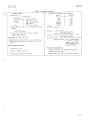


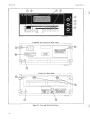


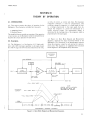
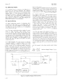
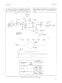

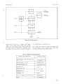
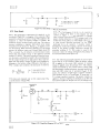


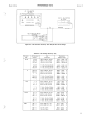
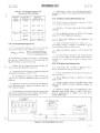

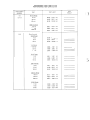

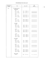
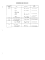
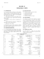


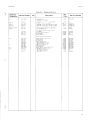
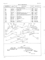
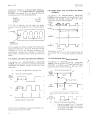
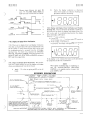

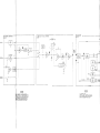
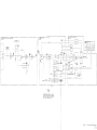

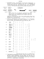
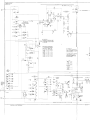
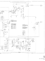
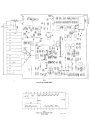

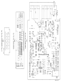
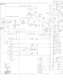

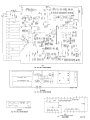
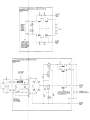

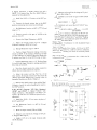

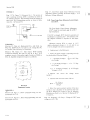

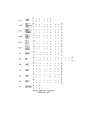


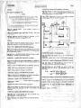


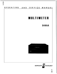
![2649 Manuals . . . . . . . . . . . . . . . . . . . . . . . . . . C. ClarWDTD [24]](http://vs1.manualzilla.com/store/data/005876281_1-ca0a669885d1d1e5f63e9b5ff82f3016-150x150.png)