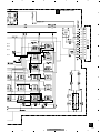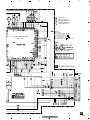
1
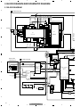
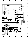
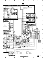
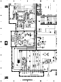
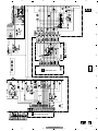
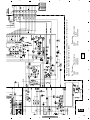
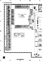
Service
Manual
ORDER NO.
CRT2985
DEH-P4500R/XM/EW
MULTI-CD CONTROL HIGH POWER CD PLAYER WITH RDS TUNER
DEH-P4500R
XM/EW, XN/EW
- This service manual should be used together with the following manual(s):
Model No.
CX-3026
Order No.
CRT2944
Mech. Module Remarks
S10
CD Mech. Module:Circuit Description, Mech.Description, Disassembly
For details, refer to "Important symbols for good services".
PIONEER CORPORATION
4-1, Meguro 1-Chome, Meguro-ku, Tokyo 153-8654, Japan
PIONEER ELECTRONICS (USA) INC. P.O.Box 1760, Long Beach, CA 90801-1760 U.S.A.
PIONEER EUROPE NV Haven 1087 Keetberglaan 1, 9120 Melsele, Belgium
PIONEER ELECTRONICS ASIACENTRE PTE.LTD. 253 Alexandra Road, #04-01, Singapore 159936
C PIONEER CORPORATION 2002
K-ZZA. NOV. 2002 Printed in Japan
1
2
3
4
3. BLOCK DIAGRAM AND SCHEMATIC DIAGRAM
3.1 BLOCK DIAGRAM
A
A TUNER AMP UNIT
VDD
IC 3 EEPROM
5.0V
5V
OSC
B
ANTENNA
CN401
AM ANT
1
1
RDS_HSLK
RDS_LOCK
DO
RDS_CK
18 19 20 21
RDS_DATA
14
LDET
11
CE1
DI
SL
10 9 8
CK
5
ROM_VDD
CE2
WC
13
IC 5
3.3V
←
7 6
FM/AM TUNER UNIT
LPF
FMRF
ATT
Rch
2
3
IC 1
3.3V
FM ANT
ATT
FMRF
ANT adj
24
IC 2
2.5V
Lch
MIXER, IF AMP
RDS_D
23
DET, FM MPX,
RDS DECODER
RF adj
RDS_H
RDS_C
T51
CF52
RDS_L
AUDIOGND
NC
15
22
16
VDD_3.3
DGND
12
VCC
OSCGND
2
4
3.3V
IC 4
3.3V 2.5V 2.5V
←
C
RFGND
CF51
17
TUN L
TUN 3.3V
SYS 8.4V
41
BUS+L
BUS+L
43
BUS-L
BUS-L
44
CD L
42
CN101
7
11
BZ 641
5
1
8
EVST,EVCK,EVD
BUZZER
LEVEL INDIC
22
IP-BUS DRIVER
BUS5
D CD CORE UNIT(S10)
BUS+
CN101
2
LOADING/ CARRIAGE
MOTOR
xtal
1
4
SERVO XTAL
CONTROL,
DSP, INTQ
LPF, DAC
TOP
M
16
SOP
15
SOM
17
LCOM
18
LCOP
M
14
FD, TD, SD, MD
42
LOEJ
23
IC 201 SO
UPD63712GC
80
24
IC 652
7
INTQ
4
18
2
Q102
4
18
1
ASENBO
SYSTEM CONTROLLER
INTQ
IC 601(2/2)
PD5801A
IC 653
12
XSI
TC7SET08FU
16
2
6
4
4
23
TC7SET08FU
LIMIT
56
87
CLMP 66
HOME
22
LOEJ
9
CONT
5
17
7
15
CLMP
6
16
11
11
1
20
2
21
VDSENS
VD
CLAMP
DSCSNS
VD
3.3V REGULATOR
3R3V
3
IC 701
XIN
XOUT
XSI
13
X601
11
CDLOEJ
CONT
DSCSNS
FLPILM
xtalen
EJTIN
VDSENS
32 20
DSCSNS
8EJ
SYSPW
BU
IC 301
BA5996FP
12EJ
IPPW
Q101
80
CONT
E
79
X201
FOP
ACT,MOTOR
DRIVER
8
34
39
33
ROT0
ILMPW
FOP
TOP
12
FOP
13
TOP
SPINDLE
MOTOR
PD
20
AC, F, E, BD
HOLOGRAM
UNIT
FOCUS ACT.
MONITOR TRACKING ACT.
DIODE
LOUT
92
85
CN651
ROT1
5
LD
mute
SWVDD
MD
1
14
8
IPPW
LVLINL
RX
DPDT
LD+
LOUT
27
PEE
TX
dsens
D
CN701
Q101
28
VDCONT
LASER
DIODE
1 TX
IC 101
6 HA12187FP 2 RX
LCDPW/
OELPW
KYDT
PICKUP UNIT
(SERVICE)(P10)
40
42
BU
Q804
38 35 36 41
Q8
Q651
VDD
BU
1
Q8
Q652
NJM2391DL1-33
S
IC 801
4
DSENS
2
TC7SET08FU
ILB
F
12
DEH-P4500R/XM/EW
1
2
3
4
6
5
8
7
A
RESET
1
2
IC 602
VDD
S-80835ANUP-EDZ
CN352
10
reset
PL
ce@
69
CE1
70
DO
98
PL
2
NON-FAD/SW L
FL
6
FRONT L
Q353
tunce@
DI
99
CK
100
FL
TUNPCE1
TUNPDI
Q352
TUNPDO
VDD REGULATOR
TUNPCK
17
ldet
95 SL
Q911
VDD
B
Q913
SYSTEM CONTROLLER
IC 601(1/2)
PD5801A
DALMON
67
CN901
Q401
46
RDS_HSLK
44
BACKUP SENSE
RDSDATA
bsens
rdshslk
asens
BU
73
16
BU
RDS_DATA
Q931
72
FUSE
16
10A
ACC
14
BACK UP
14
ACC
Q402
RDS_CK
16
rdslk
RDS_LOCK
45
rdslk
ACC SENSE
isens
ILM SENSE
81
12
12
9
9
15
15
7
7
5
5
8
8
ILM
Q951
VDD
TELIN
Q932
8
TELMUTE
TELEPHONE MUTE
C
TPD1018F
ELECTRONIC VOLUME/
SOURCE SELECTOR
TUN L
41
IN2-L
+L
43
-L
44 IN4-L
PL
IN4+L
IC 201
PML009A
FL
RL
SEL_OUT_L
42 IN3-L
BU
POWER AMP
6,20
IC 301
PAL007A
FL+
12
FL-
10
14
11
12
FLIN
RLIN
MUTE
STBY
22
1
4
23
21
3
RL-
5
RL+
B.REMOTE
25
6
6
11
11
GND
FLFL+
RLRL+
B.REM
MUTE
EVST,EVCK,EVDT
Q982
LEVEL INDICATOR IC 131
SYS 8.4V REGULATOR
BU
7
Q921
5
Q923
SYS 8.4V
MUTE
BU
Q301
NJM4558MD
Q922
Q981
BACK
UP
B.
SYSPW
ILM REM
TUNER 3.3V REGULATOR
GND ACC
IC 401
TUN 3.3V
3
1
RR
FR
FL
RL
-
RR
+
FR
+
FL
+
RL
+
D
SYS 8.4V
NJM2391DL1-33
X601
CN831
BU
Q805
DGND
Q803
ILB
5
5
6
6
8
8
9
9
7
7
ROT0 13
ROT1 12
Q804
B PANEL UNIT
C
S1970
EJECT
KEYBOARD UNIT
CN1901
4
9
13
9
4
12
7
6
2
2
11
ILB
ILB
E
S1951
ROT0
ROT0 2
ROT1
ROT1 1
3
DIMMER
Q1910
Q807
SWDVDD
VDD
2
SWVDD
ILLUMINATION
REMOTE CONTROL SENSOR
11
10
3
DPDT
9
DSENS
KYDT
2
08FU
14
14
8
5
Q806
ILB
10
10
5
8
KYDT
8
7
55 11
10
DPDT
KTDT
DIMMER
11
VDD
DPDT
S802
VLCD
Q808
4
1
IC 1901
RS-140
REMIN
OPT IN
KEY MATRIX
KEY DATA
LCD DRIVER/
KEY CONTROLLER
X1
X0
2
3
X1900
IC 1900
PD6294A
LCD
BL+B
CN1951
CN1950
F
13
DEH-P4500R/XM/EW
5
6
7
8
1
2
3
4
3.2 OVERALL CONNECTION DIAGRAM(GUIDE PAGE)
Note: When ordering service parts, be sure to refer to “EXPLODED VIEWS AND PARTS LIST” or “ELECTRICAL
PARTS LIST”.
A-a
A
A-a
A-a
A-a
A-b
A-b
A-b
Large size
SCH diagram
Guide page
Detailed page
B
FM/AM TUNER UNIT
C
D
D
C
CN701
CD CORE UNIT (S10)
KEYBOARD UNIT
E
EJECT SW
B PANEL UNIT
F
14
A B
1
DEH-P4500R/XM/EW
2
3
4
5
6
8
7
A-b
A
A
TUNER AMP UNIT
The > mark found on some component parts indicates
the importance of the safety factor of the part.
Therefore, when replacing, be sure to use parts of
identical designation.
FRONT
R CH
B
FRONT
L CH
SUB WOOFER
R CH
SUB WOOFER
L CH
C
600µH
SYSTEM CONTROLLER
>
FUSE
10A
CEK1208
BACKUP
GND
ACC
ILM
B.REM
D
TEL
RL—
DSENS SW
FL—
RL+
FL+
RR—
FR—
RR+
FR+
BACK
UP
ILM
GND ACC
RR
FR
FL
RL
-
RR
+
FR
+
FL
+
RL
+
E
For resistors and capacitors in the circuit diagrams, their resistance values or
capacitance values are expressed in codes:
Ex. *Resistors
Code
Practical value
123
12k ohms
103
10k ohms
*Capacitors
Code
Practical value
103
0.01uF
101/10
100uF/10V
A
DEH-P4500R/XM/EW
5
6
F
7
8
15
2
A-b
3
1
4
SYSTEM CONTROLLER
1
2
A
B
A-a A-b
C
D
E
F
FM/AM TUNER UNIT
A-a
16
DEH-P4500R/XM/EW
1
2
3
4
6
5
3
8
7
4
6
5
A-b
A
C
C
A-a A-b
EJECT SW
B PANEL UNIT
B
KEYBOARD UNIT
D
E
D
CN701
CD CORE UNIT (S10)
F
A-a B
17
DEH-P4500R/XM/EW
5
6
7
8
C
F
1
TUNER AMP UNIT
A-b
18
2
600µH
A
1
3
3
>
SUB WOOFER
L CH
SUB WOOFER
R CH
FRONT
L CH
FRONT
R CH
2
2
YSTEM CONTROLLER
A
B
The > mark found on some component parts indicates
the importance of the safety factor of the part.
Therefore, when replacing, be sure to use parts of
identical designation.
A-a A-b
1
4
D
E
DEH-P4500R/XM/EW
4
DSENS SW
5
3
4
6
5
6
7
RR
FR
FL
RL
-
RR
+
FR
+
FL
+
RL
+
7
A-a A-b
*Capacitors
Code
Practical value
103
0.01uF
101/10
100uF/10V
GND ACC
ILM
BACK
UP
FR+
RR+
FR—
RR—
FL+
RL+
FL—
RL—
TEL
B.REM
ILM
ACC
GND
BACKUP
6
Ex. *Resistors
Code
Practical value
123
12k ohms
103
10k ohms
For resistors and capacitors in the circuit diagrams, their resistance values or
capacitance values are expressed in codes:
>
FUSE
10A
CEK1208
5
8
A
B
C
D
E
A-b
DEH-P4500R/XM/EW
8
19
F
1
2
3
4
3.3 KEYBOARD UNIT
A
B
CL-195PG-CD
CL-195PG-CD
CL-195PG-CD
CL-195PG-CD
C
D
E
F
C
20
DEH-P4500R/XM/EW
1
2
3
4
6
5
7
C
8
KEYBOARD UNIT
A
CN1951
B
CL-195PG-CD
B
PG-CD
PG-CD
PG-CD
CL-195PG-CD
CL-195PG-CD
PG-CD
151
C
CL-195PG-CD
151
D
E
F
C
21
DEH-P4500R/XM/EW
5
6
7
8
1
2
3
4
3.4 CD MECHANISM MODULE
Pickup Unit(Service)(P10)
A
#
F
B
F
T
T
T
T
F
F
T
T
F
T
T
F
F
F
F
F
T
T
!
C
0
1
9
D
MOTOR DRIVER
@
S
T
SPINDLE MOTOR
LOADING/CARRIAGE
MOTOR
M2 CXB8933
E
7
S
M1 CXB6007
5
C
F
S
8
6
C
3
C
C
C
F
F
T
S
S
T
3.3V
REGULATOR
F
D
22
DEH-P4500R/XM/EW
1
2
3
4
6
5
8
7
A
F
TRACKING SERVO LINE
C
CARRIAGE SERVO LINE
S
SPINDLE SERVO LINE
F
T
C
S
T
SIGNAL LINE
FOCUS SERVO LINE
B
SWITCHES:
CD CORE UNIT
S901 : HOME SWITCH.....ON-OFF
S902 : CLAMP SWITCH....ON-OFF
S903 : DSCSNS SWITCH....ON-OFF
S904 : 12EJ SWITCH....ON-OFF
S905 : 8EJ SWITCH....ON-OFF
The underlined indicates the switch position.
RF AMP / SERVO / DSP
DAC / LPF
C
D
9
CD CORE UNIT (S10)
D
4
2
A
CN651
CN???
@
S
5
C
E
3
$%
F
D
23
DEH-P4500R/XM/EW
5
6
7
8
1
2
- Waveforms
A
1 DSCSNS
2 CLCONT
3 LOEJ
4 VD
B
5V/div
5V/div
5V/div
10V/div
3
4
Note : 1. The encircled numbers denote measuring points in the circuit diagram.
2. Reference voltage REFO1(1.65V)
500ms/div 1 DSCSNS
2 CLCONT
3 LOEJ
4 VD
5V/div
5V/div
5V/div
10V/div
500ms/div 5 SIN
6 CIN
7 TIN
1V/div
2s/div
500mV/div
500mV/div
When loading a 12cm CD
When loading an 8cm CD
When setting up after loading a 12cm CD-DA
disc
Ref.:
GND
Ref.:
GND
Ref.:
REFO
Mode:
Normal
Mode:
Normal
Mode:
Normal
8 FIN
9 RFOK
5 SIN
200mV/div 500ms/div 0 TE
2V/div
! FE
2V/div
500mV/div 200ms/div ! FE
500mV/div
8 FIN
0 TE
7 TIN
500mV/div 20ms/div
500mV/div
500mV/div
500mV/div
When setting up "Source On"(12cm CD-DA)
When setting up "Source On"
During "Play"(CD-DA)
Ref.:
REFO
Ref.:
REFO
Ref.:
REFO
Mode:
Normal
Mode:
Normal
Mode:
Normal
C
@ MDX
5 SIN
500mV/div 5ms/div
1V/div
@ MDX
5 SIN
500mV/div 5µs/div
1V/div
# RFAGC
500mV/div 0.5µs/div
D
E
F
Spindle waveform during "Play"
Spindle waveform during "Play"(Magnified)
Ref.:
REFO
Ref.:
REFO
Ref.:
REFO
Mode:
Normal
Mode:
Normal
Mode:
Normal
8 FIN
! FE
500mV/div 200ms/div 0 TE
500mV/div
# RFAGC
500mV/div 2ms/div
500mV/div
RF eye pattern
# RFAGC
0 TE
7 TIN
Focus Search
When "Tracking Open"
1 Track Jump
Ref.:
REFO
Ref.:
REFO
Ref.:
REFO
Mode:
TEST
Mode:
TEST
Mode:
TEST
24
1V/div
500µs/div
500mV/div
500mV/div
DEH-P4500R/XM/EW
1
2
3
4
6
5
8
7
A
# RFAGC
0 TE
7 TIN
1V/div
500ms/div # RFAGC
500mV/div
0 TE
500mV/div
7 TIN
1V/div
5ms/div
500mV/div
500mV/div
# RFAGC
7 TIN
0 TE
8 FIN
1V/div
1V/div
1V/div
1V/div
500µs/div
32 Track Jump
100(32x3) Track Jump
When reproducing black dots(1mm)
Ref.:
REFO
Ref.:
REFO
Ref.:
REFO
Mode:
TEST
Mode:
TEST
Mode:
Normal
# RFAGC
0 TE
6 CIN
5 SIN
500µs/div # RFAGC
1V/div
1V/div
0 TE
500mV/div
6 CIN
2V/div
5 SIN
5ms/div
1V/div
1V/div
500mV/div
2V/div
# RFAGC
0 TE
6 CIN
5 SIN
B
500µs/div
1V/div
1V/div
500mV/div
2V/div
When reproducing scratch(1mm)
When reproducing fingerprint(65µm)
During inside/outside search
(outer circumference → inner circumference)
Ref.:
REFO
Ref.:
REFO
Ref.:
REFO
Mode:
Normal
Mode:
Normal
Mode:
Normal
C
$ LOUT
% ROUT
1V/div
1V/div
200µs/div 1 DSCSNS 5V/div
2 CLCONT 5V/div
3 LOEJ
5V/div
200ms/div 1 DSCSNS 5V/div
2 CLCONT 5V/div
3 LOEJ
5V/div
200ms/div
D
Analog Audio
When "Eject"(12cm CD)
When "Eject"(8cm CD)
Ref.:
AGND
Ref.:
GND
Ref.:
GND
Mode:
Normal
Mode:
Normal
Mode:
Normal
E
F
25
DEH-P4500R/XM/EW
5
6
7
8
1
2
3
4
6.3 ERROR MODE
- Error Messages
A
If a CD is not operative or stopped during operation due to an error, the error mode is turned on and cause(s) of
the error is indicated with a corresponding number. This arrangement is intended at reducing nonsense calls from
the users and also for facilitating trouble analysis and repair work in servicing.
(1) Basic Indication Method
1) When SERRORM is selected for the CSMOD (CD mode area for the system), error codes are written to DMIN
(minutes display area) and DSEC (seconds display area). The same data is written to DMIN and DSEC. DTNO
remains in blank as before.
B
2) Head unit display examples
Depending on display capability of LCD used, display will vary as shown below. xx contains the error number.
8-digit display
ERROR–xx
6-digit display
ERR–xx
4-digit display
E–xx
(2) Error Code List
Displayed error code Description of the code and potential cause(s)
Code Class
Electricity Carriage Home NG
CRG can't be moved to inner diameter.
10
CRG can't be moved from inner diameter.
SERVO LSI ComC
→ Failure on home switch or CRG move mechanism.
munication Error
11
Electricity
Focus Servo NG
Communication error between microcomputer and SERVO LSI.
Focusing not available.
→ Stains on rear side of disc or excessive vibrations on REWRITABLE.
12
Electricity
Spindle Lock NG
Subcode NG
Spindle not locked. Sub-code is strange (not readable).
→ Failure on spindle, stains or damages on disc, or excessive vibrations.
A disc not containing CD-R data is found.
D
Turned over disc are found, though rarely.
CD signal error.
AGC protection doesn't work. Focus can be easily lost.
→ Damages or stains on disc, or excessive vibrations on REWRITABLE.
17
Electricity
Setup NG
30
Electricity
Search Time Out
Failed to reach target address.
→ CRG tracking error or damages on disc.
44
Electricity
ALL Skip
50
Mechanism CD On Mech Error
Skip setting for all track.
(CD-R/RW)
Mechanical error during CD ON.
→ Defective loading motor, mechanical lock and mechanical sensor.
A0
System
Power Supply NG
Power (VD) is ground faulted.
→ Failure on SW transistor or power supply (failure on connector).
E
Remarks: Mechanical errors are not displayed (because a CD is turned off in these errors).
Unreadable TOC does not constitute an error. An intended operation continues in this case.
Upper digits of an error code are subdivided as shown below:
1x: Setup relevant errors, 3x: Search relevant errors, Ax: Other errors.
F
42
DEH-P4500R/XM/EW
1
2
3
4
5
6
8
7
7. GENERAL INFORMATION
7.1 DIAGNOSIS
7.1.1 DISASSEMBLY
A
- Removing the Case (not shown)
1. Remove the Case.
- Removing the CD Mechanism Module (Fig.1)
CD Mechanism Module
1
Remove the four screws.
B
Disconnect the connector and then remove the
CD Mechanism Module.
1
1
- Removing the Grille Assy (Fig.1)
2
Remove the two screws and then remove
the Grille Assy.
1
C
1
2
2
Grille Assy
Fig.1
- Removing the Tuner Amp Unit (Fig.2)
1
Remove the screw.
2
2
2
Remove the three screws.
3
Straight the tabs at three locations
indicated.
4
Remove the screw and then remove
the Tuner Amp Unit.
D
2
4
1
E
3
3
3
F
Tuner Amp Unit
Fig.2
43
DEH-P4500R/XM/EW
5
6
7
8
1
2
3
4
- How to hold the Mechanical Unit
1. Hold the top and bottom frame.
2. Do not squeeze top frame's front portion too tight,
because it is fragile.
A
B
Do not squeeze.
- Removing the Upper and Lower Frames
C
1. With a disc clamped, remove the four springs (A),
the two springs (B), the two springs (C), and the
four screws.
2. To remove the upper frame, open it on the fulcrum
A.
3. While lifting the carriage mechanism, remove the
three dampers.
4. With the frames removed, insert the connectors
coming from the main unit and eject the disc.
Caution: Before installing the carriage mechanism in
the frames, be sure to apply some alcohol to the
dampers and set the mechanism to the clamp mode.
Upper Frame
A
A
C
A
A
Carriage Mechanism
B
Damper
Lower Frame
Damper
B
D
- Removing the Pickup Unit
E
1. Set the mechanism to the clamp mode.
2. Remove the lead wires from the inner holder.
3. Remove the two washers, styling holder, change
arm, and pickup lock arm.
4. While releasing from the hook of the inner holder,
lift the end of the feed screw.
Caution: In assembling, move the planet gear to the
load/eject position before setting the feed screw
in the inner holder.
C
A
Damper
Washer
Pickup Lock Arm
Change
Arm
Styling Holder
Feed Screw
F
Inner Holder
Planet Gear
44
DEH-P4500R/XM/EW
1
2
3
4
5
ANTENNA JACK
SW
F
FRONT OUTPUT
SUBWOOFER OUTPUT
NON FADING OUTPUT
1. FR+
2. RR+
3. FR4. RR5. FL+
6. RL+
7. FL8. RL-
6
9. TEL MUTE
10. NC
11. B.REM
12. ILM
13. NC
14. ACC
15. GND
16. BACK UP
1 3 5 7 9 11 13 15
2 4 6 8 10 12 14 16
1. BUS+
2. GND
3. GND
4. NC
5. BUS6. GND
7. BUS L+ INPUT
8. ASENB
9. BUS R+ INPUT
10. BUS R- INPUT
11. BUS L- INPUT
1 2 3 4
7
8 9 10 11
5 6
5
6
7
7
8
7.1.2 CONNECTOR FUNCTION DESCRIPTION
A
B
10A
C
D
E
F
DEH-P4500R/XM/EW
8
45
6
5
8
7
- FM/AM Tuner Unit
5V
OSC
AM ANT
1
A
RDS_HSLK
RDS_LOCK
RDS_CK
18 19 20 21
RDS_DATA
14
DO
LDET
11
CE1
DI
SL
IC 3 EEPROM
5.0V
10 9 8
CK
5
ROM_VDD
CE2
WC
13
IC 5
3.3V
←
7 6
LPF
FMRF
ATT
Rch
3
IC 1
3.3V
FM ANT
ATT
FMRF
ANT adj
24
IC 2
2.5V
B
Lch
MIXER, IF AMP
DET, FM MPX,
RDS DECODER
RF adj
T51
23
CF52
AUDIOGND
NC
15
22
16
4
VDD_3.3
DGND
12
VCC
OSCGND
2
3.3V
IC 4
3.3V 2.5V 2.5V
←
RFGND
CF51
17
C
No. Symbol
1 AMANT
2
3
4
5
6
7
RFGND
FMANT
VCC
SL
CE2
WC
I/O Explain
I AM antenna input
I
O
I
I
RF ground
FM antenna input
power supply
signal level
chip enable-2
write control
8
9
10
11
12
13
CE1
CK
DI
LDET
OSCGND
ROM_VDD
I
I
I
O
chip enable-1
clock
data in
lock detector
osc ground
power supply
14
15
16
17
18
19
20
DO
DGND
NC
VDD_3.3
RDS_CK
RDS_DATA
RDS_LOCK
O
data out
digital ground
non connection
power supply
RDS clock
RDS data
RDS lock
21 RDS_HSLK
O
O
O
O
22 AUDIOGND
23 L ch
O
24 R ch
O
RDS high speed
lock
audio ground
L channel output
R channel output
AM antenna input high impedance AMANT pin is connected with
an all antenna by way of 4.7µH. (LAU type inductor) A series circuit
including an inductor and a resistor is connected with RF ground for
the countermeasure against the ham of power transmission line.
Ground of antenna block
Input of FM antenna 75Ω Surge absorber(DSP-201M-S00B) is necessary.
The power supply for analog block. D.C 8.4V ± 0.3V
Output of FM/AM signals level
Chip enable for EEPROM ”Low” active
You can write EEPROM, when EEPROM write control is “Low”.
Ordinary non connection
Chip enable for AF•RF ”High” active
Clock
Data input
“Low” active
Ground of oscillator block
Power supply for EEPROM pin 13 is connected with a power supply of
micro computer.
Data output
Ground of digital block
Not used
The power supply for digital block. 3.3V ± 0.2V
Output of RDS clock(2.5V)
Output of RDS data(2.5V)
Output unit “High” active(2.5V) (RDS_LOCK turns over by the
external transistor. “Low” active)
Output unit “High” active(2.5V)(RDS_HSLK turns over by the
external transistor. “Low” active)
Ground of audio block
FM stereo “L-ch” signal output or AM audio output
FM stereo “R-ch” signal output or AM audio output
D
E
F
53
DEH-P4500R/XM/EW
5
6
7
8