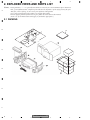
1
ORDER NO.
CRT3597
DEH-30MP/XU/EW
HIGH POWER CD/MP3/WMA PLAYER WITH RDS TUNER
DEH-30MP
/XU/EW
This service manual should be used together with the following manual(s):
Model No.
CX-3164
Order No.
CRT3583
Mech.Module
S10.5COMP1
Remarks
CD Mech. Module : Circuit Descriptions, Mech. Descriptions, Disassembly
For details, refer to "Important Check Points for Good Servicing".
PIONEER CORPORATION
4-1, Meguro 1-chome, Meguro-ku, Tokyo 153-8654, Japan
PIONEER ELECTRONICS (USA) INC. P.O. Box 1760, Long Beach, CA 90801-1760, U.S.A.
PIONEER EUROPE NV Haven 1087, Keetberglaan 1, 9120 Melsele, Belgium
PIONEER ELECTRONICS ASIACENTRE PTE. LTD. 253 Alexandra Road, #04-01, Singapore 159936
PIONEER CORPORATION 2005
K-ZZW. DEC. 2005 Printed in Japan
1
2
3
4
SAFETY INFORMATION
This service manual is intended for qualified service technicians; it is not meant for the casual do-it-yourselfer.
Qualified technicians have the necessary test equipment and tools, and have been trained to properly and safely
repair complex products such as those covered by this manual.
Improperly performed repairs can adversely affect the safety and reliability of the product and may void the warranty.
If you are not qualified to perform the repair of this product properly and safely, you should not risk trying to do so
and refer the repair to a qualified service technician.
A
- Safety Precautions for those who Service this Unit.
• When checking or adjusting the emitting power of the laser diode exercise caution in order to get safe, reliable
results.
Caution:
1. During repair or tests, minimum distance of 13cm from the focus lens must be kept.
2. During repair or tests, do not view laser beam for 10 seconds or longer.
B
- CD Section Precaution
1. You should conform to the regulations governing
the product (safety, radio and noise, and other
regulations), and should keep the safety during
servicing by following the safety instructions
described in this manual.
2. Before disassembling the unit, be sure to turn off
the power. Unplugging and plugging the connectors
during power-on mode may damage the ICs inside
the unit.
3. To protect the pickup unit from electrostatic discharge
during servicing, take an appropriate treatment
(shorting-solder) by referring to "the DISASSEMBLY".
4. After replacing the pickup unit, be sure to check the
grating.
C
D
E
F
2
DEH-30MP/XU/EW
1
2
3
4
5
6
7
8
[Important Check Points for Good Servicing]
In this manual, procedures that must be performed during repairs are marked with the below symbol.
Please be sure to confirm and follow these procedures.
A
1. Product safety
Please conform to product regulations (such as safety and radiation regulations), and maintain a safe servicing environment by
following the safety instructions described in this manual.
1 Use specified parts for repair.
Use genuine parts. Be sure to use important parts for safety.
2 Do not perform modifications without proper instructions.
Please follow the specified safety methods when modification(addition/change of parts) is required due to interferences such as
radio/TV interference and foreign noise.
3 Make sure the soldering of repaired locations is properly performed.
B
When you solder while repairing, please be sure that there are no cold solder and other debris.
Soldering should be finished with the proper quantity. (Refer to the example)
4 Make sure the screws are tightly fastened.
Please be sure that all screws are fastened, and that there are no loose screws.
5 Make sure each connectors are correctly inserted.
Please be sure that all connectors are inserted, and that there are no imperfect insertion.
6 Make sure the wiring cables are set to their original state.
Please replace the wiring and cables to the original state after repairs.
In addition, be sure that there are no pinched wires, etc.
C
7 Make sure screws and soldering scraps do not remain inside the product.
Please check that neither solder debris nor screws remain inside the product.
8 There should be no semi-broken wires, scratches, melting, etc. on the coating of the power cord.
Damaged power cords may lead to fire accidents, so please be sure that there are no damages.
If you find a damaged power cord, please exchange it with a suitable one.
9 There should be no spark traces or similar marks on the power plug.
When spark traces or similar marks are found on the power supply plug, please check the connection and advise on secure
connections and suitable usage. Please exchange the power cord if necessary.
0 Safe environment should be secured during servicing.
D
When you perform repairs, please pay attention to static electricity, furniture, household articles, etc. in order to prevent injuries.
Please pay attention to your surroundings and repair safely.
2. Adjustments
To keep the original performance of the products, optimum adjustments and confirmation of characteristics within specification.
Adjustments should be performed in accordance with the procedures/instructions described in this manual.
3. Lubricants, Glues, and Replacement parts
Use grease and adhesives that are equal to the specified substance.
Make sure the proper amount is applied.
E
4. Cleaning
For parts that require cleaning, such as optical pickups, tape deck heads, lenses and mirrors used in projection monitors, proper
cleaning should be performed to restore their performances.
5. Shipping mode and Shipping screws
To protect products from damages or failures during transit, the shipping mode should be set or the shipping screws should be
installed before shipment. Please be sure to follow this method especially if it is specified in this manual.
F
DEH-30MP/XU/EW
5
6
7
8
3
1
2
3
4
CONTENTS
SAFETY INFORMATION ..................................................................................................................................... 2
1. SPECIFICATIONS ............................................................................................................................................ 5
2. EXPLODED VIEWS AND PARTS LIST ............................................................................................................ 6
2.1 PACKING ................................................................................................................................................... 6
2.2 EXTERIOR................................................................................................................................................. 8
2.3 CD MECHANISM MODULE..................................................................................................................... 10
3. BLOCK DIAGRAM AND SCHEMATIC DIAGRAM .......................................................................................... 12
3.1 BLOCK DIAGRAM ................................................................................................................................... 12
3.2 OVERALL CONNECTION DIAGRAM(GUIDE PAGE).............................................................................. 14
3.3 KEYBOARD UNIT.................................................................................................................................... 20
3.4 CD MECHANISM MODULE(GUIDE PAGE) ............................................................................................ 22
4. PCB CONNECTION DIAGRAM ..................................................................................................................... 32
4.1 TUNER AMP UNIT................................................................................................................................... 32
4.2 KEYBOARD UNIT.................................................................................................................................... 36
4.3 CD CORE UNIT(S10.5COMP1)............................................................................................................... 38
5. ELECTRICAL PARTS LIST ............................................................................................................................ 40
6. ADJUSTMENT ............................................................................................................................................... 45
6.1 CD ADJUSTMENT................................................................................................................................... 45
6.2 CHECKING THE GRATING AFTER CHANGING THE PICKUP UNIT .................................................... 47
6.3 ERROR MODE ........................................................................................................................................ 49
7. GENERAL INFORMATION ............................................................................................................................. 50
7.1 DIAGNOSIS ............................................................................................................................................. 50
7.1.1 DISASSEMBLY ..................................................................................................................................... 50
7.1.2 CONNECTOR FUNCTION DESCRIPTION .......................................................................................... 53
7.2 PARTS...................................................................................................................................................... 54
7.2.1 IC .......................................................................................................................................................... 54
7.2.2 DISPLAY ............................................................................................................................................... 64
7.3 OPERATIONAL FLOW CHART ............................................................................................................... 65
8. OPERATIONS ................................................................................................................................................ 66
A
B
C
D
E
F
4
DEH-30MP/XU/EW
1
2
3
4
5
6
7
8
1. SPECIFICATIONS
A
B
C
D
E
F
DEH-30MP/XU/EW
5
6
7
8
5
1
2
3
4
2. EXPLODED VIEWS AND PARTS LIST
NOTES : • Parts marked by " * " are generally unavailable because they are not in our Master Spare Parts List.
• The > mark found on some component parts indicates the importance of the safety factor of the part.
Therefore, when replacing, be sure to use parts of identical designation.
• Screw adjacent to mark on the product are used for disassembly.
• For the applying amount of lubricants or glue, follow the instructions in this manual.
(In the case of no amount instructions,apply as you think it appropriate.)
A
"
2.1 PACKING
3
B
16
1
6
5
2
9
C
13
D
E
F
6
DEH-30MP/XU/EW
1
2
3
4
5
6
7
8
PACKING SECTION PARTS LIST
Mark No.
*
*
Description
Part No.
Mark No.
13
14
15
1
2
3
4
5
Accessory Assy
Screw Assy
Fixing Screw(M2x4)
Screw
Polyethylene Bag
CEA4610
CEA6002
CBA1994
CBA1650
CEG-127
6
7
8
9
10
Screw
Screw
Polyethylene Bag
Handle
Bush
CRZ50P090FTC
TRZ50P080FTC
CEG-158
CNC5395
CNV3930
11
12
Carton
Contain Box
YHG5075
YHL5075
*
*
16-1
16-2
16-3
16-4
16-5
Description
Part No.
Protector
Protector
Polyethylene Bag
YHP5009
YHP5008
CEG-162
Owner's Manual
Owner's Manual
Owner's Manual
Installation Manual
Passport
YRD5060
YRD5061
YRD5062
YRD5059
CRY1013
16-6 Warranty Card
17 Case Assy
18 Cord Assy
A
CRY1157
CXB3520
CDE7059
B
Owner's Manual,Installation Manual
Part No.
Language
YRD5060
English, Spanish
YRD5061
German, French
YRD5062
Italian, Dutch, Russian
YRD5059
English, Spanish, German, French, Italian, Dutch, Russian
C
D
E
F
DEH-30MP/XU/EW
5
6
7
8
7
1
2
3
4
2.2 EXTERIOR
A
39
34
37
31
5
38
41
40
14
42
45
43
46
6
42
46
57
B
66
B
35
42
46
53
51
12
60
70
50
52
61
64
63
68
47
54
69
48
65
67
49
58
C
15
A
9
8
9
8
59
56
3
2
2
32
62
74
55
C 36
46
53
55
33
16
72
2
2
16
73
22
28
18
25
73
30
17
29
71
B
23
19
21
20
17
26
27
D
A
11
24
10
1
13
E
7
A
B
4
4
44
4
C
F
8
DEH-30MP/XU/EW
1
2
3
4
5
6
7
8
EXTERIOR SECTION PARTS LIST
Mark No.
>
*
*
*
Description
Mark No.
Part No.
1
2
3
4
5
Screw
Screw
Screw
Screw
Cord Assy
ASZ26P050FTC
BSZ26P060FTC
BSZ30P060FTC
BSZ30P200FTC
CDE7059
6
7
8
9
10
Cap
Holder
Earth Plate
Cushion
CD Mechanism Mudule(S10.5)
CKX-003
CNC8659
CNC8915
CNM8890
CXK5750
11
12
13
14
15
Cable
Case
Insulator
Panel
Tuner Amp Unit
YDE5013
YNB5008
YNM5012
YNS5125
YWM5113
16
17
18
19
20
Screw
Screw
Screw
Fuse(10A)
Pin Jack(CN353)
ASZ26P060FTC
BPZ26P080FTC
BSZ26P160FTC
CEK1208
CKB1051
21
22
23
24
25
Plug(CN901)
Connector(CN701)
Connector(CN803)
Antenna Jack(CN401)
Holder
CKM1376
CKS3834
CKS4944
CKX1056
CND1328
26
27
28
29
30
FM/AM Tuner Unit
Holder
JACK(CN621)
Holder
Heat Sink
CWE1951
CND1054
YKS5001
YNC5017
YNR5004
31
32
33
34
35
Panel Unit
Button(DETACH)
Spring
Spring
Spring
YXA5154
CAC4836
CBH1835
CBH2208
CBH2367
36
37
38
39
40
Bracket
Holder
Cover
Arm
Arm
CNC6791
CNC8042
CNM6276
CNV4692
CNV4728
41
42
43
44
45
Arm
Screw
Panel
Chassis Unit
Detachable Assy
CNV5576
IMS20P030FTB
YNS5046
YXA5168
YXA5169
46
47
48
49
Screw
Spring
Knob(SOURCE,VOLUME)
Button(1-6)
BPZ20P080FTB
CBH2210
YAA5008
YAC5074
Description
Part No.
50
Button(EQ,BAND/ESC)
YAC5075
51
52
53
54
55
Button(ATT,DISP/SCRL)
Button(EJECT,TA/AF)
Button(UP,DOWN)
Button(DETACH)
Button(LEFT,RIGHT)
YAC5076
YAC5077
YAC5079
YAC5080
YAC5102
56
57
58
59
60
Spring
Cover
Ring
Ring
Lens
YBH5003
YNS5121
YNS5123
YNS5124
YNV5036
61
62
63
64
65
Lens
Connector(CN1801)
LCD(LCD1801)
Holder
Sheet
YNV5037
CKS4943
YAW5064
YNC5016
YNM5026
66
67
68
69
70
Cushion
Connector
Lighting Conductor
Grille Unit
Button Unit(AUDIO,FUNC)
YNM5027
YNV5040
YNV5041
YXA5143
YXA5144
71
72
73
74
IC(IC301)
IC(IC921)
Transistor(Q702,911)
IC(IC1802)
PAL007B
NJM2388F84
2SD2396
TSOP4840SB1
6
B
C
D
E
F
DEH-30MP/XU/EW
5
A
7
8
9
1
2
3
4
3
4
2.3 CD MECHANISM MODULE
A
B
C
D
E
F
10
DEH-30MP/XU/EW
1
2
5
6
7
8
CD MECHANISM MODULE SECTION PARTS LIST
Mark No.
Description
Mark No.
Part No.
1
2
3
4
5
CD Core Unit(S10.5COMP1)
Connector(CN101)
Connector(CN901)
Screw
Screw
CWX3176
CKS4808
CKS5284
BMZ20P025FTC
BSZ20P040FTC
6
7
8
9
10
Screw(M2 x 3)
Screw(M2 x 4)
Washer
•••••
Spring
CBA1511
CBA1835
CBF1038
CBH2609
11
12
13
14
15
Spring
Spring
Spring
Spring
Spring
CBH2612
CBH2614
CBH2616
CBH2617
CBH2620
16
17
18
19
20
Spring
Spring
Spring
Spring
Spring
CBH2855
CBH2937
CBH2735
CBH2854
CBH2642
21
22
23
24
25
Spring
Spring
Spring
Spring
Spring
CBH2856
CBH2857
CBH2860
CBH2861
CBL1686
26
27
28
29
30
Arm
Frame
Bracket
Arm
Lever
CND1909
CND2582
CND2583
CND2584
CND2585
31
32
33
34
35
Arm
Bracket
Arm
Lever
Holder
CND2586
CND2587
CND2588
CND2589
CNV7201
36
37
38
39
40
Gear
Gear
Gear
Gear
Gear
CNV7207
CNV7208
CNV7209
CNV7210
CNV7211
41
42
43
44
45
Gear
Rack
Arm
Roller
Gear
CNV7212
CNV7214
CNV7216
CNV8189
CNV7219
46
47
48
49
Guide
Gear
Guide
Arm
CNV7361
CNV7595
CNV8448
CNV7805
Description
Part No.
50
Rack
CNV8342
51
52
53
54
55
Roller
Holder
Arm
Guide
Arm
CNV8343
CNV8344
CNV8345
CNV8347
CNV8348
56
57
58
59
60
Arm
Arm
Clamper
Arm
Guide
CNV8349
CNV8350
CNV8365
CNV8386
CNV8396
61
62
63
64
65
Arm
Collar
Motor Unit(M2)
Arm Unit
Chassis Unit
CNV8413
CNV8447
CXC4026
CXC4027
CXC4028
66
67
68
69
70
Gear Unit
Frame Unit
Motor Unit(M1)
Screw Unit
Screw
CXC4029
CXC4031
CXC4166
CXC6359
JFZ20P020FTC
71
72
73
74
Screw
Washer
Pickup Unit(P10.5)(Service)
Screw
JGZ17P022FTC
YE20FTC
CXX1942
IMS26P030FTC
6
B
C
D
E
F
DEH-30MP/XU/EW
5
A
7
8
11
1
2
3
4
3. BLOCK DIAGRAM AND SCHEMATIC DIAGRAM
3.1 BLOCK DIAGRAM
A
IC 3 EEPROM
5.0V
5V
OSC
ANTENNA
CN401
AM ANT
1
1
RDS_HSLK
RDS_LOCK
RDS_CK
CE1
18 19 20 21
RDS_DATA
14
LDET
11
DO
TUNPDI
DI
SL
10 9 8
CK
5
ROM_VDD
CE2
NC
13
IC 5
3.3V
←
7 6
B
TUNPCK
FM/AM TUNER UNIT
TUNPDO
VDD5
LPF
FMRF
ATT
Rch
2
24
RDS-CK
IC 2
2.5V
IC 1
3.3V
FM ANT
3
ATT
FMRF
RDS-HSLK
Lch
MIXER, IF AMP
RF adj
ANT adj
23
DET, FM MPX,
RDS DECODER
RDS-LOCK
RDS-DATA
AUDIOGND
NC
15
22
16
VDD_3.3
DGND
12
VCC
OSCGND
2
CF52
4
3.3V
EL
S
IC 4
3.3V 2.5V 2.5V
TUNL
←
C
RFGND
T51
2
IN
17
VDD_3.3V
VCC8
3
1
IN
IN
A TUNER AMP UNIT
CN621
5
AUX IN
3
WIRED REMOTE CONTROL
2
AUX-L
3
IC 751
NJM4558MD
1
KEY1
34
KEY2
94
KEYD
KEYAD
D
PICKUP UNIT
(P10.5)(SERVICE)
C
D
SYSTEM C
CD CORE UNIT(S10.5COMP1)
CN101
LASER
DIODE
LDMD
15
142
15
Q101
5
VREF 8
5
REFO
AC,BD
F,E
FOM
FOCUS ACT.
MONITOR
TRACKING ACT.
DIODE
143
133
8
HOLOGRAM
UNIT
3
FOP
2
TOP
1
TOM
4
LD+
14
3
LOAD/ CARRIAGE
MOTOR
CN901
LD
IC201
UPD63763CGJ
PD
LOUT
REFOUT
RF-AMP,CD DECODER,
XTAL
MP3 , WMA, DECODER,
DIGITAL SERVO / DATA PROCESSOR
FOP
LOUT
31
CN701
16
16
11
11
/RESET
10
CDMUTE
8
10
8
LOUT
34
/XTAL 35
FOM
X201
16.93MHz
LOCK/RFOK
56
2
1 TOP
TOM
TD,FD
SD,MD
XRST,XASTB,ADO,XCK,
XSO,XSI,WAIT,XINT
VDD
4
14
CD
12
FOM
DRIVER
11
FOP
14
TOP
13
TOM
E
SPINDLE
MOTOR
IC 6
PEG
V3R3D
Q701
LOCK
16
SOP CLCONT 21
15
SOM
22
18
LOEJ
LCOP
17
9
CONT
LCOM
M
41
40
47
32
31
30
42
S904
12EJ
S905
8EJ
VDD5
63
IC301
BA5835FP
M
VDD
SWVDD
CLCONT
/CD3VON
43
14
RESET
39
CDMUTE
21
/RESET
LOEJ
IC701
CONT PE5505A
CD CONTROLLER
BRST,BRXEN,BSRQ
X1 12
12EJ
8EJ
DSCSNS
BRST,BRXEN,BSRQ,BDATA,BSCK
BDATA,BSCK
X2 13
VD
VD
X701
4.00MHz
VD
1
1
2
2
Q702
B.UP
3
Q701
4
5
2
HOME
S901
HOME
VDCONT
CD3VON
46
49
VDCONT
9
9
VDCONT
S903
DSCSNS
F
V3R3D
4
IC203
NJM2886DL3-33
1
3
VD
+3.3V REGULATOR
12
DEH-30MP/XU/EW
1
2
3
4
CDRST
5
6
7
8
A
CN353
RESET
SWL
IC 961
BD4843G
1
2
VDD5
12
RCFL
RESET
TUNPDO
LDET
SL
TUNPCK
CE1
6
FRONT OUT
VDD5V REG.
66
TUNPCE1
65 TUNPCE2
CE2
SUBWOOFER OUT
Q353
68
TPDI
75
LDET
86
TPDO
97
SL
67 TPCK
TUNPDI
2
Q351
Q911
VDD5
B
Q912
SYSTEM CONTROLLER
IC 601(1/2)
PEG159A
Q401
74
RDS-CK
83
RDS-HSLK
DALMON
BACKUP SENSE
RDS57K
BSENS
Q402
81
RDS-LOCK
47
RCK
RDSLOCK
ASENS
19
BSENS
20
ASENS
CN901
B.UP
Q931
ACC
16
16
14
14
BACK UP
ACC
82
RDS-DATA
ACC SENSE
RDSDT
15
15
7
7
5
5
8
8
6
6
11
11
GND
B.UP
AMP
TUNL
2
FRONT_L
IN2−_L
PRE/SW_L
REAR_L
VCC
14
6
1
FLIN
12
7
22
VCC
FL−
IC 301
PAL007B
12
IC 151
PML015A
3
6
20
ELECTRONIC VOLUME/
SOURCE SELECTOR
FL+
21
FL+
3
RL−
5
RL+
RL−
RLIN
RL+
MUTE
B.REM
STBY
IN3_L
FL−
23
BREM
25
B.REM
IN1_L
TEL
VCK, VDT, VST
9
9
VCC8
Q453
B.UP
TUN3V REG.
3
VDD_3.3V
IC 401
NJM2885DL1-33
SYS 8V REG.
1
2
IC 921
NJM2388F84
Q451
1
B.UP
4
53
SYSPW
MUTE
94
C
FL+
4
MUTE
34
FL−
RL−
RL+
KEYD
KEYAD
SYSPW
RR RR
48
−
SYSPW
+
FR FR
BACK
UP
B.
REM
GND ACC
−
+
FL
FL
−
D
+
RL RL
−
+
SYSTEM CONTROLLER
IC 601(2/2)
PEG159A
Q951
TELIN
XOUT
38
VDD5
13
X601
XIN
15
B
CN803
CN1801
KEY MATRIX
Q851
SWVDD
VDD5
Q852
SWVDD
DSENS
21
3
8
SWVDD
7
18
DSENS
10
1
5
6
KEYBOARD UNIT
DSENS
S1801
FUNC
S1802
BAND
S1803
1
S1804
4
S1805
2
S1806
RIGTH
S1807
LEFT
S1808
3
S1818
6
S1809
5
S1810
DOWN
S1811
S1813
AUDIO
S1814
TA
E
D1804-D1822
CDRST
Q841
B.UP
ILMB+
ILM
S1812
EQ
UP
Q842
B.UP
ILMPW
1
S1827
SSENS
ROT1
ROT0
92
SSENS
3
ROT1
4
ROT0
4
7
6
5
7
4
SRC
4
ROT1
1
ROT0
2
KYDT
35
36
DPDT
KYDT
8
3
9
2
S1816
EJECT
S1817
ATT
SWVDD
REM.CON.
3
1
IC1802
TSOP4840SB1
17
SOURCE
VOLUME
DPDT
S1815
DISP
REM
18
DPDT
20
KYDT
10
56
DPDT
KYDT
VLCD
VDD
KEY DATA
LCD DRIVER/
KEY CONTROLLER
IC 1801
PD6340A
XO
XI
22
23
X1801
5MHz
F
LCD1801
DEH-30MP/XU/EW
5
6
7
8
13
1
2
3
4
3.2 OVERALL CONNECTION DIAGRAM(GUIDE PAGE)
Note: When ordering service parts, be sure to refer to " EXPLODED VIEWS AND PARTS LIST" or
"ELECTRICAL PARTS LIST".
A
A-a
A-a
Large size
SCH diagram
A-b
C
FM : -20dBs
AM : -20dBs
A-a
Guide page
A-b
Detailed page
FM/AM TUNER UNIT
471/16
A-a
A-b
CN901
B
CD : 0.35dBs
ANTENNA
15.000MHz
C
AUX IN
AUX : 2.21dBs
WIRED REMOTE CONTROL
SYSTEM MICROCOMPUTER
D
E
B
CN1801
F
A
14
DEH-30MP/XU/EW
1
2
3
4
5
6
7
8
A
A-b
A
TUNER AMP UNIT
PRE-SUB WOOFER
OUTPUT
B
>
FM : -2.9dBs
AM : -2.9dBs
CD : 10.45dBs
AUX : 10.31dBs
PRE-FRONT
OUTPUT
3A
332/16
C
COMPUTER
>
CEK1208
10A
600µH
BACKUP
GND
ACC
B.REM
471/16
TEL
D
RL–
FL–
RL+
FL+
RR–
FR–
RR+
FR+
FM : 23.1dBs
AM : 23.1dBs
CD : 36.45dBs
AUX : 36.31dBs
E
NOTE :
Symbol indicates a resistor.
No differentiation is made between chip resistors and
discrete resistors.
Symbol indicates a capacitor.
No differentiation is made between chip capacitors and
discrete capacitors.
The > mark found on some component parts indicates
the importance of the safety factor of the part.
Therefore, when replacing, be sure to use parts of
identical designation.
For resistors and capacitors in the circuit diagrams, their resistance
values or capacitance values are expressed in codes:
Ex. *Resistors
Code
Practical value
123
12k ohms
103
10k ohms
*Capacitors
Code
Practical value
103
0.01uF
101/10
100uF/10V
BACK
UP
B.
REM
GND ACC
RR
FR
FL
RL
-
RR
+
FR
+
FL
+
RL
+
F
A
DEH-30MP/XU/EW
5
6
7
8
15
A-a
AUX IN
16
1
C
CD : 0.35dBs
1
F
2
3
SYSTEM MICROCOMPUTER
CN901
A-b
AUX : 2.21dBs
ANTENNA
FM : -20dBs
AM : -20dBs
A-a A-b
C
F
A
C
A
2
3
EMOTE CONTROL
B
15.000MHz
1
4
A
2
D
E
DEH-30MP/XU/EW
4
471/16
FM/AM TUNER UNIT
5
6
7
8
A
3
4
5
6
7
A-b
8
B
A-a A-b
C
B
CN1801
D
E
F
A-a
WIRED REMOTE CONTRO
DEH-30MP/XU/EW
5
6
7
8
17
FM : -2.9dBs
AM : -2.9dBs
CD : 10.45dBs
AUX : 10.31dBs
A-a A-b
A
B
332/16
18
1
A-b
2
600µH
C
D
E
F
1
2
DEH-30MP/XU/EW
3
4
B.REM
ACC
3
GND
BACKUP
2
CEK1208
10A
>
PRE-FRONT
OUTPUT
PRE-SUB WOOFER
OUTPUT
A
3A
>
TUNER AMP UNIT
1
4
5
3
4
6
5
6
7
7
*Capacitors
Code
Practical value
103
0.01uF
101/10
100uF/10V
Ex. *Resistors
Code
Practical value
123
12k ohms
103
10k ohms
B.
REM
GND ACC
BACK
UP
RR
FR
FL
RL
-
RR
+
FR
+
FL
+
RL
+
FR+
RR+
FR–
RR–
FL+
RL+
FL–
RL–
TEL
B.REM
ACC
GND
BACKUP
7
A-a A-b
471/16
For resistors and capacitors in the circuit diagrams, their resistance
values or capacitance values are expressed in codes:
CEK1208
10A
6
The > mark found on some component parts indicates
the importance of the safety factor of the part.
Therefore, when replacing, be sure to use parts of
identical designation.
NOTE :
Symbol indicates a resistor.
No differentiation is made between chip resistors and
discrete resistors.
Symbol indicates a capacitor.
No differentiation is made between chip capacitors and
discrete capacitors.
FM : 23.1dBs
AM : 23.1dBs
CD : 36.45dBs
AUX : 36.31dBs
600µH
5
8
A
B
8
DEH-30MP/XU/EW
8
C
D
E
F
A-b
19
1
2
3
4
3.3 KEYBOARD UNIT
A
B
C
5.00MHz
LCD DRIVER
D
E
F
B
20
DEH-30MP/XU/EW
1
2
3
4
5
6
7
8
A
B
KEYBOARD UNIT
B
A
CN803
C
D
E
F
B
DEH-30MP/XU/EW
5
6
7
8
21
1
2
3
4
3.4 CD MECHANISM MODULE(GUIDE PAGE)
A
S
C
T
F
S
C
T
F
C-a
B
PICKUP UNIT(P10.5)(SERVICE)
$
F
F
F
T
T
T
F
@
T
F
F
T
C
!
T
SWITCHES:
CD CORE UNIT(S10.5COMP1)
S901:HOME SWITCH..........ON-OFF
S903:DSCSNS SWITCH......ON-OFF
S904:12EJ SWITCH.............ON-OFF
S905:8EJ SWITCH...............ON-OFF
The underlined indicates the switch position.
CD DRIVER
M1 CXC6742
SPINDLE MOTOR
NC
NC
NC
S
NC
S
NC
NC
C
NC
#
NC
C
NC
NC
M2 CXC4026
LOADING/CARRIAGE MOTOR
T
S
NC
NC
6
8
NC
C
F
NC
7
9
4
E
NC
NC
F
F
T
3
T
S
S
C
C
2
1
F
C
22
DEH-30MP/XU/EW
1
2
3
4
NC
NC
NC
NC
NC
D
5
6
7
8
A
C-b
B
SIGNAL LINE
F
T
C
S
FOCUS SERVO LINE
TRACKING SERVO LINE
CARRIAGE SERVO LINE
Decimal points for resistor
and capacitor fixed values
are expressed as :
2.2 ← 2R2
0.022 ← R022
SPINDLE SERVO LINE
C
CD CORE UNIT(S10.5COMP1)
0
+ 3.3 V REGULATOR
C
NC
NC
NC
NC
NC
NC
NC
NC
NC
NC
NC
NC
D
NC
NC
NC
NC
CD3VON(MCKRQ)
NC
SRAMLEVEL2
NC
ADENA
NC
NC
NC
NC
NC
NC
NC
SRAMLEVEL1
NC
SRAMLEVEL0
CD CONTROLLER
5
(S904)
E
(S905)
NC
NC
NC
^
%
A
CN701
F
C
DEH-30MP/XU/EW
5
6
7
8
23
F
2
3
T
!
@
3
E
C-a
DEH-30MP/XU/EW
4
The underlined indicates the switch position.
T
F
F
T
T
T
F
F
F
T
T
C
C
S
S
1
F
24
2
T
F
F
$
C-b
SWITCHES:
CD CORE UNIT(S10.5COMP1)
S901:HOME SWITCH..........ON-OFF
S903:DSCSNS SWITCH......ON-OFF
S904:12EJ SWITCH.............ON-OFF
S905:8EJ SWITCH...............ON-OFF
PICKUP UNIT(P10.5)(SERVICE)
C-a
A-a C-b
1
4
A
1
B
C
D
5
6
M2 CXC4026
LOADING/CARRIAGE MOTOR
M1 CXC6742
SPINDLE MOTOR
C
C
S
S
F
T
T
F
F
T
C-a
A-a C-b
9
8
CD DRIVER
4
S
7
C
6
#
NC
NC
NC
NC
NC
NC
NC
NC
NC
NC
NC
NC
NC
NC
NC
NC
6
1
2
3
The underlined indicates the switch position.
SWITCHES:
CD CORE UNIT(S10.5COMP1)
S901:HOME SWITCH..........ON-OFF
S903:DSCSNS SWITCH......ON-OFF
S904:12EJ SWITCH.............ON-OFF
S905:8EJ SWITCH...............ON-OFF
S
S
C
C
5
7
7
8
A
2
3
C-b
B
C
D
E
F
C-a
DEH-30MP/XU/EW
8
25
NC
NC
NC
NC
0
C
C-b
26
1
2
S
C
T
F
Decimal points for resistor
and capacitor fixed values
are expressed as :
2.2 ← 2R2
0.022 ← R022
C CD CORE UNIT(S10.5COMP1)
SPINDLE SERVO LINE
CARRIAGE SERVO LINE
TRACKING SERVO LINE
FOCUS SERVO LINE
SIGNAL LINE
B
+ 3.3 V REGULATOR
C-a C-b
1
2
3
3
4
A
D
E
F
1
DEH-30MP/XU/EW
4
5
6
NC
NC
NC
NC
NC
NC
NC
NC
NC
NC
NC
NC
NC
NC
NC
NC
NC
NC
NC
NC
NC
NC
CD CONTROLLER
NC
(S905)
(S904)
SRAMLEVEL0
SRAMLEVEL1
ADENA
SRAMLEVEL2
CD3VON(MCKRQ)
C-a C-b
A
CN701
6
2
7
%
^
5
5
7
8
A
B
C
D
E
NC
F
3
C-b
DEH-30MP/XU/EW
8
27
NC
NC
NC
NC
NC
1
2
- Waveforms
A
1 DSCSNS 5 V/div
2 8SNS
5 V/div
3 12SNS
5 V/div
B
500 ms/div 1 DSCSNS 5 V/div
4 CLCONT 5 V/div
5 VD
10 V/div
500 ms/div 1 DSCSNS 5 V/div
2 8SNS
5 V/div
3 12SNS
5 V/div
8 cm CD Loading operation
Ref.:
GND
Ref.:
GND
Ref.:
GND
Mode:
Normal
Mode:
Normal
Mode:
Normal
1 V/div
1 s/div
500 mV/div
500 mV/div
6 SIN
7 CIN
8 TIN
6 SIN
7 CIN
8 TIN
1 V/div
1 s/div
500 mV/div
500 mV/div
500 ms/div
1 V/div
1 s/div
500 mV/div
500 mV/div
12 cm CD-DA setup operation after loading
12 cm CD-ROM(1 session) setup operation
after loading
12 cm CD-ROM(3 sessions) setup operation
after loading
Ref.:
REFO
Ref.:
REFO
Ref.:
REFO
Mode:
Normal
Mode:
Normal
Mode:
Normal
200 mV/div 500 ms/div ! TE
2 V/div
@ FE
2 V/div
500 mV/div 200 ms/div @ FE
500 mV/div
9 FIN
! TE
8 TIN
12 cm CD-DA Source On setup operation
Source On setup operation
Ref.:
REFO
Ref.:
REFO
Ref.:
REFO
Mode:
Normal
Mode:
Normal
Mode:
Normal
@ FE
9 FIN
! TE
8 TIN
E
Note : 1. The encircled numbers denote measuring points in the circuit diagram.
2. Reference voltage REFO1(1.65 V)
12 cm CD Loading operation
9 FIN
0 RFOK
6 SIN
D
4
12 cm CD Loading operation
6 SIN
7 CIN
8 TIN
C
3
500 mV/div 20 ms/div
500 mV/div
500 mV/div
500 mV/div
# MDX
6 SIN
500 mV/div 20 ms/div
500 mV/div
500 mV/div
500 mV/div
CD-DA Play operation
2 V/div
50 ms/div # MDX
200 mV/div
6 SIN
2 V/div
5 µs/div
500 mV/div
CD-ROM play operation(Regular track Jump)
Spindle waveform during play operation
Spindle waveform during play operation
(Wider)
Ref.:
REFO
Ref.:
REFO
Ref.:
REFO
Mode:
Normal
Mode:
Normal
Mode:
Normal
F
28
DEH-30MP/XU/EW
1
2
3
4
5
9 FIN
@ FE
6
500 mV/div 200 ms/div ! TE
500 mV/div
$ RFAGC
7
8
$ RFAGC
! TE
8 TIN
500 mV/div 2 ms/div
500 mV/div
500 µs/div
1 V/div
500 mV/div
500 mV/div
Focus Search waveform
Track Open waveform
1 Track Jump waveform
Ref.:
REFO
Ref.:
REFO
Ref.:
REFO
Mode:
TEST
Mode:
TEST
Mode:
TEST
A
B
1 V/div
500 µs/div $ RFAGC
500 mV/div
! TE
500 mV/div
8 TIN
$ RFAGC
! TE
8 TIN
$ RFAGC
! TE
8 TIN
1 V/div
1 ms/div
500 mV/div
500 mV/div
1 V/div
2 ms/div
500 mV/div
500 mV/div
4 Tracks Jump waveform
10 Tracks Jump waveform
32 Tracks Jump waveform
Ref.:
REFO
Ref.:
REFO
Ref.:
REFO
Mode:
TEST
Mode:
TEST
Mode:
TEST
C
$ RFAGC
! TE
7 CIN
6 SIN
200 ms/div % LOUT
1 V/div
1 V/div
^ ROUT
500 mV/div
2 V/div
Search operation(Outter to Inner)
1 V/div
1 V/div
200 µs/div 1 DSCSNS 5 V/div
2 8SNS
5 V/div
3 12SNS
5 V/div
Analog audio waveform
500 ms/div
12 cm CD Eject operation
D
Ref.:
REFO
Ref.:
AGND
Ref.:
GND
Mode:
Normal
Mode:
Normal
Mode:
Normal
1 DSCSNS 5 V/div
5 CLCONT 5 V/div
4 LOEJ
5 V/div
500 ms/div 1 DSCSNS 5 V/div
2 8SNS
5 V/div
3 12SNS
5 V/div
500 ms/div 6 SIN
7 CIN
8 TIN
1 V/div
500 ms/div
500 mV/div
500 mV/div
E
12 cm CD Eject operation
8 cm CD Eject operation
CD-DA → CD-ROM mode change(Band key)
Ref.:
GND
Ref.:
GND
Ref.:
REFO
Mode:
Normal
Mode:
Normal
Mode:
Normal
F
DEH-30MP/XU/EW
5
6
7
8
29
1
6 SIN
7 CIN
8 TIN
A
2
3
500 ms/div $ RFAGC
1 V/div
500 mV/div
8 TIN
500 mV/div
! TE
9 FIN
1 V/div
1 V/div
1 V/div
1 V/div
CD-ROM → CD-DA mode change(Band key)
Black dot(800 µm) during play
Ref.:
REFO
Ref.:
REFO
Mode:
Normal
Mode:
Normal
4
500 µs/div
B
C
D
E
F
30
DEH-30MP/XU/EW
1
2
3
4
5
6
7
8
A
B
C
D
E
F
DEH-30MP/XU/EW
5
6
7
8
31
1
2
3
4
4. PCB CONNECTION DIAGRAM
4.1 TUNER AMP UNIT
A
NOTE FOR PCB DIAGRAMS
1.The parts mounted on this PCB
include all necessary parts for
several destination.
For further information for
respective destinations, be sure
to check with the schematic diagram.
2.Viewpoint of PCB diagrams
A
TUNER AMP UNIT
AUX IN
WIRED REMOTO CONTROL
CN621
Capacitor
Connector
2
5
SIDE A
3
1
4
6
B
Chip Part
P.C.Board
SIDE B
C
CN701
D
20
19
15
10
C
CN901
5
2
1
E
F
B
CN1801
A
32
DEH-30MP/XU/EW
1
2
3
4
5
6
7
8
A
SIDE A
FRONT
OUT
5
6
7
SUBWOOFER
OUT
8
1
2
3
ANTENNA
4
B
2
1
FM/AM TUNER UNIT
C
D
E
F
A
FRONT
DEH-30MP/XU/EW
5
6
7
8
33
1
A
A
2
3
4
TUNER AMP UNIT
1
B
1
C
D
E
F
A
34
FRONT
DEH-30MP/XU/EW
1
2
3
4
5
6
7
8
A
SIDE B
1
B
C
D
1
E
F
A
FRONT
DEH-30MP/XU/EW
5
6
7
8
35
3
BAND/ESC
S1802
LEFT
1
2
S1827
D1811
4
DOWN
S1810
5
SOURCE
VOLUME
3
UP
RIGHT
S1803
1
S1805
2
C
FUNC
IC1802
2
3
D1813
S1808
3
LCD1801
4
S1804
S1809
5
B
S1801
D1810
C1804
1
EQ
S1812
S1815
E
D1806
S1817
D1807
ATT
S1811
6
S1818
S1816
D1820
EJECT
D1821
S1814
TA/AF
2
C1803
D1808
DISP/SCRL
D1809
AUDIO
D1805
D1812
S1813
S1806
2
D1814
1
D1804
36
D1817
B
D1822
A
C1812
1
3
4
4.2 KEYBOARD UNIT
KEYBOARD UNIT
SIDE A
D
F
B
DEH-30MP/XU/EW
4
D1819
D1818
D1816
D1815
S1807
5
B
6
7
8
SIDE B
KEYBOARD UNIT
A
R1803
R1809
R1808
B
IC1801
X1801
D1801
C
D1802
C1802
R1801
R1802
R1834
CN803
1
A
2
D
R1807
4
5
6
7
9
8 10
CN1801
3
R1832
E
R1831
C1801
R1835
R1833
R1810
R1804
R1805
R1806
F
B
DEH-30MP/XU/EW
5
6
7
8
37
1
2
3
4
4.3 CD CORE UNIT(S10.5COMP1)
C
SIDE A
CD CORE UNIT(S10.5COMP1)
A
PICKUP UNIT(P10.5)(SERVICE)
A
CN701
B
REFO1
20
E
F
C
HOME
CN901
D
M2
LOADING
/CARRIAGE
MOTOR
M1
SPINDLE
MOTOR
E
IC203
IC301
F
C
38
DEH-30MP/XU/EW
1
2
3
4
5
C
6
7
8
SIDE B
CD CORE UNIT(S10.5COMP1)
A
8EJ
12EJ
B
DSCSNS
C
D
E
F
C
DEH-30MP/XU/EW
5
6
7
8
39
1
2
3
4
5. ELECTRICAL PARTS LIST
A
B
NOTE:
• Parts whose parts numbers are omitted are subject to being not supplied.
• The part numbers shown below indicate chip components.
Chip Resistor
RS1/_S___J,RS1/__S___J
Chip Capacitor (except for CQS.....)
CKS....., CCS....., CSZS.....
• The > mark found on some component parts indicates the importance of the safety factor of the part.
Therefore, when replacing, be sure to use parts of identical designation.
• Meaning of the figures and others in the parentheses in the parts list.
Example) IC 301 is on the point (face A, 91 of x-axis, and 111 of y-axis) of the corresponding
PC board.
IC 301 (A, 91, 111) IC NJM2068V
Circuit Symbol and No.
C
Unit Number :
Unit Name :
Unit Number :
Unit Name :
Unit Number :
Unit Name :
Circuit Symbol and No.
Part No.
YWM5113
Tuner Amp Unit
Keyboard Unit
CWX3176
CD Core Unit(S10.5COMP1)
A
Unit Number : YWM5113
Unit Name
D
: Tuner Amp Unit
Part No.
D 801
(B,35,20) Diode
DAN202U
D
D
D
D
D
802
803
804
805
806
(B,39,23) Diode
(B,116,30) Diode
(B,115,26) Diode
(B,115,43) Diode
(B,110,44) Diode
DAP202U
DAN202U
DAP202U
DAN202U
DAP202U
D
D
D
D
D
810
813
901
902
903
(A,30,23) Diode
(A,27,28) Diode
(A,77,115) Diode
(A,80,111) Diode
(A,70,100) Diode
1SS133
1SS133
S5688G
S5688G
S5688G
D
D
D
D
D
904
911
912
931
932
(A,66,100) Diode
(A,24,84) Diode
(A,24,78) Diode
(A,60,95) Diode
(A,56,91) Diode
S5688G
S5688G
HZS6L(B2)
HZS7L(C3)
HZS7L(A1)
D
L
L
L
L
951
161
401
402
403
(B,80,97) Diode
(A,116,85) Inductor
(A,159,91) Inductor
(B,159,96) Inductor
(A,158,54) Inductor
DAN202U
LAU2R2K
LAU1R0K
LCTAW220J2520
LAU1R0K
L
L
L
L
L
602
701
852
901
951
(A,99,37) Inductor
LAU2R2K
(A,64,70) Ferri-Inductor
LAU100K
(A,50,16) Inductor
LAU2R2K
(A,39,107) Choke Coil 600µH CTH1280
(A,76,99) Inductor
LAU2R2K
MISCELLANEOUS
IC 151
IC 301
IC 401
IC 601
IC 751
(B,136,85) IC
(A,96,137) IC
(B,153,28) IC
(B,88,57) IC
(B,124,67) IC
PML015A
PAL007B
NJM2885DL1-33
PEG159A
NJM4558MD
IC 921
IC 961
Q 351
Q 353
Q 401
(A,10,124) IC
(B,67,35) IC
(B,163,134) Transistor
(B,141,129) Transistor
(B,158,38) Transistor
NJM2388F84
BD4843G
UMH3N
UMH3N
UMH1N
Q
Q
Q
Q
Q
402
451
453
701
702
(B,158,44) Transistor
(B,124,116) Transistor
(B,124,122) Transistor
(B,30,54) Transistor
(A,9,71) Transistor
UMH1N
DTC124EU
UMD2N
UMD2N
2SD2396
Q
Q
Q
Q
Q
841
842
851
852
911
(B,129,33) Transistor
(B,125,35) Transistor
(B,41,17) Transistor
(B,51,12) Transistor
(A,9,106) Transistor
2SA1036K
DTC114EU
2SA1036K
DTC114EU
2SD2396
Q
Q
Q
D
912
931
951
701
(B,21,74)
(B,64,92)
(B,84,92)
(A,25,57)
UMD2N
UMX1N
2SA1037K
HZS7L(C3)
E
X 601
>FU353
>
Z 401
AR401
(A,76,38) Crystal Resonator 15.000MHz CSS1653
(B,134,137) Fuse 3A
CEK1286
Fuse 10A
CEK1208
(A,166,99) FM/AM Tuner Unit CWE1951
(A,175,107) Surge Protector DSP-201M-S00B
RESISTORS
F
40
Transistor
Transistor
Transistor
Diode
R
R
R
R
R
151
152
153
180
301
(B,94,74)
(B,94,76)
(B,94,77)
(B,119,98)
(B,130,111)
RS1/16S102J
RS1/16S102J
RS1/16S102J
RS1/16S0R0J
RS1/16S471J
R 303
R 304
R 306
(B,129,111)
(B,145,111)
(B,147,111)
RS1/16S471J
RS1/16S471J
RS1/16S471J
DEH-30MP/XU/EW
1
2
3
4
5
Circuit Symbol and No.
6
7
Part No.
Circuit Symbol and No.
8
Part No.
R 309
R 351
(A,88,79)
(B,152,97)
RD1/4PU153J
RS1/16S821J
R 715
R 751
(B,45,56)
(B,118,64)
RS1/16S0R0J
RS1/16S103J
R
R
R
R
R
352
355
356
358
359
(B,159,133)
(B,141,126)
(B,137,103)
(B,135,133)
(B,146,133)
RS1/16S0R0J
RS1/16S821J
RS1/16S821J
RS1/16S821J
RS1/16S223J
R
R
R
R
R
752
753
754
755
756
(B,118,69)
(B,113,74)
(B,122,72)
(B,116,74)
(B,129,67)
RS1/16S103J
RS1/16S103J
RS1/16S103J
RS1/16S103J
RS1/16S103J
R
R
R
R
R
360
363
364
381
382
(B,166,139)
(B,138,133)
(B,140,133)
(B,137,129)
(B,145,129)
RS1/16S223J
RS1/16S223J
RS1/16S223J
RS1/16S0R0J
RS1/16S0R0J
R
R
R
R
R
757
758
759
760
761
(B,116,75)
(B,110,75)
(B,113,75)
(B,123,79)
(B,126,62)
RS1/16S103J
RS1/16S103J
RS1/16S103J
RS1/16S103J
RS1/16S0R0J
R
R
R
R
R
386
401
402
403
404
(B,166,136)
(B,160,60)
(B,160,76)
(B,160,78)
(B,160,81)
RS1/16S0R0J
RS1/16S681J
RS1/16S681J
RS1/16S681J
RS1/16S681J
R
R
R
R
R
762
803
804
805
806
(B,119,78)
(B,117,45)
(B,116,24)
(B,106,25)
(A,91,16)
RS1/16S0R0J
RS1/16S473J
RS1/16S222J
RS1/16S222J
RD1/4PU222J
R
R
R
R
R
405
406
407
408
409
(B,160,83)
(B,160,85)
(B,160,87)
(B,144,42)
(B,117,56)
RS1/16S681J
RS1/16S681J
RS1/16S102J
RS1/16S223J
RS1/16S223J
R
R
R
R
R
807
808
809
810
811
(B,86,15)
(B,34,24)
(B,142,39)
(B,34,22)
(B,93,31)
RS1/16S222J
RS1/16S104J
RS1/16S222J
RS1/16S103J
RS1/16S473J
R
R
R
R
R
410
411
413
414
415
(B,145,46)
(B,145,42)
(B,157,34)
(A,138,38)
(B,158,40)
RS1/16S223J
RS1/16S223J
RS1/16S221J
RD1/4PU1R8J
RS1/16S221J
R
R
R
R
R
813
814
815
816
822
(B,111,28)
(B,96,31)
(B,108,27)
(B,123,26)
(B,46,70)
RS1/16S104J
RS1/16S102J
RS1/16S102J
RS1/16S1R0J
RS1/16S102J
R
R
R
R
R
421
451
452
453
454
(B,157,77)
(B,125,113)
(B,125,125)
(B,124,119)
(A,120,119)
RS1/16S0R0J
RS1/16S103J
RS1/16S221J
RS1/16S153J
RD1/4PU102J
R
R
R
R
R
823
824
825
826
841
(B,46,71)
(B,115,50)
(B,29,21)
(B,121,25)
(B,130,29)
RS1/16S102J
RS1/16S102J
RS1/16S102J
RS1/16S0R0J
RS1/16S103J
R
R
R
R
R
602
603
604
605
606
(B,72,41)
(B,94,80)
(B,100,63)
(B,158,60)
(B,107,43)
RS1/16S103J
RS1/16S103J
RS1/16S681J
RS1/16S681J
RS1/16S103J
R
R
R
R
R
842
851
852
853
911
(B,128,28)
(B,34,17)
(B,43,14)
(B,119,17)
(B,21,71)
RS1/16S222J
RS1/16S153J
RS1/16S153J
RS1/16S222J
RS1/16S223J
R
R
R
R
R
607
610
612
613
615
(B,147,55)
(B,104,54)
(B,101,74)
(B,100,76)
(B,70,64)
RS1/16S681J
RS1/16S473J
RS1/16S103J
RS1/16S103J
RS1/16S0R0J
R
R
R
R
R
912
922
931
932
933
(A,24,81)
(B,14,117)
(B,63,56)
(B,57,57)
(B,64,94)
RD1/4PU152J
RS1/16S473J
RS1/16S104J
RS1/16S104J
RS1/16S104J
R
R
R
R
R
616
619
620
621
622
(B,61,36)
(B,116,54)
(B,96,66)
(B,18,145)
(B,16,142)
RS1/16S473J
RS1/16S0R0J
RS1/16S0R0J
RS1/16S102J
RS1/16S102J
R
R
R
R
R
934
935
936
937
938
(B,64,96)
(B,60,91)
(B,64,97)
(B,65,122)
(B,63,127)
RS1/16S473J
RS1/16S473J
RS1/16S473J
RS1/16S473J
RS1/4SA102J
R
R
R
R
R
701
702
703
704
705
(A,20,54)
(A,20,61)
(B,57,54)
(B,54,42)
(B,57,51)
RD1/4PU271J
RD1/4PU121J
RS1/16S682J
RS1/16S682J
RS1/16S682J
R
R
R
R
R
951
952
953
954
955
(B,77,90)
(B,81,89)
(B,88,94)
(B,89,96)
(A,71,110)
RS1/16S473J
RS1/16S102J
RS1/16S472J
RS1/16S472J
RD1/4PU153J
R
R
R
R
R
706
707
708
709
710
(B,57,48)
(B,45,52)
(B,57,47)
(B,48,47)
(B,57,50)
RS1/16S682J
RS1/16S104J
RS1/16S221J
RS1/16S221J
RS1/16S221J
R 961
R 962
(B,73,35)
(B,64,38)
RS1/16S102J
RS1/16S822J
R 711
R 712
R 713
(B,52,42)
(B,57,53)
(B,61,34)
RS1/16S221J
RS1/16S221J
RS1/16S102J
6
B
C
D
E
CAPACITORS
F
C 153
C 154
C 155
(B,163,71)
(B,133,67)
(B,160,69)
CKSRYB224K16
CKSRYB474K10
CKSRYB224K16
DEH-30MP/XU/EW
5
A
7
8
41
1
Circuit Symbol and No.
A
B
C
D
E
F
2
3
Part No.
4
Circuit Symbol and No.
Part No.
C 156
C 159
(B,126,79)
(B,126,89)
CKSRYB474K10
CKSRYB153K50
C 923
C 924
(A,18,120)
(B,19,116)
CEJQ101M16
CKSRYB103K50
C
C
C
C
C
160
161
162
163
165
(A,122,89)
(B,139,97)
(A,116,95)
(B,125,87)
(A,136,97)
CEJQ100M16
CKSRYB153K50
CEJQ470M10
CKSRYB104K25
CEJQ100M16
C 961
C 962
(B,70,34)
(A,67,39)
CKSRYB473K25
CEJQ100M16
C
C
C
C
C
305
306
307
308
309
(A,128,119)
(A,143,119)
(A,133,119)
(A,138,119)
(B,127,146)
CFTNA224J50
CFTNA224J50
CFTNA224J50
CFTNA224J50
CKSQYB225K10
C
C
C
C
C
310
311
313
351
352
(B,132,137)
(A,107,128)
(A,54,125) 3300µF/16V
(A,129,96)
(A,142,96)
CKSQYB225K10
CEJQ100M16
CCH1494
CEJQ2R2M50
CEJQ2R2M50
C
C
C
C
C
355
356
357
358
401
(A,127,104)
(A,148,104)
(B,147,133)
(B,164,139)
(A,152,53)
CEJQ2R2M50
CEJQ2R2M50
CKSRYB222K50
CKSRYB222K50
CEJQ470M6R3
C
C
C
C
C
402
403
404
405
406
(B,155,51)
(B,151,34)
(B,144,26)
(A,154,87)
(B,170,91)
CKSRYB103K50
CKSRYB103K50
CKSYB475K10
CEJQ101M10
CKSRYB104K25
C
C
C
C
C
407
408
451
601
602
(B,166,66)
(A,142,32)
(A,124,127)
(B,76,43)
(B,81,43)
CKSRYB103K50
CEJQ220M16
CEJQ330M10
CCSRCH180J50
CCSRCH200J50
C
C
C
C
C
604
605
606
607
609
(B,97,42)
(A,100,42)
(B,74,32)
(A,76,30)
(B,147,52)
CKSRYB104K16
CEJQ100M16
CKSRYB104K16
CEJQ100M16
CCSRCH470J50
C
C
C
C
C
701
703
704
705
751
(B,31,51)
(A,34,35) 470µF/16V
(B,145,77)
(B,134,70)
(B,116,64)
CKSRYB473K25
CCH1331
CKSRYB105K10
CKSRYB105K10
CCSRCH101J50
C
C
C
C
C
752
753
754
755
756
(B,113,69)
(B,113,72)
(B,116,72)
(B,131,67)
(B,122,71)
CKSRYB105K10
CCSRCH101J50
CCSRCH101J50
CCSRCH101J50
CKSRYB105K10
C
C
C
C
C
757
758
759
760
761
(B,116,77)
(B,107,81)
(B,113,76)
(B,121,78)
(A,107,86)
CKSRYB474K10
CKSRYB474K10
CKSRYB474K10
CKSRYB474K10
CEJQR47M50
C
C
C
C
C
762
851
901
911
912
(A,115,70)
(B,48,14)
(B,57,121)
(A,32,59)
(B,25,75)
CEJQ101M10
CKSRYB104K16
CKSRYB104K50
CEJQ470M10
CKSRYB103K50
(A,25,68) 470µF/16V
(B,19,108)
(A,20,104)
CCH1331
CKSRYB103K50
CEJQ221M10
C 913
C 921
C 922
42
B
Unit Number :
Unit Name
: Keyboard Unit
MISCELLANEOUS
IC 1801
IC 1802
D 1801
D 1802
D 1804
(B,24,94) IC
(A,14,23) IC
(B,28,81) Diode
(B,29,78) Diode
(A,20,135) LED
PD6340A
TSOP4840SB1
DAN202U
DAP202U
CL-490S-WK-SD
D
D
D
D
D
1805
1806
1807
1808
1809
(A,5,4) LED
(A,29,5) LED
(A,10,10) LED
(A,11,18) LED
(A,27,18) LED
SML-310VT
SML-310VT
SML-310VT
SML-310VT
CL-190UB2-X
D
D
D
D
D
1810
1811
1812
1813
1814
(A,20,15)
(A,33,38)
(A,22,28)
(A,11,39)
(A,22,50)
CL-190UB2-X
SML-310VT
SML-310VT
SML-310VT
SML-310VT
D
D
D
D
D
1815
1816
1817
1818
1819
(A,32,69) LED
(A,32,79) LED
(A,32,89) LED
(A,31,99) LED
(A,31,110) LED
D
D
D
X
S
1820
1821
1822
1801
1801
(A,6,121) LED
SML-310VT
(A,6,132) LED
SML-310VT
(A,30,120) LED
SML-310VT
(B,29,85) Ceramic Resonator 5.00MHz CSS1547
(A,32,5) Push Switch
CSG1155
S
S
S
S
S
1802
1803
1804
1805
1806
(A,27,21)
(A,32,65)
(A,31,97)
(A,32,75)
(A,18,50)
S
S
S
S
S
1807
1808
1809
1810
1811
(A,26,27) Push Switch
(A,32,86) Push Switch
(A,31,107) Push Switch
(A,32,42) Push Switch
(A,11,35) Push Switch
CSG1155
CSG1155
CSG1155
CSG1155
CSG1155
S
S
S
S
S
1812
1813
1814
1815
1816
(A,21,18) Push Switch
(A,3,5) Push Switch
(A,5,130) Push Switch
(A,15,18) Push Switch
(A,5,123) Push Switch
CSG1155
CSG1155
CSG1155
CSG1155
CSG1155
S 1817
S 1818
S 1827
LCD1801
LED
LED
LED
LED
LED
Push Switch
Push Switch
Push Switch
Push Switch
Push Switch
SML-310VT
SML-310VT
SML-310VT
SML-310VT
SML-310VT
CSG1155
CSG1155
CSG1155
CSG1155
CSG1155
(A,14,10) Push Switch
CSG1155
(A,32,86) Push Switch
CSG1155
(A,31,118) Encoder(SOURCE,VOLUME) YSD5005
(A,15,95) LCD
YAW5064
RESISTORS
R 1801
R 1802
R 1803
(B,28,73)
(B,29,73)
(B,20,130)
RS1/16S222J
RS1/16S222J
RS1/4SA561J
DEH-30MP/XU/EW
1
2
3
4
5
6
Circuit Symbol and No.
7
Part No.
R 1804
R 1805
(B,16,16)
(B,20,16)
RS1/4SA102J
RS1/4SA561J
R
R
R
R
R
1806
1807
1808
1809
1810
(B,25,16)
(B,20,50)
(B,5,124)
(B,5,127)
(B,12,16)
RS1/4SA821J
RS1/4SA821J
RS1/4SA821J
RS1/4SA821J
RS1/4SA102J
R
R
R
R
1831
1832
1833
1835
(B,28,28)
(B,28,29)
(B,26,21)
(B,27,23)
RS1/16S472J
RS1/16S472J
RS1/16S2R2J
RS1/16S121J
Circuit Symbol and No.
CAPACITORS
C
C
C
C
C
1801
1802
1803
1804
1812
(B,26,25)
(B,26,75)
(A,27,15)
(A,25,14)
(A,31,132)
CKSRYB474K10
CKSRYB104K16
CKSRYF104Z25
CKSRYF104Z25
CKSRYF104Z25
C
Unit Number : CWX3176
: CD Core Unit(S10.5COMP1)
Unit Name
MISCELLANEOUS
8
Part No.
R
R
R
R
R
248
307
308
309
310
(B,55,74)
(A,19,20)
(A,17,20)
(A,18,18)
(A,17,16)
RS1/16SS105J
RS1/16SS183J
RS1/16SS183J
RS1/16SS183J
RS1/16SS183J
R
R
R
R
R
601
602
606
701
707
(B,30,47)
(B,28,50)
(B,20,54)
(B,26,44)
(B,32,45)
RS1/16S101J
RS1/16S101J
RS1/16S0R0J
RS1/16SS221J
RS1/16SS473J
R
R
R
R
R
709
710
712
713
716
(A,36,35)
(B,41,46)
(A,45,57)
(B,40,57)
(B,29,37)
RS1/16SS222J
RS1/16SS102J
RS1/16SS222J
RS1/16SS222J
RS1/16SS472J
R
R
R
R
R
724
726
727
729
730
(B,31,36)
(B,23,47)
(B,31,42)
(B,20,48)
(B,20,46)
RS1/16S473J
RS1/16SS103J
RS1/16SS473J
RS1/16SS223J
RS1/16SS473J
R
R
R
R
R
740
746
750
902
905
(A,38,59)
(A,13,38)
(A,40,66)
(A,20,36)
(A,21,36)
RS1/16SS222J
RS1/16SS104J
RS1/16SS473J
RS1/16SS221J
RS1/16SS221J
R
R
R
R
906
907
908
911
(B,20,36)
(B,16,62)
(B,16,64)
(B,20,32)
RS1/16SS221J
RS1/16SS0R0J
RS1/16SS0R0J
RS1/16SS0R0J
A
B
C
IC 201
IC 203
IC 301
IC 701
Q 101
(B,39,70)
(A,12,16)
(A,28,18)
(A,32,48)
(B,60,89)
IC
IC
IC
IC
Transistor
UPD63763CGJ
NJM2886DL3-33
BA5835FP
PE5505A
2SA1577
Q
X
X
S
S
(B,24,41)
(B,28,57)
(A,24,37)
(A,57,57)
(B,23,78)
Transistor
UN2111
Ceramic Resonator 16.934MHz CSS1603
Ceramic Resonator 4.000MHz CSS1652
Switch(HOME) CSN1067
Switch(DSCSNS) CSN1067
CAPACITORS
701
201
701
901
903
S 904
S 905
(B,42,87) Switch(12EJ)
(B,28,88) Switch(8EJ)
CSN1068
CSN1068
RESISTORS
R
R
R
R
R
101
102
103
104
201
(B,61,92)
(B,63,92)
(B,63,89)
(A,52,73)
(B,44,57)
RS1/10SR2R4J
RS1/10SR2R4J
RS1/10SR2R7J
RS1/16SS102J
RS1/16SS102J
R
R
R
R
R
202
203
214
216
221
(A,38,62)
(A,37,62)
(A,46,79)
(A,46,81)
(A,44,81)
RS1/16SS473J
RS1/16SS473J
RS1/16SS472J
RS1/16SS472J
RS1/16SS103J
R
R
R
R
R
222
225
226
227
228
(A,45,81)
(B,52,78)
(B,52,77)
(A,44,75)
(A,46,72)
RS1/16SS103J
RS1/16SS103J
RS1/16SS393J
RS1/16SS562J
RS1/16SS122J
R
R
R
R
R
229
232
241
243
245
(A,44,72)
(A,46,75)
(B,26,63)
(B,26,62)
(B,26,69)
RS1/16SS472J
RS1/16SS122J
RS1/16SS333J
RS1/16SS333J
RS1/16SS333J
C
C
C
C
C
103
108
201
202
204
(B,57,83)
(A,47,66)
(B,46,56)
(B,47,58)
(B,35,48)
CEVW101M16
CKSSYB104K10
CKSSYB102K50
CKSSYB104K10
CEVW220M6R3
C
C
C
C
C
205
208
209
210
216
(A,34,63)
(B,34,54)
(B,31,57)
(A,31,66)
(B,53,77)
CKSSYB104K10
CKSSYB104K10
CKSSYB104K10
CKSRYB105K10
CKSSYB332K50
C
C
C
C
C
217
218
219
220
221
(B,52,79)
(B,52,76)
(B,52,74)
(A,46,77)
(B,51,74)
CKSSYB104K10
CKSSYB473K10
CKSSYB104K10
CKSSYB182K50
CKSSYB104K10
C
C
C
C
C
222
223
224
225
226
(A,46,73)
(A,44,74)
(B,52,68)
(A,47,67)
(A,49,67)
CCSSCH560J50
CCSSCH4R0C50
CKSSYB104K10
CKSSYB103K16
CCSSCH680J50
C
C
C
C
C
227
228
232
237
239
(A,48,65)
(A,46,62)
(A,12,31)
(A,31,67)
(A,46,74)
CCSSCH470J50
CKSSYB103K16
CKSRYB105K10
CKSSYB104K10
CCSSCH220J50
C
C
C
C
246
250
251
303
(A,42,80)
(A,42,81)
(A,41,83)
(A,18,20)
CKSSYB104K10
CKSRYB102K50
CKSRYB102K50
CKSSYB472K25
DEH-30MP/XU/EW
5
6
7
8
D
E
F
43
1
Circuit Symbol and No.
A
2
3
4
3
4
Part No.
C 304
(A,17,17)
CKSSYB103K16
C
C
C
C
C
307
308
601
602
701
(A,34,15)
(A,17,30)
(B,25,50)
(B,26,51)
(B,25,47)
CKSSYB104K10
CKSRYB105K10
CCSRCH102J50
CCSRCH102J50
CKSSYB104K10
C
C
C
C
C
703
706
707
714
722
(B,28,42)
(B,34,43)
(A,36,57)
(A,24,41)
(B,29,45)
CKSSYB103K16
CKSSYB104K10
CKSSYB104K10
CKSSYB104K10
CKSQYB475K6R3
C 903
C 907
(B,14,54)
(B,14,62)
CKSSYB471K50
CKSSYB103K16
B
Miscellaneous Parts List
M 1
M 2
Pickup Unit(P10.5)(Service) CXX1942
Motor Unit(SPINDLE)
CXC4166
Motor Unit(LOADING/CARRIAGE) CXC4026
C
D
E
F
44
DEH-30MP/XU/EW
1
2
5
6
7
8
6. ADJUSTMENT
6.1 CD ADJUSTMENT
A
1) Cautions on adjustments
• In this product the single voltage (3.3V) is used for the
regulator. The reference voltage is the REFO1 (1.65V)
instead of the GND.
If you should mistakenly short the REFO1 with the GND
during adjustment, accurate voltage will not be obtained,
and the servo’s misoperation will apply excessive shock
to the pickup. To avoid such problems:
a. Do not mix up the REFO1 with the GND when
connecting the (-) probe of measuring instruments.
Especially on an oscilloscope, avoid connecting the (-)
probe for CH1 to the GND.
b. In many cases, measuring instruments have the same
potential as that for the (-) probe. Be sure to set the
measuring instruments to the floating state.
c. If you have mistakenly connected the REFO1 to the GND,
turn off the regulator or the power immediately.
• Before mounting and removing filters or leads for
adjustment, be sure to turn off the regulator.
• For stable circuit operation, keep the mechanism
operating for about one minute or more after the
regulator is turned on.
2) Test mode
This mode is used to adjust the CD mechanism module.
• To enter the test mode.
While pressing the 4 and 6 keys at the same time, reset.
• To exit from the test mode.
Turn off the ACC and back up.
Notes:
a. During ejection, do not press any other keys than the
EJECT key until the loaded disc is ejected.
b. If you have pressed the (→) key or (←) key during focus
search, turn off the power immediately to protect the
actuator from damage caused by the lens stuck.
c. For the TR jump modes except 100TR, the track jump
operation will continue even if the key is released.
d. For the CRG move and 100TR jump modes, the tracking
loop will be closed at the same time when the key is
released.
e. When the power is turned off and on, the jump mode
is reset to the single TR (91), the RF amp gain is set to 0dB,
and the auto-adjustment values are reset to the default
settings.
B
C
• In the test mode, any software protections will not
work. Avoid applying any mechanical or electrical
shock to the mechanism during adjustment.
• The RFI and RFO signals with a wide frequency range
are easy to oscillate. When observing the signals,
insert a resistor of 1k ohms in series.
• The load and eject operation is not guarantied with the
mechanism upside down. If the mechanism is blocked
due to mistaken eject operation, reset the product or
turn off and on the ACC to restore it.
D
E
F
DEH-30MP/XU/EW
5
6
7
8
45
1
2
3
4
- Flow Chart
[Key]
Contents
A
[4] + [6] + Reset or
[4] + [6] + BU + ACC
Test Mode In
Display
[CD] or [SOURCE]
Source On
TRK
MIN
SEC
[BAND]
[3]
Power On
(T.Offset is adjusted)
TRK MIN SEC
00
[BAND]
TRK
MIN
SEC
[BAND]
MIN
SEC
[BAND]
Power Off
TRK
MIN
91
91
[1]
T.Close & AGC
Applicable servomechanism
Power Off
SEC
99
99
99
TRK
MIN
SEC
[2]
[4]
RF AMP *1
Gain switching
TRK MIN SEC
SPINDLE *9
Speed switching
TRK MIN SEC
GG
[6]
Focus Close
S curve check
TRK MIN SEC
91
TRK
00
[3]
Power Off
B
00
Power On
(T.Offset is not adjusted)
TRK MIN SEC
GG
GG
SP
[1]
Focus Mode switching
*2
TRK
MIN
SEC
0X
0X
0X
[6]
[3]
[<]
CRG -
*8
00 00 00
or 99 99 99
*8
00 00 00
or 99 99 99
8X 8X 8X
or 9X 9X 9X
8X 8X 8X
or 9X 9X 9X
[>]
[<]
[3]
[6]
F,T AGC / F.Bias
RF AGC
TRK MIN SEC
CRG/TR jump
value switching
TRK MIN SEC
TRK
?tr ?min ?sec
?tr ?min ?sec
?tr ?min ?sec
??
??
*5
CRG/TR Jump -
*4
*4
SEC
TRK
??
??
OL
OL
OL
T.Balance adjustment /
T.BAL coefficient display
TRK MIN SEC
??
??
??
[2]
CRG/TR Jump +
MIN
Gop Mode *10
Gop Mode switching
TRK MIN SEC
[2]
CRG -
[1]
??
??
??
[<]
?tr ?min ?sec
[5]
Self-adjusting
switching *3
MIN SEC
TRK
CRG +
?tr ?min ?sec
F,T,RF AGC*7
F.Bias display switching
TRK MIN SEC
??
[2]
CRG +
[>]
RF AGC /
RF AGC coefficient display
TRK MIN SEC
??
SP
[>]
Tracking Servo
Close
00 00 00
or 99 99 99
T.Close
Applicable servomechanism
TRK MIN SEC
SP
MIN
Tracking Open
SEC
?tr ?min ?sec
C
8X 8X 8X
or 9X 9X 9X
*6
[BAND]
[2]
Power Off
TRK
MIN
*1)
Tracking Open
→
TYP
TRK
MIN
8X 8X 8X
or 9X 9X 9X
SEC
SEC
+ 6 dB
→
06MIN06SEC06
TRK
+ 12 dB
12MIN12SEC12
TRK
*2) Focus Close → S Curve check setting → F EQ measurement setting
TRK
TRK
TRK
00MIN00SEC00
01MIN01SEC01
02MIN02SEC02
(TRK99MIN99SEC99)
D
[Key]
[BAND]
[>]
[<]
[1]
*3) F.Offset Display → RF.Offset → T.Offset Display → Switch to the
order of the original display
[2]
[3]
*4) 1TR/4TR/10TR/32TR/100TR
*5) Single → 4TR → 10TR → 32TR → 100TR → CRG Move
9x(8x):91(81) 92(82)
93(83)
94(84)
95(85)
96(86)
[4]
*6) Only at the time of CRG move, 100TR jump
[5]
*7) TRK/MIN/SEC → F.AGC → T.AGC Gain → F.Bias → RF AGC
E
[6]
Operation
Test Mode
Power On/Off
CRG + / TR Jump +
(Direction of the external surface)
CRG - / TR Jump (Direction of the internal surface)
T. CLS & AGC & Applicable servomechanism /
AGC,AGC display setting
RF Gain switching / Offset adjustment display /
T.Balance adjustment / T. Open
F. Close,S Curve / Rough Servo and RF AGC /
F,T,RF AGC
SPDL 1X/2X switching
As for the double speed(2x), audio output cannot be
supported.
Error Rate measurement
ON : ERR 30Counts Start
BER display data[%]
F. Mode switching / Tracking Close / CRG•TR
Jump Switching
*8) CRG motor voltage = 2 [V]
*9)
TYP (1X)
TRK
MIN
SEC
→
2X
→
22MIN22SEC22
TRK
1X
11MIN11SEC11
TRK
*10)
OFF(TYP)
TRK
MIN
SEC
→
FORCUS
→
70MIN70SEC70
TRK
TRACKING
71MIN71SEC71
TRK
• As for the double speed (2x), audio output cannot be supported
*) • After the [Eject] key is pressed keys other than the [Eject] key should not be pressed, until disc ejection is complete.
• When the key [2] or [3] is pressed during the Focus Search, the power supply should be immediately turned off (otherwise the lens
sticks to Wall, causing the actuator to be damaged).
• In the case of TR jump other than to 100TR, the function shall continue to be processed even if the TR jump key is released. As for
the CRG Move and 100TR Jump, the mechanism shall be set to the Tracking Close mode when the key is released.
• When the power is turned on/off the jump mode is reset to the Single TR (91) while the gain of the RFAMP is reset to 0 dB. At the
same time all the self-adjusting values shall return to the default setting.
F
46
DEH-30MP/XU/EW
1
2
3
4
5
6
7
8
6.2 CHECKING THE GRATING AFTER CHANGING THE PICKUP UNIT
A
• Note :
The grating angle of the PU unit cannot be adjusted after the PU unit is changed. The PU unit in the CD mechanism
module is adjusted on the production line to match the CD mechanism module and is thus the best adjusted PU
unit for the CD mechanism module. Changing the PU unit is thus best considered as a last resort. However, if the
PU unit must be changed, the grating should be checked using the procedure below.
• Purpose :
To check that the grating is within an acceptable range when the PU unit is changed.
• Symptoms of Mal-adjustment :
If the grating is off by a large amount symptoms such as being unable to close tracking, being unable to perform
track search operations, or taking a long time for track searching.
• Method :
• Measuring Equipment
• Measuring Points
• Disc
• Mode
B
• Oscilloscope, Two L.P.F.
• E, F, REFO1
• TCD-782
• TEST MODE
CD CORE UNIT(S10.5COMP1)
C
E
L.P.F.
REFO1
E
F
Xch
100kΩ
F
Oscilloscope
390pF
VREF
Ych
100kΩ
390pF
VREF
L.P.F.
D
• Checking Procedure
1. In test mode, load the disc and switch the 3V regulator on.
2. Using the → and ← buttons, move the PU unit to the innermost track.
3. Press key 3 to close focus, the display should read "91". Press key 2 to implement the tracking balance
adjustment the display should now read "81". Press key 3. The display will change, returning to "81" on the
fourth press.
4. As shown in the diagram above, monitor the LPF outputs using the oscilloscope and check that the phase
difference is within 75° . Refer to the photographs supplied to determine the phase angle.
5. If the phase difference is determined to be greater than 75° try changing the PU unit to see if there is any
improvement. If, after trying this a number of times, the grating angle does not become less than 75° then the
mechanism should be judged to be at fault.
• Note
Because of eccentricity in the disc and a slight misalignment of the clamping center the grating waveform may be
seen to "wobble" ( the phase difference changes as the disc rotates). The angle specified above indicates the
average angle.
• Hint
Reloading the disc changes the clamp position and may decrease the "wobble".
E
F
DEH-30MP/XU/EW
5
6
7
8
47
1
2
3
4
Ech → Xch 20mV/div, AC
Fch → Ych 20mV/div, AC
Grating waveform
A
0°
30°
45°
60°
75°
90°
B
C
D
E
F
48
DEH-30MP/XU/EW
1
2
3
4
5
6
7
8
6.3 ERROR MODE
- Error Messages
If a CD is not operative or stopped during operation due to an error, the error mode is turned on and cause(s) of
the error is indicated with a corresponding number. This arrangement is intended at reducing nonsense calls from
the users and also for facilitating trouble analysis and repair work in servicing.
A
(1) Basic Indication Method
1) When SERRORM is selected for the CSMOD (CD mode area for the system), error codes are written to DMIN
(minutes display area) and DSEC (seconds display area). The same data is written to DMIN and DSEC. DTNO
remains in blank as before.
2) Head unit display examples
Depending on display capability of LCD used, display will vary as shown below. xx contains the error number.
8-digit display
ERROR–xx
6-digit display
ERR–xx
B
4-digit display
E–xx
(2) Error Code List
Displayed error code Description of the code and potential cause(s)
Code Class
Electricity Carriage Home NG
CRG can't be moved to inner diameter.
10
CRG can't be moved from inner diameter.
SERVO LSI Com→ Failure on home switch or CRG move mechanism.
munication Error
C
11
Electricity
Focus Servo NG
Communication error between microcomputer and SERVO LSI.
Focusing not available.
→ Stains on rear side of disc or excessive vibrations on REWRITABLE.
12
Electricity
Spindle Lock NG
Subcode NG
Spindle not locked. Sub-code is strange (not readable).
→ Failure on spindle, stains or damages on disc, or excessive vibrations.
A disc not containing CD-R data is found.
17
Electricity
Setup NG
Turned over disc are found, though rarely.
CD signal error.
AGC protection doesn't work. Focus can be easily lost.
→ Damages or stains on disc, or excessive vibrations on REWRITABLE.
30
Electricity
Search Time Out
Failed to reach target address.
→ CRG tracking error or damages on disc.
44
Electricity
ALL Skip
50
Mechanism CD On Mech Error
Skip setting for all track.
(CD-R/RW)
Mechanical error during CD ON.
→ Defective loading motor, mechanical lock and mechanical sensor.
A0
System
Power Supply NG
D
Power (VD) is ground faulted.
→ Failure on SW transistor or power supply (failure on connector).
Remarks: Mechanical errors are not displayed (because a CD is turned off in these errors).
Unreadable TOC does not constitute an error. An intended operation continues in this case.
Upper digits of an error code are subdivided as shown below:
E
1x: Setup relevant errors, 3x: Search relevant errors, Ax: Other errors.
F
DEH-30MP/XU/EW
5
6
7
8
49
1
2
3
4
7. GENERAL INFORMATION
7.1 DIAGNOSIS
A
7.1.1 DISASSEMBLY
- Removing the Case (not shown)
1. Remove the Case.
CD Mechanism Module
- Removing the CD Mechanism Module (Fig.1)
1
Remove the four screws.
B
1
Disconnect the connector and then remove the
CD Mechanism Module.
1
- Removing the Grille Assy (Fig.1)
2
Release the two latchs and then remove
the Grille Assy.
1
C
2
2
1
Fig.1
Grille Assy
- Removing the Tuner Amp Unit (Fig.2)
1
Remove the screw.
2
2
D
2
2
Remove the three screws.
3
Straighten the tabs at three locations
indicated.
4
Remove the screw and then remove
the Tuner Amp Unit.
4
1
E
3
3
3
Tuner Amp Unit
Fig.2
F
50
DEH-30MP/XU/EW
1
2
3
4
5
6
7
8
- How to hold the Mechanism Unit
1. Hold the Upper and Lower Frames.
2. Do not hold the front portion of the Upper
Frame, because it is not very solid.
A
B
Do not squeeze this area.
- Removing the Upper and Lower Frames
1. With a disc inserted and clamped in the
mechanism, remove the two Springs (A),
the six Springs (B), and the four Screws.
2. Turn the Upper Frame using the part "a" as
a pivot, and remove the Upper Frame.
3. While lifting the Carriage Mechanism,
remove it from the three Dampers.
Caution: When assembling, be sure to apply
some alcohol to the Dampers and assemble
the mechanism in a clamped state.
a
B
Upper Frame
B
C
B
B
B
B
A
Damper
D
Damper
A
Carriage Mechanism
Lower Frame
E
F
DEH-30MP/XU/EW
5
6
7
8
51
1
2
3
4
- How to remove the CD Core Unit
Shorting Solder
1. Apply Shorting Solder to the flexible cable of
the Pickup, and disconnect it from the
connector.
2. Unsolder the four leads, and loosen the
Screw.
3. Remove the CD Core Unit.
Caution: When assembling the CD Core Unit,
assemble it with the SW in a clamped state
so as not to damage it.
A
Screw
B
CD Core Unit
Solder
- How to remove the Pickup Unit
1. Make the system in the carriage mechanism mode, and have it clamped.
2. Remove the CD Core Unit and remove the leads from the Inner Holder.
3. Remove the Poly Washer, Change Arm, and Pickup Lock Arm.
4. While releasing from the hook of the Inner Holder, lift the end of the Feed Screw.
Caution: When assembling, move the Planet Gear to the load/eject position before setting the Feed Screw in the Inner
Holder.
Assemble the sub unit side of the Pickup, taking the plate (Chassis) in-between. When treating the leads of the Load
Carriage Motor Assy, do not make them loose over the Feed Screw.
C
Poly Washer
Change Arm
Pickup Lock Arm
Inner Holder
Feed Screw
D
Planet Gear
Pickup Rack
Chassis
E
Pickup
F
52
DEH-30MP/XU/EW
1
2
3
4
5
6
7
8
7.1.2 CONNECTOR FUNCTION DESCRIPTION
A
1 3 5 7 9 11 13 15
2 4 6 8 10 12 14 16
POWER SUPPLY
SPEAKER OUTPUT
PRE-FRONT
OUTPUT
PRE-SUB WOOFER
OUTPUT
B
WIRED
REMOTE
CONTROL
AUX IN
ANTENNA JACK
POWER SUPPLY, SPEAKER OUTPUT
Pin No.
Pin No.
9
1
FR+
10
2
RR+
11
3
FR12
4
RR13
5
FL+
14
6
RL+
15
7
FL16
8
RL-
MUTE
NC
B.REM
NC
NC
ACC
GND
B.UP
C
D
E
F
DEH-30MP/XU/EW
5
6
7
8
53
1
2
3
4
7.2 PARTS
7.2.1 IC
- Pin Functions(PEG159A)
Pin No.
1
2
3,4
5
6
7
8
9
10,11
12
13
14
15
16
17
18
19
20
21
22
23
24
25
26
27
28
29
30
31
32
33
34
35
36
37
38
39
40
41-46
47
48
49-51
52
53
54
55
56
57
58
59
60
61
62
63
64
65
66
67
68
69-73
74
75
A
B
C
D
E
F
54
Pin Name
ILMPW
ejtin
ROT1,2
NC
FLPILM
SWVDD
BYTE
CNVSS
NC
reset
XOUT
VSS
XIN
VCC
NMI
dsens
bsens
asens
CDRST
NC
brst
BRXEN
bsrq
PEE
RX2
NC
RX
TX
BSO
BSI
BSCK
KEYD
DPDT
KYDT
ANTPW
TELIN
PCL
ASENBO
NC
DALMON
SYSPW
NC
IPPW
MUTE
VST
VCK
VDT
NC
ROMDATA
ROMCK
ROMCS
NC
VCC
NC
VSS
TUNPCE2
TUNPCE1
TPCK
TPDI
NC
RCK
LDET
I/O
O
I
I
O
I
I
I
O
I
I
I
I
I
O
O
I/O
I
O
I
I
O
O
I
O
I
O
I
O
I
O
O
O
O
O
O
O
O
O
O
O
O
I
I
I
Function and Operation
Illumination output
Eject key input
Rotary encoder pulse input
Not used
Flap illumination output
GRILLE : Chip enable output
External data bus width change input
Processor mode change input
Not used
Reset input
Crystal oscillating element connection output
GND
Crystal oscillating element connection input
Power supply
NMI input
Detach sense input
Back up sense input
ACC sense input
CD Mechanism Module : Reset output
Not used
P-BUS : Reset output
P-BUS : Reception enable input/output
P-BUS : Request input
PEE sound output
IP-BUS : Data input 2
Not used
IP-BUS : Data input
IP-BUS : Data output
CD Mechanism Module : Serial data output
CD Mechanism Module : Serial data input
CD Mechanism Module : Clock output
Key data input
GRILLE : Data output
GRILLE : Data input
Antenna power output
TEL mute input
Output for clock adjustment
IP-BUS : Slave ACC sense output
Not used
For consumption low-current output
System power control output
Not used
IP-BUS : Driver power supply control output
Mute output
E.VOL : Strobe output
E.VOL : Clock output
E.VOL : Data output
Not used
Not used
Not used
Not used
Not used
Power supply
Not used
GND
TUNER : Chip enable output(EEPROM)
TUNER : Chip enable output(PLL)
TUNER : Clock output(PLL)
TUNER : Data input(PLL)
Not used
RDS : Clock input
RDS : PLL lock sense input
DEH-30MP/XU/EW
1
2
3
4
5
Pin No.
76-80
81
82
83
84
85
86
87
88
89-91
92
88
88
95
96
97
98
99
100
6
Pin Name
NC
RDSLOCK
RDSDT
RDS57K
NC
RECIVE
TPDO
NC
TESTIN
NC
SSENS
CSENS
KEYAD
MODEL
AVSS
SL
VREF
AVCC
NC
I/O
8
Function and Operation
Not used
RDS : Lock signal
g
input
RDS : Data input
RDS : 57kHz count pulse input
Not used
Not used
TUNER : Data output(PLL)
Not used
Test program input
Not used
Source key sense input
Flap close sense input
Wired remote control analog input
Model detect input
Analog GND
Signal level input
Reference voltage
Analog power supply
Not used
I
I
I
O
O
I
I
I
I
I
I
* PEG159A
30
7
A
B
IC's marked by * are MOS type.
Be careful in handling them because they are very
liable to be damaged by electrostatic induction.
1
31
100
C
81
50
51
80
N.C.
BD4843G
N.C.
D
5
4
E
1
2
3
VOUT
VDD
GND
Vref
F
DEH-30MP/XU/EW
5
6
7
8
55
1
2
3
4
PAL007B
sw_vcc
A
Protector;
Over voltage
1
TAB
Reference
amp_vcc
OUT2-
3
5
VCC
6
OUT1-
7
8
OUT1+
9
SVR
10
IN1
11
IN2
12
S-GND
13
IN4
14
IN3
15
AC-GND
16
OUT3+
17
Offset
Detection
-+
P-GND1
Protector;
Thermal
+-
4
OUT2+
Offset
Detection
-+
STBY
Stand-by
Circuit
+-
2
B
P-GND2
C
23
P-GND4
24
SWITCH
25
Offset
Detection
-+
22
OUT4-
amp_vcc
21
MUTE
+-
20
OUT4+
Offset
Detection
-+
VCC
+-
OUT3-
19
E
P-GND3
18
D
Protector;
Short circuit
sw_vcc
stby
Protector;
Over current limit
Mute circuit
F
56
DEH-30MP/XU/EW
1
2
3
4
5
IN3_R
IN2_R
IN1_R
IN4-_R
IN4+_R
IN4+_L
IN4-_L
6
Soft step Blocks
TRE
Isolator
Isolator
Input Selector
(
MID
M.S.
BASS
Auto
Zero
)
Anti-Alias
Filter
Volume
Primary
HPF
CLK
STB
DATA
Filter
Radiation
Anti-
AntiRadiation
Filter
Digital
Block
Volume
Secondary
Volume
Secondary
Volume
Secondary
Volume
Secondary
Volume
Secondary
Vref
Vcc
GND
FIE
FIE
&
Reference
Supply
Rear_R
FIE_R
Front_R
Rear_L
FIE_L
Front_L
Pre/SW_R
Pre/SW_L
Vp
Pref
PGND
6
- Block Diagram
M.S.S.
LOUDNESS
Gain
Adjuster
LM_out
Level Meter
Phase inv.
LPF
IN1_L
IN2_L
IN3_L
5
7
7
8
PML015A
- Pin Layout
A
IN1_L 1
28 IN1_R
IN2_L 2
27 IN2_R
IN3_L 3
26 IN3_R
IN4+_L 4
25 IN4+_R
IN4-_L 5
24 IN4-_R
Front_L 6
23 Front_R
Rear_L 7
22 Rear_R
Vcc 8
21 STB
Vref 9
20 CLK
GND 10
19 DATA
FIE_L 11
18 FIE_R
Pre/SW_L 12
Vp 13
16 LMout
Pref 14
15 PGND
DEH-30MP/XU/EW
8
B
17 Pre/SW_R
C
D
E
F
57
1
2
3
4
- Pin Functions(PD6340A)
Pin No.
1-5
6-9
10
11-14
15,16
17
18
19
20
21
22
23
24
25,26
27
28
29-32
33-55
56
57-64
A
B
Pin Name
SEG4-0
COM3-0
VLCD
KST3-0
KDT0,1
REW
DPDT
NC
KYDT
MODA
X0
X1
VSS
KDT2,3
NC
KST4
NC
SEG35-13
VDD
SEG12-5
I/O
O
O
O
I
I
I
O
I
O
O
O
Function and Operation
LCD segment output
LCD common output
LCD drive power supply
Key strobe output
Key data input (analogue input)
Remote control reception input
Display data input
Not used
Key data output
GND
Crystal oscillator connection pin
Crystal oscillator connection pin
GND
Key data input
Not used
Key strobe output
Not used
LCD segment output
Power supply
LCD segment output
* PD6340A
16
1
C
64
17
49
32
33
48
D
NJM2886DL3-33
Thermal
Protection
-+
Bandgap
Reference
E
1
2
3
4
5
CONTROL
VIN
GND
VO
NC
F
58
DEH-30MP/XU/EW
1
2
3
4
5
6
7
8
- Pin Functions (UPD63763CGJ)
Pin No.
1
2
3
4-8
9-16
17
18
19
20
21
22
23,24
25
26
27
28
29
30
31
32
33
34
35
36
37
38
39-41
42
43
44
45
46
47
48
49
50
51
52
53
54
55
56
57
58
59
60
61
62
63
64
65
66
67
68
69
Pin Name
D.VDD
D1.GND
reset
AB12-8
AD7-0
cs
ASTB
read
write
wait
INTQ
IFMODE0,1
D1.VDD
DA.VDD
ROUT
DA.GND
REGC
DA.GND
LOUT
DA.VDD
X.VDD
XTAL
xtal
X.GND
VDDREG15
PWMSW0
TEST3-1
PWMSW1
TESTEN
D1.GND
DIN
DOUT
SCKIN
SCKO
LRCKIN
LRCK
xtalen
D1.VDD
RFCK/HOLD
WFCK/MIRR
PLCK/RFOK
LOCK/RFOK
C1D1/C8M/(RA13)
C1D2/C16M/(RA12)
C2D1/RMUTE
C2D2/LMUTE
C2D3/SHOCK
D1.GND
C33M
(rcs)
RA11
(CKE)
ras
cas)(LDQM)
cas!(UDQM)
Function and Operation
Power supply for digital circuits
Ground for 1.6 V digital circuits
Input of reset
Address bus 12-8 from the microcomputer
Address/data bus 7-0 to the microcomputer
Chip selection
Address strobe
Control signals(read)
Control signals(write)
Control signals(wait)
Interruption signals to the external microcomputer
Switching the microcomputer I/F 0, 1
Power supply for 1.6 V digital circuits
Power supply for DAC
Output of audio for the right channel
Ground for DAC
Connected to the capacitor for band gap
Ground for DAC
Output of audio for the left channel
Power supply for DAC
Power supply for the crystal oscillator
Connected to the crystal oscillator(16.9344 MHz)
Connected to the crystal oscillator(16.9344 MHz)
Ground for the crystal oscillator
Control of 1.6 V regulator
Setup 0 for PWM output(SD, MD)
Connected to Ground
Setup 1 for PWM output(FD, TD)
Connected to Ground
Ground for 1.6 V digital circuits
Input of audio data
Output of audio data
Clock input for audio data
Clock output for audio data
Input of LRCK for audio data
Output LRCK for audio data
Permission to oscillate 16.9344 MHz
Power supply for 1.6 V digital circuits
Output of RFCK/HOLD signal
Output of WFCK/MIRR signal
Output of PLCK/Output of RFOK
Output of LRCK/Output of RFOK
Information on error correction/C8M : 8 MHz
Information on error correction/C16M : 16 MHz
Information on error correction/Mute for Rch
Information on error correction/Mute for Lch
Information on error correction/Detection of vibration
Ground for 1.6 V digital circuits
Output of 33.8688 MHz(CLK for SDRAM)
DRAM cs
Output of DRAM address 11
Output of DRAM CKE
Output of DRAM ras
Output of DRAM lower cas(LDQM)
Output of DRAM upper cas(UDQM)
I/O
I
I
I/O
I
I
I
I
O
O
I
O
O
I
O
I
I
I
I
I
O
I
O
I
O
I
O
O
O
O
O
O
O
O
O
O
O
O
O
O
O
O
A
B
C
D
E
F
DEH-30MP/XU/EW
5
6
7
8
59
1
Pin No.
70
71
72
73-88
89-99
100
101
102
103
104
105
106
107
108
109
110
111
112
113
114
115
116
117
118
119
120,121
122
123
124
125
126
127
128
129
130
131
132
133
134
135
136
137
138
139
140
141
142
143
144
A
B
C
D
E
2
Pin Name
we
oe(cas)
D.GND
RDB0-15
RA0-10
D.VDD
FD+
FDTD+
TDSD+
SDMD+
MDREFOUTSV
AD.VDD
EFM
ASY
ATEST
RFI
AD.GND
AGCO
C3T
AGCI
RFO
EQ2,1
RF2RFA.GND
A
C
B
D
F
E
VREFIN
A.VDD
REFOUT
REFC
FEFEO
ADIN
TETEO
TE2
TEC
LD
PD
D.GND
I/O
O
O
I/O
O
O
O
O
O
O
O
O
O
O
O
I
O
I
O
O
I
O
I
I
I
I
I
I
I
I
I
I
O
I
I
O
I
I
O
O
I
O
I
3
4
Function and Operation
Output of DRAM we
Output of DRAM oe(cas)
Ground for digital circuits
Input/output of DRAM data0-15
Output of DRAM address0-10
Power supply for digital circuits
Output of focus drive PWM +
Output of focus drive PWM Output of tracking drive PWM +
Output of tracking drive PWM Output of thread drive PWM +
Output of thread drive PWM Output of spindle drive PWM +
Output of spindle drive PWM REFOUT for servo
Power supply for ADC
Output of EFM signals
Input of asymmetry
Analog tests
Input of RF
Ground for the analog system
Output of RF
Connection to the capacitor for detecting 3T
Input of AGC
Output of RF(AGC)
Equalizer 2, 1
Reversal input of RF2
Reversal input of RF
Ground for the analog system
Input of A
Input of C
Input of B
Input of D
Input of F
Input of E
Input of reference voltage
Power supply for the analog system
Output of reference voltage
Connected to the capacitor for output of REFOUT
Reversal input of FE
Output of FE
Input of FE, TE A/D converter
Reversal input of TE
Output of TE
TE2
TEC
Output of LD
Input of PD
Ground for digital circuits
109
144
* UPD63763CGJ
1
108
36
73
60
72
37
F
DEH-30MP/XU/EW
1
2
3
4
5
6
7
8
- Pin Functions (PE5505A)
Pin No.
1
2
3
4
5
6
7
8
9
10
11
12
13
14
15
16
17
18
19
20
21
22
23
24
25
26
27
28
29
30
31
32
33
34
35,36
37
38
39
40
41
42
43
44
45
46
47
48
49
50
51
52
53
54
55
56
Pin Name
AVREF
AVSS
testin
CLAMP
EVDD
FMODE
FLRQ
IC/FLMD0
VDD
REGC
VSS
X1
X2
reset
XT1
XT2
PULLDOWN
ejsw
xint
NC
brst
BSI
BSO
bsck
FTxD
FRxD
BRXEN
bsrq
dspok
DSCSNS
8EJ(S905)
12EJ(S904)
EVSS
EVDD
SRAMLEVEL0,1
EMPH
emph
CDMUTE
LOEJ
CLCONT
HOME
adena
LRCKOK
SRAMLEVEL2
CD3VON(MCKRQ)
CONT
xrst
VDCONT
xsi
xso
xck
xwait
XASTB
AD0
INT
I/O
Format
I
I
I
I
I
C
I
I
I
O
I/O
O
I
I/O
I/O
C
/C
C
/C
/C
I
I
I
C
C
C
O
O
C
O
I
O
O
O
O
O
O
O
I
O
O
I
O
O
C
C
C
C
C
C
C
C
C
C
C
C
Function and Operation
A power supply / Positive power supply(5V)
A power supply GND
Chip check test program starting input
Not used
E power supply / Positive power supply
For flash rewriting / L : flash rewriting mode
For flash rewriting / Reset voltage control
IC : VSS direct connection/FLMOD0 : Pull-down
Positive power supply(5V)
Connected to the capacity stabilizing output of the regulator
GND
Oscillator connection for mainclock
Oscillator connection for mainclock
System reset input
Connected to the oscillator for subclock(connected to VSS via the resistor)
Connected to the oscillator for subclock(Open)
Connected to EVDD or EVSS via the resistor
Not used
CD LSI interruption signal input
Not used
Bus reset input
Bus serial data input
Bus serial data output
Bus serial clock input/output
For flash rewriting(transmitted signal)
For flash rewriting(received signal)
Bus RX enable input/output
Bus serial clock input/output
Not used
Disc state sense input
input of detection of 8 cm disc ejection
input of detection of 12 cm disc ejection
E power supply GND
E power supply / Positive power supply
SRAM level meter output
Emphasis information output
Not used
Not used
Not used
Driver input switching output
Home SW sense input
A/D reference voltage supply control output
(DOUT mute output)
SRAM level meter output
CD + 3.3 V power supply control output(Digital output : MCKRQ)
Servo driver power supply control output
CD LSI reset control output
VD power supply control output
CD LSI serial data input
CD LSI serial data output
CD LSI serial clock output
CD LSI wait control signal input
CD LSI address strobe output
Address/data Bus 0
Not used
A
B
C
D
E
F
DEH-30MP/XU/EW
5
6
7
8
61
1
Pin No.
57
58
59
60,61
62
63
64-68
69
70
71-75
76
77-90
91-93
94
95
96,97
98
99
100
A
B
2
Pin Name
ROMDATA
ROMCK
ROMCS
NC
CLKOUT
LOCK
NC
BVSS
BVDD
NC
FLMD1
NC
A/D
csens
TYPE_A/D
NC
TEMP
VDSENS
DSCSNS
I/O
I/O
O
O
3
Format
C
I
I/O
/C
I
Function and Operation
E2PROM data input/output
E2PROM clock output
E2PROM chip selection output
Not used
Not used
Spindle lock input
Not used
B power supply GND
B power supply / Positive power supply
Not used
Address/Data Bus 5
Not used
Not used
Not used
Not used
Not used
Not used
VD power supply short sense input
Not used
* PE5505A
Format
C
76
100
4
1
75
25
51
meaning
C MOS
50
26
C
D
E
F
62
DEH-30MP/XU/EW
1
2
3
4
5
6
7
8
- FM/AM Tuner Unit
5V
OSC
AM ANT
1
RDS_HSLK
RDS_CK
RDS_LOCK
18 19 20 21
RDS_DATA
14
DO
LDET
11
CE1
DI
SL
IC 3 EEPROM
5.0V
10 9 8
CK
5
ROM_VDD
CE2
NC
13
A
IC 5
3.3V
←
7 6
LPF
FMRF
ATT
Rch
IC 1
3.3V
FM ANT
ATT
FMRF
RF adj
No. Symbol
1 AMANT
2 RFGND
MANT
4 VCC
5 SL
6 CE2
7 NC
8 CE1
9 CK
10 DI
11 LDET
12 OSCGND
13 ROM_VDD
14
15
16
17
18
19
20
DO
DGND
NC
VDD_3.3
RDS_CK
RDS_DATA
RDS_LOCK
AUDIOGND
NC
12
15
22
16
I/O Explain
I AM antenna input
I
O
I
I
I
I
O
O
O
O
B
CF52
VCC
DGND
2
OSCGND
RFGND
T51
23
DET, FM MPX,
RDS DECODER
4
VDD_3.3
ANT adj
Lch
MIXER, IF AMP
3.3V
IC 4
3.3V 2.5V 2.5V
←
3
24
IC 2
2.5V
17
C
AM antenna input high impedance AMANT pin is connected with
an all antenna by way of 4.7µH. (LAU type inductor) A series circuit
including an inductor and a resistor is connected with RF ground for
RF ground
g
FM antenna input
power supply
signal
g
level
chip enable-2
non connection
chip enable-1
clock
data in
lock detector
osc ground
g
power supply
Ground of antenna block
Input of FM antenna 75Ω Surge
g absorber
is necessary.
± 0.3V
Output of FM/AM signals
g
level
Chip enable for EEPROM ”Low” active
Not used
Chip enable for AF•RF ”High
g ” active
Clock
D
“
” active
Ground of oscillator block
Power supply for EEPROM pin 13 is connected with a power supply of
micro computer.
Data output
Ground of digital
g
block
Not used
The power supply for digital
g
block. 3.3V ± 0.2V
Output of RDS clock(2.5V)
data out
digital
g
g
ground
non connection
power supply
RDS clock
DS data
RDS lock
Output unit “
”
E
“Low” active)
21 RDS_HSLK
O
22 AUDIOGND
23 L ch
O
24 R ch
O
RDS high speed
lock
audio ground
g
L channel output
R channel output
Output unit “High
external transistor. “
” active)
Ground of audio block
FM stereo “L-ch” signal output or AM audio output
FM stereo “R-ch” signal output or AM audio output
F
DEH-30MP/XU/EW
5
6
7
8
63
1
2
3
4
3
4
7.2.2 DISPLAY
A
B
C
D
E
F
64
DEH-30MP/XU/EW
1
2
5
6
7
8
7.3 OPERATIONAL FLOW CHART
Power ON
A
VCC=5V
Pin 16, 62
bsens
Pin 19
B
bsens=L (B. UP ON)
asens
Pin 20
asens=L (ACC ON)
dsens
Pin 18
dsens=L (DETACH ON)
Starts
communication
with Grille
microcomputer.
300ms
SWVDD←H
Pin 7
C
300ms
In case of the above signal, the communication
with Grille microcomputer may fail.
If the time interval is not 300msec, the oscillator
may be defective.
Source keys
operative
D
Source ON
SYSPW←H
Pin 48
E
Completes power-on operation.
(After that, proceed to each source operation)
F
DEH-30MP/XU/EW
5
6
7
8
65
1
2
3
4
3
4
8. OPERATIONS
A
B
C
D
E
F
66
DEH-30MP/XU/EW
1
2
5
6
7
8
A
B
C
D
E
F
DEH-30MP/XU/EW
5
6
7
8
67
1
2
3
4
3
4
About the fixing screws for the front panel
If you do not operate the Detaching and Replacing
the Front Panel Function, use the supplied fixing
screws and fix the front panel to this unit.
A
Fixing screw
(CBA1994)
Fixing screw
(CBA1994)
B
C
D
E
F
68
DEH-30MP/XU/EW
1
2
5
6
7
8
A
B
C
D
E
F
DEH-30MP/XU/EW
5
6
7
8
69
1
2
3
4
- Jigs List
Name
Test Disc
L.P.F.
A
Jig No.
TCD-782
Remarks
Checking
g the g
grating
g
Checking
g the g
grating
g ((Two pieces))
Grease No.
GEM1024
GEM1045
Remarks
CD Mechanism Module
CD Mechanism Module
- Grease List
Name
Grease
Grease
B
Before shipping out the product, be sure to clean the
following portions by using the prescribed cleaning
tools:
C
Portions to be cleaned
CD pickup lenses
Cleaning
g tools
Cleaning liquid : GEM1004
Cleaning
g paper
p p : GED-008
D
E
F
70
DEH-30MP/XU/EW
1
2
3
4