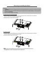
1
FILE NO SERVICE MANUAL LCD TV LCD-32E30A PRODUCT CODE No.: 168234766 CHASSIS NO. : SSA32UT-00 LCD-42E30FA PRODUCT CODE No.: 168234827 CHASSIS NO. : SSA42UT-00 REFERENCE No.: SM0945003-02 CONTENTS 1. Safety precautions .................................................................................................1 2. Alignment instructions and method of software upgrading.....................................5 3. Working principle analysis of the unit ................................................................... 18 4. Block diagram ......................................................................................................19 5. IC block diagram ..................................................................................................21 6. Wiring diagram ...................................................................................................25 7. Troubleshooting guide..........................................................................................29 8. Schematic diagram ..............................................................................................33 APPENDIX-A: Assembly list APPENDIX-B: Exploded View Removing or Installing the Stand Wall mounting instructions Attention: This service manual is only for service personnel to take reference with. Before servicing please read the following points carefully. 1.Safety precautions 1. Instructions Be sure to switch off the power supply before replacing or welding any components or inserting/plugging in connection wire Anti static measures to be taken (throughout the entire production process!): a) Do not touch here and there by hand at will; b) Be sure to use anti static electric iron; c) It’s a must for the welder to wear anti static gloves. Please refer to the detailed list before replacing components that have special safety requirements. Do not change the specs and type at will. 2. Points for attention in servicing of LCD 2.1 Screens are different from one model to another and therefore not interchangeable. Be sure to Use the screen of the original model for replacement. 2.2 The operation voltage of LCD screen is high voltage. Be sure to take proper measures in protecting yourself and the machine when testing the system in the course of normal operation or right after the power is switched off. Please do not touch the circuit or the metal part of the module That is in operation mode. Relevant operation is possible only one minute after the power is switched off. 2.3 Do not use any adapter that is not identical with the TV set. Otherwise it will cause fire or damage to the set. 2.4 Never operate the set or do any installation work in bad environment such as wet bathroom, laundry, kitchen, or nearby fire source, heating equipment and devices or exposure to sunlight etc. Otherwise bad effect will result. 2.5 If any foreign substance such as water, liquid, metal slices or other matters happens to fall into the module, be sure to cut the power off immediately and do not move anything on the module lest it should cause fire or electric shock due to contact with the high voltage or short circuit. 2.6 Should there be smoke, abnormal smell or sound from the module, please shut the power off at once. Likewise, if the screen is not working after the power is on or in the course of operation, the power must be cut off immediately and no more operation is allowed under the same condition. 2.7 Do not pull out or plug in the connection wire when the module is in operation or just after the power is off because in this case relatively high voltage still remains in the capacitor of the driving circuit. Please wait at least one minute before the pulling out or plugging in the connection wire. 2.8 When operating or installing LCD please don’t subject the LCD components to bending, twisting or extrusion, collision lest mishap should result. 2.9 As most of the circuitry in LCD TV set is composed of CMOS integrated circuits, it’s necessary to pay attention to anti statics. Before servicing LCD TV make sure to take anti static measure and ensure full grounding for all the parts that have to be grounded. 2.10 There are lots of connection wires between parts behind the LCD screen. When servicing or moving the set please take care not to touch or scratch them. Once they are damaged the screen would be unable to work and no way to get it repaired. If the connection wires, connections or components fixed by the thermo tropic glue need to disengage when service, please soak the thermo tropic glue into the alcohol and then pull them out in case of damage. 3 2.11 Special care must be taken in transporting or handling it. Exquisite shock vibration may lead to breakage of screen glass or damage to driving circuit. Therefore it must be packed in a strong case before the transportation or handling. 2.12 For the storage make sure to put it in a place where the environment can be controlled so as to prevent the temperature and humidity from exceeding the limits as specified in the manual. For prolonged storage, it is necessary to house it in an anti-moisture bag and put them altogether in one place. The ambient conditions are tabulated as follows: Temperature Humidity Scope for operation 5 ~+ 35 oC Scope for storage 0 ~+ 40oC Scope for operation 0% ~ 90 % Scope for storage 0% ~ 90% 2.13 Display of a fixed picture for a long time may result in appearance of picture residue on the screen, as commonly called “ghost shadow”. The extent of the residual picture varies with the maker of LCD screen. This phenomenon doesn’t represent failure. This “ghost shadow” may remain in the picture for a period of time (several minutes). But when operating it please avoid displaying still picture in high brightness for a long time. 3. Points for attention during installation 3.1 The front panel of LCD screen is of glass. When installing it please make sure to put it in place. 3.2 For service or installation it’s necessary to use specified screw lest it should damage the screen. 3.3 Be sure to take anti dust measures. Any foreign substance that happens to fall down between the screen and the glass will affect the receiving and viewing effect 3.4 When dismantling or mounting the protective partition plate that is used for anti vibration and insulation please take care to keep it in intactness so as to avoid hidden trouble. 3.5 Be sure to protect the cabinet from damage or scratch during service, dismantling or mounting. 4 2.Alignment instructions 1. Test equipment VG-848 (YPbPr, VGA signal generator) VG-849 (HDMI signal generator) FLUKE 54200(TV signal generator) CA210 (white balancer) 2. Power test Connect main board, power board and IR board according the wiring diagram, connect the power and press power key (Remote controller or Keypad) button to turn on the TV. a) Test the pin voltage of P802/power board , the data is shown in table1: Table1 voltage data of P802 For 32” & 42” P802 Voltage Pin1,2 GND Pin3,4 Pin5,6,7 22.8-25.2V GND Pin8,9 11.4-12.6V Pin10,11,12 Pin13 Pin14 Pin15 Pin16 4.75-5.25V On:2V-5.5V Off: 0-0.5V <0.6V 2-5V 2.5-5V PWM b) Test the pin voltage of P803/power board, the data is shown in table2: Table2 voltage data of P803 For 32” & 42” P803 Pin1,2,3,4,5 Pin6,7,8,9,10 Pin11 Pin12 Pin13 Pin14 Voltage 22.8-25.2V GND NC 2.5V-5V 2.5-5V PWM NC 5 3. Alignment flow-chart The alignment flow-chart is shown as fig-1 Check if DDC, HDCP KEY, FLASH are written Combined test for general assembly White balance adjustment Connect to the center signal source and check each Function of TV (station leaking, analog control, etc.) Check the output of earphone and speaker. Input AV/SVIDEO signal and check the function Input HD signal and check the function of YPbPr Input VGA signal and check if the display is normal, check the function (analog control), horizontal/vertical center, etc. Input HDMI signal and check if the display is normal, check the function (analog control), horizontal/vertical center, etc. Preset ex-factory Check the accessories and packing Fig-1 adjustment flow-chart 6 4. Adjustment instruction At any input source then press the “LEFT” key, “BACK” key and “OK” key orderly by the remote control to enter factory mode. During Factory menu, if “MENU” (First layer) or “BACK” key is pushed, system will exit factory mode. 4-1. Source Calibration 4-1.1. Set the signal generator to input sources Video3 on LCD-TV; ASTRO-859 signal setting to1080i (PG1 mode Timing 972 and Pattern 969 Color Bar.) 4-1.2. Entering into factory Mode: Press up or down key of remote control to select “Source Calibration”, Press 䇸RIGHT䇹 key to enter the item. -> Source calibration performed automatically when finished that will show OK. Repeat step 2 to do VGA input sources, ASTRO-859 signal setting to1024X768 60Hz. (PG1 mode: Timing 856 and Pattern 921 Gray.) 7 Repeat step 2 to do TV input sources of Video1 (Composite-AV): ASTRO-859 signal is set to Timing 969 PAL system and Pattern 969 color bar. 4-2. Color Temperature Adjustment & Check 4-2.1. Set the signal generator to RGB, 1024*768, 60HZ (ASTRO-859: PG1 856), Level: 0.56V (80%). Full white pattern. 4-2.2. Press up or down key of remote control to select “Cool”, Press 䇸OK䇹 key to enter the item. R, G, B drive values are set for COOL, Medium(Normal), and WARM independently. 4-2.3. Select 䇸Cool䇹 Cool spec. x= 0.267±0.010 y= 0.271±0.010 If the x and y value are larger than specification, Decrease Green drive from default value. Increase Blue drive from default value. If the x or y or both x and y value is/are smaller than specification. Decrease Blue drive from default value According to a x and y value, please following adjustment of 1 or 2. 1 If x value is higher than spec Increase Green drive from default value. Increase Blue drive from default value. 2 If y value is higher than spec, Decrease Green drive from default value 4-2.4. Select [Medium---Normal] Normal spec. x=0.281±0.010 y=0.288±0.010 Adjust G drive (GREEN) or B drive (BLUE) to set x and y above. 4-2.5. Select [Warm] WARM spec. x=0.301±0.010 y=0.310±0.010 Adjust G drive (GREEN) or B drive (BLUE) to set x and y above. 4-2.6 Exit Factory Mode: After finish adjusting color temperature, press [BACK] to exit factory mode. 8 5. Items of Factory menu Vendor may customize design and add adjustment items Factory menu as far as all required items are included. Press up and down key can move high light item from Color Temperature – WARM -> Color Temperature – Medium -> Color Temperature – Cool -> Timer Clear -> Preset Channel -> NVRAM Clear -> Full Power -> Source Calibration -> Reset to Default -> RF Burn In -> RF F/W Upgrade -> MCU Burn In -> USB F/W Upgrade. The NVRAM Clear and Reset to Default items will have a check dialog “yes or no” to do or not. Push “OK” key can select high light item function. (Press right key can adjust value) Display model name, firmware version and released date on bottom 5-1) Cool Press up or down key can select high light item function. Press OK key to enter the item. Following data for color temp shall be edited manually. -R, G, B data for each preset. -Press “Up” or “Down” key to select “R”, “G”, “B” item -Press “Left” or “Right” key to set the “R”, “G”, “B” value. - Press “MENU” or “BACK” item to exit to factory mode 5-2) Warm Press up or down key can select high light item function. Press OK key to enter the item. Following data for color temp shall be edited manually. -R, G, B data for each preset. -Press “Up” or “Down” key to select “R”, “G”, “B” item -Press “Left” or “Right” key to set the “R”, “G”, “B” value. - Press “MENU” or “BACK” item to exit to factory mode 9 5-3) Normal (Normal) Press up or down key can select high light item function. Press OK key to enter the item. Following data for color temp shall be edited manually. -R, G, B data for each preset. -Press “Up” or “Down” key to select “R”, “G”, “B” item -Press “Left” or “Right” key to set the “R”, “G”, “B” value. -Press “MENU” or “BACK” item to exit to factory mode 5-4) Timer Clear Press up or down key can select high light item function. Press Right key to enter the item. Reset the timer which records hours of LCD panel burn in. 5-5) Preset Channel Press up or down key can select high light item function. Press Right key to enter the item. The system will be loaded preset channel for production line. - ATV(Analog TV), DTV(Digital TV) 5-6) NVRAM Clear Initialize program’s default values to NVRAM for following adjustment items accuracy. In factory mode it is the first and important step to make sure all values are default value and correct. - Reset settings: Gamma table, Channel table (Favorite channel, Channel label etc.), Model table (H/V Position, Clock, Phase), Source dependent setting (Contrast, Brightness etc.), Common setting (Volume, Language etc.), Parental Control (Rating, Password etc). To avoid a mistake initial process after factory setting is done. This item will have a check dialog “yes or no” to do the initial or not. NOTICE: After this item is processed then needs to be DC powered on/off. 5-7) Full power This is for power consumption testing. To measure the maximum power consumption of TV set, we adjust the value of following items to maximum. - Contrast - Brightness - Audio output 5-8) Source Calibration Auto Calibration (gain/offset) must be adjusted color by firmware automatic adjustment in PC, Video1 (Composite) and Video3 input source. 5-9) Reset to Default Reset all settings of OSD menu to default value and will go to standby mode. - Reset settings: Channel table, Model table (H/V Position, Clock, Phase), Source dependent setting (Contrast, Brightness etc.), Common setting (Volume, Language etc.) 5-10) RF Burn In RF (ANT) no signal input, use “snow” pattern for burn in. 5-11) RF F/W Upgrade Press Right key to enter the item. To avoid a mistake F/W Upgrade process after factory setting is done. This item will have a check dialog “yes or no” to do the upgrade or not. 10 5-12) MCU Burn In Press Right key to enter the item. To avoid a mistake MCU Upgrade process after factory setting is done. This item will have a check dialog “yes or no” to do the upgrade or not. 5-13) USB F/W Upgrade Press Right key to enter the item. The function can be switched On/Off the update of the boot code And the F/W can be updated on USB by pressing Right key. 6. Dealer Mode Function 11 12 7. Performance check 7-1 TV function Connect RF to the center signal source, enter Channel menu ĺ auto tuning, check if there are channels be skipped, check if the picture and speaker are normal. 7-2 AV/S-Video terminals Input AV/S-Video signal, check if the picture and sound are normal. 7-3 YPbPr/YCbCr terminal Input YUV signal (VG848 signal generator), separately input the YUV signals listed in table4 and check if the display and sound are normal at any situation (power on, channel switch and format convert, etc.) Table4 YUV signal format 7-4 VGA terminal Input VGA signal (VG848 signal generator), separately input the signals listed in table5 and check the display and sound. If the image is deflection of the Horizontal and vertical, select Menu->Setup->Auto Adjust to perform autocorrect. Table5 VGA signal format 13 7-5 HDMI terminal Input HDMI signal (VG849 signal generator), separately input the signals listed in table4 and table5 and check the display and sound (32 KHz, 44.1 KHz, 48 KHz) at any situation (power on, channel switch and format convert, etc.) 7-6 other functions check a) Check the turn on/turn off timer, sleep timer, picture/sound mode, OSD, stereo and analog TV Teletext, etc. 8. Software instruction (1) USB-RS232 Tool and RS-232 male to female cable Follow below connecter function with PC and LCD TV. (2) To connect the RS-232 cable male terminal to TV set RS-232 service port. (3) To select “Setup” function to set the environment. 14 (4) Setting the Baud Rate to “115200” and select the update firmware file and press “OK” button. (5) To select “down” pattern that will show the “waiting for ping” message, then you can turn on the power by pressing “DC Power on” button. (6) When you find below message, please waiting for the F/W updating. 15 (7) When the update is finished that will show the “Close” pattern, please press the button to close the tool of the RS232. 9. SSU F/W Upgrade method (DTV Only) 16 17 Working principle analysis of the unit 1. PAL and DVB-T signals flow: Antenna reception, B/G, I, D/K, DVB-T” signal will be send to tuner FQD1116ME, t h e n T u n e r w i l l b e demodulating and output standard video signal TV-CVBS, DVB-T and sound IF signal (SIF). TV-CVBS will send to the master control IC ZR39670HGCF to video decode, de-interlace and scaler, then output LVDS level drive for panel display. DVB-T will be fed into WJE6353, after OFDM demodulator, the digital signal will be transform into MPEG transport stream out by DVB-T COFDM Terrestrial IC and sent to scaler IC ZR39670HGCF processing, then output LVDS level drive for panel display. The sound IF (SIF) will be fed into MSP4410K, after demodulating, pre-amplifying, bass adjusting and volume control, the sound signal will b e t r a n s f o r m i n t o d i g i t a l I 2 S s i g n a l b y Sound Processor I C and sent to digital amplifier TAS5706 amplifying, then sent to speaker. About Earphone output, MSP4410K will be sent analog signal to earphone amplifier TPA6110 then output to Earphone. 2. AV/SV signal flow SV signal and the Video1 path AV signal switch by menu “Setup”->“AV Connecting”->”Video1 input” via terminal socket, the signal and the Video2 path AV signal will be fed to ZR39670HGCF to perform video decode, de-interlace and scaler, then output LVDS drive level for panel display. Audio signal from AV/SV terminal via matched resistance is fed to MSP4410K to bass adjust and volume control, the sound signal will be transform into digital I2S signal by Sound Processor IC and sent to digital amplifier TAS5706 amplifying, then sent to speaker. About Earphone output, MSP4410K will be sent analog signal to earphone amplifier TPA6110 then output to Earphone. 3. PC/YPrPb signal flow PC and the Video3 path YPbPr signal are via terminal sent to ZR39670HGCF A/D conversion, output R/G/B of 24 bit to back end module to digital decode, image scale, then send to LVDS level drive for panel display. Sound signal of PC/YPrPb t e r m i n a l via matched resistance a n d sent to MSP4410K to bass adjust and volume control, the sound signal will be transform into digital I2S signal by Sound Processor IC and sent to digital amplifier TAS5706 amplifying, then sent to speaker. About Earphone output, MSP4410K will be sent analog signal to earphone amplifier TPA6110 then output to Earphone. 4. HDMI signal flow Three HDMI video signals via switcher Sil9185 are directly fed to the master control IC ZR39670HGCF to digital decode, image scale, then output LVDS drive level for panel display. HDMI audio signal via decoder built-in ZR39670HGCF is transform into digital I2S signal by scaler IC, and sent to MSP4410K to bass adjust and volume control, the sound signal will sent to digital amplifier TAS5706 amplifying, then sent to speaker. About Earphone output, MSP4410K will be sent analog signal to earphone amplifier TPA6110 then output to Earphone. 18 I. Block Diagram 19 Sanyo 32”/42” Block Diagram III. ͦ· ͣ͢ · ͣͥ · Β ΦΕ ͔ ΐ Ͳ ʹ ͵ ͝ ͑ ͔ ΐ Ρ Π Ψ Σ ͝ ͔͑ ΐ Κ Χ Ζ ΣΥ Ζ Σ ͝ ͔͑ ΐ Ε Κ Ξ Ξ Ζ Σ ͩ ͡ ͣ ͙΅ Π ͑ Ξ Β Κ Ο ͑ Γ Π Β Σ Ε ͚ ͞ ͞ ͞ ͞ ͞ ͣ ͥ · ΚΟ Χ ͞ ͑ ͔ ΐ Κ Χ Ζ Σ ΥΖ Σ͝ ͑ ͔ ΐ Ε Κ Ξ Ξ Ζ Σ 20 ͩ ͡ ͤ ͙ ΅ Π ͑ ΚΟ Χ Ζ Σ Υ Ζ Σ ͑ Γ Π Β Σ Ε ͚ ͔ ΐ Ε ΚΞ Ξ Ζ Σ ͔ ΐ Ε ΚΞ Ξ Ζ Σ ΄ͣ ͵ʹ͞͵ʹ ͷ ΝΪ Γ Β Δ Μ ͔ ΐ Κ Ο Χ Ζ Σ ΥΖ Σ · ΒΦΩ ΄͢ ͵ʹ͞͵ʹ Β ΝΗ ͞ Γ Σ ΚΕ Θ Ζ ͔ ΐ Κ Ο Χ Ζ ΣΥ Ζ Σ ͔ ΐΡ Π ΨΖ Σ ͔ΐͲʹ ͵ ͳ ΣΠ Ψ Ο Π Φ Υ ͷʹ ͩ͢͡ II. Block diagram-POWER-32”/42” ͦ͜ · Δ Δ ͜͢ ͣ · ΔΔ ͣ͜ ͥ · ΒΦ Ε ͣ͜ ͥ · ΚΟΧ IC block diagram 1. Zoran ZR39670 Feature: Embedded High Performance 300MIPS CPU z z z z z Integrated MIPS 4KEcTM CPU, 300MHz Intended to run RTOS, audio decode and Application software 32-bit MIPS32 enhanced architecture 8 K instruction cache, 8 K data cache, (2-way set associative) MMU with 16-dual entry (TLB) z z z Two Independent instances of the PHY Support for HDMI v1.3 Integrated Secure HDCP Keys z z z Three YPbPr inputs (Two SCART)(Up to 1080p) One RGB input (Up to WUXGA) Up to 165 MHz input bandwidth z Support for a single MP@HL decoder Integrated HDMI Link and PHY Integrated HD ADC High-Performance MPEG-2 Video Decoding Engine Integrated Dual Channel LVDS Output for direct Panel Display support z Supports up to 165MHz z 1080p Output Flat Panel Support z 100/120 Hz Operation with 768p panels z 6, 8, 10 and 12-bit panel support Integrated NTSC/PAL/SECAM Decoder SCART Support z Fast Blank/Fast switch inputs z Video DAC for CVBS output Display Processor & Controller z PIP operation with Digital/Analog PIP z z z z z Two 2-signal UARTs Three I2C master or Slave interfaces (up to 400 kb/s) One IR Receive, with hard N are demodulation Guest bus interface SPI interface z 128-bit device unique secret key z z High performance 32-bit DDR2 interface (400MHz) Up to 3.2GByte/second peak memory throughput z 80 nm CMOS z 1.1 V core voltage 1.8 V Memory I/F, 3.3 V I/O z z 35 mm x 35 mm Plastic Ball Grid Array package 632 BGA Common Interface (CI) Integrated USB 1.1 Interface System Interfaces Device Unique Chip ID Memory Interface Unit Process Technology Power Packaging 21 2. FQD1116ME DVB-T/Analog hybrid terrestrial video module 3. WJE6353 Nordig Unified DVB-T COFDM Terrestrial Demodulator for PC-TV and Hand-held Digital TV (DTV) 22 4. TAS5706 20-W Stereo Digital Audio Power Amplifier with EQ and DRC 5. SiI9185 3:1 HDMI 1.3 Switch 23 6. TPA6110A2 150-mW STEREO AUDIO POWER AMPLIFIER 7. MSP4410K Multi-standard Sound Processor 24 I. BLOCK 25 Sanyo 32-inch Wiring Diagram II. Wiring Connection 26 III. BLOCK 27 Sanyo 42-inch Wiring Diagram IV. Wiring Connection 28 Trouble shooting 1. Fault clearance 29 2. Troubleshooting guide The flow chart shown below will help you to troubleshoot your Televison set with it doesn’t display normally. Each procedure offers a simple way to check for system errors. Before starting, ensure that there is a signal in and that the Televison is turned on. 2-1 Power LED no light Power LED no Light Check L21 +5V_IN NG Change to new power board. P/N : PK101V1100I ( SSA32UT-00) /or PK101V1180I P/N : PK101V1110I (SSA42UG-00) OK Check CN2 Pin 2 Change MAIN PCB L H Check LED Change LED PCB NG 30 2-2 Has audio but no video out Change to new power board. P/N : PK101V1100I ( SSA32UT-00) /or PK101V1180I P/N : PK101V1110I (SSA42UG-00) 2-3 Has video but no audio out step 1 31 2-4 Has video but no audio out step 2 Change to new power board. P/N : PK101V1100I ( SSA32UT-00) /or PK101V1180I P/N : PK101V1110I (SSA42UG-00) 32 ELECTRON-32"/42" SCHEMATIC DIAGRAM 16 15 14 12 13 11 10 9 1 2 3 4 5 6 7 8 Item 5 HDMI1 HDMI2 HDMI3 Video1 Video2 Video3 Video O/P PC PC Audio Input RS232 Digital Audio Output ANT Headphone Power Supply 453C0830L01 VTV-P1903 PK101V1090I FSP123-4F01 PK101V1100I FSP138-4F01 PK101V1110I FSP226-4F01 PK101V1110I FSP226-4F01 Location/Circuits 4 JP304 (SPDIF O/P Terminal) JP201 (USB Terminal) JP101 JP701 U304 (Video filter Circuit ) JP302 JP309 JP307 SSA19U 3 SSA42U Panel M185XW01(V0)-CC 18.5"A T /AU T260XW02(VQ)-RR 26"A+ T /AU T315XW02(VS)-RR 32"A+ T /AU LC420WUN-SBA1 42"A G /LGS T420HW04-V2 3 Model SSA26U SSA32U Input Terminal difference of Model PCBA No. 451C1730L32 451C1730L12 451C1730L22 451C1730L02 451C1730L02 4 JP401 JP402 JP403 JP301 (Composite/S-Video) JP308 (Side I/O) JP306A (Component) JP306B (ATV O/P) JP305 Sanyo Model LCD-19E30A LCD-26E30A LCD-32E30A LCD-42E30A LCD-42E30A Terminal 5 PDF created with FinePrint pdfFactory Pro trial version http://www.softwarelabs.com A B C D Note : Compal Model SSA19UTA SSA26UTA SSA32UTA SSA42UGA SSA42UTA 2 2 Date: Size B Title A B C D Tuesday, September 01, 2009 401C17 Document Number 1 Sheet 2 SCHEMATIC, M/B VTV-L42008 of 18 Rev 1A COMPAL OPTOELECTRONICS CO., LTD 1 GND_POWER C501 0.1uF C502 0.1uF close scale 51 R508 S1_VREF S1_UDM S1_LDM S1_DQ15 S1_DQ14 S1_DQ13 S1_DQ12 S1_DQ11 S1_DQ10 S1_DQ9 S1_DQ8 S1_DQ7 S1_DQ6 S1_DQ5 S1_DQ4 S1_DQ3 S1_DQ2 S1_DQ1 S1_DQ0 close scale S0_VREF R509 300 A25 A26 B26 R26 L26 K26 F25 M26 E26 N25 L25 H25 M25 F26 E25 N26 D25 P26 K25 J26 P25 D26 A24 A20 A19 S0_UDM S0_LDM 5 G_ZR670 G_ZR670 G_ZR670 R507 27 C507 0.1uF C505 0.1uF 20090402 from 100 change to 91 G_ZR670 R505 91 R504 100 VCC1_8 20090402 from 100 change to 91 GND G_ZR670 G_PWR R503 91 R502 100 VCC1_8 B15 A21 A14 B22 B20 B17 B21 A15 B14 A22 B13 A23 B19 A18 B23 A13 S0_DQ15 S0_DQ14 S0_DQ13 S0_DQ12 S0_DQ11 S0_DQ10 S0_DQ9 S0_DQ8 S0_DQ7 S0_DQ6 S0_DQ5 S0_DQ4 S0_DQ3 S0_DQ2 S0_DQ1 S0_DQ0 S0_ODT S0_CKN S0_CK S0_CKE S0_RASN S0_CASN S0_WEN S0_UDQSN S0_UDQS S0_LDQSN S0_LDQS S0_A13 S0_A12 S0_A11 S0_A10 S0_A9 S0_A8 S0_A7 S0_A6 S0_A5 S0_A4 S0_A3 S0_A2 S0_A1 S0_A0 S0_BA2 S0_BA1 S0_BA0 ZR39670_A_6 RTERM RDRIVER50 RDRIVER S1_VREF S1_UDM S1_LDM S1_DQ15 S1_DQ14 S1_DQ13 S1_DQ12 S1_DQ11 S1_DQ10 S1_DQ9 S1_DQ8 S1_DQ7 S1_DQ6 S1_DQ5 S1_DQ4 S1_DQ3 S1_DQ2 S1_DQ1 S1_DQ0 S1_ODT S1_CKN S1_CK S1_CKE S1_RASN S1_CASN S1_WEN S1_UDQSN S1_UDQS S1_LDQSN S1_LDQS S1_A13 S1_A12 S1_A11 S1_A10 S1_A9 S1_A8 S1_A7 S1_A6 S1_A5 S1_A4 S1_A3 S1_A2 S1_A1 S1_A0 S1_BA2 S1_BA1 S1_BA0 S1 Memory I/F U201B ZR39670_A_6 S0_VREF S0_UDM S0_LDM S0_DQ15 S0_DQ14 S0_DQ13 S0_DQ12 S0_DQ11 S0_DQ10 S0_DQ9 S0_DQ8 S0_DQ7 S0_DQ6 S0_DQ5 S0_DQ4 S0_DQ3 S0_DQ2 S0_DQ1 S0_DQ0 S0 Memory I/F U201A 4 R501 100 G_ZR670 D24 C26 C25 M24 G23 G24 L23 G25 G26 H26 J25 E24 R24 J24 N23 J23 E23 P23 H23 K24 F24 P24 H24 K23 F23 N24 L24 M23 100 DDR II SDRAM I/F G_ZR670 K8 J8 K2 L8 S1_CKN S1_CK S1_CKE R506 K7 L7 K3 A8 B7 E8 F7 R2 P7 M2 P3 P8 P2 N7 N3 N8 N2 M7 M3 M8 L1 L3 L2 S1_RASN S1_CASN S1_WEN S1_UDQSN S1_UDQS S1_LDQSN S1_LDQS S1_A12 S1_A11 S1_A10 S1_A9 S1_A8 S1_A7 S1_A6 S1_A5 S1_A4 S1_A3 S1_A2 S1_A1 S1_A0 S1_BA2 S1_BA1 S1_BA0 S1_DQ[15..0] K8 J8 K2 L8 S0_CKN S0_CK S0_CKE A12 B12 C21 C13 K7 L7 K3 A8 B7 E8 F7 R2 P7 M2 P3 P8 P2 N7 N3 N8 N2 M7 M3 M8 L1 L3 L2 D16 C16 D20 S0_UDQSN S0_UDQS S0_LDQSN S0_LDQS S0_A12 S0_A11 S0_A10 S0_A9 S0_A8 S0_A7 S0_A6 S0_A5 S0_A4 S0_A3 S0_A2 S0_A1 S0_A0 S0_BA2 S0_BA1 S0_BA0 S0_DQ[15..0] S0_RASN S0_CASN S0_WEN B16 A16 A17 B18 C14 C24 C18 D22 D18 D14 D23 D17 C19 C15 C23 C17 D19 D15 C22 C20 D21 4 ODT ODT V59C1512164QCF25A CK CK CKE CS RAS CAS WE UDM LDM DQ15 DQ14 DQ13 DQ12 DQ11 DQ10 DQ9 DQ8 DQ7 DQ6 DQ5 DQ4 DQ3 DQ2 DQ1 DQ0 VREF DDR II UDQS UDQS LDQS LDQS A12 A11 A10 A9 A8 A7 A6 A5 A4 A3 A2 A1 A0 NC3 BA1 BA0 U502A V59C1512164QCF25A CK CK CKE CS RAS CAS WE UDM LDM DQ15 DQ14 DQ13 DQ12 DQ11 DQ10 DQ9 DQ8 DQ7 DQ6 DQ5 DQ4 DQ3 DQ2 DQ1 DQ0 VREF DDR II UDQS UDQS LDQS LDQS A12 A11 A10 A9 A8 A7 A6 A5 A4 A3 A2 A1 A0 NC3 BA1 BA0 U501A K9 J2 B3 F3 B9 B1 D9 D1 D3 D7 C2 C8 F9 F1 H9 H1 H3 H7 G2 G8 K9 J2 B3 F3 B9 B1 D9 D1 D3 D7 C2 C8 F9 F1 H9 H1 H3 H7 G2 G8 3 3 close DDR S1_VREF S1_UDM S1_LDM S1_DQ15 S1_DQ14 S1_DQ13 S1_DQ12 S1_DQ11 S1_DQ10 S1_DQ9 S1_DQ8 S1_DQ7 S1_DQ6 S1_DQ5 S1_DQ4 S1_DQ3 S1_DQ2 S1_DQ1 S1_DQ0 close DDR S0_VREF S0_UDM S0_LDM S0_DQ15 S0_DQ14 S0_DQ13 S0_DQ12 S0_DQ11 S0_DQ10 S0_DQ9 S0_DQ8 S0_DQ7 S0_DQ6 S0_DQ5 S0_DQ4 S0_DQ3 S0_DQ2 S0_DQ1 S0_DQ0 PDF created with FinePrint pdfFactory Pro trial version http://www.softwarelabs.com A B C D 5 G_ZR670 C508 0.1uF C506 0.1uF VCC1_8 G_ZR670 C504 0.1uF C503 0.1uF VCC1_8 VCC1_8 VCC1_8 A2 E2 A9 C1 C3 C7 C9 E9 G1 G3 G7 G9 A1 E1 J9 M9 R1 J1 A2 E2 A9 C1 C3 C7 C9 E9 G1 G3 G7 G9 A1 E1 J9 M9 R1 J1 NC4 NC5 NC6 NC4 NC5 NC6 2 V59C1512164QCF25A NC1 NC2 VSSQ VSSQ VSSQ VSSQ VSSQ VSSQ VSSQ VSSQ VSSQ VSSQ VSS VSS VSS VSS VSS VSSDL DDR II VDDQ VDDQ VDDQ VDDQ VDDQ VDDQ VDDQ VDDQ VDDQ VDDQ VDD VDD VDD VDD VDD VDDL U502B V59C1512164QCF25A NC1 NC2 VSSQ VSSQ VSSQ VSSQ VSSQ VSSQ VSSQ VSSQ VSSQ VSSQ VSS VSS VSS VSS VSS VSSDL DDR II VDDQ VDDQ VDDQ VDDQ VDDQ VDDQ VDDQ VDDQ VDDQ VDDQ VDD VDD VDD VDD VDD VDDL U501B R3 R7 R8 A7 B2 B8 D2 D8 E7 F2 F8 H2 H8 A3 E3 J3 N1 P9 J7 R3 R7 R8 A7 B2 B8 D2 D8 E7 F2 F8 H2 H8 A3 E3 J3 N1 P9 J7 Note: The DDR II layout will also accomodate 1M bit devices, expanding the memory footprint from 128M byte to 256M byte. 2 BP2 BP7 U502 BP9 C530 0.1uF BP3 C526 0.1uF G_ZR670 C547 2200pF VCC1_8 BP7 Thursday, August 20, 2009 401C17 Size Document Number Custom Date: BP10 C520 0.1uF BP4 C515 0.1uF BP11 C518 0.1uF BP5 C512 0.1uF 0.1uF C522 C537 C538 82pF 0.1uF 0.1uF 0.1uF G_ZR670 BP12 C521 0.1uF G_ZR670 C513 C539 C540 C516 0.1uF 0.1uF 0.1uF 0.1uF BP6 C543 82pF C536 C545 0.1uF C535 A B C D 1 Sheet 3 of 18 Rev 1A COMPAL OPTOELECTRONICS CO., LTD BP9 C517 0.1uF BP3 C514 0.1uF G_ZR670 0.1uF C532 C534 0.1uF 0.1uF 0.1uF G_ZR670 BP12 C523 0.1uF BP6 C528 0.1uF C509 C533 SCHEMATIC, M/B VTV-L42008 BP8 C519 0.1uF BP2 C511 0.1uF Title 82pF C548 C549 2200pF BP1 C546 82pF BP11 C510 0.1uF BP5 C527 0.1uF Bypass Caps BP10 C531 0.1uF BP4 C524 0.1uF Add C542~C549 From DDR II 2/19 BP8 C529 0.1uF C544 2200pF BP1 C525 0.1uF Bypass Caps C542 2200pF U501 G_ZR670 VCC1_8 1 ZR39670_A_6 5 Crystal Y1 15ppm 20C• 30ppm 0-70C• CLKOUT CLKIN RESET_n SPI_SEL2 SPI_SEL3 SPI_DO SPI_DI SPI_CLK SPI_SEL0 SPI_SEL1 SPI_HOLD I2C0_C I2C0_D I2C1_C I2C1_D I2C2_C/GADR6 I2C2_D/GADR7 I2C_MORPH__ENA USB0_DN USB0_DP USB_REXT USB_ATEST UART1_TX UART1_RX UART0_TX UART0_RX IRR TAPSEL TAPSEL_CAS 1 TP203 R219 R258 10K R257 4K7 1M RESETN C201 27pF C204 33pF G_ZR670 25MHz/20pF/S/2P Y201 RESETN 47 R229 R285 47 VCC3_3 I2C0CLK I2C0DATA I2C1CLK I2C1DATA 11 12 G_ZR670 USB0DN USB0DP 12 12 R231 9,12 0 R280 G_ZR670 4K7/NC 0/NC R222 4K7 0/NC R281 2 1 0 R202 1K R220 R221 I2C1CLK I2C1DATA L209 4 U205 74LVC1G126 SOT-353 100pF/50V C237 R284 NC/0 4 47 G_ZR670 R282 0.1uF C236 56pF C238 VCC GND /Reset U202 XCLK G_ZR670 11 2 3 1 3 5 7 9 11 13 CN201 3 2 4 6 8 10 12 14 VCC3_3 G_ZR670 Reset Switch 3 G_ZR670 C203 2200pF RESETN R225 1K VCC3_3 AE8 AA9 AC11 AB11 AA11 AA10 AA6 AA5 AB6 AB5 AB8 AA8 AC8 AD8 G_ZR670 HEADER14 2.54mm/NC SW201 B3F-1100/NC Reset Circuit STL8100GCL300 1 R263 0 4K7 4K7 VCC3_3 4K7 4K7 SIO I/F G_ZR670 20090224 del. R264 20090119 R263 NC to 0R, VCC3_3 R218 I2C0DATA VCC3_3 R217 VCC3_3 C202 0.1uF G_ZR670 I2C0CLK 4 8 VCC3_3 R203 4K7 Vcc R204 1K 47 R201 1K GND W25Q64BV DIO DO CLK CS WP HOLD SPI FLASH 64M bit U203 R212 EJTCK R207 R205 4K7 KC FBMA-L11-160808-300LMA10T G_ZR670 R283 5 2 6 1 3 7 0 SPI_WR SPI_RD SPI_CLK SPI_CS_n SPI_WEN SPI_HOLD RESETN EJTDI EJTDO EJTMS TRSTN SPI_HOLD SPI_WR SPI_RD SPI_CLK SPI_CS_n 17 17 17 R230 47 R224 4K7 5,17 VCC3_3 VCC3_3 5,17 6,9 6,9 0 0 UART1TX UART1RX SPI_WEN VCC3_3 4K7 R206 1/29 R259 10K 4K7 NC R227 R245 IRR G_ZR670 3K4_1% 10 R211 R210 VCC3_3 modify R213 from 10K to 100 3/13 R228 G_ZR670 R233 100 U25 U26 V24 AA24 AB24 Y24 W25 Y25 W24 W26 Y26 4K7 R232 UART0TX UART0RX R256 4K7 R213 AF12 AE12 AE13 AF13 AF14 AE14 AA14 R223 D5 E5 D3 D4 P22 N22 L22 M22 R22 E13 D13 EJTCK TRSTN 1 2 E16 E14 E18 E15 E17 2 EJTAG I/F 1 2 TRST TDI TDO TMS TCK 1 VCC3_3 1 2 PDF created with FinePrint pdfFactory Pro trial version http://www.softwarelabs.com A B C SIO I/F 1 2 D U201C 5 3 1 2 4 AFE & GPIO D207 1N4148 5V R251 R261 R252 R262 GPIO_P20 GPIO_P21 GPIO_P22 GPIO_P23 GPIO_P24 GPIO_P0 GPIO_P1 GPIO_P2 GPIO_P3 GPIO_P4 GPIO_P5 GPIO_P6 GPIO_P7 C233 0.1uF C230 0.1uF B2 A2 A3 B3 C3 USB0DN USB0DP AMP_PDN 9 DDCP 5,8 HP_DET 9 DCR/BRT_EN 10 R208 4K7 VCC3_3 4K7 4K7/NC 16 5 2 11 10 12 9 4 0/NC R254 VCC C2V+ T1IN T2IN R1OUT R2OUT C2+ 5V R286 R287 15 3 6 14 7 13 8 1 D209 D208 F201 1206L035-C/NC Reserve GND C1V- T1OUT T2OUT R1IN R2IN C+ 232 XCVR U204 0/NC R253 Stuff Option SP232ACN C239 47uF/16V 2 R216 R214 R209 4K7 Bootstrap Configuration R215 4K7 Date: Q207 VBUS DD+ GND Shield Shield Shield Shield B G_ZR670 PG A B C D Tuesday, September 01, 2009 401C17 1 Sheet 4 SCHEMATIC, M/B VTV-L42008 of 18 Rev 1A COMPAL OPTOELECTRONICS CO., LTD DB9H105-F 1 6 2 7 3 8 4 9 5 JP309 4.7K R266 Add R265 R266 Q207 10/2 G_ZR670 MMBT3904L JP201 Size Document Number Custom Title 1 2 3 4 5 6 7 8 VCC3_3 1 R265 4.7K 5,6,9,17 11 TYCO R/A FLAG USB/NC USB TU_RST GPIO1 G_ZR670 USB0_VCC ISP_RX 0.1uF/NC C243 G_ZR670 C234 0.1uF C232 0.1uF ISP_TX RS_RX RS_TX PANEL_PWR_EN 16 SV_DET 7 LCD_ON 16 G_ZR670 G_ZR670 G_ZR670 AMP_PMUTE 9 GPIO1 GPIO2 GPIO3 2 G_ZR670 0 0 0 0 4K7 R226 E11 D11 C11 B11 A11 E12 D12 C12 Note: Place near connector, and use layout from datasheet. UART0TX UART1RX UART0RX UART1TX ZR39670_A_6 AFE_DINCLK IF_DVAL AFE_DIN0 AFE_DIN1 AFE_DIN2 AFE_DIN3 AFE_DIN4 AFE_DIN5 AFE_DIN6 AFE_DIN7 AFE_DIN8 AFE_DIN9 AFE_DIN10 AFE_DIN11 U201K C242 C 5 C241 D202 56pF/50V/NC D203 56pF/50V/NC D201 15K/NC D204 15K/NC EZJZ1V80010 (0603)/NC EZJZ1V80010/NC EZJZ1V80010 (0603)/NC D205 EZJZ1V80010/NC EZJZ1V80010 (0603)/NC E EZJZ1V80010 (0603)/NC D206 10 EZJZ1V80010 (0603)/NC 11 EZJZ1V80010 (0603)/NC 9 1 3 SHELL3 SHELL2 HP_DET +5V GND DDC_DATA DDC_CLK SHELL4 NC CE_REMOTE CKCK_SHIELD CK+ D0D0_SHIELD D0+ SHELL5 D1D1_SHIELD D1+ D2D2_SHIELD D2+ SHELL1 SHELL0 JP401 2 19 18 17 16 15 14 13 12 11 10 9 8 7 6 5 4 3 2 1 G_ZR670 JP402 19 18 17 16 15 14 13 12 11 10 9 8 7 6 5 4 3 2 1 D416 BAV70L DDC_PW1 SHELL3 SHELL2 HP_DET +5V GND DDC_DATA DDC_CLK 24 SHELL4 NC CE_REMOTE CKCK_SHIELD CK+ D0D0_SHIELD D0+ 25 SHELL5 D1D1_SHIELD D1+ D2D2_SHIELD D2+ 21 SHELL1 20 SHELL0 23 22 C402 0.1uF G_ZR670 5V G_ZR670 JP403 G_ZR670 G_ZR670 JALCO V/T HDMI 10.5H W/O FLAG 19 18 17 16 15 14 13 12 11 10 9 8 7 6 5 4 3 2 1 D432 BAV70L DDC_PW3 SHELL3 SHELL2 HP_DET +5V GND DDC_DATA DDC_CLK 24 SHELL4 NC CE_REMOTE CKCK_SHIELD CK+ D0D0_SHIELD D0+ 25 SHELL5 D1D1_SHIELD D1+ D2D2_SHIELD D2+ 21 SHELL1 20 SHELL0 23 22 C405 0.1uF G_ZR670 5V CEC G_ZR670 CEC G_ZR670 G_ZR670 20K/NC R416 CH3_HDMI_5V 5 G_ZR670 R411 0 RR0X2+ RR0X1+ RR0X2- RR0X0+ RR0X1- RR0XC+ RR0X0- RR0XC- CH1_CBL_HPD CH1_DDC_SDA CH1_DDC_SCL 20090110 1K change to 0R R402 4.7K 2 2 1 2 1 2 1 1 4.7K R412 G_ZR670 L405 3 ACM2012D-900-2P-T00 4 L406 3 ACM2012D-900-2P-T00 4 L407 3 ACM2012D-900-2P-T00 4 L408 3 ACM2012D-900-2P-T00 4 DDC_PW1 G_ZR670 2 2 1 2 1 2 1 1 G_ZR670 L415 3 ACM2012D-900-2P-T00 4 L416 3 ACM2012D-900-2P-T00 4 L413 3 ACM2012D-900-2P-T00 4 L414 3 ACM2012D-900-2P-T00 4 4.7K R414 G_ZR670 R413 4.7K R422 0 R423 0 20090110 1K change to 0R R427 4.7K 4,8 4 1 2 3 4 VCC WP SCL SDA A0 A1 A2 GND C414 0.1uF 1 2 3 4 C429 3 82pF C418 0.1uF PIN29 C431 HDMI_VDD PIN17 2200pF C417 13 TP402 1 PIN37 C419 0.1uF 18 19 21 22 24 25 RR0XCRR0XC+ RR0X0RR0X0+ RR0X1RR0X1+ 38 39 50 51 DSDA_1 DSCL_1 RR1XCRR1XC+ 36 52 CH2_CBL_HPD CH2_HDMI_5V 27 28 30 31 RR0X2RR0X2+ 16 32 PIN69 4 RR2X2+ RR2X1+ RR2X2- RR2X0+ RR2X1- RR2XC+ RR2X0- RR2XC- CH3_CBL_HPD CH3_DDC_SDA CH3_DDC_SCL RR1X2+ RR1X1+ RR1X2- RR1X0+ RR1X1- DDCP R449 4.7K 47 R434 CH3_DDC_SDA CH3_DDC_SCL CH3_DDC_SCL CH3_DDC_SDA R428 4.7K CH2_DDC_SDA 47 47 VCC WP SCL SDA U404 A0 A1 A2 GND DSDA_2 DSCL_2 24C02AN-10SC-2.7 8 7 6 5 R447 47 R439 R450 4.7K DDC_PW3 DSDA_1 G_ZR670 82pF CEC 20090110 change to NC Sil9185 CEC_D CEC_A R2X2R2X2+ R2X1R2X1+ R2X0R2X0+ R2XCR2XC+ DSDA2 DSCL2 HPD2 RPWR2 R1X2R1X2+ R1X1R1X1+ R1X0R1X0+ R1XCR1XC+ DSDA1 DSCL1 HPD1 RPWR1 R0X2R0X2+ R0X1R0X1+ R0X0R0X0+ R0XCR0XC+ DSDA0 DSCL0 HDMI_VDD SiI9185 G_ZR670 C425 47pF/50V 100/NC R453 G_ZR670 PIN23 2 D404 Z5.6V/NC B6 A6 C6 B7 D7 D6 1 1 1 1 1 TP410 TP409 TP411 TP413 TP412 1 A5 B5 1 1 TP408 TP407 CEC_IN G_ZR670 RESET# LSCL/PSEL1 LSDA/PSEL0 I2CSEL/INT TPWR/I2CADDR HPDIN TSCL TSDA TXCTXC+ TX0TX0+ TX1TX1+ TX2TX2+ ExtSWING 12 13 15 14 35 79 76 78 77 11 10 8 7 5 4 2 1 12 R429 560/1% G_ZR670 2K/NC R442 0 R454 C427 1uF/NC G_ZR670 100K/NC R451 +3.3V_HD G_ZR670 R444 10K/NC HDMI_5V HDMI In 4,6,9,17 Date: TXC+ G_ZR670 R441 10K 1 Tuesday, September 01, 2009 401C17 Sheet 5 SCHEMATIC, M/B VTV-L42008 of 18 Rev 1A COMPAL OPTOELECTRONICS CO., LTD TU_RST 4,17 4,17 TXC3 TX0+ 4 R440 10K/NC +3.3V_HD TX_DSCL TX_DSDA Size Document Number Custom Title 0 0 I2C0CLK I2C0DATA R437 R438 1 L412 ACM2012D-900-2P-T00/NC 2 TX03 TX1+ TX1- TX2+ TX2- 4 3 L409 ACM2012D-900-2P-T00/NC 2 1 L410 ACM2012D-900-2P-T00/NC 2 4 3 4 1 LOW OXC0/OXD0/OXE0 (Default) HIGH OXC4/OXD4/OXE4 1.8K/NC R445 +3.3V_HD R443 10K +3.3V_HD 3.3pF C428 SE100uF/25V 1 1 L411 ACM2012D-900-2P-T00/NC 2 C413 SE10uF/16V +3.3V_HD C412 R446 1.8K/NC HPD0_plug I2C_SEL/INT EXT_SW C411 0.1uF G_ZR670 +1.8V_HD PIN63 82pF C430 ZR39670_A_6 HDMI1_RXATEST HDMI1_REXT HDMI1_5VSENSE HDMI1_CEC HDMI1_SCL HDMI1_SDA HDMI1_HPD HDMI1_CLKP HDMI1_CLKN HDMI1_D0P HDMI1_D0N HDMI1_D1P HDMI1_D1N HDMI1_D2P HDMI1_D2N HDMI I/F U201O C410 0.1uF E8 E7 PIN55 C409 2200pF R421 390_1% TP401 C4 C5 1 1 TP405 TP406 C7 B4 A4 1 1 TP403 TP404 PIN43 C408 0.1uF G_ZR670 R420 4K7 2 G_ZR670 HDMI Port difference of Model Port Number SSA19U SSA26U SSA32U SSA42U Port1 Port2 Port3 53 TP415 67 68 RR2X2RR2X2+ 54 64 65 TP428 61 62 RR2X1RR2X1+ 58 59 RR2X0RR2X0+ 70 71 RR2XCRR2XC+ 56 72 DSDA_2 DSCL_2 CH3_CBL_HPD CH3_HDMI_5V 47 48 13 Sil9185 1.8V 251mA 3.3V 57mA HPD0 RPWR0 U401 C422 0.1uF PIN73 C407 0.1uF DSDA_0 DSCL_0 PIN57 C421 0.1uF G_ZR670 C406 0.1uF ZR39670_A_6 HDMI0_RXATEST HDMI0_REXT HDMI0_5VSENSE CH1_CBL_HPD CH1_HDMI_5V 2200pF C420 PIN49 D10 E10 +1.8V_HD R410 390_1% PIN33 G_ZR670 R409 4K7 D9 44 45 G_ZR670 82pF C426 PIN6 C416 0.1uF 82pF HDMI_5V RR1X2RR1X2+ DSCL_1 24C02AN-10SC-2.7 8 7 6 5 U403 C403 0.1uF 1 2 3 4 G_ZR670 C415 SE10uF/16V +1.8V_HD G_ZR670 0.1uF HPD0_plug HDMI0_CEC HDMI0_SCL HDMI0_SDA HDMI0_HPD HDMI0_CLKP HDMI0_CLKN RR1XC+ RR1X0- R433 DSCL_0 DSDA_0 22uF/10V C424 DDC_PW1 47 R408 47 R403 R425 4.7K A0 A1 A2 GND C423 B10 A10 TXC+ TXC- HDMI0_D0P HDMI0_D0N HDMI0_D1P HDMI0_D1N HDMI0_D2P HDMI0_D2N HDMI I/F U201G 41 42 CH2_DDC_SCL CH2_DDC_SCL CH2_DDC_SDA R424 4.7K VCC WP SCL SDA 24C02AN-10SC-2.7 8 7 6 5 U402 C404 A9 B9 TX0+ TX0- A7 C10 E9 D8 C8 C9 TX1+ TX1- TX_DSCL TX_DSDA B8 A8 R407 2K RR1X1RR1X1+ 4,8 DDCP R426 4.7K CH1_DDC_SDA CH1_DDC_SCL CH1_DDC_SCL CH1_DDC_SDA 4.7K R417 R406 2K TX2+ TX2- R405 2K/NC +3.3V_HD+3.3V_HD+3.3V_HD RR1X0RR1X0+ 4,8 DDCP R418 R419 4.7K 4.7K DDC_PW2 3 RR1XC- CH2_CBL_HPD CH2_DDC_SDA CH2_DDC_SCL 20090110 1K change to 0R DDC_PW3 PORT 3 (for SSA32U; SSA42U) CEC G_ZR670 L402 3 ACM2012D-900-2P-T00 4 L401 3 ACM2012D-900-2P-T00 4 L403 3 ACM2012D-900-2P-T00 4 L404 3 ACM2012D-900-2P-T00 4 4.7K R401 PORT 2 (for SSA26U; SSA32U; SSA42U) 2 2 1 2 1 2 1 1 G_ZR670 20K/NC R415 CH2_HDMI_5V G_ZR670 G_ZR670 HD680_PANTHER_SCH JALCO V/T HDMI 10.5H W/O FLAG G_ZR670 G_ZR670 JALCO V/T HDMI 10.5H W/O FLAG 21 20 25 24 23 22 20K/NC R404 CH1_HDMI_5V DDC_PW2 1 PDF created with FinePrint pdfFactory Pro trial version http://www.softwarelabs.com A B C D G_ZR670 C401 0.1uF D402 BAV70L 2 QV1AA10P-R05 1 1 QV1AA10P-R05 1 D405 2 QV1AA10P-R05 1 D408 2 5V D421 QV1AA10P-R05 2 1 2 QV1AA10P-R05 1 D407 2 D412 QV1AA10P-R05 2 1 D418 QV1AA10P-R05 2 1 D434 QV1AA10P-R05 2 1 D417 QV1AA10P-R05 2 1 QV1AA10P-R05 1 D406 2 PORT 1 (for SSA19U; SSA26U; SSA32U; SSA42U) D422 QV1AA10P-R05 2 1 D403 5 1 2 DDC_PW2 D424 QV1AA10P-R05 2 1 D441 QV1AA10P-R05 2 1 3 3 D419 QV1AA10P-R05 2 1 D433 QV1AA10P-R05 2 1 D435 QV1AA10P-R05 2 1 1 D414 QV1AA10P-R05 2 1 1 2 1 2 1 2 D420 QV1AA10P-R05 2 1 D440 QV1AA10P-R05 2 1 D429 QV1AA10P-R05 2 1 2 D410 QV1AA10P-R05 2 1 1 2 D409 QV1AA10P-R05 2 1 2 D413 QV1AA10P-R05 2 1 D423 QV1AA10P-R05 2 1 D431 QV1AA10P-R05 2 1 D436 QV1AA10P-R05 2 1 D415 QV1AA10P-R05 2 1 D426 QV1AA10P-R05 2 1 D430 QV1AA10P-R05 2 1 6 17 29 37 49 57 69 AVCC18 AVCC18 AVCC18 AVCC18 AVCC18 AVCC18 AVCC18 D411 QV1AA10P-R05 2 1 D427 QV1AA10P-R05 2 1 D437 QV1AA10P-R05 2 1 D425 QV1AA10P-R05 2 1 D438 QV1AA10P-R05 2 1 D428 QV1AA10P-R05 2 1 D439 QV1AA10P-R05 2 1 33 73 DVDD18 DVDD18 AGND AGND AGND AGND AGND AGND AGND AGND AGND 3 9 20 26 40 46 60 66 80 23 43 55 63 AVCC33 AVCC33 AVCC33 AVCC33 DGND DGND 34 74 TEST 75 1 2 A B C D 4.7K/NC R105 C104 C124 C123 C125 0.15uF/25V G_ZR670 C147 100pF 100 R127 100 R126 0.1uF C132 T1V8 +5VA 10K R112 22pF 0.1uF 0.1uF 22pF C114 C113 5 C144 15K 0.01uF L109 KHB0603N121SA R120 2.2K P_CTL 27pF C137 35 36 43 21 26 22 42 41 28 29 32 33 34 30 31 T3V3 Y101 2 20.48MHz 1 CLK2 DATA2 GPP3 PLLVDD PLL1TEST PLLGND AGC1 AGC2 AVDD AGND AGND DVDD RFAGC/DGND VIN VIN C138 27pF T1V8 T3V3 Body1 Body2 Body3 Body4 Tuner FQD1116ME 4 L107 C139 0.1uF +5VA 63 61 49 50 51 52 53 56 57 58 48 47 62 11 10 6 5 4 9 82pF C159 R114 R118 1.5K R110 Q103 2SC4081 C108 LED/NC R116 100 3 L101 + C128 T3V3 4,9 4,9 4,5,9,17 C115 T1V8 C119 VCC3_3 C116 C118 7 C120 L102 R122 3.9K C101 82pF C154 TU_SDATA AB12 TU_VALID AC14 TU_FRAME AC15 TU_SCLK AB15 AC4 AC5 Transport I/F ZR39670_A_6 TPDATA0 TPVALID TPFRAME TPCLK PODIFRAM PODIVALID 2 TPDATA7/PODODATA7 TPDATA6/PODODATA6 TPDATA5/PODODATA5 TPDATA4/PODODATA4 TPDATA3/PODODATA3 TPDATA2/PODODATA2 TPDATA1/PODODATA1 PODODATA0 PODOFRAME PODOVALID U201D 0.1uF 0.1uF 0.1uF0.1uF 0.1uF AB14 AD14 AB13 AC13 AD13 AD12 AC12 AC3 AF3 AE3 2200pF 0.1uF C142 C131C140 C141 C130 0.1uF C143 VCC3_3 Date: Size B Title DM_PLL_VDD AC10 C135 1.0uF 82pF C155 G_ZR670 G_ZR670 2200pF C162 C136 close Pin AC10 G_ZR670 G_ZR670 C136 0.1uF KC FBMA-L11-160808-300LMA10T ZR39670_A_6 DMOD_RSTn IF_VDD3P3_0 IF_VDD3P3_1 IF_VREFN IF_VREFP IF_RBIAS IF_VINBIAS IF_VCM IF_AINN IF_AINP SIF_RBIAS SIF_VINBIAS SIF_VCM SIF_VDD3P3_0 SIF_VDD3P3_1 A B C D Thursday, August 20, 2009 401C17 Document Number 1 Sheet 6 SCHEMATIC, M/B VTV-L42008 of 18 Rev 1A COMPAL OPTOELECTRONICS CO., LTD G_ZR670 1 Demodulator SIF_AINN SIF_AINP SIF_VREFN SIF_VREFP U201P L106 AD9 4.7uF C122 AC1 AC2 AF1 AE1 AD3 AD2 AD1 AF2 AE2 AD6 AD5 AD4 AF6 AE6 AF5 AE5 AE4 AF4 R113 to NC R117 to 0 1/25 0 R117 0/NC R113 G_ZR670 C134 0.1uF G_ZR670 TU_RST when use external demodulator set "DMOD_RSTn" be LOW. C151 G_ZR670 R123 3.9K L105 KC FBMA-L11-160808-300LMA10T VCC3_3 C102 4.7uF 0.01uF C103 G_ZR670 G_ZR670 G_ZR670 2200pF 82pF G_ZR670 C160 C153 KC FBMA-L11-160808-300LMA10T 2 82pF 0.1uF 0.1uF 0.1uF 0.1uF 0.1uF 0.1uF C150 C157 2200pF + TU_CVBS2 VCC5_0 0.1uF 0.1uF 82pF C127 C117 SE100uF/16V C109 SE100uF/16V KHB0805Q300SA L104 C112 SE100uF/16V I2C1DATA I2C1CLK TU_RST TU_VALID TU_FRAME SE100uF/16V C126 TU_SCLK TU_SDATA 0.1uF R109 75/1% KHB0805Q300SA Default high for speaker mute. B Tuner / Demodulator VCC3_3 D101 100 100 22R/0804 2 4 6 8 0.01uF C107 3 75/NC VCC5_0 R104 close Pin Tuner 0.1uF C111 C107 C110 0.01uF RP101 ERROR 1 3 5 7 82pF C145 C110 2200pF R115 4.7K/NC C149 17 82pF TU_SIF C148 C156 2200pF 10 R125 25 26 27 28 5V_TU R107 1K MICLK MOCLK MDO0 MDO1 MDO2 MDO3 MDO4 MDO5 MDO6 MDO7 MOVAL MOSTRT BKERR STATUS SLEEP IRQ DATA1 CLK1 RESET U101 WJE6353 KHB0805Q300SA VCC5_0 change Y101 footprint to SMD type 1/28 R119 2.2K 0.1uF C133 R111 1K +5VA 1K R106 R124 0 R124 And C144 close tuner R128 L108 L109 close C113 C114 KHB0603N121SA L108 SE100uF/25V/NC + L103 KHB0805Q300SA/NC Del R121 R101for reduce TV noise 2/21 100pF C146 TSDA2 TSCL2 Q102 2N3904/NC 10K/NC Q101 2N3906/NC R103 4.7K/NC Add R126 R127 C146 C147 CLOSE Tuner 2/20 VCC5_0 P_CTL R102 4 C E PDF created with FinePrint pdfFactory Pro trial version http://www.softwarelabs.com A B C D RF Pin in/out ANT_Power 1 2 Pin 11 --- 1K , Pin 21 --- VCC5_0 Pin 11 --- NC , Pin 21 --- GND XTO 24 POWER ON : HIGH POWER OFF : LOW GND1 N.C. RF_AGC 3 4 5 JP101 GND2 6 +5V_Tuner VT 7 8 5V_TU GND3 N.C.. AS_Tuner 9 10 11 2 13 45 54 XTI 5 OSCMODE 27 VDD VDD VDD VDD SCL SDA REF IF_AGC DIF1 DIF2 CVDD CVDD CVDD CVDD CVDD CVDD 7 19 37 39 59 64 23 WIF Out/NC +5V IF TSCL2 12 TSDA2 13 14 15 16 17 R121 VCC5_0 0 18 19 R129 0/NC 2nd SIF 1 1000pF C106 20 0.01uF C105 3K R108 44 12 15 16 17 18 TEST SADD4 SADD3 SADD2 SADD1 SADD0 CVBS 24 2nd SIF 2 N.C... AS_IF 21 22 23 1 3 8 14 20 25 38 40 46 55 60 VSS VSS VSS VSS VSS VSS VSS VSS VSS VSS VSS 0.01uF C129 C121 C158 C161 2200pF 2 1 GND GND WS RB RT RS GND SW R GND GND_IO C370 100pF/50V D301 QV1AA10P-R05/NC SV_DET D302 L305 L302 10pF/NC C304 GND_IO C309 10pF/NC R308 47K D303 0 R304 R302 75/1% QV1AA10P-R05/NC D305 0 R307 GND_IO 2 8 AUDIO_R2_OUT 8 AUDIO_L2_OUT 8 CVBS_TU_OUT1 GND_IO KY-032-04 JP302 5 GND_IO R315 470K 470pF/NC C357 100pF C313 GND_IO GND_IO R313 470K 470K R314 0 100pF C301 R316 75 1%/NC R312 470uF 6.3V 4 KHB0805Q300SA L307 KHB0805Q300SA L306 470pF/NC C356 C363 AUDIO_R_2 AUDIO_L_2 17 17 17 17 R359 47K GND_IO 10pF/NC C366 GND_IO 10pF/NC C327 47K GND_IO GND_IO 470pF/NC C369 R361 L308 SPIDFO 3 AUX_RSET AUX_ATEST_RES AUX_AVID_COMP Video Out U201I AB26 AC25 AB25 10/NC R318 2 G_ZR670 VCC JP304 GND VIN AV2R_IN GND2 GND1 5 4 QV1AA10P-R05/NC D322 0 R362 GND_IO 82pF C358 CVBS_TU_OUT G_ZR670 348R_1% R322 TP301 3 1 2 AV2L_IN QV1AA10P-R05/NC D321 0 R360 GND_IO 17 17 2 SD Video Input NIKETECH V/T SPDF BLK/NC GND_IO R320 75 1% 0.1uF/NC C315 GND_IO KHB0805Q300SA/NC VCC5_0 CVBS_IN_AV2 D311 QV1AA10P-R05/NC GND_IO GND_IO 10pF/NC C368 GND_IO GND_IO GND_IO KHB0805Q300SA L322 470pF/NC C367 KHB0805Q300SA L321 GND_IO R332 75/1% SPDIF Output GND_IO L312 KHB0805Q300SA C328 470pF/NC Reserve 17 S1 B1 T1 S2 ZR39670_A_6 GND Red GND T2 B2 S3 White B3 T3 GND Yellow KY-04086 JP308 SPIDFO_RCA 17 CVBS_TU_OUT AV_R_L /CVBS/SPDIF Output AV1R_IN AV1L_IN CVBS_IN_AV1 20090526 change R310 150/1% VFE_YI QV1AA10P-R05/NC 100pF/50V/NC C302 KHB0805Q300SA GND_IO 100pF/50V/NC C310 GND_IO R306 75/1% VFE_CI KHB0805Q300SA 100pF/50V/NC C306 GND_IO GND_IO GND_IO GND_IO 470pF/NC C308 KHB0805Q300SA L304 47K R303 L301 KHB0805Q300SA GND_IO GND_IO GND_IO C305 470pF/NC KHB0805Q300SA L303 D304 QV1AA10P-R05/NC 4 QV1AA10P-R05/NC KHB0805Q300SA L323 20090113 add EMI parts GND_IO WT L MKC22-017PV YS YT GND Y/C S_GND 5 S_SW 6 3 TOP_Y 3 AV2 CVBS/Audio Input (SIDE) PDF created with FinePrint pdfFactory Pro trial version http://www.softwarelabs.com A B C 1 D 4 TOP_C 4 Audio Input 1 2 1 2 1 2 AV1 S/CVBS 1 2 JP301 1 2 1 2 1 2 5 + 6 Date: Y3 V2 U2 W3 V3 U3 G_ZR670 R321 75/1% ZR39670_A_6 CVBS1 SVIDEO1C SVIDEO1Y CVBS0 SVIDEO0C SVIDEO0Y Y4 C317 0.1uF CVBS2 SD Video In 1 A B C D 401C17 Tuesday, September 01, 2009 1 Sheet 7 SCHEMATIC, M/B VTV-L42008 of 18 Rev 1A COMPAL OPTOELECTRONICS CO., LTD TU_CVBS2 C316 0.1uF C314 0.1uF C312 0.1uF C311 0.1uF C307 0.1uF Size Document Number Custom Title C303 0.1uF 20090526 change G_ZR670 R319 75/NC CVBS_IN_AV2 G_ZR670 R317 75/NC G_ZR670 R301 75/1% G_ZR670 R311 75/NC CVBS_IN_AV1 G_ZR670 R309 75/NC VFE_CI G_ZR670 R305 150/1% VFE_YI U201L GND L R 2 1 GND_IO PhoneJack-SHI-BLU 3P 3 JP307 G_ZR670 G_ZR670 0 R356 C325 NC/0 L319 5 G_ZR670 TP305 KHB0805Q300SA L320 GND_IO D309 VGA_VSYNC AUDIO_R2_OUT C361 2pF C360 2pF VGA_HSYNCIN D324 GND_IO R338 47K GND_IO R335 47K GND_IO R369 75/1% GND_IO R368 75/1% GND_IO R367 75/1% Chip-cap 0201 place on bottom layer. Close to pin and GND as Spark gap. 7 AUDIO_L2_OUT 7 CVBS_TU_OUT1 7 GND_IO L315 KHB0805Q300SA 470pF/NC C331 KHB0805Q300SA L314 GND_IO QV1AA10P-R05/NC GND_IO KHB0805Q300SA L311 KHB0805Q300SA GND_IO C341 D312 GND_IO QV1AA10P-R05/NC GND_IO 470pF/NC R355 U302 NC/74LVC1G126 4 G_ZR670 C329 430pF/NC NC/100pF/50V C364 GND_IO VCC3_3 G_ZR670 2 S10 B10 T10 S9 T9 S8 T8 S7 T7 S6 T6 PC Audio Input VGA_VSYNCIN 1 MKC21-029PV JP306B MKC21-029PV S5 B5 T5 S4 T4 S3 T3 S2 KHB0805Q300SA GND_IO L313 QV1AA10P-R05/NC D307 KHB0805Q300SA 4 C374 GND_IO C359 100pF 0 R349 4 100pF C362 TP302 TP304 G_ZR670 47K R350 0 R358 NC/0 R357 G_ZR670 NC/100pF/50V C365 HDR1_IN 0 R351 PC_AL 17 17 0 17 GND_IOGND_IO R348 0/NC 8 9 10 11 12 13 14 C377 C378 100uF/16V C379 100uF/16V R373 75/1% R375 75/1% R374 75/1% GND_IO 3 18pF 18pF G_ZR670 C338 470 470 R334 C337 VGA_HSYNCIN R323 0.1uF C375 20090508 2pF/NC C332 L324 DDCP R330 R329 GND_IO 22uF/10V C376 R337 2.2K/NC PC_Red PC_Grn PC_Blu change to NC 2.2K/NC R336 100R change to 470R 4,5 VGA_SCL VGA_SDA GND_IO C324 5pF GND_IO C330 5pF GND_IO C320 5pF GND_IO 20090508 R328 NC GND_IO R333 NC GND_IO NC R324 PC input 100uF/16V VGA_VSYNCIN HD Analog Inputs 17 R366 LPF_SEL PR_OUT PB_OUT GND PY_OUT VCC CVBS_OUT 0/NC 0/NC R372 0/NC R371 BH76071FJ MUTE2 MUTE1 PR_IN PB_IN PY_IN VREF CVBS_IN U304 PC_AR VGA_HSYNC QV1AA10P-R05/NC D318 GND_IO 7 6 5 4 3 2 1 HDL1_IN QV1AA10P-R05/NC D313 GND_IO 22uF/10V U303 NC/74LVC1G126 R352 47K G_ZR670 2 1 VCC3_3 GND_IO C342 10pF/NC GND_IO C334 10pF/NC 1uF C373 1uF C372 2200pF C371 Pr Pb 3 PDF created with FinePrint pdfFactory Pro trial version http://www.softwarelabs.com A B C D T2 C319 430pF/NC S1 5 3 430pF/NC D323 QV1AA10P-R05/NC 2 1 T1 5 3 JP306A QV1AA10P-R05/NC + + + KC PBMA-L11-321611-300LMA60T D314 1 2 QV1AA10P-R05/NC Y 5V R326 4.7K 2pF/NC C333 100 100 QV1AA10P-R05/NC 4 QV1AA10P-R05/NC 2 1 D316 Video Filter (Only for SSA42U ) R370 R327 4.7K 150/1% R342 HD1CB HD1Y HD1CR QV1AA10P-R05/NC R343 R331 0/NC 0 U301 R345 75/NC 2 2pF NC1 NC2 NC3 VSS R340 75/1% C336 VCC VCLK SCL SDA G_ZR670 R339 75/1% 0 PC_Red PC_Grn PC_Blu 0 R353 C351 Close to U1 G_ZR670 100nF C323 G_ZR670 L316 100pF L317 R341 75/1% KHB0805Q300SA C344 22pF C343 2pF L318 KHB0805Q300SA TP303 VGA_HSYNC 1 3 Date: Size C Title 22pF C345 BAV70L D308 22pF 2pF G_ZR670 2pF C348 G_ZR670 2pF R G B G_ZR670 0.1uF C321 L309 15 10 5 14 9 4 13 8 3 12 7 2 11 6 1 1 DB15HD-F JP305 C322 10uF/16V 5.6uH(0805) G_ZR670 + 2 5V A B C D Tuesday, September 01, 2009 401C17 Document Number 1 Sheet 8 of 18 Rev 1A COMPAL OPTOELECTRONICS CO., LTD C347 C346 1 2 ZR39670_A_6 VIN_R3 VIN_G3 VIN_B3 SOYIN2 VIN_R2 VIN_G2 VIN_B2 SOYIN1 SCART_FS1 SCART_FB SCART_FS2 SCART_FB2 AFE_VS_IN AFE_HS_IN C326 HD Video In VGA_R0 VGA_G0 VGA_B0 VIN_R1 VIN_G1 VIN_B1 SOGIN0 SOYIN0 SCHEMATIC, M/B VTV-L42008 K4 K2 K3 K1 Y2 Y1 AA1 U1 D1 E1 D2 E2 L5 K5 T5 R5 R3 V4 U4 T3 R4 T4 U201F AV3/Audio/COMP_INPUT SUB output 1000pF VGA_VSYNC C355 C340 KHB0805Q300SA 2pF C339 VGA_SDA C318 1nF 1uF 1uF C350 C351 1uF 1uF 1uF 1uF C349 C352 C353 C354 R354 1K R347 1K 75/NC VGA_SCL 1 2 3 4 M24C02-WMN (SO8) 8 7 6 5 G_ZR670 4.7k/NC R325 G_ZR670 R344 150/1% R365 R364 R363 2 75/NC L310 1 2 D310 QV1AA10P-R05 1 2 150/1% D315 1 2 QV1AA10P-R05 C335 100pF R346 QV1AA10P-R05/NC 5 1 2 D319 1 2 D320 QV1AA10P-R05/NC 1 2 D306 2 1 D317 17 16 4 High Mute GND_IO 17 AUDIO_L_HP AMP_PMUTE 17 AUDIO_R_HP G_ADO PG 11 AUD_AMP_MUTE 4,12,16 5 10K R730 R715 10K/NC R714 10K G_ADO_A G_ZR670 G_ADO_A 1000pF C755 C746 AMP_PDN C747 2.2uF 16V 0603 C744 0/0603 R742 0/0603 R706 4 2 1 I2C1CLK 4,6 GND_IO 2.2uF 16V 0603 C758 G_ADO_A 0/2512 R736 39K R732 20090514 change R731 10K Low Active 39K R733 TPA6110A2 IN2 GND_IO 4 Shutdown GND Bypass U702 39K R726 Vo2 VDD Vo1 IN 1 High : MUTE 4 8 5 6 7 B R723 47K Low for SPK mode hIGH for EAR mode I2C1DATA 4,6 17 MSP_ADATA_O 17 MSP_CL_OUT 17 MSP_WS_OUT Mute : L Normal : H 4.7K R713 20090521 add AUD_AMP_MUTE_1 G_ADO_A 3 G_ADO_A 1uF 1000pF 1uF/NC C748 G_ADO 5V G_ADO MMBT3904 Q701 R703 4.7K +5V_MCU MMBT3904L Q704 R729 4.7K B G_ADO_A G_ADO_A B 5V 22pF/50V/NC C719 4.7K R707 G_ADO C718 0.1uF/50V/0805 Q702 0 R737 G_ADO_A 2200pF C757 R727 39K 0 C736 VCC3_3 G_ADO G_ADO 0.1uF/50V/0603 G_ADO G_ADO 4.7uF/10V/0805 R719 0 R720 0 R701 0 C731 C729 0.1uF R718 HR HL R L SE100uF/25V C756 1K R728 G_ADO_A VCC3_3VDD AUD_AMP_MUTE_1 Q703 SI2305DS/SOT-23 10/0805 L710 SE100uF/25V C745 R741 0 R743 TEST2 STEST HPSEL SCL SDA VR_DIG DVSS2 SDIN1 SDIN2 SCLK LRCLK /MUTE DVSS1 OSC_RES 4 82pF R734 1K AVDD /VREG_EN /PDN C259 32 31 30 29 28 27 26 25 24 23 22 21 20 19 18 17 0/NC 20081230 add Active-Low G_ADO 18.2K/1% G_ADO R740 G_ADO Active-Low RESETN 20090710 add TU_RST 20090518 from 5.6uH change to 10/0805 3.012MHz G_ADO 4,12 4,5,6,17 G_ADO 1uF/25V/NC C763 20090216 add 20081230 add G_ADO MMBT3904 0/0603 R708 C710 47nF/16V C714 4.7nF/50V C713 4.7nF/50V R710 470 C709 47nF/16V R709 470 AVDD AVSS 3 HP_DET G_ADO R722 10K U701 + 470pF C760 clost SCLAE 47K G_ADO G_ADO VAMPIN G_ADO R735 G_ADO_A 100nF C759 G_ADO TAS5706 C765 D100uF/50V VAMPIN G_ADO L708 5.6uH L707 G_ADO OUT_C OUT_C PVCC_C PVCC_C BST_C VCLAMP_CD BST_D BYPASS AGND AVCC BST_A VCLAMP_AB BST_B PVCC_B PVCC_B OUT_B OUT_B VCC3_3 470pF C761 VCC3_3 49 50 51 52 53 54 55 56 57 58 59 60 61 62 63 64 1 1uF/25V 1 C258 G_ADO + VAMPIN + VAMPIN G_ADO AGND + VAMPIN C707 L705 Date: Size C Title G_ADO 0.22uF/25V/NC C742 G_ADO 0.22uF/25V/NC C738 G_ADO 0.22uF/25V/NC C720 G_ADO G_ADO 10nF/50V/NC C715 R711 3.3/1%/NC SPK_OUTL+ 0/1206 R721 3.3/1%/NC 13 3R 12 5R 8 11 1 7 10 4L 6 9 (Top View) PHONE JACK G_ADO 10nF/50V/NC C743 R724 3.3/1%/NC SPK_OUTR- G_ADO 10nF/50V/NC C739 4 3 2 1 CN701 14 2L 15 JWT A2001WV0-4P SPK_OUTR+ SPK_OUTL+ SPK_OUTLSPK_OUTRSPK_OUTR+ FOR 6-OHM G_ADO 10nF/50V/NC C721 R717 3.3/1%/NC SPK_OUTL- G_ADO AGND R702 A B C D Tuesday, September 01, 2009 401C17 Document Number 1 Sheet 9 SCHEMATIC, M/B VTV-L42008 of 18 Rev 1A COMPAL OPTOELECTRONICS CO., LTD 0.47uF/16V/1206 LK32TT 33uH K TSL1112S L706 LK32TT 33uH K TSL1112S C740 LK32TT 33uH K TSL1112S L704 C716 0.47uF/25V/1206 C712 1 0.22uF/25V/NC 0.1uF/50V/0603 C708 AVDD AVSS 10uF/16V/0805 L701 0 0 R705 R704 LK32TT 33uH K TSL1112S 0.1uF/50V/0603 C705 C706 82pF 10uF/16V/0805 Audio I/F WTJ-035-08 JP701 C733 0.22uF/25V C732 1uF/25V Audio amplifier 2 AGND C730 0.22uF/25V C726 C724 1uF/25V G_ADO C725 0.22uF/25V C722 0.22uF/25V G_ADO C702 0.1uF/50V/0603 2 Plug in = L 5.6uH L709 KC FBMA-L11-160808-300LMA10T PDF created with FinePrint pdfFactory Pro trial version http://www.softwarelabs.com A B C D G_ADO + C E C E C717 DVDD 33 470uF/35V MCLK 34 R712 4.7K/NC /BKND_/ERR 35 R716 4.7K 15 DVDD VALID 36 +5V_MCU 16 /RESET HPL_PWM 37 5V 14 VR_ANA HPR_PWM 38 L703 13 12 PLL_FLTP PLL_FLTM SUB_PWM- KHB0805Q300SA 11 AVSS 3 PVCC_D 41 10 AVDD SUB_PWM+ 39 4 D PVCC_A PVCC_D 42 Amp. VDD difference Model VDD 12V SSA19U 24V SSA26U 24V SSA32U 24V SSA42U S 8 PVCC_A 43 5 C737 10uF/16V/0805 9 GND_PAD PGNDB C711 0.1uF/50V/0805 7 PGND_A PGND_D 5 OUT_A PGND_D 44 C741 0.1uF/50V/0805 40 6 PGND_A OUT_D 45 4 OUT_A OUT_D 46 2 PGND_C 47 C764 65 3 PGNDB PGND_C 48 4700pF/50V/0603 C723 D100uF/50V C728 D100uF/50V C735 D100uF/50V VAMPIN G +24V C E 9 10 11 5R 3R 6 7 8 4L 2L C703 4700pF/50V/0603 C704 4700pF/50V/0603 C762 4700pF/50V/0603 C701 0.1uF/50V/0603 C727 0.1uF/50V/0603 C734 0.1uF/50V/0603 2mm Place closer to 670 16 BL_BR_CNTRL R239 1K AC24 AD21 ZR39670_A_6 PWM0 LVDS_TXATST LVDS_REXT LVDS_CO_P LVDS_CO_N LVDS_CE_P LVDS_CE_N LVDS_DE1_P LVDS_DE1_N LVDS_DE2_P LVDS_DE2_N LVDS_DE3_P LVDS_DE3_N LVDS_DE4_P LVDS_DE4_N AE25 AF25 AF24 AE24 AD23 AD24 AE23 AF23 AE17 AF17 5 G_ZR670 AFN300#N2G11 1 2 3 4 5 6 7 8 9 10 11 12 13 14 15 16 17 18 19 20 21 22 23 24 25 26 27 28 29 30 CN204 4 G_ZR670 C207 LVDS_DE3_N_A LVDS_DE3_P_A LVDS_CEK_N_A LVDS_CEK_P_A LVDS_DE2_N_A LVDS_DE2_P_A LVDS_DE1_N_A LVDS_DE1_P_A 9 37 39 LVDS_COK_P_A 35 33 31 29 27 25 LVDS_COK_N_A LVDS_DO0_N_A LVDS_DO0_P_A LVDS_DO1_N_A LVDS_DO1_P_A 23 19 LVDS_DO3_N_A LVDS_DO2_N_A 17 LVDS_DO3_P_A 21 15 LVDS_DO4_N_A LVDS_DO2_P_A 13 LVDS_DO4_P_A 11 DCR/BRT 5 3 1 7 G_ZR670 0/NC CN202 3 3 39 37 35 33 31 29 27 25 23 21 19 17 15 13 11 9 7 5 3 1 40 38 36 34 32 30 28 26 24 22 20 18 16 14 12 10 8 6 4 2 40 38 36 34 32 30 28 26 24 22 20 18 16 14 12 10 8 6 4 2 R243 100/NC G_ZR670 LVDS_DE4_P_A LVDS_DE4_N_A LVDS_DE3_P_A LVDS_DE3_N_A LVDS_DE2_P_A LVDS_DE2_N_A LVDS_DE1_P_A LVDS_DE1_N_A LVDS_CEK_P_A LVDS_CEK_N_A LVDS_DE0_P_A 2 4 C206 0.1uF/25V/0805 LVDS_PWR DCR/BRT_EN 2 DCR_EN-->DCR CONTROL H(3.3V)=ON C205 SE10uF/16V LVDS_DE0_N_A G_ZR670 0 R244 R242 10K/NC VCC3_3 DCR/BRT A2006WV0-2X20P-HK G_ZR670 R238 0 R235 0/NC VCC3_3 BIT_SEL 0/NC R241 R234 0.1uF/NC C208 BIT_SEL LVDS_SEL G_ZR670 0 R240 0.1uF/NC LVDS_DE0_N_A LVDS_DE0_P_A LVDS_SEL LVDS_PWR 16 VBR_OUT R237 0/NC VCC3_3 LVDS_SEL R237 NC R240 0 FOR LG Panel 16 VBR_EXT G_ZR670 LVDS_DO4_P LVDS_DO4_N LVDS_DO3_P LVDS_DO3_N AF18 AE18 AD17 AD18 LVDS_DO2_P LVDS_DO2_N LVDS_DO1_P LVDS_DO1_N AD19 AD20 AE19 AF19 LVDS_DO0_P LVDS_DO0_N AF20 AE20 AF22 AE22 LVDS_DE0_P LVDS_DE0_N AE21 AF21 AD25 AD26 LVDS_COK_P LVDS_COK_N AF26 AE26 4 LVDS_CEK_P LVDS_CEK_N G_ZR670 LVDS_D5O_P LVDS_D5O_N LVDS_D4O_P LVDS_D4O_N LVDS_D3O_P LVDS_D3O_N LVDS_D2O_P LVDS_D2O_N LVDS_D1O_P LVDS_D1O_N LVDS_D0O_P LVDS_D0O_N LVDS_D5E_P LVDS_D5E_N LVDS_D4E_P LVDS_D4E_N LVDS_D3E_P LVDS_D3E_N LVDS_D2E_P LVDS_D2E_N LVDS_D1E_P LVDS_D1E_N LVDS_D0E_P LVDS_D0E_N LVDS Only for 26" CMO panel G_ZR670 0.01uF/NC C209 TP204 G_ZR670 R236 820_1% AD22 U201J PDF created with FinePrint pdfFactory Pro trial version http://www.softwarelabs.com A B C D 5 32 31 1 2 Date: Size B Title 1 3 5 7 1 3 5 7 33R/0804 RP204 33R/0804 RP203 33R/0804 RP202 33R/0804 RP201 33R/0804 RP206 33R/0804 RP205 2 4 6 8 2 4 6 8 2 4 6 8 2 4 6 8 2 4 6 8 2 4 6 8 LVDS_DO3_N_A LVDS_DO3_P_A LVDS_DO4_N_A LVDS_DO4_P_A LVDS_DO1_N_A LVDS_DO1_P_A LVDS_DO2_N_A LVDS_DO2_P_A LVDS_DE1_N_A LVDS_DE1_P_A LVDS_DE2_N_A LVDS_DE2_P_A LVDS_DE3_N_A LVDS_DE3_P_A LVDS_DE4_N_A LVDS_DE4_P_A LVDS_DE0_N_A LVDS_DE0_P_A LVDS_CEK_N_A LVDS_CEK_P_A LVDS_COK_P_A LVDS_COK_N_A LVDS_DO0_N_A LVDS_DO0_P_A A B C D Tuesday, September 01, 2009 401C17 Document Number 1 Sheet 10 SCHEMATIC, M/B VTV-L42008 of 18 Rev 1A COMPAL OPTOELECTRONICS CO., LTD LVDS_DO3_N LVDS_DO3_P LVDS_DO4_N LVDS_DO4_P LVDS_DO1_N LVDS_DO1_P LVDS_DO2_N LVDS_DO2_P 1 3 5 7 1 3 5 7 LVDS_DE3_N LVDS_DE3_P LVDS_DE4_N LVDS_DE4_P LVDS_DE1_N LVDS_DE1_P LVDS_DE2_N LVDS_DE2_P 1 3 5 7 1 3 5 7 LVDS_DE0_N LVDS_DE0_P LVDS_CEK_N LVDS_CEK_P LVDS_COK_P LVDS_COK_N LVDS_DO0_N LVDS_DO0_P LVDS OUT 1 K1 K4 K3 K2 H6 H2 H3 H4 J1 J2 J3 J4 H5 J5 F3 F5 F4 F2 G1 G2 G3 G5 G4 H1 F1 E3 ZR39670_A_6 DATACK HSOUT VSOUT OE_FIELD RED0 RED1 RED2 RED3 RED4 RED5 RED6 RED7 RED8 RED9 GREEN0 GREEN1 GREEN2 GREEN3 GREEN4 GREEN5 GREEN6 GREEN7 GREEN8 GREEN9 BLUE3 BLUE0 U201S 5 GADR14 GADR15 GADR0 GADR1 GADR2 GADR3 GADR4 GADR5 GCS_N0 GCS_N1 GCS_N2 GOE_N GWE_N GWS_ACK GALE GIORD_N GIOWR_N GPIO_P8 GDAT0 GDAT1 GDAT2 GDAT3 GDAT4 GDAT5 GDAT6 GDAT7 GDAT8/PODIDATA0 GDAT9/PODIDATA1 GDAT10/PODIDATA2 GDAT11/PODIDATA3 GDAT12/PODIDATA4 GDAT13/PODIDATA5 GDAT14/PODIDATA6 GDAT15/PODIDATA7 Guest Bus ZR39670_A_6 U201H 4 R255 AUD_SEL_A G_ZR670 C222 1.0uF C223 0.1uF SPI_WEN 16 4 G_ZR670 1.0uF C231 4 0.1uF C227 GPO_T2 GPO_T3 AA25 AA26 AA7 AB10 AB19 AB7 AC19 0/NC 0 R249 1 C224 4.7uF R260 2 ZR39670_A_6 NC_AA25 NC_AA26 NC_AA7 NC_AB10 NC_AB19 NC_AB7 NC_AC19 3 NC_U24 NC_U6 NC_V25 NC_B25 NC_G6 NC_K22 NC_R23 No Connect Pins U201M GPIO1 KC FBMA-L11-160808-300LMA10T VBR_LIMIT C235 0.1uF L207 G_ZR670 AC23 W22 AB20 0/NC L206 17 XCLK 3 AC7 N5 P5 G7 AE7 Y5 U24 U6 V25 B25 G6 K22 R23 G_ZR670 TP208 AD7 T1 M5 W6 L1 GPO_T4 W5 GPO_T5 AB9 GPO_T6 AC9 0R/NC 16 BL_PWM_CNTRL R246 845R 1% 2 1 TP206 L3 U7 R247 L4 2 1 AA4 845R 1% G_ZR670 TP205 KC FBMA-L11-160808-300LMA10T G_ZR670 AB2 AB3 C219 C220 1.0uF 0.1uF AA3 AB4 G_ZR670 G_ZR670 R267 4 KC FBMA-L11-160808-300LMA10T L201 C218 0.1uF C221 0.1uF G_ZR670 VCC3_3 VCC3_3 G_ZR670 VCC3_3 V22 V23 W23 U23 AC22 U22 U21 AB21 AB22 AB23 AA21 AA22 AA23 Y22 Y23 AF11 AD10 AE10 AF10 AE9 AF9 AF8 AF7 AE11 AD11 AC20 V21 AA20 AC21 W21 Y21 4 PDF created with FinePrint pdfFactory Pro trial version http://www.softwarelabs.com A B C D 5 ZR39670_A_6 TRIN_RESET_N AVSUB VBG PGA_LDO AVDDLDO LVDSTX_VDD33_0 LVDSTX_VDD33_1 LVDSRX_VDD33_0 LVDSRX_VDD33_1 LVDSVCRX_REXT LVDSVCRX_ATST LVDSVCTX_REXT LVDSVCTX_ATST AFE_TEST0 AFE_TEST1 AFE_TEST2 AFE_XCLK_TEST AFE_ATCLK0 AFE_ATCLK1 AFE_CLK AFE_TCLK_IN AFE_TCLK_OUT U201Q 2 RSET VCOM VREFP VREFN VFILTOUT AFE_VOUT VCOOUT AFE1_HSYNC_IN AFE1_VSYNC_IN AFE_CLAMPDAT DVDD18 AVDD18_HPLL AVDD18_R AVDD18_G AVDD18_B AVDD3_HPLL AVDD3_SYNC AVDD3_AFE AVDD_SYNC1 2 C225 M3 1 2 G_ZR670 Date: Size B 75R R248 0.01uF 1000pF G_ZR670 10nF C228 TVCC1_8 KC FBMA-L11-160808-300LMA10T L208 A B C D Thursday, August 20, 2009 401C17 Document Number 1 Sheet 11 SCHEMATIC, M/B VTV-L42008 of 18 Rev 1A COMPAL OPTOELECTRONICS CO., LTD C226 4.7uF G_ZR670 AUD_AMP_MUTE 9 add C244 G_ZR670 C244 10uF/16V/0805 G_ZR670 20090302 C217 0.01uF C210 TVCC1_8 L204 KC FBMA-L11-160808-300LMA10T G_ZR670 C215 1000pF G_ZR670 G_ZR670 0.1uF C213 L203 KC FBMA-L11-160808-300LMA10T C214 G_ZR670 G_ZR670 C216 1000pF 1uF C240 1 VCC3_3 L202 KC FBMA-L11-160808-300LMA10T C212 1.0uF G_ZR670 C211 0.1uF G_ZR670 Title 62K R250 1 470nF 1.0uF TP207 GPO_T1 GPO_T0 V1 C229 2 W1 W2 L2 Y6 W4 AB1 AA2 M4 T2 M2 P2 P1 R1 M1 N1 N2 R2 1 2 8 7 6 5 4 3 2 1 4 3 2 1 POWER_1 S1 POWER 5 2 CH+_1 S2 G_PWR SW PUSH/4P/180D-L 4 3 1 2 1 S3 4 10K R903 C973 2 LED_C 62K_1% R910 G_PWR 74LVC1G126 SOT-353 2 S4 VOL+_1 G_PWRSW PUSH/4P/180D-L 4 3 1 VOL+ C754 4.7uF 16 IRR S5 2 VOL-_1 3 G_PWR SW PUSH/4P/180D-L 4 3 G_PWR 4MHz 2 4 3 2 1 C9A2 1 MODE Y902 2 0/NC S6 20090225 G_PWR VSS MENU_1 4 4 22pF/NC UART1RX UART1TX R852 4.7K B 2 INPUT/EXIT_1 2 I2C_SCL I2C_SDA LED_C R927 4.7K Date: Size B Title 33 32 31 30 29 28 27 26 25 24 23 VCC WP SCL SDA A0 A1 A2 GND 100 R930 G_PWR 0.1uF 1 2 3 4 C152 24C02AN-10SC-2.7 8 7 6 5 U904 R929 100 A B C D Thursday, August 20, 2009 401C17 Document Number 1 Sheet 12 SCHEMATIC, M/B VTV-L42008 of 18 Rev 1A COMPAL OPTOELECTRONICS CO., LTD G_PWR 4.7K R926 R931 27K D901 1N4148 3V3_MCU OP_OUT INPUT/EXIT VOLVOL+ CHCH+ CEC_OUT IRR1 CEC_IN_F CEC_IN_R R928 100 16 PWR_ON CEC_IN 4,9 1 RESETN 3V3_MCU P90(TXD1) P77(INT4) P76(INT3) P75(INT2) P74(DVO) P47(AIN7) P46(AIN6) P45(AIN5) P44(AIN4) P43(AIN3) P42(AIN2) 5 AC_OFF Remote & Keypad MMBT3904L Q811 AC_OFF R840 470 G_PWR G_PWR SW PUSH/4P/180D-L 4 S7 INPUT/EXIT 1 VSS P00(XIN) P01(XOUT) MODE VDD P02(XTIN) P03(XTOUT) RESET P11(STOP/INT5) P12(INT0) P13(INT1) UART1RX UART1TX 3V3_MCU form 0R change to 4.7K 3 1 2 3 4 5 6 7 8 9 10 11 U902 20090120 NC change to 0R TMP89FM42/L-QFP44 0 C978 SE100uF/25V VDD form 4.7K change to 470 PG 20090225 4,9,16 22pF/NC G_PWR VSS XIN XOUT MODE VDD XIN_2 XOUT_2 RESET R848 C977 0.1uF 3V3_MCU 2 MODE R849 C9A4 32.768MHz/NC C9A3 22pF MENU G_PWR VSS 1 Y901 G_PWR C9A0 R923 10K G_PWR SW PUSH/4P/180D-L 1.0uF 200K_1% 16 3V3_MCU 22uF/10V RESET R913 10K 3V3_MCU C985 1 4 22pF C9A1 PW5V_ON R932 VOL- OP_OUT 10K change 62K 47 R912 LED_R LED_G POWER MENU CH+ CHVOL+ VOLINPUT/EXIT 10K/NC R922 10K/NC 3V3_MCU R925 C974 0.1uF G_PWR 10k/NC 10k/NC 20090511 100pF/50V 4IRR1 R920 change pin2,pin3 CH-_1 20090205 G_PWR SW PUSH/4P/180D-L 4 3 CH- C753 C751 C752 0 R915 0/NC R914 1 U903 0/NC LED_R LED_G +5V_MCU C750 3V3_MCU 0 R911 2 1 10K R904 R908 10K 10K R901 3V3_MCU 10K R902 R909 KHB0805Q300SA KHB0805Q300SA KHB0805Q300SA KHB0805Q300SA KHB0805Q300SA KHB0805Q300SA KHB0805Q300SA C749 CH+ JWT A2001WV2-8P-6T 8P P2.0 C987 NC KHB0805Q300SA KHB0805Q300SA KHB0805Q300SA L912 L913 L911 0.1uF C979 KHB0805Q300SA KHB0805Q300SA KHB0805Q300SA KHB0805Q300SA 0.1uF C980 L909 L916 L915 L910 0.1uF C981 G_PWR SW PUSH/4P/180D-L G_PWR C986 NC CN901 C9A6 NC 0.1uF C972 10K R906 PDF created with FinePrint pdfFactory Pro trial version http://www.softwarelabs.com A B C C9A5 NC G_PWR L902 L903 L901 L904 L905 L906 L907 0.1uF POWER_1 MENU_1 CH+_1 CH-_1 VOL+_1 VOL-_1 INPUT/EXIT_1 0.1uF 0.1uF D 0.1uF 0.1uF C982 470pF/50V C983 0.1uF C984 0.1uF 10K R907 5 3 0 R924 3 I2C_SDA I2C_SCL R905 1 2 1 2 PW5V_ON PWR_ON LED_G LED_R 0 R853 4 P41(AIN1) 5 C E R854 0 44 43 42 41 40 39 38 37 36 35 34 PB7 PB6(SCLK0) PB5(SI0) PB4(SO0) P73(TCA1) P72(TCA0) P71(TC01) P70(TC00) P81(TC03) P80(TC02) P91(RXD1) P20(TXD0) P21(RXD0) P22(SCLK0) P23(SDA0/SO0) P24(SCL0/SI0) P25(SCLK0) P26 P27 VAREF/AVDD P40(AIN0) 12 13 14 15 16 17 18 19 20 21 22 VDD POWER MENU C882 1uF C821 0.1uF C815 0.1uF 1.0uF G_ZR670 VCC1_0_Core C874 1.0uF G_ZR670 C920 1.0uF VCC3_3_IO 1.0uF 5 C900 1.0uF G_ZR670 C850 1.0uF 1.0uF 5 1.0uF C842 G_ZR670 0.1uF 1.0uF HDMI_VDD C895 0.1uF C896 2200pF C878 2200pF C921 1.0uF C922 1.0uF C923 0.1uF C924 2200pF C925 82pF C824 0.1uF C898 22uF/16V + C926 1000uF + C910 C255 1.0uF C845 G_ZR670 1.0uF C851 82pF C253 82pF C252 2200pF 82pF C826 22uF/16V 4 C254 2200pF 82pF C819 G_ZR670 + C927 C880 22uF/16V 1000uF + + C857 2200pF 1.0uF 2200pF C844 C825 1.0uF C808 1.0uF 4 C856 1.0uF C843 G_ZR670 C897 82pF 1.0uF 1.0uF 0.1uF 0.1uF 0.1uF 2200pF82pF C818 0.1uF G_ZR670 C879 82pF C903 C904 C905 C906 C907 C894 0.1uF C877 1.0uF G_ZR670 C871 C870 HDMI_VDD 1000pF G_ZR670 C865 0.01uF C864 G_ZR670 C876 1.0uF C823 0.1uF C807 0.1uF C849 C855 G_ZR670 1.0uF 1.0uF C840 C841 C811 0.1uF C817 0.1uF KC FBMA-L11-160808-300LMA10T 82pF C901 C902 C893 0.1uF C875 1.0uF G_ZR670 VCC1_8 G_ZR670 C892 0.1uF C869 0.1uF G_ZR670 VCC1_0_Core VCC3_3 L809 82pF C265 1.0uF C854 1.0uF C822 0.1uF C806 0.1uF L801 KC FBMA-L11-160808-300LMA10T TVCC1_8 82pF 82pF G_ZR670 C263 C262 C264 1.0uF VCC1_0_Core C853 1.0uF C848 1.0uF C852 VCC1_0_Core C838 1.0uF C837 C836 1.0uF C839 C810 0.1uF C816 0.1uF KC PBMA-L11-321611-300LMA60T VCC1_0_Core Bypass Caps VCC1_0 L805 1.0V C809 0.1uF VCC3_3_IO C805 0.1uF KC FBMA-L11-160808-300LMA10T 5 HDMI_VDD_0 HDMI_VDD_1 HDMI_VDD_2 HDMI_VDD_3 HDMI_VDD_4 HDMI_VDD_5 CORE_VDD18_0 CORE_VDD18_1 CORE_VDD18_2 1 cap per side G_ZR670 C885 C912 C915 G_ZR670 3 HD670 Power G_ZR670 2 caps on side, 1 cap near DDR2 10uF/16V/0805 C916 C890 C918 1 cap per side G_ZR670 C919 10uF/16V/0805 10uF/16V/0805 10uF/16V/0805 C917 VCC3_3_IO C891 10uF/16V/0805 G_ZR670 C860 0.1uF C863 0.1uF C868 0.1uF 2 C873 0.1uF L811 KC FBMA-L11-160808-300LMA10T C872 1.0uF G_ZR670 C801 0.1uF C847 0.01uF L810 KC FBMA-L11-160808-300LMA10T C867 1.0uF C832 0.1uF C820 0.1uF VCC3_3 G_ZR670 C833 0.1uF G_ZR670 C802 0.1uF VCC3_3 VCC3_3 VCC3_3 VCC3_3 Date: C257 82pF C256 82pF 1 A B C D 401C17 Thursday, August 20, 2009 1 Sheet 13 SCHEMATIC, M/B VTV-L42008 of 18 Rev 1A COMPAL OPTOELECTRONICS CO., LTD C251 82pF C250 82pF Size Document Number Custom Title KC FBMA-L11-160808-300LMA10T VCC1_0_Core L806 C835 0.01uF L808 KC FBMA-L11-160808-300LMA10T C862 1.0uF G_ZR670 C866 0.1uF C831 0.1uF C814 0.1uF L804 KC FBMA-L11-160808-300LMA10T C830 0.1uF C804 0.1uF L807 G_ZR670 KC FBMA-L11-160808-300LMA10T C859 1.0uF G_ZR670 C861 0.1uF C829 0.1uF G_ZR670 C846 1000pF 2 C813 0.1uF C834 1000pF C828 0.1uF C803 0.1uF G_ZR670 C858 0.1uF C827 0.1uF 10uF/16V/0805 10uF/16V/0805 C889 C812 0.1uF Bypass Caps VCC1_8 1.8V VCC3_3_IO C899 1uF VCC1_8 C888 10uF/16V/0805 G_ZR670 10uF/16V/0805 C914 VCC1_8 10uF/16V/0805 C887 10uF/16V/0805 VCC1_8 VCC3_3_IO 10uF/16V/0805 10uF/16V/0805 C913 AB18 AC18 AC26 V26 E4 E6 E19 E20 E21 E22 F17 F18 F19 F20 F21 F22 G17 G18 G19 G20 G21 G22 H20 H21 H22 J20 J21 J22 K20 K21 V6 G8 G9 G10 G11 H7 H8 J6 J7 U20 V7 V20 W7 W20 Y7 Y8 Y9 Y10 Y17 Y18 Y19 Y20 C886 VCC1_8 LDI_VDD1 LDI_VDD0 DAC_VDD PLL_VDD USB_VDD33 USB_VDD1 MVDD0 MVDD1 MVDD2 MVDD3 MVDD4 MVDD5 MVDD6 MVDD7 MVDD8 MVDD9 MVDD10 MVDD11 MVDD12 MVDD13 MVDD14 MVDD15 MVDD16 MVDD17 MVDD18 MVDD19 MVDD20 MVDD21 MVDD22 MVDD23 IOVDD_I IOVDD0 IOVDD1 IOVDD2 IOVDD3 IOVDD4 IOVDD5 IOVDD6 IOVDD7 IOVDD8 IOVDD9 IOVDD10 IOVDD11 IOVDD12 IOVDD13 IOVDD14 IOVDD15 IOVDD16 IOVDD17 IOVDD18 IOVDD19 IOVDD20 10uF/16V/0805 10uF/16V/0805 10uF/16V/0805 C911 VCC1_0_Core 10uF/16V/0805 10uF/16V/0805 C884 Bypass Caps ZR39670_A_6 C883 Power CORE_VDD0 CORE_VDD1 CORE_VDD2 CORE_VDD3 CORE_VDD4 CORE_VDD5 CORE_VDD6 CORE_VDD7 CORE_VDD8 CORE_VDD9 CORE_VDD10 CORE_VDD11 CORE_VDD12 CORE_VDD13 CORE_VDD14 CORE_VDD15 CORE_VDD16 CORE_VDD17 CORE_VDD18 CORE_VDD19 CORE_VDD20 CORE_VDD21 CORE_VDD22 CORE_VDD23 CORE_VDD24 CORE_VDD25 CORE_VDD26 CORE_VDD27 CORE_VDD28 CORE_VDD29 CORE_VDD30 CORE_VDD31 CORE_VDD32 CORE_VDD33 CORE_VDD34 CORE_VDD35 CORE_VDD36 CORE_VDD37 CORE_VDD38 CORE_VDD39 CORE_VDD40 CORE_VDD41 CORE_VDD42 CORE_VDD43 CORE_VDD44 CORE_VDD45 CORE_VDD46 CORE_VDD47 CORE_VDD48 CORE_VDD49 CORE_VDD50 VCC1_0_Core Bulk F6 F7 F8 F9 F10 F11 P6 R6 T6 F12 F13 F14 F15 F16 G12 G13 G14 G15 G16 K6 K7 L6 L7 M6 M7 N6 N7 P7 R7 T7 L20 L21 M20 M21 N20 N21 P20 P21 R20 R21 T20 T21 T22 T23 T24 T25 T26 Y11 Y12 Y13 Y14 Y15 Y16 AA12 AA13 AA15 AA16 AA17 AA18 AA19 VCC1_0_Core U201R 3 PDF created with FinePrint pdfFactory Pro trial version http://www.softwarelabs.com A B C D C881 1uF L802 VCC3_3_IO Bypass Caps VCC3_3VDD 3.3V COV1 Australia EMI Shielding 5 G_ZR670 EMI COVE_80X79 4 4 G_ZR670 B24 N3 N4 P3 N18 N17 N16 N15 N14 N13 N12 N11 N10 N9 M18 M17 M16 M15 M14 M13 M12 M11 M10 M9 L18 L17 L16 L15 L14 L13 L12 L11 L10 L9 K18 K17 K16 K15 K14 K13 K12 K11 K10 K9 J18 J17 J16 J15 J14 J13 J12 J11 J10 ZR39670_A_6 GND99 GND100 GND101 GND102 GND48 GND47 GND46 GND45 GND44 GND43 GND42 GND41 GND40 GND39 GND38 GND37 GND36 GND35 GND34 GND33 GND32 GND31 GND30 GND29 GND28 GND27 GND26 GND25 GND24 GND23 GND22 GND21 GND20 GND19 GND18 GND17 GND16 GND15 GND14 GND13 GND12 GND11 GND10 GND9 GND8 GND7 GND6 GND5 GND4 GND3 GND2 GND1 GND0 U201N GND106 GND105 GND104 GND103 GND49 GND50 GND51 GND52 GND53 GND54 GND55 GND56 GND57 GND58 GND59 GND60 GND61 GND62 GND63 GND64 GND65 GND66 GND67 GND68 GND69 GND70 GND71 GND72 GND73 GND74 GND75 GND76 GND77 GND78 GND79 GND80 GND81 GND82 GND83 GND84 GND85 GND86 GND87 GND88 GND89 GND90 GND91 GND92 GND93 GND94 GND95 GND96 GND97 GND98 V5 U5 R25 P4 P9 P10 P11 P12 P13 P14 P15 P16 P17 P18 R9 R10 R11 R12 R13 R14 R15 R16 R17 R18 T9 T10 T11 T12 T13 T14 T15 T16 T17 T18 U9 U10 U11 U12 U13 U14 U15 U16 U17 U18 V9 V10 V11 V12 V13 V14 V15 V16 V17 V18 3 HD780 Ground Ground 3 G_ZR670 PDF created with FinePrint pdfFactory Pro trial version http://www.softwarelabs.com A B C D 5 1 2 3 4 5 6 7 2 2 Date: Size B Title A B C D Thursday, August 20, 2009 401C17 Document Number 1 Sheet 14 SCHEMATIC, M/B VTV-L42008 of 18 Rev 1A COMPAL OPTOELECTRONICS CO., LTD 1 5V TV SE100uF/25V C995 5V MCU SE100uF/25V C959 +5V_MCU 3 C949 2 VIN OUT TAB U801 LD1117-3.3V-223-1A OUT VIN OUT TAB GND SW 2 4 2 4 TP802 VCC3_3VDD C953 220uF/10V L826 3V3_MCU G_PWR T1V8 For TV L825 TVCC1_8 4 KC PBMA-L11-321611-300LMA60T 220uF/6.3V L824 KC PBMA-L11-321611-300LMA60T C962 SE100uF/25V KC PBMA-L11-321611-300LMA60T G_ZR670 C996 MAX 250mA For SCALE DDRII ripper50m VCC1_8 KC PBMA-L11-321611-300LMA60T L823 L832 +3.3V_HD KC PBMA-L11-321611-300LMA60T TV T3V3 KC PBMA-L11-321611-300LMA60T L822 VCC3_3 KC PBMA-L11-321611-300LMA60T L821 L817 C936 1500pF 2 3 4 5 6 7 5V G_ZR670 KC PBMA-L11-321611-300LMA60T TP801 Max 700mA to IO G_PWR R801 10K 15K R802 C934 220pF/NC KC PBMA-L11-321611-300LMA60T L820 R806 30K 5 6 7 8 G_ZR670 C961 100nF TP805 C993 100nF FB TP803 100nF C952 100nF EN SS COMP C943 100nF C941 G_PWR U810 LD1117A-18PETR-223-1A 3 VIN 4 3 IN BS G_PWR SE100uF/25V 2 4 + U806 LD1117A-18PETR-252 1 GND VOUT TAB VOUT 3 C960 100nF 100nF 3 VIN C992 100nF 5 470uF/16V C942 U804 UTC1084-3.3V-263 C951 100nF C947 SE100uF/25V C950 SE100uF/25V C948 DDR II 5V G_PWR 4.7uF C940 L816 SL1112S-100M3R7 SSA33L D802 2 1 U802 ACT4060SH-T SOP-8 2A G_ZR670 H8D25 H1 L812 0R/0805 20090511 R807 6.2K/1% G_ZR670 G_ZR670 2 3 4 5 6 7 3 H8D25 G_ZR670 H804 Power & Ground 4 G_ZR670 17 16 15 14 13 12 100nF C945 6 2 3300pF/50V C938 H803 MTH400D138 G_ZR670 17 16 15 14 13 12 COMP EN VCC VIN C944 47uF/16V 3 MSP4410 C937 22pF/50V R805 100K 4 1 U803 SCALE change to 0R/0805 U805 MC7808CDT TO-252-1 1 IN OUT G_ZR670 1uF/16V/0805 C994 SE100uF/25V C933 H805 MTH400D138 12VSW 0.1uF C932 5V_SW 3 G_ZR670 H8D25 H801 C939 2 R845 C976 100nF KHB0805Q300SA/NC L814 L815 0R/0805 1 IN U811 78D05L TO-252-1 TUNER G_ZR670 OUT C975 47uF/16V 3 470uF/16V/DIP C999 VCC1_0 22uF/10V/1206 C988 Max 1380mA 2 22uF/16V C954 + VCC3_3 C957 0.1uF 3 VIN Date: C955 L838 +1.8V_HD C956 KC PBMA-L11-321611-300LMA60T SE100uF/25V G_PWR 0.1uF MAX VCC5_0 Tuner 5.0V - 600m 3.3V - 800mA MAX 1.8V - 0.25A 1.1V - 1380m MAX A B C D 401C17 Thursday, August 20, 2009 1 Sheet 15 SCHEMATIC, M/B VTV-L42008 of 18 Rev 1A COMPAL OPTOELECTRONICS CO., LTD 2 4 Size Document Number Custom Title OUT TAB U807 LD1117A-18PETR-223-1A L819 1 KC PBMA-L11-321611-300LMA60T C799 100nF 20090511 delete L815 G_PWR Add U811 L814 C976 C975 C799 L819 for improve DTV ATV noise 2/20 G_ZR670 12VSW R804 0 R803 6.2K/1% C989 270pF/50V G_ZR670 SR54 D803 L813 TDK_3.3uH/COIL/3A 1uF/16V/0805 15K/1% 7 5 3 HD680_PANTHER_SCH G_PWR C946 100nF FB LX UGND APW7080 VCC8_0 G_ZR670 PDF created with FinePrint pdfFactory Pro trial version http://www.softwarelabs.com A B C D Adjust to 1.1V C930 100nF GND 1 G_PWR 10uF/16V 100nF + GND 1 GND 9 C928 1 4 8 9 C929 GND 1 8 9 GND 8 12VSW 1 PAD 9 5 10 11 GND 2 10 11 GND 2 GND 1 12 LED_C POWER_EN_A R847 0 C969 5 0/NC R844 B DTC114EE B Q809 4.7K R831 0 R841 Q810 PG R825 4 C967 4 4.7K/NC R851 G_ZR670 B D1 D2 D3 D4 1 2 3 4 D D D D 11 C968 SE100uF/25V/NC G_ZR670 10 VBR_EXT 100nF LCD_ON B 3 G Q801 MMBT3904L 20090331 10Kcange to 4.7K G_ZR670 G_ZR670 R843 4.7K 10K R842 R838 10K +5V_MCU 19" 26" 32" 42" C971 1N4148 SE10uF/16V D801 0 R856 POWER_EN_A BKLT_EN Power ON -- 5V Power OFF -- 0V 10 2 12 G_ZR670 100pF/50V C970 4.7K R833 B 1 2 3 4 5 6 7 8 9 10 11 12 13 14 15 16 P_O/F ACD DIM Inv CN801 G_ZR670 MMBT3904L Q807 R827 1K +5V_MCU Power ON -- 5V Power OFF -- 0V POWER_EN JWT A2001WV2-16P-6T 16P P2.0 VBR_OUT BKLT_EN POWER_EN 1 Date: Size B Title A B C D Tuesday, September 01, 2009 401C17 Document Number 1 Sheet 16 SCHEMATIC, M/B VTV-L42008 of 18 Rev 1A COMPAL OPTOELECTRONICS CO., LTD Panel Backlight DC & PWM control difference Model Control C967(0.1UF) C968(100UF) PWM NC NC SSA19UTA PWM NC NC SSA26UTA PWM NC NC SSA32UTA PWM NC NC SSA42UGA DCV Mount Mount SSA42UTA PWR_ON PG G_PWR 24V=0.6A 12V=2A 5VSB=2A POWER MOUDLE 20090118 from 4.7Kcange to 1K KC PBMA-L11-321611-300LMA60T4,9,12 G_PWR 2.2uH L827 G_PWR +5VSBY G_PWR 20090424 from 470uFcange to 220uF VBR_OUT R822 L828 power 5V LGD power 12V AUO power 12V AUO power 12V LGD; AUO 4.7K/1206 -> -> -> -> R821 4.7K/1206 G_PWR R813 4.7K/1206 +24V panel panel panel panel 220uF/16V/DIP G_PWR 2 CONNECT TO POWER BOARD + C990 12VSW Mount L830 G_ZR670 Q808 2N7002 G_ZR670 S D 560 R836 0 R830 5V_SW G_PWR C998 C997 8 7 6 5 5V_SW 12VSW NC L829 Panel 19" Power Change SE100uF/25V APM4435 S S S G U809 L830 KHB0805Q300SA/NC VBR_EXT VBR_LIMIT 5 6 7 8 L829 KHB0805Q300SA APM4435 G S3 S2 S1 TP804 LVDS_PWR 3 Backlight ENABLE G_ZR670 R850 1K5 1%/NC 0.1uF/NC 4 3 2 1 U808 2500mA MMBT3904L G_PWR C963 1uF R823 47K +5VSBY Q805 B G_PWR G_PWR G_PWR 2.2K/NC 220K R824 1 SE10uF/16V C966 1000uF/10V BL_PWM_CNTRL 11 MMBT3904L/NC L831 KHB0805Q300SA +5V_MCU 2 47K R816 C991 100 R815 Q802 MMBT3904L G_PWR Modify R841 from NC to 0, R839 from NC to 2.2k 1/30 R837 from NC to 2.2K,Q809 from NC to DTC114EE R839 2.2K G_ZR670 R835 0 R834 100/NC 1K 0 MMBT3904L Q806 PW5V_ON G_PWR R829 12 B C965 10uF/16V R828 0/NC R826 510 VCC3_3 20090105 cange to NC G_ZR670 C R837 22K +5V_MCU G_ZR670 100pF/50V/NC 10 BL_BR_CNTRL R846 G_PWR 3.3K R855 R817 47K 4 C E PDF created with FinePrint pdfFactory Pro trial version http://www.softwarelabs.com A B C Panel OFF Panel ON 20081230 cange to 3.3K LOW = HIGH = 4 PANEL_PWR_EN C E C E D E C E 5 C E 1 2 C E 5 ACLK0 BCLK0 LRCLK0 TU_SIF IEC958_0 ADATAO0_0 ADATAO0_1 ADATAO0_2 ADATAI0_0 ADATAI0_1 ADATAI0_2 Audio I/F ZR39670_A_6 U201E 6 AV1L_IN AV1R_IN 7 7 AF16 AD16 AC17 AB17 AD15 AC16 AB16 AF15 AE15 AE16 HDL1_IN HDR1_IN 8 8 HI0805N310R-00 L608 47 nF 100nF EJTMS R637 R619 R623 R624 SPIDFO EJTDI EJTDO ADATAO0_DDXLB R618 10K G_ZR670 C642 VCC3_3 L601 C634 18pF C632 18 pF 0R 7 100R B 5V 4 470/1% 470/1% 470/1% 470/1% R604 R605 R606 R607 MSP_WS_OUT 9 47 R628 G_ZR670 24R R630 DVSUP 56R C652 560pF 0.1uF C651 I2C0DATA_5V I2C0CLK_5V R629 9 MSP_ADATA_O MSP_CL_OUT 9 65 66 67 68 69 70 71 72 73 74 75 76 77 78 79 80 C618 100 nF G_ZR670 0 0 R640 0 R639 0 R638 0 R620 R617 AVSUP AVSUP ANA_IN1+ ANA_INANA_IN2+ TESTEN XTAL_IN XTAL_OUT TP AUD_CL_OUT NC NC D_CTR_I/O_1 D_CTR_I/O_0 ADR_SEL STDBYQ U601 G_ZR670 C610 330nF/NC G_ZR670 G_ZR670 C617 10 uF G_ZR670 C645 220 pF STANDBYQ D_CTR_I/O_1 C644 22uF/16V 100 R615 XTAL_IN XTAL_OUT ANA_IN+ ANA_IN- G_ZR670 C624 470 pF 1500pF R614 1K 470/1% 470/1% R602 R603 AVSUP 470/1% 470/1% R633 R634 C623 Q602 MMBT3904L MSP_ADATA_O BCLK LRCLK C643 470 pF TP602 TP601 G_ZR670 4 4 R625 4 C630 56 pF C629 56p F Y601 18.432MHz/20pF/S/2P C601 1500pF 0R 0R 0R C622 G_ZR670 22uF/16V HI0805N310R-00 L603 HI0805N310R-00/NC 5V_SW G_ZR670 1K R613 5V_SW G_ZR670 C641 VCC3_3 G_ZR670 G_ZR670 10K/NC R612 R611 10K/NC VCC5_0 PC_AL PC_AR AGNDC 2.2uF/0805 2.2uF/0805 3 G_ZR670 MSP4410K U602 QV1AA10P-R05 D601 VCC3_3 7 G_ZR670 SPIDFO_RCA 74LVC1G86 0R 3 C654 470pF G_ZR670 LRCLK_IN BCLK R621 G_ZR670 4,5 4,5 0R R622 R632 0 0 G_ZR670 G_ZR670 470pF C653 VCC3_3 11 R631 AUD_SEL_A 4,5,6,9 1000pF C638 C626 1500pF I2C0DATA_5V I2C0CLK_5V G G R626 4K7 Q603 R627 4K7 S D S 2 AUDIO_R_2 AUDIO_L_HP C633 SE4.7uF/25V C648 SE4.7uF/25V C649 SE4.7uF/25V C650 2200pF Date: Size C Title AUDIO_R_HP AUDIO_L_2 C631 SE4.7uF/25V + G_ZR670 1000pF C636 Q601 2N7002/NC 2N7002/NC D VCC5_0 C647 1000pF 2 C627 22uF/16V G_ZR670 1000pF C635 G_ZR670 C625 470 pF HI0805N310R-00 L602 VCC8_0 C646 1000pF G_ZR670 1000pF C637 G_ZR670 TU_RST 22uF/16V C628 22uF/16V C621 G_ZR670 CAPL_M AHVSUP CAPL_A ADATAO0_DDXLB 40 39 38 37 36 35 34 33 32 31 30 29 28 27 26 25 I2C0DATA I2C0CLK LRCLK 100R R616 CAPL_M AHVSUP CAPL_A SC1_OUT_L SC1_OUT_R VREF1 SC2_OUT_L SC2_OUT_R NC NC DACM_SUB NC DACM_L DACM_R VREF2 DACA_L 3u3 F 100 nF G_ZR670 C620 C619 PDF created with FinePrint pdfFactory Pro trial version http://www.softwarelabs.com A B C D AV2L_IN AV2R_IN 4 MONO_IN 8 8 2.21K/1%/NC C 2.2uF/0805 2.2uF/0805 VREFTOP SC1_IN_R SC1_IN_L C611 C612 7 7 2.21K/1%/NC R608 E 5 2.21K/1%/NC R601 4 R636 2.2uF/0805 2.2uF/0805 R635 C613 C614 470K/NC 5 470K/NC 2.21K/1%/NC 2.2uF/0805 2.2uF/0805 R609 C615 C616 1000pF 1000pF C640 C639 C603 C602 64 63 62 61 60 59 58 57 56 55 54 53 52 51 50 49 48 47 46 45 44 43 42 41 R610 NC I2C_CL I2C_DA I2S_CL I2S_WS I2S_DA_OUT I2S_DA_IN1 ADR_DA ADR_WS ADR_CL DVSUP DVSUP DVSUP DVSS DVSS DVSS I2S_DA_IN2 NC I2S_CL3 I2S_WS3 RESETQ I2S_DA_IN3 NC DACA_R 1000pF 1000pF 1000pF 1000pF 1 2 3 4 5 6 7 8 9 10 11 12 13 14 15 16 17 18 19 20 21 22 23 24 C605 C604 C657 C658 NC NC AVSS AVSS MONO_IN NC VREFTOP SC1_IN_R SC1_IN_L ASG SC2_IN_R SC2_IN_L ASG SC3_IN_R SC3_IN_L ASG SC4_IN_R SC4_IN_L NC AGNDC AHVSS AHVSS NC NC C606 330pF 3 2 1 C607 330pF SC3_IN_R SC3_IN_L C608 330pF + C609 330pF + C655 330pF + C656 330pF A B C D Thursday, August 20, 2009 401C17 Document Number 1 Sheet 17 of 18 Rev 1A COMPAL OPTOELECTRONICS CO., LTD SCHEMATIC, M/B VTV-L42008 9 9 7 7 1 P20 GPO_T0 PANEL_PWR_EN AUD_AMP_MUTE 5 BL_PWM_CNTRL P7 DCR/BRT_EN MPS44XX GPO_T6 GPO_T5 GPO_T3 GPO_T2 GPO_T1 P21 SV_DET PWM0 BL_BR_CNTRL P8 P23 AMP_PMUTE VBR_LIMIT P24 PG P6 P22 LCD_ON HP_DET P5 DDCP P4 P1 GPIO1 AMP_PDN P0 TU_RST Function _____ _____ _____ _____ _____ _____ _____ _____ _____ _____ _____ _____ _____ Audio_amplifier mute Panel ON/OFF GPOIs Table _____ _____ _____ _____ _____ _____ _____ _____ _____ _____ Active high Active high _____ Active low _____ _____ S-Video detector _____ PWM Back light control _____ Active high Active high Active low Active high tied to Vcc --- Read only tied to GND --- Read/Write Active low Active low Active low Note Earphone Mute 4 Earphone insert detector LCD backlight on/off control Write Protect Pin Power Down Mute Trin Reset Tuner control ZR39670 GPIO # GPIO Pin Table 4 3 3 2 1005(0402) and 1608(0603) 1608(0603) only 2 Date: Size B Title 1 A B C D Thursday, August 20, 2009 401C17 Document Number 1 Sheet 18 SCHEMATIC, M/B VTV-L42008 of 18 Rev 1A COMPAL OPTOELECTRONICS CO., LTD Notes: (unless otherwise stated) 1. All resistors are listed in ohms and are 5%, 1/16W, Metal Film (0603 form factor) 2. All capacitors are listed in microfarads, and are 10%, 25V, ceramic, X7R (0603 form factor) 3. All inductors are listed in microhenries, and are 5%, 100ma, non-wound (0805 form factor) 4. "Signal Ports" and "Off Page Connectors" are Global, and transition between sheets. 5. Signal "Names" without "Signal Ports" or "Off Page Connectors" are Local, and only connect like named signals on the same sheet. Note: TDK and TAIYO YUDEN are major inductor vender. First priority TAIYO YUDEN: BK1608**, FBMH1608** 4 Inductor (1) For 1st PCB design Zoran choice (2) For 2nd PCB design Discuss and exchange switch to Funai parts. 3 Resisters J rank(+/- 5%) F rank(+/- 1%) 2 Aluminum Electrolytic Capacitor 6.3V <= 1000uF 10V/16V <= 470uF 25V <= 330uF 35V <= 220uF 50V <= 100uF 1 Ceramic Capacitor Size mm(mil) B Rank F Rank 1005 (0402) <= 0.1uF <= 1uF 1608 (0603) <= 1uF <= 2.2uF 2125 (0805) <= 4.7uF <= 10uF <=§ means that less than or equal§ Components requirement for 1st PCB design 32W and 42W model Notes: (unless otherwise stated) PDF created with FinePrint pdfFactory Pro trial version http://www.softwarelabs.com A B C D Signal 5 APPENDIX-A: Main assembly LCD-32E30A REF.No. PARTS No. Version:01 DESCRIPTION Q'TY REMARK 1 CLAPSA320100I FRONT CABINET 1 ʳ 2 CL454C0S30L01 IR PCB ASS’Y 1 ʳ 3 CLCG10102V54I SPK SET (SSA32/42I) 2 ʳ CLAC6VT3200R1 1 4 T315XW02(VS)-RR 32"A+ Tʳ LCD MODU CLAC6VT3200R2 5 CLFBTA322100I KEY PLATE PCB ASS’Y 1 6 CL461C1730L22 MAIN PCB ASS’Y 1 7 CLAPSA320800I BACK COVER ASSY 1 ʳ 8 CLAPSA320400I BASE ASSY GLOSSY 1 ʳ ʳ CLPK101V1100I 9 CLPK101V1180I (2nd source) ʳ POWER PCB ASS'Y 1 10 CLPK11V01160I REMOTE CTRL 1 ʳ 11 CLHDJKTA3220I USER'S MANUAL 1 ʳ 12 CLFJSA321A00I EPS FORM(TOP LIFT) 1 13 CLFJSA321B00I EPS FORM(TOP RIGHT) 1 14 CLFJSA321C00I EPS FORM(BOTTTOM LIFT) 1 15 CLFJSA321D00I EPS FORM(BOTTOM RIGHT) 1 16 CLHK1LV32D12I EPE BAG for unit 1 17 CLHB4SA32000I CARTON 1 18 CLHK3OL77801I ZIPPERED BAG for accessories 1 19 CLHK3TW26000I PE BAG-STAND 1 20 CLGA06004020I AC POWER CODE 1 8 7 LCD-32E30A Assembly 9 4 6 1 5 3 2 APPENDIX-A: Main assembly LCD-42E30FA REF.No. PARTS No. Version:01 DESCRIPTION Q’TY REMARK 1 CLAPSA420400I FRONT CABINET 1 ʳ 2 CLCG10102V54I SPK SET (SSA32/42I) 2 ʳ 3 CL454C0S30L01 IR PCB ASS’Y 1 ʳ 4 CLAC6VT4203R1 LCD MODU 1 5 CLFBTA322100I 1 6 CL461C1730L02 MAIN PCB ASS’Y 1 7 CLAPSA420B00I BACK COVER ASSY 1 ʳ 8 CLAPSA420500I BASE ASSY GLOSSY 1 ʳ 9 CLPK101V1110I POWER PCB ASS'Y 1 10 CLPK11V01160I REMOTE CTRL 1 ʳ 11 CLHDJKTA4240I USER'S MANUAL 1 ʳ 12 CLFJSA420700I EPS FORM(TOP LIFT) 1 13 CLFJSA420800I EPS FORM(TOP RIGHT) 1 14 CLFJSA420900I EPS FORM(BOTTTOM LIFT) 1 15 CLFJSA420A00I EPS FORM(BOTTOM RIGHT) 1 16 CLHK1SA42001I EPE BAG for unit 1 17 CLHB4SA42000I CARTON 1 18 CLHK3OL77801I ZIPPERED BAG for accessories 1 19 CLHK3TW37000I PE BAG-STAND 1 20 CLGA06004020I AC POWER CODE 1 KEY PLATE PCB ASS’Y T420HW04(V2)-BR 42” A+T ʳ ʳ 1 2 LCD-42E30FA Assembly 3 9 4 5 6 7 8 Removing or Installing the Stand Cautions: 1. Carefully handle the unit during setup and consult authorized service personnel to ensure successful installation. 2. Before performing work spread cushioning over the base area to lay the Display on. This will prevent it from being damaged. 3. Disconnect the AC power cord firstly. To remove the stand: (if will mounting) 1. Place the LCD TV screen facing down on a flat surface place where maintained with soft materials (such as a blanket) for protecting the display screen. 2. Release screw in 4 holes with screw driver. To install the stand 1. Place the LCD TV screen facing down on a flat surface place where maintained with soft materials (such as a blanket) for protecting the display screen. 2. Secure the stand to the TV with 4 screw. Note Ɣ Ɣ Do not remove the stand from the TV unless using an optional bracket to mount it. The appearance of the unit may differ from the actual one. AU SERVICE MANUAL CHANGE LIST DATE Page VERSION CHANGE ITEM 24 /June 2009 Page 53 01 Add power code on APPENDIX-A of each models. Page 1 02 Change to CHASSIS NO. : SSA42UT-00 Page 76 02 APPENDIX-A: Main assembly (LCD-42E30FA) Ref. No. : item : 1, 4, 5 ,10 Page 12 02 26/ August 2009 04/ September 2009 Add function sentence page after page 11 (AC POWER MODE, MUSIC MODE SETUP, RESET, BAUD RATE.). Page 19-20 Page 33-50 02 02 Add the 42” model after 32” on the Block Diagram Chapter Update and combined the schematic diagram electron-32"/42”. (Delete from page 50 to 67)