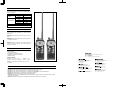
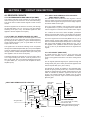
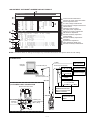
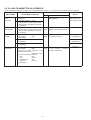
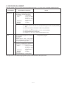
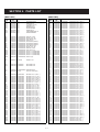
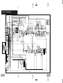
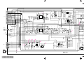
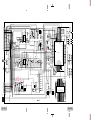
1
Count on us!
VHF MARINE TRANSCEIVER
im1v
im1euro v
6-9-16, Kamihigashi, Hirano-ku, Osaka 547-0002, Japan
S-13603MZ-CD-q
' 2000 Icom Inc.
INTRODUCTION
This service manual describes the latest service information for
the IC-M1V/IC-M1EURO V VHF MARINE TRANSCEIVER at
the time of publication.
MODEL
IC-M1V
VERSION
SYMBOL
U.S.A.
USA
S.E.Asia
SEA
Italy
ITA
Europe
EUR
United Kingdom
UK
Germany
FRG
IC-M1EURO V
To upgrade quality, all electrical or mechanical parts and internal circuits are subject to change without notice or obligation.
DANGER
NEVER connect the transceiver to an AC outlet or to a DC
power supply that uses more than 10 V. This will ruin the
transceiver.
DO NOT expose the transceiver to rain, snow or any liquids.
DO NOT reverse the polarrities of the power supply when
connecting the tranceiver.
DO NOT apply an RF signal of more than 20 dBm (100
mW) to the antenna connector. This could damage the
transceiver s front end.
ORDERING PARTS
Be sure to include the following four points when ordering
replacement parts:
1. 10-digit order numbers
2. Component part number and name
3. Equipment model name and unit name
4. Quantity required
6-9-16, Kamihigashi, Hirano-ku, Osaka 547-0002, Japan
Phone : 06 6793 5302
Fax
: 06 6793 0013
URL : http://www.icom.co.jp/world/index.html
<SAMPLE ORDER>
1140003830 S.IC TC4W66F IC-M1V
8930051080 2320 Key board IC-M1EURO V
MAIN UNIT 1 piece
CHASSIS 5 pieces
Addresses are provided on the inside back cover for your
convenience.
REPAIR NOTES
1. Make sure a problem is internal before disassembling the transceiver.
2. DO NOT open the transceiver until the transceiver is disconnected from its power source.
3. DO NOT force any of the variable components. Turn them slowly and smoothly.
4. DO NOT short any circuits or electronic parts. An insulated tuning tool MUST be used for all adjustments.
5. DO NOT keep power ON for a long time when the transceiver is defective.
6. DO NOT transmit power into a signal generator or a sweep generator.
7. ALWAYS connect a 40 dB or 50 dB attenuator between the transceiver and a deviation meter or spectrum analyzer when
using such test equipment.
8. READ the instructions of test equipment thoroughly before connecting equipment to the transceiver.
< Corporate Headquarters >
2380 116th Avenue N.E., Bellevue, WA 98004, U.S.A.
Phone : (425) 454-8155 Fax : (425) 454-1509
URL : http://www.icomamerica.com
< Customer Service >
Phone : (425) 454-7619
Glenwood Centre #150-6165
Highway 17 Delta, B.C., V4K 5B8, Canada
Phone : (604) 952-4266 Fax : (604) 952-0090
URL : http://www.icomcanada.com
A.C.N. 006 092 575
290-294 Albert Street, Brunswick, Victoria, 3056, Australia
Phone : 03 9387 0666
Fax : 03 9387 0022
URL : http://www.icom.net.au
6F No. 68, Sec. 1 Cheng-Teh Road, Taipei, Taiwan, R.O.C.
Phone : (02) 2559 1899 Fax : (02) 2559 1874
Communication Equipment
Himmelgeister Str. 100, D-40225 D sseldorf, Germany
Phone : 0211 346047 Fax : 0211 333639
URL : http://www.icomeurope.com
Crta. de Gracia a Manresa Km. 14,750
08190 Sant Cugat del Valles Barcelona, SPAIN
Phone : (93) 590 26 70 Fax : (93) 589 04 46
URL : http://www.icomspain.com
Unit 9, Sea St., Herne Bay, Kent, CT6 8LD, U.K.
Phone : 01227 741741 Fax : 01227 741742
URL : http://www.icomuk.co.uk
Zac de la Plaine, Rue Brindejonc des Moulinais
BP 5804, 31505 Toulouse Cedex, France
Phone : 561 36 03 03 Fax : 561 36 03 00
URL : http://www.icom-france.com
TABLE OF CONTENTS
SECTION 1
SPECIFICATIONS
VHF MARINE CHANNEL LIST ....................................................................................... 1 - 2
SECTION 2
INSIDE VIEWS
SECTION 3
DISASSEMBLY AND OPTION INSTRUCTIONS
SECTION 4
CIRCUIT DESCRIPTION
4-1
RECEIVER CIRCUITS ................................................................................................... 4 - 1
4-2
TRANSMITTER CIRCUITS ............................................................................................ 4 - 2
4-3
PLL CIRCUIT ................................................................................................................... 4 - 3
4-4
POWER SUPPLY CIRCUITS ......................................................................................... 4 - 3
4-5
CPU PORT ALLOCATIONS ........................................................................................... 4 - 4
SECTION 5
ADJUSTMENT PROCEDURES
5-1
PREPARATION................................................................................................................ 5 - 1
5-2
PLL AND TRANSMITTER ADJUSTMENTS .................................................................... 5 - 3
5-3
RECEIVER ADJUSTMENT ............................................................................................ 5 - 4
5-4
TRIMMER ADJUSTMENT .............................................................................................. 5 - 5
5-5
ATIS ADJUSTMENT ....................................................................................................... 5 - 5
SECTION 6
PARTS LIST
SECTION 7
MECHANICAL PARTS AND DISASSEMBLY
AD-95 INFORMATION .................................................................................................... 7 - 3
SECTION 8
SEMI-CONDUCTOR INFORMATION
SECTION 9
BOARD LAYOUTS
9-1
CHARGE UNIT (AD-95) .................................................................................................. 9 - 1
9-2
RF AND VR UNITS.......................................................................................................... 9 - 2
9-3
MAIN UNIT ..................................................................................................................... 9 - 4
SECTION 10
BLOCK DIAGRAM
SECTION 11
VOLTAGE DIAGRAM
11 - 1
RF UNIT ......................................................................................................................... 11 - 1
11 - 2
MAIN UNIT .................................................................................................................... 11 - 2
SECTION 1
SPECIFICATIONS
Frequencycoverage
EIA-152C/204D
EN301-178
Tx: 156.025 MHz–157.425 MHz
Rx: 156.025 MHz–163.275 MHz
Tx: 156.025 MHz–157.425 MHz
Rx: 156.025 MHz–162.025 MHz
Mode
16K0G3E (FM)
Power supply requirement
Usable temperature
GENERAL
Current drain
(with BP-215)
Frequency stability
Tx
Rx
BP-215 (7.4 V DC)
–10 ˚C to +60 ˚C (+14˚F to +140˚F)
± 10 ppm
± 1.5 kHz
at 5 W
1.5 A max.
at 1 W
0.7 A max.
at maximum audio
200 mA
at stand-by
20 mA
Type SMA / 50 Ω
Antenna impedance
Dimensions
(Projections not included)
52.5(W) × 129(H) × 30(D) mm; 21⁄16(W) × 53⁄32(H) × 13⁄16(D) inch (with BP-215)
Weight
(with antenna and BP-215)
RF output power (at 7.4 V DC)
TRANSMITTER
Modulation system
285 g; 10.1 oz
5 W / 1 W / 0.5 W (High / Low / Extra low)
Variable reactance frequency modulation
Max. frequency deviation
± 5.0 kHz
Spurious emissions
65 dB
Adjacent channel power
60 dB
250 nW
Residual modulation
40 dB
Audio harmonic distortion
Less than 10 % at 60 % deviation
Microphone impedance
Receive system
2 kΩ
Double-conversion super heterodyne
Intermediate frequencies
Sensitivity
Squelch sensitivity
RECEIVER
–15 ˚C to +55 ˚C (+5˚F to +131˚F)
1st: 21.70 MHz, 2nd: 450 kHz
0.35 µV at 12 dB SINAD
0.5 µV at 12 dB SINAD
0.35 µV
0.5 µV
Adjacent channel selectivity
70 dB (typical)
70 dB
Spurious response
70 dB (typical)
70 dB
Intermodulation
70 dB (typical)
68 dB
Hum and noise
Audio output power ( at 7.4 V)
Audio frequency response
40 dB
350 mW typical at 10 % distortion
with an 8 Ω load
200 mW at 10 % distortion
with an 8 Ω load
–3 dB to +1 dB of –6 dB octave from 300 Hz to 3000 Hz
All stated specifications are subject to change without notice or obligation.
1-1
‘ VHF MARINE CHANNEL LIST
Channel No.
USA INT CAN
01
01
01A
Channel No.
USA INT CAN
156.050
160.650
21A
156.050
156.050
157.050
73
73
73
156.675
156.675
157.100
161.700
74
74
74
156.725
156.725
22A
157.100
157.100
77*
77
77*
156.875
156.875
23
157.150
161.750
156.925
161.525
157.150
157.150
156.925
156.925
156.975
161.575
156.975
156.975
157.025
161.625
157.025
157.025
157.075
161.675
157.075
157.075
157.125
161.725
82A
157.125
157.125
160.700
03
03
156.150
160.750
156.150
156.150
23A
156.200
160.800
24
24
24
157.200
161.800
156.200
156.200
25
25
25
157.250
161.850
156.250
160.850
26
26
26
157.300
161.900
05A
156.250
156.250
27
27
27
157.350
161.950
06
156.300
156.300
28
28
28
157.400
162.000
156.350
160.950
60
60
156.025
160.625
07A
156.350
156.350
61
156.075
160.675
156.075
156.075
156.125
160.725
156.125
156.125
83A
156.175
160.775
84
156.175
156.175
84A
64
156.225
160.825
85
64A
156.225
156.225
85A
05
05A
06
07
07A
08
08
08
156.400
156.400
09
09
09
156.450
156.450
10
10
10
156.500
156.500
11
11
11
156.550
156.550
12
12
156.600
156.600
13*
13
13*
156.650
156.650
14
14
14
156.700
156.700
1
22A
23
61A
61A
62
62A
63
63A
64
64A
1
79
80
81
82
82A
83
65
156.275
160.875
86
16
16
16
156.800
156.800
65A 65A 65A
156.275
156.275
86A
17
17*
156.850
156.850
66
156.325
160.925
87
156.900
161.500
66A 66A 66A*
156.325
156.325
87A
156.900
156.900
67*2
67
67
156.375
156.375
88
156.950
161.550
68
68
68
156.425
156.425
88A
19A
156.950
156.950
69
156.475
156.475
20*
157.000
161.600
70*
70*
70*
156.525
156.525
157.000
157.000
71
71
71
156.575
156.575
157.050
161.650
72
72
72
156.625
156.625
17*
18
18A
18A
19
19A
20
20
1
20A
21
21
1
69
3
69
3
3
81A
81A
156.750
1
80A
80A
156.750
1
79A
79A
15*
1
78A
78A
15*
1
1
78
15*
2
Frequency (MHz)
Transmit
Receive
157.050
21A
22
156.100
04A
2
Channel No.
USA INT CAN
02
04
12
Frequency (MHz)
Transmit
Receive
02
03A
06
Frequency (MHz)
Transmit
Receive
84
85
86
83
157.175
161.775
83A
157.175
157.175
84
157.225
161.825
157.225
157.225
157.275
161.875
157.275
157.275
157.325
161.925
157.325
157.325
157.375
161.975
157.375
157.375
157.425
162.025
157.425
157.425
85
86
87
87
88
88
*1 Low power only, *2 Momentary high power, *3 Receive only
NOTE: Channels 3, 21, 23, 61, 64, 81, 82 and 83 CANNOT be used by the general public in USA waters.
‘ WX CHANNEL LIST ([IC-M1V] only)
Weather
channel
Frequency (MHz)
Receive
Transmit
Weather
channel
Frequency (MHz)
Receive
Transmit
WX01
Receive only
162.550
WX06
Receive only
162.500
WX02
Receive only
162.400
WX07
Receive only
162.525
WX03
Receive only
162.475
WX08
Receive only
161.650
WX04
Receive only
162.425
WX09
Receive only
161.775
WX05
Receive only
162.450
WX10
Receive only
163.275
1-2
SECTION 2
INSIDE VIEWS
• MAIN UNIT
EEROM
(IC7: HN58X2432TI)
CPU
(IC9: HD6433835SC94H)
CPU system clock
(X2: CR-610, 7.9872 MHz)
IF filter
(FI1, FI2: SFPC450E T001, 450 kHz)
IF discreminator crystal
(X1: CDBCA450CX24, 450 kHz)
FM IF IC
(IC1: TA431136FN (D, EL))
Microphone amplifier
(IC4: NJM2902V)
AF analog switch
(IC5: BU4066BCFV)
AF amplifier
(IC2: NJM2073M)
Microphone
(MC1: KUB2823-013280)
• RF UNIT
Top view
IF amplifier
(Q15: 2SC2714 Y)
Bottom view
PLL reference crystal
(X1: CR-659, 21.25 MHz)
VCO circuit
PLL IC
(IC1: µPD3140GS)
VCO
(Q4, Q5: 2SC4226)
1st mixer
(Q14: 3SK166)
Power amplifier
(Q11: 2SK2974)
1st IF filter
(FI1, FI2: FL-310, 21.7 MHz)
2-1
SECTION 3
DISASSEMBLY AND OPTION INSTRUCTIONS
• Removing the Rear panel
A
• Removing the MAIN unit
Rear panel
J1
B
C
C
J2
C
B
MAIN unit
Rubber
J1
Rear panel
Front panel
Unscrew 2 screws A (2 × 20 mm), and 4 screws
B (2 × 5 mm, black) from the rear panel.
q Unscrew 7 screws C (2 × 3.5 mm, silver) from
the MAIN unit.
w Unplug J1 to separate the rear panel and the
MAIN unit.
NOTE : Once the front panel is removed, grease must be
applied to
areas before assembly.
Manufacture : Shin-Etsu Chemical
Type
: G-501
• Removing the RF unit
D
• Install the optional unit (UT-98 or UT-112) to the
connector (MAIN unit ; J3)
E
MAIN unit bottom view
UT-98 or UT-112
VR unit
Connector cap
RF unit
J3
Knob
G F
H
I
J
q Remove connector cap.
w Remove 2 knobs, and unscrew 3 nuts (F, G, H)
e Unscrew 3 screws D (2 × 3.5 mm, silver), and 2 screws
E (2 × 5 mm, black) from the RF unit.
r Unscrew 1 screw J (2 × 5 mm, black), and remove 1
washer I.
t Take off the RF unit in the direction of the arrow.
CAUTION :
DO NOT guarantee the waterproof construction when
installing the optional unit except distributors or dealers.
3-1
SECTION 4
CIRCUIT DESCRIPTION
4-1-1 ANTENNA SWITCHING CIRCUIT (RF UNIT)
4-1-3 2ND IF AND DEMODULATOR CIRCUITS
(MAIN AND RF UNITS)
The antenna switching circuit functions as a low-pass filter
while receiving and as resonator circuit while transmitting.
The circuit does not allow transmit signals to enter receiver
circuits.
The 2nd mixer circuit converts the 1st IF signal to a 2nd IF
signal. A double convertion superheterodyne system (which
converts receive signal twice) improves the image rejection
and obtain stable receiver gain.
Received signals from the antenna connector pass through
the low-pass fileter (L15–L17, C72–C77, C79) and antenna
switching circuit (D11, D12). The filtered signals are then
applied to the RF amplifier circuit (Q13).
The 1st IF signal is applied to a 2nd mixer section of the FM
IF IC (MAIN unit; IC1, pin 16). The signal is then mixed with
a 2nd LO signal for conversion into a 450 kHz 2nd IF signal.
4-1 RECEIVER CIRCUITS
IC1 contains the 2nd mixer, limiter amplifier, quadrature
detector and active filter circuits. A 21.25 MHz 2nd LO signal
is produced at the PLL circuit using the reference frequency.
4-1-2 RF AND 1ST MIXER CIRCUITS (RF UNIT)
The 1st mixer circuit converts the received signals to a fixed
frequency of the 1st IF signal with a PLL output frequency.
By changing the PLL frequency, only the desired frequency
will be passed through a pair of crystal filters at the next
stage of the 1st mixer.
The 2nd IF signal from the 2nd mixer (MAIN unit; IC1, pin 3)
passes through ceramic filters (MAIN unit; FI1 and FI2) to
remove unwanted heterodyned frequencies. It is then amplified at the limiter amplifier section (MAIN unit; IC1, pin 5)
and applied to the quadrature detector section (MAIN unit;
IC1, pin 10 and 11) to demodulate the 2nd IF signal into AF
signals.
The signals from the antenna switching circuit are passed
through the tunable bandpass filter (D13, D14) and amplified
at the RF amplifier (Q13). The amplified signals are passed
through another tunable bandpass fileter (D15–D18), and
then applied to the 1st mixer circuit (Q14).
4-1-4 AF CIRCUIT (MAIN UNIT)
AF signals from the FM IF IC (IC1, pin 9) are fed to the
optional voice scrambler unit to demodulate scrambled
audio or are bypassed around the unit via the analog switch
(IC5).
The filtered signals are mixed at the 1st mixer (Q14) with a
1st LO signal coming from the PLL circuit to produce a 21.7
MHz 1st IF signal. The 1st IF signal is passed through a pair
of crystal filters (FI1, FI2) and is then amplified at the IF
amplifier (Q15).
The AF signals (detected signals) are passed through the
analog switch (IC5, pins 8 and 9) and are then applied to the
active low-pass filter (IC4c, pins 9 and 8).
The filtered AF signals are applied to and adjusted audio
level at the [VOL] control (VR unit; R1). The level controlled
signals are passed through another analog switch (IC3, Q3)
which is controlled by “SPSEL” signal from the CPU (IC9,
pin 83). The passed signals are applied to the AF power
amplifier (IC2), and then output to the internal speaker or
[EXT SP] jack.
2ND IF AND DEMODULATOR CIRCUITS
2nd IF filter
450 kHz
C4
R4
8
R3
C3
R5
7
5
FI1, FI2
3
Noise
detector
Active
filter
C2
MAIN unit
2nd
Mixer
IF amp.
FM
detector
9
11
12
C12
R6
R1
R4V
X1
450 kHz
4-1
14
16
IC1 TA31136FN(D)
"IF" (1st IF signal: 21.7 MHz)
from RF unit, Q15
"NOIS" signal to the CPU (pin 99)
"SD" signal to the CPU (pin 98)
C10
R7
C13
10
17
16
PLL IC
IC1
X1
21.25 MHz
Noise
comp.
RSSI
AF signal "DET"
2
RF unit
4-1-5 SQUELCH CIRCUIT (MAIN UNIT)
4-2-3 DRIVE/POWER AMPLIFIER CIRCUITS
(RF UNIT)
The noise squelch circuit cuts out AF signals when no RF
signals are received. By detecting noise components in the
AF signals, the squelch circuit switches the AF mute switch.
The signal from the VCO circuit passes through the transmit/receive switching circuit (D7, D8) and is applied to the
buffer-amplifier (Q9). The amplified signal is amplified by the
pre-driver (Q10) and the power amplifier (Q11) to obtain 5 W
of RF power (at 7.4 V). The amplified signal passes through
the antenna switching circuit (D9), and low-pass filter
(L15–L17, C72–C77, C79) and is then applied to the antenna connector.
A portion of the AF signals from the FM IF IC (IC1, pin 9) are
applied to the active filter section (IC1, pin 8). The active filter section amplifies and filters noise components. The filtered signals are applied to the noise detector section and
output from IC1 (pin 14) as the “NOIS” signal.
The “NOIS” signal from IC1 (pin 14) is applied to the CPU
(IC9, pin 99) to analyze the noise condition. The “SQLV” signal from R1 (VR unit) is applied to the CPU (IC9, pin 95) to
detect squelch level. The CPU detects the receiving signal
strength and cut the AF signal line.
The bias current of the power amplifier (Q11) is controlled by
the APC circuit to stabilize the output power.
4-2-4 APC CIRCUIT (RF AND MAIN UNITS)
The APC circuit provides stable output power from the
power amplifier even when the input voltage or temperature
changes, and, selects HIGH, LOW or EXTRA LOW output
power. The APC circuit consists of an APC sensor and APC
control circuits.
4-2 TRANSMITTER CIRCUITS
4-2-1 MICROPHONE AMPLIFIER CIRCUIT
(MAIN UNIT)
• APC SENSOR CIRCUIT (RF UNIT)
The APC sensor circuit (D10, C80, C81, R53, R54) detects
the transmit output power level and converts it to DC voltage
as an “TXDET” signal. The detected signal is applied to the
APC control circuit on the MAIN unit.
The microphone amplifier circuit amplifies audio signals with
+6 dB/octave pre-emphasis characteristics from the microphone to a level needed for the modulation circuit.
The AF signals from the microphone are passed through the
pre-emphasis circuit (R31, C36) and are then applied to the
microphone amplifier (IC4d). The amplified AF signals are
applied to the optional voice scrambler unit to scramble the
audio via the “MICOUT” signal, or are bypassed around the
unit via an analog switch (IC5, pin 4).
• APC CONTROL CIRCUIT (MAIN UNIT)
The “TXDET” signal from the APC sensor circuit is applied
to the CPU (IC9, pin 96) to control the input voltage of the
pre-driver (RF unit; Q10) and the power amplifier (RF unit;
Q11). When the output power changes, the CPU (IC9) outputs “POWCON” signal to the D/A converter (RF unit; IC2).
And then “POWCON” signal controls the APC controller (RF
unit; IC3) to provide stable output power.
The AF signals which bypassed or passed through the voice
scrambler unit are amplified again at the limiter-amplifier
(IC4a) and then passed through the low-pass filter (IC4b,
pins 6 and 7). The filtered audio is applied to the RF unit as
the “MOD” signal.
4-2-2 MODULATION CIRCUIT (RF UNIT)
The modulation circuit modulates the VCO oscillating signal
(RF signal) using the microphone audio signals.
The audio signals “MOD” change the reactance of D4 to
modulate an oscillated signal at the transmitter VCO (Q4,
Q5). The oscillated signal is amplified at the buffer-amplifiers
(Q6, Q8).
APC CIRCUIT
"TXDET" signal
to CPU (pin 96)
"POWCON" signal
from IC2 (pin 6)
APC ctrl
+
IC3
PWR det.
D10, C80
Pre-Drive
Q10
TX
PWR amp.
Q11
D9
"HV"
I. sens
"T4V"
RX
To 1st IF circuit
D11 D12
Ant SW
4-2
Ant
4-3 PLL CIRCUIT (RF UNIT)
4-4 POWER SUPPLY CIRCUITS
A PLL circuit provides stable oscillation of the transmit frequency and receive 1st LO frequency. The PLL output compares the phase of the divided VCO frequency to the reference frequency. The PLL output frequency is controlled by
the divided ratio (N-data) of a programmable divider.
VOLTAGE LINES
LINE
HV
VCC
The same voltage as the HV line (battery voltage) which is controlled by the power switch
([OFF/VOL] control).
4V
Common 4V converted from the VCC line by the
4V regulator circuit (MAIN unit; Q8–Q10).
The output voltage is applied to the D/A converter (RF unit; IC2) and PLL IC (RF unit; IC1), etc.
R4V
Receive 4V converted from the 4V line by the R4
regulator circuit (MAIN unit; Q5).
The regulated voltage is applied to the MOD
MUTE circuit (RF unit; Q2, D2) and receiver circuit.
T4V
Transmit 4V converted from the 4V line by the T4
regulator circuit (MAIN unit; Q6).
The regulated voltage is applied to the transmitter circuit.
S4V
Common 4V converted from the 4V line by the
S4V regulator circuit (MAIN unit; Q7).
The regulated voltage is applied to the optional
scrambler unit, limiter amplifier (MAIN unit; IC4),
etc.
The PLL circuit contains a VCO (Q4, Q5, D4, D6). The oscillated signal is amplified at the buffer-amplifiers (Q6, Q7) and
then applied to the PLL IC (IC1, pin 2).
The PLL IC contains the prescalers, programmable counter,
programmable divider, phase selector and etc. The entered
signal is divided at the prescaler and programmable counter
sections by the N-data ratio from the CPU. The divided signal is detected on phase at the phase detector using the reference frequency.
If the oscillated signal drifts, the phase of its frequency
changes from the reference frequency, causing a lock voltage changes to compensate for the drift in the oscillated frequency.
A portion of the VCO signal is amplified at buffer-amplifiers
(Q6, Q8) and is then applied to the receive 1st mixer (Q14)
or transmit driver via the TX/RX switching diode (D7, D8).
DESCRIPTION
The voltage from the attached battery pack.
The lock voltage is also used for the receiver tunable bandpass filter to match the filter’s center frequency to the
desired receive frequency. The lock voltage is amplified at
the buffer-amplifier (Q1) and then applied to the CPU (MAIN
unit; IC9, pin 93).
The amplified signal is controlled by the CPU (MAIN unit;
IC9), and is then applied to bandpass filters (D13–D18) as
“T1”, “T2”, “T3”, “T4” signals via the D/A converter (IC2).
PLL CIRCUIT
Buffer
"LVIN" signal to the CPU
(MAIN unit; IC9)
Q1
Buffer
VCO
Q6
Q4, Q5, D5, D6
X1
21.25 MHz
to transmitter circuit
Q8
to 1st mixer circuit
D7
Buffer
Q7
Loop
filter
"2nd LO" signal (21.25 MHz)
to the FM IF IC (MAIN unit; IC1)
D8
Buffer
IC1 (PLL IC)
Programmable
counter
8
Phase
detector
17
Programmable
divider
16
4-3
Prescaler
Shift register
2
3
4
5
PLST
SCK
SO
4-5 PORT ALLOCATIONS
4-5-1 CPU (MAIN UNIT; IC9)
Pin
number
Port
name
Description
Pin
number
Port
name
Description
1
BATT
Input port for the low battely detection.
82
S4C
Outputs S4 regulator control signals.
RM
Outputs the AF mute swtich control
signal when the voice scrambler is
OFF.
Low : While squelched.
83
SPSEL
Outputs speaker select signal
Low : The internal speaker
selected.
85
ESDA
Input port for EEPROM serial data.
Outputs serial data to the EEPROM.
SRM
Outputs the AF mute switch control
signal when the voice scrambler is
ON.
Low : While squelched.
86
CLIN
Input port for the cloning signal.
87
CLOUT
88
PTT
Input port for the [PTT] switch.
High : While [PTT] switch is pushed.
90
MKEY
Input port for [MIC/SP] connector
detection.
Outputs the MIC mute switch control
signal when the voice scrambler is
OFF.
Low : While muted.
91
SWA
Input port for the [CH/WX], [UP],
[DOWN] switches.
92
SWB
AFON
Outputs control signal for the AF
amplifier regulator circuit.
High : Activates the AF amplifier circuit (MAIN unit; Q2).
Input port for the [H/L], [DW], [SCN]
switches.
93
LVIN
Input port for the PLL lock voltage
detection.
94
TEMPS
OPST
Outputs strobe signals to the optional
voice scrambler unit
Input port for the transceiver’s internal
temperature detection.
95
SQLV
Input port to adjust the squelch level.
17
DST
Outputs strobe signals to the D/A converter IC (RF unit; IC2, pin 2).
96
TXDET
Input port for the TX power detection.
TONE
Input port for the WX tone detection.
PLST
Outputs strobe signals to the PLL IC
(RF unit; IC1, pin 3).
97
18
98
SD
Input port fot the receive signal
strength detection.
99
NOIS
Input port for noise signals (pulsetype) for squelch operation.
100
BTYPE
Input port for the battely’s type detection.
11
12
13
14
15
16
19
20
21
23
SMM
MM
SCK
UNLK
SO
OPTIN
Outputs the MIC mute switch control
signal when the voice scrambler is
ON.
Low : While muted.
Outputs serial clock.
Input port for unlock signal.
High : PLL is unlocked.
Low : PLL is locked.
Outputs serial data.
Input port for the optinal voice scrambler unit connection.
Low : The optional voice scrambler
unit is connected.
MONI
Input port for the [MONI] switch.
Low : While [MONI] switch
pushed.
16CH
Input port for the [16/9] switch.
Low : While [16/9] switch is pushed.
77
LIGHT
Outputs back light control signal.
High : Light ON.
78
BEEP
Outputs beep audio signals.
79
4VC
Outputs 4V regulator control signal.
80
R4C
Outputs R4 regulator control signals.
Low : While receiving.
81
T4C
Outputs T4 regulator control signals.
Low : While transmitting.
24
25
is
Outputs the cloning signal.
4-5-2 D/A converter IC (RF UNIT; IC2)
is
Pin
number
Port
name
Description
5
FRQCON
Output signal to adjust the reference
frequency.
6
POWCON Output signal to adjust TX power.
11, 12, 13
T1–T3
Output tunable bandpass filter control
signals.
T4
Output tunable bandpass filter control
signals while receiving.
MODCON
Output signal to adjust modulation
while transmitting.
14
4-4
SECTION 5 ADJUSTMENT PROCEDURES
5-1 PREPARATION
IC-M1V/M1EURO V can be adjusted by sending adjustment data to the RS-232C port via a PC. When you adjust the ICM1V/M1EURO V, the optional CS-M1V ADJ ADJUSTMENT SOFTWARE (Rev. 1.0 or later), *OPC-973 CLONING AND ADJUSTMENT
CABLE are required.
NOTE: *OPC-973 is a modified optional OPC-973 CLONING AND ADJUSTMENT CABLE (see illustration at CLONING AND ADJUSTMENT CABLE MODIFICATION).
GRADE AND RANGE
EQUIPMENT
DC power supply
Output voltage
Current capacity
: 7.4 V DC
: 2 A or more
RF power meter
(terminated type)
Measuring range
Frequency range
Impedance
SWR
:
:
:
:
Frequency counter
Spectrum analyzer
0.1–10 W
100–300 MHz
50 Ω
Less than 1.2 : 1
Frequency range
: 0.1–300 MHz
Frequency accuracy : ±1 ppm or better
Sensitivity
: 100 mV or better
EQUIPMENT
GRADE AND RANGE
FM deviation meter
Frequency range
Measuring range
: 30–300 MHz
: 0 to ±10 kHz
Audio generator
Frequency range
Measuring range
: 300–3000 Hz
: 1–500 mV
Frequency range
Output level
: 100–300 MHz
: 0.1 µV–32 mV
(–127 to –17 dBm)
Power attenuation
Capacity
: 40 dB or more
: 10 W or more
Standard signal
generator (SSG)
Attenuator
Frequency range
: at least 400 MHz
Spectrum bandwidth: ±100 MHz or more
■ SYSTEM REQUIREMENTS
■ STARTING THE PROGRAM
• IBM PC compatible computer with an RS -232C serial port
(38400 bps or faster).
• Microsoft Windows 95 or Windows 98
• Intel i486DX processor or faster (Pentium 100 MHz or
faster recommended)
• At least 16 MB RAM and 10 MB of hard disk space
• 640×480 pixel display (800×600 pixel display recommended)
q Connect IC-M1V/M1EURO V and PC with the optional
cables OPC-478, *OPC-973.
w Boot up Windows.
e Click the program group ‘CS-M1V ADJ’ in the ‘Programs’
folder of the [Start] menu, then CS-M1V ADJ’s window is
appeared.
r Click ‘Connect’ on the CS-M1V’s window, then appears
IC-M1V’s/M1EURO V’s up-to-date condition.
t Set or modify adjustment data as desired. See illustration
at ADJUSTMENT SOFTWARE’S SCREEN DISPLAY
EXAMPLE on page 5-2.
■ ADJUSTMENT SOFTWARE INSTALLATION
NOTE: Before using the program, make a backup copy of
the original disk. After making a backup copy, keep
the original disk in a safe place.
IBM is a registered trademark of International Bussiness
Machines Corporation in the U.S.A. and other countries.
Microsoft and Windows are registered trademarks of
Microsoft Corporation in U.S.A. and other countries.
Screen shots produced with permission from Microsoft
Corporation. All other products or brands are registered
trademarks or trademarks of their respective holders.
q Boot up Windows.
- Quit all applications when Windows is running.
w Insert the backup disk1 into the appropriate floppy drive.
e Select ‘Run’ from the [Start] menu.
r Type the setup program name using the full path name,
then push the [Enter] key. (A:\ setup)
t Follow the prompts.
y Program group ‘CS-M1V ADJ’ appears in the ‘Programs’
folder of the [Start] menu.
CLONING AND ADJUSTMENT CABLE MODIFICATION
a netted line (GND)
a red color line (EXT SP)
(
(
GND)
MICE)
( + CLONE)
OPC-478
( + MIC)
a black color line (CLONE)
a white color line (MIC)
INFORMATION: When ordering OPC-973
Part Name:
Order Number:
5-1
OPC-973
8900009890
ADJUSTMENT SPFTWARE’S SCREEN DISPLAY EXAMPLE
2
CS-M1V ADJ Rev.1.0
File Option
1
3
4
5
COM 1: OPEN
[A / D]
MKEY
SW A
SW B
LVIN
TEMPS
SQLV
TXDET
SD
NOIS
BTYPE
BATT
Dial
6
7
8
9
10
11
12
13
:
:
:
:
:
:
:
:
:
:
:
Connect
255
255
255
163
187
220
0
0
0
255
153
Mode :
CH No. :
RF Power :
Power (Hi) :
Power (LO) :
Power (EL) :
TXF :
MOD :
BPF ALL :
BPF T1 :
BPF T2 :
BPF T3 :
BPF T4 :
SQL :
ATIS :
:
:
:
:
:
:
:
:
:
:
:
FFh :
FFh :
FFh :
A3h :
BBh :
DCh :
00h :
00h :
00h :
FFh :
99h :
Reload (F5)
4 . 30V
4 . 30V
4 . 30V
2 . 75V
30 . 10’C
3 . 71V
0 . 00V
0 . 00V
0 . 00V
4 . 30V
8 . 26V
[D / A]
FRQCON :
POWCON :
T1
:
T2
:
T3
:
T4
:
Disp para
: Connect IC-M1V/M1EURO V
with PC via an RS-232C serial cable
2 : Renew adjustment data
3 : PLL lock voltage measurement
4 : Connected DC voltage measurement
5 : Version select
6 : Operating channel select
7 : RF output power adjustments
8 : Reference frequency adjustment
9 : FM deviation adjustment
10 : Receive sensitivity adjustment
(automatically)
11 : Receive sensitivity adjustments
(manually)
12 : Squelch level adjustment
13 : ATIS adjustment ([FRG] only)
14 : Receive sensitivity measurement
1
128 : 80h
0 : 00h
164 : A4h
164 : A4h
164 : A4h
163 : A3h
:
:
:
:
:
:
2 . 16V
0 . 00V
2 . 77V
2 . 77V
2 . 77V
2 . 75V
14
[SQL Calced]
: 17
OPEN
CLOSE : 34
USA
01A (RX Freq = 156.050,
TX Freq = 156.050)
High
145 [ # # # # # # # # # # # — — — — — — ]
100 [ # # # # # # # # — — — — — — — — — ]
90 [ # # # # # # # — — — — — — — — — — ]
[ Enter]
to Start
110 [ # # # # # # # # # — — — — — — — — ]
[ Enter]
to Start
0 [ # # # # # # # # # # — — — — — — — ] [ Enter ]
to Sweep
0 [ # # # # # # # # # # — — — — — — — ] [ Enter ]
to Sweep
0 [ # # # # # # # # # # — — — — — — — ] [ Enter ]
to Sweep
—1 [ # # # # # # # # # # — — — — — — — ] [ Enter ]
to Sweep
[ Enter]
to Start
[ Enter]
to Start
NOTE: The above values for settings are example only. Each transceiver has its own specific values for each setting.
CONNECTION
to [MIC]
Personal
computer
to an RS-232C port
DB9 female plug
(incl. level converter circuit)
OPC-478
DC POWER CABLE CONNECTION
Audio generator
to the antenna connector
Attenuator
40 dB or 50 dB
FM deviation meter
RF power meter
0.1 10 W/50
Spectrum analyzer
Frequency
counter
Standard signal generator
0.1 V to 32 mV
( 127 dBm to 17 dBm)
CAUTION:
MAIN unit bottom view
DO NOT transmit while
SSG is connected to the
antenna connector.
*OPC-973
DC POWER
SUPPLY
7.4 V/2A
+
Soldering DC
power cable here
(MP1, MP3)
5-2
AD-92SMA
Optional SMA-BNC
adapter
5-2 PLL AND TRANSMITTER ADJUSTMENTS
Select an operation using [↑] / [↓] keys, then set specified value using [←] / [→] keys on the connected computer keyboard.
ADJUSTMENT
MEASUREMENT
ADJUSTMENT CONDITION
UNIT
LOCATION
PLL
LOCK
VOLTAGE
1 • Operating channel : ch 16
• Receiving
REFERENCE
FREQUENCY
Top Loosely couple the frequnecy
1 • Operating channel : ch 16
• Connect the RF power meter or 50 Ω panel counter to the antenna connecdummy load to the antenna connector.
tor.
• Transmitting
OUTPUT
POWER
1 • Operating channel : ch 16
• [H/L] switch
: High
• Transmitting
FM
DEVIATION
Use the adjustment program.
(see page 5-2)
2 • Operating channel : ch 16
• Connect the RF power meter or 50 Ω
dummy load to the antenna connector.
• Transmitting
VALUE
2.3–3.3 V
Verify on the computer display (LVIN)
156.800000 MHz
Top Connect the RF power meter to 5.0 W (except [FRG])
panel the antenna connector.
1.0 W ([FRG] only)
2 • [H/L] switch
• Transmitting
: Low
1.0 W (except [FRG])
0.5 W ([FRG] only)
3 • [H/L] switch
• Transmitting
: Extra low
0.5 W (except [FRG])
1 • Operating channel : ch 16
Top Connect the FM deviation meter
• [H/L] switch
: High
panel to the antenna connector
• Connect the audio generator to the
through the attenuator.
[MIC] jack and set as:
1.0 kHz/40 mV rms.
• Set the FM deviation meter as:
HPF
: OFF
LPF
: 20 kHz
De-emphasis
: OFF
Detector
: (P–P)/2
• Transmitting
5-3
±4.3 kHz
5-3 RECEIVER ADJUSTMENT
Select an operation using [↑] / [↓] keys, then set specified value using [←] / [→] keys on the connected computer keyboard.
ADJUSTMENT
RX
SENSITIVITY
ADJUSTMENT CONDITION
VALUE
1 • Operating channel : ch 16
• Connect a standard signal generator to
the antenna connector and set as:
Frequency
: 156.800 MHz
Level
: 3.2 µV* (–97 dBm)
[IC-M1V]
: 4.5 µV* (–94 dBm)
[IC-M1EURO V]
Modulation
: 1 kHz
Deviation
: ±3.5 kHz
• Receiving
Maxmun level on the computer display (T1–T4) respectively.
CONVENIENT: The BPF T1–BPF T4 can be adjusted automatically.
q-1: Set the cursol to “BPF ALL” on the adjustment program and then push [ENTER]
key.
q-2: The connected PC tunes BPF T1–BPF T4 to peak levels.
or
w-1: Set the cursol to one of BPF T1, T2, T3, or T4 as desired.
w-2: Push [ENTER] key to start tuning.
w-3: Repeat w-1 and w-2 to perform additional BPF tuning.
SQUELCH
LEVEL
1 • Operating channel : ch 16
NOTE: Squelch level adjustment is adjusted automatically by
• No RF signals are applied to the antenthe adjustment program.
na connector.
• Receiving
• Set the cursol to “SQL” on the adjustment program and push [ENTER] key,
then push [ENTER] key again.
2 • Operating channel : ch 16
• Connect a standard signal generator to
the antenna connector and set as :
Level
: 0.71 µV* (–110 dBm)
[IC-M1V]
: 1 µV* (–107 dBm)
[IC-M1EURO V]
Modulation
: 1 kHz
Deviation
: ±3.5 kHz
• Receiving
• Push [ENTER] key on the keyboard.
*The output level of the standard signal generator (SSG) is indicated as the SSG’s open circuit.
5-4
5-4 TRIMMER ADJUSTMENT
ADJUSTMENT
MEASUREMENT
ADJUSTMENT CONDITION
UNIT
TX
1 • Operating channel : ch 16
SPURIOUS
• [H/L] switch
: High
([M1EURO V]
• No signal apply to the [MIC] jack.
only)
• Transmitting
ADJUSTMENT
POINT
VALUE
LOCATION
Top
panel
Connect the spec- High-harmonics comtrum analyzer to the ponents are minimum
antenna connector value.
through the attenuator.
UNIT
ADJUST
RF
L15
5-5 ATIS ADJUSTMENT
Select an operation using [↑] / [↓] keys, then set specified value using [←] / [→] keys on the connected computer keyboard.
ADJUSTMENT
ATIS
MODULATION
([FRG] only)
MEASUREMENT
ADJUSTMENT CONDITION
UNIT
LOCATION
VALUE
1 • Operating channel : ch 16
Top Connect the FM deviation meter ±1.3 kHz (1300 Hz)
• [H/L] switch
: High
panel to the antenna connector
• Connect the audio generator to the
through the attenuator.
[MIC] jack and set as:
1.0 kHz/40 mV rms.
• Set the FM deviation meter as:
HPF
: OFF
LPF
: 20 kHz
De-emphasis
: OFF
Detector
: (P–P)/2
• Set the cursol to “ATIS” on the adjustment program and push [ENTER] key.
• Transmitting
2 • Set the cursol to “ATIS” on the adjustment program and push [ENTER] key.
• Transmitting
5-5
±2.1 kHz (2100 Hz)
IC-M1EURO V RF UNIT TOP VIEW
L15
TX sprious adjustment
([IC-M1EURO V] only)
5-6
SECTION 6 PARTS LIST
[MAIN UNIT]
REF
NO.
[MAIN UNIT]
ORDER
NO.
DESCRIPTION
IC1
IC2
IC3
IC4
IC5
IC6
IC7
IC8
IC9
1110003490
1110002420
1130007300
1110003780
1130008090
1180001990
1130009680
1130009110
1140008950
S.IC
S.IC
S.IC
S.IC
S.IC
S.IC
S.IC
S.IC
S.IC
TA31136FN (D,EL)
NJM2073M-T1
TC4W66FU (TE12L)
NJM2902V-TE1
BU4066BCFV-E1
XC62FP4302MR
HN58X2432TI
S-80942ANMP-DD6-T2
HD6433835SD05H
Q1
Q2
Q3
Q4
Q5
Q6
Q7
Q8
Q9
Q10
Q11
Q12
Q13
Q14
Q15
Q16
1520000460
1590001190
1590000430
1590002530
1510000670
1510000670
1510000670
1590000430
1590001190
1520000460
1590000660
1530000160
1530000160
1530000160
1530000160
1590001920
S.TRANSISTOR
S.TRANSISTOR
S.TRANSISTOR
S.TRANSISTOR
S.TRANSISTOR
S.TRANSISTOR
S.TRANSISTOR
S.TRANSISTOR
S.TRANSISTOR
S.TRANSISTOR
S.TRANSISTOR
S.TRANSISTOR
S.TRANSISTOR
S.TRANSISTOR
S.TRANSISTOR
S.TRANSISTOR
2SB1132 T100 R
XP6501-(TX) .AB
DTC144EUA T106
UN911H (TX)
2SA1588-GR (TE85R)
2SA1588-GR (TE85R)
2SA1588-GR (TE85R)
DTC144EUA T106
XP6501-(TX) .AB
2SB1132 T100 R
DTC144TU T107
2SC2712-Y (TE85RTEM)
2SC2712-Y (TE85RTEM)
2SC2712-Y (TE85RTEM)
2SC2712-Y (TE85RTEM)
UN911F (TX)
D1
1750000130 S.DIODE
DA204U T107
FI1
FI2
2020001490 S.CERAMIC
2020001490 S.CERAMIC
SFPC450E-TC01
SFPC450E-TC01
X1
X2
6070000210 S.DISCRIMINATOR CDBCA450CX24
6050010290 S.XTAL
CR-610 (7.9872 MHz)
R1
R2
R3
R4
R5
R6
R7
R8
R9
R10
R11
R12
R13
R14
R17
R18
R19
R20
R21
R23
R24
R25
R26
R27
R28
R29
R30
R31
R32
R33
R34
R35
R36
R37
R38
R39
7030003390
7030003460
7030003700
7030003540
7030003720
7030003450
7030003400
7030003610
7030003800
7030003440
7030003480
7030003500
7030003200
7030003200
7030003560
7030003560
7030003570
7030003800
7030003720
7030003680
7030003680
7030003680
7030003680
7030003620
7030003400
7030003680
7030003790
7030003600
7030003760
7030003600
7030003680
7030003760
7030003680
7030003680
7030003680
7030003680
S.RESISTOR
S.RESISTOR
S.RESISTOR
S.RESISTOR
S.RESISTOR
S.RESISTOR
S.RESISTOR
S.RESISTOR
S.RESISTOR
S.RESISTOR
S.RESISTOR
S.RESISTOR
S.RESISTOR
S.RESISTOR
S.RESISTOR
S.RESISTOR
S.RESISTOR
S.RESISTOR
S.RESISTOR
S.RESISTOR
S.RESISTOR
S.RESISTOR
S.RESISTOR
S.RESISTOR
S.RESISTOR
S.RESISTOR
S.RESISTOR
S.RESISTOR
S.RESISTOR
S.RESISTOR
S.RESISTOR
S.RESISTOR
S.RESISTOR
S.RESISTOR
S.RESISTOR
S.RESISTOR
ERJ3GEYJ
ERJ3GEYJ
ERJ3GEYJ
ERJ3GEYJ
ERJ3GEYJ
ERJ3GEYJ
ERJ3GEYJ
ERJ3GEYJ
ERJ3GEYJ
ERJ3GEYJ
ERJ3GEYJ
ERJ3GEYJ
ERJ3GEYJ
ERJ3GEYJ
ERJ3GEYJ
ERJ3GEYJ
ERJ3GEYJ
ERJ3GEYJ
ERJ3GEYJ
ERJ3GEYJ
ERJ3GEYJ
ERJ3GEYJ
ERJ3GEYJ
ERJ3GEYJ
ERJ3GEYJ
ERJ3GEYJ
ERJ3GEYJ
ERJ3GEYJ
ERJ3GEYJ
ERJ3GEYJ
ERJ3GEYJ
ERJ3GEYJ
ERJ3GEYJ
ERJ3GEYJ
ERJ3GEYJ
ERJ3GEYJ
391
152
154
682
224
122
471
273
105
102
222
332
100
100
103
103
123
105
224
104
104
104
104
333
471
104
824
223
474
223
104
474
104
104
104
104
V
V
V
V
V
V
V
V
V
V
V
V
V
V
V
V
V
V
V
V
V
V
V
V
V
V
V
V
V
V
V
V
V
V
V
V
(390 Ω)
(1.5 kΩ)
(150 kΩ)
(6.8 kΩ)
(220 kΩ)
(1.2 kΩ)
(470 Ω)
(27 kΩ)
(1 MΩ)
(1 kΩ)
(2.2 kΩ)
(3.3 kΩ)
(10 Ω)
(10 Ω)
(10 kΩ)
(10 kΩ)
(12 kΩ)
(1 MΩ)
(220 kΩ)
(100 kΩ)
(100 kΩ)
(100 kΩ)
(100 kΩ)
(33 kΩ)
(470 Ω)
(100 kΩ)
(820 kΩ)
(22 kΩ)
(470 kΩ)
(22 kΩ)
(100 kΩ)
(470 kΩ)
(100 kΩ)
(100 kΩ)
(100 kΩ)
(100 kΩ)
REF
NO.
ORDER
NO.
R40
R41
R42
R43
R44
R45
R46
R48
R49
R50
R51
R52
R53
R54
R55
R56
R57
R58
R59
R60
R61
R62
R63
R64
R65
R66
R67
R68
R69
R70
R71
R72
R73
R74
R75
R76
R77
R78
R79
R81
R82
R83
R84
R85
R86
R87
R88
R89
R90
R91
R92
R93
R94
R95
R96
R97
R98
R99
R100
R101
R102
R103
R104
R105
R106
R107
R108
R109
R110
R111
R113
R114
R115
R117
R118
R119
7030003680
7030003680
7030003580
7030003800
7030003680
7030003480
7030003720
7030003610
7030003690
7030003600
7030003690
7030003680
7030003440
7030003460
7030003750
7030003560
7030003710
7030003650
7030003600
7030003690
7030003680
7030003440
7030003460
7030003600
7030003510
7030003470
7030003280
7030003520
7030003520
7030003520
7030003480
7030003600
7030003560
7030005520
7030005630
7030003760
7030003580
7030003440
7030003440
7030004120
7030003560
7030004120
7030003560
7030004120
7030003560
7030004120
7030003560
7030004120
7030003560
7030004120
7030003560
7030004120
7030003560
7030004120
7030004120
7030003440
7030003760
7030003560
7030003560
7030003560
7030003800
7030003680
7030003680
7030003680
7030003680
7030003440
7030003440
7030003440
7030003440
7030003440
7030003680
7030003680
7030003680
7030005320
7030006560
7030005330
DESCRIPTION
S.RESISTOR
S.RESISTOR
S.RESISTOR
S.RESISTOR
S.RESISTOR
S.RESISTOR
S.RESISTOR
S.RESISTOR
S.RESISTOR
S.RESISTOR
S.RESISTOR
S.RESISTOR
S.RESISTOR
S.RESISTOR
S.RESISTOR
S.RESISTOR
S.RESISTOR
S.RESISTOR
S.RESISTOR
S.RESISTOR
S.RESISTOR
S.RESISTOR
S.RESISTOR
S.RESISTOR
S.RESISTOR
S.RESISTOR
S.RESISTOR
S.RESISTOR
S.RESISTOR
S.RESISTOR
S.RESISTOR
S.RESISTOR
S.RESISTOR
S.RESISTOR
S.RESISTOR
S.RESISTOR
S.RESISTOR
S.RESISTOR
S.RESISTOR
S.RESISTOR
S.RESISTOR
S.RESISTOR
S.RESISTOR
S.RESISTOR
S.RESISTOR
S.RESISTOR
S.RESISTOR
S.RESISTOR
S.RESISTOR
S.RESISTOR
S.RESISTOR
S.RESISTOR
S.RESISTOR
S.RESISTOR
S.RESISTOR
S.RESISTOR
S.RESISTOR
S.RESISTOR
S.RESISTOR
S.RESISTOR
S.RESISTOR
S.RESISTOR
S.RESISTOR
S.RESISTOR
S.RESISTOR
S.RESISTOR
S.RESISTOR
S.RESISTOR
S.RESISTOR
S.RESISTOR
S.RESISTOR
S.RESISTOR
S.RESISTOR
S.RESISTOR
S.RESISTOR
S.RESISTOR
ERJ3GEYJ 104 V (100 kΩ)
ERJ3GEYJ 104 V (100 kΩ)
ERJ3GEYJ 153 V (15 kΩ)
ERJ3GEYJ 105 V (1 MΩ)
ERJ3GEYJ 104 V (100 kΩ)
ERJ3GEYJ 222 V (2.2 kΩ)
ERJ3GEYJ 224 V (220 kΩ)
ERJ3GEYJ 273 V (27 kΩ)
ERJ3GEYJ 124 V (120 kΩ)
ERJ3GEYJ 223 V (22 kΩ)
ERJ3GEYJ 124 V (120 kΩ)
ERJ3GEYJ 104 V (100 kΩ)
ERJ3GEYJ 102 V (1 kΩ)
ERJ3GEYJ 152 V (1.5 kΩ)
ERJ3GEYJ 394 V (390 kΩ)
ERJ3GEYJ 103 V (10 kΩ)
ERJ3GEYJ 184 V (180 kΩ)
ERJ3GEYJ 563 V (56 kΩ)
ERJ3GEYJ 223 V (22 kΩ)
ERJ3GEYJ 124 V (120 kΩ)
ERJ3GEYJ 104 V (100 kΩ)
ERJ3GEYJ 102 V (1 kΩ)
ERJ3GEYJ 152 V (1.5 kΩ)
ERJ3GEYJ 223 V (22 kΩ)
ERJ3GEYJ 392 V (3.9 kΩ)
ERJ3GEYJ 182 V (1.8 kΩ)
ERJ3GEYJ 470 V (47 Ω)
ERJ3GEYJ 472 V (4.7 kΩ)
ERJ3GEYJ 472 V (4.7 kΩ)
ERJ3GEYJ 472 V (4.7 kΩ)
ERJ3GEYJ 222 V (2.2 kΩ)
ERJ3GEYJ 223 V (22 kΩ)
ERJ3GEYJ 103 V (10 kΩ)
RR0816R-334-D (330 kΩ)
RR0816R-154-D (150 kΩ)
ERJ3GEYJ 474 V (470 kΩ)
ERJ3GEYJ 153 V (15 kΩ)
ERJ3GEYJ 102 V (1 kΩ)
ERJ3GEYJ 102 V (1 kΩ)
ERJ3GEYJ 203 V (20 kΩ)
ERJ3GEYJ 103 V (10 kΩ)
ERJ3GEYJ 203 V (20 kΩ)
ERJ3GEYJ 103 V (10 kΩ)
ERJ3GEYJ 203 V (20 kΩ)
ERJ3GEYJ 103 V (10 kΩ)
ERJ3GEYJ 203 V (20 kΩ)
ERJ3GEYJ 103 V (10 kΩ)
ERJ3GEYJ 203 V (20 kΩ)
ERJ3GEYJ 103 V (10 kΩ)
ERJ3GEYJ 203 V (20 kΩ)
ERJ3GEYJ 103 V (10 kΩ)
ERJ3GEYJ 203 V (20 kΩ)
ERJ3GEYJ 103 V (10 kΩ)
ERJ3GEYJ 203 V (20 kΩ)
ERJ3GEYJ 203 V (20 kΩ)
ERJ3GEYJ 102 V (1 kΩ)
ERJ3GEYJ 474 V (470 kΩ)
ERJ3GEYJ 103 V (10 kΩ)
ERJ3GEYJ 103 V (10 kΩ)
ERJ3GEYJ 103 V (10 kΩ)
ERJ3GEYJ 105 V (1 MΩ)
ERJ3GEYJ 104 V (100 kΩ)
ERJ3GEYJ 104 V (100 kΩ)
ERJ3GEYJ 104 V (100 kΩ)
ERJ3GEYJ 104 V (100 kΩ)
ERJ3GEYJ 102 V (1 kΩ)
ERJ3GEYJ 102 V (1 kΩ)
ERJ3GEYJ 102 V (1 kΩ)
ERJ3GEYJ 102 V (1 kΩ)
ERJ3GEYJ 102 V (1 kΩ)
ERJ3GEYJ 104 V (100 kΩ)
ERJ3GEYJ 104 V (100 kΩ)
ERJ3GEYJ 104 V (100 kΩ)
RR0816P-103-D (10 kΩ)
RR0816P-223-D (22 kΩ)
RR0816P-562-D (5.6 kΩ)
S.=Surface mount
6-1
[MAIN UNIT]
[MAIN UNIT]
REF
NO.
ORDER
NO.
R120
R121
R122
R123
R124
R125
R126
R127
R128
R129
R130
R131
R132
R134
R135
R136
7030003200
7030005320
7030006560
7030005330
7030003200
7030003460
7030003320
7030003320
7030003270
7030003270
7030003650
7030003500
7030003440
7030003520
7030003480
7030003560
S.RESISTOR
S.RESISTOR
S.RESISTOR
S.RESISTOR
S.RESISTOR
S.RESISTOR
S.RESISTOR
S.RESISTOR
S.RESISTOR
S.RESISTOR
S.RESISTOR
S.RESISTOR
S.RESISTOR
S.RESISTOR
S.RESISTOR
S.RESISTOR
ERJ3GEYJ 100 V (10 Ω)
RR0816P-103-D (10 kΩ)
RR0816P-223-D (22 kΩ)
RR0816P-562-D (5.6 kΩ)
ERJ3GEYJ 100 V (10 Ω)
ERJ3GEYJ 152 V (1.5 kΩ)
ERJ3GEYJ 101 V (100 Ω)
ERJ3GEYJ 101 V (100 Ω)
ERJ3GEYJ 390 V (39 Ω)
ERJ3GEYJ 390 V (39 Ω)
ERJ3GEYJ 563 V (56 kΩ)
ERJ3GEYJ 332 V (3.3 kΩ)
ERJ3GEYJ 102 V (1 kΩ)
ERJ3GEYJ 472 V (4.7 kΩ)
ERJ3GEYJ 222 V (2.2 kΩ)
ERJ3GEYJ 103 V (10 kΩ)
C1
C2
C3
C4
C5
C6
C7
C8
C9
C10
C11
C12
C13
C14
C15
C16
C17
C18
C19
C20
C21
C22
C23
C24
C25
C26
C27
C28
C29
C30
C31
C32
C33
C34
C35
C36
C37
C38
C39
C40
C41
C42
C43
C45
C46
C47
C48
C50
C51
C52
C53
C54
C55
C56
C57
C58
C59
C60
C61
C62
C63
C64
C65
C66
4030007100
4030006860
4030007140
4030007140
4030011600
4030012600
4030006900
4030006860
4030008920
4030007120
4030008900
4030006860
4030006860
4030012600
4030011600
4550006210
4030011600
4030006860
4510005960
4510005370
4030011600
4030011600
4550006390
4550006390
4030011810
4030012600
4030012600
4030012600
4030011600
4030006860
4030006860
4030006860
4030011600
4550006200
4030008860
4030011330
4030006900
4030008890
4030011600
4030006900
4030011600
4030009490
4030010770
4030007160
4030008890
4030006900
4030008770
4030007150
4030008890
4550006200
4550006200
4030006900
4550006200
4030006900
4550006200
4030006900
4550006200
4030011810
4550006950
4510005600
4030006860
4030006860
4030011600
4030011600
S.CERAMIC
S.CERAMIC
S.CERAMIC
S.CERAMIC
S.CERAMIC
S.CERAMIC
S.CERAMIC
S.CERAMIC
S.CERAMIC
S.CERAMIC
S.CERAMIC
S.CERAMIC
S.CERAMIC
S.CERAMIC
S.CERAMIC
S.TANTALUM
S.CERAMIC
S.CERAMIC
ELECTROLYTIC
S.ELECTROLYTIC
S.CERAMIC
S.CERAMIC
S.TANTALUM
S.TANTALUM
S.CERAMIC
S.CERAMIC
S.CERAMIC
S.CERAMIC
S.CERAMIC
S.CERAMIC
S.CERAMIC
S.CERAMIC
S.CERAMIC
S.TANTALUM
S.CERAMIC
S.CERAMIC
S.CERAMIC
S.CERAMIC
S.CERAMIC
S.CERAMIC
S.CERAMIC
S.CERAMIC
S.CERAMIC
S.CERAMIC
S.CERAMIC
S.CERAMIC
S.CERAMIC
S.CERAMIC
S.CERAMIC
S.TANTALUM
S.TANTALUM
S.CERAMIC
S.TANTALUM
S.CERAMIC
S.TANTALUM
S.CERAMIC
S.TANTALUM
S.CERAMIC
S.TANTALUM
S.ELECTROLYTIC
S.CERAMIC
S.CERAMIC
S.CERAMIC
S.CERAMIC
C1608 CH 1H 560J-T-A
C1608 JB 1H 102K-T-A
C1608 CH 1H 121J-T-A
C1608 CH 1H 121J-T-A
C1608 JB 1C 104KT-N
C2012 JB 1A 105M-T-A
C1608 JB 1E 103K-T-A
C1608 JB 1H 102K-T-A
C1608 JB 1C 473K-T-A
C1608 CH 1H 820J-T-A
C1608 JB 1C 333K-T-A
C1608 JB 1H 102K-T-A
C1608 JB 1H 102K-T-A
C2012 JB 1A 105M-T-A
C1608 JB 1C 104KT-N
ECST1CX106R
C1608 JB 1C 104KT-N
C1608 JB 1H 102K-T-A
10 MV 220 HC
ECEV1AA221P
C1608 JB 1C 104KT-N
C1608 JB 1C 104KT-N
TEMSVA 1C 335M-8L
TEMSVA 1C 335M-8L
C1608 JB 1A 224K-T-N
C2012 JB 1A 105M-T-A
C2012 JB 1A 105M-T-A
C2012 JB 1A 105M-T-A
C1608 JB 1C 104KT-N
C1608 JB 1H 102K-T-A
C1608 JB 1H 102K-T-A
C1608 JB 1H 102K-T-A
C1608 JB 1C 104KT-N
ECST0JY106R
C1608 JB 1C 153K-T-A
C1608 CH 1H 391J-T-A
C1608 JB 1E 103K-T-A
C1608 JB 1C 273K-T-A
C1608 JB 1C 104KT-N
C1608 JB 1E 103K-T-A
C1608 JB 1C 104KT-N
C1608 JB 1H 821K-T-A
C1608 JB 1H 392K-T-A
C1608 CH 1H 181J-T-A
C1608 JB 1C 273K-T-A
C1608 JB 1E 103K-T-A
C1608 JB 1H 562K-T-A
C1608 CH 1H 151J-T-A
C1608 JB 1C 273K-T-A
ECST0JY106R
ECST0JY106R
C1608 JB 1E 103K-T-A
ECST0JY106R
C1608 JB 1E 103K-T-A
ECST0JY106R
C1608 JB 1E 103K-T-A
ECST0JY106R
C1608 JB 1A 224K-T-N
ECST0JX476R
ECEV1CS100SR
C1608 JB 1H 102K-T-A
C1608 JB 1H 102K-T-A
C1608 JB 1C 104KT-N
C1608 JB 1C 104KT-N
REF
NO.
DESCRIPTION
ORDER
NO.
DESCRIPTION
C67
C68
C69
C71
C72
C73
C74
C75
C76
C77
C78
C79
C80
C81
C82
C83
C84
C85
C86
C87
C88
C89
C90
C91
C92
C93
C94
4030007090
4030007090
4030008650
4030006850
4030006900
4030007050
4030009650
4030008890
4030008920
4030008920
4030008920
4030008920
4030008920
4030008920
4030008920
4030008920
4030008920
4030006900
4550006200
4030011600
4030011600
4030011600
4030011600
4030008920
4030008920
4030010020
4030008860
S.CERAMIC
S.CERAMIC
S.CERAMIC
S.CERAMIC
S.CERAMIC
S.CERAMIC
S.CERAMIC
S.CERAMIC
S.CERAMIC
S.CERAMIC
S.CERAMIC
S.CERAMIC
S.CERAMIC
S.CERAMIC
S.CERAMIC
S.CERAMIC
S.CERAMIC
S.CERAMIC
S.TANTALUM
S.CERAMIC
S.CERAMIC
S.CERAMIC
S.CERAMIC
S.CERAMIC
S.CERAMIC
S.CERAMIC
S.CERAMIC
J1
J2
J3
6510021960 S.CONNECTOR AXN430C040P
6510010960 CONNECTOR PI28E-02M
6510016430 S.CONNECTOR 53307-1491
DS1
DS2
DS3
DS4
DS5
DS6
DS7
DS8
DS9
5030001810
5010000120
5010000120
5010000120
5010000120
5010000160
5010000160
5010000160
5010000160
MC1
7700002440 MICROPHONE
EP1
EP2
0910051885 PCB
B 5389E
8930051120 LCD CONTACT SRCN-2320-SP-N-W
LCD
S.LED
S.LED
S.LED
S.LED
S.LED
S.LED
S.LED
S.LED
C1608 CH 1H 470J-T-A
C1608 CH 1H 470J-T-A
C1608 JB 1H 332K-T-A
C1608 JB 1H 471K-T-A
C1608 JB 1E 103K-T-A
C1608 CH 1H 220J-T-A
C1608 CH 1H 240J-T-A
C1608 JB 1C 273K-T-A
C1608 JB 1C 473K-T-A
C1608 JB 1C 473K-T-A
C1608 JB 1C 473K-T-A
C1608 JB 1C 473K-T-A
C1608 JB 1C 473K-T-A
C1608 JB 1C 473K-T-A
C1608 JB 1C 473K-T-A
C1608 JB 1C 473K-T-A
C1608 JB 1C 473K-T-A
C1608 JB 1E 103K-T-A
ECST0JY106R
C1608 JB 1C 104KT-N
C1608 JB 1C 104KT-N
C1608 JB 1C 104KT-N
C1608 JB 1C 104KT-N
C1608 JB 1C 473K-T-A
C1608 JB 1C 473K-T-A
C1608 JB 1H 122K-T-A
C1608 JB 1C 153K-T-A
A0081A
LN1371G-(TR)
LN1371G-(TR)
LN1371G-(TR)
LN1371G-(TR)
LNJ310M6URA
LNJ310M6URA
LNJ310M6URA
LNJ310M6URA
KUB2823-013280
[RF UNIT]
REF
NO.
ORDER
NO.
DESCRIPTION
IC1
IC2
IC3
1130007610 S.IC
1110004530 S.IC
1120002830 S.IC
µPD3140GS-E1 (DS8)
M62368GP 70ED
NJM2125F-TE1
Q1
Q2
Q4
Q5
Q6
Q7
Q8
Q9
Q10
Q11
Q13
Q14
Q15
Q16
Q17
1560000540
1590000430
1530002920
1530002920
1530002600
1530002600
1530002600
1530002920
1560001020
1560001050
1580000720
1580000490
1530002360
1530002060
1590002160
2SK880-Y (TE85R)
DTC144EUA T106
2SC4226-T2 R25
2SC4226-T2 R25
2SC4215-O (TE85R)
2SC4215-O (TE85R)
2SC4215-O (TE85R)
2SC4226-T2 R25
2SK2973 (MTS101P)
2SK2974
3SK239AXRTL
3SK166A-2-T7
2SC2714-Y (TE85R)
2SC4081 T107 R
XP6401-(TX)
S.FET
S.TRANSISTOR
S.TRANSISTOR
S.TRANSISTOR
S.TRANSISTOR
S.TRANSISTOR
S.TRANSISTOR
S.TRANSISTOR
S.FET
S.FET
S.FET
S.FET
S.TRANSISTOR
S.TRANSISTOR
S.TRANSISTOR
S.=Surface mount
6-2
[RF UNIT]
REF
NO.
[RF UNIT]
ORDER
NO.
REF
NO.
DESCRIPTION
D1
D2
D4
D5
D6
D7
D8
D9
D10
D11
D12
D13
D14
D15
D16
D17
D18
D19
1720000670
1790000620
1790001650
1720000370
1720000370
1790000620
1790000620
1790000620
1790000490
1790000620
1790000620
1720000370
1720000370
1720000370
1720000370
1720000370
1720000370
1730002300
S.VARICAP
S.DIODE
S.DIODE
S.VARICAP
S.VARICAP
S.DIODE
S.DIODE
S.DIODE
S.DIODE
S.DIODE
S.DIODE
S.VARICAP
S.VARICAP
S.VARICAP
S.VARICAP
S.VARICAP
S.VARICAP
S.ZENER
HVU17TRF
MA77 (TX)
MA77 (TX) -AB
HVU350TRF
HVU350TRF
MA77 (TX)
MA77 (TX)
MA77 (TX)
HSM88AS-TR
MA77 (TX)
MA77 (TX)
HVU350TRF
HVU350TRF
HVU350TRF
HVU350TRF
HVU350TRF
HVU350TRF
MA8082-M (TX)
FI1
FI2
2010002420 MONOLITH
2010002420 MONOLITH
21R15AB (FL-310)
21R15AB (FL-310)
X1
6050010800 S.XTAL
CR-659 (21.25 MHz)
L1
L2
L3
L5
L6
L7
L8
L9
L10
L11
L12
L13
L14
L15
L16
L17
L18
L19
L20
L21
L22
L23
L24
L25
L26
L27
L28
L29
6200007000
6200008070
6200003090
6200006980
6200006980
6200006980
6200006980
6200006670
6200002320
6200009240
6200008460
6200002370
6200003090
6200008450
6200008450
6200008400
6200002820
6200002820
6200007160
6200007160
6200002360
6200002360
6200005740
6200006980
6200004790
6200003590
6200003590
6200008190
S.COIL
S.COIL
S.COIL
S.COIL
S.COIL
S.COIL
S.COIL
S.COIL
S.COIL
S.COIL
S.COIL
S.COIL
S.COIL
S.COIL
S.COIL
S.COIL
S.COIL
S.COIL
S.COIL
S.COIL
S.COIL
S.COIL
S.COIL
S.COIL
S.COIL
S.COIL
S.COIL
S.COIL
ELJRE 82NG-F
MLF1608E 6R8K 6.8U
NL 322522T-2R7J-3
ELJRE R10G-F
ELJRE R10G-F
ELJRE R10G-F
ELJRE R10G-F
ELJRE 68NG-F
LQN 1A 8N8J04
0.20-1.0-7TL 31N
0.26-0.9-5TR 15N
LQN 1A 39NJ04
NL 322522T-2R7J-3
0.35-1.6-5TL 28N
0.35-1.6-5TL 28N
0.35-1.6-6TL 36N
LQN 1A 47NJ04
LQN 1A 47NJ04
LQN 1H 54NK04
LQN 1H 54NK04
LQN 1A 33NJ04
LQN 1A 33NJ04
ELJRE 47NG-F
ELJRE R10G-F
MLF1608D R47K-T
EXCCL3225U1
EXCCL3225U1
0.25-1.9-8TL 80N
R1
R2
R3
R4
R5
R6
R7
R8
R9
R10
R11
R12
R13
R14
R15
R16
R17
R19
R20
R22
R23
R24
R26
R27
R28
7030003760
7030003640
7030003380
7510001160
7030005870
7030003440
7030003560
7030003640
7030003320
7030003440
7030003200
7030003510
7030003410
7030003660
7030003580
7030003680
7030003680
7030003440
7030003640
7030003440
7030003550
7030003550
7030003390
7030003350
7030003660
S.RESISTOR
S.RESISTOR
S.RESISTOR
S.THERMISTOR
S.RESISTOR
S.RESISTOR
S.RESISTOR
S.RESISTOR
S.RESISTOR
S.RESISTOR
S.RESISTOR
S.RESISTOR
S.RESISTOR
S.RESISTOR
S.RESISTOR
S.RESISTOR
S.RESISTOR
S.RESISTOR
S.RESISTOR
S.RESISTOR
S.RESISTOR
S.RESISTOR
S.RESISTOR
S.RESISTOR
S.RESISTOR
ERJ3GEYJ 474 V (470 kΩ)
ERJ3GEYJ 473 V (47 kΩ)
ERJ3GEYJ 331 V (330 Ω)
NTCCM1608 4LH 473KC
RR0816R-104-D (100 kΩ)
ERJ3GEYJ 102 V (1 kΩ)
ERJ3GEYJ 103 V (10 kΩ)
ERJ3GEYJ 473 V (47 kΩ)
ERJ3GEYJ 101 V (100 Ω)
ERJ3GEYJ 102 V (1 kΩ)
ERJ3GEYJ 100 V (10 Ω)
ERJ3GEYJ 392 V (3.9 kΩ)
ERJ3GEYJ 561 V (560 Ω)
ERJ3GEYJ 683 V (68 kΩ)
ERJ3GEYJ 153 V (15 kΩ)
ERJ3GEYJ 104 V (100 kΩ)
ERJ3GEYJ 104 V (100 kΩ)
ERJ3GEYJ 102 V (1 kΩ)
ERJ3GEYJ 473 V (47 kΩ)
ERJ3GEYJ 102 V (1 kΩ)
ERJ3GEYJ 822 V (8.2 kΩ)
ERJ3GEYJ 822 V (8.2 kΩ)
ERJ3GEYJ 391 V (390 Ω)
ERJ3GEYJ 181 V (180 Ω)
ERJ3GEYJ 683 V (68 kΩ)
ORDER
NO.
DESCRIPTION
R29
R30
R31
R32
R33
R34
R35
R36
R37
R38
R39
R40
R41
R42
R43
R44
R46
R47
R48
R49
R51
R52
R53
R54
R56
7030003420
7030003660
7030003400
7030003630
7030003390
7030003520
7030004050
7030003320
7030003520
7030003500
7030003450
7030003310
7030003260
7030003560
7030003580
7030003320
7030003280
7030003440
7030003320
7030003560
7030000280
7030003670
7030003600
7030003460
7030003310
S.RESISTOR
S.RESISTOR
S.RESISTOR
S.RESISTOR
S.RESISTOR
S.RESISTOR
S.RESISTOR
S.RESISTOR
S.RESISTOR
S.RESISTOR
S.RESISTOR
S.RESISTOR
S.RESISTOR
S.RESISTOR
S.RESISTOR
S.RESISTOR
S.RESISTOR
S.RESISTOR
S.RESISTOR
S.RESISTOR
S.RESISTOR
S.RESISTOR
S.RESISTOR
S.RESISTOR
S.RESISTOR
R57
R58
R59
R60
R61
R62
R63
R64
R65
R67
R68
R69
R70
R71
R72
R73
R74
R78
R80
R82
R83
R86
R87
R88
R89
R90
R91
R92
R95
R96
R97
R98
R99
R100
R101
R102
R103
R104
R105
7030003800
7030003680
7030003800
7030003680
7030003780
7030003720
7030003770
7030003780
7030003360
7030003200
7030003680
7030003800
7030003680
7030003800
7030003680
7030003320
7030003520
7030003680
7030003340
7030003200
7030003460
7030003460
7030003440
7030003680
7030003400
7030005320
7030008120
7030003440
7030003440
7030003580
7030003440
7030007330
7030003560
7030003680
7030003560
7030003680
7030003320
7030003620
7030003560
S.RESISTOR
S.RESISTOR
S.RESISTOR
S.RESISTOR
S.RESISTOR
S.RESISTOR
S.RESISTOR
S.RESISTOR
S.RESISTOR
S.RESISTOR
S.RESISTOR
S.RESISTOR
S.RESISTOR
S.RESISTOR
S.RESISTOR
S.RESISTOR
S.RESISTOR
S.RESISTOR
S.RESISTOR
S.RESISTOR
S.RESISTOR
S.RESISTOR
S.RESISTOR
S.RESISTOR
S.RESISTOR
S.RESISTOR
S.RESISTOR
S.RESISTOR
S.RESISTOR
S.RESISTOR
S.RESISTOR
S.RESISTOR
S.RESISTOR
S.RESISTOR
S.RESISTOR
S.RESISTOR
S.RESISTOR
S.RESISTOR
S.RESISTOR
ERJ3GEYJ 681 V (680 Ω)
ERJ3GEYJ 683 V (68 kΩ)
ERJ3GEYJ 471 V (470 Ω)
ERJ3GEYJ 393 V (39 kΩ)
ERJ3GEYJ 391 V (390 Ω)
ERJ3GEYJ 472 V (4.7 kΩ)
ERJ3GEYJ 1R0 V (1 Ω)
ERJ3GEYJ 101 V (100 Ω)
ERJ3GEYJ 472 V (4.7 kΩ)
ERJ3GEYJ 332 V (3.3 kΩ)
ERJ3GEYJ 122 V (1.2 kΩ)
ERJ3GEYJ 820 V (82 Ω)
ERJ3GEYJ 330 V (33 Ω)
ERJ3GEYJ 103 V (10 kΩ)
ERJ3GEYJ 153 V (15 kΩ)
ERJ3GEYJ 101 V (100 Ω)
ERJ3GEYJ 470 V (47 Ω)
ERJ3GEYJ 102 V (1 kΩ)
ERJ3GEYJ 101 V (100 Ω)
ERJ3GEYJ 103 V (10 kΩ)
MCR10EZHJ 150 Ω (151)
ERJ3GEYJ 823 V (82 kΩ)
ERJ3GEYJ 223 V (22 kΩ)
ERJ3GEYJ 152 V (1.5 kΩ)
ERJ3GEYJ 820 V (82 Ω)
[M1EURO V] only
ERJ3GEYJ 105 V (1 MΩ)
ERJ3GEYJ 104 V (100 kΩ)
ERJ3GEYJ 105 V (1 MΩ)
ERJ3GEYJ 104 V (100 kΩ)
ERJ3GEYJ 684 V (680 kΩ)
ERJ3GEYJ 224 V (220 kΩ)
ERJ3GEYJ 564 V (560 kΩ)
ERJ3GEYJ 684 V (680 kΩ)
ERJ3GEYJ 221 V (220 Ω)
ERJ3GEYJ 100 V (10 Ω)
ERJ3GEYJ 104 V (100 kΩ)
ERJ3GEYJ 105 V (1 MΩ)
ERJ3GEYJ 104 V (100 kΩ)
ERJ3GEYJ 105 V (1 MΩ)
ERJ3GEYJ 104 V (100 kΩ)
ERJ3GEYJ 101 V (100 Ω)
ERJ3GEYJ 472 V (4.7 kΩ)
ERJ3GEYJ 104 V (100 kΩ)
ERJ3GEYJ 151 V (150 Ω)
ERJ3GEYJ 100 V (10 Ω)
ERJ3GEYJ 152 V (1.5 kΩ)
ERJ3GEYJ 152 V (1.5 kΩ)
ERJ3GEYJ 102 V (1 kΩ)
ERJ3GEYJ 104 V (100 kΩ)
ERJ3GEYJ 471 V (470 Ω)
RR0816P-103-D (10 kΩ)
RR0816P-682-D (6.8 kΩ)
ERJ3GEYJ 102 V (1 kΩ)
ERJ3GEYJ 102 V (1 kΩ)
ERJ3GEYJ 153 V (15 kΩ)
ERJ3GEYJ 102 V (1 kΩ)
ERJ1WRSJR15U (0.15 Ω)
ERJ3GEYJ 103 V (10 kΩ)
ERJ3GEYJ 104 V (100 kΩ)
ERJ3GEYJ 103 V (10 kΩ)
ERJ3GEYJ 104 V (100 kΩ)
ERJ3GEYJ 101 V (100 Ω)
ERJ3GEYJ 333 V (33 kΩ)
ERJ3GEYJ 103 V (10 kΩ)
C1
C2
C3
C4
C5
C6
C7
C8
C9
C10
C11
C13
C15
C16
C17
4030006900
4030007170
4030007010
4030007020
4030008630
4030006860
4030006860
4030007000
4030007000
4030006860
4030006900
4030009520
4030009520
4550000510
4550006140
S.CERAMIC
S.CERAMIC
S.CERAMIC
S.CERAMIC
S.CERAMIC
S.CERAMIC
S.CERAMIC
S.CERAMIC
S.CERAMIC
S.CERAMIC
S.CERAMIC
S.CERAMIC
S.CERAMIC
S.TANTALUM
S.TANTALUM
C1608 JB 1E 103K-T-A
C1608 CH 1H 221J-T-A
C1608 CH 1H 100D-T-A
C1608 CH 1H 120J-T-A
C1608 JF 1C 104Z-T-A
C1608 JB 1H 102K-T-A
C1608 JB 1H 102K-T-A
C1608 CH 1H 090D-T-A
C1608 CH 1H 090D-T-A
C1608 JB 1H 102K-T-A
C1608 JB 1E 103K-T-A
C1608 CH 1H 020B-T-A
C1608 CH 1H 020B-T-A
TESVA 1V 473M1-8L
ECST1EY474R
S.=Surface mount
6-3
[RF UNIT]
REF
NO.
C18
C19
C20
C21
C22
C23
C24
C25
C27
C28
C29
C30
C31
C32
C33
C34
C35
C36
C37
C38
C39
C40
C41
C42
C43
C44
C45
C46
C47
C48
C49
C50
C52
C53
C56
C57
C58
C59
C61
C63
C64
C66
C67
C68
C69
C71
C72
C73
C74
[RF UNIT]
ORDER
NO.
4030011600
4030006860
4030011600
4030008650
4030006860
4030008770
4030006860
4550006200
4030006860
4030006860
4030007090
4030007080
4030009540
4030009540
4030007170
4030006860
4030006860
4030009570
4030006860
4030009920
4030006860
4030007050
4030007020
4030006860
4030007040
4030006860
4030007050
4030006860
4030006860
4030007030
4030009650
4550006200
4030006860
4030006860
4510004870
4030006860
4030006860
4030011340
4030006860
4030006860
4030007090
4030008560
4030011540
4030007040
4030006860
4030006860
4030006860
4030009530
4030007010
4030011530
DESCRIPTION
S.CERAMIC
S.CERAMIC
S.CERAMIC
S.CERAMIC
S.CERAMIC
S.CERAMIC
S.CERAMIC
S.TANTALUM
S.CERAMIC
S.CERAMIC
S.CERAMIC
S.CERAMIC
S.CERAMIC
S.CERAMIC
S.CERAMIC
S.CERAMIC
S.CERAMIC
S.CERAMIC
S.CERAMIC
S.CERAMIC
S.CERAMIC
S.CERAMIC
S.CERAMIC
S.CERAMIC
S.CERAMIC
S.CERAMIC
S.CERAMIC
S.CERAMIC
S.CERAMIC
S.CERAMIC
S.CERAMIC
S.TANTALUM
S.CERAMIC
S.CERAMIC
S.ELECTROLYTIC
S.CERAMIC
S.CERAMIC
S.CERAMIC
S.CERAMIC
S.CERAMIC
S.CERAMIC
S.CERAMIC
S.CERAMIC
S.CERAMIC
S.CERAMIC
S.CERAMIC
S.CERAMIC
S.CERAMIC
S.CERAMIC
S.CERAMIC
C75
4030007020 S.CERAMIC
4030011530 S.CERAMIC
C76
4030009350 S.CERAMIC
4030009910 S.CERAMIC
C77
C79
4030007030 S.CERAMIC
4030009500 S.CERAMIC
C80
C81
C83
C84
C85
C86
4030009520
4030006860
4030007040
4030007050
4030007010
4030006860
S.CERAMIC
S.CERAMIC
S.CERAMIC
S.CERAMIC
S.CERAMIC
S.CERAMIC
C87
C88
C89
C90
C91
C93
C94
C95
C96
C97
C98
C99
C100
C101
C102
4030009910
4030009350
4030007130
4030006860
4030009540
4030006860
4030007140
4030009920
4030009910
4030006860
4030006900
4030006860
4030006860
4030006860
4030006990
S.CERAMIC
S.CERAMIC
S.CERAMIC
S.CERAMIC
S.CERAMIC
S.CERAMIC
S.CERAMIC
S.CERAMIC
S.CERAMIC
S.CERAMIC
S.CERAMIC
S.CERAMIC
S.CERAMIC
S.CERAMIC
S.CERAMIC
C1608 JB 1C 104KT-N
C1608 JB 1H 102K-T-A
C1608 JB 1C 104KT-N
C1608 JB 1H 332K-T-A
C1608 JB 1H 102K-T-A
C1608 JB 1H 562K-T-A
C1608 JB 1H 102K-T-A
ECST0JY106R
C1608 JB 1H 102K-T-A
C1608 JB 1H 102K-T-A
C1608 CH 1H 470J-T-A
C1608 CH 1H 390J-T-A
C1608 CH 1H 1R5B-T-A
C1608 CH 1H 1R5B-T-A
C1608 CH 1H 221J-T-A
C1608 JB 1H 102K-T-A
C1608 JB 1H 102K-T-A
C1608 CH 1H 0R3B-T-A
C1608 JB 1H 102K-T-A
C1608 CH 1H 050B-T-A
C1608 JB 1H 102K-T-A
C1608 CH 1H 220J-T-A
C1608 CH 1H 120J-T-A
C1608 JB 1H 102K-T-A
C1608 CH 1H 180J-T-A
C1608 JB 1H 102K-T-A
C1608 CH 1H 220J-T-A
C1608 JB 1H 102K-T-A
C1608 JB 1H 102K-T-A
C1608 CH 1H 150J-T-A
C1608 CH 1H 240J-T-A
ECST0JY106R
C1608 JB 1H 102K-T-A
C1608 JB 1H 102K-T-A
ECEV1CA330P
C1608 JB 1H 102K-T-A
C1608 JB 1H 102K-T-A
C1608 CH 1H 471J-T-A
C1608 JB 1H 102K-T-A
C1608 JB 1H 102K-T-A
C1608 CH 1H 470J-T-A
C1608 CH 1H 300J-T-A
C1608 CH 1H 750J-T-A
C1608 CH 1H 180J-T-A
C1608 JB 1H 102K-T-A
C1608 JB 1H 102K-T-A
C1608 JB 1H 102K-T-A
C1608 CH 1H 030B-T-A
C1608 CH 1H 100D-T-A
[M1V]
C1608 CH 1H 110J-T-A
[M1EURO V]
C1608 CH 1H 120J-T-A
[M1V]
C1608 CH 1H 110J-T-A
[M1EURO V]
C1608 CH 1H 3R5B-T-A
[M1V]
C1608 CH 1H 040B-T-A
[M1EURO V]
C1608 CH 1H 150J-T-A
C1608 CH 1H 0R5B-T-A
[M1EURO V] only
C1608 CH 1H 020B-T-A
C1608 JB 1H 102K-T-A
C1608 CH 1H 180J-T-A
C1608 CH 1H 220J-T-A
C1608 CH 1H 100D-T-A
C1608 JB 1H 102K-T-A
[M1EURO V] only
C1608 CH 1H 040B-T-A
C1608 CH 1H 3R5B-T-A
C1608 CH 1H 101J-T-A
C1608 JB 1H 102K-T-A
C1608 CH 1H 1R5B-T-A
C1608 JB 1H 102K-T-A
C1608 CH 1H 121J-T-A
C1608 CH 1H 050B-T-A
C1608 CH 1H 040B-T-A
C1608 JB 1H 102K-T-A
C1608 JB 1E 103K-T-A
C1608 JB 1H 102K-T-A
C1608 JB 1H 102K-T-A
C1608 JB 1H 102K-T-A
C1608 CH 1H 080D-T-A
REF
NO.
ORDER
NO.
C103
C104
C105
C107
C108
C109
C110
C111
C112
C113
C114
C116
C117
C118
C119
C120
C121
C123
C126
C127
C128
C129
C130
C131
C132
C133
C134
C135
C136
C137
C138
C139
C140
C141
C142
4030007130
4030006860
4030009540
4030006860
4030007130
4030006990
4030006860
4030009920
4030007070
4030007100
4030011530
4030006860
4030006900
4030007140
4030006860
4030006860
4030006900
4030006970
4030006900
4550006200
4030006900
4550006200
4030006900
4550006200
4030006900
4030006860
4030006860
4030006860
4030006860
4030006860
4030006860
4030006860
4030011600
4030006860
4030006900
J1
J2
6510021970 S.CONNECTOR AXN330C130P
6510021950 CONNECTOR IMSA-9230B-1-07Z107-T
S1
S2
2230000900 S.SWITCH
2230000900 S.SWITCH
JPM1990-2013R
JPM1990-2013R
W1
W2
7120000470 JUMPER
7120000470 JUMPER
ERDS2T0
ERDS2T0
EP1
0910051892 PCB
0910052961 PCB
B 5390B
B 5510A
DESCRIPTION
S.CERAMIC
S.CERAMIC
S.CERAMIC
S.CERAMIC
S.CERAMIC
S.CERAMIC
S.CERAMIC
S.CERAMIC
S.CERAMIC
S.CERAMIC
S.CERAMIC
S.CERAMIC
S.CERAMIC
S.CERAMIC
S.CERAMIC
S.CERAMIC
S.CERAMIC
S.CERAMIC
S.CERAMIC
S.TANTALUM
S.CERAMIC
S.TANTALUM
S.CERAMIC
S.TANTALUM
S.CERAMIC
S.CERAMIC
S.CERAMIC
S.CERAMIC
S.CERAMIC
S.CERAMIC
S.CERAMIC
S.CERAMIC
S.CERAMIC
S.CERAMIC
S.CERAMIC
C1608 CH 1H 101J-T-A
C1608 JB 1H 102K-T-A
C1608 CH 1H 1R5B-T-A
C1608 JB 1H 102K-T-A
C1608 CH 1H 101J-T-A
C1608 CH 1H 080D-T-A
C1608 JB 1H 102K-T-A
C1608 CH 1H 050B-T-A
C1608 CH 1H 330J-T-A
C1608 CH 1H 560J-T-A
C1608 CH 1H 110J-T-A
C1608 JB 1H 102K-T-A
C1608 JB 1E 103K-T-A
C1608 CH 1H 121J-T-A
C1608 JB 1H 102K-T-A
C1608 JB 1H 102K-T-A
C1608 JB 1E 103K-T-A
C1608 CH 1H 060D-T-A
C1608 JB 1E 103K-T-A
ECST0JY106R
C1608 JB 1E 103K-T-A
ECST0JY106R
C1608 JB 1E 103K-T-A
ECST0JY106R
C1608 JB 1E 103K-T-A
C1608 JB 1H 102K-T-A
C1608 JB 1H 102K-T-A
C1608 JB 1H 102K-T-A
C1608 JB 1H 102K-T-A
C1608 JB 1H 102K-T-A
C1608 JB 1H 102K-T-A
C1608 JB 1H 102K-T-A
C1608 JB 1C 104KT-N
C1608 JB 1H 102K-T-A
C1608 JB 1E 103K-T-A
[M1V]
[M1EURO V]
[VR UNIT]
REF
NO.
ORDER
NO.
DESCRIPTION
R1
7210003100 VARIABLE
TP76D995N-20F-C103-A103-2320A
EP1
0910051902 PCB
0910052972 PCB
B 5391B
B 5391B
[M1V]
[M1EURO V]
S.=Surface mount
6-4
SECTION 7
MECHANICAL PARTS AND DISASSEMBLY
[CHASSIS PARTS]
[MAIN UNIT]
REF
NO.
ORDER
NO.
REF
NO.
ORDER
NO.
J1
J2
J3
6510019610
6510021940
6510021930
SMA-R209
246S-550-4P
2320 Contact
1
1
1
DS1
5030001810
A0081A
1
EP2
8930051120
SRCN-2320-SP-N-W
2
SP1
2510000930
SU-36W08040C
1
MP4
MP5
8930050490
8210016430
2320 LCD holder
2320 Reflector
1
1
WS1
8600036580
FX2320 P01CH
1
MP1
8210016481
8210016681
8210016691
8930050730
8930051080
8930039000
8930050680
8210016492
8110007021
8930050700
8930051490
8810009290
8930050690
8310047210
8810009290
8930050711
8930050671
8810009290
8610010760
8610010770
8930051500
8830001470
8930039840
8830001160
8930039850
8810009340
8830001480
8930050660
8810008970
8810009560
8810008970
8810009170
8810009160
2320 Front panel-1 [IC-M1V]
2320 Front panel (A) -1 [ITA], [UK]
2320 Front panel (B) -1 [EUR], [FRG]
2320 Key board [IC-M1V]
2320 Key board [IC-M1EURO V]
1757 Sheet
2320 Main seal
2320 Rear panel-2
2320 Release cover-1
2320 Release button
Push spring (AF)
Screw PH No.0 M2 × 3 SUS ZK
2320 PTT rubber
2320 PTT plate
Screw PH No.0 M2 × 3 SUS ZK
2320 Rubber-1
2320 C rubber-1
Screw PH No.0 M2 × 3 SUS ZK
Knob N274
Knob N275
O ring (AB)
VR nut (N)
1757 Ant seal
VR nut (K)
Sealing washer (J)
Screw PH M2 × 5 SUS ZK
VR nut (O)
2320 Connector cap
Screw FH BT No.0 M2 × 3.5 NI-ZU
Screw PH BT M2 × 6 ZK
Screw FH BT M2 × 3.5 NI-ZU
Screw PH B0 M2 × 5 SUS ZK
Screw PH B0 M2 × 20 SUS ZK
1
1
1
1
1
1
1
1
1
1
2
2
1
1
2
1
1
2
1
1
1
1
1
1
1
1
1
1
3
2
7
4
2
MP3
MP5
MP6
MP7
MP8
MP9
MP10
MP11
MP12
MP13
MP14
MP15
MP16
MP17
MP18
MP19
MP20
MP21
MP22
MP23
MP24
MP25
MP26
MP27
MP28
MP29
MP30
MP31
MP32
DESCRIPTION
QTY.
QTY.
DESCRIPTION
[RF UNIT]
REF
NO.
ORDER
NO.
MP2
8510012710
QTY.
DESCRIPTION
2320 VCO cover
1
Screw abbreviations
B0, BT: Self-tapping PH: Pan head FH: Flat head
NI-ZU: Nickel-Zinc SUS: Stainless ZK: Black
[ACCESSORIES]
REF
NO.
EP1
EP2
ORDER
NO.
DESCRIPTION
QTY.
EP3
EP4
Optional product Antenna FA-S57V-1
Optional product Charger BC-122A [USA]
Charger BC-122E [SEA], [ITA], [EUR], [FRG]
Optional product Battery BP-215 ACC
Optional product Adapter EX-2329 (AD-95 ACC)
1
1
1
1
1
MP1
MP2
MP3
8010018080
8930039290
8810009270
1
1
Strap belt HK-009
1757 Belt clip
Screw M3 × 4 SUS ZK
EP3
EP4
EP1
MP1
MP3
EP2
7-1
MP2
MP18 (C)
MP19 (C)
MP27 (C)
MP22 (C)
NOTE 2
Unit abbreviations: (C): CHASSIS
(M): MAIN UNIT
(R): RF UNIT
MP13 (C)
MP26 (C)
J1 (C)
MP14 (C)
MP21 (C)
MP24 (C)
MP25 (C)
NOTE 2
MP11 (C)
MP32 (C)
MP23 (C)
MP20 (C)
NOTE 2
MP8 (C)
VR unit
EP2 (M)
MP31 (C)
MP12 (C)
NOTE 4
MP5 (M)
MP2 (R)
DS1 (M)
MP10 (C)
MP9 (C)
MP17 (C)
J2 (C)
J3 (C)
MP4 (M)
MP16 (C)
MP28 (C)
MP31 (C)
J2 (C)
EP2 (M)
MP30 (C)
MP29 (C)
MP30 (C)
MP31 (C)
RF unit
MP30 (C)
MP7 (C)
MP6 (C) NOTE 1
MAIN unit
MP5 (C)
MP3 (C) NOTE 3
MP30 (C)
NOTE 3
The glue must be applied to the
areas when the front panel
is replaced with new one, to
ensure water tightness.
Manufacture : Semedain Co.
Type
: Super-X
NOTE 4
Once the PTT rubber (MP12 (C)) is
removed, the glue must be applied
between the PTT rubber and rear panel.
MP15 (C)
window
plate
6-key
WS1 (C)
MP1 (C)
NOTE 1
Once the front panel is removed,
grease must be applied to
areas
before assembly.
Manufacture : Shin-Etsu Chemical
Type
: G-501
SP1 (C)
NOTE 3
7-2
NOTE 2
Once the following parts are removed, a O ring or sealing must be
replaced with new one before reattachement.
Mother part
Daughter part for relayted
replacement
J1 (C) Antenna connector.....................MP22 (C) ANT seal
VR unit ................................................. MP20 (C) O ring
MP25 (C) Screw................................... MP24 (C) Sealing washer
Speaker
Rear view of the front panel
Rear panel
side
Front panel
side
• AD-95 CHARGER PARTS LIST
• AD-95 VOLTAGE DIAGRAM
ELECTRICAL PARTS
MECHANICAL PARTS
[CHARGE UNIT]
[CHASSIS]
1190001180 S.IC
1180001160 S.IC
1540000550
1590002880
1520000450
1510000500
1510000500
1530001950
S.TRANSISTOR
S.FET
S.TRANSISTOR
S.TRANSISTOR
S.TRANSISTOR
S.TRANSISTOR
MM1332BFBE
S-80740SN-D4-T1
2SD1664 T100Q
2SJ417-TL
2SB1132 T100 Q
2SA1162-GR (TE85R)
2SA1162-GR (TE85R)
2SC2712-GR (TE85R)
ORDER
NO.
MP1
MP2
MP3
MP4
MP5
MP6
8010018010
8930051060
8810008660
8110007040
8810008660
8930039620
E: 13.35V
F: 13.47V
QTY.
DESCRIPTION
D1
SB07-03C
J1
2329 Case
2329 Lock plate
Screw PH BT B0 3 × 8 NI-ZU
2329 Cover
Screw PH BT B0 3 × 8 NI-ZU
Leg cushion (A)
1
1
1
1
3
2
E: 11.35V
F: 12.10V
Q1
2SD1664 Q
R1
1k
1790000670
1730002540
1750000130
1730002460
S.DIODE
S.ZENER
S.DIODE
S.ZENER
C2
47
R6
2.2k
MP2
IC1
1
2
3
4
MCR10EZHJ 1 kΩ
MCR10EZHJ 10 Ω (100)
MCR10EZHJ 10 Ω (100)
MCR10EZHJ 18 kΩ
MCR10EZHJ 47 kΩ
MCR10EZHJ 2.2 kΩ
MCR10EZHJ 1 Ω (010)
MCR10EZHJ 1 Ω (010)
MCR10EZHJ 2.2 kΩ
MCR10EZHJ 2.2 kΩ
MCR10EZHJ 10 kΩ
MCR10EZHJ 39 kΩ
PTH9C32 BE 471Q-T
MCR10EZHJ 47 kΩ
MCR10EZHFX 12.1 kΩ
MCR10EZHFX 8.2 kΩ
MCR10EZHJ 39 kΩ
C1
C2
C3
C5
C6
C7
C8
C9
C10
4030004750
4510005380
4030004750
4510006160
4030004750
4030004750
4030004750
4030004720
4030004720
S.CERAMIC
ELECTROLYTIC
S.CERAMIC
ELECTROLYTIC
S.CERAMIC
S.CERAMIC
S.CERAMIC
S.CERAMIC
S.CERAMIC
C2012 JB 1H 103K-T-A
25 MV 47 HWS (5X11)
C2012 JB 1H 103K-T-A
25 MV 10 HC
C2012 JB 1H 103K-T-A
C2012 JB 1H 103K-T-A
C2012 JB 1H 103K-T-A
C2012 JB 1H 102K-T-A
C2012 JB 1H 102K-T-A
J1
6450000410 CONNECTOR
HEC0470-01-630
DS1
5040001390 LED
TLG124A
W1
W2
W3
W4
W5
7030003970
7030003970
7030003970
7030003970
7030003970
ORDER
NO.
VCC
EXT
CEL
CS
MCR18EZHJ
MCR18EZHJ
MCR18EZHJ
MCR18EZHJ
MCR18EZHJ
EP1
EP2
0910051992 PCB
6910013110 SPACER
8930051050
8930051050
8930051050
Screw abbreviations
2329 Terminal
2329 Terminal
2329 Terminal
–
E: 6.02V
F: 8.30V
1
1
1
Q5
2SA1162 GR
Q4
2SA1162 GR
R10
2.2k
R11
10k
R12
39k
(000)
(000)
(000)
(000)
(000)
Q6
2SC2712 GR
R13
PTH9C32 BE 471Q-T
C6
0.01
C7
0.01
C8
0.01
E: EMPTY
F: FULL CHARGE
CHARGER UNIT
MP3 (C)
CHARGE unit
MP4 (C)
MP5 (C)
MP5 (C)
E: 0.21V
F: 0.22V
CP1
R16
8.2k
MP6 (C)
B 5392B
TLE60-20
4
1 2 3
MP3 (CH)
JPW
JPW
JPW
JPW
JPW
5
R14
47k
MP2 (C)
MP1 (CH)
IC2
S-80740SN-D4
R15
12.1k
R19
39k
E: 10.76V
F: 11.74V
DS1
TLG124A
R8
1
W5
E: 11.27V
F: 0V
PH: Pan head
MP1 (C)
R7
1
W4
R9
2.2k
MP7 (C)
MP3
QTY.
DESCRIPTION
B0, BT: Self-tapping
NI-ZU: Nickel-Zinc
8
7
6
5
MP2 (CH)
S.JUMPER
S.JUMPER
S.JUMPER
S.JUMPER
S.JUMPER
BATV
E: 6.10V
F: 8.35V
MM1332B
SW1
SW2
LV
GND
W3
S.RESISTOR
S.RESISTOR
S.RESISTOR
S.RESISTOR
S.RESISTOR
S.RESISTOR
S.RESISTOR
S.RESISTOR
S.RESISTOR
S.RESISTOR
S.RESISTOR
S.RESISTOR
S.POSISTOR
S.RESISTOR
S.RESISTOR
S.RESISTOR
S.RESISTOR
D4
MA8330 M
10
C3
0.01
D2
MA8130 L
MP1
+
R5
47k
C5
W1
MP1
MP2
MP3
7030000380
7030000140
7030000140
7030000530
7030000580
7030000420
7030000020
7030000020
7030000420
7030000420
7030000500
7030000570
7520000180
7030000580
7030004490
7030002860
7030000570
D3
DA204U
R4
18k
REF
NO.
R1
R2
R3
R4
R5
R6
R7
R8
R9
R10
R11
R12
R13
R14
R15
R16
R19
E: 6.53V
F: 8.72V
Q3
2SB1132 Q
C10
0.001
C9
0.001
W2
SB07-03C-TB
MA8130-L (TX)
DA204U T107
MA8330-M (TX)
Q2
2SJ417
C1
0.01
E: 6.71V
F: 8.76V
E: 8.08V
F: 9.63V
R3
10
[CHARGE UNIT]
D1
D2
D3
D4
E: 10.35V
F: 11.74V
R2
10
NC
Q1
Q2
Q3
Q4
Q5
Q6
REF
NO.
DESCRIPTION
NC
IC1
IC2
ORDER
NO.
OUT
VDD
VSS
REF
NO.
MP6 (C)
NOTE: (C) : CHASSIS
(CH) : CHARGE UNIT
S.=Surface mount
7-3
SECTION 8
SEMI-CONDUCTOR
PARTS LIST
INFORMATION
8 - 1 TRANSISTORS AND FETS
NAME
SYMBOL
8 - 2 DIODES
INSIDE VIEW
NAME
SYMBOL
INSIDE VIEW
C
2SA1588 GR
2SA1162 GR
NAME
SYMBOL
INSIDE VIEW
G
DA204U
ZG
2SK880 Y
SG
B
XY
HSM88AS TR
K
C1
A
E
S
G2
C
K
D
G1
orange
2SB1132 R
BARB
3SK166 2
K
2SB1132 Q
BAQ
3SK239A
AXR
B
2SC2712 Y
LY
2SC2712 GR
LG
2SC2714 Y
QY
2SC4081 R
BR
2SC4215 O
QO
2SC4226 R25
R25
C
E
HVU17TRF
D
E
A
4
A
K
A
K
K
S
C
C
pink
DTC144EU
B
HVU350TRF
26
B
E
E
C
C
2SD1664 Q
DTC144TU
DAQ
B
06
B
E
C
MA8082 M
8-2
MA8130 L
13_
MA8330 M
33–
E
C
D
G
2SJ417-TL
UN911F
6O
MA77
4B
MA77 AB
4B
A
K
D
J417
S
B
G
S
E
K
C1
B1 C2
S
SB07-03C
XP6401
2SK2973
J
5O
K1
A
G
S
D
E1
E2 B2
C1
B1 C2
E1
E2 B2
(TOP VIEW)
2SK2974
K2974
D
S
G
D
S
G
XP6501 AB
8 -1
5N
SECTION 9
BOARD LAYOUTS
9 - 1 CHARGE UNIT (AD-95)
• TOP VIEW
• BOTTOM VIEW
MP1
MP2
J1
BATV
9-1
MP3
9 - 2 RF AND VR UNITS
RF UNIT
The combination of this page and the next page shows
the unit layout in the same configuration as the actual
P.C. Board.
IC-M1V
• TOP VIEW
MONITOR
SWITCH
PTT
SWITCH
RF UNIT
• TOP VIEW
MONITOR
SWITCH
J2
7
6
5
4
3
2
1
The combination of this page and the next page shows
the unit layout in the same configuration as the actual
P.C. Board.
IC-M1EURO V
PTT
SWITCH
J2
7
VCC
6
HV
5
GND
SQLV
4
VR UNIT
3
VOLIN
2
4V
1
VOLOUT
4
1
30
16
HV
GND
SQLV
VR UNIT
VOLIN
4V
VOLOUT
4
3
MICE
2
MIC
CLONE
EXTSP
15
VCC
1
J2
SP/MIC
2
3
1
1
(TOP VIEW)
MICE
2
MIC
CLONE
EXTSP
15
4
30
3
16
1
ANTENNA
CHASSIS J1
VR UNIT
30
• TOP VIEW
7
1
9-2
15
MAIN UNIT J1
3
1
4
(TOP VIEW)
1
J1
16
30
15
TEMPS
R4V
IF
4V
GND
S4V
2ndLO
T4V
VCC
GND
MOD
TXDET
MONI
DST
PTTSW
MICE
LVIN
HV
UNLK
HV
SO
HV
SCK
EXTSP
PLST
CLONE
VOLIN
MIC
SQLV VOLOUT
J1
2
ANTENNA
CHASSIS J1
TEMPS
R4V
IF
4V
GND
S4V
2ndLO
T4V
VCC
GND
MOD
TXDET
MONI
DST
PTTSW
MICE
LVIN
HV
UNLK
HV
SO
HV
SCK
EXTSP
PLST
CLONE
VOLIN
MIC
SQLV VOLOUT
1
J2
SP/MIC
MAIN UNIT J1
16
RF UNIT
IC-M1EURO V
• BOTTOM VIEW
The combination of this page and the previous page
shows the unit layout in the same configuration as the
actual P.C. Board.
RF UNIT
The combination of this page and the previous page
shows the unit layout in the same configuration as the
actual P.C. Board.
IC-M1V
• BOTTOM VIEW
VR UNIT
• BOTTOM VIEW
VCC
HV
GND
RF UNIT
J2
SQLV
VOLIN
4V
VOLOUT
7
VOL
6
5
4
3
2
1
9-3
SQL
9 - 3 MAIN UNIT
The combination of this page and the next page shows
the unit layout in the same configuration as the actual
P.C. Board.
• TOP VIEW
1
GND
AFOUT
SPEAKER
SP1
2
C19
9-4
The combination of this page and the previous page
shows the unit layout in the same configuration as the
actual P.C. Board.
• BOTTOM VIEW
MICROPHONE
MC1
1
15
1
2
16
MICOUT
GND
OPST
OPTIN
30
14
1
1
C19
TEMPS
IF
GND
VCC
2ndLO
MOD
MONI
PTTSW
LVIN
UNLK
SO
1
SCK
15
16
MP2
MP3
BTYPEI GND
BP-215
R4V
4V
S4V
T4V
GND
DST
TXDET
MICE
HV
HV
RF UNIT J1
MP1
HV
J1
HV
—
S4V
EXTSP
14
SO
SCK
PLST
—
7
VOLIN
GND
DET
8
MIC
TXOUT
1
7
CLONE
GND
VOLOUT
8
RXOUT
SQLV
OPTIONAL
UNIT
2
30
9-5
AFOUT
GND
SPEAKER
GND
TX LINE
RX LINE
COMMON LINE
BTYPEI
EXTSP
MICE
EXTMIC
CLONE
VCC
Q4
AF
AMP
IC2
AF
AMP
IC2
AF
REG
Q1,Q2
HV
PTT
CONT
HV
ANALOG
SW
IC3,Q3
PTT
BUFF
Q11,D1
LPF
IC4C
LPF
IC4B
MODCON
X1
450 kHz
DET
IC1
BPF
FI1,FI2
450 kHz
ANALOG
SW
Q1
MIC
AMP
IC4D
OPTION
MOD
MUTE
Q6
MAIN
T4V
S4V
R4V
4V
IF
AMP
Q15
BUFF
Q7
BUFF
R4V
IF
NOIS
SD
Q2,D2
VCO
Q4,Q5,D5,D6
BUFF
IF DET IC
IC5
PRE
ENPHA
R31,C36
CLOUT/CLIN
BEEP
ATIS
LIMIT
AMP
IC4A
LPF
2nd_LO
21.25 MHz
LOOP
FIL
Q8
BPF
FI1,FI2
REG
T4
Q6
REG
S4
Q7
REG
R4
Q5
REG
4V
TX/RX
SW
D7,D8
Q8,Q9,Q10
VCC
21.7 MHz
VCO
BUFF
Q14
Q9
APC
CTRL
IC3
BPF
D/A
R81–R96
RESET
IC8
+4
CPU
IC6
VCC
ATISO–7
TONE
CPU4V
RF
AMP
Q13
HV
BPF
D13,D14
I.SENS
Q16,Q17
Q11
PWR
AMP
Q10
PRE
DRIVE
D15,D16,D17,D18
BPF
BUFF
PWR
DET
CPU
IC9
TXDET
LVIN
IC7
EEPROM
D10,C80
ANT
SW
D9,D11,D12
X2
D/A
IC2
DS1
RF
LED
DS2–DS9
KEY
LED SW
Q12–Q15
7.9872 MHz
LPF
ANT
LCD
HV
SP
MIC
PTT
EXP JACK
VR
POWER
SQL
FRQCON
PLL IC
SMR
X1,D1
RM
VR
T3, T4
IC1
MM
10 - 1
SMM
POWCON
21.25 MHz
REF
T1, T2
SECTION 10
BLOCK DIAGRAM
SECTION 11
VOLTAGE DIAGRAM
T4V
T4V
HV
HV
S4V
S4V
4V
4V
R4
NTCCM16084LH
47k
21 25MHz
TEMPS
R1
470k
FRQCON
R2
47k
X1
CR-659
C2
220p
C25
10
R6
1k
R3
330
CP1
Q1
2SK880
C1
0.01
C3
10p
D1
HVU17
C4
12p
C5
0.1
T4V
T4
HV
H
2.6V (CH16 RX)
2.8V (CH16 TX)
4.3V
C6
0.001
R5
100k
R7
10k
R8
47k
C7
0.001
R19
1k
4V
LVIN
J1
MAIN UNIT J1
16
15
17
14
18
13
19
12
20
11
21
10
22
9
23
8
24
7
SQLV
VOLOUT
MIC
VOLIN
CLONE
PLST
EXTSP
SCK
HV
SO
HV
UNLK
HV
LVIN
MICE
PTTSW
DST
MONI
25
6
26
5
27
4
28
3
29
TXDET
MOD
GND
VCC
T4V
2ndLO
S4V
GND
4V
1
2
3
4
5
6
7
8
9
10
PLST
SCK
SO
UNLK
L1
82nH
C8
9p
DST
R9
100
C9
9p
C10
0.001
VCC1
IN1
ENB
CLK
DATA
T1
LOK
CP1
FI1
FO1
GND1
IN2
VCC2
XB
XI
XO
GND2
CP2
FI2
FO2
20
19
18
17
16
15
14
13
12
11
R10
1k
R13
560
R11
10
L3
2.7 H
C17
0.47
C16
0.047
C11
0.01
C18
0.1
C19
0.001
VOLIN
VOL
SQLV
GND
HV
VCC
1
1
2
2
3
3
4
4
5
5
6
6
7
7
R33
390
C27
0.001
C28
0.001
R30
68k
C39
0.001
R36
100
L5
0.1 H
C32
1.5p
Q5
2SC4226
C35
0.001
R3
3.3
C46
0.001
C44
0.001
C43
18p
C41
12p
C38
5p
Q6
2SC4215
3
R37
4.7k
L7
0.1 H
L6
0.1 H
C40
22p
C36
0.3p
R24
8.2k
C30
39p
R32
39k
C42
0.001
R27
180
D4
MA77
D2
MA77
R28
68k
C37
0.001
C33
220p
C29
47p
Q2
DTC144EU
Q7
2SC4215
D8
MA77
Q8
2SC4215
R35
1
C45
22p
R34
4.7k
D7
MA77
1stLO
R14
68k
L2
6.8 H
T4V
2ndLO
R39
1.2k
C20
0.1
R15
15k
R40
82
C21
0.0033
4V
C13
2p
C15
2p
R16
100k
C22
0.001
IF
TXDET
MIC
CLONE
EXTSP
VOLIN
HV
MICE
PTTSW
MONI
SQLV
4V
VOLOUT
R17
100k
4.3V (BX)
C23
0.0056
R4V
R4V
C127
10
J2
4V
L29
80nH
R22
1k
R12
3.9k
SQL
VOLOUT
R31
470
R29
680
MOD
VCC
4.3V
Q4
2SC4226
R23
8.2k
MODCON
R1
10k
C34
0.001
R26
390
C31
1.5p
D5
D6
HVU350 HVU350
2 IF
30 R4V
1 TEMPS
VR UNIT
C24
0.001
R20
47k
IC1
PD3140GS
R87
1k
VOLOUT
R82
10
R73
100
R74
4.7k
4V
VOLIN
2.3V
SQLV
HV
R89
470
VCC
R88
100k
FI1
FL-310
FI2
FL-310
IF
POWER
L26
0.47 H
C110
0.001
C105
1.5p
Q14
3SK166
C119
0.001
R83
1.5k
0V
C114
11p
C128
0.01
C134
0.001
C133
0.001
C118
120p
C120
0.001
C121
0.01
C126
0.01
GND
7.4V
L24
47nH
C111
5p
L23
33nH
R86
1.5k
Q15
2SC2714
C123
6p
R80
150
C117
0.01
R78
100k
C116
0.001
L25
0.1 H
C113
56p
C112
33p
D18
HVU350
C109
8p
D17
HVU350
MODCON
R72
100k
C107
0.001
R70
100k
C104
0.001
4V
4V
C131
10
MONITOR SWITCH
MONI
R69
1M
R92
1k
DST
SO
SCK
FRQCON
PTTSW
S1
R71
1M
C108
100p
1.1V
PTT SWITCH
D16
HVU350
S2
IC2
M62368GP
4.3V
1
R90
10k
2
3
4
R91
6.8k
5
6
7
8
EXTSP
DO
VCC
LD
VDD
CLK
AO6
DI
AO5
AO1
AO4
AO2
AO3
NC
NC
GND
VSS
16
15
14
13
12
11
10
9
TXDET
C135
0.001
COMPLETE VIEW
D19
C136
MA8082 0.001
C137
0.001
C138
0.001
11 - 1
RF UNIT
T3
C132
0.01
T4
C130
0.01
T4
C129
10
MICE
T3
MIC
T2
CHASSIS
J2
T1
EXTSP/MIC
POWCON
CLONE
4.2V (TX)
T4V
T4V
3
2
R38
3.3k
4
R96
15k
L8
0.1 H
5
R35
1
R100
100k
C56
33
L9
68nH
D7
MA77
C57
0.001
R40
82
C47
0.001
C79 0.5p
[IC-M1EURO V] only
L14
2.7 H
C69
0.001
D9
MA77
R102
100k
4
R44
100
R42
10k
R103
100
5
D10
HSM88AS
L13
39nH
L12
15nH
C80
2p
R48
100
R53
22k
C81
0.001
R54
1.5k
3
2
R104 C142
33k
0.01
C49
24p
C71
0.001
Q11
2SK2974
C59
470p
R47
1k
C141
0.001
R39
1.2k
R52
82k
C64 C63
47p 0.001
C140
0.1
1 +
R105
10k
L11
31nH
C58
0.001
Q10
2SK2973
C48
15p
34
7k
L27
EXCCL3225U
L10
8.8nH
C139
0.001
R101
10k
C45
22p
C76
3.5p [IC-M1V]
4p
[IC-M1EURO V]
6
Q9
2SC4226
D8
MA77
ANT
L17
36nH
C75
C77
12p [IC-M1V]
15p
11p [IC-M1EURO V]
C73
3p
L28
EXCCL3225U
R46
47
R99
10k
C46
0.001
C44
0.001
H
C50
10
R51
150
L16
28nH
1
Q17
XP6401
R41
33
C74
10p [IC-M1V]
11p
[IC-M1EURO V]
7.4V (RX)
6.9V (TX_HIGH)
7.2V (TX_LOW)
7.3V (TX_E—LOW)
R97
1k
Q16
2SC4081
R95
1k
R37
4.7k
L15
28nH
R98
0.15
HV
R36
100
C72
0.001
IC3
NJM2125F
C52
0.001
R43 C53
15k 0.001
MP5
C61
0.001
C66
30p
R49
10k
C67
75p
C68
18p
POWCON
4.3V (BX)
2.2V
R67
10
D17
HVU350
Q13
3SK239A
C100
0.001
D16
HVU350
R72
100k
C107
0.001
C103
100p
R70
100k
C102
8p
D14
HVU350
L19
47nH
R65
220
D12
MA77
C99 C98
0.001 0.01
R62
220k
R64 C97
680k 0.001
L18
47nH
R56
82
D13
HVU350
L21
54nH
D11
MA77
L20
54nH
R59
1M
C95 C94
5p 120p
R57
1M
C89 C88
100p 3.5p
1.6V
C93
0.001
C86
0.001
C85
10p
C84
22p
C83
18p
[IC-M1EURO V] only
R58
100k
R60
100k
C104
0.001
T3
C108
100p
T4
C109
8p
R69
1M
C96
4p
D15
HVU350
R68
100k
R71
1M
C87
4p
C91
1.5p
T2
D18
HVU350
R61
680k
TXDET
C105
1.5p
1.0V
R63
560k
C90
0.001
POWCON
L22
33nH
C101
0.001
C110
0.001
T1
R73
100
COMPLETE VIEW
VOLTAGE DIAGRAM
T4V
T4V
HV
HV
S4V
S4V
4V
4V
R4
NTCCM16084LH
47k
21 25MHz
TEMPS
R1
470k
FRQCON
R2
47k
X1
CR-659
C2
220p
4.2V (TX)
C25
10
R6
1k
R3
330
C3
10p
D1
HVU17
C4
12p
C5
0.1
T4V
HV
HV
T4V
R98
0.15
4.3V
C6
0.001
R5
100k
R7
10k
R8
47k
C7
0.001
3
2
LVIN
MAIN UNIT J1
25
6
26
5
27
4
28
3
29
TXDET
MOD
GND
VCC
T4V
2ndLO
S4V
GND
4V
1
2
3
4
5
6
7
8
9
10
UNLK
L1
82nH
C8
9p
DST
R9
100
C9
9p
C10
0.001
VCC1
IN1
ENB
CLK
DATA
T1
LOK
CP1
FI1
FO1
GND1
IN2
VCC2
XB
XI
XO
GND2
CP2
FI2
FO2
20
19
18
17
16
15
14
13
12
11
R10
1k
R13
560
R11
10
C17
0.47
C16
0.047
C11
0.01
C18
0.1
C19
0.001
VOLIN
VOL
SQLV
GND
HV
VCC
1
1
2
2
3
3
4
4
5
5
6
6
7
7
R33
390
C27
0.001
C28
0.001
R30
68k
C39
0.001
L5
0.1 H
R24
8.2k
C30
39p
C32
1.5p
Q5
2SC4226
Q6
2SC4215
Q7
2SC4215
4
R96
15k
L8
0.1 H
2ndLO
R35
1
R100
100k
C56
33
L9
68nH
D7
MA77
C57
0.001
R40
82
C47
0.001
C21
0.0033
C79 0.5p
[IC-M1EURO V] only
L14
2.7 H
C69
0.001
D9
MA77
R102
100k
R103
100
5
4
R44
100
R42
10k
D10
HSM88AS
L12
15nH
L13
39nH
C80
2p
R48
100
R53
22k
C81
0.001
R54
1.5k
3
2
R104 C142
33k
0.01
C49
24p
C71
0.001
Q11
2SK2974
C59
470p
R47
1k
C141
0.001
R39
1.2k
R52
82k
C64 C63
47p 0.001
C140
0.1
1 +
R105
10k
L11
31nH
C58
0.001
Q10
2SK2973
C48
15p
R34
4.7k
C76
3.5p [IC-M1V]
4p
[IC-M1EURO V]
C77
C75
15p
12p [IC-M1V]
11p [IC-M1EURO V]
L27
EXCCL3225U
L10
8.8nH
C139
0.001
R101
10k
C45
22p
C20
0.1
R15
15k
ANT
L17
36nH
6
R46
47
R99
10k
1stLO
R14
68k
L2
6.8 H
T4V
5
L28
EXCCL3225U
Q9
2SC4226
D8
MA77
Q8
2SC4215
C50
10
C46
0.001
C44
0.001
C41
12p
C38
5p
C35
0.001
R38
3.3k
C43
18p
C40
22p
C36
0.3p
R37
4.7k
L7
0.1 H
L6
0.1 H
R41
33
R36
100
R32
39k
C42
0.001
R27
180
D4
MA77
D2
MA77
R28
68k
C37
0.001
C33
220p
C29
47p
R22
1k
IC3
NJM2125F
C52
0.001
R43 C53
15k 0.001
MP5
C61
0.001
R49
10k
C66
30p
C67
75p
C68
18p
POWCON
4V
C13
2p
C15
2p
R16
100k
C22
0.001
IF
TXDET
MIC
CLONE
EXTSP
VOLIN
HV
MICE
PTTSW
MONI
SQLV
4V
VOLOUT
R17
100k
4.3V (BX)
C23
0.0056
R4V
R4V
C127
10
J2
4V
L29
80nH
Q2
DTC144EU
SQL
VOLOUT
R31
470
R29
680
MOD
VCC
4.3V
L3
2.7 H
R12
3.9k
MODCON
R1
10k
C34
0.001
Q4
2SC4226
R23
8.2k
D5
D6
HVU350 HVU350
2 IF
30 R4V
1 TEMPS
VR UNIT
R26
390
C31
1.5p
R51
150
C73
3p
Q17
XP6401
C24
0.001
R20
47k
IC1
PD3140GS
PLST
SCK
SO
L16
28nH
1
J1
SQLV
VOLOUT
MIC
VOLIN
CLONE
PLST
EXTSP
SCK
HV
SO
HV
UNLK
HV
LVIN
MICE
PTTSW
DST
MONI
L15
28nH
C74
10p [IC-M1V]
11p
[IC-M1EURO V]
7.4V (RX)
6.9V (TX_HIGH)
7.2V (TX_LOW)
7.3V (TX_E—LOW)
R97
1k
Q16
2SC4081
R95
1k
R19
1k
4V
16
15
17
14
18
13
19
12
20
11
21
10
22
9
23
8
24
7
C72
0.001
2.6V (CH16 RX)
2.8V (CH16 TX)
CP1
Q1
2SK880
C1
0.01
T4V
R87
1k
VOLOUT
2.2V
R82
10
R67
10
R73
100
R74
4.7k
4V
VOLIN
2.3V
SQLV
GND
HV
R89
470
VCC
C121
0.01
C126
0.01
R88
100k
FI1
FL-310
FI2
FL-310
IF
POWER
L26
0.47 H
C105
1.5p
C114
11p
7.4V
Q15
2SC2714
L24
47nH
C111
5p
L23
33nH
R86
1.5k
C123
6p
R80
150
C117
0.01
R78
100k
C116
0.001
L25
0.1 H
C113
56p
C112
33p
D18
HVU350
D17
HVU350
C109
8p
C108
100p
R69
1M
MODCON
R72
100k
C107
0.001
C96
4p
C102
8p
D14
HVU350
R65
220
R56
82
D13
HVU350
D12
MA77
C99 C98
0.001 0.01
R62
220k
R64 C97
680k 0.001
L18
47nH
L19
47nH
L21
54nH
D15
HVU350
C103
100p
R70
100k
C87
4p
C91
1.5p
D11
MA77
L20
54nH
R59
1M
C95 C94
5p 120p
R57
1M
C89 C88
100p 3.5p
1.6V
R60
100k
C104
0.001
R58
100k
C93
0.001
C86
0.001
C85
10p
C84
22p
C83
18p
[IC-M1EURO V] only
C90
0.001
4V
4V
C131
10
MONITOR SWITCH
MONI
R71
1M
R61
680k
R92
1k
DST
SO
SCK
FRQCON
PTTSW
S1
D16
HVU350
1.0V
R63
560k
Q13
3SK239A
C100
0.001
R68
100k
1.1V
PTT SWITCH
L22
33nH
C101
0.001
C110
0.001
Q14
3SK166
C119
0.001
R83
1.5k
0V
C128
0.01
C134
0.001
C133
0.001
C118
120p
C120
0.001
TXDET
SECTION 11
S2
IC2
M62368GP
4.3V
1
R90
10k
2
3
4
R91
6.8k
5
6
7
8
EXTSP
DO
VCC
LD
VDD
CLK
AO6
DI
AO5
AO1
AO4
AO2
AO3
NC
NC
GND
VSS
16
15
14
13
12
11
10
9
POWCON
T1
T2
T3
C132
0.01
T4
C130
0.01
T4
C129
10
MICE
T3
MIC
T2
CHASSIS
J2
T1
EXTSP/MIC
POWCON
CLONE
TXDET
C135
0.001
LEFT SIDE
D19
C136
MA8082 0.001
C137
0.001
C138
0.001
11 - 1
RF UNIT
RIGHT SIDE
AFOUT
AFOUT
EXTSP
EXTSP
HV
J1
Q1
2SB1132
HV
SO
21
10
HV
UNLK
22
9
HV
LVIN
23
8
MICE
PTTSW
24
7
DST
MONI
25
6
TXDET
MOD
26
5
GND
VCC
27
4
T4V
2ndLO
28
3
S4V
GND
29
2
4V
IF
30
1
R4V
TEMPS
6
1
2
3
4
5
6
7
8
C1
56p
FI1
SFPC450E
I
O
I
O
G
G
C2
0.001
C94
0.015
C3
120p
R3
150k
MIC
MOD
R5
220k
OSCIN
OSCOUT
MIXOUT
VCC
IFIN
DEC
FILOUT
FILIN
MIXIN
GND
N-REC
N-DET
RSSI
IFOUT
QUAD
AFOUT
16
15
14
13
12
11
10
9
X1
CDBCA450CX24
R8
27k
C10
82p
5
4
2
R132
1k
3
C14 R10
1k
1
C15
0.1
R13
10
R17
10k
C16
10
C17
0.1
C18
0.001
C21
0.1
C22
0.1
C23
3.3
C76
0.047
C77
0.047
C80
0.047
BTYPEI
C7
0.01
C9
0.047
C27
1
C11
0.033
C12
0.001
R19
12k
C13
0.001
C26
1
R20
1M
C25
0.22
IC3
TC4W66FU
R23
100k
AFON
NOIS
C93
R136
0.0012 10k
Q16
UN911F
C24
3.3
VOLOUT
C5 C6
0.1 1
C79
0.047
R14
10
R12
3.3k
R7
470
R4
6.8k
C4
120p
C78
0.047
R11
2.2k
1
R9
1M
R18
10k
C20
220
Q2
XP6501
R24
100k
R21
220k
SD
FI2
SFPC450E
C8
0.001
IC1
TA31136FN
R2
1.5k
R6
1.2k
8
7
6
5
TONE
20
11
R1
390
SD
EXTSP
SCK
2.9V
2ndLO
NOIS
19
12
1
2
3
4
CLOUT
CLONE
PLST
C19
220
CLIN
18
13
IC2
NJM2073M
HV
BEEP
R4V
IF
AFO
VOLOUT
MIC
VOLIN
EXTSPO
SQLV
VOLOUT
17
14
DET
RF UNIT J1
16
15
1
2
3
4
BATT
R74
330k
C28
1
8
7
6
5
R75
150k
C29
0.1
R25
100k
R26
100k
R102
1M
C73
22p
Q3
DTC144EU
MOD
BEEP
4V
4V
C86
10
R103
100k
X2
CR-610
SPSEL
MOD
C65
0.1
C74
24p
RM
7.98Z2MHz
SMM
SRM
4V
RM
MM
SRM
MM
S4V
OPST
RXOUT
C41
0.1
C36
390p
CB11
GND
R31
22k
C31
0.001
C30
0.001
R29
100k
R32
470k
C34
10
—
14
+
C37
0.01
R33
22k
R34
100k
R35
470k
MIC
R37
100k
14
13
12
11
10
9
8
2
3
— 4
+
R49
120k
1
IC4A
11
R50
22k
C42
820p
6 —
7
C50
150p
R54
1.5k
R55
390k
5 +
R38
100k
C40
0.01
R40
100k
R41
100k
R44
100k
R45
2.2k
R52
100k
R48
27k
R53
1k
C43
0.0039
9 —
R57
180k
C46
0.027
8
R63
1.5k
R64
22k
R65
3.9k
10 +
C47
0.01
IC4B
R39
100k
R59
22k
C48
0.0056
R61
100k
R62
1k
1k
R108
1k
SCK
R109
1k
UNLK
R110
1k
SO
R111
1k
OPTIN
CB8
MONI
C51
0.027
C52
10
R27
33k
PTTSW
TDEC
CP1
1.5V
IC4C
R56
10k
R107
PLST
CB9
R66
1.8k
CPU4V
MIC
IC4A — D NJM2902V
MICROPHONE
C32
0.001
R36
100k
VDD
I/O
CONT.A
O/I
CONT.D
O/I
I/O
I/O
O/I
CONT.B
O/I
CONT.C
I/O
VEE
C45
180p
DST
C35
0.015
4V
S4V
R4V
T4V
PTT
CLONE
DET
RXOUT
VOLIN
C33
0.1
VCC
MICOUT
PTTSW
HV
MICE
MC1
KUB2823
12
Q4
UN911H
PTT
IC4D
13
1
2
3
4
5
6
7
R134
4.7k
R42
15k
BTYPEI
R28
470
AFOUT
1
2
IC5 BU4066BCFV
C38
0.027
R60
120k
ESDA
AFOUT
J2
R58
56k
VCC
R30
820k
R51
120k
VOLIN
MICOUT
CB10
R46
220k
CLOUT
R43
1M
CLIN
C39
0.1
DET
SPEAKER
SP1
SMM
AFON
VOLIN
VOLIN
VOLIN
TXOUT
VCC
VCC
CPU4V
CLIN
MICE
CLOUT
ATIS7
ATIS
S4V
SCK
S4V
SO
OPTIN
R4V
R88
10k
4.3V
4.3V(RX)
R69
4.7k
MICOUT
C54
0.01
C53
10
C55
10
C56
0.01
4
Q9
XP6501
Q8
DTC144EU
DET
5
R70
4.7k
NC
GND
D1
DA204U
6
C57
10
1
2
3
IC6
XC62FP4302MR
I
R71
2.2k
C58
0.01
RXOUT
G
C60
0.22
C61
47
C62 C63
10
0.001
Q11
DTC144TU
R90
10k
R89
20k
R92
10k
R91
20k
R94
10k
R93
20k
C67
47p
R98
470k
R78
1k
R96
20k
R95
20k
ATIS0
C68
47p
CB12 CB13 CB14
C72
0.01
R99
10k
IC7
HN58X2432TI
R100
10k
ATIS1
R79
1k
C66
0.1
C64
0.001
R87
20k
ATIS2
O
TXOUT
GND
7
R97
1k
ATIS3
R77
15k
R76
470k
R72
22k
WET
RXOUT
8
GND
R68
4.7k
4VC
TXOUT
OPST
C59
10
R85
20k
ATIS4
CPU4V
R73
10k
S4C
MICOUT
DET
R67 47
R4C
OPST
OPTIN
7.4V
Q10
2SB1132
Q7
2SA1588
R86
10k
T4V
NC
SO
OPTIONAL
UNIT
1
S4V
T4C
14
SCK
Q6
2SA1588
Q5
2SA1588
4V
BTYPEI
ATIS5
VCC
J3
R83
20k
1
A0
2
A1
3
A2
4
VSS
PTT
7.4V
BP-215
BATTERY
SCK
MP1
HV
MP2
BTYPEI
MP3
GND
HV
BTYPEI
GND
COMPLETE VIEW
BTYPEI
C71
470p
MAIN UNIT
8
VCC
7
WP
6
SCL
5
SDA
VCC
R84
10k
CLONE
CLONE
VCC
ATIS6
4.3V
ESDA
4.3V
R81
20k
BTYPEI
4.2V(TX)
R82
10k
CPU4V
C69
0.0033
IC
S
1
R101
10k
2
3
BEEP
CLIN
CLOUT
R4C
4VC
WET
S7
C80
0.047
R121
10k
R117
10k
CB8
CHEXT
26
CB9
CPU4V
P64/SEG13
49
P65/SEG14
50
P66/SEG15
P36/STRB
C85
0.01
75
P97/SEG40/CL1
74
P96/SEG39/CL2
73
P95/SEG38/D0
72
P94/SEG37/M
71
P93/SEG36
70
P92/SEG35
69
P91/SEG34
68
P90/SEG33
67
P87/SEG32
66
P86/SEG31
65
P85/SEG30
64
P84/SEG29
63
P83/SEG28
62
P82/SEG27
61
P81/SEG26
60
P80/SEG25
59
P77/SEG24
58
P76/SEG23
P75/SEG22 57
P74/SEG21 56
55
P73/SEG20
P72/SEG19 54
53
P71/SEG18
52
P70/SEG17
51
P67/SEG16
R118
22k
S1
CB1
R122
22k
S4
CB4
R119
5.6k
S2
CB2
R123
5.6k
S5
CB5
R120
10
S3
CB3
R124
10
S6
CB6
SEG32
SEG31
SEG30
SEG29
SEG28
SEG27
SEG26
SEG25
SEG24
SEG23
SEG22
R131
3.3k
SEG21
SEG20
SEG19
SEG18
SEG17
SEG16
SEG15
SEG14
SEG13
SEG12
SEG11
SEG10
VCC
VCC
P16/IRQ2/TMIC
82
P15/IRQ1/TMIB 81
P14/PWM
80
P13/TMOIG
79
P12/TMOFH
78
P11/TMOFL
77
P10/TMOW
76
VCC
83
97
98
96
PB6/AN6
95
PB5/AN5
94
PB4/AN4
93
PB3/AN3
92
PB2/AN2
91
PB1/AN1
90
PB0/AN0
89
AVCC
88
P43/IRQ0
87
P42/TXD
86
P41/RXD
85
P40/SCK3
84
P17/IRQ3/TMIF
PB7/AN7
PC0/AN8
P35/SO2
P37/CS
25
SEG6
SEG7
CP1
P33/SCK2
P34/SI2
P63/SEG12
TDEC
48
22
23
24
1k
SEG5
1k
SEG3
SEG4
0
P30/SCK1
P31/SI1
P32/SO1
P57/WKP7/SEG8
44
P60/SEG9
45
P61/SEG10
46
P62/SEG11
47
19
20
21
1k
ATIS6
ATIS7
SEG1
SEG2
9
P26
P27
ATIS3
ATIS4
ATIS5
18
ATIS1
ATIS2
1k
PA2/COM3
8
PA1/COM2
35
PA0/COM1
36
P50/WKP0/SEG1
37
P51/WKP1/SEG2
38
P52/WKP2/SEG3
39
P53/WKP3/SEG4
40
P54/WKP4/SEG5
41
P55/WKP5/SEG6
42
P56/WKP6/SEG7
43
17
COM1
ATIS0
1k
IC9
HD6433835SD05H
P22
P23
P24
P25
PA3/COM4
7
P21/UD
34
14
15
16
COM2
13
MM
VCC
SMM
MD0
P20/IRQ4/ADTRG
33
SRM
10
11
12
RM
VSS
OSC1
OSC2
RES
COM3
C74
24p
X1
COM4
7
8
9
TEST
X2
V1
5
6
V2
3
4
V3
2
PC3/AN11
AVSS
VSS
1
27
28
29
30
31
32
C86
10
R103
100k
99
PC2/AN10
C65
0.1
PC1/AN9
100
BTYPEI
BATT
C92
0.047
LIGHT
DS2
LN1371G
LIGHT
C84
0.047
ESDA
C83
0.047
CLOUT
CLIN
C91
0.047
MKEY
C82
0.047
160H
SWB
SPSEL
S4C
T4C
PTT
SWA
R106
100k
LVIN
TEMPS
SQLV
R105
100k
LIGHT
C79
0.047
C81
0.047
R104
100k
BEEP
C78
0.047
7
TXDET
16CH
TONE
SD
NOIS
SWB
ESDA
SWA
16CH
DS4
LN1371G
DS3
LN1371G
Q12
2SC2712
DS5
LN1371G
Q13
2SC2712
SEG9
SEG8
R125
1.5k
R126
100
R127
100
VCC
C87
0.1
R113
100k
R114
100k
R115
100k
C88
0.1
C89
0.1
R130
56k
C90
0.1
DS6
LNJ310M6URA
DS8
LNJ310M6URA
DS7
LNJ310M6URA
DS9
LNJ310M6URA
Q14
2SC2712
Q15
2SC2712
VCC
R129
39
CPU4V
R128
39
SEG28
SEG32
23 SEG28
SEG24
SEG31
22 SEG24
SEG20
SEG30
21 SEG20
SEG16
SEG28
20 SEG16
SEG12
SEG27
19 SEG12
SEG11
SEG26
18 SEG11
17 SEG10
SEG9
SEG10
SEG24
SEG23
16 SEG9
15 SEG8
SEG8
SEG22
13 SEG6
14 SEG7
SEG7
SEG6
SEG20
12 SEG5
SEG5
10 SEG3
SEG2
9
11 SEG4
SEG4
SEG3
SEG1
8
SEG2
COM1
7
SEG1
COM2
6
COM1
COM3
5
COM2
COM4
COM3
SEG14
4
COM4
SEG18
3
SEG14
2
11 - 2
SEG32 24
SEG31 25
SEG30 26
SEG28 27
SEG27 28
SEG26 29
SEG24 30
SEG23 31
SEG22 32
SEG19
SEG20 33
SEG19 34
SEG18
SEG18 35
SEG15
SEG16
SEG16 36
SEG15 37
SEG13
SEG17
SEG14
SEG14 38
C75
0.027
SEG13 39
4
SEG21
5
SEG17 40
NC
SEG21 41
CD
SEG25
OUT
VDD
VSS
SEG25 42
2
3
SEG29
1
R101
10k
SEG18
DS1
A0081A
IC8
S-80942ANMP
R100
10k
SEG29 43
8
CC
7
WP
6
SCL
5
SDA
SEG22
SEG22
R99
10k
32TI
1
VCC
ESDA
98
70k
COMPLETE VIEW
BEEP
AFOUT
AFOUT
CLIN
EXTSP
EXTSP
CLOUT
HV
C24
3.3
C79
0.047
ATIS7
ATIS
R4C
4VC
WET
160H
SWB
SPSEL
S4C
T4C
PTT
SWA
ESDA
CLOUT
CLIN
P66/SEG15
P60/SEG9
CB2
R123
5.6k
S5
CB5
R120
10
S3
CB3
R124
10
S6
CB6
SEG32
SEG31
SEG30
SEG29
SEG28
SEG27
SEG26
SEG25
SEG24
SEG23
SEG22
R131
3.3k
SEG21
SEG20
SEG19
SEG18
SEG17
SEG15
SEG14
SEG13
SEG12
SEG11
SEG10
VCC
SEG16
VCC
DS2
LN1371G
DS4
LN1371G
DS3
LN1371G
Q12
2SC2712
DS5
LN1371G
Q13
2SC2712
SEG9
SEG8
R126
100
R127
100
SEG5
SEG6
SEG7
DS6
LNJ310M6URA
DS8
LNJ310M6URA
DS7
LNJ310M6URA
DS9
LNJ310M6URA
Q14
2SC2712
Q15
2SC2712
R129
39
23 SEG28
22 SEG24
SEG28
SEG32
21 SEG20
SEG24
SEG31
20 SEG16
SEG20
SEG30
19 SEG12
18 SEG11
17 SEG10
16 SEG9
15 SEG8
14 SEG7
13 SEG6
SEG6
SEG2
12 SEG5
SEG5
SEG1
10 SEG3
COM1
11 SEG4
SEG4
SEG3
SEG16
C75
0.027
SEG32 24
4
SEG31 25
5
SEG30 26
NC
SEG12
CD
SEG28
OUT
VDD
VSS
SEG27
2
3
SEG28 27
1
R101
10k
9
DS1
A0081A
IC8
S-80942ANMP
SEG27 28
PTT
8
VCC
7
WP
6
SCL
5
SDA
SEG11
1
A0
2
A1
3
A2
4
VSS
SEG26
R95
20k
SEG9
R96
20k
CB12 CB13 CB14
SEG10
C64
0.001
SEG24
C62 C63
10
0.001
R100
10k
SEG23
C61
47
IC7
HN58X2432TI
SEG26 29
C60
0.22
ATIS0
C68
47p
SEG24 30
RXOUT
R78
1k
SEG23 31
TXOUT
GND
7
C67
47p
R99
10k
SEG8
C66
0.1
C72
0.01
ATIS1
SEG22
G
R93
20k
SEG22 32
R71
2.2k
C58
0.01
R94
10k
R79
1k
O
SEG7
C57
10
I
SEG20
C56
0.01
R76
470k
R72
22k
ATIS2
SEG19
C55
10
3
R91
20k
SEG20 33
C54
0.01
C53
10
2
R92
10k
SEG19 34
DET
1
R89
20k
SEG18
Q8
DTC144EU
R90
10k
SEG18 35
MICOUT
IC6
XC62FP4302MR
Q11
DTC144TU
SEG16
Q9
XP6501
R70
4.7k
NC
GND
4
SEG2
4.3V(RX)
R69
4.7k
5
SEG15
RXOUT
8
GND
R68
4.7k
D1
DA204U
6
WET
TXOUT
OPST
4VC
DET
R67 47
S4C
MICOUT
OPTIN
R4C
OPST
C59
10
S2
R98
470k
8
T4V
R87
20k
ATIS3
R77
15k
7
R4V
4.3V
SEG29
SO
OPTIN
R88
10k
R73
10k
R119
5.6k
R97
1k
ATIS4
CPU4V
SEG22
S4V
7.4V
Q10
2SB1132
Q7
2SA1588
R85
20k
ESDA
S4V
SCK
NC
SO
OPTIONAL
UNIT
1
S4V
T4C
14
SCK
Q6
2SA1588
Q5
2SA1588
R86
10k
CB4
R128
39
BTYPEI
ATIS5
VCC
S4
VCC
R83
20k
VCC
R84
10k
CLONE
R81
20k
C89
0.1
R130
56k
C90
0.1
ATIS6
4.3V
CLONE
C88
0.1
BTYPEI
4.3V
R82
10k
R122
22k
CPU4V
C69
0.0033
4.2V(TX)
MKEY
R115
100k
CLOUT
4V
97
R114
100k
CLIN
MICE
J3
98
R113
100k
VCC
CPU4V
COM2
VCC
CB1
VCC
6
TXOUT
VOLIN
COM3
PTTSW
VOLIN
S1
R125
1.5k
C87
0.1
IC4A — D NJM2902V
VOLIN
5
MIC
COM4
MIC
R27
33k
P61/SEG10
46
P62/SEG11
47
P63/SEG12
48
P64/SEG13
49
P65/SEG14
50
CHEXT
CPU4V
75
P97/SEG40/CL1
74
P96/SEG39/CL2
73
P95/SEG38/D0
72
P94/SEG37/M
71
P93/SEG36
70
P92/SEG35
69
P91/SEG34
68
P90/SEG33
67
P87/SEG32
66
P86/SEG31
65
P85/SEG30
64
P84/SEG29
63
P83/SEG28
62
P82/SEG27
61
P81/SEG26
60
P80/SEG25
59
P77/SEG24
58
P76/SEG23
P75/SEG22 57
P74/SEG21 56
55
P73/SEG20
P72/SEG19 54
53
P71/SEG18
52
P70/SEG17
51
P67/SEG16
R118
22k
45
BTYPEI
ESDA
R66
1.8k
SEG3
SEG4
C52
10
ATIS6
ATIS7
SEG1
SEG2
C51
0.027
SEG14
R62
1k
SEG16 36
C48
0.0056
CB9
SEG15 37
R56
10k
CB8
MONI
P52/WKP2/SEG3
39
P53/WKP3/SEG4
40
P54/WKP4/SEG5
41
P55/WKP5/SEG6
42
P56/WKP6/SEG7
43
P57/WKP7/SEG8
44
C46
0.027
P36/STRB
SEG1
C43
0.0039
P35/SO2
COM1
R48
27k
25
OPTIN
P33/SCK2
P34/SI2
SEG13
R41
100k
22
23
24
TDEC
CP1
1.5V
IC4C
R61
100k
1k
SEG17
R40
100k
R53
1k
1k
R111
SEG14 38
R39
100k
R52
100k
R65
3.9k
R110
SO
P30/SCK1
P31/SI1
P32/SO1
SEG13 39
R38
100k
C40
0.01
R45
2.2k
8
R64
22k
10 +
C47
0.01
IC4B
R44
100k
R57
180k
R63
1.5k
UNLK
19
20
21
SEG17 40
R37
100k
7
+
9 —
1k
C35
0.015
MICROPHONE
C32
0.001
R36
100k
5
R55
390k
R109
COM2
R35
470k
R34
100k
C42
820p
R54
1.5k
SCK
P26
P27
SEG21
R33
22k
11
6 —
C50
150p
R59
22k
18
SEG21 41
C37
0.01
IC4A
R50
22k
1k
COM3
+
+
C45
180p
R49
120k
1
R108
SEG14
C34
10
4V
S4V
R4V
T4V
PTT
CLONE
DET
RXOUT
VOLIN
R32
470k
14
— 4
PLST
4
R29
100k
C33
0.1
VCC
MICOUT
PTTSW
HV
MICE
MC1
KUB2823
12
Q4
UN911H
PTT
—
3
17
SEG18
C30
0.001
13
2
R60
120k
1k
SEG25
C31
0.001
IC4D
14
13
12
11
10
9
8
R58
56k
R107
IC9
HD6433835SD05H
P22
P23
P24
P25
3
CB11
GND
R31
22k
VDD
I/O
CONT.A
O/I
CONT.D
O/I
I/O
I/O
O/I
CONT.B
O/I
CONT.C
I/O
VEE
R51
120k
DST
P21/UD
2
C36
390p
1
2
3
4
5
6
7
R134
4.7k
R46
220k
VCC
R28
470
AFOUT
R42
15k
VOLIN
R43
1M
IC5 BU4066BCFV
C38
0.027
CLOUT
R30
820k
AFOUT
CLIN
C39
0.1
J2
1
2
14
15
16
ATIS3
ATIS4
ATIS5
C41
0.1
MICOUT
CB10
13
MM
OPST
RXOUT
SPEAKER
SP1
SMM
MD0
P20/IRQ4/ADTRG
ATIS1
ATIS2
SMM
SRM
4V
RM
MM
AFON
S4V
SRM
10
11
12
RM
7.98Z2MHz
PA2/COM3
C74
24p
VSS
OSC1
OSC2
RES
PA1/COM2
35
PA0/COM1
36
P50/WKP0/SEG1
37
P51/WKP1/SEG2
38
BEEP
7
8
9
X1
SEG25 42
4V
R102
1M
C73
22p
Q3
DTC144EU
TEST
X2
COM1
ATIS0
5
6
COM4
MOD
4V
3
4
R26
100k
SPSEL
MOD
2
PC3/AN11
AVSS
PA3/COM4
R25
100k
X2
CR-610
1
VCC
C29
0.1
C86
10
R103
100k
34
R24
100k
R21
220k
C28
1
8
7
6
5
33
AFON
1
2
3
4
COM2
R23
100k
COM3
R20
1M
C25
0.22
C65
0.1
COM4
C13
0.001
R75
150k
SEG29 43
C12
0.001
IC3
TC4W66FU
96
PB6/AN6
95
PB5/AN5
94
PB4/AN4
93
PB3/AN3
92
PB2/AN2
91
PB1/AN1
90
PB0/AN0
89
AVCC
88
P43/IRQ0
87
P42/TXD
86
P41/RXD
85
P40/SCK3
84
P17/IRQ3/TMIF
83
P16/IRQ2/TMIC
82
P15/IRQ1/TMIB 81
P14/PWM
80
P13/TMOIG
79
P12/TMOFH
78
P11/TMOFL
77
P10/TMOW
76
VCC
C11
0.033
C26
1
C85
0.01
PB7/AN7
C9
0.047
R19
12k
BATT
R74
330k
PC0/AN8
C7
0.01
DET
LVIN
C80
0.047
LIGHT
C78
0.047
BEEP
C77
0.047
PC1/AN9
C5 C6
0.1 1
C76
0.047
C27
1
VOLOUT
C93
R136
0.0012 10k
Q16
UN911F
SWB
C23
3.3
R121
10k
R117
10k
BTYPEI
R4
6.8k
C4
120p
C92
0.047
LIGHT
LIGHT
C22
0.1
SEG14
R4V
TEMPS
C21
0.1
SEG18
4V
IF
30
1
C94
0.015
C18
0.001
V1
29
2
C2
0.001
R5
220k
C17
0.1
SEG22
S4V
GND
R3
150k
C16
10
C84
0.047
1
T4V
2ndLO
28
3
G
MIC
MOD
R7
470
C83
0.047
V2
27
4
G
C3
120p
R17
10k
R12
3.3k
C82
0.047
V3
GND
VCC
O
C15
0.1
C81
0.047
VSS
26
5
I
R106
100k
S7
R14
10
99
TXDET
MOD
O
C14 R10
1k
1
R9
1M
R13
10
R132
1k
3
100
25
6
I
2
PC2/AN10
DST
MONI
C10
82p
1
SD
24
7
FI1
SFPC450E
16
15
14
13
12
11
10
9
NOIS
MICE
PTTSW
FI2
SFPC450E
MIXIN
GND
N-REC
N-DET
RSSI
IFOUT
QUAD
AFOUT
R105
100k
R11
2.2k
P37/CS
HV
LVIN
23
8
OSCIN
OSCOUT
MIXOUT
VCC
IFIN
DEC
FILOUT
FILIN
R104
100k
C91
0.047
27
28
29
30
31
32
22
9
1
2
3
4
5
6
7
8
C1
56p
Q2
XP6501
R8
27k
R18
10k
C20
220
26
HV
UNLK
X1
CDBCA450CX24
4
SQLV
21
10
R6
1.2k
C8
0.001
IC1
TA31136FN
R2
1.5k
5
TXDET
HV
SO
6
16CH
20
11
R1
390
TONE
EXTSP
SCK
2ndLO
ESDA
8
7
6
5
SD
19
12
1
2
3
4
NOIS
CLONE
PLST
C19
220
CLOUT
18
13
IC2
NJM2073M
HV
2.9V
CLIN
R4V
IF
BEEP
MIC
VOLIN
AFO
VOLOUT
17
14
EXTSPO
SQLV
VOLOUT
DET
RF UNIT J1
16
15
SWA
16CH
Q1
2SB1132
TEMPS
J1
7.4V
BP-215
BATTERY
SCK
MP1
HV
MP2
BTYPEI
MP3
GND
HV
BTYPEI
GND
LEFT SIDE
BTYPEI
C71
470p
MAIN UNIT
11 - 2
RIGHT SIDE
1-1-32, Kamiminami, Hirano-ku, Osaka 547-0003, Japan
Phone : +81 (06) 6793 5302
Fax
: +81 (06) 6793 0013
URL : http://www.icom.co.jp/world/index.html
Icom America Inc.
Icom (Europe) GmbH
<Corporate Headquarters>
2380 116th Avenue N.E., Bellevue, WA 98004, U.S.A.
Phone : +1 (425) 454-8155
Fax : +1 (425) 454-1509
URL : http://www.icomamerica.com
E-mail : [email protected]
<Customer Service>
Phone : +1 (425) 454-7619
Communication Equipment
Himmelgeister Str. 100, D-40225 Dusseldorf, Germany
Phone : +49 (0211) 346047
Fax : +49 (0211) 333639
URL : http://www.icomeurope.com
E-mail : [email protected]
Icom Canada
Glenwood Centre #150-6165
Highway 17 Delta, B.C., V4K 5B8, Canada
Phone : +1 (604) 952-4266
Fax : +1 (604) 952-0090
URL : http://www.icomcanada.com
E-mail : [email protected]
Icom (Australia) Pty. Ltd.
A.B.N. 88 006 092 575
290-294 Albert Street, Brunswick, Victoria, 3056, Australia
Phone : +61 (03) 9387-0666
Fax : +61 (03) 9387-0022
URL : http://www.icom.net.au
E-mail : [email protected]
Icom New Zealand
146A Harris Road, East Tamaki,
Auckland, New Zealand
Phone : +64 (09) 274 4062
URL : http://www.icom.co.nz
E-mail : [email protected]
Icom Spain S.L
Crta. de Gracia a Manresa Km. 14,750
08190 Sant Cugat del Valles Barcelona, SPAIN
Phone : +34 (93) 590 26 70
Fax : +34 (93) 589 04 46
URL : http://www.icomspain.com
E-mail : [email protected]
Icom (UK) Ltd.
Unit 9, Sea St., Herne Bay, Kent, CT6 8LD, U.K.
Phone : +44 (01227) 741741
Fax : +44 (01227) 741742
URL : http://www.icomuk.co.uk
E-mail : [email protected]
Icom France S.a
Zac de la Plaine, 1, Rue Brindejonc des Moulinais
BP 5804, 31505 Toulouse Cedex, France
Phone : +33 (5) 61 36 03 03
Fax : +33 (5) 61 36 03 00
URL : http://www.icom-france.com
E-mail : [email protected]
Asia Icom Inc.
Fax : +64 (09) 274 4708
6F No.68, Sec. 1 Cheng-Teh Road, Taipei, Taiwan, R.O.C.
Phone : +886 (02) 2559 1899
Fax : +886 (02) 2559 1874
URL : http://www.asia-icom.com
E-mail : [email protected]
Beijing Icom Ltd.
Icom Polska
1305, Wanshang Plaza, Shijingshan Road, Beijing China
Phone : +86 (010) 6866 6337
Fax : +86 (010) 6866 3553
URL : http://www.bjicom.com
E-mail : [email protected]
Sopot, 3 Maja 54 Poland
Phone : +48 (58) 550 7135
Fax : +48 (58) 551 0484
E-mail : [email protected]
1-1-32, Kamiminami, Hirano-ku Osaka 547-0003, Japan
S-13603MZ-CD-w
© 1999 Icom Inc.