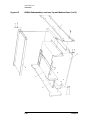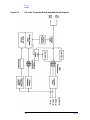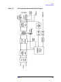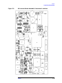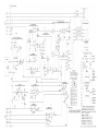
1
Operation and Service Manual Agilent Technologies 85901A AC Power Source This manual applies directly to Agilent 85901A AC Power Sources with serial numbers prefixed 2838K and below. Manual Part Number: 85901-90001 Supersedes September 1988 Microfiche Part Number: 85901-90004 Printed in USA April 2000 © Copyright 1988-2000 Agilent Technologies, Inc. The information contained in this document is subject to change without notice. Agilent Technologies makes no warranty of any kind with regard to this material, including but not limited to, the implied warranties of merchantability and fitness for a particular purpose. Agilent Technologies shall not be liable for errors contained herein or for incidental or consequential damages in connection with the furnishing, performance, or use of this material. The following safety symbols are used throughout this manual. Familiarize yourself with the symbols and their meaning before operating this instrument. WARNING Warning denotes a hazard. It calls attention to a procedure which, if not correctly performed or adhered to, could result in injury or loss of life. Do not proceed beyond a warning note until the indicated conditions are fully understood and met. CAUTION Caution denotes a hazard. It calls attention to a procedure that, if not correctly performed or adhered to, could result in damage to or destruction of the instrument. Do not proceed beyond a caution sign until the indicated conditions are fully understood and met. NOTE Agilent Technologies certifies that this product met its published specifications at the time of shipment from the factory. Agilent further certifies that its calibration measurements are traceable to the United States National Bureau of Standards, to the extent allowed by the Bureau’s calibration facility, and to the calibration facility of other International Standards Organization members. WARNING Before the charger of the 85901A is switched on, make sure it has been properly grounded through the protective conductor of the ac power cable to a socket outlet provided with the protective earth contact. Any interruption of the protective (grounding) conductor inside or outside the instrument, or disconnection of the protective earth terminal, can result in personal injury. WARNING There are voltages at many points in the instrument which can, if contacted, cause personal injury. Be extremely careful. Any adjustments or service procedures that require operation of the instrument with the protected covers removed should be performed only by trained service personnel. ii WARNING ALWAYS assume that high voltage is present at the inverter output and on the power cord adapters. NEVER rely on the position of the inverter switch or charger switch or on the front-panel LED indicators to determine if high voltage is present. Never use a damaged power cord adapter. The inverter output should be treated as cautiously as you would treat a line voltage source. WARNING When the high voltage output of the inverter is exposed, for example when the 85901A is used in servicing some other instrument, take extreme safety precautions as you would for any high voltage exposure. ALWAYS disconnect all inverter power cords before servicing the load unit. NEVER rely on the position of the inverter switch or charger switch or on the front-panel LED indicators to determine if high voltage is present. CAUTION Before an instrument is connected to the 85901A, verify that the line voltage selector of the instrument to be connected is set to the same voltage as the 85901A inverter output voltage. Failure to set the ac power input to the correct voltage could cause damage to the instrument. Regulatory Notices Herstellerbescheinigung Hiermit wird bescheinigt, daβ das Gerät/System 85901A in Übereinstimmung mit den Bestimmungen von Postverfügung 1046/84 funkentstört ist. Der Deutschen Bundespost wurde das Inverkehrbringen dieses Gerätes/Systems angezeigt und die Berechtigung Überprüfung der Serie auf Einhaltung der Bestimmungen eingeräumt. Zusaatzinformation fur Meβ-und Testgeräte Werden Meβ- und Testgeräte mit ungeschirmten Kabeln und/oder in offenen Meβaufbauten verwendet, so ist vom Betreiber sicherzustellen, daβ die Funk-Entstörbestimmungen unter Betriebsbedingungen an seiner Grundstücksgrenze eingehalten werden. iii Manufacturer’s Declaration This is to certify that the equipment 85901A is in accordance with the Radio Interference Requirements of Directive FTZ 1046/84. The German Bundespost was notified that this equipment was put into circulation, the right to check the series for compliance with the requirements was granted. Additional Information for Test- and Measurement Equipment If Test- and Measurement Equipment is operated with unscreened cables and/or used for measurements on open set-ups, the user has to assure that under operating conditions the Radio Interference Limits are still met at the border of his premises. Warranty This Agilent Technologies instrument product is warranted against defects in material and workmanship for a period of one year from date of shipment. During the warranty period, Agilent Technologies will, at its option, either repair or replace products which prove to be defective. For warranty service or repair, this product must be returned to a service facility designated by Agilent Technologies. Buyer shall prepay shipping charges to Agilent Technologies and Agilent Technologies shall pay shipping charges to return the product to Buyer. However, Buyer shall pay all shipping charges, duties, and taxes for products returned to Agilent Technologies from another country. Agilent Technologies warrants that its software and firmware designated by Agilent Technologies for use with an instrument will execute its programming instructions when properly installed on that instrument. Agilent Technologies does not warrant that the operation of the instrument, or software, or firmware will be uninterrupted or error-free. iv LIMITATION OF WARRANTY The foregoing warranty shall not apply to defects resulting from improper or inadequate maintenance by Buyer, Buyer-supplied software or interfacing, unauthorized modification or misuse, operation outside of the environmental specifications for the product, or improper site preparation or maintenance. NO OTHER WARRANTY IS EXPRESSED OR IMPLIED. AGILENT TECHNOLOGIES SPECIFICALLY DISCLAIMS THE IMPLIED WARRANTIES OF MERCHANTABILITY AND FITNESS FOR A PARTICULAR PURPOSE. EXCLUSIVE REMEDIES THE REMEDIES PROVIDED HEREIN ARE BUYER’S SOLE AND EXCLUSIVE REMEDIES. AGILENT TECHNOLOGIES SHALL NOT BE LIABLE FOR ANY DIRECT, INDIRECT, SPECIAL, INCIDENTAL, OR CONSEQUENTIAL DAMAGES, WHETHER BASED ON CONTRACT, TORT, OR ANY OTHER LEGAL THEORY. v vi Contents 1. General Information Introduction . . . . . . . . . . . . . . . . . . . . . . . . . . . . . . . . . . . . . . . . . . . . . . . . . . . . . . . . . . . . . . . .1-2 Description . . . . . . . . . . . . . . . . . . . . . . . . . . . . . . . . . . . . . . . . . . . . . . . . . . . . . . . . . . . . . . . . .1-2 Specifications . . . . . . . . . . . . . . . . . . . . . . . . . . . . . . . . . . . . . . . . . . . . . . . . . . . . . . . . . . . . . . .1-2 Safety Considerations . . . . . . . . . . . . . . . . . . . . . . . . . . . . . . . . . . . . . . . . . . . . . . . . . . . . . . . .1-4 Instruments Covered by This Manual . . . . . . . . . . . . . . . . . . . . . . . . . . . . . . . . . . . . . . . . . . .1-4 2. Installation Introduction . . . . . . . . . . . . . . . . . . . . . . . . . . . . . . . . . . . . . . . . . . . . . . . . . . . . . . . . . . . . . . . .2-2 Initial Inspection . . . . . . . . . . . . . . . . . . . . . . . . . . . . . . . . . . . . . . . . . . . . . . . . . . . . . . . . . . . .2-2 Preparation for Use . . . . . . . . . . . . . . . . . . . . . . . . . . . . . . . . . . . . . . . . . . . . . . . . . . . . . . . . . .2-4 Power Requirements . . . . . . . . . . . . . . . . . . . . . . . . . . . . . . . . . . . . . . . . . . . . . . . . . . . . . . . .2-4 Inverter Line Voltage and Fuse Selection. . . . . . . . . . . . . . . . . . . . . . . . . . . . . . . . . . . . . . . . .2-4 Connecting Internal Battery . . . . . . . . . . . . . . . . . . . . . . . . . . . . . . . . . . . . . . . . . . . . . . . . . . .2-6 Connecting External Battery. . . . . . . . . . . . . . . . . . . . . . . . . . . . . . . . . . . . . . . . . . . . . . . . . . .2-7 Power Cable for Charger Input . . . . . . . . . . . . . . . . . . . . . . . . . . . . . . . . . . . . . . . . . . . . . . . .2-10 Power Cable for Inverter Output. . . . . . . . . . . . . . . . . . . . . . . . . . . . . . . . . . . . . . . . . . . . . . .2-10 Operating Environment . . . . . . . . . . . . . . . . . . . . . . . . . . . . . . . . . . . . . . . . . . . . . . . . . . . . . .2-11 Temperature . . . . . . . . . . . . . . . . . . . . . . . . . . . . . . . . . . . . . . . . . . . . . . . . . . . . . . . . . . . . .2-11 Humidity . . . . . . . . . . . . . . . . . . . . . . . . . . . . . . . . . . . . . . . . . . . . . . . . . . . . . . . . . . . . . . . .2-11 Installation . . . . . . . . . . . . . . . . . . . . . . . . . . . . . . . . . . . . . . . . . . . . . . . . . . . . . . . . . . . . . . . .2-11 Storage and Shipment . . . . . . . . . . . . . . . . . . . . . . . . . . . . . . . . . . . . . . . . . . . . . . . . . . . . . . .2-12 Environmental. . . . . . . . . . . . . . . . . . . . . . . . . . . . . . . . . . . . . . . . . . . . . . . . . . . . . . . . . . . .2-12 Packaging. . . . . . . . . . . . . . . . . . . . . . . . . . . . . . . . . . . . . . . . . . . . . . . . . . . . . . . . . . . . . . . .2-12 3. Operation Introduction . . . . . . . . . . . . . . . . . . . . . . . . . . . . . . . . . . . . . . . . . . . . . . . . . . . . . . . . . . . . . . . .3-2 Front-Panel Features . . . . . . . . . . . . . . . . . . . . . . . . . . . . . . . . . . . . . . . . . . . . . . . . . . . . . . . . .3-2 Rear-Panel Description . . . . . . . . . . . . . . . . . . . . . . . . . . . . . . . . . . . . . . . . . . . . . . . . . . . . . . .3-4 Charging the Battery . . . . . . . . . . . . . . . . . . . . . . . . . . . . . . . . . . . . . . . . . . . . . . . . . . . . . . . . .3-4 Basic Operation Check. . . . . . . . . . . . . . . . . . . . . . . . . . . . . . . . . . . . . . . . . . . . . . . . . . . . . . . .3-5 Charger Operation . . . . . . . . . . . . . . . . . . . . . . . . . . . . . . . . . . . . . . . . . . . . . . . . . . . . . . . . .3-5 Inverter Operation . . . . . . . . . . . . . . . . . . . . . . . . . . . . . . . . . . . . . . . . . . . . . . . . . . . . . . . . .3-5 4. Performance Tests Introduction . . . . . . . . . . . . . . . . . . . . . . . . . . . . . . . . . . . . . . . . . . . . . . . . . . . . . . . . . . . . . . . .4-2 Equipment Required . . . . . . . . . . . . . . . . . . . . . . . . . . . . . . . . . . . . . . . . . . . . . . . . . . . . . . . . .4-2 Performance Test Record . . . . . . . . . . . . . . . . . . . . . . . . . . . . . . . . . . . . . . . . . . . . . . . . . . . . . .4-2 1. Inverter Output Voltage and LED Annunciators . . . . . . . . . . . . . . . . . . . . . . . . . . . . . . . . .4-3 2. Inverter DC Input Voltage Range . . . . . . . . . . . . . . . . . . . . . . . . . . . . . . . . . . . . . . . . . . . . .4-5 3. Inverter Internal DC Input Operation . . . . . . . . . . . . . . . . . . . . . . . . . . . . . . . . . . . . . . . . .4-7 4. Inverter Shutoff with Charger On. . . . . . . . . . . . . . . . . . . . . . . . . . . . . . . . . . . . . . . . . . . . .4-8 5. Adjustments Introduction . . . . . . . . . . . . . . . . . . . . . . . . . . . . . . . . . . . . . . . . . . . . . . . . . . . . . . . . . . . . . . . .5-2 Equipment Required . . . . . . . . . . . . . . . . . . . . . . . . . . . . . . . . . . . . . . . . . . . . . . . . . . . . . . . . .5-2 Pre-Adjustment Set-up . . . . . . . . . . . . . . . . . . . . . . . . . . . . . . . . . . . . . . . . . . . . . . . . . . . . . . .5-2 Reference Voltage Adjustment: A2R14 . . . . . . . . . . . . . . . . . . . . . . . . . . . . . . . . . . . . . . . . . . .5-3 7 Contents Charger Output Voltage Adjustment . . . . . . . . . . . . . . . . . . . . . . . . . . . . . . . . . . . . . . . . . . . . 5-4 After Completing All Adjustments . . . . . . . . . . . . . . . . . . . . . . . . . . . . . . . . . . . . . . . . . . . . . . 5-5 6. Replaceable Parts Introduction . . . . . . . . . . . . . . . . . . . . . . . . . . . . . . . . . . . . . . . . . . . . . . . . . . . . . . . . . . . . . . . . 6-2 7. Service Introduction . . . . . . . . . . . . . . . . . . . . . . . . . . . . . . . . . . . . . . . . . . . . . . . . . . . . . . . . . . . . . . . . 7-2 Overall Description . . . . . . . . . . . . . . . . . . . . . . . . . . . . . . . . . . . . . . . . . . . . . . . . . . . . . . . . . . 7-2 Front-Panel Description . . . . . . . . . . . . . . . . . . . . . . . . . . . . . . . . . . . . . . . . . . . . . . . . . . . . . . 7-4 Rear-Panel Description . . . . . . . . . . . . . . . . . . . . . . . . . . . . . . . . . . . . . . . . . . . . . . . . . . . . . . . 7-4 Inverter . . . . . . . . . . . . . . . . . . . . . . . . . . . . . . . . . . . . . . . . . . . . . . . . . . . . . . . . . . . . . . . . . . . 7-5 DC-to-DC Converter. . . . . . . . . . . . . . . . . . . . . . . . . . . . . . . . . . . . . . . . . . . . . . . . . . . . . . . . 7-5 Inverter Circuit Operation. . . . . . . . . . . . . . . . . . . . . . . . . . . . . . . . . . . . . . . . . . . . . . . . . . . 7-8 DC-to-AC Switcher . . . . . . . . . . . . . . . . . . . . . . . . . . . . . . . . . . . . . . . . . . . . . . . . . . . . . . . . . 7-8 Charger Introduction. . . . . . . . . . . . . . . . . . . . . . . . . . . . . . . . . . . . . . . . . . . . . . . . . . . . . . . . 7-10 Charger Block Diagram Overview. . . . . . . . . . . . . . . . . . . . . . . . . . . . . . . . . . . . . . . . . . . . 7-10 Flyback Control Circuit . . . . . . . . . . . . . . . . . . . . . . . . . . . . . . . . . . . . . . . . . . . . . . . . . . . . 7-12 Normal Operation . . . . . . . . . . . . . . . . . . . . . . . . . . . . . . . . . . . . . . . . . . . . . . . . . . . . . . . . 7-12 Power-Limited Operation. . . . . . . . . . . . . . . . . . . . . . . . . . . . . . . . . . . . . . . . . . . . . . . . . . . 7-13 Shut-Off Circuit . . . . . . . . . . . . . . . . . . . . . . . . . . . . . . . . . . . . . . . . . . . . . . . . . . . . . . . . . . 7-13 Control Circuit Introduction . . . . . . . . . . . . . . . . . . . . . . . . . . . . . . . . . . . . . . . . . . . . . . . . . . 7-14 Control Circuit Block Diagram . . . . . . . . . . . . . . . . . . . . . . . . . . . . . . . . . . . . . . . . . . . . . . 7-14 Status-Sensing Circuits . . . . . . . . . . . . . . . . . . . . . . . . . . . . . . . . . . . . . . . . . . . . . . . . . . . . 7-16 Shut-Off Circuits . . . . . . . . . . . . . . . . . . . . . . . . . . . . . . . . . . . . . . . . . . . . . . . . . . . . . . . . . 7-17 Buzzer and Indicator Driver . . . . . . . . . . . . . . . . . . . . . . . . . . . . . . . . . . . . . . . . . . . . . . . . 7-17 Bias Power Supply . . . . . . . . . . . . . . . . . . . . . . . . . . . . . . . . . . . . . . . . . . . . . . . . . . . . . . . . 7-18 8 1 General Information 1-1 General Information Introduction Introduction This manual contains information required to operate and service the Agilent Technologies Model 85901A AC Power Source. The 85901A is shown in Figure 1-1 with all of its externally supplied accessories. Description The 85901A is a portable ac power source. It can be operated on the bench or as a portable power supply for field service. Other uses are for measurements requiring power line isolation or for measurements performed during power failure. The instrument has a carrying handle that can also be used as an adjustable tilt-stand. The handle can be moved by pushing the sides of the handle in and then turning the handle to a suitable position. The 85901A consists of battery, inverter, charger, and control circuits. It provides up to 200W maximum continuous power with the internal battery, at either 115 Vrms or 230 Vrms. The 85901A weighs 14.2 kg (31.3 lbs) with the battery installed, and 8.0 kg (17.6 lbs) without the battery. The rear panel has terminals for connecting an external battery or other 12 Vdc source. The dimensions of the package are 337 mm wide by 125 mm high by 461 mm deep. Specifications Instrument specifications are listed in Table 1-1. These specifications are the performance standards or limits against which the instrument may be tested. Performance characteristics are listed in Table 1-2. Characteristics provide useful information by describing typical, non-warranted instrument performance. 1-2 Chapter 1 General Information Specifications Figure 1-1 85901A w/Complete Set of General Purpose Power-Cord Adapters Chapter 1 1-3 General Information Safety Considerations Safety Considerations The 85901A AC Power Source has been designed to conform to the safety requirements of an IEC (International Electromechanical Committee) Safety Class I instrument, and is shipped from the factory in a safe condition. This Agilent Technologies 85901A A C Power Source Operation and Service Manual, and all related documentation, must be reviewed for familiarization with safety markings and instructions before operation. This unit is to be used in a controlled environment. WARNING This unit contains more than one live circuit. See the schematic diagrams. This operation and service manual contains safety information, cautions, and warnings which must be followed by the user to ensure safe operation and to maintain the instrument in a safe condition. Instruments Covered by This Manual This instrument has a two-part serial number in the form of 00000K00000 (see Figure 1-2). The number is stamped on the serial plate attached to the rear panel of the instrument. The first five digits and the letter constitute the serial prefix; the last five digits form the digits. The prefix is the same for all identical instruments, and it changes only when a change is made to the instrument. The suffix, however, is assigned sequentially and is different for each instrument. The contents of this manual apply directly to instruments having the same serial number prefix(es) listed under "Serial Numbers” on the title page. The letter placed between the two sets of digits identifies the country where the instrument was manufactured. 1-4 Chapter 1 General Information Instruments Covered by This Manual Figure 1-2 Typical Serial Number Label An instrument manufactured after the printing of this manual may have a serial number prefix that is not listed on the title page. This unlisted serial number prefix indicates that the instrument is different from those described in the manual. The manual for a newer instrument is accompanied by a Manual Updating Supplement, which contains the change information that explains how to adapt the manual to the newer instrument. In addition to change information, the supplement may contain information for correcting errors in the manual. To keep this manual as current and accurate as possible, Agilent recommends that you periodically request Manual Updating Supplement. The supplements are identified with the manual print date and part number, both of which appear on the manual title page. For information concerning a serial number prefix that is not listed on the title page or in the Manual Updating Supplement, contact your nearest Agilent office. Chapter 1 1-5 General Information Instruments Covered by This Manual Table 1-1 85901A Specifications Specifications describe warranted performance over the temperature range of 0°C to 55°C after one hour continuous operation, unless otherwise noted. INPUTS Inverter1 Voltage 10.8 Vdc to 14.5 Vdc Charger2 Voltage 90 to 250 Vac, auto-selected Frequency 44 to 66 Hz Power consumption 122 VA, maximum OUTPUTS Inverter Voltage 135 or 270 V peak 5% Rectangular waveform with 25% dead zone (115 or 230 Vrms 5%) Frequency 60 Hz 0.1%, crystal reference Maximum power 200W, continuous 1-6 1. The inverter input must not have any transients higher than 14.5 V. Otherwise, the overvoltage protection circuit will automatically turn the inverter off. 2. Turning the charger on automatically turns the inverter off. Chapter 1 General Information Instruments Covered by This Manual Table 1-2 85901A Characteristics (1 of 2) ENVIRONMENTAL Temperature1 Operating Storage: 0°C to +55°C with battery –20°C to +40°C without battery –40°C to +70°C Conducted emission FTZ 1046 Radiated emission FTZ 1046 Type Sealed lead acid Voltage 12Vdc Capacity 17 ampere-hours EMI Battery23 MECHANICAL Dimensions: width 337mm (13.3 in) height 125 mm (4.9 in) depth 461 mm 18.1 in) Weight: with battery without battery 14.2 kg (31.3 lb) 8.0 kg (17.7 lb) Shipping weight 16.3 kg (36.0 lb) BATTERY SHELF LIFE Storage Temperature <20°C Recharge Interval 18 months 20°C to 30°C12 months 0°C to 40°C 6 months CERTIFICATION The 85901A is certified for use with the following Agilent test and measurement equipment: HP/Agilent 8562A/B, Agilent 8590A, and Agilent 8592A, and their options. 1. Shelf life of battery decreases with either extended operation or storage at higher than 40C 2. Battery cyclic life (charge-discharge) is nominally rated at more than 200 cycles. Battery is a Matsushita Electric LCR12V17P sealed lead acid. Battery is available from Agilent Technologies as HP/Agilent p/n 1420-0373. 3. Chapter 1 1-7 General Information Instruments Covered by This Manual Figure 1-3 85901A Characteristics (2 of 2) Table 1-3 Recommended Test Equipment Instrument Critical Specifications Recommended Model Where Used Perf. Tests Power Supply Output voltage: 9 to 20 Vdc HP/Agilent 6032A √ Digital Multimeter 4.5 digits display HP/Agilent 3487A √ Electronic Load Input voltage: 20 Vdc Input current: 10A minimum Fujitsu EUL-300D √ 1-8 Adj. Service √ √ √ √ Chapter 1 2 Installation 2-1 Installation Introduction Introduction This chapter provides the information needed to install the 85901A AC Power Source. Topics covered include: initial inspection, line voltage and fuse selection, operating environment, battery charging, battery replacement, storage, and shipment. Initial Inspection The 85901A AC Power Source, as shipped from the factory, meets all the specifications listed in Table 1-1. Inspect the shipping container for damage. If the shipping container or cushioning material is damaged, notify the carrier as well as the Agilent office and be sure to keep the shipping materials for the carrier's inspection until the contents of the shipment have been checked for completeness and the instrument has been checked mechanically and electrically. Complete shipment contents are shown in Figure 2-1. A test procedure for checking general electrical operation may be found under "Basic Operation Check" in Chapter 3. Performance tests to check the 85901A against its specifications are given in Chapter 4. If the instrument does not pass the performance tests, notify the nearest Agilent office (or, to obtain the address of the Agilent office nearest you, contact an office listed on the inside rear cover of this manual). The office will arrange for repair or replacement without waiting for a claim settlement. CAUTION Before using the 85901A for the first time, the internal battery should be charged. Follow the procedure for charging the battery in Chapter 3. If the shipping materials are in good condition, retain them for possible future use. You may wish to ship the instrument to another location or return it to Agilent for service. 2-2 Chapter 2 Installation Initial Inspection Figure 2-1 85901A Shipping Container and Contents Chapter 2 2-3 Installation Preparation for Use Preparation for Use Power Requirements The inverter of the 85901A requires a power source of 10.8 Vdc to 14.5 Vdc. Power consumption is approximately 330W when the 85901A provides its maximum continuous output capacity of 200W. WARNING If the instrument is to be energized via an external autotransformer for voltage reduction, make sure the common terminal is connected to the neutral pole of the charger input. CAUTION Before turning the 85901A charger switch on, verify that the line voltage is within the charger input's voltage range. The charger circuit of the 85901A requires a power source of 90 to 250 Vac, 47 to 66 Hz, single-phase. You do not need to select the correct input voltage; the charger circuit automatically does so. Maximum power consumption in the charging mode is approximately 122 VA. Inverter Line Voltage and Fuse Selection CAUTION Before turning the 85901A inverter switch on, verify that the connected instrument's line voltage selection is set to the same voltage as the 85901A inverter output voltage. The 85901A voltage selection switch selects the output voltage of the inverter (115V or 230V). The appropriate fuses are factory-installed for the instrument's destination. Figure 2-2 illustrates replacement fuses, and Table 2-1 lists their ratings and part numbers. CAUTION Before using the 85901A, check that the proper fuse for your line voltage and selected inverter-output voltage is installed. 2-4 Chapter 2 Installation Inverter Line Voltage and Fuse Selection Figure 2-2 Line Voltage and Fuse Selection Table 2-1 Replacement Fuse Ratings and Part Numbers No. Function Rating P/N 1 Line Fuse 250V, 1.6A 2110-0773 2 Battery Fuse 32V, 30A 2110-0809 3 Inverter Output Fuse 250V, 4A 2110-0734 Chapter 2 2-5 Installation Connecting Internal Battery Connecting Internal Battery The internal battery for the 85901A is not installed when the instrument is shipped from the factory. When unpacking the 85901A, you will find a package containing two battery connectors in the main container. You will also find two screws and two washers in the battery container. These connectors and screws are used to install the internal battery. You will need two screwdrivers, both slotted and Phillips. WARNING This instrument is independent of the power mains. HIGH VOLTAGE is present whenever the internal battery has been installed and the inverter switch is on. Connecting the battery may cause electrical arcing at the terminal. Do not connect the battery in an explosive atmosphere or near inflammable materials. CAUTION The voltage ratings of the battery should be the same as the input voltage range of the inverter. Verify that you are installing a battery of the correct voltage rating. Connect the internal battery's positive and negative terminals to the 85901A front-panel positive (red wire) and negative (black wire) internal battery terminals, respectively. 1. Install the two separate battery connectors on the battery. 2. Open the battery door in the right-hand side of the front panel. 3. Place the battery in the 85901A battery cage with its terminals toward the top. Correct battery position and connection polarity are shown in Figure 2-3 4. Insert the two internal battery cable terminals into the positive and negative battery connectors, respectively. Fasten them using the two screws. 5. Refasten the battery cage door. Confirm the correct placement of the wide four-terminal shorting strap at the rear-panel terminal block. Refer to Figure 2-4 for correct terminal block configurations with either internal or external batteries. 2-6 Chapter 2 Installation Connecting External Battery Connecting External Battery The 85901A AC Power Source can use an external battery by connecting the external battery to the rear-panel terminal block. Car and truck 12V batteries can be used for the external battery. Figure 2-4 shows the correct connections from the 85901A terminal block to the external battery. WARNING This instrument is independent of the power mains. HIGH VOLTAGE is present whenever a 12 Vdc source has been connected and the inverter switch is on. Connecting the battery may cause electrical arcing at the terminal. Do not connect the battery in an explosive atmosphere or near inflammable materials. NOTE When an external DC voltage source is used, voltage transients must not exceed 14.5V or the Over Voltage Protection circuitry will shut the inverter off. Likewise, if an external charger is connected to an external battery, voltage transients above 14.5V may turn the 85901A off. This may happen, for example, when a car battery is used while the car's alternator is operating. Chapter 2 2-7 Installation Connecting External Battery Figure 2-3 Battery Position and Connector Polarity 2-8 Chapter 2 Installation Connecting External Battery Figure 2-4 Battery Terminal Block CAUTION The voltage ratings of the battery should be the same as the input voltage range of the inverter. Verify that you are installing a battery of the correct voltage rating Connect the external battery's positive and negative terminals to the 85901A rear-panel positive and negative external-battery terminals, respectively. Do not remove the wide two-terminal shorting bar on rear-panel positive and negative external- battery terminals. Chapter 2 2-9 Installation Power Cable for Charger Input Power Cable for Charger Input The 85901A is equipped with a three-connector power cable.When connected to an appropriate ac power receptacle, this cable grounds the instrument cabinet. WARNING The mains plug may only be inserted in a socket outlet provided with a protective earth contact. The protective action must not be negated by the use of an extension cord (power cable) without a protective conductor (grounding). Grounding one conductor of a two-conductor outlet is not sufficient protection. Various power cables are available to connect the instrument to the types of ac power outlets unique to specific geographic areas. The cable appropriate for the area to which the analyzer is originally shipped is included with the unit. NOTE While the inverter output is used, the 85901A will meet its EMI specification with the charger input power cable removed. Power Cable for Inverter Output The 85901A standard connector is two CEE22-V connectors in place of the USA standard NEMA-15P connector. The interconnection cable, Part Number 8120-5220, CEE22-V male to NEMA-15P female, is provided. This cable is used to connect external instruments to the inverter output. Other general-purpose power-cord adapters are available. The adapters listed below allow country-specific line cords to be plugged into the 85901A AC Power Source. Europe HP/Agilent Part Number 8120-5210 U.S.A. HP/Agilent Part Number 8120-5211 United Kingdom HP/Agilent Part Number 8120-5212 2-10 Chapter 2 Installation Operating Environment Operating Environment Temperature The 85901A may be operated over temperatures from O°C to +55°C. Temperatures above +400C may reduce the life of the battery. Humidity The 85901A may be operated in environments with relative humidities up to 95% and to +40°C. However, the 85901A should be protected from temperature extremes, which cause condensation within the instrument. Installation The 85901A can be operated on the bench or as a portable power supply for field use. The instrument has a carrying handle that can also be used as an adjustable tilt-stand. The handle can be moved by pushing its sides in and then turning the handle to the desired position. The battery must be installed before the 85901A can be operated. See the battery-installation instructions, above. Before turning on the 85901A inverter switch, verify that the same line voltage is selected for both the 85901A inverter output and the equipment connected to the inverter output. Chapter 2 2-11 Installation Storage and Shipment Storage and Shipment Environmental The 85901A with battery may be stored and shipped in environments within the following limits: Temperature –20°C to +40°C Humidity <95% Altitude <50,000 ft The 85901A should be protected from temperature extremes, which cause condensation inside the equipment. Packaging Original packaging is shown in Figure 2-1. Containers and materials identical to those used in factory packaging are available through Agilent offices. If the instrument is being returned to Agilent for servicing, attach a tag indicating the type of service required, return address, model number, and full serial number. Mark the container FRAGILE to assure careful handling. In any correspondence, refer to the instrument by model number and full serial number. Other packaging may be used if these general instructions for repackaging with commercially-available materials are followed: a. Wrap instrument in heavy paper or plastic. If it is being shipped to an Agilent office or service center, attach tag indicating the type of service required, return address, model number, and full serial number. b. Use a strong shipping container. A double-walled carton made of 350-pound test material is adequate. c. Use enough shock-absorbing material (3- to 4-inch layer) around all sides of instrument to provide firm cushioning and prevent movement inside the container. d. Seal shipping container securely. e. Mark shipping container FRAGILE to ensure careful handling. 2-12 Chapter 2 3 Operation 3-1 Operation Introduction Introduction This chapter provides operating instructions for the 85901A AC Power Source. It also provides a brief description of the front- and rear-panel features. Upon receipt of the 85901A AC Power Source, perform the procedure described under "Basic Operation Check" in this chapter. This check should also be performed after the instrument has been repaired. LED indicators, which represent the status of the battery, inverter, and charger circuits, are located on the left-hand side of the front panel. See Figure 3-1. Front-Panel Features LED indicators, which represent the status of the battery, inverter, and charger circuits, are located on the left-hand side of the front panel. See Figure 3-1. The battery function area has two LEDs: the yellow LED indicates whether the charger is on or off, and the red LED indicates the state of the battery charger circuit. When the charger is operating, the red LED will be on if the battery-charging current is greater than 0.45 A 0.15 A, and it will be off if the battery-charging current is less than 0.45 A 0.15 A. The inverter function area includes a yellow LED and the inverter on/off switch. The LED should be on when the inverter switch is on and the inverter is operating, and it should be off when the inverter is not operating. The inverter will not operate while the battery charger is operating. During inverter operation, the red LED in the battery function area also is used to indicate the state of the battery output voltage. When the inverter is operating, the red LED will be off when battery voltage is greater than 10.8 V typical, and it will blink (accompanied by a buzzer) when battery voltage is less than 10.8 V typical. The battery door occupies the remaining part of the front panel. This door provides access for battery service. 3-2 Chapter 3 Operation Front-Panel Features Figure 3-1 Front-Panel Features Figure 3-2 Rear-Panel Features Chapter 3 3-3 Operation Rear-Panel Description Rear-Panel Description The charger on/off switch is located in the upper left-hand corner of the rear panel (see Figure 3-2). A yellow LED in the front-panel battery function area indicates whether the charger is on or off. The charger input line module is mounted directly below the charger switch. The line module contains the I-6A 250V charger input fuse. The inverter voltage selection switch, two CEE-22V receptacles, and 4A 250V inverter output fuse are grouped together by the INV OUTPUT bracket. The voltage selection switch sets the inverter output to 115V or 230V. The internal battery fuse and external battery fuse (both 30A 32 Vdc) are located above the inverter output receptacles. The battery selection terminal block occupies the upper right-hand half of the rear panel. Select the internal battery or an external battery by changing the position of the shorting bar on the terminal block. The external battery's positive and negative leads are connected to the terminals marked plus and minus, respectively. Charging the Battery Before the 85901A is used for the first time, the internal battery should be charged for up to six hours. This will ensure that the battery has its maximum charge. 1. After the internal battery has been installed, connect the power cable to the rear-panel charger line receptacle (directly under the charger switch). 2. Check the rear-panel battery terminal block to ensure that the battery selection jumper is connected for INT battery selection. 3. Check to make sure that no other equipment is connected to the inverter output receptacles at this time. 4. Turn on the charger switch. Verify that the yellow LED in the front-panel battery function area has turned on. 5. Let the charger continue to operate until the red LED turns off. This indicates that the battery has been fully charged. 6. Turn off the charger switch. The 85901A is now ready for normal use. CAUTION The charger circuit is designed for use with the internal battery. Do not use it to charge an external battery. 3-4 Chapter 3 Operation Basic Operation Check Basic Operation Check The following steps will verify basic operation of the 85901A. These short procedures will not verify that the 85901A meets all its specifications; they are intended simply as a quick method to verify that all major functions of the 85901A operate correctly. To verify that the instrument meets its specifications, or in case of a problem, refer to Chapter 4 for the appropriate inverter or charger performance test. Charger Operation Refer to “Charging the Battery” in this chapter to verify that the charger is functioning correctly. Inverter Operation This procedure verifies that the inverter is functioning correctly. 1. Ensure that the charger and inverter switches are turned off. 2. Connect an external instrument to one of the INV OUTPUT receptacles using the appropriate power cable and/or adapter cable. 3. Turn on the front-panel inverter switch. The yellow LED in the inverter function area just above the inverter switch should be on. Turn on the equipment connected to the inverter output. 4. The red LED in the battery function area should not be lit if the battery voltage is greater than 10.8 Vdc typical; if the battery voltage is less than 10.8 Vdc typical, the red LED should blink and a buzzer should sound. The inverter will not operate when the battery output voltage is greater than 14.5 Vdc typical or less than 10.0 Vdc typical. 5. Turn on the rear-panel charger switch. The inverter LED and the ac inverter output should turn off. The yellow battery-function LED should turn on, indicating that the charger is operating and has shut off the inverter. The red battery-function LED indicates the state of the battery-charging current: it will be lit if the battery-charging current is greater than 0.45 A 0.15 A; it will not be lit if the battery-charging current is less than 0.45 A 0.15 A. 6. Turn off the charger and inverter switches. Wait five seconds, then turn on the inverter switch. The inverter ac output should again be present and operate the external equipment. Chapter 3 3-5 Operation Basic Operation Check 3-6 Chapter 3 4 Performance Tests 4-1 Performance Tests Introduction Introduction The procedures in this section test the instrument's electrical performance using the specifications of Table 1-1 as performance standards. These tests can be performed without access to the interior of the instrument. Equipment Required Equipment required for the performance tests is listed in Table 1-3. Any equipment that satisfies the critical specifications given in the table may be substituted for the recommended model(s). CAUTION To prevent short-circuits, use suitable wire terminals for wire leads connected to the rear-panel terminal block. Performance Test Record Results of the performance tests may be tabulated at the end of this chapter in Table 4-1. The table lists all the tested specifications and their acceptable limits. Test results recorded at incoming inspection can be used for comparison in periodic maintenance, troubleshooting, and after repairs or adjustments. 4-2 Chapter 4 Performance Tests 1. Inverter Output Voltage and LED Annunciators 1. Inverter Output Voltage and LED Annunciators This test measures the output voltage of the inverter, and verifies operation of the front-panel LED annunciators. Specification Inverter output voltage1 115 Vrms 7% or 230 Vrms 7% Output frequency 60 Hz, Crystal Reference LED Annunciators Battery charge (yellow LED) OFF Battery charge low (red LED) OFF Inverter (yellow LED) ON 1. The inverter output voltage is a modified square wave of 135V or 270V, with a 25% dead zone at the zero voltage level. The output voltage waveform, with period timing and peak voltage levels, is shown in the illustration. (Note: 135V or 270V peak 5% is equivalent to 115 Vrms or 230 Vrms 5%.) Figure 4-1 Inverter Performance Test Setup Chapter 4 4-3 Performance Tests 1. Inverter Output Voltage and LED Annunciators Equipment Power Supply.......................................................HP/Agilent 6032A Digital Multimeter ..............................................HP/Agilent 3478A WARNING This instrument is independent of power mains. High voltage will be present at the inverter output, and at the resistive load(s), whenever the internal battery or an external 12 Vdc source is installed and the inverter switch is on. Procedure 1. Connect the equipment as shown in Figure 4-1. 2. Turn off the rear-panel charger switch. Set the INV OUTPUT voltage selector switch to 115 Vrms. 3. Connect the four-wide shorting strap in rear-panel terminal block to the EXT DC IN position. 4. Adjust the power supply for a dc input voltage of 12.0 Vdc 0.1 Vdc. 5. Turn on the inverter switch. 6. Read the inverter output voltage on the digital multimeter and confirm that the LED annunciators operate correctly. 7. Turn off the inverter switch and set the INV OUTPUT voltage selector switch to 230 Vrms. 8. Repeat steps 4 through 6 for 230 Vrms. 9. Record the results of steps 6 and 8 in Table 4-1. 4-4 Chapter 4 Performance Tests 2. Inverter DC Input Voltage Range 2. Inverter DC Input Voltage Range This test verifies inverter operation over the specified input voltage range, and the LED annunciator. Specification Inverter input voltage range 10.8 Vdc to 14.5 Vdc LED Annunciators Battery charge (yellow LED) OFF Battery charge low (red LED) See procedure Inverter (yellow LED) ON Equipment Power Supply................................................HP/Agilent 6032A Digital Multimeter........................................HP/Agilent 3478A WARNING This instrument is independent of power mains. High voltage will be present at the inverter output, and at the resistive load(s), whenever the internal battery or an external 12 Vdc source is installed and the inverter switch is on. Procedure 1. Connect the equipment as shown in Figure 4-1. 2. Turn off the rear-panel charger switch. Set the INV OUTPUT voltage selector switch to 115 Vrms. 3. Connect the four-wide shorting strap in rear-panel terminal block to the EXT DC IN position. 4. Adjust the power supply for a dc input voltage of 12.0 Vdc 0.1 Vdc. 5. Turn on the inverter switch. Decrease the inverter dc input voltage until the battery LED blinks and the buzzer beeps. The voltmeter of the power supply should indicate 11.0 Vdc or lower. 6. Turn off the inverter switch. Adjust the power supply for a inverter dc input voltage of 12.0 Vdc 0.1 Vdc. 7. Turn on the inverter switch. Decrease the inverter dc input voltage until the inverter is shut off. The voltmeter of the power supply should indicate 10.5 Vdc or lower. 8. Turn off the inverter switch. Increase the inverter dc input voltage to 12.0 Vdc 0.1 Vdc. Chapter 4 4-5 Performance Tests 2. Inverter DC Input Voltage Range 9. Turn on the inverter switch. Increase the inverter dc input voltage until the inverter shuts off. The voltmeter of the power supply should indicate 14.5 Vdc or higher. NOTE When an external DC voltage source is used, voltage transients must not exceed 14.5V or the Over Voltage Protection circuitry will shut the inverter off. 10.Record the results of steps 6, 8, and 9 in Table 4-1. 4-6 Chapter 4 Performance Tests 3. Inverter Internal DC Input Operation 3. Inverter Internal DC Input Operation This test measures the 115V and 230V outputs of the inverter operating with the internal battery as the dc input voltage source. CAUTION Before performing this test, ensure that the internal battery is not completely discharged. Specification Inverter output voltage 115 Vrrns 7% or 230 Vrms 7% Output frequency 60 Hz, Crystal Reference Equipment Power Supply...................................................6032A Digital Multimeter...........................................3478A WARNING This instrument is independent of power mains. High voltage will be present at the inverter output, and at the resistive load(s), whenever the internal battery or an external 12 Vdc source is installed and the inverter switch is on. Procedure 1. Connect the equipment as shown in Figure 4-1, without the power supply. 2. Turn off the rear-panel charger switch. Set the INV OUTPUT voltage selector switch to 115 Vrms. 3. Connect the four-wide shorting strap in rear-panel terminal block to the INT DC IN position. This uses the internal battery as the input voltage source. 4. Open the front-panel battery door and ensure that the internal battery terminals are connected to the correct positions. 5. Turn on the inverter switch and record the digital multimeter reading. 6. Turn off the inverter switch and set the INV OUTPUT voltage selector switch to 230 Vrms. 7. Repeat step 5 for 230 Vrms. 8. Record the results in Table 4-1. Chapter 4 4-7 Performance Tests 4. Inverter Shutoff with Charger On 4. Inverter Shutoff with Charger On This test verifies that the inverter will automatically turn off if, while it is on, the charger is turned on. Specification Inverter output voltage is automatically turned off when the charger is turned on. Equipment Power Supply. . . . . . . . . . . . . . . . . . . . . . . . . . HP/Agilent 6032A Digital Multimeter . . . . . . . . . . . . . . . . . . . . . HP/Agilent 3478A WARNING This instrument is independent of power mains. High voltage will be present at the inverter output, and at the resistive load(s), whenever the internal battery or an external 12 Vdc source is installed and the inverter switch is on. Procedure 1. Connect the equipment as shown in Figure 4-1, without the power supply. 2. Turn off the rear-panel charger switch. Set the INV OUTPUT voltage selector switch to 115 Vrms. 3. Connect the four-wide shorting strap in rear-panel terminal block to the INT DC IN position. 4. Turn on the inverter and verify that the digital multimeter indicates 115 Vrms. 5. Connect the charger to the ac mains. Turn on the charger. 6. Verify that the digital multimeter indicates that the inverter has turned off. 7. Turn off the inverter switch and the charger switch. Record this operation in Table 4-1. 4-8 Chapter 4 Performance Tests 4. Inverter Shutoff with Charger On Table 4-1 Performance Test Record Test Item Test No. Results Min. 1. Actual Max. Inverter Output Voltage and LED Annunciators 6. LED status: 2. BATT CHRG (yellow): OFF ON OFF BATT LOW (red): OFF ON OFF INV (yellow): ON ON OFF Inverter output (Vrms) 106.95 123.05 9. Inverter output (Vrms) 213.90 246.10 InverterDC Input Voltage Range 6. Battery low indication (blinking LED) DC input voltage (Vdc) 11.0 8. Lower limit DC input voltage (Vdc) 10.5 9. Upper limit DC input voltage (Vdc) 3. Inverter Internal DC Input Operation Inverter output (Vrms) 4. 14.5 106.95 123.05 213.90 246.10 Inverter Shutoff with Charger On Inverter operation: automatic shutoff Chapter 4 YES NO 4-9 Performance Tests 4. Inverter Shutoff with Charger On 4-10 Chapter 4 5 Adjustments 5-1 Adjustments Introduction Introduction This chapter describes adjustments required to return the 85901A AC Power Source to peak operating condition after repairs are required. Test setups and adjustment procedures are included in this chapter. Data taken during adjustments should be recorded in the spaces provided. Comparison of initial data with data taken during periodic adjustments assists in preventive maintenance and troubleshooting. Test points and adjustment locations are supplied in Chapter 7 and are placed just before the schematic for the assembly. Equipment Required Table 1-3 in Chapter 1 contains a list of test equipment and test accessories required in the adjustment procedures. In addition, the table contains the required minimum specifications and a suggested manufacturer's model number. Pre-Adjustment Set-up This short procedure warms up the A2 Control and A3 Charger board assemblies to remove any component value shift that might affect the adjustments. 1. Turn off the charger switch and the inverter switch. 2. Remove the 85901A cover with a 4 mm hex wrench. WARNING This instrument is independent of power mains. HIGH VOLTAGE is present whenever the internal battery has been installed and the inverter switch is on. 3. Disconnect the wide four-terminal shorting strap in rear-panel terminal block. Connect the (+) terminal of electronic load to DC IN terminal of rear-panel terminal block and the (–) terminal of electronic load to 12V EXT BATT (–) terminal of rear-panel terminal block. 5-2 Chapter 5 Adjustments Reference Voltage Adjustment: A2R14 CAUTION Be sure to connect the electronic load with the correct polarity. Do not let the cables short to the chassis. 4. Set the electronic load for 100Ω load. 5. Turn the charger switch ON Reference Voltage Adjustment: A2R14 This procedure sets the 3.0V reference voltage, by A2R14, used throughout the A2 Control assembly circuits. 1. Connect the negative (–) Digital Voltmeter probe to A2TP3, and the positive (+) probe to test point A2TP2. Refer to Figure 5-1. 2. Set the digital voltmeter to DC Volts and Autorange. 3. Adjust A2R14 for 3.000 0.001 Vdc. Refer to Figure 5-1. 4. Disconnect the probes from A2TP2 and A2TP3. Refer to Figure 5-1. 5. Turn the charger switch off. Figure 5-1 A2R14 Reference Voltage Adjustment Location Chapter 5 5-3 Adjustments Charger Output Voltage Adjustment Charger Output Voltage Adjustment This procedure sets the charger output voltage by setting A3R24 in one leg of the constant-voltage feedback-amplifier bridge. The feedback voltage picked up from the output of the charger sets the input voltage of the bridge. CAUTION Be sure to connect the internal battery cable terminals with the correct polarity. Do not let the cables short to the chassis. 1. Move the charger board jumper A3J4 from across pins 1-2 to pins 2-3. Refer to Figure 5-2. 2. Turn the charger switch on. 3. Adjust A3R24 for 14.5 Vdc 0.1 Vdc across the electronic load. Refer to Figure 5-2. 4. Turn the charger switch off. 5. Move jumper A3J4 from across pins 2-3 to its original position across pins 1-2. Refer to Figure 5-2. Figure 5-2 A3R24 Charger Output Voltage Adjustment Location 5-4 Chapter 5 Adjustments After Completing All Adjustments After Completing All Adjustments 1. Disconnect the electronic load from the rear-panel terminal block. 2. Connect the wide four-terminal shorting strap to the desired position. Refer to “Connecting Internal Battery” or “Connecting External Battery” in Chapter 2. 3. Reinstall the 85901A metal cover with a 4 mm hex wrench. Chapter 5 5-5 Adjustments After Completing All Adjustments 5-6 Chapter 5 6 Replaceable Parts 6-1 Replaceable Parts Introduction Introduction This chapter contains information for ordering parts. The tables list all replaceable parts in order by reference designator. Overall, top, and bottom views of assembly locations are illustrated in Figures 6-1 and 6-2. To order a part listed in the replaceable parts tables, quote the Agilent Technologies part number, indicate quantity required, and address the order to the nearest Agilent Technologies office. To obtain the address of the office nearest you, inquire of one of the Agilent Technologies Sales and Service Offices listed in Chapter 7. 6-2 Chapter 6 Replaceable Parts Introduction Table 6-1 Al Inverter Board Assembly, Replaceable Parts Reference Designation Part Number CD Qty A1 A1C2 A1C A1C4 A1C5 A1C6 A1C7 A1C9 A1C10 A1C11 A1C12 A1C13 A1C14 A1C15 A1C17 A1C18 A1C19 A1C20 A1C21 A1C22 A1C23 A1C24 A1C25 A1C26 A1C27 A1C28 A1C29 A1C30 A1C31 A1C32 A1C33 A1C34 A1C35 A1C36 A1C37 A1C38 A1C39 A1C40 A1C41 A1C42 A1C43 A1C44 A1C45 A1C46 A1C47 85901-60001 0160-3237 0160-7059 0180-4107 0180-4107 0160-0263 0160-3237 0180-3737 0160-7081 0160-7084 0180-2984 0160-3831 0160-0263 0160-3237 0160-7080 0160-7080 0160-7078 0160-7078 0160-7078 0180-2984 0160-7078 0160-7083 0160-3237 0160-3237 0160-7086 0160-7086 0160-0263 0160-7082 0160-0263 0160-3237 0160-3237 0180-3215 0160-3237 0160-7076 0180-0224 0180-0224 0160-4535 0160-7076 0160-7077 0160-7076 0160-7074 0160-7074 0180-4109 0180-4109 0160-7076 1 1 3 8 8 7 1 8 1 4 5 1 7 1 0 0 6 6 6 5 6 3 1 1 6 6 7 2 7 1 1 7 1 4 2 2 4 4 5 4 2 2 0 0 4 1 1 1 1 1 1 1 1 1 1 1 1 1 1 1 1 1 1 1 1 1 1 1 1 1 1 1 1 1 1 1 1 1 1 1 1 1 1 1 1 1 1 1 1 1 Chapter 6 Description INVERTER BOARD ASSEMBLY CAPACITOR-FXD 0.1UF 50VDC CER 20% CAPACITOR-FXD 1UF 250VDC MPE 10% CAPACITOR-FXD 2800UF 25VDC AL CAPACITOR-FXD 2800UF 25VDC AL CAPACITOR-FXD 0.22UF 50VDC CER 20% CAPACITOR-FXD 0.1UF 50VDC CER 20% CAPACITOR-FXD IUF 50VDC AL CAPACITOR-FXD 470PF 50VDC CER 20% CAPACITOR-FXD 2200PF 50VDC PP 2% CAPACITOR-FXD 47UF 50VDC AL CAPACITOR-FXD 0.01UF 50VDC CER 20% CAPACITOR-FXD 0.22UF 50VDC CER 20% CAPACITOR-FXD 0.1UF 50VDC CER 20% CAPACITOR-FXD 220PF 50VDC CER 5% CAPACITOR-FXD 220PF 50VDC CER 5% CAPACITOR-FXD 0.1UF 200VDC PP 10% CAPACITOR-FXD 0.1UF 200VDC PP 10% CAPACITOR-FXD 0.1UF 200VDC PP 10% CAPACITOR-FXD 47UF 50VDC AL CAPACITOR-FXD 0.1UF 200VDC PP 10% CAPACITOR-FXD 820PF 50VDC CER 4% CAPACITOR-FXD 0.1UF 50VDC CER 20% CAPACITOR-FXD 0.1UF 50VDC CER 20% CAPACITOR-FXD 270PF 1000VDC CER 20% CAPACITOR-FXD 270PF 1000VDC CER 20% CAPACITOR-FXD 0.22UF 50VDC CER 20% CAPACITOR-FXD 120PF 50VDC CER 5% CAPACITOR-FXD 0.22UF 50VDC CER 20% CAPACITOR-FXD 0.1UF 50VDC CER 20% CAPACITOR-FXD 0.1UF 50VDC CER 20% CAPACITOR-FXD 100UF 16VDC AL CAPACITOR-FXD 0.1UF 50VDC CER 20% CAPACITOR-FXD 0.033UF 630V MPE 10% CAPACITOR-FXD 10UF 16VDC AL CAPACITOR-FXD 10UF 16VDC AL CAPACITOR-FXD 1UF 50VDC CER 10% CAPACITOR-FXD 0.033UF 630V MPE 10% CAPACITOR-FXD 0.1UF 630V MPE 10% CAPACITOR-FXD 0.033UF 630V MPE 10% CAPACITOR-FXD 0.033UF 100V MPE 10% CAPACITOR-FXD 0.033UF 100V MPE 10% CAPACITOR-FXD 330UF 200VDC AL CAPACITOR-FXD 330UF 200VDC AL CAPACITOR-FXD 0.033UF 630V MPE 10% Mfr Code 28480 28480 28480 28480 28480 28480 28480 28480 28480 28480 28480 28480 28480 28480 28480 28480 28480 28480 28480 28480 28480 28480 28480 28480 28480 28480 28480 28480 28480 28480 28480 28480 28480 28480 28480 28480 28480 28480 28480 28480 28480 28480 28480 28480 28480 Mfr Part Number 85901-60001 0160-3237 0160-7059 0180-4107 0180-4107 0160-0263 0160-3237 0180-3737 0160-7081 0160-7084 0180-2984 0160-3831 0160-0263 0160-3237 0160-7080 0160-7080 0160-7078 0160-7078 0160-7078 0180-2984 0160-7078 0160-7083 0160-3237 0160-3237 0160-7086 0160-7086 0160-0263 0160-7082 0160-0263 0160-3237 0160-3237 0180-3215 0160-3237 0160-7076 0180-0224 0180-0224 0160-4535 0160-7076 0160-7077 0160-7076 0160-7074 0160-7074 0180-4109 0180-4109 0160-7076 6-3 Replaceable Parts Introduction Table 6-1 Al Inverter Board Assembly, Replaceable Parts Reference Designation Part Number A1C48 A1C49 A1C50 A1C51 A1C52 A1C54 A1CR1 A1CR2 A1CR3 A1CR4 A1CR5 A1CR6 A1CR7 A1CR8 A1CR9 A1CR10 A1CR11 A1CR12 A1CR13 A1CR14 A1CR15 A1CR16 A1CR17 A1CR18 A1CR19 A1CR20 A1CR21 A1CR26 A1CR27 A1CR28 A1CR29 A1CR30 A1CR31 A1R88 A1F2 A1J1 A1J2 A1J3 A1L3 A1L4 A1L5 A1Q1 A1Q2 A1Q3 A1Q4 0160-7074 0160-7074 0160-4535 0160-7079 0160-7079 0180-3215 1901-0978 1901-0978 1901-0704 1901-0704 1901-0704 1901-0646 1901-1165 1901-1165 1901-0704 1901-0704 1901-1273 1901-0646 1901-0646 1901-1273 1901-1273 1901-1273 1901-0704 1901-1233 1901-1233 1901-1233 1901-1233 1901-0704 1901-0704 1901-0704 1901-0704 1901-0704 1901-0704 2110-0665 2110-0665 1251-4381 1252-2787 1252-2786 9140-1346 9140-1347 9140-1347 1884-0332 1854-0215 1854-0215 1855-0694 6-4 CD Qty 2 2 4 7 7 7 4 4 3 3 3 3 3 3 3 3 4 3 3 4 4 4 3 6 6 6 6 3 3 3 3 3 3 0 0 2 0 9 6 7 7 6 1 1 2 1 1 1 1 1 1 1 1 1 1 1 1 1 1 1 1 1 1 1 1 1 1 1 1 1 1 1 1 1 1 1 1 1 1 1 1 1 1 1 1 1 1 1 1 1 Description CAPACITOR-FXD 0.033UF 100V MPE 10% CAPACITOR-FXD 0.033UF I00V MPE 10% CAPACITOR-FXD 1UF 50VDC CER 10% CAPACITOR-FXD 39PF 50VDC CER 10% CAPACITOR-FXD 39PF 50VDC CER 10% CAPACITOR-FXD 100UF 16VDC AL DIODE-GEN PRP DIODE-GEN PRP DIODE-GEN PRP 100V 1A 1N4002GP DIODE-GEN PRP 100V 1A 1N4002GP DIODE-GEN PRP 100V 1A 1N4002GP DIODE-PWR RECT 200V 1A 150NS DIODE-SCHOTTKY DIODE-SCHOTTKY DIODE-GEN PRP 100V 1A 1N4002GP DIODE-GEN PRP 100V 1A 1N4002GP DIODE-GEN PRP 100V 6A 35NS DIODE-PWR RECT 200V 1A 150NS DIODE-PWR RECT 200V 1A 150NS DIODE-GEN PRP 100V 6A 35NS DIODE-GEN PRP 100V 6A 35NS DIODE-GEN PRP 100V 6A 35NS DIODE-GEN PRP 100V 1A 1N4002GP DIODE-GEN PRP 1000V 4A 75NS DIODE-GEN PRP 1000V 4A 75NS DIODE-GEN PRP 1000V 4A 75NS DIODE-GEN PRP 1000V 4A 75NS DIODE-GEN PRP 100V 1A 1N4002GP DIODE-GEN PRP 100V 1A 1N4002GP DIODE-GEN PRP 100V 1A 1N4002GP DIODE-GEN PRP 100V 1A 1N4002GP DIODE-GEN PRP 100V 1A 1N4002GP DIODE-GEN PRP 100V 1A 1N4002GP TPN00326 0 1 RESISTOR-FUSIBLE 1 5% 0.5W FUSE 1A 125V CONNECTOR-POST-TP-HDR 7P CONNECTOR-POST-TP-HDR 3P CONNECTOR-POST-TP-HDR 2P INDUCTOR-FXD 2MH 0.4A INDUCTOR-FXD 600UH INDUCTOR-FXD 600UH THYR-SCR TO-220AB VRRM=200 TRANSISTOR NPN SI TO-92 TRANSISTOR NPN SI TO-92 TRANSISTOR MOSFET N-CHAN Mfr Code 28480 28480 28480 28480 28480 28480 28480 28480 28480 28480 28480 28480 28480 28480 28480 28480 28480 28480 28480 28480 28480 28480 28480 28480 28480 28480 28480 28480 28480 28480 28480 28480 28480 28480 28480 28480 28480 28480 28480 28480 28480 28480 28480 28480 28480 Mfr Part Number 0160-7074 0160-7074 0160-4535 0160-7079 0160-7079 0180-3215 1901-0978 1901-0978 1901-0704 1901-0704 1901-0704 1901-0646 1901-1165 1901-1165 1901-0704 1901-0704 1901-1273 1901-0646 1901-0646 1901-1273 1901-1273 1901-1273 1901-0704 1901-1233 1901-1233 1901-1233 1901-1233 1901-0704 1901-0704 1901-0704 1901-0704 1901-0704 1901-0704 2110-0665 2110-0665 1251-4381 1252-2787 1252-2786 9140-1346 9140-1347 9140-1347 1884-0332 1854-0215 1854-0215 1855-0694 Chapter 6 Replaceable Parts Introduction Table 6-1 Al Inverter Board Assembly, Replaceable Parts Reference Designation Part Number A1Q5 A1Q6 A1Q7 A1Q8 A1Q9 A1Q10 A1Q11 A1Q12 A1Q13 A1Q14 A1Q15 A1R1 A1R3 A1R4 A1R5 A1R6 A1R7 A1R8 A1R9 A1R10 A1R11 A1R13 A1R14 A1R15 A1R16 A1R17 A1R18 A1R19 A1R20 A1R23 A1R24 A1R26 A1R27 A1R28 A1R30 A1R31 A1R32 A1R33 A1R34 A1R35 A1R36 A1R37 A1R38 A1R39 A1R40 1855-0694 1855-0694 1855-0694 1855-0631 1855-0631 1855-0631 1855-0631 1855-0518 1855-0518 1855-0518 1855-0518 0699-1301 0757-0338 0757-0338 0698-5523 0698-4623 0757-0757 0757-0757 0683-6825 0757-0342 0757-0298 0698-4703 0698-3231 0757-0757 0683-0338 0699-2522 0683-2215 0757-0340 0757-0340 0757-0340 0757-0739 0757-0497 0757-0497 0757-0497 0757-0739 0757-0739 0698-7433 0811-3814 0811-3816 0757-0497 0757-0739 0811-3816 0811-3814 0757-0739 0757-0776 CD Qty 2 2 2 7 7 7 7 9 9 9 9 7 2 2 1 0 9 9 7 8 3 7 4 9 5 6 1 6 6 6 7 4 4 4 7 7 6 1 3 4 7 3 1 7 2 1 1 1 1 1 1 1 1 1 1 1 1 1 1 1 1 1 1 1 1 1 1 1 1 1 1 1 1 1 1 1 1 1 1 1 1 1 1 1 1 1 1 1 1 1 Chapter 6 Description TRANSISTOR MOSFET N-CHAN TRANSISTOR MOSFET N-CHAN TRANSISTOR MOSFET N-CHAN TRANSISTOR MOSFET N-CHAN TRANSISTOR MOSFET N-CHAN TRANSISTOR MOSFET N-CHAN TRANSISTOR MOSFET N-CHAN TRANSISTOR MOSFET N-CHAN TRANSISTOR MOSFET N-CHAN TRANSISTOR MOSFET N-CHAN TRANSISTOR MOSFET N-CHAN RESISTOR 4.7M 5% .25W CF RESISTOR 1K 5% .25W CF RESISTOR 1K 5% .25W CF RESISTOR 1.50K 1% .25W F RESISTOR 1.37K 1% .25W F RESISTOR 15K 1% .25W F RESISTOR 15K 1% .25W F RESISTOR 6.8K 5% .25W CF RESISTOR 100K 1% .25W F RESISTOR 22K 1% .25W CF RESISTOR 8.66K 1% .25W F RESISTOR 28K 1% .25W F RESISTOR 15K 5% .25W CF RESISTOR 1K 5% .25W CF RESISTOR 3.0 1% .25W F RESISTOR 220 5% .25W CF RESISTOR 10K 5% .25W CF RESISTOR 10K 5% .25W CF RESISTOR 10K 5% .25W CF RESISTOR 2K 1% .25W F RESISTOR 22 5% .25W CF RESISTOR 22 5% .25W CF RESISTOR 22 5% .25W CF RESISTOR 2K 5% .25W CF RESISTOR 2K 5% .25W CF RESISTOR 3K 5% .25W CF RESISTOR 220 10% 10W PW RESISTOR 47 10% 10W PW RESISTOR 22 5% .25W CF RESISTOR 2K 5% .25W CF RESISTOR 47 10% 10W PW RESISTOR 220 10% 10W PW RESISTOR 2K 5% .25W CF RESISTOR 110K 5% .25W CF Mfr Code 28480 28480 28480 28480 28480 28480 28480 28480 28480 28480 28480 28480 28480 28480 28480 28480 28480 28480 28480 28480 28480 28480 28480 28480 28480 28480 28480 28480 28480 28480 28480 28480 28480 28480 28480 28480 28480 28480 28480 28480 28480 28480 28480 28480 28480 Mfr Part Number 1855-0694 1855-0694 1855-0694 1855-0631 1855-0631 1855-0631 1855-0631 1855-0518 1855-0518 1855-0518 1855-0518 0699-1301 0757-0338 0757-0338 0698-5523 0698-4623 0757-0757 0757-0757 0683-6825 0757-0342 0757-0298 0698-4703 0698-3231 0757-0757 0683-0338 0699-2522 0683-2215 0757-0340 0757-0340 0757-0340 0757-0739 0757-0497 0757-0497 0757-0497 0757-0739 0757-0739 0683-3025 0811-3814 0811-3816 0757-0497 0757-0739 0811-3816 0811-3814 0757-0739 0757-0776 6-5 Replaceable Parts Introduction Table 6-1 Al Inverter Board Assembly, Replaceable Parts Reference Designation Part Number A1R41 A1R42 A1R43 A1R44 A1R45 A1R46 A1R47 A1R49 A1R50 A1R51 A1R52 A1R53 A1R54 A1R55 A1R56 A1R57 A1R58 A1R59 A1R60 A1R61 A1R62 A1R63 A1R64 A1R65 A1R66 A1R67 A1R68 A1R69 A1R70 A1R71 A1R72 A1R73 A1R74 A175 A1R76 A1R77 A1R78 A1R79 A1T1 A1T2 A1T3 A1T4 A1T5 A1T6 A1TP1 0683-4725 0811-3817 0811-3817 0811-3817 0757-0340 0698-3757 0699-1797 0683-4705 0757-0772 0757-0772 0698-4627 0757-0092 0698-3506 0757-0342 0683-3315 0683-4735 0757-0342 0699-2518 0683-4705 0683-4705 0811-3817 0683-3315 0683-6825 0683-6825 0757-0715 0683-3315 0683-3315 0683-6825 0683-6825 0757-0715 0757-0715 0683-4725 0757-0715 0757-0760 0757-0497 0757-0497 0757-0497 0757-0497 9100-4744 9100-4747 9100-4745 9140-1348 9100-4746 9100-4746 0360-2359 6-6 CD Qty Description Mfr Code 2 4 4 4 6 9 5 8 8 8 4 5 6 8 4 4 8 0 8 8 4 4 7 7 9 4 4 7 7 9 9 2 9 4 4 4 4 4 0 3 1 8 2 2 0 1 1 1 1 1 1 1 1 1 1 1 1 1 1 1 1 1 1 1 1 1 1 1 1 1 1 1 1 1 1 1 1 1 1 1 1 1 1 1 1 1 1 1 1 1 RESISTOR 4.7K 5% .25W CF RESISTOR 20K 10% 5W PW RESISTOR 20K 10% 5W PW RESISTOR 20K 10% 5W PW RESISTOR 10K 1% .25W F RESISTOR 1.2K 1% .25W F RESISTOR 10M 5% .25W F RESISTOR 47 5% .25W CF RESISTOR 68.1K 1% .25W F RESISTOR 68.1K 1% .25WF RESISTOR 1.54K 1% .25W F RESISTOR 33K 1% .25W F RESISTOR 470 1% .25W CF RESISTOR 100K 1% .25W CF RESISTOR 330 5% .25W CF RESISTOR 47K 5% .25W CF RESISTOR 100K 1% .25W CF RESISTOR 267K 1% .25W CF RESISTOR 47 5% .25W F RESISTOR 47 5% .25W F RESISTOR 20K 10% 5W PW RESISTOR 330 5% .25W CF RESISTOR 6.8K 5% .25W F RESISTOR 6.8K 5% .25W F RESISTOR 150 1% .25W CF RESISTOR 330 5% .25W CF RESISTOR 330 5% .25W CF RESISTOR 6.8K 5% .25W CF RESISTOR 6.8K 5% .25W CF RESISTOR 150 1% .25W CF RESISTOR 150 1% .25W CF RESISTOR 4.7K 5% .25W CF RESISTOR 150 1% .25W CF RESISTOR 20K 1% .25W CF RESISTOR 22K 1% .25W CF RESISTOR 22K 1% .25W CF RESISTOR 22K 1% .25W CF RESISTOR 22K 1% .25W CF CURRENT XFMR MAIN XFMR FEEDBACK XFMR IDCTR-FXD 1.3MH 2.5A DRVR XFMR DRVR XFMR CONNECTOR-SGL CONT 28480 28480 28480 28480 28480 28480 28480 28480 28480 28480 28480 28480 28480 28480 28480 28480 28480 28480 28480 28480 28480 28480 28480 28480 28480 28480 28480 28480 28480 28480 28480 28480 8480 28480 28480 28480 2840 28480 28480 28480 28480 28480 28480 28480 28480 Mfr Part Number 0683-4725 0811-3817 0811-3817 0811-3817 0757-0340 0698-3757 0699-1797 0683-4705 0757-0772 0757-0772 0698-4627 0757-0092 0698-3506 0757-0342 0683-3315 0683-4735 0757-0342 0699-2518 0683-4705 0683-4705 0811-3817 0683-3315 0683-6825 0683-6825 0757-0715 0683-3315 0683-3315 0683-6825 0683-6825 0757-0715 0757-0715 0683-4725 20757-0715 0757-0760 0757-0497 0757-0497 0757-0497 0757-0497 9100-4744 9100-4747 9100-4745 9140-1348 9100-4746 9100-4746 0360-2359 Chapter 6 Replaceable Parts Introduction Table 6-1 Al Inverter Board Assembly, Replaceable Parts Reference Designation Part Number CD Qty A1TP2 A1TP3 A1TP4 A1TP5 A1TP6 A1TP7 A1TP8 A1TP9 A1TP10 A1TP11 A1TP12 A1TP13 A1TP14 A1TP15 A1TP16 A1TP17 A1TP18 A1TP19 A1TP20 A1TP21 A1TP22 A1TP23 A1U1 A1U2 A1U3 A1U4 A1U5 A1U6 A1U7 A1U8 A1U9 A1U10 A1VR1 A1VR2 A1VR3 A1VR4 A1VR5 A1VR6 A1VR7 A1Yl 0360-2359 0360-2359 0360-2359 0360-2359 0360-2359 0360-2359 0360-2359 0360-2359 0360-2359 0360-2359 0360-2359 0360-2359 0360-2359 0360-2359 0360-2359 0360-2359 0360-2359 0360-2359 0360-2359 0360-2359 0360-2359 0360-2359 1826-1576 1820-6080 1826-1524 1820-2922 1820-3081 1820-3200 1820-3377 1826-1411 1990-1276 1826-0147 1902-0557 1902-1304 1902-1304 1902-1304 1902-1304 1902-1304 1902-1304 0410-2105 0 0 0 0 0 0 0 0 0 0 0 0 0 0 0 0 0 0 0 0 0 0 0 9 8 0 4 9 1 2 4 9 7 4 4 4 4 4 4 1 1 1 1 1 1 1 1 1 1 1 1 1 1 1 1 1 1 1 1 1 1 1 1 1 1 1 1 1 1 1 1 1 1 1 1 1 1 1 1 1 CONNECTOR-SGL CONT CONNECTOR-SGL CONT CONNECTOR-SGL CONT CONNECTOR-SGL CONT CONNECTOR-SGL CONT CONNECTOR-SGL CONT CONNECTOR-SGL CONT CONNECTOR-SGL CONT CONNECTOR-SGL CONT CONNECTOR-SGL CONT CONNECTOR-SGL CONT CONNECTOR-SGL CONT CONNECTOR-SGL CONT CONNECTOR-SGL CONT CONNECTOR-SGL CONT CONNECTOR-SGL CONT CONNECTOR-SGL CONT CONNECTOR-SGL CONT CONNECTOR-SGL CONT CONNECTOR-SGL CONT CONNECTOR-SGL CONT CONNECTOR-SGL CONT IC V RGLTR-SWG 16-DIP PKG IC UC3707 PWR DRIVER IC MISC 8-DIP-P PKG IC GATE CMOS NAND QUAD IC DUAL D FLIP FLOP CMOS NAND IC CNTR CMOS BIN ASYNCHRO IC DRVR CMOS PRPHR HI-CUR IC COMPARATOR PRCN DUAL 8-DIP-P IC CNY17GFI OPTO ISOLATOR IC V RGLTR FXD 11.5/12.5 TO-220 DIODE-ZNR 20V PO=1W 5% DIODE-ZNR 15V PO=.4W 5% DIODE-ZNR 15V PO=.4W 5% DIODE-ZNR 15V PO=.4W 5% DIODE-ZNR 15V PO=.4W 5% DIODE-ZNR 15V PO=.4W 5% DIODE-ZNR 15V PO=.4W 5% CLK-OSC-XTAL 1.96608MHZ 28480 28480 28480 28480 28480 28480 28480 28480 28480 28480 28480 28480 28480 28480 28480 28480 28480 28480 28480 28480 28480 28480 28480 28480 28480 28480 28480 28480 28480 28480 28480 28480 28480 28480 28480 28480 28480 28480 28480 28480 0360-2359 0360-2359 0360-2359 0360-2359 0360-2359 0360-2359 0360-2359 0360-2359 0360-2359 0360-2359 0360-2359 0360-2359 0360-2359 0360-2359 0360-2359 0360-2359 0360-2359 0360-2359 0360-2359 0360-2359 0360-2359 0360-2359 1826-1576 1820-6080 1826-1524 1820-2922 1820-3081 1820-3200 1820-3377 1826-1411 1990-1276 1826-0147 1902-0557 1902-1304 1902-1304 1902-1304 1902-1304 1902-1304 1902-1304 0410-2105 0360-2362 85901-00015 85901-80043 5 1 3 1 2 24 Al INVERTER MISCELLANEOUS PARTS TERMINAL BLOCK 4-TERMINAL TB JUMPER J6-2 TERMINAL-STUD SGL-TUR 28480 28480 28480 0360-2362 85901-00015 85901-80043 Chapter 6 Description Mfr Code Mfr Part Number 6-7 Replaceable Parts Introduction Table 6-1 Al Inverter Board Assembly, Replaceable Parts Reference Designation Part Number CD Qty 85901-20010 85901-00010 1990-1130 85901-40008 0515-0912 2190-0584 3050-0891 0535-0025 85901-80044 8 6 9 6 6 0 7 4 4 8 1 1 8 6 14 14 8 6 6-8 Description COOL SHEET INV. BASE LED-LAMP LUM-INT=560UCD HOLDER FET SCREW-MACH M3X0.5 8MM-LG PH WASHER-LK HLCL 3.0MM WASHER-FL MTLC 3.0MM NUT-HEX DBL-CHAM M3X0.5 2.4MM-TH EYELET Mfr Code 28480 28480 28480 28480 28480 28480 28480 28480 28480 Mfr Part Number 85901-20010 85901-00010 1990-1130 85901-40008 0515-0912 2190-0584 3050-0891 0535-0025 85901-80044 Chapter 6 Replaceable Parts Introduction Table 6-2. A2 Control Board Assembly, Replaceable Parts Reference Designation Part Number A2 A2B1 A2C1 A2C2 A2C3 A2C4 A2C5 A2C6 A2C7 A2C8 A2C9 A2C10 A2C11 A2C12 A2C13 A2C14 A2C15 A2C16 A2CI7 A2C18 A2C19 A2CR1 A2CR2 A2CR3 A2CR4 A2CR5 A2CR6 85901-60002 9164-0325 0160-3237 0180-3469 0160-3237 0160-3237 0160-3237 0180-0224 0160-3237 0160-3237 0180-4110 0180-3315 0160-3237 0160-3237 0160-3237 0160-3237 0160-3237 0160-3237 0160-3237 0160-3237 0160-0263 1901-0704 1901-0704 1901-0894 1901-0704 1901-0704 1901-0704 2 9 1 3 1 1 1 2 1 1 3 2 1 1 1 1 1 1 1 1 7 3 3 3 3 3 3 1 1 1 1 1 1 1 1 1 1 1 1 1 1 1 1 1 1 1 1 1 1 1 1 1 1 1 A2CR7 A2CR8 A2CR9 A2J1 A2J2 A2J3 A2J4 A2J5 A2JP1 A2W1 A2R1 A2R2 A2R3 A2R4 A2R5 A2R6 A2R7 A2R8 1901-0704 1901-0704 1901-0704 1251-6527 1251-5066 1251-4938 1251-4381 1251-6527 1252-2794 8151-0013 0698-4631 0698-4703 0698-4036 0757-0344 0698-4706 0757-0744 0757-0740 0757-0745 3 3 3 2 2 5 2 2 9 6 0 7 9 0 0 4 0 5 1 1 1 1 1 1 1 1 1 1 1 1 1 1 1 1 1 1 Chapter 6 CD Qty Description CONTROL BOARD ASSEMBLY PIEZOELECTRIC SOUNDER CAPACITOR-FXD 0.1UF 50VDC CER 20% CAPACITOR-FXD 100UF 25VDC AL 105C CAPACITOR-FXD 0.1UF 50VDC CER 20% CAPACITOR-FIXED 0.1UF 50VDC CER 20% CAPACITOR-FXD 0.IUF 50VDC CER 20% CAPACITOR-FXD 10UF 16VDC AL 105C CAPACITOR-FXD 0.IUF 50VDC CER 20% CAPACITOR-FXD 0.1UF 50VDC CER 20% CAPACITOR-FXD 2.2UF 50VDC AL 85C CAPACITOR-FXD 4.7UF 25VDC AL 85C CAPACITOR-FXD 0.IUF 50VDC CER 20% CAPACITOR-FXD 0.IUF 50VDC CER 20% CAPACITOR-FXD 0.1UF 50VDC CER 20% CAPICATOR -FXD 0.1UF 50VDC CER 20% CAPICATOR- FXD 0.1UF 50VDC CER 20% CAPACITOR-FXD 0.1UF 50VDC CER 20% CAPACITOR-FXD 0.1UF 50VDC CER 20% CAPACITOR-FXD 0.1UF 50VDC CER 20% CAPACITOR-FXD 0.22UF 50VDC CER 20% DIODE-GEN PRP 100V 1A 1N4002GP DIODE-GEN PRP 100V 1A 1N4002GP DIODE-SWITCHING 70V 200MA DIODE-GEN PRP 100V 1A 1N4002GP DIODE-GEN PRP 100V 1A 1N4002GP DIODE-GEN PRP 100V 1A 1N4002GP DIODE-GEN PRP 100V 1A 1N4002GP DIODE-GEN PRP 100V 1A 1N4002GP DIODE-GEN PRP 100V 1A 1N4002GP CONNECTOR-POST-TP-HDR 6P CONNECTOR-POST-TP-HDR 2P CONNECTOR-POST-TP-HDR 2P CONNECTOR-POST-TP-HDR 7P CONNECTOR-POST-TP-HDR 6P CONNECTOR-JUMPER 2P WIRE-JUMPER 22AWG 1X22 RESISTOR 1.91K 1% .25W F RESISTOR 8.66K 1% .25W F RESISTOR 16.9K 1% .25W F RESISTOR 1M 1% .25W F RESISTOR 10.2K 1% .25W F RESISTOR 3.92K 1% .25W F RESISTOR 2.21K 1% .25W F RESISTOR 4.32K 1% .25W F Mfr Code Mfr Part Number 28480 28480 28480 28480 28480 28480 28480 28480 28480 28480 28480 28480 28480 28480 28480 28480 2840 28480 28480 28480 28480 28480 28480 28480 28480 28480 28480 85901-60002 9164-0325 0160-3237 0180-3469 0160-3237 0160-3237 0160-3237 0180-0224 0160-3237 0160-3237 0180-4110 0180-3315 0160-3237 0160-3237 0160-3237 0160-3237 0160-3237 0160-3237 0160-3237 0160-3237 0160-0263 1901-0704 1901-0704 1901-0894 1901-0704 1901-0704 1901-0704 28480 28480 28480 28480 28480 28480 28480 28480 28480 28480 28480 28480 28480 28480 28480 28480 28480 28480 1901-0704 1901-0704 1901-0704 1251-6527 1251-5066 1251-4938 1251-4381 1251-6527 1252-2794 8151-0013 0698-4631 0698-4703 0698-4036 0757-0344 1215-6527 0757-0744 0757-0740 0757-0745 6-9 Replaceable Parts Introduction Table 6-2. A2 Control Board Assembly, Replaceable Parts Reference Designation Part Number A2R9 A2R10 A2R11 A2R12 A2R13 A2R14 A2R16 A2R17 A2R18 A2R19 A2R20 A2R22 A2R23 A2R24 A2R25 A2R26 A2R28 A2R29 A2R30 A2R31 A2R32 A2R33 A2R34 A2R35 A2R36 A2R37 A2R38 A2R39 A2R40 A2R41 A2R42 A2R43 A2R45 A2RT1 A2TP1 A2TP2 A2TP3 A2TP4 A2TP5 A2TP6 A2TP7 A2TP8 A2TP9 A2TP10 A2TP11 0757-0740 0683-4735 0698-3506 0757-0743 0757-0885 2100-2497 0757-0340 0699-2519 0698-4646 0698-4646 0757-0344 0757-0340 0757-0338 0698-0746 0699-1301 0698-4725 0698-4739 0757-0715 0757-0757 0698-4708 0757-0739 0757-0344 0757-0338 0757-0340 0699-2521 0698-4714 0698-4646 0757-0748 0758-0030 0758-0030 0757-0338 0757-0760 0757-0340 0837-0388 0360-2359 0360-2359 0360-2359 0360-2359 0360-2359 0360-2359 0360-2359 0360-2359 0360-2359 0360-2359 0360-2359 6-10 CD Qty 0 4 6 3 4 9 6 1 7 7 0 6 2 0 7 3 9 9 9 2 7 0 2 6 5 0 7 8 3 3 2 4 6 2 0 0 0 0 0 0 0 0 0 0 0 1 1 1 1 1 1 1 1 1 1 1 1 1 1 1 1 1 1 1 1 1 1 1 1 1 1 1 1 1 1 1 1 1 1 1 1 1 1 1 1 1 1 1 1 1 Description RESISTOR 2.21K 1% .25W F RESISTOR 47K 5% .25W F RESISTOR 470 1% .25W F RESISTOR 3.32 1% .25W F RESISTOR 15.4K 1% .25W F RESISTOR-TRMR 2K 10% RESISTOR I0K 1% .25W CF RESISTOR 470K 5% .25W CF RESISTOR 4.42K 1% .25W F RESISTOR 4.42K 1% .25W F RESISTOR 1M 1% .25W F RESISTOR 10K 1% .25W F RESISTOR 1K 1% .25W F RESISTOR 4.75K 1% .25W F RESISTOR 4.7M 5% .25W F RESISTOR 19.6K 1% .25W F RESISTOR 3.83K 1% .25W F RESISTOR 150 1% .25W CF RESISTOR 15K 1% .25W CF RESISTOR 10.7K 1% .25W F RESISTOR 2K 1% .25W F RESISTOR 1M 1% .25W F RESISTOR 1K 1% .25W CF RESISTOR 10K 1% .25W F RESISTOR 2.2M 1% .25W F RESISTOR 13.7K 1% .25W F RESISTOR 4.42K 1% .25W F RESISTOR 5.62K 1% .25W F RESISTOR 510 5% .25W F RESISTOR 510 5% .25W F RESISTOR 1K 1% .25W CF RESISTOR 20K 1% .25W F RESISTOR 10K 1% .25W CF THERMISTOR TUB 5K-OHM CONNECTOR-SGL CONT CONNECTOR-SGL CONT CONNECTOR-SGL CONT CONNECTOR-SGL CONT CONNECTOR-SGL CONT CONNECTOR-SGL CONT CONNECTOR-SGL CONT CONNECTOR-SGL CONT CONNECTOR-SGL CONT CONNECTOR-SGL CONT CONNECTOR-SGL CONT Mfr Code 28480 28480 28480 28480 28480 28480 28480 28480 28480 28480 28480 28480 28480 28480 28480 28480 28480 28480 28480 28480 28480 28480 28480 28480 28480 28480 28480 28480 28480 28480 28480 28480 28480 28480 28480 28480 28480 28480 28480 28480 28480 28480 28480 28480 28480 Mfr Part Number 0757-0740 0683-4735 0698-3506 0757-0743 0757-0885 2100-2497 0757-0340 0699-2519 0698-4646 0698-4646 0757-0344 0757-0340 0757-0338 0698-0746 0699-1301 0698-4725 0698-4739 0757-0715 0757-0757 0698-4708 0757-0739 0757-0344 0757-0338 0757-0340 0699-2521 0698-4714 0698-4646 0757-0748 0758-0030 0758-0030 0757-0338 0757-0760 0757-0340 0837-0388 0360-2359 0360-2359 0360-2359 0360-2359 0360-2359 0360-2359 0360-2359 0360-2359 0360-2359 0360-2359 0360-2359 Chapter 6 Replaceable Parts Introduction Table 6-2. A2 Control Board Assembly, Replaceable Parts Reference Designation Part Number A2TP12 A2TP13 A2TP14 A2TP15 A2TP16 A2TP17 A2TP18 A2TP19 A2TP20 A2TP21 A2TP22 A2U1 A2U2 A2U3 A2U41 A2U5 A2U6 A2U7 A2U8 A2U9 A2U10 0360-2359 0360-2359 0360-2359 0360-2359 0360-2359 0360-2359 0360-2359 0360-2359 0360-2359 0360-2359 0360-2359 1826-0161 1820-2922 1826-0161 1820-2924 1820-2923 1820-2922 1826-1624 1826-0161 1826-1115 1826-01446 Chapter 6 CD Qty 0 0 0 0 0 0 0 0 0 0 0 7 0 7 2 1 0 9 7 3 6 1 1 1 1 1 1 1 1 1 1 1 1 1 1 1 1 1 1 1 1 1 Description CONNECTOR-SGL CONT CONNECTOR-SGL CONT CONNECTOR-SGL CONT CONNECTOR-SGL CONT CONNECTOR-SGL CONT CONNECTOR-SGL CONT CONNECTOR-SGL CONT CONNECTOR-SGL CONT CONNECTOR-SGL CONT CONNECTOR-SGL CONT CONNECTOR-SGL CONT IC OP AMP GP QUAD 14-DIP IC GATE CMOS NAND QUAD IC OP AMP GP QUAD 14-DIP IC GATE CMOS NOR QUAD IC GATE CMOS NAND TPL IC GATE CMOS NAND QUAD IC OP AMP GP DUAL 8-DIP-P PKG IC OP AMP GP QUAD 14-DIP IC V RGLTR-V-REF-ADJ TO-92 IC V RGLTR-FXT-POS 4.8/5.2V Mfr Code 28480 28480 28480 28480 28480 28480 28480 28480 28480 28480 28480 28480 28480 28480 28480 28480 28480 28480 28480 28480 28480 Mfr Part Number 0360-2359 0360-2359 0360-2359 0360-2359 0360-2359 0360-2359 0360-2359 0360-2359 0360-2359 0360-2359 0360-2359 1826-0161 1820-2922 1826-0161 820-2924 1820-2923 1820-2922 1826-1624 1826-0161 1826-1115 1826-0144 6-11 Replaceable Parts Introduction Table 6-3. A3, AS, and A23 Board Assemblies, Replaceable Parts Reference Designation Part Number A3 A3C1 A3C2 A3C3 A3C4 A3C5 A3C6 A3C7 A3C8 A3C9 A3C10 A3C11 A3C12 A3C13 A3C14 A3C15 A3C16 A3C17 A3C18 A3C19 A3C20 A3C21 A3C22 A3C23 A3CR1 A3CR2 A3CR3 A3CR4 A3CR5 A3CR6 A3FL1 A3J1 A3J2 A3J3 A3J4 A3L1 A3Q1 A3Q2 A3Q3 A3R1 A3R2 A3R3 A3R4 A3R5 A3R6 85901-60003 0160-7049 0160-7049 0160-4259 0160-7075 0160-3237 0180-3737 0160-0263 0180-3705 0160-3752 0180-4106 0180-4106 0160-7076 0160-3237 0160-7049 0180-4107 0180-4108 0160-3237 0160-4259 0160-7049 0160-7085 0160-0263 0160-7086 0160-3831 1901-0646 1901-0646 1906-0356 1901-1274 1906-0321 1906-0357 9135-0364 1252-2786 1252-2786 1251-6527 1251-4938 9140-1349 1854-0210 1884-0336 1855-0766 0811-3813 0683-8245 0689-1845 0698-4712 0683-2215 0683-3925 6-12 C D Qty 3 1 1 9 3 1 8 7 0 5 7 7 4 1 1 8 9 1 9 1 5 7 6 1 3 3 2 5 1 3 5 9 9 2 5 9 6 0 6 0 9 3 8 1 2 1 1 1 1 1 1 1 1 1 1 1 1 1 1 1 1 1 1 1 1 1 1 1 1 1 1 1 1 1 1 1 1 1 1 1 1 1 1 9 1 1 1 1 1 1 Description CHARGER BOARD ASSEMBLY CAPACITOR-FXD 4700PF 250VAC Y CAPACITOR-FXD 4700PF 250VAC Y CAPACITOR-FXD 0.22UF 250VAC X CAPACITOR-FXD 4700PF 50VDC PP 2% CAPACITOR-FXD 0.1UF 50VDC CER CAPACITOR-FXD 1UF 50VDC AL 85C CAPACITOR-FXD 0.22UF 50VDC CER 20% CAPACITOR-FXD 47UF 50VDC AL 105C CAPACITOR-FXD 1000PF 50VDC CER 10% CAPACITOR-FXD 390UF 250VDC AL 105C CAPACITOR-FXD 390UF 250VDC AL 105C CAPACITOR-FXD 0.033UF 630VDC MPE CAPACITOR-FXD 0.1UF 50VDC CER 20% CAPACITOR-FXD 4700PF 250VAC Y CAPACITOR-FXD 2800UF 25VDC AL 105C CAPACITOR-FXD 220UF 25VDC AL 105C CAPACITOR-FXD 0.IUF 50VDC CER 20% CAPACITOR-FXD 0.22UF 250VAC X CAPACITOR-FXD 4700PF 250VAC Y CAPACITOR-FXD 470PF 50VDC CER 20% CAPACITOR-FXD 0.22UF 50VDC CER 20% CAPACITOR-FXD 270PF 1000VDC CER 20% CAPACITOR-FXO 0.01UF 50VDC CER 20% DIODE-PWR RECT 200V 1A 150NS DIODE-PWR RECT 200V 1A 150NS DIODE-FW BRDG 800V 3A DIODE-GEN PRF DIODE-CT-RECT 200V 16A DIODE-CT-RECT 100V 16A LINE FILTER 40MH CONNECTOR-POST-TP-HDR 2P COMMECTOR-POST-TP-HDR 2P CONNECTOR-POST-TP-HDR 6P CONNECTOR-POST--HDR 3P CHOKE COIL 30UH 4A TR NPN SI TO-18 THYR-2N5064 SCR 1TR MOSFET N-CHAN E-MODE TO-220 RESISTOR 22K 5% 10W PW RESISTOR 820K 5% .25W CF RESISTOR 180K 5% .25W CF RESISTOR 12.4K 1% .25W CF RESISTOR 220 5% .25W CF RESISTOR 3.9K 5% .25W CF Mfr Code 28480 28480 28480 28480 28480 28480 28480 28480 28480 28480 28480 28480 28480 28480 28480 28480 28480 28480 28480 28480 28480 28480 28480 28480 28480 28480 28480 28480 28480 28480 28480 28480 28480 28480 28480 28480 28480 28480 28480 28480 28480 28480 28480 28480 28480 Mfr Part Number 85901-60003 0160-7049 0160-7049 0160-4259 0160-7075 0160-3237 0180-3737 0160-0263 0180-3705 0160-3752 0180-4106 0180-4106 0160-7076 0160-3237 0160-7049 0180-4107 0180-4108 0160-3237 0160-4259 0160-7049 0160-7085 0160-0263 0160-7086 0160-3831 1901-0646 1901-0646 1906-0356 1901-1274 1906-0321 1906-0357 9135-0364 1252-2786 1252-2786 1251-6527 1251-4938 9140-1349 1854-0210 1884-0336 1855-0766 0811-3813 0683-8245 0689-1845 0698-4712 0683-2215 0683-3925 Chapter 6 Replaceable Parts Introduction Table 6-3. A3, AS, and A23 Board Assemblies, Replaceable Parts Reference Designation Part Number A3R7 A3R8 A3R9 A3R10 A3R11 A3R12 A3R13 A3R14 A3R15 A3R16 A3R17 A3R18 A3R19 A3R20 A3R21 A3R22 A3R23 A3R24 A3R25 A3R26 A3R27 A3RT1 A3RT2 A3T1 A3TP1 A3TP2 A3TP3 A3TP4 A3TP5 A3TP6 A3TP7 A3TP8 A3TP9 A3TP10 A3TP11 A3TP12 A3U1 A3U2 A3U3 A3U4 0757-0340 0757-0340 0811-3812 0683-4725 0811-3815 0698-3506 0757-0338 0757-0340 0699-2519 0699-2519 0699-2534 0698-3506 0698-3506 0757-1027 0757-0743 0699-2520 0698-7810 2100-2497 0757-0354 0757-0340 0757-0354 0837-0389 0837-0388 9100-4748 0360-2359 0360-2359 0360-2359 0360-2359 0360-2359 0360-2359 0360-2359 0360-2359 0360-2359 0360-2359 0360-2359 0360-2359 1826-1908 1990-1276 1990-1276 1826-1115 6 6 9 2 2 6 2 6 1 1 0 6 6 8 3 4 3 9 2 6 2 3 2 4 0 0 0 0 0 0 0 0 0 0 0 0 2 4 4 3 1 1 1 1 1 1 1 1 1 1 1 1 1 1 1 1 1 1 1 1 1 1 1 4 1 1 1 1 1 1 1 1 1 1 1 1 1 1 1 1 REGISTOR 10K 1% .25W CF RESISTOR 10K 1% .25W CF RESISTOR 100 5% 3W RESISTOR 4.7K 5% .25W CF RESISTOR 6.8K 5% 10W PW RESISTOR 470 1% .25W CF RESISTOR 1K 1% .25W CF RESISTOR 10K 1% .25W CF RESISTOR 470K 5% .5W CF RESISTOR 470K 5% .5W CF RESISTOR 0.03 5% .5W RESISTOR 470 1% .25W CF RESISTOR 470 1% .25W CF RESISTOR 680 1% .25W CF RESISTOR 3.32K 1% .25W CF RESISTOR 462 1% .25W CF RESISTOR 2.05K 1% .25W CF RESISTOR-TRMR 2K 10% RESISTOR 3.65K 1% .25W F RESISTOR 10K 1% .25W CF RESISTOR 3.65K 1% .25W TF THERMISTOR S1100 THERMISTOR TUB 5K-OHM XFMR POWER CONNECTOR-SGL CONT CONNECTOR-SGL CONT CONNECTOR-SGL CONT CONNECTOR-SGL CONT CONNECTOR-SGL CONT CONNECTOR-SGL CONT CONNECTOR-SGL CONT CONNECTOR-SGL CONT CONNECTOR-SGL CONT CONNECTOR-SGL CONT CONNECTOR-SGL CONT CONNECTOR-SGL CONT IC V RGLTR-SWG IC OPTO-ISOLATOR IC OPTO-ISOLATOR IC V RGLTR-V-REF-ADJ TO-92 28480 28480 28480 28480 28480 28480 28480 28480 28480 28480 28480 28480 28480 28480 28480 28480 28480 28480 28480 28480 28480 28480 28480 28480 28480 28480 28480 28480 28480 28480 28480 28480 28480 28480 28480 28480 28480 28480 28480 28480 0757-0340 0757-0340 0811-3812 0683-4725 0811-3815 0698-3506 0757-0338 0757-0340 0699-2519 0699-2519 0699-2534 10698-3506 0698-3506 0757-1027 0757-0743 0699-2520 0698-7810 2100-2497 0757-0354 0757-0340 0757-0354 0837-0389 0837-0388 9100-4748 0360-2359 0360-2359 0360-2359 0360-2359 0360-2359 0360-2359 0360-2359 0360-2359 0360-2359 0360-2359 0360-2359 0360-2359 1826-1908 1990-1276 1990-1276 1826-1115 85901-40008 0535-0025 85901-00014 6 4 0 3 3 1 A3 MISCELLANEOUS PARTS HOLDER-FET NUT-HEX OBL-CHAM M3-0.5 CHRGR-BASE 28480 28480 28480 85901-40008 0535-0025 85901-00014 Chapter 6 C D Qty Description Mfr Code Mfr Part Number 6-13 Replaceable Parts Introduction Table 6-3. A3, AS, and A23 Board Assemblies, Replaceable Parts Reference Designation Part Number C D Qty Description Mfr Code Mfr Part Number 0515-0912 2190-0584 3050-0891 1252-2794 6 0 7 9 4 7 7 1 SCREW-MACH M3X0.5 8MM-LG PAN-HD WASHER-LK HLCL 3.0MM WASHER-LK MTLC 3.0MM CONN-JUMPER 2P 28480 28480 28480 28480 0515-0912 2190-0584 3050-0891 1252-2794 A5 A5C1 A5C2 A5C3 A5C4 A5C5 A5C6 85901-60005 0160-7050 0160-7048 0160-7050 0160-7048 0160-7050 0160-7048 5 4 0 4 0 4 0 1 1 1 1 1 1 1 TERMINAL BLOCK BOARD ASSEMBLY CAPACITOR-FXD 4700PF 100V CAPACITOR-FXD 2200PF 100V CAPACITOR-FXD 4700PF 100V CAPACITOR-FXD 2200PF 100V CAPACITOR-FXD 4700PF 100V CAPACITOR-FXO 2200PF 100V 28480 28480 28480 28480 28480 28480 28480 85901-60005 0160-7050 0160-7048 0160-7050 0160-7048 0160-7050 0160-7048 A23 A23C1 A23C2 A23C3 A23C4 A23C5 A23C6 85901-60006 0160-7048 0160-7050 0160-7048 0160-7050 0160-7050 0160-7048 6 0 4 0 4 4 0 1 1 1 1 1 1 1 DC FILTER BOARD ASSEMBLY CAPACITOR-FXD 2200PF 100V CAPACITOR-FXD 4700PF 100V CAPACITOR-FXD 2200PF 100V CAPACITOR-FXD 4700PF 100V CAPACITOR-FXD 4700PF 100V CAPACITOR-FXD 2200PF 100V 28480 28480 28480 28480 28480 28480 28480 85901-60006 0160-7048 0160-7050 0160-7048 0160-7050 0160-7050 0160-7048 6-14 Chapter 6 Replaceable Parts Introduction Table 6-4. 85901A Miscellaneous Replaceable Parts Reference Designation Part Number 5041-7288 85901-80005 5021-6332 5021-8728 85901-80053 5021-6344 5021-6343 1460-2164 5041-3991 0515-0926 0515-0913 0515-1021 2190-0586 C D 3 7 4 6 5 8 7 8 7 2 7 0 2 Qty Mfr Code Mfr Part Number 2 2 2 2 1 2 2 2 2 6 6 2 2 INSTRUMENT COVER ASSEMBLY FOOT REAR SPACER FOOT PLATE HANDLE PLATE BACK-UP HANDLE SOCKET GEAR GEAR RING SPRING HANDLE CAP TRIM HANDLE SCREW-MACH M4X0.7 10MM-LG PAN-HD SCREW-MACH M4X0.7 10MM-LG FLH-HD SCREW-MACH M5X0.8 16MM-LG FLH-HD WSHR-LK HLCL 4.0MM 28480 28480 28480 28480 28480 28480 28480 28480 28480 28480 28480 28480 28480 5041-7288 85901-80005 5021-6332 5021-8728 85901-80053 5021-6344 5021-6343 1460-2164 5041-3991 0515-0926 0515-0913 0515-1021 2190-0586 BATTERY TERMINAL ASSEMBLY TERMINAL BATTERY PLATE NUT SCREW-MACH M4X0.7 8MM LG FLH 28480 28480 28480 85901-80039 85901-80042 0515-1012 28480 28480 28480 28480 28480 28480 28480 28480 28480 28480 28480 28480 85901-90001 2110-0665 2110-0773 2110-0734 2110-0809 0360-2365 0360-2364 85901-60100 85901-60101 85901-60103 85901-60104 85901-60108 85901-80039 85901-80042 0515-1012 7 2 9 2 2 2 85901-90001 2110-0665 2110-0773 2110-0734 2110-0809 0360-2365 0360-2364 85901-60100 85901-60101 85901-60103 85901-60104 85901-60108 4 0 1 4 4 8 7 1 2 4 5 9 1 1 1 1 2 1 1 1 1 1 1 1 85901-60109 0 1 3101-3000 1390-0088 1390-0818 1390-0071 5 2 6 3 1390-0293 85901-40002 85901-40003 85901-80007 1 0 1 9 Chapter 6 Description 28480 85901-60109 1 1 1 1 MANUAL FUSE 1A 125V FUSE 1.6A 250V TO IEC FUSE 4A 250V TO IEC FUSE 30A 32V TB JUMPER J8-2 TB JUMPER J8-4 CHARGER-CONTROL HARNESS ASSEMBLY INDICATOR HARNESS ASSEMBLY INVERTER-CONTROL HARNESS ASSEMBLY CHARGER OUTPUT HARNESS ASSEMBLY INVERTER DC INPUT HARNESS ASSEMBLY "A" INVERTER OC INPUT HARNESS ASSEMBLY "B" SW-RKR DPST 4A 250V (WHT) RETAINER FASTENER STUD FASTENER WSHR WEAR FASTENER 28480 28480 28480 28480 3101-3000 1390-0088 1390-0818 1390-0071 1 1 1 1 FRONT FRAME ASSEMBLY EJECTOR SPRING DOOR FRONT FRAME PANEL DRESS 28480 28480 28480 28480 1390-0293 85901-40002 85901-40003 85901-80007 6-15 Replaceable Parts Introduction Table 6-4. 85901A Miscellaneous Replaceable Parts Reference Designation DS2 DS1 DS3 Part Number C D Qty Description Mfr Code Mfr Part Number 5041-7289 85901-40007 85901-80018 85901-80041 0515-0924 0515-0910 0515-0912 3050-1313 2190-0586 3050-0891 2190-0584 4 5 2 1 0 4 6 0 2 7 0 4 1 2 1 8 2 23 2 2 3 11 BUMPER PLATE HINGE PIVOT PIN PAD DOOR SCREW-MACH M3X0.5 6MM-LG PAN-HD SCREW-MACH M4X0.7 8MM-LG PAN-HD SCREW-MACH M3X0.5 8MM-LG PAN-HD NYLON WASHER ID5.2X0D9.5MM 0.8TH WASHER-LK HLCL 4.0MM WSHR-FL MTLC 3.0MM WSHR-LK HLCL 3.0MM 28480 28480 28480 28480 28480 28480 28480 28480 28480 28480 28480 5041-7289 85901-40007 85901-80018 85901-80041 0515-0924 0515-0910 0515-0912 3050-1313 2190-0586 3050-0891 2190-0584 1252-0040 1990-1129 1990-1130 1990-1130 4 6 9 9 1 1 1 1 PCB INDICATOR BOARD ASSEMBLY CONNECTOR-POST-TP-HDR 4P LED-LAMP LUM-INT=900UCD LED-LAMP LUM-INT=560UCD LED-LAMP LUM-INT=560UCD 28480 28480 28480 28480 1252-0040 1990-1129 1990-1130 1990-1130 85901-60112 85901-60121 85901-60106 85901-60105 5 6 7 6 1 1 1 1 SELECTOR SW HARNESS ASSEMBLY INVERTER OUTPUT HARNESS ASSEMBLY INTER IN HARNESS ASSEMBLY BATT (-) HARNESS ASSEMBLY 28480 28480 28480 28480 85901-60112 85901-60121 85901-60106 85901-60105 85901-60102 85901-60118 85901-40005 85901-00002 9135-0367 0590-1661 3101-2999 1252-2772 9135-0365 3 1 3 6 8 2 9 3 6 1 1 1 1 1 4 1 1 1 CHARGER IN HARNESS ASSEMBLY EXT IN HARNESS ASSEMBLY REAR FRAME REAR PANEL CONNECTOR-AC PWR INLET MALE REC THREAD-IN M5X0.8 7.5MM-LG SW RKR DPST 4A 250V(BLK) CONNECTOR-AC PWR OUTLET CEE-22 NOISE FILTER 28480 28480 28480 28480 28480 28480 28480 28480 28480 85901-60102 85901-60118 85901-40005 85901-00002 9135-0367 0590-1661 3101-2999 1252-2772 9135-0365 85901-00003 85901-40006 2190-0584 0515-1012 0400-0325 0515-0926 2190-0586 3050-0891 0535-0025 85901-80045 85901-80046 0460-2198 7 4 0 9 2 2 2 7 4 5 6 7 1 2 22 8 0.3 4 4 10 2 1 2 0.5 MAIN DECK SIDE FRAME WASHER-LK HLCL 3.0MM SCREW-MACH M4X0.7 8MM-LG FLH-HD GRO-CHANNEL NOTCHED SCREW-MACH M4X0.7 10MM-LG PAN-HD WSHR-LK HLCL 4.0MM WSHR-FL MTLC 3.0MM NUT-HEX DBL-CHAM M3X0.5 PLATE CHOKE SPACER TAPE INSULATION 28480 28480 28480 28480 28480 28480 28480 28480 28480 28480 28480 28480 85901-00003 85901-40006 2190-0584 0515-1011 0400-0325 0515-0926 2190-0586 3050-0891 0535-0025 85901-80045 85901-80046 0460-2198 6-16 Chapter 6 Replaceable Parts Introduction Table 6-4. 85901A Miscellaneous Replaceable Parts Reference Designation Part Number C D Qty Description Mfr Code Mfr Part Number 1400-1501 9 11 MOUNTING BLOCK CABLE 28480 1400-1501 85901-60107 8 1 THERMISTOR HARNESS ASSEMBLY 28480 85901-60107 85901-00005 85901-00006 85901-20007 85901-20011 85901-80006 85901-00008 85901-80011 0510-1322 0510-1321 0515-0912 2190-0584 85901-20008 3050-1313 85901-00007 0510-1323 9 0 3 9 8 2 5 4 3 6 0 4 0 1 5 1 1 1 1 1 1 1 2 2 6 6 1 3 1 1 BATTERY CAGE ASSEMBLY CAGE BATTERY BRACKET, WIRE SHAFT ROLLER SHAFT HINGE EXTRACTOR, STRAP BRACKET BATTERY PAD BRACKET E-RETAINER 4MM E-RETAINER 8MM SCREW-MACH M3X0.5 8MM-LG PAN-HD WSHR-LK HLCL 3.0MM ROLLER EXTRACTING WASHER-NYLON ID5.2X0D10MM BRACKET THERMISTOR E-RETAINER 6MM 28480 28480 28480 28480 28480 28480 28480 28480 28480 28480 28480 28480 28480 28480 28480 85901-00005 85901-00006 85901-20007 85901-20011 85901-80006 85901-00008 85901-80011 0510-1322 0510-1321 0515-0912 2190-0584 85901-20008 3050-1313 85901-00007 0510-1323 2110-0811 0535-0023 2190-0586 3050-0893 0515-1005 0535-0025 3050-0891 2190-0584 0890-0312 0515-0913 3101-3001 8 2 2 9 0 4 7 0 4 7 6 1 8 6 1 7 7 7 7 0.24 1 11 FUSE HLDR 4A 250V NUT-HEX DBL-CHAM M4X0.7 WSHR-LK HLCL 4.0MM WSHR-FL MTLC 4.0MM SCREW-MACH M3X0.5 10MM-LG FLH NUT-HEX DBL-CHAM M3X0.5 WSHR-FL MTLC 3.0MM WASHER-LK HLCL 3.0MM TUBING-HS .25-IN-D/.125-IN-RCVD SCREW-MACH M4X0.7 10MM LG FLH SW-SL DPDT 5A 250V 28480 28480 28480 28480 28480 28480 28480 28480 28480 28480 28480 2110-0811 0535-0023 2190-0586 3050-0893 10515-1005 0535-0025 3050-0891 2190-0584 0890-0312 0515-0913 3101-3001 85901-80013 85901-80049 0515-1218 0900-0024 2190-0587 7 9 7 8 3 1 2 4 4 4 LABEL WARNING LABEL WARNING HIGH VOLTAGE SCR-SKD-HD-CAP M5X0.8 40MM-GL O-RING WSHR-LK HLCL 5.0MM 5.1-MM-ID 28480 28480 28480 28480 28480 85901-80013 85901-80049 0515-1218 0900-0024 2190-0587 1420-0373 3 1 BATTERY, MATSUSHITA ELECTRIC LCR 12V17P 28480 1420-0373 Chapter 6 6-17 Replaceable Parts Introduction Figure 6-1 85901A Overall Subassembly Locations (1 of 2) 6-18 Chapter 6 Replaceable Parts Introduction Item Part Number Qty Description 1 85901-60207 1 ASS'Y-COVER 2 85901-60208 1 ASS'Y-FRONT FRAME 3 85901-60210 1 ASS'Y-MAIN DECK 4 85901-60209 1 ASS'Y-REAR FRAME 5 0535-0025 2 NUT-HEX DBL-CHAM M3XO.5 6 2190-0584 2 WSHR-LK HLCL 3.0MM 7 0515-0913 8 SCR-MACH M4XO.7 10MM FH 8 0515-1218 4 SCR-SKD-HD-CAP M5XO.8 40MM 9 2190-0587 4 WSHR-LK HLCC 5.0MM 10 0900-0024 4 O-RING Figure 6-1. 85901A Overall Subassembly Locations (2 of 2) Chapter 6 6-19 Replaceable Parts Introduction Figure 6-2 85901A Subassembly Locations, Top and Bottom Views (1 of 3) 6-20 Chapter 6 Replaceable Parts Introduction Figure 6-3 85901A Subassembly Locations, Top and Bottom Views (2 of 3) Chapter 6 6-21 Replaceable Parts Introduction Item Part Number Qty Description 1 85901-40006 2 FRAME-SIDE 2 0515-1012 8 SCR-MACH M4XO.7 8MM FH 3 0515-0912 30 SCR-MACH M3XO.5 8MM PH 4 2190-0584 30 WSHR-LK HLCL 3.0MM 5 85901-00003 1 DECK-MAIN 6 85901-60003 1 ASS'Y-CHARGER BOARD 7 85901-60212 1 ASS'Y-BATTERY CAGE 8 85901-60001 1 ASS'Y-INVERTER BOARD 9 0515-0926 4 SCR-MACH M4XO.7 10MM PH 10 2190-0586 4 WSHR-LK HLCL 4.0MM 11 85901-60002 1 ASS'Y-CONTROL BOARD 12 3590-0891 20 WSHR-FL MTLC 3.0MM 13 85901-80045 1 PLATE-CHOKE 14 85901-60108 1 ASS'Y-"A" INV. DC INPUT 15 85901-80046 2 SPACER 16 85901-60006 1 ASS'Y-DC FILTER BOARD Figure 6-2. 85901A Subassembly Locations, Top and Bottom Views (3 of 3) 6-22 Chapter 6 7 Service 7-1 Service Introduction Introduction This chapter provides circuit descriptions, component location drawings, and schematics for the 85901A AC Power Source. Test equipment and accessories required to maintain the 85901A are listed in Table 1-3. If the equipment listed is not available, equipment that meets the minimum specifications shown may be substituted. Overall Description The 85901A is a portable ac power source. It can be operated on the bench or as a portable power supply for field service. It may also be used for measurements requiring power-line isolation or for measurements performed during power failure. The instrument has a carrying handle that can also be used as an adjustable tilt-stand. The handle can be moved by pushing the sides of the handle in and then turning the handle to a suitable position. The 85901A consists of battery, inverter, charger, and control circuits. It provides up to 200W maximum continuous power with the internal battery, at either 115 Vrms or 230 Vrms. For an overview of major circuits and their functions, refer to the overall block diagram in Figure 7-1. The 85901A weighs 14.2 kg (31.3 lb) with the battery installed, and 8.0 kg (17.6 lb) without the battery. The rear panel has terminals for connecting an external battery or other 12 Vdc source. The dimensions of the package are 337 mm wide by 125 mm high by 461 mm deep. 7-2 Chapter 7 Service Overall Description Figure 7-1 85901A AC Power Source, Overall Block Diagram Chapter 7 7-3 Service Front-Panel Description Front-Panel Description LED indicators, which represent the status of battery, inverter, and charger circuits, are located on the left-hand side of the front panel. The battery function area has two LEDs: the yellow LED indicates whether the charger is on or off, and the red LED indicates the state of the battery charger circuit. When the charger is operating, the red LED will be on if the battery- charging current is greater than 0.45 0.15 A, and it will be off if the battery-charging current is less than 0.45 0.15 A. The inverter function area includes a yellow LED and the inverter on/off switch. The LED should be on when the inverter switch is on and the inverter is operating, and it will be off when the inverter is not operating. The inverter will not operate while the battery charger is operating. During inverter operation, the red LED in the battery function area also is used to indicate the state of the battery output voltage. When the inverter is operating, the red LED will be off when battery voltage is greater than 10.8V typical, and it will blink (accompanied by a buzzer) when battery voltage is less than 10.8V typical. The battery door occupies the remaining part of the front panel. This door provides battery access for service. Rear-Panel Description The charger on/off switch is in the upper left-hand corner of the rear panel. A yellow LED that indicates whether the charger is on or off is located in the front-panel battery function area. The charger-input line module is mounted directly below the charger switch. The line module contains the 1.6A 250V charger input fuse. The inverter voltage selection switch, two CEE-22V receptacles, and 4A 250V inverter output fuse are grouped together by the INV OUTPUT bracket. The voltage selection switch sets the inverter output to 115V or 230V. The internal battery fuse and external battery fuse, both 30A 32 Vdc, are located above the inverter output receptacles. The battery-selection terminal block occupies the upper right-hand half of the rear panel. Select the internal or an external battery by changing the position of the shorting bars on the terminal block. The external battery positive and negative leads are connected to the terminals marked plus and minus, respectively. 7-4 Chapter 7 Service Inverter Inverter The inverter has two major functional blocks, a dc-to-dc converter and a dc-to-ac switcher, which are illustrated in Figure 7-2. The inverter also includes control and protection circuits. The dc-to-dc converter produces 135 Vdc and 270 Vdc from 12 Vdc input. Either output, 135 Vdc or 270 Vdc, is selected by the rear-panel INV OUTPUT voltage selector switch. Figure 7-2 A1 Inverter Board Assembly, Simplified Block Diagram DC-to-DC Converter The dc-to-dc converter uses four IGFETs in push-pull current mode driving transformer T2, transforming 12 Vdc input to 135 Vdc or 270 Vdc output. Figure 7-3 shows the circuit in greater detail. Current-mode control using two control loops is illustrated in Figure 7-4. For simplicity, only half of the push-pull configuration is shown. When the switching transistor is on, current through the primary winding of T2 is proportional to the upward-ramping filter-inductor current. When the ramp voltage Vs, also proportional to the filter inductor current, reaches the level of Ve, the switching transistor turns off. Ve is the amplified output-error voltage. Thus the outer voltage control loop defines the level at which the inner loop regulates peak current through the switching IGFET and the filter inductor. Chapter 7 7-5 Service Inverter Figure 7-3 DC-to-DC Converter Board Assembly, Block Diagram 7-6 Chapter 7 Service Inverter Figure 7-4 Current Control of Switching Power Supply Chapter 7 7-7 Service Inverter Inverter Circuit Operation The dc input is selected from either the internal or external battery by the position of the wide (four-terminal) jumper located on the rear-panel terminal block. This dc input (12V) is fed through T1 (C.T., the current transformer) to the main transformer T2 and the switching IGFETs. The dc input is switched on and off at a 100 kHz rate by the FET Switching circuitry, producing the 135V/270V output at the secondary of T2. This high voltage is then rectified and filtered to produce the 135/270 Vdc outputs of the inverter. The 135V dc output is sampled and fed to the voltage feedback circuit. The voltage feedback circuit generates an amplitude-modulated carrier signal of approximately 1 MHz. This feedback signal is transmitted to the primary side of T2 by the feedback transformer T3, where it is peak-detected and applied to the pulse-width modulator (PWM) circuit as a voltage feedback signal. The PWM circuit compares the feedback signal with the reference signal, which is the current ramp sampled from the primary switching current through T1. When the level of the current feedback signal reaches the level of the voltage feedback signal, the turn-on pulse to the IGFET switching circuit is terminated, which completes one IGFET switching cycle. When the output voltage goes below the preset level, due to an output overload or short circuit, the output voltage monitor circuit sends a shut-down signal through opto-coupler U9. When the dc input voltage is higher than 15V, FET Driver A1U2 is disabled. This is done by R14, R15 divider, and the internal comparator of U2. The comparator includes an internal offset of 0.3V. U2 pins 9 and 10 are differential inputs of this comparator. When the input dc voltage is higher than 20V, SCR A1Q1 is triggered and blows the 30A input fuse. When the input dc voltage polarity is reversed, diodes A1CR1 and A1CR2 cause the fuse to blow. DC-to-AC Switcher As shown in Figure 7-5, the dc-to-ac switcher is composed of two functional blocks: a full-wave bridge circuit with FET switches, and a 60 Hz quartz oscillator FET driver circuit. 7-8 Chapter 7 Service Inverter Figure 7-5 DC-toAC Switcher Board Assembly, Block Diagram In the 60 Hz oscillator circuit, a 1.96608 MHz quartz crystal is divided down to 60 Hz. This 60 Hz frequency switches each FET in the full-wave bridge circuit on and off to produce the ac output. The ac output waveform is a stepped square-wave with dead time, as illustrated in Figure 7-6. Figure 7-6 A1 Inverter Output Waveform Chapter 7 7-9 Service Charger Introduction Charger Introduction The charger restores the internal battery (energy) charge level. The charger also powers the control circuits and prevents the inverter from operating during battery charging. Charger Block Diagram Overview Charger-circuit function blocks and interconnections are shown in Figure 7-7. Power flows from the ac mains at the left through the circuit functions to the output terminals at the right. Control circuits (not shown) can disable the charger through the shut-off signal CHRG-SO when abnormal conditions are sensed on either the charger circuit or the internal battery. The ac mains input voltage, 90 to 250 Vac, is passed through the line filter to full-wave bridge rectifier package CR3. The rectified dc is filtered by C10 and C11, then passed to the primary of T1 and FET switch Q3. FET switch Q3 is turned on and off by U1, thus controlling current flow in T1. Flyback control circuit U1 samples the output of T1 auxiliary winding, then varies the on and off time of FET switch Q3 to regulate battery charging voltage and/or current. The power transformer stores energy in its magnetic field while current flows in its primary. When Q3 is turned off, the current of T1 reverses trying to maintain the field. However, since Q3 is turned off the current must flow through catch diode CR4. The primary energy in T1 is transferred to the secondary by the switching primary current. The CV (constant voltage) feedback amplifier block, below the output rectifier block, shows how the output voltage is regulated during CV mode of operation. The output voltage, monitored before output protection diode CR6, is compared with reference voltage from U4, CV feedback amplifier. This produces the error-feedback signal. The CV error signal is fed to flyback control circuit U1 pin 1 through opto-coupler U3 and R6. The charger shut-off signal, CHRG-SO, comes from A2U2 pin 11 on the control board. This signal is routed through opto-coupler U2, SCR Q2, and transistor Q1 to U1 pin 3. When U1 pin 3 is held below 1V, U1 turns off the charger until either the CHRG-SO signal goes away or the power switch is turned off and on. The third or auxiliary winding of power transformer T1 provides power for the primary flyback-control circuitry of U1. It also provides a zero transit signal for U1 to detect whether the secondary current of T1 is turned on or off. 7-10 Chapter 7 Service Charger Introduction Figure 7-7 A3 Charger Board Assembly, Block Diagram Chapter 7 7-11 Service Charger Introduction Flyback Control Circuit The heart of the flyback control circuit is A3U1 (TDA4605), an integrated circuit for controlling free-running flyback converters. It has four different modes of operation: no load, normal, overload, and burst. • In no-load operation mode, U1 oscillates at its resonant frequency, typically 100 to 200 kHz. The resonant frequency of U1 is determined by the inductance of the primary winding of T1 and the drain to source capacitance of Q3. The output voltage may be slightly above normal in this mode. • In normal operation mode, the switching frequency decreases as the load increases and the mains voltage drops. • When subjected to an overload in overload operation mode (power-limited operation), the energy transferred from the primary to secondary of T1 per operation cycle of U1 is limited by external components. • U1 operates in burst mode if the output is short-circuited or subjected to a very heavy load. U1 moves into burst mode when the dc input voltage at A3TP2, divided across A3R2 and A3R4, is lower than 1.0 Vdc. This activates the undervoltage protection circuit in U1, driving it into burst mode. When the charger is turned on, U1 starts switching. To start U1, A3C8 charges through A3R1. When the voltage across A3C8 reaches 12 Vdc, U1 will start switching. During start-up, the energy stored in A3C8 is used as the supply voltage for U1. Once a steady state has been reached, U1 receives its power from the auxiliary winding of T1 and rectifier A3CR1. Normal Operation When the battery voltage is near full-charge voltage, the charger operates in normal operation mode. In normal operation, A3U1 turns A3Q3 on and off to regulate the output voltage. If the output load is increased, the output voltage goes down and the voltage at A3TP11 rises, causing less current through the cathode of A3U4. This reduces current through opto-coupler A3U2, the parallel-connected A3U2 and A3R7, and decreases the voltage at A3U1 pin 1. Finally, the regulation amplifier in A3U1 widens the on-pulse to A3Q3 to transfer more power to the secondary circuit. Current flows longer in the secondary of T1, increasing the period of current conduction in the secondary winding of T1. Thus the switching frequency goes down. 7-12 Chapter 7 Service Charger Introduction When A3Q3 is turned off, the energy stored in the emf reverses the current in the primary winding of T1. This energy is absorbed by snubber circuit A3R11 and A3C12 and catch diode A3CR4, which prevents arcing across FET switch A3Q3. A3Q3 is turned on when A3U1 senses the voltage of A3TP6 has gone to zero (i.e., there is no current in the secondary winding of transformer T1). Because of the time delay between the moment A3U1 detects zero transit of the secondary and the moment A3Q3 is turned on, there is a small time interval when no current flows in either the primary or secondary of T1. This zero transit guarantees that the current in T1's primary winding starts at zero, which helps prevent saturating the power transformer T1. Power-Limited Operation When the battery voltage is approximately 10% less than full- charge voltage, the charger operates in power-limited mode (i.e., overload operation). During the off-time of A3Q3, primary current amplifier of A3U1 holds the voltage across A3C4 at 1.0 Vdc, but allows this voltage to change when A3Q3 turns on. After A3Q3 turns on, the primary current of T1 rises. This current increase is dependent on primary inductance and input dc voltage. The voltage across A3C4 also rises (depending on the time constant of A3C4, A3R3 and the input dc voltage), and is proportional to the primary current of T1. As the load is further increased and the voltage across A3C4 reaches 3.0 Vdc, the overload amplifier in A3U1 narrows the pulse width to limit power transferred through T1, thus reducing the output voltage. Shut-Off Circuit If the control circuit detects an abnormal status on the charger, such as overheating of the internal battery, it holds the CHRG-SO line low. Then opto-coupler A3U3 conducts and provides a trigger signal for A3Q2. The current through A3R13, A3R12, and A3Q2 keeps A3Q1 turned on, holding the voltage of A3RP2 low (less than 1.0 Vdc) which disables A3U1. Therefore no switching occurs and the 85901A is disabled. A3Q2 continues to conduct until the CHRG-SO signal is removed, decreasing the current through A3Q2 to less than the minimum hold current (1 mA typical). Chapter 7 7-13 Service Control Circuit Introduction Control Circuit Introduction Control Circuit Assembly A2 monitors the status of the charger circuit, inverter circuit, and internal or external battery. It also inhibits each circuit if a problem occurs on one of them and/or the battery, and provides a user interface through a buzzer and LED annunciators on the front panel. Control Circuit Block Diagram This section contains descriptions of the operation of the A2 assembly, circuit interconnections, and signal mnemonics. Refer to the block diagram, Figure 7-8, for a graphic representation of this information. 7-14 Chapter 7 Service Control Circuit Introduction Figure 7-8 A2 Control Board Assembly, Block Diagram Chapter 7 7-15 Service Control Circuit Introduction The unit is composed of three major parts: status-sensing circuits, shut-off circuits, and user-interface circuits. Status-sensing circuits include thermal protection, battery voltage monitor, auxiliary voltage monitor, AC-ON monitor, charger over-voltage protection circuit, and full-charge detector. Shut-off circuits include the inverter shut-off and charger shut-off circuits. The user-interface circuits comprise the buzzer and indicator driver for updates of equipment status. Status-Sensing Circuits The thermal protection circuit is composed of resistive bridge A2R7, R8, and R9, in addition to A2U1-U4, which monitors the internal-battery temperature using thermistor sensor RT1. This circuit generates signal OHP for the shut-off circuit if the internal battery temperature rises to 71ºC. R16 connected to pin 5 of A2U1 detects the open-circuit status of the connection between A2J2 and the thermistor. The battery voltage monitor detects two voltage levels of the internal or external battery. It compares the actual battery voltage with a 3V reference, and provides alarm signal BATLOW1 if the battery is near full discharge (typically 10.5V). It also provides inverter shut-off signal BATLOW2 to prevent over- discharging when the battery voltage is lower than 10.0V (typical). The auxiliary voltage monitor compares AUXVCC, auxiliary voltage from the inverter, with a 3V reference and generates two inverter shut-off signals, AUXLOW and AUXHI. If the inverter should stop operation by itself, AUXVCC drops to zero; the auxiliary voltage monitor then activates the AUXLOW signal to trigger the inverter shut-off circuit. If an inverter feedback loop failure occurs, AUXVCC rises to over 19V (typical) and AUXHI is activated to shut off the inverter. The AC-ON monitor compares the charger output voltage CHRG (+) and a 3V reference and sets AC-ON high and AC-ON low to indicate the presence of the ac line (i.e., charger is on). The charger over-voltage protection circuit compares the charger output and 3V reference to set the CHRG-OVP signal low when the charger output voltage is too high. Its purpose is to prevent internal battery damage. The full-charge detector amplifies the charging-current signal RM (+) and RM (–) from the charger and compares it with a 3V reference. If the charging current is reduced to 0.45A (typical), pin 7 of U7, FULL-CHG, is set high to indicate that the internal battery is fully charged. 7-16 Chapter 7 Service Control Circuit Introduction Shut-Off Circuits The inverter shut-off circuit is composed of diode OR gate A2CR5-CR9 and R-S flip-flop A2U2. All status signals concerning the inverterOHP, AC-ON, BATLOW1, BATLOW2, AUXHI, and AUXLOWare ORed and then connected to the set input of the R-S flip-flop. If one or more of the status signals goes low, A2U2 is set and its output, A2TP2, goes low. If AC-ON is low and A2TP2 is low, INV-SO A2TP21 is set high and is routed to A1U2 pin 7, which disables the inverter. Thus the charger circuit always has priority over the inverter. A2R27-R28 and A2C10 provide a reset signal when the inverter switch, INV SW, is turned on. A2CR4 provides a discharge path (about three to five seconds) for A2C10 when INV SW is turned off to ensure that the reset network works properly when INV SW is again turned on. The charger shut-off circuit consists of an OR-gate, A2U5, and NAND A2U2. If either or both OHP and CHRG-OVP signals are set low, the output of A2U2, TP7, is set high, disabling the charger. The output of A2U2 does not stay high due to the latched shut-off circuitry, A2R17 and A2C6. This RC network forms a reset circuit to eliminate power-on transients. Buzzer and Indicator Driver In normal operation, when the charger switch is off and the inverter switch is on, the INVERTER LED annunciator is turned on and BATT LOW LED annunciator is turned off. If an inverter shut-off occurs, the INVERTER LED is turned off. If BATLOW1 is held low with the inverter operating, A2U4 pin 4 goes high. It is then ANDed with the 1 Hz square wave generated by the circuitry of A2U8: resistors A2R35, A2R36, A2R37, and A2R43, and capacitor A2C19. This 1 Hz signal then switches the 1 kHz square wave from A1U6 pin 15, the inverter 60 Hz oscillator. The modulated 1 kHz square wave at A2U4 pin 10 causes the buzzer A2B1 to beep and also blinks the BATT LOW LED on the front panel. If BATLOW2 is held low when the inverter is turned on, the inverter is disabled, the buzzer is prevented from beeping, and the BATT LOW LED is prevented from blinking. BATLOW2 low turns on BATT LOW LED through U4 pin 13, U6 pin 6, and U5 pin 12. But, since the inverter is shut off, power is removed and all LEDs are turned off. If the charger is turned on, the BATT CHG LED is turned on and the BATT LOW and INVERTER status LEDs discussed above are disabled by AC-ON and AC-ON. FULL-CHG signal at pin 1 of A2U6 determines whether the BATT LED is to be turned on or off. If the internal battery is fully charged, BATT LOW LED will be turned off. The BATT CHG LED is turned off when the charger is off or disabled. Chapter 7 7-17 Service Control Circuit Introduction Bias Power Supply The bias power-supply circuit is a three-terminal voltage regulator. It receives +10V to +16V, from either the charger or battery, and regulates it to provide +5 Vdc and a +3 Vdc reference voltage, Vref for the control circuits. NOTE In Firgure 7-9 please change “F1” to R88.” 7-18 Chapter 7 Service Control Circuit Introduction Figure 7-9 A1 Inverter Board Assembly, Component Locations Chapter 7 7-19 Service Control Circuit Introduction NOTE In Figure 7-10 please change “F1(1A)” to “R88 1.” 7-20 Chapter 7 Service Control Circuit Introduction 7-22 Chapter 7 Service Control Circuit Introduction 7-24 Chapter 7 Service Control Circuit Introduction NOTE In Figure 7-11 please change “L1” to “W1.” Figure 7-11 A2 Control Board Assembly, Component Locations Chapter 7 7-25 Service Control Circuit Introduction NOTE In Figure 7-12 please note the following changes: • “L1 10mH” to “W1” • “R17 47K” to “R17 470K” • “C6 4.7uF 16V” to C6 10uF 16V” 7-26 Chapter 7 Service Control Circuit Introduction 7-28 Chapter 7 Service Control Circuit Introduction Figure 7-13 A3 Charger Board Assembly, Component Locations Chapter 7 7-29 Service Control Circuit Introduction 7-30 Chapter 7 Service Control Circuit Introduction 7-32 Chapter 7 Service Control Circuit Introduction Figure 7-15 Indicator Board Assembly, Component Locations Figure 7-16 Terminal Block Board Assembly, Component Locations Chapter 7 7-33 Service Control Circuit Introduction Figure 7-17 DC Filter Board Assembly, Component Locations 7-34 Chapter 7 Service Control Circuit Introduction Table 7-1 Agilent Technologies Sales and Service Offices UNITED STATES Instrument Support Center Agilent Technologies (800) 403-0801 EUROPEAN FIELD OPERATIONS France Agilent Technologies, Inc. 1 Avenue Du Canada Zone D’Activite De Courtaboeuf F-91947 Les Ulis Cedex France (33 1) 69 82 60 60 Headquarters Agilent Technologies S.A. 150, Route du Nant-d’Avril 1217 Meyrin 2/ Geneva Switzerland (41 22) 780.8111 Germany Agilent Technologies, Inc. GmbH Agilent Technologies, Inc. Strasse 61352 Bad Homburg v.d.H Germany (49 6172) 16-0 Great Britain Agilent Technologies, Inc. Eskdale Road, Winnersh Triangle Wokingham, Berkshire RG41 5DZ England (44 118) 9696622 INTERCON FIELD OPERATIONS Headquarters Agilent Technologies, Inc. 3495 Deer Creek Rd. Palo Alto, CA 94304-1316 USA (415) 857-5027 Australia Agilent Technologies, Inc. Ltd. 31-41 Joseph Street Blackburn, Victoria 3130 (61 3) 895-2895 Canada Agilent Technologies, Inc. 17500 South Service Road Trans-Canada Highway Kirkland, Quebec H9J 2X8 Canada (514) 697-4232 Japan Agilent Technologies, Inc. Measurement Assistance Center 9-1, Takakura-Cho, Hachioji-Shi, Tokyo 192-8510, Japan TEL (81) -426-56-7832 FAX (81) -426-56-7840 Singapore Agilent Technologies, Inc. (Pte.) Ltd. 150 Beach Road #29-00 Gateway West Singapore 0718 (65) 291-9088 Taiwan Agilent Technologies, Inc. 8th Floor, H-P Building 337 Fu Hsing North Road Taipei, Taiwan (886 2) 712-0404 China Agilent Technologies, Inc. 38 Bei San Huan X1 Road Shuang Yu Shu Hai Dian District Beijing, China (86 1) 256-6888 Chapter 7 7-35