1
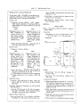
HP Archive
This vintage Hewlett Packard document was preserved
and distributed by
www. hparchive.com
Please visit us on the web !
On-line curator: Peter Reilley, KA1LAT
l
•
.
.
60BE/F
VHF SIGNAl GENERATOR
HP PART NUMBER 00608-90046
rli~ HEWLETT
~~ PACKARD
, - - - - - - - - OPERATING AND SERVICE MANUAL - - - - - - - - - - ,
608E/F
VHF SIGNAl GENERATOR
HP PART NUMBER 00608-90046
SERIALS PREFIXED:
This Operating and Service manual applies to HP
608E/F instruments with serial numbers prefixed
833- above 02720 (GOBE) and 832- above 01500
(608F).
SERIAL PREFIXES NOT
LIST~!l:
For instruments with lower serial number prefixes
a "Backdating" Appendix is supplied in the back
of this manual.
,
Flio-
HEWLETT
~r..I PACKARD
© Copyright HEWLETT-PACKARD COMPANY 1965
1501 PAGE MILL ROAD, PALO ALTO, CALIFORNIA, U.S.A.
\
OPERATING AND SERVICE MANUAL PART NO. 00608·90046
Operating end Service Menual MIcrofiche Part No. 00608-90047
Printed: APRIL 1981
Model 608E/F '
Table of Contents
TABLE OF CONTENTS
Section
Page
I
1-1
1-1
1-1
1-1
1-1
1-1
1-1
•
II
III
GENERAL INFORMATION . . . • . • . . • .
1-1. Description . . . . . . • • • . • . . . .
1-3.
Frequency . . . . . . . . • . . . . . .
1-5.
Modulation
.
1-7.
RFI . . . . • • • . . . . . . . . . . . .
1-9. Auxiliary Equipment . • . • . . . . • .
1-10.
Model 11509A Fuseholder . . . .
1-12.
Model 11508A Terminated
Output Cable • . . . . . . . . . . . .
1-14. Instrument Identification . . . . . • .
1-1
1-1
INSTALLATION . . . . . . . • . . . . . . • • •
2-1. Incoming Inspection . . . . . . . • • .
2-3. Preparation For Use
.......•
2-4.
Power Requirements • . . . . . . .
2-6.
Power Cable
.
2-8. Repacking For Shipment • . . . . . . .
2-1
2-1
2-1
2-1
2-1
2-1
OPERATION . • • . . . . . . . . . . . . . . • .
3-1. Introduction
.
3-3. Controls, Indicators and Connectors
3-5. Pre-Operational Procedures . . . .
3-7.
RF Output Loading . . . . . • . . .
3 -9.
Turn-On Procedures . . . . . • . .
3-11.
Calibration Procedures
.
3-16. Mode Operating Procedures . . . • .
3-18.
Internal Modulation. . . .
.
3 -20.
External Modulation . . . . . ..
3-22. Phase-Lock Operation Procedures
(Model 608F Only) ...
3-1
3-1
3-1
3-1
3-1
3-1
3-1
3-4
3-4
3-5
3 -5
Section
5-10.
5-12.
5-13.
5-14.
5-15.
5-16.
5-17.
5-18.
5-19.
5-20.
5-21.
5-22.
5-23.
5-24.
5-25.
5-26.
5-27.
5-28.
5-29.
5-31.
5-34.
5-37.
5-41.
IV
•
PRINCIPLES OF OPERATION . . • . . . .
4-1. Introduction
.
4-3. General Description. .. .
.
4-5.
RF Generator Section,
Mode1608E
.
4-7.
RF Generator Section,
Model 608F
.
4-9.
Amplitude Modulation Section ..
4-15.
Attenuator Section .••..•..••
4-17.
Calibrator Section . . • . . . . . • .
4-19.
Modulation Meter Section ...•.
4-21.
Power Supply Section
.
4-23. Detailed Description
.
4-25.
RF Generator Section,
Model608E . . . . • . . . . . . • •
4-33.
RF Generator Section,
Model608F . . . . • • . . . . . . .
4-37.
Amplitude Modulation Section ••
4-51.
Attenuator Section
.......•
4-55.
Calibration Section
.
4-59.
Modulation Meter Section
.
4-63.
Power Supply Section
.
4-1
4-1
4-1
5-42.
5-43.
4-1
4-1
4-1
4-2
5-46.
4-3
4-3
4-3
4-3
5-47.
5-48.
5-50.
4-3
5-54.
4-4
5-59.
5-62.
5-63.
5-64.
5-66.
4-5
4-7
4-7
4-7
4-8
5-67.
V
MAINTENANCE
.
5-1. Introduction
.........•.•..
5-3. Periodic Inspection . . . • . • . . . .
5-4.
Cleaning • . . . . . . . • . • . . . .
5-6.
Lubrication . . . . . . • . . . • . . .
5-9. Performance Tests . . . • • . • . . .
5-1
5-1
5-1
5-1
5-1
5-1
5-74.
5-82.
5-83.
5-85.
Page
Purpose
.
Frequency Accuracy and
Resettability Test . . . . • . . . .
Calibrator Accuracy Test
.
Frequency Drift Test
.
Residual FM Test
.
Incidental FM Test • . . . • . . . .
Maximum RF Output Test . . . . .
Frequency Response and
Leveling Test
.
RF Output Accuracy Test
.
Uncalibrated RF Output Test
.
External Sine-Wave Modulation
and Modulation Meter Test
..
Internal Modulation Test
.
Envelope Distortion Test
.
External Pulse Modulation and
ReSidual Level Test • . . . . . • .
RF Leakage Test
.
Frequency Control Input Test
(Model 608F Only) . . . . . . . . •
Frequency Analog Output Test
(Model 608F Only)
.
Synchronization Test with Model
8708A Synchronizer
(Model 608F) . . . • . . . . . • • .
Adjustment
.
Power Supply Voltage Adjustments
Modulation Meter Adjustment . . .
Calibration of Percent
Modulation Meter
.......•
Automatic Output Leveling
Adjustment . . . . . . . • . . . . . .
RF Oscillator Adjustment . . . . .
Uncalibrated RF Output, Minimum
RF Output, and RF Amplifier
Tracking Adjustment
....•.
RF Output Meter Accuracy
Adjustment . . . . . • • . . . . . .
RF Output Meter/AUenuator
Frequency Response and Automatic-Leveling Output
Adjustment
.
Crystal Calibrator Adjustment .•
Troubleshooting . . . • • . . . . . . . .
Isolating a Trouble to a
Circuit Section . . . . . . . . . . •
Isolating Trouble in Transistor
Circuits
.
Replacement and Repair . . . . . . •
Etched Circuit Board Repair
.
Component Replacement
.
Etched Conductor Repair • . . . .
Transistor and Semiconductor
Diode Replacement . . . • . . . . .
Replacement of Electron
Tubes
.
Attenuator Probe Repair
and Replacement . . . . . . . • . .
Replacement in Housing
.
Replacement of Lamp DSI
.
Location of Parts
.
5-1
5-1
5-5
5-5
5-5
5-7
5-7
5-8
5-8
5-8
5-8
5-9
5-9
5-10
5-10
5-11
5-12
5-12
5-12
5-13
5-13
5-14
5-15
5-15
5-16
5-16
5-17
5-17
5-18
5-18
5-23
5-23
5-23
5-25
5-25
5-26
5-26
5-29
5-30
5-32
5-32
iii
Table of Contents
List of lllustrations
Model 608E/F
TABLE OF CONTENTS (Cont.)
Section
Page
Section
VI
6-1
6-1
6-1
6-1
6-1
vn
REPLACEABLE PARTS . . . . . • . . . .
6-1.
Introduction...............
6.3.
Replaceable Parts List. • . • • ••
6-6.
Ordering Information. • • • • • ••
6-9.
Factory Selected Parts (*). . . ..
Page
SCHEMATIC DIAGRAMS
COMPONENT LQCATION INFORMATION 7-1
7-1.
Introduction............... 7-1
APPENDIX 1. . . . . . . . . . . . . . . . . . . . . ..
1·1
APPENDIX IT. . • . . • • • . • • . • • • • • • . • . •.
IT-I
LIST OF ILLUSTRATIONS
Number
1-1.
3-3.
3-4.
4-1.
5-1.
5-2,
5-3.
5-4.
5-5.
5-6.
5-7.
5-8.
5·9.
5-10.
5-11.
5-12.
5-13.
5-14.
5-15.
5-16.
5-17.
Iv
Title
Model 608E and 608F'VHF Signal
Generators • . . . . . . . . . . . . . . . .
Front Panel Controls, Indicators,
and Cormectors• • . . • . . . . . . . . . .
Controls, Indicators and Connectors
Used in Operation with Internally
Generated Signals . . . . . . • . . • . • .
Controls, Indicators and Connectors
Used In Operation with Externally
Supplied Signals . . . . . . . . . . • . . .
Controls. Indicators, .:::.!:.1 ~::'''::''::::''=3
Used in Phase-Lock Operation
(Model 608F Only) . . . • . . . . . . . . .
Overall Block Diagram, Models
608E and 608F
.
Fabricated Test EqUipment ...
Lubrication POints, RF 1\mer Drive
Mechanism. . . . • . . . . . . . . . . . . .
Frequency Accuracy and Resettability
Test Setup . . . • . . . . . . . . . . . . . .
Residual and inCidental FM Test Setup.
RF OutpJ.t Test Setup. . . . . • . . . . . •
Uncalibrated RF Output Test Setup ..
External Sine-Wave Modulation and
Modulation Meter Test Setup
.
Envelope Distortion Test Setup
.
Pulse Modulation Test Setup
.
RF Leakage Test Setup
.
Frequency Control Input TestSetup ..
Synchronization Test Setup
.
Location Power Supply and
Modulation Meter Adjustments . . . .
Modulation Meter Calibration Test
Setup. . . . . . . . . . . . • . . . . . . . . .
Pattern on 140 Oscilloscope at 50%
modulation
.
Location of Leveling and RF Output
Meter Adjustment
.
Location of RF Oscillator Adjustment
Page
1-0
3-2
3-6
3-8
3-10
4-0
5-3
5-4
5-5
5-6
5-7
5-8
5-"
5-10
5-10
5-11
5-11
5-12
5-13
Number
TtUe
Page
5-18. Frequency-Response Adjustments ...
5-18
5-19. Location of Frequency-Response and
Crystal-Calibrator Adjustments . . . . 5-18
5·20. Voltage and Resistance Measure
INT 1000 - Operation . . . • . . . . . . . 5-19
5-21. ALC Board Voltage and Resistance
Measurements, CW and PULSE
SET RF OUTPUT Operation
. 5-22
5_22. Transistor Biasing and Operating
Characteristics . . . • . . . . . . . . . . . 5-24
5·23. Location of Electron Tubes
. 5-28
5-24. Replacement of Oscillator and
Amplifier Tubes
. 5_29
5-25. Disassembly of Attenuator Drive
Cable. ,
. 5-30
5-26. Attenuator Probe, ShOWing Pickup
Loop and Impedance Matching Network 5-31
5_27. RF Generator Assembly Location of
Unlabeled Parts (Side Cover Removed) 5-32
5-28. Model 608E RF Generator Assembly
ShoWing Location of Unlabeled Parts
(Top Cover Removed) . . . . . . . • . . • 5-33
5_29. Model 608F RF Generator Assembly
ShOWing Location of Unlabeled Parts
(Top Cover Removed).
. 5-34
5-30. Right Side View Showing Location of
Unlabeled Chassis Components . . . . . 5-35
5_31. Left Side View Showing Location of
Unlabeled Components
. 5-36
5-32. Rear View Showing Location of
Unlabeled Chassis Components
. 5-37
. 5-38
5·33. Circuit Board Parts Identification
5-14
7-1.
7-2.
7-3.
5-14
7-4.
5-15
5-16
7 -5.
Schematic Wormation lllustration
_
Schematic Diagram Notes
.
Component Identification, Modulator
and ALC Board
.
RF Generator and Modulator
Schematic Diagram
.
Modulation Meter, Crystal Calibration,
and Power Supply Schematic Diagram ..
)
,
7 -1
7-2
7-3
7-3
7 -5
)
Model 608E IF
List of Tables
LIST OF TABLES
Number
•
Title
Page
1-2
5-7.
Specifications . . . . . . . . . . . . . . . • . . .
Test Equipment Required for
Maintenance
.
Lubrication Chart
.
Out-of-Circuit Transistor Resistance
Measurement
.
Safe Ohmmeter Ranges for Transistor
Resistance Measurement
.
.
Etched Circuit Soldering Equipment
Checks Following Tube and Semiconductor
Replacement
.
608E/F Troubleshooting Procedure
.
6-1.
6-2.
6-3.
6-4 .
Reference Designations
Abbreviations
Replaceable Parts
Code List of Manufacturers
6-2
6-2
6-4
6-12
I-I.
5-1.
5-2.
5-3.
5-4.
5-5.
5-6.
.
.
.
.
5-2
5-4
5-25
5-25
5-26
5-27
5-40
•
v
Section I
Model 608EIF
••
o
G
•
·eA·
•
•
-[~
-c:JP
•
o
--
-f!l-
-
•
o
Model 608E
)
e
----
.••
~
I
e
.1iJ1iia.
V
•
\
Model 608F
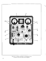
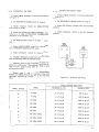
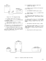
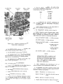
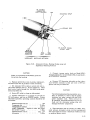
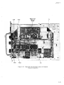
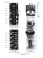
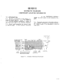
Figure 1-1. Model 60SE and 608F VHF Signal Generators
1-0
./
Model 608E/F
Sedion I
SECTION I
GENERAL INFORMATION
1·1. DESCRIPTION.
•
1-2. The Hewlett-Packard Model 608E and 608F
Signal Generators (see Figure 1-1) are designed to
meet the requirements of precision laboratory work,
and yet to be equally useful for general applications in
the VHF frequency range. The Model 608E furnishes
RF signals from O. 1 microvolt to 1 volt from 10 MHz
to 480 MHz, whiletheModel608F supplies RF signals
from O. 1 microvolt to O. 5 volt in a frequency range
from 10 MHz to 455 MHz. The RF carrier can be
amplitude modulated by internally generated sinewave signals, or by externally supplied sine-wave or
pulse signals. The Mooel 608F contains frequency
control circuitry which permits the instrument to be
used in phase-lock operation with the Model 8708A
Synchronizer. This provision provides a stabilized
output across most of the range of the instrument,
with a drift factor of < 2 x 10⁻¹ per 10 minutes. The
instruments can be used for troubleshooting, testing,
calibrating, measuring standing-wave ratios, and
checking antenna and transmission line characteristics. To preserve accuracy, equipment design holds
spurious modulation to a low value under all operating
conditions. Detailed specifications for both instruments are listed in Table 1-1.
1-3.
FREQUENCY.
1-4. The frequency ofthec'.1tpu! signal is indicated on
a direct reading dial, the calibration ofwhich is accurate
to better than ±O.5% for the 608E and ±l% for the 608F,
when the cursor and FINE FREQ are properly aligned.
Calibration accuracy may be improved further by use of
a built-in crystal-controlled heterodyne calibrator which
furnishes 1 MHz checkpoints from 10 MHz to 270 MHz, or
5 MHz checkpoints over the entire frequency range ofthe
instrument. At any checkpoint the calibration can be set
very elO8e to the calibrator accuracy of 0.01%, bringing
overall accuracy to at least ±O.O5%. F'l'equency check
point signal.e are obtained when a headphone set (not
fumi.ehed) is plugged into the XTAL CAL OUTPUT jack.
The control for the output attenuator is calibrated in both
decibels and volts. When the instrument is connected to a
5Q.ohm resistive load and power into the output attenua·
tor is exactly at the ATI'ENUATOR CALIBRATED mark
(+7 dB) on the RF OUTPUT meter, the level of power or
voltage applied to the RF OUTPUT connector may beread
directly on the A1TENUATOR dial with an accuracy of
±1 dB. When connected to a 5O-ohm resistive load, the
VSWR at the RF OUTPUT connector will nol be greater
than 1.2 (SWR of 1.6 dB). The signal generators feature
automatic output leveling, maintaining the RF output
within ±1 dB of the adjusted output.
,
1-5.
MODULATION.
1-6. The RFoutput signal can be amplitude modulated
by internally generated 400 or lOOO-cyde sine waves,
externally applied sine waves above 1. 0 volt rms over
the frequency range from 20 Hz lo 20 kHz, or externally applied pulses of 10 volts peak-lo-peak. When
pulse modulated, the signal generators are capable of
producing pulses of RF energy as short as 4 microseconds at Signal frequencies above 40 MHz, and pulses
as short as 2 microsecond above 220 MHz. The degree
of sine-wave modulation is continuously variable from
o to 90% by a front-panel control. All sine-wave modulation of the output signal is continuously monitored
and indicated in percentage on a direct reading modulation meter.
1-7.
RFI.
1-8. RF leakage is held to a minimum and is such
that when the output signal is adjusted for O. 1 microvolt, the conducted signal leakage at any other front
panel connector and the radiated leakage two inches
from the instrument are each less than 1.0 microvolt.
1·9. AUXILIARY EQUIPMENT.
1-10. MODEL 11509A FUSEHOLDER.
1-11. To protect the output attenuator from damage,
for some applications (such as transceiver testing) it
is desirable to insert a fuse between the signal generators and external equipment. The 11509A is a
special coaxial fuseholder which houses a type 8AG,
1/16 amp fuse which protects the output attenuator
from damage in the event that an external voltage is
accidently applied to the RF OUTPUT connector. The
fuseholder has an insertion loss of O. 50 dB at 200 MHz,
O. 56 dB at 300 MHz, and 0.65 dB at 400 MHz; tis
SWR is not greater than 1. 35 when connected to a 50ohm resistive load.
1-12. MODEL 1150BA TERMINATED OUTPUT
CABLE.
1-13. This cable assembly provides a SO-ohm termination and standard binding posts at the end of a 24inch length of cable. The 11508A allows direct connectionofthe instruments to a high-impedance circuit.
1·14. INSTRUMENT IDENTIFICATION.
1-15. Hewlett-Packard 1nstruments carry a two-section, eight-digit serial number. The first three digits
are a prefix. The contents of this manual apply to
those instruments having the serial number prefix
shown on the title page. If the serial prefix on your
instrument 1s not mentioned on the title page, in the
Appendix to this manual, or in a Manual Change Sheet
enclosed with the manual, the corred information may
be obtained from any Hewlett- Packard Sales and Service Office (see rear of manual for addresses).
1-1
Section I
Model 608E/F
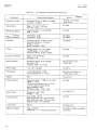
Table 1-1. Specifications
FREQUENCY CHARACTERISTICS
608E
608F
Range: 10to 480 MHz in
five bands (10-21, 2143,43-95, 95-215, and
215-480 MHz).
Range: 10 to 455 MHz in
five bands (10-21, 2144,44-95,95-210, and
210-455 MHz).
10430 MHz when used
with 8708A Synchronizer.
Accuracy: ±1 % with cursor adjustment.
Accuracy: ±O.5% with cursor adjustment.
Drift: Less than 50 parts
in 106 per 10 min.
period after 1 hr.
warmup.
Drift: Less than 50 parts
in 106 per 10 min. periodafter Ihr. warmup. Stability used with
8708A Synchronizer.
5 x 10- a/min.
2 x 10- 7 /min.
(0· -55 ·C)
2 x 10 -7 /10 % line
voltage change.
Tuning Control: Frequency control mechanism
provides a In a i n dial calibrated in MHz and a
vernier dial for interpolation purposes. Total
scale length approximately 45 inches. Calibration: every othe r MHz from 13U to 27U MHz;
every 5 MHz above 270 MHz.
Resettability: Main frequency control resettability
better than ±G. 1% after initial warmup. FINE
FREQUENCY ADJUST prOVides approximately
±25 kHz settabilityat 480 MHz (proportionately
finer adjustment at lower frequencies).
Crystal Calibrator: Provide s frequency check
points every 1 MHz up to 270 MHz or every
5 MHz over the range of the instrument. Headphone jack provided for audio frequency output
(headphones not incluC1ed). Crystal frequency
accuracy better than 0.01% at normal room
temperatures. Cursor on frequency dial adjustable over small range to aid in interpolation adjustment. -Calibrator maybe turned off when not
in use.
Residual FM: <±5 parts tn 107 in a 10 kHz postdetection bandwidth.
Harmonic Output: At least 35 dB below the carrier
for harmonic frequencies below 500 MHz.
Frequency Control Input: (608F only). The 608F
FREQ CONTROL INPUT normally used with the
8708A Synchronizer can also be use d for external frequency control by varying a dc voltage
1-2
input. A voltage change from -2 volts to -32 volts
will change the output frequency more than 0.2%
at the low end of each band and more than 1% at
the high end of each band. Nominal 4 Kn input
impedance, direct coupled. Voltage limits:
OV .::: applied voltage .::: -50V.
OUTPUT CHARACTERISTICS
608E
608F
Output Level; Continuously adjustable from
0.1 /lV to IV into a
50n load. Output attenuator calibrated in
V and dBm (0 dBm =
1 mW in SOn).
Output Level: Continuously adjustable from
0.1 trV to O. 5V into a
50n load. Output attenuator calibrated in
V and dBm (0 dBm =
1 mW in 50n).
Accuracy: Within ±1 dB of attenuator dial reading
at any frequency when RF output meter indicates
"ATTENUATOR CALIBRATED."
Leveling: Internal feedback circuit retains "ATTENUATOR CALIBRATED" reference on RF
output meter over wide frequency ranges (typically octave bands). Adjustment of front panel
AMP. TRIMMER control (only) for maximum
RF output indication automatically restores initial carr.ier level for greater frequency changes.
)
Impedance: 50n; reflection coefficient <0.091
(1. 2 SWR, 20.8 dB return loss) for attenuator
setting below -7 dBm.
RFI: Meets all conditions specified in MlL-I618m; permIts receiver sensitiVity measurements down to at least 0.1 /lV.
Auxiliary RF Output:
608E
Fixed Ie ve I CW signal from RF oscillator
(minimum amplitude 180 In V rms into 50n)
provided at front panel ENC female connector
for use with external equipment (e.g., frequency counter).
608F
cw signal from RF Oscillator pro v i de d at
front panel ENC female connector. Powe r
levels into son are as follows:
10 to 215 MHz: -1. 8 to +7 dBm
215 to 400 MHz: +2. 0 to +6 dBm
400 to 430 MHz: +1. 0 to +5 dBm
Signal for use with HP 8708A Synchronizer or
othe r external equipment (e.g., frequency
counter).
)
Model 608E/F
Section I
Table I-I.
Specifications (Cont.)
MODULATION CHARACTERISTICS
•
Above 220 MHz, combined rise and decay time
less than 2. 5 ~s.
(Front-panel AMP. TRIMMER control adjusted for
maximum indication of RF Output Meter and RF
Output Meter set to Attenuator Calibrated.)
On-Off Ratio: At least 20 dB [or pulsed carrier
levels o( O. 5 V and above.
Internal AM
Input ReqUired: Positive pulse, 10-50 V peak;
input impedance 2 k n .
Frequency: 400 and 1000 Hz, ,:tl0%. Modulalatton signal available at front panel BNC female connector for synchronization of external
equipment.
608E
Modulation Level: 0 to
95% modulation at
carrier levels 0.5 V
and below; continuously adjustable with
(ront-panel
MOD
LEVEL control.
608F
Modulation Level: 0 to
95% modulation with
Output Attenuator at
0.224 V (1 mW) or below; continuously adjustable with frontpanel MOD LEVEL
control.
Carrier Envelope Distortion: Less than 2% at
30% AM and less than 5% at 70% AM.
GENERAL
608E and 608F
Power: 115 or 230 V .±IO%, 50 to 400 Hz. Approximately 220 W.
Dimensions
Cabinet Mount: 13-1/4 in. (337 mm) wide, 16-3/4
in. (416 mm) high, 21 in. (533 mm) deep.
Rack Mount:
~"
"~'_I"'OOOU'"
--.,
,..u..... """,
".,
".
External AM
Frequency: 20 Hz to 20 kHz.
608E
Modulation Level: 0 to
95% modulation at
carrier levels 0.5 V
and -below; continuously adjustable with
front-panel
MOD
LEVEL control. Input requlred: 1 to 10
V rms (1 k n input
impedance) .
608F
Modulation Level: 0 to
95% modulation with
Output Attenuator at
0.224 V (1 roW) or below; continuously adjustable with frontpanel MOD LE VEL
control.
Input required: 1 to 10 V
rms (1 k n
lnput
lmpedance) .
Carrier Envelope DistorUon: Less than 2% at
30% AM, less than 5% at 70% AM (modulation
source distortion less than O. 5%).
External control o( carrier level can be achieved
through application o( dc voltage in EXT AM
mode.
Modulation Meter
Accuracy: ±5% o(full scale 0 to 80%, .±.IO% from
80% to 95% «(or lNT AM or 20 Hz to 20 kHz
EXT AM).
.i
"
RUR
fI
t:k'''.0'
Weight
Cabinet Mount: Net, 62 Ib (28 kg). Shipping, 74
Ib (33, 4 kg).
Rack Mount: Net, 62 lb (28 kg).
• (37, 4 kg).
Shipping, 83 lb
Accessories Available
Incidental Frequency Modulation (at 400 and 1000
Hz modulation)
11508AOutput Cable prOVides 50- n. termination
and standard binding posts at the end of a 24inch (610 mm) length of cable. Allows direct
connection o( the signal generator to hlgh impedance circuits.
Less than 1000 Hz peak at 50% AM for frequencies above 100 MHz. For frequencies below
100 MHz, less than 0.001% at 30% AM.
11509A Fuse Holder provides protection for the
output attenuator when the 608 is used for transceiver tests.
External Pulse Modulation
Rise and Decay Time: From 40 MHz to 220 MHz,
combined rise and decay time less than 4 ~s.
10514A Mixer foruseas nanosecond pulsemodulator or balanced modulator.
10515A Doubler for extending the frequency range.
1-3
Model 608E/F
Section n
SECTION II
INSTALLATION
2-1.
•
INCOMING INSPECTION.
2-2. This instrument was inspected mechanically and
electrically prior to shipment. Inspect for mechanical damage received in transit and test electrical performance using procedures given in Section V. If there
is damage or deficiency, or if electrical performance
is not within specif1cations. notify the carrier and your
Hewlett-Packard sales and Service Office immediately
(see 11st at rear of this manual.)
2-3.
PREPARATION FOR USE.
2-4.
POWER
REQUIRE~{ENTS.
2-5. The VHF Signal Generator requires a power
source of 115 or 230 volts ac .!.lo%, single phase,
which can supoly approximately 220 watts. A twoposition slide switch, on the inside rear chassis, permits operation from either a 115- or 230-volt power
soorce. The number visible on the switch slider indicates the line voltage for which the signal generator
is connected. The correct fuse rating for each line
voltage is adjacent to the switch. To prepare the signal generator for operation, position the 115-230 volt
switch so that the number visible on the slider corresponds to the available line voltage, and install a
fuse of correct r~t\.rZ ~::'!:."r~-:"! on rear apron).
CAUTION
Before connecting the power cable, set the
115-230 volt switch for the line voltage to be
used.
2-6.
POWER CABLE.
2-7. To protect operating personnel, the National
Electrical Manufacturers' Association (NEMA) recommends that the instrument panel and cabinet be
grounded. This instrument is equipped with a threeconductor power cable Which, when plugged into an
appropriate receptable, grounds the instrument. The
off-set pin of the three-prong connector is the ground
pin. To preserve the protection feature when operating
the instrument from a two-contact outlet, use a threeprong to two-prong adapter (Hewlett - Packard Stock No.
1251-0049) and connect the green pigtail on the adapter
to ground.
2-8.
REPACKING FOR SHIPMENT.
2-9. If the signal generator is to be packaged for
shipment use the original shipping container and packing materials. U these have been discarded or are not
in condition for reuse, obtain new materlals from your
local Hewlett- Packard sales and Service Office (see
rear of this manual for locations), or follow these
general instructions:
a. Wrap the signal generator in heavy paper or
plastic. (IT the signal generator is being shipped to a
Hewlett-Packard service facility, attach a tag indicating type of servicing required, return address, model
number, and full serial number.)
b. Use a strong shipping container. A carton made
of 500-600 DOUnd test material will usually provide
adequate protection.
c. Use enough shock-absorbing material (3 to <4
inch layer) around all sides of instrument to provide
firm cushion and prevent movement inside the container. Protect the control panel with cardboard.
With Hewlett-Packard "noater pack" packaging, the
foam blocks prOVide sufficient shock protection, and
additional material is unnecessary.
d. Seal the shipping container securely.
e. Mark the shipping container "FRAGILE"
assure careful handling.
to
2-10. In any correspondence refer to the signal generator by model number and full serial number.
'.
2-1
Model 608E/F
Section ill
SECTION III
OPERATION
3-1. INTROOUCTION.
•
3-2. This section provides operating instructions
for the Model 60sE and 608F SIgnal Generators. Included are a listing of controls, indicators and connectors, pre~operation procedures, mode operating
procedures, and phase-lock operation procedures
(Model 608F only). Controls and indicators on both
instruments are nearly identical; therefore, an illustration of the Model 608F will be referenced during
this discussion, with the difference between instruments identUied.
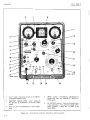
3-3. CONTROLS. INOICATORS ANO
CONNECTORS.
3-4. Except for the 115/230 volt power switch, all
controls, indicators, and connectors are located on the
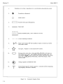
front panel. Figure 3-1 locates and provides a functional description of each front-panel mounted control, indicator and connector. The 115-230 volt power
switch is located inside the rear panel and is not
shown.
3-8. A reSistive load of 50 ohms is used at the factory
during calibration of the Attenuator Control dial.
Therefore, for an accurate indication of output power
the external load should be 50 ohms resistive. The
internal impedance of the generator is close to 50 ohms,
with a maximum VSWR of 1.2 exiSting when the generator is terminated in 50 ohms. This VSWR will have
no important eUect on the accuracy of the Attenuator
Control calibration. However, a severe mismatch
between the instrument and load will produce a considerable difference between the output voltage selected on the Attenuator Control dial and the actual
voltage impressed across the external load. Particular care should be exercised in the selection of
coaxial cormectorS. A coaxial connector that has
been improperly assembled can produce a substantial
increase in the standing-wave ratio.
3-9.
TURN-ON PROCEDURES.
3-10. Turn-on procedures for the signal generator
are as follows:
CAUTION
Do not obstruct the ventilating louvers on the
3-5.
PRE-OPERATION PROCEOURES.
3-6. Prior to use, certain procedures must be completed to obtain maximum' accuracy during operation
of the instrument. Consideration must be given to the
possibility ofRFloading, and calibration of the instru·
ment is required. During the following discussion,
each control used will be identified by an item number
that is referenced to Figure 3-1.
3-7.
RF OUTPUT LOADING.
CAUTION
•
Do not connect any source of RF or dc power
to the RF OUTPUT connector on the signal
generator. To do so may permanently damage the Impedance-matching network in the
Attenualor Section. Particular care must be
observed when testingtransceiver-type equipment to insure that the transmitter remains
inactive while the equipment is connected to
the signal generator.
NOTE
To protect the Attenuator when there is a possibility of voltage being applied to the RF
OUTPUT cormector, a Model 11509A Fuseholder is reoommended. The fuseholder is
connected between the test cable and RF OUTPUT connector.
side of the instrument cabinet. safe operating temperature requires free air flow through
the louvers.
a. Set AC POWER switch (item 12) to the OFF
position.
b. Check position of 115-230 volt power switch
(refer to paragraph 2-5) on rear of chassis.
c. Set MODULATION selector switch (item 20) to
CW position.
d. Set RF OUTPUT control (item 5) full clockwise
(maximum).
e. Set AC POWER switch to ON position.
f. Warmup equipment for 10 mirrotes prior to use.
If greater frequency stability is required, extend
warmup period to 60 minutes.
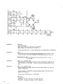
3-11. CALIBRATION PROCEDURES.
3-12. Prior to operation certain calibration of the
instrument may be deemed necessary. The following discussion contains frequency and power output
calibration procedures.
3 - 13. FREQUENCY CALIBRATION. 'I1lefrequency(MEGACYCLES) dial in the signal generators are calibrated ta
be
accurate within ±O.5% for the 608E and ±l9b for the 608F.
3-1
Section III
Model 608E/F
)
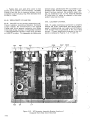
2
1
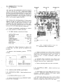
16
•
,
u __ 17
3--!~'l
•
18
4
f--~itI=!---19
6--"1:
5
fitlH--- 20
~~:JI
7
10---
21
9
11
)
---22
12
8
23
(608F ONLY)
13
(S08F
14
15
1.
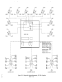
Cursor knob: Positions cursor on the MEGACYCLES (frequency) dial.
2.
PERCENT MODULATION meter: Indicates
the percent of modulation of the RF output
signal.
3.
Panel marker: Scribed mark for cursor alignment.
Figure 3-1.
3-2
26
25
24
4.
ZERO control: Screwdriver adjustment to
electrically zero the PERCENT MODULATION meter.
5.
RF OUTPUT control: Controls RF power input
to the attenuator. Also controls output power
levels between +7 dBm and +13 dBm in the
Model608E.
Front Panel Controls, Indicators, and Connectors
)
Model 608E/F
•
6.
MODULATION control: Adjusts the percent of
modulatioo ct the RF output signal as observed
on the PERCENT MODULATION meter.
7.
FINE FREQ control: Used for fine frequency
adjustments
8.
FREQUENCY RANGE switch: Five-position
switch used to select the desired frequency
range. Also positions the range pointer on the
dial. Switch positions are as follows:
.
RANGE
A
B
C
D
E
9.
m
Section
MODEL608E
MODEL 608F
10-21
21-43
43-95
95-215
215-480
10-21
21-44
44-95
95-210
210-455
MHz
MHz
MHz
MHz
MHz
MHz
MHz
MHz
MHz
MHz
AC POWER lamp: Indicates when ac power is
applied to the instrument.
10. DC .25 AMP fuse: Oierload protective device
for the +225 Vdc power supply.
19. AMPL TRIMMER control: A two-function control for peaking the RF output. During pulse
modulation, the control is tuned without pushing to peak the RF ootput. When sine-wave or
CW operations are conducted, the control is
pushed and then tuned.
20. MODULATION switch: A six-position switch
that sets the instrument mode of operation.
The switch posit~ons are identified as follows:
PULSE: Sets the instrument for external pulse
modulation.
PULSE SET RF OUTPUT: Used to establish
the instrument operating point for external
pulse mo<h.llation.
AM: sets the instrument for external sinewave modulation.
1000 - : Sets the instrument for internal AM
modulation at 1000 Hz.
400 .. : Sets the instrument for internal AM
modulation at 400 Hz.
11. AC LINE fuse: Protective device between the
instrument and the ac power source.
CW: Sets the instrument to provide aCW output.
12. AC POWER ON switch: Controls application
of ac power to the instrument.
21. XTAL CAL GAIN control: Controls audio level
of beat-frequency output at the XTAL CAL
OUTPUT connector.
13. FREQ CONTROL rNPUT connector (Model
608F only): input connector for the dc control
voltage when the instrument is used with a
Model 8708A Synchronizer.
14. AM/PULSE MOD INPUT connector: Input connector for AM or pulse signals during external
sine-wave or pulse operation. During internal
sine-wave modulation, a 400 or 1000 Hz signal
is available at the connector for synchronizing
external equipment.
15. UNCAL RF OUTPUT connector: Ultput connector in the 608E delivers an uncalibrated,
unmodulated RF signal to external equipment.
In the Model 608F used with the Model 8708A
Synchronizer, output connector delivers an
uncalibrated FM signal.
16. MEGACYCLES dial: Indicates selected frequency range and frequency in MHz.
22. Attenuator control: Controls RF ootput levels
of +7 dBm and below. OJtput levels selected
by use of the Attenuator Control are accurate
as long as the RF OUTPUT meter needle indicates +7 dBm (ATTENUATOR CALIBRATED).
23. RF OUTPUT connector: OJtput cOlUlector for
the calibrated RF signal (refer to CAUTION,
paragraph 3-7).
24. XTAL CAL switch: Three-position tog g I e
switch used when performing frequency calibrations. Switch positions are a s follows:
1 MC: Provides 1 MHz checkpoints from 10
to 270 MHz.
5 MC: Provides 5 MHz checkpoints from 10480 MHz in the Model 608E and from 10-455
MHz in the Model 608F.
OFF: De-energizes oscillator circuits.
17. RF OUTPUT meter: Indicates level of RFpower applied to the attenuator as selected by
operation of the RF OUTPUT control. Also
used in conjunction with the AMPL TRIM:MER
control to peak the RF output signal.
25. FREQ ANALOG OUTPUT connector (Model
608F only): Delivers a resistance proportional
to frequency to the Model 8708A Synchronizer
during phase-lock operation.
18. Frequency control: Used to select the output
frequency within a frequency range as observed
on the MEGACYCLES dial.
26. XTAL CAL OUTPUTCOlUlector: Supplies calibrating signals to an operator for frequency
calibration. Accommodates an earphone plug.
Figure 3-1.
Front Panel Controls, Indicators, and Connectors (Cont.)
3-3
Section III
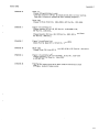
Model 608E/F
To obtain higher accuracy, a crystal-controlled calibrator has been included to provide a means of calibrating the instrument at any multiple of 1 MHz
between 10 and 270 MHz, or any multiple of 5 MHz
acr088 the frequency range of the instrument. Pl'ocedures to crystal-calibrAte the instrument are as
follows:
a.
3-9.
Conduct turn-on procedure8listed in paragraph
b. Connect headphone8 (not supplied) to the XTAL
CAL OUTPUT connector (item 26).
c. Set XTAL CAL switch (item 24) to 1 MC or 5MC
as applicable.
a.
3-9.
Conduct turn·on procedures listed in paragraph
b. Set the MODULATION 8witch (item 20) to the
CW position.
NOTE
For maximum aCi:uracy, power output calibration8 should be conducted with the in8trument 8et in the CW mode.
d. Tune the frequency control (item 18) five turn,
in from the low end ofthe selected frequency range as
indicated on the MEGACYCLES dial (item 16).
e. Adjust XTAL CAL GAIN control (item 21) for a
comfortable audio level in headphones.
e. Adjust the RF OUTPUT control (item 5) for an
indication on the RF OUTPUT meter (item 17).
NOTE
f. Depre88 the AMPL TRIMMER control (item 19)
and tune for a peak RF indication on the RFOUTPUT
meter.
Extraneous beat notes generated by RF
harmonics may be eliminated by properly
setting the RF OUTPUT control (paragraph
3-10, 8tepd) and the XTALCALGAIN control
(paragraph 3-13, step e).
g. Readjust the RF OUTPUT control until the RF
OUTPUT meter pointer ie aligned with the +7 dBm
(ATIENUATOR CAUBRATED) mark.
f. Slowly rotate frequency control around the
selected checkpoint until a null (zero beat) is reached.
NOTES
g. Rotate Cursor Knob (item 3) until cursor is
aligned on MEGACYCLES dial with zero-beat point
achieved in step f.
To calibrate range "E" tune to top of band
and repeat step8 e through g, before proceeding on to step h.
i. Set XTALCALswitch to OFF.
3.14. A FINE FREQ control (item 7) is located on the
instrument front panel for making minor frequency
adju8tments. During normal operation no adjustment
of the FINE FREQ control i8 required, and the knob
arrow should be aligned with the front-panel marker.
For a preci8ion frequency selection u8ing a frequency
counter, the FINE FREQ control is used after the frequency has been selected by U8e of the frequency control. Tuning the knob arrow counterclockwise from
the panel marker lowers the frequency, while a clockwise rotation rai8es the frequency.
3-15. POWER OUTPUT CAUBRATION. The RF
leveling circuit in the in8trument maintains a flat RF
output over wide frequency range, with proper initial
adju8tments. The8e adjustments are conducted using
the RF OUTPUT and AMPL TRIMMER controls in
conjunction with the RFOUTPUTmeter. The take-off
point for the detected RF signal displayed on the RF
OUTPUT meter is at the input circuit of the attenua·
tor. Therefore, calibrating the RF output into the at·
tenuator ensures that subsequent operation of the attenuator control will produce an accurate calibrated
RF output from the attenuator. RF output calibration
procedure8 are a8 follows:
3-4
,
c. Set the FREQUENCY RANGE switch (item 8) to
the desired range.
d. Rotate frequency control (item 18) until MEGACYCLES dial (item 16) is set on the 1 MHz or 5 MHz
checkpoint nearest the frequency to be used.
h. Rotate frequency control until 8elected frequency on MEGACYCLES dial appear8 di-re.:t!y ..;.::::.~.;=
cursor.
)
)
The RF OUTPUT control may be adjusted to
a value >+7 dBm (RF OUTPUT meter reading); however, for maximum tube life it is
recommended that the level be reduced when
the higher level is not needed.
h. Tune the frequency control across the selected
frequency range. The RF OUTPUT meter pointer
8hould remain aligned with the ATTENUATOR CALIBRATED mark.
NOTE
If the pointer does not remain aligned with
the ATIENUATOR CALIBRATED mark, the
leveling circuit is not functioning properly.
Stop tuning and readjust the AMPL TRIMMER control to restore leveling. The latter
adjustment is made without depressing the
control.
•
i. Proceed with operating adjustments listed in
paragraphs 3-18 and 3-20.
3-16.
MODE OPERATING PROCEDURES.
3-17. The signal generator8 have four operating
modes identified as CW operation, internal sine-wave
modulation, external sine-wave modulation, and external pulse modulation. In addition, the RF output level
,
.J
Mode1608E/F
•
eetabliehed for CW operation can be remotely controlled by an externally eupplied de control voltage.
The following diecueeion combines locally controlled
CW operation and internal sine-wave modulation into
operating instructions used with internally generated
signals, external sine-wave modulation, external
pulse modulation and remote-controlled CW opera·
tion. These operating procedures are used with exter·
nally supplied signals.
3-18.
INTERNAL MODULATION.
3-19. The signal generators provide internal facHi·
tiee to produce a CW output, or selection ofeither a 400
Hz or 1000 Hz sine·wave modulated signal output.
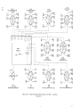
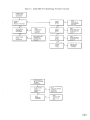
Figure 3-2 illustrates and provides instructions for
proper operation of the controls, indicators, and connectors used with internally generated signals.
3-20.
EXTERNAL MODULATION
3-21. The signal generators operate with externally
supplied signals which are used to modulate the
internally developed RF carrier. Also, an external de
voltage can be applied to provide remote on-offcontrol
of the RF carrier output from the instruments. Figure
3-3 illustrates and describes the operation of control8,
'-.
Section III
indicators, and connectors used in the three operations.
3-22.
PHASE-LOCK OPERATING PROCEDURES
(MODEL 608F ONLY).
3·23. The RF Generator section in the Model 60SF
signal generator is designed for phase-lock operation
with the Model 8708A Synchronizer_ This method of
operation provides a highly stable output from the
instrument, and require8 only normal control adjustmenta followed by cable connections between the signal generator and synchronizer. Figure 3-4 illu8trates
and describes operation of controls, indicators and
connectors on the Model608F when the instrument is
used in phase-lock operation.
3-24. Configuration of the RF Generator Section in
the Model 60BF signal generator also permits the in·
strument to be used in narrow·band frequency or
phase modulation operations. In this application,
consideration must be given tothe internal bias of -22
volta de on the FREQ CONTROL INPUT connector,
and the input impedance of approximately 5K ohms.
A blocking capacitor must be added to the input circuit for passing the modulating signal while preventing any change in the reference reverse bias applied to
the varicap diodes.
Section ill
Model 608E/F
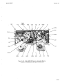
)
•
1
6
14~-_
1-----7
11
1-_- 4
13
8
12
)
~~-9
10
2
3
5
HE If l ( r r ~ ~ • ( I , I D.
)
Figure 3-2. Controls, Indicators, and Connectors Used
in Operation with Internally Generated Signals
3-6
Model 608E/F
Section III
CW OPERATION
7.
Depress and tune AMPL TRIMMER control
for maximum indication on RF OUTPUT meter.
8.
Adjust RF OUTPUT control until RF OUTPUT
Meter pointer is aligned with +7 dBm mark
(ATTENUATOR CALIBRATED).
NOTE
•
Perform turn-on procedures listed in paragraph 3-9.
1.
Align cursor knob with panel marker.
2.
Align nNE FREQ control with panel marker.
3.
Set FREQUENCY RANGE switch to desired
range (frequency limits for each range shown
on MEGACYCLES dial housing).
4.
Set MODULATION switch to the CW position.
NOTE
Accuracy of the Attenuator Control setting
and PERCENT MODULATION -JIleter are
within specifications only when the RF OUTPUT meter is indicating ATTENUATOR
CAUBRATED.
9.
Adjust Attenuator Control for desired output
level of +7 dBm or below.
CAUTION
NOTE
Do not connect any source ofRF or de power
to the R F OUTPUT connector on the signal
generator. Todo so may permanently damage the impedance-matching network in the
Attenuator Section. Particular care must
be observed when testing transceiver-type
equipmentto insure that the transmitter .remains inoperative while the equipment is
connected to the signal generator (refer to
NOTE in paragraph 3-7).
5.
Connect the equipment under test to the RF
OUTPUT connector observing that the signal
generator is terminated in the proper load
(refer to paragraph 3-8).
NOTE
If deemed necessary, conduct power out-
put calibration procedures for the selected
frequency range as listed in procedural
steps d. through h. in paragraph 3-15.
6.
Tune the Frequency Control until MEGACYCLES dial cursor is aligned with frequency
to be used as indicated on dial face.
To select RF output levels from +7 dBm to
+13 dBm in the Model 608E, perform steps
10 through 12. In this operation, the RF
OUTPUT meter pointer is used in lieu of
the Attenuator Control to indicate the power
output level.
10. Adjust the Attenuator Control to the +7 dBm dial
mark.
11. Check that the RF OUTPUT meter pointer indicates ATTENUATOR CALIBRATED.
12. Adjust RF OUTPUT control for desired output level above +7 dBm as indicated by the RF
OUTPUT meter pointer.
INTERNAL SINE-WAVE MODULATION
NOTE
Steps 1 through 12, as applicable, must be
completed before seiting the instrument for
internal sine-wave AM modulation.
13. Set MODULATION switch to 400 - or 1000
... position as desired.
NOTE
To crystal calibrate the frequency dial, refer
to procedures listed in paragraph 3-13.
14. Adjust MODULATION control for desired
rnodulationpercentage as indicated on the PERCENT MODULATION meter.
Figure 3-2. Controls, Indicators and Connectors Used
in Operation with Internally Generated Signals (Cont.)
3-7
Section
m
Model 608E/F
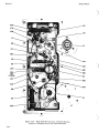
)
1
6
--'J--;71
11
8
12
15
_
4
19
13
16
11
2--
20
3 -_ _
L--~O
22
14-_ _
18
21
)
5
•
EXTERNAL SINE-WAVE MODULATION
NOTE
Perform turn-on procedures listed in paragraph 3-9.
1.
Align cursor knob with panel marker.
2.
Align FINE FREQ control with panel marker.
3.
Set FREQUENCY RANGE switch to desired
range (frequency limits for each range shown
on ME~ACYCLES dial hOUSing).
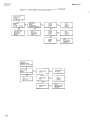
Figure 3-3. Controls, Indicators, and Connectors Used in
Operation with Externally Supplied Signals
3-8
)
Model 608E/F
4.
Section ill
Set MODULATION switch to CW position.
11. Check that the RF OUTPUT meter pointer indicates ATTENUATOR CALIBRATED.
CAUTION
Do not connect any source of RF or de power
to the RF OUTPUT connector on the signal
generator. Todosomay permanently damage the impedance-matching network in the
Attenuator Section. Particular care must
be observed when testing transceiver-type
equipment to insure that the transmitter
remains inoperative whUe the equipment is
connected to the signal generator (refer to
NOTE in paragraph 3-7).
5.
Connect the equipment under test to the RF
OUTPUT connector observing that the signal
generator is terminated in the proper load
(refer to paragraph 3-8).
NOTE
If deemed necessary, conduct power output
calibration procedures for the selected frequency range as listed in procedural steps
d. through h. in paragraph 3-15.
6.
Tune Frequency Control until MEGACYCLES
dial cursor is aligned with frequency to be used
as indicated on dial face.
12. Adjust the RF OUTPUT controliorthe desired
output level above +7 dBm as indicated by the
RF OUTPUT meter pointer.
13. Set the MODULATION switch to the AM position.
14. Connect the external sine-wave generator to
the AM/PULSE MOD lliPUT connector and set
generator for a sine-wave input between 20 Hz
and 20 kHz.
15. Set MODULATION control for desired percentage of modulatlon as observed on the PERCENT MODULATION meter.
EXTERNAL PULSE MODULATION
NOTE
Perform turn-on procedures if required,
and complete steps 1 through 3.
16. Set MODULATION switch tothe PULSE/SET
RF OUTPUT position.
NOTE
Perform steps 5 through 12 as applicable.
NOTE
To crystal calibrate the frequency, refer to
procedures listed in paragraph 3-13.
7.
Depress and tune AMPL TRIMMER control for
maximum indication on RF OUTPUT meter.
8.
Adjust RF OUTPUT control until RF OUTPUT
meter pointer is aligned with +7 dBm mark
(ATTENUATOR CALIBRATED).
NOTE
Accuracy of the Attenuator Control setting
and PERCENT MODULATION meter are
within specifications only when the RF OUTPUT meter is indicating ATTENUATOR
CALIBRATED.
9.
Adjust Attenuator Control for desired output
level of +7 dBm or below.
NOTE
To select RF output levels from +7 dBm to
+13 dBm in the Model G08E, perform steps
10 through 12. In this operation, the RF
OUTPUT meter pointer is used to indi cate
the power output level in lieu of the Attenuator Control.
10. Adjust the Attenuator Control to the +7 dBm
dial mark.
17. Set the MODULATION switch to the PULSE
position.
18. Connect the external pulse generator to the
AM/PULSE MOD INPUT connector and set
generator for an input pulse level above 10
volts peak-to-peak.
EXTERNAL DC CONTROL
NOTE
Perform turn-on procedures if required,
and complete steps I through 8.
19. Set the MODULATION control to a maximum
clockwise position.
20. Set MODULATION switch to the AM position.
21. Connect external power source to AM/PULSE
MOD INPUT connector.
NOTE
Voltages required for external control of
the RF carrier are +15 volts dc for full-on
operation and -15 volts dc for full-off operation.
22. Adjust Attenuator Control and de control voltage input for desired RF output leveL
Figure 3-3. Controls, Indicators and Connectors Used in
Operation with Externally Supplied Signals (Cant. )
3-9
Section III
Model 608E/F
)
6
1
,
8__
7
4
2
)
3
5
12
10
11
Figure 3-4. Controls, Indicators, and Connectors Used
in Phase-Lock Operation (Model 608F Only)
3-10
J
Model 608E/F
Section III
NOTE
NOTE
Perform turn-on procedures listed in paragraph 3-9, and prepare the Model 8708A
Synchronizer for use with the Model 608F
using procedures contained in Section III of
the Operating and Service Manual for Synchronizer 8708A.
1.
Align cursor knob with panel marker.
2.
Align FINE FREQ control with panel marker.
3.
Set FREQUENCY RANGE switch to desired
range (frequency limits for each range shown
on MEGACYCLES dial housing).
4.
To crystal calibrate the frequency, refer to
procedures listed in paragraph 3-13.
7.
Depress and tune AMPL TRIMMER control for
maximum indication on RF OUTPUT meter.
8.
Adjust RF OUTPUT control until RF OUTPUT
meter pointer is aligned with +7 dBm mark
(ATTENUATOR CALIBRATED).
NOTE
Accuracy of the Attenuator Control setting
and PERCENT MODULATION meter are
within specifications only when the RF OUTPUT meter is indicating AT"TENUATOR
CALIBRATED.
Set MODULATION switch to the CW position.
CAUTION
Do not connect any source of RF or dc
power to the RF OUTPUT connector on the
Signal Generator. To do so may permanently damage the impedance-matching network
in the Attenuator Section. Particular care
must be observed when testing transceivertype equipment lQ irn;ur~ unn the transmitter remains inoperative while the equipment
is connected to the signal generator (refer
to NOTE in paragraph 3-7).
5.
Connect the equipment under test to the RF
OUTPUT connector observing that the signal
generator is terminated in the proper load
(refer to paragraph 3-8).
NOTE
If deemed necessary, conduct power output
calibration procedures for the selected frequency range as listed in procedural steps
d. through h. in paragraph 3-15.
6.
Tune the Frequency Control until MEGACYCLES dial cursor is aligned with frequency
to be used as indicated on the dial face.
9.
Adjust Attenuator Control for desired
level.
output
10. Connect coaxial cable between UNCAL RFOUT1?UT connector on the Model 608F and the RF
INPUT connector (beneath lighted lamp) on the
Model B70BA Synchronizer.
11. Connect coaxial cable between FREQ ANALOG
OUTPUT connector on the Model 608F and the
FREQ ANALOG INPUT connector on the Model
B70BA Synchronizer.
12. Connect coaxial cable between FREQ CONTROL
INPUT connector on the Model 60BF and the
FREQ CONTROL OUTPUT connector on the
Model B70BA Synchronizer.
NOTE
With the foregoing adjustments and connections completed phase-lock operation of the
Model 60BF can begin. Frequency or phase
modulation o! the RF carrier can be accomplished using the procedures listed in Figure
3-2 oC the 870BA Manual.
Figure 3-4. Controls. Indicators. and Connectors used
in Phase-Lock Operation (Model 608F Only)(Cont.)
3-11
Section IV
Model 608E/F
•
PART Of
lAMP!..
r--ol
0,::, cD I======
TRIMMERIO-;
FREQUENCY
CONTROL
FREQUENCY
RANGE
I
FINE FREQ
I
I I I I
I I ( I
<i>
i 1: :
\J6
_
RF
I I t I
I
IXTAL CALlo--
IXTAL CAL GAIN
CALIBRATOR
SECTION
I0--
V9A, V99, V10.1., vn
J.' r--=cc--,
XTAL
CAL
1----('
OUTPU~T,--~
'7
I----------------------{
o
\\.J. '.!7:..-_-l__V~'~.'~21~.~'~8_-I-----.J;R!fF------11_:~:::;_1
/
RF GENERATOR
\
SECTION
'-"'=.:....J
ATTENUATOR
SECTION
AMPLITUDE
MODULATION
ATTENUATOR
CONTROL
'NO
RF L[VEUNG
DETECTOR
RF
OUTPUT
----.-J
AT'
0-
RF
UNCAL
OUTPUT
RF
CR,
RF
P.f LE'J[ ING FEEDBACK
,r~"-=-'-"=-'-"""""''------~
*
===J~)---+1
AMPLITUDE
MODULATION
--~ METER CAL
MODULATION
METER
SECTION
---@BALANCE
- -~ METER TRACKING
SECTION
n, Q2 THRU 09
/;::,;.., rR'FI
L"'T'::'~r-'-~r,j-~"\:J-<.:':J~
,,, ,,, ,,, ,
,, ,
,
,,
PART OF
I AMPL
TRIMMERI
IMOOULATlON I
(SELECTOR SW)
I MODULATIONI
0-· I,,
I
I
I
O---~
,
I
I
O-----~
I CONTROLl
OSCILLATOR
AMPl.ITUDE
RF
OuTPUT
®-------~
,,
,,
,
I
,
I
I
VIS, V19, V20, V21
".
+225
I
I
I
I
, ,,
OETECTED
-16.5
,
,
NOTE:
<1> INSTALLED IN MOOEL
60aF ONLY.
I
I
IO---uhuJ
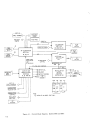
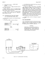
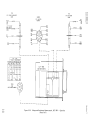
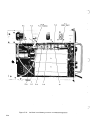
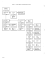
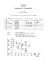
Figure 4-1. Overall Block Diagram, Models 608E and 608F.
4-0
/2'\
~
PERCENT
MODULATION
--4l! IZERO I
-63
POWER suPPLY SECTION
--"T'--T-- "T'-v12, I
,VI'I••
V13, :010 ;VI5, : Ql
VI6B 1011 IVI6A,
,
---@ METER CA"L_,
•
Model 608E/F
Section IV
SECTION IV
PRINCIPLES OF OPERATION
4-1. INTRODUCTION.
4-2. This section contains principles of operation
for the Model 608E and Model 608F Signal Generators. Included herein is a general description of the
instruments to a block diagram level, and a detailed
circuit description which references the schematic
diagrams.
Principal dissimilarities between the
Model 608E and 608F occur in the RF Generator Section; therefore, this section of each instrument will
be described separately. The remaining sections in
both instruments are nearly identical. These sections
will be presented in a single description with the minor
differences between instruments noted.
4-3. GENERAL DESCRIPTION. ,
4-4. As illustrated in Figure 4-1, the signal generators contain a RF Generator Section, Amplitude Modulation Section, Attenuator Section, Calibrator section,
Modulation Meter Section, and Power Supply Section.
Each section is described in the succeeding paragraphs.
4-5.
RF GENERATOR SECTION, MODEL 608E.
4-6.
The RF Generator Section in the Model608E
RF Oscillator V6, Buffer Amplifier V22,
Power Amplifier V8, and associated circuitry. The
RF Oscillator generates sine-wave signals from 10
MHz to 480 MHz in five frequency bands, which are
identified in Figure 3-1 (item 8). Operation of the
FREQUENCY RANGE switch selects tuned circuits in
both the RF Oscillator and Power Amplifier stages for
the desired operating range, and the Frequency Control adjustment selects frequencies within the range.
The latter control tunes the RF Oscillator and Power
Amplifier simultaneously. Mino}' frequency adjustments can be made by use of fue FINE FREQ control connected in the output circuit of RF Oscillator
V8. An uncalibrated RF output signal is also provided at the output circuit of Oscillator V6. The signal is applied to UNCAL RF OUTPUT connector J5
and is available for use with a frequency counter or
other external measuring equipment. Buffer Amplifier V22 isolates RF Oscillator V6 and the output
stages. A connection between the output stage of Buffer Amplifier V22 and the input circuit of Power Amplifier V8 serves as the modulation point, with the
modulating signal being received from the Amplitude
Modulation Section. The modulated RFsignal is amplified in V8 and applied to the output circuit of the
stage, which has been tuned by the FREQUENCY
RANGE and Frequency Control adjustments. The
AMPL TRIMMER control connected in the output circuit of Power Amplifier V8 is mechanically linked to
a pushbutton switch in the Amplitude Modulation section. The interconnected control permits peaking the
~~~~':oj,:,:,
RF output ofthe instrument, and maintaininga fixed RF
output across the frequency range of the instrument.
Tuning the control without engaging the pushbutton provides a fine-tune adjustment, which is used in conjunction with the RF OUTPUT control to maintain a fixed,
leveled RF output regardless ofthe selected frequency.
DepreSSing the control and then tuning permits a sharp
peak to be obtained on the RF OUTPUT meter for optimizing the RF output of Power Amplifier V8.
4-7.
RF GENERATOR SECTION, MODEL 608F.
4-8. The RF Generator Section in the Model 608F
Signal Generator is essentially the same as the Model
608E, containing the RF Oscillator, Buffer Amplifier,
and Power Amplifier stages discussed in paragraph
4-5. Frequency capability of the instrument is between 10 MHz and 455 MHz in five frequency ranges.
Differences between the frequency capabilities of the
Model 608F and 608E can be ascertained by reference
to Figure 3-1 (item 8). Two circuits and associated
input and output connectors have been added to the
Model 608F to permit the unit to be used with a Model
8708A Synchronizer. This equipment arrangement
provides a highly stable, phase-locked RF signal output
from the Model 608F, or permits the instrument to be
used in narrow-band frequency or phase modulation
applications. During use with a synchronizer a connection is made between UNCAL RFOUTPUT connector
J5 on the Model 608 F and synchronizer to provide a
sample to the uncalibrated RF signal output from RF
Oscillator V6. A second connection is made between
the synchronizer and FREQ CONTROL INPUT connector J6 on the Model 608F. The latter connection delivers de control voltage to va-ractors connected across
the tank circuit of RF Oscillator V6 in the Model 608F.
This dc control voltage reflects any frequency difference between the uncalibrated RF signal output of V6
and a calibrated reference frequency developed in the
synchronizer. Hence, any drift in the output of RF
Oscillator V6 is detected and an offsetting control voltage is returned to the Model 608 F to maintain a correct frequency output. A third connection between the
Model 608F and synchronizer is made at FREQ ANALOG OUTPUT connector J7. This connection provides
a resistance to the synchronizer that is inversely proportional to the frequency in use. The resistance is
used to maintain constant loop gain across the frequency band during phase-lock operation.
4-9.
AMPLITUDE MODULATION SECTION.
4-10. The Amplitude Modulation Section consists of
Modulation Oscillator V2, Differential Amplifier Q2
and Q3, Sine-Wave Amplifier Q4, Pulse Amplifier Q5,
Amplifiers Q6 and Q7, Modulators Q8 and Q9, theRF
OUTPUT meter, and associated circuits. Selection of
4-1
Sectior. IV
the signal generator mode of operation is made by use
of the MODULATION selector switch connected in the
Amplitude Modulation Section. The four modes of
operanon are internal sine-wave modulation (400 or
It100 Hz), external sine-wave modulation, external
pulse modulation, and cw operation; these four operations are discussed in the following paragraphs.
4-11. INTERNAL SINE-WAVE MODULATION. To
select internal modulation, the MODULATION selector switch is set to eIther the 400 - or 1000 - position. Modulation Oscillator V2 provides a sine-wave
output of fixed amplitude established by the Oscillator
Amplitude control, a screwdriver adjustment within
the instrument. The sine-wave output is then applied
totransistor Q3 in the differential amplifier stage, and
to AM/PULSE MOD INPUT connector J2. The signal
at the connector is made available for synchronizing
external equipment during internal modulation operation. The second siRnal applied to Differential Amplifier Q2-Q3 is adetected RFoutput Signal received from
diode CR2. This leveling feedback Signal, which is
used to counteract va.riations in the R F output signal,
is applied to transistor Q2. The product of Differential Amplifier Q2-Q3 is amplified in Sine-Wave Amplifier Q4, and Amplifiers Q6 and Q7, then passed to
Modulators Q8 and Q9. D..iring internal and external
modulation and when CW operation is conducted, Pulse
Amplifier Q5 is disabled. Signal output from the modulator stage is applied tothe input circuit of Power Amplifier V8 in the RF Generator Section where modulation of the RFsignal and signal leveling occur. A
MODULATION control between Modulator Oscillator
V2 and transistor Q3 in the differential amplifier
stage provides an adjustment to select the desired
percentage of modulation as observed on the PERCENT MODULATION meter discussed in paragraph
4-19. The RF OUTPUT control connected in the differential amplifier stage is used in conjunction with
the Attenuator Control to calibrate RFpower output
from the instrument. Final selection of the desired
output level up to +7 dBm is made using the Attenuator Control in both the Model 608E and 608F. In the
Model 608E only, an RFoutput level above +7 dBm is
selected by use of the RF OUTPUT control only. The
AMPL TRIMMER control in the Amplitude Modulation
Section is ganged to a tuning control in the output circuit of Power Amplifier V8 in the RF Generator Section. Operationofthese controls is discussed in paragraph 4-5. The Meter Cal, Balance, and Meter
Tracking controls are internal adjustments to set the
RF OUTPUT meter and differential amplifier stage
for proper operation.
4-12. EXTERNAL SINE-WAVE MODULATION. During external sine-wave modulation a connection is
made between the external modulating equipment and
AM/PULSE MODE INPUT connector J2 onthe instrument, and the MODULATION selector switch is set to
the AM position. The latter adjustment disables Modulation Oscillator V2, and routes the incoming modulationsignal through the MODULATION control to transistor Q3 in the differential amplifier stage. Operation of the remaining circuits and controls in the Amplitude Modulation Section is identical to that described
in paragraph 4-11.
4-2
Model 608E/F
4-13. EXTERNAL PULSE MODULATION. To set the
signal generators for external pulse modulation, the
desired RFoutput level and operating characteristics
of the Amplitude Modulation Section are established
with the MODULATION selector switch in the PULSE/
SET RFOUTPUT position. The switch position enables
Pulse Amplifier Q5 and disables ModulationOsciUator
V2 and Sine-Wave Amplifier Q4. With the MODULATION switch in the PULSE/SET RF OUTPUT poSition,
the operating characteristics of Amplifier Q7 and
Modulators Q8-Q9 in the Amplitude Modulation Section are established by use of the RF OUTPUT control, and the desIred RFoutput level from the instruments selected as observed on the RF OUTPUT meter.
Fine adjustment ofthe RF output level can be made at
this time uSing the AMPL TRIMMER and RF OUTPUT
controls conjunctively. Upon completion of these preliminary adjustments, the MODULATION selector
switch is set to the PULSE position, and the external
pulse source connected to the signal generators at
AM/PULSE INPUT connector J2. The input signals
are amplified by transistors Q5, Q6 and Q7 then passed
to Modulators Q8-Q9. The output of the Modulator
stage is applied to the input circuit of Power Amplifier va where modulation of the RF signal occurs.
During pulse modulation, the MODULATION, RF
OUTPUT and AMPL TRIMMER controls should not be
operated after Initial adjustments are made, and the
PERCENT MODULATION and RF OUTPUT meters
are inoperative. To readjust the RFoutput level, the
external modulating source must be removed at connector J2, and the MODULATION switch returned to
the PULSE/SET RF OUTPUT position. Adjustment
oftbe RF OUTPUT and Al\1PL TRIMMER controls can
then be made as previously discussed.
•
)
4-14. CW OPERATION. When the instrument is set
Cor CW operation with the MODULATION selector
switch in the CW position. Modulation Oscillator V2
and transistor Q3 in the differential amplifier stage
are disabled. The R F leveling signal received from
diode CR2 is passed through the Amplitude Modulation
Section in a normal manner, and applied to the Input
circuit of '?ower Amplifier V8 in the RF Generator
Section for stabilization ofthe RF power output level.
The RF leveling signal is also applied to the RF OUTPUT meter circuit in the Amplitude Modulation Section for R F level calibration. Operation of both the
AMPL TRIMMER PUSH TO PEAK and RF OUTPUT
controls is identical to that described in paragraph
4-11.
4-15. ATTENUATOR SECTION.
4-16. Attenuator Section ATl couplesR Fenergy from
'?ower Amplifier V8 in the RF Generator Section to
the load through RF OUTPUT connector J4, and provides control over the RFoutput level. The previously
discussed RF leveling Signal developed across diode
CR2 is provided by a second RFoutput from the Attenuator Section. The Attenuator Control is used in
conjunc(ionwith the RF OUTPUT meter and RF OUTPUT control in the Amplitude Modulation Section to
calibrate the RFoutput level of the instrument. and also
to select the desired output level from the equipment
after calibration procedures have been completed.
•
Model 60aE/F
4-17. CALIBRATOR SECTION.
4-18. The Calibrator Section consists of5-MHz Oscillator V9A, I-MHz Oscillator V9B, Amplifiers VIOA
and VH, and the associated circuits. Operation of
the oscillators is controlled by the XTAL CAL toggle
switch that has three positions; OFF, 1 MC, and 5
MC. With the selector switch in either the 1 Me or
5 MC position, an output from the active oscillator is
mixed wtth a sample RFsignal from Power Amplifier
V6 in the RF Generator Section to produce audio beat
signals. The audio signals are passed through amplifiers VIOA and Vll to a matching transformer. The
transformer output is then applied to XTAL CAL
OUTPUT connector J3 for use by an operator during
frequency calibration operations. A XTAL CAL GAIN
control cOMected in the output circuit of Amplifier
Vll provides an audio output level adjustment.
4-19. MODULATION METER SECTION.
4-20. The Modulation Meter Section consists of stabilized wideband amplifiers V18 and V19, rectifier
V20, and twin-triode V21 cOMected in a bridge circuit. Prior to operation the PERCENT MODULATION meter, also connected in the bridge circuit, is
calibrated by use of the Meter Calibration control, an
internal adjustment. Also, the bridge circuit is balanced to electrical zero by the ZERO adjustment
located on the front panel of the instrument. The R F
Signal output of the Attenuator Section is detected
across diode CR2 and applied to a filter network that
produces the modulating signal. 'Phis signal is amplified in via and V19, rectified in V20, and applied to
the bridge circuit. The bridge circuit is unbalanced
in direct proportion to the-peak amplitude of the input
modulaUng signal; therefore, the PERCENT MODULATION meter connected across the bridge indicates
the degree of unbalance in the bridge, or the percentage of modulation, The percentage of modulation is
established by use of the MODULATION control in the
Amplitude ModulaUon Section.
4-21. POWER SUPPLY SECTION.
4-22. The Power Supply Section consists of four
series-regulated interrelated power supplies. The
+225-volt power supply contains Comparison Amplifier V12 and a Series Regulator comprised of both
sections of VI3 and V16a. The +25-volt power supply contains Reference Amplifier QlO and Series Regulator QI1. The -165 -volt power supply consists of
Reference Tube VIS, Comparison Amplifier V14, and
Series Regulator v16A. The -6.3 volt supply contains a reference diode and Series Regulator Ql. The
-165 volt supply is used to reference both the -6.3
volt and +225 volt supplies. The +225 volt supply is
used to reference the +25 volt supply. A further discussion of these power supplies is contained in the
detailed circuit description that follows.
4-23. DETAILED DESCRIPTION.
4-24. This discussion describes the circuits in the
RF Generator Section (Model 60SE), RF Generator
Section IV
Section (Model 60SF), Amplitude Modulation Section,
Attenuator Section, Calibrator Section, Modulation
Meter Section, and the Power Supply Section. Figures
7-4 and 7-5 will be used as reference during the description, and where tr:;,nsition from one diagram to
the second is required appropriate notice will be made.
4-25. RF GENERATOR SECTION, MODEL 608E.
4-26. The RF Generator Section in the Model 60SE
includes RF Oscillator V6, Buffer Amplifier V22, and
Power Amplifier VS. RF Oscillator V6 is a type 4042
triode connected across the +225 and -165 Vdc supplies in a Colpitts circuit. The oscillator tank circuit contains split-stator capacitor CI7A and five
separate RF transformers mounted on a revolving
turret assembly. Capacitor segment CI7A is mechanically linked to segment C17B in the output circuit
of Power Amplifier V8, and the oscillator turret assembly is linked to an amplifier turret assembly also
located in lhe output circuit of VS. Choice of frequency
band 1s made by operating the FREQUENCY RANGE
switch located on the front panel of the instrument.
This function rotates the oscillator and power amplifier turret assemblies simultaneously to the selected range (Range A through E), and sets the associated inductor (LI through L6, and Ll2 through L16)
into the output circuits of RF Oscillator V6 and Power
Amplifier VS respectively.
Capacitors Cl7A and
CI7B are then tuned by the front-panel mounted Frequency Control to the desired frequency within the
range. Minor frequency adjustments can be made by
tuning capacitor C68 (FINE FREQ control) in the tank
circuit of Oscillator V6.
4-27. The plate circuit of RF Oscillator V6 is series
fed through resistors R246 and R247. These resistors in conjunction with resistor R43 in the cathode of
the stage serve to limit plate current within safe
limits. The cathode of Oscillator V6 is bypassed by
capacitor C25, which is part of the tube mounting plate
and Is not visible when the plate is in positIon. Bias
for the stage Is developed by cathode resistor R249
and grid resistor R248, with coupling capacitor Cl6
returning feedback to the grid to maintain oscillation.
Capacitor C59 connected across a portion of the tuned
circuit is used to calibrate the high end of the frequency
dial after replacing an oscillator tube. Capacitor
C18, installed in the Model 60BE only, is used to improve tracking characteristics of the tuned circuit at
higher frequencies. Adjustment of this internal control is critical, since a compromise must be reached
between tracking capabilities and optimum power output. Misadjustmentof capacitor CIS can produce improved tracking capability but a loss in RFpoweroutput. The control is factory aligned, and no further
adjustment should be reqUired.
4-2S. All voltages applied to RF Oscillator V610cated
in the RF Generator hOUSing assembly are regulated,
and brought into the stage through RFl filters. The
+225 vdc plate voltage is received through filter FL5,
the -165 Vdc supply is received through filter FL2,
and a regulated -6.3 heater voltage is received through
filter FL4.
4-3
Section IV
4-29. The secondary windings in the oscillator turret
assembly couple RF energy from RF Oscillator V6
through a coaxial cable to Buffer Amplifier V22. Resistors R240, R242, R244, and R245 located in the
secondary windings of coils L2 through L5 damp undesirable resonance in the cathode of Buffer Amplifier
V22. Resistors 8241 and R243 connected across the
secondary Windings of coils L4 and L5limit the RFdrive
at lower frequencies. Resistors R250, R251, and
capacitor C21B forma take-off network for an uncalibratedRFoutput signal that is applied through coaxial
cable WI to UNCAL RF OUTPUT connector J5. Resistor R251 in the take-oU network is 301 ohms in
the Model 60BE and 200 ohms in the Model 60BF.
This configuration is due to the difference in RF output level between instruments. The RF signal at
connector J5 can be used with a frequency counter or
other external measuring equipment. When the Model
60BF is used with a Model B70BA synchronizer during phase-lock operation, the signal is used by the
synchronizer.
4-30. Buffer Amplifier V22 is a type EC-8010 triode
connected as a grounded-grid amplifier. The stage
isolates RF OscUlator V6 and Power Amplifier va,
and reduces any incidental frequency modulation to a
minimum level. Cathode resistors R255 and R253
operate with resistors R254 and R256 in the plate circuit to limit plate current to a safe value. Power to
the stage is supplied through RFl filters FL2, FL4,
and FL5, with the plate, cathode and mament supplies
being decouple<! by capacitors C222, C220, and C221
respectively. The plate circuit of Buffer Amplifier
V22 is coupled to the cathode circuit of Power Amplifier va through a wide-band network consisting of dc
blocking capacitor C224 and coil L22. Coil L20 in the
plate circuit of V22 serves as an RFchoke, while isolation network Lll blocks an RF signal path to the output circuit of the Amplitude Modulation Section.
4-31. Power Ampli!1er VB is a grounded-grid,
cathode-modulated ampllfier that delivers the modulated or CW output signal to the Attenuator Section.
The plate circuit of va contains the amplifier turret
assembly which houses inductors L12 through L16.
These inductors are placed into the output circuit of
VB by operation of the FREQUENCY RANGE switch
discussed in paragraph 4-26. The second segment of
Frequency Control capacitor Cl7 is also located in
the plate circuit of Power Amplifier VB. Linkage
between capacitor C17B and C17A in the RF Oscillator Stage permit tuning to a frequency within a range
as discussed in paragraph 4-26. A second linkage
between capacitor C17B and the AMPL TRIMMER
control permit the capacitor to be tuned separately or
in conjunction with push-to-operate switch S6 in the
Amplitude Modulation Section for peakIng the RFoutput signal. This function is discussed further in paragraph 4-45.
4-32. When the instrument is set to provide an amplitude modulated output, the modulating signal and an
RF leveling signal are received at the cathode of Power
Amplifier VB from the Amplitude Modulation Section
through isolation network LII. During CW operation,
only the RF leveling signal is received from the
4-4
Model608E/F
Amplitude Modulation Section. Diode CR7 connected
in the signal path prevents damage to Power Amplifier
V8 by limiting the negative swing ri. the cathode. Capacitor C32 is connected in the plate circuit of VB in
the Model 608F only, and is adjusted for improved
tracking characteristics in the power amplifier stage
at higher frequencies. Capacitors C30, C229, C230,
and C231 connected across coils L16, L15, L14, and
L13 respectively are also installed in the Model 60BF
only. These capacitors are selected in test to improve
tracking between the power amplifier and oscUlator
stages. Nominal values for the capacitors are illustrated in Figure 7-4. The RF output signal from Power
Amplifier VB is inductively coupled through the amplifier turret assembly coil and applied to the Attenuator
Section. This section of the instrument is discussed
in paragraph 4-51.
•
4-33. RF GENERATOR SECTION, MODEL 6OBF.
4-34. The RF Generator Section in the .Model 606 F is
essentiall y the same as the generator section in the
Model 608E, except for the addition of circuits to permit the unit to be used with a Model 8708A Synchronizer. These circuit differences occur in the tank circuit of RF OscUlator V6 and the output stage of Power
Amplifier V8.
4-35. Two varactor diodes, CR31 and CR32, are connected across the oscillator tank circuit in the Model
6OBF. The varactors are reverse-biased junctions
that act as variable capacitors, changing capacitance
with a change in the applied reverse bias. In quiescent
corrlition the diodes are biased by a voltage divider
network comprised of resistorS R271, R267, andR268.
A change in bias, and the \ ;,;31.11t...lli .,;r.<u.ge in capacitance, is produced by a dc control voltage received at
FREQ CONTROL INPUT connectorJ6. Duringoperalion with a Model B70BA Synchronizer, a connection is
made between UNCAL RF OUTPUT connector J5 and
the synchronizer to provide a sample oftheRFoutput
from the Model 608F. A second connection is made
between the synchronizer and FREQ CONTROL INPUT
connector J6 to receive thedc control voltage from the
synchronizer. The frequency sample sent to the synchronizer is compared to a reference frequency developed in the synchronizer. A drilt tendency in R F
Oscillator V6 is compared with the reference frequency, and translated into a dc control voltage for
application to varactors CR31 and CR32 in the Model
608F. The varactors change capacitance in direct
proportion to the detected drilt holding RF Oscillator
V6 on frequency.
4-36. Potentiometer R269 is installed in the Model
60SF only, and is mechanically linked to Frequency
Control ca,acitor C17B in the output circuit of Power
Amplifier VB. The potentiometer output resistance
varies as the Frequency Control adjustment is tuned,
presenting 4K ohms at the low-frequency end of the
capacitor tuning range and zero ohms at the highfrequency end. The resistance is applied through
FREQ ANALOG OUTPUT connector J7 to the dc control voltage circuit in the synchronizer. This loop
arrangement controls the voltage level applied to
varactors CR31 and CR32, thereby assuring correct
)
•
Model 608EI F
operating conditions for thedevices across a frequency
range.
4-37. AMPLITUDE MODULATION SECTION.
4-38. The Amplitude Modulation Section consists of
Modulation Oscillator V2, a portion of the Modulator
and ALC Board, a RF OUTPUT meter and control, two
MODULATION controls, and the associated circuitry.
The Modulator and ALC Board contains Differential
Amplifier Q2-Q3, Sine-Wave Amplifier Q4, Pulse
Amplifier Q5, Amplifiers Q6 and Q7, and Modulators
Q8 and Q9. Four modes of operation will be discussed during the description of the Amplitude Modulation Section; these are identlfied as internal sinewave modulation, external sine-wave modulation, external pulse medulation, and CW operation.
4-39. INTERNAL SINE-WAVE MODULATION. The
internal sine-wave modulation mode is selected by
placing MODULATION switch 57 to either the 400 or 1000 - position (switch setting 2 or 3), which
provides a 400 i: 40 Hz or a 1000 ± 100 Hz output from
Modulation Oscillator V2. The oscillator consists of
reSistance-coupled amplifiers V2A and V2B connected
in a Wein-Bridge circuit. At the resonant frequency,
positive feedback from the plate of Amplifier V2B is
applied to the grid of amplifier V2A sustaining oscillation. A change in frequency is obtained by inserting resistors R3-R5 or R4-R6 into the feedback network through two segments of MODULATION switchwafer 2F. A negative feedback circuit consisting of
resistors R7, R8 and lamp DSl is used to stabilize
the oscillator, reduce distortion, and maintain a constant output level. U the amplitude of the signal incre;taes, current through the lamp increases thereby
raising the resistance of lamp DSl; consequently, the
signal amplitude is held constant. Potentiometer R7
is an internal adjustment for adjusting the ampUtude
of the output Signal. Heater voltage to the stage is
applied at all times during instrument operation; however, plate voltage is applied to V2A and V2B only
when MODULATION switch-wafer 2R is in position 2
or 3.
4-40. The sine-wave Signal from Modulation Oscillator V2 is applied through dc blocking capacitor C205,
MODULATION switch-wafer IF, to MODULATION
control R210. A second signal path for the sine-wave
is prOVided through resistor R262 to AM/PULSE MOD
INPUT cOimector J2 where the signal is available for
synchronizing external equipment during the internal
modulation mede. The signal at the wiper of MODULATION control R210 is passed through, afrequencycompensation network consisting of resistor R261, and
capacitors C203 and C204. The signal is then routed
through MODULATION switch-wafer lR tothe base of
transistor Q3 in the differential amplifier stage. The
second input to the differential amplifier is a detected
Signal developed across diode CR2 and filter network
C38 and R119 located in the bolometer portion of the
Attenuator Section. This leveling signal, which is representative of the RF power output Crom the instrument, is passed through R F1 filter FL8 to the base of
transistor Q2. The leveling signal is also applied
through resistor R201, Meter Cal potentiometer R202.
Section IV
MODULATION switch-wafer 4F, and AMPL TRIMMER pushbutton switch S6 to RF OUTPUT meter M1.
Operahng characteristics of switch S6 and the RF
OUTPUT meter are contained in paragraph 4-45.
4-41. Balance potentiometer R203 is a board adjustment in the emitter circuit of Differential Amplifier
Q2 and Q3 used to set the stage for proper operation.
The RF OUTPUT control R212 connected with resistor R213 in a voltage divider network sets the operating characteristics of the differential amplifier stage,
and Is used in conjunction with the Attenuator CO:J.trol
to calibrate and control the RF output from the instrument. The output of the dlJferentiai amplifier is the
product of the leveling signal on the base of transistor Q2 and the modulating signal on the base of transistor Q3. This product Signal is then applied to the
base of Sine-Wave Amplifier Q4.
4-42. The base circuit of amplifier Q4 contains a lowfrequency compensating network consisting of resistor
R214 and capacitor C202. In the Model 608E resistor
R214 Is 200 ohms, and in the Medel 608F the resistor
value is 392 ohms. Amplifier Q4 is biased by voltage
divider network R2l7 and R215, with diode CR21 installed as a protective device to maintain a safe relationship between the base and emitter circuits of Q4
during operation. The collector circuit of Q4 also
contains two frequency-compensating networks consisting of resistor R219 and capacitor C208. and resistor R2l8 and capacitor C207. The output of amplifier Q4 is developed across resistor R216 and applied
to the base circuit of AmpHfier Q6.
4-43. During internal or external SIne-wave modulation, Amplifier Q6 receives the leveling and modulating Signals from Amplifier Q4. During CW operation, only the leveling signal is received at Amplifiers Q4 and Q6. During external pulse modulation,
Amplifier Q4 is inhibited and the input pulse Signals
are received at Amplifier Q6 from Pulse Amplifier
Q5. The external pulse modulation and CW modes of
operation are discussed later in this section. The
emitter of Amplifier Q6 is biased by a voltage divider
network conSisting of resistors R223 and R224, and
during internal sine-wave operation the modulating
and leveling signals are developed across load resistor R222 for application to' Amplifier Q7.
4·44. Resistor R229 provides emitter bias for Amplifier Q7. whiletbe collector voltage is developed across
load resistor R228 and resistor R233. This voltage
divider network also establishes the base conditions
on Modulators Q8 and Q9. During the pulse modulation mode, the collector voltage on Amplifier Q7 can
be controlled by operation of the RF OUTPUT control;
this function is discussed in paragraph 4·47. The collector output of Amplifier Q7 is applied to the base of
Modulators Q8 and Q9 connected in parallel emitter·
follower configuration. The emitter bias Cor the stage
is derived from a voltage divider network consisting
ofresistor R33. Zener diode CR26, and resistor R258 in
the RF Generator Section. Diode CR25is connected as
a protective device between the base and emitter circuits of the stage. The modulator output is applied
4-5
Section IV
through RFI filter FL6 and isolation network Lll to
the cathode of Power Amplifier VB, where modulation
and RF leveling occur.
4-45. A feedback path for the output of Modulators Qa
and Q9 is provided through filter network R235 and
capacitor C200 which removes the modulating signaL
The leveling signal is passed through MODULATION
switch-wafer 4F and applied to the normally-open
contacts of AMPL TRIMMER pushbutton switch S6
when the MODULATION switch is in positions I through
4. As previously mentioned, the AMPL TRIMMER
pushbutton is mechanically linked to AMPL TRIMMER capacitor C17B in the output circuit of Power
Amplifier V8. During normal operation the detected
feedback from diode CR2 in the Attenuator Section is
applied through resistor R20l, potentiometer R202,
and the normally-closed contacts of pushbutton switch
S6 to RF OUTPUT meter MI: therefore, the meter
normally displays the leveled RFoutput of the instrument. Rotation of RF OUTPUT control R212 changes
the conduction level of Differential Amplifier Q2-Q3
arid the signal output level of Modulators Q8-Q9. This
change is reflected in the RF output of Power Amplifier
V8, and di;5played on RF OUTPUT meter Ml. Operation of AMPL TRIMMER control C17B without engagingthe pushbutton provides a fine-tune adjustment for
use with the RF OUTPUT control to maintain a constant, leveled RF output across a frequency range.
When AMPL TRIMMER pushbutton S6 is depressed the
leveling signal feedback from Mqdulators Q8-Q9'is
displayed on meter Ml, and operation of the control
permits a sharp peak to be observed on the meter.
Hence, the RFoutput of Power Amplifier va can be
peaked. During internal and external sine-wave operation, MODULATION control R210 controls the level
of the modulation and is used in conjunction with the
PERCENT MODULATION meter discussed in paragraph 4-59.
4-46. EXTERNAL SINE-WAVE MODULATION. Operation of the instruments during external sine-wave
modulation is similar to the internal mode, and is
established by setting MODULATION switch S7 to the
AM position (switch poSition4). Modulation Oscillator
Y2 is disabled by removing the stage plate voltage at
MODULATION switch-wafer 2R, and a Signal path of
the external sine-wave signal is established through
MODULATION switch-wafer IF. A cable connection
is made between the external source and AM/PULSE
MOD INPUT connector J2, with the incoming signal
being routed to MODULATION control resistor R2l0.
The signal is then applied through the frequencycompensation network and MODULATION switch -wafer
IR tothe base of transistor Q3 in the differential amplifier stage. Operation of the remaining circuits and
controls in the Amplitude Modulation Section is the
same as described during internal sine-wave modulation.
4-47. EXTERNAL PULSE MODULATION. Duringthis
mode of operation MODULATION switch S7 is set
first to the PULSE/SET RF OUTPUT position (switch
position 5) to establish operating conditions in the output circuit of the Amplitude Modulation Section, and
4-6
Model 608E/F
consequently the RF output level of the instrument.
The switch is then set to the PULSE position (switch
position 6) to pulse modulate the RF carrier. In both
positions Modulation Oscillator V2 is disabled and the
input signal path through MODULATION control resistor R210 is interrupted. The position of MODULATION switch-wafer 4F interrupts the leveling signal
path through the normally-open contacts of AMPL
TRIMMER pushbutton switch S6, and removes the
push-to-peak function of the AMPL TRIMMER control
during pulse operation. However, the detected signal
from diode CR2 in the Attenuator Section is received
through resistor R20l and potentiometer R202 for application to RF OUTPUT meter Ml. Therefore, in
the PULSE/SET RF OUTPUT position, the AMPL
TRIMMER and R F OUTPUT controls can be used to
set the desired RFoutput level as indicated on the RF
OUTPUT meter. The two controls are operated only
in the PULSE/SET RF OUTPUT position.
•
4-48. Transistor Q3 in the differential amplifier stage
has an inhibiting voltage applied to the base through
resistor R211 and MODULATION switch-wafer lR.
With transistor Q3 cut off, transistor Q2 conducts
heavily and places a disabling voltage on the base of
Amplifier Q4. This condition interrupts to leveling
signal path through the Amplitude Modulation Section.
Resistor R212 is removed from the circuit by the position of MODULATION switch-wafer lR; however, the
RF OUTPUT control is also connected to potentiometer R226 in the collector circuit of Amplifier Q7
for rf output level control. With the MODULATION
switch in position 5, a positive voltage is applied to
the base of Pulse Amplifier Q5 through resistors R220
and R225 to enable the amplifier. The position of
MODULATION switch-wafer 3R forms a voltage divider
network conSiSting of resistors R228, R226, and R270
in the collector circuit of Amplifier Q7 and the base
circuits of Modulators Qa and Q9. Operation of RF
OUTPUT potentiometer R226 controls the conduction
level of transistors Q7, Q8, and Q9, and the output
level of ?ower Amplifier va.
4-49. While the MODULATION switch is still in the
PULSE/SET RF OUTPUT position, the RF OUTPUT
control is adjusted for an indication on RF OUTPUT
meter Ml. AMPL TRIMMER control C17B in the output stage of Power Amplifier va is then peaked for
maximum RFoutput. The RF OUTPUT is readjusted
for an indication of +7 dBm (Attenuator Calibrated) on
RF OUTPUT meter Ml. With the preliminary adjustments completed, the external modulating equipment
is connected to AM/PULSE MOD INPUT connector J2,
and MODULATION switch S7 is set to the PULSE position (switch position 6). The incoming pulse train is
passed through MODULATION switch-wafer 3F to the
base of Pulse Amplifier Q5, and then routed through
Amplifier Q6 and the remaining circuits of the Amplitude Modulation Section as previously described.
4-50. CW OPERATION. Tosetthe equipment for CW
operation, MODULATION switch S7 is placed to the
CW position (switch position 1). Modulation Oscillator
)
•
•
Model 6OBE/F
V2 is removed from the circuit by the position of
switch-wafer 2R, and the sine-wave input circuit is
interrupted by the setting of switch· wafer IF. A de·
tecled RF output signalfrom diode CR2 in the Attenuator Section Is applied to the base of transistor Q2 in
the differential amplifier stage for the development of
a leveling sigr.al as preViously described. R F OUTf'UT meter MI also receives the detected signal through
AMPL TRIMMER pushbutton switch S6. Transistor
Q3 in the differential amplifier stage is terminated In
a network conSisting of resistor R263 and capacitor
C206; however, RF OUTPUT control resistor R212 Is
connected In the circuit and controls conduction of the
differential amplifier stage. Pulse Amplifier Q5 Is
disabled by the ground applied to the base circuit
through MODULATION switch-wafer 3F. Leveling
signal output of the differential amplifier stage is
passed through Amplifiers Q4, Q6, Q7 and Modulators Q8-Q9 to the input circuit of Power Amplifier
V8. RF OUTPUT meter MI displays a leveled RFoutput from the instrument as selected by the RF OUTPUT control and Attenuator Control. AMPL TRIMMER pushbutton switch S6 is returned to operation in
conjunction with AMPL TRIMMER capacitor Cl7B for
peaking the RF output uSing the leveling signal feedback
from Modulators QB-Q9.
4-51. ATTENUATOR SECTION.
'.
4-52. To extract power from the RF Generator Section, a piston-type attenuator is used. The attenuator housing projects through the rear of the generator
housing, and provides an open-ended termination near
the power amplifier plate-circuit inductor. A single·
turn pick-up loop at the end of the attenuator probe
couples energy to an impedance-matching network
consisting of capacitors C69 and C37, and resistors
R58 and R59. Capacitor C37 is a movable slug in the
probe body that Is used to adjust the standing· wave
ratiotoamlnimum value when RF OUTPUT connector
J4 is terminated In a 50-ohm load.
4-53. The front-panel mounted Attenuator Control
moves the probe in the aUenuator housing, and controls the amount of RF energy passed to the output
connector. In both the Model 608E and 608F. calibration is accomplished by adjusting the RF OUTPUT
and AMPL TRIMMER controls for a steady +7 dBm
(ATTENUATOR CALIBRATED) indication on the RF
OUTPUT meter across the frequency range in use.
An adjustment of the Attenuator Control after calibration procedures are completed prOVides the RF output level indicated on the control dial as long as the
RF OUTPUT meter needle remains in the ATTENUATOR CALIBRATED position. In the Model 608E only,
an rf output between +7 dBm and +13 dBm can be selected. The AUenuator Control is set to the +7 dBm
position (maximum clockwise), and the RF OUTPUT
and AMPL TRIMMER controls are adjusted for the
R F OUTPUT meter indication of +7 dBm as previously
discussed. The desired output level above +7 dBm is
then selected by operation of the R F OUTPUT control
only. and the output is read directly from the RF OUTPUT meter.
Section IV
4-54. Two parallel wires crossing the open end of
the attenuator housing are used to provide a sample
of RF energy delivered by Power Amplifier V8. The
energy is applied to the Bolometer through ferritebead RFCI, which provides isolation between the
Bolometer and Attenuator. The Bolometer contains
frequency-response coil Ll7, diode CR2 and resistor
R60. The RFsignal detected across resistor R60 and
diode CR2 is passed throughanRFfilter conSiSting of
capacitor C38 and resistor RU9. Thedetected Signal
is then applied through RFI filter FL8 to the Modulation Meter Section discussed in paragraph 4-60, and
to transistor Q2 in the Amplitude ModulaUon Section
discussed in paragraph 4-40.
4-55. CALIBRATOR SECTION.
4-56. The Calibrator Section consists of 5-MHz Oscillator V9A, I-MHz Oscillator V9B, Harmonic Generator and Mixer CRI, Amplifiers VIOA and VII. and
output transformer T3. The oscillator and mixer
circuits are Illustrated in Figure 7-4, while the amplifiers and transformer are located on Figure 7-5.
4-57. The 5- MHz Oscillator is a crystal-controlled,
electron-coupled oscillator utiliZing the pentode half
of a type 6UB tube. The plate and screen circuits are
tuned to the crystal frequency of 5 MHz by coils L6
and L7. Trimmer capacitor C23 is used for finefrequency adjustment of the oscillator. The I MHz
Oscillator consists of the triode portion of the tube.
with coil Ll8 used to adjust the osci'Uator to a point
where the fifth harmonic is synchronized with the 5MHz output of Oscillator V9A. WhenXTAL CAL switch
84 is set to the 5-MC position, only Oscillator V9A is
active. In the I-MC position both oscillators are
operating, with Oscillator V9A referencing the i-MHz
oscillator.
4-58. The output signai from Oscillators V9A or V9B
is passed across dc blocking capacitor C24 to diode
CRI which acts as a harmonic generator and mixer.
The anode of diode CHI is inductively coupled to the
output circuit of Power Amplifier V8 by running a lead
near the plate of the amplifier. Oscillator harmonics
within the diode are mixed with RFoutput signals to
produce audio-beat frequencies across resistor R50
in the grid circuit of Amplifier VIOA. The output of
amplifier VIOA is again amplified in VII and applied
across capacitor C36 to 600-ohm, line-matching transformer T3. The secondary of transformer T3 is connected to XTAL CAL OUTPUT connector J3 where the
calibrating signals can be monitored. XTAL CAL
GAIN resistor R56 provides front-panel control of the
audio level output at connector J3.
4-59. MODULATION METER SECTION.
4-60. The Modulation Meter Section consists of a
detector network in the Bolometer portion of the Attenuator Section, Amplifiers Vl8 and V19. Rectifier
4-7
Section IV
V20, and a balanced-bridge circuit containing PERCENT MODULATION meter M2. The Bolometer is
illustrated in Figure 7-4, and the remainder of the
section appears in Figure 7-5.
4-61. The output of diode CR2, capacitor C38 and
resistor R119 in the Bolometer is a dc Signal which
is representative ofthe RF output level, and the modulating signal when internal or external modulation is
in process. The output is passed through RFI filter
FL8 and applied to blocking capacitor C39, which
couples the modulating signal to Amplifier VI8. The
output of Amplifier VI8 is amplified again in VI9 and
passed to the plates of Rectifier V20. A stabilization
feedback circuit connects the plate of Amplifier VI9
and cathode of Amplifier VI8, with resistor R99
installed in the circuit for frequency compensation.
CS5 ac couples the plate ofV19 to the cathode ofVl8.
4-62. Rectifier V20 is connected in a balanced-bridge
detector circuit consisting of twin-triode V21, PERCENT MODULATION meter M2, and associated circuitry. With no modulating signal applied tothe circuit,
the steady-state dc potential at the plate of Amplifier
V19 is coupled to the grids of V21A and V21B. Inthis
condition, equal current flows on both sides of tne
bridge, and the PERCENT MODULATION meter reads
zero. ZERO potentiometer RI06 is a front-panel adjustment to compensate for variations in tube and component values. When a modulation mcxle of operation is
in progress, the peak value of the rectified modulating
signal is applied to the grid of V21B. The bridge is
unbalanced accordingly, and produces an indication
on the PERCENT MODULATION meter that is indirect
IJJ'vportion to the amplitude of the modulating Signal.
Triode V21A is unaffected during the detection cycle,
since the modulating signal is filtered by resistors
RIOO, RI01, and capacitor C5a.
4-63. POWER SUPPLY SECTION.
4-64. Four series-regulated power supplies are contained in the power supply section. The power supplies provide +225, -6.3, -165, and +25 voltsdc to the
Model 608 Signal Generators. The four supplies are
connected toa common input source through ON switch
83. A slide switch located on the rear panel of the instrument sets the generators for use with either a
115-Vac or 230-Vac power source, with AC LINE
fuse FI connected between the power supplies and
source as a protective device. The supplies are illustrated in Figure 7 _5 and are described in the following paragraphs.
4-65. THE +225 VOLT SUPPLY. Input ac voltage to
the +225-volt supply is received across transformer
4-8
Model 60aE/F
T1. The secondary contains bridge rectifier CRa
through CRll and filter capacitor C40. The supply is
series regulated through triodes V13A, V13B, and
VI6B, with the output connected to the load through
front-panel mounted DC 0. 25 AMP fuse F3. The -165
Volt Power Supply output is used as reference, being
applied through a voltage divider consisting of resistors R70 through R72. Any change in the load is sensed
across +225 Volts Adj potentiometer and applied to the
control grid of Comparison Amplifier V12. The plate
of amplifier V12 controls the conduction level of the
series regulators, and holds the output voltage constant. The +225 volt supply is used to reference the
+25 volt supply discussed in paragraph 4-69.
4-66. THE -6.3 VOLT SUPPLY. Input ac voltage to
the -6.3-volt supply is also received across transformer Tl. Rectification and filtering occur across
bridge rectifier CR16 through CR19 and capacitors
C75. Transistor Ql operates as a comparison amplifier and series regulator, with the base circuit referenced by -7.5 Vdc developed from the -165 Vdc
supply across resistor R260 and Zener diode CR20.
The output voltage of 7.2 Vdc is applied to RFI Filter
FL4 where 0.9 Vdc is dropped. The -6.3 volts is
then used as a filament supply for RF Oscillator V6,
Buffer Amplifier V22", and Power Amplifier va. Filament voltage for the remaining tubes in the instrument
is prOVided by a separate secondary winding of transformer T1. The latter winding also supplies voltage
to a' light behind the MEGACYCLES dial, and to the
AC POWER light located on the front panel. Both
lamps are lighted when switch S3 is in the ON position.
4-67. THE -165 VOLT SUPPLY. Input ac voltage to
the -165 volt supply is received across transformer TI,
and rectified by diodes CR12 through CRI5. Tricxle
V16A is the series regulator, with the grid controlled
by the plate of Comparison Amplifier VB whose cathcxle
is referenced by gas tube v15. The voltage level is
controlled -165 Volts Adj potentiometer R80, with the
output applied to the load and to the +225 and ·6.3 volt
supplies for reference.
4-68. THE +25 VOLT SUPPLY. Components of the
+25 volt supply are located on the Modulator and ALC
Board, which also contains a portion of the Amplitude
Modulation Section circuits discussed in paragraph
4-37. Ac power to the supply is received across transformer T2, and rectified by diodes CR29 and CR30.
Transistor Qll is the series regulator, with the conduction level being control by Amplifier QlO. The
supply is referenced by +225 Vdc received across
resistor R239.
•
)
Model 608E/F
Section V
SECTION V
MAINTENANCE
5-'_ INTRODUCTION.
•
5-2. This section contains inspection requirements,
performance and test procedures, troubleshooting
techniques, and repair instructions for the Model 608E
and 608F Signal Generators. Generally, maintenance
procedures for both instruments are identical and will
be presented in one set of instructions. Where differences occur, separate instructions for each instrument
will be included. The test equipment required for
maintenance is listed in Table 5-1. Test instruments
other than those listed may be used if the performance
equals or exceeds the minimum specification listed.
Two test instruments must be fabricated; these include
a IOO-ohm termination and loop antenna, which are
illustrated in Figure 5-1.
5-3.
PERIODIC INSPECTION.
5-4.
CLEANlNG.
bearings, including the small pulleys used in the attenuator drive system, should be lubricated quarterly
with a light slideway oil such as Shell Tonna G.
In
all cases avoid over lubrication.
The points to be
lubricated are listed in Table 5-2 and illustrated in
Figure 5-2•
5-9.
PERFORMANCE TESTS.
5-10. PURPOSE.
5-11. The following paragraphs check performance
of the signal generators during incoming inspection
tests, periodic instrument evaluation, troubleshooting,
and during equipment calibration periods. The tests
can be performed without access to the interior of the
instruments. The specifications listed in Table 1-1
are the performance standards. Unless otherwise
specified in the test procedures, the following controls
are set to the indicated position for each test:
cw
MODULATION switch.
5-5. If the equipment has been subjected to unusual
conditions (excessive moisture, dust, heat, vibration,
etc.) it is suggested that the ii;st:. U ... .:l~~ ~c cemoved
from the cabinet and inspected for dirt or moisture
accumulation, loosened components, or any possible
sign of damage. Forced air under medium pressure
is recommended for dusting and drying, although care
must be taken not to vary the settings of the internaladjustment potentiometers and capacitors during the
process.
Cursor knob. . . ,
Aligned with panel marker
FINE FREQ control
Aligned with
XTAL CAL switch .
. . . . . . . . . . OFF
p~nel
marker
5-12. FREQUENCY ACCURACY AND
RESETTABILITY TEST.
a. Connect signal generator in test setup illustrated
in Figure 5-3.
5-6.
LUBRICATION.
5-7. The signal generators are thoroughly lubricated
at the factory. Full-shielded ball bearings are used
in many applications and require no subsequent attention. Ball bearings that are not fully shielded require
only light machine oil. After prolonged use of the instrument, lubricated points should be checked for
excessive dust accumulation or drying of lubricant.
5·8. This maintenance is particularly important
when the instrument is operated continuously or for
several hours daily. Calibration accuracy and in·
strument dependability can be maintained only by
proper lubrication of the two worm gears in the tuning mechanism. Other rubbing surfaces and sleeve
b. Set FREQUENCY RANGE switch to range A.
c. Adjust FREQ OUTPUT and attenuator controls
to obtain proper triggering of electronic counter.
d. Adjust frequency control tothe low end, approximate center and high end of range Aj record MEGACYCLES dialsettingand electronic counter indication
at each position. Electronic counter should indicate
within ±1% of MEGACYCLES dial setting.
e. Retune frequency control to each MEGACYCLES
dial setting recorded in step d. Electronic counter
should indicate within ±O. 1% of indication recorded in
step d.
f. Repeat steps d. and e. for FREQUENCY RANGE
B through E.
5-1
Section V
Model 608E/F
Table 5-1.
Instrument
Test Equipment Required Cor Maintenance
Critical Specifications
Recommended Model
Electronic Counter
Frequency Range: 10 MHz to 445 MHz
Accuracy: :1::0.005%
HP 5245L with 5253B
plug-in unit
Power Meter
Range: 10 /,LW to 10 mW
Accuracy: :1::5% of full scale
HP 432A
Thermistor Mount
Frequency Range: 10 to 480 MHz
SWR:1.6max
HP 478A
Coaxial Attenuator
Coaxial Attenuator
Attenuation: 10 dB
Attenuation: 20 dB
HP 8491A
HP 8492A
Oscillator
Frequency Range: 20 Hz to 30 kHz
Envelope Distortion: 0.2% max
Output: 1 V rms
Output Impedance: BOon
HP200cD
VTVM
Voltage Range: 0.1 mV to 300V
Decibel Range: -72 to +52 dB
Frequency Range: 20 Hz to 6 MHz
HP 400E
Distortion Analyzer
Range: 5 Hz to 600 kHz
Accuracy: ::1::3%
HP 334A
Deviation Meter
Frequency Range: 50 to 150 MHz
Accuracy: ::1::3%
Deviation Range: 0 to 5 kHz
Measurements Corp.
Model 140
Power Supply
-2 to -32 V variable
HP 6217A
OsCilloscope
"F(.r~ical Bandwidth: 5 MHz
Vertical sensitivity: 5 mV/cm
HP 140A with 1402A and
1420A plug-in units
Adapter
None
UG-201A/U
Crystal Detector
Frequency Range: 10 MHz to 12.4 GHz
VSWR: 1. 2 max
Deviation Crom Square Law: <0.5 dB
over a range of at least 30 dB
Input Impedance: son
Impedance Output: 15M, 10pf
HP 423A
Dummy Load
Resistance: 1000 :1::10%
Wattage: 1/2 W
See Figure 5-2
Pulse Generator
Pulse Width: 10$.lsec
Pulse Amplitude: 10 v peak into 2Kn
Pulse Rise and Decay: 0.02 $.lsec max
Repetition Rate: 50 to 5000 pps
HP 214A
Loop Antenna
Special
See Figure 5-1
Spectrum Analyzer
Freq: 400 MHz
Sensltivity: 1 IJ. V. Absolute calibration
HP 140S with 8554L and 8552A
Plug-inS.
5-2
•
Section V
Model 608E!F
Table 5-1. Test Equipment Required for Maintenance (Cont.)
Instrument
Critical Specifications
Recommended Model
DC Ammeter
Range: 15 to 30 mA
Accuracy: .±5%
HP 428B
SWR Meter
Sensitivity: at least JJ. v full scale
Attenuator Range: 40 dB
Attenuator Accuracy: :to. 1 dB
HP 415E
Double Balanced Mixer
Frequency Range: 10 to 480 MHz
HP 10514A
Frequency Comb
Generator
Frequency Range: 10 to 480 MHz
Comb Frequency: 1 MHz
HP 8406A
Filter
Cutoff Frequency: 100 kHz
Frequency Meter!
Filter Kit
Discriminator Output: 100 kHz!V
Disc. Out Accuracy: Better than 1%
Internal Filter: 10 kHz, low pass
HP 5210AIlO531A
Oscilloscope
Bandwidth: o to 20 MHz
Vert Sensitivity: 50 JJ.V,tm
HP 140 with 1406A plug-in unit
LAB Dual Range.
DC Power Supply
Output: o to 20 Vd,
HP 6204B
Electronic Counter
Resolution: 5 digits
Function: Frequency to > 350 MHz
Input Impedance: 50 ohms
HP 5246L with 5252A
plug-in unit
Synchronizer
Compatible with the 608 F
HP 8708A
LOOP ANTENNA
6 IN. - - - - - - - - - - -
FEMALE BNC
CONNECTOR
INSULATED 16-GUAGE
COPPER WIRE
IOO-OHM LOAD
100 OHM! 10%
112 WATT
7'
UG·I094/U
FEMALE BNC
CONNECTOR
Figure 5-1.
Fabricated Test Equipment
5-3
Section V
Model 608E!F
Table 5-2.
Lubrication Chart
)
Lubrication Point (see Figure 5-2)
Lubricant
Oscillator and amplUier worm gears
"Molykote (type Z)"
A~L
Light machine oil
TRIMMER stop mechanism
AMPL TRIMMER toggle nut
Light machine oil
AMPL TRIMMER drive link
Light machine oil
Amplifier worm drive shaft
Light machine oil
RF Ampliher sliding coupler
Light machine oil
AttenuataI' pulleys
Light machine oil
Attenuator drive shaft bearing (front)
Light machine oil
Attenuator drive shaft bearing (rear)
Light machine oil
MEGACYCLES
DIAL HUB
FREQ.
DRIVE
RF AMP
SLIDING
COUPLER
RF OSC.
CAPACITOR
DRIVE SHAFT
FREQ.
STOP
GEAR
I
.....
,
RF AMP
CAPAC I TOR
DRIVE SHAFT
AMP TRIMMER
DRIVE LINK
)
- ),
;:,..
I
<_-~<.
,
AMP
AMP
TRIMMER
Figure 5-2.
5-4
AMP
TRIMMER
STOP
MECHANISM
FINE
FREQ.
ADJUST.
AMP
TRIMMER
TOGGLE NUT
OSC.
WORM
DRIVE
WORM
DRIVE SHAFT
AMP
WORM
DRIVE
Lubrication Points, RF Tuner Drive Mechanism
)
Model 608E!F
Section V
5-14. FREQUENCY DRIFT TEST.
608E/F
SIGNAL
GENERATOR
0
0
ELECTRONIC COUNTER
I
.,.,
"'
IM""T
~2!l3B
•
a. Connect signal generator in test setup illustrated in Figure 5-3.
I
~
b. Set FREQUENCY RANGE switch to range A.
-
FREQUENCY
CONVERTER PlUG·IN
Figure 5-3. Frequency Accuracy and
Resettability Test Setup
c. Adjust frequency control for a MEGACYCLES
dial reading of 15 MHz.
d. Adjust RF OUTPUT and attenuator controls for
proper triggering of electronic counter. Allow signal
generator to stabilize, i.e., for one hour after turn on
and -25 minutes after a frequency change.
e.
Record electronic counter indication.
f. Wait 10 minutes and again record electronic
counter indication. Frequency should be within
±0.005% (±750 Hz) of the indication recorded in step e.
5-13. CALIBRATOR ACCURACY TEST.
a. Connect signal generator in test setup illustrated
in Figure 5-3.
g. Repeat steps e. and f. for the following FREQUENCY RANGE and MEGACYCLES dial settings.
Allow the signal generator to stabilize for 25 minutes
after changing the frequency before making the frequency drift measurement.
b. Set FREQUENCY RANGE switch to range E.
c. Set XTAL CAL switch to 5 MC position.
d. Plug headset intoXTAL CAL OUTPUT connector.
e. Adjust Model608E frequency control for MEGACYCLES dial reading of 480 MHz, or Model 608F for
MEGACYCLES dial reading of 455 MHz.
f. Adjust RF OUTPUT and attenuator controls for
proper triggering of electronic counter.
g. Readjust frequency control for zero beat in
headset. Adjust XT AL CAL GAIN control as reqUired.
FREQ RANGE
FREQ.
DRIFT
B
30 MHz
.±l. 50 kHz
C
75 MHz
.±3. 75 kHz
D
150 MHz
±7. 50 kHz
E
340 MHz
±17.00kHz
5-15. RESIDUAL FM TEST.
a. Connect signal generator in test setup illustrated
in Figure 5-4.
b. Set FREQUENCY RANGE switch to range A.
h. Electronic COWlter should indicate within +0.01%
<.:t48 kHz) of 480 MHz in Model 608E, or .±O. 01%-8:45. 5
kHz) of 455 MHz in Mode1608F at zero beat in headset.
1.
Set XTAL CAL switch to 1 MC position.
k. Adjust frequency control on Model608E or 608F
for MEGACYCLES dial reading of 270 MHz at zero
beat in headset.
1. Repeat steps f. and g. Electronic counter should
indicate within .±O. 01% 8:27 kHz) of 270 MHz.
c. Adjust frequency control for MEGACYCLES
dial reading of 10 MHz.
d. Adjust RF OUTPUT and AMPL TRIMMER controls for a +7 dBm (ATTENUATOR CALIBRATED)
indication on RF OUTPUT meter.
e. Adjust attenuator control for output setting of
o dBm.
f. Readjust frequency control for a 50 kHz indication on frequency meter on the 100 kHz range.
5-5
Section v
Model 608E!F
60BE/F
SIGNAL GENERATOR
0
0
.
n
I0514A
MIXER
.,
OUTPuT
•
I, ,
5210A
FREQUENCY METER
Q:OW
PASS
FILTER
B406A
FREOUENCY
COMB GENERATOR
T
~
I
140A/1406A
OSCILLOSCOPE
0
~
Figure 5-4.
,~
Residual and Incidental FM Test Setup
)
g. Measure peak-to-peak amplitude of signal displayed on oscilloscope. Measurement should not exceed 100 /.LV peak-to-peak (10 Hz peak-to-peak maximum deviation).
h. Repeat steps d. through f. at the FREQUENCY
RANGE and MEGACYCLES dial settings listed with
applicable oscilloscope indications in the following
chart.
OSCILLOSCOPE INDICATION
FREQ. RANGE
5-6
FREQ.
RESIDUAL FM
MAXIMUM DEY
B
30 MHz
300 IJ.V pk-pk
30 Hz pk-pk
C
70 MHz
700 p.V pk-pk
70 Hz pk-pk
0
150 MHz
1. 5 mV pk-pk
150 Hz pk-pk
E
300 MHz
3 mV pk-pk
300 Hz pk-pk
E
400 MHz
4 mV pk-pk
400 Hz pk-pk
E
420 MHz
4.2 mV pk-pk
420 Hz pk-pk
E
450 MHz (608E)
4.5 mV pk-pk
450 Hz pk-pk
E
455 MHz (608F)
4.55 mV pk-pk
455 Hz pk-pk
E
480 MHz (608E)
4.8 mV pk-pk
480 Hz pk-pk
•
Model 608E/ F
Section V
5-16. INCIDENTAL FM TEST.
5-17. MAXIMUM RF OUTPUT TEST.
a. Connect Signal generator in test setup illustrated
in Figure 5-4.
a. Connect signal generator in test setup illustrated
in Figure 5-5.
b. Set FREQUENCY RANGE switch to range A.
b. Set FREQUENCY RANGE switch to range A.
c. Adjust frequency control for MEGACYCLES
dial setting of 10 MHz.
c. Adjust RF OUTPUT control to the full clockwise
position.
d. Adjust RF OUTPUT andAMPLTRIMMER controls for a +7 dBm (ATTENUATOR CALIBRATED)
indication on RF OUTPUT meter.
d. Adjust attenuator control to the full clockwise
position.
e. Set MODULATION switch to INT 1000
tion.
posi60BE/F
f. Adjust MODULATION control for a 50% indication on PERCENT MODULATION meter.
...
SIGNAL
GENERATOR
o
432:"
"'
0
METER
g. Adjust attenuator control for output of 0 dEmo
h. Readjust frequency control for a 50 kHz indica·
tion on frequency meter on 100 kHz range.
8491,0,
10-OB
ATTENUo\TOfl
i. Measure peak-to-peak amplitude of signal displayed on oscilloscope. Measurement should not exceed 2.0 mY peak-to-peak (200 Hz peak-to-peak
maximum deviation).
j. Repeat steps h. ::.;-.d i. :.t the FREQUENCY
RANGE and MEGACYCLES dial settings listed with
applicable oscUloscope indications in the following
chart.
478A
T~ERMISTOR
MOUNT
Figure 5-5.
RF Output Test Setup
OSCILLOSCOPE INDICATION
FREQ. RANGE
•
FREQ
INCIDENTAL FM
MAXIMUM DEY
B
30 MHz
6 mY pk-pk
600 Hz pk-pk
C
70 MHz
14 mY pk-pk
1400 Hz pk-pk
D
150 MHz
20 mY pk-pk
2000 Hz pk-pk
E
300 MHz
20 mY pk-pk
2000 Hz pk-pk
E
400 MHz
20 mV pk-pk
2000 Hz pk-pk
E
420 MHz
20 mV pk-pk
2000 Hz pk-pk
E
450 MHz (608E)
20 mY pk-pk
2000 Hz pk-pk
E
455 MHz (608F)
20 mY pk-pk
2000 Hz pk-pk
E
480 MHz (608E)
20 mV pk-pk
2000 Hz pk-pk
5-7
Section V
e. Rotate frequency· control through entire limits
of range A. Depress and tune AMPL TRIMMER control when necessary during tuning cycle to keep the
rf output peaked.
Obs~rve
power meter for minimum output during tuning cycle. Indication should be a minimun! of
+3 dBm over the range for the 60BE, and -3 dBm
across the range for the 608F.
f.
g. Repeat steps e. and f. for frequency ranges B
through E.
5-18. FREQUENCY RESPONSE AND LEVELING
TEST.
a. Connect signal generator in test setup illustrated
in Figure 5-5.
b. Set FREQUENCY RANGE switch to range D.
Model 608E/F
b. Set FREQUENCY RANGE switch to range C.
c. Adjust frequency control for MEGACYCLES dial
reading of 70 MHz.
d. Depress and adjust AMPL TRIMMER control for
maximum indication RF OUTPUT meter.
e. AdjustRF OUTPUT controlfor +7dBm (ATTENUATOR CALIBRATED) indication on RF OUTPUT
meter.
f. Set attenuator control to 0 dBm position. Power
meter should indicate 0 dBm ±l dB.
5-20. UNCALIBRATED RF OUTPUT TEST.
a. Connect signal generator in test setup illustrated
in Figure 5-6.
b. Model 608E should prOVide indication of -1. 8
dBm minimum on power meter. Model 60BF should
prOVide power meter indications as follows:
c. Adjust frequency control for a MEGACYCLES
dial reading near center of frequency range D.
10t0215MNz: -1.8to+7.0dBm
215 to 400 MHz: +2.0 to +6. 0 dBm
400 to 450 MHz: +1. 0 to +5.0 dBm
d. Adjust attenuator control for a dial reading of
+7 dBm.
e. Adjust RF OUTPUT control approximately onequarter turn from counter-clockwise stop.
f. Adjust AMPL TRIMMER control-knob arrow to
eight-o'clock position and tune (-... ~~; •..,....: -:''''t'ressing)
slowly clockwise. RF OUTPUT meter needle should
follow right and kick back suddenly. Stop tuning
AMPL TRIMMER control when needle kicks.
g. Adjust RF OUTPUT control for an RF OUTPUT
meter indication of +7 dBm (ATTENUATOR CALIBRATED).
h. Vary Frequency Control afew megacycles either
side of MEGACYCLES dial setting made in step C.
U RF OUTPUT meter needle does not lock on +7 dBm,
slowly readjust RF OUTPUT and AMPL TRIMMER
controls until needle remains at +7 dBm poSition.
i.
Vary frequency control across frequency range
D. Peak-to-peak power meter variation should be
less than ±1 dBm over range and RF OUTPUT meter
needle shOUld remain at +7 dBm position.
j. Repeat steps c. through i. for frequency ranges A
through C and range E. The AMPLIFIER TRIMMER
adjustment for leveling on bands A through B typically is the initial setting of AMPL TRIMMERplu8 one
readjustment. Band E is typically the initial setting
plus up to three readjustments.
5·19.
RF OUTPUT ACCURACY TEST.
a. Connect signal generator in test setup illustrated in Figure 5-5 omitting 8491A 10-DBAttenuator.
5-8
608E!f
SIGNAL GENERATOR
o
..
0
)
4J~A
POWER METER
I
,
TMER"'ITO~
~,
"OlJ~T
IT'"
[ t-
THERMISTOR
MOUNT
Figure 5-6.
Uncalibrated RF Output
Test Setup
,
5-21. EXTERNAL SINE-WAVE MODULATION
AND MODULATION METER TEST.
a. Connect signal generator in test setup illustrated
in Figure 5-7.
b. Set FREQUENCY RANGE switch to range A.
c. Adjust frequency control for MEGACYCLES
dial reading of 15 MHz.
d. Adjust oscilloscope gain for envelope amplitude
of 5 cm peak-to·peak.
e. Set MODULATION switch to EXT AM position.
Section V
Model 608E/F
200CO
OSCILLATOfl
400r
VTVM
5-22. INTERNAL MODULATION TEST.
~8I
a. Set FREQUENCY RANGE switch and frequency
control to any desired poSition.
b. Adjust the RFOUTPUT control for ATTENUATOR
CALIBRATED condition.
soarfF
SIGNAL GENERATOR
,
0
0
"
""JT"UT
'~/l'U.SErt
..."rN...,'
)
c. Adjust Attenuator control for 0 dBm.
140A
OSCILLOSCOPE
0
d.
",,'"
,M"-
UALRACr
"""Ht
UG-214A/U-jrIOO_OHM LOAD
Figure 5-7. External Sine-Wave Modulation
and Modulation Meter Test Setup
Set MODULATION switch to INT 1000 "" poSition.
e. Adjust MODULATION control clockwise and
PERCENTMODULATIONmeter should indicate at least
95% modulation.
f. Adjust MODULATION control to maximum counter-clockwise position. PERCENT MODULATION
meter should indicate 0%.
g.
Set MODULATION switch to INT 400 .... position.
h. Repeat steps e and f.
5-23. ENVELOPE DISTORTION TEST.
f. Adjust oscillator for a 2-kHz, I-volt rms output
as observed on VTVM.
a. COIUlect signal generator in test setup illustrated
in Figure 5-8.
g. Adjust MODULATION control maximum clockwise. PERCENT MODULATION meter should indicate
95% modulation.
h. Adjust MODULATION control for 90% modulation indication on PERCENT MODULATION meter.
b. set FREQUENCY RANGE switch to range C and
adjust frequency control for a MEGACYCLES dial
reading of 70 MHz.
c. Set MODULATION switch to CW position.
Measure peak-to-peak amplitude (in centimeters)
of modulation envelope from uppermost peak to uppermost trough. Amplitude should be 4. 5±0. 5 em (90
±10% modulation).
d. Adjust RF OUTPUT control for indication onRF
OUTPUT meter.
j. Repeat steps h. and i. to test the following modu·
lation percentages:
e. Depress and tune AMPL TRIMMER control for
peak indication on RF OUTPUT meter.
i.
Percent Modulation
Meter
(%)
Amplitude
(em)
Equivalent
Modulation
Percentage
f. Readjust RF OUTPUT control for +7 dBm (ATTENUATOR CALffiRATED) indication onRF OUTPUT
meter.
g. Adjust oscillator for a 10 kHZ, 1 V rms, output.
(%)
h. Set MODULATION switch to AM position.
80
70
60
50
40
30
20
10
4..0 ± O. 25
3. 5 ± O. 25
3.0 ± O. 25
2.5 ± O. 25
2.0 ± O. 25
1.5±0.25
1. 0 ± O. 25
0.5 ± O. 25
80.±
70 ±
60!.
50 ±
40 +
30 ±
20±
10 ±
5
5
5
5
5
5
5
5
i. Adjust MODULATION control for 30% modulation indication on PERCENT MODULATION meter.
j. Measure distortion using 334A Distortion Analyzer. Distortion should be <2%.
k. Adjust MODULATION control for 70% modulation and measure distortion at desired frequencies.
Distortion should be <5%.
5-9
Section V
Model 608E/F
608EIF
SIGNAL GENERATOR
2 ooco
0
OS CILLATOR
~
0
0
""""
000
~INPUT
334A
DISTORTION ANALYZER
EJ
"'
OUT"UT
INPUT
@
423A
CRYSTAL
DETECTOR
-
Figure 5-8.
Envelope Distortion Test Setup
5-24. EXTERNAL PULSE MODULATION AND
RESIDUAL LEVEL TEST.
g. Readjust RF OUTPUT control for a +7 dBm
(ATTENUATOR CALIBRATED) indication on R F OUTPUT meter:
a. Connect signal generator in test setup illustrated
in Figure 5-9.
h. Adjust attenuator control for output indication of
+7 dBm.
b. Set FREQUENCY RANGE switch to range C.
L
c. Adjust frequency control for a MEGACYCLES
dial reading of 44 MHz.
d. Set MODULATION switch to PULSE SET R F
LEVEL position.
e. Adjust RF OUTPUT control for indication on RF
OUTPUT meter.
f. Depress and adjust AMPL TRIMMER control for
peak indication on R F OUTPUT meter.
2144
PULSE
GENERATOR
O~
..
,~.,
COlt......
UG-200VU\..
Figure 5-9.
5-10
0
1.
Set FREQUENCY RANGE switch to range E.
o. Connect signal generator in test setup illustrated
in Figure 5-5 omitting 10-dB attenuator.
1"
608E/T
SIGNAl. G£NERATOR
k. Oscilloscope should indicate a combined pulse
rise and decay time of 4,JoLsec maximum and a pulse
width of 10 ±l. 5 ""sec.
n. Repeat steps d. through k.
~
I.OU
j. Adjust pulse generator for lo-volts positive
output, 10 p.S wide.
m. Adjust frequency control for MEGACYCLES dial
setting of 220 MHz.
...
""""''''''''
0 --
DUAL-TRACE
AW'UfIER
Set MODULATION switch to PULSE position.
p. Repeat steps d. through h.
UG-V'J
q. Set MODULATION switch to PULSE position.
Power meter should indicate -13 dB minimum.
0
5-25. RF LEAKAGE TEST.
-,-
,
423A,OPT. 0'
_5RYSTA
DETECT OR
~
~;M
~,~
J
......
Pulse Modulation Test Setup
a. Connect signal generator in test setup illustrated
in Figure 5-10.
b. Set FREQUENCY R4NGE switch to range E.
c. Adjust frequency control for MEGACYCLES dial
reading of 400 MHz.
)
Model 608E/F
Section V
608 ElF
5-26. FREQUENCY CONTROL INPUT TESf
(MODEL 608F ONLY).
000
a. Connect signal generator in test setup illustrated in Figure 5-11.
,
=
Figure 5-10.
b.
"""
,,
c. Adjust frequency control for MEGACYCLES
dial reading of 10 MHz.
RF Leakage Test setup
d. Set MODULATION switch to CW position.
e. Adjust RF output control for ATTENUATOR
CALIBRATED condition.
f.
Adjust Attenuator control for 1
/l V
output.
g.
Adjust spectrum analyzer for ref ere n c e of
1 Jl V.
h. Disconnect the cable from signal generator
RF OUTPUT connector. Set ATTEN to 0.1 p.V.
i.
set FREQUENCY RANGE switch to range A.
~,
Connect loop antelUla (see Figure 5-1) to cable.
j. Probe with loop antenna over entire signal
g e n e rat 0 r cabinet area. The spectrum analyzer
indication should not exceed 1 /l V.
d. COlUlect power supply and adjust for -2 Vdc at
FREQ CONTROL INPUT. NOTE frequency counter
reading.
e. Adjust power supply for -32 Vdc at FREQ
CONTROL INPUT. The frequency counter should
indicate a frequency change of more than 0.2%, or
20 kHz.
f.
Set frequency to high end of range A, 21 MHz.
g. Return power supply voltage to -2 Vdc at the
FREQ CONTROL INPUT. The frequency counter
should indicate a frequency change of more than 1%,
or 210 kHz.
h.
Repeat this test on other bands of interest.
S08E1F
SIGNAL GENERATOR
o
0
5246L/5242A
HARRISON
FREQUENCY COUNTER
62048
POWER SUPPLY
I
FR£O
~,---",'~"_"1'-';f,--"
Figure 5-11.
~
J
----=-----=-~L:~"]J
Frequency Control Input Test Setup
5-11
Section V
Model 608E!F
5-27. FREQUENCY ANALOG OUTPUT TEST
(MODEL 608F ONLy).
c. The 870BA meter will stop searching, indicating
that phase lock is established.
a. Connect ohmmeter to FREQ ANALOG OUTPUT
jack on signal generator.
b. Rotate frequency control for a MEGACYCLES
dial reading at the extreme low end. Ohmmeter should
indicate between 2500 and 3500 ohms.
c. Rotate frequency control for a MEGACYCLES
dial reading at the extreme high encl. Ohmmeter
should indicate zero ohms.
5-28. SYNCHRONIZATION TEST WITH MODEL
8708A SYNCHRONIZER (MODEL 608F).
a. Connect signal generator in test setup illustrated
in Figure 5-12.
d. Slowly tune 608F across band A. The 8708A
meter pointer will move to left, indicating that the
FREQ CONTROL OUTPUT voltage is changing to
maintain phase lock.
When end-of-Iock range is
reached, the B70BA meter pointer will jump to right
indicating phase-lock is re-established on the next lock
point. On the oscilloscope, the dc level will shUt to
apprOXimately +3. 0 V when the frequency is increased,
and apprOXimately -1. 0 V when the frequency is
decreased. The oscilloscope trace should not jump
outside the the +3V and -1 V limits (this indicates
weak locking due to either 608F or the 8708A).
,
e. Repeat steps c. and d. for frequency ranges B
through E.
5-29. ADJUSTMENT.
b. Set 608F and 8708A controls as follows:
5-30. The following procedures list the internal adjustments necessary for proper operation of the signal
generator. The test equipment required to perform
the adjustments are contained in Table 5-1.
608F
FREQUENCY RANGE
.....• A
FREQUENCY . . . . . high end of band
MODULATION switch
. • • • . CW
WARNING
8708A
FREQ RANGE.
FREQ TUNING.
MODULATlON .
•••
Performance of the following routines require that the dust cover be removed from
the signal generator. Lethal voltages exist
within the unit. Exercise extreme caution
when performing the procedures.
A
centered
CW
)
,608F
SIGNA
GENERATOR
.
140A/1420All402A
OSCILLOSCOPE
FIIEQ
""'~
,,~
U~(:AL
"
o..rTPUT
6708A
SYNCHRONIZER
nlEOUEN<:Y
A~ALOG
OUTPuT
- - - - - -I -
fREO
6
f INPuT
IIf
OI.IT r--.
F~~
<:oNT1lOL
fREO ANALOG
OI.ITPUT '''f'lJT
t:::T----
Figure 5-12.
5-12
I)EV
~
Synchronization Test Setup
0
,
I.. :UT
J
Mode1608E/F
Section V
5-31. POWER SUPPLY VOLTAGE
ADJUSTMENTS.
M2 CALIS.
RI04
-165 VOLT ADJ.
R80
+225YOLT ADJ.
R71
5-32. There are four adjustabledcoperatingvoltages:
-165, +225, +25, and -6.3 volts. Adjustthesevoltages
only if proven by accurate measurement to be outside
the tolerances specified below and only if voltage error
is not caused by excessive current drawn through the
regulator or by inadequate voltage supplied to the regulator from the power supply rectifiers.
5-33. Because of the interdependence of these power
supplies, the -165 volt regulator must be set first, the
+225 volt regulator second, and the +25 and -6.3 volt
regulators last. After adjusting any of these regulators, check the output voltage of each other regulator
to be sure it is stm within specified tolerances.
a. Connect an adjustable transformer to control
line voltage applied to the signal generator.
b. Set signal generator controls as follows:
MODULATION control
RF OUTPUT
FINE FREQ
Frequency .
AMPL TRIMMER
MODULATION selector
Altenuator . .
Power switch
XTAL CAL
max. ccw
max. ccw
centered
high end stop
max. cw
CW
max. cw
ON
. . OFF
c. Adjust line voltage transformer to deliver 115
(or 230) volts. Be sure 115/230 volt switch is set
correctly.
d. Measure, and if necessary, adjust the following
voltages:
Adjustment
(Figure 5-13)
Voltage
-165 + 5
+225:! 5
+25 .± 1
-7.2±G.3
R80
R71
Replace CR28 if necessary
Replace CR20 if necessary
Figure 5-13. Location of P0we:- ~.·;,~l:· :':ld
Modulation Meter Adjustments
c. Adjust mechanical zero-adjust screw clockwise
until pointer is at left of meter zero and moving towards
meter zero; stop adjustment when meter needle is
exactly at zero. If needle overshoots, repeat adjustment.
d. Carefully adjust mechanical zero-adjust screw
a few degrees to free screw from meter suspension.
If pointer moves off zero, repeat step c.
e. Remove shorting lead from meter terminals.
5-36. ELECTRICAL ZERO.
as follows:
Adjust electrical zero
5-34. MODULATION METER ADJUSTMENT.
5-35. MECHANICAL ZERO.
as follows:
Adjust mechanical zero
a. Adjust RI06 (front-panel ZERO adjustment) fully
clockwise. PERCENT MODULATION meter should
indicate at least 30% mooulation.
a. Set MODULATION selector to CWo
b. Connect shorting lead across PERCENT MODU-
LATION meter terminals.
b. Adjust line voltage from 102 to 128 (or 204 to
256) volts. PERCENT MODULATION meter indication
should not change more than .±10% of full scale.
5-13
Section V
Model 60BE!F
c. Adjust line voltage to 115 (or 230) volts. Adjust
RI06 for zero indication on PERCENT MODULATION
meter.
0
.,,,
"
140AlI4ZQ;\/I4QLA
OSCILLOSCOPE
5-37. CALIBRATION OF PERCENT MODULATION
METER.
5-38. Recalibration of the PERCENT MODULATION
meter may be necessary following a repair of the
modulation measuring circuits (VI8-V21) or after
replacement of the meter itself.
)
0
"'
~,
0
Vl~~t
IH'"T
I
I
NOTE
Figure 5-14. Modulation Meter Calibration
Test Setup
Be sure the mechanical and electrical
zero is adjusted properly; re fe r to
paragraph 5-34.
a. Connect 608EjF and oscilloscope as shown in
Figure 5-14.
Set the MODUALTION selector to CWo
b.
a. Return the MODULATION control to a meter
reading of 50%.
b. Turn the MO@. SELECTOR switch to 400'\,.
Meter should read "±5% of that obtained in step a.
FREQUENCY RANGE . . . . . . . . . • • . . A band
l\'1EGACYCLES dial .••.•••.•••..• 10 MHz
MOD. SELECTOR. • • . . • • . . . . . • ..
1000'"
AMP. TRIMMER ... Adjust for maximum output
RF OUTPUT••.. ATTENUATOR CALIBRATED
MODULATION . . . . . . . . . . . . . . . • Fully CCW
c. Set the 140/1420/1402 oscilloscope as follows:
VERT. SENS •..•...
. .. 0.2 V /cm
HOR. SWEEP TIME. . • . . • • . . •. 0.2 ms/cm
TRIGGER SOURCE •.••..•.. + !NT or - !NT
d. Adjust vertical position to place pattern at
center of screen.
e. Set MODULATION selector to 1000< Adjust
608E/F Attenuator for a 4 cm pattern on screen.
5-39. ADJUSTMENTS.
5-41. 'AUTOMATIC OUTPUT LEVELING
ADJUSTMENT.
a. COIUlect dc voltmeter (50-volt range) to junction
of CR26-R235 (Figure 5-16) and ground.
b. Set RF OUTPUT control fully counterclockwise
and MODULATION selector to CWo
)
c. Adjust R204 (Figure 5-14) to point where dc
voltmeter shows no f u rt he r voltage increase witi,l
adjustment of R204.
d. DC voltmeter should indicate greater than
30 volts.
e. Set MODULATION selector to 400 "", 1000 "",
and AM position; dc voltmeter should indicate greater
than 30 volts at each switch position.
f. Set MODULATION selector to PULSE/SET RF
OUT PUT; vol t met e r should indicate greater than
14 volts.
a. Increase MODULATION control until sine wave
pattern appears on oscilloscope. Adjust trigger level
for stable pattern.
b. Increase MODULATION control until peak-topeak pattern is 6 cm high, as shown in Figure 5-15.
Adjust R104 (METER CAL on rear panel) for a reading of 50% on the PERCENT MODULATION meter.
c. Increase MODULATION control until the peakto-peak pattern is 8 cm high. Adjust trigger level as
necessary to keep s tab I e pattern. The PERCENT
MODULATION meter should read approximately 100%.
5-40. This c he c k will determine if the modulation
meter circuitry (VIB-V21) is frequency sensitive. It
will also check the relative output of the Modulation
Oscillator (V2).
5-14
)
Figure 5-15. Pattern on 140 Oscilloscope
at 50% Modulation
Model 608E/F
CALIBRATION
R202
section V
BALANCE
R204
CA26 - R235
JUNCTION
f. Rep eat steps b. through e. for each of the
following frequencies, adjusting C59 for the best
compromise at the listed frequencies:
•
Band
Frequency
B
43 MHz
C
95 MHz
0
210 MHz
E
455 MHz
5-43. UNCALmRATED RF OUTPUT. MINIMUM RF
OUTPUT, AND RF ,u'lPLIFIER TRACKING
ADJUSTMENT.
a. Connect signal generator in test setup shown in
Figure 5-5. but delete 10-dB attenuator.
b. Set FREQUENCY RANGE switch to band A.
c. Rotate frequency control through entire range
plus one-half turn at edges of band, while adjusting
AMPL TRIMMER for maximum RF output. Observe
Model 432A power meter for following indications:
MOOULAT10N
OSCILLATOR
R7
TRACKING
R209
UNCAL RF OUTPUT (60SE): -l.SdBm minimum
RF OUTPUT (608E): 13 dBm minimum
UNCAL RF OUTPUT (608F): -1. 8dBm minimum
10-215 MHz
+2. OdBm minimum
215-400 MHz
Figure 5-16. Location of Leveling and RF
Output Meter Adjustments
+1. OdBm minimum
400-430 MHz
g. Set MODULATION selector to PU LSEj voltmeter should indicate greater than 25 volts.
RF OUTPUT (608F): +10 dBm minimum.
h. Set RF OUTPUT control fUlly clockwise.
NOTE
Set MODULATION selector to CW and PULSE/
SET RF OUTPUT pOSitions; dc voltmeter shouldindicate +0.3 to +1.0 volt dc at each switch position.
L
Although Model 608F is capable of well
in excess oUts published specification,
prolonged use at greater power levels
than +7 dBm should be avoided. However, it is usable for a short time to
make these adjustments.
j. Set MODULATION selector to PULSE; voltmeter should i?dicate greater than 20 volts.
,
5-42. RF OSCILLATOR ADJUSTMENT.
a. Connect signal generator in test setup shown in
Figure 5-11 omitting Harrison Power Supply.
b. Set FREQUENCY RANGE switch to band A.
d. AMPL TRIMMER control should peak wit h at
least one-quarter turn adjustment at either end.
e. II necessary, the power ampWier tuning coils
can be adjusted to obtain the proper output at the RF
OUTPUT connector as follows:
c. Center FINE FREQ and cursor controls.
Band A: Reposition 3 or 4 turns on coi1.
d. Adjust frequency control for 21 MHz.
e. Check counter frequency indication; counter
shou Id Indicate 21 MHz ±0.5% (±105 kHz). If not,
adjust capacitor C59 (Figure 5-17) for proper counter
indication.
Bands B through D: Reposition shorted turns on
coils.
Band E: Spread or compress coil loop.
f.
Repeat steps bthroughd for bands B through E.
5-15
Section V
Mode1608E/F
m. Readjust RF OUTPUT control for +7 dBm
(ATTENUATOR CALIBRATED) indication on RF
OUTPUT meter.
FREOUENCY
ADJUSTMENT
)
e59
•-
n. Adjust Attenuator control for output of
-1.0dBm.
o. Adjust RF OUTPUT control for power meter
readings sho\lifl below. Calibrate the output meter by
adjusting R202 and R209 as Indicated.
•
NOTE
• ,. -~ .'j
In the Model 608F, the RF OUTPUT
meter is cal1brated using full-scale
deflection when the power meter is
indicating +5 dBm. During normal
operation only half-scale (+7 dBm)
deflection is use d, indicating the
maximum RF output capabilitie s of
the instrument.
V:!!/
Figure 5-17.
Location of RF Oscillator
Adjustment
POWER OUTPUT OUTPUT METER ADJUST see
(432A Rdg) dBm
Rdg- dB
Figure 5-16
5-44. RF OUTPUT METER ACCURACY
ADJUSTMENT.
5-45. MECHANICAL ZERO AND ELECTRICAL
ADJUSTMENT _
R202 C f
+5.0
+13.0
-4.0
+4.0
R209
+5.0
+13.0
R202
-4.0
+4.0
R209
+2.0
9.8-10.2
-1. 0
6.9-7.2
)
a. Adjust mechanical zero as follows:
b. set MODULATION selector to CWo
c. Connect shorting leads across PERCENT
MODU LATION me te r.
d. Adjust mechanical zero-adjust s c re w clockwise until pointer is at left of meter zero and moving
towards meter zero. Stop adjustment when meter
needle is exactly on zero. If needle overshoots,
repeat adjustment.
e. To electrically calibrate meter, proceed as
follows:
f. COMect signal generator in test setup illustrated in Figure 5-5, omitting IO-dB attenuator.
5-46. RF OUTPUT METER/ATTENUATOR FREQUENCY RESPONSE AND AUTOMATIC
LEVEL OUTPUT ADJUSTMENT.
a. The following steps will Indicate if an adjustment is necessary. b. Connect signal generator in test setup as shown
in Figure 5-5, but delete the lO-dB attenuator.
g. Set MODULATION switch to CW position.
h. Set MODULATION control completely cOW1terclockwise.
set FREQUENCY RAN GE switch to range C,
and adjust frequency control to center mark on
MEGACYCLES dial (approximately 75-80 MHz).
i.
j. Adjust RF OUTPUT control for indication on
RF OUTPUT meter.
k. Depress and adjust AMPL TRIMMER control
for peak indication on RF OUTPUT meter.
5-16
c. Adjust AM:PL TRIMMER [or best tracking compromise over bands A through D.
d. Adjust RF OUTPUT control for ATTENUATOR
CAl.JBRATED (+7 dBm) Indication on meter.
e. Vary frequency control over entire frequency
range of bands A through D. The RF OUTPUT meter
Indication should remain constant within ±l dB over
entire range of bands A through D. There should be
no further adjustment of the AMPL TRIl\IIMER necessary, however one readjustment is acceptable (initial
setting plus one readjustment) per band.
)
Mode1608E/F
f.
Section V
Set FREQUENCY RANGE switch to band E.
CAUTION
All readings are referenced to Band C.
There are several variables which have
to be taken into accoWlt. The amplifier
coils for bands A through D can be moved
closer or further away from the attenuator probe pickup loop. In general, the
power level becomes more positive by
moving the coils closer to the attenuator, and more negative by moving the
coils further away. THERE IS HIGH
VOLTAGE ON ALL AMPLIFIER
COILS, AND ON THE STATOR OF
TUNING CAPACITOR C17. MAKE
CERTAIN THAT THERE IS SUFFICIENT CLEARANCE BETWEEN THE
COILS AND THE ATTENUATOR
PROBE PICKUP LOOP. Band E presents a different problem. The amplifier coil is not adjustable, so the procedure calls for changing the bolometer
response to conform to other bands.
g. Adjust frequency control to lower end of band,
and adjust AMPL TRIM:MER for maximum RF output.
h. Adjust frequency con t r 0 lover lower half of
band E. Power meter indication should remain constant within ±1 dB over lower half of band E.
i. Adjust frequency control to middle of band E,
and adjust AMPL TRIMMER for maximum RF output.
j. Adjust frequecy control over upper half of band
E and adjust AMPL TRIMMER for maximum output.
Power meter indication should remain constant
within ±l dB over upper half of band E.
k. Set attenuator and FREQUENCY RANGE as follows and observe power meter for proper indication:
o. Check band C and adjust if necessary to bring
into specifications.
NOTE
p. Check E band. If power output is not within
specifications, adjust either coil L17 or resistor R60
(see Figures 5-18 and 5-19). After adjusting either
L17 or R60, always repeat RF OUTPUT meter adjustments, as in paragraph 5-44.
When checking attenuator on band E ,
readjust AMPL TRIMMER for maximum RF output and then adjust RF
OUTPUT control for +7 dBm on RF
OUTPUT meter.
Attenuator
Setting dBm
Frequency
Range Band
CAUTION
Some 608E IF instruments may have a
large blob of solder on the pigtail lead
of R60. This was done at the factory to
lessen the effects of lead inductance.
This effective ly shortens the pigtail lead
of R60 without cutting the lead, which
may ataIater date prove Wlsatisfactory
and necessitate replacement.
Power
Output dBm
o to
o to
o to
o to
o to
-2.0
-1. 0
C
-1.0
A
-1.0
B
-1.0
D
-1.0
E
+7.0
E
+6.0 to +8.0
+7.0
D
+6.0 to +8.0
+7.0
C
+6.0 to +8.0
+7.0
B
+6.0 to +8.0
+7.0
A
+6.0 to +8.0
-2.0
-2.0
q. Check and adjust, if necessary, bandsD, B,
andA.
-2.0
5-47. CRYSTAL CALIBRATOR ADJUSTMENT.
-2.0
a. Remove signal generator chassis from cabinet,
and remove side plate from RF generator housing.
b. Plug headset into XTAL CAL OUTPUT jack.
c. Set signal generator controls as follows:
m. If the power output is not within the above specified limits, proceed as follows:
n. Setup RF OUTPUT meter adjustments as shown
in paragraph 5-45.
FREQUENCY RANGE
between bands
XTAL CAL GAIN. • . . • . . . • . . . •. max. cw
XTAL CAL. . . . . . . . . . . . . . . . . . . .. 1 MC
d. Adjust L18 (Figure 5-19) in clockwise direction. Two separate beat frequencies should be heard
in headset within one full turn of LIB. Adjust L18 to
audible null between the two beat notes.
e. Set signal generator controls as follows:
FREQUENCY RANGE
band E
RF OUTPUT control . . . . . . • . • . . . max. cw
f.
Set XTAL CAL to 5 MC.
5-17
Section V
Model 608E/ F
INCREASE PIGTAIL
LENGTH OF R60
/
/
/
/
)
/
SPREAD Ll7 TURNS~///
POWER
--
OUTPUT
--- --
---
./
./
-- --- -- ........
COMPRESS LI7 TURNS - - - '
...............
DECREASE PIGTAIL _ _LENGTH OF R60
10
100
200
300
FREQUENCY -
Figure 5-18.
R&O
400
(MHz)
Frequency-Response Adjustments
1I7
g. Adjust frequency control from 450 to 455 MHz.
Two beat notes should occur, orie at 450 MHz and one
at 455 MHz.
)
5-48. TROUBLESHOOTING.
5-49. The following paragraphs contain information
for trOUbleshooting the signal generators, and procedures for isolating troubles in transistor circuits.
The procedures are not intended to correct for Small
out-of-tolerance conditions, but are directed toward
correcting a major fault.
5-50. ISOLATING A TROUBLE TO A CIRCUIT
SECTION.
5-51. To isolate a trouble to a particular circuit, a
troubleshooting tree (table 5-7 ) is presented. The
tree presents five major problems that can occur during operation of the signal generators, and Includes
block-to-block instructions for maintenance personnel
to trace a malfunction to a particular circuit. Normal
shoptroubleshoottng practices must be employed after
the trouble has been isolated to the circuit section.
•
•
XTAl fREQ AD!
US
Figure 5-19. Location of Frequency-Response
and Crystal-Calibrator Adjustments
5-18
5-52. As a further aid in circuit troubleshooting the
instrument, voltage and resistance measurements are
presented In Figures 5-20 and 5-21. Figure 5-20 lists
the voltage and resistance measurements during INT
1000 - operation, and Figure 5-21 depicts the voltage measurements on the ALC board during CW and
PULSE/SET RF OUTPUT operation.
)
,
~
~
m
'.1'1
500n
ov
00
lOOK
165'0'
1.15M
0'1
I4V
Q2
+7.1'1
0.31'1
7.1'1
50--
cI
on
63VAC
00
6.3VAC
6.6'1
1400
XV2
12AU7
MOO.OSCILLATOR
0'1
30K
--
-<>66
I I
20.3'1
1~ - - - -
!
,--
,-----.J
I
I
\~
I
lI
\....!L4V
-12.0'1
-
,-
Figure 5-20.
on
0'1
OV
00
on
00
0'1
0
00
00
631/AC
63VAC
o
00
XVIO
12AT7
CAL BRATOR AMPLIFIER
lOOK
0.5'1
220K
~i~
-01
50-
6'
""
234
~
I
I
i
(] 0= ------
10
(SEE NOTE 2)
OV
SIDE
24.9V
-12.
6.
on
Oil
ov
on
22DK
I.IM
62'1
-6.8'1
FREOUENCY CONTROL
FREQUENCY RANGE -
ATTENUATOR CONTR
FlF OUTPUT-ATTENUA
FOLLOWING CONTROL
MODUlATION SWITCH
MODULATION CONTRO
- NO~.-;;E~R~E-;S-:'A-
L
I
-,
_-.J
I
~
-.JI
I
I
I
25.5'1,
:nov
Voltage and R ~sistance Measurements, INT 1000 - Operation
(,sheet 1 of 3)
-rn
I
RIGHT
___ --If@-- - - - - -- 1---- - --@-
L_ -
I
I
_ _ _ _ _ .J
3 4
0
I
I
I
,
I
L--
------,
r------- I
I
I
I
I
I
14,0'1 /
~
06
04
L
20.0'1
13.7'1
I
---------,
~
/'i\~
SOK
--01
~
L
-I
0'
13.~V
•
,
0
~
~
1,4 II
'\
90"
200K
.2011
m
6K
175 n
1.3 II
470 K
I
...J
I
176
'"
200K
_
REAR
Figure 5-20.
6
103V
6.3 VAC
122K
I.OM
,ov
10K
XV16
,~
,
,m
'OK
LIM
N.C.
'"
'---
OJ>eratlon
'155'1 REGULATOR CONTROL TUBE
t22!
O
'OK
6AU6
0
1.6\'
'"
1.0M
-I.I
0
0
-19V
XV14
6,3VAC
-66'1
~
N.C.
6.3 VAC
--------19 V
N.C.
'
'O
6.
=
22
,O
G
SERI
6.) VAC
BOOK
6.3VAC
""
'"
"""""i"2"2'K
'ii'5"i(
225\/
~BOV
115151(
38011
N.C.
I
I
--
225 II
180K
"'i5!K
~-.....!"!!.'YV
2M
I
60BO/6AS7
SERIES REGULATOR
,,,
N.C.
'0"
61<
'
1.
-------------
Voltage and RcsI8tancc Measurements, INT 1000 (S1eel 2 of 3)
5651
XVIS
REFERENCE TUBE
'165V
7K
I
I
I I
1 I
I I
I
I
1
~~--------------------,
1850-0098
-7.5\1
.19'"
'K
'"
I
I
-165\1
I
r---
1
I
I
I
I
I
CQ:'
I
1
I
:
_____ --1.0-··....0<:1
(SEE NOTE SHEET I I
CHASSIS
0- --,
_-, I
00I I
L--
3
6K
6,3VAC
0;-~
!2Y
2.
~ -= =--::. ~ •_
'"
120K
'0.
XV2Q
RECTIFIER
5126f6AL.5
: ~ cS-6-0-~------~~-~i----r
I
01
6K
o 'UL.
6"
/~
'.
'0'
6K
6.3 ....AC
6"
120 K
6.3 VAC
i - -~- - - - - ~ ~ ~ =.:. =.
00
"
10:
,,
0'
6.3 VAC
6,0, H 6
HEATER SUPPLY REGULATOR
175.It
1.4 V
470K
0'
ms.n.
1.3 II
170 11.
6.3 'lAC
6K
xv 19
2ND ST.IlGE
MOO. METER AMPLIFIER,
XV18
MOO. I.lETER AMPLIFIER,
1ST STAGE
6AH6
,
~
-
~
HEATER
4043
h
XTAL CAL AT
'"'
RESISTANCE
VOLTAGE
L
I
I
~
·1 1
XTAL CAL AT
'"
ANODE
GAl 0 _________
->6
-
"
0
0
->0
."
0
0
0
XV9
GO,
300K
'D<
0
0
lOOK
0
0
.220 lOOK
6.3AC 6.JAC
.. 21 0
+220
+220
0
(SEE CHART ABOVE l
,,
,
,,
,,
I
L
I
I
'"
0
-
lOOK
:'>OOK
lOOK
0
0
'"
-e.
'M' 'M' 'M' 'M'
,, .. 210 .. 2.20 lOOK lOOK
180 K
215 V
on
oV
''''
330K N""l,,"oo, ~
.. IV TO+30V
'n
on
6.3 V
"
V8
POWER AMPLIfiER
Figure 5-20.
_
"
on
LEFT SIDE
y
-
~
"
,
,
'
+-:-!;>
,' ,'
I
I
I
I
I
I
---,
"
,:
I
I
I
I
1
Voltage and Resistance Measuremenls, TNT 1000 (Sheet 3 tlf 3)
I
___ -J
(SEE NOTE SHEET II
I
I
I
I
---------,
L_
I
"on
""'iiK
I.Sfi
6.3',1
"
on
"
on
-on
"
I
BUFfER
[C8010
XV22
"on
!90K
106',1
Rf
Il=
Operation
V6
.J
!
1
404
Rf OSCI
,
~
N
N
0.73'"
0.03\1
0.27\1
4.8\1
-0.5\1
'"
7.IV
0.31\1
~
L
i
__
I
I
_ _ _ _ _ ...J
j
~
---~
~
T
\20.3\1
@--I-----
?@-
'0'
(\!,:) _\Q1
' - , -.J
I
CW POSITION
RIGHT SIDE
I
I
T
~--l
(~ \OS
'0'
iI
I i I t'04 &1
----<)66
~
1--
It
~
i--
- - - - - - ,L
-0.31\1
\-0.2S'I
(~ \04
13.8\1
'C
.
4.8¥
'"
.
I
'L
L_-l
- - - - - - - - , --,I
'0'
±
L
I
-,
'---'
2".9\1
I ,---
-.J I
@-------
I
I
..J
g"
'"
r-----I
25.5'1,
..J
~
'0
~----?@-
PULSE/SET RF POSITION
RIGHT SIDE
I
,
I
OT
-IOV
5-20
L
I
-,
..J I
..J
Figure 5-21 ALe Board Voltage and Resistance Measurements,
CW and PULSE SET R F OUTPUT Operation
I
_ _ _ _ _ ...JI
:
~
, _ ,_ -.J
,~Il'll
'-1t--t----J
I
------,L __II.j-_--j--<)6
I I I
6
-0.8¥
I
I _____
L
03
24.:lV
24.9\1
t :,---
..J
I
('&\011
'"
r------
2:1.:1 V,
NOTE: DIAL CONT"OL fREQUENCY, RF OUTPUT. AND ATTENUATOR CONTROL SETTINGS SAME AS FIGURE
:cJ'o,
L
i
I
03
'3.8\1
Model 608E/F
5-53. Numerous test points have been estabHshed in
the signal generators and are Identified by a circlestar designator on Figures 7- 4" and 7- 5. The dc voltages listed with the test-point designators were obtained with the instrument In an INT 1000 - mode
of operation.
5-54. ISOLATING TROUBLE IN TRANSISTOR
CmCUITs.
5-55. The following procedures and data are given to
aid indeterminingwhether a transistor is operational.
Tests are given for both in-circuit and out-of-clrcuit
transistors.
5-56. IN-CIRCUIT TESTING. The common causes
of transistor failures are internal short- and opencircuits. In transistor circuit testing the most Important consideration Is the transistor base-emitter
junction. Llkethe control grid of a vacuum tube, this
is the operational control point in the transistor.
This junction is essentially a solid-state diode. For
the transistor to conduct, the diooe must conduct; that
Is, the diode must be forward biased. As with simple
diodes, the forward-bias polarity is determined by the
materials forming the function. Use the transistor
symbol on the schematic diagram to determine the
bias polarity required to forward-bias the base-emitter
junction. The A part of Figure 5-22 shows transistor
symbols with terminals labeled. Notice that the emitter arrow conventionally points toward the type N material. The other two columns of the illustration comparethebiasing required to cause conduction ana cutoff in transistors and vacuum tubes. If the transistor
base-emitter diode (junction) is forward-biased the
transistor conducts. If the diode is heaVily forwardbiased, the transistor saturates. However, if the
base-emitter diode is reverse-biased the transistor
is cut-off. The voltage drop across a forward biased
emitter-base diode varies with transistor collector
current. For example, a germanium transistor has
a typical forward-bias, base-emitter voltage of O. 2 0.3 volt when collector current is I - 10 rnA, and 0.40.5 volt when collector current is 10 - 100 rnA. In
contrast, forward bias voltage for silicon transistors
is about twice that for germanium types: about O. 5 0.6 volt when collector current is low, and about Q.8 0.9 volt when collector current is high.
5-57. Figure 5-22, part B, shows simplified versions
of the three basic transistor circuits and gives the
operating characteristics of each. When examining a
transistor stage, first determine if the emitter-base
diode is biased for conduction (forward-biased) by
measuring the voltage difference between emitter and
base. When using an electronic voltmeter, do not
measure directly between emitter and base: there may
be sufficient loop current between the voltmeter leads
to damage the transistor. Instead, measure to a common point (e. g., chassis). If the emitter-base diode
is forward-biased, check for amplifier action by
Section V
Short-circuiting base to emitter while observing collector voltage. The short-circuit eliminates baseemitter bias and should cause the transistor to stop
conducting (cut off). Collector voltage should then
shift to near the supply voltage. Any difference is
due to leakage current through the transistor and, in
general, the smaller this current, the better the
transistor. If collector voltage does not change, the
transistor may have either an emitter-collector short
circuit of emitter-base open circuit.
5-5&. TESTING TRANSISTORS WITH AN OHMMETER. The two common causes of transistor failure are
internal short- and open-circuits. Remove thetransistor from the circuit and USi! an ohmmeter to measure
Internal resistance. See Table 5-3 for measurement
data.
CAUTION
Most ohmmeters can supply enough current
or voltage to damage a transistor. Before
using an ohmmeter to measure transistor
forward or reverse resistance, check
open-circuit voltage and short-circuit current output ONTHE RANGE TO BE USED.
Open-circuit voltage must not exceed 1. 5
volts and short-circuit current must be
less than 3 rna. See Table 5-4 for safe
resistance ranges for some common ohmmeters.
5-59. REPLACEMENT AND REPAIR.
5-60. The following procedures contain instructions
for work on etched circuit boards, replacement of
electron tubeS, atlenuator probe replacement and repair, replacement of Lamp 081, and diagrams for
locating parts in the signal generator.
5-61. ETCHED cmCUIT BOARD REPAm.
5-62. The etched circuit boards in the Signal Generatorareof the plated-through type consisting of metallic conductors bonded to both sides of insulating material. The metall1c conductors are extended through
the component mounting holes by a plating process.
Soldering can be done from either side of the board
with equally good results. Table 5-5 lists recommended tools and materials. Following are recommendations and precautions pertinenttoetched circuit
repair work.
a. Avoid unnecessary component substitution; it
can result in damage to the circuit board and/or adjacent componentS.
b. Do not use a high-power soldering iron on etched
circuit boards. Excessive heat may lift a conductor
or damage the board.
5-23
Sectlon V
Mode1608E/F
A. TRANSISTOR BIASING
DEVICE
SYMBOL
CUT OFF
PLATE
+200\1
GRIO~
VACUUM TUBE
,5V
-
CATHODE
COLLECTOR
N P N TRANSISTOR
'ASE-()
+200\1
-,v-rR
-EP
+20\1
+20'1
ov~=
+.3'1
10R-)
P N P TRANSISTOR
'AS'-()
~q
MAIN
VURRENT
CONTR~
=
CURRENT
EMITTER
COLLECTOR
CONDUCTING
-20V
-20'1
ov(>
-.3"\1
=
(ORt)
~q
MAIN
yRRENT
:ONTR00
CURRENT
EMITTER
=
)
B. AMPLIFIER CHARACTERISTICS
CHARACTERISTIC
INPUT Z
CONMON
BASE
CONNON
ENITTER
30-500
500-15000
3O-5OK
3OO-500K 0
OUTPUTZ
VOLTAGE GAIN
300-1000
500-1500
-CURRENT GAIN
<I
20-30dB
POWER GAIN
n
CONNON
COLLECTOR
20-500K
50-1000
n
n
<I
25-50
25-50
25-40 dB
1O-20dB
-15V
-15V
-1!5V
INPUT
l ~J)
'-1/
~
OUTPUT
r;
INPUT
OUTPUT
~
f:INPUT '-:::
OUTPUT
~
~
Figure 5-22, Transistor Biasing and Operating Characteristics
5-24
Model 608E/F
Section V
NOTE
Table 5-3. Out-oC-Circuit Transistor
Resistance Measurement
Transistor
Type
Connect Ohmmeter
Measure
Pos.
Neg.
Resistance
lead to
lead to
(ohms)
200 - 500
Small
Signal
emitter
base~
emitter
collector 10K - 10GK
Germanium Power
emitter
base~
30 - 50
emitter
coUeetor
several
hundred
base~
emitter
lK - 3K
•
PNP
Small
Signal
collector emitter
NPN
base
Silicon
emitter
Power
collector emitter
very high
(might read
open)
Axial lead components, such as resistors
and tubular capacitors, can be replaced
without unsoldering. Clip leads near body
of defective component, remove component
and straighten leads left in board. Wrap
leads of replacement component one turn
around original leads. Solder wrapped
connection, and clip off excess lead.
5-64. ETCHED CONDUCTOR REPAIR.
5-65. A broken or burned section of conductor can be
repaired by bridging the damaged section with a length
of tinned copper wire.
Allow adequate overlap and
remove any varnish from etched conductor before
soldering wire into place.
200 - 1000
high, often
greater than
1 M
'"To test for transistor action, add collector-base
short. Measured resistance should decrease.
Table 5-4.
Ohmmeter
c. Use a sudiul! lie. i",,,, \see Table 5-5) or wooden
toothpick to remove solder from component mounting
holes. 00 NOT USE A SHARP METAL OBJECT SUCH
AS AN AWL OR TWIST DRILL FOR THIS PURPOSE.
SHARP OBJECTS MAY DAMAGE THE PLATEDTHROUGH CONDUCTOR.
d. After soldering, remove excess flux from the
soldered areas and apply a protective coating to prevent contamination and corrosion. See Table 5-5 (or
recommendations.
412A
410C
Safe Ohmmeter Ranges for Transistor
Resistance Measurements
Lead
Open
Short
Safe
Ckt
Ckt
PolaRange(s) Voltage Current Color rity
R
R
R
R
R
R x
R x
R x
R x
R x
R
5-63. COMPONENT REPLACEMENT.
410B
a. Remove defective component from circuit board.
b. Remove solder from mounting holes using a suction desoldering aid (Table 5-5) or wooden toothpick.
c. Shape leads of replacement component to match
mounting hold spacing.
d. Insert component leads into mounting holes, and
position component as original was positioned. 00
NOT FORCE LEADS OF REPLACEMENT COMPONENT INTO MOUNTING HOLES. Sharp leads ends
may damage plated-through conductor.
x
x
x
x
x
R
R
R
R
lK
10K
lOOK
1M
HIM
I. OV
I.OV
l.OV
1. OV
LOV
O. 1 fL A
lK
10K
1.3V
1.3V
1.3V
1.3V
1.3V
O.57mA
57 1'- A Red
5.7 p:A Blk
0.5 ,..A
0.05,u.A
lOOK
1M
10M
I rnA
100 ,..A Red
10,..A Blk
•
-
I~A
•
-
x 100
x lK
1. IV
1.1 rnA
1.tV
x 10K
x lOOK
x 1M
1. 1V
1. IV
1. 1V
110,u.A Blk
11 f'-A Red
1. 1 ;.LA
O. 11 fLA
•-
Simpson
260
R x 100
1. 5V
1 rnA Red
Blk
•-
Simpson
269
R x lK
1. 5V
0.82 rnA Blk
•-
Triplett
630
R x 100
R x lK
1. 5V
1. 5V
3.25 ""
Triplett
310
R x 10
1.5V
1.5V
750 }LA
Red
R x 100
325,u.A
Varies with
Serial
Number
75 ,..A
5-25
Section V
Model608E/F
Table 5-5.
Item
Etched Circuit Soldering Equipment
Use
Specification
Item Recommended
Soldering Tool
Soldering
Unsoldering
Wattage rating: 37.5
Tip Temp: 750-8000 F
Tip Size: 1/8" OD
Ungar 1776 Handle with
Ungar 11237 Heating Unit
Soldering Tip
Soldering
Shape: chisel
Ungar IfPL1l3
General Purpose
Unsoldering
Size: 1/8"
De-soldering aid
Unsoldering multiconnection components (e. g., tube
sockets
Suction device to remove
molten solder from
connection
Soldapult by the Edsyn
Company, Arleta,
California
Resin (flux) solvent
Remove excess flux
from soldered area
before application of
protective coating
Must not dissolve etched
circuit base board material or conductor
bonding agent
Freon
Acetone
Lacquer Thinner
Isopropyl Alcohol
(100% dry)
Solder
Component replacement
Circuit board repair
Wiring
Resin (Oux) core, high tin
content (60/40 tin/lead),
18 gauge (SWG) preferred
Contamination, corrosion protection after
soldering
Good electrical insulation,
Protective Coating
corrosion-prevention
properties
)
Krylon
11302-
Humiseal Protective Coating, Type IB12 by
Columbia Technical Corp.
Woodside 77, New York
-Krylon, Inc., Norristown, PelUlsylvania
5-66. TRANSISTOR AND SEMICONDUcrOR
DIODE REPLACEMENT.
a. Do not apply excessive heat.
soldering tool specifications.
See Table 5-5 for
b. Use a heat sink, such as pliers, between semiconductor body and hot soldering iron.
c. When installing a replacement semiconductor
ensure sufficient lead length to diSSipate heat of
soldering by maintaining about the same length of exposed lead as used for original semiconductor.
d. RefertoTable 5-6 for checks following replacement of a semiconductor.
5-26
5-67. REPLACEMENT OF ELECfRON TUBES.
5-68. When replacing tubes in the Model S08E/F, it is
recommended that a check be made of the operation of
the instrument before and after each tube trial and,
if no improvement is noted, the original tube be returnedtothe socket. Figure 5-23 locates all electron
tubes in the equipment. Table 5-6 lists all tubes, together with the checks which should be made follOWing
tube replaceme~t.
5-69. OSCILLATOR TUBE REPLACEMENT: Replacement of RF Oscillator tube VB may affect the
calibration of the frequency dial and the amplitude of
the RF Generator heater-voltage supply. In addition,
Model 608E/F
Section V
Table 5-6.
Checks Following Tube and Semiconductor Replacement
Reference Designation
V2
V6
VB
•
V9
VIO
Vll
Vl2
Vl3
V14
V15
Vl6
V18
Vl9
V20
V2l
V22
Ql
Q2
Q3
Q4
Q5
Q6
Q7
Q8
Q9
QIO
Qll
CRl
CR2
CR7
CRB
CR9
CRI0
CRll
CR12
CR13
CR14
CR15
CRl6
CR17
CR18
CR19
CR20
CR21
CR23
CR24
CR25
CR26
CR27
CR28
CR29
CR30
Check
Internal Modulation
Frequency Accuracy
Frequency Drift
Maximum RF Output
Uncalibrated RF Output
Calibrator Accuracy
Calibrator Accuracy
Calibrator Accuracy
Power Supply (+225)
Power Supply (+225)
Power Supply (-165)
Power Supply (-165)
Power Supply (-165)
Modulation
Modulation
Modulation
Modulation
Meter
Meter
Meter
Meter
Accuracy
Accuracy
Accuracy
Accuracy
Maximum RF Output
Power Supply
Leveling
Leveling
Internal Modulation
Leveling
Internal Modulation
Leveling
External Pulse Modulation
Leveling
Internal Modulation
Leveling
Internal Modulation
Leveling
Internal Modulation
Leveling
Internal Modulation
Power Supply (+25)
Power Supply (+25)
Crystal Calibrator Accuracy
Modulation Meter Accuracy
Leveling
Power Supply (+225)
Power Supply (+225)
Power Supply (+225)
Power Supply (+225)
Power Supply (-165)
Power Supply (-165)
Power Supply (-165)
Power Supply (-165)
Power Supply (-6.3)
Power Supply (-6.3)
Power Supply (-6.3)
Power Supply (-6.3)
Power Supply (-6.3)
Leveling
External Pulse Modulation
External Pulse Modulation
Leveling
Leveling
Power Supply (+25)
Power Supply (+25)
Power Supply (+25)
Power Supply (+25)
Paragraph
5-22
5-12"
5-14
5-17
5-20
5-13
5-13
5-13
5-31
5-31
5-31
5-31
5-31
5-21
5-21
5-21
5-21
5-17
5-31
5-18
5-18
5-22
5-18
5-22
5-18
5-24
5-18
5-22
5-18
5-22
5-18
5-22
5-18
5-22
5-31
5-31
5-13
5-21
5-18
5-31
5-31
5-31
5-31
5-31
5-31
5-31
5-31
5-31
5-31
5-31
5-31
5-31
5-18
5-24
5-24
5-18
5-18
5-31
5-31
5-31
5-31
5-27
Section V
Model 608E/F
plate current requirements of type 4042 pencil triodes
may diller widely from tube to tube in a given application. Therefore, when V6 is replaced, heater voltage must be checked and, if necessary, reset to the
proper value; plate current must be held to between 18
and 27 milliamperes by tube selection ~·and calibration of the frequency dial must be checked.
'"
.~,
V20
Vl9
57~5"
_
VI8
u,..;
j. USing internal beat-frequency calibrator, check
frequency calibration throughout range of signal generator, noting points that are significantly oU frequency.
k. To correct calibration at the high-frequency
end of all bands simultaneously, adjust t rim mer
capacitor C18 in the 608E, and C59 in the 608F,
which i8 ac c e 5 5 i b 1 e in tube compartment in RF
Generator housing. This adjustment has only minor
effect at lOW-frequency ends of all ranges.
•
5-71. RF AMPLIFIER AfI,'D BUFFER TUBE REPLACEMENT. To remove RF Amplifier VB and Buffer
V22, refer to Figure 5-24 and proceed as follows:
NOTE
""
""
Replacement orthe RF Amplifier and Buffer
tubes can affect the amplitude of the RF gen~
erator heater-voltage supply and may limit
the power output from the signal generator.
.~.
~",
"
""
'un
a. Remove frequency dial and top plate from RF
Generator housing to gain access to tube compartment.
b. Replace Buffer V22.
"'/
c. For Amplifier va, remove socket [rom base of
V8 by straight pull.
Figu.re 5-23.
e. Using special wrench (located on instrument
'chassis, near RF Generator housing), loosen threaded
retainer ring wbich holds va in housing. Remove retainer ring and neoprene washer.
~.
4''''2
"'
d. Remove cathode clip from tube.
Location of Electron Tubes
f. Remove old tube and replace with new type 4043
tube.
5-70. To replace Oscillator V6, refer to Figure 5-24
and proceed as follows:
a. Remove frequency dial and top plate from RF
Generator housing to gain access to tube compartment. (The frequency dial is accurately indexed on
its hub by two pins to assure exact positioning when
dial is replaced on hub. )
b. Remove socket from base of V6 by straight pull.
c. Remove cathode clip from tube.
d. Remove the two BH screws holding retainer
plate, then remove plate and fiber spacer.
e. Lift tube gently from hole by straight pull.
f.
Replace tube in reverse order of above steps.
g. Connect a de voltmeter to inside lead of FL4.
Meter should indicate 6.3 Vdc. If necessary, change
value of CR20 to obtain 6.3 Vdc.
h. Using Model 428 DC Ammeter, measure current in lead to feed-through capacitor CIS.
1. Set the FREQUENCY RANGE switch to band. E.
Current meter should indicate between 18 and 27 mAo
If meter indication is not within these limits, substi-
tute another 4042 oscillator tube.
5-28
g. Check power output throughout full frequency
range of signal generator. With AMPL TRIMMER set
for maximum output at each frequency, a full-scale
reading should be obtained over entire frequency range.
5-72. CRYSTAL OSCILLATOR TUBE OR QUARTZ
CRysrAL REPLACEMENT. To gain access to the
Calibrator Oscillator, remove the side cover on the
RF Generator housing. The entire Crystal Oscillator
is mounted on a bracket on the rear wall of the amplifier compartment. Location of oscillator tube V9,
crystal Yl, and. associated adjustments are shown in
Figure 5-27. If V9 or Yl is replaced, the calibrator
should be checked and, if necessary, adjusted.
5-73. The crystal-controlled frequency calibrator is
composed ortwo circuits: the 5-MHz crystal-controlled
oscillator, which utilizes the pentode half of a type
6Uatube, and the I-MHz oscillator, utilizing the triode
section of the 6U8. Each section is adjustable, and
both sections should be adjusted at the same time.
The frequency oUhe crystal can only be adjusted over
a range of approximately 100 Hz. The frequency of
the I-MHz oscillator then locks in with the 5-MHz
frequency and is either right on frequency or is very
far off. To adjust the crystal-controlled calibrator,
refer to paragraph 5-47.
)
Model 608E!F
Section V
r~RETA"ER
WRENCH
(-4"")
SCREW
---------WASHER
, 0 - - - - - - - R E T A I N E R PLATE
~
~,_ -----/ '- ~/ (/d"'\
d
~!
FIBER SPACER
OSCILLATOR V6
/..
~
NEOPRENE
,
POWER AMPLIFIER
va
a
7---C!)
(REMOVE BY
STRAIGHT PULL 1
e
e
Figure 5-24.
(REMOVE BY
I.
STR"GHT PULLI
0
,
~
~I;:'Y~ / ' "
~~,
~~/
r-'-1' - :;,
5-74.
0
~'/
~
Replacement of Oscillator and Amplifier Tubes
ATTENUATOR PROBE REPAIR AND
REPLACEMENT.
CAUTION
During removal and replacement of the
probe, extreme care must be exercised.
The probe consists of a cylindrical metal
tube with a series of spring contact fingers
around its periphery at one end. These
fingers can be accidentally bent or twisted.
It should be noted that one or two of the fingers are bent toward the center of the probe
slightly; do not attempt to straighten them,
since these fingers have been bent to assure
clearance between the probe and the end of
the guide slot in the attenuator housing. It
is of greatest importance to make certain
that the probe is not subjected to shock. If
subjected to shock, the electrical components attached to the end of the probe can
be broken or their positions altered, with a
consequent change in the electrical characteristics of the probe.
5-75. GENERAL. The impedance-matching network
in the output attenuator can be damaged if power from
an external source is applied to the RF OUTPUT connector. If electrical components of the output attenuator are damaged, repair or replacement is necessary. Damage to the impedance-matching network
may be confirmed by measuring the VSWR of the attenuator at the RF OUTPUT connector.
5-29
Model 608 EI F
Section V
NOTE
Attenuator VSWR is determined by position·
ingofthe probe variable capacitor (C37) and
the relative position of the two resistors
(R58 and R59) on the end of the probe. If
replacement resistors are returned to their
original positions, the VSWR will not be
changed appreciably. However, if equipment is available for checking attenuator
VSWR, such a check is advisable following
replacement of resistors.
5-76. REMOVAL FROM HOUSING. If investigation
shows an attenuator to be defective, proceed as
follows:
a. Turn attenuator control on front panel until probe
reaches end of its travel at rear of allenuator housing.
b. Remove nut and washers that hold drive cable
in probe drive screw (Figure 5-25) in top of attenuator probe.
c. Remove probe split drive screw from probe
body by removing inner nut and unscrewing.
5-77. PROBE REPAIR. Capacitor C69 (Figure 5-26)
is held in place by a mounting straF and a setscrew.
To replace C69, unsolder the pickup loop at the capacitor end (ground slide of loop), loosen the setscrew,
and slide the capacitor out of the damp. Replace by
reversing this procedure. The capacitor must be
firmly seated in the hole in the end of the probe before
tightening the setscrew. Be careful when tightening
the setscrew; the capacitor ground lead can be cut in
two if the setscrew is tightened excessively.
5-78. Note location of the two resistors so that new
ones can be mounted as nearly as possible in the same
position. Install new resistors; duplicate the original
resistor mounting positions and lead lengths as closely
as possible. Make connections without excessive binding or pulling on ends of resistors as they are fragile.
CAUTION
These resistors are easily damaged by excessive heat. Use low-temperature soldering iron and solder connections as quickly
as possible.
d. Remove probe by carefuUy sliding it out of attenuator housing.
5-79. Measure resistors for any possible change tn
resistance due to soldering. The VSWR will not be
changed appreciably.
.J
DRIVE CABLE
~
~
_
5-80. The VSWR can be checked at several frequencies on band E, and the position of rt<sistul'::, a:i" ...nd
R58 adjusted for optimum VS'NR. Adjustment on the
band E will automatically correct for minimum VSWR
on the lower bands. Laboratory test equipment, such
as an impedance bridge or reflectometer setup, will
be required for measuring the VSWR. These VSWR
checks must be made with attenuator inserted in attenuator housing in the instrument, as results obtained
will be slightly different with attenuator outside of the
housing.
DRIVE SCREW
PR06E BOO1'
5-81. PROBE REPLACEMENT. II repair isnotpossible, both probe and cable must be replaced. Remove the RF OUTPUT connector from the front panel.
and release the cable from the clamp holding the cable
tothetopofthe side gusset. The entire probe assembly may then be removed from the instrument. Replacement probes are complete with cable and panel
connector; and require no adjustment oflhe impedancematching network upon installation.
5·82. REPLACEMENT IN HOUSING.
RF OUTPUT CABLE
Figure 5-25.
5-30
Disassembly of Attenuator
Drive Cable
a. Insert new or repaired probe in atlenuator housing. Care must be taken in starting probe into housing,
since diameter at probe contact fingers is slightly
greater than inner diameter of hOUSing. Contact fingers should be depressed slightly while starting probe
into its housing.
•
Model 608E/F
Section V
RF OUTPUT
CONDUCTOR
(SOFT SOLDER)
C69
MOUNTING STRAP
•
~~~(j~
--GROUND SIDE
RF OUTPUT SIGNAL
PICKUP lOOP
C37
SLUG OF
IMPEDANCE
ADJUSTING
CAPACITOR
RS9
RSS
(SOFT SOLDER)
-----~--------MATCHING NETWORK
IMPEDANCE
-Figure 5-26.
Attenuator Probe, Showing Pickup Loop and
Impedance Matching Network
CAUTION
Under no circumstances should the probe be
forced into the housing.
b. Replace split drive screw in probe, making cer-
tain that screw slot is parallel to axis of housing.
•
c. Set attenuator drive cable in screw slot and replace both washers and nut. Do not tighten nut. Cable
must move freely through the slot until probe penetration has been set.
d. Secure RF cable to clamp on side gusset.
e. Connect instrument to a source of lI5-volt for
230 volt) power, and turn on POWER switch. Unless
otherwise specified, operating controls should be set
as follows:
,
'-..
MODULATION Selector
cw
Frequency dial . . . .
70 MHz
FREQUENCY RANGE .
band C
AMPL TRIMMER. Adjust for max. RF output
RF OUTPUT meter . .
7 dBm
MODULATION control.
max. ccw
Attenuator . . . . . .
o dBm
f. Connect a power meter (such as Model 432A),
through a thermistor mount (Model 478A or equivalent),
to RF OUTPUT connector.
g. Remove RF Generator side plate so that clearance between attenuator probe and coils of RF Amplifier tank may be observed.
CAUTION
The following step must be executed as carefully as possible to insure that the pickup
loop does not make contact with any of the
power amplifier coils. These coils are at
B+ potential, and contact between anyone of
them and the attenuator pickup loop will
damage attenuator components.
h. With attenuator dial set exactly on 0 dBm, manually advance attenuator probe into the hOUSing until
RF output signal is exactly 1 milliwatt (0 dBm) as read
on external power meter.
5-31
Section V
Model 608E/F
1. Tighten down nut on split drive screw so that
probe may be actuated by its drive system. Carefully
check to see that there is clearance between various
amplifier coils and pickup loop when attenuator dial
is set .to +7 dBm.
between lamps, potentiometer R7 is provided for adjustment of the oscillator output voltage level. After
lamp n has been replaced, the oscillator output voltage, as measured at pin 3 of V2, should be adjusted
to 2 volts rms; if it cannot be adjusted to this value,
another lamp must be tried.
5-83. REPLACEMENT OF LAMP DSl.
5-85. LOCATION OF PARTS.
5-84. Lamp DSl acts asa positive temperature coefficient resistance, maintaining Modulator Oscillator
output constant. The characteristics of the type 56
lamps used for this purpose ordinarily vary Widely
from lamp to lamp, causing a corresponding variation
in the amplitude of the oscillator output from one Model 608E!F to another. To compensate for differences
R57
•
5-86. To enable maintenance personnel to properly
identify and locate replacement parts during adjustments, troubleshooting, and repair periods Figures
5-27 through 5-33 are presented at the rear of this
section. A parts identification diagram for the ALC
board is contained on Figures 7-3, 7 -4 and 7 -5.
R246
R247
R24B
~
•
)
•
•
RU9
CR'
L17
)
Figure 5-27. RF Generator Assembly ShOWing Location of
Unlabeled Parts (Side Cover Removed)
5-32
Model 6G8E/F
R43
Section V
R252
R250
C218
(HIDDEN)
R251
C219
C22
L20
R256
LII
R258
RI18
R249
CIB---~1£
CR7
V6
FL9
C59
R253
C220
V22
R257
R254
C224
L22
VB
RI14
Figure 5-28. Model 6G8E RF Generator Assembly Showing
Location of Unlabeled Parts (Top Cover Removed)
"
5-33
Section V
Model 608E/F
Model 608E/F
Section V
C205
R262
MODULATOR
AND ALe
BOARD
T2
cr>
(jj
DANGER
HIGH
VOll~G(
C'
'W iOlTS
(I)
(I)
"
,
'';'
o
C206
R263
R51
•
Figure 5-30.
Right Side View Showing Location of Unlabeled
Chassis Components
5-35
Model 608E!F
Section V
,)
FL6
FLIO
FL 11 (HIDDEN)
FL'
.------==
I~ · 11:..\;0.-_
•
---
•
w:.J
-~.
d
"6==
"
•
--
FLI
(608F ONLY 1
FL'
~=--I-FL8
FL7
•
)
--
FL2
FLS
JS
)
Figure 5-31.
5-36
Left Side View Sbowing Location of Unlabeled Components
Model 608E/F
C39
Section V
R8S Ra9 C5t R94 R95
C62
C57
C58
C56
R77
R6B
I
I
•
,
'Figure 5-32.
Rear View Showing Location of Unlabeled
Chassis Components
5-37
Section V
Model 608E/F
R92
R93
_
" '_ _-R75
, -_ _ C43
_
L..----
R98 ---'l!1II!
R97-_
_.o
R99 _ _
~
R79
---J~--- R74
_ _ _ R1I5
Rloo-_ _
_ _ _ R73
RI05-_-<!
__-RI02
RI07
•
_
R76 _ _-'::
__-R96
C44-_~
:-----C53
R78---
---R90
R81 - - RIOI---
R91
R70---
---C50
J
Resistor Board
Assembly
Stock No. 00608-60044
R55-_ _
_ _ _ R65
C35---
U!i-_-R66
R54
_
~
_ _ R67
R53---
1.-_- R69
C34 - - -
L--__ C41
R52
R50
R72
Resistor Board
Assembly
Stock No. 00608-613
Figure 5-33.
5-38
Resistor Board
Assembly
Stock No. 00608-60045
Circuit Board Parts IdentiIication
(Sbeet 1 of 2)
)
Model 608E/F
Section V
'-C225
_ _ _ _ _ C226
R264
CR3t
R259
R265
R260 _ _-J
CR32
CR20 _ _- ! ! ~
CRI9-_-J
varicap Assembly
(Model 608F Only)
Stock No. 00608-625
CRI8--CRI7----t
CRt6~-R3
Rectifier-Resistor
Board Assembly
Stock No. 00608-604
CRa
----!
CR.
---J!I!
C5
-'--R5
CRIO-_-!
Ii'iii"l'"- R6
CRII-_ _
Ra
CRI2-_ _
'G_--C6
CRI3-_ _
•
CRI4
R'
RI2
---1-"
CRI!i - - -
:
"-
Rectifier Board
Assembly
Stock No. 00608-60046
Figure 5-33.
Resistor Board
Assembly
Stock No. 00608-614
.'0
Circuit Board Parts Identification
(Sheet 2 of 2)
5-39
Section V
Model 608E!F
Table 5-7. Mode1608E!F Troubleshooting Procedure
NO RF OUT~UT
ICW POsmONI
FRONT
lAM~
~ANEL ~OWER
LIT
~
AC LINE FUSE
FlGOOD
~
CHECK -165, +225, +?5
AND -6.3 YDC POWER
SU~~L1ES IN ORDER LISTED
-rYES
m
•
CHECK ~O'h{R
CORD AND LAMP
O~
OUT~UT
I~ULSE St:T
RF
NORMAL
RF POSITION)
"
DC D. 25 AM~ FUSE
F3GOOD
f"2.
CHECK DIFFERENTIAL
AM~L1FIER Q2-Q3
CIRCUITS
[YES
VOLTAGE NORMAL
AT T~12
ICW POSITION)
CHECK
All +225 YDC
CIRCUITS
~
RF OUT~UT NORMAL AT J5
ICW POSITIONI
1YES
]m
VOLTAGE NORMAL AT TPll
(CW POSITION)
~
RF OUT~UT NORMAL AT J4
ICW POSITIONI
lYES
~
CHECK
TRANSISTDRQ4
CIRCUIT
CHECK RF
MmRMI
CIRCUIT
OUT~lIT
f"2.
CHECK
OSCILLATOR V6
CIRCUIT
f'!"...
CHECK ASSOCIATED
COMPONENTS AND
REPLACE AS NECESSARY
~
CHECK ASSOCIATED
COMPONENTS AND
REPLACE AS mCE·SSARY
] '"
BUFFER AMPLIFIER V'll
CIRCUIT NORMAL
jm
!'<IWER AM~L1FIER
V8 CIRCUIT NORMAL
)
1m
ATTENUATOR
All GOOD
I'!L
REPLACE
ATTENUATOR
1YES
DIODE
CR? GOOD
iJ!9-,
REPLACE
CR2
jm
ALC CIRCUIT
TPIO NORMAL
iJ!9-,
CHECl(
BASE CIRCUIT
MJ
I!!Q..,
CHECl( ASSOCIATEO
COMPONENTS AND
REPLACE AS NECESSARY
]",
VOLTAGES NORMAL
FROM TPII
THROUGH TPI4
J
5-40
Section V
Model 608E/F
Table 5-7. Model 608E/F Troubleshooting Procedure (Continued)
UNCONTROLLABLE
HIGH Rf OllTpUT
ICW POSITION)
J
RF OUTPUT
NORMAL
IPULSE sn Rf POSITION!
VOLTAGE
NORMAL
AT TPI2
"
"
CHECK
MOD METER AND
OJ BIASltJG
CIRCUITRY
VOLIAC(
NORMAL
AT TP13
"
CHECK
TRANSI STOR 08 AND
0'1 AND ASSOCI ATED
CI RCUI TRY
'"
CHECK CR7 AND
Flo ISHORHD
TO GROUNDI
PES
pES
VOlTAGE NORMAL
AT Tp12
ICW pOSlTlONI
"
CHECK
TRANSI STORS 06 AND
01 AND ASSOCIATED
CIRCUITRY
1YES
pES
VOLTAGE NORMAL
AT 02 AND 03
ICW POSITIONI
"
CHECK
TRANSI STOR OS
AND ASSOCIATED
CI RCU! TRY
"
CHECK TRANSISTORS
04 THROUGH Q7
AND ASSOCIATtD
CIRCUITRY
VOl/AGt
NORMAL
AT TP14
~m
VOlTAGE
NORMAL
"'11'15
01 STORTED OUTPUT
100 KHZ OSCILLATION
All MODES
EXCEPT PULSE
1
•
ALC DC VOLlAG(S
AT TP10
THROUGH Tp15
NORMAL
"
CHECK
ASSOCIATED COMpQt.ENTS
AND REPLAn
AS NECESSARY
ins
04AND
ASSOCIATED
COMf"()N[NTS
"
CHECK
R214, R2iS. 11219,
C202. 201. AND
,;OS
5-41
section V
Model 608E/F
Table 5-7. Model 608E/F Troubleshooting Procedure (Continued)
NOMOOWTlON
CAPA81llTY
liNT. Q .... POSITIONI
1
MODULATION
.MM'L
liNT. iCMXI"'POSITIONJ
~
MODUlATION
NORMAL
lAM POSITION!
EXTERNALLY MOOULATEO
~
1'''
rES
VOlTAGE
"'''''L
AT TI'I
MOOULAT1Uoi
OSCIUATOR V2
CIRCUIT
MOO. osc. V2
CIRCUIT
~
CHECK
AMPl Vl!
CI RCUlT
1'''
0<C.
CH£CJ( RESISTORS
JIl AttII R6 IN
VOlTAGE
NORMAl
AT TPl
.•
I!'!--o
"""
MUll YI'
CIRCUIT
!'''
VOlTAGE
""""l
" ""
~
"""
REC'TIFl(RV2D
AHO MOD N£T[R
MlC1RCUIT
)
NO CRVSTAL
CALIBRATOR OlfTF'UT
ISWlTot IN I Me POSITIONI
1
SIGNAL OUTPUT
~
"'''''L
(SWITCH IN SMC POSITIONl
SIGNAL NORMAl
AT TPl
1YES
CHECK
I Me OSCIUATtlR
V'B CIRCUIT
r"'-
"""
SMCOSCIUATOR
Y9A CIRCUIT
1YES
SIGNAL NORMAL
AT TP4
r"'-
CH£CK
AMPL VIOA
CIRCUli
1""
SIGHAL HORlML
ATT~
r"'-
"""
AMPlifiER VII AND
TRANSfORM£R n
CI~ITS
•
5-42
Model BOBEIF
Section VI
SECTION VI
REPLACEABLE PARTS
11-1. INTROOUCTION
&2. This section contains information for ordering
parts. Table 6-2 lists abbreviations used in the parts list
and throughout the manual. Table 6-3lista all replaceable parts in reference designator order. Table 6-4 contains the names and addresses that correspond to the
manufacturer's code numbers.
6-3. REPLACEABLE PARTS LIST
6-4. Table 6-3 is the list of replaceable parts and is
organized as follows:
a. Electrical assemblies and their components in
alphanumeric order by reference designation.
b. Chassis-mounted parta in alphanumeric order by
reference designation.
c. Mechanical parts.
6-5. The information given for each part consists of the
following:
a. The Hewlett-Packard part number.
b. Part number check digit (CD).
c. The total quantity (Qty) for the entire instrument.
d. The description of the part.
e. A typical manufacturer of the part in a five-digit
code.
f. The manufacturer's number for the part..
6-6. OROERING INFORMATION
6-7.To order a part listed in the replaceable parts table,
quote the Hewlett·Packard partnumber{with the check
digit), indicate the quantity required, and address the
order to the nearest Hewlett-Packard office. The check
digit will ensure accurate and timely processing of your
order.
6-8. To order a part that is not listed in the replaceable
parta table, include the instrument model number,
instrument serial number, description and function of
the part, and the number of parts required. Address the
order to the nearest Hewlett-Packard office.
6-9. FACTORY SELECTED PARTS (0)
6-10. Parts marked with an asterisk (*) are factory
selected parts. The value listed in the parts list is the
nominal value.
NOTE
Within the USA, it is better to order directly
from the HP Parts Center in Mountain View,
California. Ask your nearest HP office for
information and forms for the "Direct Mail
Order System".
•
6-1
Section VI
Model 608E/F
Table 6-1. Reference Designations
REFERENCE DESIGNATIONS
A . . . .. . . . . . assembly
AT .. aUenuator; laolator:
termination
8
ran; motor
8T
baUery
C
capacitor
CP
coupler
CR
diode; diode
tbyriator: varaetor
DC
directional coupler
DL
delay line
OS
annuneiator:
aipaiina devlee
(audible or vlaual):
lamp; LED
E
· .. miscellaneous
electrical Part
. . . . . . luse
fUter
hudware
circulator
eleCUleal connector
htatlonary portion);
jaek
F
FL
H
HY
J
K
L
M
MP ..
relay
coU: inductor
me1.er
mis<:eUaneous
mechanical Part
P ...
electrical connector
(movable portion):
,,~
R
,
RT
T
TB
TC
TP
V
tranllis~or: SCR;
Q
u
triode thyristor
. .. resistor
thermistor
switch
transformer
terminal board
thermocouple
test point
VR
W
x
Y
z
.. inteuated circuit:
microcircuit
electron tube
"oltaie re&\llitor:
breakdown diode
cable; transmission
path: wire
. . . . . . . .. .ocket
crystal unit (pinoelectric or quartz)
tuned cavity: tuned
circuit
•
Table 6-2. Abbreviations (l of 2)
ABBREVIATIONS
A . _ . . . . _ .. _ .. ampere
ac .. _ _ alternatinl current
ACCESS
aeeessory
A'DJ .. . . . .. adiustment
AID
analol-to-<llCital
AF
. .. audio frequency
AFC . . . '. . . . automatic
frequency
control
AGC . . . .. automatic pin
control
AL . . .
aluminum
ALC .. .. automatic level
control
AM . .
amplitude modula"00
AMPL . . . . . . . . amplltler
APe
. . . automatic phase
control
assembly
ASSY
AUX.
auxiliarY
. . . . . averaee
~.
American wire
AWG
eauee
. . . . balance
BAL
binary COded
BCD
decimal
. . . board
BD
beryllium
8E Cll
copper
8FO . . . . beat frequency
o!OCw.tor
. . . binder head
8H ..
breakdown
BKDN
8P ..
. . . . . bandpUII
BPF
bandpllSS lilter
BB'
8WO.
-
.. backward_wave
oscWator
CAL
calibrate
ccw
counter-clockWise
CER
ceramic
CHAN
channel
cm ..
. . centimeter
CMO. cabinet mount only
COAX. . .
coaxial
COEF
coeftlcient
. _. common
COM.
COMP
composition
COMPL
complete
.. connector
CONN ..
CP . . . . .. cadmium plate
CRT
catbode-ray tube
complement&ry
CTL
trall$lstor Iolk
CW
continuous wave
cw
clockwise
cm
centimeter
DIA
di~tal-to-ana1oe
dB
. . . . .. dec:ibel
dBm
decibel referred
to 1 roW
direct current
delP'ee (temperature
d ..
Interval or difference)
o
. . .. delP'l!e (plane
an&le)
°c
dellee Celsius
(oentl&rade)
o
deere. Fabn!nheit
of
K
· .. decree Kelvin
DEPC
deposited ea:rbon
DET
detector
· . . . . _ diameter
OlA
diameter (u,,"d in
"
""'m
parta list)
DIFF AMPL .. difterentilli
amplifier
div
division
DPDT
double_pole.
double-throw
DR
drive
double sideband
DSB
DTL
diode transistor
logic
DVM
dlltltal voltmeter
ECL
emitter coupled
logic
EMF.
e1e<:tromotlve force
EDP
.. electronic data
pra<:essinl
ELECT
electrolytic
ENCAP
encapsulated
eJl;ternal
EXT
F
farad
FET
field-eftect
transistor
F IF
flip-flop
FH
nat head
FlL H
fUlister head
FM . .'(requency modulation
FP
(ront panel
FREQ
frequency
FXD .
fixed
I ...
lram
GE
lermanium
GHr
. . . . elphertr
GL
&lass
GRD . . .
I!'ound(ed)
H
henry
b ...
hour
HET ..
heterodyne
HEX . .
hexalona!
HD ..
. . . . bead
HDW
hardware
HF
hilh frequency
HG
mercury
HI
.. hilh
HP
Hewlett-Packal'd
HPF
b1lh pass filter
HR
hour (used In
parte list)
HV
H.
<C
m
OF
IMPG
In ...
INCD
INCL
'NP
'N'
. . .. hilh ""Itale
Ho'"
intelrated circuit
lnaide diameter
Intermediate
frequency
imprelnated
. . . . . . inch
incandescent
include(s)
Input
insulation
NOTE
AU abbreviations In the paru list will be In upper-cue.
6-2
.. internal
k1loeram
kH.
kilohertz
kil
kilohm
kV
.. kilovolt
pound
InductanceLC
cap.tcitance
LEO
lllht-emittini diode
LF
low frequency
long
LG
LH
left hand
limit
L'M
linear taper (used
UN
in paru list)
lin ..
.. linear
LK WASH ... la<:k washcr
LO . . . low; la<:al oscma~or
LOG
10larithmic taper
(used in parU list)
lovithm(lc)
low pass filter
LPF
low voltage
LV
meter (distance)
m
milliampere
mA
MAX
maximum
Mil
. . . . . . melohm
mel (10 6 ) (used
MEG
in part. list)
MET FLM
metal film
MET OX .. metallic oxide
MF ..
medium frequency;
mlcro(arad (used in
Parts list)
MFR.
manufacturer
milliil"am
me ..
MH.
meeahert;:
mlllihelUy
mH
mho
mho
minimum
M'N
minute (time)
minute (plane
anlie)
MINAT
. miniature
mm
millimeter
'NT
'"
..
,
)
'"
m'"
•
Model 608E/F
Section VI
Table 6-2. Abbreuiations (2 of 2)
MOD
MOM
Mas.
InS
.. modulator
. momentary
• metaJ.-oxide
semicond\1ctor
millisecond
••••
MTG . . . . . . ..
mountinll
MTR • •. me~ (indicatinll
device)
mV ••
millivolt
mVac · . . . .. millivolt. ae
mVdc · . . . . . millivolt. de
mVpk
. millivolt. peak:
mVp-p . .. millivolt. peakto-peak
mVrma
. . . millivolt.
mW .
MUX
MY
nn.
• milliwatt
multiplex
mylar
IJ.A
mieroa.mPf!re
JJ.F
microfarad
JlH
. microhenry
J.lmho
•• miCl'Omho
pa .
microsecond
IJV . . . . .
miuovolt
IJ.Vac . . . . .. microvolt, ac
IlVdc
. .. microvolt, de
,uVpk
j./Vp-p
microvolt, peak
. microvolt. peak-
to·peak
JJ.Vrms . . .. microvolt, nns
jJ.W . •
• mltrawatt
nA ..
. . nanoampere
NC
no connection
NIC.
NE . • •
NEG .
of ..
.
nonnaJJy closed
neon
nepuve
nanofarad
NI PL
N/O
nickel plate
.. normaJlyopen
NOM
NORM
NPN
..
nominal
normal
neptive-posltivenep.Uve
.. neutiv,,"positive
zero (zero temperattue coefficient)
NRFR .. not recommended
tor field replacement
not separattoly
NSR.
replaceable
, , , •• , nanO!lecond
M ••
nW ., • ••••• , nanowatt
order by descripOBD
tion
00 • .
out,side diameter
OR •.
oval hud
OP AMPL
operational
amplifier
option
OPT
OSC
oscillator
OX
oxide
o.
. • • • • . . . • • ounce
,n..
o'm
peak (used In pans
lid'
PAM.
plliae-amplltude
modu.iaUon
PC .,
printed circuit
PCM ., pube-eQde modula_
tion; pulse-eount
modulation
PDM,
pulse-duration
modulation
pF ••••••••• picofarad
PH BRZ
phosphor bronze
PHL
.. PhUllps
PIN
positive-intrinsicneptive
, , ••• , peak inverse
voltale
pk
. . . • peak
PL
•.•.. ,. phase lock
PLO
phase lock
oscillator
PM
phase modulation
PNP
positive-nelauvepositive
part of
",0
polyslynne
POLY
PORC
•. porcelain
'OS , positive; position(s)
(used in Parts list)
P05N
posil.ion
POT ,
potentiometer
pop
peak-to-peak
PP •.. peak-to_pe~!r (U5erl
In Parts list)
pulse-position
PPM.
modulation
PREAMPL , • , preamplifier
PRF
pulse-repetition
frequency
pulse repetition
'RB
[ate
picosecond
• , _ , .. point
, ,. pulse·time
modulation
, , .• , pulse-width
modulation
•
PWV
.. peak worldnl
voltale
RC
resistancecapacitance
RECT
rectifier
REF
rderence
REG . . .
reculated
REPL .
replaceable
RF . .
radio frequency
RFI ..
radio frequency
Interference
RH .. . round head; riabt
IaOO
RLC , • . , , , ., resistanceinductancecapacitance
rack mount only
BMO
root-mean-square
nns ..
RNO.
.. round
read-only memory
ROM.
. .. rack and pane!
RWV
reverse workinl
voltalle
scatterinl parameter
s
second (time)
second (plane anile)
SOB .• , , , s1ow-blow (fuse)
(used In pads lIsr)
silicon controlled
seR
rectifier; screw
56
selenium
SECT
se<:tions
semkonSEMICON
ducto.
superhillh fre5H'
Quency
51, ••
silicon
silver
SIL ••
SL .•
.. slide
sillnal-to-noise ratio
5NR
sinlle-pole,
SPOT
double-throw
. sprinl
, split rinll
SR •.
sing.le-pole.
S"T
sinale-tluow
SSB
, •• sinlle sideband
SST
stainless steel
STL
•••• , , • , _. steel
SQ
square
SWR
stJlndine-wave ratio
SYNC
synchronize
T , • timed (s1ow-blow ruse)
TA
tantalum
TC
. temperature
compenutinll
R"
•
"G
t1nle delay
TD •.
TERM
terminal
thin-film transistor
TFT
TGL ,
, , • towe
duead
THO.
tbroulh
THRU ..
titanium
TO
tolerance
TOL •
trimmer
TRIM
TSTR
transistor
T.TL . , transistor-trall$istor
"'0<
TV •••. , , • •• television
TVI
televiaion Interference
TWT . travelinl wave tube
U _
.. micro (lO-~ (used
in parts list)
UF
. microfarad (used in
~rts list)
UHF • _ ultrahilb frequency
UNREG
unreculated
V
. volt
VA
voltarnpere
Vac •
volts. ac
V AR ,
• _ , variable
VCO
voltale-controlled
oscillator
Vdc
volts, de
VDCW _ • volts. dc, workinll
(used in parts list)
volts, filtered
variable·frequency
oscillator
very-high rreVH'
quency
• , .•• , • volts, peak
Vp-p . volts, peak-la-peak
volts, rms
Vrms
VSWR
voltae" standinl
wave rati..,
VTO , . " , voltalle-tuned
oscllllltot
vacuum-tube
VTVM
voltmeter
volts, switched
V(X) .
W. _.
watt
W/ ._
with
mv
w.nklnll inver..'
voltalle
wlrewound
ww
without
WIO
YW
yttlium'uon-&arnet
characteristic
Zo .
Impedance
v'"
NOTE
All abbreviatiolU In the parts list will be in upper-case.
,
MULTIPLIERS
Abbreviation
T
G
M
•
do
,d
m
",,"
•
Pr"'ix
'm
lila
mela
kilo
deka
deci
centi
milli
micro
nano
pica
femto
alto
Multiphr
10 12
.0'
'0'
",
"
10-1
10-2
lO-3
......
W ..
10- 12
10-HI
lO-18
6-3
Section VI
Model 608E/F
,Table 6-3. Replaceable Parts
Reference
HP Part
Designation
Number
c Qty
0
10"'8-4111
~'4I-'V2
,•
,
,,
•,
",
"""
""
"
'"
'"
'"
014'-"71
1141-""
0141-"«1
II"-Uta
014l-"U
~-
1151-111'
ou,-nt'
'"
liSt-IOn
'"
'"
11)3-1111
on
~.
'"
m
m
'"
'"
'"
coo
".
'"
'"
m
".
11'1-111'1
1\51-1111
I1M-IIII
It 51-II"
ItD-IiU
1151-111'5
115'-1112
It 50-111'
11"-223/0
11$1-1019
1\33-IUI
on
UllI-S2
'"
'"
'"
11$1-10.12
1\50-1112
1'''-1113
'"
'"
'"
'"
'"
'"
'"
".
m
C"'A
G4/oB
",
'"
'"
".
CO,
OHO-O'"
11100-1113
un-lin
01:50-1112
'110-1021
0151-OIU:
01$1-1012
0110-01\'
0180-0018
Ot,l-ool2
0140-0021
11'51-1012
C'2A
C:521
UII-1011l
'"
1140-1020
0,.
'"
'"
'"
'"
'"
'"
'"
m
OM
1110-1011
UbI-"U
11'50-1112
11"-0013
1133-1011
1151-0101
OtIO-O".
CIo3-
".
".
a.
on
=
'"
6-4
. .811-StH
1"1-1106
11"-'."
1151-1137 •
U9I-II].2
••
•
••
,
•
,,
,
••
,•
•
•••
,,•
,
,•
,•
•
,,,
•
,
,,
,
,
•
,,
,
,
•
,
,
•
,•
,,
,
,
,
,
,,,
,
,,,
,
•
I'lU~
IlSSEII.I.'
1101 /loSSIGND
C.... ACITOIt-fXO ::;"..,,, .-11 ,nvDC I'IIC_
CAPAClT~-FxD 5'''''' .-u; ,nU'OC IIteA
CIll'lilClTOIt-F"XD .711" .-5:1; :lnwc "teA
CAI'llClTOII-FXD • i?ZUI' .-111 ."V1IC
CI\PlilCiTtlll-F1UI
,."," .-,ox '.DVDe 1I1e,.
rtQl' "SSl~
10"'"
,,21480
UINOGW-OIAL ..."EHUAlO_
'I'V
121n
Mfr Part Number
01U8-61O
::;"'-IU2
D"JI[~'::;""""IC'
721:U,
72136
Dft2IE47IJI::;'IWYICI
2~1I
"61-1018
7:i!:136
'"UEIS2U:lIGWICI
n'12
3Z7-"5-X~'-I02"
DtI:H£'Io2fI:l.OWI ell
CIlPllCtTOII -FOn.u
~'l
C~
CAl' IlC IlOlt -FO THIt U II"'" 211 "1'" CEil
>MR
J27-I'5-15OI-'1211
CAPACITDII-STDQF' 1 lOP" 1 n
284"
U51-.....
8411
1133-1111
CN'ACH01I-FXll 5111~' .111-1% ,II"DC otJ
CMACJTCI-FlC1I
.-51 'OlYDC ~ "-30
CAI''lCHOlI-FXD 4,.F _'5% '511"1K: ClEI 0-31
CAPlloCJTCI-FlCD tl~F .-.5rF 51111DC ~
CMACHOII-l,I nlllt-fOSTN I-U" :511"
28481
1151-1114
2.2PF .-111 51111IC 11 DIal
NSIt - 'IIlIlT OF" 116
CIlr~CJTOI-FXD .I1UF .-2111 U"lc Cft
IfOT ~S51~D
CIlrllteJrol-FITHIU III." 2111 5U" CD
NOT fIilSSIGflED
CN'fIilCHOI-FXD I'F "-.25" 5U"lc cn
CMlloCtTOI-FDTHIU 1110" 2U: 5n" a:1
CAPIilCHOI-U nlll-fOI'" . 5-:J.PF 'tIlII
("QDEL U8F ONI.Yl
'~R
,,,... en
fUMING tMAClTOlt
TIllS (""'ACUI» IS 1101 1I£I'UIoCVIk£
CIlrlloCHQI-l,I TRIllt-fOITN .S-3~' :51111
UIODE\. '11IIE)
'I'"
CIlr~CJTCI-FXD
CN'~CITQ.-FXD '1"
III 'OI"OCW
CAf'ACITOIt-Fn .01UF .-UI 1il/ilC cn
CIlrIilCITOI-FXD .11UF ..-201 III/DC C[.
CMlloCHDI-FII .IUF .-111 411",IC
NSlt - ,I\IlT OF ~TT[N. 'lOBE ~1l8["""T
.q~
51-27N~o--47-5
2$481
St-27M1'D-O-5
CI-IIlfIO-II-ll2
1133-IIU
28481
1150-lIt5
,~"
C023~112JII:JIIS3B
n.82
3l7-115-15UI-102"
.
11"-22310
32?-II'-X5UI-IOZK
1133-1111
..=
0'1222
28411
~
29481
51021'
5'2"
28481
CA'ACITOR-FID .IIUf "-201 11"IlC crR
.0IU' .-2011: tlllDC CER
CAPACITOR-FID 45UF.51-101l 4'501lDC ~~
C~~ACnOR-I1LTSECT IO/IOUF 45111 THD ..Tt
NOT USED, MSI - ~A~T DI'" C.'A
510289
'5'289
21l4l0
2841'
C02JAI02I1QJ"SJ8
C02JAI02IIOJ"SJB
011l1-1019
011l1-1011l
5.2.8'
7213/0
'.289
C02J~I'2JI'JHSJe
CAP'lCITOII-"~ TSECT 11/1lllF 4'5011 THD ..TC
HS' - 'MIT OF C'2~
CAPACITOR-FXO 1901'1'" .-11% 'O'"IlC .. ICA
NOT /IleSJGNED
C/IlPAClTOII-"~TSECT 10/1lUF 4:5011 THO ..TC
28411
1110-1018
'21310
DrlJOEl12M 050lWll1 CR
28.80
0111-1018
CMlIlClTOJI-FXD .IUI" .-IU .""DC
CAf'ACITOJI-FXD .1I1ll'" .-21% II'o'DC crt
CllPACIlOJl-nD .IUI" .... U% .""DC
CMlloCITQII-U T.... -fOSTH .5-3'F 'IOU
efIIl'ACITOI-FXD :5'F '-.5" ,nullc cEA
21411
2&4l\1
210181
14222
11/00-0113
C02JAI02JIOJllSJ8
11/00-0113
1133-1101
CI-IH33I-'-1/2
NOT A1iSICNEIl
CA'ACITOJI-FXD IOIuF.75-IOX
'62"
JIOII11:125102
HOT ASSICHEO
SPECI ...... "1_.,FIH[ 'Uli. ADJUST
211481
.111.-""
MSII - 'AIIl OF ~TTEM. "Ol~ A8S£M~T
CllPlilCllOll-FlUI IU'"
_20l1: 'DI"Ot co:
efIIl~lloCITOI-f"XD 75r' .-11 51111\IC CD 1_31
CM'IilCJTOIt-nD III" "-Ill 'OO"DC ct,
C.... lloCITtIlt-FXD U" .-IPF '""\IC Ctl
0422:2
21411
2848.
$1-ltN,o--lll-211
"'1-48'/0
11"... n?
1151-IIJ2
2tl411
See introduction to this section for ordering informltion
-Indicates Cactory selee::t.ed value
)
CIl2J~102IIIJftSJ8
.",- 134-01 ~4-5511
0160-GlIJ
1180-0020
C023AIOaI1IJKSJ8
0180-1'20
='" ~
.,
0"'1-1I1J
7~82
'/0219
•
'180-82
28411i1O
U480
51021.
28'180
CA~AcnOR-FID
•
C02J~II21IIJKSJ8
CAPlloCITOR-FDTHIU 5:5'" 101 5"" Kleflll
c~'...cTTOI-FXD .1 ..... .-Iu ~~u" ....
CA'ACITOR-FXD 80ur"III-21X 45'''IlC A~
C~'AClTO.-FID .0IU' .-201 11"IlC cr.
CAf'AClTOI-FID 80UF.101-201 450"'1K: "'~
HOT ASSIGNED
NOT ASSIGNED
CAPACITOR-FID .0IU' .-2111: t_IIDC CEI
CAPAClTQI-FID IBIO~F .-IU: '5001lDC NICA
CAPAcnOI-FXD .0IU' .-2011: t_IIDC CEA
,
,•
•
•
,,•
,
,•
Description
OIl'TVWoIITOR
-j
MI,
Code
C02JA102.JIOJHSJB
DIGDEI821 0'50111\11 CR
•
Model608EIF
Section VI
Table (}'3. Replaceable Parts
Reference
HP Part
Designation
Number
D
OI:iO-OU9
01:10-90:17
0150-012\
,••
,,
,,
•••
•,•
•,•
,•,
,
,
,
".
'"
".
C17tin
C290
C201
C202
C20J
C204
,
utSO-OUI>
usa-oil'>'/>
OIBo-on..
GleD-OaS
018D-Ol0S
C20:5
C201>
C201
C20B
C209
0180-011'i'
OIBO-OIU
0140-011>1
0IBO-00'i'4
U40-0111>
C210
C211
C212
C213
C2tll
011>0-Oll>8
0140-0171>
011>0-011>8
0150-OU91>
0180-0117
CZt5
C211>
C211
C21B
C219
0180-005'i'
0180-181'i'
0150-00115
0\50-102J
C220
C22\
C222
C223
C224
0150-102J
1150-002J
0150-002J
0180-011'i'
OHO-001>9
CZ2:5
0150-0080;>
C221>
OI':lO-OOB'i'
CZ21
011>O-2H5
C22B
C22'i'_
0180-008'i'
01U-22JA
C230_
01U-22J!5
C2JH
OI60-22J~
co,
CO,
19n-OS18
1'i'00-0011
CIl3-
0. .
CO,
t 'i'l 0-0012
co.
co.
CRIO
CRll
CRI2
1911-00Z'i'
1901-0029
1'i'01-0029
t'i'01-002'i'
1901-0028
•
CR13
CRI4
CR1:5
CIl16
CR17
UOt-0028
l'i'II-0028
1'i'01-0028
191\-0026
1'i'01-0021>
,
CRIS
CRi'i'
CR20
CR21
1901-0021>
I 'i'0 1-0021>
1'i'I2-J12'1
1'i'01-0025
1901-00:50
CR2J
CII24
C1l2:5
CIl26
CR27
1'i'01-00Z5
UOI-OOZS
t'i'12 4 0227
1901-1025
CR28
CR2'i'
CRJO
CR3t
190Z-0"'i'
1'i'01-0021>
\<;111-0021>
0122-0031
om
c Qty
,
,,
,
•
••
••
•
•
•
•
,
•
,
•
••
•
•
•,••
,,,
,,
,
,,,
,
,
,
•,
,,
,,
,
,
,
,
,,
,
•
,
,
,,
,
,,
,
•
•
•
MI,
Code
Description
CAP~CITQ'~FDTHRU \OOOPF 20:1: :lOOV CEA
CAPACITOR-FXD
+-3% :lOOUDC eEl 0+-30
l~PF
CAPACITOR-FXD ,IVF +80-20% :lovoe eEl
CM'RCITOR-fXD ,D:5UF +81-20% loaUlle en
CAPACITOR-nil ,OSUF +80-20% 10QUOt eEl
CAI''''CITDR-FXD lDDUF.7S-1D:t 25110C A~
CAf'ACITDR-FXD :lOur.l00-10% 2SUDC Al 8POL
28400
CM/IICITDR-FXD SDUF+lDO-lO% 2:lVDC AI. SPill
28480
CAPACITOR-nil
CAp,.CIToR-rXIl
C"pACITDR-FXO
C"pACIToR-rxo
CApACIToR-rXO
:51>28t
:51>2B'i'
121JI>
:51>2B'i'
12IJI>
JOIlI0:5':02:58A2
JOOI0:5G025I1A2
IlM20FJ4210:500WVICR
JODI01("251l1l2
IlM15FI0IGOJOOWV1CR
CAp"'CIToR-rXO .Iur .-Ioi 200UIlC PolYE
CApACITOR-rxo 100'1' .-2l: JOOVDC MtCA
CA'Acuo~-rXD .Iur .-10%. 200UDC Pl)t.YE
CApACITOR-rxo .0:5ur .eO-20l: \OOUIlC CEI
CA'IICITOR-FXIl 2.1ur.-10%. J:5VIlC IA
28A80
12IJI>
28480
28Aeo
0160-011>8
OHI:5FIOIGOJOOWVICR
:51>~8'i'
1:500~1:5X'10J582
CIIl'ACrTOR-FXO 10ur."-10%. 2:5VDC "'L
CAPACUoR-FXD 1GOUF.7:5-IOl: 50UIlC AL
NOT Al;SIGNED
CAPACITOR-FXD B.~pr .~:5l: 500VDC TI DIllX
CA'ACT ToR-FXD 2000PF .-20% IlUDC CER
:l1>2B9
:51>289
JOD101>G02:5Ba2
JOOI01G050DH2
2B480
12'i'82
01:50-00A5
eOS-4suO-Z02MIKV
C,.pACITOR-FXIl 20001'1' .-20l: IKVIlC CER
CAPACTTIlR-FXD 2000PF .-20% IlUIlC CER
C,.PACI TOR-FXO 200lPF .-20l: IKVDC CEI
CAPilICITOR-FXD lur.7':l-10%. 25UOC ilIL
CAPilICITl»l-FDINRU 550PF 10%. ':lOOU MICA
12'i'82
12'i'82
12'1B2
51>2B'i'
12982
80S-4SUO-202MIKV
eOS-4SUO-202MIKV
80B-ASUO-202H1KV
30DIO':lC02:58112
1>I>6-034-01A4-551 K
Z81180
0150-0089
2BA80
0150-008'i'
281180
011>0-22'i'5
':l1>209
201100
JODI01OFISODD2
0160-2234
tUF.,5-1DX 25VIlC IlL
tUF.':5-tol: 2:5VOC At.
JAOOpr .-:5l: 500VIlC MTCA
100ur.':5-10l: 2:5VIlC AL
1001'1' .-2l: JOOVOt MICA
CAPACIIOR-FXIl 4.?PF ·-.2:5PF 500VDC
(MODEL 1>081' ONlYl
CilIpACTTOR~FXD A.1PF ·-.2:1PF 500VIlC
(MOOEL 6081' oNU)
CAPACIToR-fDTHRU tOOPF 20l: ':lOOV CER
(MOIlEL I>ISF ONLYl
".
".
(MOIlEL /0091' ONLY l
CA'ACIToR-fXIl lDUHSO-IOl:'. 150VDC AL
CAf'ACITO.-fXO .:51'1' .-.2SPf 500UOC CEO
(MODEL 1>101' oNLYlVALUE SELECTED IN TEST
(MODEL 1>0SF ONLY/VALUE SELECTED TM TEST
CAPACIToR-fXD .15PF .-.251'1' 500~DC CER
28480
28480
:51>289
011>0~011>8
01:50-00'i'1>
2811S0
011>0-2235
CAl'ilICI ToR-FXO .5tPr .~.25'f SOO~OC CER
(MoIlEL 60SI' oNLYlVALUE SELECTED IN nST
2SIISO
0160-22JII
DIODE-Oil SIC SCIiOHJ(Y
DIoIlE-MICROIIAVE IN218
2S'I80
I?:iAO
l'i'01-0:518
IN21B
NOT ASSIGNED
DIODE-GE INJOB 100'1 SOMA 00-1
082:57
INJOll
IlIOIlE-'IIR
UoDE-PWR
DTIlDE4PllR
OIoDE-,IIR
IlIoDE-'WR
REcr
RECT
RECT
RECT
RECT
600'1
1>00'1
'00'1
600'1
1100'1
150MA
7:50MA
1':lOMA
750MII
1':lOMA
00-2'i'
llo-2'i'
Do-2'i'
00-29
DO-2'i'
201100
2S4BB
2811BO
2S1180
281180
1'i'01-002'1
1'i'01-0029
1'i'01-002'i'
1'i'01+002'i'
\'i'01-002B
DIoDE-'WR
DIODE-'WR
IlIoDE-PWR
DIOIlE-,WR
IlIoDIE-'W.
RECI
RECI
RECT
RECT
RECT
1100'1
1100'1
IIOOU
200'1
200U
750M~
150MA
1S0"'"
1':lOMA
7S0MA
Do-2'i'
Do-2'i'
Do-Z'i'
Do-2'i'
Do-2'i'
28'180
28A80
Z0480
2811S0
28480
1'i'01-0028
1'i'01-0028
l'i'01-0029
1'i'01-0021>
,
DIODE-CEil PR' 100'1
NOT ",seTCNED
DIODE-GEIl PR' 100'1
1H0DE-IIl. 22.1>'1 :5l:
DTODE-GEM 'RP 100'1
,
32'-OO:i-~:iUO-I02"
0150-0051
01:10-0121
01S0-009b
01\'iO-0091>
300101C02.5002
OleO-OIDS
01SO-010S
DIoDE-PWR RECT 200'1 1':lOMA Do-2'i'
IlIoDE-PWII RECT 200U 7S0MA Do-2'i'
DIoDE-ZNR 1.5U 2t DO-3':l PD-.411 TC·•• 05l:
DIDllE-G[1l ,RP 100'1 200MA Do-7
DIoDE-9111lCIIINC 00'1 ZOOMA 21lS DO-J5
,
28.. 00
2B~8D
NOT ASSICNED
,,
,
12982
Mfr Part Number
1901~0021>
nOl~0021>
201180
Z8480
2UOO
20A811
2SII00
l'i'01-0021>
1'i'02-312'i'
1';141-0025
1901-00:50
2001.,,\ Do-1
20480
1'i'01-002:5
200MA 00-1
'D_I.:5W TC_ •• OO%
200MA DO~7
20AOO
2SASO
2S480
1'i'0\-002:5
1902-0227
1'i'01-0025
2SA80
28ABO
28A80
124'i'B
1902-001l'i'
DIoDE-INR 1>. I'i'V :5l: DO-J5 pD-. AW
OTOOE-f'IIR RECl 200'1 1':lOMA 00-2'i'
DloDE-PWR RECl 200U 750MA 00-2'i'
DTODE-VIIC 1S'F 2U C.1/CA-IIIM_Z.3 Do-tA
(t\oDEl.. bOOF ONLY1
See lntroduction to this section for ordering information
"'Indicates factory selected value
1'i'l1~0021>
1'i'01-0021>
V~121>
6·5
Section VI
Model 608E/F
Table 6·3. Replaceable Parts
HP Part
Number
c Qty
o
CR32
0122-0031
CRJJ
1901-0025
",
2140-0107
,
,
Reference
Designation
,
DIODE-WI: l:ll'f 20% C,l/C"-MIN_Z.J 00-14
'"
"
"
2140-00.,;'
14':50-G009
2140-0009
21\0-00\4
"
"ru
rL'
'"
'L.
'"
'co
'"
'L.
m
OOOlB~624
61161\-210
l>OeA-2?A
6J8"'-:!7D
bOBD-21C
608/1l-Z?A
1>080-278
FLU
6080-&011
1>08/11-270
FLll
60BIl-:~1D
""
1250-0001
1251-0071
1250-0099
5021-0810
1250-0001
12:50-0001
,•
,•
,
,
,
•,•
,•,
,
••
1'140-0008
9140-0035
I>OBD-I>OK
bOBC-bOA
DObOB-fl21>
OIODE-CEM PAP 10011 200M'" 00-7
26480
1 ... 01-0025
lAMP-INCAND I;!.VllC 8MA S-b-JUll
T~ER"Al RESISTOR RATING OF l~P 12V 8MA.
(lAMP MY ALSO
P1AIIKEl> 8A/56 I~V)
lllMPHOlllER SCR-J-CAND-SKT SlDR-lUG-TERI1
NOT ASSIGNED
088010
8A/Sb-\2V
28480
1450-0013
,
lAMP-lItCAND U b.3VDC 1~8MA T-a-IH-BULB
(ll1Al LlG~n
lAMP SOCKET MINTR-BAY-SKT SlDR-LUG~TERM
LAMP-INCAND 47 6.3VDC 158MA T-3-1/4-BUll
(POWER LIGHT)
LAMP SOCKET MINTR-IAY-SKT SlDR-LUG-TERM
fUSE 411 2~IlV TO 1.2~X.2~ UL
(rOR 115", OPERATION)
fUSE 21'1 2511V TO 1.25X.25 Ul
(rOR 238", OPERATION)
...OT ASSI&HED
•
,
•
,
,
•
•
,
,
,
,
,
lf556
28480
IF55b
28480
1450-0009
7l'i91~
313084
71410
2110-0804
FIlTER-WIlIICAP (MOllEl UBf OMlY)
fIlTER-D GREEM
MOT AS5ICM:D
fILTER-A RED
fILTER-D GREEM
28480
284BI
00608-1024
6OBA-271)
284BI
28481
I>06A-27A
·/o08A-271>
fIlIER-Rf (PlOD, BLUE)
fILTER-A RED
fIlIER-Rf (WHIlE)
CHOKE-RF
fIllER-D GREEM
28'188
28480
28'180
28488
28'180
b0811-27C
b08A-27A
b08D-271
1>680-10011
608A-270
•
u
""
""
VA12b
»e
001008-603
00608-623
12498
Mfr Part Number
(HODEL toleF ONLY!
14!50-0UIJ
."
".
Mlr
Code
Description
2S480
... oT ASSIGNED
CON...ECTOR-Rf BNC fEN SGl-HOlE-fR 50-OHM
(An/PULSE PlOD. IHPUT)
CO......ECTOR-IEl JlICK 2-CKI .25~SHK-DIA
(XIAl CAL. CUIPUl)
2S480
1250-0001
284BO
125\-0071
CO"'NECTOR-RF ... fEM
(Rf OUTPUT)
CO"'NECToR-RI'CEP-r"t':' I' J .. r.~ O:<l-AXIAl TYPE
HSR - PART Of W1
CAP-COAX 10 fIT f-B"'C HON-SHTG 2,S-CH
28480
CoNNECToR-Rf BNC rEM SGL-HOLE-fR 5Q~O+lM
(HODEL bQ8r ONLY) FREIi. caNnOL INPUY
CO"'NECTOR~Rf BMC FEM SSL-HOLE-FR ~D-aHM
(l'IO~El bQSF ONLY) fREIi. A... ALOG OUTPUT
TURAET OSCIllATOII ASSEMBLY
(MODEL b08E O... LY)
28488
1250-8001
28480
1250-0001
28480
00b08-b03
OSCILLAToA TURREI ASSEMBLY
("O~El 608r O"'LY)
2B48'
MsA
MSA
MsR
HSR
MSR
-
PART
PART
PART
PAAT
PAAT
OF
OF
Of
OF
or
OSC.
OSC.
OSC.
OSC.
OSC.
TURRET
TURRET
TURRET
TURRET
TUIIRET
1~50-0053
ASSEI1BlY
ASSENBlY
ASSEMBLY
ASSEnBlY
ASSENBLY
•
COIL-VAil IU.5UH-20UH
CQIl-VAR IU.~UH-20UH
l84BO
28480
91.0-0086
9140-0035
•••
HOT ASS I GHEIl
CHOKE-RF
TURRET ASSEMJLY~Al'IP (MODEL &QBE DHlY)
AMPLIfIER TURRET ASSY (MOIlEl bl8f ONLY)
26481
2B4BO
28480
608D-bOK
bOBC-bOA
001008-1026
26481
9\40-003b
LIZ-
U,
u.u.
""
",
'"
"'
"'
"""'
6-6
91<40-0091>
•,
HSR - PART OF AMPLIfIER TURAET ASSEMBLY
COIL-VAil .50UH-5DOUH
...01 AS5Il;"'ED
IMIlUCTOR IIF-CH-MlD IUH ID% .1bbDX.3eSlS
'i'lU-002b
,
NOT ASSIGNED
IHDUCTOR b.BUH lOX .lB8DX.bB8LG
9140-0031>
• 1120-0396
1120-\50:1
1121-0397
,•
ll~bQ
28480
28480
METEA
UIOllEL bOBE ONL Yl AF OUTPUT
284B'
112Q-039b
~~~~~L ~~~~
28'181
1120-1505
284BI
1120-0397
ONlY) AF OUTPUT
METER
PERCENT MODULATION
See introduction to this section for ordering information
'"lndicatl1s factory selected value
)
Mode160BE/F
Section VI
Table 6-3. Replaceable Parts
Reference
Designation
"
",."
"
"
""
"
.."
,,"..
"
..""
.
".
.n
HP Part
Number
B1l!G-OUIS
IB~O-OO87
185"-007\
19S4-U071
185,,-0171
IB5"~OOO:5
1854-0005
1853-0012
120S-0011
18:5"-0003
120S-UII
12'S-GG 11
185"-GOO3
t85"-0013
1 85"-0139
IllS-DOli
0727-018"
0730-IGSB
0727-0t8"
ano-oose
21QP-0031>
01>'1O-tl21
01>9G-1S41
01>'0-tS21
."
.n
GI>9G-IOSI
06'0-1 S41
R-14
06'13-t231
."
us""
""
..,
."
....,.,
0819-0013
R3"'-
.....",
oBII>-OOlI>
c Oty
,
,,
,,
,
,
••
,
•
,,•
,
•
,,,
,,
,,
,
,,
•
•
,
,
CABLE ASay 18"'1011> 3-CNDCT
,
TRANSISTOR
TRANSISTOR
TRANSISTOR
TRANSISTOR
TRANSISTOR
,,
,,
,
,
,,
,,
,•
,
,
,
,
."
."
.,.
'"
."
."
."
."
."
...."
......
."
."
RI>O_
Rbl-
."
."
""
""
."
",
."
""
""
""
...'"
."
...."
...
,,,
U2-
",
."
""
0&'10-IOSt
0&'1'0-1241
0693-2731
2100-01S9
06U-4711
0721-0006
0721-00010
OU ..-t211
0690-1231
01>'0-1:1.41
06'1"-18:51
01>90-IOZ1
D6'I'0-IOS1
0&'1'0-1:5"1
21"-0157
01>90-2241
0690-2731
0693-6831
01>'0-3331
O&'I'O-IOSI
06'11-1021
O&'I'O-lOSI
06'1D-2241
2100-0157
06'0~Z241
01087-47"1
0687-:51>0 I
01090-S201
06'0-8201
06'13-2231
01>'11-8231
,,,
,,
,
,,,
,
,,,
,•
,••
,
••,,
,,
,,•
,•
,,•
,,
•
,,,
,,
,,,
,
,
,
,,
,,
,,
,
,
,,
,•
Code
BLM~JICT
2B~eo
Mfr Part Number
8120-001:5
2N1S•• CE TO-J PO-IObW
51 PD.JOO~W FT_200t'lHZ
2B<lU
28480
51 ,1)-3001111 fT"200"HZ
28480
2tol708 81 TO-18 '0-31001'111
28"U
1854-007\
18:5'1-0071
18':14·0071
04113
21'1708
"'EAT SINK TO-5/T0-J9-Cll
04713
6l29!!1
28480
2S"8D
28480
21'12904"
120:O;-00tl
leS4-0GGJ
lZ015-0011
HEAT SHIK TO-5/T0-39-CS
T~ANSISTO~ NPN SI TO-39 PD_eOOIlIl
nANSISTOR MPM SI TO-39 PD"8001lW
T~ANSISTO~ NPN 2N30S39 SI TO-39 PD_Il.
HEAT SINK TO-S/TO-39-CS
28 .. 81
l8480
l8 ..8D
U'21
l8"80
IZD5·0at 1
18S4-0D03
1854-0003
2NJ0538
IZOS-ol1 1
NOT ASStCNEIl
RESI9TO~ 28."K It 111 Cf TC_O_SOO
RESISTOR 7SK It III Cf TC"O-SOO
RESISTOR 28."K It III Cf TC-O-SOO
911>3'1
9t&37
'1&37
IICSI/Z-28"l-F
PCI-7S0Z-f
IICSt/2-28"l-F
RESISTOR 75K It III CF TC-O-SOO
RESISTO~-VA~ COHT~OL CCP IK 20% LIN
~ESISTOR I. l.
IG:\'. III CC TC_0+1>..7
USISTOR lS0K 10% III CC TC-0+882
~ESISTOR I.SK IQ% III CC TC_0+1>47
91&37
28480
01121
0t121
01111
PCI-7502-f
2100-00JI>
G812Z1
C815"'1
G81S21
RESISTOR I" 10% III CC TC-O+IOOO
RESISTO~ 1SO. lOX III CC TC_0+882
MOT ASSICHEP
RESISTOR 12K lOX 211 CC TC"0+7I>S
01121
01121
G810S1
C8tS41
'"
'"
'"'" 81 PO_300"W fT_ZOONNZ
'"
To-n
'"
TRANSISTOR
2"'08 51 10-18 PO_JloOl'lloI
TRANSISTOR PHP 2N2904ll 51
Pl)sbOOIlW
NEAT
6IN~
TO-SITO-JI'-CS
TIlANSISTOR NPto/ 91 TO-39 PD_SOQlIll
18~O-oeB7
2N70e
01121
IlBtl31
NOT ASSICNED
RESISTOR SK SX lOll PII TC-0+-2M
911>37
~20-0l2-201l-SI01-J
NOT ASSIGNED
RESISTOR SK 5%
'1&37
HI. 1 2-022-1 011-50 0 1 -J
01121
01121
01121
01121
011 Zl
E82741
EI56Z1
CI1031
E91041
G812"1
RESISTOR III 11% III CC TC_0+1000 .
MESISTOR 120. lG% III CC TC-0+S8Z
RESISTO. 27K 10% 2W CC TC"0+7I>S
RESISTOM-VAR COHTROL CCP III 20X 10Cli
RESISTOR 470 lOX ZII CC TC_0+S2'1'
01121
01121
at 121
28480
01121
G91O:51
G112"1
1192731
2100-01:59
H8471 t
ME8ISTOR S3.3 IX .111 CF TC"O-SOO
RESISTOR :53.3 IX .111 CF TC_0_500
MESISTOR 120 laX .2'511 FC TC--400/+600
9Iio3'
91&37
0112t
OC1/1P-S3RJ-F
DC1/t0-S3R3-F
CII211
MEIiISTllR
lOX 111 CC TC-0+7&S
MESISTOR 1:50K 10% III CC TC"0+S82
RESISTOR 1.811 10% 111 CC TC"0+1000
10% III CC TC_O+647
RESISTOR
RESISTOR 1" lOX 111 CC TC"0+1000
01121
01121
01121
01121
01121
G91231
1011:5.. 1
C818S1
1011021
G81O:51
RESI8TOll 1:50~ 10% III CC TC-O+882
RESISTOR-VAR CONTlIO\, CCP :50. 20%
RESI8TOM 220M lOX 111 CC TC_0+S82
RESISTOR 27. lOX til CC TC_0+7I>S
RESISTOM 6SK 10% 2W CC TC.0+71>5
Oll21
lS"8D
01121
01121
01121
G115 ..1
2100-0157
G82241
G82731
HI1>831
01121
01121
01121
01121
01121
G8J331
G110:51
G810Z1
G810S1
GIZ2 ..1
RESISTOM-VAR CONTROL CCP :50K zax \,IN
RESISTOR 2ZOM lOX 111 CC TC_0+8S2
28480
01121
2100-0t57
G922 ..1
NOT ASSIGNED
MESISTOR ..7U
01121
E147 ..1
01121
Gl121
01121
It 121
OltZI
£8:5601
G88201
GB8Z01
H8Z231
G88231
~
G687-274t
0687-562t
G690-1031
0687-1041
0690-1241
MI,
Description
D
HOT ASSIGNEP
RESISTOR
RESISTOR
RESISTOR
RESISTOR
M[SISTOR
'"
PII TC_0+_2bo
270K
. 511 CC TC-0+882
5.I>K 10% .5101 CC TC_0+647
10K 10% III CC TC-0+765
100. 10% .SIl CC TC"0+88Z
120K 10% 111 CC TC_0+88Z
'"
NOT ASSICNED
'"
"
MESISTOR
RESISTOR
RESISTOR
RESISTOR
REBISTOR
RESISTOR
RESISTOR
RESISTOR
RESISTOR
RESISTOR
'"
10% III CC TC"0+71>:5
III In III CC TC-o+lolO
lK 10% 111 CC TC-0+1>47
III 10% 1101 CC TC-UIOOO
220K lOX III CC TC-0+8BZ
""
'"
.:5\1 CC TC"0+S82
51> lOX .:511 CC TC-0+4IZ
82 10% III CC TC_0+ ..12
82 10% III CC TC_0+412
22. 10% 211 CC TC_0+7IoS
SZK lOX III CC TC_0+'165
See introduction to this section for ordering mformatlon
'"Indicates factory selected value
6-7
Section VI
Model 608E/F
Table 6-3. Replaceable Parts
Reference
Designation
......
..,
HP Part
Number
c Qty
0
'"
1110
16U_11:i!1
""0-1161
0691-1051
o.n-22JI
,,•
,
•
•••,
1104
11':5
1116
11"
1108I11J
21GB-1I56
1""-2211
21 . .-11:56
1691-2231
,,,
,
."
."
1"1
1102
I"J
1114
I1U
11 ,,-
11"
1111
0687-4741
~6"-:l'1t
I""-HIII
1"f3-22JI
. . . .·12Jl
O6tO-81011
06"-1121
'''0-1:521
1124
0111-"27
111"-"22
.
11210-
0"'7-1021
••a1-273'
1128
~
I1Jf1t"9
Rnl
lUI
1212
1t2'J
121..
1113-1129
1757-0429
11S7-0"J9
2111-. .n
I;:!~~
1""'-'8$4
21"-'151
0757- ....2
121.
1t201
0"'-'281
1211
1219
1211
1211
12'2
1757-14.:5
2111-'Z81
2'"-'2J5
'757-1417
2111-1'"
1213
121"
'''7-'''.
1"7-0407
121 ..
1757-~41J
1215
12110
1211
1211
121"
''''-04''
1757-1441
1"7-'4JI
0"'-....:5
....m,
1221
122J
122.
.
1225
122.
1227
."
122"
.....=
.m
lUI
12J4
I2J:5
123&
1237"
.."
.m
6-8
,,
,,
,. '"
'"
Mfr Part Number
I(II6TOR 41U
.:lW CC TC.~.882
.:lY 1;;(; T(;_1.412
RElISTOR
RESIIlTOR 150 lOX IY Ct: TC_I+:l29
IUI6TOI ,a 11% ~ Ct: Te·I.765
IIX IW cc Te_I.765
U:lunOlt
11121
01121
01121
11121
11121
El4741
[.:lUl
UI511
"1::2JI
6112Jl
IElIBTOIt 1.9K 11% III CC TC_I+647
U:SISTOI II" IIX IW ec TC_I~1159
U:ltSTOI
lOX 1M ce Tt.'.1111
RUISTOII 221C lOX 211 CC TC_O.7.5
NOT ASSII:NED
01121
11121
11121
01121
1:11821
I:Iil61
1:111151
H12231
•
28410
11121
2a. .1
.n21
2110-11:56
1:12211
2U'-Il:!06.
HIU11
•
01121
CB:5U,
...
"
IUI8TOI-<,I",.
IUISTOIt 220
IUISTOlt-Wl.
1£1181011 2211:
CONTIOl. CC, IU 21%
1'% III t:C TC_O.:529
COIIT101.. CC1' IU 20%
,.X 2W CC lC_I.7.:5
H.
H'
11(11 1'IS91GNtJl
1119
1121lUI
1122
....
....
,
MI,
Code
Description
0~7-'.42
~'S1-0281
,
•
•,
•
,
••
,
•
,••
,•
,••
,
•
•
•,•
••
,,
,,•
,,
,,
,•,,
,
B"'-'''34
•
,
16"-....,..,
"57-1?9' ,,
0"7-0.J7
0757-'211
1757-'281
''''-128'
.1S7-IZI.
17S7-l4n
2110-"'''
01'7-18:52
'''7-142'
0"'-081'
. . . .-1 . .1
'6"'-1'"
'''7-1444
0.117-.841
1"?-'SS4
NSI - 'ART OF FL9
IE81sTOR 5Io1C lOX III CC
•
,•
NOT 1l9t1tHUI
IItSIB1D1l ,. I.X lW cc
,,
,,
,
,,
,
,,
,•
,,
,,
,
,,
,
,
,,,
,
,,
,
,,
,
,,
,,
TC_'~7&:5
lC_I~1047
UI21
1:11121
IESt\5TDl1 1.:5lC IIX III CC TC_'."41
11121
1:11521
11(11 #lS61I:HU
IUI510R llC
. 511 CC TC"'~.'"
UIISTOI 21'K IIX .511 CC TC_ ••,.:5
01121
11121
£111121
EU7Jl
IUI8TOI .1 :IX 40W 'II TC.I~-2.1
IItSJS10lt SO ~ 21W '11 TC.I __2.1
911031
J:\.4J4
,
NOT Il6SI~D
1I[81S101 ,
284al
18U-II2'1
24:546
C4-I/I-l0-1a21_F
C4_IJ'I_TO_Io8II-F
2111-1092
'"
"
JW
tI,
TC....- ' .
...
HLJ5-0aZ-401l-.01-J
NOT oJlS91CICED
U:II5TOI I. 12K
.12511 F lC.I.-1I1
IUT5TOI •. IIIC IX .12'W F TC_. __ 1I1
I[SlSTOI-vll1 CDNTIOL C, ,tIC 2U Lt/I'
2S."
.511 , TC-'+-I"
llESI!lTOII 5•• 211:
I[SIITOI-~ CONTIOL ep 501 2111; LIN
UlllSTOI 101 IX .'2SW F le... ·-I . .
IElI6TOI 10K ll: .12511' TC.I+-1I1
IElI510P 'IC
1'-'11 ~ ~C.O'-III
~~.
211'-1I~1
2454.
2454.
2.54.
C.-I/I-T.-IO.2-F
C.-I/I-TO-'I'2-F
C4-1/'-T'-1101-F
I'SI5TOI 1.01 IX .125" F TC_. __ I ••
USI9TOll-tlUII III 2U .... TIII' .....DJ I-TRN
IElI8TOII-1UtoII COIfTIOL CC' :5Il 2U LIN
IUI61D1l 132K 1% .12511 , le- ••-I'I
.tll&TOI-~1 DU#lL 5«-2'X-CC 5.K-2IX-et
"'"
C"- IJ'I-TI-lIU-F
21"-1211
21 . . ·.ZJ~
ICF"CI/I-T.-J32J-F
2110-161'
.12511 , TC.'.-ll~
RE816101 " . 9K
1£81STOI 2CID IX .12511 F TC_0._100
(~OEl. 60SE ONLY)
11:_'·_111
U8ISTOlt :5'2 IX .12511
(MODEL "8F ONLY I
2454.
IUI8TOlt
ll: .12511 ,
U:IISTDIl
IX .12SW
RESISTOI 2.2l1t IX ,~
IUI910f1 1102 11 .12:111 F
1£lISTOI 2.7"1( IX .12~1I
"
..
"
24~·U,
28411
28411
a~.
\9'111
:28411
I~7-'854
24~4.
C4-1/8-TO-'.92-F
C4-111-1O-ZlI-f
24:54.
C.-l/l-TO-JtZR-F
TC·I_II.
f lC-'+-I"
F tt••.-,..
TC"'+-'"
, TC·. .· " .
24:5. .
24'"
2454•
C4-I/I-T'-IoIII-F
2.. 5.&
C4-I/I-T'-2211-F
C4-'!e-l0-1"21-'
C4-I/I-TO_27.,_F
.125" F TC_O.-1I0
• '2511 , lC_'~_'"
2.7"1( IX .'25V , TC_.+-II.
IIC u: .125W F lC-I'-I"
II IX . U.511 F TC·''-'"
2.5••
24~ ••
2.5. .
24Sol.
24:5...
C4-1/8-TO-47SI-F
C4-1/1-T'-5621-F
C"-I1'&-U-2741-F
(4-'/I-T'-II'I-F
C4-VII-Tl-1 . . 1-F
IESISTOI 2.ZlIt n .125" , TC_"_'"
DUAL '1-2Ix-ec 50K-201-CC
2.:\.4.
211411
C4-1/8-1'-2211-F
2100-161"
IESIS101 47.SK IX .:511 F TC"O.-IOI
1£5ISTOII 1 .1I2K
.12:511 F TC-I~-I"
211"110
24Sol.
1757-'8:52
C4-1/8-11-1121-'
1[lt6101 392 IX .:5lI F TC"I __ II'
IUISTOIl 11 Ill: .2:511 FC Te--."/'~OI
UllSTOII 11 IIX .2511 FC TC·-4.0/.'.1
1E1lISTO. 12.lIt IX .12:511 F TC.'.-I"
NOT ~SSICHf:D
a ...
"
...
.....
RE5ISTOI
1£118TOlt
'£I15TOII
IUISTOlt
IESISTOfI
•. ,.:5K
,.oa
,
.
""
IEllSTOII·U~1
NOT ~SSIGNED
"
I£SI9TOI
1£5191011
RESISTOI
RESlSl01
U51510lt
.:511 CC TC_0.IS2
.80K
.12~ ,
lC_O~_lOO
J.":5lC
11.511. IX .125W F Te.O+-I'O
•• 1". ll: .'2511 , TC-'~-"I
.,.. F Te•• +-, . .
~".21
'""
"
24~4.
11121
01121
24~4.
01121
2.:54.
2~5U
19711
28411
See introduction to this section for ordering information
-lndicate5 factory selecled value
C"-'/I-Tl-~I-F
''''-1111
Cll111
C'"11
C4-111-1I·'212-'
[I.a.l
C4-I/I-l'-J&51-F
C4-1/8-T'·IIS2-F
ICF.el !e-Tt-61"I-f
'?S7-I~4
)
Model608E/F
Section VI
Table 6-3. Replaceable Parts
Reference
Designation
HP Part
Number
••
U.'....
RZ41
17'7-13'1'
112'1\
.?~-
11242
1243
1t
JUI
17$?-1411
U,'e-J4n
ItUS
12...
11241
U ..,
1249
.
.....-\SI1
.~?-.n'?
1757-11 ,.,.
1757-0141
1251
.737-1411
1251
17:i7_14,7
.=
.=
07:i7-'U4
,7.1·1121
'7101-01:511
111.-1132
'812-115'
1261
12.1
.812-103.
1757·'4:5'7
12'2
1263
"M
07:i7-'4.5
'757-'457
17:51-'442
11265
'737-0442
•
,••
,•
,•
,
•
,••
,
1126.
07:i7-,431
,
.~,
1254
.~,
....
.~,
.727-1112
",n-1841
.~.
..
"
"
",
2454.
C4-1/8-1I-211-F
5Ll
. 125Ij ~ Te.'.-l"
IK 5~ IW ~ Te•• '-2••
7:5. 5Z IW ltD le ••• -2 ••
4K 5Z l'W 'W 1e•••-2••
lK 5Z 5liI 'W 1e.'.-2'
245"
28411
2.4llt
'11037
, " ",
."
C4-1/1-1I-:5111-F
1761-1121
'7.1-11:58
HLI2-'22-I'W-4"1-J
'812-115'
28480
.1121
07Z7-1I'2
n1841
284151
24$4.
0812-'138
C4-I/S-T'-4752-F
24546
2454.
24:5. .
[4-I/I-T'-10'3-F
C4-1/8-TI-4752-F
[4-1/8-TI-II'2-F
2454.
[4-1/8-TI-1102-F
2454.
C4-1/8-T'-4751-F
2848.
1.'8-3415
28481
17:57-1833
"
1'21-1101
1200-1011
.111>-5'A-4
1921·1102
12n-101I
U80·:i8A
.I2Il-31111
IPJJ·UIJ
1932-"27
1211-. . . .
19J2·1127
1211-. . . .
••
•,••
,
,
••,
,
,•
,•
,,~.
IESlSTOlI
CF T[.I-SII
IE&I8TOI 18U
IW CC 1C.".12
IIllT MlSll:HED
IESI&TDl 8.66ll J:l 5W PW T[ . . .·21
IESISTUIl 47.:ill
.1z:lW ~ Te-"-III
"
IESISTOI 1 •• K IZ .125li1 ~ T[ •••·I ••
IESISTOI 47.51 IZ .1z:lW I' ".'.-111
IIESISTDl 1111: Ill: .125W f ".'.-111
(IlDlIEl.. IoUIF 0Hl. y)
IIESISTDII UII: IZ .125W I' "_'·_111
CI'ODEl.. .181' ONl.lI
.,,,. I' "-0.-111
." • 1[..1_11'
,,,
,
nl~5'II·J
VIlA
Villi
2454.
•,•
bI2A-3B1I
""
'~-18n
F TC.'.-lI'
IEIHSTOI III
.125li1 I' 1C.'.-11I
(ItDDEL 1018£ OIL'\')
IESISIDl 211 U: .125lI ~ TC_'_II'
IItDDEL 101111' ~.:I'l
'100-2219
'In-U'l2
'121·1111
19;1;2-116/0
1932-10106
,,
,,,
,
,
,,
,
UISII
07:57-1197
1757-"97
'757-18'11
28<1111
C4-1/8-T'-IoIV2-F
C4-I/a-T'-3'11-F
.1~
,,
JII2-0106
et12\
284"
ft.'_I"
,,
.8,.-0.02
,•
,
C4-1/8-TI-31,II-f
CBJ"l
C4-1/1-'I-JJ2I-f
P"[55-1/1-'1-21115-F
.....
It(SIstOlt 61.' u:
IlESISTDl
IESISTDIt
RES1S1Dl
IESISIQl
IESISTDl
c'l-U.-U-UIlO-i'"
2'1'4"
UIZI
24'46
n8S8
ZUlli
"
,,
,
,,
,,
,,
...
Mfr Part Number
29....
lSI 1% .5111 F
OOIo18~1o'147
on7-14.5
1'7:i7-U38
"".
'"
,,-
TC........ l . .
.SIl F H:.I_I . .
,
,,
11271
1211
"
"
li.n u:
.:lW,
,,
,
,
n
>'2
3111 -0033
JIOI-IOn
3111-0012
2111-17:i1
n
lSI It% .251' Fe f e _ ........
..:1M l:t .!l1l f fe.I_I . .
NDT A661&IO£O
SWIT[H-5L GPIlT 810
125Vlle/Ce
SWITCH-YliL BIISIC II'ST 311 250VIIC/OC
5WlICH-T&L IIISIC OPOT 10/\ 2SIVAC
eXT"'l.. CALI
126'
"""
IIESIST1lIt
RESISTOR
USISTOIl
USlSTOI{
USISTOIt
'170-0129
,
..
,
..
re ft.'_',,,.s••
'" "
,
•
06098-34'5
07:i1-.833
"""
,,
"
RESIBTOlt '11% .125" V Tt.I_I . .
RESISTOR
.1Z5U'
It--..
IIESISTOI: J, llX .2~
IlESIS10II 33:i! 11 .1Z5W r ft"'-I"
• [SISTOlt 21.S 1% .125" f 1C•••-l ••
l(SISTOI 4. 'r.;11 U
(1I0DEl. .Ul" DNl.Yl
IE&ISTOR 19.n
(MODEl.. /0.111' ONl.Yl
IESISTOI 5.IIK u:
(1IQ\)[l.. /0.81" ONLll
1268
...
,,,
,,
,,
MI,
Code
Description
,
,
,
,
,
,
11261
1212
•
,,
,,•
,,•,
.,.,.,-,." •
,,
'~'-'Z7"
12....
.~.
c Qty
0
"
." •
TC·I·-II.
RESISTOR-VAll COHUOL ec, 10K 1 n Ii-LIN
(IIDIIEL 10181' oreLll
Tl:·. __ 110
RESISTOR 1/02 U. .125W
I' Te •••-\II
IE81STOI '.1911
Il'lOIlEL UBI' oreLY)
2848.
2101-115'
2454/0
284U
C4-1/8-TI-1621-F
'757-1838
IESI5TOI JI 5Z IIW PW TC·'''-2U
'\1037
HL12-122-IIW-3001-J
CORE-SHIELOIIO& IEIID
211'1e,
'17D-102'
28480
14109
28480
3101-0033
8102.-&8
JIII-IOI2
lOOT ",S91&NEO
S\lITCH-SEIOS SPOT SUIlltlO 'A JOvoe
SWITCH-IIClD SEl..ECTOR IISSEIIIL Y
CINCl..UOES C215 1I1011 12'21
a8UO
28480
JI02-IOO/o
101008-/00047
TIIINSFOR~ER-'OWE' 115/23.V J 'IECl NOT
TIAIOSFORH.EI-'ClWEI 115/2JIV el-I"OIII
TlIlNSFOlIlER-IlUDID
15KOHIIS,
29.11.
21'181
284B1
1'111-228'
I'I0'-IJ'I2
'120-1018
3317J
:J:Il1J
1211U7
12AU1
TUBE-ELECTION 4042 Tl10~
SOCKET-TUBE 2-CONT
SClCI£T-OSCILLIlTOI &IIID
SOCKET-OSCILLAToa tuBE
. .ENCtl- T1J1IE
284S1
Z1I4S1
2848.
Z84t1
28'181
1'21-1101
1201-1110
100110-\'\'/11-'1
NOT ASSII:ItEO
lUlIE-ELECTION 414J TlIODo:
SOCltET - TI18E 2-COIOT
CCIlftACT-A" &IID
VlEHCH-TUllE
28'81
28.81
2848.
28481
1'921-1012
12:11-1111
6180-58'"
112A-3811
1"2'
WM
1211T'1Wl
" ."
~
.,.
I'tClT 1I&91&IO£D
TUilE-ELECTIOlt
NSR - rMT OF"
IfC)l
'"
,~,
".
,~,
TIIOOE-DUAL
'"
-
",&SII:IIEO
TUIE-ELE[TlOlt WIlli tlIO'E~EMTDD£
TUK-ELECtION IZAT1 1II0DE-_L
I«]T USED
SOCl:ET-tullE 9-CONt
IUIlIE-£LE[TlDIO 12Al1 1I10DE·\lIJlllI.
SOCkET-TUIE '-e:aNT
,,~
2848.
24,.,.2
284111
See introduction to this section for orderina information
'"Indicates fac::tory selected value
"8~S'II-J
61211-3811
1211-U'8
12IlTI'W1I
12"-UD8
6-9
Section VI
ModeI60BE/F
Table 6-3. Replaceable Parts
Reference
Designation
'"
\l131l
...13B
HP Part
Number
1923-01121
t200-oa09
t932-0010
c
o Oty
,
••
,
,•
t-2U-II0as
\l1I>1l
\11611
t 92.3-1021
12ta-G009
1940-100t
1210-11009
t9J2-0IlU
•••
••
TUBE-E~EClRON
6090 TRIOOE-OUI\\.
NS' - PIlRT OF VI JIll
SOCKET-TUBE O-CONT S~OR-EYE
,
MI,
Code
33173
284BO
Dt9211
Mfr Part Number
"AU6A
12110-0009
6060
2B"'U
1200-0005
331'3
28480
11192B
211490
0192B
6AUIlA
t2U-0009
1200-0009
bOBI
204110
12011-0005
3317J
284811
33173
28480
6AHIo
1200-0009
6AHb
1200-0009
TLIBE-ELECTRON bAL~ DIOOE-OVIIL
SOCKET-TUBE 1-CONT SLOR-EYE
TUBE-ELECTRON 12AV' TRIOOE-OLlAl
NSI - PART OF V21A
SOCKET-TUBE 9-CDNT
33173
211480
II 013J
6AL~
TUBE-ELECTROM EC6010 TRIODE
SOCKET-TVBE 9-CDNT
28480
2B4BO
1921-0031>
1200-0019
51>~IA
192t-0036
t200-00l9
,
•,
•
••,
,
,,
0U.Oll-U037
9
CABLE-UNCAL OUTPUT ASSEMBLY
2114BO
00609-1>0037
,•
••
FUSEHllLCEIl
FUSEHOLOER
FUSEHllLOEl'I
FUSEHOLDEII
264BO
1400-0090
345003-010
2110-04105
2110-0467
1923-0017
1210-0009
1923-001'
1210-0 DO'
\12111
\1211
TUBE-E~ECTRON 6AUI>A/842~A 'ENTOOE
BOCKET-TUBE '-CONT S~OR-EYE
TUBE-ELECTRON 61lU61l/6425A PENTOOE
SOCKET-TUBE 7-CONT S~DR-EYE
TUllE-ELECTRON 565tA DIODE-V RCl..TR
SOCKET-TUllE 7-CONT SLDR-EYE
TUBE-ELECTRON 6080 TRIODE-DUAL
NSR - PIlRT OF V\U
SOCKET-TVBE 6-CoNT SlOIl-EYE
1200-000:!
".
Description
t930-1I013
1200-0009
1932-01129
1200-000a
1400~00911
2\10-0470
2110~046:!
2110-04b7
HOT ASSIGNED
TUBE-ELECTlIoN IoAH6
SOCKET-TVBE 7-CONT
TUBE-ELECTIION 611H6
SOCKET-TVBE 7-CONT
PENTODE
SLOR-EYE
PENTODE
SLOII-EYE
COI1PONENT FOR VSE ON
BODY EXTR PST) BIITONET ~ TNO
CAP EXTI! PST ~ BAYONET) 2011
COMPONENT HEX NUT, 112-29
NOTE
1200-0009
1211U7
28480
'~'I:!
264BO
284BO
IF AMT PART OF TME OLD FUSEHOLOER
(IAOO-ll094lHEEDS REPLACING, ALL FOVR
PARTS OF THE MEW FUSEtlOLOER MVST BE
01101011100.
THE OLD FVSEHOLOEII CAN BE
IDENTIFIED BY A STRAIGHT SOLDER LVG TO
)
IIHICH THE IIHITE-BLACX-GRAY IIIRE ATTIICHES.
ON THE NEW FUSEHOlOER TNE SOLDER lUG IS
Ilt' A RIGHT ANGLE TO THE OODY.
12u-onB
•
0410-11009
80CXET-XTAL 2-CONT
284BO
1200-'028
CIYStAL-QUAliTZ 5.001 MHZ
28~Bt
1.10-000'
IITTENVIITOII OIIIL ASSEMBLY
ATTENUATOII PLUNGEII ASSEMBLY
BOIlIID-RESISTOR ASSUlll Y
BOAIIO-RESISTOII ASSEM8lT
BIJARD--RECTIFIU ASSEM8LY
2B48a
28480
2B400
2848'
28460
bOBC-40A
00606-610
ATTENUATOR TUBE ASSENBLY
ASSEMBLY-RESISTOR RECTIFIER SOAIIO
BOARO-RESIllTOR ASSEM8LY
811IlIlD-RESISTOII ASSEM8LT
ALC BOIIRO ASSEMBLY (lMlOEl 1o0BE oNLYl
28480
28480
2B480
28480
2B490
'Ob06-60041
00606-1>04
00608-b13
00b08-614
001009-1001
WASHEII-GIIOUNOIN!>
BOAIIO-VlilRICAP ASSEIIBLY
BIJARD-UARICIIP ASSEMBLY (110 DEL 100aF ONLY)
SUFFER ASSElltolY (MllOn 619E ONLYl
BUFFER ASSEIIBLY (1I110EL b08F llNLYl
2a480
28400
294BO
28480
2B490
00606-00024
'0609-1.25
00609-1>25
00100S-1o02
00608-622
CABINET IISSEMBLY
CABIMET ASSEMBLY-IIACK
CABLE-CIIYSTAL CALIBRATOR
CAOLE-CRYSTAL CALIBIIATllR ADJUST
CAOLE-POIIER HARNESS
20460
294811
28490
29480
284BO
bi60-44S
6090-44R
10090-IIoJ
6090-\6R
00609-1006
CABLE-PANEL HARNESS
CABLE-LEVELLER INPUT
CABLE-LEVELLER OUTPUT
CA8LE-VNCAL OUTPUT IISSEMBLY
CJAl-HEIlUENCY VERNIER
2848'
284Bt
294BO
211481
26480
00600-1.0'
0060S-6\1
0060B-612
10606-60037
606D-40C
GENERATOR ASSEM8lY (MODEL 60BE ONLY)
GEMEIIIITOR IISSEM8LY (MODEL 60SF ONLY)
KNOB RNO,BLK,FOR .2~O SHFT,.750D
(HAL CAL GAIN)
XNOB RND,BLX,FoR .250 SHFT,I ARO,.7~00
2B480
26480
26460
001009-600
01lb06-6ZO
0370-002:'1
tlISCELLANEOUS PIIRTS
boaC-401l
00609-6\0
0060B-60044
OU,OB-60041o
4
0
8
9
0
001008-6004t
00608-604
00608-61J
00b08-614
00608-601
5
2
3
4
9
00608-00024
00608-625
0'609-62:!
00608-1002
00608-622
9
7
,
0
"
6080-445
6000-44R
60BO-16J
6000-1611
00608-606
,•
,••
0060B-607
00600-61t
001>0B-612
00608-10003'
blBO-40C
5
1
2
9
0
00608-600
001>OB-620
0310-0025
8
2
4
0060B-6004~
6-10
,
,,
,,,
,
,
26480
See introduction to this section for ordering information
.'ndicates factory selected value
101>0B~60044
'Ob06-6004~
001008-600410
•
Model 608EIF
Section VI
Table 6-3. Replaceable Parts
Reference
Designation
HP Part
Number
1371-1121
1171-lIn
OJ711-IUS
11370-1049
1311-01"
61111-83CO
612 .....3811
c
0
,
•
,•
,
,,
Description
Qly
,
,
,
,
,
,
(FlNE F"IlEIIUENC'l'1
.1'101 lND,JlLl,FOl . ~. SliI'T,I.IOD
CIIO!l IllETEl "Mil l" OUl'UTI
lNOIIND,.u:,FOlt .asl ~Tlt ~OII."D
(","'UFIU fll"1I(1)
KMOB SkItTD,_,81l,FOII: .2':lISHT,1.IIDD
("aD SMITCMl
IlMOt
IU 'FO'l .:37:iSMT,I.llOll
IFREQfJ£lICl l"""ell
RMO. UCll,ILl, .3~D'CIt...". SPINNER
slt.n ...... '
111 ... 1>0.....'11I:11.
llRENCIt-TUI![
'>tal
MI,
Code
Mfr Part Number
2S....
t:J71-IIZ8
2848'
1371-112'
21".'
1371-IUS
28..11
1371-''''
28."
1:171-11:10
2848'
21.11
... ll-~C.
.IZ"-311A
,
See introductIon to thIS section for ordering mformatl0n
*Indicates factory selected value
6-11
Section VI
Model 608E/F
Table 6-4. Code List of Manufactures
MI,
Code
.. ns
Manufacturer Name
111"011 El.ECTlIC co
AU.O-BUDLET CO
.....,..,'",,, ...
..... "
11121
'1295
TEXIlS INSTI INC SEHlCOH' t ....'"
IIC1ll CDIP saUD .Tllln. DIll
PUDFlUI COlt,
MIIOW_1ll 1M(:
HUt
'4113
",
co
MINIATURE LA'"
...[CISJON L~ INC
'1100
...
,m
Ins,
1U"
171541
TELEDYNE INC CnlTlIl.OIUCI
19111
245·46·
I1UCO/El..ECTlIl COIl'
COINING ~ASS _ICe lBRotIOfOflO)
249"12
2....
3543"
5"~'
71"10
7llU
12. .2
1~'15
"1IoJ7
~PH'"
1110U51111[8 INC
~~-TELEFUHK[N
COliI'
HEWLETT-I'ACK....O CD CORPORaTE
"'
tIE CO TUllE DEPT
LECTIIDIIII INC
'PlAGUE ELECTlIIC CO
JUSstllilN I'lFG 01", OF IICtll/lliol-i:DtllOH
[LLCTIIO "OTI"'£ COli' lUI lEG
EllIE TECHNOLOtICIilL 'IOOUCT,
I.tTTEI.FUSE INC
DIlLE ELECnONICS INC
'"
IULWU.MU:
OOU-M
~YIL"[
"';I'PtoHT
_ll'OfID
IlTII T\.E KAC"
rllllEIIU
C ~ 'MIt
CLDlEUlHO
11000T#l11l VI£lI
CIIIl illIllG£
..GauliN
IlINE....L WELL'
BIl"'DFDIID
EMGl.EWOQO
PIlLO ilL TO
IWX C£RUles COlI'
1GT0f:0l.A SEIIICQIIllUCTDlt rlODUC1S
NI'C ELECT.ONtCS
C(
uln
...
Address
OllENSBOIlO
"
CHICIilGO
_TH 1il1lll'lS
ST LOUIS
Wlt.LI".....nC
UIE
DES 'I./IlIN£S
COl.UI'lJUI
Zip Code
...,.
532H
"n
""
"
nm
,.11.
',..,111
.,"
;M'51?
IDe"z
0-
"1304
~
44112
0-
' .. 0.1
'2\40
IIBD\
, . . .7
Uo101
M
M
n
"""
"
•
011>32
."""
'4;Sl.
423'1
/OGUG
Ill"7
/oJl17
I6l2.
11Io5U
.GO'"
~
"'''01
""
.
)
•
•
6-12
Model 608E!F
Section VTI
SECTION VII
SCHEMATIC DIAGRAMS
COMPONENT LOCATION INFORMATION
•
7-1. INTRODUCTION.
7-2. Schematic presentations in this manual show
electrical circuit operation and are not intended to
serve as wiring diagrams. Figure 7-1 shows an
example of the schematic illustrations. Figure 7-2
lists notes which apply to the schematic diagrams.
7-3. Circuit board assemblies are shown in part
on different pages. To find a specific instrument
..
component, refer to the "REFERENCE DESIGNATIONS" box which appears on each schematic diagram.
7-4. Component procurement information and specific component descriptions are included in Section
VI. Refer to page 6-1 for information on how to
order parts.
~,'""'.
",,~-,---c=--=-=-
\
_.h .
0
,~,
""--r
jJ""'".-.d
Figure 7-1.
Schematic Information illustration
7-1
Section VII
Model 608E!F
Resistance is in ohms, capacitance is in microfarads unless otherwise noted.
I.
2.
Screwdriver adjustment.
o
3.
Panel control.
____I Encloses front panel designations.
4.
•
Signal path.
::=---:
]oenotes feedback paths, used in different circuits .
••••••••
5.
- - - - - - Circuit assembly borderline.
6.
Wiper moves toward CW with clockwise rotation of control as viewed
from shaft or knob.
7.
Test point. Number in circle matches TP number.
10.
Encloses wire color code. Code used (MIL-STD-681) is the same as
the resistor color code. First number identifies the base color, second number (e Widr strip, and the third number identifies the narrow
strip. E G., 947 denotes white base, yellow wide stripe, violet
narrow stripe
11.
Voltage regulator (breakdown) diode.
)
,
12.
I
Feed-through capacitor (shunt capacitor, commonly used for bypassing
high frequency currents to chassis).
Figure 7-2.
7-2
Schematic Diagram Notes
/
Model
~/F
NOTES
o
<9
o
o
RF GENERATOR ASSEMBLY-MODEL 60eE
INSULl[l) IN "'DOEL 60ef
o
o
9
I
VAl.UE SELECTED W 1[5T- NOMIHAI.- VlI,LUE SriOW/<i
A214 IS 200
(lH~S IN MODEL 608[
ANO 19Z OHMS IN MOOEL 6::'!"
I
IS NSR.
RII. IS HSlt
PA'n or vt'
MENT
FREOUENCY
OCONTROL
FA
I
I
,
'
I
".
o.s-)
~
(59
o.• S
\
,-
C68, /
RANGE
I
p.un
m
'"
AU9
Of' 80l0"'[1[11
"0
INO'CUED VO!.'A(;ES-lt,&C PULSE SET AFOUTPUT MooE
Figure 7-3.
Component Identification. Modulation and ALe Board
-
11240
10'
I
CllA A:
-iOOv'
PART Of" ATt
1-1
I
!OA"IG£D I
G.l.NG(D
WIT"
I
>---llZ-l!6
WITMCI78r __ ....
~
I
PART OF FL9
CS7 ANO (69 ARE NSF!
l17 15 IlISIl
[;:jea
0
T~~I~~c~'tuA:~:T.1 FlJE~IQ
IllSl IS 301 OItMS IN MODEL 608E ANO 200 OHNS IJrI "'ODE!.- 6:ll!'
'0 ca
<9
r- --- --- ------- - --- --
O",~Y
lS
Cf
TO
L ell
AHI
r
,301
I
6
I_I
AM
Y2
R~ GI.Nt.RATOR
------T~
1:..1;2d
UENCY
I
rROL
CoA"fGG) I
~-_~:;~U61
-- - ....112".'0 -,
I
'0
I
L
Q
!",
"0
RZ·I
,'01
,
rI
-I
ASSEMBLY -MODEL 608F
rRr 05ClLLUOQ -
DEL 608E
TUNING
"
C~RT"ENT
-
-
-
-rf
---- - - Iiiiifl
r~i~f'
FREOUENCY
RIlNGE
I!~O
9
(;.INGEO
0
r - - - - -....----...:'""'
\,
C2Z~
"
'"
B urFER
AIoIPLIFrER
J6
Fli
00
'"
I
-it-
II'Z66
••13K
~
CIl:3l
CA 32
.,~
l.\,t;>.f..-.
R264
10K
RU3 -:
10K
"
~
0.5-3
GANGEr.
,
I
RZ"I
RZ"Z I
,to
'-
B
t
~l
L..l.;.l2
IlfOS(
SUffER Moo[l
..iIIP/,.
OR Me
t---r~-~':::~',l"\:."::r..J.Ti".:..,'
-4 I'
I
l
RArGn
,.""
TO
I LI.
10
l~
A I
I
,lIZ'1
RZ"O
(68)"
-'
__ ""'T.. 1
W~116r _ _ ..J
rt'+',\-.l•. 1
CZZT
I
V22
608f
1
1
I
,
C226
10LJf
1
,I
RA~f~ I
Dl3~ I
RZ71
,
9.09K
RA~t~
,2...l...jLZ ~
~
t
RZ·?
-163V
"00
I!,IT
RArGr
(,
3t
r--','
1I~
I
1
I
II
I
CI)
--~ f!~~------_..J
L .. ZZSVIFI
----------..,
-------..,
o
\
\
5.!!!~~0!.!!!-_
,. l~kl
6
-------------~--0
•
"~2
•
R~
:5
Z
J
o
ill
Z8..1(
"
R9
5600
•
130K:
O.ZZUf
Ill.
12K:
'0
1
1
~ I
~
[£i]
I rltO,," 'l~
,
:: IMODULATlON'I111--e~B;":
'"
'"
"
"
"r
1000<':'-"'r'
OSCILLATOR
AMPLITUOE
..
CZOl
~our
.m
11261
.T.!'iK
,~
'N
rOo
30Ur
,,
••
'"
,
,,
,,,
,
~
I
'""
"(,j
METI
C20.
==="J2
"
I
l--i;;;::=~:::::j( [ ) : DETECTOR
116
U fU
1200
,i~1\ .. 16)V
I
,
'lT°
C3
~
13K
C3
Ir=;=~,
.3~1
,
o~ I
~ l:!:iJ
I
" m
,
5600
N'
+Z25v
MOOULAl
----
60~'
Z
R6
'" .
,..~~'"
•
'MODULATiON I
•
ill
-ff
•,
,
,
,,
==!~_----C"'-'~.~-----c-:'~==~-+-"-
0
..r ~ __g",""
,---
11269
~ ~.~gJNC"'L
).::.(
j--
--rf
I
.,, ,
!:"
~
2- I
6
TO
~IIOFHIl
l:~~~l
~~CllLAltl'! :~~o
MOD£Lfo08E
OR MDD(l
~1
,,' <
~
....,...
..,PWRAMPL
v8
BUFFER
I
8.2
-
/:-
~
R251
v22
8
Lt.;.:: _)~
I fI:\R25
~I
,
,,
"
J't"
5
_
HV
1'1254
1S0
e221
I
~~ I I
l20
•
e222
.-b,
I
I
I
I
I
I
I
I
I'
J
--I
:socor
1
~__
l
, I ""'PI."TIlI"'MER
:~,7
I
I
I
I
J
el6 ~
I
f
... 225...
I
" , ' ,I
_
H25'"
"
A:
'.
0.5'
•
Ii
1•.15
Il~E II
'0'~Z30 _~~ t
D,n
Ll4
~Rl>HGEC
~.:i".
III
.....
_
80l01olET[R
-lII
' "'"
III
~
I'
I
C"2,
IR~6~
I-..,.,:.-,...O'-....
--..;;"'~--~
""... n'el I
I
'-.
~
E
liANG£:
~
IU22
1000
l7
e21
10-20
47
t
'='
b
~r ~'~RliL~_
O-'Il: __ l13
I
-""::;"* I
::=tl4NG£0~'2_0_"OI~1
• t
~~-6'~IC281(l0~
~OOO_63'"
i'
1
I
-165'"
R58
f
V;;:;:;:;;;;;;;;::='~'~'=:::::7--<:)~M
IA4~ A f":.:: h
T~
,=-,*:
00
CO,.TIIOl-
0 Cl70 ",
'"
I
C69
10 o. O'UF
,.
4Cu, %Oi~ t
....
.-1'1'
I
I
t
-1&''''
!
CiJ
I C31
'=,J..1000
-6.3"''''''
11118 I C74
1000 -J.,.IOOO
1'12'5
4000
I
I
I
I
11256
U
t
III
,
,
-6:S'"
r
- -1--"
,
I
I
I
I
I
L
r - - _·__ ..J.2~'Y L
I
-
0: 6
~'b'~~ I
t
.fj~
-
2000
+63\1
FL9
19?O1.
I
,
,
T~
L,22
.Il
I'MIj"11
I
ATT[HUATOR
•
Wtl"LI-L~'"
""t"-i
- ----
,
+6.3" I
1125:5
1000
GANGED - 7
"ll~Y,
L ' "
7
2 ,
... ·WI1"CI1/I.7'
,~40.3
I I 8',z_~Cll:'¥~G/l,IrOGlD<i},*j30
::
[
~~IT" I,
1.0: "LI6
e224
I EC8010-tI~V ~~o
C21911252
2000511
,
r - - - - - -G-;NGEO 7RFAMPliFiER TUNINGCOMPAATMiHTl ATlQ
':"
JIl
r;j
e218
RfOlJiPUT!
" l:' J~
=
o
"
I5WC
cl;g..L
LI8
J"",,,
C77~ T t -;:
cn
... lIOV
'0
CZ4
2.2
.20...
5MCOS'~", '. t
Y9A
r.I.-'
==.:
-)6'" 112608 2
',,~,
/ ,: ~~
1-'2
I
J
10
*t
1I48
21011:'= I'
l6
10-20
\3
7 +220'"
J,.C20
47
-50 V
T
;~,
I
(.1-
~
~;~
~~11121'-.
2711:
'=
1
M~g~
1/260
~- _1. _A_A
- -1 :Io---------l~
..L..""_':: --~-.::--=.,~~.~-----.::--~.~--lf~L2 lf~L5
'leo
~4
'Lit
HIO
/59 /:D
f-L..
t CD
®
CD
r
MODULATOR BAlC BOARDfPAJiTIOF2!
_
-IEo5'"
r---I rr
,
I
HZ5'"
~
~
-72.V
~
11235
61011
C200
Io.O!;Uf
IIl05
".
51 ....OOUlATION
Fig
Section YO
0
'000
,.....,.
"*" ,-R1:6 9
-
--I;:.,::.J
.-
ING COMPARTMENT
P O. OlUf0
eGg
•
010 ."
m
:~.~
1
•
t BEAO
~~ll.h H.RRIT~:
,~ BOLOlol£TE"I
Ill7
,I
~
o
tllZ
I
I
-
~
I-=
---------i~
RI19
I~OO
iQ
't
1
1
I
D~.~~~lJ
TO ",,"00
~ETEiIl
AMPl
AT C39
IFll;
c~~ I
I
-
~~
DUTI"UT
TO 11100
INPUT
.loT 02
•
'"
G)
•
R[FERENCE
OESIGNATIONS
"C2 -6.1.-11.19
,
-26.28.
,..
~-33.37,38.39,60
61 ,M-14, 200 -213.218 -227
ell 1,2.T,ZI,'U.2!l.26. )1-:53
fU~·1l
:11213
I
11220
~:_~~~
:~!!J!b~ 0
Lnn
~~
i3
l~
,~.[l=
•
4l.~11
+nv
I"
CD
R2Z~
-=
112
6
.62
~
Z
I
,/
'57
-= ~
...........
I 1)F)
,
.......
1
RZ~ C21D
12.II.O.lUF
----~~-
@l
<¥:>
:"(t.)~~':._~~'
0
..
~
~~ ,
151
10, ISIl}
,
J
I
,,,,
.~_ ='~-_..,--.~.u~oc:-I
.,"
~2,".3. 8
ll-T.U-,,,ZO,Z2
11228
""
",""
OZ-9
III '-11,14,]).43,.1,<49. n'lo, 114, 118, lit
A t2Z.IU.200-n~ 233, 240-2~. Zit· %10
54,6,7
.,"
DELETED: (:IIZ", 11221,1'1121
t
-16~V
o;Qf'y.,
0000l_
,
I,n •• HlWUTT-NoCUIIO co.
_ .....
oJ
Figure 7-4.
RF Genera-tor and Moo.ula-tor Schema-tic
Diagram
__ 7-3/7-4
SERIES REGUl
",
~
N:3l
CD
VI~.VI61
~]fJO~v/.
~:, r:,. ,.
1167
1.811l
\
..
+151\1 I
till'
"
.....
I
Lll'!£
,-
""
I~OI(
....
• '",
, \
",'W ~'
1171!i
,
.... o!>6\!
, "'= 0".
I
'000
+5011
""
'"
+7.611
•
'42
IOUJ"
1-;...I \.2..
...""
l
@
~
'To'
it ::
.
0Pi',4I,~
___ \
.0'
~
!>
-II/
p.I'COMPARISON
L- 1
AMPLIFIER
+21\1
VIZ.,4U6
-l.!>~~~OMPARISON
z __
AMPLIFIER
~::=
16 \ ,
'-:::::::;
I 1114.I5AU6_"'611
CD-7IV
7 -nv r7"'\
~I
IIU
331(
..
~
•
:REFERENCE
TUBE
III!>
,
C"
0.(
Ft~i~~~"')f~~~~~~~'~"~-~'~"~'~~'~'~'~~~~
l
JI
1
__
'~CD
~
12
.d~~!f=x:~
'"
u
+37\1
CI'l30I~r:1
!i7..!.
0.
H"'!,..
I II~Z9
CD
1!l
-..... +24 9\1
30
""rI ':"
~,
SERIES
REGULATOR"
>~
,",on.1154-0090
~
.25.5\1'
....
".
~H
"'
:UI
6190
• ""
IOU'
liZ
10
(])"+"i-:'~":;;'~",,4+~.l._~
A\
....,..A/AMPLIFIER
":"DIR"E"F"'E~R"E"'N"'C-E-1
~'F--"""'_c/yOIO.I!?4-
I(
t
f.i'.I
__
'lo._,="
+ll.:lll "'~\
J
DIODE
CAZI
'"
--~-'--
SERIES REGULATOR
+22~\I
\113,\1168
Jh
U
·HeOy
• i¥'....1.'~"':,::...,,::'=·,,'~·=·;'*";
)_t""'"'='"O"'..,,,,:::._...
'i-~
I""?"I
+225\1
:'11134
n-....!...l
1167
,,--,
,,
'"
-
,
g
,
."
00"
..
+22SV-
CD
""'='------T-...,-------T-...,-----VOLTAGE
AMPL
e"5.
'.51
+I~V I
CD
1501(
..' 112 60101
...
101M
MODULATION METER AMPLIFIER--
(
0·~'
~
21
~
n'
...
,~,
$A H6
VI3S
•,
11112
2211:
S
.n
AlIl
1211.
'"
CD
'"
'm"'
...
0.01
\ 11260BOJ'
FIIOM II'
m
C3'
1111
O[l[C7011
O, . •'~";'_'~.:..~~~
'-TFLI-~t
6 +225\1
+11'.'
.~,
+I.3V
+160y
U
"DO
m
CSU
,~,
CD
•
'"
""'
CD
."
"
21(
<127\1
."...,
II
_14 )11
m.
SERIES
,r------- CALIBRATOR
REGULATOR
'''18
"
~
"
""
.,!I
4
LAMP
L/t.1,lf>
}... },,,?'" 2"+" iJ$J'" iJ$J"'1'.''''
L"
)\112
CD
----''''''-------,-,-!~'T_--r_-__,
+ 22S V -
'"
'20IC
---;,~--~, _~,_.l.,_~._-'f::"'---'
t,
SERIES
V.,"
11272
EGULATOR
1126010/6&57
CD
1116
IIIIS
560:
1M
Rn
I
I~
I
!"r.t-"1r----r--,L
'~:,'
2r~
e".
0.01
1+34\1
~
--
I
\/14.
'79\1 (T")
'~r~,
REFERENCE
•
TUBE
,'"
IInl
6,90
.."'
'"
5651
..
_
OIO.18~
CIUI
__ _ _ _ _ _ _
.1Z>V
6
,,
,,
~-,
C3S
,
D.OllW :
:IlSG
.'",
m
AMPL'
VIDA
l/2IZAT1
".0
,.
n
liE
m
lfTAL
CAL.
GA'N
CD
~
"
1119
NOTES
2201(
o,
A2" SELECTED 'N TEST - NOMINAL VALUE 5HOWt.l
'POOIC'-TEO VOLTAG£S - CW
~O£
IOUF
, AMPLIFIER
::FERENCE
DIODE
'"
". , ,
0.1 UF
ell!>
\ +'.6\1
;.OY
VOLTS
"OJ
.,,
~
,M '165
:5)1(
..
CD
----~--,
~
"18Q
117$
~
2.7 -16511
2201(
CDcw~ +
6&Uf:~:'~"
)/l2J-r1v
1
lUI
UF
?\~OMPARISON
AMPLIFIER
-:_
,
~
120IC
-.'" "
'-AOM Ill'
O[l[CTOII
AT I ' l l _
__
t[)
-]]\1';
0.01 u'-
-
+37\1
HI(
."
'"
)000
.,03\1
AMPLIFIER
•
1I!1O-0087
,
"'.
"'"
CR27
:li~:'
MODULATORS
ALe BOARD
- - --,-<:",,-_-,,-,- --
(PART 2Of!!.l
Figu
,
\
Section VII
MODULATION METER AMPLIFIER ---------~,
(
+Z2~V_
CD
-""'------T-,-------r-,-------------r-,
5 +1'0'"
,,,
AMPL
.AIl' :5
FiI OI I II' CD Ci'~~'~"~F.'f~n
O£TECTOII
D.IUf U
"'lFl'_~
C51
6
... ...
... .""
'"
1800
470~
CD
,
6''C!17OY "'00
".
1100
CD
+ C!\.21
",",
,.
IUOI
CD
METER
TUBE
V2'1.
+U5V IlZlZAUl'
,
•
'"
""'
CD
'"
11100
'"
"
CD
'" ...u.
5n~
+81'"
'"
470~
RECTIFIER
...
°v~' +:-"'_'""-:0=
+90'"
(])
+1.3'0'
•
'"
"'
,.~
VOLTAGE
~
,.,
'"
"'
,~-------CALIBRATORAMPLIFIER ------~,
CD
..,
120K
a;
fROM Rf
DEtECTOR
AT fL 1 _
."
'"
CD
•
~
0.01 Uf
i: ,,?- ~~'"
+05V
".
DIU'
'"
_.-:\
7\_ I
A~8
lOOK
VIDA
Ifl12A1'1
...
0
.
.,
'" ""
-I.8V
'"
'"
,
CD
~v
'~YC35
I
6
Z
~;_:
:_:,-
~
~/'
;~ 1 AMPle
'"
12AT7
b
lIzn SEl£CTED IN TEST· HOIIIIIHAL II"'-U[ SHOW'"
INDlU.TEO VOlTAGES -
cwo MOOE
0.1 Uf
~-~
j~:'
-I
D.OIUf
Nons
o
,~,~
:
:
__C
0
XlAL
S
" •
II
t@) I
I
..
XUL
,<c t
OUTPUT
CD
I
"
CD
CAL.
GIUN
REfERENCE OESIG"'''TIONS
C34-36, 39.40".6,.9-53.55-:18,
tn. n. 76. 214-2"
(118-20. 21-)()
053 ...
FI.3
.'"
",
"
0 1,10,11
A50~ 56. .5-11, N· ~,~-101, Ie.
RIZ4,1~, In, 236-239, KO.Z1Z
"
f l. 2,3
Y2, 10-14,16,111-2'
_
.
~15"T I'"
H£W\.fT1
....cu.o co.
Figure 7-5. Modulation Meter, Crystal Calibration
and Power Supply Schematic Diagrams
7-5/7-6
Model 608E
Appendix I
APPENDIX I
BACKDATING
MANUAL CHANGES
Model608E
•
VHF SIGNAL GENERATOR
•
Make all backdating corrections in this manual according to the changes below•
""AKE MANUAL CHAHGES
IIIAKE MANUAL CHAHGlI!:S
539- below 00120
A through M
833-
I through M
543-
B through M
833- above 01671
J, throughM
610-, 637·
C th.rough M
833- above 01821
K. L,M
637- above 00320
D through M
710-
E through M
833- above 02121
833-abc:we 02720
L M
M
742-
F through M
742- above 00970
G through M
826-
H through M
CHANGE A
Figure 7- 5 and Parts List:
Add (in series with emitter of Ql): R128, UP Stock No.0812-0033, Fixed
v.:W 7 ohm 3% 5W.
CR20, change HP Stock No. to 1902-0037.
CHANGE B
Parts List:
Change Q7 to HP Stock No. 1850·0103, 2N2190 under Q7 change HP Stock
No. 1205-0011 to read 1205-0012. (Change included in instruments
710-00500 and below. Recommended change for all older models).
Delete under R237 descriptions: "Factory selected part - typical value given. "
Figure 7-5:
Delete asterisk ("') after R237 denoting factory selection; typical value given.
CHANGE C
Figure 7- 5 and Parts List:
Change Tl HP Stock No. from 9100-2289 to 9100-0047.
Change schematic to show filament wiring of Tl as follows:
1-1
Appendix I
Model60aE
~\
J
C 10
[E CO
v
C
24
6.3V
0
0
t
CD
5
.0
6.3V
• •
~V21
?V20
',5
',5
5
4,5
V2
',5
VIO
• •
C76
0.1
;0
CD
CRI9
VII
I
Rt29
•
1.0
UF
CO
CRIB
\-~ •
5
0
CD
6.3V
CD
2
•
VI2
5
•
7
VI3
a
3
via
VI6
VI'
a
•
3
VI'
3
I'
IpOWERI
)
CHANGE D
Parts List:
Add the following:
Right-angle connector, HP stock No. 1250-0076.
BNC connector Ja, HP stock No. 1250-0118.
Change the HP stock No. of cable assembly WI from 00608-60037 to 00608-605.
CHANGE E
Table 1-1:
Change second sentence of External Pulse Modulation specification to read,
"From 220 MHz to 480 MHz, combined rise and decay time less than 2 .usee.
Paragraph 5-27, step h:
Change test limit for"Combined pulse rise and decay times" to read,
. . . . . . . . "2 JJ sec max. "
CHANGE F
Figure 7-5 and Parts List:
Change Resistor R237 typical value from 10. 5K, HP Stock No. 0698-4477 to
11K, HP Stock No. 0757-0443. Delete the asterisk indicating typical value
given.
CHANGE G
Figure 7- 4 and Parts List:
Change MOD OSCILLATOR resistor R12 from 150K to lOOK, lW, 10%, HP
stock No. 0690-1041.
Change schematic to show R12 connected between plate of V2A (pin 6) and
cathode of V2A (pin 8).
Change Tube V2 HP Stock No. to 1932-0043.
Parts List:
Change Fl to:
2110-0013, 3.2 amp, slow-blOw, for 115V operation
2110-0005, 1. 6 amp, Slow-blow, for 230V operation
1-2
Model 608E
CHANGE H
Appendix I
Table I-I:
Change drift specification to read:
"Less than 50 parts in 106 per 10 minute period after one hour warmup.
Less than 10 minutes to restabilize after changing frequency. "
Parts List:
Change V2 from UP Part No. 1932-0029 to HP Part No. 1932-0066.
CHANGE 1
Figure 7-4 and Parts List:
Change Resistor R7 from lK. UP Part No. 2100-0036 to 2K.
UP Part No. 2100-0010.
Change Resistor R8 from 1. 2K. UP Part No. 0690-1221 to 680 ohms.
UP Part No. 0690-6811.
CHANGE J
Figure 7-4 and Parts List:
Delete Ferrite Bead RFC1, HP Part No. 9170-0029.
CHANGE K
Parts List:
Change Diode CRI from UP Part No. 1901-0518 to UP Part No. 1901-0011.
CHANGE L
Figure 7-5 and Parts List:
Change Capacitor C216 from 50 WVDC, UP Part No. 0180-1819
to 100 MF 40V, HP Part No. 0180-0138.
CHANGE M
Figure 7-3:
Change ALC Board pictorial to show soldered connections around
the edges, instead of plug-in pins .
•
1-3
Model 608F
Appendix II
APPENDIX II
BACKDATING
MANUAL CHANGES
. Model 608F
•
VHF SIGNAL GENERATOR
Make all backdating corrections in this manual according to the changes below.
SIUtlAL PREI"IX OR HUMIll!i:R
SERIAL PREFIK OR HUMBER
MIl.KE MANUIl.L CHAN<iU
MAKE MANUAL CHANtiES
530-
A through N
827-
I through
N
608-
B through N
832-
J through
N
610-, 637-
C through N
832- above 01101
K, through N
637 - above 00200
o through
N
832- above 01151
L, M,N
710-
E through N
742-
F through N
832- above 01251
832-above 01501
MN
N
742- above 00850
G through N
824-
B through N
CHANGE A
Figure 7-5 and Parts List:
Delete Resistor RU9, 1 ohm, HP Stock No. 0813-0029.
CHANGE B
Figure 7-5 and Parts List:
Change Tl from HP stock No. 9100-2289 to 9100-0047.
Change schematic to show filament wiring of Tl as follows:
C 104
[f
•
C
24
6.3V
0
5
4
6.3V
0
9
?V20 ?V21
CD
5
I 4,5
;0
4
, 50
CRI9
CRIS
CD
CD
4,5
4.5
V2
VIO
9
9
RI29
1.0
9
C76
0.1
UF
CD
VII
:r::-
5
0
CD
6.3V
QJ
2
4
7
VI2
5
4
VI4
VI3
8
4
3
VI6
8
4
VI8
3
VI9
3
14
IpOWERI
IT-I
Appendix II
CHANGE C
Model608F
Parts List:
Add the following:
Right-angle connector, HP Stock No. 1250-0076; BNC connector J8,
HP Stock No. 1250-0118.
Change the HP Stock No. of cable assembly WI from 00608-60037 to
00608-605.
CHANGE 0
Parts List:
Change Q7 to HP stock No. 1850-0103, 2N2190. Under Q7 change HP Stock
No. 1205-0011 to read 1205-0012. (Change included in instruments 710-00500
and below. Recommended change for all older models. )
Delete under R237 description: "Factory selected part - typical value given."
Figure 7-5:
Delete asterisk ("') after R237 to denoting factory selection; typical value given.
Table 1-1 (instrument serials below 710-00550):
Change Auxiliary RF Output specification to read:
"Fixed level CW signal from RF Oscillator (min amplitude 180 mv rms into
50 ohms) provided at front panel BNC female connector for use with HP 870BA
Synchronizer or other external equipment (e. g. frequency counter)."
Paragraph 5-22, step b (instrument serials below 710-00550):
Change to read, "Power meter should indicate -1. 8 dBm minimum."
CHANGE E
Table 1-1:
Change second sentence of External Pulse Modulation specification to read:
"Above 220 MHz, combined rise and decay time less than 2
~sec."
Paragraph 5-27 step h:
Change test limit for "Combined pulse rise and decay times" to r-ead:
"2
II -2
jJ
sec max. "
CHANGE F
Figure 7- 5 and Parts List:
Change Resistor R237 typical value 10.5K, HP Stock No. 0698-4477 to 11K,
HP Stock No. 0757-0443. Retain the asterisk to indicate typical value given.
CHANGE G
Parts List:
Change Meter, M 1, HP Stock No. from 1120-1505 to 1120-0396.
CHANGE H
Figure 7~4 and Parts List:
Change Resistor R12 from 150K, HP Stock No. 0690-1541 to lOOK,
HP Stock No. 0690-1041.
Change Tube V2 HP Stock No. 1932-0043.
Change schematic to show R12 connected from V2A pin 6 to V2A pin 8.
CHANGE I
Table 1-1:
Change drift specification to read:
"Less than 50 parts in 10 6 per 10 min period after one hour warmup. Less
than 10 min to restabilize after changing frequency.
Stability when used with 8708A Synchronizer:
5 x lO- B/min; 2 x 10⁻⁷/10 min; 2 x lO- ti/day; 2 x 1O-7/oC (00 to 55°C);
2 x 10- 7/10% line voltage change."
"
!
Model608F
Appendix II
Parts List:
Change Fl to:
2100-0014, 3.2 amp, slow blow, for 115V operation.
2100-0005, 1.6 amp, slow blow, for 250V operation.
Change V2 from UP Part No. 1932-0029 to HP Part No. 1932-0066.
•
CHANGE J
Figure 7 -4 and Parts List:
Change Resistor R7 from lK, HP Stock No. 2100-0036 to 21{,
UP Stock No. 2100-0010.
Change Resistor R8 from 1. 2K, UP Stock No. 0690-1221 to 680 ohms,
HP Stock No. 0690-6811.
CHANGE K
Figure 7 -4 and Parts List:
Delete Ferrite Bead RFCl, UP Stock No. 9170-0029.
CHANGE L
Parts List:
Change Diode CRI from UP Stock No. 1901-0518 to HP Stock No. 1910-0011.
CHANGE M
Figure 7 -5 and Parts. List:
Change Capacitor C216 from 50 WVDC, UP Stock No. 0180-1819 to 100 MF
40V, HP stock No. 0180-0138.
CHANGE N
Figure 7-3:
Change ALe Board pictorial to show soldered connections around the edges,
instead of plug-in pins.
,
U-3