1
OPERATING AND SERVICE AND MANUAL
TREMETRICS
MODEL 900A
VLF/LF RECEIVER
TREMETRICS
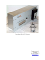
Tracor Model 900A VLF/LF Receiver
Picture courtesy of
G. Kerber
GLK INSTRUMENTS
www.glkinst.com
May 2008
==:
-l'
I
j
I
I
TREMETRICS
MODEL 900A
VLF/LF RECEIVER
OPERATION and
,
SERVICE MANUAL
l.....•__ ._.. _ .•...
....
79611 G
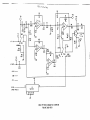
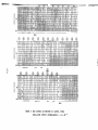
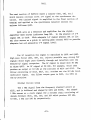
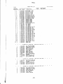
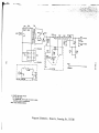
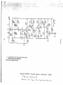
The Model 900 Receiver is modified for MSK reception by
addition of a circuit card shown in schematic diagram Figure 900ADD-l . On the large circuit card c409 is removed and U402 pin 5
supplies the i-f input to the MSK card, while R444 receives the
i-f output from the MSK card. R4l7 and R420 on the original
circuit card are changed to lOOK.
From time to time'beginning in 1976 the Navy VLF transmitters may convert to MSK transmission.
For MSK reception place the MSK on/off switch at on.
proper setting of the Baud rate will be as follows:
17.8
21.4
23.4
22.3
18.6
24.0
Cutler
Annapolis
Laulualei
Australia
Jim Creek
Balboa
The
200
200
200
200
100
200
Tuning using the front panel tuning switches is the same as
for non-MSK reception (i.e. NAA Cutler 17.8 is UDUU DDDU).
The indicator light will be active with MSK off even when
MSK is transmitting. Observation of tracking action with MSK ON
and OFF will be about the only method to determine when switchover
to MSK has occurred.
Interpretation of frequency offset (described on pages 6 through
16 for non-MSK reception) is modified as follows. For 200 Baud
MSK the received signal is 50 Hz below the nominal carrier. Thus
from NSS, Cutler Maine, for example, the frequency is 17.75 KHz
instead of 17.8 KHz. Action of the MSK card doubles the phase
shift, so the results is the same as for twice the received
frequency, or in the present example as though 2 X 17.75 or 35.5 KHz
were received. Thus if the result of figure 5, page 13 were
achieved using MSK reception from NAA, the conversion from
centicycles to microseconds would be 0.28 (using figure 1, page
8, for 35.5 KHz). The change of 2943 CEC (page 16) would be
multiplied by 0.28 to give
microseconds
CEC
The corresponding frequency offset is 0.95 X 10
-8
.
For 100 Baud the frequency is low by 25 Hz. Thus Jim
Creek would be at 18.575 KHz. Again multiply by 2 to get 37.15 KHz.
A simpler procedure which is sufficiently accurate for most
purposes is to make the calculation just as though non-MSK trans,,,
mission were in use and then divide the resul.t by 2.
R1
205K
1%
R2
10K
CI
O.I
DISCT
I17
0.1
330K
DISC
R6
536
R4
III
C3
0.1
1%
RI9
51011
DISC
I.~"
III
12
lOOK
RI4
RII
211
47K
RI6
1M
100
Ria
lOOK
OUT~'
0.1
DISC
100HZ
(FROU
UI
TP 102 )
5 N7490
MSK OPTION SCHEMATIC DIAGRAM
flGUR E 900 ADD I
0
S2
1301
0
IISK
BIT RATE
r"
+C12
10K
Gh
RIS
330K
+IOV
I-f
41K
R21
10K
II
RIO
41K
no
Itl
51 7201
NORIUL
E2
IIY
+IOV
RI3
R9
CIO
.05
+IOV
RI2
R8
+SV
ADDENDUM
900A MANUAL
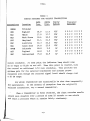
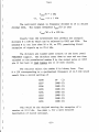
Listed below are currently available (1986) VLF/LF stations with stab;l ized
carrier frequencies suitable for reception using the 900A receiver.
STATION
Omega
Omega
Omega
Omega
Omega
Omega
Omega
Omega
GBR
FUB
JG2AS
MSF
WWVB
DCF-77
NOT
NSS
NWC
NPM
NLK
NAA
FREQUENCY
12.1
12.0
11.8
13.1
12.3
12.9
12.8
13.0
16.0
16.8
*40.0
60.0
60.0
*77.5
17.4
21.4
22.3
23.3
24.8
24.0
KHz
KHz
KHz
KHz
KHz
KHz
KHz
KHz
KHz
KHz
KHz
KHz
KHz
KHz
KHz
KHz
KHz
KHz
KHz
KHz
LOCATION
TRANSMISSION
Norway
Liberia
Hawai i
N. Dakota
La Reunion
Argentina
Japan
Australia
Rugby, England
Paris
Japan
England
Fort Collins, CO
Germany
Japan
Annapolis, MD
Australia
Hawai i
Jim Creek, WA
Cutler, ME
CW Pulse
CW Pulse
CW Pulse
CW Pulse
CW Pulse
CW Pulse
CW Pulse
CW Pulse
CW
CW
CW
CW
CW
CW
100 Baud
200 Baud
200 Baud
200 Baud
200 Baud
200 Baud
RADIATED
POWER
10 KW
10 KW
10 KW
10 KW
10 KW
10 KW
10 KW
10 KW
600 KW
Not Known
MSK
MSK
MSK
MSK
MSK
MSK
500 KW
Not Known
50 KW
400-1000 KW
1000 KW
60 KW
234 KW
1000 KW
Omega unigue frequencies are highly recommended as being most reliable and a
station near to most any location in the world. Signals from these stations
are 5 each 1 second pulse and then followed by 5 seconds of no signal.
Installation and Operation
3
Chart Recorder Adjustments
5
Choice of a Transmitter
Interpretation of Chart Records
Calculation of Frequency Switch Setting
5
6
17
Detailed Circuit Theory
21
Antenna Coupler
21
R-F/I-F Circuits
Divider Circuit Group
22
23
Synthesizer Circuit Group
26
Synchronous Detector Circuit Group
28
Ordering Information
Parts Lists
Switch Settings for Various
Transformers
Conversion from Centicyles to
Microseconds
Fractional Frequency Error Chart
WWVB (60 kHz) as Received at Austin,
Texas Oscillator Offset Approximately
.
-2.3 x 10⁻¹¹
NLK (18.6 kHz) as Received at Austin,
Texas Osci~lator Offset Approximately
+1.6 x 10-
NAA (17.8 kHz) as Received at Austin,
Texas Osci~lator Offset Approximately
-1.9 x 10Block Diagram, VLF Receiver, Model 900
19356
Diagram Schematic - Chassis
19357
Diagram Schematic - Receiver, PCB
19358
Diagram Schematic - Antenna Coupler
MODEL 9DDA VLF /LF RECEIVER
Reception is, therefore, not limited to one or two transmissions as has previously been the case with "economy"
model VLF or LF receivers. Some of the transmissions
which can be received strongly in the United States are:
NAA
NLK
NSS
•
Provides all that is necessary
parison to NBS
for frequency com-
NWC
NBA
17.8
18.6
21.4
22.3
24.0
kHz Eastern Maine
kHz Jim Creek, Washington
kHz Annapolis, Maryland
kHz Australia
kHz .. Canal Zone
(These transmISSions can be received even when MSK
keying is used.) .
An increasing number of Omega transmissions
11.0 to 12.0 kHz band
•
Monitoring
standards
of atomic
• Simple and effective
tim~base accuracy
standards
in the
against national
means of checking counter
Other stations which may be received elsewhere in the
world are:
MSF
GBR
FUB
The Model 900A VLF/LF Receiver compares the phase of a
local frequency standard with the received carrier of a
frequency stabilized transmitter. Most of the U.S. Navy
VLF transmitters, as well as the NBS LF transmitter
WWVB, derive their carriers from atomic frequency standards. A local standard can, therefore, be checked with an
accuracy approximating one part in 1011 using the Model
SOOA Receiver.
By means of front panel switches, a wide variety of
transmissions can be selected in the VLF band from 10 to
25 kHz, or in the LF band from 60 kHz to 75 kHz.
60.0
16.0
40.0
77.5
16.8
kHz
kHz
kHz
kHz
kHz
Rugby. England
Rugby. England
Japan
Mainflingen, Germany
Paris
The Model 9DDA Receiver is supplied complete with roofmounting whip antenna unit, 100 ft. antenna cable. and
front panel chart recorder. The Model 900A may be or·
dered without recorder and a local unit can be used if
desired.
FREQUENCY
COVERAGE:
100 Hz steps from 9.9 kHz to 25.6 kHz
100 Hz steps from 59.9 kHz to 75.6 kHz
The Model 900 VLF/LF Receiver is used to keep track of
the offset of a precision local frequency standard with respect
to the accurately stabilized carrier frequency of one of the VLF
or LF transmitters operated by NBS or by the United States Navy.
VLF carriers are typically synthesized from Cesium Beam Frequency
Standards located at the transmitters; a long-term frequency
accuracy at least as good as one part in (10)11 will normally
be exhibited by the VLF carrier.
SECTION II
UNPACKING AND INSPECTION
Carefully unpack the receiver and inspect it for possible
damage during shipment. Special attention should be given to
any areas where the outside shipping package was damaged. If
the frequency standard is damaged in any way, immediately
notify the carrier. Also notify TREMETRICS Inc., 6500 Tracor
Lane, Austin, Texas 78725-2100, 512/929-2051 Attention: Product
Service.
SECTION III
INSTALLATION AND OPERATION
Installation and Operation
Use of the receiver is quite simple. Mount the antenna
in a clear outdoor area, such as a rooftop. Other conducting objects should be kept at least four feet away from the
antenna, and there should be no conductors (such as power lines)
at a high elevation angle as viewed from the antenna position.
Connect the antenna coupler to the receiver ANTENNA
connector using the coaxial cable provided. Connect 1 MHz (100
kHz optional) from the frequency standard being monitored to the
1 MHz connector of the receiver.
Plug the power cord into a receptacle providing 105-125
volts, 60 Hz. (Operation at 220 V and/or 50 Hz available on special
order. )
Initially select a strong nearby transmitter, even if it is
desired later to use a different transmitter. Place the VLF/LF
switch in VLF position, and set the FREQUENCY switches as shown in
Table 1 for the selected transmitter. Within the United States
NAA, NLK, or NSS will provide strong signals. Other transmitters
not shown in the table may be on at a later date, and in particular
there will be a wide selection of transmissions from the various
OMEGA transmitters. For a general method of tuning transmitters
not shown in the table see page 17.
Turn the front panel GAIN control fully counter-clockwise.
The indicator lamp should be extinguished. Turn the GAIN control
TABLE 1
SWITCH SETTINGS FOR VARIOUS TRANSMITTERS
Transmitter
OMEGA
GBR
NAA
NLK
NSS
NWC
NBA
WWVB
MSF
HBF
Location
Trinidad
England
Maine
Wash State
Maryland
Australia
Canal Zone
Colorada
England
Switzerland
XMTR
Freg.
SYNTH
Freg.
16.0
17.8
18.6
21.4
22.3
24.0
60.0
60.0
75.0
15.9
17.7
18.5
21.3
22.2
23.9
9.9
9.9
24.9
VLF/LF
Switch
VLF
VLF
VLF
VLF
VLF
VLF
LF
LF
LF
Frequency
Switches
U
U
U
U
U
U
D
D
U
D
D
D
U
U
U
U
U
U
D
U
U
D
D
U
U
U
U
U
U
U
U
U
D
D
D
U
U U
D D
U D
DUD
U U
U U
D D
D D
U D
U U
D U
D U
U
U D
U U
U U
U U
D U
slowly clockwise. At some point the indicator lamp should come
on or begin to blink on and off. When this point is reached, turn
the control an additional 1/10 turn clockwise. This provides the
optimum gain for the selected transmitter and insures proper
reception even though the received signal level should change over
a 20 dB range.
Any given transmitter may occasionally be shut down temporarily
for maintenance.
In the absence of reception from the originally
selected transmitter, try a second transmitter.
When a transmitter is first received, the chart recorder needle
should move steadily over a period of some 10 seconds to one minute
and reach a position where it remains fairly stationary.
For a strong signal the indicator light should corneon well
below the maximum GAIN position. At maximum gain the lamp may
flicker as a result of atmospheric noise reception. When reception
is normal, and the GAIN setting proper, switching the third
FREQUENCY switch from the right away from the correct position
should usually cause the indicator lamp to go out. Keep a record
of gain setting for each transmitter normally used. This will be
a useful guide in recognizing later transmitter shutdowns.
Various chart indications of proper tracking will become
familiar after a few days of operation. The diurnal shift pattern
is one such indicator. The CEC reading should increase gradually
as the sunset line moves westward along the path between transmitter and receiver. The CEC decreases at sunrise may not be
smooth and gradual.
The chart recorder should be checked occasionally for
correct zero and full-scale indications. Depress the RCDR ZERO
toggle on the front panel. The recorder should now give a reading
of zero. If not, adjust the recorder mechanical zero.
Next depress the FULL SCALE toggle. The recorder should
now read 100 CEC. If not, adjust the RCDR FS ADJ available
through the front panel access hole.
Choice Of A Transmitter
Normally the transmitter providing the strongest signal
will be selected for continuous frequency monitoring. In some
cases a transmitter at a particular short range may give erratic
results at sunrise. Try each of several strong transmitters for
a period of several days and select one with a stable diurnal
shift pattern.
Interpretation of Chart Records
Frequency offset of the local frequency standard with
respect to the VLF carrier is determined from the chart record
produced by the receiver. In general the offset is determined
as follows:
Let dt be the phase change noted on the chart expressed
in microseconds.
Let AI be the elapsed time interval over which the change
occurs, expressed in seconds. The fractional frequency offset
1s then
In other words, a phase rate of one microsecond per
second corresponds to a fractional frequency deviation of 1
part in (lO)?
~t is determined from the chart record. Full scale deflection corresponds to 1 cycle of phase at the VLF carrier. It
will prove most convenient to read phase change in hundredths of
a cycle, or centicycles, and then convert to microseconds.
At
17.8 kHz, for example, the frequency transmitted from Cutler,
Maine, full scale is 56.2 microseconds.
To con~ert from CEC to
~s multiply by 0.562. Suppose, for example, that over a 24-hour
period from noon to noon, the phase reading increases by 7 CEC.
This corresponds to 7 x 0.562 = 3.9 us. Twenty-four hours is
86,400 seconds. So the fractional frequency offset is
3.9
8.64(10)4
(10)"6
4.5 x 10⁻¹¹
An increasing pha~~ reading indicates that the local frequency is high. A decreasing phase reading indicates that the
local frequency standard is low in frequency.
THE FOREGOING DETERMINATION OF WHETHER THE LOCAL STANDARD
IS HIGH OR LOW IN FREQUENCY ASSUMES THAT THE SYNTHESIZED
LOCAL OSCILLATOR SIGNAL IS 100 HZ BELOW THE CARRIER AS
RECOMMENDED IN THE OPERATING INSTRUCTIONS AND SET-UP
TABLES IN THIS MANUAL. IF RECEPTION IS EFFECTED BY
PLACING THE LOCAL OSCILLATOR 100 HZ ABOVE THE CARRIER,
THE SENSE OF THE READOUT WILL BE REVERSED.
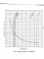
Figure 1 gives in graphic form the conversion from centicycles to microseconds, while figure 2 permits graphic determination
of fractional frequency offset.
Several facts must be understood in order to interpret
properly the receiver records. First of all, propagation time
from the transmitter to the receiver is not precisely constant.
In particular, there is a marked difference between daytime and
nighttime delay. This change is known as the "diurnal shift"
and results from the change in the height of the ionosphere.
Nighttime propagation is slower than daytime propagation by
some tens of microseconds. The delay is most stable when the
entire path is in daylight. Repeatability from day to day is
usually accurate to approximately one microsecond. At night
'••••
0-
-:...-
1.3
_
~+
~(;;)
~<v~~
1.2
~~~'¢~'~
1.1
<v~ ~~9.~~~~
~v ~ ~'i-~ ~'i~':l
~ ~~~.::s
~'i-
~~':-v-+'-~~~~
~~~~~
1.0
l.LJ
-.J
u
0.9
>-
U
l-
:z
0.8
l.LJ
u
1
00
I
a::
a..
0.7
l.LJ
en
Cl
0.6
:z
0
u
l.LJ
en
0.5
.u
==
\
:
\
.
I
\
I
\
\
I
\..
).1
:"-
0.4
I
•
I
I I
I
I
: I :
~
I
•
I
I
I
I
I
:
I
~
I
'l I
I i'k
I I I ........•....
I
I
J
•
I:
II
I
I
I I
•
~~
~
.
Iii
I
C:)
1
J
I 1 I
I
4~
I
I
II I
I •
I
<o~
I
I
.:$:'~
~~4..'
~<:::)~~
<0 q:.
~~~
II i
I I
•
N~
<vq:.
~'i-~
II I
II I
•
\
I
0
a::
1 I
I •1
~:P~~
~~<v
.I
I'---
I
I
J
I I
I I
I I
40
CARRIER
50
FREQUENCY
I
I
I
-----
~
I
KHZ
~(;;)-
I
':v~
1
I
I
I
I
I
-
I
x
10-7
.;'
/
,+-'
a:
0
a:
a:
I X 10-8
~
/
z
I X 10-9
,~
/
V
/
/
~ ~~
~(j
!:)~~
o
l/
,.•••.11
e,
...
/
/
~~~
,'\.
II
/
-\
/
V
",y
V
/1.1
VII
~
,y
/
II
/
1 X 10⁻¹⁰
/
~O
~,.
/
/
/
"
"
1.1
.;'
~~:..c.
..J
~
z
~
•...
u
~
a:
/
.;'
~Y\~
<, ~~
, -~
e,
,
tY
/
/
""
">~
1<.."
u
...
---
~=;f-q" "'~
1-,.
•••
•••
5
•••
IX
•...'+-'"
~ Y
,.
....
e,
~
,,>C.;'
II
,.~
"./
1/
/
V
I X 10-1 I
O. I
).1
,-\"'"
/
/
V"
],I
10
ACCUMULATED
100
TIME ERROR, MICROSECONDS
1000
10,000
random fluctuation of five to ten microseconds or more often
occur. Thus the best results are obtained by taking readings at
the same time each day; the time selected should be one during
hich the transmission path is entirely in daylight. The entire
chart should be examined in the neighborhood of the selected time
to insure that the appearance is normal. This is desirable
because occasionally a solar flare can affect propagation delay
for an hour or two, and a reading taken during such a time
interval would lead to inferior results. With care, an accuracy
approaching one microsecond can be achieved over a period of
one day. This results in a frequency measurement accuracy
approaching 1 part in (10)~1
,
Fortunately frequency standards which are sufficiently
stable to make readings to a part in (10)11 meaningful are also
stable enough so that a day's elapsed time does not result in a
change in frequency which is much greater than a few parts in (10)~1
Or, to put it another way, if a standard shifts so rapidly that a
measurement must be made in a period much shorter than one day,
then an accuracy of parts in (10)11 is seldom required. Utilizing
a period of all-daylight reception, a frequency determination at
least as geod as one part in (10)9 can usually be achieved in an
hour or two.
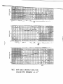
Figure 3, 4, and 5 are three representative chart recordings
from the Model 900 Receiver.
Figure 3 shows reception of WWVB, 60 kHz. Note the
gradual increase of phase after 4 PM at the right hand edge of
the upper strip chart record and the left hand edge of the center
record. This is the evening diurnal shift.
~
_.
..
= ~
....
'"..J
u
>u
•...
z
w
u
_.
- : - ".~ --:,
~.- ~
- E'- fF-"
r-::::" F-~ ~T ..
,:
, -.": -==. ~t::='
-.-~
.50 ".
-. i=:= - -'- -=
t===..
~ : ·
.T-
:E:
.'
,
-
~
:1=
-
-
S!..=
100
\..
•
(
'-
l
_______
=
,
~
.-
-
, , ,
"0
.
. -
..
-
_ ...
-- -,
-- .
--
- ..
\..
._._"!!!!!~!~~t,k.._=_:.z=.._=_-.--1tU..l.A,--~::._:.!~!!!_.__
'-
.
..
.';
-
.
-
-
--
-,.
'=' ==
-
_:-- -: -
--
-- \;.
J
.-
---
..:
-
- . ,
=
...-
~
-
.-
,
;;-
.'! .. 't .- ..
'-
:
:
·1
-
~
:
-
0
.
;
-
~
- -
~
_. " ,
:
;
~:
-:
..
- ---"
- - ..,--
-- -
~
-:
":
:
-
-- ~-
-
:
,
•.
~
"
-.F-
--
:
"
:;
.,
.
-
~
-
'
-=-
..
.--.
l-=..e _.
~.!.=
--: I
-.
-.
.. --0
--
~
~
,~~ ,.- ~ .=
"
,
.
'-
I
:;
.-
..
:
~!
'.
-
:
.. 1'1-
:
...•
0
.
-..
_.
-' --- - - ..- .- -:. ... - ,
:
.-
..
-
•...
..
.-
..__
_. ...
NOON
~
=
~.
-: =,"1-
--
..
-
"
=:-'T'";
'T
- .r ••.....·
.- I"':'"
-
..
-
•.
~.
..
--
.
..
·F ~
- ,
:;
- :-?"-: .
-: '.
•.
- ''-=. '. :
~
:
~.: _. ': ... -,~- .. .. .!::'~-- ~
_ . .. •. .. ......•
---
:
..
-. .- -
-
"""
-
~
oi,;.
;=
- ==
~
.
- ·
~
~
~
.
-
·
_.
.- ..
,
--
iCe'
~
..
"
.
.
:
.
- -.
0
.
:11
.
-
.... h!,.,
i\
"
_.
..
..
-
-
~
0
..
.,
.
.. ..
.. .
:;-'- : :.,. .. ...- --==
.
-..
..
1-£.
1
::.
-
.~,~
:
..
,
I
i1:.
:
2-
:-
"
:
..
.
.
=
-.
- ,.
:~
-
.,
.'
n;
t~
1=:=
.
h .
.'
~ ..
;
..
_.
;
- ,~
..
-
- - - - -- :-·
- == - = ~ -- -
-
-~
:1=
~.
-
-
...
--
~
..
I::::::
I~
EO'
-
_ ...
- ..
.
1=._
:
-:
_ .
0_
-
N
== -=: _.
::~
..
~!
.
;
..
MIDNIGHT
,
N
..
_.
.:.
- ~~...:-:
1'::'-
:="'~~-- 1==
"!
... ===!::= "=
:;;~
_.. -
': .,":
...-: '= :=t--=:
-,
•.
=y --
...
1=
~
.-:"" :; • -I~
· I -..
=:: ;,;
I
: .. :_- ==.
I
"
J
': :t-=_
WWVB (60KHZ)
AS RECEIVED AT AUSTIN I TEXAS
OSCILLATOR
OFFSET APPROXIMATELY
- 2.3 x 10⁻¹¹
t _
I
Ii··
i_I,;"
, i
-~-- '3.; " -
._ ,I:
·
,
..
- m - ~ -~
. :- - .==
"
-. - E
::
~ - -- ., -
_.
"'!;. "'!!'?'
.
.
-
-
_ ..
..
-
-
·
-
_
-
RU$TRAK
-
'-- ._
.- -
..
.' 177
...
-
-
. - .:
" \!'.'.---,
-
.
I
,
.,
c:
-
:
.'
. . ..
. .-_.
'
-:
-
.
..,. ~
..
._-
-
_.
-
0
..
,
'
:
'
....
-
:"
-- .
-
-.
..
.
.
:
..
"
.
--
:
'-
:
1- .
.. ._-
.. -
_ ..• .-
_.
== :.-
_ _ __ -:
".::- -.-
.~..
J -; r-...
..
_.-- -
-
~
--
.~~:
~ -~: -
=-:1=
.....•...•,.
,...,.-FfIIA
en'
- -
j
g
-
_"
... '.
"t=I,
.. .=:
~
- _.
i=
I ~
"
_. _.- .- ..
UJ
u
-._.
-
,
,
-
-
~:.
-
~ I-..
-
~
--
..
J
1-:-::::
..-~
.
-
-
-
:=:
=
S
--,
._,
--
-
,.
~-
-
...
.
.
---
~-
'.
_.
~
-
o.
~ - ,.
=
-
..
"
~
'-'
..
.
..
..
_
.
..
--
_.
-
-
.
..
,. -
.,
0
-
..
I=:::: ::==
.
_.
-
- -- ...
. - !::! --,
.:;'
---= ~
~
----
--~~L ,--
:
....
-
_ -
_.
--
.'
_.
-===
. -I~
~~1~
.:. .....•' "-
:1.:-
.
• ,C'
.-
~
'
''!.
-: -
...
-
-
~
.~~
. -.-r.=
.•
,.
- ~
..
..
.-
-_.
-
'.~
.
=.. .- ~ -: ..
~
--~ E
~
'
=
-
..
,.
:
-
.? F.i.
-,
N
-- .,.....
...: .'
, -- _. .:
.. = .. -- =
i-= ..
--- =.
- -
,.
.•
: ~"I'-:-:
::
iS~
I====,~;"-~' ...
ctl'l:
,-
~:..
..
..
-:
-:
~
-
..
~]~...-
-:
:
~
--
7
..,,;. -.;,::..
- -
.. .
!2
=1' :-1'=1
·
,_.
~-
_
.-
.•
--
...
. -= ..••.
..
•.
.~ -,,'
-- ='"
-
,=.- ,,;;=.
.
.0 _ =-
- --",
~
-
-- - F
'
..
....:::::±::::
·
_.
· _.-
. .-
=f=1
1'7•• ::1'
0;;::;
~:;
"-"
.."
- --
.-.. ..--- - - . . ....
..
· .
...
.
.:
., I-==:
-- .,- : ..
.....- ..
: .-
.
~
-
-:. -:-r;-:
~.-r:
:
0:"-'"
, =-.l'
-
RUSTRAM~
.
-.
j
!-
z:
,-
t::=.:E:'::r_.0"70,=- -- _ - "
_ -~E--""'-:'::
N
.
.. .•
-
F-....
, '50
-
-
- -"
-:::=:;=
--
= _
,
f-'-
-
- -
-0
__
.,. ..'-..
- - -- ... ..
,_.
- .
r--,
...J
U
~
-'.. -
._'.
~2=
UJ
-.:..
""'--f',.
.:.:.:1'.-
.. _ _.~
~[~._.
en
_.
-~-~-~.I~
---.-_..__ ::-
-
-_.
_"I~':=~::'-~'_~~'
__
: __
:=
=..:-
50 -:
U
_. --
=_ _.: _. __ - --=
.
z:
UJ
r.:::=._
_
1== -~.:
_:~,~r== __
.:.
..
-.-
~
. -
-•.
.
_ ..
...;:.:.
.
-'
. ., . ~ ~
-. . -,
-- - .. _ .
-- I
:
-~ :.= E ..~
-.;,
-I-:::: F=='
. - ...
=
~
0:::;
f- ", -- - = -- ..
..
-0-
.-
.
-
- ~ --
..
-
MID-
NIGHT
.- ~ _:: '~_.~-=
-- - ._~ == - : .. -
,:7:. _ ...
en
~
t
,==
__ _~. .. __ _ :
50 ~
..
,-_..
I-
=- == "';,;- .,-:~
u
1- -
:s
.., ~..
. ---
1:;;;. ';;"',
100
==on-
__r....". -.'=
:..:=-:-r:"::: .'=
-
,_
O::l" ~
- -..
._.' .. _
'
.. -_. __
-, _--
==
'L:::::
'--or
-;;... -'
-- ,:-'~
.-
.:.(
_
__.. "
-;:",---== -
_..
'= ~,
-_:.:.L":_.
-==._.
t-"
--
- .. :
.. -
._..•..•
1'"
--.'
.~_
.'
1:::= ~
=t:::1:
-
':==
_ _
s:;--
-= -:-~ ..
,'"
:t:
=t:=-C1
r=:==:
_
~
OOO;';vvvUll
tlOON
FIGURE 4
NLK (18.6 KHZ) AS RECEIVED AT AUSTIN I TEXAS
OSCILLATOR OFFSET APPROXIMATELY + 1.6 I 10-9
-= =t=t=N
I
--
__
a
o
_~__
-=
_~
:: = _. ~/
_reo. ,. -
-L=~f-~.~=_'f._
.::::
~
_••, ,_
-
~
~
7
-
_. _ -; =
_
~ .,_
r=: ~ -
~
E
u
-==E.,
:::;,.:=:.J:.
_
_.•.
~I=
__
:;;::1= -!=.":!.
.
.-
I
II
_.
Z
w
u
-i
--
.. ,"
-.. -
~
:= "=I
l-'
W
I
-
.
,
~=f
-
,
-,
,
-! .. -, =- . ... : .-
:7
=
-c= - . .•.
-~ -. -
::-
=-
i
J
E
'.
,
0
..•
- ::-<
.t'
~
. ,.
,
~I
:
.
I
~
I
.:
j
.
:
-
..
"
:-=. r .
.-
-
..
--
,-
=
.:j
t=
_.
'-
f-'
~-
.. --.
...
.'
,
-
- ;
1
--
-
c- ':
_.
;
-
;
~f ·E
~
-J
r
-
'=
-
_. :--.-=
--,
;:J= _.-
-0
:
=.i
=-!!L=:7
.. .
F
..
.,.
,
_
-
T
=1= .-.•
~
.
-
,
-
~..-
.-
- .-~
-
~ =i=-
::=
.
-
:I=!:l~-
'1
f::
.. : -- -;: .-
,
:::=-::
C:::::,==t::=
N
.
.. , . .•-
,
;
.
! .. --- f
,
-
.- -.
t ;~
:§
,-
r'
F; :
-,
t- ::-
_.
.
®
--
- '. -= t. - .,-
=
-
-
-r
-
; .)
-
II.
.-
,
,-- =
::
.
7
~
~
•• ~~~~~- - .f =-
-
f
-
I
•
.-
J
J
,
..
/ ,.'
:.:t=="
- p ..
~-r=:: ,_ ~ ~-
II!
-
-~
,.
'
I
II
J
If -
._
,
-
,
_,.-
'-
®
,
."
I
I
"i
0_
=;-~
,
-
'1 -,',
F _
I
-
_~-
,_:7
_. -
{
N·
_' _, /:.;
-;
"
!,
.,
-.
- -
."
I
-- _. -
-:. .
-..
!
.~'
!
-.
.-
-
J
!
=-:
-'
1=
.-
;
I
/
..
,
@
®
_. ---
- ~ - - . :-.~ '-=-j
-
1/
,7
"
,
-
-
:
--:
,
..~
E .. : i ,. _./
0';
.. " =E
f
.J,
-._.-
N::>,
-
,.
:
, .- 7'
L ..
"
c-'
.
0
.-
!
.,
.
--
-,
-
-f:;.
,_,
<!J _
,,-
. ,"'"If'
(
®
!
rt=
__
~!
, .=/-..
- ..'
ill
-...
_ ".
"- ::::".
'i
r=
_F
_ =- : I ,.~,
-
-
..
.
::j
,
--
r -
II
,
-J..
- ·,'11
r=.
@
-
Ir
--
7
50
I-
--
.-:
<,
-,-
co-
..
.r
..
U
~
::
".f==.
-~t:::
<
-
.-
..
:
r
,
®
r
VI
I
,
Aw
..J
l
I
-
.-
_;-
2
"_
..
l- '. _ J
=-.:
-_ .-: __
-.
®
-= ==- __ ~
:~:..
-·-f
,.j
\!J
(!)
~~AK_
_ ,.
_:·I:-=~I-::
- .:'-':
-:-y'= I == -1. =- ~;f
f.
."
f _
IF::
:
--:='l..,
"l==l=l=
=1'
,_.
- -.'1.
,', J:=-"'.,
= .- 71
-=-IE
Eo:'
-11 r~
~,
50==="':"E:
100
--Qj-.--®---l
_ c . ~•.
--------_-.
:::::'
:
1.110NIGHT
--
0
@
--- "I"
:+=~_
. F': ,=:..J:
•
-
,..
U
u
>-
z
w
u
r:-:
._.
..J
50
--i-
•.
-
..
__
U>
W
-_
._-@-- ..@
;
_.
I
I -
-
:.'1"
_:1 ~ .
'F .. ,
~
/ I '.
... 1
-
~,
-
:
:j
'~Itf~;
._.
__ ~J~..
=
E
100
I~-
~G-_·=:
__ _
-·f
-"
-
j
"---
t.
!
t - .
/e.
-:.:
,
7
l:~.:
:'
..
-0
/'
----
'.'
_
NAA (17.8 KHZ) AS RECEIVED AT AUSTIN,
OSCILLATOR
OFFSET
APPROXIMATELY
:
_
AU5TAA."
N
i-
~
....
,I:. .. - ==r::::=
-
_.
' :
~
- _.---"'1. -
=E
__ ~
~
---
,_ ~
- ~= -= ---~.
.-
_
):J
FIGURE 5
.- i
_ = - ~=t:-J=:;=.-
F.T
--._,...-:..-
/
~
10
-.
=.~ ~
--
::=f. -- .,;'
=f:. E '., g
;:1=I-~ _E=
: 'I:
j
=j
- ::-'
,I
--
I
cl=l=-:-:='
1~
,I.
...: -. :.1
_9
l:':-:
-
I
..
t: :__
.
d
I=:: _:::;::
.TEXAS
- 1.9 x 10⁻⁸
:1:= -:.!:t=
0 0
-~f
~
_
Note also the apparent sudden jump from 100 CEC to 0 CEC
at 6 PM near the left of the center strip. The total range of
the phase detector is 100 CEC, or one full cycle of phase, When
one extreme is reached the record reverts to the other extreme.
If the phase just before 6 PM is 99 CEC, the phase just after
6 PM is obviously not 1 GEC, but 101 centicycles. It is necessary
to count cycle accumulation in this fashion whe~ reading a chart
record. This will become clearer in the two later examples.
The sunrise effect between 7 and 8 AM on the lower
strip is not so smooth and gradual as the evening shift. Looking
at this area alone, it might not be easy to determine whether a
cycle could perhaps have been gained or lost. Looking at the
daytime record, however, it is clear that there i~ approximately
zero average slope so that the record returns to the same cycle
the second day as the first.
Note also that the daylight record is rather smooth, while
the nighttime record "wanders" back and forth a number of centi, cycles in the course of an hour or two.
Note also the phase shift lasting approximately five minutes
of each hour. This shift is introduced at the WWVB transmitter.
Its presence in the recording is a definite indication of proper
phase tracking.
At noon the first day the reading is 67 CEC. At noon the
second day the reading is 56 CEC. The 24 hour change is then
56 - 67 = -11 GEC.
Referring to figure 1, at 60 kHz the number of microseconds
per centicycle is 0.167. The change expressed in microseconds then
is
Referring to figure 2, 1.837 ~s in 24 hours is an offset
of 2.3 parts in (10)~1 Since the change is negative the local
frequency standard was low by 2.3 parts in (10)~1
Figure 2 shows reception of NLK, Jim Creek, Washington,
at 18.6 kl~. Here there is an obvious gradual phase increase with
time. The evening shift beginning about 6 PM is easily recognized .
.The smooth daytime and more variable nighttime characteristics
are obvious. The sunrise shift in this case is. fairly smooth.
Clearly there is a cycle change near 6:30 PM the first
day, and near 1 AM. The reading at noon the first day is 17 CEC.
Clearly by noon the second day two additional cycles have been
.accumulated and the reading is taken not simply as 69, but as 269.
A dashed line has been added showing a continuation of the steady
daytime slope. This verifies that exactly two cycle changeovers
have occurred.
The change is 269 - 17 = 252 GEC. From figure 1, at
18.6 kHz one GEC is 0.54 ~s, so the 24 hour change is
From figure 2 this represents a frequency offset of
1.6 x 10.-9 Since the change is positive the oscillator frequency
is high.
An approximation could have been obtained over a shorter
period of time. At 2 PM the first day the reading is 38 CECa
The change since noon is then
38 - 17 = 21 CEe, or
(21)(0.54) = 11.3 ~s
11.3
(2)(3600)
1.7 X 10⁻⁹
This last result could, of course, be obtained from
Figure 2 instead of making the calculation.
Figure 5 illustrates a more radical oscillator offset.
From noon the first day to noon the second there are 29 cycle
crossovers. These have been numbered on the chart reproduction.
Since the reading is decreasing it is easiest to take the final
reading as 30 CECa The initial reading is then 2973, and the
change is -2943.
From Figure 1, at 17.7 kHz, 1 CEC is 0.56 ~s. The change
is (-2943)(0.56) = - 1655 ~s. This corresponds to a frequency
offset of 1.9 x 10-~
With so great an offset, there is normally little to be
gained by seeking the accuracy inherent in a 24 hour reading.
For example, there is a complete cycle between lIon the first
day and about 11:47. 100 CEC is 56 ~s. 56 ~s in 47 minutes is,
from figure 1, about 1.8 x 10-~
Calculation of Frequency Switch Settings
The most frequently used frequency settings have been
given in Table 1. It is relatively easy to calculate any
desired setting. The switches select the frequency in binary
form as follows:
S208
S207
S206
S205
S204
S203
S202
S20l
in.
128
64
32
16
8
4
2
1
When the switch is UP, the corresponding number is added
With the switch DOWN, the number is omitted.
Suppose, for example, that it is desired to select 18.5 kHz
in order tc receive the VLF carrier at 18.6 kHz. The desired
multiple of 100 Hz is 185. 5208 is placed up contributing 128
toward the required 185. The difference 185 - 128 = 57 must be
supplied by the remaining switches. Clearly 64 would be too much,
so S207 is placed down, omitting 64. S206 is placed up, providing
32 of the required 57. The remaining switches must supply
57 - 32 = 25. S205 is placed up, providing 16, and leaving a
requirement for 9. S204 is placed up supplying 8 of the 9. S203
and S202 are then placed down, while S20l is placed up, providing
the last 1. To summarize in tabular form:
8208
8207
8206
8205
8204
8203
8202
8201
128
64
32
16
8
4
2
1
Xl
XO
Xl
Xl
Xl
XO
XO
Xl
= 128
0
(DOWN) =
32
(UP) =
16
(UP) =
(UP)
(UP)
=
(DOWN)
(DOWN)
=
=
=
(UP)
TarAL
8
0
0
1
185
SECTION IV
THEORY OF OPERATION
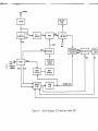
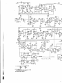
A block diagram of the Model 900 LF/VLF Receiver is
given in figure 6.
The signal is received by a vertical whip antenna mounted
on the antenna coupler unit. A pre-amplifier in the coupler
provides approximately unity voltage gain while converting the
impedance to a level which can drive the 50-ohm cable feeding
the main receiver unit.
With the LF/VLF switch in VLF position the signal goes
directly to the R-F amplifier. (For LF reception the signal is
converted down by mixing with a 50 kHz local oscillator signal.)
Another local oscillator signal is synthesized at a frequency
100 Hz below the desired VLF signal frequency. Mixer action
converts the r-f signal to 100 Hz for amplification by an I-F
amplifier tuned to 100 Hz.
The 1 MHz signal from the frequency standard being tested
is used to produce signals at various frequencies including the
local oscillator signals at 50 kHz and at fo - 100 Hz. Two
signals are produced at 100 Hz, one by simple division, the other
by a divider circuit which includes provision for adding
inhibiting pulses, thus advancing or retarding the phase of the
resulting 100 Hz. The shifted 100 Hz signal is used as a
reference signal in a synchronous detector. If the phase
difference between the 100 Hz reference and the 100 Hz I-F signal
is exactly 90G, no error signal is produced and the phase of the
l
T'U'."
INDiCATOR
LAMP
COUPLER
VLf
Lf
CONVERTER
.......••.
J
'0 -..
R-f
AMPLIfiER
MIXER
1100HZ
~
j
50KHZ
'0 -100HZ
I KHZ
®-1
I YHZ
fROM
fREQUEN CY
STANDA RD
-
_
..•.
I-f
AWPLlflER
I
I
6
GAIN
SYNCHRONOUS
DETECTOR
SYNTHESIZER
t
DIVIDER
loa
HZ
ERROIl
SIGNAL
INTEGRATOR
-.1
THRESHOLD
CIRCUITS
~
DU •••P
RET
fREQUENCY
SWITCHES
,
ZO KHZ
10 KHZ
PHASE
DETECTOR
-
-
ADVANCE/
RETARD
I
CHART
RECORDER
-
po
DIVIDE
BYIDD
COHERENT
100HZ
I
~
I
Figure 6.
Block Diagram, VLF Receiver Model 900
reference signal is maintained constant. If the phase difference
is temporarily less than 90°, retard pulses are repeatedly
generated until the phase difference is 90°. If the phase
difference is temporarily greater than 90°, r~peated advance
pulses are generated. Thus closed loop action phase locks the
coherent 100 Hz signal 90° away from the I-F signal phase.
Any phase change in the received signal thus results in
a corresponding phase change in the coherent 100 Hz signal.
Phase comparison of the coherent 100 Hz with respect to the
fixed-phase 100 Hz signal produced by direct division provides
a chart recorded signal representation of the phase of the incoming VLF carrier (with reference to the local frequency standard).
The change in phase measured over a period of ?ne day then serves
to indicate the amount of frequency offset existing in the local
standard with respect to the atomic frequency standard being used
to stabilize the VLF transmission.
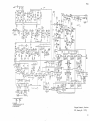
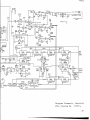
Figure
is a schematic of the antenna coupler. FET Ql
is a high-input impedance low-noise amplifier as required by the
high-impedance whip antenna. A surge voltage limiter and two
back-to-back zener diodes are included in the input circuitry to
protect the other circuit elements from high voltage surges caused
by nearby lightning strikes. RC filtering attenuates signals
above 100 kHz.
Amplifiers Q2 and Q3 provide additional gain, while
emitter follower Q4 provides a low output impedance to drive the
cable feeding the main receiver. DC voltage is supplied via the
center conductor of the coxial cable.
Figure
is a schematic diagram of the receiver proper.
For convenience the circuits are subdivided into s~ctions as
follows:
Divider
Synthesizer
Synchronous Detector
R-F/I-F
Power Supply
LF-to-VLF Converter
R10l
R20l
R30l
R40l
RSOl
R60l
Each circuit group occupies a separate section of the
printed circuit card.
The signal from the antenna coupler enters at TP405. Power
for the coupler is supplied through R446. L40l and C420 provide
additional rejection of signals above 100 kHz.
With S50l in VLF position the incoming signal goes directly
to amplifier U40l, pin 3. Two amplifier sections with a total
voltage gain of approximately 200 precede the mixer Q404. The
synthesizer signal at the gate of Q404 is chosen 100 Hz below
the VLF carrier producing an output to U402, pin 11 at a frequency
of 100 Hz. After amplification by three sections of U402 the
signal reaches an active bandpass filter (U403D, C4l0, C4ll, R424,
etc.). This stage is tuned to 100 Hz with a Q of approximately 10.
The next section of U403(C) feeds a limiter (CR1, CR2, etc.)
which insures constant level I-F signal at the synchronous detector. The limited signal is amplified in the final section of
U403(B) and applied to the synchronous detector section via
emitter follower Q403.
Q40l acts as a detector and amplifier for the signal.
Amplifier Q402 drives indicato~ lamp DSI. In the absence of I-F
signal DSI is dark. With adequate I-F ~ignal present DSI is 'lit.
DSI thus serves as a guide in setting gain control R4l6 to .,provide
adequate but not::excessive.'I-F si:'gnallevel.
For LF reception the signal is amplified by Q60l and Q602.
High pass filter L602, 609, etc. rejects possible very strong VLF
signals which might pass directly through and interfere with the
desired LF signal reception. The LF signal is mixed with 50 kHz
at mixer Q603. An LF signal at 60 kHz, for example, would then
produce an output at 10 kHz at the junction of R6l4 and C6l5. The
filter consisting of C6l5, R6l7, etc. notches out the 50 kHz local
oscillator signal. The filter output goes to U40l, via S50l in
the LF position.
The I MHz signal from the frequency standard enters at
EIOI, and is buffered and shaped by Q10I and Ul05A. The shaped
1 MHz serves as a clock signal for a divider chain consisting of
decade dividers UlOl, 102, 103, and 104 which produce 100 kHz,
10 kHz, 1 kHz and 100 Hz respectively.
The 100 kHz signal from UIOI is frequency divided by 2
to 50 kHz by J-K flip flop Ul07B. The 50 kHz output is used as
the local oscillator signal for mixing LF signals (such as 60 kHz)
down to the VLF band.
Ul02 receives 100 kHz at pin 1 and frequency divides by 5,
producing 20 kHz at pin 11. This 20 kHz signal is fed back into
the divide by 2 section at pin 14, producing 10 kHz at pin 12.
The 20 kHz signal at Ul02, pin 11 and the 10 kHz signal
at UI02, pin 12 are utilized in the ADVANCE/RETARD circuit. The
two signals are fed together to NAND gate UI05B. The output of
UI05B is ground only when both the 20 kHz signal and the 10 kHz
signal are positive. The result is a negative pulse of 25 us
duration occurring each 100 us at UI05, pin 6.
Similarly the 20 kHz signal is combined with an inverted
version of the 10 kHz signal at Ul05D to produce a second 25 us
pulse displaced 25 us in time from the first, at Ul05, pin 11.
As will be shown presently, the "retard gate" line at Ul06,
pin 2 is normally negative. Thus the output at Ul06, pin 1 goes
positive for 25 us of each 100 us. The "advance gate" line at
Ul06, pin 5 is normally positive, holding Ul06, pin 4 continuously
at ground. Under these conditions the signal at Ul06, pin 13 is
positive for 75 us of each 100 and negative for 25 us of each 100.
the repetition period is, of course, 10 kHz. The 10 kHz signal is
frequency divided to 100 Hz by Ul08 and Ul09.
Each output from Ul09 triggers one-shot Uili. The period
of the one-shot is just over 100 us, or one cycle at 10 kHz. A
positive pulse is produceu at pin b wnich feeds Ul13B. A negative
pulse at pin 1 feeds Ul12A. If a positive signal exists on the
advance enable input at Ul13, the occurrence of the positive pulse
at pin 5 results in a negative pulse at Ul13, pin 6. This is
applied as the advance gate at UI06, pin 5. This permits the
negative pulse at Ul06, pin 6 to create a positive pulse at
Ul06, pin 4 and a negative pulse at Ul06, pin 13. The pulse
at Ul06, pin 13 is in addition to the train of pulses normally
passing at a 10 kHz rate through Ul06A and Ul06D. Thus an
extra clock pulse is applied to Ul08, and the 100 Hz output signal
at Ul09, pin 12 is advanced by 1/100 of a cycle, or one centicycle,
of phase.
If a negative retard enable signal exists at Ul12, pin 3,
the negative pulse from the one-shot at Ul12, pin 2 produces a
positive pulse at Ul12, pin 1. This is fed as the retard gate
to Ul06, pin 2. This positive signal inhibits passage of one
pulse of the 10 kHz pulse train normally transmitted via Ul06A.
This results in one lost clock pulse at Ul08, pin 1, and a phase
retardation of 1 centicycle in the 100 Hz output from Ul09.
When either the positive or the negative one-shot pulse
is enabled, a negative pulse results at Ul12, pin 13. This
triggers one-shot Ul14 which produces a "dump pulse". Use of
this dump pulse and the generation of the retard enable and
advance enable signals will become clear in the later discussion
of the synchronous detector circuits group.
Ul07A serves as a linear phase detector. The 100 Hz output
of Ul09 which is phase locked to the received signals is phase
compared with the 100 Hz output of Ul04 derived by direct division
from the frequency standard. The output of U109 clocks the flip
flop Ul07A to the Q zero state; a short one-shot pulse derived
from the 100 Hz output of U104 clears the flip flop to the Q
positive state. If the clear pulse follows very quickly after the
clock pulse Q is zero only a small fraction of one cycle at 100 Hz,
and is positive the rest of the time. If there is a delay of
nearly a full cycle between clock and clear, Q is zero nearly all
the time. The DC level at Q is thus a linear measure of the
relative phase between the 100 Hz signals from UI09 and from UI04.
This signal is applied via Rl03 and Rl04 to the chart
recorder. SlOl is a hold-to-open spring loaded toggle. When
the toggle is actuated U107A is clocked to Q zero and is not
again cleared to a Q positive as long as SlOl is operated. S10l
thus serves to ZERO the chart record. When spring loaded toggle
S102 is held open Ul07A is cleared to Q positiye and is not again
clocked to Q zero. Sl02 thus serves as a FULL SCALE actuator for
the recorder. While 5102 is held open, the recorder deflection is
adjusted for 100 CEC using variable resistor Rl04.
Power for the integrated circuits is obtained from 6-volt
regulator UIIS which in turn is powered via RI07 and RI08 from the
12 volt regulator in the main power supply circuit section.
The synthesizer circuit which produces a signal 100 Hz below
the received carrier consists basically of voltage controlled
oscillator U202, phase comparator U20l, and preset dividers U20S
and U206. The dividers are set to divide the oscillator frequency
by a number N. The oscillator frequency is controlled by the phase
detector output so that the divider output fosc IN is phase locked
to the 1 kHz input. Then
fosc/N
or,
==
1 kHz
fosc = N x 1 kHz
The oscillator signal is frequency divided by 10 in decade
divider U204. The output frequency foscllO is thus
foscllO == N x 100 Hz.
Clearly then the synthesizer will produce any integral
multiple N x 100 Hz which can be selected in U205 and U206. The
maximum N is one less than 16 x 16, or 255, permitting direct
reception of signals up to 25.6 kHz.
The dividers are loaded under control of the front panel
FREQUENCY toggles. The dividers count down to zero and are then
reloaded to the preselected number N by the output pulse at U205
pin 13 fed back to load inputs pin 11 of each counter.
The switches select the number N in binary form. Thus
N == 128 corresponding to a synthesized frequency of 12.8 kHz would
result from a switch setting of
5208
5207
5206
5205
5204
5203
5202
S20l
UP
(1)
DOWN
DOWN
DOWN
DOWN
DOWN
DOWN
DOWN
(0)
(0)
(0)
(0)
(0)
(0)
(0)
This would be the desired setting for reception of a
carrier at 12.9 kHz. See page 4 for a more detailed
description of switch settings.
The synchronous detector circuit group receives the I-F
signal from the receiver circuit group and the shifted 100 Hz
signal from the divider section. The I-F signal is shorted out
via Q302 during one half-cycle of the 100 Hz reference. During
the other half cycle the I-F signal is passed through to integrator
circuit U302. If the reference signal is 900 out of phase with
the I-F, equal positive and negative portions of the I-F signal
are passed through, so net DC input to the integrator is zero
(with respect to the 5-vo1t reference level).
If the reference signal at R304 is in phase with the I-F
signal at C304, the I-F signal is shorted out during its negative
half-cycle and passed during its positive half cycle. Thus a
net positive DC (with respect to the 5-volt reference level) is
supplied to the integrator. Similarly, if the reference is 1800
out of phase with the I-F, a net negative signal reaches the integrator input.
If a positive input reaches the integrator, the integrator
output runs gradually in a negative direction from the 5-vo1t
reference level. When a voltage of approximately 3 volts is reached,
voltage comparator U303A goes suddenly positive at output pin 4.
This turns on Q306 producing a ground level retard enable signal
in the divider section. As previously shown this causes the
reference phase to be retarded by 1 CEC, and produces a negative
"dump pulse". This dump pulse turns off Q304, which turns on
FET Q303. This gives a direct low impedance feedback path
across integrator capacitor C306, and quickly returns the output
of U302, pin 6 to the 5-vo1t reference level.
If the 1 CEC phase shift is inadequate to bring the
reference signal to quadrature with the I-F so that a positive
polarity exists as before at the integrator input, the entire cycle
just described is repeated. When successive phase retardations
finally bring the reference to the other side of quadrature, a
negative input to the integrator results, and the integrator output
goes gradually positive. At about 7 volts it causes voltage
comparator U303B output to go negative, cutting off Q30S, and
producing a positive advance enable signal. This results in a
1 CEC advance of the reference phase and a "dump pulse" to restore
the integrator to 5 volts. In the steady state the reference signal
goes from side to side of the quadrature position by a fraction
of a centicycle, producing alternate advance and retard pulses.
Regulator U30l produces the S-volt reference level used in
the phase detector circuit section and also in the receiver section.
The power supply circuit which produces the regulated l2-volt
supply for the various circuits is extremely simple. (See figure
.)
AC power is applied to TS01. The secondary voltage goes to a bridge
rectifier consisting of CRSOI through CRS04. The ripple is smoothed
by CS03, producing a DC input to RSOl of approximately 32 volts
(depending upon the exact line voltage). The current drain of the
entire receiver is some ~ ampere. There is therefore a drop of
some 15 volts across 30 ohms consisting of resistors RSOl, RS02
and RS03 in series permitting some 17 volts at the input of USOI.
The LM309 holds the voltage between pins 2 and 3 at 5 volts.
This results in 12 volts to ground at output pin 2.
SECTION V
REPLACEABLE PARTS
Address
TREMETRICS
orders or inquiries
to either
Inc., Sales Representative
an authorized
or to:
TREMETRICS Inc.
Industrial Instruments
Customer Service
6500 Tracor Lane
Austin, Texas
78721
a.
Name, model,
and serial number of the instrument.
b.
TREtlliTRICS stock number
c.
Full description
of the part.
Part numbers on parts lists may change occasionally as
items are reevaluated or as improved components become available. The part shipped will be the part used in production at
the time the order is received. and will be equivalent to the
part it replaces in both dimensions and performance.
:~
"
~,
5"
ftft
ft"
"0
"6
IU ••
101
10"
C
I
C, 2
C
r
)
~
L
~
T
8
,~
r,
(
C.
(
q
r
III
II
(
11
(
13
( 101
CI03
(IC~
Llt5
CIOb
( 101
CIC,)
C1I1
(lIZ
( 113
Clh
( 115
(ZOI
(l0:
r. 203
(20~
•• I q~'l1
•• 7q~II'
••• lA7ij-0051
••••
Z3'1-01l20
•• 1~ JZq.. 000 I
•• 1t. lZq-OOnZ
•• 16 JZOi-O:lOJ
•• TI> H6-0001
PClI fR ECE I VEA
OIA
SCH '100
J/K
~SK
HE.,
SINK
S(A
PIN HO •• -40X5/11>
SllCKE7
IC I~
PIN
SUCKET
IC II> PIN
seekEr
IC 8 PIN
•• lq)S1
..lq~IC
OIA
SCH kCVA
PCB
JllifSCLOERINli
TEMMINAL
Sa.OEA
I NSUt. ATOR TS T Po PAO
CAP FXO CEA .1
~FD
CAP FXD CEA .1
~FD
CAP
FXD CEP
.1
M~D
CAP HO
C EP .1
~FO
CAP F XD lEA
• 1 >4FD
CAP FXD CEA .1
I'IFD
CAP F XO /lYLA A • 1 UF
CAP FXD I'IYLAA .1
UF
CAP F XD I'IYLA A .05
UF
CAP FXO MYlAA
.05
UF
CAP FXD CER
.1
~FO
CAP FXO fA 10 "'FD
CAP F XD CER .1
I'IFi>
CAP FXO CER
.01
UF
CAP FxO
/lICA
1000
PFD
CAP FXD I'IYL .015
"'FD
CAr
FXO fA I ~FD
CAI' FXO ELt:C
50 IIFD
CAP FXO C~A .1
IIFD
CAP FXD ELec
lOll
~FD
CAI' FXO £lee
100
IIFO
CAP FXU CEA .1
I'IFD
CAP FXD CEM .1
~FD
CAP FXO CER
.1
I'IFU
CAP FXU CEA .1
~FD
CAP FXO CEM .1
IIFO
CAP FXO 7A 100
I'IFD
CAP FXD CER
.1
IIFO
CAPACITOR
1 IIFD
CAP FXD rA 100
~FD
CAP
FXO CER
.1
I'I~D
CAP FXO CEM .1
~fU
CAP
FXO "itA
1800
PFD
CAP FXO CEA
.1
"'FO
CAP FXD 7A 100
I'IfD
CAP fXO
CER .1
'4FU
CAP
FXO CEA .1
"FD
CAP FXD CEA .1
:1FO
CAP FIO
CER .1
~FD
CAP FXO CEA .1
"'FD
(AP
F XD HE:
50 :1FO
CIJ'
FXIl CEA .1
~FD
CAP HO
E LEe
10 "FD
CAP FXD PliCA
150
PFD
CAP FXD IIYLAM 2.0
UF
CAP FXD CER
• I "FD
CAP
F XD ElEe
10 "FD
CAP FXD CER .1
"FO
CAI'
FXD "ICA
1>80 PFD
CAP FXO "IC_
1000
PFD
CAI' FXO CEA
.1
~FD
CAP FXD CEA .1
~FD
(.AI'
FXO lllCA
Z700
PFD
CAP FXO CER .1
"'FD
CAP FXO CER .1
~FD
CAP F XO "YLAR
.1
UF
CAP f XD ~YlAR
.1
OF
CAP FXU CER .1
~FU
CAP FXD /l1C_
470
PFD
CAPAC ITOM I MFO
CAP FXO CER .1
~FO
CAP FXO TA I MFo
CAI'
FXD CER .1
"FD
CAP FXO AL 1000"F
25V
CAP FXD TA Z2 "FD
tAP
FXD "YL
.0022
IIFO
CAP FXU CeA
.1
"FD
CAP FXD CEA .1
"FO
•••• I>lo-cocn
•••••
8Z
., .41l)-·Ht'Z
••• :lJ:z-ql(lZ
••• )~2Z-qI02
••• ])Z2-9ICZ
••• nzz9!OZ
••• ))22-ql(lZ
•• 71>321-0"05
•• ".)Z 1- 0005
•• , •• JZI-OOll
•• 763ZI-001I
••• 3JZZ-qI02
•• 21195-0001
••• ])27-'1102
••• ]40)-'1103
•• 2151)-0102
••• lJZ4-qI53
•• ZI4ij5-qll'l
••• )95~-0042
••• ))Z 1-910Z
••• Jq54-0'J11>
••• 3q5~-001"
••• 13Z1-910Z
••• 31ZI-·HOZ
••• 3J21-'HOZ
• •• ))Z 1- 'I I OZ
••• BZI-qIOZ
•• ZJlq5-0043
••• 332I-OiI01
•• ZHl>q-OOOq
C2C ••
•• :Jl '15-0 J4 3
(201
C20b
C2Cq
l4n~
•••
•••
••
•••
••
•••
•••
•••
•••
••
•••
•••
•••
••
••
•••
•••
•••
••
••
C~O~
••• nz I - '1 I UZ
( 110
CZlI
C~IZ
C 21~
C.'I~
r.z I 5
C JOI
elllZ
r.JC)
()U~
005
(lC6
00'
008
C~1I1
C~Z
r.~C5
C406
C~",
( ~O"
r.~10
( 4\1
C_12
( -13
C41 ••
C ~15
C ~ I"
"11
I ~I ~
C"!q
t:4t;'O
'44'
U~I
(/0:
CbC'
r. bl'l't
~3ZI-qIOZ
33ZI'11 .11
215IZ-0UZ
n:l-qIOZ
231"5-01l4)
JJZI-ql~'Z
]]ZI-qI02
)JZI-qIOZ
)]21-'1102
Z4113-qIIlZ
)q54-00~Z
3321-'110Z
)Oi54-0004
Zl51Z-0151
/(,)ZI-OOUI>
))21-qIOZ
~"54-0004
33ZZ-qIOZ
ZHl)-O~dl
Z151)-010Z
••• J JlI-910Z
•• ZT512-0Z1Z
••• 11ZI-qIOZ
••• )321-'11(11
•• /(,)21-001'5
•• 7~321-0005
••• H21-'1
102
•• 2151Z-0~'1
•• !)'16<i-OOIl'l
••• 1)ZI-9102
•• ZI485-qI01
••• 3321-'1102
•• 24182-'3101
• .231 '15-0121
••• l3H-'1l!~
••• HZ 1- '1 1"2
••• J)Z 1-'1 Ill:
••• )'154-00:'2
• •• 3311'I 1 31
••• ~'JZI-9!OZ
HEA
r S INK
fUS
CAP F xu EU:
50 "FD
tAl' ~XD ceR .1 ~FD
CAP
FXD
CER
.1
~FJ
I'ANUAl
,rl,lf
MHr"'NCf
nES Ili/lAT II.N
C~C~
(ICb
Cbl'l
('08
(toll'l
~t 1('
L~ 11
("11
I "I)
(u••
C~U
(.bl.
tlC'1
el0~
Ele)
CI~"
~II).
Elor
[l08
£101
U~I
C '02
L401
ll>OI
lbOZ
L60)
L~O"
I
0
I
0
0101
0201
0301
(I)Ol
0'02
IDO]
030]
1)]04
OJu5
Q~Ob
0401
040Z
0"03
040 ••
041'4
CbUI
0(,U2
O.OJ
JbO]
'I
I
I< 2
R ]
'I
A
R
~
~
..
5
~
1
8
R 'I
F 10
A II
I< 12
P I]
P 14
II 15
R I.
A
11
R 18
1'1
~O
R 21
"\01
F 10 Z
klO)
RI04
wlU5
MIl'''
Rlor
•
•
".
08
PlUY
"110
nil
Pill
kllJ
F ZO I
• II 2
1<10)
PARIS
1I SI
I ~ C ~ c I II I C S
O~SC~IPTIUN
STUCK. IlU.~OEI<
-------- -- ---- -
••• JJZ~-'12Ztt
••• 1]11-'1101
••• 3JZI-'l11l1
••• 3]2'0-'110)
••• ))2'0- 'llltt
••• Jl2'o-9 12ft
••• nl<O-'l"~]
••• ))11-9101
••• )]11-9101
•• 2T5Jj-0~"1
•• 2HU-OHI
..Z1~\l-02f1
•••• bl0-009'l
•••• 1010-01) •• ]
•••• 1>1O-OU'I)
•••• bI0-00'l3
• •••• 10-00 ••]
•••• blD-OO'l)
•••• I>lll-009'
•••• 610-00'11
•••• b10-00'l,
•••• I>IC-OO'I)
••• H22-0222
••• )422-0221
••• 31022-0 HZ
••• 3422-0b81
••• 3422-0222
•••• 90u-52""
••• )toll-OOll
•••• qOO-Jqo ••
•••• 'l~O-)qO~
•••• 9011-] '10'0
•••• 900-52 ••b
• •• ) ••ll-OOlJ
•••• '100-52 ••6
••• l411-002J
•••• '100-]qo ••
•••• qOll-]'10 ••
•••• '100-]'10 ••
•• • .'4] 1-0015
•••• Qo,)-]yn ••
• ••• '100- ] 9010
•••• '10t'-524.
••• 3 ••31-(]02J
•••• '100- ]90 ••
•••• yO(]-)'IOio
•••• '10:1-51 ••0
••• J ••31-002J
•••• 204-010]
•••• lOlo-0]~4
•••• 20"-0105
•••• 20"-0105
•••• ZI)••-OIO ••
•••• 2IZ-5 ]toO
•••• 212-Z053
•••• 20<O-O•• n
•••• 10~-0 ••n
•••• 20 ••-010 ••
•••• 20"-0"'3
•••• 10~-0105
•••• 20 ••-0105
•••• 20 ••-0105
•••• 20~·03J ••
•••• 20 ••-1)105
•••• 211••·0105
•••• 20~-010 ••
•••• 10lo-0~1 ••
•••• Z'1••·0IL·J
•••• 20 ••-01(,'2
• ••• ~o4-0 It 72
•••• Zu ••-010l
• ••• 20"-0 101
••• 45.1-0013
•••• 1.;10-010]
• ••• Z.l<o-Oln)
• ••• 20 l-O 1110
•••• lIlJ-01511
•••• ZO••-'I501
•••• 204-9~Zl
• ••• Z0'0-1) I 02
•••• lC,••-OodU
..•• .zO't-"" "1
••••
••••
••••
2Q"-01~1l
20lo-01n
1(\ ••-0102
CAP fXO MYL • DOll ~ftJ
(AP fXO CER .1 .~fO
CAP fXD CER .1 ~fll
CAP f XO "IYL .01 MfD
'If 0
CAP fAD MYL .0022
CAP fXO HYL • 01122 ~fD
CAP fXD MYL .ol>a MfD
CAP f XIl CEil .1 MFD
CAP fXD CER .1 "fD
CAP fXD HICA ~bO PfD
CAP fXD MICA 110 PfO
CAP fXD HleA 210 PfO
TERMINAL SOlDER
TEr MINAl SOlDER
TERIl I HAL SOl OER
TEI<~I HAl SlL OER
SlLOER
HRMINAl
TERIl I NAl SOlDER
TERIII HAL Sa.. U~R
Sa. O~ R
HRMI""l
TERMI NAl SOl 0 CR
SOl
OER
TERMINAL
INDUe TOR 21JO UH
IllOue TOR 2200 UH
INDue TOR 3lJO UH
INOUC TOR lotIO UH
II<OUC TOR 2200 UH
TSTR 2N~Hb
TSTR I I TIS H
T ST" 1113'1010
Isn
2113'11.'"
TS1R 2fI3'10lo
T ST R 2N5Hb
TS TII I I TIS 58
TSIR ZN~1"6
I SIR T I TIS 58
TSIR 2N3'l0"
TS TR 2NJ90~
TSTA 2NJ'I04
I ;IR HOT IIPS"O •••
ISTR ZNJ'lO"
TST R 2NJqO'o
TSTII 11152410
TSTR II TIS 58
TSTR lN3'l0'0
I STR 2N3'10"
TSTR 2N5H6
ISTR TI TIS 58
K.
RES f XO COMP 10.0
I(
RES fltD CO"lP no.
MEG
k ES FXD CO"" 1.00
HS f XD CO"" 1.00 MEG
PCS f XO eDMP lOll. I(
RES fXD f 11Il 536 CHIl
Z05. K.
~ES fXO fiL"
•• r.o K.
RES fXD co,...
K
liES FXD CO,... •• r.o
RES fXO CD"" 100. I(
41.J
I(
RES FXD CC~
'lEG
II ES FXo CO"" 1.00
1.00
MEG
RES FIO CO""
~ ES f 10 CO"" z.OO MEG
K
RES flO COlt' 330.
CDHI' 1.00 MEG
RES fro
1.00
IlE<i
RES fXO COIIP
RES F XD ellHP 100. K
RES F Xl> CDHI' 510 • K
~ES fXl> CD"" 10.0 K
~ ES f XO CDIIP 1.110 I(
liES fXD eoMP 10.10 I(
K
RES f XO CO"" 1.00
1.00 I(
RtiS F xo CD'"
51(
VAR
COI'P
MES
I(
PES f XO CO"" 10.0
R~S F XD eUI1P 10.0 I(
J( ES F XO (.U/4P 10.0
OH"
~ES F XO COI1P IS UH"
PES FXU COMP 5.b OHH
k ES FXO CO"" ~.2 0114
RCS Fro CO"" 1.00 K
I<ES F XO C["'" b8 OHM
RES F XO CD"" ~1.(] I(
PES F XO COI'P 10.0 uHM
RES f XO co ••• 1.0t) K.
1.011 I(
RES fXO Cll""
AS ur
TYPICAL
,~F<iA
MANUfACTUREIl
PAR T NUMBER
I ~/ 10/'10
--- --- --------- ------
S
pVlze
~EHPH;CE
OI:S I GNU
,
II'N
f
f
,
••
E
kUll8ER
.. . - - STOCK
P 204
it ~t'S
P ZOI>
·Z07
UC8
••••
••••
••••
••••
••••
••••
ZO ••·03"Z
ZO ••-,) 10Z
ZO.·OIO
••
JO •• -OII>Z
ZO •• -0162
ZO •• -OIO()
~.ZIO
••••
••••
••••
ZO"-02
70
Z04-.,5"
ZC •• -0121
••••
••••
••••
ZO"-O"'Z
2C ••-OZZ)
~1l •• -0 •• 72
••••
••••
••••
••••
••••
••••
••••
••••
••••
••••
:0"·0"
ZO"-O"
20 •• -01'11
l04-0 1\)]
ZJ ••.• O•• 72
ZO ••-O •• 72
ZO ••.•.05 I"
ZO"-01<1"
ZO"-0IC6
20 ••.•.0 •• 7Z
••••
••••
••••
••••
••••
ZC ••·OIOZ
ZO ••-0102
ZO •• ·051 ••
ZO"-I)
105
ZO •• ·OIOI>
••••
••••
••••
••••
••••
ZO"-O"
72
20 ••-0102
ZO •• ·OIIlZ
20"-01'lJ
20 ••.•.0561
••••
••••
••••
••••
••••
••••
••••
••••
••••
••••
ZIl •• -OZ11
ZO •• -0ID5
20 ••·0Z05
ZO •• -OZ23
ZO •• -UIC5
Z04-0
Z"5
ZO •• -0 •• ,2
20 •• -0lt'1
ZO ••-OBZ
ZI) ••·OIDZ
Rzr"~
.ZI3
RJI'I
R 302
, 'u 1
R10"
R~C~
, '06
RK7
Rl08
o'oq
.no
R'"
f 'I Z
PH)
, 11 ••
RJl5
'~II>
RB7
nl8
V)\'1
R Jlt"
R 1Z1
R1ZZ
P J2 3
'401
•••nz
R ••03
'''0''
.405
R ••O"
~"07
" ••Ud
~"OQ
R"ID
1\""
R"IZ
P •• l1
'''1''
~"15
""II>
R"\7
a"'18
~"I"
~ "ZC
'''ZI
~"ZZ
U,,"')
~••l"
P42~
F 42b
'''Z7
R •• Z~
fl4!"J
RHO
~ ~31
q •• .IZ
'''1)
R ••J"
" 4~~
• •• 11>
R •• J1
" •• J8
V•• "O
R •••• I
P4 .• Z
q ••••••
f' •••• ~
"'4"0
R •••• 7
A 1·1..' 1
f.lhn~
P
f,r:'
••••
••••
••••
ZO"-O"
7)
ZO"-0105
ZO •• -OZ05
•••• N"-O ZZ ••
•• 71>Z78-0005
••••
ZO ••-OIO ••
••••
ZO •• -1)105
••••
20"-0205
••••
ZO ••-I)IO ••
••••
20 •• -0105
••••
ZO"-OZD5
••••
ZIZ-8060
••••
ZIZ-31b1
••••
2IZ-I>.I
•• ,
Z04-0ZZ"
Z'I •• -IIIJ5
ZC ••-0205
ZO"-OIO
••
ZO ••-OII14
••••
••••
••••
ZO"-Ol~)
204-07.11,
ZO •• -0105
•••• ~O,,-l)ZO"
••••
••••
••••
••••
••••
••••
••••
••••
••••
••••
••••
••••
••••
••••
ZO ••-0102
2C~-0227
20 •• -02Z)
204-0223
20 •• ·010)
ZO ••-0<l20
20 •• -0102
zll ••
ZJ •• -0~22
l02-0101
lv"-O
112
20"-0
•• 1\
20 ••-0272
2C ••-010Z
-on •.
Kbl)4
•••• !Olt-ObJZ
M"u~
HoO(,
••••
••••
••••
••••
••••
M~.J1
D"UH
Pt>Uo
~0 ••-OJ.l2
Z;; •• -~IOZ
21'4-02/0
ZO ••-Olo<ll
Z'I •• ·OZ72
P
I
(
S
DE SCR I PH
-- -- ----
n
n
••••
••••
••••
••••
••••
I4ANUAL
~ES
PES
RES
RI:S
~ES
RES
PI:S
RES
RES
HS
RES
HS
RES
RES
US
.ES
RES
RES
~ ES
RES
RES
RES
RES
ReS
PES
PES
RES
RES
PES
RI:S
US
RES
RES
RES
RES
RES
HS
.B
~ES
RES
PES
RES
~ES
R I:S
RES
RES
PES
RES
RES
RES
~ES
RES
~ES
RES
RES
• ES
'ES
RES
RES
RES
~ES
PES
RES
RES
RES
PES
RES
PES
RES
RES
RES
HS
~ ES
RES
FAD
fAD
fA[I
COMP
COlt'
COlt'
COMP
CUlt'
CO •••
FAD
FAD
FAD
FAD COMP
FAD COMP
FAD COMP
FllJ
COMP
FAD COlt'
FAD CDMP
FAD CDMP
FAD COlt'
fAD
CO"'P
FAC CDMP
FAO CJIt'
FAD CCI<P
FAD CDMP
FAD CD'"
FAD COMP
FAD CDMP
F AD CO'"
F AD COlt'
FAD COMP
fAD COMP
F AD CO •••
FAD COMP
FAD COMP
FAD COMP
FAD COMP
f AU CO •••
F AU COMP
FAD COMP
fAD COMP
~ AD COMP
F AU COMP
fAD COMP
FAD Cll"'
f AD CUlt'
FAD COMP
FAD CUMP
FAD COMP
FAD COHP
FAD COMP
F AD COW
V~P U8LE
fAD COMP
FAD CD.
FAD COMP
FAD COMP
f AO COM'
FAD COMP
FAD FIL ••
FAD FIl ••
FAD FILH
f AD CO ••
F AU CllH'
fAD COMP
FAD C Q/'IP
FAll CO~
FAD C OMP
FAD COMP
FAD CO:o4'
FAll CUMP
f AD CO'"
FAD CU""
F AU COMP
FAD CO~
F llJ COMP
F AD CO,"
f ~D CO ••••
AE~
fAD
F AU
f AD
fAD
FAO
FAD
FAll
fAD
F xu
F xu
~ES
HS
RES
F AO CUI'P
f AJ COl'P
FAD C:.IMP
• E5
• ES
RE>
PES
DES
;(ES
HS
CU""
COMP
to"
COlt'
CUMP
CllHP
COHP
CO"P
CO,.P
(",1'<1'
PARr :; LI S T
TVP ICAL
~FGR
ON
J.a
K
1.00
I{
I{
100.
1.1>0
K
1.1>0
I{
10.0
D1H
27.0
OHH
CHM
5.1
120.
OHM
••• 10 K
K
2Z.0
4.70
I{
41.0
I{
"'.J
I{
3.,0.
OHH
10.0
I{
••• TO I{
".1:)
I{
510 • I{
I{
)'10
10.0
"'Eo>
••• 10 I{
1.00
'(
1.110
I{
I{
510.
1.00
10.11
••• 10
1.00
1.00
10.0
56.0
Z2.U
1.00
2.00
Z2.J
"'EG
.•••E ••
I{
I{
I{
I{
I{
I{
MEG
"EG
I{
1.110
"EG
Z ••• MEG
41.0
It
10.0
I{
3.30
I{
1.00
I{
",.0
I{
1.00
"EG
lEG
Z.OO
I{
ZZU.
~Ol{
100 • I{
1.00
"'EG
Z.OO
"EG
IUO • K
I.COHEG
Z.OO
MEG
8UI> CHM
310 • I{
b34
I{
I{
220.
1.00
"EG
2.00
"EG
I{
100.
I{
100.
\0.0
I{
Z20 • I{
1.0l)
"'EG
Z.OO
ME"
1.01l
K
2.Z0
K
Z2.0
•••
22.0
I{
10.0
I{
82 OHM
1.00
I{
I{
nu•
2.20
100.
3.30
•• 70.
2.Z0
1.01)
".JO
2.Z0
AS
I{
OHM
I{
~H
•••
I{
K
I{
1."0 I{
ZZ CH"
OH~
"<10.
Z.Z1
I{
MANUFACTU~H
PART NUHdER
--
.IF
10/30/'10
--------------
•••• 1" ••-(,))0
RblO
P~II
RolZ
~blJ
••••
•••• Zo,,-olZ2
Ah\4
DO I~
R •• llo
R ~17
."18
Rol9
II•• ZO
R611
S
I
S
1
SIOI
sin
SlOI
Slol
S20)
S20"
~105
S~06
S201
S208
Sbol
U
U
2('4-0102
I
2
UIOI
Ille1
UIO)
UI04
UI05
UI06
11101
UI08
UI09
ullo
UIIl
UII2
UII3
UII ••
UII5
U~OI
111e1
U1(,)
U204
U~'l5
••••
••••
••••
••••
••••
••••
••••
20••-0)12
ZU4-022)
10 ••-0102
20••-0))l
2IZ-I\l52
112-1051
2IZ-5111
•••• ZO ••-Olo:\
•••• Z04-04 71
•• Z,,091i-OZOI
•• 1'690-0101
•• 16)41)-1)010
•• 16 34.>-0'J 10
•• 2'690-0101
•• 246'10-0 I 01
•• 1'690-0101
,.Z'6~0-0101
•• 2 ••••'1.>-0101
•• H6?O-0101
•• 24690-0101
•• ~''1090-0101
•• l"o~O-OIOI
•• l ••201-0J'i'0
•• 11>387-0004
•• 2"~~1-00'J0
•• 241CI-00'l0
•• Z4201-I)MO
•• 24~01-00'l0
•• 24201-1"00
•• Z••lOI-0002
•• 24Z01-001)
• .24ZV I-OJ90
•• 2411)1-1)090
•• Z4Z01-0IZ1
•• 2"101-0121
•• ';:••ZOI-OO\lZ
•• 24Z01- 7"00
•• Z••ZOI-Olll
•• 16385-0004
•••• )4 ••-0001
• .143"5-0001
•• Z"ZOI-H·)O
• .Z ••201-0090
•• Z"ZOI-01'l1
U21' ••
•• Z4Z0 1-019)
lJ)OI
•• 7t 381-0006
•• 10187-0001
•• 76381-0004
•• 1~381-1)004
•• 1638 '-1)1)04
•• 7••3111-0004
•••• 800-0'/1 ••
•••• 800-0'11 .••
•••• 800·0'11 .••
•••• dOO-O'lI ••
•• 1~"H-0005
•• 11>451-0001
•••• 610-009)
•••• 610-00'1]
•••• 010-00'1)
•••• 610-01)'1]
•••• 610-009]
•••• hIO-OJ'I)
•••• 610-00'1)
•••• 610-00'1]
•••• 610-1)0'1;1
•••• 610-1)0'1]
•••• 61 0-009]
•••• 611;-00 ••3
•••• 610-0U9)
•••• 1010-00'13
•••• bIU-OO ••)
•••• 1010-00'13
U302
U )0)
\'''01
u402
U"03
e 11"01
(P407
(P"O)
(R40••
OS
I
RT •• OI
TP 101
TPI02
IPI04
TP 105
TPI(l6
• IPI01
IP IU8
TPIIO
IP1el
IP ZOl
IP301
TP JC 2
TP401
TP ••
nz
TP403
TP4U4
IP"fl~
lP4tH6
••••
h\0-00~)
•••• 6Io-00D)
•• 1'005
••••• 82
•• l'lna
RES FIO eulIP n.o
OH'I
RES FIO CDHI' 1.00 X
RES FIO eUMP l.ZO x
RES FIO CUI1P 3.10 X
RES FIO eOMP 22.0
x
rtES r xu eOM. 1.00 x
IIES F10 Cu."P ) • ) 0 x
II!S flO FII"
10.5X
RES FIO FII"
10.5X
liES FIO Fit"
5.11 x
RES FIO CO'"
10.0 x
RES FIO eo •••• 410.
OHH
SWI TeH TOGGlE OPOI
SwITCH.TOGGlE
3P07
Swl TeH TOGGlE
SWITCH TOGGLE
swl TCH rOGGLe SPUT
Swl Ie H rC'GGLE spor
sWI rCH rUGGlE spor
SWI reH rCGGL E SPOT
S~lrCH
rOGGLE SPOT
SWITCH TOG.;&.E vor
SwiTCH TOG.:t.E spor
SWI TCH TOGGlE sI'UT
Slil TCH TOGGLE SPUT
I C sN ''''ION
IC LH)'100N ~UAD ~HP
Ie SN 14'10N
IC SN 14'10N
IC SN14'10N
Ie SN14'10N
Ie SN '400N
Ie SN1"OZN
Ie 5N741)N
Ie SN14'10N
Ie SN '4'10N
Ie 5N14121P1
Ie SN741ZIN
Ie SN 1••02N
Ie SN1400N
Ie SN74121~
Ie UGH1806-)9)
6Y REG
Ie I1C4044P
Ie "C4024P
Ie SN '400N
Ie SN 74'10N
It SN'41'1)N
It SN1"'I'HN
It UnO'lH
It LH30lAN
Ie LH)'lOON ~UAO AI1P
Ie LH)'100N QUAU ANP
It LH )'100N ~UAO ANP
Ie LH3'100N ~UAD AHP
o lODE IN'll'"
o 1lI0E IN'll"
DIODE IN'I14
DIODE IN'll'"
LED HI INTE~SITY GRN
THERHlsrOR
lOX
TER"INAL SU.OER
rERHINAL SOlDER
TERHIHAL SOLOER
TERHINAL SOLOER
rEIIMI NAL SOLDER
IERHINAL SOLDER
rERl1l HAL SOLDER
TE~ 14I NAL SOLDER
TERHINAL SOLoER
TE~"INAL SOLDI:R
TERHINAL Sa.DER
TERH I NAL sa. OER
rERNI HAL Sl1.0ER
TERNI NAL Sll. OER
rERMIHAL SOLDER
HRIIINAL
SOLDER
TERMIHAL SOlDEII
I ER" I NAL SOLOER
peB "'HENNA eOUPlER
IfISUL UOK TSTR ;tAD
o IA Sl:ti ANI C WPlER
HFfR EIlC E
O~SICNall~N
C
I
C
C
C
r
2
)
4
5
L
L
6
1
C
8
C
'I
( 10
C II
C 12
E
I
[
2
( )
~ ~
E
5
E
b
Q
I
r.
l.l
)
2
q
4
I
R
2
Q
P
3
"
4
P
R
5
I>
R
1
~
8
~
'I
R 10
P
~
~
P
II
IZ
IJ
II,
R
15
• Ib
• 11
q
18
" 1'1
• ZO
n I
LP
Z
I
3
I>
8
'I
r ~C·I
T ~ ( 'I E I ~ I C S
STUCK NU"8E~
OESCRIPTIC~
••• ))ZI-'110Z
••• ));U-'110Z
••• 1),,,4-0100
••• 8'1H-OIOO
••• 8'11<10-0<1070
•• 21<1085-'1101
•• Z1HZ-0101
•• ~T511-0IJl
•• Z7HZ-010Z
•• 27512-010Z
•• '::75IZ-0100
•• 215IZ-0100
•••• blO-OO'l)
•••• bI0-00'l3
•••• bIO-OO~)
•••• bI 0-00'1)
•••• 610-00'1)
•• 18b7S-COJI
•••• '101-.ZZ1
•••• '100-Z'I0"
•••• 900-Z270
•••• 'I00-Z270
•••• ZOI-OIOI
•••• 20<lo-010Z
•••• ZOl,-0103
•••• '::0'-03'15
•••• ZOl,-0151
•••• Zu.-01~3
•••• .::01,-0332
•••• ZOl,-0151
•••• 2Cl,-0222
•••• 20<10-0211
•••• ZO.-0211
•••• 20..-0 151,
•••• 20<lo-OZf5
•••• 10 •••.01,11
•••• ZOl,-Ol, 12
•••• ZOl,-0l,1Z
•••• 101,-.,<1011
•••• ZOl,-OZ11,
•••• 20.-0JJ2
•••• 20t,.-OH5
•••• dOO-O'lIl,
•••• 800-0'11'
CAP FXD CEI( .1 '1FD
CAP FXD CER .1 Mfl)
CAP FXD TA 10 MFO
CAP FXO TA 10 MFO
CAP FXO TA H MFO
CAP F lUJ TA 1 '1FO
CAP FXO Mlt'
100 PFD
CAP FXO "ICA 100 PFO
CAP FXO "ICA
1000 PFD
CAP FXO "ICA
1000 PFO
CAP FIlO •• IC .• 10 PFD
C.•P FXD ~IC"
10 PFO
TERIUNAl
sll.OER
TERNINAl s~OER
Tf~NINAl
s11.0ER
TERN INAt S~OER
TER"INAL S~OER
P~OTECT SURCE VULT"CE
JS 7 R 2N<Io221A
TSTP ZN2'10"
ISTR ZN2210
ISTII ZN2ZTO
PES F XO CU"" 100.
OHN
MES I' XD CU"" 1.00
K
RES FXO CO'"
10.0 K
RES FXD CO"" 1.'1 "€C
~Es FXD CO"" 150.
OHN
.ES FXO CO'"
15.0
K
PES FXO CO"" 1.)0
•••
Hs
FXD CJ""
1.50
K
RES f XD CO"
2.20
K
PES no CO,.. ZTO. OH"
• Es FXD CU"" 210.
OH"
RES F XD COMP 150.
K
RES F XO CD,.. 2.70
/lEG
~ES I'XU CDKP <1070. OH/l
RES FXD CO"
1,.71) K
~ES FXD CO"," 4.70
K
PES FXD CO"" 4.70
K
RES Fxa COMP Z2,). II
liES FXO CO",
3.30 K
PES FXO COMP ).'1 "EG
OIOOE IN'll"
DIODE IN'''I,
•• 1'1350-'1'1'1'1
••• 1388-00q~
••• 5050-00 ••11
•• 1"212-0001
•• 1'1108-0001
•• 1'I)I,I,-01l01
•• 1..,31,'1-01)01
•• 19351-0001
•• 1'1352-0001
•• 19351-00~1
•• 19Hb
.5'1'1Z87-0012
••• 4Ibl-0028
••••. 152-0001
•• 7'1"'13
ASSY '11)0" OPTS/PARTS
CA8LE CO"X RG-1788/U
STANDOFF HE"( ".. ••OX314
P .•NfL FRONT .CVR
PCB AsSY AECEIVER
sCAL[ RECOIIOER
PLA TE F~EQ
8RACKET I(ECoRD~R
COVER ASsy ~ CVIl
",CC KIT assy
.CVR
OIA sCH Ps/INTERCCNN
HCO~oER
KNoD PLAIN oEC SKIAT
PlaTE
10 INST~ STD
OIA sCH '100 J/K
NsK
•• 1'I) ;0-0001
•• I'I~5b
.5'1"Z~1-01)1<Io
••• 615Z-0001
•• 1'1150-'1""'1
••• 31,8 1-'1 502
900A VLF/LF MCVR 1I5V
OIA sCH PS/INIERCONN
MECGROER
PLATE 10 INsTA STO
.• SSY '100A OPTs/Pa~IS
FUSE I/Z A ZSO VOLI
•• I'Ino-'1'1'1'1
••• ))88-I)O'lZ
••• ~050-0t}J,8
•• 1'I272-00JI
•• 1'1308-001)1
•• 1'1344-0001
•• 1" ''''1-0001
•• I'I)~I-OOlJl
ASSY 900A oPIS/p.PTS
CABLE COAX RG-1788/U
S TANonFF HEX 4-.0X)'"
P4NH
FRONT RCVR
PCU ASSY PECEIVER
SCALE PEcnROER
?LAI~
FREU
~~ACKET PECO~OEII
••• 4Iol-001d
••• 1>151-0001
•• 79I>Ol
•• 161~b-0001
CCVEII ASSY qCVR
~CC KIT ASSr RCVR
UIA SCII PSIINTERCCNN
KNOB PLAIN OEC SKIRT
PLAIE 10 INSTR STO
OIA SCH 900 J/K ~SK
COVER
•• 1'1350-0001
• .19]51>
• .19350-9'199
••• 1>151-0001
•• 181~1>-0001
••• HS7·9501
900A VLF/LF RCVR 115V
OIA SCH P5/1NTERCONN
AS5Y 900A OPT5/PARTS
PLA TE 10 INS TR sTo
COYEp
fU5E
1/1 A 1,0 VULI
•• I92S~-OOOI
COVER .REAR-~ CVII
IUBING I NSUl J. TlNG
LUG 5ClDER ~U I>
LUG TERIIINAL 3/B
IN5ULATOR '41 CA
COIIPOUNO 51 HI TRANS
IISHR SHUULOER NO II
CLIP
CLAMP CABLE
TERII RING 110 22-16
OIA 5CH P5/1NTERCONN
8MlCE ,XfllR
CAP F 10 CER .05 UF
CAP FID CEil .1 :-1FD
CAPAC ITOR 3900 .'4FD
A 250 VOLT
FUSE )H
CONN 8Nt fE"ALE
CONN 8N<: FE".llE
CONIl soc £lee
pE5 FXO pWR 1.5 OHII
IIE5 FaD pwl!. 7.5 OHII
PES f 10 PilI' 7.5 OHII
)57 OM"
RES FlU FIL"
RES FaD ~IL"
HZ OHII
PH fag CC"p SEt YAl
Sill TCH TO"GlE
V
TAANSfOR"'ER I2I2~
It LII109K
l-(UNOUCTllR
CAnE
OI.1OE 1~40C2
OIOOE IN~002
o lODE IN4002
DIODE IN4002
OIOoE IN4002
TERIII HAL S TRI I' S PIN
TCR" I"AL sn II' 5 PIN
TERlIlllAl. STR II'
TCRII I NAI. STR II'
CUIlNEClUR fl I' JACK
HUlOE" FUSE
• .I~ 3'1-0001
•• 143H-OOOI
•• 10 l'l>
I
1
II
8
10
nOI
I
17
:2
2l
25
n
]~
38
40
~2
~5
48
C501
C50l
1.~03
F~OI
J
I
J
2
1'501
1I~01
R50Z
P50]
q50~
AS05
1150/0
S,OI
1501
U101
. 11501
(A501
lll102
ep50J
CR'04
CP50/O
Tp501
11'5 ••1
I ••~n]
Tpc04
TP)05
IF 501
••• 1411>-0012
•• , 31>1~-0005
•••
•••
•••
•••
H81>-0017
]79~-0'O]
4301-0005
4~92-0011
•• 1]91>'1-057.9
•• ]2IU-OO~1
••• ~1>1>0-0005
• .19J51>
•• I of> 70-0001>
••• 3~OJ-9503
••• 3)22-9102
•• 23'lf>~000!l
••• H8'-91,Z
••• n91-0002
••• )]'11-0002
••• ]MA-OOOB
•• TI>~56-0001>
•• TM.5~-0006
•• 71>~5b-01l01>
•••• 212- 35 70
•••• 212-]3Z0
•••••
04-01l00
•• 21,1>90-1201
•• 71>31>I-OIl(1l
•• 2"1~1-0001
••• 1461-0028
•••• 800-4002
••••
••••
••••
••••
•••
•••
•••
•••
•••
•••
•
~00-4001
8CO-400Z
~O('-4007
800-4002
~61)-I);)J7
}~13-00J
7
3I>1l-00ioO
31>1l-01)40
\]44-0IlUI
] 7"9-0002
• ASSEIIALY NO •• 19353-0001
I
7.
,
..
6
7
••• J~U-9'52
••• )1>'0-0001
••• 417~-'J002
•• 1?lH-I):>nl
•• 74611
•• 7"10~-1 'lIH
.59916d
"
• ~q91>115
2
••••
•••
•••
•••
•••
•••
•••
•••
•
5
b
8
10
12
13
I~
KIT
ASSY RCVR
FilS E !/4 A 250 VOll
PAPER CHA~T ROLL
INT ENHA _HIP ~ S- UH
ANIE'INA COUPLER ASSY
"ANUAl OpS-SVC 'OOA
LAMP "INUm
E 18Y
ASSY ANTENNI CABLE
"ANUAl RUSUA"
ReOR
ASSE:-18lY
1>4'1-0193
J"l~0'1I4
31>24-00)11
41"9-1l030
424j-0t>48
4)1,3-0\)13
4)(,8-0001
5U41>-QISI>
Ace
PIC' •• 19354-0001
ANTENNA CCUPLER ASSY
Nur HEX I/~ZI)
LUG SClnER ~o 10
lUG SClOER 114
.ASHER FLAT 1/4
X 3/\
sCR PHO lI~lLt
AUHES IVE GEN PUKPOSE
~41lXl/4
SCII SLFSE
7IH
SIANOOfF H '-~QXI
•
•• lH 1'16-0ol\l1
•• 11I1'I1-000Z
• .I"l"cl-I)OOI
•• 1'1He- 0001
• .1'1'J~"
• .13451,-0001,
•• 1,,)I)I-llOOZ
•• Z)')'11l-0002
• •• )"'RIl- 01111
•• .'!)6'1~-01l21
••• t.15Z-00,)l
•••••• Oll-OOC".
••• )~'1 1-0001
nm
MCOIF
1[0
CL;VER, .'100IHEO
tWSHING ANIENNA RNO
PCB ASSY .rlf COUPLER
OIA SCH ANT CO~PlER
INSULATOR THPU-~ANEl
SEALAlH AIlH SI':i-'/1l0
Potl'lE;\
lUe TERMINAL 1/11
SCII S ET H~X SUC 6- jl
PLATE 10 INST!\ SID
ROU CCNT THO 10- II
CelIN BNC F~'1AlE
.... ,
.. ~~
- ~....•..__ •.~~
:';'::~~~~t~r:t];~
:~':"
C503
CR5D413900
C502
0.1,20V
50Y
G/IO
TO £302
I - - - - - CR505
I
I
I
I
/
J
/
I
'-------------,
I
I
I
I
I
I
1/2 AIIP
I
L
'-_J
~C~P.!!..O!L__
I
-_J
TP505
O~---------
TO TP404
IF MONITOR
I
I
I
I
4
11.2Q...Y.OJLCONNE£!.!O,L
JI 3. SELECTED
2. ALL CR'S
J
II
I
L __J
FOR 12V OUT OF U50J
ARE IN4002
I. ALL RESISTORS ARE 1/4'1 , 5% TOL WITH VALUES
CAPACITOR VALUES ARE IH 1I1CROFARADS
HOTES UNLESS
OTHERWISE
SPECIFI£ 0
IN OHliS i
Diagram Schematic, Chassis, Drawing No. 19356E
TP 10'
• "'02
A; i~v
C612
II".
0.1
C50.
0022
~D II:HZ
C6IO
221
A620
101
dV
A6I7
1051(
C614
0022
1
U04
2.2 UH
l602
J.!MH
l
+12V
11442
II
A61,
IOjl
IO
S
8
160
l603
0.61""
'
l'
C401
0'
••.• 47
].!It
1f40Z
.5Y
ZZI
B T~:g~,
m
AUI
'"
A43f
221
1431
221
A423
106
'%
J,
'421
A415
634'
2ME'
1%
e·
8
IZY
ZY
.'
veCl
veCT
TP403
C20T
A202
II
C204
10
'"EOUENCY
SnECTOI
5WlrcHfS
1
TlS-"
MAT IE REPLACED w,TK 2KI246,OISEIlVE
TIS-51
ZMSZU
$GD
'SD
US'K'
'tit'lU Iht'lll
•
2 HOT NOAMAlLY USED
I. All
"UISTOIltS 'RE:
CAPACITOR
IIOTES'
UNLESS
VAUJ£!
1/4.'
5'- TOI. WITH VALUES IN oHIlI5;
ARE .1 MICROFARADS
OTHERWISE
SPECIF'ED
"204
361
120'
10
1203
II
~~
0'
"210
-.
C411
I
IMHZ fROM
FRED srD
£101
(106
?
TP404
'I
C30.
"'~
10
C304
RSOZ
41'
AlaI
10
2Zl
DDZ~
_llY
UllflLTUED
Rll'
II
ADVANCE ENUU
8
100H/
I.
Rm' f
T
-fZY
8
•SV
REF
RETARD ENULE
TO CIRC\l1S
8
-:fo~~
I
ISV
Q
S6
CI09
100
ISV
0
'L.....I •
Cloe
8
th
RIIQ
EIOJ
VCC2
az
ClllyCIIO
100
ISV
•
Diagram
Schematic,
PCB, Drawing No.
Receiver
19357~
E7
R20
3.9MEG
.1
RIB
UK
,
\/
RI6
150K
CR2
IN 914
•
1/'
C9
1000pl
/
RI3
2 .7WE~J
RI9
3.3K
R2
E5
60
1000pl
03
2N2270
RI2
E6
.j::>
R9
2.2K
v
220K
0
'-
./
V
R7
C3 +
10
RI7
4.7K
CRI
IN914
EI
E4
ell
IOpt
IK
CI
0.1
RI5
4.7K
R5
150
4.7K
Rs
1.5k
§'
15K
E2
04
2N2270
C2
0.1
/
R3
10K
CB
lOOp'
+ C5
R6
+ C6
I
~
270
JI
./
RII
210
'"
"
RI4
410
\0
0\
I-'
I-'
I. ALL RESISTORS ARE 1/4 W 1 5% TOL WITH VALUES IN oHMSj
CAPACITOR VALUES ARE IN MICROFARAOS
NOTES: UNLESS OTHERWISE SPECIFIED
Diagcam
Schematic,
C 4- C
'r; ,Ie-
f<. Q.. c e : v ~ rD.
It('.
Antenna Coupler,
IV'r
e.. Aj J<:
P,.,.....ve"r
Drawing
No. 19358C
I~ )
.,.. L r •.•. C. .471- JC F'r.-?.,..,.... of. e. ~ "- "d~
I'
e