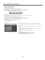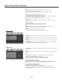
1
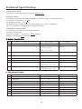
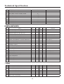
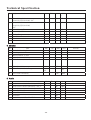
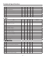
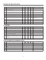
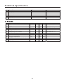
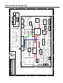
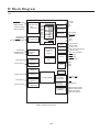
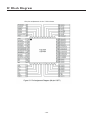
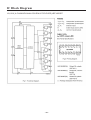
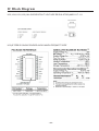
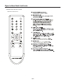
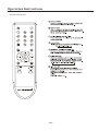
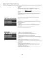
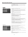
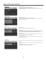
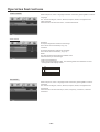
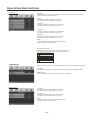
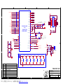
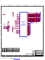
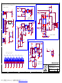
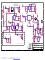
SERVICE MANUAL
8D60S CHASSIS
ON/OFF
TV/AV
MENU
PROG.-
PROG.+
VOL.-
VOL.+
Design and specifications are subject to change without prior notice.
( ONLY REFERRENCE)
_____CHECKED BY: _____PPROVED BY: _____
ENGINEER BY:
Note
Note------------------------------------------------------------------------------2
Technical specification--------------------------------------------------------3-8
Chassis Block Diagram--------------------------------------------------------9
IC Block Diagram---------------------------------------------------------------10-14
Transistor Mark-----------------------------------------------------------------15
PCB Top/Bottom Layer--------------------------------------------------------16-17
Service Adjustments-----------------------------------------------------------18-19
Control Location----------------------------------------------------------------20-21
Operation Instructions--------------------------------------------------------22-32
Service Tips---------------------------------------------------------------------33
Circuit Diagram-----------------------------------------------------------------34-46
-2-
Technical Specification
1.Application Area:
This product standard is used to the base of LCD 26” - 37”
2.Specification:
ALL standard are measured under the following conditions without other specification.
2.1 Ambient Temperature : 20 5℃
2.2 Relative Humidity : 65 10%
2.3 Power Supply Voltage: Standard Input Voltage (110 ~ 240 V ac 50/60Hz)
2.4 The TV should be measured after working 20 minutes。
3.Method of examination
3.1 capability : According to national test standard
3.2 Other requirements:
Interference(EMC) : according to FCC standard
SAFETY: according to UL standard
4.General Specification
No
Item
Specification
1.
Receive and send manner
2.
Receive Channel
VHF :E2~E13
3.
Input Voltage
CATV:S1~S125
UHF: E 1 4 ~ E 6 9
AC 110~240V, 50/60Hz
4.
Market
Southeast Asia,Taiwan
5.
26” ~37”
6.
Picture size
Tuning System
7.
Operating Environment
8.
StorageEnvironment
Remark
PAL/NTSC
181CH
PLL System
1) Temp : 0 ~ 40 deg
2)Humidity : 40 ~ 85 %
3)Temp : -20 ~ 50 deg
4)Humidity : 30 ~ 90 %
5. Feature and Function
No
1)
2)
3)
4)
1.
2.
3.
4.
5.
Item
Specification
TOSHIBA Code
X
1 YPbPr
1 OR 2
1
1 VGA
REMOCON
SCARTInput
Component input
HDMI input
S-VIDEO
RGB Input
2 Carrier Stereo
NICAM Stereo
BTSC STEREO
X
2 Carrier Dual
BTSC SAP
-3-
Remark
Technical Specification
6.
NICAM Dual
7.
SSC (Split Screen) Mode
X
X
8.
MUP (Multi Picture Display) Mode
X
9.
Film Mode
11. Progressive Scan
YES
YES
YES
12. Motion Detection
X
13. Dolby Virtual
X
14. Swivel Speaker
X
10. Noise Reduction
6.. Safety and Regulation
No
Item
Min
Typ
Max
Unit
1.
Force Stability – Incline Plane Tip Test
deg
2.
Force Stability – Level Tip Test
3.
Isolation Gap, AC-AC/ AC-DC
3
N
mm
4.
Isolation Gap, insulated-electric
6
mm
5.
Power Consumption, Max
6.
Power Consumption, Stand by
7.
Power Consumption, Current harmonics
2)
Dielectric Voltage
3
kV
8.
Isolation Resistance
4
MΩ
9.
Leakage Current
200
W
<2
0.7
4)
UL Compliance
W
at 10 mA, for 1 minutes
mApp
kg
11. Flammability – Back Cover
Sharp Edge
26’’/32’’ IEC 65
IEC 107-1
10. Power Cord Captivity
3)
Remark
V0
UL94
none
UL 6500
12. FCC Compliance
FCC PART 15
13. CDRH Radiation Compliance
14. CSA Compliance
15. CEB Compliance
16. CE Compliance
17. CB Compliance
7. Video
No
Item
Min
Typ
Max
Unit
1.
Linearity Distortion, Vertical
%
2.
Linearity Distortion, Horizontal
%
3.
Trapezoidal Distortion, Vertical
%
4.
Trapezoidal Distortion, Horizontal
%
5.
Over Scan, Vertical
%
6.
Over Scan, Horizontal
%
-4-
Remark
Technical Specification
7.
Brightness, Maximum
500
cd/m
2
8.
Video Noise Limited
Sensitivity(@S/N=30db) VHF
48
dBm
9.
Video Noise Limited
Sensitivity(@S/N=30db)
UHF
51
dBm
10. Selectivity –1.5M
35
dB
11. Selectivity +8M
40
dB
12. Tuning Range
-0.75
13. Resolution Horizontal
640
Lines
14. Resolution Vertical
480
Lines
1
MHz
8. Chroma
No
Item
Min
Typ
Max
Unit
1.
Purity (mislanding)
um
2.
Convergence
mm
3.
White Balance, X axis
4.
White Balance, Y axis
5.
White Balance, Color Temperature
12000
kdeg
6.
Color Sensitivity
45
dB
7.
Color Burst Lock-in Range
8.
Color Killer Sensitivity
+/-3
00
Remark
Hz
-80
dBm
9. Audio
No
Item
Min
Typ
Max
Unit
1.
Audio Noise Limited Sensitivity, VHF-L
42
dBm
9.
Audio Noise Limited Sensitivity, VHF-L
42
dBm
2.
Audio Noise Limited Sensitivity, UHF
48
dBm
3.
Buzz (S/N Ratio)
4.
Min. Volume Hum
20
mV
5.
Distortion
10
%
6.
Audio Output, L/R,at 7 % THD
20x2
W
40
-5-
dB
Remark
Technical Specification
7.
Audio Output, Center
8.
Audio Output, Woofer
W
W
9.
Stereo Separation
dB
10. Speaker Impedance
8
11. Speaker Power Rating
ohm
10
W
Max
Unit
264
V
12.
13.
14.
15.
10.. Power
No
Item
Min
Typ
1.
AC Power Shut Down Voltage
100
2.
DC Voltage, CRT Drive
3.
DC Voltage, FBT Drive
24
V
V
4.
DC Voltage, Audio
24
V
5.
DC Voltage, Vertical +
V
6.
DC Voltage, Vertical -
V
7.
DC Voltage, VCD(8)
V
8.
DC Voltage, VCD(5)
V
9.
DC Voltage, Tuner(5)
Remark
V
5
V
10. DC Voltage, Tuning(32)
V
11. DC Voltage, MICOM(5)
V
12. DC Voltage, MICOM(5)
V
13. CRT Heater Voltage
V
14. High Voltage
kV
15. High Voltage Regulation
kV
16. Beam Current
mA
11. External Interface
No
Item
Min
Typ
1
Max
Unit
1.15
Vpp
1.
Video Input Level
0.85
2.
Video Input Frequency Response
4.5
MHz
3.
Video Input S/N
40
dB
4.
Audio Input Level
0.4
5.
Audio Input Frequency Response
0.1
6.
Audio Input S/N
40
7.
Audio Input Distortion
8.
Audio Input Dynamic Range
0.5
0.6
Vrm
s
7
kHz
dB
2
2
-6-
%
V
Remark
Technical Specification
9.
Video Output Level
10. Video Output Frequency Response
0.85
1
1.15
Vpp
3.8
MHz
11. Video Output S/N
40
dB
12. Audio Output Level
0.4
13. Audio Output Frequency Response
0.1
14. Audio Output S/N
40
0.5
0.6
Vrm
s
7
kHz
dB
15. Audio Output Distortion
2
16. Video Input Level, R/G/B
17.
%
Vpp
0.6
0.7
0.8
Vpp
75 ohm
Video Input Level, Component(Y, P B, PR)
18. RGB Input Resolution, Vertical
pixel
19. RGB Input Resolution, Horizontal
pixel
20. RGB Input Horizontal Frequency
kHz
21. RGB Input Frame Rate
Hz
12. The others
No
Item
Min
-95
Typ
-90
Max
Unit
-85
dBm
7
sec
1.
Search Sensitivity
2.
CRT Heating Time
3.
Soft Ware Functionality Test
4.
REMOCON Working Sensitivity, Straight
8
m
5.
REMOCON Working Sensitivity, T/B/L/R
6
m
6.
Closed Caption Sensitivity
7.
Teletext Sensitivity
8.
Resonance of unit (Sweep freq : 50 ~
1000)
9.
Clock, real time gain or loss (sec per day)
-70
Remark
dBm
dBm
none
sec
13. Customer Menu Setup (as shipped condition)
No
Item
Min
1.
PSM
Movies
2.
SSM
Music
3.
Volume
30
4.
Mute
Off
5.
Input Mode
RF
6.
Customer Menu Language
English
7.
AVL
Off
-7-
Typ
Max
Unit
Remark
customer define
Technical Specification
8.
Sleep Timer
Off
9.
Auto Sleep
Off
10. Blue Back
Off
11. Surround
On
12. Caption
Off
13. Noise Reducer
AUTO
14. Reliability
No
Item
Min
Typ
Max
Unit
Remark
1.
ESD
4
kV
IEC-1000-4-2
2.
EFT/Burst
2
kV
IEC-1000-4-4
3.
Surge Immunity
30
kV
IEC-1000-4--5
4.
Voltage Dip Test, 10ms
100
%
IEC-1000-4-11
5.
Voltage Dip Test, 100ms
%
IEC-1000-4—11
6.
Operation Temperature
0
7.
Operation Humidity
8.
9.
25
45
deg
10
90
%
Storage Temperature
-20
60
deg
MTBF (Confidence Level : 90 %)
10000
10. Ship Test
-8-
hour
Chassis Block Diagram
5
PANL ON/OFF
4
IR/Key
74HC573
SC3-FS
SC2-FS
SC1-FS
ATSC READY
T5BS4
-9999
Toshiba
3
SPDIF
5V
TV-CVBS
DVD/DVB YPbPr
24V
L5
R5
YC
Y1Pb1Pr1
Pb1
Pr1
C381
2
24V
SC1-L/R
SIF
R
PT2308
TUNER
TDA9886
SCART1/AV1
Side-AV-R/L
DVD/DVB-L/R
MP7722
82X7
4052
Y1
S-VIDEO
SC2-RGB/CVBS
SCART3-L/R
L5/R5
L3R3(VGA-ADUIO)
330
LVDS
O/F 5VSB
230mm
L3
R3
PHONE
L
150mm
Date:
Size
Tuesday, May 06, 2008
Schematic Name
TK204
1
1
Sheet
Trident Digital Media, Inc.
1090 East Arques Ave. Sunnyvale, CA 94085
http://www.tridentmicro.com
Title
PLACEMENT
24V GND
512Kx8
ST Flash
4052
SVP_CX32
RGB
HV
VGA
SCART3/AV3
2
24V 12V
GND 24V
24C64
SPDIF
HDMI1
SCART2/AV2
3
1
of
15
Rev
A
D
C
B
A
-9-
SC2-YC
SiI9021
2Mx32
SDRAM
24C02
24C02
HDMI2
SIDE AV
4
SideAV-YC
D
C
B
A
S-Video
5
SC3-YC
IC Block Diagram
U4
ADTRG(P53)
A N0 To An3
(P50 TO P53)
AVCC,AVSS
TXD0(P90)
RXD0(P91)
SCLK0/CTSO(P92)
CPU(TLCS-900/L1)
10-bit4-ch
AD
converter
SIO/UART
(Channel/0)
XWA
XBC
XDE
XHL
XIX
XIY
XIZ
XSP
W A
B C
D E
H L
IX
IY
IZ
SP
High-speed
oscillator
Clock gear
Low speed
oscillator
32 bits
SR
F
PC
Port0
Port1
SCK(P60)
SO/SDA(P61)
SI/SCL(P62)
Serial bus
interface
(SBI)
Watchdog
timer
(WDT)
Port2
Port3
TA01N(P70)
8-bit timer
(TMRA 0)
TA1OUT(P71)
8-bit timer
(TMRA 1)
TA3OUT(P72)
Port9
TA5OUT(P74)
(P00 to P07)
AD0 to Ad7
( P10 to P17)
Ad8 / A8 to AD15/A15
( P20 to P25)
A0 / A16 to A5/A21
RD(P30)
WR(P31)
P93
P94
P95
Port6
8-bit timer
(TMRA 3)
10-Kbyte RAM
TA41N(P73)
XT1(P96)
XT2(P97)
RESET
Am0
Am1
ALE
HWR(P32)
RTC
8-bit timer
(TMRA 2)
DVCC
DVSS
X1
X2
8-bit timer
(TMRA 4)
CS/WAIT
controller
(4 blocks)
Interrupt
controller
8-bit timer
(TMRA 5)
16-bit timer
(TMRB0)
T5BS4-9999 Block Diagram
-10-
( P40 to P42)
cs0 to cs2
NMI
INT0(P63)
TB0IN0/INT5(P80)
TB0IN1/INT5(P81)
TB0OUT0(P82)
TB0OUT1(P83)
IC Block Diagram
-11-
IC Block Diagram
U9,U29( 4-CHANNEL ANALOGUE MULTIPLEXER)HEF4052BT
-12-
IC Block Diagram
U23(5A LOW DROPOUT LINEAR REGULATOR)1.8V TO-263-3
U28
-13-
IC Block Diagram
U22,U24,U31,U32(1A LOW DROPOUT VOLTAGE REGULATOR)AMS1117-1.8
U33(STEREO SINGLE ENDED AUDIO AMPLIFER)MP7722DF
-14-
Transistor Mark
C
C
V
BC847B
BC846B
B
B
E
C
C
PT7M7809S7
G
N
E
-15-
D
R
E
S
E
T
Main PCB Top/Bottom Layer
Main PCB top layer
-16-
Main PCB Top/Bottom Layer
Main PCB bottom layer
-17-
Service Adjustments
1.Application Area:
This product standard is used for 8D60E LCD TV。
2 . Specification:
2.1 T he LCD uses AC power supply, so please use 220VAC directly .
2.2 The power supply should keep the rating voltage 110~240 VAC 50 / 60 Hz。
2.3 Ambient conditions: All the standards are measured under following conditions without other
specification.
1)Ambient temperature : 25 ℃
5℃
2)Relative humidity : 60 %
20 %
2.4 If no prior notice, the TV set should work for more than 20 minutes before adjustment.
2.5 Equipments needed
-- Multimeter
Max Input Current : 1A / Max Input Voltage : 500Vdc
-- Measurement Range : 10Mvr~100Vdc / Accuracy : 0.03%
? Oscilloscope:
Frequency Band : 20M above/Input Impedance : 1 above
Input Capacitance : 30pF below / Max Input Voltage : 250V
-- YPBPR/YCBCR
1080i/60Hz, 720P
-- Color TV Pattern Generator
2.6 Signal
IF no extra specify, the standard input COLOR BAR PATTERN signal is 60 ~ 80 dBu from factory
centre or PM5418 signal generator
3. Software
3.1 Instructions
This chassis uses FLASH ROM to memory the program, and it can be re-rewritable.
The program is related to chassis function, the chassis with different functions should use different
program edition.
4. Chassis checking
4.1 The upside of the chassis should be clear and no short or open circuit, no missing components or
wrong polarity components insertion.
4.2 Check the input and output pins of 24V,12V,5V,3.3V,1.8V,regular IC (U23,U31,U32,U22,U24
,U21),confirm no short circuit to GND
4.3 Connect the chassis to LCD panel and the power supply ,confirm 5V,3.3V,2.4V,1.8V from any
regulators are OK.
4.4 Confirm OSD is OK, blue back appears without signals.
4.5 Confirm remote control functions and all collation keys control functions are OK.
4.6 Check searching function, save every factory TV signal, confirm the pictures in every system (PAL/
BG/DK/I,SECAM L/L') are OK.
4.7 Confirm HDMI1/HDMI2/SCART1/SCART2/SCART3/YpbPr/picture and sound in/output are OK,
confirm the picture and sound from PC are OK.
4.8 Confirm TELETEXT is OK.
4.9 Set into the whole machine, enter the aging line, set the TV to snowflake points state in the line.
5. Complete check
5.1 Check the pictures and sound in every system (PAL/BG/DK/I,SECAM L/L')are OK, check the picture
and sound under weak and strong signal, check picture in low and high voltage power input mode.
5.2 check NICAM function
5.3 Confirm teletext function is OK.
5.4 Confirm HDMI1/HDMI2/SCART1/SCART2/SCART3/YpbPr/picture and sound in/output are OK,
-18-
Service Adjustments
confirm the picture and sound from PC are OK.
5.5 C heck the remote control and the KYE-press can work normally, make sure it can make the TVset
enter the standby mode and return to the normal mode. Check the sound and picture can be adjusted
normally. Check the sound and picture ,make sure it can be adjusted normally.
6. Final setting
① PICTURE
: DYNAMIC
② VOLUME
: 30
③ SOURCE
: TV
④ SOUND SET
: BG (※)
⑤ BLUE BACK
: ON
※ special items set as the BUYER'S requirements。
7. Others
7.1 Because the LCD panel is high-tech product, please don't pull, crush or drop it, Please don't use the
cloth that with high humidity to clean it, because the moisture may lead short. You can use some soft
things to clean it, such as glasses cloth and camera lens
7.2 please pay attention to the high voltage in the INVERTER module output of the core. (About540Vrms
@60KHz)
7.3 Because the power supply id inside, please pay attention to the 220VAC.
-19-
Control Location
ON/OFF Switch/Power Indicator
Remote Sensor
ON/OFF Switch
TV/AV
MENU
CH.- Button
CH. +Button
VOL.-Button
V0L.+Button
Speakers
HDMI 2 Input
HDMI 1 Input
VGA Input
AUDIO IN 1
AUDIO IN 2
Y Pb Pr
S-Video
AV OUT
AV IN 1
Aerial input socket
Power Switch
ON/OFF
TV/AV
MENU
PROG.-
PROG.+
VOL.-
VOL.+
10
2
1
10
21
21 Power Switch
11
HDMI 1
12
VGA
RIGHT
13
14
AV IN 1
LEFT
Pb
Y
RIGHT
Pr
S-VIDEO
15
-20-
3
ON/OFF
4
TV/AV
5
MENU
6
CH.-
7
CH.+
8
VOL.-
9
VOL.+
19
17
AV OUT
HDMI 2
LEFT
AUDIO IN 2
16
AUDIO IN 1
1.
2.
3.
4.
5.
6.
7.
8.
9.
10.
11.
12.
13.
14.
15.
16.
17.
18.
19.
20.
21.
VIDEO
LEFT
RIGHT
VIDEO
LEFT
RIGHT
18
20
Control Location
LOCATION OF CONTROLS
HDMI CABLE CONNECTIONS
IMPORTANT INFORMATION
IMPORTANT INFORMATION Power off both HD player and
display before making any connections. Connect the HDMI
cable to the HDMI socket of the TV, connect the other end to
the HDMI output socket of the HD player source.
AUDIO IN 1
In the event that the TV does not power up after pressing the
remote control power button please check that the mains cable
is firmly pressed into the mains socket located on the TV and
that the mains socket has power. Also check that the mains
switch on the TV has not accidentally been turned off when
inserting the mains plug on the TV. The mains switch is located to
the side of the mains socket as shown in the accompanying
diagram. Push the switch and check that the power indicator
glows red on the right side of the TV front panel.
Connect the HDMI cable to the HDMI socket of the TV.
Connect the other end to the HDMI output socket of the HD
player source, HDMI cable will carry both Video and audio
signals from the HD source to the TV.
HDMI 2
HDMI 1
VGA
LEFT
RIGHT
AV IN 1
In the remote control and press the power button on the remote.
The power Indicator will change colour to green and shortly
afterwards the TV screen will glow. Follow the tuning
information shown on page 11 of the instruction manual.
LEFT
Pb
Y
RIGHT
Pr
S-VIDEO
HDMI
HDMI CABLE NOT SUPPLIED.
Connect the HDMI cable to the
HDMI input on the TV.
Connect the other end of this
cable to your HD device.
HDMI
HDMI CABLE NOT SUPPLIED.
Device HDMI
POWER SWITCH
PUSH UP
-21-
AV OUT
and to a 90-260VAC mains supply the Standby Light
should glow on the front panel. Insert the supplied batteries.
AUDIO IN 2
The power switch on this TV is factory set to its ON
position. After connecting the mains cable to the TV
VIDEO
LEFT
RIGHT
VIDEO
LEFT
RIGHT
Operation Instructions
OPERATION INSTRUCTIONS
Remote Control Unit
-22-
Operation Instructions
Remote Control Unit
-23-
Operation Instructions
ANALOG MENU SCREENS
Menu Structure and Navigation
Use the following keys to navigate through the main menu:
Plug in the power source, the power indicator will light up. If TV is stand by mode.
Then press
key. The picture will display in few minutes.
Press menu button to display analog menu, and press V +/- to select sub menu.
VIDEO
AUDIO
SETUP
TIMER
OPTION
Press the MENU key to invoke the main menu as shown.
Use V +/- key to select the main menu icon, the focused icon will be shown as a protruded button.
Press the CH+/- key to go to the corresponding menu.
Use the following keys to navigate through the secondary menu:
Press the CH+/- key to select menu item, the focused item will be highlighted in yellow.
Press the V +/- key to select the selection, adjust item value, or enter sub menu.
Exit the OSD mode by either of the following methods:
1.Wait for Time out (60 seconds default)
2.Press the MENU key
VIDEO menu
To adjust the picture settings, including: Picture Mode, Contrast, Brightness,
Color, Tint, Sharpness, Color Temperature , DNR, and Advanced picture settings.
Picture Mode
This option adjusts the mode of the image: User, Standard, Mild and Dynamic.
Contrast
This option adjusts the contrast level of the image.
1.The scale of control should be 0-100. When it is set to 0, the image should
not be “ Dark ” .
2.This control should not affect the OSD Menu itself.
Brightness
This option adjusts the brightness level of the image.
1.The scale of control should be 0-100. When it is set to 0,
The image should not be “ Dark ” .
2.This control should not affect the OSD Menu itself.
-24-
Operation Instructions
Color
This option adjusts the video color saturation level of the image.
1.The scale of control should be 0-100.
2.This item is disabled and can not be selected when in PC source.
Tint
This option adjusts the video tint level of the image.
1.The scale of control should be (-50) (+50).
2.When set the value towards (-50), the image tends to “ Red ” . When set the
value towards (+50), the image tends to “ Green ” .
3.This item is only enabled when input signal system is NTSC.
Sharpness
This option adjusts the sharpness level of the image. The scale of control
should be 0 -100.
Color Temperature
This option adjusts the color temperature of the image.
The selection of control is Normal, Warm and Cool.
DNR
This option adjusts the dynamic noise reduction level of the image. The
selection of control is Off, Auto, Low, Mid and High.
Advanced menu
Watch TV
Advanced
This item is to enter the Advanced Picture Menu.
Press the V +/- key to enter the Advanced Picture Menu.
Flesh Tone
This option adjusts the flesh tone level of the image. The scale of control should be 0-2.
Green Tone
This option adjusts the green tone level of the image. The scale of control should be 0-2.
Blue Tone
This option adjusts the blue tone level of the image. The scale of control should be 0-2.
Cinema Mode
This option adjusts the cinema mode of the image. The selection of control is Off and
Auto. This item is only enabled when in AV or TV source.
AUDIO menu
To adjust the audio settings, including: Volume, Balance, AVC, MTS, Sound Mode
and Equalizer.
Volume
This option adjusts the volume level of sound. The scale of control should be
(0)-(100).
Balance
This option adjusts the balance of sound between left and right speakers.
1.The scale of control should be (-50)-(+50).
2.When set the value towards (-50), the sound tends to left.
When set the value towards (+50), the sound tends to right.
AVC(Automatic Volume Correction)
This option switches the AVC function.
The selection of control is On and Off. The AVC function solves annoying volume
changes between different sound levels by equalizing the volume level.
MTS (Multichannel Television Sound)
This option switches the MTS mode.
The selection of control is Mono, Stereo and SAP.
This project include sound processing IC for processing the MTS signal
conforming to the standard recommended by the Broadcast Television Systems
Committee (BTSC).
-25-
Operation Instructions
Sound Mode
A tone control system designed to compensate for frequency distortion in audio
systems.
Entering the Custom mode, you can select the Sound quality instantly among
three preset modes and one user-defined mode.(User defined mode)
User
Pop
Rock
Live
Equalizer
A tone control system designed to compensate for frequency distortion in audio
systems.
Enter Equalizer, you can select 120HZ, 500HZ, 1.5KHZ, 5KHZ and 10KHZ items
by pressing CH.+ buttons and change the corresponding value of volume by
pressing V+/- buttons.
Setup menu
Enter setup menu, select Language, Channel Label, Auto Tuning and Color
System by pressing CH.+/- buttons.
Language
The choices are English, French, Deutsch, Espanol, Italian, Portuguese items.
Channel Label
This item is to enter the program label edit menu. Press the V+/- key to enter the
program label edit menu.
Auto Tuning
This item is to enter the Auto Tuning Menu. Press the V+ key to enter the Auto
Tuning Menu.
Color system
Press the button to select a new color standard value in TV.
The choices Auto, NTSC 3.58, PAL M, PAL N.
Auto Tuning menu
Program
This item is to change the current program number.
1.Press the V+/- key to change the current program number.
2.Press number key to directly input the current program number.
Skip
This item is to change the skip option of the current program.
The selection of control is On and Off. When the skip option of the current program
is On, user can not get to this program by press CH.+/- , but the direct number key
is working.
Program Table
This item is to change the Program Table option of the current program. The
selection of control is Air and Table.
When the Program Table option of the current program is Air, The program is by Air,
vice versa Cable.
Start Searching
This item is to enter the Auto Tuning Menu.
1.Press the V+ key to start auto tuning. After starting auto tuning, Auto Tuning
status will be shown.
2.The status bar shows the searching progress of the whole frequency band,
including VHF-L, VHF-H and UHF.
3.The program position number is the number that next searched program will be
stored. It starts from program number “ 1 ” .
-26-
Operation Instructions
4.Press the MENU key to exit all Menus and terminate the auto tuning process.
The Searched programs are stored.
5.When the whole band is searched over, or position number exceed maximum,
the auto tuning process is terminated.
6.Positions that don't store a channel in the searching process are stored with
“ skip on ” .
Timer menu
Enter timer menu, select Sleep Timer, Current Time, Off Timer, On Timer and On
Timer Channel items by pressing CH.+/- buttons.
Sleep Timer
The choices are 15 minutes, 30 minutes, 45 minutes, 60 minutes, 90 minutes,
120 minutes and OFF. During the last 30 seconds of the preset sleep time, the
sleep timer indicator is displayed in the upper center of the screen and remain
there until the TV switches auto maticlly to stand-by.
Current Time
The option adjusts the current time, the unit is minute.
You can use 0-9 digit button or V+/- button to set it.
Off Timer
This option adjusts the automatically power off timer.
The unit is minute.
Once the timer is set to a non-zero time, it is enabled and the number decreases
every minute. When the timer runsto zero, it triggers the power off action.
1.Press the V+/- key to change the timer number.
2.Continuously press down the V+/- key to
change the timer number by 30 minutes.
3.Press number key to directly input the timer number.
On Timer
This option adjusts the automatically power on timer.
The unit is minute.
Once the timer is set to a non-zero time, it is enabled and the number decreases
every minute. When the timer runs to zero, it triggers the power on action (in
power off status) or the program change action (in power on status).
1.Press the V+/- key to change the timer number.
2.Continuously press down the V+/- key to change the timer number by 30 minutes.
3.Press number key to directly input the timer number.
On Timer Channel
This option adjusts the automatically power on program position. The position is
the program that system changes to when the on timer triggers.
1.Press the V+/- key to change the program position.
2.Continuously press down the V+/- key to change the program position by 10.
3.Press number key to directly input the program position.
Option menu
Enter option menu, select Aspect, Blue Screen, Menu Background , Key Lock,
Parental and CCD items by pressing CH.+/- buttons.
Aspect
TV/AV source, press this button to select:
Original /16:9 / 16:9 Zoom/ 16:9 Sub/14:9/ 14:9 Zoom/4:3/4:3Zoom.
VGA/YPbPr/HDMI source, press this button to select:Original / 16:9 and 4:3.
Blue Screen
This option switches the blue screen function.
The selection of control is On and Off. When this function is enabled, a blue screen
will be shown in case of no signal status in TV source.
Menu Background
This option adjust the Menu Background the selection of control is transparent and
opaque.
Key Lock
This option switches the key lock function.
The selection of control is On and Off. When this function is enabled, the keyboard
will be locked and can not be used.
-27-
Operation Instructions
Parental
This item is to enter the Parental Menu. Before entering Parental Menu, password
needs to be checked.
1.Press the V+/- key to enter the Password menu.
2.Input Password. If user input a right 6-digital password saved in EEPROM or
default password (123456), system will enter Parental Menu, otherwise return to
Function Menu.
CCD
This option adjusts the setting of Closed Captioning channel.
The selection of control is Off, CC1, CC2, CC3, CC4, Text1, Text2, Text3, Text4 and
XDS.
Parental Menu
Parental Menu(V-Chip Menu)
Input the password 123456 to enter V-Chip menu.
Enter parental menu, you can select Ext Source Block, Parental Control, Unrat
Program Block, TV Rating Limit, Movie Rating Limit and Change Password items
by pressing CH.+/- Buttons.
1.Ext Source Block
This option switches the output Block Function.
The selection of control is off and on.
2.Parental Control
This option adjusts the setting of Parental control type.
The selection of control is Off, Child, Youth, Youth Adult, Custom.
If select Off, Child, Youth, Youth Adult, Block option uses default setting. See the
table below.
TV-Y TV-Y7 TV-G TV-PG TV-14 TV-MA M-G M-PG M-PG13 M-R M-NC17
Off
V
V
V
V
V
V
V
V
V
V
V
Child
V
V
V
B
B
B
V
B
B
B
B
Youth
V
V
V
V
B
B
V
V
V
B
B
Youth
V
V
V
V
V
B
V
V
V
V
V
Adult
If select custom, Block option can be edited by user. See TV Rating Menu, Moving
Rating Menu.
3.Unrat Program Block
This option switches the Program block Function
The selection of control is Off and On. When On is selected, it will Block all Ratings.
-28-
Operation Instructions
TV Rating Limit
4.TV Rating Limit
Press the V+/- key to enter the TV Rating menu.
User can edit the block option between V(view) to B(block).
Press V+/- key to change V (View)/B (Block) status, Press CH.+/- key to select
items needed to edit.
Moving Rating Limit
5.Moving Rating Limit
Press the V+/- key to enter the Moving Rating menu.
User can edit the block. Press V+/- key to change V/B status, Press CH.+/- key to
select items needed to edit.
Change Password
6.Change Password
Press the V+/- key to enter the Change Password menu.
Old Password
Input old Password. Before entering input status, user should press V+ key first.
After user input a right 6-digital password saved in EEPROM or default password
(111111), system will go into input New Password status automatically.
New Password
Input new Password. After user input a 6-digital new password, system will go into
input New Password Again status automatically.
New Password Again
Confirm New Password. If New Password Again and New Password are the same,
New Password is accepted.
AV MODE
Enter setup menu, select Language and color system by pressing CH.+/- buttons.
Language
The choices are English, French, Deutsch, Espanol, Italian, Portuguese items.
Color system
Press the button to select a new color standard value in AV.
The choices Auto, NTSC 3.58, PAL M, PAL N.
-29-
Operation Instructions
YPbPr MODE
Enter setup menu, select Language and YPbPr Channel by pressing CH.+/- buttons.
Language
The choices are English, French, Deutsch, Espanol, Italian, Portuguese items.
YPbPr Channel
Press the button to select H Position, V Position and Reset.
YPbPr Channel
H Position
This option adjust the H Position of the image.
The scale of control should be(-10)-(+10).
V Position
This option adjust the V Position of the image.
The scale of control should be (-10)-(+10).
Reset
The item resets the above setting to default value.
Press the V+ key to reset settings.
YPbPr Input Resolutions
YPbPr input typical display modes. The following table is an illustration of some
of the typical video display modes.
1
2
480i
480p
3
4
5
6
576i
576p
720p(50/60Hz)
1080i(50/60Hz)
PC MODE
Enter setup menu, select Language and PC Channel by pressing CH.+/- buttons.
Language
The choices are English, French, Deutsch, Espanol, Italian, Portuguese items.
PC Channel
Press the button to select Auto Sync, Phase, Frequency, V Position, H Position
and Reset.
PICTURE
-30-
Operation Instructions
PC Channel
Auto Sync
This item is to automatically setup the position settings of the current PC signal.
Press the V+ key to start auto sync.
Phase
This option adjusts the phase of the signal.
The scale of control should be(-10)-(+10).
Frequency
This option adjust the Frequency of the image.
The scale of control should be (-10)-(+10).
V Position
This option adjust the V Position of the image.
The scale of control should be (-10)-(+10).
H Position
This option adjust the H Position of the image.
The scale of control should be(-10)-(+10).
Reset
The item resets the above setting to default value.
Press the V+ key to reset settings.
PC Input Resolutions
PC Input typical display modes. The following table is an
illustration of some of the typical video display modes.
PICTURE
HDMI MODE
1
640X480(recommend 60Hz)
2
3
4
800X600(recommend 60Hz)
1024X768(recommend 60Hz)
480p
5
6
7
576p
720p(50/60Hz)
1080i(50/60Hz)
Enter setup menu, select Language and HDMI Channel by pressing CH.+/- buttons.
Language
The choices are English, French, Deutsch, Espanol, Italian, Portuguese items.
HDMI Channel
Press the button to select V Position, H Position and Reset.
HDMI Channel
H Position
This option adjust the H Position of the image.
The scale of control should be(-10)-(+10).
V Position
This option adjust the V Position of the image.
The scale of control should be (-10)-(+10).
Reset
The item resets the above setting to default value.
Press the V+ key to reset settings.
-31-
Operation Instructions
HDMI Input Resolutions
HDMI Input typical display modes. The following table is an illustration of some
of the typical video display modes.
1
640X480(recommend 60Hz)
2
3
4
5
800X600(recommend 60Hz)
1024X768(recommend 60Hz)
480p
576p
6
7
720p(50/60Hz)
1080i(50/60Hz)
-32-
Symptoms
n
Tr y d if
fe r e n t
chann
Check
e l, if O
a e r ia l
K, pro
conne
b a b ly
c ti o n s
Check
s ta ti o n
on bac
a e r ia l
tr o u b le
k of se
fo
r
broken
R e - o r ie
t
w ir e s
n t a e r ia
l ( if in d
Proba
o o r ty p
b ly lo c
e)
a
l
in te r fe
A d ju s t
rence,
fi n e tu
such a
n
in
g c o n tr
A d ju s t
s an a
p p li a n
ol
b r ig h tn
ce
e
s
s c o n tr
A d ju s t
ol
c o n tr a
s
t c o n tr
Check
ol
if s ta ti
o n is b
A d ju s t
roadca
c o lo u r
s ti n g c
c o n tr o
o lo u r
Check
l
if s y s te
m s w it
Check
c h is c
if o n /o
orrect
ff s w it c
Check
h is " o
B a tt e r
n"
ie s in R
e m o te
c o n tr o
l
S o lu t io
Service Tips
BEFORE CALLING FOR SERVICE, HAVE YOU
CHECKED (
) THE FOLLOWING CHART
ON SYMPTOMS AND SOLUTIONS?
No picture, no sound
Poor sound, picture OK
Poor picture, sound OK
Weak picture
Blurred picture
Double image
Lines in picture
Distorted picture
Weak reception on some channels
Picture rolls vertically
Horizontal bars
No colour
Misoperation of Remote control
No Remote control
On Screen Display Control outside the screen
Poor colour
-33-
5
4
3
U1A
C1
TUNER_MAIN
D
0.47uF 169
Y
C2
0.1uF
180
SC1_G
C3
0.1uF
181
SV_Y_MP
C4
0.1uF
182
C5
0.1uF
183
PC_GIN
PR
C6
0.1uF
188
SC1_R
C7
0.1uF
189
SC2_Y
PC_RIN
SV_C_MP
C8
0.1uF
190
C9
0.1uF
191
C10
0.1uF
PB
0.1uF
196
SC1_B
C16
0.1uF
197
C17
SC1_CVBS
C18
PC_BIN
0.1uF
0.1uF
TD1P
TD1M
Y_G1
TC1P
TC1M
Y_G2
Y_G3
TB1P
TB1M
PC_G
TA1P
TA1M
PR_R1
TCLK1P
TCLK1M
PR_R2
PR_R3
LVDSVCC
PC_R
PB_B1
PB_B2
PB_B3
199
PC_B
40
41
TD1+
TD1-
44
45
TC1+
TC1-
48
49
TB1+
TB1-
CON16
50
51
TA1+
TA1-
42
43
TCLK1+
TCLK1-
1
3
5
7
9
11
13
15
17
19
V-LVDS
3.3V POWER
FOR LVDS
CX_LVDS_VDD
46
C11
SVP-CX32_208
(1/4)
ANALOG I/O
LVDS & MISC
C
198
1
SVP_CX32
CVBS1
192
C15
2
LVDSGND
PLL_VCC
PLL_GND
C12
FB1
1
C13
C14 +
0.1uF
10uF/10V
2
150_Ohm_600mA
TD1+
TCLK1+
TC1+
TB1+
TA1+
47
0.1uF
0.1uF
CX_LVDS_VSS
con10X2_2.0
39
3.3V
38
C19
LVDS_VDDP
TD1TCLK1TC1TB1TA1-
CX_VD33
D
2
4
6
8
10
12
14
16
18
20
20pF
R74
3.3K
R205
0
52
Y1
14.318MHz
C
171
FS1
170
C22
0.1uF_DNS
CX_VREFN_1
CX_VREFP_1
SC2_C
C24
C21
0.1uF
CX_VREFP_1
CX_VREFN_1
CX_VREFP_2
AIN_VS
AIN_HS
174
VREFP_1
175
159
PC_VSIN
158
PC_HSIN
157
R2
100
163
R3
75
5V
VREFN_1
184
R206 2.0K
VREFP_2
CVBS_OUT1
CN12
CX_CVBS_OUT1
C27
0.1uF_DNS
185
VREFN_2
CVBS_OUT2
162
R4
R209
BKLT_CNTL
75
CX_CVBS_OUT2
R211
CX_VREFN_2
CX_VREFP_2
FB2
0.1uF
CX_VREFN_2
B
LAYOUT: Place xtal
circuit as compact
and close to chip
as possible
20pF
205
FB1
172
TESTMODE
C25
0.1uF
XTALI
C
204
C20
FS2
173
SC1_FB
XTALO
1
2
3
0
0_DNS
5V
3-PIN_HEADER_2MM
BACKLIGHT CONNECTOR
R212 4.7K_DNS
C28
C29
0.1uF
0.1uF
B
R213
0_DNS
BRT_CNTL
CN12
DEFINITION IN LCD203
CVBS1
MAIN TUNER INPUT
Y_G3
MAIN CHANNEL CVBS RCA CONNECTOR INPUT
PB_B3
SCART1 CVBS INPUT
PR_R3
SCART2 CVBS INPUT
FB1
SCART1 FB INPUT
FB2
SCART2 or 3 Chroma INPUT
FS1
SCART1 FS INPUT
FS2
SCART2 FS INPUT
5
2
2.2K
2
R901
K801
CH+
K800
ON/OFF
1
K802
CH-
560
1
K803
VOL+
R902
1
K804
VOL-
1K
2
R903
2
390
1
K805
MENU
R904
2
390
1
1
A
Pin Name
R905
2
2
K806
SOURCE
270
1
R906
1
2
KEY
PRELIMINARY
Trident Digital Media, Inc.
1090 East Arques Ave. Sunnyvale, CA 94085
http://www.tridentmicro.com
Title
SVP-CX32-1
4
PDF 文件使用 "pdfFactory" 试用版本创建 www.fineprint.com.cn
ÿÿÿÿÿ
3
2
Size
B
Schematic Name
TK204
Rev
A
Date:
Wednesday, October 10, 2007
1
Sheet
2
of
15
A
5
4
3
2
U1B
D
SVP_CX32
BRT_CNTL
CX_PWM0 R8
0
C31
CX_PWM0
55
CX_SCL
57
CX_SDA
58
CX_GPIO0
CX_GPIO1
60
59
ADDR0
ADDR1
ADDR2
ADDR3
ADDR4
ADDR5
ADDR6
ADDR7
PWM0
0.01uF
8051_WR#
CX_VD33
8051_RD#
8051_CS2CX
R12
C
I2C Slave Address is
fixed to 0x7e/0x7f
4.7K_DNS
R13
CX_INT#
4.7K_DNS
8051_ALE
R9
0
62
R10
0
63
R11
0
61
R14
0
56
R15
0
84
R17
0
86
SCL
SDA
WR#
5V_SDA
5V_SCL
R16
R19
10
10
CX_SDA
CX_SCL
R20
R21
10_DNS
10_DNS
C33
RESET_H
85
C34
68pF_DNS
SVP-CX32_208
RD#
(2/4)
CS
ALE
5V_SB
3V_SDA
3V_SCL
CPU INTERFACE
DIGITAL OUT
RESET
V5SF
C35
68pF_DNS
DP_HS
0.1uF
DP_VS
DP_CLK
DP_DE_FLD
DP_HS
4
DP_VS
5
DP_CLK
DP_DE_FLD
23
6
A_D0
A_D1
A_D2
A_D3
A_D4
A_D5
A_D6
A_D7
GPIO0
GPIO1
INTN
1
DP_HS
DP_VS
DP_CLK
DP_DE_FLD
DP0
DP1
DP2
DP3
DP4
DP5
DP6
DP7
DP8
DP9
DP10
DP11
DP12
DP13
DP14
DP15
DP16
DP17
DP18
DP19
DP20
DP21
DP22
DP23
uP_A[0..7]
64
65
66
67
68
69
70
71
8051_A0
8051_A1
8051_A2
8051_A3
8051_A4
8051_A5
8051_A6
8051_A7
RN1 4
3
2
1
RN2 4
3
2
1
5 100x4
6
7
8
5 100x4
6
7
8
uP_A0
uP_A1
uP_A2
uP_A3
uP_A4
uP_A5
uP_A6
uP_A7
83
82
81
80
79
78
77
76
8051_AD0 RN3 1
8051_AD1
2
8051_AD2
3
8051_AD3
4
8051_AD4 RN4 1
8051_AD5
2
8051_AD6
3
8051_AD7
4
8 100x4
7
6
5
8 100x4
7
6
5
uP_AD0
uP_AD1
uP_AD2
uP_AD3
uP_AD4
uP_AD5
uP_AD6
uP_AD7
37
36
35
34
33
32
31
30
29
26
25
24
22
21
18
17
16
15
14
11
10
9
8
7
uP_AD[0..7]
DP[0..23]
DP0
DP1
DP2
DP3
DP4
DP5
DP6
DP7
DP8
DP9
DP10
DP11
DP12
DP13
DP14
DP15
DP16
DP17
DP18
DP19
DP20
DP21
DP22
DP23
C
B
B
Pin Name
A
D
Pin No.
1 (HIGH)
GPIO0
MPU in A/D Multiplix Mode
GPIO1
Use Rising Edge of WR# to latch data
0 (LOW)
A
MPU in A/D Separate Mode
Trident Digital Media, Inc.
1090 East Arques Ave. Sunnyvale, CA 94085
http://www.tridentmicro.com
Title
SVP-CX32-2
Use Falling Edge of WR# to latch data
PRELIMINARY
5
4
PDF 文件使用 "pdfFactory" 试用版本创建 www.fineprint.com.cn
ÿÿÿÿÿ
3
2
Size
B
Schematic Name
TK204
Rev
A
Date:
Wednesday, October 10, 2007
1
Sheet
3
of
15
3
DQM0
CX_DQM2 R28
15
DQM2
CX_DQM3 R30
15
DQM3
CX_MA11
CX_BA0
CX_WE#
CX_CAS#
CX_RAS#
CX_MCLK
CX_CLKE
D
U1C
CX_MA0
CX_MA1
CX_MA2
CX_MA3
CX_MA4
CX_MA5
CX_MA6
CX_MA7
CX_MA8
CX_MA9
CX_MA10
CX_MA11
C
TP1
TP_C60
CX_CLKE R7
CX_DQM0
CX_DQM1
CX_DQM2
CX_DQM3
156
133
109
87
CX_BA0
CX_BA1
128
127
CX_RAS#
CX_CAS#
CX_WE#
15
130
131
132
112
CX_CS0#
129
15
111
MA0
MA1
MA2
MA3
MA4
MA5
MA6
MA7
MA8
MA9
MA10
MA11
SVP-CX32_208
DQM0
(3/4)
DQM1
DQM2
SDR
DQM3
BA0
BA1
RAS#
CAS#
WE#
CLKE
CS0#
MCK
MD0
MD1
MD2
MD3
MD4
MD5
MD6
MD7
MD8
MD9
MD10
MD11
MD12
MD13
MD14
MD15
MD16
MD17
MD18
MD19
MD20
MD21
MD22
MD23
MD24
MD25
MD26
MD27
MD28
MD29
MD30
MD31
155
154
153
152
151
150
149
148
CX_MD0
CX_MD1
CX_MD2
CX_MD3
CX_MD4
CX_MD5
CX_MD6
CX_MD7
145
144
143
142
141
140
139
138
CX_MD8
CX_MD9
CX_MD10
CX_MD11
CX_MD12
CX_MD13
CX_MD14
CX_MD15
107
106
105
104
103
102
101
100
CX_MD16
CX_MD17
CX_MD18
CX_MD19
CX_MD20
CX_MD21
CX_MD22
CX_MD23
95
94
93
92
91
90
89
88
CX_MD24
CX_MD25
CX_MD26
CX_MD27
CX_MD28
CX_MD29
CX_MD30
CX_MD31
CX_MD7
CX_MD6
CX_MD5
CX_MD4
DQ8
DQ9
DQ10
DQ11
CX_MD3
CX_MD2
CX_MD1
CX_MD0
DQ12
DQ13
DQ14
DQ15
CX_MD15
CX_MD14
CX_MD13
CX_MD12
DQ0
DQ1
DQ2
DQ3
CX_MD11
CX_MD10
CX_MD9
CX_MD8
DQ4
DQ5
DQ6
DQ7
CX_MD23
CX_MD22
CX_MD21
CX_MD20
DQ16
DQ17
DQ18
DQ19
CX_MD19
CX_MD18
CX_MD17
CX_MD16
DQ20
DQ21
DQ22
DQ23
CX_MD31
CX_MD30
CX_MD29
CX_MD28
DQ24
DQ25
DQ26
DQ27
CX_MD27
CX_MD26
CX_MD25
CX_MD24
DQ28
DQ29
DQ30
DQ31
D
U2
DQM0
DQM1
DQM2
DQM3
16
71
28
59
DQ0
DQ1
DQ2
DQ3
DQ4
DQ5
DQ6
DQ7
DQ8
DQ9
DQ10
DQ11
DQ12
DQ13
DQ14
DQ15
DQ16
DQ17
DQ18
DQ19
DQ20
DQ21
DQ22
DQ23
DQ24
DQ25
DQ26
DQ27
DQ28
DQ29
DQ30
DQ31
2
4
5
7
8
10
11
13
74
76
77
79
80
82
83
85
31
33
34
36
37
39
40
42
45
47
48
50
51
53
54
56
0
2Mx32_SDRAM
CX_MA0
25
A0
CX_MA1
26
A1
CX_MA2
27
A2
CX_MA3
60
A3
CX_MA4
61
A4
CX_MA5
62
A5
CX_MA6
63
A6
CX_MA7
64
A7
CX_MA8
65
A8
CX_MA9
66
A9
CX_MA10
24
A10/AP
DQM0
DQM1
DQM2
DQM3
DQ0
DQ1
DQ2
DQ3
DQ4
DQ5
DQ6
DQ7
DQ8
DQ9
DQ10
DQ11
DQ12
DQ13
DQ14
DQ15
DQ16
DQ17
DQ18
DQ19
DQ20
DQ21
DQ22
DQ23
DQ24
DQ25
DQ26
DQ27
DQ28
DQ29
DQ30
DQ31
14
21
30
CX_MCLK R111
124
123
122
121
118
117
116
115
114
113
125
126
SVP_CX32
R29
67
68
19
18
17
22
23
DQM1
15
CKE
CLK
RAS
CAS
WE
BA0
BA1
15
CX_DQM1 R27
1
B
VDD
VDD
VDD
VDD
VDDQ
VDDQ
VDDQ
VDDQ
VDDQ
VDDQ
VDDQ
VDDQ
VSSQ
VSSQ
VSSQ
VSSQ
VSSQ
VSSQ
VSSQ
VSSQ
VSS
VSS
VSS
VSS
C
R31
0
CX_CS0#
CX_VDDM
CX_VD33
FB2
1
CX_VDDM
1
15
29
43
3
9
35
41
49
55
75
81
6
12
32
38
46
52
78
84
44
58
72
86
CS
NC_57
NC_69
NC_70
NC_73
CX_DQM0 R26
2
20
57
69
70
73
4
NC_14
NC_21
NC_30
5
B
CX_VDDM
CX_VDDM
C36
+
C37
C38
C39
C40
C41
C42
C43
0.1uF
0.1uF
0.1uF
0.1uF
0.1uF
0.1uF
22uF
+
C44
C45
C46
C47
C48
C49
0.1uF
0.1uF
0.1uF
0.1uF
0.1uF
0.1uF
2
22uF
150_Ohm_600mA
SDRAM DECOUPLING CAPACITORS
PRELIMINARY
A
Trident Digital Media, Inc.
1090 East Arques Ave. Sunnyvale, CA 94085
http://www.tridentmicro.com
Title
SVP-CX32-3
5
4
PDF 文件使用 "pdfFactory" 试用版本创建 www.fineprint.com.cn
ÿÿÿÿÿ
3
2
Size
B
Schematic Name
TK204
Rev
A
Date:
Wednesday, October 10, 2007
1
Sheet
4
of
15
A
5
4
3
2
1
CX_VD18_LOCAL
C51
C52
C53
C54
C55
C56
C57
C58
CX_VD18
U1D
SVP_CX32
0.1uF 0.1uF 0.1uF 0.1uF 0.01uF 0.01uF 0.01uF 0.01uF
CX_VD18_LOCAL
D
CX_VD33
C59
10uF
+
C60
C61
19
72
0.1uF 0.1uF
CX_VDDM
L29
20m,1%
98
108
134
146
CX_VDDM_LOCAL
C64
+
10uF
C65
C66
C67
C68
0.1uF
0.1uF 0.01uF
0.01uF
CX_VL18
C
FB3
1
CX_PDVDD
C71
C72 +
0.1uF
10uF
12
27
53
74
96
119
136
160
CX_PDVDD
200
CX_PDVSS
201
CX_PAVDD
202
VDDC
VDDC
VDDC
VDDC
VDDC
VDDC
VDDC
VDDC
VSSC
VSSC
VSSC
VSSC
VSSC
VSSC
VSSC
VSSC
VDDH
VDDH
VSSH
VSSH
VDDM
VDDM
VDDM
VDDM
VSSM
VSSM
VSSM
VSSM
PDVDD
PDVSS
PAVDD
2
CX_PAVSS
203
CX_PAVDD1
208
150_Ohm_600mA
CX_PDVSS
CX_PAVSS1
206
AVDD_ADC1
SVP-CX32_208
(4/4)
Power / Ground
AVDD_ADC2
AVDD_ADC3
PAVSS
AVDD_ADC4
PAVDD1
AVSS_ADC1
PAVSS1
AVSS_ADC2
PAVDD2
AVSS_ADC3
PAVSS2
AVSS_ADC4
13
28
54
75
97
120
137
161
CX_VA18
CX_AVDD_ADC1
L1
C62
20
73
99
110
135
147
177
D
1.8V POWER
FOR ADC
2.2uH_1210
+ C63
0.1uF
CX_AVSS_ADC1
10uF
CX_AVDD_ADC2
L2
CX_VA18
CX_AVDD_ADC1
186
CX_AVDD_ADC2
193
CX_AVDD_ADC3
178
CX_AVDD_ADC4
176
CX_AVSS_ADC1
187
CX_AVSS_ADC2
194
CX_AVSS_ADC3
179
CX_AVSS_ADC4
C69
2.2uH_1210
+ C70
0.1uF
CX_AVSS_ADC2
10uF
CX_AVDD_ADC3
L3
CX_VA18
C73
C
2.2uH_1210
+ C74
0.1uF
CX_AVSS_ADC3
10uF
CX_AVDD_ADC4
L4
CX_VA18
CX_VL18
FB4
1
CX_PAVDD
CX_PAVDD2
3
CX_PAVSS2
1
2
C75
C77
0.1uF
C78 +
150_Ohm_600mA
CX_MLF1
207
CX_PLF2
2
MLF1
AVDD3_OUTBUF
PLF2
AVSS_OUTBUF
B
+ C76
0.1uF
CX_AVSS_ADC4
10uF
CX_PAVSS
165
CX_AVDD3_OUTBUF
164
CX_AVSS_OUTBUF
166
CX_AVDD3_BG_ASS
167
CX_AVSS_BG_ASS
10uF
3.3V POWER FOR CVBSCX_VD33
OUTPUT BUFFER
CX_VL18
R33
22
C82
CX_AVDD3_ADC1
168
CX_AVDD3_ADC2
195
AVDD3_ADC1
AVDD3_BG_ASS
AVDD3_ADC2
AVSS_BG_ASS
CX_AVDD3_OUTBUF
CX_PAVDD1
+
10uF
C83
C81
C79
2700pF CX_MLF1
2.2uH_1210
FB5
1
C80 +
B
2
150_Ohm_600mA
0.1uF
10uF
CX_AVSS_OUTBUF
0.1uF
CX_PAVSS1
3.3V POWER FOR
ADC
FB6
CX_VD33
CX_AVDD3_BG_ASS
R34
22
CX_PAVDD2
CX_AVDD3_ADC1
L5
10uF
+
C88
C84
2700pF CX_PLF2
C89
0.1uF
0.1uF
CX_VD33
2
2.2uH_1210
C85
C87
1
C86 +
150_Ohm_600mA
C90 +
0.1uF
CX_AVSS_BG_ASS
10uF
10uF
CX_PAVSS2
3.3V POWER
FOR ADC
CX_AVDD3_ADC2
CX_VD33
L6
2.2uH_1210
PRELIMINARY
A
C91
0.1uF
5
4
PDF 文件使用 "pdfFactory" 试用版本创建 www.fineprint.com.cn
ÿÿÿÿÿ
3
C92 +
Trident Digital Media, Inc.
1090 East Arques Ave. Sunnyvale, CA 94085
http://www.tridentmicro.com
Title
SVP-CX32-4
10uF
2
Size
B
Schematic Name
TK204
Rev
A
Date:
Wednesday, October 10, 2007
1
Sheet
5
of
15
A
5
4
3
2
1
5V_SB
3.3V_SB
R216
R217
C93
10K
R226
R43
22
TP2
4.7K
100
R53
R55
R56
100
100
100
3
+8V
4
WE#
R45
22
R47
22
8051_WR#
R49
22
8051_RD#
R150
10k
3.3V_SB
L/R_SW2
R145
10k
Q10
BC847
1
2
WR#
3
17
P04/AD4
Q12
BC847
44
A16
43
A15
42
A14
41
A13
40
A12
39
A11
38
A10
P05/AD5
uP_AD0
uP_AD1
uP_AD2
uP_AD3
uP_AD4
uP_AD5
uP_AD6
uP_AD7
2
3
4
5
6
7
8
9
11
1
A9
D0
D1
D2
D3
D4
D5
D6
D7
LE
OE
uP_A0
uP_A1
uP_A2
uP_A3
uP_A4
uP_A5
uP_A6
uP_A7
Q0
Q1
Q2
Q3
Q4
Q5
Q6
Q7
GND
19
18
17
16
15
14
13
12
uP_A0
uP_A1
uP_A2
uP_A3
uP_A4
uP_A5
uP_A6
uP_A7
10
74ALVC573D
A8
A9
A10
A11
A12
A13
A14
A15
A16
A17
A18
R70
R72
R73
A8
35
uP_AD7
34
uP_AD6
AM0
Y2
C104
C94
C95
100pF
E_PAGE
33
uP_AD5
C
A0
A1
A2
A3
A4
A5
A6
A7
A8
A9
A10
A11
A12
A13
A14
A15
A16
A17
A18
Q0
Q1
Q2
Q3
Q4
Q5
Q6
Q7
CE
OE
VDD
WE
VSS
uP_AD0
uP_AD1
uP_AD2
uP_AD3
uP_AD4
uP_AD5
uP_AD6
uP_AD7
13
14
15
17
18
19
20
21
R63
10K
PS
RD#
22
24
3.3V_SB
FB8
32
31
150_Ohm_600mA
2
1
WE#
C101
+ C102
0.1uF
10uF
16
B
3.3V_SB
3.3V_SB
3.3V_SB
R75
1K_DNS
uP_AD2
R78
uP_AD1
10K
AM0
R76
1K_DNS
AM1
R77
1K_DNS
NMI
uP_AD0
CPU_RST
0.1uF
C106
18pF
R79
1K
8051_ALE
R82
0
R83
0
R80
1K
R81
1K
RESET_H
RESET_L
SB_PWR
3.3V_SB
6
RESET_L
GND
R113
10K
1
C220
+ C219 0.1uF
VCC
RESET#
WR#
2
3.3V_SB
PT7M7809ST
A
RX
R86
0
R84
4.7K_DNS
5V_SB
R112
1K
CN30
R220
4.7K
A
CN14
R222
4.7K
3
2
3
Q3 C1815
1
2
3
4
5
2
D9
1
REMOTE_3V
1
DL4148
TJC3_10A
5
R221
0
10uF
R144
10K
R87
100K
R57
1K
1
3
5V_SB
5V_SB
U7
7
4
100
SST39LF040
2
+
27MHz
5
D
U5
12
11
10
9
8
7
6
5
27
26
23
25
4
28
29
3
2
30
1
0
0
0
uP_AD3
C105
18pF
CPU_RST
SDAE
3.3V_SB
CON4
8
SCLE
uP_AD4
150_Ohm_600mA
10uF
100
5
SW1
uP_A[0..7]
C97
10uF +
20
A17
FB9
C103
SDA
R42
6
Q13
BC847
1
2
49
50
P30/RD
P25/A5/A21
51
52
53
P40/CS0
P32/HWR
55
56
57
58
59
60
54
P41/CS1
p42/CS2
P60/SCK
P61/SO/SDA
P62/SI/SCL
P63/INT0
62
61
P50/AN0
P31/WR
P03/AD3
3.3V_SB
1
P51/AN1
63
P95/SCLK1/cts1
B
GND
7
32
16
P06/AD6
31
0
P94/RXD1
P02/AD2
R274
P07/AD7
45
36
P10/AD8/A8
P93/TXD1
30
15
P92/SCLK0/cts0
P01/AD1
0
SCL
R200
10k
3.3V_SB
37
P11/AD9/A9
P00/AD0
R273
14
P91/RXD0
29
2
DL4148
0
13
R272
P12/AD10/A10
28
1
D15
MUTE
P13/AD11/A11
P90/TXD0
ALE
12
P83/TB0OUT1
27
100
P14/AD12/A12
NMI
11
P82/TB0OUT0
26
10
100
P15/AD13/A13
NMI
UPDATA
9
P97/XT2
100
A2
8
+8V
R199
10k
1
C96
0.1uF
U6
P16/AD14/A14
T5BS4-9999
P81/TB0IN1/INT6
25
R142
P80/TB0IN0/INT5
P96/XT1
8
24
100pF
100
AM1
RX_INT#
R66
RESET
7
23
1K
P17/AD15/A15
AM1
R65
R198
10k
A18
46
P20/A0/A16
P74/TA5OUT
22
6
X1
100
PAGE
100pF
Q11
BC847
1
47
P21/A1/A17
P73/TA4IN
21
REMOTE_3V
R64
P72/TA3OUT
DVSS
BKLT_CNTL
VCC
A1
uP_AD[0..7]
P22/A2/A18
20
5
LVDS_PWR
RD#
I2C
A[8..18]
48
P23/A3/A19
X2
4
A0
SW2
R58 R59 R60 R61 R62
100K100K100K100K100K
P24/A4/A20
P71/TA1OUT
19
E_PAGE
R88 R89 R275R276
4.7K 4.7K 4.7K 4.7K
P70/TA0IN
DVCC
3
AM0
2
SCLE
AVSS
18
SDAE
C
P53/AN3/ADTRG
AVCC
U4
P52/AN2
64
C99
0.1uF
1
9
4.7K
100K
L/R_SW1
10uF
10
1
2
3
4.7K
R156
10k
2
3.3V_SB
TX
R37
R44
R54
22
2
3
R358
1
3V_SDA
3
PS
100
0
8051_CS2CX
150_Ohm_600mA
C98
YUV_SW4 R85
R36
2
FB7
1
4.7K
R248
POWER-ON/OFF
R52
KEYA
SC1_FS
SC2_FS
3.3V_SB
100
2
SC3_FS
R41
100
R50
CX_INT#
L/R_SW3
R1
CON3
24C64
4.7K
3V_SCL
5V_SDA
LED
R40
100
R48
3V_SCL
100
R39
TP_C60
R46
3V_SDA
C100
R35
U3
3
R38
I2C
D
0
5V_SCL
L/R_SW4
5V_SCL
5V_SDA
RD#
5V_SCL
5V_SDA
3
2
1
1000pF
3.3V_SB
CN13
VCC
10K
2
C222
0.01uF
4
PDF 文件使用 "pdfFactory" 试用版本创建 www.fineprint.com.cn
ÿÿÿÿÿ
R
G
GND
5V
IR
KEYA
2
1
C32
2.2pF
5PIN
3
2
Trident Digital Media, Inc.
1090 East Arques Ave. Sunnyvale, CA 94085
http://www.tridentmicro.com
Title
CPU T5BS4-9999
Size
Schematic Name
TK204
Date:
Wednesday, October 10, 2007
Rev
A
1
Sheet
6
of
15
4
3
SC1_LIN
+1.8VA
SC1_RIN
R90 R105
100K100K
470
C128
1uF
R96
470
C130 SCART1_RIN1uF
C119
C110
L9
10uH
C151
10uF/10V
C152
10uF/10V
C122
100K
R100R101
100K100K
470pF
HP_out_R
HP_DET
0.1uF
C154
0.0047uF
C114 0.1uF
C132
R109 C133
100K
470pF
470pF
R110
100K
R119
R114
100K
C136
1uF
470
C139
1uF
470
C143
R120 C144
100K
470pF
470pF
R131
SC2_LIN
B
R121
100K
R122
100K
C147
470
VSS18_2
VDD18_2
RST
S/PDIF_IN
S/PDIF_OUT
VDD33_IO1
VSS33_IO1
CK_TST_CTRL
VSS18_3
VDD18_3
CLK_SEL
XTALIN_CLKXTP
XTALOUT_CLKXTM
VCC18_CLK1
GND18_CLK1
GND18_CLK2
VCC18_CLK2
VSS33_IO2
VDD33_IO2
I2S_PCM_CLK
SCART2_LIN-
1uF
R134
SC2_RIN
C150
470
SCART2_RIN-
1uF
C160
R138
100K
470pF
C161
470pF
U8
STV82x7
80h
R139
C360
0.1uF
C371
0.1uF
IIS_DATA
IIS_WS
IIS_SCK
74HC4052D
MCLK
1
5
2
4
SC3-L
L/R_SW11
L/R_SW12
L/R_SW1
L/R_SW2
A
C26
100pF
10
9
6
C107
100pF
+8V
C213
100uF +
5
7
16
X
Y
13
C109
1uF R106
470
RIN4-
3
C23
1uF R107
470
LIN4-
C112
470pF
C113
470pF
SC3-L
INPUT
EN
VEE
VDD
C168
0.1uF
20
19
18
17
16
15
14
13
12
11
10
9
8
7
6
5
4
3
2
1
L/R_SW12
C134
0.1uF
SC2_ROUT
SC2_LOUT
C126
C120
0
0
0(Side-AV)
1
1(S-VIDEO/YPbPr)
1
0
2(DVD)
1
1
3(SCART3)
0.1uF
C116
10uF
PDF 文件使用 "pdfFactory" 试用版本创建 www.fineprint.com.cn
ÿÿÿÿÿ
10uH
C14510uF
R128
220
R132
220
C158
C159
1000pF
1000pF
220
R129
SC1_ROUT
220
R133
SC1_LOUT
C148
10uF
C380 R136
100K
470pF
R137
100K
C157
470pF
B
C108
R91 10K
1uF
R92
10K
TV_MONO
47uF
C367 0.1uf
CON25
5
4
3
2
1
L25 10uH
DVD_RIN
R108
560
C231
1uF_DNS
R146
DVD_LIN
C233
470_DNS
1uF_DNS
L24
R147 470_DNS
C372
10uH
100P
R334
4
L7
+
0.1uF
C117
C368 0.1uf
0
0.1uF
+8V
SCART1_RINSCART1_LIN-
+1.8VA
0.022uF
R328
100K
+ C125
10uF
0.1uF
C
C131
10uF
+
C124
SCART2_RINSCART2_LIN-
0.1uF
0 OHM
C376
SC3-L
X,Y
TB1:SL1 configuration
STV82X7: R149 0 OHM ;C135
STV82X8: R149
DNS ;C135
L8
10uH
C118
47uF
RIN4LIN4-
C373
R329
100K
+3.3VA
+
SC3-R
OUTPUT
L/R_SW11
1000pF
C135
0.1uF_SEE_TB1
SIF
R330
100K
SC3-R
A
B
10uF
C167
10uF
0.22uF
IIS_DATA C375
IIS_WS 0.1uF
IIS_SCK
MCLK
+8V
Y0
Y1
Y2
Y3
GND
Side-AVL
LIN5DVD_LIN
SC3-R
X0
X1
X2
X3
8
12
14
15
11
VCC_NISO
SC2_OUT_R
SC2_OUT_L
GND33_LS
VCC33_LS
SC2-IN_R
SC2_IN_L
VBG
GND_SA
VREFA
SC1_IN_R
SC1_IN_L
GND33_SC
VCC33_SC
SC3_OUT_R
SC3_OUT_L
GND_H
VCC_H
SC1-OUT_R
SC1_OUT_L
C374
100K
U9
Side-AVR
RIN5DVD_RIN
220
1000pF
0_SEE_TB1
R149
61
62
63
64
65
66
67
68
69
70
71
72
73
74
75
76
77
78
79
80
R5_IN
41
42
43
RESET_L
+3.3VA
C176
44
R115
10uF
C177 45
100K
0.1uF 46
L10 10uH C345
+
47
LIN5- +1.8VA
0.1uF
48
49
L26 10uH
50
RIN527MHz
+1.8VA 51
52
Y3
53
R123
C237
54
100K C229
0.1uF
55
27P
C230
C236
56
27P
+ 10uF
57
+8V
C240
58
0.1uF
59
60
+8V
YPbPr/S-Video-ADUIO
R116
47P
C170
0.1uF
C171
0.1uF
220 C166
R140
C162
C115
47P
RIN3-
C
L5_IN
470
470
C169
C129
1uF
470
R125
R126
Audio_out_L
R130
C163
C137
0.1uF
SDA
SCL
VDD18_1
VSS18_1
ADR_SEL
HP_DET
VDD18_CONV
VSS18_CONV
HP_LSS_R
HP_LSS_L
LS_SUB
LS_R
LS_L
LS_C
SCR_FLT
SCL_FLT
SC3_IN_R
SC3_IN_L
VDD33_CONV
CSS_CONV
R104
5V_SCL
5V_SDA
LIN3-
D
Audio_out_R
0.0047uF
C140
0.033uF
I2S_SCLK
I2S_LR_CLK
I2S_DATA0
I2S_DATA1
I2S_DATA2
VDD18_4
VSS18_4
BUS_EXP
IRQ
GND_PSUB
VDD18_ADC
VSS18_ADC
SIF_P
SIF_N
GNDPW_IF
VCC18_IF
GND18_IF
MONO_IN
SC4_IN_L
SC4_IN_R
L3_IN
R3_IN
C127
1uF
470
RIN3LIN3-
40
39
38
37
36
35
34
33
32
31
30
29
28
27
26
25
24
23
22
21
VGA-ADUIO
C141
0.0047uF
C138
0.033uF
C153
L= HD_OUTPUT
R103
C146
10uF/16V
C149
10uF/16V
C142
HP_out_L
R98
470pF 100K
C156
330uF
+
R97
C121
C155
+
Side-AVR
+
Side-AV-R
C111
1uF
470
R102
100K
470pF
Side-AVL
1uF
R94
C123
0.0047uF
470
R99
100K
470pF
1
SCART1_LIN-
+
R93
Side-AV-L
D
2
R95
+
+8V
+
5
R284R240R238 100K_DNS
R237
C234
470P_DNS
100K_DNS
100K_DNS
100K_DNS
+8V
CON5
C235470P_DNS
R151 100K_DNS
R235 100K_DNS
SC3_RIN
R331
100K
C370
C369
470P
470P
A
470
R335
SC3_LIN
R333
100K
Title
470
<Title>
Size
B
R332
100K
3
Date:
2
Document Number
<Doc>
Wednesday, October 10, 2007
Rev
<RevCode>
Sheet
1
1
of
1
3
2
C164
GND
2
1
11
VST
10
NC
D304
2
R309
75_DNS
C173
220uF/35V
3
0.47uF C314
R318
1
1
2
1
2
D305
R311
DL4148_DNS 10k_DNS
Q303
2
+12V
+1.8VA
5
2
4
13
12
12
10
11
11
9
9
8
10
8
7
R315
5
K3954M
5V_SCL
100
R314
100
4
B
5V_SDA
C305 C306
C309
0.0047uF_DNS
1
R352
0
R354
1K
TV_MONO
R313
+5VA
47K_DNS
6.8K_DNS
R18
22K
C180
R312 C307 C308
5.6K 0.01uF 0.47uF
4700pF
3
C172
100uF/25V
Q2
BC846
2
PAL制增加NTSC SYSTEM更改以下:
1.SW1(VIF)更改为K7257M,R353 103(0.01uF)0603电容
2.增加D305 IN4148,R309 75ohm,DEL:R352
3.D306 0欧电阻,SW2 PIN2要短路到地,D301 O欧电阻
3.DEL:D303,D302,Q302,R351,R305
1
C100
0.1uF
C
330pF
13
14
15
14
33pF
4.7K
SIF
1
NPN_BC846_DNS
断电静音电路,C172上接电源必需是掉电最快的
A
C311
C313
R153
R5
100K
TUNER_MAIN
L3023.3uH
R316
330
VIF
390P 0.01uF
1
75
2
R317
4.7K
15
16
17
17
16
C315
1.5nF
Y5
4MHz
C310 33pF
2
C186
220uF/35V
MUTE
680pF
DL4148_DNS
SW1
DL4148_DNS
7
2
6.8K_DNS
R310
0
R353
VDD1
C381
2200uF
9
D306
1
1
1
2
VDD2
+5VA
6
C193
0.1uF
FB11
150_Ohm_600mA
FB13
150_Ohm_600mA
C50
TDA9886
C192
390pF
L30 3.3uH
C312
0.1uF
Q304
BC847B
NPN_BC846
D4
1A
B
U301
5
+24V
C316
6
R165 4.7K
4
4
1 R307
10k
0=L'
1=L
0.01uF
0.47uF
R163
R167
10 10K
100K
2
5DL4148
5
R166
22pF
10K
5
L9453M
Q302
C191
C194
R160
Audio_out_R
100uF/16V
19
0.22uF
18
Sp_conC304
R164
10
1
2
D302
DL4148
R305
1K
1
5
11
16
R285 22K
2
DL4148
1
D309
2
470uF/25V
100K
0.1uF
20
Speaker_R
+5VA
2
C317
19
C190
C382
100uF/16V
C318
20
33uH
1
21
L12
1
D301
DL4148
1
D
0.1uF
+5VA
150_Ohm_600mA
330
22
6.2V
C303
C319
R355
SIF
4
R161
CON8
1
2
3
4
6n8
1
3
1uF
SW2
0.01uF
2
R320
47
R319
21
D3
13
15
R308
D303 100K
1
2
22
C183
0.1uF
C182
390pF
R351
6.8K
4
C189
18
20 VDD2
6.8K
3
VDD2
PGND2
14 VDD1
R306
23
C
VDD1
PGND1
R304
120_DNS
2
MUTE
IN2
EN1
EN2
AGND1
AGND2
C181
0.47uF
1
SW2
7
6
10
4
9
D2
1A
1
C188
4700pF
R158
10K
12
0.01uF
3
REF2
19
R303
39_DNS
R321
+5VA
+5VA
3
100K
SW1
NC
NC1
NC2
NC3
R162
U33
MP7722 BS2
R155L301
10C302
0.1uF
2
3
IN1
Q301
BF370_DNS
2
3
4700pF
8
R154
10
0.1uF
C321
1
3
100K
C187 4700pF
470_DNS
1uH_DNS
3
R152
Speaker_L
R302
17
C320
1
NPN_BC846BW
FB301
150_Ohm_600mA
1
C301
33uH
C179
C326
100uF/16V
24
L11
1uF
BS1
C322
1
2
C178
2
C175 REF1
o.1uF/50V
6n8/50V
C301A
0.01uF_DNS
22uF/16V
470_DNS
R301
Q305 1mH
L303
100k
23
470uF/25V
12V
0
1mH
33V
24
6.2V
R322
L304
1
BAV99_A7W
3
D1
3
100K
2
R157
C323
3
2
C324
ZD301
0.1uF/50V
0.1uF/50V
C325
0.1uF
+5VA
R148
100K
8
VS
NC
7
SDA
6
AS
VT
C328
Audio_out_L R156
4.7K
C221 4700pF
0
15
14
13
12
C327 2n7
FB302
5V_SDA
10K
22pF
5V_SCL
R269
C184
gnd4
gnd3
gnd2
gnd1
22K
+24V IN CONNECT
D
5
1
4
1
2
3
2
D308 DL4148
1
2
R268
AGC
CON7
2
NTSC: 100K
NTSC: 4.7K
NTSC: 2.2nF
1
PAL: 120K
PAL: 10K
PAL: 4.7nF
SCL
tuner2
R157,R166
R156,R165
C175,C188
1
D307
R323
3
TUNER1
18
+24V
2
4
IF
5
D12
2
DL4148
A
Trident Digital Media, Inc.
1090 East Arques Ave. Sunnyvale, CA 94085
http://www.tridentmicro.com
Title
IF and Tuner
5
4
PDF 文件使用 "pdfFactory" 试用版本创建 www.fineprint.com.cn
ÿÿÿÿÿ
3
2
Size
B
Schematic Name
TK204
Rev
A
Date:
Wednesday, October 10, 2007
1
Sheet
8
of
15
5
4
3
2
1
A5V
5V_SB
D
75_DNS
18
AV1_RIN
6
L5_IN
R3_IN
5
4
3
17
AV1_LIN
1
2
L3_IN
VIDEO1_Y
DVD_PR
+
47uF/16V_DNS
C299
+
47uF/16V_DNS
Y_
R344
100K_DNS
75
DM4
ESD
DM5
ESD
DM6
ESD
VIDEO1_C
CON6_2.0 FOR SIDE AV
R143
4.7K
U30
PI5C3306
1
2
3
4 Y
3
C197
16
U13
1
3
5
9
11
13
VCC
A1
BE2
B1
B2
GND
A2
0
VGA_BIN
R172
0
PC_RIN
D
PC_GIN
PC_BIN
R173R174R175
DM1DM2DM3
ESDESDESD75
75
75
R187
75
DM8
ESD
74LVC14A
1A
2A
3A
4A
5A
6A
1Y
2Y
3Y
4Y
5Y
6Y
VCC
GND
R179
R180
R181
R182
2
4
6
8
10
12
22_DNS
22
22_DNS
22
PC_HSIN
PC_VSIN
C
7
D5
5V_SB
2
3
1
R178
33
0.1uF
CMPSH-3C(BAV70)-NPS
7
U14
6
5V_SDA
8
5
6
4
VGA_SDA
VGA_SCL
VGA_SDA
5
1: DDC
0:
UPDATE
FLASH
C198
7
0
R171
8
SV_Y_MP1
330pF_DNS 330pF_DNS
R170
VGA_GIN
C195
0.1uF
BE1
1
7
4
3
8
4
L14
150_Ohm_600mA
1
6
5
9
330pF_DNS330pF_DNS
2
9
75
DM7
ESD
C200
6
5
8
2
C
15
14
R5_IN
CN2
svideo-rca
14
VGA_RIN
22
5V_SB
5V_SCL
L13
150_Ohm_600mA
13
R177
22
R22
75
VGA_SCL
C199
VIDEO1_Y
R347
100K_DNS
R346
100K_DNS
6
1
7
2
8
3
9
4
10
5
6
1
7
2
8
3
9
4
10
5
12
15
5V_SB
R345
100K_DNS
CN10
DB15_female
11
12
2 VGA_SCL_IN
150_Ohm_600mA
R176
AV1_RIN
AV1_LIN
UPDATE
R186
11
13
R185
SV_C_MP1
2.0K
FB15
1
1
2
3
4
5
6
100K_DNS
PR_
PB_
2.0K
FB14
150_Ohm_600mA
1
2 VGA_SDA_IN
CN4
R343
100K_DNS
47uF/16V_DNS
R169
14
R342
100K_DNS
47uF/16V_DNS
PR_
DVD_PR
PR
PR
R168
PI5V330_DNS
R341
+
C295
C
75
DVD_PB
C298
+
C294
C296
75
DVD_Y
47uF/16V_DNS
C297
A5V
R339 R340
100K_DNS
100K_DNS
CON6
PR R348
0
PB R349
0
Y R350
0
R184 R183
47uF/16V_DNS
+
1
2
3
4
5
6
+
16
CON29
16
15
14
13
12
11
10
9
G
R265
+
IN VCC
S1A /EN
S2A S1D
DA S2D
S1B DD
S2B S1C
DB S2C
GND DC
17
R260 R264
YUV_SW4 1
Y_
2
DVD_Y 3
Y
100K_DNS Y
4
PB_
5
DVD_PB6
PB
PB
7
8
R338
VGA_VSIN
3RCA-3
R336
100K_DNS
C300
47uF/16V_DNS
G
CN3
U10
74LVC14
R337
100K_DNS
VGA_HSIN
7
8
9
10
11
12
13
14
15
A5V
75_DNS 75_DNS
R188 R189
10K
C196
VCC
SDA
SCL
GND
VCLK
NC2
NC1
NC0
7
3
2
1
24LC21A
I2C Address: 1010 000x
8-pin, DIP with socket and 300mil
SOIC dual package.
10K
INPUT
OUTPUT
L/R_SW3
L/R_SW4
0
0
0 (S-VIDEO)
0
1
1(Side-AV)
1
0
1
1
A5V
X,Y
B
B
R290
100K
100K
100K
100K
R296R297 R289
100K
R295
R291
A5V
100K
2(SCART3)
3
SV_Y_MP1
SC3_Y
C361 10uF
1
5
2
4
SV_C_MP1
Side-AV-C
C239
0.1uF
C362
0.1uF
C364
0.1uF
L/R_SW3
10
9
R294 R298 R299 R300
100K
100K
100K
100K
SC3_C
SC3_C
R293
100K
A
100K
R292
L/R_SW4
6
4
PDF 文件使用 "pdfFactory" 试用版本创建 www.fineprint.com.cn
ÿÿÿÿÿ
3
VGA_VSIN
BC847
3
VGA_HSIN
D6
5.1V
SV_Y_MP
D7
5.1V
SV_Y_MP
A5V
R324
R326
SV_Y_MP1
0_DNS
330
Q9
1
R327
0_DNS
SV_C_MP1
BC847_DNS
A
B
SV_C_MP
SV_C_MP
R325
330
EN
7
VEE
16
A5V VDD
3
Y
Y0
Y1
Y2
Y3
C365
0.1uF
5
X
C366
0.1uF
Q8
1
3
SC3_Y
X0
X1
X2
X3
13
2
C238 10uF
74HC4052D
2
U29
12
14
15
11
PRELIMINARY
GND
10uF
Trident Digital Media, Inc.
1090 East Arques Ave. Sunnyvale, CA 94085
http://www.tridentmicro.com
Title
INPUT/OUTPUT_1
8
C363
Side-AV-Y
2
Size
B
Schematic Name
TK204
Rev
A
Date:
Wednesday, October 10, 2007
1
Sheet
9
of
15
A
5
4
3
21
R191
100K
19
17
D
SCART_RIN
SC1_R
L17
150_Ohm_600mA
L18
150_Ohm_600mA
15
13
SCART_GIN
SC1_G
11
9
330pF 330pF 330pF
C209 C210
75
75
7
5
C211
330pF 330pF 330pF
3
R196
C208
R197
C206 C207
150_Ohm_600mA
R195
L19
75
SCART_BIN
SC1_B
2
150_Ohm_600mA
1
VOUT
R190
75
VIN
GND
GND
RGB_ST
R
GND
GND
DT1
G
DT2
GND
V_ST
B
AIL
GND
GND
AOL
AIR
C202
330pF
1
SC1_CVBS
470uF/16V
SHIELD
C201
CX_CVBS_OUT1
+
L15
C203
330pF
20
18
L16
16
R192
75
14
12
150_Ohm_600mA
C204
C205
330pF
330pF
SC1_FB
D
10
8
R193
8.2K
6
SC1_FS
SC1_LIN
R194
4
1K
2
SC1_RIN
AOR
CN1
scart1
SC1_LOUT
SC1_ROUT
C
C
App
lication
AV
MODE
SCART
input
voltage
range
0...12 V
voltage
range
at pin
0...1.304V
ADC-slices
0...16.7%
of 1.304V
AV-mode
level
LOW
TV mode
37.5...58.3% 79.2...100%
of 1.304V
of 1.304V
Middle
Wide screen
High
A/V_MODE
B
B
CN18
SC2_FS
SC2_C
SC2_ROUT
SC2_LOUT
SC3_LIN
SC3_RIN
SC3_FS
1
3
5
7
9
11
13
15
17
19
21
2
4
6
8
10
12
14
16
18
20
22
SC2_LIN
SC2_RIN
SC2_Y
CX_CVBS_OUT2
SC3_Y
SC3_C
con11X2_2.0
注:scart1和scart2共用audio、video输出
A
A
Trident Digital Media, Inc.
1090 East Arques Ave. Sunnyvale, CA 94085
http://www.tridentmicro.com
Title
INPUT/OUTPUT_2
5
4
PDF 文件使用 "pdfFactory" 试用版本创建 www.fineprint.com.cn
ÿÿÿÿÿ
3
2
Size
B
Schematic Name
TK204
Rev
A
Date:
Wednesday, October 10, 2007
1
Sheet
10
of
15
5
4
3
2
1
To Use +12DC Power Jack or PC Power Jack
with +12 only: Remove F6 .
L20
V-LVDS
R370
1K
U18
IRF7404
R6
0
4
3
C
2
1
5
8
7
6
5
5V_SB
4
R232
100
POWER-ON/OFF
3
STANDBY: 0
POWER ON: 1
2
1
C690
+
100uF/16V
3
con9_2.0
R277
10k
R367
3.9K
L23
1
OUT1
VDD
2
1K
15uH_4.4A
HP_out_L R359
3.3K
C387
220uF/16V
R362
8.2K
2
Q613
NPN_BC847B
R366
3.9K
C386
0.1uF
FB26
1
C385
100uF/16V
R251
10K
NON DVD: 0
DVD ON: 1
+5VA
HEAD PHONE
2
150_Ohm_600mA
PNP A1091
Q1
1
Q6
BC847B
YUV_SW4
C
C228
100uF/16V
R249
3.3K
R252
10K
R694
10K
CON7
L
+
D11
B340A
1
2
3
4
5
6
7
L
R363
5V
C227
0.1uF
R234
10K
IN1-
3
+
1
2
3
4
L41
10uH_3A
+
C273
100uF/16V
J1
R
R697 10K
1
CON5_2.5_DNS
SS
BS
EN
IN
COMPSW
FB GND
C274
0.01uF
5V_SB
12V_SB
1
2
3
4
5
R233
4.7K-DNS
5V_SB
SB_PWR
C266
0.01uF
U19 MP1430
C269
3n3
1K
8
C223
100uF/16V
OUT2
+
6
SB_PWR
CN24
12V_SB
R364
PT2308S
+
5
备用系统5V供电用
125V_5A
U303
3
6
R
C384
10uF/16V
R236
10K_DNS
SB_PWR
2
7
F6
7
D
1
Q310
NPN_BC847B
C388
220uF/16V
7
5V
9
5V_PWRIN
HP_out_R
LG屏12V供
电给LVDS用
2
CN15
R368
100
3
100uF/16V
Q5
BC847B-NPS
1
4
LVDS_PWR
R360
3.3K
IN2+
47uF/35V
8
C218 +
3
+
R228
100
8
R365
8.2K
C224
CON4
9
0.1uF
mute_head_PHONE
D10 DL4148
C217
VSS
125V_5A
2
R369
100K
HP_DET
8
7
6
5
IN1+
1
D1
D2
D3
D4
IN2-
L21
F1
12V_PWRIN
1
2
3
4
S1
S2
S3
G
6
12V_SB
1
2
3
4
5
12V_SB
CN17
D
R227
10K
2
5V
Power Jack
+3.3VA
12V_SB
R231
C271
100uF/16V
+
10K
12V_SB
L42
10uH_3A
R67
1K
B
C232
0.01uF
U16
8
7
6
5
SS
BS
EN
IN
COMPSW
FB GND
B
5VLVDS
1
2
3
4
L22
12V_SB
12V
FB12
15uH_4.4A
MP1430
C268
3n3
These four holes are in
four corners of PCB.
MH2
MH_130_40x6
MH3
MH_130_40x6
MH4
MH_130_40x6
R208 10K
R239
10k
MH5
MH_130_40x6
MH6
MH_130_40x6
R255
3.3K
MH7
MH_130_40x6
R214
2.2K
LVDS_PWR
R218
22K
A
+
C226
47uF/16V
L28
3
R250
100_DNS
C225
0.1uF
V-LVDS
D8
B340A
1
Q4
BC847B
2
MH1
MH_130_40x6
C265
0.01uF
R215
3.3k
三星屏5V供
电给LVDS用
PRELIMINARY
Trident Digital Media, Inc.
1090 East Arques Ave. Sunnyvale, CA 94085
http://www.tridentmicro.com
Title
POWER 1: LDO REGULATORS
5
4
PDF 文件使用 "pdfFactory" 试用版本创建 www.fineprint.com.cn
ÿÿÿÿÿ
3
2
Size
B
Schematic Name
TK204
Rev
A
Date:
Wednesday, October 10, 2007
1
Sheet
12
of
15
A
+5VA
3
5V_SB
SVP-CX32 1.8V
Analog Power
A5V
2
CX_VA18
FB17
U21
3
Vo
FB16
1
FB10
150_Ohm_2A
IN
2
150_Ohm_600mA
C243
AP1084-33
TO-263
C244
+
C241
+
22uF
0.1uF
1
增加电阻R69目的,把LDO的热
量转移到电阻上,经测量,变化不大,不必要用
2
C245
+ C246
0.1uF
0.1uF
22uF
3.3V Stand
3.3V_SB
By Power
AP1117E33
2
OUT
+
3
C248
10uF
22uF
C249
+
D
0.1uF
GND Vo VI
L31
3
FB20
1
C251
C252
+
CX_VD33
22uF
0.1uF
5V_SB
U25
L78L08ACUTR
2
3
IN
1
OUT
3
C258
C259
RED LED
FOR
POWER
ON
R244
150_Ohm_600mA
0.1uF
330
1
0.33uF
1
IN
+8V
12V
AP1117E18
2
OUT
GNDTAB
U22
CX_VL18
GND
TAB
R69
0.47 2W-NPS
2
C
22uF
3
C257+
IN
TAB
FB304
FB21
OUT
2
1
D13
LED_YELLOW
2
+3.3VA
C255
C256
+
22uF
0.1uF
3
C359
Sil9011 3.3V Power
FB27
1
1.8V Power
VR1_8
2
0.1uF
3V3S
+1.8VA
2
AP1084K33
2
C261
22uF/16V
0.1uF
C378
22uF
+
C379
0.1uF
B
0.1uF
22uF
3
IN
U32
OUT
AP1117E18
2
1
C264
0.1uF
C377
+
TAB
C260
150_Ohm_600mA
C263
22uF/16V
OUT
C346
150_Ohm_600mA
FB28
1
C262
10uF/16V
IN
U31
1
B
Sil9011
Poarity Mark
NPN_BC847B
+5VA
100uF
1
0.1uF
2
5V
TAB
+ C254
C253
OUT
AP1084K18
150_OHM_600mA
Q7
GNDTAB
150_Ohm_2A
IN
U24
GNDTAB
3
AP1084K33
LED
CX_VD18
4.7K
1
1
FB19
TAB
2
150_Ohm_600mA
U23
GNDTAB
SVP-CX32
3.3V
Power
R247
SVP-CX32 1.8V
Core Power
GNDTAB
FB18
1
3
2
C
C247
1
22uF
C242
1
2
D
TAB
5V
4
GNDTAB
5
Trident Digital Media, Inc.
1090 East Arques Ave. Sunnyvale, CA 94085
http://www.tridentmicro.com
Title
POWER 2 : LDO REGULATORS
these are all option
A
5
4
PDF 文件使用 "pdfFactory" 试用版本创建 www.fineprint.com.cn
ÿÿÿÿÿ
3
2
Size
Schematic Name
TK204
Date:
Wednesday, October 10, 2007
A
Rev
A
Sheet
1
13
of
15
5
4
3
2
1
5V_SB
C330 C331 C332 C333 C334 C335 C336 C337 C338 C339 C340 C341
3V3S
1
2
3
R0X1-
R0XC+
47
48
51
52
R1XCR1XC+
R1X0R1X0+
RN13 8
7
6
5
1 10x4
2
3
4
58
59
62
63
R1X1RN15 8
R1X1+
7
CR1X26
CR1X2+
5
1 10x4
2
3
4
66
67
70
71
R0XC-
R0X0+
4
5
6
1
4
GND VCC
3
6
R0X0-
RClamp0504F
5V_SB
C212
R23 R25
4.7K
4.7K
RX_DDC_SDA1
RX_DDC_SCL1
0.1uF
U26A 24LC02
8
VCC
A0
7
WP
A1
6
SCL
A2
5
SDA
GND
FB22 C293
1
C343
10uF/16V
3V3S
R1X1+
R1X2-
FB23
1
R1X2+
1000pF
150_Ohm_600mA
2
C275 C276
C277 C278
0.1uF 0.1uF
1000pF1000pF 1000pF1000pF
C279 C280
21
24
36
73
80
91
106
115
127
138
150_Ohm_600mA
2
HDMI_con
C282
C283
C284
C281
10uF/10V
R1X2-
1
R1X2+
2
1
4
2
3
0.1uF
1000pF
0.1uF
L27A
4
CR1X2-
3
CR1X2+
37
55
54
C285
VR1_8
C286
ACM2012D-900(90 OHM 100M)
R51
RX3V_DDC_SCL1
1000pF 1000pF
150_Ohm_600mA
1
U48A
4
5
6
1uF
U49A
R1XC+
R1XC-
1
2
3
1
4
GND VCC
3
6
4
5
6
R1X0+
R1X0-
C289
C290
C291
0.01uF
1uF
0.1uF
LAYOUT: Place
xtal circuit as
compact and close
to chip as
possible
C292
C288
R1X2+
RClamp0504F
5V_SB
0.1uF
0.01uF
NC
MCLKIN
SCK
WS
SD0
NC/SD1
NC/SD2
NC/SD3
CGND
CGND
CGND
CGND
CGND
CGND
CGND
CGND
CGND
CGND
SPDIF
MUTEOUT
R68
EVNODD
NC
NC
NC
NC
NC
NC
NC
NC
NC
NC
NC
NC
PVCC0
PVCC1
TMDSPGND
AUDPVCC18
AUDPGND
RV1
Varistor
18pF
C358
XI
2
RClamp0504F
R262
33XO
R263
R259
Y4
28.322MHz
C347 C348C349C350C351C352
10uF/16V
0.1uF0.1uF0.1uF0.1uF
C353 C354C355C356C357
PDF 文件使用 "pdfFactory" 试用版本创建 www.fineprint.com.cn
ÿÿÿÿÿ
5
6
7
8
5
6
7
8
433x4
3
2
1
4
3
2
1
33x4
DP0
DP1
DP2
DP3
DP4
DP5
DP6
DP7
5
6
7
8
5
6
7
8
433x4
3
2
1
4
3
2
1
33x4
DP16
DP17
DP18
DP19
DP20
DP21
DP22
DP23
D
C
CI2CA
107
87
88
RN11
5
6
7
8
86
85
84
83
82
81
4
3
2
1
33x4
MCLK
IIS_SCK
IIS_WS
IIS_DATA
78
77
3V3S
9
B
6
7
8
10
11
12
13
14
17
18
19
20
C174
0.01uF
R282
4.7K_DNS
High,0x62/0x6A
C185
10uF/16V
CI2CA
R71
330
R256
4.7K
Low,0x60/0x68 (Default)
68
5V_SCL
68
A
5V_SDA
Title
<Title>
1000pF1000pF
1000pF
1000pF
1000pF
1000pF
Size
B
AVR-M1608C120MTAB_DNS
4
DP[0..23]
DP8
DP9
DP10
DP11
DP12
DP13
DP14
DP15
4.7K
1M
Date:
5
119
118
117
116
113
112
111
110
GIN0
RN8
GIN1
GIN2
GIN3
GIN4
GIN5
GIN6
GIN7
RN9
RN10
RIN0
RIN1
RIN2
RIN3
RIN4
RIN5
RIN6
RIN7
RN12
33x4
4
3
2
1
4
3
2
1
33x4
SII9023
3V3S
RV2
Varistor
132
131
130
129
126
125
124
123
RN6
BIN0
5
BIN1
6
BIN2
7
BIN3
8
BIN4
5
BIN5
6
BIN6
7
BIN7
8
RN7
R258
RXO
10K
144
143
142
141
140
137
136
133
C165
0.01uF
R271
10K C344 18pF
R270
DP_DE_FLD
DP_HS
DP_VS
DP_CLK
1
3
2
121
DE
VSYNC
HSYNC
ODCK
5
16
26
76
89
109
122
134
4
15
25
75
90
108
120
135
IOVCC
IOVCC
IOVCC
IOVCC
IOVCC
IOVCC
IOVCC
IOVCC
IOGND
IOGND
IOGND
IOGND
IOGND
IOGND
IOGND
IOGND
103
102
104
INT
SCDT
CLK48B
CVCC18
CVCC18
CVCC18
CVCC18
CVCC18
CVCC18
CVCC18
CVCC18
CVCC18
CVCC18
2
A
1
4
GND VCC
3
6
C287
IN1_5V
R1X1-
1
2
3
95
2 150_Ohm_600mA
R1X2-
1
R1X1+
SiI 9023
2
IN0_5V
RX3V_DDC_SDA1
94
100
3V3S
RX_DDC_SDA1
FB24 1
100
RX_DDC_SCL1
FB25
1
R24
Q16
Q17
Q18
Q19
Q20
Q21
Q22
Q23
144-Pin LQFP
22
23
35
74
79
92
105
114
128
139
1 33x4
2
3
4
CSDA
CSCL
R1X0+
R1X1-
R1X1R1X1+
R1X2R1X2+
27
28
R1XC+
R1X0-
R1XCR1XC+
R1X0R1X0+
1
2
3
4
VR1_8
R1XC-
Q8
Q9
Q10
Q11
Q12
Q13
Q14
Q15
TEST
R124
HDMI_HOTPLUG1
IN1_5V
1K
R0X1R0X1+
R0X2R0X2+
101
CR0X2+
19
18
17
16
15
14
13
12
11
10
9
8
7
6
5
4
3
2
1
HP DET
+5V
GND
DDC DATA
DDC CLK
NC
CE Remote
CKCK Shield
CK+
D0D0 Shield
D0+
D1D1 Shield
D1+
D2D2 Shield
SHELL3
D2+
SHELL1
1 10x4
2
3
4
100
NC
93
NC
22
20
SHELL2
SHELL4
RN14 8
7
6
5
AVCC
AVCC
AVCC
AVCC
AVCC
AVCC
AVCC
AVCC
AGND
AGND
AGND
AGND
AGND
AGND
AGND
AGND
CR0X2-
3
1
2
3
HDMI_HOTPLUG1
21
23
R0X1R0X1+
CR0X2CR0X2+
R0XCR0XC+
R0X0R0X0+
38
42
46
50
57
61
65
69
41
45
49
53
60
64
68
72
4
CN23
39
40
43
44
ANTSTO
R0PWR5V
R1PWR5V
3
1 10x4
2
3
4
34
33
2
4
RN16 8
7
6
5
Q0
Q1
Q2
Q3
Q4
Q5
Q6
Q7
RClamp0504F
5V_SB
ACM2012D-900(90 OHM 100M)
C
B
R0X2-
U49
1
R0XCR0XC+
R0X0R0X0+
XTALOUT
XTALIN
2
56
96
97
1
R0X2+
4
5
6
1
4
GND VCC
3
6
R0X2+
L27
R0X2-
RN5 8
7
6
5
U48
R0X1+
R0X1+
R0X2-
HDMI_con
R0X2+
100
RX_DDC_SDA0
R254 100 RX_DDC_SCL0
RX3V_DDC_SCL0
U50
RESET#
R281
R0XC+
RX3V_DDC_SDA0
R0X0R0X0+
R0X1-
A0
A1
A2
GND
I2C Address: 1010 000x
RX_DDC_SCL0
R0XC-
VCC
WP
SCL
SDA
1
2
3
4
10uF/16V
0.1uF 0.1uF 0.1uF 0.1uF 1000pF1000pF1000pF1000pF1000pF1000pF1000pF
0
RX3V_DDC_SDA0
SCDT
RX3V_DDC_SCL0
RX3V_DDC_SDA1
RX_INT#
RX3V_DDC_SCL1
R279
32
31
8
7
6
5
24LC02
DSCL0
DSDA0
R280 R283
IN0_5V 1K
4.7K
4.7K
RX_DDC_SDA0
RX_DDC_SCL0
19
18
17
16
15
14
13
12
11
10
9
8
7
6
5
4
3
2
1
RESET_L
XTALVCC
REGVCC
HP DET
+5V
GND
DDC DATA
DDC CLK
NC
CE Remote
CKCK Shield
CK+
D0D0 Shield
D0+
D1D1 Shield
D1+
D2D2 Shield
SHELL3
D2+
SHELL1
22
20
U26
R278
SHELL2
SHELL4
D
0.1uF
30
29
C329
DSCL1
DSDA1
HDMI_HOTPLUG0
98
99
HDMI_HOTPLUG0
CN22
21
23
C342
1000pF
3
2
Document Number
<Doc>
Wednesday, October 10, 2007
Rev
<RevCode>
Sheet
1
1
of
1
3
C164
6.2V
IF
GND
VST
10
NC
9
1
3
0.47uF C314
R318
13
330pF
12
12
10
11
11
9
C310 33pF
SIF
VIF
1
SW1
1
2
2
VDD2
C311
4.7K
13
14
15
14
33pF
R353
0.01uF
VDD1
R309
75
C173
220uF/35V
1
D305
DL4148
2
1
5
2
4
3
C381
2200uF
TUNER_MAIN
L3023.3uH
R316
330
C313
10
4
3
5
5
C192
390pF
FB11
150_Ohm_600mA
FB13
150_Ohm_600mA
D
75
2
R317
4.7K
15
C315
1.5nF
20
20
22
21
21
22
23
24
Y5
4MHz
C
D306
0
3
1A
L30 3.3uH
680pF
TDA9886
C193
0.1uF
D4
1
VS
U301
C304
0.01uF
R164
10
0.47uF
R163
R167
10 10K
100K
R165 4.7K
2
C316
4
22pF
10K
+24V
B
4
1
C
8
NC
5V_SDA
Sp_con
C191
R166
4
3
1
5
11
16
R285 22K
2
DL4148
C194
R160
Audio_out_R
2
470uF/25V
100K
1
D309
2
D302
0
5
16
Speaker_R
5
9
C190
1
16
33uH
C303
0.01uF
17
L12
CON8
1
2
3
4
330
17
6.2V
C50
1
8
13
15
C312
0.1uF
Q304
BC847B
R319
SIF L9453M
23
R161
C317
100uF/16V
R355
SW2
1
D3
1uF
0.1uF
+5VA
0.1uF
8
VDD2
PGND2
18
20 VDD2
C319
2
C318
19
0.22uF
18
VDD1
PGND1
R308
4.7K
C183
0.1uF
C182
390pF
E
6n8
+5VA
R304
120_DNS
24
IN2
EN1
EN2
AGND1
AGND2
C189
C181
0.47uF
2
7
6
10
4
9
MUTE
14 VDD1
D2
1A
R320
47
+5VA
+5VA
7
SW2
R158
10K
12
C301
0.01uF
1
C188
4700pF
19
R321
C382
100uF/16V
1
R303
39_DNS
7
REF2
Q301
BF370_DNS
2
150_Ohm_600mA
C186
220uF/35V
R315
5
K7257M
5V_SCL
100
R314
100
4
3
100K
SW1
470_DNS
1uH_DNS
R155L301
10C302
0.1uF
NC
NC1
NC2
NC3
R162
U33
MP7722 BS2
Speaker_L
R302
NPN_BC846BW
FB301
150_Ohm_600mA
1
2
IN1
4700pF
8
1
C326
100uF/16V
18
C179
R154
10
0.1uF
C321
100k
C301A
0.01uF_DNS
17
C320
1
6n8/50V
3
3
C187 4700pF
D
BS1
C322
33V
33uH
1uF
2
C175 REF1
100K
Q305 1mH
L303
BAV99_A7W
6
L11
12V
0
1mH
o.1uF/50V
0.1uF/50V
C325
0.1uF
22uF/16V
470_DNS
R301
R322
L304
1
19
470uF/25V
C178
R152
C324
ZD301
0.1uF/50V
C327 2n7
C323
3
2
6
D1
3
100K
2
R157
7
SDA
6
SCL
AS
VT
C328
+5VA
R148
100K
D307
R323
0
15
14
13
12
FB302
5V_SCL
10K
22pF
Audio_out_L R156
4.7K
C221 4700pF
gnd4
gnd3
gnd2
gnd1
22K
+24V IN CONNECT
R269
C184
5
1
4
1
2
3
D308 DL4148
1
2
R268
E
AGC
CON7
2
2
NTSC: 100K
NTSC: 4.7K
NTSC: 2.2nF
1
PAL: 120K
PAL: 10K
PAL: 4.7nF
1
3
TUNER1
tuner2
R157,R166
R156,R165
C175,C188
2
+24V
2
2
4
11
5
5V_SDA
C305 C306
C309
0.0047uF_DNS
390P 0.01uF
B
R153
1K
TV_MONO
R313
+12V
+1.8VA
47K_DNS
断电静音电路,C172上接电源必需是掉电最快的
R18
22K
Q2
BC846
C100
0.1uF
1
R5
100K
A
PAL制增加NTSC SYSTEM更改以下:
1.SW1(VIF)更改为K7257M,R353 103(0.01uF)0603电容
2.增加D305 IN4148,R309 75ohm,DEL:R352
3.D306 0欧电阻,SW2 PIN1要短路到地,D302 O欧电阻
3.DEL:D301,D303,Q302,R351,R305,R306,R307
4.R308 4.7K
2
1
D12
2
DL4148
5
4700pF
C172
100uF/25V
3
MUTE
C180
R312 C307 C308
5.6K 0.01uF 0.47uF
4
PDF 文件使用 "pdfFactory" 试用版本创建 www.fineprint.com.cn
ÿÿÿÿÿ
3
Trident Digital Media, Inc.
1090 East Arques Ave. Sunnyvale, CA 94085
http://www.tridentmicro.com
Title
IF and Tuner
2
Size
B
Schematic Name
TK204
Date:
Wednesday, October 10, 2007
A
Rev
A
1
Sheet
8
of
15