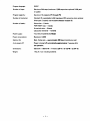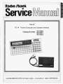
1
®
•
TRS-80
PC-4
®
Pocket Computer and Cassette Interface
26-3650
Catalog Number:
26-3651
26-3653
CUSTOM MANUFACTURED FOR RADIO SHACK, ADIVISION OF TANDY CORPORATION
1. SPECIFfCATlONS
Keyboard
ON
IACI
layout
<
INS
~ ~ [ZJ
P7
P8
P9
y
P4
P5
P6
~
P1
P2
P3
L
CD[TI00
./
..
#
$
TO
STEP
(
)
?
:
;
,
~~qJCPqJqJ~CP~q;J
GOSUB FOA
o
IT] [[]
NEXT ~
m [[]
006
X
IF
L!:!J [1]
..;-
~
..
THEN PRINT
m
•
IT] ~Nsl
•
000G
[DITJQ]0
PO
[Q]
t
D I
EXE
Display
.fbisp• ., tube: AC-61255
Display method:
5 X 7 dot matrix I iquid crystal
11 columns (alphanumeric characters and symbols)
Display capacity:
Fundamental calculation
functions:
Negative numbers, exponentials, parenthetical addition, subtraction,
multiplication and division (with priority sequence judgement
function (true algebraic logic)
Built-in functions:
Trigonometric/inverse trigonometric functions (angular units-degree/
radian/gradient), logarithmic/exponential functions, square root,
powers, conversion to integer, deletion of integer portion, absolute
value, symbolization, designation of number of effective positions,
designation of number of decimal positions, random numbers,
Commands:
1f
INPUT, PRINT, GOTO, FOR·NEXT, IF-THEN, GOSUB, RETURN,
STOP, END, RUN, LIST, LIST A, MODE, SET, VAC, CLEAR,
CLEAR A, DEFM, SAVE, SAVE A, LOAD, LOAD A, PUT, GET,
VER
Program functions:
KEYiCSR,LEN,MID,VAL
Calculation range:
±1 X 10-99 to ±9.999999999 X 1099 and 0
(internal calculation uses 12 mantissa positions)
Program system:
Stored system
-1-
Program language:
BASIC
Number of steps:
Maximum 544 steps (maximum 1,568 steps when optional RAM pack
is loaded)
Program capacity:
Maximum 10 programs (PO through P9)
Number of memories:
Standard 26, expandable to 94 (maximum 222 memories when optional
RAM pack is loaded) and exclusive character variable ($)
Number of stacks:
Subroutine - 8 levels
FOR-NEXT loop - 4 levels
Numerical value - 6 levels
Calculation elements - 12 levels
Power supply:
Two lithium batteries (CR2032)
Power consumption:
Maximum 0.02W
Battery life:
Main frame only - approxima1e1y 360 hours (continuous use)
Auto power-off:
Power is turned off automaticallyepproximately 1 minutes after
last operation.
Dimensions:
9.8mmH X 165mmW X 11mmO (318"H X 6-112"W X 2·3/4"0)
Weight:
116g (4.1 oz) including batteries
-2-
2. BLOCK DIAGRAM
LCD
AC61225
~>
R1 - R15
A
"'T
CPU
HD61913A01
-
CE2
RAM1
HD61914
Ilop
~
~
..
01-08
,--,/
CE1
~
"
r-----
K1- K12
1-----
~
.,-
I
KEYBOARD
I
RAM2
HD61914
I"
I
L
EXPANSION RAM MODULE
LCD:
12-digit dot-matrix display. A character or a number is displayed in
5 X 7 dots.
CPU:
CMOS VLSI one-chip microprocessor unit.
RAM: . Stores data and program. Each RAM has 1K bytes (8K bits) capacity
and contains self-control circuit.
-
3 -
-,
I
I
I
I
I
I
I
I
!
3. CPU (Central Processing Unit) HD61913
3-1.
Features
o
CMOS one-chip CPU
o
Built-in ROM: 100864 bits
o
Built-in RAM: 1896 bits
o
Built-in display driver
o
Memory backup function
o
Clock: 400 kHz
Internal machine cycle: 200 kHz
Minimum instruction execute time: lOpS
3-2.
CPU Block Diagram
Control signals
11
ROM
(System
Program)
)
Instruction
Decoder
-"-
-v""
>-
_.
00
~
- . III
< 'tl
CD
~
Ql
-<
RAM/ROM
Address
Control
r
/
Internal Bus
aI
..
----"..
./
i
(')
0
...
:;,
2-
·vl,
•"\./ ?
Keyboard
Control
ALU
.(
~
~
I,
Keyboard Signals
-
4 -
0
3-3.
CPU Signal Descriptions
Signal Name
In/Out
Function
1-4
01- 08
In/Out
Data bus. Also designates RAM address while
signal OP is HIGH.
S
INT
6- 18
KI2 - Kl
In/Out
Key input/output signals.
19
SW
In
Power switch input signal.
20- 24
VS- Vl
In
LCD drive voltages. These voltages are
generated by connecting external resistors to
VDD2.
25, 26
050, 051
In/Out
By connecting 56 kohm external resistance
between these terminals, clock pulse is internally generated.
27 - 72
R1S - R7
Out
LCD display signals.
73
GND
In
o (zero) volt power source.
74, 75
CE1, CE2
Out
Chip enable signals. CEl selects RAM 1 at
HIGH level while CE2 designates RAM 2 at
HIGH level.
76
VDDl
In
-5.5V input.
77
VDD2
Out
-5.SV output from the LSI.
Stays -S.5V at power ON. Goes to OV at
power-off) or APO (Auto Power-Off).
78, 79
4>1, 4>2
Out
Clock pulses.
80
OP
Out
When the signal is HIGH, the data bus becomes
address bus for RAMs and also becomes the
command code for the optional cassette tape
interface.
Pin No.
Not used.
-
5 -
4.
RAM (Random Access Memory)
HD61914 is 1K byte RAM and contains self-control circuits.
The following shows a memory map of RAM 1 and RAM 2 (optional RAM pack).
000
System Memory
t - - - - - - - - - - - - - - - - - - i 21F
220
RAM 1
User's Area
7FF
t - - - - - - - - - - - - - - - - - - i 800
RAM2
User's Area
I--.-------------~
Note: The above 8ddr. . . . for
C8I8I
FF F
when one word is 4 bits.
-6-
5. SERVICING
5-1.
Disassembly
1.
2.
3.
4.
5.
6.
-
7 -
Remove two screws from the back.
Lift and slide down the lower case.
Remove the battery cover.
Extract batteries.
Remove eight screws from the guide plate.
Remove the guide plate.
5-2.
Trouble shooting
Note: Numbers in CAUSE column denote order of possibility.
A. Display
LSI's to function: CPU, RAM 1
OPERATION
TROUBLE
Turn the power switch on.
Push the ALL RESET
button on the back of the
computer.
I_RUN_
CAUSE
I
DEG
_ _
1. RAM 1
2. CPU
Dot display cannot be shown.
No display at all or unusual indication.
.:.... :
"
! e" t
RUN
..
DEG
.
:•••1:'" ~ 't' ,
: it•••• :
CPU
1. CPU
2. LCD
. .. .
:.... i:'!
i ·...·
3. Heat seal
Some dots cannot be displayed.
B. Key Entry
LSI's to function:
CPU
Key input operation, Displaying.
RAM 1
Storing entered numbers or characters.
TROUBLE
CAUSE
t. CPU
No entry at all.
2. Wiring between CPU and keyboard.
Cursor moves, but entered number or character
cannot be displayed.
RAM 1
2. CPU
3. Wiring between CPU and RAM 1.
Only characters can be entered
1. CPU
1.
2. Wiring between CPU and keyboard.
-
8 -
C. RAM 1
(1)
Remove optional RAM module if equipped.
(2)
Push the ALL RESET button on the bottom.
(3)
Operate DEFM 62!EXEI.
Write the following program.
(4)
10 FOR I
20 A (I)
=
1 TO 87
= I
30 PRINT A (I)
40 NEXT I
50 PRINT "RAM OK"
60 END
(5)
After writing the above program, confirm that the remaining program step is O.
(6)
Execute the program and confirm the display counts up from 1 to 87 and shows RAM
OK by every depression of the [t~]key.
If the above operations cannot be made, RAM 1 may be faulty.
D. RAM2 (Optional RAM module)
(1)
Install the RAM module in a PC-4.
(2)
Push the ALL RESET button on the bottom.
(3)
Operate MODE] 1 and confirm that the remaining program step is 1568.
I
If the display shows the remaining step as 544
.
(a)
RAM 2 is not functioning.
(b)
Wiring between CPU and RAM 2 has failed.
(4)
Operate. DEFM 190 IEXEI and confirm the display ***VAR:216.
(5)
Write the following program.
10 FOR I = 1 TO 215
20 A (I)
=
I
30 PRINT A (I)
40 NEXT I
50 PRINT "MODULE OK"
(6)
Execute the program and confirm the display counts up from 1 to 215 and shows
MODULE OK by every depression of!EXElkey.
If the above program is not performed, the RAM2 (optional RAM module) may be at. fault.
-
9 -
E. Discrimination Between CPU and RAM 1
If a test unit passes the preceding checking procedures and a problem still exists,
follow the calculations.
(1)
Manual Calculations Below
Perform the following calculations manually.
1 + 2)1: (3 + 4)1: (5 + 6)1: (7 + 8)))
Correct answer
767.
(In DEG mode)
(TAN(COS(SIN(LOG 100) ))) IEXEI
Correct answer
0.0174550616
If the above calculations cannot be made, the CPU may be faulty.
(2)
Program
Execute the following program after pushing the ALL RESET button on the bottom.
10 FOR I
FOR L
= 1 TO 2 : FOR J = 1 TO 2 : FOR K = 1 TO 2:
=
1 TO 2
20 NEXT L : NEXT K : NEXT J : NEXT
30 GOSUB 40
PRINT "END" : END
40 GOSUB 50
RETURN
50 GOSUB 60
RETURN
60 GOSUB 70
RETURN
70 GOSUB 80
RETURN
80 GOSUB 90
RETURN
90 GOSUB 100
RETURN
100 GOSUB 110
RETURN
After execution of this program,
display should show END.
110 RETURN
If the above manual calculations (1) are done but the program (2) cannot be executed,
RAM 1 may be faulty.
-10-
5-3.
Program
No.
Test Program
Line
Program
No.
PO
VAC
10
--- - ._-_. ----- - - - - _ .. - - - - - FOR 1=1 TO 2: FOR J =2 TO 3: FORK = 3 TO 4: FOR
L = 6 TO 4 STEP -1
20
1---
------_ .. -
.. ' - - - ' - - . ' - - - '
NEXT L: NEXT K : NEXT J : NEXT I
- - _ .. _ - - _ . .---_. . _ - - - - .. _ _._.40
GOSUB 50: PRINT
"TEST
1 OK": END
._-_
.. . _ - - - _ .. _ - ._--- - GOSUB 60: RETURN
50
.
.
----."
--- ------t---GOSUB 70: RETURN
60
f - - - - .. t - - - .
70
GOSUB 80: RETURN _______ ._______
30
__
80
GOSUB 9O:_RETUR~ _____
. ___ ._ _ _ _ _ _ _ _ _ _ _ _ . _
90
GOSUB #1: RETURN
t - - -..
c--. -.
20
IF "AB" = "AB" THEN
10
.. _ f------ t - - - - - - - - GOTO 1
15
Pl
30
IF "AB"
35
GOTO 1
> "A" THEN 40
40
IF "12""; "AB"; IF "AB"
45
GOTO 1
50
IF -123;' 123; IF 123
r-'-'---"
~-'-
IF -1234
60
70
> "12" THEN 50
THEN-1- - - _...
< .-123
_-_.
> -123 THEN 1
IF -123"; -1234 THEN 1
.. - - - - ... ...._-_.
IF 123 ~ 456 THEN 1
80
t---90
'--.- .
__.-
P4
20
C= C+ 12345:1: 12345/234/345+ SOR 0+ SQR 2+ SOR -30+ ---SIN 30t 2
-
30
FOR H= -5 TO 4: D= D+ RND (5544.4455, H) : NEXT H
40
A-l: E=A (A (A (A (A (A (AI) I ) ) )
50
GOSUB #3
.
_--_ ... _--_....
P9
Notes:
-_
.
..
60
RETURN
10
X= 123 : 0$= "H&J" : $= 0$+"="
..
20
$=MID (1, 3) + MID (4) + "ABC"
30
GOTO #4
-.- - ---
----
10
IF I+J+ K+ L'" 15 THEN 1
20
IF A+B+ E+ X- 125 THEN 30
-----_.
GOTO ER
25
P5
- - - _.. -
10
r----'
._---
--
IF 456 = 123 THEN 1
" ' - '
Note 2
.-
.. _ - - -
- _ . ... - - - -
--'-'
No.. ,
P3
..
-------..
GOSU8 #2 : RETURN
- - -.... .. - _ . _ - - - - - - _ . - - - IF RND (SIN 195 + COS 234+ TAN lE-3+ EXP 1+ LOG 163,
-5) ;' 4.0839 THEN 1
100
__.
-
- - - r---'---"--
I-
.
--_..- -
_.
'-
IF "A" < "AB" THEN 30
GOTO 1
25
f--P2
-
. _ - - - - - - - . - - .• -_.__ ..... - - - .. -----_.-
t---.
20
.-
r -.-..- ....- -
30
IF $","H&J=ABC" THEN 1
40
IF RND (C, -5) .. 1894.4034 THEN 1
50
IF RND (D, 21 * 55000 THEN 1
50
GOTO #5
10
GOTO 20 _._-
15
RETURN
20
GOTO 15
_.
--
10
FOR A = 1 TO 201 : A (A) = A + 9999999000: NEXT A
20
$ = "ABCDEFGHIJKLMNOPORSTUVWXYZ:I: + 1-"
30
FOR A=l TO 201: IF A (A) *9999999000+ A THEN ER
40
NEXT A: IF
THEN ER
50
PRINT "TEST OK! "
$* "ABCDEFGHIJKLMNOPORSTUVWXYZ:I:+I-"
_.-
1. P2 line 10 cannot be fully ent.ed if you use
8
one-key command (e.g. 1SHI FT I~for
I F). Th.efore, enter the program manually without spaces.
2. P3 line 10; "&" can be entered by ...
(8) !MODEI
(c) Press tne
c::::J
(EXT mode set)
"u" key
(b) press the ISHIFTI (the red S) key
(d) IMODEI
-
c::::J
11-
(EXT mode reset)
Testing Procedure
Save the test program on a cassette tape through a cassette tape interface unit by the
operation SAVE A !EXEI.
(1) Install a RAM module into the test unit ( PC- 4 L
(2) Push the ALL RESET button on the bottom of the test unit.
(3) Connect the PC - 4 to a cassette tape interface and a tape
recorder which contains a test program cassette tape.
(4) Load the test program from the cassette tape by the operation LOAD A IEXEI.
(5)
After loading the Program change the PC- 4 to WR ITE mode by the operation
MOD Ell and confirm that the remaining program step is 789.
(6) Operate IMODEI 0 (RUN mode selection).
(7) Execute PO (Program numberO).
(8) Confirm the display "TEST 1 OK".
(9) Clear the programs PO to P5.
Example to clear P2 ...
(a) SH IFT I 2 (P2 designation).
(b) IMODEI 1 (WRITE mode selection).
(c) CLEAR IEXE! (erasing P2).
I
I
Note:
ISHIFTI is the red S button.
(10) Change the PC-4 to RUN mode by IMODEI 0 [fX]].
(11) Operate DEFM 1761EXEI.
(12) Execute P9.
Confirm the display 'TEST OK! "
- 12-
6. PROGRAM COMMAND LIST
C..ssification
Input
statement
Output
statement
Command
Name
Format
Function
INPUT
INPUT variable string
KEY
Character variable
PRINT
= KEY
PR INT output control
function
output
CSR
Causes data to be entered from the keyboard during execution of a program.
The program execution is stopped until
after the end of input.
f}
Reads a character entered duringexecution of a program and assigns it to a
character variable.
Since the program is not stopped by this
command, nothing is assigned to the
character variable if no key entry is made.
Outputs the designated output element.
ele~nt ({} .. .J
CSR n{} (0
~ n ~ 11)
Displays from the designated nth
position.
-
Branching
GOTO {line no. }
variable
IF ...
IF comparison expression
{TH;EN}. ..
GOSUB
Looping
Causes control to jump to the designated
line number.
GOTO
J
{THEN line no.
; command
GOSUB
~inenoJ
variable
Causes control to jump to the line
number following THEN, or executes
the command following" ;", if the
result of the comparison is true.
Causes control 10 proceed to the next
line number if the result of the comparison is false.
Calls out the subroutine of the designated line number for execution. After
the subroutine is executed, control
returns to the GOSUB statement by the
RETU RN statement to proceed to the
command following that statement.
RETURN
RETURN
Signifies the end of a subroutine;
returns control to the command/statement/
function next to the GOSUB statement.
FOR
FOR v =e1 TO e2 [STEP e31
*v denotes a numerical
variable, and e1, e2 and e3
represent a numerical expression respectively.
Declares the beginning of a loop in
which numerical value v changes from
initial value elto terminal value e2 in
increments of e3. The loop is repeated
"e2 - e1
"
--+1
times
e3
between the FOR and NEXT statements.
If the increment e3 is omitted, e3 is
regarded as "1".
NEXT
NEXT v
Signifies the end of a FOR loop.
If the result of v plus e3 is equal to or
smaller than e2, the loop is repeated
again. If it is greater than e2, control
proceeds to the line next to the NEXT
statement.
-13-
Execution stop
STOP
STOP
Stops the execution of a program temporarily to bring the system into a keyin wait state. The execution can be
continued by pressing the EXE key.
I
Execution end
END
END
I
Signifies the end of a program; the
system returns to its pre-execution
state. The execution of a program, once
ended, cannot be continued even if the
key is pressed.
It@
.
Data clearing
VAC
VAC
Clears all variable data for a program.
Program listing
LIST
LIST [line no.)
Displays a listing of all the statements in
a program from the designated line
number downward .
All program
listing
LIST A
LIST A
Displays a listing of the statements in all
programs.
Program
execution
RUN
RUN [line no.l
Causes a program to start from the
designated line number.
Program
erasing
CLEAR
CLEAR
Clears the currently designated program
area of a program.
CLEAR A
CLEAR A
Clears all the programs.
.
.
Angular unit
designation
MODE
Format
designation
SET
MODE
m
SETU~}
Designates trigonometric angular units as
degree (4), radian (5) or gradient (6).
(O~n ~9)
Designates the number of effective
positions or number of decimal positions
for the displayed numerical value.
,.,
Character
function
LEN
LEN (character variable)
MID
MID (m Ln))
Extracts n characters from the mth
character in the exclusive character
variable (S).
VAL
VAL (character variable)
Converts the numbers in a character
variable to a numerical value.
SAVE
SAVE ["filename")
LOAD
LOAD ["filename")
Calls out the program from the tape and
loads it to the currently designated
program area.
SAVE A
SAVE A ["filename")
Records the programs in all program
areas on tape at the same time.
LOAD A
LOAD A ["filename")
Calls out all programs from the tape and
loads them to the respective program
areas.
PUT
PUT ["filename")
variable
Records the data in the variable on tape.
GET
GET ["filename") variable
Calls out the data from the tape and
loads it in the variable.
VER
VER ["filename")
Checks to confirm that the programs
or data have been recorded on the tape
properly.
. - - - _ •. -
Calculates the size of the character
variable.
...
..
.-._---,
. ,.
Option use
..
- 14-
Records only the program in the
currently designated program area on
tape.
..
7. ERROR MESSAGE LIST
Error Code
Meaning
Cause
Corrective Measure
1 - - - - - + - - - - - - - - - - - + - - - - - - - - - - - - ------+-----------~
Memory overflow or
system stack overflow
• Program cannot be written due to
insufficient number of steps or
memory cannot be expanded.
• Stack overflow due to a complicated
calculation formula.
2
Syntax error
• A mistake has been made in writing
the program, etc.
• Clear unnecessary programs or
reduce the number of memories.
• Divide and simplify the numerical expression.
• Correct the error in the input
program, etc.
• The left side format is different from
the right side format in a substitution
statement. etc.
3
Mathematical error
• The calculation result of a numerical
expression is 10 100 or greater.
• Correct the calculation formula
or data.
• Outside the input range of a numerical
function.
• Verify the data.
• The result is indefinite or impossible.
4
Undefined line
number error
6
Variable error
• No designated line number for a
• Correct the designated line
GOTO statement or a GOSUB
number.
statement.
1--------1----------------- - - - - - - - - - - - - - - - - - - f - - - ----Argument error
• Correct the argument-error.
• For a command or function that
5
requires an argument. the argument is
outside the input range.
-------- - - - -
---1-- ----- -----
• Attempt was made to use a memory
which has not been expanded.
---------1
• Expand the memory properly.
• Do not use the same memory
• Attempt was made to use the same
for a numerical variable and a
memory for a numerical variable and
character variable at the same
a character variable at the same time.
time.
1 - - - - - - - - + - - - - - - - - - - - + - - - - - - - - - - - - - - - - - - - - - - f - - - - - - - - ----------~
Nesting error
7
• A RETURN statement appears other
• Remove the unnecessary
than during subroutine execution.
RETURN statement or NEXT
statement.
• A NEXT statement appears other than
during a FOR loop or the variable of
• Reduce the subroutines or
FOR-NEXT loops to within
the NEXT statement is different from
that of the FOR statement.
the maximum levels.
• Subroutine nesting exceeds 8 levels.
• FOR loop nesting exceeds 4 levels.
1-------+-----------+-----------------1-------------------1
Option error
9
• Execution is performed in the PRT
• Connect a printer or tape
mode, or an option command such as
SAVE is executed when no printer or
tape recorder is connected.
- 15-
recorder.
Release the PRT mode.
II. CASSETIE INTERFACE (26-3651)
1. SPECIFICATIONS
Output terminal:
White mini-plug, output impedance: approx. 40 kohms,
output level: 3 - 50mV
Input terminal:
Black mini-plug, input impedance: approx. 20 kohms,
input level: 2.5 - 5OV.
Remote control terminal:
Gray sub mini-plug, 24V, lA or less.
Data recording format:
Kansas City standards (JOOBPS).
Power source:
(For remote control) Two AA size dry batteries.
Power consumption:
0.3W.
Battery life
Approx. 7 hours.
(for continuous operation):
Dimensions:
173mmW X 114mmD X 31.5mmH.
2. BLOCK DIAGRAM
04
...
r
~
~
p
()
Q.
...
l:
...Sl
~
I
I
III
I
)
EAR
4>1
OP
...0
0
::;
SHAPING
CIRCUIT
Ql
-l
III
&>
H043110
CE2
Q.
E
MIC
'"~
8
c;;
)
LSI
;:,
Co
I
CIRCUIT
VD03
Ql
<oJ
E
I
FILTER
-l
III
i
::tl
III
...
...
REMOTE
CONTROL
CIRCUIT
u.
GNO
LSI:
CRYSTAL
OSCILLATOR
8...
Co
I
I
)
REMOTE
Kansas City standards applied cassette tape
interface LSI.
Transfers serial data by the following frequenci es.
Data "1" ..... 2,340 Hz
Data "0" ..... 1,170 Hz
Filter Circuit: Converts LSI's data pulse into AC
waveform for tape recorder.
Shaping Circuit: Converts AC waveform data from tape
recorder into square pulse for the LSI.
-16-
...
III
I
3.
LSI (HD43110)
HD43110 is a cassette tape interface LSI with Kansas City standards which transfers data between
the CPU and cassette tape recorder.
Data "0" and "1" are transferred in serial as 1,170 Hz and 2,340 Hz frequency pulse respectively.
Data is transferred at 300 bits per second.
The following lists the functions of each terminal of the LSI.
Pin No.
2
Signal Name
OSC
In/Out
Function
Clock pulse (32,768Hz) input.
In
- - - - ---_.-
7
VDD'
Out
8
CONT
In
-3Voutput.
The LSI functions only when'
the terminal is HIGH .
. _-.-
VDD1
In
-3V input.
10
CE
In
Chip enable terminal. The LSI
is designated from PC- 4 when
the terminal is HIGH.
11
SP
In
Strobe pulse input from PC-4.
13
04
14
GND
In
OV input terminal.
17
C3
In
Data input from cassette tape.
18
C2
Out
Data output to cassette tape.
19
C1
Out
Remote control (auto stop)
signal output.
9
In/Out
- 17-
Serial data input/output.
4. CIRCUMFERENCE CIRCUITS
4-1.
Clock Pulse Generator
32,768 Hz signal is generated by the crystal oscillator and is shaped by the inverters.
®
o
4-2.
©
Remote Control Circuit
LSI
C1
Q2
Q1
-3V
When signal C1 is HIGH, transistors Q1 and Q2 turn on causing relay RY to be
switched on so that the REMOTE terminal becomes active.
4-3.
Shaping Circuit and Filter
LSI
MIC
C2
C3 1+-----1-----,.AII!'----.--+-fl--I-~--r>tN-;;_---t.--..J
11
12
L..-
~
I--f---'
~
' - - -_ _-L-_Y-_--L.
---->,------'~
-3V
CD
-18-
EAR
Filter waveforms
approx.
1.2kHz
~
~
~
'""--
~
approx. 2.4 kHz
-3V
@
®
-3V
A
J
"
~
Af\/\{\(\f\!\/
\J\7~
V\TVV V \T -3V
Data output C2 from the LSI is integrated (waveform @) and shaped into an AC
waveform (waveform ® ) by capacitor cl and resistor rl.
~
A
/\ /\J\ .
"V VVVV
OV
®
OV
@
-3V
Input signal from tape recorder
and r3 (waveform @).
The waveform
CD
is integrated by capacitor c2 and resistors r2
® is cramped between -3V and OV by diodes dl
- 19-
and d2.
5. SERVICING
5-1.
Disassembly
~ ~\ j
(o)
1.
Remove s'
2. 0
IX scre~ f,
Pen the lOWer S rom the back
case.
- 20_
.
-)
5-2.
Troubleshooting
TROUBLE
CHECK POINT
SOLUTION
-----
SAVE impossible
Open circuit of jack cable.
Replace jack cable.
Check the LSI terminal signals.
If signals are normal, replace
the LSI.
-
Head of the cassette tape.
Clean the head.
- - _... _ - - - - - - _ . _ - - -
LOAD impossible
Output level of tape recorder.
Turn the volume control to max.
Check to see if there is an open
Replace jack cable.
circuit in jack cable.
---_.
Does the tape recorder function
Test the cassette recorder with
properly?
a tape of music.
Clock pulse.
Replace crystal oscillator.
Signal C3 of the LSI.
Shaping circuit.
If C3 is normal, replace the LSI.
Remote control
Click sound of the relay at
If click cannot be heard, check
impossible
saving or loading.
signal C1 of the LSI.
If signal C1 is not output from
the LSI, replace the LSI.
If C1 is normal, remote control
circuit may be faulty.
Check to see if there is no open
Replace jack cable.
circuit in jack cable.
No function at all
Clock pulse.
Crystal oscillator.
Is PC-4 properly
Connect correctly.
connected?
------
Poor contact of connector.
Replace connector.
Clock pulse.
Crystal oscillator.
- 21-
1V SCHEMATIC DIAGRAM
1.26-3650
r---------- K II
.--------,--------------1H~-----KIO
R15, EXT FI F2RUNWRTDEGGRARADTR
,...----------'------+-H------K 9
..-----------------11_+-+ - - - - - K 8
.--------------+-H--+ - - - - - K7
.--------~----I_+-++-+--1~---
R8
R9
RIO
RII
RI2
RI3
RI4
K6
r----....,-------+-+-+-+-t-t.....- - - K 5
...-----------1-+-++-+-H--.-- K 4
,----------t-t--+-+-++-t-t--.-- K 3
,...--------+-H--+-+-+-+-t-tf-- K 2
.--------,,==;,....---~++-t-t--+-+-++-+--
~~i~r~::;~=++t~~=tttr-CL:f]]
J:
>
--
K1
K 12
-_
1
~
0::
V'"_
PO V'" _ : - -
o
.
+ >
-:s;
41
a>
d5-~:-<Id5
C.Q.
U-.;J
~
!2
~
_ Q
24
oOVI ~2~:--V I
V2 .2:
V2
V3.
V3
V4 2
V4
V5 .~~
V5
SW
SW
K ,;~
KI
K2
K2
K3 -:~
K3
K4 -14
K4
K5
K5
K6:~
K6
K7
K7
11
K8
K8
K9
K9
KIO 9
KIO
KII 8
KII
KI2 7
KI2
c5
42 c5
b5
43 b5
05
44 05
e4
45 e4
d4
46 d4
c4
47 c4
b4
48 b4
04
04
HD 61913
e3
51 e3
(HM-49)
d3
d3
c3
52 c3
b3
53 b3
03
54 03
e2
55 e2
d2
56 d 2
c2
57 C 2
b2
58 b 2
02
59 02
KM...,6~-60
5
e I
6I eI
I NT...,::...-------.l----~....
T GNO
d I
62 d I D81-.:::4; . - -_ _--,
c I
63 C I
04 ...-=3"'--_ _---.
bibI
0 2....,,2'-_---,
a I
64 a I O N _ 0 ~
0 I ....!..ol- - - ,
(DIl)V...,N-O .... z~~Oo-N~
~~~~~
~
02
_-
nG
?
IH.GC
w.
,RA
IN
o
y
P
A
,
0
CEI
GNO
Q)
II
;:,
"'0 12,RAM
o
OP
E
01
02
~
03
«
0::
04
--
)-----<
-
oc:::
->---
-
.2
co
VOOI
V003
2,RAM~
I
1
1
I
~
I
v
I
1
I
z~ 35V 4.7jJ
most significant digit.
RI5
I bit = I/fop
I
-Ol1ltOl'--(DIl)","...,NN
g~~o~~~~o~~ "-
:~"'-
2Q.
2L
2~
NC
NC
NC
NC
NC
NC
NC
NC
NC
NC
~ ~
x
RI
RI
R2
R3
R4
R!5
R6
NC ~4
NC ~~
NC .:>:2
NC ~ I
HD61914
NC .10
(HM-S-OS)
NC ~9
NC
NC..>!'
NC ~6
NC ~5
","I") N _ NC ~4
C)
o~
;;-
Q)
(,)
.E
.!
Cl::
o u v ..., N 0 > > > >
_.J=.j...J ...J .j
CDCD CD CD
IL -
r<:llv Il) (D I'-- to 111 0 - N ...,
NNNNNNN""""""""
'---"Nt-.........
loon
-N
00
00
»
:~
L:
Q)
RI3
I
RI4
1
CIl
CIl
0
{!.
I
03
m-I),--_ru,r:
Li
:
,,
I
d6
b6
V4
V5
lie:
0
~
EVL- AHAA OOBC5
002
,,
,
,,,
,
V3
ci
l8
~h
i
flJ
I
.5
V2
.=oX .
x
lie:
~ ~~
Z
Il)
U
:ru
R4
c6
~Il)
U~---- ~r~~
r---Ul'--.. . .flJ
~
VI
>
N
_I
R3
e6
06
I-~
--Ln
:
I
04
I
O.ljJ 15V
V003
GNO
1=
~2;
~-m
fcp=200kHz.!.30% R2
(,)
01
02
1536bit
~----~
RO
-
+
I
I
'::L
11
IOOOF1
2!5VI
GNO
- 22-
iR V003
x
x
I
1
1
12.
I§.
II..
-
~>",
;39011
I
I,:~
_
r-
Q)
I~ INT
=~ ~~
t--------'='""':'[~~
IE
~
_o)---<--+-..
I RESET I
•••••
•••••
•.••••
•••••
•••••
•••••
(LSD)
Waveform tor dispiayino a 0 on the
+-
I
{!.
on the bottom
:;: a
Cl::Cl::Cl::Cl::Cl::Cl::Cl::Cl::
M' ~
th ~
I
Illl
GNO
I
VOOI
Q
CE2
OP
.8"2
.8"1
GNO
O.ljJ 15"
220K
(D1l)'<t...,N-O ....
-
J
•••••
•••••
•••••
•••••
•••••
•••••
R7
RO
:,0:
to 11110
I'-- 1'--1 to
19
CE
·rvHt-+-+-I-+----+-+-+-+-H~=---.:.;::.p.
1M
•••••
•••••
•••••
•••••
•••••
•••••
•••••
AC61225
Cl::Cl::Cl::Cl::Cl::Cl::Cl::Cl::~OO»~~O~
F
•••••
•••••
•••••
•••••
•••••
•••••
1f/-~!I~(f~ PRTSTOP
•••••
111 lJ) ~ -0
a>Cl::Cl::Cl::Cl::Cl::Cl::Cl::Cl::CJ'Pl
Il) (D .... r511 m0 - N ..., VIl) (D
(D (D (D (D (D ........ I'-- I'-- I'-- 1'--, ~
V
•••••
IMSO)
Il) (D (D (D (D (D
;6
l:L:3J -o--I--+-+-...
•••••
10
~
4~
TC30HOOOF
J9J<_....
p=..-=-t :X>"S:........_K2RAM
NAND - TC30HOOF
INVERTER-TC3OHOO4F
7Pln-VOOI
14PIn-GNO
Lr
l
--
2.
26-3661
~__
po. WER S.W
.>-----Ir....::;O.,.=~'
To optional
character printer
v
<.'.>
Cl.
...
CD
:;
a.
E
o
o
o
c
o
r
L. -
-
-
-
"
-10
T
-l
YPI
X
(!)
....
N
...'"
1«I
...
~
Ground for
~
F50V
I
I
- -l
I/
_
:IE
..
(!)
m
N
II..
'"
..,.on
II..
~
l<:
01
t'I
~
o
U
m
a.
I
~?:2:U-
0~
I
i
N
CD
eE
~
...
-=-_---<._---<.. . sta tiC, eIectriC' 't Y
$
i
llillUillU
2
AA
~
~""II..-~gg~t'I-t'l1O
FBR[21
C0003-M
<>---tIl
O-L-
~:Of~fo
t'I
10
'
o
REMOTE
o
>
u..
~
..:
.........
.....
ISI588x2
~
I
T
GRAY
Q.
0
0
on
-
68K
*~
!!l
...
,
on
.6
N
VD03'~~f~
t!!!
+
IGNOI
22}JF,IOV
~ l>
~ ~~
T
l<:
...
+u
I
MIC
-I
l<:
4.71<
~
!!!
..
WHITE
12.
ta T§
~
I
c:: l
01
....
0
... I
22K
.H
EAR
(F:l
8lACK
IV. PRINTED CIRCUIT BOARD
I~
•
I•
o~
26-3650
26-3651
26-3653
- 24-
Exploded View
26-3650
@
~-----~~
~--@
@_ _I9
@----@
---~-~
®
(j)
®
- 25-
VI.
PARTS LIST
1.
26-3850
Description
Ref.
RS Location
LSI, HD61913 (CPU)
Menufllcturer
Part Number
20013583
LSI, HD61914 (RAM)
20013516
----
MOS IC, TC40HOOOF
21003956
MOS IC, TC40H004F
21003964
..
Diode,1S1588
23003031
....
Rotary volume EVl-AHAAOO8C& f'l60Kohnil .
2n09150
Resistor, Chip ERJ-8GCSJ391·(3I8ohm, ±5%, 118W)
27909051
Resistor, Chip RC315B10K-I (10Kohm, ±5%, 1/SW)
27908196
Resistor, Chip RC315B220K-I (2OOKohm, ±5%, 1/8W)
27908071
Resistor, Chip RC315B65K-G (68Kohm, ±2%,118W)
27908561
Resistor, Chip ERJ-8GCSJ225 (2,200 Kohm, ±5%, 1/SW)
27909485
Capacitor, Chip CM21YV103P15V (0.1 J1. F, 15V, ±20%)
71032167
_..
Capacitor, Chip C3225COG1H222K
(2,2OOpF, 50V, +10%)
28907407
Capacitor, Chip CM21CH102K25V
(1,OOOpF, 25V, +10%)
28907415
Resistor, Chip ERJ-8GCSK101
(1 Kohm, 1/SW, ±5%)
27909019
Resistor, Carbon Film ERD10T~
(33Kohm, 1/tOW, +5%)
26116473
Battery, Rithium, CR-2032TRBULK
38001329
Resistor, Chip ERJ-8GCSJ563 (56Kohm, 118W, +5%)
27909400
Capacitor, Electrolytic SRA35VB-4R7
(4.7 J1. F, 35V, +10%)
28014082
- 26-
Description
Ref.
RS Location
Capacitor. Electrolytic SRA16V8-10
(10/-l F. 16V. +10%)
Manufacturer
Part Number·
28014040
--_. -
LCD. LO-B8105A
33306768
-
Connector 1260-019-12804
35113639
Seal. TH heat TH-07-1
56004397
._-_.
1
Plate. Reinforcement G420 A35393-1
63327140
Tape. LCD Adhesive G1108 A44636-1
63275120
Plate. Heat Seal Insulation A-G420 A45916A-1
-
Plate. Heat Seal Insulation 8-G420 A45916A-2
63327161
Spring, P G195 A33138A-1
63248131
2
Holder. PCB A18200-2
63345174
3
Spring, Battery A-G272 A33938A-1
63297621
4
Spring, Battery 8-G272 A33939-1
63297630
5
Spring, Battery C-G272 A33940-1
63297640
6
Plate. Bettery Insulation G272 A45154-1
63297660
Cushion Battery G1OO2 A46287-1
63336860
7
Holder. Bettery G420 A45884-1
63327190
8
Plate. Insulation 8-G420 A45918-2
63339490
Plate. Insulation A-G420. A45921A-1
63327171
Plate. Insulation E-G420A A46326-2
63339970
Plate. Insulation F-G420 A46327-1
63339980
Panel. Lower G1002R A35387A-3 (Canada. USA)
63344171
Panel. Lower G1oo2T. A35387-5
(UK, Belgium. Australia)
63351940
10
Screw for Case 8-G420 A45919-1
63326880
11
Cap. Connector G420 A45915-1
63326900
9
- 27-
. - - - - - - - - - - - . - - - - - - - - - - - - - - - - - - - _ . __...
_--_.._ - - - - - - - , - - - - - - - ,
Description
Ref.
RS Location
.. _.__. _ . _ - - - ... _ - - - - - - - - + - _ . .
12
...._ - - -
Case Sub Ass'y, Upper A35384C-3
Manufacturer
Part Number
.._ - - - - /
63344183
1 - - - - - + - - - - - - - - . - - - - . - - - - - -.. -. - - . - - - - - - t...- - . - - - . - - - - .....
13
.... - - - 1
Window G420 A35388-1
f----~-+-
-
--.
.. - - - - . - - . - - - - - - - 1 - - - . - - . - -
14
Frame, Display G1002 A45881-4
15
Key Contact, Rubber A-G420 A35389-1
.._----'+-~.--
-_._-_._-
1 - - - - - - + - - - - - . -..
16
Knob, Slide G420 A35391-1
17
Spring, Switch Contact G310 A45208-1
I
Spacer, Switch G420 A46325-1
. --_.. -.---...- - - t - - - - - - - - , - - t - - - ' - ' - - - - - - - ;
18
19
Film, Common G420 A21302-1
.._.- .... _._...._...Spacer G1002 A46286-1
20
Screw, Flat C-G321 A33793-3
_._-----+--~----
..t - - - - - - -
- - - - - - - _ .. -
21
Spring, Ground, G1002R A46432-1
22
Rubber, Key Contact B-G420 A35390-1
f------+-------.
....
...-.
:::::,:::::::2:~ . u~)
Case, Soft G1002TA, A35895-1
._+-I__'---~---'-+---------'---I
I
---- + - - - - - - + - - - - - - - /
~j,----~--+-----__t
r
__
_.
--- -
!
:
P.C.B. Assembly G1002RA
~----'------------_._-
- 28-
_._-
I
2.
26-3651
Rtf. ' '.
RS Locetion
Description
PttIIrIuf8ctunr
Part Number
LSI, HD43110, Interface Drive
20009961
IC, TC4013BP, Flip-Flop, MOS
21003310
IC, TC4059BP, Inverter, MOS
21003862
Transistor, 2SA1015-Y, Remote PNP
22003534
Transistor, 2SC1815-Y, Remote NPN
22800016
Capacitor, Ceramic, 22pF 5OV, ±10% HE405JSL220K
28188191
Cal*:itor, Ceramic, 560pF, 5OV, ±10% HE408JYB561K
28180098
.-
_.-
Capacitor, Ceramic, 15OOpF, 5OV, ±10% HE405JYB152K
28180136
,--
Capacitor, Ceramic, 3300pF, 5OV, ±10% HE705JYB332K
28180152
Capacitor, Semiconductor Ceramic,
0.047 F, 5OV, ±20%, SC45F1H473Z
28127511
Resistor, Solid, 26Mohm, 1/BW,
±20%, ERC-18GM2665
27901476
-
...-
Relay, FBR211CDOO3-M
31206057
----
----
Capacitor, Electrolytic 22 F, 10V, ±10%
28040964
.
Diode, Silicon, 1S2075K21
23001021
Resistor, Carbon Film,
39Oohm, 1/4W, ±5%, R-25-390-J
26003911
Resistor, Carbon Film,
2.2Kohm, 1/4W, ±5%, R-25-2.2K-J
26005710
_.---_.
Resistor, Carbon Film,
1Kohm, 1/4W, ±5%, R-25-1K-J
26004918
Resistor, Carbon Film,
10Kohm, 1/4W, ±5%, R-25-10K-J
26007313
---_. ,_._-
-
Resistor, Carbon Film,
22Kohm, 1/4W, ±5%, R-25-22-K-J
26008115
,---------
--
Resistor, Carbon Film,
33Kohm, 1/4W, ±5%, R-25-33K-J
--------
-
26008514
.
Resistor, Carbon Film,
47Kohm,1/4W,±5%,R-25-47K-J
26008913
.. -
- 29-
Ref.
Description
RS Location
Manufacturer
Part Number
Resistor, Carbon FUm,
68Kohm, 1/4W, ±5%, R-25-68K-J
26009316
Resistor, Carbon Film,
18OKohm, 1/4W, ±5%, R-26-180K-J
26010314
Resistor, Carbon Film,
22OKohm, 1/4W, ±5%, R-25-220K-J
26010519
Resistor, Carbon Film,
330Kohm, 1/4W, ±5%,
28010918
R-25~30-K-J
Resistor, Carbon Film,
680Kohm, 1/4W, ±5%, R-25-880K-J
26011710
-
Resistor, Carbon Film,
820Kohm, 1/4W, ±5% R-25-820K-J
Crystal, Oscillator, 32,768HZ,
26016118
KF~G
71100138
Resistor, Carbon Film,
4.7Kohm, 1/4W, ±5%, R-25-4.7K-J
28008611
Resistor, Carbon Film,
1ooKohm, 1/4W, ±5%, R-25-1ooK-J
26009715
Resistor, Carbon Film,
120Kohm, 1/4W, ±5%
26009910
[Case Sub Ass'y, Upper A35413C-2J
63344334
Plate, LOGO A36263-2
63344380
Plate, Power ON/OFF, Model Name, A45887-2
63344350
Sheet, Insulation, Aluminum
63345140
Case, Upper G426 A18038-1
63329912
[Case Sub Ass'y,Lower A213158-2J
-..
_-
63344343
Case, Lower, G426R, A1804A-2
63347241
Plate, Rating. G426R, A48351-1 (USA, Canada)
63347250
Plate, Rating. G426T, A46489~
(UK, Belgium, Australia)
63351840
-
Foot, Rubber, G426, A45990-1
63329990
Plate, Ground, For Printer
63347260
Spring, Battery Contact (-) G67 A43656 1
- 30-
·60006091
-Description
Ref.
--
,.-,....
-
RS Location
Manufacturer
Part Number
_eom-t Battery (+), A-G66 A42606A-1
63452238
Spring. Battery Contact (+/-)
C-G164 A43733-1
63249297
Bolt, HEX, 6.5 X Smm
Printer Fixing
63329900
-.
-. ---
--
Nut, Hex,
10mm (Outside) X 5mm (Inside) X 3.6mm (T)
54015020
Wuher11.2mm (Outside) X 6.5mm (Inside)
XO.Smm (T)
53012735
----
Sheet, In..lation, Alminum For Lower Case
63345090
Plate, Ground, For Computer
63345100
--
Connector, 12Pin, Female
126D-019-12N04
_.
35113639
-- - - - - - - - - - - - _ . _....
-.
Connector, 12Pin, Male
126D-019-12P22
35103244
-_ ..
-
---.
.
__ .
-.-
Cord, Connection For Cassette
PLGW-1596-01 A
27009237
-
.--
..
Cover, Battery G426 A21328-1
-_._----
I
-------
63329890
-----
-
Knob, Slide, Lock-Free B-G426 A35453-1
... __ .
63329950
----
--
Knob, Slide, Power ON-DFF G426 A35452-1
---
-
63329940
- - - - - _.. _-- -- - --
._-- t--.-
---_.
.-
Capacitor, For Connector G426R A45915-1
-._---
..._ - - _ . -
63346370
------
-
f - - - - - . - - - - .-
Plate, Computer Unit LOCK-FREE
G426 A45988-1
63329960
._- ---
Plate, Slide, LOCK-FREE Knob A45987-1
63329970
---_. ----------_._------
. -I--
----.
Spring, Switch Contact A4532C-1
- _ . _ - - . ._--
62747023
.. _--
. _ - - - - - r-.
Screw, Tapping, Flate Head,
M2 X 4 (Yellow) A-G321 A44793-1
-_ .....
63282780
------.
Screw, Tapping, Flat Head,
M2 X 7 (Yellow) A-G426
63345110
---
Spring, Earth A46432-1
63345160
- 31-
Ref.
Description
Manufacturer
Part Number
RS Location
~-
Screw, Tapping, Flat Head,
>-.-
63291680
M2 X 3 (Yellow) A-G32O A44193-11
----
.. -.-
...
-
------
Screw, Tapping, Flat Head,
M2 X 4 (Black) A-G324 A33953-3
63316610
-.. _------_ .. - - - - - - - - - - - - - - - - - - - - - - c---
Screw, Tapping, Flat Head,
M2 X 6 (Black), C-G302 A44193-9
63291620
.
-----_
..
--_
....
-._-
Case, Soft, G426RA. A35688B-1 (USA, Canida)
63344412
Case, Soft, G426TA. A35891-1
(UK, Belgium, Australia)
63352220
Cap, For Connector G426 A46150-1
---
63332410
-l
- 32-
CONTENTS
I. POCKET COMPUTER
(26-3650)
& MEMORY MODULE (26-3653)
1.
SPECIFICATIONS. . . . . . . • . • . • • . . . . . . . • . . . . . . . . . . . • • • • . • . . . . . . . . . . . . . . . ..
1
2.
BLOCK DIAGRAM . . . . . . • . • . . . . . . . . . . . . . . . . . . . . . • . . . . . . • • . . . . . . . . • • . . . ..
3
3.
CPU (Central Processing Unit)
3-1
Features..... . . . . . . . . . . • • . . . . . . . . • . . . • . . . . . . . . . . . • . . • • . . . . . . . . . . ..
4
3-2
CPU Block Diagram ..••........•..•••..••........................•...
4
3-3
CPU Signal Descriptions . . . . . . . . . . . • • . . . . . . . . . . . . . . . . . . • • . . . • . • . . . . . . . .
5
4.
RAM (Random Access Memory) .•....••..••..•.••......•..•.••.•.••..••.••..
6
5.
SERVICING
5-1
Disassembly.... . . . . • • • • • • • . . . . . . . . . . • • . . . • • . . . . . . . . • • . . • . . . . . . . • •.
7
5-2
Troubleshooting
.•.•••••......•..•...•..........................••.•
8
•.. " • . . . . . . . . . . . . . . . . . . . . . . . . . . . • . . • , . . . . . . . . . • . . . .• ..
8
•.•...........•...........•..........................
8
5-3
A
Display
B
Key Entry
C
RAM1 .•......... , . . . . . . . . . . . • • . . . . . . . . . . . . . . . . . . . . , .. •. . . . . ..
9
D
RAM2 ........•.. ,
9
E
Discrimination Between CPU and RAM1
Test Program
,
, ....•. " .. " . . . . . . . . .. ..
..•..••....••.....•........•..... 10
. . . . . . . . . . . . . . . . . . . . . . . . . • . . . . . . . . . . . . • • • . . . . . . . . . . . . • 11
6.
PROGRAM COMMAND LIST . . . . . . . . . . . . . • . . . . . . . • . . . • . . . . • . . . . . . . . . . . . . . • 13
7.
ERROR MESSAGE LIST
. . . . . . . . . . . • . . . . . . . . . . . . . . . . . . . . . . • . • . . • . . . • • . . . . 15
II. CASSETTE INTERFACE (26-3651)
1.
SPECIFICATIONS •.•.......•...........................•••••• , •...•••... 16
2.
BLOCK DIAGRAM. . . . . . • . . . . . . . . . . . . . . . . . . . . . . . . . . . . • • • • • . . . . . . . . . . . • •• 16
3.
LSI (HD43110)
4.
CIRCUMFERENCE CIRCUITS
5.
...••.........•..........................••..•.••.....•• 17
4-1
Clock Pulse Generator
4-2
Remote Control Circuit
...••••..•••.••••......•..••••••• '. • • • • • • • • • • • • •• 18
4-3
Shaping Circuit and Filter .....•......•.•...................••...••••... 18
.........•...............•••••....•..•.•......• 18
SERVICING
5-1
Disassembly. • . • • . • • • • . • • . . . . • • • . • . . • . . . . • • • . • • • • • • • • • • • . . • . • . • • • •• 20
5-2
Troubleshooting
.•.•.••.••......•.........••....•••••••............. 21
III. CIRCUIT DIAGRAM
1.
2.
26-3650 • • • • • • • • • . • • . • • • • . . . . . • • • . . . • . . . • . . . . . • • • • • • • • • • • • • • • • • • • • • •• 22
23
26-3651
IV. PRINTED CIRCUIT BOARD
1.
2.
3.
26-3650 •••••••.•.....••.••..•.......•.•.......•••.......•..••••••••• 24
24
'I. '"
'"'I. '"
'I.
26-3651 '"'I •• " ••
'I
26-3653
••
'I
•••••••••
• '"'I • • • • '"'I • • • '"'I. '"'I • • •
'I.
'I
••
'"
'"
'"'I •• '"'I • • • '"
,"'I
•
,"'I.
,"'I
••••
,"'I.
'"
'I
•••
,"'I
'I
•••
'"'I • • '" • • '" '" '" • '"
'I.
'I.
'"
'"
'I
••••
•
'I
'"
••••
25
VI. PARTS LIST
1.
26-3650 .. , .•..•.....••.••..•.......•.•....•....... , .•••••••••••••••• 26
2.
26-3651
29