1
United States Patent [19]
van Bavel et a1.
[54]
Patent Number:
Re. 31,864
[45] Reissued ‘Date of Patent:
Apr. 9, 1985
[11] E
‘
v
SELF-TEST FEATURE FOR APPLIANCE OR
OTHER PUBLICATIONS
ELECTRONIC SYSTEMS OPERATED BY
MICROPRO‘CESSOR
[75]
'
Inventors: Michael G. van Bavel, Sugarland;
Alan J. Shannon, Plano, both of Tex.
[73] Assignee:
Texas Instruments Incorporated,
Dallas, Tex.
Model 3490 A Multimeter Operating and Service Man
ual, pp. 3-3, 4-9, 4-10, 4-11. 4-12, 4-16, 4-17, Hewlet
Related U.S. Patent Documents
t-Packard 1972.
C. J. Duggan, Jr., “Microprogrammed Diagnostics for
Reissue of:
Patent N0.:
4,158,431
Issued:
Jun. 19, 1979
Appl. N0.:
749,487
Filed:
Dec. 10, 1976
.
.
I/O Attachments”, IBM Tech. Disc. Bull, vol. 15, No.
7, 12-1972, pp. 2073-2075.
Primary Examiner-Jerry Smith
[51]
Int. Cl.-‘
[52]
U.S. Cl. .................................... .. 371/20; 364/900;
.................. .. G06F 11/04
340/309.4
[58]
Model 2640 A Interactive Display Terminal Instalation
& Service Manual, pp. 3-1 to 3-5/~3-6, 5/75, Hewlet
t-Packard.
2644A Mini Data Station Reference Card, Hewlet
t-Packard, 10/75.
Composite Service Manual 264X, pp. 1-. 1-2, 2-24,
2-25, 8-1 and 8-2, Hewlett-Packard, 1975.
[21} Appl. N0.: 533,838
[22] Filed:
Sep. 19, 1983
[64]
Hewlett-Packard Journal, 6/75, p. l-24, Describing a
2640 A CRT Terminal.
Field of Search ................................. .. 371/18, 20;
364/200 MS File, 900 MS File; 340/3094,
309.5
[56]
References Cited
Assistant Examiner-Mark Ungerman
Attorney, Agent, or Firm—I_,eo N. I-leiting; Melvin Sharp
[57]
ABSTRACT
A microwave oven is disclosed as a typical appliance
controlled by a microprocessor device. The oven has an
LED digital display, a number of indicator LED‘s, and
a capacitive touch keyboard, along with circuits for
controlling a magnetron, a broiler unit, and a blower. A
"self-test" feature causes the system to sequence
U.S. PATENT DOCUMENTS
3,829,842 8/1974 Langdon et al.
3,855,461 12/1974 Stockwell
235/153 AK X
340/1725 X
3,866,171
4,011,428
4,028,536
2/1975
3/1977
Loshbough ..... ..
Fosnough et al.
6/1977
Woodward ..... ..
235/153 A X
..... .. 219/506 X
235/153 AC X
4,034,194
7/1977 Thomas et al.
through test routines whereby all LED‘s are lighted in
a set order, each digit of the display counts up from 0
through 9, keyboard inputs entered are displayed as a
code, and the magnetron and broiler are turned on.
25 Claims, 12 Drawing Figures
235/154 AC
/___//
‘Wt/o sum
0 TEMP sand
‘x it."
0 DEFROST
a 593;, ,
4“ OCLOCK
QTEMPCOOK
@9335“
liOOK
aerate
cvctsil [ianmLJ
4222',“ {coon srseo Lfg
3'\s [ sum _] l
l
5..
_
| I
STOP
‘r
1
l i
J l
3
|
4
l l
J i
6
l
7
1 l
l l
9
[ CLOCK ]
[ oeraosr l
mm coon | Ioeuv snnr
ALARM J IGOOKCYCLE zl
U.S. Patent Apr. 9, 1985
/: START
Sheetlofll
o TEMP SETTLE
9t
’ o CLOCK
oE|.A
° STAR
COOK CYCLE 1
'
FIQZ
o DEFROST
coox
—\o ALARM
4
Re. 31,864
o CYCLE I
o TEMP coon
coo
° SPE
6
anon.
o EQEEE 2
MR0"
coon SPEED _ (5
I STOP
O
2 J F 3 J
5 ll 6 J
8 J F 9
FCLOCK J (TEMP COOK DELAY snarl
[oEERosT \ Y ALARM
[COOKCYCLEZ
U.S. Patent Apr. 9, 1985
Sheet2ofll
Re. 31,864
//
MMKYID L
SEGMENT
DECODER
m
m
NEW
M
KTI
/9
L
M
cM
D2 D4 D6
RC
SPEAKER
INTERFACE
0RH
NOT
w
Z5
CM
PHmam7m0ENas Cu0c
TR
HW
,
V53
V00
F193
‘v/a
Z2
U.S. Patent Apr. 9, 1985
VREF
90
0}
Sheet5ofll
C7 C6 C5 C4 C3 C2 C1
9’)
CONTROL
Re. 31,864
RESET
J
a?
88
89
LATCHf/Sy
»w
l
<
/~:>-94
96
'
A?- 92
:1
é '
93
'
sot-25M MULTIPLEX
95
W?
%%%
K4 K2 K1
n45
Sheet6 ofll
US. Patent Apr. 9, 1985
Re. 31,864
K4- R0 TEST
1 PHASE IA
1.0x 0
CLA
A7AAC
TCY 7
TCMIY4
TCY 4
REET
ALL OUTPUT
IPHAsEI
SET R0
HIGH 8
STORE K's
m ACC.
SET UP
ACC T0
START
ROUTINE
PTR a
CONTROL
INDEX
4%
1 PHASE IB
TCY 0
SET R
TKA
RSTR
CO MC
LDP I5
INCR. PTR.
T?AYAZ
a SAVE
m
a YM(0,7)
TAM
TAY
I
LDP I
AIIA
PHASE X
CHECK
FOR
K8 TEST
Az 5
LDP I5
IAC
C PTR=5
LDPI5
NC PTR$4
K4 TEST
NORMAL
POWER-UP
(NO
TESTING)
CLA
LDP l4
WARP
DISPH
BEGIN THE
DISPLAY
SUBROUTINE
FOR COUNT
UP 0-’9
TMA
TDO
IAC
DELY
V
HLTTI
GO BACK TO MAIN PROGRAM DO NOT
EXECUTE TESTS
Fig 6
ASIN
DOUBLE
DATA
FOR
IND.
WALK
US. Patent Apr. 9, 1985
Sheet8 ofll
Re. 31,864
K4- RO TEST
THE LAST MODE
FINISH
WHERE ALL IND'BI
"——_&F FINIS
DISP DIGITS ARE
SCANNED~7%DUTY
LDP3
‘ 00 FOREVER
COMC
CLA
ABAAC
FINIS IF
LDP I0
FINNS
SEND a T0
DISPLAY ,
1*
DYN
EIE
_ FINIS
,
SET ALL RS
SETR
DYN
we
B
RESET ALL R’S
,
FlNlSl
RESTR
DYN
; N0 '
k
GFINIS
‘
LOP l2
AYAAC
"
"F FINISI
l4xl6 msr.
DELAY
=224 INST‘
~4,4ms
COMO
LDP 2
LDP 2
LDP 2
LDP 2
onms
LPP n
K2
Fig.8
U.S. Patent Apr. 9, 1985
THIS BEGINS
THE K8 TEST
Sheet9 Ofll
Re. 31,864
PHASE1
TEST USES
TMS I976
INPUTS AT
ANY TIME
FOR TOUCH
PANEL
TEST
‘ BBBB1
PUTS
BLANKS
TCM Y I5
YNEIIC 4
INT@
DISPLAY
FOR Is_I PART
#4
F4
PUT
BLANKS
IN
INDICATORS
A
II
IAC
LOCATE INDICATOR INDEX
8
8
TCMIY o
TAM
STORE e, 4, 2, CR1 INTo
INDICATOR LocATIoN
RTN
STORE IND.
= 7
pm a
TcNIIY 4
L8
INDEX
TCMIY 4
Y
PII
=
'
CALL scN |
I
(y:7] TCM|Y 3
=3
|MAC
DECREMENT
INDICATOR
Pm
TCY 7
DMAN
y
TAMDYN
ASAAC
Na pm>o
8 PTR
RELOAD
BLANKS
PTR 27
Pm‘?
‘
‘PHASE 2
CALL 8888
I
INCREMENT INDICATOR
LOCATION INDEX 6
CHECK FOR 7
CONTINUE
Fig. 9
US. Patent Apr.9, 1985
Sheet 10 ofll Re. 31,864
K8 - R0 TEST
PHASE 2
coum THE
PHASE3
5555
D'SPLAY
T
lm
‘ PHASE 3
SETS
FROM 0+9
R7-R|l
‘
DISPLAY
v
TCY 7
ALL 8's a
mo. (WAIT
ssss1 =
351R
p22
TAM
1
FOR KEYS
OR K8 DIODE
WC
YNEC 11
REMOVAL)
P23
PTR STARTS
TCY 7
5:3 ‘ON
TMY
INCREMENT
DISPLAY
TAM
ASAAC
HE DISPLAY)
¢|l
ALL
'
IMAC
‘g5-
TCMIY :5
TCMIY l5
SCN
{DATATS
AT
STAR
n
0)
TCM|Y 15
210
<10
CALL SCN
RESETS
R7-Rll
BEG , N SCAN
"
TCY
SUBROUTINE
LOAD A .25
SECOND
COUNTER
W'TH F8
RWY 15
TCMIY 8
TCY T
.
RRRRI
%
RSTR
IYC
I‘
YNEC H
RETN
LDP l4
Fly/0
9
US. Patent Apr. 9, 1985
Sheet 11 01111 Re. 31,864
K8~ R0 TEsT
KDWN
CALL 8888 SILSAPQWHE
PUT R-LINE
PTRINTO
MSD OF
DISPLAY.
MI0,0I aY
I
Y,A coNTAIN
gm
R POINTER
TOO
SAVE KEY
‘I
CODE FROM
SETR
I
,
mm 0
mm LSDOF
DISPLAY
80:]
PTR ODD?<>)DDR
RETURN PTR T0
AccuMuLAToR
a CHECK KYBD
IO INST.
AOUTPUT
IN M(0.3]
EVEN"
NEw
ExMA
KNEZ
DISPLAY
DATA
FOR KEY DOWN
i‘
,5
PTR FOR
K‘
oIsITs-A,Y
/
REsET LAsTR
K4=O A
so To R-N-I
YNEC 0
NB
#0
IF R0, K8 IS
TMS I976
:0
5
Toy 9
LOOP COUNT
OMAN
DECREMENT
REMOVED, so
THIS PATH To
NB
ORIGINAL
POWER UP
RouTINE
‘
COMC'
"DP l 5
B
TAMIY
DMAN
END scAN IF CALLED
FROM PHASE IoR 2
IF IN PHASE 3.
CONTINUE T0
DISPLAY 5555
a ALL IND. 0N
H9.”
Re. 31,864
1
tages thereof, may best be understood by reference to
the following detailed description of illustrative em
bodiments. when read in conjunction with the accom
SELF-TEST FEATURE FOR APPLIANCE OR
ELECTRONIC SYSTEMS OPERATED BY
MICROPROCESSOR
5
Matter enclosed in heavy brackets [ ] appears in the
original patent but forms no part of this reissue speci?ca
tion; matter printed in italics indicates the additions made
by reissue.
2
tion itself however, as well as other features and advan
panying drawings, wherein:
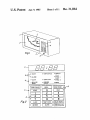
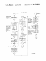
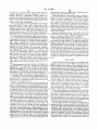
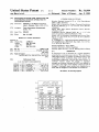
FIG. I is a pictorial view of a microwave oven con
trolled by a microprocessor which may use the self-test
feature of the invention;
FIG. 2 is an enlarged view ofthe control panel ofthe
appliance of FIG. 1;
BACKGROUND OF THE INVENTION
This invention relates to electronic systems and more
particularly to self-testing of equipment such as home
appliances operated by microprocessor devices.
Most appliances or electronic equipment such as mi—
crowave ovens, washing machines, CB radios. TV
game devices, automobile ignition controls, and the like
are being designed to be controlled by microprocessors.
Usually a microprocessor for these purposes is a semi
conductor MOS/LS] integrated circuit which has a
read only memory (ROM), data storage in the form ofa
random access memory (RAM), an arithmetic unit for
performing calculations or logic functions, and a num
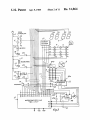
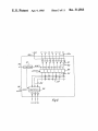
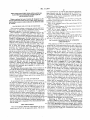
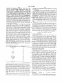
FIG. 3 is a block diagram of the electronic circuit of
the appliance of FIGS. 1 and 2;
FIG. 4 is a block diagram of the microprocessor
device in the system of FIG. 3;
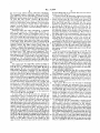
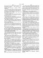
FIG. 5 is a block diagram of the keyboard interface
device in the system of FIG. 3; and
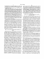
FIGS. 6-11 are flow charts ofa program which may
be used in the microprocessor device of FIG. 3 for
self-test of the appliance of FIGS. 1 and 2.
DETAILED DESCRIPTION OF SPECIFIC‘
EMBODIMENT
With reference to FIG. 1, a microwave oven which is
controlled by a microprocessor device and which may
ber of input and output terminals. An example of a
processor device of this type is described in detail in 25 employ the self-test feature ofthe invention is illustrated
US Pat. No. 3,988,604 issued Oct. 26, 1976 to J. H.
in pictorial form. It is understood, of course. that this
Raymond. assigned to Texas Instruments. The proces
equipment is merely illustrative; the same concepts
sor device contains facility for being tested, as a finished
could be used in any system. The oven comprises a
part, according to US Pat. No. 3,92l,l42, assigned to
housing 1 which has a door 2 for access to a cooking
Texas Instruments. but the system itself requires func
compartment in the usual manner. A control and indica
tional testing of each electrical component, either for
tor panel has a keyboard 3 which may be of the capaci
final test by the manufacturer or for ?eld test by a ser
tive touch type, although switches with mechanical
viceman. conventionally. systems test has required
contacts may be employed. An array of indicator lights
various equipment such as volt and ohm meters, oscillo
4 such as VLED‘s tell the operator what operation or
scopes and the like, and can be time consuming and 35 cycle the oven is engaged in. A four digit display 5
expensive. Testing is further complicated by the fact
shows the time remaining in a cook cycle, or time of
that solid state control circuitry has few components
day, or any other numerical information of use to the
and thus few terminals are available for probe or for
operator. An OFF/ON toggle switch 6 provides the
initiating conditions.
'
typical power on or off function. A temperature probe
It is therefore the principal object of the invention to
7 may be used within the cooking compartment, plug
provide an improved testing arrangement for appliances
ging into a receptacle provided in the sidewall. An
or electronic equipment. Another object is to provide a
enlarged view ofthe indicator and control panel is seen
self-test feature for apparatus controlled by a micro
in FIG. 2. The keyboard 3 consists of a glass front panel
processor. A further object is to provide a self-test pro
which has twenty-one rectangular conductive areas 8
cedure which utilizes a minor part of an existing ROM 45
thereon. When touched by the operator. the capaci
in a processor device.
SUMMARY OF THE INVENTION
In accordance with an embodiment of the invention,
an electrical appliance such as a microwave oven, for
example, includes a self-test feature wherein all of the
electrical devices such as the magnetron are actuated
and the digital display and the indicator lights are all
actuated in a pattern, this being accomplished by a mi
croprocessor device which is the same device which
controls the operation of the appliance. A capacitive
touch keyboard or other manual input is provided, and
the self-test feature may test the keyboard by displaying
row and column data in response to touching each key.
The self-test operation is initiated by connecting certain
output and input terminals of the microprocessor de
vice, in a way not encountered in ordinary operation, so
that the keyboard is bypassed. Thus the keyboard itself
can be tested.
THE DRAWINGS
The novel features believed characteristic of the in
vention are set forth in the appended claims. The inven
tance of an area changes and this can be detected by the
input circuitry. It is difficult to test this type of key
board and its associated detector circuit because the
parts cannot be reached and would be affected by test
probes. The indicator lights 4 are typically small red
light emitting diodes 9 which are covered by a glass
panel that has legends printed thereon for each lightv
The display 5 consists of a seven-segment four-digit
VLED device wherein all segments of like position are
in common, of standard design. The operating sequen
ces of this microwave oven control may be as later set
forth, it being understood that the particular way of
operation of the appliance is not part of the invention
60 and different functions on the keyboard 3 and different
indicators 4 and display 5 could be used.
Referring to FIG. 3, an electrical diagram of the
system of FIGS. 1 and 2 is shown. The principal cook
ing element of a microwave oven is of course a magne
65 tron which generates microwave energy, and a magne
tron transformer 10 is connccted to the magnetron, not
shown, and actuates it when the transformer primary is
energized by AC supply 11. A heater 12 of the conven
Re. 31,864
3
tional electric resistance type within the cooking cham
ber provides a broil or browning function, also actuated
from the AC supply 11. A fan motor and pilot lamp 13
within the cooking chamber come on when the door 2
is closed and the switch 6 is on. A buzzer l4 signals
when a cycle is completed. The main part of the con
troller is a semiconductor MOS/LS1 device or "chip"
15 which may be of the type made available by Texas
Instruments Incorporated, P. O. Box 1443, Houston,
Texas 7700i under the trade designation TMSl l 17NL
Preprogrammed 4-Bit Microcomputer, or may be any
one of various other microprocessor or microcomputer
devices available from Texas Instruments under the
general designation of TMSlOOO, TMSl 100, TMSl200
or TMSUOO, specially programmed to perform the
functions to be described by reference to Programmer's
Reference Manual, TMSlOOO Series MOS/LS] One
Chip Microcomputer. Bullet CMlZZ-l. Copyright l975,
published by Texas instruments and available at the
above address, such manual being encorporated herein
by reference. The chip 15 is also described in detail in
US. Pat. No. 3,988,604, above-mentioned. The chip l5
accepts input data from the keyboard 3 or other inputs
such as from the probe 7 by four
lines 16 labelled
K1. K2. K4 and K8. Two different independent sets of
output lines from the chip 15 are provided. one being
"5“ or segment outputs 17 labelled. S1, S2, S3 and 57
(actually the chip could have seven or eight segment
4
random-access-memory) 25. The ROM 24 contain's
i024 instruction words of eight bits per word, and is
used to store the program which operates the system.
The RAM 25 contains 256 memory cells software orga
nized as four sixteen-digit groups with four bits per
digit. The RAM may store information entered by the
keyboard, or intermediate and final results of calcula
tions, as well as status information or "flags", and other
working data. The RAM functions as the working reg
isters of the system, although it is not organized in a
hardware sense as separate registers as would be true if
shift registers or the like were used for this purpose. The
RAM is addressed by a word address on lines 26, i.e..
one out of sixteen word lines in the RAM is selected, by
means of a combined ROM and RAM word address
decode circuit 27. One of four “pages“ of the RAM is
selected by an address signal on two lines 28 applied to
a RAM page address decoder 29 in the RAM. For a
given word address on lines 26 and page address on
lines 28, four specific bits are accessed and read out on
RAM I/O lines 30, via input/output circuit 31, to RAM
read lines 32. Alternatively, data is written into the
RAM 25 via the input/output circuitry 31 and the lines
30. The same sixteen lines 26 used as the RAM word
address are also used to generate the display and key
board scan on the lines 18; to this end the lines 26 pass
through the RAM 25 and are connected to output regis
ters and buffers as will be explained.
outputs as typically used for calculators or other seven
The ROM 24 produces an eight bit instruction word
segment plus decimal point displays). The other set of 30 on ROM output lines 33 (the bits of the instruction
outputs is the “D“ or digit output lines 18 of which
word being labeled R0-R7) during each instruction
there are eleven in this case, labelled D0 to D10 (the
cycle. The instruction is selected from 8 192 bit locations
chip has sixteen possible “D" outputs in a forty pin
package. less in a standard twenty-eight pin package).
Suitable devices (not shown) such as bipolar transistors,
optical couplers or the like may connect the various
output pins to the display or controlled devices ifdifferf
ent voltage or current levels are needed, as is conven
tional. A Vdd pin would provide supply voltage to the
chip, and a Vss pin is ground. An oscillator input pin 4)
represents a frequency control for the system, as an
internal clock generator is within the chip 15. For exam
ple, thrysistors 19 in series with the magnetron trans
former 10, the broiler element 12 and the fan and lights
in the ROM, organized into 1024 words containing
eight bits each. The words are divided into sixteen
groups or pages ofsixty-four words each. To address an
instruction in the ROM requires a one-of-sixty-four
ROM word address on lines 34 and a one-of-sixteen
ROM page address on lines 35. The ROM word address
on lines 34 is generated in the same decoder 27 as used
to generate the RAM word address on lines 26. The
ROM word address is a six-bit address produced in a
program counter 36 which is a six-stage shift register
that may be updated with an instruction cycle or may
have a six-bit address loaded into it via lines 37 from
13 may be turned on by couplers 20 which are standard 45 ROM output lines 33 for a call or branch operation. The
items available from Texas Instruments as TlLl l3 cou
RAM and ROM word address decoder 27 receives a
plers. A segment decoder 21 such as available as a stan
six-bit encoded address on lines 38 from decode data
dard part SN7447A converts 4~bit binary-coded-deci
select unit 39 which has two inputs. The unit 39 may
mal or other code on the S1 to S4 lines 17 to seven lines
for driving the segments of the display 5. The signals
generated by the capacitive touch keyboard 3 are con
verted to a three-line code for input to the chip 15 on
lines 16 by an interface part 22 which is available from
Texas Instruments
TMS1976.
under
the
trade
designation
receive a four-bit address from RAM Y register 40 via
lines 41, or it may receive a six-bit address from the
program counter 36 via lines 42. A six-bit subroutine
register 43 is associated with the program counter 36 to
serve as temporary storage for the return word address
during subroutine operations. A six-bit address is stored
55 in the register 43. via lines 44 when a call instruction is
initiated so that this same address may be loaded back
THE MICROCOMPUTER CHIP
into the program counter 36 via lines 45 when execution
One example of the microcomputer chip 15 will now
of the subroutine which begins at the call location has
be described. Depending upon the complexity of the
been completed; this conserves instruction words and
functions to be implemented, the size of instruction 60 makes programming more ?exible. The ROM page
word storage needed for the chip 15 might be 1K or 2K.
address on lines 35 is generated in a page address regis»
for example. A TMSIOOO device as mentioned above
ter 46 which also has a buffer register 47 associated with
contains 1K storage, while a TMSl lOO contains 2K. A
it for subroutine purposes. The register 46 will always
[K device will be described, although it can be ex‘
contain the current page address for the ROM. and
panded if needed for a complex system.
65 directly accesses the ROM page decoder. The buffer
A block diagram of the system implemented on the
register 47. is a multifunction buffer and temporary stor
chip 15 is shown in FIG. 4. The system is centered
age register. the contents of which can be the present
around a ROM (read-only-memeory) 24 and a RAM
ROM page address, an alternate ROM page address, or
Re. 31,864
5
6
the return page address during subroutine operations.
The program counter, subroutine register and ROM
page addressing are all controlled by control circuitry
48 which receives inputs from the ROM output lines 33
via lines 49. The control circuitry 48 determines
between BCD data out on certain lines 17, and control
outputs on other lines 17.
whether branch and call on "status" or subroutine oper
ations are performed, causes loading of an instruction
word into the program counter and/or page address
A control circuit 70 determines what and when data
is written into or'stored in the RAM 25 via input/output
control 31 and lines 30. This RAM write control 70
receives inputs from either the accumulator 52 via lines
53 or the CKB logic 56 via lines 55, and this circuit
produces an output on lines 71 which go to the RAM
l/O circuit 31. Selection of what is written into the
RAM is made by the instruction word on lines 33, via
the data path control PLA 60 and command lines 61.
gram counter, etc.
An important feature of the system is that constants or
Numerical data and other information is operated
keyboard information, from CKB logic 56, as well as
upon in the system by a binary adder 50 which is a
the adder output via the accumulator. may be written
bit-parallel adder having a precharged carry circuit,
into the RAM, via the write control 70. and further the
operating in binary with software BCD correction. The
CKB logic 56 can be used to control the setting and
input to the adder 50 is determined by an input selector
resetting of bits in the RAM. via the write control 70.
51 which receives four-bit parallel inputs from several
The RAM page address into which data is written is
sources and selects from these what inputs are applied
determined by two bits of the instruction word on lines
to the adder. First, the memory read or recall lines 32
from the RAM 25 provide one of the alternatives. Two 20 ‘33, as applied via lines 72 to a RAM page address regis
ter 73 and thus to lines 28 which select the RAM page.
registers receive the adder output, these being the
The RAM word or Y address is of course selected by
uRAM Y“ register 40 and an accumulator 52, and each
the contents of RAM Y register 40, select circuit 39 and
of these has output lines separately connected as inputs
decoder 27.
53 and 54 of the selector 51. A fourth input 55 receives
The four keyboard inputs 16 appear on lines 75. from
an output from “CKB“ logic as will be explained. Thus,
which an input to the CKB logic 56 is provided. In
the adder input is selected from the following sources:
register, controls transfer of bits to the subroutine or
buffer registers and back, controls updating of the pro
normal operation. a keyboard input goes via CKB logic
56 to the accumulator 52 or RAM Y register 40, from
via lines 53-, RAM Y register 40 via lines 54-, constant,
whence it is examined by software or ROM program
keyboard or “bit" information from CKB logic 56 on
lines 55. Positive and negative inputs to the adder 50 on 30 ming. ln manufacture of the chips, a test mode is possi
ble, where the keyboard input on lines 75 can be entered
lines 57 and 58 are produced from the selector circuitry
directly into the ROM page buffer address register 46,
51.
as will be explained. Also, during hardware clear using
The output from the adder 50 is applied to either or
the KC input, the K lines can be entered into the page
both the RAM Y register 40 and the accumulator 52 via
address register, or a K line can be used as an interrupt,
lines 59. All of the operations of the adder 50 and its
in non-calculator applications.
input selector 51, etc., are controlled by a data path
Also included within the chip 15 is a clock oscillator
control PLA 60 which is responsive to the instruction
and generator 80 which generates internally a basic
word on lines 33 from the ROM. Control outputs 61
clock frequency of about 500 KHz or less, and from this
from the control PLA 60 are indicated by dotted lines.
data memory or RAM 25 on lines 32-. accumulator 52
The four-bit output from the accumulator can be ap
plied via lines 53 to an accumulator output buffer 62 and
produces five clocks (1)] to (b5 used throughout the
system. A power-up-clear circuit 82 produces controls
which clear the calculator when the power is turned on.
thus toa segment decoder 63 for ouput from the system.
This may be also supplemented by the KC input with an
The segment decoder 63 is a programmable logic array
external capacitor.
like that disclosed in application Ser. No. l63,565, and
The outputs 18 from the chip 15, used for keyboard
produces up to eight segment outputs on lines 64 which 45
and display scanning. are generated from the RAM
are applied to a set of eight output buffers 65. The out
put arrangement contains memory in the buffer 62 so
that an output digit can be held for more than one ma
chine cycle. Output is under control of the data control
logic PLA 60 which is responsive to the instruction .
word on lines 33 from the ROM.
A status logic circuit 66 provides the function of
word address on lines 26 by an output register 84 which
is loaded under control oflines 61 as addressed by RAM
word lines 26. The output from the register 84 is con
nected via lines 85 to a set of output buffers 86. Sixteen
outputs are possible, but only perhaps nine to thirteen
would be provided as outputs in a typical calculator
examining for carry or compare from the adder 50, and
determining whether to branch or call. To this end,
design; for example eight digits for mantissa, two for
inputs from the adder 50 via lines 67, and input from the
for mantissa and exponent.
It is important that the register 84 is a random access
control PLA 60 via lines 61 are provided. The status
logic 66 includes a latch which produces an output 69 to
the output buffer register 62; this can be decoded out via
exponents, and two for annotators such as minus sign
register, where all bits are separately, independently,
and mutually exclusively addressed. In this embodi
ment, only thirteen stages are provided in the register
segment decode 62 in many different ways. It can be
used to indicate decimal point DPT, and used to select 60 84, so only the first thirteen of the sixteen address lines
26 are used. When one of the twelve bits in the register
two digit code sequences such as seven-segment or
84 is addressed from decoder 27. this bit may be either
BCD out of the same PLA. For DPT, a BCD code of
set or reset as determined by controls 61 from the con
the desired DPT place would be stored in a location in
trol PLA, i.e., from the current instruction word. The
RAM 25, and this would be compared in adder 50 with
the current D line 18 being actuated which is de?ned in 65 bit will remain set or reset until again speci?cally ad
dressed and changed; meanwhile any or all of the other
RAM Y register 40, and if they are the same, status
hits my be addressed and and set or reset in any order.
latch is set and DPT is shown on the display for that
Thus, it is possible to have any combination of D regis
digit. Further, the status latch can be used to delineate
7
Re. 31,864
8
ter bits either set or reset, providing 2'3 or 8l92 code
entry into the chip 15 via K lines K1, K2, K4. The lines
combinations on the output lines 18. During power up
or hardware clear. all the bits of the register 84 are
94 are applied to a multiplexer 95 which functions to
switch between the keyboard data on the lines 94 and a
60 Hz input on a line 96 from the prior line. This allows
unconditionally reset.
Similar to the register 84, the other output register 62 5 a 60 Hz reference to operate the device as a clock for
is static in that the contents once entered will remain
time-of-day display. The multiplexer 95 is operated by
until intentionally altered. The output register 62 func
the D1, D3, D5 signal on line 90 via control 97. The
device of FIG. 5, commercially available under the part
number TMSI976 as mentioned above, actually has
nine inputs 85a and four outputs to the K lines, but only
tions as an output data buffer while the accumulator S2
and status latch 66 are being manipulated to form the
next output. The output register 84 is a similar buffer for
outputting the contents of the Y register 40, but has the
additional feature of being fully random access. The
data sources for the Y register 40 are the following: a
seven and three are needed here.
OPERATION OF THE MICROWAVE OVEN
CONTROLLER
The normal operating procedure for the system thus
four~bit constant stored in the ROM 24 as part of an
instruction word; the accumulator 52 transferred to the
Y register 40 via the selector 51 and adder 50; and data
directly from the RAM 25. Once data is in the Y regis
ter 40 it can be manipulated by additional instructions
far described will now be explained. When the oven is
not being used, the chip 15 is functioning as a clock.
such as increment or decrement.
An instruction set and explanation of each instruction _
implemented in the system of FIG. 4 is set forth in the
attached Table I. It is important to note that the system
output lines 17 and 18, independently of one another.
and is responsive to the K input lines 16, or any one or _
set of them, only when instructed. Thus, the various
segments of the display 3, or the indicator lamps 9, or
the thyristors 19, or the buzzer 14. etc. may be actuated
as needed, and the K inputs checked as needed. The
four-digit hours-minutes number by touching the num
ber areas on the keyboard 3. During this, the lamp 9 for
clock will be actuated in the indicator panel 4. Then the
START key area 8 is touched, and the clock will there
after function. continuously showing the time-of-day on
the display 5. The START light 9 comes on when
START key is touched. Thereafter, time is shown on
the display unless a cooling procedure is being pro
grammed or in process.
Independent of all other operations an alarm timer
cycle time of the chip for executing an instruction is
about twelve to fifteen microseconds, so many hun
dreds of instructions may be executed in a time less than
may be used by touching the ALARM'key and then
perceptible by the operator.
CHIP
minutes. To reset the clock, the clock key is touched on
the keyboard 3 and the current time is entered as a
can actuate any one or any combination of the S and D
THE CAPACITIVE KEYBOARD INTERFACE
storing time-of-day in the RAM 25 by counting 60 Hz.
The time-of-day is output to the display 5 in hours
entering digits 0-9 to a maximum of 99:59. A count
down begins by touching the START pad, and the
35 display 5 shows the time remaining. When the selected
time has elapsed, the chip 15 actuates S7 to average the
buzzer 14 at about 3 KHZ for three seconds, then the
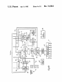
Referring to FIG. 5, a block diagram of the interface
chip 22 is shown. The capacitive keys are driven by
lines 84a which are at high voltage, boosted up from the
D2, D4 and D6 lines 17 by buffers, not shown, so that
the level distinction on lines 85a going from the array 3
display goes back to time-of-day.
Timed cooking is of course the main operation of
interest. The oven has ?ve sequential programs, each
having an associated timer. The cooking programs exe
cute in a fixed order: (1) defrost; (2) automatic tempera
ture settle; cook cycle 1; cook cycle 2; and broil. The
cooking commands may be entered in any order, how
to the chip 22 is reliable. A scan pulse from a D line 5
causing a line 84a to be actuated, but with no key area
8 touched, generates transitions of the C lines 85 that
need to be 0.5 volts less positive than a reference volt 45
ever.
age applied to a reference voltage input pin 86a. The
voltage reference is generated by resistors forming a
voltage divider across a DC supply. By touching a key,
the voltage becomes at least 0.3 volts more positive than
If the temperature probe 7 is disconnected from its
socket, all ?ve cooking times are available. Each func~
tion is programmed by touching the desired function
pad 8 followed with a data entry. Touching another
the reference voltage. Vref is adjusted to a value half SO function or the start pad stores the timer data. All func
way between not detecting and detecting a key area 8
tions programmed into a sequence have an associated
being touched. A set of seven input buffers 87 function
indicator light 9 come on and say on.
to compare Vred in line 86a with the voltages on the
With door interlock closed. the start pad 8 initiates a
lines 85a and produce an output on one of the lines 88
given sequence. Then the timer executing a count down
when a key is touched at the time D2, D4 or D6 is 55 is on display 5 while only its indicator is on. If the door
actuated. The lines 88 drive a set of seven latch circuits
2 is opened at any time. cooking. halts. The sequence
89 so that when a key is touched one of the latches will
flip and stay until reset by a reset voltage on a line 90.
restarts after the door is closed and start is hit. To end ‘a
sequence, touching STOP cancels all programming and
Protection against double key actuation may be pro
vided by disabling the buffers 87 when one latch is
?ipped so the device is not responsive to a subsequent
key. The reset line 90 is actuated by either D1, D3 or
D5 via diodes 91 (seen in FIG. 4), so that the usual
sequence
reset, address
is scanning
D2, reset,D1
address
through
D4, D6
reset,to address
provideD6“
sequence. The outputs of the latches 89 are applied via
lines 92 to a coder 93 which converts the one—of~seven
actuation in lines 92 to a three-bit code on lines 94 for
turns off the magnetron/broiler power. Then repro'
gramming the timers is enabled. Once a sequence com
pletes cooking, the speaker 14 sounds out three KHz
bursts lasting one second out of ?ve, for live minutes.
The stop command terminates the speaker signal.
The cook can select a defrost period with an auto
65
matic temperature settling period afterwards. The de
frost timer provides 60100 minutes maximum cooking
period at 15 seconds on, 15 seconds off cycle. This
function is always the ?rst one executed after the
Re. 31,864
9.
.
10
START pad is touched. If the defrost cycle is not se
temperature cooking is enabled, 'the cooking begins 30
lected. both defrost and the temperature settle are ‘
minutes before the desired end time.
Using a thermistor in the probe 7 and an analog-to
skipped. During a temperature settling period, no
power is sent to the magnetron for a period equal to the
defrost time. While the temperature settles, an indicator
9 is lit. To use the temperature settling feature. cook
cycle one has to be programmed.
Two cooking timers are programmable. cook cycle 1
and cook cycle 2. Cook cycle 1 counts down 60:00
minutes maximum. Cook cycle 2 counts down from
30:00 minutes maximum. Optionally, the user selects the
cooking speed in 10% duty-cycle increments of a 30
digital conversion by successive approximation using a
number of resistors actuated by S1, S2. S3 and S4. the
system provides a temperature controlled cooking.
First, a safety procedure checks to be sure the tempera
ture probe 7 is in its socket. Otherwise one could start
temperature cooking while forgetting to put the probe 7
inside the oven (which can result in overcooking). A 90
minute maximum time limit is allowed for the probe to
reach the desired temperature before the oven automati
second time base (e.g., a 10% duty-cycle would turn on
the magnetron 3 seconds out of 30). If not selected. full
cally stops cooking.
.
100% duty-cycle is the assumed magnetron onatime.
A typical sequence using cook cycle 1 and cook cycle
2 is programmed by touching DEFROST then entering
and inside the food, the cook closes the door 2 and
Once the temperature probe 7 is properly connected
enters
followed
a sequence
by COOKsuch
SPEED,
as TEMP
etc. or COOK
START.then
a time such as 2-3-0 or two minutes and thirty seconds.
The programmed temperature is relative on a scale of
Then COOK CYCLE 1 is touched on the keyboard 3
and a time is entered such as 5-0-0-0 or ?fty minutes.
‘Then COOK CYCLE 2 is touched and another time
enetered by the keyboard, such as l-5-3-0 or ?fteen
one (lowest) to nine (highest). The sensed temperature
displays on the right on a zero to nine scale. The tem~
perature updates are once a second. The actual tempera
ture sensed varies with the choice of sensor and the
external resistors used in the A/D converter 98. Every
ten seconds the cooking speed percentage displays on
and DEFROST. Then, START is touched, and 25 the two left-hand digits, unless the 100% default is used.
Entry to the chip 15 from the A/D converter 98 is by
START and DEFROST lights 9 come on, and the
the K2 line, which is a binary indication. Thus, the chip
display shows 2130. The defrost cycle begins counting
actuates the 81-54 lines in various combinations until
down from 2:30. After five seconds, the start indicator
the K2 line changes to produce a temperature indica
goes off. A settling time equal to two minutes, 30 sec
onds follows. Then cook cycles 1 and 2 execute with a 30 tion.
minutes and thirty seconds. At this point, indicator
lamps 9 on the panel 4 which are actuated are CCl, CC2
100% duty cycle default. At the end of cycle 2, the
ready signal sounds, and the display shows the time of
day.
SELF-TEST
In accordance with the invention, the chip 15 is pro
When programmed as just described. the magnetron
is on 100% duty cycle. To change this, the cook
grammed to test the system of FIGS. 1-3 as well as test
SPEED key is touched after a cook time is entered,
followed by a digit “1" to “9" for 10% to 90%. When
this done, the SPEED light 9 comes on on the panel 4.
used in several ways. The chip 15 may perform an in
coming functional test upon itself, by having an oven
mock up at the test location and plugging each chip 15,
During the cook cycle, the percentage displays in the
as received by the oven manufacturer. into it so that it
itself working in the system. This capability may be
40 can run through a test sequence with no elaborate test
two left hand digits of display 5, every ten seconds.
machinery. Another use is for production burn-in; often
To obtain a crust on the food, the heating element 12
an appliance is “burned in" after manufacture to assure
is controlled by a broil timer. Up to 30:00 minutes may
that parts which are to fail in a short period of power-on
will be found. The self-test feature may be used. of
45 course, for ?nal test of the oven units before shipping.
broiler for the designated time.
or by a retail store upon receipt or upon sale. Further.
In many instances the user may desire cooking to be
?eld test by a repairman in the home or at a repair
done at a speci?c time. The system computes the time to
be entered after touching the BROlL pad. Following
cook cycle 2, a dedicated output. D9, turns on the
start the cooking sequence by subtracting the total of all
cooking times entered from the desired end time. After
touching the DELAYED START pad, the cook selects .
an end time with the digit pads 8. The remainder of the
center may use the self-test feature. Also, a customer
may be directed to check his own unit in the home
before a “house-call“ by a ?eld serviceman.
The system contains two separate self-test capabili
cooking sequence is set, and then the calculation begins
ties. These are independently actuated; one or both may
with a START entry. When the clock and the start time
be used. The ?rst routine may be done without a key~
board and is relatively quick, thus it is well suited for
delayed start indication goes away, and the ?rst cooking 55 incoming inspection. The second routine is suited for
?nal test and ?eld service testing; this routine exercises
timer and its indicator are enabled. Delayed start allows
the keyboard 3, the interface device 22. the display, and
cooking to ?nish on time regardless of the cook’s pres
all of the output devices, all via the chip 15.
ence. Also delayed start eliminates any errors in sub
The ?rst test routine is actuated by connecting the
tracting minutes and seconds for up to ?ve timers. It
would be in error to try ending a one hour sequence at 60 output line D0 to the input line K4 by a line 100, a diode
and a switch 102. The switch 102 is closed before power
12:30 if it was currently 12 o‘clock. Once the desired
is applied to the system. When the chip senses K4 actu
end time is entered and some cooking sequence is en
ated when D0 is actuated, the routine begins, and the
abled, the user touches START. Then the delayed start
switch 102 may then be opened; i.e., only a momentary
indicator goes on, the start indicator lites, and the oven
lamp/fan 13 turns off. When the right time for begin 65 contact is needed. The ?rst test routine consisting of
three test operations which are automatically executed.
ning occurs, the lamp/fan goes on, the delayed start
The initial one of these ?rst turns each LED indicator
indicator turns off, and the selected cooking sequence
lamp 9 on, one at a time, for a short period, perhaps 0.2
begins as shown in the previous cooking descriptions. If
agree. the cooking mode begins automatically. The
Re. 31,864
11
12
second. The sequence is BROIL, CC2, CCl, DE
seconds (not including the fourth operation requiring
FROST, COOK SPEED, TEMP COOK, blank (S2,
D5 intersection), TEMP SETTLE, DELAYED
START, CLOCK, ALARM, START. Next, each digit
ofthe display 5, starting with the MSD, is counted from
key operation).
The program ?xed in the ROM 24 to implement the
test routines just described is set forth in FIGS. 6-11,
which are How charts giving the mnemonics of the
O to 9 at approximately 0.2 second count rate. Then, all
D and S control lines (except S7 which actuates the
buzzer or speaker 14) are turned on simultaneously.
During these three operations, all indicator lamps 9 in
the panel 4, all segments of all digits of the display 5,
and all control outputs are exercised (except the buzzer,
and this is avoided only to reduce noise in burn-in or
test areas). The system will remain in the ?nal state with
all control outputs, all indicators, and all display ele
ence to an illustrative embodiment, this description is
not intended to be construed in a limiting sense. Various
modifications of the illustrative embodiment, as well as
the first three of which execute automatically in serial _
claims will cover any such modi?cations or embodi
ments as fall within the true scope of the invention.
cator lamp 9 is turned on in sequence for about one
fourth second each. In the second operation, each digit
ofthe display starting with LSD is counted up from O to
TABLE OF INSTRUCTIONS
CALL: HXXXXXX
9 at 0.25 second count rate. The third operation sets all
D and S lines on, then terminates by going into a hold
Conditional on status; if status line 79 is a logic “0",
then the CALL instruction is not performed. lfstatus is
“1", the machine goes into the CALL mode, as indi
cated by setting the CALL latch 200 to a logic
The
program counter 36 is stored up in the subroutine regis
ter 43. The page address is stored in the buffer 47. The
mode. These control outputs are not left on as they
were in the first test routine. The fourth test operation
requires the operator to touch the keys. When one of
the key areas 8 is touched and released, the MSD of the
display 5 shows the D line (i.e.. “2", “4“ or “6") which
scans the touched key, and the LSD shows the C line 85
contents of the buffer register 47 are used as the page
(input to the interface chip 22) on which the touched
key exists. The Following list shows the display acti
vated for each key touched:
address. The W ?eld R2 to R7 of the instruction word
is loaded into the program counter 36 via devices 162.
All instructions executed while in the CALL mode
perform their normal functions, except for the CALL
and branch instructions; execution ofa CALL within a
CALL mode is not valid; branches executed within a
DlSl’LAY
Cook Cycle 1
4
7
0
5
8,
Temp. Cook
Aux. Timer
Cool; Speed
Stop
3
h
Ll
Delay Start
call mode must be intrapage.
ll .N
Clock
Defrost
Broil
r r\JOLI
a? ” Sak i-D t '
Branch (BR): IOXXXXXX
Conditional on status; ifstatus is a logic “0". then the
branch instruction is not performed. if status is "l“,
45 then the W field is loaded into the program counter 36
and the contents of the buffer register 47 become the
new page address in the register 46, except when in the
CALL mode. Branch (as well as CALL) can be uncon
ditional because ofthe nature of status logic 66. Status is
50
struction immediately preceeding the branch or CALL
branch operation. Only that instruction immediately
preceeding the branch instruction determines whether
branching is successful. Status always returns to logic
nation resulting in the display appearing for 0.8 seconds,
after which the controller returns the system to the all
remains until another key is touched. After the operator
has exercised all the keys (i.e., tests) desired, and the
system is at rest in the all lights on mode, opening the
switch 104 removing the connection from K8 to D0
normally in logic “l" which is the proper condition for
successfully performing a branch or CALL. If the in
does not affect status, then the operation will be suc'
cessful. Status is valid for only one instruction cycle. It
55 is therefore invalid to perform multiple tests before a
Each key touched will activate a C and D line combi
lights on mode. showing 88:88 in the display 5, where it
other embodiments ofthe invention. will be apparent to
persons skilled in the art upon reference to this descrip
tion. It is. therefore, contemplated that the appended
inputs. in the ?rst operation, each individual LED indi
l
digital display, indicator lights. and a touch keyboard,
ing to a visible display, indicators, key inputs and the
like.
While this invention has been described with‘ refer‘
after initiation, then the system stops in a hold condition
until the user starts the fourth operation via keyboard
Start
0
or electrical equipment which had devices correspond
ideal for burn-in.
second test routine is activated by connecting
D0 to input K8 by a line 103, a diode and a
104. This routine consists of four test operations,
KEY TOUCHED
15 may have different instruction sets, but would be
programmed in a similar manner. These routines are
described in reference to a microwave oven with a
but the same principles could be used on any appliance
ments turned on until power is removed-this condic
tion is
The
output
switch
instruction set ofthe Table. Other microcomputer chips
“1" after a branch instruction.
00
Load Y Register with a Constant (TCY): OIOOXXXX
The C field of the instruction word, bits R4 thru R7.
is transferred into the Y register 40. This is uncondi
tional. and neither carry nor compare go to status logic
66.
Compare Y Register to a Constant (YNEC):
causes the system to revert to the normal operating
mode.
The first test routine executes itself in about ?ve sec
OIUlXXXX
onds, while the second test routine requires thirteen
C field of the instruction word. Compare information
The contents of the Y register 40 are compared to the
.Re. 31,864
13
on line 67 is input to the status logic 66. Inequality will
force status to a logical
This instruction is not
conditional on status.
Constant Store. Increment Y Register (TCMIY):
O110XXXX
The contents ofthe C ?eld is stored directly into the
memory location addressed by the X and Y registers 73
and 40. The Y register 40 is then incremented by one.
The instruction is not conditional on status, and carry
and compare do not go to status.
Add constant to Ace. result to Acc, with carry
(AZAAC) (or A3AAC, etc.)
.
A constant is added to the contents of the accumula
tor and the result stored in the accumulator. lfa carry is
generated, status is set.
Load P Register (LDP): 0001XXXX
The buff register 47 is loaded with the contents ofthe
C ?eld in the instruction word. This is unconditional
and neither carry nor compare go to status.
Bit Set (SBIT): 001100XX
The contents of the memory location addressed by
the X and Y registers 73 and 40 is selected. One of the
four bits, as selected by the B ?eld of the instruction
Bit Reset
word.
is set
(RBIT):
to a logic
001101XX
The contents of the RAM 25 memory location ad
14
The contents of the accumulator 52 are added to the
contents of the RAM memory location addressed by the
X and Y registers 73 and 40 with the resulting sum
stored into the accumulator 52. Resulting carry infor
mation on line 67 is input to the status logic 66. A sum
The
that contents
is greaterofthe
than ?fteen
memorywill
location
set status
in the
to RAM
a logic25 are
unaltered.
Compare Memory to Zero (MNEZ): 00100110
The Ram memory contents addressed by the X and Y
registers 73 and 40 are compared to zero. Comparison
information on line 67 is input to the status logic. In
equality between memory and zero will set status 66 to
aMemory
logic
and
Accumulator
Subtract
(SMAN):
001001 11
The contents of the accumulator 52 are subtracted
from the contents of the RAM memory location ad
dressed by the X and Y registers 73 and 40 using T5
20 complement addition with the difference stored into the
accumulator 52. Resulting carry information is input to
status 66. Status will be set to logic "1" if the accumula
tor is less than or equal to the memory.
Load incremented Memory (IMAC): 00101000
The contents of the RAM memory location ad
dressed by the X and Y registers 73 and 40 is incre
mented by one and stored into the accumulator 52. The
original contents of the RAM memory are unaltered.
Resulting carry information is input via line 67 to the
dressed by the X and Y registers 73 and 40 is selected.
One of the four bits. as selected by the B ?eld of the
instruction word via CKB logic 56, is reset to a logic
30 status logic 66. Status will be set to a logic “ l " if the sum
“0".
is greater than ?fteen.
Bit Test (TBlTl): 001110XX
Accumulator Less than or Equal to Memory (ALEM):
The contents of the memory location addressed by
00101001
the X and Y registers 73 and 40 is selected. One of the
The accumulator 52 is subtracted from the contents
four bits, as selected by the B ?eld of the instruction
word via CKB 56, is tested in the adder 50. A logical 35 of the RAM memory location addressed by the X and Y
“1" in the selected bit will set status to a logical “1", via
compare output to status on line 67.
registers 73 and 40 using T5 complement addition. Re
Load X Register (LDX): 001111XX
sulting carry information is input via line 67 to the status
logic 66. Status equal to a logic “1“ indicates that the
The X or RAM page address register 73 is loaded
from the B ?eld of the instruction word. This is uncon
accumulator is less than or equal to the memory. Mem
ory and accumulator contents are unaltered.
ditional, and neither carry nor compare go to status
Load Decremented Memory (DMAN): 00101010
logic 66.
RAM memory location addressed by the X and Y regis
ters 73 and 40. After completion of the store operation,
The contents of the RAM memory location ad
dressed by the X and Y registers 73 and 40 are decre
mented by one and oaded into the accumulator 52.
Memory contents are unaltered. Resulting carry infor
mation is input to the status logic. If memory is greater
the Y register 40 is incremented by one. Unconditional;
than
Increment
or equal
Y register
to one, status
(TYC)will be set to log
Store and Increment (TAMIYC): 00100000
The contents of the accumulator 52 are stored in the
status is not affected.
The contents of the Y register 40 are incremented by
The contents of the RAM memory location ad 50 one. Resulting carry information is input to the status
logic 66. A sum greater than ?fteen will set status to a
dressed by the X and Y register 73 and 40 is uncondi
Transfer Memory to Accumulator (TMA): 00100001
tionally transferred into the accumulator 52. Memory
data in the RAM is unaltered. Unconditional, and carry
Decrement Y Register (DYN): 00101100
logic
and compare do not go to status.
The contents of the Y register 40 are decremented by
one. Resulting carry information is input to the status
logic 66. If Y is greater than or equal to 1, status will be
set to a logic "1“.
Transfer Memory to Y Register (TMY): 00100010
The contents of the RAM memory location ad
dressed by the X and Y registers 73 and 40 is uncondi
tionally transferred into the Y register 40. Memory data
2‘s Complement of the Accumulator (CPAIZ):
00101101
The contents of the accumulator 52 are substrated
Transfer Y Register to Accumulator (TYA): 00100011 60
in the RAM is unaltered.
The Y register 40 is unconditionally transferred into
the accumulator 52. Contents of the Y register 40 are
unaltered.
from zero using 2‘s complement addition. The result is
stored in accumulator 52. Resulting carry information is
input to the status logic 66. This operation is equivalent
to complementing and incrementing the accumulator. 1f
Transfer Accumulator to Y Register (TAY): 00100100
The accumulator 52 is unconditionally transferred 65 the accumulator contents are equal to zero, then status
into the Y register 40. Accumulator contents are unal
tered.
Exchange Memory and Accumulator (EXMA):
Memory and Accumulator Add (AMAAC): 00100101
00101110
will be set to a logic "1".
15
Re. 31,864
The contents of the RAM memory location ad
dressed by the X and Y registers 73 and 40 are ex
changed with the accumulator 52. That is, the accumu
lator is stored into memory and memory is transferred
into the accumulator.
16
If the contents of the Y register 40 are between 0
through 12 inclusive, then one of the D outputs will be
reset to a logic “0“. Selection of the D output is deter
mined by the decoded contents of the Y register 40. For
values greater than 12 in the Y register, the instruction
Clear Accumulator (CLA): 00101111
is a mop to the user.
The contents of the accumulator 52 are uncondition
ally set to zero.
Set D [Y] Output (SETR): 00001101
.
R4 of the instruction word. is added to the accumulator
52. Resulting carry information is input to the status
If the contents of the Y register 40 are between 0
through 12 inclusive, then one of the D outputs will be
set to a logic “1". Selection of the D output is deter
mined by the decoded contents of the Y register 40. For
values greater than 12 in the Y register, the instruction
logic 66. A sum greater than ?fteen will set status to a
is a no-op to the user.
Compare Y Register to the Accumulator (YNEA):
logic
Return (RETN): 0000i l 11
When executed in the CALL mode, the contents of
the subroutine register 43 are transferred into the pro
Add Eight to the Accumulator (ABAAC): 00000001
The constant eight (8), as determined by bits R7 thru
00000010
The contents of the Y register 40 are compared to the
contents of the accumulators 52. Comparison informa
tion is input to the status logic 66. Inequality between
the Y register and the accumulator will set status to a
logic
The logic state of status 66-1 is also copied
into the status latch 66-2.
Store Accumulator (TMA): 00000011
The contents of the accumulator 52 are stored into
the RAM memory location addressed by the X and Y
registers 73 and 40. Accumulator 52 contents are unaf
fected.
Store and Clear Accumulator (TAMZA): 00000l00
The contents of the accumulator 52 are stored into
gram counter 36. Simultaneously, the contents of the
buffer register 47 are transferred into the ROM page
address register 46. This operation will return the sys
tem to the proper point after a subroutine has been
executed.
When a return instruction is executed in the non
CALL mode, that is, when not executing a subroutine,
it is a no-operation.
What is claimed is:
1. Apparatus with self-test initiated at power-up, said
apparatus having a plurality of electrically operated
devices including electrically operated visible indicia, a
plurality of manually operable input means for entering
the RAM memory location addressed by the X and Y 30 functional commands. microprocessor means connected
registers 73 and 40. The accumulator 52 is then reset to
to the devices and receiving inputs from the input
zero.
means, said microprocessor means containing a fixed,
Add Ten to the Accumulator (AIUAAC): 00000101
permanently programmed read-only-memory for stor
The constant ten (10), as determined by bits R7 and
ing instruction words which define operating sequences
R4 ofthe instruction word, is added to the accumulator 35 for the apparatus, the microprocessor means further
52.
including logic means for sequentially executing the
Add Six to the Accumulator (AGAAC): 00000110
instruction words to operate the devices in response to
The constant six (6), as determined by bits R7 and R4
commands from the input means, an 01%” switch for
of the instruction word, is added to the contents of the
controlling the supply ofpowcr to the apparatus. the micro
accumulator 52. Resulting carry information is input to
processor means having self-contained test control
the status logic 66. A result greater than fifteen will set
means operable in response to actuation thereof by actu
status
Decrement
to a logic
Accumulator (DAN): 00000lll
The contents of the accumulator 52 are decremented
ation means without external control equipment to ener
gize at least some of said electrically operated devices in
sequence, the test control means including a sequence of
by one. Resulting carry information is input to the status 45 said instruction words in the read-only-memory. the
logic 66. If accumulator is greater than or equal to one,
actuation means initiating ~raid sequence of instruction
status
Increment
will be
Accumulator
set to a logic
(IAC): 00001 l 10
words for self-test upon powenup of said apparatus by
means afraid off-0n switch.
The contents of the accumulator 52 are incremented
2. Apparatus according to claim 1 wherein the visible
by one.
50 indicia include a segmented display and wherein the test
Complement X Register (COMX): 00000000
control means energizes each segment of the display.
The contents of the X or RAM page address register
3. Apparatus according to claim 1 wherein the manu
73 are logically complemented.
ally operable input means are switches which include an
Load External lnputs (TKA): 0000l000
array of rows and columns of keys and the test control
Data present on the four external K input lines 75 is 55 means produce indications on the visible indicia of the
transferred into the accumulator 52.
row and column of key actuated.
Test External lnputs (KNEZ): 00001001
4. Apparatus according to claim 2 wherein the visible
Data on the external K input lines 75 is compared to
indicia further include a plurality of lighted means each
zero. Comparison information is input to the status logic
corresponding to a function of the apparatus, and the
66.
Load
Non~zero
Output external
Register data
(TDO):
will 0000l0l0
set status to a logic
The contents of the accumulator 52 and the status
latch 66-1 are transferred to the output register 62. The
register 62 can be decoded in 62 to supply data to as
many as eight output lines 17 and is a primary register
used in data output external to the chip. The contents of
the Y register 40 are also decremented by one.
Reset D [Y] Output (RSTR): 00001100
test control means actuates the lighted means in se
quence.
5. Apparatus according to claim 1 wherein the test
control means actuates all of the devices and visible
indicia at the same time following actuation thereof in
65 sequence.
6. An electrical apparatus in a_self-contained housing
without external control equipment. the apparatus hav~
ing a plurality of electronic devices including means for