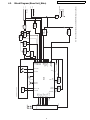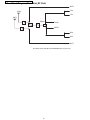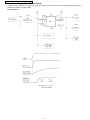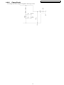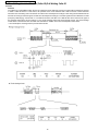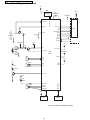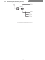
1
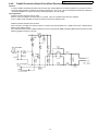
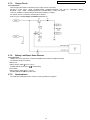
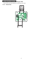
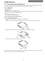
ORDER NO. KM41006121CE Telephone Equipment Model No. KX-TG4021LAT KX-TG4022LAT KX-TG4023LAT KX-TGA403LAT Expandable Digital Cordless Answering System T: Black Metallic Version (for Latin America) © Panasonic System Networks Co., Ltd. 2010 Unauthorized copying and distribution is a violation of law. KX-TG4021LAT/KX-TG4022LAT/KX-TG4023LAT/KX-TGA403LAT 2 KX-TG4021LAT/KX-TG4022LAT/KX-TG4023LAT/KX-TGA403LAT TABLE OF CONTENTS PAGE 1 Safety Precautions----------------------------------------------- 4 1.1. For Service Technicians --------------------------------- 4 2 Warning -------------------------------------------------------------- 4 2.1. Battery Caution--------------------------------------------- 4 2.2. About Lead Free Solder (PbF: Pb free)-------------- 4 2.3. Discarding of P. C. Board-------------------------------- 5 3 Specifications ----------------------------------------------------- 6 4 Technical Descriptions ----------------------------------------- 7 4.1. US-DECT Description ------------------------------------ 7 4.2. Block Diagram (Base Unit_Main)---------------------- 9 4.3. Block Diagram (Base Unit_RF Part) -----------------10 4.4. Circuit Operation (Base Unit) -------------------------- 11 4.5. Block Diagram (Handset)-------------------------------18 4.6. Block Diagram (Handset_RF Part)-------------------19 4.7. Circuit Operation (Handset)----------------------------20 4.8. Circuit Operation (Charger Unit) ----------------------22 4.9. Signal Route -----------------------------------------------23 5 Location of Controls and Components ------------------25 6 Installation Instructions ---------------------------------------25 7 Operating Instructions-----------------------------------------25 8 Test Mode ----------------------------------------------------------26 8.1. Engineering Mode ----------------------------------------26 9 Service Mode -----------------------------------------------------30 9.1. How to Clear User Setting (Handset Only)---------30 10 Troubleshooting Guide ----------------------------------------31 10.1. Troubleshooting Flowchart -----------------------------31 11 Disassembly and Assembly Instructions ---------------43 11.1. Disassembly Instructions -------------------------------43 11.2. How to Replace the Handset LCD -------------------47 12 Measurements and Adjustments---------------------------48 12.1. Equipment Required -------------------------------------48 12.2. The Setting Method of JIG -----------------------------48 12.3. Adjustment Standard (Base Unit)---------------------51 12.4. Adjustment Standard (Charger Unit)-----------------52 12.5. Adjustment Standard (Handset) ----------------------53 12.6. Things to Do after Replacing IC or X'tal ------------54 12.7. Frequency Table ------------------------------------------56 13 Miscellaneous ----------------------------------------------------57 13.1. How to Replace the Flat Package IC ----------------57 13.2. How to Replace the Shield Case ---------------------59 13.3. How to Replace the LLP (Leadless Leadframe Package) IC------------------------------------------------61 13.4. Terminal Guide of the ICs, Transistors and Diodes -------------------------------------------------------63 14 Schematic Diagram ---------------------------------------------64 14.1. For Schematic Diagram---------------------------------64 14.2. Schematic Diagram (Base Unit_Main) --------------66 14.3. Schematic Diagram (Base Unit_Operation) -------68 14.4. Schematic Diagram (Handset_Main) ----------------70 14.5. Schematic Diagram (Charger Unit) -----------------72 15 Printed Circuit Board-------------------------------------------73 15.1. Circuit Board (Base Unit_Main) -----------------------73 15.2. Circuit Board (Base Unit_Operation) ----------------75 15.3. Circuit Board (Handset_Main)-------------------------77 15.4. Circuit Board (Charger Unit) ---------------------------79 16 Exploded View and Replacement Parts List -----------80 16.1. Cabinet and Electrical Parts (Base Unit) -----------80 16.2. Cabinet and Electrical Parts (Handset) -------------81 PAGE 16.3. Cabinet and Electrical Parts (Charger Unit) ------- 82 16.4. Accessories------------------------------------------------ 83 16.5. Replacement Parts List--------------------------------- 84 3 KX-TG4021LAT/KX-TG4022LAT/KX-TG4023LAT/KX-TGA403LAT 1 Safety Precautions 1.1. For Service Technicians • Repair service shall be provided in accordance with repair technology information such as service manual so as to prevent fires, injury or electric shock, which can be caused by improper repair work. 1. When repair services are provided, neither the products nor their parts or members shall be remodeled. 2. If a lead wire assembly is supplied as a repair part, the lead wire assembly shall be replaced. 3. FASTON terminals shall be plugged straight in and unplugged straight out. • ICs and LSIs are vulnerable to static electricity. When repairing, the following precautions will help prevent recurring malfunctions. 1. Cover plastic parts boxes with aluminum foil. 2. Ground the soldering irons. 3. Use a conductive mat on worktable. 4. Do not grasp IC or LSI pins with bare fingers. 2 Warning 2.1. Battery Caution 1. Danger of explosion if battery is incorrectly replaced. 2. Replace only with the same or equivalent type recommended by the manufacturer. 3. Dispose of used batteries according to the manufacturer’s Instructions. 2.2. About Lead Free Solder (PbF: Pb free) Note: In the information below, Pb, the symbol for lead in the periodic table of elements, will refer to standard solder or solder that contains lead. We will use PbF solder when discussing the lead free solder used in our manufacturing process which is made from Tin (Sn), Silver (Ag), and Copper (Cu). This model, and others like it, manufactured using lead free solder will have PbF stamped on the PCB. For service and repair work we suggest using the same type of solder. Caution • PbF solder has a melting point that is 50 °F ~ 70 °F (30 °C ~ 40 °C) higher than Pb solder. Please use a soldering iron with temperature control and adjust it to 700 °F ± 20 °F (370 °C ± 10 °C). • Exercise care while using higher temperature soldering irons.: Do not heat the PCB for too long time in order to prevent solder splash or damage to the PCB. • PbF solder will tend to splash if it is heated much higher than its melting point, approximately 1100 °F (600 °C). • When applying PbF solder to double layered boards, please check the component side for excess which may flow onto the opposite side (See the figure below). 4 KX-TG4021LAT/KX-TG4022LAT/KX-TG4023LAT/KX-TGA403LAT 2.2.1. Suggested PbF Solder There are several types of PbF solder available commercially. While this product is manufactured using Tin, Silver, and Copper (Sn+Ag+Cu), you can also use Tin and Copper (Sn+Cu), or Tin, Zinc, and Bismuth (Sn+Zn+Bi). Please check the manufacturer's specific instructions for the melting points of their products and any precautions for using their product with other materials. The following lead free (PbF) solder wire sizes are recommended for service of this product: 0.3 mm, 0.6 mm and 1.0 mm. 2.3. Discarding of P. C. Board When discarding P. C. Board, delete all personal information such as telephone directory and caller list or scrap P. C. Board. 5 KX-TG4021LAT/KX-TG4022LAT/KX-TG4023LAT/KX-TGA403LAT 3 Specifications Note: • Design and specifications are subject to change without notice. Note for Service: • Operation range: Up to 300 m outdoors, Up to 50 m indoors, depending on the condition. • Analog telephone connection: Telephone Line 6 KX-TG4021LAT/KX-TG4022LAT/KX-TG4023LAT/KX-TGA403LAT 4 Technical Descriptions 4.1. US-DECT Description The frequency range of 1.91 GHz-1.93 GHz is used. Transmitting and receiving carrier between base unit and handset is same frequency. Refer to Frequency Table (P.56). 4.1.1. TDD Frame Format 4.1.2. TDMA system This system is the cycles of 10 ms, and has 6 duplex paths, but maximum duplex communication path is 5 because of dummy bearer use. In 1 slot 417 µs, the 10 ms of voice data is transmitted. • 2 - Handsets Link Traffic Bearer A link is established between base unit and handset. The state where duplex communication is performed. Handset doesn't make up duplex in no free RF channels because of interference. (*1) Dummy Bearer Base unit sends Dummy-data to the all stand-by state handsets. Handsets receive that data for synchronization and monitoring request from the base unit. Base unit doesn't send Dummy bearer in no free RF channels because of interference. (*1) Note: (*1) It is a feature under FCC 15 regulation and for interference avoidance. In the case of checking RF parts, it is better in least interference condition. 7 KX-TG4021LAT/KX-TG4022LAT/KX-TG4023LAT/KX-TGA403LAT 4.1.3. Signal Flowchart in the Radio Parts Reception A voice signal from TEL line is encoded to digital data "TXDATA" by BBIC (IC501) in a base unit. Then TXDATA goes to RF PART and it's modulated to 1.9 GHz. The RF signal is amplified and fed to a selected antenna. As for a handset RF, RF signal is received in one antenna. BBIC down-converts to 864 kHz IF signal from RX signal and demodulates it to digital data "RXDATA". BBIC (IC1) converts RXDATA into a voice signal and outputs it to speaker. Transmission A voice signal from microphone is encoded to digital data "TXDATA" by BBIC (IC1) in a handset. Then TXDATA goes to RF PART, and it's modulated to 1.9 GHz. The RF signal is amplified and fed to a antenna. As for a base unit RF, RF signal is received in two antennas. BBIC (IC501) compares RF signal levels and selects the antenna to be used. Then BBIC down-converts to 864 kHz IF signal from RX signal in the selected antenna, and demodulates it to digital data "RXDATA". BBIC (IC501) converts RXDATA into a voice signal and outputs it to TEL line. 8 VBAT RF_PART RSTN 9 RESET TXON TXn TXp RXON RXn RXp ANT2 ANT1 STM/CKM 3 KEY 1 VDD FLASH MEMORY IC601 KEY C, D, E CLK,DO DL,CS ANT1 ANT2 SPOUTP SPOUTN BBIC EEPROM MEMORY IC611 VCC X501 13.824 MHz IC501 SP SCL, SDA WP KEYS ANS_LED VCCA MSG_LED PDN DET DOUBOUT VBAT VCCPA VBAT_APU VCC_IF VCC_FE VCC_VCO LOUT LIN HOOK DCIN 2 DCIN 1 BELL HSMIP HSMIN 3.0V RECEIVE AMP Q171 SIDE TONE CIRCUIT Q161 RESET IC IC331 3.0 V REGULATOR IC302 INUSE DETECT 1 R131, R133 BELL DETECT Q111 D101 R371 R372 DCM DCP L1R - + CHARGE_CONTACT DC JACK TEL JACK L1T KX-TG4021/4022/4023 BLOCK DIAGRAM (Base Unit_Main) INUSE DETECT 2 R151,R152 RLY Q141 4.2. Operational P.C. Board KX-TG4021LAT/KX-TG4022LAT/KX-TG4023LAT/KX-TGA403LAT Block Diagram (Base Unit_Main) KX-TG4021LAT/KX-TG4022LAT/KX-TG4023LAT/KX-TGA403LAT 4.3. Block Diagram (Base Unit_RF Part) ANT2 TXp ANT2 TXn ANT1 DA801 TXON RXON RXp RXn ANT1 KX-TG4021/4022/4023 BLOCK DIAGRAM (Base Unit_RF Part) 10 KX-TG4021LAT/KX-TG4022LAT/KX-TG4023LAT/KX-TGA403LAT 4.4. Circuit Operation (Base Unit) General Description: (BBIC, Flash Memory, EERROM) is a digital speech/signal processing system that implements all the functions of speech compression, record and playback, and memory management required in a digital telephone answering machine. The BBIC system is fully controlled by a host processor. The host processor provides activation and control of all that functions as follows. 4.4.1. BBIC (Base Band IC: IC501) • Voice Message Recording/Play back The BBIC system uses a proprietary speech compression technique to record and store voice message in Flash Memory. An error correction algorithm is used to enable playback of these messages from the Flash Memory. • DTMF Generator When the DTMF data from the handset is received, the DTMF signal is output. • Synthesized Voice (Pre-recorded message) The BBIC implements synthesized Voice, utilizing the built in speech detector and a Flash Memory, which stored the vocabulary. • Caller ID demodulation The BBIC implements monitor and demodulate the FSK/DTMF signals that provide CID information from the Central Office. • Digital Switching The voice signal from telephone line is transmitted to the handset or the voice signal from the handset is transmitted to the Telephone line, etc. They are determined by the signal path route operation of voice signal. • Block Interface Circuit RF part, LED, Key scan, Speaker, Telephone line. 4.4.2. Flash Memory (IC601) Following information data is stored. • Voice signal ex: Pre-recorded Greeting message, Incoming message 4.4.3. EEPROM (IC611) Following information data is stored. • Settings ex: message numbers, ID code, Flash Time, Tone/Pulse 11 KX-TG4021LAT/KX-TG4022LAT/KX-TG4023LAT/KX-TGA403LAT 4.4.4. Power Supply Circuit/Reset Circuit The power supply voltage from AC adaptor is converted to VBAT (3.0V) in IC302. And +3.0V for peripherals and analog part is insulated from VBAT by Doubler of BBIC. Circuit Operation: 12 KX-TG4021LAT/KX-TG4022LAT/KX-TG4023LAT/KX-TGA403LAT 4.4.4.1. Charge Circuit The voltage from the AC adaptor is supplied to the charge circuits. 13 KX-TG4021LAT/KX-TG4022LAT/KX-TG4023LAT/KX-TGA403LAT 4.4.5. Telephone Line Interface Telephone Line Interface Circuit: Function • Bell signal detection • ON/OFF hook and pulse dial circuit • Side tone circuit Bell signal detection and OFF HOOK circuit: In the idle mode, Q141 is open to cut the DC loop current and decrease the ring load. When ring voltage appears at the Tip (T) and Ring (R) leads (When the telephone rings), the AC ring voltage is transferred as follows: T → L101 → R111 → C111 → Q111 → BBIC pin 5 [BELL] When the CPU (BBIC) detects a ring signal, Q141 turns on, thus providing an off-hook condition (active DC current flow through the circuit). Following signal flow is the DC current flow. T → L101 → D101 → Q141 → Q161 → R163 → R167 → D101 → L102 → P101 → R ON HOOK Circuit: Q141 is open, Q141 is connected as to cut the DC loop current and to cut the voice signal. The unit is consequently in an onhook condition. Pulse Dial Circuit: Pin 6 of BBIC turns Q141 ON/OFF to make the pulse dialing. Side Tone Circuit: Basically this circuit prevents the TX signal from feeding back to RX signal. As for this unit, TX signal feed back from Q161 is canceled by the canceller circuit of BBIC. 14 KX-TG4021LAT/KX-TG4022LAT/KX-TG4023LAT/KX-TGA403LAT 4.4.6. Parallel Connection Detect Circuit/Auto Disconnect Circuit Function: In order to disable call waiting and stutter tone functions when using telephones connected in parallel, it is necessary to have a circuit that judges whether a telephone connected in parallel is in use or not. This circuit determines whether the telephone connected in parallel is on hook or off hook by detecting changes in the T/R voltage. Circuit Operation: Parallel connection detection when on hook: When on hook, the voltage is monitored at pin 17 of IC501. There is no parallel connection if the voltage is 0.54 V or higher, while a parallel connection is deemed to exist if the voltage is lower. Parallel connection detection when off hook: When off hook, the voltage is monitored at pin 18 of IC501; the presence/absence of a parallel connection is determined by detecting the voltage changes. If the Auto disconnect function is ON and statuses are Hold, receiving ICM, OGM transmitting, BBIC disconnects the line after detecting parallel connection is off hook. 15 KX-TG4021LAT/KX-TG4022LAT/KX-TG4023LAT/KX-TGA403LAT 4.4.7. Calling Line Identification (Caller ID)/Call Waiting Caller ID Function: Caller ID The caller ID is a chargeable ID which the user of a telephone circuit obtains by entering a contract with the telephone company to utilize a caller ID service. For this reason, the operation of this circuit assumes that a caller ID service contract has been entered for the circuit being used. The data for the caller ID from the telephone exchange is sent during the interval between the first and second rings of the bell signal. The data from the telephone exchange is a modem signal which is modulated in an FSK (Frequency Shift Keying) * format. Data "1" is a 1200 Hz sine wave, and data "0" is a 2200 Hz sine wave. There are two types of the message format which can be received: i.e. the single message format and plural message format. The plural message format allows to transmit the name and data code information in addition to the time and telephone number data. *: Also the telephone exchange service provides other formats. 16 KX-TG4021LAT/KX-TG4022LAT/KX-TG4023LAT/KX-TGA403LAT Call Waiting Caller ID Calling Identity Delivery on Call Waiting (CIDCW) is a CLASS service that allows a customer, while off-hook on an existing call, to receive information about a calling party on a waited call. The transmission of the calling information takes place almost immediately after the customer is alerted to the new call so he/she can use this information to decide whether to take the new call. Function: The telephone exchange transmits or receives CAS and ACK signals through each voice RX/TX route. Then FSK data and MARK data pass the following route. Telephone Line → P101 → L101, L102 → C121, C122 → R121, R122 → IC501 (25, 24). If the unit deems that a telephone connected in parallel is in use, ACK is not returned even if CAS is received, and the information for the second and subsequent callers is not displayed on the portable handset display. 17 KX-TG4021LAT/KX-TG4022LAT/KX-TG4023LAT/KX-TGA403LAT 4.5. Block Diagram (Handset) 3V IC3 EEPROM ANT1 X1 10.368 MHz CHG_DET CHG_CTL WP, CLK, DATA BATTERY Power_adj TXn TXp VDD_PADRV PSEL RESET Q4 D7 CHARGE IC801 PON C144 TXON RXON RF_RXn RF_RXp BATTERY 1.8V 3V RF PART D1 AVD Q2 CP_VOUT2 BATTERY LD0_CTRL BATTERY IC1 BBIC MIC VDDPA MICp MICn 3V 1.8V Receiver LSRp LSRn LED VDD2 VDD1 (KEY) Q7 KEY_LED 3V BELL_LED Monitor SP CKM/STM PAOUTp PAOUTn CKM//STM P3_3~P3_7 P1_1~P1_4 LED (BELL) 3V LCD KEYS KX-TGA403 BLOCK DIAGRAM (Handset) 18 KX-TG4021LAT/KX-TG4022LAT/KX-TG4023LAT/KX-TGA403LAT 4.6. Block Diagram (Handset_RF Part) TXON ANT DA801 RXON RF_RXn RF_RXp KX-TGA403 BLOCK DIAGRAM (Handset_RF Part) 19 KX-TG4021LAT/KX-TG4022LAT/KX-TG4023LAT/KX-TGA403LAT 4.7. 4.7.1. Circuit Operation (Handset) Outline Handset consists of the following ICs as shown in Block Diagram (Handset) (P.18). • DECT BBIC (Base Band IC): IC1 - All data signals (forming/analyzing ACK or CMD signal) - All interfaces (ex: Key, Detector Circuit, Charge, DC/DC Converter, EEPROM, LCD, RF Power Amp.) - PLL Oscillator - Detector - Compress/Expander - Reception • RF Power Amp: IC801 - Amplifier for transmission • EEPROM: IC3 - Temporary operating parameters (for RF, etc.) 4.7.2. Power Supply Circuit/Reset Circuit Circuit Operation: When power on the Handset, the voltage is as follows; BATTERY(2.2 V ~ 2.6 V: BATT+) → F1 → Q2 (1.8 V), IC1-43pin (2.5V) The Reset signal generates IC1 (61 pin) and 1.8 V. 20 KX-TG4021LAT/KX-TG4022LAT/KX-TG4023LAT/KX-TGA403LAT 4.7.3. Charge Circuit Circuit Operation: When charging the handset on the Base Unit, the charge current is as follows; DC+(6.5 V) → F301 → R371 → R372 →CHARGE+(Base) → CHARGE+(Handset) → Q4 → D7→ F1 → BATTERY+... Battery... BATTERY- → R45 → GND → CHARGE-(Handset)→ CHARGE-(Base) → GND → DC-(GND) In this way, the BBIC on Handset detects the fact that the battery is charged. The charge current is controlled by switching Q9 of Handset. Refer to Fig.101 in Power Supply Circuit/Reset Circuit (P.12). 4.7.4. Battery Low/Power Down Detector Circuit Operation: “Battery Low” and “Power Down” are detected by BBIC which check the voltage from battery. The detected voltage is as follows; • Battery Low Battery voltage: V(Batt) 2.25 V ± 50 mV The BBIC detects this level and " " starts flashing. • Power Down Battery voltage: V(Batt) 2.0 V ± 50 mV The BBIC detects this level and power down. 4.7.5. Speakerphone The hands-free loudspeaker at SP+ and SP- is used to generate the ring alarm. 21 KX-TG4021LAT/KX-TG4022LAT/KX-TG4023LAT/KX-TGA403LAT 4.8. Circuit Operation (Charger Unit) Charge control is executed at handset side so that the operation when using charger is also controlled by handset. Refer to Circuit Operation (Handset) (P.20) The route for this is as follows: DC+pin of J1(+) → F1 → R1 → CHARGE+pad → Handset → CHARGE-pad → DC-pin of J1(-). 22 KX-TG4021LAT/KX-TG4022LAT/KX-TG4023LAT/KX-TGA403LAT 4.9. Signal Route 23 KX-TG4021LAT/KX-TG4022LAT/KX-TG4023LAT/KX-TGA403LAT RF part signal route 24 KX-TG4021LAT/KX-TG4022LAT/KX-TG4023LAT/KX-TGA403LAT 5 Location of Controls and Components Refer to the Operating Instructions. Note: You can download and refer to the Operating Instructions (Instruction book) on TSN Server. 6 Installation Instructions Refer to the Operating Instructions. Note: You can download and refer to the Operating Instructions (Instruction book) on TSN Server. 7 Operating Instructions Refer to the Operating Instructions. Note: You can download and refer to the Operating Instructions (Instruction book) on TSN Server. 25 KX-TG4021LAT/KX-TG4022LAT/KX-TG4023LAT/KX-TGA403LAT 8 Test Mode 8.1. 8.1.1. Engineering Mode Base Unit 26 KX-TG4021LAT/KX-TG4022LAT/KX-TG4023LAT/KX-TGA403LAT Frequently Used Items (Base Unit) ex.) Items Frequency ID Address 00 07 / 00 08 00 02 ~ 00 06 Default Data 00/01 Given value New Data - - Remarks Use these items in a READ-ONLY mode to confirm the contents. Careless rewriting may cause serious damage to the computer system. Note: (*1) When you enter the address or New Data, please refer to the table below. Desired Number (hex) 0 1 . . . 9 Input Keys 0 1 . . . 9 Desired Number (hex) A B C D E F 27 Input Keys [Flash] + 0 [Flash] + 1 [Flash] + 2 [Flash] + 3 [Flash] + 4 [Flash] + 5 KX-TG4021LAT/KX-TG4022LAT/KX-TG4023LAT/KX-TGA403LAT 8.1.2. Handset 28 KX-TG4021LAT/KX-TG4022LAT/KX-TG4023LAT/KX-TGA403LAT Frequently Used Items (Handset) ex.) Items Address Default Data New Data Battery Low Frequency ID 00 11 / 00 12 00 07 / 00 08 00 02 ~ 00 06 00 / 00 00 / 01 Given value - Possible Adjusted Value MAX (hex) - Possible Adjusted Value MIN (hex) - Remarks (*2) Note: (*1) When you enter the address or New Data, please refer to the table below. Desired Number (hex.) 0 1 . . . 9 Input Keys 0 1 . . . 9 Desired Number (hex.) A B C D E F Input Keys [Flash] + 0 [Flash] + 1 [Flash] + 2 [Flash] + 3 [Flash] + 4 [Flash] + 5 (*2) Use these items in a READ-ONLY mode to confirm the contents. Careless rewriting may cause serious damage to the handset. 29 KX-TG4021LAT/KX-TG4022LAT/KX-TG4023LAT/KX-TGA403LAT 9 Service Mode 9.1. How to Clear User Setting (Handset Only) Handset Press , , , simultaneously until a beep sound is heard. Then single handset is initialized. (The contents of user setting are reset to factory default) *Usage time is not cleared. 30 KX-TG4021LAT/KX-TG4022LAT/KX-TG4023LAT/KX-TGA403LAT 10 Troubleshooting Guide 10.1. Troubleshooting Flowchart Cross Reference: Check Power (P.32) Check Playback (P.34) Check Record (P.33) Check Battery Charge (P.34) Check Link (P.35) Check the RF part (P.37) Check Handset Transmission (P.42) Check Handset Reception (P.42) Check Caller ID (P.42) 31 KX-TG4021LAT/KX-TG4022LAT/KX-TG4023LAT/KX-TGA403LAT 10.1.1. Check Power 10.1.1.1. Base Unit Cross Reference: Power Supply Circuit/Reset Circuit (P.12) Note: BBIC is IC501. (*1) Refer to Specifications (P.6) for part number and supply voltage of AC adaptor. (*2) Refer to Circuit Board (Base Unit_Main) (P.73). 10.1.1.2. Handset Cross Reference: Power Supply Circuit/Reset Circuit (P.20) 32 KX-TG4021LAT/KX-TG4022LAT/KX-TG4023LAT/KX-TGA403LAT 10.1.2. Check Record 10.1.2.1. Base Unit A) Not record Incoming Message Note: Flash Memory is IC601. BBIC is IC501. Cross Reference: Signal Route (P.23) Telephone Line Interface (P.14) Parallel Connection Detect Circuit/Auto Disconnect Circuit (P.15) 33 KX-TG4021LAT/KX-TG4022LAT/KX-TG4023LAT/KX-TGA403LAT 10.1.3. Check Playback 10.1.3.1. Base Unit Cross Reference: Power Supply Circuit/Reset Circuit (P.12) Note: Flash Memory is IC601. BBIC is IC1. (*1) Refer to Circuit Board (Base Unit_Main) (P.73). 10.1.4. Check Battery Charge 10.1.4.1. Base Unit Cross Reference: Charge Circuit (P.13) 10.1.4.2. Handset Cross Reference: Check Power (P.32) Charge Circuit (P.21) 10.1.4.3. Charger Unit Cross Reference: Charge Circuit (P.21) 34 KX-TG4021LAT/KX-TG4022LAT/KX-TG4023LAT/KX-TGA403LAT 10.1.5. Check Link 10.1.5.1. Base Unit Cross Reference: Power Supply Circuit/Reset Circuit (P.12) Check the RF part (P.37) Note: *1 How to adjust +3.0V: Execute the command "VDA" Refer to Things to Do after Replacing IC or X'tal (P.54) for Base Unit. *2 How to adjust the frequency of X501: To see the frequency, execute the command “SFR“, then check the TP_CKM (IC501-57pin). To adjust frequency, send command “SFR “ until the frequency counter becomes13.824 MHZ±55HZ. 35 KX-TG4021LAT/KX-TG4022LAT/KX-TG4023LAT/KX-TGA403LAT 10.1.5.2. Handset Cross Reference: Power Supply Circuit/Reset Circuit (P.20) Check the RF part (P.37) Note: *1 How to adjust the frequency of X1: To see the frequency, execute the command “SFR“, then check the TP_CKM (IC1-46pin). To adjust frequency, send command “SFR “ until the frequency counter becomes10.368 MHz±55HZ. Refer to Things to Do after Replacing IC or X'tal (P.55) for Handset. 36 KX-TG4021LAT/KX-TG4022LAT/KX-TG4023LAT/KX-TGA403LAT 10.1.6. Check the RF part 10.1.6.1. Finding out the Defective part After All the Checkings or Repairing 1. Re-register the checked handset to the checked base unit, and Regular HS to Regular BU. Note: (*1) HS: Handset (*2) BU: Base Unit 37 KX-TG4021LAT/KX-TG4022LAT/KX-TG4023LAT/KX-TGA403LAT 10.1.6.2. RF Check Flowchart Each item (1 ~ 6) of RF Check Flowchart corresponds to Check Table for RF part (P.39). Please refer to the each item. Note: (*1) Refer to Check Link (P.35). 38 KX-TG4021LAT/KX-TG4022LAT/KX-TG4023LAT/KX-TGA403LAT 10.1.6.3. Check Table for RF part No. Item 1 Link Confirmation Normal HS, BU Mode [Normal Mode] 2 X'tal Frequency confirmation 3 HS, BU Mode: [Adjustment] TX confirmation Regular HS (BU) Mode: [Test RX Mode] 4 BU (HS) Mode: [Test TX_Burst Mode] RX confirmation Regular HS (BU) Mode: [Test TX_Burst Mode] 5 BU (HS) Mode: [Test RX Mode] Range Confirmation Normal HS, BU Mode: [Normal Mode] BU (Base Unit) Check 1. Register Regular HS to BU (to be checked). 2. Press [Talk] key of the Regular HS to establish link. Check X'tal Frequency. (13.824000 MHz ±100 Hz) HS (Handset) Check 1. Register HS (to be checked) to Regular BU. 2. Press [Talk] key of the HS to establish link. Check X'tal Frequency. (10.368000 MHz ±100 Hz) 1. Place Regular HS 15 cm away from a checked BU. 2. Confirm "TXDATA" waveform of BU (*1) and “RXDATA“ waveform of Regular HS by Digital Oscilloscope. 1. Place Regular BU 15 cm away from a checked HS. 2. Confirm "TXDATA" waveform of HS (*2) and "RXDATA" waveform of Regular BU by Digital Oscilloscope. 1. Place Regular HS 15 cm away from a checked BU. 2. Confirm "RXDATA" waveform of BU (*1) and “TXDATA“ waveform of Regular HS by Digital Oscilloscope. 1. Place Regular BU 15 cm away from a checked HS. 2. Confirm "RXDATA" waveform of HS (*2) and "TXDATA" waveform of Regular BU by Digital Oscilloscope. 1. Register Regular HS to BU (to be checked). 2. Press [Talk] key of the Regular HS to establish link. 3. Compare the range of the BU (being checked) with that of the Regular BU. 1. Register HS (to be checked) to Regular BU. 2. Press [Talk] key of the HS to establish link. 3. Compare the range of the HS (being checked) with that of the Regular HS. Note: (*1) Adjustment Standard (Base Unit) (P.51) (*2) Adjustment Standard (Handset) (P.53) 39 KX-TG4021LAT/KX-TG4022LAT/KX-TG4023LAT/KX-TGA403LAT 10.1.6.4. TEST RANGE Check Circuit block which range is defective can be found by the following check. Item Range Confirmation TX TEST (TX Power check) HS, BU setting Checked unit: Low TX power (*1) Regular unit: High TX power (*1) Range Confirmation RX TEST (RX sensitivity check) HS, BU setting Checked unit: High TX power (*1) Regular unit: Low TX power (*1) BU (Base Unit) Check 1. Register Regular HS to BU (to be checked). HS (Handset) Check 1. Register HS (to be checked) to Regular BU. 2. Set TX Power of the BU and the Regular HS according to CHART1. 2. Set TX Power of the HS and the Regular BU according to CHART1. 3. At distance of about 20m between HS and BU, Link OK = TX Power of the BU is OK. No Link = TX Power of the BU is NG. 1. Register Regular HS to BU (to be checked). 3. At distance of about 20m between HS and BU, Link OK = TX Power of the HS is OK. No Link = TX Power of the HS is NG. 1. Register HS (to be checked) to Regular BU. 2. Set TX Power of the BU and the Regular HS according to CHART1. 2. Set TX Power of the Checking HS and the Regular BU according to CHART1. 3. At distance of about 20m between HS and BU, Link OK= RX Sensitivity of the BU is OK. No Link = RX Sensitivity of the BU is NG. 3. At distance of about 20m between HS and BU, Link OK= RX Sensitivity of the HS is OK. No Link = RX Sensitivity of the HS is NG CHART1: Setting of TX Power and RX Sensitivity in Range Confirmation TX TEST, RX TEST BU (Base Unit) TX Power Check BU (Base Unit) RX Sensitivity Check BU (to be checked) TX Power Low High Regular_HS TX Power High Low HS (Handset) TX Power Check HS (Handset) RX Sensitivity Check HS (to be checked) TX Power Low High Regular_BU TX Power High Low Note: (*1) Refer to Commands (P.50). 40 KX-TG4021LAT/KX-TG4022LAT/KX-TG4023LAT/KX-TGA403LAT 10.1.7. Registering a Handset to the Base Unit 10.1.8. Deregistering a Handset 10.1.9. Deregistering All Handsets by the Base Unit 41 KX-TG4021LAT/KX-TG4022LAT/KX-TG4023LAT/KX-TGA403LAT 10.1.10. Check Handset Transmission Cross Reference: Signal Route (P.23) 10.1.11. Check Handset Reception Cross Reference: Signal Route (P.23) Note: When checking the RF part, Refer to Check the RF part (P.37). 10.1.12. Check Caller ID Cross Reference: Telephone Line Interface (P.14) Calling Line Identification (Caller ID)/Call Waiting Caller ID (P.16) Note: • Make sure the format of the Caller ID service of the Telephone company that the customer subscribes to. • It is also recommended to confirm that the customer is really a subscriber of the service. 42 KX-TG4021LAT/KX-TG4022LAT/KX-TG4023LAT/KX-TGA403LAT 11 Disassembly and Assembly Instructions 11.1. Disassembly Instructions 11.1.1. Base Unit 43 KX-TG4021LAT/KX-TG4022LAT/KX-TG4023LAT/KX-TGA403LAT 44 KX-TG4021LAT/KX-TG4022LAT/KX-TG4023LAT/KX-TGA403LAT 11.1.2. Handset 45 KX-TG4021LAT/KX-TG4022LAT/KX-TG4023LAT/KX-TGA403LAT 11.1.3. Charger Unit 46 KX-TG4021LAT/KX-TG4022LAT/KX-TG4023LAT/KX-TGA403LAT 11.2. How to Replace the Handset LCD Note: The illustrations are simplified in this page. They may differ from the actual product. 47 KX-TG4021LAT/KX-TG4022LAT/KX-TG4023LAT/KX-TGA403LAT 12 Measurements and Adjustments This chapter explains the measuring equipment, the JIG connection, and the PC setting method necessary for the measurement in Troubleshooting Guide (P.31) 12.1. Equipment Required • Digital multi-meter (DMM): it must be able to measure voltage and current. • Oscilloscope. • Frequency counter: It must be precise enough to measure intervals of 1 Hz (precision; ±4 ppm) Hewlett Packard, 53131A is recommended. • DECT tester: Rohde & Schwarz, CMD 60 is recommended. This equipment may be useful in order to precisely adjust like a mass production. 12.2. The Setting Method of JIG Note: *: If you have the JIG Cable for TCD500 series (PQZZ1CD505E), change the following values of resistance. Then you can use it as a JIG Cable for both TCD300 and TCD500 series. (It is an upper compatible JIG Cable.) <Preparation> • Serial JIG cable: PQZZ1CD300E* • PC which runs in DOS mode • Batch file CD-ROM for setting: PNZZTG4021LA Resistor R2 R3 R4 R7 12.2.1. Connections (Base Unit) Connect the AC adaptor. Connect the JIG Cable GND (black). Connect the JIG Cable RX (red) and TX (yellow). Note: *: COM port names may vary depending on what your PC calls it. 48 Old value (kΩ) 22 22 22 4.7 New value (kΩ) 3.3 3.3 4.7 10 KX-TG4021LAT/KX-TG4022LAT/KX-TG4023LAT/KX-TGA403LAT 12.2.2. Connections (Handset) Connect the DC Power or Battery to BATT+ and BATT-. Connect the JIG cable GND (black) to GND. Connect the JIG cable UTX (yellow) to UTX and URX (red) to URX. Note: *: COM port names may vary depending on what your PC calls it. 49 KX-TG4021LAT/KX-TG4022LAT/KX-TG4023LAT/KX-TGA403LAT 12.2.3. How to install Batch file into P.C. Note: • “*****” varies depending on the country or models. 12.2.4. Commands See the table below for frequently used commands. Command name rdeeprom Function Read the data of EEPROM readid writeid Read ID (RFPI) Write ID (RFPI) hookoff hookon getchk wreeprom Off-hook mode on Base On-hook mode on Base Read checksum Write the data of EEPROM Example Type “rdeeprom 00 00 FF”, and the data from address “00 00” to “FF” is read out. Type “readid”, and the registered ID is read out. Type “writeid 00 18 E0 0E 98”, and the ID “0018 E0 0E 98” is written. Type “hookoff”. Type “hookon”. Type “getchk”. Type “wreeprom 01 23 45”. “01 23” is address and “45” is data to be written. 50 CL2 YLW ANT2 L362 D363 RED CHG+2 C352 L372 D142 L361 C142 R161 R164 GND C122 PbF UTX URX C511 C510 C514 VCCA C181 C171 R166 CHARGE- C125 R121 C163 C165 Q161 C121 BLK CHG-2 R112 L371 C351 D361 C112 R162 R115 C115 L1R D143 GRN L1T C168 C530 L474 L476 C513 C661 VREF R178 VBG C478 SPP 1 8 RSTN R136 C477 SPN D133 R603 VDDC E DC 6.5V DCM PNLB1712Z IC611 R612 C321 C322 ANT1 +6.5V IC302 R605 R606 VBAT TMS TCK TDI TDO B CL1 R322 R321 C343 R302 DCDC_OUT +3.0V Q601 RTCK RTCK R502 R602 R335 4 RA504 IC601 5 FCT 3.0A DCP STM/CKM/P15 D472 C476 D153 RA151 R152 C152 R151 8 Volt Meter D473 C601 R165 C167 R167 C184 R163 C126 R601 R507 C521 F301 CHARGE+ R181 C186 C512 C475 C479 C473 C472 C120 C124 C123 C151 C133 C525 R607 R512 R604 C332 C301 R334 R305 CHG R122 R503 C524 R505 RA502 R506 4 C611 R301 C307 SP RED 51 R307 DC RED WHT Note: (*1) is referred to No.2 of Check Check Table for RF part (P.39) (*2) is referred to Power Supply Circuit/Reset Circuit (P.12) R304 BLK Oscilloscope * Start Monitor Oscilloscope (*2) * Send command "SFR", then the frequency output on this TP. Frequency Counter (*1) Spectrum Analyzer KX-TG4021LAT/KX-TG4022LAT/KX-TG4023LAT/KX-TGA403LAT 12.3. Adjustment Standard (Base Unit) When connecting the simulator equipment for checking, please refer to below. 12.3.1. Bottom View 3 KX-TG4021LAT/KX-TG4022LAT/KX-TG4023LAT/KX-TGA403LAT 12.4. Adjustment Standard (Charger Unit) When connecting the simulator equipment for checking, please refer to below. 12.4.1. Bottom View Digital Volt Meter /2 W Charge+ Charge- 12 TP3 PNLP1029YA 1 2 PQUP11532Y F1 PbF TP4 J1 A TP3 TP4 (GND) DC POWER DC 6.5 V 52 KX-TG4021LAT/KX-TG4022LAT/KX-TG4023LAT/KX-TGA403LAT 12.5. Adjustment Standard (Handset) When connecting the simulator equipment for checking, please refer to below. 12.5.1. Component View PNLB1734Y BL K TP_ANT1 C152 CLK R20 R332 Q11 R331 C331 CP3.0V RA40 8 1.8V 5 IC3 1 4 Q7 + RCV- MIC+ RCV+ UTX R4 GND RX TX GND R45 C35 R7 R30 R8 R3 C121 Q9 R31 F1 C150 BATT+ MICURX BAT Q4 C3 D7 R6 R2 RA61 C340 BATT- R74 C75 C74 R73 CHG(+) D3 2.7 V Zener C147 C5 CHG(-) D4 C113 A MIC MIC+ MIC- Note: (*1) is referred to No.2 of Check Check Table for RF part (P.39) (*2) is referred to Power Supply Circuit/Reset Circuit (P.20) 53 PC URX C1 DC 6.5V C341 AF Generator + E DC Power 2.30~2.60V D1 RA30 RA31 Current Probe R330 C342 GND 22pF Frequency Counter (*1) 100 CP 4.0V CP 3.0V R248 C172 C2 Q12 C51 CP4.0V GND R27 R249 Digital Volt Meter R23 C52 C53 C55 Q10 Power Key R37 R36 C39 C30 R403 R404 (at battery low) RA1 21 C188 L46 L47 C13 C11 C12 C18 R28 C97 C96 C49 C50 C17 R215 C40 C54 C332 GND CLK C48 Q2 DC POWER 2.00~2.25V R64 IC1 R203 C43 C47 C38 R406 R407 Oscilloscope (*2) RA32 C881 Q880 C45 C46 JTAG STM R63 R405 R66 C44 R225 1 Q401 POWER 1 C138 C819 C820 C826 C822 X1 R401 R402 R400 C400 R880 C834 C73 R807 C10 1.8V RA4 D400 Q400 IC801 C809 8 80 R806 C C861 C825 L801 C860 C182 C837 D13 C72 R801 R808 C880 RA800 R802 R805 8 SPEAKER C139 R232 R233 C802 RED D14 C863 C864 C814 C805 C810 DA801 C827 C812 C803 C813 L802 C806 L803 C811 C804 BLK Oscilloscope R55 C204 R231C201C200 C105 C206 R54 C203 R53 R50 R236 C107 C103 AF Volt Meter D22 56 D21 C106 C104 C71 R578 1 F C70 150 C187 C580 TGA250XX TGA251XX TGA403XX C175 56 TGA650XX TGA651XX ANT R ED R EC EI VE R PbF C186 DECT Tester CMD60 GND KX-TGA650XX KX-TGA651XX KX-TGA250XX KX-TGA251XX KX-TGA403XX KX-TG4021LAT/KX-TG4022LAT/KX-TG4023LAT/KX-TGA403LAT 12.6. Things to Do after Replacing IC or X'tal If repairing or replacing EEPROM and X'tal, it is necessary to download the required data such as Programming data or adjustment data, etc. in memory. The set doesn't operate if it is not executed. 12.6.1. How to download the data 12.6.1.1. Base Unit First, operate the PC setting according to The Setting Method of JIG(P.48). Then download the appropriate data according to the following procedures. EEPROM (IC611) X'tal (X1) Items How to download/Required adjustment Adjusted parameter data is stored in memory. 1) Change the address “0001” of EEPROM to “55” to download (country version batch file, default batch file, the data. etc.) 2) Default batch file: Execute the command “default.bat”. 3) Country version batch file: Execute the command “TG4021USLArevXXX_YYY.bat”. (*1) 4) Clock adjustment System clock Clock adjustment data is in EEPROM, adjust the data again after replacing it. 1) Apply 6.5V between DCP ad DCM with DC power. 2) Input Command "sendchar sfr", then you can confirm the current value. 3) Check X'tal Frequency.(13.824 MHz ± 100 Hz). 4) If the frequency is not 13.824 MHz ± 100 Hz, adjust the frequency of CLK executing the command "sendchar sfr xx xx (where xx is the value)" so that the reading of the frequency counter is 13.824000 MHz ± 15 Hz. Note: (*1) XXX_YYY: revision number “XXX”, “YYY” vary depending on the country version. You can find them in the batch file, PNZZ- mentioned in The Setting Method of JIG (P.48). 54 KX-TG4021LAT/KX-TG4022LAT/KX-TG4023LAT/KX-TGA403LAT 12.6.1.2. Handset First, operate the PC setting according to The Setting Method of JIG (P.48). Then download the appropriate data according to the following procedures. EEPROM (IC3) Items Adjusted parameter data is stored in memory. (country version batch file, default batch file, etc.) Battery Monitor Check - Battery Low Confirmation - Battery Clock Adjustment (X1) CLK How to download/Required adjustment 1) Default batch file: Execute the command “default.bat”. 2) Default batch file (remaining): Execute the command “TGA402USDEFrevXXX_YYY.bat”. (*2) 3) Country version batch file: Execute the command “TGA402USLArevXXX_YYY.bat”. (*2) 4) Clock adjustment 5) 2.35 V setting and battery low detection 1) Apply 2.25 V between BATT+ and BATT-. 2) Execute the command sendchar PAD sendchar LED 0 sendchar CRX 0 1 sendchar AD1 It assumes that the return value is XX. a) 6c XX 71: No need to adjust b) XX: 6A ~ 6B: Need to adjust XX: 72 ~ 74: Need to adjust Write AD value of 2.25 V to EEPROM. ex) read data: XX = 6A, write data:YY = 6A read data: XX =73, write data: YY = 73 EEPROM = 0009 (Low Voltage) write “YY“ Execute the command “wreeprom 00 09 01 YY“. EEPROM = 000A (No Voltage) write “YY - 1D“ Execute the command “xwreeprom 00 0A 01 ZZ“. Note: No Voltage writing data limit is “00“. c) XX: 00 ~ 69: Reject XX: 75 ~ FF: Reject 1) Apply 2.40 V between BATT+ and BATT-. 2) Confirm that there is no flashing of Battery lcon. 3) Apply 2.25 V ± 0.08 V between BATT+ and BATT-. 4) Confirm that there is flashing of Battery lcon. 1) Apply 2.6 V between BATT+ and BATT- with DC power. 2) Input Command “sendchar sfr“, then you can confirm the current value. 3) Check X’tal Frequency. (10.368 MHz ± 100 Hz). 4) If the frequency is not 10.368 MHz ± 100 Hz, adjust the frequency of CLK execute in the command “sendchar sfr xx xx (where xx is the value)“ so that the reading of the frequency counter is 10.368000 MHz ± 5 Hz. Note: (*2) XXX_YYY: revision number “XXX” and “YYY” vary depending on the country version. You can find them in the batch file, PNZZ- mentioned in The Setting Method of JIG (P.48). 55 KX-TG4021LAT/KX-TG4022LAT/KX-TG4023LAT/KX-TGA403LAT 12.7. Frequency Table Channel 0 Channel 1 Channel 2 Channel 3 Channel 4 Ch. (hex) 00 01 02 03 04 TX/RX Frequency (MHz) 1928.448 1926.720 1924.992 1923.264 1921.536 56 KX-TG4021LAT/KX-TG4022LAT/KX-TG4023LAT/KX-TGA403LAT 13 Miscellaneous 13.1. How to Replace the Flat Package IC Even if you do not have the special tools (for example, a spot heater) to remove the Flat IC, with some solder (large amount), a soldering iron and a cutter knife, you can easily remove the ICs that have more than 100 pins. 13.1.1. Preparation • PbF (: Pb free) Solder • Soldering Iron Tip Temperature of 700 °F ± 20 °F (370 °C ± 10 °C) Note: We recommend a 30 to 40 Watt soldering iron. An expert may be able to use a 60 to 80 Watt iron where someone with less experience could overheat and damage the PCB foil. • Flux Recommended Flux: Specific Gravity → 0.82. Type → RMA (lower residue, non-cleaning type) Note: See About Lead Free Solder (PbF: Pb free) (P.4) 13.1.2. How to Remove the IC 1. Put plenty of solder on the IC pins so that the pins can be completely covered. Note: If the IC pins are not soldered enough, you may give pressure to the P.C. board when cutting the pins with a cutter. 2. Make a few cuts into the joint (between the IC and its pins) first and then cut off the pins thoroughly. 3. While the solder melts, remove it together with the IC pins. When you attach a new IC to the board, remove all solder left on the board with some tools like a soldering wire. If some solder is left at the joint on the board, the new IC will not be attached properly. 57 KX-TG4021LAT/KX-TG4022LAT/KX-TG4023LAT/KX-TGA403LAT 13.1.3. How to Install the IC 1. Temporarily fix the FLAT PACKAGE IC, soldering the two marked pins. *Check the accuracy of the IC setting with the corresponding soldering foil. 2. Apply flux to all pins of the FLAT PACKAGE IC. 3. Solder the pins, sliding the soldering iron in the direction of the arrow. 13.1.4. How to Remove a Solder Bridge 1. Lightly resolder the bridged portion. 2. Remove the remaining solder along the pins using a soldering iron as shown in the figure below. 58 KX-TG4021LAT/KX-TG4022LAT/KX-TG4023LAT/KX-TGA403LAT 13.2. How to Replace the Shield Case 13.2.1. Preparation • PbF (: Pb free) Solder • Soldering Iron Tip Temperature of 700°F ± 20°F (370°C ± 10°C) Note: We recommend a 30 to 40 Watt soldering iron. An expert may be able to use a 60 to 80 Watt iron where someone with less experience could overheat and damage the PCB foil. • Hot Air Desoldering Tool Temperature: 608°F ± 68°F (320°C ± 20°C) 13.2.2. Caution • To replace the IC efficiently, choose the right sized nozzle of the hot air desoldering tool that matches the IC package. • Be careful about the temperature of the hot air desoldering tool not to damage the PCB and/or IC. 13.2.3. How to Remove the Shield Case Note: If you don’t have special tools (ex. Hot air disordering tool), conduct the following operations. 1. Cut the case along perforation. 2. Remove the cut part. 3. Cut the four corners along perforation. 4. Remove the reminds by melting solder. 59 KX-TG4021LAT/KX-TG4022LAT/KX-TG4023LAT/KX-TGA403LAT 13.2.4. How to Install the Shield Case Note: • If you don’t have special tools (ex. Hot air disordering tool), conduct the following operations. • Shield case’s No. : PNMC1013Z 1. Put the shield case. 2. Solder the surroundings. 60 KX-TG4021LAT/KX-TG4022LAT/KX-TG4023LAT/KX-TGA403LAT 13.3. How to Replace the LLP (Leadless Leadframe Package) IC Note: This description is only applied on the model with Shield case. 13.3.1. Preparation • PbF (: Pb free) Solder • Soldering Iron Tip Temperature of 700 °F ± 20 °F (370 °C ± 10 °C) Note: We recommend a 30 to 40 Watt soldering iron. An expert may be able to use a 60 to 80 Watt iron where someone with less experience could overheat and damage the PCB foil. • Hot Air Desoldering Tool Temperature: 608 °F ± 68 °F (320 °C ± 20 °C) 13.3.2. Caution • To replace the IC efficiently, choose the right sized nozzle of the hot air desoldering tool that matches the IC package. • Be careful about the temperature of the hot air desoldering tool not to damage the PCB and/or IC. 13.3.3. How to Remove the IC 1. Heat the IC with a hot air desoldering tool through the P.C.Board. 2. Pick up the IC with tweezers, etc. when the solder is melted completely. Note: • Be careful not to touch the peripheral parts with tweezers, etc. They are unstable. When it is hard to melt the solder completely, heat it with a hot air desoldering tool through the IC besides through the P.C.Board. 3. After removing the IC, clean the P.C.Board of residual solder. 61 KX-TG4021LAT/KX-TG4022LAT/KX-TG4023LAT/KX-TGA403LAT 13.3.4. How to Install the IC 1. Place the solder a little on the land where the radiation GND pad on IC bottom is to be attached. 2. Place the solder a little on the land where IC pins are to be attached, then place the IC. Note: • When placing the IC, the positioning should be done very carefully. 3. Heat the IC with a hot air desoldering tool through the P.C.Board until the solder on IC bottom is melted. Note: • Be sure to place it precisely, controlling the air volume of the hot air desoldering tool. 4. After soldering, confirm there are no short and open circuits with visual inspection. 13.3.5. How to Remove a Solder Bridge When a Solder Bridge is found after soldering the bottom of the IC, remove it with a soldering iron. 62 KX-TG4021LAT/KX-TG4022LAT/KX-TG4023LAT/KX-TGA403LAT 13.4. Terminal Guide of the ICs, Transistors and Diodes 13.4.1. Base Unit 13.4.2. Handset 63 KX-TG4021LAT/KX-TG4022LAT/KX-TG4023LAT/KX-TGA403LAT 14 Schematic Diagram 14.1. For Schematic Diagram 14.1.1. Base Unit (Schematic Diagram (Base Unit_Main)) Notes: 1. DC voltage measurements are taken with voltmeter from the negative voltage line. 2. The schematic diagrams may be modified at any time with the development of new technology. 14.1.2. Handset (Schematic Diagram (Handset_Main)) Notes: 1. DC voltage measurements are taken with an oscilloscope or a tester with a ground. 2. The schematic diagrams may be modified at any time with the development of new technology. 14.1.3. Charger Unit (Schematic Diagram (Charger Unit)) Notes: 1. DC voltage measurements are taken with voltmeter from the negative voltage line. 2. The schematic diagrams may be modified at any time with the development of new technology. 64 KX-TG4021LAT/KX-TG4022LAT/KX-TG4023LAT/KX-TGA403LAT Memo 65 KX-TG4021LAT/KX-TG4022LAT/KX-TG4023LAT/KX-TGA403LAT 14.2. Schematic Diagram (Base Unit_Main) 470 R892 ANT2 R807 470 C892 5p ANT2 W 0.2mm GND L mm 1st layer GND RXON C822 10p W 0.15mm L 20mm 3rd layer GND C827 10p GND RXn C894 C826 2.2p W 0.2mm L 10mm 1st layer C863 10p C820 1.5p 1.5p CL2 RXp GND GND ANT1 2 DA802 GND C893 CL1 3p W 0.2mm L 10mm 1st layer 1.2p C896 C859 2.2p W 0.2mm L mm 1st layer L809 C812 7.5n 0.9p C805 2.7p GND 2.2p GND GND GND GND W 0.15mm L 20mm 3rd layer GND GND 470 R891 R806 C891 5p W 0.15mm L 5.0mm 1st layer W 0.15mm L 5.0mm 1st layer C825 10p C810 2.4p 2p C895 3 GND TXp DA801 2 3 1 C813 1 TXn C806 2.7p GND GND 470 W 0.2mm L 10.0mm 1st layer GND ANT1 TXON TXn TXp RXp RXn RXON ANT2 VBAT TO RF BLOCK C811 10p GND VBAT (1) (2) (3) (4) GND TXON ANT1 45 * Start Monitor * When "SFR" command is executed, 13.824MHz frequency will be output. 46 47 48 49 50 GND 51 52 +3.0V 53 C658 NC C659 NC C660 NC *WBX01 10pin PARALLEL WIRE 1 NC K1u C515 1k C517 0.1u 57 59 61 62 5 4 63 6 3 64 7 2 8 1 5 8 C518 0.1u RA502 10k 65 66 VDDC (5) *SW1 2 RA501 33 JTAG_TDO JTAG_TDI JTAG_TCK JTAG_TMS JTAG_RTCK +3.0V 56 60 ANS_LED 6 3 7 C2 B2 55 0.1u 4 4 54 C516 58 FCT 3 680 680 2 KEYIN1 KEYIN2 KEYIN3 KEYS_C KEYS_D KEYS_E C651 C652 C653 C654 C655 C656 1 *R651 *R652 NC NC NC NC NC NC 2APVCC MSG_LED ANS_LED NC KEYIN1 KEYIN2 KEYIN3 KEYS_C KEYS_D KEYS_E E STM/CKM/P15 2 10 MSG_LED NC C1 B1 1 *R507 *Q651 5 1 VBAT *R512 RSTN TXp RXp RXn GND_RF TRSW_p ANT_n ATST_n ATST_p TEST RSTN *IC501 NC VCC_VCO GPIO[27] VDDUSB DM_USB/GPI28 DP_USB/GPI29 VDDC1 JTAG_TDO JTAG_TDI JTAG_TCK JTAG_TMS JTAG_RTCK *C661 NC NC: No Components 66 R502 33 JTAG_RTCK JTAG_TDI TDI (6) RTCK JTAG_TMS JTAG_TCK TCK TMS JTAG_TDO TDO UTX UTX URX GND URX AP1 2 3 4 *CE SO *C601 *IC601 VDD *HOLD *WP SCK VSS SI C 7 6 *R601 B 8M FLASH Q601 NC 8 R602 NC NC R603 C611 1 2 3 4 A0 VCC A1 WP A2 SCL GND SDA 64K EEPROM IC611 0.1u 8 7 +3.0V +3.0V 1.2V PDN_DET +3.0V R605 R606 67 R335 0 VBAT 1 *IC331 VOUT VIN 2.7V NC VSS 4 3 GND 3 DCDC_OUT 2 K +6.5V B 0.1u C VBAT DC/DC CONVERTOR L301 NC 6 1 1 NC 2 SA103 NC R115 NC 100u C301 33u HOOK Bell L372 JJ301 1 IC301 2 3 5 11 12 6 10 9 8 7 2 3 4 5 VOUT 4 EXT 1u 5.6 *C306 +6.5V *C351 5.6 R371 R112 100k R372 C112 0.047u R111 100k 470k R144 NC R145 2.2k R133 330k C132 K0.01u 2 270V 1 SA101 L102 0.1u K NC A *D361 10k C111 0.047u 0.022u C171 12 R163 NC 0.022u R166 C152 0.01u R152 C102 680p *C352 NC A C113 C168 NC R167 27 1 P101 22 F301 3.0A *L361 *L371 L362 NC 10p RA504 68 1 4 33u C308 C302 2 INPUT VOUT2 ADJ *D363 3.0V L101 NC IC302 2 NC 3 4 D101 R301 4 2 VOUT1 3 R302 NC 5 R165 27k C167 1000p C161 10u A R131 10M 2.7k R142 K D142 NC 25V C142 K0.01u D143 100 R176 C164 NC 560 R175 C176 10u B 47k R162 E C Q141 C303 L501 100n NC 6 PDN_DET HOOK BELL KEYS_E KEYS_D KEYS_C UTX URX K0.68u R113 VDDC NC C501 0.1u VBAT C305 4 E C304 2 1 Q142 NC 1 3 RA151 1k C NC NC R304 4 3 100k NC 17 2 R141 NC 10 Q111 C307 R307 16 BELL 10p 1u 18 E K +3.0V C322 C321 R136 NC A VBG B 47k 1u K 680p F100 19 A 680p 390k C122 D113 K 390k C121 R122 47k R114 A R121 F140 10u C506 D133 NC NC C178 B NC VDDC D153 NC K1.0u 10p C505 C525 NC 0 C181 C184 NC *R331 1 NC 10p C186 R181 Q143 NC D331 VDDC 10p C125 SPN R151 68k C331 C502 10u C524 NC 1k +3.0V 100k R322 1u 1u 100k C343 13 R161 2.7k R321 14 R164 0.1u 20 C163 NC R333 7 NC Tx *R332 8 C504 C521 C173 C165 NC 330u 21 Q161 C342 22 NC NC R178 X501 E 47k 9 R177 22 R171 E C C341 11 R334 15 NC 10p NC VREF +3.0V C172 C151 C133 VCCA Rx R305 C332 NC 12 3.0V C523 R503 NC C174 K0.22u 3.3k 3.3k EEP_SCL EEP_SDA EEP_WP MIN VCCA VREF DCIN3/LIN1 DCIN2 DCIN1 DCIN0/LIN0 DOUBOUT DOUBCAPP1 DOUBCAPP DOUBCAPN DOUBCAPN1 VBAT COREOUT VDDC2 GPIO[26] GPIO[25] GPIO[24] GPIO[23] GPIO[22] GPIO[21] GPIO[20] Q171 10u C126 C476 10p 220nH B 100k C503 10p C123 L474 *L476 K C479 10p C R501 10 NC 1000p C124 C472 NC C475 NC K R172 VCCA NC C185 K2.2u 10p C120 910 R506 NC 23 24 25 C507 C522 C473 NC A *D472 NC A C175 1000p R505 2.2k 89 *IC501 GND 88 87 86 26 27 28 29 30 31 32 33 34 35 C509 12p 10p 10p *D473 5.1V C477 C478 R160 10k E 0.1u C520 85 84 83 82 81 80 79 78 77 76 36 37 C514 0.1u C513 K2.2u C512 0.1u C511 10u C510 K1u C530 10p C508 10p +3.0V R612 +3.0V FLASH_RST SPI_CLK SPI_DO SPI_DI SPI_CS SPI_CS FLASH_RST KEYIN1 KEYIN2 KEYIN3 75 74 38 39 40 41 42 43 44 13.824M 0 *R607 (5) C519 0.1u 73 TXn TRSW_n ANT VCC_FE VDD_IF VCC_IF VDD_APU VBAT_APU XIN XOUT DCINS PWM0 PWM1 SPOUTP VCCPA SPOUTN LOUT HSSPOUTP MPWR HSMIP HSMIN MIP R509 NC NC 1 72 71 GPIO[0]/SCL_IIC GPIO[1]/SDA_IIC GPIO[2] GPIO[3] GPIO[4] GPIO[5] GPIO[6] GPIO[7] GPIO[8] VDDIO1 GPIO[9] GPIO[10] GPIO[11] GPIO[12] GPIO[13] GPIO[14] GPIO[15] GPIO[16] GPIO[17] VDDIO2 GPIO[18] GPIO[19] (1) (2) (3) (4) 70 69 68 67 SPP MSG_LED ANS_LED SPI_DI SPI_DO SPI_CLK EEP_SCL EEP_SDA EEP_WP (6) 10k *R604 KX-TG4021LAT/KX-TG4022LAT/KX-TG4023LAT/KX-TGA403LAT REFERENCE 1XX : TEL LINE 3XX : POWER, CHARGE 4XX : MIC, SP 5XX : BBIC 6XX : FLASH, EEPROM, KEY, LCD 7XX : FOR DK 8XX : RF C101 680p L1T (YELLOW) L1R C115 (GREEN) NC GAP Caller ID +6.5V DCP DCM 220nH CHARGE+ 220nH CHARGE- NC CHG+2 NC CHG-2 NC +6.5V Q301NC ON/*OFF 5 VIN NC VSS DCDC_IC 5 ZA1 NC GND NC: No Components KX-TG4021/4022/4023LA SCHEMATIC DIAGRAM (Base Unit_Main) KX-TG4021LAT/KX-TG4022LAT/KX-TG4023LAT/KX-TGA403LAT 14.3. Schematic Diagram (Base Unit_Operation) 2APVCC MEG_LED ANS_LED KEYS_B KEYIN1 KEYIN2 KEYIN3 KEYS_C KEYS_D KEYS_E LED902 LED901 K K A A ERASE 1 2 ANS1 UP 1 2 1 2 MSG2 1 RPT 1 SKIP MSG1 2 1 2 DOWN 1 2 STOP 1 2 2 1 2 LOCAT/INT 1 2 NC: No Components KX-TG4021/4022/4023 SCHEMATIC DIAGRAM (Base Unit_Operation) 68 KX-TG4021LAT/KX-TG4022LAT/KX-TG4023LAT/KX-TGA403LAT Memo 69 KX-TG4021LAT/KX-TG4022LAT/KX-TG4023LAT/KX-TGA403LAT 14.4. Schematic Diagram (Handset_Main) Charge Current BATTERY F1 BATT+ GND GND GND GND R331 27k R332 GND 27k GND C10 K2.2u GND GND KEY_LED ROW1 ROW2 ROW3 ROW0 NC Q4 C2CP2 6.3V 330u GND C332 1u CKM LCD_CD LCD_SCL LCD_SDA R2 Q2 D1 Q12 C331 1u NC SOCp 1.2k SOCn Q11 R404 NC GND GND R7 CHARGE NC Q401 R403 NC CHARGE_CTRL R330 1M Q400 C400 NC C35 J56p (MAX500mA +1.8V 1.8V LDO_CTRL NC R20 10 COL5 R400 NC GND 1.8V NC D400 C342 NC GND BATTERY R401 NC BATT- R45 0.1 R407 NC GND R402 GND C341 J39p GND C340 NC R406 NC +1.8V 3.0V C39 NC NC C3 C1CP1 6.3V 330u NC C150 5.6n BATTERY 4.0V CP+3.0V CP+4.0V CP3.0V CP4.0V GND D7 TX _RF TXp TXn SHARP 2 1 TXON BATTERY To PA 1 1 COL3 R TALK 1 2 2 1 SOFT_C R215 0 1u C50 1u (9) (10 LDO_CTRL 4 NC 2 RF-SHIELD RE2 Q7 GND NC: No Components 70 *LED23 *LED21 1 5 2 1 8 7 3 6 5 *RA32 120 3 4 1 2 3 4 2 1 8 7 6 5 *RA31 330 *RA30 330 4 NC *LED1 *LED4 *LED9 *LED5 *LED7 *LED8 *LED6 GND (7) (8) (11 (12) (13 (14) (15 KEY_LED NC LCD B/L NC *LED3 *R249 NC *LED2 *R248 0 KEY B/L [RU] CP+4.0V VREFm R27 820 R28 820 LEFT 1 2 2 1 ROW0 RIGHT ROW1 BELL_LED_A *C139 NC *C138 1 3 2 10.368M GND 0V [EX /FX] CP+3.0V GND VREFm *X1 0.75V *LED22 2 1 SOFT_B 2 1 SOFT_A ROW2 ROW3 *LED12 C49 1 2 2 1 DOWN 1 SP 2 2 UP GND COL5 BELL LED (Amber) RA4 3.3k 250mVp-p GND D10p C18 D10p COL4 BATTERY C17 RX _RF TO RF BLOCK 1 1 2 3 4 5 R203 6 F56k 7 8 9 10 C47 1u 11 C43 10p 12 13 C48 NC 14 15 16 17 18 19 20 C182 GND RF_RXp RF_RXn RXON AST 2 2 7 2 4 1 1 2 COL2 1 81 1 0 2 2 1 8 2 5 1 1 2 2 COL1 C11 K0.1u 2 1 9 2 6 1 1 3 2 COL0 (4) (5) (6) 1k 100 GND R23 PON PSEL VDD_PADRV 2 K10u JTAG C12 R63 JTAG *IC1 S1 40 39 38 37 36 35 34 33 CHARGE 32 31 CHARGE_CTRL SOCn 30 L46 SOCp 29 L47 28 27 COL0 26 COL1 25 COL2 24 COL3 23 COL4 22 21 C96 D10p 1k C45 K0.1u 1 3 RA61 220 BELL_LED_A 3p GND LCD_RESET VBAT2 CP_C1y CP_C2x CP_C1x VBAT1 PAOUTn/P3_0 VDDPA PAOUTp/P3_1 P1_7/CHARGE CHARGE_CTRL SOCn SOCp NTC/ADC2 ADC1/INT0/P1_0 ADC0/P3_3 PARADET/P3_4 RINGOUT/RINGING/P3_5 RINGn/P3_6 RINGp/P3_7 CIDINp/VREFp C13 K0.1u 4 Power_adj UTX URX RSTn JTAG P2_5/PCM_FSC/SF P2_4/SCL1/PCM_DO/DP3 P2_3/SDA1/PCM_DI/DP2 P2_2/PCM_CLK/CLK100 P2_1/ECZ2/PWM1/LED4 P2_0/ECZ1/PWM0/LED3 VDD2 LDORF_CTRL RF_SUPPLY2 RFP0n RFP4 RFP3 VDD_PADR VSS_PADR1 RF_TXp RF_TXn VSS_PADR2 RFP2 6 1 R66 3 10k 2 R64 STM BAT UTX URX GND 61 62 63 64 65 66 67 68 69 70 C46 71 72 10p 73 74 75 76 77 78 79 80 GND P0_0/UTX P0_1/URX P0_2/SDA2 P0_3/SCL2 P0_4/SPI_EN P0_5/SPI_CLK P0_6/SPI_DO P0_7/SPI_DI P2_6/WTF_IN P1_1/INT1/LE P1_2/INT2/SK P1_3/INT3/SIO P1_4/INT4/TDOD P1_5/INT5/RDI/VDDE P2_7/BXTAL VDD1 PON/P1_6 CP_VOUT2/LED2 CP_VOUT1/LED1 CP_C2y C44 K0.1u R225 0 LCD_CSB NC VSS_LNA1 RF_RXp RF_RXn VSS_LNA2 RFP1 RFP0 REF_RES AVS_XTAL XTAL2 XTAL1 AVD_XTAL RF_SUPPLY1 LDO_CTRL AVD LSRn LSRp VREFm MICh CIDOUT/MICn CIDINn/MICp GND R405 NC 100 R8 GND +1.8V C38 C55 D10p GND 60 59 58 57 56 55 54 53 52 51 50 49 48 47 46 45 44 43 42 41 1k C51 K1u C54 D10p GND Q9 GND C52 K10u 1 2 3 4 R3 GND C53 K10u C97 D10p +1.8V GND C121 NC (1) (2) (3) POWER R31 100 C40 k0.1u R6 NC 8 7 6 5 R4 NC RA1 1k R30 CHG(-) 1.5k NC C147 CHARGE Terminal C5 K1u CHG(+) GND KX-TG4021LAT/KX-TG4022LAT/KX-TG4023LAT/KX-TGA403LAT R807 1 DA801 R37 NC C30 NC GND R36 NC CP+3.0V 2p 2p GND RF_RXp GND GND GND BPF W 0.15mm L 5.0mm 1st layer C172 K0.1u GND RA40 10k C802 C804 BATTERY RF_RXn C820 3 1.5p RX_RF 4p NC C803 GND *C826 2 C837 GND 10p RXON 220 NC 27n 10p C827 L801 TP_ANT1 C822 W 0.15mm L 20+/-2mm 3rd layer W 0.125mm L 7.6mm Gap 0.125mm 1st layer GND W 0.15mm L 5.0mm 1st layer 3 3.3p C881 TXn *C834 1p RA800 1k TX_RF R805 47 VDD_PADRV GND PSEL PON 3 4 10p 2 1 W 0.15mm L 3.0mm x2 1st layer C819 1.6p C805 C806 GND GND GND R806 TXON C864 10p Power_adj TXp GND C825 NC GND 1 2 3 4 5 IC801 Pre-matching 220 VCC PSET PO GND VCCS POX PI PSEL PIX PAON PRAMP GND C863 NC W 0.15mm L 20+/-2mm 3rd layer GND 11 GND 10 9 8 7 6 1.6p C813 Balun C188 K1u 100n C808 10p 3.6n C810 3.6n L803 GND 10p (4) (5) (6) 3.3p 10p C812 Q880 GNDGNDGND GND GND GND L802 BATTERY C811 W 0.15mm L 20+/-1mm 3rd layer C809 GND NC R801:220k R808:NC *IC3 R880 NC BATTERY 4 C880 NC GND 100 SDA 2 R808 NC A2 *R801 1.2k SCL 1 *R802 A1 3.3n A0 WP C814 5 VCC 3p 6 C860 1 2 3 4 7 10p C861 8 (1) (2) (3) NC NC 8 7 6 5 Q10 GND GND Sp-phone RX/Beep 1 + SP-PHONE_SPEAKER - D13 D14 C72 NC C73 NC 2 GND GND GND GND LSRp LSRp (7) (8) LSRn RX-AF (Handset) (9) (10) LSRp NC TX _AF CN5 CN5 CN5 CN5 CN5 CN5 CN5 CN5 CN5 CN5 CN5 CN5 1 2 3 4 5 6 7 8 9 10 11 12 *C580 NC GND + MICn - RCVD21 C70 NC 2 D22 C71NC RECEIVER LSRn MICp GND 1 GND GND OPT_PWR LCD_CSB RESETB A0 SCLK SID VDD VDDA VSS V0 GND GND RS /CS SI SCL VDD V0 VR VOUT CAP2CAP2+ CAP1CAP1+ VSS /RES GND *C187 *C175 NC *R578 NC *C206*C203 1 NC *C201 1 *C200 1 *R236 NC 430k*R231 *R232 820k 100p *C105 NC *C204 0.1 CN51 CN51 CN51 CN51 CN51 CN51 CN51 CN51 CN51 CN51 CN51 CN51 CN51 CN51 CN51 CN51 100p *C103 R55 1k *R233 GND GND GND GND GND *C186 NC GND 1 2 3 4 5 6 7 8 9 10 11 12 13 14 15 16 NC *C106 *R54 10k *R53 3.3k J33p *C107 *R52 1k *R50 10k *R51 470 10p LCD_SDA LCD_SCL LCD_CD LCD_RESET LCD_CSB *C104 (11) (12) (13) (14) (15) C152 k1000p RCV+ CP+3.0V GND GND GND GND MIC+ C113 D10p R73 1 82 MIC AP1 R74 2 82 MICD4 D3 C74 C75 D10p NC NC D10p VREFm GND VREFm GND to LCD UNIT (Monochrome 1.4inc 3Line/for TGA250) to LCD UNIT (Monochrome 1.8inc FullDot/for TGA651) KX-TGA403 SCHEMATIC DIAGRAM (Handset_Main) 71 KX-TG4021LAT/KX-TG4022LAT/KX-TG4023LAT/KX-TGA403LAT 14.5. Schematic Diagram (Charger Unit) TP3 1 F1 R1 12 TP2 2 J1 TP4 TP1 G SCHEMATIC DIAGRAM (Charger Unit) 72 KX-TG4021LAT/KX-TG4022LAT/KX-TG4023LAT/KX-TGA403LAT 15 Printed Circuit Board 15.1. Circuit Board (Base Unit_Main) 15.1.1. Component View CL2 YLW ANT2 C351 CHG CHARGE- L476 RED SP RED WHT DCP DCM BLK 3.0A R301 ANT1 R321 C343 TDO TDI TCK TMS 3 4 VBAT B CL1 R322 +6.5V IC302 R605 R606 VBAT KX-TG4021/4022/4023 CIRCUIT BOARD (Base Unit_Main (Component View)) 73 STM/CKM SPN C477 D472 STM/CKM/P15 FCT R305 C307 R302 DCDC_OUT C322 C321 R307 SPP RSTN C476 R502 RTCK RTCK +3.0V IC611 R612 Q601 E 5 R603 F301 C301 R304 C478 D473 8 R512 RA502 R601 R607 R507 DC L474 IC601 4 R602 R335 VDDC RA504 R334 L371 C514 C530 1 C521 D133 D153 RA151 C479 C601 R503 D361 Q161 C181 C513 C133 R604 C332 C611 C510 C151 R136 } R152 C152 R151 PNLB1712Z R506 C511 VCCA VREF R178 VBG C661 +3.0V C524 R505 C512 C475 C473 C472 C120 C124 C123 R166 URX R181 C186 C525 R165 C167 C184 C171 C125 R121 UTX R163 C163 C165 R161 R164 C122 C121 R167 C126 L361 C142 CHARGE+ R162 C168 R122 GRN D143 R115 R112 C112 GND PbF VDDC L1R L372 C352 CHG-2 BLK UTX URX L1T D363 L362 CHG+2 RED for JIG GND D142 C115 ANT1 C341 Q301 L301 KX-TG4021/4022/4023 CIRCUIT BOARD (Base Unit_Main (Bottom View)) C331 R331 1 C892 SP C502 C501 C517 IC331 R332 1 C523 C520 C519 C822 C504 ZA1 Q651 C820 C827 C826 C863 IC501 R892 NC MSG_LED 10 KEYIN1 ANS_LED 2APVCC KEYS_C KEYIN2 KEYS_D KEYIN3 KEYS_E 1 JJ301 IC301 C306 C303 C651 C302 C308 C305 C304 C342 C652 R333 D331 C653 C515 C894 C655 C516 DC C654 RA501 C656 C518 R652 C658 C522 C507 C806 C811 C895 DA801 C805 C185 C505 R807 C172 R651 C812 L809 C859 C506 C660 WBX01 SW1 C891 C825 DA802 R177 C178 C132 R145 R133 Q111 C175 R172 R114 Q142 RED R509 R371 YLW PbF PNLB1712Z TEL GRN Q143 Q141 R141 R131 BLK CHG R372 C102 L102 RED C111 C101 SA103 P101 C893 ANT2 KX-TG65XX/75XX/40XX D101 C896 R501 R806 R891 C508 C509 C176 R144 X501 Q171 R142 C164 R171 C113 R113 C173 E C503 C659 R175 R176 R160 C174 D113 B HAK_CL1 SA101 WHT C161 0 3 74 R111 81 81 RED L101 C C BLK 15.1.2. Bottom View KX-TG4021LAT/KX-TG4022LAT/KX-TG4023LAT/KX-TGA403LAT KX-TG4021LAT/KX-TG4022LAT/KX-TG4023LAT/KX-TGA403LAT 15.2. Circuit Board (Base Unit_Operation) PNLB1753Z PbF LED901 KX-TG4021/31H ERASE ANS1 MSG1 RPT MSG2 SKIP LED902 MSG3 UP DOWN MSG4 STOP LOCAT/INT A KX-TG4021/4022/4023 CIRCUIT BOARD (Base Unit_Operation (Component View)) 75 KX-TG4021LAT/KX-TG4022LAT/KX-TG4023LAT/KX-TGA403LAT Memo 76 KX-TG4021LAT/KX-TG4022LAT/KX-TG4023LAT/KX-TGA403LAT 15.3. Circuit Board (Handset_Main) 15.3.1. Component View KX-TGA650XX KX-TGA651XX KX-TGA250XX KX-TGA251XX KX-TGA403XX PNLB1734Y RCV- TGA650XX TGA651XX C175 C186 C187 C580 TGA250XX TGA251XX TGA403XX C152 C70 D22 R55 C204 R231C201C200 C105 C206 R54 C203 R53 R50 R236 C107 C138 C73 RA32 Q880 C819 8 80 R806 C C861 C825 C826 C822 R64 C45 C46 C820 JTAG STM R63 R405 R66 C44 R225 1 R807 RA1 IC1 C48 C40 C54 Q2 C49 C50 C97 C17 C96 R215 C12 C18 R28 X1 C47 R203 C43 21 C188 L46 L47 C13 C11 R401 R37 R36 C39 C30 R23 R27 R20 C2 R332 Q11 R331 C331 R249 C51 CP4.0V R248 CP3.0V C172 C332 Q12 C52 C53 C55 X_CLK (10.368MHZ) RA40 Q10 R403 R404 C38 R406 R407 CLK Q401 POWER D13 C881 C805 L801 C860 C182 C400 R880 C834 C10 1.8V RA4 D400 Q400 SP+ RED C72 R801 R808 C880 RA800 R802 R805 C837 R402 R400 IC801 C802 SP- D14 C863 C864 C814 C809 C810 DA801 C827 C812 C803 C813 L802 C806 L803 C811 C804 BLK SPEAKER C139 R232 R233 C103 C71 R578 D21 C106 C104 RCV+ BL K TP_ANT1 R ED R EC EI VE R PbF 8 5 IC3 1 4 R330 C342 Q7 RA30 RA31 D1 E C341 C1 RCV- MIC+ RCV+ UTX R4 GND R45 C35 R7 R30 R8 R3 C121 F1 C150 BATT+ Q9 R31 BATT+ MICURX BAT Q4 C3 D7 R6 R2 RA61 C340 BATT- URX UTX JIG GND BAT BATT- } C147 R74 C75 C74 R73 CHG(+) CHG (+) C5 D3 CHG(-) D4 C113 MIC MIC+ A CHG (-) MIC- KX-TGA403 CIRCUIT BOARD (Handset_Main (Component View)) 77 KX-TG4021LAT/KX-TG4022LAT/KX-TG4023LAT/KX-TGA403LAT 15.3.2. Bottom View LED12 PNLB1734Y PbF KX-TGA650XX KX-TGA651XX KX-TGA250XX KX-TGA251XX KX-TGA403XX CN5 12 1 TGA650XX TGA651XX CN51 TGA250XX TGA251XX TGA403XX R51 SOFT_A LED23 LED3 LED2 LED22 LED1 LED21 R52 SOFT_B SOFT_C UP TALK S1 LEFT RIGHT LED6 LED8 SP R DOWN 2 3 LED7 LED5 1 5 6 7 8 9 LED9 LED4 4 0 # A MIC KX-TGA403 CIRCUIT BOARD (Handset_Main (Bottom View)) 78 KX-TG4021LAT/KX-TG4022LAT/KX-TG4023LAT/KX-TGA403LAT 15.4. Circuit Board (Charger Unit) 15.4.1. Component View PQUP11532Y R1 J1 PNLP1029YA PbF A CIRCUIT BOARD (Charger unit (Component View)) 15.4.2. Bottom View TP4 (GND) TP3 PNLP1029YA 1 2 PQUP11532Y F1 PbF TP4 J1 A TP3 CIRCUIT BOARD (Charger unit (Bottom View)) 79 KX-TG4021LAT/KX-TG4022LAT/KX-TG4023LAT/KX-TGA403LAT 16 Exploded View and Replacement Parts List 16.1. Cabinet and Electrical Parts (Base Unit) 2 1 3 4 9 5 6 10 7 11 A 12 8 PCB2 14(*1) 13 14(*1) 13 E1 A PCB1 15 A 16 Ref.No. Figure A 2.6 x 8mm Note: (*1) The SPACERs (No.14) are cut from the excess parts of SPACER (No.108) of Cabinet and Electrical Parts (Handset) (P.81). 80 KX-TG4021LAT/KX-TG4022LAT/KX-TG4023LAT/KX-TGA403LAT 16.2. Cabinet and Electrical Parts (Handset) 111 B E106 107 E105 104 E101(*1) E103 E107 106 105 103 102 E102 108 B E104 MIC100 PCB100 110 109 112 101 120 118 116 (*2) 119 (*3) 115 114 117 B Battery cover Ref.No. Figure Spacer (No.119) B Ǿ28 Stick it between ribs. mm Put it in the center. Note: (*1) This cable is fixed by welding. Refer to How to Replace the Handset LCD (P.47). (*2) The rechargeable Ni-MH battery HHR-4DPA or HHR-4MRT is available through sales route of Panasonic. (*3) Attach the SPACER (No. 119) to the exact location described above. 81 113 KX-TG4021LAT/KX-TG4022LAT/KX-TG4023LAT/KX-TGA403LAT 16.3. Cabinet and Electrical Parts (Charger Unit) 200 200-1 PCB200 B 200-3 200-2 B 200-4 Ref.No. B 82 Figure KX-TG4021LAT/KX-TG4022LAT/KX-TG4023LAT/KX-TGA403LAT 16.4. Accessories A1 A2 A3 83 KX-TG4021LAT/KX-TG4022LAT/KX-TG4023LAT/KX-TGA403LAT 16.5. Replacement Parts List Safety 1. RTL (Retention Time Limited) Note: The “RTL” marking indicates that its Retention Time is Limited. When production is discontinued, this item will continue to be available only for a specific period of time. This period of time depends on the type of item, and the local laws governing parts and product retention. At the end of this period, the item will no longer be available. 2. Important safety notice Components identified by the mark indicates special characteristics important for safety. When replacing any of these components, only use specified manufacture's parts. 3. The S mark means the part is one of some identical parts. For that reason, it may be different from the installed part. 4. ISO code (Example: ABS-94HB) of the remarks column shows quality of the material and a flame resisting grade about plastics. 5. RESISTORS & CAPACITORS Unless otherwise specified; All resistors are in ohms (Ω) k=1000Ω, M=1000kΩ All capacitors are in MICRO FARADS (µF) p=µµF *Type & Wattage of Resistor Ref. No. 13 14 15 16 Safety Ref. No. PCB1 IC302 IC331 IC501 IC601 IC611 Q111 Q141 Q142 Q161 Q171 Q651 D101 D113 D133 D143 D473 DA801 DA802 SA101 16.5.1. Base Unit R111 R112 R113 R114 R121 R122 R131 R133 R141 R142 R145 R151 R152 R160 R161 R162 R163 R164 R165 16.5.1.1. Cabinet and Electrical Parts 1 2 3 4 5 6 7 8 9 10 11 12 Part No. PNKM1132V3 K2ECYZ000001 PQJJ1T039S L0AA02A00087 PQHG10729Z PQHR11313Z PNKE1056Z1 PNJT1047Z PNBC1307Z1 PNHR1259Z PNBC1308Z1 PNJK1079Z Part Name & Description Remarks CABINET BODY JACK, DC JACK, MODULAR SPEAKER RUBBER PARTS, SPEAKER GUIDE, SPEAKER CASE, CHARGE TERMINAL CHARGE TERMINAL BUTTON, NAVIGATOR KEY GUIDE, BUTTON HOLDER BUTTON, MESSAGE KEYBOARD SWITCH ANTENNA SPACER, ANTENNA CABINET COVER RUBBER PARTS, CUSHION PS-HB FOOT 16.5.1.2. Main P.C. Board Parts RA151 RA501 RA502 RA504 Ref. No. PNLA1030Z PNYE1027Z PNKF1099Y1 PQHA10023Z Part Name & Description Remarks Note: (*1) When replacing IC611 or X501, make the adjustment using PNZZTG4021LA. Refer to How to download the data (P.54) of Things to Do after Replacing IC or X'tal. L101 L102 L361 L371 L476 L501 L809 Safety Part No. PS-HB ABS-HB PS-HB PS-HB PS-HB AS-HB 84 Part No. Part Name & Description Remarks PNWP14021LAH MAIN P.C.BOARD ASS'Y (RTL) (ICs) C0CBAYG00016 IC C0EBE0000124 IC C2HBCY000064 IC(BBIC) PNWI24021LAH IC(FLASH) PNWI14021LAH IC(EEPROM) (*1) (TRANSISTORS) 2SC6054JSL TRANSISTOR(SI) B1ACGP000008 TRANSISTOR(SI) PQVTBF822T7 TRANSISTOR(SI) 2SD0874AS TRANSISTOR(SI) 2SC6054JSL TRANSISTOR(SI) B1GFCFEN0011 TRANSISTOR(SI) (DIODES) PQVDMD5S DIODE(SI) MA111 DIODE(SI) MA111 DIODE(SI) MANV250GEL DIODE(SI) MAZ805100L DIODE(SI) B0DDCD000001 DIODE(SI) B0DDCD000001 DIODE(SI) (COILS) PQLQXF330K COIL PQLQXF330K COIL G1CR22J00006 COIL G1CR22J00006 COIL G1CR22J00006 COIL G1CR10J00010 COIL G1C7N5JA0044 COIL (RESISTOR ARRAYS) D1H410220001 RESISTOR ARRAY EXB28V330 RESISTOR ARRAY EXB28V103 RESISTOR ARRAY D1H468020001 RESISTOR ARRAY (VARISTOR) J0LF00000048 VARISTOR (SURGE ABSORBER) (RESISTORS) PQ4R10XJ104 100k PQ4R10XJ104 100k ERJ3GEYJ103 10k ERJ3GEYJ473 47k ERJ3GEYJ394 390k ERJ3GEYJ394 390k PQ4R18XJ106 10M ERJ3GEYJ334 330k ERJ3GEYJ104 100k PQ4R18XJ272 2.7k ERJ2GEJ222 2.2k ERJ2GEJ104 100k ERJ2GEJ474X 470k ERJ3GEYJ911 910 ERJ3GEYJ104 100k ERJ3GEYJ473 47k ERJ12YJ120 12 ERJ3GEYJ272 2.7k ERJ3GEYJ273 27k S S S S S S S S S S S S S S S S S S S S S S S S KX-TG4021LAT/KX-TG4022LAT/KX-TG4023LAT/KX-TGA403LAT Safety Ref. No. R167 R171 R172 R175 R176 R178 R181 R321 R322 R331 R332 R334 R335 R371 R372 R501 R502 R505 R512 R604 R605 R606 R607 R612 R651 R652 R806 R807 R891 R892 Part No. ERJ12YJ270 ERJ2GEJ220 ERJ2GEJ104 ERJ2GEJ561 ERJ2GEJ101 ERJ2GEJ102 ERJ2GE0R00 ERJ2RKF1400 ERJ2RKF1000 ERJ3EKF4702 ERJ3EKF6802 ERJ2GEJ473 ERJ2GE0R00 ERJ1TYJ5R6U ERJ1TYJ5R6U ERJ3GEYJ100 ERJ2GEJ330 ERJ2GEJ222 ERJ2GEJ102 ERJ2GEJ103 ERJ2GEJ332 ERJ2GEJ332 ERJ2GE0R00 ERJ2GEJ103 ERJ3GEYJ681 ERJ3GEYJ681 ERJ2GEJ471 ERJ2GEJ471 ERJ2GEJ471 ERJ2GEJ471 C101 C102 C111 C112 C113 C120 C121 C122 C123 C126 C132 C142 C151 C152 C161 C167 C171 C173 C175 C176 C178 C184 C186 C302 C306 C321 C322 C341 C342 C343 C351 C352 C476 C477 C478 C479 C501 C502 C503 C504 C505 C506 F1K2H681A008 F1K2H681A008 F1J2A473A024 F1J2A473A024 PQCUV1A684KB ECUE1H102KBQ F1K2H681A008 F1K2H681A008 ECUE1H100DCQ ECUE1H100DCQ ECUV1H103KBV ECUV1H103KBV ECUE1H100DCQ ECUE1C103KBQ F2G1H1000009 ECUV1H102KBV ECUV1C223KBV ECUV1A224KBV ECUE1H102KBQ PQCUV0J106KB ECUE1C223KBQ ECUV1A105KBV ECUE1H100DCQ ECUE1H100DCQ F2A1C1010119 ECUV1A105KBV ECUE1H100DCQ F2A1A3310040 ECUV1C104KBV ECUE1H100DCQ ECUV1C105KBV ECUV1C104KBV ECUE1H100DCQ ECUE1H100DCQ ECUE1H100DCQ ECUE1H100DCQ ECUE1A104KBQ ECJ1VB0G106M ECJ1VB0G106M ECUE0J105KBQ ECJ1VB0G106M ECUV1A105KBV Safety Part Name & Description Remarks 27 22 100k 560 100 1k 0 140 100 47k 68k 47k 0 5.6 5.6 10 33 2.2k 1k 10k 3.3k 3.3k 0 10k 680 680 470 470 470 470 (CAPACITORS) 680p 680p 0.047 0.047 0.68 0.001 680p 680p 10p 10p 0.01 0.01 10p 0.01 10 0.001 0.022 0.22 0.001 10 0.022 1 10p 10p 100 1 10p 330 0.1 10p 1 0.1 10p 10p 10p 10p 0.1 10 10 1 10 1 S S S S S S S S S S S S S S S S S S S S S S S Ref. No. C507 C508 C509 C510 C511 C512 C513 C514 C515 C516 C517 C518 C519 C520 C521 C522 C530 C601 C611 C805 C806 C810 C811 C812 C813 C820 C822 C825 C826 C827 C859 C863 C891 C892 C893 C894 C895 C896 Part No. ECUV1A225KB ECUE1H100DCQ ECUE1H120JCQ ECUV1A105KBV ECJ1VB0G106M ECUE1A104KBQ ECUV1A225KB ECUE1A104KBQ ECUV1A105KBV ECUE1A104KBQ ECUE1A104KBQ ECUE1A104KBQ ECUE1A104KBQ ECUE1A104KBQ ECUE0J105KBQ ECUE1H100DCQ ECUE1H100DCQ ECUE1A104KBQ ECUE1A104KBQ F1G1H2R7A480 F1G1H2R7A480 F1G1H2R4A480 F1G1H100A723 F1G1HR90A480 F1G1H2R0A480 F1G1H1R5A480 F1G1H100A723 F1G1H100A723 F1G1H100A723 F1G1H100A723 F1G1H2R2A480 F1G1H1R5A480 F1G1H5R0A480 F1G1H5R0A480 F1G1H3R0A480 F1G1H2R2A480 F1G1H1R2A480 F1G1H2R2A480 E1 WBX10SH-3.5G P101 F301 X501 D4DAY220A022 K5H302Y00003 H0J138500011 Part Name & Description Remarks 2.2 10p 12p 1 10 0.1 2.2 0.1 1 0.1 0.1 0.1 0.1 0.1 1 10p 10p 0.1 0.1 2.7p 2.7p 2.4p 10p 0.9p 2p 1.5p 10p 10p 10p 10p 2.2p 1.5p 5p 5p 3p 2.2p 1.2p 2.2p (OTHERS) LEAD WIRE, PARALLEL WIRE THERMISTOR (POSISTOR) FUSE CRYSTAL OSCILLATOR (*1) S 16.5.1.3. Operational P.C. Board Parts Safety Ref. No. PCB2 LED901 LED902 Part No. Part Name & Description Remarks PNWP2TG4031H OPERATIONAL ASS'Y (RTL) (DIODES) LNJ237W82RA LED LNJ237W82RA LED P.C.BOARD S S 16.5.2. Handset 16.5.2.1. Cabinet and Electrical Parts Safety 85 Ref. No. 101 102 103 104 105 106 107 108 109 110 111 Part No. PNGP1087Y5 PNYE1026Z PNKM1123Y6 PNHS1072Z PQHS10467Z L0AD02A00043 PQHG10729Z PNYE1027Z PNBC1003Y3 PNJK1071V PNHX1165Z Part Name & Description Remarks PANEL, LCD TAPE, DOUBLESIDED CABINET BODY SPACER, RECEIVER NET COVER, SPEAKER NET RECEIVER RUBBER PARTS, RECEIVER SPACER, CUSHION LCD BUTTON, VOLUME KEY KEYBOARD SWITCH COVER, LCD SHEET PMMA-HB PS-HB ABS-HB KX-TG4021LAT/KX-TG4022LAT/KX-TG4023LAT/KX-TGA403LAT Safety Ref. No. 112 113 114 115 116 117 118 119 120 Part No. PNJT1027Z PNJT1026Z PQHR11315Z L0AA02A00095 PQHS10784Y PQJC10056W PNKF1093Z1 PNHS1079Z PNKK1038Y1 Part Name & Description Remarks CHARGE TERMINAL (L) CHARGE TERMINAL (R) GUIDE, SPEAKER SPEAKER SPACER, SPEAKER NET BATTERY TERMINAL CABINET COVER SPACER, BATTERY LID, BATTERY Safety ABS-HB R3 R7 R8 R20 R23 R27 R28 R30 R31 R45 R50 R51 R52 R53 R54 R55 R63 R64 R66 R73 R74 R203 R215 R225 R231 R232 R248 R330 R331 R332 R801 R802 R805 R806 R807 ABS-HB ABS-HB 16.5.2.2. Main P.C. Board Parts Note: (*1) Reconfirm the model No. written on the handset's name plate when replacing PCB100. Because the model No. of the optional handset may differ from the included handset. (*2) When replacing IC3 or X1, make the adjustment using PNZZTG4021LA. Refer to Handset (P.55) of Things to Do after Replacing IC or X'tal. (*3) When replacing the handset LCD, See How to Replace the Handset LCD (P.47). (*4) When removing E106, use special tools (ex. Hot air disordering tool). Safety Ref. No. PCB100 IC1 IC3 IC801 Q2 Q4 Q7 Q9 Q11 Q12 D1 D7 D13 D14 D21 D22 DA801 LED4 LED5 LED6 LED7 LED8 LED9 LED21 LED22 LED23 F1 L801 L802 L803 RA1 RA4 RA30 RA31 RA32 RA40 RA61 RA800 Part No. Part Name & Description Remarks PNWPGA403LAR MAIN P.C.BOARD ASS'Y (RTL) (*1) (ICs) C1CB00003361 IC (BBIC (FLASH)) PNWIGA403LAR IC (EEPROM) (*2) C1CB00001842 IC (TRANSISTORS) B1ADGE000004 TRANSISTOR(SI) B1ADGE000004 TRANSISTOR(SI) UN9219J TRANSISTOR(SI) 2SC6054JSL TRANSISTOR(SI) B1ADCF000161 TRANSISTOR(SI) B1ADCF000161 TRANSISTOR(SI) (DIODES) MA2YD2120L DIODE(SI) MA2ZD0200L DIODE(SI) MA8043M DIODE(SI) MA8043M DIODE(SI) MA8043M DIODE(SI) MA8043M DIODE(SI) B0DDCD000001 DIODE(SI) (LEDS) B3ACB0000190 LED B3ACB0000190 LED B3ACB0000190 LED B3ACB0000190 LED B3ACB0000190 LED B3ACB0000190 LED B3ACB0000216 LED B3ACB0000216 LED B3ACB0000216 LED (COILS) PQLQR2M5N6K COIL G1C27NJ00010 COIL G1C3N6ZA0063 COIL G1C3N6ZA0063 COIL (RESISTOR ARRAYS) D1H810240004 RESISTOR ARRAY D1H433220001 RESISTOR ARRAY D1H83314A013 RESISTOR ARRAY D1H433120001 RESISTOR ARRAY EXB28V121JX RESISTOR ARRAY EXB28V103 RESISTOR ARRAY D1H422120001 RESISTOR ARRAY D1H410220001 RESISTOR ARRAY (IC FILTERS) Ref. No. L46 L47 S C1 C2 C5 C10 C11 C12 C13 C17 C18 C35 C40 C43 C44 C45 C46 C47 C49 C50 C51 C52 C53 C54 C55 C74 C75 C96 C97 C103 C104 C105 C107 C113 C152 C172 S S S S S S S 86 Part No. Part Name & Description Remarks J0JDC0000045 IC FILTER J0JDC0000045 IC FILTER (RESISTORS) ERJ2GEJ102 1k ERJ2GEJ122 1.2k ERJ2GEJ101 100 ERJ2GEJ100 10 ERJ2GEJ102 1k ERJ2GEJ821 820 ERJ2GEJ821 820 ERJ3GEYJ152 1.5k ERJ2GEJ101 100 ERJ6RSJR10V 0.1 ERJ2GEJ103 10k ERJ2GEJ471 470 ERJ2GEJ102 1k ERJ2GEJ332 3.3k ERJ2GEJ103 10k ERJ2GEJ102 1k ERJ2GEJ101 100 ERJ2GEJ103 10k ERJ2GEJ102 1k ERJ2GEJ820 82 ERJ2GEJ820 82 D0GA563ZA006 56k ERJ2GE0R00 0 ERJ2GE0R00 0 ERJ2GEJ824 820k ERJ2GEJ434X 430k ERJ2GE0R00 0 ERJ2GEJ105X 1M ERJ2GEJ273X 27k ERJ2GEJ273X 27k ERJ2GEJ122 1.2k ERJ2GEJ101 100 ERJ2GEJ470 47 ERJ2GEJ221 220 ERJ2GEJ221 220 (CAPACITORS) F2A0J3310067 330 F2A0J3310067 330 ECUV1A105KBV 1 ECUV1A225KB 2.2 ECUE1A104KBQ 0.1 PQCUV0J106KB 10 ECUE1A104KBQ 0.1 ECUE1H100DCQ 10p ECUE1H100DCQ 10p ECUE1H560JCQ 56p ECUE1A104KBQ 0.1 ECUE1H100DCQ 10p ECUE1A104KBQ 0.1 ECUE1A104KBQ 0.1 ECUE1H100DCQ 10p ECUV1A105KBV 1 ECUV1A105KBV 1 ECUV1A105KBV 1 ECUV1A105KBV 1 PQCUV0J106KB 10 PQCUV0J106KB 10 ECUE1H100DCQ 10p ECUE1H100DCQ 10p ECUE1H100DCQ 10p ECUE1H100DCQ 10p ECUE1H100DCQ 10p ECUE1H100DCQ 10p ECUE1H101JCQ 100p F1G1H100A723 10p ECUE1H101JCQ 100p ECUE1H330JCQ 33p ECUE1H100DCQ 10p ECUE1H102KBQ 0.001 ECUE1A104KBQ 0.1 S S S S S S S S S S S S S S S S S S S S S S S S S S S S S S S S S S KX-TG4021LAT/KX-TG4022LAT/KX-TG4023LAT/KX-TGA403LAT Safety Ref. No. C182 C188 C200 C201 C203 C204 C331 C332 C341 C802 C803 C804 C805 C806 C808 C809 C810 C811 C812 C813 C814 C819 C822 C825 C826 C827 C834 C860 C861 MIC100 E101 E102 E103 E104 E105 E106 E107 X1 Part No. 16.5.4. Accessories Part Name & Description Remarks Note: You can download and refer to the Operating Instructions (Instruction book) on TSN Server. F1G1H3R0A480 ECUE0J105KBQ ECUV1C105KBV ECUV1C105KBV ECUV1C105KBV ECUV1C104KBV ECUE0J105KBQ ECUE0J105KBQ ECUE1H390JCQ F1G1H2R0A480 F1G1H1R5A480 F1G1H2R0A480 F1G1H3R3A480 F1G1H3R3A480 ECUE1A104KBQ F1G1H100A723 F1G1H1R6A480 F1G1H100A723 F1G1H100A723 F1G1H1R6A480 ECUE1H332KBQ F1G1H100A723 F1G1H100A723 F1G1H100A723 F1G1H4R0A480 F1G1H100A723 F1G1H1R0A480 F1G1H100A723 F1G1H3R0A480 3p 1 1 1 1 0.1 1 1 39p 2.0p 1.5p 2.0p 3.3p 3.3p 0.1 10p 1.6p 10p 10p 1.6p 0.0033 10p 10p 10p 4p 10p 1p 10p 3p (OTHERS) L0CBAY000032 MICROPHONE L5DYBYY00012 LIQUID CRYSTAL DISPLAY (*3) PNHR1247Z TRANSPARENT PLATE, LCD PMMA-HB PNHR1246Z GUIDE, LCD ABS-HB PNHX1254Z COVER, LCD PNLA1020Z ANTENNA PNMC1013Z CASE,MAGNETIC SHIELD (*4) PNVE1002Z BATTERY TERMINAL H0J103500033 CRYSTAL OSCILLATOR (*2) Safety Ref. No. A1 Part No. Part Name & Description Remarks PQLV219Y AC ADAPTOR A2 A3 PQJA10075Z PNKL1010Z1 CORD, TELEPHONE STAND, WALLMOUNT ABS-HB 16.5.5. Screws Safety Ref. No. A B Part No. XTB26+8GFJ XTB2+8GFJ Part Name & Description Remarks TAPPING SCREW TAPPING SCREW 16.5.6. Fixtures and Tools Note: (*1) See Equipment Required (P.48), and The Setting Method of JIG (P.48) (*2) When replacing the Handset LCD, See How to Replace the Handset LCD (P.47) Safety Ref. No. Part No. Part Name & Description Remarks PQZZ1CD300E JIG CABLE (*1) PNZZTG4021LA BATCH FILE CD-ROM (*1) PQZZ430PIR TIP OF SOLDERING IRON (*2) PQZZ430PRB RUBBER OF SOLDERING IRON (*2) 16.5.3. Charger Unit 16.5.3.1. Cabinet and Electrical Parts Safety Ref. No. 200 Part No. PNLC1010ZT 200-1 200-2 200-3 200-4 PNKM1131Y2 PNJT1010Z PNKF1098Z1 PQHA10023Z Part Name & Description Remarks CHARGER UNIT without NAME (RTL)(for TG4022LAT)(for TG4023LAT) CABINET BODY CHARGE TERMINAL CABINET COVER RUBBER PARTS, CUSHION ASS'Y PLATE KXKXPS-HB PS-HB FOOT 16.5.3.2. Main P.C. Board Parts Safety Ref. No. PCB200 J1 R1 F1 Part No. Part Name & Description Remarks PNWPTGA641CH MAIN P.C.BOARD (RTL) (JACK) K2ECYB000001 JACK (RESISTOR) ERG2SJ120 12 (FUSE) K5H302Y00003 FUSE ASS'Y S T.I KXTG4021LAT KXTG4022LAT KXTG4023LAT KXTGA403LAT 87