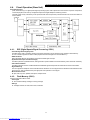
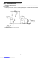
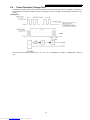
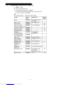
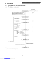
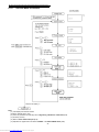
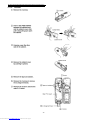
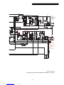
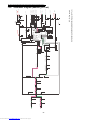
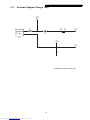
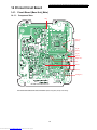
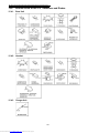
1
ORDER NO. KM40801513CE
F13
Telephone Equipment
Model No. KX-TG9341T
KX-TG9342T
KX-TG9343S
KX-TG9343T
KX-TG9344T
KX-TGA931S
KX-TGA931T
Expandable Digital Cordless Answering
System
Pearl Silver Version
Titanium Black Version
(for U.S.A.)
© 2008 Panasonic Communications Co., Ltd. All
rights reserved. Unauthorized copying and distribution is a violation of law.
Downloaded from www.Manualslib.com manuals search engine
KX-TG9341T/KX-TG9342T/KX-TG9343S/KX-TG9343T/KX-TG9344T/KX-TGA931S/KX-TGA931T
2
Downloaded from www.Manualslib.com manuals search engine
KX-TG9341T/KX-TG9342T/KX-TG9343S/KX-TG9343T/KX-TG9344T/KX-TGA931S/KX-TGA931T
TABLE OF CONTENTS
PAGE
1 Safety Precautions----------------------------------------------- 4
1.1. For Service Technicians --------------------------------- 4
2 Warning -------------------------------------------------------------- 4
2.1. Battery Caution--------------------------------------------- 4
2.2. About Lead Free Solder (PbF: Pb free)-------------- 4
2.3. Discarding of P. C. Board-------------------------------- 5
3 Specifications ----------------------------------------------------- 6
4 Technical Descriptions ----------------------------------------- 7
4.1. US-DECT Description ------------------------------------ 7
4.2. Block Diagram (Base Unit_Main)---------------------- 9
4.3. Block Diagram (Base Unit_RF Part) -----------------10
4.4. Circuit Operation (Base Unit) -------------------------- 11
4.5. Block Diagram (Handset)-------------------------------20
4.6. Block Diagram (Handset_RF Part)-------------------21
4.7. Circuit Operation (Handset)----------------------------22
4.8. Circuit Operation (RF Part)-----------------------------26
4.9. Circuit Operation (Charger Unit) ----------------------27
4.10. Signal Route -----------------------------------------------28
5 Location of Controls and Components ------------------30
5.1. Controls -----------------------------------------------------30
5.2. Display ------------------------------------------------------30
6 Installation Instructions ---------------------------------------31
6.1. Connections------------------------------------------------31
6.2. Battery-------------------------------------------------------31
7 Operating Instructions-----------------------------------------33
7.1. Programmable Settings ---------------------------------33
7.2. Error Messages -------------------------------------------36
7.3. Troubleshooting-------------------------------------------37
8 Test Mode ----------------------------------------------------------41
8.1. Adjustment and Test Mode Flow Chart -------------41
9 Service Mode -----------------------------------------------------48
9.1. How to Clear User Setting------------------------------48
10 Troubleshooting Guide ----------------------------------------50
10.1. Troubleshooting Flowchart -----------------------------50
10.2. How to Replace the Flat Package IC ----------------63
10.3. How to Replace the LLP (Leadless Leadframe
Package) IC------------------------------------------------65
11 Disassembly and Assembly Instructions ---------------68
11.1. Disassembly Instructions -------------------------------68
11.2. How to Replace the Handset LCD -------------------72
12 Measurements and Adjustments---------------------------74
12.1. Things to Do after Replacing IC or X’tal ------------74
12.2. Base Unit Reference Drawing-------------------------75
12.3. Handset Reference Drawing---------------------------76
12.4. Frequency Table ------------------------------------------77
13 Schematic Diagram ---------------------------------------------79
13.1. For Schematic Diagram---------------------------------79
13.2. Schematic Diagram (Base Unit_Main) --------------80
13.3. Schematic Diagram (Base Unit_RF Part) ----------82
13.4. Schematic Diagram (Base Unit_Operation) -------83
13.5. Schematic Diagram (Handset_Main) ----------------84
13.6. Schematic Diagram (Handset_RF Part) ------------86
13.7. Schematic Diagram (Charger Unit) -----------------87
14 Printed Circuit Board-------------------------------------------89
14.1. Circuit Board (Base Unit_Main) -----------------------89
14.2. Circuit Board (Base Unit_RF Part) -------------------91
14.3. Circuit Board (Base Unit_Operation) ----------------93
14.4. Circuit Board (Handset_Main)-------------------------95
PAGE
14.5. Circuit Board (Handset_RF Part) -------------------- 97
14.6. Circuit Board (Charger Unit)--------------------------- 98
15 Appendix Information of Schematic Diagram --------- 99
15.1. CPU Data (Base Unit) ---------------------------------- 99
15.2. CPU Data (Handset) ---------------------------------- 100
15.3. Explanation of IC Terminals (RF Part) ------------ 101
15.4. Terminal Guide of the ICs, Transistors and
Diodes ---------------------------------------------------- 102
16 Exploded View and Replacement Parts List --------- 103
16.1. Cabinet and Electrical Parts (Base Unit) --------- 103
16.2. Cabinet and Electrical Parts (Handset)----------- 104
16.3. Cabinet and Electrical Parts (Charger Unit) ----- 105
16.4. Accessories and Packing Materials --------------- 106
16.5. Replacement Parts List--------------------------------110
3
Downloaded from www.Manualslib.com manuals search engine
KX-TG9341T/KX-TG9342T/KX-TG9343S/KX-TG9343T/KX-TG9344T/KX-TGA931S/KX-TGA931T
1 Safety Precautions
1.1.
For Service Technicians
• Repair service shall be provided in accordance with repair technology information such as service manual so as to prevent fires, injury or electric shock, which can be caused by improper repair work.
1. When repair services are provided, neither the products nor their parts or members shall be remodeled.
2. If a lead wire assembly is supplied as a repair part, the lead wire assembly shall be replaced.
3. FASTON terminals shall be plugged straight in and unplugged straight out.
• ICs and LSIs are vulnerable to static electricity.
When repairing, the following precautions will help prevent recurring malfunctions.
1. Cover plastic parts boxes with aluminum foil.
2. Ground the soldering irons.
3. Use a conductive mat on worktable.
4. Do not grasp IC or LSI pins with bare fingers.
2 Warning
2.1.
Battery Caution
1. Danger of explosion if battery is incorrectly replaced.
2. Replace only with the same or equivalent type recommended by the manufacturer.
3. Dispose of used batteries according to the manufacturer's Instructions.
2.2.
About Lead Free Solder (PbF: Pb free)
Note:
In the information below, Pb, the symbol for lead in the periodic table of elements, will refer to standard solder or solder that contains lead.
We will use PbF solder when discussing the lead free solder used in our manufacturing process which is made from Tin (Sn),
Silver (Ag), and Copper (Cu).
This model, and others like it, manufactured using lead free solder will have PbF stamped on the PCB. For service and repair
work we suggest using the same type of solder.
Caution
• PbF solder has a melting point that is 50 °F ~ 70 °F (30 °C ~ 40 °C) higher than Pb solder. Please use a soldering iron with temperature control and adjust it to 700 °F ± 20 °F (370 °C ± 10 °C).
• Exercise care while using higher temperature soldering irons.:
Do not heat the PCB for too long time in order to prevent solder splash or damage to the PCB.
• PbF solder will tend to splash if it is heated much higher than its melting point, approximately 1100 °F (600 °C).
• When applying PbF solder to double layered boards, please check the component side for excess which may flow onto the
opposite side (See the figure below).
4
Downloaded from www.Manualslib.com manuals search engine
KX-TG9341T/KX-TG9342T/KX-TG9343S/KX-TG9343T/KX-TG9344T/KX-TGA931S/KX-TGA931T
2.2.1.
Suggested PbF Solder
There are several types of PbF solder available commercially. While this product is manufactured using Tin, Silver, and Copper
(Sn+Ag+Cu), you can also use Tin and Copper (Sn+Cu), or Tin, Zinc, and Bismuth (Sn+Zn+Bi). Please check the manufacturer's specific instructions for the melting points of their products and any precautions for using their product with other materials.
The following lead free (PbF) solder wire sizes are recommended for service of this product: 0.3 mm, 0.6 mm and 1.0 mm.
2.3.
Discarding of P. C. Board
When discarding P. C. Board, delete all personal information such as telephone directory and caller list or scrap P. C. Board.
5
Downloaded from www.Manualslib.com manuals search engine
KX-TG9341T/KX-TG9342T/KX-TG9343S/KX-TG9343T/KX-TG9344T/KX-TGA931S/KX-TGA931T
3 Specifications
Note:
• Design and specifications are subject to change without notice.
Note for Service:
• Optional headset: KX-TCA60, KX-TCA86, KX-TCA92, KX-TCA93, KX-TCA94, KX-TCA95
6
Downloaded from www.Manualslib.com manuals search engine
KX-TG9341T/KX-TG9342T/KX-TG9343S/KX-TG9343T/KX-TG9344T/KX-TGA931S/KX-TGA931T
4 Technical Descriptions
4.1.
US-DECT Description
The frequency range of 1.92 GHz-1.93 GHz is used. Transmitting and receiving carrier between base unit and handset is same frequency. Refer to Frequency Table (P.77).
4.1.1.
TDD Frame Format
4.1.2.
TDMA system
This system is the cycles of 10 ms, and has 6 duplex paths, but maximum duplex communication path is 5 because of dummy
bearer use.
In 1 slot 417 µs, the 10 ms of voice data is transmitted.
• 2 - Handsets Link
Traffic Bearer
A link is established between base unit and handset.
The state where duplex communication is performed.
Handset doesn't make up duplex in no free RF channels because of interference. (*1)
Dummy Bearer
Base unit sends Dummy-data to the all stand-by state handsets.
Handsets receive that data for synchronization and monitoring request from the base unit.
Base unit doesn't send Dummy bearer in no free RF channels because of interference. (*1)
Note:
(*1) It is a feature under FCC 15 regulation and for interference avoidance.
In the case of checking RF parts, it is better in least interference condition.
7
Downloaded from www.Manualslib.com manuals search engine
KX-TG9341T/KX-TG9342T/KX-TG9343S/KX-TG9343T/KX-TG9344T/KX-TGA931S/KX-TGA931T
4.1.3.
Signal Flowchart in the Radio Parts
Reception
A voice signal from TEL line is encoded to digital data "TXDATA" by DSP (IC501) in a base unit.
Then TXDATA goes to RF PART, and it's modulated to 1.9 GHz. The RF signal is amplified and fed to a selected antenna.
As for a handset RF, RF signal is received in two antennas.
RFIC (IC701) compares RF signal levels and selects the antenna to be used. Then RFIC down-converts to 864 kHz IF signal
from RX signal in the selected antenna, and demodulates it to digital data "RXDATA".
DSP (IC501) converts RXDATA into a voice signal and outputs it to speaker.
Transmission
A voice signal from microphone is encoded to digital data "TXDATA" by DSP (IC501) in a handset.
Then TXDATA goes to RF PART, and it's modulated to 1.9 GHz. The RF signal is amplified and fed to a selected antenna.
As for a base unit RF, RF signal is received in two antennas.
RFIC (IC701) compares RF signal levels and selects the antenna to be used. Then RFIC down-converts to 864 kHz IF signal
from RX signal in the selected antenna, and demodulates it to digital data "RXDATA".
DSP (IC501) converts RXDATA into a voice signal and outputs it to TEL line.
8
Downloaded from www.Manualslib.com manuals search engine
9
RF_PART
V_RF
V_RF(VPA)
SPP
SPN
SP_LED
LOUT
LIN
RLY
DCIN 2
DCIN 1
BELL
CID_IN
CID_IN
RECEIVE
AMP
Q171
MIC
SIDE TONE
CIRCUIT
Q161
INUSE
DETECT 2
R151,R152
INUSE
DETECT 1
R131, R133
RLY
Q141
RXDATA
TXDATA
RADIO_EN
IC601
FLASH
MEMORY
SLOT_CTROL
DSP
INT_1 5
MIP
MIN
VCC
VCCIN
VCCA
VCCPA
POWER_DOWN
RESET
BELL
DETECT
Q361, Q362
4.0 V
CONVERTOR
IC300, Q300
BELL
DETECT
Q111
D101
R371
R372
DCM
DCP
L1R
-
+
CHARGE_CONTACT
DC JACK
TEL JACK
L1T
KX-TG9341/9342/9343/9344 BLOCK DIAGRAM (Base Unit_Main)
Q382
3.3 V
REGULATOR
with RESET
INUSE_LED
IC331
MSG_LED
SYN_DATA
VCC
X501
13.824 MHz
IC501
SP
ANSWER_LED
SYN_CLK
SYN_EN
SYN_OUT
3
KEY 1
ANT1 ANT2
KEYS
KEY B, C, D, E
SI,SO,CS,
CLK,RST
Downloaded from www.Manualslib.com manuals search engine
INT_1
4.2.
CHARGE_DET
Operational P.C. Board
KX-TG9341T/KX-TG9342T/KX-TG9343S/KX-TG9343T/KX-TG9344T/KX-TGA931S/KX-TGA931T
Block Diagram (Base Unit_Main)
10
Downloaded from www.Manualslib.com manuals search engine
Note:
(*1) Antenna Type: wired dipole antenna
D781
D771
Mixer
Divider
1.5
A/D
Demodulator
Control
Logic
13.824 MHz
4.0 V
SYN_OUT
SYN_EN
SYN_CLK
SYN_DATA
SLOT_CTROL
RADIO_EN
TXDATA
RXDATA
BCLK
DSP
IC501
V_RF
KX-TGTG9341/9342/9343/9344 BLOCK DIAGRAM (Base Unit_RF Part)
IC701
delta-sigma Modulator
PLL
Regulator
V_PA
4.3.
ANT2 (*1)
ANT1 (*1)
3.0 V
IC741
KX-TG9341T/KX-TG9342T/KX-TG9343S/KX-TG9343T/KX-TG9344T/KX-TGA931S/KX-TGA931T
Block Diagram (Base Unit_RF Part)
KX-TG9341T/KX-TG9342T/KX-TG9343S/KX-TG9343T/KX-TG9344T/KX-TGA931S/KX-TGA931T
4.4.
Circuit Operation (Base Unit)
General Description:
(DSP, Flash Memory) is a digital speech/signal processing system that implements all the functions of speech compression,
record and playback, and memory management required in a digital telephone answering machine.
The DSP system is fully controlled by a host processor DSP. The host processor provides activation and control of all that functions as follows.
4.4.1.
DSP (Digital Speech/Signal Processing: IC501)
• Voice Message Recording/Play back
The DSP system uses a proprietary speech compression technique to record and store voice message in Flash Memory.
An error correction algorithm is used to enable playback of these messages from the Flash Memory.
• DTMF Generator
When the DTMF data from the handset is received, the DTMF signal is output.
• Synthesized Voice (Pre-recorded message)
The DSP implements synthesized Voice, utilizing the built in speech detector and a Flash Memory, which stored the vocabulary.
• Caller ID demodulation
The DSP implements monitor and demodulate the FSK/DTMF signals that provide CID information from the Central Office.
• Digital Switching
The voice signal from telephone line is transmitted to the handset or the voice signal from the handset is transmitted to the Telephone line, etc. They are determined by the signal path route operation of voice signal.
• Block Interface Circuit
RF part, LED, Key scan, Speaker, Microphone, Telephone line.
4.4.2.
Flash Memory (IC601)
Following information data is stored.
• Voice signal
ex: Pre-recorded Greeting message, Incoming message
• Settings
ex: message numbers, ID code, Flash Time, Tone/Pulse
11
Downloaded from www.Manualslib.com manuals search engine
KX-TG9341T/KX-TG9342T/KX-TG9343S/KX-TG9343T/KX-TG9344T/KX-TGA931S/KX-TGA931T
4.4.3.
Power Supply Circuit
Function:
The power supply voltage from AC adaptor is converted to the desired voltage of each block.
Circuit Operation:
• Q300 and IC300: 4.0 V DCDC Converter
• IC331: 3.3 V Regulator
12
Downloaded from www.Manualslib.com manuals search engine
KX-TG9341T/KX-TG9342T/KX-TG9343S/KX-TG9343T/KX-TG9344T/KX-TGA931S/KX-TGA931T
4.4.3.1.
Charge Circuit
The voltage from the AC adaptor is supplied to the charge circuits.
13
Downloaded from www.Manualslib.com manuals search engine
KX-TG9341T/KX-TG9342T/KX-TG9343S/KX-TG9343T/KX-TG9344T/KX-TGA931S/KX-TGA931T
4.4.4.
Reset Circuit
Function:
This circuit is used to initialize the microcomputer when it incorporates an AC adaptor.
Circuit Operation:
When the AC Adaptor is inserted into the unit, then the voltage is shifted by IC331 and power is supplied to the DSP.
The set starts to operate when VCC goes up to 3.0 V or more in the circuit voltage diagram.
Note:
(*1) The initializing time of the DSP chip is 28 ms under normal conditions.
14
Downloaded from www.Manualslib.com manuals search engine
KX-TG9341T/KX-TG9342T/KX-TG9343S/KX-TG9343T/KX-TG9344T/KX-TGA931S/KX-TGA931T
4.4.5.
Telephone Line Interface
Telephone Line Interface Circuit:
Function
• Bell signal detection
• ON/OFF hook and pulse dial circuit
• Side tone circuit
Bell signal detection and OFF HOOK circuit:
In the idle mode, Q141 is open to cut the DC loop current and decrease the ring load. When ring voltage appears at the Tip (T)
and Ring (R) leads (When the telephone rings), the AC ring voltage is transferred as follows:
T → L101 → R111 → C111 → Q111 → DSP pin 58 [BELL]
When the CPU (DSP) detects a ring signal, Q141 turns on, thus providing an off-hook condition (active DC current flow through
the circuit). Following signal flow is the DC current flow.
T → L101 → D101 → Q141 → Q161 → R163 → R167 → D101 → L102 → P101 → R
ON HOOK Circuit:
Q141 is open, Q141 is connected as to cut the DC loop current and to cut the voice signal. The unit is consequently in an onhook condition.
Pulse Dial Circuit:
Pin 59 of DSP turns Q141 ON/OFF to make the pulse dialing.
Side Tone Circuit:
Basically this circuit prevents the TX signal from feeding back to RX signal. As for this unit, TX signal feed back from Q161 is
canceled by the canceller circuit of DSP.
15
Downloaded from www.Manualslib.com manuals search engine
KX-TG9341T/KX-TG9342T/KX-TG9343S/KX-TG9343T/KX-TG9344T/KX-TGA931S/KX-TGA931T
4.4.6.
Auto Disconnect Circuit
Function:
This circuit is used to detect the fact that another telephone connected to the same line is OFF-HOOK while the unit is in a
receiving status or OGM transmitting status.
Circuit Operation:
The voltage of pin 90 of IC501 is monitored. If a parallel-connected telephone is put into OFF HOOK status, the presence/
absence of a parallel connection is determined when the voltage changes by 0.2 V or more. When the set detects the parallelconnected telephone is OFF HOOK status, the line is disconnected.
You can enable or disable the Auto Disconnect function.
See Check Record (P.52)
16
Downloaded from www.Manualslib.com manuals search engine
KX-TG9341T/KX-TG9342T/KX-TG9343S/KX-TG9343T/KX-TG9344T/KX-TGA931S/KX-TGA931T
4.4.7.
Parallel Connection Detect Circuit
Function:
In order to disable call waiting and stutter tone functions when using telephones connected in parallel, it is necessary to have a
circuit that judges whether a telephone connected in parallel is in use or not. This circuit determines whether the telephone connected in parallel is on hook or off hook by detecting changes in the T/R voltage.
Circuit Operation:
Parallel connection detection when on hook:
When on hook, the voltage is monitored at pin 86 of IC501. There is no parallel connection if the voltage is
1.65 V or higher, while a parallel connection is deemed to exist if the voltage is lower.
Parallel connection detection when off hook:
When off hook, the voltage is monitored at pin 90 of IC501; the presence/absence of a parallel connection is determined when
the voltage changes by 0.2 V or more.
17
Downloaded from www.Manualslib.com manuals search engine
KX-TG9341T/KX-TG9342T/KX-TG9343S/KX-TG9343T/KX-TG9344T/KX-TGA931S/KX-TGA931T
4.4.8.
Calling Line Identification (Caller ID)/Call Waiting Caller ID
Function:
Caller ID
The caller ID is a chargeable ID which the user of a telephone circuit obtains by entering a contract with the telephone company
to utilize a caller ID service. For this reason, the operation of this circuit assumes that a caller ID service contract has been
entered for the circuit being used. The data for the caller ID from the telephone exchange is sent during the interval between the
first and second rings of the bell signal. The data from the telephone exchange is a modem signal which is modulated in an FSK
(Frequency Shift Keying) * format. Data "1" is a 1200 Hz sine wave, and data "0" is a 2200 Hz sine wave. There are two types of
the message format which can be received: i.e. the single message format and plural message format. The plural message format allows to transmit the name and data code information in addition to the time and telephone number data.
*: Also the telephone exchange service provides other formats.
18
Downloaded from www.Manualslib.com manuals search engine
KX-TG9341T/KX-TG9342T/KX-TG9343S/KX-TG9343T/KX-TG9344T/KX-TGA931S/KX-TGA931T
Call Waiting Caller ID
Calling Identity Delivery on Call Waiting (CIDCW) is a CLASS service that allows a customer, while off-hook on an existing call,
to receive information about a calling party on a waited call. The transmission of the calling information takes place almost
immediately after the customer is alerted to the new call so he/she can use this information to decide whether to take the new
call.
Function:
The telephone exchange transmits or receives CAS and ACK signals through each voice RX/TX route. Then FSK data and
MARK data pass the following route.
Telephone Line → CN101 (T, R) → P101 → L101, L102 → C121, C122 → R121, R122 → IC501 (89, 88).
If the unit deems that a telephone connected in parallel is in use, ACK is not returned even if CAS is received, and the information for the second and subsequent callers is not displayed on the portable handset display.
19
Downloaded from www.Manualslib.com manuals search engine
KX-TG9341T/KX-TG9342T/KX-TG9343S/KX-TG9343T/KX-TG9344T/KX-TGA931S/KX-TGA931T
4.5.
Block Diagram (Handset)
IC541
CHG_DET
CHARGE
DETECT
Q362, Q364
CHG_CTL
CHARGE
CONTROL
Q361
RF part
SYN_OUT
SYN_EN
RST
CHARGE
WP, CLK, DATA
Q531
ANT
X501
13.824 MHz
EEPROM
SYN_CLK
SYN_DATA
RESET
SLOT_CTROL
RADIO_EN
D361
IC374
RST
TXDATA
RXDATA
PDN
IC371
2.7 V
REGULATOR
VCC
V_PA
VCCA
VCCPA
V_RF
BATTERY
IC501
MIC
MIP
MIN
DSP
SP
SPP1
IC561
DC/DC
CONVERTER
LCD BACKLIGHT
Headset Jack
LCD
BACK
LIGHT
SPN
HSM
CN431
R436/R437
HEADSET_DET
BL_LED
Q561
ANT_LIGHT
Monitor SP
CI
SPP2
SPPN
CI
LCD
KEYIN_1~5
Q562
HEADSET
DETECT
LED561
(ANT)
KEYSTOROBE_A~E
LED551-554
(KEY)
KEYS
IC372
DC/DC
CONVERTER
IC373
DC/DC
CONVERTER
KX-TGA931 BLOCK DIAGRAM (Handset)
20
Downloaded from www.Manualslib.com manuals search engine
Downloaded from www.Manualslib.com manuals search engine
21
D771
(*1) Antenna Type ( difference between base unit and handset in Radio parts)
ANT1: wired dipole antenna
ANT2: patterned antenna
Note:
D781
Mixer
Divider
1.5
IC701
A/D
13.824 MHz
3.1 V
SYN_OUT
SYN_EN
SYN_CLK
SYN_DATA
SLOT_CTROL
RADIO_EN
TXDATA
RXDATA
BCLK
RF_POWER
DSP
IC501
V_RF
KX-TGA931 BLOCK DIAGRAM (Handset_RF Part)
Demodulator
Control
Logic
delta-sigma Modulator
PLL
Regulator
V_PA
4.6.
ANT2 (*1)
ANT1 (*1)
2.7 V
IC741
KX-TG9341T/KX-TG9342T/KX-TG9343S/KX-TG9343T/KX-TG9344T/KX-TGA931S/KX-TGA931T
Block Diagram (Handset_RF Part)
KX-TG9341T/KX-TG9342T/KX-TG9343S/KX-TG9343T/KX-TG9344T/KX-TGA931S/KX-TGA931T
4.7.
4.7.1.
Circuit Operation (Handset)
Construction
The circuit mainly consists of DSP and RF part as shown in the block diagram.
4.7.1.1.
DSP: IC501
Function
• Battery Low, Power down detect circuit
• Ringer Generation
• Interface circuit
RF part, Speaker, Mic, LED, Key scan, LCD, Headset
Initial waves
Note:
(*1) The initializing time of the DSP chip is 20 ms under normal conditions.
4.7.1.2.
RF part
Mainly voice signal is modulated to RF, or it goes the other way.
4.7.1.3.
EEPROM: IC541
Setting data is stored.
ex: ID code, user setting
22
Downloaded from www.Manualslib.com manuals search engine
KX-TG9341T/KX-TG9342T/KX-TG9343S/KX-TG9343T/KX-TG9344T/KX-TGA931S/KX-TGA931T
4.7.2.
Power Supply Circuit
Voltage is supplied separately to each block.
23
Downloaded from www.Manualslib.com manuals search engine
KX-TG9341T/KX-TG9342T/KX-TG9343S/KX-TG9343T/KX-TG9344T/KX-TGA931S/KX-TGA931T
4.7.3.
Charge Circuit
When the handset is put on the cradle of the base unit, the power is supplied from CHARGE+ and CHARGE- terminals to
charge the battery via R366 or Q361. The voltage between CHARGE+ and CHARGE- flows Q531 → pin 38 of IC501, where
the charge is detected. Then IC501 calculates the battery consumption amount from the previous charge, and it controls Q361/
Q362/Q364 by pin 42 of IC501 until charging is complete. When charging is complete, the control pattern is switched to Trickle
charging form from Operational charging form.
Charging form
4.7.4.
Ringer and Handset SP-Phone
24
Downloaded from www.Manualslib.com manuals search engine
KX-TG9341T/KX-TG9342T/KX-TG9343S/KX-TG9343T/KX-TG9344T/KX-TGA931S/KX-TGA931T
4.7.5.
Sending Signal
The voice signal from the microphone is input to DSP (90, 91). CN431 is the headset jack. When the headphone is connected,
the R436/R437 detects it. The input from the microphone of the handset (MIM, MIP) is cut and the microphone signal from the
headset is input to DSP (95). Also the power for the microphone is supplied from DSP (92) and the power is turned OFF on
standby.
4.7.6.
Reception Signal
The voice signal from the base unit is output to DSP (98). This signal is led to the headset jack (CN431). The signal through the
headset jack and the other signal output from DSP (97) drives the speaker. When the headset is inserted to the jack, the voice
signal is cut at the jack, so the sound does not come out from the speaker, but from the headset only.
25
Downloaded from www.Manualslib.com manuals search engine
KX-TG9341T/KX-TG9342T/KX-TG9343S/KX-TG9343T/KX-TG9344T/KX-TGA931S/KX-TGA931T
4.8.
Circuit Operation (RF Part)
General Description:
RF part includes Transmitter and Receiver functions. Digital signals (Mainly voice data) that come from DSP, are modulated and
are transmitted. On the other hand, received signals are demodulated and go out to DSP.
4.8.1.
Power Supply Circuit
As indicated below, the various voltages are supplied to each block.
V_PA, about 3.2 V at base unit or 3.1 V at handset, is supplied to the Power amplifier.
IC741 is 3.0 V at base unit or 2.7 V at handset Regulator and outputs VRF (3.0 V at base unit or 2.7 V at handset) by order of
RADIO_EN signal.
V_RF is approximately 4.0 V (Base Unit) or 3.1 V (Handset).
26
Downloaded from www.Manualslib.com manuals search engine
KX-TG9341T/KX-TG9342T/KX-TG9343S/KX-TG9343T/KX-TG9344T/KX-TGA931S/KX-TGA931T
4.9.
Circuit Operation (Charger Unit)
The voltage from the AC adaptor is supplied to the charge circuits. Main charge (180~250 mA at the Battery) of maximum 7hours is started soon after the handset is placed on the charger unit. Then it changes to Trickle charge to prevent from overcharging.
Charging form
The route for this is as follows: DC+pin of J1(+) → F1 → D1 → R1 → CHARGE+pad → Handset → CHARGE-pad → DC-pin of
J1(-).
27
Downloaded from www.Manualslib.com manuals search engine
KX-TG9341T/KX-TG9342T/KX-TG9343S/KX-TG9343T/KX-TG9344T/KX-TGA931S/KX-TGA931T
4.10. Signal Route
28
Downloaded from www.Manualslib.com manuals search engine
KX-TG9341T/KX-TG9342T/KX-TG9343S/KX-TG9343T/KX-TG9344T/KX-TGA931S/KX-TGA931T
RF part signal route
29
Downloaded from www.Manualslib.com manuals search engine
KX-TG9341T/KX-TG9342T/KX-TG9343S/KX-TG9343T/KX-TG9344T/KX-TGA931S/KX-TGA931T
5 Location of Controls and
Components
5.1.
5.1.1.
5.1.2.
Handset
Controls
Base Unit
5.2.
30
Downloaded from www.Manualslib.com manuals search engine
Display
KX-TG9341T/KX-TG9342T/KX-TG9343S/KX-TG9343T/KX-TG9344T/KX-TGA931S/KX-TGA931T
6 Installation Instructions
6.2.
6.1.
6.2.1.
Connections
31
Downloaded from www.Manualslib.com manuals search engine
Battery
Battery Installation and
Replacement
KX-TG9341T/KX-TG9342T/KX-TG9343S/KX-TG9343T/KX-TG9344T/KX-TGA931S/KX-TGA931T
6.2.2.
Battery Charge
6.2.4.
Note for service:
The battery strength may not be indicated correctly if the
battery is disconnected and connected again, even after it is
fully charged. In that case, by recharging the battery as
mentioned above, you will get a correct indication of the
battery strength.
6.2.3.
Battery Level
32
Downloaded from www.Manualslib.com manuals search engine
Panasonic Ni-MH Battery Performance (supplied batteries)
KX-TG9341T/KX-TG9342T/KX-TG9343S/KX-TG9343T/KX-TG9344T/KX-TGA931S/KX-TGA931T
7 Operating Instructions
7.1.
7.1.1.
Programmable Settings
Programming by Scrolling through the Display Menus
33
Downloaded from www.Manualslib.com manuals search engine
KX-TG9341T/KX-TG9342T/KX-TG9343S/KX-TG9343T/KX-TG9344T/KX-TGA931S/KX-TGA931T
7.1.2.
Programming using the Direct Commands
34
Downloaded from www.Manualslib.com manuals search engine
KX-TG9341T/KX-TG9342T/KX-TG9343S/KX-TG9343T/KX-TG9344T/KX-TGA931S/KX-TGA931T
35
Downloaded from www.Manualslib.com manuals search engine
KX-TG9341T/KX-TG9342T/KX-TG9343S/KX-TG9343T/KX-TG9344T/KX-TGA931S/KX-TGA931T
7.2.
Error Messages
36
Downloaded from www.Manualslib.com manuals search engine
KX-TG9341T/KX-TG9342T/KX-TG9343S/KX-TG9343T/KX-TG9344T/KX-TGA931S/KX-TGA931T
7.3.
Troubleshooting
37
Downloaded from www.Manualslib.com manuals search engine
KX-TG9341T/KX-TG9342T/KX-TG9343S/KX-TG9343T/KX-TG9344T/KX-TGA931S/KX-TGA931T
38
Downloaded from www.Manualslib.com manuals search engine
KX-TG9341T/KX-TG9342T/KX-TG9343S/KX-TG9343T/KX-TG9344T/KX-TGA931S/KX-TGA931T
39
Downloaded from www.Manualslib.com manuals search engine
KX-TG9341T/KX-TG9342T/KX-TG9343S/KX-TG9343T/KX-TG9344T/KX-TGA931S/KX-TGA931T
40
Downloaded from www.Manualslib.com manuals search engine
KX-TG9341T/KX-TG9342T/KX-TG9343S/KX-TG9343T/KX-TG9344T/KX-TGA931S/KX-TGA931T
8 Test Mode
8.1.
8.1.1.
Adjustment and Test Mode Flow Chart
TX-CW Mode for Base Unit
Note:
(*1) Refer to Check Table for RF part (P.58).
41
Downloaded from www.Manualslib.com manuals search engine
KX-TG9341T/KX-TG9342T/KX-TG9343S/KX-TG9343T/KX-TG9344T/KX-TGA931S/KX-TGA931T
8.1.2.
Test Link Mode for Base Unit
Note:
(*1) Refer to Test Link Mode for Handset (P.46). If you can not proceed to the next step, refer to Registering a Handset to a
Base Unit (P.56).
(*2) Refer to Check Table for RF part (P.58).
(*3) Operation for regular base unit. Refer to CHART1 in the TEST RANGE Check (P.59).
(*4) for factory use only
42
Downloaded from www.Manualslib.com manuals search engine
KX-TG9341T/KX-TG9342T/KX-TG9343S/KX-TG9343T/KX-TG9344T/KX-TGA931S/KX-TGA931T
8.1.3.
Adjustment Mode for Base Unit
Cross Reference
Check and Adjust Frequency (Base Unit) (P.74)
43
Downloaded from www.Manualslib.com manuals search engine
KX-TG9341T/KX-TG9342T/KX-TG9343S/KX-TG9343T/KX-TG9344T/KX-TGA931S/KX-TGA931T
8.1.4.
TX-CW Mode for Handset
Note:
(*1) LCD displays the Channel number.
(exception: default/ CH00 = 0ch.)
(*2) Refer to Check Table for RF part (P.58).
44
Downloaded from www.Manualslib.com manuals search engine
KX-TG9341T/KX-TG9342T/KX-TG9343S/KX-TG9343T/KX-TG9344T/KX-TGA931S/KX-TGA931T
8.1.5.
RX-CW Test Mode for Handset
Note:
(*1) LCD displays the Channel number.
(exception: default/ CH00 = 0ch.)
(*2) Refer to Check Table for RF part (P.58).
45
Downloaded from www.Manualslib.com manuals search engine
KX-TG9341T/KX-TG9342T/KX-TG9343S/KX-TG9343T/KX-TG9344T/KX-TGA931S/KX-TGA931T
8.1.6.
Test Link Mode for Handset
Note:
(*1) LCD displays the Channel number.
(exception: default/ CH00 = 0ch.)
(*2) If can not proceed to the next step, refer to Registering a Handset to a Base Unit (P.56).
(*3) for factory use only.
(*4) Refer to Check Table for RF part (P.58).
(*5) Operation for regular base unit. Refer to CHART1 in the TEST RANGE Check (P.59).
46
Downloaded from www.Manualslib.com manuals search engine
KX-TG9341T/KX-TG9342T/KX-TG9343S/KX-TG9343T/KX-TG9344T/KX-TGA931S/KX-TGA931T
8.1.7.
Adjustment Mode for Handset
Cross Reference
(*1) Adjust Battery Low Detector Voltage (Handset) (P.74)
Note:
(*2) These are the default values.
(*3) These values may not be fixed depending on the battery strength.
47
Downloaded from www.Manualslib.com manuals search engine
KX-TG9341T/KX-TG9342T/KX-TG9343S/KX-TG9343T/KX-TG9344T/KX-TGA931S/KX-TGA931T
9 Service Mode
9.1.
How to Clear User Setting
Units are reset to the Factory settings by this operation (Erase recorded Voice messages, stored Phone numbers, Caller list and
etc.).
This operation should not be performed for a usual repair.
9.1.1.
Base Unit
Note:
(*1) Telephone line must be connected.
48
Downloaded from www.Manualslib.com manuals search engine
KX-TG9341T/KX-TG9342T/KX-TG9343S/KX-TG9343T/KX-TG9344T/KX-TGA931S/KX-TGA931T
9.1.2.
Handset
Note:
(*1) Be sure to short the battery terminals of the handset with a lead wire, etc. for 2 seconds for discharge after removing the
battery.
49
Downloaded from www.Manualslib.com manuals search engine
KX-TG9341T/KX-TG9342T/KX-TG9343S/KX-TG9343T/KX-TG9344T/KX-TGA931S/KX-TGA931T
10 Troubleshooting Guide
10.1. Troubleshooting Flowchart
Note:
(*1) When a user claims that the unit disconnects a call right
after the greeting message and no incoming messages can
be recorded, this symptom can not be reappeared with TEL
simulator in the service center. In this case, try Check
Record (P.52) item (C), (D).
Cross Reference:
Check Power (P.51)
Check Playback (P.53)
Check Record (P.52)
Check Battery Charge (P.53)
Check Link (P.54)
Check the RF part (P.55)
Check Handset Transmission (P.62)
Check Handset Reception (P.62)
Check Caller ID (P.62)
50
Downloaded from www.Manualslib.com manuals search engine
KX-TG9341T/KX-TG9342T/KX-TG9343S/KX-TG9343T/KX-TG9344T/KX-TGA931S/KX-TGA931T
10.1.1. Check Power
Cross Reference:
Power Supply Circuit (P.12)
Reset Circuit (P.14)
Note:
Flash Memory is IC601.
DSP is IC501.
(*1) Refer to Specifications (P.6) for part number and supply voltage of AC adaptor.
(*2) Refer to Circuit Board (Base Unit_Main) (P.89).
51
Downloaded from www.Manualslib.com manuals search engine
KX-TG9341T/KX-TG9342T/KX-TG9343S/KX-TG9343T/KX-TG9344T/KX-TGA931S/KX-TGA931T
10.1.2. Check Record
BASE UNIT
A) Not record Greeting Message
B) Not record Incoming Message
C) How to change the Auto Disconnect activation (time)
Some Telephone Company lines (fiber or cable) ON Hook and OFF Hook voltages are lower than conventional lines, which may
cause a malfunction of Auto Disconnect detection. To solve this problem, try changing the Auto Disconnect activation through
the procedures below.
Auto Disconnect detect
Enable*1
Enable*1 [default]
Disable*2
CPC detect
Disable
PROCEDURE at Stand-by mode
“STOP”+”GREETING CHECK”+”REC” simultaneously
“STOP”+”GREETING CHECK”+”VOL.
" simultaneously
“STOP”+”GREETING CHECK”+”VOL.
" simultaneously
Note:
*1 Both Auto Disconnect and CPC don't detect for the first 2 seconds.
*2 If the “Disable” is selected, even if the parallel-connected telephone is OFF HOOK, the line isn't disconnected.
D) How to change the VOX level
It makes easier to detect a small voice (caller) by raising the sensitivity of VOX level. Therefore, the recording of TAM is not
turned off during a detection.
VOX Level sensitivity
Normal [default]
6 dB Up
“STOP”+”LOCATOR”+”VOL.
“STOP”+”LOCATOR”+”VOL.
Note:
Flash Memory is IC601.
DSP is IC501.
Cross Reference:
Signal Route (P.28)
Telephone Line Interface (P.15)
Auto Disconnect Circuit (P.16)
Parallel Connection Detect Circuit (P.17)
52
Downloaded from www.Manualslib.com manuals search engine
PROCEDURE
" simultaneously
" simultaneously
KX-TG9341T/KX-TG9342T/KX-TG9343S/KX-TG9343T/KX-TG9344T/KX-TGA931S/KX-TGA931T
10.1.3. Check Playback
Cross Reference:
Power Supply Circuit (P.12)
Note:
Flash Memory is IC601.
DSP is IC501.
(*1) Refer to Circuit Board (Base Unit_Main) (P.89).
10.1.4. Check Battery Charge
Note:
Flash Memory is IC601.
(*1) Refer to Specifications (P.6) for part number and supply voltage of AC adaptor.
53
Downloaded from www.Manualslib.com manuals search engine
KX-TG9341T/KX-TG9342T/KX-TG9343S/KX-TG9343T/KX-TG9344T/KX-TGA931S/KX-TGA931T
10.1.5. Check Link
Cross Reference:
Check the RF part (P.55)
Note:
Flash Memory is IC601.
DSP is IC501.
(*1) Refer to Finding out the Defective part (P.55).
54
Downloaded from www.Manualslib.com manuals search engine
KX-TG9341T/KX-TG9342T/KX-TG9343S/KX-TG9343T/KX-TG9344T/KX-TGA931S/KX-TGA931T
10.1.6. Check the RF part
10.1.6.1. Finding out the Defective part
After All the Checkings or Repairing
1. Re-register the checked handset to the checked base unit, and Regular HS to Regular BU.
Note:
(*1) HS: Handset
(*2) BU: Base Unit
55
Downloaded from www.Manualslib.com manuals search engine
KX-TG9341T/KX-TG9342T/KX-TG9343S/KX-TG9343T/KX-TG9344T/KX-TGA931S/KX-TGA931T
10.1.6.1.1. Registering a Handset to a Base Unit
10.1.6.1.2. Deregistering a Handset
10.1.6.1.3. Deregistering All Handsets by the Base Unit
56
Downloaded from www.Manualslib.com manuals search engine
KX-TG9341T/KX-TG9342T/KX-TG9343S/KX-TG9343T/KX-TG9344T/KX-TGA931S/KX-TGA931T
10.1.6.2. RF Check Flowchart
Each item (1 ~ 6) of RF Check Flowchart corresponds to Check Table for RF part (P.58).
Please refer to the each item.
Note:
(*1) Refer to Things to Do after Replacing IC or X’tal (P.74).
57
Downloaded from www.Manualslib.com manuals search engine
KX-TG9341T/KX-TG9342T/KX-TG9343S/KX-TG9343T/KX-TG9344T/KX-TGA931S/KX-TGA931T
10.1.6.3. Check Table for RF part
No.
Item
1 Link Confirmation Normal
HS, BU Mode [Normal Mode]
2
Control signal confirmation
3
HS, BU Mode: [Normal Mode] (*1)
X'tal Frequency confirmation (*8)
BU (Base Unit) Check
1. Register Regular HS to BU (to be
checked).
2. Press [Talk] key of the Regular HS to
establish link.
Check DSP interface. (*2)
Check X'tal Frequency.
(13.824000 MHz ±100 Hz)
HS, BU Mode: [Adjustment] (*4)
4-1 TX confirmation
Regular HS Mode:
[Test RX_CW Mode] (*5)
↑ [AIR]
BU (to be checked) Mode:
[Normal Mode]
1. Place Regular HS 15 cm away from a
checked BU.
2. Confirm "RXDATA" waveform of Regular
HS by Oscilloscope.
Please try to vary Regular HS CH from 00
ch to 04 ch to be matched to the BU
dummy CH, then the waveform is verified.
(*6)
4-2 TX confirmation
Regular BU Mode:
[Normal Mode]
↑ [AIR]
HS (to be checked) Mode:
[TEST TX_CW Mode] (*5)
5-1 RX confirmation
Regular HS Mode:
[Test TX_CW Mode] (*5)
↓ [AIR]
BU (to be checked) Mode:
[Normal Mode]
5-2 RX confirmation
6
Regular BU Mode:
[Normal Mode]
↓ [AIR]
HS (to be checked) Mode:
[TEST RX_CW Mode] (*5)
Range Confirmation Normal
HS, BU Mode: [Normal Mode]
Check DSP interface. (*3)
Check signal at power-on.
Check X'tal Frequency.
(13.824000 MHz ±100 Hz)
—
1. Place Regular BU 15 cm away from a
checked HS.
2. Confirm "RXDATA" waveform of Regular
BU by Oscilloscope. (*7)
When Regular BU scans TX_CW, RXDATA
is LOW.
—
1. Place Regular HS 15cm away from a
checked BU.
2. Confirm "RXDATA" waveform of the BU by
Oscilloscope. (*7)
When the BU scans TX_CW, RXDATA is
LOW.
—
1. Register Regular HS to BU (to be
checked).
2. Press [Talk] key of the Regular HS to
establish link.
3. Compare the range of the BU (being
checked) with that of the Regular BU.
Note:
(*1)(*4)(*5) Adjustment and Test Mode Flow Chart (P.41)
(*2)(*3) RF-DSP Interface Signal Wave Form (P.60)
(*6) Handset Reference Drawing (P.76)
(*7) Base Unit Reference Drawing (P.75)
(*8) Things to Do after Replacing IC or X’tal (P.74)
58
Downloaded from www.Manualslib.com manuals search engine
HS (Handset) Check
1. Register HS (to be checked) to Regular
BU.
2. Press [Talk] key of the HS to establish link.
—
1. Place Regular BU 15 cm away from a
checked HS.
2. Confirm "RXDATA" waveform of the HS by
Oscilloscope.
Please try to vary the HS CH from 00 ch to
04 ch to be matched to Regular BU dummy
CH, then the waveform is verified. (*6)
1. Register HS (to be checked) to Regular
BU.
2. Press [Talk] key of the HS to establish link.
3. Compare the range of the HS (being
checked) with that of the Regular HS.
KX-TG9341T/KX-TG9342T/KX-TG9343S/KX-TG9343T/KX-TG9344T/KX-TGA931S/KX-TGA931T
10.1.6.4. TEST RANGE Check
Circuit block which range is defective can be found by the following check.
Item
Range Confirmation TX TEST
(TX Power check)
HS, BU Mode:
[Test Link Mode] (*1)
BU (Base Unit) Check
1. Register Regular HS to BU (to be checked).
2. Set BU to “Test Link mode”.
3. Set Regular HS to “Test Link mode”.
*Set TX Power and RX Sensitivity of the BU and the
Regular HS by CHART1.
* At distance of about 5 m between HS and BU,
Link OK = TX Power of the BU is OK.
No Link = TX Power of the BU is NG.
1. Register Regular HS to BU (to be checked).
Range Confirmation RX TEST
2. Set BU to “Test Link mode”.
(RX sensitivity check)
3. Set Regular HS to “Test Link mode”.
HS, BU Mode:
[Test Link Mode] (*1)
*Set TX Power and RX Sensitivity of the BU and Regular
HS by CHART1.
* At distance of about 5 m between HS and BU,
Link OK= RX Sensitivity of the BU is OK.
No Link = RX Sensitivity of the BU is NG.
HS (Handset) Check
1. Register HS (to be checked) to Regular BU.
2. Set Regular BU to “Test Link mode”.
3. Set HS to “Test Link mode”.
*Set TX Power and RX Sensitivity of the HS and the
Regular BU by CHART1.
* At distance of about 5 m between HS and BU,
Link OK = TX Power of the HS is OK.
No Link = TX Power of the HS is NG.
1. Register HS (to be checked) to Regular BU.
2. Set Regular BU to “Test Link mode”.
3. Set HS to “Test Link mode”.
* Set TX Power and RX Sensitivity of Checking_HS and
Regular_BU by CHART1.
* At distance of about 5 m between HS and BU,
Link OK= RX Sensitivity of the HS is OK.
No Link = RX Sensitivity of the HS is NG
CHART1: Setting of TX Power and RX Sensitivity in Range Confirmation TX TEST, RX TEST
BU (Base Unit) TX Power Check
BU (Base Unit) RX Sensitivity Check
BU (to be checked)
TX Power
RX Sens.
High
High
High
High
TX Power
High
Low
HS (Handset) TX Power Check
HS (Handset) RX Sensitivity Check
HS (to be checked)
TX Power
RX Sens.
High
High
High
High
TX Power
High
Low
Note:
(*1) Adjustment and Test Mode Flow Chart (P.41)
59
Downloaded from www.Manualslib.com manuals search engine
Regular_HS
RX Sens.
Low
High
Regular_BU
RX Sens.
Low
High
KX-TG9341T/KX-TG9342T/KX-TG9343S/KX-TG9343T/KX-TG9344T/KX-TGA931S/KX-TGA931T
10.1.6.5. RF-DSP Interface Signal Wave Form
Control signal for Base Unit (Normal mode)
RADEOEN
SLOT_CTRL
2 ms
SYN_DATA
SYN_CLK
SYN_EN
SYN_DATA
0V
3V
DSP IC (IC501)
3V
us
11 µs
RF IC (IC701)
Zoom
SYN_CLK
0V
3V
SYN_EN
0V
Pin Number
RADIOEN
SLOT_CTRL
SYN_DATA
SYN_CLK
SYN_EN
IC701 IC501 (BU)
21
24
22
19
23
30
24
29
25
28
Control signal for Handset (Active normal mode after power-on)
400 ms
RADEOEN
SLOT_CTRL
SYN_DATA
SYN_CLK
SYN_EN
Zoom
40 ms
3V
RADEOEN
0V
3V
0.4 µs
3V
SYN_DATA
0V
3V
SYN_CLK
0V
3V
SYN_EN
0V
Pin Number
RADIOEN
SLOT_CTRL
SYN_DATA
SYN_CLK
SYN_EN
60
Downloaded from www.Manualslib.com manuals search engine
IC701 IC501 (HS)
21
26
22
21
23
32
24
31
25
30
DSP IC (IC501)
0V
RF IC (IC701)
SLOT_CTRL
KX-TG9341T/KX-TG9342T/KX-TG9343S/KX-TG9343T/KX-TG9344T/KX-TGA931S/KX-TGA931T
Base Unit TR-DATA Signal (Normal mode)
Base unit sends a dummy slot and receves all 6 slots every frame in normal mode.
ITEM
[HS] or [REG HS]
[REG BU] or [BU]
RX
RADEOEN
SLOT_CTRL
TR_DATA
Pin Number (Base unit)
IC701 IC501 (BU)
RADIOEN
21
24
SLOT_CTRL
22
19
TR (TX)-DATA
23
18
TR (RX)-DATA
23
34
MODE
TEST
TX_CW
Normal
RX
TX (dummy ) (*3)
RX
TX (dummy )
When "TX-CW" mode in Handset, RX-DATA of base unit is LOW. (*1)
In the other case, RX-DATA of base unit is random. (*2)
3V
40 µs
REDIOEN
0V
3V
DSP IC (IC501)
RX-DATA included in TR-DATA
Zoom RX-DATA of BU is for checking for TX of HS or RX of BU.
RF IC (IC701)
2 ms
SLOT_CTRL
0V
3V
receiving TX_CW from handset
(*1)
0V
RX-DATA
3V
random pattern because of no signal
(*2)
0V
Handset TR-DATA Signal (RX data in RX CW mode)
Base unit bursts a dummy slot in normal mode in any channel.
Handset should be worked in test mode in same channel as base unit.
ITEM
[HS] or [REG HS]
[REG BU] or [BU]
MODE
TEST RX_CW
Normal Dummy
Pin Number (Handset)
IC701 IC501 (HS)
TR (RX)-DATA
23
36
RX-DATA of handset is LOW after receiving dummy from base unit.
RX-DATA just before that is same as dummy slot data of base unit.
200 µs
Zoom
10 µs
preamble (32 bit)
Base unit ID (40 bit)
3V
TR (RX)-DATA
0V
(*3) Dummy slot data in TR-DATA of Base Unit
TX
SLOT_CTRL
preamble (32 bit)
Base unit ID (40 bit)
TR-DATA
61
Downloaded from www.Manualslib.com manuals search engine
20 µs
DSP IC (IC501)
RX
RF IC (IC701)
TR (RX)-DATA
KX-TG9341T/KX-TG9342T/KX-TG9343S/KX-TG9343T/KX-TG9344T/KX-TGA931S/KX-TGA931T
10.1.7. Check Handset Transmission
Cross Reference:
Signal Route (P.28)
10.1.8. Check Handset Reception
Cross Reference:
Signal Route (P.28)
Note:
When checking the RF part, Refer to Check the RF part
(P.55).
10.1.9. Check Caller ID
Cross Reference:
Telephone Line Interface (P.15)
Calling Line Identification (Caller ID)/Call Waiting Caller
ID (P.18)
Note:
• Make sure the format of the Caller ID service of the Telephone company that the customer subscribes to.
• It is also recommended to confirm that the customer is really
a subscriber of the service.
62
Downloaded from www.Manualslib.com manuals search engine
KX-TG9341T/KX-TG9342T/KX-TG9343S/KX-TG9343T/KX-TG9344T/KX-TGA931S/KX-TGA931T
10.2. How to Replace the Flat Package IC
10.2.1. Preparation
• PbF (: Pb free) Solder
• Soldering Iron
Tip Temperature of 700 °F ± 20 °F (370 °C ± 10 °C)
Note: We recommend a 30 to 40 Watt soldering iron. An expert may be able to use a 60 to 80 Watt iron where someone with
less experience could overheat and damage the PCB foil.
• Flux
Recommended Flux: Specific Gravity → 0.82.
Type → RMA (lower residue, non-cleaning type)
Note: See About Lead Free Solder (PbF: Pb free) (P.4).
10.2.2. How to Remove the IC
1. Put plenty of solder on the IC pins so that the pins can be completely covered.
Note:
If the IC pins are not soldered enough, you may give pressure to the P.C. board when cutting the pins with a cutter.
2. Make a few cuts into the joint (between the IC and its pins) first and then cut off the pins thoroughly.
3. While the solder melts, remove it together with the IC pins.
When you attach a new IC to the board, remove all solder left on the board with some tools like a soldering wire. If some solder is
left at the joint on the board, the new IC will not be attached properly.
63
Downloaded from www.Manualslib.com manuals search engine
KX-TG9341T/KX-TG9342T/KX-TG9343S/KX-TG9343T/KX-TG9344T/KX-TGA931S/KX-TGA931T
10.2.3. How to Install the IC
1. Temporarily fix the FLAT PACKAGE IC, soldering the two marked pins.
*Check the accuracy of the IC setting with the corresponding soldering foil.
2. Apply flux to all pins of the FLAT PACKAGE IC.
3. Solder the pins, sliding the soldering iron in the direction of the arrow.
10.2.4. How to Remove a Solder Bridge
1. Lightly resolder the bridged portion.
2. Remove the remaining solder along the pins using a soldering iron as shown in the figure below.
64
Downloaded from www.Manualslib.com manuals search engine
KX-TG9341T/KX-TG9342T/KX-TG9343S/KX-TG9343T/KX-TG9344T/KX-TGA931S/KX-TGA931T
10.3. How to Replace the LLP (Leadless Leadframe Package) IC
10.3.1. Preparation
• PbF (: Pb free) Solder
• Soldering Iron
Tip Temperature of 700 °F ± 20 °F (370 °C ± 10 °C)
Note:
We recommend a 30 to 40 Watt soldering iron. An expert may be able to use a 60 to 80 Watt iron where someone with less
experience could overheat and damage the PCB foil.
• Hot Air Desoldering Tool
Temperature: 608 °F ± 68 °F (320 °C ± 20 °C)
10.3.2. Caution
• To replace the IC efficiently, choose the right sized nozzle of the hot air desoldering tool that matches the IC package.
• Be careful about the temperature of the hot air desoldering tool not to damage the PCB and/or IC.
10.3.3. How to Remove the Shield Case
Note:
If you don’t have special tools (ex. Hot air disordering tool), conduct the following operations.
1. Cut the case along perforation.
2. Remove the cut part.
3. Cut the four corners along perforation.
4. Remove the reminds by melting solder.
65
Downloaded from www.Manualslib.com manuals search engine
KX-TG9341T/KX-TG9342T/KX-TG9343S/KX-TG9343T/KX-TG9344T/KX-TGA931S/KX-TGA931T
10.3.4. How to Install the Shield Case
Note:
• If you don’t have special tools (ex. Hot air disordering tool), conduct the following operations.
• Shield case’s No. : PNMC1002Z
1. Put the shield case.
2. Solder the surroundings.
10.3.5. How to Remove the IC
1. Heat the IC with a hot air desoldering tool through the P.C.Board.
2. Pick up the IC with tweezers, etc. when the solder is melted completely.
Note:
• Be careful not to touch the peripheral parts with tweezers, etc. They are unstable.
When it is hard to melt the solder completely, heat it with a hot air desoldering tool through the IC besides through the
P.C.Board.
3. After removing the IC, clean the P.C.Board of residual solder.
66
Downloaded from www.Manualslib.com manuals search engine
KX-TG9341T/KX-TG9342T/KX-TG9343S/KX-TG9343T/KX-TG9344T/KX-TGA931S/KX-TGA931T
10.3.6. How to Install the IC
1. Place the solder a little on the land where the radiation GND pad on IC bottom is to be attached.
2. Place the solder a little on the land where IC pins are to be attached, then place the IC.
Note:
• When placing the IC, the positioning should be done very carefully.
3. Heat the IC with a hot air desoldering tool through the P.C.Board until the solder on IC bottom is melted.
Note:
• Be sure to place it precisely, controlling the air volume of the hot air desoldering tool.
4. After soldering, confirm there are no short and open circuits with visual inspection.
10.3.7. How to Remove a Solder Bridge
When a Solder Bridge is found after soldering the bottom of the IC, remove it with a soldering iron.
67
Downloaded from www.Manualslib.com manuals search engine
KX-TG9341T/KX-TG9342T/KX-TG9343S/KX-TG9343T/KX-TG9344T/KX-TGA931S/KX-TGA931T
11 Disassembly and Assembly Instructions
11.1. Disassembly Instructions
11.1.1.
Base Unit
68
Downloaded from www.Manualslib.com manuals search engine
KX-TG9341T/KX-TG9342T/KX-TG9343S/KX-TG9343T/KX-TG9344T/KX-TGA931S/KX-TGA931T
69
Downloaded from www.Manualslib.com manuals search engine
KX-TG9341T/KX-TG9342T/KX-TG9343S/KX-TG9343T/KX-TG9344T/KX-TGA931S/KX-TGA931T
11.1.2.
Handset
70
Downloaded from www.Manualslib.com manuals search engine
KX-TG9341T/KX-TG9342T/KX-TG9343S/KX-TG9343T/KX-TG9344T/KX-TGA931S/KX-TGA931T
11.1.3.
Charger Unit
71
Downloaded from www.Manualslib.com manuals search engine
KX-TG9341T/KX-TG9342T/KX-TG9343S/KX-TG9343T/KX-TG9344T/KX-TGA931S/KX-TGA931T
11.2. How to Replace the Handset LCD
72
Downloaded from www.Manualslib.com manuals search engine
KX-TG9341T/KX-TG9342T/KX-TG9343S/KX-TG9343T/KX-TG9344T/KX-TGA931S/KX-TGA931T
73
Downloaded from www.Manualslib.com manuals search engine
KX-TG9341T/KX-TG9342T/KX-TG9343S/KX-TG9343T/KX-TG9344T/KX-TGA931S/KX-TGA931T
12 Measurements and Adjustments
12.1. Things to Do after Replacing IC or X’tal
12.1.1. Preparation
Equipment: Frequency counter
Check Point for measurement: BCK
Checking tolerance: 13.824 MHz ± 100 Hz (Base Unit)/13.824 MHz ± 100 Hz (Handset)
12.1.2. Check and Adjust Frequency (Base Unit)
1. Set up base unit in TEST mode.
2. Press following keys in order to Adjust Crystal mode. [LOCATOR], [LOCATOR], [LOCATOR], [ ], [ ]. Check BCK frequency.
3. If the BCK frequency is out of the checking tolerance (± 100 Hz), adjust to Adjustment tolelance (± 30 Hz) by pressing [ ] or
[ ] key.
Adjustment Tolerance: 13.824 MHz ± 30 Hz
4. Press [LOCATOR] key to write the new frequency factor in Memory.
5. Turn the power off. Then this value is available.
Cross Reference:
Adjustment Mode for Base Unit (P.43)
12.1.3. Check and Adjust Frequency (Handset)
1.
2.
3.
4.
Set DC power supply to 2.6 V.
Set up handset in TEST mode (Adjustment flow).
Press [1] key to Adjust Crystal mode (“Clock Adj.” is displayed on LCD). Check BCK frequency.
If the BCK frequency is out of the checking tolerance (± 100 Hz), adjust to Adjustment tolelance (± 30 Hz) by pressing [ ] or
[ ] key.
Adjustment Tolerance: 13.824 MHz ± 30 Hz
5. Press [TALK] key to write the new frequency factor in EEPROM.
6. Turn the power off. Then this value is available.
Cross Reference:
Adjustment Mode for Handset (P.47)
12.1.4. Adjust Battery Low Detector Voltage (Handset)
After handset's DSP (IC501) or EEPROM (IC541) replacement, Re-writing Battery Low voltage to EEPROM is required.
With following handset Adjustment Flow, adjust DC power supply and DC voltmeter by the procedure below.
1.
2.
3.
4.
Set DC power supply to 2.6 V.
Set up handset in TEST mode (Adjustment flow).
Press [1] key and [OFF] key to Adjust Batt Low mode. (“Bat Adj.” is displayed on LCD)
Change the voltage of the DC power supply to 2.34 V accurately. Check the voltage at P.C. board pads because some voltage
drops occur due to the usage of long or thin cables.
5. Press [TALK] key twice to write voltage value in EEPROM.
6. Press [TALK] key twice to write charge value 1 in EEPROM.
7. Change the voltage of the DC power supply to 3.1 V accurately.
8. Press [TALK] key twice to write charge value 2 in EEPROM.
9. Change the voltage of the DC power supply to 3.6 V accurately.
10. Press [TALK] key twice to write primary battery detect value in EEPROM.
11. Turn the power off. Then this value is available.
Note:
Refer to Handset Reference Drawing (P.76) for connection of DC power supply and voltmeter.
Cross Reference:
Adjustment Mode for Handset (P.47)
74
Downloaded from www.Manualslib.com manuals search engine
KX-TG9341T/KX-TG9342T/KX-TG9343S/KX-TG9343T/KX-TG9344T/KX-TGA931S/KX-TGA931T
12.2. Base Unit Reference Drawing
When connecting the simulator equipment for checking, please refer to below.
DC
6.5 V
ANT2_HOT
Spectrum Analyzer
ANT1_HOT
DCP
POWER
DCP2
ANT1_GND
DCM
C_DCP
TEL
L1R RING
DCM2
G
C_DCM
ANT2_GND
EE
R
C-POWER
N
TIP L1T
YE
W
O
LL
C757
SDA
SCL
SPP
TXO
R612
JG
JO
C660
JI
MIP
MIC-
MIN
C152
D153
R114
E
KEY1
R152
R151
AF VOLT
METER
CHG
CHARGE-
PbF
C121
A
AF
OSC
MIC
Note:
(*1) is referred to No.3 of Check Table for RF part (P.58).
75
Downloaded from www.Manualslib.com manuals search engine
CHARGE+
D113
PNLP1004/1005/1009/1010/1011/1012
MIP
SP
C113
R113
E
MIC1
MIN
R111
C120
R181 R182
KEY2
C181
KEY3/TE
C111
D133
KEYB
C122
R112
C689
C661
INT1
8
SPN
R131
R134
Q362
R121
R365
R122
RA501
C422
MIC+
Oscilloscope
JS JC
INT_1
UTX
R665
UGND
E
C685
C184
1
C684
C686
C183
UVCC
R533
C182
URX
8
R133
C611
R364 C361
C112
C603
AGND
US2BT
SP
VCC
C132
5
R602
R603
DVCC
4 KEY_GND
R154
5
Q111
4
BT2US
R611
C612
R156
8 C601
Q156
1
IC601
DGND
R155 R157
BCLK
IC611
BCLK
C605 C604
Frequency Counter (*1)
Oscilloscope
R561
IC371
ANT1_HOT1
ANT1
Oscilloscope
VSS1
VBAT1
DC_VOLT_METER
8
E
RA551
RA552
C362
L373
C752
C753 C754
VBAT2
VSS2
C353
Q531
E
F301
4
C363
E
Q362
Q543
R543
C544
76
RA501
Q561
C511
1
1
D386
R560
C361
IC372
5
3
1
4
6
C761
E R363
R370
C594
R362
Q364
C415
C414
75
C508
51
50
8
C504
5
C373
IC373
1
4
3
17
8
C797
C372
16
25
IC701
9
32
C755
C756 C772
C713
L795
C795
R417 R434 R433
100
1
E
26
25
24
L721
L791
R781
C781 C796
D771
C773 R771
C762 R761
C765 C763
R763 R762
C771 C764
C776
C775
R772
C777
Q361
MICP-1
D364
R508
C722
1
C712
5
D781
C792
ANT1
C751
DC_POWER_SUPPLY
2.6 V 2.34 V
R532
C533
C540
1
C738
C743
C711
SHIELD
ANT1_HOT3
C707 C703
C704
C706 C705 C702
C701
R715
C737 C710 C708
C736
R736 C715
C739 L739
R735
R734
C733 R733
ANT1_GND
1
C417
MICM-1
C379
R379
C532
C502
C501
C427
C434
C426
D427
C791
R782
C793
E
C563
D424
4
R374
RA403 D423
RECEIVER
C432
2
5
PNL-P1016/17/18
C714
C742
3
MICP 47
47
MIC Load
OSC
1.1 kHz
A
MICM
C352
BCK
C351
C534
C572
C570
SP_PHONE
Frequency
Counter (*1)
C366
C573
C732 R732
C731 R731
C730 R730
L741
C741
ANT1_HOT2
C577
C576
C575
C574
R573
R572
C571
ANT
CI
(pin52)
R542
R541
R531
C386
Spectrum Analyzer
36
5,9
IC374
3
A9
C374
L511
C435
TG
R375
C371
C243
C565
C562
R564
C546
C422
R437 C436
R436 R435
r
Fo
CI
C564
IC561
IC546
C421
150
TDI
TCK C596
R534
R547
RXI
TX_EN
R431
R546
SPPP
SPPN
8
TMS
TDO
TE
IC501
C519
L432
Oscilloscope
TX
RX
R509 R507
R505 R506
PDN
C543
R526
C526
C503 C377
R377
RST
C512 C510
TXO
CN431
Oscilloscope
VSS2 VSS1
VBAT2 VBAT1
C541
C509
C365
BATTP
IC541
R376
C542
C416
RA401
RA402
C506
C433
R501
SPM
AF VOLT
METER
CHG1
C364
R369
R368
R367
D361
R540
BCLK
SPP
76
L351
R361
R366
R378
X501
Note:
(*1) is referred to No.3 of Check Table for RF part (P.58).
C531
L413 D531
R354
C413
D413
C354
L412
C411
D412
C412
L352
BATTN
Downloaded from www.Manualslib.com manuals search engine
CHG2
AF VOLT
METER
KX-TG9341T/KX-TG9342T/KX-TG9343S/KX-TG9343T/KX-TG9344T/KX-TGA931S/KX-TGA931T
12.3. Handset Reference Drawing
When connecting the simulator equipment for checking, please refer to below.
E
5
MICP
MICM
R525 C525
C515
C514
R510
Q563 Q562
E
1
1
L434
D426
L431
1
IC741
C721
4
C782
ANT2
ANT2_GND
KX-TGA93 R
PQUP11558Z
PbF
ANT1_HOT4
KX-TG9341T/KX-TG9342T/KX-TG9343S/KX-TG9343T/KX-TG9344T/KX-TGA931S/KX-TGA931T
12.4. Frequency Table
Channel 0
Channel 1
Channel 2
Channel 3
Channel 4
Ch. (hex)
00
01
02
03
04
TX/RX Frequency (MHz)
1928.448
1926.720
1924.992
1923.264
1921.536
77
Downloaded from www.Manualslib.com manuals search engine
KX-TG9341T/KX-TG9342T/KX-TG9343S/KX-TG9343T/KX-TG9344T/KX-TGA931S/KX-TGA931T
Memo
78
Downloaded from www.Manualslib.com manuals search engine
KX-TG9341T/KX-TG9342T/KX-TG9343S/KX-TG9343T/KX-TG9344T/KX-TGA931S/KX-TGA931T
13 Schematic Diagram
13.1. For Schematic Diagram
13.1.1. Base Unit (Schematic Diagram (Base Unit_Main))
13.1.1.1. Acoustic Testing Mode
Notes:
1. DC voltage measurements are taken with voltmeter from the negative voltage line.
2. The schematic diagrams may be modified at any time with the development of new technology.
13.1.2. Handset (Schematic Diagram (Handset_Main))
Notes:
1. DC voltage measurements are taken with an oscilloscope or a tester with a ground.
2. The schematic diagrams may be modified at any time with the development of new technology.
13.1.3. Charger Unit (Schematic Diagram (Charger Unit))
Notes:
1. DC voltage measurements are taken with voltmeter from the negative voltage line.
2. The schematic diagrams may be modified at any time with the development of new technology.
79
Downloaded from www.Manualslib.com manuals search engine
KX-TG9341T/KX-TG9342T/KX-TG9343S/KX-TG9343T/KX-TG9344T/KX-TGA931S/KX-TGA931T
13.2. Schematic Diagram (Base Unit_Main)
RF interface
3.2V
Q382
V_PA
V_PA
(VPA)
V_RF
(1)
4.0V
10u
C381
K1.0
C382
V_RF
3.3V
VCC
(2)
BCLK
C521 0.1u
BCLK
R521
NC
SYN_OUT
SYN_OUT
SYN_EN
SYN_EN
A
SCL
6
40
VSS
SDA
5
41
39
42
43
NC
*C612
45
44
45
C503
0.1u
NC
*IC611
46
47
INT0
EEPROM
48
49
51
50
K
K
E2
4
*C472
10p
*C459
6.8u
33n
10u
C513 0.1u
C514
100
(7)
98
(8)
(9)
97
94
93
0.1u
95
C518
10u
96
C517
1
2
3
4
5
6
7
0.1u
8
9
10
11
12
13
14
15
16
17
18
19
20
21
22
*IC501
1
99
92
91
90
C120
1000p
89
88
87
C516 10u
86
*R596
3
38
2
4
(6)
85
84
83
C515 K1.0
81
80
*R591 NC
79
78
R533 4.7k
(10)
(11)
(12)
(13)
UVCC
URX
UTX
82
UGND
*R592 NC
77
76
INT1
R594
NC
R593
NC
(for FLASH BOOT)
75
7
74
*WC
73
E1
72
2
37
71
VCC
70
E0
8
69
1
68
36
67
35
NC
NC
*R611
*R612
34
23
C422
33
SPN
VCCPA
NC(HSOUT)
LOUT0
LIN0
VCCA
HSMIP
HSMIN
GNDA
IN
DCIN2
CID_INN
CID_INP
VREF
DCIN1
PDN
GND5
MSG_LED
UART_RX
UART_TX
SDA
SCL
BANK2
INT1
ANS_
LED_1
66
32
NC
65
P15
*C611
64
31
63
30
62
29
GND2
VCC1
SYN_EN
SYN_CLK
SYN_DATA
NC8
NC9
FCCP15
RX_DATA
NC10
NC11
NC12
RF_RSTN
NC13
NC14
NC15
EROM_DATA
EROM_CLK
EROM_WP
F_SYNC
GND3
VCC2
INT0
FLASH_SCK
NC16
61
28
24
25
0
27
60
NC
26
59
R602
0.1u
58
5
57
*WP
16M
56
*CS
DVCC C501
55
4
NC
54
6
53
VCC
NC7
RADIO_EN
NC6
NC5
NC4
NC3
SLOT_CTRL
TX_DATA
SYN_OUT
NC2
FLASH_CS
FLASH_SI
FLASH_SO
FLASH_RE
RSTN
GND1
VCCIN
VDD
XOUT
XIN
NC1
NC(TXMOD)
BMCCLK
SPP
GNDPA
*RESET
KEYS_E
KEYS_D
KEYS_C
KEYS_B
KEYS_A
LINE_SZ
NC17
BELL
RLY
KEYIN6
KEYIN5
KEYIN4
KEYIN3
KEYIN2
KEYIN1
GND4
VCC3
T_CLK(JTAG)
T_MODE_SEL(JTAG)
T_D_IN(JTAG)
T_D_OUT(JTAG)
SP_LED
CHARGE_DET
NC18
INUSE_LED_1
3
R603
52
7
L501
8
GND
*C601 0.1u
SO
SCK
NC
SI
2
C603
1
C604 NC
NC
*IC601
3
(5)
33n
*C458
NC
*R595
NC
23
FLASH
*C457
*RA452
2.7k
C352 0.1u
R509 1M
*C473
10p
C508
13.824M
*C475
1000p *L474
6.8u
C6p
X501
*L475
0.1u
C6p C531
C509
GND
SPN
(4)
R422 1k
ANT1_HOT
ANT1_HOT2
ANT1
ANT3
ANT2_HOT
ANT2_HOT2
ANT2
ANT1_GND
ANT2_GND
*C901
NC
ANT2
SDA
SCL
DVCC
ANT1
*D473 5.1V
L472 NC
RF_RSTN
RF_RSTN
C605
*D472 5.1V
TX_DATA
TX_DATA
A
TXO
(3)
L473 NC
1n
RX_DATA
RST
AGND3
AGND
AGND2
BT2US
BT2US2
NC
SCL
RXI
RX_DATA
C_SDA
DGND
C_GND2
US2BT
US2BT2
RADIO_EN
RADIO_EN
C_SCL
*WBX03
SDA
SLOT_CTRL
47k
For TH12 series
SYN_DATA
SYN_DATA
SLOT_CTRL
R421
SYN_CLK
SYN_CLK
C504 0.1u
(14)
10pin
KEYS_E
KEYS_D
KEYS_C
KEYIN3
KEYIN2
KEYIN1
KEYS_B
ANS_LED
MEG_LED
2APVCC
*WBX01
NC: No Components
80
Downloaded from www.Manualslib.com manuals search engine
6
2
7
1
8
JG
R660 NC
NC
1
0.1u
NC
2
*SW661
C660
R661 NC
KEYA
KEYB
R662 NC
R663 NC
Power ON
(Reset)
*R665
Operation Unit interface
3
28ms
C661
NC
330
*R671
KEYC
JC
JS
JI
JO
220
*R672
R664 NC
KEYD
KEYE
KEY1
KEY2
KEY3
KEY4
KEY5
KEY6
ANS_LED
180
*R673
MSG_LED
INUSE_LED
SP_LED
270
C674 NC
*R674
C672 NC
C671 NC
C673 NC
KEYS_A
INUSE_LED
KEYIN6
KEYIN5
KEYIN4
SP_LED
6pin
5
(15)
(16)
(17)
KEY_GND
*WBX02
4
RA501
4.7k
C684 NC
C685 NC
C686 NC
C687 NC
C688 NC
C689 NC
KEYB
KEY1
KEY2
KEY3/TE
KX-TG9341T/KX-TG9342T/KX-TG9343S/KX-TG9343T/KX-TG9344T/KX-TGA931S/KX-TGA931T
4.0V
(1)
L300
E
*D362
R371 NC
*R372 6.8
A
NC
*R362
K
22V
*D361
0.1u
3.0A
DCP
DCM
CHARGE PAD
C_DCM
DCM2
E
C
SA103
300V
680p
D101
L101 33u
1
C102 680p
NC
*R157
R154
L102
33u
*C115
R121 390k C121 680p
1k
*R115
NC
C122 680p
C184
CID
K1.0
NC
C183
NC
C182
390 R182 56
0.1u
R181
C181
1k
L1R
P101 22
NC
R122 390k
(12)
(13)
*R134
NC
4
L1T
2
2
1
3
*SA101
E
*SA102
300V
C
*R133 1M
C143 NC
NC
R155
R144 NC
NC
B
R145 2.2k
NC
C167
2.7k
(3216)
Q142
E
C160
NC
R142
C141
D143 25V
K
K0.01
NC
A
C142
D142
C101
C
*C132 K0.01
B
NC
C152 K0.01
*R156
NC
*Q156
100k
*R131 10M
B
R151 10M
R152
R168
C164 NC
R141
3.3M
47k
R160 82
820
10p
NC
(4532)
R167 27
C168 2.2u
C169 NC
12
C166
100k
R163
R161
2.7k
NC
R164
R166
NC
C173
10u
NC
R162
C162
C163
E
C161
100
27k
R165
B
Q161
C165 NC
K0.22
R171 22
K
K
*D133
*Q141
A
A
D153
(8)
(9)
B
C170
NC
C
NC
E
Q171
R172
100k
0.022u
C171
1k
C
1000p
C178
C174
NC
R178
C172
C176 10u
*MIC1
MIN
TX
800mVp-p
RX
120mVp-p
R175 560
R176
1
*C452
2
4
2
(7)
(10)
(11)
NC
CHARGE-
SP electrostatic GND
1
C179
*C455 10p
*RA451
2.2k
(6)
*R363
L372
*L371 6.8uH NC
DIGITAL_GND
DCP2
F301
D301
*R373 NC
CHG electrostatic GND
MIP
*C454 10p C456 NC
(5)
3
RF_GND
C_DCP
*L362 CHARGE+
470nH
K
4
3.3k
A
VOUT
EXT
*R361
REFERENCE
1XX : TEL LINE
3XX : POWER, CHARGE
4XX : RESET, MIC, SP
5XX : DSP, RF I/F
6XX : FLASH, KEY, LCD
7XX : RF(2.4G)
8XX : RF(5.8G)
C301
NC
VSS
DCDC_IC
(4)
B
B
K1000p
3
*Q361
C
*Q362
*C361
2
1k
C
C308 K0.1
(3)
E
*R365
5
ON/*OFF
VIN
10k
*R364
IC300
1
*L361
6.8u
16
C306
Charge detection
100u
Q300
R308 120
1
C305 K0.01
2
R304 220
NC1
3
47u
35
CD
22uH
4
K1.0
*RESET
C304
C331
VDET
GND
K0.47
8
VIN
NC2
NC
6.3
7
VOUT
D300
330u
6
C341
C342
VCCA
K1.0
5
C300
(2)
6.5~12V
4.0V CONVERTOR
IC331
R303 220
3.3V
Test Signal
Frequency: 1kHz
Rx
(MIC Mute: ON)
-25dBm/600 IN
100mVp-p
R114 47k
C111
0.047 R111 100k
(14)
(15)
(16)
(17)
C112 R112 100k
0.047
Tx
-10dBm/600
700mVp-p
Q111
E
B
10k
R113
C113 0.68
A
D113
K
C
Bell detection
NC: No Components
KX-TG9341/9342/9343/9344 SCHEMATIC DIAGRAM (Base Unit_Main)
81
Downloaded from www.Manualslib.com manuals search engine
ANT1
C797 D10p
B1.0p
L795 3.9n
B1.0p
C796
C792
B1.0p
C791
B1.0p
C795
560
R782
560
R781
B2.0p
C777
B2.0p
C775
C782 D10p
C781 D10p
J33p
C772
560
R772
1
D771
C764
NC
R762 NC
C773
D10p
C763 B0.7p
C765 D10p
C752 D10p
C755 1.2p
IC701
8
7
6
5
4
3
2
33
VCC_VCO
PAEN
ATST_p
ATST_n
ANT_n
TRSW
Rxp
Rxn
25
PGND
SYN_CLK
SYN_DAT
SLOT_CTRL
RADIOEN
TR_DATA
VCC_IO
RSTN
VCC_DIG
17
18
19
20
21
22
23
24
L721
C722 J120p
NC
R715
K1uF
NC
NC
NC
100
100
NC
C742
C743
L741
NC
390
NC
FP:3.2V
V_PA PP:3.1V
RF_RSTN
FP:3.3V
DVCC PP:2.7V
TX_DATA
RX_DATA
RADIO_EN
SLOT_CTRL
SYN_DATA
SYN_CLK
SYN_EN
SYN_OUT
BCLK
FP:4.0V
PP:3.1V
V_RF
4.0V
3.2V
NC: No Components
L739
R736
1
2
VIN
3
CE
VSS
VOUT
C736 NC
SHIELD
R735
R734
R733
R732
R731
R730
5
NC
3.0V
IC741
K0.47uF
C730 NC
NC
C741
C733 NC
C713 NC
KX-TG9341/9342/9343/9344 SCHEMATIC DIAGRAM (Base Unit_RF Part)
C754 K0.1
C753 B1.0p
C711 D10p
ATSTp
1
32
9
560
R771
C771 D10p
3
R763 NC
B1.5p
R761 NC
31
10
C702 K0.1
NC
C756
30
11
2
12
C776
C762 NC
D781
1
3
2
13
L791 3.9n
C701 D10p
26
C712 K0.1
29
DETST1
DTEST
28
C714 K1uF
27
14
C703 D10p
C793 D10p
C706 K0.1
VCC_PLL
VCC_DIV
REF_IN
DTST1
DTEST
VDD_DIG_t
SYN_OUT
SYN_EN
15
TX_p
TX_n
TRSW_n
ANT
VCC_FE
VDD_IF
VCC_IF
VDD_DIG_b
16
C704 K2.2uF
C705 D10p
ANT2
B3.3p
C751
C757
NC
D10p
C707
K0.1
C715
C721 J100p
C710 K0.1
3.0V
1uH
K1uF
C708
C732 NC
NC
C739
C731 NC
C737 K0.01
Downloaded from www.Manualslib.com manuals search engine
D10p
82
C738
4
KX-TG9341T/KX-TG9342T/KX-TG9343S/KX-TG9343T/KX-TG9344T/KX-TGA931S/KX-TGA931T
13.3. Schematic Diagram (Base Unit_RF Part)
C761 NC
KX-TG9341T/KX-TG9342T/KX-TG9343S/KX-TG9343T/KX-TG9344T/KX-TGA931S/KX-TGA931T
ANS
MSG
VCC
13.4. Schematic Diagram (Base Unit_Operation)
2APVCC
MEG_LED
ANS_LED
KEYS_B
KEYIN1
KEYIN2
KEYIN3
KEYS_C
KEYS_D
KEYS_E
LED902
LED901 K
A
K
A
MEMO
2
1
REC
2
ERASE
1
2
CHK
1
2
2
1
1
UP
1
ANS2
2
MSG2
1
RPT
1
1
2
DOWN
STOP
1
1
2
1
2
1
2
1
2
1
2
1
FLS
2
1
2
LOCAT/INT
1
MUTE
2
CONF
2
1
2
1
2
1
2
1
2
1
2
INUSE
SP
1
SKIP
MSG1
2
2
2
SP_LED
KEYIN4
KEYIN5
KEYIN6
INUSE_LED
KEYS_A
LED904
K
A
K
A
LED903
1
1
2
4
1
5
7
1
1
2
2
SHA
HOLD
1
2
9
0
REDIAL
2
6
8
*
1
3
2
2
SP2
1
2
NC: No Components
KX-TG9341/9342/9343/9344 SCHEMATIC DIAGRAM (Base Unit_Operation)
83
Downloaded from www.Manualslib.com manuals search engine
KX-TG9341T/KX-TG9342T/KX-TG9343S/KX-TG9343T/KX-TG9344T/KX-TGA931S/KX-TGA931T
13.5. Schematic Diagram (Handset_Main)
RF circuit
RXI
TXO BCLK
R540 NC
BCLK
C540
TX_DATA
SLOT_CTRL
SLOT_CTRL
RX_DATA
RX_DATA
RF_POWER
RF_POWER
DSP Part (control circuit)
K0.1
27
C504
SYN_EN 30
SYN_CLK 31
SYN_DATA32
28
29
TX_EN
33
34
35
RX_DATA
36
37
38
39
40
41
SP
42
KIN_5
1
KIN_4
2
47
51
KIN_1
C510 K1.0
C532 10p
NC
C525
C506 K0.1
C534 NC
1
2
3
4
5
6
7
95
94
93
92
91
90
(5)
89
88
87
86
85
84
83
82
81
80
79
78
77
76
KIN_3
KIN_4
KIN_5
KIN_1
KIN_2
STB_E
STB_D
STB_C
STB_B
STB_A
LCD_RS
RW_WR
E_RD
6
5
4
3
RA501
4.7k
7
8
1
2
C596 K0.1
VSS
J100P
SDA
5
4
SCL
6
A2
WP
VCC
7
3
EEPROM-16K
8
CN3
1
A1
CN3
2
A0
CN3
3
2
CN3
4
1
CN3
5
IC541
CN3
6
K0.1
CN3
7
C541
CN3
8
LCD_BACKLIGHT
Parameter saving EEPROM
NC: No Components
84
Downloaded from www.Manualslib.com manuals search engine
(6)
R541 10k
C570
CN3
9
CN3
13
CN3
CN3
14
10
CN3
15
CN3
CN3
16
CN3
CN3
17
11
CN3
18
12
CN3
19
CN3
21
CN3
CN3
22
20
White_LED
B
Q543
R542 2.2k
K0.47
C571
NC
C574
K0.47
NC
C575
C572
NC
K0.47
NC
C576
Q561
LCD_BACKLIGHT ANT_LED
(Amber)
(Amber)
R534 10k
100
430K (1%)
NC
KEY_BACKLIGHT
C
R573820K (1%) R572
*R564
Top View
K0.1
C577
*Q563
LED561
*LED557
*LED556
*LED555
NC*LED554
*LED553
*Q562
C573
EEPROM
Writing
protection TR
C542
DB4
DB5
DB6
DB7
RESETB
R561
E_RD
5
4
RW_WR
6
3
LCD_RS
7
2
C563 NC
100
8
1
4
*RA552
NC
E
*LED552
C533 10p
D10P
C501
C514
D10P
K0.1
10uF6.3V
C515
C502
K0.01
C512
10
11
8
9
12
13
14
15
16
17
18
19
20
21
22
23
STB_E
STB_D
STB_C
STB_B
STB_A
*C562 K1.0
5
6
8
7
3
2
1
*RA551
330
*LED551
96
TCK
TMS
TDI
TDO
CI
(Amber)
97
75
PAUSE
74
OFF
73
RIGHT
72
HOLD
50
71
R560
*C565
KIN_2
NEXT
RESETB
70
TE
69
3
68
6
67
9
98
FL_CLK
CI
NC10
NC11
ANT_LED
LCD_RS
RW_WR
E_RD
LCDPOW
NC12
NC13
NC14
STB_E
STB_D
STB_C
STB_B
STB_A
GND8
VCC3
TCK
TMS
TDI
TDO
KIN_1
KIN_2
SYA
49
C511 NC
NC
UP
1
VOUT
VIN
2
K1.0
KIN_3
66
5
48
5
GND C+
8
100
99
6
CON/*OFF 3
*IC561
4
0
46
65
MENU
*C564K0.1
45
64
4
63
7
44
62
*
DB4
DB5
DB6
DB7
61
DOWN
43
60
TALK
59
LEFT
58
FLASH
R501 1M
SPPN
VCC4
SPN
SPP1
IBAT2
HSM
VCCA
GND10
MICBIAS
MIM
MIP
VREF
IBAT1
PDN
GND9
EE_WP
UART_RX
UART_TX
EE_SDA
EE_SCL
FB2
FB1
KIN_5
KIN_4
KIN_3
IC501
57
BACK
3.1V
Charge pump for
LCD back light
RADIO_EN
HEAD_DET
GND6
VCC1
SYN_EN
SYN_CLK
SYN_DATA
NC4
TX_EN
NC5
RX_DATA
NC6
CHG_DET
NC7
LCD_BACK_LIGHT
NC8
CHG_CTL
NC9
DB4
DB5
DB6
DB7
GND7
VCC2
RESETB
56
C386 K0.1
D386 NC
26
55
NC
54
ANT1_HOT1
ANT1_HOT2
ANT1_HOT3
ANT1_HOT4
ANT2
ANT1_GND
ANT2_GND
(3)
(4)
24
*WP 5
IC546
25
3.1V
RF_RSTN
VCC 6
*CS
NC
13.824MHz
NC3
RF_POWER
NC2
SLOT_CTRL
TX_DATA
SYN_OUT
BL_LED
FL_CS
FL_DI
FL_DO
FL_RST
RST
GND5
GND4
GND3
GND2
VCCIN
VDD
XOUT
XIN
NC1
BCLK
SPP2
GND1
*RESET
4
53
3
52
C519 NC
V_PA
V_RF
SO 8
NC
GND 7
R547
SCK
C546 NC
SI
2
R546
NC
1
SYN_OUT
SYN_OUT
R525
X501
SYN_CLK
SYN_CLK
3.1V
R510 NC
Flash memory for booting
SYN_EN
SLOT_CTRL
TX_DATA
SYN_OUT
RF_RSTN
SYN_DATA
SYN_EN
RF_POWER
RF_RSTN
SYN_DATA
ANT2
(2)
RST
RF_RSTN
ANT1_b
(1)
RF control line
RADIO_EN
ANT1_a
K0.1
TX_DATA
(7)
(8)
(9)
(10)
(11)
KX-TG9341T/KX-TG9342T/KX-TG9343S/KX-TG9343T/KX-TG9344T/KX-TGA931S/KX-TGA931T
TEST SIGNAL
FREQUENCY: 1kHz
Voice circuit
SPPP
SPPN
1
-
2
10p
C426
D426
1
10p
C427
2
D427
1
SP phone RX
(MIC Mute: ON)
1.8Vp-p/8
(Vol. Max)
+
2
SP_PHONE
*R436 1k
*R431 NC
*R437
(2)
Headset TX
50mVp-p/600
100k
(1)
(3)
L431
L432
IN
*CN431
NC
NC
1
2
3
4
10p
NC
C432
NC
C436
*C434
5
*L434
*C435
10uF
HEADSET_JACK
Headset RX
170mVp-p/150
(Vol. Max)
SPP
NC
RA403
C508
2
4
C422
3
C421 K1.0
RECEIVER
(4)
1
68
1
2
+
-
*R433 1k
2
1
2.2k
R505 NC
R506 NC
R507 NC
AVR, PDN_IC
R509 100k
VDD
NC
2
1
NC
L412
L413
2
NC
NC
CHG1
2
E
C
C351 NC
NC
NC
NC
C354
C353
B
K
A
R354
10k
L352 NC
CHG2
Q362
B
Q531
C
C
B
R531 NC
E
E
K
E
A
C
D531 NC
IC373
B
C531 K0.1
33k
NC
R369
3.1V
R532
Q364
4
C352 NC
R363 47k
BATTN
VDD
VSS
VSS1 VSS2
L351
R361 47k
R368
C363 K0.1
3
ON/*OFF
5
IN
R362 560
BATTP
EXT
C365
K1.0
D364
F301
5.6n
L4.3V
6
SP phone TX
30mVp-p/600
Q361
1.2
120
D
A
R367
5
1
K
K0.1
NC
G
VBAT1 VBAT2
D361
C366
S
IN
R366 3.3k
R370
C362 K0.1
2
Handset TX
88mVp-p/600
Charging control circuit
C361 330u 6.3
4
MIC
3.1V
C364 NC
R378 1.0M
R379 2.2M
C379 K0.1
2.7V
NC
C543
3
A
2
R376 1.0M
1
3
1
2.7V
L373
10uH
K
VOUT
R377 2.2M
VIN
5
4
OUT
VSS
2
2.6~3.0V
IC372
1
C377 K0.1
C371 K1.0
C509
NC
C544 K0.1
3.0V
C373 330u 6.3
(7)
(8)
(9)
(10)
(11)
2
1
DC/DC step-up circuit
R543 270k
C372
VSS
VOUT
NC L511
(6)
3
NC
R375
NC
C374 K0.1
C243 NC
NC
UART
2.0V_Reset
R374 220k
ONOFF
2
MIC-TP
MICP MICP-1
IC374
IC371
4
D413
6.3V
10uF
C417
K6800P
1
R526
NC
C415
RA402
4
C411 NC
1k
3
D412
1
1
4
C412
2
NC
33k
NC
K6800P
RA401
3
C413
C416 K5600P
PDN
RX
TX
2
C414
C503 K1.0
C526
K0.1
D424
MICM MICM-1
MIC-TP
*R434 2.2k
(5)
C594
SPM
*C433 K6800P
R417 390
R508 10
1
*R435 NC
D423
6.3V 10uF
Handset RX
(MIC Mute: ON)
590mVp-p/150
(Vol. Max)
Charging detection
NC: No Components
KX-TGA931 SCHEMATIC DIAGRAM (Handset_Main)
85
Downloaded from www.Manualslib.com manuals search engine
ANT1
C797 B3.3p
NC
L795
5.6n
NC
C796
C792
NC
C791
NC
C795
560
R782
560
R781
B1.5p
1
D771
C764
NC
R762 NC
C773
D10p
C763 B0.7p
C765 D10p
C755 B1.2p
1p
C752 D10p
C754 K0.1
C753
C711 D10p
8
7
6
5
4
3
2
33
VCC_VCO
PAEN
ATST_p
ATST_n
ANT_n
TRSW
Rxp
Rxn
PGND
SYN_CLK
SYN_DAT
SLOT_CTRL
RADIOEN
TR_DATA
VCC_IO
RSTN
VCC_DIG
17
18
19
20
21
22
23
24
L721
C713 NC
C757
NC
50
C782 D10p
C781 D10p
J33p
C772
C722 J120p
R715 NC
K1uF
VSS 2
R735 NC
R734 NC
R733 NC
R732 100
R731 100
SHIELD
L741
NC
NC
RF_POWER
3.1V
PP:3.1V
PP:3.1V
V_PA
RF_RSTN
DVCC PP:2.7V
TX_DATA
RX_DATA
RADIO_EN
SLOT_CTRL
SYN_DATA
SYN_CLK
SYN_EN
SYN_OUT
BCLK
V_RF
3.1V
NC: No Components
L739
R736 390
VOUT
VIN 1
R730 NC
5
2.7V
NC
ON/OFF 3
C742
C743
32
KX-TGA931 SCHEMATIC DIAGRAM (Handset_RF Part)
IC701
ATSTp
1
30
560
R772
560
R771
C771 D10p
3
R763 NC
31
C702 K0.1
2
13
C776
R761 NC
D781
1
3
2
C762 NC
27
C712 K0.1
29
DTEST1
DTEST
28
C714 K1uF
26
TX_p
9
TX_n
10
TRSW_n
11
ANT
12
VCC_FE
VDD_IF
VCC_IF
VDD_DIG_b
15
L791 5.6n
C701 D10p
25
VCC_PLL
VCC_DIV
REF_IN
DTST1
DTEST
VDD_DIG_t
SYN_OUT
SYN_EN
14
C703 D10p
C793 B3.3p
C706 K0.1
ANT2
D10p
C707
NC
C741
IC741
C736 NC
C721 J100p
1uH
K1uF
C708
16
C704 K2.2uF
C705 D10p
K0.1
C715
NC
C739
2.7V
C710 K0.1
NC
C730
K0.47uF
NC
C731
D10p
86
C738
NC
C732
C737 K0.01
NC
Downloaded from www.Manualslib.com manuals search engine
C733
4
KX-TG9341T/KX-TG9342T/KX-TG9343S/KX-TG9343T/KX-TG9344T/KX-TGA931S/KX-TGA931T
13.6. Schematic Diagram (Handset_RF Part)
C751 B3.3p
C756 NC
C761 NC
B2.0p
C775
B2.0p
C777
KX-TG9341T/KX-TG9342T/KX-TG9343S/KX-TG9343T/KX-TG9344T/KX-TGA931S/KX-TGA931T
13.7.
Schematic Diagram (Charger Unit)
TP3
1
F1
2
A
R1 10
K
TP2
D1
J1
TP4
TP1
G
SCHEMATIC DIAGRAM (Charger Unit)
87
Downloaded from www.Manualslib.com manuals search engine
KX-TG9341T/KX-TG9342T/KX-TG9343S/KX-TG9343T/KX-TG9344T/KX-TGA931S/KX-TGA931T
Memo
88
Downloaded from www.Manualslib.com manuals search engine
KX-TG9341T/KX-TG9342T/KX-TG9343S/KX-TG9343T/KX-TG9344T/KX-TGA931S/KX-TGA931T
14 Printed Circuit Board
14.1. Circuit Board (Base Unit_Main)
14.1.1. Component View
DC
ANT2
ANT1_HOT2
ANT2_HOT2
ANT1
3.0A
F301
R167
WBX01 KEYS_E
C792
C795
L791
R781
C776
C775
SHIELD
C456
MIC-
MEG_LED
PbF
WBX03
C508
SP_LED
RA451
C452
KX-TG6311/21/TG9331/41/61/71H
KX-TG9341/9342/9343/9344 CIRCUIT BOARD (Base Unit_Main (Component View))
89
Downloaded from www.Manualslib.com manuals search engine
L475
C455
PQUP11552
6
KEYIN5
C518
C517
V_PA
(3.2 V)
Digital Vcc
Vcc
SP Vcc
L474
C458
C454
SW661
V_RF
(4.0 V)
Reset
X501
C509
C457
C352
RA452
R671 R672
1
C473 R509
C459
C671 C672 C516
7
KX-TH1221/11/01H
IC741
C741
C513
R596
R595
100
76
AGND2
BT2US2
C475
1
75
R593
R592
C674
KEYIN3
KEYIN1
ANS_LED 2APVCC
KEYS_A
KEYIN6
KEYIN4
INUSE_LED
L741
C730 R730
C731 R731
R734
C732 R732
R594
10
WBX02
C733 R733
R735
C739 L739
R736 C715
C736
C501
D300
C687
IC501
C504
1
KEYS_D
C777
C773 R771
D771
R772
C762 R761
C765 C763
R763 R762
C771 C764
C704
C531
C515
KEYS_B
AGND3
C514
25
C673
KEYIN2
1
26
MIC+
KEYS_C
3
C742
C688
R422
C160
R662
IC331
C331
R142
C169
L371
C168
L372
R163
RST
R673
R373
R168
RF_Vcc
(3.0 V)
E Q382
C521 R521
C_GND2
C381
C382
US2BT2
P15
R663
R661
R660
1
R172 C176
R421
Q171 R175 R176
C161
R363
1
24
17
4
C714
51
4
C164
C173 C174
R171
C178 E
R674
R164
8
C172
C165
R144
C167
R165
E
5
5
C722
25
50
C170
R178 C179
C143
L721
IC701
16
L501 INT0 C503
R664
C342
R145
C171 R166 R160
C166
E
C163 C162
Q161
D361
L361
R161 R162
Q142
C721
C_SDA
R591
Q141
C141
D142
L362
32
Q361
R141
D143
L473
C782
C738
C743
C712
9
C341
R115
R782
C711
C472
D101
C142
C791
D781
1
E
D473
C793
C_SCL
R362
L472
C752
C753 C754
R361
E
8
C707 C703 C751
R371
R372
C115
D362
D472
C706 C705 C702
C701
L795
C756 C772
C713
C755
C761
R715
C308
C304
C102
C101
R304
5
L300
L102
L101
C797
R303
1
C300
SA101
SA102
P101
SA103
3
Q300
4
C781 C796
IC300
R308
C305
C737 C710 C708
C301
C901
D301
C306
A
Analog Vcc
KX-TG9341T/KX-TG9342T/KX-TG9343S/KX-TG9343T/KX-TG9344T/KX-TGA931S/KX-TGA931T
14.1.2. Bottom View
ANT2_HOT
ANT1_HOT
ANT2_GND
DCP
POWER
DCP2
only for TGxxxx
Series
ANT1_GND
DCM
C_DCP
C_DCM
C-POWER
TEL
RING
DCM2
L1R
G
R
EE
only for TH12xx
Series
YE
N
LL
O
W
TIP L1T
C757
Vcc
Digital Vcc
only for TH12xx
Series
SDA
SCL
SP
SPP
TXO
R612
JO
C422
MIC-
MIC+
MIP
INT1
R114
E
KEYB
C121
R111
C122
C152
D153
KEY1
R152
R151
C111
C120
CHARGE+
C113
R113
E
CHG
D113
R181 R182
KEY2
C181
KEY3/TE
R121
R122
D133
C660
JC
R112
C689
C661
JI
JS
MIN
RA501
C184
JG
UTX
SPN
R131
R134
Q362
R155 R157
US2BT
UGND
R665
AGND
E
R365
C183
1
C684
C686
C112
UVCC
R533
C182
URX
8
R133
C611
R364 C361
Q111
C603
C685
C132
5
R154
R603
VCC
4 KEY_GND
R156
5
R602
BT2US
R611 DVCC
C612
Q156
4
8 C601
IC611
1
IC601
DGND
C605 C604
BCLK
13.824 MHz
BCLK
CHARGE-
PbF
MIC1
A
PNLP1004/1005/1009/1010/1011/1012
INT1
KX-TG9341/9342/9343/9344 CIRCUIT BOARD (Base Unit_Main (Bottom View))
90
Downloaded from www.Manualslib.com manuals search engine
KX-TG9341T/KX-TG9342T/KX-TG9343S/KX-TG9343T/KX-TG9344T/KX-TGA931S/KX-TGA931T
D781
C782
C711
C738
C743
L721
IC701
1
3
C714
C730 R730
C731 R731
C732 R732
C733 R733
24
R734
4
C742
L741
25
R735
5
C722
16
C736
C721
KX-TG9341/9342/9343/9344 CIRCUIT BOARD (Base Unit_RF Part (Component View))
91
Downloaded from www.Manualslib.com manuals search engine
IC741
32
R736 C715
R782
1
9
C739 L739
C792
C795
L791
R781
C777
C776
C775
R772
C791
C712
C707 C703 C751
C793
C741
C752
8
17
R715
C704
C737 C710 C708
C706 C705 C702
L795
C756 C772
C713
C755
C761
C701
C773 R771
D771
C762 R761
C765 C763
R763 R762
C771 C764
C753 C754
C797
C781 C796
14.2. Circuit Board (Base Unit_RF Part)
RF_Vc
(3.0 V)
V_RF
(4.0 V)
KX-TG9341T/KX-TG9342T/KX-TG9343S/KX-TG9343T/KX-TG9344T/KX-TGA931S/KX-TGA931T
Memo
92
Downloaded from www.Manualslib.com manuals search engine
KX-TG9341T/KX-TG9342T/KX-TG9343S/KX-TG9343T/KX-TG9344T/KX-TGA931S/KX-TGA931T
14.3. Circuit Board (Base Unit_Operation)
14.3.1. Component View
PbF
KX-TG9341H
PQUP11555Z
PNLP1014Z
WBX01
WBX02
A
10
6
1
1
KX-TG9341/9342/9343/9344 CIRCUIT BOARD (Base Unit_Operation (Component View))
93
Downloaded from www.Manualslib.com manuals search engine
KX-TG9341T/KX-TG9342T/KX-TG9343S/KX-TG9343T/KX-TG9344T/KX-TGA931S/KX-TGA931T
14.3.2. Bottom View
PbF
KX-TG9341H
LED901
MEMO
UP
ERASE
ANS2
MSG1
RPT
MSG2
SKIP
REC
LED902
STOP
DOWN
LOCAT/INT
CHK
PQUP11555Z
PNLP1014Z
1
2
3
4
5
6
CONF
7
8
9
MUTE
0
#
FLS
LED903
LED904
REDIAL
INUSE
HOLD
MSG
KEYS_E
KEYS_C
KEYS_D
KEYIN2
KEYS_B
SP
VCC
MEG_LED
ANS
KEYIN3
KEYIN1
ANS_LED
2APVCC
KEYIN6
KEYIN4
KEYS_A
INUSE_LED
SP2
KEYIN5
A
SP_LED
KX-TG9341/9342/9343/9344 CIRCUIT BOARD (Base Unit_Operation (Bottom View))
94
Downloaded from www.Manualslib.com manuals search engine
KX-TG9341T/KX-TG9342T/KX-TG9343S/KX-TG9343T/KX-TG9344T/KX-TGA931S/KX-TGA931T
14.4. Circuit Board (Handset_Main)
14.4.1. Component View
ANT1_HOT4
ANT1
KX-TGA93 R
PQUP11558Z
ANT1_HOT3
PbF
C795
L791
SHIELD
C782
C738
C743
C712
32
C721
L721
IC701
5
1
3
C742
C741
L741
C730 R730
C731 R731
C732 R732
C733 R733
R734
R735
RF_Vcc
(2.7 V)
IC741
C714
24
17
4
C722
25
16
R736 C715
C792
R781
C776
C777
D771
C781 C796
C775
R772
C773 R771
C752
ANT2
R782
D781
1
9
R715
ANT2_GND
C711
8
C751
C737 C710 C708
C793
C791
C755
C707 C703
C704
C706 C705 C702
C701
ANT1_HOT2
L795
C756 C772
C713
C761
C739 L739
ANT1_GND
C736
C753 C754
C762 R761
C765 C763
R763 R762
C771 C764
C797
PNL-P1016/17/18
ANT1
r
Fo
C362
1
R572
C571
C573
3
5
R573
C574
4
C372
D427
C426
D426
IC373
TG
IC372
A9
5
1
C373
R436 R435
R437 C436
6
C435
,93
CN431
35
2
C432
L432
IC374
L431
C427
C434
L434
C361
DSP_Vcc
(2.7 V)
SPPN
3
SP_PHONE
SPPP
4
1
C570
C386
6
C576
C577
L373
V_RF/V_PA
(3.1 V)
C575
C572
ANT1_HOT1
1
R374
RA403 D423
SPM
C421
SPP
R546
R431
Q563 Q562
26
51
25
E
TXO
RXI
R534
C504
C519
CI
1
R547
8
50
CI
4
IC546
C546
1
C511
RA551
C422
R564
5
TX_EN
RA552
C562
L511
C371
D424
C563
R560
C565
R561
D386
RECEIVER
IC561
V_BACK LIGHT
(5.0 V)
C243
R375
IC371
C564
C374
1
E
E
IC501
R510
C433
RST
X501
R501
R540
BCLK
BCLK
(13.824 MHz)
C534
C379
C417
R379
MICM-1
R378
RA402
C503 C377
MICM
C351
D361
BATTN
R361
C352
CHG2
R532
C531
L351
E
R531
E
R354
Q531
Q361
Analog_Vcc
(2.7 V)
L352
C353
R362
C413
D413
C354
C366
L413 D531
Q362
MICP
R366
E R363
C363
L412
C411
F301
D364
D412
C412
Q364
C364
4
R368
R367
R370
1
R369
C541
C365
C414
C415
MICP-1
E
CHG1
C532
5
IC541
8
C594
RA401
Q543
C514
C502
C501
C533
R508
R417 R434 R433
C416
E
C542
PDN
R543
C543
R526
R376
R377
C526
C544
100
C508
RST
(Reset)
C515
C540
1
TE
R509 R507
R505 R506
R542
R541
BATTP
TX
RX
VSS2 VSS1
C509
C512 C510
75
76
VBAT2 VBAT1
VBAT1
2.0~2.9 V
TDO
PDN
(Power Down)
TMS
TDI
TCK C596
RA501
R525 C525
C506
Q561
A
KX-TGA931 CIRCUIT BOARD (Handset_Main (Component View))
95
Downloaded from www.Manualslib.com manuals search engine
KX-TG9341T/KX-TG9342T/KX-TG9343S/KX-TG9343T/KX-TG9344T/KX-TGA931S/KX-TGA931T
14.4.2. Bottom View
LED561
KX-TGA93 R PbF
PQUP11558Z
CN3
LCD
LED557
LEFT
LED556
LED555
MENU
RIGHT
UP
TALK
BACK
SP
NEXT
PAUSE
DOWN
1
2
7
5
3
LED552
LED551
4
OFF
9
8
LED554
LED553
0
6
#
HOLD
FLASH
MIC
A
KX-TGA931 CIRCUIT BOARD (Handset_Main (Bottom View))
96
Downloaded from www.Manualslib.com manuals search engine
KX-TG9341T/KX-TG9342T/KX-TG9343S/KX-TG9343T/KX-TG9344T/KX-TGA931S/KX-TGA931T
C792
C795
L791
R781
C776
C777
C775
D771
R772
C791
1
R782
D781
C782
C712
32
9
25
C741
C742
L741
C730 R730
C731 R731
3
KX-TGA931 CIRCUIT BOARD (Handset_RF Part (Component View))
97
Downloaded from www.Manualslib.com manuals search engine
RF_Vcc
(2.7 V)
IC741
1
C732 R732
R734
4
C714
24
R735
R736 C715
C736
5
C722
16
C739 L739
C738
C743
C721
L721
IC701
17
R715
C793
C711
8
C733 R733
C751
C707 C703
C773 R771
C762 R761
C765 C763
R763 R762
C771 C764
C704
C737 C710 C708
C706 C705 C702
C701
L795
C756 C772
C713
C755
C761
C752
C753 C754
C797
C781 C796
14.5. Circuit Board (Handset_RF Part)
V_RF/V_PA
(3.1 V)
KX-TG9341T/KX-TG9342T/KX-TG9343S/KX-TG9343T/KX-TG9344T/KX-TGA931S/KX-TGA931T
14.6. Circuit Board (Charger Unit)
14.6.1. Component View
J1
PQLV30055
PQLV30056
PbF
PQUP11532Z
R1
D1
A
CIRCUIT BOARD (Charger Unit (Component View))
14.6.2. Bottom View
TP4 (GND)
D1
TP3
PQLV30055
PQLV30056
1
2
PQUP11532Z
F1
PbF
TP4
J1
A
TP3
CIRCUIT BOARD (Charger Unit (Bottom View))
98
Downloaded from www.Manualslib.com manuals search engine
KX-TG9341T/KX-TG9342T/KX-TG9343S/KX-TG9343T/KX-TG9344T/KX-TGA931S/KX-TGA931T
15 Appendix Information of Schematic Diagram
15.1. CPU Data (Base Unit)
15.1.1. IC501
PIN
1
2
3
4
5
6
7
8
9
10
11
12
13
14
15
16
17
18
19
20
21
22
23
24
25
26
27
28
29
30
31
32
33
34
35
36
37
38
39
40
41
42
43
44
45
46
47
48
49
50
51
52
53
54
55
56
57
58
59
Description
GNDPA
SPOUTP
BCLK
TXMOD
NC
XIN
XOUT
VDD
VCCIN
GND
Reset
FLASH_RST
FLASH_SO
FLASH_SI
FLASH_CS
NC
SYN_OUT
TX_DATA
SLOT_CTRL
NC
NC
NC
NC
RADIO_EN
NC
GND
VCC
SYN_LE1
SYN_CLK
SYN_DATA
RXEN
TXEN
NC
RXI
NC
NC
NC
RF_RST
NC
NC
NC
NC
NC
NC
NC
GND
VCC
NC(INT0)
FLASH_SCK
NC
KEY_STB_E
KEY_STB_D
KEY_STB_C
KEY_STB_B
KEY_STB_A
NC
NC
BELL
RLY
I/O
High
GND
-A.O
-A.O
-A.O
-A.I
-A.I
-A.O
-D.O
-VCC
-GND
-D.I Normal
*
High
*
High
*
High
*
High
D.O
-D.I
High
D.O
High
D.O
High
D.O
-D.O
-D.O
-D.O
-D.O Active
D.O
-GND
-VCC
VCC
D.O
Not
D.O
High
D.O
High
D.O Active
D.O Active
D.O
-D.I
High
D.O
-D.O
-D.O
-D.O Normal
D.O
-D.O
-D.O
-D.O
-D.O
-D.O
-D.O
-GND
-VCC
VCC
D.I.O
-*
High
D.O
-D.O Active
D.O Active
D.O Active
D.O Active
D.O
-D.O
-D.O
-D.I
OFF
D.O Off Hook
High_Z
-----------Middle
Middle
Middle
Middle
---------------------------------Middle
-Not
Not
Not
Not
------
Low
---------GND
Reset
Low
Low
Low
Low
-Low
Low
Low
----Not
-GND
-Active
Low
Low
Off
Off
-Low
---WakeUp
-------GND
--Low
--------ON
On Hook
Description
KEY_IN6
KEY_IN5
KEY_IN4
KEY_IN3
KEY_IN2
KEY_IN1
GND
VCC
TCK
TMS
TDI
TD0
SP_LED
CHG_DET
I/O
D.I
D.I
D.I
D.I
D.I
D.I
GND
VCC
D.O
D.I
D.O
D.O
D.O
D.O
74
75
76
77
78
79
80
81
82
83
84
85
86
87
88
89
90
91
92
93
94
95
96
97
98
99
100
NC
INUSE_LED
ANS_LED
NC(INT1)
NC
NC
NC
UART_TX
UART_RX
MSG_LED
GND
PDN
DCIN1
VREF
MIP
MIN
DCIN2
NC
GNDA
HSMIP
HSMIN
VCCA
Headset_MIC_in
LOUT0
NC
VCCPA
SPOUTN
D.O
D.O
D.I.O
D.O
D.O
D.O
D.O
D.O
D.I
D.I.O
GND
A.I
A.I
A.O
A.I
A.I
A.I
A.I
GND
A.I
A.I
VCC
A.I
A.O
A.O
VCC
A.O
High
Non
Non
Non
Non
Non
Non
-VCC
-----Off
Charge
-------High
High
-------------------
High_Z
------------Off
--Off
Off
------Off
------------------
Low
Key In
Key In
Key In
Key In
Key In
Key In
GND
-----On
On
Charge
-On
On
----Low
Low
On
GND
-----------------
Note:
• The mark “*” in the I/O column means the port is controlled
by the firmware.
99
Downloaded from www.Manualslib.com manuals search engine
PIN
60
61
62
63
64
65
66
67
68
69
70
71
72
73
KX-TG9341T/KX-TG9342T/KX-TG9343S/KX-TG9343T/KX-TG9344T/KX-TGA931S/KX-TGA931T
15.2. CPU Data (Handset)
15.2.1. IC501
PIN
1
2
3
4
5
6
7
8
9
10
11
12
13
14
15
16
17
18
19
20
21
22
23
24
25
26
27
Description
GNDPA
SPOUTP
BCLK
NC
XIN
XOUT
VDD
VCCIN
GND
GND
GND
GND
RESET
(FLASH_RESET)
(FLASH_SO)
(FLASH_SI)
(FLASH_CS)
KEY_BL LED
SYN_OUT
TX OUT
SLOT_CTRL
NC
RF_POWER
NC
RF_RESET
RADIO_EN
HEADSET_DET
I/O
GND
A.O
A.O
A.I
A.I
A.O
VDD
VCC
GND
GND
A.I
A.O
D.I
D.O
D.O
D.O
D.O
D.O
D.I
D.O
D.O
D.O
D.O
D.0
D.O
D.O
D.I
28
29
30
31
32
33
34
35
36
37
38
GND
VCC
SERIAL_LE
SERIAL_CLK
SERIAL DATA
RXEN
TXEN
NC
TR_DATA
NC
CHARGE_DET
GND
VCC
D.O
D.O
D.O
D.O
D.O
D.O
D.I
D.I
D.I
High
-------VCC
----Normal
--High
-On
High
High
High
-High
-On
On
Non
-VCC
High
High
High
Active
Active
---Off
Charge
39 NC
D.I
-40 LCD_BL
D.O BL_ON
41 NC
D.O
-42 CHARGE_CNT
D.O Trickle
43 NC
D.O
-44 DOT_LCD_D4
D.O
High
45 DOT_LCD_D5
D.O
High
46 DOT_LCD_D6
D.O
High
47 DOT_LCD_D7
D.O
High
48 GND
GND
-49 VCC
VCC
VCC
50 DOT_LCD_RESET
D.O Normal
51 (FLASH_SCK)
D.O
High
52 CI
D.O
-53 NC
D.O
-54 NC
D.O
-55 ANT_LED1
D.O
On
56 DOT_LCD_RS
D.O
Data
57 DOT_LCD_RW_WR
D.O
Read
58 DOT_LCD_E_RD
D.O Active
59 DOT_LCD_POWER_SW D.O
On
60 NC
D.O
--
High_Z
-----------------------------------------Normal
-------------------
PIN
61
62
63
64
65
66
67
68
69
70
71
72
73
74
75
76
77
78
79
80
81
82
83
84
85
86
87
88
89
90
91
92
93
94
95
96
97
98
99
100
Low
GND
--Normal
----GND
GND
--Reset
Normal
Normal
Low
Normal
Off
Low
Low
Low
-Low
-Off
Off
Headset
In
GND
-Low
Low
Low
Off
Off
Normal
--On
Charge
-BL_OFF
Normal
-Normal
Low
Low
Low
Low
GND
-Reset
Low
Normal
--Off
Instruct
Write
Not
Off
Normal
100
Downloaded from www.Manualslib.com manuals search engine
Description
NC
NC
KEYSTROBE_E
KEYSTROBE_D
KEYSTROBE_C
KEYSTROBE_B
KEYSTROBE_A
GND
VCC
TEST_CLK
TEST_MODE_SELECT
TEST_DATA_IN
TEST_DATA_OUT
KEYIN1
KEYIN2
KEYIN3
KEYIN4
KEYIN5
(INT1)
(INT0)
EEPROM_CLK
EEPROM_DATA
UART_TX
UART_RX
EEPROM_WP
GND
PDN
Battlow
VREF
MIP
MIN
DCIN2
GNDA
VCCA
Headset_MIC_in
DCIN0
LOUT0
HSSPOUT
VCCPA
SPOUTN
I/O
D.O
D.O
D.O
D.O
D.O
D.O
D.O
GND
VCC
D.I
D.I
D.I
D.O
D.I
D.I
D.I
D.I
D.I
D.O
D.O
D.O
D.I.O
D.O
D.I
D.O
GND
A.I
A.I
A.O
A.I
A.I
A.I
GND
VCC
A.I
A.I
A.O
A.O
VCC
A.O
High
--------VCC
----Non
Non
Non
Non
Non
--High
-High
High
WP
--------VCC
----VCC
--
High_Z
--Not
Not
Not
Not
Not
--------------High
-------------------
Low
Normal
Normal
Active
Active
Active
Active
Active
GND
-----Key In
Key In
Key In
Key In
Key In
Normal
Normal
Low
Low
Low
Low
Write
GND
------GND
--------
KX-TG9341T/KX-TG9342T/KX-TG9343S/KX-TG9343T/KX-TG9344T/KX-TGA931S/KX-TGA931T
15.3. Explanation of IC Terminals (RF Part)
15.3.1. IC701
101
Downloaded from www.Manualslib.com manuals search engine
KX-TG9341T/KX-TG9342T/KX-TG9343S/KX-TG9343T/KX-TG9344T/KX-TGA931S/KX-TGA931T
15.4. Terminal Guide of the ICs, Transistors and Diodes
15.4.1. Base Unit
15.4.2. Handset
15.4.3. Charger Unit
102
Downloaded from www.Manualslib.com manuals search engine
KX-TG9341T/KX-TG9342T/KX-TG9343S/KX-TG9343T/KX-TG9344T/KX-TGA931S/KX-TGA931T
16 Exploded View and Replacement Parts List
16.1. Cabinet and Electrical Parts (Base Unit)
103
Downloaded from www.Manualslib.com manuals search engine
KX-TG9341T/KX-TG9342T/KX-TG9343S/KX-TG9343T/KX-TG9344T/KX-TGA931S/KX-TGA931T
16.2. Cabinet and Electrical Parts (Handset)
Note:
(*1) This cable is fixed by welding. Refer to How to Replace the Handset LCD (P.72).
(*2) Refer to Handset (P.102) of Terminal Guide of the ICs, Transistors and Diodes.
(*3) Attach the SPACER (No. 129) to the exact location described above.
104
Downloaded from www.Manualslib.com manuals search engine
KX-TG9341T/KX-TG9342T/KX-TG9343S/KX-TG9343T/KX-TG9344T/KX-TGA931S/KX-TGA931T
16.3. Cabinet and Electrical Parts (Charger Unit)
105
Downloaded from www.Manualslib.com manuals search engine
KX-TG9341T/KX-TG9342T/KX-TG9343S/KX-TG9343T/KX-TG9344T/KX-TGA931S/KX-TGA931T
16.4. Accessories and Packing Materials
16.4.1. KX-TG9341T
106
Downloaded from www.Manualslib.com manuals search engine
KX-TG9341T/KX-TG9342T/KX-TG9343S/KX-TG9343T/KX-TG9344T/KX-TGA931S/KX-TGA931T
16.4.2. KX-TG9342T
107
Downloaded from www.Manualslib.com manuals search engine
KX-TG9341T/KX-TG9342T/KX-TG9343S/KX-TG9343T/KX-TG9344T/KX-TGA931S/KX-TGA931T
16.4.3. KX-TG9343S/T
108
Downloaded from www.Manualslib.com manuals search engine
KX-TG9341T/KX-TG9342T/KX-TG9343S/KX-TG9343T/KX-TG9344T/KX-TGA931S/KX-TGA931T
16.4.4. KX-TG9344T
109
Downloaded from www.Manualslib.com manuals search engine
KX-TG9341T/KX-TG9342T/KX-TG9343S/KX-TG9343T/KX-TG9344T/KX-TGA931S/KX-TGA931T
16.5. Replacement Parts List
Safety
1. RTL (Retention Time Limited)
Note:
The “RTL” marking indicates that its Retention Time is
Limited.
When production is discontinued, this item will continue to be available only for a specific period of time.
This period of time depends on the type of item, and
the local laws governing parts and product retention.
At the end of this period, the item will no longer be
available.
2. Important safety notice
Components identified by the mark indicates special
characteristics important for safety. When replacing any
of these components, only use specified manufacture's
parts.
3. The S mark means the part is one of some identical parts.
For that reason, it may be different from the installed part.
4. ISO code (Example: ABS-94HB) of the remarks column
shows quality of the material and a flame resisting grade
about plastics.
5. RESISTORS & CAPACITORS
Unless otherwise specified;
All resistors are in ohms (Ω) k=1000Ω, M=1000kΩ
All capacitors are in MICRO FARADS (µF) p=µµF
*Type & Wattage of Resistor
Ref.
No.
4
5
6
7
8
9
10
10
11
12
12
13
13
14
14
15
16
17
18
19
20
20
21
22
22
16.5.1. Base Unit
23
16.5.1.1. Cabinet and Electrical Parts
24
25
Safety
Ref.
No.
1
1
2
3
4
Part No.
Part Name & Description Remarks
PNKM1008Y2
CABINET BODY (for KXTG9343S)
PNKM1008Y1
CABINET BODY (for KXTG9341T)
(for
KXTG9342T)
(for
KXTG9343T),(for
KXTG9344T)
L0AA04A00028 SPEAKER
PQHR11082Z
GUIDE, SPEAKER
PNKE1001Y1
CASE,
CHARGE
TERMINAL
(for KX-TG9343S)
Part Name & Description Remarks
PNKE1001Y3
CASE,
CHARGE
TERMINAL
(for
KX-TG9341T)
(for
KX-TG9342T)
(for
KXTG9343T),(for
KXTG9344T)
PNJT1003Z
CHARGE TERMINAL
PNBC1004Y1
BUTTON, ANSWER ON
PNBC1005Y1
BUTTON, ERASE
PNBC1006Y1
BUTTON, STOP
PNBC1007Y1
BUTTON, LOCATOR
PNBC1002Z1
BUTTON,
NAVIGATOR
KEY
(for KX-TG9343S)
PNBC1002Z2
BUTTON,
NAVIGATOR
KEY
(for
KX-TG9341T)
(for
KX-TG9342T)
(for
KXTG9343T),(for
KXTG9344T)
PNHR1001Z
GUIDE, BUTTON
PNBC1001Z1
BUTTON, MESSAGE (for KXTG9343S)
PNBC1001Z2
BUTTON, MESSAGE (for KXTG9341T)
(for
KXTG9342T)
(for
KXTG9343T),(for
KXTG9344T)
PNJK1009Y
KEYBOARD SWITCH (for KXTG9343S)
PNJK1009Z
KEYBOARD SWITCH (for KXTG9341T)
(for
KXTG9342T)
(for
KXTG9343T),(for
KXTG9344T)
PNJK1010Y
KEYBOARD SWITCH (for KXTG9343S)
PNJK1010Z
KEYBOARD SWITCH (for KXTG9341T)
(for
KXTG9342T)
(for
KXTG9343T),(for
KXTG9344T)
PNHR1008Z
PLASTIC
PARTS,
JACK
HOLDER
K2ECYZ000001 JACK, DC
PQJJ1T039Y
JACK, MODULAR
PNLA1004Z
ANTENNA
PQMG10025W
RUBBER PARTS, MIC
PNKF1008Z2
CABINET COVER (for KXTG9343S)
PNKF1008Z1
CABINET COVER (for KXTG9341T)
(for
KXTG9342T)
(for
KXTG9343T),(for
KXTG9344T)
PQHA10023Z
RUBBER PARTS, FOOT CUSHION
PNGT1009Y
NAME
PLATE
(for
KXTG9343S)
PNGT1009Z
NAME
PLATE
(for
KXTG9341T)
(for
KXTG9342T)
(for
KXTG9343T),(for
KXTG9344T)
PQXDZLDRS1
MAGNET ELECTRIC TRANSDUCER, SECURITY TAG
PQHG10756Z
RUBBER PARTS
PQHS10722Y
SPACER
PS-HB
ABS-HB
ABS-HB
ABS-HB
ABS-HB
ABS-HB
ABS-HB
PS-HB
AS-HB
AS-HB
PS-HB
PS-HB
PS-HB
16.5.1.2. Main P.C. Board Parts
PS-HB
Note:
(*1) When you have replaced IC501, IC601 or X501, make
adjustments. Refer to Check and Adjust Frequency
(Base Unit) (P.74).
(*2) When replacing IC701, refer to How to Replace the
LLP (Leadless Leadframe Package) IC (P.65).
PS-HB
PS-HB
PS-HB
Safety
110
Downloaded from www.Manualslib.com manuals search engine
Part No.
Ref.
No.
PCB1
Part No.
Part Name & Description Remarks
PNWPTG9341TH MAIN
(RTL)
(ICs)
P.C.BOARD
ASS'Y
KX-TG9341T/KX-TG9342T/KX-TG9343S/KX-TG9343T/KX-TG9344T/KX-TGA931S/KX-TGA931T
Safety
Ref.
No.
IC300
IC331
IC501
IC601
IC701
IC741
Part No.
C0DBAGZ00023
C0DBFGD00017
C2HBBY000094
PNWITG9341TH
C1CB00002852
C0CBABE00029
Q111
Q141
Q142
Q161
Q171
Q300
Q361
Q362
Q382
2SC6054JSL
B1ACGP000008
PQVTBF822T7
2SD0874AS
2SC6054JSL
B1ZBZ0000065
2SB1218A
UNR92A2J0L
B1ADGE000004
D101
D113
D133
D143
D153
D301
D361
D362
D472
D473
D771
D781
PQVDMD5S
MA111
MA111
MANV250GEL
MA111
B0JCME000035
MA8220
B0ECKM000008
MAZ805100L
MAZ805100L
B0DDCL000001
B0DDCL000001
L101
L102
L300
L361
L362
L371
L474
L475
L721
L791
L795
PQLQXF330K
PQLQXF330K
G1C220M00037
G1C6R8MA0072
G1CR47J00005
G1C6R8MA0072
G1C6R8MA0072
G1C6R8MA0072
G1C1R0KA0096
MQLRF3N9ZFB
MQLRF3N9ZFB
RA451
RA452
RA501
D1H422220001
D1H427220001
D1H84724A013
SA102
PQVDDSS301L
SA103
PQVDDSS301L
R111
R112
R113
R114
R121
R122
R131
R133
R134
R141
R142
R145
R151
R152
R154
R160
R161
R162
R163
R164
R165
R167
R168
PQ4R10XJ104
PQ4R10XJ104
ERJ3GEYJ103
ERJ3GEYJ473
ERJ3GEYJ394
ERJ3GEYJ394
PQ4R18XJ106
ERJ3GEYJ105
ERJ3GEYJ102
ERJ3GEYJ104
PQ4R18XJ272
ERJ2GEJ222
ERJ3GEYJ106
ERJ3GEYJ335
ERJ3GEYJ102
ERJ3GEYJ820
ERJ3GEYJ104
ERJ3GEYJ473
ERJ12YJ120
ERJ3GEYJ272
ERJ3GEYJ273
ERJ12YJ270
ERJ3GEYJ821
Part Name & Description Remarks
IC
IC
IC (*1)
IC (*1)
IC (*2)
IC
(TRANSISTORS)
TRANSISTOR(SI)
TRANSISTOR(SI)
TRANSISTOR(SI)
TRANSISTOR(SI)
TRANSISTOR(SI)
TRANSISTOR(SI)
TRANSISTOR(SI)
TRANSISTOR(SI)
TRANSISTOR(SI)
(DIODES)
DIODE(SI)
DIODE(SI)
DIODE(SI)
DIODE(SI)
DIODE(SI)
DIODE(SI)
DIODE(SI)
DIODE(SI)
DIODE(SI)
DIODE(SI)
DIODE(SI)
DIODE(SI)
(COILS)
COIL
COIL
COIL
COIL
COIL
COIL
COIL
COIL
COIL
COIL
COIL
(COMPONENTS PARTS)
RESISTOR ARRAY
RESISTOR ARRAY
RESISTOR ARRAY
(VARISTORS)
VARISTOR
(SURGE
ABSORBER)
VARISTOR
(SURGE
ABSORBER)
(RESISTORS)
100k
100k
10k
47k
390k
390k
10M
1M
1k
100k
2.7k
2.2k
10M
3.3M
1k
82
100k
47k
12
2.7k
27k
27
820
Safety
S
S
S
S
S
S
S
S
S
S
S
S
S
S
S
111
Downloaded from www.Manualslib.com manuals search engine
Ref.
No.
R171
R172
R175
R176
R178
R181
R182
R303
R304
R308
R361
R364
R365
R372
R421
R422
R509
R533
R671
R672
R673
R674
R731
R732
R736
R771
R772
R781
R782
L501
Part No.
ERJ2GEJ220
ERJ3GEYJ104
ERJ3GEYJ561
ERJ2GEJ101
ERJ2GEJ102
ERJ2GEJ391
ERJ2GEJ560X
ERJ3GEYJ221
ERJ3GEYJ221
ERJ3GEYJ121
ERJ3GEYJ332
ERJ3GEYJ103
ERJ3GEYJ102
ERX2SJ6R8
ERJ3GEYJ473
ERJ2GEJ102
ERJ3GEYJ105
ERJ2GEJ472X
ERJ2GEJ331
ERJ2GEJ221
ERJ3GEYJ181
ERJ2GEJ271
ERJ2GEJ101
ERJ2GEJ101
ERJ2GEJ391
ERJ2GEJ561
ERJ2GEJ561
ERJ2GEJ561
ERJ2GEJ561
ERJ6GEY0R00
C101
C102
C111
C112
C113
C120
C121
C122
C132
C142
C152
C161
C163
C168
C172
C173
C176
C178
C181
C184
C300
C304
C305
C306
C308
C331
C341
C342
C352
C361
C381
C382
C422
C452
C454
C455
C457
C458
C459
C472
C473
C475
F1B2H681A070
F1B2H681A070
F1J2A473A024
F1J2A473A024
PQCUV1A684KB
ECUE1H102KBQ
F1K2H681A008
F1K2H681A008
ECUV1H103KBV
ECUV1H103KBV
ECUV1H103KBV
EEE1EA100WR
ECUV1H100DCV
PQCUV1A225KB
ECUE1H102KBQ
ECUV1A224KBV
PQCUV0J106KB
ECUE1C223KBQ
ECUE1A104KBQ
ECUV1A105KBV
PSEA1VXF470
ECUV1A105KBV
ECUV1H103KBV
ECEA1CKS101
ECUV1E104KBV
ECUV1A474KBV
ECEA0JK331
ECUV0J105KBV
ECUE1A104KBQ
ECUE1H102KBQ
ECUV1A105KBV
PQCUV0J106KB
ECUE1A104KBQ
ECUE1A104KBQ
ECUE1H100DCQ
ECUE1H100DCQ
ECUE1C333KBQ
ECUE1C333KBQ
ECUE1H102KBQ
ECUE1H100DCQ
ECUE1H100DCQ
ECUE1H102KBQ
Part Name & Description Remarks
22
100k
560
100
1k
390
56
220
220
120
3.3k
10k
1k
6.8
47k
1k
1M
4.7k
330
220
180
270
100
100
390
560
560
560
560
0
(CAPACITORS)
680p
680p
0.047
0.047
0.68
0.001
680p
680p
0.01
0.01
0.01
10
10p
2.2
0.001
0.22
10
0.022
0.1
1
47
1
0.01
100
0.1
0.47
330
1
0.1
0.001
1
10
0.1
0.1
10p
10p
0.033
0.033
0.001
10p
10p
0.001
S
S
S
KX-TG9341T/KX-TG9342T/KX-TG9343S/KX-TG9343T/KX-TG9344T/KX-TGA931S/KX-TGA931T
Safety
Ref.
No.
C501
C503
C504
C508
C509
C513
C514
C515
C516
C517
C518
C521
C531
C601
C660
C701
C702
C703
C704
C705
C706
C707
C708
C710
C711
C712
C714
C715
C721
C722
C737
C738
C742
C743
C751
C752
C753
C754
C755
C763
C765
C771
C772
C773
C775
C776
C777
C781
C782
C791
C792
C793
C795
C796
C797
Part No.
ECUE1A104KBQ
ECUE1A104KBQ
ECUE1A104KBQ
ECUE1H6R0CCQ
ECUE1H6R0CCQ
ECUE1A104KBQ
PQCUV0J106KB
ECUV0J105KBV
PQCUV0J106KB
ECUE1A104KBQ
PQCUV0J106KB
ECUE1A104KBQ
ECUE1A104KBQ
ECUE1A104KBQ
ECUE1A104KBQ
ECUE1H100DCQ
ECUE1A104KBQ
ECUE1H100DCQ
ECUV1A225KB
ECUE1H100DCQ
ECUE1A104KBQ
ECUE1H100DCQ
ECUV1A105KBV
ECUE1A104KBQ
ECUE1H100DCQ
ECUE1A104KBQ
ECUE0J105KBQ
ECUE1A104KBQ
ECUE1H101JCQ
ECUE1H121JCQ
ECUE1C103KBQ
ECUE1H100DCQ
ECUV1A474KBV
ECUV1A105KBV
F1G1H3R3A562
ECUE1H100DCQ
ECUE1H1R0BCQ
ECUE1A104KBQ
F1G1H1R2A561
F1G1HR70A561
ECUE1H100DCQ
ECUE1H100DCQ
ECUE1H330JCQ
ECUE1H100DCQ
ECUE1H2R0BCQ
ECUE1H1R5BCQ
ECUE1H2R0BCQ
ECUE1H100DCQ
ECUE1H100DCQ
ECUE1H1R0BCQ
ECUE1H1R0BCQ
ECUE1H100DCQ
ECUE1H1R0BCQ
ECUE1H1R0BCQ
ECUE1H100DCQ
MIC1
E1
E2
E3
P101
F301
X501
L0CBAY000016
PNMC1002Z
PNWHK06SS05N
PNWHK10SS05N
PFRT002
K5H302Y00003
H0J138500010
Safety
Part Name & Description Remarks
0.1
0.1
0.1
6p
6p
0.1
10
1
10
0.1
10
0.1
0.1
0.1
0.1
10p
0.1
10p
2.2
10p
0.1
10p
1
0.1
10p
0.1
1
0.1
100p
120p
0.01
10p
0.47
1
3.3p
10p
1
0.1
1.2p
0.7p
10p
10p
33p
10p
2p
1.5p
2p
10p
10p
1
1
10p
1
1
10p
(OTHERS)
MICROPHONE
MAGNETIC SHIELD, CASE
LEAD WIRE, PARALLEL WIRE
LEAD WIRE, PARALLEL WIRE
THERMISTOR (POSISTOR)
FUSE
CRYSTAL OSCILLATOR (*1)
Ref.
No.
PCB2
Part No.
PNLP1014Z
LED901 PQVDBR1111C
LED902 PQVDBR1111C
Safety
S
S
S
S
Ref.
No.
101
Part No.
PNGP1002Y2
101
PNGP1002Z1
102
103
PNHS1002Z
PNKM1006Y2
103
PNKM1006Y1
104
PNHR1005Z
105
PNGT1014Y
105
PNGT1014Z
106
107
108
109
110
111
112
113
114
PNHS1001Z
L0AD02A00041
PQHG10756Z
PQHS10722Y
PNBC1008Y1
PNBC1009Y1
PNBC1010Y1
PNBC1011Y1
PNBC1003Z1
114
PNBC1003Z2
115
PNJK1006X
115
PNJK1006Z
116
117
118
119
120
121
122
123
124
125
PNHX1036Z
PNLA1005Z
PNJT1002Z
PNJT1001Z
PQHR11313Z
PQHG10729Z
L0AD02A00026
PQHS10622Z
PQJC10056X
PNKE1002Z1
125
PNKE1002Z2
126
PNKF1006Z2
126
PNKF1006Z1
127
128
129
130
PQQT23182Z
PNQT1057Z
PQHS10792Z
PNKK1001Z1
130
PNKK1001Z2
131
PNYNTGA931SR
131
PNYNTGA430BR
Part Name & Description Remarks
PANEL,
LCD
(for
KXTGA931S)
PANEL,
LCD
(for
KXTGA931T)
TAPE, DOUBLE SIDED
CABINET BODY (for KXTGA931S)
CABINET BODY (for KXTGA931T)
OPTIC CONDUCTIVE PARTS,
LED LENS
NAME
PLATE
(for
KXTGA931S)
NAME
PLATE
(for
KXTGA931T)
SPACER, RECEIVER NET
RECEIVER
RUBBER PARTS, RECEIVER
SPACER, CUSHION LCD
BUTTON, TALK
BUTTON, OFF
BUTTON, SP
BUTTON, PAUSE
BUTTON,
NAVIGATOR
KEY
(for KX-TGA931S)
BUTTON,
NAVIGATOR
KEY
(for KX-TGA931T)
KEYBOARD SWITCH (for KXTGA931S)
KEYBOARD SWITCH (for KXTGA931T)
COVER, LCD SHEET
ANTENNA
CHARGE TERMINAL (R)
CHARGE TERMINAL (L)
GUIDE, SPEAKER
RUBBER PARTS, SPEAKER
SPEAKER
SPACER, SPEAKER NET
BATTERY TERMINAL
COVER, EP CAP (for KXTGA931S)
COVER, EP CAP (for KXTGA931T)
CABINET COVER (for KXTGA931S)
CABINET COVER (for KXTGA931T)
LABEL, ATTENTION
LABEL, BATTERY
SPACER, BATTERY
LID, BATTERY COVER (for
KX-TGA931S)
LID, BATTERY COVER (for
KX-TGA931T)
LID, BATTERY COVER ASS'Y
(for KX-TGA931S)
LID, BATTERY COVER ASS'Y
(for KX-TGA931T)
AS-HB
AS-HB
PS-HB
PS-HB
PS-HB
ABS-HB
ABS-HB
ABS-HB
ABS-HB
ABS-HB
ABS-HB
ABS-HB
ABS-HB
ABS-HB
ABS-HB
ABS-HB
ABS-HB
ABS-HB
16.5.2.2. Main P.C. Board Parts
Note:
(*1) When you have replaced IC501, IC541 or X501, make
adjustments. Refer to Check and Adjust Frequency
(Handset) (P.74) and Adjust Battery Low Detector Voltage (Handset) (P.74).
P.C.BOARD
S
S
112
Downloaded from www.Manualslib.com manuals search engine
LED
LED
16.5.2.1. Cabinet and Electrical Parts
Part Name & Description Remarks
OPERATIONAL
ASS'Y (RTL)
(DIODES)
LED
LED
Part Name & Description Remarks
16.5.2. Handset
16.5.1.3. Operational P.C. Board Parts
Safety
Ref.
Part No.
No.
LED903 LNJ308G8JRA
LED904 PQVDBR1111C
KX-TG9341T/KX-TG9342T/KX-TG9343S/KX-TG9343T/KX-TG9344T/KX-TGA931S/KX-TGA931T
(*2) When replacing IC701, refer to How to Replace the
LLP (Leadless Leadframe Package) IC (P.65).
(*3) When replacing the handset LCD, See How to
Replace the Handset LCD (P.72).
Safety
Safety
Ref.
Part No.
Part Name & Description Remarks
No.
PCB100 PNWPTGA931TR MAIN
P.C.BOARD
ASS'Y
(RTL)
(ICs)
IC371 C0DBGYY00297 IC
IC373 C0DBAYY00067 IC
IC374 C0EBD0000355 IC
IC501 C2HBBY000097 IC (*1)
IC541 PNWITGA931TR IC (*1)
IC561 C0DBZHA00012 IC
IC701 C1CB00002852 IC (*2)
IC741 C0CBCAC00252 IC
(TRANSISTORS)
Q361
B1ADGE000004 TRANSISTOR(SI)
Q362
2SC6054JSL
TRANSISTOR(SI)
Q364
2SC6054JSL
TRANSISTOR(SI)
Q531
UNR921EJ0L
TRANSISTOR(SI)
Q543
UNR9215J0L
TRANSISTOR(SI)
Q561
UNR921MJ0L
TRANSISTOR(SI)
Q562
UNR921MJ0L
TRANSISTOR(SI)
IC372 MTM767200LBF TRANSISTOR(SI)
(DIODES)
D361
MA2ZD0200L
DIODE(SI)
D364
MA8043L
DIODE(SI)
S
D771
B0DDCL000001 DIODE(SI)
D781
B0DDCL000001 DIODE(SI)
LED551 B3ACB0000190 LED
LED552 B3ACB0000190 LED
LED553 B3ACB0000190 LED
LED554 B3ACB0000190 LED
LED561 B3ACB0000190 LED
(COILS)
L373
G1C100MA0283 COIL
L434
PQLQR2KB113T COIL
S
L721
G1C1R0KA0096 COIL
L791
MQLRF5N6ZFB
COIL
L795
MQLRF5N6ZFB
COIL
F301
PQLQR2M5N6K
COIL
S
(VARISTORS)
D412
D4ED1180A013 VARISTOR
D413
D4ED1180A013 VARISTOR
D423
D4ED1180A013 VARISTOR
D424
D4ED1180A013 VARISTOR
D426
D4ED1180A013 VARISTOR
D427
D4ED1180A013 VARISTOR
(COMPONENTS PARTS)
RA401 D1H410220001 RESISTOR ARRAY
RA402 D1H422220001 RESISTOR ARRAY
RA403 D1H468020001 RESISTOR ARRAY
RA501 D1H84724A013 RESISTOR ARRAY
S
RA551 D1H83314A013 RESISTOR ARRAY
S
(RESISTORS)
R361
ERJ2GEJ473
47k
R362
ERJ2GEJ561
560
R363
ERJ2GEJ473
47k
R366
ERJ3GEYJ332
3.3k
R367
ERJ2GEJ121
120
R368
ERJ2GEJ103
10k
R369
ERJ2GEJ333
33k
R370
ERJ8GEYJ1R2
1.2
R374
ERJ2GEJ224
220k
R376
ERJ2GEJ105X
1M
R377
ERJ2GEJ225
2.2M
R378
ERJ2GEJ105X
1M
R379
ERJ2GEJ225
2.2M
R417
ERJ2GEJ391
390
R433
ERJ2GEJ102
1k
R434
ERJ2GEJ222
2.2k
113
Downloaded from www.Manualslib.com manuals search engine
Ref.
No.
R436
R437
R501
R508
R509
R526
R534
R541
R542
R543
R561
R564
R572
R573
R731
R732
R736
R771
R772
R781
R782
Part No.
ERJ2GEJ102
ERJ2GEJ104
ERJ3GEYJ105
ERJ3GEYJ100
ERJ2GEJ104
ERJ2GEJ333
ERJ2GEJ103
ERJ2GEJ103
ERJ2GEJ222
ERJ2GEJ274
ERJ2GEJ101
ERJ3GEYJ101
D1BB4303A055
D1BB8203A055
ERJ2GEJ101
ERJ2GEJ101
ERJ2GEJ391
ERJ2GEJ561
ERJ2GEJ561
ERJ2GEJ561
ERJ2GEJ561
C361
C362
C363
C366
C371
C372
C373
C374
C377
C379
C386
C414
C415
C416
C417
C421
C426
C427
C433
C434
C435
C501
C502
C503
C504
C506
C508
C510
C512
C514
C515
C526
C531
C532
C533
C540
C541
C542
C544
C562
C564
C565
C570
C571
C572
C573
C596
C701
C702
C703
C704
F2A0J3310067
ECUE1A104KBQ
ECUE1A104KBQ
ECUE1A104KBQ
ECUV0J105KBV
ECUV0J105KBV
F2A0J3310068
ECUE1A104KBQ
ECUE1A104KBQ
ECUE1A104KBQ
ECUE1A104KBQ
ECUE1E682KBQ
ECUE1E682KBQ
ECUE1E562KBQ
PQCUV0J106KB
ECUV0J105KBV
ECUE1H100DCQ
ECUE1H100DCQ
ECUE1E682KBQ
ECUE1H100DCQ
PQCUV0J106KB
ECUE1H100DCQ
ECUE1H100DCQ
ECUE0J105KBQ
ECUE1A104KBQ
ECUE1A104KBQ
PQCUV0J106KB
ECUE0J105KBQ
ECUE1C103KBQ
PQCUV0J106KB
ECUE1A104KBQ
ECUE1A104KBQ
ECUE1A104KBQ
ECUE1H100DCQ
ECUE1H100DCQ
ECUE1A104KBQ
ECUE1A104KBQ
ECUE1H101JCQ
ECUE1A104KBQ
ECUV1A105KBV
ECUV1C104KBV
ECUV0J105KBV
ECUV1C474KBV
ECUV1C474KBV
ECUV1C474KBV
ECUV1C104KBV
ECUE1A104KBQ
ECUE1H100DCQ
ECUE1A104KBQ
ECUE1H100DCQ
ECUV1A225KB
Part Name & Description Remarks
1k
100k
1M
10
100k
33k
10k
10k
2.2k
270k
100
100
430k
820k
100
100
390
560
560
560
560
(CAPACITORS)
330
0.1
0.1
0.1
1
1
330
0.1
0.1
0.1
0.1
0.0068
0.0068
0.0056
10
1
10p
10p
0.0068
10p
10
10p
10p
1
0.1
0.1
10
1
0.01
10
0.1
0.1
0.1
10p
10p
0.1
0.1
100p
0.1
1
0.1
1
0.47
0.47
0.47
0.1
0.1
10p
0.1
10p
2.2
KX-TG9341T/KX-TG9342T/KX-TG9343S/KX-TG9343T/KX-TG9344T/KX-TGA931S/KX-TGA931T
Safety
Ref.
No.
C705
C706
C707
C708
C710
C711
C712
C714
C715
C721
C722
C737
C738
C742
C743
C751
C752
C753
C754
C755
C763
C765
C771
C772
C773
C775
C776
C777
C781
C782
C793
C797
Part No.
Part Name & Description Remarks
ECUE1H100DCQ
ECUE1A104KBQ
ECUE1H100DCQ
ECUV1A105KBV
ECUE1A104KBQ
ECUE1H100DCQ
ECUE1A104KBQ
ECUE0J105KBQ
ECUE1A104KBQ
ECUE1H101JCQ
ECUE1H121JCQ
ECUE1C103KBQ
ECUE1H100DCQ
ECUV1A474KBV
ECUV1A105KBV
F1G1H3R3A562
ECUE1H100DCQ
ECUE1H1R0BCQ
ECUE1A104KBQ
F1G1H1R2A561
F1G1HR70A561
ECUE1H100DCQ
ECUE1H100DCQ
ECUE1H330JCQ
ECUE1H100DCQ
ECUE1H2R0BCQ
ECUE1H1R5BCQ
ECUE1H2R0BCQ
ECUE1H100DCQ
ECUE1H100DCQ
F1G1H3R3A562
F1G1H3R3A562
10p
0.1
10p
1
0.1
10p
0.1
1
0.1
100p
120p
0.01
10p
0.47
1
3.3p
10p
1p
0.1
1.2p
0.7p
10p
10p
33p
10p
2p
1.5p
2p
10p
10p
3.3p
3.3p
(OTHERS)
MICROPHONE
LIQUID CRYSTAL DISPLAY
(*3)
TRANSPARENT PLATE, LCD PMMA-HB
PLATE
GUIDE, LCD
ABS-HB
COVER, LCD COVER SHEET
LEAD WIRE, FPC
LED
MAGNETIC SHIELD, CASE
BATTERY TERMINAL
ABS-HB
JACK
CRYSTAL OSCILLATOR (*1)
MIC100 L0CBAY000018
E101
L5DCBYY00020
E102
PQHR11279Z
E103
E104
E105
E106
E107
E108
CN431
X501
PNHR1006Z
PNHX1004Z
PQJE10179V
B3AFB0000211
PNMC1002Z
PQWE10050Z
K2HD103D0001
H0J138500010
Safety
Safety
Part No.
PNLC1001YS
200
PNLC1001YT
PNKM1015Y3
200-1
PNKM1015Y2
200-2
200-3
PNJT1010Z
PNKF1012Z2
200-3
PNKF1012Z1
200-4
PQHA10023Z
200-5
PNGT1050Z
NAME
PLATE
(for
TG9332T)
(for
TG9333T)
(for
TG9334T)
KXKXKX-
Ref.
Part No.
Part Name & Description Remarks
No.
PCB200 PQWPTGA721CH MAIN
P.C.BOARD
ASS'Y
(RTL)
(DIODE)
D1
B0JAME000095 DIODE(SI)
(JACK)
J1
K2ECYB000001 JACK
(RESISTOR)
R1
ERG2SJ100E
10
(FUSE)
F1
K5H302Y00003 FUSE
Note:
(*1) You can download and refer to the Operating Instructions (Instruction book) on TSN Server.
16.5.4.1. KX-TG9341T
Safety
Ref.
No.
A1
Part No.
PQLV207T
A2
A3
A4
PQJA10075Z
PNQX1005X
PNQW1005Z
A5
PNQW1006Z
A6
A7
PNKE1004Z1
PNKL1001Z1
A7
PNKL1001Z2
P1
PQPP10152Z
P2
XZB08X25B02
P3
P4
PNPK1015Z
PQXDDS400-8
Part Name & Description Remarks
AC ADAPTOR (for Base
Unit)
CORD, TELEPHONE
INSTRUCTION BOOK (*1)
LEAFLET,
QUICK
GUIDE
(for English)
LEAFLET,
QUICK
GUIDE
(for Spanish)
HANGER, BELT CLIP
ABS-HB
STAND, WALL MOUNT (for SP-HB
Service,Black metallic)
STAND, WALL MOUNT (for SP-HB
Service,Perl Silver)
PROTECTION
COVER
(for
Base Unit)
PROTECTION
COVER
(for
Handset)
GIFT BOX
MAGNET ELECTRIC TRANSDUCER, SECURITY TAG
16.5.4.2. KX-TG9342T
Part Name & Description Remarks
Safety
200-1
PNGT1021Y
Part Name & Description Remarks
16.5.4. Accessories and Packing Materials
16.5.3.1. Cabinet and Electrical Parts
Ref.
No.
200
Part No.
16.5.3.2. Main P.C. Board Parts
16.5.3. Charger Unit
Safety
Ref.
No.
200-5
CHARGER UNIT ASS'Y (RTL)
(for KX-TG9332S)
CHARGER UNIT ASS'Y (RTL)
(for
KX-TG9332T)
(for
KX-TG9333T)
(for
KXTG9334T)
CABINET BODY (for KXTG9332S)
CABINET BODY (for KXTG9332T)
(for
KXTG9333T)
(for
KXTG9334T)
CHARGE TERMINAL
CABINET COVER (for KXTG9332S)
CABINET COVER (for KXTG9332T)
(for
KXTG9333T)
(for
KXTG9334T)
RUBBER PARTS, FOOT CUSHION
NAME
PLATE
(for
KXTG9332S)
PS-HB
PS-HB
PS-HB
Part No.
PQLV207T
A102
PQLV209T
A103
A104
A105
A106
PQJA10075Z
PQQV10494Z
PNQX1005X
PNQW1005Z
A107
PNQW1006Z
A108
A109
PNKE1004Z1
PNKL1001Z1
A109
PNKL1001Z2
P101
PQPP10152Z
P102
XZB08X25B02
PS-HB
114
Downloaded from www.Manualslib.com manuals search engine
Ref.
No.
A101
Part Name & Description Remarks
AC ADAPTOR (for Base
Unit)
AC ADAPTOR (for Charger
Unit)
CORD, TELEPHONE
CARD, CCP
INSTRUCTION BOOK (*1)
LEAFLET,
QUICK
GUIDE
(for English)
LEAFLET,
QUICK
GUIDE
(for Spanish)
HANGER, BELT CLIP
ABS-HB
STAND, WALL MOUNT (for SP-HB
Service, Black metallic)
STAND, WALL MOUNT (for SP-HB
Service, Perl silver)
PROTECTION
COVER
(for
Base Unit)
PROTECTION
COVER
(for
Handset)
KX-TG9341T/KX-TG9342T/KX-TG9343S/KX-TG9343T/KX-TG9344T/KX-TGA931S/KX-TGA931T
Safety
Ref.
No.
P103
Part No.
XZB13X19C03
P104
P105
PNPK1016Z
PQXDDS400-8
16.5.6. Screws
Part Name & Description Remarks
PROTECTION
COVER
(for
Charger Unit)
GIFT BOX
MAGNET ELECTRIC TRANSDUCER, SECURITY TAG
Safety
A
B
16.5.4.3. KX-TG9343S/T
Safety
Ref.
No.
A201
Part No.
PQLV207T
A202
PQLV209T
A203
A204
A205
PQJA10075Z
PNQX1005X
PNQW1005Z
A206
PNQW1006Z
A207
A208
PQQV10494Z
PNKE1004Z2
A208
PNKE1004Z1
A209
PNKL1001Z1
A209
PNKL1001Z2
P201
PQPP10152Z
P202
XZB08X25B02
P203
XZB13X19C03
P204
PNPK1072Z
P204
PNPK1017Z
P205
P206
PNPD1006Z
PQXDDS400-8
Part No.
XTB26+8GFJ
XTB2+8GFJ
Part Name & Description Remarks
TAPPING SCREW
TAPPING SCREW
16.5.7. Fixtures and Tools
Note:
When replacing the Handset LCD, See How to Replace
the Handset LCD (P.72).
Part Name & Description Remarks
AC ADAPTOR (for Base
Unit)
AC ADAPTOR (for Charger
Unit)
CORD, TELEPHONE
INSTRUCTION BOOK (*1)
LEAFLET,
QUICK
GUIDE
(for English)
LEAFLET,
QUICK
GUIDE
(for Spanish)
CARD, CCP
HANGER, BELT CLIP (for
KX-TG9343S)
HANGER, BELT CLIP (for
KX-TG9343T)
STAND, WALL MOUNT (for
Service,Black metallic)
STAND, WALL MOUNT (for
Service,Perl silver)
PROTECTION
COVER
(for
Base Unit)
PROTECTION
COVER
(for
Handset)
PROTECTION
COVER
(for
Charger Unit)
GIFT
BOX,(for
KXTG9343S)
GIFT
BOX,(for
KXTG9343T)
CUSHION
MAGNET ELECTRIC TRANSDUCER, SECURITY TAG
Ref.
No.
Safety
Ref.
No.
Part No.
PQZZ430PIR
PQZZ430PRB
Part Name & Description Remarks
TIP OF SOLDERING IRON
RUBBER OF SOLDERING IRON
ABS-HB
ABS-HB
SP-HB
SP-HB
16.5.5. KX-TG9344T
Safety
Ref.
No.
A301
Part No.
PQLV207T
A302
PQLV209T
A303
A304
A305
PQJA10075Z
PNQX1005X
PNQW1005Z
A306
PNQW1006Z
A307
A308
A309
PQQV10494Z
PNKE1004Z1
PNKL1001Z1
A309
PNKL1001Z2
P301
PQPP10152Z
P302
XZB08X25B02
P303
XZB13X19C03
P304
P305
P306
PNPK1018Z
PNPD1007Z
PQXDDS400-8
Part Name & Description Remarks
AC ADAPTOR (for Base
Unit)
AC ADAPTOR (for Charger
Unit)
CORD, TELEPHONE
INSTRUCTION BOOK (*1)
LEAFLET,
QUICK
GUIDE
(for English)
LEAFLET,
QUICK
GUIDE
(for Spanish)
CARD, CCP
HANGER, BELT CLIP
ABS-HB
STAND, WALL MOUNT (for SP-HB
Service, Black metallic)
TAND, WALL MOUNT (for SP-HB
Service, Perl silver)
PROTECTION
COVER
(for
Base Unit)
PROTECTION
COVER
(for
Handset)
PROTECTION
COVER
(for
Charger Unit)
GIFT BOX
CUSHION
MAGNET ELECTRIC TRANSDUCER, SECURITY TAG
Y.S/N
KXTG9341T
KXTG9342T
KXTG9343S
KXTG9343T
KXTG9344T
KXTGA931S
KXTGA931T
115
Downloaded from www.Manualslib.com manuals search engine