1
♦ PRECISION INSTRUMENTS FOR TEST AND MEASUREMENT ♦
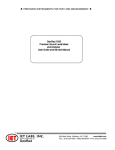
1316
Oscillator
User and Service Manual
Copyright © 2005 IET Labs, Inc.
1316 im/August, 2005
IET LABS, INC.
Standards • Decades • Strobes • Sound Level Meters • Bridges
Formerly manufactured by
GenRad
534 Main Street, Westbury, NY 11590
TEL: (516) 334-5959 • (800) 899-8438 • FAX: (516) 334-5988
www.ietlabs.com
♦ PRECISION INSTRUMENTS FOR TEST AND MEASUREMENT ♦
IET LABS, INC.
534 Main Street, Westbury, NY 11590
www.ietlabs.com
TEL: (516) 334-5959 • (800) 899-8438 • FAX: (516) 334-5988
WARRANTY
We warrant that this product is free from defects in material and workmanship and, when properly used, will
perform in accordance with applicable IET specifications. If within one year after original shipment, it is found
not to meet this standard, it will be repaired or, at the option of IET, replaced at no charge when returned to IET.
Changes in this product not approved by IET or application of voltages or currents greater than those allowed by
the specifications shall void this warranty. IET shall not be liable for any indirect, special, or consequential
damages, even if notice has been given to the possibility of such damages.
THIS WARRANTY IS IN LIEU OF ALL OTHER WARRANTIES, EXPRESSED OR IMPLIED, INCLUDING BUT NOT LIMITED TO, ANY IMPLIED WARRANTY OF MERCHANTIBILITY OR FITNESS FOR
ANY PARTICULAR PURPOSE.
iii
WARNING
OBSERVE ALL SAFETY RULES
WHEN WORKING WITH HIGH VOLTAGES OR LINE VOLTAGES.
Dangerous voltages may be present inside this instrument. Do not open the case
Refer servicing to qulified personnel
HIGH VOLTAGES MAY BE PRESENT AT THE TERMINALS OF THIS INSTRUMENT
WHENEVER HAZARDOUS VOLTAGES (> 45 V) ARE USED, TAKE ALL MEASURES TO
AVOID ACCIDENTAL CONTACT WITH ANY LIVE COMPONENTS.
USE MAXIMUM INSULATION AND MINIMIZE THE USE OF BARE
CONDUCTORS WHEN USING THIS INSTRUMENT.
Use extreme caution when working with bare conductors or bus bars.
WHEN WORKING WITH HIGH VOLTAGES, POST WARNING SIGNS AND
KEEP UNREQUIRED PERSONNEL SAFELY AWAY.
CAUTION
DO NOT APPLY ANY VOLTAGES OR CURRENTS TO THE TERMINALS OF THIS
INSTRUMENT IN EXCESS OF THE MAXIMUM LIMITS INDICATED ON
THE FRONT PANEL OR THE OPERATING GUIDE LABEL.
vii
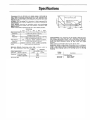
Specifications
Frequency: 10 Hz to 100 kHz in 4 decade ranges. Controlled by
one 11-position and one 10-position switch for the most-significant
digits and a continuously adjustable dial with detented zeroposition for the third digit; in-line readout with decimal point and
frequency units.
Accuracy: ::!::1% of setting~ Drift (typical at 1 kHz), warmup 0 .1 %,
short-term (10 min) 0.001%, long-term (12 h) 0.005%. Resettability,
within 0.005%.
Power Output: Controlled by 5-posi tion switch and uncalibrated
verni er. Monitored by meter with ::!::3% .accuracy. Available at rear
BNC connector.
+with continuously adjustable dial set at zero detent position.
Output Range
IOHr
IOO Hr
lt~;Ht
IOOIII:Hz
f'fiEOUfNCY- Hr
i
IJ16-1
1.s v
s v .I 1s v 1 so v 1 1so v
Open circuit, rms === 1.25 v- === 4 v 1=== 12.s v 1 === 4o v 1 === 125 v
Distortion
< 0.2% from 100Hz to 10kHz
Hum
0.003% of max output
Resoonse
Short Circuit
Distortion
Impedance
Power
output constant within ±2% from 10 Hz to 50 kHz,
±5% for frequencies >50 kHz
I 1.6 A J
0.25
I
0.05 A
l
2.5 kO
0.5 A j 0.16 A
< 0.2% from 100Hz to 10kHz
5A
{l
l 2.5 0 l
25 0
j
250 0
Synchronization: Input, frequency can be locked to external signal;
lock range, ::!: 1%/V rms input up to 10 V: frequency controls function as phase adjustment. Output, ==:o.3 V rms beh ind 27 kO; useful to sync oscilloscope or to drive a counter or another osci llator.
Single rear BNC connector serves as both input and output
terminal.
·
Power: 100 to 125 and 200 to 250 v, 50 to 60 Hz, 36 W.
Mechanical: Bench or rack mount. Dime.1sions (w X h x d): Bench,
19.75 X 5 X 13.06 in. (502 X 127 X 332 mm); rack, 19 X 3.47 X
11.44 in. (483 X 88 X 291 mm). Weight: Bench, 26 lb (12 kg) net,
32 lb (14 kg) shipping; rack, 21 lb (10 kg) net, 27 lb (12 kg)
shipping.
1.6 W nominal into matched load
Reference Outputs: Quadrature output lags 1n-phase output by
go•. Each availab le at rear BNC connectors.
-::--:---;--------:---:-:------~-l_n·_Ph
_a~s-::e:::-_ 1
Output, open-circuit
Distortion, 100 Hz to 10 kHz
Response,
10 Hz to 10 kHz
10 kHz to 100 kHz
Minimum Load
Quadrature
1.25 ::!:0.25 V rms
- <
- 0- .-2-:-%.,---'1
:< 0.4%
Catalog
Number
Description
_ _ ___:t_2:-0:".Vo:__ _ _ __
1316 Oscillator
:t4%
47 kO
-----
1316-9700
1316-9701
Bench Model
Rack Model
---GenRad
WARRANTY
We warrant that this product is free from defects in material and workmanship and,
when properly used, will perform in accordance with GenRad's applicable published
specifications. If within one (1) year after original shipment it is found not to meet this
standard, it will be repaired or at the option of GenRad, replaced at no charge when
returned to a GenRad service facility.
CHANGES IN THE PRODUCT NOT APPROVED BY GENRAO SHALL VOID
THIS WARRANTY.
GENRAD SHALL NOT BE LIABLE FOR ANY INDIRECT, SPECIAL, OR CONSEQUENTIAL DAMAGES, EVEN IF NOTICE HAS BEEN GIVEN OF THE POSSIBILITY OF SUCH DAMAGES.
THIS WARRANTY IS IN LI.EU OF ALL OTHER WARRANTIES, EXPRESS OR
IMPLIED, INCLUDING, BUT NOT LIMITED TO, ANY IMPLIED WARRANTY OF
MERCHANTABILITY OR FITNESS FOR A PARTICULAR PURPOSE.
SERVICE POLICY
Your local GenRad office or representative will assist you in all matters relating to
product maintenance, such as calibrat ion, repair, replacement parts and service
contracts.
GenRad policy is to maintain product repair capability for a period of five (5) years
after origin.al shipment and to make this capability available at the then prevailing
schedule of charges.
NOTE
The material in this manual is for informational purposes only and is subject to change
without notice. GenRad assumes no responsibility for any errors or for consequential
damages that may result from the use or misinterpretation of any of the procedures in
this publication.
Introduction-Section 1
1.1
1.2
1.3
1.4
1.5
PURPOSE
DESCRIPTION . . . . . . . . . . . . .
CONTROLS, CONNECTORS, AND INDICATORS .
SYSTEMS . . . . . .
ACCESSORIES SUPPLIED . .
1.1 PURPOSE.
The Type 1316 Osci llator is a high-performance instrument with an output of 10 Hz to 100 kHz . It was
specifically designed for use with the Type 1238 Detector
and the Type 1616 Precision Capacitance Bridge, and is also
an excellent general purpose instrument.
1.2 DESCRIPTION.
The 1316 Oscillator is a decade-conductance-tuned,
Wien-bridge oscillator containing a low-distortion power
amplifier that is transformer coupled to provide isolation
from the load. Output power and frequency are selected by
front-panel controls; al l external connections are made to
the rear panel for clutter-free operation.
A provision to introduce or extract a synchronizing
signal is included in the oscillator circuit. The extracted
signal is independent of the output setting and can be used
t o operate a counter or to synchronize an oscilloscope.
Other features are: unambiguous in-line readout, decade-frequency selection with positioned decimal point and
1·1
1-1
1-1
1-1
1-1
units, and two reference outputs (IN-PHASE and OUADRA TU RE). The reference outputs are for use with the Type
1238 phase-sensitive Detector.
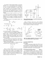
1.3 CONTROLS, CONNECTORS, AND INDICATORS.
The front- and rear-panel controls, connect ors and
indicator are shown in Figures 1-1 and 1-2 respectively.
Refer to Tables 1-1 and 1-2 for a functional and physical
description.
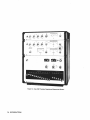
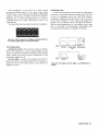
1.4 SYSTEMS.
The 1316 osci llator is used as a component in the 1621
Precision Capacitance Measurement System (Figure 1-3).
1.5 ACCESSORIES SUPPLIED.
A 3-wire, 7-ft power cord (P/N 4200-9625) is supplied
with the instrument.
INTRODUCTION 1-1
4
5
6
7
8
Figure 1·1. Front-panel controls, connectors·and indicators.
-------------------------------------Table1-1------------------------------------FRONT PANEL CONTROLS AND INDICATOR
Figure 1·1
Ref. No.
Name
Description
Function
POWER switch
2-position toggl e switch, down
position: OFF.
Turns instrument on or off.
2
FREQUENCY selector
10-position rotary switch, dial -marked
1 to 10.
Selects and indicates 1st d igit of
frequency.
3
FREQUENCY selector
11-position rotary switch, dial marked
0 to 9 and X (X indicate$ 10 or 0).
Selects and indicates 2nd digit of
frequency .
4
FREQUENCY selector
Stepless potentiometer, dial marked
0 to 9 with detent at 0 .
Selects and indicates 3rd digit of
frequency.
5
FREQUENCY range
switch
4-position switch, dial marked Hz, Hz,
kHz, and kHz.
Selects frequency range, indicates
unit s, and controls illuminated
decimal point.
6
OUTPUT VOLTAGE
RANGE switch
5-position rotary switch, panel-marked
1.5, 5.0 , 15.0, 50.0, and 150.
Selects output-voltage range and
indicates full-scale meter range
(item 7). Simultaneously switches
the output impedance from 0.25 n
to 2.5 kU in decade steps.
7
Voltmeter
Ac meter with 0-15 and 0-50-V scales.
Indicates output terminal voltage,
in ranges selected by item 6.
8
OUTPUT ADJUST
contro l
Stepless, rotary potentiometer with
limits labeled 0 and MAX .
Controls output level in the range
selected by item 6.
Zero-adjust screw.
Mechanically adjusts outputvoltage meter for mechanical zero.
Front-panel, white indicator lights.
Indicates position of decimal
point, controlled by the FREQUENCY range switch (item 5).
9
10
1-2 INTRODUCTION
figure 1-2. Rear-panel control and connectors.
- - - - - - -- -- - - - - - - - - - T a b l e 1 - 2 - - - - -- - - -- - - -REAR -PANEL CONTROLS AND CONNECTORS
Figure 1·2
Ref. No.
Description
Function
Name
-----
QUADRATURE REFERE NCE
OUTPU T
BNC jack
Provides a reference output that lags the
"in-phase" reference by 90° at 1.25 V o.c.
2
I N-PHASE REFERE NCE OUTPUT
BNC jack
Provides a reference output, in-phase with
power output, at 1.25 V o.c.
3
EXT SYNC connector
BNC jack
For synchronizing output f req uency to an
external source (lock range is ±1%/Vrms, up
to 10 V) or constant-amplitude signal source
(0.3 V behind 27 knl.
4
POWER OUTPUT connect or
BNC jack
Main output, 1.6 W nominal may be 125 V o.c.
or 5 A s.c.
5
Fuse
Bussman MD L 8/10 A,
slo-blo
Protect ion. against damage f rom a short circu it for 110- or 220-V operation.
6
5Q-60 Hz
100 V- 125 V
200 V-250 V
Two-position slidt.
switch
Switches line power connect ion f or eit her
11 0-V or 220-V operat ion.
T hree-pin power plug
Accepts 3-wire line cord to power
instrument.
7
INTRODUCTION 1-3
...
~
-·.· -·
_,.,.. , IN
I
'
- . . ... lVIII
Figure 1-3. Type 1621 Precision Capacitance-Measurement System.
1-4 INTRODUCTION
Installation-Section 2
2.1 GENERAL . . . . . .
2.2 DIMENSIONS . . . . .
2.3 POWER-LINE CONNECTION
2.4 BENCH MODELS . . . .
2.5 RACK MODELS . . . .
2.6 LINE-VOLTAGE REGULATION .
2.7 EXTERNAL CONNECTIONS . .
2·1
2·1
2-1
2·1
2·2
2·4
2-4
2.1 GENERAL
2.4 BENCH MODELS.
The Type 1316 Osci llator is available for either bench
use or installation in an EIA Standard RS-310, 19-in. relay
rack with universal hole spacing. Appropriate cabinet and
hardware sets are available for conversion of a bench model
for rack installation or vice versa.
2.4.1 General.
Each bench model comes completely assemb led in a
metal cabinet intended f or use on a table or laboratory
bench. The instru ment is mounted on tracks that permit
easy removal for inspection or repair.
2.2 DIMENSIONS.
2.4.2 Cabinet Removal.
Outl ine drawings showing overall dimensions of the
osci llator in bench and rack models are shown in Figure
2-1.
a. Set the instru ment in the horizontal position , free of
unnecessary cables.
b. Remove the four dress-panel screws (A), accessible
through holes in the handles.
c. Careful ly pull the inst rument out of the cabinet.
2.3 POWER-LINE CONNECTION .
Power requirement is 36 W at 100 t o 125 or 200 to 250
V, 50 to 60Hz. Make connections as follows:
a. Set the line-voltage switch on the rear panel to
correspond with the avai lab le power-line voltage. Use a
sma ll screwdriver to slide the switch.
b. Connect the external power line to the power plug,
using the power cord supplied or an equivalent, 3-conduc·
tor cord.
A single 8/10-A fuse protects both the low· and
high-voltage circuits.
2.4.3 Conversion for Rack Mounting.
To convert a bench instrument for rack mounting,
exchange the cabinet and instal l appropriate hardware, as
follows:
a. Obt ain a Rackable Cabinet Assembly PIN 4174-3240
(Table 2-1) fr-om General Radio Company.
b. Obtain, optional ly, Bracket Set P/ N 4174-2007 (Table
2·2). This is especially recommended for a heavy instrument,
which needs support from the rear rai l of the rack.
INSTALLATION 2·1
DIM.
INCHES
A
11 .562
12.837
4.031
4.906
B
c
D
I.
19.8
BENCH MODEL
t
1
c
FRONT PANEL
D
J
1
J~' ro'"~ 1 I
1r
-TOPVIEW
,
W
19
~
__1 ,
L=f-J
FRONT PANEL
~ ~
p
13.640
11.749
13.062
1 .625
3.469
Q
R
s
T
l
T
END VIEW
l
Figure 2-1. Dimensions of the 1316 bench and rack·model instruments.
2.5 RACK MODELS.
2.5.1 General.
Each rack model comes completely assembled in a
suitable metal cabinet, w hich is designed to stay semipermanently in a rack. The instrument can be drawn forward on
extending tracks for access with support, or (with a lift}
withdrawn comp letely. The cabinet and hardware listed in
Tables 2-1 and 2-2 are all included with a rack-model
instrument.
Figure 2·3
Directions fo-llow for mounting the cabinet in a rack and
installing the instrument on its tracks:
a. Remove 4 dress-panel screws (A) and slide the
instrument out of the cab inet until the tracks are fully
extended. Continue pulling the instrument forward unti l
motion along the tracks is stopped. At this juncture, tilt the
f ront of the instrument up slightly and continue withdrawal, past the stops, until it is free.
2-2 INSTALLATION
INCHES
DI M.
RACK MODEL
c. Remove the cabinet, as in paragraph 2.4.2.
d. Remove the rear cover from the bench cabinet, with
screws (B Figure 2-2 } , for later installation on the rack
cab inet.
e. Proceed with the rack installation; skip to paragraph
2.5.2, step b.
2.5.2 Installation.
END VIEW
b. Insert the rack cab inet wherever desi red in the rack be sure it's level - and fasten it with 4 screws (C) to the
front rai ls.
c. If the rack con tains a rear support rai l, use brackets
(0) to support the cabinet with the rear rail s; open-slotted
screw holes allow positioning.
d. Use the set of slots in the sides of t he cabinet that
allow alignment of the open-slotted holes in the brackets
with threaded holes in the rai l. The long flange should extend to the rear.
e. Insert screws (E) f rom inside the cabinet, through the
slotted holes and drive them into the holes in the long
flange of the bracket. Each side takes 2.
--------Table 2·1-------RACKABLE CABINET ASSEMBLY (P/N 4174-3240)
Quantity
Description
Hardware set, includ ing:
2 Screws, 0464-32, 1/4-in, thread
forming ("B" for rear cover) .
4 Screws, 0.190-32, 9/16 in, dress
("A" for front panel).
4 Sets of 10-32 nuts and washers
(for screws "A", if needed) .
4174-2004
BENCH·CABINET
ASSEMBLY
REAR COVER
SLIDE
BLOCKS
417.0
Figure 2·2. Bench-cabinet installation.
NOTE
Start the screws in t he appropriate holes off t he
rack , to make the thread ing easier.
f. Pass screws (B) through brackets and screw 2 into
each rear rail. (Details may be varied to suit particular
situations.)
g. To install the instrument, f irst set its rear edge in the
cabinet front opening. Slide the instrument back, mak ing
sure that the rear and the upper front slide b locks engage
the tracks. (Stops prevent further insertion.)
h. Pull the instrument forward with the tracks, keeping a
hand on each side (fingers underneath). Slide the instrument back about %in. along both tracks, past the stops, by
pressing down on the tracks (with thumbs) wh ile tilting the
front of the instrument up sl ightly.
i . Push the instrument back into the rack, checking for
smooth operat ion of the tracks and sl ide blocks.
NOTE
The instrument is now read ily accessible for
beh ind-the-panel adjustments. It slides in and
out freely on extendi ng tracks.
- - - - - - - T a b l e 2·2 - - - - - - - BRACKET SET FOR RACK MODEL (P/ N 4174-2007)
R ef Quan tity'
De scrip lion
D
2 L brackets with open-slotted holes.
E
4 Screws, 8-32. 3/1 6 in., thread forming.
C, B 8 Screws, 10-32, 1/2-in., thread forming .
2.5.3 Conversion for Bench Use.
To convert a rack-mounting instrument for bench use,
exchange the cabinet, as follows:
a. Obtain a Bench Cabinet assembly P/N 4172-4015
(Table 2·3) from General Radio Company.
b. Remove the instru ment f rom the rack cabinet , using
the procedure in step a, para. 2.5.2.
c. Stand t he instrument face down, t o rest on its
handles, and slip the bench cabinet over it. Carefully return
it to a horizontal position.
RACK·CABINET
ASSEMBLY
B
FRONT
RAIL
A
Figure 2·3. Rack-cabinet installation.
INSTALLATION 2-3
d. Fasten the instrument to the cabinet using dress-panel
screws (A, Figure 2-2).
e. Transfer the rear cover, with screws (B), from rack
cab inet to bench cab inet.
The lock range is ±1%/V rms in pu t. up to 10 V , and the
front-panel frequency controls function as the phase
adjustme nt. As an output, 0. 3 V rms behind 27 kQ is
avai lable to lock the frequency of another instrument to
that of t he asci llator .
2.6 LINE-VOLTAGE REGULATION.
The accuracy of measurements accomplished with precision electron ic test equ ipmen t operated from ac line
sources can often be seriously degraded by fluctuations in
pri mary input power. Line-voltage variations of ±15% are
commo nly encountered, even in laboratory environments.
A lthough most modern electronic instruments incorporate
some degree of regulation, possible power-source problems
should be considered for every instrumentation setup. The
use of line-voltage regu lators between power lines and the
test equipment is recommended as t he only sure way to
rule out the effect s on measurement data of variations in
I ine voltage.
2.7.4 REFERENCE OUTPUT Connectors.
General. The REFERENCE OU TPUT connect ors were
designed into the Oscillator primarily to provide low-level
fixed-amplitude reference signals for the Type 1238 Detect or . However, they can be used for any application
requiring a pair of 1-V reference signals with a phase
difference of 90°.
IN·PHASE. The IN-PHASE output jack provides a
reference voltage that is in phase w ith the main POWER
OUTPUT of the 1316 Osci llator. This voltage (open circuit)
is 1.25 ±0.2 V rms. Distortion is less than 0.2% from 100
Hz to 10 kHz and the voltage response is typi cally ±2%
from 10Hz to 10 kHz,and ±4% from 10kHz to 100kHz.
The minimum load impedance should. be 47 k 0.. A smaller
impedance wi ll reduce the output voltage and possibly
cause distort ion.
- - - - - - - - T a b l e 2·3 - - - - - - - BENCH CABINET ASSEMBLY COMPLETE (4172-4015)
Quan·
tity
Description
1 Bench Cabinet Assembly, includ ing:
1 Cabinet
1 Gasket
1 Base with hardware (includes
hinge and toggles)
2.7 EXTERNAL CONNECTIONS .
2. 7.1 General.
All ex ternal co nnections to the Type 1316 Osci llat or are
made t o rear-panel BNC connectors. This feature facil itates
the use of the 1316 in the Type 1621 Precision-Capacitan ce-Measurement System (Figure 1-3).
2.7.2 POWER OUTPUT Connector.
The main out put of the osci llator is avai lable at the
rear-panel POWER OUTPUT jack . Output-voltage range and
ampl itude are controlled by the front-panel OUTPUT
VOLTAGE RAN GE and OUTPUT ADJUST controls respectively.
2.7.3 EXT SYNC Connector.
A single rear-panel BNC connector serves the dual
purpose of an in put or output jack . As an input, the
osci llator frequency can be locked to an external signal.
2·4 INSTALLAT ION
2
2
Pa rt No.
4172-2042
Factory assembled with :
Tracks
Brack ets, rear, (and screws)
Supplied w ith:
Screws, 0. 164-32, 1/4 in., thread
forming ("B" f or rear cover)
4
Screws. 10-32, 9/16 in. , dress
("A" for f ront panel)
2
OUADRA TURE. The OUADRATU R E out put jack provides a reference voltage that leads the IN-PHASE and
POWER OUTPUT vo ltages by 90° . This voltage (open
circuit) is 1.25 ±0.2 V rms. Distortion is less than 0.4%
from 100 Hz to 10 kHz and t he voltage response is
typically ±4% from 10kHz to 100kHz. The minimum load
impedance should be 47 kQ.
INSTALLATION 2-5
NOTE
The instrument is fitted with a new-design power·
connector that is in conformance with the Inter·
national Electrotechnical Commission publication
320. The 3 flat contacts are surrounded by a
cylindrical plastic shroud that eliminates the pos·
sibility of electrical shock whenever the power
cord is being unplugged from the instrument. In
addition, the center ground pin is longer, which
means that it mates first and disconnects last,
ensuring greater user protection from electric
shock.
The panel connector is a standard 3-pin ground·
ing·type, the design of which has been accepted
world wide for electronic instrumentation, and
is rated for 250 V at SA. It also meets require·
ments of Underwriter's laboratories in the U.S.
and the Canadian Standards Association. The
receptacle accepts power cords fitted with the
Belden type SPH-386 connector.
2·6 INSTALLATION
Operation-Section J
3-1
3-1
3-2
3-2
3.1 GENERAL . .
3.2 OPERATIONAL CHECKS
3.3 NORMAL OPERATION
3.4 APPLICATIONS
3.1 GENERAL
T his section contains operational checks, operating
inst ructions, and a basic description of some applications
for which t he 1316 Oscillator can be used.
3.1.1 Equipment Turn-on.
To prepare t he instru ment for use, perform the following steps:
a. Set the rear-panel line-voltage selector switch to the
line-voltage used (100-125 V or 200-250 V. 50-60Hz), and
connect t he instrument to the power line, using the power
cab le supplied.
b. Set the power switch to POWER . One of the
deci mal-point lamps should glow. Its position wi ll depend
on the FREQUENCY range-switch setting (Refer to Table
3-1 ).
b. Adjust the meter zero-adjust screw for a zero
indication. Gently tap the meter face occasionally during
adjustment.
c. Set t he oscillator controls for any output within the
range of the instrument.
d. Turn on the oscillator. Note that an output is
indicated and then turn off the oscillator.
e. Check to see that the meter indicator stabilizes on
zero.
3.1.3 Stray Capacitance.
Stray capacitance of most shielded leads or coaxial
cab les is about 30 pF per foot. which. at 100kHz, amounts
to a shunt impedance of about 55 k! l Therefore, t he cable
length should be kept to a minimum when a high-i mpedance load is to be driven at high frequencies.
3.1 .2 Meter Zeroing.
3.2 OPERATIONAL CHECKS.
The output voltage meter has been zeroed at the factory .
If it becomes necessary to re-zero the meter, proceed as
fo llows:
a. Check to see that the POWER swi tch is set to OFF. If
the instrument has been operating, al low sufficient time for
the meter indicator to stabili ze near zero.
3.2.1 General.
These procedures can be used for incoming inspect ion,
operator famil iarization, or as a periodic quick-check on
inst rument operation . Table 5-1 includes recommended t est
equipment for these checks. Refer to para. 5.8 if unable to
obta in the performance cal led for.
OPERATION 3-1
--------Table3-1 - - - - - - - DECIMAL POINT POSITION
Position of A-55 (from
fully counterclockwise)
1 (Hz)
2 (Hz)
3 (kHz)
4 (kHz)
•X
=a
POSITION OF
DECIMAL POINT*
XX.X
XXX.
X.XX
XX.X
frequency dial
3.2.2 Output Frequency.
The frequency of the oscillator output signal should
correspond with the setting of the FREQUENCY selectors.
For a quick-check of output frequency proceed as follows :
a. Set the 1192 counter controls to measure frequency
and connect it to the oscillator POWER OUTPUT jack.
b. Turn the oscillator on and set the frequency selectors
for any frequency between 10Hz and 100kHz.
c. Observe the counter visual register. It should display
the same frequency set by the frequency selectors ±1
count.
3.2.3 Output Voltage.
The Oscillator is equipped with an ac voltmeter for
monitoring the output voltage. For an operational check of
the output voltage, simply turn the instrument on, set the
frequency and voltage controls for some value within the
range of the instrument, and observe the front-panel meter.
This meter will indicate the voltage at the output jack
within ±3%.
3.3 NORMAL OPERATION.
To use the instrument as a source:
a. Turn on the oscillator and allow approximately 1
minute for it to reach normal operating temperature. For
optimum frequency and amplitude stability allow 30minutes warmup.
b. Set the FREQUENCY range switch to the desired
frequency range. Notice that this control positions the
decimal point.
c. Set the FREQUENCY selectors to the desired
frequency.
d. Set the OUTPUT VOLTAGE RANGE switch to the
range that will provide the desired output voltage.
e. Adjust the OUTPUT ADJUST control to obtain the
desired output voltage reading on the output voltage meter.
To use the instrument synchronized to an external
source.
a. Perform steps a·e above.
b. Connect the external signal to the EXT SYNC jack
(Figure 1-2). The lock range of the oscillator is ±1 %/V rms
sync input up to 10 V. For example, if a 1-kHz, 1-V sync
signal is used, the oscillator output frequency will lock to
3·2 OPERATION
the external signal within the range 990-1010 Hz. If the
sync-signal voltage is doubled the lock range also doubles
(980·1 020 Hz).
The oscillator will remain synchronized so long as it is
operated w ithin the lock range.
3.4 APPLICATIONS.
3.4.1 General.
One of the most important fedtures of the Type 1316
Oscillator is that it provide-s an easy-to-read, unambiguous,
repeatable, in-line readout of its frequency. This will be of
value in production testing and calibrating where many
accurate and repeatable frequencies must be selected
quick ly.
Some typical applications are presented in the following
paragraphs.
3.4.2 Slaved Oscillators.
Because the EXT SYNC jack is simultaneously an input
and an output connector, two or more oscillators can be
synchronized or slaved by connecting their EXT SYNC
jacks together (Figure 3·1). Oscillators connected in this
manner will operate at the same frequency, or multiple
thereof, and can be made to differ in phase (180° ±75°) by
adjustment of the frequency selectors within the lock
range. The lock range is ±1%/V rms input up to 10 V.
Another obvious application is to lock one or more
oscillators to a reference source that has greater accuracy
and long-term stability. This is done by connecting the
source to the EXT SYNC jack. If more than one oscillator
is to be used, connection between instruments is shown in
Figure 3·1. With the instrument(s) synchronized in this
fashion accuracy and long-term stability will be identical
with the reference; short-term stability will be the same as
if the oscillator was free-running.
3 .4.3 Ampl itude-Modu Iated Oscillator.
Amplitude modulation. if the oscillator is operated out·
side of the lock range, the sync signal will beat with the
oscillatorfrequency and produce an audio-frequency, ampli·
plitude-modulated output. The modulation will be approxi·
mately sinusoidal for modulatian levels up to about 10%.
776- C
PATCHCORO
~BNC TEE UG-274/U
~~1--'-.;.;.;.;.;~~...,D
~
6
EX.T SYNC
GR 1316
OSCILLATOR
~
L {]
¢
176 ·C
)
PATCH CORD
.------61----,
EXT SYNC
G
1
i
6
EXT SY~C
GR 1316
GR 1316
OSCILLATOR
OSCILLATOR
1316-3
Figure 3·1. Method of connecting slaved oscillators.
This arrangement is not ideal , but it does provide
amplitude-modulated signals in the audio range where
normally they are not conveniently obtainable. Modulated
outputs of this type can be used to measure the effects of
incidental am on other measurements and to provide a
modulated source to reduce meter-friction errors in ac
measurements.
The figure shows one example of amplitude modulation:
3.4.5 Systems Use.
All external connections to the oscillator are made at the
rear panel- a convenient feature for systems use. The 1316
is one of 3 integrated units in our Type 162 1 Precision
Capacitance Measurement System (Figure 1-3). It f unctions
as the drive oscillator for the system and supplies the
detector with 2 reference inputs. The high level, stability,
and low-noise characteristics of this oscillator play a large
role in producing the ultra-precise measurements and
comparisons that the system is capable of providing.
Figure 3-2. 10.kHz output of an oscillator modulated at 500 Hz
by a 9.5-kHz signal applied to the EXT SYNC jack.
3.4.4 Output Sync.
Oscilloscope trigger. Since the sync output is independent of the output level, it can be used to trigger an osci lloscope in applications where the oscillator output is often
varied, thereby eliminating frequent readjustment of the
oscilloscope trigger circuits.
Counter trigger. A counter can be driven from the EXT
SYNC jack when more precise adjustment of frequency is
desired or when the front-panel out put is not sufficient to
trigger the counter.
0
EXT '-- OUTPUT•
SYNC
GR 1316
=
SYNC
--
EX~
TRIG
VERTICAL
f-. I N our•r- ~ IN PUT
DEVICE UNDER
TEST
OSCI LLOSCOPE
W,,j~
GRI316
Figure 3-3. The oscillator used to trigger: a. an oscilloscope; b. a
counter.
OPERATION 3-3
Theory-Section 4
4·1
4·2
4·3
4.1 GENERAL
4.2 WI EN-BRIDGE THEORY
4.3 CIRCUIT DESCRIPTION
4.4 SYNCHRONIZATION
4·5
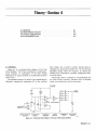
4.1 GENERAL.
Figure 4-1 is a functional block diagram of the Type
1316 Oscillator. The 1316 is comprised of a conductance·
tuned oscillator (a modification of the Wien bridge)
followed by an output amplifier, an autotransformer, and a
meter circuit.
The oscillator frequency is varied in four decade steps by
effectively changing t he capacitance (C) of the modified
Wien bridge, and is varied in smaller, discrete steps by
changing two conductance decades (G). The continuously
adjustable decade varies the frequency by a_ltering the
voltage across conductance g, thereby. changing the effective conductance.
Wien-bridge theory is essential to comprehending how
the 1316 circuit ry functions. Therefore, para. 4.2 precedes
a basic circuit description for this instrument.
IN·P>iASE
OUTPUT
1 2~
v
R
40
v
R
12.5V
R
4.0 v
R
1.25V
R
POWER
OUTPUT
~~~"'----...r-----~~
CURRENT TO VOLTAGE
AMPLIFIER
MOOIFIEO WIEN
BRIDGE
DIFFERENTIAL
AMPLIFIER
OUTPUT
AMPL IFIER
TRANSFORMER
OUTPUT
OUTPUT M ETER
CIRCUITRY
13161
Figure 4·1. Functional block diagram of the type 1316 decade oscillator.
THEORY 4·1
where
4.2 WI EN-BRIDGE THEORY.
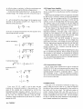
4.2.1 General.
A Wien bridge (Figure 4-2) consists of two parts: a
frequency-determining impedance divider, wh ich provides
positive feedback to sustain oscillation and an amp I itude·
determining resistive divider, wh ich supplies negative feedback to stabilize amplitude. The following paragraphs
explain how both of t hese work.
FREQUENCY· DETERMINING
(
DIVIDER
\
AMPLITUDE
DETERMINING DIVIDER
- FEEDBACK
G L = loop gain
GA =ampl ifier gain
.v1'd er ga1n
.
-E, = d 1
E3
Or:
1I 3
=3
The amplifier then, must have a gain of 3 to preserve
un ity gain in the loop and, therefore, to sustain
oscillation at w 0 .
R0
+90°
"'
w
0
w""
(/)0
<
Figure 4-2. Schematic diagram of a typical Wien bridge.
~
:r:z
c.~
w~
0"'+-------~-------
w
Q:
-go•
Figures 4-2 & 4-3.
4.2.2 Frequency.
The operating frequency, f 0 , of a Wien-bridge oscillator
depends on the values of the compo nents in the impedance
divider:
since w = 21r then w 0 =
"'o
FREQUENCY
2
w "' 3
cw
:::> ...
t-0
:io
The transfer function (gain and phase shift Figure 4-3) of
the frequency divider is:
E,
E3
3+ j
(~
w
0
_
W0
c.~
::::l!<l
<"'<(
I
3
W"'
<(
)
w
At the operating frequency, w = w 0 , therefore :
"'o
FREQUENCY
Figure 4-3. Typical transfer function of a Wien bridge.
4 .2.3 Amplitude Stabilization.
This means that at t he operating frequency of the
oscillator, one-thi rd of the signal appl ied t o the divider
appears at the input to the ampl ifier. To sustain oscillations
in any oscil lator, a loop gain of unity is necessary, i.e. , the
gain from any one point in the circuit, around the loop and
back to that same point, must be equal to one. Thus:
4-2 THEORY
Figures 4-2, 4·4 and 4-5.
Under ideal conditions, the only requirement for stable
osci llations is a constant loop gain of 1, i.e., if the amplifier
gain and impedance-divider gain remained constant with
changes in frequency , ci rcuit parameters, and environment,
only the frequency-determin ing i mpedance divider wou ld
be necessary. However, changes in frequency and environment affect the gain, phase, and ter minal impedance of the
amplifier and slight unbalances in C and R affect the gain
(voltage ratio) of the divider. These factors change the loop
gain and wou ld cause the oscillator amp I itude to increase or
decrease.
For example, if these anomal ies resu lted in a momentary
decrease in E3 , E1 would decrease, further decreasing E3 ,
and so on unt il t he amplitude became zero. Conversely if
E3 were to increase momentarily, E1 would increase,
further increasing E3 until the ampl ifier saturated. This
latter case can be easi ly demonstrated by removing the
thermistor ( R 1} and mon itoring the output. The output
wi ll be square waves instead of sinewaves and will not
necessar ily be at t he frequency indicated by the frequency
selectors.
To overcome this problem a divider R 1 and R2 (F igure
4-2) is used. The input to the amplifier is the difference
between the output of the two dividers. (E 2 is negative
feedback and if it increases. E3 decreases.) Note that the
amplifier is across t he bridge as is the detector/amplifier of
any bridge.
T he transfer funct ion of the resistance divider is the
simple voltage rat io:
E2
T he loop gain is now :
L
E1
A
(- E3
E2
-
E3
Figure 4-4. Schematic diagram of a typical Wien bridge showing
the amplifier as a current source.
When a t hermistor is used for R 1 , and its resistance
characteristic is chosen so that the slope of its I R drop is
equal to t he slope of the I R2 drop, but of opposite sign, E3
remains constant with changes in amplif ier gain .
E3
G =G
+V
)or
a.
b.
T!iERMISTOR
OPERATING
REGION
'l
I
and must still be equal t o 1 for stable amplitude.
In order to stabi Iize E3 with changes in frequency and
ampl ifier gain, a negative-temperature-coefficient t hermistor is used for R 1 . A n ordinary resist or is linear , its
resistance remains essenti ally constant as the cu rrent
through it changes. But, t he thermist or used in the Type
13 16 is non-linear, its resistance decreases as the current
through it increases.
To explain t he action of t he t hermistor, t he ampl ifier is
shown as a current source (Figure 4-4} with a certain
current -deliver ing capabil it y represen ted by the const ant
voltage (+V) and a resistor (RG ).
Note that the same voltage, E 3 , is 'across all t hree legs
(impedance divider, resistance divider , and R Ll:
E3
= E2 + E4
E4
=
I R1
When an ordinary resistor is used fo r R 1 , t he voltage
drops across R 1 and R2 change in direct proportion to the
current t hrough them, which in turn , changes in direct
proportion to the gain (current-delivering capabil ity) of the
amplifier. In Figure 4-5, the result of increasing current (I).
is shown. Since E3 is the sum of E2 and E4 , E3 rises
Iinearl y as t he gain of the amplifier rises.
E
E 2 +E 4
t" - - - - - - - - E3
'X
~'j. E4
E
I~
L___ _ _ __
I
STANDARD RESISTOR
E2
I
WIT H THERMISTOR
Figure 4-5. Graphical representation of the current II) through
R1 : a. using a standard resistor; b. using a thermistor.
4.3 CIRCUIT DESCRIPTION.
4.3.1 General.
As previously mentioned, the heart of t he 1316 circuitry
is a modification of the Wien-bridge osci llator. The modification consist of a conductance-tuning method as opposed
to resistance t uning. Para. 4.3.2 presents a basic circuit
description of this osci llator in terms of conduct ance.
4.3.2 Modified Wien-Bridge Oscillator.
Figure 4-1 .
An incremental variation in the frequency of a Wien
bridge oscil lation may be effected by shunting the lower
conductance arm of the bridge (G) by a variable conductance (g) , w hose value is variable between 0 and g. Since it is
difficu It, if not impracti cal, t o reciprocally vary resistance
THEORY 4·3
to infinite values, a variation in effective conductance can
be produced by varying the effective voltage across it.
In th is instrument a: varies from 0 to 1, an easy task for a
variable-voltage. The voltage across the conductance (g) is:
V - ( 1 - a:) V = a:V
( 1 - a:)V is derived fro m the voltage Vat the negative input
terminal of the oscillator amplifier (A1, Figure 4-1). The
effective conductance (g) is:
1L_ =
a:Vg
V9
a:g
V
If we sum G and a:g and substitute into the equation for a
Wien-bridge oscillator we have:
~G(G + a:g)
=
W0
c2
and by rearranging
1
c
c
G
a:g
c
G
4.3.3 Output Power Amplifier.
The final output power from the instrument is transformer coupled from a class-8 power amplifier consisting of
013-018.
Signal from the oscillator section is amplitude controlled
by the OUTPUT ADJUST control (A-R27) and appl ied to
the base of the input-voltage amplifier 013. The collector
output of 013 is applied to the base of 014 and the
collector circuit of this stage feeds the final output stages.
The collector load of 014 consists of R43 and R44; the
junction is bootstrapped to the amplifier output via C35, to
provide ac multiplication of the impedance of R43.
The two halves of the class-B output stage consist of
composite states 015-018. Each pair is connected as a
high-input-impedance, unity-gain stage. Final output is
provided by the collectors of 017 and 018. These two
stages also drive the feedback divider R40 and R39, whose
values are chosen to provide a closed-loop gain of 4.
Idle current in 017 and 018, necessary to minimize
crossover distortion, is maintained by the voltage drop
across CR 11 and CR 12. This voltage is equal to that across
R47 and R48 plus the base-emitter drop of 015 and 016.
Diodes CR9, CR10, CR13, CR14, CR19, and CR20
provide protection from transients occurring during the
oscillator start-up period.
R41, C34 and R42, C36 modify the high-frequency loop
gain to maintain loop stability. R42 is variable to adjust the
time constant of this network to compensate for variations
in winding capacitance of the low-frequency transformer
T2. This transformer has some effect on the high-frequency
characteristics of the feedback loop.
It can be shown that:
~~
1 +
~
whena<<1
and since g << G
then
c ~1 +
G
Wo
~
~
G
-
c
1
-
c
1 +
a:g
G
a:g
2G
One of three output transformers is used to couple the
POWER OUTPUT jack to the power-amplifier output. Each
transformer is tapped to provide a choice of voltage. T2
operates between 10-100 Hz, T3 between 100Hz-10kHz
and T4 between 10kHz-100kHz. Resistance is added to
the normal winding resistance to define the maximum short
circuit current at each tap.
(G + a:g )
2
From w 0 ~ 1/C (G + a:g/2) it can be seen that a:g
produces an incremental variation in the product w 0 . The
value of the var iable (a:) is determined by A-R 14, the
least-significant-digit frequency selector. The term G is
varied by means of parallel-resistor combinations selected
by the first two frequency selectors, A-S3 and A-S4.
Frequency range is determined by the value of C, which is
selected by A-S5.
4-4 THEORY
4.3.4 Autotransformer Output.
4.3.5 Meter Circuit.
If the gain of A (comprised of 019-02 1) is large, VFs
{base of 020) wil l be very close to V 1N (base of 019) and
the effect of the nonlinear characteristic of the rectifier at
low levels will be very small. The half-cycle pulses of
current, flowing through R61 and R62, set the gm of
system; the average value of the full -wave rectified pulses of
current is indicated by the meter A-M1. The time constant
of C42, & C43 and the meter resistance is long enough to
permit steady readings at low frequencies.
4 .3 .6 Reference Outputs.
Figure 4 ·1.
Two reference outputs (IN-PHASE and QUADRATURE) were built into the 1316 oscillator to facilitate its
use with the double-phase-sensitive 1238 Detect or.
The IN -PHASE out put is derived directly from t he
oscillator output and is in-phase with the output voltage,
disregarding phase errors in the power amplifier and output
t ransformer. The QUADRATURE output lags the INPHASE output by 90° and is derived by sampling the
current f lowing t hrough Cb (Figure 4- 1).
By making t he gain of A 3 large most of the input
current is forced to flow through R F. This provides an
outpu t voltage proportional to the input current. However,
since the magnitude of I depends on the frequency setting
and the value of C f or t he range in use, RF must be var ied
wit h frequen cy to maintain a constant quadrature out put.
This is accomp lished with conductance decades A -R102A-R 109, which are controlled with A-S3 and A-S4 respectively.
4 .3 .7 Power Supply.
Power fo r all sections of the oscillator is obtained from a
regu lated supply consisting of 0 1, A-02, A-03, 04 and 05.
The regu lator is on the negative or return side of the
supply.
A fraction of the output voltage is compared, via 05,
with t he 6.8-V Zener-diode reference. The collector current
of 05 varies with the difference between the two voltages
and is ampl ified by 01 . The current source (04) and the
Darlington pair (A-02 and A-03) comprise t he collector
load of Q 1. Variations of t he voltage at t he Darli ngton-pair
input (AT5) cause the output voltage at WT1 0 to change in
such a manner t hat any original error is vastly reduced.
4 .4 SYNCHRONIZAT ION.
4 .4 .1 General.
The method used to synchronize the oscillator is
commonly called injection locking and is the same mechanism t hat causes some oscillators to beat with t he powerline f requency or t o lock with it.
1njection lock ing is a nat ural extension of th e normal
oscillator operation and, except for an isolating resistor and
capacitor, is dependent only upon the proper operat ion of
the osci llator. The naturalness of t he extension is apparent
when it is rea lized that normal operation is, in fact, only an
amplitude-regulated, frequency-selective regenerat ion of
noise sources within the oscillator. Synchronizat ion is an
amp I itude-regulated, frequency-selective regenerat ion of an
ext ernally applied signal.
There are t hree import ant characteristics associated wit h
t he use of t he EXT SY NC feat ure:
a. Output.
b. Input synchron izing or phase lock ing.
c. Input-frequency selectivity or filtering.
These characteristics are discussed in the following
paragraphs.
4 .4.2 Output Characteristic.
A nominal 0.3-V rms output signal, behi nd 27 kQ, is
available from the EXT SYNC jack. The level of this sync
output signal is independent of the output voltage controls
or t he out put load. One side of the sync output is chassis
ground and the signal is in phase with the POWER
OUTPUT.
The sync output will drive any size load without
increasing the oscillator distortion. However, only highimpedance loads are recommended where full frequency
accuracy is requ ired. The worst-case load, a short circuit,
will decrease t he f requency by 1 or 2%.
4.4.3 Input Synchronizing Characteristic.
The oscillator freq uency can be synchron ized or locked
with any input signal t hat is applied to the EXT SYNC jack,
if the oscillator is tuned to t he approx imate f requency of
the input. The range of frequencies, over which this
synchronization will take place, is a function of the
ampl itude of the frequency component to which t he
oscillator locks. It increases approximately li nearly, and
produces a lock range of approximately ± 1% for each volt
input.
The oscillator will maintain synchronization if either the
osci llator f requency or the synchronizing frequency is
changed, with in the lock range. However, there is a time
constan t of about one second associated w ith. t he synchronizing mechanism. Thus, if the amplitude or frequency of
t he sync signal or t he f requency setting of the oscillator is
changed , there w ill be transient changes in amplitude and
phase for a few seconds before t he oscillator ret urns to
steady-state synch ron izatio n.
This time constant is caused by the therm istor amplitude
regulator as it· readjusts to the different operating conditions. The thermistor is sensitive only to changes in average
values of f requency or amplitude where the averaging t ime
is in t he order of seconds. Hence, frequency-modu lated and
amplitude-modulated sync signals, which have a constant
average value of frequency and amplitude over a period of a
second or less, are not affected by this time constant. They
are affected by t he equivalent ti me constant of the filter
characteristic, discussed in para. 4.4.4.
For slow changes in f requency or amplitude, t he lock
range and the capture range are the same; i.e., the
frequency or amplitude at which the oscillator goes from
the synchronized state to t he unsynchronized stat e is t he
same as when it goes from t he unsynchronized state to the
synchron ized stat e. Synchronizat ion is a true-phase-lock,
because it maintains a constant phase difference between
the sync input and the oscillator output. The phase
difference is 180° when t he dialed f requency is identical to
THEORY 4-5
the sync frequency and approaches ±90° as the f requency
approaches the li mits of the lock range (see Figure 4-6) .
Note that the phase difference is also a function of the
amplitude of the sync signal, because the lock range is a
function of the amplitude.
The input impedance at the EXT SYNC jack is 27 kfl at
all frequencies except the synchronizing frequency. At the
synchronizing frequency, the impedance, in general . ~
complex and can vary over a wide range, including negative
values because the connector is also a source at the
synchronizing frequen cy.
Since the connector is simultaneously a source and an
input, care should be taken to ensure that the sync-output
voltage does not interfere with the drive source. The high
output impedance of the EXT SYNC jack makes it easy to
minimize the sync-output signal. For example, if a 600-n
source is used less than 20 mV will appear across t he
source.
that are close to t he frequency of synchronization will be
amplified in the output, but those frequencies outside the
lock range will be reduced. The intr insic selectivity or 0 , of
this fi lter is constant and is determined on ly by the RC
Wien network.
The voltage gain between the EXT SYNC jack and the
OUTPUT jack is constant at any output level and output
frequency, except the frequency of oscillation, regard less of
the amplitude of the incoming signal.
~-go•r-1-----------~------~~~~
...:>
(l.
0
1-0
\:z
~= 180°~~----------~----------~-
W:>
(/)(l_
<tz
:1: -
o.z
w
+----------+-
~ +90°f-'="F=:::...._______
I-
w
([)
4.4.4 Input Frequency Selectivity.
The RC network in the oscillator. used to det ermine the
frequency of oscillation can also be used to filter signals
applied externally. Signals applied to the EXT SYNC jack
4·6 THEORY
LOWER LIMIT
OF
LOCK RANGE
DIAL
FREQUENCY
UPPER LI MIT
OF
LOCK RAN GE
INPUT FREQUENCY
Figure 4-6. Phase shift over the lock range.
11<n 28
Service and Maintenance-Section 5
5.1 GR FIELD SERVICE . . . .
5.2 MINIMUM PERFORMANCE STANDARDS
5.3 ASSEMBLY/DISASSEMBLY PROCEDURES
. . . .
5.4 MAJOR COMPONENTS .
5.5 SERVICING THE ETCHED-CIRCUIT BOARD
5.6 CALIBRATION PROCEDURES
5.7 GENERAL MAINTENANCE
5.8 TROUBLE ANALYSIS . . .
5-1
5-1
5-5
5-5
5·5
5-5
5-6
5-6
WARNING
Potentially lethal shock hazards exist in the circuitry inside. If troubleshooting
is necessary, it should be performed by qualified personnel familiar with the
hazard.
5.1 GR FIELD SERVICE.
The stated warranty attests t he qual ity of materials
and wor kmanship in our products. When difficulties do
occur, our serv ice engineers will assist in any way possib le.
If the difficulty cannot be eli minated by use of the
following service instructions, please write or phone the
nearest G R service facil ity (see back page). giving fu ll
information of t he trouble and of st eps taken to remedy it.
Describe the instrument by type number (front panel) ,
serial, and I D numbers (rear panel ).
Instrument Return. Before return ing an instrument to
General Radio for servi ce, please ask our nearest office for a
"Returned Material" number. Use of this number in
correspondence and on a t ag tied to the instrument w ill
ensure proper handling and identification. For instruments
not covered by the warranty, a purchase order should be
forwarded to avoid unnecessary delay.
For retu rn shipment , please use packag ing t hat is
adequate to prot ect the instrument from da mage, i.e. ,
equivalent to t he or iginal packaging. Advice may be
obtained f rom any G R office.
5.2 MINIMUM PERFORMANCE STANDARDS.
5.2.1 General.
The equipment, methods, and criteria for verifying the
specified perfor mance of the oscillator are presented in the
following paragraphs. Table 5-1 l ists the necessary equipment and Figure 5-1 shows a typical setup f or the service
and maintenance checks.
5.2.2 Power-Circuit Check.
a. Connect the oscillator under test to a metered
autotransformer set t o 0-V.
b. Set the oscil lator rear-panel power-selector slide
switch to 100-125 V, and power switch on.
c. Slowly increase the Iine voltage to 115 V. The input
power shou ld be 5 W (nominal).
d. Connect the 1807 from AT3 t o chassis. (See Figure 5-2) .
e. Vary the line vol t age f rom 100 to 125 V. The 1807
should read between 19.7 and 20.3 V de.
f. Reset t he line voltage to 11 5 V and ma intain this
voltage f or all further checks.
SERVICE 5-1
GR 1807
M ICROVOLTER
TO GRI316
TO AT3
CHASSIS
GR 1808
MILLIVOLTMETER
'
/
0
GR 1840
POWER OUTPUT
METER
/
IN• PHASE\>
POWERr
OUTPUT
' '()-
-----0
QUAD
I
I
I
GR 1316
I OSCILLATOR
I
r--G
776•C PATCH CORDS
I
I
I
0----- --,
o- - --,
I
'
C~A c~ a
TEE
L--- - ~BNC
UG -274/U
TEKTRONIX
516
'
~
776-C
PATCH CORD
l716-A
o-- -
-QTRIG INPUT
PATCH CORD
METERED
AUTOTRANSFORMER
6
DISTORTION
ANALYZER
W5MT3AW
GR 1232
TUNED
AMPLIFIER
GRI346
M I CROVOLTER
GR 1316
OSCILLATOR
POWER
LIN E VOLTAGE
~
776-A
INPUT
OUTPUT
874-A34
INPUT
OUTPUT~!-~-<)
0--~-9
~--------~/--------~
776-B
Figure 5-1. Test-equipment setup.
5.2.3 Frequency Accuracy and Range.
5.2.4 Output-Voltage and Power Levels.
The output frequency of this oscillator is typically ±1%
of the value set by the FREQUENCY selectors; the range is
10 Hz to 100 kHz. Following is a procedure that can be
used to check both the accuracy and the range:
a. Connect INPUT A of the 1192 Counter to the
POWER OUTPUT jack (Figure 5-1). Set the counter
controls to measure period with a 100-MS gate time.
b. Set the 1316 controls as follows:
POWER
POWER switch . . . . . . . . .
FREQUENCY Selectors
. ... .
10.0 Hz
. . .15
OUTPUT VOLTAGE RANGE control
MAX
OUTPUT ADJUST Control
c. Observe the counter visual register. It should display a
reading within the limits specified in Table 5-2.
d. Set the oscillator FREQUENCY selectors to 1kHz and
adjust the counter controls to measure frequency.
e. Again observe the counter visual register and check
Table 5-2 for the specified frequency limits.
Output-Voltage Level. The following procedure can be
used to check the oscillator output-voltage:
a. Set the oscillator controls as follows:
1 kHz
FREQUENCY SELECTORS
1.5 v
OUTPUT VO LTAGE RANGE
OUTPUT ADJUST
MAX
b. Set the Type 1808 AC Millivoltmeter to the 1.5-V
range.
5-2 SERVICE
CAUTION
Make sure that the oscillator is set to the 1.5-V
range before connecting the voltmeter.
c. Connect the Millivoltmeter to the POWER OUTPUT
jack (Figure 5-1).
d. Observe the voltmeter indication - it should be~ 1.25 V.
- - - - - - - - - - - -- - -----Table
5- 1------------------~
TEST EQUIPMENT
Item
Requirements
Recommended Type*
Counter
Range: 0.1 - 200 V, 10Hz - 100kHz
GR 1192
De Microvoltmeter
Range: up to 100 V , 1% accuracy
GR 1807
Ac Millivoltmeter
Range: 0.5- 300 V , 1% accuracy
GR 1808
Power Meter
Range: 16 W, 40Hz to 20kHz
GR 1840
Oscillosccpe
Bandwidth: 15 MHz
Deflection factor : 5 V / em
TEKTRONIXt 516 with Type 1A 1
dual-trace plug-in unit.
Patch Cord
874 to
274
Probe
X10, low capacitance
Patch Cord
Double plug to BNC plug, 3 ft.
Patch Cord
Patch Cord
Patch Cord
Tektronix P6008
776-A
874 to BNC
776-8
BNC plug to BNC plug, 3ft. (3)
274 to
776-C
274, 3ft.
274-NP
Tee
BNC each end
Type BNC (UG-274/U)
Tuned Amplifier
and Null Detector
Range: 20Hz - 2kHz
GR 1232
Audio Frequency
Microvolter
Output: 1 V, sensitivity: 15 J.LV min.
GR 1346
Distortion Meter
Distortion level down to 0.1%
HP 332
Metered Autotransformer
Output Voltage: 0-140 V, single phase,
50-60Hz
• Or equivalent
tAegistered trademark, Tektronix , Inc., Beaverton, Ore.
To check the other output-voltage ranges, adjust the 1808
voltmeter accordingly, and·set the OUTPUT VOLTAGE
RANGE switch to the desired range. The value indicated by
the voltmeter sh ould be as listed in Tabl e 5-3.
Output Power Level. The following procedure can be
used to check the output-power level:
a. Connect the Type 1840 Output Power Meter to the
POWER OUTPUT jack . (Figure 5-1).
b. Adjust the power-meter controls to conform to any of
the conditions depicted by the 1~40 Impedance and
Nominal Output Power, columns of Table 5·3.
c. Adjust the oscillator controls as f ollows:
. . 1 kHz
FREQUENCY Selectors
. . Desired Range
OUTPUT VOLTAGE RANGE
OUTPUT ADJUST
. . . .
. . . . . MAX
d. Observe the power-meter indications. They should be
as listed in Table 5-3.
The lowest impedance obtainable from the 1840 is 0.6
which was suggested as the nominal load for the
oscillator on its lowest-voltage range (Table 5-3). If the
n,
output impedance for this range is matched with 0.25
1.6-W, out can be obtained.
n.
5.2.5 Amplitude v Frequency Response.
The response (o.c.) should be constant within±2% from
10 Hz- 50 kHz, for frequencies >50 kHz the specification
is±5%.
- - - - - - - - T a b l e 5-2 - -- - - - - -
0SCILLATOR OUTPUT-FREQUENCY-RANGE LIMITS
Frequency-Selecto~ Setting
10Hz
100Hz
1 kHz
10kHz
100kHz
OutPut-Frequency Limits
101-99ms
10.1 - 9.9ms
990- 1010Hz
9900- 10100 Hz
99000- 101000 Hz
SERVICE 5·3
- - - - - - - - - T a b l e 5-3 - - -- - - - 0UTPUT-VOLTAGE AND POWER LEVELS
Output
V-Range
Open-Circuit
Voltage
Impedance
1.5
5
15
50
150
1.25
4
!1;. 12.5
~ 40
~ 125
0. 6 il
2.5il
25
250
2.5 kil
!1;.
~
1840
n
n
Nominal
Output Power-W
0.66
1.6
1.6
1.6
1.6
Following is a procedure that can be used to check the
response:
a. Set the 1808 to the 15-V range.
b. Connect the 1808 to the oscillator POWER OUTPUT.
c. Set the oscillator frequency for 1 kHz and adjust the
ou t put voltage controls for 10-V out, as ind icated by the
1808.
d. Set the oscillator frequency controls for any frequency within th e oscillator range and not e th e 1808
volta ge indication. It should be within ±2% of the voltage
set in step c, for frequencies S50 kHz, ±5% f or frequenc ies > 50 kHz.
5.2.6 Hum.
The f ollowing procedure can be used to check for 60-Hz
hum at the output of t he power amplif ier:
NOTE
This check must be made with the instru ment
in its cabinet .
a. Connect the instruments as shown in Figure 5- 1.
b. Set the oscillator f or a 1-V, 60Hz output
c. Set the Type 1346 Audio-Frequency-M icrovolter
con trols as follows:
METER FUL L SCA LE . . . . .
. ... 1 v
FU LL SCAL EOUTPUTVO LTAGE
. . . 10 mV
LEVE L . . . . . . . . . . .
10 (full scale}
OUTPUT Switch
. . . . ON
d. Set the Type 1232 Tuned-Amp! ifier-and-Nuii-Det ector
controls as follows:
METER Switch
. LINEA R
Fl LTER FREQUENCY
20-200 Hz
~I LTER TUNING
.... 6
e. Adjust the 1232 GAIN and FILTER-TUNING controls for a peak reading of 100 on t he linear (black } scale.
After this adjustment is completed the amplifier is calibrated for 10 mV full scale. Be careful not to change these
control adjustments.
f. Remove the 1346 from the setup.
g. Set t he oscillator controls as follows:
FREQU ENCY SE LECTORS
. . 1 kHz
OUTPUT ADJUST
. . . .
. Fully ccw
OUTPUTVOLTAGERANGE
. . 150 v
5-4 SERVICE
CAUTION
Before reconnecting the 1232, make sure that
the oscillator OUTPUT ADJUST control is
fully ccw.
h. Connect the oscillator POWER OUTPUT directly to
the 1232 INPUT connector, with a 776-B Patch Cord.
i. The oscillator OU TPUT-VOLTAGE-RANGE control
can now be set to any of its f ive positions and the
corresponding hum voltage read fro m the 1232 meter. The
voltages should not be greater than those specified in Table
5-4.
5.2.7 Dist ortion.
Output distortion can be checked by the following
procedure:
a. Set the oscillator OUTPUT VOLTAGE RANGE and
ADJUST controls for maximum output.
b. Connect the HP 332 Distortion Analyzer to the
osci llat or output as shown in Figure 5-1.
c. Adjust the analyzer controls to measure distortion.
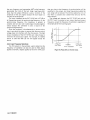
d. Refer to the OUTPU T DISTOR TION LI MITS curve
contained in the specifications near t he front of this
manual. The measured value of distort ion should conform
to t he curve.
- - - -- - - Table 5·4 - - - - - - CALIBRATED 1232 MEASUREMENTS
Oscillator
Voltage
Range
Hum Voltage
150
50.0
15.0*
5.0
1.5
4.5 mV
1.5 mV
450 f.J.V
150 f.J.V
45 p.V
*Recalibrate 1232 for 1mV full scale using 1346.
5.2.8 Reference Outputs.
Phase Relationship . The QUADRATURE output lags the
IN-PHASE output by approx imately 90°. Following .is a
method t hat can be used to check this phase relationship:
a. Connect the oscilloscope as shown in Figure 5-1.
b.Adjust the scope controls as follows:
TR IGGERING SE LECTOR
. A UTO
TIME/CM . . .
. 1 ms
CH A VOLTS/CM
.10
CH 8 VO LTS/CM
. . 10
c. Set t he oscillator controls for any output.
d. Using the position controls, position the scope patter")
so t hat the graticu le can be used as a reference.
e. Observe t he scope pattern carefully. Notice that the
QUADRATURE output lags the IN-PHASE out put by
approximately 90° .
Output Level. The open-circuit outputs at the RE FE RENCE OUTPUTS jacks are constant over the range of the
oscil lator. Following is a procedure that can be used to
check the level of these outputs:
a. Set the oscillator controls for any output.
b. Connect the 1808 Mill ivoltmeter to the IN-PHASE
output.
c. Adjust the voltmeter cont ro ls to measure 1.5 V, ac.
d. Observe the voltmeter indication - it shou ld be 1.25
± 0.25 V.
To measure the QUADRATURE output level, connect
the 1808 to the QUADRATURE output and repeat steps
b-d above.
Output Distortion. To make output distortion checks of
the REFERENCE OUTPUTS, use the same procedure
presented in para. 5.2.7 with one exception. The distortion
analyzer is connected to either the IN-PHASE or QUADRATURE output jack.
Amplitude v Frequency Response. With the exception of
step b, para 5.2.5 can be used to make response checks of
the REFERENCE OUTPUTS. Regarding step b, the 1808
must be connected to either the IN-PHASE or the
QUADRATURE output jack, depending on which is being
checked.
The output level for both outpu ts is 1.25 ± 0.25 V and
the measuring equipment wi ll have to be adjusted accordingly.
5.3 ASSEMBLY/DISASSEMBLY PROCEDURES.
5.3.1 Knob Removal.
CAUTION
Do not use a screwdriver or other tool to pry
off the knob if it is tight. Do not lose the spring
clip in the knob while it is off.
To remove the knob from a front-panel control. to
replace a damaged knob or the associated control, proceed
as follows:
a. Grasp the knob firmly with dry f ingers, close to the
panel, and pull the knob straight away.
b. Observe the position of the setscrew in the bushing
when the control is fully ccw.
c. Release the setscrew with a 5/64-in. Allen wrench;
pull the dial/bushing off the shaft.
d. Remove and retain the black felt washer, behind the
dial/ knob assembly (FREQUENCY controls only).
NOTE
To separate the bushing from the knob, if for
any reason they should be combined off of the
shaft, drive a machine tap a turn or two into
the bushing to provide sufficient grip for easy
separation. If the retention spring in the knob
falls out, reinstall it in the interior notch w ith
the small slit in the in ner diameter of the wall.
5.3.2 Knob Installation.
To instal l a knob assembly on the control shaft:
a. Place the black felt washer over the control shaft.
b. Mount the dial bushing on the shaft.
c. Orient the setscrew properly on the bushing, with
respect to step b in para. 5.3. 1 and lock the setscrew with
an A llen w rench.
NOTE
If the end of the shaft protrudes through the
bushing, the knob cannot seat properly .
d. Place the knob on the bushing w ith the
retention spring opposite the setscrew.
e. Push the knob in until it botto ms and pull it
slightly to check that the retention spring is seated in
the groove in the bushing.
5.4 MAJOR COMPONENTS.
Figure 5-2 identif ies the major components of the
osci llator with their correspond ing locations.
5.5 SERVICING THE ETCHED-CIRCUIT BOARD.
The 1316 Oscillator has one etched-circuit board .
When removing or replacing parts, use a low-heat
soldering iron and a small-diameter rosin-core solder. Do
not subject the parts or board to excessive or prolonged
heat. If a part is obviously faulty or damaged, clip the leads
close to the part and then remove the leads from the circuit
side.
5.6 CALIBRATION PROCEDURES.
5.6.1 General.
Cal ibrate the oscillator whenever minimum performance
standards. operating procedures. trouble analysis, or maintenance checks indicate that t he instrument is out of
calibration.
5.6.2 Power-Supply Adjustment.
To adjust the power-supp ly, B+ voltage, connect the
1807 between TP3 (F igure 5-2) and the chassis for a de
measuremen t. Use a pair of short cli p leads. Adjust R 11 for
a reading of 20 V.
5.6.3 Frequency Stability.
Following is a frequency-stabi lity adj ustment procedu re:
a. Set the oscillator controls as follows:
FREQUENCY Selectors
50 Hz*
OUTPUT VOLTAGE RANGE
150 v
OUTPUT ADJUST
0
b. Connect a short across the POWER OUTPUT. (Use a
short clip lead.)
• The third digit must be set to the d e tented zero-position.
SERVICE 5-5
A·T3
A·C45
R42
AT35
A·S6
Figure 5·2. Top, interior view.
c. Connect the oscilloscope probe t o AT35 (Figure 5·2).
d. Set the OUTPUT ADJUST con trol to MAX.
e. Adjust the oscilloscope controls to obtain a sinewave
pattern; observe the pattern carefully for aberrations of the
signal.
f. Adjust R42 (Figure 5·2) to eliminate the aberrations.
g. Rotat e the FRE QUENCY range selector fro m the Hz
to the kHz position. Slightly readjust R42 to el iminate any
aberrations that reappear.
5.6.4 Meter Accuracy .
The meter accuracy can be adjusted by the following
procedure:
a. Set the oscillator controls for a 100-V , 1-kHz output.
b. Set the 1808 to the 150·V range and connect it to the
oscillator POWER OUTPUT.
c. Adjust the OUTPUT ADJUST control for a 100-V
indication on the 1808.
d. Adjust R60 (Figure 5·2) so that the panel-meter
indicat ion is t he same as that of the 1808 ±1 %.
Following is a recommended adjustment procedure for
the highest frequency range:
a. Set the osci IIator cont rols for a 4· V , 50-kHz output.
b. A djust the counter controls to measure frequency and
connect it to t he oscillator POWER OUTPUT.
c. Adjust C5 to obtain a counter reading of 50.02 kHz.
5.7 GENERAL MAINTENANCE.
5.7.1 Lamp Replacement.
To replace t he decimal-point lamps, slide th e metal clip
off the back of the metal holder and remove the lamp.
Insert a new lamp (Chicago Miniature Lamp Works, No.
327 or equ ivalent) , and replace the clip.
5.7.2 Panel Finish.
If the f ront panel becomes marred or scratched , retouch
with a I ight gray paint that conforms with the Federal
Standard 595 (gray . 26492).
5.8 TROUBLE ANALYSIS.
5.8.1 General.
5.6.5 Frequency Accuracy.
The highest frequency range is adjusted with the variable
capacitor C5. All other ranges are adjusted w ith fixed-value
capacitors chosen at the f actory.
5-6 SERVICE
Isolating a symptom to a particular circu it can be done
by checking for the presence or absence of signals at the
rear-panel output jacks. For example, if t he instrument
controls are adjusted for a 10.0 k Hz, 10-V output, the
front-panel-meter ind icati on should be 10 V. If there is no
indicat ion, check the POWER OUTPUT. A voltage here
indicates a problem in the meter circuit. If no voltage is
present, check t he IN-PHASE outpu t. There should be 1.25
±0.25 V present regardless of the frequency and voltagecontrol setti ngs. The correct voltage indicates a proble m in
the output power amplifier. An incorrect voltage indicates
an oscillator or power-supply problem. The decimal-point
lamps are connect ed directly to B+: therefore, if they are
on the power supply is working.
The next step should be to check resist ance and/or
voltages within the circu it suspected of having a malfunct ion . A functiona l block diagram (F igure 4- 1) and the
schematic diagram (F igure 5-5) are suppl ied as an aid f or
local izing problems.
5.8.2 Incorrect Output Frequency.
An incorrect output frequency should be isolated to a
particular range, and if possible, to a particular step w ithin
a range. If the output is incorrect f or one of the frequency
ranges, the capaci tors for that range should be checked. If
the output is incorrect for a step within one of the ranges,
the resistors for that step should be checked . (Refer to the
schematic diagram Figure 5-3.)
5.8 .4 Excessive Distortion.
If there is excessive distortion at the POWER OUTPUT,
check the IN-PHASE output. (Refer to the OUTPUT
DISTORTION LI MI T S curve contained in the specifications near the front of this manua l. ) Excessive distortion
here indicates that the problem is in the osci llator and is
probably caused by the thermistor (R23) . Otherwise the
problem is probably caused by a defect ive component in
the power amplifier.
5.8.5 Excessive Hum.
If the hum specif ication is exceeded at the POWER
OUTPUT, the B + voltage should be checked for ripple.
Ripple voltages > 100 mV pk-pk can contribute to
excessive hum. Co mponents to suspect are f ilter capacitors
C1, C4, and CR 1-CR4.
5.8.6 low Output from EXT SYNC.
The most common cause of a low EXT-SYNC output is
capaci tance load ing of the signal. Output impedance is 47
kn; therefore 100 pF across th·e output (e.g. about 3ft . of
shielded cab le) w il l reduce the output at t he higher
frequencies. If this condition creates a problem, a shorter
patch cord should be used.
5.8. 7 Meter Window Care
5.8.3 Incorrect Output Voltage.
If the POWER OUTPUT voltage is incorrect. check the
IN-PHASE output jack to be 1.25 ± 0.25 V. rms. An
incorrect voltage at t his jack indicates either a power-supply
or an oscillat or problem. The next step shou ld be to check
t he 20-V, B +voltage. If it is incorrect, the problem can be
isolated by making resistance and voltage checks in the
power supply . If it is correct, the problem is in the
oscillator and the first component to suspect is the
thermistor.
A correct IN-PHASE. output voltage ind icates th at the
problem is between the power-amplifier input and the
output from the instrument. Therefore, check the voltage
at A T 35 to be approx imately 5 V, rms. A n incorrect
voltage here indicates output-power-amplifier problems. A
correct voltage indicates an output-t ransformer or power
resistor problem. (Refer to the schematic diagram Figure
5-3.)
The clear acrylic met er w indow can become suscepti ble
to electrostatic-charge buildup and can be scratched, if
improperly cleaned .
It is treated inside and out i n manufacturing with a
special non-abrasive anti-static sol ution, Statnul *, which
norm ai ly should preclude any interference in meter operat ion caused by electrostatic effects. The problem is evidenced by the inability of the meter movement to return
promptly to a zero reading, once it is deenergized. As supplied, the meter shou ld return to zero readi ng within 30
seconds, immediat ely fol lowin g the placement of a stat ic
charge, as by rubbing t he outside surface. This meets the
requiremen ts of ANSI standard C39. 1-1972.
If static-charge problems occur, possibly as the result of
frequent cleaning, the window should be careful ly pol ished
wit h a sof t dry cloth, such as cheesecloth or nylon chif fon.
Then, a coating of St atnul should be applied with the
pol ishing cloth.
"Avail able from Mancib Co. , Burl ington, MA 01803
SERVICE 5-7
Figure 5·3. Mechanical parts, front view.
MECHANICAL PARTS LIST
Fig
Ref
Fed
Ont
FRONT VIEW
1,
2
2.
1
3.
1
4,
1
1
1
1
5.
6.
7,
8.
1
1
2
9.
4
1
10.
Description
GR Pan No.
Handle
Cabinet gasket
Dial asm., FREQUENCY
Bench cabinet asm. complete:
Bench cabinet asm.
Base asm,
Foot
Dial a sm., FREQUENCY
Dial asm., FREQUENCY
Dial asm., Range
Knob asm,, OUTPUT ADJUST; OUTPUT
VOLTAGE RANGE, including retainer
5220-5402
Knob asm., FREQUENCY, including
retainer 5220 -5402
Toggle switch, A-Sl, POWER/OFF
MfgCode
Mfg Pan No.
5360-2007
5331 -2156
1864-1213
4172-4015
4172-2042
4171-1021
4171-7010
5120-2440
1864-1230
5120-2450
5520-5221
24655
24655
24655
24655
24655
24655
24655
24655
24655
24655
24655
5360-2007
5331 -2156
1864-1213
4172-4015
4172-2042
4171-1021
4171-7010
5120 -2440
1864-1230
5120-2450
5520-5221
5520 -5220
24655
5520-5220
7910-1300
04009
83053-SA
Figure 5·4. Mechanical parts, rear view.
MECHANICAL PARTS LIST
Fig
Ref
Ont
Description
GR Pan No.
Fed
Mfg Code
Mfg Pan No.
REAR VIEW
1.
3
2,
4.
1
1
1
5.
1
3.
5-8 SERVICE
Connector, A-]3, QUADRATURE;
A-J4, IN-PHASE; A-J2, EXT SYNC,
Connector, A -Jl, POWER OUTPUT
Fuse mounting device
Slide switch, A-S2, LINE VOLTAGE
SELECTOR
Connector, power plug, A -J5
4230-2300
81349
UG-1094/U
4230 -2301
5650-0100
7910-0832
09408
71400
82389
UG -1094A/U
HKP -H
ll A-11 18
4240-0210
24655
4240- 0 210
~
~
~ ~ ·~
c
. clo ofo
•f r-c ~
;
7
t•
~ ~
<t><R
~·
0
..., ...,f' "''-
.A-.04S:A-'"'" A-~ kJIP7
1$ 1C ~ '7.S.:
'1.S¥. 800
!lilt
~ 101• ' tUC ~
10711t
••
c
,~Lt.
5!"~-:t~t.~~~ ~C*HCfll
~ fiii,IUL COII'Uo~
: : : : :.> ••llllr ai,..,.ML ' '
~~Jk~~~t~~:-~
RlAD!H&.S .Ml.E NOMJM L
CICTSC!CIJ:.IO .AS RII.f'
lie F"ACTOfll" ADJUSTME.NT
•
((lt.'f CCTIIQG
___.. MOOOI UWU tl;- t(lltl.r
~ ~'- lllffl:IIOII ...• U U1111.7
u-. ...
........( • •
- - ( ) MJJYI' . ..
~
E>----o:-....,.,_..,.. ,_'""""'"tt.~.
~} R(ADI HG$ 1N
,}'!'!:/
•
VOt.TS:TAKCN
AT IKHz , lOY
CIIT O,.EHC:I<T
~·O.a
\:0
Ql,<..,7. 1'0.1 1,1?, 20
•
17'\
e.Uc
QIS..-.
,.li·Q.?
~~§]
E I C
' • c
e
~.5,.13,. ...
~'I"'RMI'fAG"
CO
LS1M-lll ll' Rl'Q'O
· ~· e
.:oTt C~i.l'CTOR f
C I t/=t:.:fo~~,w;.
Q 9,12.,RI
Q8
V"'N $1/1'f'UCR.
Ao011,.A-rQ t B
B~
~~ ~ rh
.4·02
GltOOHOS
C~S
CIRCUI T
Figure 5-5. Schematic diagram of the Type 1316 Oscillator.
SERVICE 5-9
ELECTRICAL PARTS LIST
CH4SSIS MOUNTED PARTS
REF DES
c
c
c
c
c
c
c
OS
OS
OS
1
12
45
49
50
51
52
l
2
3
F
J
J
J
J
J
1
2
3
4
5
M
Q
Q
Q
Q
R
R
R
R
R
R
R
R
R
R
R
R
R
R
R
R
R
R
R
R
R
R
R
R
R
R
R
R
R
R
R
R
R
R
R
R
R
R
R
R
R
R
R
R
R
R
R
R
R
R
2
3
17
18
DESCRIPTION
PIN 1316-3000
PART
NO.
FMC
MFGR
PART
NUMBER
CAP ALUM 10000 Uf 40V
CAP ALUM 15 UF 15V
CAP ALUM 40000 UF 10V
FACTORY ADJUST
FACTOAY ADJUST
FACTORY ADJUST
CAP CER DISC 180PF lOPCT 500V
4450-6211
4450-3700
4450-6216
90201
56289
90201
CGS 10000UF 40V
300156G015
CGS 40000Uf lOV
4404-1188
72982
0831082Z5000181 J
LAMP FLANGE BASE 28V e04A 25000H
LAMP FLANGE BASE 28V e04A 25000H
LAMP FLANGE BASE 28V .D4A 2SOOOH
5600-0 301
5600-0307
5600-0307
71744
71744
1l744
CM-387
CM-387
CM-387
FUSE SLQ-BLOW 8/lOA
5330-1200
75915
313
RE CPT BNC
RECPT BNC
RECPT BNC
RECPT BNC
RECEPTACLE POWER IEC STD 6A 250V
4230-2301
4230-2300
4230-2300
4230-2300
42't0-0210
24655
24655
24655
24655
24655
423o-2301
423o-2300
423o-2300
4B0-2300
4240-0210
METER
5730-1430
24655
5730-1430
8210-1213
6210-1028
8210-1208
8210-1207
01295
04713
01295
01295
TIP-33A
2N22l8
TIP-JZA
TlP-3lA
6760-83.35
6099-2105
6451-2750
6000-0300
6000-0600
6660-2105
6660-1105
666o-0125
6670-921t5
75042
81349
81349
01121
01121
75042
75o42
75042
24655
BWH 0.33 OHM 5PCT
RCR07GL02J
RN6 5075 020
JA I N0 56 S 1 02UZ
JAl N056S1 03UZ
AS-5 1K 5PCT
AS-5 100 OHM 5PCT
AS-5 12 OHM SPCT
667D-9245
6670-2225
6670-1225
6670-0245
6670-9245
6670-8225
6670-2245
6670-1225
6670-0245
667o-9245
6670-8225
6250-3249
6250-2787
6250-2232
6250-1604
6250-0499
6451-2150
6451-1750
6451-1750
6451-1301
6451-3150
6451-2750
6451-2750
6451-2101
6451-2150
6451-1750
6451-1750
6451-1301
6451-3150
6451-2750
6451-2750
6451-2101
6351-2448
6351-2226
6351-2226
6351-1898
6351-3448
6351-3226
6351-3226
635~-2 898
75042
75042
24655
21t655
24655
75042
75042
24655
24655
24655
81349
81349
81349
81349
81349
81349
81349
81349
81349
81349
81349
81349
81349
81349
81349
81349
81349
61349
81349
81349
81349
81349
81349
81349
81349
81349
81349
81349
81349
AS-10 2.2 K 5PCT
AS-10 220 OHM 5PCT
667D-0245
667o-9245
667D-8225
AS-10 2e4 K 5PCT
AS-10 220 OHM 5PCT
667D-0245
667o-9245
667o-8225
RN55D21t93F
RN55D78 72F
RN5502322F
RN55D6041F
RN55D4990F
RN65D1502D
RN65075 010
RN65D75 01D
RN65D30 UO
RN65015 030
RN65075020
RN65D75 020
RN65030 12D
RN65015020 .
RN65075 010
RN6507501D
RN65030 110
RN65Dl5030
RN65D7502D
RN65075020
RN6503012D
RN60D44820
RN60D2262D
RN6002262D
RN60089810
RN6004483D
RN60D2263D
RN60022630
RN60D8982D
TRANSISTOR
TRANSISTOR
TRANSISTOR
TRANSISTOR
250V
TIP-33A
2N2218
TIP-32A
TIP-31A
1 . RES WW MOLDED • 33 OHM 5 PCT 2W
2 RES COMP 1.0 K 5PCT 1/4W
13 RES FLM 76K
1/2 PCT 1/2W
14 POT COMP KNOB lK OHM 10 PCT LIN
27 POT CO~P ~N08 10K OHM 10 PCT LIN
66 RES WW AX LEAD 1K OHM 5 PCT 5W
67 RES WW AX LEAD 100 OHM 5 PCT sw
68 RES WW AX LEAD 12 OHM 5 PCT 5W
69 RES WW AX LEAD 2.4 OHM 5PCT lOW
70 FACTORY ADJUST
71 RES WW AX LEAD z.zK OHM 5PCT lOW
72 RES WW AX LEAD 220 OHM 5 PCT lOW
73 RES -W AX LEAD 24 OHM 5 PCT lOW
74 RES WW AX LEAD 2.4 OHM 5PCT lOW
75 RES WW AX LEAD .22 OHM 5PCT lOW
76 RES WW AX LEAD 2e4K OHM 5PCT lOW
11 RES WW AX LEAD 220 OHM 5 PCT lOW
18 RES WW AX LEAD 24 OHM 5 PCT lOW
79 RES WW AX LEAD 2.4 OHM 5PCT lOW
80 RES WW AX LEAD .22 OHM 5PCT lOW
81 RES FLM 249K
1 PCT 1/BW
82 RES FLM 78e7K
1 PCT 1/BW
83 RES FLM 23.2K
1 PCT 1/Bw
84 RES FU1 6e 04K
1 PCT
1/81ii
65 RES FLM 499 OHM 1 PCT 1/SW
liZ PCT l/2W
86 RES FLM 15K
1/2 PCT 1/2W
87 RES FLM 7e5K
88 RES FLM 7.5K
1/2 PCT l/2W
1/2PCT l/2W
89 RES FLM 3.01K
112 PCT l/2W
90 RES FLM 1·50K
1/2 PCT 1/ 2W
91 RES FLM 76K
112 · PCT l/2W
92 RES FLM 75K
1/ZPCT 1/2W
93 RES FlM 30e1K
94 RES FLM 15K
112 PCT li2W
95 RES FLM 7.5K
l/2 PCT l/2W
96 RES FlM 7e5K
1/2 PCT li2W
l/2PCT l/2W
97 RES F LM 3e 01K
1/2 PCT 1/2W
98 RES FlM loOK
99 RES FLM 75K
112 PCT l/2W
1/2 PCT 1/2W
100 RES fU1 75K
101 RES FUI 30.1K
1/2PCT 1/ZW
112PC T 1/4W
102 RES FLM ft4.8K
1/2 PCT l/4W
103 RES FLM 22e6K
1/2 PCT l/4W
104 RES FLM 22.6K
105 RES .FLM Be 98K
112PCT l/4W
106 RES FLM 44 8K
l/2PCT 114W
112 PCT l/4W
107 RES FlM 226K
1/2 PCT l/4W
108 RES FLM 226K
1/2PCT l/4W
109 RES FLM 8!te8K
116 FACTORY ADJUST
Note: Add Prefix Letter "A" To All Design&tor Letter"
.aoo
ELECTRICAL PARTS LIST (cont)
CHASSIS MOUNTED PARTS
REFDES
s
s
s
s
s
s
T
T
T
T
1
DESCRIPTION
SWITCH
SWITCH
SWITCH
4
SWITCH
5 · SWITCH
6 SWITCH
2
3
1
2
3
4
TOGGLE 2POS OPST STEADY
SLIDE 2 POS OPDT ST C40Y
ROTARY ASH
ROTARY ASI4
ROTARY ASM
ROTARY AS/1
TRANSFORMER POWER
TRANSFORMER
TRANS FORM6R OUTPUT
TRANSfORMER ASH
PART
PIN 1316-3000
NO.
FHC
11FGR
PART
7910-1300
7910-0832
7890-551t0
7890-SSitl
7890-5542
7890-5543
04009
82.389
24655
H655
24655
24655
83053
11A-1266
789D-5540
789D-5541
789D-5542
789D-S543
0485-4046
0485-4047
0345-4890
1316-2010
21t655
24655
2U55
24655
0485-4046
0485-4041
0345-4890
1316-2010
Note: Add Prefix Letter "li." To All Designator Letter s.
NUMBER
ELECTRICAL PARTS LIST
PC BOARD ASM
REf[)ES
c
c
c
c
c
c
::
c
c
c
c
c
c
c
c
c
c
c
c
c
::
c
c
c
c
c
c
c
c
c
2
3
4
S
-6
l
CR
CR
::R
CR
3
4
5
6
8
9
10
11
12
13
:R
CR
:R
::R
14
15
16
17
18
CR
19
::R
Q
;}
20
1
4
Q
5
Q
:)
6
7
Q
8
Q
Q
9
10
11
12
13
14
1'5
16
19
20
21
Q
Q
;)
Q
Q
Q
Q
;)
Q
5-10 SERVICE
14433
14433
14433
14433
14433
14433
01910
14433
14433
14433
14433
14433
14433
14433
14433
14433
14433
14433
14433
1N4140
lN4140
1N4140
1 N4l40
IN41 54
IN41'54
I N9576
IN750
IN750
1 N36v!t
1N3604
lN3604
lN3604
1N3604
1N36.:>4
1N3604
1N3604
IN4154
IN4154
TRANSISTOR
TRAN51STCR
TRA"'SISTOR
TRANSISTOR
TRANSISTOR
TRANSISTOR
TRANSISTOR
TIU N SIS TOR
TRANSISTOR
TRANS IST OR
82 10-12 90
8Zl0- 1ll4
8210-llH
821D-l290
82 10-1290
8210-11 23
821D-1294
8210-1290
821D- 1 290
8210-1294
d210-1 132
821C>-11H
8210-1028
8210-1074
8210-1292
8210-1292
82 1()-1294
56289
04713
04713
56289
56289
04713
07263
5&289
562 69
07263
04713
04713
04713
04713
56289
56289
07263
2N3414
2N3905
2N3905
2N3414
2N3414
2N4123
2N4250
2N3414
2N3414
2N4250
2N3903
2N3905
2N2218
2N2904
PN3391A
PN3391A
2N4250
CliP
<'
NUMBER
6081-1014
6081-1014
6081-1014
6081-1014
6082-1012
608 2-1012
6083-1009
6083-1003
6083-1003
6082-l 001
6082-1001
6082-1001
6082-1001
6082-1001
6082-1001
6082- 1001
6082-1001
60 82-1012
6082- 1012
CAP
CAP
CV
C{
PART
RE:T 1N4l40 lOOPIII 3A SI A1XM
FCT 11114140 1001>1 V 311 S ( lllXM
RECT 1N4l40 100P1V 311 Sl A1X~
RE:T 11114140 100~III 3A 5 1 A1XM
OIQOF. 111141 54 2'5P IV IR.lUA Sl
OIGOE lN41 54 25PtV IR.lUA 51
ZE\IER 1N957B
6.8V
5PC T • 4W
ZENER lN750
4.711
10PCT
.4W
ZENER 1N750
4.7V
10PCT .4W
OIJOE 1N41 51 75PIII I R.1 UA St
DI ODE 1N4151 75PIV IR.lUA St
DI'Ji>E 1N4151 15PIV tR.1UA SI
O!COE 1N4151 7'5PIII !R.lUA 51
OI::JDE 1~4151 7'5Plll 1R.1UA St
DlJ 0 F. 1 N 4151 7 5P l II I R. 1UA S I
DIODE 11114151 75Plll lR.llJASI
D!()')E lN4151 75PIII !R.1UA Sl
DIODE lN41 5'+ 25P IV IR.1UA SI
DIODE 1N4l '54 2'5PIV IR.1UA SI
C~?
19
21
24
25
26
27
28
30
31
3?.
33
34
35
36
37
38
39
40
41
42
43
MfGR
0801082Z5U00472Z
56 15- 000- Y5F - 224Z
1 S 004 76 X0035 S2
557-051 E 8-50PF
DM19F01000PF 1PCT40
CM07F010500PF lPCT
X463UW 0. 105UF lPCT
48 73-6105
30D207G012
4873-6105
X4o3UW O.l05Uf lPCT
CM07FiH 0500Pf 1 PCT
CM06F010SOFN
300207G012
300 156G015
600 1011
3002 07G012
300 36 7G 02 5
0831082Z5D00391J
150D4 76X002 OR2
08010 62Z5U00477Z
30Dl07G02 5
30Dl01G025
30 D606G025
FP 2000UF 3 5 II
0845024Z 5U05 032
TDC lOvUF 20PCT 2011
B4 6-Z5 U-6 800 PF20 PCT
1500 156 X0020B 2
15i>Ol56X002 0 62
l 50D225X0020A2
1500685X0035B2
l500685X0035B2
150012 7X001 OR2
1500l27X0010R2
1~0022 7X0010S2
TDC 100UF 20PC T 2011
TOC lOOUF 20PCT 2011
TDC lO OUF 20PCT 20V
18
44
46
47
48
FMC
72982
72982
56289
72982
72136
81349
75042
24655
56289
24655
75042
81349
81349
56289
56 2 89
56289
56289
56289
72982
'56289
72982
56289
56289
56289
90201
56269
90201
72<182
56289
56289
56289
56289
562B9
56269
56289
56289
90201
9020 1
90201
CA~
14
15
16
17
NO.
4405-2479
4432-4229
445()-5702
4910-1170
4851-0361
4565-2105
4862-2060
4873-6105
445D-0400
4873-6105
4862-2060
4565-2105
4710-1050
4450-0400
445D-3700
4450-5609
445Q-0400
44'50-6025
lo404-1395
4'+50-'5614
4405-2479
4450-2300
445D-2300
4450-2900
445()-7430
4403-3500
4450-6253
4406-26A9
44So-5200
445()-5200
44'5o-4500
it450-5000
445()-5000
4450-5616
4450-5616
445o-5706
445()-6253
4450-6253
44 50-6 253
CAP
CV
CAP
CAP
n
PARt
CER OISC.0041UF80/20PCT~OOII
CER DISK 0.22UF 80/?.0PCT 1211
T4NT 47 UF 20PCT 3511
CER TRIM 8-50 PF
MICA 1000 PF
1PCT 5JOII
MICA 10500PF lP:T 50011
POLY CARR O. t05JF 1PCT 1 0011
POLY 1. 05\IF lPCT 10011
ALV'1 20\l VF 1211
POLY 1.05UF 1P CT 10011
POLY Ct1R8 O. 105UF 1PCT 10011
MICA 1050JPF 1PCT 50011
!4ICA 1050PF 1PCT 50011
ALUM 200 UF 12V
ALUM 15 UF 1511
ALUM 3600-1800- 1800 UF 1011
ALUM 200 UF 1 211
ALUM 360 UF 2511
CER DISC
390PF
5PCT 5.lOV
TANT H UF 20PCT 2\l\1
CER OISC.0047UF80/20PC T500V
ALUM 100 UF 2511
ALUM 100 Uf 2511
ALUM 60 UF 2511
ALUM ?.000 UF
3511
CER OISC.047/.05UF80/20 10011
TANT ·tOO
UF 20PCT 2011 DIP
CER DISC 6800PF 20PCT 1. -tKII
TANT 15 UF 20PCT 2011
TAN T 15 UF 2 OPC T 2011
TANT 2.? Uf 20PCT 2011
TANT 6.8 UF 20PC T 3511
TANT 6.8 llf 20PC T 3511
TANT 120 Uf 20PC T lOll
TAN T 12 0 Uf 2 0 PC T 1 vV
TANT 220 UF 20:>:;T 1011
TANT 100
UF 20PCT 2011 DIP
TANT 100
UF 20PCT 2011 01 P
TANT 100
UF ZOPCT 20V DIP
CAP
CAP
CAP
CAP
CAP
9
CR
CR
CR
CR
CR
C'l.
CR
::R
OE SC R l PTl ON
tO
13
P /N 1316- 4 700
CA~
CA>
CAP
CAP
CAP
CAP
CAP
CAP
CAP
CAP
rAP
CAP
CA~
CAP
CAP
CAP
CAP
CAP
CAP
CAP
CAP
CAP
CV
CAP
~
TR~NS!STOR
TRANSISTOR'
TRANSISTOR
TRANSISTOR
TRANSISTOR
TRANSISTOR
TRANSISTOR
2N3414
2N390'5
2N390'5
2N34 14
2N3 414
2N4123
21114250
2 N34 1 4
2N3414
2 N4250
2N3903
2N3905
2N22 18
2N2904
PN3391A
PN3391A
2N4250
ELECTRICAL PARts. LIST J®:Otl
PRINTED CIRCUIT BOARO
REFDES
R
R
R
R
R
R
R
R
R
R
3
4
5
6
7
6
9
10
11
R
R
R
12
15
16
17
18
19
20
21
22
23
24
25
26
26
29
30
31
32
34
35
R
36
R
R
R
37
38
39
40
41
42
43
44
45
46
47
48
49
50
51
52
53
54
55
56
57
58
59
60
61
62
63
64
110
111
112
113
114
115
116
/(
R
R
R
R
R
R
f{
R
R
R
R
R
R
R
R
R
R
R
R
R
R
R
R
R
R
R
R
R
R
R
R
R
R
R
R
R
R
R
R
R
R
R
R
R
R
R
R
AR 150
AR 151
OESCRlPllGN
RES COMP 110
CHM
5PCT 1/4~
RES COMP 4.7 K 5PCT l/4~
RES COMP 22 K 5PCT 1/4k
RES COMP 200 K CHM · 5PCT 1/4k
RES COMP 47 OHM 5PCT 1/4W
RES COMP 4.7 K SPCT 1/4W
RES COMP 6.8 K 5PC1 l/4W
RES COMP 2.2 K SPCT 1/4W
POT WW TRH lK OHM 10 PCT lT
RES COMP 4.3 K OHM
5PCT 1/4~
RES COMP 2.2 K 5PCT l/4W
RES COMP 12 K 5PCT 1/4W
RES COMP " 10 K 5PCT 1/4~
RES COMP 56 K 5PCT 1/4k
RES COMP 27 K SPCT 1/4w
RES FLM 249 OHM 1 PCT l/4W
RES COMP 3.9 K SPCT l/4W
RES COHP 27 OHM 5PCT 1/4W
THERMISTOR 40K OHM 20PCT
RES COMP 3.0 K CHM
5PCT 1/4k
RES COMP 820 OHM 5PCT 1/4W
RES COMP 1.0 K 5PCT 1/4W
RES COMP 4.7 K siit.T . li4W
RES COMP 680 OHM 5PCT 1/4W
RES COMP 10 K 5PCT 1/4W
RES COMP 10 K 5PCT 1/~W
RES COHP 51
OH~
5PCT l/4~
RES COHP 2.0 K OHM
5PCT l/4w
RES COMP 2.2 K 5PCT 1/4W
RES COHP 6.8 K 5PCT l/4W
RES COMP 43 K OHM
5PCT 1/4W
RES COMP 51 K CH~
5PCT 1/4W
RES COMP 100 OHM 5PCT 1/4W
RES COHP 300
OHM
5PCT 1/4W
RES COHP 4.7 OHM SPCT 1/4W
POT CERM TRM 500 OHM 10 PCT 1T
RES COMP 750
OHM
5PCT 1/4W
RES COMP 750
OHM
SPCT 1/4~
RES COMP 100 CHM SPCT 1/~W
RES COHP. 100 OHM 5PCT 1/4W
RES WW MOLDED .47 OHH 10 PCT 2W
RES WW MOLOEO .47 OHM 10 PCT 2W
RES FLM 2.03K
1/2PCT 1/6W
RES COMP 10 K 5PCT l/4W
RES COHP 130 K OHM
5PCT 1/~W
RES COMP 10 K 5PCT 1/4W
RES COMP 1.0 K 5PCT 1/4W
RES COHP 7.5 K OHM
5PCT 1/4k
RES COMP 51 K CHM
5PCT 1/4W
RES COMP 100 K 5PCT 1/4W
RES COMP 100 K 5PCT 1/4W
RES COHP 3.0 K OHM
5PCT 1/4"
RES COHP 12 K 5PCT 1/4W
POT CERM TRM 10K OHM 10 PCT 1T
RES COHP 3.9 K 5PCT 1/4W
RES COMP 3.9 K 5PCT 1/4W
RES COMP 10 K 5PCT l/4W
RES COMP 10 K 5PCT 1/4W
RES COMP 2.0 K OHM
5PCT 1/4"
RES COHP 2.2 K 5PCT l/4W
RES COMP 200
OHM
5PCT 1/4k
RES COMP 200
OHM
5PCT 1/4W
RES COMP 100 OHM 5PCT 1/~W
RES COHP 1.0 K 5PCT 1/4W
RES COMP 1.0 K 5PCT 1/4W
RES COHP 2.7 OHM
RES COHP 2.7 OHM
5PCT 1/~W
5PCT l/4W
P/N 1316-4700
PART
NO.
6099-11 15
6099-2~75
6099-3225
6099-4205
6099-0475
6099-24 75
6099-2685
6099-2225
6056-0138
6099-2435
6099-2225
6099-3125
6099-3105
609S-3565
6099-3275
6350-0249
6099-2395
6C99-0275
674Q-1400
6099-2305
6099-1825
6099-2105
6C99-2475
6099-1685
6099-3105
6099-3105
6099-0515
6099-2205
6099-2225
6099-2685
6099-3'135
6099-3515
609~1105
609~1305
6099-9~75
6Q4c;-0214
6099-1755
6099-1755
6099-1105
6099-1105
6 76Q-8479
676G-8479
6251-1203
6099-3105
6099-4135
6099-3105
6099-2105
6099-2755
6099-3515
6099-4105
FMC
81349
81349
El349
81349
81349
81349
81349
81349
2465~
81349
81349
81349
813Lo9
81349
81349
81349
81349
81349
15801
81349
81349.
81349
81349
81349
813Lo9
81349
81349
81349
81349
813Lo9
81349
81349
81349
81349
81349
01121
813~9
81349
Sl349
81349
75042
75042
81349
Sl34~
6099-2105
81349
81349
8131t9
8131t9
813Lo9
81349
81349
81349
81349
01121
81349
81349
8134CJ
81349
e1349
81349
81349
813Lo9
81349
81349
81349
6099-9215
6099-9275
81349
81349
609~4105
6099-2305
6099-3125
6049-0218
609CJ-2395
6099-23~5
609c;-3105
6099-3105
6099-2205
6099-2225
6099-1205
6099-1205
6099-1105
609~2105
MFGR PART NUMBER
RCRC7Gl11J
RCR07G472J
RCR07G223J
RCRC7G204J
RCR07G470J
RCR07G472J
RCR07G682J
RCR07G222J
6056-0138
RCR07G432J
RCR07G222J
~CR07G123J
RCR07Gl03J
RCR07G563J
RCR07G273J
RN6002490F
RCR 071>3 92J
RCR07G270J
8A-44V3
RCR07G302J
RCR07G821J
RCRC7Gl02J
RCR07G472J
RCR07G68lJ
RCR07Gl03J
RCR07Gl03J
RCR07G51 0J
RCR07G202J
RCR07G222J
RCR07G682J
RCR07G433J
RCR07G513J
RCR07Gl01J
RCR07G301J
RCR07G4R7J
SV5011
RCR07G 75lJ
RCR07G751J
RCRC7Gl0lJ
RCR07G101J
BWH 0.47 OH~ lOPCT
BWH 0.47 OHM 10PCT
RN55C20310
RCR07G103J
RCR07Gl34J
RCR07G 103J
RCRC7G102J
RCR07G752J
RCR07G51JJ
RCR07G104J
RCR07G104J
RCR 0 7G302J
RCR07G123J
SV1031
RCR07G392J
RCR07G392J
RCR07G103J
RCR07G1.0 3J
RCR07G202J
RCR07G222J
RCR07G201J
RCR07G201J
RCRC7Gl01J
RCR07G102J
RCR07G10~J
RCR07G2R7J
RCR07G2R7J
SERVICE 5·11
_ ,_ __
' ,4.:"·'
·-0 , '
.. . •, . -
<tt
.J..•
-~~~£~\~~
'l
.~ .
"'
~
t.'
"· --~ ..... ,.~.., '~ ·-~··'.~-~,,·-""'
':
"' g
' ill,
'----y----'~
. ~12
(;f
. Zi!~
·• •
\ot'
~' . ·- -G~.·- ¢ I
, ~~<>
. -~-~l ' , ··
-.:J:,·
.~
),'
,
""'-,.,.,. • -~'<)
"'
.
"~' . o
2
..~ ,
-~~~.,."~
-~
·t
~~"'-'t~'.(~~~~m~-~--...~_;
..~~·~A"">Y«vw,.
....,
-~
R
~-.
•
I
..
.
•
~;\~~~~~'!~~
Etched-circuit board assembty (P/N 1316-4700) for the Type 1316 Oscillator.
NOTE: The board is shown foil-side up. The number appearing on the
foil side is not the part number. The dot on the foil at the transistor
socket indicates the collector lead.
~
'•·