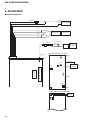
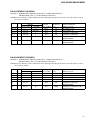
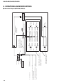
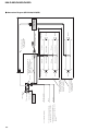
1
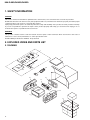
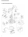
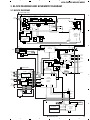
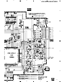
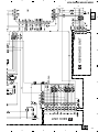
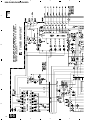
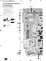
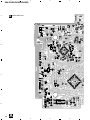
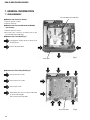
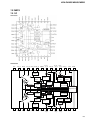
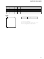
Service Manual KEH-P490/X1M/UC ORDER NO. CRT2398 MULTI-CD CONTROL HIGH POWER CASSETTE PLAYER WITH FM/AM TUNER KEH-P490 KEH-P4900 X1M/UC X1M/UC KEH-P4950 X1M/ES - This service manual should be used together with the following manual(s): Model No. Order No. CX-1011 CRT2406 Mech. Module 3L Remarks Cassette Mech. Module:Mech.Description and Greasing, Disassembly, Adjustment - This service manual does not describe the CD test mode. For the operations in the CD test mode, refer to the CD player's Service manual. CONTENTS 1. 2. 3. 4. 5. 6. SAFETY INFORMATION ............................................2 EXPLODED VIEWS AND PARTS LIST .......................2 BLOCK DIAGRAM AND SCHEMATIC DIAGRAM .....9 PCB CONNECTION DIAGRAM ................................24 ELECTRICAL PARTS LIST ........................................33 ADJUSTMENT..........................................................40 7. GENERAL INFORMATION .......................................42 7.1 DISASSEMBLY ...................................................42 7.2 PARTS .................................................................43 7.2.1 IC.................................................................43 7.2.2 DISPLAY .....................................................47 8. OPERATIONS AND SPECIFICATIONS.....................48 PIONEER CORPORATION 4-1, Meguro 1-Chome, Meguro-ku, Tokyo 153-8654, Japan PIONEER ELECTRONICS SERVICE INC. P.O.Box 1760, Long Beach, CA 90801-1760 U.S.A. PIONEER ELECTRONIC [EUROPE] N.V. Haven 1087 Keetberglaan 1, 9120 Melsele, Belgium PIONEER ELECTRONICS ASIACENTRE PTE.LTD. 253 Alexandra Road, #04-01, Singapore 159936 C PIONEER CORPORATION 1999 K-ZZB. OCT. 1999 Printed in Japan KEH-P490,P4900,P4950 1. SAFETY INFORMATION CAUTION This service manual is intended for qualified service technicians; it is not meant for the casual do-it-yourselfer. Qualified technicians have the necessary test equipment and tools, and have been trained to properly and safely repair complex products such as those covered by this manual. Improperly performed repairs can adversely affect the safety and reliability of the product and may void the warranty. If you are not qualified to perform the repair of this product properly and safely; you should not risk trying to do so and refer the repair to a qualified service technician. WARNING This product contains lead in solder and certain electrical parts contain chemicals which are known to the state of California to cause cancer, birth defects or other reproductive harm. Health & Safety Code Section 25249.6 - Proposition 65 2. EXPLODED VIEWS AND PARTS LIST 2.1 PACKING 1 3 6 7 4 16 5 9 12 2 10 20 8 19 15 18 17 14 11 13 2 KEH-P490,P4900,P4950 NOTE: - Parts marked by “*” are generally unavailable because they are not in our Master Spare Parts List. - Screws adjacent to ∇ mark on the product are used for disassembly. - PACKING SECTION PARTS LIST Part No. KEH-P4900/X1M/UC CEA2350 CBH1650 CEA2351 CBA1304 CEG-127 Mark No. * 1 2 3 4 * 5 Description Accessory Assy Spring Screw Assy Screw Polyethylene Bag KEH-P490/X1M/UC CEA2350 CBH1650 CEA2351 CBA1304 CEG-127 6 7 8 9 10 Screw Screw Polyethylene Bag Handle Bush CRZ50P090FMC TRZ50P080FMC CEG-158 CNC5395 CNV3930 CRZ50P090FMC TRZ50P080FMC CEG-158 CNC5395 CNV3930 CRZ50P090FMC TRZ50P080FMC CEG-158 CNC5395 CNV3930 11 12 13 14 15 Polyethylene Bag Carton Contain Box Protector Protector CEG1173 CHG3893 CHL3893 CHP2244 CHP2243 CEG1173 CHG3889 CHL3889 CHP2244 CHP2243 CEG-162 CHG3890 CHL3890 CHP2244 CHP2243 Owner’s Manual Owner’s Manual Installation Manual Warranty Card Card CRD3090 Not used CRD3091 CRY1070 Not used CRD3088 Not used CRD3089 CRY1070 ARY1048 CRD3083 CRD3084 CRD3085 Not used Not used Cord assy Case assy Battery Remote Control Unit CDE6222 CXB3520 CEX1030 CXB4284 CDE6222 CXB3520 Not used Not used CDE6222 CXB3520 Not used Not used * * * 16-1 16-2 16-3 16-4 16-5 17 18 19 20 KEH-P4950/X1M/ES CEA2350 CBH1650 CEA2351 CBA1304 CEG-127 - Owner's Manual, Installation Manual Model KEH-P490/X1M/UC KEH-P4900/X1M/UC KEH-P4950/X1M/ES Part No. CRD3090 CRD3091 CRD3088 CRD3089 CRD3083 CRD3084 CRD3085 Language English, French English, French English, French, Spanish English, French, Spanish English, Spanish, Portuguese(B) Chinese, Arabic English, Spanish, Portuguese(B), Chinese, Arabic 3 KEH-P490,P4900,P4950 2.2 EXTERIOR 2 29 7 1 4 1 32 1 1 68 A 33 5 12 28 15 40 38 19 24 41 14 27 35 13 26 6 14 31 18 44 45 42 69 46 36 20 25 39 23 46 9 43 46 22 37 A 46 8 21 34 48 59 11 48 17 60 16 62 55 61 65 63 64 51 52 48 66 47 10 56 3 2 53 50 67 3 2 2 58 57 49 54 30 4 KEH-P490,P4900,P4950 (1) EXTERIOR SECTION PARTS LIST Mark No. Description 1 2 3 4 5 Part No. Mark No. Description Part No. Screw Screw Screw Cord Assy Fuse(10A) BSZ26P050FMC BSZ30P050FMC BSZ30P200FMC CDE6222 CEK1136 36 37 38 39 40 Spring Spring Bracket Bracket Arm CBH1835 CBH2182 CNC6135 CNC6791 CNV4692 6 7 8 9 10 Transistor(Q904) Case Holder Cushion Insulator 2SD2396 CNB2350 CNC5704 CNM5210 CNM5963 41 42 43 44 45 Arm Arm Panel Unit Door Spring CNV4693 CNV4728 CXB4927 CAT2109 CBH1838 11 12 13 14 15 Panel Tuner Amp Unit Screw Screw Screw CNS5132 46 47 48 49 50 Screw Detach Grille Assy Screw Button(DETACH) Button(1-6) IMS20P030FZK 16 17 18 19 20 FM/AM Tuner Unit Holder Pin Jack(CN301) Plug(CN603) Connector(CN701) See Contrast table(2) CNC6554 CKB1035 CKM1270 CKS3408 51 52 53 54 55 Button(SOURCE) Button(+) Button(-) Button(AUDIO) Button(EQ) CAC6241 CAC6242 CAC6243 CAC6245 CAC6247 21 22 23 24 25 Connector(CN602) Connector(CN601) Antenna Jack(CN402) Panel Holder CKS3568 CKS3581 CKX1056 CNB2343 CNC5399 56 57 58 59 60 Button(EJECT) Button(BAND) Spring Cover Keyboard Unit CAC6268 CAC6269 CBH2103 CNS5635 26 27 28 29 30 Holder Holder Heat Sink Holder Unit Chassis Unit CNC6845 CNC7996 CNR1505 CXB2687 CXB3012 61 62 63 64 65 LCD(LCD1901) Connector(CN1901) Holder Sheet Connector CAW1563 CKS3580 CNC8485 CNM6453 CNV5914 31 32 33 34 35 IC(IC302) Remote Control Unit Cover Button Spring TDA7384 66 67 68 69 Lighting Conductor Grille Sub Assy See Contrast table(2) See Contrast table(2) BPZ26P080FMC BSZ26P080FMC BSZ26P160FMC See Contrast table(2) See Contrast table(2) CAC4836 CBH1834 See Contrast table(2) BPZ20P100FZK CAC5789 CAC6239 See Contrast table(2) CNV5915 Cassette Mechanism Module EXK4000 Screw ISS26P055FUC (2) CONTRAST TABLE KEH-P490/X1M/UC, KEH-P4900/X1M/UC and KEH-P4950/X1M/ES are constructed same except for the following: Mark No. 12 16 32 33 47 60 67 Description Tuner Amp Unit FM/AM Tuner Unit Remote Control Unit Cover Detach Grille Assy KEH-P490/X1M/UC CWM7021 CWE1467 CXB4284 CNS4948 CXB5152 Part No. KEH-P4900/X1M/UC CWM7021 CWE1467 Not used Not used CXB4788 KEH-P4950/X1M/ES CWM7025 CWE1486 Not used Not used CXB4789 Keyboard Unit Grille Sub Assy CWM7022 CXB5209 CWM7024 CXB5210 CWM7024 CXB5211 5 KEH-P490,P4900,P4950 2.3 CASSETTE MECHANISM MODULE 6 KEH-P490,P4900,P4950 - CASSETTE MECHANISM MODULE SECTION PARTS LIST Mark No. Description Part No. Mark No. Description Part No. 1 2 3 4 5 Screw Washer Washer Screw Screw BSZ20P040FMC CBF1037 CBG1003 EBA1028 EBA1037 46 47 48 49 50 Pinch Roller Pinch Holder Unit Pinch Roller Reel Unit Head Base Unit ENV1518 EXA1583 ENV1518 EXA1585 EXA1586 6 7 8 9 10 Spring Spring Spring Spring Spring EBH1531 EBH1624 EBH1625 EBH1626 EBH1627 51 52 53 54 Lever Unit Gear Unit Motor Unit(Service) Washer EXA1587 EXA1588 EXX1055 HBF-179 11 12 13 14 15 Spring Cord Photo-reflector(EGN1) Arm Lever EBH1628 EDD1024 EGN1004 ENC1526 ENC1530 16 17 18 19 20 Lever Arm Frame Holder Gear ENC1531 ENC1532 ENC1533 ENC1534 ENC1535 21 22 23 24 25 Arm Roller Belt Collar Arm ENC1536 ENR1040 ENT1027 ENV1508 ENV1539 26 27 28 29 30 Arm Gear Gear Gear Worm Wheel ENV1540 ENV1544 ENV1547 ENV1548 ENV1550 31 32 33 34 35 Lever Flywheel Gathering PCB Switch(S1,S2) Deck Unit ENV1551 ENV1554 ENX1054 ESG1007 EWM1023 36 37 38 39 40 Plug(CN251) Gathering PCB Motor Unit(M1) Motor Head Assy(HD1) CKS3540 ENX1053 EXA1491 EXM1028 EXA1506 41 42 43 44 45 Motor Unit(M2) Screw Bracket Chassis Unit Pinch Holder Unit EXA1580 BMZ20P022FMC ENC1528 EXA1582 EXA1584 7 KEH-P490,P4900,P4950 8 1 3 2 4 KEH-P490,P4900,P4950 3. BLOCK DIAGRAM AND SCHEMATIC DIAGRAM 3.1 BLOCK DIAGRAM A TUNER AMP UNIT B FM/AM TUNER UNIT Q3 FM RF CN402 T31 FM MIX CF52 FM IF Q31 CF51 FM IF A CF53 FM IF T51 25 TUNER Lch 26 FM/AM PROCESSOR IC1 PA4023B 38 32 36 AM OSC AMTV 19 20 FMTV AMTV 18 31 30 43 40 28 15 17 14 FMVCC VCC Q921 FMSL 9 AMSL 18 CF232 AM IF AMVCC 7 Q920 SYSPW 55 6 13 21 Q907 IC501 AMVCO PM2006A IC601(1/2) PE5086A Q909 4 5 AM Q908 38 FM PLLDATA FMVCO 37 68 74 SYSTEM CONTROLLER 9 29 AMTV FMTV 76 SL 53 SD SD AMIF PLL 25 25 23 VDD B.U 19 FM PROCESSOR IC2 PA4024A SL FMTV AM RF/AGC 16 AMIFC VCO 6 Q201 Q202 Q903 2 1 47 AVDD 34 19 17 FMSD FM OSC 14 15 SYSPW 41 9 10 VDD FM/AM ANTENNA 29 FM 30 AM VCC Q910 PDI/PCK/PDO/PCE X501 TUN-L BUS-L1 BUS-L2 7 BUSL+ 11 BUSL5 BUS1 BUS+ IP-BUS DRIVER 5 6 Q701 8 IC702 CA0008AM B.U 8 1 2 IC301 PML003AM 6 3 TAPE-L Q309 MUTE 11 RL FL 10 CN301 2 MUTE 1 Q310 TX RX VCK/VDT/VST IP-BUS 2 5 B TUN-L ELECTRONIC VOLUME CN701 ASENBO ASENBO Q702 POWER AMP 11 15 Q307 IC302 TDA7384 FL RL MUTE MUTE FL- 7 6 5 FRONT-L SPEAKER 9 9 8 8 REAR-L SPEAKER 7 BACK UP 2 2 ACC 1 1 6 5 RL- 19 RL+ 17 STBY 22 9 4 Q306 Q911 Q904 VCC CN603 FL+ B.U SYSPW Q901 7 FUSE 10A BSENS Q905 VDD D DECK UNIT 2 7 Lch 17 20 19 19 MTL 8 LOAD 11 11 STBY IC351 PA2020A 7 8 CN253 10 3 1 5 6 3 1 5 6 8 MCMUTE 37 MCMUTE B.U STBY 48 MTL 38 42 LDSW 1 C 70 X2 69 MTL LOADSW CN602 8 9 5 VDD EGN1 REEL SENSE SWVDD Q601 VDD SWITCH SW5V E REEL SENSE PCB KYDT S1 LOAD ILL1 S2 MODE B.REMOTE 6 IC601(2/2) PE5086A STBY 63 CN256 B REMOTE IC901 TPD1018F X601 SYSTEM CONTROLLER SWVDD 20 B.U 19 18 CN255 9 DPDT CN601 8 5 3 4 6 8 5 3 4 6 REMOTE CONTROL SENSOR CN1901 3 1 20 VDD 56 10 18 DPDT KYDT KEY MATRIX REM IC1902 RS-140 D 17 LCD XI LCD DRIVER IC1901 PD6278C XO M 9 5 SYSPW X1 KYDT MUTE MECHANISM DRIVER 2 1 5 2 1 M1 MAIN MOTOR 3 DSENS M 3 56 TX 61 RX 1 ASEMBO 18 17 CN254 M2 SUB MOTOR 54 LOUT B.U 66 65 60 SW5V 4 4 DSENS REV L-ch IC251 CXA2559Q 4 LCDB 5 TAPE+B ACC DPDT 37 36 39 5 ASENS EQ AMP RESET 1 FWD L-ch Q902 ASENS Q906 VCC BSENS CN251 B.U SYSPW 1 IC602 S-80734AN MUTE CN252 8V REGULATOR RESET 23 22 X1901 C KEYBOARD UNIT 1 2 9 3 4 2 1 3 4 KEH-P490,P4900,P4950 3.2 OVERALL CONNECTION DIAGRAM(GUIDE PAGE) Note: When ordering service parts, be sure to refer to “EXPLODED VIEWS AND PARTS LIST” or “ELECTRICAL PARTS LIST”. A-a A A-a A-b Large size SCH diagram B A-a A-a A-b A-b FM/AM TUNER UNIT Guide page Detailed page B D DECK UNIT C D C 10 A 1 2 3 KEYBOARD UNIT 4 5 7 6 8 KEH-P490,P4900,P4950 A-b A A TUNER AMP UNIT B CEK1136 C D 5 6 7 A 8 11 1 2 3 2 3 4 A A-a A-b 1 KEH-P490,P4900,P4950 FM/AM TUNER UNIT B B C D 12 A-a 1 4 5 7 6 8 KEYBOARD UNIT A-a A-b 3 2 KEH-P490,P4900,P4950 A C B C D DECK UNIT 6 7 D 5 A-a 8 13 1 2 3 2 3 4 TUNER AMP UNIT CEK1136 A A-a A-b KEH-P490,P4900,P4950 A B C 14 A-b 1 1 D 4 5 7 6 8 A-a A-b KEH-P490,P4900,P4950 A B C 5 6 3 2 D 7 A-b 8 15 2 1 3 4 KEH-P490,P4900,P4950 3.3 FM/AM TUNER UNIT - CWE1467(KEH-P490/X1M/UC, KEH-P4900/X1M/UC) A B FM/AM TUNER UN D6 MA157 R1 2R2M R2 2R2M D2 RD39JS D1 RD39JS B C 1 2 3 D 16 B 1 2 3 4 5 6 7 8 KEH-P490,P4900,P4950 A A IFC ER UNIT B C D 5 6 7 B 8 17 2 1 3 4 KEH-P490,P4900,P4950 - CWE1486(KEH-P4950/X1M/ES) A B FM/AM TUNER UN D6 MA157 R1 2R2M R2 2R2M D2 RD39JS D1 RD39JS B C 1 2 3 D 18 B 1 2 3 4 5 6 7 8 KEH-P490,P4900,P4950 A A IFC R UNIT B C D 5 6 7 B 8 19 1 2 3 4 2 3 4 KEH-P490,P4900,P4950 3.4 KEYBOARD UNIT A B C D 20 C 1 5 7 6 8 KEH-P490,P4900,P4950 A KEYBOARD UNIT B A CN601 C DISP C CLOCK RPT PAUSE/BSM D 5 6 7 C 8 21 2 1 3 4 KEH-P490,P4900,P4950 3.5 CASSETTE MECHANISM MODULE A D DECK UNIT 18K R1 R301 16K C302 1K R304 R258 R01 16K C256 PBGND TCH2 LINEOUT2 GND DIREF TAPEIN2 MSSW R273 1K R272 1K R271 1K R274 1K R403 C402 3900P C401 R33 0R0 C 0R0 0R0 R286 R285 C272 R1 MUTE CN251 -6dBs(388mV)±1dB A 3 4 D 22 D 1 2 R290 C403 R323 100P 1K G2FB C313 R257 R01 16K C255 G1FB 20 19 18 17 16 15 14 13 12 11 MSLPF PBFB1 PBTC1 TEST TAPE NCT-150 (400Hz, 200nWb/m) MSTC EQ AMP PBRIN1 LINEOUT1 R255 220 HD1 HEAD ASSY EXA1506 MSOUT PBFIN1 TCH1 C251 330P PBREF 16K FL CXA2559Q VCT VCC 0R0 R281 0R0 R1 Fwd-L TAPESW MUTESW PBFIN2 TAPEIN1 R287 22/16 FR IC251 PBGND C301 C252 330P C273 DRSW PBRIN2 OUTREF1 R282 0R0 MSMODE PBFB2 1 2 3 4 5 6 7 8 9 10 Fwd-R 31 32 33 34 35 36 37 38 39 40 PBOUT1 R256 220 C254 330P R284 0R0 RR R303 Rev-R B OUTREF2 PBTC2 R283 0R0 R305 Rev-L RL PBOUT2 30 29 28 27 26 25 24 23 22 21 C253 330P R302 CN252 CN602 5 7 6 8 KEH-P490,P4900,P4950 A M1 MOTOR UNIT (MAIN MOTOR) EXA1491 CN255 CN253 CN256 REEL SENSE RSB EGN1 EGN1004 GND RS 0R0 300 FRS SC1 R403 82K C402 R402 18K C352 3900P RRS SC2 R068 S1 LOAD ESG1007 RS2 RS1 C403 load MCS R362 0R0 TAB C CN254 TAB NC NC SM1 MM NC R01 C354 R01 1K 1K R353 R354 0R0 C353 1K 1K R351 R374 R352 M2 MOTOR UNIT (SUB MOTOR) EXA1580 C351 VCC2 VCC IC351 CE R22 MS2 MC R401 4R7K B REEL SENSE E PCB RSB 3900P 1SS355 C D352 C401 R33 S2 MODE ESG1007 MCS RS3 PA2020A R290 270K mtl MECHANISM DRIVER R355 R373 C356 C355 R01 SWITCHES: PCB UNIT S1:LOAD SWITCH..........EJECT-PLAY S2:MODE SWITCH............ON-OFF The underlined indicates the switch position. R1 D 5 6 7 D E 8 23 2 1 3 4 KEH-P490,P4900,P4950 4. PCB CONNECTION DIAGRAM 4.1 TUNER AMP UNIT CORD ASSY NOTE FOR PCB DIAGRAMS A 1. The parts mounted on this PCB include all necessary parts for several destination. For further information for respective destinations, be sure to check with the schematic diagram. 2. Viewpoint of PCB diagrams Connector Capacitor SIDE A P.C.Board Chip Part SIDE B B A TUNER AMP UNIT C D 24 A 1 C CN1901 2 3 4 5 6 7 8 KEH-P490,P4900,P4950 SIDE A A IP-BUS ANTENNA B B D CN251 C D 5 6 7 A 8 25 1 2 3 4 2 3 4 KEH-P490,P4900,P4950 A TUNER AMP UNIT A B C D 26 A 1 5 6 7 8 KEH-P490,P4900,P4950 SIDE B A B C D 5 6 7 A 8 27 2 1 3 4 KEH-P490,P4900,P4950 4.2 FM/AM TUNER UNIT SIDE A A A B B FM/AM TUNER UNIT C D 28 B 1 2 3 4 1 2 3 4 KEH-P490,P4900,P4950 SIDE B A B B FM/AM TUNER UNIT C 1 D 2 3 B 4 29 D 30 1 2 C KEYBOARD UNIT SOURCE EQ1 C A CN601 2 3 4 5 6 CLOCK RPT DISP PAUSE/BSM AUDIO BAND 1 VOL- EQ+ B EJECT A VOL+ C KEYBOARD UNIT KEH-P490,P4900,P4950 2 3 3 4 4.3 KEYBOARD UNIT SIDE A SIDE B C 4 1 3 2 4 KEH-P490,P4900,P4950 4.4 CASSETTE MECHANISM MODULE D DECK UNIT A CN602 A SIDE A B SIDE B D DECK UNIT HEAD ASSY M2 M1 IC,Q ADJ C VR302 CN254 CN252 CN255 CN253 22 21 IC253 IC251 Q351 Q352 VR301 E 1 2 3 D CN256 D 4 31 2 1 3 4 KEH-P490,P4900,P4950 E REEL SENSE PCB A S1 LOAD SW S3 70µs SW S2 MODE SW CN256 6 5 4 3 2 1 EGN1 REEL SENSE D CN253 B C D 32 E 1 2 3 4 KEH-P490,P4900,P4950 5. ELECTRICAL PARTS LIST NOTES: - Parts whose parts numbers are omitted are subject to being not supplied. - The part numbers shown below indicate chip components. Chip Resistor RS1/_S___J,RS1/__S___J Chip Capacitor (except for CQS.....) CKS....., CCS....., CSZS..... =====Circuit Symbol and No.===Part Name --- ----------------------------------------------- A Part No. ------------------------- Unit Number : CWM7021(KEH-P490/X1M/UC) (KEH-P4900/X1M/UC) Unit Number : CWM7025(KEH-P4950/X1M/ES) Unit Name : Tuner Amp Unit MISCELLANEOUS =====Circuit Symbol and No.===Part Name --- ----------------------------------------------- Part No. ------------------------- D D D L L 908 909 910 401 501 Diode Diode Diode Inductor Ferri-Inductor HZS9L(A2) 1SR139-400 1SR139-400 See Contrast table LAU2R2K L L L L L 502 601 602 603 702 Ferri-Inductor Ferri-Inductor Ferri-Inductor Ferri-Inductor Ferri-Inductor LAU2R2K LAU2R2K LAU2R2K LAU2R2K LAU2R2K L X X 901 501 601 Choke Coil 600µH Crystal Resonator 7.2MHz Ceramic Resonator 4.194MHz FM/AM Tunew Unit CTH1168 CSS1474 CSS1047 See Contrast table IC IC IC IC IC 301 302 501 601 602 IC IC IC IC IC PML003AM TDA7384 PM2006A PE5086A S-80734AN IC IC Q Q Q 702 901 306 307 308 IC IC Transistor Transistor Transistor CA0008AM TPD1018F DTC124EK 2SC1740S DTC143TK Q Q Q Q Q 309 310 401 505 506 Transistor Transistor Transistor Transistor Transistor DTC143TK DTA124EK 2SC2412K DTA124EK DTC114EK R R R R R 301 302 310 317 318 RS1/10S0R0J RS1/10S0R0J RS1/10S103J RS1/10S152J RS1/10S103J Q Q Q Q Q 601 701 702 901 902 Transistor Transistor Transistor Transistor Transistor 2SA933S 2SA1037K DTC114EK 2SC1740S 2SC2412K R R R R R 319 320 321 322 323 RS1/10S221J RS1/10S101J RS1/10S223J RS1/10S153J RS1/10S103J Q Q Q Q Q 903 904 905 906 907 Transistor Transistor Transistor Transistor Transistor 2SD2037 2SD2396 2SB1238 2SC1740S 2SA1048 R R R R R 325 326 327 328 333 RS1/10S821J RS1/10S821J RS1/10S223J RS1/10S223J RS1/10S101J Q Q Q Q Q 908 909 910 911 920 Transistor Transistor Transistor Transistor Transistor DTC114TK 2SA1048 DTC114TK 2SC2412K DTC114ES R R R R R 334 335 336 337 338 RS1/10S101J RS1/10S223J RS1/10S223J RD1/4PU102J RD1/4PU102J Q D D D D 921 301 302 401 402 Transistor Diode Diode Diode Diode DTA124ES 1SS270 1SS270 1SS270 1SS270 R R R R R 342 401 402 403 404 RS1/10S0R0J See Contrast table RS1/10S162J RS1/10S162J RS1/10S0R0J D D D D D 601 602 603 604 605 Diode Diode Diode Diode Diode 1SS270 1SS270 1SS270 1SS270 1SS270 R R R R R 405 406 407 408 410 See Contrast table RS1/10S102J RD1/4PU222J RS1/10S222J RS1/10S102J D D D D D 606 607 608 901 902 Diode Diode Diode Diode Diode 1SS270 1SS270 1SS270 HZS7L(C2) 1SR139-400 R R R R R 412 413 417 418 419 RD1/4PU103J RS1/10S393J RS1/10S0R0J RS1/10S0R0J RS1/10S0R0J D D D D D 903 904 905 906 907 Diode Diode Diode Diode Diode 1SR139-400 HZS7L(A1) 1SR139-400 HZS6L(B2) HZS9L(B3) R R R R R 502 503 506 511 512 RS1/10S102J RS1/10S222J RS1/10S182J RS1/10S0R0J See Contrast table RESISTORS 33 KEH-P490,P4900,P4950 =====Circuit Symbol and No.===Part Name --- ----------------------------------------------- Part No. ------------------------- =====Circuit Symbol and No.===Part Name --- ----------------------------------------------- Part No. ------------------------- R R R R R 513 514 515 517 518 RS1/10S102J RS1/8S0R0J RS1/10S562J RS1/10S473J RS1/10S152J R R R R R 725 726 901 902 903 RD1/4PU472J RS1/10S222J RS1/10S473J RS1/10S223J RS1/10S223J R R R R R 519 520 521 523 524 RS1/10S472J RS1/10S472J RS1/10S472J RS1/10S0R0J RS1/10S103J R R R R R 904 905 906 907 908 RS1/10S473J RD1/4PU102J RD1/4PU473J RS1/10S473J RS1/10S472J R R R R R 525 526 527 528 529 RS1/10S152J RS1/10S392J RS1/10S392J RS1/10S472J RS1/10S473J R R R R R 909 910 911 912 913 RS1/10S332J RD1/4PU101J RS1/10S102J RS1/10S103J RS1/10S103J R R R R R 531 532 535 601 604 RS1/10S104J RS1/10S473J RS1/10S102J RS1/10S124J RS1/10S473J R R R R R 914 915 916 917 919 RS1/10S222J RS1/8S103J RS1/10S103J RS1/10S0R0J RS1/10S102J R R R R R 607 610 611 612 613 RD1/4PU102J RS1/10S473J RS1/10S473J RS1/10S473J RS1/10S473J R R R R R 920 921 922 923 924 RS1/10S103J RS1/10S152J RS1/10S102J RS1/10S103J RS1/10S223J R R R R R 614 615 616 617 618 RS1/8S103J RS1/10S392J RD1/4PU222J RD1/4PU223J RD1/4PU222J R R R R 932 944 949 955 RS1/10S473J RS1/10S152J RS1/8S1R0J RD1/4PU473J R R R R R 619 621 622 623 624 RD1/4PU222J RS1/10S222J RS1/10S222J RD1/4PU222J RS1/10S222J R R R R R 625 626 627 628 629 RD1/4PU222J RD1/4PU222J RD1/4PU222J RD1/4PU222J RD1/4PU681J R R R R R 630 633 634 635 636 RS1/10S681J RD1/4PU681J RD1/4PU681J RD1/4PU222J RS1/10S472J R R R R R 637 638 639 641 642 RS1/10S103J RD1/4PU222J RS1/10S223J RD1/4PU222J RS1/10S473J R R R R R 643 644 645 646 647 RS1/10S472J RS1/10S472J RS1/10S472J RS1/10S103J RS1/10S103J R R R R R 648 649 651 653 654 See Contrast table RS1/10S103J RD1/4PU222J RS1/8S0R0J RS1/10S0R0J R R R R R 655 716 717 718 719 RS1/10S473J RS1/10S620J RS1/10S101J RS1/10S101J RS1/10S473J R R R R R 720 721 722 723 724 RS1/10S473J RS1/10S102J RS1/10S102J RS1/10S102J RS1/10S223J CAPACITORS 34 C C C C C 303 304 308 309 310 CEJA470M10 CEJA100M16 CKSQYB104K50 CKSQYB224K16 CKSQYB224K16 C C C C C 311 312 313 314 315 CKSQYB224K16 CKSQYB224K16 CEJA4R7M35 CEJA4R7M35 CEJA330M10 C C C C C 316 317 318 319 320 CEJA1R0M50 CEJA100M16 CKSYB225K16 CKSQYB474K16 CKSQYB474K16 C C C C C 321 322 323 324 325 CKSQYB474K16 CKSQYB474K16 CKSQYB104K50 CCH1169 CEJA2R2M50 C C C C C 326 327 328 329 330 CEJA2R2M50 CEJA1R0M50 CEJA1R0M50 CEJA1R0M50 CEJA1R0M50 C C C C C 331 332 391 392 393 CKSQYB153K50 CKSQYB153K50 CKSQYB225K10 CKSYB474K16 CKSYB474K16 C C C C C 394 395 401 402 403 CKSYB474K16 CKSYB474K16 CKSQYB473K50 CKSQYB473K50 CKSQYB223K25 3300µF/16V KEH-P490,P4900,P4950 =====Circuit Symbol and No.===Part Name --- ----------------------------------------------- Part No. ------------------------- =====Circuit Symbol and No.===Part Name --- ----------------------------------------------- Part No. ------------------------- C C C C C 407 408 411 413 414 CKSQYB223K50 CCSQSL101J50 CCSQSL101J50 CKSQYB223K50 CKSQYB103K50 C C C C C 530 601 602 603 604 CEJA220M10 CKSQYB473K50 CEJA2R2M50 CKSQYB103K50 CCSQCH101J50 C C C C C 504 505 506 507 508 CKSQYB103K50 CKSQYB103K50 See Contrast table CEJA220M6R3 CKSQYB102K50 C C C C C 608 609 610 611 715 CEJA4R7M35 CEJA100M16 CEJA220M10 CKSQYB223K50 CKSQYB102K50 C C C C C C 510 511 512 513 514 515 CCSQSL101J50 CKSQYB103K50 CKSQYB103K50 CKSQYB103K50 CCSQCH150J50 CKSQYB102K50 C C C C C 716 901 902 903 904 CKSQYB104K50 CEJA101M10 CKSQYB473K50 CCH1183 CKSQYB103K50 C C C C C 516 518 519 520 521 CCSQCH150J50 CKSQYB103K50 CEJA220M6R3 CKSQYB103K50 CEJA220M6R3 C C C C C 905 906 907 908 910 C C C C C 522 524 525 527 528 CKSQYB103K50 CKSQYB103K50 CCH1250 CKLSR473K16 CKSQYB154K16 4.7µF/16V 470µF/16V 330µF/10V 100µF/16V CCH1181 CKSQYB103K50 CCH1179 CKSQYB103K50 CKSQYB473K50 CONTRAST TABLE of TUNER AMP UNIT KEH-P490/X1M/UC, KEH-P4900/X1M/UC and KEH-P4950/X1M/ES are constructed same except for the following: Symbol and Description FM/AM Tuner Unit L401 Inductor R401 R405 R512 KEH-P490/X1M/UC KEH-P4900/X1M/UC CWE1467 LCTBR39K2125 Not used Not used RS1/10S0R0J R648 C506 Not used Not used =====Circuit Symbol and No.===Part Name --- ----------------------------------------------- B Part No. ------------------------- Unit Number : CWE1467(KEH-P490/X1M/UC) (KEH-P4900/X1M/UC) Unit Name : FM/AM Tuner Unit MISCELLANEOUS IC IC Q Q Q 1 2 1 2 3 IC IC Transistor Transistor FET PA4023B PA4024A 2SC2412K DTC124EU 3SK263 Q Q Q Q D 31 201 202 203 1 Transistor FET Transistor Transistor Diode 2SC2412K 2SK932 2SC2412K DTC124EU RD39JS D D D D D 2 4 5 6 7 Diode Diode Diode Diode Diode RD39JS 1SV250 KV1410-F1 MA157 KV1410-F1 Part No. KEH-P4950/X1M/ES CWE1486 Not used RS1/10S182J RS1/10S510J Not used RS1/10S183J CKSQYB103K50 =====Circuit Symbol and No.===Part Name --- ----------------------------------------------- Part No. ------------------------- D D D D L 8 201 202 231 2 Diode Diode Diode Diode Coil KV1410-F1 MA157 MA157 SVC253 CTC1133 L L L L L 3 4 5 51 201 Inductor Coil Coil Ferri-Inductor Ferri-Inductor LCTB2R2K2125 CTC1133 CTC1132 LAU150K LAU4R7K L L L L T 202 203 208 231 31 Ferri-Inductor Inductor Inductor Inductor Coil LAU330K CTF1287 LAU121K LCTA3R3J3225 CTE1117 T CF CF CF CF 51 51 52 53 232 Coil Ceramic Filter Ceramic Filter Ceramic Filter Ceramic Filter CTC1159 CTF1441 CTF1441 CTF1441 CTF1348 35 KEH-P490,P4900,P4950 =====Circuit Symbol and No.===Part Name --- ----------------------------------------------- Part No. ------------------------- =====Circuit Symbol and No.===Part Name --- ----------------------------------------------- X X VR CSS1365 CSS1111 CCP1213 CAPACITORS 151 231 154 Radiator 918.5Hz Crystal Resonator 10.26MHz Semi-fixed 150kΩ(B) RESISTORS R R R R R 1 2 4 5 6 RS1/16S225J RS1/16S225J RS1/16S154J RS1/16S391J RS1/16S223J R R R R R 7 8 9 10 11 RS1/16S123J RS1/16S332J RS1/16S473J RS1/16S223J RS1/16S124J R R R R R 13 15 16 17 18 RS1/16S563J RS1/16S271J RS1/16S104J RS1/16S332J RS1/16S332J R R R R R 31 32 33 34 35 RS1/16S470J RS1/16S822J RS1/16S822J RS1/16S331J RS1/16S331J R R R R R 40 51 52 55 56 RS1/16S470J RS1/16S271J RS1/16S560J RS1/16S102J RS1/16S823J R R R R R 61 62 101 102 103 RS1/16S392J RS1/16S273J RS1/16S272J RS1/16S682J RS1/16S333J R R R R R 104 105 107 151 152 RS1/16S334J RS1/16S683J RS1/16S222J RS1/16S222J RS1/16S393J R R R R R 155 156 157 160 161 RS1/16S273J RS1/16S243J RS1/16S203J RS1/16S222J RS1/16S563J R R R R R 162 163 202 203 204 RS1/16S105J RS1/16S223J RS1/16S223J RS1/16S225J RS1/16S103J R R R R R 206 207 208 209 214 RS1/16S220J RS1/16S101J RS1/16S102J RS1/16S471J RS1/16S822J R R R R R 215 217 231 232 237 RS1/16S822J RS1/16S102J RS1/16S272J RS1/16S473J RS1/16S103J R R R R R 238 239 240 241 243 RS1/16S104J RS1/16S104J RS1/16S332J RS1/16S202J RS1/16S183J R R 244 247 RS1/16S392J RS1/16S123J 36 Part No. ------------------------- C C C C C 1 2 4 6 8 CCSQCH6R0D50 CCSRCK2R0C50 CCSRCH820J50 CCSRCH820J50 CKSRYB103K25 C C C C C 9 10 11 12 13 CKSQYB104K16 CCSRCKR50C50 CEJA1R0M50 CKSRYB222K50 CKSRYB222K50 C C C C C 14 15 16 17 18 CCSRCH220J50 CCSRCH6R0D50 CCSRCH8R0D50 CKSRYB222K50 CKSRYB103K25 C C C C C 19 20 21 22 23 CKSRYB222K50 CKSRYB222K50 CEJA100M16 CCSRTH9R0D50 CCSRTH120J50 C C C C C 24 25 26 31 32 CCSRCH471J50 CKSRYB103K25 CCSRCH101J50 CKSRYB103K25 CKSQYB472K50 C C C C C 33 34 36 51 52 CCSRCH5R0C50 CKSQYB104K16 CCSRRH201J50 CKSRYB223K25 CKSRYB103K25 C C C C C 54 55 56 57 58 CCSRCH470J50 CKSQYB223K25 CKSQYB104K16 CKSRYB472K50 CEJA330M10 C C C C C 59 60 61 62 63 CKSRYB103K25 CKSRYB102K50 CCSRCH270J50 CKSRYB103K25 CEJAR22M50 C C C C C 101 102 103 104 105 CEJANP100M10 CKSRYB182K50 CKSRYB682K25 CEJA2R2M50 CKSRYB103K25 C C C C C 106 107 151 152 153 CCSRCH151J50 CKSRYB103K25 CKSRYB472K50 CKSQYB104K16 CEJA3R3M50 C C C C C 154 157 158 159 160 CKSQYB104K16 CEJA3R3M50 CKSYB474K16 CEJA220M6R3 CKSQYB104K16 C C C C C 161 162 163 170 201 CKSQYB104K16 CEJA3R3M50 CKSRYB102K50 CCSRCH100D50 CCSRCH471J50 C C C C C 202 203 204 205 206 CCSRCH100D50 CKSRYB332K50 CKSQYB473K16 CKSQYB473K16 CKSQYB104K16 KEH-P490,P4900,P4950 =====Circuit Symbol and No.===Part Name --- ----------------------------------------------- Part No. ------------------------- =====Circuit Symbol and No.===Part Name --- ----------------------------------------------- Part No. ------------------------- C C C C C 207 209 211 212 213 CCSRCH560J50 CKSQYB104K16 CCSRCH101J50 CEJA470M6R3 CKSRYB103K25 CF X X VR CTF1348 CSS1365 CSS1111 CCP1213 C C C C C 216 217 219 220 230 CCSRCH101J50 CEJA1R5M50 CCSRCH471J50 CKSRYB103K25 CKSRYB103K25 C C C C C 231 232 233 234 235 CCSRCH330J50 CCSRCH150J50 CKSQYB104K16 CEJA330M10 CKSRYB332K50 C C C C C 236 237 239 240 241 CKSQYB473K16 CCSRCH120J50 CKSRYB472K50 CEJAR47M50 CKSQYB104K16 C C C C C 242 243 244 245 246 CEJAR47M50 CEJAR33M50 CKSQYB473K16 CKSRYB333K16 CKSQYB473K16 C 250 CCSRCH471J50 232 151 231 154 Ceramic Filter Radiator 918.5Hz Crystal Resonator 10.26MHz Semi-fixed 150kΩ(B) RESISTORS B Unit Number : CWE1486(KEH-P4950/X1M/ES) Unit Name : FM/AM Tuner Unit MISCELLANEOUS IC IC Q Q Q 1 2 1 2 3 IC IC Transistor Transistor FET PA4023B PA4024A 2SC2412K DTC124EU 3SK263 Q Q Q Q D 31 201 202 203 1 Transistor FET Transistor Transistor Diode 2SC2412K 2SK932 2SC2412K DTC124EU RD39JS D D D D D 2 4 5 6 7 Diode Diode Diode Diode Diode RD39JS 1SV250 KV1410-F1 MA157 KV1410-F1 D D D D L 8 201 202 231 2 Diode Diode Diode Diode Coil KV1410-F1 MA157 MA157 SVC253 CTC1133 L L L L L 3 4 5 6 51 Inductor Coil Coil Inductor Ferri-Inductor LCTB2R2K2125 CTC1133 CTC1132 LCTBR15K1608 LAU150K L L L L L 201 202 203 208 231 Ferri-Inductor Ferri-Inductor Inductor Inductor Inductor LAU4R7K LAU330K CTF1287 LAU121K LCTA3R3J3225 31 51 51 52 53 Coil Coil Ceramic Filter Ceramic Filter Ceramic Filter CTE1117 CTC1159 CTF1441 CTF1441 CTF1441 T T CF CF CF R R R R R 1 2 4 5 6 RS1/16S225J RS1/16S225J RS1/16S154J RS1/16S391J RS1/16S223J R R R R R 7 8 9 10 11 RS1/16S123J RS1/16S332J RS1/16S473J RS1/16S223J RS1/16S124J R R R R R 13 15 16 17 18 RS1/16S563J RS1/16S271J RS1/16S104J RS1/16S332J RS1/16S332J R R R R R 31 32 33 34 35 RS1/16S470J RS1/16S822J RS1/16S822J RS1/16S331J RS1/16S331J R R R R R 40 51 52 55 56 RS1/16S470J RS1/16S271J RS1/16S560J RS1/16S102J RS1/16S823J R R R R R 61 62 101 102 103 RS1/16S392J RS1/16S273J RS1/16S272J RS1/16S682J RS1/16S333J R R R R R 104 105 107 151 152 RS1/16S334J RS1/16S683J RS1/16S222J RS1/16S222J RS1/16S393J R R R R R 155 156 157 160 161 RS1/16S273J RS1/16S243J RS1/16S203J RS1/16S222J RS1/16S563J R R R R R 162 163 202 203 204 RS1/16S105J RS1/16S223J RS1/16S223J RS1/16S225J RS1/16S103J R R R R R 206 207 208 209 214 RS1/16S220J RS1/16S101J RS1/16S102J RS1/16S471J RS1/16S822J R R R R R 215 217 231 232 237 RS1/16S822J RS1/16S102J RS1/16S272J RS1/16S473J RS1/16S103J R R R R R 238 239 240 241 243 RS1/16S104J RS1/16S104J RS1/16S332J RS1/16S202J RS1/16S183J R R 244 247 RS1/16S392J RS1/16S123J 37 KEH-P490,P4900,P4950 =====Circuit Symbol and No.===Part Name --- ----------------------------------------------- Part No. ------------------------- CAPACITORS C C C C C 1 2 4 6 8 CCSQCH6R0D50 CCSRCK2R0C50 CCSRCH820J50 CCSRCH820J50 CKSRYB103K25 C C C C C 9 10 11 12 13 CKSQYB104K16 CCSRCKR50C50 CEJA1R0M50 CKSRYB222K50 CKSRYB222K50 C C C C C 14 15 16 17 18 CCSRCH220J50 CCSRCH6R0D50 CCSRCH8R0D50 CKSRYB222K50 CKSRYB103K25 C C C C C 19 20 21 22 23 CKSRYB222K50 CKSRYB222K50 CEJA100M16 CCSRTH9R0D50 CCSRTH120J50 C C C C C 24 25 31 32 33 CCSRCH471J50 CKSRYB103K25 CKSRYB103K25 CKSQYB472K50 CCSRCH5R0C50 C C C C C 34 36 51 52 54 CKSQYB104K16 CCSRRH201J50 CKSRYB223K25 CKSRYB103K25 CCSRCH470J50 C C C C C 55 56 57 58 59 CKSQYB223K25 CKSQYB104K16 CKSRYB472K50 CEJA330M10 CKSRYB103K25 C C C C C 60 61 62 63 101 CKSRYB102K50 CCSRCH270J50 CKSRYB103K25 CEJAR22M50 CEJANP100M10 C C C C C 102 103 104 105 106 CKSRYB182K50 CKSRYB682K25 CEJA2R2M50 CKSRYB103K25 CCSRCH151J50 C C C C C 107 151 152 153 154 CKSRYB103K25 CKSRYB472K50 CKSQYB104K16 CEJA3R3M50 CKSQYB104K16 C C C C C 157 158 159 160 161 CEJA3R3M50 CKSYB474K16 CEJA220M6R3 CKSQYB104K16 CKSQYB104K16 C C C C C 162 163 170 201 202 CEJA3R3M50 CKSRYB102K50 CCSRCH100D50 CCSRCH471J50 CCSRCH100D50 C C C C C 203 204 205 206 207 CKSRYB332K50 CKSQYB473K16 CKSQYB473K16 CKSQYB104K16 CCSRCH560J50 38 =====Circuit Symbol and No.===Part Name --- ----------------------------------------------- Part No. ------------------------- C C C C C 209 211 212 213 216 CKSQYB104K16 CCSRCH101J50 CEJA470M6R3 CKSRYB103K25 CCSRCH101J50 C C C C C 217 219 220 230 231 CEJA1R5M50 CCSRCH471J50 CKSRYB103K25 CKSRYB103K25 CCSRCH330J50 C C C C C 232 233 234 235 236 CCSRCH150J50 CKSQYB104K16 CEJA330M10 CKSRYB332K50 CKSQYB473K16 C C C C C 237 239 240 241 242 CCSRCH120J50 CKSRYB472K50 CEJAR47M50 CKSQYB104K16 CEJAR47M50 C C C C C 243 244 245 246 250 CEJAR33M50 CKSQYB473K16 CKSRYB333K16 CKSQYB473K16 CCSRCH471J50 Unit Number : CWM7022(KEH-P490/X1M/UC) : CWM7024(KEH-P4900/X1M/UC) C Unit Number Unit Name (KEH-P4950/X1M/ES) : Keyboard Unit MISCELLANEOUS IC IC D D X 1901 1902 1901 1902 1901 IC HIC Module(KEH-P490/X1M/UC) Chip Diode Chip Diode Ceramic Resonator 4.97MHz PD6278C RS-140 MA151WK MA151WA CSS1422 S S S S S 1901 1902 1903 1904 1905 Switch Push Switch Push Switch Push Switch Push Switch CSG1041 CSG1111 CSG1111 CSG1111 CSG1111 S S S S S 1906 1907 1908 1909 1910 Push Switch Push Switch Push Switch Push Switch Push Switch CSG1111 CSG1111 CSG1111 CSG1111 CSG1111 S S S S S 1911 1912 1913 1914 1915 Push Switch Push Switch Push Switch Switch Push Switch CSG1111 CSG1111 CSG1111 CSG1110 CSG1111 S S S S S 1916 1917 1918 1919 1920 Push Switch Push Switch Switch Push Switch Switch CSG1111 CSG1111 CSG1110 CSG1111 CSG1110 S S IL IL IL 1921 1922 1901 1902 1903 Switch Push Switch Lamp 14V 40mA Lamp 14V 40mA Lamp 14V 40mA CSG1041 CSG1111 CEL1549 CEL1549 CEL1549 IL 1904 IL 1905 LCD1901 Lamp 14V 40mA Lamp 14V 40mA LCD CEL1549 CEL1549 CAW1563 KEH-P490,P4900,P4950 =====Circuit Symbol and No.===Part Name --- ----------------------------------------------- Part No. ------------------------- RESISTORS =====Circuit Symbol and No.===Part Name --- ----------------------------------------------- Part No. ------------------------- CAPACITORS R R R R R 1901 1902 1903 1904 1905 RS1/10S222J RS1/10S222J RS1/10S472J RS1/10S473J RS1/10S473J C C C C C 251 252 253 254 255 CKSRYB331K50 CKSRYB331K50 CKSRYB331K50 CKSRYB331K50 CKSRYB103K50 R R R R R 1906 1907 1908 1909 1910 (KEH-P4900/X1M/UC) (KEH-P4950/X1M/ES) RS1/10S473J RS1/10S473J RS1/10S473J RS1/10S473J RS1/10S473J RS1/10S473J C C C C C 256 272 273 301 302 CKSRYB103K50 CKSRYB104K16 CEJA220M16 CKSRYB104K16 CKSRYB104K16 R R 1911 1912 (KEH-P490/X1M/UC) (KEH-P490/X1M/UC) RS1/10S121J RS1/10S2R2J C C C C C 313 351 352 353 354 CCSRCH101J50 CKSYB224K25 CKSRYB392K50 CKSRYB103K50 CKSRYB103K50 C C C C C 355 356 401 402 403 CKSYB104K50 CKSRYB103K50 CKSQYB334K16 CKSRYB392K50 CKSRYB683K16 CAPACITORS C C 1902 1903 D (KEH-P490/X1M/UC) CKSQYB104K16 CEAL100M16 Unit Number : EWM1023 Unit Name : Deck Unit MISCELLANEOUS IC IC D 251 351 352 IC IC Diode CXA2559Q PA2020A 1SS355 RESISTORS R R R R R 255 256 257 258 271 RS1/16S221J RS1/16S221J RS1/16S102J RS1/16S102J RS1/16S102J R R R R R 272 273 274 281 282 RS1/16S102J RS1/16S102J RS1/16S102J RS1/8S0R0J RS1/8S0R0J R R R R R 283 284 285 286 287 RS1/8S0R0J RS1/8S0R0J RS1/16S0R0J RS1/16S0R0J RS1/8S0R0J R R R R R 290 301 302 303 304 RS1/8S0R0J RS1/16S183J RS1/16S163J RS1/16S163J RS1/16S163J R R R R R 305 323 351 352 353 RS1/16S163J RS1/8S0R0J RS1/16S102J RS1/16S102J RS1/16S102J R R R R R 354 355 362 373 374 RS1/16S102J RS1/10S274J RS1/8S301J RS1/8S0R0J RS1/8S0R0J R R R 401 402 403 RS1/16S472J RS1/16S183J RS1/16S823J E S S EGN Unit Number : Unit Name : Reel Sense PCB 1 2 1 Switch(LOAD) Switch(MODE) Photo-reflector ESG1007 ESG1007 EGN1004 Miscellaneous Parts List M M HD 1 2 1 Motor Unit(MAIN) Motor Unit(SUB) Head Assy Fuse(10A) EXA1491 EXA1580 EXA1506 CEK1136 39 KEH-P490,P4900,P4950 6. ADJUSTMENT - Connection Diagram BACK UP +14.4V ACC GND DC Regulated Power Supply GND Lch + Lch - 4Ω Oscilloscope mV Meter(1) Rch + Rch - 4Ω Dummy Antenna 50Ω (37.5Ω ) Antenna Plug Stereo Modulator FM SSG 50 Ω(75Ω ) FM/AM TUNER UNIT (TOP VIEW) Main Antenna Jack L2 Pin26 TUNER AMP UNIT Pin 19 TC1 L4 FM/AM TUNER UNIT DECK UNIT T31 Pin14 DC V Meter(1) L5 Pin13 VR154 T51 Pin1 FM/AM TUNER UNIT (BOTTOM VIEW) T51 C63 40 Center Meter KEH-P490,P4900,P4950 FM ADJUSTMENT (UC MODEL) Modulation M:MONO MOD., 400Hz 30%(22.5kHz Dev.) or 400Hz 100%(75kHz Dev.) S:STEREO MOD., 1kHz, L or R=30%(20.25kHz+7.5kHz Dev.) NOTE:Before proceeding to further adjustments after switching power ON, let the tuner run for ten minutes to allow the circuits to stabilize. FM SSG No. TUN Volt 1 IF 2 ANT Coil 3 RF Coil 4 IFT 5 ARC 6 Frequency(MHz) ••••• 98.1 98.1 98.1 98.1 M M M M Displayed Level(dBf) ••••• 60—100 5 5 5 98.1 S 40 107.9 98.1 98.1 98.1 98.1 Adjustment Point L5 T51 L2 L4 T31 98.1 VR154 Frequency(MHz) Adjustment Method (Switch Position) DC V Meter(1) : 6V Center Meter : 0 mV Meter(1) : Maximum mV Meter(1) : Maximum mV Meter(1) : Maximum (STEREO MODE) mV Meter(1) : Separation 5dB (STEREO MODE) FM ADJUSTMENT (ES MODEL) Modulation M:MONO MOD., 400Hz 30%(22.5kHz Dev.) or 400Hz 100%(75kHz Dev.) S:STEREO MOD., 1kHz, L or R=30%(20.25kHz+7.5kHz Dev.) NOTE:Before proceeding to further adjustments after switching power ON, let the tuner run for ten minutes to allow the circuits to stabilize. FM SSG No. TUN Volt 1 Frequency(MHz) 2 ANT Coil 3 RF Coil 4 IFT 5 ••••• 98.1 98.1 98.1 98.1 ARC 98.1 S IF 6 M M M M Displayed Level(dBf) ••••• 60—100 5 5 5 40 108.0 98.1 98.1 98.1 98.1 Adjustment Point L5 T51 L2 L4 T31 98.1 VR154 Frequency(MHz) Adjustment Method (Switch Position) DC V Meter(1) : 6V Center Meter : 0 mV Meter(1) : Maximum mV Meter(1) : Maximum mV Meter(1) : Maximum (STEREO MODE) mV Meter(1) : Separation 5dB (STEREO MODE) 41 KEH-P490,P4900,P4950 7. GENERAL INFORMATION 7.1 DISASSEMBLY Cassette Mechanism Module - Remove the Case(not shown) 1. Remove the two screws. 2. Remove the Case. - Remove the Cassette Mechanism Module (not shown) 1. Remove the four screws. 2.Disconnect the connector, and then remove the Cassette Mechanism Module. - Remove the Panel Unit(Fig.1) Disengage the stopper at two locations indicated by arrow. Remove the Panel Unit. Fig.1 Panel Unit - Remove the Tuner Amp Unit(Fig.2) Remove the two screws. Remove the four screws. Remove the screw. Unbend the tabs at four locations indicated by arrow until straight. Remove the Tuner Amp Unit. Tuner Amp Unit 42 Fig.2 KEH-P490,P4900,P4950 7.2 PARTS 7.2.1 IC CXA2559Q PML003AM VCC IN1_R IN2_R 28 27 26 IN3_R IN4+_R IN4-_R 23 25 24 LoudAGND out_R 22 SVin_R Frontout_R 20 19 21 Rearout_R FIE_R 18 17 STB DATA 16 15 Isolator circuit FIE Anti Alias filter Auto-Zero Primary volume Anti radiation filter Fader volume Treble Loudness volume Middle Bass Secondary volume Zero cross detect circuit Digital block Auto-Zero Primary volume Anti Alias filter Middle Bass Zero cross detect circuit Treble Loudness volume Fader volume Anti radiation filter Secondary volume FIE Isolator circuit 1 2 3 4 Vref IN1_L IN2_L IN3_L 5 6 IN4+_L IN4-_L 7 8 AGND Loudout_L 9 10 SVin_L Frontout_L 11 12 Rear- FIE_L out_L 13 14 DGND CLK 43 KEH-P490,P4900,P4950 - Pin Functions(PE5086A) Pin No. 1 2 3 4 5 6 7 8 9 10 11 12 13 14 15 16 17 18-12 22 23 24 25-28 29 30 31 32 33 34 35 36 37 38 39 40 41 42 43 44 45 46 47 48 49-52 53 54 55 56-59 60 61 62 63 64 65 66 67 68 69 70 44 Pin Name ASENBO NC ADPW AVSS swvdd st AVREF1 KYDT DPDT NC TUNPD1 TUNPD0 TUNPCK TUNPCE currrq NC TX NC VST VCK VDT NC FM AM CM NC VSS SC2 SC1 MS mcmute mtl NC n/R PLAY loadsw POS RES PEE NES NC STBY NC SD mute SYSPW NC reset RX NC dsens TELIN asens bsens CLKIN VDD X2 X1 I/O O Format C O C O I C I O C I O O O O C C C C O C O O O C C C O O O C C C O O I I I C C O O I I I O I C C O C I O O C C C I I I I I I I O I C Function and Operation Slave power supply control output Not used A/D converter power GND Grille power supply control output FM stereo input D/A converter standard voltage Grille MicroComputer data input Grille MicroComputer data output Not used PLL IC data input PLL IC data output PLL IC clock output PLL IC chip enable output Tuner voltage FIX output Not used IP-BUS data output Not used Strobe pulse output for electronic volume Clock output for electronic volume Data output for electronic volume Not used FM power control output AM power control output Cassette mechanism capstan motor control output Not used GND Cassette mechanism sub motor control output Cassette mechanism sub motor control output Cassette mechanism MS sense input Cassette mechanism mute input Metal sense input Not used Normal reverse output Tape MS filter select output Tape loading input Cassette mechanism position sense input Cassette mechanism reverse end sense input Beep tone output Cassette mechanism forward end sense input Not used Stand-by output Not used SD input Mute output System power supply control output Not used Reset input IP-BUS data input Not used Grille detach sense input Cellular mute input ACC power sense input Back up power sense input Clock sense input VDD Oscillator output Oscillator input KEH-P490,P4900,P4950 Pin No. 71 72 73 74 75 76 77,78 79,80 Pin Name GND NC TESTIN AVDD AVREF0 SL MODEL2,1 NC I/O I I I I Format Function and Operation GND Not used Test program mode input A/D converter analog power supply (VDD) A/D converter standard voltage input Signal level input Model select input Not used *PE5086A 80 61 1 60 Format C Meaning C MOS IC's marked by* are MOS type. Be careful in handling them because they are very liable to be damaged by electrostatic induction. 20 41 21 40 45 KEH-P490,P4900,P4950 - Pin Functions (PD6278C) Pin No. 1-5 6-9 10 11-14 15,16 17 18 19 20 21 22 23 24 25,26 27,28 29-55 56 57-64 Pin Name SEG4-0 COM3-0 V3 KS4-1 KD1,2 REM RXD rst TXD MODA X0 X1 VSS KD3,4 KS6,5 SEG39-13 VCC SEG12-5 I/O O O O I I I I O I O O O Function and Operation LCD segment output LCD common output LCD drive power supply Key strobe output Key data input (analogue input) Remote control reception System micro computer UART communication data input System reset System micro computer UART communication data output GND Crystal oscillator connection pin Crystal oscillator connection pin GND Key data input Key strobe output LLCD segment output Power supply LCD segment output *PD6278C 64 48 16 33 17 46 49 1 32 KEH-P490,P4900,P4950 7.2.2 DISPLAY COMMON SEGMENT - CAW1563 47 48 Yellow To terminal always supplied with power regardless of ignition switch position. Fuse Perform these connections when using a different amp (sold separately). With a 2 speaker system, do not connect anything to the speaker leads that are not connected to speakers. Red Black (ground) To electric terminal controlled by ignition switch (12 V DC) ON/OFF. To vehicle (metal) body. Multi-CD player (sold separately) Antenna jack Rear output This Product Rear speaker Rear speaker Left Front speaker ≠ + ≠ + ≠ + Green/black Green White/black White To system control terminal of the power amp or Auto-antenna relay control terminal. (Max. 300 mA 12 V DC.) Blue/white Violet/black Violet Gray/black Gray ≠ + ≠ + ≠ + Rear speaker Rear speaker Right Front speaker System remote control Connecting cords with RCA pin plugs (sold separately) Power amp (sold separately) KEH-P490,P4900,P4950 8. OPERATIONS AND SPECIFICATIONS - Connection Diagram (KEH-P490/X1M/UC) Yellow To terminal always supplied with power regardless of ignition switch position. Fuse Perform these connections when using a different amp (sold separately). With a 2 speaker system, do not connect anything to the speaker leads that are not connected to speakers. Red To electric terminal controlled by ignition switch (12 V DC) ON/OFF. To vehicle (metal) body. Black (ground) Multi-CD player (sold separately) Antenna jack Rear output This Product Rear speaker Rear speaker Left Front speaker ≠ + ≠ + ≠ + Green/black Green White/black White To system control terminal of the power amp or Auto-antenna relay control terminal. (Max. 300 mA 12 V DC.) Blue/white Violet/black Violet Gray/black Gray ≠ + ≠ + ≠ + Rear speaker Rear speaker Right Front speaker System remote control Connecting cords with RCA pin plugs (sold separately) Power amp (sold separately) KEH-P490,P4900,P4950 - Connection Diagram (KEH-P4900/X1M/UC) 49 50 7. Red 9. Yellow 10. To terminal always supplied with power regardless of ignition switch position. 30. Perform these connections when using a different amp (sold separately). 20. Rear 20. Rear 19. Front ≠ + ≠ + ≠ + 17. Left speaker 26. Green/black 25. Green 22. White/black 21. White 14. To system control terminal of the power amp or Auto11. Fuse antenna relay control terminal. (Max. 300 mA 12 V DC.) 13. Blue/white 29. With a 2 speaker system, do not connect anything to the speaker leads that are not connected to speakers. 5. Black (ground) 8. To electric terminal controlled by ignition switch (12 V DC) ON/OFF. 6. To vehicle (metal) body. 4. Multi-CD player (sold separately) 3. Antenna jack 2. Rear output 1. This Product 28. Violet/black 27. Violet 24. Gray/black 23. Gray ≠ + ≠ + ≠ + 20. Rear 20. Rear 19. Front 18.Right speaker 15. System remote control 12. Connecting cords with RCA pin plugs (sold separately) 16. Power amp (sold separately) KEH-P490,P4900,P4950 - Connection Diagram (KEH-P4950/X1M/ES) KEH-P490,P4900,P4950 8.1 OPERATIONS (KEH-P490/X1M/UC) PAUSE/BSM button 5/∞/2/3 buttons EJECT button EQ button BAND button Cassette door Detach button Buttons 1–6 SOURCE/OFF button CLOCK button DISPLAY button RPT button +/– button AUDIO button KEH-P490/X1M/UC ONLY +/– button PAUSE button Press once to pause play. AUDIO button 5/∞/2/3 buttons BAND button CD button Press once to select a CD. TUNER button Press once to select the tuner. TAPE button Press once to select a tape. ATT button This lets you quickly lower volume level (by about 90%). Press once more to return to the original volume level. 51 52 Hold for 1 second 3. Turn the source OFF. 2. Raise or lower the volume. • External Unit refers to a Pioneer product (such as one available in the future) that, although incompatible as a source, enables control of basic functions by this product. Only one External Unit can be controlled by this product. • In the following cases, the sound source will not change: * When a product corresponding to each source is not connected to this product. * When no tape is set in this product. * When no magazine is set in the Multi-CD player. * When no disc is set in the CD player. * When the AUX (external input) is set to OFF. • When this product’s blue/white lead is connected to the car’s Auto-antenna relay control terminal, the car’s Auto-antenna extends when this product’s source is switched ON. To retract the antenna, switch the source OFF. Note: Each press of the button selects the desired source in the following order: TUNER button : Tuner = OFF TAPE button : Tape = AUX = OFF CD button : CD player (one disc only) = Multi-CD player = OFF 7 Remote Controller Each press of the SOURCE/OFF button selects the desired source in the following order: CD player (one disc only) = Tuner = Tape = Multi-CD player = External Unit = AUX 7 Head Unit Each press changes the Source ... 1. Select the desired source. (e.g. Tuner) • Loading a cassette in this product. Note: The following explains the initial operations required before you can listen to music. To Listen to Music Seek Tuning 2 seconds or more Broadcast station preset memory • Up to 18 FM stations (6 in F– (FM1), F— (FM2) and F“ (FM3)) and 6 AM stations can be stored in memory. • You can also use the 5 or ∞ buttons to recall broadcast stations memorized in buttons 1 through 6. Note: 2 seconds or less Preset station recall • You can memorize broadcast stations in buttons 1 through 6 for easy, one-touch station recall. Preset Tuning Frequency Indicator Band Indicator Preset Number Indicator F– (FM1) = F— (FM2) = F“ (FM3) = AM Band • If you continue pressing the button for longer than 0.5 seconds, you can skip broadcasting stations. Seek Tuning starts as soon as you release the button. • Stereo indicator “” lights when a stereo station is selected. Note: 0.5 seconds or less 0.5 seconds or more Manual Tuning (step by step) • You can select the tuning method by changing the length of time you press the 2/3 button. Manual and Seek Tuning Basic Operation of Tuner KEH-P490,P4900,P4950 Direction Indicator • The Tape function can be turned ON/OFF with the cassette tape remaining in this product. Note: Eject Cassette Loading Slot Direction Change • Fast Forward/Rewind and Music Search can be canceled by pressing the BAND button. Note: REW (Rewind) = R-MS (Rewind-Music Search) = Normal Playback • Each press of the 2 button selects Rewind or Rewind-Music Search. FF (Fast Forward) = F-MS (Forward-Music Search) = Normal Playback • Each press of the 3 button selects Fast Forward or ForwardMusic Search. Fast Forward/Rewind and Music Search Basic Operation of Cassette Player Disc Number Indicator • The Multi-CD player may perform a preparatory operation, such as verifying the presence of a disc or reading disc information, when the power is turned ON or a new disc is selected for playback. “READY” is displayed. • If the Multi-CD player cannot operate properly, an error message such as “ERROR-14” is displayed. Refer to the Multi-CD player owner’s manual. • If there are no discs in the Multi-CD player magazine, “NO DISC” is displayed. Note: • When a 12-Disc Multi-CD Player is connected and you want to select disc 7 to 12, press the 1 to 6 buttons for 2 seconds or longer. Note: • You can select discs directly with the 1 to 6 buttons. Just press the number corresponding to the disc you want to listen to. Disc Number Search (for 6-Disc, 12-Disc types) Track Number Indicator Disc Search Continue pressing Fast Forward/Reverse Play Time Indicator 0.5 seconds or less Track Search • You can select between Track Search or Fast Forward/Reverse by pressing the 2/3 button for a different length of time. Track Search and Fast Forward/Reverse This product can control a Multi-CD player (sold separately). Basic Operation of Multi-CD Player KEH-P490,P4900,P4950 53 KEH-P490,P4900,P4950 8.2 SPECIFICATIONS General FM tuner (KEH-P490/X1M/UC, KEH-P4900/X1M/UC) Power source .......... 14.4 V DC (10.8 – 15.1 V allowable) Grounding system ........................................ Negative type Max. current consumption ........................................ 8.5 A Dimensions (KEH-P490/X1M/UC, KEH-P4900/X1M/UC) (DIN) (chassis) ...... 178 (W) × 50 (H) × 155 (D) mm [7 (W) × 2 (H) × 6-1/8 (D) in] (nose) ............ 188 (W) × 58 (H) × 20 (D) mm [7-3/8 (W) × 2-1/4 (H) × 3/4 (D) in] (D) (chassis) ...... 178 (W) × 50 (H) × 160 (D) mm [7 (W) × 2 (H) × 6-1/4 (D) in] (nose) ............ 170 (W) × 48 (H) × 15 (D) mm [6-3/4 (W) × 1-7/8 (H) × 5/8 (D) in] Weight ........................................................ 1.2 kg (2.6 lbs) Frequency range .................................... 87.9 – 107.9 MHz Usable sensitivity .................................................... 11 dBf (1.0 µV/75 Ω, mono, S/N: 30 dB) 50 dB quieting sensitivity .... 16 dBf (1.7 µV/75 Ω, mono) Signal-to-noise ratio ...................... 70 dB (IHF-A network) Distortion .......................... 0.3% (at 65 dBf, 1 kHz, stereo) Frequency response ...................... 30 – 15,000 Hz (±3 dB) Stereo separation .......................... 40 dB (at 65 dBf, 1 kHz) Selectivity .................................................... 70 dB (2ACA) Three-signal intermodulation (desired signal level) ........................................ 50 dBf (two undesired signal level: 100 dBf) FM tuner (KEH-P4950/X1M/ES) Dimensions (KEH-P4950/X1M/ES) (DIN) (chassis) ...... 178 (W) × 50 (H) × 155 (D) mm (nose) ............ 188 (W) × 58 (H) × 20 (D) mm (D) (chassis) ...... 178 (W) × 50 (H) × 160 (D) mm (nose) ............ 170 (W) × 48 (H) × 15 (D) mm Weight ...................................................................... 1.2 kg Amplifier Continuous power output is 17 W per channel min. into 4 ohms, both channels driven 50 to 15,000 Hz with no more than 5% THD. Maximum power output ...................................... 40 W × 4 Load impedance .......................... 4 Ω (4 – 8 Ω allowable) Preout maximum output level/ output impedance .................................... 2.2 V/1 kΩ Equalizer (3 band equalizer) (Low) .............................................................. ±12 dB (Mid) .............................................................. ±12 dB (High) .............................................................. ±12 dB Loudness contour (Low) .................. +3.5 dB (100 Hz), +3 dB (10 kHz) (Mid) ................ +10 dB (100 Hz), +6.5 dB (10 kHz) (High) ................ +11 dB (100 Hz), +11 dB (10 kHz) (volume: –30 dB) Frequency range ...................................... 87.5 – 108 MHz Usable sensitivity .................................................... 11 dBf (1.0 µV/75 Ω, mono, S/N: 30 dB) 50 dB quieting sensitivity .... 16 dBf (1.7 µV/75 Ω, mono) Signal-to-noise ratio ...................... 70 dB (IEC-A network) Distortion .......................... 0.3% (at 65 dBf, 1 kHz, stereo) Frequency response ...................... 30 – 15,000 Hz (±3 dB) Stereo separation .......................... 40 dB (at 65 dBf, 1 kHz) AM tuner (KEH-P490/X1M/UC, KEH-P4900/X1M/UC) Frequency range ...................................... 530 – 1,710 kHz Usable sensitivity .............................. 18 µV (S/N: 20 dB) Selectivity ................................................ 50 dB (±10 kHz) AM tuner (KEH-P4950/X1M/ES) Frequency range ........................ 531 – 1,602 kHz (9 kHz) 530 – 1,710 kHz (10 kHz) Usable sensitivity .............................. 18 µV (S/N: 20 dB) Selectivity .................................................. 50 dB (±9 kHz) 50 dB (±10 kHz) Cassette player Tape ........................ Compact cassette tape (C-30 – C-90) Tape speed ........ 4.76 cm/sec.(+0.14cm/sec.,-0.05cm/sec.) Fast forward/rewinding time .... Approx. 100 sec. for C-60 Wow & flutter .......................................... 0.09% (WRMS) Frequency response ...................... 30 – 16,000 Hz (±3 dB) Stereo separation ...................................................... 45 dB Signal-to-noise ratio...................... 61 dB (IHF-A network) Note: • Specifications and the design are subject to possible modification without notice due to improvements.