1
Operating, Programming and
Servicing Manual
HP 8112A 50 MHz Programmable
Pulse Generator
SERIAL NUMBERS
This manual applies directly to instruments with serial number
3205G010006 and below.
If your instrument has a higher serial number, refer to Appendix
C Updating which contains manual changes for later instruments.
Be sure to examine this supplement for changes which apply to your
instrument , and record these changes in the manual.
F/i0'9
a!�
HEWLETT
PACKARD
HP Part No. 08 1 1 2-90004
Microfiche Part No. 08 1 1 2-95004
Printed in Federal Republic of Germany January 1992
First Edition
E0 192
Notice
Subject Matter Notice
The information in this document is subject to change without
notice.
Hewlett-Packard makes no warranty of any kind with regard to
this printed material, including, but not limited to, the implied
warranties of merchantability and fitness for a particular purpose.
Hewlett-Packard shall not be liable for errors contained herein or
for incidental or consequential damages in connection with the
furnishing, performance or use of this material.
Copyright
This document contains proprietary information which is protected
by copyright . All rights are reserved. No part of this document may
be photocopied, reproduced or translated into another language
without the prior consent of Hewlett-Packard GmbH.
© Copyright 1991 by Hewlett-Packard GmbH
Herrenberger Strasse 1 30, D-7030 Boeblingen
Federal Republic of Germany
Printing History
Safety
New editions are complete revisions of the manual. Update
packages, which are issued between editions, contain additional and
replacement pages to be merged into the manual by the customer.
The date on the title page and back cover of the manual only changes
when a new edition is published. When an edition is reprinted, all
the prior updates to the edition are incorporated. No information is
incorporated into a new edition unless it appears in a prior update.
Edition
Print Date
Manual Part
No.
1
February 1984
08 112-90002
E0284
1
January 1992
08 1 12-90004
E0192
This product has been designed and tested according to International
Safety Requirements. To ensure safe operation and to keep the
product safe, the information, cautions and warnings in this manual
must be heeded.
iii
Preface
Introduction
This manual describes the following procedures for the HP 8 1 1 2A
50MHz Programmable Pulse Generator:
•
•
•
•
•
•
Certification
Warranty
Installation
Operation
Programming
Performance Test
Adjustment
Service
Hewlett-Packard Company certifies that this product met its
published specifications at the time of shipment from the factory.
Hewlett-Packard further certifies that its calibration measurements
are traceable to the United States National Institute of Standards
and Technology, to the extent allowed by the Institute's calibration
facility, and to the calibration facilities of other International
Standards Organization members.
This Hewlett-Packard instrument product is warranted against
defects in material and workmanship for a period of one year from
date of shipment . During the warranty period, HP will, at its option,
either repair or replace products which prove to be defective.
For warranty service or repair, this product must be returned to a
service facility designated by HP. The Buyer shall prepay shipping
charges to HP and HP shall pay shipping charges to return the
product to the Buyer. However, the Buyer shall pay all shipping
charges, duties, and taxes for products returned to HP from another
country.
HP warrants that its software and firmware designated by HP for
use with an instrument will execute its programming instructions
when properly installed on that instrument . HP does not warrant
that the operation of the instrument , software, or firmware will be
uninterrupted or error free.
Limitation of Warranty
The foregoing warranty shall not apply to defects resulting from
improper or inadequate maintenance by the Buyer, Buyer-supplied
software or interfacing, unauthorized modification or misuse,
operation outside of the environmental specifications for the product ,
or improper site preparation or maintenance.
No other warranty is expressed or implied. HP specifically disclaims
the implied warranties of Merchantability and Fitness for a Particular
Purpose.
iv
Exclusive Remedies
Assistance
The remedies provided herein are the Buyer's sole and exclusive
remedies. HP shall not be liable for any direct, indirect , special,
incidental, or consequential damages, whether based on contract ,
tort , or any other legal theory.
Product maintenance agreements and other customer assistance
agreements are available for Hewlett-Packard products.For any
assistance, contact your nearest Hewlett-Packard Sales and Service
Office. Addresses are provided at the back of this manual.
v
Contents
1.
2.
Introduction
General . .
Instruments Covered by This Manual
Instrument Description
HP 8112A Options . . . . . .
Accessories . . . . . . . .
Recommended Test Equipment
1-1
1-1
1-2
1-2
1-3
1-4
Specifications
Introduction .
Timing Para.meters .
.
Common Specifications
Period (PER) .
. .
Delay (DEL) (after Trigger Out )
Double Pulse (DBL) (interval between lea.ding edges)
Pulse Width (WID ) . . . . . . . . . . . . .
Duty Cycle (DTY) . . . . . . . . . . . . . .
Linear Transitions (between 10% and 90% amplitude)
Output Parameters
High Level (HIL) . . .
Low Level (LOL) . . .
Opera.ting Characteristics
Trigger Modes
Normal
Trigger . .
Gate . . .
External Width
External Burst .
Control Modes . .
Period, Delay, Double pulse and Width Control
High-level Control . . . . . .
. . .
Settling time (within 5% of final value)
Output Modes
Complement
Disable . .
Limit . . .
Fixed transitions
Cosine transitions
Linear transitions .
Inputs and Outputs .
External Input
Control Input
2-1
2-1
2-1
2-2
2-2
2-2
2-2
2-2
2-2
2-3
2-3
2-3
2-3
2-4
2-4
2-4
2-4
2-4
2-4
2-4
2-4
2-4
2-4
2-5
2-5
2-5
2-5
2-5
2-5
2-5
2-5
2-5
2-5
.
.
.
Contents-1
3.
4.
Contents-2
Trigger Output .
Main Output
Additional Features
General Characteristics
Environmental
Power supply
Weight
Dimensions
Recalibration period
2-5
2-6
2-6
2-7
2-7
2-7
2-7
2-7
2-7
Installation
Introduction
Safety Considerations
Initial Inspection
Power Requirements and Line Voltage Selection
Power Cable
HP-IB Connector .
HP-IB Logic Levels
Operating Environment
Temperature .
Humidity
Instrument Cooling .
Claims and Repackaging .
Storage and Shipment .
Return Shipment to HP
3-1
3-1
3-1
3-2
3-3
3-5
3-5
3-6
3-6
3-6
3-6
3-6
3-7
3-7
Operating
Introduction
Switching On
Error Codes
Standard Parameter Set
Selecting Trigger Mode
Mode Selection .
Controlling the External Trigger
Trigger Slope
Trigger Level
Manual Trigger MAN
Single Pulse 1 PULSE
Trigger Output .
Selecting Control Mode
Control Input
Mode Selection .
Period Control ( PERC )
Delay Control ( DELC )
Width Control ( WIDC )
High Level Control ( HILC )
Setting Transition Modes
Fixed
Linear
Gaussian
Transition Ranges
4-1
4-2
4-2
4-4
4-5
4-5
4-6
4-6
4-6
4-6
4-6
4-6
4-7
4-7
4-8
4-8
4-8
4-8
4-8
4-10
4-10
4-10
4-10
4-11
Up and Down-ranging, Using the VERNIER keys .
Up and Down-ranging Using the RANGE key
Setting Parameters
Selection . . . .
Adjustment . . .
Period/Burst Key
(PER )
(BUR )
Delay /Double Key
(DEL )
. .
(DBL)
Width/Duty Key
(WI D )
(DTY)
Leading and Trailing edge Keys (LEE ) ( TRE)
High and Low level Keys @ ( LOL )
Set Key (SET )
Store and Recall Key (sTO/RCL ) .
Selecting Output Mode .
Limited Output (LIMIT) . . .
Complement Output (COM PL )
Disabled Output (DISABLE )
Rear Panel . . . .
HP-IB Connector .
X-Out . . . .
Marker Output .
Hold In
Fuse
.
•
.
.
.
•
.
.
.
•
.
•
.
•
.
.
•
•
.
•
•
.
.
•
•
5.
•
.
.
.
.
.
.
.
.
.
Operating Examples
Introduction . . . .
Triggering Examples
Normal Mode
Trig Mode . . . .
Gate Mode
External Width Mode .
External Burst Mode
Applications . .
.
Analog Applications
Fixed transition mode .
Linear transition mode
Cosine shaped transition modes (Gaussian)
Digital Applications .
Fixed transition mode . . . . .
Linear variable transition mode
Cosine shaped transition mode .
.
.
.
.
.
.
.
.
4-11
4-12
4-13
4-13
4- 1 3
4-13
4-13
4-13
4-14
4-14
4-14
4-14
4-14
4-14
4-14
4-14
4-14
4-15
4-16
4-16
4-16
4- 16
4-18
4-18
4-18
4-18
4-18
4-18
5-1
5-1
5-1
5-2
5-3
5-4
5-5
5-6
5-6
5-6
5 -6
5-6
5-7
5-7
5-7
,5-7
Contents-3
6.
Contents-4
Programming
General . . . . . . . . . . . . .
Setting the HP-IB Address
Local , Remote and Local Lockout
Abbreviations used in this Document
Terminators .
Programming
Example:
Example:
Multiple Commands
Examples: . . . .
Selecting Trigger Modes
Standard Trigger Modes
Trigger Control
Example . . . . . .
Selecting Control Modes .
Example . . . . . .
Selecting Output Waveform Mode
Example . . . .
Setting Parameters .
Timing parameters
Example
Level parameters
Example
Burst Parameter
Example
Vernier . . .
Example
Range Change
Example
Stored Parameters
Example
Excessive Slope Calculation
Example . . . .
Reading parameters .
Standard . . . .
Example . . . .
Selecting Output Modes
Output Controls . .
Example . . . . .
Reading the Current Settings
Example . . . . . . .
Timing . . . . . . . . .
Data Transmission Time
Send . . . . . .
Answer . . . . . .
Implementation Time .
Hardware Settling Time
Error, Fault and Status Reporting
HP-IB Status Byte
Limit Error ( Bit 0 ) . . . . . .
6-1
6-1
6-2
6-3
6-3
6-4
6-4
6-4
6-4
6-4
6-6
6-6
6-6
6-6
6-6
6-6
6-7
6-7
6- 7
6-7
6-7
6-8
6-8
6-8
6-8
6-8
6-8
6-9
6-9
6-9
6-9
6-9
6-9
6-10
6-10
6-10
6-11
6-11
6-11
6-11
6-12
6-12
6-12
6-12
6-12
6-12
6-13
6-13
6-13
6-14
7.
Timing Error ( Bit 1 )
Syntax Error ( Bit 2 )
Slope Error ( Bit 3 ) .
Example . . . .
Duty Cycle Error ( Bit 4 )
Input Error ( Bit 5 ) . . .
Service Request ( Bit 6 ) .
Buffer not Empty ( Bit 7 )
HP-IB Universal Commands
DCL
SDC . . . . . . . . .
GET . . . . . . . . .
Hints for solving Problems that might occur
Reading the Status Byte
Example: . . . . . . . .
Terminators . . . . . . . .
Possible Problem with SPOLL
Interrogate Timing .
6- 1 5
6- 15
6-15
6-16
6- 16
6-1 7
6- 1 7
6- 1 7
6- 18
6- 1 8
6- 1 8
6-18
6- 1 9
6- 1 9
6- 19
6-20
6-20
6-21
Programming Examples
Introduction . . . . .
General Examples
Common Task Examples
Testing communication . .
Performing self-test . . . .
Using the Buffer Not Empty Flag .
Common Task Examples
Program DEL_WID
Purpose . . . .
Comments . . .
Program SPOLL_2
Purpose . . . .
Important program lines
Comments . . . . . .
Initialization section
Main section
INTR_2 . .
Purpose . . .
Comments . .
Setup section ( lines 1 1 0 - 1 20 ) :
Main section . . . . . . . .
Subroutine section . . . . .
The Service_srq subroutine
ERROR_DEMO . . . . . . . .
Purpose . . . . . . . . . . .
Important program lines and their function
Comments .
LRN_DEMO
Purpose . .
Comments .
Learn String ( Delay Mode active )
7- 1
7- 1
7- 1
7-2
7-4
7-6
7-8
7-8
7-8
7-8
7- 10
7- 10
7- 10
7- 10
7- 10
7- 10
7-12
7- 12
7-12
7- 12
7-12
7- 12
7-12
7- 13
7- 13
7-13
7- 13
7- 1 6
7- 16
7- 1 6
7- 16
Contents-5
Learn String (Double Mode active)
INTERROG
Purpose . . . . . . . . . . . . .
Comments . . . . . . . . . . . .
Screen dump of the results printed when running
the program INTERROG
Program listing . . . . . . . . . . . . . .
8.
Contents-6
Testing Performance
Introduction . . . .
Test Equipment
Period Performance Test
Specifications
Equipment
Test Setup . .
Procedure . .
Delay Performance Test
Specifications
Equipment
Test Setup . .
Procedure . .
Double Pulse Performance Test
Specifications
Equipment
Test Setup 1
Test Setup 2
Procedure .
Pulse Width Performance Test
Specifications
Equipment
Test Setup 1
Test Setup 2
Procedure .
Constant Duty Cycle Performance Test
Specifications
Equipment
Test Setup . .
Procedure . .
Output Levels Performance Test
Specifications (values in parenthesis into open circuit)
Equipment
Test Setup . . . . . . . . . .
Procedure . . . . . . . . . .
Transition Time Performance Test
Specifications
Equipment
Test Setup . .
Procedure . .
Fast transitions
Slow transitions
Pulse Performance Test
7-16
7-18
7-18
7-18
7-18
7-18
8-1
8-2
8-3
8-3
8-3
8-3
8-3
8-4
8-4
8-4
8-5
8-5
8-6
8-6
8-6
8-6
8- 7
8-7
8-8
8-8
8-9
8-9
8-9
8-9
8-10
8-10
8-11
8-11
8-11
8-12
8-12
8-12
8-12
8-12
8-14
8-14
8-14
8-14
8-14
8-15
8-15
8-16
Specifications
Equipment
Test Setup . .
Procedure . .
Trigger,Gate,E.Width and E.Burst Verification Test
Characteristics
Equipment
Test Setup . .
Procedure . .
Output Mode Verification Test
Characteristics
Test Setup 1
Test Setup 2
Equipment
Procedure .
Period Control Verification Test
Characteristics
Equipment
Test Setup . .
Procedure . .
Delay Control Verification Test
Characteristics
Equipmeµt
Test Setup . .
Procedure . .
Width Control Verification Test
Characteristics
Equipment
Test Setup . .
Procedure . .
High-Level Control Verification Test
Characteristics
Equipment
Test Setup . .
Procedure . .
Store and Recall Function Test
Characteristics . . .
Procedure . . . . .
HP-IB Verification Test
Test Setup .
Equipment . . . .
Procedure . . . . .
Performance Test Record
8-16
8- 16
8-16
8-16
8- 1 8
8- 1 8
8- 1 9
8-19
8- 1 9
8-21
8-21
8-21
8-22
8-22
8-22
8-23
8-23
8-23
8-23
8-24
8-24
8-24
8-24
8-25
8-25
8-26
8-26
8-26
8-26
8-27
8-27
8-27
8-27
8-28
8-28
8-29
8-29
8-29
8-30
8-30
8-30
8-30
8-33
Contents-7
9.
10.
10.1.
Adjustment Procedures
Safety Considerations
Introduction . . .
Test Equipment
Test Preparation
Power Supplies
Equipment
Procedure .
Pre Adjustments
Equipment
Procedure . .
Minimum Pulse Droop
Normal/Complement .
Amplitude/Offset . . .
Overshoot & Transition Time Adjustment
Equipment
Procedure .
Timing . . .
Equipment
Procedure .
Period
Delay (Double Pulse)
Width Adjustment
Equipment . . . . .
Procedure . . . . . .
Shaper and Offset Adjustments
Equipment
Procedure . . . . .
Fixed amplitude .
Linear Amplitude
Gauss Amplitude
Offset .
HIL C
Slope . . .
Equipment
Procedure .
9- 1
9- 1
9-4
9-4
9-4
9-4
9-4
9-5
9-5
9-5
9-5
9-6
9-6
9-7
9-7
9-7
9- 10
9- 10
9- 10
9- 10
9- 1 1
9- 13
9-13
9-13
9- 15
9- 15
9- 15
9- 15
9- 16
9- 1 7
9- 1 7
9- 1 8
9- 19
9- 19
9- 19
Introduction to Servicing
Safety Considerations
Safety Check .
General . . . . . .
10- 1
10- 1
10-3
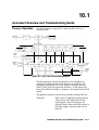
Instrument Overview and Troubleshooting Guide
Theory of Operation . . . . . . . .
. . .
Trouble shooting . . . . . .
Preparing the HP 8 1 12A for servicing
Key Jammed
.
0
RAM Test . .
EOl . . . .
Timing Tests
Contents-a
10.1-1
10. 1-3
10. 1-3
10. 1-5
10. 1-5
10.1-5
10.1-5
10. 1-5
10.2.
10.3.
Ell .
E12 .
E13 .
E14 .
Output Amplifier Tests
E21 . . . . . . .
E22 . . . . . . .
Overall Tests , Static
E31 .
E32 .
E33 .
E34 .
Overall Tests, Dynamic
E35 .
E36 .
E37 .
E38 .
E39 .
Amplitude Tests
E41 . . . . .
Shaper Output State Test
E42 . . .
Burst Tests
E5 1 .
E52 . . .
10.1-5
10. 1-5
10.1-5
10.1-5
10.1-7
10 .1-7
10.1-7
10. 1-7
10. 1-7
10. 1-7
10.1-7
10.1- 7
10.1-7
10.1- 7
10.1-9
10.1-9
10.1-9
10.1-9
10.1-9
10.1-9
10.1-9
10.1-9
10.1-9
10. 1-9
10.1-9
Servicing the Power Supply
Theory of Operation
. . . . . .
Introduction . . . . . . . . . . . .
Line Voltage Selector and Transformer
Bridge Rectifiers and Regulators . .
Voltage and Current Sensing Circuits
+5.1 V supply
+5 V supply . . . .
-5.4 V supply
Power-down Detection
Troubleshooting the Power Supply
Removing the fan
Re-fitting the fan . . . . . . .
10.2-1
10.2- 1
10.2- 1
10.2- 1
1 0.2-2
10.2-2
10.2-2
10.2-2
10.2-3
10.2-9
10.2-9
10.2-9
Servicing the Timing and Slope Generators
Theory of Operation
Introduction . .
Trigger Input
Trigger mode
Address Decoder
Mode and Range Decoders
Control Input Circuits
Timing IC . . . . .
Timing Generation
RATE Mode . . .
10.3- 1
10.3- 1
10.3-1
10.3-1
10 .3-2
10.3-2
1 0.3-2
10.3-2
10.3-3
10.3-4
Contents-9
10.4.
TIME Mode . .
Outputs . . . .
Error Output
Period, Delay and Width Generation
Period Generator
Delay Generator
Width Generator
Slope Generation .
Fixed Transition
Linear and Gaussian Transitions
Current Sources
Range Switches
Reference Circuit
Error Feedback .
Troubleshooting
Address Decoder .
Control Mode Selection
Period Generator
Delay Generator
Width Generator
Slope Generator
Range Decoder
Example
Servicing the Shaper and Output Amplifier
Theory of Operation
Introduction
Bus Latch . . .
Shaper IC . . .
Wave Forming
Output Mode
Shaper Output
Current Mirror .
Pre-Attenuator .
Signal Output Amplifier
Input . . .
Voltage gain . . . .
Output . . . . . .
Trigger Output Amplifier
Level Check Circuit .
Troubleshooting . . . . .
Shaper IC Inputs . . . .
Transition Mode and Output Control Signals
Shaper IC Amplitude-vernier Control-voltage
Shaper IC Reference Current . . . . . . . .
Shaper IC Current-mirror . . . . . . . . .
Pre-Attenuator and Output Attenuator Control
Signals . . . . . . . .
Offset-vernier Control-voltage
Output Amplifier . . . . . .
.
Contents-1 O
10.3-4
10.3-5
10 .3-5
10 .3-5
10.3-5
10.3-6
10.3-6
10.3-7
1 0.3-7
10 .3-7
10 .3-8
10 .3-8
10.3-8
10.3-8
1 0.3-14
1 0.3- 14
10.3-15
1 0.3- 16
10.3- 18
10.3-19
10.3-21
10.3-22
10 .3-22
10.4- 1
10.4- 1
10.4- 1
10.4- 1
10.4-2
10.4-3
10.4-3
10.4-3
10.4-4
10.4-4
10.4-5
10.4-6
10.4-6
10.4-6
10.4-6
1 0.4- 1 1
1 0.4- 1 1
10.4- 13
10.4- 13
10.4- 13
1 0.4- 13
10.4- 13
10.4- 14
10 .4-14
10.5.
10.6.
10.7.
Servicing the Control Board
Theory of Operation
Introduction
Timer .
Address Decoders
Timing Range Decoder
DAC Reference Circuit
Digital to Analog Converters .
Normal operation .
Reciprocal operation
Byte offset latches and Offset DAC
Byte Latching
Offset DAC
Parameter Control
Troubleshooting
Timer .
Address Decoders
Timing Ranges
Period Control
Delay Control
Width Control
Slope Control
Amplitude Control
Offset Control
Timer .
10.5-1
10 ..5- 1
10.5- 1
10.5- 1
10.5-2
10.5-2
10 .5-2
10.5-2
10 .5-3
10.5-3
10.5-3
10.5-4
1 0.5-4
1 0.5- 1 1
10.5- 1 1
10.5- 1 1
10.5-13
10.5-13
10.5- 13
10 .5- 14
10.5- 14
10.5- 14
10.5-15
10.5-16
Servicing the Burst Control Circuit
Theory of Operation
Introduction
Burst Number Acceptors
Counter .
Blocking Flip-flop
Period Generator Control
Counter reset
Troubleshooting
Output Address Decoder
Burst Counter
10 .6- 1
10.6- 1
10.6- 1
10.6-2
10 .6-2
10 .6-2
10.6-2
10.6-5
10.6-5
10 .6-6
Servicing the Microprocessor and Front-panel
Theory of Operation . . . .
Introduction . . . . . . . . .
Read Only Memory ( ROM ) . .
Random Access Memory ( RAM )
RAM Battery Supply . . .
HP-IB General Purpose Interface Adapter
Microprocessor Interface Signals
HP-IB Interface Signals
Address Decoding
Sub-decoder 1 . . . .
Sub-decoder 2 . . . .
Control Board Address Decoding
10.7- 1
10 .7- 1
10.7-2
10.7-2
10.7-2
10.7-2
10.7-2
10.7-3
10.7-4
10. 7-4
10. 7-4
10. 7-5
.
.
Contents-1 1
Key Scanning
Display Driving
Display Driver U22
HP-IB Status Latch U37
Display Latche U23
Reset Circuits . . . . . .
Troubleshooting . . . . . .
Free Running Signature Analysis
Address Bus . . .
ROM . . . . . .
Changing the ROM
Keyboard . . .
A.
B.
Replaceable Parts
Introduction . .
General . . . .
Ordering Parts .
Standard Instrument Parts-lists
Master List
Main Board . . . .
Control Board . . .
Microprocessor Board
Keyboard . .
Display Board
A- 1
A-1
A- 1
A-6
A-6
A-8
A-26
A-33
A-37
A-40
Backdating
Introduction
B- 1
C. Updating
Introduction
C-1
D.
Sales and Service Offices
Information
Asia . . . . .
Canada . . . .
Eastern Europe
Northern Europe
South East Europe
Middle East and Central Africa
United Kingdom . . . .
United States of America
Eastern USA . .
Midwestern USA
Southern USA .
Western USA
Other International Areas
Index
Contents- 12
10.7-5
10.7-5
10.7-5
10.7-6
10.7-6
10 .7-6
10.7-15
10 .7- 15
10 .7-15
10.7-16
10.7- 1 7
10.7- 1 7
D- 1
D- 1
D- 1
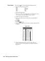
D-1
D-1
D-1
D-2
D-2
D-2
D-2
D-2
D-2
D-2
D-3
Figures
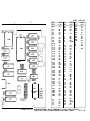
1- 1 .
3- 1 .
3-2.
3-3.
4- 1 .
4-2.
4-3.
4-4.
4-5.
4-6.
4-7.
4-8.
4-9.
4- 10.
4- 1 1 .
4- 12.
5- 1 .
5-2.
5-3.
5-4.
5-5.
5-6.
8- 1 .
8-2.
8-3.
8-4.
8-5.
8-6.
8-7.
8-8.
8-9.
8- 10.
8- 1 1 .
8- 12.
8- 13.
8- 14.
8-15.
8- 16.
8- 1 7.
8- 18.
8- 19.
Serial Number Plate ( FRG ) . . .
Line Voltage Selector Switches . .
Power Cables & Plug Identification
HB-IB Connector . . .
HP 8 1 12A Front Panel
Trigger Mode Controls
External Trigger Controls
Control mode controls
Relationship Between Control Input Voltage and
Controlled Parameter
High Level Control Capabilities
Transition Controls .
LEE and TRE ranges
Ranging examples
Parameter controls
Output controls
Rear panel . . . .
Typical output in Normal mode
Typical signals in Trigger mode
Typical signals in Gate mode
Typical signals in External Width mode
Typical signals in External Burst mode
Capacitance circuit . . .
Period Performance Test
Delay Performance Test .
Double Pulse Performance Test
Double Pulse Performance Test
Pulse Width Performance Test
Pulse Width Performance Test .
Duty Cycle Performance Test
Output Levels Performance Test
Transition Times Performance Test
Pulse Performance Test . . . . .
Pulse Performance Characteristics
Trigger, Gate,E.WID & E.BUR Verification Test
Output Mode Verification Test .
Output Mode Verification Test .
Period Control Verification Test
Delay Control Verification Test .
Correct Delay Control . . . . .
Width Control Verification Test·
High-Level Control Verification Test
1-1
3-2
3-3
3-5
4-2
4-5
4-6
4-7
4-7
4-9
4- 10
4- 1 1
4-12
4- 13
4-16
4- 18
5- 1
5-2
5-3
5-4
5-5
5-6
8-3
8-5
8-6
8-7
8-9
8-9
8- 1 1
8- 12
8-14
8-16
8- 18
8-19
8-2 1
8-22
8-23
8-25
8-25
8-26
8-28
Contents-13
8-20.
8-21 .
8-22.
9- 1 .
9-2.
9-3.
9-4 .
9-5.
9-6.
9-7.
9-8.
9-9.
1 0 . 1- 1 .
10. 1-2.
10. 1-3.
10.2- 1 .
10.2-2.
10.2-3.
1 0.2-4.
10.2-5.
10.3- 1 .
10.3-2.
1 0.3-3.
1 0.3-4.
10.3-5.
1 0.3-6.
1 0.3-7.
1 0.3-8.
10.3-9.
1 0.3- 10.
1 0.3- 1 1 .
1 0.3- 12.
1 0.3- 13 .
1 0.3-14.
10.3- 1 5 .
10.3- 1 6 .
1 0.4- 1 .
10.4-2.
10.4-3.
10.4-4.
10.4-5.
1 0.4-6.
1 0.4-7.
1 0 .4-8.
10.4-9.
1 0.4- 10.
1 0.4- 1 1 .
10.4- 12.
10.5- 1 .
10.5-2.
Contents-14
8-28
Correct High-level Control .
8-29
Correct Delay Control . . .
8-30
HP-IB Verification Test . .
9-4
Access to the HP 8 1 1 2A for Adjustments
9-5
Pre adjustments setup
9-8
Typical Pulse Display . .
9- 1 0
Decade Accuracy . . . .
9- 1 2
Double Pulse Adjustment
9- 1 6
Low Pass Filter . . . .
9- 19
Slope test setup . . . .
9-22
Adjustment Points on the Main Board Al
9-23
Adjustment Points on the Control Board A2
10.1-1
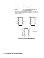
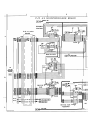
HP 8 1 1 2A Functional block diagram
10.1-2
Custom ICs used in the HP 81l2A
10. 1-3
HP 8 1 12A in its servicing position
1 0.2- 1
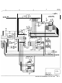
Power Supply block diagram .
1 0.2-5
Main Board Al - Schematic 1
1 0.2-7
Main Board Al - Schematic 2
1 0.2-9
Detail of wiring to Line Voltage Selector switches
Power supply components - Underside of main board
10.2- 10
Al . . . . . . . . . .
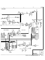
Timing IC block diagram . .
1 0.3-3
1 0.3-5
Example of signal generation .
Slope IC block diagram . . .
10.3-7
10.3-9
Main Board Al - Schematic 3
10.3- 1 1
Main Board Al - Schematic 4
1 0.3- 13
Main Board A l - Schematic 5
1 0.3-14
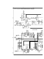
Address decoder - Simplified block diagram
Period Generator Input pin 7
1 0.3- 16
1 0.3- 1 7
Period Generator ramp signal pin 20
Period Generator output signals . .
1 0.3- 1 7
Delay Generator I/P O / P waveforms
1 0.3- 18
Delay Generator ramp signal pin 20 .
10.3-18
Width Generator Input . . .
1 0.3- 19
Width Generator ramp signal
10.3-20
10.3-20
Width Generator output
Slope Generator Input and Output signals
10.3-21
Shaper IC Block Diagram . . . .
10.4-2
Current Mirror . . . . . . . . .
10.4-4
Simplified Output Amplifier circuit
10.4-5
10.4-7
Main Board Al - Schematic 6 . .
10 .4-9
Main Board Al - Schematic 7 . .
Shaper IC Input Signals on Pins 18/19
1 0.4- 1 1
Shaper I C Output on Pin 1 2 .
1 0.4- 1 1
Shaper I C Output (FIXED) . . . . .
10.4- 12
Shaper IC Output (LINEAR) . . . .
10.4- 12
Shaper IC Output (FIXED, HIL +0.99 V)
10.4- 12
Main Board Al - Component layout
1 0.4- 1 7
Main Board Al - Component locator
1 0.4- 19
Principle of DAC Operation
10.5-2
DAC - Reciprocal operation . . . .
10.5-3
10.S-3.
10.S-4.
10.S-S.
10.S-6.
10.6-1.
10.6-2.
10.6-3.
10. 7-1.
10.7-2.
10.7-3.
10.7-4.
10.7-S.
10. 7-6.
10.7-7.
10.7-8.
10.7-9.
10.7-10.
A- 1 .
A-2.
B-1.
B-2.
B-3.
B-4.
B-5.
B-6.
B-7.
B-8.
B-9.
B-10.
B- 1 1 .
B-12.
B- 13.
B-14.
B- 15.
10.S-S
Standard Control Board A2 - Schematic 1
10.S-7
Standard Control Board A2 - Schematic 2
10.S-9
Standard Control Board A2 - Schematic 3
Standard Control Board A2 - Component layout and
locator . . . . . . . .
10 .S- 1 7
Simplified Burst Generator . . . .
10.6-1
Burst Control - Schematic 1 . . . .
10.6-3
Burst-counter waveforms and timing
10.6-7
10.7-1
Microprocessor board architecture
GPIA IC pins . . . . . . . . . .
10. 7-3
10.7-4
Address decoding . . . . . . . . .
Microprocessor Board A3 - Schematic 1
10.7-7
Microprocessor Board A3 - Schematic 2
10.7-9
Microprocessor Board A3 - Schematic 3
10. 7- 1 1
Keyboard A 4 and Display Board AS - Schematic
10.7-13
Microprocessor Board A3 - Component layout and
locator . . . . . . . . . . . . . . . . . . 10.7-19
Keyboard A4 and Display Board AS - Component'
layouts and locators . . . . . . . . . . . . 10. 7-21
Keyboard A4 and Display Board AS - Component
layouts and locators ( Option 001)
10. 7-23
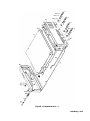
Mechanical Parts - 1
A-2
Mechanical Parts - 2 . . . .
A-3
Example output pulse . . . .
B- 1 1
081 16-66S23: UlO, U l l layout
B-14
081 16-66523: UlO, U l l schematic
B-14
081 16-66533: ROM layout . .
B-23
08116-66533: ROM schematic
B-24
08116-66S33: U28 layout
B-25
08116-66S33: U28 schematic .
B-25
08116-66S33: Deletion of W3
B-26
08116-66S33: Reset circuit .
B-26
Rear Panel . . . . . . . .
B-39
HP-IB Address Switch ( Factory setting )
B-40
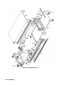
Exploded view of HP 8 112A rear frame
B-42
Microprocessor Board A3 Component Layout and
Locator . . . .
B-43
Mechanical Parts - 1
B-44
Mechanical Parts - 2
B-45
.
Contents-15
Tables
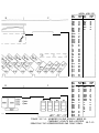
1- 1 .
3- 1 .
4- 1 .
4-2.
4-3.
6- 1 .
8- 1 .
9- 1 .
1 0- 1 .
10.2- 1 .
1 0.2-2.
10.3- 1 .
10.3-2.
1 0.3-3.
1 0.3-4.
1 0.3-5.
1 0.3-6.
10.3- 7.
10.3-8.
10.3-9.
1 0.3- 10.
1 0. 3- 1 1 .
1 0.3- 12.
1 0.3- 13.
10.3-14.
10.3- 1 5 .
10.3- 1 6 .
1 0.4- 1 .
10.4-2.
10.4-3.
1 0.4-4.
10.4-5.
1 0 .4-6.
1 0.5- 1 .
1 0.5-2.
10.5-3.
1 0.5-4.
1 0.5-5.
1 0.5-6.
1 0.5-7.
10.5-8.
10.5-9.
10.6- 1 .
Contents-1 6
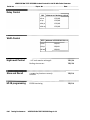
Recommended Test Equipment . . . .
Line Voltage and Fuse Selection
Operating/Control Mode Combinations
Active slope moves from Range 3 to Range 2 (Yl )
Active slope moves from Range 3 to Range 4 (Y2 )
. . . . . . . . . . . . . . . . . . . . . .
Test Equipment . . . . . . . . . . . . . . .
Adjustment Procedures - Changeable Components
HP 8 1 1 2A Board Assemblies & Servicing Chapters
Power supply rectifiers . . . .
Regulated voltage supplies . . .
Address decoder enable outputs
IC Digital Control Signals . . .
Timing IC Time/frequency Range Selection
Timing IC mode selection . .
Reference current input levels
Address Decoder Signatures
Address Decoder Signatures .
Mode Decoder check table . .
UlOl Mode Decoder truth table
Period Generator Operation .
Period Generator Signal Levels
Delay Generator Operation
Delay Generator Signal Levels
Width Generator Operation .
Width Generator Signal Levels
Range Decoder Truth Table
Shaper IC Output Modes . .
Pre-attenuator ranges . . . .
Waveform Control truth table
Amplitude-vernier Control-voltages
Attenuator Control truth table .
Offset-vernier Control-voltages .
A2 Address Decoder Signatures
Timing range decoder . . . . .
Typical Period Control DAC Output
Typical Delay Control DAC Output
Typical Width Control DAC Output
Typical Slope (LEE) Control DAC Output
Typical Slope (TRE) Control DAC Output
Amplitude Gain Control truth table
Offset DAC - Output Voltages . . .
Output Address Decoder Signatures
1-4
3-2
4-8
4- 1 2
4- 12
6- 1 2
8-2
9-2
1 0-4
10.2-2
10.2-2
10.3-2
1 0.3-3
1 0.3-4
1 0.3-4
1 0.3-5
1 0.3- 15
1 0.3- 15
1 0.3- 15
1 0.3-16
10.3- 1 7
1 0.3-18
1 0.3- 19
1 0.3- 19
1 0.3-20
10.3-21
10.3-22
10.4-2
10.4-4
10.4- 13
10.4- 13
10.4- 13
1 0.4- 14
1 0.5- 12
10.5-13
1 0.5- 13
10 .5- 13
10.5- 14
10.5-14
10.5-14
1 0.5-15
1 0.5- 15
10.6-5
10.6-2.
10.7- 1 .
1 0.7-2.
1 0.7-3.
10.7-4.
1 0.7-5.
10.7-6.
A- 1 .
A-2.
A-3.
A-4.
A-5.
A-6.
A-7.
B- 1 .
B-2.
B-3.
B-4.
B-5.
B-6.
. . . . . . . . . . . . . . . . .
10.6-6
10.7-5
Display Driver Control Signals . . . .
Signature Analyzer Probe connections .
10.7- 15
Signatures for Address Drivers and Decoders
10.7- 16
Signature Analyzer Probe connections for ROM Test 1 0.7- 16
ROM U40 signatures . . . . .
10.7-17
10.7- 18
Keyboard signatures . . . . . . . .
HP 8 1 12A Parts Manufacturers
A-4
Standard HP 8 1 1 2A Master Parts List
A-6
A-8
Main Board Parts List . . . .
A-26
Control Board Parts List
Microprocessor Board Parts List
A-33
Keyboard Parts List
A-37
A-40
Display Board Parts List
B-2
Backdating Changes
B- 10
. . . . . . . . . . .
Address bus Signature Analysis
B-27
B-27
Main Decoder Signature Analysis .
Sub Decoder Signature Analysis
B-28
ROM signatures . . . . . . . .
B-29
Contents-1 7
1
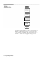
I ntroduction
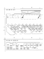
General
This manual describes the following procedures for the HP 81 12A
50 MHz Programmable Pulse Generator:
•
•
•
•
•
•
Installation
Operating
Programming
Testing Performance
Adjustment
Servicing
A Microfiche version of this manual is available on 4 x 6 inch
microfilm transparencies (refer to title page for order number) .
The microfiche package also includes the latest Manual Changes
supplement and all relevant Service Notes.
Instruments Covered
by This Manual
HEWLETT-PACKARD
�51G9506
Boeblingen Fed.
Rep.
GmbH
of Germany
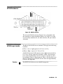
Figure 1·1. Serial Number Plate (FRG)
Attached to the rear of the instrument is a serial number plate
(Figure 1-1). The first four digits only change when there is a
significant modification to the instrument , the last five digits are
assigned sequentially to instruments. This manual applies directly to
the instruments with the serial numbers quoted on the title page. For
instruments with higher serial numbers, refer to the Manual Change
sheets in Appendix C Updating. To keep this manual up-to-date,
Hewlett-Packard recommends that you periodically request the
latest Manual Change supplement by quoting the part-number and
print-date of this manual, both of which appear on the title page.
Introduction 1·1
The HP 8 1 12A Programmable Pulse Generator operates over the
frequency range 1 Hz to 50 MHz with a maximum 32 V peak-to-peak
output signal delivered into a 50 fl/high impedance load.
Instrument capabilities include:
Instrument
Description
•
Fixed 5 ns transition times.
•
6.5 ns to 95 ms variable rise and fall times.
•
Variable delay in all modes
•
High and Low Level Limit for device under test (DUT) protection.
•
HP-IB programmable.
•
Easily accessible memory for up to 9 sets of mode and parameter
selections .
The self-prompting operation and HP-IB programmability of the
HP 8 1 12A ensure that it is quick and easy to use in stand-alone
and automatic-test applications. Self-test and fault diagnosis are
performed each time the instrument is switched on. Error recognition
(and prompt) helps the operator to recover from incorrect front panel
or programming operation.
Note
Throughout this manual, instrument keys are shown as � in the
text. "Key" is the key name which appears above the key on the
instrument front panel.
HP 8 1 1 2A Options
Opt 910
Opt W30
1 ·2 Introduction
Option 910 is an extra Operating and Service Manual.
Extended Repair Service for the instrument .
Accessories
Included
The HP 8 1 12A is supplied complete with the following:
HP Part Nwnber
21 10-0813
750 mA fuse for 220/240 V operation
or
1 .5 A fuse for 100/ 120 V operation
2 1 10-0043
and
Power cable
See Chapter 3 Installation
Item
Available
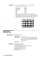
The following accessories are available for the HP 8 1 12A:
Item
HP Part Nwnber
Carrying handle (Bail Handle Kit)
HP 5062-4001
Rack mount kit (single HP8112A)
HP 5062-3972
Rack mount kit (Two instruments)
HP 5062-3974
Lock Link kit for use with HP 5062-3974
HP 5062-3994
Introduction 1-3
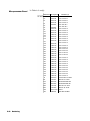
Recommended Test
Equipment
The recommended test equipment and accessories required to
maintain the HP 8 1 12A, are listed in Table 1-1. Alternative
equipment may be substituted, provided that it meets or exceeds the
critical specifications given in the tables.
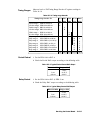
Table 1 - 1 . Recommended Test Equipment
Recommended
Model
Instrument
Alternative
Required Characteristics
Counter
50 MHz, Start/Stop,
HP 5335A
TI,
A to B
with OPT 040
Digital Voltmeter
HP 3458A
HP5345A
DC 0.01 V-50 V, .004% acc. HP 3456A
HP 3478
Pulse amplitude facility
P, A
P, A, T
P,A,T
Function Generator HP 8 1 16A
20 MHz, THD � . 1 %
HP3324A #002 P, A
Digitizing Scope
HP 5412xT
HP 54100D
or
HP 5450A
> 10 GHz Bandwidth
<30 ps Transition times
Flatness = 5%
< 100 MHz , 500 inputs
P, A
P, A
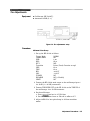
Signature Analyzer HP 5005B
T
Power Supply
HP 6237B
0 - 20 v
Attenuator
HP 33340C
20 dB, 2W
P, A, T
SMA to BNC
P, A, T
10 W, 50 n, ±0.l %
2 w, 50 n
P, A
T
Adaptor
Terminators
HP 1 1 048C
HP lOlOOC
*
1 -4 Introduction
..
Use
P
=
Performance Test; A
HP 3324A
=
Adjustments; T
=
P, A, T
Troubleshooting
2
Specifications
Introduction
All specifications in the following sections describe the warranted
performance of the instrument:
•
•
•
Timing parameters
Output parameters
Waveform characteristics
All specifications apply with a 50 n load, after a 30 minute warm-up
period, and are valid for ambient temperature in the range 1 5°C to
35°C. Refer to the General Characteristics section of this chapter for
the performance derating factor to be used outside this temperature
range ( within the specified operating range of 0°C to 55°C ) .
All operating characteristics given in the following sections describe
typical performance figures which are non-warranted:
•
•
•
•
•
•
Trigger modes
Control modes
Output Modes
Inputs and Outputs
Additional features
General characteristics
Timing Parameters
Common Specifications
Unless otherwise stated, specifications are quoted for 503 amplitude
in normal mode, fastest transitions.
Resolution
3 digits, best case 1 00 ps
Accuracy
± 53 of programmed value ±2 ns
Repeatability
Factor 4 better than accuracy
Jitter
max 0.2% of programmed value + 100 ps
Specifications 2-1
Period (PER)
Range
20.0 ns to 950 ms
Delay {DEL) {after
Trigger Out)
Rang e
75.0 ns to 950 ms (max:PER+55 ns)
Accuracy
±5% of programmed value ±5 ns
Double Pulse {DBL)
{interval between
leading edges)
Pulse Width {WID)
Range
20.0 ns to 950 ms (max:PER-WID)
DEL and DBL are mutually exclusive
Range
10.0 ns to 950 ms (max: PER- 10 ns)
Duty Cycle (DTY)
Range
1 % to 99%, subject to Width specification
Resolution
1
Accuracy
±10% of programmed number
WID and DTY are mutually exclusive
Linear Transitions
{between 10% and 90%
amplitude)
Note
2-2 Specifications
Range
6.5 ns to 95 ms, leading edge (LEE) and trailing edge (TRE)
independantly programmable within 1 :20 ratio
Delay, Width, and Transitions are under-programmable to ensure
that the specified minimum values can always be obtained.
Output Parameters
Note
Output voltages are specified for a 50 n load. Output voltages
double when driving a high impedance load.
High Level (HIL)
-7 .90 V to +8.00 V
Low Level (LOL)
-8.00 V to + 7 .90 V
Resolution
3 digits (10 mV)
Level accuracy
± 1 3 of programmed value ±33 of amplitude ±40 mV
Repeatability
factor 4 better than accuracy
Settling time
100 ns +LEE
Preshoot, Overshoot, Ringing
±53 ± 10 m V (variable transitions)
± 103 ±10 mV (fixed transitions)
Operating
Characteristics
The following sections give non-warranted information on the typical
operating characteristics of the instrument :
•
•
•
•
•
•
Trigger modes
Control modes
Output modes
Inputs and Outputs
Additional features
General characteristics
Specifications 2-3
The external trigger signal referred to in this section is applied to the
EXT INPUT BNC connector on the instrument front panel. The
trigger level and sense are adjustable. An external trigger can be
simulated by pressing the (MAN ) key.
Trigger Modes
The (1 PULSE) key gives an additional pulse in Gate and External
Burst modes.
Normal
A continuous pulse train is generated .
Trigger
Each active input edge triggers a single pulse (or double pulse if DBL
is selected)
Gate
Active input level enables pulse train, last pulse always complete.
Width and period of first pulse may deviate 103 from subsequent
pulses.
External Width
Pulse recovery, input edges toggle output .
External Burst
Each active input edge triggers a burst of pulses [BUR] ( 1 to 1 999
pulses). Width and period of first pulse may deviate 103 from
subsequent pulses.
Control Modes
An external control signal applied to the CTRL INPUT BNC
connector can be used to modulate the output signal.
Period, Delay, Double
pulse and Width Control
1 V to 10 V voltage at Cntrl Input varies the selected parameter over
one decade. Eight non-overlapping decades cover the range specified
under "Timing Parameters " . Display shows max value available in
selected range.
High-level Control
101.
-8 V to +8 V input varies HIL over the same range irrespective of
Settling time (within 5% of final value)
200 µs
2-4 Specifications
Output Modes
Complement
Disable
Limit
Fixed transitions
Cosine transitions
Linear transitions
Selectable on/off
Disconnects output , default at switching on.
Implements present output levels as output limits.
5 ns from 10% and 90% amplitude, 3.5 ns from 20% to 80%
amplitude
Up to 25% faster between 10% and 90% of amplitude than linear
transitions
±3% linearity
Inputs and Outputs
External Input
Threshold level
± 10 V adjustable
Minimum amplitude
500 mV (p-p)
Maximum Input voltage
Minimum pulse width
Control Input
10 ns
Input impedance
10 kn
Trig slope
off, pos, neg, both (Trigger and Ext
Width only)
Bandwidth
1 kHz
Input voltage limits
Input impedance
Trigger Output
±20 v
High level
±2-0 v
10 kn
+2.4 v into 50 n
+4.8 V into high impedance
Low level
ov
Duty cycle
50%
Output impedance
50 n
Propagation Delay
( EXT INPUT to TRIG
OUTPUT )
25 ns
Specifications 2-5
Main Output
External voltage limits
- 0 v, +5 v
Amplitude
100 mV to 16 V (200 mV to 32 V) pp
Reflections
< 103
Source Impedance
50 n
Short circuit capability
Maximum peak current 150 mA
for up to 1 hour ( 1 5°C to 35°C)
External voltage limits
±5 V
Additional Features
Set
Non-Volatile Memory
Sets up square wave, delay min. LEE, TRE=103 PER or fixed
Power down location
9
programmable locations
Standard settings location
Self-test
Error detection
HP-18 Capability
Capability codes
Learn modes
Service request
2-6
Specifications
saves current settings
each stores a complete setup
1 00 µs, 1 V pulse at 1 kHz
The instrument performs a self-test when switched on, and by HP-IB
command.
Visual and Status Byte indication of incompatible settings,
under-range control voltage, and clipped amplitude (excessive
transition time).
The HP 8 1 1 2A is fully programmable except for the External Input
trigger level.
SHl , AHl , T6, 14, SRl , RLl , PPO, D C l , DTl,
co
All or individual parameters can be programmmed and uploaded
Initiated by syntax and operating errors, returns error number
Status byte
Message Times
Returns text of operating-error message
Time to receive and execute a message
5 ms (Offset 30 ms)
Time to send a message
1 5 ms
1 ms per character, Status byte:15 ms
Status byte
Learn string
General
Characteristics
Environmental
Power supply
Storage temperature range
-40°C to 70°C
Operating temperature range
0°C to 55°C
Humidity range
Up to 953 RH between 0°C and
40°C
•
•
•
Weight
Dimensions
Net
Shipping
•
•
•
Recalibration period
100/120/220/240 V rms (selectable) +53, - 103
48-440Hz
120 VA maximum
5.9 kg (13 lbs)
8.0 kg (18 lbs)
89 mm high (3.5 in)
213 mm wide (8.4 in)
445 mm deep ( 1 7.5 in)
1 year recommended
Specifications
2-7
3
Installation
Introduction
Safety
Considerations
This chapter provides installation instructions for the HP 81 12A. It
also includes information about initial inspection and damage claims,
preparation for use, packaging, storage and shipment.
The HP 81 12A is a Safety Class 1 instrument ( instrument with an
exposed metal chassis that is directly connected to earth via the
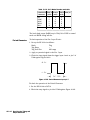
power supply cable ) .
Before operation review the instrument and manual, including
the red safety page, for safety markings and instructions. These
must then be followed to ensure safe operation and to maintain the
instrument in safe condition.
Initial Inspection
Warning
To avoid hazardous electric shock, do not perform electrical tests
when there are signs of shipping damage to any part of the outer
covers or panels.
Inspect the shipping container for damage. If the container or
cushioning material is damaged, keep it until the contents of the
shipment have been checked for completeness and the instrument
been verified both mechanically and electrically.
has
The contents of the shipment should be as shown in the shipping
document plus any accessories that were ordered with the
instrument. Procedures for checking the operation of the instrument
are given in Chapter 8 Performance Tests.
If the contents are incomplete, mechanical damage or defect is
apparent , or if the instrument does not pass the operators checks,
notify the nearest Hewlett-Packard office. Keep the shipping
materials for carrier's inspection. The HP office will arrange for
repair or replacement without awaiting settlement.
Installation 3-1
Power Requirements
and Line Voltage
Selection
Caution
I
BEFORE APPLYING AC LINE POWER TO THE HP 8 1 1 2A,
ensure that the instrument is set to the local line voltage and the
correct line fuse is installed in the fuse holder.
The instrument requires a power source of 100, 120, 220 or 240 V
rms ( +53, - 103 ) at a frequency of 48-440 Hz single phase. The
maximum power consumption is 120 VA.
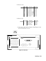
The line voltage selector switches can be seen through the left hand
side of the instrument cover towards the rear. The line voltage
selector is set at the factory to the most commonly used line voltage
for the country of destination. The instrument power fuse is located
on the rear panel.
o
�: �
�'D�'---�' �:� �
L I NE VOLTAGE SELECTOR
o
Caution
I
Figure
:�� �
3-1.
I._
__._/_D__,/ ;;: �
__
o
o
Line Voltage Selector Switches
Do not change the Line Voltage Selector switch settings with the
instrument switched ON, or with power connected via the rear panel.
To change the selected line voltage:
1 . Remove the power cord.
2. Remove the instrument top cover by releasing the captive securing
screw at the rear, and sliding the cover off.
3. Using a screwdriver, move the switches to the required position for
the voltage to be used.
4. Replace the instrument top cover.
5. Fit the correct power fuse for the selected operating voltage.
Table 3-1. Line Voltage and Fuse Selection
Line Voltage
3-2
Installation
Fuse Type HP Part Nwnber
100 v / 120 v 1.5 A
2110-0043
220 v / 240 v 750 mA
2110-0813
Power Cable
Warning
To avoid the possibility of injury or death, the following precautions
must be followed before the instrument is switched on:
•
If the instrument is to be energized via an auto transformer for
voltage reduction, ensure that the Common terminal is connected to
the grounded pole of the power source
•
The power cable must only be inserted into a socket outlet provided
with a protective ground contact. The protective action must not
be negated by the use of an extension cord without a protective
conductor.
•
Before switching on the instrument, the protective ground terminal
of the instrument must be connected to the protective conductor of
the power cable. This is verified by using the power cord which is
supplied with the instrument.
•
Intentional interruption of the protective ground connection is
prohibited.
In accordance with international safety standards, the HP 8 1 12A
is equipped with a three-wire power cable. When connected to an
appropriate ac power receptacle, this cable grounds the instrument
cabinet . The type of cable shipped with each instrument depends on
the country of destination. Refer to Figure 3-2 for the part numbers
of the available cables.
Austra lia
Denmark
Europe
Great Brit a i n
8 120-1369
8120-2956
8120-1689
8120-13151
�
Switzerland
8120-2104
So uth Africa
United States 120V
8120-4211
8120-1378
Figure
3-2.
Japan 120V
8120-4753
Power Cables & Plug Identification
Installation
3-3
The following work should be carried out by a qualified electrician all local electrical codes being strictly observed. If the plug on the
cable does not fit the power outlet, or the cable is to be attached to a
terminal block, cut the cable at the plug end and re-wire it.
The color coding used in the cable will depend on the cable supplied.
If a new plug is to be connected, it should meet local safety
requirements and include the following features:
•
•
•
3·4
Installation
Adequate load-carrying capacity ( see specifications in Chapter 2).
Ground connection.
Cable clamp.
HP-I B Connector
NDRC
NRFD
DAV
EOI
D I04
IFC
SRO
C GN D ONLY AT
SYSTEM CONTROLLER )
SH I ELD
TYPE
57
CONNECTOR
GUARD
GROUNDS
C GND R T SYSTEM
CONTROLLER )
REN
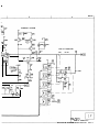
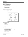
Figure 3-3. HB-18 Connector
The rear panel HP-IB connector ( Figure 3-3 ) , is compatible with
the connector on Cable Assemblies 10833A, B, C and D. If a cable
is to be locally manufactured, use male connector, HP part number
1251-0293.
HP-I B Logic Levels
The HP 8 1 12A HP-IB lines use standard TTL logic, the levels being
as follows:
•
True
•
False
= =
= =
Low
High
digital ground or 0 V de to 0.4 Vde,
open or 2.5 V de to 5 V de.
All HP-IB lines have LOW assertion states. High states are held at
3.0 V de by pull-ups within the instrument. When a line functions
as an input , approximately 3 .2 mA of current is required to pull it
low through a closure to digital ground. When a line functions as an
output, it will sink up to 48 mA in the low state and approximately
0.6 mA in the high state.
Caution
'
The HP-IB line screens are not isolated from ground.
Installation
3-5
Operating
Environment
Warnin g
HP 8 1 12A Is not designed for outdoor use. To prevent potential
fire or shock hazard, do not expose the HP 8 1 12A to rain or other
The
excessive moisture.
Temperature
Humidity
The HP 81 12A may be operated in temperatures from 0°C to 55°C.
The HP 81 12A may be operated in environments with humidity up
to 95% (0°C to +40°C). However, the HP 81 12A should be protected
from temperatures or temperature changes which cause condensation
within the instrument.
Instrument Cooling
The HP 81 12A is equipped with a cooling fan mounted inside the
rear panel. The instrument should be mounted so that air can
freely circulate through it. When operating the HP 8112A, choose a
location that provides at least 75 mm (3 inches ) of clearance at the
rear, and at least 25 mm ( 1 inch) of clearance at each side. Failure
to provide adequate air clearance will result in excessive internal
temperature, reducing instrument reliability.
Claims and
Repackaging
If physical damage is evident or if the instrument does not meet
specification when received, notify the carrier and the nearest
Hewlett-Packard Service Office. The Sales / Service Office will arrange
for repair or replacement of the unit without waiting for settlement of
the claim against the carrier.
3-6
Installation
Storage and
Shipment
The instrument can be stored or shipped at temperatures between
-40° C and +75° C. The instrument should be protected from
temperature extremes which may cause condensation within it .
Return Shipment
to HP
If the instrument is to be shipped to a Hewlett-Packard Sales/Service
Office, attach a tag showing owner, return address, model number
and full serial number and the type of service required.
The original shipping carton and packing material may be re-usable,
but the Hewlett-Packard Sales/Service Office will also provide
information and recommendations on materials to be used if
the original packing is no longer available or reusable. General
instructions for repacking are as follows:
1. Wrap instrument in heavy paper or plastic.
2. Use strong shipping container. A double wall carton made of
350-pound test material is adequate.
3. Use enough shock-absorbing material ( 3 to 4 inch layer ) around
all sides of the instrument to provide a firm cushion and prevent
movement inside container. Protect control panel with cardboard.
4. Seal shipping container securely.
5. Mark shipping container FRAGILE to encourage careful handling.
6. In any correspondence, refer to instrument by model number and
serial number.
Installation 3-7
4
Operating
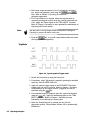
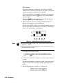
This chapter explains the use of all controls, indicators and
connectors on the front and rear panels of the HP 8 1 12A. Figure 4- 1
and Figure 4- 12 show the front and rear panel respectively. Each
group of controls is explained in subsequent sections of this chapter
under the following headings:
I ntroduction
Switching On
Trigger Mode Selection
External Trigger Controls
Control Mode Selection
Transition Mode Selection
• Parameter Selection
• Rear Panel
•
•
•
•
•
Examples are given in Chapter 5.
Before applying power to the HP 81 12A:
1. Read the red Safety Summary sheet at the front of this manual.
2. Ensure the Line Voltage Selector switches are set properly for
the power source to be used. Refer to Chapter 3 on instrument
installation if necessary.
Caution
I
Do not change the Line Voltage Selector switches with the
instrument switched on or with power connected to the rear panel.
3. Ensure that the device under test cannot be overdriven by
the HP 81 12A output ( 1 6 V p-p into 50 !l; 32 V p-p into high
impedance).
4. Ensure that the maximum external voltage applied to the
HP 8 1 12A falls within these limits: -5 V to +5 V de).
Caution
&
I
Do not apply an external voltage greater than ±5 V, or electrostatic
discharge to the output connector.
Operating
4-1
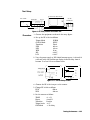
���
�/;.
8112A PULSE GENERATOR 50MHz
IEWLETT-PACKARD
,-- llCIOE � ,-C'IRL-.
o NORN
o RlfT o TRIG
O ADS
O SRQ
0 PERC
Ef'ROR
0 DELC
0 WJDC
O BUI
O E .WJD 0 E . BUI O HJLC
0 PER
0 GATE
..
20
0I
'---------'
o DBL
0 DEL
o DTY
o WJD
,-EXCESSIVE\
O LEE
o"
OY
o TRE
o
HIL
O LOL
D D D G G G G G G G
f
tO
I
0 ••
o ,,.
o na
G
EXT
1111'111'
±20V
dJ l o
0
1PUL.aE
D
LEYB.
(@)
· 10¥ +1DY
SET
I
./
f
G G G G
0
C1"L
1111'111'
t20V
1"IG
OUTPUT
0
HHHH
uSTO
ITO/RCL
n RCL
L ill I T
COMPL
DllMILE
G G G G
e
OOTPUT
0
A
Figure 4-1. HP 81 12A Front Panel
The HP 81 12A performs a "self test" when the power is switched
on. All the front panel LEDs should light momentarily. If a fault is
detected, the word "ERROR" is illuminated and an error code is
displayed on the front panel digital display. The possible error codes
are:
Switching On
CJ
4-2 Operating
A key is stuck in the depressed position.
E01
Fail RAM test
E11
Fail Period Timing test
E12
Fail Delay Timing test
E13
Fail Width Timing test
E14
Fail Slope Generation test
E21
Fail Output Amp +ve Offset test
E22
Fail Output Amp -ve Offset test
E31 to E39
E41/42
E51 and 52
Fail Overall tests
The output amplifier is faulty.
Fail Burst Counter tests
Refer to Chapter 10.1 Troubleshooting for more information on the
error codes and their causes.
When the self-test is completed successfully, the instrument
automatically assumes the operating state which was active when
it was last switched off, excep't that the output is disabled to
protect the unit under test. If the instrument battery has failed, the
Standard Parameter Set is selected.
Operating 4-3
Standard Parameter
Set
The Standard Parameter Set exists for two reasons:
•
If the instrument RAM becomes corrupted due to battery failure,
the Standard Parameter Set will be selected when the instrument is
switched on to give an error free display.
•
If an invalid combination of Operating and Control modes is
selected, switching the instrument off and on again, or selecting
RCL 0, will revert to the Standard Parameter Set. The Standard
Parameter Set is detailed below.
Trigger mode
Control mode
Burst
Period
Delay
Pulse width
Double pulse
Duty cycle
Leading edge
Trailing edge
High output level
Low output level
External input
Transition
Limit
Complement
Output Disable
NORM
CTRL
BUR
PER
DEL
WID
DBL
DTY
LEE
TRE
HIL
LOL
EXT INPUT
LIMIT
COM PL
DISABLE
Normal
Off
0001 #
1.00 ms
65 ns
100 µs
200 µs
50%
10 ns
10 ns
1 .00 v
0.00 v
Positive slope
Linear
Off
Off
On
NORM, PER, WID , DEL, illuminated ( active )
4-4 Operating
Selecting Trigger
Mode
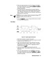
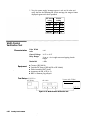
���
�fa
8112A PULSE GENERATOR SOMHz
HEWLETT -PACKARD
,-- MODE �
O NORM
o TRIG
0 GATE
O E . W J D O E .Bi.I
D D
I
Figure 4-2. Trigger Mode Controls
Mode Selection
The currently active mode is shown by LED indicator. The trigger
mode can be cycled through available options by pressing the key
below the mode indicators.
The standard instrument offers the following trigger modes:
NORM
In normal mode a continuous pulse stream is
generated.
TRIG
In trigger mode each active input edge triggers a
single output cycle.
GATE
In gate mode the active level of the external input
signal enables output period. The first output cycle
is synchronous with the active trigger slope. The last
output cycle is always completed.
E.WID
This mode can be used for recovery of external signal
with selectable transition times and output levels.
E.BUR
In
external burst mode each active external trigger
generates a pre-programmed number of pulses ( 1 to
1999) . Minimum time between two bursts is 100 ns.
Operating 4-5
Controlling the
External Trigger
�,,.�
��
8112A PULSE GENERATOR 50MHz
IEWLETT ·PACKAAD
1PULSE
D
LEVEL
(@)
EXT
JIFUT
- 1ov +iov
±20V
TRIG
OUTPUT 0
e
Figure 4-3. External Trigger Controls
The external trigger signal required in some trigger modes must be
applied to the EXT INPUT BNC connector.
Caution
I
Trigger Slope
Do not apply voltages outside the range ±20 V to the EXT INPUT
connector.
Select a positive or negative trigger slope by pressing the CZ) or GJ
key respectively. The current slope is indicated by the LED on the
key.
The trigger can be switched off by pressing the currently active key
again. Both key LEDs will then be off.
Trigger Level
Manual Trigger
(MAN )
Single Pulse
(1 PULSE )
Trigger Output
4·6 Operating
Trigger level can be varied in the range ± 10 V using the LEVEL
adjuster.
This key can be used to simulate the external trigger signal.
This key initiates a single pulse in TRIG, GATE, and E.BUR modes.
The trigger output provides a timing reference signal synchronised
to the main output signal. Output levels are 0 and 2.4 V into 50 n.
Delay from trigger input to trigger output is 25 ns.
Selecting Control
Mode
8112A PULSE GENERATOR 50MHz
IEWLETT -PACKARD
rClRL-.
0 PERC
o DELC
O WIDC
O HILC
D
0 ClRL
INPUT
t20V
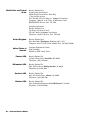
Figure 4-4. Control mode controls
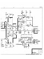
Control Input
Caution
I
An analog signal can be applied to the control input to modulate or
control the HP 8 1 1 2A output signal. This external input may be any
waveform in the range ±20 V. However, the overall range within
which the instrument actually responds to a control signal, is 1 .0 V
to 10 V, as shown below.
Do not apply voltages outside the range ±20 V to the CTRL INPUT
connector.
CTRL
INPUT
10V
9V
BV
7V
6V
5V
4V
3V
2V
1 v
lOns
1 00 ns
1
�s
10
fl'
PERIOD, WIDTH and DELAY
100
�s
1 ms
10 ms
100 ms
1 s
Figure 4-5. Relationship Between Control Input Voltage and Controlled Parameter
Operating 4-7
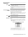
Mode Selection
Depending on the control mode selected, the output signal may be
either Period, Delay, Width, or High Level controlled, by an external
voltage applied to the CTRL INPUT.
The control mode can be cycled through available options by pressing
the key below the mode indicators and the currently active mode
is shown by an LED indicator. Table 4- 1 indicates the permitted
combinations of control and operating modes.
Table 4-1. Operating/Control Mode Combinations
MODE
CTRL
NORM TRIG GATE EWID EBUR
PERC
DELC
DBLC
WIDC
HILC
x
x
x
x
x
x
x
x
x
x
x
x
x
x
x
x
x
x
x
x
Period Control (PERC)
Control input sensitivity is + LO V to + 10.0 V ( +2.0 V to +10 V in
the 20 ns to 100 ns range) and period ranges from 20 ns to 1 s are
available in eight non-overlapping decades. See Figure 4-5.
The decade is selected by setting PER within that decade, i .e.
PER=3 µs would mean than control input voltage cycling between
1 V and 10 V, will control the period between 1 µs and 10 µs.
Whatever the value you select for PER, the upper limit for that
decade is displayed ( 10 µs if 3 µs was selected as above). The vernier
keys are inoperative and the Range key is used to change range.
Delay Control (DELC)
Control input sensitivity is + LO V to +10.0 V. Minimum delay is 75
ns and a maximum delay of 1 second is obtainable.
Note
In DBL mode the time between pulses will be varied by the control
input, when DELC is selected.
See Figure 4-5.
Width Control (WIDC)
Control input sensitivity is + LO V to + 10.0 V and width range 10 ns
to 1 s in eight non-overlapping decades. See Figure 4-5.
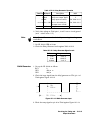
High Level Control (HILC)
High Level control is available in the range -8.0 V to +8.0 V. It is
important to note that while the Low Level (LOL) value can be
set to a maximum of + 7.95 V in 50 mV steps, the LIMIT facility
4-8 Operating
becomes non-operational in this Control mode, and the button LED
will blink. See Figure 4-6.
HIL M
Maximum
LOL set (+7. 95\/) -
+8V
ov
The d otted line shows
the H I LC range
-8V
Figure 4-6. High Level Control Capabilities
Operating 4-9
Setting Transition
Modes
�Ii�
�fa
8112A PULSE GENERATOR 50MHz
HEWLETT ·PACIWID
I
Figure 4-7. Transition Controls
The transition mode keys enable the operator to select the type of
pulse transition and to vary transition time.
Fixed CD
Linear (J]
Gaussian
0
This key provides a fixed transition of 4.5 ns. You cannot adjust the
LEE or TRE parameters when this key is operated (lit).
Permits both the leading and trailing edges of the HP 8 1 12A output
pulse to be programmed independently of each other, in the range
6.5 ns to 95 ms, by setting values for LEE and TRE. Maximum
permissible ratio is 1 :20.
This key is the same as the linear mode key except that edges are
co-sinusoidal in shape. It is important to note that the actual rise
and fall times of the transitions will be up to 253 faster than the
selected and displayed value for slopes of greater than 50 ns duration.
For slopes less than 50 ns, transition times tend increasingly towards
the displayed value.
The reason for this variation is that selected values are based only
upon times between 103 and 903 of total trigonometric transition.
Values between 0 to 103 and 903 to 1003 are not taken into
account by the HP 8 1 12A instrument.
4-1 O Operating
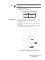
Transition Ranges
There are seven overlapping ranges for linear and gauss transitions,
and it is important to note the following:
•
•
Within any range, the maximum ratio of the leading edge
transition time to the trailing edge transition time is 1 :20 and vice
versa.
When you move the currently active slope to higher or lower range
than the non-active slope, the latter will be automatically pulled
into the same range.
ns
Range
Upper
Limit
99.9
Range
1
•
9.99
999
fS
ms
999
99.9
9.99
95
:
Range 2., :
Range 3
Range 4
Range 5
-
Range
Lower 6.5
Limit
50
M
500
I
5
50
fS
500
Range 6
I
Range 7
5
95
�
Figure 4-8. LEE and TRE ranges
Up and Down-ranging,
Using the VERNIER
keys
There is an overlap between all ranges.
When the currently active slope is altered so that it falls within a
range above or below the non-active slope, the value of the non
non-active slope automatically increases/decreases in value by a
factor of 10 or 100, depending on where it lay within the overlap.
Figure 4-9, Table 4-2 and Table 4-3 illustrate the technique of passing
Range "Break Points".
Operating
4- 1 1
50ns
99ns 500ns
999ns
�
5 0fS
5� s
'
'
'
'
Range 2:
X
=
Non-active S lope
Y
=
Active S lc:ipe
'
'
'
'
'
'
'
X1
///////
/ / / JI' / / /
///////
///////
///////
X2
,,,,,,, Range 5
Y1
'
'
'
Y2
Figure 4·9. Ranging examples
Table 4-2.
Active slope moves from Range 3 to Range 2 (Y1 )
Inactive slope Change Value
Reason
Xl
n o change
X2
-:-10
not in overlap
X3
-:-10
in overlap with higher range (4)
in a shared overlap, range 2/3
Table 4·3.
Active slope moves from Range 3 to Range 4 (Y2)
Inactive slope Change Value
Up and Down-ranging
Using the RANGE key
4·12
Operating
Reason
Xl
x lOO
in shared overlap
X2
x lO
not in overlap
X3
no change
in overlap with higher range
When this key is used to move a currently active slope up or down
a range, the non-active slope will be automatically pulled into the
Same Decade as the active slope setting. This effect is particularly
usefull for fast ranging between decades.
Setting Parameters
8112A PULSE GENERATOR 50MHz
,- VERNIER ------
HEWLETT-PACKARD
ERROR
o Bi.I
O PER
�
I _
2o
o DBL
O DEL
o DTY
O WID
SET
I
oI
0 ••
a ,...
o na
�
G
,-EXCESSIVE-,
o LEE
O
TRE
o"
av
0 HIL
O LOL
G
RANGE
HHHH
uSTO
" RCL
STO/RCL
G
Figure 4· 1 O. Parameter controls
The parameters available for selection depend on the currently
selected modes. All parameters are described below.
Selection
Pressing a parameter key selects the parameter indicated by the
illuminated mnemonic above the key.
The current value of the selected parameter is shown on the digital
display. The parameter units are indicated by the LEDs to the right
of the display.
Adjustment
Period/Burst Key
The currently selected parameter is adjusted using the (VERNIER) and
(RANGE ) rocker keys. Each (VERNIER ) key increments or decrements the
corresponding digit in the digital display. Similarly, the (RANGE ) key
increases or decreases the parameter value by a factor of 10.
(PER )
When selected, allows the period of the HP81 12A output signal to be
set and or adjusted.
(BUR)
In
EBUR mode, this key is used to set the number of pulses (between
1 and 1999) which will comprise the burst.
Operating
4-1 3
Delay/Double Key
(DEL )
Enables the operator to set the desired delay between TRIG
OUTPUT pulse and HP 8 1 12A OUTPUT pulse.
(DBL )
When selected, double pulses are output, their characteristics being
defined by the parameter settings. The width of each pulse is either
equal to the WID setting or half the DTY setting. The range of
delay between the two pulses is 20 ns to 950 ms.
Width/Duty Key
(w1D )
Enables pulse width to be set between 10 ns and 950 ms.
(DTY J
Pulse duty cycle is variable from 1 % to 99%. Percentage values are
shown on the digital display.
Leading and Trailing
edge Keys (LEE ) ( TRE )
High and Low level
Keys CillD ( LOL )
Note
Set Key (SET)
These two keys are used in conjunction with TRANSITION MODE
keys. It is possible to increase or decrease rise and fall times of
output pulses. Should you select a rise or fall time which degrades
the HI1 or 101 settings, an EXCESSIVE message will illuminate
above the two keys and the key associated with the incompatible
parameter will flash.
When either of these keys is selected, the corresponding level may be
set.
The selected HI1 value is inoperative in the HI1C mode.
This key causes the HP 81 12A to assume a factory programmed
parameter set as follows:
NORM
PER
WID
LEE
TRE
Active
Active
503 of PER
10% of PER
10% of PER
SET is automatically eliminated by selection of any other mode or
parameter key or by pressing PER again.
4-14
Operating
Store and Recall Key
(STO/RCL )
The HP 81 12A has the capability to store nine complete sets of mode
and parameter information in it's memory.
To store settings, press (STO/RCL). The digital display now reads
unX, where X is the file identity number ( 1 to 9). The right hand
vernier key is used to alter the value of X, to determine which file the
parameter set will be stored as. Now press the bottom of the left
hand vernier key and the current instrument settings will be stored in
the selected file.
To recall settings, press (sTO/RCL ). The digital display now reads
unx, where X is the file identity number ( 1 to 9). The right hand
vernier key is used to alter the value of X, to determine which
parameter set file will be recalled. Now press the bottom of the
center vernier key and the instrument settings will be altered to those
of the stored file which has been selected.
Note
RCL 0 reverts the instrument to it's standard setting, see Chapter 2.
If no settings have been stored, the instrument will revert to standard
settings whichever file number is selected for recall.
Operating 4-1 5
Selecting Output
Mode
��
��
8112A PULSE GENERATOR 50MHz
HElfl.ETT ·PACICARD
L JllJT
I
COllPL
DJMllL&
G G G
�0
Lt
Figure 4· 1 1. Output controls
Limited Output
(LIMIT)
Pressing the (LIMIT ) key sets the current high and low output levels
( HIL,LOL ) as output limits which cannot be exceeded until limited
output mode is switched off. While limited output mode is active,
the high and low output levels ( HIL,LOL ) can be varied within the
output limits.
Limited output mode is switched off by pressing the (LIMIT ) key again.
The (LIMIT ) key LED is lit when this mode is active.
Caution
I
Complement Output
(COMPLJ
Disabled Output
(DISABLE)
4-16
Operating
Limit does not work when using HILC mode, the LIMIT key will
fl.ash if HILC is selected to remind you that it is no longer active.
Pressing the ( COMPL) key complements the instrument output,
pressing the key again returns the instrument output to normal.
The (coMPL) key LED is lit when the output is complemented.
Pressing the (DISABLE ) key disables the instrument output, pressing
the key again enables the output.
The (DISABLE) key LED is lit when the output is disabled.
Caution
&
I
Do not apply an external voltage greater than ±5 V, or electrostatic
discharge to the output connector.
Operating 4-1 7
Rear Panel
WARN ING:
NO OPERATOR SERVICEABLE PARTS INSIDE. REFER SERVICING TO TRAINED PERSONNEL
0
0
=
=
=
=
..- "- LINE --,
= t00t""'22a240V
=
� +5"
=
'!-:40 Hz c=:=:l
-:VA
0
=
0
WARN ING:
FUSE -E3-
100/120V 1.5A 220/240V 750mA
©
0
0
H P- I B
aaaaaaaaaaaaaaa
000000000000000
©
100
220
120
240
'"'"""'
&
•lllWlllrl.
MARKER
X-OUT
OUTPUT
HOLD-IN
0
0
0
v
v
v
v
HEWLETT-PACKARD GMBH
FTZ-SERIENPRUFNR.
C-31 8/86
I
8112A
SN 3027 G 06175
Fff. R9p. of Germany
Made in
I
FOR CONTINUED FIRE PROTECTION USE SPECIFIED ,,......_,, LINE FUSE.
Figure 4- 1 2. Rear panel
HP-IB Connector
X-Out
Not used with HP 81 12A.
Marker Output
Not used with HP 81 12A.
Hold In
Not used with HP 8 1 12A.
Fuse
4-1 8
Refer to Figure 3-3 for a definition of the HP-IB connector pins.
Refer to "Setting the HP-IB Address" in Chapter 6 if you want to
know how to set the instrument's HP-IB address.
Operating
The fuseholder accepts standard fuses to provide instrument
protection in case of current overload. Refer to Table 3- 1 for
appropriate fuse selection.
5
Operating Examples
Introduction
To obtain an output from the HP 81 12A it is only necessary to set
the mode, period and transition type. Then press the green (SET ) key.
A stable error free pulse train is generated and you can then alter
parameter values, and external input and control modes to derive
your desired output.
Triggering Examples
The following examples show how the HP 81 12A instrument can be
set up for each type of trigger mode. The examples list the basic
operating steps in the order in which they would normally occur after
switching on.
In the applications section, examples are given of how the HP 81 12A
can be used in common design and test situations.
Normal Mode
r--1 ( 5 0� d u t y
_J L cyc l e )
TR I G
OUTPUT
MA I N
OUTPUT
Figure
5-1.
Typical output in Normal mode
1 . Switch the instrument on using the line switch.
2. If neccessary, select normal mode by repeatedly pressing the
standard mode key until the NORM LED is lit.
3. Select the Transition mode by pressing the key with the
appropriate symbol. The parameter window will be automatically
illuminated.
Operating Examples
5·1
4. Select each output parameter in turn by pressing its associated
key. Adjust the parameter value using the (VERNIER) and (RANGE )
keys. Refer to Chapter 4 Operating for additional information on
parameter adjustment.
5. If a Control Function is required, select the required mode by
repeatedly pressing the control mode key until the required mode
is lit . Apply the Control signal to the CTRL INPUT connector.
Refer to Chapter 4 Operating for more permissible combinations of
Operating and Control modes.
Note
You may wish to set up Output Limits as described in Chapter 4
Operating to protect the device under test.
6. Press the (DISABLE ) key to turn off output disable mode and enable
the output (LED extinguished).
Trig Mode
E XT
I N PUT
TRIG
OUTPUT
MA I N
O UTPUT
Figure 5-2. Typical signals In Trigger mode
1 . Switch the instrument on using the line switch.
2. If neccessary, select Trig mode by repeatedly pressing the standard
mode key until the TRIG LED is lit.
3. Apply the external trigger signal to the EXT INPUT and select
trigger slope and level as required. Refer to Chapter 4 Operating
for information on the trigger controls. Triggering can also be
simulated using the (MAN ) key.
4. If a modulated output is required, select the required modulation
using the [ CTRL) key. Apply the modulating signal to the CTRL
INPUT connector. Refer to Chapter 4 Operating for more
information on modulating the output signal.
5. Select the Transition mode by pressing the key with the
appropriate symbol. The para.meter window will be automatically
illuminated.
5-2
Operating Examples
6. Select each output parameter in turn by pressing its associated
key. Adjust the parameter value using the (VERNIER) and (RANGE)
keys. Refer to Chapter 4 Operating for additional information on
parameter adjustment .
7. If a Control Function is required, select the required mode by
repeatedly pressing the control mode key until the required mode
is lit . Apply the Control signal to the CTRL INPUT connector.
Refer to Chapter 4 Operating for more permissible combinations of
Operating and Control modes.
Note
You may wish to set up Output Limits as described in Chapter 4
Operating to protect the device under test .
8. Press the (DISABLE) key to turn off output disable mode and enable
the output (LED extinguished) .
Gate Mode
EXT
INPUT
TR I G
OUTPUT
I
I ,.-·���
-----: ----------------------- ----------:------------\------'
I
l
r--1 < 50% d u t y
LJ L cyc l e )
MA I N
OUTPUT
Figure 5-3. Typical signals in Gate mode
1 . Switch the instrument on using the line switch.
2. If neccessary, select gate mode by repeatedly pressing the standard
mode key until the GATE LED is lit .
3. Apply the external gating signal t o the EXT INPUT and select
trigger slope and level as required. Refer to Chapter 4 Operating
for information on the trigger controls. Triggering can also be
simulated using the (MAN ) key.
4. Select the Transition mode by pressing the key with the
appropriate symbol. The parameter window will be automatically
illuminated.
5. Select each output parameter in turn by pressing its associated
key. Adjust the parameter value using the (VERNIER ) and (RANGE)
keys. Refer to Chapter 4 Operating for additional information on
parameter adjustment.
Operating Examples
5-3
6. If a Control Function is required, select the required mode by
repeatedly pressing the control mode key until the required mode
is lit. Apply the Control signal to the CTRL INPUT connector.
Refer to Chapter 4 Operating for more permissible combinations of
Operating and Control modes.
Note
You may wish to set up Output Limits as described in Chapter 4
Operating to protect the device under test.
7. Press the (DISABLE) key to turn off output disable mode and enable
the output (LED extinguished).
External Width Mode
EXT INPUT
TRIG OUT
OUTPUT
Figure 5-4. Typical signals in External Width mode
1 . Switch the instrument on using the line switch.
2. If neccessary, select external width mode by repeatedly pressing
the standard mode key until the E.WID LED is lit.
3 . Apply the E. WID signal to the EXT INPUT and select trigger
slope and level as required. Refer to Chapter 4 Operating for
information on the trigger controls.
4. Select the Transition mode by pressing the key with the
appropriate symbol. The parameter window will be automatically
illuminated.
5. Select each output parameter in turn by pressing its associated
key. Adjust the parameter value using the (VERNIER) and (RANGE )
keys. Refer to Chapter 4 Operating for additional information on
parameter adjustment.
6.
5-4
Operating Examples
If a Control Function is required, select the required mode by
repeatedly pressing the control mode key until the required mode
is lit. Apply the Control signal to the CTRL INPUT connector.
Refer to Chapter 4 Operating for more permissible combinations of
Operating and Control modes.
Note
You may wish to set up Output Limits as described in Chapter 4
Operating to protect the device under test.
7. Press the (DISABLE) key to turn off output disable mode and enable
the output (LED extinguished).
External Burst Mode
EXT
I NPUT
TR I G
OUTPUT
MA I N
OUTPUT
�
n
n
( 50" d u t y
cyc l e )
Figure 5·5. Typical signals in External Burst mode
1 . Switch the instrument on using the line switch.
2. If neccessary, select external burst mode by repeatedly pressing
the standard mode key until the E.BUR LED is lit.
3. Apply the E.BUR signal to the EXT INPUT and select trigger
slope and level as required. Refer to Chapter 4 Operating for
information on the trigger controls.
4. Select the Transition mode by pressing the lkey with the
appropriate symbol. The parameter window will be automatically
illuminated.
5. Select each output parameter in turn by pressing its associated
key. Adjust the parameter value using the (VERNIER) and (RANGE)
keys. Refer to Chapter 4 Operating for additional information on
parameter adjustment.
6. If a Control Function is required, select the required mode by
repeatedly pressing the control mode key until the required mode
is lit. Apply the Control signal to the CTRL INPUT connector.
Refer to Chapter 4 Operating for more permissible combinations of
Operating and Control modes.
Note
You may wish to set up Output Limits as described in Chapter 4
Operating to protect the device under test .
7. Press the (DISABLE) key to turn off output disable mode and enable
the output (LED extinguished).
Operating Examples
5-5
Applications
Analog Applications
Fixed transition mode
The fixed transition time ( 5 ns ), is ideally suited for step response
measurements such as:
•
Transient behaviour of amplifiers (transient time, overshoot,
ringing, settling time).
•
Reverse recovery time of transistors and diodes.
•
Characterization of capacitors (equivalent serial resistance,
inductance, high frequence capacitance).
50 o h m
50 ohm
l oa d
load
O s ci l l o s co pe
H P 8112A
I
___.._
-=-
I
I
G rou nd
Figure
5-6.
Capacitance circuit
Linear transition mode
lndependantly variable leading and trailing edges between 6.5 ns and
95 ms can be used to generate ramps or sawtooth waveforms for:
•
Stimulation of hydraulic or pneumatic devices
•
Mechanical tests
•
Hysteresis of Schmidt trigger circuits
•
Stress testing of capacitors and thyristors by measuring maximum
allowed voltage increase per time (max. dV /dt)
Cosine shaped translUon modes (Gaussian)
Independantly variable cosine shaped leading and trailing edges
between 6.5 ns and 95 ms can be used to generate smooth transitions
which do not include high frequencies for:
•
5-6
Operating Examples
Communications, reduced reflections and crosstalk
Digital Applications
•
Simulation of bandpass filtered signals such as data transmission
over telephone lines
•
Generation of haversines
Fixed transition mode
Can be used for stimulation of fast logic components and circuits as
follows:
•
Clock generation
•
Producing known good data inputs for logic sub assemblies and
modules
•
Integrated circuit parameter settings
o
maximum clock speed
o
noise sensitivity and threshold level verification
o
set-up time
o
hold time
o
propagation delay
o
minimum clock pulse width
Linear variable transition mode
•
Reduced relations and crosstalk
•
Driving CMOS devices
•
Parametric tests with manufacturer-recommended transition times
Cosine shaped transition mode
•
Simulation of degraded pulses, for example after storage on a
magnetic medium
Operating Examples 5·7
6
Programming
In remote mode, all HP 81 12A settings, except EXT INPUT trigger
level, are programmable via the HP-IB . The HP 81 12A also provides
error messages and can report operating parameters when requested
by the controller.
General
This chapter describes the valid programming mnemonics and syntax
for the HP 8 1 1 2A. Example program statements are based on HP
BASIC 5.0/5. 1 for the HP 9000 Series 200/300 controllers. Example
program statements also assume that the instrument HP-IB address
is 12 decimal.
This manual does not discuss the HP-IB protocol or hardware. For
detailed information on the HP-IB refer to any of the following
publications:
•
•
•
•
•
Setting the HP-18
Address
Note
IEEE Interface Standard 488-1975
ANSI Interface Standard MC l . 1 .
H P Publication 59401-90030
HP Publication 5952-0058
HP Publication 5952-0156
The HP 8 1 12A's HP-IB address is set at the factory to 12 decimal.
The address is stored in the instrument 's RAM, along with the
current instrument settings.
•
You can only change the address in NORMal trigger mode,
immediately after switching the instrument on. Pressing the ( LCL )
key at any other time displays the current address while the key is
depressed, but no change is possible.
•
When allocating HP-IB addresses make sure no instruments on the
bus have the same address.
•
If the RAM battery fails, the HP-IB address is set to 12 when the
instrument is switched on.
To change the instrument's HP-IB address:
1 . Switch the instrument on.
2. If the instrument is NOT in NORM trigger mode:
a. Select NORM trigger mode.
b. Switch the instrument off and on again.
3. Press the (LCL ) key. The current HP-IB address is displayed on the
frontpanel.
4. Use the vernier keys to change the address.
Programming 6-1
5. Press the (LCL) key again to set the new address.
Local, Remote and
Local Lockout
Local mode
In this mode the RMT LED is off, the front panel is used to operate
the instrument and programming messages are ignored.
You can select local mode in the following ways:
•
•
•
Switching the HP 8 1 12A on.
Pressing the (LCL) key, if Local Lockout is inactive.
Sending an HP-IB Local command to the instrument from the
system controller (use the LOCAL statement in BASIC 5.0/5.1).
LOCAL 7 1 2
The output signal and all instrument settings remain unchanged
following a change from remote to local mode.
Remote mode
In
this mode the RMT LED is illuminated and programming
messages received via the HP-IB are interpreted (parsed) and used to
control the instrument . The front panel controls are disabled apart
from:
•
•
•
The (LINE ) switch.
The trigger LEVEL adjust knob.
The (LCL ) key, if Local Lockout is inactive.
You can select remote mode by sending an HP-IB Remote Enable
command from the system controller (use the REMOTE statement in
BASIC 5 .0/5.1).
REMOTE 7 1 2
The output signal and all instrument settings remain unchanged
following a change from local to remote mode.
Local Lockout
The (LcL) key can be disabled by sending an HP-IB Local Lockout
command from the system controller (use the LOCAL LOCKOUT
statement in BASIC 5 .0/5 . 1 ) .
LOCAL LOCKOUT 712
This ensures that only the system controller can return the
instrument to Local mode, except when the instrument is switched
off and on again.
It is recommended that all programming applications use this facility,
because if a programming message is interrupted by pressing the
(LcL ) key during data transmission from the system controller, the
HP 81 12A may be left in an unknown state.
6-2
Programming
Abbreviations used in
this Document
EOL
Sequence
End of Line Sequence (used for termination).
Character( s) at the end of a line or message
EOI Signal End-or-Identify Signal (separate HP-IB signal line used
for terminating a message)
Terminators
Note
CR
carriage-return; ASCII character with the ASCII-code
13
CST
current settings command (used to read the current
instrument state)
LF
line-feed; ASCII character with the ASCII-code 10
STB
Status Byte Register
RQS
Request Service Bit
SRQ
Service Request
SPOLL
Serial Poll (used to determine whether a device is
requesting service; returns the value of the Status Byte
Register)
PPOLL
Parallel Poll (not supported by the HP 8 1 12A)
Learn
String
ASCII string returned after a CST command; contains
all necessary commands to set the HP 81 12A to its
present state. The Learn String may later be sent back
to the device to place it in this state.
The HP 81 12A accepts the following terminators:
•
CR/LF (the default EOL sequence)
•
EOI only
•
CR/LF and EOI
•
LF and EOI
LF alone is not accepted as terminator when the HP 81 12A is
connected to a HP9000 Series 200/300 controller. When connected to
other controllers, the HP 81 12A may accept J,F as terminator.
The HP 81 12A itself, terminates a data message sent to the computer
with:
CR/LF followed by a SPACE character
The EOI line is not polled by the HP 81 12A.
Programming
6-3
Programming
To select an operating mode or to set a parameter to a specific value,
the appropriate ASCII mnemonic must be sent to the HP 81 12A.
Example:
To set the Operating Mode to TRIG, the ASCII mnemonic M2 has
to be sent to the HP 8 1 1 2A.
HP Ba.sic Statement for this is:
OUTPUT 712 ; "M2"
When programming parameters, such as Period, Delay or Width,
the ASCII mnemonic must be followed by the value and the
appropriate unit. The ASCII mnemonic, the value and unit may be
separated by a comma or space character. For better readability it is
recommended to use a space character.
Example:
To set the Period to 2.2 ms, the ASCII mnemonic PER followed by
the new value 2.2 and the unit MS must be sent to the HP 81 12A.
HP Basic Statement for this is:
OUTPUT 712 ; "PER 2 . 2 MS"
or
OUTPUT 7 12 ; " PER2 . 2MS"
Note
Multiple Commands
Program commands can be a combination of upper case or lower
case ASCII characters, whereas the responses are always returned in
uppercase.
You can send multiple programming commands on the same line.
The commands may be separated by a comma or a space character.
It is recommended to separate the commands with a comma, because
this makes it easier to read such a programming message.
Examples:
OUTPUT 7 12 ; "M 1 , CTO , PER 1 . 25 MS"
OUTPUT 712 ; " M 1 CTO PER 1 . 25 MS"
OUTPUT 7 1 2 ; "M1CTOPER 1 . 25 MS"
Commands separated with
commas
Commands separated with
space characters
Commands not separated
Commands which change modes are processed before commands
which set parameters, irrespective of the command order within the
programming message. If your application requires a parameter
change to occur before a mode change, use seperate programming
messages for the two commands.
6-4
Programming
The HP 8 1 12A can be programmed into an error condition in
just the same way as when using the front panel. For example,
attempting to program a larger 101 than HIL:
OUTPUT 7 1 2 ; "HIL 1 V , LOL 2 V "
Refer to "Error, Fault and Status Reporting" for details of error,
fault and status reporting using the HP-IB .
Programming
6-5
Selecting Trigger
Modes
Standard Trigger Modes
Action
Mnemonic
Select NORM
Ml
Select TRIG
M2
Select GATE
M3
Select E.WID
M4
Select E.BUR
M5
Trigger Control
Mnemonic
Action
Example
Select trigger off
TO
Select positive trigger slope
Tl
Select negative trigger slope
T2
Select both
T3
OUTPUT 7 1 2 ; 11 M3 , T1 11
Select
slope.
GATE mode
with a positive trigger
Selecting Control
Modes
Example
6-6
Programming
Action
Mnemonic
Switch off control mode
CTO
Select PERC
CTl
Select DELC
CT2
Select WIDC
CT3
Select HILC
CT4
OUTPUT 7 12 ; 11 CT2 11
Select Delay Control
Selecting Output
Waveform Mode
Action
Example
Mnemonic
Select fixed
Wl
Select linear
W2
Select gaussian
W3
Select mode off
SMO
Select mode on
SMl
OUTPUT 7 1 2 ; "W2 , SM1 11
Select linear output waveform transitions
Setting Paraf,lleters
Note
A parameter programming mnemonic is the sa.me as its front panel
description, DEL = delay for example.
Timing parameters
Action
Set
Set
Set
Set
Set
Set
period
delay
double pulse
width
leading edge
trailing edge
Set duty cycle
Example
Mnemonic
Value Delimiter
PER
DEL
DBL
WID
LEE
NS = nanoseconds
US = microseconds
MS = milliseconds
DTY
%
TRE
OUTPUT 7 1 2 ; "PER 10 MS , DTY 30 Y. 11
Set period to 10 ms, set
duty cycle to 30%.
Programming
6- 7
Level parameters
Mnemonic Value Delimiter
Action
Set high level
Set low level
Example
HIL
LOL
V
V
=
=
OUTPUT 7 1 2 ; 1 1 HIL 2 V . LOL - 1 . 2S V"
volts
volts
Set high level to plus 2 V,
low level to minus 1 . 25 V
Burst Parameter
Mnemonic Value Delimiter
Action
Set burst number
Example
OUTPUT 712 ; " BUR 375 1 1
#
BUR
Provides a burst of 375 output pulses
Vernier
Mnemonic
Action
Example
6-8
Programming
Most signicant digit up
MU
Second significant digit up
SU
Least significant digit up
LU
Most signicant digit down
MD
Second significant digit down
SD
Least significant digit down
LD
OUTPUT 712 ; 1 1HIL 5 V , SD , SD , SD 11
Set high level to 5 V and
decrement in three steps of
1 00 m V.
]
Range Change
Example
Action
Mnemoruc
Next higher range
Next lower range
RU
RD
OUTPUT 7 1 2 ; "RU"
Change vernier range upwards
Stored Parameters
Example
Action
Mnemonic
Value Delimiter
Store parameter set
Recall parameter set
STO
RCL
l . . 9 Set ident
0 = Standard
l . . . . 9 Stored set
OUTPUT 7 12 ; "STD 5 "
OUTPUT 712 ; " RCL O"
.
.
Store current parameters set o n instrument
as setting number /j
Revert instrument to standard parameter
settings
Excessive Slope
Calculation
Example
Action
Mnemonic
Excessive slope calculation off
Excessive slope calculation on
SRO
SRl
OUTPUT 712 ; " SRO "
Switches off calculation of excessive slope
(speeds up program e;xecution)
Programming
6-9
Reading parameters
The HP 81 12A provides special commands with which information
can be read by the computer. These commands are called Talker
Function Commands. After Sending a Talker Function Command
the HP 8 1 12A will return a response message. A response message
remains in the HP 81 12A output queue until it is read or another
command is issued.
For example, to read the current value of the Period, the following
commands are necessary:
OUTPUT 712 ; 11 IPER 1 1
ENTER ; A$
PRINT " 8 1 1 2A PER=
Note
II ;
A$
After the Interrogate Parameter commands ( IPER, IDE1, IDB1,
etc. ) the HP 81 12A does not return only the numeric values, instead
it returns an ASCII-response that contains the command to set the
interrogated parameter to its present value.
If the current period is set to 1 ms, the variable A$ will contain the
string "PER 1 .00 MS" after conducting the example above.
It is possible to read the current setting of a parameter using the
interrogation mnemonics listed here:
Standard
•
•
•
•
•
•
•
•
•
•
IPER
IDE1
IDB1
IDTY
IWID
ILEE
ITRE
IHI1
1101
IBUR
The HP 8 1 12A reply has the same format
the parameter, for example:
as
that used when setting
PER 10MS
The reply length is always 12 characters.
It is also possible to read all the instrument settings in one go using
the CST mnemonic. Refer to "Reading the Current Settings"
Example
D IM B$ [ 12]
OUTPUT 712 ; 11 IDEL 11
ENTER 712 ; B$
PRINT " 8 1 12A DEL=
6-1 O'
Programming
II
; B$
Dimension string allocates 1 2 char
acters of memory for reply.
Request current delay setting.
Read reply into allocated memory.
Print the reply.
Selecting Output
Modes
Output Controls
Action
Example
Reading the Current
Settings
Mnemonic
Switch off output limits
LO
Switch on output limits
11
Switch off complementary output
co
Complement output
Cl
Enable output
DO
Disable output
Dl
OUTPUT 712 ; 11 L 1 , D O 1 1
Switch o n output limits and enable the
output signal.
The Current Setting interrogate command CST tells the HP 8 1 12A
to send a response that contains all necessary commands to set the
device to its present state. The response message, called ( ASCII )
learn string, can be retransmitted as a program message without
alteration.
The learn string may be altered in the computer before
retransmitting it. Since the learn string is made up of the several
independent commands, it is possible to send parts of the learn string
( complete commands ) to the instrument .
Note
The description of the example program LRN _DEMO in Chapter 7
Programming Examples contains more details about the usage of the
CST command. Also refer to the example program INTERROG.
When the HP 8 1 12A replies with a string containing all current
settings. The data is always in the same order:
M 1 , CTO , T1 , W1 , SMO , LO , CO , D 1 , BUR 00 1 # , PER 1 . 00 MS , DBI. 200 US , DEL 65 . 0 NS ,
DTY 50 Y. , WID 100 US , LEE 10 . 0 NS , TRE 1 0 . 0 NS , HIL 0 . 30 V , LOL - 0 . 70 V
Programming
6-1 1
Example
DIM B$ [ 153]
OUTPUT 712 ; " CST"
ENTER 712 ; 8$
PRINT " 8 1 1 2A s ett ings are :
Timing
" ; 8$
Allocate memory for max
imum reply length
Request current settings
of instrument
Read reply into allocated
memory
Print the reply.
The time taken for the HP 8 1 1 2A to receive and implement a
programming message can be divided into three parts:
Data Transmission Time
Send
This is the time taken to transmit the programming message over the
HP-IB, which is 130 µs ms per ASCII character (7.6 kByte/ sec). The
system controller is free to continue with its program after this time.
Answer
This is the time taken by the HP 8 1 1 2Ato transmit a message when
error reporting or learn mode. Time is 1 ms per character, status
byte < 15 ms
Implementation Time
This is the time taken by the HP81 12A to interpret and carry out all
the commands in received message. Typical implementation times
vary between 4 ms for select mode to 1 85 ms to recall a parameter
set. Typical implementation times for various commands are given in
the following table.
Table 6-1.
Command (s )
Mode change
Control modes
Level
Burst
Timing (not in duty mode)
Duty cycle
Period (DTY active)
Store
Recall
Norm/Compl
Enable/Disable
Limit
6- 1 2
Programming
hnplementation Without Excess
Time
< 4 ms
< 50 ms
< 90 ms
< 12 ms
< 50 ms
< 80 ms
< 80 ms
6 ms
180 ms
< 4 ms
< 4 ms
< 4 ms
Slope calc.
< 25 ms
< 50 ms
< 50 ms
1 50 ms
The timings given are worst case. When parameter settings
are combined into one programming message, the combined
implementation time can be up to 40% more efficient .
The Buffer Not Empty flag in the HP 81 12A status byte is set during
this time. The system controller can therefore monitor this flag to
detect when a programming message has been implemented. Refer to
"Error, Fault and Status Reporting" .
Hardware Settling Time
The hardware requires time to settle after a change. This sometimes
takes longer than the time taken to interpret and execute the
message, typically < 5 ms.
Error, Fault and
Status Reporting
HP-18 Status Byte
The HP 8 1 12A is provided with the capabilities of requesting service
from the controller (the computer) whenever the instrument detects
an error.
To be able to determine if an error was caused, Status Reporting
Structures are required. For this purpose the instrument contains the
Status Byte register:
The Status Byte Register (STB) is composed of seven single-bit
"summary-messages" . Each of the bits 0 thru 5 summarizes a specific
type of error. For example, bit 0 represents all types of Limit errors.
(See the operating manual of the HP 8 1 12A) Bit 6 of the STB is the
Request Service (RQS) Bit and is set whenever a service request is
caused. Bit 7 indicates whether the Buffer is empty or not .
After a Serial Poll (SPOLL) the complete Status Byte is cleared.
The Status Byte is updated after every command received by the HP
8 1 12A.
The HP 8 1 12A status byte can be read using a serial poll.
A = SPOLL (712)
Read instrument status byte
into variable A
PRINT 11 8 1 12A Status Byte = 11 ; A
The meaning of each bit in the status byte is given below. In all
cases, the bit is set to 1 to indicate that the condition described is
true.
Programming
6-13
Meaning
Bit
0 LIMIT ERROR (Causes SRQ)
1
TIMING ERROR (Causes SRQ)
2
SYNTAX ERROR (Causes SRQ)
3
SLOPE ERROR (Causes SRQ)
4
DUTY CYCLE ERROR (Causes SRQ)
5
INPUT ERROR (Causes SRQ)
6
SERVICE REQUEST ( =SRQ)
7
BUFFER NOT EMPTY
The SRQ bit generates an interrupt at the system controller to
indicate that the instrument requires attention. You can use this
facility as the basis of interrupt driven error handling in your
programming application.
The SRQ, Programming Error, Syntax Error and System Error bits
are latched until the status byte is polled by the system controller.
The other status bits represent the current condition at the time the
status byte is read.
You can obtain more detailed information about timing and
programming errors using the interrogate error (IER.R) mnemonic.
The HP 8 1 12A responds with a string describing the current error
conditions. The descriptions are covered in subsequent parts of this
section.
Allocate memory for error string
Request error information
Read reply into allocated string
D IM E$ [45]
OUTPUT 7 1 2 ; " IERR"
ENTER 7 12 ; E$
PRINT " 8 1 12A Error= " ; E$
Limit Errpr
(Bit 0)
Note
6-14
Programming
There are two types of error which set the limit error bit in the
status byte. The conditions which cause them and the description
used by the HP 8 1 12A when replying to an IERR command are
listed below. The limit error bit is not latched, therefore a transient
error is only recorded by generating an SRQ .
More than one error condition can occur at one time. When using
the IERR command ensure that you allow for a reply containing
more than one error description.
IERR Description
Comments
LIMIT ERROR
This error appears only when the limit is on
and:
a. the programmed High-level is greater
than the limited High-level
b. the programmed Low-level is lower than
the limited Low-level
LIMIT-HILC
This error appears only when the limit is on
and:
a. High-level control has been selected
b. no High-level limit is possible as HILC is
an external control voltage
Timing Error
(Bit 1)
Note
There are two types of error (shown for NORM mode only) which set
the timing error bit in the status byte. The conditions which cause
them and the description used by the HP 8 1 12A when replying to an
IERR command are listed below. The timing error bit is not latched,
therefore a transient error is only recorded by generating an SRQ .
More than one error condition can occur at one time. When using
the IERR command ensure that you allow for a reply containing
more than one error description.
IERR Description
Comments
DELAY ERROR
• Delay value is greater than Period value.
i .e. PER 1 ms, DEL 1 . 1 ms
• The front panel LEDs flash to indicate the
invalid settings.
• The ERROR LED is on
WIDTH ERROR
• Width value is greater than Period value.
i.e. PER 1 ms, WID 1 . 1 ms
• The front panel LEDs flash to indicate the
invalid settings.
• The ERROR LED is on
Syntax Error
(Bit 2)
This error occurs when the HP 8 1 12A cannot understand a
programming message. e.g DDY 503 instead of DTY 503. The bit
is latched until cleared by reading the status byte.
Slope Error
(Bit 3)
This error is caused by excessive slope. The conditions which caused
it and the description used by the HP 8 1 12A when replying to an
IERR command are listed below. The slope error bit is not latched,
therefore a transient error is only recorded by generating an SRQ .
Note
More than one error condition can occur at one time. When using
the IERR command ensure that you allow for a reply containing
more than one error description.
IERR Description
Comments
EXCESSIVE SLOPE
Programming
6-15
•
•
No valid waveform at the output:
a. LEE > WID x0.8 or
(PERx DTY/ lOO) x 0.8
b. TRE > (PER-WID ) x 0.8 or
PER-{PERxDTY/lOO)) x 0.8
c. TRE � (DBL-WID) x 0.8 or
DBL-{PERx DTY/200)) x 0.8
d. TRE � (PER-DBL-WID) x 0.8 or
PER-DBL-{PERx DTY/200)) x 0.8
No calculation with "SRl"
The "EXCESSIVE SLOPE" error message and calculation can be
suppressed with the SRO command. This will reduce programming
time.
Example
OUTPUT 7 1 2 ; "SRO "
This is particularly useful for character strings where a multiple of
the same timing parameter is programmed such as
OUTPUT 712 ; 1 1 SR0 11
FOR A = 1 to 100
OUTPUT 712 ; "PER ( CHR$ A ) MS "
NEXT A
Immediately upon receiving the new PERIOD value, the HP 81 12A
would calculate the excessive slope error for each period time
interval. By suppressing "EXCESSIVE SLOPE" , new settings for
Period are accepted by the instrument without any calculation, and a
reduction in programming time of typically 30 ms may be achieved.
Note
In the permanently stored Mode/Parameter settings in the
HP 81 12A ROMs, "SR" is set to "O" (zero). If these settings are
recalled as current settings, the Service Request function can be
re-activated by programming "SR" to " 1 " .
OUTPUT 712 ; 11 SR1 1 1
The (LCL ) key re-activates the Excessive Slope Error.
Duty Cycle Error
(Bit 4)
Note
6-16
Programming
There are three types of error which set the duty cycle error bit
in the status byte. The conditions which cause them and the
description used by the HP 8 1 12A when replying to an IERR
command are listed below. The timing error bit is not latched,
therefore a transient error is only recorded by generating an SRQ .
More than one error condition can occur at one time. When using
the IERR command ensure that you allow for a reply containing
more than one error description.
I nput Error
(Bit 5)
Note
Service Request
(Bit 6)
Buffer not Empty
(Bit 7)
IERR Description
Comments
DTY-PERC
Duty cycle not available in PERC . An
external voltage controls the Period and
NOT the Duty Cycle
DTY-WIDC
As above. External voltage controls the
Width and NOT the Duty Cycle
DTY-TRIG
An external trigger signal generates the
Period. The displayed Duty Cycle is
calculated from the internal Period. DTY is
not confirmed with the external period
There are four types of error which set the input error bit in the
status byte. The conditions which cause them and the description
used by the HP 8 1 12A when replying to an IERR command are
listed below. The timing error bit is not latched, therefore a transient
error is only recorded by generating an SRQ .
More than one error condition can occur at one time. When using
the IERR command ensure that you allow for a reply containing
more than one error description.
IERR Description
Comments
EWID-PERC
The external trigger input signal is passed
through to the output. A Control input
cannot alter period, delay, or width.
Identical returns are EWID-DELC and
EWID-WIDC
TRIG-PERC
Both inputs will attempt to control the
period. This is not possible.
GATE-TRIG slope
Both EXT INPUT slopes selected. Either
leading edge or trailing edge may be
specified but not both.
EWID-TRIG slope
As above. Either leading edge or trailing
edge may be specified but not both.
This bit indicates that a service request has occurred. The bit is
latched until cleared by reading the status byte.
This bit is set when there is data in the HP 8 1 12A input buffer.
You can monitor this bit to determine if the instrument has finished
interpreting a long programming message.
Programming 6-17
The HP 8 1 12A supports the following HP-IB Universal commands:
HP-I B Universal
Commands
These are HP-IB commands, NOT instrument programming
commands. They are not used in programming messages. If you
require more information on the HP-IB protocol and hardware refer
to "General" for a list of references.
Note
HP-IB
Description
BASIC
5.0/5.1 equivalent
Mnemonic
6·18
Programming
DCL
Device Clear
CLEAR 7
SDC
Selected Device Clear
CLEAR 712
LLO
Local Lockout
LOCAL LOCKOUT 7
GTL
Go to Local
LOCAL 712 / LOCAL 7
GET
Group Execute Trigger TRIGGER 712 / TRIGGER 7
UNL
Unlisten
SEND 712;UNL
UNT
Untalk
SEND 712;UNT
SPE
Serial Poll Enable
SPOLL ( 712 )
SPD
Serial Poll Disable
MLA
My listen address
selectable
MTA
My talk address
selectable
DCL
An HP-IB D CL command causes the HP 8 1 12A to load its standard
parameter set. The instrument remains in its current mode (local or
remote).
SOC
An HP-IB SDC command causes the HP 8 1 12A to load its standard
parameter set and enter remote mode.
GET
An HP-IB GET command simulates an external trigger to the HP
8 1 12A in TRIG, E.BUR and E.SWP modes.
Hints for solving
Problems that might
occur
Reading the Status Byte
When programming the HP 8 1 12A it must be considered that the
instrument needs some time to:
•
receive the commands
•
interpret the commands
•
update the Status Byte.
The hardware settling time must also be considered. (See Chapter 2
Specifications for more details).
When a command is sent to the HP 8 1 12A, the device places all
received characters into a buffer. Interpretation of the command( s)
starts as soon as a valid terminator is received.
To determine if the buffer is empty or not, read the Status Byte by
conducting a SPOLL. If bit 7 is set (decimal value of the STB is
bigger than 127) then the buffer is not yet empty.
Whenever the status byte is read directly after sending a command,
the HP 81 12A should be given sufficient time to update the status
byte. The time needed, varies with the type and number of the
commands sent . For single commands 100 to 200 ms should be
adequate.
Example:
10
CLEAR 7 1 2
20
A = SPOLL ( 7 1 2 )
30
!
40
OUTPUT "WID 10 MS "
50
WAIT
60
PRINT " St atus Byt e : " ; A
70
END
.2
!
caus e s error
give HP 8 1 1 2A t ime to updat e the STB
If the wait period in line 50 is too low, the value of the Status Byte
printed in line 60 will be 128. This indicates tlhat the buffer is not
yet empty. An adequate wait period (here 200 ms) will give the HP
8 1 12A enough time to process the command and update the status
byte. As expected, the value of the status byte printed in line 60 will
therefore be 74.
Programming
6-19
Terminators
HP 8 1 1 2As with the new firmware (starting with serial number
2851 G07381 ) work correctly with the terminators listed on page
3. Devices with older firmware will hang up when receiving both
CR/LF and EOI. Therefore termination with both CR/LF and EOI
should be avoided when programming devices with old firmware.
Note
Since some controllers cannot (easily) be configured so that they do
not to use CR/LF and EOI as terminator, the EOI line of some older
devices is disconnected.
Users of some non-HP versions of BASIC may experience difficulty in
terminating with CRLF alone, i .e. EOI cannot easily be turned off.
If this is the case, a jumper setting inside the instrument allows EOI
line to be ignored. To set this jumper proceed as follows:
•
•
Remove rear feet and top cover
Transfer jumper A3W3 at the center of the microprocessor board
A3 from the factory setting EOI to position 3.
The HP 81 12A (with old and new firmware) does not pull the EOI
line. The device terminates all messages with CR/LF and a space
character.
Possible Problem with
SPOLL
If the HP 81 12A is the only instrument on the bus, the SPOLL
statement may cause the instrument to "hang up" .
Either of the following will clear the fault :
1 . Use an HP-IB cable of not less than 2m length. Or:
2. Use a user-defined function to interrogate the status byte instead
of the usual SPOLL statement .
In the following program, line 20 causes a syntax error so that a
SRQ is generated. Lines 40 to 1 30 show how the status byte can be
interrogated with a user-defined function:
10
20
30
40
50
60
70
80
90
100
1 10
120
130
6-20
Programming
A = 712
OUTPUT A ; " XYZ "
WAIT . 05
PRINT "Status byte : " , FNSpoll (A)
END
DEF FNSpol l (A)
S_ code= A DIV 100
H_ addr=A MOD 100
SEND S_code ; UNL MLA TALK H_addr CMD 24
ENTER S_ code USING " # , B " ; Stb
SEND S_ code ; CMD 25 UNT
RETURN Stb
FNEND
Interrogate Timing
After receiving an interrogate command, the HP 8 1 12A needs some
time until it is ready to send the response to the computer. If
the device is not yet ready, it will send the string NO MESSAGE
instead of the response. Should your computer be too fast for the
HP 8 1 1 2A, it will be necessary to force the computer to wait a few
hundred milli-seconds before reading the response after an interrogate
command.
The HP 81 12A needs time to interpret and implement the commands
which it receives. You need to allow for this in your controller
program. A summary of programming timings is given in Table 6- 1 .
Programming
6-21
7
Programming Examples
I ntroduction
General Examples
Common Task
Examples
Note
The following examples are an introduction to programming the
HP 8 1 1 2A using HP BASIC 5.0/5.1 for the HP 9000 Series 200/300
controllers. The examples cover the following subjects:
•
Testing communication with the HP 8 1 12A.
•
Performing the instrument self-test.
•
Using the Buffer not Empty flag.
Program
Description
DEL_WID
Shows how to program and increment /decrement
some HP 8 1 1 2A parameters
SPOLL_2
Shows how to service a SRQ by directly
conducting a SPOLL
INTR_2
Shows how to service SRQ 's by using interrupts
and print the error bits which are set in the status
byte
ERROR_DEMO
Demonstrates how to determine which error bits
are set in the status byte
LRN _DEMO
Shows how to read the Learn String with the
CST command and how to send it back to the
HP 8 1 1 2A
INTERROG
Demonstrates the usage of all types of interrogate
commands offered by the HP 81 12A
In the examples it is not strictly necessary to put the HP 8 1 12A into
remote mode using the REMOTE 712 command because:
•
The CLEAR 712 statement used to initialise the instrument also
selects remote mode.
•
The OUTPUT statement itself selects remote mode.
However, the REMOTE statement is included for completeness.
Programming Examples 7-1
Testing
communication
START
Put 8112A into
remote mode
Set 8112A
delay t o 100 ms.
Interrogate 8112A
delay setting.
Print 8112A
delay value
END
Programming applications should include an initial check that the
HP 8 1 12A is communicating correctly. A suitable quick check is
to set a parameter to a particular value and then read it back, as
illustrated by the flow chart and program example given here.
7-2
Programming Examples
1
Comment s :
10
Adr=7 1 2
20
CLEAR Adr
! Init ial ize Interf ac e ,
30
CLEAR SCREEN
! Standard s ett ing , an d clear s cr e en
40
A=SPOLL (Adr)
! Cl ear the Status Byte
! Device addr e s s of the HP 8 1 1 2A
s et HP 8 1 12A t o
50
60
Program t o check TALK/LISTEN FUNCTION
70
(Vi sual Indicators )
80
90
100
REMOTE Adr
! Enable Remote Control of HP 8 1 12A
1 10
( RMT LED on)
120
140
OUTPUT Adr ; "DEL 100MS "
! S et HP8 1 1 2A delay to 100 ms
150
( RMT and ADS LED ' s on ,
160
DEL key LED on ,
170
180
' 1 . 00 ms ' displayed)
OUTPUT Adr ; " !DEL"
! " Int errogat e Delay " command
ENTER Adr ; A$
! Input data from HP 8 1 1 2A
PRINT A$
! Print on s creen
200
210
220
250
260
(Printout " DEL 1 00 MS " )
270
290
LOCAL Adr
! Return HP 8 1 12A t o lo cal operat ing mode
300
320
END
Programming Examples 7 -3
Performing self-test
START
Put 8112A into
remote mode
Instruct 8112A
to
execute self-test.
Read 8112A
Status Byte
Print
"8112A Fault"
CONTINUE
END
The HP 81 12A RAM/Hardware self-test can be initiated via the
HP-IB using the EST message. If a fault is detected, the HP 81 12A
sets the System Failure and Service Request bits in its HP-IB Status
Byte. Refer to Chapter 6 Error reporting for more information on
the Status Byte.
7-4
Programming Examples
1
Comment s :
! D evice addre s s of the HP 8 1 12A
10
Adr= 7 1 2
20
CLEAR Adr
! Initialize Interf ac e ,
s et HP 8 1 12A to
! Standard s ett ing and remote mode
25
30
CLEAR S CREEN
40
A=SPOLL ( Adr)
! Cl ear the Status Byt e
50
60
Pro�ram to check RAM and HARDWARE
70
80
100
( V i sual Indicat ors )
REMOTE Adr
! Enable Remote Control of HP 8 1 1 2A
OUTPUT Adr ; " EST"
! " Execute Self Test" command
WAIT 1000
! Time for HP 8 1 1 2A int ernal pro c e s s ing
A=SPOLL ( Adr)
! Read and clear Status Byt e
IF A=#O THEN
! If Status Byte is zero , HP 8 1 12A has a f ault
1 10
140
( RMT LED on)
150
160
( RMT and ADS LED ' s on)
170
180
190
200
210
220
PRINT "HP 8 1 12A FAULT WITH ERROR" ; A-64
230
! Pr int f ault message on s creen which is Error
240
! code minus the dec imal value of the
250
! Serv i c e Request
260
270
END IF
280
290
LOCAL Adr
! S et HP 8 1 12A to lo cal operating mode
300
310
END
HP 8 1 1 2A SeU-test
Programming Examples 7-5
Using the Buffer Not
Empty Flag
START
Put 8112A into
remote mode
Send programming
message to 8112A
Read 8112A's
status byte
YES
CONTINUE
The Buffer Not Empty flag indicates that the HP 8 1 12A is currently
interpreting a programming message. You can use the flag to make
the system controller wait until a message has been implemented
before proceeding. This is an alternative to using the WAIT
statement with a fixed delay.
7-6
Programming Examples
Comment s :
10
20
Adr= 7 1 2
! Addr e s s of the HP 8 1 12A
30
CLEAR Adr
! Initialize int erfac e ,
s et HP 8 1 1 2A to
! st andard s ett ing and remote mode
40
50
CLEAR SCREEN
60
A=SPOLL ( Adr)
! Clear the s t atus byte
60
70
OUTPUT Adr ; " M2 , T 1 , W2 , PER 10 US , DEL SONS , WID 2 . 5 US "
80
! S elect trigger mode with tr iggering on
90
! po s it ive s lope , l inear tran s it ion output
100
! and change period , delay and width
1 10
130
REPEAT
140
1 50
A=SPOLL ( 7 1 2 )
UNTIL B I T ( A , 7 ) =0
160
! Keep polling the HP 8 1 12A. status byte
! until Buffer Not Empty flag r eturns to
! z ero indicating the command message has
! b een implement ed
170
180
LOCAL Adr
! Return HP 8 1 1 2A to lo cal mode
190
200
210
END
Programming Examples 7-7
These are more comprehensive program listings which provide further
examples of multiple commands involving program loops and sub
routines
Common Task
Examples
Program DEL_ WID
Purpose
Comments
This program shows how to program and change some of the
HP 8 1 12A parameters periodically. In this example every 2 second
Delay will be incremented by 1 ms while Width is decremented by 2
ms.
The interface is initialized and the HP 8 1 12A is set to the standard
settings ( see Chapter)
Lines 100 to 120 setup period, delay, width, high-level, and low-level
and line 130 enables the output.
The test signal is now output from the HP 8 1 12A.
In the " Width and delay loop " ( lines 250 to 350), every 2 second
delay is incremented by 1 ms while width is decremented by 2 ms.
The current values are printed in the Display subroutine (lines 440 to
490).
Width finally reaches the value of 2 ms.
The output is not automatically disabled when the program is exited.
Note
10
20
30
40
50
60
70
80
90
100
110
120
130
140
150
160
170
180
7-8
!
Program name : DEL_WID
!
This example shows how to program and increment some HP8 1 1 2A
paramet ers (width and delay) .
! - - - - - - - - - -- - - - - - ---------------------------------------------
Addr= 7 1 2
CLEAR Addr
A = SPOLL (Addr)
OUTPUT
OUTPUT
OUTPUT
OUTPUT
Device address of the HP8 1 12A
initial ize interface and s et HP8 1 12A to standard sett ing
clear the status byt e
Addr ; "PER40MS"
Addr ; " DEL9MS , WID22MS "
Addr ; " HIL2 . 5V , LOL - 2 . 5V "
Addr ; "DO "
Set Period to 40 ms
Set Delay to 9 ms , Width to 22 ms
High Level = 2 . 5V , Low Level = - 2 . 5V
Enable Output
CLEAR SCREEN
PRINT " The test s ignals are output now . "
PRINT
Programming Examples
190
PRINT "Every two s econds delay i s increment ed by 1 ms and w idth is decrement ed"
200
PRINT "by 2 ms
210
PRINT
. . ."
220
230
!
D e l ay and W idth loop
240
250
260
270
FOR I=O TO 1 0
New_del=9+I * 1
New_w id=22 - I * 2
280
290
GOSUB D i sp l ay
! Print the values for the Setup and Hold t ime
300
3 10
OUTPUT Addr ; " DEL " ; New _del ; " MS "
320
OUTPUT Addr ; " W ID " ; New_wid ; "MS "
330
340
350
WAIT 2
NEXT I
360
370
LOCAL Addr
Turn HP8 1 12A back to Local mode
380
PRINT
390
PRINT " End of the program DEL_WI D . 11
400
STOP
410
420
! - - - - - - - - - - - - - - - - - - - - - - - - - - - - - - - - -- - - - - - - - - - - - - - - - - - - - - - - - - - -
430
440 D isplay : ! D i sp l ay the current values of Delay and Width
PRINT " De l ay = 11 ;
450
460
PRINT USING " ZZ . DD , #" ; New_del
470
PRINT " ms
W i dth = " ;
PRINT USING " ZZ . DD , 1 1 1 1 ms '""' ; New_wid
480
RETURN
490
500
END
Programming Examples 7 -9
Program SPOLL_2
Purpose
The main purpose of this program is to demonstrate how to service
an SRQ directly in the program. It also demonstrates how to:
initialize the interface of the HP 8 1 12A and set it to the standard
setting
clear the status byte
conduct a serial poll (SPOLL)
return the instrument to local mode
Important program lines
130
CLEAR 712
170
A =SPOLL (712)
210
270
OUTPUT 7 1 2 ; " XXX"
A= SPOLL ( 7 12)
280
PRINT "SPOLL= " ; A
310
LOCAL 7 1 2
Initialize the HP 81 1 2A interface and
set it to the standard setting
Read the status byte to clear it
Case a syntax error
Conduct a serial poll
Print the result
Return the HP 81 1 2A back to local
mode
Comments
Initialization section
The interface is initialized. The HP 8 1 12A is set to the Standard
Setting and the status byte is cleared
Main section
In the main section "XXX" is sent over the HP-IB to the instrument
(line 210) but it is not a valid command so it causes a syntax error
Since the instrument needs some time to parse "XXX" , the computer
should wait a sufficient amount of time before conducting the
following SPOLL (line 270). This is done by forcing the computer to
wait for 0 . 1 seconds (line230).
The HP 8 1 12A detects a syntax error and therefore sets the syntax
error bit of the Status Byte. As a result , bit 6 of STB is set and a
SRQ is generated. The result of the SPOLL printed in line 160 will
be value 68.
After every SPOLL the complete status byte is cleared. This means
the RQS bit is reset after the first SPOLL.
Note
7-1 O
Programming Examples
The status byte is updated after every command received by the
HP 8 1 12A
Without the synchronization with the WAIT command (line 230),
the SPOLL would be conducted whilst "XXX" is being parsed. At
this moment there is neither a syntax error or SRQ active. The
resultant SPOLL would be 1 28, indicating that the HP 8 1 12A
command buffer is not empty. (See Chapter 6 Error, fault and status
reporting.
10
20
30
40
!
N am e o f t h i s program : SPOLL_2
! ---------------------------------------------!
This program demonstrat e s that the HP8 1 12A ' s
SRQ is cleared after SPOLL .
50
60
CLEAR SCREEN
70
CLEAR 7 1 2
Init ial ize Int ef ace and HP8 1 12A
80
A=SPOLL ( 7 1 2 )
clear status byt e
90
100
!
1 10
A=SPOLL ( 7 12 )
120
read the status byte with SPOLL
PRINT " SPOLL b ef ore the syntax error = " ; A
130
PRINT
140
PRINT " XXX is output . This will cause a syntax error . "
1 50
OUTPUT 7 12 ; " XXX"
160
WAIT . 1
! C ause a syntax error .
! give HP8 1 12A t ime t o receive " XXX" and updat e the Status Byt e
170
180
A=SPOL L ( 7 1 2 )
190
PRINT " 1st SPOLL after syntax error = " ; A
200
WAIT . 1
210
A=SPOL L ( 7 1 2 )
220
PRINT " 2nd SPOLL after syntax error = " ; A
230
PRINT
240
WAIT 2
250
A=SPOLL ( 7 12 )
260
PRINT " SPOLL after wait ing 2 s econds = " ; A
270
PRINT
280
290
PRINT "End of the program SPOLL_2 . "
300
LOCAL 7 1 2
3 10
END
Programming Examples 7-1 1
I NTR_2
Purpose
This program demonstrates how to use interrupts to service SRQs.
Comments
Setup section (llnes 1 10 - 1 20):
The interrupt service subroutine Service_srq is set up. SRQs from
interface 7 are enabled to cause an interrupt.
Main section
A SPOLL is conducted to show the value of the STB before the
syntax error. The computer is forced to wait 2 seconds (line 190) for
the SRQ before exiting the program.
Subroutine section
This subroutine conducts a SPOLL.
Then the value and the bits which are set in the Status Byte are
printed.
The Service_srq subroutine.
10
20
30
40
50
60
70
80
90
100
1 10
120
130
140
150
1 60
1 70
180
190
200
7- 1 2
! Name of this program : INTR_2
! - - - - - --------- --------------------------------------------This program demonstrates hov to use interrupts to service
! a SRQ from the HP8 1 12A .
CLEAR SCREEN
CLEAR 712
A= SPOLL (7 12) ! clear status byte
ON INTR 7 , 2 CALL Service_srq ! Setup s ervice routine for SRQ
ENABLE INTR 7 ; 2
! Enable only service requests for interrupt .
A =SPOLL ( 7 1 2)
PRINT "SPOLL before the syntax error : " ; A
PRINT "Syntax error ca.us ed"
OUTPUT 712 ; " XXX"
WAIT 2 ! Wait 2 seconds , to enable the HP8 1 12A to request service
210
220
230
240
250
PRINT " End of the ma.in program . "
PRINT " End of the program INTR_2 . "
LOCAL 7 1 2
END
260
270
! =================================================================
280
! Subrout ine for servicing the interrupts .
Programming 'Examples
290
300
310
320
SUB Service_srq
PRINT " - - - - - - - - - - - - - - - - - -- - - - - - -- - - - - - - - - - - - - - - - - - - - - "
PRINT 11 SRQ from HP8 1 12A - - > Main Program interrupted . "
330
PRINT
340
Print _ spoll
350
PRINT
! read the Status Byt e and print the results
360
PRINT " End of the interrupt rout ine . "
370
PRINT " - - - - - - - - - -- - - - - -,- - - - - - - - - - - - - - - - - - - - - - - - - - - - - - "
380
390
ENABLE
SUBEND
! Enab l e interrupt s again .
400
410
SUB Print _ spoll
The subrout ine Print _ spoll conduct s a SPOLL to read the Status Byt e .
420
430
440
Errors as indicat e d by the s et b i t s are print ed .
A=SPOLL (7 12)
450
PRINT "Value of the Status Byt e (read with SPOLL ) :
460
PRINT
470
PRINT " Serv i c e requested b e c ause of : "
IF B IT (A , 5 ) THEN PRINT 11 - Input Error "
480
IF B IT ( A , 4) THEN PRINT 1 1 - Duty Cycle Error"
IF B IT (A , 3 ) THEN PRINT 1 1 - Slope Error "
I F B IT ( A , 2 ) THEN PRINT 11 - Syntax Error"
490
500
510
IF BIT ( A , 1 ) THEN PRINT 1 1 - Timing Error"
IF B IT ( A , O ) THEN PRINT 11 - L imit Error "
520
530
540
";A
SUBEND
ERROR_DEMO
Purpose
Important program lines
and their function
Comments
Note
This program demonstrates how to determine which error bit ( s ) are
set in the HP81 12 Status Byte. Also it is shown how to get a more
detailed description of an error with the interrogate error command
IERR. Both functions are performed by the subroutine PrinLerrors.
750
OUTPUT 7 1 2 ; 1 1 IERR 1 1
760
ENTER 7 12 ; A$
Interrogate error
Read the response and store it
After an interrogate error command IERR the HP81 12A returns a
more detailed description of errors. The different error descriptions
are separated by commas. If no error is active then the string "NO
ERROR" is returned.
The WAIT 2 statements in the program are only used to emphasize
the functions of the program.
Programming Examples 7-13
10
20
! Name of this program : ERROR_DEMO
! - - - - - - - - - - - - - - - - - -- - - - - - - - - - - - - - - - - - - - - - - - - - - - - - - - - - - - - - - - - - - - - - - "
30
This program demonstrates hov to determine which error bit ( s )
40
are set in the HP8 1 12A ' s Status Byte . Also it is shown hov to
50
get a more detailed description of an error with the
60
" Interrogate Error" ( !ERR) command . Both funct ions are performed
in the subroutine Print_errors .
70
80
90
CLEAR SCREEN
100
1 10
int ial ize interface and HP8 1 12A
CLEAR 7 1 2
clear status byt e
120
A= SPOLL ( 7 12 )
130
140
PRINT " Nov Period is 1 ms , Width is set to 10 ms . 11
150
PRINT "This causes width and slope error (Width>Period) . 1 1
160
PRI NT " - - - - - - - - - - - - ------------- - -------- -- - - - - - - ---- ------- -- "
170
180
OUTPUT 7 1 2 ; " WID 10MS " ! set width to 10 ms ( ca.uses width error)
190
200
WAIT . 1
HP8 1 12A needs t ime to execute a command and update the
210
Status Byte .
220
230
GOSUB Print _errors
240
250
D ISP "Paus ing , press Continue to continue . "
260
PAUSE
270
CLEAR SCREEN
280
290
PRINT "Nov Width is set to 500 us . This removes the cause for the errors . "
300
PRINT " - - - - - - - - - - - - - - - - - - - - - - - - - - - - - - - - - - - - - - - - - - - - - - - - - - - - - - - - - - - - - - - - - - "
310
320
OUTPUT 7 12 ; "WID500US"
330
340
WAIT . 1
HP8 1 12A needs t ime to execut e a command and update the
Status Byt e .
350
360
370
GOSUB Print_ errors
380
390
PRINT
400
PRINT "End of the program ERROR_DEM0 . 1 1
410
LOCAL 7 1 2
420
STOP
430
440 Print_ errors : ! prints the errors set in the Status Byt e and uses the " !ERR"
450
command to get more det ailed descript ions of the errors .
460
470
WAIT 2
not necessary
480
490
A=SPOLL (712)
read the status byt e
500
PRINT " Value of the Status Byt e : " ; A
7-14
Programming Examples
510
PRINT
520
WAIT 2
530
540
PRINT " The following bits are set in the Status Byt e : "
550
PRINT
560
WAIT 2
570
IF A=O THEN PRINT
11
No bit i s s et . "
Bit 7 --> Buffer Not Empty "
580
IF B I T ( A , 7) THEN PRINT
11
590
I F BIT (A , 6 ) THEN PRINT
11
Bit 6 --> Servi c e Requ e s t "
600
I F B IT ( A , 5 ) THEN PRINT
11
Bit 5 --> Input Error"
610
IF B I T ( A , 4) THEN PRINT
11
Bit 4 --> Duty Cycle Error"
620
IF B I T ( A , 3 ) THEN PRINT
11
B it 3 - - > Slope Error"
630
IF B IT (A , 2 ) THEN PRINT
11
Bit 2 - - > Syntax Error"
640
IF B I T ( A , 1 ) THEN PRINT
11
Bit 1 - - > Timing Error"
650
IF B I T ( A , O ) THEN PRINT
11
Bit 0 --> L imit Error"
660
PRINT
11 - - - - - - ----------------------------------------------- 11
670
680
Use the !ERR command t o get more detailed informat ion .
690
700
WAIT 2
710
PRINT " More detailed decript ion read with the !ERR command : "
720
WAIT 2
730
740
DIM A$ [200]
750
OUTPUT 7 1 2 ; 1 1 IERR 11
760
ENTER 7 1 2 ; A$
770
PRINT A$
780
" Interrogate Error" command
NOTE : The HP8 1 12A ' s St atus Byt e i s updat ed after every command .
790
In this program the Status Byt e was cleared by
800
reading it with SPOLL b efore the !ERR command was conduct ed .
810
T o restore the previous status , the St atus Byt e has to b e
820
cleared again .
830
WAIT . 1
840
A=SPOLL ( 7 1 2 )
850
860
WAIT 2
870
PRINT
880
PRINT
890
900
! clear the St atus Byte
give HP8 1 12A t ime t o f inish internal pro c e s s ing
' ' ============================================ ============= = ' '
RETURN
910
20
END
Programming Examples 7-15
LR N_DEMO
P urpose
Comments
This program demonstrates the Learn String's usage:
•
Reading the current Learn String with CST
•
Sending the Learn String back to the HP81 12A
•
Time taken for transferring the Learn String is printed
•
Recalling a setting from a location is shown (RCLO)
There is no direct command in the Learn String which indicates
the active parameter of the two modes: DELAY/DOUBLE and
WIDTH/DTY. Instead the command of the active parameter is
preceded by the non-active parameter's command. The two examples
below will help to understand this structure.
Learn String (Delay Mode active)
Ml ,CTO,Tl ,W2,SMO,LO,CO,D l,BUR 0001 #,PER 1 .00 MS,DBL 200
US, D EL 65.0
NS ,DTY 50 %,WID 100 US,LEE 10.0 NS,TRE 10.0 NS ,HIL + LOO
V,LOL +o.oo v,
Learn String (Double Mode active)
Ml,CTO,Tl ,W2,SMO,LO,CO,D l,BUR 0001 #,PER 1.00 MS ,DEL 65.0
NS,DBL 200
US, DTY 50 %,WID 100 US ,LEE 10.0 NS,TRE 10.0 NS ,HIL + LOO
V,LOL +o.oo v,
Please refer to the listing of the program for the exact usage of the
commands above.
The Learn String consists of upto 153 ASCII characters.
Note
The time for transferring Learn Strings may vary with different
settings.
10
20
30
40
50
60
70
80
90
100
1 10
120
7-1 6
! Program name : LRN_DEMO
! - - - - - - - - - - - - - - -- - - - - - - - - - - - - - - - - - - - - - - - - - - - - - - - - - - - - - - - - - - - - - - - - - - - -
Funct ion : Demonstration of the Learn String ' s usage :
- Reading the current Learn String with " CST"
- Sending the Le arn String back to the HP8 1 12A
Additional features :
- Time taken f or transfering the Learn String is printed
- Recalling a sett ing from a locat ion is shown
CLEAR SCREEN
CLEAR 712
Programming Examples
initial ize interface and HP8 1 1 2A
130
! clear St atus Byte
A=SPOLL ( 7 1 2 )
140
1 50
! The L e arn String cons ists of 153 ASC I I charact ers .
DIM A$ [ 1 53]
1 60
170
PRINT " Re c all ing s ett ing from locat ion 0 (Standard S ett ing)
180
OUTPUT 7 1 2 ; " RCLO"
. . ."
190
200
PRINT
210
PRINT "Reading the current s ett ing . . .
220
Oldt ime=TIMEDATE
11 .
'
230
240
OUTPUT 7 1 2 ; " CST"
250
ENTER 7 1 2 ; A$
read the current s ett ing
260
270
Timetaken= ( (TIMEDATE-Oldtime) DIV . 00 1 ) / 1 000
280
PRINT "
290
PRINT " This took " ; Timetaken ; " s econds . "
f inished . "
300
PRINT
3 10
PRINT "The current Learn String is : "
320
PRINT A$
330
PRINT
340
350
WAIT 4
360
PRINT " P eriod is s et t o 999 ms . "
370
OUTPUT 7 1 2 ; " PER999MS "
380
WAIT 4
390
400
PRINT
410
PRINT " S ending the L earn String b ack t o the HP8 1 1 2A
420
430
.
.
.
"
·
,
O l dt ime=TIMEDATE
440
450
OUTPUT 7 12 ; A$
460
470
Timetaken= ( (TIMEDATE-Oldtime) DIV
480
PRINT "
. 00 1 ) / 1 000
490
PRINT "This took " ; Timetaken ; " seconds . "
f inished . "
500
PRINT
510
PRINT " End o f the program LRN_DEMO . "
520
530
LOCAL 7 1 2
540
END
Programming Examples
7 -17
I NTERROG
Purpose
Comments
This program demonstrates the usage of all types of interrogate
commands offered by the HP81 12A.
Please refer to the listing of the program for the exact usage of the
commands.
Below is a screen dump of the results printed when running the
program.
The interrogate parameter set commands IRCL0 .. 9 return the
Learn String of the given setting with a prefix that indicates from
which location the Learn String was loaded. For example, after the
command IRCL5 the response returned will start with the prefix SET
5:. This prefix must be cut off, if the Learn String shall be sent back
to the HP81 12A.
The current setting of the HP81 12A can be stored in another
location with the command STO 1 . .9. For example, STO 3 stores the
current setting in location 3 .
Screen dump of the results printed when running the program
INTERROG
The current sett ing of the HP 8 1 12A is :
M1 , CTO , T 1 , W2 , SMO , LO , CO , D 1 , BUR 000 1 # , PER 1 . 00 MS , DBL 200 US , DEL 65 . 0 NS , DTY 50
Y, , WID 100 US , LEE 10 . 0 NS , TRE 10 . 0 NS , HIL + 1 . 00 V , LOL +0 . 00 V ,
The current sett ing of location 5 is :
SET5 : M 1 , CTO , T 1 , W2 , SMO , LO , CO , D 1 , BUR 000 1 # , PER 1 . 00 MS , DBL 200 US , DEL 66 . 0 NS , D
TY 90Y. , WID 500 US , LEE 1 00 US , TRE 100 US , HIL + 1 . 00 V , LOL - 4 . 56 V ,
Width and slope error caused .
Errors read with !ERR : WIDTH ERROR , EXCESSIVE SLOPE
Response aft er !PER command :
Response after IHIL command :
Response after !BUR command :
PER 1 . 00 MS
HIL + 1 . 00 V
BUR 000 1 #
End of the program INTERROG
Program listing
10
20
30
40
50
60
7·18
Program name : INTERROG
- - - - - - - �- - - - - - - - - - - - - - - - - - - - - - - - - - - - - - - - - - - - - - - - - - - - - - - - - - - - - - - - - - - - -
Funct ion : Demonstrate the usage of all types interrogate commands
offered by the HP8 1 12A .
- - - ------ - - - - - - - - - - - - - - - - - - - - - - - - - - - - - - - - - - - - - - - - - - - - - - - - - - - - - - - - - - - -
Programming Examples
70
CLEAR SCREEN
80
CLEAR 7 1 2
init i al ize int erface and HP8 1 1 2A
100
A=SPOLL ( 7 1 2 )
clear status byte
1 10
! L e arn String interrogate funct ion CST ( Current S ett ing)
90
1 20
130
140
DIM S ett ing$ [ 1 53]
150
OUTPUT 7 1 2 ; " CST"
160
ENTER 7 1 2 ; Sett ing$
170
180
PRINT " The current s ett ing of the HP8 1 1 2A i s : "
190
PRINT S ett ing$
200
PRINT
210
PRINT
220
! Interrogate Parameter Set IRCL0 . . 9
230
240
250
OUTPUT 7 1 2 ; " IRCL 5 "
260
ENTER 7 1 2 ; Sett ing$
read s ett ing from locat ion 5
270
280
PRINT " The current s ett ing of locat ion 5 i s : "
290
PRINT Sett ing$
300
PRINT
3 10
PRINT
320
! Interrogate Error !ERR
330
340
350
DIM A$ [ 1 00]
! cause width and s lope error
360
OUTPUT 7 1 2 ; "WID 1MS "
370
PRINT " Width and s lope error caused . "
380
390
OUTPUT 7 12 ; " IERR"
400
ENTER 7 12 ; A$
! read error ( s )
410
420
PRINT " Errors read with !ERR :
430
PRINT
440
450
460
470
OUTPUT 7 1 2 ; 1 1 WID 1US 11
!
" ; A$
! correct error
Interrogate Error commands
(here shown :
!PER , IHIL , and !BUR)
480
490
OUTPUT 7 12 ; " IPER"
500
ENTER 7 1 2 ; P eriod$
510
520
PRINT " Respon s e after !PER command :
" ; Perfod$
530
540
OUTPUT 7 1 2 ; " IHIL"
550
ENTER 7 1 2 ; H igh_ l evel$
560
570
PRINT " Respon s e after IHIL command :
" ; High_l evel$
Programming Examples 7 -19
580
59 0
OUTPUT 7 12 ; 11 IBUR 11
600
ENTER 7 12 ; Burst$
610
620
PRINT "Respons e after !BUR command :
630
640
PRINT
650
PRINT " End of the program I NTERROG . 11
660
670
LOCAL 7 1 2
680
END
7 ·20 Programming Exarttpl es
" ; Burst$
8
Testing Performance
I ntroduction
This chapter lists a number of test procedures designed to test the
electrical performance of the HP 8 1 12A against the Specifications
and Operating Characteristics given in Chapter 2 Specifications. The
tests described are in two groups, Performance tests which check
warranted Specifications and Verification tests which verify Operating
Characteristics.
Performance Tests
•
•
•
•
•
•
•
•
Period
Delay
Double Pulse
Pulse Width
Constant Duty Cycle
Output LeYels
Transition Times
Pulse Performance
Verification Tests
•
•
•
•
•
•
•
•
Trigger, Gate, External Width and External Burst modes
Man, 1 Pulse, Limit, Complement and Disable
Store and Recall Functionality
Period Control
Delay Control
Width Control
High-Level Control
HP-IB Capability
The tests can be used for incoming inspection, troubleshooting or
preventative maintenance. Note that to prove that the instrument
is within specification, only the Performance Tests have to be
carried out . The test results can be recorded on a copy of the Test
Records which follow the test procedures. Test results recorded at
incoming inspection can be used for comparison after carrying out
maintenance, repair or adjustments.
The tests must be performed with the HP 8 1 12A in its normal
operating condition, that is, with all shields, connections and the case
in place.
Testing Performance 8-1
Test Equipment
Table 8-1. Test Equipment
Recommended
Instrwnent
Alternative
Required Characteristics
Use
*
Model
Counter
50 MHz, Start/Stop,
HP 5335A
with OPT 040 TI, A to B
Digital Voltmeter
HP 3458A
Function Generator HP 8 116A
Digitizing Scope
HP 5412xT
or
HP 5450A
HP5345A
DC 0.01 V-50 V, .0043 acc. HP 3478A
HP 3456
Pulse amplitude facility
P, A
P, A, T
P,A,T
20 MHz, THD � . 13
HP3324A #002 P, A
> 1 0 GHz Bandwidth
<30 ps Transition times
Flatness = 53
< 100 MHz , 50!1 inputs
HP 54503A
P, A
P, A
T
Signature Analyzer HP 5005B
P, A, T
Power Supply
HP 6237B
0 - 20 v
Attenuator
HP 33340C
20 dB, 2W
P, A, T
SMA to BNC
P, A, T
10 w, 50 n, ±0. 1 3
2 w, 50 n
P, A
T
Adaptor
Terminators
HP 1 1048C
HP 10100C
*
Test Record
8·2 Testing Performance
P
=
Performance Test; A = Adjustments; T
HP 3324A
=
Troubleshooting
Equipment Test Records are provided at the end of this chapter.
Make a copy in order to record your test results.
Period Performance
Test
Specifications
Range
20 ns to 950 ms
Accuracy
±5% of programmed value ±2 ns
Repeatability
Factor 4 better than accuracy
Max Jitter
0 .2% of programmed value ± lOOps
Equipment
•
•
•
Test Setup
Counter ( HP 5335A)
Cable Assembly BNC
50 n Feedthrough Termination
( Required if counter input impedance
HP 8t12A
0
0
=/; 50 n)
C o u n t e r (H P 5 33 5A)
0
Figure 8·1. Period Performance Test
Procedure
1 . Connect the equipment as shown in the setup figure. Use a
50 n feedthrough termination if you cannot select 50 n input
impedance on the counter.
2. Set up the HP 8 1 12A as follows:
Input Mode
Control Mode
Transition
DTY
HI1
101
NORM
Off
Fixed
50%
1 .00 v
- 1 .00 v
3 . Set the counter function control to PER A.
4. Set the HP 8 1 12A Period to the following values and read the
actual output from the counter. Record your results on a copy of
Testing Performance 8-3
the Test Record, specified limits are given here and on the Test
Record.
Collllter reading
HP 81 12A
setting
PER
20 ns
10 µs
10 ms
950 ms
Low Limit High Limit
17.0 ns
9.5 µs
9.5 ms
902.5 ms
23.0 ns
10.5 µs
10.5 ms
997.5 ms
Delay Performance
Test
Specifications
Range
75 ns to 950 ms
Accuracy
±53 of programmed value ±5 ns
Max Delay
1 period plus ( +) 55 ns
Repeatability
Factor 4 better than accuracy
Max Jitter
0.2% of programmed value ±lOOps
Equipment
•
•
•
8·4
Testing Performance
Counter (HP 5335A)
Two cable assembly BNC (same length)
50 n Feedthrough Termination
(Required if counter input impedance :f: 50 11)
Test Setup
Counter (H P 5 3 3 5A)
H P 8112A
0
�-==:J
l
--+-f -+f _
o J
?
'---
Figure 8-2. Delay Performance Test
Procedure
1 . Connect the equipment as shown in the setup figure. Use a
50 n feedthrough termination if you cannot select 50 n input
impedance on the counter.
2. Set up the HP 8 1 12A as follows:
Input Mode
Control Mode
Transition
DTY
HI1
NORM
Off
Fixed
50%
2.40 v
0.00 v
101
3. Set the counter as follows:
TIME
Slopes A and B
Trigger levels
Gate Mode
A ---+ B
Positive
1 .2 v
---+ MIN
4. Set the HP 8 1 12A Delay and Period to the following values and
read the actual output from the counter. Record your results on a
copy of the Test Record, specified limits are given here and on the
Test Record.
HP 81 12A
Cmmter reading
setting
D EL
75 ns
50 µs
10 ms
900 ms
PER
Low Limit High Limit
95 ns
95 µs 47.50 µs
95 ms 9.50 ms
950 ms 855.0 ms
-
83.75 ns
52.50 µs
10.50 ms
945.0 ms
Testing Performance 8-5
Double Pulse
Performance Test
Note
Specifications
The DBL measurement is described as the time interval between the
two leading edges of the double pulse, recorded at 50% amplitude.
Range
20 ns to 950 ms
Accuracy
±5% of programmed value ±2 ns
Repeatability
Factor 4 better than accuracy
Max Jitter
0.2% of programmed value ± lOOps
Equipment
•
Digitizing Oscilloscope with Accessory (HP 54121 T)
•
Counter (HP 5335A)
•
Cable, 50
•
20 dB attenuators
•
n, BNC to BNC, coaxial, 2 each (HP 8120- 1839).
son feedthrough termination
( Required if counter input impedance f 50
Test Setup 1
n)
Oscilloscope (HP 5412xTI
HP 8112A
ID
;j�:;�r1
20 dB Attenuator
with BNC/SMA Ada ptor
Figure 8-3. Double Pulse Performance Test
8·6 Testing Performance
Test Setup 2
C o u n t e r (H P 5 33 5A)
H P 8112A
0
0
0
Figure 8-4. Double Pulse Performance Test
Procedure
1 . Connect the HP 81 12A to the oscilloscope as shown in Test
Setup 1
2. Set up the HP 8 1 12A as follows:
Input Mode
Control Mode
Transition
DEL
HIL
LOL
NORM
Off
Fixed
65 ns
1 .00 v
- 1 .00 v
3. Connect the HP 8 1 12 TRIG OUTPUT via a BNC to S MA
adaptor and a 20 dB attenuator, to the TRIG Input of the HP
54121A.
4. Connect the HP 8 1 12 OUTPUT via a BNC to SMA adaptor and
a 20 dB attenuator, to Input 4 of the oscilloscope.
5. Set up the HP 54121 T Oscilloscope
as
follows:
a. Press AUTOSCALE.
b. Select the Display menu and set the Number of Averages to
64.
c. Select the delta V menu and turn the voltage markers On.
d. Set Preset Levels = 50-50% and press Auto Level Set .
e. Select the delta t menu and turn the time markers On.
f. Set START ON EDGE = POSl and STOP ON EDGE =
POS2.
g. Press the Precise Edge Find key for each new Double setting.
6. Check the HP 81 12A double pulse delay.
7. Record your results on a copy of the Test Record, specified limits
are given here and on the Test Record.
Testing Performance 8-7
HP 81 12A
Oscilloscope
setting
WID
DBL
PER
Low Limit High Limit
100 ns 20 ns 10 ns 17.0 ns
lOOµs 20 µs 10 µs 19.0 µs
23.0 ns
2 1 .0 µs
8. Connect the HP 8 1 12A to the counter as shown in Test Setup 2
9 . Set the counter as follows:
Trigger level
Mode
Impedance
Gate Mode
Slope
transition A
10. Set up the HP
Preset
PER A
son
--+ MIN
Positive
8 1 12A as follows:
TRIG
Input Mode
1 1 . Check the HP 8 1 12A double pulse delay for each new DBL
setting and at each change press the (MAN ) key once.
12. Record your results on a copy of the Test Record, specified limits
are given here and on the Test Record.
HP 81 12A
setting
PER
DBL
WID
Oscilloscope
Low Limit High Limit
20 ms 10 ms 19.0 ms
800 ms 50 ms 760. 0 ms
Pulse Width
Performance Test
Specifications
Range
10 ns to 950 ms
Accuracy
±53 of programmed value ±2 ns
Repeatability
Factor 4 better than accuracy
8-8 Testing Performance
21.0 ms
840.0 ms
Max Jitter
0.2% of programmed value ± lOOps
Equipment
•
•
•
•
•
Counter ( HP 5335A )
Cable Assembly BNC ( 2 X )
Digitizing Oscilloscope ( HP 54121T )
Attenuator 20 dB, 2 W. ( 2 x )
50 !lFeedthrough Termination
( Required if counter input impedance -f; 50 fl).
Oscilloscope (HP 5412xTI
Test Setup 1
ID
HP 8112A
��:: � r1
20 dB Attenuator
with BNC/SMA Adaptor
Figure
Test Se1up 2
Pulse Width Performance Test
Counter (H P 5 33 5A)
H P 8112A
0
0
0
Figure
Procedure
8·5.
8-6. Pulse Width Performance Test
1 . Set up the HP 81 12A as follows:
Input Mode
Control Mode
Transition
DEL
HIL
LOL
NORM
Off
Fixed
65 ns
1 .00 v
- 1 .00 v
2 . Connect the HP 8 1 12A and oscilloscope as shown in Figure 8-5 .
3 . Verify that for the following HP81 12A WID settings the scope
display indicates that the HP 8 1 12A output is within the specified
limits.
4. Record your results on a copy of the Test Record, specified limits
are given here and on the Test Record.
Testing Performance
8-9
Note
Pulse width is measured at 50% of pulse amplitude.
Oscilloscope
HP 8112A
setting
PER
100
WID
ns 10 ns
200µs
Low Limit High Limit
7.5
ns
12.5
40 µs 38.0 µs
ns
42 .0 µs
5. Connect the HP 8 1 12A and counter as shown in Figure 8-6.
6. Set the counter as follows:
Trigger level
Mode
Impedance
Gate Mode
Slope A
Slope B
7.
- Preset
Time A � B
50!1
� MIN
Positive
Negative
Check the HP81 1 2A WID settings against the table below
8. Record your results on a copy of the Test Record, specified limits
are given here and on the Test Record.
HP 81 12A
Oscilloscope
setting
PER
5 ms
WID
1
ms
Low Limit High Limit
0.95 ms
999 ms 950 ms 902 .5 ms
1 .05 ms
997.5 ms
Constant Duty Cycle
Performance Test
Specifications
Range
1 % to 99% of period. 10 ns min, PER- 10 ns max.
Accuracy
± 1 0% of programmed value
Repeatability
Factor 4 better than accuracy
8-10
Testing Performance
Equipment
•
Counter (HP 5335A )
Cable Assembly BNC
50 n Feedthrough Termination
( Required if counter input impedance
•
•
Test Setup
H P 8112A
0
Counter (H P 5 33 5A)
0
Figure
Procedure
i= 50 n).
8·7. Duty Cycle
Performance Test
1. Connect the equipment as shown in the setup figure. Use a
50 n feedthrough termination if you cannot select 50 n input
impedance on the counter.
2. Set up the HP 81 12A as follows:
NORM
Off
Fixed
lOOµs
65 ns
1.00 v
- 1 .00 v
Input Mode
Control Mode
Transition
PER
DEL
HIL
101
3. Set the counter to DTY CY A.
4.
Set the HP 81 12A DTY to the following values and read the
actual output from the counter. Record your results on a copy of
the Test Record, specified limits are given here and on the Test
Record.
HP 8112A
setting
Cowiter reading
DTY
Low Limit High Limit
1 .0%
10%
50%
90%
* 993
Note
0.9%
9%
45%
81%
89. 1%
1 . 1%
1 1%
55%
99%
-
Using the (VERNIER ) key adjust the duty cycle in steps until the
counter displays 993.
*
Testing Performance
8· 1 1
Output Levels
Performance Test
Specifications (values
in parenthesis into open
circuit)
High Level Range
- 7.90 V to 8 .00 V ( - 15.8 V to 16.0 V)
Low Level Range
-8.00 V to 7.90 V ( - 16.0 V to 15.8 V)
Level Accuracy
±40 mV ± 1 % of programmed value ±3% of amplitude
Repeatability
Factor 4 better than accuracy
Equipment
•
•
•
Digital Voltmeter (HP 3458A)
Two Cable Assemblies BNC (same length)
son feedthrough connector ( ±0. 1 % )
50 Ohm Feedthrou g h connector
Test Setup
and BNC to dual banana plu g adapter
HP 8112A
Voltmeter (HP 3458A)
. .
.
.
0
0
EXT TRIGGER on rear of DVM
Figure 8-8. Output Levels Performance Test
Connected to
Procedure
1 . Connect the equipment as shown in the setup figure. Use a 50
feedthrough termination 0.1 %.
2. Set up the HP 81 12A as follows:
Input Mode
Control Mode
Transition
PER
DEL
DTY
HIL
LOL
NORM
Off
Fixed
100 ms
6.5 ms
503
+0.10 v
0.00 v
3. Set up the DVM as follows:
Function
8-12
Testing Performance
DCV
n
Trigger
EXT
4. For each value of HIL in table, verify that the DVM reading is
within the specified limits.
5. Record your results on a copy of the Test Record , specified limits
are given here and on the Test Record.
HP 81 12A
setting
HP3458A Reading
HIL
Low Limit High Limit
0.056 v
0.44 v
0.92 v
4.76 v
7.64 v
0.1 v
0.5 v
1.0 v
5.0 v
8.0 v
0. 144 v
0.56 v
1 .08 v
5.24 v
8.36 v
6. Set up the HP 8 1 12A as follows:
65 ns
0.0 v
-0.10 v
DEL
HIL
101
7. For each value of LOL in table, verify that the DVM reading is
within the specified limits.
8. Record your results on a copy of the Test Record, specified limits
are given here and on the Test Record.
HP 81 12A
DVM Reading
setting
Low Limit High Limit
LOL
-0.1 v
-0.5 v
- 1 .0 v
-5.0 v
-8.0 v
Note
Specification for 101/HIL
-0.056 v
-0.44 v
-0.92 v
-4.76 v
-7.64 v
=
-0. 144 v
-0.56 v
- 1 .08 v
-5.24 v
-8.36 v
0 V is ±40 m V, ±33 of amplitude.
Testing Performance 8-13
Transition Time
Performance Test
Specifications
1 0% - 90% of amplitude
Leading and trailing edge times are independently programmable
within a common range ( max ratio = 1 :20 )
Fixed transition (typical)
5ns for leading and trailing edges
Linear transitions
LEE and TRE, 6.5 ns to 95 ms
Accuracy
±5% of programmed value, ±2ns
Linearity (typical)
±3% for transition times greater than lOOns
Equipment
•
•
Oscilloscope HP 54121T
Two Cable Assemblies BNC
Test Setup
Oscilloscope (HP 5412xTI
HP 8112A
o �r
r
I
ID
����r1
20 dB Attenuator
with BNC/SMA Adaptor
Figure 8-9. Transition Times Performance Test
Procedure
1 . Connect the equipment as shown in the setup figure above.
2. Set up the HP 8 1 12A as follows:
Input Mode
Control Mode
PER
DEL
DTY
HIL
LOL
8-14 Testing Performance
NORM
Off
100 ns
65 ns
50%
1 .00 v
0 .00 v
Fast transitions
•
•
Verify that for the following HP 81 12A settings, the sampling scope
display indicates, the transition times are within the specified
limits.
Record your results on a copy of the Test Record, specified limits
are given here and on the Test Record.
Oscilloscope
HP 8 1 12A
setting
Transition
PER
Fixed
100
100
Linear
Note
ns
ns
LEE
TRE
4.5 ns 4.5 ns
*
6.5 ns 6.5 ns
Low Limit
High Limit
5.0 ns (typical)
8.825 ns
-
* Under programming to 5.5 ns is permissible to meet this
specification.
Slow transitions
•
•
•
•
Note
Set up the HP 81 12A as follows:
Input Mode
NORM
Control Mode
Off
PER
2 µs
DEL
65 ns
50%
DTY
Transition
Linear
HIL
+5.00 v
LOL
0.00 v
For the HP 81 12A to the settings in the table below, measure the
displayed leading edges ( LEE ) and trailing edges ( TRE ) .
Verify that the transition times do not exceed the specified limits.
Record your results on a copy of the Test Record, specified limits
are given here and on the Test Record.
The oscilloscope response is very slow for measurements with PER in
the ms range. The HP 54503A or the HP 54100D oscilloscopes will
provide faster response.
HP 81 12A
Oscilloscope
setting
PER
LEE
TRE
2 µs
500 µs
2 ms
5 ms
5 ms
50 ms
500 ns
100 µs
500 µs
999 µs
1 ms
10 ms
500 ns
100 µs
500 µs
999 µs
1 ms
10 ms
Low Limit High Limit
473 ns
95 µs
475 µs
949 µs
0.95 ms
9.5 ms
'
527 ns
105 µs
525 µs
1.049 ms
1 .05 ms
10.5 ms
Testing Performance 8-15
Pulse Performance
Test
Specifications
Preshoot, Overshoot, Ringing
53 of amplitude ±10 mV for both Linear and Gauss modes, 103 of
amplitude ±10 mV for Fixed transitions
Settling time
100 ns + transition time
Source Impedance
50
Equipment
•
•
•
n
Digital Oscilloscope (HP 54121 T)
Two Cable Assemblies BNC
Attenuator 20 dB, 2 W (two off)
Test Setup
Procedure
1 . Connect the equipment as shown in the setup figure above.
2. Set up the HP 81 12A as follows:
Input Mode
Control Mode
PER
DEL
DTY
Transition
HIL
LOL
NORM
Off
500 ns
65 ns
50%
Fixed
1 .00 v
0.00 v
3. Adjust the oscilloscope so that one pulse fills the display.
4. Examine the HP 81 12A output on the scope display in order to
verify that the pulse characteristics do not exceed the specified
limits as identified in Figure 8-1 1 .
Oscilloscope (HP 5412xTI
ID
HP 8112A
��6;�r1
20 dB Attenuator
with BNC/SMA Ada ptor
Figure
8-16
Testing Performance
8-1 O.
Pulse Performance Test
5. Record your results on a i:opy of the Test Record, specified limits
are given here and on the Test Record.
Note
The oscilloscope trace flatness error may affect the measurement of
pre- and overshoot.
Specification
Characteristic
::;±10% of amplitude ±10 mV
Preshoot
Overshoot/Ringing ::;±10% of amplitude ±10 mV
Settling time
::; 105 ns
6. Change HP 8 1 12A settings as follows:
Transition
LEE
TRE
7.
Linear
6.5 ns
6.5 ns
Examine the HP 8 1 12A output on the scope display in order to
verify that the pulse characteristics do not exceed the specified
limits as identified in Figure 8- 1 1.
8 . Record your results on a copy of the Test Record, specified limits
are given here and on the Test Record.
Note
The oscilloscope trace flatness error may affect the measurement of
pre- and overshoot .
Characteristic
Preshoot
Specification
::;±5% of amplitude ±10 mV
Overshoot /Ringing ::;±5% of amplitude ±10 mV
Settling time
::; 107 ns
Testing Performance
8-17
i------ Pulse Width
-----1
Overshoot
50%
10%
0%
I
Pre-shoot
Amplitude
50%
LOL
Figure 8-1 1 . Pulse Performance Characteristics
Trigger ,Gate,E.Width
and E.Burst
Verification Test
Characteristics
Trigger
Minimum
amplitude
500 mV ( p-p)
Minimum
10 ns
pulse width
Each active input generates one output pulse.
Gate
•
•
•
External signal enables Period Generator.
First output pulse synchronous with external trigger.
Last output pulse always completed.
External Width
Restoration of external signal with selectable transition times and
output levels.
External Burst
Each active input transition generates a preprogrammed number of
pulses ( 1 to 1999). Minimum time between bursts is 100 ns.
8-18 Testing Performance
Max Input
±20 v
Equipment
•
•
•
•
•
Pulse/function generator (HP 81 16A)
Oscilloscope (HP 54121T)
Attenuator 20 dB, 2 W ( 4 x )
Cable Assembly BNC ( 5 x )
BNC T-connector
Test Setup
Oscilloscope (HP 54121TI
H P 8116A
0
0
ID 0 l�
0
HP 6112A
0
0
&
20 dB Attenuators with BNC/SMA Adaptors
Figure 8-12. Trigger, Gate,E.WID
Procedure
E.BUR Verification Test
1 . Connect the equipment as shown in the setup figure
2. Set up the HP 81 12A as follows:
Trigger Mode
Trigger Slope
Control Mode
Transition
PER
DEL
WID
HIL
101
TRIG
f
Off
Fixed
2.0 µs
65 ns
1 .0 µs
1.00 v
0.00 v
3. Set up the external pulse generator (HP 8 1 1 6A) as follows:
Frequency
Width
Amplitude
Offset
50 kHz
5.0 µs
2.0 V
0.00 V
4. Using the oscilloscope, adjust the HP 81 12A trigger level to allow
triggering from the external pulse generator.
5. Verify that each external trigger pulse generates one complete
output cycle as shown shown here.
Testing Performance 8-19
EXT I N PUT
(I N PUT 1)
OUTPUT
(I N PUT 2)
TRIG OUTPUT
(I N PUT 3)
6. Set the HP 81 1 2A to GATE trigger mode, PER = 900 ns and
DTY = 50%. Verify that each gate leading edge releases a train
of output pulses and that each cycle is complete. As shown here.
EXT IN PUT
OUTPUT
TRIG OUTPUT
7. Set the HP 81 12A to E.WID trigger mode
8. Select Linear transition and LEE, TRE to 1 µs
9. Verify that each external input pulse triggers an output pulse of
the same width, as shown here.
EXT IN PUT
OUTPUT
TRIG OUTPUT
10. Set up the HP 81 12A as follows:
Input Mode
Control Mode
Transition
BUR
PER
DEL
DTY
HIL
LOL
E.BUR
Off
Fixed
50
300 ns
65 ns
50%
1 .00 v
0.00 v
1 1 . Change the external pulse generator ( HP 81 16A) width setting to
1 .0 µs.
8-20 Testing Performance
12. Using the oscilloscope, adjust the HP 8 1 1 2A trigger level to allow
triggering from the negative going edge of the external input
signal.
13. Set the oscilloscope sweep speed to 2 µsf division.
14. Verify that each external trigger pulse generates a burst of 50
output pulses as shown here.
EXT IN PUT
OUTPUT
_Jl_
___J
_
Output Mode
Verification Test
Characteristics
1
Simulates an external input
Provides one output pulse in TRIG, Gate, and
E.BUR modes
Implements the present output levels as output limits
to protect the device under test . (when lit ).
Inverts the output signal (when lit) .
Disconnects the output (default at switching on) .
MAN
Pulse
Limit
Complement
Disable
Test Setup 1
Oscilloscope IHP 5412xTI
HP 8112A
ID
��6: �r
20 dB Attenuator
with BNC/SMA Ada ptor
Figure
8-13. Output Mode Verification Test
Testing Performance
8-2 1
Test Setup 2
C o u n t e r (H P 5 335A)
H P 8112A
0
0
t
0
0
0
Figure 8·14. Output Mode Verification Test
Equipment
•
•
•
•
•
Procedure
Oscilloscope ( HP 54121 T )
Counter ( HP 5335A )
Cable Assembly BNC ( 2 X )
Attenuator 2 0 dB, 2 W ( 2 x )
50f! Feedthrough Termination
( required if counter input impedance � 50f!
1 . Connect the equipment as shown in the setup 1 figure
2. Set up the HP 81 12A as follows:
Trigger Mode
Control Mode
Transition
BUR
PER
DEL
DTY
Complement Output
HIL
LOL
Limit Mode
NORM
Off
Fixed
472
1 .0 µs
65 ns
253
Off
2.0 v
-2.0 v
Off
3. Verify that the output signal is inverted by pressing the (COM PL)
key.
4. Deselect the ( COMPL) key.
5. Verify that the (DISABLE ) key disables the output signal.
6 . Re-enable the output signal.
7. Change Limit mode to ON
8. Press the @ key and verify that the vernier keys do not
increase the HIL beyond the +2.0 V as set previously.
9. Press the (LOL ) key and verify that the vernier keys do not
decrease the 101 below the -2.0 V as set previously.
10. Reconnect the equipment as setup 2. ( use the 50f! feedthrough if
neccessary ) .
8-22 Testing Performance
1 1 . Change the HP 8 1 1 2A settings as follows:
E.BUR
2.0 v
-2.0 v
Input Mode
HI1
101
12. Set the counter as follows:
A
Manual Open
Positive
preset
TOT
GATE
Slope A
Trigger level
13. Press the (MAN ) key on the HP 8 1 1 2A to simulate an external
trigger and verify that the counter counts 4 72 pulses.
14. Press the (1 PULSE ) key and confirm that the counter reading
increments to 4 73.
Period Cont(ol
Verification Test
Characteristics
Equipment
Pulse Period
ratio
Control Voltage
1 : 10
1.0 V to 10 V
Period Ranges
20 ns to 1 .0 s in eight non-overlapping decade
ranges
Bandwidth
1 kHz
•
•
•
•
•
Counter ( HP 5335A )
Variable Power Supply ( HP 6237B or HP 3324A)
Cable Assembly BNC ( 2 off )
50 f! Feedthrough Termination
BNC to Banana plug adaptor
Test Setup
H P 62378 o r
[0 o r�
I _
I o rCJO r�I
H P 3324A
Counter ( H P 5335A)
HP 8112A
J0 0
_
_
Figure
8· 1 5.
Period Control Verification Test
Testing Performance
8-23
Procedure
1 . Connect the equipment as shown in the setup figure
2. Set up the HP 8 1 12A as follows:
NORM
P ERC
Fixed
65 ns
2.00 v
0.00 v
Trigger Mode
Control Mode
Transition
DEL
HIL
101
3. Vary the power supply ( or HP 3324 in DC Mode ) between
approximately 1 volt and 10 volts, and verify that the counter
display indicates a range of periodic times which agree with the
specified limits for each of the HP 8 1 1 2A settings below.
HP 81 12A
setting
PER
WID
100 ns
10 µs
10 ms
1000 ms
10 ns
1 µs
1 ms
100 ms
Counter
reading
Low
High
20 ns
1 µs
1 ms
100 ms
100 ns
10 µs
lO ms
1 .0 s
Delay Control
Verification Test
Characteristics
Equipment
Pulse Delay ratio 1 : 10
Control Voltage
1 .0 V to 1 0 V
Delay Ranges
1 0 ns to 1 .0 s in eight non-overlapping decade
ranges. The fixed 55 ns delay of the instrument
has to be added to the delay induced by the
CTRL voltage
Bandwidth
1 kHz
•
•
•
•
•
•
•
8-24
Testing Performance
Oscilloscope ( HP 54121 T )
Counter ( HP 5335A )
Variable DC Source ( HP 6237B or HP 3324A)
Cable Assembly BNC ( 7 off )
Attenuator 20 dB, 2 W ( 2 x )
BNC to Banana plug adaptor
BNC TEE piece
Test Setup
Oscilloscope (H P 541211)
H P 3324A
D
H P 81 12A
BNC-Tee
0
Figure
Procedure
8-16.
ID l a
Cd
20 d B
Attenuator
Delay Control Verification Test
1 . Connect the equipment as shown in the setup figure.
2 . Set up the HP 81 12A as follows:
Trigger Mode
Control Mode
Transition
PER
DEL
WID
HIL
NORM
DELC
Fixed
200 ns
100 ns
50 ns
2.00 v
0.00 v
101
3. Vary the power supply or HP 3324A between approx 1 volt and 10
volts and verify that oscilloscope display indicates delay time of
between 75 ns and 1 70 ns as shown below.
TRIG OUTPUT t---__.
10 V
OV
HIL
_J
8·17.
HIL
LOI.
LOI.
Figure
10 V
OV
Correct Delay Control
4. Connect the HP 8 1 12A output to the counter.
5. Change HP 81 12A as follows:
PER
WID
999 ns
300 ms
6 . Set the counter as follows:
TIME
Slopes
Transition
Trigger levels
Gate Mode
A -+ B
A and B
Positive
1.0 v
-+ No delay
Testing Performance
8-25
7. Vary the power supply between approx 1 volt and 10 volts and
verify that for the following HP 8 1 1 2A settings, the range of times
displayed agrees with those specified.
HP 81 12A
setting
DEL
100 ns
10 µs
1000 µs
1000 ms
Counter
reading
High
Low
75 ns
1 µs
100 µs
100 ms
170 ns
10 µs
1 ms
1.0 s
Width Control
Verification Test
Characteristics
Pulse Width
ratio
Control Voltage
10 ns to 1 .0 s in eight non-overlapping decade
ranges.
Bandwidth
1 kHz
•
•
•
•
Test Setup H P
1 .0 V to 10 V
Delay Ranges
•
Equipment
1 :10
Counter .(HP 5335A )
Variable D C Source (HP 6237B or HP 3324A )
Cable Assembly BNC ( 2 off )
Attenuator 20 dB, 2 W ( 2 x )
BNC to Banana plug adaptor
62378 or
Counter (H P 5335A)
H P 33 24A
1°
8-26
Testing Performance
0
11
HP 8112A
_
I o rc:io r�I
�
8· 1 BJ Width Control Verification Test
}
_
_
Figure
0
0
Procedure
1 . Connect the equipment as shown in the setup figure
2. Set up the HP 81 12A as follows:
Trigger Mode
Control Mode
Transition
PER
DEL
HIL
LOL
NORM
WIDC
Fixed
999 ms
65 ns
2.00 v
0.00 v
3. Set the counter to PULSE A
4. Vary the power supply or HP 3324A between approx 1 volt and
10 volts and verify that for the following HP 8 1 1 2A settings, the
pulse width range agrees with those specified.
HP 8 112A
setting
WID
100 ns
100 µs
100 ms
Counter
reading
Low High
10 ns 100 ns
10 µs 100 µs
10 ms 100 ms
High-Level Control
Verification Test
Characteristics
Equipment
Control Voltage
-8.0 V to +8.0 V
High-Level
Output Window
-8.0 v to +8.0 v into son, independent of actual
low level which is programmable between -8.0 V
and + 7.95 V in 50 mV steps.
Settling Time
200 µs to settle within 53 of final level.
•
•
•
•
Oscilloscope (HP 54121T or HP 54503A)
Pulse/Function Generator (HP 81 16A)
Cable Assembly BNC (5 off)
Attenuator 20 dB, 2 W (2 x )
Testing Performance 8-27
Test Setup
Oscilloscope
HP 8116A
0
0
H P 8112A
0
(H P 54503A)
0
Figure 8-19. High-Level Control Verification Test
Procedure
1 . Connect the equipment as shown in the setup figure.
2 . Set up the HP 81 12A as follows:
Trigger Mode
Control Mode
Transition
PER
DEL
DTY
LOL
NORM
HILC
Fixed
200 µs
65 ns
50%
-2.00 v
3. Set up the HP 81 1 6A Pulse/Function Generator as follows:
Output
Frequency
Amplitude
Offset
Sinewave
50 Hz
16.0 V
0.00 V
4. Verify that the High-level output can be varied between +8 V and
- 8 V while the - 2 V level remains unchanged as shown below.
Control
Input
Q
I
\J
UUUUUUU U
c���;:1:d _JA�����.
U i;nnnnnr
� � � � uv{,
.
o v
-2
v
Figure 8-20. Correct High-level Control
5 . Set up the HP 8 1 1 2A as follows:
Trigger Mode
Transition
PER
DEL
WID
LOL
COMPL
8-28 Testing Performance
NORM
Fixed
10.0 ms
65 ns
1 0 ns
- 2.00 v
On
6. Set up the HP 81 16A Pulse/Function Generator as follows:
Output
Frequency
Amplitude
Offset
Squarewave
1 kHz
2.0 V
0.00 V
7. Verify that the scope display indicates a settling time of less than
200 µs as shown below.
1 00%
95%
Se t t l i n g t i m e
�
'
.�
'
Figure 8-21 . Correct Delay Control
Store and Recall
Function Test
Characteristics
P�o��ure
,
Nine programmable locations for user preferred mode and parameter
settings
One for the standard (switch on) instrument mode and parameter set
(RCL 0).
One non accessible location for currently active mode and parameter
settings.
•
Press (sTotRcL)
•
Use right hand VERNIER key to obtain display
•
Press centre VERNIER key to recall the standard parameters.
•
Alter one of the parameters.
•
Press (STO/RCL)
•
Use right hand VERNIER key to obtain display UX, where X is
any number from 1 to 9.
•
Press left hand VERNIER key to store the altered parameter.
no
Testing Performance 8-29
•
Alter one or more other parameters and note the values.
•
Select R�L X (the number chosen in step 6).
•
Check that the recalled parameter set matches the standard
parameter set (RCLO) except for the change made to the standard
set in step 4.
HP-I B Verification
Test
Test Setup
System Controller
1---r
oc:=:::_:J _lI
l_J I , 1-o f
HP-IB
HP B112A
Oscilloscope (HP 5 4121T)
I �00"""'�'
I
Figure 8-22. HP-IB Verification Test
Equipment
•
•
•
•
Controller (HP Series 200/300)
Oscilloscope (HP 54121 T)
Cable Assembly BNC (2 x )
HP-IB cable
Procedure
Note
All program statements assume that the HP 81 12A is at HP-IB
address 12 and that BASIC 5.0/5.1 is being used.
1 . Connect the equipment as shown in the setup figure.
2. Use the following program statements to read the HP 81 12A
Standard Parameter Set :
D IM A$ [ 1 6 1]
REMOTE 7 1 2
CLEAR 712
OUTPUT 7 12 ; " CST"
ENTER 7 12 ; A$
PRINT A$
8-30 Testing Performance
Allocate controller memory to receive HP
81 12A status string
Set HP 81 12A to remote mode
Clear HP 81 12A status and select stan
dard parameter set
Request current settings from HP 81 12A
Read the HP 81 12A settings
Display the HP 81 12A settings
3. Verify that the result is:
W2 , D 1 , PER 1 . 0 MS , DTY 50 Y, , HIL 1 . 0 V , LOL 0 . 0 V , M 1 , CTO , T 1 , LO , CO , BUR 000 1 # ,
DEL 65 NS , WID 100 US , DBL 200 US , LEE 10 NS , TRE 10 NS
4. Use the following program statements to change some instrument
settings and then re-read the current settings:
D IM B$ [ 1 6 1]
OUTPUT 712 ; 11PER 10 MS ,
Allocate controller memory to
receive second status string
Change settings
DTY 10 Y, ,
W3 , HIL 1 . 5 V ,
DO"
OUTPUT 'f 12 ; " CST"
ENTER 712 ; B$
PRINT B$
Request current settings from
HP 8112A
Read the HP 8112A settings
Display the HP 8112A settings
5. Verify that the settings are the same
following:
as
before, except for the
W3
DO
PER 10 . 0 MS
DTY 10 Y,
HIL 1 . 50 V
6 . Using the oscilloscope connrm that th� HP 81 12A output has the
following form:
Pulses
Period
Duty Cycle
High-Level
Low-Level
Square
10 ms
103
+ 1 .5 v
o.o v
Testing Performance 8-3 1
8-32
Testing Performance
PERFORMANCE TEST RECORD: Hewlett-Packard 8 1 1 2A 50 M Hz Pulse Generator
Serial No: --------------------------- Report No: -------------------------- Date: -------------
Test Facility :
Test Conditions :
Installed Options :
Ambient Temperature :
Relative Humidity :
Line Frequency :
Special Notes :
PERFORMANCE TEST RECORD Page 1 of 6
Testing Performance 8-33
PERFORMANCE TEST RECORD: Hewlett-Packard 8 1 1 2A 50 MHz Pulse Generator
Serial No: --------------------------- Report No: -------------------------- Date:
____________ _
Test Equipment
Use(j :
Description
Model No.
Serial No.
Trace No.
Counter
Oscilloscope
Digital Voltmeter
Function Generator
Controller
8-34 Testing Performance
PERFORMANCE TEST RECORD Page 2 of 6
Cal.Due Date
PERFORMANCE TEST RECORD: Hewlett-Packard 8 1 1 2A 50 MHz Pulse Generator
Serial No:
---------------------------
Report No: -------------------------- Date:
_ _ _ _ _ _ _ _ _ _ _ __
Period
Period Minimum MEASURED Maximum Uncertainty
20
ns
17.0 ns
23.0
ns
10
µs
9.5 µs
10.5
µs
lO ms
9.5
10.5 ms
950
902.5
ms
ms
997.5 ms
ms
Delay
Delay
Period Minimum MEASURED Maximum Uncertainty
75
ns
95
ns
-
50
µs
95
µs
47.50 µs
52.50 µs
10 ms
95
ms
9.50
ms
10.50 ms
900
950
855.0 ms
945.0 ms
ms
ms
83.75
ns
Double Pulse
Period Double Width Minimum MEASURED Maximum Uncertainty
100
ns
20
ns
10
ns
17.0 ns
23
ns
lOOµs
20 µs
10 µs
19.0 µs
2 1 .0 µs
100
ms
20 ms
lO ms
19.0 ms
21.0 ms
999
ms
800
50
760.0
840.0
ms
ms
ms
PERFORMANCI;: TEST RECORD Page 3 of 6
ms
Testing Performance 8-35
PERFORMANCE TEST RECORD: Hewlett-Packard 8 1 1 2A 50 MHz Pulse Generator
Serial No: --------------------------- Report No: -------------------------- Date: -------------
Pulse Width
Pulse
Period Width Minimum MEASURED Maximum Uncertainty
100 ns 10 ns
7.5 ns
12.5 ns
Settings
Period Width Minimum MEASURED Maximum Uncertainty
200µs
40 µs
38.0 µs
42.0 µs
5 ms
1 ms
0.95 ms
1 .05 ms
999 ms 950 ms 902.5 ms
997.5 ms
Duty Cycle
Duty Minimum MEASURED Maximum Uncertainty
1 .0% 0.9%
1.1%
10%
9%
1 1%
50%
45%
55%
90%
81%
99%
99%
89.1%
-
Output Levels
High
High-Level Minimum MEASURED Maximum Uncertainty
8-36 Testing Performance
0.1 v
0.056 v
0. 144 v
0.5 v
0.44 v
0.56 v
1.0 v
0 .92 v
1 .08 v
5.0 v
4.76 v
5.24 v
8.0 v
7.64 v
8.36 v
PERFORMANCE TEST RECORD Page 4 of 6
PERFORMANCE TEST RECORD: Hewlett-Packard 8 1 1 2A 50 MHz Pulse Generator
Serial No:
---------------------------
Report No: -------------------------- Date: -------------
Low
Low-Level Minimum MEASURE.D Maximum Uncertainty
-0. l v
-0.056 v
-0. 144 v
-0.5 v
-0.44 v
-0.56 v
- 1 .0 v
-0.92 v
- 1 .08 v
-5.0 v
-4.76 v
-5.24 v
-8.0 v
-7.64 v
-8.36 v
Transition Times
Fast
Transition Period Leading Edge Trailing Edge Minimum MEASURED
Maximum Uncertainty
Fixed
100 ns 4.5 ns
4.5 ns
-
5.0 ns (typ)
Linear
100 ns 6.5 ns
6.5 ns
4.675 ns
8 .825 ns
Slow
Period Leading Edge Trailing Edge Minimum MEASURED Maximum Uncertainty
2 µs
500 ns
500 ns
473 ns
527 ns
500 µs 100 µs
100 µs
95 µs
105 µs
2 ms
500 µs
500 µs
475 µs
525 µs
5 ms
999 µs
999 µs
949 µs
l.049ms
5 ms
1 ms
1 ms
0.95 ms
1 .05 ms
50 ms
10 ms
lO ms
9.5 ms
10.5 ms
PERFORMANCE TEST RECORD Page 5 of 6
Testing Performance 8-37
PERFORMANCE TEST RECORD: Hewlett-Packard 8 1 1 2A 50 MHz Pulse Generator
Serial No: --------------------------- Report No: -------------------------- Date: -------------
Pulse Performance
Fixed Transition
Characteristic
Preshoot
Specification
MEASURED Uncertainty
�±10% of amplitude ±10 mV
Overshoot/Ringing �±10% of amplitude ± 1 0 mV
Settling time
� 105 ns
Linear Transition
Characteristic
Preshoot
Specification
�±5% of amplitude ±10 mV
Overshoot/Ringing �±5% of amplitude ±10 mV
Settling time
8-38
Testing Performance
� 107 ns
PERFORMANCE TEST RECORD Page 6 of 6
MEASURED Uncertainty
VERIFICATION TEST RECORD: Hewlett-Packard 8 1 1 2A 50 MHz Pulse Generator
Serial No: --------------------------- Report No: -------------------------- Date:
_ _ _ _ _ _ _ _ _ _ _ __
Trigger, Gate,
Extern�I Wtdth and
Burst Modes
Trigger
Positive trigger initiates one complete output cycle:
YES/NO
Each gate leading edge releases train of output
pulses, last cycle completed:
YES/NO
External Width
Each ext input pulse enables output pulse of same
width:
YES/NO
External Burst
Number of output cycles = set burst number:
YES /NO
(MAN ) key functioning:
YES /NO
(1 PULSE) key functioning:
YES/NO
Limited output mode functioning:
YES/NO
(COM PL) key functioning:
YES /NO
(DISABLE ) key functioning:
YES/NO
Gate
Output modes
Period Control
PER
WID
Minimwn and Maximwn achieved
100 ns
10 ns
YES/NO
10 µs
1 µs
YES/NO
10 ms
1 ms
YES/NO
1000 ms 100 ms
YES/NO
VERIFICATION TEST RECORD Page 1 of 2
Testing Performance 8-39
VERIFICATION TEST RECORD: Hewlett-Packard 8 1 1 2A 50 MHz Pulse Generator
/
Serial No:
---------------------------
Report No: -------------------------- Date:
____________ _
Delay Control
DEL
100
10
Minimum and Maximum achieved
ns
YES/NO
µs
YES/NO
1000
µs
YES/NO
1000
ms
YES/NO
Width Control
WID
Minimum and Maximum achieved
100
ns
YES/NO
100
µs
YES/NO
100 ms
YES/NO
-2 V level remains unchanged:
YES /NO
Settling time correct:
YES/NO
Store and Recall
( STO /RCL) key functions correctly:
YES/NO
HP-I B programming
HP-IB functioning:
YES/NO
High-Level Control
8-40 Testing Performance
VERIFICATION TEST RECORD Page 2 of 2
9
Adjustment Procedures
Safety
Considerations
Warning
Dangerous voltages, capable of causing serious personal injury, are
present in this instrument. Use extreme caution when handling, testing
and adjusting.
The adjustments described in this chapter are performed with the
instrument switched on and its protective covers removed. Therefore,
the adjustments must only be carried out by a skilled person, who is
aware of the hazards involved, and in the presence of another person
who is capable of rendering first aid and resuscitation.
Capacitors inside the instrument may still be charged after the
instrument has been disconnected from its external power supply.
Any disconnection of the protective ground connection, inside or
outside the instrument , is prohibited, as this is likely to make the
instrument dangerous.
I ntroduction
This chapter describes the adjustment procedures which return the
HP 81 12A to peak operating condition after repairs are completed.
The procedures cover:
•
•
•
•
•
•
Note
Power Supplies
Preliminary Adjustments
Overshoot & Transition Time Adjustment
Timing
Shaper and Offset Adjustment
Slope
Always allow the HP 81 12A to warm up for at least 1 hour before
starting any adjustment procedures .
The Power Supply and Preliminary adjustment procedure must
always be carried out after any repairs. If any re-adjustment is
required during this procedure then all the remaining procedures
must be carried out . If no re-adjustment is required during the
Power Supply and Preliminary adjustment procedure then only those
procedures which the repair could affect need to be carried out .
Adjustment Procedures 9-1
Always carry out an adjustment procedure completely and in the
order in which it is presented.
If the HP 81 12A is very badly out of adjustment , turn A 1 R4 1 3 fully
clockwise and all other adjustment potentiometers to their mid
position. Then carry out all the adjustment procedures.
Some of the adjustment procedures may require components to be
changed. These components are summarised in Table 9- 1 .
0
Warning
Do not change a component while power is connected to the
instrument.
Figure 9-8 and Figure 9-9 at the end of the chapter show the
locations of all the adjustment points in the instrument .
Table 9-1. Adjustment Procedures - Changeable Components
Procedure
Reference
Overshoot/ A1C409
Transition
Times
Range
Description
0 pF (open) - 3.3 pF Increasing the value decreases transition times and
increases overshoot in Fixed mode
A1C414
as used
Increasing C414 decreases overshoot at amplitudes
� 14 v
A1C501
27 pF
Pulse performance at ampl. 0.1 V - 0.99 V
A1C502
120 pF
Pulse performance at ampl. 1 V - 9.99 V
A 1C528
1.5 pF
Pulse shape
A1C532
0 pF (open) - 33 pF
Increasing C352 decreases transition times and
decreases overshoot in Fixed and Linear mode
A1C535
47 pF
Pulse shape
A1C541
0.01 pF
Pulse shape
A 1C200
22 pF
Range capacitor
A1R2 1 1
2 15n
Bias adjustment
A2VR2
open or 4.3 V
Both influence linearity of
A2R62
open or 5 1 . 1 kn
Period Generator
A2R2
3.83 kn
used to get A2R4 (PER 1 ms Adj .) to it's mid
range
A2R53
3.83 kn
used to get A2R3 (PER 20 ms Adj .) to it's mid
range
Timing
Period
and
9-2 Adjustment Proc�dures
Table 9-1. Adjustment Procedures - Changeable Components (continued)
Description
Range
Reference
Procedure
A1C220
22 pF
Range capacitor
A1R225
215n
Bias adjustment
A2VR4
open or 4.3 V
Both influence linearity of
A2R64
open or 51 .1 kn
Delay Generator
MR.12
3.83 kn
used to get A2R14 (DEL 1 ms Adj . ) to it 's mid
range
A2R55
3.83 kn
used to get A2R13 (DEL 20 ms Adj .) to it's mid
range
A1C240
22 pF
Range capacitor
A1R244
215n
Bias adjustment
A2VR3
open or 4.3 V
Both influence linearity of
A2R63
open or 5 1 . 1 kn
Width Generator
A2R7
4.42
used to get A2R9 (WID 1 ms Adj . ) to it's mid
range
A2R54
4.87
used to get A2R8 (WID 20 ms Adj .) to it's mid
range
A2R243
46.4 kn endash; 51.1 Influences minimum width
kn
A2R248
1.96 kn
Influences minimum width
Linear
A1R317
1.78 kn
Amplitude in linear mode
Fixed
A1R422
5.11 kn
Amplitude vernier, 1 V, in fixed mode
A1R423
i . 1 kn
Al TP 10, 2.1 V to 2.6 V
A1R427
i . 1 kn
Al TP 1 1 , 2.1 V to 2.6 V
AlR437
9.53 - 16.2 kn
Increasing the value of R437 Normal/Complement
differential offset
Delay
and
Width
and
.
Shaper and
Offset
Adjustment Procedures 9-3
Test Equipment
Test Preparati pn
,
Refer to Chapter 1 Introduction for the recommended test equipment
and accessories.
Refer to Chapter 10.1 Troubleshooting for instructions on how to
open up the HP 81 12A instrument and prepare for servicing>
M i c r o p rocessor B oar d
Control Board
/
�
0
0
0
0
Figure 9-1. Access to the HP 8 1 1 2A for Adjustments
Power Supplies
Equipment
Digital Voltmeter (HP 3456A)
Procedure
1 . Connect the DVM low terminal to the ground testpoint on board
Al.
2. Test the supply voltages and, i f necessary, make adjustments to
achieve the levels given here:
Testpoint Adjust
Result
Al+l5 V A1R24 +15.000 V ±15 mV
Al-5.4 V A1R12 -5.40 V ±10 mV
A1+5.0 V
-
+5.050 V ±50 mV
A3+5.0 V
-
+5. 150 V ±50 mV
A 1+23 V A1R18 +23 .000 V ±50 mV
Al -23 V A1R19 -23.000 V ±50 mV
A l - 1 5 V A1R25 - 1 5.000 V ±15 mV
3. Disconnect the DVM.
9-4 Adjustment Procedures
Pre Adjustments
Equipment
•
•
Oscilloscope (HP 54121 T).
Attenuator 20 dB (3 x ).
Oscilloscope (H P 54121TI
H P 8112A
0
� f'fI
I D jbI ;-.,L--1
·�MI
0
-------,.L....
_
_
Attenuators, 40dB (2x20)
20dB
Figure 9-2. Pre adjustments setup
Procedure
Minimum Pulse Droop
1 . Set up the HP 8 1 12A as follows:
Trigger Mode
Control Mode
PER
DEL
DTY
Transition
LEE
TRE
HIL
LOL
COMPL
DISABLE
LIMIT
NORM
Off
1 ms
65 ns
503
Linear, Fixed, Gaussian as reqd.
10 ns
10 ns
+4.99 v
-4.99 v
Off
Off ( = Enable)
Off
2. Connect the HP 8 1 12A main output to the oscilloscope input 4
via 40 dB (2 x 20 dB) attenuation.
3. Connect TRIGGER OUT of the HP 81 12A to the TRIG IN of
the oscilloscope, via a 20 dB Attenuator.
4. On the oscilloscope:
a. Press (Autoscale ) and set for 2 V /division.
b. Set the attenuation factor to 1 00 and its offset to 0 V.
5. Adjust A1R515 for best pulse droop in all three transition
modes.
Adjustment Procedures 9-5
Normal/Complement
6. Set the HP 81 12A Transition to FIXED .
7. Switch the HP 8 1 1 2A COMPL on and off .
8. Adjust A1R403 for same HIL and LOL on the screen in both
modes.
Amplitude/Offset
9. Set the HP 81 12A Transition to FIXED.
10. Set the HP 81 12A output to COMPL off.
1 1 . Connect the HP 81 12A trigger output to the oscilloscope trigger
input via 20 dB attenuation.
12. On the oscilloscope press (Autoscale) and set for 2 V /div vertically
and 200 µs/div.
13. Adjust A1R410 (amplitude)/R425 (bal.) to achieve an output
amplitude of 10 V symmetrical about 0 V.
14. Set the HP 81 12A as follows:
Transition
LEE
TRE
LIMIT
Linear
5.5 ns
5.5 ns
Off
15. Adjust A1R318 (amplitude)/R407 (bal.) to achieve an output
amplitude of 10 V symmetrical about 0 V.
16. Alter HP 81 12A Transition to Gaussian.
17. Adjust A1R418 (amplitude)/R402 (bal.) to achieve an output
amplitude of 10 V symmetrical about 0 V.
18. Set up the HP 81 12A as follows:
DTY
Transition
HIL
LOL
LIMIT
753
Fixed
0.5 v
-0.5 v
Off
19. On the oscilloscope, remove one of the 20 dB attenuators from
input 4 and set the attenuation factor to 10.
20. Press (Autoscale) and set to 200 mV/division , Ext . trigger, pos.
2 1 . Turn A2R46 fully clockwise.
22. Adjust A2R46 (amplitude) / A1R416 (bal.) for a symetrical 1 V
signal.
9-6 Adjustment Procedures
Overshoot &
Transition Time
Adjustment
Equipment
Procedure
•
•
Oscilloscope (HP 54121T) .
Attenuator 20 dB (3 x ) .
1 . Set up the HP 8 1 12A as follows:
Trigger Mode
Control Mode
PER
DEL
DTY
Transition
LEE
TRE
HIL
LOL
COMPL
DISABLE
LIMIT
NORM
Off
200 ns
65 ns
503
Linear
15.5 ns
15.5 ns
8V
-8 v
Off
Off (=Enable)
Off
2. Connect the HP 8 1 12A main output to the oscilloscope input 4,
via two 20 dB attenuators ( 40 dB ) .
3. Connect the H P 8 1 12A trigger output t o the oscilloscope trigger
input via 20 dB attenuation.
4. Press (Autoscale ).
5. Adjust A1R535 to give best slope linearity in both COMPL off
(=Norm) and COMPL on modes.
6. Set the HP 8 1 12A as follows :
LEE
TRE
5.5 ns
5.5 ns
7. Set the oscilloscope as follows:
a. Full screen display (center one pulse horizontally and
vertically on the screen) .
b . Number o f averages to 64.
c. Attenuation factor to 100.
d. Select the D�ita V and turn the voltage markers on.
e. Set VARIABLE LEVELS = 95 - 1053 and press the Auto
Level Set .
f. Center the pulse top vertically (offset = 8 V).
g. Set V /div to 500 mV.
8. Adjust A1 C530 for overshoot < 53 in normal and complement
modes.
Adjustment Procedures 9-7
9. Centre the pulse base line vertically (offset = 8 V) and set
10. Set the VARIABLE LEVELS = -5 to +53
1 1 . Check overshoot < 53 in normal and complement modes.
Re-adjust A1 C530 if necessary.
12. Set the HP 81 12A as follows:
Transition
Fixed
_
_
_
,__
_
Pulse Width _____ ,
Overshoot
50%
0%
t0%
Pre-shoot
Amplitude
50%
LOL
---,
Figure 9-3. Typical Pulse Display
13. Repeat steps 7 to 1 1 using 90 - 1 103 / - 10 - 103 and adjust
A1C410 for overshoot < 103 in both normal and complement
modes.
14. Set the HP 8 1 1 2A as follows:
LOL
LIMIT
- 2.0 v
Off
15. Check the overshoot at both HIL and LOL for both Fixed and
Linear modes. If necessary, re-adjust A1 C530 or A1C410 to
achieve the above limits. Repeat steps 1 to 12 if necessary.
Note
The oscilloscope trace :flatness error ( GaAs input circuit ) may affect
measurement of pre- and over-shoot
16. Set the HP 81 12A as follows:
Transition
HIL
LOL
LIMIT
Fixed
+0.5 v
-0.5 v
Off
17. Remove one of the two 20 dB attenuators and set attenuation
factor to 10.
9-B Adjustment Procedures
18. Take full screen display on the scope. Check that the transition
times <4.8 ns in both normal and complement modes.
19. Set the HP 8 1 12A to Linear transition.
20. Measure the transition times are <6.2 ns.
Note
Transition times can be increased by increasing the overshoot . If
Overshoot/Transition times adjustment cannot be achieved within
specification, change values of A1 C532/C409 (See table 9- 1 ) and
repeat steps 1 to 15.
Adjustment Procedures 9-9
Timing
Equipment
Procedure
•
•
Counter (HP 5335A)
Oscilloscope (HP 52141 T)
Period
1 . Set up the HP 8 1 1 2A as follows:
Trigger Mode
Control Mode
PER
DEL
DTY
Transition
HIL
LOL
COMPL
DISABLE
LIMIT
NORM
Off
1 ms
65 ns
503
Fixed
+3.0 v
0.0 v
Off
Off
Off
2. Set the counter for Period measurement .
3. Connect HP 8 1 1 2A output via a 50!1 feedthrough to the counter.
4. The typical period accuracy of the period decades is as shown in
Figure 9-4.
+ 2%
E R ROR
PERIOD
-2
Figure 9-4. Decade Accuracy
5. Adjust the range high end with A2R4 for approx 1 3 above the
programmed value (i.e. l .Olms).
6. Alter HP 8 1 1 2A PER to 9.99 ms.
7. Adjust the range low end with A2R6 for approx 1 3 above the
programmed value (i.e. 10. lms).
8. Alter HP 8 1 1 2A PER to 5.0 ms.
9. Check that the mid-range deviation is about the same as the
low /high range BUT negative. See Figure 9-4.
9-10 Adjustment Procedures
10.
Note
If necessary, repeat steps 1 to 9 to achieve an equal and opposite
percentage deviation (up to ± 1 .53).
If the adjustment is not possible alter the value of A2VR2/R62 (See
table 9- 1 ) and repeat steps 1 to 9.
1 1 . Alter HP 8 1 1 2A PER to 20 ns.
12. Adjust the range high end with A2R3 for 19.5 ns ±0.2 ns.
13. Alter HP 8 1 1 2A PER to 99.9 ns.
14. Adjust the range low end with A2R57 for 102.5 ns ±0.2 ns.
15. Alter HP 8 1 1 2A PER to 50 ns.
16. Check that the mid-range reading for 50 ns ± 2ns.
17.
If
necessary, repeat steps 1 to 17 and adjust if necessary.
Delay (Double Pulse}
18. Set up the HP 8 1 1 2A as follows:
Trigger Mode
Control Mode
PER
DEL
DTY
Transition
HIL
LOL
COMPL
DISABLE
LIMIT
NORM
Off
50 ms
1 ms
203
Fixed
+3.0 v
0.0 v
Off
Off
Off
19. Set the counter as follows:
Time interval
Trigger (both chan)
A --+ B
1 , DC,
Z
= 50 n
20. Connect HP 8 1 1 2A Trigger Output to channel A of the counter.
2 1 . Connect HP 8 1 12A Output to channel B of the counter.
22. Set trigger levels to trigger at about 503 of amplitudes.
23. The typical DELAY (DBL) range characteristic is similar to that
shown in Figure 9-5.
24. Adjust the range high end with A2R14 for approx 13 above the
programmed value (i.e. l .Olms) .
25. Alter HP 8 1 1 2A DEL to 9.99 ms.
26. Adjust the range low end with A2R15 for approx 13 above the
programmed value (i.e. 10. lms).
27. Alter HP 8 1 12A DEL to 3.5 ms.
Adjustment Procedures 9-1 1
28. Check that the mid-range for 3.5 ms is ± 50 ms.
29. Repeat steps 18 to 28 and re-adjust if necessary.
Note
If the adjustment is not possible add the value of A2VR4/R64 (See
table 9- 1 ) and repeat steps 18 to 28.
30. Set the HP 8 1 1 2A as follows:
PER
DBL
WID
LIMIT
200 ns
20 ns
10 ns
Off
3 1 . Connect HP 8 1 12A Trigger Output via a 20 dB attenuator, to
Ext. trigger of the HP 54121A.
32. Connect HP 8 1 1 2A Output via a 20 dB attenuator to input 4 of
the HP 541 21A.
33. Press (Autoscale) and adjust A2Rl3 for 18 ns ± 0.3 ns at 503 of
amplitude. See Figure 9-5.
50% Ampl - -
--
---
-- -------------------
18ns
DBL
i---- 200ns
-
--
- - - -----
PER --- 1
Figure 9-5. Double Pulse Adjustment
34. Alter HP 81 1 2A DBL to 99.9 ns.
35. Adjust A2R61 for 100 ns ±1 ns at 50 3 of amplitude.
36. Alter HP 8 1 12A DBL to 50 ns.
37. Check that the mid-range reading for 50 ns ± 2ns at 503 of
amplitude.
38. If necessary, repeat steps 30 to 37 and adjust if necessary.
9-12 Adjustment Procedures
Width Adjustment
Equipm ent
Procedure
•
•
Counter (HP533 5A)
Oscilloscope (HP 541 2 1 T)
1 . Set up the HP 8 1 1 2A as follows:
Trigger Mode
Control Mode
PER
DEL
WID
Transition
HIL
LOL
COMPL
DISABLE
LIMIT
NORM
Off
20 ms
65 ns
1 ms
Fixed
+3.0 v
0.0 v
Off
Off
Off
2. Set the counter to TIME Interval A-+B, COM, A
level 1 .50 v, z = son
f ,
B \ , Trig
3. The typical Width range characteristic is shown in Figure 9-4.
4. Connect the HP 8 1 1 2A main output to channel A of the counter.
5. Adjust the range high end with A2R9 for about 1 % above
programmed value ( 1 .0 1 ms).
6. Set the HP 8 1 12A WID parameter to 9.99 ms.
7. Adjust the range low end with AlRl l for about 1% above
programmed value ( 1 0 . 1 ms).
8. Set the HP 8 1 12A WID parameter to 3.5 ms.
9. Check the mid range for 3.5 ms ±50 µs .
10. Repeat steps
compromise.
Note
5
to 9, adjusting again if necessary for the best
If the adjustment is not possible, alter the value of A2VR3/R63 (see
table 9- 1 ) . Repeat steps 5 to 9 if neccessary.
1 1 . Set the HP 8 1 1 2A as follows:
PER
WID
200 ns
10 ns
12. Connect HP 8 1 12A Trigger Output via a 20 dB attenuator, to
trigger input of the HP 54121A.
13. Connect HP 8 1 1 2A Output via a 20 dB attenuator to input 4 of
the HP 54121A.
Adjustment Procedures 9-13
14. On the oscilloscope press (Autoscale ) and adjust A2R8 for
10 ns ± 0.2 ns at 503 of amplitude. See Figure 9-5.
15. Alter HP 8 1 12A WID to 99.9 ns.
16. Adjust the low range end with A2R59 for 101 ns ±0.2 ns.
1 7. Repeat previous six steps and re-adjust if necessary.
18. Alter HP 8 1 1 2A WID to 50 ns.
19. Check that Min. width is 50 ns ± 2ns.
9-14 Adjustment Procedures
Shaper and Offset
Adjustments
Equipment
•
•
•
•
•
Procedure
Oscilloscope (HP 54503A)
Digital Voltmeter (HP 3458A)
Counter HP S33SA
Pulse/Function Generator (HP 8 1 16A)
Low pass filter (Refer to Figure 9-6)
( Only required if DVM does not have built-in 5 Hz low-pass input
filter.)
Fixed amplitude
1 . Set up the HP 8 1 12A as follows:
Trigger Mode
Control Mode
PER
DEL
WID
Transition
HIL
LOL
COMPL
DISABLE
LIMIT
NORM
Off
1 ms
6S ns
500 µs
Fixed
+0.99 v
-0.99 v
Off
Off
Off
2. Set the counter to TIME Interval A-+B, COM, A
level 0 v, z = son
.f ,
B
\ ,
Trig
3. Connect the HP 8 1 12A main output to channel A of the counter.
4. Observe the counter whilst switching the HP 8 1 12A output from
COMPL on and COMPL off.
S. Step the HP 8 1 12A WID with the vernier until the counter reads
exactly the same (Exactly SO% Duty Cycle).
6. Set the HP 8 1 12A for STO 9.
7. Disconnect HP 8 1 1 2A from the counter.
8. Set the HP 8 1 1 2A as follows:
HIL
LOL
LIMIT
+4.99
-4.99
Off
v
v
9. Set up the DVM to read AC voltages up to 10 V.
10. Connect the HP 8 1 12A main output to the DVM via an exact
son feedthrough ( 0 . 1 3 ) .
1 1 . Adjust A1R410 until the measured voltage is 5.045 V +20 mV
- 0 mV RMS.
Adjustment Procedures 9- 1 5
12. Make a note of the adjusted voltage.
13. Set the DVM to read DC voltages. If the DVM does not have
a built-in filter, use an external low pass filter, as shown in
Figure 9-6.
HP 8112A
I
0
OCJ 0
0
I
_L_q_� __ f'�_§§__ _F._i__l_j;_f?_f: __
:
50 O hm fee dt h r ou h
g
-t=I
�
-j- ::
�'--i 20K I
I
I
·····---
J2.c2uFi
- - · · · · · · · · · - - ----. . . . . . . .
Voltmeter ( H P 3458A)
I
c=J
============:'.__J
=@· .
---
Figure 9-6. Low Pass Filter
14. Switch COMPL on and off, and adjust A1R403 to obtain the
minimum amplitude difference between the two modes (Same
DVM reading as step 1 1 ) .
1 5 . Adjust A 1 R425 for 0 V ± 1 0 mV.
Note
If
the adjustments are not possible, change value of A1R437 (see
table 9- 1 ) and repeat steps 1 to 15.
1 6 . Set the HP 8 1 12A as follows:
101
HIL
+0.5
-0.5
v
v
1 7. Set up the DVM to read AC voltages up to 10 V. Switch filter
OFF or remove external filter.
18. Adjust A2R46 for 0 .506 V ±5 mV RMS .
19. Use the DVM built-in filter and set the DVM to read DC
voltages . If the DVM does not have a built-in fil ter, use an
external low pass filter, as shown in Figure 9-6.
20. Adjust A1R416 for 0 V ±5 mV.
Linear Amplitude
2 1 . Set up the HP 8 1 1 2A as follows:
Transition
HIL
101
Linear
+4.99 v
-4.99 v
22. Switch COMPL on and off, and adjust A 1 R407 to obtain
the minimum amplitude difference between the two modes
0 V ± 10 mV (Same DVM reading) .
23. Set up the DVM t o read A C voltages up t o 1 0 V. Switch filter
OFF or remove external fil ter.
9-16 Adjustment Procedures
24. Adjust A1R3 1 8 for 5.045 V -0/+20 mV RMS. Same DVM
reading as in FIXED transition mode.
Gauss Amplitude
25. Set the HP 8 1 1 2A transition to GAUSS.
26. Adjust A 1 R418 for 5 .045 V -0/+20 mV RMS . Same DVM
reading as in FIXED and LINEAR transition modes.
27. Use the DVM built-in filter and set the DVM to read D C
voltages. If the DVM does not have a built-in fil ter, use an
external low pass filter, as shown in Figure 9-6.
28. Switch COMPL on and off, and adjust A 1 R402 to obtain
the minimum amplitude difference between the two modes
0 V ± 10 mV (Same DVM reading) .
2 9 . Set up the H P 81 12A as follows:
Transition
HIL
LOL
LIMIT
Fixed
+8.0 v
-8.0 v
Off
30. Set up the DVM to read AC voltages up to 20 V. Switch filter
OFF or remove external fil ter.
3 1 . Check that the amplitude for FIXED , LINEAR and GAUSS
transition mode is 8.080 V -0/+40 mV RMS .
32.
If
re-adjustment i s necessary, repeat Fixed, Linear and Gauss
adjustments as required.
Offset
33. Set up the HP 8 1 1 2A as follows:
HIL
LOL
+8.00
+7.90
v
v
34. Set up the DVM to read DC voltages up to 10 V.
35. Connect the HP 8 1 12A main output via an exact 50 n 0.13
feedthrough terminator to the DVM, and enable the DVM
built-in filter. If the DVM does not have a built in filter, use a
low-pass filter as shown in Figure 9-6.
36. Adjust A2R42 for 7.95 V ± 10 mV.
37. Set up the HP 8 1 1 2A as follows:
HIL
LOL
- 7.90
- 8.00
v
v
38. Check accuracy of negative offset . DVM reading
- 7.95 V ± 30 mV.
39. Re-adjust A2R42 if necessary.
Adjustment Procedures 9-17
HIL C
40. Set up the HP 8 1 12A as follows:
Trigger Mode
Control Mode
P ER
DEL
WID
Transition
HIL
LOL
COMPL
DISABLE
LIMIT
NORM
HILC
1 ms
65 ns
500 µs
Fixed
+8.00 v
0.0 v
Off
Off
Off
4 1 . Connect the HP 8 1 1 2A output via an exact 50
feedthrough, t o the oscilloscope ( HP 54503A).
n
0.13
42. Adjust A2R50 for 0 V amplitude (no signal).
43. Set the HP 8 1 1 6A Signal Generator as follows:
Trigger Mode
FREQ
AMPL
DISABLE
NORM
2 Hz
8 V, symetrical
Off
44. Connect the signal to the HP 8 1 1 2A CTRL INPUT.
45. Adjust A1R506 for minimum change in the waveform baseline.
9- 18 Adjustment Procedures
Slope
Equipment
Procedure
•
•
Oscilloscopes (HP 54121 T /HP 54503A)
20 dB attenuators (3 x )
1 . Set up the HP 8 1 12A as follows:
Trigger Mode
Control Mode
PER
DEL
DTY
Transition
LEE
TRE
HIL
LOL
COMPL
DISABLE
LIMIT
STO
NORM
Off
5 ms
65 ns
50%
Linear
100 µs
500 µs
+4.00 v
-4.00 v
Off
Off
Off
1
Oscillo scope (H P 54121T)
I D 8�o;w1
H P 8112A
Attenuators, 40d B (2x20)
20dB
Figure 9-7. Slope test setup
2. Set the HP 81 12A as follows :
LEE
999 µs
STO
2
3. Set the HP 8 1 1 2A as follows:
LEE
STO
500 µs
5
4. Set the HP 8 1 1 2A as follows :
TRE
STO
1 00 µs
3
5. Set the HP 8 1 12A as follows:
Adjustment Procedures 9-19
TRE
STO
999 µs
4
6. Set the HP 8 1 1 2A as follows:
RCL
1
7. Connect the HP 8 1 1 2A Trigger Output to the oscilloscope
Trigger Input.
8. Connect the HP 8 1 12A output to input 4 of the oscilloscope.
9. Set the oscilloscope to display one pulse using the
mode.
Delta
t
10. Observe LEE on the oscilloscope ( 1 03 - 903 of amplitude).
Adjust A2R37 for about 0.53 below programmed value (i.e. 99.5
µs).
1 1 . Set the HP 8 1 12kas follows :
RCL
2
12. Observe LEE on the oscilloscope and adjust A2R32 for about
0.53 below programmed value (i.e. 995 µs ).
13. Repeat last two steps and re-adjust if necessary.
14. Set the HP 81 12A as follows:
RCL
5
15. Check LEE on the oscilloscope for < 510 µs and
>
480 µs.
16. Step LEE up and down using the vernier keys and observe the
oscilloscope for < 23 deviation.
1 7. Set the HP 8 1 1 2A as follows:
RCL
3
18. Observe TRE on the oscilloscope (903 - 103 of amplitude) and
adjust A2R38 for about 0.53 below programmed value (i.e. 99.5
µs) .
19. Set the HP 8 1 1 2A as follows:
RCL
4
20. Observe TRE on the oscilloscope and adjust A2R35 for about
0.53 below programmed value (i.e. 995 µs ) .
2 1 . Repeat last two steps and re-adjust i f necessary.
22. Set the HP 8 1 1 2A as follows:
RCL
5
23. Check TRE on the oscilloscope for < 510 µs and
>
480 µs.
24. Step TRE up and down using the vernier keys and observe the
oscilloscope for < 23 deviation .
25. Set the HP 8 1 1 2A as follows:
9-20 Adjustme nt Procedures
LEE
TRE
1 ms
1 ms
26. Observe TRE on the oscilloscope and adjust A2R27 for 1 .000 ms
±5 µs.
27. Switch COMPL on and off and adjust A2R27 for best
compromise 1 .000 ms ±5µs.
28. Set the HP 8 1 1 2A as follows:
PER
LEE
TRE
50 ms
10 ms
10 ms
29. Observe LEE and TRE on the oscilloscope and adjust A2R28
whilst switching COMPL on and off, and adjust for best
compromise 1 0.00 ms ±50 µs .
30. If the last two steps cannot be achieved, repeat steps 1 1 to 26 for
the minimum difference between LEE and TRE.
3 1 . Set the HP 8 1 1 2A as follows:
PER
LEE
TRE
500 ns
1 00 ns
1 00 ns
32. Connect the HP 8 1 12A to the HP 54121A oscilloscope using two
20 dB attenuators.
33. Set the oscilloscope to display one pulse and set it to measure
Rise/Fall time.
34. Observe the oscilloscope and adjust A 1 C304 for best compromise
of LEE and TRE { 100 ns ±2 ns ).
35. Set the HP 8 1 1 2A as follows:
LEE
TRE
49.9 ns
49.9 ns
36. Observe the oscilloscope and adjust A2R26 for best compromise
of LEE and TRE ( 50 ns ± 1 ns).
Adjustment Procedures 9-2 1
P/O RI
ED RY
ADJUSTMENT POINTS
HP 8 I 12A BOARD A l
I Rl9�1
-23V
• ""'
ADI
J.
-c:BLJ- +SV
-cBLJ- --'5.Z"'
� -15V
-crr:::J- -l3V
(;;;\ mo
� ""'""''°'
'RSI�'
"'''"
Figure 9-8. Adjustment Points on the Main Board A 1
9-22 Adjustment Procedures
P/O
R2
BO
RY
ADJUSTMENT PO I NT S
H P 8 1 1 2 R BOARD R2
n
� 49.9ns
TRE/LEE
n
� lms
�
L:.J
�
� 999us
TRE/LEE
TRE/LEE
1 0ms
n
�
n
� 100us
LEE
LEE
1 00us
n
L.:::J 999us
TRE
TRE
OFFSET
" [;j
��D
7 . 95V
@
99. 9ms
WID
�
n � 99.9ms
9.99ms�EJ
n:.J l:::J
� 99.9ms
lms L..:
PERIOD
PERIOD
PER I O D
DBL
@
HILC
0V WW
n
�
n
� 9.99ms
PERIOD
20ns
WI DTH
n
lms n
� � !ms
n n
� �
WIDTH
DEL
WIDTH
DBL
50ns
20n s
9.99ms
DELAY
Figure 9-9. Adjustment Points on the c;ontrol Board A2
Adjustment Procedures 9-23
10
l nt;roduction to Servicing
Safety
Considerations
Warning
Dangerous voltages, capable of causing serious personal injury, are
present in this instrument. Use extreme caution when handling, testing
an(i adjusting.
The servicing described in the following chapters is performed with the
instrument switched on and its protective covers removed. Therefore,
servicing must only be carried out by a skilled person, who is aware
of the hazards involved, and in ttte presence of another person who is
capable of rendering first aid and resuscitation.
Capacitors inside the instrument may still be charged after the
instrument h�s been disconnected from its external power supply
•
•
�
ATTENT ON
I
Static Sensitive
Safety Check
The HP 81 1 2A contains static-sensitive devices.
Ensure that "static-safe " precautions are taken to
prevent electro-static discharge when the instrument
covers are removed.
The following safety checks must be carried out after any servicing is
completed:
1. Disconnect the power cord from the external voltage supply.
2. Inspect the interior of the instrument for any signs of abnormal
overheating or arcing, such as :
•
•
•
Discolored circuit board
Discolored components
Damaged insulation
If a problem exists, it must be investigated and fixed before
proceeding.
3. Check the case to power-cord ground-pin continuity in
accordance with IEC & VDE. Flex the power cord during
the measurement to check for any intermittent discontinuity.
If a problem exists, it must be investigated and fixed before
proceeding.
4. Check the internal ground connections between circuit boards
and the instrument frame. If a problem exists, it must be
investigated and fixed before proceeding.
Introduction to Servicing 1 0-1
5. Check that the case is isolated from the power-cord power-pins
in accordance with IEC & VDE. If a problem exists, it must be
investigated and fixed before proceeding.
6. Check that the correct line fuse is fitted.
7. Check that all safety covers are fitted.
8. Check that all inter-connecting co-axial and flat cables are
properly connected.
9. Check that all boards are properly fitted.
10. Check that the heatsink connections between the main board and
the front frame member are secure.
1 1 . Inform Hewlett-Packard of any repeated failures of any of the
checks, or any other safety features.
1 0-2 lntroAuction to Servicing
General
The servicing information is divided into chapters as summarised
here:
Instrument Overview
This chapter deals with the overall
instrument and is intended to help
you to isolate a fault at a functional
level. You can then proceed to the
appropriate chapter which covers that
function in more detail.
Servicing the Power Supply
This chapter deals with the power
supply, including rectification,
regulation, voltage and current sensing
and power-down detection.
Servicing the Time and Slope This chapter covers the trigger-input
Generator
circuits, slope generator IC , timing IC ,
error feedback circuit and the vernier
feedback circuit.
Servicing the Shaper and
Output Amplifier
This chapter covers the shaper
IC, amplitude modulator, current
mirror, pre-attenuator, signal output
amplifier, output attenuator and the
trigger-output amplifier.
Servicing the Standard
Control Board
This chapter covers the byte-offset
latches, Digital to Analog Converters,
timer, reference circuits, and the
width-vernier current source.
Servicing the Microprocessor This chapter covers the microprocessor
and Frontpanel
board including ROM , RAM , HP-IB
interfacing, address decoding and the
RAM battery supply. It also covers
the keyboard and display board which
make up the frontpanel.
Each of these chapters contains an explanation of the theory
of operation, a troubleshooting guide and circuit schematics.
Component layouts for each board assembly are also provided.
The five board assemblies contained in the HP 8 1 1 2A are listed
in Table 1 0- 1 which lists the servicing chapters applicable to each
board.
Introduction to Servicing 10-3
Table 10-1.
HP 8 1 1 2A Board Assemblies & Servicing Chapters
Assembly
10-4 Introduction to Servicing
Reference
Chapter(s)
Main Board
Al
10.2, 10.3, 10.4
Control Board
A2
10.5, 10.6
Microprocessor Board
A3
10.7
Keyboard
A4
10.7
Display Board
A5
10.7
1 0. 1
Instru ment Overview and Troubleshooting Guide
Theory of Operation
The block diagram in Figure 10.1-1 shows the HP 81 12A at a
functional level.
DISPLAY BO
KEY BOARD
BURST
BURST
OFFSET
CLOCK
COUNTER
BURST
OPT I ON
DAC
ON
CONTROL
INPUT
a
ANALOG
CONTROL
PERO PVC
l:ELC
DVC
W! DC
WVC
!CUP
ICON
HILC
AVC
HILC
OVC
TR I GGER
PERIOD
LEVEL
TRI GGER
AMPL IFIER
Figure 10. 1·1. HP 8 1 1 2A Functional block diagram
The microprocessor controls the operation of the instrument by
reading inputs from the front panel keyboard or the HP-IB , and
sending the appropriate data to the Digital-to-Analog Converters
( DACs ) which control the generator hardware. It also updates the
front panel LEDs and display in response to the keyboard and HP-IB
inputs.
The generator hardware contains three specially developed HP ICs:
Timing IC
This is used as triggerable pulse generators.
Three ICs are used, taking the external
signal applied to the Control Input and
applying Period, Delay and Width control in
successive stages to provide pulses for the
Slope IC .
Instrument Overview and Troubleshooting Guide 10.1-1
Slope IC
This is used as a pulse generator up to 50
MHz, with the output either continuous,
gated or triggered. It is also used as a burst
generator.
Shaper IC
This is used as a linear preamplifier and
final output pulse shaper.
The ICs and their supporting circuits are covered in more detail in
the relevant parts of the later chapters, however, the IC pin identities
are given in Figure 10. 1-2.
TOP
5Ir£
fffll.. .
ADJ.
24
SEE
HOOC 2
23
NOTE
l
22
HOOC
i..F DC
VIEH
ADJUST
GNO
l
T D ADJUST
2
VEE
vcc
21
20
mm
L9
NOD ADJUST 2
Ii'f'UT
TOP VIE_,
TRIGGER GATE
24
ERROR CXJT
23
LB
TRIGGER IN
BLRST ON
22
I Ol'-I REF
GNOX
TRIGGER OUT
21
OOT
GND
20
OUT+
19
OUT-
18
GAIN CELL ADJUST
l
2
+5V
GND
OUT
SEE
NOTE
ll.F
REF
SW+
s"-
I REF
L7
LS
L0
BIAS 2
S . 2V
16
NORM/CQtoP
SCH1 HI
15
10
EXT/INT
LF If\A.JT
L4
LL
BIAS
SCH1 LO
14
L2
I
EEQ If\PUT
FL...K:/SLOPE
13
ll
PH'lSE
HOD ADJUST
1
L6
L3
SHAPER
OUT
VERNI ER ADJUST
VERNI ER lf\PUT
BIAS
-
IC
17
2 I [J<
RFH'
12
Ftf>
Ir-A.JT
VCO IC
TOP
VIEH
TRIGGER POS
L2
13
GATE/TRIGGER
11
14
1 11'£/RATE
CON Ef'J=IBLE
10
15
MOOC I N
VEE
16
GND
17
RfNGE c
TRIGGER IN
18
RfNGE A
- IN
19
GND
Tli'£ IN
20
Rfff'
FREQ IN
21
OOT
22
OUT
�T ON
ERROR OUT
a..RT
REN REF
SEE
L
NOTE
TRIGGER t-.EG
RfNGE 8
23
EXT C l
24
EXT
NOTE:
P I N NO l
C2
T I M ING IC
Figure 10.1-2. Custom ICs used in the HP 8 1 1 �A
1 0. 1 -2 Instrument Overview and Troubleshooting Guide
IOCNTIFIED ON
LNOCRSIIE
OF
IC BY DOT
Trouble shooting
Preparing the HP 81 12A
for servicing
Every time the instrument is switched on, or when an EST command
is received on the HP-IB, the HP 8 1 12A executes a self-test. If a
fault is detected an error code is displayed, otherwise the instrument
is ready for operation. The error code can be used to locate the fault
by referring to the following flowchart. If more than one fault exists,
only the first one is detected and displayed. After this is successfully
repaired, the self-test will be able to proceed further and detect other
remaining faults .
•
'�
ATTENTION
Static Sensitive
The HP 8112A contains static-sensitive devices.
Ensure that "static-safe " precautions are taken to
prevent electro-static discharge when the instrument
covers are removed.
1 . Remove the rear of the instrument by unscrewing the two TORX
fastening screws.
2. Remove the single screw securing the instrument 's case
underneath the instrument .
3. Remove the case by sliding it backwards. You may need to use a
screwdriver in one of the case ventilation holes to gently lever the
case back. It is held tightly by the RFI seals at the front of the
frame.
4. Remove the four screws securing the microprocessor board.
5. Lift the microprocessor board and stand it vertically by placing
the cut-outs on the edge of the board over the locating lugs on the
inside of the right-hand side-panel (as seen from the front of the
instrument).
6. Remove the screen covering the control board.
7. Lift the control board and stand it vertically on the inside of the
left-hand side-panel.
M i c r o p rocessor B oard
Control Board
/
�
0
0
0
0
Figure 1O.1-3. HP 8 1 1 2A in its servicing position
Instrument Overview and Troubleshooting Guide 10.1-3
HP -
IB
POWER ON
KEY
JAMMED
YES
0
LAMP
TESTS
RAM
TESTS
TEST
YES
1_ n I
L LI I
T I M I NG
TESTS
DELAY
NO
OK?
I_
L
�
YES
W I DTH
LEE
& TRE
OK?
YES
A
1 O. 1 -4 Instrument Overview and Troubleshooting Guide
NO
NO
I-
-I
I-
'-I
i---- STOP
Key Jammed
0
Possible faulty A3 Processor Board (ROM reset circuit ) or power
supply fault (restart signal)
A front panel key is stuck. The instrument cannot be used until it is
freed.
RAM Test
E0 1
The microprocessor is unable to load a test pattern into the RAMs
U lO/U l l and verify it . In order to avoid influence from the control
or main board, remove the device-bus cable from the main board
Al at connector J2 (See Chapter 10.2. mainlayout\) and from the
control board A2 at connector J5 (See Chapter 10.5.
Timing Tests
E11
Period generator U200 i s not able t o supply a period of 1 ms in MAN
mode with a software trigger. Possible failure of Period control
circuit U4, U7, Error feedback U141 or trigger input stage U l O l , LDO
and Q lOO. See Chapter 10.3.
E12
Delay generator U220 i s not able t o supply a pulse of 3 m s when
in positive trigger mode and triggered via the Period generator.
Possible failure of Delay control circuit U5, U7, Error feedback U 140
or level shifter Q200. See Chapter 10.3.
E13
Width generator U240 i s not able t o supply a pulse of 9 ms when in
positive trigger mode and triggered via the Delay generator. Possible
failure of Width control circuit U6, US, Error feedback U141 or level
shifter Q220. See Chapter 10.3.
E14
The Slope IC U301 in function mode, is unable to produce pulses
with a period of 2.5 ms and rise/fall times of 1 ms. Possible failure of
Slope control circuit U12, Ul3, U14 or U302, Slope range switching
circuit Q305 to Q309, U300, or reference circuit U320. See Chapter
10.3.
Instrument Overview and Troubleshooting Guide 1 O. 1 -5
A
F I XED
MODE
OK ?
No
-_
_
>--
-N
_o__
E 32
_N
_o__
E :J :J
-
-
MAN
OK ?
.,__
_
L I NEAR >---_
NO
__
MODE
LE T m�RC
OK ?
YES
B
10.1-6 Instrument Overview and Troubleshooting Guide
E
3
>-
>-
NO
-_-.i
-
1---
1-----
E 3 '-I
E 3s
,____
Output Amplifier Tests
E2 1
Offset generator is unable to produce positive offset . Possible failure
in Output amplifier or offset control circuit U l 7 to Ul9, U20 to U22,
or U27. See Chapter 10.4.
E22
Offset generator is unable to produce negative offset . Possible failures
as E21 .
Overall Tests, Static
These tests check pulse generation using the level check circuits.
E3 1
When software triggered (low ) , a fixed mode negative pulse is not
detected. Possible failure in signal transfer between:
•
•
•
•
•
Period generator U200
Delay generator U220
Width generator U240
Slope generator U301
Shaper IC U401
and output pre-attenuator and amplifier. Refer to Chapters 10.5,
1 0.3 and 1 0.4.
E32
When software triggered (low ) , a fixed mode positive pulse is not
detected. Possible failures as in E3 1 .
E33
When software triggered ( high ) , a fixed mode negative pulse is not
detected. Possible failures as in E31 .
E34
When software triggered (low ) , a linear mode negative pulse is not
detected. Possible failures as in E31 .
Overall Tests, Dynamic
These tests check the accuracy of the output pulse rise and fall times
in normal output mode.
E35
When software triggered ( high ) , rise time of 1 ms ( Range 6) out of
limits. Possible faults in leading edge slope control circuit U12, U14
or U302. See Chapter 1 0.5.
Instrument Overview and Troubleshooting Guide 1 o. 1 -7
B
>---N°
>--O..,
N_
o
Nr---
;r--N°
EN D
1 O. 1 -8 Instrument Overview and Troubleshooting Guide
E 35
E 31
E
\------
\----
5
E s2
\----
E36
When software triggered (low), fall time of 1 ms (Range 6) out of
limits. Possible faults in trailing edge slope control circuit U13, U14
or U302. See E:hapter 10.5.
E37
When software triggered (high), rise time of 9.99 ms (Range 6 ) out of
limits. Possible faults as in E35.
E3tl
When software triggered (low), fall time of 9.99 ms (Range 6 ) out of
limits. Possible faults as in E35.
E39
When software triggered (high), rise time of 10 ms (Range 7) out of
limits. Possi� faults as in E35.
Amplitude Tests
E41
Amplitude range 2 ( 9.99 V ) not possible. Possible faults:
•
•
•
Pre-attenuator circuit
Amplitude control circuit U23 to U25
Offset control circuit U20 to U22
See Chapters 10.5 and 1 0.4.
Shaper Output State
Test
Burst Tests
E42
Amplitude range 1 ( 1 V ) not possibl�. Possible faults as in E41 .
HP 8 1 1 2A set to produce a burst of 10 pulses of period 250 µs.
E5 1
Burst counter supplies less than 10 pulses. Possible fault in Burst
flip-flop U201 or Burst control circuit U102 to U 1 12 . Refer to
Chapter 10.6.
E52
Burst counter produces more than 10 pulses. Possible faults
E5 1 .
as
Instrument Overview and Treubleshooting Guide
in
1 0 . 1 -9
1 0.2
Servicing the Power Supply
Theory of Operation
Introduction
The HP 8 1 1 2A power supply unit occupies part of the main
board Al and consists of the following four parts, as shown in
Figure 1 0.2- 1 :
•
•
•
•
Line voltage selector and transformer
Voltage rectifiers and regulators
Voltage and current sensing circuits
Power-down detection circuit
>------ -23V
Lil\E
SELECT
Figµre 1 0.2-1 . Power Supply block diagram
Line Voltage Selector
and Transformer
Refer to Figure 1 0.2-2. The line-voltage selector-switches, S2 and
S3, connect the incoming line-voltage lines to an appropriate pair of
transformer inputs. The transformer provides six ac outputs and an
earth line to the bridge rectifiers.
Bridge Rectifiers and
:Regulators
There are three bridge rectifiers, all modular and therefore
replaceable:
Servicing the Power Supply 1 0.2-1
Table 1 0.2-1 . Power supply rectifiers
Rectifier Output
±5 V DC
CRl
±23 V DC
CR2
±15 V DC
CR3
The raw voltage outputs are all smoothed by capacitors, as shown
in Figure 10.2-3. The following supplies are then fed to voltage
regulators, with potentiometers to adjust the final voltage level:
Table 1 0.2-2. Regulated voltage supplies
Supply Regulator Adjustor
R18
U3
+23 v
U4
R19
-23 v
R24
U5
+15 v
R25
U6
-15 v
Voltage and Current
Sensing Circuits
The smoothed ±5 V DC outputs of CRl , which drive the fan, also
provide the basis for the voltage and current sensing circuits which
control the +5.1 V, +5 V and -5.4 V supplies.
+5. 1 V supply
A reference voltage of 5 . 1 V is obtained from the +15 V regulated
supply, using zener diode VRl (6.2 V) ,Rl l and R12. UlC compares
the +5.1 V supply with this reference voltage and drives the
regulator transistor Q l , via driver transistor Q2, until there is zero
difference.
If the current drawn from the +5.1 V supply is excessive, a distinct
voltage drop develops across R2. UlD detects this and its output
switches toward the negative supply. This forward-biases diode CR8,
switches off Q2 and Q l , and hence the +5.1 V supply is withdrawn.
+5 V supply
The same principles of operation apply to the +5 V voltage
regulator, U2C, and current sensor, U2B . The 5 V reference is
obtained from the 5 . 1 V reference via Rl3.
-5.4 V supply
The -5.4 V reference is obtained from the 5 V reference using U2D as
an inverter with a gain of 1 .08. The voltage regulator UlB and the
current sensor UlA operate as above except that the comparator
output is normally negative and switches positive to withdraw the
supply.
1 0.2-2 Servicing the Power Supply
Power-down Detection
U2A is used to detect the power being switched off. Normally
its output is negative because its inverting input is at a higher
potential (5.1 V) than its non-inverting input (5 V). When the
HP 8 1 1 2A is switched off, the 5 . 1 V supply breaks down faster
than the 5 V reference because it is loaded by the microprocessor
board. This is detected by U2A which switches its output towards
its positive supply. This "Power Down Detected" signal is used
on the microprocessor board to ensure that the microprocessor
and HP-IB switch off cleanly. Refer to Chapter 10.7 Servicing the
Microprocessor.
Servicing the Power Supply 10.2-3
10.2-4 Servicing the Power Supply
2
1
P/O
A l
MA I N
SERV I CE
BOARD
Tl
A
3
5
JIC2>
L I NE VOLTAGE 8EL£CTIIR
, - PIO A l
248¥
22flV
l BBV
1211V
-
F"1
• • 75A
I . 5A
918
L I NE
F I LTER
98
B
c
-
I
I
I�
0
0
MA I N
80
l
ON
I
I
S3
1•
1211
248
8
J1(3)
[ill
8
928
9
89
Jl(4)
J1 ( 5 )
MODEL HPB 1 1 2A
F I GURE 1 111 . 2- 2.
'-----' MA I N BOARD A l SCHEMATIC 1
SERV I C I NG THE POWER SUPPLY
1 0 . 2-5
SERV I CE
3
2
+23Y
1112
_
.fJO:
...,.. cs
-----------------------------------------------------------1c::J
=
•:J---:r
...--_
1 1_______
-tl
J�
c
c114
l. 47
4,._
l u
i
Al/117
i•·lu
I
+ISY
W2
71u
i·
Cl
1.115
4
R28
IK
REF' AC.I
R378.7K
RIZ
IK
R2
QI
CURRENT SENSOR
3
0
II
R28
IK
i ZZlkJ
+
CID
RS
I. II
+llV ...,.y
...
11.IK
RI
REF"ERENCE
YRI
+5V
I
1•
14
+
CIZ
i ZZlkJ
CRI
+
i
+l5V
J4 Cl3)
CllZ
llu
�"'}
J3C3>
NORMALLY
J3 < l >
J3C2>
-l6V
�II·11u
r
TO A3
M I CROP.
BO
�
Al/117
11.IK
RI
7
R28
lK Rll
1.115
II
[ill
u
113
Rl3
CONTROL BO
.J 1 . zv
RU
CIRCUIT
TO A2/J4
c
141
C3
J4 Cl2>
au
i s.
+
I
��--....
1
t--------..
rr
.--oo -23Y
._----------------------------------------------------------�
I
T •· •1 u
V
Oll
+
au
Cla
i s.
MODEL HPB1 1 2A
--
---_J MAIN
UJ. 2-3.
BOARD A l SCHEMAT I C 2
r I GURE
SERV I C I NG THE POWER SUPPLY
1e. 2-7
Troubleshooting the
Power Supply
WHITE I RED /GREY
Figure 1 0.2-4. Detail of wiring to Line Voltage Selector switches
Removing the fan
Starting with the instrument in its Servicing position:
1 . Unplug the red and blue wires connecting the fan to the main
board.
2. Remove the four screws securing the fan to the rear of the frame.
3. Take out the fan assembly.
Re-fitting the fan
1 . Orient the fan so that the arrow on its case ( indicating the
direction of air-flow ) :
•
•
points to the rear of the instrument
and is on the bottom.
2. Secure the fan to the rear of the frame using the four screws,
keeping the arrow at the bottom and pointing outwards.
3. Plug the red cable onto the pin marked 2, on the main board,
routing the cable between the side of the frame and the heatsink.
4. Plug the blue cable onto the pin marked 6.
Servicing the Power Supply 1 0.2-9
JJ
.-- i
: • I
I • I
POWE �
DOWN I • I
DE1CCT
r�.!..!l-'U. .!..11
,
:-1
rl
•
5.1 V
:;s �
•
-;iI
r;I
• ' •-- J'
\ .,L1-f'
• •B \I
04
•C1
L--- J
I
•
1
,._ __,,
1
1 1
L.. ..,,.... .-nr'
I
>�·
�
14
U1
I
,. -- :i..
1 ,.
••14
••I �
•I U 2 jll
•
•
•
91
.,
19
•
... __ .J
�
z
5 z
0 0 ....
r-----, .... -- -- -,
• • •J1 LI • • •J1
LI!._!_!.: �!-� !J L
w u cc
cc
.-w
-- o
- ---. r- ----..
Q f>
I/
I
,,.,
/
'
\
\
+
,'
Q3
,
\\
I/
I
'',
•
......... ___
.
\
'
_____
, - - --,
•
•
', ..._ _ ! _. ........-
\I
\l1'
,
5�
1-
---
/,' •
,,
C4
I
U f>
5 �
,_
I '\
I
...
U4
,
,
c3
'
•
, ...., _+
_ _ ,,,
'
\ /'
11
II
/ \'
/
',
\
- - - ...
CS
•
•
, ,_
+ .,- _,/
I
J
•+l
C2
C f>
'
\
'
, - ---,
US
_____
u w
I •- -•- -•J
• • • J '-'- ------' '-------
•
/1
'..... .._ __..,. .," \
,
UJ
-,
r;- ;- ;1 r ------, ,. - - ---
,,
..,./
I
I
I
\
,,,- -.. ,,
\
,
.
',
I
....
C1
I
\'
:
I
..
- - - .....
01
__
cc
l
/
',,_� _ ,,
.
Figure 1 0.2-5. Power supply components - Underside of main board A 1
Note
The main component layout and locator for the main board
in Chapter 10.4.
1 0.2-10 Servicing the Power Supply
Al
are
1 0.3
Servicing the Timing and
Slope Generators
Theory of Operation
Introduction
The majority of the timing and slope generation circuit components
are on the main board A l . A small part of the associated circuitry,
concerned with burst control, is on the control board A2. Operation
of the timing and slope circuits is explained under the following
functions:
•
•
•
•
•
•
•
Trigger Input
Trigger input
Address decoder
Control input
Timing IC (General)
Period, Width and Delay generation
Slope generation
Error feedback
The trigger input level circuit provides the required trigger-level to
the period generator without affecting the external trigger source.
When enabled by TON, the External Input signal from the front
panel is buffered by Op-amp Ul lOB and shifted to produce an input
in the range -4.3 V to +0.4 V for the TRIG IN input for the period
generator U200. The actual triggering level is controlled by the front
panel level control R119, via Op-amp U l lOA. When the external
trigger signal matches the selected level, Ul lOB applies an input
voltage of approximately - 1 .3 V to pin 7 of the period generator
U200.
Trigger mode
Trigger mode selection (positive, negative, gate etc.) is performed by
the timing IC U200, in conjunction with the mode decoder circuit
UlOl and U102 (see "Mode and Range Decoders" and Figure 10.3- 1)
to provide the type of trigger selected.
Servicing the Timing and 1 0.3-1
Slope Generators
Address Decoder
An eight line decoder U lOO is controlled by address lines LA3 to LA5
with WS 1 . The decoder output lines determine which timing, mode
or range circuit latches data from the data bus ( LDO to LD7 ) as
shown in Table 10.3- 1. The address decoder also controls the output
of the contents of the error latches onto the data bus.
Table 1 0.3-1. Address decoder enable outputs
UlOO pin Mnemonic
IC
Circuit Action
7
SRC
U300 Load Range Decoder
10
PIC
U200 Load Period Generator
11
CLR
U 142 Output Error Latches
12
MAMO
U l O l Load Mode Decoder
13
WIC
U240 Load Width Generator
14
DIC
U220 Load Delay Generator
Mode and Range
Decoders
Under the control of the Address Decoder, these decoders latch data
from the data bus and input it to the various switches that select
control and trigger modes and the switching transistors which select
the range capacitor to be used by the slope IC .
Control Input Circuits
Refer to Figure 10.3-4. The control input signal is clamped within
±5 V by the protection diodes CR130 to CR132. For Period , Delay,
and Width control the input voltage is rectified by precision rectifier
U132B and associated components. The signal then passes to the
control mode selector switch U130 where microprocessor control
signals ACO and ACl from the mode decoder UlOl select its route to
the appropriate timing IC.
When the High Level Control ( HILC ) is selected, the control input
signal is routed through the switch ( U131 ) and low pass filter ( U1 32a
with associated components ) , to the output stages. See chapter
10.5. The low pass filter is needed because of the 20 µs settling time
inherant in HILC mode operation.
Timing IC
1 0.3-2 Servicing the Timing and
Slope Generators
The timing ICs used in the HP 8 1 12A are programmable timers
which can be used to produce repetition rates, pulse widths and
delay times by utilizing a variety of trigger and gate mode inputs.
3
z
0
f-
8!
�
:J
"'
f-
"'
u
fx
w
9:
a:
"'
u
Cl
z
"'
fx
w
"!
>
Lf)
I
Cl
z
"'
�
"'
l�
f:J
0
22
19
f:J
0
"'
w
21
2
OUTPUT
SWITCHING
RANGE CONTROL
INPUT STORE
I
-5 . 2V
�
�
f-
"'
f-
ui
<:J
°'
I�
._;
<:J
H
w
5
'
f-
14
3
w
Cl
0
16
15
c
17
8
RANGE
18
A
10
�f- rd
a:
_J
w
8 w
z z
>:
Figure 1 0.3· 1 . Timing IC block diagram
Refer to Figure 1 0.3- 1 and Figure 1 0.3-6. The timing IC has an input
store containing 8 control bits which control the mode of the IC :
Table 1 0.3-2. IC Digital Control Signals
Pin
Naine
Signal
Function
A positive TTL edge on this pin latches all
the digital control signals into the input
store.
Selects trigger or gate
Positive trigger
Negative trigger
Selects TIME or RATE mode
Always 0 in this application
Range selection, refer to Table 10.3-3
10
CONTROL
ENABLE
WS3
11
12
13
14
15
16
17
18
GATE/TRIG
TRIG POS
TRIG NEG
TIME/ RATE
MODE
RANGE C
RANGE B
RANGE A
LD7
LD6
LD5
LD4
LD3
LD2
LDl
LDO
Timing Generation
The main timing element of the IC is a voltage controlled oscillator
(VCO) which has two ranges of operation in each of the two
operating modes (see TIME and RATE below) . These two basic
ranges, time and frequency, are further divided if necessary by
switching divider circuits ( 6 x decade counters) into operation under
control of the range setting.
Servicing the Timing and 10.3-3
Slope Generators
In TIME mode the ranges are from 1 0 ns to 99.9 ms and 50 ns to
500ns. In RATE mode, ranges are from 1 00 MHz to 1 0 MHz and
20 MHz to 2 MHz. Ranges are selectable as shown in Table 1 0.3-3.
Table 1 0.3-3. Timing IC Time/frequency Range Selection
Range Range
Number c B A
0
1
2
3
4
5
6
7
0
0
0
0
1
1
1
1
0
0
1
1
0
0
1
1
0
1
0
1
0
1
0
1
FREQ OUT in
RATE Mode
10 MHz - 100 MHz
1 MHz - 10 MHz
100 kHz - 10 MHz
10 kHz 100 kHz
1 kHz -10 kHz
100 Hz - 1 kHz
10 Hz - 100 Hz
1 Hz - 10 Hz
-
Out WID or DEL
in TIME Mode
10 ns - 100 ns
100 ns - 1 µs
1 µs - 10 µs
10 µs - 100 µs
100 µs lms
l ms - lO ms
10 ms - 100 ms
100 ms - 1 s
-
Analog control within each range is controlled by the FRQ IN (Pin 4)
current , derived from the appropriate DAC on the control board A2,
and the TIME IN ( Pin 5) current, derived from the control input via
the control mode switch U 130. The signal passes through a divider
circuits before being applied to the VCO .
RATE Mode
In the RATE mode, the timing IC output is a 50% duty cycle square
wave whose repetition rate is directly related to the internal range
data and the IFRQ input current
TIME Mode
In the TIME mode, the output signal repetition is identical to
the input trigger frequency but the output pulse width or delay,
depending on trigger mode selection, is directly related to the
internal store range data and the FRQ IN current from the relavent
DAC .
Selection of the above modes is made by using the MODE IN and
RATE inputs as shown below.
Table 10.3-4. Timing IC mode selection
TIME MODE IN MODE/OUTPUT
1 0.3-4 Servicing the Timing and
Slope Generators
0
0
RATE RATE
0
1
Not used
1
0
TIME TIME
1
1
Not used
Because CUR REF, FRQ IN and TIME IN are virtual earth inputs,
the external input currents can be produced by a voltage source and
series resistance. The control mode functions (PERC , DELC, WIDC)
are produced by feeding the conditioned control input voltage to the
TIME IN input of the relevant timing IC. The approximate value of
current drawn by the input current pins is shown below.
Table 1 0.3-5. Reference current input levels
FRQ IN
Reference Current
TIME IN
RATE mode approx 80 µA 2 mA - 0.2 mA 0.2 mA const
TIME mode approx 80 µA 2 mA - 0.2 mA 0.2 mA const
CTRL mode approx 80 µA 2 mA - 0.2 mA 2 mA - 0.2 mA
Outputs
The three outputs of the Timing ICs (OUT, OUT, ERROR OUT)
are all open-collector with a fixed current (HI = 0 mA, LO = 12 mA)
and a fixed transition time of 2.5 ns.
Error Output. The error output from the timing IC indicates that
a trigger signal has been received before the completion of the
previously triggered event .
Period, Delay and Width
Generation
Period, Delay and Width signals are generated by Timing ICs U200,
U240 and U220 respectively.
--.j
f4--
f4---.j
L
PERIOD
U200 OUT
U220 OUT
DELAY
f4--
C DELAY
MUST BE LESS THAN PERIOD )
U240 OUT
W I DTH
( W I DTH MUST BE LESS
C DEL MODE J
THAN PERIOD )
___JLJl_�
_J
�
U2 4 0 OUT
< DBL MODE )
DOUBLE PULSE
< LEE &
--.j f4-- TRE
U3 0 1
D I FFERENT IAL
OUTPUT
< DEL MODE )
TRE MUST BE LESS THAN WIDTH )
Figure 1 0.3-2. Example of signal generation
Period Generator
The period generator operating in the RATE mode produces 503
duty cycle square wave output pulses at a repetition rate governed
by the analog current input (from the Period DAC or Control Input)
and the internal range data.
Servicing the Timing and 1 0.3-5
Slope Generators
The IC is either free running or triggered by the EXT INPUT,
depending on the state of the internal trigger mode latches (data
from LD5 to LD7). The inverse output O UT is passed to the trigger
amplifier (Chapter 10.7) for subsequent output as TRIG OUT.
Normal output OUT, is passed via level shifter Q200 to the delay
generator trigger input .
Connections are also made from the period generator to the Burst
Clock described in chapter 10.6.
Delay Generator
The delay generator, working in TIME mode produces a time-shifted
output identical in rate to its trigger input. The delay time is
dependant on the analog inputs, internal range data, and triggering
mode. See Figure 10.3-2 for an example of signal generation. A delay
time greater than the periodic time will cause ERROR OUT to
become active. Normal output OUT, is passed via level shifter Q220
to the width generator trigger input .
Width Generator
The width generator, working in TIME mode produces an output
of equal repetition rate to its trigger input , but whose width is
dependant on the analog inputs, internal range data. In DBL mode
the width generator is configured to produce an output pulse at
both leading and trailing edges of the trigger pulse from the delay
generator. See Figure 10.3-2 for an example of signal generation. An
output pulse width which is greater than the periodic time will cause
ERROR OUT to become active. Normal output OUT, is passed
directly to the Slope Generator IC.
10.3-6 Servicing the Timing and
Slope Generators
Slope Generation
CCNTRCL SIGR....
-s.2v
13
FRCl1 WIDTH
GENERATOR
I
_J SLCF'E
FIXED
TRIG IN
21 EECL
JUL.r
+2
RAt'P
'
a=FACITOR :. ;
10
' "
EXT
6 5
SQ-IMtTT TRIGCER
ADJUST
14 La.I LEVEL
+6.2V
R:3 1 a .
.
OUT BIAS
"
l2.srnA
Figure 1 0.3-3. Slope IC block diagram
Refer to Figure 1 0.3-5 and Figure 1 0.3-3. When triggered by the
output of the width generator, the Slope IC U301 operates in one of
two transition modes.
Fixed Transition
In fixed mode (fixed 4.5 ns transitions ) , an ECL trigger output is
used by the Shaper IC ( See Chapter 10.4) to produce fixed transition
time output pulses.
With fixed mode selected, the input trigger signal on pin 1 is
passed via ECL circuitry to the EECL output , pin 2 1 . See Figure
Figure 1 0.3-3. An error output is available at pin 23, this goes active
if a trigger input is detected whilst the IC output is still active.
Linear and Gaussian Transitions
In linear and gauss slope modes, a differential output ( OUT, OUT )
is used to drive the Shaper IC ( See Chapter 10.4) to produce output
pulses with variable transition times.
When linear or gaussian mode is selected, the slope generator relies
on four current sources and a switched range capacitor network
to produce variable transition time leading and trailing edges,
depending on the LEE and TRE DACs in the control section ( See
Chapter 10.5). The slope ramp value is controlled internally, or
externally, according to the condition of pin 1 0 ( EXT ) .
Servicing the Timing and 1 0.3-7
Slope Generators
Current Sources
External constant current sources on the control board A2 provide
Iup ref and Idown ref· When a rising edge is detected at TRIG IN,
Q303 is switched on via the internal buffer to enable one of the
internal or external ramp capacitors to charge up linearly by Iup
(derived from Iup ref ) at a rate set by the LEE DAC on the control
board. Once the charge threshold of 2 V has been reached, charging
current is diverted via internal diodes into the current mirror circuit,
and the capacitor voltage remains constant.
When a falling edge is detected at pin 1 , Q303 is switched off and
Q304 is switched on, dumping Iup to ground. The capacitor now
discharges via the current mirror at a rate set by Idown ref, to 0 V.
At this point Idown is diverted via the internal diodes and the current
mirror circuit, and the capacitor voltage remains at 0 V until the
next trigger is detected.
Range Switches
The ramp timing capacitance is selected from range latch U300.
Slopes from 100 µs to 95 ms are possible with the external
capacitors, slopes less than 100 µs use the internal capacitor in U30 1 .
Reference Circuit
An external reference source U320 and associated components,
provides the reference voltage (via the Schmidt trigger) required by
the internal switching diodes which clamp the ramp voltage and the
output current sources.
Error Feedback
1 0.3-8 Servicing the Timing and
Slope Generators
The four ECL error feedback outputs from the Timing and Slope ICs
are converted to TTL levels by transistors Q140 to Q143 and their
associated components. The error outputs are fed via latches and
drivers to the Data Bus when RSA is active,
1
PIO
Al
MA I N
2
BOARD
ADDRESS DECODER
MODE DECODER
+5V
l c3.1•13p
N.C.
A
FROM A3
MI CROP . BO
J5/W4
I Jc I
J2(4 )
JZCI> >-
J2(9)
JZUI>
JZ U U
D
N.C.
JZCB> ;>-t=:!----11-1,__F"t
.......
+-""
-
J2(7)
J2(13)
JZCUll :)
�Ui!:�
J2U2l >-........__,
J2(21) ��-- @[!QJ �
0415
Ulll
74Ul273N II
AOI
TO
"*221p
ACI
U131/ll
TO U131/8
TO
Ul�
FROM FRONT
PANEL
JI
RUI
TR I GGER LEVEL C I RCU I T
I= l
Rl29
3
lIK
RU9 ....::14�-�=
:::>---....,.f.. �
l
TIU& L£YEI.. ® lK
I I
CUI
I. tu
ADJ
L-::....J
B
.,_
Ulll/11
+llV
RU7 RUI
332
3.82K
J2
Rl31
5. UK
R131
13.31<
C133
2.Zn
Rl41
21.llK
CIU31
CR132
-s.zv
c
R127
51. l
Rll4
29.IK
-15V
Rl39
8.25K
FROM FRONT
PANEL
J
23.31<
CR131
R132
8.25K
+5V
R135
CR133
I I . SK
R134
2.BIK
R138
2.15K
R137
81.IK
-15V
4
3
------------...-"11S2
.
_..
. -�e�
-o
1,.
---------------.--------------------------.....-
RANGE DECODER
SERV I CE
G)[!fil[!I)IT§]
Rlm +5V
IX4, 7K
y
ti
+sV
11
Z.ZlK
ltll2
74LllZ73N
11113
Z. ZlK
0 Ulll.11
11
/
'----"'-4
-s. zv
BURST FF
11111
179
::-l
cuz
l.lK Tl. lu
v
ZIK
-s.zv
CUI
4. 7p
RUZ
a.ac
11111
cua
Tl.lu
v
-5. ZV
-5. ZV
Rlll
11. 1
CONTROL MODE
·lliJ
SELECTOR
,_
Ulll/8
,_ Ulll/11
-
+sV
11
••
: . llC
••
1IK
.n
;,II(
'------..
§}�
MODEL HP81 1 2A
-----....J
rIGURE Ill . 3-4.
MAIN BOARD Al sa£MAT I C 3
SERVICING THE TIMING
AN> SLOPE GENERATORS
U l . 3-9
1
PIO
Al
MA I N
2
BOARD
A
�M"
FROM A2
CONTROL BOARD
J4
J4(4
�·-
"""
:
nvr.
J4C3 :
-
PER I OD
CD
4)
®
•
L.Olll-LD7
-
- 1nll"
IV
11212
l•
_!_0294
r··
-tl.2Y
�cza
�
ll.IK
11214
31.llC
I
I _...
II
Y•- '"
'
,.._.,.
7
TRla 111
8
�
..
rvT
VEE
RATEl
U2BB
•· lu
24. IK
l• U 1 2 13 14
I�
Dl � =l
I
POllElt
,.nt
.....
-
p
=
19
�
•
I
3
=��
I
-tl.2Y
I
I ClJT
ERR
.. ...
..:.. 1--
=.i 1
.. .,. ....,. C2
Z2p
R2a
.... -
112211
31.BIC
[ill @
..
....
@�
,..
Sl. l
112115
l:.,
�
at299 �Clml
��
�
23
17
[ill @
TRIG. SIGNAL
-tfN p
•.947u
111. 1
c
RANllE
CONTRal.
L____
Olla.II
8U'PLY
111 18 1 7 1 8
tlTOllE
llECOOEll
TRI
-
R22ll
NIAl.08
Ill
8
@
[ill @ ·JIW
4ISV
24.IK
.......
GENE
� � ! ! c !
§
. ......
11291
B
DI
GENERATOR
1llR2ll
2111
17
-
™
l•
-
R2ll3
p
-
�
v lt228
l•
�C222
81.IK
l
-
I ....,
Y•- ...
..
......., IN
7
YD•n
.LC2244
t_ r·
·· �
L.299
•. lu
..
8
-tl. 2Y
J
IN
...,.,. Dt
�
0
-
,
Cl
-
VEE
1> n 1
a
.-
ll£AD
17
R294
511
-tl. 2Y
4
3
SERV I CE
+15V
N.C.
ERROR FEEDB ACK
15
N.C.
C LD121-LD2 , LD 7 )
�------l<!o.0...
@[!fil
LEVEL CHECK
N.C.
741.S311711
AUTO VERN I ER
9
N.C.
FEEDB ACK
C LD 7 )
DELAY .
3ENERATOR
W I DTH
.:zzz
I. lu
U228
RATEi
I• II I
R24tl
24.11<
13 14 115 18 17 18
GENERA TOR
U24fll
RATEi
+15V
-15. 2V
tlR244
215
R223
1•
R224
IK
-11 . ZV
MODEL HP8 l l 2A
f" I GURE l fll . 3-5.
����--��__. MAIN BOARD A l SCHEMATI C
��
SERV I C I NG THE T I M I NG AND SLOPE GENERATORS
4
1 111 . 3- 1 1
2
1
PIO
Al
MA I N
BOARD
RAMP CURRENT SOURCES
+lllV
I DOWN REF
,., l . 121< �l.lu
0391
11391
C313
R382
-
7
.--����-...
A
Al1W7
+lllV
,.. l .121<
�
-
RAM P
+urv
I UP REF
i
N.C.
TP8
!DOWN
2 I DOWN
RANGE SW I TCH I N G
>l us
R312
,.
lt328
111
B
lt328
111
C3IS
ln
113211
lM
-11. ZV
c
-- �
1
[!£]� �.r�a..._�
���
Ill
4
3
MP CURRENT
SERV ICE
SOURCES
•llY
+sv
+lllV
T
I UP
R3l2
-
..
•
R3l l
13 . 3
REFERENCE
II
R3ll
+111V
�
vco
C321
1..
i---.-•<
.211K
::::>"'1--���-�
�·2VRD'
_,. �[!I]
R32 1
+llV
+l5V
11328
1 . 151<
l.....,.U
l....:F"
21*'
U3Ql1
It.OPE
�
TRIG IN
R314
88. 1
IKR8T ON
-S. ZllV
-S. ZllV
�
C318
8. 47u
R31S
2.21K
-S. ZllV
MODEL HP81 l2A
F"IGURE ll. 3-8.
----' MAIN BOARD Al sa£MAT I C 5
-SERV I C I NG THE TIMING AND SLOPE GENERATORS
1 1/l . 3- 1 3
Troubleshooting
Note
Address Decoder
•
If an error code is being displayed by the HP 8 1 12A you must press
a key, ( LCL ) for example, to return the microprocessor to normal
operation before troubleshooting.
•
The component layout and locator for the main board Al is at the
end of this chapter.
The address decoder UlOO can be checked with signature analysis.
Set the microprocessor to free run mode as follows:
1. Set the Pl wire on board A3 ( See Chapter 10.7) to position Pl.
2. Disconnect Jumper A2W l .
3. Connect RES on A 3 t o ground for a short time t o ensure the
microprocessor is reset.
4: Connect the signature analyser ground to the microprocessor
board ground, then set the signal analyser as follows:
Signal
Analyzer
Start .r
Stop .r
Clock \
Ground
A3 µP Board
Connections
TP "SA"
TP "SP"
TP "E"
Ground
5. Verify that the reading at the microprocessor board +5 V is 0003.
6. Check the signature of board inputs against those given in
Table 1 0.3-6
LA3
LA4
LA5
r- WS1
r- WS2
U100
SRC
PIC
CLR
MAMO
WIC
DIC
LRC
RSA
A3W4
Figure 1 0.3-7. Address decoder - Simplified block diagram
10.3-14 Servicing the Timing and
Slope Generators
Table 1 0.3-6. Address Decoder Signatures
Free run
S.A.
Description
Connector Mnemonic
A3W4
Area
LA3
Sub coded address
P50H
U l00/1
LA4
Sub coded address
CH9U
Ul00/2
LA5
Sub coded address
8759
Ul00/3
WSl
Enable address decoder
1P50
U l00/4
WS2
LRC
Data load signal for U500 PU99
U500/1 1
see chapter 10-4
Error feedback gate signal 9H1P
RSA
U 142/1
7. Check the signature of address decoder outputs against those
given in Table 1 0 .3-7
Table 10.3-7. Address Decoder Signatures
UlOO Mnemonic
Pin
Control Mode Selection
Description
Free run
S.A.
Area
7
SRC
Slope range decoder load signal 273U
U300/ll
10
PIC
Period input store select
U859
U200/10
11
CLR
Error feedback reset
P54U
U 142/12
12
MAMO
Mode decoder data load signal 8PHH
UlOl/11
13
WIC
Width input store select
C lOF
U240/ 10
14
DIC
Delay input store select
3813
U220/ 10
Check the control-mode selection signals from control-latch
against Table 1 0.3-8 and Table 1 0.3-9:
UlOl
Table 1 0.3-8. Mode Decoder check table
Mode
Ext. Input Slope Switch UlOl pin
TON
TRIG + f and,or
GATE + f or "\.
E.WID + f or "\.
E.BUR + f and,or
"\.
"\_
Low
Low
Low
Low
12
Relay
KlOO
On
On
On
On
Servicing the Timing and 1 0.3-15
Slope Generators
Table 1 0.3-9. U 1 0 1 Mode Decoder truth table
CTRL Mode UlOl/9 UlOl/6 UlOl/5 UlOl/16
Mnemonic (AC2) (ACl) (ACO)
Off
PERC
DELC
WIDC
HILC
Area
L
L
H
H
L
L
L
L
L
H
L
H
L
H
L
U131/2 U130/10 U 130/9 U503/1
The level check output ( LCO ) on pin UlOl/16 is LOW in normal
mode and HIGH during self test .
Period Generator
To check operation of the Ext. Input Circuit:
1 . Set up the HP 8 1 12A as follows:
Mode
Trig Slope
Trig Level Pot
Trig
f
Mid-range
2 . Apply a symetrical signal to the Ext . Input .
3. Check the input signal from the trigger input circuit at pin 7 of
U200 against Figure 10.3-8.
-0 . 2 V
- 1 . 5V
--.J
EXT . PE R .
J.-
Figure 1 0.3-8. Period Generator Input pin 7
To check the operation of the Period Generator:
1 . Set the HP 8 1 12A to RCL 0
2. Check the ramp signal at pin 20 of U200 against Figure 10.3-9.
1 0.3-1 6 Servicing the Timing and
Slope Generators
-0 . ? V
- 1 . 6V
�
70ns
�
Figure 1 0.3-9. Period Generator ramp signal pin 20
3. Check the trigger output signal at pin 2 1 of U200 against
Figure 10.3- 10.
4. Check the signal being sent to the delay generator IC220 at TPl
against Figure 10.3-10.
0
OUTPUT � P l � l
� ,J �-:1-�l
-0 . 7V
OUTPUT TO DELAY
GENERATOR ON TP I
�1�---- �--�•1
-ZV
l ms
J--1�
50%
I
---•I
l
5 0%
-
�
�
l ms
Figure 1 0.3-1 O. Period Generator output signals
5. Check the period generator operation against Table 10.3- 10 and
Table 10.3- 1 1 :
Table 1 0.3-1 0. Period Generator Operation
U200 Pin
5
2
10
1 1 to 18
R212
Mnemonic
PERC
ERP
PIC
LD7 - LDO
PVC
Description
State
L
Period control voltage input
L
Period error output signal
Period input store select
See Table 10.3- 1
See Table 10.3-2
Data to be latched into
the input store of U200
Period vernier current
See Table 1 0.3- 1 1
6. Verify that voltage at U200 pins 1, 4 and 5 are at virtual ground
( min. -40 mV max. 0 V )
Servicing the Timing and 1 0.3- 1 7
Slope Generators
Note
Period Vernier Current can be checked by measuring the voltage
across R212.
Table 1 0.3- 1 1 . Period Generator Signal Levels
PER Setting Voltage across R21 2
1
+0.16 v
+0.003 v
-0.016 v
ms
5 ms
9.99 ms
Delay Generator
1. Set up the HP 81 12A as follows:
RCL
D EL
DBL
0
650 µs or
200 µs
2. Check the input signal from the period generator pin 7 of U220
against Figure 10.3- 1 1.
J1�
J,: J
5 0%
50%
·I
! ms
I
//
-
�
�
II
DEL 6 5 0u s
DEL 200us
Figure 1 0.3- 1 1 . Delay Generator l/P O/P waveforms
3. Check the ramp signal at pin 20 of U220 against Figure 10.3- 12.
4. Check the signal being sent to the width generator IC240 at TP2
against Figure 10.3- 1 1 .
-
0.
-!
?V
. 9V
-1 4 90nsr-
i
I
I
I
-_.j
i !\_
I
I
I
DEL
:::::::
:::::::
65 0us /.-
Figure 1 0.3-1 2. Delay Generator ramp signal pin 20
5. Check the Delay Generator operation against Table 10.3- 1 2
1 0.3- 1 8 Servicing the Timing and
Slope Generators
Table 1 0.3-12. Delay Generator Operation
U220 Pin Mnemonic
5
2
10
11 to 18
DELC
ERD
DIC
LD7 - LDO
R226 DVC
Description
State
L
Delay control voltage input
L
Delay error output signal
Delay input store select
See Table 10.3-1
Data to be latched into
See Table 10 .3-2
the input store of U220
Delay vernier current
See Table 10.3-13
6. Verify that voltage at U220 pins 1 , 4 and 5 are at virtual ground
( min. -40 mV max. 0 V )
Note
Delay Vernier Current can be checked by measuring the voltage
across R226.
7. Set HP 8 1 1 2A PER to 20 ms
8. Check the Delay Generator levels against Table 1 0.3-13
Table 10.3-13. Delay Generator Signal Levels
DEL Setting Voltage across R226
+0.16 v
+0.003 v
-0.02 v
1 ms
5 ms
9.99 ms
Width Generator
1 . Set up the HP 81 12A as follows:
RCL
DEL
DBL
0
650 µs
200 µs
OT
2. Check the input signal from the delay generator at TP2 ( pin 7 of
U240 against Figure 1 0.3- 13.
J.---
I
i.._ DBL
2 00u s
I
I
----./
L - - - - - - �---�
DEL 6 5 0 u s
L
_
_
Figure 1 0.3-13. Width Generator Input
3. Check the ramp signal at pin 20 of U240 against Figure 10.3- 14.
Servicing the Timing and 1 0.3-1 9
Slope Generators
-0 . 6 V
___,
- 1 . BV
70ns
1
I
I
I
I
I
I
�
r-
\
I
I
!\_
:::::
�
1 00us
�
Figure 1 0.3-14. Width Generator ramp signal
4. Check the signal being sent to the slope generator IC at TP3
against Figure 10.3- 15.
-0 . 2 V
W I D TH
! 00u s
11-t_
_
L_M ODE
E_
D_
__
__
_
-0 . B V
_
DBL MODE
�
2 00us
�
Figure 1 0.3-1 5. Width Generator output
5. Check the Width Generator operation against Table 10.3- 14 and
Table 10.3- 1 5
Table 1 0.3-14. Width Generator Operation
U240 Pin Mnemonic
5
2
10
11 to 18
WIDC
ERW
WIC
LD7 - LDO
R245 wvc
Description
State
L
Width control voltage input
L
Width error output signal
Width input store select
See Table 10 .3-1
Data to be latched into
See Table 10 .3-2
the input store of U240
See Table 10.3-15
Width Vernier Current
6. Verify that voltage at U240 pins 1, 4 and 5 are at virtual ground
(min. -40 mV max. 0 V)
1 0.3-20 Servicing the Timing and
Slope Generators
Note
Width vernier current can be checked by measuring the voltage
across R245.
7. Set HP 8 1 1 2A PER to 20 ms
8. Check signal levels against Table 10.3- 1 5
Table 1 0.3-15. Width Generator Signal Levels
WID Setting Voltage across R245
+0.125 v
1 ms
5 ms
+0.004 v
-0.02 v
9.99 ms
Slope Generator
1 . Set the HP 8 1 1 2A to RCL 0 and press the � key:
2. Check the input signal from the width generator at pin 1 of U301
against Figure 10.3- 16
3. Check the ramp current input at pins 9 and 12 of U301 against
Figure 1 0.3- 16
4 . Check the signals being sent to the shaper IC (waveforms at TP l ,
TP4 and pin 2 1 of U301 ) against Figure 1 0.3- 16.
P i ns
9
&
+ l . BV
12
OV
P1 n
TP
TP
1
4
5
-: ::150000�
l ms
I"
+0. 1 4 V
+0 . 2 5 V
+0 .
-0
-
0.
-
"j
I
I
I
I
I
----�1
I
r 1 00us
I
I
I
I
14V
39V
Figure 1 0.3-1 6. Slope Generator Input and Output signals
Servicing the Timing and 1 0.3-2 1
Slope Generators
5. Verify that the voltages at U301 pins 1 1 / 1 5 are at REF voltage
(typ. + l .85 V)
6. Verify that the voltage at U301 pin 13 is at TTL LOW level ( typ.
+90 mV)
Range Decoder
1 . Check the range decoder against Table 1 0 .3-16.
Table 1 0.3-1 6. Range Decoder Truth Table
U300 Pin
Slope Range Transition Time
1
2
3
4
5
6
7
5.5 ns - 99.9 ns
50 ns - 999 ns
0.5µs - 9.9 µs
5µs - 99.9 µs
50 µs - 999 µs
0.5 ms - 9.99 ms
50 ms - 99.9 ms
Area
I
2
Ext
5
Ext
6
R2
9
R3
12
R4
15
R5
16
R6
19
F /S
L
H
H
H
H
H
H
H
L
L
L
L
L
L
H
H
L
L
L
L
L
H
H
H
L
L
L
L
H
H
H
H
L
L
L
H
H
H
H
H
L
L
H
H
H
H
H
H
L
L
L
L
L
L
L
L
U301/ K300 Q311 Q312 Q313 Q314 Q315 U301/
10
13
Only in Self-Test
Note
H
LEE and TRE must be in the same range. See transition modes
operating section)
2. Should values of LEE and TRE be selected that overlay in an
overlap region, the microprocessor selects the nearer range.
Example. If LEE and TRE are changed from 100 ns to 750ns, Range
2 will be selected and if they are changed from 100 µs to 750 ns,
Range 3 will be selected.
1 0.3-22 Servicing the Timing and
Slope Generators
1 0.4
Servicing the Shaper and Outp ut Amplifier
Theory of Operation
Introduction
The shaper and output amplifier circuits are located on the main
board Al and are divided into the following parts:
•
•
•
•
•
•
•
•
Bus Latch
Shaper IC
Current Mirror
Pre-Attenuator
Signal Output Amplifier
Output Attenuator
Trigger Output Amplifier
Level Check Circuit
These circuits are the last in the signal path.
Bus Latch
An eight line decoder U500 latches data from the data bus when
enabled by WS2/LRC ( sent by the microprocessor) and outputs
the data to the shaper IC where it is used to control pulse
shaping/correction and to select output mode and complement .
The data is also applied to the pre-attenuator where it controls the
attenuation and output disable functions via relays K500 to K504.
Shaper IC
The shaper IC U40 1 , shown in Figure 10.4- 1 ,is a high-performance
signal-control circuit which, depending on the state of its mode
inputs ( pins 22 and 23) , produces outputs as shown in Table 10.4- 1 .
Servicing the Shaper and Output Amplifier 10.4-1
/ "
SYP+£TRY
ADJUST
CONTROL
I NPUT N . C .
NORWCO.-F'L
SELECT
POS
AP'F'LI TUOC
CONTROL VOLTAG£
t£G
VERNIER
ADJUST
N.C.
!NP
INPUT
NORM/COl"PL
OF"f"SET
ADJUST
21
RfoFl.... ITUOC
RD.JUST
+SV -5 . 2. V
SELECT
Fff'LITUIE
AO.JUST
Figure 1 0.4-1. Shaper IC Block Diagram
Table 1 0.4-1. Shaper IC Output Modes
Inputs
Input
Output
WFl WF2
Selected
Signal
LO
LO
Differential
Linear
LO
HI
Differential
Shaped
HI
LO Not used
HI
HI
---
EECL (0 V, -0.6 V) Fast Pulse
The main inputs are differential current inputs INP or INP . The
single-ended EECL voltage input (0 V to -0.6 V) generates an output
pulse with fast, but fixed, transition times.
Wave Forming
In Linear transition mode, the waveform block within the shaper IC
acts as a linear amplifier upon the input from the slope generator
(See Chapter 10.3).
In shaped ( Gaussian) mode, the linear slopes of the input pulses are
given gaussian characteristics controlled by the inputs on pins 1 and
24 of the shaper IC.
For fixed transitions, the single ended EECL input is used to provide
fast, fixed mode output pulses having a fixed transition of 4.5 ns.
10.4-2 Servicing the Shaper and Output Amplifier
Output Mode
For all waveforms, normal or complement output is selected by a
digital input from the bus latch to pin 15 of the shaper IC. This
input works in conjunction with a bias adjusting network and the
internal level shift, to provide normal and complement output modes.
Shaper Output
A portion of the amplitude vernier control (See Chapter 10.5) and
HILC input (See Chapter 10.3) are used by the vernier block in the
shaper IC to attenuate the output signal. The IC output amplifier
block is a differential output circuit, whose reference currents are
derived from the 6.2 V reference on the timing generator.
Current Mirror
The differential output of the shaper IC requires a "current mirror"
output stage which eliminates the effect of quiescent currents and
doubles the available output signal. The operating principle is
illustrated in Figure 10.4-2, and depends on Q lA and Q l B being a
matched pair so that Ia = lb .
In the HP 81 12A Q lA = Q400A, Q l B = Q400B and Q2 = Q402.
In fixed mode, Q403 js turned on, switching the R430/C409
combination into the 'current mirror in order to improve its
performance.
Servicing the Shaper and Output Amplifier 1 0.4-3
+V
Ia
-
+V
lb
( Q l A A N D 0 1 8 ARE
A MATCHED PA I R )
I BE
OlA
IsE
OlB
Figure 1 0.4-2. Current Mirror
Pre-Attenuator
The pre-attenuator circuit is controlled by the microprocessor via
latch U500. Logic signals K l - K4 control relays K500 - K503 to
provide three levels of attenuation according to the range of output
voltage required.
Table 10.4-2. Pre-attenuator ranges
Attenuation
0 dB
-4 dB
-24 dB
Signal Output Amplifier
Active Relay(s)
K503
K502
K500 & K501
Final Output Range
10 to 16 V
1 to 9.99 V
0 . 1 to 0.99 V
The output amplifier amplifies the signal received from the shaper
IC via the pre-attenuator and adds the required offset voltage as
dictated by the HIL and 101 settings. A simplified version of the
circuit is given in Figure 10.4-3
1 0.4-4 Servicing the Shaper and Output Amplifier
Rfb
Rin
S I GNAL
I NPU T -----.-��-L____,.___,..�-i.______,
50
OHM
OFFSET CURRENT
CONTROL
c
x
Rin
Ro f f s
OFFSET
I NPUT ------j____,
Figure 1 0.4-3. Simplified Output Amplifier circuit
The circuit is effectively an inverting amplifier with a voltage gain
given by
R fb
Gain = R ·
in
-
The main HF amplifier consists of the discrete transistors Q501 Q513 and their related components on Figure 10.4-5.
The offset current error of the amplifier is compensated for by the
offset-current control amplifier U50 1 . This amplifier compares the
virtual ground at the inverting-input of the main-amplifier with
actual ground, and supplies a compensating current via Re in order
to maintain zero difference.
The offset-voltage control amplifier U502 detects any offset
voltage at the main amplifier output , vi_a the feedback network
c x Rin / c x Rrb , and compensates for it via the main-amplifier 's
non-inverting input.
The required output-offset is created by injecting the offset-input
signal from, the offset vernier DAC and the HILC from the timing
circuit, into the summing point of the offset-voltage control amplifier
via Roffs ·
The main amplifier can be divided into three stages:
Input
The signal from the shaper IC current-mirror is applied to the
inverting input where it is amplified by Q501 and Q502 (common
base amplifiers) . CR501 and CR502 provide the required bias
voltages. The offset signal is applied to the non-inverting input at
the junction of CR501 , CR502 to ensure a constant reference point.
Servicing the Shaper and Output Amplifier 1 0.4-5
Voltage gain
The signals from the input stage, generated across R524 and R527,
are applied to the bases of Q503 and Q504. These transistors operate
as emitter followers for Q505 and Q506 which provide the actual
voltage gain.
Output
The output stage consists of the emitter-follower pairs Q510, Q512
and Q51 1 , Q513. These decouple the voltage gain stage from the low
output-impedance.
Trigger Output Amplifier
The input to the trigger amplifier, derived from the period generator
( See Chapter 10.3), is passed via a schmidt trigger input Q280 and
Q281 , to the output stage. With a logic high on the input , Q282 is
switched on and in turn switches Q283 off, to produce a low (0 V)
output.
When the circuit input goes low, Q282 is switched off allowing Q283 .
to switch on and provide an output voltage of 2.4 V into 50 n or
4.8 V into a high impedance.
Due to the inverting action of the trigger amplifier, the inverted
trigger input pulse is output as a positive going pulse, synchronized
to the output of the period generator. In normal mode the TRIG
OUT signal is a 503 duty cycle square wave at the same frequency
as the main HP 81 12A output . In TRIG and GATE modes, the
TRIG OUT signal is a pulse-shaped equivalent of the trigger input.
The rising and falling edges correspond to the trigger level voltage
passing through the threshold level set by the TRIG LEVEL control.
Level Check Circuit
This circuit is used during instrument self-test which is performed
at switch on, to verify the operation of the output amplifier and
pre-attenuator. For more details see the self-test routine described in
chapter 10.1.
1 0.4-6 Servicing the Shaper and Output Amplifier
4
3
SERV ICE
";./
1425
2K
�27
K
CURRENT M I RROR
lK
+5V
0415
R419
14. 7 �l.47u
llU514
llR42l
147
CR41l
+5V
)JS
1HIER
R4211
14. 7
BEAD
R438
l.541<
R4ll
2IK
-
CR414
Q4l2
-s.zv
N.O.
PRE-ATTENUATOR
llC414
lip
0dB
1111V-18V
�ll..!f-i���+--���-..�C419�......
... ���--�----.�,
..
0-��--�
R431
I
11
lM
�
...-- � [!EJ
1 . Sp
0413
+5V
F'IXED
OVERSHOOT
9
R4U
R412
178
�47n
Z. UIK
CR412
8 . 1V-8. 99V
RSl3
8. 1V-9.99V
-24dB
C4ll
C411
IR422
:
S.UK R414
l.49K I�
i31.I
.-----
178K
l47K RSll
RSl7
---+--+-<::::>-' s
RSll HIL LOL.
-
@C!EJ
K
•
71.8
RSl2
22.1
7.87
CONST. Sii
K4
MOOEL HP8 1 1 2A
f" I GURE 1111 . 4-4.
�����..J MAIN
SERV I C I NG THE SHAPER
BOARD Al SCHEMAT I C 8
ANO OUTPUT AMPL i r I ER
1 0 . 4-7
2
1
P/O
Al
MA I N
BOARD
+lSV
BIAS ADJIR::
®
JR424
R438
4.141<
1111lK423+lSV
l.lK l �
R437
18.ZK
+5V
-
11114
-
•
A
VENll
N/C OFF'SET
TR497lK
R418 R418
R484
249
l.BZK
274 � R485
® LIN. BAL
825
OUT
EECL
� J
l N.C.l N.C.
14 13 111 15 11 11
.
+5V
>
+5V
OUT
ADJ(
liil'"
WAYEIND
llP F'llRM
J-rl.:U�.Tat� =�
� � l �ON�
23 WAYEFORM�
LOGIC �
24 l �1 3 2
'"
N
"'
p
Rl24
121
+5V
�� arl..
IHlll
R434
8.191<
... �
1'
R4311K35 I
R411
R41l t:t -- 320100 ......lL...
15• 4K 51.1K
4112
100'- 3
GAUSS R
20
BAL lllK I
30
MC14852�8 r
® LJ
EN
+5V
t
U4111
R413
lK
I
-S. 25V
.
B
FROM A2 CONTROL
BOARD
[ill @
jl'"
Al/W7
�
c
- LD8-LD7. WSz
I.
+5V
2IK
®�
[!fil @ �
"""
+5V
�r-rH[,Cl
T
+5V
21
J 11557
EN 11!1111
lD
...
2V
-S.2V
·-
�
C4l3
I.
-SY
�
J4Cll) �
�
+SY C4l2lu r
'!" -15�'"l
'!" lu
R418
-
•
nxm BAL.
® f']_�=
p·
SHAPut
22
+5V
f
74L8374N
v
�11
89
Kl
N.O.
..
ZX11K
4
3
+SY
1
+Z3V
+
i- Z79u
0521
'Jl.47u
CSZ3
115 '
l
1
Rl5l57
2X4. 7K
z 7 .
+l5V
Uil7
BEAD
0519
'Jl. 47u
-
c.
Uil9
BEAD
0518
l. lu
1
8.481<
-
l.llu
0541
Rl541
0528
-
I . Sp
Rl542
-
CRl5l8
3
81.81<
[}£]@
)�
l
RSl57
4.71<
Rl5S7
[ill @
+l5V
3. 83
+SY
4.71<
4
N.C.
Rl5llZ
BZ.15
+SY
SERV I CE
Rl543
1
Rl54l5
1
II
Rl544
11
L.1512
BEAD
1
05 3
+SY
l
1
ZX4.7K
Rl5S7
15
11519
74Ul83N
+Z3V
4. 7K
8
Rl5l57
La..
Al/118
CRl513
Kll84
•1
CRS14
11548
111
11
1
Ul5l38
Rl547
111
-
LEVEL CHECK
Rl549
8ZS
<DDI1
TO FRONT
PANEL J4
OUTPUT
ITEl
-Z3V
Kll84
TR I GGER OUTPUT AMPL I F I ER
+lSV
Rl54I
3. 83
- 'Jl.lu
RZ83
+l5V
Cll5l9
I�
)QS81
/::"
i=-
J Rl538 llCl53l5
�47p
LZ8I
·�
'J l..
CZll
q l.0518lu
{j_ Cl524
Z79u
-Z3V
-
BZ . 15
rC1521
l. 47u
p=
l. 47u
+l5V
RZ8t
llS '
CZ8Z
CZll RZ88
l.47K'Jl.47u 182
RZ8Z
11282
R287
1112
QZ83
151. l
RZ8I
REF'EROIC£
TRIG OUT
0281
L.1518
BEAD
[!fil @
237
-
787
RZ8l5
-s.zv -s.zv
RZ84
51 . 1
MoOEL HP8 1 12A
F" I GURE U I . 4-5.
������--.--.��--1 MA I N BO ARD A l SCHEMAT I C 7
SERV I C I NG Tl£ SHAPER AND OUTPUT AMPL l f" I ER
11!1. 4-9
2
1
P/O
Al
MA I N
BOARD
OUTPUT AMPL I F I ER
A
OFFSET
CURRENT
COMPENSAT I ON
+'DV
R533
+'DV
RS24
ll8
+l5V
+24V
RSl8
UK
+l5V
YR51l
ll.I
11534
l4
2K
R525
CSl2
l.lu
- ·
CS31s
OYDtSH:IOT
CS2I
L.Sl
l. llp l-3p
llEAD
-
CRSlll � CSl9
ln � � 11518 RS2I RS22
59 lK IK
�ln
[!f]@
B
+15V
[ill @
RSl9
249
RSll
IK
lK 11523
59 RS2l
CR5ll2
7K
Siu.a
CSl3
l.lu
RSl3
B. 1181<
IZV
OFFSET
VOLTAGE
CONTROL
M21
881
11529
RS31
2. Zp
�
lp
881
l . 781<
u
11[
2K
RS28
-
DROOP
C5l8
�l.47u
c
N.C.M
II
llC532
-15V RSll
7.SK
RSl2
12.
R5l4
849
RSl5
118
1.711<
R528
7.SK
CSU
lln
-15V
C5l8
AD.l s
BIAll
RS32
RS27
ll8
-23V
C515
9.lu
-23V
Ml4
CRSll4
R5
11
Troubleshooting
Note
Shaper IC Inputs
•
If an error code is being displayed by the HP 8 1 12A you must press
a key, ( LCL) for example, to return the microprocessor to normal
operation before troubleshooting.
•
The component layout and locator for the main board Al is at the
end of this chapter.
1 . Set up the HP 8 1 1 2A as follows:
RCL
Output
0
Enabled
2. Press the (SET ) key
3. Use an oscilloscope to check the signals at pins 19 and 18 of U401
against Figure 10.4-6. Note that the signals on pins 18 and 19 are
not necessarily symmetrical.
+0 . 2 6 V
PIN
1g
I
+0 . 1 4 V
+0 . 2 6 V
PIN
I
I
I
I
18
+0 . 1 4 V
I
I
I
I
I
I
1 00u s ----.i
I
I
I
I
I
I
I
I
I
I
I
:.--
I
I
Figure 1 0.4-6. Shaper IC Input Signals on Pins 1 8/19
-0
1 2J
-0 . 4 V
1...
�I
l ms ------�
Figure 1 0.4-7. Shaper IC Output on Pin 1 2
4. Change the H P 8 1 1 2A transition mode t o FIXED .
5. Check the output on U401 pin 6 against Figure 10.4-8
Servicing the Shaper and Output Amplifier 1 0.4-1 1
+2 . 4 V
+2 . 3 V
�
F I XED
l ms
Figure 10.4-8. Shaper IC Output (FIXED)
6. Change the HP 81 12A transition mode to LINEAR or
GAUSSIAN.
7. Check the output on TP6 against Figure 10.4-9
+0 . 05V
-0 . 05V
-------- --------------- --------- L I NERR
+0 . 05V
-0 . 0 5 V
GRUSS
Figure 10.4-9. Shaper IC Output (LINEAR)
8. Change the HP 81 12A HIL to +0.99 V and transition mode to
FIXED .
9. Check the output on TP6 against Figure 10.4- 10
Figure 1 0.4-10. Shaper IC Output (FIXED, HIL +0.99 V)
1 0.4-12 Servicing the Shaper and Output Amplifier
Transition Mode and
Output Control Signals
Check the logic levels on shaper IC pins for each type of transition
and output mode, against Table 10.4-3:
Table 10.4-3. Waveform Control truth table
Transition WFl WF2 N / C
Type
Pin 22 Pin 23 Pin 19
Fixed
Linear
Gauss
H
L
H
L
L
L
x
x
x
x
x
x
x
L
H
Output
Mode
Norml
COMPL
Shaper IC
Amplitude-vernier
Control-voltage
Check the amplitude-vernier control-voltage with the HP 8 1 12A
HI1 and 101 settings as indicated in Table 10.4-4. The voltage is
measured at the board connector side of R422.
Table 1 0.4-4. Amplitude-vernier Control-voltages
HP 8112A Setting Control voltage
LOL
at R422 ( typ)
HIL
+0.5 v -0.5 v
+2.5 v -2.5 v
+4.99 v -4.99 v
Shaper IC Reference
Current
Shaper IC
Current-mirror
Pre-Attenuator and
Output Attenuator
Control Signals
+5.03 v
+2.8 v
< lO mV
Shaper IC reference current (Iref) can be checked by measuring the
voltage across R41 1 . The reading should be approximately 5.4 V
which equates to Iref of 2.5 mA.
Check that the signal levels at the emitters of Q400A and Q400B are
identical, as these transistors are a matched pair.
Check the relay control signals KO -K4 against Table 10.4-5:
Table 1 0.4-5. Attenuator Control truth table
Amplitude range KO Kl K2 K3 K4
10.0 V 16.0 V
1 .00 V 9.99 V
100 mV 999 mV
Output Disabled
-
-
-
H
L
L
H
H
H
L
L
H
L
H
H
L
H
H
H
L
L
L
H
Servicing the Shaper and Output Amplifier 10.4-13
Offset-vernier
Control-voltage
Check the offset-vernier control-voltage, received from the control
board A2 at board connector side of R501 , against Table 10 .4-6:
Table 10.4-6. Offset-vernier Control-voltages
HP 8112A Setting Control voltage
LOL
at R501 (typ)
HIL
+8.0 v
+5.5 v
+0.5 v
-4.5 v
-7.9 v
+7.9 v
+4.5 v
-0.5 v
-5.5 v
-8.0 v
-7.45 v
-4.8 v
< lO mV
+4.8 v
+7.45 v
Output Amplifier
Caution
I
•
Do not operate the HP 8 1 1 2A without the heatsinks fitted on
board Al
•
If you need to replace one or more of the transistors Q505 - Q513,
do not attempt to remove the heatsink and transistor adaptors
together, this is likely to damage the transistors.
1.
2.
3.
4.
5.
Remove all the screws securing the heatsink(s).
Remove the heatsink(s).
Remove the adaptor( s) from the transistor( s) to be replaced.
Replace the transistor( s )
Re-fit the adaptor(s) and heatsink(s).
.
1. Set up the HP 8 1 1 2A as follows:
101
RCL
Output
0
-1 v
Disabled
2. Press the (SET ) key
3. Measure the voltage at CR501 and CR502 (typ . 10 mV):
If it is fully negative (approximately -15 V) check U502, Q502,
Q504 and Q506.
If it is fully positive (approximately + 15 V) check Q50 1 , Q503,
Q505 and U502.
4. Check if Q510/Q5 1 1 or Q512/Q513 have failed (emitter-collector
short-circuit) .
If you need to change any of the output-stage transistors Q508 Q513, also check CR505 and CR506. They protect the output
stage at high amplitudes and frequencies by discharging the
base-emitter capacitor of Q510 -Q513.
5. Set the HP 8 1 1 2A to FIXED mode, output ENABLED .
1 0.4-14 Servicing the Shaper and Output Amplifier
6. Observe the main output using an oscilloscope and check the
leading and trailing edges for distortion.
7. If there is distortion, check the output-amplifier input signal at
TP4. Then do the following:
a. Set up the HP 81 12A as follows:
HI1
101
+8.0 v
-8.0 v
b. If the input signal is clean but the leading edge of the output
signal is distorted, check Q503 and Q505.
c. If the trailing edge is distorted, check Q504 and Q506.
Servicing the Shaper and Output Amplifier 1 0.4- 1 5
10.4- 1 6 Servicing the Shaper and Output Amplifier
c
I �:
D
MOIEL H"B 1 1 2A
J2
Rl 19
+23V
23V
-
-1 SV
+ l SV
+sV
-5 . 25V
NOTE: C l 4 1 , C4 1 5 , H l nTTED all TI£ NON. COtf'Ot£NT SIIE OF' n£ BOFRD
C141 nTTED I.NIER IC Ulli!B, C4 1 5 FITTED I.NIER CXlN£CT(lR J2
C245 ,C41!19, CS54 ,C336,R437 NOT FUfit'S FITTED
nG..R: ll!l. 4- 1 1 . tf'IIN BOARD Al COl'POt£N1" LAYOUT
SERVICING T1£ 5lff'ER FNl OUT'f'UT FtA...IFIER
10.4-17
B
A
Rl
B D R Y MR I N
1
2
7
I•
•
-
-
•
·
·
•
•
-
•
I
•
I Jt
,e=:=:i
-
1 ---
51
-
CR 1
+ "' "'
-
_
_
_
20
_
,
REF .
DES .
Cl
C2
C3
C4
cs
GRID REF .
LOC . DES .
GRID REF .
LOC. DES .
B2
B2
A2
A2
C2
C2
C2
C2
C2
A2
C6
C?
CB
B2
Al
A!
A!
C10
Al
Cl !
C12
C13
C14
ClS
Bl
Bl
Bl
A2
cs
C320
C32 1
C322
C400
C401
A2
A2
A2
C402
C403
C40S
C409
C4 1 0
C2
C2
D2
C2
C2
C4 1 4
C4 1 S
CS01
C502
CS03
D2
Cl
D2
D2
D2
D2
D2
D2
D2
D2
C!S
C17
ClB
C19
C 1 00
B2
B2
C2
C504
CS05
CS06
CS07
C508
C1 01
C 1 02
C 1 03
C 1 04
C 1 05
C2
C2
C2
C2
C2
C509
C5 1 0
CS ! !
C5 1 2
CS 1 3
C 1 06
Cl 10
Cl l !
C1 12
C! 13
82
Cl
Cl
Bl
Bl
C5 1 4
CS ! S
C5 1 6
C5 1 7
CS ! B
D2
Dl
D1
D!
Cl 14
Cl IS
Cl 16
C13 1
C 1 32
Bl
82
Bl
Cl
Cl
C5 1 9
C520
C52 1
C522
C523
D1
DI
DI
DI
C!
Dl
MP4 0 1
MP500
MPS05
MPS06
MP508
C2
Dl
DI
D1
Dl
MP509
MP5 1 0
MP5 1 1
MP5 1 2
MP5 1 3
D!
D!
Dl
Dl
Dl
CR7
CR8
CR9
CR 1 30
A!
Al
Al
Al
Cl
Ql
02
03
04
Al
Al
Al
Al
CR 1 3 1
CR 1 32
CR 1 33
CR 1 40
CR 1 4 1
Cl
Cl
Cl
82
82
as
CR 1 42
CR 1 43
CR200
CR201
CR220
82
B2
C2
C2
C2
CR22 1
CR240
C2
C2
C2
C2
C2
CSS4
CSSS
D2
D2
CR !
CR2
CR3
CR4
CRS
CR6
CR2 4 1
CR40 1
CR402
CR403
CR404
I
D2
Bl
Cl
Cl
C!
C2
C!
C2
C!
Cl
Cl
C2
82
82
C2
B2
C2
K503
K504
D2
D2
D2
l'P201
MP202
l'P220
MP240
MP301
C22 1
C222
C224
C22S
C240
C3 1 2
C3 1 3
C3 1 4
C3 1 5
C3 1 6
C3 1 8
B2
C2
Al
D2
DI
DI
Dl
DI
B2
B2
B2
C2
C2
K 1 00
K300
K500
KS0 1
K502
MP !
MP2
MP3
MP 1 00
MP200
C530
C53 1
C532
CS3S
CS4 1
C307
C308
C309
C3 1 0
C3 1 1
82
C!
Bl
Dl
D!
Dl
C2
C2
Cl
C2
Cl
Cl
Cl
82
C2
B2
B2
B2
J!
J2
J3
L5 1 0
LS ! 1
LS 1 2
LS 1 4
LS ! S
D2
C201
C202
C204
C205
C220
C30 1
C303
C304
C305
C306
D1
D1
D!
D!
D!
D!
DI
D2
D2
D2
D!
D2
DI
Bl
Bl
Bl
Bl
82
CRS 1 3
CRS 1 4
LS03
LS04
LS07
LS08
LS09
D2
D2
C524
C52S
C526
C52B
C529
C2B0
C2B l
C2B2
C2B3
C300
D2
Dl
D!
Cl
Cl
Bl
D!
D1
Cl
Cl
B2
Bl
Cl
Cl
C2
Cl
Cl
Cl
D2
D2
CRS02
CRS03
CRS04
CR505
CRS06
L200
L220
L2B0
LS01
LS02
C 1 33
C 1 34
C 1 40
C141
C200
C24 1
C242
C244
C24S
C246
GR I D REF .
LOC . DES .
CR5 0 1
DI
DI
B2
A2
A2
A!
Al
C2
C2
D2
as
Al
Al
D2
Bl
Al
0 1 40
0141
0 1 42
0 1 43
Al
82
B2
82
B2
0200
0220
Q2B0
028 1
0282
Cl
Cl
Bl
Bl
Bl
0283
Q300
0301
0302
0303
Bl
C2
0304
Q30S
B2
C2
82
82
82
0306
0307
030B
0309
03 1 0
GR I D REF .
LOC . DES .
82
82
82
B2
82
03 1 1
03 1 2
03 1 3
03 1 4
B!
Bl
B!
Bl
Q3 1 S
Bl
0400
0402
0403
0404
0501
C2
C2
C2
C2
D2
0502
0503
0504
0505
0506
0507
050B
0509
05 1 0
05 1 1
05 1 2
05 1 3
05 1 4
05 1 S
05 1 6
05 1 7
05 1 B
05 1 9
R!
R2
R3
R4
RS
R6
D2
D2
D2
Dl
D!
GRID REF .
LOC . DES .
Bl
Bl
D2
Bl
Bl
C2
C2
C2
C2
B/C2
RS2B
R529
R530
RS3 1
R532
U50 1
U502
U503
R3 1 B
R320
R32 1
R322
R32S
D2
D2
D2
D2
D!
R 130
R131
R 1 32
R 1 34
R 1 3S
Cl
Cl
Cl
Cl
Cl
R326
R327
R32B
R329
R400
B2
B2
B2
B2
C2
R533
R5 3 4
RS3S
RS36
R537
D!
D!
D!
DI
D!
R 1 36
R 1 37
R 1 3B
R 1 39
R 1 40
Cl
Cl
Cl
Cl
Cl
R401
R402
R403
R404
R405
C2
C2
D2
C2
C2
RS3B
R539
RS40
R54 1
RS42
D!
D!
D!
Dl
DI
C2
C2
Cl
C2
R406
R407
R408
R4 1 0
R4 1 1
C2
C2
C2
C2
C2
RS43
R544
RS4S
RS46
R54 7
DI
Dl
Dl
Dl
D!
D!
D!
R14 1
R200
R201
R202
R203
B2
Cl
C2
C2
C2
C2
R4 1 2
R4 1 3
R4 1 4
R4 1 S
R4 1 6
C2
C2
C2
C2
C2
R5 4 B
RS49
RSS0
RSS !
RSS2
D!
Dl
D2
D2
R209
R2 1 0
R2 1 1
R2 1 2
R2 1 4
C2
C2
C2
C2
C2
R4 1 B
R4 1 9
R420
R42 1
R422
C2
C2
C2
C2
C2
RSS3
RSS4
RSSS
RSSS
RSS7
D2
D!
D!
Dl
Cl
R220
R22 1
R222
R223
R224
C2
C2
Cl
Cl
C!
R423
R424
R42S
R426
R427
C2
C2
C2
C2
C2
R560
RS62
RS63
D!
D!
Dl
51
82
R22S
R226
R229
R240
R24 1
C2
C2
C2
C2
C2
R429
R430
R43 1
R432
R433
C2
C2
C2
C2
C2
TP!
TP2
TP3
TP4
TPS
C2
C!
C2
C2
C2
R242
R243
R244
R245
R24B
Cl
C2
C2
C2
Cl
R434
R43S
R436
R437
R43B
C2
C2
C2
C2
C2
TPS
TP9
TP 1 0
TP! 1
TP 1 2
C2
82
C2
C2
R249
R2B0
R2B 1
R2B2
R2B3
C2
Bl
B!
Bl
Bl
R439
R500
R5 0 1
R502
R503
C2
D2
D2
D2
D2
Ul
U2
U3
Al
A!
A!
A!
R2B4
R2BS
R2BS
R2B7
R2BB
Bl
Bl
Bl
Bl
Bl
R504
RS05
R506
R507
RS0B
D2
D2
D2
D2
D2
R2B9
R290
R300
R301
R302
Bl
Bl
82
82
82
R509
R5 1 0
RS l 1
R5 1 2
R5 1 3
R304
R30S
R306
R307
R30B
82
C2
C2
Bl
Bl
RS 1 4
RS l S
R5 1 6
R5 1 7
R5 1 B
R309
R3 1 0
R3 1 1
R3 1 2
R3 1 3
Bl
82
C2
R5 1 9
R520
R52 1
C2
R523
D2
R3 1 4
R3 1 S
R3 1 6
R3 1 7
C2
C2
C2
C2
R524
R525
RS26
R527
D2
D2
D2
D2
D1
D2
D2
DI
DI
Al
A!
A!
A!
A!
Rl 1
R12
R13
R14
R!S
Al
Al
A!
A!
A!
RlS
R17
R!B
R19
R20
A!
Al
A!
A!
A2
A2
A!
Al
Al
Al
R26
R27
R2B
R30
R 1 00
Al
Al
Al
A!
Bl
R101
R 1 02
R 1 03
Rl 10
Cl
Bl
Bl
Cl
R1 12
Rl 1 3
Rl 14
Rl 15
R1 16
GR ID REF .
LOC. DES .
R204
R205
R206
R207
R208
A!
Al
Al
Al
Al
Rl l 1
GRI D REF .
LOC . DES .
D!
D!
D!
D!
R7
RB
RS
R10
R2 1
R22
R23
R24
R25
Rl 17
Rl lB
Rl 19
R 1 26
R 1 27
MODEL HP8 1 1 2A
Cl
Cl
C2
Bl
Bl
Bl
C2
R522
D2
D2
D2
D2
D2
D2
D2
D2
D2
D2
D2
D2
D2
D2
U4
us
us
U 1 00
U101
U 1 02
u 1 l'!J
GRID
LOC .
D2
D2
Cl
VR!
A!
VR32 0
VR50 1
VRS02
C2
D2
D2
�
W4
HS
C2
82
B2
82
82
W7
WB
W9
W10
W! l
82
Dl
Bl
Cl
82
W12
W13
B2
82
WI
�
D2
D2
D2
D2
Al
A!
Cl
Cl
Bl
Bl
U 1 30
U131
U 1 32
U 1 40
U141
Cl
Cl
Cl
B2
82
U 1 42
U200
U20 1
U220
U240
Bl
C!
C2
Cl
Cl
U300
U30 1
U302
U320
U400
Bl
C2
B2
C2
C2
U40 1
C2
US00
Cl
FIGURE 1 0 . 4- 1 2 . MA I N BOARD A l COMPOl\ENT LOCATOR
SERVICING THE SHAPER AND OUTPUT AMPLIFIER
10. 4- 1 9
1 0.5
Servicing the Control Board
Theory of Operation
Introduction
The main function of the control board A2 is to convert digital
control data into analog control signals used on the main board
A l . The main board supplies power to the control board and the
microprocesor board A3 supplies the digital control data. The
standard control board is divided into the following areas:
•
•
•
•
•
•
•
Timer
Timer circuit
Address decoders
Timing range decoder
DAC Reference circuit
Digital to Analog Converters (DA Cs)
Byte Offset and Offset DAC
Parameter control
Refer to Figure 1 0.5-3. The timer circuit, U26 and associated
components, provides the Non-Maskable Interrupt signal NMI, used
by the microprocessor to produce the flashing error display when an
error condition is detected. The 555 timer is configured as an astable
multivibrator which produces an output of approximately 100 Hz
when enabled when TIRE is active (low ) .
RESET is held high for a short time at instrument switch on, to
disable the timer so that NMI cannot be transmitted before the
power supplies have settled.
Note
If an error code is shown in the display, it is necessary to press a
key, e.g. (LCL ), to set the microprocessor to normal, then commence
troubleshooting.
Address Decoders
Refer to Figure 10.5-3. Local address decoding is performed by U l
and U 1 6 . Both decoders share LA3 - LA5 from the microprocessor
board as address inputs, WS5 enables decoder Ul and WS4 enables
decoder U16. The decoder outputs enable the various devices on the
latched-data bus LDO-LD7.
Servicing the Control Board 1 0.5·1
Timing Range Decoder
The timing range decoder U2, controlled by RCT from U l , latches
data from the data bus which is then used to select the timing ranges
required by the period, delay, width and transition time control
sources.
DAC Reference Circuit
Refer to Figure 10.5-4. The references are used by DACs. Op amps
U lOA and U lOB with associated components, provide constant
current sources of -9 V and - 1 V , derived from the - 1 5 V and
+ 5 V supplies.
D igital to Analog
Converters
Normal operation
2R
0V
x
0V
0V
Figure 1 0.5-1 . Principle of DAC Operation
The amplitude control DAC ( U23 ) operates on the principle
summarised in Figure 10.5- 1 . The current Iin comes from a
reference voltage and is repeatedly divided by two at each branch
of the resistance network. This process provides a series of binary
current-fractions which are switched to ground or the summing
point X. Each switch is operated by the data bit which has the same
significance as the current it controls ( A=Most Significant Bit ) . The
total current summed at X therefore represents the data value as a
fraction of lin· For example, in Figure 10.5- 1 with all three switches
on ( all three data bits on) :
Ix
10.5-2 Servicing the Control Board
fin fin fin 7 [
= 2 + 4 + 8 = 8 in
Reciprocal operation
2R
- va
0V
R
0V
Figure 1 0.5-2. DAC - Reciprocal operation
The remaining DACs operate in a similar manner to the amplitude
control but are set up to produce an output which is the reciprocal of
the input value. Refer to Figure 10.5-2. The currents summed at the
inverting input of the op-amp can be expressed as:
"Va
"Va
2R + 4R
Therefore:
+
"Va =
"Va
8R
"Vref
= -R
8
- 7 VreJ
Byte offset latches and
Offset DAC
Note
Although this description describes output in terms of offset and
amplitude, instrument output levels are programmed as high and low
levels (HI1, 101).
Refer to Figure 10.5-4 and Figure 10.5-1.
Byte Latching
U20 has no internal latches and, since the DAC output must be
available continuously and simultaneously with the amplitude DAC
output, external latches are provided ( See Figure 10.5-3). The low
and high bytes of the offset value are loaded seperately from the
latched-data bus into latches U 1 9 and U l 7 using the negative edges
of 1BO and HBO to enable the latches. The 1RC (WS2) signal is
then used to pass the data to U20 via U27 and U18 simultaneously
as a 12-bit word. The 1RC signal is also inverted by U15 and used to
enable the amplitude DAC U23. Therefore the microprocessor can
prepare new data for U20 and U23 before enabling both with WS2.
Servicing the Control Board 1 0.5-3
The time difference between LRC , enabling U23, and LRC , enabling
new data for U20, is the propagation delay through U19.
Offset DAC
The offset level output from U21 can be attenuated using R42.
The offset DAC U20 is a 1 2-bit multiplying device which provides
two output currents. lout l is the summed current derived from the
reference voltage via the selected 211 networks. (Ix in "Digital to
Analog Converters" ) . Iout 2 is the sum of the unselected currents and
hence:
Ioutl + fout2 = fin
Parameter Control
The remaining DACs, U4-U6, Ul2, Ul3 and U23, convert the digital
vernier values input to the microprocessor from the instrument front
panel or system controller, into analogue signals for use by:
•
Timing ICs on Al Main Board which generate the required period,
delay and width delay signals.
•
Slope IC on Al Main Board which generates the leading and
trailing edges of the output pulse.
•
Shaper IC on the Al Main Board which governs the final
amplitude of the output pulse.
Range switching circuits are included in the outputs of these DACs,
that are selected automatically by the microprocessor in conjunction
with the Timing range decoder.
10.5-4 Servicing the Control Board
4
3
T I M I NG COMP/H I GH
BYTE BURST
SERV I CE
+5V
DAC
REFERENCE
__....___
._
LD1H.01
@�I 2c 11 20 I
Rl7
lK
1 cl4
1. 1u
..----�u-
+5V
+5V
T I MER
T RE
FROM A3/W4
M I CROP . BD
I 3c II 3e 1 @3 J5< l•>
-lYREF'
L--
TP8
2
1
P/O
A2
CONTROL
W7
,..
....,
....
<
,
'
<
<
<
<
,
A
�IELD
�lGITAL
J4(28)
Qfil
....,.
J4<lll
.14(11)
J4(9)
J4Cll
J4(3)
J4(2)
J4 ( l )
·�AILOG
..._
..._
�AINI
...
....,
Tcz
SLOPE
� . ..
J4<lS>
I
L
�
J._03
....
�
+5V
llu
J..
�
cs
llu
DAC SUPPLY
l ' r:.,._::r
+lSV
.
ID4
.. I
�
UI
+5YRED
@fil
I 2c I
2
C33
l. l u
•'7
�·
�
3
4
I
-s.zv
Rl l l
lK
I
--.7V
Rlll
215
20
s... N.C.
$
l
l
..
z
=�
�i7u v
1"1111'"
,
B
FROM A3 •
M I CROP . 80
[ill
'
'
JSU>
r
:::
JS<2>
(
¥'
�
3
4
.....
... N.C.
:::.
,
JSC3l
..
c
I
$
7
(
JS(4)
JSCll
JSCll
JSUI> <
JS ( l l )
<
JS(7)
JS(l3)
JSUS>
JSC12l
JS(l4)
JS(ll)
JS(l7)
LOW BYTE OFFSET
LATCHE
...,..
1ll4
+5V o-d'-l
I.,
+5V
l
28
Ull
R
Cl
Cll
l. lu
r
tn
(._
741.1127311
,
"'<
,_. E
�
.......
,
,
"
�
"\
rwr. �
"'t
,...,. L
I
_ ,
_. ,,_
I'
s
'lllif
-
;
\.
Cl
-
W4
mr
.._.
�
+5V
74Ull-
'\/
.....
ADDRESS DECODER
T I M I NG
LA3
-ISV
I
..
T11
74Ull-
QND
r
l
Z
+sV o--i:-
-
.14<12>
J4(l3)
...
LA4
QND
• OIJ1'PUT
'
, J4(l4)
....,
ADDRESS DECODER OUTPUT
QND
'
, J4( l l )
FROM A l
MA I N BO
BOARD
� "-
'
,._ "-
'
-- "'
I!
+5V -rt--f;
. �.
...
741.127:;
ll
H I GH BYTE OFFSET
LATCHE
1 ...-
+5V
+5V
LD9
-rt4_I.,
It
T211
+SY
Ul7
Cl
'
ID
�
�
�I
.._
I-
'-
c
741.11273N
�
11
+SY
.....
.._
.._
.__
74LS273
1
P/O
A2
CONTROL
BOARD
.---=LDA=C- @[ill
+l5V
PER I O
TPl
FROM A3/W4
MI CROP. BO JS<S>
�
J5(1) "'>-+"'..._....
_ ""1
...
A
1...1=111-++--irt-1 D&8I
UI
AD7S22
TP3
+lllV
�@
@
rllf
lilT"
Liii
ICUfl
D&8I
B
us
@ ,.;;;..;
; ;;.;..
LDl-LD7
�
9.-;,.-...
01-0 1 1
____
,
____
+lllV
Cl
15
LSB
U2I
ICUfl
c
�:::::l:l -
W�---t-
--J
3
, ,�
CONV
.__....,
i.:______,.
3
2
+SY
Ell
® llf"f"SET
R32 ADJ 999ue
UP CURRENT SOURCE
11111<
27
R33 -s.zv
11151<
Al /117
4
-----311 J ( >
7
+lSV
7
R34
•
...
8. ZSK
R3l
l . 27K
R29
7. 111<
®
;->-++--+---tf---
2. 2K
@
�
R24
l . 47K
TO A 1 /W 7
1 ...
MA I N BOARD
+SY
:ci
SERV I CE
DOWN CURRENT SOURCE
® llf"f"SET
R35 ADJ 999ue
!7
11111<
.;..
l_
DOWN
___-311
•
J4(8>
1--- @ �
::::
>-++--+.....
AMPL I TUDE CONTROL
lV
+lSV
R43
111. 51<
®
Ml'I. .
- @[!£]
....--------�
•�
vc
......,,.
..
J411>;�-t-T--t-1>-+--..
R44
2. 281<
MODEL HPB 1 12A
f" I GURE 1111 . 5-5.
BO A2 SCHEMAT I C 3
------' CONTROL
SERV I C I NG THE CONTROL BO
1 111 . 5-9
P/O
{@
A2
1
CONTROL
2
BOARD
+15V
LDlll-LD7
+SY
+5VREO
®
orrsc
e
R32 ADJ
119<
UP CURRENT SOURCE
27
,....&.----'-
� @ ��---11- -----'2;;;;4�
@ All"
�c
LBS
LD9
19
"34
•
Z. 2K
A
llA1N
11
AD7522
R31
1 . 271<
R29
7 . 51(
®
1 ..
-s . zv
-IVREF"
+15V
+5VREll
DOWN CURRENT SOURCE
27
IDUTZ
U13
<TRE>
B
AD7522
AONO
LDTR --e--l"
RF112
RF"81 -�-'--'
GAIN
11
DONO
za
AMPL I TUDE CONTROL
®
IV All'L .
+15V
TP7
CZ7
, ..
R43
18. 51<
c
R44
Z. 281<
R48
2K
+!
Troubleshooting
Note
•
If an error code is being displayed by the HP 81 12A you must press
a key, ( LCL ) for example, t o return the microprocessor to normal
operation before troubleshooting.
•
The component layout and locator for the standard control board
A2 is at the end of the chapter.
Verify the following voltages:
•
•
•
Timer
DAC supply U9 pin 2: +5 V
DAC reference TP9: - 1 V
DAC reference TP8: -9 V
1 . Set up the HP 81 12A as follows:
RCL
PER
0
10 µs
2. Check that pin 3 of U26 is delivering a signal of approximately
100 Hz.
Address Decoders
The address decoders can be checked using signature analysis:
1. Set the microprocessor to free run mode as follows:
a. Set the Pl wire on board A3 ( See Chapter 10.7 ) to position Pl.
b. Disconnect Jumper A2W l .
c . Connect RES on A 3 to ground for a short time t o ensure the
microprocessor is reset .
d. Connect the signature analyser ground to the Control Board
ground and connect the probes as follows:
Sig. Analyser
Start .f
Stop .r
Clock \
A3 µP Board
Connections
TP "SA"
TP "SP"
TP "E"
e. Verify that the reading at the Microprocessor +5 V is 0003. If
it is not, then the microprocessor is not free running.
f. Check the signatures of U l , U15 and U16 against those given
in Table 1 0.5- 1
Servicing the Control Board 1 0.5-1 1
Table 1 0.5· 1 . A2 Address Decoder Signatures
Ul Mnemonic
pin
Description
Free run
S.A.
Area
7
HBS
High Byte Slope
HHF2
U12,U 13/25
9
LBS2
Low Byte Slope (TRE)
63A2
U 13/24
10
LBSl
Low Byte Slope (LEE)
FAFP
U 12/24
11
RCT
Range Compensation
9CPH
U2/ 1 1
12
HBT
High Byte Timing
OP 16
U4,U5,U6/25
13
LBW
Low Byte Width
FP31
U6/24
14
LBD
Low Byte Delay
509H
U5/24
WS3 LPB
Low Byte Period
79HU
U4/24
LA3
Sub coded address
050H
U l ,U16/1
LA4
Sub coded address
CH9U
U l ,Ul6/2
LAS
Sub coded address
8759
U l ,Ul6/3
WS4
Sub coded address
55F4
U l/4,5
WS5
Sub coded address
8U95
U 16/4,5
U16
Pin
7
LBA
Low Byte Amplitude
F2F2
U23/24
14
HBA
High Byte Amplitude
P lOH
U23/25
13
LBO
Low Byte Offset
F491
U19/ l l
12
HBO
High Byte Offset
27A6
U17 / 1 1
11
LBB
Low Byte Burst
58F8
U l00/ 1 1
10
HBB
High Byte Burst
71PO
UlOl/11
9
LBC
Load Burst Counter
OF4F
Ul0,U109/1
13
LRC
Offset Data Load Signal
PU99
U18,U17/ 1 1
12
LRC
Ampl. Data Load Signal
PU9A
U23/22
11
LDAC
Data Load Signal
1P53
U4,U5,U6,U12
U15
Pin
and U13 pin 22
1 0.5-12 Servicing the Control Board
Timing Ranges
Measure levels at U2 Timing Range Decoder IC against readings in
Table 10 .5-2
Table 1 0.5-2. Timing range decoder
Pin 2 Pin 5 Pin 6 Pin 12
PRO DRO WRO SCPO
Timing Range Decoder U2
Period range 1
all other ranges
Double range 1
all other ranges
Width range 1
all other ranges
Slope range 1
Slope range 2
Slope range 3
Slope range 4
Slope range 5
Slope range 6
Slope range 7
PER 20 ns-99.9 ns
PER 100 ns-950 ms
DBL 20 ns-99.9 ns
DBL 100 ns-950 ms
WID 20 ns-99.9 ns
WID 100 ns-950 ms
LEE=TRE 5.5 ns-99.9 ns
LEE=TRE 50 ns-999 ns
LEE=TRE 0.5 µs-9.99 µs
LEE=TRE 5 µs-99.9 µs
LEE=TRE 50 µs-999 µs
LEE=TRE 0.5 ms-9.99 ms
LEE=TRE 5 ms-99.9 ms
Area
Period Control
l . Set the HP 8 1 1 2A to RCL
Pin15
SC Pl
L
H
L
H
L
H
L
L
L
H
H
L
L
H
H
L
L
H
H
H
U3/3 U28/4 U3/4 U l l/10 U l l/9
O
2. Check the Period DAC output according to the following table:
Table 1 0.5-3. Typical Period Control DAC Output
HP 8112A PER Voltage at TPl
1 ms
5 ms
9.99 ms
Delay Control
+9.8 v
+l.95 v
+0.98 v
l . Set the HP 8 1 1 2A to RCL 0, PER 15 ms
2. Check the Delay DAC output according to the following table:
Table 1 0.5-4. Typical Delay Control DAC Output
HP 8112A DEL Voltage at TP3
1 ms
5 ms
9.99 ms
+9.8 v
+l .95 v
+0.98 v
Servicing the Control Board 1 0.5-13
Width Control
1 . Set the HP 8 1 1 2A to RCL 0, PER 15 ms
2. Check the Width DAC output according to the following table:
Table 10.5-5. Typical Width Control DAC Output
HP 8112A WID Voltage at TP2
1 ms
5 ms
9.99 ms
Slope Control
+9.8 v
+ l .95 v
+0.98 v
1 . Set up the HP 81 12A as follows:
RCL
0
DTY
503
PER
lO ms
TRE
500µs
2. Check the Slope DAC leading edge output according to the
following table:
Table 1 0.5·6. Typical Slope (LEE) Control DAC Output
HP 8112A LEE Voltage at TP4
50 µs
500 µs
999 µs
+l.65 v
+0.16 v
+0.08 v
3. Set the HP 81 12A LEE to 500µs
4. Check the Slope DAC trailing edge output according to the
following table:
Table 10.5·7. Typical Slope (TRE) Control DAC Output
HP 811 2A TRE Voltage at TP5
50 µs
500 µs
999 µs
Amplitude Control
+l .65 v
+0.16 v
+0.08 v
1. Set up the HP 81 1 2A as follows:
RCL
101
Output
0
-8.0 v
Enabled
2. Check that U18 operates according to the following table:
10.5-14 Servicing the Control Board
Table 1 0.5-8. Amplitude Gain Control truth table
HP 8112A
Setting
Amplitude
U18 Pin
Range
16
15
GR O GR l
HIL +8.0 V
L
L
to
:
HIL +2.0 V
HIL + l .99 V
to
H
L
HIL -7.9 V
L
HILC Mode
H
Area
U25/10 U25/9
Offset Control
1
2
3
1 . Set the HP 81 12A as follows:
RCL
Output
0
Enabled
2. Check the offset DAC's output-voltage against the following table.
If necessary you can also check that the DAC is receiving the
correct data from the offset latches.
Table 1 0.5-9. Offset DAC - Output Voltages
HP 8112 Setting
HIL
LOL
+8.00 v
+5.62 v
+ l .05 v
+0.55 v
+0.15 v
+0.10 v
+0.05 v
0.00 v
-0.05 v
-0.45 v
-0.95 v
-4.62 v
-7.90 v
+7.90 v
+4.62 v
+0.95 v
+0.45 v
+0.05 v
0.00 v
-0.05 v
-0.10 v
-0.15 v
-0.55 v
- 1 .05 v
-5.62 v
-8.00 v
Voltage
at TP6
-7.45 v
-4.80 v
-0.94 v
-0.47 v
-0.09 v
-0.05 v
< 10 mV
+0.05 v
+0.09 v
+0.47 v
+0.95 v
+4.80 v
+7.45 v
Servicing the Control Board 10.5-15
Timer
1. Set the HP 81 12A as follows:
RCL
P ER
Output
0
10 µs
Enabled
2. Check the TIRE signal on U26 pin 4 is HIGH.
3. Check U26 pin 3 for a 100 Hz signal.
1 0.5- 1 6 Servicing the Control Board
MOIE....
c
B
REF .
DES
.
Cl
C2
C3
C4
cs
C10
C1 1
C14
B3
B3
A2
B2
C15
C16
C17
C20
C2 1
G�
1.
Rl
10
l
el �
G��
le
R 1 02
�
+5V
�[0:!]
•
1
•
.
Bl
C24
C25
C26
C27
C28
C3
C3
C3
C29
C30
C3 1
C32
C33
Al
Al
A2
A2
A3
B3
A2
C101
C 1 02
C103
C104
C105
C2
C2
C2
Cl
C2
C106
C107
C 1 08
C109
.C1 10
C1 1 1
C2
C3
C3
C3
C2
C3
CR 1
CR2
CR3
CR4
CR5
·
CR6
av
CR8
]4
JS
Bl
Bl
B2
B2
Bl
A3
B3
K2
K3
L100
C3
Pl
C3
01
A3
K4
0100
0101
•TEST
B2
B2
B3
A2
A2
A2
A2
Kl
Q2
Q3
•
B3
B3
B3
B3
B3
A2
A2
A2
B3
A3
C6
c:7
(i)�
lg}�
GRID REF .
LOC. DES.
Rl
R2
R3
R4
RS
R6
R7
Al
Al
C3
C3
Bl
A2
A2/3
A2
A2
A2
A2
R8
R9
R10
R1 1
R12
R13
R14
R15
R16
R17
R18
R19
R2 1
R22
R23
GRID
LOC .
A3
A3
A2
A3
A3
A3
A3
A3
A3
A3
A3
A3
Al
Al
Al
R24
R26
R27
R28
R29
Al
Al
Al
Al
Al
R30
R3 1
R32
R33
R34
Al
Al
R35
R36
R37
R38
R39
R40
R4 1
R42
R43
R44
R45
R46
R47
R48
R49
RS0
RS I
RS2
RS3
RS4
RSS
RS6
RS?
RS9
RS9
A2
A2
Al
A2
Al
A2
A2
A3
REF' .
DES
.
l-F8 1 1 2A
GRID
LOC.
TP2
TP3
A2
A2
A3
TP6
TP7
TP8
TP9
A2
A2
A3
B3
TPl
TP4
TP5
TP 1 0
Ul
U2
U3
U4
us
U6
U7
1..8
U9
U10
U1 1
U12
U13
U14
U15
U16
U17
U18
UIS
U20
Al
Al
Al
B3
B2
A2
B2
B3
B2
A2
A3
A2
B3
Al
Bl
Bl
Al
C3
B3
B2
Bl
Bl
Bl
Bl
Bl
A2
A2
A2
U2 1
U22
U23
U24
U25
C3
Bl
C3
C3
C3
U26
U27
U29
U100
U101
U 1 02
U 1 03
U 1 04
U105
U106
C3
C3
C2
C3
C3
U107
U 1 08
U109
U1 10
U1 1 1
U 1 12
C3
C2
C2
Cl
C2
C2
Bl
Bl
A2
A2
A2
C3
C3
A2
A3
A3
A2
A2
A2
A2
R60
R6 1
R62
R63
R64
A2
A2
A2
A2/3
A3
R101
R102
R 1 03
R104
R105
C2
C2
C3
C3
C3
R 1 06
R 1 07
R108
R109
Rl 10
Rl l l
C2
C3
C3
C2
C2
C2
B2
A2
A2
A3
B2
B2
VR2
VR3
A3
A2
A2
Hl
C3
VR1
F"IGLRE 1 0 . S-6 . CONTRa.... BD A2 COf'FOllENT LAYOUT Flllil LOCATOR
SERVICING n£ CONTRa.... ea:IRD
1 0 . 5- 1 7
A
A2 ED RY CONTROL
B
1 0.6
Servicing the Burst Control Circuit
Theory of Operation
Introduction
This chapter covers the burst control circuit on the A2 control-board
that controls the output of the period generator on board Al ( See
Chapter 10-3), when burst mode is selected.
DATA BUS
TRI GGER
INPUT
DATA BUS
JLJL SQUARE OUTPUT
Figure 1 0.6-1 . Simplified Burst Generator
Figure 1 0 .6- 1 shows a simplified view of the burst-generator circuits.
The burst flip-flop is located on the main board, not on the control
board. Refer to Figure 10.6-2.
Operation of the burst control circuit can be categorised as follows:
•
•
11
Burst Number
Acceptors
Burst number acceptors
Counter
Blocking flip-flop
The burst number input from the front panel or system controller,
is loaded into latches U lOO and UlOl on receipt of LBB ( low byte
burst ) and HBB ( high byte burst ) , from the control-board address
decoder. The LBC signal loads the preset burst number into the
counter circuits and resets the blocking flip-flop U109 which allows
the counter to start counting down.
Servicing the Burst Control Circuit 1 0.6-1
Counter
Burst is triggered by external trigger or operation of the (MAN )
key. The counter is then clocked by output pulses from the period
generator on the main board Al.
The 1 1-bit counter consists of two 4-bit counter ICs (Ul l l and
U 1 1 2 ) and three flip-flops U105 and U106A which handle the three
least-significant bits. The whole counter counts down when clocked
by the burst-clock signal from the main board. The burst-clock
signal is enabled by the burst-on signal which is withdrawn when the
counter reaches "1" (See "Blocking Flip-flop" ) .
Blocking Flip-flop
The blocking flip-flop U 109A performs two functions:
•
Period Generator control
•
Counter resetting
Period Generator Control
When counters Ul 1 1 and U l 1 2 have both cleared, the TC output
from them (pin 12), gated by Ul lO, sets the flip-flop U109A. The Q
output disables counter U l l l and the Q output enables the wired-or
"Burst On" circuit via U 107B . In this configuration the BURST ON
signal is active (low), only when all the the counter inputs are low
signifying the burst is complete.
Counter reset
For the counter to be re-enabled, the logic signal LBC from the
address decoder U16 must be set true (low). This resets the blocking
flip-flop, re-loads the burst counter and sets the counter enable input
(CE) low. The burst circuitry is then in a stand-by state awaiting
the next period generator pulse train.
Once started, count-down continues until the counter flip-flops (U105
and U106A) reach 1 and the burst-on signal ·is withdrawn, stopping
the burst-clock signal.
1 0.6-2 Servicing the Burst Control Circuit
4
3
13"
18
138
�
EB&l13N
"
"'
>llHN
14A
s-
..
IR17115
l4
3llHN
148
-5.2V
"'
Cl Ul
----8-"""1!1.,
... lJ
1
-S.2V >-'r
'"'l 1K
I R
5
lS
Rll9
lK
Clll
l. lu
C l )
BURST COUNTER
:11,
a -" -..
-5
14
P/O A l
Rll5
Ull7C12
�-471 N.C. �
J',4�
-fr
9 ......!!L..l --r
..- nrl
�'it� --, 8
� --1-f--l--1>----f-,,.-::-l
N.O ..
�115
-5. 2V
EB&ll3N ifi9
EBl114Nl'
l Rll5
'i1
471
-5. 2V -ti. 7V
471
�
-5 2V
" ---t-t--w
a ,__
.---+-11-----6-_,.� lK
1
N.C.
a
-L
..!
l-(
_..
RL
:}!!
•
===1t
:t:=
-L
2
�
rtl
rli
"
1
r
1
5
>llHN
Rll4
�
'::
71
14
N.C.J 14
...
_
.4Q
18
llURllT QN
+5V
-S. 2V
....
·�
w:
BLOCK ING F F
uum
p.....18....+
..
--+-if""I 8
1J
l_ T l1
'V � i: :>;�
- .
.\0 LOW
BYTE
UNTER
::g:: =
Cll3
��
Ul19 8
N.C.- ->
N.C._ ..,
N.C.- """'
74Lil119N �8
_..7
2
••
_
R317
_..
u.
.,.�
311
N.C.
-5.2V
�
r: �
Clll
� l. lu
__
--C.117
� l. lu
•
_l
-S. 2V
___.
_
_
318
--Clll
� l. lu
RS2
-S. 2V
-S. 2V
+sV
....1L N.C.
_
rJ J4<19
@ ) ::in
LJ
u
........
Q
187
-5. 2V
187
11218
511
Ul.----'4'--' .Ir �->-ii2-N-.C-.-t----------.,__
UlllA
EB8125N
7�
8
�:S11
:125N
lI
+5V
-s.
Rr
R2l4
llURllT CLQCK
r
�
flC1
�
Rll5
471
Rll7
1.54K
AUTO LOAD F F
_.,1...,11 �
Pl --5.
l �_
l' EB8135N
l8
i
-s. 2V
__
21
_
•
1---+-"
""1• 8
.. lJ
•31J
MA I N BO
8
•
o1 u1
UIHN
SERV ICE
I
Rll2
4.71<
8
8
_
_
_
,.__!._ N.C.
Rlll : : Clll
8.81< 33p
·
9
2Rl13
llK
I
Ull7D
•• -5.2V....
.-,r-i
EB&il3N
).-1.i.
Ulla!
N.C.
�
N. c. � N· C·
EB8125N
U118£
· N.C.
�
N. c. � N · C·
EBS125N
-5.2V
MODEL HP8 1 12A
n ouRE ua. e-2.
-----.---� BURST CONTROL BO A2 SCHEMAT I C 1
SERV I C I NG THE BURST CONTROL C IRCU I T
1'1. 6-3
2
1
P/O
A2
CONTROL
BOARD
�
BURST NUMBER ACCEPTOR ' S
R Cl!1:
�
Liii .,
+5V
.'IB'"
+5V
1n
A
r
R112
4
3X . 7K
�
�..
--
..._ ,..
�
-S. 2V
-S . 2V
R111Bk
3XI
4 13§
4
7
741.127311 �·
.
11
II
y,
12 V1 U112
4 1
7
l
W§r �
3X11K
LOW BYTE
BURST
-S. 2V
E9S111N� 11
-
_ N.C.
r
l1
2X4.R112 2 3 Rlll
14 3
7K
1lla"
Ul5D
9
741.&14N
1lla"
8
�
l
3
J
C'I I )
�R ClUlllTza
+5V
iiiif
c
LD8-LIJ7 ..,
+5V
l
Liii
[,
1n
741.8273N �
ll
�
•Ii
1 1 1 1 1 1
,.
�
E9S125N
: u1')i_
w·
1 U1138
;::±C)-1.E81114N
4 U114A
-rQ-L
E81114H
U11411
-;::±Q-L
E81114N
111 U1113D
.•
nT"'I--µ
m
-s. zv
1l4H
5 U117A 2
.· -,
,,
l
ms183N
R
l
-s. zv
BURST COUNTER
H I GH BYTE
BURST
l. 1u
113
2X11K
+SV UllllC
U1llll
-M--,-� u
741.-
U111A
l ��
� 741.S81111
l7
N.C.
C119
1 1 1 1 11 1 1 11
111
1
N.C.
Cll4
U7
ZXl.IK
z
ll
11
R114
IX471
+5V
B
nrl
E9S1
>
.,.
-
-S . 2V
+5V
U113C1-a..9
-tl 7V �
•
+5V
.l c1llp
12
LOAD BURST
C I RCU I T
BN9
-1·l
N.C.
l N.C.
N.C.
N.C.
1
-
7X471
-s. zv
�
1u
4_., Bl CTRDIV11 �
J2
- 112<001110 2<CT-l>ZI
M3<1P>
3<CT•lS>ZI
1 '!:
•. .
l .,� u111 1 • 12
15
(1) +-, cf: N.O.
N.o
' N.C
..,
74LS191N �I
4 uu•
01•
:=q_yCTRD��
LOAD L
IV11-l>ZI 12
f � BlNZ<DOllll> 2<CT
BYTE
M3CIP> 3CCT•15>ZI
COUNT I
' l 4 _J
,.!!.... N.C .
l ., U112
...I
N.C
,. ,
+-, LL
N.C.
,.
__L2 N.c.
'.41
N.C.
74LS191N �I
_
+5V o--
_..
�
· - 1 , 2-1 1 , 3+
50
1
••
•
+5V
...
r
·�
11
N.C.
•
•
+5V
7�
•
-
T
r-Rl•
1 , 2-1 1 , 3+
1 1-b 94
CS
""
"
(8)
I
'
r
•
11
Troubleshooting
Note
Output Address
Decoder
•
If an error code is being displayed by the HP 8 1 12A you must press
a key, ( LCL) for example, to return the microprocessor to normal
operation before troubleshooting.
11
The component layout and locator for the burst control part of
board A2 is the same as Figure 10.5-6.
Address decoder Ul6 provides control signals for the burst control
circuits. These can be checked using signature analysis:
1 . Set the microprocessor to free run mode as follows :
a. Set the P l wire on board A3 ( See Chapter 10.7) to position Pl.
b. Disconnect Jumper A2W l .
c . Connect RES o n A 3 to ground for a short time t o ensure the
microprocessor is reset .
d. Connect the signature analyser ground to the Control Board
ground and connect the probes as follows:
Sig. Analyser
Start f
Stop /
Clock "\.
A3 µP Board
Connections
TP "SA"
TP "SP"
TP "E"
e. Verify that the reading at the Microprocessor +5 V is 0003. If
it is not , then the microprocessor is not free running.
f. Check the signatures of U16 against those given in Table 10.6-1
Table 1 0.6-1 . Output Address Decoder Signatures
U16
pin
Mnemonic
Description
Free run
Signature
1
LA3
Sub decoded address
P50H
2
LA4
Sub decoded address
CH9U
3
LA5
Sub decoded address
8759
4&5
WS5
Sub decoded address
8U95
9
LBC
Load Burst Counter
OF4F
10
HBB
High Byte Burst
71PO
11
LBB
Low Byte Burst
58F8
Servicing the Burst Control Circuit 1 0.6-5
Burst Counter
Test the burst counter circuits using the following procedure:
1 . Set up the HP 8 1 12A up as follows:
1 µs
E.BURST
50 3
1024
PER
Mode
DTY
BUR
2. Switch off the HP 8 1 12A
3. Desolder wire W3 on the control board A2 and resolder it to the
"test" position. This pulls BURST ON low via R105.
4. Connect Al U201 pin 10 to ground.
5. Switch on the HP 8 1 12A and check that error number E52 is
displayed.
6. Press (LCL )
7. Press the (MAN) button
8. Check the TTL logic levels at the burst acceptors UlOO and UlOl
as follows:
Table 1 0.6·2.
Pin
Level
BNl UlOO Pin 2
L
BN2 U lOO Pin 5
L
BN3 UlOO Pin 6
L
BN4 U lOO Pin 9
L
BN5 UlOO Pin 12 L
BN6 UlOO Pin 15 L
BN7 UlOO Pin 16 L
BN8 U lOO Pin 19 L
BN9 UlOl Pin 2
L
BNlO UlOl Pin 5
L
B N l l UlOl Pin 6
H
Signal
9. Using an oscilloscope and ECL- and TTL-logic probes you
can test the burst- counter waveform and timing data against
Figure 10.6-3.
1 0.6-6 Servicing the Burst Control Circuit
U l 05/9
ECL
U l l2l5/3
ECL
U l 05/2
ECL
U l 05 / l 5
ECL
U l l2l5 / l 4
ECL
U l l2l6/2
ECL
U I I l /4
T TL
UI I l / 1 4
TTL
Ul l l/12
TTL
UI I l / 1 3
TTL
U I 1 2/ 1 2
TTL
U I 1 0/6
TTL
T I ME/D I V
OSC I LLOSCOPE SCREEN
BOARD A2 LEVEL
l us
I
CHECK WITH ECL PROBE
I
0 . 2ms
lus
I
CHECK WITH ECL PROBE
J
I
I
L
12l . 2ms
lus
! us
I
CHECK WITH TTL PROBE
J
I
_ll
_ll
I
0 . 2ms
L
2us
20us
50us
CHECK WITH TTL PROBE
n
I
,
12l . 2ms
0 . 2ms
Figure 1 0.6-3. Burst-counter waveforms and timing
Servicing the Burst Control Circuit 1 0.6-7
Servicing the Microprocessor and Front-panel
1 0.7
Theory of Operation
The microprocessor board is the control center of the HP 81 12A.
The microprocessor monitors the keyboard and HP-IB , interprets the
key-presses and commands, and implements them by sending control
data to the control circuits and updating the front-panel display and
LEDs.
Introduction
When in remote control mode all the front panel keys, except ( LCL ),
are ignored by the microprocessor. If the local lockout command has
been received on the HP-IB then the (LCL ) key is also ignored.
Ke yb o a r d
Keyboard
Scanner
O at a
Bu s
D i s p l ay
Bo a r d
Co n t r o l
Bo a r d
Figure 1 o.7-1. Microprocessor board architecture
Figure 10.7- 1 summarises the parts of the microprocessor board and
the connecting busses. The purpose of the address bus is to allow the
microprocessor to select a particular location in the instrument. The
location can be in ROM , in RAM , in the GPIA, or one of the other
devices. The data bus allows the microprocessor to read data from,
Servicing the Microprocessor and Front-panel 1 0.7-1
or write data to, the addressed location. Note that some devices can
only be read from, others can only be written to, and others can both
be read from and written to.
Read Only Memory
(ROM)
Random Access
Memory (RAM)
The ROM is a permanent data-store which contains the
microprocessor program and other fixed data such as the standard
parameter set.
The RAM is a data-store which the microprocessor can write to and
read from using the read/write (R/W) control line to choose which
operation is required.
The RAM is used to store the current parameter set and temporary
data needed by the microprocessor. The HP 8 1 1 2A RAM has a
battery back-up power supply, described in the following section,
which means the data in the RAM is maintained while the
instrument is switched off. This allows the current parameter set to
be restored when the instrument is switched on again.
The normally negative "Power Down Detected" signal is used to
ensure that the RAM data is not corrupted when the instrument is
switched off.(Refer to Figure 1 0.7-5). Normally U27A output is low,
U27B output is therefore positive and the RAM SELECT output
from U 1 5C can enable the RAM by switching on U29C. When the
"Power Down Detect" signal goes high, U27A output goes low, U27B
output goes low and U15C cannot switch on U29C. Therefore the
RAM becomes, or remains, disabled.
RAM Battery Supply
When the instrument is operating, U27C output is high, QI is
switched on and the RAM UlO is powered from the +5 V supply.
(Refer to Figure 10.7-5). "Power Down Detected" signal goes high,
U27C output goes low and switches off Q l . The +5V supply to the
RAM is now maintained by the battery BTl.
HP-IB General Purpose
Interface Adapter
The GPIA IC U30 interfaces between the microprocessor and the
HP-IB , as shown in Figure 10.7-4. The IC pin configuration is given
in Figure 10. 7-2.
Microprocessor Interface Signals
D0-07. Eight bi-directional, tri-state data lines allowing data transfer
between the microprocessor and the GPIA.
CS. A negative edge selects the GPIA enabling the microprocessor to
communicate with the GPIA.
R/W. The READ/WRITE input controls GPIA register access and
the direction of data transfer on the data pins. It is connected to the
microprocessor READ/WRITE output .
10.7·2 Servicing the Microprocessor and Front-panel
RSO-RS2. The register select lines are connected to the three lowest
address lines AO-A2 and allow the microprocessor to choose a GPIA
register to read from or write to.
IRQ. The interrupt request output allows the GPIA to interrupt the
microprocessor.
RESET. This input is used to initialize the GPIA. The signal is the
same RESET signal generated to reset the microprocessor.
E. The enable input activates the address inputs, R/W input and
enables data transfer with the data bus. It is also used internally as
a state counter, allowing the GPIA to change interface states. E is
connected to the micropocessor clock output .
vss
40
!RO
l:J-FI GRfl\IT
39
RS2
ASE
37
RS0
35
IBT
a;
38
R/1r
36
ll0
3'
DI
RS!
IE0
192
33
183
32
184
D3
10
31
!BS
D4
LL
30
1 86
D5
12
29
IB7
Il6
13
28
T/Rl
D2
27
T�
26
RTN
25
EOi
24
TRIG
23
SRO
22
REN
I
IFC
2
Figure 10.7-2. GPIA IC pins
HP-IB Interface Signals
IB0-187. Eight HP-IB data lines.
DAC. When valid data is received, the GPIA switches DAC high to
indicate that the data has been accepted.
RFD. The GPIA switches the RFD line high to indicate that it is
ready for data.
DAV. The GPIA pulls the DAV line low to indicate that it has valid
data to transmit .
ATN,IFC,SRQ,EOl,REN. These bus management lines are used to
control the flow of data on the HP-IB data lines.
ASE. Enables a data bus driver U36, which allows the remote
programmer to read the address set on the HP-IB address switch.
Servicing the Microprocessor and Front-panel 1o.7-3
Address Decoding
ADDRESS BUS
ROM SELECT
MA I N
DECODER
S U B DECODER
SELECT
I
SUB SUB DECODER 2
SELECT
DECODER
2
} LATCHED
BUS
} D I SPLAY
Figure 1 O.7-3. Address decoding
Address decoding is performed at two levels, as shown in
Figure 10.7-3. The main decoder U12 uses microprocessor addresss
lines A12, A13 and A15 to enable one of the following:
• ROM U40
Sub-decoder 1 U13
• Sub-decoder 2 U14
•
Sub-decoder 1
If sub-decoder 1 U13 is enabled by the main decoder, it uses
microprocessor address lines A8, A9 and AlO to enable one of the
following:
• RAM UlO
• Keyboard Scanner U19
• GPIA U30
Sub-decoder 2
If sub-decoder 2 U14 is enabled by the main decoder, it uses
microprocessor address lines AO, Al and A2 to enable one of the
following:
• Latched Data Bus Latch U16
• Control Board Addressing via U l8,U21 ,U l 7 ( Refer to "Control
Board Address Decoding" )
• Device Bus Feedback Latch U26
• Display Latche U23
• HP-IB Status Latch U37
10.7-4 Servicing the Microprocessor and Front-panel
Control Board Address
Decoding
Key Scanning
Address decoding for the control board functions is partially carried
out on the microprocessor board. Address lines A3-A9 and A14 are
passed through latch U18 under the control of sub-decoder 2 (U14).
A14 then becomes the MODE control for the display driver (refer
to "Display Driving" ) , while A3-A9 pass through bus driver U21 .
Decoder U l 7 uses A 6 and A 7 t o produce the "write select" signals
WS 1-WS6 and the WRITE signal to the display driver (refer to
"Display Driving" ) .
Refer t o Figure 10. 7-6 and Figure 1 0 . 7-7 The keyboard assembly
A4 is a switch panel on which all mode, control, parameter,
waveform, output and trigger control pushbuttons are mounted.
The microprocessor scans the frontpanel key matrix using a BCD to
decimal converter U20 and an 8-to- l multiplexer U 1 9. A3, A4 and
A5 are the inputs to U20 and are continuously incremented from one
to six by the microprocessor. The six "decimal" outputs from U20,
KDO-KD5, are used as the vertical signal paths to the key matrix.
The horizontal signal paths of the key matrix, KSO-KS7, form the
inputs to the multiplexer U19, which is controlled by address lines
AO, Al and A2. The output from U 1 9 therefore represents the state
of the key joining the vertical signal path (addressed by A3-A5) and
the horizontal signal path (addressed by AO-A2) . Each time the
microprocessor increments the address to U20 it cycles the address to
Ul9 through all 8 horizontal paths.
Display Driving
Display Driver U22
The display driver operates the key, mode, control and unit LEDs,
along with the individual digital display segments, using a matrix
technique similar to the keyboard. The outputs DIGO-DIG7 form
the vertical signal paths while the outputs a-g and DP form the
horizontal paths. The display driver contains 8 bytes of RAM which
store 8 data bits (a-g and DP) to be used with each of the 8 "digit"
outputs DIGO-DIG7.
The MODE signal determines whether the display driver interprets
data as control instructions or display data to be stored in RAM:
Table 1 0.7-1 . Display Driver Control Signals
Signal
MODE
WRITE
Pin Status
9
8
HIGH
LOW
HIGH
LOW
Function
Load control instruction on WRITE pulse
Load display data on WRITE pulse
Data not loaded
Data loaded
Servicing the Microprocessor and Front-panel 1o.7 -5
After the appropriate control instruction, eight bytes of display data
are loaded by the microprocessor using eight successive WRITE
pulses.
HP-IB Status Latch U37
The data stored in the HP-IB status latch drives the HP-IB status
LEDs on the frontpanel.
Display Latche U23
The data stored in the display latch drives the parameter LEDs on
the frontpanel.
Reset Circuits
When the instrument is switched on, the microprocessor RESET
input is held low ( reset ) for approximately 2.5 ms. This allows the
power supplies to become established before the microprocessor starts
running. This delay is achieved using the CR network R12 (3 x lOK)
and C4 ( 0.1 µF ) . U27D output goes high when C4 has charged to
approximately 420 mV and the RESET signal is withdrawn.
When the instrument is switched off, the "Power Down Detected"
signal goes high forcing the output of U27 A high. This switches on
transistor U29A which discharges C4 and switches the output of
U27D low. The RESET signal to the microprocessor and GPIA is
therefore established before their power supply is totally withdrawn.
1 0. 7 ·6 Servicing the Microprocessor and Front-panel
3
4
I
38
t @�
..
[@ @
y �Aw�
lllK'f
�Tt
i �l
9X�� 11 11 11 11 11 11 11 1
+5V
DATA BUS
TRANSCE I VER
+sv
1 111111
L 3 4 s s 7 9 e 11
R2ll
�
t
I
'.3
4
.,__,N.C.
Z>C3.3K
u1sa 1
,.
..
..
I
I 74LS12H
5
'.
RU
µ...( A
..
17
lK
,')
!!.._
Al
&l
a:z
1
d 27p
�T T
- 27P..,.
-
+5V
Rl9
1
I
T
I
Yl c:::J
14 13
37
II
,____j
C29
1111p
l 2A I@� >-!�
W4U9J
VMA
l'llllr
1"41
@130 1
@
Ul
DB
CZ
..
3 4
J...i.
.L c1
•
II
-
N.C. -2...
9
'
Q J
74LS12N
'2
RN
DB
G3 U2
3
'---
18
�
--:::. I
_.:: I
-·
�
744..S245N
..
-·
ll
D4
t
!
�EN ��
ADD.R ESS BUS
RlB
4X11K
07 n-::::::..
1•
D8 8
I
D5 ..
rw 1111
I
DR I V�R A8-A 1 5
U4A
IA
AB
..
..
All
All
Al2
Al3
Al4
AlS
AZ
A3
A4
��
l
...
2
17
A9
A7
<I
::: l
33
D5
DB
D7
�
llC8al2
I> 2 V
2� "
D3
LT
AS
A8
ts�
4 EN1C8Al
ENZUBl
•
Dl
D2
Al
Al
- -
l
\.:v
CR2
F.'""i:'\
\.:v
��
311
UlSA
c::;fl1
CRl r.""i:'\
RES
l�
lK
2
.. , 18
IR
8
I lb
...
21
� SP
SA °\.-.
....
�
'"
17
_)Ill_
•G
�
,.. A••
'2 Al l
EN U48
I>
�
RlS
4XllK
..
�
9 Al2
7 Al">
"
..
•r
1)'
11 74LS244N
RN
Ci
DATA BUS
...
�
ADDRESS BUS
ADDRESS
BUS
.
.
DR I VER A0-A7
r1""1
EN
, ....
4
ts�
U3A
.
... ..
��
g � l3cl
.. Al
'" A
... . .,
'" ...
•
..
74LS244N
�EN lfJB
,.,. . .
t!!I
...
... ..
•
7
II
A4
...
aa
3A
.. ..
�11
I
MODEL HP8 1 1 2A
F I GURE Utt . 7-4.
----__J
-- MI CROPROCESSOR BO
A3 SCHEMAT I C 1
SER V I C I NG THE M I CROPROCESSOR ANO FRONT PANEL
1111 . 7-7
I
2
1
A3
P/O
M I CROPROCESSOR
BOARD
u
�q,
Al
•
1
7
9
15
HP- 1 8
J1<1 ) <
J1<2 ) <
J1(3 <
J1C4�
A
DID1
"'�
mD4
al,,..
-
112
�
�
J
>
>
>
-
J2(1 ) >
J2(3)
J2U5) >
J2(7) >
'
D1
lJ2
11:11
[M
�
f
�
+sV
J1Cl2)
-
DID5
D 08
D
-
>
>
>
J2(2) I>J2(4) I>
J2(8) ""'
J2(9) "
05
...
n7
'�
""
HP- I B
f
11 u
74LS14N
9
+sV
1
7
9
REMOTE PROGR.
,\"TN
-
-
Jl<24> "
J1C23)
J1(22) ""
J1C21> "
Jl<21> "
Jl<19> "
J1C19)
Jl<ll> <
Jl<l7> <
Jl(8)
Jl<S) <
c
F-
J
>
>
>
>
>
>
-
rnT
'--
>
>
_J
J2C13) J2(l5) >
J2Cll) >
J2(21> >
'
J2<12>
J2C14)
J2<18>
J2<18>
J2<21>
J2(22)
J2<24>
......
p
�
..
�
.
·�
- -- -- ·
---·
- -- ·
- -- ·
- -- ·
- -- ·
J2<19) J2<11> .,..
J2<17> .,..
J2(8) >
'
�
...
l . lu
�q,
Al
A2
u.. II
12F'
Le. Cl
C2r- �
U33
+sV
., Cl R �
7 Cl r? h.
2 <I D l>I
l
,
R
,.
...
�
+sV
U34
+sV
T
C34
l. lu
�q,
Al
A2
Le. II
+sV
12F'I
Cl
u. C2F'l � +sV
Rl3
DI
Le. 02
111<
r
o;-2
� i1£2 <ICi AA l>l
bl R
••
7 d ll h. t
2 <I D l>I ...
t
7
9
v 15
u.
'�
MC3448AI.�
""'
32
;n
=2!!I
Ill
211
C33
DI
Le. 02
�
3 , .., A I>'
"
34
18
U35E
u..
35
�
'27
MC34
48AL
CONNECTOR F'OR
.-n
Lt..
Cl
r
�
74LS14N
J1C7> <
J1(8) <
Jl<B>
Jl<U> <
U32
C2n
DI
u.. 02
.......1 2
�
. =2 :Cl !u :I> lBII
.. <I u l>l 14
1"
U35D
B
C32
•.tu
�q,
u.. Al
A2
II
u..
12f'I
!II
>- "'""":I_
1
7
ONO TO
CHASS I S
J1<13) .
Jl<14) .
J1Cl5) .
JI< 18>
3
Le. A2
Le. 11
12rl
Cl
u.. C2F';
DI
u.. 02
,.
..---� 2 <I A bl ..2
t•
:
�
:
11
13 2 :
<I D 1>1 14
CONNECTOR
-
U31
�
2B
23
zz
21
I
Ti+
g�
Rm _a_
U3m
E
Ii&!'
I
Riil
IT)lf1
al
TJRll
I
•
....
'
•
Al '
Am
DI
02
DI
03
04
05
08
4
Ai �
IPl81144�2 �I
_Q_
-
N.C.
3
2
SERV I CE
BOARD
Rl2
llK 13
4
+SV
Rll
3
9
11
· 3K
a
14
12
+5V
Rll
3
01
• 3K 3
11
Rll
3
II
. 31<
Rll
3
a
. 31(
14
24
RAM BATTERY
RAM POWER
SUPPLY
SUPPLY
::;.oo...=--="""'+
Rll
14 lK 3
0 I 3c I
•
114<18>
R24
2K
_ an
SUB DECODER
+SV
T 3V
ClB
l. lu
�
l. lu
+SV C2I
RAM SELECT
�
� 1 3c l
L.L.--J..,.....�-----'151-:� @ [ill
t-"ii--�������m:
....
A, Z4
Dl
+SV
11
I
2B
.._ 32K xa
U4I
6
���u
�
A
AVV t-if'it----'iiDIT'11-&'I
AV H�--H�---iar'I
I
A 327i7
:; H!lr----iii-'I
A
--ISi-'I
AVV 1-l!r--__,..._, ---='I
._.
....,,.,__
AV �---
+SV
+SY
R21
@ .,..i:=-4-r'
�_.��
.,._ ����__,._-1__r�a-Cill � ....�
_
_
VPP
+SV
o +5Vf'L
N.C. � N · C ·
N.c. �
U39C
74LS81N
@fil
EPROM
MODEL HP8 1 12A
f" I GURE
UJ. 7-5.
-------1 M I CROPROCESSOR BO A3 SCHEMAT I C 2
SERV I C I NG THE M I CROPROCESSOR AND F'RONT PANEL
U I . 7-9
1
P/O
A3
M I CROPROCESSOR
BOARD
+5Y
1
:I
12
11
R12
3X11K
+5'1
8
A
8
Rll
3 . 31<
9
Rll
Rll
14
I
K l I
K
FROM A l
MA I N BD
+5. lY
[!!]
E
J3(4)
J3(3)
J3( l )
J3(2) �.6-....C&..--<W---�--<11--..LI
SUB DECODER
All
@
�--� @
@ �
�l.!!!4 @
@
A
B
I
l
-----=--
ADDRESS BUS
z
3
4
5
I
7
x.11
............
...
...
..
__....__
..
______________.,......."-++-.-----� DATA BUS
h}.
��
� ....----....
.
...---------------....
.
-----1"4------.
Rl5
4Xl lK
Cl
,,_ 32K X8
11411
MA I N DECODER
AV
AV
AV
A 32787 AV
AV
AV
AV
AV
I
l
Rl5
l lK ll
Al
A lZ
1l ""-'
r:o-..+;!-+.+-�"''p..l..IL!-....::'.::li;�
�--4�..A:I......
2
3
4
L-.J....,.---'7u
5
8
c
N.C.
N.C.
N. C.
N.C .
N.C.
N. C.
8 74LS138N
EPROM
.q
�
3
..
""'
�
-
....,
l. lu
u 19
... 14
&!§ 13
r.
-
-H
-
C22
-
l
2
3
..��
·-
f.":
-- 7
4LS25 111
3
>9Za
N.C.
N.C•
N.C.
N.C.
$
74l.Sl45N
v
v
5
I
UZI l_
2_
3_
l
2
.._
4
s_
8
llll .__ _
7jQ
;CiDI
-..
ljQ
...
9jQ
$
frfli
Tia
Lill
4
LDl
5
LD2
12
LD3
13
Rl4
4X471
r
lD
�.. .
ie 1
.- N. C.
I
N.C.
-
2
,,.__
8
74LS175N $
l 3e l @ T"i'l'i'll"f
N.C. I t
_
N.C.
1
2
,....1.L N.C. L
15
"=---.J
A1if
..
D I SPLAY
DR I VER
iiiiT
'
1iRii
---rH �,u1e
3
4
,
cz4
lu
9 l,l«IJE ·�
..
lit
U22
'lilm'f
lze
nt-f..EN U23
V
LD5
[,
3
Cl
IDI
IDl
.....
tn
r
74LS374N
....
.Ji'
DEV I CE BUS
LATCH
117
�
r
SEGO
&EOf'
SEGE
&EDD
8DlC
SEQ8
&EGA
D.P.
DIDI
0107
0108
DIGS
DllM
0103
DIQ2
ue.PIJftl
Cl
47u
y�
+
28
2
"
0
"
:r
4
l
.
.
.
0
28
JlCl2)
Jl(l3)
JlCl4)
J l C ll>
J l C lS>
JlCl7)
JlCl8)
JlCll)
J l C ll>
Jl<I>
JlC9)
JlC8)
JlCS>
JlC4)
JlC3)
JlC 7 )
JlCl)
JlC27)
JlC2)
TO
A4 KEY
BOARD
J4/W 1
w
�3
8Xll8
v
JI
_2
04
741..S374N
l
JlC32)
Jl(3l)
JlC31>
JlC29)
JlC 28 >
Jl(33)
JlC34>
+5V
v
10
� RZ
Jl(28)
Jl(25)
Jl<24)
Jl(23)
JlC22)
Jl<2ll
Jl(28)
JlUS>
..
+5V
+SY
19
�
...
b*I.
.
"""
iwl
+SY --
+5V --Hl,R l U37
""
ii
-
+5Vfl.
+5V
m
N.C •
�·�
auco
�-
ICM72l8A
9
�I--
KEY SCANNER BUS
LATCH DATA BUS
•
2
R3
BX2.2K
...__ .....
IDS
ID&
1-4
n
8 9 11 5 4 3 8 2
-------
T
'
J� l
...__ ...
102
103
104
. C25
· 1. 1u
l
---
Lill 12
-
+SV
,...,...
-
HP- I B STATUS
LATCH
-
SERV ICE
� EN Ullix
........
.,,. ..
---:L eza
-
��
: ;H bf�
�@ N
Al
+5Vfl.
4
J
'8'
KEY BOARD
!�!·
"'
R8
I 385
I
R
5
2
L...==.
4
Ll
LZ
.5
'"
LD2'
'
LOS'
�
I
"
,
�'.
n4
.
-
�L
I
1111
.
JlC42 )
JlC 4l )
JlC411 )
JlC39)
JlC38)
Jl C37)
JlC38)
JlC35)
..
D I SPLAY LATCH
MODEL HPB 1 1 2A
r I GURE 1 B . 7-8.
-----.J M ICROPROCESSOR BO A3 SCHEMA T I C ;:
SERV I C I NG THE MI CROPROCESSOR ANO f"RONT PANEL
trll . 7- 1 l
I
1
2
P/O
A3
r.;71 h},,
ADDRESS BUS
M I ROPROCESSOR
BOARD
� ----------------------------� � ...------------------------..
DECODER
CONTROL
P/O A l MA I N
BOARD
A3/W4
...
�
tR
'17
I
I
I
I
I
TO
A2/JS
CONTROL
BOARD
l 2A I
JSUI> :�
JSUI> ·� l mn
RESET
-
1-i --
.a ----------1---'
' •�
..lo!
-·�
c
-
: LA4
I> ::::
-!
_:..+"-,.'4-J2U8) 4-::-i
.isJSU
7>
,
u
J2U
>
u
JSU
>
IE
,
q]
�
I±�
�
Bi:
JS<21>4 IE.. ::t: I > .12J2<21>4n �>-ti:E8:i
1 l:::::::::::::::::::::::::;l
A
B
In
l..!-1-J
•
bC27
UZlA i •. lu
EN
74LS273N �·
-
BUS DR I VER
�@
LJ
IF=ta LAtM
..
4
"
7
"
3
...
""
DI
...
741.53
R
DE'
...
D7
4
3
AS
D I SPLAY
SERV ICE
BOARD
VERN I ER
KEYS
; Jl<I>
Jl(4)
; Jl(7>)
JUS
; Jl(3)
J Jl<I>
•
•
JUI >
JU Z>
Jl<I>
] Jl(ll)
J
•
Jl< U >
JtC lZ>
J1(11)
J1Cl1>
JlUZ>
IF'--+-==-
LD7
I
JZU7>
JZUI>
JZUS>
JZU4>
JZU3>
JZUZ>
JZClU
JZUI>
JZ(9)
. JZ(7)
. JZCI>
;im
; JZCZI>
::��=:
J
•
JZ(3)
i :=m
JZCl 7)
JZCll>
JZUS>
JZ(14)
JZU3)
JZUZ>
DlG7
--Hi--
--nr--
---......
1F'--+4-1F'--+4-
IF'--+'l'-
N.C.
N.C.
N.C.
JZClU ICE--H0..----1
JZUI>
JZCI>
JZC7>
JZCI>
JZ(S)
JZ(4)
JZ(I)
JZ(ll) �+"'""---1
JZUI> �-t""..._-'11
JZCZI> �........_
... .......
JZ(3)
��[E:::J
JZ(Z)
JZU> IE
----1�--==---t.Jt.t::t::=ilij
...
tJIL----+....--..::::=
fo:ob
DSZ7
•
A
;
�!.--"ii-I : 0 0 o A 1--1"'-'....,...,.
1'1-1��1--l •
.-..=-------+-+------+.....
---�,_...,._..,,_
_
.
_ �
fo�obA
dp a•
9'.-1'---�-=---+4--1-£-u=:tf:j ==
P-!-�+-
:
d
c:::i
c!:.
et 0o A
� dp a
. -+.iLll,__...,l!"!_,-_-_....JI�
.!. !... -.:::--l-4-__::::___��......:::.
t...!-4
c:::i
.......
CIS
1--1�....,
; fo:ob A
�j�c::�t� i :Oc!. Oo A l-J�•..!!11.1E1..r
�....�.:::
..J
:: +....�==---1f-+-��
--f.Jl-J:t::=itt:l
...
'-"C-._-=::___.__.:::___..___:::..__--111:.J
MODEL HP81 12A
r I GURE U1. 7-7.
KEYBOARD A4 AND D I SPLAY
·----· ·-------------...J BOARD A5 SCHEMAT I C
SERV I C I NG THE M I CROPROCESSOR ANO F"RONT PANEL
l B . 7- 1 3
2
1
A4
KEY
BOARD
_D_
Elll D r s1-
NORM
C-
Jl<ztl)
<
Jl<:ZS)
Jl<24)
J1<23)
J1<22)
J1<21>
J1<28)
J l < l9)
Ill
�
J4
......
"'
"
"
"
....
KS2
N.C.
.....
FROM A3
M I ROPR. BO
@Q]
JlC2)
J1<27)
_o_
r S4-
BUR
PER
....o._
rss-
DBL
......
....o._
r ..-
DTY
WID
-
ii
I
"'
"'
"
"
"
"'
"
Jl(l)
HILC r 83-
DEL
+5V
Jl < l2)
•
JlCl3)
•
JlCl4)
<
JlCll)
<
J l ( l5)
•
JlCl7)
<
JlClS>
<
Jl(ll)
•
Jl < ll>
Jl<I>
J1<8)
Jl<S>
JlC5)
JlC4)
Jl(3)
Jl(7)
DELC ....o._
WIDC
PERC
"
Jl C34)
LCL
EIUt ....o._
'""'
r sz-
....
J1<32)
J1<31> .
Jl(31)
•
Jl<ZS>
•
J1<28)
<
Jl(33)
A
"""'
TRIG
GATE
_D_
r S7-
Tll£
..r
�
!WI
_o_
r sso-
_o_
rss -
....o._
r.u-
lPILS£
./
....o._
rBl.-
U>L
./
n JUI>
,,..,..
.,_
....
""""
......
""""
....o._
rs11- KSI
STOIRCL
_o_
r.1.- KS2
JlCS>
- ,_..> Jl(4)
-
..,.> Jl(7)
- ..,.> Jl(5)
> Jl(3)
Jl C l )
>
JlCZ>
�
Jl<S>
I '" '
,_ .
....o._
rS28- ICS3
N.c.-
C ll )
> Jl
Jl ( l l )
t:::5
Jl C lZ>
ICS4
_o_
rsz1- """
COIA.
DllAILE
LIMIT
....o._
r°S23-
KS7
...
,..
DISABLE
, _
LD3'
�
N.C.
N.C.
_D_
rs17-
_o_
....
-
HIL
rszz- KS8
KS8
._
J1<35)
<
J1<38) c
JlC41)
<
Jl(38) <
Jl (37)
<
JlC38)
D
' l'::\ Dll
I �
' 'f.::\ DSZ
�
' LIMIT
..._
,. I
a
I
' 't'::\ DS3
\.:::,/
' CDM'L
KEY LEDS
' ./
''t'::\
Dl4
�
" I
B
1-
" l
llP
I
�
I
I
./
'/':
'
:\ DIS
BUR
PER
' l'::\ DS8
'
�
�
�
DBL
' DEI.
''t'::\ Dl9
�
'
..
c
....o._
rs14-
_o_ .r _o_
rs11
r.111-
-�
B
&ET
....o._
r s1t""
KS7
c
c
c
(_
_D_
rs12-
LEE
U>L
'-f'::'\ Dlll
I \.:::,/
II,.''/'::\ DS15
�
..r
I
J
II,.,'/:::\ DllS
�
�
,..
D
D
Tll£
n
R
\.:::,/
' &ET
l
...
\.:::,/
I
.r
'b DS8
' l'::\ DS7
' '/:::\ Dll3
\.:::,/
'
LEE
'DTY WID
' I'::'\ Dll 4
'V
.....
-
IP
,.
�
�
,.
.J J2Cl8)
.J J2Cl8>
') J2(28)
+5V ....
'-'l'::\ os12
J �
�
-=
...
' HIL
JZClS>
J2(l5)
J2Cl4>
>
J2(l3)
J2Cl2>
JZ ( l l )
>
J2Cll)
>
J2(8)
J2(7)
� JZ<S>
J2(5)
J2(4)
J2(8)
,.
,
..
..
' /'::\ Dill
J �
!J J2(l7)
'
,
r5,
_J
J2(3)
J2(2)
JZ( l )
Troubleshooting
Note
Free Running Signature
Analysis
•
If an error code is being displayed by the HP 8 1 1 2A you must press
a key, ( LCL ) for example, t o return the microprocessor t o normal
operation before troubleshooting.
•
The component layouts and locators for the microprocessor board
A3, the keyboard A4 and the display board A5 are at the end of
the chapter.
To carry out signature analysis the microprocessor must be set to
a free-running routine in which it increments through all addresses
continuously. To set the microprocessor to free-run:
1 . Move the jumper on J4 to the free-run position.
2. Disconnect the W4, (the cable to the Control Board) to force NMI
high.
3. Reset the microprocessor by shorting TP RES to ground (the pin
beside TP RES) for a short time
Note
Address Bus
When you have finished testing, return the jumper on J4 to its
normal position and reconnect W4.
The address bus drivers and decoders can be checked using signature
analysis.
1. Set the microprocessor to free-run as described in "Free Running
Signature Analysis" and connect the signature analyzer probes as
given in Table 1 0.7-2.
Table 1 O.7-2. Signature Analyzer Probe connections
Probe
Trigger Connect to
Start
f
TP "SA"
Stop
f
TP "SP"
Clock
\
TP "E"
Ground
Ground
2. Verify the reading at microprocessor +5 V supply is is 0003. If it
is not , the microprocessor is not free-running.
3. Use the data probe to check the signatures given in Table 1 0.7-3:
Servicing the Microprocessor and Front-panel 1 o.7 - 1 5
Table 1 o.7-3. Signatures for Address Drivers and Decoders
Pin
1
2
3
4
5
6
7
8
9
10
11
12
13
14
15
16
17
18
ROM
U3
U4
U13
U12
U14
U36
UlO
U17
UIS
U21
667C
P50H
6F9A
0002
P50H
U759
9UP1
0356
4868 41P4 748C PHCC
CH9U 3P76
8759
9H1H
5U3F
1U5P 4FCA 3 1AC
36F8
4685
P763 6U28 20UO
18H7
8484 37C5 1 C66
2340
FFFF 6321
uuuu
8069
U638
9CPH
359H
H883
OA8U
5HP5
C6P l
HC8A
6P25
C898
P26P
89C7
26Hl
uuuu
1FH6 3P76 9H 1P
8U95
55F4 C898 9H1P
79HU 65A5 65A5
PU99
FF4H
1P50
FF4H
9H1H 8759
8UP9
7791
9UP1 CH9U
The ROM can be checked using signature analysis.
1 . Set the microprocessor to free-run as described in "Free Running
Signature Analysis" and connect the signature analyzer probes as
given in Table 1 0 . 7-4.
Table 10.7-4.
Signature Analyzer Probe connections for ROM Test
Probe Trigger
Connect to
S tart
\
See Table 10.7-5
Stop
f
See Table 10.7-5
Clock
\
TP "E"
Ground
Ground
2. Verify the reading at microprocessor +5 V supply is is 0003. If it
is not , the microprocessor is not free-running.
3. Use the data, start and stop probes to check the signatures given
in Table 10.7-5:
1 0.7-16 Servicing the Microprocessor and Front-panel
Table 1 0.7-5. ROM U40 signatures
Data probe Connect Start/Stop probes to Ul2 pin:
U140 pin
7
10
12
11
9
11
12
13
15
16
17
18
19
Changing the ROM
P191
618A
OlUP
H862
61Cl
F8H8
5U29
P3F3
3HA1
3HFH
03A9
34PH
C3FO
73UF
FP6U
A795
5808
60F5
452P
7733
41PU
3HOH
P912
8PF7
U88F
70CU
6PC3
3C35
U623
A4HF
2C09
2125
OA6P
UPlC
95FH
4102
AHUA
06AF
7000
4C7P
If the ROM is changed, the data saved in the RAM has to be made
compatible with the new ROM . This can be done by setting the HP
8 1 1 2A to RCLO and turning the instrument off and on again.
If the instrument becomes totally inoperable switch it off and
disconnect the RAM back-up battery ( by removing W2 jumper )
for at least 30 seconds. This will destroy the stored RAM data.
Re-connect the RAM back-up battery and switch the instrument on.
The Standard Parameter Set is now loaded into the RAM .
Keyboard
The keyboard can be checked using signature analysis:
1 . Set the microprocessor to free-run as described in "Free Running
Signature Analysis" and connect the signature analyzer probes as
given in Table 10.7-2.
2. Verify the reading at microprocessor +5 V supply is is 0003 . If it
is not , the microprocessor is not free-running.
3. Connect the data probe to TP7, on the microprocessor board A3,
and check the signature obtained when each key is pressed against
Table 10. 7-6.
Servicing the Microprocessor and Front-panel 1 0.7-17
Table 1 0.7-6. Keyboard signatures
TP7 Signature
Key
0003
no key pressed
9HP6
LCL
P28A
MODE! (NORM . . . )
U8Al
MODE2 (E.BUR . . . )
3P2C
CTRL
OU89
PER
83Pl
DEL
20UC
WID
7CUC
LEE
5PUH
TRE
F980
HIL
3263
LOL
99HH
Slope f
2674
Slope \
899P
MAN
A264
1 Pulse
95PF
Set
P578
FIXED
795H
LINEAR
P325
GAUSS
8F5C
STO/RCL
PUPO
LIMIT
UP31
COMPL
CU8U
DISABLE
OP5P
Vernier MSD UP
973F
Vernier MSD DOWN
8394
Vernier middle UP
P5H4
Vernier middle DOWN
60P6
Vernier LSD UP
3976
Vernier LSD DOWN
983A
RANGE UP
260H
RANGE DOWN
10.7-18 Servicing the Microprocessor and Front-panel
MODEL HP8 l 1 2A
c
REF .
DES .
U40
U30
--
t:::�::::i
t:::�:::J
�
=
-fil-
+
BT l
J3
MP l
�
FIGURE 1 0 . 7-8 .
GR I D REF .
LOC . DES .
MP l
MP2
MP3
MP4
C3
Cl
82
Bl
Ql
C2
Rl
R2
R3
R4
82
A3
A2
A2
BT l
C3
Cl
C2
C3
C4
cs
B2
82
C3
C2
C2
C6
C7
CB
C9
Cl0
C3
C3
A3
C2
82
Cl l
Cl2
Cl3
C14
ClS
B2
82
B2
Al
Bl
R9
Rl0
Rl l
R12
R13.
C3
C2
C2
C2
Cl
Cl6
Cl?
ClB
C19
C20
Bl
Bl
Bl
Bl
Bl
R14
RlS
R16
Rl?
Rl9
A3
Bl
Bl
C3
Bl
C2 1
C22
C23
C24
C2S
A2
A2
B3
A2
A2
R20
R2 1
R22
R24
R2S
Bl
Al
C2
C3
C2
C26
C27
C28
C29
C30
A3
83
83
83
C2
R26
R27
C3
C2
Ul
U2
U3
U4
U10
82
82
82
B2
Bl
U12
U13
U14
UlS
U16
Bl
B2
82
Bl
C3 1
C32
C33
C34
C3S
C37
Cl
Cl
Cl
Cl
Al
CR l
CR2
CR3
CR4
CRS
CR6
B2
82
C3
C3
C2
C3
Jl
J2
J3
J4
JS
A2
Cl
C3
Al
Al
A3
R6
FV82
83
83
A2
A2
83
U22
U23
U2S
A2
A2
A/B3
U27
U29
U30
U3 1
U32
U33
C2
Cl
Cl
Cl
Cl
U34
U3S
U37
U39
U40
Cl
C2
A3
Al
Bl
Wl
W2
W4
Al
C2
83
Yl
83
A2
U17
UlB
Ul9
U20
U2 1
U26
GRI D
LOC .
GRI D REF .
LOC . DES .
A2
C2
SERVICING THE M ICROPROCESSOR AND FRONT PANEL
M ICROPROCESSOR BD A3 COMPONENT LAYOUT AND LOCATOR
1 0 . 7- 1 9
R
R3
B
c
BD RY M I CROPROCESSOR
1
2
3
FIGURE 1 0 . 7-8 .
REF .
DES .
DS l
052
DS3
DS4
DS5
c
B
DS7
DS6
DS8
DS9
DS 1 0
r-
�
--
.
--
�-
_:_!____
---
--,
�
DS l l
DS 1 2
DS 1 3
DS 1 4
DS 1 5
DS 1 6
Jl
J2
Cl
Bl
Bl
Bl
56
57
SB
59
510
82
A2
A2
A2
A2
51
52
53
54
SS
51 1
512
513
514
515
516
517
c
B
��
g
EJ o
D
0DS2
I
DS22
REF .
DES .
DS l
052
DS3
DS4
DS5
DS7
DS6
DS8
DS9
DS 1 0
DSl l
DS 1 2
DS13
DS14
DS 1 5
0DS 1 1
0DS4
I
DS 1 6
DS 1 7
DS 1 8
DS 1 9
F I GURE
MODEL HPB 1 1 2 A
GRI D REF .
LOC . DES .
C2
518
C2
519
C2
520
52 1
C2
82
522
523
82
82
Wl
Bl
Bl
Cl
GRID
LOC .
C2
C2
C2
C2
C2
C2
Bl
R2
R2
C2
Al
A2
A2
A2
82
82
82
82
82
82
R2
82
C2
GRID REF .
LOC . DES .
DS2 0
Bl
052 1
Bl
0522
Bl
0523
Cl
0524
Al
Al
Bl
Bl
Bl
Bl
Cl
Al
Al
Al
Al
Al
Al
Al
Al
0525
0526
052 7
0528
0529
Jl
J2
51
52
53
54
KEYBOARD A4 AND D I SPLAY BOARD AS
COMPONENT LAYOUTS AND LOCATORS
10.
SERV I C I NG THE MI CROPROCESSOR AND FRONT PANEL
GRID
LOC .
Al
Al
Bl
Al
Al
Al
Bl
Bl
Bl
Bl
Cl
Al
Cl
Cl
Cl
Cl
1 0 . 7 -9 .
7 -2 1
B
R
R4 BD RY KEY
Wl
-
----:J
�
_
_
_
_
_
-
1
r-
--
�
--
--
--
1_:__
--
�
�
•
•
•
•
•
•
•
•
40
_
4
1
I
_J
2
B
R
RS ED RY D I SPLAY
1
( 20
- iJ
- J2
QDS 1 7
0DS 1 3
QDSlB
QDS23 QDS 1 4
0DS 1 9
0DS24 0DS 1 5
0DS25 0DS 1 6 QDS 1 2 0DS20
-
DS2 t l
ODSS
0DS6
D 0 EJ Og:�
DD D
QDS l l
ODS2 QDS4
S28
0DS7
ODSB
0DS9
0DS 1 0
I
DS22
I
A
Replaceable Parts
I ntroduction
General
This Appendix contains information for ordering all the replaceable
parts contained in the HP 8 1 12A.
The information consists of the following:
•
•
•
•
•
•
The schematic and component layout reference.
The Hewlett-Packard part-number.
The part-number check-digit.
The part description.
The Hewlett-Packard reference number for the part manufacturer.
The manufacturer's part-number.
A list of manufacturers and their Hewlett-Packard reference numbers
is given in Table A- 1 . Figure A- 1 and Figure A-2 identify the main
mechanical parts of the instrument.
Ordering Parts
To order a part listed in one of the parts-lists, you must quote the
Hewlett-Packard part-number and check-digit , together with the
quantity required, and send the order to the nearest Hewlett-Packard
office. A list of Sales & Service offices is given in Appendix D.
If you require a part which is not listed in one of the parts-lists,
then quote the instrument model-number, serial number, and the
function / description of the part .
Within the USA you can use the Hewlett-Packard direct mail-order
system. This offers the following advantages:
•
Ordering and shipment are via the HP Parts Center in Mountain
View, California.
•
There is no maximum or minimum order value.
•
A small handling charge means that all transportation is pre-paid.
•
Payment must accompany the order, therefore there is no invoice
processing.
The mail-order forms required to use this system are available from
your local Hewlett-Packard office.
Replaceable Parts A·1
-8(X2l
�
�
-2(X2)
Figure A· 1 . Mechanical Parts 1
A-2 Replaceable Parts
•
MP !
MP?
MP2
MP3
MP4
MPS
MP 1 2
MPS
MP ! ?
MP I B
. . ElElElEl
Replaceable Parts A-3
Table A-1 . HP 8 1 1 2A Parts Manufacturers
Name
Reference
Name
Reference
METHODE ELECTRONICS INC
00046
UNITRODE CORP
03394
00359
O'HARA METAL PRODUCTS C O
03406
NATIONAL SEMICONDUCTOR CORP
00493
UNITED CHEMI- C O N INC
03418
MOLEX INC
00746
ROHM CORP
03480
H E Y C O MOLDED PRODUCTS
01020
C O L O R A D O SCREW MACHINE CO
03744
B O U R N S NETWORKS INC
01074
H O L S WORTHY ELECTRONICS LTD
03799
HARRIS CORP
01136
ELCO INDUSTRIES INC
03827
FAIR RITE PRODUCTS CORP
01339
GETTIG ENGRG & M F G C O INC
04068
LABINAL C O M P O N E N T S & SYSTEMS INC
01380
AMP INC
04078
S G S - TH O M S O N MICROELECTRONICS INC
01461
G O E ENGINEERING C O INC
04200
SPRAGUE ELECTRIC C O
01468
STETTNER & CO
04225
T H O M A S & BETTS CORP
01542
HP DIV 0 1 S A N J O S E COMPONENTS
04486
ITT CORP
01607
ALLEN-BRADLEY C O INC
04504
GENERAL INSTRUMENT CORP
01698
TEXAS INSTRUMENTS INC
04539
G C ELECTRONICS CO
01854
RCL ELECTRONICS INC
04568
BECKMAN INDUSTRIAL CORP
01876
HP DIV 02 S C D ! C ' S
04605
FISCHER SPECIAL MFG C O
02010
AVX CORP
04703
LITTELFUSE INC
3M C O
02037
MOTOROLA INC
04726
02062
HP DIV 05 M S D
04775
NATIONAL LOCK WASHER C O
02121
LYN-TRON INC
04805
ILLINOIS TOOL WORKS INC SHAKEPROOF
02123
E G & G INC
04821
TILLEY MFG CO
02137
CHAMPLAIN CABLE CORP DIV HERCULES
04822
STACKPOLE CARBON C O
02180
PRECISION MONOLITH!CS INC
04880
ZIERICK MFG C O
02367
02414
C O RNELL-DUBIL!ER/ S A N G A M O
BURNDY CORP
05131
ELECTRONIC D E V I C E S I N C
05176
AMERICAN SHIZUK! CORP
02440
T H O M P S O N BREMER DIV VARE
05518
AUGAT !NC
02465
ANILLO INDUSTRIES INC
05524
DALE ELECTRONICS INC
DURALITH CORP
02483
CTS CORP
05584
02499
!RC INC
05610
CAMCAR SCREW & MFG CO
02531
CHICAGO RIVET & MACHINE C O
05912
RU D O L F SCHADOW G M B H
02582
CLAROSTAT MFG CO INC
05937
RAYCHEM G M B H
02608
THERMALLOY INC
05992
EFCO C O M P O S A N T S
02688
MICROSEM! CORP
06113
HIPP ESSL!NGEN
02744
ELEC-TROL INC
06121
SIEMENS AG
02805
C O OPER INDUSTRIES INC
06328
S CHURTER AG
TDK C O R P ORATION O F AMERICA
02946
D U P O N T E I D E NEMOURS & C O
06352
02995
NORTH AMERICAN PHILIPS CORP
06653
KLAR
03273
GOWANDA ELECTRONICS CORP
07492
ELECTRO DYNAMICS CORP
+
03285
ANALOG DEVICES INC
08360
DAUT
03316
S P E C IALTY C O N N E C T O R CO
08623
WOLFLE & C O
A-4 Replaceable Parts
RIETZ GMBH & CO KG
Table A-1 . HP 8 1 1 2A Parts Manufacturers (continued)
Reference
08709
Name
Reference
Name
PANASONIC INDUSTRIAL C O
08839
C O MATEL
10358
VOGT AG
09442
REAL-PACK
11039
PA P S T M E C H ATRONIC CORP
09538
TUSONIX
12482
BRADFORD ELECTRONICS INC
09939
MU RATA ERIE N O RTH AMERICA INC
28480
HEWLETT PACKARD C O M PA N Y
Replaceable Parts A-5
Standard I nstrument
Parts-lists
Master List
Table A-2. Standard HP 8 1 1 2A Master Parts List
Reference HP Part # CD Qty
Description
Manuf'r
Part #
8112A
081 12-66511
08112-66502
08112-66534
08112-66504
AO
AO Al
AO A2
AO A3
AO A4
81 12A
08112-66521
081 12-66502
08112-66535
08112-66504
8
3
2
0
4
1
1
1
1
1
PROGRAMM PULSGEN 28480
28480
BD AY MAIN
28480
BD AY CONTROL
BD AY MICROPROCR 28480
28480
BD AY KEY
AO
AO
AO
AO
AO
A5
Bl
Cl
Fl
Jl
08112-66505
3160-0497
0 160-4323
2110-0043
1250-0083
5
2
8
8
1
1
1
1
1
1
BD AY DISPLAY
FAN-TBAX
CAP 0.047uF 0 V
FUSE 1 .5A 250V
CONN-RF BNC
28480
1 1039
11892
04703
05879
08112-66505
612
PME271M547M
312 01.5
31-221-1020
AO
AO
AO
AO
AO
J2
J3
J4
MPl
MP2
1250-0083
1250-0083
1250-0083
5041-0531
5040-9317
1
1
1
5
1
1
1
1
1
1
CONN-RF BNC
CONN-RF BNC
CONN-RF BNC
05879
05879
05879
28480
28480
31-221-1020
31-221-1020
31-221- 1020
5041-0531
5040-9317
AO
AO
AO
AO
AO
MP3
MP4
MP7
MPS
MPl l
4040-1971
08112-00204
5021-8413
03478-88304
081 16-21107
6
3
6
5
7
1
1
1
1
1
LABEL-INFO
05584
28480
28480
28480
28480
08112-00204
502 1-8413
502 1-5814
081 12-21 105
AO
AO
AO
AO
AO
MP14
MP15
MP16
MP19
MP20
081 16-04154
5040-1 136
08112-00601
081 16-21102
5001-0538
0
6
4
8
8
1
1
1
1
1
28480
28480
28480
28480
28480
081 12-04154
5040-1 136
08112-00601
081 16-2 1102
5001-0538
AO
AO
AO
AO
AO
MP21
MP22
MP24
MP25
MP26
5041-8803
5041-8801
5041-8822
2110-0566
2110-0565
0
8
3
8
9
1
1
1
1
1
28480
28480
28480
06328
06328
5041-8803
5041-8801
5041-8822
031.1657
031.1666
A-6 Replaceable Parts
BEZEL REAR
HEATSINK POWER
KEEPER
FUSEHOLDER BODY
FUSEHOLDER CAP
Table A·2. Standard HP 8 1 1 2A Master Parts List (continued)
Reference HP Part # CD Qty
Description
Manuf'r
Part #
MP27
MP28
MP30
MP33
2 1 10-0569
1460-1345
1400-0290
081 16-40601
3
5
1
2
1
1
1
1
FUHLR-CMPNT
TILT STAND
BRACKET-RTANG
06328
00359
04604
28480
098.0043
AO MP40
AO MP42
AO MP50
AO MP51
AO MP52
0360- 1 190
2950-0043
081 16-60101
081 16-01203
08 116-01201
5
8
9
8
6
1
1
1
1
1
TERM-SOLDER LUG
NUT-HEX-DBL-CHAM
CHASSIS
BRACKET-XFMR
BRACKET-XFMR
04880
04605
28480
28480
28480
720-.380H
28200-10- 101
081 16-60101
081 16-01203
081 16-01201
AO MP54
AO MP55
AO MP56
AO MP57
AO MP58
AO MP60
AO Tl
0624-0413
081 1 6-04123
0363-0125
6960-0001
5180-2462
0380-1482
081 12-6 1 10 1
3
7
7
7
7
0
7
1
1
2
2
2
1
1
SCR-TPG 8- 16
COVER
RFI STRP-FINGERS
HOLE PLUG
HP-IB CABLE ASSY
STDF-HEX .34-IN
05610
28480
03647
224-41390-382
081 1 6-04123
97-555
02685
28480
081 12-6 1 10 1
AO
AO
AO
AO
129530
08116-40601
Replaceable Parts A-7
Main Board
Table A-3. Main Board Parts List
Reference HP Part # CD Qty
Description
Manuf'r
Part #
Cl
C2
C3
C4
081 12-66521
0180-3159
0 180-3158
0180-3160
0180-3160
3
8
7
1
1'
1
1
1
1
1
BD AY-MAIN
CAP 25 V
CAP 6800uF 16 V
CAP 2200uF 50 V
CAP 2200uF 50 V
28480
00493
00493
00493
00493
081 12-66521
NM25VN103Q25X51
NM16VN682Q22X41
NM50VN222Q22X41
NM50VN222Q22X41
Al
Al
Al
Al
Al
C5
C6
C7
CS
C9
0180-4313
0180-3008
0 180-2984
0180-2984
0180-2984
8
6
5
5
5
1
1
1
1
1
CAP
CAP
CAP
CAP
CAP
2200uF 50 V
470uF 35 V
47uF 50 V
47uF 50 V
47uF 50 V
00493
04200
00493
00493
00493
KME50VB222M l8X35LL
502D4 77F035EG lD
SM50VB47R(M)8Xll
SM50VB47R(M)8Xl l
SM50VB4 7R(M)8Xl l
Al
Al
Al
Al
Al
ClO
C11
Cl2
Cl3
Cl4
0180-2984
0180-2962
0180-2962
0 180-2962
0160-2055
5
9
9
9
9
1
1
1
1
1
CAP
CAP
CAP
CAP
CAP
47uF 50 V
220uF 10 V
220uF 10 V
220uF 10 V
O.OluF 100 V
00493
00493
00493
00493
09538
SM50VB4 7R(M)8Xl l
SL10VB221 TlOX16
SL10VB221 TlOX16
SL10VB221TlOX16
805-504 Y5V 103Z
Al
Al
Al
Al
Al
Cl5
Cl6
C17
Cl8
Cl9
0160-2055
0 160-2055
0160-2055
0160-6596
0160-6596
9
9
9
1
1
1
1
1
1
1
CAP
CAP
CAP
CAP
CAP
O.OluF
O.OluF
O.OluF
0 .47uF
0.47uF
09538
09538
09538
02010
02010
805-504 Y5V 103Z
805-504 Y5V 103Z
805-504 Y5V 103Z
SA305E474MAAH
SA305E474MAAH
Al
Al
Al
Al
Al
ClOO
ClOl
Cl02
Cl03
C104
0180-0116
0180-01 16
0180-0374
0180-0374
0 180-0116
1
1
3
3
1
1
1
1
1
1
CAP
CAP
CAP
CAP
CAP
6.8uF 35 V
6.8uF 35 V
lOuF 20 V
lOuF 20 V
6.8uF 35 V
04200
04200
04200
04200
04200
150D685X9035B2-DYS
150D685X9035B2-DYS
150D 106X9020B2-DYS
150D 106X9020B2-DYS
150D685X9035B2-DYS
Al
Al
Al
Al
Al
Cl05
C106
C110
C111
C112
0180-0116
0160-5746
0160-3873
0160-4385
0160-5746
1
1
1
2
1
1
1
1
1
1
CAP
CAP
CAP
CAP
CAP
6.8uF 35 V
0 .luF 50 V
4. 7pF 200 V
15pF 200 V
O. luF 50 V
04200
06121
06352
09939
06121
150D685X9035B2-DYS
B37987-T5104-M11
FD12COG2D4R7D
RPE121-105COG 150J200V
B37987-T5104-M11
Al
Al
Al
Al
Al
A-8 Replaceable Parts
100 V
100 V
100 V
50 V
50 V
Table A-3. Main Board Parts List (continued)
Reference HP Part # CD Qty
Description
Manuf'r
Part #
Al
Al
Al
Al
Al
C 1 13
C 1 14
C 1 15
C116
Cl31
0 160-5746
0 160-3879
0 160-3879
0 160-5746
0 160-3879
1
7
7
1
7
1
1
1
1
1
CAP
CAP
CAP
CAP
CAP
O.luF 50 V
O .OluF 100 V
O.OluF 100 V
O. luF 50 V
O.OluF 100 V
06 121
02010
02010
06121
02010
B37987-T5 104-Mll
SR20 1C103MAAH
SR201C103MAAH
B37987-T5104-Mll
SR201Cl03MAAH
Al
Al
Al
Al
Al
Cl32
Cl33
Cl34
Cl40
C200
0 160-3879
0 160-0572
0 160-0573
0 160-5746
0160-4521
7
1
2
1
8
1
1
1
1
CAP
CAP
CAP
CAP
CAP
O .OluF 100 V
2200pF 100 V
4700pF 100 V
O. luF 50 V
12pF 200 V
02010
02010
02010
06121
06352
SR201Cl03MAAH
SR201C222MAAH
SR201C472MAAH
B37987-T5104-Mll
FD12COG2Dl20J
Al
Al
Al
Al
Al
C201
C202
C204
C205
C220
0 160-5746
0 160-5746
0 160-0575
0 160-0575
0160-4521
1
1
4
4
8
1
1
1
1
CAP
CAP
CAP
CAP
CAP
O.luF 50 V
O. luF 50 V
0.047uF 50 V
0.047uF 50 V
12pF 200 V
06121
06121
02010
02010
06352
B37987-T5104-Mll
B37987-T5104-Ml l
SR205C473MAAH
SR205C473MAAH
FD12COG2Dl20J
Al
Al
Al
Al
Al
C221
C222
C224
C225
C240
0 160-5746
0 160-5746
0 160-0575
0 160-0575
0 160-4385
1
1
4
4
2
1
1
1
1
CAP
CAP
CAP
CAP
CAP
O. luF 50 V
O . luF 50 V
0.047uF 50 V
0.047uF 50 V
15pF 200 V
06121
06121
02010
02010
09939
B37987-T5104-Mll
B37987-T5 104-Mll
SR205C473MAAH
SR205C473MAAH
RPE121-105COG 150J200V
Al
Al
Al
Al
Al
C241
C242
C244
C246
C280
0 160-5746
0 160-5746
0 160-0575
0 160-5746
0 160-3879
1
1
4
1
7
1
1
1
1
1
CAP
CAP
CAP
CAP
CAP
O . luF 50 V
O. luF 50 V
0.047uF 50 V
O. luF 50 V
O.OluF 100 V
06121
06121
02010
06121
02010
B37987-T5104-Mll
B37987-T5104-Mll
SR205C473MAAH
B37987-T5104-Mll
SR20 1Cl03MAAH
Al
Al
Al
Al
Al
C281
C282
C283
C300
C301
0 160-6596
0 160-5746
0160-3878
0 160-3879
0 160-3879
1
1
6
7
7
1
1
1
1
1
CAP
CAP
CAP
CAP
CAP
0.47uF 50 V
O. luF 50 V
lOOOpF 100 V
O.OluF 100 V
0 .0luF 100 V
02010
06121
02010
02010
02010
SA305E474MAAH
B37987-T5104-Mll
SR201C102MAAH
SR201Cl03MAAH
SR201C103MAAH
Replaceable Parts A-9
Table A-3. Main Board Parts List (continued)
Reference HP Part # CD Qty
Description
Manuf'r
Part #
Al
Al
Al
Al
Al
C303
C304
C305
C306
C307
0160-4493
0121-0046
0 160-3766
0160-3548
0 160-4622
3
2
1
7
0
1
1
1
1
1
CAP
CAP
CAP
CAP
CAP
27pF 200 V
35pF 9pF 200
lOOOpF 100 V
O.OluF 100 V
O. luF 160 V
06352
09538
02367
02367
05992
FD12COG2D270J
538-016 D 9-35
CD15FA102F03
CD19.5FA103F03
23410410
Al
Al
Al
Al
Al
C308
C309
C310
C311
C312
0160-3726
0160-3998
0160-6596
0 160-0572
0 160-6596
3
1
1
1
1
1
1
1
1
1
CAP
CAP
CAP
CAP
CAP
luF 40 V
lOuF 40 V
0.47uF 50 V
2200pF 100 V
0.47uF 50 V
05992
05992
02010
02010
02010
23110550
23110650
SA305E474MAAH
SR201C222MAAH
SA305E474MAAH
Al
Al
Al
Al
Al
C313
C314
C315
C316
C318
0 160-5746
0 160-6596
0 160-4386
0 160-4385
0160-5746
1
1
3
2
1
1
1
1
1
1
CAP
CAP
CAP
CAP
CAP
O . luF 50 V
0.47uF 50 V
33pF 200 V
15pF 200 V
O . luF 50 V
06121
02010
09939
09939
06121
B37987-T5104-Mll
SA305E474MAAH
RPE121-105COG330J200V
RPE121-105COG 150J200V
B37987-T5104-Mll
Al
Al
Al
Al
Al
C320
C321
C322
C400
C401
0160-5746
0160-3879
0160-3879
0 160-0575
0 160-3879
1
7
7
4
7
1
1
1
1
1
CAP
CAP
CAP
CAP
CAP
O .luF 50 V
O.OluF 100 V
O.OluF 100 V
0.047uF 50 V
O.OluF 100 V
06121
02010
02010
02010
02010
B37987-T5104-Mll
SR201Cl03MAAH
SR201Cl03MAAH
SR205C473MAAH
SR201C103MAAH
Al
Al
Al
Al
Al
C402
C403
C405
C409
C410
0 160-5746
0 160-5746
0160-6596
0160-4381
0121-0466
1
1
1
8
0
1
1
1
CAP
CAP
CAP
CAP
CAP
O. luF 50 V
O. luF 50 V
0.47uF 50 V
l .5pF 200 V
3pF lpF 100
06121
06121
02010
06352
09538
B37987-T5104-Mll
B37987-T5104-Mll
SA305E474MAAH
FD1 1COG2DlR5C
518-003 A 1-3
Al
Al
Al
Al
Al
C414
C415
C501
C502
C503
0 160-5738
0160-5731
0160-5742
0160-4512
0160-3879
1
4
7
7
7
CAP
CAP
CAP
CAP
CAP
6.8pF 100 V
220pF 100 V
27pF 100 V
120pF 200 V
O.OluF 100 V
06121
06121
06121
02010
02010
B37979-J 1060-D834
B37986-J 1221-J 034
B37979-J 1270-J 034
SR202Al21JAAH
SR201C103MAAH
A-1 0 Replaceable Parts
1
1
1
1
Table A-3. Main Board Parts List (continued}
Reference HP Part # CD Qty
Description
Manuf'r
Part #
Al
Al
Al
Al
Al
C504
C505
C506
C507
C508
0160-3879
0160-0572
0 160-3878
0160-6596
0160-6596
7
1
6
1
1
1
1
1
1
1
CAP
CAP
CAP
CAP
CAP
O.OluF 100 V
2200pF 100 V
lOOOpF 100 V
0.47uF 50 V
0.47uF 50 V
02010
02010
02010
02010
02010
SR201C103MAAH
SR201 C222MAAH
SR201 C102MAAH
SA305E474MAAH
SA305E474MAAH
Al
Al
Al
Al
Al
C509
C510
C511
C512
C513
0160-3878
0160-3878
0 160-3879
0160-5746
0160-5746
6
6
7
1
1
1
1
1
1
1
CAP
CAP
CAP
CAP
CAP
lOOOpF 100 V
lOOOpF 100 V
O.OluF 100 V
O. luF 50 V
O. luF 50 V
02010
02010
02010
06121
06121
SR201C102MAAH
SR201C102MAAH
SR201C103MAAH
B37987-T5104-Mll
B37987-T5104-Mll
Al
Al
Al
Al
Al
C514
C515
C516
C517
C518
0160-5746
0 160-5746
0 160-5746
0 160-5746
0160-5746
1
1
1
1
1
1
1
1
1
1
CAP
CAP
CAP
CAP
CAP
O . luF
O. luF
O. luF
O. luF
O. luF
06121
06121
06121
06121
06121
B37987-T5104-Mll
B37987-T5104-Mll
B37987-T5104-Mll
B37987-T5104-Mll
B37987-T5 104-Mll
Al
Al
Al
Al
Al
C519
C520
C521
C522
C523
0160-6596
0160-6596
0 160-6596
0160-6596
0180-0582
1
1
1
1
5
1
1
1
1
1
CAP
CAP
CAP
CAP
CAP
0 .47uF 50 V
0.47uF 50 V
0.47uF 50 V
0.47uF 50 V
270uF 40 V
02010
02010
02010
02010
04200
SA305E474MAAH
SA305E474MAAH
SA305E474MAAH
SA305E474MAAH
672D277H040DT4C
Al
Al
Al
Al
Al
C524
C525
C526
C528
C529
0180-0582
0160-5746
0160-5746
0 160-4381
0160-4381
5
1
1
8
8
1
1
1
1
1
CAP
CAP
CAP
CAP
CAP
270uF 40 V
O. luF 50 V
O. luF 50 V
l .5pF 200 V
l .5pF 200 V
04200
06121
06121
06352
06352
672D277H040DT4C
B37987-T5104-Mll
B37987-T5104-Mll
FD11COG2DlR5C
FD1 1COG2DlR5C
Al
Al
Al
Al
Al
C530
C53 1
C532
C535
C541
0121-0466
0160-4380
0160-3872
0160-4387
0160-3879
0
7
0
4
7
1
1
CAP
CAP
CAP
CAP
CAP
3pF lpF 100
lpF 200 V
2.2pF 200 V
4 7pF 200 V
O.OluF 100 V
09538
06352
06352
06352
02010
518-003 A 1-3
FD 11 COK2D lROC
FD12COG2D2R2C
FD12COG2D470J
SR201C103MAAH
1
50
50
50
50
50
V
V
V
V
V
Replaceable Parts A-1 1
Table A-3. Main Board Parts List (continued)
A-1 2 Replaceable Parts
Manuf'r
Description
Reference HP Part # CD Qty
Part #
KBU4B
Al
Al
Al
Al
Al
CRl
CR2
CR3
CR4
CR5
1901-0638
1906-0096
1906-0096
1901- 1098
1901- 1098
3
7
7
1
1
1
1
1
1
1
DIO-FW BRDG lOOV 04504
DIO-FW BRDG 200V 05131
DIO-FW BRDG 200V 05131
04486
DI0-1N4150
04486
DI0-1N4150
Al
Al
Al
Al
Al
CR6
CR7
CR8
CR9
CR130
1901-1098
1901-1098
1901-1098
1901-1098
1901-1098
1
1
1
1
1
1
1
1
1
1
DI0-1N4150
DI0-1N4150
DI0-1N4150
DI0-1N4150
DI0- 1N4150
Al
Al
Al
Al
Al
CR131
CR132
CR133
CR140
CR141
1901-1098
1901-1098
1901-1098
1901-0535
1901-0535
1
1
1
9
9
1
1
1
1
1
04486
DI0-1N4150
04486
DI0-1N4150
04486
DI0-1N4150
DIO- SCHOTTKY SM 02062
DIO- SCHOTTKY SM 02062
Al
Al
Al
Al
Al
CR142
CR143
CR200
CR201
CR220
1901-0535
1901-0535
1901-1068
1901-1068
1901-1068
9
9
5
5
5
1
1
1
1
1
DIODIODIODIODIO-
02062
02062
02062
02062
02062
50825511
50825511
5082-5541
5082-5541
5082-5541
Al
Al
Al
Al
Al
CR221
CR240
CR241
CR401
CR402
1901-1068
1901-1068
1901-1068
1901-1098
1901-1098
5
5
5
1
1
1
1
1
1
1
DIO- SCHOTTKY SM 02062
DIO- SCHOTTKY SM 02062
DIO- SCHOTTKY SM 02062
04486
DI0-1N4150
04486
DI0-1N4150
5082-5541
5082-5541
5082-5541
Al
Al
Al
Al
Al
CR403
CR404
CR501
CR502
CR503
1901-0518
1901-0518
1901-1098
1901-1098
1901-0179
8
8
1
1
7
1
1
1
1
1
DIO- SCHOTTKY SM 02062
DIO- SCHOTTKY SM 02062
04486
DI0-1N4150
04486
DI0-1N4150
03406
DIO-SWITCHING
5082-5509
5082-5509
SCHOTTKY
SCHOTTKY
SCHOTTKY
SCHOTTKY
SCHOTTKY
04486
04486
04486
04486
04486
SM
SM
SM
SM
SM
5082551 1
50825511
FD777
Table A-3. Main Board Parts List (continued}
Reference HP Part # CD Qty
Manuf'r
Description
Part #
Al
Al
Al
Al
Al
CR504
CR505
CR506
CR513
CR5 14
1901-0179
1901-0179
1901-0179
1901-0732
1901-0732
7
7
7
8
8
1
1
1
1
1
DIO-SWITCHING
DIO-SWITCHIN G
DIO-SWITCHING
DIO-PWR RECT
DIO-PWR RECT
03406
03406
03406
02037
02037
FD777
FD777
FD777
SR3010-4R1
SR3010-4R1
Al
Al
Al
Al
Al
Jl
J2
J3
J200
J220
1251-5184
1252-0277
1251-3305
1200-0541
1200-0541
5
9
8
1
1
1
1
1
1
1
CONN-POST-TP-HDR
CONN-POST-TP-HDR
CONN-POST-TP-HDR
SKT-IC-DIP
SKT-IC-DIP
03418
04726
03418
02414
02414
26-60-0070
3428-6202
26-60- 1040
DILB24P-308T
DILB24P-308T
Al
Al
Al
Al
Al
J240
J301
J401
KlOO
K300
1200-0541
1200-0541
1200-0541
0490-1412
0490-1412
1
1
1
9
9
1
1
1
1
1
SKT-IC-DIP
SKT-IC-DIP
SKT-IC-DIP
R1Y-REED lA
R1Y-REED lA
02414
02414
02414
1 1263
1 1263
DI1B24P-308T
DILB24P-308T
DILB24P-308T
3570. 1332.053
3570. 1332.053
Al
Al
Al
Al
Al
K500
K501
K502
K503
K504
0490-1412
0490-1412
0490-1412
0490-1412
0490-1412
9
9
9
9
9
1
1
1
1
1
R1Y-REED
R1Y-REED
R1Y-REED
R1Y-REED
R1Y-REED
1 1263
1 1263
1 1263
1 1263
11263
3570. 1332.053
3570. 1332.053
3570. 1332 .053
3570. 1332.053
3570 .1332.053
Al
Al
Al
Al
Al
1200
1220
1280
1501
1502
9 170-0029
9170-0029
9100-2255
9170-0029
9170-0029
3
3
4
3
3
1
1
1
1
1
CORE-SH1D BEAD
CORE-SH1D BEAD
1 470NH +-10%
CORE-SH1D BEAD
CORE-SH1D BEAD
04822
04822
03273
04822
04822
57-3452
57-3452
10M470K
57-3452
57-3452
Al
Al
Al
Al
Al
1503
1504
1507
1508
1509
9170-0029
9170-0029
9170-0029
9 170-0029
9170-0029
3
3
3
3
3
1
1
1
1
1
CORE-SH1D BEAD
CORE-SH1D BEAD
CORE-SH1D BEAD
CORE-SH1D BEAD
CORE-SH1D BEAD
04822
04822
04822
04822
04822
57-3452
57-3452
57-3452
57-3452
57-3452
lA
lA
lA
lA
lA
Replaceable Parts A- 1 3
Table A-3. Main Board Parts List (continued)
Description
Reference
HP Part # CD Qty
Al
Al
Al
Al
Al
L510
L51 1
L512
L514
L515
9170-0029
9170-0029
9170-0029
9170-0029
9170-0029
3
3
3
3
3
1
1
1
1
1
Al
Al
Al
Al
Al
MPl
MP2
MP3
MPlOO
MP200
08116-21 106
08112-45401
08112-45401
08112-04155
1205-0235
6
6
6
1
0
1
1
1
1
1
Al
Al
Al
Al
Al
MP201
MP500
MP505
MP506
MP508
1205-0235
08116-04152
1205-0662
1205-0662
1205-0662
0
2
7
7
7
1
1
1
1
1
HEAT SINK
Al
Al
Al
Al
Al
MP509
MP510
MP5 1 1
MP512
MP513
1205-0662
1205-0662
1205-0662
1205-0662
1205-0662
7
7
7
7
7
Al
Al
Al
Al
Al
Ql
Q2
Q3
Q4
Q5
1854-0368
1854-0637
1854-0368
1854-0637
1853-0314
Al
Al
Al
Al
Al
Q6
Ql40
Ql41
Ql42
Ql43
1853-0212
1854-1028
1854- 1028
1854-1028
1854-1028
A-14 Replaceable Parts
Part #
Manu.rr
04822
04822
04822
04822
04822
57-3452
57-3452
57-3452
57-3452
57-3452
28480
28480
28480
28480
02608
081 16-21 106
081 12-45401
08112-45401
08112-04155
2224-B
HEAT SINK
HEAT SINK
HEAT SINK
02608
28480
02123
02123
02123
2224-B
081 16-04152
260-4TH5B-SPECIAL THREAD
260-4TH5B-SPECIAL THREAD
260-4TH5B-SPECIAL THREAD
1
1
1
1
1
HEAT
HEAT
HEAT
HEAT
HEAT
02123
02123
02123
02123
02123
260-4TH5B-SPECIAL
260-4TH5B-SPECIAL
260-4TH5B-SPECIAL
260-4TH5B-SPECIAL
260-4TH5B-SPECIAL
5
1
5
1
9
1
1
1
1
1
XSTR NPN 2N5191
XSTR NPN 2N2219A
XSTR NPN 2N5191
XSTR NPN 2N2219A
XSTR PNP 2N2905A
02037
02037
02037
02037
02037
2N5191
2N2219A
2N5191
2N2219A
2N2905A
6
6
6
6
6
1
1
1
1
1
XSTR PNP 2N5194
XSTR NPN SI
XSTR NPN SI
XSTR NPN SI
XSTR NPN SI
02037
02037
02037
02037
02037
2N5194
2N3904
2N3904
2N3904
2N3904
CORE-SHLD
CORE-SHLD
CORE-SHLD
CORE-SHLD
CORE-SHLD
BEAD
BEAD
BEAD
BEAD
BEAD
HEAT SINK
SINK
SINK
SINK
SINK
SINK
THREAD
THREAD
THREAD
THREAD
THREAD
Table A-3. Main Board Parts List (continued)
Reference HP Part # CD Qty
Manuf'r
Description
Al
Al
Al
Al
Al
Q200
Q220
Q280
Q281
Q282
1854- 1028
1854-1028
1854- 1139
1854-1 139
1853-0357
6
6
0
0
0
1
1
1
1
1
XSTR NPN SI
XSTR NPN SI
XSTR NPN SI
XSTR NPN SI
XSTR PNP SI
02037
02037
02037
02037
02037
Al
Al
Al
Al
Al
Q283
Q300
Q301
Q302
Q303
1853-0357
1853-0563
1853-0563
1853-0563
1853-0354
0
0
0
0
7
1
1
1
1
1
XSTR PNP
XSTR PNP
XSTR PNP
XSTR PNP
XSTR PNP
SI
SI
SI
SI
SI
02037
02037
02037
02037
02037
Al
Al
Al
Al
Al
Q304
Q305
Q306
Q307
Q308
1853-0354
1854-1028
1854-1028
1854-1028
1854-1028
7
6
6
6
6
1
1
1
1
1
XSTR PNP SI
XSTR NPN SI
XSTR NPN SI
XSTR NPN SI
XSTR NPN SI
02037
02037
02037
02037
02037
Al
Al
Al
Al
Al
Q309
Q310
Q311
Q312
Q313
1854-1028
1853-0563
1853-0569
1853-0569
1853-0569
6
0
6
6
6
1
1
1
1
1
XSTR
XSTR
XSTR
XSTR
XSTR
02037
02037
02037
02037
02037
Al
Al
Al
Al
Al
Q314
Q315
Q400
Q402
Q403
1853-0569
1853-0569
1853-0589
1853-0218
1855-0386
6
6
0
2
9
1
1
1
1
1
XSTR PNP SI
XSTR PNP SI
XSTR-DUAL PNP
XSTR PNP SI
J-FET 2N4392
02037
02037
02037
03406
02037
Al
Al
Al
Al
Al
Q404
Q501
Q502
Q503
Q504
1853-0569
1854-0809
1853-0405
1854-0354
1853-0357
6
9
9
9
0
1
1
1
1
1
XSTR PNP
XSTR NPN
XSTR PNP
XSTR NPN
XSTR PNP
02037
02037
02037
02037
02037
NPN
PNP
PNP
PNP
PNP
SI
SI
SI
SI
SI
SI
2N2369A
SI
SI
SI
Part #
2N3904
2N3904
MPSHlO
MPSH lO
2N3906(SEL)
2N3906(SEL)
2N3906(SEL)
2N3904
2N3904
2N3904
2N3904
2N3904
2N3906(SEL)
MD4260
NS65098
2N4392
2N2369A
2N4209
Replaceable Parts A-1 5
Table A-3. Main Board Parts List (continued)
Description
Reference HP Part # CD Qty
A-1 6 Replaceable Parts
SI
2N5943
2N2222A
2N5943
SI
Manuf'r
02037
02037
02037
02037
02037
Part #
Al
Al
Al
Al
Al
Q505
Q506
Q507
Q508
Q509
1853-03 12
1854-0597
1854-0477
1854-0597
1853-0312
7
2
7
2
7
1
1
1
1
1
XSTR PNP
XSTR NPN
XSTR NPN
XSTR NPN
XSTR PNP
Al
Al
Al
Al
Al
Q510
Q511
Q512
Q513
Q514
1854-0597
1853-0312
1854-0597
1853-0312
1853-0563
2
7
2
7
0
1
1
1
1
1
XSTR NPN 2N5943
XSTR PNP SI
XSTR NPN 2N5943
XSTR PNP SI
XSTR PNP SI
02037
02037
02037
02037
02037
2N5943
Al
Al
Al
Al
Al
Q515
Q516
Q517
Q518
Q519
1854-1028
1854-1028
1853-0563
1854-1028
1854-1028
6
6
0
6
6
1
1
1
1
1
XSTR NPN SI
XSTR NPN SI
XSTR PNP SI
XSTR NPN SI
XSTR NPN SI
02037
02037
02037
02037
02037
2N3904
2N3904
2N3906(SEL)
2N3904
2N3904
Al
Al
Al
Al
Al
Rl
R2
R3
R4
R5
0764-0013
0812-0111
0698-4508
0698-0085
0812-0045
5
7
0
0
6
1
1
1
1
1
RES
RES
RES
RES
RES
56 5% 2W MO
.05 3% 3W
78.7K 1%
2.61K 1%
.15 5% 3W
02499
05524
05524
05524
05524
GS-3
RS-2B
CMF-55-1
CMF-55-1
CW-2B-39
Al
Al
Al
Al
Al
R6
R7
RS
R9
RlO
0757-0460
0698-0085
0698-0085
0757-0464
0812-0111
1
0
0
5
7
1
1
1
1
1
RES
RES
RES
RES
RES
61 .9K 1%
2.61K 1%
2.61K 1%
90.9K 1%
.05 3% 3W
05524
05524
05524
05524
05524
CMF-55-1
CMF-55- 1
CMF-55-1
CMF-55-1
RS-2B
Al
Al
Al
Al
Al
Rl l
Rl2
Rl3
Rl4
Rl5
0698-4460
2100-3211
0757-0401
0698-6320
0698-6320
3
7
0
8
8
1
1
1
1
1
RES 649 1%
RES-TRMR
RES 100 1%
RES 5K .1%
RES 5K .1%
. 125W
05524
lK 10% 03744
.125W 05524
. 125W 05524
. 125W 05524
2N5943
2N2222A
2N5943
2N5943
2N3906(SEL)
CMF-55-1
3386P-Y46-102
CMF-55-1
CMF-55-1 , T-9
CMF-55-1, T-9
Table A-3. Main Board Parts List (continued)
Al Rl6
Al Rl7
Al Rl8
Al Rl9
Al R20
0698-3442
0757-0434
2100-321 1
2100-321 1
0757-0434
9
9
7
7
9
1
1
1
1
1
RES 237 1% . 125W
RES 3.65K 1%
RES-TRMR lK 10%
RES-TRMR lK 10%
RES 3.65K 1%
M anuf'r
05524
05524
03744
03744
05524
CMF-55-1
CMF-55-1
3386P-Y46-102
3386P-Y46-102
CMF-55-1
Al
Al
Al
Al
Al
R21
R22
R23
R24
R25
0698-3442
0698-4421
0698-4435
2100-0554
2100-0554
9
6
2
5
5
1
1
1
1
1
RES 237 1% . 125W
RES 249 1% . 125W
RES 2.49K 1%
RES-TRMR 500 10%
RES-TRMR 500 10%
05524
05524
05524
03744
03744
CMF-55-1
CMF-55-1
CMF-55-1
3386P-Y46-501
3386P-Y46-501
Al
Al
Al
Al
Al
R26
R27
R28
R30
RlOO
0698-4435
0698-4421
1810-0037
0698-3445
1810-0205
2
6
3
2
7
1
1
1
1
1
RES 2.49K 1%
RES 249 1% . 125W
NETWORK-RES DIP
RES 348 1% . 125W
NETWORK-RES SIP
05524
05524
02483
05524
02483
CMF-55-1
CMF-55-1
76 1-3-RlK
CMF-55-1
750-8 1
Al RlOl
Al Rl02
Al R103
Al RllO
Al Rll l
1810-0206
0757-0430
0757-0430
0698-4485
0757-0446
8
5
5
2
3
1
1
1
1
1
NETWORK-RES SIP
RES 2 .21K 1%
RES 2.21K 1%
RES 23.2K 1%
RES 15K 1 % .125W
02483
05524
05524
05524
05524
750-81
CMF-55- 1
CMF-55-1
CMF-55-1
CMF-55-1
Al
Al
Al
Al
Al
Rll2
Rl13
Rl 14
Rl15
Rl16
0698-3151
0698-3439
0698-3159
0757-0449
0757-0394
7
4
5
6
0
1
1
1
1
1
RES
RES
RES
RES
RES
2.87K 1%
178 1% .125W
26.lK 1%
20K 1% . 125W
5 1 . 1 1%
05524
05524
05524
05524
05524
CMF-55-1
CMF-55-1
CMF-55-1
CMF-55-1
CMF-55-1
Al
Al
Al
Al
Al
Rl l7
Rl18
Rl19
Rl26
Rl27
0757-041 1
0757-0435
2100-3976
0757-0442
0757-0394
2
0
1
9
0
1
1
1
1
1
RES 332 1% . 125W
RES 3.92K 1%
RES-V SS lOK
RES lOK 1% . 125W
RES 5 1 . 1 1%
05524
05524
02582
05524
05524
CMF-55-1
CMF-55-1
392
CMF-55-1
CMF-55-1
Description
Reference HP Part # CD Qty
Part #
Replaceable Parts A-17
Table A-3. Main Board Parts List {continued}
Reference HP Part # CD Qty
A-18 Replaceable Parts
Description
Manuf'r
Part #
Al
Al
Al
Al
Al
Rl30
Rl31
Rl32
Rl34
Rl35
0757-0438
0757-0289
0757-0441
0698-0085
0698-3268
3
2
8
0
7
1
1
1
1
1
RES
RES
RES
RES
RES
5 . l lK
13.3K
8.25K
2.61K
l l .5K
1%
1%
1%
1%
1%
05524
05524
05524
05524
05524
CMF-55-1
CMF-55-1
CMF-55-1
CMF-55-1
CMF-55-1
Al
Al
Al
Al
Al
Rl36
Rl37
Rl38
Rl39
Rl40
0698-0084
0757-0460
0757-0289
0698-7258
0698-7268
9
1
2
3
5
1
1
1
1
1
RES
RES
RES
RES
RES
2. 15K
61 .9K
13.3K
8.25K
21.5K
1%
1%
1%
1%
1%
05524
05524
05524
05524
05524
CMF-55-1
CMF-55-1
CMF-55-1
CMF-50-2
CMF-50-2
Al
Al
Al
Al
Al
Rl41
R200
R20 1
R202
R203
1810-0037
0698-4486
0757-0460
0698-7205
0757-0401
3
3
1
0
0
1
1
1
1
1
NETWORK-RES DIP
RES 24.9K 1%
RES 61 .9K 1%
RES 5 1 . 1 1% .05W
RES 100 1 % . 125W
02483
05524
05524
05524
05524
761-3-RlK
CMF-55-1
CMF-55-1
CMF-50-2
CMF-55-1
Al
Al
Al
Al
Al
R204
R205
R206
R207
R208
0757-0416
0757-0394
0698-6324
0757-0410
0698-3700
7
0
2
1
2
1
1
1
1
1
RES 511 1% .125W
RES 5 1 . 1 1%
RES 187 1% . 125W
RES 301 1% . 125W
RES 715 1 % . 125W
05524
05524
05524
05524
05524
CMF-55-1
CMF-55-1
CMF-55-1
CMF-55-1
CMF-55-1
Al
Al
Al
Al
Al
R209
R210
R21 1
R212
R214
0757-0403
0698-3446
0698-3441
0757-0401
0698-3160
2
3
8
0
8
1
1
1
1
1
RES 121 1 % . 125W
RES 383 1% . 125W
RES 215 1% . 125W
RES 100 1% . 125W
RES 31.6K 1%
05524
05524
05524
05524
05524
CMF-55-1
CMF-55-1
CMF-55-1
CMF-55-1
CMF-55-1
Al
Al
Al
Al
Al
R220
R221
R222
R223
R224
0698-4486
0757-0460
0698-7205
0757-0401
0757-0280
3
1
0
0
3
1
1
1
1
1
RES 24.9K 1%
RES 61 .9K 1%
RES 51.1 1% .05W
RES 100 1% . 125W
RES lK 1% . 125W
05524
05524
05524
05524
05524
CMF-55-1
CMF-55-1
CMF-50-2
CMF-55-1
CMF-55-1
Table A-3. Main Board Parts List (continued)
Reference HP Part # CD Qty
Part #
Description
Manuf'r
CMF-55-1
CMF-55- 1
CMF-55-1
CMF-55-1
CMF-55-1
Al
Al
Al
Al
Al
R225
R226
R229
R240
R241
0698-3441
0757-0401
0698-3160
0698-4486
0757-0460
8
0
8
3
1
1
1
1
1
1
RES
RES
RES
RES
RES
215 1% . 125W
100 1% . 125W
31.6K 1%
24.9K 1%
61 .9K 1%
05524
05524
05524
05524
05524
Al
Al
Al
Al
Al
R242
R243
R244
R245
R249
0698-7205
0757-0394
0698-3441
0757-0401
0698-3160
0
0
8
0
8
1
1
1
1
RES
RES
RES
RES
RES
5 1 . 1 1 % .05W
5 1 . 1 1%
215 1% . 125W
100 1% . 125W
31 .6K 1%
05524
05524
05524
05524
05524
CMF-50-2
CMF-55- 1
CMF-55-1
CMF-55-1
CMF-55-1
Al
Al
Al
Al
Al
R280
R281
R282
R283
R284
0698-3442
0698-4404
0757-1094
0698-4460
0757-0394
9
5
9
3
0
1
1
1
1
1
RES
RES
RES
RES
RES
237 1 % . 125W
105 1% . 125W
l .47K 1%
649 1 % . 125W
5 1 . 1 1%
05524
05524
05524
05524
05524
CMF-55-1
CMF-55-1
CMF-55-1
CMF-55-1
CMF-55- 1
Al
Al
Al
Al
Al
R285
R286
R287
R288
R289
0698-4014
0757-0803
0757-0803
0757-0394
0757-0499
3
6
6
0
6
1
1
1
1
1
RES
RES
RES
RES
RES
787 1 % . 125W
182 1 % .5W
182 1 % .5W
5 1 . 1 1%
27.4 1% .25W
05524
05524
05524
05524
05524
CMF-55-1
CMF-65-2
CMF-65-2
CMF-55-1
CMF-60-1 , T-1
Al
Al
Al
Al
Al
R290
R300
R301
R302
R304
0757-1000
0757-0428
0757-0428
1810- 1091
0698-7227
7
1
1
1
6
1
1
1
1
1
RES 5 1 . 1 1% .5W
RES l .62K 1%
RES l .62K 1%
NETWORK-RES SIP
RES 422 1 % .05W
05524
05524
05524
05524
05524
CMF-65-2
CMF-55-1
CMF-55-1
MSP08A01
CMF-50-2
Al
Al
Al
Al
Al
R305
R306
R307
R308
R309
0698-7219
0698-7212
1810-0371
1810- 1091
1810-0205
6
9
8
1
7
1
1
1
1
1
RES 196 1 % .05W
RES 100 1% .05W
NETWORK-RES SIP
NETWORK-RES SIP
NETWORK-RES SIP
05524
05524
02483
05524
02483
CMF-50-2
CMF-50-2
750-81
MSP08A0 1
750-81
Replaceable Parts A-1 9
Table A-3. Main Board Parts List (continued)
Reference HP Part # CD Qty
A-20 Replaceable Parts
Part #
Description
Manuf'r
10 1 % .05W
13.3 1%
100 1 % .05W
90.9 1% .05W
68.1 1%
05524
05524
05524
05524
05524
CMF-50-2
CMF-55-1
CMF-50-2
CMF-50-2
CMF-55- 1
Al
Al
Al
Al
Al
R310
R31 1
R312
R313
R314
0698-7188
0698-3427
0698-7212
0698-7211
0757-0397
8
0
9
8
3
1
1
1
1
1
RES
RES
RES
RES
RES
Al
Al
Al
Al
Al
R315
R316
R317
R318
R320
0757-0430
0698-3439
0757-0278
2100-3211
0698-4469
5
4
9
7
2
1
1
1
1
1
RES 2.21K 1%
RES 178 1% . 125W
RES l.78K 1%
RES-TRMR lK 10%
RES l .15K 1%
05524
05524
05524
03744
05524
CMF-55-1
CMF-55-1
CMF-55-1
3386P-Y46-102
CMF-55-1
Al
Al
Al
Al
Al
R321
R322
R325
R326
R327
0757-0441
0698-3152
0698-4073
0698-4073
0698-4073
8
8
4
4
4
1
1
1
1
1
RES
RES
RES
RES
RES
8.25K 1%
3.48K 1%
lM 10% . 125W
lM 10% .125W
l M 10% . 125W
05524
05524
01607
01607
01607
CMF-55-1
CMF-55-1
BB 105 1
BB1051
BB 1051
Al
Al
Al
Al
Al
R328
R329
R400
R401
R402
0698-4073
0698-4073
0698-3540
0757-0458
2100-3097
4
4
8
7
7
1
1
1
1
RES lM 10% . 125W
RES l M 10% . 125W
RES 15.4K 1%
RES 5 1 . lK 1%
RES-TRMR lOOK
01607
01607
05524
05524
04568
BB1051
BB1051
CMF-55-1
CMF-55-1
67WR
Al
Al
Al
Al
Al
R403
R404
R405
R406
R407
2100-3097
0757-0409
0757-0428
0757-0421
2100-3296
7
8
1
4
8
1
1
1
1
1
RES-TRMR lOOK
RES 274 1% . 125W
RES l .62K 1%
RES 825 1% . 125W
RES-TRMR lK 10%
04568
05524
05524
05524
04568
67WR
CMF-55-1
CMF-55-1
CMF-55-1
67WR
Al
Al
Al
Al
Al
R408
R410
R41 1
R412
R413
0698-4448
2100-3211
0698-7244
0698-7218
0698-7236
7
7
7
5
7
1
1
1
1
1
RES 294 1% . 125W
RES-TRMR lK 10%
RES 2. 15K 1%
RES 178 1% .05W
RES lK 1 % .05W
05524
03744
05524
05524
05524
CMF-55-1
3386P-Y46-102
CMF-50-2
CMF-50-2
CMF-50-2
Table A-3. Main Board Parts List (continued)
Reference HP Part # CD Qty
Description
Manurr
Part #
Al
Al
Al
Al
Al
R414
R415
R416
R418
R419
0698-3226
0698-7200
2100-3659
2100-0558
0698-3428
7
5
7
9
1
1
1
1
1
1
RES 6.49K 1%
RES 31.6 1 % .05W
RES-TRMR 20K 10%
RES-TRMR 20K 10%
RES 14.7 1%
05524
05524
04568
03744
05524
CMF-55-1
CMF-50-2
67WR
3386P-Y46-203
CMF-55-1
Al
Al
Al
Al
Al
R420
R421
R422
R423
R424
0698-3428
0698-7221
0757-0438
0698-4467
0757-0280
1
0
3
0
3
1
RES
RES
RES
RES
RES
05524
05524
05524
05524
05524
CMF-55-1
CMF-50-2
CMF-55-1
CMF-55-1
CMF-55-1
Al
Al
Al
Al
Al
R425
R426
R427
R429
R430
2100-3091
0757-0280
0698-4467
0698-7202
0698-7226
1
3
0
7
5
1
1
RES-TRMR 2K 10%
RES lK 1% . 125W
RES l.05K 1%
RES 38.3 1 % .05W
RES 383 1% .05W
04568
05524
05524
05524
05524
67WR
CMF-55-1
CMF-55-1
CMF-50-2
CMF-50-2
Al
Al
Al
Al
Al
R431
R432
R433
R434
R435
0698-8827
0698-7288
0698-7283
0757-0290
0757-0476
4
9
4
5
9
1
1
1
1
1
RES
RES
RES
RES
RES
lM 1% . 125W
147K 1% .05W
90.9K 1%
6. 19K 1%
301K 1%
05524
05524
05524
05524
05524
CMF-55-1
CMF-50-2
CMF-50-2
CMF-55-1
CMF-55-1
Al
Al
Al
Al
Al
R436
R437
R438
R439
R500
0698-7252
0698-4020
0698-4425
0757-0276
0698-7195
7
1
0
7
7
1
1
1
1
RES
RES
RES
RES
RES
4.64K 1%
9.53K 1%
l.54K 1%
61.9 1%
19.6 1 % .05W
05524
05524
05524
05524
05524
CMF-50-2
CMF-55-1
CMF-55-1
CMF-55-1
CMF-50-2
Al
Al
Al
Al
Al
R501
R502
R503
R504
R505
0698-3243
0757-0385
0698-4392
0757-0294
0757-0346
8
9
0
9
2
1
1
1
1
1
RES
RES
RES
RES
RES
178K 1%
22.1 1%
71.5 1%
17.8 1%
10 1% . 125W
05524
05524
05524
05524
05524
CMF-55- 1
CMF-55-1
CMF-55-1
CMF-55-1
CMF-55-1
1
1
1
1
14.7 1%
237 1% .05W
5 . l lK 1%
l .05K 1%
lK 1% . 125W
Replaceable Parts A-2 1
Table A-3. Main Board Parts List (continued)
Description
Reference HP Part # CD Qty
A-22 Replaceable Parts
Manuf'r
Part #
Al
Al
Al
Al
Al
R506
R507
R508
R509
R51 0
2100-3253
0698-3452
0699-0644
0698-4421
0698-4488
7
1
9
6
5
1
1
1
1
1
RES-TRMR 50K 10%
RES 147K 1%
RES 7.87 1%
RES 249 1% .125W
RES 26.7K 1%
03744
05524
01074
05524
05524
3386P-Y46-503
CMF-55-1
H8
CMF-55-1
CMF-55-1
Al
Al
Al
Al
Al
R511
R512
R513
R514
R515
0698-3359
0698-3359
0698-3498
0698-4460
2100-0568
7
7
5
3
1
1
1
1
1
1
RES 12.7K 1%
RES 12.7K 1%
RES 8.66K 1%
RES 649 1% . 125W
RES-TRMR mo 10%
05524
05524
05524
05524
03744
CMF-55-1
CMF-55- 1
CMF-55- 1
CMF-55-1
3386P-Y46-101
Al
Al
Al
Al
Al
R516
R517
R518
R519
R520
0757-0443
0757-0443
0698-4386
0698-4386
0757-0280
0
0
2
2
3
1
1
1
1
1
RES
RES
RES
RES
RES
l lK 1% . 125W
l l K 1% . 125W
59 1% .125W
59 1 % .125W
lK 1% . 125W
05524
05524
05524
05524
05524
CMF-55-1
CMF-55-1
CMF-55-1
CMF-55-1
CMF-55-1
Al
Al
Al
Al
Al
R521
R522
R523
R524
R525
0757-0280
0757-0280
0757-0280
0757-0401
0757-0283
3
3
3
0
6
1
1
1
1
1
RES
RES
RES
RES
RES
lK 1% . 125W
lK 1% . 125W
lK 1% .125W
100 1% . 125W
2K 1% . 125W
05524
05524
05524
05524
05524
CMF-55-1
CMF-55-1
CMF-55-1
CMF-55-1
CMF-55-1
Al
Al
Al
Al
Al
R526
R527
R528
R529
R530
0757-0283
0757-0401
0698-3495
0698-3495
0757-1022
6
0
2
2
3
1
1
1
1
1
RES
RES
RES
RES
RES
2K 1% . 125W
100 1 % .125W
866 1 % . 125W
866 1% . 125W
l.78K 1%
05524
05524
05524
05524
05524
CMF-55- 1
CMF-55-1
CMF-55- 1
CMF-55- 1
CMF-60-1, T-1
Al
Al
Al
Al
Al
R531
R532
R533
R534
R535
0757-1022
0757-0751
0698-3429
0698-4358
2100-3211
3
3
2
8
7
1
1
1
1
1
RES l .78K 1%
RES 7.5K 1% .25W
RES 19.6 1%
RES 14 1% . 125W
RES-TRMR lK 10%
05524
05524
05524
05524
03744
CMF-60-1, T-1
CMF-60- 1 , T-1
CMF-55-1
CMF-55-1
3386P-Y46-102
Table A-3. Main Board Parts List (continued)
Reference HP Part # CD Qty
Manuf'r
Description
Part #
Al
Al
Al
Al
Al
R536
R537
R538
R539
R540
0698-7220
0698-4358
0698-3429
0698-8819
0698-8819
9
8
2
4
4
1
1
1
1
1
RES
RES
RES
RES
RES
215 1 % .05W
14 1% . 125W
19.6 1%
3.83 1%
3.83 1%
05524
05524
05524
05524
05524
CMF-50-2
CMF-55- 1
CMF-55-1
CMF-55-1
CMF-55-1
Al
Al
Al
Al
Al
R541
R542
R543
R544
R545
0698-3495
0698-3495
0757-0346
0757-0346
0757-0346
2
2
2
2
2
1
1
1
1
1
RES
RES
RES
RES
RES
866 1% . 125W
866 1 % . 125W
10 1% . 125W
10 1% . 125W
10 1% . 125W
05524
05524
05524
05524
05524
CMF-55-1
CMF-55-1
CMF-55-1
CMF-55- 1
CMF-55- 1
Al
Al
Al
Al
Al
R546
R547
R548
R549
R550
0757-0346
0766-0025
0766-0025
0757-0818
0757-0442
2
3
3
3
9
1
1
1
1
1
RES
RES
RES
RES
RES
10 1% .125W
101 2% 3W MO
101 2% 3W MO
825 1% .5W
lOK 1% . 125W
05524
12482
12482
05524
05524
CMF-55-1
FP-3
FP-3
CMF-65-2
CMF-55-1
Al
Al
Al
Al
Al
R55 1
R552
R553
R554
R555
0757-0442
0757-0346
0757-0346
0757-0460
0757-0442
9
2
2
1
9
1
1
1
1
1
RES
RES
RES
RES
RES
lOK 1% . 125W
10 1% . 125W
10 1% . 125W
6 1 .9K 1%
lOK 1% . 125W
05524
05524
05524
05524
05524
CMF-55-1
CMF-55-1
CMF-55- 1
CMF-55- 1
CMF-55- 1
Al
Al
Al
Al
Al
R556
R557
R560
R562
R563
0757-0290
1810-0279
0757-0384
0757-0399
0757-0399
5
5
8
5
5
1
1
1
1
1
RES 6.19K 1%
NETWORK-RES SIP
RES 20 1% . 125W
RES 82.5 1%
RES 82.5 1%
05524
05524
05524
05524
05524
CMF-55-1
MSPlOAOl
CMF-55-1
CMF-55-1
CMF-55-1
Al
Al
Al
Al
Al
Sl
TPl
TP2
TP3
TP4
3101-2956
0360-2264
0360-2264
0360-2264
0360-2264
8
6
6
6
6
1
1
1
1
1
SW-PB DPDT
TERMINAL-TEST
TERMINAL-TEST
TERMINAL-TEST
TERMINAL-TEST
05912
10358
10358
10358
10358
104-02-01003
1095D
1095D
1095D
1095D
PO
PO
PO
PO
Replaceable Parts A-23
Table A·3. Main Board Parts List (continued}
Reference HP Part # CD Qty
A-24 Replaceable Parts
Description
Manuf'r
10358
10358
10358
10358
10358
Part #
1095D
1095D
1095D
1095D
1095D
Al
Al
Al
Al
Al
TP5
TP6
TP9
TPl O
TPl l
0360-2264
0360-2264
0360-2264
0360-2264
0360-2264
6
6
6
6
6
1
1
1
1
1
TERMINAL-TEST PO
TERMINAL-TEST PO
TERMINAL-TEST PO
TERMINAL-TEST PO
TERMINAL-TEST PO
Al
Al
Al
Al
Al
TP12 0360-2264
1826-0315
Ul
1826-0315
U2
1826-0393
U3
1826-0527
U4
6
3
3
7
9
1
1
1
1
1
TERMINAL-TEST PO 10358
03406
IC 348
03406
IC 348
03406
IC LM317T
03406
IC LM337T
Al
Al
Al
Al
Al
U5
U6
U lOO
UlOl
Ul02
1826-0393
1826-0527
1820-1216
1820-1997
1826-0501
7
9
3
7
9
1
1
1
1
1
IC LM317T
IC LM337T
IC-SN74LS138N
IC-SN74LS374N
ANLG MUXR
03406
03406
0 1698
03406
02037
LM317T
LM337T
SN74LS138N
DM74LS374N
MC14053BCP
Al
Al
Al
Al
Al
U l lO
Ul30
Ul31
U l32
Ul40
1826-0111
1820-1546
1826-0476
1826-0111
1820-1112
7
2
7
7
8
1
1
1
1
1
IC 1458
ANLG MUXR
ANLG SW TL601CP
IC 1458
IC-SN74LS74AN
03799
02037
01698
03799
01698
CA1458T
MC14052BCL
TL601CP
CA1458T
SN74LS74AN
Al
Al
Al
Al
Al
U l41
Ul42
U200
U201
U220
1820-1112
1820-1491
1DD6-0002
1820-2849
1DD6-0002
8
6
5
0
5
1
1
1
1
1
IC-SN74LS74AN
IC-SN74LS367AN
01698
01698
28480
02037
28480
SN74LS74AN
SN74LS367AN
1DD6-0002
MC10Hl31P
1DD6-0002
Al
Al
Al
Al
Al
U240
U300
U301
U302
U320
1DD6-0002
1820-1997
1826-0955
1826-0600
1826-0111
5
7
7
9
7
1
1
1
1
1
28480
03406
01876
01698
03799
1DD6-0002
DM74LS374N
1DB6
TL074ACN
CA1458T
IC-MC10Hl31P
IC-SN74LS374N
IC 1DB6
IC 074A
IC 1458
1095D
LM348N
LM348N
LM317T
LM337T
Table A-3. Main Board Parts List (continued)
Manuf'r
Description
Part #
Reference
HP Part # CD Qty
Al
Al
Al
Al
Al
U400
U401
U500
U501
U502
1820-1546
1826-0923
1820- 1997
1826-0635
1826-0635
2
9
7
0
0
1
1
1
1
1
ANLG MUXR
IC 1DC7
IC-SN74LS37 4N
IC OP-07C
IC OP-07C
02037
0 1876
03406
02 180
02180
MC14052BCL
Al
Al
Al
Al
Al
U503
VRl
VR320
VR501
VR502
1820-1 198
1902-0680
1902-0680
1902-0960
1902-0960
0
7
7
6
6
1
1
1
1
1
IC-SN74LS03N
DIO-ZNR 1N827
DIO-ZNR 1N827
DIO-ZNR 12V 5%
DIO-ZNR 12V 5%
0 1698
02037
02037
02037
02037
SN74LS03N
1 N827
1N827
SZ30035- 18RL
SZ30035-18RL
Al
Al
Al
Al
W2
W3
W4
W5
8 159-0005
8 159-0005
8 159-0005
8 159-0005
0
0
0
0
1
1
1
1
RES
RES
RES
RES
CWM
CWM
CWM
CWM
0 1339
01339
01339
01339
L-2007-1
L-2007-1
L-2007-1
L-2007-1
Al
Al
Al
Al
Al
W8
W9
WlO
Wll
Wl2
08 1 16-61605
081 16-61607
081 12-61608
081 12-6 1609
8 159-0005
0
2
9
0
0
1
1
1
1
1
RES 0 CWM
28480
28480
28480
28480
0 1339
081 16-6 1605
08 1 16-61607
081 12-61608
081 12-61609
L-2007-1
8 159-0005
0
1
RES 0 CWM
0 1339
L-2007-1
Al Wl3
0
0
0
0
DM74LS374N
OP-07CP
OP-07CP
Replaceable Parts A-25
Control Board
Table A-4. Control Board Parts List
Reference HP Part # CD Qty
Description
Part #
28480
02010
04200
04200
04200
08 112-66502
SA305E474MAAH
150D685X9035B2-DYS
150D685X9035B2-DYS
150D 106X9020B2-DYS
CAP
CAP
CAP
CAP
CAP
04200
lOuF 20 V
04200
luF 35 V
O.OluF 100 V 02010
O .OluF 100 V 02010
O.OluF 100 V 02010
150D 106X9020B2-DYS
173D105X9035V
SR201C103MAAH
SR201Cl03MAAH
SR201Cl03MAAH
1
1
1
1
1
CAP
CAP
CAP
CAP
CAP
O .luF 50 V
O.OluF 100 V
O.OluF 100 V
luF 35 V
O.OluF 100 V
06121
02010
02010
04200
02010
B37987-T5104-Mll
SR201Cl03MAAH
SR201C103MAAH
173D105X9035V
SR201C103MAAH
7
5
7
3
7
1
1
1
1
1
CAP
CAP
CAP
CAP
CAP
O.OluF 100 V
0.47uF 35 V
O.OluF 100 V
0.047uF 250
O.OluF 100 V
02010
04200
02010
05992
02010
SR201Cl03MAAH
150D474X9035A2-DYS
SR201C103MAAH
23547350
SR201Cl03MAAH
0160-3879
0160-3879
0160-3879
0180-4129
0160-5746
7
7
7
4
1
1
1
1
1
1
CAP
CAP
CAP
CAP
CAP
O.OluF 100 V
O .O luF 100 V
O.OluF 100 V
luF 35 V
O.luF 50 V
02010
02010
02010
04200
06121
SR201C103MAAH
SR201Cl03MAAH
SR201C103MAAH
173D105X9035V
B37987-T51 04-Mll
0160-5746
0160-4386
0160-4389
0160-5746
0160-5746
1
3
6
1
1
1
1
1
1
1
CAP
CAP
CAP
CAP
CAP
O. luF 50 V
33pF 200 V
lOOpF 200 V
O. luF 50 V
0. luF 50 V
06 121
09939
02010
06121
06121
B37987-T5104-Mll
RPE121-105COG330J200V
SR202A101J AAH
B37987-T5104-Mll
B37987-T5104-Ml 1
A2
A2
A2
A2
A2
Cl
C2
C3
C4
08112-66502
0160-6596
0180-0116
0180-0116
0180-0374
2
1
1
1
3
1
1
1
1
1
BD AY-CONTROL
CAP 0.47uF 50 V
CAP 6.8uF 35 V
CAP 6.8uF 35 V
CAP lOuF 20 V
A2
A2
A2
A2
A2
C5
C6
C7
ClO
Cll
0180-0374
0180-4129
0160-3879
0160-3879
0160-3879
3
4
7
7
7
1
1
1
1
1
A2 C14
A2 C15
A2 C16
A2 C17
A2 C20
0160-5746
0160-3879
0160-3879
0180-4129
0160-3879
1
7
7
4
7
A2
A2
A2
A2
A2
C21
C24
C25
C26
C27
0160-3879
0180-0376
0160-3879
0160-3718
0160-3879
A2 C28
A2 C29
A2 C30
A2 C31
A2 C32
A2 C33
A2 ClOl
A2 C102
A2 C103
A2 C104
A-26 Replaceable Parts
Manuf'r
Table A-4. Control Board Parts List (continued)
Description
Reference HP Part # CD Qty
0160-5746
0 160-5746
0 160-5746
0 160-5746
0 160-5746
1
1
1
1
1
1
1
1
1
1
CAP
CAP
CAP
CAP
CAP
A2 C l l O
A2 C l l l
A 2 CRl
A 2 CR2
A2 CR3
0 160-5746
0160-5746
1901-0535
1901-0535
1901-0535
1
1
9
9
9
1
1
1
1
1
CAP O. luF 50 V
CAP O. luF 50 V
DIO- SCHOTTKY SM
DIO- SCHOTTKY SM
DIO- SCHOTTKY SM
06121
06121
02062
02062
02062
B37987-T5 104-M l 1
B37987-T5104- M l l
5082551 1
508255 1 1
508255 1 1
A 2 CR4
A 2 CR5
A 2 CR6
A2 CR7
A2 CR8
190 1-0535
1901-0535
1901-0535
1901-0535
1901-0535
9
9
9
9
9
1
1
1
1
1
DIODIODIODIODIO-
02062
02062
02062
02062
02062
508255 1 1
5082551 1
508255 1 1
5082551 1
5082551 1
A2 J4
A2 J5
A2 L lOO
A2 P l
A2 Q l
1251-31 19
1251-3 1 19
9170-0029
1258-0124
1853-0569
2
2
3
7
6
1
1
1
1
1
CONN-POST-TP-HDR
CONN-POST-TP-HDR
CORE-SHLD BEAD
SHUNT-PROGRAMMAB
XSTR PNP SI
04726
04726
04822
05518
02037
3428-2002
3428-2002
57-3452
8 136-475Gl
A2
A2
A2
A2
A2
1854-0472
1854-0472
1853-0563
1854-1028
1810-0277
2
2
0
6
3
1
1
1
1
1
XSTR NPN SI DARL
XSTR NPN SI DARL
XSTR PNP SI
XSTR NPN SI
NETWORK-RES SIP
02037
02037
02037
02037
05524
MPS-Al4
MPS-A14
2N3906(SEL)
2N3904
MSPlOAOl
0698-3153
2 100-0567
2 100-0567
0757-0462
2 100-3214
9
0
0
3
0
1
1
1
1
1
RES 3.83K 1%
RES-TRMR 2K 10%
RES-TRMR 2K 10%
RES 75K 1 % . 125W
RES-TRMR lOOK
05524
03744
03744
05524
03744
CCF-55- 1 , T- 1
3386P-Y46-202
3386P-Y46-202
CCF-55- 1, T-1
3386P-Y46- 104
Q2
Q3
QlOO
QlOl
Rl
A2 R2
A2 R3
A2 R4
A2 R5
A2 R6
50
50
50
50
50
V
V
V
V
V
Part #
B37987-T5104-M l l
B37987-T5 104-Ml l
B37987-T5 104-Ml l
B37987-T5 104-M l l
B37987-T5 104-M l l
C 105
C 106
C 107
C108
Cl09
A2
A2
A2
A2
A2
O. luF
O. luF
O. luF
O. luF
O. luF
Manuf'r
06121
06121
06121
06121
06121
SCHOTTKY SM
SCHOTTKY SM
SCHOTTKY SM
SCHOTTKY SM
SCHOTTKY SM
Replaceable Parts A-27
Table A-4. Control Board Parts List (continued}
Description
Reference HP Part # CD Qty
A-28 Replaceable Parts
Manuf'r
Part #
A2
A2
A2
A2
A2
R7
R8
R9
RlO
Rll
0698-3153
2100-0567
2100-0567
0757-0462
2100-3214
9
0
0
3
0
1
1
1
1
1
RES 3.83K 1%
RES-TRMR 2K 10%
RES-TRMR 2K 10%
RES 75K 1 % .125W
RES-TRMR lOOK
05524
03744
03744
05524
03744
CCF-55-1, T-1
3386P-Y46-202
3386P-Y46-202
CCF-55-1, T-1
3386P-Y46-104
A2
A2
A2
A2
A2
R12
R13
R14
R15
R16
0698-3153
2100-0567
2100-0567
2100-3214
0698-4014
9
0
0
0
3
1
1
1
1
1
RES 3.83K 1%
RES-TRMR 2K 10%
RES-TRMR 2K 10%
RES-TRMR lOOK
RES 787 1% . 125W
05524
03744
03744
03744
05524
CCF-55-1, T-1
3386P-Y46-202
3386P-Y46-202
3386P-Y46-104
CCF-55-1, T-1
A2
A2
A2
A2
A2
R17
R18
R19
R21
R22
0757-0280
0757-0280
0698-4473
0698-4428
0698-4428
3
3
8
3
3
1
1
1
1
1
RES
RES
RES
RES
RES
05524
05524
05524
05524
05524
CCF-55-1 , T-1
CCF-55-1 , T-1
CCF-55-1, T-1
CCF-55-1 , T-1
CCF-55-1, T-1
A2 R23
A2 R24
A2 R26
A2 R27
A2 R28
0757-1094
0757-1094
2100-3252
2100-0554
2100-0554
9
9
6
5
5
1
1
1
1
1
RES l .47K 1%
RES l .47K 1%
RES-TRMR 5K 10%
RES-TRMR 500 10%
RES-TRMR 500 10%
05524
05524
03744
03744
03744
CCF-55- 1, T-1
CCF-55-1, T-1
3386P-Y46-502
3386P-Y46-501
3386P-Y46-501
A2 R29
A2 R30
A2 R31
A2 R32
A2 R33
0757-0440
0757-0441
0698-4422
2100-3214
0698-4514
7
8
7
0
8
1
1
1
1
1
RES 7.5K 1%
RES 8.25K 1%
RES l .27K 1%
RES-TRMR lOOK
RES 105K 1%
05524
05524
05524
03744
05524
CCF-55-1, T-1
CCF-55-1, T-1
CCF-55- 1, T-1
3386P-Y46-104
CCF-55-1, T-1
A2 R34
A2 R35
A2 R36
A2 R37
A2 R38
1810-0470
2100-3214
0698-4514
2100-0554
2100-0554
8
0
8
5
5
1
1
1
1
1
NETWORK-RES DIP
RES-TRMR lOOK
RES 105K 1%
RES-TRMR 500 10%
RES-TRMR 500 10%
02483
03744
05524
03744
03744
761-3-R2.2K
3386P-Y46-104
CCF-55- 1 , T-1
3386P-Y46-501
3386P-Y46-501
lK 1% . 125W
lK 1% .125W
8.06K 1%
l .69K 1%
l.69K 1%
Table A-4. Control Board Parts List (continued)
Reference HP Part # CD Qty
Manuf'r
Description
Part #
R39
R40
R41
R42
R43
0757-0462
0698-6360
0698-6360
2 100-3252
0698-4481
3
6
6
6
8
1
1
1
1
1
RES 75K 1% . 1 25W
RES lOK .1%
RES lOK .1%
RES-TRMR 5K 10%
RES 16.5K 1%
05524
05524
05524
03744
05524
CCF-55-1, T-1
CMF-55- 1 , T-9
CMF-55- 1 , T-9
3386P-Y46-502
CCF-55- 1 , T-1
A2 R44
A2 R45
A2 R46
A2 R47
A2 R48
0698-4433
0757-0442
2 100-0567
0757-0277
0757-0280
0
9
0
8
3
1
1
1
1
1
RES 2.26K 1%
RES lOK 1% . 125W
RES-TRMR 2K 10%
RES 49.9 1%
RES lK 1% . 125W
05524
05524
03744
05524
05524
CCF-55-1 , T- 1
CCF-55- 1 , T-1
3386P-Y46-202
CCF-55- 1 , T- 1
CCF-55- 1 , T-1
A2
A2
A2
A2
A2
R49
R50
R51
R52
R53
0698-3452
2 100-0554
0698-6324
0698-3444
0698-3153
1
5
2
1
9
1
1
1
1
1
RES 147K 1%
RES-TRMR 500 10%
RES 187 1% . 125W
RES 316 1 % . 125W
RES 3.83K 1%
05524
03744
05524
05524
05524
CCF-55- 1 , T-1
3386P-Y46-501
CCF-55- 1 , T-1
CCF-55- 1 , T-1
CCF-55-1 , T- 1
A2 R55
A2 R56
A2 R57
A2 R58
A2 R59
0698-3153
0757-0462
2100-3214
0757-0462
2 100-3214
9
3
0
3
0
1
1
1
1
1
RES 3.83K 1%
RES 75K 1% .125W
RES-TRMR lOOK
RES 75K 1% . 125W
RES-TRMR lOOK
05524
05524
03744
05524
03744
CCF-55-1 , T-1
CCF-55- 1 , T- 1
3386P-Y46-104
CCF-55-1 , T- 1
3386P-Y46-104
A2 R60
A2 R61
A2 R62
A2 R63
A2 R64
0757-0462
2100-3214
0757-0458
0757-0458
0757-0458
3
0
7
7
7
1
1
1
1
1
RES 75K 1% . 125W
RES-TRMR lOOK
RES 5 1 . l K 1%
RES 5 1 . lK 1%
RES 5 1 . l K 1%
05524
03744
05524
05524
05524
CCF-55- 1 , T- 1
3386P-Y46-104
CCF-55- 1 , T-1
CCF-55-1 , T- 1
CCF-55- 1 , T- 1
A2 RlOl
A2 R102
A2 R103
A2 R104
A2 R105
1810-0243
1810-0205
1810-0206
18 10-0203
1810-0203
3
7
8
5
5
1
1
1
1
1
NETWORK-RES
NETWORK-RES
NETWORK-RES
NETWORK-RES
NETWORK-RES
02483
02483
02483
02483
02483
761-3-R6 .8K
750-8 1
750-81
750-81
750-81
A2
A2
A2
A2
A2
DIP
SIP
SIP
SIP
SIP
Replaceable Parts A-29
Table A-4. Control Board Parts List (continued}
Reference HP Part # CD Qty
A-30 Replaceable Parts
Manuf'r
Description
Part #
A2 R106
A2 R107
A2 R108
A2 R109
A2 R110
1810-0203
0698-4425
0698-4425
0757-0280
0698-3441
5
0
0
3
8
1
1
1
1
1
NETWORK-RES SIP
RES l .54K 1%
RES l .54K 1%
RES lK 1% . 125W
RES 215 1% . 125W
02483
05524
05524
05524
05524
750-81
CCF-55-1 , T-1
CCF-55-1, T-1
CCF-55- 1 , T-1
CCF-55- 1, T-1
A2 R 1 1 1
A2 TPl
A2 TP2
A2 TP3
A2 TP4
0757-0280
0360-2264
0360-2264
0360-2264
0360-2264
3
6
6
6
6
1
1
1
1
1
RES lK 1% . 125W
TERMINAL-TEST
TERMINAL-TEST
TERMINAL-TEST
TERMINAL-TEST
PO
PO
PO
PO
05524
1 0358
10358
10358
10358
CCF-55- 1 , T-1
1095D
1095D
1095D
1095D
A2 TP5
A2 TP6
A2 TP7
A2 TP8
A2 TP9
0360-2264
0360-2264
0360-2264
0360-2264
0360-2264
6
6
6
6
6
1
1
1
1
1
TERMINAL-TEST PO
TERMINAL-TEST PO
TERMINAL-TEST PO
TERMINAL-TEST PO
TERMINAL-TEST PO
10358
1 0358
10358
10358
1 0358
1095D
1095D
1095D
1095D
1095D
A2 TPlO
A2 TP1 1
A2 TP12
A2 TP13
A2 Ul
0360-2264
0360-2264
0360-2264
0360-2264
1820-1216
6
6
6
6
3
1
1
1
1
1
TERMINAL-TEST PO
TERMINAL-TEST PO
TERMINAL-TEST PO
TERMINAL-TEST PO
IC-SN74LS 138N
10358
10358
10358
10358
01698
1095D
1095D
1095D
1095D
SN74LS138N
A2 U2
A2 U3
A2 U4
A2 U5
A2 U6
1820-1730
1826-0821
1826-0857
1826-0857
1826-0857
6
6
8
8
8
1
1
1
1
1
IC-SN74LS273N
ANLG SW
D /A 10-BIT
D / A 10-BIT
D /A 10-BIT
0 1698
03285
03285
03285
03285
SN74LS273N
AD75 12DIJN
AD7522LN
AD7522LN
AD7522LN
A2
A2
A2
A2
A2
1826-0547
1826-0547
1826-0276
1826-01 11
1820-1546
3
3
5
7
2
1
1
1
1
1
IC 072A
IC 072A
IC MC78L05ACP
IC 1458
ANLG MUXR
01698
0 1698
02037
03799
02037
TL072ACP
TL072ACP
MC78L05ACP
CA1458T
MC14052BCL
U7
U8
U9
UlO
U11
Table A-4. Control Board Parts List (continued)
Reference HP Part # CD Qty
Manuf'r
Description
Part #
A2
A2
A2
A2
A2
U12
Ul3
Ul4
U15
U16
1826-0857
1826-0857
1826-0600
1820-1199
1820-1216
8
8
9
1
3
1
1
1
1
1
D/A 10-BIT
D/A 10-BIT
IC 074A
IC-SN74LS04N
IC-SN74LS138N
03285
03285
01698
01698
0 1698
AD7522LN
AD7522LN
TL074ACN
SN74LS04N
SN74LS138N
A2
A2
A2
A2
A2
U17
U18
Ul9
U20
U21
1820-1730
1820-1730
1820-1730
1826-0697
1826-0635
6
6
6
4
0
1
1
1
1
1
IC-SN74LS273N
IC-SN74LS273N
IC-SN74LS273N
D/A 12-BIT
IC OP-07C
01698
01698
0 1698
03285
02180
SN74LS273N
SN74LS273N
SN74LS273N
AD7541JN
OP-07CP
A2
A2
A2
A2
A2
U22
U23
U24
U25
U26
1826-0635
1826-0857
1826-0547
1820-1546
1826-0180
0
8
3
2
0
1
1
1
1
1
IC OP-07C
D/A 10-BIT
IC 072A
ANLG MUXR
IC-NE555N
02180
03285
01698
02037
02910
OP-07CP
AD7522LN
TL072ACP
MC14052BCL
NE555N
A2
A2
A2
A2
A2
U27
U28
U lOO
UlOl
U102
1820-1730
1826-0821
1820-1730
1820-1730
1820-0801
6
6
6
6
0
1
1
1
1
1
IC-SN74LS273N
ANLG SW
IC-SN74LS273N
IC-SN74LS273N
IC-MC10101P
01698
03285
01698
01698
02037
SN74LS273N
AD75 12DIJN
SN74LS273N
SN74LS273N
MC10101P
A2
A2
A2
A2
A2
U103
U104
U105
U106
U 107
1820-1400
1820-1400
1820-0820
1820-0820
1820-1686
7
7
3
3
1
1
1
1
1
1
IC-MC10 104P
IC-MC10104P
IC-MC10 135L
IC-MC10135L
IC-MC10103P
02037
02037
02037
02037
02037
MC10104P
MC10104P
MC10135L
MC10135L
MC10 103P
A2
A2
A2
A2
A2
U108
U109
U l lO
Ulll
U112
1820-1052
1820-1282
1820-1 197
1820-1278
1820-1278
5
3
9
7
7
1
1
1
1
1
IC-MC 10125L
IC-SN74LS 109AN
IC-SN7 4LSOON
IC-SN74LS 191N
IC-SN74LS 191N
02037
0 1698
01698
01698
0 1698
MC10 125L
SN74LS 109AN
SN74LSOON
SN74LS 191N
SN74LS191N
Replaceable Parts A-3 1
Table A-4. Control Board Parts List (continued)
Reference HP Part # CD Qty
A2 VRl
A2 Wl
A-32 Replaceable Parts
1902-0786
8159-0005
4
0
1
1
Description
Manuf'r Part #
DIO-ZNR 1 N937 02688
RES 0 CWM
0 1339
L-2007-1
Microprocessor Board
Table A-5. Microprocessor Board Parts List
Reference HP Part # CD Qty
A3
A3 BTl
A3 Cl
A3 C2
A3 C3
A3 C4
A3 C5
A3 C6
A3 C7
A3 CS
A3 C9
A3 ClO
A3 C l l
A3 C12
A3 C13
A3 C 14
A3 C15
A3 C16
A3 C17
A3 C18
A3 C19
A3 C20
A3 C21
A3 C22
A3 C23
A3 C24
A3 C25
A3 C26
A3 C27
A3 C28
A3 C29
A3 C30
081 1 6-66535 0
1420-0273
2
0 160-4493
3
0160-4493
3
0 160-6623
5
0 160-6623
5
5
0 160-6623
0180-0229
7
0180-2207
5
0 180-0229
7
0 160-6623
5
0 160-6623
5
0160-6623
5
0 160-6623
5
0 160-6623
5
0160-6623
5
0 160-6623
5
0160-6623
5
0 160-6623
5
0 160-6623
5
0 160-6623
5
0 160-6623
5
0160-6623
5
0 160-6623
5
0 160-6623
5
0160-6623
5
0 160-6623
5
0 160-6623
5
0 160-6623
5
0 160-6623
5
0 160-3877
5
0 160-6623
5
1
1
1
1
1
1
1
1
1
1
1
1
1
1
1
1
1
1
1
1
1
1
1
1
1
1
1
1
1
1
1
1
Description
BD AY MICROPRCR
BAT 3V
CAP 27pF 200 V
CAP 27pF 200 V
CAP O. luF 50 V
CAP O. luF 50 V
CAP O. luF 50 V
CAP 33uF 10 V
CAP lOOuF 10 V
CAP 33uF 10 V
CAP 0. luF 50 V
CAP 0. luF 50 V
CAP O. luF 50 V
CAP O. luF 50 V
CAP O. luF 50 V
CAP O. luF 50 V
CAP O. luF 50 V
CAP O. luF 50 V
CAP O. luF 50 V
CAP O. luF 50 V
CAP 0. luF 50 V
CAP O. luF 50 V
CAP O. luF 50 V
CAP O. luF 50 V
CAP O. luF 50 V
CAP 0. luF 50 V
CAP 0. luF 50 V
CAP O. luF 50 V
CAP 0. luF 50 V
CAP 0. luF 50 V
CAP lOOpF 200 V
CAP O . luF 50 V
Manuf'r
28480
08709
06352
06352
020 10
02010
02010
04200
04200
04200
02010
02010
02010
02010
02010
02010
02010
02010
020 10
02010
02010
02010
02010
02010
02010
020 10
02010
02010
02010
02010
02010
02010
Part #
081 16-66535
BR-2 / 3AT2P
FD 12COG2D270J
FD12COG2D270J
SA115C104MAAH
SA1 15Cl04MAAH06121
SA1 15C104MAAH06 121
5 10D336X9010R2-DYS
150D 107X9010R2-DYS
5 10D336X9010R2-DYS
SA1 15C l04MAAH06121
SA115C104MAAH06 121
SA1 15Cl04MAAH06121
SA1 15C104MAAH06 121
SA1 15Cl04MAAH06121
SA1 1 5Cl04MAAH06121
SA1 15Cl04MAAH06 121
SA1 15C104MAAH06121
SA1 15C 104MAAH06 121
SA1 15Cl04MAAH06 121
SA1 15C104MAAH06 121
SA115Cl04MAAH06 121
SA115C104MAAH06121
SA1 15C104MAAH06121
SA1 15Cl04MAAH06121
SA1 15C l04MAAH06121
SA1 15C104MAAH06 121
SA1 15C 104MAAH06 121
SA1 15C104MAAH06 121
SA1 15Cl04MAAH06121
SR202Cl01MAAH
SA1 15Cl04MAAH06 121
Replaceable Parts A-33
Table A-5. Microprocessor Board Parts List (continued)
Reference HP Part # CD Qty
A3 C31
A3 C32
A3 C33
A3 C34
A3 C35
A3 C36
A3 C37
A3 CRl
A3 CR2
A3 CR3
A3 CR4
A3 CR5
A3 CR6
A3 J l
A3 J2
A3 J3
A3 J4
A3 J5
A3 MPl
A3 Ql
A3 Rl
A3 R2
A3 R3
A3 R4
A3 R6
A3 R9
A3 RlO
A3 Rll
A3 R12
A3 R13
A3 R14
A3 R15
A3 R16
A-34 Replaceable Parts
0 160-6623
0 160-6623
0 160-6623
0 160-6623
0 160-6623
0 160-6623
0 160-6623
1901-0535
1901-0535
1901-1098
190 1-1098
1901-0535
1901-0535
1251-8980
1252-1979
125 1-3167
1251-4670
1251-4672
1400-0824
1853-0281
1810-0280
0698-8812
1810-0277
1810-0338
0698-3446
0757-0465
1810-0037
1810-0503
0757-0449
0757-0442
1810-0330
1810-0280
1810-0280
5
5
5
5
5
5
5
9
9
1
1
9
9
5
0
0
2
4
7
9
8
7
3
7
3
6
3
8
6
9
9
8
8
1
1
1
1
1
1
1
1
1
1
1
1
1
1
1
1
1
1
1
1
1
1
1
1
1
1
1
1
1
1
1
1
1
Description
CAP O. luF 50 V
CAP O. luF 50 V
CAP O . luF 50 V
CAP O. luF 50 V
CAP O . luF 50 V
CAP O. luF 50 V
CAP O. luF 50 V
DIO- SCHOTTKY SM
DIO- SCHOTTKY SM
DI0-1N4150
DI0-1N4150
DIO- SCHOTTKY SM
DIO- SCHOTTKY SM
CONN-POST-TP-HDR
CONN-POST-TP-HDR
CONN-POST-TP-BDY
CONN-POST-TP-HDR
CONN-POST-TP-HDR
STRAP-CABLE
XSTR PNP 2N2907A
NETWORK-RES SIP
RES 1 1% . 125W
NETWORK-RES SIP
NETWORK-RES DIP
RES 383 1% . 1 25W
RES lOOK 1%
NETWORK-RES DIP
NETWORK-RES DIP
RES 20K 1% . 125W
RES lOK 1% . 1 25W
NETWORK-RES DIP
NETWORK-RES SIP
NETWORK-RES SIP
Manuf'r
02010
02010
02010
02010
02010
02010
02010
02062
02062
04486
04486
02062
02062
04726
04726
03418
02946
02946
04225
02037
05524
05524
05524
02483
05524
05524
02483
02483
05524
05524
02483
05524
05524
Part #
SA1 15C104MAAH06121
SA1 15C104MAAH06121
SA115C104MAAH06121
SA115C104MAAH06121
SA1 15C104MAAH06121
SA1 15C104MAAH06121
SA1 15C104MAAH06121
5082551 1
5082551 1
5082551 1
50825511
3432-5202
3627-5202
09-50-3041
68000-603
68000-610
TY-23M
2N2907A
MSPlOAOl
CMF-55-1
MSPlOAOl
761-3-RlOO
CMF-55- 1
CMF-55-1
761- 3-RlK
761-3-R3.3K
CMF-55-1
CMF-55-1
761-3-R470 OHMS
MSPlOAOl
MSPlOAOl
Table A-5. Microprocessor Board Parts List {continued)
Reference HP Part # CD Qty
A3 R17
A3 R19
A3 R20
A3 R21
A3 R22
A3 R24
A3 R25
A3 R26
A3 R27
A3 U l
A3 U2
A3 U3
A3 U4
A3 U lO
A3 U12
A3 U13
A3 U 14
A3 U15
A3 U16
A3 U17
A3 U 19
A3 U20
A3 U21
A3 U22
A3 U23
A3 U25
A3 U26
A3 U27
A3 U29
A3 U30
A3 U31
0698-8812
0757-0280
0757-0280
0698-3162
0757-0442
0757-0280
0757-0442
0757-0442
0757-0279
1820-2099
1820-2075
1820-2024
1820-2024
1LJ6-0001
1820-1216
1820-1216
1820-1216
1820-1414
1820-1997
1820-1216
1820-1298
1820-1426
1820-2024
1820-2132
1820-1997
1820-2075
1820-2024
1826-0161
1858-0053
1820-2219
1820-2058
7
3
3
0
9
3
9
9
0
2
4
3
3
7
3
3
3
3
7
3
1
7
3
4
7
4
3
7
3
8
3
1
1
1
1
1
1
1
1
1
1
1
1
1
1
1
1
1
1
1
1
1
1
1
1
1
1
1
1
1
1
1
Manuf'r
Description
05524
05524
05524
05524
05524
05524
05524
05524
05524
02037
01698
01698
01698
28480
01698
IC-SN74LS138N
01698
IC-SN74LS138N
01698
IC-SN74LS138N
01698
IC-SN74LS 12N
IC-SN74LS374N
03406
01698
IC-SN74LS138N
IC-SN74LS251N
01698
01698
IC-SN74LS145N
IC-SN74LS244N
01698
IC-INTERFACE
03799
03406
IC-SN74LS37 4N
IC-SN74LS245N
01698
IC-SN74LS244N
01698
IC 324
03406
XSTR ARY 14P-DIP 02037
IC-68488
02037
IC-INTERFACE
02037
RES 1 1% . 125W
RES lK 1 % . 125W
RES lK 1% . 125W
RES 46.4K 1%
RES lOK 1% .125W
RES lK 1 % . 125W
RES lOK 1% . 125W
RES lOK 1% . 125W
RES 3. 16K 1%
IC-6802
IC-SN74LS245N
IC-SN74LS244N
IC-SN74LS244N
Part #
CMF-55-1
CMF-55-1
CMF-55- 1
CMF-55-1
CMF-55-1
CMF-55-1
CMF-55- 1
CMF-55-1
CMF-55-1
MC6802P
SN74LS245N
SN74LS244N
SN74LS244N
1LJ6-0001
SN74LS138N
SN74LS 138N
SN74LS138N
SN74LS12N
DM74LS374N
SN74LS138N
SN74LS251N
SN74LS 145N
SN74LS244N
ICM7218A
DM74LS374N
SN74LS245N
SN74LS244N
LM324N
MC68488P
MC3448AL
Replaceable Parts A-35
Table A-5. Microprocessor Board Parts list (continued)
Reference HP Part # CD Qty
A3 U32
A3 U33
A3 U34
A3 U35
A3 U36
A3 U37
A3 U39
A3 U40
A3 W3
A3 W4
A3 Yl
A-36 Replaceable Parts
1820-2058
1820-2058
1820-2058
1820-1416
1820-1640
1820- 1 195
1820- 1 197
081 12-13728
8 159-0005
5 180-2469
0410-0762
3
3
3
5
7
7
9
2
0
0
2
1
1
1
1
1
1
1
1
1
1
1
Description
IC-INTERFACE
IC-INTERFACE
IC-INTERFACE
IC-SN74LS 14N
IC-SN74LS366AN
IC-SN74LS 175N
IC-SN74LSOON
Manuf'r
02037
02037
02037
01698
0 1698
0 1698
01698
28480
0 1339
RES 0 CWM
CABLE RBN
28480
XTAL 4.000 MHZ 07492
Part #
MC3448AL
MC3448AL
MC3448AL
SN74LS14N
SN74LS366AN
SN74LS175N
SN74LSOON
08 112-13728
L-2007-1
5180-2469
Keyboard
Table A-6. Keyboard Parts List
Reference H P Part # CD Qty
Manuf'r
Description
Part #
081 12-66504
A4
A4 DSl
A4 DS2
A4 DS3
A4 DS4
081 1 2-66504
1990-0665
1990-0665
1990-0665
1990-0665
4
3
3
3
3
1
1
1
1
1
BD AY-KEY
LED-LMP
LED-LMP
LED-LMP
LED-LMP
28480
0 1542
01542
0 1542
0 1542
A4
A4
A4
A4
A4
1990-0665
1990-0665
1990-0665
1990-0665
1990-0665
3
3
3
3
3
1
1
1
1
1
LED-LMP
LED-LMP
LED-LMP
LED-LMP
LED-LMP
0 1542
0 1542
0 1542
01542
01542
A4 DSlO
A4 DS l l
A 4 DS12
A4 DS13
A4 DS14
1990-0665
1990-0665
1990-0665
1990-0665
1990-0665
3
3
3
3
3
1
1
1
1
1
LED-LMP
LED-LMP
LED-LMP
LED-LMP
LED-LMP
01542
01542
0 1542
01542
01542
A4 DS15
A4 DS16
A4 Jl
A4 J2
A4 MPl
1990-0665
1990-0665
1251-7409
1251-6255
5041-0309
3
3
1
3
5
1
1
1
1
1
LED-LMP
LED-LMP
CONN-POST-TP-SKT
CONN-POST-TP-SKT
0 1542
01542
03418
03418
28480
22-14-2124
22- 14-2204
5041-0309
A4 MP2
A4 MP3
A4 MP4
A4 MP5
A4 MP6
5041-0309
5041-0309
5041-0351
5041-0351
5041-0351
5
5
7
7
7
1
1
1
1
1
28480
28480
28480
28480
28480
5041-0309
5041-0309
5041-0351
5041-0351
5041-035 1
A4 MP7
A4 MP8
A4 MP9
A4 MPlO
A4 MPl l
5041-0726
5041-0285
5041-0285
5041-0276
5041-0276
0
6
6
5
5
1
1
1
1
1
28480
28480
28480
28480
28480
5041-0726
5041-0285
5041-0285
5041-0276
5041-0276
DS5
DS6
DS7
DS8
DS9
Replaceable Parts A-37
Table A-6. Keyboard Parts List {continued)
Reference HP Part # CD Qty
A-38 Replaceable Parts
Description
Manuf'r
Part #
A4 MP12
A4 MP13
A4 MP14
A4 MP15
A4 MP16
5041-0351
5041-0351
5041-0516
5041-0285
5041-0285
7
7
6
6
6
1
1
1
1
1
28480
28480
28480
28480
28480
5041-035 1
5041-0351
5041-0516
5041-0285
5041-0285
A4 MP17
A4 MP18
A4 MP19
A4 MP20
A4 MP21
5041-0351
5041-0351
5041-0342
5041-0285
5041-0285
7
7
6
6
6
1
1
1
1
1
28480
28480
28480
28480
28480
5041-035 1
5041-0351
5041-0342
5041-0285
5041-0285
A4 MP22
A4 MP23
A4 Sl
A4 S2
A4 S3
5041-0285
5041-0285
5060-9436
5060-9436
5060-9436
6
6
7
7
7
1
1
1
1
1
28480
28480
SW-PB SPST NO 04486
SW-PB SPST NO 04486
SW-PB SPST NO 04486
5041-0285
5041-0285
5560-9436
5560-9436
5560-9436
A4 S4
A4 S5
A4 S6
A4 S7
A4 SS
5060-9436
5060-9436
5060-9436
5060-9436
5060-9436
7
7
7
7
7
1
1
1
1
1
SW-PB
SW-PB
SW-PB
SW-PB
SW-PB
SPST NO
SPST NO
SPST NO
SPST NO
SPST NO
04486
04486
04486
04486
04486
5560-9436
5560-9436
5560-9436
5560-9436
5560-9436
A4 S9
A4 SlO
A4 S l l
A4 S12
A4 S13
5060-9436
5060-9436
5060-9436
5060-9436
5060-9436
7
7
7
7
7
1
1
1
1
1
SW-PB
SW-PB
SW-PB
SW-PB
SW-PB
SPST NO
SPST NO
SPST NO
SPST NO
SPST NO
04486
04486
04486
04486
04486
5560-9436
5560-9436
5560-9436
5560-9436
5560-9436
A4 S14
A4 S15
A4 S16
A4 S17
A4 S 18
5060-9436
5060-9436
5060-9436
5060-9436
5060-9436
7
7
7
7
7
1
1
1
1
1
SW-PB
SW-PB
SW-PB
SW-PB
SW-PB
SPST NO
SPST NO
SPST NO
SPST NO
SPST NO
04486
04486
04486
04486
04486
5560-9436
5560-9436
5560-9436
5560-9436
5560-9436
Table A-6. Keyboard Parts List {continued)
Reference HP Part # CD Qty
A4 Sl9
A4 S20
A4 S21
A4 S22
A4 S23
5060-9436
5060-9436
5060-9436
5060-9436
5060-9436
7
7
7
7
7
1
1
1
1
1
A4 Wl
5 180-2402
7
1
Description
SW-PB
SW-PB
SW-PB
SW-PB
SW-PB
SPST
SPST
SPST
SPST
SPST
NO
NO
NO
NO
NO
Manuf'r
Part #
04486
04486
04486
04486
04486
5560-9436
5560-9436
5560-9436
5560-9436
5560-9436
28480
5 180-2402
Replaceable Parts A-39
Display Board
, Table A·7. Display Board Parts List
Reference HP Part # CD Qty
Description
Manuf'r
Part #
DSl
DS2
DS3
DS4
08112-66505
1990-0486
1990-0486
1990-0486
1990-0486
5
6
6
6
6
1
1
1
1
1
BD AY-DISPLAY
LED-LMP
LED-LMP
LED-LMP
LED-LMP
28480
01542
01542
01542
01542
08112-66505
HLMP-1301
HLMP-1301
HLMP-1301
HLMP-1301
A5
A5
A5
A5
A5
DS5
DS6
DS7
DS8
DS9
1990-0486
1990-0486
1990-0486
1990-0486
1990-0486
6
6
6
6
6
1
1
1
1
1
LED-LMP
LED-LMP
LED-LMP
LED-LMP
LED-LMP
01542
01542
0 1542
01542
01542
HLMP-1301
HLMP-1301
HLMP-1301
HLMP-1301
HLMP-1301
A5
A5
A5
A5
A5
DSlO
DSl l
DS12
DS13
DS14
1990-0486
1990-0486
1990-0486
1990-0486
1990-0486
6
6
6
6
6
1
1
1
1
1
LED-LMP
LED-LMP
LED-LMP
LED-LMP
LED-LMP
01542
01542
01542
01542
01542
HLMP-1301
HLMP-1301
HLMP-1301
HLMP-1301
HLMP-1301
A5
A5
A5
A5
A5
DS15
DS16
DS17
DS18
DS 19
1990-0486
1990-0486
1990-0486
1990-0486
1990-0486
6
6
6
6
6
1
1
1
1
1
LED-LMP
LED-LMP
LED-LMP
LED-LMP
LED-LMP
01542
01542
01542
01542
01542
HLMP-1301
HLMP-1301
HLMP-1301
HLMP-1301
HLMP-1301
A5
A5
A5
A5
A5
DS20
DS21
DS22
DS23
DS24
1990-0486
1990-0806
1990-0805
1990-0486
1990-0486
6
4
3
6
6
1
1
1
1
1
LED-LMP
LED-LT BAR
LED-LT BAR
LED-LMP
LED-LMP
01542
01542
01542
01542
01542
HLMP-1301
HLMP-2300(SELECTED)
HLMP-2350(SELECTED)
HLMP-1301
HLMP-1301
A5
A5
A5
A5
A5
DS25
DS26
DS27
DS28
DS29
1990-0486
1990-0846
1990-0846
1990-0846
1990-0846
6
2
2
2
2
1
1
LED-LMP
DISPLAY-NUM-SEG
DISPLAY-NUM-SEG
DISPLAY-NUM-SEG
DISPLAY-NUM-SEG
01542
01542
01542
01542
01542
HLMP-1301
A5
A5
A5
A5
A5
A-40 Replaceable Parts
Table A-7. Display Board Parts List (continued}
Reference HP Part # CD Qty
Description
Manuf'r Part #
Jl
J2
Sl
S2
S3
1251-7430
1251-7431
3101-2529
3101-2529
3101-2529
8
9
1
1
1
1
1
1
1
1
CONN-POST-TP-HDR
CONN-POST-TP-HDR
SW-RKR DPDT
SW-RKR DPDT
SW-RKR DPDT
08839
08839
08360
08360
08360
5912575
5920575
326.2-0 1
326 .2-0 1
326.2-01
A5 S4
3101-2529
1
1
SW-RKR DPDT
08360
326 .2-01
A5
A5
A5
A5
A5
Replaceable Parts A-41
B
Backdating
Backdating information is only required for instruments with a serial
number lower than that shown on the front page of this manual
i.e. When you have an older instrument than those covered in this
manual.
I ntroduction
This appendix contains backdating information to adapt this manual
for instruments with a serial number lower than that shown on the
title page. Only the digits following the letter are important when
deciding which changes apply to your instrument . If your instrument
has a higher serial number than that shown on the title page, refer to
Appendix C Updating for any possible changes instead.
To adapt this manual for an earlier instrument , look up your serial
number in Table B- 1 and implement the changes from the latest back
to the earliest change which applies to your instrument . For example,
if the serial number of your instrument is 2633G04470 , implement
changes in order from Change 57 to 36. Change 35 and earlier would
have been incorporated during manufacture.
Where changes to components occur, modify the appropriate
schematic and component layout accordingly.
Note
•
•
Some components may have been changed more than once during
production of the HP 8 1 12A. Therefore Hewlett-Packard suggests
you make the modifications to the manual in pencil as you work
through the changes for your instrument .
Some components may have been changed individually, or as part
of an associated group , to improve performance etc. In these cases
Hewlett-Packard suggests you note the difference between the
build standard of your instrument and current models, but do not
implement what would in effect, be a retrograde change.
Backdating B-1
Table B-1. Backdating Changes
B-2 Backdating
Instrument Serial
No.
Implement Changes
From 58 to:
Instrument Serial
No.
Implement Changes
From 58 to:
GOOxxx to G001 1 9
G00120 to G00159
G00160 to G00189
G00190 to G00219
G00220 to G00354
G00355 to G00373
G00374 to G00404
G00405 to G00554
G00555 to G00579
G00580 to G00604
G00605 to G00704
G00705 to G00729
G00730 to G01 180
G01 181 to G0 1580
G01581 to G01630
G01631 to G01855
G01856 to G01930
G01931 to G02105
G02106 to G02180
G02181 to G02255
G02256 to G02330
G02331 to G02380
G0238 1 to G02555
G02556 to G02630
G02631 to G02655
G02656 to G03005
G03006 to G03055
G03056 to G03230
G0323 1 to G03255
1
2
3
4
5
6
7
8
9
10
11
12
13
14
15
16
17
18
19
20
21
22
23
24
25
26
27
28
29
G03256 to G03480
G03481 to G04105
G04106 to G04230
G04231 to G04280
G04281 to G04460
G04461 to G04530
G04531 to G04605
G04606 to G04730
G04731 to G04830
G04831 to G04880
G04881 to G05780
G05781 to G05830
G05831 to G06180
G06181 to G06580
G06581 to G06930
G06931 to G07230
G07231 to G07280
G07281 to G07380
G07381 to G07680
G07681 to G07780
G0778 1 t o G07980
G07981 to G08630
G08631 to G08780
G08781 to G08949
G08950 to G09030
G09031 to G09130
G09131 to G09505
G09506 to G09530
G09531 to G 10005
30
31
32
33
34
35
36
37
38
39
40
41
42
43
44
45
46
47
48
49
50
51
52
53
54
55
56
57
58
Component value change to improve vernier adjustment .
Change 1
For instruments with serial numbers 2136G00120 and lower, make the
following change to the parts-list for the Main Board assembly Al in
Appendix B , Table A-3.
Reference Description
RESISTOR
Al 08 112-66501 R438
HP Part #
0698-4425
For instruments with serial numbers 2136G00160 and lower, make the
following changes to the appropriate parts-lists:
Change 2
Instrument case
In Appendix A, Table A-2 modify :
Reference
AO 081 12 MP2
MPS
MP9
Display Board
Description
HP Part #
SHAFT, POWER SW
FRAME REAR
PANEL REAR
081 12-43701
5020-8814
081 12-60253
In Appendix A, Table A-7 modify:
Reference
A5 08 112-66505 DS26
DS27
DS28
DS29
HP-18 Board
Description
HP Part #
DISPLAY NUM
DISPLAY NUM
DISPLAY NUM
DISPLAY NUM
1990-0649
1990-0531
1990-0531
1990-0531
In Appendix A, Table A-8 modify:
Reference Description
A6 081 16-66506 Sl
SW AY-SL
HP Part #
3101-2097
Backdating B-3
Minor mechanical improvements were made.
Change 3
For instruments with serial numbers 2136G00190 and lower, make the
following changes to the appropriate parts-lists:
Main Board
In Appendix A, Table A-3 modify:
Reference Description
HT-SINK
Al 081 12-66501 MP200
Microprocessor Board
1205-0018
In Appendix A, Table A-5 modify:
Reference
A3 081 16-66523 MPl
Change 4
HP Part #
Description
HP Part #
CLAMP CABLE
RIVET 0. 125
1400-0304
0361-0140
Several component changes were made to improve pulse response in
Linear and Fixed Transition Mode.
For instruments with serial numbers 2136G00219 and lower, make the
following changes to the appropriate parts-list:
Main Board
In Appendix A , Table A-3 modify:
Reference Description
Al 081 1 2-66501 C532
C534
Q504
R534
R537
R559
B-4 Backdating
CAP 1 pF
CAP 27 pF
XSTR SI
RES 16.9S1
RES 12.7S1
RES 30.rn
HP Part #
200 v
0160-4380
0160-4393
2N4209 1853-0405
1%
0698-4363
1%
0698-4356
1%
0757-0388
A faster IC was substit:uted to improve reset after power interruption.
Change 5
For instruments with serial numbers 2136G00354 and lower, make the
following changes to the appropriate parts-list :
Microprocessor Board
In Appendix A, Table A-5 modify:
Reference
A3 08 116-66523 U35
Description
HP Part #
IC SN74LS04
1820-1199
Component changes were made to improve slope stability.
Change 6
For instruments with serial numbers 2 136G00374 and lower, make the
following changes to the appropriate parts-lists:
Main Board
In Appendix A, Table A-3 modify :
Reference Description
Al 081 1 2-66501 R437
HP Part #
RES 16 .2D 1% .5 0698-7265
In Appendix A, Table A-3 delete :
Reference
Description
HP Part #
Al 08 112-66501 R325 to R329
Change 7
Microprocessor Board
This change was to clarify incorrect labelling on the ROM ICs. No
change action is required, however do not order replacement ICs as
detailed in the first table below. Use the correct numbers given in
the second table.
In Appendix A, Table A-5:
Faulty la bels to disregard
Reference Description
A3 08 1 16-66523 U5
U6
U7
us
U9
ROM
ROM
ROM
ROM
ROM
HP Part #
081 12-10001
081 12-10002
081 12-1 0003
081 12-10004
08112-10005
Backdating B-5
In Appendix A, Table A-5:
Correct Part Numbers
Reference Description
ROM
ROM
ROM
ROM
ROM
A3 081 16-66523 U5
U6
U7
U8
U9
Main Board
081 12-13701
081 12-13702
081 12-13703
081 1 2-13704
081 12-13705
In Appendix A, Table A-3 delete :
Reference Description
HP Part #
DIODE
DIODE
Al 081 12-66501 CR513
CR514
Change 8
HP Part #
An extra test point and an isolator link were added to the
microprocessor board to improve test facility.
For instruments with serial numbers 2136G00405 and lower, make the
following changes to the appropriate parts-list:
Microprocessor Board
In Appendix A, Table A-5 delete :
Reference Description
A3 081 16-66523 TP8
W2
Change 9
Test point
Wire jumper
HP Part #
0360-0535
8159-0005
Two bus termination resistor networks were changed to reduce
crosstalk.
For instruments with serial number 2136G00579 and lower, make the
following changes to the appropriate parts-list :
Microprocessor Board
In
Appendix A, Table A-5 modify:
Reference
A3 081 16-66523 R15
R16
B-6 Backdating
Description
HP Part #
R-NETWORK 47 k 1810-0378
R-NETWORK 47 k 18 10-0378
Component value change t o provide greater adjustment range on
Width generator.
Change 1 0
For instruments with serial number 21 36G00605 and lower, make the
following changes to the appropriate parts-list :
Control Board
In Appendix A, Table A-4 modify :
HP Part #
Reference Description
R-F 4.64 k/ 0698-3155
A2 081 12-66502 R7
For instruments with serial number 2136G00705 and lower, make the
following changes to the appropriate parts-list :
Change 1 1
Main Board
In Appendix A, Table A-3 modify:
Reference Description
R-F 2k
Al 08 112-66501 R3 17
HP Part #
0757-0283
In Appendix A, Table A-3 delete :
Reference Description
Al 08112-66501 C541
Change 1 2
C-F
HP Part #
0.01 µF
The performance of the rate ICs was improved. With introduction of
new version, components and values were changed .
For instruments with serial number 2 1 36G00730 and lower, make the
following changes to the appropriate parts lists:
Main Board
In Appendix A, Table A-3 modify :
Reference
Al 08112-66501 R21 1
R225
R244
U200
U220
U240
Description
HP Part #
R-F lk
1% .125W 0757-0280
R-F lk
1% .125W 0757-0280
R-F lk
1% .125W 0757-0280
IC TIMING SEL 2%
5180-2410
IC TIMING SEL 2%
5180-2410
IC TIMING SEL 2%
5180-2410
Backdating B· 7
In Appendix A, Table A-3 delete :
Reference
Description
HP Part #
A l 081 12-66501 C204,205,224,225,244,246 C-F
0.47 µF 0 160-0575
1 90 1-1068
CR200,201 ,220,221 ,240,241 DIODE
R214,R229,R249
0698-3160
R-F 31.6 k 1 %
In Appendix A, Table A-3 add :
Reference
Description
HP Part #
0 . 1 µF 0 160-0576
C-F
Al 081 12-66501 C203 ,223 ,243
R-F 10 k
1%
0757-0442
R213,
0757-0430
R227,228,246,247 R-F 2.21 k
Control Board
In Appendix A, Table A-4 modify :
Reference
A2 08112-66502 R62 *
R64 *
VR2 *
VR4 *
Microprocessor Board
HP Part #
Description
R-F 5 1 . 1 kl
R-F 5 1 . 1 kl
DIODE ZENER
DIODE ZENER
0757-0458
0757-0458
4.3 V 1 % 1902-0949
4.3 V 1 % 1902-0949
In Appendix A, Table A-5 add:
Reference Description
Jumper
A3 08 1 16-66523 Wl
Change 1 3
HP Part #
8 159-0005
Component changes to improve slope accuracy and prevent erroneous
error message "E31"
For instruments with serial number 2136G00780 and lower, make the
following changes to the appropriate parts lists:
Main Board
In Appendix A, Table A-3 modify :
Reference Description
Al 081 12-66501 C305
R15
B-8 Backdating
HP Part #
0 140-0178
C-F 1000 pf 2%
R-F 5.2 k
1 % . 125W 0698-8863
In Appendix A, Table A-3 delete :
Reference Description
R-F 200 D
Al 08112-66501 R30
Microprocessor Board
HP Part #
0757-0407
In Appendix A, Table A-5 modify:
Reference
A3 08 1 16-66523 Ul7
Description
HP Part #
IC-SN74LS 138
1820- 1216
Component changes were introduced to improve overshoot. New
firmware was introduced with a new set of ROMS. If you have the
old firmware installed, signature analysis readings for the ROM
test ( see Trouble shooting in Chapter 10. 7) will be as detailed in
Table B-2:
Change 14
For instruments with serial number 2343G01 130 and lower make the
following changes to the appropriate parts-list :
Main Board
In Appendix A, Table A-3 delete :
Reference Description
Al 08112-66501 C541
Capacitor
HP Part #
0.01 µF 100 V 0 160-3879
In Appendix A, Table A-3 modify :
Reference
Al 08112-66501 C414
RlOO
R556
R557
Control Board
Description
Capacitor
Resistor network
Resistor
Resistor network
HP Part #
15 pF
7 x 10 k
13.3 k 1 %
9 x 10 k
0 160-4385
1810-0206
0757-0289
1810-0280
In Appendix A, Table A-4 modify :
Reference Description
A2 08 112-66502 R7
R55
Resistor
HP Part #
5.62 k 0757-2000
4.42 k 0698-4442
Backdating B-9
Microprocessor Board
In Appendix A, Table A-5 modify :
Reference Description
A3 081 16-66523 U5
U6
U7
U8
U9
ROM
ROM
ROM
ROM
ROM
6
5
4
3
2
HP Part #
8 1 12-137 1 1
81 12- 13712
8 1 12-13713
8 1 12- 13714
81 1 2-13715
Table B-2.
Pin U9 ROM2 US ROM3 U7 ROM4 U6 ROMS U5 ROM6
Change 1 5
9
U3H3
5U37
F90P
98HH
6855
10
274F
AOAH
U397
6AH5
UACl
11
89CC
5U76
6U6P
99A U
9C5F
13
U630
P4Al
UlA3
OP4H
A375
14
4P70
9U82
75 12
H4F6
0064
15
l lUF
H OF4
C3AU
8FC2
22A3
16
A3CP
28P7
89P4
7HU1
F55F
17
4C7P
AH62
99Cl
1P86
668A
A ferrite bead was introduced around the base connector of Q400A,
and the value of C535 altered, to improve pulse performance when
ringing and fall times are excessive, as shown in Figure B- 1 .
For instruments with serial number 2343G01580 and lower make the
following changes to the appropriate parts-list :
B - 1 0 Backdating
Main Board
In Appendix A, Table A-3 delete :
HP Part #
Reference Description
Capacitor
47 pF 0160-4387
Capacitor
68 pF 0160-5737
Ferrite bead Green 9170-0029
Al 08 112-66501 C535
* c535
L513
/
overshoot
,-------
90%
Ringing
not m o re than
plus/minus 4%
Figure B-1. Example output pulse
Capacitor C41 5 was added between Pin 20 of connector J2 and
ground to provide a cleaner signal at low period times. Other
component value changes were to compensate for slight variations in
dual transistor performance.
Change 16
For instruments with serial number 2343G0 1 630 and lower make the
following changes to the appropriate parts-lists:
Main Board
In Appendix A, Table A-3 modify :
Reference Description
Al 081 1 2-66501 R406
R408
R421
Resistor
Resistor
Resistor
HP Part #
1 .62 k 0757-0428
249n 0698-4421
231n 0698-1221
In Appendix A, Table A-3 add:
Reference Description
Al 081 12-66501 * R421
Resistor
HP Part #
147 0698-72 16
Backdating B-1 1
In Appendix A, Table A-3 delete:
Reference Description
Al 081 1 2-66501 C415
Capacitor
HP Part #
220 pF 0160-5731
Component value changes were introduced to improve linearity.
Change 1 7
For instruments with serial number 2343G01855 and lower make the
following changes to the appropriate parts-lists:
Main Board
In Appendix A, Table A-3 modify:
Reference Description
Al 081 12-66501 C240
R7
Capacitor
Resistor
HP Part #
10 pF 0 160-3874
4.87 k 0698-4444
In Appendix A, Table A-3 delete :
Reference Description
Al 08112-66501 * R7
Change 1 8
Resistor
HP Part #
4.42 k 0698-4442
Component value changes were introduced with a change in dual
transistor supplier. Glass spacers were fitted to the leads of R419, to
increase inductance and the ferrite bead was discarded from Q400.
Note
This change is associated with change 15 and change 24.
For Instruments with serial number 2343G01930 and lower make the
following changes to the appropriate parts-lists:
B-12 Backdating
Main Board
In Appendix A, Table A-3 modify:
HP Part #
Reference Description
Al 08 112-66501 C535
Q400
Capacitor
Transistor
0160-5737
68 pF
Dual PNP 1853-0075
In Appendix A, Table A-3 add:
Reference Description
Al 08112-66501 1513
Change 1 9
Ferrite Bead
HP Part #
9170-0029
There was a board revision involving component changes and
substitution, caused by a changeover from l k x 4 RAM chips to 2k x 8.
For instruments with serial number 2343G02105 and lower,
1 . Make the following changes to the appropriate parts-lists:
Microprocessor Board
In Appendix A, Table A-5 modify:
Reference
A3 08 1 16-66523 UlO
Description
HP Part #
IC RAM 444C
18 18-1330
In Appendix A, Table A-5 delete :
Reference Description
HP Part #
A3 08 1 16-66523 R2 1
U38
In Appendix A, Table A-5 add:
Reference
A3 081 16-66523 U l l
Description
HP Part #
IC RAM 444C
18 18-1330
Backdating B-13
2. Figure B-2 shows the location of the RAMs UlO and U l l on the
microprocessor board 081 16-65503. Modify Chapter 10.7, Figure
10.7-9 accordingly.
A3 M I C R O P R O C E S S O R B O A R D 081 1 6- 6 6 5 2 3
TPl
•
SA
•
+5V
•
U5
SP
•
TP2
•
TP3
•
TP1
•
U8
'fl
a:
J1
Figure B-2. 08 1 16-66523: U 1 0, U 1 1 layout
3. Figure B-3 shows the RAM circuit on the microprocessor board
081 16-65523. Modify Chapter 10.7, Figure 10.7-5 accordingly.
TO U 2 9 B / 8
-
�
R/W
10
Alil
Al
A2
A3
A4
A5
A6
A7
AB
A9
5
6
7
4
3
2
1
17
16
15
07 1 1
06 1 2
05 13
04 14
t
{
B-14 Backdating
A D D R E S S B U S _..
D A T A BUS
lB
VCC
CS
-
R/W
� Gl
G2
1
2
4
B
16
32
64
1 2B
256
512
N
&
-
I
&
<(
-,
Ul l
RAM
[> 1
<J 2
[> 1
<J 2
[> 1
<J 2
[> 1
<J 2
10
A0
Al
A2
A3
A4
A5
A6
A7
AB
A9
(")
� ,,
r
5
6
7
4
3
2
1
17
16
15
03
1 1
02
12
01
13
Olil
14
9
1
-
FROM U 30/5 R/W
FROM
U30
TO U2B/ 1
TO U2B/ l
�
� GI
G2
1
2
(")
N
&
B
I
16 &
<(
32
64
1 2B
256
U10
512
4
'-,
RAM
f---
[> 1
<J 2
[> 1
<J 2
[> 1
<J 2
[> 1
<J 2
9
1
...
...
1�
...
Figure B-3. 08 1 1 6-66523: U 1 0, U 1 1 schematic
r
Component value change t o increase adjustment range and improve
compatibility.
Change 20
For instruments with serial number 2343G02180 and lower, make the
following changes to the appropriate parts-lists:
Main Board
In Appendix A, Table A-3 modify:
Reference Description
A l 081 12-66501 R400
HP Part #
RES 15.4K 1 % 0698-3540
New part numbers were allocated to case components, caused by
standardisation on metric screw threads.
Change 2 1
Caution
I
If you are replacing any of the parts identified below, you should take
care before ordering a replacement from the parts list in Appendix A
of this manual . Any part containing a screw thread will require new
compatible screws and the instrument case will then contain a mix of
screw types! .
For instruments with serial number 2343G02255 and lower, make the
following changes to the appropriate parts-lists:
Instrument
In Appendix A , Table A-2 modify:
Reference
AO 08112 MP4
MP7
MPS
MP12
MP13
MP17
MP18
Description
HP Part #
PANEL SUB
08112-00202
FRAME FRONT
5020-8813
FRAME REAR
08112-21103
SIDE STRUT
17 IN 5020-8831
SIDE STRUT
17 IN 5020-8831
COVER BOTTOM
081 12-04158
COVER TOP 31/2#M
08 112-04101
Backdating B-15
For instruments with serial number 2343G02330 and lower.
Change 22
Changes in component sourcing required several changes to the
parts lists. Because the changes did not affect the manual or the
performance of the instrument , they are not detailed here.
For instruments with serial number 2343G02380 and lower.
Change 23
Changes in component sourcing required several changes to the
parts lists. Because the changes did not affect the manual or the
performance of the instrument , they are not detailed here.
For instruments with serial number 2343G02555 and lower.
Change 24
This change introduced ferrite beads (1514 and 15 15) on the base of
Q400 and the collector of Q402 respectively. The change is associated
with change 18 and was found to ensure more stable performance
when the dual transistor type was changed.
Change 25
For instruments with serial number 2507G02630 and lower:
A new microprocessor board (081 1 6-66533) was introduced which
gave improved jitter and standard setting characteristics. See change
4 1 for more information.
Make the following changes to the appropriate parts-lists:
Instrument
In Appendix A, Table A-2 modify :
Reference
AO 081 1 2 A3
Microprocessor Board
Description
HP Part #
BD AY-MICROPROCESSOR
081 1 6-66523
In Appendix A, Table A-5 delete :
Reference Description
A3 081 16-66533 W5
B-1 6 Backdating
Resistor
HP Part #
zero n 8159-0005
For instruments with serial number 2522G02655 and lower.
Change 26
This change was a change in part number for fuse Fl caused by
component obsolescence.
Changed the value of C246 on the main board to suppress an
intermittent and unwanted pulse in one of the width ranges.
Change 27
For instruments with serial number 2522G03005 and lower, make the
following changes to the appropriate parts-lists:
Main Board
In Appendix A, Table A-3 modify:
Reference Description
A l 081 12-66501 C246
Change 28
Capacitor
HP Part #
0.047 µF 0160-0575
Made R53 value selectable during manufacture and thus added an
alternative ( * ) value to the parts list .
For instruments with serial number 2522G03055 and lower make the
following changes to the appropriate parts-lists:
Control Board
In Appendix A, Table A-4 delete :
Reference Description
A2 08112-66502 * R53
Change 29
Resistor
HP Part #
4.42 k 0698-4442
Component value change improved 101 variation about HI1.
For instruments with serial number 2522G03230 and lower, make the
following changes to the appropriate parts-list :
Main Board
In Appendix A, Table A-3 modify :
Reference Description
Al 081 12-66501 R507
Resistor
HP Part #
178 k 0698-3243
Backdating B-17
For instruments with serial number 2522G03269 and lower.
Change 30
Introduced a new main board with changed board layout. This was
caused by substitution for relay type that was no longer available.
Note
Board Al 081 12-66501 rev E changed to rev F . Newer board type can
be recognized by fuses F l and F2 which are mounted in clips.
Alternative component value selection, improved linearity of Period,
Delay and Width adjustment.
Change 3 1
For instruments with serial number 2522G03480 and lower, make the
following changes to the appropriate parts-lists:
Main Board
In Appendix A, Table A-3 delete:
HP Part #
Reference Description
Al 08112-66501 C200
Capacitor
12 pF 0 160-4521
New heat sink introduced by metrication. Components added to
improve switch-on reset conditions.
Change 32
For instruments with serial number 2522G041 30 and lower, make the
following changes to the appropriate parts-list :
Main Board
In Appendix A, Table A-3 modify :
Reference
Description
Al 081 12-66501 MP505,506, and
MP508 to 513 HT-SINK SGL
HP Part #
1205-0329
For instruments with serial number 2522G041 05 and lower, make the
following changes to the appropriate parts-list:
Microprocessor Board
In Appendix A, Table A-5 delete :
Reference Description
A3 081 16-66533 CR5
Q2
R22,23
B-18 Backdating
HP Part #
8 159-0005
Board edge connectors were changed for improved type with ejector
latches. These provided more secure fastening for the ribbon cable
ends into the board connectors.
Change 33
Instruments with serial number 2522G04230 and lower will have older
type of connector fitted.
For instruments with serial number 2522G04280 and lower, make the
following changes to the appropriate parts-lists:
Change 34
Instrument
Standardisation of rear frame assembly introduced new part number.
Old part in Appendix A, Table A-2 was:
Reference
AO 081 1 2 MP8
Description
HP Part #
FRAME REAR
5021-5814
Note
This change was reversed by change 37 to provide improved
screening. This means if your instrument pre-dates this change,
implement Change 34 and ignore Change 37.
Main Board
Components on the main board and control board were allocated
alternative values to improve pulse specification.
In Appendix A, Table A-3 modify:
Reference Description
A l 081 12-66501 c200 *
c220 *
C240 *
Control Board
Capacitor
Capacitor
Capacitor
HP Part #
12 pF 0 160-452 1
12 pF 0160-452 1
12 pF 0160-4521
In Appendix A, Table A-4 modify:
Reference Description
A2 081 1 2-66502 R53
R54
Resistor
Resistor
HP Part #
4.22 k 0698-3158
4.42 k 0698-4442
In Appendix A, Table A-4 delete :
Reference Description
A2 081 1 2-66502 R55
Resistor
HP Part #
4.02 k 0698-3558
Backdating B- 1 9
Introduction of new Main board assembly ( 0811 2-665 1 1 ) .
Change 35
For instruments with serial number 2633G04460 and lower, make the
following change to the appropriate parts-list:
Instrument
In Appendix A, Table A-2 modify:
Reference
AO 081 1 2 Al
Change 36
Description
HP Part #
Board Ay Main
8 1 12-66501
Component value and/or type changes, made to improve adustment
range.
For instruments with serial number 2633G04505 and lower, make the
following changes to the appropriate parts-list:
Main Board
In Appendix A, Table A-3 modify:
Reference
Description
HP Part #
Al 08112-6651 1 R302,R308 Resistor Network 680 0 1810-0332
For instruments with serial number 2633G04530 and lower, make the
following changes to the appropriate parts-list :
Main Board
In Appendix A, Table A-3 modify:
Reference Description
Al 081 12-6651 1 R3 17
B-20 Backdating
Resistor
HP Part #
1 .87 k 0698-4429
For instruments with serial number 2633G04605 and lower, make the
following changes to the appropriate parts-lists:
Change 37
Instrument
Note
This change reverses change 34! . Do not reverse-implement this
change. Ignore it . Information here is for the sake of completeness
only.
Reversion to previous frame assembly. In Appendix A, Table A-2
modify:
Reference
AO 08112 MPS
Description
HP Part #
FRAME REAR
5021-0512
Change 38
This change applied only to a special version of the HP 8 1 12A, and
therefore is not detailed here.
Change 39
Changes to part numbers on introduction of improved D / A converter
chips.
For instruments with serial number 2633G04830 and lower, make the
following changes to the appropriate parts-lists:
Main Board
In Appendix A, Table A-3 modify :
Reference Description
Al 081 12-6651 1 R41 1
Control Board
Resistor
HP Part #
2.37 k 0698-7245
In Appendix A, Table A-4 modify :
Reference
Description
HP Part #
A2 081 12-66502 U4,5,6 and
U12, 13,23 D/A Converter 10 bit 1826-0729
Backdating B-2 1
This change introduced the HP 8 1 16A sub-panel which has better
RFI characteristics. No backdating action for earlier instruments is
required.
Change 40
New microprocessor board A3 ( 08 1 12-66534 ) was introduced with
one 32k EPROM replacing old ROMs. Changes to circuit diagrams
and trouble shooting signature analysis table ( s ) were involved in this
change. Details of appropriate parts, drawings etc. for older style
microprocessor boards are given here.
Change 4 1
For instruments with serial number 2633G05780 and lower:
1 . Make the following changes to the appropriate parts-lists and
trouble shooting information:
I nstrument
In Appendix A, Table A-3 and Table A-5: modify
Reference
AO 08112 A3
Microprocessor Board
In
Description
HP Part #
BD AY-MICROPRCR
081 12-66533
Appendix A, Table A-5 modify:
Reference
A3 081 1 6-66533 BTl
UlO
Description
HP Part #
BAT NI-CAD
RAM
1420-0251
1818- 1 768
In Appendix A, Table A-5 delete :
Reference Description
A3 081 16-66533 CR6
R24
U40
W3
B-22 Backdating
HP Part #
In Appendix A, Table A-5 add :
Reference
A3 08116-66533 C14
Q2
R7
RS
R18
RTl
U5
U6
U7
U8
U9
U28
W5
UlO
HP Part #
Description
CAP . 1 µF CER
XSTR NPN 2N3904
RES 200 n . 125 W
RES lOOK . 125 W
RES lK . 125 W
THMS lK DIS
ROM 6
ROM 5
ROM 4
ROM 3
ROM 2
XSTR QUAD PNP
RES-ZERO OHMS
RAM
SOCKET 24 PIN
TEST POINT
20% 0 160-5746
1854- 1028
1% 0757-0407
1% 0757-0465
1% 0757-0280
0837-0050
08112-13721
081 12-13722
081 12-13723
08 112-13724
08 112-13725
1858-0058
8159-0005
1818-1768
1200-0541
0360-2264
2. Figure B-4 shows the location of the ROMs on microprocessor
board 66533, modify Figure 1 0 . 7-9.
A3 M I C R OPROCE S S O R BOA R D 0 8 1 1 6 - 6 6 5 3 3
TP7
•
+SV
•
TP2
•
TP1
•
U5
J1
Figure B-4. 081 1 6-66533: ROM layout
Backdating B-23
3. Figure B-5 shows the change to Figure 1 0.7-5 for enabling five
individual ROMS.
FROM
U30
{D ATA
BUS
ADDRESS
BUS
MA I N
+SV
C17
��
r�D- EN
AL2 1
AL3 2
A!S 3
VMA
DECODER
6
L
2
4
6
.,
�
�
13
r
12
II
l8
�
�
c,2_
ROMI
S000-SFFF
7
6
s
AS
A7
AS
AS
Al0
Al!
"'...
'
4
8
IS
4
3
2
1
23
22
32
64
�
<(
TPI
AG
AG
AG
AG
AG
AG
AG
AG
ROM4
4
3
2
1
A9
23
22
A10
All
19
18
+SV
LS
32
�
TP4
ISi
<(
6
00
01
02
s
10
11
03
13
14
16
17
�
.,
U7
J..1 2
AG
AG
AG
+ SV
C
C !S
0. lu
AG
AG
AG
AG
AG
00
9
DI
02
13
14
03
04
OS
OS
07
11
lS
lS
17
AG
AG
AG
AG
.lL2
AG
AG
s
rn
11
13
14
lS
16
17
A0
Al
A2
A3
A4
AS
AS
e
7
6
s
4
3
2
1
23
22
19
18
A000-AFFF
s
4
3
2
L
23
22
lS
LS
ROMS
"'...
'
00
01
02
03
04
rr-c
TP3
� +SV
I/)
8
16
32
64
�
ISi
<(
s
2
4
e
UB
ROM
r
OS
06
07
--
.i1 2
AG
AG
AG
AG
AG
AG
AG
AG
s
10
00
01
lS
04
11
13
14
16
17
02
03
OS
06
07
4
8
LS
32
S4
� +SV
A3
A4
AS
AS
A7
AS
AS
A10
<(
s
2
U6
2
i1
r
AG
AG
AG
AG
AG
AG
AG
AG
9
10
11
13
14
lS
lS
17
00
01
02
03
04
OS
OS
07
ROMS
6
s
4
3
2
B000-BFFF
I
"'"'
1
2
4
8
lS
32
1
23
22
S4
19
18
+SV � r
G
TPS
+sv
�
cC l <
1
r
�
rr-c
All
4
8
ROM
8
7
A0
Al
A2
1'
ISi
iliW
� G
-,
TPS
I
"'"'
1
2
ROM6
Figure B-5. 08 1 1 6-66533: ROM schematic
B-24 Backdating
A3
A4
AS
I
"'
L
2
4
ROM3
+sv __£L r
10
7
6
A2
8000-BFFF
+SV � F
G
U9
AG
AG
A7
AS
AS
Al0
All
r
Al
ROMS
8
ROM
�
8
AS
ROM
06
07
4
G
�
F
G
ROM3
A0
A10
All
4
e
OS
lS
2
F
18
"
...
AS
A7
AB
ISi
<(
2
IS
TP2
+SV
C!S
(
10. L u
04
1
"f
ISi
S4
...#!20
0
I
"'"'
8
22
�
s
ROM2
ROM4
1
2
4
23
+sv __£!_
r
S000-SFFF
8
2
I
All
.i12
7
s
s
IS
32
64
3
A!0
4
"'...
'
8
4
A7
e
6
s
AS
AS
I
"'
"'
L
2
4
7
6
A3
2
LS
18
A0
Al
A4
AS
AS
ISi
s
7000-7FFF
8
A2
+SV.2L F
U38
20
G
ROM
A0
Al
A2
A3
A4
AS
AS
A7
AS
� +SV
"'"'I
L
2
8
AS
TO U 1 4/4
ROM2
ROM l
A0
Al
A,
A3
A4
TO U l 3/4
U12
"
...
"
ISi
0. l u
<(
s
2
4
8
us
ROM
r
AG
AG
AG
AG
AG
AG
AG
AG
12
i
9
10
11
13
14
lS
lS
17
00
01
02
03
04
OS
OS
07
4. Figure B-6 shows the location of U28 and other additional
components, modify Figure 10. 7-9 accordingly.
Figure B-6. 08 1 1 6-66533: U28 layout
5. Figure B- 7 shows the RAM battery supply circuit on
microprocessor board 66533, modify Figure 10. 7-5 accordingly.
+5 v
R10
R18
R10
-=. sr1
J
24
RT1
U10
- - . . . 'i7
Figure B-7. 08 1 1 6-66533: U28 schematic
Backdating B-25
6 . Modify the schematic Figure 10.7-4 as shown in Figure B-8.
U30
U34
Figure B-8. 08 1 16-66533: Deletion of W3
7. Figure B-9 shows the microprocessor reset circuit on
microprocessor board 66533, modify the schematic Figure 10. 7-5
accordingly.
+5 v
RESET
Figure B-9. 08 1 16-66533: Reset circuit
B-26 Backdating
8. In Chapter 10.7 substitute Table B-3, Table B-4, and Table B-5
for Table 1 0. 7-3, Signatures for address drivers and decoders
Table B-3. Address bus Signature Analysis
Address Free Run Ul
Pin
S.A.
Bus
uuuu
AO
Al
A2
A3
A4
A5
A6
A7
A8
A9
AlO
All
A12
A13
A14
A15
9
10
11
12
13
14
15
16
17
18
19
20
22
23
24
25
FFFF
8484
P763
1U5P
0356
U759
6F9A
7791
632 1
37C5
6U28
4FCA
4868
9UP1
0002
U3
Pin
2
4
6
8
11
13
15
17
U4
Pin
18
16
14
12
9
7
5
3
2
4
6
8
11
13
15
17
18
16
14
12
9
7
5
3
Table B-4. Main Decoder Signature Analysis
Main Free Run U12 U13 U14 U9 us U7 U6 U5 TP
S.A.
Decoder
Pin Pin Pin Pin Pin Pin Pin Pin
ROM2
ROM3
ROM4
ROMS
ROM6
2340
1C66
20UO
4685
36F8
3 1AC
41P4
15
14
12
11
10
9
12
4
4
20
20
20
20
20
2
3
4
5
6
Backdating B-27
Table B-5. Sub Decoder Signature Analysis
Sub
Decoder
GPIA CS
Keyboard
LB
ADD
READ
LATCH l
HP-IB
RAM-SEL
Free Run UlO U l l U13 U14 U15 Ul6 UIS U19 U23 U26 U30 U37
Pin Pin Pin Pin Pin Pin Pin Pin Pin Pin Pin Pin
S.A.
748C
U638
89C7
C898
6P25
HCSA
PHCC
8UP9
5HP5
OASU
H883
9.
ROM
7
10
3
7
14
12
11
10
7
8
11
11
1/19
11
9
8
9
10
11
15
14
13
In Chapter 10.7 modify the section on trouble-shooting the ROM
as follows:
The ROMs can be checked using signature analysis:
1 . Set the microprocessor to free-run as described in Chapter 10. 7
and connect the signature analyzer probes as instructed.
Signature Analyzer Probe connections for ROM Test
Probe
Trigger
Connect to
Start
\
See Table B-6
Stop
f
See Table B-6
Clock
\
TP "E"
Ground
Ground
2. Connect the data probe to the +5 V supply and check that the
signature is P254. If not , the microprocessor is not free-running.
B-28 Backdating
3. For each ROM in Table B-6 connect the start and stop probes
to the indicated test point and use the data probe to check the
signature at the listed pins :
Table B-6. ROM signatures
ROM:
Start/Stop:
Pin
9
10
11
13
14
15
16
17
Changing the ROM
U9
ROM2
TP2
OA6P
UPlC
95FH
4102
AHUA
06AF
7000
4C7P
US
ROM3
TP3
U88F
70CU
6PC3
3C35
U623
A4HF
2C09
2125
U7
ROM4 U6 ROM5 U5 ROM6
TP6
TP4
TP5
5808
60F5
452P
7733
41PU
3HOH
P912
8PF7
3HA1
3HFH
03A9
34PH
C3FO
73UF
FP6U
A795
P191
61A8
OlUP
H862
61Cl
F8H8
5U29
P3F3
If the ROMs are changed, the data saved in the RAM has to be
made compatible with the new ROMs. This can be done by setting
the HP 8 1 12A to RCL 0 and turning the instrument off and on
again.
If the instrument becomes totally inoperable switch it off and
disconnect the RAM back-up battery for at least 30 seconds. This
will destroy the stored RAM data. Re-connect the RAM back-up
battery and switch the instrument on. The Standard Parameter Set
is now loaded into the RAM.
Change 42
A change in manufacturing method introduced a part number change
for a widely used 0.47 µF capacitor.
Backdating B-29
Change 43
This change introduced a standardisation of switch part numbers, no
backdating action is required.
Change 44
For instruments with serial number 2739G06580 and lower.
This change introduced a standardisation of switch part numbers, no
backdating action is required.
Main Board
In Appendix A Table A-3 modify :
Reference Description
Al 081 12-66511 MP2, MP3 Insulator
Change 45
HP Part #
08112-05401
For instruments with serial number 2739G06930 and lower, make the
following changes to the appropriate parts-list:
Main Board
In Appendix A Table A-3 modify :
Reference
HP Part #
Description
Al 081 12-66511 C523,524 CAP 270 µF 40 V
0180-2455
In Appendix A Table A-3 delete :
Reference Description
HP Part #
Al 081 12-66511 Wl2,13
In Appendix A Table A-3 add:
Reference Description
Al 081 12-66511 F l ,2
Note
B-30 Backdating
FUSE 5 A
HP Part #
125 V 21 10-0297
Fl replaces W12 and F2 replaces W13 in Figure 1 0.2-3 and 1 0.2-6
This change introduced a component value change to provide
increased slope adjustment range.
Change 46
For instruments with serial number 2739G07230 and lower, make the
following changes to the appropriate parts-lists:
Main Board
In Appendix A, Table A-3 modify:
Reference Description
Al 081 1 2-665 1 1 IQ282 , Q283 XSTR PNP
Note
Control Board
HP Part #
1853-0218
This change duplicates change 55
In Appendix A Table A-4 modify:
Reference Description
HP Part #
A2 081 1 2-66502 R37, R38 Resistor
200 n 2 100-3212
Change 47
Changed component value to provide greater adjustment range and
eliminate select on test value.
For instruments with serial number 2739G07280 and lower, make the
following changes to the appropriate parts-list :
Main Board
In Appendix A, Table A-3 modify :
Reference Description
HP Part #
Al 081 12-665 1 1 R3 17
Resistor
2 . 15 k 0698-0084
R3 18
500 n 2100-0554
Resistor
Backdating B-3 1
Standardisation of case colors.
Change 48
Note
Old case parts as detailed below can only be obtained as long as
stocks last at the Hewlett-Packard manufacturing plant .
For instruments with serial number 22739G07380 and lower:
l . Make the following changes to the appropriate parts-lists:
Instrument
In In Appendix A, Table A-2 modify :
Reference
AO 081 1 2 MP7
MPS
MP17
MP18
MP20
MP21
MP22
MP23
MP24
Bl
Description
HP Part #
FRAME FRONT
5021-5813
FRAME REAR
502 1-0512
COVER-BOTTOM . 5001-1227
COVER-TOP
081 12-04160
TRIM STRIP
5001-0438
TRIM STRIP
5040-7203
FOOT
5040-7201
PNL REAR STD
5040-7221
FOOT-REAR N-SKI 5040-7222
FAN-TBAX
3 160-0266
In Appendix A, Table A-2 add:
Reference
AO 081 1 2 B2
Microprocessor Board
Description
MOD MOTOR CON
3 160-0310
In Appendix A, Table A-5 modify:
Reference Description
A3 081 1 2-66534 U40
B-32 Backdating
HP Part #
ROM 6
HP Part #
081 12-13726
Change 49
Changed component value to improve overshoot adjustment , and
introduction of fast fuse.
For instruments with serial number 2851 G07680 and lower, make the
following changes to the appropriate parts-list:
Main Board
In Appendix A, Table A-3 modify:
HP Part #
Reference Description
Al 081 12-6651 1 C529
Instrument
Capacitor
1 .0 pF 0 160-4380
In Appendix A, Table A-2 modify:
Reference Description
AO 081 12 Fl
Change 50
Fuse
HP Part #
750 mA 2110-360
IC changed to LS type
For instruments with serial number 285 1G07780 and lower, make the
following changes to the appropriate parts-lists:
Main Board
In Appendix A, Table A-3 modify:
Reference Description
A l 081 12-6651 1 R422
Microprocessor Board
Resistor
HP Part #
4.64 k 0698-3 155
In Appendix A , Table A-5 modify:
Reference Description
A3 081 12-66534 U l 7
IC SN741138
HP Part #
1820-2861
Backdating B-33
Capacitor added on back of board from U lOO Pin 1 2 to +5 V rail, to
suppress spikes.
Change 5 1
For instruments with serial number 285 1 G07980 and lower, make the
following changes to the appropriate parts-lists:
Main Board
In Appendix A, Table A-3 delete :
HP Part #
Reference Description
Al 08112-665 11 Cl41
Change 52
Capacitor
3 .3 pF 0160-4382
Changed component values to increase adjustment range.
For instruments with serial number 285 1 G08630 and lower, make the
following changes to the appropriate parts-list :
Main Board
In Appendix A, Table A-3 modify:
Reference Description
Al 081 12-66511 R410
R41 1
Change 53
Resistor
Resistor
HP Part #
500 n 2100-0554
2.61 k 0698-7246
Heatsink added to Q282.
For instruments with serial number 285 1 G08780 and lower, make the
following changes to the appropriate parts-list :
Main Board
In
Appendix A, Table A-3 delete :
Reference Description
Al 081 12-66511 MP201
B-34 Backdating
Heatsink
HP Part #
1205-0235
Heatsink changed Q505 and Q506 a capacitor added between Q282
collector and ground to improve trigger output .
Change 54
For instruments with serial number 285 1G08949 and lower, make the
following changes to the appropriate parts-list :
Main Board
In Appendix A, Table A-3 modify:
Reference Description
Al 081 1 2-665 1 1 MP500
Main Board
In Appendix A, Table A-3 delete :
HP Part #
Reference Description
Al 081 12-6651 1 C283
Change 55
HP Part #
081 16-04151
Heatsink
Capacitor
0.001 µF 0160-3878
For instruments with serial number 285 1G08699 and lower, make the
following changes to the appropriate parts-lists:
Main Board
In Appendix A, Table A-3 modify:
Reference
Description
A l 081 12-6651 1 Q282, Q283 XSTR PNP
Note
Change 56
HP Part #
1853-0218
This change is repeated by change 46
Component value change.
For instruments with serial number 285 1G09130 and lower, make the
following changes to the appropriate parts-list :
Main Board
In Appendix A, Table A-3 modify:
Reference Description
Al 081 12-6651 1 C501
Capacitor
HP Part #
15 pF 0 160-4385
Backdating B-35
Component values changed to improve instrument performance at
low operating temperatures required by changeover to new style Rate
I Cs.
Change 57
For instruments with serial number 2851 G09506 and lower, make the
following changes to the appropriate parts-list :
Main Board
In Appendix A, Table A-3 modify:
Reference
Al 081 12-6651 1 C200, C220 Capacitor
Capacitor
C240
Resistor
R30
Change 58
HP Part #
Description
15 pF 0160-4385
18 pF 0160-4492
200 n 0757-0407
For instruments with serial number 3205G 1 0006 and lower:
1 . Make the following changes to the appropriate parts-lists:
Instrument
In Table A-2 modify:
Reference
AO 081 1 2 A l
In Table A-2 add:
B-36 Backdating
Description
HP Part #
BD AY-MAIN
081 1 2-6651 1
081 1 2-66534
A3
BD AY-MICROPRCR
MPS
FRAME REAR 2
5021-5814
MP11
HEATSINK POWER
08112-21105
MP14
KEEPER
081 1 2-04154
MP25
FUSEHOLDER BODY 2 1 1 0-0564
Reference
Description
HP Part #
BO AY-HPIB
081 1 6-66506
MPS
BRACKET FAN
081 1 2-04156
MP6
BRACKET XFMR
081 1 2-04153
AO 081 1 2 A 6
MP9
PANEL REAR
5061-2 1 1 6
MPlO
HEATSINK REAR
08112-21101
MP12
SIDE STRUT 1 2 M 5021-5831
MP13
SIDE STRUT 1 2M 5021-5831
MP17
COVER BOTTOM
/
/
5001-1233
MP18
COVER TOP
0811 2-04170
MP23
FOOT REAR
5041-8821
MP29
FUHLR-CMPNT
1400-0090
MP31
CLMP-CA
1 400-0024
MP32
STDF-HEX .327-IN
0380-0644
MP34
WSHR-LK HLCL
2190-0074
MP41
WSHR-LK INTL T
2 190-001 6
In Table A-2 delete:
Reference
HP Part #
C A P 0.047uF 0 V
0160-4323
MP50
CHASSIS
081 1 6-60101
MP51
BRACKET-XFMR 081 1 6-01203
AO 081 1 2 C l
Main Board
Description
MP52
BRACKET-XFMR
081 16-01201
MP54
SCR-TPG 8-16
0624-0413
MP55
COVER
081 1 6-04123
In Table A-3 modify:
Reference
Al 081 1 2
Description
HP Part #
BD-AY MAIN
081 12-66511
MPl
HEATSINK
08112-21 104
Rl
RES 47 5% 2W MO
0698-3615
Backdating B-37
Microprocessor Board
In Table A-5 modify:
Reference Description
A3 081 1 2
C3
081 1 2-66534
BD AY MICROPRCR
0160-5746
CAP O. luF 50 V
C4
0160-5746
CAP 0.luF 50 V
cs
0160-5746
CAP O.luF 50 V
C6
0180-2856
CAP 47uF 25 V
cs
0180-2856
CAP 47uF 25 V
C9
0160-5746
CAP O.luF 50 V
Cll
0160-5746
CAP O.luF 50 V
C12
0160-5746
CAP O.luF 50 V
C 13
0 160-5746
CAP O. luF 50 V
C15
0160-5746
CAP O.luF 50 V
C 16
0160-5746
CAP O.luF 50 V
C17
0160-5746
CAP O.luF 50 V
C 18
0160-5746
CAP O.luF 50 V
C19
0 160-5746
CAP O.luF 50 V
C20
0160-5746
CAP O. luF 50 V
C21
0160-5746
CAP O.luF 50 V
C22
0160-5746
CAP O.luF 50 V
C23
0160-5746
CAP O.luF 50 V
C24
0160-5746
CAP O.luF 50 V
C25
0160-5746
CAP O.luF 50 V
C26
0 160-5746
CAP O . luF 50 V
C27
0160-5746
CAP O . luF 50 V
C28
01 60-5746
CAP O . luF 50 V
C30
0160-5746
CAP O. luF 50 V
C31
0160-5746
CAP O.luF 50 V
C32
01 60-5746
CAP O.luF 50 V
C33
0160-5746
CAP O.luF 50 V
C34
0160-5746
CAP O.luF 50 V
0 160-5746
CAP O.luF 50 V
C36
B-38 Backdating
HP Part #
J2
12 5 1-8930
CONN-POST-TP-HDR
R6
0757-041 2
RES 365 1 % . 1 2 5 W
R12
1810-0316
NETWORK-RES DIP
NETWORK-RES SIP
R13
1810-0206
R22
0757-0442
RES lOK 1% . 1 25W
R24
0757-0283
RES 2K 1% . 1 25W
U40
0811 2-13727
ROM 1
W4
5 180-2405
CBL RBN 350 MM
In Table A-5 delete :
Description
Reference
HP Part #
A3 081 12 C l o
C A P O .luF 5 0 V
0 1 60-6623
C l4
C A P O.luF 50 V
0 160-6623
C35
CAP O . l uF 50 V
01 60-6623
C37
CAP O.luF 50 V
0 160-6623
J4
CONN-POST-TP-HDR 1 2 51-4670
J5
CONN-POST-TP-HDR 1 251-4672
R25
RES lOK 1 % . 1 25W
R26
RES lOK 1 % . 1 25W
0757-0442
R27
RES 3 .16K 1 %
0757-0279
0757-0442
In Table A-5 add:
Description
Reference
HP Part #
SHUNT-PROGRAMMAB
1 258-0124
R23
RES lOK 1% . 1 25W
0757-0442
U18
IC-SN74LS273N
1820- 1 730
W2
RES-ZERO OHMS
8 1 59-0005
A3 081 1 2 P l
2. In the section "Rear Panel" in Chapter 4, delete Figure 4- 12 and
add the following figure and text:
0
1�����1
<>�1111111111111 I�()
Figure B-10. Rear Panel
Backdating B-39
HP-IB Address
When the instrument is switched on it determines its HP-IB
address from the address switches on the rear panel. The address
switches are preset at the factory to 12 decimal:
To change the address, change the bit settings on the rear panel
switch, then either press the (LCL ) key, or switch the instrument
off and on again.
Pressing the (LCL ) key will display the current HP-IB address in
decimal on the front panel digital display.
3. Delete the text in the section "Setting the HP-IB Address" in
Chapter 6, and replace it with the following:
The HP 8 1 1 2A HP-IB address is read from the address switch on
the rear panel when the instrument is switched on. The address
switch is set at the factory to 1 2 decimal.
>
01
>
�
>
w
>
I\)
>
......
Figure B-1 1 . HP-IB Address Switch (Factory setting)
Note
•
Pressing the (LCL ) key displays the current address while the key is
depressed.
•
When allocating addresses ensure that no two instruments on the
bus have the same address.
To change the instrument address:
1 . Change the address on the rear-panel address-switch.
2. Press the ( LCL ) key or switch the instrument off and on
again.
4. In the section "General" in Chapter 10, correct the last sentence
to read:
The six board assemblies contained in the HP 8 1 16A are listed in
Table 1 0- 1 which lists the servicing chapters applicable to each
board.
5. Add the following line to Table 10- 1 in Chapter 1 0 :
I HP-IB Connector Board I A6, 10.7 I
B-40 Backdating
6. In the section "Preparing the HP 8 1 1 2A for servicing" in
Chapter 1 0 . 1 , replace the procedure with the following text :
7.
1 . Remove all four feet at the rear of the instrument by
unscrewing the fastening screws.
2. Remove the single screw holding the instrument top cover
to the rear panel.
3. Remove the cover by sliding it backwards.
4. Remove the four screws securing the microprocessor board.
5. Lift the microprocessor board and stand it vertically by
placing the cut-outs on the edge of the board over the locating
lugs on the inside of the right-hand side-panel (as seen from
the front of the instrument) .
6. Remove the screen covering the control board.
7. Lift the control board and stand it vertically by placing the
cut-outs on the edge of the board over the locating lugs on the
inside of the left-hand side-panel (as seen from the front of the
instrument ).
In the section "Troubleshooting the Power Supply" in
Chapter 10.2 delete the sub-sections "Removing the Fan" , and
"Re-fitting the Fan" . Replace these sections with the following:
Starting with the instrument in its servicing position (as
described in Chapter 1 0 . 1 and referring to Figure B-12:
Backdating B-41
c
Figure B-12. Exploded view of HP 8 1 1 2A rear frame
1.
Turn off the instrument and disconnect the power cord.
2. Disconnect and remove the microprocessor board A3 and
the control board A2 (Note which cables connect to which
connectors/pins in order to make re-assembly simple) .
3. Remove the bottom cover from the instrument .
Remove the heatsink, located in front of the fan, by unscrewing
the two screws A.
4. Remove the two screws B , holding the rear frame to the
brackets.
5 . Remove the four screws C, holding the rear frame to the
side frames.
6. Remove the rear frame by pulling it gently backwards.
If necessary, the fan can be removed by unscrewing screws D.
Similarly, the transformer can be removed by unscrewing screws
E.
B-42 Backdating
8. In Chapter 1 0.2 make the following change to the schematic
diagram for the Main Board A l , Figure 10.2-2 as follows:
9.
Delete the capacitor Cl ( 0.047 µF ) from the outputs of the line
filter.
(fElfi) - � :
In Chapter 10.7 replace the component location diagram for the
Microprocessor Board, Figure 10.7-8 , with the following:
9,.. .
1
..
�
..,.
U40
=
LJ
. ..... ..... .
.
""'
HP2-
.
�
Wl
ffREEJ
<NOAl'll
..
U30
�
B G
�
@-cfil-
Figure B-13. Microprocessor Board A3 Component Layout and Locator
10. In Appendix A delete Figure A- 1 and Figure A-2 and add the
following two figures:
Backdating B-43
Figure B-14. Mechanical Parts - 1
B-44 Backdating
J4
HP40 ( 4x )
"P41 ( 4x )
�
�' . �
tlP3
�'-
�
I •
i
O.'
J2
a1/.?�!J
I
A3
I
I
�
a'
I
I
�· I
�
V3- tlP1
I
4'
,,
"
Figure B-15. Mechanical Parts 2
-
Backdating B-45
c
Updating
I ntroduction
This appendix contains information to correct errors in the manual,
and to update the manual for instruments with a serial number
higher than that shown on the title page of this .manual.
Please file all update information behind this page. If any text or
drawings are affected, it is useful to indicate whether that update
information has been incorporated in the manual.
You should ensure that you request update information for this
manual at regular intervals from Hewlett-Packard.
Updating C-1
F//#9 H EWLETT.
a=/!a PACKARD
July, 1996
MANUAL CHANGES
Manual for Model Number
8 1 1 2A
Manual printed on
January 1 992
Manual Part Number
081 12-90004
Make all ERRATA corrections.
Check the following table for your instrument serial prefix/serial number/EDC and make the listed
changes to your manual
New Item
Serial Prefix or
Manual
Serial Number
Changes
ERRATA
32050 1 0 1 8 1
1
3205010381
2
320501 0706
3
320501 0986
4
32050 1 1 0 1 6
5
32050 1 1 6 1 6
6
320501 1 84 1
7
1 0. July 1 996
,,,. .
OTS V ;,..; '"' " " Y
.
.
i
....
' \ i .....d \
Page 1 of 1 6
MODEL 81 12A
INDEX OF MANUAL CHANGE
MANUAL
CHANGE FRAME
Al
A2
A3
AS
ERRATA
1
C l 8,1 9,281 C l
C3 1 0,3 1 2,
C3 1 4,405,
C507,508,
C51 9,520,
C521 ,522
J3,W3
2
3
U30 1 ,401
4
5
UIO
U30 1
6
7
DS2 1
U401
/
1 0. July 1 996
Page 2 of 16
MODEL 8112A
ERRATA
On Page A-7, change the Table of Repl.Parts to read:
MP58
MP60
5 1 80-2471
0380-0643
CABLE HP IB
SCREW HP IB
On Page A-36, change the Table of Repl.Parts to read:
A3
08 1 12-1 3729
U40
ROMl
On Page 9-2, Adjustment Procedure, change to read:
Al
C541
O.O l uF (was pF)
On Page 9-3, Adjustment Procedure, change to read:
A l (was A2)
A l(was A2)
R243
R248
46.4k_ endash; 5 1 .l K_
1 .96k
On Page 9-3, Adjustment Procedure add:
Al
C245
47pF
On Page a-36, change the Table of Repl.Parts List add:
A3
1 0. July 1 996
W2
8 1 59-0005
RES O CWM
Page 3 of 1 6
MODEL 81 12A
ERRATA (Cont.)
page 1 -3, Introduction
Accessories
Change to read:
Item
HP Part Number
Description
Carrying handle
5062-4001
Bail Handle Kit
Rack mounting a single unit
5062-3972
Rack Mounting Flange
and Filler Panel Kit
5062-3996
5062-4022
081 1 6-68703
Support Shelf
Filler Panel
Special Mounting Kit
+
5062-3996
5062-4022
1494-001 5
081 1 6-68703
Support Shelf
Filler Panel
Rack Slide Kit
Special Mounting Kit
+
5062-3974
506 1 -9694
Rack Flange Kit
Lock Link Kit
Rack mounting a single unit
on a shelf
+
+
Rack slide mounting of a
single unit
+
+
Rack mounting of two units
side by side
Rack mounting of two units
side by side on a shelf
Rack slide mounting of two
units side by side
Linking with an HP 8 1 1 2A,
sin 3 1 27G1 0005 and lower,
a special linking kit is
required
1 0. July 1 996
+
5062-3996
2x 08 1 1 6-68703
5062-3996
1494-001 5
+ 2x 08 1 1 6-68703
+
08 1 1 6-68704
Support Shelf
Special Mounting Kit
Support Shelf
Rack Slide Kit
SpecialMounting Kit
Special Linking Kit
Page 4 of 1 6
MODEL 81 12A
ERRATA (Cont.)
page 1 -4, Introduction
and
page 8-2, Testing Performance
Test Equipment Required
Add or change to read:
Instrument
Recom. Model
Characteristics
Alternative
Use
Counter
HP 5335A
HP 5370B
SO MHz
TI A to B
HP 5334A/B
HP 5370A
P, A
P, A
Digitizing
HP 541 2 1 T
HP 54503A
.....
500 MHz Bandwidth
Adaptor
HP 1 250-1200
SMA (m) to BNC (t)
Feedthrough
HP 1 0 1 00C
50 ohms, 2 W
SO ohms, l O W
see Figure:
Feedthrou
Termination
..
······
.
p
p
P, A
Add: Figure: Feedthrough Termination
FHd&htough TerID11talicln
Tiu• r.-ach,...... ftt•H be 1111Cd 011tr wk.c1c �1,c4 lot DC •ol1•r.• ,..,..... ,....."'•·
TIM Cotlowii:1 Ji1111re ,....,..._ .a. 6dw•a1ic aa4 a �ts list. tACCf!I IDr 11M: .a.M, TM cue ...."
prctwiM 1bt.i4i•1 aaJ mAi•l..i• &rHlllli•1 i.ie.,rit,..
F9're •·1. SO Q, 0.1%, 10 W FHOllWOUVI' f•llliftallGll
R.!
.:s
'lOO ll, 10�. D.3 W, Y&r1.a."lc lriia1Mr; UP Pu1 Mllmbtr: 2100·�-
1;"4C:(M): KP Put No11nbel: 1:?)().00oi3.
BHC (f): llP r..o N...... IHC!·oc>s:i
10. July 1 996
Page 5 of 1 6
MODEL 81 12A
ERRATA (Cont.)
page 2-3, Specifications
Output parameters change to read:
1 00 ns
Settling Time:
page 8- 16, Testing Performance
Pulse Performance Test change to read:
1 00 ns
Settling Time:
page 8-1 7, Testing Performance
Pulse Performance Test
First table: change to read:
Settling Time
<= I OO ns
(third line in the first table)
Second table:
Delete settling time test with linear transitions!
Delete:
Settling Time
<= 1 07 ns
(third line in the second table)
page 8-38, Testing Performance
Test Record page of Pulse Performance
First table: Change to read:
Settling time
<= 1 00 ns
Second table:
Delete:
Settling time
1 0. July 1 996
<= 1 07 ns
Page 6 of 1 6
MODEL 8112A
ERRATA (Cont.)
page 8-12, Testing Performance
Output Levels Performance Test change to read:
step 3. Set up the DVM as follows
DCV
Function
Add or
Change:
Measurement
Peak Voltage
HP 3458A setup for peak-voltage measurement:
Function
DCV
MENU -> Trig
EXT
(press Trig button, select EXT, terminate
with ENTER key)
MENU -> NPLC
0.1
(press NPLC button, press period ".",
then " I " keys, terminate with ENTER key)
HP 3456A setup for peak-voltage measurement:
Function
=V
TRIGGER EXT
0. 1
N CYC INT
(press period ". ", then " l " keys,
press STORE button,
press CHS (N CYC INT) key)
page 9-2, Adjustment Procedures
Table 9-1 , Adjustment Procedures - Changeable Components change to read:
Procedure
Reference
Range
Description
Overshoot/Transition Times
A l C532
0 pF (open) to 33 pF
Increasing V532 dereases
transition times and
increases overshoot in
FIXED and LINEA mode
1 0. July 1 996
Page 7 of 1 6
MODEL 8112A
ERRATA (Cont.)
page 1 0 . 1 -5, Troubleshooting Guide
RAM Test change to read:
The microprocessor is unable to load a test pattern into the
RAM U l O and verify it.. .
..
page 1 0.7-9, Servicing the Microprocessor
Schematic 2 (3B), Figure 1 0.7-5
�
B
J3
+5. 1V
W3
J3 ( 4 )
J3( 3 )
J3( 1 )
J3 ( 2 )
2
+5 . 1V
0
8
5
POD �
page A-2, Replaceable Parts
Add as a title:
MASTER PARTS:
page A-3, Replaceable Parts
Add as a title to the upper two figures:
MASTER PARTS (continued):
Add as a title to the third figure:
KEYBOARD PARTS:
1 0. July 1 996
Page 8 of 1 6
MODEL 81 12A
ERRATA (Cont.)
page A-6, Replaceable Parts
Table A-2
Add descriptions:
Reference
AO MP l
..
.
AO MP2
.
AO MP4
.
AO MP7
AO MP1 5
AO MP1 6
AO MP 1 9
AO MP20
AO MP2 1
AO MP22
AO MP24
AO MP33
AO Tl
.
.
.
..
..
...
..
.
..
.
..
..
KEY
SHAFT-POWER-SW
PNL SUB
FRAME FRONT
KNOB, LONG
SHIELD
.
HEATSINK OUTPUT
.
TRIM STRIP
...
...
. ..
.
Description
..
...
TRIM STRIP
FOOT
FOOT REAR, N-SKI
COVER-PLASTIC
TRANSFORMER, PWR
...
...
..
..
.
.
...
...
..
.
.
...
.
.
.
.
..
.
.
..
.
.
...
...
.
..
...
...
...
.
..
...
..
.
.
..
.
...
.
...
...
...
...
...
.
.
.
page A- 14, Replaceable Parts
Table A-3
Add the descriptions:
Reference
Al MPl
A l MP2
Al MP3
...
..
.
.
..
...
Al MP4 to
Al MP20
Al MPI OO
Al MP500
1 0. July 1 996
Description
PLATE TRANSISTOR
PLATE INSULATOR
PLATE INSULATOR
..
.
...
.
.
.
. ..
...
...
>>> see next Page 1 0 <<<
...
..
.
BRACKET
TRANSISTOR - HEATSINK
.
.
..
.
.
. ..
..
.
Page 9 of 1 6
MODEL 81 12A
ERRATA (Cont.)
Add to Page A-1 4, Table A-3
c
REFERENCE
DESIGNATOR
H-P PART
NUMBER
DESRCIPTION
D
Al MP4
5
1 200-0 1 8 1
INSUL-XSTR NYLO
Al MPS
7
1 400-0824
STRAP-CABLE
Al MP6
0
1 25 1 -0600
CONN-SGL CONT
Al MP7
1
05 1 5-0652
SCR-MACHINE
Al MP8
8
06 1 0-0003
NUT-HEX-DBL-CHA
Al MP9
7
0520-01 28
SCR-MACH 2-56
Al MPI O
9
3050-00 1 7
WSHR-FL MTLC
Al MPl l
3
2950-0072
NUT-HEX-DBL-CHA
A l MP1 2
4
2 1 90-0067
WSHR-LK INTL T
Al MP1 3
0
2 1 90-0584
WASHER-LK HLCL
Al MP1 4
7
3050-0891
WASHER-FL MTLC
Al MP1 5
4
3 050- 1 1 0 1
WASHER-SHLDR 3
A l MP1 6
9
05 1 5- 1 1 1 1
SCR-MACH M3X0.5
Al MP 1 7
4
0535-0025
NUT-HEX DBL-CHA
Al MP1 8
7
05 1 5-1755
SCR-MACHINE
Al MP1 9
0
2 1 90-01 1 2
WSHR-LK HLCL
Al MP20
8
4330-0467
INSUL-BEAD GLAS
page A-24, Replaceable Parts
Table A-3
Add the descriptions:
Reference
Al U200
Al U220
A l U240
1 0. July 1 996
.
.
..
.
.
...
...
Description
TIMING IC, PERIOD
TIMING IC, DELAY
TIMING IC, WIDTH
...
.
. ..
..
. ..
...
. ..
...
.
.
.
Page 1 0 of 1 6
MODEL 81 12A
ERRATA (Cont.)
page A-25, Replaceable Parts
Table A-3
Add the descriptions:
Refernce
Al W8
A l W9
Al WlO
A l Wl l
.
..
...
..
..
.
.
...
Description
..
CABLE AY SIG OUT
...
CABLE AY TRG OUT
CABLE AY CTL IN
CABLE AY EXT!fRG IN
.
.
..
...
...
...
..
..
...
..
.
.
.
page A-37, Replaceable Parts Table A-6
Add the descriptions:
Reference
A4 MPl
A4 MP2
A4 MP3
A4 MP4
A4 MP5
A4 MP6
A4 MP7
A4 MP8
.
..
KEY CAP QUARTER
..
...
KEY CAP QUARTER
.
KEY CAP QUARTER
..
KEY CAP SRF-G-L
..
.
...
..
KEY CAP SRF-G-L
..
..
.
.
..
.
.
.
...
.
..
.
A4 MP9
.
A4 MPl O
..
A4 MPl l
1 0. July 1 996
Description
.
..
..
.
...
KEY CAP SRF-G-L
KEY CAP LCL
KEY CAP PRL-G L
KE Y C AP PRL-G L
KEY CAP PRL-GRA
KEY CAP PRL-GRA
..
.
..
.
...
.
.
.
..
.
..
.
.
.
.
.
.
...
.
.
.
.
..
..
.
.
.
.
..
.
.
...
.
. ..
.
.
...
.
.
.
..
Page 1 1 of 1 6
MODEL 81 12A
ERRATA (Cont.)
page A-38, Replaceable Parts
Table A-6
Add the descriptions:
Reference
..
A4 MP12
.
A4 MP1 3
.
A4 MP14
A4 MP1 5
A4 MP16
A4 MP1 7
A4 MP 1 8
A4 MP19
A4 MP20
A4 MP2 1
A4 MP22
A4 MP23
.
..
..
...
.
.
.
Description
.
KEY CAP SRF-G L
..
KEY CAP SRF-G L
.
KEY CAP GRN LT
.
KEY CAP PRL-G L
...
.
.
KEY CAP SRF-G L
...
...
..
.
..
.
..
.
..
..
KEY CAP PRL-G L
.
KEY CAP PRL-G L
.
...
KEY CAP PRL-G L
KEY CAP PRL-G L
.
...
KEY CAP SRF-G L
...
.
.
...
.
KEY CAP SRF-GRA
..
..
.
...
.
.. .
.
KEY CAP PRL-G L
..
.
..
...
..
.
.
..
...
.
.
.
..
.
..
..
.
.
.
...
..
.
..
.
.
.
.
page A-39, Replaceable Parts
Table A-6
Add the description:
Reference
A4 WI
1 0. July 1996
...
...
Description
CABLE AY RBN 260 MM
...
.
.
.
. ..
.. .
Page 12 of 1 6
MODEL 8112A
ERRATA (CONT.)
On page 1 0. 1 -5, Instrument Overview and Troubleshooting Guide
RAM Test
EOl
delete: U l 1
Timing Tests
E 12
change to read:
...Possible failure of Delay control circuit U5, U7, Error
feedback U 1 40, level shifter Q200 or Period IC U200 . ...
E 13
change to read:
...Possible failure of Width control circuit U6, U8, Error
feedback U 1 4 1 , level shifter Q220, Period IC U200 or
DelayIC U220 . ...
E 14
change to read:
...Possible failure of Slope control circuit U 1 2, U 1 3, U14 or
U302, Slope range switching circuit Q305 to Q309, U300,
reference circuit U320, Period IC U200, Delay IC U220 or
Width IC U240 . ...
1 0. July 1 996
Page 1 3 of 1 6
MODEL 81 12A
ERRATA (Cont.)
page 2-7, Specifications add:
General Characteristics
Capitel 2
DECLARATION OF CONFORMITY
similar to ISO/IEC Guide 22)
Manufacturer:
Hewlett-Packard GmbH
Boeblingen Instruments Division
Herrenberger Str. 1 30
D-71 034 Boeblingen
Germany
We declare that the product
HP 8112A Pulse Generator
conforms to the following standards:
Safety:
EMC:
IEC 348 ( 1 978)
EN 5501 1 ( 1 991) I CISPR 1 1 Group 1 , Class A
EN 50082-1 ( 1 99 1 )
IEC 80 1 -2 ESD: 4kV cd , 8 kv ad
IEC 801 -3 Radiated Immunity: 3V/m
IEC 80 1 -4 Fast transients: O.SkV, l kV
Supplementary Information:
During the measurements against EN 5501 1 , the 110 ports
were terminated with their nominal impedance, the HP-IB
connection was terminated with the cable HP 1 0833B.
When the product is connected to other devices, the user
must ensure that the connecting cables and the other
devices are adequately shielded to prevent radiation.
Boeblingen, 25th August 1 993
Hans Baisch
Product Regulations Consultant
1 0. July 1 996
Page 1 4 of 1 6
MODEL 81 12A
MANUAL CHANGE I
On Page A- 8/9/1 0/1 1 , Repl.Parts List,change to read:
Al
C l 8,1 9,28 1 ,
C3 1 0,3 1 2,3 14
C405 ,507 ,508
C5 l 9 ,520,52 1
C522
,01 60-3097
CAP 0.47uF 50V
0 1 60-3097
CAP 0.47uF 50V
1 2 5 1 -3 1 67
CONN-POST-TB
08 1 1 6-6 1 693
CBL BD AY'S
On Page A-26, Repl.Parts List,change to read:
A2
Cl
MANUAL CHANGE 2
On Page A-34, Repl.Parts List, delete:
A3
J3
On Page A- 36, Repl.Parts List, add:
A3
W3
On 8 1 1 2A Manual Page 1 0.7-9 middle left side correct schematic as follows:
From Main Board Al J3 pin W3 (J3) color Signal
ground V-- .< 1 <--------V gray ground
page I B --- . < 2 <--------- green PDD
ground V-- .< 3 <--------V black ground
+5 . l V 0-- . < 4 <--------- red +5. I V
NOTE: EDC-LBL:ENGINEERING DATE CODE
LABEL = BOARD REVISION
+ DATE CODE
1 0. July 1 996
Page 1 5 of 1 6
MODEL 81 12A
MANUAL CHANGE 3
On Page A-24/25, Repl.Parts List, change to read:
EDC-LBL
Al
A-33 1 0
U301
U401
1DB6-0001
1 DC7-0001
IC SNAKE
IC BOOSTER
1 8 1 8-1 768
IC HM6 1 1 6LP-3
1 826-0955
IC 1 DB6
1 990-1 840
LED-LT BAR
MANUAL CHANGE 4
On Page a-6, Repl.Parts List, change to read:
A-3401
A3
UlO
MANUAL CHANGE 5
On Page A-24, Repl.Parts List, change to read:
A-3408
Al
U301
MANUAL CHANGE 6
On Page A-40, Repl.Parts List, change to read:
B-3550
A5
DS2 1
MANUAL CHANGE 7
On Page A-25 Repl.Parts, Table A-3 Parts List change to read:
A-3624
1 0 . July 1 996
Al
U401
1 826-0923
IC BOOSTER
Page 1 6 of l 6
D
Sales and Service Offices
I nformation
Hewlett-Packard products are sold and supported worldwide through
local HP Offices.
To contact the closest sales and service office, check your telephone
directory, or contact one of the Headquarters listed below.
Asia
Canada
Eastern Europe
Northern Europe
South East Europe
Hewlett-Packard Asia Ltd.
22/F, Bond Center
West Tower, 89 Queensway, Central, Hong Kong
G.P. 0 . Box 863, Hong Kong
Telephone: 5-848 7777, Telex: 76793 HPA HX, Cable: HPASIAL TD
Hewlett-Packard (Canada) Ltd.
6877 Goreway Drive, Mississauga, Ontario L4V 1 M8, Canada
Telephone: ( 4 16) 678-9430, Telex: 069-8644, Fax: ( 416) 678-942 1
Hewlett-Packard Ges.m.b.H
Lieblgasse 1
P.O. Box 72, A- 1222 Vienna, Austria
Telephone: (222) 2500-0, Telex: 13 4425 HEPA A
Hewlett-Packard S .A.
V.D. Hooplaan 241
P.O . Box 999, NL- 1 18 LN 15 Amstelveen, The Netherlands
Telephone: 20 547 9999, Telex: 189 19 hpner
Hewlet-Packard S.A.
World Trade Center
1 1 0 Avenue Louis-Casai , 1215 Cointrin Geneva, Switzerland
Telephone: (022) 98 96 5 1 , Telex: 27225 hpser
Mail Address:
P.O. Box CH- 1 2 1 7 Meyrin 1 , Geneva, Switzerland
Sales and Service Offices D-1
Middle East and Central
Africa
Hewlett-Packard S .A.
International Sales Branch
Middle East/Central Africa Sales H . Q .
7, Rue d u Bois-du-Lan
P.O . Box 364, CH- 1 2 1 7 Meyrin 1 , Geneva, Switzerland
Telephone: (022) 83 1 2 12, Telex: 27835 hmea, Cable:
HEWPACKSA Geneve, Fax: 783 7535
European Operations
Hewlett-Packard S .A.
150, Route du Nante d'Avril
CH- 1 2 1 7 Meyrin 2 Geneva, Switzerland
Telephone: (41 /22) 780.8 1 1 1 , Fax: 780 8542
United Kingdom
Hewlett-Packard Ltd.
Nine Mile Ride, Wokingham, Berkshire, RG 1 1 311
Telephone: 0344 773 100, Telex: 848805, Fax: (44/344) 763526
United States of
America
Customer Information Center
(800) 752-0900
6.00AM to 5PM Pacific Time
Eastern USA
Midwestern USA
Southern USA
Western USA
D-2 Sales and Service Offices
Hewlett-Packard Co.
4 Choke Cherry Road, Rockville, MD 20850
Telephone: (30 1 ) 670-4300
Hewlett-Packard Co.
5201 Tollview Drive, Rolling Meadows , IL 60008
Telephone (312) 255-9800
Hewlett-Packard Co.
2015 South Park Place, Atlanta, GA 30339
Telephone: ( 404) 955- 1500
Hewlett-Packard Co.
5 1 6 1 Lankershim Boulevard, North Hollywood, CA 9 1601
Telephone: (818) 505-5600
Other I nternational
Areas
Hewlett-Packard Co.
Intercontinental Headquarters
3495 Deer Creek Road, Palo Alto, CA 94304
Telephone: (415) 857-5027, Telex: 034-8300, Cable: HEWPACK
Hewlett-Packard Trading S .A.
Bureau de Liaison/Bureau de Support
Ville des Lions, 9, Hai Galloul. DZ-BORDJ EL BAHRI
Telephone: 76 02 07, Fax: 281 0387
Sales and Service Offices D-3
I ndex
A
Accessories, 1-3
AC line voltage, 3-2
Adjustment, 9-1
B
BUR, 6-8
c
CO - C l , 6-l l
Calibration, 9- 1
Capability codes, 2-6
Connector
HP-IB, 3-5
Control Input, 2-5
Control mode, 2-4
DELC, 4-8
HILC, 4-8
PERC, 4-8
Programming, 6-6
Selecting, 4-7
WIDC, 4-8
CST, 6- l l
CTO - CT4, 6-6
D
DO - Dl, 6-l l
DBL, 6-7
DCL, 6-1 8
DEL, 6-7
Delay
Specification, 2-2
Delay timing, 9- l l
DELC, 4-8
Dimensions, 2-7
Double Pulse
Specification, 2-2
DTY, 6-7
Duty cycle
Specification, 2-2
Duty Cycle error, 6-16
E
EOl , 1 0 . 1-5
El l , 10.1-5
E12, 10. 1-5
E13, 10. 1-5
E14, 10.1-5
E2 1, 10. 1-7
E22, 10.1-7
E3 1 , 10. 1-7
E32, 10.1-7
E33, 10. 1-7
E34, 10. 1-7
E35, 1 0 . 1-7
E36 , 10. 1-9
E37, 10.1-9
E38, 10. 1-9
E39, 10. 1-9
E41 , 10.1-9
E42, 1 0 . 1-9
E51, 10. 1-9
E52 , 10.1-9
Environmental characteristics, 2-7
Error
Duty cycle, 6- 16
Input. 6-17
Limit, 6- 14
reporting, 6- 13
Slope, 6-15
Syntax, 6- 15
Timing, 6-15
Error detection, 2-6
External Input, 2-5
External Trigger Controls, 4-6
F
Fault
0, 10. 1-5
EOl , 10. 1-5
E l l , 10. 1-5
E12, 10. 1-5
E13, 10.1-5
E14, 10. 1-5
E21 , 10. 1-7
E22, 10. 1-7
E31 , 10. 1-7
lndex-1
E32, ·10. 1-7
E33, 10.1-7
E34, 10. 1-7
E35, 10.1-7
E36, 10.1-9
E37, 10.1-9
E38, 10.1-9
E39, 10.1-9
E41, 10.1-9
E42, 10.1-9
E5 1, 10.1-9
E52, 10.1-9
Fault reporting, 6-13, 10.1-3
G
General characteristics, 2-7
GET, 6-18
GTL, 6-18
H
High Level
Specification, 2-3
HIL, 6-8
HILC , 4-8
HP-IB, 2-6
Address, 6-1
connector, 3-5
logic levels, 3-5
Status byte, 6-13
Universal commands, 6-18
IERR, 6-14, 6- 15, 6- 16, 6-17
Input error, 6-17
Inputs, 2-5
Inspection, 3-1
Installation, 3-1
K
Keys
(1 PULSE), 4-6
(COMPL ), 4- 16
(DISABLE ), 4-16
(LCL), 6-2
(LIMIT), 4-16
@m), 4-6
(VERNIER), 4-13
Keys (BUR), 4-13
Keys (DBL), 4-14
Keys (DEL), 4- 14
Keys (DTY), 4- 14
Keys CE[), 4-14
Keys (LEE ), 4-14
Keys (LOL ), 4-14
lndex-2
Keys (PER), 4-13
Keys @IT), 4-14
Keys (STO/RCL), 4-15
Keys (TRE), 4-14
Keys (WID ), 4- 14
L
LO - Ll, 6-1 1
L D , 6-8
Learn modes, 2-6
LEE, 6-7
Limit error, 6-14
Linear Transitions
Specification, 2-2
LLO, 6-18
Local lockout, 6-2
Local mode, 6-2
LOL, 6-8
Low Level
Specification, 2-3
LU, 6-8
M
Ml - MS, 6-6
MD, 6-8
Memory, 2-6
Message times, 2-7
MLA, 6-18
MTA, 6-18
MU, 6-8
0
Operating characteristics, 2-3
Operation, 4-1
Options, 1-2
Output , 2-6
Specification, 2-3
Output Amplifier, 10 .4-4
Output mode
Programming, 6-1 1
Selecting, 4-16
Output Modes, 2-5
Outputs, 2-5
p
Parameter
Programming, 6-7
Range Down, 6-9
Range Up , 6-9
Reading, 6-10, 6-11
Recall, 6-9
Setting, 4-13
Slope calculation, 6-9
Store, 6-9
PER, 6-7
PERC, 4-8
Performance Tests, 8-1
Period
Specification, 2-2
Period timing, 9-10
Power
cable, 3-3
requirements, 3-2
Requirements, 2-7
Power on, 4-2
Power Supply, 10.2-1
Programming, 6-1
Examples, 7-1
Pulse Width
Specification, 2-2
R
RCL, 6-9
RD, 6-9
Recalibration, 2- 7, 9-1
Remote mode, 6-2
Replaceable Parts
Control Board A2 , A-26
Display Board A5 , A-40
Instrument, A-6
Keyboard A4 , A-37
Main Board Al, A-8
Microprocessor Board A3, A-33
RU, 6-9
s
SD, 6-8
SDC, 6-18
Self test , 2-6
Service request, 2-6
Servicing, 10- 1
Address Decoder, 10.3-2
Burst Control, 10.6- 1
Control Board, 10.5- 1
Control Input, 10.3-2
Display, 10.7-5
Introduction, 10- 1
Keyboard, 10.7-5
Microprocessor, 10.7-1
Output Amplifier, 10.4- 1
Overview, 10.1- 1
Power Supply, 10.2- 1
Self-test, 10. 1-3
Shaper, 10.4-1
Slope Generator, 10.3- 1
Timing, 10.3- 1
Trigger Input, 10.3- 1
Servicing position, 1 0 . 1-3
Shaper IC, 10. 1-1, 10.4-1
Signature Analysis, 10.7-1 5
Slope Error, 6-1 5
Slope Generator I C , 1 0 . 1- 1
Slope IC, 10.3-7
SPD, 6-18
SPE, 6-18
Specifications, 2-1
SRO, 6-9
SRl, 6-9
SRQ, 6-13, 6-17
Standard Parameter Set, 4-4
Status byte, 2-7, 6-13
Status reporting, 6-13
STO , 6-9
SU, 6-8
Switching on, 4-2
Syntax error, 6- 15
T
Tl - T3, 6-6
Test
Recommended test equipment, 1-4
Self-test, 4-2, 1 0 . 1-3
Testing
Self-test, 7-4
Timing adjustment
Delay, 9-1 1
Period, 9-10
Timing error, 6-15
Timing IC, 10.1-1, 10.3-2
Transition Modes, 4- 10
TRE, 6-7
Trigger Controls, 4-6
Triggering examples, 5-1
External burst mode, 5-5
Gate mode, 5-3
Normal mode, 5-1
Trig mode, 5-2
Width mode, 5-4
Trigger mode
Programming, 6-6
Selecting, 4-5
Trigger modes
Specifications, 2-4
Trigger Output, 2-5, 4-6
Trouble shooting, 10.1-3
Troubleshooting
Address Decoder, 10.3-14
Burst Control, 10.6-5
Control Board, 10.5- 1 1
Keyboard, 10.7-17
Main Board, 10.3-14
Microprocessor, 10.7- 15
Output Amplifier, 10.4-14
lndex-3
u
Power Supply, 10.2-9
Shaper, 10.4-1 1
UNL, 6-18
UNT, 6- 18
v
VCO IC, 10.3-7
Verification Tests, 8-1
Vernier
lndex-4
Programming, 6-8
w
WO - W), 6-7
Waveform
programming, 6-7
Weight, 2-7
WID, 6-7
WIDC, 4-8