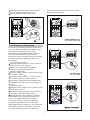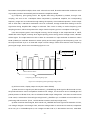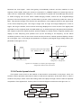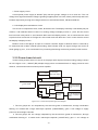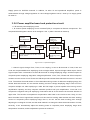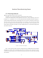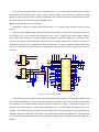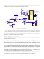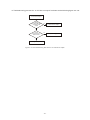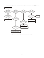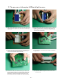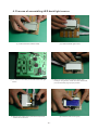
1
AV225T
service manual
Catalog
Chapter One About Maintenance
1.1 Safety precautions
1
1
1.1.1 Power supply
1
1.1.2 Precautions for antistatic
1
1.1.3 About placement position
2
1.2 Maintenance method
2
1.2.1 Visualized method
2
1.2.2 Electric resistance method
2
1.2.4 Current method
2
1.2.5 Cutting method
2
1.2.4Currentmethod
2
1.2.5Cuttingmethod
2
1.2.6 Element substitution method
3
1.2.7 Comparison method
3
1.3 Required device for maintenance
Chapter Two Operation Instructions
2.1 Control button locations and explanations
3
4
4
2.1.1 Front panel illustratlons
5
2.1.2 Rear panel illustration
5
2.1.3 illustrations to the
5
2.2 Basic operations remote control
6
2.2.1 Turn on/off this unit
6
2.2.2 O tp function
6
2.2.3 Select Input Sound Source
7
2.2.4 Bass Enhancer
7
2.2.5 Select Sound Field
8
2.2.6 Adjust Volume
9
2.2.7 Adjust Level
9
2.2.8 EQ function
10
2.2.9 Parameter Processing
11
2.2.10 Adjust Karaoke
12
2.2.11 Tuning Function
13
2.2.12 Other Operations
15
Chapter Three Principle and Servicing
17
Section One Principle of the Player
17
3.1.1 Composition of the player
17
3.1.2 Function and features
17
3.1.3 Player block diagram
18
3.1.4 The player signal flow chart
19
Section Two Unit Circuit Principle
20
3.2.1 Volume board circuit
20
3.2.2 Signal processing board circuit
23
3.2.3 MCU board circuit
25
3.2.4 Control panel circuit
29
3.2.5 Power board circuit
30
3.2.6 Power amplifier board and protection circuit
31
3.2.7 MIC, headphone board
34
3.2.8 Video in/out board circuit
34
Section Three Servicing Cases
36
3.3.1 Servicing instances
36
3.3.2 Troubleshooting process
41
Section Four Servicing Parameters
49
3.4.1 Signal waveform diagram
49
3.4.2 Key point voltage
56
Section Five Function Introduction to IC
57
3.5.1 function introduction to 4558
57
3.5.2 function introduction to Pt2399
58
3.5.3 function introduction to Cd4051
59
3.5.4 function introduction to Cd4052
60
3.5.5 function introduction to Cd4053
61
3.5.6 function introduction to Sm79164
62
3.5.7 function introduction to Pt2308
65
3.5.8 function introduction to Pt2222
66
3.5.9 function introduction to Lm1875
67
3.5.10 function introduction to TDA7265
68
3.5.11 function introduction to M62446
69
3.5.12 function introduction to AT24C02
70
3.5.13 function introduction to L7805
71
3.5.14 function introduction to 7812
72
3.5.15 function introduction to 7912
72
3.5.16 function introduction to LM324
73
3.5.17 function introduction to Pt2315
74
3.5.18 function introduction to 74VHC245
75
3.5.19 function introduction to Cd4094
77
Chapter Four Disassembly and Assembly Process
79
Chapter Cinque PCB board & Circuit diagram
87
Section One PCB board
87
Section Two circuit diagram
96
Chart 6 BOM List
105
6.1 Volume board
105
6.2 Volume board ai segment
105
6.3 Signal disposal board
106
6.4 Signal disposal board ai segment
108
6.5 C pu board
110
6.6 C pu board-smd
111
6.7 A mplifier board
112
6.8 Surface control board
116
6.9 Video input output board
117
6.10 Microphone holder board
117
6.11 Power board
118
6.12 R emote coneroller
120
6.13 P anel units
120
6.14 S ofeware program
121
6.15 S n lasel
121
6.16 Supplement module
121
Chapter One About Maintenance
1.1 Safety precautions
1.1.1 Power supply
When servicing audio power amplifier, the servicing personnel pay special attention to the power
board with 220V AC, or else the improper operation will lead to body damage. The alternate current
which outputs to power amplifier board through power board is also up to voltage with about 50V; when
servicing, short-circuit and joint welding cannot occur, or else the elements will be burnt out and trouble
range will be enlarged.
1.1.2 Precautions for antistatic
Movement and friction will both bring static electricity which causes serious damages to integrated
IC. Though static charge is little, when a limited quantity of electric charge is added to largescaleintegrated IC, as the capacitance is very small in the meantime, now the integrated IC is very much
easy to be struck through by static electricity or the performance will decrease. Thus static electricity
prevention is of extraordinary importance. The following are several measures to prevent static
electricity:
1. Use a piece of electric conduction metal with the length of about 2 metres to insert into the earth,
and Fetch the lead wire from the top of the surplus metal and connect to the required static electricity
device. The length and depth of the metal embedded under the earth should be determined according to
the wettability of the local soil. For humid places, it may be shorter, and longer and deeper for dry places.
If possible, it can be distributed and layed in terms of “#”shape.
2. On operating table-board, the antistatic table cushion should be covered and grounded.
3. All devices and equipments should be placed on the antistatic table cushion and grounded.
4. Maintenance personnel should wear antistatic wrist ring which should be grounded.
5. Places around the operating position should also be covered with electric conduction cushion or
Painted with antistatic paint.
-1-
1.1.3 About placement position
1. Audio power amplifier cannot be installed in places with high temperature and humidity.
2. Positions for placement should be stable and secure.
1.2 Maintenance method
1.2.1 Visualized method
Directly view whether abnormalities of collision, lack of element, joint welding, shedding welding,
rosin joint, copper foil turning up, lead wire disconnection and elements burning up among pins of
elements appear. Check power supply of the machine and then use hands to touch the casing of part of
elements and check whether they are hot to judge the trouble spot. You should pay more attention when
using this method to check in high voltage parts.
1.2.2 Electric resistance method
Set the multimeter in resistance position and test whether the numerical value of resistance of each
point in the circuit has difference from the normal value to judge the trouble spot. But in the circuit the
tested numerical value of resistance is not accurate, and the tested numerical value of integrated IC's
pins can only be used for reference, so the elements should be broken down for test.
1.2.3 Voltage method
Voltage method is relatively convenient, quick and accurate. Set the multimeter in voltage position
and test power supply voltage of the player and voltage of a certain point to judge the trouble spot
according to the tested voltage variation.
1.2.4 Current method
Set the multimeter in current position and test current of the player of a certain point to judge the
trouble spot. But when testing in current method, the multimeter should be series connected in the
circuit, which makes this method too trivial and troublesome, so it is less frequently used in reality.
1.2.5 Cutting method
Cutting method should be combined with electric resistance method and voltage method to use.
This method is mainly used in phenomena of short circuit and current leakage of the circuit. When
cutting the input terminal voltage of a certain level, if voltage of the player rises again, it means that the
trouble lies in this level.
-2-
1.2.6 Element substitution method
When some elements cannot be judged good or bad, substitution method may de adopted directly.
1.2.7 Comparison method
A same good PC board is usually used to test the correct voltage and waveform. Compared these
data with those tested through fault PC board, the cause of troubles may be found.
Through the above maintenance method, theoretical knowledge and maintenance experience, all
difficulties and troubles will be readily solved.
1.3 Required device for maintenance
◆ Audio Generator
◆ Digital oscillograph (≥100MHE)
◆ SMD rework station
◆ Multimeter
◆ Soldering iron
◆ Pointed-month pincers
◆ Cutting nippers
◆ Forceps
◆ Electric screw driver
◆ Terminals connecting cord
◆ Headphone
◆ Microphone
-3-
Chapter Two Operation Instructions
2.1 CONTROL BUTTON LOCATIONS AND EXPLANATIONS
2.1.1 FRONT PANEL ILLUSTRATLONS
1
2
3
4
5
6
7
8
POWER SWITCH
Power on/off this unit
LCD Screen
Buttons operation indication and spectrum
display when working
IR sensor
Receive the infrared signals transmitted from
the remote control
MASTER VOLUMEPress this button to synchronously lower all
6CH volumes
INPUT
Sound source input button
MIC VOLUME+
Press this button to increase the volume of
MIC
MIC VOLUMEPress this button to lower the volume of MIC
TUNING
Select other frequency radio stations upwards
Tuning
Select other frequency radio stations
downwards
10 BAND
Select FM/AM tuner BAND
11 PRESET
Select the latter preset radio station
12 PRESET
Select the previous preset radio station
13 MODE
Select tuner mode:manual/auto
14 MASTER VOLUME+
Press this button to synchronously increase
all 6CH volumes
15 STANDBY
Standby
16 COVER OF PHONE JACK AND
MICROPHONE JACK
9
-4-
2.1.2 REAR PANEL ILLUSTRATION
1
2
3
4
5
6
7
8
9
10
11
AC-3/DTS 5.1CH INPUT
5.1CH audio signals input terminals that
connect to DVD, AC-3/DTS
AM/FM antenna terminal
Connect AM/FM antenna outside
Stereo Audio jack
The terminals that connect with VCD, DVD
stereo audio signals input
Video input
The terminals that connect with VCD,DVD
Video signals input
Video output jack
The terminals that connect with TV Video
signal output
Data
The data plate of this unit
SERIAL NO. Mark
The manufacturing records
CAUTION mark
Remind the user of dangerous voltage inside
Line-out
Subwoofer signals line-out jack
This unit's manufacturer
Terminals
Connect with SPEAKER terminals
12
2.1.3 ILLUSTRATIONS TO THE
REMOTE CONTROL
13
14
STANDBY button: Power on, STANDBY switch button
2 DISPLAY button: Select audio spectrum display modes
3 MUTE button: Mute On/Off button
4 INPUT button: Select input signal sources manually
5 MOVIE button: OTP button to set standard movie
theater surround mode
6 MUSIC button: OTP button to set standard concert mode
7 K.R.OK: OTP button to set standard Karaoke mode
8 HI-FI button: Select the Hi-Fi sound field
9 STANDARD button: Select the standard sound field
10 CYBER LOGIC button: Select the cyber logic sound
field
11 BASS ENHANCER button: Select the bass enhancing
effect
1
15
16
17
18
19
20
21
22
23
-5-
Number buttons 1~8: Select 8 preset working modes
with the help of SAVE/CALL button, capable of storing
and calling the user-set working mode parameters
SPEAKERS button: Adjust the separate channel level
with the help of / keys
CHILD LOCK button: Lock the functions of the front
panel controls
SURR. Button: Select the surround sound field
DEFAULT button: Restore the factory default settings
SAVE button: Store the current working mode
parameters with the help of number buttons 1~8
CALL button: Call the user-stored working mode
parameters with the help of number buttons 1~8
EQ select button: Select the equalization frequency
MULTI-BAND EQ button:Adjust multi-band electronic
equalization
Adjust button: Adjust level and multi-band EQ
EQ button: Circularly call the preset EQ modes
AUTO EQ button: Analyze the current signal spectrum,
automatically set EQ parameters
24
25
26
27
28
29
30
31
32
33
34
35
36
37
38
39
VOLUME button: Adjust the karaoke level with / keys
ECHO button: Adjust the karaoke ECHO with / keys
VOICE MODIFY:
MODIFY button: Select Karaoke voice modify
WF button: Karaoke wide sound field On/Off
TONE button: Adjust the karaoke BASS/Treble tone
levelwith / keys
DELAY button: Adjust the karaoke delay time with /
keys
MASTER VOL button: Synchronously increase/decrease
6 channels' volume
BAND button: Select FM/AM tuner band
The signal automatically, press the INPUT button
on the remote control to select the input signal.
When the unit is in normal working mode,
press the STANDBY button on the front panel or
remote control if you want to enter standby mode.
Please turn off the power when you are not
going to use the unit for a long time.
MODE button: Select tuner mode:manual/auto
STEP button: Select AM tuning step:9K/10K
MEMORY button: Memory the received radio station
with the help of number buttons 0~9
CLEAR button: Clear the preset radio station with the
help of number buttons 0~9
TUNING
: Scan other frequency radio station upwards
TUNING
: Scan other frequency radio station
downwards
PRESET
: Select the latter preset radio station
PRESET
: Select the previous preset radio station
NUMBER 0~9 :Save the received radio station programs
or directly call the preset programs with the help of
MEMORY button
use the unit.
Please turn off the power every time after you
Press the "
POWER" button on the front
panel to power off this unit.
2.2 BASIC OPERATIONS
POWER
2.2.1 TURN ON/OFF THIS UNIT
Please check the connection cords before
turning this unit on. If all connections are correct,
you can connect this unit to power.
Press the POWER button, this unit enters the
standby mode .
When this unit is in the standby mode, it
detects the input signals automatically.
When there is signal input, this unit turns on
automatically.
When the input signal is too small, this unit
might not detect the signal and will not turn on
automatically.
When there is signal input and the unit cannot
turn on automatically, press the STANDBY
button on the front panel or remote control to
operate manually and select input signals by
using the INPUT button.
When the unit is in the standby mode, press
the STANDBY button on the front panel or
remote control to turn on this unit.
Press the STANDBY button on the front panel
or remote control.
After turning on this unit, it detects the input
signal automatically. When there is signal input,
it receives the input signal automatically.
Otherwise, the unit will automatically search
signals all the time.
When there is signal input but it cannot receive
2.2.2 OTP function
We have set the OTP function to simplify the
operation of testing sound effects.If the played
disc is movie or story, you just press the MOVIE
button and the system will automatically set
standard movie mode.If the played disc is music,
you just press the MUSIC button and the system
will automatically set standard music mode.If
you want to sing Karaoke, you just press the
-6-
K.R.OK button after inserting microphone and
The system will automatically set standard
Karaoke mode.
Press the MOVIE button to set standard
theater surround mode.
Automatically detect the input signal source. If
many signal sources input, it will select the
current signal input preferentially.
Automatically set the parameters of surround.
If 5.1CH input signal is detected, it will
automatically adopt standard mode; if 2CH
signal source is detected, it will automatically
adopt Cyber Logic.
Press the MUSIC button to set standard music
modeAutomatically detect the input signalsource.
If many signal sources input, it will select the
current signal preferentially.
Automatically set the parameters when
enjoying music. If 5.1CH input signal is detected,
it will automatically adopt standard mode;if 2CH
signal source is detected, it will automatically
adopt Hi-Fi mode.
Press the K.R.OK button to set standard
Karaoke mode.
Automatically detect the input signal source. If
many signal sources input, it will select the
current signal preferentially.
Automatically set the parameters of Karaoke
mode.
NOTE: If the signal is too weak or in the blank
segment of music
when operating, the system will probably appear
wrong indications.
2.2.3 Select Input Sound Source
This unit utilizes two input lines of stereo audio
sources: VCD, DVD; one line 5.1 channel signal
input. Select the input signal source manually
through the remote control.
Press the INPUT button on the remote control,
and "INPUT TUNER" splays, which means
TUNER has been selected.
Press the INPUT button on the remote control,
and "INPUT VCD" displays, which means VCD
2CH input jack has been selected.
Press the INPUT button on the remote control,
and "INPUT DVD" displays, which means DVD
2CH input jack has been selected.
Press the INPUT button on the remote control,
and "INPUT 5.1CH" displays, which means
5.1CH input jack has been selected.
2.2.4 Bass Enhancer
In order to strengthen the low frequency of music,
you may start up Bass Enhancer function.
Press the "BASS ENHANCER" button on the
front panel or remote control, "BASS driver 0",
“BASS driver 1 ", "BASS driver 2 " or”BASSdriver
3" will display.
-7-
Press the STANDARD button on the remote
control and "STANDARD" will display, which
means the system enters standard sound field.
The display "BASS driver 1-3" means the first,
second and third Bass Enhancer; the subwoofer
signal adds into the master channelsignal; turn
off the subwoofer line output.
The display "BASS driver 0 " means turn off
Bass Enhancer; normal subwoofer line output.
Bass Enhancer function cannot be started up
in Hi-Fi mode.
3 Cyber Logic
In order to make 2 channel input signals have
multi-channel sound field effect, you may select
Cyber Logic sound field.
Press the CYBER LOGIC button on the remote
control and "CYBER LOGIC" will display, which
means the system enters Cyber Logic sound
field: if "INVALID" displays, it means the system
cannot enter Cyber Logic
Cyber Logic mode is invalid in 5.1 channel
signal input.
2.2.5 Select Sound Field
1 HI-FI
In 2CH signal input, you may select the Hi-Fi
mode to keep the originally musical features.
Press the HI-FI button on the remote control
and "HI-FI" will displays, which means the
system enters the Hi-Fi mode; if "NVALID"
displays, it means the system cannot enter the
Hi-Fi mode.
Bass Enhancer function and operations
related to EQ are invalid in Hi-Fi mode.
Pressing the HI-FI button is invalid in
5.1channel input.
4 Surround
In order to cater for different listening
Environments and meet different sound effect
requirements of customers, you may select
different surround modes in 5.1 channel signal
input status.
Press the SURR button on the remote control
in 5.1 channel signal source input, the surround
will display.
Press the SURR button on the remote control
Repeatedly; you may select the environment
2 Standard
In order to keep the correspondence with input
signals and adjust output timbre according to
personal habit, you may select the standard
sound field.
-8-
Modes between Affectional movie, Sowordsmen
movie, Gunfignt movie, Sci-fi movie and music.
The environment surround is invalid in 2channel signal input status.
The environment surround is invalid if
microphone is inserted.
2.2.7 Adjust Level
1
Left channel level
When sound of left and right channels is
imbalance, you may adjust R channel level to
make it in balance with L channel.
Press the SPEAKERS button on the remote
control and "L: 00" will display. Operate as
follows:
Press the " " button on the remote control to
Increase the volume of L channel. The max level
is +60.Press the “ " button on the remote
control to decrease the volume of L channel. The
min level is -60.
2 Right channel level
When sound of left and right channels is
imbalance, you may adjust L channel level to
make it in balance with R channel.
Press the SPEAKERS button on the remote
control and "L: 00" will display. Operate as
follows:
Press the " " button on the remote control to
Increase the volume of L channel. The max level
is +60.Press the “ " button on the remote
control to decrease the volume of L channel. The
min level is -60.
3 Center level
When sound of left and right channels is
imbalance, you may adjust R channel level to
make it in balance with L channel.
Press the SPEAKERS button on the remote
control and "R: 00" will display. Operate as
follows:
Press the “ " button on the remote control to
increase the volume of R channel. The max level
is +60.Press the “ " button on the remote
control to decrease the volume of R channel.
The min level is -60.
4 Surround Left level
When sound of center channel is unsuitable,
you may adjust center level to make it suitable to
the sound field.
Press the SPEAKERS button on the remote
control and "C: 00" will display. Operate as
follows:
Press the “ " button on the remote control to
increase the volume of C channel. The max level
is +60.Press the “ " button on the remote
control to decrease the volume of C channel.
The min level is -60.
NOTE: The center level cannot be adjusted only
when left and right channels have output.
5 Surround Right level
When sound of surround left is unsuitable, you
2.2.6 Adjust Volume
1 Master Volume
When the current sound is too high, too low or
unsuitable, you may press the MASTER VOL on
the front panel or remote control to adjust the
volume of all channels.
Press the "+" button of master volume on the
front panel or remote control to increase all
channels' volume simultaneously; the max
volume is 60.
Press the "-" button of master volume on the
front panel or remote control to decrease all
channels' volume simultaneously; the min
volume is 0.
The master volume displays as the example:
"VOL: 20”
-9-
Press the " " button on the remote control to
increase the volume of subwoofer. The max level
is +60.
Press the " " button on the remote control to
decrease the volume of subwoofer. The min level
is -60.
NOTE: The subwoofer level cannot be adjusted
only in Hi-Fi and Bass Enhancer conditions.
may adjust surround left level to make it suitable
to the sound field.
Press the SPEAKERS button on the remote
control and "SL: 00" will display. Operate as
follows:
Press the " " button on the remote control to
increase the volume of surround left. The max
level is +60.Press the " " button on the remote
control to decrease the volume of surround left.
The min level is -60.
NOTE: The surround left level cannot
beadjusted only when left and right channels
have output.
When sound of surround right is unsuitable,
you may adjust surround right level to make it
suitable to the sound field.
Press the SPEAKERS button on the remote
control and "SR: 00" will display. Operate as
follows:
Press the " " button on the remote control to
increase the volume of surround right. The max
level is +60.Press the " " button on the remote
control to decrease the volume of surround right.
The min level is -60.
NOTE: The surround right level cannot be
adjusted only when left and right channels have
output.
6
2.2.8 EQ function
Due to the personal like to music, you may adjust
EQ to meet your own needs. If the music tempo
is not enough or full, adjust bass; if the voice is
unclear, adjust middle frequency; if the
musical details are not rich, adjust treble.
1 Pre-set EQ
When the sound of master volume is too weak
or unclear, you may directly use pre-set EQ
mode to make it accordant with the current music.
This unit utilizes 8 EQ modes: Rock, Jazz,
Classical, Pop, Disco, Rap and Blues.
Press the EQ button on the remote control to
display the EQ curve.
Press the EQ button repeatedly to select the
EQ mode accordant with the current music.
EQ mode cannot be adjusted in Hi-Fi mode.
2 Multi-band EQ
When the sound of master volume is too weak
or unclear, you may set EQ mode yourself to
meet you own taste.
Press the "AUTO EQ" button on the remote
control to display the current EQ curve. There is
a cursor flashing in the current frequency.
Press the " " button on the remote control to
select the high
frequency. The flashing cursor moves rightwards
until the rightmost.
Press the " " button on the remote control to
select the low frequency. The flashing cursor
moves leftwards until the leftmost.
Press the " " button on the remote control and
the current frequency level increases until the
maximum.
Press the " " button on the remote control and
the current frequency level decreases until the
minimum.
EQ mode cannot be adjusted in Hi-Fi mode.
3 Auto EQ
When the sound of master volume is
unsuitable to you listening, you may select auto
EQ.
The unit will automatically analyze the current
spectrum to set the current EQ according to the
current music.
Subwoofer level
When sound of subwoofer is unsuitable, you
may adjust the volume of subwoofer speaker
and the level of subwoofer channel to make it
balanced to the sound field.
Press the SPEAKERS button on the remote
control and "SW: 00" will display. Operate as
follows:
- 10 -
Press the AUTO EQ button on the remote
control
to display the analyzing curve.
EQ function
Auto EQ setup is invalid in Hi-Fi mode.
channel level is too high or too low, the system
will adjust automatically
2.2.9 Parameter Processing
To memory the current parameter for later use,
or use the defauly parameter, the Memory and
Call functions will be used. The current
parameters to be adjusted include: Channel
Level, EQ, Bass Enhancer, Sound Field,
Environment Surround, MIC Volume, MIC Treble,
MIC Bass, MIC Delay, MIC Echo and Voice
Modification.
1 Call Default parameter
Press the number buttons 1-8 on the remote
control and "CALL 1-8" displays.
Setup will be processed automatically
according to the default parameters.
2 Memory Parameters
Press the "SAVE" button on the remote control
first to display "SAVE "
Press the number buttons 1-8 on the remote
control again under the display "SAVE "
The current parameter is memorized into the
corresponding number buttons and "SAVE 1-8"
displays.
3 Call parameters
Press the "CALL" button on the remote control
first to display "CALL "
Press the number buttons 1-8 on the remote
control again under the display "CALL "
The parameters memorized in the number
buttons before will be adopted currently and
"CALL 1-8" displays.NOTE: Due to some
unexpected reasons, the user-memorized
parameters will probably be lost, so please
adjust again and then memorize. The system will
automatically check the parameter saved ast
time when switching on this unit. When the
- 11 -
2.2.10 Adjust Karaoke
1 Microphone Volume
When inserting microphones to sing Karaoke,
press the MIC VOL button to adjust the volume
of microphonewhen the microphone voice is too
high, too low or unsuitable.
Press the " " button of MIC VOL on the front
panel to increase the volume of microphone
The maximum volume is 30.
Press the " " button of MIC VOL on the front
panel to decrease the volume of microphone
The minimum volume is 0.
Press the "VOLUME" on remote control,then
press " "" " to adjust karaoke volume.
The microphone volume displays as "MIC VOL
20".
The microphone volume cannot be adjusted
when not inserting microphones.
2 Bass
When inserting microphone to sing Karaoke, you
may adjust microphone bass when the sound
tempo is not full or rich.
Press the "TONE" button on the remote control
once then press" " or " " to adjust the bass of
microphone. The adjustable range is 6.
The microphone bass displays as "MIC BASS
+2”
The microphone bass cannot be adjusted
when not inserting microphone.
3 Treble
When inserting microphone to sing Karaoke, you
may adjust microphone treble when the sound is
unclear.
Press the "TONE" button on the remote
control twice, then press " " or "
" to adjust
the treble of microphone. The adjustable range
is 6
The microphone treble displays as "MIC
TREBL+2”
The microphone treble cannot be adjusted
when not inserting microphone.
4 Echo
When inserting microphone to sing Karaoke, you
may adjust microphone echo when the sound is
weak or not full.
Press the "ECHO" button on the remote
control then press " " or" " to adjust the echo of
microphone. The adjustable range is 0~7.
The microphone echo displays as "MIC ECHO
2”
The microphone echo cannot be adjusted
when not inserting microphone.
- 12 -
5 Delay
When inserting microphone to sing Karaoke, you
may adjust microphone delay when the sound is
not full.
Press the "DELAY" button on the remote
control then press " " of " " to adjust the delay
of microphone. The adjustable range is 0~7..
The microphone delay displays as "MIC
DELAY 2”
The microphone delay cannot be adjusted
when not inserting microphone.
7 Wide Field
When inserting microphone to sing Karaoke, you
may select to switch on/off Karaoke wide field
when the sound field is not wide.
Press the "WF" button on the remote control to
display "MIC WIDE ON", which means Karaoke
Wide Sound Field is switched on.
Press the "WF" button on the remote control
again to display "MIC WIDE OFF", which means
Karaoke Wide Sound Field is switched off.
The karaoke WF button cannot be selected
when not inserting microphone.
NOTE: If noise appears when adjusting Karaoke,
please refer to TROUBLESHOOTING for details.
6 Modify
When inserting microphone to sing Karaoke, you
may select microphone euphonize mode when
the sound is unsuitable.
Pressing the "MODIFY" button on the remote
control
can circularly select the euphonized
¡ï
voice"NATURAL", "Full", "Fruity", "Bright" and
"Ringing".
The MODIFY button cannot be selected when
not inserting microphone.
2.2.11 Tuning Function
Auto Tuning One:
1 Press INPUT button on the front panel or
remote control to select TUNER as the input
sound source.
2 Press BAND button on the front panel or
remote control to select receiving wave band.
7 Wide Field
When inserting microphone to sing Karaoke, you
may select to switch on/off Karaoke wide field when
the sound field is not wide.
- 13 -
NOTE: 1. This operation will search and save
automatically, so the user-preset programs will
be covered.
2. Pressing TUNING / button may
stop the function in the course of this operation.
If the tuning searching stops in imperfect radio
station (because of weak radio station signals or
radio wave interferes), please change into
manual tuning method.
Clear Radio Station
If you do not need the preset radio station, you
may clear it by using CLEAR button on the
remote control with the help of number buttons
0~9.
1 Press CLEAR button on the remote control.
2 Press the serial number of the radio station
that you want to clear in the course of the
screen's displaying”CLEAR " to finish this
operation.
3 Press TUNING / button on the front panel
or remote control for above 5 seconds to
automatically tune upwards/downwards until
your needed radio station programs. When
programs are searched, it will stop searching
automatically.
3¡¢
If the tuning searching stops in imperfect radio
station or radio wave interferes, please continue
operating.
If the tuning searching stops in imperfect radio
station (because of weak radio station signals),
please change into manual tuning method.
4 The following save and call operations are
the same with manual tuning operations.
Auto Tuning Two:
1 Firstly select TUNER as the current input
sound source according to the operations oF
"Manual Tuning", and then select the wave band
to be received.
2 Press MEMORY button on the front panel or
remote control, and then press TUNING /
button for above 0.5 seconds during the course
of displaying MEMORY to enter the radio station
auto searching status.
NOTE: 1. This operation is beyond retrieve, so
please take care to operate.
2. If you clear the radio station
incautiously, you may save again according to
the select operation.
The Explanation of MODE button
This unit has two working modes in the receiving
status: AUTO/MANUAL
1 In AUTO working mode, if you select FM
wave band, this unit will automatically recognize
the radio station program is mono signal or
stereo signal and keep the mono or stereo
receiving status.
2 If the received radio station program has
louder noise or cacophony in stereo status, you
may switch to MANUAL working mode.In this
way, the unit is in mono receiving status to
decrease noise and cacophony generally.
You may switch the two working modes through
MODE button on the remote control.
- 14 -
NOTE: 1. AM round antenna should be placed far
away from the equipment. You may put up on the
wall or on the bookshelf.
2. AM round antenna and outdoor antenna can
be used at the same time.
Connect to FM Antenna
Connect to the indoor FM antenna
Connect the accessional indoor FM antenna to
75 UNBAL.FM ANT terminal.
Antenna Connection
You may use our accessional AM and FM indoor
antenna when in bad receiving effect. Generally
speaking, these antennae can supply enough
signal strength.
Connect to AM Round Antenna
1 Push the jack button to open it.Push the jack
button to open it.
2 Connect the AM round antenna cord to AM
ANT and GND terminals.
3 Let go of the button to clamp the speaker
cord. Pull the cord lightly to check the connection
is right or not.
NOTE:Do not use the outdoor and indoor FM
antennae at the same time.
How to Connect
GND (Grounding) terminal
Push the jack button to open it.
In order to ensure the safety and decrease the interference,
please well connect the GND terminal. The better grounding
method is insert the metal pole into wet ground.
Insert the speaker cord.
Let go off the button to clamp
thespeaker cord.
4
2.2.12 Other Operations
Connect the AM round antenna to the stand.
1 Mute
Mute the sound to make your conversation or
answering telephone not be affected by music.
Press the MUTE button on the remote control
to mute the sound and the display "MUTE"
flickers.
AM round antenna
5 Adjust the direction of AM round antenna
to get the best receiving effect.
Rotate
Mute
- 15 -
The DISPLAY button cannot be selected when
no signals input.
2 Child Lock
To prevent the children wrongly pressing the
front panel buttons, you may lock the buttons on
Other Operations
the front panel.
Press the CHILD LOCK button on the remote
control to display "LOCK". The buttons on the
front panel are invalid and now "LOCKED"
displays.
Press the CHILD LOCK button on the remote
control again to display"UNLOCK" and the fronta
pnel buttons can be normally used.
4 Default
When the system parameters adjusted disorderly,
you may restore the default settings.
Press the DEFAULT button on the remote
control to display "DEFAULT".
The unit automatically sets the default
parameters.
3 Display
To make the display spectrum colorful, we have
set many kinds of spectrum display means. You
may press the DISPLAY button to select.
After switching on the unit, it will automatically
select a kind of spectrum display mode every
third moment or so.
Pressing the DISPLAY button on the remote
control can cancel auto switch and select your
favorite display mode.
Pressing the DISPLAY button on the remote
control repeatedly can select many kinds of
spectrum display effects until auto switch.
Default
- 16 -
Chapter Three Principle and Servicing
Section One Principle of the Player
AV225T (RU) is an advanced power amplifier with complete functions. Based on the former power
amplifiers, it adopts LCD screen, with sky blue background matched with 16 different kinds of spectrum
display styles, in addition, this player is with tuning function and it is an excellent selection for users who
love listening to radio.
3.1.1 Composition of the player
1. Volume board: select input signal source, Cyber Logic and bass enhancer control.
2. Signal processing board: Karaoke signal processing and 5.1CH signal amplifying.
3. MCU board: player control, frequency point gating, and auto search circuit.
4. Control panel: LCD display, remote keyboard and background light display.
5. Power board: supply the working voltage required by each unit circuit and perform player
protection function.
6. Power amplifier board: perform power amplifying to 5.1CH analog signal.
7. Digital tuner: receive radio signal and then send to power amplifier for signal processing.
8. MIC, headphone board: MIC signal input, headphone amplifying output circuit.
9. Video input and output board: fulfil the switch of VCD, DVD channel.
3.1.2 Function and features
◆ Built-in 5CH power amplifying, applicable to AC-3/DTS and stereo music replay. Main channel
80W, central/surround 15W with strong power.
◆ AC-3/DTS, VCD, DVD input jack and subwoofer output jack.
◆ 6CH volume control and separate level control, with 7-band electronic equalization.
◆ Bass enhancer system, Cyber logic function and Hi-Fi playback function.
◆ Q-play function of movie, music and Karaoke.
◆ Multiple EQ modes, applicable to different music styles.
◆ Auto spectrum analysis compensation function performs compensation to signals automatically.
◆ Complete Karaoke function, including separate MIC volume control, high/low tone adjustment,
voice compensation, delay and echo adjustment, Karaoke wide sound field function.
- 17 -
220V
XP7
SWM
Signal output
XS1
XL100
XP13
RLY0
XS7
P_RC
OVER
XP8
Power board
XS8
XS2
XS3
XS13
RLY
P_RC
P_LRM
P_CSM
L2
R2
C2
SL2
SR2
VC+
GND
GND
VC-
Video board
XS101
Tuner socket
XP101
XP9
XS9
Volume board
SWM
L1
R1
XS20
XS22
XP20
XP22
C1
SL1
SR1
XS4
Xp101
Transformer
elementary
Sublevel coil
D+5V
DGND
L1
R1
SWITCH
CPU board
XP100
XS25
XP23
XS23
Sublevel coil
+12V
GND
GND
-12V
XS6
XS102
XS103
XP102
XP103
+12V
GND
-12V
Transformer
XP25
MIC holder
board
Control panel
XP12
XS12
LR
C/SL/SR
Signal board
L
R
AGND
VS+ GND VS-
C
Power
SL
SR
Load
test
MIC
VSTNDANCK
OK-R
SR/SL
Clipping
OK-L
+12V
AGND
-12V
-VS
Detect
EEPROM
24C02
Sampling
+6.8V
AGND
-6.8V
AGND
-6.8V
+5V
Control panel
channel
switch
Dual-limit
compare
Power
±6.8V
Bandpass
filtering
Amplifying
+12V
AGND
-12V
+6.8V
Power
±6.8V
+5V
P_DO-P_D7
intermit
P_SELECT
P_SEARCH
Reset
circuit
CPU board
P_CHARGE
RST/RS/RW/PE
CPU
LCD display
PT2222 remote control
buttons array
P REM
Remote control
receiving
Relay
MIC direct connection
C
Clipping
Protection circuit
DIST
Mixed Mixed
Delay
adjustment
OKL/OKR
Reverse
Detect
Amplifying
Echo
adjustment
Mixed Mixed Mixed
SW
Electronic
echo
Low frequency
boost
MIC
OK
volume
tone
Mixed
L/R
Switch in bass
enhancer and line output
DVD all-in-one input
L
R
C
SL
SR
Relay
drive
SW mute and relay state detect
VC+
AGND
VC-
Main power
amplifier power
Power board
- 19 -
A
B
Video in/out board
L/R/C
-12V
+12V
CD4051
Preposition power
6
Figure 3.1.4.1 The player signal flow chart
MIC, headphone
board
SL/SR
C/SL/SR
S-C C/SL/SR/SW
Mix
MIC input
C
SW-OUT
Program
amplifying
The player signal flow chart is shown as the following figure 3.1.4.1:
5.1CH(SW)
DLSPLY
MIC
DVD
Power amplifying
Mix SW
Headphone
amplifier
L/R
1
2
3
4
5
Mute
5.1CH(C/SL/SR)
5.1CH(SW)
C/SL/SR
S-C
D-SW
5.1CH(C/SL/SR)
Preposition
amplifying
3.1.4 The player signal flow chart
S-C/S-SL/S-SR
Channel selection
Volume board
Cyber logic
L/R
LR_T
L/R
Follow buffering
5.1CH(L/R)
Power amplifier board
VCD
Electronic volume
DVD(L/R)
5.1CH
VCD(L/R)
A
B
5.1CH
LR_T
V-OUT
A
B
Input selection
TUNER(L/R)
Section Two Unit Circuit Principle
3.2.1 Volume board circuit
AV225T (RU) has 4 kinds of input means in all: tuning input, VCD, DVD stereo input and 5.1CH
input. The Cyber logic function of AV225T (RU) is to achieve C, SR, SL and SW signal through buffer and
processing of adder and subtracter after sampling from L, R channels. In this circuit, electronic
simulation switch is adopted to fulfil the switch in all kinds of state. Signal flow is shown as the following
figure 3.2.1.1:
Tuner
VCD
DVD
5 1CH
L
N101
CD4052
R
Electronic
switch
N104A
OUT
N104B
N106
N107B
SL
M62446
SR N105B
N10 5A
SWIN
S -C
C
S SR
SR
S SL
N107A
CD
4053
Electronic
switch
N102
SL
S-C
SW
N108B
CD
4053
DISPLY
Electronic
switch
N103
Figure 3.2.1.1 Volume board signal flow chart
- 20 -
1. Input selection and sound field processing mode
The input selection of AV225T (RU) is fulfilled through electronic switch CD4052 and CD4053, and
the truth value table is shown as follows:
CD4052 Truth value table
Mode
CD4053 truth value table
Tuner
VCD
DVD
5.1
A
X
B
Y
C
Z
A
0
1
0
1
0
X0
0
Y0
0
20
B
0
0
1
1
1
X1
1
Y1
1
Z1
Pin
(1) 5.1CH input state: now A, B, 5.1CH of M62446 are in high level, L and R channel signals of
5.1CH input terminal are outputted from pin 3, 13 of N101 respectively and then sent to IC N106 for
volume and tone adjustment; meanwhile C, SR, SL signals of 5.1CH input terminal are outputted from
pin 14, 15, 4 of N102 and then sent to IC N106 for separate volume adjustment; in addition, SW signal of
5.1CH is outputted through pin 4 of N103, amplified by N107A and then sent to M62446.
(2) 3 kinds of analog input modes: AV225T (RU) has 3 kinds of analog input modes: tuning signal,
VCD and DVD are controlled through signals A, B separately. Please refer to CD53 truth value table for
reference.
(3) AV225T (RU) has 3 kinds of sound field modes in all: standard, Cyber logic and Hi-Fi.
A. Standard: under the control of the player MCU, when bass enhancer is off, left channel, right
channel and subwoofer have output; when bass enhancer is on, only left and right channels have output.
B. Hi-Fi: under the control of MCU, only left and right channels of M62446 have output; when bass
enhancer is off, volume adjustment is off.
C. Cyber logic: pin 9, 10 of electronic switch N101 (CD4052) select a group of analog left and right
channel input signals according to the truth value table, the left and right channel signals are outputted
from pin 3, 13 through the electronic switch inside N101 and divided into 2 ways: one way is sent to pin
13, 15 of M62446 for electronic volume and tone adjustment, and the other way gets SW, S-SR, S-SL
and S-C signals though buffer and adder and subtracter, in which S-C, S-SR and S-SL signals are sent
to pin 12, 2, 5 of N102, under the control of 5.1CH signal, N102 selects Cyber logic signal input (see
Cd4053 truth value table) from Cyber logic and 5.1CH signal, central, right surround and left surround
signals are outputted from pin 14, 15 and 4 respectively and then sent to pin 11, 8 and 9 of M62446 for
volume adjustment. Another SW signal is outputted from N107A and then sent to pin 6 of M62446.
5.1CH signal sen t to M62446 outputs from pin 31, 36 after volume adjustment, and then is outputted by
XS20 flat cable holder to signal board.
(4) The relationship between the switch in all kinds of sound sources and sound handling mode in
input circuit is show as the following figure 3.2.1.2:
- 21 -
Hi-Fi mode
2 kinds of analog
input modes
Press INPUT
button to select
circularly
Standard mode
Cyber logic mode
5.1CH input mode
Only L/R channel has output,
sound field and EQ setup is
invalid
Only L, R and SW channel
has output, capable of
performing sound field and
EQ setup
6CH output, capable of
performing cinema sound
field and EQ setup
6CH output, capable of performing cinema sound field and EQ setup
Figure 3.2.1.2 Illustration between input circuit
2. Control circuit
The latched, data and clock signals outputted by MCU (N100) pin are sent to pin 39, 40, 41 of
M62446, pin 1, 2, 3, 4 of M62446 output control level to select the input signal and spectrum sampling
signal. Other functions, such as volume and tone adjustment, are also controlled by the three control
signals. The display of display screen is controlled by CPU directly.
3. Spectrum sampling circuit
The spectrum sampling in AV225T (RU) is sent from pin 13 of N103 to N108B for amplification, and
then sent to spectrum gating circuit. 5.1CH of M62446 selects sampling signal. When selecting Cyber
Logic, 5.1CH control signal is low level, now pin 9, 11 of N103 is low level, and it is known from the truth
value table that the output is X0 and Z0 and this two sampling signals are grounded. It is known from
Cyber logic principle, centre, surround and subwoofer channels are all produced by left and right
channel signals, but in S-C signal, complete left and right channel signals are included, so it is ok to
sample from S-C only. Therefore, S-C signal is outputted through R195 (pin 13 of N103) to N108B and
added with OK-R signal for the amplification of spectrum sampling signal, and then sent through XS20
to frequency point gating and auto search circuit; the same, when selecting 5.1CH input, 5.1CH control
signal is high level, pin 14, 15, 4 of N102 select pin 14, 4 of X1, Y1, Z1 of N103 and connect to X1, Z1,
thus, the 6-channel signals are outputted through pin 13 of N103 to N108B and added with OK-R signal
for the amplification of spectrum sampling signal, and then sent to frequency point gating and auto
search circuit through XS20.
4. Tuning function
This player has tuning function, which provides a good selection for users. It directly controls digital
tuner through MCU to receive audio signal, and then output after amplification by power amplifier. The
clock and data line of digital tuner is commonly used together with M62446, the other two control lines
are directly connected to MCU, L, R signals after being handled by digital tuner are directly sent to pin 1
and 12 of N101 CD4052 for gating input.
- 22 -
3.2.2 Signal processing board circuit
The signal board performs mixed amplification to 5.1CH signal sent from volume board, voice signal
sent from microphone, headphone board and Karaoke echo signal.
1. AV225T (RU) Karaoke circuit
(1) Function: this circuit is to reset by loudspeaker after handling voice and being amplified by
power amplifier. It includes voice beautification circuit, wide sound field processing circuit and Karaoke’s
echo and delay adjustment circuit.
(2) Function of IC of Karaoke circuit is shown as the following table:
IC SN
IC name
IC function
IC SN
IC name
IC function
N201
4558
Operational amplifier performs
preamplification to voice signals
N207
CD4051
Karaoke delay adjustment
N200
PT2315
Karaoke volume adjustment,
including tone adjustment
N208
CD4051
Karaoke echo adjustment
N205
CD4053
Electric switch
N204
4558
Inverter
N209
PT2399
Karaoke echo settlement
(3) Karaoke signal flow chart
MIC
N200
N20A1
N202B
N203B
N202A
N209
N204
N207
Directly connected
V200
N205
N100
N211
N100
OK
Mixed
output
N208
P_OKT
Figure 3.2.2.1 Karaoke signal flow chart
Shown as in the figure 3.2.2.1, when microphone is inserted, MIC signal is sent to N201A
operational amplifying circuit for amplification. One path of MIC signal after being amplified gives MCU a
microphone input identification signal P_OKT through VD201 rectification filtering control triode V200
after being amplified by N202A; when there is signal input, P_OKT is low level, MCU makes N210
CD4094 send out KM low level signal to make triode V103, V105, V104 ccutoff and then to make MIC
signal can output; the other path is coupled by C219 to pin 6 of PT2315, and then output from pin 16
after internal volume adjustment to N202B and N203B for amplification. The signal after being amplified
of N203B is divided into two paths, one path outputs directly, and the other path is coupled byR222,
C247 to PT2399 inside for delay and echo adjustment and then outputs from pin 14, and then mix output
- 23 -
Together with direct connection OK signal through N204B, while OK-R is outputted from pin 14 after
being gated by N205 and then overlapped to left and right channels.
In this circuit, the low frequency exalt network composed by triode V201 connected to the reverse
end of N202B is mainly to exalt 75HZ low frequency signal.
When performing delay adjustment to PT2399, firstly give control signal to MCU, and MCU controls
N207 after being extended by N211 IC CD4094, then selects different resistance value to connect into
pin 6 of PT2399 to reach the purpose of delay adjustment.
Similarly, through changing the resistance value in R229 to change the echo level overlapped to
direct connection signal, the echo adjustment is realized.
The wide sound field control signal of Karaoke is sent by N211 to pin 11 of N205, when it is high
level, pin 14 of N205 is connected to X1, now the phase of OK-R signal is reverse from that of OK-L,
sound field is widened and Karaoke is in wide sound filed state. On the contrary, the phase of OK-R
signal is the same with that of OK-L, Karaoke is in the narrow sound field state.
In addition, microphone plug has a detect signal P_MICDET, and it composes the detection to
microphone inserting together with the circuit composed of V202. When microphone is not inserted, it is
low level, V202 cutoff; when microphone is inserted, it is high level, V202 is on, now turn off scene
surround mode and forbid tuning.
Otherwise, there is OK auto mute function. When P-KT cannot detect any signal in a continuous
period, MCU will send out a control signal to make KM be high level, triode V103, V105, V104 is on to
mute OK signal to advance SNR of the player and better listening effect.
(4) Scene mode signal flow
AV225T (RU) has a special function, that is, it may realize switch in 5 kinds of scene mode when there
is no Karaoke, which is fulfilled by Karaoke part. Signal flow chart is shown as in the figure 3.2.2.2:
R-1
L -1
C-1
N203B
N205
N209
N204B
N207
Mixed output
N208
Figure 3.2.2.2 Scene mode signal flow chart
When pin 9 and 10 of N205 is in high level, the sampled L, R, C signals are outputted by pin 3
through N205 gating, after being amplified by N203B, one path is sent to PT2399 inside for echo and
delay adjustment (controlled by IC CD4094), the effect after adjustment is overlapped to L, R, C channel
- 24 -
To form various scene modes. Seen from this, its principle is the same with that of Karaoke. In scene
mode, it functions only when microphone is not inserted and in 5.1CH mode at the same time.
2. Bass enhancer circuit
BURST sent out by N210 is bass enhancer on/off signal. When it is high level, it is added to base
electrode of V102, V102 is on, base electrode outputs low level, V107, V100 are cutoff, SW signal
outputs to external terminal normally, at the same time, BURST high level signal is added to emitting
electrode of V108, V108 is on, collector electrode output high level is added to the base electrode of
V101, V101 is on to make SW signal grounding and it will not be overlapped to left and right channel
signals.
Reversely, when BURST is low level, V100 is on, SWM signal cannot output from external terminal,
at the same time V101 is cutoff, SW signal is overlapped to left and right channel signal.
Bass enhancer of AV225T (RU) is divided into 3 levels, the principle is to change the high/low of
bass enhancer level through changing SW output volume of M62446.
Meanwhile, SWM signal is added to relay through XS9, when relay is disconnected, SWM signal is
grounded to make subwoofer terminal have no output to avoid the concussion to speakers at the
moment of power-on.
3. 5.1 signal and Karaoke signal mixed amplification circuit
Left and right channel signals of 5.1 signal, after being mixed with SW signal and being amplified by
N101B, N100B, are sent to the reverse end of N101A, N100A, at the same time, OK-R, OK-L signals are
respectively added to the reverse end of N101A, N100A and then output from pin 1 of N100A, N101A to
power amplifying circuit for amplification after the mixed amplification of N100A, N101A.
Meanwhile, the centre C-1 signal sent from volume board is added to the pin 6 reverse end of
N102B, and then added to the reverse end of N102A after amplification. Now the C1-1 signal after
processed by echo (scene surround mode) is also required to add to the reverse end of N102A and
mixed amplifying with it, then sent to centre channel power amplification circuit.
Surround SR-1, SL-1 signal of the other path volume board is directly sent to surround channel
power amplification circuit.
One path of 5.1 signal after mixed amplification is sent to power amplification circuit through XS9,
the other path forms DIST signal (distortion detect signal) to MCU board through R111, R112, R142,
R145, VD100-VD104 to perform auto gain adjustment to control the volume output.
3.2.3 MCU board circuit
MCU board is composed of player control circuit, auto search input signal and spectrum analysis
circuit.
- 25 -
1. The player MCU control
N100 is the control centre of the player, various control instruction are outputted by it to each
controlled circuit to fulfil each control function. +5V power supply is adopted, and pin 40 is its power
supply pin. Pin 18, 19 externally connects with 12M crystal oscillator to provide itself with working clock
frequency. Pin 9 is its reset pin, when power on, +5V charges C106 through R100. The voltage on the
two ends of capacitor cannot change suddenly, so B-pole of triode V100 is low level, that is, V100 is not
on, a high level reset signal is given to MCU. When capacitor C106 charging finishes, V100 is on, now
reset finishes. Form of this kind of reset circuit is high level reset, and low level is kept.
When the player is working, information of power-on picture and Chinese characters when
operating displayed on display screen are all saved in the static memorizer inside MCU. N101 is a state
memorizer and it can save the working state of the player at the time of power-off and then call these
states until power-on next time to avoid the adjustment of users again. All kinds of user-set sound field
modes are also saved in it and can be called when necessary.
2. Input signal detecting, search circuit automatically
DISPLAY signal from volume board is sent to N103A for amplification, after being coupled by
capacitor C110, sent to the reverse end of voltage comparator N103B, outputted from pin 7 of N103B,
then sent to pin 16 of the player MCU through VD103, V101, R109, R107. When N103B outputs a high
level, Vd103 is in reverse cutoff state, B-electrode of switch pipe V101 is high level, now switch pipe
V101 is in on state, and then a +5V P_SEARCH high level is achieved through VD101 voltage regulating
to MCU, which means there is no signal input, and the search continues. When output terminal of N103B
outputs a low level, VD103 is in positive direction on state, B-electrode of switch pipe V101 is low level,
now switch pipe is in curoff state, MCU detects that P_SEARCH is low level, which means there is signal
input, at the same time, the search stops. The working principle is as follows:
(1) After power-on, under the control of MCU internal program, data signal is outputted to M62446,
then M62446 sends out high/low level to perform scanning to N101, N102, N103 each input port of
volume board, at the same time, P_SELECT is high level, V102 is on, now the in-phase end voltage of
comparator N103B is about 0.1V. When these input ports have no signal output, voltage of pin 6 of
N103B is less than 0.1V, pin 7 outputs
12V, Vd103 is in reverse cutoff state. It is known from the above
analysis, P_SEARCH is high level, which means there is no signal input. After all ports being searched
once, it enters standby state automatically; when a certain port has signal input, this signal is compared
with pin 5 of N103B through N108B of volume board and MCU board N103A amplification, if voltage of
pin 6 of N103B is more than 0.1V, pin 7 outputs -12V, Vd103 is in positive direction on state, now,
P_SEARCH is low level, which means there is signal input, through controlling IC M62446, MCU locks
this port that has signal input to enter normal playback.
(2) When pressing “GOTO” button on remote controller, through remote control receiver on the
panel, the switch from light signal to electric signal is performed, thus, pin 11 of MCU sends out a high
- 26 -
Level to make V102 in on state, and search also according to the above program.
3. Spectrum analysis circuit
(1) Spectrum analysis circuit is composed of auto spectrum gain adjustment circuit, frequency point
gating circuit, A/D conversion circuit and display output circuit, shown as in the following figure 3.2.3.1:
N105C
B
DISPLAY
35HZ
}
+
134HZ
-
300HZ
N108
1KHZ
CD4051
N104 3
CD4051
2.2KHZ
Auto spectrum
Gain adjustment
MCU
Frequency
point gating
6.3KHZ
}
3
16KHZ
CPU
N102A
-
A/D conversion
V105
Pin 12 of MCU
V104
Pin 14 of MCU
+
+5V
V103
Figure 3.2.3.1 Spectrum analysis circuit
(2) Auto spectrum gain adjustment circuit: in order to avoid the two conditions that when input signal
is too weak, screen display range is too low, or when input signal is too strong, full screen will appear,
AV225T (RU) has set auto spectrum gain adjustment circuit and adopted a single-channel 1-selectedfrom-8 electronic analog switch N104 CD4051, with its truth value table shown as follows:
X0
X1
X2
X3
X4
X5
X6
X7
A
0
1
0
1
0
1
0
1
B
0
0
1
1
0
0
1
1
C
0
0
0
0
1
1
1
1
Through changing the resistance value of the reverse end grounding resistor of operation amplifier
N104, gain of the operation amplifier is changed. See the details of the working of the entire circuit. The
spectrum analysis signal source (DISPLAY), mentioned above, is sent to the in-phase input terminal of
operational amplifier N105C for amplification, and its amplified multiple depends on the ratio of the
resistor connected by feedback resistor R130 and N104 electronic switch. When main volume is too high,
through the control of MCU, N104 increases the resistance value of grounding resistor automatically and
- 27 -
Decreases the amplified multiple; when main volume is too small, N104 decreases the resistance value
of grounding resistor automatically and increases the amplifies multiple.
(3) Frequency point gating circuit: the signals after being amplified by N105C, through C115
coupling, are sent to the 7 bandpass filters composed by operational amplifier, the corresponding
frequency range can be confirmed through setting the capacity of its feedback capacitor. On the output
end of each filter, a half-wave rectification circuit is connected, through rectification filtering to the AC
signal after being amplified DC voltage is achieved. This circuit is mainly to realize frequency point
sampling function, which can represent the range of each frequency point in a complete sound signal.
If the low frequency part in sound signal is strong, the DC voltage on the output terminal of 35HZ,
100HZ filter will be higher, similarly, when high frequency part is strong, the DC voltage on10K, 16K filter
will be higher. The output terminal of this 7 filters is connected to 7 input terminals of electronic switch
N108 (Cd4051) to make this electrtonic switch quickly and circularly gating in each frequency point. On
the output terminal of pin 3 of N108 will output a series voltage values that stand for each frequency
point signal range, shown as in the following figure 3.2.3.2:
Note: the voltage range
in the figure is uncertain.
V
1KHZ
100HZ
10KHZ
300HZ
16KHZ
35HZ
3KHZ
35HZ
T
Time interval of swich
Frequency point circular gating cycle
Figure 3.2.3.2 Frequency point signal range voltage value
(4) A/D conversion, display output circuit (two cases divided)
1) When there is no signal input, MCU sends a P_CHARGE high level signal to B-electrode of V104,
the positive direction end of comparator N102B is low voltage, for the reverse end of N102B gets the
partial pressure of R169, R172, thus it will make N102B output voltage with -12V about to make triode
V105 cutoff; C-electrode of V105 will give a high level P_ADINT0 to pin 12 of MCU to inform MCU of not
performing A/D conversion. (Pin 9, 10 of N108 has no action and keep in high level)
2) When machine detects signal, MCU sends a P_CHARGE low level signal to B-electrode of V104,
+5V voltage charges C137 through V103; when the voltage value of reverse end is reached, comparator
turns over, pin 7 of N102B outputs
12V voltage to make V105 on, C electrode is low level, after MCU
- 28 -
Receives low level signal,
35Hz level gating is immediately finished, and then switches to next
frequency Point 100Hz. During the course of conversion, P_CHARGE outputs an instant high level to
make V104 on, releases the voltage on C137, and makes the in-phase end of N102B begin the process
of 100Hz charging from 0 level. When 100Hz charging finishes, switch into the charge/discharge
process of the next frequency point, and this kind of process circles continuously under the control of
MCU. This period of charge, from 0 level to the point that turn over happens, stands for the signal range
of the current frequency point. The range is larger, time is longer and range displayed on screen is
higher; the range is smaller, time is shorter and range displayed on screen is lower. The digital pulse
outputted from the output terminal of N102B adds to pin 12 of MCU through V105 phase, MCU handles it
and outputs to panel and makes dynamic spectrum display on display screen. Originally speaking the
display of each frequency point performs one by one according to the sequency, for the above
circulation process is fast, on the screen we will see the process of a whole spectrum displays. Shown
as in the figure 3.2.3.3, the charge time parameter is frequency point signal range voltage value cyclic
parameter in the figure 3.2.3.2:
V
V
High level discharge
100HZ
Frequency point signal range voltage
35HZ
value switches into
time interval
35HZ
100HZ
T
T
Switch time interval
Charge time
Charge time
Figure 3.2.3.3 Illustration of "Frequency point signal range
voltage value switches into time interval"
3.2.4 Control panel circuit
Front panel control circuit is the window of man-machine conversation of the player, and it can
transmit various operation instructions to MCU to fulfil various operation. At the same time, it is also a
window of the player. Users control the working state of the player through it and it is also an important
composition of the appearance. Control panel circuit block diagram is shown as in the figure 3.2.4.1:
LCD display
Drive circuit
MCU
Power
Remote control
receiving
Button
Figure 3.2.4.1 Control panel circuit block diagram
- 29 -
1. Power supply circuit
Control panel power supply of AV225T (RU) has two groups voltage of +3.3V and +5V. The +5V
voltage from signal board after voltage regulating supplies power for N102, N103 (74VHC245) and N101
PT2222 respectively through the voltage reduction of three diode VD105, VD106 and VD107.
2. LCD display drive and buttons circuit
This circuit is composed of N101, N102, N103 and LCD. The display is directly controlled by P0 port
of MCU, LCD is banded with IC inside. For working voltage of display screen is
line level sent out by MCU is
3.3V, but the control
5V, between MCU and LCD display screen, two IC 74VHC245 are used
to perform level conversion to change the +5V control level from MCU into +3.3V control level to control
the display of display screen.
Buttons circuit of this player is equal to a remote controller. Signal of buttons matrix is received by
PT 2222 and then makes infrared light emitting diode VD100 send out signal through the control of
triode gating by pin 7 , then send to MCU for processing after being received by remote control receiver.
3.2.5 Power board circuit
Power board provides each unit circuit of the player with required various working voltage. Shown
as in the figure 3.2.5.1, AV225T (RU) adopts a large power round transformer to supply power for main
channel, central and surround channel power amplifier.
9.8 V
Panel display,
MCU power supply
Fan
220V 50HZ
31V
15V
Rectification
filtering
Rectification
filtering
Left/right channel
power amplifying
level
C , SL, SR channel
power amplifying
level
Figure 3.2.5.1 Power board power supply block diagram
1. The two groups AC 31V outputted by the first time grade of transformer, through rectification
filtering of 8 In5404 and 2 large electrolytic capacitor (15000uF/68V), gets +/-43V voltage to supply
power for left and right channels.
2. The two groups AC 15V voltage outputted by the second time grade of transformer, through
rectification filtering of 4 In5404 and 2 electrolytic capacitor (4700uF/35V), gets +/- 21V voltage to
- 30 -
Supply power for SL/SR/C channels. In addition, for other IC and operational amplifiers, power is
achieved also through voltage regulation of 3-end voltage regulator L7812, L7912 by it to supply power
for other IC.
3.2.6 Power amplifier board and protection circuit
1. L/R channel power amplifying circuit
L, R channel power amplifying circuit of AV225T (RU) is composed of discrete components. The
composed block diagram is shown as in the figure 3.2.6.1: (take L channel as instance)
AC negative
feedback
R121,R109,C105
L IN
Difference
amplification
Stage V102,V103
Composite power
amplifying
V132 V112
Voltage
amplification
stage V105
Temperature
compensation
stage V106
Speaker
V101
V116
Mute
Relay
Composite power
amplifying V133,
V113
Constant current source V104, V107,
Vd102, Vd103
Figure 3.2.6.1 L input block diagram
L channel signal, through R101, R103, C101 coupling, is sent to B electrode of V102; V102 and
V103 are composed difference amplifying circuit of single ended input and single ended output. Sound
signal outputs from C electrode of V102 to B electrode of voltage amplifying stage, and then outputs to
composite power amplifying stage after voltage amplification. V104, V107, VD102 and VD103 compose
constant current source circuit. VD102 and VD103 provide constant base electrode current for V104 and
V107. The emitter electrode resistor of V104 decodes working current of difference amplifying stage, the
emitter electrode resistor of V107 decides working current of voltage amplifying stage. V132 and V112
compose multiple unit tube amplifying to make the final stage of power amplifier have strong current
amplification capacity and they compose waveform positive half cycle amplification. V133 and V113
compose the negative half cycle amplifying of waveform and its circuit structure is the same with that of
upper tube. The function of temperature compensation tube V106 in the circuit has two: firstly, it is the
base electrode bias of upper/lower multiple unit tube and its working state decides the static working
current of composite power amplifying stage, that is, we can set the static working point through
adjusting the on degree of V106, and the usual method is to change the base electrode resistor of V106;
secondly, it can automatically adjust the working state of composite power amplifying stage when
temperature increases, and the adjustment process is as follows:
- 31 -
Total current of output stage = working current + leakage current
When temperature increases, the increase of leakage current leads to the drift of static working
point (unfavourable), at the same time, the leakage current of V106 increases, Uce decreases to make
the bias current of output stage decrease to make working state change and working current of back
stage decrease to reach the purpose of temperature compensation.
Introduce voltage negative feedback to power amplifying circuit of AV225T (RU) and it is composed
of R121, R109 and C105, which can stabilize static working point of difference stage. AV225T (RU)
adopts direct output means, R111, C116 (on power board) connected with output end compose Zobel
Network to prevent the high frequency self-exitation caused by the AC inductive reactance of speaker
voice coil.
2. Mute circuit
When pressing MUTE button on remote controller, after the photoelectric conversion performed by
infrared receiver, a mute signal is achieved to send to MCU, which sends out P_LR high level and
P_CSM high level mute instruction at the same time. P_LRM high level make 2N5401 (V115), S8050
(V101), S8050 (V116) on, left/right channel signal is short circuited to ground to fulfil the mute control
function of left/right channel; P_CSM high level makes 9014 (V150)on, 2N5401 (V130) and S8050 (V131)
on, centre channel signal is short circuited to ground and centre channel mute control function is fulfilled;
at the same time, the on of 9014 (V150) makes 9014 (V151) cutoff, voltage of pin 5 of TDA7265 is
positive power voltage, TDA7265 internal mute circuit works to reach surround mute function. When
headphone is inserted, HEADPHONE controls LRM and SCM through
VD203 and VD204 to make
main channel, centre and surround channel mute.
3. C, SR, SL power amplifying circuit
Compared with the former models, the three channels of AV225T (RU) adopt power amplifying IC
CD1875CZ (N104) and TDA7265 (N106) special for audio. As for TDA7265 (N106), it has 11 pins in all,
pin 3, 1 and 6 are its positive and negative power pins respectively; pin 10, 8 are its reverse input end,
the rated output power of each channel of this power IC may be up to 15W and it is with function of auto
mute when power on; it has 5 pins in all, and it is a good-performance power amplifying IC, the
application circuit is simple and has 15W power output in rated state. Pin 5 and 3 are positive/negative
power pins.
4
Protection circuit
Protection circuit of AV225T (RU) power amplifier is on power board. Protection means of L, R, C
channel is through disconnecting relay Y100 when protection starts up to disconnect its output. SR, SL
channel fulfils the protection function through mute. AV225T (RU) is with power-on delay protection,
central point over-voltage and over-current protection, standby protection.
- 32 -
(1) Power-on delay attracting protection circuit: when power on, working of circuit is stable, and the
produced current has great damage to speaker and power amplifier, so delay attracting protection circuit
is set. Power-on delay attracting protection circuit is divided into 2 steps: 1. C, L, R channel working
process: the AC outputted from transformer, through rectification filtering of Vd113, C110, gets +22V
voltage to make VD111 reverse broken-down through charge to C115 by R108 to make Vd111 reverse
broken down to make V105, V104 positive direction on to make relay Y100 attracting to realize delay
attracting effect. SR, SL channels performs concussion protection when power-on/off through the
following means: after machine system resets, MCU outputs a P_CMS high level signal to make V150
on and make V151 cutoff; pin 5 of TDA7265 is power voltage, TDA7265 outputs mute. After delay startup of machine succeeds, the output signal P_CMS of MCU switches into low level immediately, V150 is
cutoff to make V151 on, voltage of pin 5 of TDA7265 is about 5V lower than power voltage, SL/SR
channel resumes normal output.
(2) Over-voltage protection: on each channel’s output end, a over-voltage sampling resistor is
connected, L channel is R116, R channel is R117, C is R118, SR and SL are R120 and R119 respectively.
When just one channel’s central point voltage is more than +3.5V or less than -3.5V, V101 or V102 is on
to make their C electrode voltage decrease, B electrode of V103 is pulled down to make V103 on, relay
is disconnected finally and over-voltage protection is fulfilled. Working process is shown as the following
figure 3.2.6.2:
Over-voltage
sampling resistor
is connected to
each channel
When more
than +3.5V
L channel
i s R 11 6
When less
than -3.5V
V101 is on
V102 is on
Voltage
of C
electrode
decreases
V103
is on
Relay
disconnects
and protection
starts up
Figure 3.2.6.2 Over-voltage protection flow chart
(3) Over-current and short-circuit protection: on the output load resistor of L, R channel, a overcurrent sampling triode is connected. Sampling triode of L channel is V114 (on power amplifier board),
load resistor is R126, R127 (on power amplifier board). C, SR, SL channel power amplifying IC is with
over-curent protection function inside. Only over-current appears in L channel, the voltage decrease
that produces on R126, R127 will increase. Once the voltage decrease of R129 (on power amplifier
board) is more than 0.7V, V114 will be on, V103 is also on, and relay is disconnected finally and shortcircuit protection is finished. Working process is shown as the following figure 3.2.6.3:
Over-current
sampling triode
is connected to
each channel
L channel
is V114
Voltage decrease
on R126, R127
increases when
over-current
V114 is
on
C electrode
voltage
decreases
Figure 3.2.6.3 Over-current and short-circuit protection flow chart
- 33 -
V103
is on
Relay
disconnects
and protection
starts up
Similarly, when over-current appears in R channel, (on power amplifier board) voltage on R159 will
be more than 0.7V to make (on power amplifier board) V129 on, and also make V103 on, relay is
disconnected finally to reach the purpose of protecting speaker.
3.2.7 MIC, headphone board
MIC signal is directly sent to signal processing board through flat cable XP12, the principle has
been specified in section 3, so it is omitted here. The main element of headphone part is headphone
amplifier N100 PT2308. It is a dual-channel operational amplifier, has 8 pins in all and adopts signal
power (+5V) to supply power. Pin 1 and 7 are two channels’ signal output ends; pin 2 and 6 are two
channels’ reverse input ends; pin 3 and 5 are two channels’ in-phase input ends; pin 8 and 4 are positive
and negative power pins.
When no headphone is inserted, headphone detect signal PH_SW is low level, now the mute
control signals P_LRM and P_CSM of main channel, centre and surround channels are low level, these
5 channels all have normal output; when headphone is inserted, PH_SW is high level, now diode VD203
and VD204 on signal board make the mute control signals P_LRM and P_CSM of main channel, centre
and surround channels be high level, and make main channel, centre and surround channels have no
output on account of mute. Please refer to mute circuit part for the principle. At the same time, triode
V111 is made on through the resistor R166 on signal board, so V110 and V109 are cutoff to cut the
power supply loop of fan; when volume is more than 45dB, fan tunning is forbidden to facilitate to listen
with headphone.
Please be noted here that headphone detect signal PH_SW is not connected with MCU, but is set
by machinery structure of headphone jack.
3.2.8 Video in/out board circuit
AV225T (RU) is with two-channel composite video input (VCD, DVD or 5.1CH) and one-channel
composite video output (VCD, DVD or 5.1CH).
Input/video switch of video signal is realized through a electronic switch CD4051 (N101), the truth
value table is shown as follows:
X0
X1
X2
X3
X4
X5
X6
X7
A
0
1
0
1
0
1
0
1
B
0
0
1
1
0
0
1
1
C
0
0
0
0
1
1
1
1
- 34 -
When select VCD channel, pin 1 and 2 of N106 (M62446) of volume board sends out two control
signals of A and B, and one INH control signal. A=1, B=0, INH=0, known from Cd4051 truth value table
that output pin of CD4051 (pin 3) selects X1, ie, VCD channel, now, in terms of volume board working
principle in section 2, A and B also control gating of audio part CD4052, that is, audio channel also
selects VCD channel, thus, the synchronous switch of audio and video of VCD channel is realized.
Similarly, for the synchronous switch of audio and video of DVD channel, pin 1 and 2 of N106
(M62446) of volume board send out 0, 1 and INH=0 control signal of A and B to fulfil the corresponding
switch. When 5.1CH is selected, A=1, B=1, INH=0, the audio/video switch in 5.1CH is fulfilled.
At last, composite video signal outputs through triode V101 (1015) .
When INH=1, CD4051 gas no output.
- 35 -
Section Three Servicing Cases
3.3.1 Servicing instances
Instance 1 Trouble symptom: power-on protection
Description: relay not attracting and display “System abnormal, auto protection”.
Analysis and troubleshooting: system protection after power-on, relay not attracting; shown as in
the figure 3.3.1.1, test whether L, R, C, SL, SR of power board flat cable holder XP8 has DC output, pin 1
of power board flat cable holder XS7 is tested high level, pin 2 is low level, C electrode of triode V101 is
high level, known from the above test that protection is not caused by over-current and over-voltage
(you may also unplug XP7 and XP8 flat cable holder and check whether it also has protection). The
anode voltage of diode VD112 is tested 0, so relay is judged abnormal. It is normal after changing relay
and trouble is removed.
VD113
C110
220u/35V
R100
1N4004
IN4148
R102
1K
VD110
47/3W
C122
104
R104
R106
4.7K
OVER
P_RC
RLY0
SWM
R108
100K
XP7
VD108
4
3
2
1
RLY0
SWM
IN4148
10K
R101
1K
CON4
R107
V100
C9014
R103
47K
100K
R105
10K
C126
103
VD111
5.1V
V103
C9015
V101
C9014
V102
C9014
C113
R109
220u/16V
10k
R110
56K
C115
47U/25V
C121
103
C114
220u/16V
R111
XL101A
R116
Y100
4.7/1W
C1160.1u
0.7UH
R112
4.7/1W
XP8
L2
R2
C2
SL2
SR2
VC+
GND
GND
VC-
1
2
3
4
5
6
7
8
9
C1170.1u
VC+
VC-
CON9
L101
0.7UH
R113
4.7/1W
L100
C1180.1u
51K
R117
51K
10
R118
11
R119
4.7/1W
47K
C1190.1u
R115
4.71W
47K
1
1
5
2
2
2
2
7
4
12
8
1
1
2
2
13
R120
C1200.1u
XL100A
1
6
3
47K
R114
XL100A
1
9
WP6
WP4
WP4
SWM
RLY0
14
V105
RELAY-4
XL101A
WP6
XL101A
WP6
VD112
C9014
V104
C8050
1N4148
Figure 3.3.1.1 Protection circuit diagram
Note: 1. After relay being used for a period, working state may be unstable and some abnormalities
will appear. For instance, relay not attracting after power-on sometimes; each contact point not fully
contacted after relay attracting; CPU not detect RLY0 signal (this signal is low level after relay attracting);
auto protection.
- 36 -
2. Power-on protection causes: over-current protection, over-current protection and CPU not detect
RLY0 signal: test whether each output channel has DC output; when power-on protection trouble
appears, make clear which kind of reason caused this. The common protection is that abnormal centre
or surround power IC causes that output signal has DC.
Instance 2 Symptom: no sound output
Description: system not detect signal after power on, no output when switching various sound
sources
Analysis and troubleshooting: select VCD channel after power on, input sine wave signal, shown as
in the figure 3.3.1.2; test volume board capacitor C133, C134, no signal; test volume board capacitor
C122, C121, also no signal; pin 5 and 14 of N101 have signal; test power voltage of pin 7 and 8 of N101,
normal; it is known primarily that N101 has input but no output, change N101 and N101 still has no
output after changing, so it is judged that N101has no problem, it is that A, B signal of N106 have trouble
when this channel has not been selected; change N106, output is normal after changing and trouble is
removed.
N101
CD4052
12
VCD-R 14
DVD-R 15
5.1CH-R11
1
5
2
4
6
VCD-L
DVD-L
5.1CH-L
B
A
B
9
A10
X0
X1
X2
X3
13
X
R153
22K
3
Y
Y0
Y1
Y2
Y3 VDD
INH
VSS
B
VEE
A
16 A+6.8V
8
7
A+6.8V
N102
CD4053
S-C
12
5.1CH-C13
S-SR
2
5.1CH-SR1
S-SL
5
5.1CH-SL 3
5.1CH
6
11
10
9
5.1CH
X0
X1
X
Y0
Y1
Y
Z0
Z1
Z
VDD
INH
A Vss
B
C VEE
C115
47u/16V
14
B
1
A
2
INH
3
OUT2
DATA
40
5.1CH
4
OUT1
LATCH
39
5
AVDD
DGND
38
C117 6
4.7u/16V
R157
7
100K
C118 8
4.7u/16V
C119 9
4.7u/16V
15
R160
4
16
7
10
100K
C12011
4.7u/16V
A+6.8V
R161
8
12
100K
C12113
4.7u/16V
A-6.8V
R134
150K
R135
150K
R136
150K
R162
14
100K
C12215
4.7u/16V
R158
16
100K
R133
150K
C143
47n
R156
22K
A
5.1CH
C116
47n
R155
22K
B
INH
A-6.8V
R154
22K
R159
100K
C123
822
C124
15n
C125
0.33u
OUT4
DVDD
OUT3
CLK
SWIN
GNDS
AGND
N106
M62446
SWOUT
SRIN
SROUT
SLIN
SLOUT
GNDC
COUT
CIN
ROUT
GNDR
LOUT
AVSS
CL1
RIN
CL2
CR1
BYPASR
17
BYPASL
18
19
LTRE
LBASS3
L101 100uH
42
41
C141
C140
C139
101
101
101
37
36 C138
4.7u/16V
35 C137
4.7u/16VSR1
34 C136
4.7u/16VSL1
33 C135
4.7u/16VC-1
32 C134
4.7u/16VR-1
31 C133
30
29
4.7u/16VL-1
A-6.8V
C13147n
C130
4.7u/16V
GNDL
LIN
C142
47u/16V
C132
47u/16V
28
27
C129
4.7u/16V
CR2
RTRE
RBASS3
26
25
24
20
LBASS2
RBASS2
23
21
LBASS1
RBASS1
22
C128
822
C127
15n
C126
0.33u
Figure 3.3.1.2 Volume circuit diagram
Note: when there is no output, firstly make sure whether signal input can be detected; if signal input
can be correctly detected, it means that signal source conversion circuit has no problem, then make
sure whether it is a certain channel has no output or all have no output; if all have no output, it is
probably that power supply of certain part is abnormal, also it is mute signal that abnormal, etc. For
Cd4052 and Cd4053 belong to the electronic switch with high conversion frequency, they are easy to be
damaged; after being damaged, +6.8V and -6.8V voltage may probably be pulled down, or gating signal
A, B of 62446 will be pulled down, and then troubles, such as signal not detected and no output, will
appear.
- 37 -
Instance 3 Symmtom: no output
Description: after power on, connect to 5.1CH, main channel has no output, central and surround
have output, power board FL101, FL102 fuse is burnt down.
Analysis and troubleshooting: change fuse of FL101, FL102 and power on again. Fuse is burnt
down, power off, test resistance to ground of power board Vc+, Vc- and find that resistance is 0 ohm;
unplug power board flat cable holder XS8, shown as in the figure 3.3.1.3; test resistance to ground of
power amplifier board Vc+, Vc-, it is also 0 ohm, the trouble lies in power amplifier board by primary
judgment, test resistance in each pin of power amplifier board power tube V112, they are all 0 ohm,
resistance in each pin of power tube is 0 ohm, V112 and V113 have been broken down, change V112,
V113, change fuse, output is normal after power on again, and trouble is removed.
C103
47u/100V
P+30V
R117
P+30V
220/0.5W
R105
2K
R106
2K
V132
R113
150
VD104
V112
2SD1047C
2SC5248
1N4148
R128
C101
10u/16V
R104
47K
V102
2N5551
V103
2N5551
C104
220p
R108
47
R107 47
C108
33p/500V
R109 1K
C105
100u/16V
VD102
1N4148
R110
C107
510 VD103
47u/100V
1N4148
1K
4.3K
R120
100/0.25W
R111 R114 2.7K
33K/0.5W
V106
2N5551
R115
1.2K
R112
V104
2N5551
V105
2N5401
V114
2N5551
R126 R129
0.25/7W 2.7K
C110
1u/16V
R121
C109
47n
33K
R122
100/0.25W
V107
2N5551
R127
0.25/7W
R130
4.3K
R116
150
V133
2SA1964
R125
V113
2SB817C
P-30V
P-30V
220/0.5W
Figure 3.3.1.3 Power amplifier output circuit diagram
Note: when a certain channel has no output, firstly confirm whether voltage of power amplifying
circuit of each channel is normal. We often test stage by stage from the final stage of signal output and
then analyse. Vibration exists in the course of moving machines, the line of PCB board of signal board
will probably be broken off, or copper surface of element pin will fall off, so you should consider when
analysing problems.
Instance 4 Symptom: microphone has no output
Description: insert microphone after power on, that MIC input has been detected displays, but
microphone has no output.
Analysis and troubleshooting: after power on, insert microphone, microphone inputs sine wave
signal, shown as in the figure 3.3.1.4; test base electrode of signal board triode V105, it is low level, MIC
mute signal is normal, test signal board capacitor C245, C246, they both have no signal, test pin 7 of
signal board N202, there is no signal, considering that MIC input can be detected, test signal board
- 38 -
Capacitor C219, there is signal, power supply voltage of N200 is normal, the trouble lies in N200
PT2315 by primary judgment; change PT2315 and trouble is removed.
+12V
R204
100/0.25W
C20247u/16V N200PT2315
1
2
3
VD200
9.1V
C200151
C211
47n
C208
100u/16V
C225
5.6n
C226
5.6n
C21910u/16V
R20039K
4
5
4
C217
R2075.1K
2
R2132K
C252
TREBL LOUT
TREBR ROUT
NC
BOUT_L
LOUD_LBIN_L
NC
LIN
20
P_SCL
19
P_DATA
18
17
16 C221
13
8
+12V
11
4
-12V
N202A
4558
2
1
2
3
4
VD201
1
R2091K
V200
9014
3
8
1N4148
CON4
R216
5.6K
12
P_OKT
10u/16V
XS12
R22010K
10u/16V
15 C227
68n
14 C228
68n
3
10u/16V
MIC1
GND
GND
MIC-DET
AGND DGND
LOUD_R
BIN_R
10
R240220K
DATA
RIN BOUT_R
9
1
VDD
7
C23610P
N201A
4558
CLK
6
8
-12V
REF
P_MICDET
+12V
C205
47u/16V
C237
103
R241
47K
V202
9014
R243
10K
Figure 3.3.1.4 MIC circuit diagram
Note: when changing PT2315, microphone still has no output sometimes. Considering that PT2315
and N101 24C02 of CPU board commonly use P_DATA and clock line P_SCL, when 24C02 is abnormal,
the communication between CPU and PT2315 may probably be affected to cause no output for
microphone, so 24C02 is required to change sometimes.
Instance 5 Symptom: no sound output
Description: signal input may be detected after power on, but no signal output, no output when
switching various sound sources.
Analysis and troubleshooting: after power on, VCD channel inputs sine wave signal, check power
amplifier board Vc+, Vc- , Vs+ and Vs-, power supply is normal, test volume board capacitor C133.C134,
there is signal, test pin 4 and 5 of volume board flat cable holder XS20, there is signal, so it is sure that
volume board working is normal; test pin2 and 3 of signal board socket XS9, there is no signal, trouble
lies in signal board by primary judgment; test power supply voltage +12V and -12V of pin 4 and 8 of
N100, normal, left channel output is normal after changing N100, right channel output is normal after
changing N101, centre has no output when adjusting to Cyber logic state, test pin 3 of volume board flat
cable holder XS20, there is signal, test pin 4 of signal board socket XS9, there is no signal, test N102,
power supply is normal, change N102 and output is normal, so trouble is removed.
Note: because of unstable voltage, 4558 of some part will be burnt down, +12V, -12V is pulled down,
then whole system working is abnormal, so several 4558 are required to change sometimes.
- 39 -
Instance 6 Symptom: no OSD (on screen display)
Description: after power on, relay attracting, output signal is normal, LCD has no display,
background light of display screen is lighted when pressing buttons.
Analysis and troubleshooting: because background light is bright, it is confirmed that +5V voltage of
control panel is normal. When using remote controller, remote control function is normal, which means
that control panel +3.3V is normal; change LCD screen, display is normal and trouble is removed.
Note: when no OSD appears, firstly make sure whether display screen voltage is normal, whether
data buffer output is normal; because display screen is easy to damage, in most conditions, it is display
screen that is damaged.
Instance 7 Symptom: power not on
Description: not any reaction after power on, relay not attracting, no OSD
Analysis and troubleshooting: power on and observe that each fuse is normal, secondary stage
voltage of transformer is tested 0, primary stage voltage of transformer is tested normal, primary stage
resistance is tested infinite, so it is judged that transformer has been burnt down; change transformer
and trouble is removed.
Note: when power not on, firstly confirm that whether it is power not on or no OSD, whether part of
voltage or all voltage is abnormal; if it is that power not on, test step by step from power socket until the
trouble is found.
Instance 8 Symptom: remote controller has no function
Description: after power on, panel buttons have no function, remote controller has no function.
Analysis and troubleshooting: after power on, remote controller has no function, change its battery
and it also has no function, test pin 3 P_REM signal of CPU board socket XP100, when remote
controlling, this signal has no pulse waveform, test voltage of control panel resistor R102, it is +5V, when
checking the welding point of N100 remote control receiver, we found that pin has rosin joint, after
adding tin, remote control is normal and trouble is removed.
Note: buttons function and remote control function are all fulfilled by infrared receiver, when buttons
and remote control have no function, trouble may lie in remote control receiver.
Instance 9 Symptom: Microphone has no delay and echo
Description: after power on, insert microphone, set echo and delay in maximum, beat microphone
and there is no echo and no delay.
Analysis and troubleshooting: test pin 7 of signal board N204, there is no signal, test power supply
of N209 PT2399, it is normal; change PT2399, trouble is not removed; test resistance of signal board
capacitor C242, C243, C238, we find that resistance of C243 only has 2.5K; change capacitor C243 and
trouble is removed.
Note: no echo and delay for microphone is caused by abnormal working of Pt2399; one case is that
PT2399 is abnormal itself; the other is that PT2399 peripheral circuit has trouble. Porcelain capacitor in
peripheral circuit is easy to damage.
- 40 -
3.3.2 Troubleshooting process
1. Symptom: Karaoke has no sound
Analysis: for this kind of trouble, you may usually adopt signal injection method to check stage by
stage. If a certain stage does not give out disturbance sound, this stage has problem; this method is
generally preformed from back stage to front stage. Another is signal control method. Check stage by
stage from front stage to back stage. If a certain stage has no sound, it means that this stage has trouble.
The troubleshooting process is shown as the following figure 3.3.2.1:
Karaoke has no sound
Check signal board
Check
whether there
is sound signal on
C252,C217
N
Check N210 and MIC hole circuit
Y
Check
whether there
is sound on R219,
R221
N
Check PT2315 and CPU signal
P-SCCL, P-DATA
Y
Check
whether there is sound
on R230
N
Check N202 and its power
supply circuit
N
Check N203 and its power
supply circuit
N
Check whether V104 or
V105 is stricken through
Y
Check
whether there
is sound on C245,
C246
Y
Check
whether base
electrode of V104,
V105 is
0.7AV
Y
Check
whether E-electrode
of V103 is high
level
N
Change V103
Y
Whether
MICDET is high
level; whether PKT is
low level
N
CPU, MIC hole and V200
are damaged
Figure 3.3.2.1 Troubleshooting process for "Karaoke has no sound"
- 41 -
2. Troubleshooting process for “No spectrum display” is shown as the following figure 3.3.2.2;
No spectrum display
Whether
V105 collector
electrode has high and
low level
variation
Y
2
Check CPU, I C bus
N
No spectrum display
N
Check power supply, V105
and peripheral circuit
Y
Check
whether VD118 is
normal
N
Change VD118
Y
Whether
positive direction
voltage of N102B has
sawtooth
waveform
N
Check V103, V104, VD115,
VD116, C137
Y
Whether
negative direction
voltage of N102B has
sawtooth
waveform
N
Check N102 and
peripheral circuit
Y
Whether
N108 and CPU
control pin working
is normal
N
Check control signal,
N108 and peripheral circuit
Y
Check 7-segment bandpass
filter, C115 and the auto
gain adjustment circuit
composed by N105
Figure 3.3.2.2 Troubleshooting flow chart for "No spectrum display"
- 42 -
3. Troubleshooting process for “Power-on protection” is shown as the following figure 3.3.2.3:
Power-on protection
Check
whether there is
central point
voltage
N
Check which channel outputs
DC and check this channel
N
Check whether the currentprotection diode or triode is
damaged, or capacitor C115
is not good
Y
Check
whether protection
is fulfilled when signal is
added or main volume
is increased
Y
Check
whether power
amplifier board resistor
R111, R141 has
open-circuit
N
Change resistor
Y
Check
whether resistor R108
has open
circuit
N
Change resistor
Y
Check
whether RLY detect
signal is
abnormal
N
Check whether power board
VD108 is low level, and
change V100
Y
Whether it is machine
vibration protection
Y
Change relay
Figure 3.3.2.3 Troubleshooting flow chart for "Power-on protection"
- 43 -
4. Troubleshooting process for “Cannot search automatically” is shown as the following figure
3.3.2.4:
Cannot search automatically
Whether
DISPLAY signal is
sent to the negative direction
terminal of N103A of
CPU board
Y
Check CPU board spectrum sampling
and amplifying circuit N103, N108B
of volume board
Y
Check N103A amplifying and
power supply circuit
Y
Check V102 and peripheral
circuit
N
Whether
the in-phase
terminal of N103B is
low level
N
Whether
the in-phase
terminal of N103B is
low level
N
Whether
VD103 is normal
Y
Change VD103
Y
Check VD101, CPU, V101
and peripheral circuit
Figure 3.3.2.4 Troubleshooting flow chart for "Cannot search automatically"
- 44 -
5. Troubleshooting process for “No output (2-channel)” is shown as the following figure 3.3.2.5:
No output (2-channel)
Check
whether power
supply of each channel
is normal
N
Refer to troubleshooting
of "Power not on"
N
Check whether MIC holder
is normal and then check
mute circuit
Y
Check
whether mute circuit
signal is normal
Y
Check
whether power
amplifier board XS8
has output
N
Check
whether signal of
X20 is normal
Y
Check
whether voltage of
power board R100
is normal
Y
Change relay
N
Check
power supply of signal
board N106
N
Y
Y
Change N106
N
Change VD113
Check
whether 12V voltage
of signal board
is normal
N
Check power supply circuit
Y
Change signal board
N100, N101, N102
Figure 3.3.2.5 Troubleshooting flow chart for "No output (2-channel)"
- 45 -
Check power supply and
change N106
6. Troubleshooting process for “5.1CH has no output” is shown as the following figure 3.3.2.6:
5.1CH has no output
Change
into 2CH and check
whether it has
output
N
Refer to troubleshooting
of "2CH has no output"
Y
Check
power supply of
N102, N103
N
Check power supply circuit
Y
Change N102, N103
Figure 3.3.2.6 Troubleshooting flow chart for "5.1CH has no output"
- 46 -
7. Troubleshooting process for “Left channel has no output” is shown as the following figure 3.3.2.7:
Left channel has no output
Check
whether power
amplifier board flat
cable XS8 has
output
N
Check
whether power
amplifier board flat
cable XS9 has
waveform
Check
whether signal board
X200 is
normal
N
N
Y
Check
whether power
board R113 has
output
Y
Check
waveform of volume
board C122
Y
Y
Check
power supply of N106
Y
Check
whether C101 has
waveform
Y
Change N106
Change relay
Check
power supply of signal
board N100
Y
N
Check power circuit
Y
Change N100
Check
R125, R127 power
supply
N
Check power supply circuit
Y
Check whether R121 has DC voltage;
check triode of amplification part of
this channel and then change it
Figure 3.3.2.7 Troubleshooting flow chart for "Left channel has no output"
- 47 -
N
Check power
supply circuit
8. Troubleshooting process for “Power not on” is shown as the following figure 3.3.2.8:
Power not on
Check
whether each
protector tube is
normal
Y
Check
whether voltage
of power board XP8VC+
and VC- is normal ( 4.35V);
whether 20 of power amplifier
board is normal; whether
+5V of signal board
is normal
N
Check
whether AC
output of each sublevel
of transformer is
normal
N
Check
whether each
channel power is
short-circuited to
ground
N
Change the burnt-out
protector tube
Y
Check
the voltage
regulation capacitor of
short-circuited
power
N
Check the load circuit of
this channel power
N
Change transformer
Figure 3.3.2.8 Troubleshooting flow chart for :Power not on"
- 48 -
Section Four Servicing Parameters
3.4.1 Signal waveform diagram
This section collects signal waveform diagram of audio, video and each unit circuit with the purpose
of helping servicing personnel to judge where the trouble lies accurately and quickly to promote their
servicing skills. Because of the difference of oscillograph brand, model and tuning, the servicing
personnel should pay more attention to check in daily work for some difference may exist.
1. Input signal (2-channel input) waveform diagram:
2. Volume board capacitor C122 (L) waveform diagram:
- 49 -
3. Volume board capacitor C121 R
waveform diagram:
4. Volume board capacitor C120 C
waveform diagram:
5. Volume board capacitor C119 (SL) waveform diagram:
- 50 -
6. Volume board capacitor C118 (SR) waveform diagram:
7. Volume board capacitor C117 (SW) waveform diagram:
8. Waveform diagram of outputting C133 (L) after volume adjustment:
- 51 -
9. Waveform diagram of outputting C134 R
10.C135
C
after vvolume adjustment:
waveform diagram in Cyber Logic state:
11. C136 (SL) waveform diagram in Cyber Logic state:
- 52 -
12. C137 (SR) waveform diagram in Cyber Logic state:
13. Output to flat cable XS8 after power amplification, pin 1 (L) waveform diagram:
14. Output to flat cable holder Xs8 after power amplification, pin 2 R
- 53 -
waveform diagram:
15. Output to flat cable holder XS8 after power amplification, pin 3 C
waveform diagram:
16. Output to flat cable holder XS8 after power amplification, pin 4 (SL) waveform diagram:
17. Output to flat cable holder XS8 after power amplification, pin 5 (SR) waveform diagram:
- 54 -
18. P_CHARGE waveform diagram after signal being detected:
19. P_ADINTO waveform diagram after signal being detected:
Note: C138 (SW) has waveform only when bass enhancer is in off state.
- 55 -
3.4.2 Key point voltage
1. Power board:
VC+=43.5V
VC-=-43.5V
VD113 cathode terminal 12.8V (19.3V when in standby)
Vd111 cathode terminal 6.3V (DV when in standby)
P-RC=0V (4.8V when in standby)
2. Power amplifier board:
L7812 pin 3 +12V
L7912 pin 2 12V
TDA7265 pin 3 +20V
Pin 6 20V
over 5.3V (0V when in standby)
S-MVTE 0V (19.5V when in mute)
3. CPU board:
When in standby:
V103 pin 5 2.0V (0.1V after signal being detected)
VD101 cathode terminal 3.45V (0.6V after signal being detected)
R175 (P_CHARGE) 0.65V (waveform after signal being detected)
R179 (P_ADINTO) 5.0V (waveform after signal being detected)
- 56 -
Section Five Function Introduction to IC
3.5.1 function introduction to 4558
1. Description
The RC4558 and RM4558 devices are dual general-purpose operational amplifiers with each half
electrically similar to the ? A741 except that offset null capability is not provided.
The high common-mode input voltage range and the absence of latch-up make these amplifiers ideal for
voltage-follower applications. The devices are short-circuit protected and the internal frequency compensation
ensures stability without external components.
The RC4558 is characterized for operation from 0? C to 70? C, and the RM4558 is characterized for
operation over the full military temperature range of –55 C to 125 C.
2. FEATURES
◆ Continuous-Short-Circuit Protection
◆ Wide Common-Mode and Differential
◆ Voltage Ranges
◆ No Frequency Compensation Required
◆ Low Power Consumption
◆ No Latch-Up
◆ Unity-Gain Bandwidth . . . 3 MHz Typ
◆ Gain and Phase Match Between Amplifiers
◆ Low Noise . . . 8 nV?
Hz Typ at 1 kHz
◆ Designed To Be Interchangeable With
◆ Raytheon RC4558 and RM4558 Devices
3. PIN CONFIGURATION
Description
PIN No.
Symbol
I/O
1
1OUT
O
2
1IN–
I
Inverting Input Pin 1
3
1IN+
I
Non-Inverting Input Pin 1
Output 1
- 57 -
Description
PIN No.
Symbol
I/O
4
VCC–
I
Negative Power Supply
5
2IN+
I
Non-Inverting Input Pin 2
6
2IN–
I
Inverting Input Pin 2
7
2OUT
O
Output 2
8
VCC+
I
Positive Power Supply
3.5.2 function introduction to PT2399
1. DESCRIPTION
PT2399 is an echo audio processor IC utilizing CMOS Technology which is equipped with ADC and DAC,
high sampling frequency and an internal memory of 44K digital processing is used to generate the delay time,
it also feature an internal VCO circuit in the system clock, thereby , making the frequency easily adjustable.
PT2399 boast of very low distortion (THD<0.5%) and very low noise (No<-90dBV), thus producing high
quality audio output .The pin assignments and
application circuit are optimized for easy PCB layout and cost
saving advantage.
2. FEATURES
◆ CMOS Technology
◆ Least External component
◆ Auto Reset Function
◆ Low Noise, No<-90dBV Typical
◆ Low Distortion, THD<0.5% Typical
◆ External Adjustable VCO
◆ Available
in 16 pins DIP or SOP package
3. PIN CONFIGURATION
PIN No.
Symbol
I/O
1
VCC
I
Positive Power Supply
2
REF
I
Reference Power Supply
3
AGND
I
Simulative Ground
4
DGND
I
Digital Ground
5
CLK_O
O
NC
6
VCO
O
Voltage Controlled Oscillator
7
CC1
O
External capacitor
- 58 -
Description
PIN No.
Symbol
I/O
Description
8
CC0
O
External capacitor
9
OP1-OUT
O
External capacitor 1 output
10
OP1-IN
I
External capacitor 1 input
11
OP2-OUT
O
External capacitor 2 output
12
OP2-IN
I
External capacitor 2 input
13
LPF2-IN
I
Low pass filter 2 input
14
LPF2-OUT
O
Low pass filter 2 output
15
LPF1-OUT
O
Low pass filter 1 input
16
LPF1-IN
I
Low pass filter 1 output
3.5.3 function introduction to CD4051
1. DESCRIPTION
The CD4051 is a single 8-channel multiplexer with three binary control inputs and inhibit input.
The three binary control input signals select 1 of 8 channels to be turned on and connect it to the single
out.
The operating voltage is as 3 to 18V and quiescent current is as low as 5 µA max. (at Vpp=5V ).
2. PIN CONFIGURATION
PIN No.
Symbol
I/O
Description
1
X4
I/O
Channel selection port 4
2
X6
I/O
Channel selection port 6
3
X
I/O
Channel selection output
4
X7
I/O
Channel selection port 7
5
X5
I/O
Channel selection port 5
6
INH
I
7
VEE
I/O
8
GND
I
GND
9
C
I
Channel selection binary bit C
10
B
I
Channel selection binary bit B
11
A
I
Channel selection binary bit A
12
X3
I/O
Channel selection port
13
X0
I/O
Channel selection port 0
Inhibit
Negative Power Supply
- 59 -
PIN No.
Symbol
I/O
Description
14
X1
I/O
Channel selection port 1
15
X2
I/O
Channel selection port 2
16
VCC
I
Positive Power Supply
3. TRUTH TABLE
INH
C
B
A
ON SWITH
0
0
0
0
X0
0
0
0
1
X1
0
0
1
0
X2
0
0
1
1
X3
0
1
0
0
X4
0
1
0
1
X5
0
1
1
0
X6
0
1
1
1
X7
1
X
X
X
NONE
3.5.4 function introduction to CD4052
1. DESCRIPTION
The CD4052 is a dual 4-channel multiplexer with two binary control inputs and inhibit input.
The two binary control input signals select 1 of 4 pairs of channels to be turned on and connect it to the
two outputs.
The operating voltage is as 3 to 18V and quiescent current is as low as 5 µA max. (at Vpp=5V ).
2. PIN CONFIGURATION
PIN No
Symbol
I/O
Description
1
Y0
I/O
Y channel selection port 0
2
Y2
I/O
Y channel selection port 2
3
Y
I/O
Y channel selection output
4
Y3
I/O
Y channel selection port 3
5
Y1
I/O
Y channel selection port 1
6
INH
I
7
VEE
I/O
Inhibit
Negative Power Supply
- 60 -
PIN No
Symbol
I/O
Description
8
GND
I
GND
9
A
I
Channel selection binary bit A
10
B
I
Channel selection binary bit B
11
X3
I
X channel selection port 3
12
X0
I/O
X channel selection port 0
13
X
I/O
X channel selection output
14
X1
I/O
X channel selection port 1
15
X2
I/O
X channel selection port 2
16
VCC
I
Positive Power Supply
3. TRUTH TABLE
INH
B
A
ON SWITH
0
0
0
X0
Y0
0
0
1
X1
Y1
0
1
0
X2
Y2
0
1
1
X3
Y3
1
X
X
NONE
3.5.5 function introduction to CD4053
1. DESCRIPTION
The CD4053 is a triple 2-channel multiplexer having three separate digital control inputs, A, B, and C and
an inhibit input. Each control input selects one of a pair of channels which are connected in a single-pole
double-throw configuration
The three binary control input signals select 1 of 2 pairs of channels to be turned on and connect it to the
three outputs.
2. Features
The operating voltage is as 3 to 18V and quiescent current is as low as 5 µA max. (at Vpp=5V ).
3. PIN CONFIGURATION
PIN No.
Symbol
I/O
Description
1
by
I
Y1
2
bx
I
Y0
- 61 -
PIN No.
Symbol
I/O
Description
3
cy
I
Z1
4
c
O
Z
5
cx
I
Z0
6
INH
I
Enable
7
Vee
I
Negative Power Supply
8
Vss
I
GND
9
C
I
Select C
10
B
I
Select B
11
A
I
Select A
12
ax
I
X0
13
ay
I
X1
14
a
O
X
15
b
O
Y
16
Vdd
I
Positive Power Supply
4. TRUTH TABLE
INH
B
A
ON
SWITH
0
0
0
X0
Y0
0
0
1
X1
Y1
0
1
0
X2
Y2
0
1
1
X3
Y3
1
X
X
NONE
3.5.6 function introduction to SM79164
1. Description
The SM79164 series product is an 8 - bit single chip microcontroller with 64KB on-chip flash and 4K byte
RAM embedded. It is a derivative of the 8052 micro controller family. It has 8-channel PWM build-in. User can
access on-chip expanded RAM with easier and faster way by its ‘
bank mapping direct addressing mode’
scheme. With its hardware features and powerful instruction set, it’
s straight forward to make it a versatile and
cost effective controller for those applications which demand up to 32 I/O pins for PDIP package or up to 36
I/O pins for PLCC/QFP package, or applications which need up to 64K byte flash memory for program data.
To program the on-chip flash memory, a commercial writer is available to do it in parallel programming
method.
- 62 -
2. Features
◆ 2.4V ~ 3.0V For V Version
◆ Working voltage: 3.0V ~ 3.6V For L Version
◆ 4.5V ~ 5.5V For C Version
◆ General 8052 family compatible
◆ 12 clocks per machine cycle
◆ 64K byte on chip program flash
◆ 4096 byte on-chip data RAM
◆ Three 16 bit Timers/Counters
◆ One Watch Dog Timer
◆ Four 8-bit I/O ports for PDIP package
◆ Four 8-bit I/O ports + one 4-bit I/O ports for PLCC or QFP package
◆ Full duplex serial channel
◆ Bit operation instruction
◆ Industrial Level
◆ 8-bit Unsigned Division
◆ 8-bit Unsigned Multiply
◆ BCD arithmetic
◆ Direct Addressing
◆ Indirect Addressing
◆ Nested Interrupt
◆ Two priority level interrupt
◆ A serial I/O port
◆ Power save modes: Idle mode and Power down mode
◆ Code protection function
◆ Low EMI (inhibit ALE)
◆ Bank mapping direct addressing mode for access on-chip RAM
◆ 8 channel PWM function with P1.0 ~ P1.7
3. PIN CONFIGURATION
DIP
Symbol
I/O
Define Name
1
P1.0/T2
O
P_RST
Liquid crystal reset
2
P1.1/T2
O
P_RS
Liquid crystal data
3
P1.2
I
P_MICDET
4
P1.3
O
P_E
5
P1.4
O
P_ADSELA
- 63 -
Function
Microphone detecting input
Liquid crystal read control bit
Selection spectrum sampling control A
DIP
Symbol
I/O
Define Name
6
P1.5
O
P_ADSELB
Selection spectrum sampling control B
7
P1.6
O
P_ADSELC
Selection spectrum sampling control C
8
P1.7
O
P_GNB
Spectrum gain control B
9
RST
I
RESET
System reset
10
P3.0
O
P_GNC
Selection spectrum sampling control C
11
P3.1
I
P_SELECT
Mute/input detecting selection
12
P3.2
I
P_ADINT0
Spectrum sampling interruption
13
P3.3
I
P_REM
14
P3.4
O
P_CHARGE
15
P3.5
I
P_DIST
Distortion detecting
16
P3.6
I
P_SEARCH
Mute/input detecting
17
P3.7
O
P_OKT
18
XTAL2
O
Crystal out
Crystal out
19
XTAL1
I
Crystal in
Crystal in
20
GND
I
GND
21
P2.0
O
P_SDA
I2C data line
22
P2.1
O
P_SCL
I2C clock line
23
P2.2
O
P_LT62446
LT62446 latched
24
P2.3
O
P_LT4094
LT4094 latched
25
P2.4
O
P_SCART
SCART detecting
26
P2.5
O
P_CLK
Click line
27
P2.6
I
P_ RLY
Relay state input
28
P2.7
O
P_GNA
Selection spectrum sampling control A
29
/PSEN
I
Blank
30
ALE
I
Blank
31
/EA/Vpp
I
Vpp
32
P0.7
O
P_D7
Liquid crystal data D7 bit
33
P0. 6
O
P_D6
Liquid crystal data D6 bit
34
P0.5
O
P_D5
Liquid crystal data D5 bit
35
P0.4
O
P_D4
Liquid crystal data D4 bit
36
P0.3
O
P_D3
Liquid crystal data D3 bit
37
P0.2
O
P_D2
Liquid crystal data D2 bit
- 64 -
Function
Remote control detecting
Spectrum sampling discharge control
OK sampling
GND
+5V pull up
DIP
Symbol
I/O
Define Name
Function
38
P0.1
O
P_D1
Liquid crystal data D1 bit
39
P0.0
O
P_D0
Liquid crystal data D0 bit
40
Vcc
I
Vcc
Vcc
3.5.7 function introduction to PT2308
1. DESCRIPTION
PT2308L is a Class AB stereo headphone driver chip utilizing CMOS Technology specially designed for
portable digital audio
applications. It is housed in an 8-pin DIP or SO package and is
functionally compatible with TDA1308. Pin assignments and application circuit are
optimized for lower cost effectiveness and easy PCB Layout
2. FEATURES
◆ CMOS Technology
◆ Low Power Consumption
◆ Wide Temperature Range
◆ Excellent Power Supply Ripple Rejection
◆ High Signal-to-Noise Ratio, S/N=110dB
◆ Low Harmonic Distortion, THD= 0.001%
◆ Large Output Voltage Swing
◆ Low Supply Voltage Available (VDD=2V)
3. PIN DESCRIPTION
PIN No.
Symbol
I/O
Description
OUT1
O
Output Pin R
2
IN1-
I
Inverting Input Pin R
3
IN1+
I
Non-Inverting Input Pin R
4
Vss
I
Negative Power Supply
5
IN2-
I
Inverting Input Pin L
6
IN2+
I
Non-Inverting Input Pin L
7
OUT2
O
Output Pin L
8
Vdd
I
Positive Power Supply
1
- 65 -
3.5.8 function introduction to PT2222
1. DESCRIPTION
The PT2222is remote control transmitters utilizing CMOS Technology specially designed for use on
infrared remote control applications .It is pin-to-pin compatible with NEC µPD6122 respectively. PT2222 is
housed in 24 pins so and capable of controlling 64 function kens and 3 double keys. PT2222 may be paired
with PT2225to construct a powerful remote control system.
2. FEATURES
◆ CMOS Technology
◆ Low Power Consumption (Vdd=2.0~5.5V)
◆ Pin-to-Pin Consumption with µPD6122
◆ Using SEL pin, PT2222can support 128+6 function codes
◆ Customer Code can be selected (please contact PTC for details)
3. PIN DESCRIPTION
PIN No.
Symbol
I/O
Description
1
K12
I
Nc
2
K13
I
Nc
3
K14
I
Nc
4
K15
I
Nc
5
K16
I
Nc
6
K17
I
Nc
7
REM
O
Serial data output
8
VDD
I
9
SEL
I
GND
10
OSCO
O
Crystal out
11
OSCI
I
Crystal in
12
VSS
I
VSS
13
LMP
14
KI/O7
O
Keyboard matrix line control
15
KI/O6
O
Keyboard matrix line control
16
KI/O5
O
Keyboard matrix line control
17
KI/O4
O
Keyboard matrix line control
18
KI/O3
O
Keyboard matrix line control
19
KI/O2
O
Keyboard matrix line control
Positive Power Supply
Emission output indication
- 66 -
PIN No.
Symbol
I/O
Description
20
KI/O1
O
21
KI/O0
22
CCS
I
Address code control
23
K10
I
Keyboard matrix row control
24
K11
I
Keyboard matrix row control
Keyboard matrix line control
Keyboard matrix line control
3.5.9 function introduction to LM1875
1. Description
The LM1875 is a monolithic power amplifier offering very low distortion and high quality performance for
consumer audio applications.
The LM1875 delivers 20 watts into a 4? ?
or 8? ?
load on ±25V supplies. Using an 8? ?
load and ±30V
supplies, over 30 watts of power may be delivered. The amplifier is designed to operate with a minimum of
external components. Device overload protection consists of both internal current limit and thermal shutdown.
The LM1875 design takes advantage of advanced circuit techniques and processing to achieve extremely
low distortion levels even at high output power levels. Other outstanding features include high gain, fast slew
rate and a wide power bandwidth, large output voltage swing, high current capability, and a very wide supply
range. The amplifier is internally compensated and stable for gains of 10 or greater.
2. Features
◆ Up to 30 watts output power
◆ AVO typically 90 dB
◆ Low distortion: 0.015%, 1 kHz, 20 W
◆ Wide power bandwidth: 70 kHz
◆ Protection for AC and DC short circuits to ground
◆ Thermal protection with parole circuit
◆ High current capability: 4A
◆ Wide supply range 16V-60V
◆ Internal output protection diodes
◆ 94 dB ripple rejection
◆ Plastic power package TO-220
3. PIN DESCRIPTION
PIN No.
Symbol
I/O
Description
1
+IN
I
Non-Inverting Input Pin C
- 67 -
PIN No.
Symbol
I/O
Description
2
-IN
I
Inverting Input Pin C
3
-VEE
I
Negative Power Supply
4
OUTPUT
O
Signal out C
5
VCC
I
Positive Power Supply
3.5.10 function introduction to TDA7265
1. DESCRIPTION
The TDA7265 is class AB dual Audio power amplifier assembled in the Multiwatt package, specially
designed for high quality sound application as Hi-Fi music centers and stereo TV sets.
2. Features
◆ WIDE SUPPLY VOLTAGE RANGE (UP TO ? 25V ABS MAX.)
◆ SPLIT SUPPLY
◆ HIGH OUTPUT POWER 25 + 25W @THD =10%, RL = 8? , VS = +20V
◆ NO POPAT TURN-ON/OFF
◆ MUTE (POP FREE)
◆ STAND-BY FEATURE (LOW Iq)
◆ SHORT CIRCUIT PROTECTION
◆ THERMAL OVERLOAD PROTECTION
3. PIN DESCRIPTION
PIN No.
Symbol
I/O
Description
1
-Vs
I
Negative Power Supply
2
OUT1
O
Signal out SL
3
+Vs
I
Positive Power Supply
4
OUT2
O
Signal out SR
5
MUTE
I
Mute control
6
-Vs
I
Negative Power Supply
7
IN2+
I
Non-Inverting Input Pin SR
8
IN2-
I
Inverting Input Pin SR
9
GND
I
GND
10
IN1+
I
Non-Inverting Input Pin SL
11
IN1-
I
Inverting Input Pin SL
- 68 -
3.5.11 function introduction to M62446
1. DESCRIPTION
The M62446FP is 6 channels electric volume controlled 3-wire serial data.
The IC is suitable for use in home-use audio systems and TV sets.
2. Features
◆ Electric volume: Volume level•••••0dB ~ -79dB, - ? dB (1dB / step)
◆ Tone control: Bass / Treble, 0dB ~ ±10dB(2dB / step)
◆ 4 Output ports: Built-in microcomputer interface circuit controlled by 16-bit serial data.
3. PIN DESCRIPTION
PIN No.
Symbol
I/O
Description
1
Out 4
O
Source select control 4
2
Out3
O
Source select control 3
3
Out2
O
Source select control 2
4
Out1
O
Source select control 1
5
AVdd
I
Positive Power Supply
6
SWin
I
SW Input
7
GNDS
I
SW GND
8
SRin
I
SR Input
9
SLin
I
SL Input
10
GNDC
I
C GND
11
Cin
I
C Input
12
GNDR
I
R GND
13
Rin
I
R Input
14
GNDL
I
L GND
15
Lin
I
L Input
16
BYPASSR
O
R bypass capacitance
17
BYPASSL
O
L bypass capacitance
18
LTRE
O
L treble capacitance
19
LBASS3
O
L bass capacitance
20
LBASS2
O
L bass capacitance
21
LBASS1
O
L bass capacitance
22
RBASS1
O
R bass capacitance
- 69 -
PIN No.
Symbol
I/O
Description
23
RBASS2
O
R bass capacitance
24
RBASS3
O
R bass capacitance
25
RTRE
O
R treble capacitance
26
CR2
O
R capacitance
27
CR1
I
R capacitance
28
CL2
O
L capacitance
29
CL1
I
L capacitance
30
AVSS
I
Negative Power Supply
31
Lout
O
L out
32
Rout
O
R out
33
Cout
O
C out
34
SLout
O
SL out
35
SRout
O
SR out
36
SWout
O
SW out
37
AGND
I
AGND
38
DGND
I
DGND
39
LATCH
I
Select control
40
DATA
I
Serial Data input
41
CLK
I
Serial CLK input
42
DVDD
I
Digital Power Supply
3.5.12 function introduction to AT24C02
1. Description
The AT24C02 provides 2048 bits of serial electrically erasable and programmable read-only memory
(EEPROM) organized as 256 words of 8 bits each. The device is optimized for use in many industrial and
commercial applications where low-power and low-voltage operations are essential. The AT24C02 is
available in space-saving 8-lead PDIP,
8-lead MAP, 8 lead TSSOP and 8-ball dBGA2 packages and is accessed via a 2-wire serial interface. In
addition, the entire family is available in 2.7V (2.7V to 5.5V) and 1.8V (1.8V to 5.5V) versions.
2. Features
◆ Low-voltage and Standard-voltage Operation
– 2.7 (VCC = 2.7V to 5.5V)
- 70 -
– 1.8 (VCC = 1.8V to 5.5V)
◆ Internally Organized, 256 x 8 (2K),
◆ 2-wire Serial Interface
◆ Schmitt Trigger, Filtered Inputs for Noise Suppression
◆ Bi-directional Data Transfer Protocol
◆ 100 kHz (1.8V) and 400 kHz (2.5V, 2.7V, 5V) Compatibility
◆ Write Protect Pin for Hardware Data Protection
◆ 8-byte Page (1K, 2K), Write Modes
◆ Partial Page Writes are Allowed
◆ Self-timed Write Cycle (5 ms max)
◆ High-reliability
– Endurance: 1 Million Write Cycles
– Data Retention: 100 Years
◆ Automotive Grade, Extended Temperature and Lead-Free Devices Available
◆ 8-lead PDIP, 8-lead JEDEC SOIC, 8-lead MAP, 5-lead SOT23,
8-lead TSSOP and 8-ball dBGA2™ Packages
3. PIN DESCRIPTION
PIN No.
Symbol
I/O
Description
1
A0
I
To Ground
2
A1
I
To Ground
3
A2
I
To Ground
4
VSS
I
To Ground
5
SDA
I/O
Serial Data input
6
SCL
I/O
Serial SCL input
7
TEST
I/O
Test port
8
VDD
I
Positive Power Supply
3.5.13 function introduction to L7805
1. Description
LM7805 is 5V voltage regulator, locates on power board in this player and is used to generate 5V stable
voltage.
2. Features
◆ Suitable for CMOS ,TTL,
the other digital IC’
s power supply
- 71 -
◆ Internal thermal overload protection
◆ Internal short circuit current limiting
◆ Output current in excess of 1 A
◆ Metal Fin is fully covered with Mold Resin
3. PIN DESCRIPTION
PIN No.
Symbol
I/O
Description
1
Input
I
Input +18V
2
Common
I
Ground
3
Output
O
Output +12V
3.5.14 function introduction to 7812
1. Description
LM7812 is +12V voltage regulator, locates on power board in this player and is used to generate +12
stable voltage.
2. Features
◆ Suitable for CMOS ,TTL,
the other digital IC’
s power supply
◆ Internal thermal overload protection
◆ Internal short circuit current limiting
◆ Output current in excess of 1 A
◆ Metal Fin is fully covered with Mold Resin
3. PIN DESCRIPTION
PIN No.
Symbol
I/O
Description
1
Input
I
Input +18V
2
Common
I
Ground
3
Output
O
Output +12V
3.5.15 function introduction to 7912
1. Description
LM7812 is +12V voltage regulator, locates on power board in this player and is used to generate +12
stable voltage.
- 72 -
2. Features
◆ Suitable for CMOS ,TTL,
the other digital IC’
s power supply
◆ Internal thermal overload protection
◆ Internal short circuit current limiting
◆ Output current in excess of 1 A
◆ Metal Fin is fully covered with Mold Resin
3. PIN DESCRIPTION
PIN No.
Symbol
I/O
Description
1
Input
I
Input
2
Output
O
Output
3
Common
I
-18V
-12V
Ground
3.5.16 function introduction to LM324
1. Description
The LM124 series consists of four independent, high gain, internally frequency compensated operational
amplifiers which were designed specifically to operate from a single power supply over a wide range of
voltages. Operation from split power supplies is also possible and the low power supply current drain is
independent of the magnitude of the power supply voltage.
Application areas include transducer amplifiers, DC gain blocks and all the conventional op amp circuits
which now can be more easily implemented in single power supply systems. For example, the LM124 series
can be directly operated off of the standard a 5 V power supply voltage which is used in digital systems and
will easily provide the required interface electronics without requiring the additional g15V power supplies.
2. Features
◆ Internally frequency compensated for unity gain
◆ Large DC voltage gain 100 dB
◆ Wide bandwidth (unity gain) 1 MHz (temperature compensated)
◆ Wide power supply range: Single supply 3V to 32V or dual supplies ±1.5V to ±16V
◆ Very low supply current drain (700 µA)–essentially independent of supply voltage
◆ Low input biasing current 45 n A
(temperature compensated)
◆ Low input offset voltage 2 mV and offset current 5 n A
◆ Input common-mode voltage range includes ground
◆ Differential input voltage range equal to the power supply voltage
◆ Large output voltage swing 0V to ±1.5V
- 73 -
3. PIN DESCRIPTION
PIN No.
Symbol
I/O
Description
1
Output 1
O
Output 1 Pin
2
Input 1-
I
Inverting Input Pin
3
Input 1+
I
Non-Inverting Input Pin
4
V+
I
Positive Power Supply
5
Input 2+
I
Non-Inverting Input Pin
6
Input 2-
I
Inverting Input Pin
7
Output 2
O
Output 2 Pin
8
Output 3
O
Output 3 Pin
9
Input 3-
I
Inverting Input Pin
10
Input 3+
I
Non-Inverting Input Pin
11
GND
I
GND
12
Input 4+
I
Non-Inverting Input Pin
13
Input 4-
I
Inverting Input Pin
14
Output 4
O
Output 4 Pin
3.5.17 function introduction to PT2315
1. Description
PT2315 is a two-channel digital audio processor utilizing CMOS Technology . Volume, Bass, Treble and
balance controls are incorporated into a single chip. Loudness Function is also provided to build a highly
effective electronic audio processor having the highest performance and reliability with the least external
components. All functions are programmable using the IIC Bus. The pin assignments and application circuit
are optimized for easy PCB layout and cost saving advantage for audio application. Housed in a 20-pin
DIP/SO Package, PT2315is pin-to-pin compatible with TDA7315 and is very similar in performance with
performance with the later.
2. Features
◆ CMOS Technology
◆ Least External Components
◆ Treble and Bass Control
◆ Loudness Function
◆ Input/Output External Noise Reduction System/Equalizer
◆ 2 Independent Speaker Controls for Balance Function
- 74 -
◆ Independent Mute Function
◆ Volume Control in 1.25 dB/step
◆ Low Distortion
◆ Low Noise and DC Stepping
◆ Controlled by IIC BUS Micro-Processor Interface
◆ Pin-to-Pin Compatible with TDA7315
3. PIN DESCRIPTION
PIN No.
Symbol
I/O
Description
1
REF
O
Reference Power Supply
2
VDD
I
Power Supply
3
AGND
I
AGND
4
TREB_L
O
L treble adjust capacitance
5
TREB_R
O
R treble adjust capacitance
6
RIN
I
R input
7
LOUD_R
O
R Loud adjust
8
NC
9
LOUD_L
10
NC
11
LIN
I
L input
12
BIN_L
I
L adjust capacitance input
13
BOUT_L
O
L adjust capacitance output
14
BIN_R
I
R adjust capacitance input
15
BOUT_R
O
R adjust capacitance output
16
ROUT
O
R output
17
LOUT
O
L output
18
DGND
I
DGND
19
DATA
I
Serial Data input
20
CLK
I
Serial CLK input
NC
O
R Loud adjust
NC
3.5.18 function introduction to 74VHC245
1. Description
The VHC245 is an advanced high speed CMOS octal bus transceiver fabricated with silicon gate CMOS
technology. It achieves high-speed operation similar to equivalent Bipolar Schottky TTL while maintaining the
- 75 -
CMOS low power dissipation. The VHC245 is intended for bi-directional asynchronous communication
between data busses. The direction of data transmission is determined by the level of the T/R input. The
enable input can be used to disable the device so that the busses are effectively isolated. All inputs are
equipped with protection circuits against static discharge.
2. Features
◆ High Speed: Tpd= 4.0 ns (typ) at Vcc= 5V
◆ High Noise Immunity: Vnih= Vnil = 28% Vcc (Min)
◆ Power Down Protection is provided on all inputs
◆ Low Noise: Volp= 0.9V (typ)
◆ Low Power Dissipation:
◆ Icc= 4 µA (Max) @ TA=
25qC
◆ Pin and Function Compatible with 74HC245
3. Truth table
Inputs
Outputs
-OE
T/–R
L
L
Bus B Data to Bus A
L
H
Bus A Data to Bus B
H
X
HIGH-Z State
H= HIGH Voltage Level L= LOW Voltage Level X= Immaterial Any unused bus terminals during HIGH-Z
State must be held HIGH or LOW.
4. PIN DESCRIPTION
PIN No.
Symbol
I/O
Description
1
T/–R
I
Transmit/Receive Input
2
A0
I/O
3
A1
I/O
4
A2
I/O
5
A3
I/O
6
A4
I/O
7
A5
I/O
8
A6
I/O
9
A7
I/O
10
Nc
Side B Inputs or 3-STATE Outputs
- 76 -
PIN No.
Symbol
I/O
Description
11
B7
I/O
12
B6
I/O
13
B5
I/O
14
B4
I/O
15
B3
I/O
16
B2
I/O
17
B1
I/O
18
B0
I/O
19
-OE
I
Output Enable Input
20
Vcc
I
Power Supply
Side B Inputs or 3-STATE Outputs
3.5.19 function introduction to CD4094
1. Description
The CD4094BC consists of an 8-bit shift register and a 3-STATE 8-bit latch. Data is shifted serially
through the shift register on the positive transition of the clock. The output of the last stage (QS) can be used
to cascade several devices. Data on the QS output is transferred to a second output, Q′S, on the following
negative clock edge.
The output of each stage of the shift register feeds a latch, which latches data on the negative edge of the
STROBE input. When STROBE is HIGH, data propagates through the latch to 3-STATE output gates. These
gates are enabled when OUTPUT ENABLE is taken HIGH.
2. Features
◆ Wide supply voltage range: 3.0V to 18V
◆ High noise immunity: 0.45 VDD (typ.)
◆ Low power TTL compatibility: Fan out of 2 driving 74L or 1 driving 74LS
3-STATE outputs
3. PIN DESCRIPTION
PIN No.
Symbol
I/O
Description
1
STROBE
I
Store control
2
DATA
I
Serial data
3
CLOCK
I
Serial clock
4
Q1
O
Bit 1 output
5
Q2
O
Bit 2 output
6
Q3
O
Bit 3 output
- 77 -
PIN No.
Symbol
I/O
Description
7
Q4
O
Bit 4 output
8
Vss
I
GND
9
Qs
O
Top Bit output
10
Qs’
O
Non-Qs
11
Q8
O
Bit 8 output
12
Q7
O
Bit 7 output
13
Q6
O
Bit 6 output
14
Q5
O
Bit 5 output
15
Output enable
I
Output enable
16
Vdd
I
Positive Power Supply
- 78 -
Chapter Four Disassembly and Assembly Process
In order to know the structure of audio power amplifier AV225T easily, visibly and quickly, now each
key link of the disassembly and assembly process of the player is presented in means of pictures to
prevent users from incorrect operating and damaging elements. This player is composed by control
panel components, power amplifier board components, signal board components, volume board
components, power board components and MIC board components. So please operate according to
illustration strictly.
1. Disassembly and assembly process for the unit
E
D
F
C
C
B
A
G
B
A
B
(2) Use electric screwdriver to unfix left and right hand
side upper cover screws A , B and C.
(1) Use electric screwdriver to unfix screws in the joint
place of upper cover and rear cover.
B
A
(4) Pull down tuner flat cable A and video flat cable B.
(3) Take down upper casing.
- 79 -
C
D
A
A
B
B
C
(5) Use electric screwdriver to unfix screws A and B in the
joint position of tuner and rear cover, and then unfix
screws C and D in the joint position of video board and
rear cover, then take them down.
A
(6) Pull down flat cable A, B and C on volume board.
B
A
A
B
D
B
E
D
C
E
C
(7) Use electric screwdriver to unfix screws A~E and screws
A, B in the joint position of volume board and rear cover,
and then take down volume board.
(8) Pull down flat cable A E on signal board.
A
A
B
B
C
E
D
D
C
A
(9) Use electric screwdriver to unfix screws A, B, C, D and E
in the joint position of signal board and rear cover, and
then take down signal board.
(10) Pull down flat cable A, B C and D on power amplifier
board.
- 80 -
E
A
A
B
B
D
C
C
(11) Use electric screwdriver to unfix screws A~D in the
point position of bottom casing and power amplifier
board heat radiator and screw E in the joint place
with rear cover.
(12) Use electric screwdriver to unfix screws A, B and C of
power amplifier board, and then take down power
amplifier board.
A
B
A
B
C
D
C
D
(14) Use electric screwdriver to unfix screws A~D in the
joint place of rear cover and output terminal of power
amplifier output board (power board and power
amplifier output board are both in one).
(13) Pull down flat cable A, B, C and D on power board.
A
D
B
C
(15) Use electric screwdriver to unfix screws A~D of power
board, and then take down power board.
(16) Use electric screwdriver to unfix screws on two sides
of panel.
- 81 -
A
B
A
C
C
D
E
D
B
(17) Use electric screwdriver or “+”-shaped screwdriver to
unfix screws A~E in the joint place of panel and
bottom casing.
(18) Take hold of panel by right hand, fasten the bottom
casing D with 4 fingers of left hand, hold the panel
button bracket C with thumb and exert strength
towards direction of arrow C until panel comes off from
bottom casing clasp B, then exert strength towards
direction of arrow C, left side panel falls off from
bottom casing, and then right hand panel clasp falls
off from bottom casing automatically.
(19) Use electric screwdriver to unfix screws of panel and
MIC board, and then take down PCB board.
(20) PCB board has been taken away.
2. Assembly process for whole unit
(1) Install panel, MIC board and use electric screwdriver to
fix screws.
(2) Take hold of panel components and exert strength
towards arrow direction (inward) until the clasp is f
astened.
- 82 -
A
B
C
D
E
(3) Use electric screwdriver to fix screws in two sides of
surface casing.
(4) Use electric screwdriver to fix screws A~E in the joint
place of surface casing and bottom casing.
A
B
A
B
C
D
C
D
(5) Install power board and then Use electric screwdriver to
fix screws A~D in the joint place of rear cover and output
terminal of power amplifying output board (power board
and power amplifying output board are both in one).
(6) Use electric screwdriver to fix screws of power board
and insert flat cable A D to proper position.
A
A
B
B
C
D
C
(7) Install power amplifier board, and use electric
screwdriver to fix screws A~D in the joint place of
bottom casing and power amplifier board heat radiator.
(8) Use electric screwdriver to fix screws A, B, C of power
amplifier board and then insert flat cable to proper
position.
- 83 -
A
A
B
A
C
D
(9) Install signal board and use electric screwdriver to fix
screw A of signal board.
(10) Use electric screwdriver to fix screws A, B, C, D of signal
board and then insert flat cable to proper position.
B
B
D
A
A
C
(12) Use electric screwdriver to fix screws A, B of volume
board and then insert flat cable to proper position.
(11) Install volume board and use electric screwdriver to fix
screws A~D in the joint place of rear cover.
E
D
F
C
C
D
B
A
B
A
G
(13) Take hold of tuner by left hand, use electric screwdriver
to fix screws A, B; take hold of video board by left hand,
use electric screwdriver to fix screws C, D; insert flat
cable respectively to proper position.
- 84 -
(14) Install upper cover, use electric screwdriver to
fix screws of left, back and right sides; power on and
test, and it is ok.
3. The process of changing LED back light source
(1) Use nail to enter the gap between LCD screen and upper
edge of LED back light source, and then exert strength
to put it up.
2 Take LCD screen with thumb and forefinger of left hand,
press the whole board by right hand, take hold of the
upper edge of LCD screen and exert strength towards
arrow direction (leftwards).
A
B
(3) After LCD screen falls off, take hold of forceps by right
hand to move away flat cable holder of LCD screen,
and the flat cable falls off automatically.
(4) Use brand iron to weld away pin A and B of LED back
light source.
A
C
B
(5) Press down LCD screen bracket clasp A, B with thumb
and forefinger of right hand, exert strength with thumb
towards direction of arrow A; after clasp A is away from
PCB board, press down towards direction of arrow C,
clasp A falls off and then clasp B falls off automatically.
(6) Separate LED back light source and LCD screen
bracket clasp.
- 85 -
4. Process of assembling LED back light source
(1) Install LCD screen bracket clasp.
(2) Install LED back light source.
A
B
(3) Use brand iron to solder pin A and B of LED back light
source.
(4) Take LCD screen flat cable between thumb and
forefinger of right hand, insert it into flat cable holder,
push up flat cable plug to proper position.
(5) Take hold of LCD screen by left hand and put down
towards arrow direction.
(6) Press the LCD screen tightly.
- 86 -
Chapter Cinque
PCB board & Circuit diagram
Section One PCB board
5.1.1 Video Board
R107
R101
R102
R105 C101
TC104
N101 R103
C103 R104
V101
TC103
-12V
V-B
V-A
INH
DGND
+5V
TC101
R106
R109
R108
C102
XC101
C110T-2
- 87 -
2005.11.14
XS101
5.1.2 Volume Board
XC102
XJ2
C148
C144
XC101
W61
R197
XS19
1
N102
W5
N101
R120
W56
R119
R121
R122
W4
W6
W2
W73
C105
R
W59
W3
W7
N104
L
R104
R130
SR
R103
R105
W1
R107
R111
R112
R114
R113
R115
R116
R118
R117
R132
SL
SW
R106
C
R108
VCDR
R110
VCDL
R109
DVDR
R152
DVDL
R125
R162
C154
R161
W8
C106
C152
W11
R126
W10
W9
W14
R142
W32
W33
W69
C119
W34
R154
R153
C138
C147
C117
W41
W42
N106
C121
C124
C153
GND
D+5V
C120 C118
XP101
C103
C123
C101C102
W53
C130
C133
C135 C134
R177
W47
R178
R191
C104
C128
VD100
C129
VD101
C149
R131
W57
R129
- 88 -
P_TCE
P_CLK
P_TDO
DGND
D+5V
P_VST
P_VDA
XS22
-12V
+12V
SW1
L-1
R-1
C-1
SL1
SR1
OK
DISP
GND
GND
XS20
W65
2006-01-17
W60
W62
2110T-1
W72
C150
R160
R158
W31
C131
C126 C127
C142
W46
C137 C136
R176
C122
W48
W44
W70
W66
W29
W30
R156
W45
C143
R155
C125
C108
L101
W43
C107
R159
W51
W40
R167
W28
R163
W37
C132
W36
W39
C140
R164
C141
W38
W50
W49
C145
R141
R168
-12V
B
A
INH
W27
W55
R139
C109
W35
W71
W68
W67
R140
R174
R169
W64
W20
R138
R137
C114
W26
W24
R143
N105
W25
N103
W54
W22
R196
C146
C110
R175
N108
R170
W19
W58
R135
R195
R133
W63
W21
R149
W23
C139
R165
R157
W18
GND
TUNER_L
+12V
TUNER_R
GND
P_TDO
P_CLK
P_DATA
P_TCE
R134
W52
C111
R198
W17
R145
R148
C115
C112
R146
C116
W12
R136
R124
W16
VD112
W13
W15
R147
V106
R144
C113
11
N107
R150
NC
GND
C202
C208
W57
W33
W52
W71
N210
W18
R253
R252
N203
R250
C248
W21
C247 W22
R267
N208
FAN-
W67
W66
R115
C135
W26
W25
R122
C101
R121
C103
R101
R132
R120
R137
N100
W13
C108
C245
XC100
R128
N101
W3
W6
C113
C246
R127
R124
W7
C107
C116
R261
R103
R269
C118
R271
R284
R264C235 N204
C238
C105
R133
R140
C104
R266
R222
R123
R102
C131
W10 R251
R231
W39
C121
W24
VD111
R116
V101
R104
R100
W75
R143
W8
R105
VD109
C 114
VD110
R118
W4
W37
C242
R249
C243
R268
R134
R108
R129
X100
N102
R272
R163
R215
W30
W29
W9
VD105
R112
W23
C233
C232
W55
W68
FAN+
C251
R226
C214
R161
P_SCM
P_LRM
P_RC
P_RLY
AGND
W83
W74
R233
W77
W81
R234
W79
R235
VD203
VD204
W73
C239
R258
C213
C249
R229
R259
R227
R270
V108
R151
N211
W41
W27
VD206
C115
R265
W59
R157
R169
C143
C102
R236
C144
C117
R154
SW'
C'
SR'
SL'
L'
R'
AGND
AGND
W60
VD205
R239
R275
W62
W47
R243
W35
W78
R111
VD101
W32
R232
C138
V106
W43
2
1
C142
C218
R221
R224
R225
W48
W80
R208
C217
W45 C250
N209
C207
W58
XS12
MIC2
AGND
MIC1
MIC-T
VD100
C215
R201
C201
R113
C216
V202
C211
R142
VD102
W14
R274
R207
C225
C206
C212
GND
GND
W63
C226
W1
XP22
P_SDA
D+5V
N201
VD103
W20
W5 C122
C106
C132
C100
W49
P_SCL
C219
P_E
R238
N205
W44
W34
P_LT62446
P_LT4094
W46
W42
R200
W38
P_RS
R260
P_DATA
C221
C220
C222
C200
P_D7
W72
W17
C227
C228
R145
W16
R218
R254
VD202
P_CLK
R219
R216
VD104
R223
P_OKT
R220
R204
P_D6
R255
R273
P_D5
DSIT
R247
C230
W82
W61
W53
P_RLY
DISP
XS101
XS100
C237
VD200
N207
SL-1
R248
R256
R211
R228
R214
R217
W76
C229
DGND
DGND
D+5V
W64
R230
R257
V100
R109
R110
W40
XS9
R262
W70
C234
R213
P_RST
LED
V201R210
W36
W19
P_D3
P_D4
R202
C124
C125
V104
W28
P_D2
P_D6
C252
V200
SW
L-1
R-1
C-1
SR-1
W31
P_D5
C231
C119
V105
R153
P_D4
P_D0
P_D1
R242
V103
R162
R139
XS13
W65
R263
P_REM
P_E
P_REM
R246
N202
R240
C205
P_D2
OK-R
DISP
AGND
AGND
W54
R244
C236
P_D3
P_RST
P_RS
VD201
R241
P_D1
XS103
W56
C240
C209 C210
R209
+12V
-12V
XP20
W50
W84
W11
XS102
P_D7
W12
C204
+12V
DGND
DGND
-12V
P_D0
W15
R170
C128
R171
VD107
C203
XS6
R106
W85
N107
VD106
V102
R152
C129C134
I
C130
XS23
~9V
GND
~9V
XS24
R158
W69
G
O
W2
V107
3215T-2 LLC
2005-06-15
W51
XS25
R167
V109VD108V110 V111
SRQ1
R168
5.1.3 Signal Board
C137
- 89 -
XP19
XJ2
W21
C112
R105
W20
W14
R104
R103
C126
R101
V100
5.1.4 Power Board
C120
R120
R115
C119
R114
XL101
C125
VD108
R109
V103 R107 V101 V102
C124
XL100
L104
R122
R102
W19
C123
C121
L102
R118
R113
C118
C116
L100
R116
Y100
W11
W10
L2
R2
W5
W12
W4
C110
C122
C2
SL2
W18
R117
R112
C117
XP7
R100
V104
R108
V105
L101
R110
W15
VD112
VD110
FL100 T4AL250V
RLY0
P_RC
OVER
R111
R106
VD111
SWM
L103
W9
W16
W22
5100-5 LJQ 05/12/2
XS1
R119
W13
R121
C115 C114 C113
SR2
- 90 -
C107
VC-
VD113
C111
VD106
VD107
VD100
XP8
C100
W3
VD101
VD102
C101
VD103
C108
VD104
VD105
W6
W17
C104
FL101 T6.3AL250V
C103
XS4
FL102 T6.3AL250V
XS3
TRANS
GND
GND
W8
W7
W2
W1
C105
C109
SW
C102
XS2
C106
VC+
- 91 SOL
VD106
XP103
VD107
VD105
C107
C108
C109
W10
W1
7
XP105
W6
VD109
VD104
VD103
VD102
VD101
C106
W2
W9W11W3
1
S105
XP104
8
S111
S103
S101
2
VD108
S104
S110
S109
S107
7
S102
S100
1
S108
S106
2004-03-30
8
XP102
N102
W4
N103
W5
R105
W7
C103 R106
C102
R104
W8
R102
G100
C101 C100
N101
W12
V101
C110
R101
C104
N100
C105
R107
R100
VD100
V100
O
2
V
G
R103
6228-1 LJQ
5.1.5 Key Scan Board
SW
+5V
DG
R
L
5.1.6 MIC Board
C105 C101
R105
R106
XJ2
XP24
C104
C107
R104
R102
R108
C106 R109R110
W1
W3
C100
R101
W2
R103
C102
XJ1
XP12
MIC-DET
GND
GND
MIC1
R100
R107
C103
MIC1
9215T-1
2004-08-09
- 92 -
X100
C127
-12V GND+12V
XP6
R167
W18
V131
V130
W19
R177
C157
N104
R169
C128
R171
C126
R170
V150
R165
R166
R164
R172
V151
R178
R174
C155
R175
W40
W39
W15
R168
R163
V128
C156
R179
W58
V126
W11
V125
R153
R152
V135
R154W12
V122
C118
R142
C134
C159
W42
C149
C148
C124 C151
W77
W78
XS8
C150
C154 N102
7912
W35
C116
C117
C141
C139
C140
VD111
VD113
C142
T4225T-0
W20
W74
VC-
GND
GND
VC+
SR2
SL2
C2
R2
L2
XS5
- 93 -
R184 R183
FL101
FL102
N1017812
C146
C147
C144 C143
SWM
RLY0
P_RC
OVER
W43
G
I
G
R181
SRQ1
VD108
R180
C145
W81
C115
VD109
VD112
R134
W59
R139
R151
C123C122
W54
VD110
W53
W28
W52
C130C129
W31
R173
R176
VD10
W41
W71
W65
W27
R140
VD105
VD106
V119
2006 02 22
XS7
R155
R141
R138
R137
W49
C111C112 C113
W46
C131
W80
W45
C132
C125
T6.3AL250V
C106 C101
W51
W26
C136
W3
W37
W24
T6.3AL250V
C107
C114
W62
W60
R157
VD114
W33
W57
W48
R148
V123
V134
R149
V124
R136
R135
R162
W66
R147
R143
R101
W55
V118V117
R146
W70
R104
C105
R121
R109
C102
C103
W69
V120
R161
R124
V133
R123
V110
R125
R110
R103 R102
V115
V101V116R133
W47
C137
C135
W36
W72
W1
I
C104 V104
V103V102
W73
W21
XP9
C121
VD102
VD103
R113
W10
GND
P_RLY
P_RC
P_LRM
P_CSM
W16
W50
W5
R122
W6
R112
V107
W76
V111
R107
R108
R111
R118
V108
V105
C108
W75
W64
R106
R105
W68
R116
R156
XP13
W67
VD101
W22
R159
O
V114
R127
C119
N106
R160
O
C110
VD104
V129
R117 VD107
C120
R126
R119
V132
V109
W61
W7
W2
W13
R150
R158
W56
C109
P
R144
R145
R130
W8
W14
V121
N
W9
R129
R131
R132
R120
R128
V127
P
R114
R115
2SA1964
W63
V113
V106
N
V112
5.1.7 audio power amplifying Board
R166
1
7
8
C103
XP105
1228-0
C108
C111
VD106
C141
VD107
XP100
RR100
R118 R119
- 94 C138
C137
N102
C155 C142
R203 R204 R205
C136
C100
R217R216
C106
G100
R195
N103
N107
7228-1
N101
R197 R214
R192
VD101
R179
R173
R174
R175
R111
R108
R109
R107
VD116
R113 R189
R114 R104
R112 C108
C150
R117
R116
C109
R231
R230
R229
R228
R227
R202
R201
R200
R198 R213 R212
R185
R184
GND
D+5V
GND
GND
NC
P_SCL
P_SDA
P_LT4094
P_SCART
P_LT62446
P_RLY
DISP
DSIT
P_OKT
P_CLK
C149R110
V101
V102
VD118
V104
V103
C151
R183 R182
R180
R181
C152
XP101
R191
N100
C103
R196
R209
R210
R226
C104 R221C105
R101
C107
XP100
R211R100
VD115
V105
C139
VD119
R115
R199
R187
C121
C110
R215
R186
R156
R161
C118
R127R128R129R126
V100
R160
R165
VD117
R170
R169
C147
R172
R178
R177
R206
R225
R224
R223
R222
R207
R208
R220
R219
R218
1
2
C102
C140
R137
C102
R167
C148
R155
R125
R123
R122
R124
C124
N104 C115
L101
VD112
VD113
L100
VD111
R142
R147
C130
VD110
VD108
R141
R146
R136
R151
C127
N105
C133
C113
R130
C145
R131
R132
C114
C112
R100
B100
N108
R144
R143
C122
R145
C123
VD109
R158
R157
C131
R159
C132
C100
R101
VD114
R162
R163
C143
7
8
C135
R164
C134
28
C101
N106
1
XP104
C104
C129
R154
C128
R152
R153
C144
R149
R148
C125
R150
C126
C116
R133
R134
R135
C117
C107 C106
2
C105
C120
R140
C119
R138
R139
C146
5.1.8 Surface layer of CPU Board
VD102 VD103
P_E
P_MT
P_RS
P_RST
P_D7
P_D6
P_D5
P_D4
P_D3
P_D2
P_D1
P_D0
P_REM
-12V
+12V
5.1.9 Bottom layer of CPU Board
- 95 -
1
13
2
DVD
3
R101 100
4
R102 100
VCD
14
DVD
15
12
R108 22
5
VOUT
1
TC103
- 96 -
6
AV3
+5V
R107 10k
5
2
220u/16V
R105
100
4
X0
XCOM
X1
VDD
X2
VSS
INH
X3
X4
VEE
3
16
+5V
XS101
R103 22
8
6
DGND
INH
V-A
V-B
-12V
7
X5
R104 100
X6
A(0)
B(1)
C(2)
X7
1
2
3
4
5
6
CON6
11
10
9
VOUT
+5V
TC101
V101
A1015
R109 1
100u/16V
C102
R106
22K
C103
103
103
C101
103
TC104
220u/16V
Section Two circuit diagram
5.2.1 Video IN Board
N101 CD4051
XC101
VCD
5.2.2 Volume Board
XS22
R132 47K
DVD-R
5.1CH-R
R152 47K
L
DVD-L
5.1CH-L
R112 47K
B
B
2
R113 47K
1
R114 1K
9
A 10
A
5
DVD
L
4
R
R
3
2
L
L
1
SR
R
6
5
SL
L
S-C
5.1CH-C
R116 47K
R117 47K
R118 1K
12
13
S-SR
5.1CH-SR
2
1
S-SL
5
3
5.1CH-SL
6
11
10
9
R120 47K
R121 47K
5.1CH
R122 1K
4
R104 47K
5.1CH
C143
47n
R156
22K
1
A
2
INH
3
5.1CH
4
OUT4
OUT3
Y0
Y1
14
X
C115
C116
47u/16V
47n
100K
C118
Y
Z0
Z1
2
1
R106 1K
5
3
SW
6
11
10
9
R108 47K
R109 47K
4.7u/16V
R160
4
Z
10
16
C120 11
4.7u/16V
A+6.8V
R161
8
12
100K
7
C121 13
4.7u/16V
A-6.8V
R135
150K
R136
150K
R162
14
C122
X
Y0
Y1
Y
Z0
Z1
Z
15
C123
822
100K
4
VDD
INH
A
Vss
B
C
VEE
16
ROUT
GNDR
LOUT
AVSS
CL1
101
35
C137
4.7u/16V
SR1
34
C136
4.7u/16V
SL1
33
C135
4.7u/16V
C-1
32
C134
4.7u/16V
R-1
31
30
29
C133
4.7u/16V
L-1
11
10
9
8
7
6
5
4
3
2
1
TUNER_L
V-TU
A-6.8V
C131 47n
CON11
C132
47u/16V
28
27
C129
4.7u/16V
CR2
RTRE
RBASS3
26
25
24
C128
822
C127
15n
LBASS2
RBASS2
23
C125
0.33u
101
4.7u/16V
TUNER_R
CL2
CR1
LTRE
LBASS3
20
A+6.8V
101
C138
C130
4.7u/16V
BYPASL
18
19
C139
36
C124
15n
8
7
CIN
C140
XS19
COUT
BYPASR
17
R159
SLOUT
LIN
16
100K
R133
150K
15
SLIN
GNDL
4.7u/16V
R158
SROUT
RIN
100K
14
SRIN
C141
37
AGND
GNDC
100K
VDD
INH
A
Vss
B
C
VEE
X0
X1
8
4.7u/16V
C119 9
R165 100
38
SWOUT
M62446
R164 100
39
N106
GNDS
CON5
R163 100
40
DGND
SWIN
7
15
LATCH
AVDD
C117 6
4.7u/16V
R157
DATA
OUT1
+12V
-12V
L101 100uH
41
CLK
OUT2
C142
47u/16V
42
DVDD
XP101
+5V
GND
INH
A
B
-12V
C126
21
LBASS1
RBASS1
22
0.33u
INH
A
B
A-6.8V
R110 1K
R174
1
2
3
4
5
6
CON6
47K
V106 S8050
R175
V-TU
R124
1K
R125
1K
R126
1K
+12V
47K
VD112
9.1V
C144
103
C149
103
R176
C152
47u/16V
C153
47n
C150
103
47K
R198 1K
R195
56K
R177
C154
47u/16V
XS20
47K
C148
103
R178
SR1
SL1
47K
C-1
R-1
L-1
R196 100K
SW1
C114 22P
C113
DISP
OK-R
221
R149 22K
N104B
4558
6
7
5
C105
R137
56K
R138
56K
R139
R191
S-C
-12V
4558
C111
4558
6
DISP
5
-12V
N107A
4558
R148 30K
1
2
3
1
3
4.7u/16V
100K
-12V
221
C109 101
+12V
C110
N104A
2
4558
1
3
C108
47u/16V
C106
221
R170 75K
+12V
A-6.8V
+12V
+12V
A+6.8V
R129
220/0.5W
C107
47u/16V
-12V
1
2
3
4
5
6
7
8
9
10
CON10
7
100K
N105A
2
N108B
R150 22K
101
C112
R140 47K
R141 22K
R142 33K
6
R143
R147
27K
27K
N105B
4558
R144 47K
7
5
S-SR
R145 22K
R146 33K
6
3.9n
N107B
4558
R168 27K
7
5
R131
220/0.5W
C146
101
S-SL
R167
R169 68K
C145
10n
-12V
N108A
2
C147
4558
3
47u/16V
100K
+12V
C101
C102 47n
1
8
7
X0
X1
R105 47K
4
L
A+6.8V
N103
8
C
A-6.8V
4
- 97 -
8
INH
7
VEE
A
R155
22K
8
9
B
CD4053
12
13
R107 1K
R
A
8
VSS
R154
22K
B
B
A+6.8V
R134
150K
XC102C
SW
16
VDD
5.1CH
R103 1K
XC102B
Y0
Y1
Y2
Y3
INH
CD4053
R119 1K
XC102A
P_LT62446
R153
22K
3
Y
N102
R115 1K
6
X
1
2
3
4
5
6
7
8
9
P_CLK
P_DATA
D+5V
5
XC101B
R
13
4
VCD
3
1
5
2
4
6
VCD-L
R111 1K
XC101A
R
R197 1K
X0
X1
X2
X3
4
TUNER_L
12
14
15
11
VCD-R
8
TUNER_R
N101
CD4052
R130 1K
47u/16V
VD100
6.8V
C103
C104
47n
47u/16V
VD101
6.8V
R164
100K
14
12
N106D
LM324
R165
1K
P_CLK
P_SCART
35Hz
C136
2.2u/50V
R166
10K
+12V
R181
683
VD113
1N4148
8
10
R158
4.7K
C139
134Hz
R152
10K
R180
47K
-12V
VD112
1N4148
11
N106A
LM324
R155
1K
R156
2.2u/50V
4
VD111
1N4148
N106B
LM324
R151
1K
-12V
C127
10K
2.2u/50V
VD110
1N4148
7
N105B
LM324
R146
1K
2.2KHz
R147
10K
C120
C124
2.2u/50V
C145
103
11
+5V
-12V R140
VD109
1N4148
2
1
R142
C121
10K
2.2u/50V
8
13
14
VD108
1N4148
N105D
LM324
16KHz
R137
12
1
5
R132
75K
R126
27K
R125
10K
R124
4.3K
R123
2.2K
R122
1.5K
14
15
12
1
5
2
4
X
VCC
X2
X3
GND
INH
X4
VEE
8
3
+6.8V
VD106
6.8V
C111
10u/16V
P_KT
C103 30P
A
B
C
X7
N104
CD4051
11
10
9
P_D4
P_D5
P_D1
P_D2
P_D6
P_D7
P_D3
P_D4
P_D5
R212
P_D6
P_D7
470
470
R226
R199
470
470
R195
R196
470
470
470
R192
R191
R198
470
R197
P_GNA
P_RLY
P_CLK
P_RST
P_RS
P_MICDET
P_SCART
P_LT4094
P_E
P_LT62446
P_SCL
P_SDA
R213
10K
30P
24.576M
R169
470K
R214
10K
+5V
-
+5V
VEE
7
5
11
10
9
R177
V105
9014
1K
R172
10K
C148
-12V
-6.8V
103
0.22u/16V
R173
V103
5.6K
2N5401
+5V
A
B
C
1N4148
C138
8
6
7
N102B
4558
6
R170
1K
100K
+6.8V
VD118
VD117
3.3V
1
16
8
C108
104
P_ADINT0
7
P_SCL
6
P_SDA
5
R178
10K
VDD
A0
TEST
A1
SCL
A2
SDA
VSS
24C02
V104
C137
0.1u
P_ADSELA
P_ADSELB
P_ADSELC
VD115
VD116
R174
1N4148
1N4148
4.7K
R175
P_CHARGE
2.2K
9014
R117
+12V
+12V
103
N103A
3
4558
C110
4.7u/16V
1
C112
10u/16V
-6.8V
R119
470/0.25W
R116
R110
22K
C105
103
V101
9014
R101
4.7K
R100
22K
C107
104
RESET
+12V
47K
-12V
R115
R111
4.7K
R113
180K
470k
VD102
-12V 1N4148
P_SELECT
R109
15K
R107
V102
-12V
P_GNB
P_GNC
C109
2.2u/50V
5
C150
P_GNA
1N4148
7
10K
VD107
6.8V
VD103
N103B
4558
6
2
R114
1.5K
R112
2.2K
R189
10K
9014
R108
10K
100
VD101
4.7V
P_SEARCH
V100
R211
9014
4.3K
C106
4.7u/16V
1
2
3
4
5
6
7
8
9
10
11
12
13
14
15
CON15
N101
4558
3
103
7
X5
X6
R118
470/0.25W
+12V
16
8
6
-12V
P_REM
P_D0
R+5V
C113
10P
X1
+12V
P_D1
P_D2
P_D3
C149
4
180K
R127
X0
X4
X7
470K
13
10K
9
R130
470K
R128
R201
R200
P_D0
CD4051
8
R131
10K
X3
GND
INH
X6
4
N105C
LM324
10
3
X5
2
R129
470
470
R179
10K
R167 2
VCC
X2
2.2u/50V
C114
X
X1
15
C118
10K
10u/16V
R228
R227
R202
+12V
N102A
X0
14
R136
1K
C115
10u/16V
22K
470
470
470
+5V
+12V
N108
R135
100K
12
R230
R229
C147
561
13
470
470
6.3KHz
C117
C116
561
DISPLAY
1M
XP100
R231 470
+5V
R141
1K
+12V
103
R134
4.7K
22
R210
103
N105A
LM324
C146
R133
10K
R209
4
R139
4.7K
R222
R221
P10(T2)
Vcc
P11(T2) P00(AD0)
P12
P01(AD1)
P13
P02(AD2)
P14
P03(AD3)
P15
P04(AD4)
P16
P05(AD5)
P17
P06(AD6)
RST
P07(AD7)
P30(RXD) EA/Vpp
P31(TXD)
ALE
P32(INT0)
PSEN
P33(INT1) P27(A15)
P34(T0) P26(A14)
P35(T1) P25(A13)
P36(WR) P24(A12)
P37(RD) P23(A11)
XTAL2
P22(A10)
XTAL1
P21(A9)
GND
P20(A8)
40
39
38
37
36
35
34
33
32
31
30
29
28
27
26
25
24
23
22
21
10K
100K
3
104
C104
R187
4
- 98 -
C119
152
C155
C142
103
G100
152
R138
10K
R225
R224
R223
R217
P_SEARCH R216
P_OKT
R215
R145
100K
5
R144
4.7K
R205
R206
1
2
470 3
470 4
470 5
470 6
470 7
470 8
470 9
470 10
470 11
470 12
470 13
470 14
470 15
470 16
470 17
18
19
20
P_DIST
472
6
P_MICDET
P_E
P_ADSELA
470
470
R207
P_SELECT R208
P_ADINT0 R220
R219
P_REM
P_CHARGE R218
C123
C122
472
R203
R204
P_GNB
RESET
P_GNC
1KHz
R186
P_RST
P_RS
P_ADSELB
P_ADSELC
C141
100u/16V
R150
100K
7
R143
10K
RH-357508
8*4.7K
+12V
C140
100u/16V
C126
5
CON15
+5V
L101
RR100
C130
+12V
6
104
100uH
+12V
103
R149
4.7K
L100
C102
N100
SM79164
300Hz
10K
103
C100
47u/16V
R183
22K
C144
C125
103
DGND
R185
4.7K
1N4148
100
1
R148
10K
N107A
4558
D+5V
-12V
3
C152
103
DGND
D+5V
DGND
P_DIST
R182
100K
2
R153
4.7K
2
C133
2.2u/50V
R154
C128 103
C143
223
R184
5.6K
VD119
1
1K
R161
10K
C129
223
3
R160
10u/25V
N106C
LM324
P_SDA
103
100
DIST
R159
100K
9
P_LT62446
P_LT4094
P_SCL
C151
C132
C131
683
R157
10K
1
2
3
4
5
6
7
8
9
10
11
12
13
14
15
0
1
2
3
4
5
6
7
8
13
R163
4.7K
VD114
1N4148
8
154
4
C134
R162
10K
DISP
DIST
P_OKT
154
1
2
3
4
R104
0
5.2.3 CPU Board
XP101
P_RLY
C135
XC100
SW-OUT
R120 22K
V100
R115
100K
S8050
22u/16V
L-1
R-1
C-1
N100B
R137 12K
4558
R139
7
10K
V102
9014
C115
R121 22K
R101 43K
R162
10K
4558
C113
1
4.7u/16V
5
-12V
N100A
2
R1
3
C131 10u/16V
+12V
8
BURST
BURST
R127 39K
6
R152 2.2K
R169 4.7K
R132 27K
R100
47K
V107
2N5401
4
1K
C104 47P
2
C103 47P
C100
10u/16V
R109
+12V
XS9
C105 47P
SR-1
SL-1
1
2
3
4
5
6
7
8
9
10
C-1
R-1
R128 22K
R133 27K
R123 22K
4
SR1
C101
R110 1K
R122 39K
N101B
6
R151 2.2K
2N5401
CON10
10u/16V
V101
5
CON7
4558
2
C114
4.7u/16V
-12V
N101A
R140 12K
4558
7
V108
1
L1
3
R116
100K
C132 10u/16V
8
S8050
DISP
XS13
+12V
P_RLY
RLYC
LRM
SCM
R163
10K
C108 47P
C107 47P
V104
R118
100K
R124 12K
R153
5
C118
4.7u/16V
1N4148
DIST
1
C1
DIST
3
8
S8050
4.7K
VD101
4558
R142 47K
VD103
1N4148
+12V
R145 47K
C1-1
C1-1
R112 4.7K
-12V
V105
C119
22u/16V
R158
R143
10K
VD104
1N4148
SR1
-
220
R161
R104
22K
SL1
R105
22K
220
XS24
1
2
3
VD108
CON3
1N4148
R167
FAN
FAN
V110
9014
4.7K
HEADPHONE
HEADPHONE
R168
4.7K
R106
V111
9014
V109
S8050
22/0.5W
XP22
P_TCE
P_TDO
P_CLK
P_DATA
P_LT62446
D+5V
P_TCE
P_TDO
P_CLK
P_DATA
P_LT62446
A+5V
+12V
R170 1
VD106 1N4004
1
1
2
3
CON3
R171 1
N107 7805
C130
VD107 1N4004
1000u/16V
C128
Vin
GND
XS23
Vout
3
C134
220u/16V
47n
2
- 99 -
KM
VD100
N102A
2
7
KM
SCM
R111 4.7K
R103 47K
R108 7.5K
4558
OK-L
V103
2N5401
RLYC
LRM
1N4148
N102B
6
OK-L
1
2
3
4
5
P_RLY
CON5
R134 22K
4
S8050
R129 20K
OK-R
OK-R
1
2
3
4
5
6
7
C1
SL1
R102 43K
L-1
SW1
DISP
SWM
L1
R1
C106 47P
From AMP Board
XP20
D+5V
C129
47n
C142 100u/16V
C143
47n
C144
47n
+12V
C124
47u/16V
C121
47n
C125
C122
+12V
-12V
1
2
3
4
5
6
7
8
9
CON9
47u/16V
-12V
C135
103
47n
-12V
C137
103
C138
103
5.2.4 Signal Board
LINE OUT
1
1
2
3
4
5
6
7
8
9
10
11
12
13
14
15
+12V
R-1
L-1
HEADPHONE
R204
C202 47u/16V
100/0.25W
N200 PT2315
1
CON5
REF
2
3
VD200
9.1V
C211
47n
C200 151
C208
100u/16V
C225
4
5.6n
C226
5.6n
5
6
C219 10u/16V
R200 39K
4
R207 5.1K
9
2
C252
R213 2K
1
10u/16V
R240 220K
LOUT
TREBR
ROUT
BOUT_R
BIN_R
BOUT_L
LOUD_L
10
BIN_L
NC
LIN
P_DATA
19
18
17
4
+12V
15
C227
68n
14
C228
68n
P_D1
P_D2
P_D3
P_D4
P_D5
P_D4
P_D5
P_D6
P_D7
P_RST
P_D6
P_D7
1
2
3
4
5
6
7
8
P_E
P_REM
LED
D+5V
DGND
DGND
D+5V
CON9
P_TDO
P_E
1
2
3
4
5
6
7
8
9
P_RS
CON8
P_RS
P_MICDET
CON15
13
5
R216
5.6K
12
-12V
P_DATA
P_DATA
DGND
D+5V
DGND
D+5V
DGND
R233
200K
R234
200K
R235
200K
L-1
L-1
R-1
R-1
C-1
6
7
+12v
5
N203A
4558
3
1
R247 3.9K
C1-1
C1-1
2
VD201
C237
103
V200
9014
1N4148
C205
47u/16V
N205
CD4053
+12V
R209 1K
1
8
P_TCE
C234
3
P_MICDET
P_CLK
P_LT62446
P_LT4094
P_SCL
4558
6
R228
100K
11
P_CLK
P_TCE
P_LT62446
N203B
R230 15K
7
P_RLY
DISP
DIST
DIST
P_OKT
CON15
R231 47K
N202B
4558
P_OKT
N202A
4558
2
1
2
3
4
CON4
R220 10K
C221
10u/16V
16
P_D1
P_D2
P_D3
P_RLY
DISP
1
2
3
4
5
6
7
8
9
10
11
12
13
14
15
XS103
P_RST
3.9n
8
XS12
MIC-DET
TREBL
P_SCL
20
P_D0
3
10u/16V
MIC1
GND
GND
DGND
NC
C236 10P
N201A
4558
DATA
AGND
LOUD_R
8
C217
VDD
RIN
7
-12V
CLK
XS102
P_REM
P_D0
8
D+5V
12
13
R211
1K
R241
47K
R242
330
2
1
+12V
V201
5
3
9014
V202
9014
C231
C240
68n
R243
10K
R244
0.47u/16V
R246 R210
150K
39K
R202
1K
20K
R248
2K
R249
2K
R238
10K
6
11
10
9
X0
X1
X
Y0
Y1
Y
Z0
Z1
14
4
D+5V
DGND
1
2
3
4
5
XS101
+12V
-12V
-12v
15
R253 10K
Z
VDD
INH
A
Vss
B
C
VEE
4
C245 4.7u/16V
16
OK-L
+6.8V
8
7
OK-L
R250 2K
-6.8V
R251 2K
C246 4.7u/16V
HEADPHONE
OK-R
VD203
HEADPHONE
-12V
OK-R
R252 2K
VD204
1N4148
N210 CD4094
P_LT4094
P_DATA
P_CLK
D+5V
1
2
3
9
10
8
15
16
STR
DATA
CLK
Qs
Q`s
VSS
OUTB
VDD
Q1
Q2
Q3
Q4
Q5
Q6
Q7
Q8
4
5
6
7
14
13
12
11
FAN
LED
BURST
RLYC
-
FAN
VD206
BURST
RLYC
LRM
LRM
KM
VD205
SCM
KM
R275
R265
SCM
D+5V
Q1
Q2
Q3
Q4
Q5
Q6
Q7
Q8
10K
10K
C247 4.7u/16V
R263
220/0.5W
4
5
6
7
14
13
12
11
N209
PT2399
1
C206 47u/16V
VD202
5.1V
C212
47n
2
3
C207
47u/16V
4
R258
56K
5
6
R254 15K
R218 20K
R223 27K
14
15
12
X0
XCOM
X1
INH
X2
VDD
X3
VSS
3
13
6
R256 62K
R257 120K
680
1
R215
2K
R272 3.3K
8
14
15
12
X0
XCOM
X1
INH
X2
VDD
X3
VSS
X4
VEE
3
0.22u
6
16
7
8
VCC F1-I
REF F1-O
AG F2-O
DG
F2-I
CLK P2-O
VCO P2-I
CC1
P1-I
CC0 P1-O
R221 12K
16
C250
15
561
R222 10K
C216
10u/16V
R274
680
R273 510
C248 4.7u/16V
-6.8V
R224 10K
14
13
R264
0.1u
R268 10K
9
C232
0.1u
47u/16V
C209
47n
C204
47u/16V
C210
47n
R226 15K
R267 10K
C238
10
+12V
C203
4.7K
R225 10K
C233
11
+12V
C251
R232 15K
561
12
-12V
R284 22K
C243
5.6n
C235
103
101
C249
4.7u/16V
-12V
-12V
-12v
R227
10K
+6.8V
6
N204B
4558
N204A
4558
2
7
8
5
XS6
1
3
+12V
R270 6.8K
1
R262 43K
R259
+6.8V
R260 30K
R255 36K
C213
0.22u
C214
N208 CD4051
16
10u/16V
4
N207 CD4051
C242
5.6n
A+5V
C239
103
13
R239
+12V
N211 CD4094
STR
DATA
CLK
Qs
Q`s
VSS
OUTB
VDD
+12V
C215
1N4148
1N4148
1
2
3
9
10
8
15
16
R236 510
+6.8V
5
2
4
X4
VEE
X5
A(0)
X6
B(1)
X7
C(2)
7
11
10
9
1
-6.8V
R266 8.2K
R271 12K
R261 18K
R269 33K
5
2
4
X5
A(0)
X6
B(1)
X7
C(2)
7
11
-6.8V
R229
100K
8
- 100 -
1N4148
+12v
10
9
-12V
+12V
DGND
DGND
-12V
1
2
3
4
CON4
5.2.5 Decode Board
XS100
XS25
XS7
R117
P+30V
SWM
P+30V
R106
2K
V132
R113
150
VD104
V112
2SD1047C
2SC5248
1N4148
R128
R103
10K
1K
V101
S8050
VD101
1N4148
V105
C108
33p/500V
V102
2N5551
V103
2N5551
R102
R104
C104
R108
100K
47K
220p
10u/16V
47
1K
SWM
L1
SR1
R122
V107
R116
150
1N4148
V133
P-30V
P_RC
P_LRM
P_CSM
R147
220/0.5W
R161
4.7K
CON5
R135
2K
R131
C111
V120
C118
33p/500V
VD107
1N4148
- 101 -
V117
2N5551
V118
2N5551
R162
R132
R134
C114
R138
10K V116
S8050
100K
47K
220p
10u/16V
47
R137
47
R139
R150
R141 R144
33K/0.5W
1K
C119
R145
1.2K
47n
2N5551
R152
V122
C148
16V/100U
+12V
DGND
DGND
-12V
R156
R159
0.25/7W
2.7K
R184
C147
25V/220U
3
3W/22
Vout
Vin
2
C151
473
C149
16V/100U
N102
L7912
C120
1u/16V
R157
-
0.25/7W
4.3K
R140
510 VD106
V135
R146
150
1N4148
V128
2SB817C
2SA1964
R155
P-30V
P-30V
XS8
220/0.5W
P+18V
L2
R2
P+30V
P+18V
R175
P-30V
P+18V
47n
R163
C125
R168
10K
C122
22u/16V
22u/16V
10K
VD10
R165
4.7K
V150
9014
C123
22u/16V
3.3V
R171
R170
820
27K
C128
C126
47p
R174
820
R177
1K
R164
20K
R176
27K
V151
9014
-Vs
IN+(1)
OUT(1)
IN-(1)
R173 1K
S_MUTE
47n
CON9
N106
11
10
R172
47K
3
2K
N104
LM1875
P-18V
+12V
V130
2N5401
R169
S8050
P-30V
1
2
3
4
5
6
7
8
9
C130 1u/50V
C131
22u/16V
P+18V
4
2
10u/16V
V131
P-18V
4.7K
C129
1u/50V
1
4.7K
R166
P+30V
24K
5
C124
C2
SL2
SR2
C155 47p
C127
R167
1
2
3
4
CON4
R160
2N5551
1K
VD105
1N4148
XP6
C150
473
33K
100/0.25W
R142
V119
3
R151
V121
2N5551
C115
100u/16V
C117
47u/100V
100/0.25W
2.7K
P-18V
V129
2N5551
4.3K
2N5401
Vout
P+30V
V127
2SD1047C
R158
R133
1K
22u/16V
P+30V
V134
2SC5248
R143
150
10K
V115
2N5401
C121
R136
2K
Vin
C146
25V/220U
P-30V
12
C113
47u/100V
1
P+18V
220/0.5W
P_Rly
N101
L7812
R183
3W/10
V113
2SB817C
2SA1964
R125
CON7
XP13
1
2
3
4
5
R127
0.25/7W
4.3K
R110
510 VD103
C107
47u/100V
C110
1u/16V
R130
2N5551
1K
VD102
1N4148
R129
2.7K
33K
100/0.25W
R112
2N5551
R126
0.25/7W
R121
C109
47n
1.2K
V104
R1
C1
SL1
100/0.25W
2.7K
V106
2N5551
R115
C105
100u/16V
XP9
1
2
3
4
5
6
7
R109
R120
R111 R114
33K/0.5W
47
R107
4.3K
2N5401
CON4
V114
2N5551
GND
R101
C101
Over
GND
R105
2K
1
2
3
4
Rly0
P_RC
220/0.5W
9
8
7
C132
22u/16V
R178
820
+Vs
GND
OUT(2)
IN-(2)
MUTE
IN+(2)
-Vs
TDA7265
1
2
3
P+18V
4
C159
5S_MUTE
6
100V/10U
P-18V
C136
C157
473
25V/47U
C135
C134
25V/47U 473
C141
VD112
25V/4700U
VD111
C142
VD114
25V/4700U
VD113
1N5404
FL102
T6.3AL250V
XS5
1N5404
C144
224
1N5404
1N5404
FL101
T6.3AL250V
R179
24K
C156 47p
C143
224
1
2
3
CON3
5.2.6 audio power amplifying Board
C103
47u/100V
22n
VD100
1N5404
~220V 50HZ
VD101
XS1
1
2
T6.3AL250V
2
1
1N5404
XS2
FL100
C102
CT7 103
C101
TO SWITCH
1
2
VD102
FL101
1N5404
From TRANS
CON2
XS3
CON2
22n
XS4
~V1
0
~V1
V-RLY
TO TRANS
CON2
C103
0.22u
1
2
3
4
T8AL250V
Vc+
C108
8200u/63V
VD103
VD104
1N5404
C104
0.22u
CON4
C109
8200u/63V
VD105
1N5404
FL102
T8AL250V
C105
VcC123
1N5404
C111
22n
C112
IN4148
R102
C122
104
1K
103
1N5404
VD110
47/3W
1N4004
R106
4.7K
R104
103
R108
100K
XP7
10K
OVER
P_RC
RLY0
SWM
VD108
4
3
2
1
R101
RLY0
SWM
IN4148
1K
R107
V100
C9014
R103
47K
CON4
100K
R105
10K
C126
103
VD111
5.1V
V103
C9015
V101
C9014
C113
220u/16V
V102
C9014
R110
56K
C115
47U/25V
-
C121
103
R109
10k
C114
220u/16V
R111
R116
Y100
4.7/1W
C116 0.1u
XP8
1
2
3
4
5
6
7
8
9
CON9
51K
C117 0.1u
L101
51K
5
2
2
2
2
7
4
47K
12
R114
R119
4.7/1W
47K
C119 0.1u
VC-
1
8
1
1
2
2
13
R115
WP6
47K
WP4
SWM
RLY0
14
R120
4.71W
WP4
11
C118 0.1u
VC+
XL100A
1
6
3
R118
4.7/1W
XL100A
1
10
0.7UH
R113
XL101A
1
9
R117
4.7/1W
L2
R2
C2
SL2
SR2
VC+
GND
GND
VC-
L100
0.7UH
R112
From AMP
- 102 -
From AMP
VD107
C110
220u/35V
R100
C107
0.1u
22n
VD106
VD113
C106
0.1u
1N5404
V105
C120 0.1u
RELAY-4
XL101A
WP6
XL101A
WP6
VD112
1N4148
C9014
V104
C8050
5.2.7 Power Board
C100
5.2.8 MIC Board
8
D+5V
N100A
PT2308
3
C106 330u/16V
1
C103
2
R103 4.7K
10u/16V
R109
47K
4
R101
47K
D+5V
X100
XP24
5
4
3
2
1
PH_R
PH_L
C105 10u/16V
CON5
R106
47K
C102
100u/16V
9
8
7
6
5
4
3
2
1
D+5V
R107 10K
R105
47K
D+5V
DGND
R
L
PH_SW
MIC
5
N100B
PT2308
C107
7
6
R104 4.7K
330u/16V
C104 10u/16V
- 103 -
R102
47K
R108 10K
R110
47K
-
PH_SW
R100 22K
C100 103
XP12
MIC1
1
2
3
4
CON4
MIC1
GND
GND
MIC-DET
C101 103
5.2.9 Key Scan Board
XP104
1
2
3
4
5
6
7
8
P_RST'
P_RS'
P_RW'
P_E'
P_D0'
P_D1'
P_D2'
N102 74VHC245
2
3
4
5
6
7
8
9
CON8
XP105
1
2
3
4
5
6
7
8
A0
A1
A2
A3
A4
A5
A6
A7
19
1
P_D3'
P_D4'
P_D5'
P_D6'
P_D7'
+3V3
SGND
B0
B1
B2
B3
B4
B5
B6
B7
E
VCC
DIR GND
XS102
18
17
16
15
14
13
12
11
P_D0
P_D1
P_D2
P_D3
P_D4
P_D5
P_D6
P_D7
+3V3
N103 74VHC245
P_RST'
P_RS'
P_RW'
P_E'
1
2
3
4
5
6
7
8
CON8
20
10
2
3
4
5
6
7
8
9
19
1
C102
A0
A1
A2
A3
A4
A5
A6
A7
B0
B1
B2
B3
B4
B5
B6
B7
E
VCC
DIR GND
XS103
18
17
16
15
14
13
12
11
P_RST
P_RS
1
2
3
4
5
6
7
8
9
P_RW
P_E
P_REM
DGND
DGND
D+5V
+3V3
20
10
CON9
C103
104
104
R101
R102
10K
47
CON8
N100 REMOT
1
VS
OUT
GND
3
2
C104
47u/16V
- 104 -
N101 PT2222
+3V3
1
2
C105
R100
47U/16V
1
3
4
VD100
LED
5
6
V100
7
S8050
8
9
C100 151 G100
10
KI2
KI1
KI3
KI0
KI4
CCS
KI5
KI/O0
KI6
KI/O1
KI7
KI/O2
REM
KI/O3
VDD
KI/O4
SEL
KI/O5
OSCO
KI/O6
OSCI
KI/O7
VSS
LMP
24
11
12
S100
S106
KEY
KEY
S101
S107
KEY
KEY
S102
S108
KEY
KEY
S103
S109
KEY
KEY
S104
S110
KEY
KEY
S105
S111
KEY
KEY
22
VD101 1N4148
21
20
VD102 1N4148
19
18
VD103 1N4148
17
16
15
C101 151
455KHZ
-
23
14
13
VD104 1N4148
VD105
VD106
VD107
1N4148
C108
47U/16V
1N4148
1N4148
D+5V
+3V3
C107
47U/16V
C106
473
Chart 6 BOM List
MATERIAL
CODE
MATERIAL NAME
SPECIFICATIONS
LOCATION
6.1 VOLUME BOARD
AV225T(RU)
5447607
0881743 IC
F4558 DIP
N108
0882161 IC
AZ4558 DIP
N108
①
0880445 IC
4558C DIP
N108
①
0880124 IC
NJM4558D DIP
N108
①
0881393 IC
IL4558N DIP
N108
①
0882223 IC
NE5532 DIP
N104,N105,N107
0880417 IC
CD4053BCN DIP
N103,N102
0881430 IC
CD4053BE DIP
N103,N102 ②
0881429 IC
CD4052BE DIP
N101
0880443 IC
CD4052BCN DIP
N101 ③
0881380 IC
M62446AFP SOP
N106
2120325 FLATCABLE
6P140 2.5 2 SOCKET WITH NEEDLE
XP101
3870591 GROUNDING PIECE
AV100
0390425 INDUCTOR
100UH±10% 0307 SHAPED 12.5
L101
1940029 SOCKET
9P 2.5mm
XS22
1940030 SOCKET
10P 2.5mm
XS20
1910117 TERMINAL SOCKET
AV6-8.4-13/ES
XC102
1910118 TERMINAL SOCKET
AV4-8.4-13/ES
XC101
1940072 CABLE SOCKET
6/5P 1.25mm STRAIGHT DUAL LINE PLUG XS19
5447608 PCB SEMI-FINISHED PRODUCT
2110T-0 AV110T(RU) AI SEGMENT
6.2 VOLUME BOARD AI SEGMENT
AV225T(RU)
5447608
2100003 CONNECTED CORDS
F 0.6 SHAPED 7.5mm
W1~W73
00000099 CARBON FILM RESISTOR
1/6W100O±5% BELT
R163,R164,R165
00000229 CARBON FILM RESISTOR
1/6W1K±5% BELT
R103,R106,R107,R110,R111,R114,R
115,R118,R119,R122,R124~R126,R1
97,R130,R198
00000469 CARBON FILM RESISTOR
1/6W22K±5% BELT
R141,R145,R149,R150,R153,R154,R
155,R156
00000489 CARBON FILM RESISTOR
1/6W27K±5% BELT
R143,R147,R168
- 105 -
MATERIAL
CODE
MATERIAL NAME
SPECIFICATIONS
LOCATION
00000499 CARBON FILM RESISTOR
1/6W30K±5% BELT
R148
00000509 CARBON FILM RESISTOR
1/6W33K±5% BELT
R142,R146
00000529 CARBON FILM RESISTOR
1/6W47K±5% BELT
R104,R105,R108,R109,R112,R113,R
116,R120,R117,R132,R121,R144,R1
40,R152,R174~R178
00000549 CARBON FILM RESISTOR
1/6W56K±5% BELT
R137,R138,R195
00000569 CARBON FILM RESISTOR
1/6W68K±5% BELT
R169
00000579 CARBON FILM RESISTOR
1/6W75K±5% BELT
R170
00000599 CARBON FILM RESISTOR
1/6W100K±5% BELT
R139,R157~R162,R167,R191,R196
00000629 CARBON FILM RESISTOR
1/6W150K±5% BELT
R133,R134,R135,R136
00006239 CARBON FILM RESISTOR
1/2W220O±5% BELT
R129,R131
02003059 POLYPROPYLENECAPACITOR
50V 22P±10% SHAPED 5mm BELT
C114
02003079 POLYPROPYLENECAPACITOR
50V 101±10% SHAPED 5mm BELT
C109,C110,C112,C139,C140,C141
02003089 POLYPROPYLENECAPACITOR
50V 221±10% SHAPED 5mm BELT
C105,C106,C113
02003109 POLYPROPYLENECAPACITOR
50V 103±10% SHAPED 5mm BELT
C144,C148
02003149 POLYPROPYLENECAPACITOR
50V 822±10% SHAPED 5mm BELT
C123,C128
02101439
TEMETAL OXIDE FILM
RESISTORLENECAPACITOR
100V392±10% C5 BELT
C146
02101449
TEMETAL OXIDE FILM
RESISTORLENECAPACITOR
100V 153±10% C5 BELT
C124,C127
02101489
TEMETAL OXIDE FILM
RESISTORLENECAPACITOR
100V 473±10% SHAPED 5mm BELT
C102, C103,C116,C131,C143,C153
02102209
TEMETAL OXIDE FILM
RESISTORLENECAPACITOR
100V 473±5% SHAPED 5mm BELT
C102, C103,C116,C131,C143,C153
④
02101599
TEMETAL OXIDE FILM
RESISTORLENECAPACITOR
100V 103±10% SHAPED 5mm BELT
C145
02102239
TEMETAL OXIDE FILM
RESISTORLENECAPACITOR
100V 103±5% SHAPED 5mm BELT
C145 ⑤
02101419
METAL POLYESTER
FILMCAPACITOR
CL21X100V334K C5 BELT
C125,C126
02600029 CD
CD11 16V47U±20%5×11 C5 BELT
C101,C104,C107,C108,C115,C132,C
142,C147,C152,C154
02604389 CD
CD11 16V4.7U±20%5×11C5 BELT
C111,C117,C118,C119,C120,C121,C
122,C129,C130,C133,C134,C135,C1
38,C136,C137
05800459 VOLTAGE REGULATOR DIODE
6.8V±5% 1/2W BELT
VD100,VD101
05800099 VOLTAGE REGULATOR DIODE
9.1V±5% 1/2W BELT
VD112
07801389 TRIODE
8050D BELT
V106
1564153 PCB
2110T-1
6.3 SIGNAL DISPOSAL BOARD
AV225T(RU)
5448199
- 106 -
MATERIAL
CODE
MATERIAL NAME
SPECIFICATIONS
LOCATION
0880230 IC
PT2399 DIP
N209
0880417 IC
CD4053BCN DIP
N205
0881430 IC
CD4053BE DIP
N205 ⑥
0880379 IC
LM7805 GOLD SEALED TO-220
N107
0880247 IC
MC7805CT GOLD SEALED TO-220
N107 ⑦
0880499 IC
L7805CV GOLD SEALED TO-220
N107 ⑦
0881743 IC
F4558 DIP
N201~N204
0882161 IC
AZ4558 DIP
N201~N204 ⑧
0880445 IC
4558C DIP
N201~N204 ⑧
0880124 IC
NJM4558D DIP
N201~N204 ⑧
0881393 IC
IL4558N DIP
N201~N204 ⑧
0882223 IC
NE5532 DIP
N100~N102
0880807 IC
PT2315 SOP
N200
0880271 IC
CD4051 DIP
N207,N208
0881428 IC
CD4051BE DIP
N207,N208 ⑨
0880444 IC
CD4094BCN DIP
N210,N211
0880654 IC
TC4094BP DIP
N210,N211 ⑩
0882338 IC
CD4094BE(TI) DIP
N210,N211 ⑩
0260030 CD
CD11 16V1000U±20%10×16 5
C130
0010226 METAL OXIDE FILM RESISTOR
1/2W22O±5% SHAPED 12.5
R106
1940002 SOCKET
3P 2.5mm
XS23,XS24
1940003 SOCKET
4P 2.5mm
XS6,XS12
1940004 SOCKET
5P 2.5mm
XS13
1940007 SOCKET
7P 2.5mm
XS9
1940009 SOCKET
8P 2.5mm
XS102
1940029 SOCKET
9P 2.5mm
XS103
1910034 TERMINAL SOCKET
AV1-8.4-5G BLACK
XC100
1970064 FLAT NEEDLE
15P 40mm2.54mm GLUE CORE OUTSIDE
SPACE BETWEEN:28.4mm
2120296 FLATCABLE
5P140 2.5 2 SOCKET WITH NEEDLE
2121187 FLATCABLE
10P75 2.5 2 PIN,WITH NEEDLE,THE SAME
XP20
DIRECTION
2121561 FLATCABLE
9P75 2.5 2 PIN,WITH NEEDLE,TOGETHER
XP22
DIRECTION
- 107 -
XS25
MATERIAL
CODE
MATERIAL NAME
SPECIFICATIONS
3580092 HEAT RADIATION BOARD
14×8×16 AV130
3870591 GROUNDING PIECE
AV100
3026724 PLASTIC BRACKET
H=28.4mm AV230
4000197 SELF-TAPPING SCREW
BT3×8 NICKEL
4000462 SELF-TAPPING SCREW
BT 3×6H WHITE NICKEL
5448200 PCB SEMI-FINISHED PRODUCT
3215T-3 AV225T(RU)AI SEGMENT
5448201 PCB SEMI-FINISHED PRODUCT
7228-1 AV225T(RU)
LOCATION
6.4 SIGNAL DISPOSAL BOARD AI SEGMENT
AV225T(RU)
5448200
2100003 CONNECTED CORDS
F 0.6 SHAPED 7.5mm
W1,W3~W24,W26~W46,W48~59,W
84,W85
2100004 CONNECTED CORDS
F 0.6 SHAPED 10mm
W2,W60~W70
2100007 CONNECTION CORDS
F 0.6 SHAPEN 15mm
W71~W78
2100017 CONNECTED CORDS
F 0.6 SHAPED 20mm
W79~W83
00000029 CARBON FILM RESISTOR
1/6W1O±5% BELT
R259
00000119 CARBON FILM RESISTOR
1/6W220O±5% BELT
R158,R161
00000139 CARBON FILM RESISTOR
1/6W330O±5% BELT
R242
00000179 CARBON FILM RESISTOR
1/6W510O±5% BELT
R236,R273
00000199 CARBON FILM RESISTOR
1/6W680O±5% BELT
R239,R274
00000229 CARBON FILM RESISTOR
1/6W1K±5% BELT
R110,R109,R209~R211
00000269 CARBON FILM RESISTOR
1/6W2K±5% BELT
R248~R252,R213,R215
00000279 CARBON FILM RESISTOR
1/6W2.2K±5% BELT
R151,R152
00000309 CARBON FILM RESISTOR
1/6W3.3K±5% BELT
R272
00000329 CARBON FILM RESISTOR
1/6W3.9K±5% BELT
R247
00000349 CARBON FILM RESISTOR
1/6W4.7K±5% BELT
R153,R167,R168,R169,R264,R111,R
112
00000359 CARBON FILM RESISTOR
1/6W 5.1K±5% BELT
R207
00000369 CARBON FILM RESISTOR
1/6W5.6K±5% BELT
R216
00000379 CARBON FILM RESISTOR
1/6W6.8K±5% BELT
R270
00000389 CARBON FILM RESISTOR
1/6W8.2K±5% BELT
R266
00000409 CARBON FILM RESISTOR
1/6W10K±5% BELT
R139,R220,R222,R238,R253,R267,R
268,R143,R162,R163,R224,R225,R2
27,R243,R265,R275
00000419 CARBON FILM RESISTOR
1/6W12K±5% BELT
R271,R221,R137,R140,R124,R103
00000439 CARBON FILM RESISTOR
1/6W15K±5% BELT
R232,R254,R226,R230
- 108 -
MATERIAL
CODE
MATERIAL NAME
SPECIFICATIONS
LOCATION
00000449 CARBON FILM RESISTOR
1/6W18K±5% BELT
R261
00000459 CARBON FILM RESISTOR
1/6W20K±5% BELT
R202,R129,R218
00000469 CARBON FILM RESISTOR
1/6W22K±5% BELT
R121,R123,R120,R128,R284,R134,R
104,R105
00000489 CARBON FILM RESISTOR
1/6W27K±5% BELT
R223,R132,R133
00000499 CARBON FILM RESISTOR
1/6W30K±5% BELT
R260
00000509 CARBON FILM RESISTOR
1/6W33K±5% BELT
R269
00000519 CARBON FILM RESISTOR
1/6W39K±5% BELT
R127,R122,R246,R200
00000529 CARBON FILM RESISTOR
1/6W47K±5% BELT
R100,R241,R231,R142,R145
00000549 CARBON FILM RESISTOR
1/6W56K±5% BELT
R258
00000559 CARBON FILM RESISTOR
1/6W62K±5% BELT
R256
00000599 CARBON FILM RESISTOR
1/6W100K±5% BELT
R115,R116,R228,R229,R118
00000609 CARBON FILM RESISTOR
1/6W120K±5% BELT
R257
00000629 CARBON FILM RESISTOR
1/6W150K±5% BELT
R244
00000659 CARBON FILM RESISTOR
1/6W200K±5% BELT
R233,R234,R235
00000669 CARBON FILM RESISTOR
1/6W220K±5% BELT
R240
00001759 CARBON FILM RESISTOR
1/4W100O±5% BELT
R204
00003459 CARBON FILM RESISTOR
1/6W36K±5% BELT
R255
00003519 CARBON FILM RESISTOR
1/6W43K±5% BELT
R262,R101,R102
00003609 CARBON FILM RESISTOR
1/6W 7.5K±5% BELT
R108
00006239 CARBON FILM RESISTOR
1/2W220O±5% BELT
R263
00102289 METAL OXIDE FILM RESISTOR
1/4W1O±5% BELT
R170,R171
02003069 POLYPROPYLENECAPACITOR
50V 47P±10% SHAPED 5mm BELT
C103~C108
02003079 POLYPROPYLENECAPACITOR
50V 101±10% SHAPED 5mm BELT
C235
02003109 POLYPROPYLENECAPACITOR
50V 103±10% SHAPED 5mm BELT
C237~C239,C135,C138,C137
02003159 POLYPROPYLENECAPACITOR
50V 10P±10% SHAPED 5mm BELT
C236
02003299 POLYPROPYLENECAPACITOR
50V561±10% SHAPED 5mm BELT
C250,C251
02003309 POLYPROPYLENECAPACITOR
50V151±10% SHAPED 5mm BELT
C200
02100689
TEMETAL OXIDE FILM
RESISTORLENECAPACITOR
100V 683 ±10% SHAPED 5mm BELT
C227,C228,C231
02101439
TEMETAL OXIDE FILM
RESISTORLENECAPACITOR
100V392±10% C5 BELT
C234
02101489
TEMETAL OXIDE FILM
RESISTORLENECAPACITOR
100V 473±10% SHAPED 5mm BELT
C121,C122,C128,C129,C143,C144,C
209~C212
02102209
TEMETAL OXIDE FILM
RESISTORLENECAPACITOR
100V 473±5% SHAPED 5mm BELT
C121,C122,C128,C129,C143,C144,C
209~C212 ⑾
- 109 -
MATERIAL
CODE
MATERIAL NAME
SPECIFICATIONS
LOCATION
02101579
TEMETAL OXIDE FILM
RESISTORLENECAPACITOR
100V 562±10% SHAPED 5mm BELT
C225,C226,C242,C243
02102219
TEMETAL OXIDE FILM
RESISTORLENECAPACITOR
100V 562±5% SHAPED 5mm BELT
C225,C226,C242,C243 ⑿
2101049
METAL POLYESTER
FILMCAPACITOR
CL21X100V224 K C5BD
C213,C214
02101459
METAL POLYESTER
FILMCAPACITOR
CL21X 100V 104K C5 BELT
C232,C233
02600019 CD
CD11 16V22U±20%5×11 C5 BELT
C119,C115
02600029 CD
CD11 16V47U±20%5×11 C5 BELT
C124,C125,C202~C207
02601819 CD
CD11 16V220U±20%6×12 C5 BELT
C134
02601889 CD
CD11 16V100U±20%6×12 C5 BELT
C142,C208
02603909 CD
CD11 50V0.47U±20%5×11C5 BELT
C240
02604379 CD
CD11 16V10U±20%5×11C5 BELT
C131,C100,C101,C132,C215~C217,
C219,C221,C252
02604389 CD
CD11 16V4.7U±20%5×11C5 BELT
C113,C114,C118,C245~C249
05700049 DIODE
1N4004 BELT
VD106,VD107
0570006 DIODE
1N4148
VD201,VD100,VD101,VD103,VD104,
VD108,VD203~VD206
05800069 VOLTAGE REGULATOR DIODE
5.1V±5% 1/2W BELT
VD202
05800099 VOLTAGE REGULATOR DIODE
9.1V±5% 1/2W BELT
VD200
07800259 TRIODE
2N5401 BELT
V103,V107,V108
07800329 TRIODE
9014C BELT
V102,V110,V111,V200,V201,V202
07801389 TRIODE
8050D BELT
V105,V101,V104,V100,V109
1564230 PCB
3215T-3
6.5 CPU BOARD
AV225T(RU)
5448201
0260019 CD
CD11 16V10U±20%5×11 2
C111,C112,C114,C115,C139
0260025 CD
CD11 16V47U±20%5×11 2
C100
0260049 CD
CD11 50V0.22U±20%5×11 2
C138
0260067 CD
CD11 50V2.2U±20%5×11 2
C118,C121,C124,C127,C130,C133,C
136,C109
0260096 CD
CD110 16V100U±20%6×12 2.5
C140,C141
0260127 CD
CD11 16V4.7U±20%5×11 2
C110,C106
0880013 IC
LM324N DIP
N105,N106
0880271 IC
CD4051 DIP
N104,N108
0881428 IC
CD4051BE DIP
N104,N108 ⒀
0881523 IC
AT24C04 DIP
N101
- 110 -
MATERIAL
CODE
MATERIAL NAME
SPECIFICATIONS
LOCATION
0881227 IC
RC4558P DIP
N102,N103,N107
0880445 IC
4558C DIP
N102,N103,N107 ⒁
0880124 IC
NJM4558D DIP
N102,N103,N107 ⒁
0881393 IC
IL4558N DIP
N102,N103,N107 ⒁
0100008 RESISTANCE NETWORK
1/6W 4.7K±5% 9P
RR100
0970036 CERAMIC RESONATOR
24.576MHz
G100
0960165 CRYSTAL OSCILLATOR
24.576MHz 49-U
G100 ⒂
0960169 CRYSTAL OSCILLATOR
24.576MHz 49-S
G100 ⒂
0390168 INDUCTOR
100UH±10% 0410 SHAPED 12.5mm
L100
0390353 SMDMAGNETIC BEADS
RH-357508 SHAPED 12.5mm
L101
0000279 CARBON FILM RESISTOR
1/4W470O±5% SHAPED 10
R118,R119
CL21X 63V 104±5% 5
C137
0570006 DIODE
1N4148
VD102,VD103,VD108,VD109,VD110,
VD111,VD112,VD113,VD114,VD115,
VD116,VD118,VD119
05800019 VOLTAGE REGULATOR DIODE
3.3V±5% 1/2W BELT
VD117
05800059 VOLTAGE REGULATOR DIODE
4.7V±5% 1/2W BELT
VD101
05800459 VOLTAGE REGULATOR DIODE
6.8V±5% 1/2W BELT
VD106,VD107
0780025 TRIODE
2N5401
V103
0780032 TRIODE
9014C
V101,V104,V102,V105,V100
0890283 PROGRAM CPU
CPU225TRU-0
1850005 DUAL RANKIC SOCKET
40P DIP
5448209 PCB SEMI-FINISHED PRODUCT
7228-1-SMD AV225T(RU)
0260547 CD
CD11C 16V1U±20%4×7 1.5
C104~C108
0260548 CD
CD11C 16V2.2u±20%4×7 1.5
C100~C103
1970073 DUAL FLAT NEEDLE
2×4 11.6/16.5 2.54mm STRAIGHT FLEX
XP104,XP105
0090004 SMD RESISTOR
1/16W 22O±5% 0603
R209
0090011 SMD RESISTOR
1/16W 470O±5% 0603
R191,R192,R195~R208,R215~R231
0090014 SMD RESISTOR
1/16W 1K±5% 0603
R136,R141,R146,R151,R155,R160,R
165,R170,R177
0090016 SMD RESISTOR
1/16W 1.5K±5% 0603
R122,R114
0090017 SMD RESISTOR
1/16W 2.2K±5% 0603
R112,R123,R175
0210111
METAL POLYESTER
FILMCAPACITOR
N100
6.6 CPU BOARD-SMD
AV225T(RU)
5448209
- 111 -
MATERIAL
CODE
MATERIAL NAME
SPECIFICATIONS
LOCATION
1/16W 4.7K±5% 0603
R111,R134,R139,R144,R149,R153,R
158,R163,R174,R185,R101
0090023 SMD RESISTOR
1/16W 10K±5% 0603
R108,R117,R125,R131,R133,R137,R
138,R142,R143,R147,R148,R152,R1
56,R157,R161,R162,R166,R172,R17
8,R179,R186,R187,R189,R212,R213,
R214
0090024 SMD RESISTOR
1/16W 15K±5% 0603
R109
0090026 SMD RESISTOR
1/16W 22K±5% 0603
R100,R110,R132,R183
0090027 SMD RESISTOR
1/16W 27K±5% 0603
R126
0090029 SMD RESISTOR
1/16W 47K±5% 0603
R115,R180
0090034 SMD RESISTOR
1/16W 100K±5% 0603
R135,R140,R145,R150,R154,R159,R
164,R167
0090109 SMD RESISTOR
1/16W 1MO±5% 0603
R210
0090181 SMD RESISTOR
1/16W 100O±5% 0603
R107,R181,R182
0090184 SMD RESISTOR
1/16W 4.3K±5% 0603
R124,R211
0090199 SMD RESISTOR
1/16W 180K±5% 0603
R128,R113
0090208 SMD RESISTOR
1/16W 470K±5% 0603
R129,R130,R116,R169
0090225 SMD RESISTOR
1/16W 5.6K±5% 0603
R173,R184
0090242 SMD RESISTOR
1/16W 75K±5% 0603
R127
0310067 SMD CAPACITOR
50V 152 ±10% 0603
C119,C120
0310072 SMD CAPACITOR
50V 103 ±10% 0603
C105,C142,C143,C144,C145,C146,C
147,C148,C149,C150,C125,C126,C1
52,C151
0310594 SMD CAPACITOR
25V 104 ±10% 0603
C102,C107,C108,C155
0310188 SMD CAPACITOR
50V 10P ±5% NPO 0603
C113
0310191 SMD CAPACITOR
50V 30P ±5% NPO 0603
C103,C104
0310471 SMD CAPACITOR
50V 561±5% NPO 0603
C116,C117
0310198 SMD CAPACITOR
50V 472 ±10% X7R 0603
C122,C123
0310202 SMD CAPACITOR
50V 223 ±10% 0603
C128,C129
0310206 SMD CAPACITOR
50V 683 ±10% 0603
C131,C132
0310634 SMD CAPACITOR
25V 154 ±10% X7R 0603
C134,C135
1631531 PCB
7228-1
0090023 SMD RESISTOR
1/16W 10K±5% 0603
R100,R101
1940214 CABLE SOCKET
28P 0.5mm SMD, SUBMIT MEET WITH
CLASP
B100
1631476 PCB
1228-0
0090019 SMD RESISTOR
6.7 AMPLIFIER BOARD
- 112 -
MATERIAL
CODE
AV225T(RU)
MATERIAL NAME
SPECIFICATIONS
LOCATION
5448202
2100003 CONNECTED CORDS
F 0.6 SHAPED 7.5mm
W1,W16,W42,W43,W54,W61,W76,
W77,W78
2100004 CONNECTED CORDS
F 0.6 SHAPED 10mm
W8,W9,W15,W21,W24,W36,W37,W
45,W46,W48,W51,W57,W63,W69,W
71,W74,W80
2100006 CONNECTION CORDS
F 0.6 SHAPED 12.5mm
W3,W18,W20,W22,W27,W31,W35,
W41,W52,W59,W62,W65,W70,W73
2100007 CONNECTION CORDS
F 0.6 SHAPEN 15mm
W2,W14,W19,W26,W50,W53,W67,
W72,W81
2100010 CONNECTED CORDS
F 0.6 SHAPED 5mm
W33,W47,W49,W60,W68
2100016 CONNECTION CORDS
F 0.6 SHAPEN 18mm
W28,W39,W40,W58,W75
2100017 CONNECTED CORDS
F 0.6 SHAPED 20mm
W56
2100024 CONNECTION CORDS
F 0.6 SHAPEN 22mm
W5,W6,W7,W10,W11,W12,W13,W6
4
0010340 RY
3W10O±5% SHAPED R 20×8
R183,R184
0000125 CARBON FILM RESISTOR
1/6W510O±5% SHAPED 7.5
R110,R140
0000128 CARBON FILM RESISTOR
1/6W820O±5% SHAPED 7.5
R170,R174,R178
0000129 CARBON FILM RESISTOR
1/6W1K±5% SHAPED 7.5
R103,R109,R112,R133,R139,R142,R
173,R177
0000130 CARBON FILM RESISTOR
1/6W1.2K±5% SHAPED 7.5
R115,R145
0000133 CARBON FILM RESISTOR
1/6W4.7K±5% SHAPED 7.5
R161,R166,R165,R167
0000137 CARBON FILM RESISTOR
1/6W10K±5% SHAPED 7.5
R101,R131,R162,R163,R168
00000139 CARBON FILM RESISTOR
1/6W330O±5% BELT
R164
0000141 CARBON FILM RESISTOR
1/6W27K±5% SHAPED 7.5
R171,R176
0000144 CARBON FILM RESISTOR
1/6W47K±5% SHAPED 7.5
R104,R134,R172,R169
0000146 CARBON FILM RESISTOR
1/6W100K±5% SHAPED 7.5
R102,R132
0000276 CARBON FILM RESISTOR
1/4W100O±5% SHAPED 10
R120,R122,R150,R152
0000339 CARBON FILM RESISTOR
1/6W3.3K±5% SHAPED 7.5
R129,R159
0000379 CARBON FILM RESISTOR
1/6W2K±5% SHAPED 7.5
R105,R106,R135,R136
0000386 CARBON FILM RESISTOR
1/6W30K±5% SHAPED 7.5
R175,R179
0000452 CARBON FILM RESISTOR
1/6W150O±5% SHAPED 7.5
R113,R116,R143,R146
0000466 CARBON FILM RESISTOR
1/2W220O±5% SHAPED 12.5
R117,R125,R147,R155
0000495 CARBON FILM RESISTOR
1/6W4.3K±5% SHAPED 7.5
R128,R130,R158,R160
0000475 CARBON FILM RESISTOR
1/6W2.7K±5% SHAPED 7.5
R114,R144
0000556 CARBON FILM RESISTOR
1/6W47O±5% SHAPED 7.5
R107,R108,R137,R138
0040069 CEMENT RESISTOR
7W0.25O±5%SQM SHAPED R 10×5
R126,R127,R156,R157
- 113 -
MATERIAL
CODE
MATERIAL NAME
SPECIFICATIONS
LOCATION
0010322 METAL OXIDE FILM RESISTOR
1/4W33K±5%
R121,R151
0010321 METAL OXIDE FILM RESISTOR
1/2W33K±5% SHAPED 12.5
R111,R141
0200066 PORCELAINCAPACITOR
50V 221±10% 2.5mm
C104,C114
0200333 POLYPROPYLENECAPACITOR
500V33P±10% NPO SHAPED 5mm
C108,C118
0200306 POLYPROPYLENECAPACITOR
50V 47P±10% SHAPED 5mm
C155,C156
0210030 TERYLENECAPACITOR
100V 104±10% 7mm
C143,C144
0210147 TERYLENECAPACITOR
100V 473±10% 5mm
C109,C119,C127,C128,C139,C140,C
150,C151,C102,C106,C112,C116,C1
34,C157
0260039 CD
CD11 25V47U±20%5×11 2
C135,C136
0260019 CD
CD11 16V10U±20%5×11 2
C101,C111,C124
0260021 CD
CD11 16V22U±20%5×11 2
C121,C123,C122,C125,C131,C132
0260027 CD
CD11 16V100U±20%6×12 2.5
C105,C115,C148,C149
0260063 CD
CD11 50V1U±20%5×11 2
C129,C130,C110,C120,C137
0260163 CD
CD11 50V47U±20%6×12 2.5
C103,C107,C113,C117
0260134 CD
CD11 25V4700U±20%16×35 7.5
C141,C142
0260135 CD
CD11 25V4700U±20%16×40 7.5
C141,C142 ⒃
0260465 CD
CD11 100V10U±20%6.3×11 2.5
C159
0260487 CD
CD11K35V220U±20% 8×16 3.5
C146,C147
0882646 IC
CW7812CS TO-220
N101
0880131 IC
L7812CV GOLD SEALED TO-220
N101 ⒄
0880380 IC
LM7812 GOLD SEALED TO-220
N101 ⒄
0881418 IC
UA7812C GOLD SEALED TO-220
N101 ⒄
0880324 IC
MC7812CT GOLD SEALED TO-220
N101 ⒄
0880325 IC
MC7912CT GOLD SEALED TO-220
N102
0880381 IC
LM7912CT GOLD SEALED TO-220
N102 ⒅
0882618 IC
CD1875CZ TO-220
N104
0881102 IC
TDA7265 Multiwatt11
N106
0570006 DIODE
1N4148
VD101~VD107
0570020 DIODE
1N5404
VD111,VD112,VD113,VD114
0580080 VOLTAGE REGULATOR DIODE
3.3V±5% 1/2W SHAPED 7.5
VD10
0780032 TRIODE
9014C
V150,V151
0780025 TRIODE
2N5401
V105,V115,V120,V130
- 114 -
MATERIAL
CODE
MATERIAL NAME
SPECIFICATIONS
LOCATION
0780026 TRIODE
2N5551
V102~V104,V106~V107,V114,V117~
V119,V121~V122,V129
0780138 TRIODE
8050D
V101,V116,V131
0780070 TRIODE
2SA1964E
V133,V135
0780255 TRIODE
2SA940
V133,V135 ⒆
0780257 TRIODE
KSA940
V133,V135 ⒆
0780072 TRIODE
2SC5248E
V132,V134
0780021 TRIODE
2SC2073
V132,V134 ⒇
0780258 TRIODE
KSC2073
V132,V134 ⒇
0780275 TRIODE
2SD1047C
V112,V127
0780274 TRIODE
2SB817C
V113,V128
1564209 PCB
4225T-0
1940003 SOCKET
4P 2.5mm
XS7
1940040 SOCKET
3P 3.96mm
XS5
1940155 SOCKET
9P 3.96mm
XS8
2120267 FLATCABLE
4P140 2.5 2 SOCKET WITH NEEDLE
XP6
2121182 FLATCABLE
5P 125 2.5 2 PIN,WITH NEEDLE,THE SAME
XP13
DIRECTION
2121183 FLATCABLE
7P 145 2.5 2 PIN,WITH NEEDLE,THE SAME
XP9
DIRECTION
3580085 HEAT RADIATION BOARD
15.4×10.7×45 AV220
3580092 HEAT RADIATION BOARD
14×8×16 AV130
3580118 BIG HEAT RADIATION BOARD
261×50×100 AV228
2300005 FUSE
T6.3AL 250V
FL101,FL102
3870057 FUSE HOLDER
FL101,FL102
3870603 PCB BRACKET
AV130
4000516 SELF-TAPPING SCREW
PT 3×12H WHITE NICKEL
4000453 SELF-TAPPING SCREW
BT 3×8H WHITE NICKEL
4000462 SELF-TAPPING SCREW
BT 3×6H WHITE NICKEL
3870950 IC PRESSING PIECE
AV228
4450012 BOLT PAD
F 3×7.2×0.5
4490001 SPRING PAD
F3
5230395 INSULATED SPACER SET
F 3×6×3
5232281 INSULATED SPACER SET
F 3×6×3.2
- 115 -
MATERIAL
CODE
MATERIAL NAME
SPECIFICATIONS
5230979 MICA PAD
28×22×0.1
5230928 MICA PAD
18×13×0.1
5231418 MICA PAD
22×22×0.1
5232006 SOFT SPONGE SPACER
80×12×1.5 SINGLE-FACED,SOFT
LOCATION
6.8 SURFACE CONTROL BOARD
AV225T(RU)
5448203
2100003 CONNECTED CORDS
F 0.6 SHAPED 7.5mm
W1~W12
0000133 CARBON FILM RESISTOR
1/6W4.7K±5% SHAPED 7.5
R105
0000137 CARBON FILM RESISTOR
1/6W10K±5% SHAPED 7.5
R101
0000338 CARBON FILM RESISTOR
1/6W15K±5% SHAPED 7.5
R104
0000129 CARBON FILM RESISTOR
1/6W1K±5% SHAPED 7.5
R106
0000488 CARBON FILM RESISTOR
1/6W220O±5% SHAPED 7.5
R107
0000556 CARBON FILM RESISTOR
1/6W47O±5% SHAPED 7.5
R102,R103
0000599 CARBON FILM RESISTOR
1/6W1O±5% SHAPED 7.5
R100
0200062 PORCELAINCAPACITOR
50V 151±10% 2.5mm
C100,C101
0200310 POLYPROPYLENECAPACITOR
50V 103±10% SHAPED 5mm
C109
0200138 PORCELAINCAPACITOR
50V 104±20% 5mm
C102,C103
0210147 TERYLENECAPACITOR
100V 473±10% 5mm
C105,C106
0210025 TERYLENECAPACITOR
100V 473±5% 6mm
C105,C106 (21)
0260025 CD
CD11 16V47U±20%5×11 2
C104,C107,C108,C110
0882135 IC
SN74HC245DW SOP
N102,N103
0882134 IC
SN74AHC245DW SOP
N102,N103
0882088 IC
74AHC245D SOP
N102,N103 (22)
0880220 IC
PT2222 SOP
N101 (23)
0570006 DIODE
1N4148
VD101~VD109
0780032 TRIODE
9014C
V101
0780138 TRIODE
8050D
V100
0630003 EMISSION PIPE
TSAL6200
VD100
0970003 CERAMIC RESONATOR
455E
G100
1350090 POWER SUPPLY SWITCH
@PS4D-A-062 VDE
1340003 LIGHT TOUCH RESTORE SWITCH HORIZONTAL 6×6×1
2121085 FLATCABLE
2P270 7.92 1 PIN
- 116 -
S100~S111
MATERIAL
CODE
MATERIAL NAME
SPECIFICATIONS
LOCATION
2121387 FLAT CABLE
8P 150 2.5 2 PIN,WITH L
NEEDLE,TOGETHER DIRECTION
XP102
2121388 FLAT CABLE
9P 150 2.5 2 PIN,WITH L
NEEDLE,TOGETHER DIRECTION
XP103
2360011 IR SENSOR
HS0038A2
N100
3027993 LCD SCREEN BRACKET
AV228 BLACK
0620126 LED GROUND LIGHT SOURCE
QBL04021A-09 73×33
1200566 LCD SCREEN SCREEN
JCM12864V 58×28
5233838 PYROCONDENSATION SLEEVE
@F 22 UL
5232576 SOFT SPONGE SPACER
11×11×11 DOUBLE-FACED,HARD
1563092 PCB
6228-1
6.9 VIDEO INPUT OUTPUT BOARD
AV225T(RU)
5447611
0260027 CD
CD11 16V100U±20%6×12 2.5
TC101
0260028 CD
CD11 16V220U±20%6×12 2.5
TC103,TC104
0880271 IC
CD4051 DIP
N101
0881428 IC
CD4051BE DIP
N101 (24)
0780043 TRIODE
2SA1015
V101
0000599 CARBON FILM RESISTOR
1/6W1O±5% SHAPED 7.5
R108
0000120 CARBON FILM RESISTOR
1/6W22O±5% SHAPED 7.5
R103
0000122 CARBON FILM RESISTOR
1/6W100O±5% SHAPED 7.5
R101,R102,R104,R105
0000140 CARBON FILM RESISTOR
1/6W22K±5% SHAPED 7.5
R106
0000137 CARBON FILM RESISTOR
1/6W10K±5% SHAPED 7.5
R107
0200174 PORCELAINCAPACITOR
50V 103±10% 2.5mm
C101,C102,C103
1940006 SOCKET
6P 2.5mm
XS101
1910239 TERMINAL SOCKET
AV3-8.4-14/ES-10
XC101
1564056 PCB
C110T-2
6.10 MICROPHONE HOLDER BOARD
AV225T(RU)
5448204
2100003 CONNECTED CORDS
F 0.6 SHAPED 7.5mm
W1,W2,W3
0000133 CARBON FILM RESISTOR
1/6W4.7K±5% SHAPED 7.5
R103,R104
0000137 CARBON FILM RESISTOR
1/6W10K±5% SHAPED 7.5
R107,R108
0000140 CARBON FILM RESISTOR
1/6W22K±5% SHAPED 7.5
R100
0000144 CARBON FILM RESISTOR
1/6W47K±5% SHAPED 7.5
R101,R102,R105,R106,R109,R110
- 117 -
MATERIAL
CODE
MATERIAL NAME
SPECIFICATIONS
LOCATION
0200174 PORCELAINCAPACITOR
50V 103±10% 2.5mm
C100,C101
0260019 CD
CD11 16V10U±20%5×11 2
C103,C104,C105
0260027 CD
CD11 16V100U±20%6×12 2.5
C102
0260214 CD
CD11 16V330U±20%8×12 3.5
C106,C107
0881537 IC
TDA1308 SOP
N100
2110329 LEAD
XP12
1940066 SOCKET
22# 70mm BLACK,WITH WELD PIECE
4P250 2.5T2 2P SHIELD,WITH
NEEDLE,DISTANCE MAGNETISM LOOP
200
5P 2.5mm STRAIGHT CURVING
1980006 MICROPHONE SOCKET
CK3-6.35-106
X100
1980030 MICROPHONE SOCKET
CK3-6.35-19
MIC1
1564231 PCB
9215T-2
2150164 FLAT CABLE
XP24
6.11 POWER BOARD
AV225T(RU)
5448205
2100003 CONNECTED CORDS
F 0.6 SHAPED 7.5mm
W14,W16,W17,W22
2100004 CONNECTED CORDS
F 0.6 SHAPED 10mm
W7,W8,W10,W11,W1,W2,L102,L103
,L104,W13
2100007 CONNECTION CORDS
F 0.6 SHAPEN 15mm
W5,W12,W15,W4,W9,W19
2100008 CONNECTION CORDS
F 0.6 SHAPEN 6mm
W20,W21
2100017 CONNECTED CORDS
F 0.6 SHAPED 20mm
W18,W3,W6
0000129 CARBON FILM RESISTOR
1/6W1K±5% SHAPED 7.5
R101,R102
0000137 CARBON FILM RESISTOR
1/6W10K±5% SHAPED 7.5
R104,R105
0000144 CARBON FILM RESISTOR
1/6W47K±5% SHAPED 7.5
R103
0000146 CARBON FILM RESISTOR
1/6W100K±5% SHAPED 7.5
R107
0000289 CARBON FILM RESISTOR
1/4W4.7K±5% SHAPED 10
R106
0000294 CARBON FILM RESISTOR
1/4W10K±5% SHAPED 10
R109
0000301 CARBON FILM RESISTOR
1/4W47K±5% SHAPED 10
R118~R120
0000302 CARBON FILM RESISTOR
1/4W51K±5% SHAPED 10
R116,R117
0000305 CARBON FILM RESISTOR
1/4W100K±5% SHAPED 10
R108
0000476 CARBON FILM RESISTOR
1/6W56K±5% SHAPED 7.5
R110
0000499 CARBON FILM RESISTOR
1W4.7O±5% SHAPED R 15×9
R111~R115
0000622 CARBON FILM RESISTOR
2W22O±5% SHAPED R 20×8
R100
0200138 PORCELAINCAPACITOR
50V 104±20% 5mm
C122
0200174 PORCELAINCAPACITOR
50V 103±10% 2.5mm
C121,C112,C123,C126
- 118 -
MATERIAL
CODE
MATERIAL NAME
SPECIFICATIONS
LOCATION
0210022 TERYLENECAPACITOR
100V 223±5% 5mm
C100,C101,C105,C111
0210029 TERYLENECAPACITOR
100V 104±5% 7mm
C106,C107,C116~C120
0210031 TERYLENECAPACITOR
100V 224±10% 8mm
C103,C104
0210213 TERYLENECAPACITOR
100V 224±5% 8mm
C103,C104 (25)
0200378 CERAMIC CAPACITOR
@400VAC 472 ±10% 10mm VDE
C102
0260028 CD
CD11 16V220U±20%6×12 2.5
C113,C114
0260039 CD
CD11 25V47U±20%5×11 2
C115
0260452 CD
CD11 35V220U±20% 8×14 3.5
C110
0260572 CD
CD293 63V15000u±20%35×70 10
C108,C109
0570004 DIODE
1N4004
VD113
0570006 DIODE
1N4148
VD112,VD108,VD110
0570020 DIODE
1N5404
VD100~VD107
05800069 VOLTAGE REGULATOR DIODE
5.1V±5% 1/2W BELT
VD111
0780032 TRIODE
9014C
V100,V101,V102,V105
0780033 TRIODE
9015C
V103
0780138 TRIODE
8050D
V104
1250025 RELAY
JH1806-012-(3H1+1Z1) DC12V
Y100
0410007 INDUCTOR COIL
0.7UH SC-0.8×8.0×11.5
L100,L101
2120535 FLATCABLE
4P60 2.5 2 SOCKET WITH NEEDLE
XP7
2121040 FLATCABLE
9P60 3.96 1 PIN
XP8
1940037 SOCKET
4P 3.96mm
XS4
1940074 SOCKET
2P 7.92mm
XS1~XS3
2010003 CONNECTION POLE SOCKET
WP4-10A
XL100
2010004 CONNECTION POLE SOCKET
WP6-10A
XL101
2300051 FUSE
@T6.3AL 250V VDE
FL100
2300008 FUSE
T8AL 250V
FL101,FL102
3020402 FUSE HOLDER
BLX-2
FL100
3870057 FUSE HOLDER
0
FL101,FL102
3540076 SCREEN-SHIELDED PIECE
AV100 OUTPUT SOCKET
3870591 GROUNDING PIECE
AV100
5180263
NOT DMETAL OXIDE FILM
RESISTOR GLUE LABELL
T8AL 250V
5180388
NOT DMETAL OXIDE FILM
RESISTOR GLUE LABELL
T6.3AL250V 18×3
- 119 -
MATERIAL
CODE
MATERIAL NAME
1564105 PCB
SPECIFICATIONS
LOCATION
@5100-5 CQC
6.12 REMOTE CONEROLLER
AV225T(RU)
5471647
0000599 CARBON FILM RESISTOR
1/6W1O±5% SHAPED 7.5
R800
0200062 PORCELAINCAPACITOR
50V 151±10% 2.5mm
C801,C802
0880220 IC
PT2222 SOP
N800
0570006 DIODE
1N4148
VD800~VD802
0780138 TRIODE
8050D
V800
0630003 EMISSION PIPE
TSAL6200
LED800
4000258 SELF-TAPPING SCREW
BB 2.3×8 BLACK
0970003 CERAMIC RESONATOR
455E
GLUE BAG FOR
5070698 ENVIRONMENTAL PROTECTION 90×255×0.05 PE
(WITHOUT HOLE)
SURFACE STICKER OF REMOTE
AV225T(RU)
5156245
CONTROL
4630759
CONDUCT GLUE OF REMOTE
CONTROL
1561893 PCB
AV215T(RU)
8213-0
6.13 PANEL UNITS
AV225T(RU)
5462310
3072242 GLASS
AV225T(RU) TRANSPARENCE
3003011 PANEL
AV215T(RU) SUB-LIGHT BLACK
3027985 RIGHT COVER BOARD
AV228 SILVER
3072003 LEFT COVER BOARD
AV225T(RU) AETHER SILVER
3027989 DECORATIVE BOARD
AV228 SILVER
3029042 POWER PRESS BUTTON BOARD AV215T(RU) SILVER
3027988 POWER BUTTON
AV228 BLACK
3027992 FUNCTION PRESS-BUTTON
AV228 SILVER
3029043
DECORATIVE BOARD OF
FUNCTION PRESS-BUTTON
AV215T(RU) SILVER
3810047 RESET SPRING
AV228 STAINLESS STEEL
3870960 SWITCH LOCK CLASP
AV228 BLACK
3871101 MIC BRACKET
AV215T(RU)
4000048 SELF-TAPPING SCREW
PB 3×8 COLOR ZINC
5232707 SOFT SPONGE SPACER
AV228 SINGLE-FACED,HARD
- 120 -
G800
MATERIAL
CODE
MATERIAL NAME
SPECIFICATIONS
5232532 3M DOUBLE-FACE GLUE
65×46 AV228
5232675 SOFT SPONGE SPACER
8×8×6 SINGLE-FACED,HARD
5448203 PCB SEMI-FINISHED PRODUCT
6228-1 AV225T(RU)
5448204 PCB SEMI-FINISHED PRODUCT
9215T-2 AV225T(RU)
LOCATION
6.14 SOFEWARE PROGRAM
AV225T(RU)
890283
0882087 IC
SM79164C25P DIP
5156400 SIGN STICKER
CPU225TRU-0
6.15 SN LASEL
AV225T(RU)
5142076
5142067 SN LABELL
RUSSIA WITHOUT BAR CODE NUMBER
6.16 SUPPLEMENT MODULE
AV225T(RU)
5110002 ELECTRO WELDING WIRE
F 1.0
5110018 ELECTRO WELDING WIRE
f 2.0
5110004 ADHESIVE TAPE
5110003 ELECTRO WELDING WIRE
5120096 PEANUT OIL
5120001 THINNER
5120004 SOLDERING FLUX
5120011 WIPING WATER
5120012 RED GLUEWATER
5120332
SILICONE GREASE HEAT
CONDUCT OIL
GB-304
5120067 GLUEWATER
502
5230021 SCOTCH TAPE
12mm
5230022 SEALING PAPER
COLORLESS
5233436 SEALING PAPER
LENGTH:39M WIDTH:60MM COLORLESS
16X
5231514
HIGH TEMPERATURE MASKING
PAPER
LENGTH:15 YARD WIDTH:20mm
5231454
HIGH TEMPERATURE MASKING
PAPER
LENGTH:15 YARD WIDTH:6mm
5231455
HIGH TEMPERATURE MASKING
PAPER
LENGTH:15 YARD WIDTH:12mm
5231456
HIGH TEMPERATURE MASKING
PAPER
LENGTH:15 YARD WIDTH:24mm
- 121 -
N100
MATERIAL
CODE
MATERIAL NAME
2100002 CONNECTION CORDS
SPECIFICATIONS
F 0.6
5120013 YELLOW GLUEWATER
5120007 BLACK GLUE
3M4799#
5180452 QA ENVELOPCASE STICKER
QA PASS 110×45
- 122 -
LOCATION