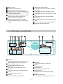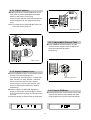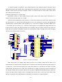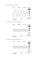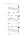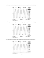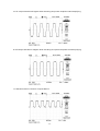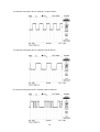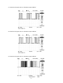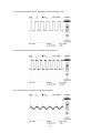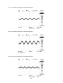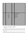
1
AV311T
service manual
Catalog
Chapter One About Maintenance
1.1 Safety precautions
1
1
1.1.1 Power supply
1
1.1.2 Precautions for antistatic
1
1.1.3 About placement position
2
1.2 Maintenance method
2
1.2.1 Visualized method
2
1.2.2 Electric resistance method
2
1.2.3 Voltage method
2
1.2.4 Current method
2
1.2.5 Cutting method
2
1.2.6 Element substitution method
3
1.2.7 Comparison method
3
1.3 Required device for maintenance
Chapter Two Functions and Operation Instructions
3
4
2.1 FEATURES
4
2.2 Control button Locations and Exp Lanations
5
2.2.1 Front panel functions and illustrations
5
2.2.2 VFD DISPLAYY
5
2.2.3 REAR PANEL ILLUSTRATIONS
6
2.2.4 ILLUSTRATIONS TO THE REMOTE CONTROL
7
2.3 BASIC OPERATIONS
8
2.3.1 Turn On/Off the Unit
8
2.3.2 Mute
8
2.3.3 Select Input Sound Source and Video Source
8
2.3.4 Select Decode Mode
9
2.3.5 Adjust Volume
10
2.3.6 Adjust Channel Level
10
2.3.7 Adjust Main Channel Tone
10
2.3.8 Select EQ Mode
10
2.3.9 DEFAULT
11
2.3.10 Karaoke
11
2.3.11 Tuning
12
2.3.12 Tuning (Continued)
13
2.3.13 Channel Delay
14
2.3.14 Noise Testing
14
2.3.15 Select Speaker Mode
15
2.3.16 Headphone
15
2.4 ACCESSORIES
16
2.5 SPECIFICATIONS
16
Chapter Three Unit Circuit Principle
Section One Principle of the player
17
17
3.1.1 Composition of the player
17
3.1.2 Function and features
17
3.1.3 Block diagram of the player
18
3.1.4 Signal flow chart of the player
19
Section Two Unit Circuit Principle
20
3.2.1 Signal processing board
20
3.2.2 Decode board
21
3.2.3 Control panel
22
3.2.4 Power board
23
3.2.5 Power amplifier board and protection circuit
24
3.2.6 Video input/output board
27
3.2.7 MIC, headphone board
27
Section Three Servicing Cases
29
3.3.1 Servicing cases
29
3.3.2 Troubleshooting flow chart
35
Section Four Servicing Parameter
40
3.4.1 Signal waveform diagram
40
3.4.2 Key point voltage
50
Section Five Function Introduction to IC
51
3.5.1 function introduction to 4558
51
3.5.2 function introduction to Pt2399
52
3.5.3 function introduction to Cd4051
53
3.5.4 function introduction to Cd4052
54
3.5.5 function introduction to Cd4053
55
3.5.6 function introduction to Pt6311
56
3.5.7 function introduction to UTCLM4880
59
3.5.8 function introduction to 74HC04
59
3.5.9 function introduction to Lm1875
60
3.5.10 function introduction to TDA2052
61
3.5.11 function introduction to M62446
62
3.5.12 function introduction to AT24C02
64
3.5.13 function introduction to L7805
65
3.5.14 function introduction to 7812
65
3.5.15 function introduction to 7912
66
3.5.16 function introduction to Ne5532
66
3.5.17 function introduction to Pt2315
67
3.5.18 function introduction to Cs4360
69
3.5.19 function introduction to Cd4094
70
3.5.20 function introduction to Cs5340
71
3.5.21 function introduction to Cs8415
73
3.5.22 function introduction to Cs49326
74
Chapter Four Disassembly and Assembly Process
77
Chapter Cinque PCB board & Circuit diagram
78
Section One PCB
78
BoardSection Two circuit diagram
86
Chapter six BOM List
96
6.1 SIGNAL DISPOSAL BOARD
96
6.2 SIGNAL DISPOSAL BOARD AI SEGMENT
97
6.3 DECODE BOARD
99
6.4 DECODE BOARD-SMD
99
6.5 AMPLIFIER BOARD
101
6.6 SURFACE CONTROL BOARD
104
6.7 POWER BOARD
105
6.8 MICROPHONE HOLDER BOARD
107
6.9 VIDEO FREQUENCY BOARD
108
6.10 REMOTE CONEROLLER
108
6.11 PANEL UNIT
109
6.12 PROGRAM CPU
110
6.13 SN LABEL
110
6.14 SUPPLEMENT MODULE
110
Chapter One About Maintenance
1.1 Safety precautions
1.1.1 Power supply
When servicing audio power amplifier, the servicing personnel pay special attention to the power
board with 220V AC, or else the improper operation will lead to body damage. The alternate current
which outputs to power amplifier board through power board is also up to voltage with about 50V; when
servicing, short-circuit and joint welding cannot occur, or else the elements will be burnt out and trouble
range will be enlarged.
1.1.2 Precautions for antistatic
Movement and friction will both bring static electricity which causes serious damages to integrated
IC. Though static charge is little, when a limited quantity of electric charge is added to largescaleintegrated IC, as the capacitance is very small in the meantime, now the integrated IC is very much
easy to be struck through by static electricity or the performance will decrease. Thus static electricity
prevention is of extraordinary importance. The following are several measures to prevent static
electricity:
1. Use a piece of electric conduction metal with the length of about 2 metres to insert into the earth,
and Fetch the lead wire from the top of the surplus metal and connect to the required static electricity
device. The length and depth of the metal embedded under the earth should be determined according to
the wettability of the local soil. For humid places, it may be shorter, and longer and deeper for dry places.
If possible, it can be distributed and layed in terms of “#”shape.
2. On operating table-board, the antistatic table cushion should be covered and grounded.
3. All devices and equipments should be placed on the antistatic table cushion and grounded.
4. Maintenance personnel should wear antistatic wrist ring which should be grounded.
5. Places around the operating position should also be covered with electric conduction cushion or
Painted with antistatic paint.
-1-
1.1.3 About placement position
1. Audio power amplifier cannot be installed in places with high temperature and humidity.
2. Positions for placement should be stable and secure.
1.2 Maintenance method
1.2.1 Visualized method
Directly view whether abnormalities of collision, lack of element, joint welding, shedding welding,
rosin joint, copper foil turning up, lead wire disconnection and elements burning up among pins of
elements appear. Check power supply of the machine and then use hands to touch the casing of part of
elements and check whether they are hot to judge the trouble spot. You should pay more attention when
using this method to check in high voltage parts.
1.2.2 Electric resistance method
Set the multimeter in resistance position and test whether the numerical value of resistance of each
point in the circuit has difference from the normal value to judge the trouble spot. But in the circuit the
tested numerical value of resistance is not accurate, and the tested numerical value of integrated IC's
pins can only be used for reference, so the elements should be broken down for test.
1.2.3 Voltage method
Voltage method is relatively convenient, quick and accurate. Set the multimeter in voltage position
and test power supply voltage of the player and voltage of a certain point to judge the trouble spot
according to the tested voltage variation.
1.2.4 Current method
Set the multimeter in current position and test current of the player of a certain point to judge the
trouble spot. But when testing in current method, the multimeter should be series connected in the
circuit, which makes this method too trivial and troublesome, so it is less frequently used in reality.
1.2.5 Cutting method
Cutting method should be combined with electric resistance method and voltage method to use.
This method is mainly used in phenomena of short circuit and current leakage of the circuit. When
cutting the input terminal voltage of a certain level, if voltage of the player rises again, it means that the
trouble lies in this level.
-2-
1.2.6 Element substitution method
When some elements cannot be judged good or bad, substitution method may de adopted directly.
1.2.7 Comparison method
A same good PC board is usually used to test the correct voltage and waveform. Compared these
data with those tested through fault PC board, the cause of troubles may be found.
Through the above maintenance method, theoretical knowledge and maintenance experience, all
difficulties and troubles will be readily solved.
1.3 Required device for maintenance
◆ Audio Generator
◆ Digital oscillograph (≥100MHE)
◆ SMD rework station
◆ Multimeter
◆ Soldering iron
◆ Pointed-month pincers
◆ Cutting nippers
◆ Forceps
◆ Electric screw driver
◆ Terminals connecting cord
◆ Headphone
◆ Microphone
-3-
Chapter Two
Functions and Operation Instructions
2.1 FEATURES
◆2-way coaxial digital signal input, 1-way optical digital signal input
◆ With 5.1CH input terminal, capable of connecting with external multi-channel advanced decode
output signals such as DOLBY DIGITAL, DTS
◆With subwoofer output terminal, capable of connecting with active subwoofer speaker
◆Built-in FM/AM tuner
◆With headphone output jack
◆6CH digital volume control
◆Separate level adjustment to left, right, centre, surround and subwoofer channel
◆Dolby Digital ,DTS,Dolby Pro Logic II,DSP, STEREO decode
◆Automatically recognize input signal format and select the corresponding decode mode
◆Decode mode manual selection
◆Main channel high/low tone adjustment
◆Video and S-Video selected function
◆Centre, surround delay adjustmen
◆Noise testingt
◆5 preset EQ modes
◆Digital tuning function
◆Capable of storing 36 FM and 12 AM radio stations
◆Automatically/Manually searching radio stations
◆Auto mute if there is no signal
◆High-performance digital Karaoke, with MIC volume, tone and echo adjustment
◆Separate 5CH power amplification
◆Specially automatic protection of short-circuit,over-voltage and over-current
◆Full remote control operation
◆Complete unit interface
-4-
2.2 Control button Locations and Exp Lanations
2.2.1 Front panel functions and illustrations
6
HOME THEATRE RECEIVER AV311T
MUTE
L
SL
1
1
2
3
C
STERO TUNER
MP3
R
PRESET
SLEEP
STEREO SOUNDFIELD
STADIUM
OPTICAL DIGITAL
STAGE
CH
HALL
KHZ DISCO
MHZ
LIVE
SR
2
3
4
POWER switch
Switch on/off the AC power of the unit
MENU button
MENU button, please refer to the related
chapters for details
Multi-Function Knob
In normal working mode, synchronously
adjust 6-channel level. In addition, by
using this knob and MENU button, you
may fulfil multiple functions. Please refer
to the related chapters for details...
5
4
Headphone jack
5
MIC jack
RE
6
IR sensor window
Receive the remote control signals.
2.2.2 VFD DISPLAY
3
5
6
7
8
9
10
11
13
12
16
15
-5-
14
1
2
3
4
5
6
7
8
MUTE symbol
DTS decode mode symbol
Dolby Digital decode mode symbol
Dolby Pro Logic Ⅱ decode mode symbol
TUNER symbol,its flicker shows the tuner is
in signal searching state
Call the preset saved radio station, or has
saved the currently tuning channel
The tuner has received signal
Stereo decode mode or the currently
received FM radio station is stereo output
signal
9
10
11
12
13
14
15
16
DSP decode mode symbol
In DSP decode mode, stimulate STADIUM
sound field
In DSP decode mode, stimulate STAGE
sound field
In DSP decode mode, stimulate HALL sound
field
In DSP decode mode, stimulate DISCO
sound field
In DSP decode mode, stimulate LIVE sound
field
Connect channel, data format display area
Effective channel display area
2.2.3 REAR PANEL ILLUSTRATIONS
7
8
9
10
11
1
VCD
DVD
OUT
VCD
DVD
OUT
VCD
1
2
3
4
5
6
DIGITAL
Coaxial digital sound source input jack 1,2;
optical digital sound source input jack
AM/FM antenna terminal
Connect AM/FM antenna outside
S-VIDEO
VCD、DVD S-Video Selected Jacks
STEREO
VCD、DVD stereo audio signal input jack
5.1 CH
5.1CH audio signal input jack
VIDEO
VCD、DVD Video Selected Jacks
7
8
9
10
11
-6-
LINE OUT
Subwoofer signal line output jack
Data
Model data plate
Speaker jack
Connect with speaker terminals
CAUTION mark
Remind the user of dangerous voltage
Inside
Dual square symbol
Class II electric shock protection product
2.2.4 ILLUSTRATIONS TO THE REMOTE CONTROL
1
2
STANDBY
3
MUTE
1
28
4
OPTICAL
COAX. 1
COAX. 2
TEST
DVD
TUNER
5.1 CH
27
2
VCD
5
3
6
26
9
0
MEM
BAND
25
MODE
24
7
7
4
STEP
8
5
5
6
23
9
DELAY
DEFAULT
10
11
7
L
C
R
SL
SW
SR
STEREO
PL Ⅱ
DSP
DTS
DIGITAL
12
8
VOL
22
13
9
10
21
14
11
12
SPK.
EQ MODE
TREBLE
BASS
20
13
15
14
19
16
15
16
ECHO
TREBLE
BASS
MIC VOL
KARAOKE
RC-311
18
17
17
18
19
20
21
22
23
24
26
27
28
MEMORY button: Save tuning stations
NOISE TESTING button
MUTE button
25
-7-
STANDBY button: Enter or exit standby state
SOUND/VIDEO SOURCE button: Select input
signal sources manually
NUMBER buttons: For saving and calling saved
radio stations
AM STEP button: Pressing this button for long
(above 3 seconds) may switch step valus 9KHz
or 10KHz in the AM wave band
FORWARD/AFTERWARD button: Call the
saved radio stations forward/backward
DEFAULT button: Press this button for long
(above 3 seconds), the unit automatically
restores system parameter to default value
MULTI-FUNCTION buttons
CHANNEL buttons: Using with multi-function
buttons may separately adjust channel leve
STEREO MODE buttonl
DOLBY PRO LOGIC ⅡDECODE MODE button
DTS DECODE MODE button
DOLBY DIGITAL DECODE MODE button
SPEAKER MODE SETUP button: Pressing this
button may circularly select main speaker mode
and subwoofer on/off mode
EQ MODE button: Press this button to
circularly select EQ mode
KARAOKE ECHO (+,-) button: Adjust Karaoke
echo
KARAOKE TREBLE (+,-) button: Adjust
Karaoke treble
KARAOKE BASS (+,-) button: Adjust Karaoke
bass
KARAOKE VOLUME ( 、 )button: Adjust
Karaoke volume
MAIN CHANNEL TREBLE (+,-) button: Adjust
main channel treble
MAIN CHANNEL BASS (+,-) button: Adjust
main channel bass
DSP DECODE MODE button
MAIN VOLUME button: Capable of
synchronously adjusting 6-channel volume
DELAY button: Using with multi-function
adjustment buttons may adjust centre, surround
channel delay
FM STEREO MODE button: Manually/
automatically select FM stereo mode
WAVE BAND button: Used to switch FM/AM
wave band
the VFD screen is lightened. In mute state,
press MUTE button on the remote control, the
unit restores to output sound and the "MUTE"
symbol turns out. Using the MULTIFUNCTION
knob on the front panel or pressing MAIN
VOLUME button on the remote control may
also cancel mute.
2.3 BASIC OPERATIONS
2.3.1 Turn On/Off the Unit
1. Power On
◆Before power on, please check whether the
power accords with the marked specs of the
unit, whether the power socket accords
with the power plug of the unit and whether
the sound source connection cords, output
cords are correctly connected. Then you may
connect the power;
◆Press POWER switch on the front panel of the
unit and the indicator light on the panel flickers
The unit automatically connect with the input
sound source before power-off last time, and
automatically select decode mode according
to the input sound source format.
2. Standby
◆If the user wants to finishing operating in a
short time, you may press STANDBY button
on the remote control to enter standby state. If
you want to operate it again, press STANDBY
button again to exit standby state.
3. Power Off
◆If not going to use for a long period, press
POWER switch on the front panel to turn off
the power, and the indicator light turns out.
MUTE
L
SL
STERO TUNER
MP3
C
R
SR
PRESET
SLEEP
STEREO
OPTICAL DIGITAL
SOUNDFIELD
STADIUM
STAGE
CH
HALL
KHZ DISCO
MHZ
LIVE
MUTE
VCD
Mute
2.3.3 Select Input Sound Source and
Video Source
MUTE
L
SL
C
R
SR
STERO TUNER
MP3
PRESET
SLEEP
STEREO
OPTICAL DIGITAL
◆This unit has 1-way optical input terminal, 2way coaxial input terminal, 1-way VCD input
terminal, 1-way DVD input terminal and 5.1CH
input terminal. You may use the remote control
to directly select input sound source, or use
MENU button and MULTI-FUNCTION knob on
the front panel to select input sound source
through menu. You are recommended to use
remote control means.
Remote Control Means
◆Press the SOUND SOURCE button on the
remote control to separately select the sound
source of optical, coaxial1, coaxial2, VCD and
DVD as the working sound source of this unit.
Press TUNER button to select the built-i tuner
of this unit as the working sound source.
Menu Means
◆Press MENU button on the front panel of the
unit and VFD screen displays "SOURCE".
SOUNDFIELD
STADIUM
STAGE
CH
HALL
KHZ DISCO
MHZ
LIVE
STANDBY
VCD
Turn On/Off
the Unit
2.3.2 Mute
◆In normal working state, press MUTE button
on the remote control, the unit is silent and the
"MUTE" symbol on the top left corner of
-8-
◆Rotate the MULTI-FUNCTION knob, VFD
screen will display "OPTICAL", "COAX1",
"COAX2", "DVD", "VCD", "EXT 5.1CH",
"AM" and "FM" symbols which respectively
stands for the sound sources on optical,
coaxial1, coaxial2, DVD, VCD and external
5.1CH terminals, and the built-in AM, FM wave
band signals. Press MULTI-FUNCTION knob
to select this sound source.
Select video
◆When Tuner in,No video out;When VCD Audio
in,the VCD videois selected; When DVD
audio、5.1CH、COAXIAL and Optical in,The
DVD video is selected.
MUTE
L
SL
OPTICAL
COAX.1
VCD
DVD
C
R
SR
STERO TUNER
MP3
PRESET
SLEEP
STEREO
OPTICAL DIGITAL
Input channel
Analog
Signal
5.1CH
Yes
Yes
Yes
Digital
Signal
(from 2/0 AC-3 Yes
Optical,
Yes
Coax1, AC-3
Coax2 )
DTS
Yes
Dolby
Digital
Yes
No
Yes
No
Yes
No
PLII
Yes
Yes
No
Yes
No
No
DTS DSP Default
Decode
No
Yes Stereo
No
Yes Stereo
No
Yes Stereo
Dolby
No
No Digital
No
No Dolby
Digital
Yes No
DTS
NOTE: In Dolby Pro Logic Ⅱ decode mode ,it is
effective only when sampling rate less
than 96KHz.
This unit can only receive PCM signals with
sampling rate less than 96KHz.There are two
means of manually selecting decode mode:
Remote control and menu.
Remote Control Means
◆Press STEREO,
II, DSP, DTS,
DIGITAL
buttons on the remote control, if the decode
mode that you selected cannot be realized to
input signal, the system still remains the
Original decode mode.
Menu Means
◆Press MENU button on the front panel
continuously until DECODE appears. Rotate
the MULTI-FUNCTION knob, and VFD screen
will display "STEREO, DSP,DOLBY, PRO II,
Dolby Digital, DTS", whichstands for STEREO,
DSP, Dolby Pro Logic II,Dolby Digital and DTS
decode mode respectively. You need to press
the MULTI-FUNCTION knob to confirm to
enter new decode mode.
Note: As for a certain input channel, if some
decode modes do not exist, the operation
is invalid.
SOUNDFIELD
STADIUM
STAGE
CH
HALL
KHZ DISCO
MHZ
LIVE
COAX.2
TUNER
DVD
VCD
PCM
Stero
VCD
Select Source
2.3.4 Select Decode Mode
◆This unit has Dolby Digital, Dolby Pro II, DTS,
DSP and STEREO decode modes, but not
every input channel has all the decode modes.
When the user switches the input channel or
changes the input signal format, the unit may
automatically select the default decode mode
according to the input signal format. Certainly,
the user may also select the decode mode
manually, and please refer to the following
table for the selected decode mode of each
channel and the default decode mode.
Table 1: Relation between input channel and
decode mode
HOMETHEATRERECEIVERAV311T
MUTE
L
SL
STERO TUNER
MP3
C
R
SR
PRESET
SLEEP
STEREO SOUNDFIELD
STADIUM
OPTICAL DIGITAL
STAGE
CH
HALL
KHZ DISCO
MHZ
LIVE
Select Decode Mode
-9-
2.3.5 Adjust Volume
◆Rotating the MULTI-FUNCTION knob on the
front panel or pressing the MAIN VOLUME
button on the remote control may
synchronously adjust 6-channel level and the
screen displays"VOL XX" adjustment range
0~60.
Note: The main volume automatically sets in 20
each time when power on.
Adjust Channel Level
HOMETHEATRERECEIVERAV311T
MUTE
L
SL
STERO TUNER
MP3
C
R
SR
PRESET
SLEEP
STEREO
OPTICAL DIGITAL
SOUNDFIELD
STADIUM
STAGE
CH
HALL
KHZ DISCO
MHZ
LIVE
2.3.7 Adjust Main Channel Tone
◆Press TREBLE and BASS button of main
channel on the remote control to adjust the
main channel treble and bass
respectively.
MASTER
VOL
Adjust Volume
TREBLE
BASS
2.3.6 Adjust Channel Level
◆Press CHANNEL button on the remote control
and the VFD screen displays the
corresponding channel symbol: "FL XXX, FR
XXX, FC XXX, SL XXX, SR XXX , SW XXX",
which means left channel, right channel,
centre channel, surround left channel, right
surround channel and subwoofer channel
respectively.
◆Press the MULTI-FUNCTION adjustment
button on theremote control to adjust channel
level. The adjustment range of channel level is
-60~+60
Figure:The design of channel level on thescreen
Adjust Main Channel Tone
2.3.8 Select EQ Mode
◆Pressing EQ button on the remote control may
select FLAT, DISCO, POP, ROCK and JAZZ
mode respectively. Figure: EQ mode display
- 10 -
1. Karaoke volume
◆There are two means to adjust Karaoke
volume: remote control and menu.
Remote Control Means
Press KARAOKE VOLUME button on the
Remote control
Menu Means
Press MENU button on the front panel until
MIC VOL appears, and then rotate the MULTIFUNCTION knob.
EQ MODE
Select EQ Mode
2.3.9 DEFAULT
Press DEFAULT button for long (above 3
seconds) , and the unit restores the channel
level and Karaoke volume parameters to default
Parameters.
MIC VOL
Karaoke volume
DEFAULT
2. Karaoke echo
◆There are two means to adjust Karaoke echo:
remote control and menu.
Remote Control Means
Press KARAOKE ECHO button on the remote
control.
Menu Means
Press MENU button on the front panel until
MIC ECHO appears, and then rotate the MULTIFUNCTION knob.
Call default parameter
2.3.10 Karaoke
Insert the microphone into the MIC jack on
the front panel and push the MIC switch to ON (if
there is switch). Keep an appropriate distance
With speaker to avoid whistle.
HOMETHEATRERECEIVERAV311T
MUTE
L
SL
STERO TUNER
MP3
C
R
SR
PRESET
SLEEP
STEREO SOUNDFIELD
STADIUM
OPTICAL DIGITAL
STAGE
CH
HALL
KHZ DISCO
LIVE
MHZ
ECHO
2
1
Menu and MIC jack
Karaoke echo
- 11 -
3. Karaoke tone
◆Press TREBLE and BASS button of Karaoke
on the remote control to adjust Karaoke treble
and bass.
TREBLE
After 3 seconds searching radio station, you
may rotate the MULTI-FUNCTION knob to
Adjust volume.
VCD
BASS
TUNER
Karaoke tone
TUNER
BASIC OPERATIONS
2.3.11 Tuning
2. Auto search and save radio station
◆Press MEMORY button on the remote control
until VFD screen displays "MEMORY".
◆Press MULTI-FUNCTION button for long
(above 1 seconds),the unit will automatically
search radio station forward or backward and
then automatically save it. This unit may
automatically save 36 FM and 12 AM radio
stations.
Before tuning operation, please select
appropriate wave band according to the
Following steps.
◆Press TUNER button of sound source
selection on the remote control;
◆Press BAND button on the remote control to
select wave band or directly enter the tuning
FM, AM wave band through menu.1. Auto
search
Remote Control Means
◆Press the MULTI-FUNCTION button for long
(above 1 second), and the unit will
automatically search radio stations forward or
afterward.Until radio station with strong
signal is searched, it will automatically stop.
◆Press the MULTI-FUNCTION button to fine
adjust if necessary.
Menu Means
◆Press MENU button on the front panel until
VFD screen displays "TUN SEEK".
BAND
VCD
BAND
◆Rotate the MULTI-FUNCTION knob and the
unit will automaticallystop after searching the
radio station with enough strong signal. Within
about 3 seconds, you may continue rotating
the knob and searching radio station.
3. Save radio station manually
◆Press MEMORY button on the remote control
and then NUMBER buttons to save radio
station. If the saved radio station number is
over 9, please press 2 numbers continuously.
- 12 -
◆After completely saving, PRESET symbol on
the screen is lightened.
The Explanation of MODE button
This unit has two working modes in the
Receiving status:
AUTO/MANUAL
1、In AUTO working mode, if you select FM
Wave band, this unit will automatically
recognize the radio station program is mono
signal or stereo signal and keep the mono or
stereo Receiving status.
2、If the received radio station program has
Louder noise or cacophony in stereo status,
you may switch to MANUAL working mode.In
this way, the unit is in mono receiving status
to decrease noise and cacophony
generally.You may switch the two working
modes through MODE button on the remote
control.
HOMETHEATRERECEIVERAV311T
MUTE
L
STERO TUNER
MP3
C
SL
R
SR
PRESET
SLEEP
STEREO
OPTICAL DIGITAL
SOUNDFIELD
STADIUM
STAGE
CH
HALL
KHZ DISCO
MHZ
LIVE
1
2
MULTI-FUNCTION knob
Remote control
4. Call the saved radio station
◆Press NUMBER buttons to call the saved radio
station directly.
◆Press FORWARD/BACKWARD buttons to call
the saved radio station. Call the former or
behind one of the saved radio station.
◆After completely calling, "PRESET" symbol on
the VFD screen is lightened.
5. Select AM step value
◆Pressing AM STEP button for long (above 3
seconds) mayswitch the AM step frequency
value, that is, when tuning the step value each
time is 9KHz or 10KHz.
Antenna Connection
You may use our accessional AM and FM
indoor antenna when in bad receiving effect.
Generally speaking, these antennae can supply
enough signal strength.
Connect to AM Round Antenna
1、Push the jack button to open it.
2、Connect the AM round antenna cord to AM
ANT and GND terminals.
3、Let go off the button to clamp the speaker
cord. Pull the cord lightly to check the
connection Is right or not.
MEM
VCD
How to Connect
Call the saved radio station
1 Push the jack button to open it.
1
2 Insert the speaker cord.
3
3 Let go off the button to clamp
the speaker cord.
2.3.12 Tuning (Continued)
2
- 13 -
4、Connect the AM round antenna to the stand.
NOTE:
Do not use the outdoor and indoor FM
Antennae at the same time.
4
AM round antenna
GND (Grounding) terminal
In order to ensure the safety and decrease the
interference, please well connect the GND terminal.
The better grounding method is insert the metal pole
into wet ground.
Stand
5
5、Adjust the direction of AM round antenna to
get the best receiving effect.
2.3.13 Channel Delay
◆Channel delay operation is only available in
Dolby Digital, DTS and Dolby Pro Logic II
modes.
◆Press DELAY button on the remote control.
When VFD screen displays "C XXMS", use
MULTI-FUNCTION button to adjust the centre
channel delay. The adjustment range is 0~5ms
◆Press DELAY button on the remote control
again. When VFD screen displays "S XXMS",
use MULTI-FUNCTION button to adjust the
surround channel delay. The adjustment range
is 0~15ms in DTS and Dolby Digital decode
modes, and 15~30ms in Dolby Pro Logic II
decode mode.
Rotate
NOTE:
1、AM round antenna should be placed far away
from the equipment. You may put up on the
wall or on thebookshelf.
2、AM round antenna and outdoor antenna can
be used at the same time.
Connect to FM Antenna
Connect to the indoor FM antenna
Connect the accessional indoor FM antenna
to 75Ω UNBAL.FM ANT terminal.
DELAY
Channel delay
2.3.14 Noise Testing
- 14 -
◆During system working, it is used for users to
adjust level balance between channels in
multi-channel state.
◆In non-STEREO decode mode, press TEST
button on the remote control to enter noise
testing mode. The unit will output noise
according to the sequence of left, centre, right,
surround rignt and surround left. The lasting
period of each channel is 2s, during which
time users may press the MAIN VOLUME
button on the remote control to synchronously
adjust 6-channel level, and may also press
MULTI-FUNCTION button to adjust each
cnahhel's level. To exit noise testing mode,
please press TEST button again.
SPK.
1
Select speaker mode
2.3.16 Headphone
◆This unit is with individual headphone amplifier.
If necessary,please insert the headphone plug
into the headphone jack on the front panel. In
this state, changing decode mode is invalid.
VCD
TEST
Noise testing
HOMETHEATRERECEIVERAV311T
MUTE
L
SL
2.3.15 Select Speaker Mode
STERO TUNER
MP3
C
R
SR
PRESET
SLEEP
STEREO SOUNDFIELD
STADIUM
OPTICAL DIGITAL
STAGE
CH
HALL
KHZ DISCO
MHZ
LIVE
Headphone
◆Press SPEAKER MODE SETUP button on the
remote control, when"SP SMALL"or”SP
LARGE"appears,pressing MULTI-FUNCTION
button again may change the left/right speaker
mode. Press speaker mode button on the
remote control, when "SUB ON" or "SUB OFF"
appears, pressing MULTI-FUNCTION button
again may set whether there is subwoofer
speaker mode.
Note: The selection of "Large" or "Small" is set
by speaker calibrater and bass playing
ability. When subwoofer speaker and
subwoofer output terminal are connected,
you may set "SUB ON", or else, "SUB
OFF". When speaker mode is set in
"SMALL", subwoofer speaker must be set
in "ON".
- 15 -
2.4 ACCESSORIES
◆User Manual
◆Remote Control
◆AV Cord
'
'
◆Jack to mini-jack adapter
◆7 #AAA battery
◆Warranty card
◆FM/AM antenna
1pcs
1pcs
1pcs
1pcs
2pcs
1pcs
1suit
2.5 SPECIFICATIONS
1、Rated Output Power
Main Channel(1kHz/4Ω,RMS,Total Harmonic Distortion≤1%):
80W+80W
Centre Channel(1kHz/4Ω,RMS,Total Harmonic Distortion≤1%):
15W
Surround Channel(1kHz/4Ω,RMS,Total Harmonic Distortion≤1%):
15W+15W
2、Separability(1kHz,Rated Condition):
≥40dB
3、Total Harmonic Distortion(1kHz,Rated Condition):
≤0.7%
4、Effective Frequency Range under Limited Gains(Normal Working Condition):
+1
Main Channel
20Hz~20kHz -3 dB
Centre/Surround Channel
20Hz~20kHz +1 dB
-3
5、Signal-to-Noise Ratio
≥80dB
Main Channel(Input 600Ω Short-Circuit,A weighted):
≥73dB
Centre Channel(Input 600Ω Shout-Circuit,A weighted):
≥73dB
Surround Channel(Input 600Ω Shout-Ciucuit,A weighted):
6、TUNER
Frequency range:
FM:65-74MHz,87-108MHz
AM:500-1611KHz(9K STEP)
520-1710KHz(10K STEP)
7、Input Sensitivity(Rated Condition)
≤100mV
8、Load Impedance
A11 4~8Ω
POWER
1、Power Supply:
~220V±10%50Hz
2、Maximum Power Consumption:
500W
OTHERS
1、Net Weight:
About 8kg
2、Dimensions:
420×337×135mm
- 16 -
Chapter Three Unit Circuit Principle
Section One Principle of the player
AV311T (RU) is an advanced power amplifier launched into market recently. It is with DTS/AC-3
digital decode function, which makes sound processing more perfect to effectively control the distortion
and noise in the course of audio signal.
3.1.1 Composition of the player
1. Signal processing board: gating, front stage amplifying of signal and front stage processing of
Karaoke signal.
3. Control panel: VFD display, menu button and main volume control.
4. Power board: provide voltage required by each unit circuit, and perform the player protection
function.
5. Power amplifier board: power amplifying of 5.2CH signal or analog signal.
6. Headphone board: Karaoke input and headphone output signal amplifying.
7. Vide board: input/output switch of two-channel composite video and S-video video signal.
3.1.2 Function and features
◆ Simple operation panel interface; the panel of the player has only one power switch button, menu
button and a large knob, simple and clear;
◆ Wirh DTS/AC-3 decode function;
◆ Optical, coaxial signal decode function;
◆ Built-in 5-channel power amplifying, adaptable to AC-3/DTS and stereo music replay. Main
channel 110W. Centre/surround 22W with powerful power;
◆ With 6-channel volume control and separate level control, and also with 7-band electronic
equalization;
◆ With multiple electronic EQ modes, adaptable to different musical styles;
◆ Digital sound field delay function;
◆ With tuning function;
◆ With intelligent protection of over-current and over-voltage
◆ Karaoke function and headphone output;
- 17 -
220V
Signal output
Xs1
Xl100
Power board
Xs3
RLY
P_RC
P_LRM
P_CSM
xs101
xp20
SWM
L1
R1
C1
Sl1
L2
R2
C2
Sl2
Sr2
VC+
Sr1
+12V
GND
GND
GND
VC-
Transformer entry-level
Xs2
Video board
SWM
RLY0
P_RC
OVER
Xs100
RDS outlet
Xs101
Xs22
Signal board
-12V
Xs4
D+5V
DGND
L1
R1
PH_SW
GND
MIC
Secondary coil
SWITCH
Xp16
Xs16
Xp17
Xp14
Xs17
Xs14
LAT
CE
Decode board
Secondary coil ~8.5V
GND
~8.5V
Transformer
+5VD
GND
Xp25
Mic or earphone board
CLK
DATA
DO
P_DIST
OK_DAT
OK_CLK
P_KT
REM
DST
DCK
DDA
View board
RLYC
NC
DDA
DCK
DST
FAN
REMMOTE
P_LRM/P_SCM
DIGITALAUDIO INPUT
4052-A/4052-B
Digital
audio
SL/SR
5.1CH
L/R
AMP BOARD
Mix & buffer
VOL&TONE
INPUTSET
2*COAXIAL/OPTICAL
4558
4053_INT
L
TUNER
VCD
1
L
2
DVD
Dual-decode IC,
CPU
L/R
L/R
4052*2
L/R/SL/SR/C/SW
M62446
L/R
C
5532
SL
3
R
Pre position
power
R
Mix & buffer
SR
Vs+
2
C
5.1CH(L/R/SL/SR/C/SW)
CLK/DAT/LAT
P_DISP
SW
SW_OUT
DISPLAY BOARD
DO/CLK/DAT/CE
2*LED
CPU
1
Central
surround
power
Load
detect
2*KEY
KM
DCL/DDA/DST
VFD
PT6311
2
FAN
CD4052
3
4558
3
R
DVD
Vs-
1
L
5.1CH
VCD
NGD
Mix & buffer
0_LEVEL
FAN
L
4
TUN_L/TUN_R FUN VOL
5
R
6
REMOTE
REMOTE
C
4558_B
VCD
SL
4558
4558_A
6
SR
MIC_VOL
TONE
DVD
Straight through Mix & buffer
PT2315
6
Echo volume
Relay drive
ECHO
RLYC
S W mute and relay
state detect
OK_CLK/OK_DATA
PT2399
CD4052
ECHO
adjustment
Vc+
AGND
Vc-
6
CPU
+5V
VIDEO BOARD
9
8
7
6
5
4
3
2
1
PH_SW
PH_L
PH_R
MIC 、PHONE BOARD
Amplify
LM4880
CLK/DATA/LAT
DO/CE
OK-CLK/OK-DATA P-KT
I/O:DCL/DDA/DATA
REMOTE
P-LRM/P-SCM
P-RLY P-DISP
KM
POWER BOARD
6311 I/O:TUN-L/TUN-R
FAN
RLYC
62446 I/O:4 0 5 2 - A / 4 0 5 2 - B
5.1CH 4053-INT
Main power
amplifier board
power
+12V
AGND
-12V
~VS
~VS
Power
+6.8V
+5V
+6.8V
AGND
-6.8V
+5V
+5VD
Section Two Unit Circuit Principle
3.2.1 Signal processing board
1. Input selection circuit
AV321T(RU) has6 kinds of input means in all: optical input, coaxial input, CD, DVD, 5.1CH and
tuning input. Digital signals of optical, coaxial input of this player are directly sent to power amplifier
board for processing through flat cable. Analog input selection of AV321T(RU) is fulfilled through an
electronic switch Cd4052 (N101) and its truth value table is shown as the following:
Estate
状态
VCD
Tuning
DVD
A
1
0
1
B
1
1
0
PIN
引脚
AV321T (RU) has 3 kinds of input states: tuning, VCD , DVD, and they are controlled through 4052A, 4052-B signal respectively (refer to truth value for details). Signals after being gated output from pin 3
and pin 13 of N101, and then output left/right main channel signal from its pin1, 12 through N111 CD
4052 to decode board for signal processing.
Analog signal input in 5.1 state: the gating of 5.1 analog signal input of AV321T(RU)is controlled by
two IC CD 4053 (N102,N103), control pin 9,10,11 of CD 4053 are all controlled by the 5.1CH signal
outputted from pin 4 of M62446(N104), when 5.1CH signal is high level, the gating is analog signal input
of 5.1 state; in this state, there is no digital sound field, all signals are straight through; when 5.1CHis
low level, the gating is the synthesized signal after decoding.
Straight through and digital sound field switch control: AV321T (RU) has two different modes of
straight through and digital sound field, and its gating input is controlled by N111/CD4052 and N102/CD.
When control signal 4053-INT is high level, for it is connected to the enabled end of N102, this IC is in
non working state, main channel signals output through pin 5, 11 of N111 and directly send to M62446
for processing to output Hi-Fi musical signals. When 4053-INT is low level, main channel signals are
sent to decode board for digital sound field processing through Xp17, and N102 is also in working state.
2. Karaoke signal processing circuit
For karaoke signals sent from MIC base board, after coupling and amplifying, one path is sent to
volume and tone adjustment IC PT 2315 (N203) for processing, then after echo and delay adjustment
- 20 -
through PT 2399 (N204), it is sent to power amplifier board for small signal amplifying through bandPass filter. PT 2315 is controlled by MCU, so users may adjust his desired Karaoke effect at will through
remote controller.
Another path signal, after amplifying rectification, controls a switch triode V201 9014 to control the
high/low level of detect signal P-KT to fulfil the detecting of Karaoke signals. When the inputted Karaoke
signal is large enough, the DC after being rectified makes triode V201 on and then pulls down P-KT
signal, which means that there is Karaoke signal input. Now, KM control signal is low level, triode V101
2N5401, V102 S8050 both cut off, Karaoke signals enter IC N107 NE5532 for amplifying through
coupling capacitor C147, C149, then they are sent to left/right channel; when CPU cannot detect signals
in a certain period, P-KT is high level, now KM control signal of CPU changes into high level, triode
V101, V102 are both on to make Karaoke signal short circuit to ground, system mutes Karaoek part
automatically to prevent the influence to sound effect caused by noise.
3. Fan starting circuit
When power amplifier is with load, for power is large and temperature rise is high, this player
adopts fan to perform heat radiation. When volume is more than 45dB, FAN signal sent out from control
pane N101 changes into high level, V103 9014 and V105 S8050 are on to form power supply loop of fan.
When the connected load is headphone, control line PH-SW is high level, V104 9014 is on to pull down
FAN signal, so no matter how is the volume of system, fan will not start up.
3.2.2 Decode board
Main element function of decode board is shown as follows:
◆ IC SM8958AC25P (N116): control core of MCU system
◆ IC 493264 (N105): high performance digital audio decoder, including DOLBY decode, DTS
decode and DSP processing
◆ IC CS8415 (N106): serial digital audio signal receiver
◆ IC CS5340 (N108): 2-channel A/D converter
◆ IC CS 4360 (N107): 6-chanel D/A converter
◆ IC 24C02 (N115): state memorizer
◆ IC 74HC04 (N101): 6-channel phase inverter
◆ IC BM1117-3.3 (N109): 3.3V voltage regulating IC, which provides power for CS8415, Cs4923
Working principle: for optical and coaxial signals, after being filtered by inductor, capacitor,
reshaped by phase inverter 74HC04 (N101), they are sent to serial audio digital signal to receive signal
input pin 4, 12 14 of IC Cs8415 (N106), then converse serial digital audio signal to PCM signal through
this IC, and output from pin 16 (sampling speed signal), 17 (main channel clock signal), 18 (audio data
signal) of this IC to pin 25 (sampling speed control signal), pin 26 (clock signal), 22 (PCM data input port
- 21 -
1) of digital audio decode IC Cs493264 (N105) for data processing.
Analog signals of left/right channel are sent to decode board through flat cable Xs17, after front
stage small signal processing, then sent to pin 10, 12 of IC Cs5340 (N108) for A/D conversion to change
analog audio signal into PCM signal, then sent from pin 4 (audio PCM signal), 17 (sampling speed
signal), 18 (clock signal) of N108 to pin 27, 28, 29 of N105, that is, input from another PCM input port of
N105 for data processing.
Therefore, digital sound field processing of analog signal and processing of coaxial, optical audio
digital signal are separate, if only one path works abnormally, the possibility that problem appears
before N105 is large.
CS493264 (N105) is with powerful digital sound field processing function, all DSP processing, Pro.
Logic II processing and DOBLY/AC-3 processing are all performed inside under the control of
MCU/SM8958AC25P (N116).
Audio PCM signal after being processed by CS493264 (N105) is sent to CS 4360 (N107) for D/A
conversion to restore PCM signal into 6-channel analog signal, then filter high frequency signal outside
the range of audio frequency through a band-pass filter, then sent to input gating part for selection input.
Acted as he core of the whole system, MCU/SM8958AC25P (N116) has important function. All
control signals are sent out by it, and it will detect each different signal and user order at any time to
control action of each part of machine. If this IC has trouble, the player will be not able to work normally.
In addition, this player has no auto search function, but is can automatically save and memorize the
working state laet time, and enter the previous working state when power on next time.
This player is with tuning function, which provides a good function selection for users. It directly
controls digital tuner receiving (AM/FM) signal through MCU N116, and then outputs through power
amplifier. Clock and date line of digital tuner is used together with LM62446 (N104), another two control
lines are directly connected to N116, TUNER L, TUNER R signal after being processed by digital tuner is
directly sent to CD4052 (N101) for gating input.
3.2.3 Control panel
Control panel is mainly composed by VFD display screen, drive IC Pt6311 (N101), infrared remote
controller HSOO38A2 (N102) and indicator light display circuit. It completes man-machine conversation
and working state display mainly. The composed block diagram is shown as the following figure 3.2.3.1:
Under the control of MCU, through DST state, DCK clock, DDA data, control PT6311 (N101),
display working state of the player and fan state, and receive user control order sent out by PT6311
(N101), control the controlled circuit of the player to make the player work in indicated working state.
When user are operating panel buttons, control order is sent to PT6311 (N101) through keyboard
scanning circuit, PT6311 (N101) outputs control data to MCU through coding drive inside and realizes
the control of controlled circuit through MCU, and controls VFD through PT6311 (N101).
- 22 -
Button control
DDA
N101
VFD
Display
DCK
PT6311
MCU
DST
Panel indicator light control area
Remote control receiving
Figure 3.2.3.1 Control panel circuit block diagram
VFD101 is vacuum flourescent display screen and the most distinct feature is high brightness. The
working principle is similar with that of kinescope of TV set. Pin 1, 2, 46, 47 are filament power supply,
MCU controls SEG electrode through the control of PT6311 (N101) to make characters of corresponding
working state display on screen.
Remote control receiving circuit is mainly composed of remote control receiver HS0038A2 (N102),
in whicj pin 1 is grounded, pin 2 power supply end, pin 3 is signal receiving output pin and sent to MCU
directly to control corresponding circuit.
3.2.4 Power board
The function of power board is to provide all kinds of working voltage required by each unit circuit.
Shown as in the figure 3.2.4.1 AV321T (RU) adopts large-power round transformer. Centre and surround
channel of AV321T (RU) adopt CD1875 and 2×TDA2052 respectively, TDA2052 is mono channel power
amplifying and adopts separate positive/negative power supply.
~ 26 V
Panel display
~2.2V
Filament voltage
~ 220V 50HZ
~ 38V
Rectification
Filtering
~16.3V
Rectification
Filtering
Figure 3.2.4.1 Power block diagram
- 23 -
Left/right channel
power amplifying
level
C , SL, SR channel
power amplifying
level
The two groups AC 35V voltage outputted from the first sublevel winding of transformer, after
rectification and filtering of 8 In5404 (VD100~ VD107) diode and 2 electrolytic capacitor (15000uF/63V,
C108, C109), positive/negative 53V power is achieved to supply power for left/right channel.
The two groups AC 17V voltage outputted from the second sublevel winding of transformer, after
rectification and filtering of 4 IN5404 (VD111~VD114) diode and 2 electrolytic capacitor (4700uF/35V,
C141, C142), positive/negative 23V power is achieved to supply power for SL/SR/C channel. For other
IC and operational amplifiers, after voltage regulating of 3-end voltage regulator L7812 (N101), L7912
(N102), positive/negative 12V power is achieved to supply power for other IC.
3.2.5 Power amplifier board and protection circuit
1, L, R channel power amplifying circuit
L, R channel power amplifying circuit: L, R main power amplifying circuit of AV321T (RU) is
composed of discrete component, the composed block diagram is shown as the following figure 3.2.5.1
(take L channel for instance):
AC negative feedback
R121, R108, C105
L IN
Difference amplifying
level V102, V103
Composite power
amplifying V132, V112
Voltage
amplifying
level V105
Temperature
compensation
level V106
Speaker
V101
V115
Mute
Relay
Composite power
amplifying V133,
V113
Mirror image constant current source V104,
V107, VD102, VD103
Figure 3.2.5.1 Power amplifier and protection circuit diagram
L channel signal, through R101, R103, C101 coupling, is sent to B electrode of differential
amplifying stage V102, V102 and V103 compose the differential amplifying circuit of single-end input
and single-end output. Audio signal is outputted from C electrode of V102 to B electrode of voltage
amplifying stage, then to composite power amplifying stage after voltage amplifying.
V104, V107,
VD102 and Vd103 compose mirror constant current circuit. VD102, VD103 provide V104, V107 with
constant base electrode current. Emitter electrode resistance of V104 decides working current of
differential amplifying stage, emitter electrode resistance of V107 decides working current of voltage
amplifying stage. V132 and V112 compose multiple unit tube amplifying to make final stage of power
amplifier have powerful current amplifying ability, and they compose positive half cycle amplifying
waveform. V133 and V113 compose negative half cycle amplifying waveform. The function of
- 24 -
Temperature compensation tube in circuit has two: firstly, it is the base electrode bias of upper/lower
geminate transistor and its working state decides static working current of composite power amplifying
stage, that is, through adjusting the on state of V106, static working point of composite power amplifying
stage may be set. The common means is change base electrode resistance of V107; it may also
automatically adjust working state of composite power amplifying stage after temperature increases.
The adjustment process is as follows:
Total current of output level = working current + leakage current
When temperature becomes high, leakage current increases to lead to static working point drift
(unfavourable).
At the same time, the leakage current of V106 increases, Uce decreases to make bias current of
output level decrease, working state changes, working current of back stage decrease, and temperature
compensation function is realized.
In power amplifying circuit of AV321T (RU), voltage negative feedback is introduced and composed
by R121, R109, C105, which may stabilize static working point of differential level. AV321T (RU) adopts
direct output means, R111 and C116 connected on output end compose Zobel network, which may
prevent high frequency self-excitation caused by AC inductive reactance of speaker sound coil.
2. Mute circuit
When pressing MUTE button on remote controller, after optical-electric conversion of signal
conducted by infrared receiver, a mute signal is achieved and sent to MCU, P_LRM high level and
P_CSM low level mute order is sent out from MCU at the same time, P_LRM high level makes 2N5401
(V115), S8050 (V101), S8050 (V116) on, left and right channel signal are short-circuited to ground, and
mute control function of left/right channel finishes; P_CSM low level makes 9014 (V150) cut off, 2N5401
(V130) and S8050 (V131) are on, center channel signal is short-circuited to ground, and mute control
function of center channel finishes; at the same time, P_CSM low level makes 9014 (V151) cut off,
voltage of pin 5 of TDA7265 os power voltage, TDA7265 internal mute circuit works to reach surround
channel mute effect.
3. C, SR, SL power amplifying circuit
Compared with the former models, the three channels of AV311T (RU) adopt special audio power
amplifying IC CD1875CZ (N104) and TDA7265 (N106). As for TDA7265 (N106), it has 11 pins in all, pin
3, 1 and 6 are its positive/negative power pin; pin 11 and 7 are its in-phase input terminal; pin 10 and 8
are its reverse input end, the rated output power of each channel of this power IC may be up to 15W,
with auto mute function when power on; as for CD1875CZ (N104), it has 5 pins in all and is a good
performance power amplifying IC with 15W power output in rated state. pin 5 and 3 are positive and
negative power pin.
- 25 -
4. Protection circuit
Protection circuit of power amplifier of AV321T (RU) is designed on power board. The protection
means of L, R, C channel is fulfilled through disconnecting delay Y100 when starting up to disconnect
the output. SR, SL channel achieves protection function through mute. AV321T (RU) is with power-on
delay protection, central point over-voltage and over-current protection, standby protection.
(1) Power-on delay attracting protection circuit: the working of circuit is unstable when power on,
and the produced impulse current does great harm to speaker and power amplifying circuit, so delay
attracting protection circuit is set. Power-on delay attracting protection circuit is divided into 2 steps: the
first step: C, L, R channel and its working process is as follows: for AC outputted from transformer, after
rectification and filtering of Vd113, C110, +22V voltage is achieved, charges C115 through R108 to make
Vd111 struck through reversely and to make V105, V104 forwards on, relay Y100 is made attracting
finally to reach delay attracting effect. The second step: SR, SL channel performs power-on anti-impulse
protection through the following means: when power on, reset of machine system has not finished,
P_CMS may probably be high level to make triode V137 on to cause power-on impulse sound, now a
+VS level is added on B electrode of triode V137 through resistor R163 to make it in cutoff state at the
moment of power-on; a -VS level is added on pin 3 of TDA2052 through resistor R189 to make TDA2052
in mute state to avoid the impulse to loudspeaker; after machine system resets, MCU outputs a P_CMS
low level signal to still make V137 cut off, pin 3 of TDA2052 is still -VS, TDA2052 outputs mute. After
delay start up of machine is successful, output signal P_CMS of MCU switches into high level
immediately, now relay has attracted, RLY0 is grounded through relay to make V137 on, voltage of pin 3
of TDA2052 is about 5V higher than negative power voltage, SL/SR channel restores normal output.
TDA2052 chip, under the condition that load is not connected, will appear component DC, so false load
R121, R122 is added in power board surround channel.
(2) Over-voltage protection: on output end of each channel, an over-voltage sampling resistor is
connected, L channel is R116, R channel is R117, C is R118, SR and SL are R120 and R119 respectively,
only one channel’
s central point voltage is more than +3.5V or less than -3.5V, V101 or V102 is on to
make their C electrode voltage decrease, B electrode V103 is pulled down to make V103 on, relay
disconnects finally, and over-voltage protection finishes. The working process is shown in the figure
3.2.5.2:
Over-voltage
sampling
resistor is
connected to
each channel
When m o r e
than +3.5V
V101 is on
C electrode
voltage
decreases
L channel R116
When less
than -3.5V
V102 is on
Figure 3.2.5.2 Over-voltage protection flow chart
- 26 -
V103 is on
Relay
disconnects
and protection
starts up
(3) Short-circuit protection: an over-current sampling triode is connected to output load resistor of L,
R channel, sampling triode of L channel is V114 (on power amplifier board), load resistor is R126,
R127(on power amplifier board). C, SR, SL channel power amplifying IC has been with over-current
protection inside. Only over-current appears in L channel, the pressure drop produced on R126, R127
will increase, once the pressure drop of R129 (on power amplifier board) is more than 0.7, V114 will be
on, V103 will also be on, relay disconnects finally, and short-circuit protection completes. The working
process is shown in the figure 3.2.5.3:
Over-current
sampling triode
is connected to
each channel
L channel
V114
When over-current,
pressure drop on
R126, R127
increases
V114 is on
C electrode
voltage
decreases
Relay
disconnects
and protection
starts up
V103 is on
Figure 3.2.5.3 Short-circuit protection flow chart
Similarly, when R channel has over-current, voltage on R159 (on power amplifier board) will be
more than 0.7V to make (on power amplifier board) V129 on, also to make V103 on, and relay
disconnect finally to achieve the purpose of protecting loudspeaker.
3.2.6 Video input/output board
AV321T (RU) is with two-channel composite video input (VCD, DVD or 5.1CH); two-channel S-video
video input (VCD, DVD or 5.1CH); 1-channel composite video output (VCD, DVD or 5.1CH); 1-channel
S-video video output (VCD, DVD or 5.1CH).
Input/output switch of video signal is realized through two electronic switch Cd4052 (N100,N101).
When VCD channel is selected, pin 1 and 2 of N104 (M62446) of signal processing board send out A and
B high level control signal, according to working principle of signal processing board in section 2, now A
and B also control gating of CD4052 of audio part, that is, audio channel also selects VCD channel, thus,
the synchronous switch of audio and video of VCD channel is realized.
Similarly, for synchronous switch of audio and video of DVD channel, pin 1 and 2 of N104 (M62446)
of signal processing board send out 1 and 0 control signal of A and B to finish the corresponding switch.
When 5.1CH is selected, it is equal to selecting DVD channel.
Composite video signal is outputted through triode V100 (1015), V101 (1015) and V102 (1015)
output S-video signal.
3.2.7 MIC, headphone board
Working principle of microphone part has been shown in section 2 of chapter 2, so we will not
repeat here.
Headphone part: L and R channel signal is outputted from pin 31 and 32 of signal processing board
- 27 -
N104 (M62446), through coupling capacitor C103, C104, then sent to pin 2 and 6 of two operational
Amplifiers of N100 (LM4880), after amplifying, headphone signal is outputted from pin 1 an d7 of N100
respectively.
When headphone is inserted, MCU detects that PH_SW signal is high level, the corresponding
control signal P_LRM is high level, main channel is muted; P_RC controlled by CPU changes into high
level, relay on power board disconnects, RLY0 of power board is pulled up to +5V, P_RLY control signal
changes into high level, triode V101 (S8050) is on, pin 5 of headphone amplifier N100 has +2.5V voltage
input, headphone amplifier is in working state to make V104 of signal processing board on at the same
time, V103 and V105 cut off, power supply loop of fan is cut off, when volume is over 45dB, fan rotation
is forbidden to facilitate to listen with headphone.
When no headphone is inserted, MCU detects that PH_SW signal is low level, the corresponding
control signal P_LRM is low level, P_RC controlled by CPU changes into low level, relay on power board
attracting, RLY0 of power board is pulled down to 0V, P_RLY control signal changes into low level,
triode V101 (S8050) cuts off, pin 5 of headphone amplifier N100 has 0V voltage input, headphone
amplifier is in standby state. Central and surround channel of signal board volume adjustment IC N104
(M62446) is opened to make power amplifier output signal and drive loudspeaker.
- 28 -
Section Three Servicing Cases
3.3.1 Servicing cases
[ Example 1 ] Symptom: power-on protection
Description: after power on, relay does not attract and "system abnormal, auto protection" displays.
Analysis and troubleshooting: after power on, system protects, relay does not attract, shown as in
the figure 3.3.1.1; test L, R, C, SL, SR of power board flat cable holder XP8 and there is no DC output,
test pin 1 of power board flat cable holder XS7 and it is high level, pin 2 is low level, C electrode of triode
V101 is high level; it is known from the above test that the protection is not caused by over-current and
over voltage (you may also unplug flat cable holder XP7 and XP8 and check whether it has protection).
Test positive voltage of diode VD112 and it is 0. We judge that relay has trouble. After changing relay,
trouble is removed.
VD113
R100
1N4004
47/3W
C110
220u/35V
R102
IN4148
R106
4.7K
104
R104
1K
VD110
C122
OVER
P_RC
RLY0
SWM
R108
100K
XP7
VD108
4
3
2
1
RLY0
SWM
IN4148
10K
R101
V100
C9014
1K
R103
47K
CON4
C126
R107
100K
R105
10K
VD111
103
220u/16V
C9014 V101
5.1V
V103
C113
V102
C9014
C121
103
R109
10k
C9015
R110
56K
C115
47U/25V
C114
220u/16V
R116
R111
4.7/1W
C1160.1u
L100 0.7UH
R112
4.7/1W
XP8
L2
R2
C2
SL2
SR2
VC+
GND
GND
VC-
1
2
3
4
5
6
7
8
9
CON9
C1170.1u
L101 0.7UH
R114
R119
47K
C1190.1u
4.71W
C1200.1u
47K
1
2
WP6
7
4
SWM
8
RLY0
12
1
1
2
2
13
R120
R115
2
XL100A
XL100A
1
2
WP4
WP4
11
VC+
VC-
5
2
6
3
47K
4.7/1W
1
10
51K
R118
C1180.1u
1
9
R117
R113
4.7/1W
XL101A
Y100
51K
XL101A
WP6
14
V105
C9014
XL101A
WP6
RELAY-4
VD112
V104
C8050
1N4148
Figure 3.3.1.1 Protection circuit diagram
Note: 1. After relay is used for a period, working state may be unstable and some abnormalities may
appear: relay does not attract after power on sometimes; each contact point does not touch fully after
relay attracting sometimes; CPU cannot detect RLY0 signal (after relay attracting this signal is low
level), auto protection.
- 29 -
2. Causes of power-on protection: over-current protection, over-voltage protection and CPU cannot
detect RLY0 signal; test whether each output channel has DC output; when power-on protection trouble
appears, make clear which reason caused it. Centre or surround power IC have trouble, which cause
that output signal has DC in it.
[ Example 2 ] Symtopm: no sound output
Description: power on, after system resets normally, switch each sound source and there is no
output, select decode and there is no output.
Analysis and troubleshooting: after power on, select VCD channel, input sine wave signal, shown
as in the figure 3.3.1.2; test volume board capacitor C119, C121 and there is no signal, test signal board
capacitor C122, C124 and there is still no signal, pin 4, 11 of N101 has signal, test power voltage of pin
7, 16 of N101 and it is normal, pin 3, 13 of N101 has no signal, so we preliminarily judge that N101 has
input but has no output, we judge that N101 has no trouble, test pin 9 of N111 and it is high level, we
judge that this channel is not gated, signal A, B of N104 has trouble. Change N104, after changing,
output is normal and trouble is removed.
N101
CD4052
12
TUNER_R 14
DVD-R 15
CD-R
11
TUNER_L
DVD-L
CD-L
1
5
2
4
6
B
9
4052_B
4052_A
C108
10u/16V
A10
X0
X1
X2
X3
X
13
Y
3
Y0
Y1
Y2
Y3 VDD
INH
VSS
B
VEE
A
+5VD
16
R127
22K
A-6.8V
4052_A
A
1
OUT4
A+6.8V 4052_B
B
2
OUT3
CLK
41
INT
3
OUT2
DATA
40
4053_INT
C107
1
5
2
4
6
10u/16V
B
9
A10
5.1CH
X0
X1
X2
X3
13
X
4
5.1CH
5
C110
47u/16V
C112 6
4.7u/16V
3
Y
Y0
Y1
Y2
Y3 VDD
INH
VSS
B
VEE
A
7
16
C115 8
4.7u/16V
C117 9
4.7u/16V
A+6.8V
8
10
7
A-6.8V
INT
C12011
4.7u/16V
12
4053_INT
R1494K7
C12213
4.7u/16V
14
R1504K7
C12415
4.7u/16V
16
N102
CD4053
12
13
X0
X1
X
2
1
Y0
Y1
Y
15 FL
Z
4
5
3
6
11
10
9
Z0
Z1
VDD
INH
A Vss
B
C VEE
C111
47n
R136
22K
C133
47u/16V
L103100uH
C109
47n
N111
CD4052
12
14
15
11
R135
22K
A+6.8V
8
7
R134
22K
C126
822
14 FR
C
C127
15n
C128
0.33u
DVDD
42
LATCH
AVDD
DGND
38
AGND
37
N104
M62446
DATA
R141100
39
OUT1
SWIN
CLK
C134
C135
101
101
LAT
36 C113
4.7u/16V
SW-1
SRIN
SROUT
35 C114
4.7u/16V
SR-1
SLIN
SLOUT
34 C116
4.7u/16V
SL-1
COUT
33 C118
4.7u/16V
C-1
32 C119
10u/16V
R-1
31 C121
10u/16V
L-1
GNDS
GNDC
CIN
GNDR
RIN
SWOUT
ROUT
LOUT
AVSS
CL1
CL2
CR1
BYPASR
17
BYPASL
18
19
LTRE
LBASS3
LAT
SW-1
SR-1
SL-1
C-1
R-1
L-1
A-6.8V
C13747n
C123
4.7u/16V
GNDL
LIN
30
29
CLK
DATA
C138
47u/16V
28
27
C125
4.7u/16V
CR2
RTRE
RBASS3
26
25
24
20
LBASS2
RBASS2
23
21
LBASS1
RBASS1
22
C139
822
C140
15n
C141
0.33u
16 A+6.8V
8
7
A-6.8V
Figure 3.3.1.2 Volume circuit diagram
Note: when there is no output, firstly make sure that it is a certain channel has no output or all
channels have no output; that all channels have no output may be caused by abnormal power supply of
a certain part, or abnormal mute signal; then make clear whether it is decode has no output or signals
without being decoded have no output; that decode has no output is caused by abnormal working of
decode part, please refer to cases of “decode has no output”. CD4052 and CD4053 belong to electronic
switch with high switch frequency easy to damage and may pull down +6.8V and -6.8V voltage after
damage, or pull down the gating signals A, B of 62446, and trouble of no output appears.
- 30 -
[ Example 3 ] Symptom: decode has no function
Description: when in analog input, decode has no output, input digital signals have no output
Analysis and troubleshooting: analog signals with decoding have output, so we can judge that
power amplifier circuit working is normal, and trouble is preliminarily decided on decode board. Shown
as in the figure 3.3.1.3, input digital signal, test pin OSCLK, OLRCK, SDOUT of N106 Cs8415 and there
is pulse waveform output, test AD2, AD1, AD0, WCK, BCK, MCLK of N105 CS4923 and they all have
signal output, test AOUTA1, AOUTB1, AOUTA2, AOUTB2, AOUT3, AOUTB3 of N107 CS4360 and they
all have no waveform output, test voltage of power supply pin of N107 and it is normal, test SDIN1,
SDIN2, SDIN3, LRCK, MCLK of N107 CS5340 and they all have signal, so we judge that N107 CS4360
has input but has no output. After changing N107, output is normal and trouble is removed.
C157
1U/16V
L107
VD2.5
FB
C108
104
C159
104
R105
4K7
R108
4K7
R106
51
R107
R110
51
51
R161
51
N107
CS4360
1
2
3
4
SCLK 5
LRCK 6
MCLK 7
8
9
DARST10
SCK 11
SDA 12
13
14
SDIN2
C203
30P
N105
CS49326-3
7
8
9
10
11
12
13
14
15
16
17
C202
30P
C109
104
R120
10K
SCK
GPIO7
GPIO6
GPIO5
GPIO4
VD2
DGND2
GPIO3
GPIO2
GPIO1
GPIO0
CS4923
R121
10K
39
38
37
36
35
34
33
32
31
30
29
AD2
DC
DD
/RESET
AGND
VAA
FILT1
FILT2
CLKSEL
CLKIN
LR2
C116
1U/16V
R122
33K
C123
1U/16V
L104
FB
C127
104
C204
2
51
SDOUT
5
FB
C113
104
C112
1U/16V
C114
472
R119
1.2K
C115
104
R162
470
28 SCK
27
26
25
24
23
22
21
20
19
18
17
16
15
SDA/CDOUT
SCL/CCLK
AD0/CS
AD1/CDIN
EMPH RXP6
RXP0 RXP5
RXN0
H/S
VA+
VD+
AGND DGND
FILT
OMCK
RST
U
RMCK
INT
RERR SDOUT
RXP1 OLRCK
RXP2 OSCLK
RXP3 RXP4
N106
CS8415ASO
8415_ERR
8415_INT
L 117
1
N101C
C129 VD5
100U/16V
3
5
6
74HC04
N101E
11
4
74HC04
10
74HC04
3
L112
VA5
FB
C150
104
13
C151
104
12
Ain-R
Ain-R
11
10
C153
104
9
C152
1U/16V
Ain-L
Ain-L
VD3.3
+12V
R157
C131
100U/16V
Vin
Vout
C154
104
C136
104
VD102
5.6V
VD2.5
2
C134
100U/16V
+5VD
R158
100K
2.2K
C107 C161
104
10U/16V
L116
1UH
VA5
V102
5551
2
C158
104
C132
10U/16V
VD5
R163
VA5
0Ohm
VD1031N4004
C217
13
74HC04
N109
BM1117-3.3
Vin
Vout
C130
104
0
N101F
12
RST
C149
1U/16V
14
C213
101
47K
R182
1UH
L 119
N101B
C214
R179
N101A
74HC04
R10251
9
2
AINL
LRCK
N110
BM1117-2.5
104
1M
SCLK
L103
N101D
74HC04
8
VQ
C148
1U/16V
15
FB
C210
104
1UH
AINR
16
C135
1U/16V
3
C105
104
R101
R165
L102VD3.3
C121
104
470
L122
1UH
C147
1u/16V
CS5340
VD5
L121
G101
C103
C104 1UH
30P 12.288MHz 30P
VA
VD
8
LRCK1
R164
VD3.3
GND
6
L114C106 C128
FB 1U/16V 104 SCLK17
51
SDA1
2
3
4
5
6
7
8
9
10
11
12
13
14
FILT+
VL REF_GND
DIN1 4
VD3.3
R155
M1
MCLK
3
R159 10K
VD5
L111
FB
C146
104
0Ohm
N108
M0
1
30P
C111
104
DA_SW
VD3.3
R156
L101
DA_SR
DA_C
DA_C
DA_SW
VD3.3 L113 C155
FB 1U/16V
49326_DI
49326_CK
49326_CS
49326_DO
INT_49
DSPRST
SDA
SCK
DARST
RR105
8*3.3K
C156
104
VD5
C126
104
R111
10K
R114 51
R112 51 C205
R154 470 30P
C206
R153 51
30P
R152 51
R151 51
R118
R150 51
10K
DA_L
DA_R
DA_SL
DA_SL
DA_SR
C125 L106
1U/16V FB
C110
104
C101
104
L105
FB
C124
104
C120
471
VD3.3
DA_L
DA_R
VA5
2.2U/16VC118
104
C119
103 VD2.5
R113
51
28
27
26
25
24
23
22
21
20
19
18
17
16
15
C117
R123
10K
R109
51
MUTEC1
AOUTA1
AOUTB1
MUTEC2
AOUTA2
AOUTB2
VA
AGND
AOUTA3
AOUTB3
MUTEC3
VQ
FILT+
M2
VLS
SDIN1
SDIN2
SDIN3
SCLK
LRCK
MCLK
VD
GND
/RST
DIF1
DIF0
M1
VLC
104
L118
L120
1UH
VD3.3
VD2.5
1UH
R181
VD5
47K
R183
0
XS14
CON7
XS17
CON9
IDI P ITAL
N G UT
Figure 3.3.1.3 Decode circuit diagram
Note: if decode has no output, firstly make clear whether digital audio signal has no output; if it is
only analog signal decode has no output, firstly consider whether N108 CS5340 and peripheral circuit
work normally, after getting rid of it, you may consider that whether it is a certain input channel of N105
- 31 -
Works abnormally; if it is only digital audio signal has no output, firstly judge whether shaping circuit of
digital audio signal works normally, then check whether N106 and peripheral circuit works normally.
Abnormal system working may probably affect voltage, so in actual working firstly judge whether system
power supply is normal. Key point waveform mentioned above is also a good reference standard.
[ Example 4 ] Symptom: micophone has no output
Description: after power on, insert microphone, display has detect the input of microphone, but
microphone has no output.
Analysis and troubleshooting: after power on, insert microphone, microphone inputs sine wave
signal, shown as on the figure 3.3.1.4, test base electrode of signal board triode V101 and it is low level,
Mic mute signal is normal, test signal board capacitor C244 and there is no signal, test signal board
capacitor C224 and there is no signal. Considering that MIC input can be detected, test signal board
capacitor C202 and there is signal, power supply voltage of N203 is normal, so we preliminarily judge
that trouble lies in N203 PT2315. After changing PT2315, trouble is removed.
+12V
R205
100/0.25W
C21047u/16V N203PT2315
1
2
3
VD201
9.1V
C211
47n
C201151
C215
100u/16V
4
C212
5.6n
C213
5.6n
5
6
7
C2024.7u/16V
R20133K
8
9
MIC
MIC
C203
R2024.7K
6
N201B
4558
10
7
4.7u/16V
5
REF
CLK
VDD
DATA
AGND
DGND
TREBL
LOUT
TREBR
ROUT
RIN
BOUT_R
LOUD_R
NC
BIN_R
BOUT_L
LOUD_L
NC
BIN_L
LIN
20
OK_CLK
19
OK_DAT
OK_CLK
OK_DAT
18
R21820K
C224
17
R21947K
4.7u/16V
16 C214
R22010K
4.7u/16V
15 C216
68n
14 C217
68n
C226
101
-12v
13
R210
5.6K
12
N202A
2
1
11
R2211K
3
C244
OK
OK
4.7u/16V
4558
R203
1K
+12v
C218
4.7u/16V
R222
C204
10u/16V
4.7K
C227
C20510P
103
R204100K
P_KT
-12V
2
N201A
4558
VD202
1
V201
9014
1N4148
C220
47u/16V
P_KT
6
R2061K
3
+12V
R225
22K
C230
4.7u/16V
C219
103
R224
10K
N202B
4558
C228
4.7u/16V
R226
2.7K
C229
R227
C231
4.7u/16V
2.7K
103
C232
7
5
5.6n
R207
47K
C233
5.6n
C234
681
C235
681
C236
0.1u
C237
0.1u
N204
PT2399
C238
47u/16V
C242
47n
+12V
R234
220/0.5W
R233
20K
C240
C243
C239
0.22u
103
47u/16V
VD203
5.1V
Figure 3.3.1.4 MIC circuit diagram
[ Example 5 ] Symptom: headphone has no output
Description: after power on, power amplifier has output, headphone has no output.
Analysis and troubleshooting: power on, input DVD signal, insert headphone and find that relay
disconnects, P_RLY of headphone board flat cable is high level, SHUTDOWN pin voltage of N100
Lm4880 is 2.5V, IN_A, IN_B of N100 has audio signal, test power supply pin voltage of N100 and it is
normal, test the positive audio signal of capacitor C106, C107 and it is normal, so we judge that
headphone has trouble. After changing headphone, trouble is removed.
- 32 -
Note: when headphone has no output, firstly make clear whether relay is disconnected, then test
whether SHUTDOWN pin voltage of LM4880 is normal ( 2.5V when in normal condition), and finally
judge whether headphone has trouble or LM4880 has trouble.
[ Example 6 ] Symptom: no sound output
Description: after power on, connect to 5.1CH, main channel has no output, centre and surround
have output, power board FL101, FL102 fuse is burnt down.
Analysis and troubleshooting: change FL101, FL102 fuse, power on again, fuse is burnt down,
power off, shown as in the figure 3.3.1.5, test resistence to ground of power board Vc+, Vc- and
resistance is zero ohm, unplug power board flat cable holder XS8, test resistance to ground of power
amplifier board Vc+, Vc- and it also zero, so we preliminarily judge that trouble lies on power amplifier
board. Test resistence between each pin of power pipe V112 of power amplifier board and they are all 0,
resistance between each pin of power pipe V113 is 0, V112, V113 have been stricken through, change
V112, V113, change fuse, after power on again, output is normal and trouble is removed.
C103
47u/100V
R117
Vc+
220/0.5W
R105
2K
R106
2K
V132
2SC5248
R113
150
VD104
V112
2SC5200
1N4148
R128
R101
10K
V101
S8050
R103
1K
R102
100K
C101
10u/16V
R104
47K
V102
2N5551
V103
2N5551
C104
220p
R108
47
R107 47
R109 1K
C105
100u/16V
C108
33p/500V
VD102
1N4148
R110
C107
510 VD103
47u/100V
1N4148
4.3K
R120
100/0.25W
R111 R114 4.7K
33K/0.5W
V106
2N5551
R115
2.2K
R112
V104
2N5551
V105
2N5401
R126 R129
0.25/7W 1.5K
C110
0.47u/16V
R121
C109
47n
33K
R122
100/0.25W
V107
2N5551
1K
V114
2N5551
R127
0.25/7W
R130
4.3K
R116
150
V133
2SA1964
V113
2SA1943
R125
Vc220/0.5W
Figure 3.3.1.5 Power amplifier circuit diagram
Note: when a certain channel has no output, firstly make sure voltage of each channel power
amplifying circuit is normal. Generally, test stage by stage from final stage of signal output and analyse
the reasons. For voltage is unstable, power IC is easy to burn down; machine vibrates in the course of
con, which may break the line of PCB board of signal board, or make copper piece of element pin fall off.
When analysing questions, we should consider.
[ Example 7 ] Symptom: no screen display
Description: after power on, relay attracts, output signal is normal, VFD has no display.
Analysis and troubleshooting: connect to power, test voltage of panel XS10 and it is normal, change
VFD display screen, display is normal and trouble is removed.
- 33 -
Note: when no screen display appears, firstly make clear whether voltage of display screen is
normal, whether display drive IC is normal; VFD screen is vacuum packaged and it is easy to damage,
so in most conditions it is the screen that has been damaged.
[ Example 8 ] Symptom: power not on
Description: no action after power on, relay does not attract, no screen display.
Analysis and troubleshooting: power on, observe each fuse and it is normal, test secondary stage
voltage of transformer and it is 0, test primary stage voltage of transformer and it is normal, test primary
resistance of transformer and it is infinite, so we judge that transformer has been burnt down. Change
transformer and trouble is removed.
Note: when power not on, firstly make clear that it is power not on or has no screen display, whether
it is part of voltage is abnormal or all voltage is abnormal; if it is power not on, test stage by stage from
power socket until the trouble is found.
- 34 -
3.3.2 Troubleshooting flow chart
1. Troubleshooting process for “Power-on protection”is shown as in the following figure 3.3.2.1:
Power-on protection
Check
whether there is
central point voltage
N
Check which channel outputs
DC and then check this channel
N
Check whether the diode or
triode of over-current protection
is damaged, or capacitor
C115 has trouble
Y
Check
whether signal
is added or main volume
is increased and protection
is available
Y
Check
whether power
amplifier board resistor
R111, R141 has
open circuit
N
Change resistor
Y
Check
whether resistor
R108 has open
circuit
N
Change resistor
Y
Check
whether RLY
detect signal is
abnormal
N
Check whether power board
VD108 is low level and change V100
Y
Whether
player protection
Y
Change relay
Figure 3.3.2.1 Troubleshooting flow chart for “Power-on protection”
- 35 -
2. Troubleshooting flow chart for “Karaoke has no sound”is shown as in the following figure 3.3.2.2:
Analysis: this kind of trouble may adopt signal input method. Test stage bu stage, when a certain
stage does not have disturbance sound in loudspeaker, this stage has trouble; when using this method,
check from back stage to front stage. Another method is signal control method, check stage by stage
from front to back stage, if a stage has no sound, it means that this stage has trouble.
Karaoke has no sound
Check signal board
Check
whether C202 has
sound signal
N
Check N210 and MIC
hole circuit
N
Check PT2315 and CPU
signal P-SCCL, P-DATA
N
Check N203 and power
supply loop
N
Check whether V104 or
V105 is stricken through
Y
Check
whether R219,
R221 has sound
Y
Check
whether C245,
C246 have sound
Y
Check
whether V104,
V105 base electrode
is 0.7AV
Y
Check
whether V103
E electrode is high
level
N
Change V103
Y
Whether
MICDET is start
level, and whether KT
is low level
N
CPU, MIC hole and
V200 have trouble
Figure 3.3.2.2 Troubleshooting flow chart for “Karaoke has no sound”
- 36 -
3. Troubleshooting process doe “No output (2 channels)”is shown as in the figure 3.3.2.3:
No output (2 channels)
Check
whether power
supply of each channel
is normal
N
Refer to troubleshooting
for "power not on”
N
Check whether MIC holder
is normal, and check mute
circuit
Y
Check
whether mute
circuit signal is
normal
Y
Check
whether power
amplifier board XS8 has
signal output
N
Check
whether signal
board capacitor C119
C121 have signal
Y
Check
whether voltage
of power board R100 is
normal
Y
Change relay
N
Check
signal board N104
power supply
N
Y
Y
Change N104
N
Change VD113
Check
whether signal
board ±12V voltage
is normal
N
Check power circuit
Y
Change signal board N107
Figure 3.3.2.3 Troubleshooting flow chart for “No output (2 channels)”
- 37 -
Check power supply
VCD channel has no output
Switch
to DVD channel
and check whether there
is output
Check
whether pin 3
and 13 of signal board
N10have
waveform
N
Change N101
Y
Y
Input
VCD channel
and check whether pin 4
and 11 of signal board N101
have waveform
N
Check
whether signal
board C119, C121 has
waveform
N
Change VCD input terminal
Y
N
Check
whether voltage
of pin 42 of N104 is
normal
N
Refer to troubleshooting of voltage
Y
Y
Change N104
Change N101
Check
whether pin 2, 3
of signal board flat cable
holder XS9 has
waveform
N
Check
whether +12V
power supply of pin 4, 8
of N106 and N107
is normal
N
Refer to troubleshooting of voltage
Y
Y
Change N106 and N107
Check
whether power
board PCB has phenomena
of rosin joint, fallen welding
and copper
piece
Y
Change relay
N
Check
whether power
board PCB has phenomena
of rosin joint, fallen welding
and copper
piece
N
Check
whether power
amplifier board C101,
C111 have
signal
N
Check mute circuit
Y
Check
whether power
amplifier board ±VC
is normal
N
Refer to troubleshooting of voltage
DSP has no output
Switch
digital input or
analog input and check
whether there is
no output
N
Digital signal has output
N
Change signal board N111
Y
Y
N
Check
whether pin 10,
12 of decode board
N108 has
signal
Check
whether +5V,
+3.3V and 2.5V of decode
board power supply voltage
is normal
N
Test
whether R128
and R131 have
waveform
Y
Y
Y
N
Check
whether signal
board C108 and C107
have waveform
Y
Analog signal has output
Check
whether N108
power supply is normal,
whether RST is
normal
Check flat cable XP17
Whether
N111 power supply is
normal
Y
Y
Change N108
Y
Refer to troubleshooting
process for voltage
N
Test
whether decode
board L121 voltage is
normal
N
Change N111
Y
Disconnect
decode board resistor
R155, test whether two ends
of resistor R155 have
waveform signal
(MCLK)
N
Check
whether voltage
of decode board L102 is
normal
N
Refer to troubleshooting
process for voltage
Input
sine wave to
VCD channel, under DSP
decode state, test whether
waveform of pin 39, 40, 41, 42, 43
of N105 is
correct
N
Y
Change decode board N106
N
N
Change N107
Y
Check decode board
N106, C107, C108
Change N105
Test
whether decode
board C207 has
signal
Y
Test
whether N105
power supply is
normal
Y
Y
Test
whether waveform
of pin 19, 20,23, 24, 26, 27
of N107 is correct (refer to
key point
waveform)
Y
Change N101
Change C207
Y
Input
optical signal
and test whether decode
board L119 has
signal
Refer to troubleshooting
process for voltage
N
Test
whether decode
board L101 voltage is
normal
Y
Change N106
Section Four Servicing Parameter
3.4.1 Signal waveform diagram
This section collects signal waveform diagram of audio, video and each unit circuit and the purpose
is to help servicing people accurately and quickly judge where trouble lies to better servicing skills for
servicing personnel. Because of the difference in brand, model and tuning of oscillograph, some
difference may exist, so servicing people should pay more attention in daily work.
1. Waveform diagram of pin 13 of N101
2. Waveform diagram of pion 3 of N101
- 40 -
3. Waveform diagram of pin 2 of XS9
4. Waveform diagram of pin 3 of XS9
5. Waveform diagram of pin 1 of XS8
- 41 -
6. Waveform diagram of pin 2 of XS8
7. FL waveform diagram n DSP decode state
8. FR waveform diagram in DSP decode state
- 42 -
9. C waveform diagram in DSP decode state
10. SL waveform diagram in DSP decode state
11. SR waveform diagram in DSP decode state
- 43 -
12. FL output waveform diagram after decoding and power amplifier board amplifying
13. FR output waveform diagram after decoding and power amplifier board amplifying
14. C output waveform diagram after decoding and power amplifier board amplifying
- 44 -
15. SL output waveform diagram after decoding and power amplifier board amplifying
16. SR output waveform diagram after decoding and power amplifier board amplifying
17. Waveform about “CS5340 outputs MCLK”
- 45 -
18. Waveform diagram about “CS5340 outputs LRCK”
19. Waveform diagram about “CS5340 outputs SCLK”
20. Waveform diagram about “CS5340 outputs SDOUT”
- 46
3-
21. Waveform diagram about “CS49326 outputs SDIN1”
22. Waveform diagram about “CS49326 outputs SDIN2”
23. Waveform diagram about “CS49326 outputs SDIN3”
-47-
24. Waveform diagram about “CS49326 outputs left/right clock”
25. Waveform diagram about “CS49326 outputs SCLK”
26. C175 waveform diagram in DSP decode state
- 48 -
27. C178 waveform diagram in DSP decode state
28. C184 waveform diagram in DSP decode state
29. C187 waveform diagram in DSP decode state
- 49 -
30. C190 waveform diagram in DSP decode state
3.4.2 Key point voltage
1. Power board: +Vc voltage of flat cable holder XS8 is +53V, and -Vc voltage is -53V; negative
voltage of diode VD113 is +14.6V;
2. Power amplifier board: negative voltage of diode VD111 is +22.3V, positive voltage of diode is 22.3V, pin 3 of N105 mute signal voltage: -19.0V when mute is off, -22.4V when mute is on (main
channel mute signal P_LRM and central surround mute signal P_CSM are separate, central surround
channel in stereo state is always muted);
3. Control panel: ~V3 of flat cable holder XS10 is 26.5 AC; F1, F2 is 2.1V AC each;
4. Video board: pin 1 of XS100 is +12V, pin 3 is -12V;
5. MIC board: before inserting headphone, P_RLY is low level, PH_SW is low level; after inserting
headphone, P_RLY is high level, PH_SW is high level;
6. Decode board: voltage of pin 3 of N109 is 5V, voltage of pin 2 is 2 3.3V, negative voltage of diode
VD103 is 2.5V.
- 50 -
Section Five Function Introduction to IC
3.5.1 function introduction to 4558
1. Description
The RC4558 and RM4558 devices are dual general-purpose operational amplifiers with each half
electrically similar to the ? A741 except that offset null capability is not provided.
The high common-mode input voltage range and the absence of latch-up make these amplifiers ideal for
voltage-follower applications. The devices are short-circuit protected and the internal frequency compensation
ensures stability without external components.
The RC4558 is characterized for operation from 0? C to 70? C, and the RM4558 is characterized for
operation over the full military temperature range of –55 C to 125 C.
2. FEATURES
◆ Continuous-Short-Circuit Protection
◆ Wide Common-Mode and Differential
◆ Voltage Ranges
◆ No Frequency Compensation Required
◆ Low Power Consumption
◆ No Latch-Up
◆ Unity-Gain Bandwidth . . . 3 MHz Typ
◆ Gain and Phase Match Between Amplifiers
◆ Low Noise . . . 8 nV?
Hz Typ at 1 kHz
◆ Designed To Be Interchangeable With
◆ Raytheon RC4558 and RM4558 Devices
3. PIN CONFIGURATION
Description
PIN No.
Symbol
I/O
1
1OUT
O
2
1IN–
I
Inverting Input Pin 1
3
1IN+
I
Non-Inverting Input Pin 1
Output 1
- 51 -
Description
PIN No.
Symbol
I/O
4
VCC–
I
Negative Power Supply
5
2IN+
I
Non-Inverting Input Pin 2
6
2IN–
I
Inverting Input Pin 2
7
2OUT
O
Output 2
8
VCC+
I
Positive Power Supply
3.5.2 function introduction to PT2399
1. DESCRIPTION
PT2399 is an echo audio processor IC utilizing CMOS Technology which is equipped with ADC and DAC,
high sampling frequency and an internal memory of 44K digital processing is used to generate the delay time,
it also feature an internal VCO circuit in the system clock, thereby , making the frequency easily adjustable.
PT2399 boast of very low distortion (THD<0.5%) and very low noise (No<-90dBV), thus producing high
quality audio output .The pin assignments and
application circuit are optimized for easy PCB layout and cost
saving advantage.
2. FEATURES
◆ CMOS Technology
◆ Least External component
◆ Auto Reset Function
◆ Low Noise, No<-90dBV Typical
◆ Low Distortion, THD<0.5% Typical
◆ External Adjustable VCO
◆ Available
in 16 pins DIP or SOP package
3. PIN CONFIGURATION
PIN No.
Symbol
I/O
1
VCC
I
Positive Power Supply
2
REF
I
Reference Power Supply
3
AGND
I
Simulative Ground
4
DGND
I
Digital Ground
5
CLK_O
O
NC
6
VCO
O
Voltage Controlled Oscillator
7
CC1
O
External capacitor
- 52 -
Description
PIN No.
Symbol
I/O
Description
8
CC0
O
External capacitor
9
OP1-OUT
O
External capacitor 1 output
10
OP1-IN
I
External capacitor 1 input
11
OP2-OUT
O
External capacitor 2 output
12
OP2-IN
I
External capacitor 2 input
13
LPF2-IN
I
Low pass filter 2 input
14
LPF2-OUT
O
Low pass filter 2 output
15
LPF1-OUT
O
Low pass filter 1 input
16
LPF1-IN
I
Low pass filter 1 output
3.5.3 function introduction to CD4051
1. DESCRIPTION
The CD4051 is a single 8-channel multiplexer with three binary control inputs and inhibit input.
The three binary control input signals select 1 of 8 channels to be turned on and connect it to the single
out.
The operating voltage is as 3 to 18V and quiescent current is as low as 5 µA max. (at Vpp=5V ).
2. PIN CONFIGURATION
PIN No.
Symbol
I/O
Description
1
X4
I/O
Channel selection port 4
2
X6
I/O
Channel selection port 6
3
X
I/O
Channel selection output
4
X7
I/O
Channel selection port 7
5
X5
I/O
Channel selection port 5
6
INH
I
7
VEE
I/O
8
GND
I
GND
9
C
I
Channel selection binary bit C
10
B
I
Channel selection binary bit B
11
A
I
Channel selection binary bit A
12
X3
I/O
Channel selection port
13
X0
I/O
Channel selection port 0
Inhibit
Negative Power Supply
- 53 -
PIN No.
Symbol
I/O
Description
14
X1
I/O
Channel selection port 1
15
X2
I/O
Channel selection port 2
16
VCC
I
Positive Power Supply
3. TRUTH TABLE
INH
C
B
A
ON SWITH
0
0
0
0
X0
0
0
0
1
X1
0
0
1
0
X2
0
0
1
1
X3
0
1
0
0
X4
0
1
0
1
X5
0
1
1
0
X6
0
1
1
1
X7
1
X
X
X
NONE
3.5.4 function introduction to CD4052
1. DESCRIPTION
The CD4052 is a dual 4-channel multiplexer with two binary control inputs and inhibit input.
The two binary control input signals select 1 of 4 pairs of channels to be turned on and connect it to the
two outputs.
The operating voltage is as 3 to 18V and quiescent current is as low as 5 µA max. (at Vpp=5V ).
2. PIN CONFIGURATION
PIN No
Symbol
I/O
Description
1
Y0
I/O
Y channel selection port 0
2
Y2
I/O
Y channel selection port 2
3
Y
I/O
Y channel selection output
4
Y3
I/O
Y channel selection port 3
5
Y1
I/O
Y channel selection port 1
6
INH
I
7
VEE
I/O
Inhibit
Negative Power Supply
- 54 -
PIN No
Symbol
I/O
Description
8
GND
I
GND
9
A
I
Channel selection binary bit A
10
B
I
Channel selection binary bit B
11
X3
I
X channel selection port 3
12
X0
I/O
X channel selection port 0
13
X
I/O
X channel selection output
14
X1
I/O
X channel selection port 1
15
X2
I/O
X channel selection port 2
16
VCC
I
Positive Power Supply
3. TRUTH TABLE
INH
B
A
ON SWITH
0
0
0
X0
Y0
0
0
1
X1
Y1
0
1
0
X2
Y2
0
1
1
X3
Y3
1
X
X
NONE
3.5.5 function introduction to CD4053
1. DESCRIPTION
The CD4053 is a triple 2-channel multiplexer having three separate digital control inputs, A, B, and C and
an inhibit input. Each control input selects one of a pair of channels which are connected in a single-pole
double-throw configuration
The three binary control input signals select 1 of 2 pairs of channels to be turned on and connect it to the
three outputs.
2. Features
The operating voltage is as 3 to 18V and quiescent current is as low as 5 µA max. (at Vpp=5V ).
3. PIN CONFIGURATION
PIN No.
Symbol
I/O
Description
1
by
I
Y1
2
bx
I
Y0
- 55 -
PIN No.
Symbol
I/O
Description
3
cy
I
Z1
4
c
O
Z
5
cx
I
Z0
6
INH
I
Enable
7
Vee
I
Negative Power Supply
8
Vss
I
GND
9
C
I
Select C
10
B
I
Select B
11
A
I
Select A
12
ax
I
X0
13
ay
I
X1
14
a
O
X
15
b
O
Y
16
Vdd
I
Positive Power Supply
4. TRUTH TABLE
INH
B
A
ON
SWITH
0
0
0
X0
Y0
0
0
1
X1
Y1
0
1
0
X2
Y2
0
1
1
X3
Y3
1
X
X
NONE
3.5.6 function introduction to PT6311
1. DESCRIPTION
PT6311 is a Vacuum Fluorescent Display (VFD) Controller driven on a 1/8 to 1/16 duty factor housed in
52-pin plastic QFP Package. Twelve segment output lines, 8 grid output lines,
8 segment/grid output drive lines, one display memory, control circuit, key scan circuit are all incorporated
into a single chip to build a highly reliable peripheral device for a single chip micro computer. Serial data is fed
to PT6311 via a three-line serial interface.
2. FEATURES
◆ CMOS Technology
- 56 -
◆ Low Power Consumption
◆ Key Scanning (12 x 4 matrix)
◆ Multiple Display Modes: (12 segments, 16 digits to 20 segments, 8 digits)
◆ 8-Step Dimming Circuitry
◆ LED Ports Provided (5 channels, 20 mA max.)
◆ 4- Bits General Purpose Input Ports Provided
◆ Serial Interface for Clock, Data Input, Data Output, Strobe Pins
◆ No External Resistors Needed for Driver Outputs
◆ Available in 52-pin QFP Package
3. PIN DESCRIPTION
PN No.
Symbol
I/O
Description
1
SW1
I
2
SW2
I
3
SW3
I
4
SW4
I
5
DOUT
O
Data Output Pin
6
DIN
I
Data Input Pin
7
NC
8
CLK
O
Clock Input Pin
9
STB
O
Serial Interface Strobe Pin
10
K1
I
11
K2
I
12
K3
I
13
K4
I
14
VDD
I
15
SG1/KS1
O
16
SG2/KS2
O
17
SG3/KS3
O
18
SG4/KS4
O
High-Voltage Segment Output Pins
19
SG5/KS5
O
Also acts as the Key Source
20
SG6/KS6
O
21
SG7/KS7
O
22
SG8/KS8
O
General Purpose Input Pins
NC
Key Data Input Pins
Logic Power Supply
- 57 -
PN No.
Symbol
I/O
Description
23
SG9/KS9
O
24
SG10/KS10
O
25
SG211KS11
O
26
SG12/KS12
O
27
SG13/KS13
O
High-Voltage Segment Output Pins
28
SG14/KS14
O
Also acts as the Key Source
29
SG15/KS15
O
30
SG16/KS16
O
31
SG17/KS17
O
32
SG18/KS18
O
33
VDD
I
Logic Power Supply
34
VEE
I
Pull-Down Level
35
SG19/GR10
O
36
SG20/GR9
O
37
GR8
O
38
GR7
O
39
GR6
O
40
GR5
O
41
GR4
O
42
GR3
O
43
GR2
O
44
GR1
O
45
VDD
I
46
LED5
O
47
LED4
O
48
LED3
O
49
LED2
O
50
LED1
O
51
GND
I
GND
52
OSC
I
Oscillator Input Pin
High Voltage Segment/Grid Output Pins
High-Voltage Grid Output Pins
High-Voltage Grid Output Pins
Logic Power Supply
LED Output Pin
- 58 -
3.5.7 function introduction to UTCLM4880
1. DESCRIPTION
The UTC LM4880 is a dual audio power amplifier capable of delivering typically 250mW per channel of
continuous average power to an 8O load with 0.1% THD+N using a 5V power supply.
The UTC LM4880 features an externally controlled, low-power consumption shutdown mode, as well as
an internal thermal shutdown protection mechanism. The unity-gain stable UTC LM4880 can be configured
by external gain-setting resistors.
2. FEATURES
◆ No bootstrap capacitors or snubber circuits are necessary
◆ Unity-gain stable
◆ External gain configuration capability
3. PIN DESCRIPTION
PIN No.
Symbol
I/O
Description
1
Out A
O
R
2
In A
I
3
Bypass
O
Bypass capacitor
4
GND
I
GND
5
Shutdown
I
Shutdown control
6
In B
I
7
Out B
O
8
Vdd
I
R
L
L
Output
Input
Input
Output
VDD
3.5.8 function introduction to 74HC04
1. DESCRIPTION
The MC74HC04A is identical in pinout to the LS04 and the MC14069. The device inputs are compatible with
Standard CMOS outputs; with pullup resistors, they are compatible with LSTTL outputs.
The device consists of six three–stage inverters.
2. FEATURES
◆ Output Drive Capability: 10 LSTTL Loads
?
◆ Outputs Directly Interface to CMOS, NMOS and TTL
◆ Operating Voltage Range: 2 to 6V
?
◆ Low Input Current: 1? A
- 59 -
◆ High Noise Immunity Characteristic of CMOS Devices
◆ In Compliance With the JEDEC Standard No. 7A Requirements
◆ Chip Complexity: 36 FETs or 9 Equivalent Gates
3. PIN DESCRIPTION
PIN No.
Symbol
I/O
Description
1
A1
I
Signal input
2
Y1
O
Signal output
3
A2
I
Signal input
4
Y2
O
Signal output
5
A3
I
Signal input
6
Y3
O
Signal output
7
GND
I
Ground
8
Y4
O
Signal output
9
A4
I
Signal input
10
Y5
O
Signal output
11
A5
I
Signal input
12
Y6
O
Signal output
13
A6
I
Signal input
14
Vcc
I
Voltage input
3.5.9 function introduction to LM1875
1. Description
The LM1875 is a monolithic power amplifier offering very low distortion and high quality performance for
consumer audio applications.
The LM1875 delivers 20 watts into a 4? ?
or 8? ?
load on ±25V supplies. Using an 8? ?
load and ±30V
supplies, over 30 watts of power may be delivered. The amplifier is designed to operate with a minimum of
external components. Device overload protection consists of both internal current limit and thermal shutdown.
The LM1875 design takes advantage of advanced circuit techniques and processing to achieve extremely
low distortion levels even at high output power levels. Other outstanding features include high gain, fast slew
rate and a wide power bandwidth, large output voltage swing, high current capability, and a very wide supply
range. The amplifier is internally compensated and stable for gains of 10 or greater.
2. Features
◆ Up to 30 watts output power
- 60 -
◆ AVO typically 90 dB
◆ Low distortion: 0.015%, 1 kHz, 20 W
◆ Wide power bandwidth: 70 kHz
◆ Protection for AC and DC short circuits to ground
◆ Thermal protection with parole circuit
◆ High current capability: 4A
◆ Wide supply range 16V-60V
◆ Internal output protection diodes
◆ 94 dB ripple rejection
◆ Plastic power package TO-220
3. PIN DESCRIPTION
PIN No.
Symbol
I/O
Description
1
+IN
I
Non-Inverting Input Pin C
PIN No.
Symbol
I/O
Description
2
-IN
I
Inverting Input Pin C
3
-VEE
I
Negative Power Supply
4
OUTPUT
O
Signal out C
5
VCC
I
Positive Power Supply
3.5.10 function introduction to TDA7265
1. DESCRIPTION
The TDA7265 is class AB dual Audio power amplifier assembled in the Multiwatt package, specially
designed for high quality sound application as Hi-Fi music centers and stereo TV sets.
2. Features
◆ WIDE SUPPLY VOLTAGE RANGE (UP TO ? 25V ABS MAX.)
◆ SPLIT SUPPLY
◆ HIGH OUTPUT POWER 25 + 25W @THD =10%, RL = 8? , VS = +20V
◆ NO POPAT TURN-ON/OFF
◆ MUTE (POP FREE)
◆ STAND-BY FEATURE (LOW Iq)
◆ SHORT CIRCUIT PROTECTION
◆ THERMAL OVERLOAD PROTECTION
- 61 -
3. PIN DESCRIPTION
PIN No.
Symbol
I/O
Description
1
-Vs
I
Negative Power Supply
2
OUT1
O
Signal out SL
3
+Vs
I
Positive Power Supply
4
OUT2
O
Signal out SR
5
MUTE
I
Mute control
6
-Vs
I
Negative Power Supply
7
IN2+
I
Non-Inverting Input Pin SR
8
IN2-
I
Inverting Input Pin SR
9
GND
I
GND
10
IN1+
I
Non-Inverting Input Pin SL
11
IN1-
I
Inverting Input Pin SL
3.5.11 function introduction to M62446
1. DESCRIPTION
The M62446FP is 6 channels electric volume controlled 3-wire serial data.
The IC is suitable for use in home-use audio systems and TV sets.
2. Features
◆ Electric volume: Volume level•••••0dB ~ -79dB, - ? dB (1dB / step)
◆ Tone control: Bass / Treble, 0dB ~ ±10dB(2dB / step)
◆ 4 Output ports: Built-in microcomputer interface circuit controlled by 16-bit serial data.
3. PIN DESCRIPTION
PIN No.
Symbol
I/O
Description
1
Out 4
O
Source select control 4
2
Out3
O
Source select control 3
3
Out2
O
Source select control 2
4
Out1
O
Source select control 1
5
AVdd
I
Positive Power Supply
6
SWin
I
SW Input
7
GNDS
I
SW GND
- 62 -
PIN No.
Symbol
I/O
Description
8
SRin
I
SR Input
9
SLin
I
SL Input
10
GNDC
I
C GND
11
Cin
I
C Input
12
GNDR
I
R GND
13
Rin
I
R Input
14
GNDL
I
L GND
15
Lin
I
L Input
16
BYPASSR
O
R bypass capacitance
17
BYPASSL
O
L bypass capacitance
18
LTRE
O
L treble capacitance
19
LBASS3
O
L bass capacitance
20
LBASS2
O
L bass capacitance
21
LBASS1
O
L bass capacitance
22
RBASS1
O
R bass capacitance
23
RBASS2
O
R bass capacitance
24
RBASS3
O
R bass capacitance
25
RTRE
O
R treble capacitance
26
CR2
O
R capacitance
27
CR1
I
R capacitance
28
CL2
O
L capacitance
29
CL1
I
L capacitance
30
AVSS
I
Negative Power Supply
31
Lout
O
L out
32
Rout
O
R out
33
Cout
O
C out
34
SLout
O
SL out
35
SRout
O
SR out
36
SWout
O
SW out
37
AGND
I
AGND
38
DGND
I
DGND
39
LATCH
I
Description
- 63 -
PIN No.
Symbol
I/O
Select control
40
DATA
I
Serial Data input
41
CLK
I
Serial CLK input
42
DVDD
I
Digital Power Supply
3.5.12 function introduction to AT24C02
1. Description
The AT24C02 provides 2048 bits of serial electrically erasable and programmable read-only memory
(EEPROM) organized as 256 words of 8 bits each. The device is optimized for use in many industrial and
commercial applications where low-power and low-voltage operations are essential. The AT24C02 is
available in space-saving 8-lead PDIP,
8-lead MAP, 8 lead TSSOP and 8-ball dBGA2 packages and is accessed via a 2-wire serial interface. In
addition, the entire family is available in 2.7V (2.7V to 5.5V) and 1.8V (1.8V to 5.5V) versions.
2. Features
◆ Low-voltage and Standard-voltage Operation
– 2.7 (VCC = 2.7V to 5.5V)
– 1.8 (VCC = 1.8V to 5.5V)
◆ Internally Organized, 256 x 8 (2K),
◆ 2-wire Serial Interface
◆ Schmitt Trigger, Filtered Inputs for Noise Suppression
◆ Bi-directional Data Transfer Protocol
◆ 100 kHz (1.8V) and 400 kHz (2.5V, 2.7V, 5V) Compatibility
◆ Write Protect Pin for Hardware Data Protection
◆ 8-byte Page (1K, 2K), Write Modes
◆ Partial Page Writes are Allowed
◆ Self-timed Write Cycle (5 ms max)
◆ High-reliability
– Endurance: 1 Million Write Cycles
– Data Retention: 100 Years
◆ Automotive Grade, Extended Temperature and Lead-Free Devices Available
◆ 8-lead PDIP, 8-lead JEDEC SOIC, 8-lead MAP, 5-lead SOT23,
8-lead TSSOP and 8-ball dBGA2™ Packages
- 64 -
3. PIN DESCRIPTION
PIN No.
Symbol
I/O
Description
1
A0
I
To Ground
2
A1
I
To Ground
3
A2
I
To Ground
4
VSS
I
To Ground
5
SDA
I/O
Serial Data input
6
SCL
I/O
Serial SCL input
7
TEST
I/O
Test port
8
VDD
I
Positive Power Supply
3.5.13 function introduction to L7805
1. Description
LM7805 is 5V voltage regulator, locates on power board in this player and is used to generate 5V stable
voltage.
2. Features
◆ Suitable for CMOS ,TTL,
the other digital IC’
s power supply
◆ Internal thermal overload protection
◆ Internal short circuit current limiting
◆ Output current in excess of 1 A
◆ Metal Fin is fully covered with Mold Resin
3. PIN DESCRIPTION
PIN No.
Symbol
I/O
Description
1
Input
I
Input +18V
2
Common
I
Ground
3
Output
O
Output +12V
3.5.14 function introduction to 7812
1. Description
LM7812 is +12V voltage regulator, locates on power board in this player and is used to generate +12
stable voltage.
- 65 -
2. Features
◆ Suitable for CMOS ,TTL,
the other digital IC’
s power supply
◆ Internal thermal overload protection
◆ Internal short circuit current limiting
◆ Output current in excess of 1 A
◆ Metal Fin is fully covered with Mold Resin
3. PIN DESCRIPTION
PIN No.
Symbol
I/O
Description
1
Input
I
Input +18V
2
Common
I
Ground
3
Output
O
Output +12V
3.5.15 function introduction to 7912
1. Description
LM7812 is +12V voltage regulator, locates on power board in this player and is used to generate +12
stable voltage.
2. Features
◆ Suitable for CMOS ,TTL,
the other digital IC’
s power supply
◆ Internal thermal overload protection
◆ Internal short circuit current limiting
◆ Output current in excess of 1 A
◆ Metal Fin is fully covered with Mold Resin
3. PIN DESCRIPTION
PIN No.
Symbol
I/O
Description
1
Input
I
Input
2
Output
O
Output
3
Common
I
-18V
-12V
Ground
3.5.16 function introduction to NE5532
1. DESCRIPTION
The NE5532 is high-performance operational amplifiers combining excellent DC and AC characteristics. It
- 66 -
is low noise, high output-drive capability, high unity-gain and maximum-out-swing bandwidths, low
distortion ,high slew rate, input-protect diodes, and output short-circuit protection. The operational amplifier is
compensated internally for unity-gain operation. The device has specified maximum limits for equivalent input
noise voltage.
2. FEATURES
◆ Unity-gain bandwidth …100MHz Typ
◆ Common-mode rejection ratio …100dB Typ
◆ High dc voltage gain …100V/mV Typ
◆ Peak-to-peak output voltage swing 32 V Typ with Vcc=±18V and Rl=600Ω
◆ High slew rate …9V/us Typ
◆ Wide supply-voltage range …±3V to ±20V
3. PIN DESCRIPTION
PIN No.
Symbol
I/O
Description
1
1OUT
O
2
1IN–
I
Inverting Input Pin 1
3
1IN+
I
Non-Inverting Input Pin 1
4
VCC–
I
Negative Power Supply
5
2IN+
I
Non-Inverting Input Pin 2
6
2IN–
I
Inverting Input Pin 2
7
2OUT
O
Output 2
8
VCC+
I
Positive Power Supply
Output 1
3.5.17 function introduction to PT2315
1. Description
PT2315 is a two-channel digital audio processor utilizing CMOS Technology . Volume, Bass, Treble and
balance controls are incorporated into a single chip. Loudness Function is also provided to build a highly
effective electronic audio processor having the highest performance and reliability with the least external
components. All functions are programmable using the IIC Bus. The pin assignments and application circuit
are optimized for easy PCB layout and cost saving advantage for audio application. Housed in a 20-pin
DIP/SO Package, PT2315is pin-to-pin compatible with TDA7315 and is very similar in performance with
performance with the later.
- 67 -
2. Features
◆ CMOS Technology
◆ Least External Components
◆ Treble and Bass Control
◆ Loudness Function
◆ Input/Output External Noise Reduction System/Equalizer
◆ 2 Independent Speaker Controls for Balance Function
◆ Independent Mute Function
◆ Volume Control in 1.25 dB/step
◆ Low Distortion
◆ Low Noise and DC Stepping
◆ Controlled by IIC BUS Micro-Processor Interface
◆ Pin-to-Pin Compatible with TDA7315
3. PIN DESCRIPTION
PIN No.
Symbol
I/O
Description
1
REF
O
Reference Power Supply
2
VDD
I
Power Supply
3
AGND
I
AGND
4
TREB_L
O
L treble adjust capacitance
5
TREB_R
O
R treble adjust capacitance
6
RIN
I
R input
7
LOUD_R
O
R Loud adjust
8
NC
9
LOUD_L
10
NC
11
LIN
I
L input
12
BIN_L
I
L adjust capacitance input
13
BOUT_L
O
L adjust capacitance output
14
BIN_R
I
R adjust capacitance input
15
BOUT_R
O
R adjust capacitance output
16
ROUT
O
R output
17
LOUT
O
L output
18
DGND
I
DGND
19
DATA
I
Serial Data input
NC
O
R Loud adjust
NC
- 68 -
PIN No.
Symbol
I/O
20
CLK
I
Description
Serial CLK input
3.5.18 function introduction to CS4360
1. DESCRIPTION
The CS4360 is a complete 6-channel digital-to-analog system include digital interpolation, fourth-order
delta-sigma digital–to-analog conversion, digital de-emphasis, volume control, channel mixing and analog
filtering. The advantages of this architecture include: ideal differential linearity, no distortion mechanism due to
resistor matching error, no linearity drift over time and temperature and a high tolerance to clock jitter.
The CS4360 accepts data at audio sample rates from 4 kHz to 200 kHz, consumes very little power and
operates over a wide power supply range. These features are ideal for cost-sensitive, multi-channel audio
systems including DVD players, A/V receivers, set-top boxes, digital TVs and VCRs, mini-component systems,
and mixing consoles.
2. FEATURES
◆ 24-Bit Conversion
◆ 102 dB Dynamic Range
◆ -90 dB THD+N
◆ +3 V to +5V Power Supply
◆ Digital volume Control with Soft Ramp:
◆ -119 dB Attenuation
◆ -1 dB Step Size
◆ Low Power Consumption
◆ -105 m W with 3 V Supply
◆ Low Clock Jitter Sensitivity
◆ ATAPI Mixing
◆ Popguard Technology for Control of Clicks and pops
3. PIN DESCRIPTION
PIN
No.
Symbol
I/O
Description
1
VLS
I
Serial Audio Interface Power
2
SDIN1
I
Serial Audio Data Input 1
3
SDIN2
I
Serial Audio Data Input 2
4
SDIN3
I
Serial Audio Data Input 3
5
SCLK
I
Serial Clock
- 69 -
PIN
No.
S ymbol
I/O
Description
6
LRCK
I
Left/Right Clock
7
MCLK
I
Master Clock
8
VD
I
Digital Power
9
GND
I
GND
10
/RST
I
Reset
11
DIF1/SCL/CCLK
I
Digital Interface Format 1
12
DIF0/SDA/CDIN
I
Digital Interface Format 0
13
M1/AD0/CS/
I
Mode Selection 1
14
VLC
I
Control Port Power
15
M2
I
Mode Selection 2
16
FILT+
O
Positive Voltage Reference
17
VQ
O
Quiescent Voltage
18
MUTEC3
O
Mute Control 3
19
AOUTB3
O
Analog Output B3
20
AOUTA3
O
Analog Output A3
21
GND
I
GND
22
VA
I
Analog Power
23
AOUTB2
O
Analog Output B2
24
AOUTA2
O
Analog Output A2
25
MUTEC2
O
Mute Control 2
26
AOUTB1
O
Analog Output B1
27
AOUTA1
O
Analog Output A1
28
MUTEC1
O
Mute Control 1
3.5.19 function introduction to CD4094
1. Description
The CD4094BC consists of an 8-bit shift register and a 3-STATE 8-bit latch. Data is shifted serially
through the shift register on the positive transition of the clock. The output of the last stage (QS) can be used
to cascade several devices. Data on the QS output is transferred to a second output, Q′S, on the following
negative clock edge.
The output of each stage of the shift register feeds a latch, which latches data on the negative edge of the
STROBE input. When STROBE is HIGH, data propagates through the latch to 3-STATE output gates. These
- 70 -
gates are enabled when OUTPUT ENABLE is taken HIGH.
2. Features
◆ Wide supply voltage range: 3.0V to 18V
◆ High noise immunity: 0.45 VDD (typ.)
◆ Low power TTL compatibility: Fan out of 2 driving 74L or 1 driving 74LS
3-STATE outputs
3. PIN DESCRIPTION
PIN No.
Symbol
I/O
Description
1
STROBE
I
Store control
2
DATA
I
Serial data
3
CLOCK
I
Serial clock
4
Q1
O
Bit 1 output
5
Q2
O
Bit 2 output
6
Q3
O
Bit 3 output
7
Q4
O
Bit 4 output
8
Vss
I
GND
9
Qs
O
Top Bit output
10
Qs’
O
Non-Qs
11
Q8
O
Bit 8 output
12
Q7
O
Bit 7 output
13
Q6
O
Bit 6 output
14
Q5
O
Bit 5 output
15
Output enable
I
Output enable
16
Vdd
I
Positive Power Supply
3.5.20 function introduction to CS5340
1. DESCRIPTION
The CS5340 is complete analog-to-digital converter for digital audio systems. It performs sampling,
analog-to-digital conversion and anti-alias filtering ,generating 24-bit values for both left and right inputs in
serial form at sample rates up to 200 kHz per channel.
th
The CS5340 uses a 5 -order,multi-bit delta-sigma modulator followed by digital filtering and decimation,
which removes the need for an external anti-alias filter.
The CS5340 is ideal for audio systems requiring wide dynamic range, negligible distortion and low noise,
- 71 -
such as set-top boxes, DVD-karaoke players, DVD recorders, A/V receivers, and automotive applications.
2. FEATURES
◆ Advanced multi-bit Delta-Sigma architecture
◆ 24-bit conversion.
◆ Supports all audio sample rates including 192kHz.
◆ 101dB Dynamic Range at 5V.
◆ -94
dB
THD+N.
◆ High pass filter to remove DC offsets.
◆ Analog/digital core supplies from 3.3V to 5V..
◆ Linear phase digital anti-alias filtering.
◆ Auto-mode selection.
◆ Pin compatible with the cs5341
3. PIN DESCRIPTION
PIN No.
Symbol
I/O
Description
1
M0
I
Mode selection 0
2
MCLK
I
Master clock
3
VL
I
Logic power
4
SDOUT
O
Serial audio data output
5
GND
I
GND
6
VD
I
Digital power
7
SCLK
I
Serial clock
8
LRCK
I
Left right clock
9
/RST
I
Reset
10
AINL
I
Analog input L
11
VQ
O
Quiescent voltage
12
AINR
I
Analog input R
13
VA
I
Analog power
14
REF_GND
I
GND
15
FILT+
I
Positive voltage reference
16
M1
I
Mode selection 1
- 72 -
3.5.21 function introduction to CS8415
1. DESCRIPTION
The CS 8415A is a monolithic CMOS device which receives and decodes one of 7 channels of audio data
according to the IEC60958, S/PDIF and EIAJ CP 1201 interface standards or one channel of AES3 data. The
CS8415A has a serial digital audio output port and comprehensive control ability via a 4-wire microcontroller
port. Channel status and user data are assembled in block sized buffers, making reading access easy.
A low jitter clock recovery mechanism yields a very clean recovered clock from the incoming AES3
stream.
Stand-alone operation allows system with no microcontroller to operate the CS8415A with dedicated
output pins for channel status data.
Target applications include AVR, CD-R, DAT, DVD, Multimedia Speakers, MD and VTR equipment, mixing
consoles, digital audio transmission equipment, high quality D/A and A/D converters, effects processors,
set-top box and computer audio systems.
2. FEATURES
◆ +3V to +5V Digital supply.
◆ Complete EIAJ CP 1201, IEC-60958, AES3, S/PDIF compatible receiver.
◆ 7: 1 S/PDIF input MUX.
◆ Flexible 3-wire serial digital output port .
◆ 8 kHz to 96 kHz sample frequency rang .
◆ Low jitter clock recovery
◆ Pin and conrocontroller read access to channel statue and user data
◆ Microcontroller and stand-alone mode
◆ Differential cable receiver
◆ On-chip channel statue and User data buffer memory
◆ Auto-detection of compressed audio input streams
◆ Decodes Q CD sub-code
◆ OMCK System clock mode
3. PIN DESCRIPTION
PIN No.
Symbol
I/O
Description
1
SDA/CDOUT
I/O
2
AD0/CS/
I
Address bit 0
3
/EMPH
O
Pre-emphasis
4
RXP0
I
AES3/SPDIF receiver port
5
RXN0
I
AES3/SPDIF receiver port
Serial control data I/O
- 73 -
PIN No.
Symbol
I/O
Description
6
VA+
I
Positive analog power
7
AGND
I
Analog ground
8
FILT
O
PLL loop filter
9
/RST
O
Reset
10
RMCK
I
Input section recovered master clock
11
RERR
O
Receiver error
12
RXP1
I
AES3/SPDIF receiver port 1
13
RXP2
I
AES3/SPDIF receiver port 2
14
RXP3
I
AES3/SPDIF receiver port 3
15
RXP4
I
AES3/SPDIF receiver port 4
16
OSCLK
O
Serial audio output bit clock
17
OLRCK
O
Serial audio output left/right clock
18
SDOUT
O
Serial audio output data
19
INT
O
Interrupt
20
U
O
User data
21
OMCK
I
System clock
22
DGND
I
Digital ground
23
VD+
I
Positive digital power
24
H/S/
I
Hardware mode control
25
RXP5
I
AES3/SPDIF receiver port 5
26
RXP6
I
AES3/SPDIF receiver port 6
27
AD1/CDIN
I
Address bit 1
28
SCL/CCLK
I
Control port clock
3.5.22 function introduction to CS49326
1. DESCRIPTION
By the CS49236, compressed data can delivered in IEC61937 format via the S/PDIF port and in burst
mode via the PC interface. PCM data can be accept through digital input connectors or from the on-board
ADC. Six channels of audio are provided on the six analog outputs and on three optical S/PDIF transmitters.
CLKIN for the DSP can be derived either from the on-board oscillator or the external PLL. MCLK can be
extracted from incoming S/PDIF streams, generated with the external PLL , or mastered by audio decoder.
- 74 -
2. FEATURES
◆ CDB49236 demonstrates 5.1channel decode capability of the CS4923 family .
◆ 6 discrete analog outputs driven by CS4340 DAC
◆ 4 S/PDIF optical outputs.
◆ Accepts analog input, s/PDIF digital input, burst compressed data.
◆ Discrete PLL which can provide multiple sampling frequencies
◆ Interfaces to a personal computer through the parallel port.
◆ Stake headers provide convenient location for direct writing control signals from off-board
microcontroller.
◆ Interface for external memory card.
◆ Digital and analog patch areas
3. PIN DESCRIPTION
PIN No.
Symbol
I/O
Description
1
VD1
I
Digital power supply 1
2
DGND1
I
Digital ground 1
3
XMT958
4
XMWR
I
Connect down-pull resistance
5
EMOE
I
Connect up-pull resistance
6
DIN
I
Data input
7
SCK
I
Serial clock
8
GPIO 7
Nc
9
GPIO 6
Nc
10
GPIO 5
Nc
11
GPIO 4
Nc
12
VD2
I
Digital power supply 2
13
DGND2
I
Digital ground 2
14
GPIO 3
Nc
15
GPIO 2
Nc
16
GPIO 1
Nc
17
GPIO 0
Nc
18
/CS
I
Select control
19
DOUT
O
Data output
20
/INT
O
Interrupt
Nc
- 75 -
PIN No.
Symbol
I/O
Description
21
EXTMEM
I
Connect up-pull resistance
22
SDATAN
I
Data input 2
23
VDD3
I
Digital ground 3
24
DGND3
I
Digital ground 3
25
BCK1
I
SCLK
26
WCK1
I
LRCK
27
CMPDAT
I
Data input 1
28
BCK2
I
SCLK 1
29
LR2
I
LRCK 1
30
CLKIN
I
Clock input
31
CLKSEL
I
CLK select
32
FILT2
O
PLL loop filter 2
33
FILT1
O
PLL loop filter 1
34
VAA
I
Analog power input
35
AGND
I
Analog ground
36
/RESET
I
Reset
37
DD
O
Connect up-pull resistance
38
DC
O
Connect up-pull resistance
39
AD2
O
Serial data input 2
40
AD1
O
Serial data input 1
41
AD0
O
Serial data input 0
42
WCK
O
SCLK output
43
BCK
O
LRCK output
44
MCLK
I
Master clock
- 76 -
Chapter Four Disassembly and Assembly Process
Audio power amplifiers manufactured in BBK are largely identical but with minor differences and are
mainly composed of decode board components, power board components, control panel components,
CPU control board components, power amplifier board components, MIC board components and signal
board components. In order to speed up the compilation of “Service Manual”, we shall not give repeat
explanation to model with minor differences in chapter four “Disassembly and Assembly Process”for the
later compiled service manuals. For disassembly and assembly process in this chapter, please refer to
chapter 4 of “AV225T Service Manual”.
The pictures of this model are shown as follows:
- 77 -
Chapter Cinque
PCB board & Circuit diagram
Section One PCB board
5.1.1 MIC Board
R109
R105
C102
R106
C107
X100
MIC
- 78 -
2004 12 03
N100
9310T-4
R107
R111
C106
V101
R110
C101
R104
C104 C109
C111
R108
C105 R102
R101
C110
XJ1
L101
C108
R100
R103
C100
XP14
C103
MIC
GND
PH_SW
R-1
L-1
AGND
+5VD
P_RLY
XC102
5.1.2 SIGNAL Board
C171
R152
XC104
C106
R106
R112
- 79 -
W36
N101
11
C139
1
C134 C135
C111
DD DC DS REM P_ OK_ OK_ P_D D DAT CL CE LA
T
A K T OT KT CL DAT IST O A K
L102
K
E
C241
R234
VD203
C238
XP18
XS15
R143
W17
C218
1310T-2
2005 10 22
N203
C213
C210
+5VD
DGND
RLYC
NC
DDA
DCK
DST
FAN
REMOTE
GND
MIC
C243
R222
C242
R210
C201
VD201
C203
C219
PH_SW
R233
C217
C202
W52
R205
C233
C216
XS12
W28
P_RLY
+5VD
GND
L-1
R-1
PH_SW
W50
KM
P_RLY
P_SCM
P_LRM
+5VD
DGND
R146
R145
~8V5
DGND
~8V5
R144
C110
C133 C123 C125
C240
C234
R224
W44
XP14
R170
W3
R226
R225
C205
V201
R207
C220
R206
R142
W21
XS11
N201
VD202
C103
VD108
V104
R204
R186
C239
R228
R227
R218
R203
C175
C173
C230
I
C204
VD109
C150
V103
R230
C235
C232
C231
C226
R219
C151
N109
R165
R164
VD103
W29
R231 R232
C228
R167
V105
R184
R183
C153
N105
N204
R229
W18
R220
O
VD106
VD105
C169
G
VD104
C168
R185
C237
C236
C227
R158
N202
XS6
VD107
W6
W42
W4
C229
W16
R221
C166
R181
W32
C244
C148
C114
VD111
VD110
C152
C147 W13
W2
R160
C164
R166
-12V
W40
W25
R182
C167
+12V
DGND
DGND
V101
R180
N108
W24
R189
C116
R163
C162
W31
C149
R161
R141
XS22 C170
5
W1
R177
C161 R179
R188
XP20
V102
W54
V106
L103
C119
T_L
GND
DO
CLK
DATA
CE
XS20
R139
R135
C121
R137
XS13
R107
W34
W8
C160
R162
N104
C212
C131
C129
W41
RLYC
LRM
CSM
VD101
N107
P_RLY
W43
R178
C126
C112
R136
C115
R128
R176
GND
R133
C211
R138
R157
R159
C158
N111
W53
W37
R150
R132
VD102
GND
NC
NC
T_R
+9V
VD112
C215
C132
W27
XS9
C117
R151
C102
C101
R127
R129
C159
R173
R175
C140C141
C130
C156 R156
C128
R168
C157
R131
R104
C107
W47
C224 R223
C146
R134
C108
Lin
GND
Rin
W48
W49
C122 C124
W38
R130
C118
W26
R174
SWM
L1
R1
C1
SL1
SR1
GND
W19
R148
C154
N106
W45
W46
W9
W11
W39
C127
R155
XS21
R101
R103
W1
W22
R149
W10
R201 C214
W55
C113
R202
R171
C120
W30
R147
C155
VD5
RX3
RX2
DGND
RX1
GND
XP17
W7
R102
W12
W51
W14
W33
R172
C105
N102
W20
N103
R108
W23
W5
W35
L101
L104
R111
R110
R109
R115
R116
R117
R118
R125
R126
R121
R122
R124
R123
R119
R120
R105
GND
FL
C
FR
GND
SL
SW
SR
XP16
+12V
-12V
C176
C109
XC101
XC103
R187
5.1.3 Surface layer of DECODE Board
C163
C112
L101
C190
R106
N107
C132
R163
R108
R112
R114
R105
R157
2310T-0
C103
C104
R175
R124
VD101
R125
VD105
R101
R171
R169 R170
N116
R153
RR105
VD102
V102
R176
C206
C203
R158
C107
C157
R150
R151
C110
C205
R152
R111
R154
C204
R107
L105
C161
C136
R166 R167 R168
R121
R120
R122 C159
R113
R109
C202
N105
2004 12 03
C109
R173 RR102
N115
- 80 -
R174
XS18
C124
C123
R162
L107
C118C120
R110
C133
L104
R164
C125
C146 C145
C144
N114
N110
C117
C155 L113
R156
C126
G101
C158
RR104
C121
C116
C135
L106
C147
C164
V101
RR103
R118
C134
C210
C151
R159
C143
R165
L102
C207
C209
C208
R155
L114
N106
C127
C172
C111
R119C114 C113
C108
C156
C129
L122 C131
R116
C101
VD103
C115 R117
C218
R103
C105
C119
R123
L112
N101
L121
C122
L111
R144
C212 R177
C169
C106
C153 N108
R145
C187
C211 C162
L115
C154
N109
C128
C149
C148
C175
C141
C178
C142
C188
C200
R182
R131
C166
C152
R146
R148
L108
C130
R115
C170
C150
C186
C191R149 R147
C201
R104
N111
R133
C189
L117
C215
C167
R129
N113
C194
C184
C181
C176
C192
R102
R181
C174
R134
N112
C219
R179
R178
C214
C171
R132 R142C185R143 R141
C199
C137
C177
R136 C179R137 R135
C183
L116 L120
C168
R161
C197
C198
C196
C138
C193
L118 C213
R140
C182
R139
R130
C139
C195
XS14
L103
C216 C217
R180 R183 L119
C140
L110
C180
R138
R126 R127
C165 R128
L109
XS17
VD104
XS16
5.1.4 Bottom layer of DECODE Board
- 81 -
C127
-12V GND+12V
XP6
R167
W18
V131
V130
W19
R177
C157
N104
R169
C128
R171
C126
R170
V150
R165
R166
R164
R172
V151
R178
R174
C155
R175
W40
W39
W15
R168
R163
V128
C156
R179
W58
V126
W11
V125
R153
R152
V135
R154W12
V122
C118
R142
C134
C159
W42
C149
C148
C124 C151
W77
W78
XS8
C150
C154 N102
7912
W35
C116
C117
C141
C139
C140
VD111
VD113
C142
4138-1
W20
W74
VC-
GND
GND
VC+
SR2
SL2
C2
R2
L2
XS5
- 82 -
R184 R183
FL101
FL102
N1017812
C146
C147
C144 C143
SWM
RLY0
P_RC
OVER
W43
G
I
G
R181
SRQ1
VD108
R180
C145
W81
C115
VD109
VD112
R134
W59
R139
R151
C123C122
W54
VD110
W53
W28
W52
C130C129
W31
R173
R176
VD10
W41
W71
W65
W27
R140
VD105
VD106
V119
2005 08 23
XS7
R155
R141
R138
R137
W49
C111C112 C113
W46
C131
W80
W45
C132
C125
T6.3AL250V
C106 C101
W51
W26
C136
W3
W37
W24
T6.3AL250V
C107
C114
W62
W60
R157
VD114
W33
W57
W48
R148
V123
V134
R149
V124
R136
R135
R162
W66
R147
R143
R101
W55
V118V117
R146
W70
R104
C105
R121
R109
C102
C103
W69
V120
R161
R124
V133
R123
V110
R125
R110
R103 R102
V115
V101V116R133
W47
C137
C135
W36
W72
W1
I
C104 V104
V103V102
W73
W21
XP9
C121
VD102
VD103
R113
W10
GND
P_RLY
P_RC
P_LRM
P_CSM
W16
W50
W5
R122
W6
R112
V107
W76
V111
R107
R108
R111
R118
V108
V105
C108
W75
W64
R106
R105
W68
R116
R156
XP13
W67
VD101
W22
R159
O
V114
R127
C119
N106
R160
O
C110
VD104
V129
R117 VD107
C120
R126
R119
V132
V109
W61
W7
W2
W13
R150
R158
W56
C109
P
R144
R145
R130
W8
W14
V121
N
W9
R129
R131
R132
R120
R128
V127
P
R114
R115
2SA1964
W63
V113
V106
N
V112
5.1.5 AMPLIFIER POWER Board
W21
C112
W20
R105
W14
R104
C126
R101
R103
V100
5.1.6 POWER Board
V103 R107V101 V102
C120
R120 XL101
R115
C119
R114
C118
R119
R118
R113
C124
C125
VD108
R109
XL100
L104
R122
R102
W19
C123
C121
W13
L103
W9
C116
Y100
XP7
R100
R2
W5
W12
L2
C122
C110
C2
SL2
W18
W10
W4
V105
C117
W11
V104
R117
R112
R110
L101
VD112
W15
W16
R116
VD110
R108
VD111
SWM
RLY0
P_RC
OVER
L100
R111
R106
FL100 T4AL250V
5100-5 LJQ 05/12/2
XS1
W22
R121
L102
C115 C114 C113
SR2
C107
VC-
VD113
C111
VD107
C100
VD106
XP8
VD100
W3
VD101
VD102
VD103
W6
- 83 -
C101
VD104
W2
W1
C105
C104
FL102T6.3AL250V
C103
W17
XS4
FL101T6.3AL250V
XS3
TRANS
GND
GND
W8
W7
VD105
C108
C109
SW
C102
XS2
C106
VC+
5.1.7 Key Scan Board
O
15
28
R107 C106
43
47
C109
C104
C108
C102
R109
W17
W12
W16
VD103
~V3
R114
R103
W20
VD102
00
F2
R110
W14
W19
F1
R105
R104
W13
W18
~V3
XP15
R116
C103
R113
R122
W6
W2
C107
RE
+5 DG P_ NC DD DC D FA MO
TE
V ND RL
A K ST N
Y
VFD101
W15
5
C110
W3
1
G
V
N102
R111
W7
R115
L101
XP10
VD101
W10
W1
W11
R112
W8
C101
C113
C114
W5
6310T-2
2006 01 18
V101
S101
- 84 -
R118
R120
R117
R119
W4
VD105
R102
RP101
VD104
R101
C115
R106
R121
C111C112
R108
C105
W9
5.1.8 VIDEO Board
R119
XC100
R118
R102
VD100
C100
- 85 -
R109
R107
W9
TC103
W10
R110
W12
R111
R113
R112
TC105
N101
7310T-1
2006-01-18
W4
W1
C101
V100
R100
R101
TC100
R117
W7
R116
N100
XS100
V104
V101
R108
W3
W2
W11
V103
W8
R105
R114
TC101
R104
R115
V102
VD101
W5
C103 R103
W6
R106
XL100
TC104
C102
TC102
X100
R161
51
7
8
9
10
11
12
13
14
15
16
17
CS4923
R113
51
SDIN3
DARST
SCK
SDA
C116
1U/16V
C117
LRCK1
2.2U/16V
C119
103
2
51
R159
3
10K
DIN1
4
5
R162
470
CS8415ASO
N106
8415_ERR
8415_INT
C121
104
L102
C210
104
3
10
74HC04
R178
0
XS17
CON9
DIGITAL INPUT
PH_SW
P14
P15
P16
P17
RX1
VD5
1
2
3
4
5
6
7
R183
1UH
RX2
RX3
L118
Lin
104
Rin
74HC04
13 C217
R181
47K
-
VA5
R158
100K
Vout
2
C134
100U/16V
C158
104
XS14
CON7
VD2.5
C136
104
2.2K
VD102
5.6V
VD2.5
VD3.3
1
2
3
4
5
6
7
8
9
R117
C215
R116
C154
104
VD103 1N4004
101
12
Ain-L
V102
5551
+12V
R157
C131
100U/16V
C213
101
1UH
C216
75
101
101
C219
75
101
74HC04
Ain-L
C161
C107
10U/16V 104
C132
10U/16V
VD5
R163
0Ohm
P_SCM
P_LRM
P_RLYC
KM
PH_SW
11
4
75
74HC04
N101E
3
C218
N101B
6
R115
N101C
Vin
+5VD
1UH
750
7
N101F
104
2
N110
BM1117-2.5
L120
L119
C153
9
VD3.3
Vout
0
N101A
74HC04
Ain-R
C152
1U/16V
10
R182
1UH
5
Vin
L116
750
C209
47K
2
R102 51
C214
R180
14
9
104
C105
104
1
RST
C130
104
R179
1M
AINL
LRCK
Ain-R
11
VQ
SCLK
C151
104
104
12
AINR
VD
1
104
104
104
C208
C207
X01
X02
51
51
R103
R104
XTAL1
XTAL2
R101
GND
N109
BM1117-3.3
VD5
L103
N101D
74HC04
8
C150
13
VA
C135
1U/16V
3
1UH
14
REF_GND
SDOUT
L112
VA5
FB
C149
1U/16V
VD3.3
C129
100U/16V
470
L117
VL
C148
1U/16V
15
FILT+
FB
R164
L122
1UH
16
M1
MCLK
C133
C115
104
L121
1UH
C147
1u/16V
R165
CS5340
GND
R119
1.2K
C114
472
M0
1
1
7
LRCK1 8
GND
C112
R109
1U/16V
C128
104 SCLK1
SCK
X01
FB
28
27
26
25
24
23
22
21
20
19
18
17
16
15
SDA/CDOUT
SCL/CCLK
AD0/CSAD1/CDIN
EMPH
RXP6
RXP0
RXP5
RXN0
H/S
VA+
VD+
AGND
DGND
FILT
OMCK
RST
U
RMCK
INT
RERR
SDOUT
RXP1
OLRCK
RXP2
OSCLK
RXP3
RXP4
DIN2
LRCK2
SCLK2
L101
L114 C106
FB 1U/16V
51
SDA 1
2
3
4
5
6
7
8
9
10
11
12
13
14
C111
104
VD5
6
R155
X02
- 86 -
9
8
7
6
5
4
3
2
1
VD3.3
51
51 C205
470 30P
C206
51
30P
51
51
R118
51
10K
RR105
8*3.3K
C101
104
1
30P
C104
30P
VA5
N108
C204
G101
12.288MHz
L111
FB
C146
104
L113 C155
FB 1U/16V
C127
104
VD3.3VD5
DA_C
DA_SW
VD3.3
R156
C113
104
DA_C
DA_SW
L106
FB
C125
1U/16V
VD3.3
49326_DI
49326_CK
49326_CS
49326_DO
INT_49
DSPRST
SDA
SCK
DARST
R114
R112
R154
R153
R152
R151
R150
DA_SL
DA_SR
C126
104
R111
10K
VD3.3
DA_L
DA_R
DA_SL
DA_SR
0Ohm
VD2.5
C120
471
C156
104
VD5
C124
104
C110
104
C103
30P
L105
FB
C123
1U/16V
L104
FB
R122
33K
R123
10K
C118
104
DA_L
DA_R
VA5
47U/16V
51
R121
10K
39
38
37
36
35
34
33
32
31
30
29
AD2
DC
DD
/RESET
AGND
VAA
FILT1
FILT2
CLKSEL
CLKIN
LR2
18
19
20
21
DIN2 22
23
24
SCLK2 25
LRCK226
DIN1 27
SCLK1 28
C109
104
SCK
GPIO7
GPIO6
GPIO5
GPIO4
VD2
DGND2
GPIO3
GPIO2
GPIO1
GPIO0
/CS
DOUT
/INT
EXTMEM
SDATAN
VD3
DGND3
BCK1
WCK1
CMPDAT
BCK2
C202
30P
R120
10K
28
27
26
25
24
23
22
21
20
19
18
17
16
15
MUTEC1
AOUTA1
AOUTB1
MUTEC2
AOUTA2
AOUTB2
VA
AGND
AOUTA3
AOUTB3
MUTEC3
VQ
FILT+
M2
C145
104
SCLK
LRCK
MCLK
VLS
SDIN1
SDIN2
SDIN3
SCLK
LRCK
MCLK
VD
GND
/RST
DIF1
DIF0
M1
VLC
C144
1u/16V
SDIN2
DIN
EMOE
EMWR
XMT958
DGND1
VD1
MCLK
BCK
WCK
AD0
AD1
N105
CS49326-3
R109
N107
CS4360
1
2
3
4
5
6
7
8
9
10
11
12
13
14
C143
104
51
51
51
C122
1u/16V
R106
R107
R110
6
5
4
3
2
1
44
43
42
41
40
C203
30P
R108
4K7
SDIN1
R105
4K7
MCLK
SCLK
LRCK
C159
104
Section Two circuit diagram
C108
104
FB
5.2.1 DECODE Board 1
C157
1U/16V
L107
VD2.5
1
2
3
4
5
6
7
8
9
P10
P11
P12
P13
P30
P31
R166
R167
R168
R169
470
470
470
470
R170
R171
470
470
P14
P15
P16
P17
1
2
4
VDD
8
TEST
7
5
C212
DA_SL
DA_SL
10U/16V
R133
R134
6
7
3.9K
5.6K
5
C176
272
C137
10U/16V
N112B
5532
+5V
10K
C177
R174
470
471
-12V
N116
P_SCM
P_LRM
P_RLYC
KM
VD104
1N4148
470
8415_INT
INT_49
P34
P35
P36
P37
P25
VCC
P00(AD0)
P01(AD1)
P02(AD2)
P03(AD3)
P04(AD4)
P05(AD5)
P06(AD6)
P07(AD7)
/EA(VPP)
ALE
/PSEN
P27(A15)
P26(A14)
P25(A13)
P24(A12)
P23(A11)
P22(A10)
P21(A9)
P20(A8)
40
39
38
37
36
35
34
33
32
31
30
29
28
27
26
25
24
23
22
21
+5V
49326_DO
DSPRST
SDA
SCK
DARST
49326_DI
49326_CK
49326_CS
C178
DA_SR
DA_SR
10U/16V
R137
3.9K
R136
C192
104
2
1
5.6K
3
C179
272
C138
10U/16V
N112A
5532
C193
104
+12V
R138
P27
P26
P25
8415_ERR
47K
C180
153
C181
DA_SW
DA_SW
R139
R140
22K
10K
10U/16V
C139
10U/16V
6
7
5
C182
104
1
2
3
4
5
6
7
8
9
+5V
P10(T2)
P11(T2)
P12
P13
P14
P15
P16
P17
RST/VPD
P30(RXD)
P31(TXD)
P32(INT0)
P33(INT1)
P34(T0)
P35(T1)
P36(WR)
P37(RD)
XTAL2
XTAL1
VSS
4
1
2
3
4
5
6
7
8
9
10
11
12
13
14
15
16
17
18
19
20
R172
P27
P26
C171
104
8
1
2
3
4
5
6
7
8
9
10
11
12
13
471
C175
R135
R173
470
C164
10U/16V
+5V
XS18
CON13
47U/16V
C172
R175
4.3K
LAT
CE
CLK
DATA
DO
P_DIST
OK_DAT
OK_CLK
P_KT
Remote
DST
DCK
DDA
C211
104
47U/16V
C162
104
SCL
R124
22K
V101
9014
6
SDA
47K
RR102
8*4.7K
10K
C174
A0
A1
A2
VSS
VD101
1N4148
3
R132
L108
FB
C163
104
R125
5.2.2 DECODE Board 2
N115
24C02
L115
+5VD
XS16
CON10
N113B
5532
P89C238MBP/B
RR103
8*4.7K
XTAL1
XTAL2
SR
SW
SL
AGND
FR
C
FL
AGND
R141
10K
C183
1K
+5V
R177
10K
471
DA_C
DA_C
R143
2
-
3
C185
272
C195
104
331
R127
22K
C166
7
Ain-R
5
N111B
5532
Ain-R
471
C187
DA_R
R145
DA_R
R146
5.6K
6
7
3.9K
5
C188
272
C141
10U/16V
N114B
5532
R129
10K
R147
C167
10K
C189
-12V
471
R130
Lin
2
C169
1
22K
Ain-L
3
R131
100K
10U/16V
N111A
5532
C170
104
-12V
C200
104
C190
Ain-L
DA_L
R148
DA_L
R149
5.6K
10U/16V
2
1
3.9K
C191
272
3
N114A
5532
8
Lin
4
C168
104
C198
-12V
+12V
47U/16V
10U/16V
331
C196
104
C199
10K
C186
10U/16V
L109
FB
C197
104
R144
6
R128
100K
L110
FB
+12V
C165
Rin
C140
10U/16V
N113A
5532
R126
10K
Rin
1
2
3
4
5
6
7
8
9
10
1
3.9K
5.6K
8
10U/16V
R142
-12V
C194
104
4
C184
RR104
8*4.7K
4
- 87 -
1N4148
R176
1
2
3
4
5
6
7
8
9
VD105
8
PH_SW
C201
104
+12V
+12V
C142
10U/16V
47U/16V
V106
S8050
XS20
TUNER_R
R168 470K
10u/16V
R131
100K
R103 47K
R104 1K
9
R
R107 47K
7
L
R108 1K
6
CD
R110 47K
4052_B
5
R111 47K
4052_A
4
L
1
5
2
4
6
TUNER_L
DVD-L
CD-L
R109 1K
XC101B
R
TUNER_R
DVD-R
CD-R
R106 47K
8
12
14
15
11
B
A 10
R112 1K
12
14
15
11
C108
3
10u/16V
2
C171
104
1
L
1
5
2
4
6
C107
10u/16V
XC102
OPTICAL
C105
47u/16V
1
VCC
2
GND
B
R152
3
OUTPUT
75
RX178B
C109 104
XP17
- 88 -
9
8
7
6
5
4
3
2
1
L101
47uH
C106
104
9
A 10
5
3
R170
47K
16
VDD
R127
22K
B
7
VEE
A-6.8V
C109
47n
A+6.8V
A
1
B
2
INT
3
5.1CH
4
5.1CH
13
5
C110
47u/16V
C112 6
4.7u/16V
3
Y
7
16
VDD
C115 8
4.7u/16V
C117 9
4.7u/16V
A+6.8V
8
VSS
10
B
7
VEE
A-6.8V
C120 11
4.7u/16V
A
12
4053_INT
C122 13
4.7u/16V
14
C124 15
4.7u/16V
16
AGND
17
N102
CD4053
2
1
1
2
3
4
5
6
7
8
9
10
5
3
6
11
10
9
-12V
+12V
X
Y0
Y1
Y
Z0
Z1
Z
VDD
INH
A
Vss
B
C
VEE
C126
822
14 FR
15 FL
4
16
C111
47n
R136
22K
4052_B
4053_INT
X
R135
22K
4052_A
A
X0
X1
R186
10K
C170
10u/16V
C133
47u/16V
A+6.8V
8
VSS
R134
22K
R150 4K7
12
13
4558
+12V
P_DISP
1N4148
+5VD
INT
XP16
CON10
R185
680
-12V
VD5
RX3
RX2
DGND
RX1
AGND
1N4148
4.7u/16V
4558
3
Y
X0
X1
X2
X3
R184
20K
VD111
VD110
1
13
X
Y0
Y1
Y2
Y3
INH
2
C153
R149 4K7
CON9
SR
SW
SL
AGND
FR
C
FL
AGND
-12V
+12V
R132
470K
N105B
7
N111
CD4052
XC101A
R
9
6
R128
470K
X0
X1
X2
X3
Y0
Y1
Y2
Y3
INH
R129
470K
R133
470K
N101
CD4052
R105 1K
+12V
N105A
R102 47K
DVD
From Audio Decoder
-12V
R130
100K
C110
VD112
10V
R101 1K
XC101C
COAX2
R183
470K
C102
47u/16V
4
C101
47n
CON11
COAX1
+12V
8
TUNER_L
+12V
L102 47uH
R139 1K
C
C127
15n
C128
0.33u
18
19
20
21
OUT4
DVDD
OUT3
CLK
OUT2
DATA
OUT1
LATCH
AVDD
SROUT
SLIN
SLOUT
GNDC
COUT
CIN
ROUT
GNDR
LOUT
AVSS
CL1
RIN
R141 100
37
SWOUT
SRIN
DATA
38
AGND
N104
M62446
GNDS
CLK
40
39
DGND
SWIN
L103 100uH
42
41
LIN
101
101
LTRE
LBASS3
CR2
RTRE
RBASS3
LBASS2
RBASS2
LBASS1
RBASS1
SW-1
SW-1
35
C114
4.7u/16V
SR-1
SR-1
34
C116
4.7u/16V
SL-1
SL-1
33
C118
4.7u/16V
C-1
C-1
32
C119
10u/16V
R-1
R-1
31
30
29
C121
10u/16V
L-1
L-1
A-6.8V
C138
47u/16V
28
27
26
25
24
-
23
22
C139
822
C140
15n
C141
0.33u
A+6.8V
8
7
R
R
L
3
2
L
1
R116 47K
A-6.8V
N103
CD4053
R117 47K
12
13
R118 1K
2
1
R119 1K
SR
R
XC103B
SL
6
5
L
4
5
3
R120 47K
R121 47K
R122 1K
5.1CH
R123 1K
SW
R
XC103C
C
9
8
L
7
R124 47K
R125 47K
R126 1K
5.1CH
6
11
10
9
X0
X1
X
Y0
Y1
Y
Z0
Z1
14 SR
-12V
Z
VDD
INH
A
Vss
B
C
VEE
+12V
15 SL
A-6.8V
4
16
SW
R137
220/0.5W
A+6.8V
R138
220/0.5W
A+6.8V
8
7
XS6
A-6.8V
C131 47n
C129
47u/16V
VD101
6.8V
C132 47n
C130
47u/16V
LAT
4.7u/16V
C125
4.7u/16V
BYPASL
LAT
C113
C137 47n
CL2
CR1
BYPASR
C135
CLK
DATA
36
C123
4.7u/16V
GNDL
C134
R115 1K
XC103A
5.2.3 SIGNAL Board 1
CE
DATA
CLK
DO
11
10
9
8
7
6
5
4
3
2
1
VD102
6.8V
-12V
+12V
-12V
DGND
DGND
+12V
4
3
2
1
CON4
5.2.4 SIGNAL Board 2
+12V
C210 47u/16V
1
2
3
VD201
9.1V
C201 151
C211
47n
C215
100u/16V
4
C212
5.6n
C213
5.6n
5
6
7
C202 4.7u/16V
R201 33K
8
9
C203
MIC
6
N201B
4558
10
7
4.7u/16V
5
REF
CLK
VDD
DATA
AGND
DGND
TREBL
LOUT
TREBR
RIN
ROUT
BOUT_R
LOUD_R BIN_R
NC
BOUT_L
LOUD_L
NC
BIN_L
LIN
20
OK_CLK
OK_CLK
19
OK_DAT
OK_DAT
18
17
R218 20K
C224
4.7u/16V
16
C214
4.7u/16V
15 C216
68n
14 C217
68n
R219 47K
R220 10K
C226
101
-12v
13
R210
5.6K
12
N202A
2
R221 1K
1
11
C244
OK
3
4.7u/16V
4558
R203
1K
8
MIC
R202 4.7K
N203 PT2315
4
R205
100/0.25W
C218
4.7u/16V
+12v
R222
C204
10u/16V
4.7K
C227
C205 10P
103
VCO P2-I
9
10
C237
0.1u
CC0 P1-O
10K
R232 15K
12
CLK P2-O
F2-I
DG
-
C236
0.1u
11
15K
R231
10K
14
C235
681
5.6n
C242
47n
CON9
+12V
C243
R234
220/0.5W
47u/16V
VD203
5.1V
8
7
6
4
5
R233
20K
C240
103
0.22u
C238
47u/16V
C241
DDA
DCK
DST
FAN
REMOTE
3
+5VD
RLYC
NC
1
1
2
3
4
5
6
7
8
9
C234
681
AG F2-O
N204
PT2399
XS15
R230
C233
5.6n
13
12K
R207
47K
R229
C220
47u/16V
103
C232
7
5
R228
1N4148
+12V
C219
103
15
V201
9014
2.7K
CC1 P1-I
6
R206 1K
C231
4.7u/16V
16
VD202
1
3
C229
R227
R224
10K
N202B
4558
REF F1-O
2
LAT
CE
CLK
DATA
DO
P_DIST
OK_DAT
OK_DAT
OK_CLK
OK_CLK
P_KT
P_KT
Remote
DST
DCK
DDA
P_KT
C228
4.7u/16V
R226
2.7K
2
1
2
3
4
5
6
7
8
9
10
11
12
13
P_KT
-12V
N201A
4558
8
- 89 -
XP18
CON13
R225
22K
C230
4.7u/16V
VCC F1-I
4
R204 100K
C239
0.22u
OK
5.2.5 SIGNAL Board 3
R171 47K
R147 15K
C154
1
103
XC104
SW-OUT
P_RLY
C155 10u/16V
+5V
DGND
L-1
R-1
PH_SW
GND
R155
47K
C146
103
N106B
5532
6
R187
47K
2
1
2
3
4
5
6
7
8
LINE OUT
R172 1K
R148 10K
XS12
7
5
MIC
C156 47P
CON8
SW-1
C-1
L-1
R-1
SL-1
SR-1
R156 20K
1
R174
C1
C157 10u/16V
C158
R157 20K
+12V
CON7
47P
4.7u/16V
R158
100K
R160
10K
R159 15K
7
R176
R161 20K
P_SCM
+12V
R1
R162 15K
PH_SW
P_LRM
P_SCM
-12V
1
VD103
R178
1N4148
VD104
47K
1N4148
VD105
+12V
C166
47u/16V
C167
104
C168
47u/16V
C169
104
C161 10u/16V
N107A
5532
2
3
-12V
-12V
8
P_LRM
47P
R177 33K
C149
4.7u/16V
+5VD
1
2
3
4
5
CON5
C160
+12V
C162 47P
LRM
1N4148
VD106
LRM
R179 22K
C176
103
R188 100
SL1
SCM
SCM
1N4148
R164
10K
R163 20K
R165
10K
N108B
5532
6
7
R180
5
47K
C164 47P
XS21
1
2
3
VD107
R181 22K
4
1N4148
PH_SW
R143
4.7K
R144
4.7K
XS11
R145 1
1
2
3
V103
9014
N109
AMS1085-5
-12V
3
N108A
5532
2
R189 100
1
V104
9014
VD108 1N4004
C103
104
CON3
R146 1
R166 20K
VD109 1N4004
R182
V105
S8050
3
SR1
Vin
GND
47K
C150
2200u/16V
2
PH_SW
FAN
8
FAN
C151
104
+12V
1
Vout
CON3
R167
1/0.5W
- 90 -
PH_SW
5
47K
PH_SW
KM
P_RLY
P_LRM
P_SCM
CON7
P_RLY
RLYC
LRM
SCM
P_RLY
RLYC
LRM
SCM
N107B
5532
6
S8050
C148
22u/16V
V102
4.7K
XP14
XS13
C159 10u/16V
4
KM
KM
L1
V101
2N5401
R142
1
2
3
4
5
6
7
R175 33K
OK
OK
SWM
L1
R1
C1
SL1
SR1
3
47K
C147
7
6
5
4
3
2
1
XS9
-12V
N106A
5532
2
8
SW-1
C-1
L-1
R-1
SL-1
SR-1
From AMP Board
4
R173 22K
C173
1000u/16V
C175
104
+5VD
VCD
XC100
1
2
R102 100
1
5
2
4
6
3
DVD
4
R103 100
TC100
5
VOUT
V-OUT
9
B
6
220U/16V
AV3
A 10
X0
X1
X2
X3
+12V
DGND
-12V
R101
100
1
2
3
CON3
V-OUT
TC101
13
X
16V/10U
3
Y
Y0
Y1
Y2
Y3
INH
XS100
R100
10K
N100
CD4052
12
14
15
11
5.2.6 VIDEO Board
+12V
16
VDD
R104 V100
10K
1015
A+8.2V
8
VSS
B
7
VEE
A-8.2V
A
A-8.2V
V104
8550
-12V
A+8.2V
V103
8050
+12V
R106
C100 47n
C101
47u/16V
VD100
R105
2.2K
7.5V
C102 47n
2.2k
VD101
7.5V
C103
47u/16V
7
9
11
XL100B
R107
12
+12V
100
8
- 91 -
10
DSW-10-3A
R108
1
3
5
12
14
15
11
XL100A
1
5
2
4
6
R109
2
4
6
R112
10K
N101
CD4052
100
100
R110
DSW-10-3A
100
B
9
A 10
X0
X1
X2
X3
S-OUT1
TC102
X
13
-
16V/10U
Y
Y0
Y1
Y2
Y3
INH
R113
100
3
R111 V101
10K
1015
X100
VDD
VSS
B
VEE
16
A+8.2V
B
A
+12V
8
7
CON2
A-8.2V
A
R116
10K
R117
100
S-OUT2
TC103
18
S-OUT1
R114
14
16
10K
DSW-10-3A
220U/16V
13
17
15
TC105
XL100C
R118
10K
TC104
S-OUT2
220U/16V
1
2
16V/10U
R115 V102
10K
1015
5.2.7 Key Scan Board
VFD101
HL-D253
R112
47/0.5W
VD103
1N4004
R113
270/0.5W
-30V
R114
C107
47u/35V
C108
100u/35V
XS10
1
2
3
4
5
~V3
~V3
F1
0
F2
CON5
From TRANS
F
F
VD102
5.6V/0.5W
2
1
NOP
NOP
P1
P2
P3
P4
P5
P6
P7
P8
P9
P10
P11
P12
P13
P14
P15
P16
NOP
NOP
NOP
NOP
NOP
NOP
NOP
NOP
NOP
NOP
NOP
NOP
G11
G10
G9
G8
G7
G6
G5
G4
G3
G2
G1
NOP
NOP
45
44
43
42
41
40
39
38
37
36
35
34
33
32
31
30
29
28
27
26
25
24
23
22
21
20
19
18
17
16
15
14
13
12
11
10
9
8
7
6
5
4
3
47
46
F
F
1/0.25W
VD101
30V/1W
R115
4.7k/0.25w
C101
-30V
+5VD
104
R116
100
N102 HS0038A2
3
C109
47u/16V
SG13/GR16
SG14/GR15
SG15/GR14
SG16/GR13
SG17/GR12
SG18/GR11
VDD
VEE
SG19/GR10
SG20/GR10
GR8
GR7
GR6
+5VD
GR5
GR4
GR3
GR2
GR1
VDD
LED5
LED4
LED3
LED2
LED1
GND
OSC
N101 PT6311
40
41
42
43
44
45
46
47
48
49
50
51
52
R121
100/0.25W
VD104
5R3HD
VD105
5R3HD
2
R117
10K
R108
4.7K
C105
47u/16V
R122 100
RP101A
3
2
1
R120
100
C111
103
RVP-1
-
C112
103
XP15
P_RLY
DDA
DCK
DST
FAN
REMOTE
13
12
11
10
9
8
7
6
5
4
3
2
1
S101
INPTUSET
1
OUT
GND
R118
10K
R119
100
R107
47K
VS
+5VD
V101
2N5551
+5VD
C106 104
SG12/KS12
SG11/KS11
SG10/KS10
SG9/KS9
SG8/KS8
SG7/KS7
SG6/KS6
SG5/KS5
SG4/KS4
SG3/KS3
SG2/KS2
SG1/KS1
VDD
K4
K3
K2
K1
STB
CLK
NC
DIN
DOUT
SW4
SW3
SW2
SW1
- 92 +5VD
+5VD
26
25
24
23
22
21
20
19
18
17
16
15
14
R106
100/0.25W
C110
103
RP101B
RVP-1
From Signal Board
27
28
29
30
31
32
33
34
35
36
37
38
39
+5VD
1
2
3
4
5
6
7
8
9
CON9
R103 470
R104 470
L101 100uH
+5VD
R105 470
R101
10k
R102
10k
C102
221
C103
221
C104
221
R109
4.7k
R110
4.7k
R111
4.7k
+5VD
C113
47u/16V
C114
103
5.2.8 MIC Board
C102
100u/16V
+5V
8
L101
47uH
N100A
LM4880
3
C108
104
C106 330u/16V
1
C103
2
R103 4.7K
473
10u/16V
C105
10u/16V
R101
47K
R107 10K
+5V
R105
4.7K
XP14
1
2
3
4
5
6
7
8
P_RLY
+5VD
DGND
L-1
R-1
PH_SW
GND
MIC
R109
47K
4
C110
R106
10K
X100
+5V
V101
8050
C109
104
R111
PH_R
PH_L
47K
9
8
7
6
5
4
3
2
1
MIC
CON8
N100B
LM4880
5
C107
- 93 -
7
6
R104 4.7K
C111
473
330u/16V
C104 10u/16V
R102
47K
R108 10K
R110
47K
-
R100
4K7
C100 103
C101 103
MIC
5.2.9 POWER Board 1
C100
22n
VD100
1N5404
~220V 50HZ
VD101
XS1
1
2
T6.3AL250V
2
1
1N5404
XS2
FL100
C102
CT7 472
C101
TO SWITCH
1
2
VD102
FL101
1N5404
From TRANS
CON2
XS3
CON2
22n
Vc+
~V1
0
~V1
V-RLY
TO TRANS
CON2
T8AL250V
C103
0.22u
XS4
1
2
3
4
C108
8200u/63V
VD103
C106
0.1u
1N5404
VD104
1N5404
C104
0.22u
CON4
C109
8200u/63V
VD105
1N5404
FL102
C107
0.1u
VcT8AL250V
C105
22n
VD106
C123
1N5404
VD113
1N4004
R106
4.7K
R104
22n
C112
103
R108
100K
XP7
OVER
P_RC
RLY0
SWM
C111
IN4148
C122
104
1K
103
1N5404
VD110
47/3W
R102
From AMP
VD107
C110
100u/35V
R100
VD108
4
3
2
1
R101
RLY0
SWM
IN4148
10K
C126
2.2u/16V
10K
R107
V100
C9014
100K
R105
10K
R103
47K
VD111
CON4
- 94 -
R110
56K
5.1V
V103
C9015
V101
C9014
C113
220u/16V
V102
C9014
C115
47U/25V
C121
103
R109
10k
-
C114
220u/16V
R111
R116
Y100
4.7/1W
C116 0.1u
From AMP
1
2
3
4
5
6
7
8
9
CON9
C117 0.1u
L101
51K
10
4.7/1W
R118
11
XL100A
1
1
2
2
2
7
4
47K
C118 0.1u
12
R114
R119
VC+
4.7/1W
47K
C119 0.1u
VC-
XL100A
1
5
2
6
3
0.7UH
R113
XL101A
1
9
R117
4.7/1W
L2
R2
C2
SL2
SR2
VC+
GND
GND
VC-
51K
0.7UH
R112
XP8
L100
8
1
1
2
2
13
R115
WP6
47K
WP4
SWM
RLY0
14
R120
4.71W
WP4
V105
C120 0.1u
RELAY-4
XL101A
WP6
XL101A
WP6
VD112
1N4148
C9014
V104
C8050
XS7
R117
SWM
Rly0
P_RC
Over
Vc+
100/0.5W
R106
2K
V132
R113
150
VD104
V112
2SD1047C
C2073
1N4148
R128
R101
R103
10K
1K
V101
S8050
VD101
1N4148
R102
100K
C101
C108
33p/500V
V102
2N5551
10u/16V
R104
47K
V103
2N5551
C104
220p
R108
47
R107 47
R109 1K
C105
100u/16V
XP9
SWM
L1
R1
C1
SL1
SR1
GND
R111 R114
33K/0.5W
V106
2N5551
R115
1.2K
VD102
1N4148
C107
47u/100V
CON4
R126 R129
0.25/7W 2.7K
C110
1u/16V
R121
33K
R122
100/0.25W
V107
2N5551
1K
R127
0.25/7W
R130
4.3K
R110
510 VD103
1N4148
R116
150
V133
V113
2SB817C
A940
C146
220u/25V
R183
1
Vs+
N101
L7812
C148
Vin
15/2W
R125
CON7
XP13
Vc-
Vout
3 100u/16V
+12V
DGND
DGND
-12V
12
C113
47u/100V
XP6
C150
47n
100/0.5W
GND
P_Rly
P_RC
P_LRM
P_CSM
R147
Vc+
220/0.5W
R161
4.7K
CON5
R135
2K
R131
10K
R133
1K
- 95 -
R162
10K V116
S8050
R143
150
V134
C2073
VD107
V127
2SD1047C
R184
R132
100K
C111
V120
2N5401
C118
33p/500V
10u/16V
V117
2N5551
R134
47K
C114
220p
V118
2N5551
R138
47
R137
47
R139 1K
C115
100u/16V
R142
V119
2N5551
VD105
1N4148
C117
47u/100V
R141 R144
33K/0.5W
V121
2N5551
R145
1.2K
R140
510 VD106
1N4148
1K
R150
100/0.25W
2.7K
15/2W
V129
2N5551
4.3K
R156 R159
0.25/7W 2.7K
2
Vs-
1N4148
R158
V115
2N5401
C121
22u/16V
R136
2K
C147
220u/25V
Vin
C151
47n
Vout
CON4
C149
100u/16V
N102
L7912
C120
1u/16V
R151
C119
47n
33K
R152
100/0.25W
V122
2N5551
R157
0.25/7W
-
R160
4.3K
R146
150
V135
V128
2SB817C
A940
R155
Vc-
XS8
R163
10K
C155 47p
L2
R2
C2
SL2
SR2
R182 33K
R164
GND
33K
Vs+
C129
1u/50V
C130 1u/50V
C131
22u/16V
R174
820
N105
LM1876
Vc24K
C122
22u/16V
R172 47K
4
10u/16V
V131
S8050
R165
V130
2N5401
R168
10K
2
R169
47K
C125
22u/16V
N104
LM1875
R171
R170
820
27K
C128
C126
68p
6
11
C158
471
C157
471
9
Vs-
R176
47K
R177
1K
R166
4.7K
C123
22u/16V
VDDA
MUTEA
GNDA
MUTEB
VDDB
STAN-A
GNDB
STAN-B
VEE
3
2
B
R178
820
OUTB
R179
24K
C156 47p
R185 33K
C139
47n
C134
104
C141
4700u/35V
Vs+
VD111
1N5404
15
10
4
1
C135
104
Vs+
C159
10u/100V
1N5404
C140
47n
C143
0.1u
XS5
C144
0.1u
CON3
1N5404
VD113
VsC136
104
FL101
T6.3A250V
VD112
5
13
12
C132
22u/16V
CON9
OUTA
R173 1K
14
47n
A
8
47n
1
4.7K
1
2
3
4
5
6
7
8
9
7
5
C124
R167
4.7K
Vc+
R175
C127
1
2
3
4
3
220/0.5W
Vs+
3
1
2
3
4
5
R120
100/0.25W
C109
47n
R112
V104
2N5551
4.3K
2.7K
1
2
3
4
V114
2N5551
GND
1
2
3
4
5
6
7
V105
2N5401
GND
R105
2K
C142
4700u/35V
VD114
1N5404
FL102
T6.3A250V
1
2
3
5.2.10 POWER Board 2
C103
47u/100V
Chapter six BOM List
MATERIAL
CODE
MATERIAL NAME
SPECIFICATIONS
LOCATION
6.1 SIGNAL DISPOSAL BOARD
AV311T(RU)
5447861
0881743 IC
F4558 DIP
N105,N201,N202 ①
0882161 IC
AZ4558 DIP
N105,N201,N202 ①
0880445 IC
4558C DIP
N105,N201,N202 ①
0880230 IC
PT2399 DIP
N204
0880417 IC
CD4053BCN DIP
N102,N103 ②
0881430 IC
CD4053BE DIP
N102,N103 ②
0881429 IC
CD4052BE DIP
N101,N111 ③
0880443 IC
CD4052BCN DIP
N101,N111 ③
0882223 IC
NE5532 DIP
N106,N107,N108
0880807 IC
PT2315 SOP
N203
0881380 IC
M62446AFP SOP
N104
0882154 IC
UZ1085-5 GOLD SEALED TO-220
N109
0260015 CD
CD11 10V1000U±20%8×16 3.5
C173
0260303 CD
CD11 16V2200u±20%10×30 5
C150
0390425 INDUCTOR
100UH±10% 0307 SHAPED 12.5
L101
0200310
POLYPROPYLENECAPACITO
50V 103±10% SHAPED 5mm
R
C176
2120709 FLAT CABLE
7P90 2.5 2 SOCKET WITH NEEDLE
2121674 FLAT CABLE
9P260 2.5 2 PIN,WITH NEEDLE, TOGETHER
XP17
DIRECTION
2121676 FLAT CABLE
10P260 2.5 2 PIN,WITH NEEDLE,
TOGETHER DIRECTION
XP16
2120622 FLAT CABLE
2P140 2.5 2 SOCKET WITH NEEDLE
XS22
2122009 FLAT CABLE
3P140 2.5 2 PIN,WITH NEEDLE, REVERSE
XP20
2121675 SOFT FLAT CABLE
13P180 2.5 2 PIN,WITH NEEDLE,
TOGETHER DIRECTION
XP18
1940002 SOCKET
3P 2.5mm
XS11,XS21
1940003 SOCKET
4P 2.5mm
XS6
1940004 SOCKET
5P 2.5mm
XS13
1940007 SOCKET
7P 2.5mm
XS9
1940009 SOCKET
8P 2.5mm
XS12
- 96 -
XP14
MATERIAL
CODE
MATERIAL NAME
SPECIFICATIONS
LOCATION
1940029 SOCKET
9P 2.5mm
XS15
1910034 TERMINAL SOCKET
AV1-8.4-5G BLACK
XC104
1910102 TERMINAL SOCKET
AV6-8.4-13
XC103
1910193 TERMINAL SOCKET
AV6-8.4-13/ES-3
XC101
1940033 CABLE SOCKET
11P 1.25mm STRAIGHT DUAL LINE PLUG
XS20
RX179AT
XC102 ④
HKRX178A
XC102 ④
3580159 HEAT RADIATION BOARD
20×14×40 BLACK,SINGLE HOLE AV310T
配UZ1085-5
4000453 SELF-TAPPING SCREW
BT 3×8H WHITE NICKEL
IC
OPTIC-ELECTRO
CONVERTOR
OPTIC-ELECTRO
1090085
CONVERTOR
1090071
5447420
PCB SEMI-FINISHED
PRODUCT
1310T-2 AV310T(RU)-2 AI SEGMENT
6.2 SIGNAL DISPOSAL BOARD AI SEGMENT
AV311T(RU)
5447420
2100003 CONNECTED CORDS
F 0.6 SHAPED 7.5mm
W25~W45
2100004 CONNECTED CORDS
F 0.6 SHAPED 10mm
W14~W24
2100007 CONNECTION CORDS
F 0.6 SHAPEN 15mm
W1~W6
2100010 CONNECTED CORDS
F 0.6 SHAPED 5mm
W46~W54
2100017 CONNECTED CORDS
F 0.6 SHAPED 20mm
W7~W13
00000029 CARBON FILM RESISTOR
1/6W1O±5% BELT
R151
00000099 CARBON FILM RESISTOR
1/6W100O±5% BELT
R141,R188,R189,R152
00000199 CARBON FILM RESISTOR
1/6W680O±5% BELT
R185
00000229 CARBON FILM RESISTOR
1/6W1K±5% BELT
R101,R104,R105,R108,R109,R112,R115
,R118,R119,R122,R123,R126,R172,R20
3,R206,R221,R139
00000289 CARBON FILM RESISTOR
1/6W2.7K±5% BELT
R226,R227
00000349 CARBON FILM RESISTOR
1/6W4.7K±5% BELT
R142,R143,R144,R202,R149,R150,R222
00000369 CARBON FILM RESISTOR
1/6W5.6K±5% BELT
R210
00000409 CARBON FILM RESISTOR
1/6W10K±5% BELT
R160,R164,R165,R220,R224,R229,R231
,R186,R148
00000419 CARBON FILM RESISTOR
1/6W12K±5% BELT
R228
00000439 CARBON FILM RESISTOR
1/6W15K±5% BELT
R159,R162,R230,R232,R147
00000459 CARBON FILM RESISTOR
1/6W20K±5% BELT
R156,R157,R161,R163,R166,R184,R233
,R218
00000469 CARBON FILM RESISTOR
1/6W22K±5% BELT
R127,R134,R135,R136,R225,R179,R181
,R173
00000509 CARBON FILM RESISTOR
1/6W33K±5% BELT
R175,R177,R201
00000599 CARBON FILM RESISTOR
1/6W100K±5% BELT
R130,R131,R158,R204
-97 -
MATERIAL
CODE
MATERIAL NAME
SPECIFICATIONS
LOCATION
00000529 CARBON FILM RESISTOR
1/6W47K±5% BELT
R102,R103,R106,R107,R110,R111,R116
,R117,R120,R121,R124,R125,R155,R17
0,R174,R176,R178,R180,R182,R187,R2
07,R219,R171
00000729 CARBON FILM RESISTOR
1/6W470K±5% BELT
R128,R129,R132,R133,R168, R183
00001759 CARBON FILM RESISTOR
1/4W100O±5% BELT
R205
00006239 CARBON FILM RESISTOR
1/2W220O±5% BELT
R137,R138,R234
1/4W1O±5% BELT
R145,R146,R167
50V 47P±10% SHAPED 5mm BELT
C156,C158,C160,C162,C164,C205
50V 101±10% SHAPED 5mm BELT
C134,C135,C226
50V 103±10% SHAPED 5mm BELT
C219,C227,C229,C240,C146,C154
50V 822±10% SHAPED 5mm BELT
C126,C139
50V 562±10% SHAPED 5mm BELT
C212,C213,C232,C233
50V561±10% SHAPED 5mm BELT
C234,C235
50V151±10% SHAPED 5mm BELT
C201
00102289
02003069
02003079
02003109
02003149
02003169
02003299
02003309
METAL OXIDE FILM
RESISTOR
POLYPROPYLENECAPACITO
R
POLYPROPYLENECAPACITO
R
POLYPROPYLENECAPACITO
R
POLYPROPYLENECAPACITO
R
POLYPROPYLENECAPACITO
R
POLYPROPYLENECAPACITO
R
POLYPROPYLENECAPACITO
R
02100689
TEMETAL OXIDE FILM
100V 683 ±10% SHAPED 5mm BELT
RESISTORLENECAPACITOR
C216,C217
02101489
TEMETAL OXIDE FILM
100V 473±10% SHAPED 5mm BELT
RESISTORLENECAPACITOR
C101,C111,C131,C132,C211,C242,C151
,C167,C169,C175 ⑤
02102209
TEMETAL OXIDE FILM
100V 473±5% SHAPED 5mm BELT
RESISTORLENECAPACITOR
C101,C111,C131,C132,C211,C242,C151
,C167,C169,C175 ⑤
02101049
METAL POLYESTER
FILMCAPACITOR
CL21X100V224 K C5BD
C239,C241
02101409
METAL POLYESTER
FILMCAPACITOR
CL21X63V153±5%C5 BELT
C127,C140
02101419
METAL POLYESTER
FILMCAPACITOR
CL21X100V334K C5 BELT
C128,C141
02101459
METAL POLYESTER
FILMCAPACITOR
CL21X 100V 104K C5 BELT
C103,C106,C236,C237,C109,C171
02600019 CD
CD11 16V22U±20%5×11 C5 BELT
C148
02600029 CD
CD11 16V47U±20%5×11 C5 BELT
C102,C105,C129,C130,C133,C166,C168
,C210,C220,C238,C243,C215
02604379 CD
CD11 16V10U±20%5×11C5 BELT
C107,C108,C119,C121,C155,C157,C159
,C161,C204,C170,C110
02604389 CD
CD11 16V4.7U±20%5×11C5 BELT
C112,C113,C114,C115,C116,C117,C118
,C120,C122,C123,C124,C125,C147,C14
9,C202,C203,C214,C218,C224,C228,C2
30,C231,C244,C153
03901979 INDUCTOR
100UH±10% 0410 BELT
L102,L103
05700049 DIODE
1N4004 BELT
VD108,VD109
0570006 DIODE
1N4148
VD104,VD107,VD110,VD111,VD202,VD
103,VD105,VD106
5.1V±5% 1/2W BELT
VD203
9.1V±5% 1/2W BELT
VD201
VOLTAGE REGULATOR
DIODE
VOLTAGE REGULATOR
05800099
DIODE
05800069
- 98 -
MATERIAL
CODE
MATERIAL NAME
SPECIFICATIONS
VOLTAGE REGULATOR
DIODE
VOLTAGE REGULATOR
05800459
DIODE
05800329
LOCATION
10V±5% 1/2W BELT
VD112
6.8V±5% 1/2W BELT
VD101,VD102
07800259 TRIODE
2N5401 BELT
V101
07800329 TRIODE
9014C BELT
V103,V104,V201
07800509 TRIODE
S8050D BELT
V102,V105,V106
1564008 PCB
1310T-2
6.3 DECODE BOARD
AV321T(RU)
5448412
0880664 IC
24C02 DIP
N115
0882223 IC
NE5532 DIP
N111,N112,N113,N114
0260027 CD
CD11 16V100U±20%6×12 2.5
C129,C131,C134
0260019 CD
CD11 16V10U±20%5×11 2
C137,C138,C139,C140,C141,C142,C164
,C166,C169,C175,C178,C181,C184,C18
7,C190
0260025 CD
CD11 16V47U±20%5×11 2
C172,C198,C199,C212
0260067 CD
CD11 50V2.2U±20%5×11 2
C117
0260126 CD
CD11 16V1U±20%5×11 2
C106,C112,C116,C122,C123,C125,C135
,C144,C147,C148,C149,C152,C155,C15
7
0100008 RESISTANCE NETWORK
1/6W 4.7K±5% 9P
RR102,RR103,RR104,RR105
0390353 SMDMAGNETIC BEADS
RH-357508 SHAPED 12.5mm
L103,L115
0570004 DIODE
1N4004
VD103
0780032 TRIODE
9014C
V101
0960182 CRYSTAL OSCILLATOR
12.288MHz 49-S
G101
1940007 SOCKET
7P 2.5mm
XS14
1940029 SOCKET
9P 2.5mm
XS17
1940030 SOCKET
10P 2.5mm
XS16
1940171 SOCKET
11P 2.5mm
XS18
1850005 DUAL RANKIC SOCKET
40P DIP
N116
0890284 PROGRAM CPU
CPU311TRU-0
N116
5446068
PCB SEMI-FINISHED
PRODUCT
2310T-0-SMD AV310T(RU)
6.4 DECODE BOARD-SMD
AV321T(RU)
5446068
0090001 SMD RESISTOR
1/16W 0O±5% 0603
R165,R163
0090006 SMD RESISTOR
1/16W 75O±5% 0603
R115,R116,R117
- 99 -
MATERIAL
CODE
MATERIAL NAME
SPECIFICATIONS
LOCATION
0090181 SMD RESISTOR
1/16W 100O±5% 0603
R109,R112,R113,R114,R150,R151,R152
,R153
0090011 SMD RESISTOR
1/16W 470O±5% 0603
R154,R162,R164,R166,R167,R168,R169
,R170,R171,R173,R174,R178,R180
0090014 SMD RESISTOR
1/16W 1K±5% 0603
R176
0090015 SMD RESISTOR
1/16W 1.2K±5% 0603
R119
0090019 SMD RESISTOR
1/16W 4.7K±5% 0603
R105,R108
0090023 SMD RESISTOR
1/16W 10K±5% 0603
R111,R118,R120,R121,R123,R126,R129
,R132,R135,R140,R141,R144,R147,R15
9,R177
0090026 SMD RESISTOR
1/16W 22K±5% 0603
R127,R130,R139,R124
0090028 SMD RESISTOR
1/16W 33K±5% 0603
R122
0090029 SMD RESISTOR
1/16W 47K±5% 0603
R138,R125,R179,R181
0090034 SMD RESISTOR
1/16W 100K±5% 0603
R128,R131
0090109 SMD RESISTOR
1/16W 1MO±5% 0603
R101
0090184 SMD RESISTOR
1/16W 4.3K±5% 0603
R175
0090220 SMD RESISTOR
1/16W 51O±5% 0603
R102,R103,R104,R106,R107,R110,R155
,R156,R161
0090224 SMD RESISTOR
1/16W 3.9K±5% 0603
R134,R137,R143,R146,R149
0090225 SMD RESISTOR
1/16W 5.6K±5% 0603
R133,R136,R142,R145,R148
0310047 SMD CAPACITOR
50V 101±5% NPO 0603
C213,C216,C215,C218,C219
0310051 SMD CAPACITOR
50V 331±5% NPO 0603
C165,C167
0310053 SMD CAPACITOR
50V 471±5% NPO 0603
C120,C174,C177,C183,C186,C189
0310057 SMD CAPACITOR
16V 104±10% 0603
C105,C108,C109,C110,C111,C113,C115
,C118,C121,C124,C126,C127,C128,C13
0,C143,C145,C146,C150,C151,C153,C1
54,C158,C159,C162,C163,C168,C170,C
171,C182,C192,C193,C194,C195,C196,
C197,C200,C201,C207,C208,C209,C101
,C211,C210,C214,C217,C156
0310069 SMD CAPACITOR
50V 272±10% 0603
C176,C179,C185,C188,C191
0310072 SMD CAPACITOR
50V 103±10% 0603
C119
0310191 SMD CAPACITOR
50V 30P±5% NPO 0603
C103,C104,C202,C203,C204,C205,C206
0310198 SMD CAPACITOR
50V 472±10% X7R 0603
C114
0310201 SMD CAPACITOR
50V 153±10% 0603
C180
0390096 SMD INDUCTOR
1.8UH±10% 1608
L116,L117,L118,L119,L120,L121
0390044 SMD INDUCTOR
10UH±10% 2012
L101,L102,L104,L105,L106,L107,L108,L
109,L110,L111,L112,L113,L114
0700007 SMD DIODE
1N4148
VD101,VD104,VD105
0880165 IC
74HCU04D SOP
N101
- 100 -
MATERIAL
CODE
MATERIAL NAME
SPECIFICATIONS
LOCATION
0881057 IC
CS4360 SSOP
N107
0882353 IC
CS5340 TSSOP
N108
0882413 IC
CS8415A TSSOP
N106
0882446 IC
CS493264 PLCC
N105
0882114 IC
AMS1117-3.3 SOT-223
N109 ⑥
0882505 IC
VS1117-3.3 SOT-223
N109 ⑥
0882485 IC
AZ1117H-3.3 SOT-223
N109 ⑥
1632000 PCB
2310T-0
6.5 AMPLIFIER BOARD
AV321T(RU)
5447863
2100003 CONNECTED CORDS
F 0.6 SHAPED 7.5mm
W1,W16,W42,W43,W54,W55,W61,W76
,W77,W78
2100004 CONNECTED CORDS
F 0.6 SHAPED 10mm
W8,W9,W15,W21,W24,W36,W37,W45,
W46,W48,W51,W57,W63,W69,W71,W7
4,W80
2100006 CONNECTION CORDS
F 0.6 SHAPED 12.5mm
W3,W18,W20,W22,W27,W31,W35,W41
,W52,W59,W62,W65,W66,W70,W73
2100007 CONNECTION CORDS
F 0.6 SHAPEN 15mm
W2,W14,W19,W26,W50,W53,W67,W72
,W81
2100010 CONNECTED CORDS
F 0.6 SHAPED 5mm
W33,W47,W49,W60,W68
2100016 CONNECTION CORDS
F 0.6 SHAPEN 18mm
W28,W39,W40,W58,W75
2100017 CONNECTED CORDS
F 0.6 SHAPED 20mm
W56,R183,R184
2100024 CONNECTION CORDS
F 0.6 SHAPEN 22mm
W5,W6,W7,W10,W11,W12,W13,W64
0040069 CEMENT RESISTOR
7W0.25O±5%SQM SHAPED R 10×5
R126,R127,R156,R157
0000128 CARBON FILM RESISTOR
1/6W820O±5% SHAPED 7.5
R170,R174,R178
0000129 CARBON FILM RESISTOR
1/6W1K±5% SHAPED 7.5
R103,R109,R112,R133,R139,R142,R173
,R177
0000130 CARBON FILM RESISTOR
1/6W1.2K±5% SHAPED 7.5
R115,R145
0000133 CARBON FILM RESISTOR
1/6W4.7K±5% SHAPED 7.5
R161,R166,R167
0000137 CARBON FILM RESISTOR
1/6W10K±5% SHAPED 7.5
R101,R131,R162,R163,R168
0000139 CARBON FILM RESISTOR
1/6W20K±5% SHAPED 7.5
R164
0000141 CARBON FILM RESISTOR
1/6W27K±5% SHAPED 7.5
R176,R171
0000144 CARBON FILM RESISTOR
1/6W47K±5% SHAPED 7.5
R104,R134,R165,R169,R172
0000146 CARBON FILM RESISTOR
1/6W100K±5% SHAPED 7.5
R102,R132
0000276 CARBON FILM RESISTOR
1/4W100O±5% SHAPED 10
R120,R122,R150,R152
0000475 CARBON FILM RESISTOR
1/6W2.7K±5% SHAPED 7.5
R105,R106,R135,R136,R114,R144,R129
,R159
0000495 CARBON FILM RESISTOR
1/6W4.3K±5% SHAPED 7.5
R128,R130,R158,R160
- 101 -
MATERIAL
CODE
MATERIAL NAME
SPECIFICATIONS
LOCATION
0000466 CARBON FILM RESISTOR
1/2W220O±5% SHAPED 12.5
R117,R125,R147,R155
0000489 CARBON FILM RESISTOR
1/6W24K±5% SHAPED 7.5
R175,R179
0000556 CARBON FILM RESISTOR
1/6W47O±5% SHAPED 7.5
R107,R108,R137,R138
0000562 CARBON FILM RESISTOR
1/6W620O±5% SHAPED 7.5
R110,R140
0000610 CARBON FILM RESISTOR
1/6W200O±5% SHAPED 7.5
R113,R116,R143,R146
METAL OXIDE FILM
1/2W33K±5% SHAPED 12.5
RESISTOR
METAL OXIDE FILM
0010322
1/4W33K±5%
RESISTOR
POLYPROPYLENECAPACITO
0200306
50V 47P±10% SHAPED 5mm
R
0010321
0200066 PORCELAINCAPACITOR
0200333
50V 221±10% 2.5mm
POLYPROPYLENECAPACITO
500V33P±10% NPO SHAPED 5mm
R
R111,R141
R121,R151
C155,C156
C104,C114
C108,C118
0210030 TERYLENECAPACITOR
100V 104±10% 7mm
C143,C144 ⑦
0210029 TERYLENECAPACITOR
100V 104±5% 7mm
C143,C144 ⑦
0210147 TERYLENECAPACITOR
100V 473±10% 5mm
C102,C106,C109,C112,C116,C119,C127
,C128,C139,C140,C150,C151,C134,C15
7 ⑧
0210025 TERYLENECAPACITOR
100V 473±5% 6mm
C102,C106,C109,C112,C116,C119,C127
,C128,C139,C140,C150,C151,C134,C15
7 ⑧
0260039 CD
CD11 25V47U±20%5×11 2
C135,C136
0260465 CD
CD11 100V10U±20%6.3×11 2.5
C159
0260019 CD
CD11 16V10U±20%5×11 2
C101,C111,C124
0260021 CD
CD11 16V22U±20%5×11 2
C121,C122,C123,C125,C131,C132
0260027 CD
CD11 16V100U±20%6×12 2.5
C105,C115,C148,C149
0260063 CD
CD11 50V1U±20%5×11 2
C110,C120,C129,C130,C137
0260163 CD
CD11 50V47U±20%6×12 2.5
C103,C107,C113,C117
0260134 CD
CD11 25V4700U±20%16×35 7.5
C141,C142 ⑨
0260135 CD
CD11 25V4700U±20%16×40 7.5
C141,C142 ⑨
0570006 DIODE
1N4148
VD101~VD107
0570020 DIODE
1N5404
VD111,VD112,VD113,VD114
0780025 TRIODE
2N5401
V105,V115,V120,V130
0780026 TRIODE
2N5551
V102~V104,V106~V107,V114,V117~V11
9,V121~V122,V129
0780032 TRIODE
9014C
V150,V151
0780070 TRIODE
2SA1964E
V133,V135 ⑩
0780255 TRIODE
2SA940
V133,V135 ⑩
0780257 TRIODE
KSA940
V133,V135 ⑩
- 102 -
MATERIAL
CODE
MATERIAL NAME
SPECIFICATIONS
LOCATION
0780072 TRIODE
2SC5248E
V132,V134 ⑾
0780021 TRIODE
2SC2073
V132,V134 ⑾
0780258 TRIODE
KSC2073
V132,V134 ⑾
0780138 TRIODE
8050D
V101,V116,V131 ⑿
0780050 TRIODE
S8050D
V101,V116,V131 ⑿
0780275 TRIODE
2SD1047C
V112,V127
0780274 TRIODE
2SB817C
V113,V128
VOLTAGE REGULATOR
0580080
DIODE
3.3V±5% 1/2W SHAPED 7.5
VD10
0882646 IC
CW7812CS TO-220
N101 ⒀
0880131 IC
L7812CV GOLD SEALED TO-220
N101 ⒀
0880380 IC
LM7812 GOLD SEALED TO-220
N101 ⒀
0881418 IC
UA7812C GOLD SEALED TO-220
N101 ⒀
0880381 IC
LM7912CT GOLD SEALED TO-220
N102
0882618 IC
CD1875CZ TO-220
N104
0881102 IC
TDA7265 Multiwatt11
N106
1940003 SOCKET
4P 2.5mm
XS7
1940040 SOCKET
3P 3.96mm
XS5
1940155 SOCKET
9P 3.96mm
XS8
2120280 FLAT CABLE
5P120 2.5 2 SOCKET WITH NEEDLE
XP13
2121677 FLAT CABLE
4P250 2.5 2 PIN,WITH NEEDLE, TOGETHER
XP6
DIRECTION
2120499 FLAT CABLE
7P140 2.5 2 SOCKET WITH NEEDLE
XP9
4000516 SELF-TAPPING SCREW
PT 3×12H WHITE NICKEL
DA2050/TDA7265
4000453 SELF-TAPPING SCREW
BT 3×8H WHITE NICKEL
7812
4000462 SELF-TAPPING SCREW
BT 3×6H WHITE NICKEL
7912
3580085 HEAT RADIATION BOARD
15.4×10.7×45 AV220
SRQ1
3580092 HEAT RADIATION BOARD
14×8×16 AV130
7912
3580118
BIG HEAT RADIATION
BOARD
261×50×100 AV228
2300005 FUSE
T6.3AL 250V
FL101,FL102
3870057 FUSE HOLDER
0000000
FL101,FL102
3870631 IC PRESSING PIECE
AV130
TDA7265
3870603 PCB BRACKET
AV130
5230454 MICA PAD
22×19×0.1
- 103 -
MATERIAL
CODE
MATERIAL NAME
SPECIFICATIONS
LOCATION
5230928 MICA PAD
18×13×0.1
5231418 MICA PAD
22×22×0.1
4450012 BOLT PAD
F 3×7.2×0.5
4490001 SPRING PAD
F3
5230395 INSULATED SPACER SET
F 3×6×3
TDA2050
5232281 INSULATED SPACER SET
F 3×6×3.2
TDA7265
5231816 SOFT SPONGE SPACER
60×12×1.5 SINGLE-FACED,SOFT
XP9,XP13
1564254 PCB
4138-2
6.6 SURFACE CONTROL BOARD
AV311T(RU)
5448413
2100003 CONNECTED CORDS
F 0.6 SHAPED 7.5mm
W1~W9
2100006 CONNECTION CORDS
F 0.6 SHAPED 12.5mm
W10~W20
0000122 CARBON FILM RESISTOR
1/6W100O±5% SHAPED 7.5
R116,R119,R120,R122,R106,R121
0000133 CARBON FILM RESISTOR
1/6W4.7K±5% SHAPED 7.5
R108~R111
0000137 CARBON FILM RESISTOR
1/6W10K±5% SHAPED 7.5
R101,R102,R117,R118
0000144 CARBON FILM RESISTOR
1/6W47K±5% SHAPED 7.5
R107
0000608 CARBON FILM RESISTOR
1/2W4.7K±5% SHAPED 12.5
R115
0000588 CARBON FILM RESISTOR
1/2W 47O±5% SHAPED 12.5
R112
0000673 CARBON FILM RESISTOR
1/2W270O±5% SHAPED 12.5
R113
0000124 CARBON FILM RESISTOR
1/6W470O±5% SHAPED 7.5
R103,R104,R105
1/4W1O±5% SHAPED 10
R114
0160193 DIGITAL POTENTIOMETER
EC11P20L20F6.5M7V1S
RP101
0200066 PORCELAINCAPACITOR
50V 221±10% 2.5mm
C102,C103,C104
0200138 PORCELAINCAPACITOR
50V 104±20% 5mm
C101,C106,C115
0200131 PORCELAINCAPACITOR
50V 103±10% 5mm
C110,C111,C112,C114
0260025 CD
CD11 16V47U±20%5×11 2
C105,C109,C113
0260232 CD
CD11 35V47U±20%6×12 2.5
C107
0260233 CD
CD11 35V100U±20%8×12 3.5
C108
0390168 INDUCTOR
100UH±10% 0410 SHAPED 12.5mm
L101
0570004 DIODE
1N4004
VD103
30V±5% 1W
VD101
5.1V±5% 1/2W SHAPED 10mm
VD102
0010224
METAL OXIDE FILM
RESISTOR
VOLTAGE REGULATOR
0580026
DIODE
VOLTAGE REGULATOR
0580073
DIODE
- 104 -
MATERIAL
CODE
MATERIAL NAME
SPECIFICATIONS
LOCATION
0620040 RADIATION DIODE
3B 4SC WHITE ISSUE BLUE
VD104,VD105
0780026 TRIODE
2N5551
V101
0880275 IC
PT6311 QFP
N101 ⒁
0881563 IC
S0791GC QFP
N101 ⒁
0880251 IC
D16311GC QFP
N101 ⒁
0881409 IC
TP6311Q QFP
N101 ⒁
0882463 IC
CS16311EN QFP
N101 ⒁
2110484 LEAD
22# 140mm BLACK,WITHf 3 WELD PIECE
XJ/机壳
2121589 FLAT CABLE
5P50 2.5 2 PIN, WITH L NEEDLE/SM HEAD
TOGETHER DIRECTION
XP10
2121590 FLAT CABLE
2P340 7.92 1 PIN
2121673 SOFT FLAT CABLE
9P250 2.5 2 PIN,WITH NEEDLE, TOGETHER
XP15
DIRECTION
1200646 DISPLAY SCREEN
HL-D253
VFD101
2360011 IR SENSOR
HS0038A2
N102
1350090 POWER SUPPLY SWITCH
@PS4D-A-062 VDE
LIGHT TOUCH RESTORE
SWITCH
HORIZONTAL 6×6×1
S101
5230074 SOFT SPONGE SPACER
25×12×5 DOUBLE-FACED,HARD
VFD/PCB
5231493 SOFT SPONGE SPACER
12×10×9 DOUBLE-FACED,HARD
1340003
5233838
PYROCONDENSATION
SLEEVE
1564154 PCB
@F 22 UL
6310T-2
6.7 POWER BOARD
AV311T(RU)
5448414
2100003 CONNECTED CORDS
F 0.6 SHAPED 7.5mm
W14,W16,W17,W22
2100004 CONNECTED CORDS
F 0.6 SHAPED 10mm
W7,W8,W10,W11,W1,W2,L102,L103,L1
04,W13
2100007 CONNECTION CORDS
F 0.6 SHAPEN 15mm
W5,W12,W15,W4,W9,W19
2100008 CONNECTION CORDS
F 0.6 SHAPEN 6mm
W20,W21
2100017 CONNECTED CORDS
F 0.6 SHAPED 20mm
W18,W3,W6
0260067 CD
CD11 50V2.2U±20%5×11 2
C126
0260028 CD
CD11 16V220U±20%6×12 2.5
C113,C114
0260039 CD
CD11 25V47U±20%5×11 2
C115
0260233 CD
CD11 35V100U±20%8×12 3.5
C110
0260572 CD
CD293 63V15000u±20%35×70 10
C108,C109
- 105 -
MATERIAL
CODE
MATERIAL NAME
SPECIFICATIONS
LOCATION
0200138 PORCELAINCAPACITOR
50V 104±20% 5mm
C122
0620040 RADIATION DIODE
3B 4SC WHITE ISSUE BLUE
VD104,VD105
0200174 PORCELAINCAPACITOR
50V 103±10% 2.5mm
C121,C112,C123
0210022 TERYLENECAPACITOR
100V 223±5% 5mm
C100,C101,C105,C111
0210029 TERYLENECAPACITOR
100V 104±5% 7mm
C106,C107,C116~C120
0210031 TERYLENECAPACITOR
100V 224±10% 8mm
C103,C104 ⒂
0210213 TERYLENECAPACITOR
100V 224±5% 8mm
C103,C104 ⒂
0200378 CERAMIC CAPACITOR
@400VAC 472±10% 10mm VDE
C102
0000129 CARBON FILM RESISTOR
1/6W1K±5% SHAPED 7.5
R102
0000137 CARBON FILM RESISTOR
1/6W10K±5% SHAPED 7.5
R104,R105,R101
0000144 CARBON FILM RESISTOR
1/6W47K±5% SHAPED 7.5
R103
0000146 CARBON FILM RESISTOR
1/6W100K±5% SHAPED 7.5
R107
0000289 CARBON FILM RESISTOR
1/4W4.7K±5% SHAPED 10
R106
0000294 CARBON FILM RESISTOR
1/4W10K±5% SHAPED 10
R109
0000301 CARBON FILM RESISTOR
1/4W47K±5% SHAPED 10
R118~R120
0000302 CARBON FILM RESISTOR
1/4W51K±5% SHAPED 10
R116,R117
0000305 CARBON FILM RESISTOR
1/4W100K±5% SHAPED 10
R108
0000476 CARBON FILM RESISTOR
1/6W56K±5% SHAPED 7.5
R110
0000499 CARBON FILM RESISTOR
1W4.7O±5% SHAPED R 15×9
R111~R115
0000622 CARBON FILM RESISTOR
2W22O±5% SHAPED R 20×8
R100
0410007 INDUCTOR COIL
0.7UH SC-0.8×8.0×11.5
L100,L101
0570004 DIODE
1N4004
VD113
0570006 DIODE
1N4148
VD112,VD108,VD110
0570020 DIODE
1N5404
VD100~VD107
5.1V±5% 1/2W BELT
VD111
0780032 TRIODE
9014C
V100,V101,V102,V105
0780033 TRIODE
9015C
V103
0780138 TRIODE
8050D
V104
1250025 RELAY
JH1806-012-(3H1+1Z1) DC12V
Y100
2120535 FLAT CABLE
4P60 2.5 2 SOCKET WITH NEEDLE
XP7
2121040 FLAT CABLE
9P60 3.96 1 PIN
XP8
1940037 SOCKET
4P 3.96mm
XS4
05800069
VOLTAGE REGULATOR
DIODE
- 106 -
MATERIAL
CODE
MATERIAL NAME
1940074 SOCKET
SPECIFICATIONS
2P 7.92mm
LOCATION
XS1~XS3
2010003 CONNECTION POLE SOCKET WP4-10A
XL100
2010004 CONNECTION POLE SOCKET WP6-10A
XL101
0620040 RADIATION DIODE
3B 4SC WHITE ISSUE BLUE
VD104,VD105
2300051 FUSE
@T6.3AL 250V VDE
FL100
2300008 FUSE
T8AL 250V
FL101,FL102
3020402 FUSE HOLDER
BLX-2
FL100
3540076 SCREEN-SHIELDED PIECE
AV100 OUTPUT SOCKET
3870591 GROUNDING PIECE
AV100
3870057 FUSE HOLDER
FL101,FL102
5180388
NOT DMETAL OXIDE FILM
RESISTOR GLUE LABELL
T6.3AL250V 18×3
AL250V
5180263
NOT DMETAL OXIDE FILM
RESISTOR GLUE LABELL
T8AL 250V
FL101,FL102
1564105 PCB
@5100-5 CQC
6.8 MICROPHONE HOLDER BOARD
AV311T(RU)
5448415
0882398 IC
LM4880M SOP
N100
0260019 CD
CD11 16V10U±20%5×11 2
C103,C104,C105
0260027 CD
CD11 16V100U±20%6×12 2.5
C102
0260214 CD
CD11 16V330U±20%8×12 3.5
C106,C107
0200077 PORCELAINCAPACITOR
50V 102±10% 2.5mm
C110,C111
0200138 PORCELAINCAPACITOR
50V 104±20% 5mm
C108,C109
0200174 PORCELAINCAPACITOR
50V 103±10% 2.5mm
C100,C101
0000133 CARBON FILM RESISTOR
1/6W4.7K±5% SHAPED 7.5
R103,R104,R100,R105
0000137 CARBON FILM RESISTOR
1/6W10K±5% SHAPED 7.5
R107,R108,R106
0000144 CARBON FILM RESISTOR
1/6W47K±5% SHAPED 7.5
R101,R102,R109,R110,R111
0390168 INDUCTOR
100UH±10% 0410 SHAPED 12.5mm
L101
2110484 LEAD
22# 140mm BLACK,WITHf 3 WELD PIECE
XJ1/机壳
2121672 FLAT CABLE
8P170 2.5 2 PIN,WITH NEEDLE, TOGETHER
XP14
DIRECTION
0780050 TRIODE
S8050D
V101
1980006 MICROPHONE SOCKET
CK3-6.35-106
X100
1980030 MICROPHONE SOCKET
CK3-6.35-19
MIC
1563524 PCB
9310T-0
- 107 -
MATERIAL
CODE
MATERIAL NAME
SPECIFICATIONS
LOCATION
6.9 VIDEO FREQUENCY BOARD
AV311T(RU)
5448416
2100003 CONNECTED CORDS
F 0.6 SHAPED 7.5mm
W1,W2,W3,W4,W5,W6,W9,W12
2100006 CONNECTION CORDS
F 0.6 SHAPED 12.5mm
W7,W11
2100007 CONNECTION CORDS
F 0.6 SHAPEN 15mm
W8
2100010 CONNECTED CORDS
F 0.6 SHAPED 5mm
W10
0260019 CD
CD11 16V10U±20%5×11 2
TC101,TC102,TC105
0260028 CD
CD11 16V220U±20%6×12 2.5
TC100,TC103,TC104
0260163 CD
CD11 50V47U±20%6×12 2.5
C101,C103
0881429 IC
CD4052BE DIP
N100,N101 ⒃
0880443 IC
CD4052BCN DIP
N100,N101 ⒃
0780043 TRIODE
2SA1015
V100,V101,V102
0780138 TRIODE
8050D
V103 ⒄
0780050 TRIODE
S8050D
V103 ⒄
0780049 TRIODE
S8550D
V104
7.5V±5% 1/2W
VD100, VD101
0000137 CARBON FILM RESISTOR
1/6W10K±5% SHAPED 7.5
R100,R104,R111,R112,R114,R115,R116
,R118
0000132 CARBON FILM RESISTOR
1/6W2.2K±5% SHAPED 7.5
R105,R106
0000599 CARBON FILM RESISTOR
1/6W1O±5% SHAPED 7.5
R119,R120
0000122 CARBON FILM RESISTOR
1/6W100O±5% SHAPED 7.5
R101,R102,R103,R107,R108,R109,R110
,R113,R117
0210147 TERYLENECAPACITOR
100V 473±10% 5mm
C100,C102 ⒅
0210025 TERYLENECAPACITOR
100V 473±5% 6mm
C100,C102 ⒅
1940001 SOCKET
2P 2.5mm
X100
1940002 SOCKET
3P 2.5mm
XS100
1910239 TERMINAL SOCKET
AV3-8.4-14/ES-10
XC100
1910240 TERMINAL SOCKET
DSW-10-3A
XL100
1564307 PCB
7310T-2
0580047
VOLTAGE REGULATOR
DIODE
6.10 REMOTE CONEROLLER
AV311T(RU)
5471645
0880220 IC
PT2222 SOP
N800
0000599 CARBON FILM RESISTOR
1/6W1O±5% SHAPED 7.5
R800
- 108 -
MATERIAL
CODE
MATERIAL NAME
SPECIFICATIONS
LOCATION
0200062 PORCELAINCAPACITOR
50V 151±10% 2.5mm
C801,C802
0630003 EMISSION PIPE
TSAL6200
LED800
0570006 DIODE
1N4148
VD800~VD802
0780138 TRIODE
8050D
V800
0970003 CERAMIC RESONATOR
455E
G800
4000258 SELF-TAPPING SCREW
BB 2.3×8 BLACK
4630958
CONDUCT GLUE OF
REMOTE CONTROL
AV310T(RU)-2
GLUE BAG FOR
ENVIRONMENTAL
5070698
PROTECTION (WITHOUT
HOLE)
90×255×0.05 PE
5154818 BOTTOMCASING LABELL
AV310T(RU)
5156243
SURFACE STICKER OF
REMOTE CONTROL
1561893 PCB
AV311T(RU)
8213-0
6.11 PANEL UNITS
AV311T(RU)
5462353
3003076 PANEL
DECORATIVE BOARD
(MIDDLE)
DECORATIVE
3072239
BOARD(RIGHT)
3029795
AV138 IRON GREY
AV310T(RU) SILVER WHITE,BRONZING
AV311T(RU) IRON GREY
3072001 DECORATIVE BOARD(LEFT) AV311T(RU) IRON GREY
3060396 PLASTIC DECORATIVE LOOP AV138 SILVER WHITE
3072240 FILTER
AV310T(RU)LENS COVER
3029208 GUIDING LIGHT RING
AV138 TRANSPARENCE
3024848 BIG KNOB
AV227 SILVER WHITE
3029205 POWER BUTTON
AV138
3029206 SELECT PRESS-BUTTON
AV138
3110381 SELECT BUTTON SET
AV138 SILVER WHITE
3110380
POWER BUTTON DECORATE
AV138 SILVER WHITE
SET
5231765 DOUBLE-FACED GLUE
3M LENGTH:50m WIDTH:10mm
5233841 3M DOUBLE-FACE GLUE
Y-9448 105×22×0.15
DOUBLE-FACED GLUE
LABELL
MICROPHONE PRESSING
3871295
PIECE
5233014
4000048 SELF-TAPPING SCREW
30×12×0.15 3M-Y9448
AV310T(RU) T=0.8
PB 3×8 COLOR ZINC
- 109 -
MATERIAL
CODE
MATERIAL NAME
SPECIFICATIONS
4000120 SELF-TAPPING SCREW
PB 3×10 COLOR ZINC
4400028 NUT OF POTENTIOMETER
M7
PCB SEMI-FINISHED
PRODUCT
PCB SEMI-FINISHED
5448415
PRODUCT
5448413
LOCATION
6310T-2 AV311T(RU)
9310T-0 AV311T(RU)
6.12 PROGRAM CPU
AV311T(RU)
0890284
0881591 IC
SM8958AC25P DIP
5156402 SIGN STICKER
CPU311TRU-0
6.13 SN LABEL
AV311T(RU)
5142076
5142067 SN LABEL
RUSSIA WITHOUT BAR CODE NUMBER
6.14 SUPPLEMENT MODULE
2100002 CONNECTION CORDS
F 0.6
5110002 ELECTRO WELDING WIRE
F 1.0
5110018 ELECTRO WELDING WIRE
f 2.0
5110004 ADHESIVE TAPE
5110003 ELECTRO WELDING WIRE
5120096 PEANUT OIL
5120001 THINNER
5120004 SOLDERING FLUX
5120013 YELLOW GLUEWATER
5120007 BLACK GLUE
3M4799#
5120011 WIPING WATER
5120012 RED GLUEWATER
5120332
SILICONE GREASE HEAT
CONDUCT OIL
GB-304
5120067 GLUEWATER
502
5230021 SCOTCH TAPE
12mm
5230022 SEALING PAPER
COLORLESS
5230020 MASKING PAPER
24mm
5231514
HIGH TEMPERATURE
MASKING PAPER
LENGTH:15 YARD WIDTH:20mm
5231454
HIGH TEMPERATURE
MASKING PAPER
LENGTH:15 YARD WIDTH:6mm
5231455
HIGH TEMPERATURE
MASKING PAPER
LENGTH:15 YARD WIDTH:12mm
- 110 -
N116
MATERIAL
CODE
5231456
MATERIAL NAME
HIGH TEMPERATURE
MASKING PAPER
SPECIFICATIONS
LENGTH:15 YARD WIDTH:24mm
5180452 QA ENVELOPCASE STICKER QA PASS 110×45
- 111 -
LOCATION