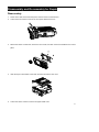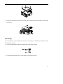
1
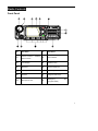
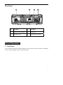
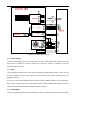
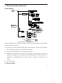
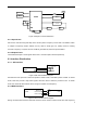
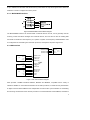
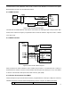
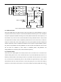
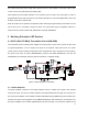
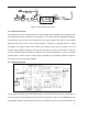
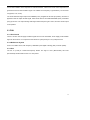
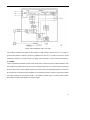
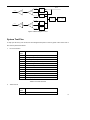
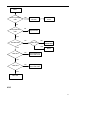
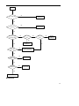
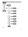
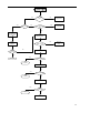
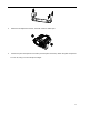
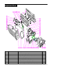
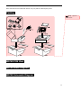
Contents
Revision History .....................................................................................................................................0
Introduction ............................................................................................................................................1
Radio Controls........................................................................................................................................2
Circuit Description .................................................................................................................................3
Description of Components ................................................................................................................20
Tuning....................................................................................................................................................22
Port Definition.......................................................................................................................................22
Troubleshooting Flow Chart................................................................................................................26
Disassembly and Re-assembly for Repair .........................................................................................31
Exploded View ......................................................................................................................................34
Packing..................................................................................................................................................36
MD78X PCB View..................................................................................................................................36
MD78X Block Diagram .........................................................................................................................36
Specifications .......................................................................................................................................37
Revision History
Material No.
Date of
Issue
May 2010
Changes
Initial Release
Introduction
Manual Scope
This manual is intended for use by experienced technicians familiar with similar types of communication
equipment. It contains all service information required for the equipment and is current as of the
publication date.
This mobile radio shall be serviced by qualified technicians only.
Copyright Information
Hytera and HYT are the trademark or registered trademark of Hytera Communications Corporation
Limited (hereinafter referred to as “Hytera”) in PRC and other countries and/or areas. Hytera retains the
ownership of its trademarks and product names. All other trademarks and/or product names that may be
used in this manual are properties of their respective owners.
The Hytera product described in this manual may include Hytera computer programs stored in memory
or other media. Laws in the PRC and/or other countries or areas preserve for Hytera exclusive rights for
Hytera computer programs. The purchase of this product shall not be deemed to grant, either directly or
by implication, any rights to the purchaser with respect to Hytera computer programs. Any Hytera
computer programs may not be copied, modified, distributed, decompiled, or reverse-engineered in any
manner without the prior written consent of Hytera.
Disclaimer
Hytera endeavors to achieve the accuracy and completeness of this manual, but no warranty of
accuracy or reliability is given. All the specifications and designs are subject to change without prior
notice due to continuous technology development. Changes which may occur after publication are
highlighted by Revision History contained in Service Manual.
No part of this manual may be copied, modified, translated, or distributed in any manner without the
express written permission of Hytera.
1
Radio Controls
Front Panel
No.
1
○
Part Name
Volume Control / Channel
Selector Knob
No.
Part Name
2
○
LED Indicator
3
○
LCD Display
4
○
OK/Menu Key
5
○
Back Key
6
○
Power On/Off Key
7
○
Up Key
8
○
Down Key
9
○
Speaker
10
○
Programmable Keys
11
○
Microphone Jack
12
○
Emergency
key
(programmable)
2
Rear Panel
No.
Part Name
No.
Part Name
1
○
Antenna Connector (BNC)
2
○
Power Inlet
3
○
Accessory Jack
4
○
GPS Antenna Connector
Circuit Description
1. Front Panel
The front panel provides parts including speaker, keys, power switch, volume control knob, LCD display
and etc. The block diagram is shown as the figure below:
3
Figure 1 Front Panel Block Diagram
1.1 Power Supply
The main board supplies power to the front panel via 5VD, so that RX/TX LED, backlight and USB
devices can be powered up. Power is further fed to U5 LDO, and then is supplied to LCD and
serial-to-parallel converter IC.
1.2 Keys
The front panel provides as much as ten keys including the programmable keys (S2, S3, S8, S9, S10
and S12), Up/Down key (S5, S11), Menu key (S4), Back key (S6), Power On/Off key (S1) and
Emergency key (S7).
A 3 row by 4 column matrix keyboard of the processor is used to identify operations of front panel keys.
Each of the 3 row signal lines are connected with the pull-up resistors R488, R499 and R511, and the 4
column lines are monitored to detect if a button has been pressed.
1.3 LCD Display
The TFT LCD can transfer data via the bus EMIFS of U302. Control signals include, write/read enable,
4
memory chip select, LCD chip select and reset signal, and the signals will be pulled up by R36, R35, R34,
R33 and R6 respectively. 5V voltage is converted to 3.3V by U5, and is then supplied to the LCD.
1.4 LED and Backlight
LED enable signal is fed to the serial-to-parallel converter IC, and then is output by U302. RX status is
indicated by green LED, and TX is by red LED. Backlight will be illuminated once any key is pressed.
The red and green LEDs in series are powered by 5V (U902) and controlled by Q2 and Q3. The
backlight is powered by 5V and controlled by Q1. Control signals are output via U1.
1.5 MMP Interfaces
The MMP interfaces are defined as follows:
No.
1
2
3
MMP10
Definition & Description
Accessory identifier
The pin together with pin 10 can form an accessory
port 1
identification matrix.
PTT input
Handset audio
output
4
USB_D-
5
GND
6
USB_VBUS
7
Mic input
8
USB_D+
9
HOOK
10
Accessory identifier
port 2
Used to input PTT signal from microphone. The pin is at
low level when PTT is hold down.
Used to output audio received from accessories; the
Handset option must be checked in the CPS.
USB data line DGround
Provides +5V for USB accessories.
Used to input external microphone signal. Vrms=80mV
@ 3K dev.
USB data +
Valid upon low level. The default is high level.
The pin together with pin 1 can form an accessory
identification matrix, details of which are stated in the file
“Definition of External Interfaces”.
Table 1 Definition of MMP Interfaces
1.6 Audio output
The front panel provides two paths of audio output Handset_audio and SPK±. Handset_audio is the
output of received audio via MMP interface, and SPK± is the output by the PA U201 as audio signal for
the front panel speaker.
1.7 Volume Control
The encoder switch U7 will generate volume adjustment signals, which will be routed to U302 by
GPIO17 and GPIO18.
5
2. Working Principle of Baseband
Power System
Figure 2 Diagram of Power Distribution
Both the baseband control IC and the RF section can convert the supplied voltage to the appropriate
level via the voltage conversion IC.
z
RF section: U914, Q920 and Q921 supply power for the RF section. High current PNP transistor
and comparator can function as LDO (Low Dropout Regulator).
z
FGU: U918 and U915 supply 3.3V and 5V respectively to U100.
z
Baseband: the processor U302 is supplied by 3.3V (U900), 1.8V (U903) and 1.6V (U919); the
memories are supplied by 3.3V (U900) and 1.8V (U903) respectively; the audio processor IC is
supplied by 3.3V (U900&U909) and 1.8V (U903); the DAC is supplied by 5V (U905) and 3.3V
(U900).
z
EXT_SWB+: Q909.
2.1 Power On/Off
6
The mobile radio can be powered on/off through any of the following methods:
1)
Power On/Off key
2)
Ignition sense or Power On/Off key
3)
Emergency
2.1.1 Power On/Off key
After the user presses the front panel Power On/Off key, R944 is grounded, and Q910 and Q905 are
turned on, causing the power management IC U902 and Q920 to start working. Then the processor
U302 will execute user routines, and can identify power on/off signals if low level is detected from Q914,
using the level PWR_CTRL to maintain or cut off the connection with the power system.
2.1.2 Ignition Signal
When voltage of ignition signal exceeds 7V, Q1 will be turned on through charging by C933, R955 and
R956, and the PNP transistor of Q905 will be further turned on to supply power. Q401 will also be turned
on. If signal is detected from Q401, U302 can identify ignition signals and then will generate the level
PWR_CTRL.
2.1.3 Emergency Alarm
When the emergency alarm pin is at low level, R940 is grounded, and Q906 is turned on to supply power.
Q908 is also turned on. When low level is detected from Q908 but the radio is powered off, U302 will
output the level PWR_CTRL and send emergency signal. If the radio is powered on then, U302 will only
output emergency signal.
2.1.4 Power-up Process
1)
Turn on the radio through any of the methods mentioned above, and ensure enough time for
U900, U902, U903 and U919 to be turned on.
2)
U917 will generate reset signal and remain low level for 1.25 seconds. Then the processor
starts to work.
3)
Each method will generate and send a specific power-up signal to the processor.
4)
After the signal is received, the processor will generate the level PWR_CTRL, and finish
power-up procedures.
2.2 Clock
7
Figure 3 Diagram of Clock Distribution
2.2.1 Input Clock
32K clock is used for timing and sleep of the whole system. Frequency of this clock is 32.768kHz, which
is subject to frequency division without error by U302 to finally get 1Hz, usually used for counting
seconds. Frequency of system clock is 19.2MHz, generated by external crystal oscillator.
2.2.2 Output Clock
The baseband outputs 3 clock signals fed to U231, U100 and Option board respectively.
2.3 Interface Distribution
2.3.1 SPI Interface
Figure 4 SPI Interface Block Diagram
SPI interface of the processor U302 can operate in master mode, controlled by MPU or DMA. In master
mode, U302 can provide 4 chip select signals, with CS2 used to enable IF processor U701. In master
mode, the maximum data transfer rate is as high as system clock frequency.
2.3.2 MCSI Interface
MCSI1.DOUT
Dat
a
CLK
MSCI1.SYNC
/CS
MCSI1.CLK
U302
U100
Figure 5 MCSI Interface Block Diagram
During communication between U302 and U100, the former works in master mode with clock frequency
8
of up to 9.6MHz, and the latter uses MCSI frame synchronization as chip select signal. MCSI1.DOUT as
a data line is used to configure the memory U100.
2.3.3 MICROWIRE Interface
Figure 6 MICROWIRE Interface Block Diagram
The MICROWIRE interface can accommodate 4 external devices at most, and is generally used for
receiving control and status messages from external devices, and can also be used for reading data
from ROM. Its maximum clock frequency is a quarter of system clock frequency. MICROWIRE is used
for configuration of and reading from the audio processor, and requires chip select signal CS3.
2.3.4 SSI Interface
MCBSP3.CLKX
MCBSP3.FSX
U231
BCLK
MCBSP1.CLKX
WCLK
MCBSP1.FSX
SDIN
MCBSP1.DX
SDOUT
MCBSP1.DR
PCMCLK
PCMSYNC
MCBSP3.DX
PCMIN
MCBSP3.DR
PCMOUT
Option
Board
U302
CLKOUT
U701
FS
DOUTA
SCLK
FS
U500
DIN
/ LOAD
/PD
MCBSP2.CLKR
MCBSP2.FS
R
MCBSP2.DR
MCBSP2.CLKX
MCBSP2.FSX
MCBSP2.DX
GPIO29
GPIO31
Figure 7 SSI Interface Block Diagram
U302 provides 3 McBSP interfaces McBSP1, McBSP2 and McBSP3, compatible with a variety of
interfaces. McBSP1 is connected with interface I2C of audio processor, to realize two-way transmission
of digital voice and data. McBSP2 uses independent clock and frame synchronization for transmitting
and receiving. Interface SSI of the receiver processor is connected with RX end of McBSP2, and U500 is
9
connected with TX end of McBSP2. U302 works in master mode. McBSP3 is connected to the Option
Board interface for both voice and data transmission.
2.3.4 USB Interface
Figure 8 USB Interface Block Diagram
The radio has two USB interfaces, and both are connected to the USB signal port of the processor. REF
CLOCK is the reference frequency in specified mode. It should be 12MHz in high rate mode or 1.5MHz
in low rate mode.
2.3.5 UART Interface
Figure 9 UART Interface Block Diagram
U302 provides three UART interfaces, which enables the processor to communicate with a variety of
external devices. UART2 is used for communication with front panel and serial port on PC, and UART3
is used for communication with Option board and accessory jack (USB).
2.3.6 Further Development Port (MAP)
Further development port includes audio interface, programmable I/O, serial port, USB port, accessory
identifier port and etc, used for further development by the user. The pins are defined as follows:
Pin
Function
Description
10
1
Vbus USB power supply
2
Ground
3
+5V power supply
GP5_3 general purpose I/O port
General purpose I/O port with function defined
(Chan_Act)
through the CPS
4
SW B+ sense power output
13V output voltage; output current ≤1.5A
5
External Alarm
Programmable output pin (the default is External
Alarm)
6
Power Ground
7
Tx Audio input (audio from external
Used to input signal from external mic; audio
mic)
path is valid upon press of external PTT.
8
RX Audio output
Used to output received audio signal.
9
Spkr-
External speaker output -
10
USB D+
USB data +
11
USB_GROUDN
Ground line
12
GP5_2 general purpose I/O port
General purpose I/O port with function defined
(Monitor)
through the CPS (the default is Monitor)
13
ACC_IO2
Accessory identifier port; three kinds of
accessory identification status, and one default
status are provided by the pin together with pin
15 ACC_IO3.
When Emergency is active, this pin is at low
14
Emergency switch
15
ACC_IO3
Accessory identifier port
16
PRGM_IN_PTT
Programmable input pin (the default is PTT)
17
Audio Ground
18
Speaker +
External speaker output +
19
USB D-
USB data -
20
GP5_8 general purpose I/O port / serial
level.
valid upon low level
port RX
21
Ground
22
GP5_7 general purpose I/O interface /
serial port TX
general purpose I/O interface
general purpose I/O interface
General purpose I/O interface with function
23
GP5_6 general purpose I/O interface
24
AUX Audio Output 1
External speaker audio output 1
25
AUX Audio Output 2
External speaker audio output 2
26
Ignition sense
Used to input ignition voltage
defined through the CPS
Table 2 Definition of Further Development Port
2.4 Audio Path
11
PUB_ADDRESS2
RX_AUDIO
PUB_ADDRESS1
EXT_SPK
INT_MIC
Figure 10 Block Diagram of Audio Path Connection
2.4.1 RX Audio Path
U302 sends digital audio to the audio processor codec via the SSI bus of interface MCBSP1. The bus is
composed of CLKX, FSX, DX and DR. It sends the demodulated PCM audio signal to codec, and adjusts
the signal to appropriate amplitude according to the volume (RMS should be 80mv when frequency is 1k
and deviation is 3k). Then the codec converts PCM data into analog audio data via DAC. U231 provides
two outputs SPK1 and SPK2. SPK1 is amplified by U238 and then is fed to the PA U201, to derive two
outputs of received audio, which will be applied to the front panel speaker and further development
interface respectively. SPK2 is amplified and divided into the four paths of signal HANDSET_AUDIO,
RX_AUDIO, PUB_ADDESS1 and PUB_ADDESS2. The first two paths are amplified by U235, and the
last two paths are amplified by U236. Output of HANDSET_AUDIO, PUB_ADDESS1 and
PUB_ADDESS2 are controlled by Q231, Q235 and Q233 respectively.
2.4.2 TX Audio Path
There are two mic inputs applied to the audio processor U231. The internal mic is connected to the
interface MICIN_HND of U231, and is combined with AUX1 to provide differential input. After 9.3V is
divided by R255 and R264, a bias voltage of about 7V is provided to the front panel mic. The external
mic is connected to the interface MIC_HED of codec, featured as single-ended input . Q232 controls
switch between both mics. When internal mic is active, EXT_MIC_EN is at low level, bias voltage of
external mic is disconnected, and the ADC in U231 senses voltage at pin MICIN_HND. When external
12
mic is active, EXT_MIC_EN is at high level, Q232 is turned on, bias voltage is connected, and the ADC
in U231 senses only audio data at pin MICIN_HED.
Audio signals input from MMP interface or the accessory jack, are fed to the codec (gain of codec is
programmable via the CPS) and then are converted by the ADC into 16-bit PCM digital audio, which will
be fed to U302 via the interface SSI.
When the radio is set to operate in loudspeaker mode, audio signal is generated by the internal mic, and
then is fed to U231, and finally is output via SPK2. The output audio signal is amplified, and then is
output as the two paths of audio PUB_ADDRESS1 and PUB_ADDRESS2.
3. Working Principle of RF Section
3.1 UHF1 (400-470 MHz) Transmitter Circuit (5W-45W)
The transmitter section includes power amplifier circuit and power control circuit. The PA circuit is used
for signal amplification, so as to amplify VCO signal to the required output power level. The power
control circuit is used to maintain output power at the required level, and to protect the PA from heating,
and protect the driver PA Q801 (RD07MUS2B), pre-driver PA Q805 (RD01MUS1) and final PA
(PD85035S-E) from damage caused by antenna mismatch, or high/low voltage.
Figure 11 Block Diagram of Transmitter
3.1.1 Power Amplifier
The power amplifier comprises of four-stage amplifier circuits, to amplify VCO signal to the required
output power level. The first is the buffer amplifier circuit (BFG540W) with fixed gain, the second is the
pre-driver power amplifier circuit LDMOS (Lateral Double Diffuse MOS) (RD01MUS1) with variable gain,
the third is the driver power amplifier circuit LDMOS (RD01MVS1) with variable gain, and the last is the
final power amplifier circuit LDMOS (PD85035STR1-E) with fixed gain. The TX power amplifier circuit
13
also includes TX/RX switch and low pass filter.
3.1.2 TX Buffer Amplifier
The buffer amplifier BFG540W (Q801) provides about 16dB power gain, and adjusts the bias circuit to
get quiescent bias current of 28mA for Q801. Power supply for the switching transistor Q810 is
controlled by TX signal (antenna switch enable signal), so as to connect or cut off the power supply for
the whole circuit.
3.1.3 Pre-driver Power Amplifier
The pre-driver power amplifier comprises of LDMOS RD01MUS1 (Q805), with gain controlled by voltage
VGG. The input matching circuit is composed of C826, L826, L814, C843 and R824.
3.1.4 Driver Power Amplifier
The driver power amplifier comprises of LDMOS RD07MVS1 (Q804), with gain controlled by voltage
VGG. The maximum output power is 38.5dBm, and the maximum gain is above 11dB.
3.1.5 Final Power Amplifier
The final power amplifier comprises of two LDMOS PD85035STR1-E (Q802 and Q803), with the
maximum output power of 48.5dBm, and the maximum gain of above 10dB. The input matching circuit is
composed of C815, C839, R804, R806, R807, R813, R818 and R861. And the power combining circuit
comprises of C820, C8330, C831, C819, C812, C841 and C842.
3.1.6 Antenna Switch
The antenna switch is used to switch between the transmitter circuit and the receiver circuit. In TX mode,
the switching transistor Q810 is controlled by TX signal, so as to supply 9V 3A to the PIN diodes D801
and D802. Quiescent bias current of the PIN diode is controlled by the resistors R821 and R825. In TX
mode, D801 and D802 are turned on, and RF signals are applied to the low pass filter (C871, C816,
C836, C837, C838, L809, L813, and L810) and then transmitted via the antenna port.
In RX mode, TX signal controls the switching transistor Q810, to further control the power supply for the
PIN diodes D801 and D802, which has no DC bias current. When the two diodes are turned off, signals
are fed into the low pass filter (L871, C852, C862) and then passed to the RX path.
3.1.7 Low Pass Filter
The low pass filter comprises of inductors L809, L813 and L810, and capacitors C836, C837, C830 and
C838, and is used for attenuation of harmonic energy from the transmitter.
3.1.8 Directional Coupler
The directional coupler is comprised of the Microstrip Directional Coupler, D803, D804 and etc, and is
14
used for detecting forward power and reverse power of the transmitter. The forward power is coupled
with the diode D803, and the voltage is applied to the power control circuit (U801). Then the output
voltage VGG is applied to control the gate voltage of pre-driver and driver PA, for the purpose of stable
power output.
The directional coupler is not only the TX power adjustment circuit, but also a part of the VSWR
detection circuit. The reverse power is coupled with D804. The voltage is applied to U802 and then is fed
into U302 for judgment.
3.1.9 Output Power Control
The TX power is controlled via the power control IC U801. The forward power is applied to the directional
coupler, to output a voltage that can represent the forward power. The voltage together with the preset
voltage are fed into U801 to output a voltage VGG, which can control both gate voltage and gain of Q804
and Q805, for the purpose of stable power output.
3.1.10 Heating and Over-voltage Protections
The circuit comprises of thermistor RT804 and resistor R884. The output voltage is proportional to the
detected temperature. Both the voltage used for temperature detection and the threshold voltage are fed
into the operational amplifier U803, to output a voltage signal that is in proportional to the detected
temperature. The voltage is applied to software judgment, and then the preset voltage will be
subsequently changed to lower TX power, and to protect the PA from over-heating.
3.1.11 Pressure Pad Switch
The power control circuit includes a pressure pad switch SW1, which is controlled by the conductive
rubber part mounted on the top cover. When the switch is off, the power control voltage VGG is pulled
low, and the PA gives no power output. When the top cover is secured to the base, the switch will be
turned on and the PA will work normally. This mechanism will help to protect the PA from damage due to
improper installation.
3.2 UHF1 (400-470 MHz) Receiver Circuit
The receiver utilizes double conversion superheterodyne techniques. The first IF is 73.35MHz and the
second IF is 2.25MHz. The first local oscillator signal is supplied by the PLL circuit U100. And the second
local oscillator signal (71.1MHz) is generated by the PLL circuit U701. The main units are BPF and LNA,
mixer, IF filter, IF amplifier and IF processor.
15
Figure 12 Block Diagram of Receiver
3.2.1 Front-end Circuit
RF signals are fed into the low pass filter to remove signals above 550MHz, and are applied to the
two-stage band pass filter to select the wanted signal. TV can realize 400-470M bandwidth adjustment.
After passing through the BPF and LNA (Q6102), the RF signals together with the first local oscillator
signal are fed into the mixer for the first time frequency conversion, to generate the first IF signal
(73.35MHz). The passive diode mixer provides good dynamic range and port isolation. The local
oscillator signal (3-5dBm) supplied by the VCO is fed into Q6103, to get the required gain of 17dB. The
first local oscillator signal (73.35MHz) is applied to the crystal filter (Z6100) to remove out-of-band
spurious signal, and then is fed into the two-stage IF amplifier circuit composed of Q6133 and Q6134,
and finally goes to the IF processor AD9864.
3.2.1 Rear-end Circuit
SSI TO OMAP
IF input
16.8MHZ
Reference
frequency
Figure 13 IF processor AD9864
The IF signal (73.35MHz) goes into AD9864 via pin 47 for the second time mixing, to generate the
second IF signal (2.25MHz). Digital I/Q signal output from the SSI pin is fed into U302 (OMAP5912) to be
demodulated. AD9864 employs reference frequency of 19.2MHz and shares the crystal with OMAP. The
16
second local oscillator VCO comprises of external transistor, varactor and some other components, to
generate the second local oscillator signal. The 18MHz clock frequency is generated by LC resonance
loop (D702, L715, C745).
The 16-bit 20K audio signal output from AD9864 (U701) is applied to the DSP pin (U302C), and then is
applied to U302 to output 8K data signal, which will be fed into TLV320AIC29IRGZR (U231) and PIN44
(SSI_DI) for DAC. The output analog audio signal will be subject to gain control, and then will be output
to the speaker.
3.3 FGU
3.3.1 PLL Circuit
The PLL circuit is used to supply excitation signal source for the transmitter, and to supply local oscillator
signal for the receiver. It is composed of the reference crystal (X100), PLL IC (U100) and VCO.
3.3.2 Reference Crystal
X100 is a 19.2MHz TCXO, with frequency calibrated by the Digital to Analog (D/A) converter (U500).
3.3.3 PLL
The PLL IC (U100) is a fractional frequency divider. The logic IC U101 (MC74VHCS) and U102
(MC74VHCS) will work with the PLL IC to lock phase.
17
Figure 14 Block Diagram of PLL IC (U100)
The 19.2MHz frequency generated by the reference crystal (X100) is fed into the PLL IC (U100), to
generate the reference frequency. Frequency obtained from the PLL IC (U100) is fed into the phase
comparator, and is then converted to DC CV voltage via the loop filter, to control and lock the frequency.
3.3.4 VCO
VCO is comprised of transistors (Q100, Q103, Q106, Q110), varactors and four Colpitts Oscillators, with
two transistors (Q100 and Q103) as the source of excitation signal for TX, and the other two (Q106 and
Q110) as the source of local oscillator signal for RX. U302 controls the operating frequency of the VCO.
Q102 and Q107 constitute the buffer amplifier for the transmitter section, and Q111 and Q109 constitute
the buffer amplifier for the receiver section. The Digital to Analog (D/A) converter (U500) outputs
demodulation signal to demodulate TX oscillator signal.
18
MOD
TX_L_VCO
Q103
TX PA
Q102
Q107
Q100
TX_H_VCO
LPF
PLL IC (U100)
RX_L_VCO
Q110
RX Lo
Q111
Q109
Q106
RX_H_VCO
Figure 15 Block Diagram of VCO
System Test Plan
To help you test every unit circuits, we have designed test points on the key parts of the circuit. Test of
RF circuit is planned as follows:
1.
PLL/VCO Section
Test
Points
Definition
TP101
Feedback signal output from VCO
TP102
RF signal output from VCO
TP103
CV voltage/LPF output
TP104
Modulation signal MOD1 output from DAC
TP105
Control voltage terminal of crystal
TP106
Modulation signal MOD2
TP107
PLL-Data
TP108
PLL-CLK
TP109
PLL-LE
TP110
LD detection signal
TP111
3.3VA
TP112
5V charge pump
Table 3 PLL/VCO Test Plan
2.
TX/RX Circuit
Test
Points
TP601
Definition
9.3VA
19
TP602
TV
TP603
RF signal input
TP604
LNA input
TP605
LNA output
TP606
LO input
TP607
Mixer input
TP608
Mixer output
TP609
Crystal filter output
TP610
AD9864 input
TP611
5VA
Table 4 TX/RX Test Plan
Description of Components
1. Main Board
Ref No.
Part
Name
Specifications
Description
U100
IC
SKY72310 2.1 GHz
PLL IC
U101
IC
FSA66P5X 1-channel 1.65-5.5V 0.3ns
-65~+150°C 7Ω SC70-5
Switch IC
U102
IC
FSA66P5X 1-channel 1.65-5.5V 0.3ns
-65~+150°C 7Ω SC70-6
Switch IC
U201
IC
TDA7297D 10
Audio amplifier
U231
IC
TLV320AIC29IRGZ
Baseband processor
U232
IC
K4M28163PN-BG75 SDRAM 128M 1.8
-25~+85℃ FGBA-54
Memory
U233
IC
TV00570002CDGB
NOR-FLASH+PSRAM
Memory
U235
IC
LM2902 Quad Operational Amplifier
Operational
Amplifier
U236
IC
LM2902 Quad Operational Amplifier
Operational
Amplifier
U237
IC
TS5A3159DCKR 1-channel
Switch IC
U238
IC
NJM2904V
Operational
Amplifier
U302
IC
OMAP5912ZZG 32
MCU
U327
IC
74HC595DTR2G
Logic IC serial to
parallel converter
U328
IC
74HC595DTR3G
Logic IC serial to
parallel converter
U401
IC
AAT4618IGV
Current Limited
Load Switch
20
U500
IC
TLV5614IPW
D/A converter
U6000
IC
TA75S01F
Operational
Amplifier
U701
IC
AD9864 10-300MH
IF processor
U702
IC
RP102N331B LDO
Power management
IC
U703
IC
XC6209F502PR LDO
Power management
IC
U801
IC
AD8566ARMZ 0.256
Operational
Amplifier
U802
IC
TA75W01FU
Operational
Amplifier
U803
IC
TA75S01F
Operational
Amplifier
U900
IC
RP102N331B LDO
Power management
IC
U901
IC
RP102N331B LDO
Power management
IC
U902
IC
AAT1189IRN-0.6-T1
Power management
IC
U903
IC
XC6209F182PR LDO
Power management
IC
U905
IC
XC6209F502PR LDO
Power management
IC
U909
IC
RP102N331B LDO
Power management
IC
U910
IC
TPS3808G33-Q1 3.3
Reset IC
U914
IC
NJM2904V
Operational
Amplifier
U915
IC
XC6209F502PR LDO
Power management
IC
U917
IC
R3111N421A-TR-F 4
Reset IC
U918
IC
XC6209F332PR LDO
Power management
IC
U919
IC
TPS62050DGS Regulator 2.7~10Vin
1.5~5.5Vout 800mA -40~85℃ DGS
Power management
IC
X100
IC
DSA535SD-19.2MHz
TCXO
X302
IC
DSB321SDA 19.2MHz
TCXO
X375
IC
SSP-T7F 32.768KHz
Crystal
Z6100
IC
D73312GQ12 73.35
Crystal filter
F900
IC
046602.5NR 32V 2.
Fuse
Specifications
Description
2. Display Section
Ref No.
Part
Name
21
U1
IC
Serial to parallel converter
-40~125℃ TSSOP16 NXP
2~5.5V
U2
IC
CM1440-06CP low-pass
35dB@1GHz -40~+85 ℃
CSP-16 CMD
EMI Filter
30KV ESD
EMI Filter
U3
IC
CM1440-06CP low-pass
35dB@1GHz -40~+85 ℃
CSP-16 CMD
EMI Filter
30KV ESD
EMI Filter
U4
IC
CM1440-06CP low-pass
35dB@1GHz -40~+85 ℃
CSP-16 CMD
EMI Filter
30KV ESD
EMI Filter
U5
IC
XC6209F332PR LDO 12V 3.3V 300mA
-40℃-85℃ SOT89-5
Power management
IC
U8
IC
PRTR5V0U2X ESD&EMI 5V -40~85 ℃
SOT143B NXP
USB port protection
device
Logic IC
Tuning
For details about radio tuning, please refer to the help file of DMR Tuner Software supplied by Hytera.
Port Definition
1.1 Main Unit
Pin No.
Name
Description
J404 (to front panel socket)
1
INT_MIC
Audio input
2
MIC_GROUND
Mic ground
3
ACC_IO1
Accessory identifier port 1
4
USB_VBUS
USB power supply
5
HOOK
HOOK
6
PTT
PTT
7
USB_D-
USB data -
8
USB_D+
USB data +
9
ACC_IO2
Accessory identifier port 2
10
UART2_RXD_A
Volume control port
11
UART2_TXD_B
12
HANDSET_AUDI
O
Audio signal output by accessory
13
SPKR1+
Speaker audio signal+
14
SPKR1-
Speaker audio signal-
15
5VD
Power supply
16
PRST
Reset signal
22
17
KB_C0
18
KB_C1
19
KB_C2
20
KB_C3
21
KB_R0
22
KB_R1
23
KB_R2
24
CSLED
Backlight control IC chip select
25
CLOCK
Backlight control IC clock
26
DATA
Backlight control IC chip data
27
OE_LCD
LCD read enable
28
WE_LCD
LCD write enable
29
CS2_LCD
LCD chip select
30
F_A1_LCD
LCD memory select enable
31
F_D7
32
F_D6
33
F_D5
34
F_D4
35
F_D3
36
F_D2
37
F_D1
38
F_D0
39
GND
Ground
40
PWB_IN
Power on/off signal
Matrix keyboard
LCD data bus
LCD data bus
1.2 Main Unit
Pin No.
Name
I/O
Description
J403 (to end pin socket)
1
Vbus USB
2
Ground
Ground line
GP5_3
Digital
input/output
General purpose I/O interface with
function defined through the CPS
13V output voltage; output current
≤1.5A
3
Power supply
+5V, 500mA. 5V is output when
accessory identification code is
00|01|10, and low level is output when
the code is 11.
4
SW B+ sense
Power supply
5
External Alarm
Analog voltage
output
6
Power Ground
Power supply
ground
7
Tx Audio
Analog input
Programmable output pin with function
defined through the CPS (the default
is External Alarm)
Used to input signal from external mic;
audio path is valid upon press of
external PTT.
23
8
RX Audio
Analog output
Used to output received audio signal.
9
Spkr-
Analog output
External speaker output -
10
D+ USB
USB data +
11
USB_GROUDN
Ground line
GP5_2
Digital
input/output
General purpose I/O interface with
function defined through the CPS (the
default is Monitor)
13
ACC_IO2
Digital input
Accessory identifier port; three kinds
of accessory identification status, and
one default status are provided by the
pin together with pin 15 ACC_IO3.
14
Emerg Sw
Digital input
When Emergency is active, this pin is
at low level.
15
ACC_IO3
Digital input
Accessory identifier port
16
PRGM_IN_PTT
Digital input
Programmable input pin (the default is
PTT) valid upon low level
17
Audio Ground
Audio ground
18
Spkr+
Analog output
19
D- USB
12
External speaker output +
USB data -
20
Input/output
GP5_8
This pin is used as UART RX for
TETRA mobile radio, and is used as
general purpose I/O interface for DMR
mobile radio.
21
Ground
Ground line
22
GP5_7
Input/output
General purpose I/O interface
23
GP5_6
Digital
input/output
General purpose I/O interface with
function defined through the CPS
24
AUX Audio Out 1
25
26
Analog output
Aux audio (external speaker) output 1
AUX Audio Out 2
Analog output
Aux audio (external speaker) output 2
Ign Sense
Analog voltage
input
Ignition sense pin
2.1 Front Panel
Pin No.
Name
I/O
Description
J404 (to front panel aviation socket)
1
Accessory
identifier port 1
Digital input
Pin 1 and pin 10 (accessory identifier
port 2) compose an accessory
identification matrix. See MMP
accessory identification for more
details.
2
PTT input
Digital input
Used to input PTT signal from
microphone. The pin is at low level
when PTT is hold down.
3
Handset audio
output
Analog output
Accessory audio line. It is open when
accessory identification code is
24
00|01|10, and is off when the code is
11.
4
USB_D- / serial
port RX
USB data
line/input pin
USB data bus D- (compared with CPU
inside the mobile radio)
5
GND
Ground line
This pin together with MIC provides
differential input.
6
USB_VBUS
Power supply
+5V, 500mA. 5V is output when
accessory identification code is
00|01|10, and low level is output when
the code is 11.
7
Mic input
Analog input
Palm microphone input. Vrms=80mV
@ 60% system max. deviation
8
USB_D+ / serial
port TX
USB data
line/output pin
9
10
HOOK
Accessory
identifier port 2
USB data bus D+ (compared with
CPU inside the mobile radio)
Hook signal
input
Valid upon low level. The default is
high level. Hook and Monitor
functions: when key is pressed, low
level is present at this pin. Then Hook
function will be active if palm
microphone or keypad microphone is
detected, or the Monitor function will
be active if desktop microphone is
detected.
Digital input
Pin 1 (accessory identifier port 1) and
pin 10 compose an accessory
identification matrix. See MMP
accessory identification for more
details.
2.2 Front Panel
Pin No.
Name
Description
J2 (to LCD socket)
1
GND
Ground
2
VCI
2.5V-3.3V adjustable port
3
VCI
2.5V-3.3V adjustable port
4
IOVCC
1.65V-3.3V adjustable; input/output port
5
FLM
Synchronization signal control port
6
CS
Chip select signal
7
RS
Memory select
8
WR
Write signal
9
RD
Read signal
10
DB0
Data bus
11
DB1
12
DB2
13
DB3
25
14
DB4
15
DB5
16
DB6
17
DB7
18
DB8
19
DB9
20
DB10
21
DB11
22
DB12
23
DB13
24
DB14
25
DB15
26
DB16
27
DB17
28
RESET
29
IM3
30
IM0
31
LEDA
32
LED_K1
33
LED_K2
34
LED_K3
Reset signal
Select data line
LED positive
LED negative
Troubleshooting Flow Chart
MCU
26
MCU
Power-up display
OK?
Yes
Check control
circuit
RF circuit does
not work
No
Front panel FPC
OK?
No
Replace FPC
Yes
19.2 MHz OK?
No
No
3V3A OK?
Yes
Yes
1V6D OK?
No
Check
U905&U909
Reset
Check power-up
circuit and U919
Yes
1V8D OK?
No
Check power-up
circuit and U903
Yes
MCU OK
VCO
27
VCO
No
Replace
U915&U918
5VA, 3V3A OK?
Yes
No
4V3A OK?
Replace Q104
Yes
RX oscillator OK?
CV voltage OK?
No
Q108, Q112
OK?
Yes
Q106, Q110
OK?
No
Replace
Q106&Q110
No
Replace
Q108&Q112
Yes
Q106, Q110
output OK?
No
Yes
Check D107, D108,
D109, D110, D121,
D122, D125, D126
Yes
Feedback OK?
No
Check
feedback circuit
Yes
19.2MHz
oscillator OK?
No
Check power
supply circuit
Yes
Check CPU data circuit
RX Circuit
28
No RX audio
No
9V3A output OK?
Check power-up
circuit
Yes
Yes
9V1A output OK?
No
Check Q902,
Q903
No
Front panel output
OK?
Replace front
panel
Yes
No
Check U703
U703 output OK?
Yes
No
Check IC125
U702 output OK?
Yes
No
2nd local oscillator
OK?
Check Q701,
Q702
Yes
No
18MHz OK?
Check D702
Yes
IF input present
at U701 PIN47?
Yes
Check U701 and
surrounding
components
No
Yes
Is RF signal present?
Check VCO
No
Check Q6103
TX Circuit
29
Yes
Yes
No
Current OK?
Power supply
OK?
Control voltage
OK?
No
Check power
supply circuit
Low
Check U801
High
Check transistor,
bias voltage and
low pass filter
Check driver PA
Yes
Repair
transmission
network
Driver PA OK?
See VCO
troubleshooting
chart
No
Power
output OK?
No
Check matching circuit
No
Yes
Yes
Complete
Power OK?
No
Complete
Replace Q805
No
Yes
Power output OK?
Complete
No
Replace Q804
No
Yes
Power
output OK?
Complete
No
Replace Q802
30
Disassembly and Re-assembly for Repair
Disassembly
1. Power off the radio, disconnect the power cord and screw out the antenna.
2. Loosen the three screws to remove the front panel. Remove the FFC.
3. Detach the volume control knob, loosen the four screws, and then remove the PCB from the control
panel.
4. Undo the clips on both sides of the radio, and then remove the rear cover.
5. Loosen the eleven screws to remove the upper shield cover.
31
6. Loosen the screw fixing the antenna connector and two screws fixing the PA module, and then take
the PCB out.
Assembly
For the reassembly of the mobile radio, please do the contrary to disassembly procedures. Other
procedures are as follows:
1.
Fix the microphone hanger with three self-tapping screws (white, 4.0X16).
2.
Fix the radio bracket with four or six self-tapping screws (black, 4.8X20).
32
3.
Fasten the two adjustment screws, each with a silicone rubber pad.
4.
Connect the palm microphone to the radio (via front-panel connector). When the palm microphone
is not in use, hang it on the microphone hanger.
33
Exploded View
B
39 38 37 36 35 34
A
40
41
33
42
43
44
45
46
47
32
31
30
29
28
48
49
27
26
25
24
23
22
50
21
1
No.
Material No.
1
6300109000000
2
3
4 5 6
7 8 9 10 11 12 13 14 15 16
Description
17 18 19 20
Qty.
Aluminum chassis (RoHS)
1
2
7500358000000
Heat sink pad 00 (RoHS)
1
3
6100492101000
Waterproof ring for front case 00 (RoHS)
1
4
4210090000200
Signal cable (RoHS)
1
5
5208010100010
Connector (male) 10Pin (RoHS)
1
6
6001079000000
Light-guide plate for keys 00 (RoHS)
1
7
7300048000000
Metal dome for main key 00 (RoHS)
1
8
6100408001000
Waterproof ring for microphone jack 00 (RoHS)
1
34
9
6100488000000
P+R control panel keys 00 (RoHS)
1
10
6201893000000
Speaker fixing sheet 0.8mm 00 (RoHS)
1
11
7102606021000
Self-tapping screw ST2.6*6.0mm 00 (RoHS)
6
12
4210080000700
Speaker cable (with 2-Pin plug) (RoHS)
1
13
5001210000390
Speaker 20Ω 4/8W (RoHS)
1
14
7400297000000
Speaker felt 00 (RoHS)
1
15
7102505000110
Machine screw M2.5*5.0mm (RoHS)
3
16
6001076000010
17
18
6201739000000
Front case for control panel (RoHS)
1
Logo (RoHS)
1
Inner lining of knob 00 (RoHS)
1
19
6000876000000
Encoder knob 00 (RoHS)
1
20
6100493000000
Power on/off key 00 (RoHS)
1
21
6100404000000
Emergency key 00 (RoHS)
1
22
7500344000000
PORON pad T=1.0mm (RoHS)
1
23
5130000000040
TFT LCD 2.0" TFT (RoHS)
1
24
6001078000000
LCD bracket 00 (RoHS)
1
25
5202002100270
Board-to-wire connector 2-Pin female (RoHS)
1
26
7207003700000
Nut M6.0*2.3mm 00 (RoHS)
1
27
6100334000000
O-ring for encoder switch 00(RoHS)
1
28
4399030000020
Rotary switch (RoHS)
1
29
PCB for control panel
1
30
6100533101000
Waterproof ring for aluminum chassis 00 (RoHS)
1
31
6300126000000
Upper cover of aluminum chassis 00 (RoHS)
1
32
7103015000000
Machine screw M3.0*15.0mm 00 (RoHS)
11
33
6001080000000
Plastic upper cover 00 (RoHS)
1
34
6100496000000
Conductive silicone rubber for main board 00 (RoHS)
1
35
7103008000400
Machine screw M3.0*8.0mm 00 (RoHS)
2
36
7500272000000
Heat sink pad 00 (RoHS)
2
37
1301000000000
Semi-finished PA with heat sink pad (136-870MHz)
(RoHS)
1
38
3414999000020
PNP transistor (RoHS)
1
39
40
6100532100000
Main PCB
1
D_SUB waterproof ring 00 (RoHS)
1
41
5208026100000
Jack 26-Pin D_SUB (RoHS)
1
42
6100530100000
Waterproof ring for power socket 00 (RoHS)
1
43
5205002100110
Power socket male (RoHS)
1
44
3103994770150
Electrolytic capacitor (RoHS)
1
45
7212002500000
Nut M12.0*2.5mm 00 (RoHS)
1
46
6100531100000
Waterproof ring for antenna connector 00 (RoHS)
1
47
4401000009000
BNC RF connector (RoHS)
1
48
6100494000000
GPS soft stopple 00 (RoHS)
1
49
7500159000100
Thermal conductive silicone rubber 00 (RoHS)
2
50
7500357000000
Heat sink pad 00 (RoHS)
1
A
6100574100000
O_RING 00 (RoHS)
11
B
7500344000000
PORON pad (RoHS)
1
35
Note: Parts that are not marked with Part No. may vary with the radio frequency band.
Packing
批注 [Iris1]: 主机图 HYT
LOGO 需处理。
MD78X PCB View
MD78X Block Diagram
MD78X Schematic Diagram
36
Specifications
General
Frequency Range
UHF: 400-470MHz
Channel Capacity
256
Channel Spacing
25/20/12.5 KHz
Operating Voltage
13.6V DC ±15%
Current
Drain
Standby
0.6A
Receive
<2.0A
Transmit
<12A (5-45W)
Operating Temperature
-30℃~+60℃
Dimensions (H×W×D)
174 X 60 X 200 mm
Weight
1.7 Kg
Frequency Stability
±1.5ppm
<8A (5-25W)
Receiver
0.3μV (12dB SINAD)
Sensitivity
0.22μV (Typical) (12dB SINAD)
0.4μV (20dB SINAD)
Adjacent Channel Selectivity
65dB @ 12.5 kHz / 75dB @ 20&25 kHz
Intermodulation
75dB @ 12.5/20/25 kHz
Spurious Response Rejection
75dB @ 12.5/20/25 kHz
Rated Audio Power Output
3W
Rated Audio Distortion
≤3%
Transmitter
RF Power Output
Spurious and Harmonics
Low Power: UHF1 (400-470MHz), 5-25W;
High Power: UHF1 (400-470MHz), 5-45W;
-36dBm<1GHz
-30dBm>1GHz
±2.5kHz @ 12.5 kHz
Modulation Limiting
±4.0kHz @ 20 kHz
±5.0kHz @ 25 kHz
FM Noise
40dB @ 12.5 kHz
43dB @ 20KHz
45dB @ 25 kHz
Audio Distortion
≤3%
NOTE: All Specifications are tested according to TIA/EIA-603, and subject to change without notice due
37
to continuous development.
38