1
SERVICE MANUAL
I.
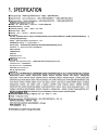
1 SPEClFlCAlON
CONTENTS
................................
2 . STRUCTURAL DIAGRAM
........................
..............................
.............................
5 . P.C. BOARDS ..................................
6 . CIRCUITEXPLANATION .........................
1
2
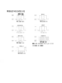
3 . BLOCK DIAGRAM
3.a
4 . CIRCUIT DIAGRAM
3.b. 3-c
.
.....................
...............................
9 . REFERENCE DATA .............................
10. PARTSLIST ....................................
7 CHECK AND ADJUSTMENT
8. ICCHECK POINT
4
8
10
16
19
25
I.SPECIFICATION
W Front panel inpul : FRONT (GUITAR IN) fixed al - 2OdB ( - MBm h4AX)IlM R
W Back panel inpul : Input levelmpedance : 44dB (+19dBmMAX)IMK O
W Back panel oulpul : Oulpul levelmpcdance : A d B (19dBm W ) 1 4 7 0 O
- lCdB (+%Ern MAX) 150K O
- 1WB (+SdBmMAX)/4700
Headphoneoul impedance: over 10 R
W ADDA : 16 - bil Itnear (DA: 4 - l r m s over - sampling digilal filler)
W Sampling frequency : 37.1KHz
W Frequency rcsponse : 24HZ
- 18KHz + 1.51 - 3dB
W Dynamic range :9WB
Mcmory : No.1 - 100: No.1
- 200 when using card
Front panel :
KEY SW: UP.WWN.DISPLAY SELECT.PARAMETER EOIT.UTILTrY.WRITE.POWERSW. DOUBLE FUNCTION EOrrOR [A - F.
CHAINEFFECT(BYPASS1J
Display : Backl~lLCD display: 40 characlers x 1 row
PROGRAM No. display :7 - segmenl LED X 3
Do! typc LEOS : PERFORMANCE.INOIVIDUAL.BYPASS,PARAMETER EDIT.UTILIN
Input level : 5 element level meter, with digilal clip
-
INPUT VOLUME
PHONES LEVEL
CARD slol
GUITAR IN lerm~nnl
PHONES lermlnal (5:ereol
W Rear pancl
Swilchcs : level aftenualionswitch (
- lWBI+4dB). MIDI OUTfWRU logghng Swifch
LINE IN lermlnal x 2 (UMON0.R)
OUT PUT lerrnmal X 2 (UMON0.R)
PEDAVSW ~nputlcrminal X 2
MlDlIN.MlDlOUTITHRU
REMOTE IN
W Internal enecls: REVERB GROUP. COMPRESSOR GROUP. DISTORTION GROUP. DELAY GROUPSTEREO DELAY GROUP.
MODULATION DELAY GROUP. MODULATION GROUP. ROTARY SPEAKER GROUP. PAN GROUP. PARAMETRIC
EQUALIZER. PITCH SHIFTER GROUP. EXClTER GROUP. ENSEMBLE GROUP. PHASER GROUP. 3 BAND EOUALIZER.
SPEAKER SIMULATION GROUP. PEDAL PAN. GATE.PEDAL WAH. EARLY REFLECTION. HARD DISTORTION GROUP. AUTO
WAH GROUP. SPACE PHASER GROUP. MULTl TAP D E W GROUP. LONG DELAY GROUP.TEMP0 DELAY. DYNAMIC
MODULATION GROUP. 4CH MIXER. GATE II GROUP. LIMITER. BAND CHORUS GROUP. STEREO EXCITER.
COMPLIMITTER. SUPER DISTORTION GROUP. HARD DISTORTION II GROUP. NEW 3 BAND EOUALIZER. MULTl - TAP
CHORUS. REVERB II GROUP.DRNER. ROTARY SPEAKER II. MODULATION II GROUP. STEREO COMPlLlMlTTER LEFT.
STEREO COMPLlMllTER RIGHT.STERE0 PITCH SHlFTERlDELAY GROUP. SPECIAL REVERBGROUP,
Powcr consumplion: 26 W
I
Dimensions: 482(W) x 332.5(0) x 44(H)rnm (19- x I 2 - 15/16 x 1 - 314.1
W e i g h t : 4.5 kg (albs 14%oz)
-
W Oplional accessories: VOLUME PEDAL(KVP 001). FOOT SWTTCH(PS - 1.PS
REMOTE CABLE(RCC
- 0M.RCC - 100).
FOOT CONTROLLER(FC6).RAM CARO(MCR
- 03 only).
ROM CARDISPC - 01 -)
*
Specifications are subjecl lo change wilhoul notica
- 2).
I
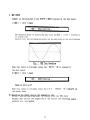
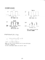
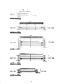
2. STRUCTURAL DIAGRAM
3. BLOCK DIAGRAM
4. CIRCUIT DIAGRAM
K L M - 1502
K L M - 1506
POWER
.".C
GUITAR
IN
INPUT
K L M - 1508
C3
v.0.
El
::"
PHONES
OUTPUT
K L M - 1506
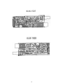
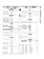
5. P.C. BOARDS
6. CIRCUIT EXPLANATION
1. The MPU section
The YPU uses UPD78C10 and processes the following. The port of the MPU are
indicated in the parentheses.
1 ) The control of the LCD unit
PA5-7. PBO-7
(
)
The LCD are controlled by using a part of the Port A and the Port B.
2 ) The bank change of the memory area
PA3. 1
(
)
The bank of the memory and the 1/0 is changed by using a par1 of the
Port A.
3 ) The 1/0 reset
The MDE
(
PCG
MB87305
(
)
and the MDE I/F
,I) The detection of the card
(
CDST
(
MB620140
)
are resct.
)
The esistence of the card are detected by using this port
If the card is not inserted : HIGH
: LOW
If the card is insertcd
5 ) The multiplexer control
The multiplexer llC4052
6) XlDl I/O
(
PCO. 1
(
PC3. 4
IC2
(
)
)
are controlled in the KLM-1503.
)
i ) I\/D
The A/D convertor in the MPU are used and the A/D conversion of the
following data are carried out.
PEDALiSA 1-2
CARD B,\TTERY
IXTERIAL BATTERY
EDIT YR
(
ANG. 7
AN3
AN2 )
(
AX4
(
(
(
)
). . . . . CIIAIN/EFFECT. B. D, F \
'A
AS5 ).....A. C. E VR
2. Thc MPU I/F section
The XPU I / F MB620140 is the LSI to be the interface of the YPU and each 1/0
and the main functions arc as follows.
1) Address Latch
(
ADO-7
This IC latchs the lower 8 bit of the address bus of the MPU with the
timing of the ALE terminal.
2 ) LED Control
(
LLO-3. LEDI-7
)
This I C receives t h e data from t h e MPU and puts the LED on.
3 ) Bank Change lnput
(
PO-2 )
This I C reccives t h c bank change signal and controls thc ROA 14 and each
CE output.
4 ) SW Data lnput
SW1-7 )
(
This I C i s the input port t o transmit t h e S
W data t o the IPU.
5 ) Address Output
(
AO-7
)
This I C transmits t h e latched time-division address bus.
6 ) C A R D 1/0
(
CAA. CAD
)
The address bus f o r the card and the data bus f o r the card.
7 ) CE Output
Each memory. the CE output terminal f o r the 1/0.
3. The YDE I/F section
The MDE I/F 18620140 i s the LSI t o be t h e i n t e r f a c e between the A/D convertor
and the D/A convertor. This a l s o transmits and receives the remote s i g n a l f o r
the FC6.
1 ) The i n t e r f a c e with the A / D convertor
(
BCK. CC. Dlh'
)
This I C converts the s e r i a l data of CX-20018 i n t o the p a r a l l e l data and
transmits t o the PDEO. The CC terminal transmits 37.1 KHz and the BCK
transmits 1. 188 Illz.
2 ) The i n t e r f a c e a i t h the D/A convertor
(
DATAO. 192FS. LRCR. BCLR
)
This I C converts t h e p a r a l l e l d a t a from the MDE to the s e r i a l data and
transmits t o t h e d i g i t a l f i l t e r PD0028.
3 ) The remote 1/0
(
RS.
TS
)
When t h e data i s received from t h e I/O terminal f o r the FC6. t h i s IC
transmits the i n t e r r u p t i o n s i g n a l to the MPU.
7. CHECK AND ADJUSTMENT
Before you start the diagnostic test
If necessary data are memorized in the A2. please save the data into the RAY
card before starting the test.
Starting the diagnostic test
Connect the YlDl cable to the MIDI IN and OUT of the rear panel.
Insert a RAY card ( YCR-03 ) into the card slot.
When the power is turned on while CHAIWEFFECT " and C are being
pressed. this diagnostic test ( Self Test Program ) starts.
-
- -
The explanation of the operation switches on the diagnostic test
WRITE ' switch
- A ' switch
'v' switch
BYPASS " switch
"
Regarding the
-
:
:
:
:
The
The
The
The
check proceeds to the nest.
item proceeds to the nest.
item returns to the previous one.
diagnostic test mode returns to the norm1 mode.
PARAMETER INITIALIZE '
rhen the diagnostic test starts nor~nlly. the screen of the
ISITI.4LIZE ' is indicated.
PARAMETER INlTlr\LIZE ?
Press " YES
A2 or press
-
-
*
PARAPETER
YES / NO
( E ) if you would like to initialize the internal data of the
SO ' ( F 1 if you don't want to do that.
1. INTERN,\L CHECK
Ahcn the PARAYETER INITIALIZE is finished. the item proceeds to the ISTERNAL
CHECK automaticallr.
I) MIDI circuit check
The YlDl IN-OUT is checked.
When this check passes, the item proceeds to the next autonatically.
When this check fails. all the LEDs go on and off and the letter - Err
is indicated in the LED display.
Then the follow in^ is indicated in the LCD.
2 ) Renote circuit check
The remote terminal circuit is checked.
lhen this check passes. the item proceeds to the nest automatically.
lhen this check fails. all the LEDs go on and off and the letter
is indicated in the LED display.
Then the following is indicated in the LCD.
-
(
-
REEOTE
-
-
Err
"
-
OUT--X--IN
)
X You need a short plug
( DIN plug whose 1 pin and J pin. 3 pin and 5 pin
are short-circuits ). If the short plug is not avnilnble, press the
" RRlTE - Sl and proceed to the next check.
3 ) Card battery check
The battery of the RAN card into the card slot is checked.
R'hen this check passes. the item proceeds to the nest automatically.
lhen this check fails. all the LEDs go on and off and the letter - Err
is indicated, in the LED display.
Then. when no RAM card is inserted into the card slot or a ROM card is
inserted into it. the following is indicated in the LCD.
!
CARD ! R'RlTE / READ
sx
Ahen the battery voltage of 111s RAM card is lor. the following is
indicated in the LCD.
(
CARD i
CARD Battery Lor
xs
4 ) Internal battery check
The bat tery voltage of the A2 is checked.
When this check passes. the item proceeds t o the nest automatically.
lhen this check fails. all the LEDs go on and off and the letter Err
is indicated in the LED display.
Then the following is indicated in the LCD.
-
i INT BATT )
Internal Battery Lor
ss
-
2. A/D LEVEL CONFIRMATION AND ADJUSTMENT
When the ILTERXAL CHECK i s finished. t h e item proceeds t o t h e A / D LEVEL
COXFIRMATION A N D ADJUSTMENT automatically.
1 ) L ch A / D level confirmation and adjustment
I
(
A/D LEVL
)
Lch Checking
I
..
( 1 ) Input the s i n wave of IVp-p 400Hz to the L I N E IS L/ilOLO terminal of
the r e a r panel.
( 2 ) Connect an oscilloscope t o the OUTPUT L/MO#O terminal of t h e rear
panel and a d j u s t the output waveform t o 40mVp-p with the master V R of
the f r o n t panel.
( 3 ) Confirm the output waveform transforms the noroal s i n mve.
If i t i s not so, adjust with the V R 1 of RLY-1506.
Rhen t h i s check i s finished. press the
t h e next check.
"
WRITE
-
Sf to proceed t o
2 ) R ch h/D l e v e l confirmation and adjustment
! h/D LEVL
)
Rch Checking
..
( 1 ) Connect an oscilloscope t o the OUTPUT R terminal of the rear panel and
a d j u s t the output waveform t o IOmVp-p with the master V R of t h e front
panel.
( 2 ) Confirm the output waveform transforms the normal s i n wave
If i t i s not so. a d j u s t with the \'R2 of RLM-1506.
GOOD
% If t h i s adjustment i s not i t s proper position. the noise will be much
bigger.
3. LED. LCD. SW. D. F. E . . AND PEDAL CHECKS
1 I LED check
The LEDs of the front panel l i g h t nutomatically on t h i s check
LED
(
)
Checking
..
The t u r n t o l i g h t i s as follows.
-UTILITY'-"PRAM
EDIT--'PERFORM---
INDI\'ID--.-BYPASS"-7
SECHEST LED
Confirm a l l the LEDs l i g h t .
lhcn a l l the LEDs go oul:, t h e itcm proceeds to the nest check a u t o ~ a t i c ' a l l y .
2 ) LCD check
When the " WRITE
indicated.
Confirm t h i s .
'
SR i s pressed once, a l l the dots of t h e LCD a r e
<
LCD
)
I
11111111111111111111111
{'hen t h i s check i s finished, press thc
the nest check.
"
TRITE
"
ST to proceed ro
3 ) Panel S1 check
Press t h e switch indicated in the LCD t o check i t
-
(eg.
)
(
PANEL S
W
)
Push
WRITE 1
The t u r n to press i s as follows.
When t h i s check i s f i n i s h e d , t h e item proceeds t o t h e next check
automatically.
4 ) D. F. E.
check
When t h e D. F.E. which i s indicated i n t h e LCD i s pressed once, t h e name of
the D. F. E. which i s beine pressed and the A/D value a r e indicated i n t'he
LCD.
Also. confirm t h e A/D value changes between 0 and 255 when t h i s D. F. E. i s
turned.
(eg.
)
(
D. F.
E.
)
[ A
Push
I
BYPASS
T
i
next S
W
When t h i s check i s f i n i s h e d . press t h e
t h e nest check.
-
252
!
push S
W
WRITE
"
A/D
S
W t o proceed t o
5 ) Pedal check
Connect t h e volume pedal XVP-001 t o the PEDAL/SA I and 2 terminal of the
r e a r panel. Set the s l i d e BR of the KVP-001 t o be 0.
( 1 ) Pedal I check
Confirm the A / D value changes between 0 and 255. the M I D I dnta changes
between 0 and 127 when the KVP-001 i s operated a t the condition that
the l e t t e r " PEDAL 1 - i s indicated in t h e LCD.
T
T
M I D I DATA
A/D
When t h i s check i s finished. press the
the nest check.
"
%RITE
'
S
W t o proceed t o
'
WRITE
"
ST t o proceed t o
( 2 ) Pedal 2 check
Check a s well a s ( I )
Chen t h i s check i s finished. press the
t h e nest check.
4.
MDE CHECK
Connect an oscilloscope to the OUTPUT L/YONO teroinal of the rear panel.
1 ) MDE 1
(
1C15
)
check
(
YDE
)
MDEl Checking
..
The waveform sl~ich is oscillated only from the YDE I ( lCl5 ) internally
is transmitted.
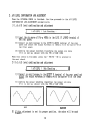
Confirm that the following wnveforo can be monitored on the oscilloscope.
Fig. 1
HDE Test Waveform
When this check is finished. press the
the nest check.
2 ) 4DE 2
(
lC16
I
)
-
lFRlTE
-
SW to proceed to
check
:
MDE
. MDEO Chccting
I
..
Check as re11 as 2 )
Xhen this check is finished, press the D. F. E. - BYPASS
the normal mode.
-
ST
to return to
% Regarding the check item of thc dia~nosticlest
Re don' 1 mention anything about thc checks after the MDE check
because they are for the inspection at the factory and because an audio
analyzer etc. are needed.
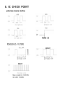
8. IC CHECK POINT
UPD78ClOCW (MPU)
ov
I
I
POWER ON
PD0029 (D. FILTER)
WOUT
2V/2uS d i ~
DOUT
Khcn a sound i s r e c e i v e d .
the p u l s e changes.
?V/IuS
div
CXZOO18 (ADC)
2V/IOuS d i v
BCLK
5v
ov
-1
0.8uS r2V/O, 2uS d i v
:;
2V/lOuS d i v
2V/5uS d i v
Chen a sound i s received.
the pulse changes.
Ahen the level of this aaveform has the large difference.
the noise i s generated.
I n t h i s case. please adjust with the YR 1 and 2.
MB620140 (MDE IIF)
500K (IN)
3 0 . 5uS d i v
2V/0,2uS d i v
2V/lmS d i v
2V/lOuS d i v
When the internal noise
the d a t a i s fixed.
2V/IOuS
div
gate
works.
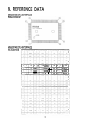
9. REFERENCE DATA
MB620140 (CPU-INTERFACE)
PIN ASSIGNMENT
MB620140 (CPU-INTERFACE)
PIN FUNCTION
n
/
2
/
1
7
l
l
:
1
:
I
I
I
rul
31
$42
IE
110
11
I4
1.
I,O
I43
-
1
I
I
1
,
COD'
~e
I
ole
81
C.03
57
I
1111
81
I
O
COO?
Is
I
112
89
/
0
013
Bl
j
.-
I
0
1
WE
RWtl
I X E
IIYqcF
MB620140 (MDE INTERFACE)
PIN ASSIGNMENT
MB620140 (MDEINTERFACE)
PIN FUNCTION
1
(
I
6.
45
(
60)
70
(
120
:a
$5
(
l
GiE
rC
I 1
302
11
I
L
;J
50
I> l
C11
17
6
DO#
72
0
501,
$7
:1a1uI
I8
0
DOJ
21
0
25611
II
28
il
i j
2%
(
1
1 1
1
0
0
1
o
(
0
1 1
I /
PCliQ
7%
20
1
I
I
I
(I*U
110
j
8
(
1 1
I
CI1
1
)I>
I
DIX
1 I
(
012
l
0
(
CC
MPU (UPD78C1OACW)
PIN A S S I G N M E N T
MPU (UPD78ClOACW)
PIN F U N C T I O N
PIN NAME
PAT-0
I
1/0
I
1 1/O 1
FUNCTION
Port A
1
I
PIN NAYE
NYI
INTI
I
I
PC3
/
I
/
Interrupt Request
PC4
I
0
/
Timer Output
RD
I
0
I
0
YODEO. I
110
Bend Strobe
Address Lntch Enable
1
Yode
FUNCTION
Y o n - h s k a b l e Interrupt
Interrupt Request
YAREF
/ 1 /
I - I
VDD
I
AS7-0
I
1;1
I I/O I
-
1
1
Analog Input
Reference Voltage
YDD
I
FOR HARNESSES
HNS- 1556
HNS- 1558
390
EHR- 3
HNS- 1559
EHR- 5
HNS- 1560
8320-5
CN 8A
HNS- 1561
I
PHR- 12
8520- 12
10
10
CN 9A
H N S - 1562
CN 9B
I
I
PHR- I 0
CN 1 0 ~
HNS- 1563
CN
HNS- 1 5 6 4
5320-14~~2
9520- 10
CN 10B
5360- I + A T
HNS- I566
HNS- 1567
7
7
CN 17A
CN 178
I
I
EHR- 7
BSZO-7
HNS- 1568
CN18A:
:cNI~B
EHR-3
HNS- 1569
8525-3
'IRTS
CODEI
I
PARTS NAME
SFEClFlCATlOHS
P. C.
BOARD
I
IDENTlFlCATlDN NO.
FUSCTIOR
I
a'TY
I
PABTS NAME
IDENTlFlCATlOR NO.
I
P. C. BOARD ASSEMBLE
FET
DIODES
I
BLOCK RESISTORS
BRIDGE DIODE
LC FILTER
CL3HDB
SL-1179-3?H (RED)
CL-9HD22
CL-9EC22
AC LINE FILTER
219051500
DSR1100-SGE222YVA2
1502-5
1502-5
1502-5
1502-5
2
LCD
ZENER DIODES
BLOCR CAPACITOR
I
DOUBLE DIODE
315000<00
YC932-TI2
2
1502-5
SRAY
CPU
11
I :
'ODE
1
PARTS HAKE
SPECIFICATIONS
I
P. C.
BOAR0
lDENTlFlCATlON NO.
FUNCTION
PARTS C O D E
I I7EX
IOOJP
220CE
240GE
220SE
220SC
2201G
240AU
24OUh
220FR
240AF
47lOGllOO
471070300
471070800
471071000
4710i1200
471090200
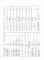
PARTS N A M E
I D E N T I F I C A T I O NO.
N
P. C.
BOADD
SPEC1 FlCATlONS
a' TY
FUNCTION
HEADER
474014702
14P 5332-l4T2
1502-5
I
HARNESSES
HNS-1556
HSS-1557
HSS-1558
HBS-1559
HSS-1560
HSS-1561
IISS- 1562
HNS-1563
HNS-1564
HNS-1565
HHS-I566
HNS-1567
HHS-1568
HHS-1569
BlIB-EH
TOP 838-PH
088-PH
TOP BIOB-PH
TOP BI2B-PH
TOP 5096-OZC
Y. PRT
1506
1506
I506
1506
1502-5
1502-5
Y. PRT
1502-5
I. PET
1502-5
1507/8
150718
1502-5
BOARD
BOARD
BOARD
BOARD
BOARD
BOARD
Ih'
Ih'
IS
IS
IN
IN
BOARD IN
BOARD
BOARD
BOARD
BOARD
IN
IS
IS
IS
lC SOCKET
480001324
32P DICF-32CS-E
1502-5
I
FUSE HOLDER
515002300
S-S505i 801
1502-5
2
BC COXSECTOR
LlTHlC BATTERY
474009900
L-32
1502-5
I
520001700
CR2032
Y. PET
CARD FIT CONNECTORS
474012300
474012400
ZC-I12
ZC-I13
1502-5
1502-5
I
I
Y. PRT
Y. PRT
SYCD CONNECTORS
474012500
474012600
FC-12 (1. 6)
FC-13 (1. 6)
474012700
BZP-LV-TN
1502-5
1502-5
Y. PRT
I
I
I.\' COHHECTOR
1502-5
I
-
I
A
0
1
I.. C
BOARD
PARTS NAME
SPECIFICATIONS
1
IDENTlFlCATION N O
FUNCTION
I
Q'TY
1
PARTS CODE
1
P A R A
SPECIFICATIONS
(
P. C
BOARD
1
IDENTIFICATION NO.
PUSll $1 INOB
INOB
TEST PINS
540007100
54001190I
L C - 2 - 6 YELL01
LC-2-6
1506
1506
I
Y. PET
620020800
I I. PRT I
2
I
ISOLATION SllEET
SYCD IIARNESSES
I
Y. PRT
1
Y. PRT
630007500
COPPER SHEET
I
I
"RT
1 y;;
LCD llNDOl
1502-5
630014200
I. PRT
1
LED SPACERS
CARD GUIDE
AC CORDS
Y. PIT
SAA (SU428-58)
BS PLUG (SU431A581
SEV (SU430-58)
PP-48190
SJT(SU338-56)
1 640088500 1
I
I 640098500 I
7
I I. PIT I
LOlER CASE
I Y. PRT
I
1
1
COVER
Y. PET
PSI SUPPORT
Y. PET
Y. PRT
Y. PRT
I. PET
I.PRT
I. PET
640096700
I
1502-5
PSI BAR
640096800
I.PRT
640096900
Y. PR7
I
I
FRONT PANEL
641018300
I
IPRT
REAP PANEL
641018500
1
I.PPT
I
VP SHIELD
SPRING PLATE
044003000
I.PET
3
117VS
2201C
3
P S I FRAME
646030200
I
I.PET
1
1
CT BOOD
646030500
I.PRT
I
RATTEPY HOLDER
649007400
1502-5
I
Paristo voi rajahtad, jos se on virhecllisesti asennettu.
Vaihda paristo ainoastaan laitevalmistajan suosittelemaan
tyyppiin.
Havita
kaytetty
paristo
valmistajan
ohjeiden
mukaisesti.
ADVARSEL!
Lithiumbatteri
- Eksplosionsfare ved fejlagtig handtering.
Udskiftning ma kun ske rned batteri af samme
fabrikat og type.
Lever det brugte batteri tilbage ti1 leverand o ren.
ADVERSEL
Lithiumbatteri
- Eksplosjonsfare.
Ved utskifting benyttes kun batteri som
anbefalt av apparalfabrikanten.
Brukt batteri returneres apparalleverand 0 ren.
Explosionsfara vid felaktigt batteribyle.
Anvand samma batterityp eller en ekvivalent typ som
rekommenderas av apparattillverkaren.
Kassera anvant batteri enligt fabrikantens instruktion.
CAUTION
.
Danger of explosion if battery ,is incorrectly replaced
Replace only with the same or equivalent type
recommended by the equipment manufacturer .
Discard used batteries according to manufacturer 's
instructions.
KORG INC. 15-12, Shimotakaido 1-chorne, Suginarni-ku, Tokyo 168
@
KORG INC. 1991
0301 CEH. PRINTED IN JAPAN
a