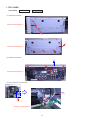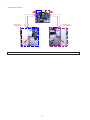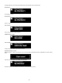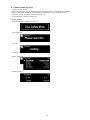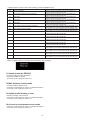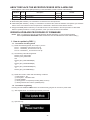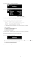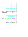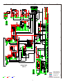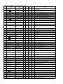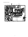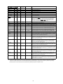
1
e
Ver. 6
Please refer to the
MODIFICATION NOTICE.
SERVICE MANUAL
MODEL
RCD-N7
JP
E3
E2
EK
K2A E1C E1K EUT
P P
NETWORK CD RECEIVER
•For purposes of improvement, specifications and design are subject to change without notice.
•Please use this service manual with referring to the operating instructions without fail.
•Some illustrations using in this service manual are slightly different from the actual set.
e
D&M Holdings Inc.
S0458-1V06DM/DG1203
Copyright 2012 D&M Holdings Inc. All rights reserved.
WARNING: Violators will be prosecuted to the maximum extent possible.
g
P
SAFETY PRECAUTIONS
The following check should be performed for the continued protection of the customer and service technician.
LEAKAGE CURRENT CHECK
Before returning the unit to the customer, make sure you make either (1) a leakage current check or (2) a line to chassis
resistance check. if the leakage current exceeds 0.5 milliamps, or if the resistance from chassis to either side of the
power cord is less than 460 kohms, the unit is defective.
Be sure to test for leakage current with the AC plug in both polarities, in addition, in each power ON, OFF and STANDBY
mode, if applicable.
CAUTION Please heed the points listed below during servicing and inspection.
◎◎ Heed the cautions!
◎◎ Inspect for safety after servicing!
Spots requiring particular attention when servicing, such
as the cabinet, parts, chassis,etc., have cautions indicated
on labels. be sure to heed these causions and the
cautions indicated in the handling instructions.
Check that all screws, parts and wires removed or
disconnected for servicing have been put back in their
original positions, inspect that no parts around the area
that has been serviced have been negatively affected,
conduct an inslation check on the external metal
connectors and between the blades of the power plug,
and otherwise check that safety is ensured.
◎◎ Caution concerning electric shock!
(1)An AC voltage is impressed on this set, so touching
internal metal parts when the set is energized could
cause electric shock. Take care to avoid electric
shock, by for example using an isolating transformer
and gloves when servicing while the set is energized,
unplugging the power cord when replacing parts, etc.
(Insulation check procedure)
Unplug the power cord from the power outlet, disconnect
the antenna, plugs, etc., and turn the power switch on.
Using a 500V insulation resistance tester, check that the
inplug and the externally exposed metal parts (antenna
terminal, headphones terminal, input terminal, etc.) is
1MΩ or greater. If it is less, the set must be inspected and
repaired.
(2)Tere are high voltage parts inside. Handle with extra
care when the set is energized.
◎◎ Caution concerning disassembly and
assembly!
Through great care is taken when manufacturing parts
from sheet metal, there may in some rare cases be burrs
on the edges of parts which could cause injury if fingers
are moved across them. Use gloves to protect your hands.
CAUTION Concerning important safety
parts
Many of the electric and structural parts used in the set
have special safety properties. In most cases these
properties are difficult to distinguish by sight, and using
replacement parts with higher ratings (rated power and
withstand voltage) does not necessarily guarantee that
safety performance will be poreserved. Parts with safety
properties are indicated as shown below on the wiring
diagrams and parts lists is this service manual. Be sure to
replace them with parts with the designated part number.
◎◎ Only use designated parts!
The set's parts have specific safety properties (fire
resistance, voltage resistance, etc.). For replacement
parts, be sure to use parts which have the same
poroperties. In particular, for the important safety parts
that are marked z on wiring diagrams and parts lists, be
sure to use the designated parts.
◎◎ Be sure to mount parts and arrange the wires
as they were originally!
(1)Schematic diagrams.......Indicated by the z mark.
(2).Parts lists.......Indicated by the z mark.
Using parts other than the designated
parts could result in electric shock, fires
or other dangerous situations.
For safety seasons, some parts use tape, tubes or other
insulating materials, and some parts are mounted away
from the surface of printed circuit boards. Care is also
taken with the positions of the wores omsode amd clamps
are used to keep wires away from heating and high
voltage parts, so be sure to set everything back as it was
originally.
2
NOTE FOR SCHEMATIC DIAGRAM
WARNING:
Parts marked with this symbol z have critical characteristics. Use ONLY replacement parts recommended by the manufacturer.
CAUTION:
Before returning the unit to the customer, make sure you make either (1) a leakage current check or (2) a line to chassis resistance check. If the
leakage current exceeds 0.5 milliamps, or if the resistance from chassis to either side of the power cord is less than 460 kohms, the unit is defective.
WARNING:
DO NOT return the unit to the customer until the problem is located and corrected.
NOTICE:
NOTE FOR PARTS LIST
ALL RESISTANCE VALUES IN OHM. k=1,000 OHM / M=1,000,000 OHM
ALL CAPACITANCE VALUES IN MICRO FARAD. P=MICRO-MICRO FARAD EACH VOLTAGE AND CURRENT ARE MEASURED AT NO SIGNAL
INPUT CONDITION. CIRCUIT AND PARTS ARE SUBJECT TO CHANGE WITHOUT PRIOR NOTICE.
NOTE FOR PARTS LIST
1. Parts for which "nsp" is indicated on this table cannot be supplied.
2. When ordering of part, clearly indicate "1" and "I" (i) to avoid mis-supplying.
3. Ordering part without stating its part number can not be supplied.
4. Part indicated with the mark "★" is not illustrated in the exploded view.
5. Not including General-purpose Carbon Film Resistor in the P.W.Board parts list. (Refer to the Schematic Diagram for those parts.)
6. Not including General-purpose Carbon Chip Resistor in the P.W.Board parts list. (Refer to the Schematic Diagram for those parts.)
WARNING: Parts marked with this symbol z have critical characteristics. Use ONLY replacement parts recommended by the manufacturer.
● Resistors
Ex.:
RN
Type
RD :
RC :
RS :
RW:
RN :
RK :
14K
2E
Shape
and performance
Carbon
Composition
Metal oxide film
winding
Metal film
Metal mixture
* Resistance
1 8 2
2B
2E
2H
3A
3D
3F
3H
Power
:
:
:
:
:
:
:
182
G
FR
Resistance
Allowable
error
Others
F
G
J
K
M
1/8 W
1/4 W
1/2 W
1 W
2 W
3 W
5 W
:
:
:
:
:
±1%
±2%
±5%
±10%
±20%
P :
NL :
NB :
FR :
F :
Pulse-resistant type
Low noise type
Non-burning type
Fuse-resistor
Lead wire forming
1800ohm=1.8kohm
Indicates number of zeros after effective number.
2-digit effective number.
1 R
2
: Units: ohm
1.2ohm
1-digit effective number.
2-digit effective number, decimal point indicated by R.
● Capacitors
Ex.:
CE
Type
04W
Shape
and performance
CE : Aluminum foil
electrolytic
CA : Aluminium solid
electrolytic
CS :
CQ :
CK :
CC :
CP :
CM:
CF :
CH :
Tantalum electrolytic
Film
Ceramic
Ceramic
Oil
Mica
Metallized
Metallized
1H
3R2
Dielectric
strength
Capacity
0J
1A
1C
1E
1V
1H
2A
2B
2C
2D
2E
2H
2J
:
:
:
:
:
:
:
:
:
:
:
:
:
6.3 V
10 V
16 V
25 V
35 V
50 V
100 V
125 V
160 V
200 V
250 V
500 V
630 V
M
F
G
J
K
M
Z
:
:
:
:
:
:
:
P :
C :
D :
= :
BP
Allowable
error
Others
±1%
±2%
±5%
±10%
±20%
HS :
BP :
HR :
DL :
HF :
High stability type
Non-polar type
Ripple-resistant type
For change and discharge
For assuring high requency
±80%
- 20%
+100%
±0.25pF
±0.5pF
Others
U
C
W
F
UL part
CSA part
UL-CSA part
Lead wire forming
:
:
:
:
* Capacity (electrolyte only)
2 2
2
・ Units:μF.
2 R
2200μF
Indicates number of zeros after effective number.
2-digit effective number.
2
・ Units:μF.
2.2μF
1-digit effective number.
2-digit effective number, decimal point indicated by R
* Capacity (except electrolyte)
2 2
2
・ Units:pF
2200pF=0.0022μF
2 2
Indicates number of zeros after efective number. (More than 2)
2-digit effective number.
1
・ Units:pF
・ When the dielectric strength is indicated in AC,"AC" is included after the dieelectric strength value.
3
220pF
Indicates number of zeros after effective numver. (0 or 1)
2-digit effective number.
WARNING AND LASER SAFETY INSTRUCTIONS
GB
WARNING
NL
All ICs and many other semi-conductors are
susceptible to electrostatic discharges (ESD).
Careless handling during repair can reduce
life drastically.
When repairing, make sure that you are
connected with the same potential as the
mass of the set via a wrist wrap with
resistance.
Keep components and tools also at this
potential.
F
WAARSCHUWING
Alle IC’s en vele andere halfgeleiders zijn
gevoelig voor elektrostatische ontladingen
(ESD).
Onzorgvuldig behandelen tijdens reparatie
kan de levensduur drastisch doen
verminderen.
Zorg ervoor dat u tijdens reparatie via een
polsband met weerstand verbonden bent met
hetzelfde potentiaal als de massa van het
apparaat.
Houd componenten en hulpmiddelen ook op
ditzelfde potentiaal.
D
ATTENTION
Tous les IC et beaucoup d’autres semiconducteurs sont sensibles aux décharges
statiques (ESD).
Leur longévité pourrait être considérablement
écourtée par le fait qu’aucune précaution
n’est prise a leur manipulation.
Lors de réparations, s’assurer de bien être
relié au même potentiel que la masse de
l’appareil et enfiler le bracelet serti d’une
résistance de sécurité.
Veiller a ce que les composants ainsi que les
outils que l’on utilise soient également a ce
potentiel.
WARNUNG
I
Alle IC und viele andere Halbleiter sind
empfindlich gegen elektrostatische
Entladungen (ESD).
Unsorgfältige Behandlung bei der Reparatur
kann die Lebensdauer drastisch vermindern.
Sorgen sie dafür, das Sie im Reparaturfall
über ein Pulsarmband mit Widerstand mit
dem Massepotential des Gerätes verbunden
sind.
Halten Sie Bauteile und Hilfsmittel ebenfalls
auf diesem Potential.
AVVERTIMENTO
Tutti IC e parecchi semi-conduttori sono
sensibili alle scariche statiche (ESD).
La loro longevita potrebbe essere fortemente
ridatta in caso di non osservazione della piu
grande cauzione alla loro manipolazione.
Durante le riparazioni occorre quindi essere
collegato allo stesso potenziale che quello
della massa dell’apparecchio tramite un
braccialetto a resistenza.
Assicurarsi che i componenti e anche gli
utensili con quali si lavora siano anche a
questo potenziale.
D
GB
Bei jeder Reparatur sind die geltenden Sicherheitsvorschriften zu beachten.
Der Originalzustand des Gerats darf nicht verandert werden.
Fur Reparaturen sind Original-Ersatzteile zu verwenden.
Safety regulations require that the set be restored to its original condition
and that parts which are identical with those specified be used.
NL
I
Veiligheidsbepalingen vereisen, dat het apparaat in zijn oorspronkelijke
toestand wordt terug gebracht en dat onderdelen, identiek aan de
gespecifieerde worden toegepast.
Le norme di sicurezza esigono che l’apparecchio venga rimesso nelle
condizioni originali e che siano utilizzati pezzi di ricambiago idetici a quelli
specificati.
F
“Pour votre sécurité, ces documents
doivent être utilisés par des
spécialistes agrées, seuls habilités à
réparer votre appareil en panne.”
Les normes de sécurité exigent que l’appareil soit remis a l’état d’origine et
que soient utilisées les pièces de rechange identiques à celles spécifiées.
LASER SAFETY
This unit employs a laser. Only a qualified service person should remove the cover or attempt to service this
device, due to possible eye injury.
USE OF CONTROLS OR ADJUSTMENTS OR PERFORMANCE OF PROCEDURE OTHER THAN THOSE
SPECIFIED HEREIN MAY RESULT IN HAZARDOUS RADIATION EXPOSURE.
AVOID DIRECT EXPOSURE TO BEAM
WARNING
The use of optical instruments with this product will increase eye hazard.
Repair handling should take place as much as possible with a disc loaded inside the player
WARNING LOCATION: INSIDE ON LASER COVERSHIELD
CAUTION VISIBLE AND INVISIBLE LASER RADIATION WHEN OPEN AVOID EXPOSURE TO BEAM
ADVARSEL SYNLIG OG USYNLIG LASERSTRÅLING VED ÅBNING UNDGÅ UDSÆTTELSE FOR STRÅLING
ADVARSEL SYNLIG OG USYNLIG LASERSTRÅLING NÅR DEKSEL Å PNES UNNGÅ EKSPONERING FOR STRÅLEN
VARNING SYNLIG OCH OSYNLIG LASERSTRÅLNING NÄR DENNA DEL ÄR ÖPPNAD BETRAKTA EJ STRÅLEN
VARO! AVATT AESSA OLET ALTTIINA NÄKYVÄLLE JA NÄKYMÄTTÖMÄLLE LASER SÄTEILYLLE. ÄLÄ KATSO SÄTEESEEN
VORSICHT SICHTBARE UND UNSICHTBARE LASERSTRAHLUNG WENN ABDECKUNG GEÖFFNET NICHT DEM STRAHL AUSSETSEN
DANGER VISIBLE AND INVISIBLE LASER RADIATION WHEN OPEN AVOID DIRECT EXPOSURE TO BEAM
ATTENTION RAYONNEMENT LASER VISIBLE ET INVISIBLE EN CAS D'OUVERTURE EXPOSITION DANGEREUSE AU FAISCEAU
4
030804ecm
INSTRUCTIONS FOR HANDLING SEMI-CONDUCTORS AND OPTICAL UNIT
Electrostatic breakdown of the semi-conductors or optical pickup may occur due to a potential difference caused by
electrostatic charge during unpacking or repair work.
1.Ground for Human Body
Be sure to wear a grounding band (1 MΩ) that is properly grounded to remove any static electricity that may be
charged on the body.
2.Ground for Workbench
Be sure to place a conductive sheet or copper plate with proper grounding (1 MΩ) on the workbench or other surface,
where the semi-conductors are to be placed. Because the static electricity charge on clothing will not escape through
the body grounding band, be careful to avoid contacting semi-conductors with your clothing
<Correct>
<Incorrect>
Grounding Band
1MΩ
CBA
CBA
1MΩ
Conductive Sheet or
Copper Plate
5
SPECIFICATIONS
nn CD player
• Audio performance
S/N ratio (1 kHz)
Dynamic range (1 kHz)
Total harmonic distortion (1 kHz)
nn Clock
nn Wireless LAN
Network type (wireless LAN standards)
nn Audio AMP
Rated output
Dynamic power
High frequency distortion
Input sensitivity/impedance
AUX1,AUX2
Portable in
Frequency response (5 W, 8 Ω)
AUX input
Total harmonic distortion (1 kHz, 5 W, 8 Ω)
AUX input
S/N ratio (10 W, 8 Ω, IHF-A)
AUX input
Conforming to IEEE 802.11b
Conforming to IEEE 802.11g
(Conforming to Wi-Fi®)z
2-channel driving
65 W + 65 W (4 Ω/ohms,
1 kHz, T.H.D. 0.7 %)
80 W + 80 W (4 Ω/ohms)
0.1 % (Rated output: –3
dB), 4 Ω/ohms, 1 kHz
Transfer rate
DS-SS: 11 / 5.5 / 2 / 1 Mbps (Automatic switching)
OFDM: 54 / 48 / 36 / 24 / 18 / 12 / 9 / 6 Mbps (Automatic switching)
Security
SSID (Network name)
WEP key (network key) (64/128 bits)
WPA-PSK (TKIP/AES)
WPA2-PSK (TKIP/AES)
Used frequency range
2,412 MHz – 2,462 MHz(E3)
2,412 MHz – 2,472 MHz(E2)
No. of channels
E3: Conforming to IEEE 802.11b : 11ch (DS-SS) (Of which 1 channel used)
Conforming to IEEE 802.11g : 11ch (OFDM) (Of which 1 channel used)
E2: Conforming to IEEE 802.11b : 13ch (DS-SS) (Of which 1 channel used)
Conforming to IEEE 802.11g : 13ch (OFDM) (Of which 1 channel used)
200 mV/32 kΩ
110 mV/24 kΩ
5 Hz to 20 kHz (±3 dB)
0.05 %
86 dB
nn Tuner
• FM tuner
Range of receivable frequencies
S/N ratio (mono)
Sensitivity (S/N 30 dB)
• AM tuner
Range of receivable frequencies
S/N ratio
Sensitivity (S/N 20 dB)
Within 1 – 2 minutes per month
Clock method
100 dB
100 dB
0.01 %
nn Power supply
87.5 to 107.9 MHz(E3)
87.5 to 108.0 MHz(E2)
65 dB
9 dBµV (IHF)
Power supply voltage/frequency
Power consumption
Power consumption in standby mode
530 to 1710 kHz(E3)
522 to 1611 kHz(E2)
40 dB
55 dBµV/m
AC 120 V, 60 Hz(E3)
AC 230 V, 50 Hz(E2)
65 W
0.3 W(E3)/ 0.4 W(E2)
nn Miscellaneous
External dimensions
Weight
DIMENSION
6
280 (W) x 112 (H)x 300.7 (D) mm
4.3 kg
CAUTION IN SERVICING
ABOUT REPLACE THE WLAN MODULE WITH A NEW ONE g
When replaced of the RCD-N7 WLAN MODULE (8R1821000100S), confirm contents of the following.
(1)
(2)
Replace the WLAN MODULE with the 8R1821000100S (MAC Address was written).
After the RCD-N7 built, DISC using firmware CR870 (Net (IMG)) to change the E2 or E3 Version.
The file name of CR870 (Net(IMG)): M_CR603_BCI_mmddvv.BIN
NOTE : The mm is month. The dd is date. The vv is version.(Version: NA/EU/JP)
Refer to "9. Update mode (by disc)" (page 31) for the details of the Version up with disc.
qPressing the VOLUMEf and CURSORu buttons for simultaneously, plug the AC cord into a power outlet. To
automatically open the tray, when set is turned on.
wThe disk is put on the tray, 5 buttons are pushed, and the tray is closed. The update begins pressing the 1/3
ENTER button of the set.
e To automatically open the tray, when version up is finished.
r Disconnect the AC cord into a power outlet.
(3)MAC Address Label pasted to Bottom is pasted to Mac Address Label(GEN8341; MAC ADDRESS SUB ASSY ) of
exchanged WLAN MODULE and it substitutes it.
(4)The firmware is updated by DPMS. Refer to [ VERSION UPGRADE PROCEDURE OF FIRMWARE "2. How to
update by DPMS" ] (page 38) for the details of the Version up.
Initializing NETWORK CD RECEIVER (Factory Rerset)
NETWORK CD RECEIVER initialization should be performed when the μcom, peripheral parts of μcom, and Digital PCB.
are replaced.
1. Turn off the power using ON/STANDBY button, unplug the power cord.
2. Plug the power cord into a power outlet while pressing VOLUMEd and CURSORi button simultaneously.
* Initialize.
Note:•All user settings will be lost and this factory setting will be recovered when this initialization mode.
So make sure to memorize your setting for restoring after the initialization.
CURSORi
NETWORK CD RECEIVER
RCD-N7
VOLUMEd
Service tools
Measuring Disc:
CD/TCD-784
CD-R/TCD-R082W
CD-RW/TCD-W082W
z Refer to "MEASURING METHOD AND WAVEFORMS".
7
DISASSEMBLY
• Disassemble in order of the arrow of the figure of following flow.
• In the case of the re-assembling, assemble it in order of the reverse of the following flow.
• In the case of the re-assembling, observe "attention of assembling" it.
• If wire bundles are untied or moved to perform adjustment or parts replacement etc., be sure to rearrange them neatly
as they were originally bundled or placed afterward.
Otherwise, incorrect arrangement can be a cause of noise generation.
CAUTION: Through great care is taken when manufacturing parts from sheet metal, there may in some rare cases be
burrs on the edges of top cover which could cause injury if fingers are moved across them. Use gloves to
protect your hands.
SIDE PANEL
TOP COVER
Refer to "DISASSEMBLY
1. TOP COVER"
and "EXPLODED VIEW"
COVER, TOP
(Ref. No. of EXPLODED VIEW : P13)
IPOD DOCK CON UNIT
(Ref. No. of EXPLODED VIEW : C5)
DOOR
Refer to "DISASSEMBLY
2. DOOR"
and "EXPLODED VIEW"
DOOR, TRAY
(Ref. No. of EXPLODED VIEW : P2)
CD MECHA ASSY
Refer to "DISASSEMBLY
3. CD MECHA ASSY"
and "EXPLODED VIEW"
CD MECHANISM ASS'Y
(Ref. No. of EXPLODED VIEW : C8)
ETHERNET PCB ASS'Y
(Ref. No. of EXPLODED VIEW : C6)
MODULE , TUNER
(Ref. No. of EXPLODED VIEW : C4)
FRONT PANEL ASSY
Refer to "DISASSEMBLY
4. DISPLAY ASSY"
and "EXPLODED VIEW"
DISPLAY PCB ASS'Y
(Ref. No. of EXPLODED VIEW : C1)
OLED MODULE
(Ref. No. of EXPLODED VIEW : C9)
MAIN PCB ASSY
Refer to "DISASSEMBLY
5. MAIN PCB ASS'Y"
and "EXPLODED VIEW"
MAIN PCB ASS'Y
(Ref. No. of EXPLODED VIEW : C2)
SMPS PCB ASSY
Refer to "DISASSEMBLY
6. SMPS PCB ASS'Y"
and "EXPLODED VIEW"
SMPS PCB ASS'Y
(Ref. No. of EXPLODED VIEW : C3)
8
About the photos used for descriptions in the DISASSEMBLY" section.
• T
he direction from which the photographs used herein were photographed is indicated at "Direction of photograph: ***"
at the left of the respective photographs.
• Refer to the table below for a description of the direction in which the photos were taken.
• Photographs for which no direction is indicated were taken from above the product.
The viewpoint of each photograph
(Photografy direction)
Direction of photograph: B
Front side
[View from above]
Direction of photograph: D
Direction of photograph: C
Direction of photograph: A
9
1.TOP COVER
Proceeding : SIDE PANEL → TOP COVER
(1) Remove the screws.
Direction of photograph: C
Direction of photograph: D
(2) Remove the screws.
Direction of photograph: A
(3) Disconnect the connector wire.
CN22
Direction of photograph: A
10
2.DOOR
Proceeding : SIDE PANEL → TOP COVER
→ DOOR
(1) Take off the Chucking plate after removing screws.
Chucking plate
(2) Open the CD tray by turning the Drive gear clockwise.
Drive gear
CD tray
(3) Detach the DOOR CD.
Direction of photograph: B
DOOR CD
11
3.CD MECHA ASS'Y
Proceeding : SIDE PANEL → TOP COVER
→ DOOR
→ CD MECHA ASSY
(1) Remove the screws.
(2) Laser short-circuit in Pick-up of CD MECHANISM ASS'Y, then disconnect the connector wires and FFC cable.
Be sure to wear a grounding band.
Soldering place
FFC Cable
Direction of photograph: A
(3) Disconnect the connector wires.
Direction of photograph: C
Please refer to "EXPLODED VIEW" for the disassembly method of each PCB included in ETHERNET PCB ASSY
and DAB PCB ASSY, TUNER MODULE.
12
4.FRONT PANEL ASSY
Proceeding : SIDE PANEL → TOP COVER
→ DOOR
→ FRONT PANEL ASSY
(1) Remove the screws.
View from bottom
(2) Cut the wire clamp band, then disconnect the connector wires and the FFC Cable.
CN21
cut
Direction of photograph: D
CN44
CN41
13
(3) Remove the screws.
Direction of
photograph: C
Direction of
photograph: D
Please refer to "EXPLODED VIEW" for the disassembly method of each PCB included in FRONT PANEL ASSY.
14
5.MAIN PCB ASSY
Proceeding : SIDE PANEL → TOP COVER
→ FRONT PANEL ASSY
→ DOOR
→ CD MECHA ASSY
→ MAIN PCB ASSY
(1) Remove the screws.
Direction of photograph: A
(2) Remove the screws.
View from bottom
(3) Remove the SUPPORT MECHA.
SUPPORT MECHA
15
(4) Remove the screws, then disconnect the connector wire.
CN45
CN43
CN61
16
6.SMPS PCB ASSY
Proceeding : SIDE PANEL → TOP COVER
→ DOOR
→ SMPC PCB ASSY
(1) Remove the screws.
View from bottom
(2) Cut the wire clamp band, then disconnect the connector wires.
CN45
CN43
cut
CN61
17
→ FRONT PANEL ASSY
(3) Remove the screws.
Direction of photograph: C
(4) Remove the screws.
Direction of photograph: A
18
NOTE HANDLING AND REPLACEMENT OF THE LASER PICK-UP
1.Protection of the LD
Short a part of the LD circuit by soldering. After connection to a circuit, remove the short solder.
2.Precautions when handling the laser CD mechanism
•Handle the laser pick-up so that it is not exposed to dust.
•Do not leave the laser pick-up bare. Be sure to cover it.
•If dust adheres on lens of the pick-up, blow it off with a blower brush.
•Do not shock the laser pick-up.
•Do not watch the light of the laser pick-up.
3.Cautions on assembling and adjustment
•Be sure that to the bench, jig, head of soldering iron (with ceramic) and measuring instruments are well grounded.
•Workers who handle the laser pick-up must be grounded.
•The finished mechanism (prior to anchoring in the set) should be protected against static electricity and dust.
The mechanism must be stored that damaging outside forces are not received.
•When carrying the finished mechanism, hold it by the chassis body
•For proper operation, storage and operating environment should not contain corrosive gases. For example H2S, SO2,
NO2, CI2 etc. In addition storage environment should not have materials that emit corrosive gases especially from
silicic, cyanic, formalin and phenol group. I the mechanism or the set, existence of corrosive gases may cause no
rotation in motor.
4.Determining whether the laser pick-up is defective
•Check the Iop(Laser drive current). Check lop in "SPECIAL MODE". (Refer to 20 page.)
•If the present Iop (current) value becomes more than 50mA, replace the Traverse unit with a new one.
•No mechanical adjustment is necessary after the replacement.
Protective soldering place for laser diode.
19
SPECIAL MODE
Special mode setting
Plug AC cord into power outlet while pressing buttons A and B.
Each button continue to press until the lit of ON/STANDBY.
No.
Mode
Button A
Button B
Contents
1
Initialization mode
(Factory Reset)
VOLUME UP
CURSOR
DOWN
Initializing. Factory Reset
2
Initialization mode
( User Reset)
VOLUME UP
VOLUME
DOWN
Initializing. (Contents User's Guide is published)
3
Version display
CURSOR UP
-
4
CD test mode
ON/
STANDBY
OPEN/
CLOSE
5
Heat Run mode
ON/
STANDBY
SOURCE
Heat run
6
Product mode 1
VOLUME UP
CURSOR
RIGHT
Factory use.
7
Prodcut mode 2
VOLUME UP
CURSOR
LEFT
Factory use.
8
Protection history mode
CURSOR
RIGHT
VOLUME
DOWN
Protection history view and reset
9
Hidden serial number mode
-
-
10
Update mode (by disc)
VOLUME
DOWN
11
DPMS update mode
SOURCE
OPEN/
CLOSE
12
Update mode (by RS232C)
PLAY/ PAUSE
CURSOR
LEFT
Development/Fuctory use. The details cannot be disclosed.
13
MAC Address rewrite mode
PLAY/ PAUSE
CURSOR
DOWN
Development/Fuctory use. The details cannot be disclosed.
14
Update mode (display µ-com)
PLAY/ PAUSE
CURSOR
RIGHT
Development/Fuctory use. The details cannot be disclosed.
15
Access to development server mode
PLAY/ PAUSE
CURSOR
DOWN
Development/Fuctory use. The details cannot be disclosed.
ON/STANDBY
Version Display
Servo adjustment, Leaser current, ON time
Factory use.
CURSOR UP Development/Fuctory use. The details cannot be disclosed.
DPMS Up date Mode
CURSORuiop
5
NETWORK CD RECEIVER
SOURCE
VOLUME f
20
RCD-N7
VOLUMEd
1. Initialization mode (Factory Reset)
Backup data initialization is carried out. Refer to Initialization Items.
After initialization, move on to nomal mode.
CAUTION
Version information (such as rewriting failed log) Clear.
Clear the history of protection.
"Initial value of laser current"and"The accumulated laser on time"not cleared.
Power failure flag is not cleared.
Startup display
All lights display(2 seconds) - All off display(2 seconds)
Power LED(red/Green) lighting(4 seconds)
"Factory Reset" displayed for 5 seconds.
Initialization Items (Default setting)
source
TUNER(band)
SDB
BASS
TREBLE
BALANCE
DIMMER
VOLUME
TUNER Preset
Favorite list
Clock
TIMER (EVERYDAY/ONCE)
SPK Response
iPod mode
AUTO STANDBY
Protection history
Auto Adjust
Network setting
PC Language
Screen Saver
Default
Internet Radio
FM
OFF
0 dB
0 dB
CENTER
100%
3
Clear all
Clear all
00:00 (JP/EU), 12:00AM (NA)
Timer function CD
ON TIME 0:00 (JP/EU), 12:00AM (NA)
OFF TIME 0:00
ON
Browse mode
OFF
NO PROTECT
Time Zone : 1h /Summer Time : 0h
DHCP (On)
chi(smpl)
Off
21
2. Initialization mode (User Reset)
Backup data initialization is carried out. Refer to Initialization Items.
After initialization, move on to nomal mode.
CAUTION
The difference is the following two points.
Version information (such as rewriting failed log) not cleared.
History of protection not cleard.
Startup display
"Initialized" displayed for 5 seconds.
All lights display(2 seconds) - All off display(2 seconds)
Power LED(Green) lighting(4 seconds)
3. Version display
Menu items appear in the Add Version.Otherwise, normal operation.
To exit this mode, unplug the power cord.
Startup display
"Version" displayed for 5 seconds.
How to Display Version
Press SOURCE and Cursor u , Cursor i to select the Menu.
Press 1/3 ENTER button.
Favorite
iPod
AUX1
Internet Radio
USB
AUX2
Music Server
FM
AUX3(OPT)
Napster
AM
Menu
Pandora
CD
Rhapsody
Portable Inz
22
Pressing the 1/3 ENTER button will be displayed below.
Press Cursor p
The version of the system-Up.
Press Cursor i
The version of the boot loader(system-Up).
Press Cursor i
The version of the display-Up.
Press Cursor i
The version of the boot loader(network-Up).
Press Cursor i
The version of the image(network-Up).
23
4. CD test mode
Startup display
"CD Test Mode" displayed for 5 seconds.
CDCD TEST MODE display
To exit this mode, unplug the power cord.
4.1. Before starting the test
Open the tray and disc.
Even if the disk is, the tray must let OPEN → CLOSE.
Press the SOURCE button to return to "0 CD TEST MODE".
4.2. Servo check
Press 1/ 3 ENTER button.Execute the following steps.
* 1/ 3 ENTER button continuously for over 1 second to switch directly to SUB CODE readout in stepq.
Press the SOURCE button to return to "0 CD TEST MODE".
Press 1/ 3 ENTER button
q LD ON
Press 1/ 3 ENTER button
w FOCUS ON
Press 1/ 3 ENTER button
e CLV ON
Press 1/ 3 ENTER button
24
r TRACKING ON
Press 1/ 3 ENTER button
t SUB CODE readout (playback sound output)
The BER (Block Error Rate) generated in 1second's time is displayed of the display.
Press Cursor o button
Press Cursor p button
Press Cursor o button
Press Cursor p button
Inner (IN), Ataru Amane (MID), outer (OUT) to play go to three places, make the error count.
4.3. Pickup movement
In the stop mode, pickup moves in FWD (outwards) or REV (inwards) direction when Cursor p or Cursor o button
pressed.
Pickup movement stops when button released.(Pickup moves while button is pressed.)
When Cursor o button pressed, move to stop operation after detection that inner switch has turned on.
25
4.4. All servo on and auto adjustment.
When Cursor u button is pressed, all servos turn on, auto adjustment is performed and switch to playback operation.
(Playback sound output)
Stop (stop to the playback state after auto adjustment)
When SOURCE button is pressed, play operation and servo stop. The following will be displayed.
After stopping, conduct reading of auto adjust values.
Stop (stop to the playback state after auto adjustment)
When Cursor u/ i button is pressed, the adjustment values are displayed in the following order.
qFOCUS BALANCE
wFOCUS GAIN
eTRACKING BALANCE
rTRACKING GAIN
tFOCUS OFFSET
yTRACKING OFFSET
uRFRP
(Caution) If you have not completed the adjustment, the value is not correct.
4.5. All servo on and auto adjustment.
When VOLUME d button is pressed for over 1 second while the RCD-N7 is in the CD TEST MODE, the laser turns on
and the laser current is measured.
The laser drive current undergoes A/D conversion for calculation.
The current value is updated every 3 seconds.
Press the SOURCE button, CD TEST MODE display reappears.
Stored data is not cleared, even when the RCD-N7 is reset(Factory/User).
Overwriting the stored data
When the 1/ 3 ENTER button is pressed for over 5 seconds while the laser current is displayed, thecurrent value is
stored in the EEPROM (overwriting the stored data).
Once rewriting is completed, the display in "Laser current display" reappears.
Rewriting is performed upon shipment from the factory and when the mechanism is replaced.
26
4.6. Accumulated laser on time display
When the Volume f button is pressed while the RCD-N7 is in the "CD TEST MODE"displayed, the accumulated laser on
time is displayed.
The laser drive times are added and the result is displayed.
One count corresponds to 10 minutes.The accumulated laser on time is displayed in hours.Displays up to 10922 hours.
Press the SOURCE button, CD TEST MODE display reappears.
The count values are not cleared, even when the set is reset (Factory/User).
Count value is reset
When the 1/ 3 ENTER button is pressed for over 5 seconds while the accumulated laser on time is displayed, the count
value is reset.
Count value is reset upon shipment from the factory and when the mechanism is replaced.
5. CD heat run mode
Startup display
"Heatrun Mode" displayed for 5 seconds.CD heat run mode
Press the Cursor u/ i button to switch the mode. (H.R. Normal, H.R. Short, H.R. Chacking)
After loading the disc, press 1/ 3 ENTER button.
While heat run, the operation of each button is not valid
If an error occurs, display the error and stop operation at that point.Refer to Heat run error coad table.
To exit this mode, unplug the power cord.
5.1. Normal heat run mode
Playing from the first track to last track on disc. After disc playback has finished, then tray open and close. And playback
again.
The heat run repetition no. is incremented (increased by 1) when the tray is opened.
Repeat this operation.
[H.R. Normal] displayed.
Select "H.R.Normal", and press 1/ 3 ENTER button.
Press the Cursor u button to display the count.
27
5.2. Heat run Short mode
Playing last track on disc. After disc playback has finished, then tray open and close. And playback again.
The heat run repetition no. is incremented (increased by 1) when the tray is opened.
Repeat this operation.
[H.R. Short] displayed.
Select "H.R.Short", and press 1/ 3 ENTER button.
Press the Cursor u button to display the count.
5.3. Heat run chacking mode
TOC read the CD, the first song disk search, open / closed later, and again read TOC.
The heat run repetition no. is incremented (increased by 1) when the tray is opened.
Repeat this operation.
[H.R. Chacking] displayed.
Select "H.R.Chacking", and press 1/ 3 ENTER button.
Press the Cursor u button to display the count.
5.4. Error display
Press the Cursor u/ i to display the error information.
Heat run error code table
Error Code
E1-00
E1-01
E1-02
E2-00
E2-01
E2-03
E2-05
E2-10
E2-11
E2-12
E2-14
E2-15
E3-00
E3-01
E4-04
E4-05
E5-00
E6-00
E8-00
E8-01
E9-00
E9-01
Details of Error code
Disc cannot be detected
Tracking offset adjustment not possible
Focus offset adjustment not possible
Focus servo dropped during playback.
Focus servo dropped during searching.
Focus servo dropped during TOC reading.
Focus servo dropped during manual search.
Subcode can no longer be read during playback
Subcode can no longer be read during searching
Subcode can no longer be read during TOC reading
Subcode cannot be read during pause
Subcode cannot be read during manual search
TOC could not be read within specified time
PVD/SVD analysis could not be completed within specified time
Search time out (The search was not completed within the stipulated time)
Decoder bus error (Error in communications with CD decoder)
Inner switch not on
Inner switch not off
Tray is not opened by the specified time.
Tray is not closed by the specified time.
CD Microprocessor error
Other error
28
6. Product Mode 1
Startup display
"Product Mode1" displayed for 5 seconds.
Tested during production to perform the following settings automatically.
Tuner Preset
To exit this mode, unplug the power cord.
7. Product Mode 2
Startup display
"Product Mode2" displayed for 5 seconds.
Tested during production to perform the following settings automatically.
Sleep setting : 1 minutes
Auto Standby :1 minutes
Sleep setting and timer started.
Auto Standby to set up and will stand under the following conditions.
Auto Standby Conditions
CD : No Disc, Tray Open, Unsupported Disc or continue no operation and Stop state.
USB/iPod : No Connection or Unsupported Disc or continue no operation and Stop state.
Network : No Connection or Unsupported Disc or continue no operation and Stop state.
AUX3(OPT) : No Input(unlock)
Portable In : No Input
To exit this mode, unplug the power cord.
8. Protection history display mode
Startup display
"Detect Protection" displayed for 5 seconds.
To exit this mode, unplug the power cord.
No history found
Thermal protection
Speaker short protection
29
Potential difference across the terminal detects that the speaker was more than DC9V
DC protect 1
Overvoltage of +B/-B
DC protect 2
Short of '+B/-B
Over current
Over-current detection digital amplifier
SubWoofer DC protect
Over voltage
Supply voltage is detected beyond the provisions
Protection history is reset.
When the Cursor u button is pressed for over 5 seconds while the protection history is displayed, the count value is
reset.
After the reset is complete, the display “No Protection“.
Protection history is not cleared, even when the set is reset (Factory/User).
30
9. Update mode (by disc)
Firmware update disc by.
When you replace the RCD-N7 WLAN MODULE (8R1821000100S), you need software updates.
Refer to [ VERSION UPGRADE PROCEDURE OF FIRMWARE "1. How to update by disc" ].
Upgrade by DPMS. This mode describes a display only.
To exit this mode, unplug the power cord.
Startup display
"Disc Update Mode" displayed for 5 seconds.
The tray will open.
Insert disc.
The following states are displayed
Display update file.
Updating display
31
Error code table
Error Code
01
02
03
04
05
10
11
12
13
20
21
22
23
24
30
31
32
33
34
B2
Details of Error code
Tray Open/Close failure
No Disc
Disc error(TOC not read )
No update file
Update file read error
Update file check sum error
Erase failure
Write failure
Verify uncorrect
Update file check sum error
Erase failure
Write failure
Verify uncorrect
Communication error
Update failure check sum error
Erase failure
Writef failure
Verify failure
Communication error
DM8x0 firmware rewrite error information received
10.DPMS UP date mode
Update the firmware of DPMS.
Refer to [ VERSION UPGRADE PROCEDURE OF FIRMWARE "2. How to update by DPMS" ].
Error code table
• Preparation operation rewritten, Update error code checking. (Check ETHERNET unit) h
Error Code
Details of Error code
01
Login failed(DPMS Access Login Incorrect notification)
02
Login failed(DPMS Access Server Busy information)
03
Login failed(DPMS Access link failure information)
04
Firm Info response acquisition error recived
05
Firm Info response acquisition TimeOut
06
All Firm Info response acquisition error recived
07
All Firm Info response acquisitionTimeOut
08
Main Firm Info response acquisition error recived
09
Main Firm Info response acquisition TimeOut
0A
DownLoad failed ((NG)information recieved)
0B
DownLoad failed((ServerBusy) information recieved)
0C
DownLoad failed((connection failed)information recived)
32
Coping strategies
Reset and update again. Carry out the update in an environment
that has little network load.
Carry out the update in an environment that has little network
load.
Check the network connection. Carry out the update in an
environment that has little network load.
Check the network connection. Carry out the update in an
environment that has little network load.
Check the network connection. Carry out the update in an
environment that has little network load.
Check the network connection. Carry out the update in an
environment that has little network load.
Check the network connection. Carry out the update in an
environment that has little network load.
Check the network connection. Carry out the update in an
environment that has little network load.
Check the network connection. Carry out the update in an
environment that has little network load.
Check the network connection. Carry out the update in an
environment that has little network load.
Check the network connection. Carry out the update in an
environment that has little network load.
Check the network connection. Carry out the update in an
environment that has little network load.
• Firm error codes at the main microprocessor rewritten. (Check main microprocessor ) h
Error Code
Details of Error code
10
Firm Info response acquisition TimeOut(Main rewrite
Firmware recived failure(TimeOut))
11
Firm Info response acquisition recived error(Main rewrite
Firmware recived failure(Error)
12
Firm Info response acquisition recived error (Main rewirte
Firmware recived data incorrect(CheckSumError))
13
Rewrite failure (BlockErase failued before Main rewriting )
14
Rewrite failure (BlockWrite failued before Main rewriting)
15
Rewrite failure (Verify incorrect after Main rewriting)
36
Login failure(DPMSAccess Login incorrect infomation)
37
38
39
3A
3B
3C
Coping strategies
Turn off and on the power. Updating starts automatically.
Turn off and on the power. Updating starts automatically.
Turn off and on the power. Updating starts automatically.
Turn off and on the power. Updating starts automatically.
Turn off and on the power. Updating starts automatically.
Turn off and on the power. Updating starts automatically.
Carry out the update in an environment that has little network
load.
Login failure(DPMSAccess Server busy infomation)
Carry out the update in an environment that has little network
load.
Login failure(DPMSAccess connection failed infomation) Check the network connection. Carry out the update in an
environment that has little network load.
Login failure(DPMSAccess access TimeOut)
Check the network connection. Carry out the update in an
environment that has little network load.
DownLoad failure(Download error (NG)information
Turn off and on the power. Updating starts automatically. Carry
recieved)
out the update in an environment that has little network load.
DownLoad failure(Download error (ServerBusy)
Turn off and on the power. Updating starts automatically. Carry
information recieved)
out the update in an environment that has little network load.
DownLoad failure(Download error (connection failed)
Turn off and on the power. Updating starts automatically. Carry
information recived)
out the update in an environment that has little network load.
• Firm error codes at the display microprocessor rewritten.(Check display microprocessor) h
Error Code
Details of Error code
50
After download request, Login Failed
51
After download request, Login Failed
52
After download request, Login Failed
54
Error receiving response FirmInfo acquisition
55
FirmInfo Get Response TimeOut
56
Failure of DownLoad
57
Failure of DownLoad
58
Failure of DownLoad
5A
5B
5C
5D
5E
5F
60
61
62
70
C command error
L command error
Receive error update data
Receive error update data
Receive error update data
Receive error update data
P command error
I command error
Launch failure
T command error
Coping strategies
Carry out the update in an environment that has little network
load.
Carry out the update in an environment that has little network
load.
Check the network connection. Carry out the update in an
environment that has little network load.
Turn off and on the power. Updating starts automatically. Carry
out the update in an environment that has little network load.
Turn off and on the power. Updating starts automatically. Carry
out the update in an environment that has little network load.
Turn off and on the power. Updating starts automatically. Carry
out the update in an environment that has little network load.
Turn off and on the power. Updating starts automatically. Carry
out the update in an environment that has little network load.
Turn off and on the power. Updating starts automatically. Carry
out the update in an environment that has little network load.
Turn off and on the power. Updating starts automatically.
Turn off and on the power. Updating starts automatically.
Turn off and on the power. Updating starts automatically.
Turn off and on the power. Updating starts automatically.
Turn off and on the power. Updating starts automatically.
Turn off and on the power. Updating starts automatically.
Turn off and on the power. Updating starts automatically.
Turn off and on the power. Updating starts automatically.
Turn off and on the power. Updating starts automatically.
Turn off and on the power. Updating starts automatically.
33
• DM8x0 system Firm error codes when rewriting. (Check ETHERNET unit) h
Error Code
Details of Error code
A0
Net not connected
A1
Net Connection TimeOut can not get status
A2
Login failed
A3
Login failed
A4
Login failed
A6
Error receiving response FirmInfo acquisition
A7
FirmInfo Get Response TimeOut
A8
Net not connected
A9
Net Connection TimeOut can not get status
AA
After download request, Login Failed
AB
After download request, Login Failed
AC
After download request, Login Failed
AE
Failure of DownLoad
AF
Failure of DownLoad
B0
Failure of DownLoad
B2
Update error
Coping strategies
Check the network connection. Carry out the update in an
environment that has little network load.
Check the network connection. Carry out the update in an
environment that has little network load.
Check the network connection. Carry out the update in an
environment that has little network load.
Check the network connection. Carry out the update in an
environment that has little network load.
Check the network connection. Carry out the update in an
environment that has little network load.
Turn off and on the power. Updating starts automatically. Carry
out the update in an environment that has little network load.
Turn off and on the power. Updating starts automatically. Carry
out the update in an environment that has little network load.
Check the network connection. Carry out the update in an
environment that has little network load.
Check the network connection. Carry out the update in an
environment that has little network load.
Check the network connection. Carry out the update in an
environment that has little network load.
Check the network connection. Carry out the update in an
environment that has little network load.
Check the network connection.Carry out the update in an
environment that has little network load.
Turn off and on the power. Updating starts automatically. Carry
out the update in an environment that has little network load.
Turn off and on the power. Updating starts automatically. Carry
out the update in an environment that has little network load.
Turn off and on the power. Updating starts automatically. Carry
out the update in an environment that has little network load.
Turn off and on the power. Updating starts automatically. Carry
out the update in an environment that has little network load.
Failure to update, After the move again 8x0 selfe display retry processing
11.Update mode (by RS232C)
Firmware update using PC via RS232C
Upgrade by DPMS. No display.
To exit this mode, unplug the power cord.
12.MAC Address rewrite mode
Rewriting the MAC address mode.
Production / development for, there is no detailed description.
To exit this mode, unplug the power cord.
13.Update mode (display µ-com)
Rewriting of display microprossecor.
Production / development for, there is no detailed description.
To exit this mode, unplug the power cord.
14.Access to development server mode
Production / development for, there is no detailed description.
To exit this mode, unplug the power cord.
34
ABOUT REPLACE THE MICROPROCESSOR WITH A NEW ONE
When replaced of the U-PRO (Microprocessor) or the Flash ROM, confirm contents of the following.
PWB Name Ref. No.
After
replaced
Description
DISPLAY
IC81
R5F64169DFD
B
MAIN
IC11
R5F64169DFD
B
Remark
After replaced
A : Mask ROM (With software). No need write-in of software to the microprocessor.
B :Flash ROM (With software). Usually, no need write-in of software. But, when the software was updated, you should be
write-in of the new software to the microprocessor or flash ROM. Please check the software version.
C :Empty Flash ROM (Without software). You should be write-in of the software to the microprocessor or flash ROM.
Refer to "Update procedure" or "writing procedure", when you should be write-in the software.
VERSION UPGRADE PROCEDURE OF FIRMWARE
NOTE:When you replace the RCD-N7 WLAN MODULE (8R1821000100S), you need software updates.
Refer to [CAUTION IN SERVICING "ABOUT REPLACE THE WLAN MODULE WITH A NEW ONE"].g
1. How to update by DISC g
1.1. Procedure of making CD-R
(1) Please download zipped file, and unzip on your PC.
For E3 : RCDN7E3_xxxxxxxxxxxx-xxxx.zip
For E2 : RCDN7E2_ xxxxxxxxxxxx-xxxx.zip
For E1C :RCDN7E1C_ xxxxxxxxxxxx-xxxx.zip
(2) The following 3-file will be appeared.
RCD-N7_SYS_000xxx.BIN
RCD-N7_OEL_0000xx.BIN
and
RCD-N7_BCI_CREUNM.BIN(E3)
or
RCD-N7_BCI_CRNANM.BIN(E2)
or
RCD-N7_BCI_CRNANM.BIN(E1C)
or
RCD-N7_BCI_CRJPNM.BIN(JP)
(3) Please burn 3-file to CD-R with the following conditions.
q Multi Session:No
w File System:ISO9660+Joliet
e Mode: MODE1
r Writing speed: 8~16 speed (according ability of CD-R)
t Writing method: Disc at Once (Finalize(Close)
1.2. Procedure of updating
Pressing the VOLUMEf and 8 buttons for simultaneously, plug the AC cord into a power outlet.
(1) "Disc Update Mode" is indicated approximately 5 seconds.
(2) Open the Tray.
35
(3) Please put CD-R on Tray, and press 5 button.
(4) After loading CD-R, version number of firmware will be indicated.
xxxxxx : Version number
(5) If there is no any firmware of updating, [xxxxxx="None"] will be indicated.
Please confirm version of each firmware by Cursor d / f buttons.
(6) Press "Enter" button, unit will update firmware automatically.
Display will be indicated procedure of updating firmware.
First line :
Version of updating firmware/ a number of firmware
Second line : Rest time and progress of updating (….%)
Third line : Name of Microprocessor and Version
b while updating firmware, any buttons of R/C and Front panel are not worked.
---Order of updating--q Network microprocessor (Boot Loader)
w Network microprocessor (Image)
e Microprocessor for indication
r Microprocessor for system
(7) After 27 minutes, unit will be updated completely, and open the tray automatically.
(8) Remove CD-R, and pull out AC cord from AC wall socket.
(9) Please initialize unit after updating.
q Please insert AC cord to AC wall socket while pressing Volumed button and Volumef button.
w After power LED is indicated, remove your finger.
e "Initialize" will be indicated 5 seconds.
r Pull out AC cord from AC wall socket.
(10)Updated unit completely.
36
1.3. Trouble Shooting
If you find the following Error codes, please solve root cause of malfunction.
(1) If updating is failed, the following ERROR indication is displayed.
First line (Error number): "Updating fail: YY, n/N"YY: Error number
Second line (Time on error): "xx min yy%"
Third line (name of firmware)
Error code table
Error Code
Details of Error code
q Error before updating
01
Tray Open/Close failure
02
No Disc
03
Disc error(TOC not read )
04
No update file
05
Update file read error
w Error at writing System Microprocessor
10
Update file check sum error
11
Erase failure
12
Write failure
13
Verify incorrect
e Error at writing Display Microprocessor
20
Update file check sum error
21
Erase failure
22
Write failure
23
Verify incorrect
24
Communication error
r Error at writing DM8x0
30
Update failure check sum error
31
Erase failure
32
Write failure
33
Verify incorrect
34
Communication error
B2
DM8x0 firmware rewrite error information received
1.4. Notice of updating firmware
(1)When unit is updating firmware on item "1.2. Procedure of updating (6)", do not turn off the power, or pull out AC
cord from AC wall socket.
(2) If power supply stop to supply microprocessor, unit will be broken.
q When AC cord is pulled while updating System firmware.
⇒ System microprocessor will be broken. Please replace it.
w When AC cord is pulled while updating Display firmware.
⇒ Display microprocessor will be broken. Please replace it.
e When AC cord is pulled while updating DM870Net (IMG) firmware.
⇒ Please update firmware by CD-R again.
(3)When updating is not finished (not 100%), but tray opens automatically over 27 minutes. Probably unit will be
updated firmware completely, therefore please confirm version of firmware. If no, please update again.
(4)After 35 minutes, try does not open or try does open with error indication, please update firmware of unit with CD-R
again.
37
2. How to update by DPMS
You can update by downloading the latest firmware from the Internet.
2.1. Connecting to the Network
(1) System Requirement
・ Internet Connection by Broadband Circuit
・ Modem
・ Router
・ Ethernet cable (CAT-5 or greater recommended)
(2) Setting
Internet
Computer
Modem
Router
LAN port/
Ethernet
connector
To WAN port
RCD-N7W
To LAN port
WLAN ANTENNA
COAX.
75Ω
NETWORK
To LAN port
ETHERNET
FM
AM
ETHERNET
connector
SUBWOOFER
PREOUT
AUX OUT
AUX IN 1
AUX IN 2
AUX IN 3
2.2. Check for Update and Update
Check if the latest firmware exists. You can also check approximately how long it will take to complete an update.
(1) Turn on the power pressing ON/STANDBY button.
(2) Press SOURCE and Cursor u/ i buttons. Select the Menu, then press 1/3 ENTER button.
・ Press Cursor u/ i buttons select to Others. Press 1/3 ENTER button.
・ Press Cursor u/ i buttons select to Firmware Update. Press 1/3 ENTER button.
・ Press Cursor u/ i buttons select to CHECK For UPDATE.
(3) Press the 1/3 ENTER button.
・ The latest version of the firmware uploaded to the web is displayed.
・ If the latest firmware version is on the web, proceed to (4).
・ If the latest firmware is already installed, press the SOURCE button to close the Update menu.
(4) Press 1/3 ENTER button. Select "YES", then press 1/3 ENTER button.
(5) Firmware Update will be started.
--- Cautions on Firmware Update --・In order to use these functions, you must have the correct system requirements and settings for a broadband Internet
connection.
・ Do not turn off the power until updating is completed.
Even with a broadband connection to the Internet, approximately about 1 hour is required for the updating procedure
to be completed.
Once updating starts, normal operations on the RCD-N7 cannot be performed until updating is completed.
Also, setting items may be initialized.
Make a note of the settings before updating, and set them again after updating.
38
TROUBLE SHOOTING
1.OLED dosen't light
Check Power Supply Voltages for System µ-com.
MAIN B'D
•+6V_CPU, [CN43] : 4pin
•+3.3V_CPU, [IC12] : 3pin
NG
Check Soldering.
•[IC12] on MAIN B'D
•[CN43] : 4pin
•SMPS B'D
OK
Check Reset signal for System µ-com.
MAIN B'D
•[IC11] : 19pin RESET
"H" level O.K.?
NG
Check Soldering.
•[IC11] on MAIN B'D
OK
Check Oscillation waveform.
MAIN B'D
•[IC11] : 20pin
16MHz OK?
NG
Check Soldering.
•[X202] on MAIN B'D
OK
Check Reset signal for OLED µ-com.
DISPLAY B'D
•[IC81] : 19pin RESET
"H" level O.K.?
NG
Check Soldering.
•[IC81] on DISPLAY B'D
OK
Check Oscillation waveform.
DISPLAY B'D
•[IC81] : 20pin
16MHz OK?
NG
Check Soldering.
•[X802] on DISPLAY B'D
OK
Check Power Supply Voltages for OLED.
DISPLAY B'D
•[CN84] : 24pin +3.3V
•[CN84] : 3pin +16V
NG
Check Soldering.
•[CN88] on DISPLAY B'D
•[CN41] on MAIN B'D
NG
Check Soldering.
•[IC81] on DISPLAY B'D
NG
Check Soldering.
•[IC81] on DISPLAY B'D
OK
Check Reset Signal for OLED.
DISPLAY B'D
•[CN84] : 20pin
"H" level O.K.?
OK
Check OLED dirive Signal.
DISPLAY B'D
•[CN84] : 13-6pin DA0-DA7
END
39
2.No Sound,Noise generated
2.1. COMMON
Check Power Supply Voltages for CODEC.
MAIN B'D
•[IC41] : 1,20,33,43,50pin VDD +5V
•[IC41] : 18pin
VDD +3.3V
O.K.?
NG
Check Soldering.
•[IC13] : 3pin +5V
•[CN45] : 10pin +3.3VD
OK
Check Power Supply Voltages for PWM CONTROLLER.
MAIN B'D
•[IC51] : 9,15,36,54pin
VDD +3.3V OK?
NG
Check Soldering.
•[CN45] : 10pin +3.3VD
•POWER B'D
OK
Check Power Supply Voltages for AMP IC.
MAIN B'D
•[IC71, IC72] : 1,36,18,19pin
GVDD +12V OK?
•[IC71, IC72] : 21,26,29,34pin
PVDD +29V(Bi-Amp : +19V) OK?
NG
Check Soldering.
•[CN45] : 2pin +12V
•[CN61] : 1,2,3pin +29V
•POWER B'D
OK
Check Reset signal for PWM CODEC.
MAIN B'D
•[IC41] : 25pin 4683_RESET
"H" level O.K.?
NG
Check Soldering.
•[IC11] : 102pin 4683_RESET on MAIN B'D
OK
Check Reset signal for PWM CONTROLLER.
MAIN B'D
•[IC51] : 11pin RESET
"H" level O.K.?
NG
Check Soldering.
•[IC11] : 95pin RESET_5508 on MAIN B'D
OK
Check Reset signal for AMP IC.
MAIN B'D
•[IC71,IC72] : 5,15pin VALID
"H" level O.K.?
NG
Check Soldering.
•[IC51] : 39pin VALID on MAIN B'D
OK
Check Oscillation waveform.
MAIN B'D
•[IC41] : 22pin TXO
12.288MHz OK?
NG
Check Soldering.
•[X401] on MAIN B'D
OK
Check Oscillation waveform.
MAIN B'D
•[IC51] : 19pin XTL_O
13.5MHz OK?
•[IC51] : 63pin MCLK
MCLK OK?
NG
Check Soldering.
•[X501] on MAIN B'D
•[IC41] : 17pin 5508_MCLK on MAIN B'D
OK
Check controll signal for CODEC.
MAIN B'D
•[IC41] : 26,27,28pin
4683_CDTI,4683_CCLK,4683_CSN
NG
OK
40
Check Soldering.
•[IC11] : 105,106,107pin
4683_CDTI,4683_CCLK,4683_CSN
Check controll signal for PWM CONTROLLER.
MAIN B'D
•[IC51] : 24,25pin
5508_SDA, 5508_SCL
•[IC51] : 13,14pin
PDN,MUTE
"H" level O.K.?
NG
Check Soldering.
•[IC11] : 94,92pin
5508_SDA, 5508_SCL on MAIN B'D
•[IC51] : 13,14pin PDN,MUTE on MAIN B'D
END
2.2. CD PLAY
Check Power Supply Voltages for CD.
MAIN B'D
•[CN45] : 6pin +7V
•[CN45] : 10pin +3.3V_D
NG
Check Soldering.
•MAIN B'D
•SMPS B'D
[CN45] : 6pin +7V, 10pin +3.3V_D
[BN58] : 1,3pin +3.3VD, +5V
OK
Check Power Supply Voltages for CD.
MAIN B'D
•+1.5VD [IC18] : 2pin 1.5V OK?
NG
Check Soldering.
•[IC18] on MAIN B'D
OK
Check Reset signal for CD.
MAIN B'D
•[IC21] : 69pin /RST "H" level O.K.?
•[IC11] : 78pin DECRST "H" level O.K.?
NG
Check Soldering.
•[IC11] : 78pin DECRST on MAIN B'D
OK
Check Oscillation waveform.
MAIN B'D
•[IC21] : 49pin XO
16.9344MHz OK?
NG
Check Soldering.
•[X201] on MAIN B'D
OK
Check Digital Audio Data for CODEC.
MAIN B'D
•[IC41] : 2pin CD_SPDIF
NG
Check Soldering.
•[IC21] : 33pin CD_SPDIF on MAIN B'D
•[IC41] : 2pin CD_SPDIF on MAIN B'D
OK
z
Check Digital Audio Data output from CODEC.
MAIN B'D
•[IC41] : 13,15,16pin
5508_LRCK,5508_SCLK,5508_SDATA
NG
Check Soldering.
•[IC41] : 13,15,16pin on MAIN B'D
OK
Check Digital Audio Data input for PWM CONTROLLER.
MAIN B'D
•[IC51] : 26,27,28pin
5508_LRCK,5508_SCLK,5508_SDATA
NG
OK
41
Check Soldering.
•[IC51] : 26,27,28pin on MAIN B'D
Check PWM Audio Data output from PWM CONTROLLER.
MAIN B'D
•[IC51] : 44,45,40,41pin
NG
Check Soldering.
•[IC51] on MAIN B'D
OK
Check PWM Audio Data output for PWM CONTROLLER.
MAIN B'D
•[IC71,IC72] : 14,16pin
NG
Check Soldering.
•[IC71,IC72] on MAIN B'D
OK
Check Audio Data output from AMP to SPEAKER.
MAIN B'D
•[IC71,IC72] : 22,25pin
•[JK71]
NG
Check Soldering.
•[IC71,IC72] on MAIN B'D
•[JK71] on MAIN B'D
END
2.3 .AM/FM TUNER-in
Check Power Supply Voltages for AM/FM TUNER.
MAIN B'D
•[CN31] : 4pin +9V
•[CN45] : 2pin +12V
NG
Check Soldering.
•[CN45] : 2pin +12V on MAIN B'D
•SMPS B'D
Check Parts
•[IC26]
OK
Check Analog Audio Data output from TUNER PACK.
MAIN B'D
•[TUNER PACK] output and [CN31]
: 7,5pin TUNER_L_IN, TUNER_R_IN
•[IC41] : 59,60pin
NG
Check Soldering.
•[CN31]
: 7,5 pin TUNER_L_IN, TUNER_R_IN on MAIN B'D
•[C426],[C427] on MAIN B'D
OK
to 2.2. CD PLAY z Mark
2.4. Portable In
Check Analog Audio Signal from Portable In.
Portable In B'D
•[Portable In] input
•[BN81] : 1,3pin AUX_L_IN,AUX_R_IN
NG
Check Soldering.
•[JK83] on FRONT B'D
•[BN81] on FRONT B'D
NG
Check Soldering.
•[CN44] : 1,3pin AUX1_L_IN, AUX1_R_IN
•[C428], [C429] on MAIN B'D
OK
Check Audio Data input from DISPLAY B'D.
MAIN B'D
•[IC41] : 61,62pin AUX1_L_IN, AUX1_R_IN
OK
to 2.2. CD PLAY z Mark
42
2.5 .AUX1/AUX2
Check Analog Audio Signal from AUX1/AUX2.
MAIN B'D
•[AUX1], [AUX2] input
•[IC41] : 55,56pin AUX1_L_IN, AUX1_R_IN
•[IC41] : 53,54pin AUX2_L_IN, AUX2_R_IN
NG
Check Soldering.
•[JK63] on MAIN B'D
•[C422], [C423] on MAIN B'D
•[C420], [C421] on MAIN B'D
OK
to 2.2. CD PLAY z Mark
2.6. AUX3 (OPTICAL-in)
Check Power Supply Voltages for OPTICAL Input IC.
MAIN B'D
•[JK64] : 3pin +3.3V
•[CN45] : 10pin +3.3V
NG
Check Soldering.
•[JK64] : 3pin +3.3V
•[CN45] : 10pin +3.3V
•SMPS B'D
OK
Check Digital Audio Data from OPTICAL Input IC
MAIN B'D
•[IC42] : 3,5pin OPT_IN
•[IC41] : 5pin OPT_IN
NG
OK
to 2.2. CD PLAY z Mark
43
Check Soldering.
•[IC42] on MAIN B'D
•[IC41] OPT_IN on MAIN B'D
2.7 .USB/iPod Dock/ETHERNET/WiFi
Check Power Supply Voltages for ETHERNET B'D.
ETHERNET B'D
•[CN25] : 1,2pin +6V
•[CN25] : 5,6pin +15V
NG
OK
Check Power Supply Voltages for USB.
ETHERNET B'D
•[CN21] : 1pin +5V
NG
Check Soldering.
•[CN25] : 1,2pin +6V on ETHERNET B'D
•[CN25] : 5,6pin +15V on ETHERNET B'D
•[BN62] : 1,2pin +6V on MAIN B'D
•[BN62] : 5,6pin +15V on MAIN B'D
•[CN43] : 4pin +6V on MAIN B'D
•[CN45] : 9pin +15V on MAIN B'D
•SMPS B'D
Check Soldering.
•[CN21] : 1pin +5V on ETHERNET B'D
•[BN82] : 1pin +5V on DISPLAY B'D
•[JK81] on DISPLAY B'D
•[IC28] on ETHERNET B'D
OK
Check Power Supply Voltages for iPodDock.
ETHERNET B'D
•[CN22] : 1pin +5V
NG
Check Soldering.
•[CN22] : 1pin +5V on ETHERNET B'D
•[BN83] : 1pin +5V on iPodDock B'D
•[JK82] on iPodDock B'D
•[IC28] on ETHERNET B'D
OK
Check Power Supply Voltages for CR870.
ETHERNET B'D
•[IC24] : 5,6,7pin NET3.3V
•[IC23] : 5,6,7pin NET1.2V
•[CN26] : 3pin E_POWER_CONT "H" level O.K.?
NG
Check Soldering.
•[IC24] on ETHERNET B'D
•[IC23] on ETHERNET B'D
•[CN26] : 3pin on ETHERNET B'D
OK
Check Reset signal for ETHERNET B'D (CR870)
ETHERNET B'D
•[CN26] : 15pin E_RESET
"H" level O.K.?
NG
Check Soldering.
•[CN26] : 15pin E_RESET on ETHERNET B'D
•[CN42] : 15pin E_RESET on MAIN B'D
•[IC11] : 127pin E_RESET on MAIN B'D
OK
Check Digital Audio Data for CODEC.
ETHERNET B'D
•[CN26] : 6pin 860_SPDIF
MAIN B'D
•[CN42] : 6pin 860_SPDIF
•[IC43] : 3,5pin 860_SPDIF
•[IC41] : 4pin 860_SPDIF
NG
OK
to 2.2. CD PLAY z Mark
44
Check Soldering.
•[CN26] : 6pin 860_SPDIF on ETHERNET B'D
•[CN42] : 6pin 860_SPDIF on MAIN B'D
•[IC41] : 4pin 860_SPDIF on MAIN B'D
•[IC43] : on MAIN B'D
MEASURING METHOD AND WAVEFORMS
To check the waveforms, the GND (-) probe of the oscilloscope to specified reference voltage.
(Except for lnner SW, TRVSW)
NOTES
Measuring Disc:
CD/TCD-784
CD-R/TCD-R082W
CD-RW/TCD-W082W
(It is better to use wires for extending between the probe and test points.)
•When watching the HF waveform, use the extending wire as short as possible.
•When HF waveform is noisy or cannot discriminate the eye-pattern, replace the Traverse Unit after measuring the lop.
•Point q ~ Q5 is measured with the point shown below.
1.MAIN PCB : TEST POINT
B
A
Detail A
Component side
Detail B
t e
w q
A
y
r
u
Q5
Q4
i
Q3
B
45
C
Foil side
Detail C
o
Q2
C
Q1
Q0
No.
Symbol
No.
q
TP
RFEQO
Ⓐ
TP
w
TP
RFO
Ⓑ
C900 -
e
TP
FEI
Ⓒ
CN26(4)
r
TP
FOC1
t
TP
TEI
y
TP
TRO1
u
TP
FMO1
i
TP
DMO1
o
CN26(3)
OPSW
Q0
CN26(5)
CLSW
Q1
CN26(2)
LOAD+
Q2
CN26(1)
LOAD-
Q3
R407
LRCK
Q4
R408
SCLK
Q5
R409
SDATA
46
Symbol
Reference voltage
VC : q ~ i
DGND : Q3 ~ Q5
GND_DRV : o ~ Q2
2.WAVEFORMS
1. DISC PLAY RF WAVEFORM (EYE-PATTERN)
CD(TCD784) PLAY
qRFEQO
2. DISC DETECTION
CD(TCD784) DETECTION
wRFO
1V/div
eFEI
500mV/div
rFOO
1V/div
tTEI
1V/div
yTRO
uFMO
iDMO
1V/div
500mV/div
1V/div
3. TOC READ
CD(TCD784) READ
1.2 CD-R (TCDR082W) PLAY
4. FOCUS ADJUSTMENT
CD(TCD784) FOCUS ADJUSTMENT
2.2 CD-R (TCDR082W) DETECTION
wRFO
1V/div
eFEI
500mV/div
rFOO
1V/div
RFEQO
qt
TEI
1V/div
yTRO
uFMO
iDMO
1.3
(TCDW082W) PLAY
3.2CD-RW
CD-R (TCDR082W)
READ
wRFO
1V/div
eFEI
500mV/div
rFOO
1V/div
tTEI
1V/div
iDMO
1V/div
500mV/div
1V/div
1V/div
yTRO
500mV/div
uFMO
1V/div
2.3 CD-RW (TCDW082W)
DETECTION
4.2 CD-R (TCDR082W)
FOCUS ADJUSTMENT
wRFO
wRFO
1V/div
eFEI
e
500mV/div
rFOO
1V/div
qRFEQO
FEI
1V/div
500mV/div
rFOO
1V/div
tTEI
1V/div
yTRO
1V/div
500mV/div
1V/div
tTEI
1V/div
yTRO
uFMO
iDMO
1V/div
uFMO
500mV/div
iDMO
1V/div
4.3 CD-RW (TCDW082W) FOCUS ADJUSTMENT
3.3 CD-RW (TCDW082W) READ
wRFO
47
1V/div
eFEI
500mV/div
5. CD Playback
Q3LRCK
Q4SCLK
Q5SDATA
STANDARD GND
WF12 (9)
6. LOADER OPEN-CLOSE
oOPSW
Q0FCLSW
Q2LOAD-
Q1LOAD+
OPEN
CLOSE
STANDARD GND
48
BLOCK DIAGRAM
+29V_DAMP
OLED DISPLAY
+18V_OLED
CD
MECHA
LODING+/-
IC81
+12V_A1
-12V_A1
16MHz
+15V_D
+6V_CPU
IC31
PICK-UP
CONTROL
RF_DATA
MOTOR
DRIVER
INTERPION
IP4001CRL
DATA & CLOCK
+7V_CD DRIVE
OPEN/CLOSE
+3.3V_CPU
OLED UCOM
Renesas
R5F64169DFD
CONTROL
REMOTE IN
CONTROL
50/60_Puls
CONTROL
CD DSP
TOSHIBA
TC94A92FG
OASIS
PROTECT & /POWER ON/OFF
IC21
EEPROM
16.9344MHz
CONTROL
IC11
AUX OUT
SYS UCOM
Renesas
SUBWOOFER
OUT
PROTECT & /PON
R5F64169DFD
H/P OUT
DATA &
CLOCK
SPDIF_CD
SDA/SCL
TUNER MODULE
16MHz
DATA & CLOCK
AM/FM
Kwang Sung
Electronics
AUX3
(OPT IN)
IC41
OPT
IC71
IC51
PORTABLE IN
(Φ3.5)
LB+
LB-
AUX1
IC72
R+
AUX2
RRB+
RB-
SPDIF_Ethernet
12.288MHz
13.5MHz
CONTROL
Ethernet
RJ-45
TD+/RD+/-
LAN8700
D+/-
USB
I2C_SDA/SCL
i-Pod
DOCK
D+/-
RCD-N7
Wi-Fi
RF
BLOCK DIAGRAM
49
POWER DIAGRAM
OPT
Ethernet
AUX 1 IN
AUX 2 IN
iPod
Chassis GND
SW PRE OUT
CR870 Module
Chassis GND
NET_3.3V
NET_1.2V
IC24
EN5311
+6V_CPU
+12V_A1
IC23
EN5311
AUX OUT
-12V_A1
+5.0V
VBUS
IC28
SI8005Q
IC41
CODEC/DIR
AK4683EQ
+15V_U/W
Chassis GND
IC54
PWM Processor
TAS5508B
IC13
KIA78R050
IC71/IC72
DIGITAL AMP
TAS5142DKD
H/P
Chassis GND
+32.5V_A
TF93
AC
INLET
GND_A
TF92
IC97
KIA7812API
+12V_A1
IC26
KIA78R090
TUNER PACK
GND_A1
IC93
ICE2QS01
IC98
KIA7912API
-12V_A1
Chassis GND
+15V_USB
GND_D1
GND_DRV
+5V_D
IC92
ICE2B265
IC90
KIA78D33
+3.3V_D1
+7V_D1
POWER
ON/OFF
IC94
KIA7818
TF91
+18V_OLED
+6V_CPU
IC91
ICE3B0365
IC18
KIA1117S15
IC31
Motor Driver
IP4001CR
Q932
2SC107
IC12
BA33BC0
GND_
D2
+3.3V_CPU
IC32
KIA78R050
IC21 CD DSP
TC94A92FG-301
CD Mechanism
IC11 u-com SYS
R5F64169DFD
REST IC
GND_D1
Chassis
+5V_CPU
LED
Remote
Sensor
IC83
BA00D00W
+16V_OLED
Organic Electro-Luminescence
IC81 u-com OLD
R5F64169DFD
TACT SW
Q936
FDC608
GND_A1
GND_D1
Chassis GND
USB/oPod
H/P Out
Portable in
Chassis
50
GND_D1
Chassis
GND_A1
Chassis
GND_A1
Chassis
LEVEL DIAGRAM
AK4683
AUDIO CODEC
TUNER
PACK
TAS5508
PWM CONTROLLER
DSP
CD UNIT
TAS5142DKD
DIGITAL AMP
SP L OUT
TAS5142DKD
DIGITAL AMP
SP R OUT
TC94A92FG
USB
DM870
Portable In
MUTE
PHONES
MUTE
SUBWOOFER OUT
MUTE
AUX OUT
AUX(1,2)
SP OUT
Impedance 4 ohm
16.12V (18.1dB)
+20dB
VOL MAX : +10dB(6V)
+10dB
0dB(2V)
: Analog Input
: Digital Input
SW OUT 1.2V(-4.2dB)
-10dB
HP OUT 770mV(-9.2dB)
AUX/TUNER/MX PORT
-20dB AUX 200mV / TUNER 200mV
-6dB(100mV)
+6dB(200mV)
AUX OUT 200mV(-20dB)
CD/USB 200mV
-26dB M-X PORT 100mV
-30dB
Portable In 120mV TC94A92FG
-6dB
-26dB(100mV)
Portablel, CD,USB
0dB(100mV)
-40dB
51
RCD-N7
結線図
WIRING DIAGRAM
HeadPhone Out
Portable In
REMOTE PART
Front In /
Head phone Out
USB PART
BN82
(5P Wire)
IR SENSOR
LED PART
KEY INPUT
FRONT UNIT
CUP12347Z-1
BN81
(7P Wire)
(OLED
CONTROL)
+3.3V_OLED
+16V_OLED
GND_OLED
CN84
(30P FFC)
(P=0.5)
USB
S C
Connector (A)
30P FFC
Cable
OLED MODULE
CN88
(30P FFC) (P=1)
CN45
(13P PH)
CN61
(5P PH)
A
B
C
D
E
F
FCK
LD
(120P BtoB Connector)
CN43
(7P PH)
1U-3773-1
AUDIO/VIDEO UNIT
(ANALOG AUDIO,VIDEO IN/OUT)
+6V_CPU
+6V_CPU
DGND
DGND
+15V_USB_WIFI
+15V_USB_WIFI
DGND
DGND
23P FFC Cable
(BridgCo Control)
(SPDIF)
(I2S)
NET3.3V
E_POWER_CONT
GND_D1
DIGITAL AMP PART
AM/FM TUNER PACK
Component IN x1
Component OUT x1
+9V_TU
STEREO
AUX L/R TUNED
IN x3
L_OUT
ZONE2 L/R
OUT
R_OUT
SB PREOUT
x1
GND_A1
(I2C)
(RDS)
YC,CVBS IN x3
YC,CVBS OUT x1
CN22
(6P Wire)
CR870 Module
Wi-Fi Antenna Wire
Ether Connector
(RJ-45)
LOADINGLOADING+
OPEN-SW
GND
CLOSE-SW
+DATA
-DATA
VBUS
iPod DET
SubWoofer Out PreOut
Sheld Wire
Speaker Out
Lch
Wi-Fi Anttena
iPod Dock UNIT
CUP12347Z-2
BN83
(6P Wire)
JK82
(30P iPod Connector)
52
Speaker Out
Rch
AUX 1
AUX 2
x1
AUX 3
Optical In
FM Antenna Connector
11P FFC Cable
(11P FFC)
(P=1.25)
CN27
(120P BtoB Connector)
SP+
SPSLED+
SLEDGND
CD-LIMIT-
Sheld Wire
CN42
(23 FFC) (P=1)
BridgCo INTERFACE UNIT
CUP12348Z
CN26
(23P FFC) (P=1)
CN25
(8P PH)
CN21
(5P PH)
BN25
(8
8P PH)
+18V
DGND
Power-H
+6V_CPU
DGND
DGND
CN94
(7P Wire)
MAIN UNIT
(SYSTEM uCOM/CODEC/ANALOG AUDIO/DIGITAL AMP)
CUP12367Z
16P FFC Cable
(16P FFC)
( (P=1)
+18V_D
+3.3V_D
+5V_D
GND_D
KEY INPUT
HP DETECT
OLED BOOT
LED CONTROL
REMOTE IN
PORTABLE DETECT
(DISP Ucon Control Signal)
WN24
(16P FFC)
(P=1)
AUX1 IN L
AUX1 IN R
HP OUT L
HP OUT R
CD MECHA UNIT
(6P PH
H)
CN93
(13P Wire)
+32.5V
+32.5V
+32.5V
HGND
HGND
CN41
(30P FFC) (P=1)
(5P PH)
Bi-amp
Bi
+!2V
AGND
-12V
DGND
+7V
DGND
DGND
+!5V
+3.3V
DGND
+5V
CN92
(5P Wire)
EUR,JPN
: CJJ8A012Z
USA
: CJJ8A013Z
CN44
(7P PH)
CN25
H)
(6P PH
SMPS UNIT
CUP12369Z
30P FFC Cable
CN31
25)
(11P FFC) (P=1.2
CN91
(Power Cord
2P Inlet)
+DATA
-DATA
VBUS
CN26
(5P PH)
Sheld Wire
Sheld Wire
Power Cord
EUR : CJA2B108ZV
JPN : CJA2J116Z
USA : CJA2A107ZV
AM Antenna Connector
PRINTED WIRING BOARDS
1
2
3
4
5
6
7
8
9
10
11
12
A
MAIN PCB (COMPONENT SIDE)
B
C
D
E
F
G
H
I
J
K
L
鉛フリー半田
半田付けには、鉛フリー半田 (Sn-Ag-Cu) を使用してください。
M
Lead-free Solder
When soldering, use the Lead-free Solder (Sn-Ag-Cu).
53
12
11
10
9
8
7
6
5
4
3
2
1
A
MAIN PCB (FOIL SIDE)
B
C
D
E
F
G
H
I
J
K
L
鉛フリー半田
M
半田付けには、鉛フリー半田 (Sn-Ag-Cu) を使用してください。
Lead-free Solder
When soldering, use the Lead-free Solder (Sn-Ag-Cu).
54
DISPLAY PCB (COMPONENT SIDE)
1
2
3
4
5
6
7
8
9
10
11
12
13
14
A
B
C
D
E
DISPLAY PCB (FOIL SIDE)
14
13
12
11
10
9
8
7
6
5
4
3
2
1
A
B
C
D
E
鉛フリー半田
半田付けには、鉛フリー半田 (Sn-Ag-Cu) を使用してください。
Lead-free Solder
When soldering, use the Lead-free Solder (Sn-Ag-Cu).
55
iPod DOCK PCB (COMPONENT SIDE)
1
2
3
iPod DOCK PCB (FOIL SIDE)
4
5
6
7
ETHERNET PCB (COMPONENT SIDE)
1
2
3
8
8
7
6
5
4
3
2
1
A
A
B
B
C
C
D
D
E
E
ETHERNET PCB (FOIL SIDE)
4
5
6
6
5
4
3
2
1
A
A
B
B
C
C
D
D
E
E
F
F
鉛フリー半田
G
G
半田付けには、鉛フリー半田 (Sn-Ag-Cu) を使用してください。
Lead-free Solder
When soldering, use the Lead-free Solder (Sn-Ag-Cu).
56
SMPS PCB (COMPONENT SIDE)
1
2
3
4
5
6
7
8
9
10
11
12
A
B
C
D
E
F
鉛フリー半田
半田付けには、鉛フリー半田 (Sn-Ag-Cu) を使用してください。
Lead-free Solder
When soldering, use the Lead-free Solder (Sn-Ag-Cu).
57
1
2
3
4
5
6
7
8
A
TUNER BLOCK
SHEET 001
FM/AM TUNER
KSE_TUNER
+9V_T
RDS_DATA
C322
100/25V
2
GND
5
0.01uF
C323
VIN
VOUT
1
VC
3
4
ADJ
100/16V
0.01uF
C320
C318
OPEN
R124
C353
0.1uF
L302
RDS_CLK
OPEN
C351
220
R134
GND
47/16V
C350
2200P
GND_A
TUNED
0
STEREO
R316
0
R317
0
TU_SCL
R318
0
RDS_CLK
R319
0
RDS_DATA
0.1uF
C317
1000P
0.01uF
C316
OPEN
OPEN
L304
120
C315
OPEN
C312
C314
OPEN
C408
R319
C
TUNER_L_IN
R318
120
C313
OPEN
OPEN
GND_D1
VERSION
GND_D1
TU_SDA
C125
OPEN
C476
OPEN
C475
0.1uF
C355
0.1uF
C474
OPEN
R313
0
Not Used RCD-N7
C354
OPEN
R129
OPEN
R314
R315
L303
6
3
4
VCC
0.1uF
L301
STEREO
C352
R_OUT
0.1uF
5
8
7
L_OUT
100
C321
100
47/16V
R127
220
C319
220
R125
TUNER_R_IN
11
10
9
SDA
TUNED
2
IC26
KIA78R090F
PORT_SEL
SCL
1
+12V_A
R128
R126
B
KDS160
D302
CN31
E2(N)
OPEN
0
OPEN
TU_POWER
E1/E3(F,U)
0
TO CODEC BLOCK
SHEET 002
TUNER_L_IN
TUNER_R_IN
+12V_A
C349
100/16V
R342
4.7K
Not Used RCD-N7
DAB_L_IN
DAB_R_IN
DAB_SPDIF
TU_POWER
TUNED
STEREO
KRA102S
TU_SDA
Q312
KRC102S
Q311
TU_SCL
T.MUTE
RDS_DATA
2
1
DAB_L_IN
4
3
DAB_R_IN
6
5
DAB_SPDIF
7
DAB_DI
TO MAIN CPU BLOCK
SHEET 003
T.MUTE
GND_D1
10
9
8
DAB_DO
DAB-P_CONT
11
CJP11GA117ZY
D
RDS_CLK
CN32
C346
GND_A
C347
C348
1000P
0.01uF
+5V_D1
0.1uF
E
GND_D1
ANALOG L SIGNAL LINE
ANALOG R SIGNAL LINE
DIGITAL SIGNAL LINE
SW SIGNAL LINE
GND
POWER +
SCHEMATIC DIAGRAMS (1/8)
POWER -
58
F
1
2
CODEC BLOCK
SHEET 002
4
5
C658
R606
0.01uF
Open
1uF
22K
R611
0.01uF
47K
C479
1K
0.01uF
8
R616
* DC_PROTECT
0
GND_A
0
0
C598
OPEN
R774
GND_D1
0
IC13
KIA78R050F
0
R775
0
R776
0
ET61
1
2
GND
3
4
10K
D254
FROM CODEC BLOCK
10K
D208
Sheet004
7
6
5
4
3
2
CN44
1
+12V_A
100K
R367
D255
22K
1SS355T
100
5508_LRCK
4683_VOUT
7
6
5
4683_INT
DAB_SPDIF
R403
I2C
RX0
0
PVDD
R
OPT_IN
860_SPDIF.
4683_I2C_CONT
R401
0
64
1
0
R402
3
RX1
CD_SPDIF
CD_SPDIF
4683_CSN
4683_CCLK
R429
4683_CDTI
12K-F
4683_RESET
0.1uF
C431
4683_INT
10/50V
C430
1/50V27K
1/50V27K
1/50V47K
1/50V47K
OPEN 47K
OPEN 47K
1/50V47K
1/50V47K
R372
+5V_A
+5V_CPU
+9V_T
D213
OPEN
R374
POWER_ON/OFF
22K
Q238
C107S
D214
Q240
KRC102S
1SS355T
D215
GND_D1
1SS355T
DC_PROTECT2
Not Used RCD-N7
4683_CDTO
2
RX2
4
RX3
TO MAIN CPU BLOCK
Sheet 003
R407
+5V_A
4683_VOUT
4683_I2C_CONT
TO MAIN CPU BLOCK TO TCD DSP BLOCK
Sheet 004
Sheet 003
10/50V C900
0.1uF C902
5508_SCLK
8
9 10 11 12 13 14 15 16
17
MCKO
20
DVSS 19
TVDD 18
INT
63 PVSS
62 RIN6
60 RIN5
61 LIN6
R428
R427
R426
59 LIN5
58 RIN4
R424
R425
57 LIN4
55 LIN3
56 RIN3
R423
R422
R421
100
R373
OPEN
+3.3V_MX
0
120
L601
R121
47P
0.1uF C903
10/50V C901
100
DVDD
RESET 25
MCLK2 24
CSN 28
CDTI 26
CCLK 27
54 RIN2
53 LIN2
52 RIN1
R419
R420
1/50V 47K
1/50V 47K
R418
R417
51 LIN1
50 AVDD
49 AVSS
BICKA R408
Q239
OPEN
OPEN
Q237
A107S
OPEN
R414
0
C407
C414 C412
0.1uF 0.1uF
5508_SDATA
R409
D
OPEN
D212
5508_MCLK
100
SDTOA
D210
1SS355T
R371
HIGH: DC PROTECT
LOW: NORMAL
GND_D1
E
C429
C428
C427
C426
C425
C424
C423
C421
0
DAB_SPDIF.
TUNER_R_IN
AUX1_R_IN
AUX1_L_IN
TUNER_R_IN
TUNER_L_IN
MX_R_IN
MX_L_IN
AUX2_R_IN
AUX2_L_IN
TUNER_L_IN
AUX3_L_IN
CODEC PARTS
AUX3_R_IN
GND_A
C420
-12V_A
C422
R120
GND_A
DAB_L_IN
DAB_R_IN
GND_C1
POWER +
+3.3V_CPU.
RESET_5508
100
Q236
KRC102S
PU+3.3V
5508_PDN
4683_CDTO
OPEN 27K
C417
10/50V
C416
RISEL
OPEN 27K
4.7K
+5V_A
ROPIN
C419
220
24k
LOPIN
0.1uF
4
10K
R459
V-
GND_A
3
LISEL
24k
R416
C418
22/50V
R457
220
OPEN
R657
10K
R458
B+INPUT
B
+ A+INPUT
B-INPUT
V+
5
C433
R453
OPEN
C655
6
22/50V
C443
VOUT
AVSS
R415
22/50V
C437
R449
OPEN
GND_A
GND_C3
2
C432
GND_A
10K
D209
1SS355T
TO TUNER BLOCK
Sheet 001
GND_A
7
330P
R456
CDTO
AVDD
DAB_R_IN
OPEN
1
BICKB
LRCKB
DAB_L_IN
0.1uF
R658
*FOR ESD
1SS355T
C656
OPEN
D604
330P
8
AK4683
VCOM
47/25V
1SS355T
D606
4.7K
C435
3.3K
4.7K
+5V_A
0.1uF
C434
R448
3.3K
R455
4.7K
D603
0.01uF
R433
470
D605
GND_A
10K
AUX2_R_IN
Q407
KTC2875B
C441
R465
Q405
KTC2875B
R451
11
47K
C457
9
GND_A
R454
C436
8
IC41
LOUT2
ROUT1
B OUTPUT
A
- +
A-INPUT
3.3K
220
A OUTPUT
3.3K
22/50V
IC44
HVINJM2068MTE1
Q406
KTC2875B
0.01uF
100P
100P
220
R447
R452
10K
C453
C454
R466
R467
47K
OPEN
R432
C442
SDTOB
MUTET
LOUT1
C415 C413
10/50V2.2/50V
C446
R444
OPTION
Q404
KTC2875B
AUX2_L_IN
OPEN
C439
C440
100P
C450
47K
R463
OPEN
OPTION
100P
C449
47K
R462
OPEN
C451
C452
C456
7
ILRCKA
OLRCKA
ROUT2
0.1uF
R446
AUX3_R_IN
470
47/25V
GND_A
6
R464
1/50V
-12V_A
AMUTE.
GND_A
470
R461
C438
GND_D1
4
5
*FOR ESD
100K
1SS355T
H/P_ON
HPL
C411
GND_D1
-12V_A
AUX3_L_IN
470
OPEN
HPR
R450
R460
3
SDTIA2 30
AUX_R OUT
SDTIA1 29
HVSS
48 47 46 45 44 43 42 41 40 39 38 37 36 35 34 33
32
SDTIB
SDTIA3 31
HVDD
+12V_A
2
5508_SDATA
R410
0.1uF
GND_D1
5508_SCLK
R122
4
10/50V
C409
C410
91
GND_A
+5V_A
SW_DOWN
5508_LRCK
F_MUTE
TX 23
3
GND_A1
IC41-23P
XTI 21
2
+5V_A
OPEN
0
1
C405
56P
C406
0
5
R412
0.1uF
4
6
XTO 22
3
7
0.01uF
R411
2
8
IC43
CVITC7WHU04FU
1
C996
5
47K
6
R901
IC42
CVITC7WHU04FU
KDS160
D616
7
2.2K
R119
C607
2.2K
R722
Q624
KRC102S
220/25V
Q622
KRC102S
2.2K
R718
R719
R717
0
47K
C447
R430
47K
R431
100P
C448
100P
AUX_L OUT
1
8
X401
12.288MHz
R130
Q623
KRA102S
AMUTE
JK63
CJJ4R019W
10
D615
+3.3V_D1
AUX OUT
KDS160
+6V_CPU +12V_A
AUX OUT
C
R370
TO MAIN CPU BLOCK
Sheet 003
4683_CSN
4683_RESET
4683_CDTI
4683_CCLK
5508_MCLK
10/16V
C995
GND_D1
H/P_MUTE
+3.3V_D1
0.1uF
AUX IN
R364
1K
D211
AMUTE
R413
0.01uF
1
C993
OUT
GND
CHGND_1
Q235
KRC102S
1SS355T
5142_SD
33
2
C994
GND
860_SPDIF
860_SPDIF.
R903
3
OPT IN
0.1uF
+3.3V_D1
5142_OTW
33
10/16V
C992
RX
R902 OPT_IN
C991
AUX2
OPEN
GND_A
R368
+3.3V_D1
AUX3
R362
Sheet 002
GND_A
VCC
GND_C3
OPEN
R621
Q252
KRC102S
1SS355T
5
22K 1SS355T
1SS355T
R365
GND_A1
JK64
HJSTORX147L
GND_A GND_A
-12V_A
OPEN
GND_A
OPTION
+7V_D1
50V/1000PF C599
D253
PWM_HP-R
C597
GND_A
R619
1SS355T
10/50V
0
C554
D251
DC_PROTECT2
KDS160
D401
C560
OPEN
0.1uF
OPEN
C559
C590
C595
VOUT
OPEN
OPEN
ADJ
C589
50V/0.01uF C594
10K
50V/0.1uF
C592
R587
C588
D252
R360
8.2K
GND_A
ET61
C553
0
C555
OPTION
Q251
KRC102S
100K
R109
0
R591
0
0
VIN
OPEN
R597
10K
+5V_A
VC
R592
OPEN
OPTION
C490
15K
0
R100
R358
+12V_A
R366
R589
R359
0
R363
R593
PWM_HP-L
OPEN
PWM_HP+L
R561
0
0
PWM_HP+R
R590
PWM_HP-L
0
PWM_HP+L
R595
PWM_HP+R
0
OPEN
R361
0
R770
R560
R596
OPTION
D504
0
R769
0.1uF
ET61
0
R772
R771
0
C596
R773
C558
0
10/50V
0
C557
C587
C591
GND_A
GND_A
PWM_HP-R
ET51
C_GND
D503
OPTION
R620
0
0
OPTION
OPTION
C489
GND_C3
R617
0
C543
D501
D502
JK51
GND_A
0.1uF
7
C486
6
SW OUT PARTS
+12V_A
C485
1
* WIRE ASS'Y(7P)
L406
120
*FOR ESD
0
C542
2
47/25V
V-
R604
10K
GND_A
Q609
KTC4075GR
3
A OUTPUT
1K
R615
10K
Q615
KTC2875B
GND_A
4
V+
+12V_A
Q608
KTC4075GR
R601
HVINJM2068MTE1
IC52
10K
R614
10K
Q614
KTC2875B
C487
R600
A-INPUT
+ A
B OUTPUT
1SS355T
C478
R608
R609
-12V_A
SW OUT
1K
AUX1_R_IN
1K
H/P_L_OUT
H/P_R_OUT
47/16V
AUX1_L_IN
47K
100P
1K
47K
22K
C482
R618
1uF
C488
Open
D508
0.1uF
1K
0
GND_A
TO DISPLAY BLOCK
AUX1_R_IN
AUX1_L_IN
R613
4.7K
R612
5
R700
100P
C477
B-INPUT
A+INPUT
- +
B
SW_DOWN
0
C541
ET51
C472
R610
47K
R602
4.7K
4.7K
R498
R497
4.7K
D609
0
C540
C561
100P
R607
B+INPUT
+5V_STBY
DETECT
RC5
AGND
+3V3
MXP_R
RC5_GND
A_GND
MXP_L
C473
R605
270P
MX_RC-5
1
2
3
4
5
6
7
8
9
4.7K
C481
C480
D507
C539
* RCD-N7 Not Used
B
GND_A
4.7K
4.7K
R472
AMUTE.
H/P_MUTE
GND_A
C469
270P
R487
R496
R495
C468
4.7K
91
10
R603
GND_D1
R473
R123
2.2K
C608
220/25V
2.2K
R111
R115
100
4700P
270P
R479
100(20)
C484
4.7K
C467
270P
R477
10/50V
0.1uF
4.7K
R970
0
R971
4.7K
0
4.7K
C466
4.7K
0
GND_A
R469
C483
C532
R482
MX_R_IN
0
220
C471
SW_OUT-
39K
R481
R585
10/50V
10K
AGND
GND_A
AUX1_L_IN
A
SW_OUT+
100P
0
C536
0
R476
AUX1_R_IN
GND_A
AMUTE.
100P
C465
GND_A
39K
47/25V
C464
R499
R490
R995
0.1uF
C458
C459
47/25V
C463
100P
39K
C462
R484
R581
AGND
AUX1_R
Q613
KTC2875B
47/25V
Sheet 003
GND_A
AGND
1
0.1uF
47K
C537
R582
OPEN
100P
GND_A
H/P_L_OUT
-12V_A
2
39K
47/25V
GND_A +12V_A
R599
3
C461
R489
4.7K
R580
L-CH
4
100P
C460
R483
C531
0.1uF
+
-
R480
OPEN
GND_D1 GND_A
5
R486
10K
R567
6
OPEN
R586
47
R-CH
7
R996
C530
-12V
10K
R471
HP_R
MX_R_IN
100P
8
MX_L_IN
C538
7
8
+12V_A
GND_A
47K
V+
A OUTPUT
A-INPUT
+ A
B OUTPUT
B-INPUT
A+INPUT
- +
B
6
0
C495
1
+
-
+ 12V
R475
10K
IC53 NJM4556AL
HVINJM2068MTE1
IC63
C533
47K
5
M-X_RC
0.1uF
R566
220
H/P_R_OUT
HP_L
AUX1_L
-12V_A
C529
10K
R563
OPEN
R562
GND_D1
10/50V
2
GND_D1
3
4
0
HP_R
10
Q612
KTC2875B
Q611
KTC2875B
GND_D1
HEADPHONE PARTS
R485
GND_A
10
R470
GND_D1
4.7K
5
10K
MX_L_IN
0
R488
C659
7
R584
R583
10/50V
C535
OPEN
100
R578
C534
R571
0
3
V-
R572
0
R559
0.1uF
R558
9
8
JK62
4
B+INPUT
100P
100P
R573
47K
R110
200
200
R185
R564
6
C500
R577
OPEN
47K
C497
C498
10/50V
47K
C499
100
C494
C493
R568
0.1uF
47/25V
GND
0.1uF
47/25V
C492
C491
M-X PORT
GND_D1
OPEN
R576
10K
0.1uF
GND_A
R570
GND_A
TO CODEC BLOCK
0.1uF
C527
47/25V
C528
Q618
KRC102S
R117
R478
100
Q610
KTC2875B
10K
R112 2.2K
47K
R594
C496
R574
KDS160
OPEN
Q616
KRC102S
MX_DETECT
+3.3V_MX
1
2
D612
Q617
KRA102S
GND_D1
R474
R468
100(20)
+6V_CPU +12V_A
+12V_A
IC64
KIA1117S33
1
C470
10/50V
+3.3V_D1
KDS160
MX_MUTE
MX_DETECT
HP_L
D613
-12V_A
+3.3V_CPU.
Q601
KRC107S
3 In Out 2
8
Sheet 003
M-X PORT
R118
(MARANTZ MODEL ONLY)
7
TO MAIN CPU BLOCK
M-X PORT
D402
6
KDS160
+5V_CPU
+5V_D1
3
ANALOG L SIGNAL LINE
ANALOG R SIGNAL LINE
DIGITAL SIGNAL LINE
SW SIGNAL LINE
SCHEMATIC DIAGRAMS (2/8)
POWER -
59
F
22
DC_PROTECT1
USB_P.CONT
860SPDIF
GND
E_POWER_CONT
VBUS_MONI
GND
E_REQ
E_SPIMTEO
E_TXDMIEO
E_RXDMOEI
E_SPIMOEI
E_RESET
E_SPICLK
HVBUS_CTL1
GND
E_SPICS
TO CODEC BLOCK
Sheet 002
USB_P.CONT
E_POWER_CONT
VBUS_MONI
E_REQ
E_TXDMIEO
E_SPIMOEI
E_RXDMOEI
E_SPIMIEO
E_SPICLK
E_SPICS
E_RESET
0
R697
HVBUS_CTL1
B1/B2
0
0
0
FAULT_FLAG2R699
HVBUS_CTL2
R696
IPOD_DET R698
MX_RC-5
4683_CSN
33
1000P
33
R387
R388
7
6
2
0.1uF
C332
1000P
0.1uF
C331
C334
1
8
4683_CCLK
SDA
4.7K
5
4
VSS
P41/A17
P37/A15
P36/A14
P40/A16
P34/A12
P35/A13
P42/A18
VCC
P43/A19
P33/A11
P31/A9
P32/A10
A23
P121/CLK6
A122/RXD6
P120/TXD6
VSS
VCC
P27/A7
P30/A8
P25/A5
P24/A4
P26/A6
P124
P71/RXD2
P65/CLK1 42
4.7K
B
BUS3
CCE
R399
CE_M
SRAMSTB
33
R382
10K
R349
B_POWER_ON/OFF
10K
POWER_ON/OFF
P_DOWN(50/60)
DC_PROTECT1
10K
R384
TO POWER BLOCK
IC11-63PIN
POWER_ON/OFF
5142_OTW
EPM_M
R323
4.7K
R322
4.7K
P75/RXD8
R345
10K
R346
10K
EL_RESET
H/P_MUTE
KILL_IR
10K
R391
E_RXDMOEI
R974
33
R975
33
BUSY_M/STEREO
10K
P66/RXD1 40
RXD/232CMI
33
R976
VCC 39
TXD/232CMO
38
33
37
10K
R991
10K
33
10K
33
R392
R139
R341
DAB_DI
DAB_DO
OLED_BOOT
E_SPIMOEI
E_SPICLK
TU_SDA
TU_SCL
HP/DET
E_SPIMIEO
RC_IN
10K
R355
R347
R162
OPEN
AUX1/DET
E_REQ
OPEN
C391
C390
R390
0
R386
1K
X202
16M
R385
GND_CPU
YOBI
RESET
CNVSS_M
10K
10K
10K
R992
10K
R993
IC11-13P
IC11-18P
X1
OPEN
NSD_M
RDS_CLK
P_DOWN(50/60)
EL_CLK
EL_MISO
R984
OPEN
IC21-28P
C392
10K
33
33
R395
R394
R397
R396
C
SCLK_M
R256
9 10 11 12 13 14 15 16 17 18 19 20 21 22 23 24 25 26 27 28 29 30 31 32 33 34 35 36
10K
OLED_CPU_POWER
R344
EL_MOSI
E_TXDMIEO
R857
VSS 41
P74/CLK8
P76/TXD5
P77/CLK5
P80/RXD5
P72/CLK2
P64 43
P67/TXD1
P70/TXD2
P81
INT0
INT2
NMI
VCC
XIN
VSS
XOUT
8
C389
7
33
33
33
10K
R296
LED_CONT2
GND_D1
4.7K
+6V_CPU
D
+3.3V_CPU +3.3V_CPU.
D202
DC_PROTECT1
DC_PROTECT2
OPEN
VCC
D207
L605
220
C700
0
0
0
0
0
C728
0
C729
0
GND_D1
1
+3.3V_CPU
TXD_CO
(2)
R284
1K
3
RXD_CO
(3)
(4)
(5)
(6)
(7)
(8)
(9)
(10)
RXD/232CMI
R983 R249 R250 R255 R251
R252 R253 R254
OPEN OPEN OPEN OPEN OPEN O PEN OPEN OPEN
E2
1K
OPEN
150 OPEN 180 OPEN 270
E1C
1K
OPEN
150 OPEN 180 OPEN 270
0
JP
1K
OPEN OPEN OPEN OPEN OPEN OPEN OPEN OPEN OPEN
OPEN
OPEN OPEN
1K
0
GND
CNVSS_CO.
CNVSS_M
6
(1)
R269
OPEN
100K
R986
RESET.
RESET
JIG TP DEBUG
0
E
2
OPEN
OPEN OPEN OPEN OPEN OPEN OPEN OPEN OPEN OPEN
CN24
4
1K
1K
150 OPEN 180 OPEN 270 OPEN 1K
(J)
R287
5
(I)
R282
EPM_CO
EPM_M
7
(H)
R288
CE_CO
CE_M
8
M-CR603
RCD-N7
MODEL
(C)
(D)
(E)
(F)(G)
R200 R285 R982 R289 R997
NSD_CO
NSD_M
BUSY_CO
BUSY_M/STEREO
SCLK_CO
SCLK_M
9
(B)
R286
OPTION
R726
1000P
+3.3V_CPU
(A)
R944
OPTION
E3
R724
C280
1K
1K
IC25
BD4730G
GND_CPU
MODEL
R727
D239
3 GND VOUT 4
0
(10)
TXD/232CMO
R725
KDS160
2 SUB
R254
0
(8)
R252
NC
(6)
R981
1K
R271
0
OPEN
R281
R287
NC
R288
NC
R289
R285
NC
NC
R255
VOUT
NC
NC
R249
VIN
390
(4)
10
8
GND_D1
GND_D1
(9)
R253
270
11
7
GND_D1
(7)
R251
180
OPEN
6
+15V_USB/Wi-Fi(1.5A)
(5)
R250
150
47K
R263
3
4
5
+15V_USB/Wi-Fi(1.5A)
(2)
IC14
(3)
R983
10/50V
VCC 5
4.7K
GND_D1
KIC3201S-33
1M
0.1uF
C271
4.7K
R259
1000P
(J)
C224
4.7K
R262
C606
(H)
R261
1000P
(F)
R258
C603
1K
4.7K
GND_D1
(I)
R282
270
R260
0.01uF
(G)
R977
180
100K
0.1uF
C605
(E)
R982
10K
C604
2
0.1uF
0.01uF
3
150
(D)
R950
+6V_CPU
C601
C602
TO NETWORK BLOCK
BN62
+6V_CPU
1
L603
2
(C)
R200
R257
DC_PROTECT1
1
R985
(A)
1 NC
R284
GND_CPU
(B)
GND
100
V-DET
TO MAIN CPU BLOCK FROM CODEC BLOCK
Sheet 003
Sheet 002
R273
R272
100
100
R276
100
100
R278
R277
100
R279
Q303
C102S
GND_D1
R286
R269
+3.3V_CPU.
(1)
R944
C286
0.1uF
4
100/16V
C285
0.1uF
C266
100/16V
C265
20V
7.5V
3
GND
GND_CPU
GND_A
OPEN
1N4003ST
D235
D234
20V
5.6V
11V
D231
D232
D233
D230
B_POWER_ON/OFF
OUT
1
16V
R980
OPEN
D229
OPEN
OPEN
D227
Q302
OPEN
D228
D226
OPEN
OPEN
OPEN
D225
OPEN
D223
D224
OPEN
OPEN
D222
D221
D236
OPEN
IC12
BA33BC0FP
OPEN
D237
GND_CPU
L604
SCL
GND
BUCK
P63/TXD0 44
KDS160
+6V_CPU
+3.3V_CPU.
R233
P_DOWN(50/60)
Q301
C3875S
+15V_D1
A
OPSW
4683_CDTI
4683_RESET
4683_CDTO
4683_CCLK
CLSW
INSW
SBSY
DREQ
DECRST
10K
R354
MX_DETECT
4683_I2C_CONT
4683_INT
4683_VOUT
OPEN
CLOSE
DRVMUTE
10K
R138
H/P_ON
R350
R352
R351
10K
10K
5508_PDN
5508_MUTE
5142_OTM
SP_PROTECT
5142_SD
5508_SCL
10K
F_MUTE
5508_SDA
5508_SCL
10K
R353
5508_SDA
RESET_5508
PDN_5508
P91/RXD3
6
33
10K
R295
R398
UART_MISO
5VCPU_ON/OFF
GND_CPU
R680
5
C223
10K
R393
4.7uF/10V
C247
R215
4.7uF/10V
C248
OPEN
+6V_CPU
+3.3V_CPU.
4
P146/INT8
3
P90/CLK3
2
RESET
AVCC
P97/RXD4
P92/TXD3
1
LED_CONT1
1000P
P23/A3
P62/RXD0 45
UART_MOSI
0.01uF
C699
F_MUTE
H/P ON
136 P104/AN4
144
OPEN
OPEN
C222
OPEN
C287
OPEN
OPEN
C288
C289
4.7uF/10V
4
5
C698
6
0.1uF
5508_MUTE
P61/CLK0 46
GND_CPU
C697
P22/A2
135 P105/AN5
C264
POWER_ON/OFF
3
C282
4
0.1uF
100/16V
VOUT
GND
5
C278
C279
2
2
A2
1000P
3
ADJ
1000P
VIN
C663
+18V_OLED
VC
0.01uF
1
0.1uF
GND_D1
0.1uF
1
C661
C662
open
0.1uF
C263
0.01uF
C667
KDS160
100/16V
C680
4683_VOUT
4683_RESET
P60/CTS0 47
IC32
KIA78R050F
+5V_D1
1000P
C249
+6V_CPU
+3.3V_D1
OPEN
+5V_CPU
4.7uF/10V
+15V_D1
P21/A1
P20/A0
P17/D15
P137 48
134 P106/AN6
P73//TXD8
1000P
P136/ISCLK2 49
133 P107/AN7
INT1
1K
R294
1K
1K
R293
R270
47K
R266
D204
KDS160
P135/ISRXD2 50
132 VCC
143
C270
0.1uF
0.1uF
7
GND_CPU
P_DOWN_50/60
P134/TSTXD2 51
131 P150/TXD7
142 VREF
C272
0.01uF
C682
0.01uF
C685
CN43
+6V_CPU
130 VSS
138 P102/AN2
GND_D1
C290
C683
C686
Not Used RCD-N7
1000P
C681
GND_CPU
RDY 52
140 AVSS
OPEN
9
10
C684
1000P
R268
GND_D1
129 P151/CLK7
139 P101/AN1
D203
+5V_D(0.8A)
GND_CPU
10K
B1/B2
ALE 53
137 P103/AN3
FAULT_FLAG2
LD_CHK
+7V_D1
7
GND_D1
11
+3.3V_D(0.5A)
12
+15V_USB/Wi-Fi(1.5A)
C687
13
GND_D1
POWER_ON/OFF
47K
GND_DRV
128 P152/RXD7
141 P100/AN0
8
GND_D1
+18V_OLED(0.06A)
R151
C234
0.1uF
KEY1
C235
6
C664
+7V_CD DRIVE(1A)
R265
1000P
5
0.01uF
C245
1000P
C665
1000P
C666
GND_DRV
KEY2
Q204
C3875S
18K
-12V_A(0.1A)
10K
KEY3
R267
GND_A
4
GND_A
P55/EPM 54
127 P153
1
1000P
3
C696
WP
P54/HLDA 55
126 P156/TXD6
P86
OPEN
+3.3V_CPU.
HVBUS_CTL2
P132 58
P133 56
P87
OPEN
R994
R298
-12V_A
2
1000P
C693
4683_I2C_CONT
10K
10K
R988
EL_CS
0.01uF
Sheet 002
VSS 57
125 P155/RXD6
R140
0.1uF
C695
TO ETHER BLOCK
BUS2
VCC 59
IC11
R5F64169DFD
124 P156
CNVSS
Q202
KRC102S
P131 60
NSD
R297
P130 61
121 D01/D1
123 P157
10K
R150
FAULT_FLAG1
120 D02/D2
122 P00/D0
R343 4.7K
HVBUS_CTL1
KILL_IR
+12V_A
C694
33
150K
R133
E_RESET
0.01uF
33
R321
VBUS_MONI
E_SPICS
Q203
A107S
B_POWER_ON/OFF
1
BUS1
R52/RD 63
P53/BCLK 62
VDC0
10K
OPEN
E_POWER_CONT
RC_IN
VCC
A1
P126 67
119 P03/D3
VDC1
R383
R137
DC_PROTECT2
R264
A0
P47/A23 69
P127 66
P141/(TN)
Only RCD-N7 Use
CN42
2
3
BUS0
P51/WR1/BC1 64
SP_PROTECT
1
CN41
10K
R348
4
5
IC22
M24256-BWMN6TP +3.3V_CPU.
72
118 P110/TXD8
R389
TU_POWER
7
860_SPDIF
P50/WR0/WR/CE 65
4.7uF/10V
TUNED
6
9
P125 68
117 P111
P93/CTS3
T.MUTE
8
10
11
71
P45/A21
P46/A22 70
P44/A20D8
116 P112/RXD8
10K
2
GND
GND
0
0.1uF
115 P113
R161
10K
R990
10K
R291
P143
DAB-P_CONT
P94/CTS4
AMUTE
+3.3V
+5V_CPU
3
4
5
6
114 P114
+3.3V
GND_D1
C688
AMUTE
R290
10K
USB_P.CONT
C689
RESET_5508
113 P4/D4
P144/INT6
7
R141
RDS_DATA
CN45
4683_CDTO
112 P5/D5
IPOD_DET
SW_DOWN
12
13
GND_D1
+3.3V_CPU.
P13/D11
8
10K
111 P6/D6
P95/CLK4
R299
110 P7/D7
10K
R292
P96/TXD4
11
10
9
109 P10/D8
LED_CONT2
14
15
8
R324
DC_PROTECT1
LED_CONT1
+5V_CPU
16
17
108107106105104103102101100 99 98 97 96 95 94 93 92 91 90 89 88 87 86 85 84 83 82 81 80 79 78 77 76 75 74 73
OLED_CPU_POWER
GND
OPEN
19
10K
R135
R987 OPEN
LED_CONT1
OPEN
R667
5142_SD
REMOTE IN
OLED_CPU_POWER
OPEN
R668
5VCPU_ON/OFF
P145/INT7
KEY1
P16/D14
KEY2
KEY1
OPEN
R665
18
21
+3.3V_D1
10K
P12/D10
KEY3
KEY2
R666
C335
EL_MISO
KEY3
10K
R136
P15/D13
18
17
16
15
R283
GND
B_I_AMP
H/P_MUTE
EL_CS
EL_CLK
EL_MOSI
P14/D12
20
19
YOBI
EL_CS
EL_MOSI
EL_MISO
14
OPEN
UART_MOSI
EL_CLK
13
OPEN
R274
UART_MISO
UART_MOSI
YOBI
12
R275
HP/DET
EL_RESET
UART_MISO
P11/D9
21
22
23
24
HP/DET
10K
26
25
AUX1/DET
AUX1/DET
EL_RESET
LED_CONT2
+12V_A(0.35A)
4683_INT
SW_DOWN
4683_CSN
OLED_BOOT
4683_CDTI
STEREO
TU_SDA
+18V
R989
27
28
+18V
OLED_BOOT
4683_CCLK
GND
C276
C274
29
30
GND
0.1uF
GND_D1
R973
33
BUSY_M/STEREO
TUNED
RDS_CLK
RDS_DATA
TU_SCL
T.MUTE
DAB-POWER_CONT
DAB_DI
DAB_DO
CCE
SRAMSTB
BUCK
DECRST
BUS3
BUS2
BUS1
BUS0
CLOSE
DREQ
OPEN
SBSY
LD_CHK
OPSW
0.01uF
DRVMUTE
INSW
CLSW
C275
MAIN CPU BLOCK
SHEET 003
+18V_OLED
1000P
+3.3V_CPU.
20
23
TO CODEC BLOCK
Sheet 002
3
TO TUNER BLOCK
Sheet 001
TO TUNER BLOCK
Sheet 001
FAULT_FLAG1
7
B1/B2
6
FAULT_FLAG1
5
GND
4
FAULT_FLAG2
3
IPOD_DET
2
HVBUS_CTL2
1
F
GND_CPU
GND_D1
GND
POWER +
SCHEMATIC DIAGRAMS (3/8) g
POWER -
60
1
2
3
4
5
6
7
8
SRAMSTB
CD_SPDIF
A
FMO1
DMO2
DMO1
FMO2
CD_SPDIF
CCE
BUCK
BUS3
BUS2
BUS1
BUS0
DREQ
SBSY
CLOSE
OPEN
OPSW
MSTBY
CLSW
LMSW
CD DSP BLOCK
SHEET 004
LD_CHK
TO MAIN CPU BLOCK SHEET 003
DMO
R211
FMO
0
GND_D1
18P
15P
100
R212
C229
0.1uF
C230
+1.5V_D2
R217
R236
OPEN
R218
OPEN
R219
OPEN
R224
OPEN
10K
OPEN
R230
OPEN
R223
C231
R220
DECRST
33
0.1uF
100
100
100
100
100
0
R225
OPEN
10K
DREQ
0
+3.3V_D2
OPEN
R221
R222
OPEN
R131
0.1uF
61
62 S0
63 MS2
64 BUS2/SO
65 BUS3/SI
66 BUCK
67 /CCE
68 M S
C226
C225
16.9344MHz
40
39
100
R207
R102
38
37
36
LRCK
BICK 35
SDTI 34
31
DMO
VDD1-3 32
69 /RST
70 TEST
LRCK1
100/10V
R214
R104
R242
R243
R244
R245
C
BUS0
BUS1
BUS2
BUS3
BUCK
CCE
+VREF
C232
10K
R108
GND_DA
TRO
1000P
10K
R107
C233
10K
R106
0.1uF
10K
10K
R234
R105
10K
C246
0.1uF
+1.5V_D3
R132
0.1uF
C237
47P
10K
SRAMSTB
+3.3V_D2
R229
15K
0.1uF
C242
47uF/10V
C243
OPEN
R312
47K
0
R208
0
30
29
28
VSS
FMO
71 VDD1-2
72 VSS4
73 /SRAMSTB
AIN
OPEN
R307
GND_DRV
C221
0.1uF
0
0
R210
R209
R203
27
TRO
25
26
FOO
AVDD3
PIO3
R235
1
RVDD3
VCOI
PIO2
BCK1
C228
1M
R237
SLCO
B
0.1uF
OPEN
RFI
60 59 58 57 56 55 54 53 52 51 50 49 48 47 46 45 44 43 42 41
RFRPI
FMO
C309
C302
C310
0.1uF
470/16V
0.1uF
100/10V
GND_DA
D O U T 33
C213
R205
0.1uF
RFEQO
80
100/10V
C239
C211
PIO1
C241
C307
R309
VSS
PIO0
C238
C311
0.1uF
47K
21
20
19
8
9
10
GND_D1
GND_D1
OPEN
18
TR+
17
OPO
RFO
R213
+3.3V_D2
C227
TR-
D
C304
MOTOR DRIVE
OPSW
OPSW
4
GND
+3.3V_D1
0.1uF
120
100/16V
C291
1
0.1uF
C292
0
2 Out In 3
GND
R784
C293
0
C178
R783
100/16V
120
0
GND_D1
C294
0
0
0
C259
1000P
R779
R780
C258
C180
L105
0.1uF
0
0
0
C177
R782
R778
C257
IC18
KIA1117S15
0.1uF
1000P
0.1uF
C176
C175
100/16V
C174
+1.5V_D3
KDS160
D103
L104
0
100/16V
0.1uF
GND_DRV
ET51
R781
C261
+1.5V_D1
+1.5V_D2
CLSW
C262
C260
0.1uF
5
CLSW
ET81
FG2
TCLO
VDD1-2
0
0.1uF
1
2
3
CN26
TO MECHANISM
4.7K
CLIN
T+
R308
OPEN
XO
XVDD3
RVSS3
X201
TRO
CLOSE
FGND2
SLIN
16
C303
R306
VCC2
LD_CTL
15
F+
OPEN
FC-
SPIN
11
0
FC+
OPIN
12
4.7K
13
R304
R305
FCO
TC94A92FG
FNI1
0.01uF C244
GND_DA
470
C306
VCC2
XI
FNI2
VCOF
220
XVSS3
AGCI
R201
0.1uF
DVSS3-2
IC21
FPI2
TSETR
2
28
26
25
27
3
4
VREF
14
FCO
GND1
OPEN
LOADING+
C204
LO
CD DSP
TPI
FPI1
FMO
C305
MUTE
TIN
R310
470/16V
R303
REO
SLED-
R311
OPEN
0
LOADING-
C205
C202
C201
SLED+
C308
R103
OPEN
REB
DMO
DRVMUTE
SLTIN-R
FIN
470
5
1
FIN-R
OPEN
R302
DMO
24
R301
SP+
6
2
SPINDLE+
SL+
2200P
GND_DRV
23
SP+
GND3
22
OPEN
C301
SP- SP+
1
SP-
SLED+ SP-
2
IP4001CRLTF
SLED-
7
4
3
5
IC31
C240
0.1uF
6
INSW
SPINDLE-
0.1uF
4700P
C203
DVDD3-2
74 VDDM1
10K
R248
10K
10K
R247
FREQO
0.01uF
GND
CN25
TO MECHANISM
R246
+7V_D1
SLED+
C207
0.1uF
0.015u
DVDD3
VRO
75 PDO
RFO
C206
GND_DA
RO
AVSS3
76 TMAX
FG1
OPEN
DVSS3
TNI
330K
C
SBSY
47K
LD
GND_DA
MDI
R226
A
C208
LMSW
C214
OPEN
D
+3.3V_D1
SLED-
C215
470P
B
LDO
R227
0.1uF
F
C251
0.1uF
C145
C252
C146
OPEN
100/16V
C269
C143
C144
OPEN
120
0.1uF
C268
100/16V
L102
OPEN
C216
AGND
E
22
RFZI 23
RFRP
TEI 24
C253
PD
100/10V
C267
C218
+1.5V_D2
R228
120
C219
OPEN
77 LPFN
C254
+3.3V_D3
LD
78 LPFO
R241
L101
0.047u
+3.3V_D3
0.015u
R240
39
FEI
PVREF 79
39
PDIC VC
0.033u
PDIC VCC
0.1uF
R239
470/16V
39
0.1uF
R238
21
10uH
39
9 10 11 12 13 14 15 16 17 18 19 20
E
C220
8
PDIC E
R206
0.047u
7
L201
6
PDIC D
D
OPEN
TEI
A1504S
Q201
5
A
R202
0
4
PDIC A
GND_DA
3
B
C209
C
0
C210
F
FCO
1K
PDIC F
PDIC C
PDIC B
R232
+3.3V_D3
+VREF
5600P
D201
R204
0.1uF
1SS355T
91
C256
1
WN24
2
3
4
5
6
7
8
10
LD LD
TRO
470P
PD
R231
C255
12
11
9
PDIC GND
1000uF/6.3V
FC+
LD PD
LD VR
FCO2
1000uF/6.3V
FCS+
TRO2
C217
TR+
0.01uF
TR-
TRKTRK+
470/16V
16
15
14
13
TO CD PICKUP
VC
+3.3V_D3
C212
LD_CHK
FC-
FCS-
FCO1
TRO1
+3.3V_D1
FG2
0
R143
0
L106
R144
0
120
R145
0
+1.5V_D1
DC_PROTECT2
D256
OPEN
R978
R142
OPEN
1000P
0.1uF
C191
+3.3V_D3
C190
GND_D1
C189
GND_DRV
100/16V
+3.3V_D2
Q253
OPEN
D257
OPEN
E
C188
GND_D1
0.1uF
C131
120
0.01uF
1000P
C187
0.1uF
C186
100/16V
C185
L107
R146
0
R147
0
R148
0
R149
0
C192
OPEN
C193
OPEN
C194
OPEN
C195
OPEN
GND_DA
GND
POWER +
ANALOG L SIGNAL LINE
ANALOG R SIGNAL LINE
DIGITAL SIGNAL LINE
SW SIGNAL LINE
SCHEMATIC DIAGRAMS (4/8)
POWER -
61
F
+3.3V_D1
SW_OUT0
5
6
7
A
+3.3V_5508
AMP PARTS
22
R494
C551
OPEN
OPEN
C552
OPEN
FG4
HT_GND
GND_A1
GND_A
GND_D1
GND_A1
OPEN
R406
OPEN
GND_A1
+12V_5142
0.1uF
0.1uF
0.1uF
C746
C747
C748
*FOR EMI
0.1uF
C745
100N(20)
C744
R716
100N(20)
R715
C743
C742
0.47uF(M)
C740
100N(20)
C737
R712
100N(20)
R711
C733
C735
0.47uF(M)
C734
C736
-
3
+
-
7
+
8
-
C
LB-
LB+
LA-
LA+
RB-
RB+
C692
GND_A1
GND_A1
1
CN61
2
3
4
C786
0.1uF
100N(20)
C787 R762
100N(20)
C783
3R3-F(20)
+32V
+32V
GND_A1
0.1uF
C798
D
*FOR EMI
0.1uF
L752-N7
C797
COIL, 10uH
0.1uF
L752
COIL, 10uH
C757
RA-
RA+
R766
100N(20)
C794
C792
C790
HLZ9Z014Z
10N(20)
0.1uF
0.1uF
10N(20)
C795
120
33N(20)
C758
L728
COIL, 10uH
3R3-F(20)
C796
L712
C759
18-F(20)
L751
COIL, 10uH
L751-N7
R761
21
20
L711
120
0.1uF(32)
18-F(20)
L727
HLZ9Z014Z
6
+32V
L754
C690
0.1uF(32)
+
+32V
0.01uF
1000P
C761
10N(20)
3R3-F(20)
C691
33N(20)
10N(20)
C793
33N(20)
C762
18-F(20)
100N(20)
C763
18-F(20)
L726
HLZ9Z014Z
-
5
10
3R3-F(20)
R765
0.1uF(32)
COIL, 10uH
0.47uF(M)
R764
R763
C764
HLZ9Z014Z
4
9
L753
C791
0.1uF(32)
L725
C789
C765
RCD-N7 Not Used
330pF(20)
33N(20)
+
2
SPEAKER OUT
1
0
C892
C785
26
C741
C739
330pF(20)
R714
R713
330pF(20)
C738
C732
330pF(20)
R710
R709
C731
10
R758
36
35
34
0.1uF
C766
24
25
JK71
ET71
C891
3300/50V
33
22
10N(20)
COIL, 10uH
0
C893
10/50V
C767
C760
R757
VDD
BST_D
GVDD_C
GVDD_D
3R3-F(20)
L702
COIL, 10uH
19
16
17
18
0.1uF
GND_A1
32
23
RESET_CD
OUT_D
PWM_D
PVDD_D
10N(20)
3R3-F(20)
5
10/50V
31
14
PWM_C
DGND_D
OUT_C
COIL, 10uH
L702-N7
30
13
M1
DGND_C
10
0.1uF
29
12
M2
L701
COIL, 10uH
L701-N7
ET71
27
10
11
M3
PVDD_C
15
1K
1K
C756
R756
1
100/16V
C755
R633
10K
R753
R754
R644
R646
R645
10K
10K
10K
10K
R649
R648
VREG
BST_C
B
0
28
2
3
4
5
6
DGND
PVDD_B
AGND
BST_B
9
LALB-
RB-
RA-
RB+
LB+
RA+
R650
10K
10K
R647
10K
100K
100K
C571
1000P
R651
R652
R654
100K
47K
R655
C572
100K
220/25V
L724
HLZ9Z014Z
10
1
OPEN
L402
1000P
R656
OPEN
R405
R436
R755
C754
TO CODEC BLOCK
SHEET 002
R404
OPEN
OC_ADJ
OUT_B
10N(20)
RCD-N7 Not Used
OPEN
0.1uF
GND_D1
10
R751
OPEN C548
OPEN C549
OPEN
R435
7
SP_PROTECT
5508_SDATA
LA+
C545
C546
R434
GND_A1
R653
10K
L401
C401
R999
0
C575
18-F(20)
33N(20)
10/50V
C573
C550
C574
1000P
0
OPEN
R553
0.1uF
+12V_5142
+12V_A
KSD160
C724
0.01uF
R557
OPEN C547
R549
C544
0
0
+3.3V_5508
C753
Q708
KTC3875S
D608
0
+3.3V_D1
PWM_B
DGND_B
0.1uF
RCD-N7 Not Used
220/25V
Q707
KTA1504S
KDS160
0
C725
R556
0
0
0
0
Q705
KTA1504S
D607
C726
R998
R555
RESET_AB
DGND_A
3R3-F(20)
0.1uF
R997
1000p
R552
R554
0
0
PWM_A
OUT_A
56K
Q752
A107S
+32V
Q706
KTC3875S
C403
GND_A
0
0
R550
R551
0
0
SD
PVDD_A
C752
100/25V
C404
R548
0
0
R767
R768
0.1uF
R546
R547
*LEFT CHASSIS
TO MAIN CPU BLOCK
SHEET 002
100/25V
C402
TO CODEC BLOCK
SHEET 002
TO MAIN CPU BLOCK
SHEET 003
GND_D1
DC_PROTECT2
OTW
BST_A
R752
Q751
C107S
GVDD_B
GVDD_A
8
5508_SDATA
5508_SCLK
5508_LRCK
5508_SCL
5508_SDA
F_MUTE
5508_MUTE
5508_PDN
RESER_5508
5508_MCLK
R972
10K
5508_SCLK
5508_LRCK
5508_SCL
5508_SDA
5508_MUTE
F_MUTE
5508_PDN
RESET_5508
5508_MCLK
R979
22K
D262
1SS355T
D240
16V
20V
D241
V-DET
18-F(20)
0.1uF
C768
TAS5142
5142_SD
0.1uF(32)
L723
HLZ9Z014Z
L708
120
3R3-F(20)
L704
COIL, 10uH
+32V
10N(20)
COIL, 10uH
C707
IC72
0.1uF
5142_OTW
L721
HLZ9Z014Z
0.47uF(M)
120
C751
51K
100
D238
R280
KDS160
+3.3V_5508
R969
0.1uF(32)
18-F(20)
L703
COIL, 10uH
C784
120
120
$$$28292
$$$6118
C711
C769
+32V
CNVSS_M
33N(20)
HLZ9Z014Z
18-F(20)
330pF(20)
R708
36
35
34
33
32
31
30
29
28
27
26
25
L710
L707
D263
C712
24
23
22
21
20
GVDD_C
GVDD_D
L709
+12V_5142
1SS355T
0.1uF(32)
33N(20)
C709
+12V_5142
DC_PROTECT1
Q256
KRC102S
C714
C713
C708
10
VDD
BST_D
19
0.1uF
0.1uF(32)
C710
R707
1
18
C706
C715
L720
C788
3
4
5
6
8
9
11
12
13
14
RESET_CD
OUT_D
PWM_D
PVDD_D
16
PWM_C
DGND_D
17
R705
OUT_C
M1
DGND_C
0
R513
R512
M3
PVDD_C
M2
15
1K
1K
GND_D1
1
OPEN
VREG
BST_C
0.1uF
R703
C520
Q702
A107S
Q502
A107S
ET72
DGND
PVDD_B
AGND
BST_B
C702
0
GND_D1
OC_ADJ
OUT_B
56K
C107S
R704
OPEN
OPEN
OPEN
PWM_B
DGND_B
10
C522
10/50V
C521
Q701
0.1uF
PSVC
R523
R524
R525
RESET_AB
DGND_A
R702
1.0
0.1uF
C519
2.2K
2.2K
PWM_A
OUT_A
7
VALID
C704
0
R521
SD
PVDD_A
100
C703
R522
OTW
BST_A
33N(20)
330pF(20)
100
RCD-N7 Not Used
0.1uF
C716
C782
2
R533
GVDD_B
GVDD_A
330pF(20)
0.1uF
100
C718 3300/50V
C717
R760
100
R534
TAS5142
R759
R535
5142_SD
10
C701
RCD-N7 Not Used
10/50V
10
R701
100
10
100
32
31 SDIN1
30 SDIN2
4.7K
29 SDIN3
100K
100K
R527
R528
100K
R526
R529
33
R520
R519
33
27 SCLK
28 SDIN4
25 SCL
26 LRCK
24 SDA
33
33
33
R516
R518
R517
100
GND_D1
ET72
IC71
R538
+3.3V_5508
R491
10K
DGND
VR_DIG
120
R536
0
DVDD
DGND
L706
0.1uF
13.5MHz
22P
C518
R530
L705
120
R537
1M
X501
18P
DVDD
DGND
23 DGND
MUTE
21 DGND
22 DGND
PDN
100
R532
R531
0.1uF
BKEND_ERR
33 34 35 36 37 38 39 40 41 42 43 44 45 46 47 48
49
50
51
52
54
55
56
53
DGND_PWM
PWM_8+
PWM_8-
DVDD_PWM
57
PWM_6-
PWM_5-
PWM_5+
59
58
PWM_6+
DGND
R539
R706
C582
VALID
0.1uF
100/16V
C705
0
PWM_1-
HP_SEL
R515
C581
PWM_HPL-
IC51
TAS5508B
RESET
Q504
A107S
Q503
C107S
PWM_1+
VBGAP
R514
ET72
C719
C523
C781
C524
VDD_PLL
Q501
C107S
0
60
61
62
63
AGND_PLL
0.1uF
PWM_HPL+
PWM_HPR-
64
1
2
DGND
MCLK
PWM_HPR+
3
5
6
7
PWM_2-
8
0.1uF
0.1uF
VRD_PLL
C517
C567
0.1uF
10/50V
C511
C512
C513
1.0
R493
C510
33
0.1uF
33
R511
0.1uF
0.1uF
R510
C515
C514
C516
0.1uF
1K
AGND
16 15 14 13 12 11 10 9
0.1uF
C507
1000P
PWM_3-
19 XTL_O
20 XTL_I
10/50V
C509
33
R508
PWM_4+
PWM_4-
PWM_3+
PWM_2+
18
H/P_ON
C508
10K
10K
10K
10K
R507
R506
R505
R504
R509
C506
0.1uF
VR_PWM
AGND
17
PLL_FLTP
4
PLL_FLT
PLL_FLTM
OSC_CAP
VRA_PLL
VR_DPLL
200
C502
200
R502
R503
0.01uF
0.1uF
C503
C504
0.1uF
0.1uF
R492
2.2
5142_SD
VALID
C501
C526
C525
100/16V
L501
5142_OTW
0.1uF
33
LOW ESR
0.01uF
OPEN
0.1uF
OPEN
R101
3.3
R544
+32V
+12V_5142
R540
C505
OPEN
R501
R543
330pF(20)
R681
OPEN
C580
8
PWM/AMP BLOCK
SHEET 005
0
R542
PWM_HP-L
SW_OUT+
R569
R545
PWM_HP-R
R575
PWM CONTROLLER
PARTS
PWM_HP+L
4
R565
3
PWM_HP+R
2
R579
1
GND_A
GND_D1
GND_A
E
ANALOG L SIGNAL LINE
ANALOG R SIGNAL LINE
DIGITAL SIGNAL LINE
SW SIGNAL LINE
GND
POWER +
SCHEMATIC DIAGRAMS (5/8)
POWER -
62
F
2
3
4
+18V_OLED
+18V
5
6
7
8
BN85
OPEN
1
1
OPEN
D
6
R826
DA2
R816
22
R810
4.7K
R815
22
DA4
R814
22
DA5
R813
22
DA6
R812
22
DA7
0.01
C825
OPEN
1000P
C826
R808
33
BUSY_CO
R807
33
SCLK_CO
R806
33
RXD_CO
R805
33
TXD_CO
R827
+5V
GND_OELD1
0.1
+3.3V
680
LED_CONT2
LED_CONT1.
LED_CONT1
NC
REMOTE
R802
GND_OELD1
KEY1
KEY2
KEY2
KEY3
KEY3
EL_MISO.
EL_MISO.
EL_MOSI.
EL_MOSI.
EL_CLK.
EL_CLK.
EL_CS.
EL_CS
YOBI.
YOBI.
4.7K
4.7K
R851
HP_DET.
UART_MOSI.
UART_MOSI.
UART_MISO.
UART_MISO.
EL_RESET.
HP/DET.
5
GND
4
RXD_CO
CNVSS_CO.
6
CNVSS_CO.
7
NSD_CO.
CE_CO
NSD_CO
9
BUSY_CO
BUSY_CO
SCLK_CO
SCLK_CO
OPEN
47K
R855
4.7K
R854
4.7K
R853
10K
R852
OPEN
R856
10
11
CE_CO
8
EPM_CO
TO MAIN CPU BLOCK
Sheet 003
1
RXD_CO
3
TXD_CO
TXD_CO
2
+3.3V_OLED
S915
AUX1_DET.
AUX1_DET.
OLED_BOOT
OLED_BOOT
+18V
+18V_OLED
CN87
OPEN
EL_RESET.
EL_RESET.
REMOTE
KEY1
HP_DET.
21
1
OLED_CPU_POWER
OPEN
X802
16M
AUX1_DET.
22
2
GND
LED_CONT2.
EL_RESET.
GND_C3
3
10K
R828
10K
10K
R804
4.7
C801
10K
GND
+3.3V
+3.3V_OLED
26
C984
GND
YOBI.
R850
6
18
19
GND_OELD1
23
IPOD_DET
GND_OELD1
CN88
+3.3V_CPU +5V_CPU
EL_CS
100K
GND
GND_C3
27
29
C983
0
GND_OELD2
GND_OELD2
EL_CLK.
R849
4
-DATA
G N D _C3
GND_OELD1
0
1000P
0
R864
EL_MISO.
37
34
37
R862
0
R863
GND_OELD3
EL_RESET.
3
+DATA
GND_OELD3
CNVSS_CO.
2
GND
GND_C3
G
_
NSD_CO.
1
VBUS
5
OPEN
OPEN
C981
C998
OPEN
OPEN
OPEN
R981
0
BN83
R982
R980
A
D901
A
A OPEN
OPEN
C999
D902 A
OPEN
0.1
0.1
C990
C989
C988
OPEN
OPEN
C987
C986
0
TO USB SELECT BLOCK
Sheet 003
5
8
10
11
15
R979
R983
36
R861
0
33P
1000P
D903
R936
UART_MISO.
EPM_CO
KDS160
C934
0
UART_MOSI.
+18V
C972
1000P
GND
C971
0.01
GND
C970
0.1
Sheet 003
OPEN
C822
0.01
C819
0.01
C845
0.1
0.1uF
0
R860
TO MAIN CPU BLOCK
0.1
C818
C
R859
GND
0.1
C844
C982
1.5K
R935
4.7K
R809
10
0.1
C824
C843
35
0.1uF
GND_OELD2
0.01
C973
C823
OPEN
C821
OPEN
DA3
C975
C820
33P
C817
OPEN
C940
EPM_CO
1000P
C974
C816
OPEN
C939
4
VCC 39
38
C938
5
VSS 41
P66/RXD1 40
JW82
6
P75/RXD8
P65/CLK1 42
P74/CLK8
P77/CLK5
P76/TXD5
P80/RXD5
INT2
NMI
VCC
XIN
VSS
XOUT
RESET
P86
P87
22
B
CHASSIS
7
10 11 12 13 14 15 16 17 18 19 20 21 22 23 24 25 26 27 28 29 30 31 32 33 34 35 36
CNVSS
R817
OPEN
GND_OELD1
8
9
NSD
DA1
11
P71/RXD2
P72/CLK2
P73//TXD8
8
INT1
7
P81
6
INT0
5
VDC1
DA0
22
12
4
P67/TXD1
P70/TXD2
OPEN
13
3
P64 43
OPEN
C937
14
2
10K
22
EL_MOSI.
R801
0.1uF
0.1uF
0.1uF
0.1uF
1
0.1uF
C815
C814
C813
C812
C811
4.7uF
0.1uF
C810
4.7uF
C809
2.7V
C829
D941
144
1M
VCC
1uF
142 VREF
143
P141/(TN)
140 AVSS
141 P100/AN0
VDC0
10K
P93/CTS3
OPEN
P143
139 P101/AN1
NC
1uF
P95/CLK4
0
KEY1.
R830
R832
R818
P63/TXD0 44
AVCC
P97/RXD4
138 P102/AN2
R831
P94/CTS4
VLSS
P61/CLK0 46
P62/RXD0 45
137 P103/AN3
P96/TXD4
R838
P60/CTS0 47
135 P105/AN5
136 P104/AN4
P145/INT7
VSL
134 P106/AN6
P144/INT6
VCI
10K
KEY2.
R839
VDDIO
1000P
KEY3.
C830
NC
P90/CLK3
IREF
P146/INT8
EL_RST.
NC
VDD
P137 48
133 P107/AN7
OPEN
C936
15
CS
RES
P136/ISCLK2 49
C935
16
EL_DC
CS
P91/RXD3
D/C
131 P150/TXD7
132 VCC
OPEN
JW81
CE_CO
R819
GND_OELD2
Q937
KRC102S
CS
EL_RST.
17
BS1
33
CHASSIS
G
9
VSS
P41/A17
P37/A15
P40/A16
P34/A12
P33/A11
P36/A14
P35/A13
P32/A10
P42/A18
VCC
P43/A19
A23
P124
P31/A9
P121/CLK6
A122/RXD6
P120/TXD6
VSS
VCC
P30/A8
P27/A7
P26/A6
RDY 52
P134/TSTXD2 51
P135/ISRXD2 50
R811
GND_C3 GND_OELD1
18
1000P
0
30
AUDIO_GND
IPOD_DET
ALE 53
129 P151/CLK7
130 VSS
28
AUDIO_LOUT
AUDIO_ROUT
128 P152/RXD7
24
CVBS
AUDIO_LIN
AUDIO_RIN
E
R/W
BS0
P92/TXD3
R/W
VSS 57
22
33
EL_DC
GND_C3 GND_OELD1
19
DA0
E
25
S-VIDEO_Y
REM_SENSE
P25/A5
P54/HLDA 55
P55/EPM 54
R822
R824
1000P
0.1
20
TX
S-VIDEO_C
P24/A4
P133 56
126 P156/TXD6
127 P153
P132 58
220
1000P
3
D
Q936
FDC608PZ
R803
17
RESERVED
RX
P23/A3
125 P155/RXD6
DA1
D0
C802
0.1
C993
16
USB_GND
ACC_DET
P22/A2
124 P156
DA2
D1
C827
C994
14
ACC_PWR
DGND
C992
1000P
C991
13
12
F/W_CHG_PWR+
RESERVED
P21/A1
DA3
D2
IC81
R823
2
D
0.01
C871
EL_RESET.
L933
9
TPB-
F/W_CHG_PWR+
P20/A0
D3
1000P
7
TPB+
ACC_ID
P17/D15
123 P157
R/W
0.1
C870
1000P
OLED_BOOT
6
USB_D-
P13/D11
DA4
FG_IPOD
TPA-
USB_PWR
P16/D14
D4
P131 60
VCC 59
E
22
C869
0.01
C860
S
4
USB_D+
P12/D10
121 D01/D1
122 P00/D0
3
TPA+
P15/D13
DA5
22
R821
0.1
C859
0
4
1K
2
F/W_CHG_GND
P53/BCLK 62
P130 61
DA6
1
F/W_CHG_GND
R52/RD 63
119 P03/D3
120 D02/D2
D5
33
JK82
IPOD JACK(TEAC)
P51/WR1/BC1 64
118 P110/TXD8
D6
OPEN
0.1
P127 66
P50/WR0/WR/CE 65
117 P111
DA7
30P(9631S)
CN84
1000P
P125 68
P126 67
1
R820
C858
0
C853
20
1uF
P44/A20D8
72
71
P45/A21
P46/A22 70
P47/A23 69
0
C852
0
C976
OPEN
C847
VLSS
R840
30
29
28
27
26
25
24
23
22
21
GND_C3
C846
VCOMH
1uF
20
19
0.01
VCC
C828
18
17
0.1
C957
115 P113
116 P112/RXD8
10/16V
C808
1
2
3
4
5
6
7
8
9
10
11
12
13
14
GND
15
BN82
C956
C861
P11/D9
113 P4/D4
114 P114
D7
16
GND
5
DATA-
Sheet 006
TO ETHERNET BLOCK
1
2
DATA+
3
VBUS
4
1000P
C966
0.01uF
0.1uF
C965
C964
OPEN
C963
OPEN
OPEN
OPEN
R961
C961
C962
0
R962
0
A OPEN
R958
R959
D937 A
OPEN
A OPEN
OPEN
C960
D936 A
A OPEN
OPEN
R963
D935 A
0.1uF
220/10V
C958
C959
0
L932
0.1uF
C967
JK81
4321
Bead(220)
DATADATA+
GND
TO IPOD
112 P5/D5
VSS
NC
P14/D12
110 P7/D7
111 P6/D6
10/50V
USB HOST
D
5
C851
0
C850
GND_OELD2
108107106105104103102101100 99 98 97 96 95 94 93 92 91 90 89 88 87 86 85 84 83 82 81 80 79 78 77 76 75 74 73
109 P10/D8
4.7uF
C833
C996
C933
R825
2.2
0
C855
4.7K
1000P
C806
0.1uF
C805
R887
C854
D
21
KEY1
2700P
0.1uF
KEY2
KEY3
C968
2700P
C969
0.1uF
C980
GND_C3
22
0.1
GND_OELD2
GND_C3
23
OPEN
C941
24
OPEN
C942
0.1
25
C943
OPEN
C949
26
OPEN
C948
27
C947
28
0.1
29
OPEN
C944
30
C924
0.1
0.01
C978
OPEN
C946
1000P
120
L802
C945
+3.3V_CPU
4.7uF
C832
C995
0
0
+3.3V_OLED
GND_C3
32
G
R931
330K
31
R
GND_OELD2
C831
C997
LED_CONT1.
LED_CONT2.
150
R998
L931
Q934
KRC102S
D946
GND_A
VBUS
Q932
KRC102S
47/16V
OPEN
0.1uF
KDS160
C955
D933
3
C931
R951
C835
KDS160
D934
5
Vcc
2
A
HVDSPR39MVW3
2
4
GND
1
0.1uF
C932
R950
0.01uF
C836
3
L907
Bead(60)
VOUT
R934
LEFT
S907
VOL DOWN
270
S909
180
S908
150
S906
VOL UP
UP
S904
S903
S902
PLAY/PAUSE
S901
POWER
OPEN
0.1uF
L906
Bead(60)
6
R947
GND_A
1
7
H/P OUT
R946
GND_OELD3
+3.3V_OLED
C834
GND_A1
JK84 HJJ2D003Y
R945
Q935
KRA102S
+3.3V_CPU
0.1
C977
0
Q933
KRA102S
RC81 KSM603TH5B
R944
+3.3V_CPU
REMOTE
0
R966
270
S912
0
R967
180
RIGHT
0
R968
150
S911
0.1uF
GND_C3
OPEN
SOURCE
R969
R941
OPEN
470
Bead (60)
R940
GND_A
GND_A1
R955
KEY3.
KDS160
C985
R939
DOWN
0.01uF
47/50V
C841
KEY2.
C842
10K
15K
8.2K
R848
R845
R846
R847
R938
OPEN
1
2
R943
CTL
VOUT
GND
VCC
ADJ
4
KEY1.
GND_OELD3
OPEN/CLOSE
4
OPEN
GND
1000P
R263
3
0.1uF
C979
3
0.1uF
0.1uF
C857
2K
GND_A1
L905
GND
R949
180P
47K
C953
R957
C951
1000P
KDS160
D945
1000P
H/P_R_OUT
C837
GND_A
5
C838
5
H/P_L_OUT
6
180P
4
D944
120
47/50V
GND_A1
5
L801
C839
3
AUX_R_IN
C840
1
2
GND_A1
7
2
47K
AUX 1
AUX_L_IN
470
Bead (60)
OPEN
3
C952
R965
6
R954
C950
FRONTF IN
L904
1000P
7
R956
0
1
4
R964
JK83 HJJ2D003Y
0.01uF
IC83
BA00D00WHFP
+16V_OLED
BN81
2
+3.3V_OLED
+18V
C856
GND_OELD3
E
OPEN
GND_OELD1
GND_IPOD_A1
ANALOG L SIGNAL LINE
ANALOG R SIGNAL LINE
DIGITAL SIGNAL LINE
SW SIGNAL LINE
GND
POWER +
SCHEMATIC DIAGRAMS (6/8)
POWER -
63
F
1
2
3
4
5
6
7
8
A
B
C
D
E
F
GND
POWER +
SCHEMATIC DIAGRAMS (7/8)
POWER -
64
CN26
22
23
20
21
16
17
8
9
DC_PROTECT2
E_POWER_CONT
6
7
NET1.2V
2
4
3
5
1
9
CVIEN5311QI
8
20
7
1
2
3
4
5
R310
0
R311
0
IC24
18
9
CVIEN5311QI
19
8
7
1
2
3
4
5
R321
0
KDS160
R322
0
D203
E_RXDMOEI
E_REQ
E_TXDMIEO
E_SPIMOEI
E_SPICLK
E_SPIMIEO
E_SPICS
E_RESET
HVBUS_CTL1
FAULT_FLAG1
GND_D1
0.01uF
C241
0.01uF
C230
1000P
1000P
A
CN27
6
C225
4.7uF/10V
0.1uF
C236
4.7uF/10V
C214
0.1uF
4
NET3.3V
6
0.1uF
4.7uF/10V
C294
Q201
KRC102S
1005 /1/16W / 10Kohm
8
C506
C259
R211
0
0
OPEN
R312
R313
5.6V
4.7uF/10V
100
4.7uF/10V
C505
D211
C504
0.1uF
C202
4.7uF/10V
C503
12
9
Q202
KRC102S
GND_D1
11
10
8
C501
C502
C207
0
OPEN
0
R302
OPEN
R301
OPEN
100/25V
0.1
C206
C285
1000P
10
20
C507
4
C226
0
NET3.3V
11
0.1uF
C246
GND_D1
5
6
7
R320
12
17
6
+15V_U/W
CN25
0
0
13
OPEN
C275
0.1uF
C251
2
19
GND_D1
R319
R317
16 15 14
OPEN
C284
1
IC23
18
R318
0
B1/B2
10
OPEN
HVBUS_CTL2
17
OPEN
OPEN
FAULT_FLAG2
0
11
R316
IPOD_DET
R309
12
13
R315
3
1SR159-200
0
NET1.2V
0
16 15 14
R314
5
1SR159-200
R308
R306
+6V.
C205
7
D202
R307
0
OPEN
R241
0.1
C208
C283
100/16V
C231
1000P
OPEN
L201
D201
1
2
3
OPEN
+6V.
R305
L204
+6V_CPU
R304
NET3.3V
C204
+6V.
R303
8
USB_P.CONT
860SPDIF
GND
6
7
VBUS_MONI
GND
E_REQ
E_RXDMOEI
10
11
13
E_TXDMIEO
E_SPIMOEI
E_SPICS
12
14
15
E_SPIMTEO
E_SPICLK
E_RESET
FAULT_FLAG1
18
19
GND
HVBUS_CTL1
IPOD_DET
5
B1/B2
4
HVBUS_CTL2
3
GND
2
FAULT_FLAG2
1
5
R259
0
R252
33
R253
33
R260
33
E_TXDMIEO
18
17
20
19
21
23
24
30
E_SPICS
26
E_SPIMOEI
E_SPICLK
Q209
B
25
33
27
33
28
33
R254
R258
29
33
R257
22
1
2
3
E_SPIMIEO
6
CN24
KRC104S
180P
C288
0.1uF
1000P
30K
C270
C239
R256
4
47K
R267
Q208
R251
R269
C233
5
4.7
4.7uF/10V
C299
6
SS34SR
4.7uF/10V
1000P D210
1000P
0.01uF
C229
C253
C298
3.9K
150uF/25V
C209
R262
43K
150uF/25V
R263
C210
5.1K
3
37
39
32
36
40
7
6
GND_D1
38
5
4
OPEN
33
E_RESET
34
1
E_RXDMOEI
R255
35
KRC104S
100
R237
G
31
CN23
3
D
2
2
D
R271
D204
R264
1
D212
S
4
KDS160
D
5
4.7K
D
6
7.5V
IC30
OPEN
7
8
22UH/3A
C211
0.01uF
IC28
SI8005QTL
L203
GND_D1
NET3.3V
+6V_CPU
4
150uF/25V
0.1
3
C234
C255
C282
2
1000P
C257
1
DM_VBUS.
0.01uF
1000P
GND_D1
GND_D1
16
+15V_U/W
220
15
L202
C245
0.01uF
C238
FG12
13
14
GND_D1
2
1
C273
2B2
GND
C274
R230
0
0
0.1uF
C220
16V/0.1uF
C295
22/16V
41
46
45
51
49
47
54
102
101
103
8
104
100
0
7
R272
1005 /1/16W / 10ohm
106
6
5
4
1
108
R273
3
4
E
2
3
OPEN
IC33
110
1
2
1005 /1/16W / 10ohm
R274
1005 /1/16W / 10ohm
1
IC32
OPEN
112
4
2
114
1005 /1/16W / 10ohm
116
1005 /1/16W / 510ohm
R233
GND_D1
FG6
0
0
C262
OPEN
C276
OPEN
GND_D1
GND_D1
118
117
120
119
OPEN
OPEN
R216
C221
OPEN
R215
OPEN
R214
D216
D215
OPEN
D214
OPEN
OPEN
R232
OPEN
C278
OPEN
C218
C263
1005 /1/16W / 510ohm
OPEN
C216
D213
R218
OPEN
C217
POWER +
0
R226
75
R275
FG12
53
52
R235
3
C219
55
56
R234
10
13
57
50
0
59
58
80
82
84
86
R221
D
R227
GND_D1
R217
GND
88
92
0
94
OPEN
96
C266
R220
12
11
JK21 CJJRJ45_LED
USB SELECT BLOCK
SHEET 003
9
C286
0.1uF
C252
0.01uF
OPEN
FG6
IPOD_DET
C237
0.1uF
C272
OPEN
0
GND_D1
1000P
OPEN
C279
98
Q205
KRC102S
NET3.3V
FG6
C277
90
10K
R243
USB+DATA
R219
GND_D1
4.7uF/10V
C281
OPEN
C292
SIGN4353
Q203
KRC102S
4.7K
C215
OPEN
1uF
C224
R266
61
60
78
6
R245
100K
100K
2
VIN 4
3FLG
R246
0.1uF
C260
0.01uF
C290
C254
A
A
0.1uF
D207
1000P
C247
0.01uF
C264
C228
USB-DATA
OPEN
FAULT_FLAG2
OPEN
5
2A
15 14 13 12 11
10
16
IC21
17
9
MFI341S2164
8
18
19
7
6
20
1 2 3 4 5
R239
6
CN22
A
4
GND
A
3
-DATA
IC26
OPEN
GND
5VOUT EN 1
0/OPEN
OPEN
D208
+DATA
IPOD_DET
R228
2
GND
0/OPEN
220/6.3V
1
VBUS
R231
R236
R222
0
100
72
70
1A
33
1005 /1/16W / 10Kohm
73
9
2B1
R261
74
OE
1B2
R213
1005 /1/16W / 10Kohm
R212
76
10
1B1
S
R240
F202
POLY SW, 1.6A
64
NET3.3V
GND_D1
VCC
8
G
7
D
1
D
0.01uF
IC22
TS3USB30EDGS
10K
B1/B2
2
3
3
2
4
1
43
44
3
63
62
4
65
5
66
6
22/6.3V
C248
R242
5
4
R265
5
68
C203
S
6
4.7K
D
75
IC31
OPEN
D
67
E_REQ
69
7
IC29
OPEN
FG6
71
14
77
13
79
12
81
11
83
10
85
9
0.1uF
8
87
NET3.3V
NET3.3V
89
0.1uF
C271
UDZJ5.1BSR
TP1
GND_D1
91
OPEN
93
OPEN
R203
95
R209
97
OPEN
USB+DATA
HVBUS_CTL2
99
1005 / 1/16W / 0ohm
105
R201
R208
USB-DATA
Q207
KRC102S
107
OPEN
109
OPEN
R206
111
R205
C
113
OPEN
C293
C240
DM_VBUS
HVBUS_CTL1
R207
OPEN
48
DM_VBUS
D271
100K
100K
1uF
Q204
KRC102S
0.1uF
C250
0.01uF
C268
C227
100
Q206
KRA102S
R247
R244
0.1uF
C265
R204
1005 / 1/16W / 0ohm
GND_D1
1000P
OPEN
R270
115
100
VIN 4
0
R225
2
0.01uF
C291
220/6.3V
A
OPEN
A
A
OPEN
D206
A
C280
0.1uF
D205
0.01uF
C235
FAULT_FLAG1
C249
0/OPEN
R268
C222
GND
0/OPEN
R224
5
CN21
GND
1000P
C258
2
-DATA
4
+DATA
3
VBUS
1
F201
POLY SW, 1.6A
R223
3FLG
0
R229
IC25
OPEN
GND
5VOUT EN 1
R238
42
GND_D1
+6V_CPU
ANALOG L SIGNAL LINE
ANALOG R SIGNAL LINE
DIGITAL SIGNAL LINE
SW SIGNAL LINE
d SCHEMATIC DIAGRAMS (8/8)
POWER -
65
F
EXPLODED VIEW g
WARNING:
Parts marked with this symbol have critical
characteristics.
Use ONLY replacement parts recommended by
the manufacturer.
66
印の部分は安全を維持するために重要
な部品です。従って交換時は必ず指定の
部品を使用してください。
PARTS LIST OF EXPLODED VIEW
zParts for which "nsp" is indicated on this table cannot be supplied.
zP.W.B. ASS'Y for which "nsp" is indicated on this table cannot be supplied. When repairing the P.W.B. ASS'Y, check the board parts table and order replacement parts.
zPart indicated with the mark " ★ " is not illustrated in the exploded view.
zThe parts listed below are for maintenance only, might differ from the parts used in the unit in appearances or dimensions.
Note: The symbols in the column "Remarks" indicate the following destinations.
E3 : U.S.A. & Canada model
Ref. No.
M1
M2
M3
M3
M3
M4
M5
M6
M7
M8
M9
M10
P1
P2
P2
P3
P3
P4
P4
P5
P5
P6
P6
Part No.
nsp
nsp
nsp
nsp
nsp
nsp
nsp
nsp
nsp
nsp
nsp
nsp
943416011790D
943418011800D
943418100280S
943402011030D
943402101880D
943411011810D
943411101500D
943411011820D
943411101510D
943411011830D
943411101520D
P7 943411011840D
P7 943411101530D
P8
P9
P10
P11
P12
P13
P13
P14
P14
P15
P15
P16
P16
P17
P17
P18
P19
P20
P21
P22
P23
P23
P24
P24
P25
P26
nsp
407010002000M
943407002950M
nsp
nsp
943403011850D
943403100490D
943415011860D
943415100300D
943419011870D
943419100340D
943453011880D
943453100270D
943471011890D
943471100500D
nsp
nsp
nsp
nsp
nsp
943471011900D
943404100380D
943471011910D
943404100390D
nsp
nsp
E2 : Europe model
Part Name
E1C : China model g
Remarks
COVER, SHIED OLED
CHASSIS, FRONT
CHASSIS, BOTTOM
CHASSIS, BOTTOM
CHASSIS, BOTTOM
COVER , SHIELD
COVER , SCREW
HEAT SINK
SPRING, DOOR
CHASSIS, TOP
WASHER
PLATE, TUNER
E2
E3
E1C
WINDOW, OLED
DOOR, TRAY
DOOR, TRAY
PANEL, FRONT
PANEL, FRONT
BUTTON, CONTROL
BUTTON, CONTROL
BUTTON, POWER
BUTTON, POWER
BUTTON, CURSOR
BUTTON, CURSOR
BUTTON, ENTER A
BUTTON, ENTER B
BUTTON, ENTER A
BUTTON, ENTER B
HOLDER, OLED
FOOT
RUBBER ,FOOT
HOLDER , PCB
SUPPORT, MECHA
COVER, TOP
COVER, TOP
DOOR, IPOD
DOOR, IPOD
ESC, IPOD DOCK
ESC, IPOD DOCK
SPRING, ADAPTOR
SPRING, ADAPTOR
CUSHION
CUSHION
SUPPORT, PCB(LCA3-3)
SUPPROT, PCB(MC-5)
SUPPORT, PCB(MC-10)
INSULATOR
INSULATOR
COVER, SIDE L
COVER, SIDE L
COVER, SIDE R
COVER, SIDE R
LOCKER
SHEET
White model
Black model
White model
Black model
White model
Black model
White model
Black model
White model
Black model
White model
White model
Black model
Black model
White model
Black model
White model
Black model
White model
Black model
White model
Black model
White model
Black model
White model
Black model
White model
Black model
67
Q'ty
CMC1A405
CUF1A016
CUA5A287Z
CUA5A287Y
CUA5A287W
CMD1A678
CMD1A495
CMY1A368
CUS1A161
CUF1A017
CNW1A035
CMC1A418
CGU1A454Z
CGR1A514W4
CGR1A514B60
CGW1A504ZW4
CGW1A504YB60
CBT1A1146W4
CBT1A1146B60
CBT1A1145ZW4
CBT1A1145YB60
CBT1A1147ZW4
CBT1A1147YB60
CBT1A1077YW4
CBT1A1089YW4
CBT1A1077XB60
CBT1A1089XB60
CMH1A309
CKL1A102
CHG1A297
CHE170
CMH1A311
CKD1A074W4
CKD1A074B60
CGR1A515ZAW4
CGR1A515ZAB60
CGR1A516W4
CGR1A516B60
CBH1A005
CBH1A005Z
CHG1A482
CHG1A482Z
CRE1A096
CRE1A097
CRE1A098
CMX1A289
CMX1A284
CKD1A072W4
CKD1A072B60
CKD1A073W4
CKD1A073B60
CRE1A037
CMX1A293
1
1
1
1
1
1
1
1
2
1
1
1
1
1
1
1
1
4
4
1
1
1
1
0.5
0.5
0.5
0.5
1
4
4
3
2
1
1
1
1
1
1
1
1
2
2
3
1
1
1
1
1
1
1
1
4
1
New
*
*
*
*
g
*
*
*
*
*
*
*
*
*
*
*
*
*
*
*
*
*
*
g
g
g
g
g
g
g
g
g
g
g
g
*
*
*
*
*
*
*
*
*
*
*
g
g
g
g
g
g
g
g
g
g
*
*
*
*
g
g
g
g
Ref. No.
Part No.
Part Name
Remarks
P27
nsp
COVER, SHIELD
P28
nsp
RUBBER
P29
nsp
PEF 5X8
P30
nsp
RUBBER
P31 943454100020D FIXING, BOARD
P32 943432100020D HIMELON, TAPE
z
z
C1
C2
C2
C3
C3
C4
C4
C5
C6
C7
nsp
nsp
nsp
nsp
nsp
943183009250S
943183011920D
8U6321011200D
8U6321000200S
8R1821000100S
DISPLAY PCB ASS'Y
MAIN PCB ASS'Y
MAIN PCB ASS'Y
SMPS PCB ASS'Y
SMPS PCB ASS'Y
MODULE , TUNER (EUR)
MODULE , TUNER (USA)
IPOD DOCK CON UNIT
ETHERNET PCB ASS'Y
WLAN MODULE
MECHANISM ASS'Y
E2,E1C
E3
E2,E1C
E3
E2,E1C
E3
Q'ty
New
CMX1A294
CHG1A113
CHG1A490
CHG1A491
CMH1A323
CHS1A032
1
1
2
2
1
1
*
*
COP12347B
COP12316F
COP12316E
COP12319E
COP12319G
CNVMT104MS1-80A
CNVMT004MS0-80
CUP12347Z
COP12348B
CNVCR870-2G
1
1
1
1
1
1
1
1
1
1
(CJDL2130BZ)
C9 943179011170S OLED MODULE
C10
nsp
SUPPORT PCB ASS'Y
C11
nsp
PLUG, WIFI ANT ASS'Y
CJDL2130BZ
1
CFLMXS4003-A
-
1
2
1
S1
S2
S3
S4
S5
S6
S7
S8
S9
S10
CTB3+6JR
CTB3+8JR
CTB3+10JR
CTB3+6FFZR
CTB3+8JFZR
CTB3+10JFZ
CTB26+8JFR
CTS3+8JR
CTW3+8JR
CTW3+12JR
28
14
21
10
2
7
3
6
12
3
CWC4F4A23A120B08
CWC4F4A11B080B08
1
1
C8 943302009630S
d
d
g
g
g
f
s
SCREWS
nsp
nsp
nsp
nsp
nsp
nsp
nsp
nsp
nsp
nsp
SCREWS
SCREWS
SCREWS
SCREWS
SCREWS
SCREWS
SCREWS
SCREWS
SCREWS
SCREWS
g
g
g
WIRES
★ 101 943606011980S CABLE , CARD(1.0MM, 23P, 150MM, B TYPE)
★ 102 943606011340S CABLE , CARD(1.25MM, 11P, 80MM, B TYPE)
68
*
PACKING VIEW
14
9
13
g23
11
12
8
10
5
3
6
7
4
15
19
20
g 22
1
g21
g24
20
PARTS LIST OF PACKING & ACCESSORIES
zParts for which "nsp" is indicated on this table cannot be supplied.
zThe parts listed below are for maintenance only, might differ from the parts used in the unit in appearances or dimensions.
Note: The symbols in the column "Remarks" indicate the following destinations.
E3 : U.S.A. & Canada model
Ref. No.
E2 : Europe model
E1C : China model g
Part No.
Part Name
Remarks
943531011930D
943531011940D
53121017900AD
53121018000AD
nsp
nsp
943533011950D
943533011960D
nsp
943611000190S
BOX, OUT CARTON
BOX, OUT CARTON
BOX, OUT CARTON
BOX, OUT CARTON
BAG , POLY(SET)
UNWOVEN CLOTH
PAD, EPS L
PAD, EPS R
BAG , POLY
CORD , POWER EUR(H03VVH2-F 2X0.75MM
E2 White model
E3 White model
E1C White model
Black model
White model
Black model
z
1
1
1
1
2
2
3
4
5
6
z
z
NM)
6 943611000230S CORD , POWER UL(NISPT-2 18/2 105C)
6 943611500440S CORD , POWER CN
69
Q'ty
New
1
1
1
1
1
1
1
1
1
1
*
*
*
*
E2
CPG1A932Z
CPG1A932Y
CPG1A932W
CPG1A932R
CPB1A184Z
CHS1A202
CPS1A887
CPS1A888
CPB1A008Z
CJA2B108ZV
E3
E1C
CJA2A107ZV
CJA2N078Z
1
1
g
g
g
g
g
g
*
*
g
Ref. No.
7
7
8
9
9
9
10
10
11
12
13
13
14
15
16
17
18
19
20
21
22
23
24
Part No.
307010080001D
30701000600AD
nsp
541110540104D
541110541107D
54111000500AD
nsp
nsp
nsp
nsp
nsp
nsp
nsp
nsp
90M-ZA000240R
90M-ZA000220R
nsp
943116011970S
nsp
nsp
nsp
nsp
nsp
Part Name
Remarks
REMOCON TRANSMITER ASS'Y (RCD-N7)
REMOCON TRANSMITER ASS'Y (RCD-N7)
BAG , POLY(ENGLISH/FRANCH)
MANUAL, INSTRUCTION
MANUAL, INSTRUCTION
MANUAL, INSTRUCTION
SETUP GUIDE A
SETUP GUIDE C
SETUP GUIDE B
CARD , WARRANTY
LIST , S.S (104D)
LIST , S.S
SHEET , THANK YOU NOTE 100th
BAG , POLY(ENGLISH/FRANCH)
ANT , AM LOOP
FM 1 POLE ANT
BATTERY , AAA 2PCS IN PACK
WIFI ANTENNA
CONTROL, LABEL
LABEL, WIFI
LABEL, LAST FM
CARD FOR CHINA INDENTIFICATION
WARRANTY CHINA
70
White model
Black model
E2
E3
E1C
E2,E3
E1C
E2
E3
E2
E3
E2
E2 Black model
E1C
E1C
CARTRCDN7
CARTRCDN7BK
CPB1061W
CQX1A1575Z
CQX1A1576Z
CQX1A1578Z
CQE1A492Z
CQE1A529Z
CQE1A493Z
CQE1A224R
CQE1A226Q
CQE1A226P
CQB549010052008S-DM
CPB1061W
CSA1A020Z
CSA1A018Z
CABR03PPB
CSA274Z
CQB1A993Z
CQB1A1027Z
CQB1A1025Z
CQE1A450Z
CQE1A473Y
Q'ty
New
1
1
1
1
1
1
1
1
1
1
1
1
1
1
1
1
2
1
1
1
1
1
1
*
*
g
g
*
*
*
*
*
*
g
g
g
g
g
*
g
g
g
SEMICONDUCTORS
Only major semiconductors are shown, general semiconductors etc. are omitted to list.
The semiconductor which described a detailed drawing in a schematic diagram are omitted to list.
1.IC's
P1_1 / D9 / IIO0_1 / IIO1_1
P1_2 / D10 / IIO0_2 / IIO1_2
P1_3 / D11 / IIO0_3 / IIO1_3
P1_4 / D12 / IIO0_4 / IIO1_4
P1_5 / D13 / INT3 / IIO0_5 / IIO1_5
P1_6 / D14 / INT4 / IIO0_6 / IIO1_6
P1_7 / D15 / INT5 / IIO0_7 / IIO1_7
P2_0 / A0 / [A0/D0] / BC0 / [BC0/D0] / AN2_0
P2_1 / A1 / [A1/D1] / BC2 / [BC2/D1] / AN2_1
P2_2 / A2 / [A2/D2] / AN2_2
P2_3 / A3 / [A3/D3] / AN2_3
P2_4 / A4 / [A4/D4] / AN2_4
P2_5 / A5 / [A5/D5] / AN2_5
P2_6 / A6 / [A6/D6] / AN2_6
P2_7 / A7 / [A7/D7] / AN2_7
VSS
P3_0 / A8 / [A8/D8] / TA0OUT / UD0A / UD1A
VCC
P12_0 / D16 / TXD6 / SDA6 / SRXD6
P12_1 / D17 / CLK6
P12_2 / D18 / RXD6 / SCL6 / STXD6
P12_3 / D19 / CTS6 / RTS6 / SS6
P12_4 / D20
P3_1 / A9 / [A9/D9] / TA3OUT / UD0B / UD1B
P3_2 / A10 / [A10/D10] / TA1OUT / V
P3_3 / A11 / [A11/D11] / TA1IN / V
P3_4 / A12 / [A12/D12] / TA2OUT / W
P3_5 / A13 / [A13/D13] / TA2IN / W
P3_6 / A14 / [A14/D14] / TA4OUT / U
P3_7 / A15 / [A15/D15] / TA4IN / U
P4_0 / A16 / CTS3 / RTS3 / SS3
P4_1 / A17 / CLK3
VSS
P4_2 / A18 / RXD3 / SCL3 / STXD3 / ISRXD2 / IEIN
VCC
P4_3 / A19 / TXD3 / SDA3 / SRXD3 / OUTC2_0 / ISTXD2 / IEOUT
R5F64169DFD (MAIN : IC11, DISPLAY : IC81)
73
74
77
75
78
76
79
80
81
84
82
83
87
88
85
86
89
92
90
91
93
96
94
97
98
95
99
100
101
104
102
103
105
108
106
109
72
110
71
111
70
112
69
113
68
114
67
115
66
116
65
117
64
118
63
119
62
120
61
121
60
R32C/116 GROUP
122
123
124
59
58
57
125
56
PLQP0144KA-A
(144P6Q-A)
(Top view)
126
127
128
129
130
131
55
54
53
52
51
50
36
35
34
33
32
31
30
29
28
27
26
25
24
23
21
20
22
19
17
16
18
P4_4 / CS3 / A20 / CTS6 / RTS6 / SS6
P4_5 / CS2 / A21 / CLK6
P4_6 / CS1 / A22 / RXD6 / SCL6 / STXD6
P4_7 / CS0 / A23 / TXD6 / SDA6 / SRXD6
P12_5 / D21
P12_6 / D22
P12_7 / D23
P5_0 / WR0 / WR
P5_1 / WR1 / BC1
P5_2 / RD
R5_3 / CLKOUT / BCLK
P13_0 / D24 / OUTC2_4
P13_1 / D25 / OUTC2_5
VCC
P13_2 / D26 / OUTC2_6
VSS
P13_3 / D27 / OUTC2_3
P5_4 / HLDA / CS1 / TXD7
P5_5 / HOLD / CLK7
P5_6 / ALE / CS2 / RXD7
P5_7 / RDY / CS3 / CTS7 / RTS7
P13_4 / D28 / OUTC2_0 / ISTXD2 / IEOUT
P13_5 / D29 / OUTC2_2 / ISRXD2 / IEIN
P13_6 / D30 / OUTC2_1 / ISCLK2
P13_7 / D31 / OUTC2_7
P6_0 / TB0IN / CTS0 / RTS0 / SS0
P6_1 / TB1IN / CLK0
P6_2 / TB2IN / RXD0 / SCL0 / STXD0
P6_3 / TXD0 / SDA0 / SRXD0
P6_4 / CTS1 / RTS1 / SS1 / OUTC2_1 / ISCLK2
P6_5 / CLK1
VSS
P6_6 / RXD1 / SCL1 / STXD1
VCC
P6_7 / TXD1 / SDA1 / SRXD1
P7_0 / TA0OUT / TXD2 / SDA2 / SRXD2 / IIO1_6 / OUTC2_0 / ISTXD2 / IEOUT / MSDA
SRXD4 / SDA4 / TXD4 / ANEX1 / P9_6
CLK4 / ANEX0 / P9_5
SS4 / RTS4 / CTS4 / TB4IN / DA1 / P9_4
SS3 / RTS3 / CTS3 / TB3IN / DA0 / P9_3
IEOUT / ISTXD2 / OUTC2_0 / SRXD3 / SDA3 / TXD3 / TB2IN / P9_2
IEIN / ISRXD2 / STXD3 / SCL3 / RXD3 / TB1IN / P9_1
CLK3 / TB0IN / P9_0
INT8 / P14_6
INT7 / P14_5
INT6 / P14_4
P14_3
VDC0
P14_1
VDC1
NSD
CNVSS
XCIN / P8_7
XCOUT / P8_6
RESET
XOUT
VSS
XIN
VCC
NMI / P8_5
INT2 / P8_4
INT1 / P8_3
INT0 / P8_2
UD0B / UD1B / IIO1_5 / RTS5 / CTS5 / SS5 / U / TA4IN / P8_1
UD0A / UD1A / RXD5 / SCL5 / STXD5 / U / TA4OUT / P8_0
UD0B / UD1B / IIO1_4 / CLK5 / TA3IN / P7_7
UD0A / UD1A / IIO1_3 / RTS8 / CTS8 / TXD5 / SDA5 / SRXD5 / TA3OUT / P7_6
IIO1_2 / RXD8 / W / TA2IN / P7_5
IIO1_1 / CLK8 / W / TA2OUT / P7_4
IIO1_0 / TXD8 / SS2 / RTS2 / CTS2 / V / TA1IN / P7_3
CLK2 / V / TA1OUT / P7_2
MSCL / IEIN / ISRXD2 / OUTC2_2 / IIO1_7 / STXD2 / SCL2 / RXD2 / TA0IN / TB5IN / P7_1
15
37
(Note 2)
14
38
144
13
39
143
12
40
142
11
41
141
9
42
140
8
43
139
10
44
138
7
45
137
6
46
136
5
47
135
4
48
134
3
49
133
2
132
1
IIO0_0 / IIO1_0 / D8 / P1_0
AN0_7 / D7 / P0_7
AN0_6 / D6 / P0_6
AN0_5 / D5 / P0_5
AN0_4 / D4 / P0_4
WR3 / BC3 / P11_4
IIO1_3 / RTS8 / CTS8 / WR2 / CS3 / P11_3
IIO1_2 / RXD8 / CS2 / P11_2
IIO1_1 / CLK8 / CS1 / P11_1
IIO1_0 / TXD8 / CS0 / P11_0
AN0_3 / D3 / P0_3
AN0_2 / D2 / P0_2
AN0_1 / D1 / P0_1
AN0_0 / D0 / P0_0
IIO0_7 / RTS6 / CTS6 / SS6 / AN15_7 / P15_7
IIO0_6 / CLK6 / AN15_6 / P15_6
IIO0_5 / RXD6 / SCL6 / STXD6 / AN15_5 / P15_5
IIO0_4 / TXD6 / SDA6 / SRXD6 / AN15_4 / P15_4
IIO0_3 / RTS7 / CTS7 / AN15_3 / P15_3
IIO0_2 / RXD7 / AN15_2 / P15_2
IIO0_1 / CLK7 / AN15_1 / P15_1
VSS
IIO0_0 / TXD7 / AN15_0 / P15_0
VCC
KI3 / AN_7 / P10_7
KI2 / AN_6 / P10_6
KI1 / AN_5 / P10_5
KI0 / AN_4 / P10_4
AN_3 / P10_3
AN_2 / P10_2
AN_1 / P10_1
AVSS
AN_0 / P10_0
VREF
AVCC
STXD4 / SCL4 / RXD4 / ADTRG / P9_7
107
(Note 1)
Notes:
1. Pin names in brackets [ ] represent a functional signal as a whole and should not be considered as two separate pins.
2. The position of pin number 1 varies by product. Refer to the index mark in attached “Package Dimensions”.
71
5F64169DFD (MAIN : IC11) Terminal Function
Pin No
Pin Name
PU/
PD
UART_MOSI
LED_CONT1
PD
LED_CONT2
PD
OLED_CPU_POWER PD
EL_MOSI
EL_MISO
PD
EL_CLK
RDS_CLK
PD
P_DOWN_50/60
PU
SP_PROTECT
PU
EL_CS
VDC0
CHECK-1
PD
VDC1
NSD_M
PU
Port Name
I/O
STBY
O
O
O
O
O
I
O
I
I
I
O
I
I
O/L
O/L
O/L
O/L
O/L
I
O/L
I
I
I
O/H
I
-
Network
STBY
O/L
O/L
O/L
O/L
O/L
I
O/L
I
I
I
O/H
I
-
1
2
3
4
5
6
7
8
9
10
11
12
13
14
15
P96/(TXD4)
(P95)/CLK4
P94/(CTS4)
P93/(CTS3)
P92/TXD3
P91/RXD3
P90/(CLK3)
(P146)/INT8
P145/INT7
P144/INT6
P143
VDC0
P141(INPUT ONLY)
VDC1
NSD
16
CNVSS(INPUT ONLY) CNVSS
PD
I
-
-
17
18
19
20
21
22
23
24
25
26
27
28
29
30
31
32
33
34
35
36
37
P87/(XCIN)
P86/(XCOUT)
RESET
XOUT
VSS
XIN
VCC
P85/NMI(INPUT ONLY)
P84/INT2
P83/INT1
P82/INT0
P81
P80/RXD5
(P77)/CLK5
(P76)/TXD5
P75/RXD8
P74/CLK8
P73/TXD8
P72/CLK2
P71/RXD2/(MSCL)
P70/TXD2/(MSDA)
YOBI
CHECK-2
RESET
X2
VSS
X1
VCC1
NMI
AUX1/DET
E_REQ
RC_IN
CHECK-3
HP/DET
TU_SCL
TU_SDA
E_SPIMIEO
E_SPICLK
E_SPIMOEI
OLED_BOOT
DAB_DI
DAB_DO
PD
PU
PU
PU
PD
PU
PD
PU
PU
PU
PU
PU
PU
PD
-
O
I
I
I
I
I
I
I
I
O
O
I
O
O
O
SI
SO
O/L
I
I
I
I
I
I
O/L
O/L
I
O/L
O/L
O/L
I
O/L
O/L
I
I
I
I
I
I
O/L
O/L
I
O/L
O/L
O/L
I
O/L
38
P67/TXD1
TXD/232CMO
-
SO
O/L
O/L
39
VCC
VCC1
-
-
-
-
40
P66/RXD1
RXD/232CMI
PD
SI
I
I
41
42
43
44
45
46
47
48
49
50
51
52
53
54
55
56
57
58
59
60
61
VSS
P65/CLK1/SCLK(L)
P64/BUSY
P63/TXD0
P62/RXD0
P61/CLK0
P60/CTS0
P137
P136/ISCLK2
P135/ISRXD2
P134/ISTXD2
P57/RDY
P56/ALE
P55/HOLD/EPM
P54/HLDA
P133
VSS
P132
VCC
P131
P130
VSS
SCLK_M
BUSY_M/STEREO
E_RXDMOEI
E_TXDMIEO
KILL_IR
/H/P_MUTE
EL_RESET
NC
NC
NC
RDY
ALE
EPM_M
/5142_OTW
NC
VSS
NC
VCC2
POWER_ON/OFF
B_POWER_ON/OFF
PD
PU
PU
PU
PD
PD
PU
PD
PU
PU
PD
PD
O
I
SO
SI
O
O
O
O
O
O
I
O
I
I
O
O
O
O
O/L
I
O/L
I
O/H
O/L
O/L
O/L
O/L
O/L
I
O/L
I
I
O/L
O/L
O/L
O/L
O/L
I
O/L
I
O/H
O/L
O/L
O/L
O/L
O/L
I
O/L
I
I
O/L
O/L
O/L
O/L
72
Note
Transfer Data for Display ucom at Updating
LED Control1
LED Control2
Power Control for Display ucom
Display Data for Display ucom
Display Data from Display ucom
Clock of Display Data for Display ucom
RDS Clock input(interrupt)
Power Down Detection/signal for Clock
DC Protection Detection
Chip Select of Display Data for Display ucom
Smoothing capacitor connection terminal
NC
Smoothing capacitor connection terminal
Emulator communication pin
Single-chip / Micro-processor mode switching
(Normal single-chip : L, Rewrite boot program start : H
input set)
Not Use
NC
Reset
Clock(Output)
GND
Clock(Input)
+3V
NC
AUX1(Portable In) Detection
DM870/860 Interrupt
IR Interrupt
NC
H/P Detection
Clock for TUNER (I2C)
Data for TUNER (I2C)
Data from ETHERNET (SPI)
Clock for ETHERNET (SPI)
Data for ETHERNET (SPI)
Boot for Display ucom
Data from DAB (TX)
Data for DAB (RX)
Data transfer to external terminal(AMX)/MITSUBISHI
writer
+3V
Data received from the external terminal(AMX)/
MITSUBISHI writer
GND
Writing Mode Select
STREO Indicator input/BUSY at Updating
Network Serial Data Output (DM870/860 RXD)
Network Serial Data Input (DM870/860 TXD)
Control terminal for Front IR Disable
H/P MUTE
Reset for Displey ucom
NC
NC
NC
NC
NC
Rewrite boot program start : L input set
TAS5508 Overtemperature warning signal
NC
GND
NC
+3V
ON/STANDBY Control H:ON/L:STANDBY
Bi-Amp Select for Power
Pin No
62
63
64
65
66
67
68
69
70
71
72
73
74
75
76
77
78
79
80
81
82
83
84
85
86
87
88
89
90
91
92
93
94
95
96
97
98
99
100
101
102
103
104
105
106
107
108
109
110
111
112
113
114
115
116
117
118
119
120
121
122
123
124
125
126
127
Pin Name
P53/BCLK
P52/RD
P51/(WR1)/BC1
P50/(WR0)/WR/CE
P127
P126
P125
P47/CS0/(A23)
P46/(CS1)/A22
P45/(CS2)/A21
P44/(CS3)/A20
P43/A19
VCC
P42/A18
VSS
P41/A17
P40/A16
P37/A15
P36/A14
P35/A13
P34/A12
P33/A11
P32/A10
P31/A9
P124
P123
P122/(RXD6)
P121/(CLK6)
P120/(TXD6)
VCC
P30/A8
VSS
P27/A7
P26/A6
P25/A5
P24/A4
P23/A3
P22/A2
P21/A1
P20/A0
P17/D15
P16/D14
P15/D13
P14/D12
P13/D11
P12/D10
P11/D9
P10/D8
P07/D7
P06/D6
P05/D5
P04/D4
P114
P113
P112/(RXD8)
P111/
P110/(TXD8)
P03/D3
P02/D2
P01/D1
P00/D0
P157
P156
P155/RXD6
P154/TXD6
P153
PU/
PD
NC
CHECK-4
PD
SRAMSTB
PU
CE_M
PD
CCE
PU
BUCK
PU
NC
BUS3
PU
BUS2
PU
BUS1
PU
BUS0
PU
OPSW
PU
VCC
CLSW
PU
VSS
INSW
PU
DECRST
PU
DREQ
SBSY
PU
DRVMUTE
PD
OPEN
CLOSE
MX_DETECT
PU
/H/P_ON
PU
/PDN_5508
PD
/5508_MUTE
PD
E2PROMSCL
PU
E2PROMSDA
PU
/F_MUTE
PD
VCC
5508_SCL
PU
VSS
5508_SDA
PU
/RESET_5508
PD
NC
NC
NC
4683_VOUT
4683_I2C_CONT GND
5VCPU_ON/ /OFF PD
/4683_RESET
PD
4683_CDTO
4683_INT
4683_CDTI
4683_CCLK
4683_CSN
/5142_SD
PU
DC_PROTECT1
PU
NC
NC
NC
IPOD_DET
PU
SW_DOWN
PU
AMUTE
PD
MX_MUTE
PD
DAB-P_CONT
PD
T.MUTE
PD
TUNED
PU
TU_POWER
PD
RDS_DATA
PD
USB_P.CONT
PD
DC_PROTECT2
PU
E_POWER_CONT PD
VBUS_MONI
PD
/E_SPICS
PU
/E_RESET
PU
Port Name
I/O
STBY
O
I
O
I
O
O
O
O
O
O
O
I
I
I
O
I
I
O
O
O
I
O
I
O
I/O
I/O
O
I/O
I/O
O
O
O
O
I
I
O
O
I
I
O
O
O
I
I
O
O
O
I
I
O
O
O
O
I
O
I
O
I
O
O
O
O
O/L
I
O/L
I
O/L
O/L
O/L
O/L
O/L
O/L
O/L
I
I
I
O/L
I
I
O/L
O/L
O/L
I
O/L
I
O/L
I
I
O/L
I
I
O/L
O/L
O/L
O/L
I
O/L
O/H
O/L
I
I
O/L
O/L
O/L
I
I
O/L
O/L
O/L
I
I
O/L
O/L
O/L
O/L
I
O/L
I
O/L
I
O/L
O/L
O/L
O/L
73
Network
STBY
O/L
I
O/L
I
O/L
O/L
O/L
O/L
O/L
O/L
O/L
I
I
I
O/L
I
I
O/L
O/L
O/L
I
O/L
I
O/L
I
I
O/L
I
I
O/L
O/L
O/L
O/L
I
O/L
O/H
O/L
I
I
O/L
O/L
O/L
I
I
O/L
O/L
O/L
I
I
O/L
O/L
O/L
O/L
I
O/L
I
O/L
I
O/H
O/L
O/L
O/H
Note
NC
NC
Control for TC94A92FG SRAMSTB
Rewrite boot program start : H input set
Chip Enable for CD DSP
BUS Clock for CD DSP
NC
BUS3 for CD DSP
BUS2 for CD DSP
BUS1 for CD DSP
BUS0 for CD DSP
Open SW from CD Mecha
+3V
Close SW from CD Mecha
GND
Limit SW from CD Mecha
Reset for TC94A92FG
TC94A92FG DREQ
CD Monitor3 (Default: SBSY) from TC94A92FG
Motor stanby
Tray Open
Tray Close
M-XPort Detection
TAS5508 Headphone in/out selector
TAS5508 Power down
TAS5508 Soft mute of outputs
Serial Clock for EEPROM (Default:O/L)
Serial Data for EEPROM (Default:O/L)
TAS5508 Soft mute of outputs
+3V
I2C serial Clock for TAS5508
GND
I2C serial data for TAS5508
System Reset for TAS5508
NC
NC
NC
AK4683 VOUT Monitor
AK4683 Communication format Select
5V Control
AK4683 Reset Signal
AK4683 SCI Data Input
AK4683 Request Signal
AK4683 SCI Data Output
AK4683 SCI Clock
AK4683 Chip Enable Signal
TAS5508 Shutdown signal
Power Protection Detect for USB
NC
NC
NC
iPod Detect (RCD-N7)
SW LEVEL Detect
AUX/SW MUTE
NC
Power Control for DAB
Mute for TUNER
Tuned
Power Control for TUNER
RDS DATA for Eur Version
USB Power Control
Power Down Detect
Power Control for DM870/860
USB Data Output Enable (RCD-N7)
DM870/860 SCI Chip Select
DM870/860 Reset
Pin No
128
129
130
131
132
133
134
135
136
137
138
139
140
141
142
143
144
Pin Name
Port Name
P152/RXD7
P151/(CLK7)
VSS
P150/TXD7
VCC
P107/(AN7)/(KI3)
P106/AN6/KI2
P105/AN5/KI1
P104/AN4/KI0
P103/AN3
P102/AN2
P101/(AN1)
AVSS
P100/AN0
VREF
AVCC
(P97)/RXD4
HVBUS_CTL1
FAULT_FLAG1
VSS
/B1/B2
VCC
HVBUS_CTL2
KEY3
KEY2
KEY1
FAULT_FLAG2
LD_CHK
MODEL_1
AVSS
MODEL_2
VREF
AVCC
UART_MISO
PU/
PD
PD
PU
PD
PD
PU
PU
PU
PU
PU
PU
-
I/O
STBY
O
I
O
O
I
I
I
I
I
I
I
I
O/L
I
O/L
O/L
I
I
I
I
I
I
I
I
74
Network
STBY
O/L
I
O/L
O/L
I
I
I
I
I
I
I
I
Note
USB1 VBUS Control
USB1 VBUS Current Limit Signal
GND
USB BUS Switch Control (RCD-N7)
+3V
USB2 VBUS Control (RCD-N7)
Key Input3
Key Input2
Key Input1
USB2 VBUS Current Limit Signal (RCD-N7)
Laser Current Check
Version Select
GND
Model Select
+3V
+3V
Receive Data for Display ucom at Updating
R5F64169DFD (DISPLAY : IC81) Terminal Function
Pin No
1
2
3
4
5
6
7
8
9
10
11
12
13
14
15
Port Name
P96/(TXD4)
(P95)/CLK4
P94/(CTS4)
P93/(CTS3)
P92/TXD3
P91/RXD3
P90/(CLK3)
(P146)/INT8
P145/INT7
P144/INT6
P143
VDC0
P141(INPUT ONLY)
VDC1
NSD
Symbol
NC
NC
NC
NC
NC
NC
NC
NC
NC
NC
NC
VDC0
NC
VDC1
NSD
I/O
O
O
O
O
O
O
O
O
O
O
O
I
-
Pull-U/D
PD
PU
16
CNVSS(INPUT ONLY) CNVSS
I
PD
17
18
19
20
21
22
23
24
25
26
27
28
29
30
31
32
33
34
35
36
37
38
39
40
41
42
43
44
45
46
47
48
49
50
51
52
53
54
55
56
57
58
59
60
61
62
63
64
P87/(XCIN)
P86/(XCOUT)
RESET
XOUT
VSS
XIN
VCC
P85/NMI
P84/INT2
P83/INT1
P82/INT0
P81
P80/RXD5
(P77)/CLK5
(P76)/TXD5
P75/RXD8
P74/CLK8
P73/TXD8
P72/CLK2
P71/RXD2/(MSCL)
P70/TXD2/(MSDA)
P67/TXD1
VCC
P66/RXD1
VSS
P65/CLK1/SCLK(L)
P64/BUSY
P63/TXD0
P62/RXD0
P61/CLK0
P60/CTS0
P137
P136/ISCLK2
P135/ISRXD2
P134/ISTXD2
P57/RDY
P56/ALE
P55/HOLD/EPM
P54/HLDA
P133
VSS
P132
VCC
P131
P130
P53/BCLK
P52/RD
P51/(WR1)/BC1
O
I
I
I
O
O
O
I
I
O
O
O
O
O
O
O
O
O
I
O
O
O
I
O
O
O
O
O
O
O
O
I
O
O
O
O
O
O
I
O
PD
PU
PU
PD
PD
PD
PD
PD
PD
PU
PD
-
NC
NC
OLED_RESET
X2
VSS
X1
VCC1
NMI
NC
YOBI
OLED_CS
NC
BOOT
NC
NC
OLED_POWER
NC
NC
OLED_CLK
OLED_TX
OLED_RX
TXD CO
VCC1
RXD CO
VSS
SCLK_CO
BUSY_CO
OLED_UART_RX
OLED_UART_TX
NC
NC
D7
D6
D5
D4
NC
NC
EPM
NC
D3
VSS
D2
VCC2
D1
D0
NC
NC
NC
Note
NC
NC
NC
NC
NC
NC
NC
NC
NC
NC
NC
Smoothing capacitor connection terminal
NC
Smoothing capacitor connection terminal
Emulator communication pin
Single-chip / Micro-processor mode switching
(Normal single-chip : L, Rewrite boot program start : H input set)
NC
NC
Reset input(Reset ="L")
Clock output
GND
Clock input
+3V
NC
NC
Not use
Chip Select of Display Data for Display ucom
NC
Boot signal
NC
NC
OLED Power On/Off
NC
NC
Clock of Display Data for Display ucom
Display Data for Display ucom
Not use
Data transfer to external terminal(AMX)/MITSUBISHI writer
+3V
Data received from the external terminal(AMX)/MITSUBISHI writer
GND
Writing Mode Select
BUSY Output at updating
Transfer Data for Display ucom at Updating
Receive Data for Display ucom at Updating
NC
NC
Data Bus for OLED
Data Bus for OLED
Data Bus for OLED
Data Bus for OLED
NC
NC
Rewrite boot program start : L input set
NC
Data Bus for OLED
GND
Data Bus for OLED
+3V
Data Bus for OLED
Data Bus for OLED
NC
NC
NC
75
Pin No
65
66
67
68
69
70
71
72
73
74
75
76
77
78
79
80
81
82
83
84
85
86
87
88
89
90
91
92
93
94
95
96
97
98
99
100
101
102
103
104
105
106
107
108
109
110
111
112
113
114
115
116
117
118
119
120
121
122
123
124
125
126
127
128
129
130
131
Port Name
P50/(WR0)/WR/CE
P127
P126
P125
P47/CS0/(A23)
P46/(CS1)/A22
P45/(CS2)/A21
P44/(CS3)/A20
P43/A19
VCC
P42/A18
VSS
P41/A17
P40/A16
P37/A15
P36/A14
P35/A13
P34/A12
P33/A11
P32/A10
P31/A9
P124
P123
P122/(RXD6)
P121/(CLK6)
P120/(TXD6)
VCC
P30/A8
VSS
P27/A7
P26/A6
P25/A5
P24/A4
P23/A3
P22/A2
P21/A1
P20/A0
P17/D15
P16/D14
P15/D13
P14/D12
P13/D11
P12/D10
P11/D9
P10/D8
P07/D7
P06/D6
P05/D5
P04/D4
P114
P113
P112/(RXD8)
P111/
P110/(TXD8)
P03/D3
P02/D2
P01/D1
P00/D0
P157
P156
P155/RXD6
P154/TXD6
P153
P152/RXD7
P151/(CLK7)
VSS
P150/TXD7
Symbol
CE_M
RES#
CS#
D/C#
R/W#,WR#
E,RD#
NC
NC
NC
VCC
NC
VSS
NC
NC
NC
NC
NC
NC
NC
NC
NC
NC
NC
NC
NC
NC
VCC
NC
VSS
NC
NC
NC
NC
NC
NC
NC
NC
NC
NC
NC
NC
NC
NC
NC
NC
NC
NC
NC
NC
NC
NC
NC
NC
NC
NC
NC
NC
NC
NC
NC
NC
NC
NC
NC
NC
VSS
NC
I/O
I
O
O
O
O
O
O
O
O
O
O
O
O
O
O
O
O
O
O
O
O
O
O
O
O
O
O
O
O
O
O
O
O
O
O
O
O
O
O
O
O
O
O
O
O
O
O
O
O
O
O
O
O
O
O
O
O
O
O
O
O
O
Pull-U/D
PD
-
Note
Rewrite boot program start : H input set
Reset, Active "L" for OLED
Chip Select for OLED
Data/Command Control. "H" :Data, "L":Command for OLED
Write (This pin stays "L"(low) in Serial Interface Mode) for OLED
Read (This pin stays "L"(low) in Serial Interface Mode) for OLED
NC
NC
NC
+3V
NC
GND
NC
NC
NC
NC
NC
NC
NC
NC
NC
NC
NC
NC
NC
NC
+3V
NC
GND
NC
NC
NC
NC
NC
NC
NC
NC
NC
NC
NC
NC
NC
NC
NC
NC
NC
NC
NC
NC
NC
NC
NC
NC
NC
NC
NC
NC
NC
NC
NC
NC
NC
NC
NC
NC
GND
NC
76
Pin No
132
133
134
135
136
137
138
139
140
141
142
143
144
Port Name
VCC
P107/(AN7)/(KI3)
P106/AN6/KI2
P105/AN5/KI1
P104/AN4/KI0
P103/AN3
P102/AN2
P101/(AN1)
AVSS
P100/AN0
VREF
AVCC
(P97)/RXD4
Symbol
VCC
NC
NC
NC
NC
NC
NC
NC
AVSS
NC
VREF
AVCC
NC
I/O
O
O
O
O
O
O
O
I
O
Pull-U/D
PD
-
Note
+3V
NC
NC
NC
NC
NC
NC
NC
GND
Not use
+3V
+3V
NC
77
60
59
58
57
56
55
54
53
52
51
50
49
48
47
46
45
44
43
42
41
Pio7
Pio6
Pio5
Pio4
Pio3
Pio2
Pio1
Pio0
VSS-2
VDD1-2
XVDD3
Xo
Xi
XVSS3
DVSS3L
Lo
DVDD3L
DVDD3R
Ro
DVSS3R
TC94A92FG (MAIN : IC21)
TC94A92FG
(Top View)
40
39
38
37
36
35
34
33
32
31
30
29
28
27
26
25
24
23
22
21
CDMoN3
Pio14/CDMoN2
Pio13/CDMoN1
Pio12/CDMoN0/FGiN
Pio11
Pio10
Pio9
Pio8
VDD1-3
DMo
FMoS
FMo
VSS-3
TRo
Foo
AVDD3
TEi
RFRP
RFZi
FSMoNiT
1
2
3
4
5
6
7
8
9
10
11
12
13
14
15
16
17
18
19
20
61
62
63
64
65
66
67
68
69
70
71
72
73
74
75
76
77
78
79
80
VCoi
RVDD3
SLCo
RFi
RFRPi
RFEQo
DCoFC
AGCi
RFo
RVSS3
FNi2
FNi1
FPi2
FPi1
TPi
TNi
VRo
AVSS3
MDi
LDo
VDD3
BUS0
BUS1
BUS2
BUS3
BUCK
/CCE
MS
/RST
TEST
VDD1-1
VSS-1
/SRAMSTB
VDDM1
PDo
TMAX
LPFN
LPFo
PVREF
VCoF
3
78
2009-05-27
TC94A92FG
Block Diagram
EFM
slicer
SLCo
RFi
+
VCO
PVREF
PVREF
PLL
TMAX
DSP-VCO
For
DSP
SRAM
512kbit
SRAM
512kbit
MCU I/F
Resume
(4kw*128bit) (4kw*128bit)
VDD3
MS
/CCE
BUCK / CLK / SCL
BUS3 / Si / SDA
BUS2 / So
BUS1 / MS2
BUS0 / Pio15
TEST
/RST
VSS1
VDD1
/SRAMSTB
VDDM1
VCoi
PDo
TMAX
LPFN
VCoF
PVREF
LPFo
TC94A92FG Block Diagram
I2C
Intrupt
Cont.
MX
4kw*9=36kw
(40bit)
PRAM
MY
PROM
Program
Control
4kw*11=44kw
(24bit)
4kw
(24bit)
4kw
(24bit)
4kw
(24bit)
CROM
ERAM
YRAM
XRAM
Servo
Control
ROM
X-Pointer
register
Bus
Switch
CD monitor
General I/O
I/F
UART
Digital out
VDD1
Audio out
VSS1
IO_CTR
DF
SBAD
Tracking
Error
Stepping
Motor
Control
XVSS3
Equalizer Output Control
TEI
(TE&SBAD)
To AudioDAC
XVDD3
OSC
RFRP
DVSS3L
VREF
5bit DAC
Multi-bit ΔΣ
DA converter
TEZI
TEi
16.9MHz
Pio8-14
+
+
-
PWM
Lo
DVDD3L
DVDD3R
Ro
Pio8
Pio9
Pio10
Pio11
VSS1
VDD1
FMo
FMoS
DMo
Foo
RFRP
(FEi/SBAD/RFDC)
FSMoNiT
DVSS3R
RFZi
TNi
Y-Pointer
register
Auto laser
Power Cont.
(APC)
FEI
TPi
Automatic adjustment
circuit
RESiN
Reference
Voltage
gene.(VRO)
Reference
Voltage(APC)
C-Pointer
register
Address Calc.
2sets
RAM
Digital equalizer
Bias circuit
CLV
servo
FEI
TRo
MDi
MZ
AX
register
X0/X1/X2
Y0/Y1/Y2
10bit ADC
LDo
A0
MAC
Y-Bus
X-Bus
AVSS3
AVDD3
VREF
PVREF
A1
Clock Gen
Focus
Error
(FE)
AY
Error
Correction
RF
FPi1
VRo
Address
RFDC
RFo
FPi2
A2
ALU
Pio7
Pio6
Pio5
Pio4
Pio3
Pio2
Pio1
Pio0
IO_CTR
A3
DC level
DET(RFDC)
1024w
(40bit)
Pio0-7
4KB SRAM
RFEQo
FNi1
Instruction
Decoder
40bit
RF-EQ
FNi2
round & limit
4
79
CDMoN0
CDMoN1
CDMoN2
CDMoN3
DCoFC
round & limit
General I/O
I/F
Auto Gain
Cont.(AGC)
Subcode
decoder
For CD/DAC
AGCi
Synchronous
guarantee EFM
decoder
IP
/ATT
RF Ripple
DET.(RFRP)
RFRP
RFRPi
IRQ
SRAM I/F
RVDD3
RVSS3
2009-05-27
TC94A92FG
1. Pin Descriptions
TC94A92FG Terminal Function
1.1 Pin Descriptions
Pin
No.
1
Symbol
VCoi
2
RVDD3
3
SLCo
4
RFi
5
RFRPi
6
RFEQo
7
DCoFC
8
AGCi
9
RFo
10
RVSS3
11
FNI2
12
FNI1
13
FPI2
14
FPI1
15
TPi
16
TNi
17
VRo
18
AVSS3
19
MDi
20
LDo
I/O
O
3AI/F
O
3AI/F
I
3AI/F
I
3AI/F
O
3AI/F
O
3AI/F
I
3AI/F
O
3AI/F
I
3AI/F
I
3AI/F
I
3AI/F
I
3AI/F
I
3AI/F
I
3AI/F
O
3AI/F
I
3AI/F
O
3AI/F
Description
Remarks
Default
DSP VCO - EFM and PLCK Phase difference
signal output pin.
O
3 state output
(DSP VCO control voltage inputr pin.)
CD-DSP-Power supply for 3.3V RF
amplifier core and PLL circuit
-
EFM slice level output pin
O
RF signal input pin
I
RF ripple signal input pin
I
RF equalizer circuit output pin.
O
RFEQo offset compensation LPF output
O
RF signal AGC amplifier input pin
I
RF signal generation amplifier output pin
O
Grounding pin for 3.3 RF amplifier core and PLL
circuit
Main beam signal input pin.
To be connected to PIN diode C.
Main beam signal input pin.
To be connected to PIN diode A.
Main beam signal input pin.
To be connected to PIN diode D.
Main beam signal input pin.
To be connected to PIN diode B.
Sub beam signal input pin.
To be connected to PIN diode F.
Sub beam signal input pin.
To be connected to PIN diode E.
Connect capacitor according with se
rvo frequency band.
Selectable Zin 20/10 kΩ
Connect to RFRPi by 0.1uF, to RFi by
4700pF.
Connect to Vro by more than 0.015uF
I
I
I
I
I
I
Connected to PVREF,
1.65 V reference voltage output pin.
O
And
connect
to
GNG
by
0.1uF+100uF.
Grounding pin for 3.3V CD analog circuits.
-
Monitor photodiode amplifier input pin.
I
Laser diode amplifier output pin
O
5
80
Reference Voltage=178mVtyp.
2009-05-27
TC94A92FG
Pin
No.
Symbol
21
FSMoNiT
22
RFZi
23
RFRP
24
TEi
25
AVDD3
26
FOo
27
TRo
28
VSS-3
29
FMo
30
FMoS
31
DMo
32
VDD1-3
33
Pio8
34
Pio9
35
Pio10
36
Pio11
37
I/O
O
3AI/F
I
3AI/F
O
3AI/F
O
3AI/F
O
3AI/F
O
3AI/F
O
3AI/F
O
3AI/F
O
3AI/F
3I/F
I/O
3I/F
I/O
3I/F
I/O
3I/F
I/O
3I/F
39
40
Pio14/
CDMoN2
CDMoN3
I/O
3I/F
I/O
3I/F
O
3I/F
Remarks
O
I
RF ripple signal output pin.
O
Tracking error signal output pin.
O
Power supply pin for 3.3 V CD analog circuits.
-
Focus servo equalizer output pin.
O
Bulit-in serises R=3.3 kΩ
Tracking servo equalizer output pin.
O
Bulit-in output R=3.3 kΩ
Grounding pin for 1.5V Decoder-DSP
CD circuit
Feed servo equalizer output pin.
Feed servo equalizer output pin.
(Stepper motor application)
Disc servo equalizer output pin
/CD circuit
I/O
Default
RF ripple zero-cross signal Input pin
Power supply pin for 1.5V Decoder-DSP
CDMoN0/
CDMoN1
output pin(monitor pin/GND)
I/O
Pio12/
Pio13/
Focus Error signal / Sub beam add signal
3I/F
FGiN
38
Description
O
Bulit-in output R=3.3 kΩ
O
Bulit-in output R=3.3 kΩ
O
Bulit-in output R=3.3 kΩ
-
Port 8(General Input/Output Port )
I
Port 9(General Input/Output Port )
I
Port 10(General Input/Output Port )
I
Port 11(General Input/Output Port )
I
Port 12(General Input/Output Port )
/ CD Monitor 0 / FG signal input
Port 13(General Input/Output Port )
/ CD Monitor1
Port 14(General Input/Output Port )
/ CD Monitor 2
CD Monitor3 (Default output : SBSY)
6
81
Bulit-in serises R=500Ω.
Connect to VRo by
capacitor.
I
I
I
O
CMOS Port
Schmitt input
Refer to [1.2 Pin Assinment Table]
CMOS Port
Schmitt input
Refer to [1.2 Pin Assinment Table]
CMOS Port
Schmitt input
Refer to [1.2 Pin Assinment Table]
CMOS Port
Schmitt input
Refer to [1.2 Pin Assinment Table]
CMOS Port
Schmitt input
Refer to [1.2 Pin Assinment Table]
CMOS Port
Schmitt input
Refer to [1.2 Pin Assinment Table]
CMOS Port
Schmitt input
Refer to [1.2 Pin Assinment Table]
CMOS Port
Refer to [1.2 Pin Assinment Table]
2009-05-27
TC94A92FG
Pin
No.
Symbol
41
DVSS3R
42
Ro
43
DVDD3R
44
DVDD3L
45
Lo
46
DVSS3L
47
XVSS3
48
Xi
I/O
-
Description
Grounding pin for 3.3V Muiti-Bit DAC circuit
-
R channel audio output pin of Audio DAC.
O
-
Power supply pin for 3.3V Audio DAC circuit.
-
-
Power supply pin for 3.3V Audio DAC circuit.
-
L channel audio output pin of Audio DAC
O
-
Grounding pin for 3.3V Muiti-Bit DAC Circuit
-
-
Grounding pin for 3.3V clock oscillator circuit
-
System clock Input pin
I
O
3AI/F
O
3AI/F
I
3AI/F
O
49
Xo
50
XVDD3
-
51
VDD1-2
-
Power Supply pin for 1.5V Digital circuit
-
52
VSS-2
-
Grounding pin for 1.5V digital circuit
-
53
Pio0
Port 0(General Input/Output Port )
I
54
Pio1
Port 1(General Input/Output Port )
I
55
Pio2
Port 2(General Input/Output Port )
I
56
Pio3
Port 3(General Input/Output Port )
I
57
Pio4
Port 4(General Input/Output Port )
I
58
Pio5
Port 5(General Input/Output Port )
I
59
Pio6
Port 6(General Input/Output Port)
I
60
Pio7
Port 7(General Input/Output Port )
I
3AI/F
I/O
3I/F
I/O
3I/F
I/O
3I/F
I/O
3I/F
I/O
3I/F
I/O
3I/F
I/O
3I/F
I/O
3I/F
System clock Output pin
O
Power Supply pin for 3.3V clock
oscillator circuit
7
82
Remarks
Default
Xtal oscillation circuit.
Connect
feedback
resistor
1
MΩ between Xo and Xi
-
CMOS Port
Schmitt input
Refer to [1.2 Pin Assinment Table]
CMOS Port
Schmitt input
Refer to [1.2 Pin Assinment Table]
CMOS Port
Schmitt input
Refer to [1.2 Pin Assinment Table]
CMOS Port
Schmitt input
Refer to [1.2 Pin Assinment Table]
CMOS Port
Schmitt input
Refer to [1.2 Pin Assinment Table]
CMOS Port
Schmitt input
Refer to [1.2 Pin Assinment Table]
CMOS Port
Schmitt input
Refer to [1.2 Pin Assinment Table]
CMOS Port
Schmitt input
Refer to [1.2 Pin Assinment Table]
2009-05-27
TC94A92FG
Pin
No.
Symbol
61
VDD3
62
BUS0
63
BUS1
64
BUS2
65
BUS3
66
BUCK
67
/CCE
68
MS
69
/RST
70
Test
71
VDD1-1
72
VSS-1
73
/SRAMSTB
74
VDDM1
75
PDo
76
TMAX
77
LPFN
78
LPFo
79
PVREF
80
VCoF
I/O
I/O
3I/F
I/O
Description
Power Supply pin for 3.3V Digital circuit
Microprocessor I/F data input/output pin 0
Remarks
Default
I
CMOS Port
Schmitt input
Refer to [1.2 Pin Assinment Table]
CMOS Port
Schmitt input
Refer to [1.2 Pin Assinment Table]
CMOS Port
Schmitt input
Refer to [1.2 Pin Assinment Table]
CMOS Port
Schmitt input
Refer to [1.2 Pin Assinment Table]
Microprocessor I/F data input/output pin 1
I
Microprocessor I/F data input/output pin 2
I
Microprocessor I/F data input/output pin 3
I
Microprocessor I/F BUS clock Input pin
I
Schmitt input
Refer to [1.2 Pin Assinment Table]
Microprocessor I/F chip enable input pin
I
Schmitt input
Refer to [1.2 Pin Assinment Table]
I
Refer to [1.2 Pin Assinment Table]
Reset Input pin
I
Schmitt input
Test pin (”L” fixed)
I
Connect to GND for normal operation
-
Power Supply pin for 1.5V Digital circuit
-
-
Grounding pin for 1.5V Digital circuit
-
1Mbit SRAM stand by pin(/SRAMSTB="L")
I
Power Supply for 1.5V 1Mbit SRAM circuit
-
EFM and PLCK Phase difference signal output pin.
O
TMAX detection result output pin
O
PLL circuit LPF amplifier inversion input pin
I
PLL circuit LPF amplifier Output pin
O
PLL circuit 1.65 V reference voltage pin.
-
VCO filter pin
O
3I/F
I/O
3I/F
I/O
3I/F
I
3I/F
I
3I/F
I
3I/F
I
3I/F
I
3I/F
I
3I/F
O
3AI/F
O
3AI/F
I
3AI/F
O
3AI/F
O
3AI/F
Microprocessor I/F mode selection pin.
“H”: Parallel I/F,
3A I/F
: 3 V analog circuit input/output pin.
1.5 I/F
: 1.5Vdigital input/output pin.
3 I/F
: 3 V digital input/output pin.
“L”: Serial I/F
8
83
4-state output ( RVDD3,
RVSS3,PVREF, Hiz)
3-state output ( RVDD3, RVSS3, Hiz)
Connected to VRO. Connect to
GND by 0.1uF and 100uF.
Connect to GND by 0.01uF
2009-05-27
The IP4001 is a monolithic integrated circuit, and
suitable for 5-ch motor driver which drives focus5-CHMOTORDRIVEIC
actuator, tracking actuator, sled motor, spindle motor
and Tray motor of CDP & V-CD system.
PINCONNECTIONS
IP4001CRLTF (MAIN : IC31)
PGND2 DO427
28
28SSOP H/S
DO4+
26
IN4
25
IN4A
24
REF
23
(FIN)
VCC2
22
VCC1
21
FEATURES
CTL
20
IN3
19
DO3+
18
DO317
DO516
DO5+
15
ORDERINFORMATION
- 1ch(forward-reverse) control DC motor driver
- 4ch BTL(Balanced Transformerless) driver
- Built-in TSD (Thermal shutdown) circuit
- Built-in 5V regulator with an internal NPN TR
- Built-in mute circuit
- Built-in Tray motor speed control circuit
- Wide operating supply voltage range: 6.5V~13.2V
IP4001
IP4001
1
2
3
4
5
6
7
DO1-
DO1+
IN1
IN1A
N/C
REO
MUTE
Device
IP4001TF
8
(FIN)
9
SGND
FWD
Package
OperatingTemp
28SSOPH-375
-35 OC ~ +85 OC
28SSOPH-375
-35 OC ~ +85 OC
10
11
IN2
DO2+
12
13
14
DO2- PGND1 REV
BLOCKDIAGRAM
IP4001CRLTF Block Diagram
PGND2
DO4-
DO4+
IN4
IN4A
REF
VCC2
28
27
26
25
24
23
22
D
D
PINDESCRIPTIONS
DO3+
DO3-
DO5-
DO5+
19
18
17
16
15
D
D
D
D
NO
SYMBOL 10K I/O
15
DO5+
O
10K
16
DO5-
O
DO1+
O
3
IN12 8
I
PGND2 DO427
CH1 OUTPUT (+)
DO4+
26
IN4
IN4A
REF
25 INPUT
24
231
CH1
4
IN1A
I
5
N/C
-
NO-CONNECTION
6
REO
O
REGULATOR
REGULATOR
OUTPUT
I
MUTE
INPUT
- 10K
SIGNAL
GROUND
PWR
Level Shift
1
D
9
D
DO1FWD
1
IN2
DO1-
11
2
3
I
DO1+
2
DO1+
DO2+
IN1
3
I
4
5
TR
6
4
5
6
7
IN1A
N/C
REO
MUTE
CH2 INPUT
IN1
O
DO317
O
I
CH3 INPUT
CTL
I
21
VCC1
I
22
VCC2
BIAS
9
23
24
(FIN)
CH2 OUTPUT (+)
I N 1 IN2
CH5 MOTOR
SPEED
CONTROL
10K
10
11
FWD
IN2
REF
DO2+
8
IN4A
SGND
25
12
I
14
PGND1
NO
SYMBOL
13
14
D
D
CH BIAS INPUT
9
10
IN2
I
I
11
12
13
14
DO2-
PGND1
REV
CH4 INPUT 1
DO2+
CH4 INPUT 2
CH4 OUTPUT (+)
- I/O POWER
GROUND 1
DESCRIPTION
NO
27
DO4O
CH4 OUTPUT (-)
SYMBOL
I/O DESCRIPTION
CH1INPUT
OUTPUT2 (-)
I O CH5
15
O
28 DO5+PGND2
1
REVDO1-
2
DO1+
O
CH1 OUTPUT (+)
16
3
IN1
I
CH1 INPUT 1
4
I
CH1 INPUT 2
5
IN1A
(Rev.7)
N/C
6
REO
O
7
MUTE
8
August. 2002
SUPPLY VOLTAGE 2
(CH1,CH4,SIGNAL,REG)
DO2- PGND1 REV
FWD
IN4
SUPPLY VOLTAGE 1
(CH2,CH3,CH5)
Level Shift
I
26
DO4+
O
WWW.INTERPIONSEMI.COM
13
SWITCH
IN3
SGND
PINDESCRIPTIONS
IP4001CRLTF
Pin
Discriptions
12 2002
DO2CH2 OUTPUT (-)
August.
(Rev.7) O
DO5+
CH31 5OUTPUT (-)
19
10K
(FIN)
DO516
CH3 OUTPUT (+)
8
MUTE
DO3+
18
CH5 OUTPUT (-)
O
7
IN1A INPUT
N/C
REO
CH5
1
MSC
10K
DO3+
20
3.3K
SGND
IN3
19
DO3-
Level Shift
CH5 OUTPUT (+)
18
IP4001
3.3K
8
CTL
20
MUTE
2.5V
MUTE
17
CH1 INPUT 2
VCC2
7
10K
TSD
VCC1
21
(FIN)
VCC2
22
DESCRIPTION
Level Shift
PINCONNECTIONS
DO1O
CH1 OUTPUT (-)
2
10
IN3
20
5-CHMOTORDRIVEIC
10K
I/O DESCRIPTION
Level Shift
CTL
21
20K
1
SYMBOL
VCC1
IP4001
20K
NO
(FIN)
CH5
(+)
- OUTPUT
POWER
DO5-
O
CH5 OUTPUT (-)
17
DO3-
O
CH3 OUTPUT (-)
18
DO3+
O
CH3 OUTPUT (+)
REGULATOR
OUTPUT
20
CTL
I
I
MUTE
INPUT
21
VCC1
I
SGND
-
SIGNAL
GROUND
22
VCC2
I
-
-2-
CH5 MOTOR SPEED
CONTROL
SUPPLY VOLTAGE 1
(CH2,CH3,CH5)
SUPPLY VOLTAGE 2
(CH1,CH4,SIGNAL,REG)
9
FWD
I
CH5 INPUT 1
23
REF
I
CH BIAS INPUT
IN2
I
CH2 INPUT
24
IN4A
I
CH4 INPUT 1
11
DO2+
O
CH2 OUTPUT (+)
25
IN4
I
CH4 INPUT 2
12
DO2-
O
CH2 OUTPUT (-)
26
DO4+
O
CH4 OUTPUT (+)
13
PGND1
-
27
DO4-
O
CH4 OUTPUT (-)
14
REV
I
28
PGND2
-
August. 2002 (Rev.7)
GROUND 2
WWW.INTERPIONSEMI.COM
NO-CONNECTION
19
IN3
I
CH3 INPUT
10
POWER GROUND 1
CH5 INPUT 2
84
WWW.INTERPIONSEMI.COM
-1-
POWER GROUND 2
-2-
AVSS1
AVDD1
LIN1
RIN1
RIN2
LIN2
RIN3
LIN3
LIN4
RIN4
LIN5
RIN5
LIN6
RIN6
R
AK4683 (MAIN : IC41)
PVSS
ピン配置
PVDD
1
64 63 62 61 60 59 58 57 56 55 54 53 52 51 50 49
48
RISEL
RX0
2
47
ROPIN
I2C
3
46
LOPIN
RX1
4
45
LISEL
RX2
5
44
AVSS2
RX3
6
43
AVDD2
INT
7
42
VCOM
VOUT
8
41
ROUT2
AK4683EQ
Top View
CDTO
9
40
LOUT2
LRCKB
10
39
ROUT2
BICKB
11
38
LOUT2
SDTIB
SDTIA3
SDTIA2
MCKO
SDTIA1
HVDD
CSN
HVSS
33
16
17 18 19 20 21 22 23 24 25 26 27 28 29 30 31 32
SDTOA
CCLK
HPR
34
CDTI
35
15
PDN
14
BICKA
MCLK2
ILRCKA
TX
HPL
XTO
MUTET
36
XTI
37
13
DVSS
12
DVDD
SDTOB
OLRCKA
TVDD
■
[AK4683]
■ ブロック図
AK4683
Block Diagram
■ AK4588 との相違点
RX0
RX1
RX2
RX3
LISEL
LOPIN
LIN1
LIN2
LIN3
LIN4
LIN5
LIN6
RIN1
RIN2
RIN3
RIN4
RIN5
RIN6
Functions
Clock
4:2
DAC, ADC
非同期動作
Recovery
Input
DAC チャネル数
Selector
HP-Amp
ADC 入力セレクタ
IPS0/1, OPS0/1 bit
MS0427-J-02
RMCLK
AK4588
非対応
DAIF
8chDecoder
非内蔵
非内蔵
LIN0/1/2, RIN0/1/2 bit
HPF,
DVOL
ADC
XTI
MCKO
2007/04
PORTB
ADC
-4Audio
I/F
BICKB
LRCKB
DIR
ADC
SDTIA1
SDOUT
SDTOB
off
SDTOB0/1 bit
ROPIN
RISEL
Through
TX
DIT
DIT bit
DIT
DIR
ADC
SDTIB
LOUT1
LPF
DAC
DVOL
ROUT1
LPF
DAC
DVOL
LOUT2
LPF
DAC
DVOL
ROUT2
LPF
DAC
DVOL
SDTIB
I2C
SDTIA1
DIR
ADC
SDTIB
SDTIA1
SDTIA2
DIT0/1 bit
DAC1
Audio
I/F
μP I/F
CSN
CCLK
CDTI
CDTO
SDTIA3
DIR
ADC
SDTIB
SDTIA1
SDTIA2
DAC2
Audio
I/F
SDTIA3
DIR
ADC
SDTIB
off
SDTOA0/1 bit
PORTA
SDTOA
OLRCKA
BICKA
ILRCKA
DAC10/11/12,
HPL
HPR
XTO
X’tal
Oscillator
MCLK2
HPF
DVOL
ADC
AK4683
対応
4ch
2ch
6:1
OPGA
DAC20/21/22 bit
85
SDTIA1
SDTIA2
SDTIA3
[AK4683]
AK4683 Pin Discriptions
No.
1
2
Pin Name
PVDD
RX0
I/O
I
3
I2C
I
4
5
6
7
RX1
RX2
RX3
INT
VOUT
I
I
I
O
O
DZF
O
OVF
O
8
9
10
11
12
13
14
15
16
17
18
19
20
21
22
CDTO
LRCKB
BICKB
SDTOB
OLRCKA
ILRCKA
BICKA
SDTOA
MCKO
TVDD
DVSS
DVDD
XTI
XTO
O
I/O
I/O
O
I/O
I/O
I/O
O
O
I
O
23
TX
O
24
MCLK2
I
25
PDN
I
29
30
31
32
33
34
35
36
CDTI
SDA
CCLK
SCL
CSN
TEST
SDTIA1
SDTIA2
SDTIA3
SDTIB
HVDD
HVSS
HPR
HPL
I
I/O
I
I
I
I
I
I
I
I
O
O
37
MUTET
-
26
27
28
ピン/機能
Function
PLL Power supply Pin, 4.5V∼5.5V
Receiver Channel 0 Pin (Internal biased pin. Internally biased at PVDD/2)
Control Mode Select Pin.
“L”: 4-wire Serial, “H”: I2C Bus
Receiver Channel 1 Pin
Receiver Channel 2 Pin
Receiver Channel 3 Pin
Interrupt Pin
V-bit Output Pin for Receiver Input
Zero Input Detect Pin
When the input data of DAC follow total 8192 LRCK cycles with “0” input data, this
pin goes to “H”. And when RSTN1 bit is “0”, PWDA bit is “0”, this pin goes to “H”.
Analog Input Overflow Detect Pin
This pin goes to “H” if the analog input of Lch or Rch overflows.
Control Data Output Pin in Serial Mode and I2C pin = “L”.
Channel Clock B Pin
Audio Serial Data Clock B Pin
Audio Serial Data Output B Pin
Output Channel Clock A Pin
Input Channel Clock A Pin
Audio Serial Data Clock A Pin
Audio Serial Data Output A Pin
Master Clock Output Pin
Output Buffer Power Supply Pin, 2.7V∼5.5V
Digital Ground Pin, 0V
Digital Power Supply Pin, 4.5V∼5.5V
X'tal Input Pin
X'tal Output Pin
Transmit Channel Output pin
When DIT bit = “0”, RX0~3 Through.
When DIT bit = “1”, Internal DIT Output.
Master Clock Input Pin
Power-Down Mode & Reset Pin
When “L”, the AK4683 is powered-down, all registers are reset. And then all digital
output pins go “L”. The AK4683 must be reset once upon power-up.
Control Data Input Pin in Serial Mode and I2C pin = “L”.
Control Data Pin in Serial Mode and I2C pin = “H”.
Control Data Clock Pin in Serial Mode and I2C pin = “L”
Control Data Clock Pin in Serial Mode and I2C pin = “H”
Chip Select Pin in Serial Mode and I2C pin = “L”.
This pin should be connected to DVSS in Serial Mode and I2C pin = “H”.
Audio Serial Data Input A1 Pin
Audio Serial Data Input A2 Pin
Audio Serial Data Input A3 Pin
Audio Serial Data Input B Pin
HP Power Supply Pin, 4.5V∼5.5V
HP Ground Pin, 0V
HP Rch Output Pin
HP Lch Output Pin
HP Common Voltage Output Pin
1μF capacitor should be connected to HVSS externally.
MS0427-J-02
2007/04
-7-
86
[AK4683]
No.
38
39
40
41
Pin Name
LOUT2
ROUT2
LOUT1
ROUT1
I/O
O
O
O
O
42
VCOM
-
43
44
45
46
47
48
49
50
51
52
53
54
55
56
57
58
59
60
61
62
63
AVDD2
AVSS2
LISEL
LOPIN
ROPIN
RISEL
AVSS1
AVDD1
LIN1
RIN1
LIN2
RIN2
LIN3
RIN3
LIN4
RIN4
LIN5
RIN5
LIN6
RIN6
PVSS
O
O
O
O
I
I
I
I
I
I
I
I
I
I
I
I
-
64
R
-
Function
DAC2 Lch Positive Analog Output Pin
DAC2 Rch Positive Analog Output Pin
DAC1 Lch Positive Analog Output Pin
DAC1 Rch Positive Analog Output Pin
DAC/ADC Common Voltage Output Pin
2.2μF capacitor should be connected to AVSS2 externally.
DAC Power Supply Pin, 4.5V∼5.5V
DAC Ground Pin, 0V
Lch Feedback Resistor Output Pin
Lch Feedback Resistor Input Pin, 0.5xAVDD1
Rch Feedback Resistor Input Pin. 0.5xAVDD1
Rch Feedback Resistor Output Pin
ADC Ground Pin, 0V
ADC Power Supply Pin, 4.5V∼5.5V
Lch Input 1 Pin
Rch Input 1 Pin
Lch Input 2 Pin
Rch Input 2 Pin
Lch Input 3 Pin
Rch Input 3 Pin
Lch Input 4 Pin
Rch Input 4 Pin
Lch Input 5 Pin
Rch Input 5 Pin
Lch Input 6 Pin
Rch Input 6 Pin
PLL Ground pin
External Resistor Pin
12kΩ +/-1% resistor should be connected to PVSS externally.
Notes: 内部バイアスピン(RX0)とアナログ入力ピン(LIN1-6, RIN1-6)を除くすべての入力ピンはフローティン
グにしないで下さい。
■
使用しないピンの処理について
使用しない入出力ピンは下記の設定を行い、適切に処理して下さい。
Classification
Analog
Digital
Pin Name
RX0, LOUT1-2, ROUT1-2, LIN1-6, RIN1-6
INT, XTO, MCKO, VOUT/DZF/OVF, SDTOA-B,
CDTO, TX
RX1-3, CSN, CCLK, CDTI, XTI, MCLK2,
OLRCKA, ILRCKA, BICKA, SDTIA1-3,
LRCKB, BICKB, SDTIB
MS0427-J-02
Setting
These pins should be open.
These pins should be open.
These pins should be connected to DVSS.
2007/04
-8-
87
The TAS5142 is available in two thermally enhanced packages:
• 36-pin PSOP3 package (DKD)
• 44-pin HTSSOP PowerPad™ package (DDV)
Both package types contain a heat slug that is located on the top side of the device for convenient thermal
coupling to the heatsink.
DKD PACKAGE
TAS5142 (MAIN
: IC71,72)
(TOP VIEW)
GVDD_B
OTW
SD
PWM_A
RESET_AB
PWM_B
OC_ADJ
GND
AGND
VREG
M3
M2
M1
PWM_C
RESET_CD
PWM_D
VDD
GVDD_C
1
2
3
4
5
6
7
8
9
10
11
12
13
14
15
16
17
18
36
35
34
33
32
31
30
29
28
27
26
25
24
23
22
21
20
19
www.ti.com
DDV PACKAGE
(TOP VIEW)
GVDD_A
BST_A
PVDD_A
OUT_A
GND_A
GND_B
OUT_B
PVDD_B
BST_B
BST_C
PVDD_C
OUT_C
GND_C
GND_D
OUT_D
PVDD_D
BST_D
GVDD_D
P0018-01
TerminalPin
Functions
TAS5142
Discriptions
TERMINAL
NAME
2
(1)
DKD NO.
DDV NO.
GVDD_B
OTW
NC
NC
SD
PWM_A
RESET_AB
PWM_B
OC_ADJ
GND
AGND
VREG
M3
M2
M1
PWM_C
RESET_CD
PWM_D
NC
NC
VDD
GVDD_C
FUNCTION
1
2
3
4
5
6
7
8
9
10
11
12
13
14
15
16
17
18
19
20
21
22
GVDD_A
44
BST_A
43
NC
42
PVDD_A
41
PVDD_A
40
OUT_A
39
GND_A
38
GND_B
37
OUT_B
36
PVDD_B
35
34
BST_B
BST_C
33
32
PVDD_C
31
OUT_C
30
GND_C
29
GND_D
28
OUT_D
27
PVDD_D
26
PVDD_D
SLES126B
– DECEMBER 2004 – REVISED MAY 2005
25
NC
24
BST_D
23
GVDD_D
TAS5142
P0016-02
(1)
DESCRIPTION
AGND
9
11
P
Analog ground
BST_A
35
43
P
HS bootstrap supply (BST), external capacitor to OUT_A required
BST_B
28
34
P
HS bootstrap supply (BST), external capacitor to OUT_B required
BST_C
27
33
P
HS bootstrap supply (BST), external capacitor to OUT_C required
BST_D
20
24
P
HS bootstrap supply (BST), external capacitor to OUT_D required
GND
8
10
P
Ground
GND_A
32
38
P
Power ground for half-bridge A
GND_B
31
37
P
Power ground for half-bridge B
GND_C
24
30
P
Power ground for half-bridge C
GND_D
23
29
P
Power ground for half-bridge D
GVDD_A
36
44
P
Gate-drive voltage supply requires 0.1-µF capacitor to AGND
GVDD_B
1
1
P
Gate-drive voltage supply requires 0.1-µF capacitor to AGND
GVDD_C
18
22
P
Gate-drive voltage supply requires 0.1-µF capacitor to AGND
GVDD_D
19
23
P
Gate-drive voltage supply requires 0.1-µF capacitor to AGND
M1
13
15
I
Mode selection pin
M2
12
14
I
Mode selection pin
M3
11
13
I
Mode selection pin
NC
–
3, 4, 19, 20, 25,
42
–
No connect. Pins may be grounded.
OC_ADJ
7
9
O
Analog overcurrent programming pin requires resistor to ground
OTW
2
2
O
Overtemperature warning signal, open-drain, active-low
OUT_A
33
39
O
Output, half-bridge A
OUT_B
30
36
O
Output, half-bridge B
OUT_C
25
31
O
Output, half-bridge C
OUT_D
22
28
O
Output, half-bridge D
PVDD_A
34
40, 41
P
Power supply input for half-bridge A requires close decoupling of
0.1-µF capacitor to GND_A.
PVDD_B
29
35
P
Power supply input for half-bridge B requires close decoupling of
0.1-µF capacitor to GND_B.
PVDD_C
26
32
P
Power supply input for half-bridge C requires close decoupling of
0.1-µF capacitor to GND_C.
PVDD_D
21
26, 27
P
Power supply input for half-bridge D requires close decoupling of
0.1-µF capacitor to GND_D.
PWM_A
4
6
I
Input signal for half-bridge A
PWM_B
6
8
I
Input signal for half-bridge B
PWM_C
14
16
I
Input signal for half-bridge C
PWM_D
16
18
I
Input signal for half-bridge D
RESET_AB
5
7
I
Reset signal for half-bridge A and half-bridge B, active-low
RESET_CD
15
17
I
Reset signal for half-bridge C and half-bridge D, active-low
SD
3
5
O
Shutdown signal, open-drain, active-low
VDD
17
21
P
Power supply for digital voltage regulator requires 0.1-µF capacitor
to GND.
VREG
10
12
P
Digital regulator supply filter pin requires 0.1-µF capacitor to AGND.
I = input, O = output, P = power
88
TAS5142
www.ti.com
SLES126B – DECEMBER 2004 – REVISED MAY 2005
FUNCTIONAL
BLOCK
DIAGRAM
TAS5142 Block
Diagram
VDD
Undervoltage
Protection
OTW
Internal Pullup
Resistors to VREG
SD
M1
Protection
and
I/O Logic
M2
M3
4
VREG
VREG
Power
On
Reset
AGND
Temp.
Sense
GND
RESET_AB
Overload
Protection
RESET_CD
OC_ADJ
Isense
GVDD_D
BST_D
PVDD_D
PWM_D
PWM
Rcv.
Ctrl.
Gate
Drive
Timing
OUT_D
BTL/PBTL−Configuration
Pulldown Resistor
GND_D
GVDD_C
BST_C
PVDD_C
PWM_C
PWM
Rcv.
Ctrl.
Gate
Drive
Timing
OUT_C
BTL/PBTL−Configuration
Pulldown Resistor
GND_C
GVDD_B
BST_B
PVDD_B
PWM_B
PWM
Rcv.
Ctrl.
Gate
Drive
Timing
OUT_B
BTL/PBTL−Configuration
Pulldown Resistor
GND_B
GVDD_A
BST_A
PVDD_A
PWM_A
PWM
Rcv.
Ctrl.
Gate
Drive
Timing
OUT_A
BTL/PBTL−Configuration
Pulldown Resistor
GND_A
B0034-02
7
89
2
Terminal Assignments
PAG PACKAGE
(TOP VIEW)
RESEVED
MCLK
PWM_HPPR
PWM_HPMR
PWM_HPPL
PWM_HPML
PWM_P_6
PWM_M_6
PWM_P_5
PWM_M_5
DVDD_PWM
DVSS_PWM
PWM_P_8
PWM_M_8
PWM_P_7
PWM_M_7
TAS5508 (MAIN : IC51)
64 63 62 61 60 59 58 57 56 55 54 53 52 51 50 49
VRA_PLL
PLL_FLT_RET
PLL_FLTM
PLL_FLTP
AVSS
AVSS
VRD_PLL
AVSS_PLL
AVDD_PLL
VBGAP
RESET
HP_SEL
PDN
MUTE
DVDD
DVSS
1
48
2
47
3
46
4
45
5
44
6
43
7
42
8
41
9
40
10
39
11
38
12
37
13
36
14
35
15
34
33
16
VR_PWM
PWM_P_4
PWM_M_4
PWM_P_3
PWM_M_3
PWM_P_2
PWM_M_2
PWM_P_1
PWM_M_1
VALID
DVSS
BKND_ERR
DVDD
DVSS
DVSS
VR_DIG
17 18 19 20 21 22 23 24 25 26 27 28 29 30 31 32
VR_DPLL
OSC_CAP
XTL_OUT
XTL_IN
RESERVED
RESERVED
RESERVED
SDA
SCL
LRCLK
SCLK
SDIN4
SDIN3
SDIN2
SDIN1
PSVC
1
Physical Characteristics
TAS5508
8-Channel Digital Audio PWM Processor
Ordering Information
2.1.3
www.ti.com
P0010-01
SLES091C – FEBRUARY 2004 – REVISED AUGUST 2005
Terminal Descriptions
TAS5508 Pin Discriptions
TA
0°C to 70°C
TERMINAL
NAME
NO.
AVDD_PLL
AVSS
TYPE (1)
9
P
5-V PLASTIC 64-PIN(2)PQFP
TERMINATION
TOLERANT
(PN)
DESCRIPTION
TAS5508PAG
3.3-V analog power supply for PLL. This terminal can be connected to the same
power source used to drive power terminal DVDD, but to achieve low PLL jitter,
this terminal should be bypassed to AVSS_PLL with a 0.1-µF low-ESR
capacitor.
5, 6
P
Analog ground
AVSS_PLL
8
P
Analog ground for PLL. This terminal should reference the same ground as
terminal DVSS, but to achieve low PLL jitter, ground noise at this terminal must
be minimized. The availability of the AVSS terminal allows a designer to use
optimizing techniques such as star ground connections, separate ground planes,
or other quiet ground-distribution techniques to achieve a quiet ground reference
at this terminal.
BKND_ERR
37
DI
15, 36
P
3.3-V digital power supply
54
P
3.3-V digital power supply for PWM
16, 34,
35, 38
P
Digital ground
DVSS_PWM
53
P
HP_SEL
12
DI
5V
LRCLK
26
DI
5V
MCLK
63
DI
5V
Pulldown
MCLK is a 3.3-V master clock input. The input frequency of this clock can range
from 4 MHz to 50 MHz.
MUTE
14
DI
5V
Pullup
Soft mute of outputs, active-low (muted signal = a logic low, normal operation =
a logic high). The mute control provides a noiseless volume ramp to silence.
Releasing mute provides a noiseless ramp to previous volume.
OSC_CAP
18
AO
PDN
13
DI
5V
Pullup
Power down, active-low. PDN powers down all logic and stops all clocks
whenever a logic low is applied. The internal parameters are preserved through
a power-down cycle, as long as RESET is not active. The duration for system
recovery from power down is 100 ms.
PLL_FLT_RET
2
AO
PLL external filter return
PLL_FLTM
3
AO
PLL negative input. Connected to PLL_FLT_RTN via an RC network
PLL_FLTP
4
AI
PLL positive input. Connected to PLL_FLT_RTN via an RC network
PSVC
32
O
Power-supply volume control PWM output
PWM_HPML
59
DO
PWM left-channel headphone (differential –)
PWM_HPMR
61
DO
PWM right-channel headphone (differential –)
PWM_HPPL
60
DO
PWM left-channel headphone (differential +)
PWM_HPPR
62
DO
PWM right-channel headphone (differential +)
PWM_M_1
40
DO
PWM 1 output (differential –)
PWM_M_2
42
DO
PWM 2 output (differential –)
PWM_M_3
44
DO
PWM 3 output (differential –)
PWM_M_4
46
DO
PWM 4 output (differential –)
PWM_M_5
55
DO
PWM 5 output (differential –)
PWM_M_6
57
DO
PWM 6 output (differential –)
PWM_M_7
49
DO
PWM 7 (lineout L) output (differential –)
PWM_M_8
51
DO
PWM 8 (lineout R) output (differential –)
PWM_P_1
41
DO
PWM 1 output (differential +)
PWM_P_2
43
DO
PWM 2 output (differential +)
DVDD
DVDD_PWM
DVSS
(1)
(2)
18
Pullup
Active-low. A back-end error sequence is generated by applying logic low to this
terminal. The BKND_ERR results in no change to any system parameters, with
all H-bridge drive signals going to a hard-mute (M) state.
Description
17
Digital ground for PWM
Pullup
Headphone in/out selector. When a logic low is applied, the headphone is
selected (speakers are off). When a logic high is applied, speakers are selected
(headphone is off).
Serial-audio data left/right clock (sampling-rate clock)
Oscillator capacitor
Type: A = analog; D = 3.3-V digital; P = power/ground/decoupling; I = input; O = output
All pullups are 200-mA weak pullups and all pulldowns are 200-mA weak pulldowns. The pullups and pulldowns are included to ensure
proper input logic levels if the terminals are left unconnected (pullups => logic-1 input; pulldowns => logic-0 input). Devices that drive
inputs with pullups must be able to sink 200 mA, while maintaining a logic-0 drive level. Devices that drive inputs with pulldowns must be
able to source 200 mA, while maintaining a logic-1 drive level.
Description
90
TAS5508
8-Channel Digital Audio PWM Processor
www.ti.com
SLES091C – FEBRUARY 2004 – REVISED AUGUST 2005
TERMINAL
NAME
NO.
TYPE (1)
5-V
TOLERANT
TERMINATION (2)
DESCRIPTION
PWM_P_3
45
DO
PWM 3 output (differential +)
PWM_P_4
47
DO
PWM 4 output (differential +)
PWM_P_5
56
DO
PWM 5 output (differential +)
PWM_P_6
58
DO
PWM 6 output (differential +)
PWM_P_7
50
DO
PWM 7 (lineout L) output (differential +)
PWM_P_8
52
DO
PWM 8 (lineout R) output (differential +)
RESERVED
21, 22,
23, 64
Connect to digital ground
RESET
11
DI
5V
SCL
25
DI
5V
I2C serial-control clock input/output
SCLK
27
DI
5V
Serial-audio data clock (shift clock) input
SDA
24
DIO
5V
SDIN1
31
DI
5V
Pulldown
Serial-audio data input 1 is one of the serial-data input ports. SDIN1 supports
four discrete (stereo) data formats and is capable of inputting data at 64 Fs.
SDIN2
30
DI
5V
Pulldown
Serial-audio data input 2 is one of the serial-data input ports. SDIN2 supports
four discrete (stereo) data formats and is capable of inputting data at 64 Fs.
SDIN3
29
DI
5V
Pulldown
Serial-audio data input 3 is one of the serial-data input ports. SDIN3 supports
four discrete (stereo) data formats and is capable of inputting data at 64 Fs.
SDIN4
28
DI
5V
Pulldown
Serial-audio data input 4 is one of the serial-data input ports. SDIN4 supports
four discrete (stereo) data formats and is capable of inputting data at 64 Fs.
VALID
39
DO
VBGAP
10
P
Band-gap voltage reference. A pinout of the internally regulated 1.2-V reference.
Typically has a 1-nF low-ESR capacitor between VBGAP and AVSS_PLL. This
terminal must not be used to power external devices.
VR_DIG
33
P
Voltage reference for 1.8-V digital core supply. A pinout of the internally
regulated 1.8-V power used by digital core logic. A 4.7-µF low-ESR capacitor (3)
should be connected between this terminal and DVSS. This terminal must not
be used to power external devices.
VR_DPLL
17
P
Voltage reference for 1.8-V digital PLL supply. A pinout of the internally
regulated 1.8-V power used by digital PLL logic. A 0.1-µF low-ESR capacitor (3)
should be connected between this terminal and DVSS_CORE. This terminal
must not be used to power external devices.
VR_PWM
48
P
Voltage reference for 1.8-V digital PWM core supply. A pinout of the internally
regulated 1.8-V power used by digital PWM core logic. A 0.1-µF low-ESR
capacitor (3) should be connected between this terminal and DVSS_PWM. This
terminal must not be used to power external devices.
VRA_PLL
1
P
Voltage reference for 1.8-V PLL analog supply. A pinout of the internally
regulated 1.8-V power used by PLL logic. A 0.1-µF low-ESR capacitor (3) should
be connected between this terminal and AVSS_PLL. This terminal must not be
used to power external devices.
VRD_PLL
7
P
Voltage reference for 1.8-V PLL digital supply. A pinout of the internally
regulated 1.8-V power used by PLL logic. A 0.1-µF low-ESR capacitor (3) should
be connected between this terminal and AVSS_PLL. This terminal must not be
used to power external devices.
XTL_IN
20
AI
XTL_OUT and XTL_IN are the only LVCMOS terminals on the device. They
provide a reference clock for the TAS5508 via use of an external fundamental-mode crystal. XTL_IN is the 1.8-V input port for the oscillator circuit. A
13.5-MHz crystal (HCM49) is recommended.
XTL_OUT
19
AO
XTL_OUT and XTL_IN are the only LVCMOS terminals on the device. They
provide a reference clock for the TAS5508 via use of an external fundamental-mode crystal. XTL_OUT is the 1.8-V output drive to the crystal. A 13.5-MHz
crystal (HCM49) is recommended.
(3)
Pullup
System reset input, active-low. A system reset is generated by applying a logic
low to this terminal. RESET is an asynchronous control signal that restores the
TAS5508 to its default conditions, sets the valid output low, and places the
PWM in the hard mute (M) state. Master volume is immediately set to full
attenuation. On the release of RESET, if PDN is high, the system performs a 4to 5-ms device initialization and sets the volume at mute.
I2C serial-control data-interface input/output
Output indicating validity of PWM outputs, active-high
If desired, low-ESR capacitance values can be implemented by paralleling two or more ceramic capacitors of equal value. Paralleling
capacitors of equal value provides an extended high-frequency supply decoupling. This approach avoids the potential of producing
parallel resonance circuits that have been observed when paralleling capacitors of different values.
Description
91
19
MUTE
HP_SEL
BKND_ERR
Serial
Control
I/F
Control
8 × 8 Crossbar Mixer
8
Digital Audio Processor
9
DAP Control
4
Volume
Cotrol
8
8
2
8
8
DC
De Interpolate SRC NS PWM
Block Emph
DC
De Interpolate SRC NS PWM
Block Emph
DC
De Interpolate SRC NS PWM
Block Emph
DC
De Interpolate SRC NS PWM
Block Emph
DC
De Interpolate SRC NS PWM
Block Emph
DC
De Interpolate SRC NS PWM
Block Emph
0
7
Soft Soft Loud
Det Biquads Tone Vol Comp DRC
2
PWM Section
DC
De Interpolate SRC NS PWM
Block Emph
DC
De Interpolate SRC NS PWM
Block Emph
8 × 2 Crossbar Mixer
0
7
Soft Soft Loud
Det Biquads Tone Vol Comp DRC
0
7
Soft Soft Loud
Det Biquads Tone Vol Comp DRC
0
7
Soft Soft Loud
Det Biquads Tone Vol Comp DRC
0
7
Soft Soft Loud
Det Biquads Tone Vol Comp DRC
0
7
Soft Soft Loud
Det Biquads Tone Vol Comp DRC
0
7
Soft Soft Loud DRC
Det Biquads Tone Vol Comp
0
7
Soft Soft Loud
Det Biquads Tone Vol Comp DRC
Output Control
PSVC
PSVC
VALID
PWM AP and AM6 R Surround
PWM R Lineout
PWM AP and AM5 L Surround
PWM L Lineout
PWM AP and AM8
Sub woofer
PWM AP and Am7 Center
PWM AP and AM4 R Rear
PWM AP and AM3 L Rear
PWM AP and AM2 R Front
PWM AP and AM1 L Front
PWM_HPP and MR
PWM_HPP and ML
TAS5508 Block Diagram
RESET
PDN
SCL
Clock, PLL, and Serial Data I/F
SDA
SDIN1
SDIN2
SDIN3
SDIN4
PLL_FLTM
PLL_FLTP
OSC CAP
SCLK
LRCLK
MCLK
XTL_OUT
XTL_IN
AVSS
AVDD
DVSS
DVDD
VRD_PLL
VRA_PLL
VBGAP
AVDD_REF
AVSS_PLL
AVDD_PLL
VR_PLL
Power Supply
w.ti.com
TAS5508
8-Channel Digital Audio PWM Processor
SLES091C – FEBRUARY 2004 – REVISED AUGUST 2005
PWM Control
System Control
Figure 1-1. TAS5508 Functional Structure
B0011-01
Introduction PWM
92
13
1
GND
VCC
FB Depl.
Feedback
Drain (Drain2of integrated
CoolMOS™)
Pin Drain is the
DrainSense/
of the internal
3 connection
CS to the
Current
Depl. CoolMOSTM.
650V1) Depl. CoolMOS™ Source
Package PG-DIP-8-6
ICE3B0365J (SMPS : IC91)
SoftS
1
FB
8
2
CS
7
3
Drain
1)
FB (Feed
The inform
FB Pin to
PWM-Co
Signal co
Mode of t
at Tj = 110°C
FigureRepresentative
1
Pin Configuration PG-DIP-8-6(top
view)
Blockdiagram
GND
CS (Curr
The Curre
on the s
integrated
threshold
output is
current
Compara
VCC
Drain (Dr
Pin Drain
Depl. Coo
ICE3B0365J Block Diagram
+
Note:
Pin 4 and 5 are shorted within the DIP
package.
Converter
DC Output
VOUT
-
2
SoftS (S
Jittering
The Soft
during St
Mode. Th
adjusted
ground. T
blanking
enters int
also used
during no
CoolSET™-F3
7
VCC
Controller Supply Voltage
GND (Ground)
ICE3Bxx65J
GND of the
Controller
Ground
The GND pin8is the ground
controller.
Drain
5
1.2
4
Drain
650V1) Depl. CoolMOS™ Drain
VCC (Power supply)
5 is the Drain
650V1) Depl.
The VCC pin
positive supply
of theCoolMOS™
IC. The Drain
operating range is between 10.3V and 26V.
6
N.C.
Not Connected
N.C
6
4
Pin Configuration and Functiona
CS (Current Sense)
The Current Sense pin senses the voltage developed
on the series
in the source
the
1.1resistor
Pininserted
Configuration
with of
PG-DIP-8-6
integrated Depl. CoolMOS™. If CS reaches the internal
threshold of the Current Limit Comparator, the Driver
output is immediately switched off. Furthermore the
Pin
Symbol
Function
current information
is provided
for the PWMComparator to realize the Current Mode.
1
SoftS
Soft-Start
Package PG-DIP-8-6
CS
6
N.C
Drain
4
5
Drain
GND (Gro
The GND
0.32V
C12
&
G10
Pin 4 and 5 are shorted within the DIP
package.
ICE3xxx65J / CoolSET™- F3 Jitter version
&
G11
&
G6
G5
C6b
Control Unit
3.0V
C6a
1.35V
2pF
5
CSoftS
FB
3.61V
C5
C4
25kΩ
RFB
5V
Pin Configuration PG-DIP-8-6(top view)
Current Mode
x3.2
PWM OP
0.6V
Active Burst
Mode
Auto Restart
Mode
&
4.5V
C3
4.0V
3.1V
3
Representative Blockdiagram
6
14 Nov 72006
CS
Current Limiting
D1
10kΩ
1pF
Propagation-Delay
Compensation
C8
PWM
Comparator
C10
Vcsth Leading
Edge
Blanking
220ns
&
G9
&
G7
Tj >140°C
Thermal Shutdown
2
8
VCC (Pow
The VCC
operating
Figure 1
FF2
C2
1
Version 2.4
3V
S1
Version 2.4
SoftS
85 ... 270 VAC
Figure 2
FB
Note:
C7
Soft Start Soft-Start
Comparator
UVLO
20.5V
C13
VCC
RSoftS
R
S Q
G13
Spike
Blanking
8.0us
G12
&
&
T3
T1
T2
3.25kΩ
Freq
Jitter
Clock
Duty Cycle
max
10.3V
Power-Down
Reset
0.8V
Internal Bias
5V
CBulk
Power Management
Voltage
Reference
18V
Undervoltage Lockout
5V
Oscillator
VCC
0.75
1
G8
FF1
S
R Q
PWM
Section
Gate
Driver
Startup Cell
Drain
GND
5
CVCC
Depl. CoolMOS™
Snubber
Version 2.4
RSense
SoftS
93
14 Nov 2006
Pin Configurati
1
Package PG-DIP-8-6
ICE2B265 (SMPS : IC92)
Pin Configuration and Functionality
1.1Package
Pin PG-DIP-7-1
Configuration with PG-DIP-8-6
Pin
SoftS
1
8
GND
FB
2
7
VCC
Isense
3
6
N.C
5
4
Function
1
SoftS
8
Soft-Start
FB
Pin Configur
Pin
Symbol
Funct
1
SoftS
Soft-S
Feedback
2
FB
Feedb
Isense
2
Controller
Current
VCC Sense Input,
7
CoolMOS™ Source Output
3
Isense
Contro
CoolM
4
Isense
5
Drain
3
Drain
650V1)/800V2) CoolMOS™ Drain
4
N.C.
Not co
5
Drain
650V1
6
n.c.
7
N.C
4
VCC
Not connected
5
Drain
Controller Supply Voltage
7
VCC
Contro
8
GND
Contro
SoftS
1
2
Drain
Symbol
1.2
3
FB
Drain
1)
GND
2)
650V /800V
CoolSET™-F2
CoolMOS™ Drain
8
GND Blockdiagram
Controller Ground
Representative
2Figure 1 Representative
BlockdiagramFigure 2
Pin Configuration PG-DIP-8-6 (top view)
at Tj = 110°C
Pin Configuration PG-DIP-7-1 (top view)
2)
at Tj = 25°C
at Tj = 110°C
2)
at Tj = 25°C
+
Converter
DC Output
VOUT
-
ICE2B265 Block Diagram
1)
1)
Package PG-DIP-8-6
Isense
8
GND
SoftS
1
FB
2
7
VCC
FB
2
Isense
3
6
N.C
Isense
3
fstandby
20kHz
21.5kHz
fnorm
67kHz
100kHz
x3.65
PWM OP
5
Drain
n.c.
Pin Configuration PG-DIP-8-6 (top view)
Figure 2
fnorm
fstandby
fosc
G3
Standby Unit
UFB
0.8V
4
ICE2Axxxx
Current Limiting
Improved Current Mode
Drain
ICE2Bxxxx
D1
Current-Limit
Comparator
Q
R
Error-Latch
Q
Spike
Blanking
5 s
S
0.3V
Soft Start
Power-Up
Reset
1
Figure 1
C5
PWM
Comparator
Soft-Start
Comparator
Propagation-Delay
Compensation
Vcsth
Gate
Driver
Q
R
G4
Clock
fstandby-fnorm
Duty Cycle
max
Oscillator
6.5V
5.3V
4.8V
4.0V
Power-Down
Reset
Voltage
Reference
Internal Bias
13.5V
8.5V
Undervoltage
Lockout
Power Management
CVCC
CLine
SoftS
Leading Edge
Blanking
220ns
10k
CoolMOS™
Q
S
PWM-Latch
0.72
Duty Cycle Max
Drain
Snubber
Package P
25 Dec 2006
Optocoupler
6
RSense
Version 2.6
GND
CoolSET™-F2
Protection Unit
Tj >140°C
Thermal Shutdown
6
Figure 5
RFB
FB
CSoft-Start
SoftS
85 ... 270 VAC
T1
6.5V
RSoft-Start
5.6V
5.3V
4.8V
C3
G2
C4
G1
C2
4.0V
6.5V
16.5V
C1
VCC
RStart-up
Version 2.6
Representative Blockdiagram
Version 2.6
9
25 Dec 2006
94
4
Pin Configurat
OUT
gate driver output
VCC
IC supply voltage
8
GND
Common ground
1.2
Pin Conf
CS (Current Sensing)
This pin is connected to the shunt resistor for the
primary current sensing, externally, and the PWM
signal generator for switch-off determination (together
1.1
Pin Configuration
with the regulation voltage),
internally. Moreover,
shortwinding protection is realised by monitoring the voltage
Vcs during on-time of the main power switch.
1
REG (Regulation
Normally, an exte
for a smooth v
connected to the
Pin
Symbol Function
HV (High Voltage)
determination (t
The pin HV is connected to the bus voltage, externally,
signal), the digita
1
ZC current through
Zero Crossing
and to the power cell, internally.
The
reduction with
this pin pre-charges the VCC capacitor once the supply
operation, and th
2
REG
Regulation
bus voltage is applied. Additionally,
the current through
burst mode ope
this pin supplies the IC in case that the output voltage
3
CS
Primary Current Sensing
is lowered during active burst
mode operation, or
Quasi-Resonant
PWM Controllercontrol during bu
during latch-off mode.
open-loop / ove
4, 5
HV
High Voltage input
ICE2QS01monitoring the vo
OUT
gate driver output
OUT (Gate drive output) 6
Package PG-DIP-8
ICE2QS01 (SMPS : IC93)
ZC
1
8
GND
REG
2
7
VCC
CS
3
6
OUT
HV
4
5
HV
Representative
voltage block diagram
CS (Current Sens
This output signal drives7 the external
VCC main power
IC supply
switch, which is a power MOSFET in most case.
8
2
GND
Representative block diagram
Figure 1
Pin Configuration PG-DIP-8(top view)
Pin Functionality
VZCT2
VZCT1
ZC (Zero
ZCCrossing)
At this pin,
1 the voltage from the auxiliary winding after
a time delay circuit is applied. Internally, this pin is
VOLP
connected to the zero-crossing detector for switch-on
determination. Additionally, the output overvoltage
detection is realized by comparing the voltage Vzc with
VVCCOVP
an internal preset threshold.
REG
2
Version 2.0
GND (Ground)
2
REG Zero-crossing
counter
ThisOLP
is the common ground of the controller.
VCC
OVP
Vvccuvp
VOPOVP
VREF
VcsSW
output
OVP
SWP
power management
power cell
controller
VCC
7
Figure 2
4 2006
HVDecember
5
CS
3
HV
4, 5
active burst
control
VCC
UVP
RReg
up/down
counter
3
CS
auto
restart
This pin is conn
primary current
signal generator
with the regulatio
winding protectio
Vcs during on-tim
Common ground
VCC (Power supply)
This is the IC power supply pin. Externally, this pin is
connected to the VCC capacitor,
is supplied byPG-DIP-8
1.2 whichPackage
the inside power cell during VCC charge-up, burst
mode operation at lowered output voltage or during
latched-off of the IC, and the auxiliary winding during
normal operation or burst mode operation with high
ringing
enough voltage across the auxiliary
Based
ZCwinding.
1 on
8
suppression
this voltage, the VCC under- or over-voltage
protection
are implemented.
time control
ICE2QS01 Block Diagram
1.3
Pin Configuration and Functionalit
PWM generator
6
7
GND
7
VCC
6
OUT
5
HV (High Voltage
The pin HV is con
and to the powe
this pin pre-charg
bus voltage is app
this pin supplies
is lowered durin
during latch-off m
OUT (Gate drive
This output sign
switch, which is a
HV
VCC (Power sup
This is the IC po
Figure 1
Pin Configuration PG-DIP-8(top view)
connected to the
latch
on/off FF
the inside powe
off
mode operation
latched-off of the
gate driver
normal operation
1.3
Pin Functionality
enough voltage a
current limitation /
OUT this voltage, the V
foldback correction
are implemented
6
ZC (Zero Crossing)
Vcsth
At this pin, the voltage from the auxiliary winding after
a time delay circuit is applied. Internally, this pin is GND (Ground)
connected to the zero-crossing detector for switch-on This is the comm
determination. Additionally, the output overvoltage
current detection
measurement
is realized by comparing the voltage Vzc with
an internal preset threshold.
GND
v1
8
Vos
Version 2.0
Representative Blockdigram
95
5
S020-MXS4003A-A
2.DISPLAY
15. IO インターフェイス IOInterfaces
MXS4003A
(DISPLAY : CN84)
端子番号 端子名 入出力
Pin No. Pin Name
IO
1
VSS
P
2
NC
-
3
VCC
P
4
VCOMH
O
5
VLSS
P
6
D7
I
7
D6
I
8
D5
I
9
D4
I
10
D3
I
11
D2
I
12
I
15
D1
(SDIN)
D0
(SCLK)
E,
RD#
R/W#,
WR#
16
BS0
I
17
BS1
I
18
D/C#
I
19
CS#
I
20
RES#
I
21
Reserved
O
22
IREF
O
23
NC
-
24
VDDIO
P
25
VDD
O
26
VCI
P
27
VSL
P
28
VLSS
P
29
NC
-
30
VCC
P
13
14
I
I
I
機能
Functions
グランド
GND
ドライバー系陽極電源
Power supply for Anode Driver
ドライバー系陰極電源
Power supply for Cathode Driver
アナロググランド
Analog system ground
データバス
Data Bus
データバス
Data Bus
データバス
Data Bus
データバス
Data Bus
データバス
Data Bus
データバス
Data Bus
データバス、またはシリアルデータ入力
Data Bus or Serial Date Input
データバス、またはシリアルクロック入力
Data Bus or Serial Clock Input
読み出し (シリアルインターフェース時、内部で "L" 固定になる)
Read (This pin stays "L"(low) in Serial Interface Mode)
書き込み (シリアルインターフェース時、内部で "L" 固定になる)
Write (This pin stays "L"(low) in Serial Interface Mode)
インターフェース選択子
Select MCU bus interface setting
・BS0=0, BS1=0 : 4 line SPI
・BS0=0, BS1=1 : 8bit 8080 Parallel
・BS0=1, BS1=0 : 3 line SPI ・BS0=1, BS1=1 : 8bit 6800 Parallel
データ/コマンド切替制御 "H":データ, "L":コマンド
Data/Command Control. "H" :Data, "L":Command
チップセレクト "L" でI/F通信可能
Chip Select, Active "L"
リセット "L"でリセット
Reset, Active "L"
NCとしてください
Please No Connect.
陽極出力基準電流設定端子
Reference current setting
インターフェイス系電源
Power supply for Interface logic level
内部ロジック系電源
Power supply for Core logic operation
外部ロジック系電源
Low voltage power supply
陽極基準電位
Segment Reference voltage
アナロググランド
Analog system ground
ドライバー系陽極電源
Power supply for Anode Driver
印刷用m
Display Side
1Pin
30Pin
東北パイオニア株式会社 Tohoku Pioneer Corporation
96
35
PARTS LIST OF P.C.B. UNIT
zParts for which "nsp" is indicated on this table cannot be supplied.
zThe parts listed below are for maintenance only, might differ from the parts used in the unit in appearances or dimensions.
Note: The symbols in the column "Remarks" indicate the following destinations.
E3 : U.S.A. & Canada model
DISPLAY PCB ASSY
Ref. No.
Part No.
E2 : Europe model
Part Name
Remarks
SEMICONDUCTORS GROUP
IC81
8R2431005500S MCU, IC (R32C/100, 144P6Q-A)
IC83
943231011200S 2A Low Drop Regulator (HRP-5)
Q'ty
CVIBA00DD0WHFP
Q932
Q933
Q934
Q935
Q936
Q937
90M-HX800010R
90M-HX600010R
90M-HX800010R
90M-HX600010R
00D2757001907
90M-HX800010R
T.R , CHIP , SOT-23
T.R , CHIP , SOT-23
T.R , CHIP , SOT-23
T.R , CHIP , SOT-23
MOSFET (P-CH, 2.5V POWER TRENCH)
T.R , CHIP , SOT-23
HVTKRC102S
HVTKRA102S
HVTKRC102S
HVTKRA102S
CVTFDC608PZ
HVTKRC102S
D903
D933,934
D941
D944,945
D946
00D2760794900
00D2760794900
nsp
00D2760794900
90M-HI101090R
DIODE , CHIP
confirm a last version in SDI.
DIODE , CHIP
Use the service board after
updating it.
DIODE , ZENER(CHIP,2.7V)
DIODE , CHIP
L.E.D , 2COLOR(RED/GREEN)
CVDKDS160RTKP
CVDKDS160RTKP
HVDUDZS2.7BSR
CVDKDS160RTKP
HVDSPR39MVW3
CAP, CHIP (4.7uF/6.3V, 1608, MURATA GRM18)
CAP , CHIP (1608, 50V/1000pF)
CAP , CHIP (1608, 50V/1000pF)
CAP , CHIP (1608, 50V/0.1uF)
CAP , CHIP (1608, 10V/4.7uF)
CAP , CHIP (1608, 50V/0.1uF)
CAP , CHIP (1608, 50V/33pF)
CAP , CHIP (1608, 50V/0.1uF)
CAP , CHIP (1608, 50V/0.01uF)
CAP , CHIP (1608, 50V/1000pF)
CAP , CHIP (1608, 50V/0.1uF)
CAP , CHIP (1608, 50V/0.01uF)
CAP , CHIP (1608, 50V/1000pF)
CAP , CHIP (1608, 50V/33pF)
CAP, CHIP 1UF/25V/2012/Y5V
CAP , CHIP (1608, 10V/1uF)
CAP , CHIP (1608, 50V/1000pF)
CAP , CHIP (25V/4.7uF, 2125 SIZE)
CAP , ELECT
CAP , CHIP (1608, 50V/0.1uF)
CAP , CHIP (1608, 50V/0.01uF)
CAP , CHIP (1608, 50V/0.1uF)
CAP , CHIP (1608, 50V/1000pF)
CAP , CHIP (1608, 50V/0.1uF)
CAP , ELECT
CAP , CHIP (1608, 50V/0.01uF)
CAP , ELECT ( 47uF/50V )
CAP , CHIP (1608, 50V/0.1uF)
CAP , CHIP (1608, 50V/0.01uF)
CAP , CHIP (1608, 50V/1000pF)
CAP, CHIP (1uF/25V, 2012, MURATA GRM21)
RES , CHIP(0 OHM , 5% , 1608)
CAP , CHIP (1608, 50V/0.01uF)
CAP , CHIP (1608, 50V/0.1uF)
CAP , CHIP (1608, 50V/0.01uF)
CAP , CHIP (1608, 50V/1000pF)
CAP , CHIP ELECT
CAP , CHIP (1608, 50V/0.1uF)
CAP , CHIP (1608, 50V/0.01uF)
CAP , CHIP (1608, 50V/1000pF)
CAP , CHIP (1608, 50V/0.1uF)
CAP , ELECT
CCUS0J475KC
CCUS1H102KC
CCUS1H102KC
CCUS1H104KC
CCUS1A475KC
CCUS1H104KC
CCUS1H330JA
CCUS1H104KC
CCUS1H103KC
CCUS1H102KC
CCUS1H104KC
CCUS1H103KC
CCUS1H102KC
CCUS1H330JA
CCUC1E105ZF
CCUS1A105KC
CCUS1H102KC
CCUC1E475KC
CCEA1HKS100T
CCUS1H104KC
CCUS1H103KC
CCUS1H104KC
CCUS1H102KC
CCUS1H104KC
CCEA1VKS470T
CCUS1H103KC
CCEA1HKS470T
CCUS1H104KC
CCUS1H103KC
CCUS1H102KC
CCUMUC1H105KC
CRJ10DJ0R0T
CCUS1H103KC
CCUS1H104KC
CCUS1H103KC
CCUS1H102KC
HCEC1CRV2100T
CCUS1H104KC
CCUS1H103KC
CCUS1H102KC
CCUS1H104KC
CCEA1CKS470T
CAPACITORS GROUP
C801
C802
C805
C806
C808,809
C810-815
C816
C817
C818
C819
C823
C824
C825
C826
C827
C828,829
C830
C831,832
C833
C834
C835
C836,837
C838
C839
C840
C841
C842
C843
C844
C845
C847
C850-855
C856
C857,858
C859
C860
C861
C869
C870
C871
C931
C932
nsp
nsp
nsp
nsp
nsp
nsp
nsp
nsp
nsp
nsp
nsp
nsp
nsp
nsp
nsp
nsp
nsp
nsp
nsp
nsp
nsp
nsp
nsp
nsp
nsp
nsp
nsp
nsp
nsp
nsp
nsp
nsp
nsp
nsp
nsp
nsp
nsp
nsp
nsp
nsp
nsp
nsp
NOTE :
When update Firmware, please
97
New
Ref. No.
C933,934
C941
C944
C946
C949
C950,951
C952,953
C955,956
C957
C958
C959
C964
C965
C966
C967
C968,969
C970
C971
C972
C973
C974
C975
C976
C977
C978,979
C980
C982
C983
C985
C988,989
C991
C992,993
C994
C995
C996
Part No.
nsp
nsp
nsp
nsp
nsp
nsp
nsp
nsp
nsp
nsp
nsp
nsp
nsp
nsp
nsp
nsp
nsp
nsp
nsp
nsp
nsp
nsp
nsp
nsp
nsp
nsp
nsp
nsp
nsp
nsp
nsp
nsp
nsp
nsp
nsp
OTHER PATRS GROUP
BK81-84
nsp
Part Name
Remarks
Q'ty
CAP , CHIP (1608, 50V/0.1uF)
CAP , CHIP (1608, 50V/0.1uF)
CAP , CHIP (1608, 50V/0.1uF)
CAP , CHIP (1608, 50V/0.1uF)
CAP , CHIP (1608, 50V/0.1uF)
CAP , CHIP (1608, 50V/1000pF)
CAP , CHIP (1608, 50V/180pF)
CAP , CHIP (1608, 50V/0.1uF)
CAP , CHIP (1608, 50V/0.01uF)
CAP , CHIP (1608, 50V/0.1uF)
CAP , ELECT
CAP , CHIP (1608, 50V/0.1uF)
CAP , CHIP (1608, 50V/0.01uF)
CAP , CHIP (1608, 50V/1000pF)
CAP , CHIP (1608, 50V/0.1uF)
CAP , CHIP (1608, 50V/2700pF)
CAP , CHIP (1608, 50V/0.1uF)
CAP , CHIP (1608, 50V/0.01uF)
CAP , CHIP (1608, 50V/1000pF)
CAP , CHIP (1608, 50V/0.1uF)
CAP , CHIP (1608, 50V/0.01uF)
CAP , CHIP (1608, 50V/1000pF)
CAP , CHIP (1608, 50V/0.1uF)
CAP , CHIP (1608, 50V/0.01uF)
CAP , CHIP (1608, 50V/1000pF)
CAP , CHIP (1608, 50V/0.1uF)
CAP , CHIP (1608, 50V/0.1uF)
CAP , CHIP (1608, 50V/1000pF)
CAP , CHIP (1608, 50V/0.1uF)
CAP , CHIP (1608, 50V/0.1uF)
CAP , CHIP (1608, 50V/0.1uF)
CAP , CHIP (1608, 50V/1000pF)
CAP , CHIP (1608, 50V/0.1uF)
CAP , CHIP (1608, 50V/1000pF)
CAP , CHIP (1608, 50V/0.1uF)
CCUS1H104KC
CCUS1H104KC
CCUS1H104KC
CCUS1H104KC
CCUS1H104KC
CCUS1H102KC
CCUS1H181JA
CCUS1H104KC
CCUS1H103KC
CCUS1H104KC
CCEA1AKS221T
CCUS1H104KC
CCUS1H103KC
CCUS1H102KC
CCUS1H104KC
CCUS1H272KC
CCUS1H104KC
CCUS1H103KC
CCUS1H102KC
CCUS1H104KC
CCUS1H103KC
CCUS1H102KC
CCUS1H104KC
CCUS1H103KC
CCUS1H102KC
CCUS1H104KC
CCUS1H104KC
CCUS1H102KC
CCUS1H104KC
CCUS1H104KC
CCUS1H104KC
CCUS1H102KC
CCUS1H104KC
CCUS1H102KC
CCUS1H104KC
BRACKET , PCB
CMD1A569
BN81
BN82
BN83
nsp
nsp
nsp
WIRE ASS'Y (SHIELD, 7P, 2MM, 250MM)
WIRE ASS'Y (SHIELD, 5P, 2MM, 250MM)
WIRE ASS'Y (SHIELD, 6P, 2MM, 120MM)
CWB1C90725047001
CWB1C905250NG002
CWB1C906120NG001
CN84
CN88
nsp
nsp
WAFER, SMD (30P, 0.5mm, FRONT FLIP)
WAFER, STRSIGHT, 1MM, SMD
CJP30GB278ZY
CJP30GA193ZY
JK81
JK82
JK83,84
L801,802
L904-907
L931
L932,933
943643001320S JACK , USB STRAIGHT(BLACK)
nsp
JACK , IPOD CONNECTOR (37P, DENON)
00D9430105204 JACK , HEADPHONE (SILVER)
CJJ9X006Z
CJJ00D051451004-DM
HJJ2D003Y
nsp
BEAD , FERRITE (FCM2012KF-121T08 , 120
CLZ9R010Z
nsp
nsp
nsp
OHM)
CHIP , BEAD
FERRITE , CHIP BEAD(220ohm, 2012)
RES , CHIP , 0 OHM, 5% , 1/8W , 2012
HLZ9Z014Z
CLZ9R006Z
CRJ18AJ0R0T
RC81
00D9430194706 SENSOR , REMOCON
CRVKSM603TH5B
S901-904
S906-909
S911,912
90M-SP001210R SW , TACT
90M-SP001210R SW , TACT
90M-SP001210R SW , TACT
CST1A012ZT
CST1A012ZT
CST1A012ZT
X802
943142011280S 16M Resonator
COXCSTCE16M0V51
943606011480S CABLE , CARD(1.0MM, 30P, 180MM, B TYPE)
98
CN88
CWC4F4A30A180B08
New
MAIN PCB ASS'Y
Ref. No.
Part No.
Part Name
SEMICONDUCTORS GROUP
IC11
8R2431005400S MCU, IC (R32C/100, 144P6Q-A)
IC12
943231011000S I,C , REGULATOR(3.3V SMD Type)
IC13
943231011210S I.C , REGULATOR
Remarks
(SWITCH LOW DROP,5V,DPAK-5)
I.C , REGULATOR(SOT-223)
I.C , CD DSP (SERVO,AMPLIFIER,DSP,LQFP-80P)
I.C EEPROM(256K, 32-kword x 8 bit)
Reset IC (3V, SSOP5)
I.C , REGULATOR (9V, DPAK-5)
I.C , 5-CH MOTOR DRIVE IC
IC18
IC21
IC22
IC25
IC26
IC31
90M-HC900160R
943245006980S
943249011290S
943239011300S
943231011220S
943239006900S
IC32
(WITH REG,SSOP-28P)
943231011210S I.C , REGULATOR
Q'ty
CVIR5F64169DFD
BVIBA33BC0FP
CVIKIA78R050F
CVIKIA1117S15
CVITC94A92FG
CVIR1EX24256ASAS0A
CVIBD4730G
CVIKIA78R09F
CVIIP4001CRLTF
CVIKIA78R050F
IC41
IC42,43
IC44
IC51
IC52
IC53
IC71,72
00D2623762008
00MHC008005K0
00MHC10102090
00MHC12273370
00MHC10102090
00MHC10200090
00D2623503911
(SWITCH LOW DROP,5V,DPAK-5)
I.C , AUDIO CODEC(64PIN_LQFP, 0.5MM)
I.C , INVERTER(CMOS)
NOTE :
I.C , OP AMP (JRC)
When update Firmware, please
I.C , PWM PROCESSOR
confirm a last version in SDI.
I.C , OP AMP (JRC)
Use the service board after
I.C , HEADPHONE (JRC)
updating it.
I.C , STEREO DIGITAL AMP
Q201
Q235,236
Q237
Q238
Q239
Q251,252
Q256
Q301
Q303
Q404-407
Q501
Q502
Q503
Q504
Q608,609
Q610-615
Q616
Q617
Q618
Q622
Q623
Q624
Q701
Q702
Q705
Q706
Q707
Q708
Q751
Q752
90M-HX600020R
90M-HX800010R
90M-BA001600R
90M-HX800080R
90M-HX800010R
90M-HX800010R
90M-HX800010R
90M-HX800100R
90M-HX800010R
90M-HT300970R
90M-HX800080R
90M-BA001600R
90M-HX800080R
90M-BA001600R
90M-HT800110R
90M-HT300970R
90M-HX800010R
90M-HX600010R
90M-HX800010R
90M-HX800010R
90M-HX600010R
90M-HX800010R
90M-HX800080R
90M-BA001600R
90M-HX600020R
90M-HX800100R
90M-HX600020R
90M-HX800100R
90M-HX800080R
90M-BA001600R
T.R , CHIP
T.R , CHIP , SOT-23
T.R , CHIP , SOT-23
T.R , CHIP , SOT-23
T.R , CHIP , SOT-23
T.R , CHIP , SOT-23
T.R , CHIP , SOT-23
T.R , CHIP
T.R , CHIP , SOT-23
T.R , CHIP
T.R , CHIP , SOT-23
T.R , CHIP , SOT-23
T.R , CHIP , SOT-23
T.R , CHIP , SOT-23
T.R , CHIP
T.R , CHIP
T.R , CHIP , SOT-23
T.R , CHIP , SOT-23
T.R , CHIP , SOT-23
T.R , CHIP , SOT-23
T.R , CHIP , SOT-23
T.R , CHIP , SOT-23
T.R , CHIP , SOT-23
T.R , CHIP , SOT-23
T.R , CHIP
T.R , CHIP
T.R , CHIP
T.R , CHIP
T.R , CHIP , SOT-23
T.R , CHIP , SOT-23
HVTKTA1504SYRTK
HVTKRC102S
HVTKRA107S
HVTKRC107S
HVTKRC102S
HVTKRC102S
HVTKRC102S
HVTKTC3875SYRTK
HVTKRC102S
HVTKTC2875B
HVTKRC107S
HVTKRA107S
HVTKRC107S
HVTKRA107S
HVTKTC4075GR
HVTKTC2875B
HVTKRC102S
HVTKRA102S
HVTKRC102S
HVTKRC102S
HVTKRA102S
HVTKRC102S
HVTKRC107S
HVTKRA107S
HVTKTA1504SYRTK
HVTKTC3875SYRTK
HVTKTA1504SYRTK
HVTKTC3875SYRTK
HVTKRC107S
HVTKRA107S
D103
D201
D202,203
D207
D208-211
D230
D231
D232
D233
D234
D235
D238,239
00D2760794900
00MHZ21303210
00D2760794900
nsp
00MHZ21303210
nsp
nsp
nsp
nsp
nsp
nsp
00D2760794900
DIODE , CHIP
DIODE , CHIP
DIODE , CHIP
DIODE , RECT
DIODE , CHIP
DIODE , ZENER
DIODE , ZENER
DIODE , ZENER
DIODE , ZENER
DIODE , ZENER
DIODE , ZENER
DIODE , CHIP
CVDKDS160RTKP
HVD1SS355T
CVDKDS160RTKP
CVD1N4003T
HVD1SS355T
HVDMTZJ16BT
HVDMTZJ11BT
HVDMTZJ20BT
HVDMTZJ5.6BT
HVDMTZJ7.5BT
HVDMTZJ20BT
CVDKDS160RTKP
99
CVIAK4683EQ
CVITC7WHU04FU
HVINJM2068MDTE1
CVITAS5508BPAG
HVINJM2068MDTE1
HVINJM4556AL
CVITAS5142DKDG4
New
Ref. No.
D240
D241
D251-255
D262,263
D302
D401
D501-504
D605-606
D607,608
D609
D612,613
D615,616
Part No.
nsp
nsp
00MHZ21303210
00MHZ21303210
00D2760794900
00D2760794900
00MHZ21303210
00MHZ21303210
00D2760794900
00MHZ21303210
00D2760794900
00D2760794900
CAPACITORS GROUP
C131
C143
C144
C145
C146
C174
C175
C176
C177
C178
C180
C185
C186
C187
C188
C189
C190
C191
C201
C202
C203
C204
C205
C206
C207
C209
C210
C211
C212
C213
C214,215
C216
C217
C219,220
C221
C224
C225
C226
C227
C228
C229-231
C232
C233
C234,235
C237
C238
C239
C240
C241
C242
C243
C244
nsp
nsp
nsp
nsp
nsp
nsp
nsp
nsp
nsp
nsp
nsp
nsp
nsp
nsp
nsp
nsp
nsp
nsp
nsp
nsp
nsp
nsp
nsp
nsp
nsp
nsp
nsp
nsp
nsp
nsp
nsp
nsp
nsp
nsp
nsp
nsp
nsp
nsp
nsp
nsp
nsp
nsp
nsp
nsp
nsp
nsp
nsp
nsp
nsp
nsp
nsp
nsp
Part Name
Remarks
Q'ty
DIODE , ZENER
DIODE , ZENER
DIODE , CHIP
DIODE , CHIP
DIODE , CHIP
DIODE , CHIP
DIODE , CHIP
DIODE , CHIP
DIODE , CHIP
DIODE , CHIP
DIODE , CHIP
DIODE , CHIP
HVDMTZJ16BT
HVDMTZJ20BT
HVD1SS355T
HVD1SS355T
CVDKDS160RTKP
CVDKDS160RTKP
HVD1SS355T
HVD1SS355T
CVDKDS160RTKP
HVD1SS355T
CVDKDS160RTKP
CVDKDS160RTKP
CAP , CHIP (1608, 50V/0.01uF)
CAP , ELECT
CAP , CHIP (1608, 50V/0.1uF)
CAP , ELECT
CAP , CHIP (1608, 50V/0.1uF)
CAP , ELECT
CAP , CHIP (1608, 50V/0.1uF)
CAP , CHIP (1608, 50V/1000pF)
CAP , ELECT
CAP , CHIP (1608, 50V/0.1uF)
CAP , CHIP (1608, 50V/1000pF)
CAP , ELECT
CAP , CHIP (1608, 50V/0.1uF)
CAP , CHIP (1608, 50V/1000pF)
CAP , CHIP (1608, 50V/0.1uF)
CAP , ELECT
CAP , CHIP (1608, 50V/0.1uF)
CAP , CHIP (1608, 50V/1000pF)
CAP , CHIP (1608, 50V/0.1uF)
CAP , CHIP (1608, 50V/2200pF)
CAP , CHIP (1608, 50V/0.01uF)
CAP , CHIP (1608, 50V/4700pF)
CAP , CHIP (1608, 50V/0.1uF)
CAP , CHIP (1608, 50V/0.015uF)
CAP , CHIP (1608, 50V/0.1uF)
CAP , CHIP (1608, 50V/0.1uF)
CAP , CHIP ELECT
CAP , CHIP (1608, 50V/0.033uF)
CAP , CHIP (1608, 50V/5600pF)
CAP , CHIP (1608, 50V/0.1uF)
CAP , CHIP (1608, 50V/470pF)
CAP , CHIP ELECT
CAP , CHIP (1608, 50V/0.01uF)
CAP , CHIP (1608, 50V/0.047uF)
CAP , CHIP (1608, 50V/0.1uF)
CAP , CHIP (1608, 50V/0.1uF)
CAP , CHIP (1608, 50V/15pF)
CAP , CHIP (1608, 50V/18pF)
CAP , CHIP (1608, 50V/0.1uF)
CAP , ELECT
CAP , CHIP (1608, 50V/0.1uF)
CAP , CHIP (1608, 50V/1000pF)
CAP , CHIP (1608, 50V/0.1uF)
CAP , CHIP (1608, 50V/1000pF)
CAP , CHIP (1608, 50V/0.1uF)
CAP , CHIP (1608, 50V/0.015uF)
CAP , ELECT
CAP , CHIP (1608, 50V/0.1uF)
CAP , CHIP (1608, 50V/47pF)
CAP , CHIP (1608, 50V/0.1uF)
CAP , ELECT
CAP , CHIP (1608, 50V/0.01uF)
CCUS1H103KC
CCEA1CKS101T
CCUS1H104KC
CCEA1CKS101T
CCUS1H104KC
CCEA1CKS101T
CCUS1H104KC
CCUS1H102KC
CCEA1CKS101T
CCUS1H104KC
CCUS1H102KC
CCEA1CKS101T
CCUS1H104KC
CCUS1H102KC
CCUS1H104KC
CCEA1CKS101T
CCUS1H104KC
CCUS1H102KC
CCUS1H104KC
CCUS1H222KC
CCUS1H103KC
CCUS1H472KC
CCUS1H104KC
CCUS1H153KC
CCUS1H104KC
CCUS1H104KC
HCEC0JRV102T
CCUS1H333KC
CCUS1H562KC
CCUS1H104KC
CCUS1H471JA
HCEC0JRV102T
CCUS1H103KC
CCUS1H473KC
CCUS1H104KC
CCUS1H104KC
CCUS1H150JA
CCUS1H180JA
CCUS1H104KC
CCEA1AKS101T
CCUS1H104KC
CCUS1H102KC
CCUS1H104KC
CCUS1H102KC
CCUS1H104KC
CCUS1H153KC
CCEA1AKS101T
CCUS1H104KC
CCUS1H470JA
CCUS1H104KC
CCEA1AKS470T
CCUS1H103KC
100
New
Ref. No.
C245
C246
C247,248
C251
C252
C253
C254
C255
C256
C257-259
C260-263
C264,265
C266
C270
C271
C272
C274
C275
C276
C278
C279
C280
C285
C286
C291
C292
C293
C294
C304
C306
C307
C308
C309
C310
C311
C315
C316
C317,318
C319
C320
C321
C322
C323
C331,332
C334,335
C350
C351
C352-355
C389
C392
C401
C402
C403
C404
C405
C406
C407
C409
C410
C411
C412
C413
C414
C415
C416
C417
C420-423
Part No.
Part Name
nsp
nsp
nsp
nsp
nsp
nsp
nsp
nsp
nsp
nsp
nsp
nsp
nsp
nsp
nsp
nsp
nsp
nsp
nsp
nsp
nsp
nsp
nsp
nsp
nsp
nsp
nsp
nsp
nsp
nsp
nsp
nsp
nsp
nsp
nsp
nsp
nsp
nsp
nsp
nsp
nsp
nsp
nsp
nsp
nsp
nsp
nsp
nsp
nsp
nsp
nsp
nsp
00D2544694909
nsp
nsp
nsp
nsp
nsp
nsp
nsp
nsp
nsp
nsp
nsp
nsp
00D2544583942
nsp
CAP , CHIP (1608, 50V/1000pF)
CAP , CHIP (1608, 50V/0.1uF)
CAP , CHIP(2012 SIZE)
CAP , CHIP (1608, 50V/0.1uF)
CAP , ELECT
CAP , ELECT
CAP , CHIP (1608, 50V/0.1uF)
CAP , ELECT
CAP , CHIP (1608, 50V/0.1uF)
RES , CHIP(0 OHM , 5% , 1608)
CAP , CHIP (1608, 50V/0.1uF)
CAP , ELECT
CAP , CHIP (1608, 50V/0.1uF)
CAP , CHIP(2012 SIZE)
CAP , ELECT
CAP , CHIP(2012 SIZE)
CAP , CHIP (1608, 50V/1000pF)
CAP , CHIP (1608, 50V/0.01uF)
CAP , CHIP (1608, 50V/0.1uF)
CAP , CHIP (1608, 50V/0.1uF)
CAP , ELECT
CAP , CHIP (1608, 50V/1000pF)
CAP , ELECT
CAP , CHIP (1608, 50V/0.1uF)
CAP , ELECT
CAP , CHIP (1608, 50V/0.1uF)
CAP , ELECT
CAP , CHIP (1608, 50V/0.1uF)
CAP , CHIP (1608, 50V/0.1uF)
CAP , CHIP (1608, 50V/0.1uF)
CAP , ELECT
CAP , SMD ELECT(MANLEX RV, 16V/470, 10X10)
CAP , CHIP (1608, 50V/0.1uF)
CAP , ELECT
CAP , CHIP (1608, 50V/0.1uF)
CAP , CHIP (1608, 50V/1000pF)
CAP , CHIP (1608, 50V/0.01uF)
CAP , CHIP (1608, 50V/0.1uF)
CAP , ELECT
CAP , CHIP (1608, 50V/0.01uF)
CAP , ELECT
CAP , CHIP (1608, 50V/0.01uF)
CAP , ELECT
CAP , CHIP (1608, 50V/1000pF)
CAP , CHIP (1608, 50V/0.1uF)
CAP , CHIP (1608, 50V/2200pF)
CAP , ELECT
CAP , CHIP (1608, 50V/0.1uF)
CAP , CHIP(2012 SIZE)
CAP , CHIP (1608, 50V/1000pF)
CAP , ELECT
CAP , CHIP (1608, 50V/0.1uF)
CAP , ELECT(ELNA RFO 100uF/25V)
CAP , CHIP (1608, 50V/0.1uF)
CAP , CHIP (1608, 50V/47pF)
CAP , CHIP (1608, 50V/56pF)
CAP , CHIP (1608, 50V/0.01uF)
CAP , CHIP (1608, 50V/0.1uF)
CAP , ELECT
CAP , ELECT
CAP , CHIP (1608, 50V/0.1uF)
CAP , ELECT
CAP , CHIP (1608, 50V/0.1uF)
CAP , ELECT
CAP , CHIP (1608, 50V/0.1uF)
CAP , ELEC ELNA ROB 10uF/50V
CAP , ELECT
101
Remarks
Q'ty
CCUS1H102KC
CCUS1H104KC
CCUC1A475ZF
CCUS1H104KC
CCEA1AKS101T
CCEA1CH471T
CCUS1H104KC
CCEA1CH471T
CCUS1H104KC
CRJ10DJ0R0T
CCUS1H104KC
CCEA1CH101T
CCUS1H104KC
CCUC1A475ZF
CCEA1HH100T
CCUC1A475ZF
CCUS1H102KC
CCUS1H103KC
CCUS1H104KC
CCUS1H104KC
CCEA1CH101T
CCUS1H102KC
CCEA1CH101T
CCUS1H104KC
CCEA1CKS101T
CCUS1H104KC
CCEA1CKS101T
CCUS1H104KC
CCUS1H104KC
CCUS1H104KC
CCEA1CH471T
CCEC1CRV471T
CCUS1H104KC
CCEA1AH101T
CCUS1H104KC
CCUS1H102KC
CCUS1H103KC
CCUS1H104KC
CCEA1CH470T
CCUS1H103KC
CCEA1CH101T
CCUS1H103KC
CCEA1EH101T
CCUS1H102KC
CCUS1H104KC
CCUS1H222KC
CCEA1CH470T
CCUS1H104KC
CCUC1A475ZF
CCUS1H102KC
CCEA1EH101T
CCUS1H104KC
CCEA1ERFO101T
CCUS1H104KC
CCUS1H470JA
CCUS1H560JA
CCUS1H103KC
CCUS1H104KC
CCEA1HH100T
CCEA1HH1R0T
CCUS1H104KC
CCEA1HH2R2T
CCUS1H104KC
CCEA1HH100T
CCUS1H104KC
CCEA1HROB100T
CCEA1HH1R0T
New
Ref. No.
C426-429
C430
C431
C432,433
C434
C435
C436,437
C438
C439
C440,441
C442,443
C447-450
C453,454
C458
C459
C460-463
C464
C465
C466-469
C470,471
C472,473
C477
C478,479
C480
C481,482
C483
C484
C485
C486,487
C488
C489,490
C501
C502
C503,504
C505
C506,507
C508
C509
C510
C511
C512-517
C518
C519
C520,521
C522
C523,524
C525
C526
C539
C540
C541
C550
C553-555
C557
C558,559
C560
C561
C571
C567
C572,573
C574,575
C580-582
C587
C588
C591
C592
C596
Part No.
nsp
nsp
nsp
nsp
nsp
nsp
nsp
nsp
nsp
nsp
nsp
nsp
nsp
nsp
nsp
nsp
nsp
nsp
nsp
nsp
nsp
nsp
nsp
nsp
nsp
nsp
nsp
nsp
nsp
nsp
nsp
nsp
nsp
nsp
nsp
nsp
nsp
nsp
nsp
nsp
nsp
nsp
nsp
nsp
nsp
nsp
nsp
nsp
nsp
nsp
nsp
nsp
nsp
nsp
nsp
nsp
nsp
nsp
nsp
nsp
nsp
nsp
nsp
nsp
nsp
nsp
nsp
Part Name
CAP , ELECT
CAP , CHIP (1608, 50V/0.1uF)
CAP , ELECT
CAP , ELECT
CAP , ELECT
CAP , CHIP (1608, 50V/0.1uF)
CAP , CHIP (1608, 50V/330pF)
CAP , ELECT
CAP , CHIP (1608, 50V/0.1uF)
CAP , CHIP (1608, 50V/0.01uF)
CAP , ELECT
CAP , CHIP (1608, 50V/100pF)
CAP , CHIP (1608, 50V/100pF)
CAP , ELECT
CAP , CHIP (1608, 50V/0.1uF)
CAP , CHIP (1608, 50V/100pF)
CAP , CHIP (1608, 50V/0.1uF)
CAP , ELECT
CAP , CHIP (1608, 50V/270pF)
CAP , ELECT
CAP , CHIP (1608, 50V/100pF)
CAP , ELECT
CAP , CHIP (1608, 50V/0.01uF)
CAP , CHIP (1608, 50V/4700pF)
CAP , CHIP (1608, 10V/1uF)
CAP , ELECT
CAP , CHIP (1608, 50V/0.1uF)
CAP , ELECT
CAP , CHIP (1608, 50V/0.1uF)
CAP , CHIP (1608, 50V/100pF)
CAP , CHIP (1608, 50V/0.1uF)
CAP , CHIP (1608, 50V/0.1uF)
CAP , CHIP (1608, 50V/0.01uF)
CAP , CHIP (1608, 50V/0.1uF)
CAP , CHIP (1608, 50V/0.01uF)
CAP , CHIP (1608, 50V/0.1uF)
CAP , ELECT
CAP , CHIP (1608, 50V/1000pF)
CAP , CHIP (1608, 50V/0.1uF)
CAP , ELECT
CAP , CHIP (1608, 50V/0.1uF)
CAP , CHIP (1608, 50V/22pF)
CAP , CHIP (1608, 50V/18pF)
CAP , CHIP (1608, 50V/0.1uF)
CAP , ELECT
CAP , CHIP (1608, 50V/0.1uF)
CAP , ELECT
CAP , CHIP (1608, 50V/0.1uF)
CAP , CHIP (1608, 50V/0.1uF)
CAP , CHIP (1608, 50V/0.01uF)
CAP , CHIP (1608, 50V/1000pF)
RES , CHIP(0 OHM , 5% , 1608)
RES , CHIP(0 OHM , 5% , 1608)
CAP , ELECT
CAP , CHIP (1608, 50V/0.1uF)
CAP , ELECT
CAP , CHIP (1608, 50V/0.1uF)
CAP , CHIP (1608, 50V/1000pF)
CAP , CHIP (1608, 50V/0.1uF)
CAP , CHIP (1608, 50V/1000pF)
CAP , ELECT
RES , CHIP(0 OHM , 5% , 1608)
RES , CHIP(0 OHM , 5% , 1608)
CAP , CHIP (1608, 50V/0.1uF)
RES , CHIP(0 OHM , 5% , 1608)
CAP , CHIP (1608, 50V/0.01uF)
RES , CHIP(0 OHM , 5% , 1608)
102
Remarks
Q'ty
CCEA1HH1R0T
CCUS1H104KC
CCEA1HH100T
CCEA1HH220T
CCEA1EH470T
CCUS1H104KC
CCUS1H331JA
CCEA1EH470T
CCUS1H104KC
CCUS1H103KC
CCEA1HH220T
CCUS1H101JA
CCUS1H101JA
CCEA1EH470T
CCUS1H104KC
CCUS1H101JA
CCUS1H104KC
CCEA1EH470T
CCUS1H271JA
CCEA1HH100T
CCUS1H101JA
CCEA1CH470T
CCUS1H103KC
CCUS1H472KC
CCUS1A105KC
CCEA1EH470T
CCUS1H104KC
CCEA1EH470T
CCUS1H104KC
CCUS1H101JA
CCUS1H104KC
CCUS1H104KC
CCUS1H103KC
CCUS1H104KC
CCUS1H103KC
CCUS1H104KC
CCEA1HH100T
CCUS1H102KC
CCUS1H104KC
CCEA1HH100T
CCUS1H104KC
CCUS1H220JA
CCUS1H180JA
CCUS1H104KC
CCEA1HH100T
CCUS1H104KC
CCEA1CH101T
CCUS1H104KC
CCUS1H104KC
CCUS1H103KC
CCUS1H102KC
CRJ10DJ0R0T
CRJ10DJ0R0T
CCEA1HH100T
CCUS1H104KC
CCEA1HH100T
CCUS1H104KC
CCUS1H102KC
CCUS1H104KC
CCUS1H102KC
CCEA1EH221T
CRJ10DJ0R0T
CRJ10DJ0R0T
CCUS1H104KC
CRJ10DJ0R0T
CCUS1H103KC
CRJ10DJ0R0T
New
Ref. No.
C597
C601
C602
C603
C604
C605
C606
C607,608
C656
C658
C661
C662
C663
C664
C665
C666
C667
C680
C681
C682
C683
C684
C685
C686
C687
C688
C689
C690
C691
C692
C693
C694
C695
C696
C697
C698
C699
C700
C701-703
C704
C705,706
C707
C708
C709
C710,711
C712,713
C714,715
C716
C717
C718
C719
C724-726
C728,729
C731,732
C733
C734,735
C736,737
C745,746
C751-753
C754
C755,756
C757
C758
C759
C760,761
C762,763
C764,765
Part No.
nsp
nsp
nsp
nsp
nsp
nsp
nsp
nsp
nsp
nsp
nsp
nsp
nsp
nsp
nsp
nsp
nsp
nsp
nsp
nsp
nsp
nsp
nsp
nsp
nsp
nsp
nsp
nsp
nsp
nsp
nsp
nsp
nsp
nsp
nsp
nsp
nsp
nsp
nsp
nsp
nsp
nsp
nsp
00MDK56333300
943132003120S
00MDK56333300
943132003120S
00MDK56333300
nsp
943134003040S
00D2544692901
nsp
nsp
00MDD95331300
nsp
943132003110S
943132003100S
nsp
nsp
nsp
nsp
nsp
nsp
00MDK56333300
943132003120S
00MDK56333300
943132003120S
Part Name
CAP , CHIP (1608, 50V/1000pF)
CAP , CHIP (1608, 50V/0.1uF)
CAP , CHIP (1608, 50V/0.01uF)
CAP , CHIP (1608, 50V/1000pF)
CAP , CHIP (1608, 50V/0.1uF)
CAP , CHIP (1608, 50V/0.01uF)
CAP , CHIP (1608, 50V/1000pF)
CAP , ELECT
CAP , CHIP (1608, 50V/0.1uF)
CAP , CHIP (1608, 50V/0.01uF)
CAP , CHIP (1608, 50V/0.1uF)
CAP , CHIP (1608, 50V/0.01uF)
CAP , CHIP (1608, 50V/1000pF)
CAP , CHIP (1608, 50V/0.1uF)
CAP , CHIP (1608, 50V/0.01uF)
CAP , CHIP (1608, 50V/1000pF)
CAP , CHIP (1608, 50V/0.1uF)
CAP , CHIP (1608, 50V/0.01uF)
CAP , CHIP (1608, 50V/1000pF)
CAP , CHIP (1608, 50V/0.1uF)
CAP , CHIP (1608, 50V/0.01uF)
CAP , CHIP (1608, 50V/1000pF)
CAP , CHIP (1608, 50V/0.1uF)
CAP , CHIP (1608, 50V/0.01uF)
CAP , CHIP (1608, 50V/1000pF)
CAP , CHIP (1608, 50V/0.1uF)
CAP , CHIP (1608, 50V/0.01uF)
CAP , CHIP (1608, 50V/1000pF)
CAP , CHIP (1608, 50V/0.01uF)
CAP , CHIP (1608, 50V/0.1uF)
CAP , CHIP (1608, 50V/1000pF)
CAP , CHIP (1608, 50V/0.1uF)
CAP , CHIP (1608, 50V/0.01uF)
CAP , CHIP (1608, 50V/1000pF)
CAP , CHIP (1608, 50V/0.1uF)
CAP , CHIP (1608, 50V/0.01uF)
CAP , CHIP (1608, 50V/1000pF)
RES , CHIP(0 OHM , 5% , 1608)
CAP , CHIP (1608, 50V/0.1uF)
CAP , ELECT
CAP , CHIP (1608, 50V/0.1uF)
CAP , ELECT
CAP , CHIP (1608, 50V/0.1uF)
CAP , CHIP(2012, 33nF/50V)
CAP , CHIP (3216, 100V/0.1uF)
CAP , CHIP(2012, 33nF/50V)
CAP , CHIP (3216, 100V/0.1uF)
CAP , CHIP(2012, 33nF/50V)
CAP , CHIP (1608, 50V/0.1uF)
CAP , ELECT
CAP , ELECT(ELNA, RFO, 63V/10U)
CAP , CHIP (1608, 50V/0.1uF)
RES , CHIP(0 OHM , 5% , 1608)
CAP , CHIP
CAP , METALIZED FILM(100V/0.47UF, 5%)
CAP , CHIP (2012, 100V/0.1uF)
CAP , CHIP (2012, 100V/0.01uF)
CAP , CHIP (1608, 50V/0.1uF)
CAP , CHIP (1608, 50V/0.1uF)
CAP , ELECT
CAP , CHIP (1608, 50V/0.1uF)
CAP , ELECT
CAP , CHIP (1608, 50V/0.1uF)
CAP , CHIP(2012, 33nF/50V)
CAP , CHIP (3216, 100V/0.1uF)
CAP , CHIP(2012, 33nF/50V)
CAP , CHIP (3216, 100V/0.1uF)
103
Remarks
Q'ty
CCUS1H102KC
CCUS1H104KC
CCUS1H103KC
CCUS1H102KC
CCUS1H104KC
CCUS1H103KC
CCUS1H102KC
CCEA1EH221T
CCUS1H104KC
CCUS1H103KC
CCUS1H104KC
CCUS1H103KC
CCUS1H102KC
CCUS1H104KC
CCUS1H103KC
CCUS1H102KC
CCUS1H104KC
CCUS1H103KC
CCUS1H102KC
CCUS1H104KC
CCUS1H103KC
CCUS1H102KC
CCUS1H104KC
CCUS1H103KC
CCUS1H102KC
CCUS1H104KC
CCUS1H103KC
CCUS1H102KC
CCUS1H103KC
CCUS1H104KC
CCUS1H102KC
CCUS1H104KC
CCUS1H103KC
CCUS1H102KC
CCUS1H104KC
CCUS1H103KC
CCUS1H102KC
CRJ10DJ0R0T
CCUS1H104KC
CCEA1CH101T
CCUS1H104KC
CCEA1HH100T
CCUS1H104KC
CCUC1H333KC
CCUP2A104KC
CCUC1H333KC
CCUP2A104KC
CCUC1H333KC
CCUS1H104KC
CCET1HKLH332KK8
CCEA1JRFO100T
CCUS1H104KC
CRJ10DJ0R0T
CCUC1H331JA
CCME2A474JR08T
CCUC2A104KC
CCUC2A103KC
CCUS1H104KC
CCUS1H104KC
CCEA1CH101T
CCUS1H104KC
CCEA1HH100T
CCUS1H104KC
CCUC1H333KC
CCUP2A104KC
CCUC1H333KC
CCUP2A104KC
New
Ref. No.
C766
C767
C768
C769
C781,782
C783
C784,785
C786,787
C790
C797,798
C891-893
C900,901
C902,903
C991
C992
C993
C994
C995,996
Part No.
00MDK56333300
nsp
943134003040S
00D2544692901
00MDD95331300
nsp
943132003110S
943132003100S
nsp
nsp
nsp
nsp
nsp
nsp
nsp
nsp
nsp
nsp
Part Name
CAP , CHIP(2012, 33nF/50V)
CAP , CHIP (1608, 50V/0.1uF)
CAP , ELECT
CAP , ELECT(ELNA, RFO, 63V/10U)
CAP , CHIP
CAP , METALIZED FILM(100V/0.47UF, 5%)
CAP , CHIP (2012, 100V/0.1uF)
CAP , CHIP (2012, 100V/0.01uF)
CAP , METALIZED FILM(100V/0.47UF, 5%)
CAP , CHIP (1608, 50V/0.1uF)
RES , CHIP(0 OHM , 5% , 1608)
CAP , ELECT
CAP , CHIP (1608, 50V/0.1uF)
CAP , ELECT
CAP , CHIP (1608, 50V/0.1uF)
CAP , CHIP (1608, 50V/0.01uF)
CAP , ELECT
CAP , CHIP (1608, 50V/0.1uF)
Remarks
E2
Q'ty
CCUC1H333KC
CCUS1H104KC
CCET1HKLH332KK8
CCEA1JRFO100T
CCUC1H331JA
CCME2A474JR08T
CCUC2A104KC
CCUC2A103KC
CCME2A474JR08T
CCUS1H104KC
CRJ10DJ0R0T
CCEA1HH100T
CCUS1H104KC
CCEA1CH100T
CCUS1H104KC
CCUS1H103KC
CCEA1CH100T
CCUS1H104KC
RESISTORS GROUP
R111,112
nsp
R115
nsp
R429
nsp
R565
nsp
R569
nsp
R575
nsp
R579
nsp
R700
nsp
R709,710
943124003380S
R711,712
943124003360S
R718,719
nsp
R722
nsp
R759,760
943124003380S
R761,762
943124003360S
R997
nsp
R998
nsp
R999
nsp
RES , METAL OXIDE FILM
RES , METAL OXIDE FILM
RES , CHIP 1%
FERRITE , CHIP BEAD(220ohm, 2012)
FERRITE , CHIP BEAD(220ohm, 2012)
FERRITE , CHIP BEAD(220ohm, 2012)
FERRITE , CHIP BEAD(220ohm, 2012)
CAP , CHIP (1608, 50V/0.1uF)
RES , CHIP , 18 OHM, 1% , 1/8W , 2012
RES , CHIP , 3.3 OHM, 1% , 1/8W , 2012
RES , METAL OXIDE FILM
RES , METAL OXIDE FILM
RES , CHIP , 18 OHM, 1% , 1/8W , 2012
RES , CHIP , 3.3 OHM, 1% , 1/8W , 2012
CAP , CHIP (1608, 50V/1000pF)
CAP , CHIP (1608, 50V/0.01uF)
CAP , CHIP (1608, 50V/0.1uF)
KRG1SANJ222RT
KRG1SANJ222RT
CRJ10DF1202T
CLZ9R006Z
CLZ9R006Z
CLZ9R006Z
CLZ9R006Z
CCUS1H104KC
CRJ18AF18R0T
CRJ18AF3R30T
KRG1SANJ222RT
KRG1SANJ222RT
CRJ18AF18R0T
CRJ18AF3R30T
CCUS1H102KC
CCUS1H103KC
CCUS1H104KC
OTHER PATRS GROUP
BK51
nsp
BRACKET , PCB
CMD1A569
BN62
nsp
WIRE ASS'Y (8P, 2MM, 250MM)
CWB1C008250NG
CN24
CN25
CN26
CN31
CN41
CN42
CN43,44
CN45
CN61
nsp
nsp
nsp
nsp
nsp
nsp
nsp
nsp
nsp
WAFER
WAFER , STRAIGHT(DVD LOADER)
WAFER , STRAIGHT
WAFER(11P, ST 1.25MM)
WAFER, STRSIGHT, 1MM, SMD
WAFER , CARD CABLE (SMD, 1MM)
LOCKING TYPE , STRAIGHT WAFER , 2MM
LOCKING TYPE , STRAIGHT WAFER , 2MM
LOCKING TYPE , STRAIGHT WAFER , 2.5MM
CJP11GA117ZY
CJP06GA19ZY
CJP05GA19ZY
CJP11GA115ZY
CJP30GA193ZY
CJP23GA193ZY
CJP07GI236ZW
CJP13GI236ZW
CJP05GI237ZW
ET51
ET61
ET71,72
ET81
nsp
nsp
nsp
nsp
PALTE , EARTH
PALTE , EARTH
PALTE , EARTH
PALTE , EARTH
HJT1A025
HJT1A025
HJT1A025
HJT1A025
JACK , BOARD
TERMINAL , IN/OUT
MODULE , OPTICAL (RX,3.3V)
TERMINAL , SPEAKER (2P, RED BLACK)
TERMINAL , SPEAKER (2P, BLACK, RED)
CJJ4M046Z
CJJ4R019W
HJSTORX147L
CJJ5N016Z
CJJ5N017Z
JK51
JK63
JK64
JK71
JK72
943643002710S
90M-YT004010R
262010004005S
943646011730S
943646011740S
104
New
*
*
Ref. No.
Part No.
L101,102
nsp
L104-107
nsp
L201
L301
nsp
nsp
L303,304
nsp
L401,402
nsp
L406
nsp
L501
nsp
L601
nsp
L603-605
nsp
L701,702
nsp
L705-712
nsp
L723,724
L727,728
L751,752
Part Name
BEAD , FERRITE
(FCM2012KF-121T08 , 120 OHM)
BEAD , FERRITE
(FCM2012KF-121T08 , 120 OHM)
INDUCTOR CHIP 10UH (3225 PKG)
FERRITE , CHIP BEAD(220ohm, 2012)
BEAD , FERRITE
(FCM2012KF-121T08 , 120 OHM)
BEAD , FERRITE
(FCM2012KF-121T08 , 120 OHM)
BEAD , FERRITE
(FCM2012KF-121T08 , 120 OHM)
BEAD , FERRITE
(FCM2012KF-121T08 , 120 OHM)
BEAD , FERRITE
(FCM2012KF-121T08 , 120 OHM)
BEAD , FERRITE
(FCM2012KF-121T08 , 120 OHM)
COIL , SPEAKER (10UH/7A)
BEAD , FERRITE
Remarks
Q'ty
CLZ9R010Z
CLZ9R010Z
HLQ10E100KRZ
CLZ9R006Z
CLZ9R010Z
CLZ9R010Z
CLZ9R010Z
CLZ9R010Z
CLZ9R010Z
CLZ9R010Z
CLZ9Z116Z
nsp
nsp
nsp
HLZ9Z014Z
HLZ9Z014Z
CLZ9Z116Z
WN24
nsp
WAFER , CD MECHA
CJP16GA117ZY
X201
X202
X401
X501
943141001190S
943142011280S
90M-JX001070R
943141003490S
CRYSTAL, 16.934MHz, HC-49/SMD, 12pF, 25PPM
16M Resonator
CRYSTAL, 12.288MHz, HC-49/S, 32pF, 50PPM
CRYSTAL, 13.500MHz, HC-49/SMD, 16pF, 30PPM
COX16934E120S
COXCSTCE16M0V51
HOX12288E320C
COX13500E160S
HEAT SINK
CMY1A368
105
*
CLZ9R010Z
(FCM2012KF-121T08 , 120 OHM)
CHIP , BEAD
CHIP , BEAD
COIL , SPEAKER (10UH/7A)
nsp
New
*
1
*
ETHER NET PCB ASS'Y d
Ref. No.
Part No.
SEMICONDUCTORS GROUP
IC21
236710076509S
Part Name
I.C , IPOD AUTHENTICATION CHIP FROM
Remarks
Q'ty
CVI236710076509S-DM
IC22
IC23,24
IC28
MARANTZ
943236011750S USB 2.0 De/MultiPlexer Switch (480Mbps, 1:2)_
231810051504S I.C , DC-DC CONVERTER (1A,QFN-20P)
231810041507S IC , DCDC Converter (3.5A, SOP8) SANKEN
CVITS3USB30EDGSR
CVIEN5311QI
CVISI8005QTL
D201,202
D203,204
D210
D211
D212
D213-216
90M-HD201840R
nsp
nsp
nsp
nsp
nsp
DIODE , RECTIFIER
DIODE , CHIP
DIODE , SCHOTTKY (40V,3A, DO-214AC) DELTA
DIODE , ZENER (CHIP,5.6V)
DIODE , ZENER (CHIP,7.5V)
ESD SUPPRESSOR
HVD1SR159-200
CVDKDS160RTKP
CVDSS34SR
HVDUDZS5.6BSR
HVDUDZS7.5BSR
CLZ9Z120Z
D271
nsp
(ASQS 12U 02 0R2, 0.2pF/12V 1005)
DIODE , ZENER (CHIP,5.1V)
HVDUDZS5.1BSR
Q201-205
Q206
Q207
Q208,209
nsp
nsp
nsp
nsp
T.R , CHIP , SOT-23
T.R , CHIP , SOT-23
T.R , CHIP , SOT-23
T.R , CHIP , SOT-23
HVTKRC102S
HVTKRA102S
HVTKRC102S
HVTKRC104S
nsp
nsp
nsp
nsp
nsp
nsp
nsp
nsp
nsp
nsp
nsp
nsp
nsp
nsp
nsp
nsp
nsp
nsp
nsp
nsp
nsp
nsp
nsp
nsp
nsp
nsp
nsp
nsp
nsp
nsp
nsp
nsp
nsp
nsp
CAP , CHIP ELECT
CAP , CHIP ELECT(100UF/25V)
CAP , CHIP ELECT (100UF/16V)
CAP , ELEC SMD (150uF/25V, 8X10.5, SANYO)
CAP , CHIP (1608, 50V/0.1uF)
CAP , CHIP(2012 SIZE)
CAP , CHIP (1005, 16V/0.1uF)
CAP , CHIP (1608, 10V/1uF)
CAP, CHIP (4.7uF/25V, 2012, MURATA GRM21)
CAP , CHIP (1608, 50V/1000pF)
CAP , CHIP (1608, 50V/1000pF)
CAP, CHIP (4.7uF/25V, 2012, MURATA GRM21)
CAP , CHIP (1608, 50V/1000pF)
CAP , CHIP (1608, 10V/1uF)
CAP , CHIP (1608, 50V/1000pF)
CAP , CHIP (1608, 50V/0.01uF)
CAP , CHIP (1608, 50V/0.01uF)
CAP, CHIP (4.7uF/25V, 2012, MURATA GRM21)
CAP , CHIP (1608, 50V/0.1uF)
CAP , CHIP (1608, 50V/0.1uF)
CAP , CHIP (1608, 50V/0.1uF)
CAP , CHIP (1608, 50V/0.1uF)
CAP , CHIP (1608, 50V/0.1uF)
CAP , CHIP (1608, 50V/0.1uF)
CAP , CHIP (1608, 50V/0.1uF)
CAP , CHIP (1608, 50V/180pF)
CAP , CHIP ELECT(220UF/6.3V)
CAP , CHIP (1608, 50V/0.1uF)
CAP , CHIP ELECT
CAP , CHIP (1608, 10V/4.7uF)
CAP, CHIP (4.7uF/25V, 2012, MURATA GRM21)
CAP , CHIP (1608, 50V/0.1uF)
CAP, CHIP (4.7uF/25V, 2012, MURATA GRM21)
CAP , CHIP (1608, 50V/0.1uF)
HCEC0JRV2220T
CCEC1ERV2101T
HCEC1CRV2101T
CCEC1EHVH151TY
CCUS1H104KC
CCUC1A475ZF
CCUI1C104KC
CCUS1A105KC
CCUMUC1E475KC
CCUS1H102KC
CCUS1H102KC
CCUMUC1E475KC
CCUS1H102KC
CCUS1A105KC
CCUS1H102KC
CCUS1H103KC
CCUS1H103KC
CCUMUC1E475KC
CCUS1H104KC
CCUS1H104KC
CCUS1H104KC
CCUS1H104KC
CCUS1H104KC
CCUS1H104KC
CCUS1H104KC
CCUS1H181JA
HCEC0JRV2221T
CCUS1H104KC
HCEC1CRV2220T
CCUS1A475KC
CCUMUC1E475KC
CCUS1H104KC
CCUMUC1E475KC
CCUS1H104KC
BRACKET , PCB
CMD1A569
WAFER , SMD (2MM PITCH)
WAFER , SMD (2MM PITCH)
WAFER , CARD CABLE SMD
CJP05GA208ZY
CJP06GA208ZY
CJP07GA193ZY
CAPACITORS GROUP
C203
C206
C208
C209-211
C214
C215
C220
C224
C225
C226-231
C233-235
C236
C237-239
C240
C241
C245-255
C257,258
C259
C260
C264,265
C268
C270,271
C273-275
C279,280
C282-286
C288
C290,291
C294
C295
C298,299
C502
C503
C504,505
C506
OTHER PATRS GROUP
BK81,82
nsp
CN21
CN22
CN23
nsp
nsp
nsp
106
New
*
Ref. No.
CN25
CN26
CN27
Part No.
nsp
nsp
nsp
Part Name
WAFER, 2mm, SMD, Vertical, 8P
WAFER , CARD CABLE (SMD, 1MM)
120p connector(SMD)
Remarks
Q'ty
CJP08GA208ZY
CJP23GA193ZY
CJP120GA277ZP
F201,202
943661006910S POLY SWITCH (1.6A, 8V)
CBA5H1600PSUYT
JK21
00D2051333009 RJ45 with LED
CJJ9L019Z
L201
nsp
L202
L203
nsp
nsp
L204
nsp
BEAD , FERRITE
(FCM2012KF-121T08 , 120 OHM)
FERRITE , CHIP BEAD(220ohm, 2012)
COIL , SMD POWER (22UH/3A)
BEAD , FERRITE
(FCM2012KF-121T08 , 120 OHM)
107
CLZ9R10Z
CLZ9R06Z
CLQ13E220MRZ
CLZ9R10Z
New
SMPS PCB ASS'Y
Ref. No.
Part No.
SEMICONDUCTORS GROUP
IC90
90M-HC300960R
IC91
943235003220S
IC92
943235003200S
IC93
943235003210S
IC94
00MHC3891899F
IC95,96
90M-HC300770R
IC97
00MHC3891299F
IC98
00D2631099022
IC99
90M-HC300770R
Part Name
Remarks
Q'ty
I.C , REGULATOR(TO220IS-4)
IC, CooLSET ICE3B0365J
IC , COOLSET
I.C , PWM CONTROLLER(PG-DIP-8)
I.C , VOL REGULATOR(18V, TO-220IS)
I.C , REGULATOR
I.C , REGULATOR
I.C , REGULATOR
I.C , REGULATOR
CVIKIA78D33PI
CVIICE3B0365J
CVIICE2B265
CVIICE2QS01
CVIKIA7818API
HVIKIA431BAT
HVIKIA7812API
HVIKIA7912PI
HVIKIA431BAT
D901,902
D903
D904
D905
D906,907
D908
D909,910
D911
D912
D913
D914,915
D916
D917
D918
D919
D921
D922
D923,924
D927-929
D931
D933
D934
D935
D942
D943
D944,945
D946
D951
90M-HD201860R
90M-HD201870R
90M-HD201860R
90M-HD201870R
90M-HD201860R
90M-HD201870R
943203003150S
nsp
nsp
nsp
nsp
nsp
nsp
90M-HD201890R
nsp
nsp
943203003150S
nsp
nsp
90M-HD201990R
90M-HD201860R
nsp
nsp
943204003160S
90M-HD201890R
90M-HD201860R
90M-HD201890R
943203003140S
DIODE , SCHOTTKY
DIODE , SCHOTTKY
DIODE , SCHOTTKY
DIODE , SCHOTTKY
DIODE , SCHOTTKY
DIODE , SCHOTTKY
DIODE
DIODE , FAST SWITCHING(0.5W, SOD-123)
DIODE , ZENER
DIODE , ZENER
DIODE , ZENER
DIODE , ZENER
DIODE , FAST SWITCHING(0.5W, SOD-123)
DIODE , ULTRA FAST (DELTA)
DIODE , ZENER(27V/0.5W, SOD-123)
DIODE , ZENER(20V/0.5W, SOD-123)
DIODE
DIODE , FAST SWITCHING(0.5W, SOD-123)
DIODE , FAST SWITCHING(0.5W, SOD-123)
DIODE
DIODE , SCHOTTKY
DIODE , ZENER(27V/0.5W, SOD-123)
DIODE , ZENER
DIODE , SCHOTTKY (100V/3A)
DIODE , ULTRA FAST (DELTA)
DIODE , SCHOTTKY
DIODE , ULTRA FAST (DELTA)
DIODE , SCHOTTKY(20A, 200V)
HVDUF4004T
HVDUF4007T
HVDUF4004T
HVDUF4007T
HVDUF4004T
HVDUF4007T
HVD1N4007T
CVD1N4448W
HVDMTZJ20BT
HVDMTZJ16BT
HVDMTZJ20BT
HVDMTZJ24BT
CVD1N4448W
HVDUF5404H
CVDMM1Z27
CVDMM1Z20
HVD1N4007T
CVD1N4448W
CVD1N4448W
HVD31DQ06H
HVDUF4004T
CVDMM1Z27
HVDMTZJ16BT
HVD31DQ10FC5
HVDUF5404H
HVDUF4004T
HVDUF5404H
CVDFCH20A20
Q901,902
Q903
Q925
Q932
Q934
Q936
Q937
90M-HT600060R
943235003230S
90M-HT800050R
90M-BA001460R
00D2710323907
00MBA20001000
00MBA10001000
T.R
I.C
T.R
T.R , TO-92M
T.R
T.R , TO-92M
T.R , TO-92M
HVTKSA708YT
CVISPP11N60C3
HVTKTC3198YT
HVTKRC107MT
HVTKTA1273YT
HVTKRC102MT
HVTKRA102MT
CAP , ELECT(TDA, 450V/270UF, 105C, 35X30)
CAP, ELECT(22uF/100V, 6X11)
CAP , CHIP
CAP , CHIP
CAP , CERAMIC
CAP , ELECT
CAP, ELECT(22uF/100V, 6X11)
CAP , CHIP
CAP , CHIP
CAP , CERAMIC
CAP , ELECT(KRH, 450V/22UF, 12.5X25)
CAP , CHIP(2012, 2200PF/50V)
CAP , CHIP
CAP , CERAMIC
CAP, ELECT(22uF/100V, 6X11)
CCET450VTDA271N
CCEA2AH220TS
CCUC1H472KC
CCUC1H474KC
CCKT3A222KBL
CCEA1HH220TS
CCEA2AH220TS
CCUC1H472KC
CCUC1H474KC
CCKT3A222KBL
CCET450VKRH220KS
CCUC1H222KC
CCUC1H101JA
CCKT3A471KBL
CCEA2AH220TS
CAPACITORS GROUP
C901
nsp
C902
943134010940S
C903
00MDK96472300
C904
943132003090S
C905
nsp
C906
90M-OA000320R
C907
943134010940S
C908
00MDK96472300
C909
943132003090S
C910
nsp
C911
943134003060S
C912
00MDK56222300
C913
00MDD95101300
C914
nsp
C915
943134010940S
108
New
*
Ref. No.
C916
C917
C918
C919
C921
C922
C923
C924
C925-928
C929
C930
Part No.
nsp
nsp
943132002470S
nsp
943132002470S
943134003030S
943132002470S
90M-OA000320R
943132002470S
nsp
943132002470S
C931
C932
C933
C934
C935
C936
C937
C938
C939
C940
C941
C942
C943
C944
C945
C946
C947,948
C949
C950
C951
C952
C953
C954
C955
C956
C957
C958
C959
C960
C961
C962
C963
C964
C967,968
C972-975
C991
nsp
nsp
00MOA47701020
nsp
90M-OA000320R
00MOA47701020
nsp
943134003000S
90M-OA000320R
nsp
943134007810S
90M-OA000310R
00MOA47701020
90M-OA000320R
943132002470S
nsp
943134003000S
90M-OA000320R
943134003000S
nsp
nsp
nsp
943132002470S
nsp
943132002470S
nsp
943132002470S
nsp
943132002470S
nsp
943132002470S
nsp
nsp
nsp
943132002470S
nsp
RESISTORS GROUP
R910
R911
R920,921
R928
R934
R935
R937
R949
R954
R956
R958
R960
R985
nsp
nsp
nsp
nsp
nsp
nsp
nsp
nsp
nsp
nsp
nsp
nsp
nsp
Part Name
CAP , CHIP
CAP , CERAMIC
CHIP, CAP 0.1UF/50V/2012
CAP , CHIP
CHIP, CAP 0.1UF/50V/2012
CAP , ELECT(KRM, 100V/1UF, 105C, 5X11)
CHIP, CAP 0.1UF/50V/2012
CAP , ELECT
CHIP, CAP 0.1UF/50V/2012
CAP , CHIP
CHIP, CAP 0.1UF/50V/2012
CAP , ELECT
Remarks
Q'ty
CCUC1H471JA
CCKT3A222KBL
CCUC1H104KC
CCUC1H103KC
CCUC1H104KC
CCEA2AH1R0TS
CCUC1H104KC
CCEA1HH220TS
CCUC1H104KC
CCUC1H103KC
CCUC1H104KC
CCEA1AKLH222EKS
(105'C, 10X25) 10V 2200uF, KLH SERIES
CAP , CHIP(2012, 1uF/50V)
CAP , ELECT
CAP , CHIP
CAP , ELECT
CAP , ELECT
CAP , ELECT
CAP , ELECT
CAP , ELECT
CAP , CHIP(2012, 1uF/50V)
CAP , ELECT(10V/2200UF, 105C, 10X20)
CAP , ELECT
CAP , ELECT
CAP , ELECT
CHIP, CAP 0.1UF/50V/2012
CAP , ELECT
CAP , ELECT
CAP , ELECT
CAP , ELECT
CAP , ELECT
CAP , CERAMIC
CAP , CHIP
CHIP, CAP 0.1UF/50V/2012
CAP , CHIP
CHIP, CAP 0.1UF/50V/2012
CAP , CHIP
CHIP, CAP 0.1UF/50V/2012
CAP , CHIP
CHIP, CAP 0.1UF/50V/2012
CAP , CHIP
CHIP, CAP 0.1UF/50V/2012
CAP , CHIP
CAP , CERAMIC (4700PF/1KV)
CAP , ELECT
CHIP, CAP 0.1UF/50V/2012
CAP , CHIP
CCUC1H105KC
CCEA1AH471TS
CCUC1H103KC
CCEA1HH220TS
CCEA1AH471TS
CCEA1EH102ES
CCEA1EH101TS
CCEA1HH220TS
CCUC1H105KC
CCEA1AH222ES
CCEA1HH1R0TS
CCEA1AH471TS
CCEA1HH220TS
CCUC1H104KC
CCEA1EH102ES
CCEA1EH101TS
CCEA1HH220TS
CCEA1EH101TS
CCEA1EH220TS
CCKT3A102KBL
CCUC1H103KC
CCUC1H104KC
CCUC1H103KC
CCUC1H104KC
CCUC1H103KC
CCUC1H104KC
CCUC1H103KC
CCUC1H104KC
CCUC1H103KC
CCUC1H104KC
CCUC1H103KC
CCKT3A472KBL
CCEA1HH102ES
CCUC1H104KC
CCUC1H224KC
RES , WIRE WOUND (1W/0.68 OHM)
RES , METAL OXIDE FILM (2W, 68K)
RES , WIRE WOUND (1 W/ 0.2 OHM)
RES , METAL OXIDE FILM (2W, 68K)
RES, CHIP, 6.8K OHM, 1%, 1/8W, 2012
RES , CHIP , 5.1K OHM, 1% , 1/8W , 2012
RES , METAL OXIDE FILE (10K , J)
RES , CHIP , 4.3K OHM, 1% , 1/8W , 2012
RES , CHIP , 5.1K OHM, 1% , 1/8W , 2012
RES , CHIP , 5.1K OHM, 1% , 1/8W , 2012
RES , METAL OXIDE FILM
RES , METAL OXIDE FILM (270 OHM)
RES, CHIP, 43K OHM, 1%, 1/4W, 3216
CRW1PJ0R68V
CRG2SANJ683RT
CRW1PJR20V
CRG2SANJ683RT
CRJ18AF6801T
CRJ18AF5101T
CRG1SANJ103RT
CRJ18AF4301T
CRJ18AF5101T
CRJ18AF5101T
CRG1ANJ220H
KRG1SANJ271RT
CRJ14CF4302T
109
New
Ref. No.
Part No.
Part Name
Remarks
OTHER PATRS GROUP
BD89-99
90M-FC900340R CHIP , BEAD
z CN91
z CN91
CN92
CN93
CN94
z CX91
z CX92
CY91-93
CY94
z DB91
F901
FH91,92
Q'ty
HLZ9Z014Z
943641009280S INLET , AC (250V/2.5A PCB MOUNT TYPE)
00D2033905015 INLET , AC (125V/7A PCB MOUNT TYPE)
WIRE ASS'Y
nsp
(5P, 2.5MM, 350MM, WITH HEMELON)
nsp
WIRE ASS'Y (13P, 2MM, 120MM)
nsp
WIRE ASS'Y (7P, 2MM, 150MM)
E2
E3
CJJ8A012Z
CJJ8A013Z
CWB1D90535058001
CWB1C91312047
CWB1C90715047
943133003080S CAP , POLYPROPYLENE FILM
90M-OF100550R CAP , X2
CCQF2E224KZE
CCQF2E104KZC
90M-DK100930R CAP , CERAMIC (400V Y-CAP)
90M-DK100870R CAP , CERAMIC (400V Y-CAP)
CCKDHS102ME
CCKDHS222ME
943203003170S DIODE , BRIDGE
HVDGBJ606
00D2061090060 FUSE, 215 SERIES, 4A, 250V
CBA2C4000TLHEY
nsp
HOLDER , FUSE
KJCFC5S
JS90-99
00MNI05000110 RES , CHIP , 0 OHM, 5% , 1/8W , 2012
CRJ18AJ0R0T
L921-923
L925
L928
L929,930
943111003320S
943111003320S
943111003330S
nsp
CLZ9Z040Y
CLZ9Z040Y
CLZ9Z090Z
HLZ93001Z
z LF91,92
z LF93
PC91-95
COIL , CHOCK(6.8uH)
COIL , CHOCK(6.8uH)
COIL , CHOKE(7UH)
CORE , BEAD
943111011760S LINE FILTER, 10MH, 0.5PI, 50TS
943111011770S LINE, FILTER (150uH, RING-616)
90M-HW100710R I.C , PHOTO COUPLER
CLZ9Z122Z
CLZ9Z121Z
943102011250S TRANS , SWITCHING (EE1625, M-CR603)
943102011260S TRANS , SWITCHING (EE2525, M-CR603)
943102011270S TRANS , SWITCHING (EER4042, M-CR603)
CLT9Z064ZE
CLT9Z065ZE
CLT9Z066ZE
z TH91
90M-HH000110R NTC , THERMISTOR (10MM PITCH)
KRT5D15MSFC
z VT91
nsp
PROTECTOR, THERMAL(80'C, 100mm)ST-22 SEIRES
943251011310S VARISTOR(560V, 14mm)
nsp
nsp
nsp
nsp
nsp
*
*
HVIPC17L1CB
z TF91
z TF92
z TF93
TS91
New
CRTST22080120W
*
CRVSVC561D14A
BRACKET , THERMAL SENSOR
HOLDER, IC
MICA , SILICONE
HEAT SINK
HEAT, SINK
110
CMD1A720
CMH1A251
CMX2A164
CMY2A283
CMY3A222X
1
1
1
1
1