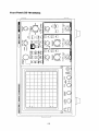
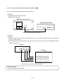
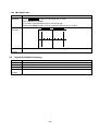
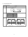
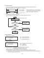
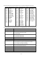
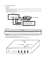
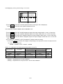
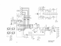
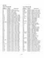
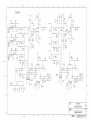
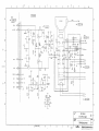
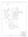
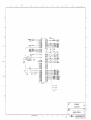
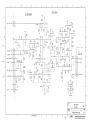
1
Service Manual Oscilloscope SS-7810/05/04 Introduction ◇ Thank you very much for your purchase of Iwatsu electronic measuring instruments. ◇ Please adjust or calibrate your instrument after throughly reading this service manual and understanding its contents. After reading this manual, please keep it for future reference. Cautions for safe use Matters that must be observed for operation of this instrument and for prevention of injury to humans and damage to property are described as “ warnings” and “ cautions” in this service manual. Explanation of “ Warnings” and “ Cautions” coulmns in this manual Warning Incorrect operation or failure to need warnings may result in death or serious injury. Caution Incorrect operation or failure to need cautions may result in injury or damage to equipment. Cautions ◇ Parts of the contents of this service manual may be modified without notice to accommodate improvements in performance and function. ◇ Reproduction of the contents of this service manual without previous consent is prohibited. History ◇ Jan. 2004 : Issue of the 1st edition KML045311 A1-523150(B) 0-1 Warnings Use care when servicing with power on: Dangerous voltages exist at several points in this product. To avoid personal injury, do not touch exposed connections or components while power is on. Disconnect power before removing protective panels, soldering, or replacing components. Cautions ● Never place a heavy substance on the power cord: It will cause an electric shock or fire. ● Prior to connecting or disconnecting the power cord, set the power supply to STBY: Its negligence will cause an electric shock or trouble. ● Use the specified AC power to operate the instrument: Use of non-specified power will cause an electric shock, fire, or trouble. The available AC power supplies are as follows: ・ Supply voltage : 90 to 132V AC/180 to 250V AC ・ Frequency : 48 to 440Hz ・ Power consumption : Max. 110VA ● Use a 3-core power cord suitable to the supply voltage: Use of other cord will an electric shock or fire. ● When replacing a fuse, be sure to use our specified one (φ φ5× ×20mm, 250VA, 2A, slow): Use of other fuse will cause a fire or trouble. ● Do not place any substance near the air vent of this instrument or fan: It will cause a fire or trouble. ● Use the instrument within the specified operating range: Otherwise, it will cause a trouble. An available temperature range is as follows: ・ Temperature : 0 to 40℃ ・ Relative humidity : 90% RH(40℃) ● Do not apply an overvoltage to the input terminal: It will cause a trouble. A maximum allowable input voltage is as follows: ・ CH1, CH2, CH3 (EXT): Directly : Max. ± 400V ・ When the SS-087R (10:1) or SS-088 (1:1, 10:1) probe is used: At 10:1 : Max. ± 600V At 1:1 : Max. ± 400V [NOTE] The maximum input voltage decreases depending on frequency and high voltage pulse of the input signal. 0-2 Table of Contents Introduction .................................................................................................................................................... 0Caution for safe use ...................................................................................................................................... 0Warnings ....................................................................................................................................................... 0Cautions ........................................................................................................................................................ 0- 1 1 2 2 Section 1 Specifications ................................................................................................................................. 1- 1 Section 2 Check and Adjustment 2.1 Knowledge Required before Beginning Adjustment .............................................................................. 2- 1 2.1.1 Introduction .................................................................................................................................... 2- 1 2.1.2 Check and Adjustment Intervals ..................................................................................................... 2- 1 2.1.3 Menu Screen .................................................................................................................................. 2- 1 ① Menu Tree SS-7810/05/04 ........................................................................................................ 2- 2 ② Manual Adjustment Menu .......................................................................................................... 2- 3 ③ Menu Screen (f:MAN-ADJ, AUTO-ADJ, AUTO-CONF) ............................................................. 2- 4 ④ Key Function/Movement in Adjustment Menu ............................................................................ 2- 5 2.1.4 Check and Adjustment Method ....................................................................................................... 2- 6 ① Check/Adjustment Procedure Flow Chart SS-78** .................................................................... 2- 6 ② Automatic Adjustment Items ...................................................................................................... 2- 7 ③ Automatic Comfirmetion Items .................................................................................................. 2- 8 ④ The Check/Adjustment Items and Sequence With Jig IE-1066 ................................................. 2- 9 ⑤ The Check/Adjustment Items and Sequence Without Jig IE-1066 ............................................ 2- 10 2.1.5 Check and Adjustment Affected Item .............................................................................................. 2- 11 2.1.6 Test Equipment Required ............................................................................................................... 2- 12 2.1.7 Preparation for Check and Adjustment ........................................................................................... 2- 14 2.1.8 Connection the Adjustment Jig IE-1066 to the SS-78** .................................................................. 2- 15 2.1.9 Check and Adjustment Locations ................................................................................................... 2- 16 ① POWER BOARD ....................................................................................................................... 2- 16 ② ANA BOARD Ⅰ ......................................................................................................................... 2- 17 ③ ANA BOARD Ⅱ ......................................................................................................................... 2- 18 ④ HV BOARD ............................................................................................................................... 2- 19 ⑤ V MAIN BOARD Ⅰ (SS-7810) .................................................................................................. 2- 20 2.2 DC Power Supply .................................................................................................................................. 2- 21 2.3 CRT Display .......................................................................................................................................... 2- 22 2.3.1 CRT Cathode Voltage ..................................................................................................................... 2- 22 2.3.2 CRT Heater Voltage ....................................................................................................................... 2- 22 2.3.3 Focus ............................................................................................................................................. 2- 23 2.3.4 Intensity .......................................................................................................................................... 2- 23 2.3.5 Trace Rotation ................................................................................................................................ 2- 24 2.3.6 Orthogonality .................................................................................................................................. 2- 25 2.4 Check the Key Function in Automatic Confirmation Mode ..................................................................... 2- 26 2.5 Gain (Coarse) ....................................................................................................................................... 2- 27 2.5.1 Vertical Gain ................................................................................................................................... 2- 27 2.5.2 Horizontal Gain ............................................................................................................................... 2- 28 2.5.3 △V Readout Gain .......................................................................................................................... 2- 28 2.5.4 △t Readout Gain ............................................................................................................................ 2- 29 2.6 Crystal Oscillation Frequency ................................................................................................................ 2- 29 2.7 Balance Coarse .................................................................................................................................... 2- 30 2.7.1 Balance Coarse (Automatic Adjustment Menu "D, L") .................................................................... 2- 30 2.7.2 Magnification Gain .......................................................................................................................... 2- 31 0-3 2.8 Vertical Deflection System .................................................................................................................... 2- 32 2.8.1 Flatness CHI/CH2/CH3 (SS-7810) ................................................................................................. 2- 32 2.8.2 Attenuator Compensation CH1/CH2 ............................................................................................... 2- 33 2.8.3 Attenuator Compensation CH3 (SS-7810)...................................................................................... 2- 34 2.8.4 High-frequency Compensation CH1/CH2 ....................................................................................... 2- 34 2.8.5 High-frequency Compensation CH3 (SS-7810) .............................................................................. 2- 35 2.8.6 Bandwidth ....................................................................................................................................... 2- 36 2.9 Horizontal Deflection System ................................................................................................................ 2- 37 2.9.1 High-speed Sweep Rate ................................................................................................................. 2- 37 2.9.2 Sweep Linearity at High-speed Sweep Rate (SS-7810) .................................................................. 2- 38 2.10 Calibrator Output ................................................................................................................................... 2- 39 2.11 Automatic Adjustment ........................................................................................................................... 2- 40 2.11.1 Automatic Adjustment Item ............................................................................................................. 2- 42 2.11.2 Error Message ................................................................................................................................ 2- 43 2.12 Automatic Confirmation ......................................................................................................................... 2- 50 2.12.1 Automatic Confirmation Items ........................................................................................................ 2- 51 2.13 Manual Adjustment Menu ..................................................................................................................... 2- 52 2.13.1 Manual Adjustment Items ............................................................................................................... 2- 53 2.13.2 Vertical Gain ................................................................................................................................... 2- 55 2.13.3 Trigger ............................................................................................................................................ 2- 56 2.13.4 X-Y Gain and Position .................................................................................................................... 2- 57 2.13.5 Manual Adjustment Procedure ....................................................................................................... 2- 58 2.14 Adjustment Jig IE-1066 ......................................................................................................................... 2- 72 2.14.1 Specifications ................................................................................................................................. 2- 72 2.14.2 Preparation ..................................................................................................................................... 2- 72 2.14.3 Adjustment of IE-1066 .................................................................................................................... 2- 73 2.14.4 Schematic Diagram ........................................................................................................................ 2- 75 Section 3 Block Diagram SS-7810 Block Diagram ........................................................................................................................ 3- 1 SS-7805/04 Block Diagram ................................................................................................................... 3- 7 Section 4 Electrical Parts List SS-7810 Parts List CH1 ATTENUATOR 1 ........................................................................................................................ 4- 10 CH2 ATTENUATOR 2 ........................................................................................................................ 4- 12 CH3 ATTENUATOR 3 ........................................................................................................................ 4- 14 CH1 1ST PREAMP 4 ......................................................................................................................... 4- 15 CH2 1ST PREAMP 5 ......................................................................................................................... 4- 17 CH1 2ND PREAMP 6 ......................................................................................................................... 4- 18 CH2 2ND PREAMP 7 ......................................................................................................................... 4- 19 CH3 PREAMP 8 ................................................................................................................................. 4- 20 CH SW & DRY LINE DRIV 9 .............................................................................................................. 4- 22 V CHARA AMP 10 .............................................................................................................................. 4- 23 V MAIN AMP 11 ................................................................................................................................. 4- 24 V OUTPUT AMP 12 ........................................................................................................................... 4- 25 CH1 TRIG PREAMP 13 ..................................................................................................................... 4- 26 CH2 TRIG PREAMP 14 ..................................................................................................................... 4- 28 CH3 TRIG PREAMP 15 ..................................................................................................................... 4- 29 A/B TRIG SELECT 16 ........................................................................................................................ 4- 30 A TRIG AMP 17 .................................................................................................................................. 4- 31 B TRIG AMP 18 ................................................................................................................................. 4- 32 TV SYNC SEP 19 .............................................................................................................................. 4- 33 0-4 TLC CIRCUIT 20 ................................................................................................................................ 4- 34 A SAWTOOTH BUFF 21 .................................................................................................................... 4- 35 B SAWTOOTH BUFF 22 ................................................................................................................... 4- 36 A TIMING 23 ...................................................................................................................................... 4- 37 B TIMING 24 ...................................................................................................................................... 4- 38 H & Z SW 25 ...................................................................................................................................... 4- 39 H MAIN AMP 26 ................................................................................................................................. 4- 41 H OUTPUT AMP 27 ........................................................................................................................... 4- 42 Z AMP 28 ........................................................................................................................................... 4- 43 PROBE SENCE 29 ............................................................................................................................ 4- 44 ANA BOARD CONTROL 30 ............................................................................................................... 4- 45 ANA BOARD 8 BIT D/A 31 ................................................................................................................. 4- 45 CRT CONT BOARD 32 ...................................................................................................................... 4- 46 H.V. CIRCUIT 33 ................................................................................................................................ 4- 47 CPU BOARD 35 ................................................................................................................................. 4- 49 36 (missing number) PANEL BOARD 37 ............................................................................................................................. 4- 51 KEY BOARD 38 ................................................................................................................................. 4- 51 POWER 39 ........................................................................................................................................ 4- 52 OVER ALL 40 ..................................................................................................................................... 4- 54 SS-7805/04 Parts List CH1 ATTENUATOR 1 ........................................................................................................................ 4- 56 CH2 ATTENUATOR 2 ........................................................................................................................ 4- 58 EXT TRIG IN 3 ................................................................................................................................... 4- 60 CH1 1st PREAMP 4 ........................................................................................................................... 4- 61 CH2 1st PREAMP 5 ........................................................................................................................... 4- 63 CH1 2nd PREAMP 6 .......................................................................................................................... 4- 65 CH2 2nd PREAMP 7 .......................................................................................................................... 4- 66 CH SW & DRY LINE DRIV 9 .............................................................................................................. 4- 67 V CHARA AMP 10 .............................................................................................................................. 4- 68 V MAIN AMP 11 ................................................................................................................................. 4- 69 V OUTPUT AMP 12 ........................................................................................................................... 4- 71 CH1 TRIG PREAMP 13 ..................................................................................................................... 4- 72 CH2 TRIG PREAMP 14 ..................................................................................................................... 4- 73 A TRIG SELECT 16 ........................................................................................................................... 4- 74 A TRIG AMP 17 .................................................................................................................................. 4- 75 TV SYNC SEP 19 .............................................................................................................................. 4- 77 TLC CIRCUIT 20 ................................................................................................................................ 4- 78 A SAWTOOTH BUFF 21 .................................................................................................................... 4- 79 A TIMING 23 ...................................................................................................................................... 4- 80 H & Z SW 25 ...................................................................................................................................... 4- 81 H MAIN AMP 26 ................................................................................................................................. 4- 83 H OUTPUT AMP 27 ........................................................................................................................... 4- 85 Z AMP 28 ........................................................................................................................................... 4- 87 PROBE SENCE 29 ............................................................................................................................ 4- 89 ANA BOARD CONTROL 30 ............................................................................................................... 4- 89 ANA BOARD 8 bit D/A 31 ................................................................................................................... 4- 89 CPU BOARD 35 ................................................................................................................................. 4- 89 PANEL BOARD 37 ............................................................................................................................. 4- 90 V MAIN BOARD .................................................................................................................................... 4- 90 CRT CONT BOARD 32 ...................................................................................................................... 4- 91 H.V. CIRCUIT 33 ................................................................................................................................ 4- 92 CPU BOARD 35 ................................................................................................................................. 4- 94 0-5 KEY BOARD 38 ................................................................................................................................. 4- 96 SS-78LVPS(100M) POWER 39 ......................................................................................................... 4- 97 OVER ALL 40 ..................................................................................................................................... 4-100 Selection 5 Schematic Diagrams SS-7810 CH1/CH2 ATTENUATOR 1 2 .......................................................................................................... 5- 1 CH3 ATTENUATOR 3 ........................................................................................................................ 5- 2 CH1/CH2 1st PREAMP 4 5 ............................................................................................................. 5- 3 CH1 2nd PREAMP 6 .......................................................................................................................... 5- 4 CH2 2nd PREAMP 7 .......................................................................................................................... 5- 5 CH3 PREAMP 8 ................................................................................................................................. 5- 6 CH SW & DRY LINE DRIV 9 .............................................................................................................. 5- 7 V CHARA AMP 10 .............................................................................................................................. 5- 8 V MAIN AMP 11 ................................................................................................................................. 5- 9 V OUTPUT AMP 12 ........................................................................................................................... 5- 10 CH1 TRIG PREAMP 13 ..................................................................................................................... 5- 11 CH2/3 TRIG PREAMP 14 15 .......................................................................................................... 5- 12 A/B TRIG SELECT 16 ........................................................................................................................ 5- 13 A/B TRIG AMP 17 18 ...................................................................................................................... 5- 14 TV SYNC SEP 19 .............................................................................................................................. 5- 15 TLC CIRCUIT 20 ................................................................................................................................ 5- 16 A/B SAWTOOTH BUFF 21 22 ........................................................................................................ 5- 17 A/B TIMING 23 24 ........................................................................................................................... 5- 18 H & Z SW 25 ...................................................................................................................................... 5- 19 H MAIN AMP 26 ................................................................................................................................. 5- 20 H OUTPUT AMP 27 ........................................................................................................................... 5- 21 Z AMP 28 ........................................................................................................................................... 5- 22 PROBE SENCE 29 ............................................................................................................................ 5- 23 ANA BOARD CONTROL 30 ............................................................................................................... 5- 24 ANA BOARD 8 BIT D/A 31 ................................................................................................................. 5- 25 CRT CONT BOARD 32 ...................................................................................................................... 5- 26 H.V. CIRCUIT 33 ................................................................................................................................ 5- 27 CPU BOARD 35 ................................................................................................................................. 5- 29 PANEL BOARD 37 ............................................................................................................................. 5- 33 KEY BOARD 38 ................................................................................................................................. 5- 34 POWER 39 ........................................................................................................................................ 5- 35 OVER ALL 40 ..................................................................................................................................... 5- 36 SS-7805/04 CH1/CH2 ATTENUATOR 1 2 .......................................................................................................... 5- 38 EXT TRIG IN 3 ................................................................................................................................... 5- 39 CH1/2 1st PREAMP 4 5 .................................................................................................................. 5- 40 CH1 2nd PREAMP 6 .......................................................................................................................... 5- 41 CH2 2nd PREAMP 7 .......................................................................................................................... 5- 42 CH SW & DRY LINE DRIV 9 .............................................................................................................. 5- 43 V CHARA AMP 10 .............................................................................................................................. 5- 44 V MAIN AMP 11 ................................................................................................................................. 5- 45 V OUTPUT AMP 12 ........................................................................................................................... 5- 46 CH1 TRIG PREAMP 13 ..................................................................................................................... 5- 47 CH2 TRIG PREAMP 14 ..................................................................................................................... 5- 48 A TRIG SELECT 16 ........................................................................................................................... 5- 49 A TRIG AMP 17 .................................................................................................................................. 5- 50 TV SYNC SEP 19 .............................................................................................................................. 5- 51 0-6 TLC CIRCUIT 20 ................................................................................................................................ 5- 52 A SAWTOOTH BUFF 21 .................................................................................................................... 5- 53 A TIMING 23 ...................................................................................................................................... 5- 54 H & Z SW 25 ...................................................................................................................................... 5- 55 H MAIN AMP 26 ................................................................................................................................. 5- 56 H OUTPUT AMP 27 ........................................................................................................................... 5- 57 Z AMP 28 ........................................................................................................................................... 5- 58 PROBE SENCE 29 ............................................................................................................................ 5- 59 ANA BOARD CONTROL 30 ............................................................................................................... 5- 60 ANA BOARD 8 BIT D/A 31 ................................................................................................................. 5- 61 CRT CONT BOARD 32 ...................................................................................................................... 5- 62 H.V. CIRCUIT 33 ................................................................................................................................ 5- 63 CPU BOARD 35 ................................................................................................................................. 5- 64 PANEL BOARD 37 ............................................................................................................................. 5- 68 KEY BOARD 38 ................................................................................................................................. 5- 69 POWER BOARD 39 .......................................................................................................................... 5- 70 OVER ALL 40 ..................................................................................................................................... 5- 71 Selection 6 Mechanical Parts Lists and Illstration .......................................................................................... 6- 1 0-7 Section 1 Specifications 1 Section 2 Check and Adjustment 2 Section 3 Block Diagram 3 Section 4 Electrical Parts List 4 Section 5 Schematic Diagrams 5 Section 6 Mechanical Parts List and Illustration 6 1 Section 1 Specifications SS-7810 CRT Type Display area Accelerating voltage Vertical defection system (Y axis) Vertical mode CH1, CH2 Deflection factor Range Variable control range Accuracy Frequency characteristics Bandwidth 5 mV to 5 V/div 2 mV/div Band width limiter Rise time 6 inch, diagonal rectangular flat face, intemal graticule, meshelss CRT with graticule illumination 8 div × 10 div (1 div = 10 mm) Approx. 16 kV CH1, CH2, CH3, ADD, ALT/CHOP CHOP mode switching rate 555 kHz ± 1 % 2 mV/div to 5 Vdiv, 1-2-5 sequence, 11 steps 2 mV/div to 12.5 V/div continuously variable ± 2% DC to 100 MHz − 3 dB DC to 50 MHz − 3 dB DC to approx. 20 MHz [Note] AC coupled low cutoff frequency (−3 dB) is 4 Hz. Approx. 3.5 ns [Note] Rise time Tr is calculate from: Tr = Step response Over shoot Sag (at 1 KHz) Signal delay Input coupling Input RC Maximum input voltage Position control range Invert ADD Accuracy of sum (at 1 kHz) Frequency characteristics Common-mode rejection ratio 1 kHz sin wave 20 MHz sine wave Dynamic range Probe sense 350 [ns] Bandwidth [MHz] at 10 mV/div, with 50 Ω termination 3% 1% At least 30 ns of the sweep is displayed before the triggering event. AC, DC, GND 1 M Ω ± 1.5 % // 20pF ± 2pF ± 400 V MAX Approx. ±10 div from the center line of the screen Available on CH2 ± 3% DC to 60 MHz − 3 dB at 10 mV/div 50:1 15:1 Overranging the screen at 100 MHz in the case of 10 mV/div 10:1, 100:1 detection 1-1 CH3 Deflection factor Range Accuracy Bandwidth Rise time 50 mV/div, 100 mV/div, 500 mV/div ±2% DC to 100 MHz − 3 dB Approx. 3.5 ns [Note] Rise time Tr is calculate from: Tr = Step response Over shoot Sag (at 1 KHz) Imput coupling Input RC Maximum input voltage Position control range Dynamic range Probe sense Triggering A triggering Trigger sensitivity Trigger level range Signal source Coupling Slope B triggering Trigger sensitivity Trigger level range Signal souroe Coupling Slope TV mode TV synchronization 350 [ns] Bandwidth [MHz] at 50 mV/div, with 50Ω termination 6% 1 % [Note] AC coupled low cutoff frequency (−3 dB) is 10 Hz AC, DC 1 M Ω± 1.5 % // 20 pF ± 3pF ± 400 V MAX Approx. ± 10 div from the center line of the screen Overranging the screen at 100 MHz 10:1, 100:1 detection Frequency P.P signal amplitude DC to 10 MHz 0.4 div 10 MHz to 100 MHz 1.0 div [Note] TV : The ratio between the composite video signal and synchronization signal is 7:3 and synchronization signal amplitude is 1.5 div or more. HF-REJ : Attenuates at 10 kHz or more LF:REJ : Attenuates at 10 kHz or less ± 9.5 div or more (set range: ± 10 div) CH1, CH2, CH3, LINE, VERT AC, DC, HF-REJ, LF-REJ +, − Frequency P.P signal amplitude DC to 10 MHz 0.4 div 10 MHz to 100 MHz 1.0 div [Note] HF-REJ : Attenuates at 10 kHz or more LF-REJ : Attenuates at 10 kHz or less ± 9.5 div or more (set range: ±10 div) CH1, CH2, CH3 AC, DC, HF-REJ, LF-REJ +, − NTSC, PAL, (SECAM) ODD, EVEN, BOTH TV-H [Note] ODD/EVN, or BOTH can be seiected NTSC: 5 H to 2000 H PAL (SECAM), HDTV: 2 H to 1997 H 1-2 AUTO SETUP Channels Frequency Horizontal deflection system (X axis) Horizontal display A sweep Sweep mode Sweep rates Maximum sweep Range Variable range Accuracy Ⅰ Accuracy Ⅱ Hold-off time B sweep Delay Sweep rates Maximum sweep Range Accuracy Ⅰ Accuracy Ⅱ Delay time Position control range Accuracy Avallable CH1 and CH2 50 Hz to 50 MHz A, ALT, B, X-Y AUTO, NORMAL SINGLE 2 ns/div 20 ns to 500 ms/div 1-2-5 sequence, 23 steps 20 ns to 1.5 s/div ± 2 % over center 8 div ± 5 % over center any 2 div within center 8 div Countinuously variable Triggered delay or continuous delay (RUNS AFTER) 2 ns/div 20 ns to 5 ms/div 1-2-5 sequence, 17 steps ± 2 % over center 8 div ± 5 % over center any 2 div within center 8 div 0.2 to 10.2 div ± [(set value × 0.005)+(sweep rate × 0.1)]−55 ns with in range of 1 μ s/div to 500 ms/div 1/2000, at 1 ms/div of A sweep:, at 500 ns/div of B sweep Delay pick off jitter Sweep magnification Magnifying ratio 10 times Accuracy Ⅰ over center 8 div 20 ns/div, 50 ns/div ±5% 100 ns/div to 500 ms/div ±3% 1 * Accuracy Ⅱ Over any 2 div within center 8 div 20 ns/div, 50 ns/div ±8% 100 ns/div to 500 ms/div ±5% *1 30 ns or 1 div at the beginning of sweep and 30 ns at the end of sweep are excluded. X-Y operation X axis (CH1) Deflection factor Same as CH1 Accuracy ±4% Bandwidth DC to 2 MHz, − 3 db Y axis CH1, CH2, CH3, ADD Phase difference between × axis and Y axis 3' or less (DC to 200 kHz) CAL (Probe calibration signal) Waveform Rectangular wave Fraquency 1 kHz ± 0.1 % Duty ratio 49 % to 51 % Output voltage 0.6 V ± 1% 1-3 Measurement with cursors and counter Measurement with cursors Type of measurement Cursor position control range X axis Y axis Accuracy Voltage difference ( △ V) Time difference ( △ t) MAG OFF MAG ON (MAG × 10) 500 ms to 100 ns/div 50 ns, 20 ns/div Counter Number of digits displayed Accuracy Frequency measurement range Saving data Type of date to be saved Data retention time Power source Voltage range Frequency range Power consumption Mass and Dimension Mass Dimension Environmental condtions Specification assurance temperature Operating Temperature Humidity Storage Temperature Humidlty Altitude Operating Nunoperating Vibration Time difference ( △ t), Voltage difference ( △ V) ± (5 ± 0.2) div from the center line of the screen ± (4 ± 0.2) div from the center line of the screen ± [(2 % of reading) + (0.3 % of full scale)] ± [(2 % of reading) ± (0.3 % of full scale)] ± [(3 % of reading) + (0.3 % of full scale)] ± [(5 % of reading) + (0.3 % of full scale)] 5 digits ± 0.01 % 2 Hz to 100 MHz Backup by built-in battery Panel setup conditions immediately before turning power off *2 Storing of panel setup conditions *3 (SS-7821/11) *2 The state where the power cord is disconnected. *3 The maximum number of date items that can be stored: 32 Approx. 30000H (at approx. 25 ℃) 90 to 132 VAC / 180 to 250 VAC 48 to 440 Hz 110 VA MAX Approx. 7.5 kg (without accessories) Approx. 272W × 152 H × 390 L [mm] [Note] Without accessories, and projections. 10 to 35 ℃ 0 to 40 ℃ 90 % RH or less (at 40 ℃) − 20 to 70 ℃ 80 % RH or less (at 70 ℃) 5000 m, atmospheric pressure: Approx. 55 kPa 15000 m, atmospheric pressure: Approx. 12 kPa 15 minutes along each of three axes at a total displacement of 0.67 mmp. p with frequency Varied from 10 Hz to 55 Hz in 1 minute sweep. 1-4 Shock Dropping packaged Warm up time Lifting a side to a height of 10 cm and dropping it naturally onto hard wood: 4 times on each side. Dropping an instrument packaged for transportation from a height of 90 cm. The specifications for this instrument are the assured values after more than 30 min of power on. 1-5 SS-7805/04 CRT Type Display area Accelerating voltage Vertical deflection system (Y axis) Vertical mode CH1, CH2 Deflection factor Range Variable control range Accuracy Frequency characteristics Bandwidth 5 mV to 5 V/div 2 mV/div Rise time SS-7804 SS-7805 6 inch, diagonal rectangular flat face, internal graticule, meshelss CRT with graticule illumination 8 div × 10 div (1 div = 10 mm) Approx. 16 kV CH1, CH2, ADD, ALT/CHOP CHOP mode switching rate 555 kHz ± 1 % 2 mV/div to 5 V/div, 1-2-5 sequence, 11 steps 2 mV/div to 12.5 V/div continuously variable ± 2% DC to 40 MHz −3 dB (SS-7804) / DC to 50 MHz −3 dB (SS-7805) DC to 20 MHz −3 dB (SS-7804) / DC to 20 MHz −3 dB (SS-7805) Approx. 8.75 ns Approx. 7.0 ns [Note] Rise time Tr is calculate from: Tr = Step response Over shoot Sag (at 1 kHz) Signal delay Input coupling Input RC Maximum input voltage Position control range Invert ADD Accuracy of sum (at 1 kHz) Frequency characteristics Common-mode rejection ratio 50:1 15:1 Dynamic range Probe sense Attached probe Optional probe 350 [ns] Bandwidth [MHz] at 10 mV/div, 50 Ω termination 3 % (SS-7804) / 8 % (SS-7805) 1 % (SS-7804) / 1 % (SS-7805) At least 30 ns of the sweep is displayed before the triggering event. AC, DC, GND 1 M Ω ± 1.5 % // 25 pF ± 2 pF ± 400 V (DC+ACpeak) Approx. ±10 div from the center line of the screen Available on CH2 ± 3% DC to 20 MHz − 3 dB 1 kHz sine wave 20 MHz sine wave Overranging the screen at 40 MHz (SS-7804) Overranging the screen at 50 MHz (SS-7805) No function. 10:1, 100:1 detection 1-6 Triggering Trigger sensitivity Trigger level range Signal source Coupling Slope TV mode TV synchronization EXTTRIG Input RC Input coupling Maximum input voltage Probe sence Horizontal deflection system (X axis) Horizontal display Sweep mode Sweep rates Maximum sweep Range Variable range Accuracy Ⅰ Accuracy Ⅱ Hold-off time Sweep magnification Magnifying ratio Accuracy Ⅰ 100 ns/div to 200 ns/div 500 ns/div to 500 ms/div *1 Accuracy Ⅱ 100 ns/div to 200 ns/div 500 ns/div to 500 ms/div Frequency CH1, CH2 EXT DC to 5 MHz 0.4 div 80 mV 5 MHz to 40 MHz (SS-7804) 1.0 div 200 mV 5 MHz to 50 MHz (SS-7805) [Note] TV : The ratio between the composite video signal and synchronization signal is 7:3 and synchronization signal amplitude is 1.5 div or more. HF-REJ : Attenuates at 10 kHz or more LF-REJ : Attenuates at 10 kHz or less ± 9.5 div or more (set range: ± 10 div) CH1, CH2, EXT, LINE, VERT AC, DC, HF-REJ, LF-REJ +, − NTSC, PAL (SECAM) ODD, EVEN, BOTH TV-H [Note] ODD, EVEN, or BOTH can be selected NTSC: 5 H to 2000 H PAL (SECAM): 2 H to 1997 H 1 MW ± 2 % // 25 pF ± 3 pF DC ± 400 V (DC+ACpeak) 10:1 and 100:1 detection with an optional probe (SS-78R) A, X-Y AUTO, NORMAL SINGLE 10 ns/div 100 ns to 500 ms/div 100 ns to 1.25 s/div ± 2 % over center 8 div ± 5 % over center any 2 div within center 8 div Countinuously variable 10 times over center 8 div ±5% ±3% Over any 2 div within center 8 div ±8% ±5% 1-7 X-Y operation X axis (CH1) Deflection factor Accuracy Bandwidth Y axis Phase difference between × axis and Y axis Same as CH1 ±3% DC to 2 MHz − 3 dB CH1, CH2, ADD 3°or less (DC to 50 kHz) CAL (Probe calibration signal) Waveform Fraquency Duty ratio Output voltage Rectangular wave 1 kHz ± 0.1 % 49 to 51 % 0.6 V ± 1% Measurement with cursors and counter Measurement with cursors Type of measurement Time difference ( △ t), Voltage difference ( △ V) Cursor position control range X axis ± (5 ± 0.2) div from the center line of the screen Y axis ± (4 ± 0.2) div from the center line of the screen Accuracy Voltage difference ( △ V) ± [(2 % of reading) + (0.3 % of full scale)] Time difference ( △ t) MAG OFF ± [(2 % of reading) + (0.3 % of full scale)] MAG ON (MAG × 10) 100 ns, 200 ns/div ± [(5 % of reading) + (0.3 % of full scale)] 500 ns to 500 ms/div ± [(3 % of reading) + (0.3 % of full scale)] Counter Number of digits displayed 5 digits Accuracy ± 0.01 % Frequency measurement range SS-7804 2 Hz to 40 MHz SS-7805 2 Hz to 50 MHz Saving data Type of date to be saved Data retention time Power source Voltage range Frequency range Power consumption Mass and Dimension Mass Dimension Backup by built-in battery Panel setup conditions immediately before turning power off *2 *2 The state where the power cord is disconnected. Approx. 30,000H (at approx. 25 ℃) 90 to 132 VAC / 180 to 250 VAC 48 to 440 Hz 110 VA MAX Approx. 7.5 kg (without accessories) Approx. 272W × 152 H × 390 L [mm] [Note] Without accessories, and projections. 1-8 Environmental conditions Specification assurance temperature Operating Temperature Humidity Storage Temperature Humidity Altitude Operating Nunoperating Vibration Shock Dropping packaged Warm up time 10 to 35 ℃ 0 to 40 ℃ 90 % RH or less (at 40 ℃) -20 to 70 ℃ 80 % RH or less (at 70 ℃) 5,000 m, atmospheric pressure : Approx. 55 kPa 15,000 m, atmospheric pressure : Approx. 12 kPa 15 minutes along each of three axes at a total displacement of 0.67 mmp. p with frequency Varied from 10 Hz to 55 Hz in 1 minute sweep. Lifting a side to a height of 10 cm and dropping it naturally onto hard wood: 4 times on each side. Dropping an instrument packaged for transportation from a height of 90 cm. The specifications for this instrument are the assured values after more than 30 min of power on. 1-9 SS-501 (CH2 OUT, Z AXIS IN) Factory option for the SS-7800 series. SS-501 : SS-7804/7805 CH2 OUT connector (rear panel) Outputs a sample of the signal applied to the CH2 signal input. Z AXIS IN connector (rear panel) Input a signal for an intensity modulation on screen. Specification CH2 OUT Deflection factor DC level Output coupling Bandwidth Output resistance Z AXIS IN Input voltage Polarity Input frequency Input resistance Maximum input voltage 45 mV ±20 % per one division screen amplitude (at 50 Ω load) ± 100 mV (at 50 Ω load) DC 20 MHz –3 dB (at 50 Ω load) 50 Ω± 20 % 0.5 Vp-p or more Positive going signal decreases intensity and negative going signal increases intensity DC to 5 MHz 4.5 k Ω± 20 % ± 50 V (DC+ACpeak) 1-10 2 Section 2 Check and Adjustment Table of Contents Section 2 Check and Adjustment 2.1 Knowledge Required before Beginning Adjustment .............................................................................. 2- 1 2.1.1 Introduction .................................................................................................................................... 2- 1 2.1.2 Check and Adjustment Intervals ..................................................................................................... 2- 1 2.1.3 Menu Screen .................................................................................................................................. 2- 1 ① Menu Tree SS-7810/05/04 ........................................................................................................ 2- 2 ② Manual Adjustment Menu .......................................................................................................... 2- 3 ③ Menu Screen (f:MAN-ADJ, AUTO-ADJ, AUTO-CONF) ............................................................. 2- 4 ④ Key Function/Movement in Adjustment Menu ............................................................................ 2- 5 2.1.4 Check and Adjustment Method ....................................................................................................... 2- 6 ① Check/Adjustment Procedure Flow Chart SS-78** .................................................................... 2- 6 ② Automatic Adjustment Items ...................................................................................................... 2- 7 ③ Automatic Comfirmetion Items .................................................................................................. 2- 8 ④ The Check/Adjustment Items and Sequence With Jig IE-1066 ................................................. 2- 9 ⑤ The Check/Adjustment Items and Sequence Without Jig IE-1066 ............................................ 2- 10 2.1.5 Check and Adjustment Affected Item .............................................................................................. 2- 11 2.1.6 Test Equipment Required ............................................................................................................... 2- 12 2.1.7 Preparation for Check and Adjustment ........................................................................................... 2- 14 2.1.8 Connection the Adjustment Jig IE-1066 to the SS-78** .................................................................. 2- 15 2.1.9 Check and Adjustment Locations ................................................................................................... 2- 16 ① POWER BOARD ....................................................................................................................... 2- 16 ② ANA BOARD Ⅰ ......................................................................................................................... 2- 17 ③ ANA BOARD Ⅱ ......................................................................................................................... 2- 18 ④ HV BOARD ............................................................................................................................... 2- 19 ⑤ V MAIN BOARD Ⅰ (SS-7810) .................................................................................................. 2- 20 2.2 DC Power Supply .................................................................................................................................. 2- 21 2.3 CRT Display .......................................................................................................................................... 2- 22 2.3.1 CRT Cathode Voltage ..................................................................................................................... 2- 22 2.3.2 CRT Heater Voltage ....................................................................................................................... 2- 22 2.3.3 Focus ............................................................................................................................................. 2- 23 2.3.4 Intensity .......................................................................................................................................... 2- 23 2.3.5 Trace Rotation ................................................................................................................................ 2- 24 2.3.6 Orthogonality .................................................................................................................................. 2- 25 2.4 Check the Key Function in Automatic Confirmation Mode ..................................................................... 2- 26 2.5 Gain (Coarse) ....................................................................................................................................... 2- 27 2.5.1 Vertical Gain ................................................................................................................................... 2- 27 2.5.2 Horizontal Gain ............................................................................................................................... 2- 28 2.5.3 △V Readout Gain .......................................................................................................................... 2- 28 2.5.4 △t Readout Gain ............................................................................................................................ 2- 29 2.6 Crystal Oscillation Frequency ................................................................................................................ 2- 29 2.7 Balance Coarse .................................................................................................................................... 2- 30 2.7.1 Balance Coarse (Automatic Adjustment Menu "D, L") .................................................................... 2- 30 2.7.2 Magnification Gain .......................................................................................................................... 2- 31 2.8 Vertical Deflection System .................................................................................................................... 2- 32 2.8.1 Flatness CHI/CH2/CH3 (SS-7810) ................................................................................................. 2- 32 2.8.2 Attenuator Compensation CH1/CH2 ............................................................................................... 2- 33 2.8.3 Attenuator Compensation CH3 (SS-7810)...................................................................................... 2- 34 2.8.4 High-frequency Compensation CH1/CH2 ....................................................................................... 2- 34 2.8.5 High-frequency Compensation CH3 (SS-7810) .............................................................................. 2- 35 2.8.6 Bandwidth ....................................................................................................................................... 2- 36 2.9 Horizontal Deflection System ................................................................................................................ 2- 37 2.9.1 High-speed Sweep Rate ................................................................................................................. 2- 37 2.9.2 Sweep Linearity at High-speed Sweep Rate (SS-7810) .................................................................. 2- 38 2.10 Calibrator Output ................................................................................................................................... 2- 39 2.11 Automatic Adjustment ........................................................................................................................... 2- 40 2.11.1 Automatic Adjustment Item ............................................................................................................. 2- 42 2.11.2 Error Message ................................................................................................................................ 2- 43 2.12 Automatic Confirmation ......................................................................................................................... 2- 50 2.12.1 Automatic Confirmation Items ........................................................................................................ 2- 51 2.13 Manual Adjustment Menu ..................................................................................................................... 2- 52 2.13.1 Manual Adjustment Items ............................................................................................................... 2- 53 2.13.2 Vertical Gain ................................................................................................................................... 2- 55 2.13.3 Trigger ............................................................................................................................................ 2- 56 2.13.4 X-Y Gain and Position .................................................................................................................... 2- 57 2.13.5 Manual Adjustment Procedure ....................................................................................................... 2- 58 2.14 Adjustment Jig IE-1066 ......................................................................................................................... 2- 72 2.14.1 Specifications ................................................................................................................................. 2- 72 2.14.2 Preparation ..................................................................................................................................... 2- 72 2.14.3 Adjustment of IE-1066 .................................................................................................................... 2- 73 2.14.4 Schematic Diagram ........................................................................................................................ 2- 75 2.1 Knowledge Required before Beginning Adjustment 2.1.1 Introduction Periodic check and adjustment maintains reliable performance of this instrument for a long time. 2.1.2 Check and Adjustment Intervals To measure signals accurately, it is necessary to periodically check and adjust the measuring instrument. Recommended check and adjustment intervals for this instrument are approx. 6 months. 2.1.3 Menu Screen For this instrument, there are three of menu screens for check and adjustment. ◇Adjustment Menu Screen ・Adjust 116 items manually on the adjust menu screen. For further details, refer to "2.13" Manual Adjustment Items". ◇Automatic Adjustment Menu Screen ・Adjust the instrument automatically with the jig IE-1066. For futrther details, refer to "2.11 Automatic Adjustment". ◇Automatic Confirmation Menu Screen ・Confirm and check the instrument functions and perfomances automatically with the jig IE-1066. For furher details, refer to "2.12 Automatic Confirmation". ・For KEY confirmation, refer to "2.4 KEY". Use IE-1066 when carrying out Automatic Adjustment or/and Automatic Confirmation. ・For connections, refer to "2.18 Connection the Adjustment Jig IE-1066. ・For calibration of IE-1066, refer to "2.14 Adjustment Jig IE 1066". 2-1 ① Menu Tree SS-7810/05/04 QUIT NORMAL SCOPE MODE PRESS HOLD OFF PRESS NORM QUIT FUNCTION OFF READ OUT OFF PRESS【FUNCTION】KNOB SAVE ADJUST VALUE DEPRESS 3 second 【FUNCTION】KNOB TURN【FUNCTION】KNOB ADJUST VALUE SYSTEM MENU PRESS【FUNCTION】KNOB DETERMINE ITEM PRESS SEVERALTIMES CH2【VOLT/DIV】 TURN【FUNCTION】KNOB SELECT ADJUST ITEM MANUAL ADJUSTMENT SCREEN QUIT PRESS PRESS AUTO EXECUTE AUTO BAL CAL PRESS SGL/RST SGL/RST PRESS TCK/C2 AUTOMATIC ADJUSTMENT PRESS △V•△t•OFF AUTOMATIC CONFIRMATION TURN【FUNCTION】KNOB SELECT ADJUST ITEM TURN【FUNCTION】KNOB SELECT CONF ITEM PRESS【FUNCTION】KNOB DETERMINE ITEM PRESS【FUNCTION】KNOB DETERMINE ITEM PRESS A EXECUTE AUTO ADJ PRESS NORM EXECUTE AUTO CONF 2-2 QUIT ② Mannual Adjustment Menu The following describes how to enter the manual adjustment screen. Procedure ── Enter to Manual Adjustment Menu Screen ── ①Turn off all the functions to disable【FUNCTION】.*1 *1 Condition that f・XXXX is not being displayed at the upper right of the screen (the delay time, number of TV lines, etc.) ② Press READOUT to set the charactors to OFF (non-display). ③ Press【VOLTS/DIV】of CH2 several times quickly. ・ Manual adjustment menu is displayed. ・ The function indication turns to f:MAN-ADJ. ・ Select the adjustment item by turrning【FUNCTION】. The steps below describes an example when INTEN is to be selected. ── Selecting the Adjustment Item ── ④Turn【FUNCTION】to select INTEN. ・ For details of the adjustment menu items, refer to the "2.13.5 Manual Adjustment Procedure". ── Setting the Value ── ⑤ Press【FUNCTION】. ・ The adjustment item is determined. ⑥ Turn【FUNCTION】to set the VALUE. ── Saving the VALUE ── ⑦ Press【FUNCTION】. ・ The set value is saved and "SAVED" appears at the lower left of the screen. ── Canceling the Adjustment Menu Screen ── ⑧To cancel the adjustment menu screen, press HOLD OFF . 2-3 ③Menu Screen (f:MAN-ADJ, AUTO-ADJ, AUTO-CONF) ◇Procedure ① to ③, refer to "2.1.3 ② Adjustment Menu". ・ Display the adjustment menu screen. Automatic Adjustment Menu screen ◇Press TCK/C2 in the manual adjustment screen. ・ Display the automatic adjustment menu screen. For the automatic adjustment menu, see "2.11 Automatic Adjustment". ── Return to Manual Adjustment Menu Screen ── ・ To cancel the auto adjustment menu screen, press SGL/RST . Automatic Confirmation Menu screen ◇Press △V-△t-OFF in the adjustment menu screen. ・ Display the automatic confirmation menu screen. ・ For the "KEY", see "2.4 KEY on automatic confirmation". For the items except "KEY", see "2.14 Automatic Confirmation". ── Return to Manual Adjustment Menu Screen ── ・To cancel the auto confirmation menu screen, press SGL/RST . 2-4 ④ Key Function/Movement in Adjustmnet Menu MANUAL ADJUSTMENT MENU A. B. C. D. Selecting the Adjust Item Determine the Adjust Item Vary the Adjust Value Save the Adjust Value Turn FUNCTION key Press FUNCTION key Turn FUNCTION key Press FUNCTION key QUIT Press HOLD OFF or POWER OFF AUTO ADJUSTMENT MENU A. Selecting All Adjust Item A'. Selecting Individual Adjust Item B. Determine the Adjust Item C. Start AUTO ADJUSTMENT Press AUTO key Turn FUNCTION key Press FUNCTION key Press NORM QUIT Press SGL/RST or POWER OFF AUTO CONFIRMATION MENU A. Selecting All Confirmation Item A'. Selecting Individual Confirmation Item B. Determine the Confirmation Item C. Startr AUTO CONFIRMATION Press AUTO key Turn FUNCTION key Press FUNCTION key Press NORM QUIT Press SGL/RST or POWER OFF 2-5 2.1.4 Check and Adjustment Method ① Check/Adjustment Procedure Flow Chart SS-78 ** SEQUENCE 1 2 3 ※1 DISPLAY SCOPE SCOPE AUTO-CONF ※2 ADJUST ITEM POWER SUPPLY CRT CHECK the KEY SEQUENCE 4 5 6 DISPLY SCOPE SCOPE AUTO-ADJ ADJUST ITEM V. H GAIN COARSE CRYSTAL-OSCILLATION-FREQ V. H BALANCE COARSE SEQUENCE 7 8 9 DISPLY SCOPE MAN-ADJ. SCOPE MAN-ADJ ADJUST ITEM VERTICAL DEFELECTION HORIZONTAL DEFELECTION CALIBRATION OUTPUT Cover the Case, Warm up the Scope. AUTOMATIC ADJUST WITH JIG SEQUENCE 12 DISPLY AUTO-ADJ SEQUENCE DISPLY 13 AUTO-CONF MANUAL ADJUST WITHOUT JIG SEQUENCE 11 DISPLY MAN-ADJ ADJUST ITEM ALL ITEMS SEQUENCE 12 DISPLY ADJUST ITEM AUTO-ADJ A,B,D,F,G,H,J,K,L,M,N,O ADJUST ITEM ALL ITEMS SEQUENCE DISPLY 13 AUTO-CONF Check Items (Vertical Gain. Sweep Rate. Trigger. Others) ※ 1 DISPLAY SCOPE MAN-ADJ AUTO-ADJ AUTO-CONF SYS-MENU : NORMAL OSCILLOSCOPE MODE : MANUAL ADJUSTMENT SCREEN : AUTOMATIC ADJUSTMENT : AUTOMATIC CONFIRMATION : SYSTEM MENU ※2 ADJUST ITEM A, B, C, O ※ : refer to"2.1.4. ② ADJUSTMENT ITEM" next page. 2-6 ADJUST ITEM C,I,P ADJUST ITEM A,E,J,L,M,N,O Table 2.1.1 ② Automatic Adjustment Items Description Item Page A. CHAR Y Cursor moving range and intercursor accuracy at △V cursor measurement time 2-48 B. CHAR X Cursor moving range and Intercursor accuracy at △t cursor measurement time 2-48 C. *V-GAIN Vertical gain (CH1 to CH3) 2-48 D. V-BAL DC balance (CH1, CH2) and Step balance (CH1 to CH3) 2-49 E. *V-VARI Beginning of the effect of the vertical variable (CH1, CH2) 2-49 F. ADD-BL Add balance 2-49 G. CH2 INV CH2 Inversion balance 2-49 H. V-POSI Vertical position (CH1 to CH3) 2-50 I. *TRIG Trigger level and trigger gain 2-50 J. H-SWP Sweep rate (A/B) 2-50 K. H-LENG Sweep length (A/B) 2-51 L. MAG Magnification center 2-51 M. H-POSI Horizontal position 2-51 N. BS-POS B sweep start position 2-51 O. B-DLY Delay time 2-52 P. *X-Y X-Y gain and position 2-52 *: Denotes the item for which an adjusting jig is required. 2-7 Table 2.1.2 ③ Automatic Confirmation Items Item Description Rating Check the operations of the keys, controls, and pulse switches. A. KEY B. *V DCSFT Inputs a 6 div DC signal and automatically confirms a move amount 0.06/6div or less 10 seconds later (CH1 to CH3) C. *V POSI Automatically confirms the variable range of the ±10.0div or more 【▲POSITION▼】control (CH1 to CH3). D. *ADD GAI Automatically confirms sensitivity at ADD mode. A 3 div signal for 3.0% CH1 and CH2 is turned to 6 div at ADD mode. E. H POSI Automatically confirms the variable range of the ±6.5div or more ▲ ▲ 【 POSITION 】control. F. *POL GAI 1.5% Automatically confirms sensitivity of CH2 INV. G. *AC/DC Normal changed Automatically confirms the operation of input coupling AC/DC (CH1 to CH3). H. *V RANGE Automatically confirms the next range of vertical sensitivity. 1.5% CH1, CH2: 20 Mv, 50 mV/div. CH3: 50 mV, 500 mV/div I. *TRIG LVL Automatically confirms the variable range of the ±9.5 div or more 【TRIG LEVEL】control. J. H VAR Automatically confirms the variable range of the【VARIABLE】 2.5 times or more control. K. *V VAR Automatically confirms the operation of the Variable Range: 2.5 times or more 【VARIABLE】 control (CH1, CH2) of VOLTS/DIV. Variable Balance 20mV to 5V/div : 0.5div or less 2mV to 10mV/div : 5mV or less L. H RANGE ± 1.8% Automatically confirms 200 μs or 500 μs/div at A TIME/DIV or B TIME/DIV. M. TR-SEP +4div or more N. LINETRG Automatically confirms Automatically confirms trace separation. the line synchronism. O. H START 2div or less Automatically confirms shifting of the A-sweep start point upon ( × 10 MAG) switching the【TIME/DIV】control in the following ranges: 100 ms, 10 ms, 1 ms, 500 μs, 200 μs, 100 μs, 10 μs, 1 μs P. *: Denotes the item for which an adjusting jig is required. 2-8 ④ The Check/Adjustment Items and Sequence With Jig IE-1066 Table2.1.3 The check list With Jig IE-1066 Condition Function SEQ See Remarks Adjust Item Adjust/Check Page Display *1 39VR1 ADJ-VR *2 SCOPE 1 DC Power Supply 22 CRT Display 33VR15 HV ADJ ADJ-VR SCOPE 2 Cathode Voltage 23 33R21 HEATER Heater Voltage 23 33R23, 33R41, 33R51, 33R54 Focus 24 33R46 Intensity 25 TRACE ROTATION Trace Rotation 26 MENU "ORTHOGO" ADJ-VALUE *3 27 MAN-ADJ Orthogonality MENU "A. KEY" AUTO-CONF Check 3 KEY Switch 28 Gain Coarse 11R41 "CH1 10mV GAIN" VALUE 180 ADJ-VALUE SCOPE 4 Vertical Gain 29 24R84 "AS100-500μs" VALUE 128 ADJ-VR Horizontal Gain 30 10R24 "Y-CHRG" VALUE 128 △V readout Gain 30 26R49 "X-CHRG" VALUE 128 △t readout Gain 31 20IC3#1 with the counter Check SCOPE 5 Crystal Oscillation 20MHz 31 MENU "D, L" Check AUTO-ADJ 6 V BAL Coarse 32 MENU "MAG SWEEP REF" ADJ-VALUE MAN-ADJ Magnification Gain 33 Vertical Deflection System 1R39(CH1),2R39(CH2),3R39(CH3) ADJ-VR, C *4 34 SCOPE 7 ① Flatness (CH1)1C4,1C5,1C12A,(CH2)2C4,2C5 ② Attenuator Compensa35 2C12A,(CH3)3C5,7C3,7C4,8C3,8C4 tion 36 6C4,7C4,9R23,9C23,9C12,11C22, ③ High-FREQ Compensa37 11C23,11C39B,11148, etc 4 point tion 38 ④Bandwidth 39 8 Horizontal Deflection System MENU "AS 100-500ns", etc ADJ-VALUE SCOPE High-speed Sweep Rate 40 MENU "AS 20-50ns" ADJ-VALUE Sweep Linearity at High 41 27C13, 27C33 ADJ-C -speed Sweep Rate MENU "CAL LEVEL" ADJ-VALUE MAN-ADJ 9 Calibration Output 42 10 Cover the Case. Warm up the Scope. 11 Automatic Adjustment. Connection the jig IE-1066 to the 43 to A,B,C,D,E,F,G,H,I,J,K,L,M,N,O,P SS-78** . 51 12 Automatic Confirmation. Connection the jig IE-1066 to the 52 to A,B,C,D,E,F,G,H,I,J,K,L,M,N,O SS-78** . 53 13 Check Items (Vertical Gain, Sweep Rate, Trigger, Others) using the standard measurement instrument. *1 *2 *3 *4 SEQ ADJ-VR ADJ-VALUE ADJ-C : The Check/Adjustment Sequence number : Adjust variable resistor : Set Value on Manual Adjustment Screen : Adjust variable capacitor 2-9 ⑤The Check/Adjustment Items and Sequence Without Jig IE-1066 Table2.1.3 The check list Without Jig IE-1066 Function Condition SEQ Adjust Item Display Adjust/Check *1 SCOPE ADJ-VR *2 1 DC Power Supply CRT Display SCOPE ADJ-VR 2 Cathode Voltage Heater Voltage Focus Intensity Trace Rotation MAN-ADJ ADJ-VALUE *3 Orthogonality AUTO-CONF Check 3 KEY Switch Gain Coarse SCOPE ADJ-VALUE 4 Vertical Gain ADJ-VR Horizontal Gain △V readout Gain △t readout Gain Check 5 Crystal Oscillation 20MHz SCOPE AUTO-ADJ Check 6 V BAL Coarse MAN-ADJ ADJ-VALUE Magnification Gain Vertical Deflection System SCOPE ADJ-VR, C *4 7 ① Flatness ② Attenuator Compensation ③ High-FREQ Compensation ④ Bandwidth 8 Horizontal Deflection System SCOPE ADJ-VALUE High-speed Sweep Rate ADJ-VALUE Sweep Linearity at High ADJ-C -speed Sweep Rate ADJ-VALUE MAN-ADJ 9 Calibration Output 10 Cover the Case. Warm up the Scope. C: V-GAIN I: TRIG 11 Manual Adjustment P: X-Y 12 Automatic Adjustment. 13 14 *1 *2 *3 *4 See Page 39VR1 22 Remarks 23 23 24 25 26 27 28 33VR15 HV ADJ 33R21 HEATER 33R23, 33R41, 33R51, 33R54 33R46 TRACE ROTATION MENU "ORTHOGO" MENU "A. KEY" 29 30 30 31 31 32 33 11R41 "CH1 10mV GAIN" VALUE 180 24R84 "AS100-500μs" VALUE 128 10R24 "Y-CHRG" VALUE 128 26R49 "X-CHRG" VALUE 128 20IC3#1 with the counter MENU "D, L" MENU "MAG SWEEP REE" 34 35 36 37 38 39 1R39(CH1),2R39(CH2),3R39(CH3) (CH1)1C4,1C5,1C12A,(CH2)2C4,2C5 2C12A,(CH3)3C5,7C3,7C4,8C3,8C4 6C4,7C4,9R23,9C23,9C12,11C22, 11C23,11C39B,11148, etc 4 point 40 41 MENU "AS 100-500ns", etc MENU "AS 20-50ns" 27C13, 27C33 MENU "CAL LEVEL" 42 54 to C, I, P 60 43 to A,B,D,E,F,G,H,J,K,L,M,N*5,O*5 51 Automatic Confirmation. 52 to A,E,J,L,M,N,O 53 Check Items (Vertical Gain, Sweep Rate, Trigger, Others) using the standard measurement instrument. SEQ ADJ-VR ADJ-VALUE ADJ-C : The Check/Adjustment Sequence number : Adjust variable resistor : Set Value on Manual Adjustment Screen : Adjust variable capacitor 2-10 2.1.5 Check and Adjustment Affected Item Table 2.1.5 shows the check/adjustment items and sequence. a. When replaced CRT, adjust/check all the itmes start from top of the next flow chart. b. When checking/adjusting/repairing only the limited items: Check/adjust the items Iisted in the right "Affected Item" column of the table below. Table 2.1.5 Check and Adjustment items Sequence 1 2 Item 2.2 DC Power Supply 2.3 CRT Display 2.3.1 CRT Cathode Voltage 2.3.2 3 4 5 6 7 8 9 10 11 12 13 CRT Heater Voltage Page 2-22 Affected Item All items 2-23 2.3.2 to 2.3.6, 2.5, 2.8.4 to 2.8.6 2.9, 2.13, 2.11 2.3.2 to 2.3.6, 2.5, 2.8.4 to 2.8.6 2.9, 2.13, 2.11 2.3.4 2-23 2.3.3 Focus 2.3.4 Intensity 2.3.5 Trace Rotation 2.3.6 Orthogonality 2.4 Check the Key Function in Automatic Confirmation Mode 2.5 Gain Coarse 2.5.1 Vertical Gain 2.5.2 Horizontal Gain 2.5.3 △V Readout Gain 2.5.4 △t Readout Gain 2.6 Crystal Oscillation Frequency 2.7 Balance Coarse 2.7.1 Balance Coarse (AUTO-ADJ "D, L") 2.7.2 Magnification sweep reference 2.8 Vertical Deflection System 2.8.1 Flatness CH1/CH2/CH3 2.8.2 Attenuator Compensation CH1/CH2 2.8.3 Attenuator Compensation CH3 2.8.4 High-frequency Compensation CH1/CH2 2.8.5 High-frequency Compensation CH3 2.8.6 Bandwidth 2.9 Horizontal Deflection System 2.9.1 High-speed Sweep Rate 2.9.2 Sweep Linearity at High-speed Sweep Rate 2.10 Calibration Output Cover the Case, Warm up the Scope. 2.13 Manual Adjustment 2.13.1 Vertical Gain 2.13.2 Trigger 2.13.3 X-Y gain and position 2.11 Automatic Adjustment 2.12 Automatic Confirmation *1 : Except SS-7804/02 2-11 2-24 2-25 2-26 2-27 2-28 2-29 2-30 2-30 2-31 2-31 2.8.4 to 2.8.6, 2.13, 2.11 2.9, 2.13.3, 2.11 2.11 2.11 2-32 2-33 2.13, 2.11 2.11 2-34 2-35 2-36 2-37 2-38 2-39 2.8.2 to, 2.8.6 2.8.4, 2.8.6 2.8.5, 2.8.6 2.8.6 2.8.6 2-40 2-41 2.9.2 2-42 2-57 2-58 2-59 2-43 2-52 2.12 2.12 2.12 2.12 2.1.6 Test Equipment Required a. When checking or adjusting this instrument, the measuring instruments, etc. listed in Table 2.1.6 are required. ・Adjustment jig IE-1066 for the SS-78XX are required. ・The performance of the measuring instruments should be equivalent or higher than that described below. b. The signal input connector for this instrument is a BNC type. When the terminator or signal output terminal used for the measuring instrument is not a BNC type, prepare a proper adaptor. Table 2.1.6 Test Equipment Required Ⅰ (1/2) Equipment/Minimum Specification 1. Adjustment jig IE-1066 for SS-78XX Ⅰ 2. OscilloscopeⅠ Minimum deflection factor : 1mV/div Bandwidth : DC to 1MHz 3. OscilloscopeⅡ Ⅱ Deflection factor : 10mV to 5V/div Bandwidth : DC to 350MHz 4. Digital multimeter Range : DC to 300V Accuracy : 0.2%+1dgt TRUE RMS bandwidth : 100kHz 5. Frequency counter Range : 20MHz or more Reference oscillator accuracy : ± 3 × 10⁻⁵ or more 6. Function generator Repetition rate : DC to 10MHz Signal level : 1Vp-p or more 7. Scope calibrator ・Calibration voltage Output voltage : 12mV to 60V Accuracy : 0.5% or less ・Time marker Repetition rate : 10ns to 2s Accuracy : 0.5% or less ・Square wave Repetition rate : 50Hz to 200kHz Rise Time : 5ns or less ・Sine wave Repetition rate : 1kHz Accuracy : 20% or less Purpose Vertical, horizontal, triggering check and adjustment Power supply check and adjustment Recommended Model General signal check IWATSU SS-7840 Power supply check and adjustment IWATSU VOAC7411 with SC306 Battery Unit Crystal oscillator frequency and calibrator frequency check IWATSU SC-7201 Vertical, horizontal, triggering check and IWATSU FG-350 adjustment Display, vertical, horizontal, triggering check IWATSU SC-340 and adjustment 2-12 Table 2.1.7 Test Equipment RequiredⅠ (2/2) Equipment/Minimum Specification 8. Constant amplitude signal generator Frequency : 50kHz to 250MHz Signal level*1 : 60mV or more 9. Pulse generator Repetition rate : 50kHz to 100kHz Rise Time : 1ns or less Waveform distorion : Should be less Signal level : 60mVp-p or more 10. Time mark generator 11. Probe for osilloscope Attenuation ratio : 10:1, 1:1 12. High-voltage probe for digital multimeter Attenuation ratio : 1000:1 Range : DC to 30kV DC Accuracy : ± 5%+1digit 13. BNC coaxial cable (5 pieces) Impedance : 50 Ω Length : 50cm, 1.2 m 14. 50ƒ¶ termination (2 pieces) Impedance : 50 Ω Connector : BNC 15. Attenuater Ratio : 0 to 50dB Bandwidth : DC to 2GHz 16. Screwdriver (Low capacitance) Purpose Bandwidth check Recommended Model TEK SG-503 Step response check and adjustment TEK PG-506 PSPL MODEL 2600 Sweep linerarity at high-speed sweep rate TEK TG501 Signal probe SS-0130R (10:1) : SS-7810's accessory SS-0110R (10:1) : SS-7805/04's assessory High-voltage check and adjustment Signal interconnection IWATSU BB-120C IWATSU BB-50M1 Signal termination Signal attenuation Adjustment of variable resistors and capacitors 17. 2mm hexagonal-head screw driver *1 Should be calibrated to a constant level if the frequency is changed. 2-13 IWATSU AA-03B, AA-06B AA-10B, AA-20B Probe's accessory 2.1.7 Preparation for Check and Adjustment Prior to starting a check or Adjustment, prepare the following: a. Set an ambient temperature to 23℃±5℃. b. Adjust INTEN, READOUT, FOCUS, and SCALE to ensure a clear display. c. Warm up the instrument for approx. 30 minutes. d. Set the keys and controls as shown in Table 2.1.8. Table 2.1.8 Key and Control Setting Key and Control Setting CRT Display INTEN Midrange READOUT Midrange FOCUS Vertical Deflection System CH1, CH2 VOLTS/DIV (CH1, CH2) VARIABLE (CH1, CH2) DC/AC (CH1, CH2) GND (CH1, CH2) CH2 INV Triggering A/B LEVEL SOURCE COUPL Horizontal Deflection System HORIZ DISPLAY SWEEP MODE TIME/DIV VARIABLE MAG Midrange ON (Display) 10mV OFF (CAL) DC OFF (GND release) OFF (INV release) A Midrange CH1 DC A AUTO 1ms/div OFF OFF ( × 1) 2-14 ** 2.1.8 Connection the Adjustment Jig IE-1066 to the SS-78** How to use Adjustment Jig IE-1066 is described as below. ・Preparation ① Peel the grey tape on the rear panel. ② Appear the I/F connector SS-78 (rear sub panel) FAN MOTOR Adjustment Jig IE-1066 I/F connector CH1 CH2 CH3 CH4 I/F connector LINE INPUT I/F cable Figure 2.1 Rear sub panel of SS-78** ・Connection Procedure ① Connect between the IE-1066 I/F connector and SS-78** I/F connector with the exclusive I/F cable (See Figure 2.1 and Figure 2.2). ② Connect between the IE-1066 OUTPUT connectors and the SS-78** INPUT connector with the BNC coaxial cables (See Figure 2.2). IE-1066 I/F connector BNC OUT CH1 CH2 CH3 SS-78 to CH3 INPUT (front panel) to CH2 INPUT (front panel) to CH1 INPUT (front panel) to I/F connector (rear panel) Figure 2.2 Connection IE-1066 to SS-78** Calibrating IE-1066 See "2.14 Adjustment Jig IE-1066". 2-15 2.1.9 Check and Adjustment Locations See Figure 2.1.1. to 2.1.7 Figure 2.1.1 POWER BOARD Figure 2.1.2 ANA BOARD Ⅰ Figure 2.1.3 ANA BOARD Ⅱ Figure 2.1.4 HV BOARD Ⅰ Figure 2.1.5 HV BOARD Ⅱ Figure 2.1.6 V MAIN BOARD Ⅰ (SS-7810) Figure 2.1.7 V MAIN BOARD Ⅱ (SS-7805/04) : See page 2-16 : See page 2-17 : See page 2-18 : See page 2-19 : See page 2-19 : See page 2-21 : See page 2-21 ① POWER BOARD Top View CRT BOARD CRT FRONT REAR HV BOARD POWER BOARD POWER BOARD VR1 #11 CN5 #3 #1 Figure 2.1.1 POWER BOARD 2-16 ② ANA BOARD Ⅰ Bottom View ANA BOARD ANA BOARD 8 3R29B 8C2 3C5 9 9R23 3 9C23 2C4 2 2R39B 7 7C4 2R27 (SS-7802) 2C5 2C12A 1C4 13 6 1 1R39B 6C4 31 1R27 (SS-7802) 1C5 1C12A ANA BOARD ANA BOARD 3 8 15 8 2 5 14 7 9 13 1 FRONT 4 13 6 REAR 31 24 30 26 CRT CRT CONT BOARD 18 16 25 22 20 21 27 17 1 29 Figure 2.1.2 23 ANA BOARD Ⅰ 2-17 ③ ANA BOARD Ⅱ Bottom View ANA BOARD ANA BOARD 3 8 15 8 2 5 14 7 9 13 1 FRONT 4 13 6 REAR 31 24 30 26 CRT CRT CONT BOARD 18 16 25 22 20 21 27 17 1 23 29 ANA BOARD ANA BOARD 30 24 25 31JP100 31 26 20 50 26R11 26R49 25 27P2 20IC3 21 27C33 27JP102 27C13 29 23 Figure 2.1.3 27 ANA BOARD Ⅱ 2-18 ④ HV BOARD Side View TOP CPU BOARD HV BOARD FRONT POWER BOARD REAR ANA BOARD BOTTOM R23 R41 R46 R15 R54 R51 R21 P3(hided) HV BOARD Figure 2.1.4 HV BOARD Ⅰ (SS-7810/05/04) Side View TOP CPU BOARD FRONT HV BOARD POWER BOARD ANA BOARD BOTTOM R15 R62 R54 R51 R21 P3(hided) HV BOARD Figure 2.1.5 HV BOARD Ⅱ (SS-7810) 2-19 REAR ⑤ V MAIN BOARD Ⅰ (SS-7810) Side View TOP CRT BOARD V MAIN BOARD V MAIN AMP [11] REAR FRONT Z AMP[28] V CHARA AMP [10] BOTTOM V MAIN BOARD V MAIN AMP [11] Z AMP [28] 11C48 (SS-7810) 11C39B 11C22 11R41 11C23 10R24 V CAHRA AMP [10] Figure 2.1.6 V MAIN BOARD Ⅰ (SS-7810/05/04) 2-20 2.2 DC Power Supply Item Rating and test point Equipment Procedure Description DC voltage -12V +50V +12V +5V +150V Accuracy ± 0.5% ± 2.0% ± 1.5% ± 3.0% ± 3.0% Ripple voltage 3mVp-p or less 5mVp-p or less 3mVp-p or less 40mVp-p or less 20mVp-p or less Test point ANA BOARD 27P2 (BLUE) ANA BOARD 27JP102 ANA BOARD 27PS (RED) ANA BOARD 31JP100 POWER BOARD CN5 #3 Adjuster 39VR1 − − − − ・ Digital multimeter: VOAC7411 or equivalent ・ 1mV/div oscilloscope with a probe of 1:1 attenuation ratio ── DC Voltage ── ① Chcek a voltage between the test points and ground with a digital multimeter. ② Adjust -12 V with 39VR1. within 11.94 to 12.06. ── Ripple Voltage ── Reference Test/ Adjustment Location ③ Set SWEEP MODE to SINGLE. ④ Check the ripple voltage of each power supply with a 1mV/div oscilloscope (use a probe of 1:1attenuation ratio). If -12 V is adjusted, the other power supplies should be meet to the specification. 39VR1, +150V 39 CN5 #3: See "Figure 2.1.1 POWER BOARD" ・ 27P2 (BLUE, -12V), 31JP100 (+5V), 27P2 (RED, +12V), 27JP102 (+50V): See "Figure 2.1.3 ANA BOARD II" 2-21 2.3 CRT Display 2.3.1 CRT Cathode Voltage Item Rating Equipment Note Procedure Check/ Adjustment Location Description -1975V ±20V ・ Digital multimeter: VOAC7411 or equivalent ・ High-voltage probe (adjusted one) ・ Adjustment of the CRT cathode voltage affects most of the items. When it is within the specification, do not adjust it. ・ When the CRT cathode voltage is adjusted, check/adjust the affected items in accordance with Table 2.1.5. ① Use the digital multimeter (high-voltage probe used) to check a voltage between 33 P3 #4 and GND. ② When a check result is nonstandard, adjust it to -1,975V with 33R15 HV ADJ. 33P3, 33R15 : See "Figure 2.1.4 HV BOARD Ⅰ" 2.3.2 CRT Heater Voltage Item Rating Equipment Procedure Description 5.6 to 6.1 Vrms (When SS-7802's Serial Number is XXXX 268 or more, it's 6.0 to 6.6 Vrms.) Digital multimeter with rms function: VOAC7411 with SC306 (Battery Unit) or equivalent ① At MIN load, check a voltage between 33 P3 #5 and 33 #6 using the digital multimeter. ・ The MIN load is as follows: INTEN : Fully counterclockwise READ OUT : OFF (not displayed) FOCUS : Fully clockwise ② When a check result is nonstandard, adjust it to 5.80 Vrms (When SS-7802's Serial Number is XXXX 268 or more, it's 6.3 Vrms.) with 33 R21 HEATER. ③ At MAX load, check a heater voltage. ・ The MAX load is as follows: INTEN : Fully clockwise READ OUT : OFF (not displayed) FOCUS : Fully counterclockwise TIME/DIV : 500 μ s/div Check/ Adjustment Location 33P3, 33R21 : See "Figure 2.1.4 HV BOARD Ⅰ" 2-22 2.3.3 Focus Item Rating Description The trace should be focused when the【FOCUS】control is positioned between plus minus 45 ° from the midrange. Connection The scope Function generator (FG-350 or equivalent) Sine wave, 1kHz Procedure Check/ Adjustment Location ① Set the instrument as follows: INTEN : To such an extent that the trace can be slightly seen READ OUT : To such an extent that the characters can be slightly seen FOCUS : midrange ② Check 33 P3 #1 with the digitl multimeter (high-voltage probe used) and adjust to -625V with 33 R51. ③ Input a sine wave (1KHz) and adjust the amplitude to 4 div. ④ Adjust the following variable resistors to optimize the focus. 33 R23, 33 R41, 33 R54 33 P3, 33 R51, 33 R23, 33 R41, 33 R54 : See "Figure 2.1.4 HV BOARD Ⅰ" 2.3.4 Intensity Item Rating Procedure Adjustment Location Description ・ The trace should disappear when the【INTEN】control is turned fully counterclockwise. ・ The characters should disappear when the【READOUT】control is turned fully counterclockwise. ① Set the scope as follows so that a spot is displayed. INTEN : Fully counterclockwise READOUT : OFF (not displayed) HORIZ DISPLAY : X-Y ② Adjust 33 R46 CUT OFF so that the spot disappear thoroughly. ③ Set HORIZ DISPLAY to A. ④ Set TIME/DIV to 100 μs/DIV. ⑤ Set the INTEN to 10 O'clock position. ⑥ Adjust the brightness of Intensity by using adjustment menu so that trace line is slighly appear. ⑦ Set READOUT INTEN to the 12:00 position and make sure that the characters have not disappeared. ・ Refer to "2.1.3 Manual Adjustment Menu". 33R46 : See "Figure 2.1.4 HV BOARD " 2-23 2.3.5 Trace Rotation Item Rating Procedure Description The horizontal trace should be aligned with the horizontal graticule. ① Set the scope as follows. HORIZ DISPLAY : A SWEEP MODE : AUTO TIME/DIV : 1 ms/div ② Adjust with TRACE ROTATION and align the horizontal trace. Waveform on Screen Dislocation of horizontal trace from horizontal graticule ② Align horizontal trace with horizontal graticule Adjustment Location Front panel 2-24 2.3.6 Orthogonality Item Rating Procedure Waveform on Screen Description ±0.03/6 div or less ① In the adjustment menu, select the ORTHOGO adjustment menu. ② Press a function key. A crosshair cursor will appear. ③ Adjust the value and align the vertical cursor with the vertical graticule. 0.03 div less 6div Dislocation of Vertical Trace from Vertical Graticule ③ Align Vertical Trace with Vertical Graticule 2-25 2.4 Check the Key Function in Automatic Confirmation Mode Check the function of the keys, controles, and pulse switches on the front panel. In this section, check only the functions of those keys. For the other items, refer to "2.12 Automatic Confirmation". Procedure ── Entering the Automatic Confirmation Menu ── ① Press △V-△t-OFF in "the manual adjustment menu screen". ・The automatic confirmation menu is displayed. ── Selecting the Automatic Conifirmation Item A ── ②Select an item A for automatic confirmation. ◇ Only A (KEY) is displayed. ── Execute the Automatic Confirmation ── ③ Press NORM . ・ The KEY SW confirmation screen is displayed. ── Confirming the Operations ── ④ Press all the keys and pulse switches to confirm that a display "KEY=XXXX" will change. ⑤ Turn all VRs to confirm that VOL is set to 0 to 4095. ⑥ Confirm that "P_SW1:>" is displayed by turning all the pulse switch to the right, and that "P_SW1:<" is displayed by turning them to the left. ── End of Confirmation ── ⑦ Press 【FUNCTION】. ・ "KEY=23" is displayed. ⑧ Press 【FUNCTION】. ・ "OK!" is displayed. ⑨ Press NORM . ・ You are returned to a normal screen. 2-26 2.5 Gain (Coarse) 2.5.1 Vertical Gain Item Rating Connection Description ± 2% or less The Scope Generator (SC-340 or equivalent) Square Wave, 1 kHz, 60 mV Procedure ① Set VOLTS/DIV of CH1 to 10 mV/div. ② Input a square wave (1kHz, 60mV) to CH1. ③ CH1 10mV GAIN in the Adjustment Menu to set VALUE 180. ④ Adjust 11R41 to 6 div amplitude. Waveform on Screen 6div Adjustment Location 11R41 : See "Figure 2.1.6 V MAIN BOARD Ⅰ" 2-27 2.5.2 Horizontal Gain Item Connection Description The Scope Time marker generator (SC-340 or equivalent) Time Marker 100μs Procedure ① "AS 100-500μs" in the Adjustment Menu to set VALUE 128. ② Input a time marker 100μs to CH1. ③ Set A TIME/DIV to 100μs/div. ④ Adjust 26R11 so that the pulse meet to graticule over ±4div from the screen center. Waveform on Screen Adjustment Location 8div 26R11 : See "Figure 2.1.3 ANA BOARD Ⅱ" 2.5.3 △ V Readout Gain Item Procedure Description ① "Y-CHRG" in the Adjustment Menu to set VALUE 128. ② Set VOLTS/DIV to 10 mV/div. ③ Use △V-△t-OFF to select △V and display the △V cursor. ④ Adjust with 10R24 so that an intercursor distance will be 6 div on △V=60 mV. Waveform on Screen 6div Adjustment Location SS-7810 (10R24) : See "Figure 2.1.6 V MAIN BOARD Ⅰ" SS-7805/04 (10R24) : See "Figure 2.1.7 V MAIN BOARD Ⅱ" 2-28 2.5.4 △ t Readout Gain Item Procedure Description ① Use △V-△t-OFF to select △t and display the △t cursor. ② Set TIME/DIV to 1 ms/div. ③ "X-CHRG" is the Adjustment Menu to set VALUE 128. ④ Adjust with 26R49 so that an intercursor distance will be 8 div on △t=8ms. Waveform on Screen Adjustment Location 2.6 8div 26R49 : See "Figure 2.1.3 ANA BOARD Ⅱ" Crystal Oscillation Frequency Item Rating Equipment Procedure Check Location Description 20MHz±100ppm (±0.01%: 19,998 to 20,002MHz) Frequency Counter Check 20IC3 #1 with the counter. 20IC3 : See "Figure 2.1.3 ANA BOARD Ⅱ" 2-29 2.7 Balance Coarse 2.7.1 Balance Coarse (Automatic Adjustment Menu "D, L") Item Procedure Description ① Enter the Adjustment Menu Screen. (refer to "2.1.3 Menu Screen") ② Press TCK/C2 in the adjustment menu screen. ・Display the automatic adjustment menu screen. ③ Select an item "D, L" for automatic adjustment. Display the symbol for the automatic adjustment item and undisplay those for the non-automatic adjustment items. (refer to 2.11 Automatic Adjustment) ④ Press NORM to execute the automatic adjustment items (D, L). Waveform on Screen symbol of item Adjustment item Adjustment ・ DC BAL : 2mV, 5mV, 100mV and 1V of CH1 and CH2 Symbol D: V- ・ STEP BAL : CH1 to CH3 BAL Rating ・ DC BAL : 0.5div ・ STEP BAL 10mV TO 5V/dib : 0.5div 2mV, 5mV : 5mV Error display Menu No. Detail Menu No. 000 CH1 2mV DC BAL 006 001 CH1 5mV DC BAL 007 002 CH1 100mV DC BAL 008 003 CH1 1V DC BAL 009 004 CH2 2mV DC BAL 010 005 CH2 5mV DC BAL Adjustment ・ Magnification center Symbol L: HMAG Rating ・ Magnification center: ±3.0 div or less Error display Menu No. Detail 001 Out of center at MAG ON Jig Unnecessary 2-30 Menu No. 002 Detail CH2 100mV DC BAL CH2 1V DC BAL CH1 STEP BAL CH2 STEP BAL CH3 STEP BAL Detail Out of center at MAG OFF 2.7.2 Magnification Gain Item Connection Description The Scope Time marker generator (SC-340 or equivalent) Time Marker 100μs Procedure ① Set the scope as follows: A TIME/DIV : 1ms, MAG×10 : OFF ② Input the 100μs time marker to CH1. ③ Set MAG × 10 ON. ④ Adjust with MAG SWEEP REF in the adjustment menu so that the pulse meet to graticule. over ±4div, from the screen center. [Note] New setting VALUE is effective by pressing MAG×10 after saving VALUE by pressing the FUNCTION Key. Waveform on Screen 8div 100μs/div Adjust the sweep time with "MAG SWEEP REF". 2-31 2.8 Vertical Deflection System 2.8.1 Flatness CH1, CH2, CH3 (SS-7810) Item Connection Description The Scope Square wave generator (SC-340 or equivalent) Coaxial cable Square wave, 100 Hz 60mV or 300mV (CH3) Procedure ① Set VOLTS/DIV of CH1 and CH2 to 10mV, CH3 to 50mV. ② Set TIME/DIV to 1ms. ③ Set DC/AC of CH1, CH2 and CH3 to DC. ④ Input the 100Hz 60mV or 300mV(CH3) from the SC-340. ⑤ Adjust Flatness of square wave with the 1R39B(CH1), 2R39B(CH2), 3R39B(CH3) Waveform on Screen Correctly Adjusted Waveform Adjustment Location See "2.1.9② ANA BOARD Ⅰ" 2-32 2.8.2 Attenuator Compensation CH1/CH2 Item Rating Connection Description ± 2.0% or Less The Scope Square wave generator (SC-340 or equivalent) Probe or coaxial cable Square wave, 1 kHz Procedure ──CH1 (CH1 ATT UNIT)── ① Connect CH1 INPUT to the output of the square wave generator (1kHz) with coaxial cable. ② Adjust the waveform of 100mV/div to flat with 1C5, and that of 1V/div with 1C12A (refer to the following table). ③ Set VOLTS/div to 10mV. ④ Connect CH1 INPUT to the output of the square wave generator (1kHz) with a probe. ⑤ Adjust the waveform to flat with the Variable Capacitor on the probe. ⑥ Set the VOLTS/div to 100mV, and adjust the waveform with 1C4. ──CH2 (CH2 ATT UNIT)── ⑦ Adjust CH2 in accordance with the following table as same as CH1 Channel 1 CH1 CH2 Connection Coaxial cable Probe Coaxial cable Probe VOLTS/DIV 10mV/div ── Variable capacitor on the probe ── Variable capacitor on the probe 100mV/div 1C5 1C4 2C5 2C4 1V/div 1C12A ── 2C12A ── Waveform on Screen Correctly Adjusted Waveform Adjustment Location See "2.1.2② ANA BOARD Ⅰ" 2-33 2.8.3 Attenuator Compensation CH3 (SS-7810) Item Rating Connection Description ± 2.0% or less The Scope Square wave generator (SC-340 or equivalent) Coaxial cable Square wave, 1 kHz Procedure Waveform on screen Adjustment Location ──CH3 (CH1 ATT UNIT)── ① Connect CH3 INPUT to the output of the square wave generator 1kHz with coaxial cable. ② Adjust the waveform of 50mV/div to flat with 3C5. Refer to "2.8.2 Attenuator Compensatin" See "2.1.2 ② ANA BOARD Ⅰ " 2.8.4 High-frequency Compensation CH1/CH2 Item Rating Connection Description Overshoot : 3% at 10mV/div, 50Ω termination The Scope Pulse generator (PG506 or equivalent) 50Ω Cable Square Wave, 1 MHz Procedure ① Set VOLTS/DIV of CH1 and CH2 to 10 mV. ② Input a square wave (1 MHz) from the PG-506 and adjust the amplitude to 6 div. ③ Adjust the waveform with the following variable capacitors and resistors. ANA BOARD V MAIN BOARD Adjustment Location CH1 6C4 ── CH2 7C4 ── Common 9R23, 9C23 11C22, 11C23, 11C39B, 11C48(SS-7810 ONLY) ANA BOARD : See "Figure 2.1.2 ANA BOARD Ⅰ" V MAIN BOARD : See "Figure 2.1.6 V MAIN BOARD Ⅰ" 2-34 2.8.5 High-frequency Compensation CH3 (SS-7810) Item Rating Connection Description Overshoot : 6% at 50mV/div, 50Ω termination The Scope Pulse generator (PG506 or equivalent) 50Ω Coaxial Cable Square Wave, 1 MHz Procedure Adjustment Location ① Set VOLTS/DIV of CH3 to 50 mV. ② Input a square wave (1MHz) from the PG-506 and adjust the amplitude to 6 div. ③ Adjust the waveform with 8C2. [Note] Adjust to meet to both specifications of overshoot and frequency characteristic. For the frequency characteristic checking method, refer to "2.8.6 Bandwidth." 8C2 : See "Figure 2.1.2 ANA BOARD Ⅰ" 2-35 2.8.6 Bandwidth Item Rating SS-7810 (CH1 to CH3) SS-7805 (CH1, CH2) SS-7804 (CH1, CH2) Description : DC to 100MHz -3dB : DC to 50MHz -3dB : DC to 40MHz -3dB Connection The Scope Constant amplitude signal generator (SG-503 or equivalent) 50Ω Coaxial Cable Sine Wave, 50 kHz to 100/40/20 MHz Procedure ── CH1, CH2 ── ① Set VOLTS/DIV of CH1 and CH2 to 10 mV. ② Input a sine wave (50kHz) from the signal generator and adjust the amplitude to 6 div. ③ Read the amplitude when the frequency of the signal generator is changed to the respective specified frequencies. ── CH3 (SS-7810) ── ④ Set VOLTS/DIV of CH3 to 50 mV. ⑤ Check the frequency bandwidth in the same manner as for CH1 and CH2. Waveform on Screen 4.25 div. or more 6div ② Amplitude for Reference Frequency (50kHz): 6 div Reference ③ Amplitude for Specified Frequency: 4.25 div or more The following is a decibel conversion table to be applied when the reference amplitude is set to 6 div. Amplitude (div) 6.0 4.4 4.3 4.25 4.2 4.1 4.0 Decibel (dB) 0.0 -2.7 -2.9 -3.0 -3.1 -3.3 -3.5 2-36 2.9 Horizontal Deflection system 2.9.1 High-speed Sweep Rate Item Rating Description ± 2% ± 5% (Central 8 div of screen) (Optional 2 div of central 8 div of screen) Connection The Scope Time marker generator (SC-340 or equivalent) Time Maker 50ns 500ns Procedure ① Adjust 500ns/div and 50ns/div in the adjustment menu. (Refer to the table below) TIME/DIV Adjustment Menu A 500ns/div AS 100-500ns A 50ns/div (SS-7810) AS 20-50ns B 500ns/div (SS-7810) BS 100-500ns B 50ns/div (SS-7810) BS 20-50ns Waveform on Screen 8div 8div 2div Cantral 8 Div of Screen Optional 2 Div of Central 8 Div of Screen 2-37 2.9.2 Sweep Linearity at High-speed Sweep Rate (SS-7810) Description Item Connection The Scope Time marker generator (SC-340 or equivalent) Time Marker, 50ns, 20ns, 10ns 5ns Procedure ① Confirm A Sweep Rate (50ns/div, 20ms/div) before adjusting this item, if rating is out of range, adjust "2.9.1 High speed Sweep Rate." ② Set TIME/DIV to the scope to 20ns/div and the time marker to 10ns/div. ③ Set MAG × 10 to ON. ④ Adjust sweep linearity (left and right distortions of the screen) with 27C13 and 27C33. Waveform on Screen ←② Set TIME/DIV to 20ns/div. and the time market to 10ns/div. ←③ Set MAG × 10 to ON. ←④ Adjust left and right distortions the screen. Adjustment Location 27C13, 27C33: See "Figure 2.1.3 ANA BOARD Ⅱ" 2-38 2.10 Calibrator Output Item Rating Equipment Procedure Check Location Description 0.6V ± 0.8% Digital multimeter (DCV): VOAC7411 or equivalent ① Check a voltage between the CAL terminal and ground with digital multimeter. ② Adjust it to +0.599 to +0.601 with "CAL LEVEL" in manual adjustment menu. ③ Save the setting value. ・"the manual adjustmen menu" refer to 2-1-3 Menu Screen" ④ Turn on the power again. A 1 kHz square wave will be oscillated. Front panel 2-39 2.11 Automatic Adjustment The following describes the automatic adjustment method. Procedure ── Connection ── ① Connect the adjustment jig IE-1066 to the SS-78**. ・ See 2.1.8 about connection. ── Displaying the Automatic Adjustment Screen ── ② Press TCK/C2 in the adjustment menu screen change to the automatic adjustment menu screen. ・ To enter the adjustment menu screen, refer to "2.1.3 menu Screen". ── Selecting the Automatic Adjustment Item ── ③ Select some adjust items for automatic adjustment. Ⅰ. Press AUTO to display all the items (A to P). ・ Every time AUTO is pressed, the all symbols are displayed/undisplayed altemately. Ⅱ. Turn【FUNCTION】to select the relevant symbol with a " ↑ " mark. Ⅲ . Press【FUNCTION】to determine the adjust item. Ⅳ . *mark, use the jig. ◇ The following shows an example of adjusting A and B automatically. ── Setting the Screen Reference Position ── ④ Press NORM of SWEEP MODE. ・ The upper cursor position setting screen (SET: UPPER) is displayed. ⑤ Turn or press【FUNCTION】to set the cursor to the position 3 div. above the horizontal center line. ⑥ Press AUTO of SWEEP MODE. ・ The lower cursor position setting screen (SET: LOWER) is displayed. ⑦ Turn or press【FUNCTION】to set the cursor to the position 3 div. below the horizontal center line. 2-40 ⑧ Press AUTO . ・ The left cursor position setting screen (SET: LEFT) is displayed. ⑨ Turn or press【FUNCTION】to set the cursor to the position 4 div to the left of the vertical center line. ⑩ Press AUTO . ・ The right cursor position setting screen (SET: RIGHT) is displayed. ⑪ Turn or press【FUNCTION】to set the cursor to the position 4 div to the right of the vertical center line. ・ Every time AUTO is pressed, the display in the SET field. The cursor position can be set in the indicated direction. UPPER → LOWER → LEFT → RIGHT ── Performing Automatic Adjustment ── ⑫ Press A of HORIZ DISPLAY. ・ The displayed items are automatically adjusted in an alphabetic order. ◇ When automatic adjustment is completed, "OK!" is displayed. ・ The symbol for the automatically adjusted item is displayed at the upper left of the screen. ・ The left figure shows that automatic adjustment of A and B has been performed. ◇ Unless automatic adjustment is performed, "NG" is displayed. ・ An error item is displayed at the bottom of the screen and an error message is displayed in the NG field, respectively. ・ The left figure shows that the item A has been automatically adjusted and the item B has an error. ── Cancelling Automatic Adjustment ── ⑬ To cancel the automatic adjustment menu screen, press SGL/RST . 2-41 Table 2.11.1 Automatic Adjustment Item Item A. CHAR Y B. CHAR X C. *V-GAIN D. V-BAL E. *V-VARI F. ADD-BL G. CH2 INV H. V-POSI I. *TRIG J. H-SWP K. H-LENG L. MAG M. H-POSI ↑ N. BS-POPS ↑ O. B-DLY P. *X-Y Description Cursor moving range and intercursor accuracy at △V cursor measurement time Cursor moving range and intercursor accuracy at △t cursor measurement time Vertical gain (CH1 to ↑CH3) DC balance (CH1, CH2) and Step balance (CH1 to ↑CH3) Beginning of the effect of the vertical varlable (CH1, CH2) Add balance CH2 inversion balance Vartical position (CH1 to ↑CH3) Trigger level and trigger gain Sweep rate (A/ B) Sweep length (A/ B) Magnification center Horizontal position B sweep start position Delay time X-Y gain and position * : Denotes the item for which an adjusting jig is required. ↑ : Except SS-7805/04. 2-42 Page 2-47 2-47 2-47 2-48 2-48 2-48 2-48 2-49 2-49 2-49 2-50 2-50 2-50 2-50 2-51 2-51 2.11.2 Error message ・When automatic adjutment is not performed collectly, an error message is displayed as below. ・There are two type Error messages depends on a judgement. ާVALUE RANGEި Error message Ⅰ : Unable the adjustment in〔VALUE RANGE〕 Error message Ⅱ : Completed the adjustment, but the adjusted value is close to upper or lower limit. Range = Error Adjusted Value ާE-LIMITި (Proper Range) ・Rating Accuracy : Refer to page 48 to 52 ・ 〔VALUE RANGE〕 〔E-LIMIT〕: Refer to 2.13.5 Manual Adjustment Procedure e.g. Start Automatic Adjustment Items A to P C:V-GAIN Rating Accuracy ±2% Adjustment Value Value check in range? NG Display Error message Ⅰ NG -AA -BB -CC PUSH:NORM *V-GAIN NG Display Error message Ⅱ NG -AA -BB -CC PUSH:NORM E-LIMIT Y Y More Adjustment items? N E-LIMIT CHECK Y OK ! PUSH NORM a. Error message Ⅰ ・Display of Error message Ⅰ NG - AA - BB - CC PUSH:NORM *V-GAIN AA : 000 to 015(Error Items) BB : Refer to page 48 to 52. CC : Refer to page 48 to 52. b. Error message Ⅱ ・Display of Error messageⅡ NG - AA - BB - CC PUSH:NORM E-LIMIT AA : Error NO. (Refer to table 2.11.2) BB : No meaning CC : Adjusted value ・E-LIMIT judgement : The adjusted value is close to upper or lower limit This judgement is avalable from CPU Ver5.1 ・If plural E-LIMIT error occured, smaller error number is displayed. ・E-LIMIT judgement is applyed to all adjustment items including designated adjustment items. e.g. After adjustment item A and B(read out adjustment) are completed, the error message is displayed in case of the A trigger center value is 255. 2-43 The following table shows the relations between the error numbers and adjustment menu items. Error No. 006 007 008 009 010 011 012 013 014 015 016 017 018 019 020 021 022 023 024 025 Manual Adjustment Item Y-CHR G Y-CHR 0 X-CHR G X-CHR O B START POSI NORM POSI ADD BAL CH2 POLA BAL CH1 STEP BAL CH2 STEP BAL CH3 STEP BAL CH3 50mV GAIN A LENGTH B LENGTH INTEN ─ CAL LEVEL ORTHOGO X-Y GAIN X-Y POSI Error No. 026 027 028 029 030 031 032 033 034 035 036 037 038 039 040 041 042 043 044 045 046 047 048 049 Manual Adjustment Item AS 100-500ms AS 10-50ms AS 1-5ms AS 100-500us AS 10-50us AS 1-5us AS 100-500ns AS 20-50ns ─ BS BS BS BS BS BS 1-5ms 100-500us 10-50us 1-5us 100-500ns 20-50ns ─ AT AC CENT AT CH1 CENT AT CH2 CENT AT CH3 CENT BT AC CENT BT CH1 CENT BT CH2 CENT BT CH3 CENT Error No. 050 051 052 053 054 055 056 057 058 059 060 061 062 063 064 065 066 067 Manual Adjustment Item CH1 2mV BAL CH1 5mV BAL CH1 100mV BAL CH1 1V BAL CH2 2mV BAL CH2 5mV BAL CH2 100mV BAL CH2 1V BAL CH1 2mV GAIN CH1 5mV GAIN CH1 10mV GAIN CH1 100mV GAIN CH1 1V GAIN CH2 2mV GAIN CH2 5mV GAIN CH2 10mV GAIN CH2 100mV GAIN CH2 1V GAIN The following table shows the relations between the auto adjustment items and manual adjustment items. Auto Adjustment Item A (CHAR Y) B C (CHAR X) (*V-GAIN) Manual Adjustment Item Y-CHR.G, Y-CHR.0 X-CHR.G, X-CHR.0 CH1 2mV/5mV/10mV/100mV/1V GAIN CH2 2mV/5mV/10mV/100mV/1V GAIN CH3 50mV GAIN D (V-BAL) CH1 STEP BAL, CH2 STEP BAL, CH3 STEP BAL CH1 2mV/5mV/100mV/1V BAL E (*V-VARI) CH2 2mV/5mV/100mV/1V BAL CH1 VAR ADJ, CH2 VAR ADJ F G (ADD-BL) (CH2INV) ADD BAL CH2 POLA BAL H I (V-POSI) (*TRIG) CH1 POST CENT, CH2 POSI CENT, CH3 POSI CENT AT AC CENT, AT CH1 CENT, AT CH2 CENT, AT CH3 CENT BT AC CENT, BT CH1 CENT, BT CH2 CENT, BT CH3 CENT AT CH1 GAIN, AT CH2 GAIN, AT CH3 GAIN J (H-SWP) BT CH1 GAIN, BT CH2 GAIN, BT CH3 GAIN AS 100-500ms/10-50ms/1-5ms/100-500us/10-50us/1-5us K (H-LENG) BS 1-5ms/100-500us/10-50us/1-5us A LENGTH, B LENGTH L M (MAG) (H-POSI) NORM POST H-POS CENT N O (BS-POS) (B-DLY) B START POSI DELAY OFS, DELAY GAIN P (*X-Y) X-Y GAIN, X-Y POSI 2-44 A. CHAR Y Automatically adjusts the cursor moving range and intercursor probability at △V cursor measurement time. Rating Cursor moving range ±(4.0±0.2) div from the center of the screen. △V intercursor probability ±[(2% of reading)+(0.3% of full scale)] Error display Ⅰ . 001 (+3 div cursor error) 002 (-3 div cursor error) Ⅱ . Y-cursor POSI adjustment value Ⅲ . Y-cursor GAIN adjustment value B. CHAR X Automatically adjusts the cursor moving range and intercursor probability at △t cursor measurement time. Rating Cursor moving range MAG △V intercursor probability MAG OFF Error display ±(5.0±0.2) div from the center of the screen. ±[(2% of reading)+(0.3% of full scale)] Ⅰ . 001 (-4 div cursor error) 002 (-4 div cursor error) Ⅱ . Y-cursor POSI adjustment value Ⅲ . Y-cursor GAIN adjustment value C. V-GAIN Automatically adjusts the vertical gain in the following ranges: CH1, CH2 : 2 mV, 5 mV, 10 mV, 100 mV, 1 V CH3 : 50mV Rating Accuracy ± 2% Error display Ⅰ . 001 (CH1 error) 002 (CH2 error) 003 (CH3 error) Ⅱ . GAIN adjustment value 2-45 D. V-BAL Automatically adjusts the DC balance and step balance. DC BAL : 2 mV, 5mV, 100 mV and 1 V of CH1 and CH2 STEP BAL : CH1 to CH3 Rating DC BAL STEP BAL 10mv to 5V/div 2mV, 5mV/div Error display 0.5div 0.5div 5mV Ⅰ . 000 (CH1 2mV DC BAL) 001 (CH1 5mV DC BAL) 002 (CH1 100mV DC BAL) 008 (CH1 STEP BAL) 009 (CH2 STEP BAL) 010 (CH3 STEP BAL) 003 (CH1 1V DC BAL) 004 (CH2 2mV DC BAL) 005 (CH2 5mV DC BAL) 006 (CH2 100mV DC BAL) 007 (CH2 1V DC BAL) Ⅱ . Difference from the reference (lower 8 bits) Ⅲ . Adjustment value E. V-VARI Automatically adjusts the beginning of effect of the【VARIABLE】control of VOLTS/DIV. Error display Ⅰ . 001 (CH1 error) 002 (CH2 error) Ⅱ . Difference from the reference (lower 8 bits) Ⅲ . VAR adjustment value F. ADD-BL Automatically adjusts the Add balance. Rating 0.5 div Error display Ⅰ . Difference from the reference (upper 8 bits) Ⅱ . Difference from the reference (lower 8 bits) Ⅲ . ADD BAL adjustment value G. CH2 INV Automatically adjusts the CH2 polarity balance. Rating 0.5 div Error display Ⅰ . Difference from the reference (upper 8 bits) Ⅱ . Difference from the reference (lower 8 bits) Ⅲ . POL BAL adjustment value 2-46 H. V-POSI Automatically adjust the center position of the【▲ POSITION ▼】control. Rating Error from the center line of the scale when the【▲POSITION▼】control is set to the midrange ±1 div or less Error display Ⅰ . 001 (CH1 error) 002 (CH2 error) 003 (CH3 error) Ⅱ . Center value (upper 8 bits) Ⅲ . Center value (lower 8 bits) I. TRIG Automatically adjusts the center position of the【TRIG LEVEL 】control and the trigger gain. Rating Gain Error display ±(5% of the set value +50% of sensitivity +1 mV) Ⅰ . 000 (A AC POSI error) 010 (A CH1 GAIN error) 001 (A CH1 POSI error) 011 (A CH2 GAIN error) 002 (A CH2 POSI error) 012 (A CH3 GAIN error) 003 (A CH3 POSI error) 013 (B CH1 GAIN error) 004 (B AC POSI error) 014 (B CH2 GAIN error) 005 (B CH1 POSI error) 015 (B CH3 GAIN error) 006 (B CH2 POSI error) 007 (B CH3 POSI error) Ⅱ . TRIG POSI adjustment value/GAIN adjustment value (upper 8 bits) Ⅲ . Difference from the reference (lower 8 bits)/GAIN adjustment value (lowre 8 bits) J. H-SWP Automatically adjusts the following sweep rate ranges: A TIME/DIV : 100 ms, 10 ms, 1 ms, 100 μs, 50 μs, 5 μs B TIME/DIV : 1 ms, 100 μs, 50 μs, 5 μs Rating Accuracy ± 1.8% Error display Ⅰ . 000 (A 100ms error) 001 (A 10ms error) 002 (A 1ms error) 006 (B 1 ms error) 007 (B 100μs error) 008 (B 50μs error) 003 (A 100μs error) 009 (B 5μ error) 004 (A 50μs error) 005 (A 5μs error) Ⅱ . 001 (4th div to the right of the screen center, beyond the right limit) 002 (4th div to the left of the screen center, beyond the left limit) Ⅲ . A/B adjustment value 2-47 K. H-LENG Automatically adjusts the A/B sweep length at 1 ms/div. Rating 1 ms/div 11.0 div to 11.6 div All ranges 10.5 div or more Error display Ⅰ . 001 (B sweep length error) 002 (A sweep length error) Ⅱ . 001 (11.1 div or less) 002 (11.3 div or more) Ⅲ . A/B LENGTH adjustment value L. MAG Automatically adjusts the × 10 MAG center. Rating Error display ±3.0 div or less Ⅰ . 001 (Out of center at MAG ON) 002 (Out of center at MAG OFF) Ⅱ . Difference from the reference (lower 8 bits) Ⅲ . NORM POSI adjustment value M. H-POSI Automatically adjust the center position of the【▲ POSITION ▼】control. Rating Error from the center line of the scale when the【▲POSITION▼】control is set to the midrange ±1 div or less Variable range Should overlap the center of the screen. Error display Ⅰ . Horizontal position adjustment value (upper 8 bits) Ⅱ . Horizontal position adjustment value (lower 8 bits) Ⅲ . Difference from the reference (lower 8 bits) N. BS-POS Automatically adjusts the B-sweep start position no that it will coincide with the A-sweep start position. Rating 1 div or less (× 10 MAG ON) Error display Ⅰ . 000 (Error) Ⅱ . B START POSI adjustment value Ⅲ . Difference from the reference (lower 8 bits) 2-48 O. B-DLY Automatically adjusts probability of the delay time. Rating At 1 μs to 500ms/div ±(0.5% of the set value +10% of the sweep time)-55ns Error display Ⅰ . 001 (To the right of the set value; Error: 930μs) 002 (To the left of the set value; Error: 910μs) Ⅱ . DLY OFFSET (lower 8 bits) Ⅲ . DYL AGAIN (lower 8 bits) P. X-Y Automatically adjusts the sensitivity and position at X-Y mode. Rating Gain Accuracy Position Error display ± 3.5% ±1 div from the center Ⅰ . GAIN adjustment value Ⅱ . POSI adjustment value Ⅲ . Difference from the reference (lower 8 bits) 2-49 2.12 Automatic Confirmation Confirm and check the functions and performances automatically. The following describes the automatic confirmation method. Procedure ── Connection ── ① Connect the adjustment jig IE-1066 to the SS-78**. ・ See 2.1.8 about connection. ── Displaying the Automatic Confirmation Screen ── ② Press △V-△t-OFF in the adjustment menu screen to display the automatic confirmation menu screen. ・ For the adjustment menu screen, refer to "2.1.3 Menu Screen". ── Selecting the Automatic Confirmation Item ── ③ Select some check items for automatic confirmation. Ⅰ . Press AUTO to display all the items (A to P). ・ Every time AUTO is pressed, the symbols are displayed/ undisplayed alternately. Ⅱ . Turn【FUNCTION】to select the relevant symbol with a " ↑ " mark. Ⅲ . Press【FUNCTION】to determine the check item. ◇ In this example, undisplay "A" (operation check for KEY) and select an automatic confirmation item "B". ── Performing Automatic Confirmation ── ④ Press NORM . ・ Perform automatic confirmation on the displayed items in an alphabetic order. ・ When automatic confirmation is properly performed. "OK!!!" is displayed. The symbol for the automatically confirmed item appears at the upper left on the screen. ・ When automatic confirmation is not performed, "NG" is displayed. ── Cancelling Automatic Confirmation ── ⑤ To cancel the automatic confirmation screen, press 【SGL/RST】. 2-50 Table 2.12.1 Automatic Confirmation Items Item A. KEY B. *V DCSFT C. *V POSI D. *ADD GAI ▲ Description Check the operations of the keys, controls, and pulse switches. 0.06/6div or less Inputs a 6 div DC signal and automatically confirms a move amount 10 seconds later (CH1 to ↑CH3). ±10.0div or moer Automatically confirms the variable range of the 【▲POSITION▼】control (CH1 to ↑ CH3). 3.0% Automatically confirms sensitivity at ADD mode. A 3 div singal for CH1 and CH2 is turned to 6 div at ADD mode. ±6.5div or more Automatically confirms the variable range of the 【 POSITION 】control. 1.5% Automatically confirms sensitivity of CH2 INV. Normal changed Automatically confirms the operation of input coupling AC/DC (CH1 to ↑ CH3). 1.5% Automatically confirms the next range of vertical sensitivity. CH1, CH2: 20 mV, 50 mV/div ↑CH3: 50 mV, 500 mV/div ±9.5 div or more Automatically confirms the variable range of the 【TRIG LEVEL】control. 2.5 times or more Automatically confirms the variable range of the【VARIABLE】 control. Variable Range : 2.5 times or more Automatically confirms the operation of the Variable Blance 【VARIABLE】 control (CH1, CH2) of VOLTS/DIV. 20mV to 5V/div : 0.5div or less 2mV to 10mV/div : 5mV or less ± 1.8% Automatically confirms 200μs or 500μs/div at A TIME/DIV or B TIME/DIV. ±4div or more Automatically confirms trace separation. Automatically confirms the line synchronism. 2div or less Automatically confirms shifting of the A-sweep start point upon ( × 10 MAG) switching the【TIME/DIV】control in the following ranges: 100 ms, 10 ms, 1 ms, 500 μs, 200 μs, 100 μs, 10 μs, 1 μs ▲ E. H POSI Rating ── F. *POL GAI G. *AC/DC H. *V RANGE I. *TRIG LVL J. H VAR K. * V VAR L. H RANGE M. TR-SEP N. LINETRG O. H START P. ── * : Denotes the item for which an adjusting jig is required. ↑ : Except SS-7805/04. 2-51 2.13 Manual Adjustment Menu The following describes how to enter the manual adjustment screen. Procedure ── Enter to Manual Adjustment Menu Screen ── ① Turn off all the functions to disable【FUNCTION】.*1 *1 Condition that f:XXXX is not being displayed at the upper right of the screen (the delay time, number of TV lines, etc) ② Press READOUT to set the charactors to OFF (non-display). ③ Press【VOLTS/DIV】of CH2 several times quickly. ・ Manual adjustment menu is displayed. ・ The function indication turns to f: MAN-ADJ. ・ Select the adjustment item by turning【FUNCTION】. The steps below describes an example when INTEN is to be selected. ── Selecting the Adjustment Item ── ④ Turn【FUNCTION】to select INTEN. ・ For details of the adjustment menu items, refer to the "2-13-5 Manual Adjustment Procedure". ── Setting the VALUE ── ⑤ Press【FUNCTION】. ・ The adjustment item is determined. ⑥ Turn【FUNCTION】to set the VALUE. ── Saving the VALUE ── ⑦ Press【FUNCTION】. ・ The set value is saved and "SAVED" appears at the lower left of the screen. ── Canceling the Adjustment Menu Screen ── ⑧ To cancel the adjustment menu screen, press HOLD OFF . 2-52 2.13.1 Manual Adjustment Items Number 1.1 1.2 1.3 1.4 ※ 1.5 ※ 1.6 ※ 1.7 ※ 1.8 1.9 1.10 1.11 1.12 1.13 1.14 1.15 1.16 1.17 1.18 1.19 1.20 1.21 1.22 1.23 1.24 1.25 1.26 1.27 1.28 1.29 1.30 1.31 1.32 1.33 1.34 1.35 1.36 ※ 1.37 ※ 1.38 Item SYSTEM ID INTEN CAL LEVEL ORTHOGO AS 100-500ns AS 20-50ns BS 100-500ns BS 20-50ns MAG SWEEP REF A LENGTH B LENGTH Y-CHR G Y-CHR O X-CHR G X-CHR O CH1 STEP BAL CH1 1V BAL CH1 100mV BAL CH1 5mV BAL CH1 2mV BAL CH1 10mV GAIN CH1 5mV GAIN CH1 2mV GAIN CH1 100mV GAIN CH1 1V GAIN CH2 STEP BAL CH2 1V BAL CH2 100mV BAL CH2 5mV BAL CH2 2mV BAL CH2 10mV GAIN CH2 5mV GAIN CH2 2mV GAIN CH2 100mV GAIN CH2 1V GAIN CH2 POLA BAL CH3 STEP BAL CH3 50mV GAIN Auto adj item Menu Menu Menu Menu Menu Menu Menu Menu Menu K K A A B B D D D D D *C *C *C *C *C D D D D D *C *C *C *C *C G D *C Description Omitted Brightness adjustment CAL signal amplitude adjustment ORTHOGONALITY A sweep 100ns∼500ns/div adjustment A sweep 20ns∼50ns/div adjustment B sweep 100ns∼500ns/div adjustment B sweep 20ns∼50ns/div adjustment MAG×10 adjustment A sweep Length adjustment B sweep Length adjustment CURSOR V gain adjustment CURSOR V position adjustment CURSOR X gain adjustment CURSOR X position adjustment CH1 2mV/div GND adjustment Trace shift at CH1 1V/div Trace shift at CH1 100mV/div Trace shift at CH1 5mV/div Trace shift at CH1 2mV/div Gain adjust at CH1 10mV/div Gain adjust at CH1 5mV/div Gain adjust at CH1 2mV/div Gain adjust at CH1 100mV/div Gain adjust at CH1 1V/div CH1 2mV/div GND adjustment Trace shift at CH1 1V/div Trace shift at CH1 100mV/div Trace shift at CH1 5mV/div Trace shift at CH1 2mV/div Gain adjust at CH1 10mV/div Gain adjust at CH1 5mV/div Gain adjust at CH1 2mV/div Gain adjust at CH1 100mV/div Gain adjust at CH1 1V/div CH2 INV balance adjustment Trace sift at CH3 50mV/div Gain adjust at CH3 50mV/div Arranged in order of setting items. *indicates the item which requires a jig to make automatic adjustment. ※1.5,1.6,1.7,1.8,1.37,1.38 ORTHOGO : * Except SS-7805/04 2-53 Number 1.39 1.40 1.41 1.42 ※ 1.43 ※ 1.44 ※ 1.45 ※ 1.46 ※ 1.47 1.48 1.49 1.50 1.51 1.52 1.53 ※ 1.54 ※ 1.55 ※ 1.56 ※ 1.57 1.58 ※ 1.59 1.60 1.61 1.62 1.63 1.64 1.65 ※ 1.66 1.67 1.68 ※ 1.69 ※ 1.70 ※ 1.71 ※ 1.72 1.73 ※ 1.74 ※ 1.75 Item ADD BAL AT AC CENT AT CH1 CENT AT CH2 CENT AT CH3 CENT BT AC CENT BT CH1 CENT BT CH2 CENT BT CH3 CENT AS 100-500μs AS 100-500ms AS 10-50ms AS 1-5ms AS 10-50 μs AS 1-5 μs BS 100-500μs BS 1-5ms BS 10-50 μs BS 1-5 μs NORM POSI B START POSI X-Y GAIN X-Y POSI CHI VARI ADJ CH2 VARI ADJ CH1 POSI CENT CH2 POSI CENT CH3 POSI CENT AT CH1 GAIN AT CH2 GAIN AT CH3 GAIN BT CH1 GAIN BT CH2 GAIN BT CH3 GAIN H POSI CENT DELAY OFS DELAY GAIN Auto adj item F *I *I *I *I *I *I *I *I J J J J J J J J J J L N *P *P *E *E H H H *I *I *I *I *I *I M O O Description ADD (CH1+CH2) balance A TRIG JEVEL center adjustment at AC cupling A TRIG LEVEL center adjustment at CH1 DC cupling A TRIG LEVEL center adjusrment at CH2 DC cupling A TRIG LEVEL center adjustment at CH3 DC cupling B TRIG LEVEL center adjustment at AC cupling B TRIG LEVEL center adjustment at CH1 DC cupling B TRIG LEVEL center adjustment at CH2 DC cupling B TRIG LEVEL center adjustment at CH3 DC cupling A SWEEP 100∼500μs/div adjustment A SWEEP 100∼500ms/div adjustment A SWEEP 10∼500ms/div adjustment A SWEEP 1∼5ms/div adjustment A SWEEP 10∼50μs/div adjustment A SWEEP 1∼5μs/div adjustment B SWEEP 100∼500μs/div adjustment B SWEEP 1∼5ms/div adjustment B SWEEP 10∼50μs/div adjustment B SWEEP 1∼5μs/div adjustment MAG×10 center adjustment B SWEEP START POSITION adjustment X GAIN adjustment X-Y POSITION adjustment CH1 VARIABLE GAIN at fully turned to clockwise CH2 VARIABL GAIN at fully turned to clockwise CH1 POSI CENTER by AUTOSET CH2 POSI CENTER by AUTOSET CH3 trace position center CH1 A TRIG LEVEL GAIN CH2 A TRIG LEVEL GAIN CH3 A TRIG LEVEL GAIN CH1 B TRIG LEVEL GAIN CH2 B TRIG LEVEL GAIN CH3 B TRIG LEVEL GAIN H POSI CENTER by AUTOSET Delay time adjustment at TIME/DIV×0.2 Delay time adjustment at TIME/DIV×10.2 Arranged in order of setting items. *indicates the item which requires a jig to make automatic adjustment. ※Except SS-7805/04 2-54 2.13.2 Vertical Gain Item Rating Connection Description ± 2% or less The Scope Square wave generator (SC-340 or equivalent) Square wave, 1kHz, 60mV Setting Procedure ① INPUT CUPLING : DC ② VOLTS/DIV(CH1) : 10mV ① Input a square wave (1kHz, 60mV) to CH1. ② Adjust with "CH1 10mV GAIN" in the adjustment menu to set the amplitude to 6 div. ③ Save the setting VALUE. ④ Adjust in order "5mV GAIN", "2mV GAIN", "100mV GAIN". ──"CH2 10mV GAIN", "CH3 50mV GAIN"── ① Adjust by the procedure which is the same above. Waveform on Screen 6div 2-55 2.13.3 Trigger Item Rating Connection Description Trigger level control readout accuracy: ±(5% of set value+0.5div+1mV) The Scope Function Generator (FG-350 or equivalent) Setting Procedure ① VOLTS/div : 10mV ② INPUT COUPLING : AC ── A Trigger level AC CENTER ── ① Disconnect signal. ② Set the trace on the center horizontal graticule line using the CH1【POSITION】. ③ Input a 1kHz sine wave about 60mVP-P. ④ Select Trigger source CH1, trigger coupling AC, trigger level 0V and adjust "AT AC CENT" VALUE so that the trigger point will be at the center of the CRT screen. ⑤ Save the setting VALUE [NOTE] New setting VALUE is uneffective by switching Trigger Coupling before saving VALUE by pressing the FUNCTION Key. ── Atrigger level DC CENTER ── ① Select Trigger couplling DC and adjust "AT CH1 CENT" VALUE so that trigger point will be at the center of the CRT screen. ② Save the setting VALUE [NOTE] New setting VALUE is uneffective by switching Trigger Coupling before saving VALUE by pressing the FUNCTION Key. ──"AT CH2 CENT" "AT CH3 CENT"── ① Adjust in the same manner as CH1 above. ── B Trigger level AC CENTER ── "BT AC CENT" ① Adjust in the same manner as Trigger level AC CENTER above. ── B Trigger level DC CENTER ── "BT CH1 CENT", "BT CH2 CENT", "BT CH3 CENT" ① Adjust in the same manner as A Trigger level DC CENTER above. 2-56 2.13.4 X-Y Gain and Position Item Rating Connection Description ± 2% or less The Scope Square wave generator (SC-340 or equivalent) Square wave, 1 kHz, 60 mV Setting Procedure ① INPUT COUPLING : DC ② INPUT RC : 1M Ω ③ VOLTS/DIV (CH1) : 10mV ④ VERT MODE : CH2 ⑤ HORIZ DISPLAY : X-Y ① Input a suquare wave (1 kHz, 60mV) to CH1. ② Adjust with "X-Y GAIN" in the adjustment menu to set the amplitude to 6 div. ③ Save the setting VALUE. ④ Disconnect CH1 signal. ⑤ Set HORIZ DISPLAY to A. ⑥ Set the sweep start point to the vertical left end line of graticule with the horizonal POSITION. ⑦ Set HORIZ DISPLAY to X-Y. ⑧ Adjust with "X-Y POSI" in the adjustment menu so that the spot meet to the center of graticule. ⑨ Save the setting VALUE. ◇ This item should be adjusted after Vertical GAIN, BALANCE adjustment. Waveform on Screen 6 div Adjust the amplitude to 6div Adjust the spot to the center of graticule. 2-57 2.13.5 Manual Adjustment Procedure The relation between 〔VALUE〕and〔E-LIMIT〕is as below. ާVALUE RANGEި Adjusted Value ާE-LIMITި (Proper Range) Range = Error 1.SYSTEM ID Omitted 2.INTEN (INTENSITY) 〔DESCRIPTION〕 〔VALUE RANGE〕 〔E-LIMIT〕 Brightness adjustment 0 to 255 1 to 254 Refer to "2.3.4 Intensity" 3.CAL LEVEL (CALIBRATOR OUTPUT LEVEL) 〔DESCRIPTION〕 CAL signal amplitude adjustment 〔VALUE RANGE〕 0 to 255 〔E-LIMIT〕 1 to 254 Refer to "2.10 Calibration Output" 4.ORTHOGO 〔DESCRIPTION〕 〔VALUE RANGE〕 〔E-LIMIT〕 ORTHOGONALITY 0 to 255 1 to 254 Refer to "2.3.6 Orthogonality" 5.AS 100-500ns 〔DESCRIPTION〕 〔VALUE RANGE〕 〔E-LIMIT〕 A sweep 100n to 500ns/div Adjustment 0 to 255 1 to 254 Refer to "2.9.1 High-speed Sweep Rate" 6.AS 20-50ns (Except SS-7805/7804) 〔DESCRIPTION〕 A sweep 20n to 50ns/div Adjustment 〔VALUE RANGE〕 0 to 255 〔E-LIMIT〕 1 to 254 Refer to "2.9.1 High-speed Sweep Rate" 7.BS 100-500ns (Except SS-7805/7804) 〔DESCRIPTION〕 B sweep 100n to 500ns/div Adjustment 〔VALUE RANGE〕 0 to 255 〔E-LIMIT〕 1 to 254 Refer to "2.9.1 High-speed Sweep Rate" 2-58 8.BS 20-50ns (Except SS-7805/7804) 〔DESCRIPTION〕 B sweep 20n to 50ns/div Adjustment 〔VALUE RANGE〕 0 to 255 〔E-LIMIT〕 1 to 254 Refer to "2.9.1 High-speed Sweep Rate" 9.MAG SWEEP REF 〔DESCRIPTION〕 〔VALUE RANGE〕 〔E-LIMIT〕 MAG × 10 adjustment 0 to 255 1 to 254 Setting value is effective when MAG×10 is pressed after saved value. 10.A LENGTH 〔DESCRIPTION〕 〔VALUE RANGE〕 〔E-LIMIT〕 〔AUTO ADJ〕 〔SPECIFICATION〕 〔SIGNAL〕 A sweep length adjustment 0 to 255 1 to 254 ITEM K (H-LENG) 11.2 ± 0.1 div (1ms/div) 5kHz(0.2ms/div) pulse train Adjust A SWEEP LENGTH to 11.2 at 1ms/div. 11.B LENGTH 〔DESCRIPTION〕 〔VALUE RANGE〕 〔E-LIMIT〕 〔AUTO ADJ〕 〔SPECIFICATION〕 〔SIGNAL〕 B sweep length adjust 0 to 255 1 to 254 ITEM K (H-LENG) 11.2 ± 0.1 div (1ms/div) 5kHz(0.2ms/div) pulse train Adjust B SWEEP LENGTH to 11.2 at 1ms/div. 12.Y-CHR G 〔DESCRIPTION〕 〔VALUE RANGE〕 〔E-LIMIT〕 〔AUTO ADJ〕 CURSOR V gain adjustment 0 to 255 1 to 254 ITEM A (CHAR Y) Enter 1.4. ORTHOGO adjustment menu to display + pattern cursor. Press the FUNCTION knob to display 4 cursors(box) without changing the ORTHOGO adjustment value. Turn the FUNCTION knob to select Y-CHR Gadjustment. Adjust the coarce △V gain if needed. Adjust the span of two △V cursors to 6.00div.(Initial adjustment value 128) 13.Y-CHR O (Y Character Offset) 〔DESCRIPTION〕 〔VALUE RANGE〕 〔E-LIMIT〕 〔AUTO ADJ〕 CURSOR V position adjustment 0 to 255 1 to 254 ITEM A (CHAR Y) 2-59 Adjust after Y-CHR G completed. Adjust upper and lower cursors to meet to ±3div graticule. Return to Y-CHR G adjustment if needed. 14.X-CHR G 〔DESCRIPTION〕 〔VALUE RANGE〕 〔E-LIMIT〕 〔AUTO ADJ〕 CURSOR X gain adjustment 0 to 255 1 to 254 ITEM B (CHAR X) Enter 1.4. ORTHOGO adjustment menu to display + pattern cursor. Press the FUNCTION knob to display 4 cursors(box) without changing the ORTHOGO adjustment value. Turn the FUNCTION knob to select X-CHR G adjustment. Adjust the coarce △t gain if needed. Adjust the span of two △t cursors to 8.00div.(Initial adjustment value 128) 15.X-CHR O (X Character Offset) 〔DESCRIPTION〕 〔VALUE RANGE〕 〔E-LIMIT〕 〔AUTO ADJ〕 CURSOR X position adjustment 0 to 255 1 to 254 ITEM B (CHAR X) Adjust after X-CHR G completed. Adjust left and right cursors to meet to ±4div graticule. Return to X-CHR G adjustment if needed. 16.CH1 STEP BAL 〔DESCRIPTION〕 〔VALUE RANGE〕 〔E-LIMIT〕 〔AUTO ADJ〕 〔SPECIFICATION〕 CH1 2mV/div GND adjustment 0 to 255 41 to 209 ITEM D (V-BAL) Less than ±0.1 div Trace Shift when GND ON/OFF at CH1 2mV/div Adjust GND trace meet to 0V trace. 17.CH1 1V BAL 〔DESCRIPTION〕 〔VALUE RANGE〕 〔E-LIMIT〕 〔AUTO ADJ〕 〔SPECIFICATION〕 Trace shift at CH1 1V/div 0 to 255 11 to 244 ITEM D (V-BAL) ±0.1 div Trace Shift between 10mV/div and 1V/div. Adjust after CH1 10mV GAIN and 1V GAIN completed. New setting value is not effective when V range changed before saving. 2-60 18.CH1 100mV BAL 〔DESCRIPTION〕 〔VALUE RANGE〕 〔E-LIMIT〕 〔AUTO ADJ〕 〔SPECIFICATION〕 Trace shift at CH1 100mV/div 0 to 255 11 to 244 ITEM D (V-BAL) ±0.1 div Trace Shift between 10mV/div and 100mV/div. Adjust after CH1 10mV GAIN and 100mV GAIN completed. New setting value is not effective when V range changed before saving. 19.CH1 5mV BAL 〔DESCRIPTION〕 Trace shift at CH1 5mV/div 〔VALUE RANGE〕 0 to 255 〔E-LIMIT〕 11 to 244 〔AUTO ADJ〕 ITEM D (V-BAL) 〔SPECIFICATION〕 ±0.1 div Trace Shift between 10mV/div and 5mV/div. Adjust after CH1 10mV GAIN and 5mV GAIN completed. New setting value is not effective when V range changed before saving. 20.CH1 2mV BAL 〔DESCRIPTION〕 Trace shift at CH1 2mV/div 〔VALUE RANGE〕 0 to 255 〔E-LIMIT〕 11 to 244 〔AUTO ADJ〕 ITEM D (V-BAL) 〔SPECIFICATION〕 ±0.1 div Trace Shift between 10mV/div and 2mV/div. Adjust after CH1 10mV GAIN and 2mV GAIN completed. New setting value is not effective when V range changed before saving. 21.CH1 10mV GAIN 〔DESCRIPTION〕 Gain adjust at CH1 10mV/div 〔VALUE RANGE〕 0 to 255 〔E-LIMIT〕 1 to 254 〔AUTO ADJ〕 ITEM C (*V-GAIN) 〔SPECIFICATION〕 ± 1.0 % 〔SIGNAL〕 60mV SQUARE WAVE Adjust after 2.5.1 Vertical Gain(Coarse) completed. Refer to "2.5.1 Vertical Gain(Coarse)" 22.CH1 5mV GAIN 〔DESCRIPTION〕 〔VALUE RANGE〕 〔E-LIMIT〕 〔AUTO ADJ〕 〔SPECIFICATION〕 〔SIGNAL〕 Gain adjust at CH1 5mV/div 0 to 255 1 to 254 ITEM C (*V-GAIN) ± 1.0 % 30mV SQUARE WAVE 23.CH1 2mV GAIN 〔DESCRIPTION〕 〔VALUE RANGE〕 〔E-LIMIT〕 Gain adjust at CH1 2mV/div 0 to 255 1 to 254 2-61 〔AUTO ADJ〕 〔SPECIFICATION〕 〔SIGNAL〕 ITEM C (*V-GAIN) ± 1.0 % 12mV SQUARE WAVE 24.CH1 100mV GAIN 〔DESCRIPTION〕 〔VALUE RANGE〕 〔E-LIMIT〕 〔AUTO ADJ〕 〔SPECIFICATION〕 〔SIGNAL〕 Gain adjust at CH1 100mV/div 0 to 255 1 to 254 ITEM C (*V-GAIN) ± 1.0 % 600mV SQUARE WAVE 25.CH1 1V GAIN 〔DESCRIPTION〕 〔VALUE RANGE〕 〔E-LIMIT〕 〔AUTO ADJ〕 〔SPECIFICATION〕 〔SIGNAL〕 Gain adjust at CH1 1V/div 0 to 255 1 to 254 ITEM C (*V-GAIN) ± 1.0 % 6V SQUARE WAVE 26.CH2 STEP BAL Refer CH1 STEP BAL 27.CH2 1V BAL Refer CH1 1V BAL 28.CH2 100mV BAL Refer CH1 100mV BAL 29.CH2 5mV BAL Refer CH1 5mV BAL 30.CH2 2mV BAL Refer CH1 2mV BAL 31.CH2 10mV GAIN 〔DESCRIPTION〕 〔VALUE RANGE〕 〔E-LIMIT〕 〔AUTO ADJ〕 〔SPECIFICATION〕 〔SIGNAL〕 Gain adjust at CH2 10mV/div 0 to 255 1 to 254 ITEM C (*V-GAIN) ± 1.0 % 60mV SQUARE WAVE 32.CH2 5mV GAIN Refer CH1 5mV GAIN 33.CH2 2mV GAIN Refer CH1 2mV GAIN 34.CH2 100mV GAIN Refer CH1 100mV GAIN 35.CH2 1V GAIN Refer CH1 1V GAIN 2-62 36.CH2 POLA BAL 〔DESCRIPTION〕 〔VALUE RANGE〕 〔E-LIMIT〕 〔AUTO ADJ〕 〔SPECIFICATION〕 CH2 INV balance adjustment 0 to 255 1 to 254 ITEM G (CH2INV) 0.1 div Adjust to reduce the trace shift when CH2 INV ON/OFF where center position at CH2 10mV/div. Adjust after ADD BAL completed. 37.CH3 STEP BAL (Except SS-7805/7804) 〔DESCRIPTION〕 CH3 50mV/div to 500mV/div balance 〔VALUE RANGE〕 0 to 255 〔E-LIMIT〕 41 to 209 〔AUTO ADJ〕 ITEM D (V-BAL) 〔SPECIFICATION〕 0.1 div Trace Shift between 50mV/div 100mV and 500mV/div. 38.CH3 50mV GAIN (Except SS-7805/7804) 〔DESCRIPTION〕 CH3 50mV/div gain adjustment 〔VALUE RANGE〕 0 to 255 〔E-LIMIT〕 1 to 254 〔AUTO ADJ〕 ITEM C (*V-GAIN) 〔SPECIFICATION〕 ± 1.0 % 39.ADD BAL 〔DESCRIPTION〕 〔VALUE RANGE〕 〔E-LIMIT〕 〔AUTO ADJ〕 〔SPECIFICATION〕 ADD(CH1+CH2) balance 0 to 255 1 to 254 ITEM F (ADD-BL) 0.1 div Adjust ADD trace meet to center position when ADD ON where both CH1 and CH2 traces are center position. (After CH1 trace set to center by CH1 position and ADD trace set to center position by CH2 position control, then adjust CH2 trace position to meet to center position by function knob.) 40.AT AC CENT 〔DESCRIPTION〕 〔VALUE RANGE〕 〔E-LIMIT〕 〔AUTO ADJ〕 A TRIG LEVEL center adjustment at AC coupling. 0 to 255 1 to 254 ITEM I (*TRIG) Input CH1 approx.1kHz 60mv SINE wave Set CH1 trace to center at GND AC 10mV/div, then GND off. Set A TRIG LEVEL display at 0mV. Adjust the trigger center point(Center point of +, - slope) to start from GND(Center of the screen) New setting value is not effective when SLOPE changed before saving. 41.AT CH1 CENT 〔DESCRIPTION〕 〔VALUE RANGE〕 A TRIG LEVEL center adjustment at CH1 DC coupling. 0 to 255 2-63 〔E-LIMIT〕 〔AUTO ADJ〕 1 to 254 ITEM I (*TRIG) Input CH1 approx.1kHz 60mv SINE wave Set CH1 AC 10mV/div Adjust the DC trigger point to start from same as AC trigger point when trigger coupling changed AC to DC. New setting value is not effective when COUPLE changed before saving. 42.AT CH2 CENT Refer AT CH1 CENT 43.AT CH3 CENT (Except SS-7805/7804) 〔DESCRIPTION〕 A TRIG LEVEL center adjustment at CH3 DC coupling. 〔VALUE RANGE〕 0 to 255 〔E-LIMIT〕 1 to 254 〔AUTO ADJ〕 ITEM I (*TRIG) <For SS-7811> Input CH3 approx.1kHz 300mv SINE wave Set CH3 AC 50mV/div Adjust the DC trigger point to start from same as AC trigger point when trigger coupling changed AC to DC. New setting value is not effective when COUPLE changed before saving. 44.BT AC CENT 〔DESCRIPTION〕 〔VALUE RANGE〕 〔E-LIMIT〕 〔AUTO ADJ〕 B TRIG LEVEL center adjustment at AC coupling. 0 to 255 1 to 254 ITEM I (*TRIG) Input CH1 approx.1kHz 60mv SINE wave Set CH1 trace to center at GND AC 10mV/div, then GND off. Set B TRIG LEVEL display at 0mV. Adjust the trigger center point(Center point of +, - slope) to start from GND(Center of the screen) New setting value is not effective when SLOPE changed before saving. 45.BT CH1 CENT (Except SS-7805/7804) 〔DESCRIPTION〕 B TRIG LEVEL center adjustment at CH1 DC coupling. (Except SS-7802/7804) 〔VALUE RANGE〕 0 to 255 〔E-LIMIT〕 1 to 254 〔AUTO ADJ〕 ITEM I (*TRIG) Input CH1 approx.1kHz 60mv SINE wave Set CH1 AC 10mV/div Set CH1 trace to center at GND AC 10mV/div ,then GND off. Adjust the DC trigger point to start from same as AC trigger point when B trigger coupling changed AC to DC. New setting value is not effective when B COUPLE changed before saving. 46.BT CH2 CENT Refer BT CH1 CENT 2-64 47.BT CH3 CENT Refer BT CH1 CENT 48.AS 100-500us 〔DESCRIPTION〕 〔VALUE RANGE〕 〔E-LIMIT〕 〔AUTO ADJ〕 〔SPECIFICATION〕 A SWEEP 100u to 500us/div Adjustment 0 to 255 1 to 254 ITEM J (H-SWP) ± 1.0 % Adjust A SWEEP 100us/div after coarse HORIZONTAL adjustment under nominal set value "128". New setting value is not effective when SWEEP RANGE changed before saving. 49.AS 100-500ms 〔DESCRIPTION〕 A SWEEP 100m to 500ms/div Adjustment 〔VALUE RANGE〕 0 to 255 〔E-LIMIT〕 1 to 254 〔AUTO ADJ〕 ITEM J (H-SWP) 〔SPECIFICATION〕 ± 1.0 % Note:Manual adjustment procedure for this item needs highly trained skill, using jig is quick and easier. Adjust A SWEEP 100ms/div after AS 100-500us adjustment.(coarse adjustment) New setting value is not effective when SWEEP RANGE changed before saving. 50.AS 10-50ms 〔DESCRIPTION〕 〔VALUE RANGE〕 〔E-LIMIT〕 〔AUTO ADJ〕 〔SPECIFICATION〕 A SWEEP 10m to 50ms/div Adjustment 0 to 255 1 to 254 ITEM J (H-SWP) ± 1.0 % Adjust A SWEEP 10ms/div after AS 100-500us adjustment.(coarse adjustment) New setting value is not effective when SWEEP RANGE changed before saving. 51.AS 1-5ms 〔DESCRIPTION〕 〔VALUE RANGE〕 〔E-LIMIT〕 〔AUTO ADJ〕 〔SPECIFICATION〕 A SWEEP 1m to 5ms/div Adjustment 0 to 255 1 to 254 ITEM J (H-SWP) ± 1.0 % Adjust A SWEEP 1ms/div after AS 100-500us adjustment.(coarse adjustment) New setting value is not effective when SWEEP RANGE changed before saving. 52.AS 10-50us 〔DESCRIPTION〕 〔VALUE RANGE〕 〔E-LIMIT〕 〔AUTO ADJ〕 〔SPECIFICATION〕 A SWEEP 10u to 50us/div Adjustment 0 to 255 1 to 254 ITEM J (H-SWP) ± 1.0 % Adjust A SWEEP 10us/div after AS 100-500us adjustment.(coarse adjustment) New setting value is not effective when SWEEP RANGE changed before saving. 2-65 53.AS 1-5us 〔DESCRIPTION〕 〔VALUE RANGE〕 〔E-LIMIT〕 〔AUTO ADJ〕 〔SPECIFICATION〕 A SWEEP 1u to 5us/div Adjustment 0 to 255 1 to 254 ITEM J (H-SWP) ± 1.0 % Adjust A SWEEP 1us/div after AS 100-500us adjustment.(coarse adjustment) New setting value is not effective when SWEEP RANGE changed before saving. 54.BS 100-500us (Except SS-7805/7804) 〔DESCRIPTION〕 B SWEEP 100u to 500us/div Adjustment 〔VALUE RANGE〕 0 to 255 〔E-LIMIT〕 1 to 254 〔AUTO ADJ〕 ITEM J (H-SWP) 〔SPECIFICATION〕 ± 1.0 % Adjust B SWEEP 100us/div after AS 100-500us adjustment.(coarse adjustment) New setting value is not effective when SWEEP RANGE changed before saving. 55.BS 1-5ms (Except SS-7805/7804) 〔DESCRIPTION〕 B SWEEP 1m to 5ms/div Adjustment 〔VALUE RANGE〕 0 to 255 〔E-LIMIT〕 1 to 254 〔AUTO ADJ〕 ITEM J (H-SWP) 〔SPECIFICATION〕 ± 1.0 % Adjust B SWEEP 1ms/div after AS 100-500us adjustment.(coarse adjustment) New setting value is not effective when SWEEP RANGE changed before saving. 56.BS 10-50us (Except SS-7805/7804) 〔DESCRIPTION〕 B SWEEP 10u to 50us/div Adjustment 〔VALUE RANGE〕 0 to 255 〔E-LIMIT〕 1 to 254 〔AUTO ADJ〕 ITEM J (H-SWP) 〔SPECIFICATION〕 ± 1.0 % Adjust B SWEEP 10us/div after AS 100-500us adjustment.(coarse adjustment) New setting value is not effective when SWEEP RANGE changed before saving. 57.BS 1-5us (Except SS-7805/7804) 〔DESCRIPTION〕 〔VALUE RANGE〕 〔E-LIMIT〕 〔AUTO ADJ〕 〔SPECIFICATION〕 B SWEEP 1u to 5us/div Adjustment 0 to 255 1 to 254 ITEM J (H-SWP) ± 1.0 % Adjust B SWEEP 1us/div after AS 100-500us adjustment.(coarse adjustment) New setting value is not effective when SWEEP RANGE changed before saving. 58.NORM POSI 〔DESCRIPTION〕 〔VALUE RANGE〕 〔E-LIMIT〕 MAG ×10 center adjustment 0 to 255 1 to 254 2-66 〔AUTO ADJ〕 〔SPECIFICATION〕 ITEM L (MAG) ±0.5 div (1ms/div) Adjust sweep start point to start from center of the screen whether MAG × 10 ON/OFF at A SWEEP 1ms/div. 59.B START POSI (Except SS-7805/7804) 〔DESCRIPTION〕 B SWEEP START POSITION adjustment 〔VALUE RANGE〕 0 to 255 〔E-LIMIT〕 1 to 254 〔AUTO ADJ〕 ITEM N (BS-POS) 〔SPECIFICATION〕 ±0.2 div (1ms/div MAG×10) Adjust A and B sweep start point to meet to same position while HORIZ DISPLAY switch A or B at MAG × 10 ON. 60.X-Y GAIN 〔DESCRIPTION〕 〔VALUE RANGE〕 〔E-LIMIT〕 〔AUTO ADJ〕 〔SPECIFICATION〕 〔SIGNAL〕 X GAIN adjustment 0 to 255 1 to 254 ITEM P (*X-Y) ± 1.0 % 60mV SQUARE WAVE 61.X-Y POSI 〔DESCRIPTION〕 〔VALUE RANGE〕 〔E-LIMIT〕 〔AUTO ADJ〕 〔SPECIFICATION〕 X-Y POSITION adjustment 0 to 255 1 to 254 ITEM P (*X-Y) ±0.5 div Set the trace position start from left end graticule at 1ms/div. Change HORIZONTAL DIS`PLAY from A to X-Y. Adjust the spot position to center of the screen. Adjust after X-Y GAIN completed. 62.CH1 VAR ADJ 〔DESCRIPTION〕 〔VALUE RANGE〕 〔E-LIMIT〕 〔AUTO ADJ〕 〔SIGNAL〕 CH1 VARIABLE GAIN at fully turned to clockwise. 0 to 511 None ITEM E (*V-VARI) 60mV SQUARE WAVE Set VARIABLE ON at 10mv/div. Turn the VOLTS/DIV knob to clockwise till "CH1 VAR LIMIT" is displayed. Set the value and press the FUNCTION knob to save. Press VOLTS/DIV for VARIABLE ON/OFF Check the VARIABLE ON gain as slightly reduced from VARIABLE OFF gain. If gain difference is large, set the value again. <For SS-7810> Increment 20 counts to the value. 2-67 Save the incremented value to press the FUNCTION knob. New setting value is not effective when VARIABLE turned before saving. 63.CH2 VAR ADJ Refer CH1 VAR ADJ 64.CH1 POSI CENT 〔DESCRIPTION〕 CH1 POSI CENTER by AUTOSET 〔VALUE RANGE〕 64736 to 65535 or 0 to 800 〔E-LIMIT〕 None 〔AUTO ADJ〕 ITEM H (V-POSI) Note:Manual adjustment procedure for this item needs highly trained skill, using jig is quick and easier. Set VERT MODE to CH1 and turn the V POSITION knob to fully counter clockwise or clockwise. Adjust the trace position to center after pressing AUTOSET at 10mv/div with no signal. Save the new value to press the function knob. (To set the trace 1div above, increment the value 120 count. To set the trace 1div down, decrement the value 120 count.) Confirmation procedure Press HOLDOFF key to quit from adjustment menu after new value saving.. Confirm the trace position to center after pressing AUTOSET. 65.CH2 POSI CENT Refer CH1 POSI CENT 66.CH3 POSI CENT (Except SS-7805/7804) 〔DESCRIPTION〕 CH3 trace position center 〔VALUE RANGE〕 64736 to 65535 or 0 to 800 〔E-LIMIT〕 None 〔AUTO ADJ〕 ITEM H (V-POSI) Note:Manual adjustment procedure for this item needs highly trained skill, using jig is quick and easier. Set CH3 V POSITION knob to mechanical center position. Adjust the CH3 trace position to center of the screen. Save the new value to press the function knob. (To set the trace 1div above, increment the value 120 count. To set the trace 1div down, decrement the value 120 count.) Confirmation procedure Press HOLDOFF key to quit from adjustment menu after new value saving.. Turn CH3 V POSITION knob to fully counter clockwise and clockwise. Set CH3 V POSITION knob to mechanical center position. Confirm CH3 trace position 67.AT CH1 GAIN 〔DESCRIPTION〕 〔VALUE RANGE〕 〔E-LIMIT〕 〔AUTO ADJ〕 〔SIGNAL〕 CH1 A TRIG LEVEL GAIN 183 to 339 None ITEM I (*TRIG) +-80mV TRIANGLE WAVE 2-68 Set CH1 10mV/div DC,A TRIG COUPL DC.A TRIG LEVEL value 0mV Set V POSITION knob as the trigger point 3div below from the center of screen. Set A TRIG LEVEL value 60mV Adjust FUNCTION knob as the trigger point 3div above from the center of screen. (To set the trigger point 1div above, increment the value 40 count. To set the trigger point 1div down, decrement the value 40 count.) 68.AT CH2 GAIN Refer AT CH1 GAIN 69.AT CH3 GAIN (Except SS-7805/7804) 〔DESCRIPTION〕 CH3 A TRIG LEVEL gain 〔VALUE RANGE〕 183 to 339 〔E-LIMIT〕 None 〔AUTO ADJ〕 ITEM I (*TRIG) <For SS-7810> Input ±400mV TRIANGLE WAVE to CH3 50mV/div Set A TRIG COUPL DC, A TRIG LEVEL 0mV Set V POSITION knob as the trigger point 3div below from the center of screen. Set A TRIG LEVEL value 60mV Adjust FUNCTION knob as the trigger point 3div above from the center of screen. (To set the trigger point 1div above, increment the value 40 count. To set the trigger point 1div down, decrement the value 40 count.) <For SS-7805/7804> Input ±800mV TRIANGLE WAVE to both EXT TRIG and CH1 100mV/div Set A TRIG COUPL DC, A TRIG LEVEL 0mV Set V POSITION knob as the trigger point 3div below from the center of screen. Set A TRIG LEVEL value 600mV Adjust FUNCTION knob as the trigger point 3div above from the center of screen. (To set the trigger point 1div above, increment the value 40 count. To set the trigger point 1div down, decrement the value 40 count.) Confirmation procedure <For SS-7810> Press HOLDOFF key to quit from adjustment menu after new value saving.. Turn CH3 V POSITION knob to fully counter clockwise and clockwise. Set CH3 V POSITION knob to mechanical center position. Confirm CH3 trace position 70.BT CH1 GAIN (Except SS-7805/7804) 〔DESCRIPTION〕 CH1 B TRIG LEVEL gain 〔VALUE RANGE〕 183 to 339 〔E-LIMIT〕 None 〔AUTO ADJ〕 ITEM I (*TRIG) Input •}80mV TRIANGLE WAVE to CH1 10mV/div. Set CH1 10mV/div DC, A TRIG COUPL DC, B TRIG LEVEL value 0mV Set V POSITION knob as the trigger point 3div below from the center of screen. Set B TRIG LEVEL value 60mV Adjust FUNCTION knob as the trigger point 3div above from the center of screen. (To set the trigger point 1div above, increment the value 40 count. To set the trigger point 1div down, decrement the value 40 count.) 2-69 71.BT CH2 GAIN Refer BT CH1 GAIN 72.BT CH3 GAIN (Except SS-7805/7804) 〔DESCRIPTION〕 CH3 B TRIG LEVEL gain 〔VALUE RANGE〕 183 to 339 〔E-LIMIT〕 None 〔AUTO ADJ〕 ITEM I (*TRIG) Input ±400mV TRIANGLE WAVE to CH3 50mV/div. Set B TRIG COUPL DC§B TRIG LEVEL value 0mV Set V POSITION knob as the trigger point 3div below from the center of screen. Set B TRIG LEVEL value 300mV Adjust FUNCTION knob as the trigger point 3div above from the center of screen. (To set the trigger point 1div above, increment the value 40 count. To set the trigger point 1div down, decrement the value 40 count.) 73.H-POS CENT 〔DESCRIPTION〕 〔VALUE RANGE〕 〔E-LIMIT〕 〔AUTO ADJ〕 〔SPECIFICATION〕 H-POS CENTER by AUTOSET 64736 to 65535 or 0 to 800 None ITEM M (H-POSI) -5.0 ±0.2 div (After AUTO SET at 1ms/div) Note:Manual adjustment procedure for this item needs highly trained skill, using jig is quick and easier. Set A TIME/DIV 1ms/div,no signal input Press AUTOSET key Check trace start position as 5div left from the center of screen. (To set the start point 1div left, increment the value 250 count. To set the start point 1div right, decrement the value 250 count.) 74.DELAY OFS (Except SS-7805/7804) 〔DESCRIPTION〕 Delay time adjustment at TIME/DIV X 0.2 〔VALUE RANGE〕 64736 to 65535 or 0 to 800 〔E-LIMIT〕 None 〔AUTO ADJ〕 ITEM O (B-DLY) 〔SIGNAL〕 5kHz pulse train Note:Manual adjustment procedure for this item needs highly trained skill, using jig is quick and easier. Set A TIME 1ms/div, B TIME 100us/div, H DISPLAY ALT, DELAY 0.200ms Adjust FUNCTION knob as B SWEEP start from 2nd pulse. Save the new value to press the function knob. Confirmation procedure Press DELAY/TRACE SEP key to quit from adjustment menu after new value saving.. Confirm the delay start position at 0.200ms DELAY. (To set the start point 0.1 div right, increment the value 30 count. To set the start point 0.1 div left, decrement the value 30 count.) 2-70 75.DELAY GAIN (Except SS-7805/7804) 〔DESCRIPTION〕 Delay time adjustment at TIME/DIV X10.2 〔VALUE RANGE〕 183 to 339 〔E-LIMIT〕 None 〔AUTO ADJ〕 ITEM O (B-DLY) 〔SIGNAL〕 5kHz pulse train Note:Manual adjustment procedure for this item needs highly trained skill, using jig is quick and easier. Set A TIME 1ms/div, B TIME 100us/div, H DISPLAY ALT, DELAY 10.200ms Adjust FUNCTION knob as B SWEEP start from 10.2 ms position. Save the new value to press the function knob. Confirmation procedure Press DELAY/TRACE SEP key to quit from adjustment menu after new value saving.. Confirm the delay start position at 10.200ms DELAY. (To set the start point 0.5 div right, increment the value 10 count. To set the start point 0.5 div left, decrement the value 10 count.) 2-71 2.14 Adjustment Jig IE-1066 How to calibrate Adjustment Jig IE-1066 is described as below. 2.14.1 Specifications a. Power supply Votage range Frequency range Power consumption Dimensions 100V/125V/225/250V ±10% (By changing the internal wiring) 50Hz or 60 Hz 5W MAX Approx. 160W × 65H × 180L[mm] b. Environmental conditions ・Performance assurance temperature ・Operating temperature ・Perheating time : 20 to 25℃ : 0 to 40℃ : 30 minutes or more 2.14.2 Preparation a. Required equipment ・Oscilloscope SS-78** ・Exclusive I/F cable ・Digital multimeter (5 1/2 digits) Recomended model: IWATSU VOAC7513 ・BNC coaxial cable (3 pieces) ・Screw driver (Low capacitance) ・BNC terminal adapter. b. SS-78** I/F connector ①Peel the grey tape on the rear panel. ②Appear the I/F connector SS-78 (rear sub panel) FAN MOTOR Adjustment Jig IE-1066 I/F connector CH1 CH2 CH3 CH4 I/F connector LINE INPUT I/F cable Figure 2.12 Rear panel of SS-78** 2-72 2.14.3 Adjustment of IE-1066 a. Connection Procedure ① Connect between the IE-1066 I/F DSUB 9 PIN connector and the SS-78** I/F 6 PIN connector with the I/F cable (See Figure 2.12 and 2.13). ② Connect between the IE-1066 OUTPUT connectors and the SS-78** INPUT connectors with the BNC coaxial cables (See Figure 2.13). IE-1066 BNC OUT CH1 CH2 CH3 VOAC-7513 06,0000V I/F connector BNC Terminal Adapter BNC coaxial cable BNC coaxial cable SS-78 to CH2 INPUT (front panel) to CH1 INPUT (front panel) BNC coaxial cable I/F Cable to I/F connector (rear panel) Figure 2.13 Connection IE-1066 to SS-78** b. Adjustment Caution In order to cancel the offest voltage of the digital multimeter, use its REL computation to measure. Procedure ① At an ambient temperature of 21 to 24℃, turn on the IE-1066 and warm it up for 30 minutes or more. ② Display the "Automatic Adjustment Menu" screen. ・For the Automatic Adjustment Menu, see "2.11 Automatic Adjustment". VR3 (RIGHT) VR2(LOWER) VR4(UPPER) VR1(LEFT) JIG-IE-1066 I/F CH1 CH2 CH3 Figure 2.14 IE-1066 2-73 CH4 ── Displaying "Cursor position setting" screen ── 3div CHANG: AUTO END: NORM/A SET: RIGHT ③ Press AUTO to select the automatic adjustment items (A through P are not displayed). Press NORM to enter the cursor position adjustment mode. ── Calibrating "UPPER, LOWER, LEFT and RIGHT" ── ④ Press AUTO . With "SET: UPPER" displayed, adjust CH3 output voltage within 0 ±30.0 μV with VR4. ⑤ Press AUTO . With "SET: LOWER" displayed, tadjust CH3 output voltage within 0 ±0.30 mV with VR2. ⑥ Press AUTO . Wtih "SET: LEFT" displayed, adjust CH3 output voltage to within 6.00 V ±1.50 mV with VR1. ⑦ Press AUTO . With "SET: RIGHT" displayed, adjust CH3 output voltage to within 300 mV ±0.15 mV with VR3. ⑧ For UPPER④ , LOWER⑤ , LEFT ⑥ and RIGHT ⑦ adjust to within this rating. ◇ Every time AUTO is pressed, the voltages corresponding to the respective cursors are output from the IE-1066 in the following order. UPPER → LOWER → LEFT → RIGHT → UPPER Table 2.14.1 Calibration of IE-1066 (Ambient Temperature 21 to 24℃) Rating Type of cursor CH3 output Ⅰ(21 to 24℃) Ⅱ(20 to 25℃) UPPER 0 mV(1/20) 0 ± 30.0 μ V 0 ± 120.0 μ V LOWER 0 mV(1/1) 0 ± 0.30mV 0 ± 1.20mV LEFT 6.00V 6.00V ±1.50mV 6.00V ±6.00mV RIGHT 300 mV 300 mV ±0.15mV 300 mV ±0.60mV ◇ Rating Ⅰ: Specification for IE-1066 calibration. ◇ Rating Ⅱ: Specification for scope SS-78** with IE-1066 calibration. 2-74 Adjuster VR4 VR2 VR1 VR3 2.14.4 Schematic Diagram 2-75 Section 3 Block Diagram 3 Table of Contents SS-7810 Block Diagram .................................................................................................................................. 3- 1 Summary of SS-7810 Block Functions ............................................................................................................ 3- 3 SS-7805/04 Block Diagram ............................................................................................................................. 3- 7 Summary of SS-7805/04 Block Functions ....................................................................................................... 3- 9 Section 4 Electrical Parts List 4 Table of Contents Ordering Information ........................................................................................................................................ 4- 1 How to Use This Parts List .............................................................................................................................. 4- 1 Assembled P.C.B for Repair ............................................................................................................................ 4- 3 SS-7810 Parts List ........................................................................................................................................... 4- 10 SS-7805/04 Parts List ...................................................................................................................................... 4- 56 Order Information Replacement parts may be ordered through an IWATSU representative or directly from the factory. For receiving the proper parts, the following information should be included. a. Model Number and serial number of the instrument. b. Circuit reference number and subassembly name, if applicable, for which the part is intended. If the part does not have a circuit reference, the description from the parts list should be used. c. Iwatsu part number. For asking the repair, contact the IWATSU agent and inform the followings. a. Model number and serial number of the instrument. b. Details of the malfunction. * When yhou order the parts, please use a copy of the "INQUIRY (for REPAIR PARTS)" form on the following page. How to Use This Parts List The parts list is devided into subsections corresponding to the schematic diagrams. Component locations can be determined from the schematic diagrams, each componento is listed only one part in the partslist. At the begining of each subsection are listed part number of any complete subassemblies in that category that are available replacement parts. These subassemblies may include individually-listed components; care should be taken to pin point malfunctions to the exact replacement parts actually needed and thus avoid the time and cost involved in "over-repair". 4-1 SS-7810 Parts List CH1 ATTENUATOR 1 ........................................................................................................................ 4- 10 CH2 ATTENUATOR 2 ........................................................................................................................ 4- 12 CH3 ATTENUATOR 3 ........................................................................................................................ 4- 14 CH1 1ST PREAMP 4 ......................................................................................................................... 4- 15 CH2 1ST PREAMP 5 ......................................................................................................................... 4- 17 CH1 2ND PREAMP 6 ......................................................................................................................... 4- 18 CH2 2ND PREAMP 7 ......................................................................................................................... 4- 19 CH3 PREAMP 8 ................................................................................................................................. 4- 20 CH SW & DRY LINE DRIV 9 .............................................................................................................. 4- 22 V CHARA AMP 10 .............................................................................................................................. 4- 23 V MAIN AMP 11 ................................................................................................................................. 4- 24 V OUTPUT AMP 12 ........................................................................................................................... 4- 25 CH1 TRIG PREAMP 13 ..................................................................................................................... 4- 26 CH2 TRIG PREAMP 14 ..................................................................................................................... 4- 28 CH3 TRIG PREAMP 15 ..................................................................................................................... 4- 29 A/B TRIG SELECT 16 ........................................................................................................................ 4- 30 A TRIG AMP 17 .................................................................................................................................. 4- 31 B TRIG AMP 18 ................................................................................................................................. 4- 32 TV SYNC SEP 19 .............................................................................................................................. 4- 33 TLC CIRCUIT 20 ................................................................................................................................ 4- 34 A SAWTOOTH BUFF 21 .................................................................................................................... 4- 35 B SAWTOOTH BUFF 22 ................................................................................................................... 4- 36 A TIMING 23 ...................................................................................................................................... 4- 37 B TIMING 24 ...................................................................................................................................... 4- 38 H & Z SW 25 ...................................................................................................................................... 4- 39 H MAIN AMP 26 ................................................................................................................................. 4- 41 H OUTPUT AMP 27 ........................................................................................................................... 4- 42 Z AMP 28 ........................................................................................................................................... 4- 43 PROBE SENCE 29 ............................................................................................................................ 4- 44 ANA BOARD CONTROL 30 ............................................................................................................... 4- 45 ANA BOARD 8 BIT D/A 31 ................................................................................................................. 4- 45 CRT CONT BOARD 32 ...................................................................................................................... 4- 46 H.V. CIRCUIT 33 ................................................................................................................................ 4- 47 CPU BOARD 35 ................................................................................................................................. 4- 49 36 (missing number) PANEL BOARD 37 ............................................................................................................................. 4- 51 KEY BOARD 38 ................................................................................................................................. 4- 51 POWER 39 ........................................................................................................................................ 4- 52 OVER ALL 40 ..................................................................................................................................... 4- 54 4-9 SS-7805/04 Parts List CH1 ATTENUATOR 1 ........................................................................................................................ 4- 56 CH2 ATTENUATOR 2 ........................................................................................................................ 4- 58 EXT TRIG IN 3 ................................................................................................................................... 4- 60 CH1 1st PREAMP 4 ........................................................................................................................... 4- 61 CH2 1st PREAMP 5 ........................................................................................................................... 4- 63 CH1 2nd PREAMP 6 .......................................................................................................................... 4- 65 CH2 2nd PREAMP 7 .......................................................................................................................... 4- 66 CH SW & DRY LINE DRIV 9 .............................................................................................................. 4- 67 V CHARA AMP 10 .............................................................................................................................. 4- 68 V MAIN AMP 11 ................................................................................................................................. 4- 69 V OUTPUT AMP 12 ........................................................................................................................... 4- 71 CH1 TRIG PREAMP 13 ..................................................................................................................... 4- 72 CH2 TRIG PREAMP 14 ..................................................................................................................... 4- 73 A TRIG SELECT 16 ........................................................................................................................... 4- 74 A TRIG AMP 17 .................................................................................................................................. 4- 75 TV SYNC SEP 19 .............................................................................................................................. 4- 77 TLC CIRCUIT 20 ................................................................................................................................ 4- 78 A SAWTOOTH BUFF 21 .................................................................................................................... 4- 79 A TIMING 23 ...................................................................................................................................... 4- 80 H & Z SW 25 ...................................................................................................................................... 4- 81 H MAIN AMP 26 ................................................................................................................................. 4- 83 H OUTPUT AMP 27 ........................................................................................................................... 4- 85 Z AMP 28 ........................................................................................................................................... 4- 87 PROBE SENCE 29 ............................................................................................................................ 4- 89 ANA BOARD CONTROL 30 ............................................................................................................... 4- 89 ANA BOARD 8 bit D/A 31 ................................................................................................................... 4- 89 CPU BOARD 35 ................................................................................................................................. 4- 89 PANEL BOARD 37 ............................................................................................................................. 4- 90 V MAIN BOARD .................................................................................................................................... 4- 90 CRT CONT BOARD 32 ...................................................................................................................... 4- 91 H.V. CIRCUIT 33 ................................................................................................................................ 4- 92 CPU BOARD 35 ................................................................................................................................. 4- 94 KEY BOARD 38 ................................................................................................................................. 4- 96 SS-78LVPS(100M) POWER 39 ......................................................................................................... 4- 97 OVER ALL 40 ..................................................................................................................................... 4-100 4-55 SS-7805/04 CH1 ATTENUATOR(1) 1/2 CIRCUIT REFERENCE 1C2 1C3 1C4 1C5 1C7A 1C12A 1C14 1C15 1C19 1C20 1C24 1C26A,1C26B,1C27A,1C27B 1C29,1C31,1C32 1C33 1C36,1C39,1C42B 1C44 1C47 1C55 1C56,1C58,1C60,1C62,1C67 to 1C69 1C72,1C73 1C100,1C101A,1C101B,1C102 1C103A 1C103B 1C104 1C105A 1C105B 1C106 1C107A 1C107B 1C112,1C113 1C115 1C116,1C117 1C118 1D1,1D2,1D4,1D5 1D6,1D7 1D8 to 1D11 1D14 to 1D16 1IC2 1IC3 1JP3 1Q1 to 1Q3 1Q4 1Q6 1Q8 to 1Q12 1R1 1R2 1R3A to 1R3D 1R5 1R6A 1R6B 1R7 1R9A 1R10 1R11 1R12 1R13A 1R13B 1R14 1R15 1R16 1R17,1R18 1R19 1R20A,1R20B PART NO. DCC810511 DCF168011 DCV019602 DCV019612 DCC816561 DCV819061 DCC816561 DCC816361 DCC259281 DCC159021 DCC816601 DCC810571 DCC810511 DCC810571 DCC810511 DCC816491 DCC816361 DCC810571 DCC810511 DCC810571 DCC810511 DCC810841 DCC816601 DCC810511 DCC810841 DCC816601 DCC810511 DCC810841 DCC816601 DCE229221 DCC810511 DCC810841 DCC810511 DDD810241 DDD810521 DDD810241 DDD830341 DIC619101 DIC495081 DRZ831501 DTR890791 DTR890861 DTR860171 DTR860161 DRD137241 DRZ832251 DRZ832071 DRE938081 DRE138371 DRZ832261 DRZ833531 DRZ832041 DRZ833441 DRZ833511 DRE938081 DRE138371 DRZ832261 DRZ833531 DRZ832381 DRZ832041 DRZ833441 DRZ832251 DRE138451 4-56 DESCRIPTION C2012F 1H 103Z A TD84N 4MFT-D 473M/MM-3 2G 473KS ECV-1ZW 10X53T ECV-1ZW 06X53T C2012CH 1H 470J A TD84N TZBX4 Z060BA110 TE1208R C2012CH 1H 470J A TD84N C2012CH 1H 010C A TD84N CC45CH 2H 050C TC04N CK45B 2H 222K TC04N C2012CH 1H 101J A TD84N C2012F 1H 104Z A TD0804N C2012F 1H 103Z A TD84N C2012F 1H 104Z A TD0804N C2012F 1H 103Z A TD84N C2012CH 1H 100D A TD84N C2012CH 1H 010C A TD84N C2012F 1H 104Z A TD0804N C2012F 1H 103Z A TD84N C2012F 1H 104Z A TD0804N C2012F 1H 103Z A TD84N C2012B 1H 102K A TD84N C2012CH 1H 101J A TD84N C2012F 1H 103Z A TD84N C2012B 1H 102K A TD84N C2012CH 1H 101J A TD84N C2012F 1H 103Z A TD84N C2012B 1H 102K A TD84N C2012CH 1H 101J A TD84N SME-CE04W 1E 221M TC04R C2012F 1H 103Z A TD84N C2012B 1H 102K A TD84N C2012F 1H 103Z A TD84N 1SS 272 TE0804R 1SS 307 TE0804L 1SS 272 TE0804R RD6.8M-T1B B2 NJM 4558M(TE3) TE1208L TC 4052BF (EL) TE1612B MCR10 000E TD0804N IMD3 TE0804R IMZ1 TE0804R FC13-TL TE0804L 2SK 508 K51 TE0804L PSS1/4S 22ΩJ TA21N RK73H 2A 1.0KΩF TD0804N RK73H 2A 180ΩF TD0804N SN14K 2E 900KΩD TA21N EF1/4S 110KΩF TA21N RK73H 2A 1.1KΩF TD0804N RK73H 2A 27ΩF TD0804N RK73H 2A 130ΩF TD0804N RK73H 2A 10ΩF TD0804N RK73H 2A 22ΩF TD0804N SN14K 2E 900KΩD TA21N EF1/4S 110KΩF TA21N RK73H 2A 1.1KΩF TD0804N RK73H 2A 27ΩF TD0804N RK73H 2A 3.6KΩF TD0804N RK73H 2A 130ΩF TD0804N RK73H 2A 10ΩF TD0804N RK73H 2A 1.0KΩF TD0804N EF1/4S 240KΩF TA21N SS-7805/04 CH1 ATTENUATOR(1) 2/2 CIRCUIT REFERENCE 1R21 1R24,1R25 1R26 1R27 1R28 1R29 1R30 1R31 1R32 1R33,1R34 1R35 1R36 1R37 1R38 1R39 1R40 1R41,1R42 1R44 1R45,1R46 1R47 1R48 1R49 1R50 1R51 to 1R54 1R55,1R57,1R59,1R61 1R63 1R65 1R67 1R68,1R69 1R70 1R72,1R73 1R74 1R110 1RL1 to 1RL3 1U1 PART NO. DRE930221 DRZ832011 DRZ833011 DRV810201 DRZ833011 DRZ832331 DRZ833011 DRZ832241 DRZ832161 DRZ832331 DRZ832811 DRZ832561 DRZ832661 DRZ832331 DRZ832491 DRZ832441 DRZ832491 DRZ833071 DRE938611 DRE938621 DRZ833441 DRE938531 DRZ833071 DRZ832591 DRZ832701 DRZ833531 DRZ832681 DRZ832591 DRZ832621 DRZ832431 DRE137401 DRZ832411 DRE138291 DKD028361 DCN041171 4-57 DESCRIPTION SN14K 2E 1MΩD RK73H 2A 100ΩF TD0804N RK73H 2A 47ΩF TD0804N G4AT/ST-4TA 100Ω TE1208L RK73H 2A 47ΩF TD0804N RK73H 2A 2.2KΩF TD0804N RK73H 2A 47ΩF TD0804N RK73H 2A 910ΩF TD0804N RK73H 2A 430ΩF TD0804N RK73H 2A 2.2KΩF TD0804N RK73H 2A 220KΩF TD0804N RK73H 2A 20KΩF TD0804N RK73H 2A 51KΩF TD0804N RK73H 2A 2.2KΩF TD0804N RK73H 2A 10KΩF TD0804N RK73H 2A 6.2KΩF TD0804N RK73H 2A 10KΩF TD0804N RK73H 2A 82ΩF TD0804N CRB25CY 160Ω T-29E TA21N CRB25CY 390Ω T-29E TA21N RK73H 2A 10ΩF TD0804N CRB25CY 100Ω T-29E TA21N RK73H 2A 82ΩF TD0804N RK73H 2A 27KΩF TD0804N RK73H 2A 75KΩF TD0804N RK73H 2A 27ΩF TD0804N RK73H 2A 62KΩF TD0804N RK73H 2A 27KΩF TD0804N RK73H 2A 36KΩF TD0804N RK73H 2A 5.6KΩF TD0804N EF1/4S 10ΩF TA21N RK73H 2A 4.7KΩF TD0804N EF1/4S 51KΩF TA21N Relay A12W-K Connector L235 UL-I SS-7805/04 CH2 ATTENUATOR(2) 1/2 CIRCUIT REFERENCE 2C2 2C3 2C4 2C5 2C7A 2C12A 2C14 2C15 2C19 2C20 2C24 2C26A,2C26B,2C27A,2C27B 2C29,2C31,2C32 2C33 2C36,2C39,2C42B 2C44 2C47 2C55 2C56,2C58,2C60,2C62,2C67 to 2C69 2C72,2C73 2C100,2C101A,2C101B,2C102 2C103A 2C103B 2C104 2C105A 2C105B 2C106 2C107A 2C107B 2C112,2C113 2C115 2C116,2C117 2C118 2D1,2D2,2D4,2D5 2D6,2D7 2D8 to 2D11 2D14 to 2D16 2IC2 2IC3 2JP3 2Q1 to 2Q3 2Q4 2Q6 2Q8 to 2Q12 2R1 2R2 2R3A to 2R3D 2R5 2R6A 2R6B 2R7 2R9A 2R10 2R11 2R12 2R13A 2R13B 2R14 2R15 2R16 2R17,2R18 2R19 2R20A,2R20B PART NO. DCC810511 DCF168011 DCV019602 DCV019612 DCC816561 DCV819061 DCC816561 DCC816361 DCC259281 DCC159021 DCC816601 DCC810571 DCC810511 DCC810571 DCC810511 DCC816491 DCC816361 DCC810571 DCC810511 DCC810571 DCC810511 DCC810841 DCC816601 DCC810511 DCC810841 DCC816601 DCC810511 DCC810841 DCC816601 DCE229221 DCC810511 DCC810841 DCC810511 DDD810241 DDD810521 DDD810241 DDD830341 DIC619101 DIC495081 DRZ831501 DTR890791 DTR890861 DTR860171 DTR860161 DRD137241 DRZ832251 DRZ832071 DRE938081 DRE138371 DRZ832261 DRZ833531 DRZ832041 DRZ833441 DRZ833511 DRE938081 DRE138371 DRZ832261 DRZ833531 DRZ832381 DRZ832041 DRZ833441 DRZ832251 DRE138451 4-58 DESCRIPTION C2012F 1H 103Z A TD84N 4MFT-D 473M/MM-3 2G 473KS ECV-1ZW 10X53T ECV-1ZW 06X53T C2012CH 1H 470J A TD84N TZBX4 Z060BA110 TE1208R C2012CH 1H 470J A TD84N C2012CH 1H 010C A TD84N CC45CH 2H 050C TC04N CK45B 2H 222K TC04N C2012CH 1H 101J A TD84N C2012F 1H 104Z A TD0804N C2012F 1H 103Z A TD84N C2012F 1H 104Z A TD0804N C2012F 1H 103Z A TD84N C2012CH 1H 100D A TD84N C2012CH 1H 010C A TD84N C2012F 1H 104Z A TD0804N C2012F 1H 103Z A TD84N C2012F 1H 104Z A TD0804N C2012F 1H 103Z A TD84N C2012B 1H 102K A TD84N C2012CH 1H 101J A TD84N C2012F 1H 103Z A TD84N C2012B 1H 102K A TD84N C2012CH 1H 101J A TD84N C2012F 1H 103Z A TD84N C2012B 1H 102K A TD84N C2012CH 1H 101J A TD84N SME-CE04W 1E 221M TC04R C2012F 1H 103Z A TD84N C2012B 1H 102K A TD84N C2012F 1H 103Z A TD84N 1SS 272 TE0804R 1SS 307 TE0804L 1SS 272 TE0804R RD6.8M-T1B B2 NJM 4558M(TE3) TE1208L TC 4052BF (EL) TE1612B MCR10 000E TD0804N IMD3 TE0804R IMZ1 TE0804R FC13-TL TE0804L 2SK 508 K51 TE0804L PSS1/4S 22ΩJ TA21N RK73H 2A 1.0KΩF TD0804N RK73H 2A 180ΩF TD0804N SN14K 2E 900KΩD TA21N EF1/4S 110KΩF TA21N RK73H 2A 1.1KΩF TD0804N RK73H 2A 27ΩF TD0804N RK73H 2A 130ΩF TD0804N RK73H 2A 10ΩF TD0804N RK73H 2A 22ΩF TD0804N SN14K 2E 900KΩD TA21N EF1/4S 110KΩF TA21N RK73H 2A 1.1KΩF TD0804N RK73H 2A 27ΩF TD0804N RK73H 2A 3.6KΩF TD0804N RK73H 2A 130ΩF TD0804N RK73H 2A 10ΩF TD0804N RK73H 2A 1.0KΩF TD0804N EF1/4S 240KΩF TA21N SS-7805/04 CH2 ATTENUATOR(2) 2/2 CIRCUIT REFERENCE 2R21 2R24,2R25 2R26 2R27 2R28 2R29 2R30 2R31 2R32 2R33,2R34 2R35 2R36 2R37 2R38 2R39 2R40 2R41,2R42 2R44 2R45,2R46 2R47 2R48 2R49 2R50 2R51 to 2R54 2R55,2R57,2R59,2R61 2R63 2R65 2R67 2R68,2R69 2R70 2R72,2R73 2R74 2R110 2RL1 to 2RL3 2U1 PART NO. DRE930221 DRZ832011 DRZ833011 DRV810201 DRZ833011 DRZ832331 DRZ833011 DRZ832241 DRZ832161 DRZ832331 DRZ832811 DRZ832561 DRZ832661 DRZ832331 DRZ832491 DRZ832441 DRZ832491 DRZ833071 DRE938611 DRE938621 DRZ833441 DRE938531 DRZ833071 DRZ832591 DRZ832701 DRZ833531 DRZ832681 DRZ832591 DRZ832621 DRZ832431 DRE137401 DRZ832411 DRE138291 DKD028361 DCN041171 4-59 DESCRIPTION SN14K 2E 1MΩD RK73H 2A 100ΩF TD0804N RK73H 2A 47ΩF TD0804N G4AT/ST-4TA 100Ω TE1208L RK73H 2A 47ΩF TD0804N RK73H 2A 2.2KΩF TD0804N RK73H 2A 47ΩF TD0804N RK73H 2A 910ΩF TD0804N RK73H 2A 430ΩF TD0804N RK73H 2A 2.2KΩF TD0804N RK73H 2A 220KΩF TD0804N RK73H 2A 20KΩF TD0804N RK73H 2A 51KΩF TD0804N RK73H 2A 2.2KΩF TD0804N RK73H 2A 10KΩF TD0804N RK73H 2A 6.2KΩF TD0804N RK73H 2A 10KΩF TD0804N RK73H 2A 82ΩF TD0804N CRB25CY 160Ω T-29E TA21N CRB25CY 390Ω T-29E TA21N RK73H 2A 10ΩF TD0804N CRB25CY 100Ω T-29E TA21N RK73H 2A 82ΩF TD0804N RK73H 2A 27KΩF TD0804N RK73H 2A 75KΩF TD0804N RK73H 2A 27ΩF TD0804N RK73H 2A 62KΩF TD0804N RK73H 2A 27KΩF TD0804N RK73H 2A 36KΩF TD0804N RK73H 2A 5.6KΩF TD0804N EF1/4S 10ΩF TA21N RK73H 2A 4.7KΩF TD0804N EF1/4S 51KΩF TA21N Relay A12W-K Connector L235 UL-I SS-7805/04 EXT TRIG IN(3) CIRCUIT REFERENCE 3C2 3C20 3C24 3C26A,3C26B,3C27A,3C27B 3C29,3C31,3C32 3C50 3C72,3C73 3C75A 3C75B 3C100,3C101A,3C101B 3C112,3C113,3C201,3C203 3D2 3D6,3D7 3D8,3D9 3D15,3D16 3FL1,3FL2 3Q4 3Q6 3R1 3R2 3R18 3R20A,3R20B 3R21 3R24 to 3R26 3R28 3R29 3R30 3R31 3R32 3R33,3R34 3R50 3R72,3R73 3R74 3U1 PART NO. DCC810511 DCC159021 DCC816601 DCC810571 DCC810511 DCC816541 DCC810571 DCC259281 DCC259031 DCC810511 DCE229201 DDD810241 DDD810521 DDD810241 DDD830341 DCL119361 DTR890861 DTR860171 DRD137241 DRZ832251 DRZ833511 DRE138451 DRE930221 DRZ832011 DRZ833011 DRZ832331 DRZ833011 DRZ832241 DRZ832171 DRZ832351 DRZ832011 DRZ833441 DRZ832411 DCN041171 4-60 DESCRIPTION C2012F 1H 103Z A TD84N CK45B 2H 222K TC04N C2012CH 1H 101J A TD84N C2012F 1H 104Z A TD0804N C2012F 1H 103Z A TD84N C2012CH 1H 330J A TD84N C2012F 1H 104Z A TD0804N CC45CH 2H 050C TC04N CC45CH 2H 070D TC04N C2012F 1H 103Z A TD84N SME-CE04W 1E 470M TC04R 1SS 272 TE0804R 1SS 307 TE0804L 1SS 272 TE0804R RD6.8M-T1B B2 BL02RN2-R62 TD04N IMZ1 TE0804R FC13-TL TE0804L PSS1/4S 22ΩJ TA21N RK73H 2A 1.0KΩF TD0804N RK73H 2A 22ΩF TD0804N EF1/4S 240KΩF TA21N SN14K 2E 1MΩD RK73H 2A 100ΩF TD0804N RK73H 2A 47ΩF TD0804N RK73H 2A 2.2KΩF TD0804N RK73H 2A 47ΩF TD0804N RK73H 2A 910ΩF TD0804N RK73H 2A 470ΩF TD0804N RK73H 2A 2.7KΩF TD0804N RK73H 2A 100ΩF TD0804N RK73H 2A 10ΩF TD0804N RK73H 2A 4.7KΩF TD0804N Connector L235 UL-I SS-7805/04 CH1 1st PREAMP(4) 1/2 CIRCUIT REFERENCE 4C3 4C7 4C9,4C11 4C15 4C16 4C18,4C19,4C29,4C30 4C37,4C42 4C48 4C58B,4C61,4C62 4C63 4C66,4C68,4C71,4C75,4C77,4C79 4C81 4C83 4C100,4C102 4C104,4C105 4D1 4D2 4D3 to 4D6 4IC1 4IC2 4JP1 to 4JP8,4JP10 to 4JP13 4JP100 to 4JP104 4Q1 to 4Q3 4Q4,4Q5 4Q6 4Q7 4Q8 to 4Q10 4Q11,4Q12 4Q13 4Q14,4Q20 4R2 4R3 4R4A 4R4B 4R5 4R7,4R8 4R9 4R10 4R11 4R12 4R13,4R14 4R15 4R16,4R17 4R18,4R19 4R20 4R21 4R25,4R26 4R27,4R28 4R29,4R30 4R31 4R32 4R33 4R34,4R35 4R36 4R37 4R38 4R39 4R40 4R41 4R42,4R43 4R44 4R45 4R46,4R47 PART NO. DCC810511 DCC816361 DCC810841 DCC816401 DCC816361 DCC810841 DCC810511 DCC816441 DCC810511 DCC810571 DCC810511 DCC816601 DCC816491 DCC810571 DCC810841 DDD830361 DDD830151 DDD810241 DIC619101 DIC889171 DRZ831501 DZB999011 DTR890891 DTR890841 DTR890891 DTR810041 DTR838661 DTR890831 DTR838661 DTR860161 DRZ833051 DRZ832311 DRZ832151 DRZ832481 DRZ833481 DRZ832051 DRZ832101 DRZ831501 DRZ832101 DRZ831501 DRZ833011 DRZ832011 DRZ832041 DRZ832191 DRZ832481 DRZ832531 DRZ833561 DRZ832071 DRZ832201 DRZ832481 DRZ832531 DRZ832011 DRZ820011 DRZ832011 DRZ832431 DRZ832341 DRZ832011 DRZ832081 DRZ832321 DRZ832011 DRZ832081 DRZ832321 DRZ832141 4-61 DESCRIPTION C2012F 1H 103Z A TD84N C2012CH 1H 010C A TD84N C2012B 1H 102K A TD84N C2012CH 1H 030C A TD84N C2012CH 1H 010C A TD84N C2012B 1H 102K A TD84N C2012F 1H 103Z A TD84N C2012CH 1H 050C A TD84N C2012F 1H 103Z A TD84N C2012F 1H 104Z A TD0804N C2012F 1H 103Z A TD84N C2012CH 1H 101J A TD84N C2012CH 1H 100D A TD84N C2012F 1H 104Z A TD0804N C2012B 1H 102K A TD84N RD5.1M-T1B B2 TE0804L RD9.1M-T1B B/MA3091 TE0804L 1SS 272 TE0804R NJM 4558M(TE3) TE1208L TC 7W04F(TE12L) TE1208R MCR10 000E TD0804N JPW 01 TA21N IMX5(S-DTR890761 IS)TE0804R IMX3 TE0804R IMX5(S-DTR890761 IS)TE0804R 2SA 1162Y TE85L 2SC 2712LG TE85L IMD2 TE0804R 2SC 2712LG TE85L 2SK 508 K51 TE0804L RK73H 2A 68ΩF TD0804N RK73H 2A 1.8KΩF TD0804N RK73H 2A 390ΩF TD0804N RK73H 2A 9.1KΩF TD0804N RK73H 2A 15ΩF TD0804N RK73H 2A 150ΩF TD0804N RK73H 2A 240ΩF TD0804N MCR10 000E TD0804N RK73H 2A 240ΩF TD0804N MCR10 000E TD0804N RK73H 2A 47ΩF TD0804N RK73H 2A 100ΩF TD0804N RK73H 2A 130ΩF TD0804N RK73H 2A 560ΩF TD0804N RK73H 2A 9.1KΩF TD0804N RK73H 2A 15KΩF TD0804N RK73H 2A 36ΩF TD0804N RK73H 2A 180ΩF TD0804N RK73H 2A 620ΩF TD0804N RK73H 2A 9.1KΩF TD0804N RK73H 2A 15KΩF TD0804N RK73H 2A 100ΩF TD0804N RN73G 2A 30ΩD TD0804N RK73H 2A 100ΩF TD0804N RK73H 2A 5.6KΩF TD0804N RK73H 2A 2.4KΩF TD0804N RK73H 2A 100ΩF TD0804N RK73H 2A 200ΩF TD0804N RK73H 2A 2.0KΩF TD0804N RK73H 2A 100ΩF TD0804N RK73H 2A 200ΩF TD0804N RK73H 2A 2.0KΩF TD0804N RK73H 2A 360ΩF TD0804N SS-7805/04 CH1 1st PREAMP(4) 2/2 CIRCUIT REFERENCE 4R48 4R50,4R51 4R52,4R53 4R54 4R55 4R56,4R57 4R58 4R59 4R60 4R61 4R62 4R64 4R65 4R66 4R67 4R68 4R69 4R70 4R71 4R72 4R73 4R74 4R75 4R76 4R77 4R78 4R79 4R80 4R81 4R82 4R83 4R84 4R85 4R86 4R87 4R100,4R101 4R110 PART NO. DRZ832771 DRZ833051 DRZ832251 DRZ832511 DRZ832321 DRZ832511 DRZ832011 DRZ832081 DRZ832311 DRZ832411 DRZ832421 DRZ832201 DRZ832151 DRZ832271 DRZ832151 DRZ832271 DRZ832011 DRZ832431 DRZ832531 DRZ832341 DRZ832381 DRZ832081 DRZ832291 DRZ832231 DRZ832541 DRZ832621 DRZ832251 DRZ832491 DRZ832481 DRZ832531 DRZ832481 DRZ832531 DRZ832681 DRZ833531 DRZ832511 DRZ832351 DRE138291 4-62 DESCRIPTION RK73H 2A 150KΩF TD0804N RK73H 2A 68ΩF TD0804N RK73H 2A 1.0KΩF TD0804N RK73H 2A 12KΩF TD0804N RK73H 2A 2.0KΩF TD0804N RK73H 2A 12KΩF TD0804N RK73H 2A 100ΩF TD0804N RK73H 2A 200ΩF TD0804N RK73H 2A 1.8KΩF TD0804N RK73H 2A 4.7KΩF TD0804N RK73H 2A 5.1KΩF TD0804N RK73H 2A 620ΩF TD0804N RK73H 2A 390ΩF TD0804N RK73H 2A 1.2KΩF TD0804N RK73H 2A 390ΩF TD0804N RK73H 2A 1.2KΩF TD0804N RK73H 2A 100ΩF TD0804N RK73H 2A 5.6KΩF TD0804N RK73H 2A 15KΩF TD0804N RK73H 2A 2.4KΩF TD0804N RK73H 2A 3.6KΩF TD0804N RK73H 2A 200ΩF TD0804N RK73H 2A 1.5KΩF TD0804N RK73H 2A 820ΩF TD0804N RK73H 2A 16KΩF TD0804N RK73H 2A 36KΩF TD0804N RK73H 2A 1.0KΩF TD0804N RK73H 2A 10KΩF TD0804N RK73H 2A 9.1KΩF TD0804N RK73H 2A 15KΩF TD0804N RK73H 2A 9.1KΩF TD0804N RK73H 2A 15KΩF TD0804N RK73H 2A 62KΩF TD0804N RK73H 2A 27ΩF TD0804N RK73H 2A 12KΩF TD0804N RK73H 2A 2.7KΩF TD0804N EF1/4S 51KΩF TA21N SS-7805/04 CH2 1st PREAMP(5) 1/2 CIRCUIT REFERENCE 5C3 5C7 5C9,5C11 5C15 5C16 5C18,5C19,5C29,5C30 5C37,5C42 5C48 5C58B,5C61,5C62 5C63 5C66,5C68,5C71,5C75,5C77,5C79 5C81 5C83 5C100,5C102 5C104,5C105 5D1 5D2 5D3 to 5D6 5IC1 5IC2 5JP1 to 5JP8,5JP10 to 5JP13 5JP100 to 5JP104 5Q1 to 5Q3 5Q4,5Q5 5Q6 5Q7 5Q8 to 5Q10 5Q11,5Q12 5Q13 5Q14,5Q20 5R2 5R3 5R4A 5R4B 5R5 5R7,5R8 5R9 5R10 5R11 5R12 5R13,5R14 5R15 5R16,5R17 5R18,5R19 5R20 5R21 5R25,5R26 5R27,5R28 5R29,5R30 5R31 5R32 5R33 5R34,5R35 5R36 5R37 5R38 5R39 5R40 5R41 5R42,5R43 5R44 5R45 5R46,5R47 PART NO. DCC810511 DCC816361 DCC810841 DCC816401 DCC816361 DCC810841 DCC810511 DCC816441 DCC810511 DCC810571 DCC810511 DCC816601 DCC816491 DCC810571 DCC810841 DDD830361 DDD830151 DDD810241 DIC619101 DIC889171 DRZ831501 DZB999011 DTR890891 DTR890841 DTR890891 DTR810041 DTR838661 DTR890831 DTR838661 DTR860161 DRZ833051 DRZ832311 DRZ832151 DRZ832481 DRZ833481 DRZ832051 DRZ832101 DRZ831501 DRZ832101 DRZ831501 DRZ833011 DRZ832011 DRZ832041 DRZ832191 DRZ832481 DRZ832531 DRZ833561 DRZ832071 DRZ832201 DRZ832481 DRZ832531 DRZ832011 DRZ820011 DRZ832011 DRZ832431 DRZ832341 DRZ832011 DRZ832081 DRZ832321 DRZ832011 DRZ832081 DRZ832321 DRZ832141 4-63 DESCRIPTION C2012F 1H 103Z A TD84N C2012CH 1H 010C A TD84N C2012B 1H 102K A TD84N C2012CH 1H 030C A TD84N C2012CH 1H 010C A TD84N C2012B 1H 102K A TD84N C2012F 1H 103Z A TD84N C2012CH 1H 050C A TD84N C2012F 1H 103Z A TD84N C2012F 1H 104Z A TD0804N C2012F 1H 103Z A TD84N C2012CH 1H 101J A TD84N C2012CH 1H 100D A TD84N C2012F 1H 104Z A TD0804N C2012B 1H 102K A TD84N RD5.1M-T1B B2 TE0804L RD9.1M-T1B B/MA3091 TE0804L 1SS 272 TE0804R NJM 4558M(TE3) TE1208L TC 7W04F(TE12L) TE1208R MCR10 000E TD0804N JPW 01 TA21N IMX5(S-DTR890761 IS)TE0804R IMX3 TE0804R IMX5(S-DTR890761 IS)TE0804R 2SA 1162Y TE85L 2SC 2712LG TE85L IMD2 TE0804R 2SC 2712LG TE85L 2SK 508 K51 TE0804L RK73H 2A 68ΩF TD0804N RK73H 2A 1.8KΩF TD0804N RK73H 2A 390オΩF TD0804N RK73H 2A 9.1KΩF TD0804N RK73H 2A 15ΩF TD0804N RK73H 2A 150ΩF TD0804N RK73H 2A 240ΩF TD0804N MCR10 000E TD0804N RK73H 2A 240ΩF TD0804N MCR10 000E TD0804N RK73H 2A 47ΩF TD0804N RK73H 2A 100ΩF TD0804N RK73H 2A 130ΩF TD0804N RK73H 2A 560ΩF TD0804N RK73H 2A 9.1KΩF TD0804N RK73H 2A 15KΩF TD0804N RK73H 2A 36ΩF TD0804N RK73H 2A 180ΩF TD0804N RK73H 2A 620ΩF TD0804N RK73H 2A 9.1KΩF TD0804N RK73H 2A 15KΩF TD0804N RK73H 2A 100ΩF TD0804N RN73G 2A 30ΩD TD0804N RK73H 2A 100ΩF TD0804N RK73H 2A 5.6KΩF TD0804N RK73H 2A 2.4KΩF TD0804N RK73H 2A 100ΩF TD0804N RK73H 2A 200ΩF TD0804N RK73H 2A 2.0KΩF TD0804N RK73H 2A 100ΩF TD0804N RK73H 2A 200ΩF TD0804N RK73H 2A 2.0KΩF TD0804N RK73H 2A 360ΩF TD0804N SS-7805/04 CH2 1st PREAMP(5) 2/2 CIRCUIT REFERENCE 5R48 5R50,5R51 5R52,5R53 5R54 5R55 5R56,5R57 5R58 5R59 5R60 5R61 5R62 5R64 5R65 5R66 5R67 5R68 5R69 5R70 5R71 5R72 5R73 5R74 5R75 5R76 5R77 5R78 5R79 5R80 5R81 5R82 5R83 5R84 5R85 5R86 5R87 5R100,5R101 5R110 PART NO. DRZ832771 DRZ833051 DRZ832251 DRZ832511 DRZ832321 DRZ832511 DRZ832011 DRZ832081 DRZ832311 DRZ832411 DRZ832421 DRZ832201 DRZ832151 DRZ832271 DRZ832151 DRZ832271 DRZ832011 DRZ832431 DRZ832531 DRZ832341 DRZ832381 DRZ832081 DRZ832291 DRZ832231 DRZ832541 DRZ832621 DRZ832251 DRZ832491 DRZ832481 DRZ832531 DRZ832481 DRZ832531 DRZ832681 DRZ833531 DRZ832511 DRZ832351 DRE138291 4-64 DESCRIPTION RK73H 2A 150KΩF TD0804N RK73H 2A 68ΩF TD0804N RK73H 2A 1.0KΩF TD0804N RK73H 2A 12KΩF TD0804N RK73H 2A 2.0KΩF TD0804N RK73H 2A 12KΩF TD0804N RK73H 2A 100ΩF TD0804N RK73H 2A 200ΩF TD0804N RK73H 2A 1.8KΩF TD0804N RK73H 2A 4.7KΩF TD0804N RK73H 2A 5.1KΩF TD0804N RK73H 2A 620ΩF TD0804N RK73H 2A 390ΩF TD0804N RK73H 2A 1.2KΩF TD0804N RK73H 2A 390ΩF TD0804N RK73H 2A 1.2KΩF TD0804N RK73H 2A 100ΩF TD0804N RK73H 2A 5.6KΩF TD0804N RK73H 2A 15KΩF TD0804N RK73H 2A 2.4KΩF TD0804N RK73H 2A 3.6KΩF TD0804N RK73H 2A 200ΩF TD0804N RK73H 2A 1.5KΩF TD0804N RK73H 2A 820ΩF TD0804N RK73H 2A 16KΩF TD0804N RK73H 2A 36KΩF TD0804N RK73H 2A 1.0KΩF TD0804N RK73H 2A 10KΩF TD0804N RK73H 2A 9.1KΩF TD0804N RK73H 2A 15KΩF TD0804N RK73H 2A 9.1KΩF TD0804N RK73H 2A 15KΩF TD0804N RK73H 2A 62KΩF TD0804N RK73H 2A 27ΩF TD0804N RK73H 2A 12KΩF TD0804N RK73H 2A 2.7KΩF TD0804N EF1/4S 51KΩF TA21N SS-7805/04 CH1 2nd PREAMP(6) CIRCUIT REFERENCE 6C3 6C4 6C6 6C7 6C10,6C12 6C18 6C25,6C33 6C37 6C39,6C40,6C42 to 6C44,6C46 6C104,6C105 6FL1,6FL2 6Q1,6Q2 6Q5,6Q7 6R1,6R2 6R3 6R4 6R5,6R6 6R7 6R10,6R12 6R17 6R18 6R24 6R25,6R26 6R27 6R28,6R29 6R37 6R38 6R39 6R40 6R41 6R42,6R43A 6R43B 6R44 6R45 6R46,6R47 PART NO. DCC816421 DCV819071 DCC810511 DCC816401 DCC810841 DCF121781 DCC810511 DCC816421 DCC810511 DCE229201 DCL119361 DTR810221 DTR890841 DRZ833011 DRZ833441 DRZ832031 DRZ832281 DRZ832371 DRZ832131 DRZ833011 DRZ832611 DRZ832351 DRZ832091 DRZ832351 DRZ832131 DRZ832011 DRZ832471 DRZ832351 DRZ832411 DRZ832401 DRZ832201 DRZ832411 DRZ832401 DRZ832081 DRZ832321 4-65 DESCRIPTION C2012CH 1H 040C A TD84N TZBX4 N100BA110 TE1208R C2012F 1H 103Z A TD84N C2012CH 1H 030C A TD84N C2012B 1H 102K A TD84N MF-3S 1H 333J TC04N C2012F 1H 103Z A TD84N C2012CH 1H 040C A TD84N C2012F 1H 103Z A TD84N SME-CE04W 1E 470M TC04R BL02RN2-R62 TD04N 2SA 1462-T1B Y34 IMX3 TE0804R RK73H 2A 47ΩF TD0804N RK73H 2A 10ΩF TD0804N RK73H 2A 120ΩF TD0804N RK73H 2A 1.3KΩF TD0804N RK73H 2A 3.3KΩF TD0804N RK73H 2A 330ΩF TD0804N RK73H 2A 47ΩF TD0804N RK73H 2A 33KΩF TD0804N RK73H 2A 2.7KΩF TD0804N RK73H 2A 220ΩF TD0804N RK73H 2A 2.7KΩF TD0804N RK73H 2A 330ΩF TD0804N RK73H 2A 100ΩF TD0804N RK73H 2A 8.2KΩF TD0804N RK73H 2A 2.7KΩF TD0804N RK73H 2A 4.7KΩF TD0804N RK73H 2A 4.3KΩF TD0804N RK73H 2A 620ΩF TD0804N RK73H 2A 4.7KΩF TD0804N RK73H 2A 4.3KΩF TD0804N RK73H 2A 200ΩF TD0804N RK73H 2A 2.0KΩF TD0804N SS-7805/04 CH2 2nd PREAMP(7) CIRCUIT REFERENCE 7C3 7C4 7C6 7C7 7C10,7C12 7C18 7C25,7C33,7C34,7C39,7C40,7C42 to 7C44,7C46 7C48 7C50,7C51 7C100,7C102 7C104,7C105 7FL1,7FL2 7IC1 7JP1,7JP2 7Q1,7Q2 7Q5,7Q6 7Q7 7Q8 7Q9 7R1,7R2 7R3 7R4 7R5,7R6 7R7 7R10,7R12 7R17 7R18 7R24 7R25,7R26 7R27 7R28,7R29 7R32 7R33 7R34 7R37 7R38 7R39 7R40 7R41 7R42,7R43A 7R43B 7R44 7R45 7R46,7R47 7R48 7R49 7R50 7R51 7R52 7R53 PART NO. DCC816421 DCV819071 DCC810511 DCC816421 DCC810841 DCF121781 DCC810511 DCC810841 DCC810511 DCC810571 DCE229201 DCL119361 DIC619101 DRZ831501 DTR810221 DTR890841 DTR890841 DTR890851 DTR890551 DRZ833011 DRZ833441 DRZ832031 DRZ832281 DRZ832371 DRZ832131 DRZ833011 DRZ832611 DRZ832351 DRZ832091 DRZ832351 DRZ832131 DRZ832011 DRZ832471 DRZ832351 DRZ832011 DRZ832471 DRZ832351 DRZ832411 DRZ832401 DRZ832201 DRZ832411 DRZ832401 DRZ832081 DRZ832321 DRZ832491 DRZ832461 DRZ832551 DRZ832491 DRZ832591 DRZ832421 4-66 DESCRIPTION C2012CH 1H 040C A TD84N TZBX4 N100BA110 TE1208R C2012F 1H 103Z A TD84N C2012CH 1H 040C A TD84N C2012B 1H 102K A TD84N MF-3S 1H 333J TC04N C2012F 1H 103Z A TD84N C2012B 1H 102K A TD84N C2012F 1H 103Z A TD84N C2012F 1H 104Z A TD0804N SME-CE04W 1E 470M TC04R BL02RN2-R62 TD04N NJM 4558M(TE3) TE1208L MCR10 000E TD0804N 2SA 1462-T1B Y34 IMX3 TE0804R IMX3 TE0804R IMH1 TE0804N DTC114EK/RN1402 TE0804L RK73H 2A 47ΩF TD0804N RK73H 2A 10ΩF TD0804N RK73H 2A 120ΩF TD0804N RK73H 2A 1.3KΩF TD0804N RK73H 2A 3.3KΩF TD0804N RK73H 2A 330ΩF TD0804N RK73H 2A 47ΩF TD0804N RK73H 2A 33KΩF TD0804N RK73H 2A 2.7KΩF TD0804N RK73H 2A 220ΩF TD0804N RK73H 2A 2.7KΩF TD0804N RK73H 2A 330ΩF TD0804N RK73H 2A 100ΩF TD0804N RK73H 2A 8.2KΩF TD0804N RK73H 2A 2.7KΩF TD0804N RK73H 2A 100ΩF TD0804N RK73H 2A 8.2KΩF TD0804N RK73H 2A 2.7KΩF TD0804N RK73H 2A 4.7KΩF TD0804N RK73H 2A 4.3KΩF TD0804N RK73H 2A 620ΩF TD0804N RK73H 2A 4.7KΩF TD0804N RK73H 2A 4.3KΩF TD0804N RK73H 2A 200ΩF TD0804N RK73H 2A 2.0KΩF TD0804N RK73H 2A 10KΩF TD0804N RK73H 2A 7.5KΩF TD0804N RK73H 2A 18KΩF TD0804N RK73H 2A 10KΩF TD0804N RK73H 2A 27KΩF TD0804N RK73H 2A 5.1KΩF TD0804N SS-7805/04 CH SW&DLY LINE DRIV(9) CIRCUIT REFERENCE 9C18 9C23 9C24 9C28 9C30 9C31 9C33 9C36 9C37 9C41 9C42 9C54 9C55 9C64 9C65 9D1 9D2 9D3 9D4 9J4 9JP4 9JP100 to 9JP110,9JP114,9JP116 9Q1 9Q2 9Q3 9Q5,9Q6 9R1 to 9R4 9R7,9R8 9R10,9R11 9R12 9R13 9R14 9R15 9R16 9R17 9R23 9R24,9R25 9R26,9R27 9R28 9R29 9R30 9R31 9R32 9R33 9R34 9R35 9R36 to 9R39 9R40 9R41,9R42 9R43 9R50 9R51 9R53 9R54 9R55 9R60 9R61 9R63 9R64 9R65 PART NO. DCC810511 DCV819071 DCC816551 DCC810841 DCC815891 DCC810841 DCC815891 DCC810511 DCE229201 DCC810511 DCE229201 DCC810571 DCC810511 DCC810571 DCC810511 DDD810241 DDD810141 DDD810241 DDD810141 DCN124751 DRZ831501 DZB999011 DTR890761 DTR890841 DTR830371 DTR838661 DRZ833011 DRZ833441 DRZ832511 DRZ832301 DRZ832291 DRZ832301 DRZ832291 DRZ832011 DRZ832251 DRV810201 DRZ833011 DRZ832131 DRZ833441 DRZ832061 DRZ833081 DRZ833441 DRZ832061 DRZ833081 DRZ833011 DRZ832331 DRZ832341 DRZ832011 DRZ832031 DRZ832011 DRZ832331 DRZ832251 DRZ832391 DRZ832011 DRZ832451 DRZ832331 DRZ832251 DRZ832391 DRZ832011 DRZ832451 4-67 DESCRIPTION C2012F 1H 103Z A TD84N TZBX4 N100BA110 TE1208R C2012CH 1H 390J A TD84N C2012B 1H 102K A TD84N C2012CH 1H 150J A TD84N C2012B 1H 102K A TD84N C2012CH 1H 150J A TD84N C2012F 1H 103Z A TD84N SME-CE04W 1E 470M TC04R C2012F 1H 103Z A TD84N SME-CE04W 1E 470M TC04R C2012F 1H 104Z A TD0804N C2012F 1H 103Z A TD84N C2012F 1H 104Z A TD0804N C2012F 1H 103Z A TD84N 1SS 272 TE0804R MA 159A-(TX) TE0804L 1SS 272 TE0804R MA 159A-(TX) TE0804L FF3-34-S55 MCR10 000E TD0804N JPW 01 TA21N IMX5 TE0804R IMX3 TE0804R 2SC 3735B34/B35-T1B 2SC 2712LG TE85L RK73H 2A 47ΩF TD0804N RK73H 2A 10ΩF TD0804N RK73H 2A 12KΩF TD0804N RK73H 2A 1.6KΩF TD0804N RK73H 2A 1.5KΩF TD0804N RK73H 2A 1.6KΩF TD0804N RK73H 2A 1.5KΩF TD0804N RK73H 2A 100ΩF TD0804N RK73H 2A 1.0KΩF TD0804N G4AT/ST-4TA 100Ω TE1208L RK73H 2A 47ΩF TD0804N RK73H 2A 330ΩF TD0804N RK73H 2A 10ΩF TD0804N RK73H 2A 160ΩF TD0804N RK73H 2A 91ΩF TD0804N RK73H 2A 10ΩF TD0804N RK73H 2A 160ΩF TD0804N RK73H 2A 91ΩF TD0804N RK73H 2A 47ΩF TD0804N RK73H 2A 2.2KΩF TD0804N RK73H 2A 2.4KΩF TD0804N RK73H 2A 100ΩF TD0804N RK73H 2A 120ΩF TD0804N RK73H 2A 100ΩF TD0804N RK73H 2A 2.2KΩF TD0804N RK73H 2A 1.0KΩF TD0804N RK73H 2A 3.9KΩF TD0804N RK73H 2A 100ΩF TD0804N RK73H 2A 6.8KΩF TD0804N RK73H 2A 2.2KΩF TD0804N RK73H 2A 1.0KΩF TD0804N RK73H 2A 3.9KΩF TD0804N RK73H 2A 100ΩF TD0804N RK73H 2A 6.8KΩF TD0804N SS-7805/04 V CHARA AMP(10) CIRCUIT REFERENCE 10C9,10C12 10C13,10C14 10C18,10C19,10C39 10C43 10C49 10C50 10C61 10C63,10C64 10C100 10C101 10C102 10C103 10D1 to 10D4 10D5 10FL1 to 10FL3 10IC1 10J1 10J2 10Q1,10Q2 10Q3 10Q4 to 10Q7 10Q8 10R1 10R4 10R5 10R6 to 10R8 10R9 to 10R11 10R12 10R13 10R14 10R15 10R16,10R17 10R18 10R20 10R21,10R22 10R23 10R24 10R25 10R26,10R27 10R28,10R29 10R30 10R31,10R32 10R33 10R34 10R35 10R36 10R37 10R38 10R39 10R40 10R41 10R42 10R43 10R44 10R49,10R50 10R51 10R61,10R62 10R63 PART NO. DCC810511 DCE229201 DCC810511 DCC816551 DCE249481 DCE229201 DCC159011 DCC810511 DCE229201 DCC810511 DCE219051 DCC810511 DDD019071 DDD830121 DCL119361 DIC889171 DCN124721 DCN124701 DTR890841 DTR890861 DTR139011 DTR139351 DRZ832011 DRE137681 DRZ832071 DRZ832011 DRZ832221 DRZ832411 DRZ832471 DRE137971 DRE137881 DRZ832031 DRE137701 DRZ832021 DRZ832031 DRZ832021 DRV810241 DRZ832231 DRZ833511 DRE137811 DRE137761 DRE137811 DRZ833511 DRE137791 DRE137801 DRE137761 DRE137801 DRE137791 DRE138201 DRE137561 DRE138201 DRE137561 DRZ832171 DRZ832301 DRZ832971 DRZ833511 DRZ832971 DRZ832011 4-68 DESCRIPTION C2012F 1H 103Z A TD84N SME-CE04W 1E 470M TC04R C2012F 1H 103Z A TD84N C2012CH 1H 390J A TD84N SME-CE04W 1J 220M TC04R SME-CE04W 1E 470M TC04R CK45B 2H 102K TC04N C2012F 1H 103Z A TD84N SME-CE04W 1E 470M TC04R C2012F 1H 103Z A TD84N SME-CE04W 1A 101M TC04R C2012F 1H 103Z A TD84N 1SS 120 TA21R RD6.8M-T1B B/MA3068 TE0804L BL02RN2-R62 TD04N TC 7W04F(TE12L) TE1208R FF3-34-R15 FF3-18-R15 IMX3 TE0804R IMZ1 TE0804R 2SC 1815GR TPER1 2SC 2901-T RK73H 2A 100ΩF TD0804N EF1/4S 150ΩF TA21N RK73H 2A 180ΩF TD0804N RK73H 2A 100ΩF TD0804N RK73H 2A 750ΩF TD0804N RK73H 2A 4.7KΩF TD0804N RK73H 2A 8.2KΩF TD0804N EF1/4S 2.4KΩF TA21N EF1/4S 1.0KΩF TA21N RK73H 2A 120ΩF TD0804N EF1/4S 180ΩF TA21N RK73H 2A 110ΩF TD0804N RK73H 2A 120ΩF TD0804N RK73H 2A 110ΩF TD0804N G4AT/ST-4TA 2KΩ TE1208L RK73H 2A 820ΩF TD0804N RK73H 2A 22ΩF TD0804N EF1/4S 510ΩF TA21N EF1/4S 330ΩF TA21N EF1/4S 510ΩF TA21N RK73H 2A 22ΩF TD0804N EF1/4S 430ΩF TA21N EF1/4S 470ΩF TA21N EF1/4S 330ΩF TA21N EF1/4S 470ΩF TA21N EF1/4S 430ΩF TA21N EF1/4S 22KΩF TA21N EF1/4S 47ΩF TA21N EF1/4S 22KΩF TA21N EF1/4S 47ΩF TA21N RK73H 2A 470ΩF TD0804N RK73H 2A 1.6KΩF TD0804N RK73H 2A 1.0MΩF TD0804N RK73H 2A 22ΩF TD0804N RK73H 2A 1.0MΩF TD0804N RK73H 2A 100ΩF TD0804N SS-7805/04 V MAIN AMP(11) 1/2 CIRCUIT REFERENCE 11C1,11C6,11C7 11C22 11C23 11C24 11C27 11C29,11C30 11C36,11C37 11C39A 11C53 11C55,11C59 11C66 11C67 11C75 11C76,11C77 11C78,11C79,11C84,11C85,11C89 11C92 11C100 11C101 11C102 11C103 11C104,11C105 11D1,11D2 11D4 to 11D7 11IC1 11Q1 11Q2 11Q3,11Q4 11Q5 11Q6 11Q7 to 11Q10 11Q11 11Q13 11Q14 11R1,11R2 11R4,11R5 11R6 11R7 to 11R10 11R11,11R12 11R13 to 11R18 11R19 11R20,11R21 11R22 11R23 11R24 11R25 11R26 11R27 11R28 11R29 11R30 11R31 11R32 11R33 11R34,11R35 11R36 11R37,11R38 11R39 11R41 11R42 11R44 to 11R47 11R51,11R52 11R53,11R54 11R55 to 11R58 PART NO. DCC810511 DCV819051 DCV819071 DCC816481 DCC816491 DCC810841 DCC810511 DCC816531 DCC816601 DCC810511 DCC816491 DCC810511 DCC816491 DCC810841 DCC810511 DCC816551 DCC810511 DCE229201 DCC810511 DCE229201 DCC810511 DDD810401 DDD019071 DIC619101 DTR890841 DTR890761 DTR810221 DTR838661 DTR890841 DTR165031 DTR890791 DTR810041 DTR139351 DRZ832011 DRZ833011 DRE137721 DRZ832461 DRZ833011 DRZ832431 DRZ832081 DRE138141 DRZ832251 DRZ832291 DRZ832401 DRZ832311 DRE137851 DRZ832521 DRZ833511 DRZ832011 DRZ833511 DRZ832011 DRZ833051 DRZ833041 DRZ833061 DRZ832301 DRZ832411 DRZ832051 DRV810251 DRZ832231 DRZ832021 DRZ833011 DRE138121 DRZ832451 4-69 DESCRIPTION C2012F 1H 103Z A TD84N TZBX4 Z030BA110 TE1208R TZBX4 N100BA110 TE1208R C2012CH 1H 090D A TD84N C2012CH 1H 100D A TD84N C2012B 1H 102K A TD84N C2012F 1H 103Z A TD84N C2012CH 1H 270J A TD84N C2012CH 1H 101J A TD84N C2012F 1H 103Z A TD84N C2012CH 1H 100D A TD84N C2012F 1H 103Z A TD84N C2012CH 1H 100D A TD84N C2012B 1H 102K A TD84N C2012F 1H 103Z A TD84N C2012CH 1H 390J A TD84N C2012F 1H 103Z A TD84N SME-CE04W 1E 470M TC04R C2012F 1H 103Z A TD84N SME-CE04W 1E 470M TC04R C2012F 1H 103Z A TD84N HVU 202A3 TE0804R 1SS 120 TA21R NJM 4558M(TE3) TE1208L IMX3 TE0804R IMX5 TE0804R 2SA 1462-T1B Y34 2SC 2712LG TE85L IMX3 TE0804R 2SC 2570A-T IMD3 TE0804R 2SA 1162Y TE85L 2SC 2901-T RK73H 2A 100ΩF TD0804N RK73H 2A 47ΩF TD0804N EF1/4S 220ΩF TA21N RK73H 2A 7.5KΩF TD0804N RK73H 2A 47ΩF TD0804N RK73H 2A 5.6KΩF TD0804N RK73H 2A 200ΩF TD0804N EF1/4S 12KΩF TA21N RK73H 2A 1.0KΩF TD0804N RK73H 2A 1.5KΩF TD0804N RK73H 2A 4.3KΩF TD0804N RK73H 2A 1.8KΩF TD0804N EF1/4S 750ΩF TA21N RK73H 2A 13KΩF TD0804N RK73H 2A 22ΩF TD0804N RK73H 2A 100ΩF TD0804N RK73H 2A 22ΩF TD0804N RK73H 2A 100ΩF TD0804N RK73H 2A 68ΩF TD0804N RK73H 2A 62ΩF TD0804N RK73H 2A 75ΩF TD0804N RK73H 2A 1.6KΩF TD0804N RK73H 2A 4.7KΩF TD0804N RK73H 2A 150ΩF TD0804N G4AT/ST-4TA 5KΩ TE1208L RK73H 2A 820ΩF TD0804N RK73H 2A 110ΩF TD0804N RK73H 2A 47ΩF TD0804N EF1/4S 10KΩF TA21N RK73H 2A 6.8KΩF TD0804N SS-7805/04 V MAIN AMP(11) 2/2 CIRCUIT REFERENCE 11R59 11R60,11R61 11R62 to 11R65 11R66 11R67,11R68 11R69,11R70 11R71 to 11R74 11R75 11R76,11R77 11R78 11R79 11R80 11R81 11R82 11R83 11R84 11R90,11R91 11R92 11R93 11R94 PART NO. DRE137721 DRZ833511 DRE137811 DRE137551 DRZ832571 DRZ833011 DRE137791 DRE137551 DRE137581 DRZ832491 DRZ832571 DRZ832451 DRZ832411 DRZ832471 DDD880081 DRZ832361 DRZ832491 DRZ832171 DRZ832301 DDD880081 4-70 DESCRIPTION EF1/4S 220ΩF TA21N RK73H 2A 22ΩF TD0804N EF1/4S 510ΩF TA21N EF1/4S 43ΩF TA21N RK73H 2A 22KΩF TD0804N RK73H 2A 47ΩF TD0804N EF1/4S 430ΩF TA21N EF1/4S 43ΩF TA21N EF1/4S 56ΩF TA21N RK73H 2A 10KΩF TD0804N RK73H 2A 22KΩF TD0804N RK73H 2A 6.8KΩF TD0804N RK73H 2A 4.7KΩF TD0804N RK73H 2A 8.2KΩF TD0804N DTN-T203K 103KS TD0804N RK73H 2A 3.0KΩF TD0804N RK73H 2A 10KΩF TD0804N RK73H 2A 470ΩF TD0804N RK73H 2A 1.6KΩF TD0804N DTN-T203K 103KS TD0804N SS-7805/04 V OUTPUT AMP(12) CIRCUIT REFERENCE 12C8 12C9 12C10 12C11 12C17,12C21,12C23 12C57,12C100 12C101 12C102 12C103 12C104 12C105 12C107 12C108 12D1,12D2 12D3,12D4 12FFC7 12IC1 12J1 12J2 12L1,12L2 12L3,12L4 12P3 12P4 12PB3 12Q1,12Q2 12Q7 12Q8 12R1 12R2,12R3 12R4 12R5 12R6 12R7 12R8,12R9 12R10 12R16 12R17 12R18 12R19 12R20 12R21 12R22 12R23 12R56 12R57 12R58 12R59 12R60 12R104 to 12R107 PART NO. DCC139501 DCE249481 DCC159011 DCE249481 DCC139271 DCC139501 DCE229201 DCC139501 DCE229201 DCC159011 DCC139501 DCC159011 DCC171931 DDD019071 DDD038891 AHB201711 DIC614101 DCN124731 DSK010251 DCL151301 DCL119361 KHB177511 KHB177421 KPN362641 DTR191331 DTR139011 DTR119011 DRE137641 DRE137561 DRE137701 DRE137401 DRE137701 DRE137401 DRS341201 DRS331471 DRE138361 DRE138201 DRE138181 DRE138201 DRE138361 DRE138201 DRE138121 DRE137641 DRE138281 DRE138291 DRE138211 DRE137881 DRE138051 DRD147401 4-71 DESCRIPTION CK45F 1H 103ZYR TC04N SME-CE04W 1J 220M TC04R CK45B 2H 102K TC04N SME-CE04W 1J 220M TC04R UP050B 101K TA21N CK45F 1H 103ZYR TC04N SME-CE04W 1E 470M TC04R CK45F 1H 103ZYR TC04N SME-CE04W 1E 470M TC04R CK45B 2H 102K TC04N CK45F 1H 103ZYR TC04N CK45B 2H 102K TC04N DE1610F 103Z 3K 1SS 120 TA21R RD33ESB/HZS33NB TA21R FFC-18P-L040-P1.25 NJM 082D (JRC) FF3-18-S55 CRT socket E-2025 UL-I Peaking coil BL02RN2-R62 TD04N SS-7810 X SIG CABLE UL-L SS-7810 CRT CABLE 2 UL-I CRT BOARD UL-M MRF 544 2SC 1815GR TPER1 2SA 1015Y TPER1 EF1/4S 100ΩF TA21N EF1/4S 47ΩF TA21N EF1/4S 180ΩF TA21N EF1/4S 10ΩF TA21N EF1/4S 180ΩF TA21N EF1/4S 10ΩF TA21N RSS3 330ΩJ L20 RSS2 150ΩJ L15 EF1/4S 100KΩF TA21N EF1/4S 22KΩF TA21N EF1/4S 18KΩF TA21N EF1/4S 22KΩF TA21N EF1/4S 100KΩF TA21N EF1/4S 22KΩF TA21N EF1/4S 10KΩF TA21N EF1/4S 100ΩF TA21N EF1/4S 47KΩF TA21N EF1/4S 51KΩF TA21N EF1/4S 24KΩF TA21N EF1/4S 1.0KΩF TA21N EF1/4S 5.1KΩF TA21N PSS1/2S 100ΩJ TA21N SS-7805/04 CH1 TRIG PREAMP (13) CIRCUIT REFERENCE 13C3 13C7 13C8 13C12,13C14 13C25 13C26 1328,13C30A 13C30B 13C44 13C45,13C46 13C54 13C56 13C74 13C100 13C101 13C102 13C103 13C104,13C200 13D1 13IC1 13JP100,13JP101 13Q1,13Q2 13Q4 13Q5 13Q6 13R1 to 13R3 13R6 13R7,13R8 13R12,13R14 13R25,13R26 13R27 13R28 13R29,13R30,13R33,13R34 13R35 to 13R38 13R41 13R42 13R44 13R45 13R46,13R47 13R48 13R49 13R50 13R51 13R52 13R53 13R54 13R55 13R56 13R60 13R74,13R80 13R100 PART NO. DCC816561 DCC810571 DCC810511 DCC810841 DCC816601 DCC816381 DCC810511 DCC810571 DCC816551 DCC810511 DCC816441 DCC810511 DCC816561 DCC810511 DCE229201 DCC810511 DCE229201 DCC810511 DDD830341 DIC619191 DZB999011 DTR810221 DTR810041 DTR890821 DTR890761 DRZ833011 DRZ833031 DRZ832281 DRZ832171 DRZ832141 DRZ832341 DRZ832351 DRZ832411 DRZ832351 DRZ832201 DRZ832011 DRZ832391 DRZ832691 DRZ832701 DRZ832711 DRZ832631 DRZ832381 DRZ832691 DRZ832491 DRZ832221 DRZ832411 DRZ832051 DRZ832671 DRZ832371 DRZ832011 DRV419371 4-72 DESCRIPTION C2012CH 1H 470J A TD84N C2012F 1H 104Z A TD0804N C2012F 1H 103Z A TD84N C2012B 1H 102K A TD84N C2012CH 1H 101J A TD84N C2012CH 1H 020C A TD84N C2012F 1H 103Z A TD84N C2012F 1H 104Z A TD0804N C2012CH 1H 390J A TD84N C2012F 1H 103Z A TD84N C2012CH 1H 050C A TD84N C2012F 1H 103Z A TD84N C2012CH 1H 470J A TD84N C2012F 1H 103Z A TD84N SME-CE04W 1E 470M TC04R C2012F 1H 103Z A TD84N SME-CE04W 1E 470M TC04R C2012F 1H 103Z A TD84N RD6.8M-T1B B2 NJM 082M(TE3) TE1208L JPW 01 TA21N 2SA 1462-T1B Y34 2SA 1162Y TE85L IMT2 TE0804R IMX5 TE0804R RK73H 2A 47ΩF TD0804N RK73H 2A 56ΩF TD0804N RK73H 2A 1.3KΩF TD0804N RK73H 2A 470ΩF TD0804N RK73H 2A 360ΩF TD0804N RK73H 2A 2.4KΩF TD0804N RK73H 2A 2.7KΩF TD0804N RK73H 2A 4.7KΩF TD0804N RK73H 2A 2.7KΩF TD0804N RK73H 2A 620ΩF TD0804N RK73H 2A 100ΩF TD0804N RK73H 2A 3.9KΩF TD0804N RK73H 2A 68KΩF TD0804N RK73H 2A 75KΩF TD0804N RK73H 2A 82KΩF TD0804N RK73H 2A 39KΩF TD0804N RK73H 2A 3.6KΩF TD0804N RK73H 2A 68KΩF TD0804N RK73H 2A 10KΩF TD0804N RK73H 2A 750ΩF TD0804N RK73H 2A 4.7KΩF TD0804N RK73H 2A 150ΩF TD0804N RK73H 2A 56KΩF TD0804N RK73H 2A 3.3KΩF TD0804N RK73H 2A 100ΩF TD0804N GF06VT2/CT-6TH00 10KΩ (T) SS-7805/04 CH2 TRIG PREAMP (14) CIRCUIT REFERENCE 14C3 14C7 14C8 14C12,14C14 14C25 14C26 14C28,14C30A,14C30B 14C42 14C43,14C46,14C47 14C74 14C200 14D1 14D3,14D4 14JP1 14JP100 14Q1,14Q2 14Q4 14Q5 14Q6 14Q7 14Q8 14R1 to 14R3 14R6 14R7,14R8 14R12,14R14 14R25,14R26 14R27 14R28 14R29,14R30,14R33,14R34 14R35 to 14R38 14R41 14R42 14R43 14R44 14R45 14R47,14R48 14R49,14R50 14R51 14R74 PART NO. DCC816561 DCC810571 DCC810511 DCC810841 DCC816601 DCC816421 DCC810511 DCC816451 DCC810511 DCC816561 DCC810511 DDD830341 DDD810241 DRZ831501 DZB999011 DTR810221 DTR810041 DTR890821 DTR890761 DTR810221 DTR830121 DRZ833011 DRZ833031 DRZ832281 DRZ832171 DRZ832141 DRZ832341 DRZ832351 DRZ832411 DRZ832351 DRZ832201 DRZ833011 DRZ832341 DRZ833011 DRZ832051 DRZ832341 DRZ832491 DRZ833011 DRZ832011 4-73 DESCRIPTION C2012CH 1H 470J A TD84N C2012F 1H 104Z A TD0804N C2012F 1H 103Z A TD84N C2012B 1H 102K A TD84N C2012CH 1H 101J A TD84N C2012CH 1H 040C A TD84N C2012F 1H 103Z A TD84N C2012CH 1H 060D A TD84N C2012F 1H 103Z A TD84N C2012CH 1H 470J A TD84N C2012F 1H 103Z A TD84N RD6.8M-T1B B2 1SS 272 TE0804R MCR10 000E TD0804N JPW 01 TA21N 2SA 1462-T1B Y34 2SA 1162Y TE85L IMT2 TE0804R IMX5 TE0804R 2SA 1462-T1B Y34 2SC 3123 TE85L RK73H 2A 47ΩF TD0804N RK73H 2A 56ΩF TD0804N RK73H 2A 1.3KΩF TD0804N RK73H 2A 470ΩF TD0804N RK73H 2A 360ΩF TD0804N RK73H 2A 2.4KΩF TD0804N RK73H 2A 2.7KΩF TD0804N RK73H 2A 4.7KΩF TD0804N RK73H 2A 2.7KΩF TD0804N RK73H 2A 620ΩF TD0804N RK73H 2A 47ΩF TD0804N RK73H 2A 2.4KΩF TD0804N RK73H 2A 47ΩF TD0804N RK73H 2A 150ΩF TD0804N RK73H 2A 2.4KΩF TD0804N RK73H 2A 10KΩF TD0804N RK73H 2A 47ΩF TD0804N RK73H 2A 100ΩF TD0804N SS-7805/04 A TRIG SELECT(16) CIRCUIT REFERENCE 16C5 to 16C8 16C9 16C10,16C13,16C16,16C18,16C20 16C24 16C25 16C26 16C100 16C101,16C102 16C200 16C201 16D1,16D2 16D3 16IC1 16Q1 to 16Q4 16Q5 16Q6 16R1 to 16R4 16R5 to 16R8 16R9 to 16R12 16R13 16R14 16R15,16R16 16R18,16R19 16R20 16R24 16R26 16R74 16R100,16R103,16R106 PART NO. DCC810511 DCC810571 DCC810511 DCC810841 DCE249321 DCE229201 DCC810511 DCC810841 DCE229201 DCC810511 DDD810241 DDD830341 DIC495081 DTR860161 DTR890861 DTR860161 DRZ832591 DRZ831501 DRZ832701 DRZ832051 DRZ832591 DRZ832401 DRZ832271 DRZ832011 DRZ832521 DRZ832251 DRZ832011 DRZ833061 4-74 DESCRIPTION C2012F 1H 103Z A TD84N C2012F 1H 104Z A TD0804N C2012F 1H 103Z A TD84N C2012B 1H 102K A TD84N SME-CE04W 1H 2R2M TC04R SME-CE04W 1E 470M TC04R C2012F 1H 103Z A TD84N C2012B 1H 102K A TD84N SME-CE04W 1E 470M TC04R C2012F 1H 103Z A TD84N 1SS 272 TE0804R RD6.8M-T1B B2 TC 4052BF (EL) TE1612B 2SK 508 K51 TE0804L IMZ1 TE0804R 2SK 508 K51 TE0804L RK73H 2A 27KΩF TD0804N MCR10 000E TD0804N RK73H 2A 75KΩF TD0804N RK73H 2A 150ΩF TD0804N RK73H 2A 27KΩF TD0804N RK73H 2A 4.3KΩF TD0804N RK73H 2A 1.2KΩF TD0804N RK73H 2A 100ΩF TD0804N RK73H 2A 13KΩF TD0804N RK73H 2A 1.0KΩF TD0804N RK73H 2A 100ΩF TD0804N RK73H 2A 75ΩF TD0804N SS-7805/04 A TRIG AMP(17) 1/2 CIRCUIT REFERENCE 17C2 17C4,17C5 17C12 17C16,17C20,17C23,17C24 17C48 17C51,17C53,17C56 17C57 17C58 17C59 17C64,17C66 17C67 17C68,17C69,17C100,17C101 17C105 17C108 17C109 to 17C111 17D1 17IC1 17IC2 17IC3 17JP1 17JP100 17Q1 17Q2 17Q4 17Q5 17Q6 17R1 17R2 17R3 17R4 17R5 17R6 17R7 17R8 17R9 17R10 17R11 17R12 17R13 17R14,17R15 17R16 17R17 17R18 17R19 17R20 17R21 17R22 17R23 17R24 17R25,17R26 17R27,17R28 17R31 17R32 17R33 17R34 17R36 17R37 17R46,17R47 17R48,17R49 17R50 17R51 17R52 17R53,17R54 PART NO. DCE949441 DCC810511 DCF121721 DCC810511 DCC810571 DCC810511 DCC810841 DCE219051 DCC810841 DCC810511 DCE229201 DCC810511 DCC810571 DCC810511 DCC810841 DDD810241 DIC499641 DIC619101 DIC623501 DRZ831501 DZB999011 DTR838661 DTR890841 DTR890761 DTR890841 DTR890861 DRZ832331 DRZ832491 DRZ833011 DRZ832051 DRZ832411 DRZ832401 DRZ832571 DRZ832561 DRZ832361 DRZ832571 DRZ832491 DRZ832301 DRZ832491 DRZ833011 DRZ832711 DRZ832491 DRZ832571 DRZ832741 DRZ832491 DRZ832671 DRZ832441 DRZ832491 DRZ832301 DRZ832291 DRZ832191 DRZ832501 DRZ831501 DRZ832501 DRZ831501 DRZ832131 DRZ832351 DRZ832011 DRZ832181 DRZ832351 DRZ832421 DRZ832391 DRZ832271 4-75 DESCRIPTION SME 50VB-1(M)BP TC04N C2012F 1H 103Z A TD84N MF-3S 1H 103J TC04N C2012F 1H 103Z A TD84N C2012F 1H 104Z A TD0804N C2012F 1H 103Z A TD84N C2012B 1H 102K A TD84N SME-CE04W 1A 101M TC04R C2012B 1H 102K A TD84N C2012F 1H 103Z A TD84N SME-CE04W 1E 470M TC04R C2012F 1H 103Z A TD84N C2012F 1H 104Z A TD0804N C2012F 1H 103Z A TD84N C2012B 1H 102K A TD84N 1SS 272 TE0804R TC4053/MC14053BF EL TE1612B NJM 4558M(TE3) TE1208L Μpc 1663G-E1 TE1208F MCR10 000E TD0804N JPW 01 TA21N 2SC 2712LG TE85L IMX3 TE0804R IMX5 TE0804R IMX3 TE0804R IMZ1 TE0804R RK73H 2A 2.2KΩF TD0804N RK73H 2A 10KΩF TD0804N RK73H 2A 47ΩF TD0804N RK73H 2A 150ΩF TD0804N RK73H 2A 4.7KΩF TD0804N RK73H 2A 4.3KΩF TD0804N RK73H 2A 22KΩF TD0804N RK73H 2A 20KΩF TD0804N RK73H 2A 3.0KΩF TD0804N RK73H 2A 22KΩF TD0804N RK73H 2A 10KΩF TD0804N RK73H 2A 1.6KΩF TD0804N RK73H 2A 10KΩF TD0804N RK73H 2A 47ΩF TD0804N RK73H 2A 82KΩF TD0804N RK73H 2A 10KΩF TD0804N RK73H 2A 22KΩF TD0804N RK73H 2A 110KΩF TD0804N RK73H 2A 10KΩF TD0804N RK73H 2A 56KΩF TD0804N RK73H 2A 6.2KΩF TD0804N RK73H 2A 10KΩF TD0804N RK73H 2A 1.6KΩF TD0804N RK73H 2A 1.5KΩF TD0804N RK73H 2A 560ΩF TD0804N RK73H 2A 11KΩF TD0804N MCR10 000E TD0804N RK73H 2A 11KΩF TD0804N MCR10 000E TD0804N RK73H 2A 330ΩF TD0804N RK73H 2A 2.7KΩF TD0804N RK73H 2A 100ΩF TD0804N RK73H 2A 510ΩF TD0804N RK73H 2A 2.7KΩF TD0804N RK73H 2A 5.1KΩF TD0804N RK73H 2A 3.9KΩF TD0804N RK73H 2A 1.2KΩF TD0804N SS-7805/04 A TRIG AMP(17) 2/2 CIRCUIT REFERENCE 17R55 17R56 17R57 17R58 17R59 to 17R61 17R62,17R63 17R64 to 17R67 17R68,17R69 17R70 17R71 PART NO. DRZ832261 DRZ832071 DRZ832011 DRZ832071 DRZ832011 DRZ832341 DRZ832441 DRZ832251 DRZ833011 DRZ832351 4-76 DESCRIPTION RK73H 2A 1.1KΩF TD0804N RK73H 2A 180ΩF TD0804N RK73H 2A 100ΩF TD0804N RK73H 2A 180ΩF TD0804N RK73H 2A 100ΩF TD0804N RK73H 2A 2.4KΩF TD0804N RK73H 2A 6.2KΩF TD0804N RK73H 2A 1.0KΩF TD0804N RK73H 2A 47ΩF TD0804N RK73H 2A 2.7KΩF TD0804N SS-7805/04 TV SYNC SEP(19) CIRCUIT REFERENCE 19C2,19C3 19C6 19C15 19C16 19C17 19C22,19C100 19C101 19C102 19C103 19C104,19C105,19C107 19C109,19C110 19C111 19D1,19D4,19D5 19D7 19D8 19IC1 19IC2 19IC3 19IC4 19JP100 19JP101 19Q1 19Q2 19Q3 19R1 19R2 19R3 19R4 19R5 19R6 19R7 19R8 19R9,19R10 19R11,19R12 19R13 19R14 19R15 19R16 19R17,19R18 19R22 19R23 19R24 19R27 PART NO. DCC810511 DCE919461 DCC816601 DCE929841 DCE949441 DCC810511 DCE219051 DCC810511 DCE219051 DCC810511 DCC810841 DCC810511 DDD810241 DDD830341 DDD830101 DIC623501 DIC889161 DIC619191 DIC639031 DRD137001 DZB999011 DTR838661 DTR890831 DTR860161 DRZ832471 DRZ832011 DRZ832431 DRZ832561 DRZ832171 DRZ832251 DRZ832291 DRZ832491 DRZ832251 DRZ832011 DRZ832491 DRZ832731 DRZ832501 DRZ832731 DRZ832971 DRZ832561 DRZ832121 DRZ832251 DRZ833011 4-77 DESCRIPTION C2012F 1H 103Z A TD84N SME 10VB-100(M)BP TC04N C2012CH 1H 101J A TD84N SME 16VB-10(M)BP TC04N SME 50VB-1(M)BP TC04N C2012F 1H 103Z A TD84N SME-CE04W 1A 101M TC04R C2012F 1H 103Z A TD84N SME-CE04W 1A 101M TC04R C2012F 1H 103Z A TD84N C2012B 1H 102K A TD84N C2012F 1H 103Z A TD84N 1SS 272 TE0804R RD6.8M-T1B B2 RD5.6M-T1B B/MA3056 TE0804L µPC 1663G-E1 TE1208F TC 4W53F(TE12L) TE1208R NJM 082M(TE3) TE1208L NJM 2903M(TE3) TE1208L PSS1/4S 2.2ΩJ TA21N JPW 01 TA21N 2SC 2712LG TE85L IMD2 TE0804R 2SK 508 K51 TE0804L RK73H 2A 8.2KΩF TD0804N RK73H 2A 100ΩF TD0804N RK73H 2A 5.6KΩF TD0804N RK73H 2A 20KΩF TD0804N RK73H 2A 470ΩF TD0804N RK73H 2A 1.0KΩF TD0804N RK73H 2A 1.5KΩF TD0804N RK73H 2A 10KΩF TD0804N RK73H 2A 1.0KΩF TD0804N RK73H 2A 100ΩF TD0804N RK73H 2A 10KΩF TD0804N RK73H 2A 100KΩF TD0804N RK73H 2A 11KΩF TD0804N RK73H 2A 100KΩF TD0804N RK73H 2A 1.0MΩF TD0804N RK73H 2A 20KΩF TD0804N RK73H 2A 300ΩF TD0804N RK73H 2A 1.0KΩF TD0804N RK73H 2A 47ΩF TD0804N SS-7805/04 TLC CIRCUIT(20) CIRCUIT REFERENCE 20C34,20C36 to 20C39 20C40 20C41 to 20C43 20C44 20C50 20C53,20C54 20C56 20C58 20C59 20FL1 20IC1 20IC3 20JP100 to 20JP104 20R30 20R33,20R37 20R42 to 20R44 20R46 20R47 20R48,20R49 PART NO. DCC810511 DCE219051 DCC810571 DCE219051 DCC816561 DCC816601 DCC816491 DCC810841 DCC816601 DCL119361 DIC470081 DHF012991 DZB999011 DRZ832011 DRZ832131 DRZ832011 DRZ832321 DRZ832011 DRZ832251 4-78 DESCRIPTION C2012F 1H 103Z A TD84N SME-CE04W 1A 101M TC04R C2012F 1H 104Z A TD0804N SME-CE04W 1A 101M TC04R C2012CH 1H 470J A TD84N C2012CH 1H 101J A TD84N C2012CH 1H 100D A TD84N C2012B 1H 102K A TD84N C2012CH 1H 101J A TD84N BL02RN2-R62 TD04N CD107BPF (NEC) EXO-3C 20.000MHZ JPW 01 TA21N RK73H 2A 100ΩF TD0804N RK73H 2A 330ΩF TD0804N RK73H 2A 100ΩF TD0804N RK73H 2A 2.0KΩF TD0804N RK73H 2A 100ΩF TD0804N RK73H 2A 1.0KΩF TD0804N SS-7805/04 A SAWTOOTH BUFF(21) CIRCUIT REFERENCE 21C2 21C6,21C7,21C10,21C12,21C14,21C17,21C19 21C21 21C22 21C25 21C26 21C32 21C33 21C100 21D1 21D2 21D3 21D4 21D5 21D6 21D7,21D8 21D9 21D10 21D11 21IC1 21JP100 to 21JP103 21Q1 21Q2 21Q3 21Q4 21Q5 21Q6 21Q7 21Q8 21Q9,21Q10 21R1 21R2,21R3,21R5 21R6 21R7,21R8 21R9 21R10 21R11 21R12 21R13 21R14 21R15 21R16 21R17 21R18 21R19 21R20 21R21,21R22 21R23 21R24 21R25 21R26,21R27 21R28 21R32 PART NO. DCC816491 DCC810511 DCC810841 DCC810511 DCC816491 DCC810571 DCC810511 DCE229201 DCE219051 DDD810261 DDD810241 DDD810261 DDD810521 DDD830231 DDD830161 DDD830201 DDD830061 DDD810261 DDD810241 DIC499681 DZB999011 DTR890861 DTR890841 DTR830371 DTR838661 DTR830081 DTR860171 DTR838661 DTR890861 DTR838661 DRZ832301 DRZ832251 DRZ832151 DRZ832341 DRZ832371 DRZ832121 DRZ832451 DRZ832421 DRZ832411 DRZ832211 DRZ832081 DRZ832061 DRZ832221 DRZ832011 DRZ832091 DRZ832011 DRZ832551 DRZ832591 DRZ832011 DRZ832471 DRZ832491 DRZ832251 DRZ832361 4-79 DESCRIPTION C2012CH 1H 100D A TD84N C2012F 1H 103Z A TD84N C2012B 1H 102K A TD84N C2012F 1H 103Z A TD84N C2012CH 1H 100D A TD84N C2012F 1H 104Z A TD0804N C2012F 1H 103Z A TD84N SME-CE04W 1E 470M TC04R SME-CE04W 1A 101M TC04R HSM 88AS TL 1SS 272 TE0804R HSM 88AS TL 1SS 307 TE0804L RD20M-T1B B/MA3200 TE0804L RD10M-T1B B/MA3100 TE0804L RD15M-T1B B/MA3150 TE0804L RD3.9M-T1B B/MA3039 TE0804L HSM 88AS TL 1SS 272 TE0804R 74HC14F TE1612B JPW 01 TA21N IMZ1 TE0804R IMX3 TE0804R 2SC 3735B34/B35-T1B 2SC 2712LG TE85L 2SC 2714 TE85L FC13-TL TE0804L 2SC 2712LG TE85L IMZ1 TE0804R 2SC 2712LG TE85L RK73H 2A 1.6KΩF TD0804N RK73H 2A 1.0KΩF TD0804N RK73H 2A 390ΩF TD0804N RK73H 2A 2.4KΩF TD0804N RK73H 2A 3.3KΩF TD0804N RK73H 2A 300ΩF TD0804N RK73H 2A 6.8KΩF TD0804N RK73H 2A 5.1KΩF TD0804N RK73H 2A 4.7KΩF TD0804N RK73H 2A 680ΩF TD0804N RK73H 2A 200ΩF TD0804N RK73H 2A 160ΩF TD0804N RK73H 2A 750ΩF TD0804N RK73H 2A 100ΩF TD0804N RK73H 2A 220ΩF TD0804N RK73H 2A 100ΩF TD0804N RK73H 2A 18KΩF TD0804N RK73H 2A 27KΩF TD0804N RK73H 2A 100ΩF TD0804N RK73H 2A 8.2KΩF TD0804N RK73H 2A 10KΩF TD0804N RK73H 2A 1.0KΩF TD0804N RK73H 2A 3.0KΩF TD0804N SS-7805/04 A TIMING(23) CIRCUIT REFERENCE 23C1,23C2 23C4 23C5 23C15,23C17 23C18,23C21,23C23 23C25,23C26 23C28 23C29 to 23C32 23C100 23C101 23C102 23C103 23C105 23C106 23C107 23C110 23C111 23D6 23D7 23D8 23D9 23D10 23D11 23IC1 23IC2 23Q1 to 23Q4 23Q5 23Q6 23Q8 to 23Q11 23Q13,23Q14 23Q15 to 23Q17 23Q18,23Q19 23Q20 23R1 23R2 23R3 23R4 23R5 23R6 23R7 23R8 23R9 to 23R11 23R12 23R13 23R14 23R15 23R16 23R17 23R18 23R19 23R20 23R21 23R22 23R23 23R24 23R25,23R26 23R27 23R28,23R30 to 23R32 23R34 to 23R36 2338 23R39 23R40 23R41 PART NO. DCC810511 DCC810571 DCC810511 DCC816601 DCC810571 DCC810841 DCC810571 DCC816601 DCF420401 DCF128461 DCC816591 DCC816471 DCF139011 DCC810511 DCC810571 DCF139011 DCC810571 DDD810241 DDD830271 DDD830341 DDD830041 DDD830201 DDD810241 DIC619171 DIC619101 DTR838661 DTR818021 DTR838661 DTR818021 DTR830081 DTR890831 DTR890851 DTR890551 DRZ832651 DRZ832491 DRZ832541 DRZ832501 DRZ832171 DRZ832381 DRZ832591 DRZ832631 DRZ832491 DRE938641 DRZ832661 DRE938651 DRZ832721 DRE938661 DRZ832791 DRZ832601 DRZ832531 DRZ832601 DRZ832561 DRZ832251 DRZ832011 DRZ832511 DRZ832171 DRZ832731 DRZ832591 DRZ832491 DRE997151 DRE997161 DRE948091 DRZ832751 4-80 DESCRIPTION C2012F 1H 103Z A TD84N C2012F 1H 104Z A TD0804N C2012F 1H 103Z A TD84N C2012CH 1H 101J A TD84N C2012F 1H 104Z A TD0804N C2012B 1H 102K A TD84N C2012F 1H 104Z A TD0804N C2012CH 1H 101J A TD84N 2222 371 1µF J ECQP 1H 103GZ C2012CH 1H 820J A TD84N C2012CH 1H 080D A TD84N MF-3 2A 103K TC04N C2012F 1H 103Z A TD84N C2012F 1H 104Z A TD0804N MF-3 2A 103K TC04N C2012F 1H 104Z A TD0804N 1SS 272 TE0804R RD24M-T1B B3 TE0804L RD6.8M-T1B B2 RD3.3M-T1B B/MA3033 TE0804L RD15M-T1B B/MA3150 TE0804L 1SS 272 TE0804R NJM 353M(TE3) TE1208L NJM 4558M(TE3) TE1208L 2SC 2712LG TE85L 2SA 811A-T1B C17/C18 2SC 2712LG TE85L 2SA 811A-T1B C17/C18 2SC 2714 TE85L IMD2 TE0804R IMH1 TE0804N DTC114EK/RN1402 TE0804L RK73H 2A 47KΩF TD0804N RK73H 2A 10KΩF TD0804N RK73H 2A 16KΩF TD0804N RK73H 2A 11KΩF TD0804N RK73H 2A 470ΩF TD0804N RK73H 2A 3.6KΩF TD0804N RK73H 2A 27KΩF TD0804N RK73H 2A 39KΩF TD0804N RK73H 2A 10KΩF TD0804N CRB25CY 15KΩ T-29E TA21N RK73H 2A 51KΩF TD0804N CRB25CY 30KΩ T-29E TA21N RK73H 2A 91KΩF TD0804N CRB25CY 75KΩ T-29E TA21N RK73H 2A 180KΩF TD0804N RK73H 2A 30KΩF TD0804N RK73H 2A 15KΩF TD0804N RK73H 2A 30KΩF TD0804N RK73H 2A 20KΩF TD0804N RK73H 2A 1.0KΩF TD0804N RK73H 2A 100ΩF TD0804N RK73H 2A 12KΩF TD0804N RK73H 2A 470ΩF TD0804N RK73H 2A 100KΩF TD0804N RK73H 2A 27KΩF TD0804N RK73H 2A 10KΩF TD0804N CRB20 22KΩDY T-29E TA21N CRB20 220KΩDY T-29E TA21N SN14K 2H 2.2MΩD TA21N RK73H 2A 120KΩF TD0804N SS-7805/04 H&Z SW(25) 1/2 CIRCUIT REFERENCE 25C5A 25C5B 25C8 25C10 25C11 25C12 25C13,25C17 25C19A 25C19B 25C23 25C28,25C29 25C32,25C35,25C38,25C39 25C41 25C45,25C46 25C48 25C100 to 25C103,25C200 25D1 to 25D3 25D4 25D6 25D7,25D9 25D10 25IC1 25IC2 25IC3 25JP100 to 25JP102 25Q2 25Q3 25Q4 25Q5 25Q6,25Q7 25Q8,25Q9 25Q10 25Q11 25Q12 25Q13 25R4 25R5,25R8A 25R8B 25R9 25R10 25R11A 25R11B 25R12 25R13 25R14 25R15 25R16,25R17 25R18 25R19 25R20 25R21A,25R21B 25R22 25R23 25R24 25R25 25R26 25R27 25R28 25R29 25R32,25R33 25R36 25R37 25R38 PART NO. DCC810511 DCE229201 DCC816601 DCC810511 DCC816601 DCC810571 DCC810511 DCC810571 DCE229201 DCC810511 DCC810571 DCC810511 DCE219051 DCC810571 DCE229201 DCC810511 DDD810241 DDD810261 DDD830691 DDD810241 DDD810341 DIC619101 DIC889171 DIC499361 DZB999011 DTR838661 DTR890851 DTR810041 DTR838661 DTR810041 DTR838661 DTR890821 DTR890841 DTR810041 DTR838661 DRZ832381 DRZ832361 DRZ832191 DRZ832251 DRZ832301 DRZ832331 DRZ832071 DRZ832261 DRZ832271 DRZ832321 DRZ832311 DRZ832411 DRZ832401 DRZ832251 DRE997131 DRZ833511 DRZ832321 DRZ832251 DRE997121 DRZ832361 DRZ832251 DRZ832361 DRZ832251 DRZ832151 DRZ832361 DRZ832601 DRZ832531 DRZ832501 4-81 DESCRIPTION C2012F 1H 103Z A TD84N SME-CE04W 1E 470M TC04R C2012CH 1H 101J A TD84N C2012F 1H 103Z A TD84N C2012CH 1H 101J A TD84N C2012F 1H 104Z A TD0804N C2012F 1H 103Z A TD84N C2012F 1H 104Z A TD0804N SME-CE04W 1E 470M TC04R C2012F 1H 103Z A TD84N C2012F 1H 104Z A TD0804N C2012F 1H 103Z A TD84N SME-CE04W 1A 101M TC04R C2012F 1H 104Z A TD0804N SME-CE04W 1E 470M TC04R C2012F 1H 103Z A TD84N 1SS 272 TE0804R HSM 88AS TL RD10M-T1B B2/B3 TE0804L 1SS 272 TE0804R HSM 88WK TE0804L NJM 4558M(TE3) TE1208L TC 7W04F(TE12L) TE1208R 74HC32F/AF TE1612B JPW 01 TA21N 2SC 2712LG TE85L IMH1 TE0804N 2SA 1162Y TE85L 2SC 2712LG TE85L 2SA 1162Y TE85L 2SC 2712LG TE85L IMT2 TE0804R IMX3 TE0804R 2SA 1162Y TE85L 2SC 2712LG TE85L RK73H 2A 3.6KΩF TD0804N RK73H 2A 3.0KΩF TD0804N RK73H 2A 560ΩF TD0804N RK73H 2A 1.0KΩF TD0804N RK73H 2A 1.6KΩF TD0804N RK73H 2A 2.2KΩF TD0804N RK73H 2A 180ΩF TD0804N RK73H 2A 1.1KΩF TD0804N RK73H 2A 1.2KΩF TD0804N RK73H 2A 2.0KΩF TD0804N RK73H 2A 1.8KΩF TD0804N RK73H 2A 4.7KΩF TD0804N RK73H 2A 4.3KΩF TD0804N RK73H 2A 1.0KΩF TD0804N CRB20 1.8KΩDY T-29E TA21N RK73H 2A 22ΩF TD0804N RK73H 2A 2.0KΩF TD0804N RK73H 2A 1.0KΩF TD0804N CRB20 180ΩDY T-29E TA21N RK73H 2A 3.0KΩF TD0804N RK73H 2A 1.0KΩF TD0804N RK73H 2A 3.0KΩF TD0804N RK73H 2A 1.0KΩF TD0804N RK73H 2A 390ΩF TD0804N RK73H 2A 3.0KΩF TD0804N RK73H 2A 30KΩF TD0804N RK73H 2A 15KΩF TD0804N RK73H 2A 11KΩF TD0804N SS-7805/04 H&Z SW(25) 2/2 CIRCUIT REFERENCE 25R39 25R40 25R42 25R43 25R44 25R45 25R46,25R48 25R50 to 25R52 25R53,25R54 25R200 25R201 PART NO. DRZ832421 DRZ832131 DRZ832241 DRZ820881 DRZ832011 DRZ820871 DRZ832351 DRZ831501 DRZ833011 DRZ832211 DRZ832111 4-82 DESCRIPTION RK73H 2A 5.1KΩF TD0804N RK73H 2A 330ΩF TD0804N RK73H 2A 910ΩF TD0804N RN73F 2A 180ΩD TD0804N RK73H 2A 100ΩF TD0804N RN73F 2A 2.4KΩD TD0804N RK73H 2A 2.7KΩF TD0804N MCR10 000E TD0804N RK73H 2A 47ΩF TD0804N RK73H 2A 680ΩF TD0804N RK73H 2A 270ΩF TD0804N SS-7805/04 H MAIN AMP(26) 1/2 CIRCUIT REFERENCE 26C1,26C4,26C6 26C10 26C15,26C16 26C19,26C23,26C26 26C27 26C34 26C37,26C38,26C41,26C44,26C56,26C60 26C63 26C100 26C103 26C104 26C105 to 26C107 26D1,26D2 26D3 26FL1 to 26FL5 26IC1 26JP1,26JP2,26JP5,26JP6 26JP100,26JP101,26JP103 26L2 to 26L4 26P1 26Q1 26Q2 26Q3 26Q4 26Q5 26Q6 26Q7 26Q8 26Q9 26R1 26R2 26R3 26R4 26R5 26R6 26R7 26R8,26R9 26R10 26R11 26R12 26R15,26R16 26R17 26R18 26R19,26R20 26R21 26R22 26R23 26R26,26R27 26R28 26R29 26R30 26R34 26R35,26R36 26R37 26R38 26R39 26R40 26R41 26R42 26R43 26R44 26R45 26R46,26R47 PART NO. DCC810511 DCC816531 DCC810841 DCC810511 DCE219051 DCC816361 DCC810511 DCE929841 DCC810511 DCE249481 DCE229201 DCE229221 DDD810241 DDD830151 DCL119361 DIC889171 DRZ831501 DZB999011 DCL152581 KHB176911 DTR890861 DTR890841 DTR890821 DTR890861 DTR890841 DTR890861 DTR890841 DTR890821 DTR890431 DRZ832471 DRZ832211 DRZ832321 DRZ832571 DRZ832371 DRZ832231 DRZ833011 DRZ832041 DRZ832141 DRV810241 DRZ832171 DRZ832241 DRZ833071 DRZ832251 DRZ832131 DRZ832251 DRZ832491 DRZ832321 DRZ832131 DRZ832011 DRZ832201 DRZ832371 DRZ832931 DRZ832201 DRZ832421 DRZ832381 DRZ832101 DRZ832011 DRZ832441 DRZ832401 DRZ832371 DRZ832231 DRZ832011 DRZ832111 4-83 DESCRIPTION C2012F 1H 103Z A TD84N C2012CH 1H 270J A TD84N C2012B 1H 102K A TD84N C2012F 1H 103Z A TD84N SME-CE04W 1A 101M TC04R C2012CH 1H 010C A TD84N C2012F 1H 103Z A TD84N SME 16VB-10(M)BP TC04N C2012F 1H 103Z A TD84N SME-CE04W 1J 220M TC04R SME-CE04W 1E 470M TC04R SME-CE04W 1E 221M TC04R 1SS 272 TE0804R RD9.1M-T1B B/MA3091 TE0804L BL02RN2-R62 TD04N TC 7W04F(TE12L) TE1208R MCR10 000E TD0804N JPW 01 TA21N LHB0812-303 SS78ANALOG POWER CABLE UL-L IMZ1 TE0804R IMX3 TE0804R IMT2 TE0804R IMZ1 TE0804R IMX3 TE0804R IMZ1 TE0804R IMX3 TE0804R IMT2 TE0804R DTA114EK/RN2402 TE0804L RK73H 2A 8.2KΩF TD0804N RK73H 2A 680ΩF TD0804N RK73H 2A 2.0KΩF TD0804N RK73H 2A 22KΩF TD0804N RK73H 2A 3.3KΩF TD0804N RK73H 2A 820ΩF TD0804N RK73H 2A 47ΩF TD0804N RK73H 2A 130ΩF TD0804N RK73H 2A 360ΩF TD0804N G4AT/ST-4TA 2KΩ TE1208L RK73H 2A 470ΩF TD0804N RK73H 2A 910ΩF TD0804N RK73H 2A 82ΩF TD0804N RK73H 2A 1.0KΩF TD0804N RK73H 2A 330ΩF TD0804N RK73H 2A 1.0KΩF TD0804N RK73H 2A 10KΩF TD0804N RK73H 2A 2.0KΩF TD0804N RK73H 2A 330ΩF TD0804N RK73H 2A 100ΩF TD0804N RK73H 2A 620ΩF TD0804N RK73H 2A 3.3KΩF TD0804N RK73H 2A 680KΩF TD0804N RK73H 2A 620ΩF TD0804N RK73H 2A 5.1KΩF TD0804N RK73H 2A 3.6KΩF TD0804N RK73H 2A 240ΩF TD0804N RK73H 2A 100ΩF TD0804N RK73H 2A 6.2KΩF TD0804N RK73H 2A 4.3KΩF TD0804N RK73H 2A 3.3KΩF TD0804N RK73H 2A 820ΩF TD0804N RK73H 2A 100ΩF TD0804N RK73H 2A 270ΩF TD0804N SS-7805/04 H MAIN AMP(26) 2/2 CIRCUIT REFERENCE 26R49 26R50 26R51 26R52,26R53 26R54 26R55 26R56,26R57 26R58 26R59 26R60 26R63 PART NO. DRV810241 DRZ832231 DRZ833061 DRZ832111 DRZ833071 DRZ832251 DRZ832131 DRZ832251 DRZ832491 DRZ832321 DRZ832571 4-84 DESCRIPTION G4AT/ST-4TA 2KΩ TE1208L RK73H 2A 820ΩF TD0804N RK73H 2A 75ΩF TD0804N RK73H 2A 270ΩF TD0804N RK73H 2A 82ΩF TD0804N RK73H 2A 1.0KΩF TD0804N RK73H 2A 330ΩF TD0804N RK73H 2A 1.0KΩF TD0804N RK73H 2A 10KΩF TD0804N RK73H 2A 2.0KΩF TD0804N RK73H 2A 22KΩF TD0804N SS-7805/04 H OUTPUT AMP(27) 1/2 CIRCUIT REFERENCE 27C2A 27C2B 27C3 27C4 27C5 27C6 27C9 27C13,27C14 27C22 27C23 27C24 27C26 27C29 27C33,27C34 27C43,27C45 27C48 27C54,27C55,27C100 27C101 27C102 27C103 27C104,27C105 27C106 27D1 27IC1 27IC2 27IC3 27JP102 27P1 27Q1 27Q2 27Q3 27Q4 27Q5 27Q6 27Q7 27Q8 27R1 27R2 27R3 27R4 27R6 27R7 27R8 27R9A to 27R9D 27R11,27R12 27R13 27R14,27R15 27R16,27R17 27R18 27R21 27R22 27R23 27R24 27R26 27R27 27R28 27R29A to 27R29D 27R31,27R32 27R33 27R34,27R35 27R36,27R37 27R38 27R41 PART NO. DCC810511 DCE229201 DCC810841 DCC810511 DCE229201 DCF139011 DCF121971 DCC259151 DCC810511 DCC810841 DCC810511 DCF139011 DCF121971 DCC259151 DCC816491 DCC816601 DCC810511 DCC816491 DCC810511 DCE219051 DCC810511 DCC810571 DDD810241 DIC619101 DIC639041 DIC499371 DZB999011 DCN990871 DTR830371 DTR139011 DTR119011 DTR830371 DTR139011 DTR119011 DTR838661 DTR890431 DRZ831501 DRZ832421 DRZ832011 DRZ832341 DRZ832551 DRZ832431 DRZ832231 DRZ832651 DRZ831501 DRZ833011 DZB999011 DRE138061 DRZ832541 DRZ831501 DRZ832421 DRZ832011 DRZ832341 DRZ832551 DRZ832431 DRZ832231 DRZ832651 DRZ831501 DRZ833011 DZB999011 DRE138061 DRZ832541 DRE138361 4-85 DESCRIPTION C2012F 1H 103Z A TD84N SME-CE04W 1E 470M TC04R C2012B 1H 102K A TD84N C2012F 1H 103Z A TD84N SME-CE04W 1E 470M TC04R MF-3 2A 103K TC04N MF-3 2A 104K TC04N CC45SL 2H 030C TC04N C2012F 1H 103Z A TD84N C2012B 1H 102K A TD84N C2012F 1H 103Z A TD84N MF-3 2A 103K TC04N MF-3 2A 104K TC04N CC45SL 2H 030C TC04N C2012CH 1H 100D A TD84N C2012CH 1H 101J A TD84N C2012F 1H 103Z A TD84N C2012CH 1H 100D A TD84N C2012F 1H 103Z A TD84N SME-CE04W 1A 101M TC04R C2012F 1H 103Z A TD84N C2012F 1H 104Z A TD0804N 1SS 272 TE0804R NJM 4558M(TE3) TE1208L µPC 311G2-E1 TE1208F 74HC74F/AF TE1612B JPW 01 TA21N Connector 5267-02A 2SC 3735B34/B35-T1B 2SC 1815GR TPER1 2SA 1015Y TPER1 2SC 3735B34/B35-T1B 2SC 1815GR TPER1 2SA 1015Y TPER1 2SC 2712LG TE85L DTA114EK/RN2402 TE0804L MCR10 000E TD0804N RK73H 2A 5.1KΩF TD0804N RK73H 2A 100ΩF TD0804N RK73H 2A 2.4KΩF TD0804N RK73H 2A 18KΩF TD0804N RK73H 2A 5.6KΩF TD0804N RK73H 2A 820ΩF TD0804N RK73H 2A 47KΩF TD0804N MCR10 000E TD0804N RK73H 2A 47ΩF TD0804N JPW 01 TA21N EF1/4S 5.6KΩF TA21N RK73H 2A 16KΩF TD0804N MCR10 000E TD0804N RK73H 2A 5.1KΩF TD0804N RK73H 2A 100ΩF TD0804N RK73H 2A 2.4KΩF TD0804N RK73H 2A 18KΩF TD0804N RK73H 2A 5.6KΩF TD0804N RK73H 2A 820ΩF TD0804N RK73H 2A 47KΩF TD0804N MCR10 000E TD0804N RK73H 2A 47ΩF TD0804N JPW 01 TA21N EF1/4S 5.6KΩF TA21N RK73H 2A 16KΩF TD0804N EF1/4S 100KΩF TA21N SS-7805/04 H OUTPUT AMP(27) 2/2 CIRCUIT REFERENCE 27R42 27R43,27R44 27R45 27R46 27R47 27R48,27R51 27R52 27R53 27R54 27R55 27R56,27R57 27R58 27R59 27R60 PART NO. DRZ832541 DRZ832561 DRZ832571 DRE138361 DRZ832491 DRZ832011 DRZ832731 DRZ832551 DRZ832391 DRZ832491 DRZ832251 DRZ832491 DRZ832251 DRZ832011 4-86 DESCRIPTION RK73H 2A 16KΩF TD0804N RK73H 2A 20KΩF TD0804N RK73H 2A 22KΩF TD0804N EF1/4S 100KΩF TA21N RK73H 2A 10KΩF TD0804N RK73H 2A 100ΩF TD0804N RK73H 2A 100KΩF TD0804N RK73H 2A 18KΩF TD0804N RK73H 2A 3.9KΩF TD0804N RK73H 2A 10KΩF TD0804N RK73H 2A 1.0KΩF TD0804N RK73H 2A 10KΩF TD0804N RK73H 2A 1.0KΩF TD0804N RK73H 2A 100ΩF TD0804N SS-7805/04 Z AMP(28) 1/2 CIRCUIT REFERENCE 28C1,28C6,28C8,28C11,28C12,28C14 28C16 28C19,28C23 28C33,28C35 28C38 28C43,28C45 to 28C47 28C48 28C49,28C50 28C57,28C58 28C59 28C100,28C101 28C102,28C103 28C106 28C107 28D1 28D2,28D3 28D5 28D6 28D7,28D8 28D9 28IC1 28P1 28Q1 28Q2 to 28Q5 28Q6,28Q7 28Q8 28Q9 28Q10 28R1 28R3 28R4 28R5 28R6 28R7,28R9 28R10 28R11 28R12 28R13 28R14 28R15 28R16 28R17 28R18 28R19 28R20 28R21 28R22 28R23 28R24 28R25 28R26 28R27 28R28 28R31 28R33 28R34 28R35 28R36 28R37 28R38 to 28R41 28R42 28R43,28R44 28R45 PART NO. DCC810511 DCC810571 DCC816491 DCC810511 DCC810571 DCC810511 DCF121981 DCF121971 DCC816401 DCC816541 DCC810511 DCE229201 DCC816601 DCC810511 DDD810141 DDD810241 DDD830361 DDD019291 DDD810241 DDD830381 DIC619101 DCN990881 DTR890831 DTR838661 DTR810041 DTR838661 DTR119011 DTR139011 DRE138241 DRD137741 DRD137731 DRE137401 DRE138011 DRE138001 DRZ832591 DRE138121 DRZ832491 DRZ832401 DRZ832371 DRZ832381 DRZ832291 DRZ832281 DRZ832371 DRZ832321 DRZ832411 DRZ832461 DRZ832371 DRZ832321 DRZ832411 DRZ832461 DRZ832281 DRZ832611 DRZ832381 DRE138011 DRZ832391 DRZ832471 DRZ832321 DRZ832491 DRZ832371 DRZ832501 DRZ832691 DRZ832251 DRZ832011 4-87 DESCRIPTION C2012F 1H 103Z A TD84N C2012F 1H 104Z A TD0804N C2012CH 1H 100D A TD84N C2012F 1H 103Z A TD84N C2012F 1H 104Z A TD0804N C2012F 1H 103Z A TD84N MF-3 2A 473K TC04N MF-3 2A 104K TC04N C2012CH 1H 030C A TD84N C2012CH 1H 330J A TD84N C2012F 1H 103Z A TD84N SME-CE04W 1E 470M TC04R C2012CH 1H 101J A TD84N C2012F 1H 103Z A TD84N MA 159A-(TX) TE0804L 1SS 272 TE0804R RD5.1M-T1B B2 TE0804L 1SS 83 TA21R 1SS 272 TE0804R RD15M-T1B B2 TE0804L NJM 4558M(TE3) TE1208L Connector 5267-03A IMD2 TE0804R 2SC 2712LG TE85L 2SA 1162Y TE85L 2SC 2712LG TE85L 2SA 1015Y TPER1 2SC 1815GR TPER1 EF1/4S 33KΩF TA21N PSS1/4S 2.7KΩJ TA21N PSS1/4S 2.4KΩJ TA21N EF1/4S 10ΩF TA21N EF1/4S 3.6KΩF TA21N EF1/4S 3.3KΩF TA21N RK73H 2A 27KΩF TD0804N EF1/4S 10KΩF TA21N RK73H 2A 10KΩF TD0804N RK73H 2A 4.3KΩF TD0804N RK73H 2A 3.3KΩF TD0804N RK73H 2A 3.6KΩF TD0804N RK73H 2A 1.5KΩF TD0804N RK73H 2A 1.3KΩF TD0804N RK73H 2A 3.3KΩF TD0804N RK73H 2A 2.0KΩF TD0804N RK73H 2A 4.7KΩF TD0804N RK73H 2A 7.5KΩF TD0804N RK73H 2A 3.3KΩF TD0804N RK73H 2A 2.0KΩF TD0804N RK73H 2A 4.7KΩF TD0804N RK73H 2A 7.5KΩF TD0804N RK73H 2A 1.3KΩF TD0804N RK73H 2A 33KΩF TD0804N RK73H 2A 3.6KΩF TD0804N EF1/4S 3.6KΩF TA21N RK73H 2A 3.9KΩF TD0804N RK73H 2A 8.2KΩF TD0804N RK73H 2A 2.0KΩF TD0804N RK73H 2A 10KΩF TD0804N RK73H 2A 3.3KΩF TD0804N RK73H 2A 11KΩF TD0804N RK73H 2A 68KΩF TD0804N RK73H 2A 1.0KΩF TD0804N RK73H 2A 100ΩF TD0804N SS-7805/04 Z AMP(28) 2/2 CIRCUIT REFERENCE 28R46 28R47 28R48 28R49 28R51 to 28R53 28R54 28R56 28R57,28R58 28R59 28R61 28R62 PART NO. DRZ832231 DRZ832611 DRZ832421 DRZ832161 DRE137971 DRZ833011 DRE138051 DRE138031 DRZ833061 DRE137721 DRZ832091 4-88 DESCRIPTION RK73H 2A 820ΩF TD0804N RK73H 2A 33KΩF TD0804N RK73H 2A 5.1KΩF TD0804N RK73H 2A 430ΩF TD0804N EF1/4S 2.4KΩF TA21N RK73H 2A 47ΩF TD0804N EF1/4S 5.1KΩF TA21N EF1/4S 4.3KΩF TA21N RK73H 2A 75ΩF TD0804N EF1/4S 220ΩF TA21N RK73H 2A 220ΩF TD0804N SS-7805/04 PROBE SENCE(29) CIRCUIT REFERENCE 29C7 to 29C9,29C100 29C101 to 29C103 29C104 29D1,29D2 29D3,29D4 29D7 29IC1 29IC2 29JP100 29R1 29R2 29R3 29R4 29R5 29R6 29R7,R8 29R9 29R10 29R17 PART NO. DCC810571 DCC816601 DCC810571 DDD830061 DDD810241 DDD830341 DIC483021 DIC619101 DZB999011 DRZ832581 DRZ832511 DRZ832581 DRZ832511 DRZ832581 DRZ832511 DRZ832371 DRZ832491 DRZ832131 DRZ832011 DESCRIPTION C2012F 1H 104Z A TD0804N C2012CH 1H 101J A TD84N C2012F 1H 104Z A TD0804N RD3.9M-T1B B/MA3039 TE0804L 1SS 272 TE0804R RD6.8M-T1B B2 TC 4051BF (EL) TE1612B NJM 4558M(TE3) TE1208L JPW 01 TA21N RK73H 2A 24KΩF TD0804N RK73H 2A 12KΩF TD0804N RK73H 2A 24KΩF TD0804N RK73H 2A 12KΩF TD0804N RK73H 2A 24KΩF TD0804N RK73H 2A 12KΩF TD0804N RK73H 2A 3.3KΩF TD0804N RK73H 2A 10KΩF TD0804N RK73H 2A 330ΩF TD0804N RK73H 2A 100ΩF TD0804N PART NO. DCC810571 DCE219051 DCC810571 DCE219051 DCC810571 DIC499381 DIC483321 DIC889131 DIC889171 DCN124501 DRZ831501 DZB999011 DRZ832131 DESCRIPTION C2012F 1H 104Z A TD0804N SME-CE04W 1A 101M TC04R C2012F 1H 104Z A TD0804N SME-CE04W 1A 101M TC04R C2012F 1H 104Z A TD0804N 74HC138F/AF TE1612B 74HC595F/AF TE1612B TC 7W32F(TE12L) TE1208R TC 7W04F(TE12L) TE1208R FF3-22-S55 MCR10 000E TD0804N JPW 01 TA21N RK73H 2A 330ΩF TD0804N PART NO. DCC810571 DCE929841 DCC810511 DCC810571 DCC816521 DCC810571 DCC810511 DIC642201 DIC619101 DCN124501 DZB999011 DRZ832531 DRZ832551 DRZ832431 DESCRIPTION C2012F 1H 104Z A TD0804N SME 16VB-10(M)BP TC04N C2012F 1H 103Z A TD84N C2012F 1H 104Z A TD0804N C2012CH 1H 220J A TD84N C2012F 1H 104Z A TD0804N C2012F 1H 103Z A TD84N MB88346BPF-G-BND-EF TE2412F NJM 4558M(TE3) TE1208L FF3-22-S55 JPW 01 TA21N RK73H 2A 15KΩF TD0804N RK73H 2A 18KΩF TD0804N RK73H 2A 5.6KΩF TD0804N PART NO. DIC557921 DIC519351 KHB178111 DRZ832411 DESCRIPTION µPD 78014FGC-711-8BS SRAM 8KX8(M100)LLF TE2416B SS-78XX EXT I/F CABLE UL-L RK73H 2A 4.7KΩF TD0804N ANA BOARD CONTROL(30) CIRCUIT REFERENCE 30C101,30C102A 30C102B 30C103A 30C103B 30C105,30C106 30IC1 30IC2,30IC3,30IC5 30IC6 30IC7 30J1,30J2 30JP5 30JP100 30R1 to 30R3,30R5 to 30R9 ANA BOARD 8bit D/A(31) CIRCUIT REFERENCE 31C2 31C3 31C5 31C20 31C31,31C32 31C40,31C60 31C114 31IC1 to 31IC3 31IC4 31J1 31JP100 to 31JP103 31R1 31R2,31R3 31R4 CPU BOARD 02/04(35) CIRCUIT REFERENCE 35IC1 35IC22 35P2 35R73 4-89 SS-7805/04 PANEL BOARD(37) CIRCUIT REFERENCE 37C1 37C2,37C3 37C4 37C5 37C6 37C7,37C8 37C9 37C10 to 37C17 37D1 to 37D7 37IC1 37IC2 37IC3 37IC4 37J1 37J2 37PB5 37Q1,37Q2 37Q3,37Q4 37R1 37R2 37R3 37R4 37R5 37R6 37R7 37R8 37R9 37R10 37R11 37R12 37R13 to 37R21 37R22 37S1 to 37S4 37VR1 to 37VR4 PART NO. DCE229201 DCC810571 DCE229201 DCC810571 DCE229201 DCC810571 DCE229201 DCC810571 DDD810241 DIC499381 DIC619191 DIC483021 DIC483321 DCN124741 DCN124501 KPN362351 DTR830041 DTR890431 DRZ832491 DRZ832561 DRZ832491 DRZ832561 DRZ832491 DRZ832561 DRZ832491 DRZ832561 DRZ832491 DRZ832561 DRZ832491 DRZ832561 DRZ832211 DRZ832491 DSW035561 DRV131991 DESCRIPTION SME-CE04W 1E 470M TC04R C2012F 1H 104Z A TD0804N SME-CE04W 1E 470M TC04R C2012F 1H 104Z A TD0804N SME-CE04W 1E 470M TC04R C2012F 1H 104Z A TD0804N SME-CE04W 1E 470M TC04R C2012F 1H 104Z A TD0804N 1SS 272 TE0804R 74HC138F/AF TE1612B NJM 082M(TE3) TE1208L TC 4051BF (EL) TE1612B 74HC595F/AF TE1612B FF3-26-S55 FF3-22-S55 PANEL BOARD UL-M 2SC 2712 TE85L DTA114EK/RN2402 TE0804L RK73H 2A 10KΩF TD0804N RK73H 2A 20KΩF TD0804N RK73H 2A 10KΩF TD0804N RK73H 2A 20KΩF TD0804N RK73H 2A 10KΩF TD0804N RK73H 2A 20KΩF TD0804N RK73H 2A 10KΩF TD0804N RK73H 2A 20KΩF TD0804N RK73H 2A 10KΩF TD0804N RK73H 2A 20KΩF TD0804N RK73H 2A 10KΩF TD0804N RK73H 2A 20KΩF TD0804N RK73H 2A 680ΩF TD0804N RK73H 2A 10KΩF TD0804N Pulse switch RK09710WL RK11K1140 (20KB) PART NO. DRE138161 KPN362841 DESCRIPTION EF1/4S 15KΩF TA21N V MAIN BOARD UL-M V MAIN BOARD CIRCUIT REFERENCE JP100 PB2 4-90 CRT CONT BOARD(32) CIRCUIT REFERENCE 32C1 to 32C3,32C10,32C11,32C14,32C17,32C18,32C20 32C21 32C22 32C23,32C24 32C103 32C104 32C105 32C106,32C107 32D1 32D2 32IC1 32J1 32P2,32P3 32Q1,32Q2 32Q3 32Q4 32Q5 32Q6 32Q7 32Q8 32Q9 32Q10A to 32Q10C 32R1,32R2 32R3 to 32R5 32R6 32R7A to 32R7C 32R8 32R9 32R10 32R11 32R12 32R13 32R14 32R15 32R16 32R17 32R18 32R19 32R20 32R21 32R22 32R23,32R24 32S1 PART NO. DCC810511 DCE229221 DCC816601 DCC810511 DCE229201 DCE229221 DCE229201 DCC810511 DDD810241 DDD830141 DIC619101 DCN124711 DCN034901 DTR890431 DTR838661 DTR890431 DTR890551 DTR139011 DTR119011 DTR890861 DTR838661 DTR139011 DRV120731 DRV120612 DRZ832541 DRE137541 DRZ833441 DRE137541 DRZ832551 DRZ832521 DRZ832691 DRZ832491 DRZ832671 DRZ833441 DRZ832321 DRZ832491 DRZ832421 DRZ832441 DRZ832331 DRZ832251 DRZ832031 DRZ832011 DSW017001 4-91 DESCRIPTION C2012F 1H 103Z A TD84N SME-CE04W 1E 221M TC04R C2012CH 1H 101J A TD84N C2012F 1H 103Z A TD84N SME-CE04W 1E 470M TC04R SME-CE04W 1E 221M TC04R SME-CE04W 1E 470M TC04R C2012F 1H 103Z A TD84N 1SS 272 TE0804R RD8.2M-T1B B/MA3082 TE0804L NJM 4558M(TE3) TE1208L FF3-22-R15 Connector M36-02-30-134P DTA114EK/RN2402 TE0804L 2SC 2712LG TE85L DTA114EK/RN2402 TE0804L DTC114EK/RN1402 TE0804L 2SC 1815GR TPER1 2SA 1015Y TPER1 IMZ1 TE0804R 2SC 2712LG TE85L 2SC 1815GR TPER1 RK0971114 (S10KB+PS) D RK0971110 20KB D RK73H 2A 16KΩF TD0804N EF1/4S 39ΩF TA21N RK73H 2A 10ΩF TD0804N EF1/4S 39ΩF TA21N RK73H 2A 18KΩF TD0804N RK73H 2A 13KΩF TD0804N RK73H 2A 68KΩF TD0804N RK73H 2A 10KΩF TD0804N RK73H 2A 56KΩF TD0804N RK73H 2A 10ΩF TD0804N RK73H 2A 2.0KΩF TD0804N RK73H 2A 10KΩF TD0804N RK73H 2A 5.1KΩF TD0804N RK73H 2A 6.2KΩF TD0804N RK73H 2A 2.2KΩF TD0804N RK73H 2A 1.0KΩF TD0804N RK73H 2A 120ΩF TD0804N RK73H 2A 100ΩF TD0804N SPUP19 H.V. CIRCUIT(33) 1/2 CIRCUIT REFERENCE 33C1 33C5 33C6 33C13 33C16 to 33C18 33C19 33C20 33C22 33C23 33C28 33C29 33C30 33C32 33C33 33C34 33C38 33C39 33C43 33C44 33C45 33C49 33C50 33C51 33C54,33C56 33C100 33C101 33C102 33C103 33D1 33D2 33D3,33D4 33D5 to 33D12 33D13 to 33D15 33D16 33D17,33D18 33D19 33D20,33D21 33FL1,33FL2 33IC1 33L1 33NE1 33P1 33P2 33P3 33P4 33PB8 33Q1 33Q2,33Q3 33Q4,33Q5 33Q6 33R1 33R2 33R3 33R4 33R5 33R6 33R7 33R8 33R9 33R10 33R11 33R12 33R13 PART NO. DCE259111 DCF121721 DCF121841 DCF121841 DCC171931 DCC171911 DCC171931 DCF179061 DCF179041 DCF179061 DCC163141 DCC929031 DCC171951 DCC171941 DCC171951 DCF179061 DCE285031 DCC171931 DCC171911 DCE259101 DCC171941 DCC171931 DCC171911 DCF169011 DCC929031 DCE229201 DCC929031 DCE229201 DDD019071 DDD021451 DDD021541 DDD019291 DDD019071 DDD021541 DDD019291 DDD019291 DDD021541 DCL119361 DIC613771 DCL113701 DLP025171 KHB177111 KHB177211 DCN990901 DCN990911 KPN363061 DTR136301 DTR139011 DTR135231 DTR136181 DRE137801 DRE138321 DRE138121 DRE138161 DRE137481 DRE138011 DRE138121 DRE138201 DRE997011 DRE138351 DRE998621 DRE137881 DRE138041 4-92 DESCRIPTION SME-CE04W 2A 470M TD04R MF-3S 1H 103J TC04N MF-3S 1H 104J TC04N MF-3S 1H 104J TC04N DE1610F 103Z 3K DE0910B 102K 3K DE1610F 103Z 3K MMH 2J 473K MMH 2J 103K MMH 2J 473K DE1310E 103Z 1K EP050Y 103N-B TA21N DE0507B 221K 3K DE0707B 471K 3K DE0507B 221K 3K MMH 2J 473K KME 400VB-3R3(M) DE1610F 103Z 3K DE0910B 102K 3K SME-CE04W 2A 4R7M TC04R DE0707B 471K 3K DE1610F 103Z 3K DE0910B 102K 3K MM-3D 2E 103K TC04N EP050Y 103N-B TA21N SME-CE04W 1E 470M TC04R EP050Y 103N-B TA21N SME-CE04W 1E 470M TC04R 1SS 120 TA21R SHV-06/SHV-06EN TA21R SHV-02 TA21R 1SS 83 TA21R 1SS 120 TA21R SHV-02 TA21R 1SS 83 TA21R 1SS 83 TA21R SHV-02 TA21R BL02RN2-R62 TD04N 4558 Choke coil AN FS-44263-11 Neonlamp NL-235D SS-78XX Z SIG CABLE UL-L SS-78XX HV POWER CABLE UL-L Connector 5267-06A Connector 5267-07A HV BOARD UL-M 2SC 3570L 2SC 1815GR TPER1 2SC 2752 2SC 2551 EF1/4S 470ΩF TA21N EF1/4S 68KΩF TA21N EF1/4S 10KΩF TA21N EF1/4S 15KΩF TA21N EF1/4S 22ΩF TA21N EF1/4S 3.6KΩF TA21N EF1/4S 10KΩF TA21N EF1/4S 22KΩF TA21N CRB20 220KΩFY T-29E TA21N EF1/4S 91KΩF TA21N CRB20 1.3KΩFY T-29E TA21N EF1/4S 1.0KΩF TA21N EF1/4S 4.7KΩF TA21N H.V. CIRCUIT(33) 2/2 CIRCUIT REFERENCE 33R14 33R15 33R16 to 33R18 33R19 33R20 33R21 33R22 33R23 33R24 33R25 33R26,33R27 33R28A to 33R28C 33R29 33R30 33R31 33R32 to 33R35 33R36,33R37 33R38,33R39 33R40 33R41 33R42 33R43 33R44 33R45 33R46 33R47 33R48 33R49 33R50 33R51 33R52 33R53 33R54 33R55 33R61 33T1 33U1 PART NO. DRE998611 DRV419371 DRD137761 DRG152001 DRE138361 DRV419451 DRE138381 DRV419411 DRE138451 DRE138451 DRS320661 DRE138351 DRE138391 DRE138211 DRE138261 DRE138481 DRE137961 DRE949141 DRE949151 DRV419361 DRE138201 DRG940651 DRD147481 DRE138291 DRV419391 DRE138241 DRE138381 DRG940631 DRG940671 DRV419431 DRG940621 DRE138321 DRV419391 DRE137801 DRE138421 DCL220432 DES050762 4-93 DESCRIPTION CRB20 82KΩFY T-29E TA21N GF06VT2/CT-6TH00 10KΩ (T) PSS1/4S 3.3KΩJ TA21N RH1HVD 15MΩF EF1/4S 100KΩF TA21N GF06VT2/CT-6TH00 10ΩTE04B EF1/4S 120KΩF TA21N GF06VT2/CT-6TH00 200KΩ (T) EF1/4S 240KΩF TA21N EF1/4S 240KΩF TA21N RSS1 56KΩJ TA21N EF1/4S 91KΩF TA21N EF1/4S 130KΩF TA21N EF1/4S 24KΩF TA21N EF1/4S 39KΩF TA21N EF1/4S 330KΩF TA21N EF1/4S 2.2KΩF TA21N MBA0204-50 1 CT 330K TA21N MBA0204-50 1 CT 24K TA21N GF06VT2/CT-6TH00 5KΩTE04B EF1/4S 22KΩF TA21N VR37 18MΩF PSS1/2S 220ΩJ TA21N EF1/4S 51KΩF TA21N GF06VT2/CT-6TH00 50KΩ (T) EF1/4S 33KΩF TA21N EF1/4S 120KΩF TA21N VR37 5.1MΩF VR37 6.8MΩF GF06VT2/CT-6TH00 1MΩTE04B VR37 2.2MΩF EF1/4S 68KΩF TA21N GF06VT2/CT-6TH00 50KΩ (T) EF1/4S 470ΩF TA21N EF1/4S 180KΩF TA21N High voltage trans. CP3003 UL-I HV block MSL3587R UL-I CPU BOARD(35) 1/2 CIRCUIT REFERENCE 35BT1 35C1 to 35C4 35C5 to 35C15 35C17 35C18 to 35C21 35C22,35C23 35C24 to 35C27,35C31 35C33,35C34,35C36,35C39 35C40 35C41 to 35C43 35C45 to 35C47 35C48,35C50 35C52 35C53 35C54,35C55 3556 35C57 to 35C60,35C62,35C63,35C65 to 35C68 35C71 to 35C74 35C75,35C76 35C78,35C80 35C81 35C82,35C83 35C85 35C86,35C87 35C88 35C90,35C92 35C93,35C94 35C95,35C103,35C104 35C105 35C106 35C107 35C108 35D1 to 35D6 35FL1 to 35FL3 35IC2,35IC3 35IC4 35IC6 35IC8 35IC9 35IC10 35IC11 35IC12,35IC13 35IC16,35IC17 35IC18 35IC19 35IC20 35IC21 35J1 35J2,35J3 35P1 35PB4 35Q1 35Q2,35Q3 35Q4,35Q5 35Q6 35R1 35R2 35R3 35R4 35R5 35R6,35R7 35R8 35R9,35R10 PART NO. DES011881 DCE229201 DCC810571 DCE229201 DCC810571 DCC816521 DCC810571 DCC810511 DCC816601 DCC810571 DCC816601 DCC810571 DCC816601 DCE229201 DCC810571 DCE229201 DCC810571 DCC810511 DCC816521 DCC810571 DCC816491 DCC810571 DCC816491 DCC810571 DCE229201 DCC810571 DCC816581 DCC810571 DCE229201 DCC810571 DCE229201 DCC810571 DDD810241 DHF039021 DIC699231 DIC483041 DIC529072 DIC641111 DIC619191 DIC639031 DIC483021 DIC619191 DIC641111 DIC619191 DIC619101 DIC659011 DIC470091 DCN124741 DCN124501 KHB181511 KPN362451 DTR810041 DTR890411 DTR810041 DTR830041 DRZ832631 DRZ832431 DRZ832411 DRZ832491 DRZ832391 DRZ832411 DRZ832651 DRZ832411 4-94 DESCRIPTION CR2450-H03 SME-CE04W 1E 470M TC04R C2012F 1H 104Z A TD0804N SME-CE04W 1E 470M TC04R C2012F 1H 104Z A TD0804N C2012CH 1H 220J A TD84N C2012F 1H 104Z A TD0804N C2012F 1H 103Z A TD84N C2012CH 1H 101J A TD84N C2012F 1H 104Z A TD0804N C2012CH 1H 101J A TD84N C2012F 1H 104Z A TD0804N C2012CH 1H 101J A TD84N SME-CE04W 1E 470M TC04R C2012F 1H 104Z A TD0804N SME-CE04W 1E 470M TC04R C2012F 1H 104Z A TD0804N C2012F 1H 103Z A TD84N C2012CH 1H 220J A TD84N C2012F 1H 104Z A TD0804N C2012CH 1H 100D A TD84N C2012F 1H 104Z A TD0804N C2012CH 1H 100D A TD84N C2012F 1H 104Z A TD0804N SME-CE04W 1E 470M TC04R C2012F 1H 104Z A TD0804N C2012CH 1H 680J A TD84N C2012F 1H 104Z A TD0804N SME-CE04W 1E 470M TC04R C2012F 1H 104Z A TD0804N SME-CE04W 1E 470M TC04R C2012F 1H 104Z A TD0804N 1SS 272 TE0804R DSS306-91FZ 103N 100 TE04N M51957BFP TE1208F 74HC03F/AF TE1612B CAT93C57K-TE13 TE1612B BA 9221F (Rohm) NJM 082M(TE3) TE1208L NJM 2903M(TE3) TE1208L TC 4051BF (EL) TE1612B NJM 082M(TE3) TE1208L BA 9221F (Rohm) NJM 082M(TE3) TE1208L NJM 4558M(TE3) TE1208L TA 78L005AP TPE5 CD108BPF (NEC) FF3-26-S55 FF3-22-S55 SS-78XXCPU POWER CABLE UL-L CPU BOARDUL-M 2SA 1162Y TE85L DTA124EK/RN2403 TE0804L 2SA 1162Y TE85L 2SC 2712 TE85L RK73H 2A 39KΩF TD0804N RK73H 2A 5.6KΩF TD0804N RK73H 2A 4.7KΩF TD0804N RK73H 2A 10KΩF TD0804N RK73H 2A 3.9KΩF TD0804N RK73H 2A 4.7KΩF TD0804N RK73H 2A 47KΩF TD0804N RK73H 2A 4.7KΩF TD0804N CPU BOARD(35) 2/2 CIRCUIT REFERENCE 35R12,35R15 35R17 to 35R20 35R21 35R22 35R23 35R30 35R31 35R32,35R33 35R34 35R35 35R36 35R38 35R39 35R40 35R41 35R42 35R43 35R44 35R45 35R46 to 35R49 35R51,35R53,35R55,35R57 35R66 35R69,35R70 35R71 35R76 35R85 35R86 35R87 35R88 35R89 35R90 35R91 35R92 35R93 35R94 35R95 35R96 35R97 35R98,35R99 35R100 35R101 35R102 35R103 35R104 35R105 35R106 35R107 35R108 35R109 35R110 35R111 35R112 35R113 35R114,35R115 35R116 35R117 35R118,35R119 35R120,35R121 35R122,35R123,35R134 to 35R141 35R142 to 35R149 35R150,35R151 35X1 35X2 PART NO. DRZ832651 DRZ832011 DRZ832411 DRZ832291 DRZ832131 DRZ832231 DRE138141 DRZ832511 DRZ832271 DRZ832291 DRE138141 DRZ832131 DRZ832491 DRZ832131 DRZ832491 DRZ832131 DRZ832491 DRZ832131 DRZ832491 DRZ832411 DRZ832011 DRZ832271 DRZ832451 DRZ831501 DRZ832411 DRZ832651 DRZ832511 DRZ832631 DRZ832411 DRZ832371 DRZ832511 DRZ832631 DRZ832411 DRZ832371 DRZ832431 DRZ832401 DRZ832351 DRZ832191 DRZ832391 DRZ831501 DRZ832291 DRZ832271 DRZ832231 DRZ832351 DRZ832191 DRZ832351 DRZ832191 DRZ832391 DRZ832291 DRZ832271 DRZ832231 DRZ832491 DRZ832291 DRZ832271 DRZ832371 DRZ832491 DRZ832271 DRZ832011 DRZ832131 DRZ832561 DRZ832491 DHF013521 DHF013621 4-95 DESCRIPTION RK73H 2A 47KΩF TD0804N RK73H 2A 100ΩF TD0804N RK73H 2A 4.7KΩF TD0804N RK73H 2A 1.5KΩF TD0804N RK73H 2A 330ΩF TD0804N RK73H 2A 820ΩF TD0804N EF1/4S 12KΩF TA21N RK73H 2A 12KΩF TD0804N RK73H 2A 1.2KΩF TD0804N RK73H 2A 1.5KΩF TD0804N EF1/4S 12KΩF TA21N RK73H 2A 330ΩF TD0804N RK73H 2A 10KΩF TD0804N RK73H 2A 330ΩF TD0804N RK73H 2A 10KΩF TD0804N RK73H 2A 330ΩF TD0804N RK73H 2A 10KΩF TD0804N RK73H 2A 330ΩF TD0804N RK73H 2A 10KΩF TD0804N RK73H 2A 4.7KΩF TD0804N RK73H 2A 100ΩF TD0804N RK73H 2A 1.2KΩF TD0804N RK73H 2A 6.8KΩF TD0804N MCR10 000E TD0804N RK73H 2A 4.7KΩF TD0804N RK73H 2A 47KΩF TD0804N RK73H 2A 12KΩF TD0804N RK73H 2A 39KΩF TD0804N RK73H 2A 4.7KΩF TD0804N RK73H 2A 3.3KΩF TD0804N RK73H 2A 12KΩF TD0804N RK73H 2A 39KΩF TD0804N RK73H 2A 4.7KΩF TD0804N RK73H 2A 3.3KΩF TD0804N RK73H 2A 5.6KΩF TD0804N RK73H 2A 4.3KΩF TD0804N RK73H 2A 2.7KΩF TD0804N RK73H 2A 560ΩF TD0804N RK73H 2A 3.9KΩF TD0804N MCR10 000E TD0804N RK73H 2A 1.5KΩF TD0804N RK73H 2A 1.2KΩF TD0804N RK73H 2A 820ΩF TD0804N RK73H 2A 2.7KΩF TD0804N RK73H 2A 560ΩF TD0804N RK73H 2A 2.7KΩF TD0804N RK73H 2A 560ΩF TD0804N RK73H 2A 3.9KΩF TD0804N RK73H 2A 1.5KΩF TD0804N RK73H 2A 1.2KΩF TD0804N RK73H 2A 820ΩF TD0804N RK73H 2A 10KΩF TD0804N RK73H 2A 1.5KΩF TD0804N RK73H 2A 1.2KΩF TD0804N RK73H 2A 3.3KΩF TD0804N RK73H 2A 10KΩF TD0804N RK73H 2A 1.2KΩF TD0804N RK73H 2A 100ΩF TD0804N RK73H 2A 330ΩF TD0804N RK73H 2A 20KΩF TD0804N RK73H 2A 10KΩF TD0804N AT-51 10.00MHZ AT-51 20MHZ KEY BOARD(38) CIRCUIT REFERENCE 38D1 to 38D8 38J1 38PB7 PART NO. DDD870281 DCN124501 KPN362221 4-96 DESCRIPTION PY1102W-1 TE0804R FF3-22-S55 KEY BOARD UL-M SS-78LVPS(100M) POWER(39) 1/3 CIRCUIT REFERENCE 39C1,39C2 39C3,39C4 39C5,39C6 39C7 39C9 39C10 39C11 39C12 39C13 39C14 39C15 39C16 39C17 39C19 39C20 39C21 39C22 39C24 39C25 39C27 39C28 39C29 39C30,39C32 39C33 39C34 39C35 39C36 39C37 39C38 39C40 39C41,39C42 39C43 39C44 39C45 39C46 39C47 39C48 39C49 39C50,39C51 39C56 39C57 39C59,39C60 39C61 39C70,39C100 to 39C102 39C103,39C104 39C105 39C106,39C108 39C111 39CN1 39CN2,39CN3 39CN4 39CN5 39CN6 39CN7 39CN8,39CN9 39CN10 39D1 39D2 39D3 39D5 39D6 39D7 39D8 PART NO. DCF161711 DCC140161 DCE979041 DCF168261 DCE935411 DCC239181 DCE949761 DCF121721 DCF121761 DCF168661 DCF121801 DCF135041 DCE926461 DCE929631 DCE919661 DCE926331 DCC163251 DCE915961 DCE919861 DCF121841 DCC163251 DCE921351 DCE920891 DCF121841 DCC163251 DCE921351 DCF121721 DCE920891 DCF121841 DCE920891 DCF121841 DCC163251 DCE945761 DCE945671 DCF121971 DCE945671 DCC163251 DCE262731 DCE965121 DCF121721 DCC171961 DCF121841 DCF121971 DCC140131 DCE229211 DCF121721 DCF121841 DCF121971 DCN121511 DCN990901 DCN990911 DCN120191 DCN015961 DCN990871 DCN996681 KHB181821 DDD029471 DDD021591 DDD021481 DDD029411 DDD038791 DDD029551 DDD021481 4-97 DESCRIPTION ECQ-U2A 224MT DE1307 E 472M-KH KMH250VNSN 330M22D MMH 2G 104K LXZ 35VB100M F50 TC04R USD10SL 331J TC04N KME 50VB-1(M) TC04R MF-3S 1H 103J TC04N MF-3S 1H 223J TC04N MMH 2G 683K MF-3S 1H 473J TC04N MMH 2A 224K 20SH100M TD04R LXZ 16VB220M F50 TC04R KME 10VB-100(M) TC04R LXZ 35VB220M H15 DE0705R 221K 1K LXV 10VB-330M H12 TC04R KME 10VB-220(M) TC04R MF-3S 1H 104J TC04N DE0705R 221K 1K SXE 16VB-680(10X20) KME 16VB-1000(M) MF-3S 1H 104J TC04N DE0705R 221K 1K SXE 16VB-680(10X20) MF-3S 1H 103J TC04N KME 16VB-1000(M) MF-3S 1H 104J TC04N KME 16VB-1000(M) MF-3S 1H 104J TC04N DE0705R 221K 1K LXV 63VB-150M J25 KME 63VB-220(M) MF-3 2A 104K TC04N KME 63VB-220(M) DE0705R 221K 1K KMF 160VB-47M MC KME 200VB-22(M) MF-3S 1H 103J TC04N DE1210E 222M-KX MF-3S 1H 104J TC04N MF-3 2A 104K TC04N DE1007 E 222M-KH SME-CE04W 1E 101M TC04R MF-3S 1H 103J TC04N MF-3S 1H 104J TC04N MF-3 2A 104K TC04N Connector 5268-06A Connector 5267-06A Connector 5267-07A Connector 5267-11A Inlet NC-187-10N Connector 5267-02A Post RTB-1.5-1F UL-I AC input selecter FS44298-21 UL-I D1NL40 TA21R D3SB60 RG1C D1NS4 TA21R RD12ESB/HZS12NB TA21R D1NL20U TA21R RG1C SS-78LVPS(100M) POWER(39) 2/3 CIRCUIT REFERENCE 39D9,39D10 39D11 39D12,39D13 39D14 39D17 39D18 39D19 39D20 39D22 39D23 39D24 39D25 39D26 39D27 39D28 39D29 39D31,39D32 39F1 39GA1 39IC1,39IC2A,39IC2B 39IC4 39IC5 39IC6 39IC7,39IC8 39IC9,39IC100 39JP100,39JP101 39L1 39L3,39L4,39L5,39L7 39L8A,39L8B,39L9,39L10A,39L10B,39L11A,39L11B 39L100 to 39L105 39L106,39L107 39PB9 39Q1 39Q2 39Q3 39Q4 39Q5 39Q6 39Q7 39Q8 39Q9 39Q10 39Q11 39Q12 39Q13 39Q15 39R1,39R2 39R5 39R6 39R7 39R8 39R9 39R10 39R11 39R12 39R13 39R14 39R15 39R16 39R17 39R18 39R19 39R20 PART NO. DDD019071 DDD038741 DDD029551 DDD019071 DDD029551 DDD019071 DDD024031 DDD029091 DDD024031 DDD029091 DDD024021 DDD033241 DDD029091 DDD033241 DDD024011 DDD029551 DDD038731 DFU025841 DFU066011 DFB031681 DIC653611 DIC659011 DIC653901 DIC613771 DIC653771 DCL119361 DCL170204 DCL113701 DCL321111 DCL119361 DCL321111 KPN368541 DTR215921 DTR138011 DTR139011 DTR199511 DTR215911 DTR139011 DTR119011 DTR225011 DTR219051 DTR136181 DTR146231 DTR136181 DTR116571 DTR119291 DRS331261 DRS320071 DRE137641 DRS320361 DRD137381 DRD137921 DRE138191 DRE138211 DRE137681 DRD137921 DRE137571 DRS331271 DRD148281 DRE137681 DRE137881 DRE137511 DRS320151 4-98 DESCRIPTION 1SS 120 TA21R RD7.5ESB/HZS7.5NB TA21R D1NL20U TA21R 1SS 120 TA21R D1NL20U TA21R 1SS 120 TA21R D5LC20U EM01 TA21R D5LC20U EM01 TA21R D3L60 RD47EB TA21R EM01 TA21R RD47EB TA21R S2L60 D1NL20U TA21R RD6.8ESB/HZS6.8NB TA21R Fuse 218 002. UL-L Arrester CMP-470L TLP421F(D4-GR) M 51995AP (Mitsubishi) TA 78L005AP TPE5 NJM 7805FA (JRC) 4558 NJM 431L TE04F BL02RN2-R62 TD04N Line filter FS-44302-31 UL-I Choke coil AN FS-44263-11 Ferrite beads HF70BB3.5X5X1.3 BL02RN2-R62 TD04N Ferrite beads HF70BB3.5X5X1.3 POWER BOARD UL-M 2SK 2610 2SC 5353 2SC 1815GR TPER1 DTC 114ES/ESA TP TE04B 2SK 2385 2SC 1815GR TPER1 2SA 1015Y TPER1 2SJ 143 2SK 373-GR TPE2 2SC 2551 2SD 1407A-Y 2SC 2551 2SA 1668 2SA 1091-O TPE2 RSS2 68KΩJ L15 RSS1 0.68ΩJ TA21N EF1/4S 100ΩF TA21N RSS1 180ΩJ TA21N PSS1/4S 82ΩJ TA21N PSS1/4S 15KΩJ TA21N EF1/4S 20KΩF TA21N EF1/4S 24KΩF TA21N EF1/4S 150ΩF TA21N PSS1/4S 15KΩJ TA21N EF1/4S 51ΩF TA21N RSS2 100KΩJ L15 PSS1/2S 470KΩJ TA21N EF1/4S 150ΩF TA21N EF1/4S 1.0KΩF TA21N EF1/4S 30ΩF TA21N RSS1 3.3ΩJ TA21N SS-78LVPS(100M) POWER(39) 3/3 CIRCUIT REFERENCE 39R23 39R24 39R25 39R26 39R27 39R29 39R30 39R31 39R32 39R33 39R34 39R35 39R36 39R37 39R38 39R39 39R40 39R41 39R42 to 39R44 39R45 39R46,39R47 39R48 39R49 39R50 39R51 39R52 39R53 39R54 39R55 39R56 39R57 39R58 39R59 39R60 39R61 39R65 39R70 39R100,39R101 39R102 39R103 39T1 39T2 39TH1 39VR1 PART NO. DRS321151 DRE137851 DRS320491 DRS320371 DRD137321 DRE137881 DRE137971 DRE138101 DRS320451 DRS320491 DRE138121 DZB999011 DRD137601 DRE137971 DRE138121 DRS320371 DRD137321 DRD137841 DRE138141 DRE138171 DRE138141 DRE137881 DRS320411 DRE138281 DRE137911 DRS321321 DRE137881 DRE138121 DRE138131 DRE138261 DRE137881 DRE138131 DRS321331 DRD137061 DRE138401 DZB999011 DRD137181 DRE137971 DRE138401 DRD137481 DCL233821 DCL215191 DDD080391 DRV419191 4-99 DESCRIPTION RSS1 6.8KΩJ L12.5 EF1/4S 750ΩF TA21N RSS1 2.2KΩJ TA21N RSS1 220ΩJ TA21N PSS1/4S 47ΩJ TA21N EF1/4S 1.0KΩF TA21N EF1/4S 2.4KΩF TA21N EF1/4S 8.2KΩF TA21N RSS1 1.0KΩJ TA21N RSS1 2.2KΩJ TA21N EF1/4S 10KΩF TA21N JPW 01 TA21N PSS1/4S 680ΩJ TA21N EF1/4S 2.4KΩF TA21N EF1/4S 10KΩF TA21N RSS1 220ΩJ TA21N PSS1/4S 47ΩJ TA21N PSS1/4S 6.8KΩJ TA21N EF1/4S 12KΩF TA21N EF1/4S 16KΩF TA21N EF1/4S 12KΩF TA21N EF1/4S 1.0KΩF TA21N RSS1 470ΩJ TA21N EF1/4S 47KΩF TA21N EF1/4S 1.3KΩF TA21N RSS1 4.7ΩJ L12.5 EF1/4S 1.0KΩF TA21N EF1/4S 10KΩF TA21N EF1/4S 11KΩF TA21N EF1/4S 39KΩF TA21N EF1/4S 1.0KΩF TA21N EF1/4S 11KΩF TA21N RSS1 100ΩJ L12.5 PSS1/4S 3.9ΩJ TA21N EF1/4S 150KΩF TA21N JPW 01 TA21N PSS1/4S 12ΩJ TA21N EF1/4S 2.4KΩF TA21N EF1/4S 150KΩF TA21N PSS1/4S 220ΩJ TA21N Trans FS44237-21 UL-I Sub trans FS44238-21 UL-I 8D13 GF06UT2/CT-6TV00 2KΩTE04B OVER ALL(40) CIRCUIT REFERENCE 40DL1 40FFC1 40FFC2 40FFC3,40FFC4 40FFC5 40FFC6 40L1 40L2 40R1 40TA1 40V1 PART NO. KHB179011 AHB201311 AHB201811 AHB202011 AHB202111 AHB201911 KHB188021 KHB188121 DRD147641 DTA010871 DET016163 4-100 DESCRIPTION Delay line SU-3-100CM UL-I FFC-22P-L040-P1.25 FFC-34P-L040-P1.25 FFC-22P-L150-P1.25 FFC-26P-L150-P1.25 FFC-22P-L200-P1.25 Rotation coil(Φ53.5) Orthogonality coil(Φ53.5) PSS1/2S 1.0KΩJ TA21N Terminal CAL CRT S-8100A Section 5 Schematic Diagrams 5 Table of Contents SS-7810 Schematic Diagrams ..................................................................................................................... 5- 1 SS-7805/04 Schematic Diagrams ................................................................................................................. 5- 38 SS-7810 CH1/CH2 ATTENUATOR 1 2 .......................................................................................................... 5- 1 CH3 ATTENUATOR 3 ........................................................................................................................ 5- 2 CH1/CH2 1st PREAMP 4 5 ............................................................................................................. 5- 3 CH1 2nd PREAMP 6 .......................................................................................................................... 5- 4 CH2 2nd PREAMP 7 .......................................................................................................................... 5- 5 CH3 PREAMP 8 ................................................................................................................................. 5- 6 CH SW & DRY LINE DRIV 9 .............................................................................................................. 5- 7 V CHARA AMP 10 .............................................................................................................................. 5- 8 V MAIN AMP 11 ................................................................................................................................. 5- 9 V OUTPUT AMP 12 ........................................................................................................................... 5- 10 CH1 TRIG PREAMP 13 ..................................................................................................................... 5- 11 CH2/3 TRIG PREAMP 14 15 .......................................................................................................... 5- 12 A/B TRIG SELECT 16 ........................................................................................................................ 5- 13 A/B TRIG AMP 17 18 ...................................................................................................................... 5- 14 TV SYNC SEP 19 .............................................................................................................................. 5- 15 TLC CIRCUIT 20 ................................................................................................................................ 5- 16 A/B SAWTOOTH BUFF 21 22 ........................................................................................................ 5- 17 A/B TIMING 23 24 ........................................................................................................................... 5- 18 H & Z SW 25 ...................................................................................................................................... 5- 19 H MAIN AMP 26 ................................................................................................................................. 5- 20 H OUTPUT AMP 27 ........................................................................................................................... 5- 21 Z AMP 28 ........................................................................................................................................... 5- 22 PROBE SENCE 29 ............................................................................................................................ 5- 23 ANA BOARD CONTROL 30 ............................................................................................................... 5- 24 ANA BOARD 8 BIT D/A 31 ................................................................................................................. 5- 25 CRT CONT BOARD 32 ...................................................................................................................... 5- 26 H.V. CIRCUIT 33 ................................................................................................................................ 5- 27 CPU BOARD 35 ................................................................................................................................. 5- 29 PANEL BOARD 37 ............................................................................................................................. 5- 33 KEY BOARD 38 ................................................................................................................................. 5- 34 POWER 39 ........................................................................................................................................ 5- 35 OVER ALL 40 ..................................................................................................................................... 5- 36 SS-7805/04 CH1/CH2 ATTENUATOR 1 2 .......................................................................................................... 5- 38 EXT TRIG IN 3 ................................................................................................................................... 5- 39 CH1/2 1st PREAMP 4 5 .................................................................................................................. 5- 40 CH1 2nd PREAMP 6 .......................................................................................................................... 5- 41 CH2 2nd PREAMP 7 .......................................................................................................................... 5- 42 CH SW & DRY LINE DRIV 9 .............................................................................................................. 5- 43 V CHARA AMP 10 .............................................................................................................................. 5- 44 V MAIN AMP 11 ................................................................................................................................. 5- 45 V OUTPUT AMP 12 ........................................................................................................................... 5- 46 CH1 TRIG PREAMP 13 ..................................................................................................................... 5- 47 CH2 TRIG PREAMP 14 ..................................................................................................................... 5- 48 A TRIG SELECT 16 ........................................................................................................................... 5- 49 A TRIG AMP 17 .................................................................................................................................. 5- 50 TV SYNC SEP 19 .............................................................................................................................. 5- 51 TLC CIRCUIT 20 ................................................................................................................................ 5- 52 A SAWTOOTH BUFF 21 .................................................................................................................... 5- 53 A TIMING 23 ...................................................................................................................................... 5- 54 H & Z SW 25 ...................................................................................................................................... 5- 55 H MAIN AMP 26 ................................................................................................................................. 5- 56 H OUTPUT AMP 27 ........................................................................................................................... 5- 57 Z AMP 28 ........................................................................................................................................... 5- 58 PROBE SENCE 29 ............................................................................................................................ 5- 59 ANA BOARD CONTROL 30 ............................................................................................................... 5- 60 ANA BOARD 8 BIT D/A 31 ................................................................................................................. 5- 61 CRT CONT BOARD 32 ...................................................................................................................... 5- 62 H.V. CIRCUIT 33 ................................................................................................................................ 5- 63 CPU BOARD 35 ................................................................................................................................. 5- 64 PANEL BOARD 37 ............................................................................................................................. 5- 68 KEY BOARD 38 ................................................................................................................................. 5- 69 POWER BOARD 39 .......................................................................................................................... 5- 70 OVER ALL 40 ..................................................................................................................................... 5- 71 5-37 Section 6 Mechanical Parts List and Illustration 6