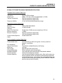
1
ADVANCED SYSTEM CONTROLLER ASC/2S MAINTENANCE MANUAL P/N 37539-05 Copyright 1993 by Econolite Control Products, Inc. 010702 WARRANTY Econolite Control Products, Inc. warrants, for a period as shown below, from date of shipment, all control equipment listed below to be free from defects in material or workmanship and to be of the kind and quality designated or specified in the contract. This warranty does not extend to products not manufactured or sold by Econolite. Econolite has the sole right to determine whether or not an item is covered under our warranty policy. Controller Warranty Period ASC/2S Series Controller 2 years Econolite is not responsible for damage caused by negligence, acts of God, or use of equipment in a manner not originally intended. Econolite's liability under this warranty shall not exceed the cost of correcting defects in the equipment. Upon the expiration of the warranty period, all such liability shall terminate. To obtain service under this warranty, deliver the product to the factory at the address listed below. When returning products to Econolite, the following must be done: Pack in original (or equivalent) shipping container Insure it (or assume the risk of loss/damage during shipment) Obtain Return Authorization number from your sales representative Pay all shipping charges to factory. Econolite will pay the return shipping charges List on packing sheet inside carton the return Authorization No., Econolite's Sales Order No., your Purchase Order No., equipment serial No., description of problem with equipment, and date of installation. Ship to the nearest Econolite Service Department: Econolite Control Products, Inc. Attn: Service Department 3360 E. La Palma Anaheim, California 92806 ii or Econolite Control Products, Inc. Attn: Service Department 446 Third Street, Suite #3 Neptune Beach, Florida 32266 Table of Contents SECTION 1 ................................................................................................................................1-1 INTRODUCTION .......................................................................................................................1-1 ASC/2S FAMILY .................................................................................................................1-1 MANUALS ..........................................................................................................................1-3 Programming Manuals ....................................................................................................1-3 Maintenance Manual.......................................................................................................1-3 SECTION 2 ................................................................................................................................2-1 THEORY OF OPERATION........................................................................................................2-1 FUNCTIONAL DESCRIPTION ...........................................................................................2-1 Processor Module ...........................................................................................................2-3 I/O Interface Modules......................................................................................................2-4 Power Supply Module .....................................................................................................2-4 Telemetry Module ...........................................................................................................2-5 Transceiver Operation .................................................................................................2-5 Processor Module (Schematic document number 34251, pages 1-20) ........................2-10 Microprocessor ..........................................................................................................2-10 Clocks........................................................................................................................2-10 System Control Pins ..................................................................................................2-10 System Busses..........................................................................................................2-11 Decode And Control ..................................................................................................2-12 External Interrupt Sources.........................................................................................2-15 Internal Interrupt Sources ..........................................................................................2-15 Memory......................................................................................................................2-16 Voltage Monitor Control.............................................................................................2-17 Down Time Accumulator ...........................................................................................2-18 Local Voltage Regulators ..........................................................................................2-18 Back-Up Power Supply..............................................................................................2-19 Display.......................................................................................................................2-19 Keyboard ...................................................................................................................2-20 Buzzer .......................................................................................................................2-20 Parallel I/O Section .......................................................................................................2-21 Address Bus ..............................................................................................................2-22 Data Bus....................................................................................................................2-22 Logic Level Translators .............................................................................................2-22 Input Multiplexers ......................................................................................................2-23 Input Buffers ..............................................................................................................2-23 Overlap Program Inputs ............................................................................................2-23 Output Latches ..........................................................................................................2-24 SDLC (EIA-485) Interface..........................................................................................2-25 Terminal (EIA-232) Interface .....................................................................................2-25 Telemetry Interface....................................................................................................2-26 AC Power Input .............................................................................................................2-27 Line Reference Circuits .............................................................................................2-27 Processor-I/O DC input circuit ...................................................................................2-27 FSK Telemetry Module .................................................................................................2-28 Modulator-Transmitter Circuit ....................................................................................2-28 Receive Filter And Demodulator Circuit ....................................................................2-29 iii Table of Contents (continued) SECTION 3 ................................................................................................................................3-1 MAINTENANCE ........................................................................................................................3-1 UNPACKING ......................................................................................................................3-2 INSTALLATION PROCEDURE ..........................................................................................3-2 CONNECTOR CABLE ASSIGNMENT ...............................................................................3-3 ENVIRONMENTAL REQUIREMENTS ...............................................................................3-4 TEST EQUIPMENT ............................................................................................................3-5 DISASSEMBLY ..................................................................................................................3-6 Processor Module ...........................................................................................................3-6 Power Supply ..................................................................................................................3-6 CLEANING AND INSPECTION ..........................................................................................3-7 Cleaning ..........................................................................................................................3-7 Inspection........................................................................................................................3-8 Lithium Battery ................................................................................................................3-9 IMPORTANT SAFETY INFORMATION .............................................................................3-9 ADJUSTMENTS AND TESTS ..........................................................................................3-10 MODEM Check Out Procedure.....................................................................................3-10 Crystal Adjustment Procedure ......................................................................................3-12 Diagnostics Menu..........................................................................................................3-13 Outputs (2).................................................................................................................3-15 Display (3) .................................................................................................................3-16 Keyboard (4)..............................................................................................................3-17 Overlap (5).................................................................................................................3-17 Telemetry (6) .............................................................................................................3-18 Loopback (7)..............................................................................................................3-19 Memory Tests ...............................................................................................................3-20 SECTION 4 ................................................................................................................................4-1 TROUBLESHOOTING ..............................................................................................................4-1 PRECAUTIONS..................................................................................................................4-2 HARDWARE FAULT ISOLATION ......................................................................................4-3 SECTION 5 ................................................................................................................................5-1 PARTS LISTS............................................................................................................................5-1 SECTION 6 ..............................................................................................................................5-30 SCHEMATICS AND ASSEMBLY DRAWINGS.......................................................................5-30 iv LIST OF FIGURES Figure 1-1. Figure 2-1. Figure 2-2. Figure 2-3. Figure 2-4. ASC/2S Family .......................................................................................................1-2 ASC/2S System Block Diagram .............................................................................2-2 Processor Section Block Diagram ..........................................................................2-7 I/O Section Block Diagram .....................................................................................2-8 Processor-I/O Module Component Placement .......................................................2-9 v SECTION 1 INTRODUCTION ASC/2S FAMILY The ASC/2S family of actuated controllers consists of three models. Each provides the same control functions but uses a different type of input/output (I/O) structure to interface with other components of the traffic control cabinet. The first model, the ASC/2S-1000, provides an I/O interface conforming to NEMA TS2 standard requirements for Type 1 controllers. This interface controls all cabinet I/O over a serial communications channel (Port 1). This serial communications channel is used for data exchange with a Malfunction Management Unit (MMU), to retrieve vehicle detector data from detector racks and interface to Terminals and Facilities within the traffic control cabinet. All I/O functions are handled by one or more Bus Interface Units (BIUs). Each BIU controls up to 15 outputs, 24 input/outputs, 8 inputs and four optically coupled inputs. Type 1 I/O also includes EIA-232 compatible terminal (Port 2) and telemetry (Port 3) interfaces. The second model of the ASC/2S family, the ASC/2S-2000, has an I/O interface that conforms to both NEMA TS1 and TS2 Type 2 controller requirements. This interface controls I/O functions through industry standard circular connectors (A, B, & C) and includes the serial communications, terminal, and telemetry interfaces of the Type 1 interface. TS1 operation allows the ASC/2-2000 to be used in existing traffic control cabinets without any cabinet changes. The Type 2 I/O operates in one of eight I/O modes. Each mode assigns specific functions to 24 input and output connections. The first I/O mode (Mode 0) provides compatibility with the I/O requirements of the NEMA TS1 standard. This TS1 operational mode is selected by setting the Type 2 I/O mode to Mode 0 (default) and disabling the serial communications channel. The serial communications channel of the Type 2 interface is used to communicate with a Malfunction Management Unit and detector racks as with the Type 1 interface. However, a minimum of 20 vehicle detectors can optionally be connected directly to the controller using one of the Type 2 I/O modes. The ASC/2S-2000 can also be programmed to operate as a Type 1 controller. In this mode external I/O interface is disabled and all I/O functions are handled over the serial communications channel. This allows the ASC/2S-2000 to duplicate the operation of the ASC/2S-1000. The ASC/2S-2100 is the third model of the ASC/2S actuated controller family. The ASC/2S2100 Processor-I/O module includes components that add additional I/O to the ASC/2S-2000 capabilities described above. The expansion I/O components include the "D" connector, 25-pin telemetry connector, and optionally, the NEMA overlap card connector interfaces matching those of the ASC-8000. This allows the ASC/2S-2100 to be used as a replacement for an ASC8000 or ASC/2-2100 in existing traffic control cabinets without any cabinet changes. 1-1 INTRODUCTION ASC/2 FAMILY The ASC/2S family of actuated controllers are made of a formed aluminum enclosure. Controller fronts consist of the User Interface panel and the Connector Interface panel. The User Interface panel consists of a custom, weather and dust-proof conductive rubber keyboard with numeric, function and cursor keys, and a high-contrast 16 line by 40 character liquid crystal display with LED back lighting. The Connector Interface panel contains two fuses (115 VAC/1 Amp and +24 VDC/ 0.75 Amp) and various interface connectors. The type of connectors depends on the controller model. The ASC/2S controller unit contains two main electronic modules and a power supply. The first main module is the Processor-I/O module which is installed directly in the enclosure. This module contains the MC68302 microprocessor which controls all ASC/2S operations and circuitry that transfers input and output signals between the I/O connectors and the processor. Also located on the Processor-I/O module is a connector for installing a telemetry module. The second main module is the User Interface assembly mounted to the hinged front panel. All versions of the ASC/2S controller use the same modules. The model type is defined by the components installed on the Processor-I/O module. The Processor-I/O and User Interface modules are interconnected by a ribbon cable located across the front panel hinge. The Processor-I/O module together with the connector interface panel, is held in place by two quarter turn fasteners and a card guide. The User Interface panel is held in place by 3 nuts. Both modules may be easily removed. The ASC/2S power supply furnishes +24VDC for controller unit operation. It is mounted internally on the back panel of the enclosure. The power supply is held in place four screws and is connected to the processor-I/O module by two wire harnesses. ASC/2S TYPE 2 ASC/2S-2000 TYPE 2 WITH EXPANDED I/O ASC/2S-2100 Figure 1-1. ASC/2S Family 1-2 TYPE 1 ASC/2S-1000 PROGRAMMING/MAINTENANCE INTRODUCTION MANUALS MANUALS Programming Manuals Programming of the ASC/2S controller unit is covered in the ASC/2S programming manual. However, maintenance information is provided for all ASC/2S family members in this manual. Maintenance Manual This manual contains the information needed to understand the hardware functions of the ASC/2S controller family. Information about the circuitry, general maintenance requirements, installation and disassembly is included. Fault isolation charts are provided to help the technician isolate problems or to at least provide a good starting point for troubleshooting. Schematics and comprehensive parts lists are included as well as several appendices to supplement the hardware descriptions. Section II contains the ASC/2S theory of operation beginning with a functional description of each module followed by a detailed description of circuit operation. Section III is a collection of procedures and check lists that should be used as part of regular maintenance. Included are procedures for installation, disassembly, visual inspection, cleaning, battery check, and various adjustments. Test equipment and connector-cable assignment lists are included. ASC/2S diagnostic tests, the primary method for hardware verification and fault isolation, are explained. Section IV is a troubleshooting chart. The chart outlines a series of possible hardware, software, and programming problems with associated possible causes and suggested solutions. Section V contains controller assembly parts lists. It lists components, cables and assemblies with both Econolite and manufacturer's part numbers. Section VI contains schematics and assembly drawings. Appendix A contains cable diagrams to be used when interfacing the ASC/2S to a printer or personal computer or for data transfer. Appendix B contains pin lists for all connectors A-D, SDLC, Terminal and Telemetry. Appendix C describes standard system interconnection using Econolite telemetry interface boards and transient suppressors. Appendix D is a guide to lease-line installation used in Econolite system communication. Appendix E lists and identifies loopback diagnostic error codes. 1-3 FUNCTIONAL DESCRIPTION SECTION 2 THEORY OF OPERATION FUNCTIONAL DESCRIPTION This section begins with a functional description of the ASC/2S modules. Each module is then described in detail. The circuit and signal descriptions are best understood when studied together with the block diagrams and system schematics. The block diagrams are included in this section and schematics are located in Section VI. As an aid to finding circuitry described in the detail text, schematic zone references, which contain the schematic coordinates of the circuitry, are included in the text where pertinent. A schematic zone reference has the format [(D),N,X,Y] where (D) is the optional document number, N is the schematic page, X is the horizontal coordinate and Y is the vertical coordinate of the page. The document number is normally referenced at the beginning of each new section. Also, all part numbers, pin, and signal names are printed in bold type. 2-1 Figure 2-1. ASC/2S System Block Diagram 2-2 Processor Module THEORY OF OPERATION FUNCTIONAL DESCRIPTION Processor Module The Processor-I/O module contains the microprocessor chip, memory chips and support circuitry required to operate and control all ASC/2S functions. This module also includes all I/O circuitry and controls the User Interface module keyboard and display operations. Ribbon connector J3 connects this module to the User Interface module. The system busses include the address bus that identifies the device or memory location targeted for information exchange, the data bus, which carries the information, and the control bus which synchronizes the data transfers. The communications busses include the Telemetry bus, SDLC bus and Terminal bus which transfer serial data between the microprocessor and the dual asynchronous receiver transmitter (DUART) chips and their associated interface chips. The Processor-I/O module is connected to the power supply module via connectors J18 and J19. The power supply provides +24VDC. Auxiliary processor functions include a watchdog timer which checks for proper program operation, the voltage monitor which checks for power fail conditions, and the battery-backed clock circuit which keeps accurate time when power is removed from the unit. System RAM is powered by the rechargeable, backup battery circuit so that data integrity is maintained during power fail conditions. Also included on the module are the AC line transient protection circuit and line referenced, 120Hz interrupt generator. The I/O interface section connects external inputs and outputs, with the microprocessor system address, data and serial communications busses. This allows the microprocessor to perform all input and output functions. 2-3 THEORY OF OPERATION FUNCTIONAL DESCRIPTION I/O Interface Module/Power Supply Module I/O Interface Modules The I/O section of the Processor-I/O module consists of input multiplexers, logic level translators, output latches, output drivers, serial communications interface circuits, the telemetry module interface connector J4 and expansion I/O connector J1 (unused). External parallel inputs are applied through front panel connectors A, B and C. The input voltage levels are translated to logic levels to be used by the system. The TRUE/FALSE (LOW/HIGH) states are then applied to input multiplexers. The processor reads the input status by addressing the input and enabling the multiplexer, thus transferring the input status onto the system data bus. The processor uses output latches to control the external parallel signals. It addresses a specific output and latches that output status from the data bus by enabling the latch. The signal is then sent to external connectors A, B or C. In the event of a long power failure, the latches are cleared to prepare for an orderly controller re-start. The Terminal bus signals interface with external equipment through Terminal connector J13 (PORT 2). It is used to communicate with printers, computer terminals or other controllers in the ASC family. The SDLC bus signals interface with optional Bus Interface Units and/or a Malfunction Management Unit via SDLC connector J15(PORT 1). The Telemetry bus signals attach to connector J4 and supply the signals required for FSK and EIA-232/fiber optic telemetry interconnects. Once translated by the Modem module, the signals interface with external signals via connectors J17(PORT 3) and J14 on the model ASC/2S2100. VOLTAGE MONITOR CONTROL is generated by monitoring the power supply and battery voltages and Processor signals. It is output to external equipment as VOLTAGE MONITOR. When the processor-I/O module is configured as an ASC/2S-2100 it includes type D and 25-pin Telemetry connectors and associated input multiplexers, logic level translators, output latches and output drivers. External parallel inputs and outputs are processed as mentioned above. A plug-in NEMA overlap programming card (optional) is connected to the input multiplexers by connector J6. When programmed, the overlap inputs are read by the processor in the same way as external inputs. Power Supply Module The Power Supply module is a 40 watt, 24 volt off-line switching supply set for 120VAC operation. When configured as an ASC/2S-2000 or ASC/2S-2100 controller, input power is applied through the A-connector on the controller front panel and then routed, via the AC line transient protection circuit, to J19 on the I/O module. A wire harness connects between J19 and the power supply module. When used in the ASC/2S-1000 controller, input power is applied through MS connector J16 on the front panel and then routed to the power supply module as mentioned above. The +24VDC output from the supply is routed back to the Processor-I/O module via a wire harness connected to J18. 2-4 Telemetry Module - Transceiver Operation THEORY OF OPERATION FUNCTIONAL DESCRIPTION Telemetry Module The Telemetry module operates as a transceiver providing communication between the ASC/2S-1000, ASC/2S-2000 or ASC/2S-2100 and an ASC/2M-1000 or KMC-10000 master controller. The module is controlled by the Processor module and interfaces with to the Telemetry bus via connector J4. Transmit, and receive signals are interfaced through the Telemetry connector(s) on the front panel. Transceiver Operation Communication between the local and master controllers is achieved over voice grade four-wire (two data channels) type 3002 leased telephone lines, or customer owned cable. The telemetry data channel is made up of command (master to local) and readback (local to master) lines. Additional lease-line information is found in Appendix D. Each local transceiver is assigned a unique telemetry address used by the master to identify the transceiver. The address is assigned by either direct keyboard entry (refer to the ASC/2S Programming Manual) or by activating External Address Enable (J14-15) and assigning the desired bit pattern to the appropriate Dconnector system inputs (refer to Appendix E). Devices connected to the local transceiver are identified by subaddresses assigned and used by the master. The master generates command messages containing local telemetry address, message type, subaddress, data, and a horizontal parity word. Command messages are transmitted to the local transceiver in a predefined sequence. The sequence begins with a zero address command which simultaneously transmits, to all local controllers, the system traffic program and four special functions. Local controllers do not respond to the zero address command. Subsequent messages request the status of the devices (listed above) connected to the local transceiver. The addressed local controller sends an appropriate response to the master on the readback line. Transmission of commands and readbacks occurs simultaneously. An error status is generated if a readback is not received by the master within a predefined period. For more information on master controller operation using telemetry, refer to the ASC/2M-1000 or KMC 10,000 Master Programming and Maintenance Manuals. At the local transceiver, modulated command message signals are transformer coupled to the receiver where they are filtered and demodulated to a serial-bit pattern. The serial-bit pattern is converted by an SCC receive channel on the microprocessor into a parallel pattern, four-word command message which is read by the microprocessor. If the message address corresponds to that of the local transceiver and if the message is valid, the microprocessor performs the operation specified by the message type. Where readbacks are required, the local transceiver generates a three-word readback message containing the requested data and horizontal parity word. The three data words from the microprocessor are converted to a serial bit pattern by a transmit channel on the DUART. The serial bit pattern is then sent to the MODEM which provides frequency shift key (FSK) modulation for transmission. Valid data, transmit, and received carrier LEDs are ON or flash during normal data transmission. 2-5 THEORY OF OPERATION DETAILED DESCRIPTION This section contains detailed descriptions of the various ASC/2S modules. Each module is described in detail with references to schematics in the format [(D),N,X,Y] where (D) is the document number, N is the schematic page, X is the horizontal coordinate and Y is the vertical coordinate of the page. The document number (D) is not always provided in this format but it is normally referenced at the beginning of each new section. Part numbers are identified in parenthesis (###) immediately before references to schematic coordinates. Example: U24 (74HCT244) [4,2,C]. Pin and signal names are also printed in bold type. The schematics are found in Section VI of this manual. Also, a module block diagram is shown before the discussion of each module. These block diagrams illustrate general functional operation. 2-6 Figure 2-2. Processor Section Block Diagram 2-7 Figure 2-3. I/O Section Block Diagram 2-8 Figure 2-4. Processor-I/O Module Component Placement 2-9 Processor Module Microprocessor/Clocks/System Control Pins THEORY OF OPERATION DETAILED DESCRIPTION Processor Module (Schematic document number 34251, pages 1-20) Microprocessor The ASC/2S family of controllers uses the Motorola MC68302 integrated multiprotocol processor. This is a Very Large Scale Integration (VLSI), CMOS device which includes a 16-bit, 68000 core processor, a system integration block and a (RISC) communications processor. Features of the system integration block that are used by the ASC/2 include: the independent DMA controller, a 19-level interrupt controller, the dual port RAM area, three programmable timers, the four programmable chip select lines, sixteen parallel I/O lines, the on-chip clock generator and several other "glue logic" functions. The communications processor provides the following functions: the main controller (RISC Processor), three independent full-duplex serial communications controllers (SCC), six serial DMA channels for the three SCCs and an SCP channel for synchronous peripheral communications. The following is the microprocessor signal description. All relevant information about the microprocessor signals and their associated control circuits is discussed. Clocks The system clock synchronizes the internal operations of the microprocessor and all external devices on the system busses. Microprocessor timing is controlled by a 14.7456 MHz crystal attached to the on chip clock generator circuit through pins EXTAL and XTAL [2,2,B]. The system clock rate is 14.7456 MHz. This system clock is output by the processor on the CLKO pin [2,2,B]. The CLKO signal is divided by four by U21 (GAL16V8) [4,4,D], to provide a 3.6864 Mhz clock to DUART U20 (SCN2681)[4,5,A]. U20 divides the 3.6864 MHz clock by 96 and outputs a 19,200 Hz clock (16 X 1200 baud) on OP3 [4,5,A] for the external transmit clock inputs of SCC1 (TCLK1) and SCC2 (TCLK2) on processor chip U12 [2,5,C]. This signal is also used to trigger the processors data request line /DREQ [2,5,B] of the independent DMA controller which transfers data to the LCD module. System Control Pins /RESET is a bi-directional pin, acting as an input and when asserted along with the /HALT pin [2,3,B], it causes a total system reset. The /RESET and /HALT signals are generated by a combination of U11 (74LS09), U5 (14538b) [8,2-4,B-C] and U4 (LM2598-5.0) [3,5,B]. U4 holds the PWRGOOD signal low anytime VCC is out of tolerance. If the program running in the processor fails to toggle the /WDOG signal [8,5,B], the U5 watchdog timer circuit will time out and generate a reset pulse. The /RESET pin can also act as an output which allows the program to output a /RESET signal to peripheral devices. /BERR, BUSW, DISCPU and /FRZ pins are not used. 2-10 Processor Module - System Busses THEORY OF OPERATION DETAILED DESCRIPTION System Busses Data Bus (D0-D16) This 16-bit, bi-directional, three-state bus is the general-purpose path for exchanging data with memory and other system devices. It can transmit and accept data in either byte or word widths. For all 16-bit accesses, byte 0, the high-order byte of a word, is available on D8-D15 and the low-order byte is available on D0-D7 [2,3,C]. The low order data lines are buffered by the system data buffers before being routed to the various I/O circuits. Buffering to the parallel I/O section is performed by U25 (74HCT245) [4,4,D]. Unbuffered data signals are labeled D(n) and buffered signals are labeled BD(n). Buffering to the User Interface panel is performed by U38 (74HCT245) [10,5,C]. Unbuffered data signals are labeled D(n) and buffered signals are labeled FPD(n). Address Bus (A1-A23) Pins A1-A23 [2,3,D] form a 24-bit address bus when combined with the /LDS and /UDS pins [2,3,B]. The address bus is a bi-directional, three-state bus capable of addressing 16M bytes of data. On the ASC/2S, address lines A21-A23 are not used. All address lines are buffered before being routed to the various I/O circuits. Buffering to the parallel I/O section is performed by U24 (74HCT244) [4,2,C]. Unbuffered address signals are labeled A(n) and buffered signals are labeled BA(n). Buffering for the User Interface panel is performed by U39 (74HCT244) [10,5,B]. Buffered address signals are labeled FPA(n). Control Bus This is a multipurpose bus that includes all the Processor-I/O modules chip select, write enable and output enable signals. These signals are used to control communications with the various RAM and EPROM devices, parallel I/O devices, the data module and the User Interface module. The control bus signals are generated by the decode and control section. These signals will be explained when their associated circuitry is discussed. Telemetry Bus This bus contains the serial data and hand shaking signals which are routed to the Telemetry module connector. Signals included in this bus are: the receive data line RXD1 [2,5,D] which inputs serial data into SCC1 on the processor, the transmit data line TXDA [4,5,B] which transmits data out of U20 and /CTSA, /RTSA/, /CDA, MDCTL1 and MDCTL2, generated by U20 [4,5,B], which control communications handshaking and provide modem control. Terminal Bus This bus contains the serial data and hand shaking signals which are routed to the Terminal Port (PORT2) RS-232 interface chip U80 (MAX214) [7,2,C]. Signals included in this bus are: the receive data line RXD2 which inputs serial data into SCC2 on the processor, the transmit data line TXD2 which transmits data out of SCC2, /CTS2, /RTS2, and /CD2 generated by SCC2 [4,6,C] and /DTRT generated by U20 [4,5,A] which control communications handshaking and provide modem control. SDLC Bus This bus contains the serial data and clock signals which are routed to the SDLC Port (PORT1) RS-485 interface chips U81 and U82 (LT490) [7,D,6]. Signals included in this bus are: the receive data line RXD3, which inputs serial data into SCC3 on the processor, TXD3 which outputs serial data from SCC3 and transmit and receive clocks TCLK3 and RCLK3 [2,5,C] which are required to synchronize communications over the SDLC channel. 2-11 THEORY OF OPERATION DETAILED DESCRIPTION Processor Module System Busses/Decode and Control SPI Bus This bus contains the serial data, clock and handshake signals which are used for communications with U3 (68HC68T) [8,4,D], the battery-backed clock. Signals included in this bus are: serial transmit data line SPTXD, serial receive data line SPRXD, synchronizing clock line SPCLK and slave select line SS [2,5,C]. Decode And Control This section takes the microprocessors address, data strobe, address strobe, read/write, chip select and clock signals and combines them in various ways to generate the control bus signals required for proper interaction between devices on the Processor-I/O module and the User Interface panel. These signals will be discussed below. All signals starting with a slash character i.e. /xxx are low only when active otherwise they are normally high. CLKO [2,2,D] outputs the 14.7456 MHz system clock. /AS [2,3,B] indicates when there is a valid address on the address bus (/AS is not used outside the processor chip in this design.). R/W [2,3,B] defines the data bus transfer as a read or write cycle. It is HIGH during a read and LOW only during a write cycle. /UDS [2,3,B] is the upper data strobe signal. It controls the flow of data on data bus lines D8D15 by specifying when valid data should be on the bus. /LDS [2,3,B] is the lower data strobe signal. It controls the flow of data on data bus lines D0-D7 by specifying when valid data should be on the bus. /CS0-/CS3 [2,3,A] are the four system chip select signals. /CS0 is the primary chip select for all EPROM accesses. /CS1 selects the RAM bank. /CS2 is the chip select signal for the data module /CS3 is the primary chip select for all I/O accesses. Address decoding and DTACK and Wait-State generation for these signals is performed onboard the processor chip. RESETB [2,5,B] is an active high reset signal for the DUART (SCN2681) U20 [4,5,A]. /WEO [4,5,D] is the write enable signal for the odd addressed RAM chip. This signal is generated by U14B (74ALS32) [4,6,D] by ORing the lower data strobe /LDS from the processor and the gated read/write signal GR/W from U21 (GAL16V8) [4,4,D]. GR/W is held inactive when VCC fails which write protects the RAM when power is removed. /OEO [4,5,D] is the output enable signal for the odd addressed RAM and EPROM chips and the data module. This signal gates the data from the device onto the data bus allowing the processor to read the data. This signal is generated by U14A (74ALS32) [4,6,D] by ORing the lower data strobe /LDS with the inverted read/write line /RW. /RW is generated by U15A (74ACT04) [4,5,C] by inverting the R/W signal from the processor. /WEE [4,5,D] is the write enable signal for the even addressed RAM chip. This signal allows the processor to write data from the data bus into the device if the devices chip select line is active. This signal is generated by U14D (74ALS32) [4,6,C] by ORing the upper data strobe /UDS from the processor and the gated read/write signal GR/W from U21 (GAL16V8) [4,4,D]. GR/W is held inactive when VCC fails which write protects the RAM when power is removed. 2-12 THEORY OF OPERATION Processor Module - Decode and Control DETAILED DESCRIPTION /OEE [4,5,D] is the output enable signal for the even addressed RAM and EPROM chips. This signal gates the data from the device onto the data bus allowing the processor to read the data. This signal is generated by U14C (74ALS32) [4,6,D] by ORing the upper data strobe /UDS with the inverted read/write line /RW. /RW is generated by U15A by inverting the R/W signal from the processor. /CS0L [4,3,C] is the chip select signal for the onboard flash EPROM chip. This signal is generated by U13 (GAL16V8) [4,4,C] by combining the main EPROM chip select line /CS0 from the processor with A20. /CS0L is active for the address range $000000-$0FFFFF /CS0H [4,3,C] is the chip select signal for the off board flash EPROM memory space. This signal is generated by U13 (GAL16V8) [4,4,C] by combining the main EPROM chip select line /CS0 from the processor with A20. /CS0H is active for the address range $100000-$1FFFFF /CS1L [4,3,C] is the chip select signal for the onboard RAM chips. This signal is generated by U13 (GAL16V8) [4,4,C] by combining the RAM chip select signal from the processor /CS1 and A16. This signal utilizes the fact that GAL16V8 outputs float when power is removed. This eliminates a current path out of the RAM chips during battery backup operation thus extending battery life. /CS1L [4,3,C] is the chip select signal for the off board RAM memory space. This signal is generated by U13 (GAL16V8) [4,4,C] by combining the RAM chip select signal from the processor /CS1 and A16. This signal utilizes the fact that GAL16V8 outputs float when power is removed. This eliminates a current path out of the RAM chips during battery backup operation thus extending battery life. /CSWE [4,3,C] is the write enable signal for the data module. This signal allows the processor to write data from the data bus into the device if the devices chip select line is active. This signal is generated by U13 (GAL16V8) [4,4,C] by combining input signals GR/W, A9-A13 and the input from the EEPROM write protect jumper JP3 [4,4,B]. A9-A13 are used to differentiate between the write-protected and non write-protected areas of the module. /SWAPCS0 [4,4,C] is used during flash EPROM download module. 3.6864 [4,3,D] provides a 3.6864 Mhz clock signal to the DUART U20 (SCN2681) [4,6,A]. This signal is generated by U21 (GAL16V8) [4,4,D] by dividing the system clock CLKO by four. STOP HERE /DWEO [4,3,D] is the write enable signal for DUART U20 (SCN2681) [4,6,A]. This signal allows the processor to write data from the data bus into the device if the devices chip select line is active. This signal is buffered version of /WEO and is generated by U21 (GAL16V8) [4,4,D]. /DOEO [4,3,D] is the output enable signal for DUART U20 (SCN2681) [4,6,A]. This signal gates the data from the device onto the data bus allowing the processor to read the data. This signal is buffered version of /OEO and is generated by U21 (GAL16V8) [4,4,D]. /DUART [4,3,D] is the DUART chip enable line. This signal is generated by U21 (GAL16V8) [4,4,D] by combining the system I/O enable signal /CS3 from the processor and address lines A17-A19. It is routed to U20 (SCN2681) [4,5,A]. /DUART is active for the address range $E00000-$E1FFFF. 2-13 THEORY OF OPERATION DETAILED DESCRIPTION Processor Module - Decode and Control /PIOSL [4,3,D] is the parallel I/O device enable line. It is generated by U21 (GAL16V8) [4,4,D] by combining the system I/O enable signal /CS3 from the processor and address lines A17A19. This signal enables the I/O data buffer U25 (74HCT245) [4,2,D] and bank selector U23 [13,6,D]. /PIOSL is active for the address range $E20000-$E3FFFF. GR/W [4,3,C] is the R/W line from the processor combined with the PWRGOOD signal. A write to a memory device can not be accomplished until PWRGOOD is asserted high. /FPSEL [10,5,D] is the User Interface buffer U38 (74HCT245) [10,5,C] enable line. This signal is generated by U22 (GAL16V8) [10,5,D] by combining the system I/O enable signal /CS3 from the processor and address lines A17-A19. /KEYSEL [10,5,D] is the keyboard input buffer enable line that is routed to the User Interface module connector J3 [10,5,A]. This signal is generated by U22 (GAL16V8) [10,5,D] by combining the system I/O enable signal /CS3 from the processor and address lines A17-A19. /KEYSEL is active for the address range $EC0000-$EDFFFF. /LCDSEL [10,5,D] is the LCD module select line. This signal is generated by U22 (GAL16V8) [10,5,D] by combining the system I/O enable signal /CS3 from the processor and address lines A17-A19. /LCDSEL is routed to the User Interface module connector J3 [10,5,A]. /LCDSEL is active for the address range $E80000-$E9FFFF. LCDEN is the LCD module enable line. This signal is generated by U22 (GAL16V8) [10,5,D] by stretching /LCDSEL by one system clock period and then ANDing this signal with /LDS. LCDEN is routed to the User Interface module connector J3 [10,5,A]. 2-14 Processor Module - Interrupt Sources External /Internal THEORY OF OPERATION DETAILED DESCRIPTION External Interrupt Sources An interrupt signal causes the processor to stop normal program execution and go to an address that is the beginning of an interrupt service routine. Executing the routine provides whatever action is necessary to service the device generating the interrupt. /IRQ41 [2,5,B] is a signal which requests service by the real-time clock interrupt routine. This AC line referenced, 120Hz square wave signal is generated by U1B (14538) [8,5,A] in conjunction with optoisolator U91 [20,2,C]. This routine controls timing of all controller software activity and provides real-time clock updates. /IRQ6 [2,3,A] is an active LOW open drain signal generated by U20 (SCN2681) [4,5,B] during telemetry transmissions. /IRQ4F [2,5,B] interrupt is used to shut down the controller in the event of a power failure. /IRQ4F is one of the highest priority interrupts thus causing the processor to take immediate action for an orderly controller shut-down. /IRQ4F is generated by the missing pulse detector circuit U1A (14538) [8,4,A]. The missing pulse detector is used to detect a loss of 120 Hz pulses. It is a re-triggerable one shot with a period of approximately 22 milliseconds. Positive transitions of OPTO1, from U91 [20,2,C], are cleaned up by U1B then fed to U1A. This signal retriggers the one shot every 8.33 milliseconds and also produces the /IRQ41 signal. During a power failure the one shot will not be retriggered and will time out, causing an /IRQ4F interrupt. Also, if the power supply output voltage is out of tolerance, VM24 will go LOW, thus forcing an /IRQ4F interrupt. Internal Interrupt Sources The 68302 processor contains 16 on-board sources which can generate interrupts. The ASC/2 controller family uses the following interrupts: SCC1-SCC3 and Timers 1-2. The receive channel of SCC1 which is used for the telemetry channel, is set up to generate an interrupt when: 1. The controllers' address is recognized on the telemetry line, 2. After the block of data has been received and 3. When the checksum has been received. The receive channel of SCC2 which is used for the terminal interface, generates an interrupt when: 1. An XON or XOFF character is recognized while the port is used for printing, 2. Blocks of data of various predefined lengths are received from another device during the direct connect process. The receive channel of SCC3 which is used for the SDLC interface, generates an interrupt after a complete frame is received from a BIU or MMU. Timer 1 is used for the telemetry channel and generates an interrupt when: 1. It is time to turn on the carrier signal, 2. It is time to transmit the data packet and 3. It is time to turn off the carrier. Timer 2 is used for the SDLC channel and generates interrupts that set the proper timing of the transmission of SDLC frames to the BIUs and MMU. 2-15 THEORY OF OPERATION DETAILED DESCRIPTION Processor Module - Memory Memory Flash EPROM Program Memory The software program that controls processor operation is written into U2 (29F800AB-90) [5,4,D]. This is a 90-nanosecond rewritable flash EPROM that provides 1 Megabyte of program address space configured as 512K x 16 words. The EPROM is accessed using zero wait states. The number of wait states are set using the processors internal wait state generator associated with the master EPROM chip select signal /CS0. U2 is enabled by chip enable line /CS0L. U2 puts its data on the data bus (D0-D15) when the chip enable line is low and either or both output enable lines /OEE or /OEO [5,6,C] are low. A write operation to U2 requires that /CS0L is low and /WEO is low. RAM All variable data is stored in Random Access Memory (RAM) pair U6 and U7 (628128-) [5,3,D]. The standard ASC/2S configuration uses 128K x 8, 70 nanosecond devices. This provides 256K bytes of data memory . The RAM is accessed using zero wait states. This is set using the processors internal wait state generator associated with the master RAM chip select signal /CS1. RAM is powered by voltage BAT [5,4,B] so that data is not lost during power outages. The RAM read/write operations function as follows: When the RAM chip select signal /CS1L and the odd write enable signal /WEO are LOW, and the odd output enable signal /OEO is HIGH, the RAM stores the data on the odd data bus (D0D7) in the location specified by the address bus (A1-A15). When the RAM chip select signal /CS1L and the even write enable signal /WEE are LOW, and the even output enable signal /OEE is HIGH, the RAM stores the data on the even data bus (D8-D15) in the location specified by the address bus (A1-A15). When the RAM chip select signal /CS1L is low and the odd write enable signal /WEO are high, and the odd output enable signal /OEO is low, the RAM supplies the odd data bus (D0-D7) with the data stored in the location specified by the address bus (A1-A15). When the RAM chip select signal /CS1L is low and the even write enable signal /WEE are high, and the even output enable signal /OEE is low, the RAM supplies the even data bus (D8-D15) with the data stored in the location specified by the address bus (A1-A15). When the processor does a word read or write access, both odd and even chips within the bank are enabled simultaneously Data Module The Data module is mounted on the Processor-I/O module. The module is connected by J5 [6,5,C]. **CAUTION** Do not remove or insert data module with power applied to controller. 2-16 Processor Module - Memory/Voltage Monitor Control THEORY OF OPERATION DETAILED DESCRIPTION EEPROM Memory All user entered data is stored on the data module. The ASC/2S comes standard with a 32K x 8, 250 nanosecond Electrically Erasable Programmable Read Only Memory (EEPROM) installed on its data module. During a write cycle, the address and data are latched internally and the cycle is automatically completed by the EEPROM. The write cycle takes a maximum of 10 milliseconds during which the chip cannot be accessed. The EEPROM is accessed using three wait states. This is set using the processors internal wait state generator associated with the master EEPROM chip select signal /CS2. The processor writes to EEPROM when the EEPROM chip enable signal /CS2 is low, the odd output enable signal /OEO is HIGH, and the write enable signal /CSWE is LOW. When the EEPROM chip enable signal /CS2 and the odd output enable signal /OEO are LOW, and the write enable signal /CSWE is HIGH, the EEPROM supplies the data bus (D0-D7) with the data stored in the location specified by address bus (A1-A14). The processor then reads the data from the data bus. EEPROM retains all user data when power is not applied to the controller. Memory Expansion Connector Connector J2 [9,2-6,A-D] allows for several functions including memory system expansion, Flash EPROM programming and system debugging. The Flash EPROM download module can be inserted into this connector for rapid programming of the on board Flash EPROM. All 68000 bus signals used by the ASC/2S are present on this connector. Voltage Monitor Control The voltage monitor control circuit is used to force the Voltage Monitor output FALSE, thus setting the intersection to flash and turning on LED1 [8,2,C]. The circuit consists of U11C and U11D (74LS09) [8,1,C]. These two gates AND the VM24 and /CPUVM signals. VM24 is an open collector output from comparator U10A (LM393) [3,4,B] that uses as its pull up voltage, the output of the watchdog timer /DOG. If VM24, /CPUVM or /DOG goes low, VMC will go low (FALSE). VM24 is the output from the power supply voltage monitor circuit. This signal is set low if the +24VDC supply voltage goes out of tolerance. /CPUVM is an output from the processor chip. This line is set low when a flash condition is detected by the processor. /DOG is the output from the system watchdog timer circuit U5 (14538) [8,4,B]. The watchdog input is toggled by the processor approximately once every 100 milliseconds. /DOG is set low if, due to erratic program behavior, the processor fails to toggle the watchdog input. Under normal conditions all three inputs are high thus maintaining Voltage Monitor Control VMC HIGH. A flash condition is indicated by a VMC LOW. The LOW VMC signal is inverted again at the I/O Interface and output as Voltage Monitor. This signal can be used in conjunction with a conflict monitor to set the intersection in flash. 2-17 THEORY OF OPERATION DETAILED DESCRIPTION Processor Module Down Time Accumulator/Local Voltage Regulators Down Time Accumulator The Down Time Accumulator (DTA) is used to detect missing 120 Hz interrupts and to time the length of power outages. The DTA consists of battery-backed real time clock chip U3 (68HC68T) [8,4,D] and the processor chips' internal Timer 3. **CAUTION** Do not attempt to adjust the crystal oscillator C19 in the field. This is a precision adjustment. See maintenance section for proper adjustment procedure. Timer 3 is used to determine whether the length of a power failure is less than or greater than 0.75 seconds. This time was selected as the limit, within NEMA range, in determining the action to take after a short ( < 0.75) or long ( > 0.75) power failure. If the power failure is less than 0.75 seconds the controller continues to operate. If the power failure is greater than 0.75 seconds the controller reverts to its start-up sequence. If power fails altogether, the processor writes its internal RTC time out to U3 to keep accurate time until power is reapplied. U3 uses a combination of VCC and battery B1 [8,5,C] voltage to operate. The processor communicates with U3 over the SPI bus. When power is reapplied, the processor reads the time from U3 and updates its internal RTC time. Local Voltage Regulators Switching regulator U4 (LM2598-5.0) [3,5,B] converts the incoming +24VDC into the +5VDC VCC signal used throughout the module. U4 also generates the PWRGOOD signal used by the reset circuit and GR/W generation. Diode CR11 protects other circuits in the event of a short between U4-2 (+24VDC) and U4-3. Transient voltage suppressor CR1 (P6KE27A) [3,6,B] protects the input from any transients greater than about +30VDC. Linear regulator U79 (LM7812) [7,3,D] provides a high current, short circuit protected +12VDC source for use by the telemetry module and external fiber optic modems. 2-18 Processor Module Back up Power Supply/Display THEORY OF OPERATION DETAILED DESCRIPTION Back-Up Power Supply The back-up power supply provides power to the RAM and the battery-backed clock during a power failure. With power applied, the VCC power supply provides power to the battery-backed real time clock U3 (68HC68T) [8,5,D] and the RAM chips via transistor Q1 (MMBT3904ALT1) [8,5,B]. As long as VCC is greater than 4.74VDC, PWRGOOD will be high and Q1 will turn on. When power is removed, Q1 turns off and diode CR3 conducts, thus supplying power from the lithium battery B1 [8,5,C]. Jumper JP2 disconnects the battery during troubling shooting or periods of extended storage. B1 is a rechargeable lithium battery and uses resistors R36, R38 and diode CR13 as the charging circuit. Battery voltage is monitored by comparator circuit U10B (LM393) [3,4,A]. When battery voltage drops below 2.2 VDC, the comparator triggers causing output signal /LOBAT to go low thus signaling the processor that the battery is not recharging properly and replacement is required. Display The User Interface module contains a Liquid Crystal Display (LCD) formatted as 16 lines of 40 characters, the display contrast control, the display backlight circuit, the display heater circuit, the keyboard matrix and the system buzzer. The display contains its own control and drive electronics and appears as two registers to the processor. The display is connected to the processor module via User Interface connector J3. Please note: The User interface panel should be sent to Econolite for repair. Display Interface The processor uses its Independent Direct Memory Access (IDMA) channel to write to the display. When a screen update is required, the program fills a RAM buffer with screen data. The program then initializes and activates the IDMA channel. The IDMA transfers one byte at a time from the buffer to transceiver U38 (74HCT245) [10,5,C] via D00-D07. When /FPSEL [10,6,C] is low and R/W is low, the data is transferred to the User Interface module data bus and routed to the LCD modules data lines. The LCD module uses a combination of signals LCDEN, /LCDSEL, A01 buffered by U39A (74HCT244) [106,B] and R/W buffered by U39B on its inputs to transfer the data to its internal circuitry. The IDMA uses the signal TCLK1 [4,3,A] to generate its data request signal /DREQ [2,5,B]. Thus one byte is transferred for each cycle of TCLK1. The LCD module has a cycle time of 1 microsecond. The processor has a cycle time of 271 nanoseconds. The master I/O chip select signal /CS3 is generated using 6 wait states and signal LCDEN is stretched by U22 (GAL16V8) [10,5,D] to accommodate this discrepancy. Display LED Backlight The LCD module contains a matrix of yellow/green LEDs used to backlight the display. The backlight is enabled from the front panel. The processor uses its PB2 output signal LCD-B [2,5,B] to activate the backlight. The processor turns the backlight ON by setting PB2 HIGH. LCD-B is buffered before going to the User Interface module by U39B (74HCT244) [10,5,B]. 2-19 THEORY OF OPERATION DETAILED DESCRIPTION Processor Module Keyboard/Buzzer Keyboard The User Interface module keyboard consists of a matrix of conductive rubber switches. The processor scans the matrix via J3 by reading specific addresses. The lower nibble of the address bus (A01-A04), which generates the row strobes, is buffered by U39A (74HCT244) [10,5,B]. The column data is input by buffer U38 (74HCT245) [10,5,C]. Scan circuitry on the User Interface module is enabled by signal /KEYSEL. The processor then decodes the four column status bytes to determine which key is pressed. Buzzer The processor uses its PB1 output signal BUZ [2,5,B] to activate the User Interface module buzzer. The processor turns the buzzer ON by setting PB1 HIGH. BUZ is buffered before going to the User Interface module by U39B (74HCT244) [10,5,B]. 2-20 Parallel I/O Interface THEORY OF OPERATION DETAILED DESCRIPTION Parallel I/O Section The three members of the ASC/2S family use the same Processor-I/O module. The model type is differentiated by which components are installed in the parallel I/O section. The following discussion will address the board generically. Any circuits associated with a particular model type will be addressed separately. All processor access to the parallel I/O section is done through buffers U25 (74HCT245) [4,2,D] and U24 (74HCT244) [4,2,C]. These chips buffer the D00-D07 data lines, A01-A06 address lines, /LDS and /RESET. The I/O DECODER U23 (74HCT138) [12,6,D] divides the I/O block defined by parallel I/O chip select signal /PIOSL into 8 sections, /LE0, /LE1, /I/O0, I/O1, /Y4, /Y5, /Y6 and /Y7. These signals are generated by combining the block select signal /PIOSL with the buffered lower data strobe /BLDS and the addresses appearing on BA4-BA6 and BA17. The following signals are generated: /LE0 is the latch enable for the bank of outputs containing the following phase 1-8 functions: PHASE ON, PHASE NEXT, PHASE CHECK, GREEN, YELLOW and RED DRIVERS, WALK DRIVER and PED CLEAR DRIVER. It is selected by address $E20001. /LE1 is the latch enable for the bank of outputs containing the following functions: Phase 1-8 DON'T WALK DRIVERS, RING 1 AND 2 STATUS BIT DRIVERS and OVERLAP DRIVERS. /LE1 is also routed to the expansion I/O connector I/O2P1. It is selected by address ($E20011) /I/O0 selects the input multiplexer bank containing the following functions: Phase 1-8 HOLD, PHASE OMIT, PED OMIT, VEH CALL DET, PED CALL DET, RING 1 and 2 INH MAX TERM, MAX II SELECT, OMIT ALL RED CLEAR, RED REST MODE, PED RECYCLE, FORCE OFF and STOP TIME along with CALL TO NON-ACT, WALK REST MODIFIER, MIN RECALL, INTERVAL ADVANCE, MANUAL CONTROL ENABLE, INDICATOR LAMP CONTROL AND EXTERNAL START. It is selected by address $E20021. /I/O1 selects the input multiplexer bank for the expanded I/O function of the ASC/2S-2100. It is selected by address $E20031. /Y4 selects the input buffer containing the following functions: MODE BIT A-C, PREEMPT DET 2,4,5,6 and the COORD FREE INPUT. It is selected by address $E20041. /Y5 selects the input buffer containing the following functions: TEST C, SPARES 1-6 and the signal that tells the controller that an expansion I/O module is present ASCIO. It is selected by address $E20051. /Y6 and /Y7 select the expanded I/O input buffers. They are selected by addresses $E20061 and $E20071, respectively. 2-21 THEORY OF OPERATION DETAILED DESCRIPTION Parallel I/O Interface Address Bus/Data Bus/Logic Level Translators Address Bus This bus carries the address information used by the input multiplexers and output latches to select a particular I/O line. It is a buffered subset of the processors address bus and includes BA1-BA3. Data Bus This bus carries the data that is sent to the output latches or received from the input multiplexers. It contains the buffered lower (ODD) data bus which includes BD0-BD7. Logic Level Translators Each logic level translator consists of a three resistor network (10K, 75K, and 18K) which converts the 24 V (FALSE), 0 V (TRUE) logic levels of control signals from external equipment to the HCMOS logic levels required by the input multiplexers. A 10K pull-up resistor biases the input to the FALSE state when the external control input is not connected. The voltage divider (75K and 18K) establishes the input level to the input multiplexer. An external input of 0 V to 8 V is detected as TRUE and an input of 16 V to 24 V is detected as FALSE (inputs are inverted internal to the processor). The combination of the 75K resistor, acting as a current limiter, and the internal protection circuit of the input multiplexer protects against transient input voltages exceeding 24 V. 2-22 Parallel I/O Interface Input Multiplexers/Input Buffers/Overlap Program Inputs THEORY OF OPERATION DETAILED DESCRIPTION Input Multiplexers Input multiplexers interface external control inputs (from connectors A, B, C and D) with the system data bus. The processor controls the multiplexer functions by enabling the multiplexer, addressing the inputs, and reading the input status. In this way, it controls the 16 HCMOS tristate, 8-bit multiplexers U51, U52, U53, U54, U55, U56, U58 and U60 (74HC251) [14-15,1-6,AD] on the ASC/2S-2000 plus U40, U41, U42, U43, U47, U48, U49, U50 on the ASC/2S-2100. Each multiplexer receives eight external control inputs from a corresponding logic level translator. Each control input has a unique address associated with it. When the input is addressed and the multiplexer is enabled, the input status (ON/OFF) is routed to a single data bit at the multiplexer output pin (W) connected to the data bus. The processor reads the input data by addressing it through the I/O Interface address bus BA1BA3. The selected input is gated onto the I/O data bus by the LOW state of signal I/O0 or I/O1. The processor simultaneously reads eight I/O data bits from 8 different multiplexors onto BD0BD7. Typical input operation is described below. The signal from input pin A1-/h (PHASE 1 HOLD) [15,4,D] is applied, via logic level translator RP22 [15,4,D] to input DO (pin 4), of input multiplexer U58. Coded address bits BA1-BA3 from the address bus are applied to address select inputs S0, S1, and S2 (pins 11, 10, and 9) of input multiplexer U29. When address lines BA1-BA3 are all LOW, input D0, pin 4 of input multiplexer U29 is selected. The LOW state of signal I/O0 enables the multiplexer and causes the selected input to be inverted and output from /Y (pin 6) as I/O module data bit BD0. Input Buffers Input buffers U19A and U59 (74HCT244) [12,6,B-C] transfer local and external data to the data bus. U59 receives its inputs from logic level translator RP23. U19A inputs a combination of external and local status inputs. On an ASC/2S-2100, input buffer U30B (74HCT244) [12,3,B-C] and U57 get their inputs from the 25-pin telemetry connector via logic level translators RP36 and RP35 respectively. The buffers output their data onto the data bus when the proper chip select line /Y4-/Y8 goes low. Among other signals, U19A inputs the signal that tells the processor, when low, that the board is configured as an ASC/2S-2100. Overlap Program Inputs On the ASC/2S-2100, a NEMA overlap program card is optionally available for programming overlaps A-D. This plug-in card is connected to optional connector J6 [11,1,D]. Phase combinations of the four programmable overlap phases A, B, C and D are programmed by installing jumpers on the card. When the overlap card is installed, the jumpers ground the 10K pull-up resistors, RP5-RP8 [17-18,3,B-D] at the (74HC251) multiplexer inputs. A ground at these inputs indicates that the associated phase is assigned to the overlap while an open circuit indicates that it is not. Program data for each overlap phase (A-D) is output by the multiplexers as eight bits representing the eight controller phases N1-N8. The overlap inputs are read by the processor at the multiplexer output pins as described above. 2-23 THEORY OF OPERATION DETAILED DESCRIPTION Parallel I/O Interface Output Latches Output Latches Output latches are used to interface data from the system data bus with external control output lines. The processor controls the data transfer by enabling the latches and addressing the output, thus latching the data from the data bus to be sent to external equipment. In this way, it controls twelve addressable 8-bit output latches, U31, U32, U33, U34, U35, U36, U37, U44, U45, U46, U61 and U62 (74HC259) [13-14,1-6,A-D] with associated output drivers, U67, U68, U69, U70, U71, U72, U73, U74, U75, U76, U77 and U78 (ULN2803A) on an ASC/2S-2000. In addition the ASC/2S-2100 also includes latches U26-U29 [19,1-6, A-D] and associated output drivers U63-U66. All output drivers are biased to the 24 V (FALSE) state, when not asserted, through a 10K pull-up resistor. Latches are addressed by bits A1-A3 and enabled by the /LE0 and /LE1 signals from the I/O device selector U23 [12,6,D]. At the same time, data bits DB0-DB7 are input to the addressed latches. Data is latched on the rising edges of the enable signals and remains latched until changed during a data update from the processor, which occurs every 100 ms. The buffered /RESET signal, /IORESET [4,2,B], clears all data from the latches at power on. The Q outputs of each latch are applied to a high-current, high-voltage, Darlington transistor output driver (ULN2803A). Logic level transition to +24V (FALSE) and 0 V (TRUE) occurs at the driver outputs. Output lines are connected to interface connectors A, B C and D. The ULN2803 output drivers are protected from transients on their output pins by Transient Voltage Suppressors CR16 and CR19 (P6KE33A) [13,3,C] [19,3,C]. These provide the output devices with a low impedance path to ground for voltages greater than 33VDC. This prevents damage to a driver by the reverse voltage generated when a relay coil connected to the output is de-energized or other transient occurs. The FLASH LOGIC OUT output on A1-X [14,3,A] is derived from the Q4 output of latch U62 (74HC259) [14,6,B]. When this output is active, output driver U78 (ULN2803A), sinks current from A1-X through diode CR15. When U78 is off, Q2 (MMBT2222ALT1) [14,4,A], is turned on and current is sourced to A1-X through the current sourcing circuit consisting of transistor Q2 diodes CR17-CR20 and current limit resistors R57-R58. This output can source 50mA maximum and can sink 200mA maximum. Diode CR20 shunts any negative voltages on the output to ground. CR17 shunts any voltage greater than 33VDC to ground. On the ASC/2S-2100 the PREEMPT CMU INTERLOCK output associated with U27 (pin 5) [19,5,B] is active only if there is a preemption requirement. The circuit consists of Q3 (MMBT2222ALT) [19,3,C] R62, CR16 and CR21. If a preemption sequence is not programmed, this output is forced LOW. This output can be connected to the conflict monitor 24 V monitor input to set the intersection to flash if a required preempt sequence is not programmed. The voltage monitor VMC and fault monitor /FLTMN signals, generated by U11 [8,1,C], detect out of tolerance voltage levels and processor failures and send control signals to the I/O section to be output as VOLTAGE MONITOR and FAULT MONITOR. The VMC signal is inverted and buffered by U78 (ULN2803A) [14,5,B] and routed to A1-C. The /FLTMN signal is inverted and buffered by U74A (ULN2803A) [14,3,C] and routed to J16-F. 2-24 Parallel I/O Interface SDLC Interface/Terminal Interface THEORY OF OPERATION DETAILED DESCRIPTION SDLC (EIA-485) Interface The SDLC interface circuit sends and receives its signals on the SDLC bus. All TTL to EIA-485 signal level translation is provided by U81 and U82 (LT690) [7,6,C]. These contain one EIA-485 driver and one EIA-485 receiver each. After the signals are translated to EIA-485, they are routed to the outside world via connector J15 (DA15S) [7,4,D] The interface includes the following signals: TXD+ and TXD- are the differential transmit data pair. The processor transmits this serial data signal as TXD3 from SCC3 [2,5,C]. This signal is converted to a differential pair by U81. It is then output on connector J15 pins 1 and 9. TXC+ and TXC- are the differential transmit clock pair. The processor transmits this serial data signal as TCLK3 from SCC3 [2,5,C]. The signal is converted to a differential pair by U82. It is then output on connector J15 pins 3 and 11. RXD+ and RXD- are the differential receive data pair. These signals appear on pins 5 and 13 of connector I/O2P5. After conversion by U81, the single ended TTL signal is routed to SCC3 on the processor as RXD3 [2,5,C]. RXC+ and RXC- are the differential receive clock pair. These signals appear on pins 7 and 15 of connector I/O2P5. After translation by U82, the single ended TTL signal is routed to SCC3 on the processor as RCLK3 [2,5,C]. Terminal (EIA-232) Interface The terminal interface circuit sends and receives its signals on the terminal bus. All TTL to EIA232 signal level translation is provided by U80 (MAX214) [7,2,C] which contains three EIA-232 drivers and three EIA-232 receivers. U80 uses capacitors C66, C67, C71 and C72 for its onboard positive and negative voltage generation circuits. U80 also has an internal DCE/DTE switch that is controlled by TERMCTRL1 [7,3,B]. Terminal signals are routed to the outside world via connector J13 (DB25) [7,1,C]. The EIA-232 level signals are protected against over voltage transients by transient voltage suppressors (MMBZ15VDLT1) [7,1,B]. The interface contains the following signals: TXD is the transmit data signal. The processor outputs this serial signal from SCC2 as TXD2 [2,5,C]. After translation, it appears on pin 2 of J13. RXD is the receive data signal. This serial input signal appears on pin 3 of J13. It is translated and routed to SCC2 of the processor as RXD2 [2,5,C]. This signal is also routed to the DUART U20 [4,5,B] as RXDB. CD is the Data Carrier Detect handshaking signal. This input signal appears on pin 8 of J13. It is translated and routed to SCC2 of the processor as /CD2 [2,5,C]. CTS is the Clear To Send handshaking signal. This input signal appears on pin 5 of J13. It is translated and routed to SCC2 of the processor as /CTS2 [2,5,C]. RTS is the Request To Send handshaking signal. The processor outputs this serial signal from SCC2 as /RTS2 [2,5,C]. After translation, it appears on pin 4 of J13. 2-25 THEORY OF OPERATION DETAILED DESCRIPTION Parallel I/O Interface SDLC Interface/Telemetry Interface DTR is the Data Terminal Ready handshaking signal. DUART U2 [4,5,A] outputs this serial signal from OP2 as /DTRT. After translation, it appears on pin 20 of J13. Signals RTS, CTS, CD and DTR are handled under program control and are implemented only as required. Communications with a printer utilize the XON / XOFF software handshake protocol. Telemetry Interface The Telemetry interface sends and receives its signals on the Telemetry bus. The signals are routed to the telemetry module connector J4 [7,5,B], translated by the telemetry module and then routed to the outside world via connectors J17 (DE9P) [7,3,B] and J14 (DB25P) [7,4,A]. All TTL to FSK, EIA-232 or EIA-485 signal level translation is provided by the telemetry module attached to connector J4. The interface contains the following signals: TXD is the transmit data signal. The DUART U20 [4,5,B] outputs this serial signal to the telemetry module as TXDA. After translation, it is routed to J17, pins 1 and 2, and expansion I/O connector J14 as signal pair XMIT+ and XMIT-. RXD is the receive data signal. This serial input signal appears on pins 4 and 5 of J17 and expansion I/O connector J14 as RECV+ and RECV- then routed to J4. It is translated by the Telemetry module and routed to SCC1 of the processor as RXD1 [2,5,D]. CD is the Data Carrier Detect handshaking signal. This signal is generated by the FSK telemetry module and appears on pin 9 of J4. It is routed to the DUART as /CDA [4,5,B]. EIA-232 telemetry modules input this signal form J17 pin 1. CTS is the Clear To Send handshaking signal. This input signal, generated by the telemetry module, appears on pin 7 of J4. It is routed to the DUART as /CTSA [32806,5,3,A]. This signal also serves as the MODEM PRESENT signal used by the processor to determine if a Telemetry module is present. The Telemetry module will pull this signal low if present. EIA-232 telemetry module input this signal from J17 pin 1. RTS is the Request To Send handshaking signal. The DUART outputs this signal as /RTSA [4,5,B]. It is routed to pin 8 of J4. EIA-232 telemetry modules output this signal on J17 pin 7. MDCTL1 and MDCTL2 are used to control various functions on the Telemetry module. They are generated under program control by using two of the DUARTs parallel I/O lines [4,5,A]. MDCTL2 is also routed to inverter/driver U64 (ULN2803A) [19,5,B] It is used on J14 as the KEY signal required by the radio interconnect. /IORESET is used to reset the telemetry module circuitry. It is a buffered version of system /RESET. Signals RTS, CTS and CD are handled under program control and are implemented only as required. 2-26 Power Supply Module AC Power Input THEORY OF OPERATION DETAILED DESCRIPTION AC Power Input The AC line transient protection circuit consists of resistors R65 and R67, and varistors RV1, RV2 and RV3. The circuit receives a three-wire, 120 VAC, 60 Hz input from the A connector J12 or J16 on the ASC/2S-1000. The three inputs are AC line, AC neutral, and earth ground. AC line is over current protected by fuse F2. AC line and AC neutral are then routed to currentlimiting resistors R67 and R65 respectively. Varistor RV1, RV2, and RV3 provide both common and differential mode transient protection. This is accomplished by clamping transients occurring between AC line and AC neutral with varistor RV2. Transients occurring between AC line or AC neutral and earth ground are clamped by RV1 and RV3, respectively. The output of the transient protection circuit is then applied to the power supply via connector J19 [20,2,D]. Additional transient protection and noise filtering circuits are present on the power supply module. Line Reference Circuits Signal OPTO1 is the 120 Hz line frequency reference used by the controller program as the input to the real time clock. It is generated by full wave rectifier CR25 (VM88) [20,3,C] which rectifies the 120 VAC 60 Hz line voltage, to produce a 120 Hz signal which is presented to dual opto-isolator U91 (MCT6). Zener diode CR24 (1N4763A) prevents output of the OPTO1 signal when the line voltage is below 82 VAC. The OPTO1 signal is routed to U1B (14538) [8,6,A] Signal OPTO2 is the 60 Hz line frequency reference used by the controller program during dimming operations. It is generated by opto-isolator U91 which only turns on during the positive half cycle of the waveform thus, producing a 60 Hz signal. The OPTO2 signal is routed to an input on DUART U20 (SCN2681) [4,5,A] Processor-I/O DC input circuit +24VDC enters the Processor-I/O module on connector J18. Diode CR4 (MBRS340T3) [20,4,B] provides reverse polarity protection. CR7, CR8 and CR10 provide current steering for the proper charging and discharging of the hold-up capacitor C76. R31 limits inrush current while charging C76. +24VE is the primary onboard +24VDC voltage source for I/O devices. +24VI supplies +24VDC to the +5VDC voltage regulator in the processor section. The +24VEXT external output is applied to connector pin A-B. This output is rated at 500 mA and provides sufficient current for most traffic applications. The 24 VDC has been fused with a 3/4 Amp SLO-BLO fuse, F1, to allow the controller to supply sufficient current for a controller test fixture using LED displays (20 mA per LED). This higher current capability should only be used during testing. Note that the 24 VDC load in the traffic control cabinet should never exceed 500 mA. Inductor L2 [20,4,A] filters out noise induced on the logic ground (FGND) when it is run outside the controller. 2-27 THEORY OF OPERATION DETAILED DESCRIPTION FSK Telemetry Module/ Modulator-Transmitter Circuit FSK Telemetry Module The MODEM provides Frequency Shift Keying (FSK) modulation of data from TXDA to make the data compatible for transmission over telephone lines or twisted pair cable. It also receives FSK signals and demodulates them to provide the RXD1 signal. All signals going to or from the telemetry module are routed through connector J1 [2,6,A-D and others]. This connector interfaces with connector J4 on the Processor-I/O module. Transmit Data (TXDA) The TXDA [3,6,B] line carries TTL level serial data from the DUART on the processor module [34251,4,5,B] to the analog multiplexer U2 (74HC4051) [3,3,C] which is then routed to the FSK modulator. The data rate is 1200 bits per second. Receive Data (RXD1) The RXD1 [4,1,D] line sends TTL level serial data, that originates at the FSK demodulator, from output buffer U10 [4,5,D] to the SCC1 receive channel on the processor chip [34251,2,5,D]. The data rate is 1200 baud. Data Carrier Detect (/CDA) This signal originates at the FSK demodulator and is routed via U10 [4,5,D] to the DUART. It indicates the status of the MODEM carrier signal. The line is HIGH if the carrier is lost, usually because of an abnormal condition. Under normal conditions the line is LOW, indicating that the carrier is present. Modem Control 1 (MDCTL1) This signal which originates on the DUART is used by the program to turn on the VALID DATA LED DS2 [2,5,C]. Modem Control 2 (MDCTL2) This signal which originates on the DUART is used by the program to turn on the transmit interface circuit. When MDCTL2 is LOW the LEDs inside opto-isolators U4 and U5 (MCT6) turn on thus, turning on the transmitter output. Modulator-Transmitter Circuit U7C [3,4,A] in conjunction with U2 [3,3,C] set the voltages used by U3 [3,1,D], the FSK modulator. U3 is a voltage to frequency converter. One of three voltages are generated by U2 to select 1200 Hz (Mark), 2200Hz (Space) or 900Hz (Soft Carrier Turn Off) generation by U3. During standard four-wire operation, the TXDA signal selects between Mark and Space generation. When Soft Carrier Turn Off operation is selected during two wire operation, it operates as follows: /RTSA [3,6,A] goes low at the start of a message. During this time, the pull up resistor R14 [3,4,A], at the output of U7C has no pull up voltage thus, the output of U7C is low. Because of this, the level of the TXDA line is used by U2 to select between Mark and Space voltages. At the end of the message, /RTSA goes high turning on the soft carrier voltage. During this time, C20 charges through R26 (an 8mS time constant). After 8mS, the threshold voltage of the comparator is exceeded and its output goes low thus, turning off the softcarrier voltage. R24 [3,2,C] sets the 1200Hz voltage, R23 [3,2,B] sets the 2200 Hz voltage and R6 sets the 900Hz SCTO voltage. When the input voltage to U3 pin 8 changes, the frequency output by U3 pin 2 varies. R25 [3,2,D] is the transmitter output level adjust. 2-28 Modulator-Transmitter Circuit/ Receive Filter And Demodulator Circuit THEORY OF OPERATION DETAILED DESCRIPTION Opto couplers U4A and U4B gate the analog signal from the FSK modulator according to the level on MDCTL2. U6 acts as a temperature compensated output buffer with gain. Opto couplers U5A and U5B allow the output stage to be permanently enabled with a 600 ohm load or gated by MDCTL2. U7, Q1, DS3 and associated components are the output level comparator circuit that is used for measurement of the output level and transmit level indication. When U5 is ON, the FSK output signal is coupled through transformer T1 (T2104) [4,5,A] to transmitter terminations XMIT+ and XMIT-. Transformer T1, R28, R29 RV2 CR3 and CR4 provide a balanced, isolated, transient protected output. Receive Filter And Demodulator Circuit Transformer T2, R1, R3, RV1, CR1 and CR2 [2,5,B] provide a balanced, isolated input with transient protection. C24 and R43 are the initial high pass filter. This filter provides -6dB/octave attenuation of frequencies below 480Hz. U9A (LM324) [2,4,C] is the input preamplifier with adjustable gain. U9B-U9D are the band pass filter that remove out-of-band high and low frequency noise signals. Jumper JP3 [2,5,C] allows routing of the signal from the secondary of the output transformer to the input circuit (in two wire mode, the output transformer T1 is also the input transformer.). JP7 [2,1,B] provides a way to bypass the input filter. The output from JP7 is then sent to the FSK demodulator as RC [3,6,D]. U8 (XR-2211) [3,5,D] is the FSK demodulator. It outputs the received data RD signal, carrier detect /CD and drives the carrier detect LED DS4 via Q2 [2,6,C]. R22 [2,4,D] sets the receiver center frequency (1700Hz). 2-29 SECTION 3 MAINTENANCE Several procedures, guides and lists are provided for general maintenance of the ASC/2S family. This section contains unpacking and installation procedures, useful for the first ASC/2S installation and for later reference. A disassembly procedure instructs on removing each module and major components. Basic procedures include printed circuit board cleaning, voltage checking and down time accumulator crystal adjustment. A list of test equipment recommended for maintenance is also included. The circuit components used in the ASC/2S require care in handling, installing, storing, and operating both unmounted and mounted on printed circuit boards. Modules and their components should only be handled at a static-free workstation. Personnel and equipment MUST be properly grounded. Please refer to the Motorola CMOS LOGIC data book or any other MOS manufacturer's procedures for more information. 3-1 MAINTENANCE UNPACKING AND INSTALLATION UNPACKING The ASC/2S controller is packed in a specially designed protective shipping carton. All necessary precautions have been taken to ensure that the equipment is received intact and in proper working order. However, the following steps should be taken when unpacking the controller to verify that there is no shipping damage. 1. Carefully inspect the shipping container for damage before opening. If the container is damaged, unpack the controller in the presence of the carrier. 2. Do not discard the packing materials (foam endcaps and box) as they have been specially made for the ASC/2S and must be used should it be necessary to ship the controller again. 3. Once unpacked, carefully inspect the controller for damage. Check for broken wires, connectors, loose components, bent panels, and dents or scratches on the enclosure. 4. If any physical damage is discovered, notify the carrier immediately. INSTALLATION PROCEDURE The ASC/2S should be installed in a location where the front panel is easily accessible. Adequate room should be left around the controller to allow easy removal if necessary. Care should be taken to install the controller so that vents on the back side are not blocked. Before applying AC power, perform the following pre-installation checks: 1. Open the front panel door, remove the plug-in data module and verify that the number on the EEPROM label matches the program number on the controller label located on the top surface of the unit. Reseat the data module. 2. Verify that all modules are properly secured and that all connector ribbon cables are in place. Once these preliminary steps have been taken the controller is ready for operation. Required cable connector part numbers are listed below. Refer to Appendix B for the connector pin lists. 3-2 MAINTENANCE CONNECTOR CABLE ASSIGNMENT CONNECTOR CABLE ASSIGNMENT CONNECTOR ECONOLITE PART NUMBER A MS-3116-22-55S 44143P1 B MS-3116-22-55P 44143P2 C MS-3116-24-61P 44143P3 D AMP #205842-1 31163P2 CONNECTOR CABLE CRIMP SOCKET 31163P4 SDLC (PORT1) DAU-15P 54665P4 TERMINAL (PORT2) CANNON #DBC25P 54665P7 TELEMETRY (PORT3) DEU-9S 54647P9 TELEMETRY (EXPIO) CANNON #DBC25S 54647P6 3-3 MAINTENANCE ENVIRONMENTAL REQUIREMENTS AND STORAGE ENVIRONMENTAL REQUIREMENTS The ASC/2S meets or exceeds the NEMA environmental standards for traffic control equipment summarized below: ENVIRONMENTAL OPERATION SPECIFICATIONS (NEMA TS 2 SECTION 2) CATEGORY Input Power Power Consumption Ambient Temperature REQUIREMENT Line Voltage: 89 to 135 VAC ASC/2S-1000 20 Watts ASC/2S-2100 25 Watts Operating Range: -34EC to +74EC Storage Range: -45EC to +85EC Humidity Relative humidity is not to exceed 95% over the temperature range of +4.4EC to +43.4EC The major units of the controller assembly maintain their programmed functions and physical integrity when subjected to a vibration of up to 0.5g at 5 to 30 cycles per second, applied in each of the three mutually perpendicular planes. The major units of the controller assembly do not suffer either permanent mechanical deformation or any damage that renders the unit inoperable, when subjected to a shock of 10G applied in each of the three mutually perpendicular planes. Vibration Shock 3-4 MAINTENANCE TEST EQUIPMENT TEST EQUIPMENT The following is a list of suggested test equipment to be used for fault isolation, basic check-out, and general maintenance. 1. 100Mhz, digital, dual-trace oscilloscope. Used for observing signals and checking of time relationships of two waveforms where necessary. 2. Digital Multimeter (DMM). Used for continuity testing, diode and transistor checks, and general voltage measurements. The DMM should meet the following specifications: PARAMETER RANGE DC VOLTS 200mV-1000V AC VOLTS 200mV-750V RESISTANCE 200S-20MS (OHMS) ACCURACY INPUT IMPEDANCE "0.25% of Input 10 MS 10 MS, Capacitance < 100 pF - - 3. Frequency counter. Used for Down Time Accumulator crystal adjustment. Note that the DTA crystal adjustment is a high precision adjustment, therefore an accurate frequency counter is required. 3-5 MAINTENANCE DISASSEMBLY Processor/I/O Interface Modules/Power Supply DISASSEMBLY When disassembling the controller always disconnect input power before attempting to disassemble any part of the controller. Below is a disassembly description for each module. ** CAUTION ** Disconnect Input Power before attempting to disassemble the controller Processor Module The Processor-I/O module is attached to the enclosure by two 1/4 turn fasteners. To remove the module: 1. Disconnect the interface cable to the front panel. 2. Turn the fasteners 1/4 turn to the left. 3. Hold onto the assembly by the connector plate and pull the module out from the bottom until it slides out of the card guide on the inside top of the enclosure. 4. Pull the module out far enough to disconnect the two power supply harnesses attached to the rear of the module. Power Supply The power supply is mounted on the inside rear panel of the enclosure on standoffs. The supply is held in place by four screws and washers. To remove the Power Supply module: 1. 2. 3. 4. 3-6 Remove the Processor-I/O module. Remove the two wire harnesses from the power supply module. Remove the four screws and washers. Remove the supply from the enclosure. MAINTENANCE CLEANING AND INSPECTION CLEANING AND INSPECTION General controller maintenance includes regular cleaning and inspection of the controller printed circuit boards (PCB's), electronic components, connectors, cables, and plastic and metal parts of the enclosure. Use the following cleaning and inspection procedure to prolong equipment life and to minimize the risk of failure. Cleaning 1. The power source must be disconnected before attempting to clean any of the controller components. 2. When boards are repaired, clean flux residue from solder connections with or an environmentally safe flux remover. Free air dry. 3. Clean keys and front panels with a soft, lint free, damp cloth. Free air dry. Do not allow excessive amounts of water to collect around or enter keyboard and display areas. ** CAUTION ** Do not apply any cleaning solvents to keyboards, front panel, display, or any other plastic parts. 4. Clean PCBs with a non-abrasive, moisture and residue free aerosol duster. 3-7 MAINTENANCE CLEANING AND INSPECTION Inspection The following inspection guide is provided as a quick reference when inspecting the controller and its components. Table 3-1. Visual Inspection Guide Item Capacitors, general Capacitors, ceramic or tantalum Capacitors, electrolytic Connectors Equipment, general Hardware Integrated circuits Markings, decals, and designators Printed circuit boards Resistors Solder connections Transformers Terminal strips and boards Wiring 3-8 Defect Burned spots, damaged leads. Broken or cracked bodies. Ruptured bodies, leaking electrolyte. Broken, loose, bent, corroded, or missing pins; cracked insulation; incorrect polarization. Dented or bent. Dust, dirt, lint, grease, oil; excess resin, spattered solder, metal chips, filings, or other foreign matter in equipment. Worn spots or deep scratches on surfaces, marred protective finish exposing bare metal, evidence of arcing, loosening screw thread assemblies. Incorrect screw length. Missing screws, nuts, bolts, rivets, lockwashers, and nutplates; screws, nuts, or bolts with stripped threads. Broken or cracked bodies, corrosion, shorted contacts. reference Missing, incorrect, illegible, or obliterated. Broken, cracked, or burned parts; broken or missing rivets; broken circuitry; chipped contacts; copper showing on contacts; copper showing on circuitry; cracks, holes, or burns in cards; defective soldering joints; cracks; flat surfaces; bubbles or holes; lifted pads; broken or missing eyelets. Discolored body, loose connections. No solder, insufficient solder, excess solder, cold or crystallized joints. Melted insulation compound, frayed insulation Cracked, burned, or damaged terminal pins Cut, burned, or abraded insulation exposing bare conductor, abrupt V bends which weaken conductor; points of abrasion not insulated; pinched or damaged wires; broken or loose lacing; loose clamps. Lithium Battery/Safety Information MAINTENANCE CLEANING AND INSPECTION Lithium Battery The lithium-cell battery, mounted in the upper left side of the Processor-I/O module, supplies power to the CMOS RAM and the Battery Backed Clock during a power failure. This battery is rechargeable and should not require replacement during the life of the controller. However, if a battery requires replacement, please observe the following precautions: IMPORTANT SAFETY INFORMATION Lithium cells or batteries are very high energy power sources and therefore must be handled with care. Please observe the following precautions. Do not short battery terminals. Cells and batteries contain high energy. If they are short circuited or heat up, immediately disconnect from load using JP2 [8,5,C]. Do not open, puncture, or crush batteries. Cells and batteries contain sulphur dioxide and flammable material. Dispose of properly. Do not incinerate. Cells and batteries can be disposed of in sanitary land fills. Discharged lithium cells and batteries may contain significant amounts of unused energy and should be handled carefully. They should be packed for disposal and electrically isolated. Do not compact for disposal. 3-9 MAINTENANCE ADJUSTMENTS AND TEST Modem Check ADJUSTMENTS AND TESTS MODEM Check Out Procedure Required Test Equipment: Test Loopback Cable 33279G6 Oscilloscope 1. Install A. B. C. D. E. F. G. H. I. 2. 3. 4. 5. 6. 7. 8. 9. 10. 11. 12. 13. 14. 15. 16. 17. 18. 19. jumpers as follows: JP1 JP2 JP3 JP6 JP4 JP5 JP7 JP8 JP9 4W 4W 4W 4W 2W/O ESC FE INSTALLED OPEN Turn off controller power. Install module in controller. Reapply power. Attach 600 ohm load loop back cable (33279G6) to telemetry connector. Set oscilloscope to 5 Volts/Division and .1mSec/Division. Adjust R22 to produce a 1,700 (±15) Hz square wave on JP9 pin 2. This corresponds to approximately 5.8 horizontal divisions on the oscilloscope screen (.58mS). Remove jumper on JP8 and install it on JP9. Attach scope or frequency counter probe across R28 and R29. Go to the controllers telemetry diagnostic display (Main Menu, 9, 6). Select #1, Mark. Turn R25 all the way counter clockwise (35 turns max.). Then, turn R25 clockwise until DS3 (TD/TLEV) just turns fully on. Set oscilloscope to 5 Volts/Division and .2mSec/Division. Adjust R24 to produce a 1200 (±15) Hz sine wave. This corresponds to approximately 4.2 horizontal divisions on the oscilloscope screen (.83mS). Go to the controllers telemetry diagnostic display (Main Menu, 9, 6). Select #2, Space. Set oscilloscope 5 Volts/Division and .1mSec/Division. Adjust R23 to produce a 2200 (±15) Hz sine wave. This corresponds to approximately 4.5 horizontal divisions on the oscilloscope screen (.454mS). Verify that the output is 2.2 (+.6 -.2) volts peak-to-peak when DS3 is on. Adjust R25 as necessary. Turn R20 all the way counter-clockwise (35 turns max.). Then turn R20 8 turns clockwise. (This sets receiver gain to unity. For field adjustment, turn R20 clockwise to increase the receiver gain.) Verify that DS4 (CD) and DS1 (RDATA) turn on when mark or space are selected on the controller menu. Go to the controllers telemetry diagnostic display (Main Menu, 9, 6). Select #3, Modem. Verify that DS2 (VDATA) blinks briefly at start of test. Verify that “Telemetry Data Test Passed” message is displayed at end of test. 3-10 Modem Check MAINTENANCE ADJUSTMENTS AND TEST 1. Install module in test controller. Attach telemetry Master cable to Port 3. 2. Set proper telemetry channel. 3. If controller is attached to an ASC/2M, set telemetry response delay on controller to 8800. (Set ASC/2M "TELEMETRY WINDOW to 80.) If controller is attached to a KMC 10,000, set telemetry response delay to 10,000. 4. Verify that controller communicates with master. 5. Set jumper JP5 to the DSC position. 6. Verify that controller communicates with master. Page 1 of 2 7. Verify that jumpers are set according to the following table before shipment: A. B. C. D. E. F. G. H. I. JP1 = 4W JP2 = 4W JP3 = 4W JP4 = 2W/O JP5 = DSC JP6 = 4W JP7 = FE JP8 = NOT INSTALLED JP9 = INSTALLED 27. Remove test equipment. 28. If the controller is to be stored, set the battery jumper to the OFF position. . 3-11 MAINTENANCE ADJUSTMENTS AND TEST Crystal adjustment Crystal Adjustment Procedure Replacement of any Battery Backed Clock oscillator circuit components (U3, R12, C5, C12, Y1) [8,4,D] requires a crystal adjustment. Before the controller is put back in service, the following adjustment procedure should be completed. ** CAUTION ** Setting the Battery Backed Clock oscillator requires careful adjustment. This MUST be done in the lab NOT in the field Required Test Equipment: Frequency counter, oscilloscope 1. Verify that the battery jumper is in the ON (top)position. 2. Allow controller and test equipment to warm up for approximately 10 minutes. This is an important step in achieving an accurate adjustment. 3. Connect the oscilloscope/frequency counter to the top terminal of Y1. 4. Monitor the oscilloscope and set waveform for maximum amplitude by adjusting capacitor C5. Adjust the clock using a non-metallic adjustment tool. 5. Verify frequency is set to 32.768 kHz ± 2 Hz and remove test equipment. 3-12 MAINTENANCE ADJUSTMENTS AND TEST Diagnostics Menu - Inputs Diagnostics Menu Several diagnostic functions are included in the standard release controller software. These functions are accessed by selecting the DIAGNOSTICS (9) menu item from the MAIN MENU. The DIAGNOSTICS menu includes functions for testing INPUTS (1), OUTPUTS (2), DISPLAY (3), KEYBOARD (4), OVERLAP PROGRAM (5), TELEMETRY (6) and LOOPBACK (7). Following is a description of each test function and how to perform the test. ASC/2 MAIN MENU DIAGNOSTICS SUBMENU 1. CONFIGURATION 6. DETECTORS 1. INPUTS 5. OVERLAP PROGRAM 2. CONTROLLER 7. STATUS DISPLAY 2. OUTPUTS 6. TELEMETRY 3. COORDINATOR 8. UTILITIES 3. DISPLAY 7. LOOPBACK 4. PREEMPTOR 9. DIAGNOSTICS 4. KEYBOARD 5. NIC/TOD PRESS KEYS 1..9 TO SELECT PRESS KEYS 1..7 TO SELECT Inputs (1) This test displays the state of each input from connectors A, B and C when the controller is connected to a suitcase tester. Perform the following steps: 1. Attach controller to a suitcase tester. 2. Select INPUTS (1) from the DIAGNOSTICS SUBMENU. When this is selected, the controller beeps and displays a message saying that it will go into flash when this test is started. 3. When the INPUT DIAGNOSTIC screen is displayed, push VEH DETECTOR #1 input on the suitcase tester. An X will be displayed on the screen in the VEH DETECTOR #1 position. Activate the other switches on the suitcase tester to verify proper operation of all inputs. 4. Press the NEXT PAGE (F6) key to view and activate inputs on the remaining screens. Push SUB MENU (F3) to exit this test. If this test uncovers an input failure, use the detailed description of the I/O section of the Processor-I/O and the schematic included in the document to pinpoint the problem. 3-13 MAINTENANCE ADJUSTMENTS AND TEST Diagnostics Menu - Inputs INPUT DIAGNOSTIC CONNECTORS A, B & C PHASE ************************************** * WARNING * * * * THIS DIAGNOSTIC RESULTS IN * * INTERSECTION FLASH! PRESS ENTER TO * * PROCEED OR SUBMENU TO EXIT. * ************************************** 1 2 3 4 5 6 7 8 VEH DETECTOR.. PED DETECTOR HOLD PHASE OMIT. PED OMIT INPUT DIAGNOSTIC CONNECTORS A, B & C RING 1 RING 2 MAX RED STP FRC INH RST TIM OFF MAX RED STP FRC INH RST TIM OFF PED MAX OMT REC 2 AR PED MAX OMT REC 2 AR INPUT DIAGNOSTIC CONNECTORS A, B & C MIN WRST CNA CNA TEST TEST TEST REC MOD 1 2 A B C INT NCON LAMP EXT ADV EN OFF STRT PMT 2 INPUT DIAGNOSTIC CONNECTOR D CYC 1 X CYC 2 X CYC 3 CORD OFT FREE 1 X OFT 2 X OFT 3 PMT 4 PMT 5 PMT 6 I/O MODE A B C CORD FREE INPUT DIAGNOSTIC TELEMETRY CONNECTOR REM FLSH LOC MAIN ALRM ALRM CMU EXTD TLM FLSH REQD 1 2 FLSH ADDR SP1 TLM SP2 SPLT SPLT DUAL SPLT PMT PMT TIME 1 2 CORD DMD 1 2 RESET 1 PMT 3 3-14 PMT 4 PMT 5 PMT 6 2 3 SYSTEM DETECTORS 4 5 6 7 8 MAINTENANCE ADJUSTMENTS AND TEST Diagnostics Menu - Outputs Outputs (2) This test allows for manual activation of each output to connectors A, B and C when the controller is connected to a suitcase tester. Perform the following steps: 1. Attach controller to a suitcase tester. 2. Select OUTPUTS (2) from the DIAGNOSTICS SUBMENU. When this is selected, the controller beeps and displays a message saying that it will go into flash when this test is started. 3. When the OUTPUT DIAGNOSTIC screen is displayed, the cursor will be in the PHASE #1 RED position. Push the TOGGLE (0) key several times. Notice that the PHASE #1 RED LED on the suitcase tester is turned on and off. Use the cursor keys to position the cursor over the other output locations. Verify proper operation of all the outputs. 4. Press the NEXT PAGE (F6) key to view and activate outputs on the remaining screens. Push SUB MENU (F3) to exit this test. If this test uncovers an output failure, use the detailed description of the I/O section of the Processor-I/O and the schematic included in the document to pinpoint the problem. OUTPUT DIAGNOSTIC CONNECTORS A, B & C PHASE RED YELLOW GREEN WALK DON'T WALK PED CLEAR CHECK PHASE ON PHASE NEXT 1 2 3 4 5 6 7 OUTPUT DIAGNOSTIC CONNECTOR D 8 CYC 1 CYC 2 CYC 3 SPLT SPLT NIC 1 2 SF1 SYNC OFT OUT 1 NIC PMT SF2 1 OFT OFT XSTR 2 3 SYNC PMT 2 CMU INLK CORD STAT PRESS TOGGLE TO CHANGE PRESS TOGGLE TO CHANGE OUTPUT DIAGNOSTIC CONNECTORS A, B & C RING 1 STATUS A B C OVERLAP A B RING 2 STATUS A B C C OUTPUT DIAGNOSTIC CONNECTOR D PMT 3 PMT 4 PMT 5 1 2 3 D RED YELLOW GREEN SPARE OUTPUTS 4 5 6 7 8 OUTPUT DIAGNOSTIC TELEMETRY CONNECTOR FLASHING LOGIC PRESS TOGGLE TO CHANGE 3-15 PMT 6 TLM SF1 TLM TLM TLM SF2 SF3 SF4 PRESS TOGGLE TO CHANGE MAINTENANCE ADJUSTMENTS AND TEST Diagnostics Menu - Display Display (3) This menu provides a comprehensive set of functions for testing all aspects of the LCD module. Perform the following steps: 1. Select DISPLAY (3) from the DIAGNOSTICS SUBMENU. When this is selected, the controller beeps and displays a message saying that it will go into flash when this test is started. 2. When the DISPLAY SUBMENU is displayed, select CURSOR ADDRESS (1). This will perform a test which causes the cursor to address every character location on the display. Verify all positions are addressed. Push SUB MENU (F3) to exit this test. 3. Select CHARACTER FONT (2). This test will display complete ASCII character set supported by the module. Verify all characters are properly formed. Push SUB MENU (F3) to exit this test. 4. DISPLAY ADJUST (3). The display adjust test does not work on the ASC/2S controller. 5. Select BACKLIGHTING (4). This test will continuously turn the display backlight on and the off. Verify this operation. Push SUB MENU (F3) to exit this test. 6. Select FULL SCREEN (5). This test fills the display with dark characters. This should give the appearance of forty black columns each separated by a one white pixel. Verify this operation. Push SUB MENU (F3) to exit this test. If this test produces a screen with missing pixels, LCD module replacement may be required. 7. ALL TESTS (6) automatically performs tests 1-5 above. Push SUB MENU (F3) to exit this test. Please note: There are no user serviceable parts on the User Interface module. If it has been determined that a display problem is caused by the module, please return it to Econolite. DISPLAY SUBMENU 1. CURSOR ADDRESS 2. CHARACTER FONT 3. DISPLAY ADJUST 4. BACKLIGHTING 5. FULL SCREEN 6. ALL TESTS PRESS KEYS 1..6 TO SELECT 3-16 Diagnostics Menu - Keyboard/Overlap MAINTENANCE ADJUSTMENTS AND TEST Keyboard (4) This function tests all front panel keys. Perform the following steps: Select KEYBOARD (4) from the DIAGNOSTICS SUBMENU. When this is selected, the controller beeps and displays a message saying that it will go into flash when this test is started. 1. When the KEYBOARD DIAGNOSTICS screen is first displayed, the user is prompted to push the "0" key. Push this key and verify that the number "0" is displayed in the proper position on the keyboard diagram shown on the LCD. The user is then prompted to push the next key. Continue for all twenty five keys. If a key is not pressed within twenty seconds or a key is pressed out of sequence, the test will fail. Push SUB MENU (F3) to exit this test Please note: There are no user serviceable parts on the User Interface module. If it has been determined that a display problem is caused by the module, please return it to Econolite. Overlap (5) This test is used to verify proper reading of the optional overlap card which can be installed on the optional Expansion I/O module. Perform the following steps. 1. Select OVERLAP (5) from the DIAGNOSTICS SUBMENU. 2. Verify that the displayed X's correspond to the jumpers inserted on the overlap card. Push SUB MENU (F3) to exit this test. If this test uncovers an Overlap card failure, use the detailed description of the I/O section of the Processor-I/O and the schematic included in the document to pinpoint the problem. OVERLAP PROGRAM CARD DATA PHASE OVERLAP A OVERLAP B OVERLAP C OVERLAP D 3-17 1 2 3 4 5 6 7 8 MAINTENANCE ADJUSTMENTS AND TEST Diagnostics Menu - Telemetry Telemetry (6) This menu provides a set of functions for testing all aspects of the Telemetry module and the PORT3 and 25-pin Telemetry ports. Test loop back cable 33279G6 is required for testing the PORT3 Telemetry port. Loop back cable 33279G5 is required for testing the 25-pin Telemetry port. Perform the following steps: 1. Select MARK (1) or SPACE (2). This generates a Mark frequency of 1200 Hz or SPACE frequency of 2200 Hz. This signal can be viewed with an oscilloscope across resistors R28 and R29 on the telemetry module [34091, 4,6,A]. This signal should also be present across pins 1 and 2 of J17 [34251,7,3,B] the PORT3 telemetry connector and across pins 12 and 13 of connector J14 [34251,7,4,A] the 25-pin Telemetry connector, if installed. These signals can be used for line attenuation testing in the field. Push SUB MENU (F3) to exit either test. 2. Attach the appropriate loop back cable for the port to be tested. Select MODEM (3). This starts a test that transmits ASCII characters modulated by the modem transmitter. The modulated signal is routed back to the modem chips receiver via the loop back cable. The display will reflect the pass or fail condition. If test fails, replace Telemetry module. Check receiver/transmitter circuits. Refer to the detailed description of the Telemetry module and document 34091. 3. Attach the 33279G5 loop back cable to 25-pin Telemetry connector J14 [34251,7,4,B]. Select TELEMETRY I/O LOOP BACK (4). This tests the parallel I/O lines on the 25-pin Telemetry connector. Input and output circuitry including input multiplexers, logic level translators, output latches, and output drivers are exercised. The display will output a hexadecimal code corresponding to any I/O loop failure. Use this code in conjunction with Appendix F, document 34251, and the detailed description of the I/O section of the Processor-I/O module to determine the cause of failure. TELEMETRY SUBMENU 1. MARK 2. SPACE 3. MODEM 4. TELEMETRY I/O LOOPBACK PRESS KEYS 1..4 TO SELECT 3-18 Diagnostics Menu - Loopback MAINTENANCE ADJUSTMENTS AND TEST Loopback (7) This menu provides a set of functions for performing loop back tests on the A, B, C, D, TERMINAL (PORT2) and SDLC (PORT1) connectors. Proceed as follows: 1. Attach the 33279G1, 33279G2 and 33279G3 loop back cables to the A, B and C connectors. Select STANDARD I/O (1). This tests the parallel I/O lines on the Type2 I/O module connectors. Input and output circuitry including input multiplexers, logic level translators, output latches, and output drivers are exercised. The display will output a hexadecimal code corresponding to any I/O loop failure. Use this code in conjunction with APPENDIX F, document 34251 and the detailed description of the I/O section to determine the cause of failure. 2. Attach the 33279G4 loop back cable to the D connector. Select EXPANDED I/O (2). This tests the parallel I/O lines on the Expansion I/O module D connector. Input and output circuitry including input multiplexers, logic level translators, output latches, and output drivers are exercised. The display will output a hexadecimal code corresponding to any I/O loop failure. Use this code in conjunction with Appendix F, document 34251 and the detailed description of the I/O section to determine the cause of failure. 3. Attach the 33279G8 loop back cable to the Terminal port (PORT 2). Select TERMINAL (3).This starts a test that transmits ASCII characters through the RS-232 level translator chip and exercises the RS-232 hand shake lines. The signal is routed back to the translator chips receiver via the loop back cable. The display will reflect the pass or fail condition. If test fails, check signals at RS-232 transceiver chip U80 in the I/O section and DUART U20 in the processor section. Refer to the detailed descriptions of the Processor-I/O module, and document 34251. 4. Attach the 33279G7 loop back cable to the SDLC port (PORT 2). Select SDLC (3). This starts a test that transmits SDLC frames of ASCII characters through the RS485 level translator chips. The signal is routed back to the translator receivers via the loop back cable. The display will reflect the pass or fail condition. If test fails, check signals at RS-485 transceiver chips U81 and 82 in the I/O section. Refer to detailed descriptions of Processor-I/O module and document 34251. 3-19 MAINTENANCE ADJUSTMENTS AND TEST Diagnostics Menu - Memory Tests Memory Tests The ASC/2S does not require keyboard entered memory testing. All memory tests are performed automatically as follows: During power on, the controller does a preliminary check of all memory components. All system RAM chips are completely checked for read/write integrity. A check sum test is performed on each EPROM pair and program compatibility checks are performed. A cyclic redundancy check (CRC) is performed on the data module EEPROM. If any of these tests fail, an appropriate message is displayed and the program goes into a continuous loop with the voltage monitor ON which forces the intersection into flash. After start up checks are performed, the controller enters the main program. While the main program is running, a CRC is continuously run, in background, on both the EPROMS and EEPROM. If either of these tests fail, an appropriate message is displayed and the program goes into a continuous loop with the voltage monitor ON which forces the intersection into flash. 3-20 SECTION 4 TROUBLESHOOTING The fault isolation tables in this section list malfunctions and their possible causes. The list is by no means complete but careful study of the symptoms may provide a starting point for troubleshooting. Because of the modular design of the ASC/2S, repair at the cabinet level should be limited to removal and replacement of bad modules and fuses. Any in-depth fault isolation should be done in a shop with the proper test equipment. Personnel and equipment should be properly grounded to prevent damage due to static electricity. Exercise caution so that the programming integrity within the controller is maintained, as intended for the particular intersection, during removal and replacement of modules. Therefore, modules containing unique programming for a specific intersection (Processor module, overlap program board, Data module) must not be used operationally anywhere other than at that intersection. If a problem is found, on the Processor-I/O module, the customer has the option to either repair the equipment or return it to Econolite for service. The User Interface and Power Supply modules should always be returned to Econolite for service. In any case, all information, relevant to the failure, must be recorded. If a defective module or the complete controller is returned for service, please send as much information as possible about the failure. Note the nature of the malfunction and details about the conditions affecting the controller at the time of failure. Try to reproduce the failure in a lab to determine the pattern, if any. Use these guidelines when documenting a failure. Record: a) All controller settings. Print all data if possible. b) Mode of operation (coordination, preemption, NIC,. c) All external conditions (temperature, humidity, lightning,. d) Time of failure. e) Interconnect type. Record details of a failure condition: f) Controller hangs-up. g) Record: The interval, how often hang-up occurs (every cycle, during a certain function,...). h) Controller skips intervals. i) Record: The interval, under what conditions (every cycle, only when external command is applied,...). Use descriptive statements: j) Local not responding. k) Incorrect data in a readback. 4-1 TROUBLESHOOTING PRECAUTIONS i) Incorrect output at a local. j) Abnormal LCD indications. k) Improper signal indications on the same phase (conflicting conditions). The fault isolation tables are preceded by some precautions. It is imperative that these be read and understood before attempting to work on the ASC/2S controller. PRECAUTIONS CAUTION: Before doing any troubleshooting please note that much of the ASC/2S operation is determined by the program contained in the configuration EEPROM. 1. Make sure that the program number on top of the controller matches the label number on EEPROM U1 located on the Data module. 2. If necessary, and if PROM programming equipment is available, use Appendix G to check EEPROM against required intersection configuration. 3. DO NOT unplug Data module while power is applied to the controller. Before working on any module ALWAYS take the following precautionary steps: 4. Disconnect primary power from the controller before removing or installing modules. 5. Allow at least 15 seconds for the filter capacitors to discharge before working on any module in the controller. 6. Do not use low resistance VOM or continuity tester for continuity checks. These may damage CMOS circuits. 7. Remember to handle the Processor module with care to ensure that the on-card battery is not inadvertently shorted (such as by laying the module on a metal surface) or bent. 8. Be careful not to flex the Processor-I/O module excessively. When bench testing, the module should be supported by a fixture so that it lays flat and does not rest on the capacitor mounted on the read of the module. WARNING Line voltages are present on the Processor-I/O and Power Supply modules. Extreme care should be taken when working in these areas. 4-2 TROUBLESHOOTING HARDWARE FAULT ISOLATION HARDWARE FAULT ISOLATION A = Cabinet-level fault isolation. B = Bench-level fault isolation. PROBLEM POSSIBLE CAUSE ACTION Controller is inoperative. Processor Monitor LED LED1 is OFF. 1. 115 VAC fuse blown. 2. Controller not supplied with 115 VAC. 2 Loose power supply harnesses 4. Power supply module failure A) Check fuse F2 replace if necessary. 2. A) Verify that power is applied. 3. B) Check construction and seating of harnesses. 4. B) Verify +24VDC output. Return supply to Econolite for repair. Time is lost when power removed. Timing incorrect or inconsistent or controller hangs up. 1. Battery jumper JP2 not on. 1. 120 Hz reference circuit. 2. OPTO1 circuit. Voltage monitor/ Fault monitor output FALSE One phase has no outputs. 1. Power supply out of tolerance, voltage or voltage monitor control circuit failed. 2. a) Preemptor phases programmed not IN USE when preemptor becomes active. b) Preemption active during power outage. 1. I/O secton failure. Output circuitry for phase in I/O Interface section failed. 2. Phase omitted in configuration PROM programming. Controller appears to be operating but all outputs are OFF. 1. 24 V EXT fuse (F1) is blown. 1. A) Remove/replace Processor-I/O module. B) Check AC power monitor circuit interrupt operation (U1)[8,4-6,A]. 2. A) Remove/replace Processor-I/O module. B) Check OPTO1 circuit [20,2-3,C]. (CAUTION: LETHAL VOLTAGES PRESENT IN THIS CIRCUIT). 1. A) Remove/replace power supply. B) Check +24VDC and voltage monitor circuits [3,4,B]. 2. a) Program preemption phases IN USE (Recall data page PREEMPTOR Submenu). 1. A) Remove/replace Processor-I/O Interface module. B) Check output circuit operation for the particular output. 2. A) Replace EEPROM with correct program. B) Reprogram EEPROM in order to correct phase omitted. 1. Check fuse F1. 2. Processor section failure. /PIOSL decode circuits failed. 2. A) Remove/replace Processor-I/O module. B) Check /PIOSL decode circuit operation U21 [4,4,C]. Check I/O module buffers U24 and U25 [4,2,B-D] 3. I/O Interface module failure. 3.. Check output latch chip select decoder operation U22 [10,6,D]. All outputs from one phase or one output does not turn ON. 1. I/O section failure. Output driver failed. All inputs inoperative. 1. I/O Interface section failure. 1. A) Remove/replace Processor-I/O module. B) Check output latch and output driver for that phase. 1. A) Remove/replace Processor-I/O module. B) Check I/O decoder U23 [12,6,D]. 2. Processor section failed. 2. A) Remove/replace Processor-I/O module. B) Check /PIOSL decode circuit operation U21 [4,4,B]. Check I/O buffers U24 and U25 [4,3,B-D]. 4-3 TROUBLESHOOTING HARDWARE FAULT ISOLATION PROBLEM All inputs to one phase or one input inoperative. POSSIBLE CAUSE 1. I/O Interface section failure. Input multiplexer failed. ACTION 1.A) Remove/replace Processor-I/O module. B) Check input multiplexer operation for that particular phase. 2. Phase not IN USE. 2. Program phase IN USE on Recall data page Controller Submenu. 1. Check Recall data page Controller Submenu. 1. A) Check User Interface control circuits [10,46,A-D]]. 1. Remove User Interface panel and return to Econolite for repair. 1. A) Remove/replace Data Module. B) Check configuration EEPROM programming if programming equipment available otherwise contact Econolite for another configuration EEPROM. 1. A) Remove/replace Processor module. B) Use displayed message to localize problem. Check program memory and program memory circuit operation. 1. A) Remove/replace Processor module. B) Check processor operation. 1. A) Remove/replace power supply. B)Check power supply for low voltage output. No inputs or outputs from a phase Controller beeps repetitively. Does not accept any keyboard inputs. A key is inoperative or intermittently inoperative. 1. Phase not IN USE. 1. A key is stuck ON or the keyboard control circuit failed. 1. Keyboard failed. Phase sequencing problem. 1. Incorrect configuration EEPROM installed. Controller hangs up after a certain condition occurs. 1. Program memory failed. Watch dog timer timed out. Controller hangs up and PROCESSOR MONITOR LED LED1 is ON. 1. 2. Characters are lost while printing. 1. XON / XOFF handshake protocol not recognized. 4-4 Processor failed. Power supply failed. 1. Program printer to recognize XON / XOFF protocol. SECTION 5 PARTS LISTS The parts list is divided into tables as shown. Parts are listed with both Econolite and manufacturer's part numbers and primary and secondary descriptions. All components of the ASC/2S controller are listed including software. Only one supplier part number is given; however, qualified equivalent parts, as determined by Econolite, may be used. When ordering controller software always specify the latest software version and part number. ** CAUTION ** HC and HCT CMOS parts are NOT interchangeable. When changing parts, be careful to replace with the same type of part. Table Title 5-1 Controller Assembly ASC/2S-1000 (34240G1) [E] 5-2 Controller Assembly ASC/2S-2000 (34240G2)[E] 5-3 Controller Assembly ASC/2S-2100 (34240G3)[F] 5-4 Controller Assembly ASC/2S-2100 with OLAP (32420G4)[F] 5-5 Processor-I/O PCB Subassembly ASC/2S-1000 (34250G1)[J] 5.6 Processor I/O PCB Subassembly ASC/2S-2000 (34250G2)[J] 5-7 Processor I/O PCB Subassembly ASC/2S-2100 (34250G3)[K] 5-8 Processor I/O PCB Subassembly ASC/2S-2100 Exp W/Olap (34250G4)[A] 5-9 Telemetry PCB Assembly (34090G1)[G] 5-10 RS-232 Telemetry PCB Assembly (33525G1)[F] 5-11 Data Module PCB Assembly (32845G2)[A] 5-1 PARTS LISTS Table 5-1. Controller Assembly ASC/2S-1000 (34240G1) (Page 1 of 1) ECONOLITE P/N PRIMARY DESC/REF DESGN SECONDARY DESCRIPTION 34240 34285G2 34250G1 32845G2 34280P1 ASSY DWG ASC/2S C/C ASSY P/S DC OUTPUT PCA PROCESSOR I/O INTF PCA DATA MODULE ASC/2 POWER SUPPLY INTERNAL CABLE ASC/2S CONTROLLER TYPE 1 W/EPROM 32K X 8 110VAC 50/60HZ N695P9008C N695P9006C N44P9005C N695P13004C 31348P51 SCRW SEMS #4 X SCRW SEMS #4 X SCRW #4 X 5/16 SCRW SEMS #6 X BLOCK LATCHING 34269P1 32542P1 RESTRAINT, CABLE STUD SNAP IN .345L ASC/2S A/MD SLOTTED HD 1/4 TURN 31144P1 34255G1 34259P1 34260G1 34285G1 N138P9008C N238P9B 32542P20 IDENT PLATE CNTLR CHASSIS SUB ASSY PLATE CONN, TYPE 1 DISPLAY PANEL ASC/2S C/C ASSY PS AC INPUT SCRW SEMS #4 X ½ PH SLT HEX NUT/LK WSHR #4 STL/CAD FSTNR BAIL RING ECONOLITE 32542P103 WSHR WEAR CUP NYLON BLACK 32542P106 SPRING RETAINER 1/4 TURN 32542P100 RETAINER LOCK RING S/STL NO. 82 53048P15 TIE CABLE 4” DIA ST BLACK 55399P1 GROMMET STRIP .062-.099 THK 53048P12 TIE CABLE .75” DIA ST BLACK 5-2 1/2 3/8 FIL SLT 1/4 2 PC PKG MFGR/PART# POWER ONE MAP42-S204 PH PHIL PH PHIL STL CD MACH PH PHIL AMP 745286-2 SOUTHCO 82-11-200-16-1 SEE ENG DWG DENSITRON HC4129BGHNGO345 SOUTHCO 82-15-200-16 SOUTHCO 82-46-101-41 SOUTHCO 43-13-1-24 SOUTHCO 82-32-201-20 DENNISON 10-408 PANDUIT GES99F-A-C DENNISON 08-404 PARTS LISTS Table 5-2. Controller Assembly ASC/2S-2000 (34240G2) (Page 1 of 1) ECONOLITE P/N PRIMARY DESC/REF DESGN 34240 34255G1 34259P2 ASSY DWG ASC/2S CHASSIS SUB ASSY ASSY, PLATE CONN 34260G1 DISPLAY PANEL ASC/2S 34250G2 32845G2 34280P1 ASC/2S 34251S 34253AW 256K RAM PCA PROCESSOR I/O INTERFACE TYPE 2 PCA DATA MODULE ASC/2 W/EPROM 32K X 8 POWER SUPPLY 110VAC 50/60HZ N695P9006C N44P9005C N695P13004C 31348P51 SCRW SEMS #4 X SCRW #4 X 5/16 SCRW SEMS #6 X BLOCK LATCHING 34269P1 32542P1 RESTRAINT, CABLE STUD SNAP IN .345L ASC/2S A/MD SLOTTED HD 1/4 TURN 31144P1 IDENT PLATE CNTLR ECONOLITE 34285G1 N138P9008C N238P9B 32542P20 C/C ASSY PS AC INPUT SCRW SEMS #4 X ½ PH SLT HEX NUT/LK WSHR #4 STL/CAD FSTNR BAIL RING 32542P103 WSHR WEAR CUP NYLON BLACK 32542P106 SPRING RETAINER 1/4 TURN 32542P100 RETAINER LOCK RING S/STL NO. 82 53048P15 TIE CABLE 4” DIA ST BLACK 55399P1 GROMMET STRIP .062-.099 THK 53048P12 TIE CABLE .75” DIA ST BLACK 3/8 FIL SLT 1/4 2 PC PKG SECONDARY DESCRIPTION MFGR/PART# ASC/2S TYPE 2 ASC/2S D/AD DENSITRON HC4129BGHNG0345 POWER ONE MAP42-S204 PH PHIL STL CD MACH PH PHIL AMP 745286-2 SOUTHCO 82-11-200-16-1 SEE ENG DWG SOUTHCO 82-15-200-16 SOUTHCO 82-46-101-41 SOUTHCO 43-13-1-24 SOUTHCO 82-32-201-20 DENNISON 10-408 PANDUIT GES99F-A-C DENNISON 08-404 5-3 PARTS LISTS Table 5-3. Controller Assembly ASC/2S-2100 (34240G3) (Page 1 of 1) ECONOLITE P/N PRIMARY DESC/REF DESGN 34240 34255G1 34259P3 ASSY DWG ASC/2S CHASSIS SUB ASSY ASSY, PLATE CONN 34260G1 DISPLAY PANEL ASC/2S 34285G1 34285G2 34250G3 C/C ASSY PS AC INPUT C/C ASSY P/S DC OUTPUT PCA PROCESSOR I/O INTF 32845G2 34280P1 PCA DATA MODULE ASC/2 POWER SUPPLY N695P9006C N695P13008C N44P9005C N695P13004C 31348P51 SCRW SEMS #4 X SCRW SEMS #6 X SCRW #4 X 5/16 SCRW SEMS #6 X BLOCK LATCHING 31348P12 LATCH SPRING 1 SET PER PKG 34269P1 32542P1 RESTRAINT, CABLE STUD SNAP IN .345L ASC/2S A/MD SLOTTED HD 1/4 TURN 31144P1 IDENT PLATE CNTLR ECONOLITE N138P9008C N238P9B 32542P20 SCRW SEMS #4 X ½ PH SLT HEX NUT/LK WSHR #4 STL/CAD FSTNR BAIL RING 32542P103 WSHR WEAR CUP NYLON BLACK 32542P106 SPRING RETAINER 1/4 TURN 32542P100 RETAINER LOCK RING S/STL NO. 82 53048P15 TIE CABLE 4” DIA ST BLACK 55399P1 GROMMET STRIP .062-.099 THK 53048P12 TIE CABLE .75” DIA ST BLACK 3/8 1/2 FIL SLT 1/4 2 PC PKG SECONDARY D ESCRIPTION MFGR/PART# ASC/2S TYPE 2 EXP ASC/2S D/AD DENSITRON HC4129BGHNG0345 INTERNAL CABLE ASC/2S INTERNAL CABLE ASC/2S CONTROLLER TYPE 2 EXP ASC/2S W/EPROM 32K X 8 110VAC 50/60HZ POWER ONE MAP42-S204 PH PHIL PH PHIL STL CD MACH PH PHIL AMP 745286-2 CANNON D110277 SOUTHCO 82-11-200-16-1 SEE ENG DWG 5-4 SOUTHCO 82-15-200-16 SOUTHCO 82-46-101-41 SOUTHCO 43-13-1-24 SOUTHCO 82-32-201-20 DENNISON 10-408 PANDUIT GES99F-A-C DENNISON 08-404 PARTS LISTS Table 5-4. Controller Assembly ASC/2S-2100 with OLAP (34240G4) (Page 1 of 1) ECONOLITE P/N PRIMARY DESC/REF DESGN 34240 34255G1 34259P3 ASSY DWG ASC/2S CHASSIS SUB ASSY ASSY, PLATE CONN 34260G1 DISPLAY PANEL ASC/2S 34285G1 34285G2 34250G4 32845G2 34280P1 C/C ASSY PS AC INPUT C/C ASSY P/S DC OUTPUT PCA PROCESSOR I/O INTF PCA DATA MODULE ASC/2 POWER SUPPLY INTERNAL CABLE ASC/2S INTERNAL CABLE ASC/2S CNTRL TYPE 2 EXP W/OLAP W/EPROM 32K X 8 110VAC 50/60HZ N695P9006C N695P13008C N44P9005C N695P13004C 31348P51 SCRW SEMS #4 X SCRW SEMS #6 X SCRW #4 X 5/16 SCRW SEMS #6 X BLOCK LATCHING PH PHIL PH PHIL STL CD MACH PH PHIL 31348P12 LATCH SPRING 1 SET PER PKG 34269P1 32542P1 RESTRAINT, CABLE STUD SNAP IN .345L ASC/2S A/MD SLOTTED HD 1/4 TURN 31144P1 IDENT PLATE CNTLR ECONOLITE 31775G1 N138P9008C N238P9B 32542P20 PCB ASSY O/LAP STD NEMA SCRW SEMS #4 X ½ PH SLT HEX NUT/LK WSHR #4 STL/CAD FSTNR BAIL RING B/AD 31777AW 32542P103 WSHR WEAR CUP NYLON BLACK 32542P106 SPRING RETAINER 1/4 TURN 32542P100 RETAINER LOCK RING S/STL NO. 82 53048P15 TIE CABLE 4” DIA ST BLACK 55399P1 GROMMET STRIP .062-.099 THK 53048P12 TIE CABLE .75” DIA ST BLACK 3/8 1/2 FIL SLT 1/4 2 PC PKG SECONDARY DESCRIPTION MFGR/PART# ASC/2S TYPE 2 EXP ASC/2S D/AD DENSITRON HC4129BGHNG0345 POWER ONE MAP42-S204 AMP 745286-2 CANNON D110277 SOUTHCO 82-11-200-16-1 SEE ENG DWG SOUTHCO 82-15-200-16 SOUTHCO 82-46-101-41 SOUTHCO 43-13-1-24 SOUTHCO 82-32-201-20 DENNISON 10-408 PANDUIT GES99F-A-C DENNISON 08-404 5-5 PARTS LISTS Table 5-5. Processor-I/O PCB Subassembly ASC/2S-1000 (34250G1)* (Page 1 of 5) ECONOLITE P/N PRIMARY DESC/REF DESGN SECONDARY DESCRIPTION 34250 34251 34253 34254 34252P1 32911P21 ASSEMBLY DRAWING SCHEMATIC PROCESSOR I/O MASTER ARTWORK TEST SPEC PCB PROCESSOR I/O INTF BTRY 3V PC MTG B1 CAPAC .01MF 50V C1 C3 C4 C8 C13 C14 C15 C16 C17 C18 C19 C20 C21 C22 C23 C24 C26 C27 C28 C32 C33 C34 C35 C36 C37 C38 C45 C46 C47 C48 C75 CAPAC 22PF 50V C12 CAPAC .1MF 50V C2 C11 C68 CAPAC 1MF 35V TANT C29 CAPAC 10MF 35V ELECT C31 CAPAC 27PF 50V C43 CAPAC 33PF 50V C44 CAP VARIABLE 7-50PF C5 CAPAC 120MF 50V ELECT C6 C7 CAPAC 4.7MF 25V ELECT C66 C67 C71 C72 C73 CAPAC ELECT 18000MF 35V C76 TRANSORB P6KE27A CR1 DIODE FDLL4148 CR2 CR12 CR13 PROCESSOR I/O 33748P5103 33740P5220 33741P5104 33877P105 33878P10 33740P5270 33740P5330 31884P4 32895P7 33878P047 32169P19 31769P61 33870P1 PROCESSOR I/O PROCESSOR I/O ASC/2S LITHIUM SMT 0603 10% X7R CERM SMT 0805 COG CERAM SMT 1206 10% X7R CERM SMT 3528 SMT NEMCO CASE B SMT 0805 COG CERAM SMT 0805 COG CERAM SMT A-TYPE SMT NEMCO CASE B AL SNAP MTG 25.7-28.4V SMT D035 MFGR/PART# PANASONIC VL2330-1VC AVX 06035C103KAT2A MURATA GRM40COG220J050BD KEMET C1206C104K5RAC SPRAGUE 293D105X9035B2T NICHICON UWX1V100MCR1GB MURATA GRM40COG270J050BD MURATA GRM40COG330J050BD MURATA TZBX4R500BA110 NICHICON UPL1H121MPH NICHICON UWX1E4R7MCR1GB NICHICON LLK1V183MHSC GEN INST P6KE27A NATIONAL FDLL4148 *For Parts lists 34250G1, 34250G2, and 34250G3 the following note applies. One 8 MB of flash PROM (U2) can be replaced by installing two 4 MB flash PROMs in locations U2 and U92. The following parts must also be installed: C78, C79, C80, R82, R83 and U93. 33748P5103 33748P5471 33872P122 33901P1 33902P32 5-6 CAPAC .01MF 50V C78*C79 CAPAC 470PF 50V C80 RES 1.2K 5% 1/16W R82*R83 IC 29F400BB FLASH 4 MB U2*U92 IC 74VHC32 SMT S014 U93 AVX* 06035C103KAT2A MURATA ERIE GRM39X7R47K050B DALE CRCW0603122J AMD AM29F400BB-90EC FAIRCHILD 74VHC32MTC PARTS LISTS Table 5-5. Processor-I/O PCB Subassembly ASC/2S-1000 (34250G1) (Page 2 of 5) ECONOLITE P/N PRIMARY DESC/REF DESGN SECONDARY DESCRIPTION MFGR/PART# 58064P12 DIODE 1N4763A CR24 DIODE BRIDGE 1A 8OOV CR25 DIODE MBR0520 20V 1/2A CR3 CR5 CR11 DIODE MRB34 34V CR4 CR6 CR7 CR8 CR10 DIODE 1N5232B 5.6V 5% CR9 FUSE 3/4A 250V 3AG S/B F1 FUSE 1A 250V 3AG S/B 3 F2 FUSE HLDR W/CARRIER XF1 XF2 SPCR NYL .50ID X.76OD XF1 XF2 WIRE 22AWG BLK 19 STRD XF1 XF2 INDUCTOR FERRITE BEAD FB1 FB2 FB3 FB4 CONN 10P PCMT J16 CONN D SUB 25S W/W J13 CONN D SUB 15S W/W J15 CONN D SUB 9P J17 HDR 3 CKT LKG STRGHT J18 WAFER POLARIZING 5 CKT J19 CONN 68 PIN STRAIGHT J2 HDR 13/26 CTR POL STR J3 CONN DIN 32P R/A J4 CONN DIN 32S STR J5 WAFER 2 CKT J7 J8 TP1 TP2 TP3 WAFER 3 CKT JP2 JP3 JP4 JP5 INDUCTOR POWER SMT L1 CHOKE HASH 250MH L2 DIODE LED BRIGHT RED LED1 XSTR 2N3904 NPN Q1 RES 10K 5% 1/16W SMT R1 R6 R8 R26 R27 R32 R40 R44 R55 1W ZENER MOTOROLA 1N4763A DIODES INC DB106 OR DF08 MOTOROLA MBR0520LT1 MOTOROLA MBRS340TS 32416P6 33831P4 33831P3 58873P29 55205P17 55205P19 32183P4 31912P1 57255P700 32758P1 33857P10 31369P27 31369P26 31369P25 58751P32 58751P14 33852P68 32158P113 32219P1 32219P8 31535P1 31535P2 33879P1 56668P3 37129P2 33730P2 33872P103 4 PIN DIP SCHOTTKY SMT CASE 403 SCHOTTKY SMT CASE 403 500MW ZENER REPLACES 58052P6 1.25 X .25 1.25X.25 SOLDER TERM .18 THK 3 AG F/HLDR MOTOROLA 1N5232B LITTELFUSE 313.750 LITTELFUSE 313001 SCHURTER FEU031.1659 SEASTROM 5606-44-177 TYPE B/N 600V CIRCULAR METAL SHELL METAL SHELL METAL SHELL .156 CTRS W/LOCK GOLD .156 CTRS W/LOCK .050 PITCH .100 CTRS W/SHORT LATCH W/W .512L A/SD .100 CTRS .100 CTRS DO3316 SMT SOT23 GENERAL PURPOSE 0603 SEE ENG SPEC TDK BF45-4002 ITT CANNON CA24252-2599 CINCH DBKL-25SUT CINCH DAKL-15SUT CINCH DEKL-09PUTI MOLEX 26-61-4030 AMP 640388-5 MOLEX 15-92-1468 HIROSE HIF3BAG-26PA-2.54DSA PANDUIT 100-632-051 PANDUIT 100-632-432 MOLEX 22-03-2021 MOLEX 22-03-2031 COILCRAFT DO3316P-104 JW MILLER 5254 GEN INST MV5752 ZETEX FMMT3904-NDA DALE CRCW0603103J 5-7 PARTS LISTS Table 5-5. Processor-I/O PCB Subassembly ASC/2S-1000 (34250G1) (Page 3 of 5) ECONOLITE P/N PRIMARY DESC/REF DESGN SECONDARY DESCRIPTION MFGR/PART# 33872P681 RES 680 5% 1/16W SMT R10 RES00HM 5% 1/6W R81 RES 330 5% 1/16W SMT R11 R16 R20 R45 R46 R48 R51 R52 RES 22 MEG 1/4W 5% R12 RES 5.49K 1% 1/16W SMT R14 RES 13K 1% 1/16W SMT R17 RES 4.7K 1/16W SMT R19 R30 RES 22.1K 1% 1/16W SMT R2 RES 10K 1% 1/16W SMT R22, R76, R77, R78, R79 RES 1M 5% 1/16W SMT R23 R25 RES 1K 5% 1/16W SMT R24 RES 220 5% 1/16W SMT R28 RES 47K 5% 1/16W SMT R29 R34 RES 90.9K 1% 1/16W SMT R3 RES 15 OHMS 1/2W 5% R31 RES ZERO OHM JUMPER R35 RES 270 5% 1/16W SMT R36 RES 100 5% 1/16W SMT R37 R42 R47 RES 1.1K 5% 1/16W SMT R38 RES 1.2K 5% 1/16W SMT R39 R41 R82 R83 RES 51.1K 1% 1/16W SMT R4 R5 RES ZERO OHM JUMPER SMT R43 R50 R60 RES 681K 1% 1/16W SMT R49 RES 2.2K 5% 1/2W SMT R56 RES 18K 5% 1/16W SMT R64 RES 2.2 OHMS 5W R65 R67 RES 1.5K 5% 1/16W SMT R68 R70 R71 R73 RES 120 5% 1/16W SMT R69 R72 RES 449K 1% 1/16W SMT R7 0603 DALE CRCW0603681J DALE CRCW0603000J DALE CRCW0603331J 33872P000 33872P331 54719P153 33873P5491 33873P1302 33872P472 33873P2212 33873P1002 33872P105 33872P102 33872P221 33872P473 33873P9092 54582P5 33825P000 33872P271 33872P101 33872P112 33872P122 33873P5112 33711P000 33873P6813 33713P222 33872P183 43654P2 33872P152 33872P121 33873P4493 5-8 SMT0603 0603 MIL-R-11F FIXED COMP 0603 0603 0603 0603 0603 0603 0603 0603 0603 0603 FIXED COMP THICK FILM 0805 0603 0603 0603 0603 0603 THICK FILM 1206 0603 THICK FILM 2010 0603 WIRE WOUND 0603 0603 0603 RC07GF226J DALE CRCW06035491F DALE CRCW06031302F DALE CRCW0603472J DALE CRCW0602212F DALE CRCW06031002F DALE CRCW0603105J DALE CRCW0603102J DALE CRCW0603221J DALE CRCW0603473J DALE CRCW06039092F A/BRADLEY EB1505 DALE CRCW080500J DALE CRCW063271J DALE CRCW0603101J DALE CRCW0603112J DALE CRCW0603122J DALE CRCW06035112F KOA SPEER RM73Z2BT DALE CRCW06036813F DALE CRCW2010222J DALE CRCW0603183J OHMITE 95J2R2 DALE CRCW0603152J DALE CRCW0603121J DALE CRCW06034493F PARTS LISTS Table 5-5. Processor-I/O PCB Subassembly ASC/2S-1000 (34250G1) (Page 4 of 5) ECONOLITE P/N PRIMARY DESC/REF DESGN SECONDARY DESCRIPTION MFGR/PART# 31263P97 RES 10K 3W 5% W/W R74 R75 RES 100K 1% 1/16W SMT R9 R15 R18 RES NTWK 10K COM PIN RP1 RP2 RP10 RP34 RES NTWK 10K COM PIN RP3 RP4 VARISTOR 55 JOULES RV1 RV2 RV3 IC 14538B DUAL MONOSTBL U1 U5 IC LM393 U10 IC TTL LPS 74LS09 U11 IC 68302 U12 IC PRGMD PER 34245 U13 IC ALSMOS 74ALS32 U14 IC ACTMOS 74ACT04 U15 IC ALSMOS 74ALS08 U16 IC HCTMOS 74HCT244 U17 U18 U19 U24 U39 IC 29F800BB U2 IC 88C681 U20 IC PRGMD PER 34247 U21 IC PRGMD PER 34248 U22 IC HCTMOS 74HCT138 U23 IC HCTMOS 74HCT245 U25 U38 IC 68HC68T U3 IC 2598 VOLTAGE REG U4 IC 128K X 8 STATIC RAM U6 U7 XSTR NTWK ULN-2803A U64 U69 U74 VOLT REG +12V U79 IC MAX214 U80 REPLACES 0500-0039 DALE CW2C-14-10K 5% DALE CRCW06031003F BOURNS 4610X-101-103 BOURNS 4310R-101-103 HARRIS V150LA20B MOTOROLA MC14538BDW NATIONAL LM393M MOTOROLA SN74LS09D MOTOROLA MC68302FC16C 33873P1003 43577P3 43577P26 31770P1 33859P1 33772P2 33864P09 32878P1 34245P13 33854P32 33703P04 33854P08 33863P244 33860P1* 33865P1 34247P21 34248P22 33863P138 33863P245 33861P1 33868P1 33858P1 31414P3 40029P4 33764P4 0603 10 PIN SIP 9 RES 1W 2% REPLACES 0500-0213 10 PIN 9 RES MOLDED 212V-255V METAL OXIDE UL/CSA RECOGNIZED PRECISION SMT SO16-.150 DUAL COMPARATOR SMT S08-.150 QUAD 2 INPUT POS ANGATE SMT SO14-.150 SMT PQFP-132 GAL16V8B M/F 34290P1 QUAD 2-INPUT POS-ORGATE SMT SO14-.150 HEX INVERTER SMT SO14-.150 QUAD 2-INPUT AND-GATE SMT SO14-.150 OCTAL BUFFER/LINE DRVR SMT SO20-.300 SMT TSOP48 SMT PLCC44 SEE ENG DWG NATIONAL DM74ALS32M NATIONAL 74ACT04SC NATIONAL DM74ALS08M MOTOROLA MC74HCT244AD AMD AM29F800BB-90EC PHILLIPS SCN2681TC1A44 GAL16V8D M/F 33866P1 SEE ENG DWG GAL16V8D M/F 33866P1 3 TO 8 LINE DECODE/DMUX SMT SO16-.150 OCTAL BUS TRANSCVR SMT SO20-.300 SMT SOIC16-.300 SMT 100 NS SMT SOL32-.500 18P DIP DARLINGTON TESTED REPLD 0900-0132 TO-220 1 AMP QUAD RS-232 XMTR/RCVR SMT SO28-.300 SEE ENG DWG MOTOROLA MC74HCT138AD MOTOROLA MC74HCT245AD MOTOROLA MC68HC68T1DW NATIONAL LM2598-5.0 HITACHI HM628128BLFP-10 SPRAGUE ULN2803A MOTOROLA MC7812CP MAXIM MAX214CWI 5-9 PARTS LISTS Table 5-5. Processor-I/O PCB Subassembly ASC/2S-1000 (34250G1) (Page 5 of 5) ECONOLITE P/N PRIMARY DESC/REF DESGN SECONDARY DESCRIPTION MFGR/PART# 33853P1 SMT SO8-.150 LINEAR TECH LTC490CS8 MOTOROLA MMBZ15VDLT1 33395P3 IC 490 RS-485 XMTR U81 U82 IC MMBZ15VDLT1 U83 U84 U85 U86 U87 U88 U89 U90 IC MCT6 DUAL OPTO ISOL U91 XTAL 32.768KHZ Y1 XTAL 14.7456MHZ Y2 HEATSINK PLUG-IN TO-220 XU79 JUMPER SHORTING XJP2 XJP3 XJP4 XJP5 XJ7 XJ8 STNDF SWAGE #4 X .125 M2 M3 STNDF SWAGE #4 X.469L XJ16 STNDF SWAGE #4 X .250 XJ13 XJ15 XJ17 STNDF SWAGE #2 X .38L XJ4 SCRW #2 X 3/8 PH SLT XJ4 WSHR LK INT #2 STL XJ4 SPCR PCB LKING .38L 53048P12 TIE CABLE .75” DIA ST BLACK 33851P1 43730P2 33737P3 33737P4 33245P8 32289P1 56671P41 56671P4 56671P42 56671P25 N57P5006C N404P8C 5-10 SMT SOT23 8P DIP SMT MC-405 SMT MA-505 .25 DIA BRS/NI .25 DIA BRS/NI .25 DIA BRS/NI .16 DIA BRS/NIC MONSANTO MCT6 EPSON MC-405-32.768K-A2 EPSON MA-505-14.745M-C2 AAVID 576802B03100 AMP 531220-2 UNICORP SS240-1-D-7 UNICORP SS251-1-D-7 UNICORP SS244-1-D-7 UNICORP SS130-1-D-7 STL CD MACH CAD PLATED 1/4 TURN PLASTIC HARTWELL HNST4-375-1 DENNISON 08-404 PARTS LISTS Table 5.6. Processor I/O PCB Subassembly ASC/2S-2000 (34250G2)* (Page 1 of 6) ECONOLITE P/N PRIMARY DESC/REF DESGN SECONDARY DESCRIPTION 34250 34251 34253 34254 34252P1 32911P21 ASSEMBLY DRAWING SCHEMATIC PROCESSOR I/O MASTER ARTWORK TEST SPEC PCB PROCESSOR I/O INTF BTRY 3V PC MTG B1 CAPAC .01MF 50V C1 C3 C4 C8 C13 C14 C15 C16 C17 C18 C19 C20 C21 C22 C23 C24 C26 C27 C28 C32 C33 C34 C35 C36 C37 C38 C45 C46 C47 C48 C49 C50 C51 C52 C53 C54 C55 C61 C62 C63 C64 C65 C70 C75 CAPAC 22PF 50V C12 CAPAC .1MF 50V C2 C11 C68 CAPAC 1MF 35V TANT C29 CAPAC 10MF 35V ELECT C31 C69 CAPAC 27PF 50V C43 CAPAC 33PF 50V C44 CAP VARIABLE 7-50PF C5 CAPAC 120MF 50V ELECT C6 C7 CAPAC 4.7MF 25V ELECT C66 C67 C71 C72 C73 CAPAC ELECT 18000MF 35V C76 CAPAC 1MF 16V C9 C10 C25 PROCESSOR I/O 33748P5103 33740P5220 33741P5104 33877P105 33878P10 33740P5270 33740P5330 31884P4 32895P7 33878P047 32169P19 33745P2105 PROCESSOR I/O PROCESSOR I/O ASC/2S LITHIUM SMT 0603 10% X7R CERM SMT 0805 COG CERAM SMT 1206 10% X7R CERM SMT 3528 SMT NEMCO CASE B SMT 0805 COG CERAM SMT 0805 COG CERAM SMT A-TYPE SMT NEMCO CASE B AL SNAP MTG SMT 3216 20% TANT MFGR/PART# PANASONIC VL2330-1VC AVX 06035C103KAT2A MURATA GRM40COG220J050BD KEMET C1206C104K5RAC SPRAGUE 293D105X9035B2T NICHICON UWX1V100MCR1GB MURATA GRM40COG270J050BD MURATA GRM40COG330J050BD MURATA TZBX4R500BA110 NICHICON UPL1H121MPH NICHICON UWX1E4R7MCR1GB NICHICON LLK1V183MHSC KEMET T491A105M016AS *For Parts lists 34250G1, 34250G2, and 34250G3 the following note applies. One 8 MB of flash PROM (U2) can be replaced by installing two 4 MB flash PROMs in locations U2 and U92. The following parts must also be installed: C78, C79, C80, R82, R83 and U93. 33748P5103 33748P5471 33872P122 33901P1 33902P32 CAPAC .01MF 50V C78*C79 CAPAC 470PF 50V C80 RES 1.2K 5% 1/16W R82*R83 IC 29F400BB FLASH 4 MB U2*U92 IC 74VHC32 SMT S014 U93 AVX* 06035C103KAT2A MURATA ERIE GRM39X7R47K050B DALE CRCW0603122J AMD AM29F400BB-90EC FAIRCHILD 74VHC32MTC 5-11 PARTS LISTS Table 5.6. Processor I/O PCB Subassembly ASC/2S-2000 (34250G2) (Page 2 of 6) ECONOLITE P/N PRIMARY DESC/REF DESGN SECONDARY DESCRIPTION MFGR/PART# 31769P61 TRANSORB P6KE27A CR1 CR22 CR23 TRANSORB P6KE6.8A CR14 TRANSORB P6KE33A CR18 CR19 DIODE FDLL4148 CR2 CR12 CR13 CR15 CR17 CR20 DIODE 1N4763A CR24 DIODE BRIDGE 1A 8OOV CR25 DIODE MBR0520 20V 1/2A CR3 CR5 CR11 DIODE MRB340 34V CR4 CR6 CR7 CR8 CR10 DIODE 1N5232B 5.6V 5% CR9 FUSE 3/4A 250V 3AG S/B F1 FUSE 1A 250V 3AG S/B 3 F2 FUSE HLDR W/CARRIER XF1 XF2 SPCR NYL .50ID X.76OD XF1 XF2 WIRE 22AWG BLK 19 STRD XF1 XF2 INDUCTOR FERRITE BEAD FB1 FB2 FB3 FB4 CONN CIRC 61S BOX MTG J10 CONN CIRC 55S BOX MTG J11 CONN CIRC 55P BOX MTG J12 CONN D SUB 25S W/W J13 CONN D SUB 15S W/W J15 CONN D SUB 9P J17 HDR 3 CKT LKG STRGHT J18 WAFER POLARIZING 5 CKT J19 CONN 68 PIN STRAIGHT J2 HDR 13/26 CTR POL STR J3 CONN DIN 32P R/A J4 CONN DIN 32S STR J5 WAFER 2 CKT J7 J8 TP1 TP2 TP3 25.7-28.4V GEN INST P6KE27A MOTOROLA P6KE6.8A MOTOROLA P6KE33A NATIONAL FDLL4148 31769P59 31769P60 33870P1 58064P12 32416P6 33831P4 33831P3 58873P29 55205P17 55205P19 32183P4 31912P1 57255P700 32758P1 31058P4 31058P3 31058P2 31369P27 31369P26 31369P25 58751P32 58751P14 33852P68 32158P113 32219P1 32219P8 31535P1 5-12 600W UNIDIRECTIONAL 6.45-7.14V 600W UNIDIRECTIONAL 31.4-34.7V SMT D035 1W ZENER 4 PIN DIP SCHOTTKY SMT CASE 403 SCHOTTKY SMT CASE 403 500MW ZENER REPLACES 58052P6 1.25 X .25 1.25X.25 SOLDER TERM .18 THK 3 AG F/HLDR MOTOROLA 1N4763A DIODES INC DB106 OR DF08 MOTOROLA MBR0520LT1 MOTOROLA MBRS340TS MOTOROLA 1N5232B LITTELFUSE 313.750 LITTELFUSE 313001 SCHURTER FEU031.1659 SEASTROM 5606-44-177 TYPE B/N 600V D/SLDR CONT MIL-C-26482 D/SLDR CONT MIL-C-26482 D/SLDR CONT MIL-C-26482 METAL SHELL METAL SHELL METAL SHELL .156 CTRS W/LOCK GOLD .156 CTRS W/LOCK .050 PITCH .100 CTRS W/SHORT LATCH W/W .512L A/SD .100 CTRS SEE ENG SPEC TDK BF45-4002 CANNON KPT02E24-61S SPCL CANNON KPT02E2255S SPCL CANNON KPT02E22-55PDV CINCH DBKL-25SUT CINCH DAKL-15SUT CINCH DEKL-09PUTI MOLEX 26-61-4030 AMP 640388-5 MOLEX 15-92-1468 HIROSE HIF3BAG-26PA-2.54DSA PANDUIT 100-632-051 PANDUIT 100-632-432 MOLEX 22-03-2021 PARTS LISTS Table 5.6. Processor I/O PCB Subassembly ASC/2S-2000 (34250G2) (Page 3 of 6) ECONOLITE P/N PRIMARY DESC/REF DESGN SECONDARY DESCRIPTION MFGR/PART# 31535P2 WAFER 3 CKT JP2 JP3 JP4 JP5 INDUCTOR POWER SMT L1 CHOKE HASH 250MH L2 DIODE LED BRIGHT RED LED1 XSTR 2N3904 NPN Q1 XSTR NPN 2222A Q2 RES 10K 5% 1/16W SMT R1 R6 R8 R26 R27 R32 R40 R44 R54 R55 RES 680 5% 1/16W SMT R10 RES 330 5% 1/16W SMT R11 R16 R20 R45 R46 R48 R51 R52 RES 22 MEG 1/4W 5% R12 RES 5.49K 1% 1/16W SMT R14 RES 13K 1% 1/16W SMT R17 RES 4.7K 1/16W SMT R19 R30 RES 22.1K 1% 1/16W SMT R2 RES 10K 1% 1/16W SMT R22 R76 R77 R78 RES 1M 5% 1/16W SMT R23 R25 RES 1K 5% 1/16W SMT R24 RES 220 5% 1/16W SMT R28 RES 47K 5% 1/16W SMT R29 R34 RES 90.9K 1% 1/16W SMT R3 RES 15 OHMS 1/2W 5% R31 RES ZERO OHM JUMPER R35 RES 270 5% 1/16W SMT R36 RES 100 5% 1/16W SMT R37 R42 R47 RES 1.1K 5% 1/16W SMT R38 RES 1.2K 5% 1/16W SMT R39 R41 RES 51.1K 1% 1/16W SMT R4 R5 RES 0 OHM 5% 1/16 W R81 .100 CTRS MOLEX 22-03-2031 COILCRAFT DO3316P-104 JW MILLER 5254 GEN INST MV5752 ZETEX FMMT3904-NDA MOTOROLA MMBT2222A DALE CRCW0603103J 33879P1 56668P3 37129P2 33730P2 33730P1 33872P103 33872P681 33872P331 54719P153 33873P5491 33873P1302 33872P472 33873P2212 33873P1002 33872P105 33872P102 33872P221 33872P473 33873P9092 54582P5 33825P000 33872P271 33872P101 33872P112 33872P122 33873P5112 33872P000 DO3316 SMT SOT23 GENERAL PURPOSE SMT SOT23 0603 0603 0603 DALE CRCW0603681J DALE CRCW0603331J MIL-R-11F FIXED COMP 0603 0603 0603 0603 0603 R79 0603 0603 0603 0603 0603 FIXED COMP THICK FILM 0805 0603 0603 0603 0603 0603 SMT 0603 RC07GF226J DALE CRCW06035491F DALE CRCW06031302F DALE CRCW0603472J DALE CRCW06032212F DALE CRCW06031002F DALE CRCW0603105J DALE CRCW0603102J DALE CRCW0603221J DALE CRCW0603473J DALE CRCW06039092F A/BRADLEY EB1505 DALE CRCW080500J DALE CRCW063271J DALE CRCW0603101J DALE CRCW0603112J DALE CRCW0603122J DALE CRCW06035112F DALE CRCW0603000J 5-13 PARTS LISTS Table 5.6. Processor I/O PCB Subassembly ASC/2S-2000 (34250G2) (Page 4 of 6) ECONOLITE P/N PRIMARY DESC/REF DESGN SECONDARY DESCRIPTION MFGR/PART# 33711P000 RES ZERO OHM JUMPER SMT R43 R60 RES 681K 1% 1/16W SMT R49 RES 2.2K 5% 1/2W SMT R56 RES 240 5% 1W SMT R57 R58 RES 75K 5% 1/16W SMT R63 RES 18K 5% 1/16W SMT R64 RES 2.2 OHMS 5W R65 R67 RES 1.5K 5% 1/16W SMT R68 R70 R71 R73 RES 120 5% 1/16W SMT R69 R72 RES 499K 1% 1/16W SMT R7 RES 10K 3W 5% W/W R74 R75 RES 100K 1% 1/16W SMT R9 R15 R18 RES NTWK 10K COM PIN RP1 RP2 RP25 RP26 RP27 RP29 RP30 RP31 RP32 RP33 RP34 LOGIC LEVEL TRANS RP12 RP13 RP14 RP15 RP16 RP17 RP18 RP19 RP20 RP21 RP22 RP23 RP24 RES NTWK 10K COM PIN RP3 RP4 RP37 RP38 RP39 VARISTOR 55 JOULES RV1 RV2 RV3 IC 14538B DUAL MONOSTBL U1 U5 IC LM393 U10 IC TTL LPS 74LS09 U11 IC 68302 U12 IC PRGMD PER 34245 U13 IC ALSMOS 74ALS32 U14 IC ACTMOS 74ACT04 U15 IC ALSMOS 74ALS08 U16 THICK FILM 1206 10 PIN SIP 9 RES 1W 2% REPLACES 0500-0213 KOA SPEER RM73Z2BT DALE CRCW06036813F DALE CRCW2010222J DALE CRCW2512241J DALE CRCW0603753J DALE CRCW0603183J OHMITE 95J2R2 DALE CRCW0603152J DALE CRCW0603121J DALE CRCW0604993F DALE CW2C-14-10K 5% DALE CRCW06031003F BOURNS 4610X-101-103 SURFACE MTG CUSTOM SO20-.300 SPRAGUE 820C110N187 10 PIN 9 RES MOLDED BOURNS 4310R-101-103 212V-255V METAL OXIDE UL/CSA RECOGNIZED PRECISION SMT SO16-.150 HARRIS V150LA20B MOTOROLA MC14538BDW NATIONAL LM393M MOTOROLA SN74LS09D MOTOROLA MC68302FC16C 33873P6813 33713P222 33875P241 33872P753 33872P183 43654P2 33872P152 33872P121 33873P4493 31263P97 33873P1003 43577P3 32876P1 43577P26 31770P1 33859P1 33772P2 33864P09 32878P1 34245P13 33854P32 33703P04 33854P08 5-14 0603 THICK FILM 2010 2512 0603 0603 WIRE WOUND 0603 0603 0603 REPLACES 0500-0039 0603 DUAL COMPARATOR SMT S08-.150 QUAD 2 INPUT POS ANGATE SMT SO14-.150 SMT PQFP-132 GAL16V8B M/F 34290P1 QUAD 2-INPUT POS-ORGATE SMT SO14-.150 HEX INVERTER SMT SO14-.150 QUAD 2-INPUT AND-GATE SMT SO14-.150 SEE ENG DWG NATIONAL DM74ALS32M NATIONAL 74ACT04SC NATIONAL DM74ALS08M PARTS LISTS Table 5.6. Processor I/O PCB Subassembly ASC/2S-2000 (34250G2) (Page 5 of 6) ECONOLITE P/N PRIMARY DESC/REF DESGN SECONDARY DESCRIPTION MFGR/PART# 33863P244 IC HCTMOS 74HCT244 U17 U18 U19 U24 U39 U59 IC 29F800BB FLASH 8 MB U2 IC 88C681 U20 IC PRGMD PER 34247 U21 IC PRGMD PER 34248 U22 IC HCTMOS 74HCT138 U23 IC HCTMOS 74HCT245 U25 U38 IC HCMOS 74HC259 U31 U32 U33 U34 U35 U36 U37 U44 U45 U46 U61 U62 IC 68HC68T U3 IC 2598 VOLTAGE REG U4 IC HCMOS 74HC251 U51 U52 U53 U54 U55 U56 U58 U60 IC 128K X 8 STATIC RAM U6 U7 XSTR NTWK ULN-2803A U64 U67 U68 U69 U70 U71 U72 U73 U74 U75 U76 U77 U78 VOLT REG +12V U79 IC MAX214 U80 IC 490 RS-485 XMTR U81 U82 IC MMBZ15VDLT1 U83 U84 U85 U86 U87 U88 U89 U90 IC MCT6 DUAL OPTO ISOL U91 XTAL 32.768KHZ Y1 XTAL 14.7456MHZ Y2 HEATSINK PLUG-IN TO-220 XU79 JUMPER SHORTING XJP2 XJP3 XJP4 XJP5 XJ7 XJ8 OCTAL BUFFER/LINE DRVR SMT SO20-.300 MOTOROLA MC74HCT244AD SMT TSOP48 AMD AM29F800BB-90EC PHILLIPS SCN2681TC1A44 33860P1* 33865P1 34247P21 34248P22 33863P138 33863P245 33862P259 33861P1 33868P1 33862P251 33858P1 31414P3 40029P4 33764P4 33853P1 33851P1 43730P2 33737P3 33737P4 33245P8 32289P1 SMT PLCC44 GAL16V8D M/F 33866P1 SEE ENG DWG GAL16V8D M/F 33866P1 3 TO 8 LINE DECODE/DMUX SMT SO16-.150 OCTAL BUS TRANSCVR SMT SO20-.300 8 BIT ADDRESSABLE LATCH SMT SO16-.150 SMT SOIC16-.300 SEE ENG DWG MOTOROLA MC74HCT138AD MOTOROLA MC74HCT245AD MOTOROLA MC74HC259D 1 OF 8 DATA SEL/MPLEX SMT SO16-.150 MOTOROLA MC68HC68T1DW NATIONAL LM2598-5.0 MOTOROLA MC74HC251D 100 NS SMT SOL32-.500 18P DIP DARLINGTON TESTED REPLD 0900-0132 HITACHI HM628128BLFP-10 SPRAGUE ULN2803A TO-220 1 AMP MOTOROLA MC7812CP MAXIM MAX214CWI LINEAR TECH LTC490CS8 MOTOROLA MMBZ15VDLT1 SMT QUAD RS-232 XMTR/RCVR SMT SO28-.300 SMT SO8-.150 SMT SOT23 8P DIP SMT MC-405 SMT MA-505 MONSANTO MCT6 EPSON MC-405-32.768K-A2 EPSON MA-505-14.745M-C2 AAVID 576802B03100 AMP 531220-2 5-15 PARTS LISTS Table 5.6. Processor I/O PCB Subassembly ASC/2S-2000 (34250G2) (Page 6 of 6) ECONOLITE P/N PRIMARY DESC/REF DESGN SECONDARY DESCRIPTION MFGR/PART# 56671P41 .25 DIA BRS/NI UNICORP SS240-1-D-7 UNICORP SS251-1-D-7 UNICORP SS244-1-D-7 UNICORP SS130-1-D-7 33395P3 STNDF SWAGE #4 X .125 M2 M3 STNDF SWAGE #4 X.469L XJ10 XJ11 XJ12 STNDF SWAGE #4 X .250 XJ13 XJ15 XJ17 STNDF SWAGE #2 X .38L XJ4 SCRW #2 X 3/8 PH SLT XJ4 WSHR LK INT #2 STL XJ4 SPCR PCB LKING .38L 53048P12 TIE CABLE .75” DIA STD BLACK 56671P4 56671P42 56671P25 N57P5006C N404P8C 5-16 .25 DIA BRS/NI .25 DIA BRS/NI .16 DIA BRS/NIC STL CD MACH CAD PLATED 1/4 TURN PLASTIC HARTWELL HNST4-375-1 DENNISON 08-404 PARTS LISTS Table 5-7. Processor I/O PCB Subassembly ASC/2S-2100 (34250G3)* (Page 1 of 6) ECONOLITE P/N PRIMARY DESC/REF DESGN SECONDARY DESCRIPTION 34250 34251 34253 34254 34252P1 32911P21 ASSEMBLY DRAWING SCHEMATIC PROCESSOR I/O MASTER ARTWORK TEST SPEC PCB PROCESSOR I/O INTF BTRY 3V PC MTG B1 CAPAC .01MF 50V C1 C3 C4 C8 C13 C14 C15 C16 C17 C18 C19 C20 C21 C22 C23 C24 C26 C27 C28 C32 C33 C34 C35 C36 C37 C38 C39 C40 C41 C42 C45 C46 C47 C48 C49 C50 C51 C52 C53 C54 C55 C56 C57 C58 C59 C60 C61 C62 C63 C64 C65 C70 C75 CAPAC 22PF 50V C12 CAPAC .1MF 50V C2 C11 C68 CAPAC 1MF 35V TANT C29 CAPAC 10MF 35V ELECT C31 C69 CAPAC 27PF 50V C43 CAPAC 33PF 50V C44 CAP VARIABLE 7-50PF C5 CAPAC 120MF 50V ELECT C6 C7 CAPAC 4.7MF 25V ELECT C66 C67 C71 C72 C73 CAPAC ELECT 18000MF 35V C76 PROCESSOR I/O 33748P5103 33740P5220 33741P5104 33877P105 33878P10 33740P5270 33740P5330 31884P4 32895P7 33878P047 32169P19 PROCESSOR I/O PROCESSOR I/O ASC/2S LITHIUM SMT 0603 10% X7R CERM SMT 0805 COG CERAM SMT 1206 10% X7R CERM SMT 3528 SMT NEMCO CASE B SMT 0805 COG CERAM SMT 0805 COG CERAM SMT A-TYPE SMT NEMCO CASE B AL SNAP MTG MFGR/PART# PANASONIC VL2330-1VC AVX 06035C103KAT2A MURATA GRM40COG220J050BD KEMET C1206C104K5RAC SPRAGUE 293D105X9035B2T NICHICON UWX1V100MCR1GB MURATA GRM40COG270J050BD MURATA GRM40COG330J050BD MURATA TZBX4R500BA110 NICHICON UPL1H121MPH NICHICON UWX1E4R7MCR1GB NICHICON LLK1V183MHSC *For Parts lists 34250G1, 34250G2, and 34250G3 the following note applies. One 8 MB of flash PROM (U2) can be replaced by installing two 4 MB flash PROMs in locations U2 and U92. The following parts must also be installed: C78, C79, C80, R82, R83 and U93. 33748P5103 33748P5471 33872P122 33901P1 33902P32 CAPAC .01MF 50V C78*C79 CAPAC 470PF 50V C80 RES 1.2K 5% 1/16W R82*R83 IC 29F400BB FLASH 4 MB U2*U92 IC 74VHC32 SMT S014 U93 AVX* 06035C103KAT2A MURATA ERIE GRM39X7R47K050B DALE CRCW0603122J AMD AM29F400BB-90EC FAIRCHILD 74VHC32MTC 5-17 PARTS LISTS Table 5-7. Processor I/O PCB Subassembly ASC/2S-2100 (34250G3) (Page 2 of 6) ECONOLITE P/N PRIMARY DESC/REF DESGN SECONDARY DESCRIPTION MFGR/PART# 58064P12 DIODE 1N4763A CR24 DIODE BRIDGE 1A 8OOV CR25 DIODE MBR0520 20V 1/2A CR3 CR5 CR11 DIODE MRB340 34V CR4 CR6 CR7 CR8 CR10 DIODE 1N5232B 5.6V 5% CR9 FUSE 3/4A 250V 3AG S/B F1 FUSE 1A 250V 3AG S/B 3 F2 FUSE HLDR W/CARRIER XF1 XF2 SPCR NYL .50ID X.76OD XF1 XF2 WIRE 22AWG BLK 19 STRD XF1 XF2 INDUCTOR FERRITE BEAD FB1 FB2 FB3 FB4 CONN CIRC 61S BOX MTG J10 CONN CIRC 55S BOX MTG J11 CONN CIRC 55P BOX MTG J12 CONN D SUB 25S W/W J13 CONN D SUB 25P W/W J14 CONN D SUB 15S W/W J15 CONN D SUB 9P J17 HDR 3 CKT LKG STRGHT J18 WAFER POLARIZING 5 CKT J19 CONN 68 PIN STRAIGHT J2 HDR 13/26 CTR POL STR J3 CONN DIN 32P R/A J4 CONN DIN 32S STR J5 CAPAC 1MF 16V C9 C10 C25 TRANSORB P6KE27A CR1 CR22 CR23 TRANSORB P6KE6.8A CR14 TRANSORB P6KE33A CR18 CR19 1W ZENER MOTOROLA 1N4763A DIODES INC DB106 OR DF08 MOTOROLA MBR0520LT1 MOTOROLA MBRS340TS 32416P6 33831P4 33831P3 58873P29 55205P17 55205P19 32183P4 31912P1 57255P700 32758P1 31058P4 31058P3 31058P2 31369P27 31369P28 31369P26 31369P25 58751P32 58751P14 33852P68 32158P113 32219P1 32219P8 33745P2105 31769P61 31769P59 31769P60 5-18 4 PIN DIP SCHOTTKY SMT CASE 403 SCHOTTKY SMT CASE 403 500MW ZENER REPLACES 58052P6 1.25 X .25 1.25X.25 SOLDER TERM .18 THK 3 AG F/HLDR MOTOROLA 1N5232B LITTELFUSE 313.750 LITTELFUSE 313001 SCHURTER FEU031.1659 SEASTROM 5606-44-177 TYPE B/N 600V D/SLDR CONT MIL-C-26482 D/SLDR CONT MIL-C-26482 D/SLDR CONT MIL-C-26482 METAL SHELL METAL SHELL METAL SHELL METAL SHELL .156 CTRS W/LOCK GOLD .156 CTRS W/LOCK .050 PITCH .100 CTRS W/SHORT LATCH W/W .512L A/SD SMT 3216 20% TANT 25.7-28.4V 600W UNIDIRECTIONAL 6.45-7.14V 600W UNIDIRECTIONAL 31.4-34.7V SEE ENG SPEC TDK BF45-4002 CANNON KPT02E24-61S SPCL CANNON KPT02E2255S SPCL CANNON KPT02E22-55PDV CINCH DBKL-25SUT CINCH DBKL-25PUTI CINCH DAKL-15SUT CINCH DEKL-09PUTI MOLEX 26-61-4030 AMP 640388-5 MOLEX 15-92-1468 HIROSE HIF3BAG-26PA-2.54DSA PANDUIT 100-632-051 PANDUIT 100-632-432 KEMET T491A105M016AS GEN INST P6KE27A MOTOROLA P6KE6.8A MOTOROLA P6KE33A PARTS LISTS Table 5-7. Processor I/O PCB Subassembly ASC/2S-2100 (34250G3) (Page 3 of 6) ECONOLITE P/N PRIMARY DESC/REF DESGN SECONDARY DESCRIPTION MFGR/PART# 31535P1 WAFER 2 CKT J7 J8 TP1 TP2 TP3 CONN CIRC 63P BOX MTG J9 WAFER 3 CKT JP2 JP3 JP4 JP5 INDUCTOR POWER SMT L1 CHOKE HASH 250MH L2 DIODE LED BRIGHT RED LED1 XSTR 2N3904 NPN Q1 XSTR NPN 2222A Q2 Q3 RES 10K 5% 1/16W SMT R1 R6 R8 R26 R27 R32 R40 R44 R54 R55 RES 680 5% 1/16W SMT R10 RES 330 5% 1/16W SMT R11 R16 R20 R45 R46 R48 R51 R52 RES 22 MEG 1/4W 5% R12 RES 0 5% 1/16W SMT R13 R21 R81 RES 5.49K 1% 1/16W SMT R14 RES 13K 1% 1/16W SMT R17 RES 4.7K 1/16W SMT R19 R30 RES 22.1K 1% 1/16W SMT R2 RES 10K 1% 1/16W SMT R22 R76 R77 R78 R79 RES 1M 5% 1/16W SMT R23 R25 RES 1K 5% 1/16W SMT R24 RES 220 5% 1/16W SMT R28 RES 47K 5% 1/16W SMT R29 R34 RES 90.9K 1% 1/16W SMT R3 RES 15 OHMS 1/2W 5% R31 RES ZERO OHM JUMPER R35 DIODE FDLL4148 CR2 CR12 CR13 CR15 CR16 CR17 CR20 CR21 .100 CTRS MOLEX 22-03-2021 D/SLDR CONT PLASTIC AMP 206455-2 MOLEX 22-03-2031 COILCRAFT DO3316P-104 JW MILLER 5254 GEN INST MV5752 ZETEX FMMT3904-NDA MOTOROLA MMBT2222A DALE CRCW0603103J 31163P31 31535P2 33879P1 56668P3 37129P2 33730P2 33730P1 33872P103 33872P681 33872P331 54719P153 33872P000 33873P5491 33873P1302 33872P472 33873P2212 33873P1002 33872P105 33872P102 33872P221 33872P473 33873P9092 54582P5 33825P000 33870P1 .100 CTRS DO3316 SMT SOT23 GENERAL PURPOSE SMT SOT23 0603 0603 0603 DALE CRCW0603681J DALE CRCW0603331J MIL-R-11F FIXED COMP 0603 0603 0603 0603 0603 0603 0603 0603 0603 0603 0603 FIXED COMP THICK FILM 0805 SMT D035 RC07GF226J DALE CRCW0603000J DALE CRCW06035491F DALE CRCW06031302F DALE CRCW0603472J DALE CRCW06032212F DALE CRCW06031002F DALE CRCW0603105J DALE CRCW0603102J DALE CRCW0603221J DALE CRCW0603473J DALE CRCW06039092F A/BRADLEY EB1505 DALE CRCW080500J NATIONAL FDLL4148 5-19 PARTS LISTS Table 5-7. Processor I/O PCB Subassembly ASC/2S-2100 (34250G3) (Page 4 of 6) ECONOLITE P/N 33872P271 33872P101 33872P112 33872P122 33873P5112 33711P000 33873P6813 33713P222 33875P241 33872P222 33875P102 33872P753 33872P183 43654P2 33872P152 33872P121 33873P4993 31263P97 33873P1003 43577P3 32876P1 43577P26 31770P1 5-20 PRIMARY DESC/REF DESGN RES 270 5% 1/16W SMT R36 RES 100 5% 1/16W SMT R37 R42 R47 RES 1.1K 5% 1/16W SMT R38 RES 1.2K 5% 1/16W SMT R39 R41 RES 51.1K 1% 1/16W SMT R4 R5 RES ZERO OHM JUMPER SMT R43 R60 RES 681K 1% 1/16W SMT R49 RES 2.2K 5% 1/2W SMT R56 RES 240 5% 1W SMT R57 R58 RES 2.2K 5% 1/16W SMT R61 RES 1K 5% 1W SMT R62 RES 75K 5% 1/16W SMT R63 RES 18K 5% 1/16W SMT R64 RES 2.2 OHMS 5W R65 R67 RES 1.5K 5% 1/16W SMT R68 R70 R71 R73 RES 120 5% 1/16W SMT R69 R72 RES 499K 1% 1/16W SMT R7 RES 10K 3W 5% W/W R74 R75 RES 100K 1% 1/16W SMT R9 R15 R18 RES NTWK 10K COM PIN RP1 RP2 RP5 RP6 RP7 RP8 RP9 RP10 RP11 RP25 RP26 RP27 RP28 RP29 RP30 RP31 RP32 RP33 RP34 LOGIC LEVEL TRANS RP12 RP13 RP14 RP15 RP16 RP17 RP18 RP19 RP20 RP21 RP22 RP23 RP24 RP35 RP36 RES NTWK 10K COM PIN RP3 RP4 RP37 RP38 RP39 VARISTOR 55 JOULES RV1 RV2 RV3 SECONDARY DESCRIPTION 0603 10 PIN SIP 9 RES 1W 2% REPLACES 0500-0213 MFGR/PART# DALE CRCW063271J DALE CRCW0603101J DALE CRCW0603112J DALE CRCW0603122J DALE CRCW06035112F KOA SPEER RM73Z2BT DALE CRCW06036813F DALE CRCW2010222J DALE CRCW2512241J DALE CRCW0603222J DALE CRCW2512102J DALE CRCW0603753J DALE CRCW0603183J OHMITE 95J2R2 DALE CRCW0603152J DALE CRCW0603121J DALE CRCW06034993F DALE CW2C-14-10K 5% DALE CRCW06031003F BOURNS 4610X-101-103 SURFACE MTG CUSTOM SO20-.300 SPRAGUE 820C110N187 10 PIN 9 RES MOLDED BOURNS 4310R-101-103 212V-255V METAL OXIDE UL/CSA RECOGNIZED HARRIS V150LA20B 0603 0603 0603 0603 THICK FILM 1206 0603 THICK FILM 2010 2512 0603 2512 0603 0603 WIRE WOUND 0603 0603 0603 REPLACES 0500-0039 0603 PARTS LISTS Table 5-7. Processor I/O PCB Subassembly ASC/2S-2100 (34250G3) (Page 5 of 6) ECONOLITE P/N PRIMARY DESC/REF DESGN SECONDARY DESCRIPTION MFGR/PART# 33859P1 IC 14538B DUAL MONOSTBL U1 U5 IC LM393 U10 IC TTL LPS 74LS09 U11 IC 68302 U12 IC PRGMD PER 34245 U13 IC ALSMOS 74ALS32 U14 IC ACTMOS 74ACT04 U15 IC ALSMOS 74ALS08 U16 IC HCTMOS 74HCT244 U17 U18 U19 U24 U30 U39 U57 U59 IC 29F800BB FLASH 8 MB U2 IC 88C681 U20 IC PRGMD PER 34247 U21 IC PRGMD PER 34248 U22 IC HCTMOS 74HCT138 U23 IC HCTMOS 74HCT245 U25 U38 IC HCMOS 74HC259 U26 U27 U28 U29 U31 U32 U33 U34 U35 U36 U37 U44 U45 U46 U61 U62 IC 68HC68T U3 IC 2598 VOLTAGE REG U4 IC HCMOS 74HC251 U40 U41 U42 U43 U47 U48 U49 U50 U51 U52 U53 U54 U55 U56 U58 U60 IC 128K X 8 STATIC RAM U6 U7 XSTR NTWK ULN-2803A U63 U64 U65 U66 U67 U68 U69 U70 U71 U72 U73 U74 U75 U76 U77 U78 VOLT REG +12V U79 PRECISION SMT SO16-.150 MOTOROLA MC14538BDW NATIONAL LM393M MOTOROLA SN74LS09D MOTOROLA MC68302FC16C 33772P2 33864P09 32878P1 34245P13 33854P32 33703P04 33854P08 33863P244 33860P1* 33865P1 34247P21 34248P22 33863P138 33863P245 33862P259 33861P1 33868P1 33862P251 33858P1 31414P3 40029P4 DUAL COMPARATOR SMT S08-.150 QUAD 2 INPUT POS ANGATE SMT SO14-.150 SMT PQFP-132 GAL16V8B M/F 34290P1 QUAD 2-INPUT POS-ORGATE SMT SO14-.150 HEX INVERTER SMT SO14-.150 QUAD 2-INPUT AND-GATE SMT SO14-.150 OCTAL BUFFER/LINE DRVR SMT SO20-.300 SMT TSOP48 SMT PLCC44 SEE ENG DWG NATIONAL DM74ALS32M NATIONAL 74ACT04SC NATIONAL DM74ALS08M MOTOROLA MC74HCT244AD AMD AM29F800BB-90EC PHILLIPS SCN2681TC1A44 GAL16V8D M/F 33866P1 SEE ENG DWG GAL16V8D M/F 33866P1 3 TO 8 LINE DECODE/DMUX SMT SO16-.150 OCTAL BUS TRANSCVR SMT SO20-.300 8 BIT ADDRESSABLE LATCH SMT SO16-.150 SMT SOIC16-.300 SEE ENG DWG MOTOROLA MC74HCT138AD MOTOROLA MC74HCT245AD MOTOROLA MC74HC259D 1 OF 8 DATA SEL/MPLEX SMT SO16-.150 MOTOROLA MC68HC68T1DW NATIONAL LM2598-5.0 MOTOROLA MC74HC251D 100 NS SMT SOL32-.500 18P DIP DARLINGTON TESTED REPLD 0900-0132 HITACHI HM628128BLFP-10 SPRAGUE ULN2803A TO-220 1 AMP MOTOROLA MC7812CP SMT 5-21 PARTS LISTS Table 5-7. Processor I/O PCB Subassembly ASC/2S-2100 (34250G3) (Page 6 of 6) ECONOLITE P/N PRIMARY DESC/REF DESGN SECONDARY DESCRIPTION MFGR/PART# 33764P4 QUAD RS-232 XMTR/RCVR SMT SO28-.300 SMT SO8-.150 MAXIM MAX214CWI LINEAR TECH LTC490CS8 MOTOROLA MMBZ15VDLT1 33395P3 IC MAX214 U80 IC 490 RS-485 XMTR U81 U82 IC MMBZ15VDLT1 U83 U84 U85 U86 U87 U88 U89 U90 IC MCT6 DUAL OPTO ISOL U91 XTAL 32.768KHZ Y1 XTAL 14.7456MHZ Y2 HEATSINK PLUG-IN TO-220 XU79 JUMPER SHORTING XJP2 XJP3 XJP4 XJP5 XJ7 XJ8 STNDF SWAGE #4 X .125 M2 M3 STNDF SWAGE #4 X.469L XJ10 XJ11 XJ12 STNDF SWAGE #4 X .250 XJ13 XJ14 XJ15 XJ17 STNDF SWAGE #2 X .38L XJ4 STNDF SWAGE #6 X .406 XJ9 SCRW #2 X 3/8 PH SLT XJ4 WSHR LK INT #2 STL XJ4 SPCR PCB LKING .38L 53048P12 TIE CABLE .75” DIA STD BLACK 33853P1 33851P1 43730P2 33737P3 33737P4 33245P8 32289P1 56671P41 56671P4 56671P42 56671P25 56671P37 N57P5006C N404P8C 5-22 SMT SOT23 8P DIP SMT MC-405 SMT MA-505 .25 DIA BRS/NI .25 DIA BRS/NI .25 DIA BRS/NI .16 DIA BRS/NIC .25 DIA BRS/NI MONSANTO MCT6 EPSON MC-405-32.768K-A2 EPSON MA-505-14.745M-C2 AAVID 576802B03100 AMP 531220-2 UNICORP SS240-1-D-7 UNICORP SS251-1-D-7 UNICORP SS244-1-D-7 UNICORP SS130-1-D-7 UNICORP SS359-1-D-7 STL CD MACH CAD PLATED 1/4 TURN PLASTIC HARTWELL HNST4-375-1 DENNISON 08-404 PARTS LISTS Table 5-8. Processor I/O PCB Subassembly ASC/2S-2100 Exp W/Olap (34250G4) ECONOLITE P/N PRIMARY DESC/REF DESGN SECONDARY DESCRIPTION 34250G3 56157P6 PCA PROCESSOR I/O CONN E/CARD 22/44 J6 KEY XJ6 SCREW #4 X 3/4 PH S XJ6 SPCR .25D X .25L XJ6 HEX NUT/LK WSHR #4 XJ6 CONTROLLER TYPE 2 EXP .156 CTR R/ANGLE 56157P101 N57P9012C 58229P3 N238P9B USE W/56157P5, P6 MFGR/PART# MICROPLASTICS MP0156-22-DW8R(.375) MICROPLASTICS 04-0004-000 STL CD MACH .140 DIA THRU AL AMATOM 9224-A140-10 5-23 Table 5-9. Telemetry PCB Assembly (34090G1) (page 1 of 4) ECONOLITE P/N PRIMARY DESC/REF DESGN SECONDARY DESCRIPTION 34092P1 56829P4 PCB TELEM 2 & 4 WIRE HNDLE PCB 1.25L HDW MTG ASC/2 54552P5 RIVET 3/32 X .34L O/HD AL POP N402P3C WSHR FL #2 NAR STL CAD PLATED 56182P25 RES 10 OHM 2W 5% W/W R1 R3 R28 R29 RES 330 OHM 1/4W 5% R9 R31 RES 470 OHM 1/4W 5% R60 R61 R62 R63 RES 1K 1/4W 5% R10 RES 2.7K 1/4W 5% R32 R33 RES 4.7K 1/4W 5% R27 RES 10K 1/4W 5% R8 R12 R14 R15 R37 R45 R46 RES 24K 1/4W 5% R59 RES 200 OHM 1/8W 1% R7 RES 487 OHM 1/8W 1% R18 WIRE 22AWG SOLID XR58 RES 1.47K 1/8W 1% R48 RES 1.62KOHM 1/8W 1% R36 RES 2K OHM 1/8W 1% R47 RES 2.67KOHM 1/8W 1% R39 RES 5.11K OHM 1/8W 1% R19 R30 RES 5.62K OHM 1/8W 1% R67 RES 6.98K OHM 1/8W 1% R65 RES 27.4K OHM 1/8W 1% R21 RES 15.4K OHM 1/8W 1% R68 RES 10K OHM 1/8W 1% R38 RES 11.8K OHM 1/8W 1% R64 RES 13.7K OHM 1/8W 1% R55 54719P37 54719P41 54719P49 54719P59 54719P65 54719P73 54719P82 31489P126 31489P163 57250P16 31489P209 31489P213 31489P222 31489P234 31489P261 31489P265 31489P274 31489P331 31489P307 31489P289 31489P296 31489P302 5-24 MFGR/PART# BIVAR CP-3 CHERRY AAP-34 IRC SPH-10-5% MIL-R-11F FIXED COMP RC07GF331J MIL-R-11F FIXED COMP RC07GF471J MIL-R-11F FIXED COMP RC07GF102J MIL-R-11F FIXED COMP RC07GF272J MIL-R-11F FIXED COMP RC07GF472J MIL-R-11F FIXED COMP RC07GF103J MIL-R-11F FIXED COMP RC07GF243J MF55C2000F MF55C4870F BUS TINNED MIL-W-3861/1 TYPE S,QQ-W-343,ASTM-B3 SEE ENG SPEC MF55C1471F MF55C1621F MF55C2001F MF55C2671F MF55C5111F MF55C5621F MF55C6981F MF55C2742F MF55C1542F MF55C1002F MF55C1182F MF55C1372F PARTS LISTS Table 5-9. Telemetry PCB Assembly (34090G1) (page 2 of 4) ECONOLITE P/N PRIMARY DESC/REF DESGN 31489P306 RES 15K OHM 1/8W 1% R2 R5 R11 R43 RES 16.9K OHM 1/8W 1% R56 RES 19.1K OHM 1/8W 1% R50 RES 21.5K OHM 1/8W 1% R41 RES 30.9K 1/8W 1% R49 RES 31.6K 1/8W 1% R4 R17 RES 56.2K OHM 1/8W 1% R16 RES 60.4K OHM 1/8W 1% R34 RES 75K OHM 1/8W 1% R42 RES 100K OHM 1/8W 1% R51 RES 110K 1/8W 1% R13 RES 143K OHM 1/8W 1% R66 RES 162K 1/8W 1% R6 RES 475K OHM 1/8W 1% R44 RES 511K 1/8W 1% R57 RES 806K OHMS 1/8W 1% R26 RES 46.4K 1/8W 1% R40 RES 4.75K OHM 1/8W 1% R52 R53 RES 7.15K OHM 1/8W 1% R54 CAPAC CERM .015MF 50V C27 CAPAC CERM .0022MF 50V C31 CAPAC CERM .022MF 50V C21 C24 CAPAC CERM .0068MF 50V C11 CAPAC CERM .1MF 50V C23 CAPAC CERM .22MF 50V C16 C30 CAPAC CERM .047MF 50V C13 CAPAC CERM .1MF 50V C10 C15 C25 C26 31489P311 31489P316 31489P321 31489P336 31489P337 31489P361 31489P364 31489P373 31489P385 31489P389 31489P400 31489P405 31489P434 31489P435 31489P454 31489P353 31489P258 31489P275 58454P34 58454P35 58454P36 58454P37 58454P38 58454P39 58454P40 58454P1 SECONDARY DESCRIPTION MFGR/PART# MF55C1502F MF55C1692F MF55C1912F MF55C2152F MF55C3092F MF55C3162F MF55C5622F MF55C6042F MF55C7502F MF55C1003F MF55C1103F MF55C1433F MF55C1623F MF55C4753F MF55C5113F MF55C8063F MF55C4642F MF55C4751F 5% COG 5% COG 5% COG 5% COG 10% X7R 10% XR7 10% X7R 20% MF55C7151F MURATA RPE113COG153J50V MURATA RPE121COG222J50V MURATA RPE114COG223J50V MURATA RPE113COG68250V MURATA RPE122X7R104K50V MURATA RPE113X7R224K50V MURATA RPE122X7R473K50V MURATA ERIE RPE122Z54104M50V 5-25 PARTS LISTS Table 5-9 Telemetry PCB Assembly (34090G1) (page 3 of 4) ECONOLITE P/N PRIMARY DESC/REF DESGN SECONDARY DESCRIPTION MFGR/PART# 32082P2 CAPAC TANT 2.2MF 20V C1 C2 C3 C4 C12 DIODE 1N5233B 6V 5% CR1 CR2 CR3 CR4 DIODE LED RED DS1 DS2 DS3 DS4 DIODE 1N4148 CR6 CR7 DIODE 1N5817 20V CR5 CONN DIN 32S RA J1 WAFER 2 CKT JP8 JP9 TP1 WAFER 3 CKT JP1 JP2 JP3 JP4 JP5 JP6 JP7 XSTR NPN 2N2222 Q1 Q2 THERMISTOR NTC 10K RT1 VARISTOR 3 JOULES RV1 RV2 POTEN 50K .5W 10% CRMT R20 R22 R23 R24 POTEN 10K .5W 10% CRMT R25 XFMR TELE COUPLING T1 XFMR ISOLATION T2 IC LM339 VOLT COMP QUAD U7 IC XR2206 MONO FUNC GEN U3 IC XR2211 FSK DEMOD U8 IC OP-AMP-QUAD 324 U9 IC OP AMP 741 U6 IC HCMOS 74HC125 U1 IC HCMOS 74HC4051 U2 IC MCT6 DUAL OPTO ISOL U4 U5 CAPAC CERM .01MF 50V C18 C19 C20 C22 C28 C29 C32 C33 CAPAC CERM .01MF 50V C5 C6 C7 C8 C9 C14 C17 10% REPLACES 0400-0097 SPRAGUE 199D225X9025AE3 500MW ZENER MOTOROLA 1N5233B HP HLMP-3301 NATL 1N4148 MOTOROLA 1N5817 PANDUIT 130-632-533B MOLEX 22-03-2021 MOLEX 22-03-2031 58873P1 33214P1 58053P2 31626P2 32219P16 31535P1 31535P2 32099P1 31872P1 40057P10 58874P9 58874P16 58583P2 58583P3 31397P1 31495P1 31495P2 31938P3 31938P1 32529P125 32529P4051 43730P2 58454P33 58454P3 5-26 DIFFUSED T-1 3/4 HIGH EFFICIENCY RECT SCHOTTKY PWR W/BOARD LOCKS .100 CTRS .100 CTRS 14CV-18V METAL OXIDE 25 TRN PC MTG 25 TRN PC MTG LOW POWER 8P DIP QUAD BUS BUFFER W/ 3 STATE OUTPUTS 8-CHANNEL ANALOG MULTIPLEXER/DEMULTIPLEXER 8P DIP 5% COG 20% MOTOROLA 2N2222 KETEMA 1DC103H-EC-24 PANASONIC ERZ-C14DK180 BOURNS 3299W-1-503 BOURNS 3299W-1-103 PREMIER MAGNETICS TSD-544 PREMIER MAG TSD-545 MOTOROLA LM339P EXAR XR2206CP EXAR XR2211P MOTOROLA LM324N MOTOROLA MC1741CP1 TEXAS INST SN74HC125N MOTOROLA MC74HC4051AN MONSANTO MCT6 MURATA RPE113COG103J50V SPRAGUE 1C10ZU103M050B PARTS LISTS Table 5-9 Telemetry PCB Assembly (34090G1) (page 4 of 4) ECONOLITE P/N PRIMARY DESC/REF DESGN SECONDARY DESCRIPTION MFGR/PART# 31913P2 VOLT REG +9V U11 JUMPER SHORTING T0-92 NATIONAL LM78L09ACZ AMP 390088-2 32289P1 5-27 PARTS LISTS Table 5-10. RS-232 Telemetry PCB Assembly (33525G1) (Page 1 of 1) ECONOLITE P/N PRIMARY DESC/REF DESGN SECONDARY DESCRIPTION 33527P1 PWB CAB RS232 TEL INTF ASC/2 32082P18 10% DIPPED RADIAL 56829P4 CAPAC TANT 10MF 35V C1 C2 C3 CAPAC CERM .01MF 50V C4 C5 C6 CAPAC CERM 47PF 200V C7 C9 C10 C11 C12 C13 DIODE 1N4148 CR1 CR2 CR3 CR5 DIODE LED RED DS1 DS2 DS3 XSTR NPN 2N2222 Q1 RES 470 OHM 1/4W 5% R2 R3 R4 R5 IC TTL 1488 U1 IC TTL 1489 U2 CONN DIN 32S R/A J1 SWITCH 6PDT SW1 WAFER 3 CKT JP1 JP2 JP3 JP4 HNDLE PCB 1.25L HDW MTG 54552P5 RIVET 3/32 X .34L O/HD N402P3C 32289P1 WSHR FL #2 NAR STL JUMPER SHORTING AL POP REPLACES 40418P100 CAD PLATED 54719P90 RES 51K 1/4W 5% R1 R7 R8 RES 2.2K 1/4W 5% R6 58454P3 44076P12 58053P2 33214P1 32099P1 54719P41 31283P105 31283P106 32219P16 32740P1 31535P2 54719P57 5-28 20% MFGR/PART# SEE ENG SPEC SPRAGUE 199D106X9035BE2 SPRAGUE 1C10ZU103M050B 10% CK05BX470K REPLACES 0600-0026 DIFFUSED T-1 3/4 HIGH EFFICIENCY NATL 1N4148 HP HLMP-3301 MOTOROLA 2N2222 MIL-R-11F FIXED COMP QUAD LINE DRVR QUAD LINE RCVR W/BD LK 2 PER PC DIP .100 CTRS RC07GF471J NATIONAL DS1488N NATIONAL DS1489N PANDUIT 100-632-533B ALCO ASF62 MOLEX 22-03-2031 BIVAR CP-3 CHERRY AAP-34 AMP 390088-2 MIL-R-11F FIXED COMP RC07GF513J MIL-R-11F FIXED COMP RC07GF222J PARTS LISTS Table 5-11. Data Module PCB Assembly (32845G2) (Page 1 of 1) ECONOLITE P/N PRIMARY DESC/REF DESGN SECONDARY DESCRIPTION 32847P1 PCB DATA MOD ASC/2 C/SD C32846S 32848AW 32082P1 CAPAC TANT 1MF 35V C1 CAPAC CERM .01MF 50V C2 CONN DIN 32P STR DMP6 IC EEPROM 28C256 U1 SOCKET 28P IC MACH CONT XU1 10% DIPPED RADIAL 58454P3 32219P7 32849P1 31260P5 20% A/SD 256K X 8 BIT ELECTRIC ERASABLE PROM 90-200NS AUTO INSERT MFGR/PART# SEE ENG SPEC SPRAGUE 199D105X9035AE3 SPRAGUE 1C10ZU103M050B PANDUIT 100-632-133 ATMEL AT28C256-20PC ROB NUGENT ICE-286-SD2-TG 5-29 SCHEMATICS AND ASSEMBLY DRAWINGS Schematics and assembly drawings for the controller are listed below in the order that they appear in this section. These are subject to revision due to design changes made after the revision date of this manual. Contact Econolite if revised drawings are required. Schematic Number 34251 34091 33526 32846 Drawing Number 34240 34250 34280 34090 33525 32845 5-30 Description Processor I/O Module Telemetry Module RS-232 Telemetry Data Module Description ASC/2S Controller Processor I/O Interface Power Supply Telemetry Module RS-232 Telemetry Interface Data Module APPENDIX A TERMINAL CABLE DIAGRAMS The ASC/2S has the capability to switch between Data Communication Equipment (DCE) and Data Terminal Equipment (DTE) operation. To talk directly to a Personal Computer with a standard cable, the controller should be set into the DCE mode. This makes the controller appear to the PC as a modem. When attaching a serial printer or modem to the controller, set the controller to the DTE mode. When connecting two controllers together for data transfer, set one controller to DTE and the other to DCE. The controller is switched between mode via either jumper JP4 [34251,7,2,B] or through the user interface on the PORT 2 configuration screen. Set JP4 to the left hand position for DCE mode and the right hand position for DTE mode. The Terminal port uses the XON / XOFF protocol for device to device handshaking. In addition to correct cable and jumper connections, the TERMINAL PORT page of the CONFIGURATION submenu must be correctly programmed before data transfer occurs. The following NULL MODEM cable diagrams are provided for reference only. The cables are constructed to mate with the terminal interface on the I/O Interface modules. Figures A-1 and A-2 represent configurations for ASC/2 to ASC/2 communication. Figure A-2 illustrates the minimum cable for both controller to controller and controller to printer communication. Figure A-3 illustrates the minimum cable to attach an ASC/2 to a laptop with a DB-9 connector. CONTROLLER TO CONTROLLER CABLE DIAGRAM CONTROLLER TO CONTROLLER CABLE DIAGRAM (MINIMUM CABLE) DB25P CONNECTOR PORT2 DB25P CONNECTOR PORT2 DB25P CONNECTOR PORT2 2 ))))))))))))))))))))) 3 3 ))))))))))))))))))))) 2 7 ))))))))))))))))))))) 7 FIGURE A-1 DB9S CONNECTOR 2 ))))))))))))))))))))) 2 3 ))))))))))))))))))))) 3 7 ))))))))))))))))))))) 5 FIGURE A-2 A-1 APPENDIX B PIN LISTS/INTERFACE CONNECTORS CONNECTOR A 55 Pin (Plug) Type #22-55P PIN FUNCTION A Fault Monitor B +24 VDC External C Voltage Monitor D N1 Red E N1 Don't Walk F N2 Red G N2 Don't Walk H N2 Ped Clear J N2 Walk K Vehicle Detector 2 L Ped Detector 2 M N2 Hold N Stop Time (Ring 1) P Inhibit Max Term (Ring 1) R External Start S Interval Advance T Indicator Lamp Control U AC-Common V Chassis Ground W Logic Ground X Flashing Logic Out Y Status Bit C (Ring1) Z N1 Yellow a N1 Ped Clear b N2 Yellow c N2 Green d N2 Check e N2 Phase On f Vehicle Detector 1 g Ped Detector 1 h N1 Hold i Force-Off (Ring 1) j Ext Min Recall k Manual Control Enable m Call To Non Actuated I n Test A p AC+ (Control) q I/O Mode Bit A r Status Bit B (Ring 1) s N1 Green t N1 Walk u N1 Check v N2 Ped Omit w Omit All Red Clear (Ring1) x Red Rest (Ring 1) y I/O Mode Bit B z Call To Non Actuated II AA Test B BB Walk Rest Modifier CC Status Bit A (Ring 1) DD N1 Phase On EE N1 Ped Omit FF Ped Recycle (Ring 1) GG Max II Selection (Ring 1) HH I/O Mode Bit C I/O [O] [O] [O] [O] [O] [O] [O] [O] [O] [I] [I] [I] [I] [I] [I] [I] [I] [I] [I] [O] [O] [O] [O] [O] [O] [O] [O] [O] [I] [I] [I] [I] [I] [I] [I] [I] [I] [I] [O] [O] [O] [O] [I] [I] [I] [I] [I] [I] [I] [O] [O] [I] [I] [I] [I] CONNECTOR B 55 Pin (Socket) Type #22-55S PIN FUNCTION A N1 Phase Next B Preempt 2 Detector C N2 Phase Next D N3 Green E N3 Yellow F N3 Red G N4 Red H N4 Ped Clear J N4 Don't Walk K N4 Check L Vehicle Detector 4 M Ped Detector 4 N Vehicle Detector 3 P Ped Detector 3 R N3 Phase Omit S N2 Phase Omit T N5 Ped Omit U N1 Phase Omit V Ped Recycle (Ring 2) W Preempt 4 Detector X Preempt 5 Detector Y N3 Walk Z N3 Ped Clear a N3 Don't Walk b N4 Green c N4 Yellow d N4 Walk e N4 Phase On f N4 Phase Next g N4 Phase Omit h N4 Hold i N3 Hold j N3 Ped Omit k N6 Ped Omit m N7 Ped Omit n N8 Ped Omit p Overlap A Yellow q Overlap A Red r N3 Check s N3 Phase On t N3 Phase Next u Overlap D Red v Preempt 6 Detector w Overlap D Green x N4 Ped Omit y Free (No Coord) z Max II Selection (Ring 2) AA Overlap A Green BB Overlap B Yellow CC Overlap B Red DD Overlap C Red EE Overlap D Yellow FF Overlap C Green GG Overlap B Green HH Overlap C Yellow I/O [O] [I] [O] [O] [O] [O] [O] [O] [O] [O] [I] [I] [I] [I] [I] [I] [I] [I] [I] [I] [I] [O] [O] [O] [O] [O] [O] [O] [O] [I] [I] [I] [I] [I] [I] [I] [O] [O] [O] [O] [O] [O] [I] [O] [I] [I] [I] [O] [O] [O] [O] [O] [O] [O] CONNECTOR C 61 Pin (Socket) Type #24-61S PIN FUNCTION A Status Bit A (Ring 2) B Status Bit B (Ring 2) C N8 Don't Walk D N8 Red E N7 Yellow F N7 Red G N6 Red H N5 Red J N5 Yellow K N5 Ped Clear L N5 Don't Walk M N5 Phase Next N N5 Phase On P Vehicle Detector 5 R Ped Detector 5 S Vehicle Detector 6 T Ped Detector 6 U Ped Detector 7 V Vehicle Detector 7 W Ped Detector 8 X N8 Hold Off Y Force-Off (Ring 2) Z Stop Time (Ring 2) a Inhibit Max Term (Ring 2) b Test C c Status Bit C (Ring 2) d N8 Walk e N8 Yellow f N7 Green g N6 Green h N6 Yellow i N5 Green j N5 Walk k N5 Check m N5 Hold n N5 Phase Omit p N6 Hold q N6 Phase Omit r N7 Phase Omit s N8 Phase Omit t Vehicle Detector 8 u Red Rest Mode (Ring 2) v Omit Red Clear (Ring 2) w N8 Ped Clear x N8 Green y N7 Don't Walk z N6 Don't Walk AA N6 Ped Clear BB N6 Check CC N6 Phase On DD N6 Phase Next EE N7 Hold [O] FF N8 Check GG N8 Phase On HH N8 Phase Next JJ N7 Walk KK N7 Ped Clear LL N6 Walk MM N7 Check NN N7 Phase On PP N7 Phase Next B-1 APPENDIX B PIN LISTS/INTERFACE CONNECTORS CONNECTOR D PIN FUNCTION 25 SYSTEM COMMAND CYCLE BIT 1 INPUT 35 SYSTEM COMMAND CYCLE BIT 2 INPUT 6 SYSTEM COMMAND CYCLE BIT 3 INPUT 12 SYSTEM COMMAND OFFSET BIT 1 INPUT/ EXTERNAL ADDRESS BIT 0 10 SYSTEM COMMAND OFFSET BIT 2 INPUT/ EXTERNAL ADDRESS BIT 1 36 SYSTEM COMMAND OFFSET BIT 3 INPUT/ EXTERNAL ADDRESS BIT 2 16 SYSTEM COMMAND SPLIT BIT 1 INPUT/ EXTERNAL ADDRESS BIT 3 9 SYSTEM COMMAND SPLIT BIT 2 INPUT/ EXTERNAL ADDRESS BIT 4 4 SYSTEM COMMAND COORD SYNC INPUT 26 60 3 38 14 COORD FREE REMOTE FLASH SPLIT DEMAND DUAL COORD TIME RESET 20 37 19 57 49 50 55 56 61 58 TEST INPUT C TEST INPUT D TEST INPUT E PREEMPTOR CALL #1 PREEMPTOR CALL #2 PREEMPTOR CALL #3/BUS PREEMPTOR #1 PREEMPTOR CALL #4/BUS PREEMPTOR #2 PREEMPTOR CALL #5/BUS PREEMPTOR #3 PREEMPTOR CALL #6/BUS PREEMPTOR #4 CMU STOP TIME (CONFLICT FLASH) 17 47 31 18 30 39 40 13 EXPANDED DETECTOR #1 EXPANDED DETECTOR #2 EXPANDED DETECTOR #3 EXPANDED DETECTOR #4 EXPANDED DETECTOR #5 EXPANDED DETECTOR #6 EXPANDED DETECTOR #7 EXPANDED DETECTOR #8 NOTE Priority preemptors 1 & 2 will respond to any NEMA defined input that is applied to Preemptor Call input 1 & 2, respectively. Priority preemptors 3-6 will respond to any NEMA defined input that is applied for at least 0.8 seconds to Preemptor Call inputs 3-6, respectively. Bus Preemptors 1-4 will respond to a pulsing (1 pps at 50% duty cycle) NEMA defined input that is applied to Preemptor Call input 3-6, respectively. B-2 PIN 43 44 29 33 42 2 21 46 53 23 32 22 34 1 48 59 27 5 28 8 24 11 15 41 45 51 52 54 FUNCTION SYSTEM COMMAND CYCLE BIT 1 OUTPUT SYSTEM COMMAND CYCLE BIT 2 OUTPUT SYSTEM COMMAND CYCLE BIT 3 OUTPUT SYSTEM COMMAND OFFSET BIT 1 OUTPUT SYSTEM COMMAND OFFSET BIT 2 OUTPUT SYSTEM COMMAND OFFSET BIT 3 OUTPUT SYSTEM COMMAND SPLIT BIT 1 OUTPUT SYSTEM COMMAND SPLIT BIT 2 OUTPUT SYSTEM COMMAND SYNC OUT PREEMPTOR #1 ACTIVE PREEMPTOR #2 ACTIVE PREEMPTOR #3 ACTIVE PREEMPTOR #4 ACTIVE PREEMPTOR #5 ACTIVE PREEMPTOR #6 ACTIVE PREEMPT CMU INTERLOCK (1K PULL UP) COORD STATUS CROSS STREET SYNC NIC SPECIAL FUNCTION 1 NIC SPECIAL FUNCTION 2 NIC SPECIAL FUNCTION 3/ SPARE OUTPUT 1 NIC SPECIAL FUNCTION 4/ SPARE OUTPUT 2 PREEMPTOR FLASH CONTROL SPARE OUTPUT 4 SPARE OUTPUT 5 SPARE OUTPUT 6 SPARE OUTPUT 7 SPARE OUTPUT 8 APPENDIX B PIN LISTS PORTS 1, 2, 3 / TYPE 1 POWER PORT 1 SDLC PIN FUNCTION 1 Tx Data + 2 Logic Ground 3 Tx Clock + 4 Logic Ground 5 Rx Data + 6 Logic Ground 7 Rx Clock + 8 Logic Ground 9 Tx Data 10 Port 1 Disable (0VDC=disable) 11 Tx Clock 12 Chassis Ground 13 Rx Data 14 Reserved 15 Rx Clock PORT 2 TERMINAL PIN FUNCTION 1 Chassis Ground 2 Transmit Data 3 Receive Data 4 Request To Send 5 Clear To Send 6 Not Used 7 Logic Ground 8 Data Carrier Detect 9-19 Not Used 20 Data Terminal Ready 21-25 Not Used I/O [-] [O] [I] [O] [I] [-] [I] [O] PORT 3 FSK TELEMETRY PIN FUNCTION I/O 1 Transmit 1 [O] 2 Transmit 2 [O] 3 Reserved 4 Receive 1 [I] 5 Receive 2 [I] 6 Chassis Ground [-] 7 Reserved 8 Reserved 9 Chassis Ground [-] PORT 3 EIA-232 TELEMETRY PIN FUNCTION I/O 1 DCD 2 RXD 3 TXD 4 DTR 5 GND 6 DSR 7 RTS 8 NC 9 NC 25-pin TELEMETRY CONNECTOR PIN FUNCTION 3 SYSTEM DETECTOR A1 2 SYSTEM DETECTOR A2 5 SYSTEM DETECTOR B1 19 SYSTEM DETECTOR B2 4 SYSTEM DETECTOR C1 1 SYSTEM DETECTOR C2 7 SYSTEM DETECTOR D1 8 SYSTEM DETECTOR D2 18 LOCAL FLASH 16 DOOR OPEN (MAINTENANCE REQUIRED) 14 TLM SPARE 1 17 ALARM 1 21 ALARM 2 6 TLM SPARE 2 15 EXTERNAL ADDRESS ENABLE 20 CONFLICT FLASH 24 RECEIVE 1 25 RECEIVE 2 9 TLM SPECIAL FUNCTION 1 22 TLM SPECIAL FUNCTION 2 10 TLM SPECIAL FUNCTION 3 23 TLM SPECIAL FUNCTION 4 12 TRANSMIT 1 13 TRANSMIT 2 TYPE 1 POWER PIN FUNCTION A AC Neutral B Not Used C AC Line D Not Used E Not Used F Fault Monitor G Logic Ground H Chassis Ground I Not Used J Not Used I/O [I] [I] [O] [O] [I] B-3 APPENDIX B PIN LISTS CONNECTOR A 55 Pin (Plug) Type #22-55P PIN FUNCTION A Fault Monitor B +24 VDC External C Voltage Monitor D N1 Red E N1 Don't Walk F N2 Red G N2 Don't Walk H N2 Ped Clear J N2 Walk K Vehicle Detector 2 L Ped Detector 2 M Mode* Input 2 N Stop Time (Ring 1) P Inhibit Max Term (Ring 1) R External Start S Interval Advance T Indicator Lamp Control U AC-Common V Chassis Ground W Logic Ground X Flashing Logic Out Y Status Bit C (Ring1) Z N1 Yellow a N1 Ped Clear b N2 Yellow c N2 Green d Mode* Output 18 e Mode* Output 2 f Vehicle Detector 1 g Ped Detector 1 h Mode* Input 1 i Force-Off (Ring 1) j Ext Min Recall k Manual Control Enable m Call To Non Actuated I n Test A p AC+ (Control) q I/O Mode Bit A r Status Bit B (Ring 1) s N1 Green t N1 Walk u Mode* Output 17 v Mode* Input 18 w Omit All Red Clear (Ring1) x Red Rest (Ring 1) y I/O Mode Bit B z Call To Non Actuated II AA Test B BB Walk Rest Modifier CC Status Bit A (Ring 1) DD Mode* Output 1 EE Mode* Input 17 FF Ped Recycle (Ring 1) GG Max II Selection (Ring 1) HH I/O Mode Bit C B-4 Type-2 I/O Modes I/O [O] [O] [O] [O] [O] [O] [O] [O] [O] [I] [I] [I] [I] [I] [I] [I] [I] [I] [I] [O] [O] [O] [O] [O] [O] [O] [O] [O] [I] [I] [I] [I] [I] [I] [I] [I] [I] [I] [O] [O] [O] [O] [I] [I] [I] [I] [I] [I] [I] [O] [O] [I] [I] [I] [I] CONNECTOR B 55 Pin (Socket) Type #22-55S PIN FUNCTION A Mode* Output 9 B Preempt 2 Detector C Mode* Output 10 D N3 Green E N3 Yellow F N3 Red G N4 Red H N4 Ped Clear J N4 Don't Walk K Mode* Output 20 L Vehicle Detector 4 M Ped Detector 4 N Vehicle Detector 3 P Ped Detector 3 R Mode* Input 11 S Mode* Input 10 T Mode* Input 21 U Mode* Input 9 V Ped Recycle (Ring 2) W Preempt 4 Detector X Preempt 5 Detector Y N3 Walk a N3 Don't Walk b N4 Green c N4 Yellow d N4 Walk e Mode* Output 4 f Mode* Output 12 g Mode* Input 12 h Mode* Input 4 i Mode* Input 3 j Mode* Input 19 k Mode* Input 22 m Mode* Input 23 n Mode* Input 24 p Overlap A Yellow q Overlap A Red r Mode* Output 19 s Mode* Output 3 t Mode* Output 11 u Overlap D Red v Preempt 6 Detector w Overlap D Green x Mode* Input 20 y Free (No Coord) z Max II Selection (Ring 2) AA Overlap A Green BB Overlap B Yellow CC Overlap B Red DD Overlap C Red EE Overlap D Yellow FF Overlap C Green GG Overlap B Green HH Overlap C Yellow I/O [O] [I] [O] [O] [O] [O] [O] [O] [O] [O] [I] [I] [I] [I] [I] [I] [I] [I] [I] [I] [I] [O] [O] [O] [O] [O] [O] [O] [I] [I] [I] [I] [I] [I] [I] [O] [O] [O] [O] [O] [O] [I] [O] [I] [I] [I] [O] [O] [O] [O] [O] [O] [O] CONNECTOR C 61 Pin (Socket) Type #24-61S PIN FUNCTION A Status Bit A (Ring 2) B Status Bit B (Ring 2) C N8 Don't Walk D N8 Red E N7 Yellow F N7 Red G N6 Red H N5 Red J N5 Yellow K N5 Ped Clear L N5 Don't Walk M Mode* Output 13 N Mode* Output 5 P Vehicle Detector 5 R Ped Detector 5 S Vehicle Detector 6 T Ped Detector 6 U Ped Detector 7 V Vehicle Detector 7 W Ped Detector 8 X Mode* Input 8 Y Force-Off (Ring 2) Z Stop Time (Ring 2) a Inhibit Max Term (Ring 2) b Test C c Status Bit C (Ring 2) d N8 Walk e N8 Yellow f N7 Green g N6 Green h N6 Yellow i N5 Green j N5 Walk k Mode* Output 21 m Mode* Input 5 n Mode* Input 13 p Mode* Input 6 q Mode* Input 14 r Mode* Input 15 s Mode* Input 16 t Vehicle Detector 8 u Red Rest Mode (Ring 2) v Omit Red Clear (Ring 2) w N8 Ped Clear x N8 Green y N7 Don't Walk z N6 Don't Walk AA N6 Ped Clear BB Mode* Output 22 CC Mode* Output 6 DD Mode* Output 14 [O] EE Mode* Input 7 FF Mode* Output 24 GG Mode* Output 8 HH Mode* Output 16 JJ N7 Walk KK N7 Ped Clear LL N6 Walk MM Mode* Output 23 NN Mode* Output 7 PP Mode* Output 15 APPENDIX B PIN LISTS Type-2 I/O Modes I/O MODE BITS (3 PER UNIT) Mode Bit States State # A B C Names 0 OFF OFF OFF TS 1 Compatible 1 ON OFF OFF Hardwire Interconnect 2 OFF ON OFF System Interface 3 ON ON OFF Reserved 4 OFF OFF ON Reserved 5 ON OFF ON Reserved 6 OFF ON ON Manufacturer Specific 7 ON ON ON Manufacturer Specific Voltage Levels: OFF = +24; ON = 0 MODE 0 INPUT/OUTPUT FUNCTIONS Inputs: Pin Function A-h Phase 1 Hold A-M Phase 2 Hold B-i Phase 3 Hold B-h Phase 4 Hold C-m Phase 5 Hold C-p Phase 6 Hold C-EE Phase 7 Hold C-X Phase 8 Hold B-U Phase 1 Phase Omit B-S Phase 2 Phase Omit B-R Phase 3 Phase Omit B-g Phase 4 Phase Omit C-n Phase 5 Phase Omit C-q Phase 6 Phase Omit C-r Phase 7 Phase Omit C-s Phase 8 Phase Omit A-EE Phase 1 Ped Omit A-v Phase 2 Ped Omit B-j Phase 3 Ped Omit B-x Phase 4 Ped Omit B-T Phase 5 Ped Omit B-k Phase 6 Ped Omit B-m Phase 7 Ped Omit B-n Phase 8 Ped Omit MODE 1 INPUT/OUTPUT FUNCTIONS Inputs: Pin Function A-h Preempt 1 A-M Preempt 3 B-i Vehicle Detector 9 B-h Vehicle Detector 10 C-m Vehicle Detector 13 C-p Vehicle Detector 14 C-EE Vehicle Detector 15 C-X Vehicle Detector 16 B-U Vehicle Detector 11 B-S Vehicle Detector 12 B-R Timing Plan C B-g Timing Plan D C-n Alternate Sequence A C-q Alternate Sequence B C-r Alternate Sequence C C-s Alternate Sequence D A-EE Dimming Enable A-v Automatic Flash B-j Timing Plan A B-x Timing Plan B B-T Offset 1 B-k Offset 2 B-m Offset 3 B-n TBC On Line MODE 2 INPUT/OUTPUT FUNCTIONS Inputs: Pin Function A-h Preempt 1 A-M Preempt 3 B-i Vehicle Detector 9 B-h Vehicle Detector 10 C-m Vehicle Detector 13 C-p Vehicle Detector 14 C-EE Vehicle Detector 15 C-X Vehicle Detector 16 B-U Vehicle Detector 11 B-S Vehicle Detector 12 B-R Vehicle Detector 17 B-g Vehicle Detector 18 C-n Vehicle Detector 19 C-q Vehicle Detector 20 C-r Alarm 1 C-s Alarm 2 A-EE Dimming Enable A-v Local Flash Status B-j Address Bit 0 B-x Address Bit 1 B-T Address Bit 2 B-k Address Bit 3 B-m Address Bit 4 B-n MMU Flash Status Outputs: Pin Function A-DD Phase 1 Phase On A-e Phase 2 Phase On B-s Phase 3 Phase On B-e Phase 4 Phase On C-N Phase 5 Phase On C-CC Phase 6 Phase On C-NN Phase 7 Phase On C-GG Phase 8 Phase On B-A Phase 1 Phase Next B-C Phase 2 Phase Next B-t Phase 3 Phase Next B-f Phase 4 Phase Next C-M Phase 5 Phase Next C-DD Phase 6 Phase Next C-PP Phase 7 Phase Next C-HH Phase 8 Phase Next A-u Phase 1 Check A-d Phase 2 Check B-r Phase 3 Check B-K Phase 4 Check C-k Phase 5 Check C-BB Phase 6 Check C-MM Phase 7 Check C-FF Phase 8 Check Outputs: Pin Function A-DD Preempt 1 Status A-e Preempt 3 Status B-s TBC Auxiliary 1 B-e TBC Auxiliary 2 C-N Timing Plan A C-CC Timing Plan B C-NN Offset 1 C-GG Offset 2 B-A Preempt 2 Status B-C Preempt 4 Status B-t Preempt 5 Status B-f Preempt 6 Status C-M Offset 3 C-DD Timing Plan C C-PP Timing Plan D C-HH Reserved A-u Free/Coord Status A-d Automatic Flash B-r TBC Auxiliary 3 B-K Reserved C-k Reserved C-BB Reserved C-MM Reserved C-FF Reserved Outputs: Pin Function A-DD Preempt 1 Status A-e Preempt 3 Status B-s TBC Auxiliary 1 B-e TBC Auxiliary 2 C-N Timing Plan A C-CC Timing Plan B C-NN Offset 1 C-GG Offset 2 B-A Preempt 2 Status B-C Preempt 4 Status B-t Preempt 5 Status B-f Preempt 6 Status C-M Offset 3 C-DD Timing Plan C C-PP Timing Plan D C-HH Reserved A-u Free/Coord Status A-d Automatic Flash B-r TBC Auxiliary 3 B-K Reserved C-k System Special Function 1 C-BB System Special Function 2 C-MM System Special Function 3 C-FF System Special Function 4 B-5 APPENDIX B PIN LISTS MODE 2 ADDRESS BIT ASSIGNMENT ADDRESS BITS EXTERNAL ADDRESS 4 3 2 1 0 0 0 0 0 0 0 0 0 0 0 0 0 0 0 0 0 1 1 1 1 1 1 1 1 1 0 0 0 0 0 0 0 0 1 1 1 1 1 1 1 1 0 0 0 0 0 0 0 0 1 0 0 0 0 1 1 1 1 0 0 0 0 1 1 1 1 0 0 0 0 1 1 1 1 0 0 0 1 1 0 0 1 1 0 0 1 1 0 0 1 1 0 0 1 1 0 0 1 1 0 0 1 0 1 0 1 0 1 0 1 0 1 0 1 0 1 0 1 0 1 0 1 0 1 0 0 = FALSE (24 V OR OPEN) 1 = TRUE (0 V OR GROUND) B-6 0 1 2 .3 4 5 6 7 8 9 10 11 12 13 14 15 16 17 18 19 20 21 22 23 24 APPENDIX C SYSTEM INTERCONNECTION A master transceiver can be interconnected with a number of local transceivers to make up a system. If a leased line is used for interconnection, up to 19 local transceivers can be connected. If customer-owned twisted pair lines are used, up to 24 local transceivers can be connected. Each transmitter output is essentially an open circuit unless it is ON. Each receiver input impedance is 15 kilohms. The system is interconnected by one or two data channels implying either one or two Telemetry modules at the master. For each channel, the master transmitter outputs are connected to a wire pair designated as the command line which is connected to all local receiver inputs. The master receiver inputs and all local transmitter outputs are connected to another wire pair designated as the readback line. Transient protection on these lines is achieved with a Telemetry Interface Board (TIB) or a Communications Transient Suppressor (CTS) installed in the cabinets between each transceiver and the communication lines. C-1 APPENDIX D GUIDE TO LEASE-LINE INSTALLATION Telephone Companies offer several types of networks designed for lease-line service. This guide is intended to assist Econolite system users and their local telephone company with installation of the proper data transmission lines required for Econolite systems. Econolite recommends the Broadcast Polling Multipoint Method as a cost-effective and reliable means of networking traffic control equipment. "Polling" refers to the method in which a Master station addresses a particular local station, anticipating a data response. Upon completion of the data transaction, the next local station is polled. Econolite utilizes this method but employs full duplex communications; whereby the Master station addresses the next local station while simultaneously receiving data from a previously addressed station. The system consists of a single Master station, ASC/2M-1000 Zone Master or KMCE-10,000 Arterial Master and one to 24 local stations with any combination of the following controllers: ASC/2(S) family, the CBD, ASC-8000, ASC-8000RM, KMCE-8000, KFT-18/2400. All transmissions from the master station are simultaneously received by all local stations while all transmissions from local stations are received only by the master. Thus, the master station controls the network and no interaction between the local stations occurs. The following specifications define telephone company lease-line requirements for Econolite Master/Local station networking. Econolite telemetry module modem design specifications are also enclosed to assist in telephone company circuit design. Further assistance from Econolite is available upon request. D-1 APPENDIX D GUIDE TO LEASE LINE INSTALLATION LEASE-LINE SPECIFICATIONS Line Type: Voice Grade Interconnect Method: Broadcast Polling Multipoint Drops: 20 Points or 4,000 Facility Miles Battery Voltage: DC Voltage shall not be present on the line between tip and ring or tip, ring, and ground Data Signal Power: Maximum Transmitted: 0 dBm (3 second average) +13 dBm (instantaneous) Received: -16 dBm "1 dB Loss Variation: No more than "4 dB long term (12 dB to 20 dB) No more than "3 dB short term Terminal Equipment Impedance: 600 S "10% resistive over the voiceband and balanced Isolation To Ground: At least 50 kS AC (300-3000 Hz) Breakdown Voltage: At least 1500 VRMS at 60 Hz Channel Requirements: Two channels minimum: (1) transmit, (1) receive. This is equivalent to one Econolite telemetry channel. For systems larger than 10 intersection controllers, Econolite recommends the use of two telemetry channels (four leased-lines) to ensure full data communications within 1 second. D-2 APPENDIX D GUIDE TO LEASE-LINE INSTALLATION ECONOLITE TELEMETRY MODULE MODEM SPECIFICATIONS TRANSMITTER CHARACTERISTICS Transmitter: Output Level: Transmit Frequencies: Frequency Stability: Digital-to-FSK modulator 0 dBm "15% into a 600 S load adjustable to +6 dBm 2200 Hz represents a digital LOW 1200 Hz represents a digital HIGH ±1 Hz over the operating temperature range RECEIVER CHARACTERISTICS Receiver: Signal-To-Noise: (In-band) Signal-To-60 Hz Noise: Receiver Sensitivity: Receiver Frequency: Common Mode Rejection: (Input) FSK-to-digital demodulator +10 dB or greater Greater than -50 dB at an input signal level of 50 mV -34 dBm 2200 Hz represents a digital LOW 1200 Hz represents a digital HIGH Greater than 40 dB DATA CHANNEL CHARACTERISTICS Communication Line: Line Impedance: Type of Transmission: Baud Rate: Word Length: Command Message: Readback Message: Channel Capacity: Channel Operation: Unconditioned type 3002 voice grade, four-wire private line channel, or equivalent 600 S Time division multiplex/frequency shift keying 1200 bps Eight bits plus odd vertical parity Three words plus odd horizontal parity Two words plus odd horizontal parity with phantom address Twenty-five messages per second One command message containing cycle, offset, split, master zero, and four special function commands is simultaneously transmitted to all local transceivers. Up to twenty-four command messages per second are then transmitted requesting status readbacks, data and special command and information. D-3 APPENDIX E ASC/2S LOOPBACK DIAGNOSTIC INPUT/OUTPUT TABLES Loopback diagnostic failures are identified by error codes. The tables in this appendix list these error codes and the input and output connections required for loopback diagnostics. For connectors A, B, C, D, and Telemetry, the connector pins and their corresponding input or output buffer circuits are listed with the associated error code. The tables show groups of circuits that can be connected for loopback diagnostics. Some groups contain one input (or output) circuit which can be paired with more than one output (or input) circuit to generate a different error code with each connection. CONNECTOR A PIN ERROR CODE f 00 s g 01 Z h 02 D N 03 t EE 04 a FF 05 E w 06 INPUT BUFFER RP22-16 U76-15 RP22-15 U76-14 RP22-19 U76-13 RP17-14 U76-12 RP22-17 U76-11 RP18-14 U78-18 RP20-14 OUTPUT CIRCUITS U58-1 (IN) U46-7 (OUT) U58-15 (IN) U46-9 (OUT) U58-4 (IN) U46-10 (OUT) U52-14 (IN) U46-11 (OUT) U58-2 (IN) U46-12 (0UT) U53-14 (IN) U62-4 (OUT) U55-14 (IN) DD P u T R AA CC U76-18 RP22-14 U76-16 RP16-12 RP17-12 RP21-13 U78-13 U46-4 (OUT) U58-14 (IN) U46-6 (OUT) U51-12 (IN) U52-12 (IN) U56-13 (IN) U62-10 (OUT) 07 08 09 0A S r 0B RP19-12 U78-12 k 0C RP18-12 BB 0D RP21-12 Y j m X U78-11 0E 0F RP20-12 RP22-12 CR20 Q2 CR15 U62-9 DESCRIPTION ∅1 VEH DET ∅1 GRN ∅1 PED DET ∅1 YEL ∅1 HOLD ∅1 RED RING 1 STOP TIME ∅1 WALK ∅1 PED OMIT ∅1 PED CLR RING 1 PED REC ∅1 DON'T WALK RING 1 OMIT ALL RED ∅1 PHASE ON RING 1 INH MAX ∅1 CHECK LAMP CONTROL EXTERNAL START TEST "B" RING 1 STATUS BIT "A" U54-12 (IN) INTERNAL ADVANCE U62-11 (OUT) RING 1 STATUS BIT "B" U53-12 (IN) MANUAL CONTROL ENABLE U56-12 (IN) WALK REST MODIFIER U62-12 (OUT) RING 1 STATUS BIT "C" U55-12 (IN) MINIMUM RECALL U58-12 (IN) NON-ACTUATED 1 CR17 (OUT) FLASHING LOGIC R58 FLASHING LOGIC U78-14 FLASHING LOGIC FLASHING LOGIC PIN ERROR CODE z 10 K 11 c L 12 b M 13 F n 14 J v 15 H i 16 G BUFFER INPUT RP24-12 RP24-16 U77-15 RP24-15 U77-14 RP24-19 U77-13 RP21-14 U77-12 RP24-17 U77-11 RP16-14 U78-17 OUTPUT CIRCUITS U60-12 (IN) U60-1 (IN) U61-7 (OUT) U60-15 (IN) U61-9 (OUT) U60-4 (IN) U61-10 (OUT) U56-14 (IN) U61-11 U60-2 (IN) U61-12 (OUT) U51-14 (IN) U62-5 (OUT) x e GG d q A HH RP19-14 U77-18 RP24-14 U77-16 RP23-19 U74-18 RP23-17 U54-14 U61-4 U60-14 U61-6 U59-2 U73-4 U59-6 (IN) (OUT) (IN) (OUT) (IN) (OUT) (IN) RP23-18 U78-16 U59-4 U62-6 (OUT) (IN) y C 17 18 19 1A 1B 1C p U V DESCRIPTION NON-ACTUATED 2 ∅2 VEH DET ∅2 GRN ∅2 PED DET ∅2 YEL ∅2 HOLD ∅2 RED TEST "A" ∅2 WALK ∅2 PED OMIT ∅2 PED CLR RING 1 FORCE OFF ∅2 DON'T WALK RING 1 RED REST ∅2 PHASE ON RING 1 MAX 2 ∅2 CHECK I/O MODE "A" FAULT MONITOR I/O MODE "C" I/O MODE "B" VOLTAGE MONITOR RESERVED AC+ ACCHASSIS GROUND E-1 APPENDIX E ASC/2S LOOPBACK DIAGNOSTIC INPUT/OUTPUT TABLES CONNECTOR B PIN ERROR CODE N D 1D AA 1E P E 1F p 20 i F 21 q 22 R Y 23 FF 24 m Z 25 HH 26 T a 27 RP19-17 U73-18 U54-2 U37-4 (IN) ∅5 PED OMIT (OUT) ∅3 DON'T WALK x e 39 RP20-17 U75-18 DD 28 U74-14 U44-9 (OUT) OVERLAP "C" RED C 3A U77-17 U56-2 U36-4 U46-5 U58-3 U36-6 U53-13 (IN) (OUT) (OUT) (IN) (OUT) (IN) S K z B W X 3B 2C RP21-17 U72-18 U76-17 RP22-18 U72-16 RP18-13 RP24-18 U75-16 RP24-13 RP23-16 RP23-15 RP23-14 CIRCUITS OUTPUT U55-15 (IN) U45-9 (OUT) U37-11 (OUT) U55-4 (IN) U45-10 (OUT) U37-12 (OUT) U55-3 (IN) U45-11 (OUT) U44-10 (OUT) U52-2 (IN) U45-12 (OUT) U44-11 (OUT) U53-2 (IN) U37-5 (OUT) U44-12 (OUT) U55-2 (IN) U45-4 (OUT) U61-5 (OUT) U60-3 (IN) U45-6 (OUT) U60-13 (IN) U59-8 (IN) U59-11 (IN) U59-13 (IN) 2D 2E U72-17 RP20-16 U75-15 U73-13 RP23-13 RP23-12 U75-17 U59-15 (IN) PREEMPT 6 CALL U59-17 (IN) COORD FREE U45-5 (OUT) ∅4 PHASE NEXT j s A U r V t L b GG E-2 29 2A 2B INPUT BUFFER RP21-16 U72-15 U73-16 RP21-15 U72-14 U73-15 RP21-19 U72-13 U73-14 RP21-18 U72-12 U74-16 RP16-17 U72-11 U74-15 CIRCUITS OUTPUT U56-1 (IN) U36-7 (OUT) U37-6 (OUT) U56-15 (IN) U36-9 (OUT) U37-7 (OUT) U56-4 (IN) U36-10 (OUT) U37-9 (OUT) U56-3 (IN) U36-11 (OUT) U44-6 (OUT) U51-2 (IN) U36-12 (OUT) U44-7 (OUT) DESCRIPTION ∅3 VEH DET ∅3 GRN OVERLAP "A" GRN ∅3 PED DET ∅3 YEL OVERLAP "A" ∅3 HOLD ∅3 RED OVERLAP "A" RED ∅3 PHASE OMIT ∅3 WALK OVERLAP "C" GRN ∅7 PED OMIT ∅3 PED CLEAR OVERLAP "C" YEL ∅3 PED OMIT ∅3 PHASE ON ∅1 PHASE NEXT ∅1 PHASE OMIT ∅3 CHECK RING 2 PED RECYCLE U36-5 (OUT) ∅3 PHASE NEXT U55-1 (IN) ∅4 VEH DET U45-7 (OUT) ∅4 GRN U37-10 (OUT) OVERLAP "B" GRN PIN ERROR CODE M c 2F BB 30 h G 31 CC 32 g d 33 w 34 n H 35 EE 36 k J 37 u 38 v y f 3C 3D 3E 3F 40 41 INPUT BUFFER RP20-15 U75-14 U73-12 RP20-19 U75-13 U73-11 RP20-18 U75-12 U74-13 RP17-17 U75-11 U74-12 RP18-17 U73-17 U74-11 DESCRIPTION ∅4 PED DET ∅4 YEL OVERLAP "B" YEL ∅4 HOLD ∅4 RED OVERLAP "B" RED ∅4 PHASE OMIT ∅4 WALK OVERLAP "D" GRN ∅8 PED OMIT ∅4 PED CLEAR OVERLAP "D" YEL ∅6 PED OMIT ∅4 DON'T WALK OVERLAP "D" RED ∅4 PED OMIT ∅4 PHASE ON ∅2 PHASE NEXT ∅2 PHASE OMIT ∅4 CHECK RING 2 MAX 2 PREEMPT 2 CALL PREEMPT 4 CALL PREEMPT 5 CALL APPENDIX E ASC/2S LOOPBACK DIAGNOSTIC INPUT/OUTPUT TABLES CONNECTOR C PIN ERROR CODE P i 42 K 43 M 44 R J 45 L 46 DD 47 m H 48 N 49 n j 4A k 4B a 4C PP u 4D HH v 4E A U69-13 Z B 4F Y 50 c S g AA T h z p INPUT BUFFER RP19-16 U68-15 U68-11 U68-17 RP19-15 U68-14 U69-18 U70-17 RP19-19 U68-13 U68-18 RP19-18 U68-12 U68-16 RP22-13 U71-17 RP19-13 U67-17 RP20-13 RP17-13 U69-12 RP16-13 U69-11 51 52 53 54 CIRCUITS OUTPUT U54-1 (IN) U32-7 (OUT) U32-12 (OUT) U32-5 (OUT) U54-15 (IN) U32-9 (OUT) U33-4 (OUT) U34-5 (OUT) U54-4 (IN) U32-10 (OUT) U32-4 (OUT) U54-3 (IN) U32-11 (OUT) U32-6 (OUT) U58-13 (IN) U35-5 (OUT) U54-13 (IN) U31-5 (OUT) U55-13 (IN) DESCRIPTION ∅5 VEH DET ∅5 GRN ∅5 PED CLEAR ∅5 PHASE NEXT ∅5 PED DET ∅5 YEL ∅5 DON'T WALK ∅6 PHASE NEXT ∅5 HOLD ∅5 RED ∅5 PHASE ON ∅5 PHASE OMIT ∅5 WALK ∅5 CHECK RING 2 INH MAX ∅7 PHASE NEXT RING 2 RED REST ∅8 PHASE NEXT RING 2 OMIT ALL RED U33-10 (OUT) RING 2 STATUS BIT "A" U52-13 (IN) RING 2 STOP TIME U33-11 (OUT) RING 2 STATUS BIT "B" U51-13 (IN) RING 2 FORCE OFF RP18-16 U70-15 U70-11 RP18-15 U70-14 U69-17 U33-12 (OUT) RING 2 STATUS BIT "C" U53-1 (IN) ∅6 VEH DET U34-7 (OUT) ∅6 GRN U34-12 (OUT) ∅6 PED CLEAR U53-15 (IN) ∅6 PED DET U34-9 (OUT) ∅6 YEL U33-5 (OUT) ∅6 DON'T WALK RP18-19 U53-4 (IN) ∅6 HOLD PIN ERROR CODE G 55 CC 56 q LL 57 BB 58 V f 59 KK 5A U E 5B y 5C EE F 5D NN 5E r JJ 5F MM 60 t x 61 INPUT BUFFER U70-13 U70-18 RP18-18 U70-12 U70-16 RP16-16 U71-15 U71-11 RP16-15 U71-14 U69-16 RP16-19 U71-13 U71-18 RP16-18 U71-12 U71-16 RP17-16 U67-15 CIRCUITS OUTPUT U34-10 (OUT) U34-4 (OUT) U53-3 (IN) U34-11 (OUT) U34-6 (OUT) U51-1 (IN) U35-7 (OUT) U35-12 (OUT) U51-15 (IN) U35-9 (OUT) U33-6 (OUT) U51-4 (IN) U35-10 (OUT) U35-4 (OUT) U51-3 (IN) U35-11 (OUT) U35-6 (OUT) U52-1 (IN) U31-7 (OUT) 62 U67-11 W e 63 RP17-15 U67-14 C 64 U69-15 U31-12 (OUT) U52-15 (IN) U31-9 (OUT) U33-7 (OUT) U52-4 (IN) ∅8 HOLD U31-10 U31-4 U52-3 U31-11 U31-6 U19-2 ∅8 RED ∅8 PHASE ON ∅8 PHASE OMIT ∅8 WALK ∅8 CHECK TEST C w X D GG s d FF b RP17-19 65 66 67 68 69 U67-13 U67-18 RP17-18 U67-12 U67-16 R54,R63,R 64 (OUT) (OUT) (IN) (OUT) (OUT) (IN) DESCRIPTION ∅6 RED ∅6 PHASE ON ∅6 PHASE OMIT ∅6 WALK ∅6 CHECK ∅7 VEH DET ∅7 GRN ∅7 PED CLEAR ∅7 PED DET ∅7 YEL ∅7 DON'T WALK ∅7 HOLD ∅7 RED ∅7 PHASE ON ∅7 PHASE OMIT ∅7 WALK ∅7 CHECK ∅8 VEH DET ∅8 GRN ∅8 PED CLEAR ∅8 PED DET ∅8 YEL ∅8 DON'T WALK SEE TELEMETRY PORT 1 E-3 APPENDIX E ASC/2S LOOPBACK DIAGNOSTIC INPUT/OUTPUT TABLES CONNECTOR D PIN ERROR CODE 1 57 6A 2 50 6B 5 INPUT BUFFER U65-12 RP14-17 U64-14 PR15-17 U63-17 CIRCUITS OUTPUT U28-11 (OUT) U49-2 (IN) U27-9 (OUT) U50-2 (IN) U26-5 (OUT) 60 49 8 6C 6D RP15-18 RP14-13 U65-16 U50-3 (IN) U42-2 (IN) U28-6 (OUT) 61 11 55 15 56 21 58 22 9 23 38 24 6E RP13-13 U63-16 RP15-13 U66-18 RP13-17 U63-15 RP12-17 U64-13 RP14-15 U66-13 RP13-18 U64-16 U41-2 (IN) U26-6 (OUT) U43-2 (IN) U29-4 (OUT) U48-2 (IN) U26-7 (OUT) U47-2 (IN) U27-10 (OUT) U42-4 (IN) U29-10 (OUT) U48-3 (IN) U27-6 (OUT) 3 27 12 28 74 RP15-14 U63-12 RP13-15 U66-16 U43-3 U26-11 U41-4 U29-6 36 29 76 RP12-15 U64-15 U40-4 (IN) U27-7 (OUT) PREEMPT 5 ACTIVE PREEMPT 1 CALL OFFSET BIT 3 PREEMPT 3 CALL CROSS STREET SYNC REMOTE FLASH PREEMPT 2 CALL NIC SPECIAL FUNTN 2 PREEMPT 6 CALL SPARE 2 PREEMPT 4 CALL SPARE 3 PREEMPT 5 CALL SPLIT BIT 1 CMV STOP TIME PREEMPT 3 ACTIVE SPLIT BIT 2 PREEMPT 1 ACTIVE DUAL COORD NIC SPECIAL FUNTION 3 SPLIT DEMAND COORD STATUS OFFSET BIT 1 NIC SPECIAL FUNCTN 1 OFFSET BIT 3 CYCLE BIT 3 10 77 RP12-19 U47-4 OFFSET BIT 2 U65-13 U28-10 (OUT) PREEMPT 2 ACTIVE 6F 70 71 72 73 75 32 (IN) (OUT) (IN) (OUT) 6 78 RP13-19 U48-4 33 4 34 79 U66-14 RP14-18 U66-12 U29-9 (OUT) OFFSET BIT 1 U49-3 (IN) COORD SYNC U29-11 (OUT) PREEMPT 4 ACTIVE E-4 (IN) DESCRIPTION PIN ERROR CODE 47 7A 41 20 7B 42 13 7C INPUT BUFFER RP14-12 U65-18 RP12-18 U65-14 RP12-12 CIRCUITS OUTPUT U42-1 (IN) U28-4 (OUT) U47-3 (IN) U28-9 (OUT) U40-1 (IN) 43 16 44 U66-15 RP14-19 U65-15 U29-7 U49-4 U28-7 (OUT) CYCLE BIT 1 (IN) SPLIT BIT 1 (OUT) CYCLE BIT 2 RP13-14 U64-18 RP12-13 U63-14 RP15-12 U64-12 RP14-16 U63-18 RP15-19 U66-17 RP13-16 U63-13 U41-3 U27-4 U40-2 U26-9 U43-1 U27-11 U49-1 U26-4 U50-4 U29-5 U48-1 U26-10 (IN) (OUT) (IN) (OUT) (IN) (OUT) (IN) (OUT) (IN) (OUT) (IN) (OUT) TIME RESET SPARE 5 SPARE 3 SPLIT BIT 2 EXP DET 4 PREEMPT 6 ACTIVE EXP DET 1 SPARE 6 CYCLE BIT 1 SPARE 7 EXP DET 5 SYNC RP14-14 RP12-16 U65-17 RP15-16 U42-3 U47-1 U28-5 U50-1 (IN) (IN) (OUT) (IN) COORD FREE EXP DET 7 SPARE 8 EXP DET 3 RP15-15 CR16 U43-4 (IN) CYCLE BIT 2 CR21 (OUT) PREEMPT CMU INTERLOCK R62 PREEMPT CMU INTERLOCK U27-5 PREEMPT CMU INTERLOCK PREEMPT CMU INTERLOCK U40-3 (IN) TEST D U41-1 (IN) EXP DET 6 7D 14 45 19 46 18 48 17 51 25 52 30 53 7E 26 40 54 31 84 85 35 59 87 7F 80 81 82 83 86 Q3 R61 CYCLE BIT 3 37 39 88 89 RP12-14 RP13-12 DESCRIPTION EXP DET 2 SPARE 4 TEST C OFFSET BIT 2 EXP DET 8 APPENDIX E ASC/2S LOOPBACK DIAGNOSTIC INPUT/OUTPUT TABLES 25-PIN TELEMETRY CONNECTOR AND PORT 1 PIN ERROR CODE 9 3 8A 4 8B 14 8C 15 8D INPUT BUFFER U66-11 RP36-19 RP36-15 RP35-19 RP35-15 22 2 1 17 20 U65-11 RP36-18 RP36-14 RP35-18 RP35-14 8E 8F 90 91 CIRCUITS OUTPUT U29-12 (OUT) U30-2 (IN) U30-11 (IN) U57-2 (IN) U57-11 (IN) DESCRIPTION TLM SPF 1 SYS DET A1 SYS DET C1 TLM SPARE 1 EXT ADDRESS ENABLE U28-12 (OUT) TLM SPF 2 U30-4 (IN) SYS DET A2 U30-13 (IN) SYS DET C2 U57-4 (IN) ALARM 1 U57-13 (IN) CONFLICT FLASH PIN ERROR CODE 10 5 92 7 93 21 94 18 95 INPUT BUFFER U64-11 RP36-17 RP36-13 RP35-17 RP35-13 CIRCUITS OUTPUT U27-12 (OUT) U30-6 (IN) U30-15 (IN) U57-6 (IN) U57-15 (IN) 23 19 8 6 16 U63-11 RP36-16 RP36-12 RP35-16 RP35-12 U26-12 U30-8 U30-17 U57-8 U57-17 96 97 98 99 69 (OUT) (IN) (IN) (IN) (IN) DESCRIPTION TLM SPF 3 SYS DET B1 SYS DET D1 ALARM 2 LOCAL FLASH TLM SPF 4 SYS DET B2 SYS DET D2 TLM SPARE 2 DOOR OPEN TELEMETRY FAIL PORT 1 FSK LOOP BACK CONNECTOR OUTPUT PIN 1 2 INPUT PIN 4 5 (Attach a 600 ohm resistor between pins 1 and 5.) TERMINAL (PORT 2) PIN ERROR CODE 9A INPUT BUFFER CIRCUITS OUTPUT DESCRIPTION PIN ERROR CODE INPUT BUFFER CIRCUITS OUTPUT DESCRIPTION INPUT BUFFER CIRCUITS OUTPUT DESCRIPTION TERMINAL FAIL PORT 2 TERMINAL LOOP BACK CONNECTOR OUTPUT PIN 2 5 20 8 INPUT PIN 3 4 6 6 SDLC (PORT 3) PIN ERROR CODE 9B INPUT BUFFER CIRCUITS OUTPUT DESCRIPTION PIN ERROR CODE SDLC FAIL E-5 APPENDIX E ASC/2S LOOPBACK DIAGNOSTIC INPUT/OUTPUT TABLES PORT 3 SDLC LOOP BACK CONNECTOR OUTPUT PIN 1 3 9 11 INPUT PIN 5 7 13 15 E-5-1 Figure 2-1. ASC/2S System Block Diagram Figure 2-2. Processor Section Block Diagram Figure 2-3. I/O Section Block Diagram Figure 2-4. Processor-I/O Module Component Placement