1
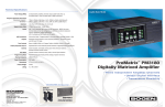
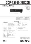
CDP-XA50ES AEP Model E Model SERVICE MANUAL Photo: Black Model Name Using Similar Mechanism CD Mechanism Type Base Unit Name NEW CDM32BB-12B (BLACK) CDM32BN-12B (GOLD) BU-12B Optical Pick-up Name KSS-273B/J1N SPECIFICATIONS – Continued on next page – COMPACT DISC PLAYER MICROFILM TABLE OF CONTENTS 1. SERVICING NOTES 1-1. How to Open the Disc Tray When Power Switch Turns Off .......................................................................... 3 1-2. Preparation for Adjustment and Measurement ................ 3 2. GENERAL ................................................................... 4 3. DISASSEMBLY .......................................................... 15 4. TEST MODE 4-1. AF Mode .......................................................................... 20 4-2. ADJ Mode ....................................................................... 21 4-3. CLV-S Mode .................................................................... 21 MODEL IDENTIFICATION – BACK PANEL – 4-986-742- AEP Model : 1 π (CED) Singapore Model : 2 π (SP) 5. ELECTRICAL ADJUSTMENTS ......................... 22 6. DIAGRAMS 6-1. 6-2. 6-3. 6-4. 6-5. 6-6. 6-7. Printed Wiring Boards — SERVO Section — ................. 25 Schematic Diagram — SERVO Section — ..................... 27 Schematic Diagram — AUDIO Section — ..................... 32 Printed Wiring Boards — AUDIO Section — ................. 37 Printed Wiring Boards — PANEL Section — ................. 39 Schematic Diagram — PANEL Section — ..................... 41 Printed Wiring Boards — POWER SUPPLY Section — ..................................... 44 6-8. Schematic Diagram — POWER SUPPLY Section — ..................................... 47 6-9. IC Pin Function Description ............................................ 54 7. EXPLODED VIEWS ................................................ 60 8. ELECTRICAL PARTS LIST ................................ 66 SAFETY-RELATED COMPONENT WARNING!! COMPONENTS IDENTIFIED BY MARK ! OR DOTTED LINE WITH MARK ! ON THE SCHEMATIC DIAGRAMS AND IN THE PARTS LIST ARE CRITICAL TO SAFE OPERATION. REPLACE THESE COMPONENTS WITH SONY PARTS WHOSE PART NUMBERS APPEAR AS SHOWN IN THIS MANUAL OR IN SUPPLEMENTS PUBLISHED BY SONY. –2– SECTION 1 SERVICING NOTES 1-1. NOTES ON HANDLING THE OPTICAL PICK-UP BLOCK OR BASE UNIT The laser diode in the optical pick-up block may suffer electrostatic break-down because of the potential difference generated by the charged electrostatic load, etc. on clothing and the human body. During repair, pay attention to electrostatic break-down and also use the procedure in the printed matter which is included in the repair parts. The flexible board is easily damaged and should be handled with care. HOW TO OPEN THE DISC TRAY WHEN POWER SWITCH TURNS OFF Insert a tapering driver into the aperture of the unit bottom, and turn in the direction of arrow (to OUT direction). NOTES ON LASER DIODE EMISSION CHECK The laser beam on this model is concentrated so as to be focused on the disc reflective surface by the objective lens in the optical pick-up block. Therefore, when checking the laser diode emission, observe from more than 30 cm away from the objective lens. tray Notes on chip component replacement • Never reuse a disconnected chip component. • Notice that the minus side of a tantalum capacitor may be damaged by heat. Flexible Circuit Board Repairing • Keep the temperature of the soldering iron around 270 ˚C during repairing. • Do not touch the soldering iron on the same conductor of the circuit board (within 3 times). • Be careful not to apply force on the conductor when soldering or unsoldering. tapering driver * To close the disc tray, turn the tapering driver in the reverse direction (to IN direction). 1-2. PREPARATION FOR ADJUSTMENT AND MEASUREMENT Perform connecting the IC261 pin 2 of SERVO board to the line of +5V because this unit does not work without the stabilizer structurally. CAUTION Use of controls or adjustments or performance of procedures other than those specified herein may result in hazardous radiation exposure. [SERVO BOARD] – Conductor side – This appliance is classified as a CLASS 1 LASER product. The CLASS 1 LASER PRODUCT MARKING is located on the rear exterior. Laser component in this product is capable of emitting radiation exceeding the limit for Class 1. The following caution label is located inside the unit. –3– IC91 +5 V 1 2 IC261 IC101 This section is extracted from instruction manual. SECTION 2 GENERAL –4– –5– –6– –7– –8– –9– – 10 – – 11 – – 12 – – 13 – – 14 – SECTION 3 DISASSEMBLY • This set can be disassembled in the order shown below. LOADING PANEL SECTION (Page 15) CASE (TOP PLATE ), FRONT PANEL SECTION (Page 16) MECHANISM DECK (CDM32BB-12B/CDM32BN-12B) (Page 17) BASE UNIT (BU-12B) (Page 18) SERVO BOARD (Page 17) AUDIO BOARD (Page 16) PANEL (DRAWER) (Page 18) SLED MOTOR (M21), OPTICAL PICK-UP (KSS-273B/J1N) (Page 19) Note: Follow the disassembly procedure in the numerical order given. LOADING PANEL SECTION 5 connector (CN292) 4 loading panel section tray 3 two hexagon hole bolts (LID) (for black/gold) 1 Open the tray turning the tapering screwdriver to the arrow direction. 2 two screws (KTP3 × 8) (for black/gold) – 15 – CASE (TOP PLATE), FRONT PANEL SECTION 1 three flat head screws 1 three flat head screws 9 three connectors (CN351, 352, 461) 2 case (top plate) 3 two connectors (CN201, 993) 6 four screws (3 × 8) 7 two brakets (case) 4 screw (3 × 8) 0 front panel section 4 two screws (3 × 8) 3 two connectors (CN202, 203) 4 four screws (3 × 8) 8 two screws (K3 × 8) 5 lag AUDIO BOARD 6 eight screws (BV3 × 8 B) 3 two connectors (CN922, 923) 4 TR screw 3 two connectors (CN401, 501) 5 lag 3 four connectors (CN103, 104, 105, 202) 3 four connectors (CN402, 502, 610, 611) 7 audio board 3 two connectors (CN608, 609) 2 side plate (R) 1 four flat head screws – 16 – MECHANISM DECK (CDM32BB-12B/CDM32BN-12B) 2 two screws 2 two screws 3 clamp 3 clamp 1 connector (CN952) 4 mechanism deck (CDM32BB-12B) (CDM32BN-12B) 1 connector (CN105) 1 two connectors (CN103, 104) SERVO BOARD 1 two screws (BVTP3 × 6) 1 two screws (BVTP3 × 6) 5 six screws (BVTP3 × 6) 3 wire (flat type) (26 core) (CN102) 4 wire (flat type) (12 core) (CN101) 2 bracket (servo) 6 servo board bracket (servo) – 17 – PANEL (DRAWER) 1 two tapping screws 3 Remove the panel (drawer) to direction of the arrow. 2 two ditch BASE UNIT (BU-12B) 4 two screws (PTPWH2.6 × 8) 4 two screws (PTPWH2.6 × 8) 5 two holders (SP) 5 two holders (SP) 1 flexible board (CN192) 6 base unit 7 two coil springs (F) 7 flexible board (CN291) 2 screw (B2.6 × 10) 7 two coil springs (F) 3 lag – 18 – SLED MOTOR (M21), OPTICAL PICK-UP (KSS-273B/J1N) 2 two screws (BTP2.6 × 8) 7 poly-slider washer 8 gear (D) 4 tapping screw 5 lag 3 leaf spring (skew) 6 leaf spring (OP) 9 Remove the sled motor (M21) and optical pick-up (KSS-273B/J1N) to direction of the arrow A. A 0 bracket (OP base) 1 flexible board (CN11) 4 tapping screw – 19 – SECTION 4 TEST MODE 4-1. AF MODE REPEAT button Connect the TP2 (AFJ) on the SERVO board to the ground and turn on the power supply. The AF mode is then activated and the following check can be made. SIDE-B ( MIN 4-1-1. Fluorescent Indicator Tube Check After confirming display of all on, keep pressing the following button, and the following display is attained. TIME ) (1) C. FILE INDEX • (Display: 09) TIME button p (STOP) button (Display: 01) (Display: 10) ” (PLAY) button Keep pressing the §OPEN/CLOSE button, and all on display is attained again. (Display: 02) P (PAUSE) button 4-1-2. Key Check All buttons are assigned with numbers respectively, and when each button is pressed, it is counted and its number is displayed. Up to “16” can be counted. A button pressed once is not further counted but the number is displayed. Table 4-1. (Display: 03) ) button SHUFFLE REPEAT AAUTO SPACE EDIT (Display: 04) STEP – Button Display 00 P 03 EDIT/ TIME FADE 12 ) 04 FILE 13 0 05 FILTER 20 CHECK 06 23 CLEAR 07 § OPEN/CLOSE all light up P MODE 08 p 01 REPEAT 09 ( 02 TIME 10 ( JUST ) B Display PUSH ENTER 0 button 1 Button ERASE PROGRAM (Display: 05) PEAK CHECK button 1 3 7 11 4-1-3. Remote Commander Check Press the ( button on remote commander, and “ ˚ ” ( on the set turn on. Nothing will be displayed if pressing another button. 5 9 13 15 ( (Display: 06) ( INDEX CLEAR button 2 6 4 8 12 count display 10 14 ” (Display: 07) P MODE button SIDE-A CUSTOM INDEX FADE C. SEC DELETE (Display: 08) – 20 – button number display [SERVO BOARD] – Conductor side – 4-2. ADJ MODE Connect the TP1 (ADJ) on the SERVO board to the TP (GND) and turn on the power supply. The ADJ mode is then activated and the following operation is executed. • There is no problem even if GFS is low value continuously during playing. • Do not perform high speed search during an access. • The gain of focus servo and spindle servo does not lower during playing. • Manual operation and measurement of the servo system are possible. (For detailed operating method, see Table 4-2. in ADJ Mode.) 4-2-1. Button Operation Table in ADJ Mode After all music numbers are displayed, press the TIME button, and the jitter display mode is then set. The button functions are as listed below. Button Functions (Operate with remote commander.) Table 4-2. Button No. Test Mode 3 Tracking servo off 8 Tracking servo on 11 S-curve measuring mode 12 All servo off 13 Top turnback display 14 Botton turnback display 15 Center display 16 Optimum point display 17 Optimum jitter display 18 TE traverse display 19 VC, FE and RF display 20 Autogain display (Focus, tracking and sled) * For button numbers 3, 8, 11, and 12, use them only when an oscilloscope is connected. 4-3. CLV-S MODE The spindle servo can be operated for play in the CLV-S mode by connecting TP (ADJ) and TP (GND) after turning on the power supply. – 21 – TP (GND) TP 1 (ADJ) IC101 CN101 CN102 TP 2 (AFJ) SECTION 5 ELECTRICAL ADJUSTMENTS RF signal waveform Notes: 1. CD block basically constructed to operate without adjustment. Therefore, check each item in order given. 2. Use YEDS-18 disc (Part No.: 3-702-101-01) unless otherwise indicated. 3. Use the oscilloscope with more than 10 MΩ impedance. 4. Clean an object lens by an applicator with neutral detergent when the signal level is low than specified value with the following checks. S-Curve Check Connection: VOLT/DIV: 200 mV TIME/DIV: 500 ns (with the 10: 1 probe in use) +0.25 level: 1.2 –0.20 Vp-p When observing the eye pattern, set the oscilloscope for AC range and raise vertical sensitivity. oscilloscope SERVO board TP (FE) TP (VC) E-F Balance (Traverse) Check Connection: + – Procedure: 1. Connect the oscilloscope to TP (FE) and TP (VC) on SERVO board. 2. Connect the TP (FEI: IC101 pin @ª) and TP (VC) with lead wire. 3. Turned power switch on. 4. Put disc (YEDS-18) in and turned power switch on again and actuate the focus search. (actuate the focus search when disc table is moving in and out.) 5. Confirm that the oscilloscope waveform (S-curve) is symmetrical between A and B. And confirm peak to peak level within 3.0 ± 1.0 Vp-p. S-curve waveform symmetry oscilloscope (DC range) SERVO board TP (TE) TP (VC) + – Procedure: 1. Connect the TP1 (ADJ) to ground and TP (TEI: IC101 pin @¶) to TP (VC) with lead wire. 2. Connect the oscilloscope to TP (TE) and TP (VC) on SERVO board. 3. Turned power switch on. 4. Put disc (YEDS-18) in and press the ( button. 5. Confirm that the oscilloscope waveform is symmetrical on the top and bottom in relation to 0 Vdc, and check this level. Traverse waveform A within 3.0 ± 1.0 Vp-p B A B 6. After check, remove the lead wire connected in step 2. Note: • Try to measure several times to make sure that the ratio of A : B or B : A is more than 10 : 7. • Take sweep time as long as possible and light up the brightness to obtain best waveform. RF Level Check Connection: 6. After check, remove the lead wire connected in step 1. oscilloscope (AC range) RF PLL Free-run Frequency Check Connection: SERVO board TP (RF) TP (VC) level: 200 ± 100 mVp-p + – frequency counter SERVO board Procedure: 1. Connect the oscilloscope to TP (RF) and TP (VC) on SERVO board. 2. Turned power switch on. (stop mode) 3. Put disc (YEDS-18) in and press the ( button. 4. Confirm that the oscilloscope waveform is clear and check RF signal level is correct or not. Note: Clear RF signal waveform means that the shape “≈” can be clearly distinguished at the center of the waveform. TP (PLK) + – Procedure: 1. Connect the frquency counter to TP (PLK). 2. Turned power switch on. 3. Put disc (YEDS-18) in and press the ( button. 4. Confirm that the reading on frequency counter is 4.3218 MHz. – 22 – SECTION 6 DIAGRAMS Skew Adjustment Note : Do not perform the skew adjustment when not using attached stabilizer to a set. [SERVO BOARD] – Conductor side – • Circuit Boards Location TP (TEI) oscilloscope (AC range) 29 (FEI) TP (RFI) SERVO board TP (RF) TP (VC) + – TP (FE) TP (RF) TP (TE) TP TP (VC) (PLK) CN101 RF signal waveform IC101 SERVO board BSL board LOADING MOTOR board TP1 (ADJ) TP2 (AFJ) POWER board FUSE board COAX board CN102 OPT board SW board VOLT/DIV: 200 mV TIME/DIV: 500 ns (with the 10: 1 probe in use) +0.25 level: 1.2 –0.20 Vp-p LINE board VR board AUDIO board KEY-R board DISPLAY board FLEX RELAY board LOADING SW board KEY-L board FL RELAY board adjustment screw ‘ screwdriver 1. Remove the bottom plate, put one third of the unit out from the desk. 2. Connect the osiclloscope to TP (RF) and TP (VC) on SERVO board. 3. Turned power switch on. 4. Put disc (YEDS-18) in and press the ( button. 5. Adjust to be clear the waveform of the oscilloscope turning the adjsutment screw with a ‘ screwdriver. Note: Clear RF signal waveform means that the shap “≈”can be clearly distinguished at the center of the waveform. 6. After the adjustment, lock the adjustment screw. – 23 – – 24 – • IC Block Diagrams – SERVO Section – IC203 LB1641 IC91 M51957AL T.S.D O.C.P MOTOR DRIVE MOTOR DRIVE 2 3 4 5 6 7 8 9 REV.IN VCC 1 VCC 2 NOISE FILTER 10 MOTOR DRIVE 1 FWD.IN GND DL OUT FWD/REV/STOP CONTROL LOGIC CLAMP 5 NOISE FILTER 4 GND 3 MOTOR DRIVE 1 2 VDD IN 1.25V – + MDS MDP MON FSW FOK DFCT MIRR ADD COUT CLOK XLAT DATA ATSK DFSW SCLK DIRC XRST SENS MUTE SQCK SQSO EXCK 96 95 94 93 92 91 90 89 88 87 86 85 84 83 82 81 80 79 78 77 76 SLED PWM GENERATOR SLED SERVO TRACKING PWM GENERATOR TRACKING SERVO FOCUS PWM GENERATOR FOCUS SERVO LOCK SSTP 99 98 97 CLV PROCESSOR VCO0 12 VCO1 13 CPU ADDRESS INTERFACE GENERATOR RESISTER DIGITAL OUT PEAK DETECTOR CLOCK GENERATOR DIGITAL PLL VARI-PITCH DOUBLE SPEED A/D CONVERTER FE VC FILO FILI PCO CLTV 35 36 37 38 39 40 41 42 43 44 45 46 — 50 DA16 | DA12 34 WDCK LRCK 33 PSSL 32 AVDD ADD 31 ASYI 30 BIAS 29 RFAC 28 61 DA01 | | 51 DA11 SERIAL PARALLEL PROCESSOR MUX AVSS 27 TE ASYMMETRY CPU CORRECTION INTERFACE SE RFDC 66 FSTI 65 DVSS 4 SWITCH & BUFFER 26 70 MD2 64 XTSL 63 XTAO 62 XTAI CPU EFM INTERFACE DEMODULATOR 71 D OUT 69 C16M 68 C4M 67 FSTO 3 VPCO 19 VCKI 20 73 WFCK 72 EMPH CPU TIMING INTERFACE 2 GENERATOR PDO 18 RFC 25 74 SCOR SYNC PROTECTOR D/A DIGITAL PROCESSOR ERROR CPU CORRECTOR INTERFACE MIRR DFCT FOK DETECTOR ADIO 24 TIMING GENERATOR 1 32K RAM PRIORITY CPU ENCODER INTERFACE 18-TIMES OVER SAMPLING FILTER AVDD 21 IGEN 22 AVSS 23 75 SBSO SERVO MICRO PROGRAM INTERFACE NOISE SHAPER 14 15 16 17 SUBCODE P-W PROCESSOR SERVO AUTO SEQUENCER SERVO DSP PWM GENERATOR TEST DVSS TES2 TES3 SUBCODE Q PROCESSOR CPU INTERFACE – 49 – ASYE 1 2 3 4 5 6 7 8 9 10 11 100 ASYO SRON SRDR SFON TFDR TRON TRDR TFON FFDR FRON FRDR FFON SFDR IC101 CXD2545Q – 50 – – AUDIO Section – IC603 CXD2562Q-CS 2 3 4 5 6 7 8 9 INPUT 1 INPUT 2 NC GND Vcc OUTPUT 2 OUTPUT1 NC SWITCHING CIRCUIT INIT MUTER MUTEL LRCKI DRI DLI BCKI 512FSO DVSSR DVSSL 128FS DINIT INAF LRCKO DRO DLO 51 50 49 48 47 46 45 44 43 42 41 40 IN2– IN2+ NC IN1+ IN1– NC C4 C3 GND2 VEE2 39 38 37 36 35 34 33 TIMING CIRCUIT 32 SYNC 31 COEF 30 SPLM INTERPOLATER DATAOUT 52 ON/OFF TEST1 53 VCC1 10 29 18/20 S/P INTERPOLATER 28 DVDDR 27 VSUB (D) R TEST2 54 REFERENCE VOLTAGE CIRCUIT VREF 11 18 VEE1 17 C6 26 VSUB (CHIP) R THIRD ORDER NOISE SHAPER TEST3 55 CONSTANT CURRENT CIRCUIT DVDDL 56 PLM 25 VDD2 24 VDD VSUB (D) L 57 23 R1 (–) VSUB (CHIP) L 58 VCNT 12 GND1 13 RIREF 14 VDD 60 16 C5 15 CIREF CONTROL CIRCUIT VSS 62 CLOCK GENERATOR NRGCLR SYSM LATCH SHIFT ATT INIT LRCKI DATAI BCKI VSS VSS NC INVO2 INVO1 INVI NC 128FSO CKVDD DINIT 51 50 49 48 47 46 45 44 43 42 41 40 39 38 37 36 35 34 33 VDD2 VSUB (A) L XVDD XOUT XIN FIR 4 DFDTOL 59 FIR 1 FIR 2 FIR 4 FIR 3 FIR 1 FIR 2 26 MODE FIR 3 L . I . P. 25 NC 3rd order NOISE SHAPER 24 DFDTOR OVERFLOW DETECTOR 23 DFLRCKO POLALITY 22 TEST4 TEST1 62 P/S CONVERT & D/F-CLK GEN. TEST2 63 R Q C D Q 1 2 3 4 21 TEST3 CLOCK GENERATOR VSS 64 LC7570E CL S VSS IC801-803 48 47 46 45 44 43 42 41 40 39 38 37 28 MTPOL ATT x 0.75 DFDTEN 61 5 27 DRPOL DFBCKO 60 OVERFLOW DETECTOR Q 3rd order NOISE SHAPER DITHER NC 58 6 29 MUTEL ATT x 0.75 BITSTREAM 7 GND SDATAL 57 IIR CLR IIR PR L . I . P. SDATAR 56 8 Q ATT MODE VCC 30 MUTER NC 54 D 31 OVFLAG CK "0" DETECT MUTE CIRCUIT IF SELC 53 DATA TC7W74F NC VDA IC610 OR ATT VSS2 VDD – PANEL Section – 32 INAF S/P 4BIT DATA R2 (+) 10 11 12 13 14 15 16 17 18 19 R2 (–) 9 VDD 8 VDD2 7 VSUB (A) R 6 XVSS 5 XVSS 4 VSS VSS2 3 L2 (–) 2 L2 (+) CXD8679Q 1 TIMING CIRCUIT SBCKI 55 21 R1 (+) 20 VSS2 VSS2 64 IF SELD 52 PLM L1 (–) 61 L1 (+) 63 IC601 22 VSS THIRD ORDER NOISE SHAPER VDD2 59 VFL S0 S1 S2 S3 NC S4 1 NC REG 28 27 26 25 24 23 22 21 20 19 WR MOTOR DRIVE SWITCH 1 2 3 4 5 6 7 8 9 I01+ I02– NC I01– I02+ NC VCC2 C2 C1 DM1/SDLO MOTOR DRIVE SWITCH DM2/SDRO IC404, 504 CXA8042AS BA6208 DPO/BCKO IC350 NC 1 BLK 2 VSS 3 SIN S33 S32 S31 S30 S29 S28 S27 S26 4 5 6 7 8 9 10 11 12 SHIFT REGISTER A/D CONVERTER LATCH, FL DRIVER 20 VSS NC S25 S24 S23 S22 S21 NC S20 S19 S18 S17 NC 13 14 15 16 17 18 19 20 21 22 23 24 DATA SELECT DATA SELECT NSDOL1 NC NC 13 14 15 16 17 18 19 PLMG1 NSDOL2 12 VDD NSDOL3 11 MCKIN NSDOL4 10 NSDOR4 VDD 9 NSDOR3 8 NSDOR2 7 NSDOR1 6 64FSI 5 NC 4 VDD 3 VDD 2 PLMG2 2 1 – 51 – – 52 – 36 35 34 33 32 31 30 29 28 27 26 25 S5 S6 S7 S8 S9 S10 S11 S12 S13 S14 S15 S16 6-9. IC PIN FUNCTION DESCRIPTION • Waveforms – SERVO Section – – AUDIO Section – 1 IC101 @§ (RFDC) 200 mV/DIV, 500 ns/DIV 6 IC101 $¶ (BLCK) 1.2 +0.25 –0.20 Vp-p 2 IC101 @¶ (TE) 200 mV/DIV, 100 µs/DIV 1.8 Vp-p 16.9344 MHz 474 ns 7 IC101 ^™ (XTAI) 2 IC602 6 5.2 Vp-p 4.8 Vp-p 16.9344 MHz 3 IC101 @ª (FE) 200 mV/DIV, 50 ns/DIV Pin No. Pin Name 1 IC602 1 5.2 Vp-p Approx. 400 mVp-p SERVO BOARD IC101 CXD2545Q (DIGITAL SIGNAL PROCESSOR, FOCUS/TRACKING/SLED SERVO, EFM COMPARATOR) 180 ns 8 IC101 (§ (MDP) 3 IC603 0 (XIN) 2.8 Vp-p Approx. 200 mVp-p 4.8 Vp-p 4 IC101 #§ (RFAC) 200 mV/DIV, 500 ns/DIV 1.2 +0.25 –0.20 Vp-p 4 IC604 3 4.8 Vp-p 4 MHz 5 IC101$∞ (LRCK) 840 mVp-p 45.159 MHz 5 IC610 1 (CK) 5.2 Vp-p 4 Vp-p 22.7 µs Function SRON SRDR O O Sled servo drive PWM signal (–) output to the BA6297AFP (IC102) 3 SFON O Sled servo drive PWM signal output terminal 4 TFDR O Tracking servo drive PWM signal (–) output to the BA6297AFP (IC102) 5 TRON O Tracking servo drive PWM signal output terminal 6 TRDR O Tracking servo drive PWM signal (+) output to the BA6297AFP (IC102) 7 TFON O Tracking servo drive PWM signal output terminal 8 FFDR O Focus servo drive PWM signal (+) output to the BA6297AFP (IC102) Sled servo drive PWM signal output terminal Not used (open) Not used (open) Not used (open) 9 FRON O Focus servo drive PWM signal output terminal FRDR O Focus servo drive PWM signal (–) output to the BA6297AFP (IC102) FFON O Focus servo drive PWM signal output terminal 12 VCOO O Oscillator circuit output terminal for analog PLL of the playback EFM 13 VCOI I Oscillator circuit input terminal for analog PLL of the playback EFM 14 15 TEST DVSS I — Input terminal for the test (fixed at “L”) 16 TES2 I Input terminal for the test (fixed at “L”) 17 18 TES3 PDO I O Input terminal for the test (fixed at “L”) 19 VPCO O PLL charge-pump output terminal for the variable pitch 20 21 VCKI I Clock signal input from external VCO for the variable pitch AVD2 — Not used (open) Not used (open) Not used (open) Not used (fixed at “L”) Ground terminal (digital system) Charge-pump output terminal for analog PLL of the playback EFM Not used (open) Not used (open) Not used (fixed at “L”) Power supply terminal (+5V) (analog system) 22 IGEN I 23 AVS2 — 24 ADII I Input terminal for the A/D converter 25 ADIO O Output terminal of the operational amplifier 26 RFDC TE I I RF signal (DC level) input terminal for the digital servo process 28 29 SE I Sled error signal input from the RF amplifier in optical pick-up FE I Focus error signal input from the RF amplifier in optical pick-up 30 VC I Middle point voltage (+2.5V) input from the RF amplifier in optical pick-up 31 FILO O Filter output terminal for master clock of the playback master PLL 32 FILI I Filter input terminal for master clock of the playback master PLL 33 PCO O Phase comparison output terminal for master clock of the playback EFM master PLL 34 CLTV I Internal VCO control voltage input of the playback master PLL 35 AVS1 — 36 RFAC I RF signal (AC level) input terminal for the EFM demodulator 37 BIAS I Constant current input terminal of the playback EFM asymmetry circuit 38 ASYI I Playback EFM asymmetry comparator voltage input terminal 39 ASYO O Playback EFM full-swing output terminal 40 AVD1 — Power supply terminal (+5V) (analog system) 41 DVDD — Power supply terminal (+5V) (digital system) 42 ASYE I Playback EFM asymmetry circuit on/off selection input terminal (fixed at “H”) 43 PSSL I Audio data output mode selection input terminal (fixed at “L”) Power supply terminal (+5V) (for operational amplifier) Ground terminal (analog system) Not used (open) Not used (open) Tracking error signal input from the RF amplifier in optical pick-up Ground terminal (analog system) 44 ns – 53 – Not used (open) 10 11 27 22 ns 8 ns 9 IC201 #¡ (XTALI) I/O 1 2 – 54 – Pin No. Pin Name I/O Function 44 WDCK O Word clock signal (88.2 kHz) output terminal 45 LRCK O L/R sampling clock signal (44.1 kHz) output to the CXD8679Q (IC601) Not used (open) 46 DATA O DA16 output when PSSL=“H”, 48-bit slot serial data output when PSSL=“L” (PSSL (pin $£)=fixed at “L”) Serial data output to the CXD8679Q (IC601) 47 BCLK O DA15 output when PSSL=“H”, 48-bit slot bit clock signal output when PSSL=“L” (PSSL (pin $£)=fixed at “L”) Bit clock signal (2.8224 MHz) output to the CXD8679Q (IC601) 48 64 DATA O DA14 output when PSSL=“H”, 64-bit slot serial data output when PSSL=“L” (PSSL (pin $£)=fixed at “L”) Not used (open) 49 64 BCLK O DA13 output when PSSL=“H”, 64-bit slot bit clock signal output when PSSL=“L” (PSSL (pin $£)=fixed at “L”) Not used (open) 50 64 LRCK O DA12 output when PSSL=“H”, 64-bit slot L/R sampling clock signal output when PSSL=“L” (PSSL (pin $£)=fixed at “L”) Not used (open) 51 GTOP O DA11 output when PSSL=“H”, GTOP signal output when PSSL=“L” (PSSL (pin $£)=fixed at “L”) Not used (open) 52 XUGF O DA10 output when PSSL=“H”, XUGF signal output when PSSL=“L” (PSSL (pin $£)=fixed at “L”) Not used (open) 53 XPLCK O DA09 output when PSSL=“H”, XPLCK signal output when PSSL=“L” (PSSL (pin $£)=fixed at “L”) Not used (open) 54 GFS O DA08 output when PSSL=“H”, GFS (guard frame sync) signal output when PSSL=“L” (PSSL (pin $£)=fixed at “L”) Not used (open) 55 RFCK O DA07 output when PSSL=“H”, RFCK (read frame clock) signal output when PSSL=“L” (PSSL (pin $£)=fixed at “L”) Not used (open) 56 C2PO O DA06 output when PSSL=“H”, C2PO signal output when PSSL=“L” (PSSL (pin $£)=fixed at “L”) Not used (open) 57 XRAOF O DA05 output when PSSL=“H”, XRAOF (RAM over flow) signal output when PSSL=“L” (PSSL (pin $£)=fixed at “L”) Not used (open) 58 MNT3 O DA04 output when PSSL=“H”, MNT3 (monitor 3) signal output when PSSL=“L” (PSSL (pin $£)=fixed at “L”) Not used (open) 59 MNT2 O DA03 output when PSSL=“H”, MNT2 (monitor 2) signal output when PSSL=“L” (PSSL (pin $£)=fixed at “L”) Not used (open) 60 MNT1 O DA02 output when PSSL=“H”, MNT1 (monitor 1) signal output when PSSL=“L” (PSSL (pin $£)=fixed at “L”) Not used (open) 61 MNT0 O DA01 output when PSSL=“H”, MNT0 (monitor 0) signal output when PSSL=“L” (PSSL (pin $£)=fixed at “L”) Not used (open) 62 XTAI I System clock input terminal (16 MHz) 63 XTAO O System clock output terminal (16 MHz) 64 XTSL I System clock selection input terminal (fixed at “L”) 65 DVSS — 66 FSTI I 67 FSTO O 2/3 divider output terminal of pins ^™ (XATI) and ^£ (XTAO) 68 C4M O 4.2336 MHz clock signal output terminal Not used (open) 69 C16M O 16.9344 MHz clock signal output terminal Not used (open) 70 MD2 I Digital out on/off control signal input from the system controller (IC201) 71 DOUT O Digital signal (for coaxial out and optical out) output terminal 72 EMPH O Emphasis control signal output terminal 73 WFCK O Write frame clock signal output terminal 74 SCOR O Sub-code sync (S0+S1) detection signal output to the system controller (IC201) Not used (open) Ground terminal (digital system) 2/3 divider input terminal of pins ^™ (XATI) and ^£ (XTAO) – 55 – Not used (open) Not used (open) Pin No. Pin Name 75 SBSO 76 77 I/O Function O Sub-code P-W serial data output terminal Not used (open) EXCK I Sub-code P-W serial data reading clock signal input terminal SUBQ O Sub-code Q data signal output to the system controller (IC201) Not used (fixed at “L”) 78 SQCK I Sub-code Q data reading clock signal input from the system controller (IC201) 79 MUTE I Mute signal input from the system controller (IC201) 80 SENS O Internal status (SENSE) signal output to the system controller (IC201) XRST I System reset signal input from the reset signal generator (IC91) “L”: reset For several hundreds msec. after the power supply rises, “L” is input, then it changes to “H” 82 DIRC I 1-track jump mode input terminal 83 SCLK I Sense serial data reading clock signal input from the system controller (IC201) 84 DFSW I Defect on/off select signal input terminal 85 ATSK I Input terminal for the anti-shock 86 DATA I Serial data input from the system controller (IC201) 87 XLAT I Serial data latch pulse signal input from the system controller (IC201) 88 CLOK I Serial data transfer clock signal input from the system controller (IC201) 89 COUT O Track number count signal output terminal 90 DVDD — Power supply terminal (+5V) (digital system) 91 MIRR O Mirror detection signal output terminal 92 DFCT O Defect signal output terminal 93 FOK O Focus OK signal output terminal 94 95 FSW O Selection signal output terminal of the output filter for spindle motor MON O Spindle motor on/off control signal output terminal 96 MDP O Spindle servo control signal output terminal 97 MDS O 98 LOCK O Spindle servo control signal output terminal Not used (open) GFS is sampled by 460 Hz “H” output when GFS is “H” Not used (open) 99 SSTP I Detection input from the sled limit-in detect switch (S22) The optical pick-up is inner position when “H” 100 SFDR O Sled servo drive PWM signal (+) output to the BA6297AFP (IC102) 81 Not used (fixed at “H”) Not used (fixed at “L”) Not used (fixed at “L”) Not used (open) Not used (open) Not used (open) – 56 – Not used (open) Not used (open) Not used (open) SERVO BOARD IC201 Pin No. Pin Name I/O 1 2 A3 A4 O O 3 A5 O 4 A6 O 5 A7 O 6 A8 O 7 A9 O 8 A10 O CXP84124-068Q (SYSTEM CONTROLLER) Function Address signal output to the static RAM (IC202) 9 A11 O 10 11 A12 O WE O Write enable signal output to the static RAM (IC202) 12 NC O Not used (open) 13 NC O Not used (open) 14 15 LED-PLAY LED-PAUSE O O ( LED (D871) drive signal output terminal 16 LED-FILTER O FILTER LED (D873) drive signal output terminal 17 18 SPDL-MUTE SHIFT-ON/OFF O O Mute signal output to the spindle motor driver (IC104, 105) P LED (D872) drive signal output terminal “H”: LED on “H”: LED on “H”: LED on Reset signal output to the CXD2562Q-CS (IC603) “L”: reset 19 VOL UP O Volume up control signal output to the volume control motor driver (IC350) 20 21 VOL DOWN O Volume down control signal output to the volume control motor driver (IC350) BLANK O Blank signal output to the fluorescent indicator tube driver (IC801 to IC803) 22 FL D0 O Serial data output to the fluorescent indicator tube driver (IC803) 23 FL D1 O Serial data output to the fluorescent indicator tube driver (IC802) 24 FL D2 O Serial data output to the fluorescent indicator tube driver (IC801) 25 FL CLK O Serial data transfer clock signal output to the fluorescent indicator tube driver (IC801 to IC803) 26 27 FL WR SENSER SW O O On/off control signal output to the stabilizer detect sensor (IC261) 28 SENSER I Detect signal input from the stabilizer detect sensor (IC261) 29 LIMIT OUT I Detection input from the sled limit-out detect switch (S21) The optical pick-up is outer position when “L” 30 RESET I System reset signal input from the reset signal generator (IC91) “L”: reset For several hundreds msec. after the power supply rises, “L” is input, then it changes to “H” Read/write select signal output to the fluorescent indicator tube driver (IC801 to IC803) 31 XTALI I Main system clock input terminal (4 MHz) 32 XTALO O Main system clock output terminal (4 MHz) 33 VSS — Ground terminal 34 TX O Sub system clock output terminal Sub system clock input terminal “H”: on “H”: on Not used (open) 35 TEX I 36 AVSS — 37 AVREF I Reference voltage input terminal (+5V) 38 K0 I Key input terminal (A/D input) 39 K1 I Key input terminal (A/D input) FILE, EDIT/TIME FADE, TIME, REPEAT, P MODE keys (S851 to S855) input 40 K2 I Key input terminal (A/D input) CHECK, CLEAR, FILTER, 0, ) , PUSH ENTER keys (S884 to S888, RV870) input Not used (fixed at “L”) Ground terminal (for A/D converter) – 57 – ERASE key (S850) input Pin No. Pin Name I/O 41 K3 I Key input terminal (A/D input) § OPEN/CLOSE, (, P, p keys (S889 to S892) input 42 K4 I Rotary encoder input terminal (A/D input) AMS ± key (RV870) input 43 K5 I Rotary encoder input terminal (A/D input) AMS ≠ key (RV870) input 44 ADJ/AFJ I Setting terminal for the test mode 45 IN/OUT SW I Detection input from the loading in/out detect switch (S281, S282) (A/D input) 46 SCLK O Sense serial data reading clock signal output to the CXD2545Q (IC101) 47 PRGL O Serial data latch pulse signal output to the CXD8679Q (IC601) 48 CLK O Serial data transfer clock signal output to the CXD2545Q (IC101) and CXD8679Q (IC601) 49 SENSE I Internal status (SENSE) signal input from the CXD2545Q (IC101) 50 DATA O Serial data output to the CXD2545Q (IC101) and CXD8679Q (IC601) 51 SQCK O Sub-code Q data reading clock signal output to the CXD2545Q (IC101) 52 SUBQ I Sub-code Q data signal input from the CXD2545Q (IC101) 53 TEST O Output terminal for the test 54 SEL1 I Destination setting terminal (fixed at “L”) *1 Function “L” active Not used (open) 55 SEL0 I Destination setting terminal (fixed at “L”) 56 RMIN I Remote control signal input from the remote control receiver (IC804) 57 TIMER I Timer control input terminal 58 TEST O Output terminal for the test Not used (open) 59 TEST O Output terminal for the test Not used (open) Not used (fixed at “H”) 60 SCOR I Sub-code sync (S0+S1) detection signal input from the CXD2545Q (IC101) 61 AMUTE O Muting control signal output to the analog mute driver and mute relay driver 62 LDON O Laser diode on/off selection signal output to the RF amplifier in optical pick-up 63 XLT O Serial data latch pulse signal output to the CXD2545Q (IC101) 64 LOAD OUT O Loading motor (M271) drive signal output to the LB1641 (IC203) *1 65 LOAD IN O Loading motor (M271) drive signal output to the LB1641 (IC203) *1 66 DOUT O Digital out on/off control signal output to the CXD2545Q (IC101) 67 DMUTE O Muting control signal output to the CXD2545Q (IC101) and CXD8679Q (IC601) 68 D0 I/O 69 D1 I/O 70 D2 I/O 71 D3 I/O 72 VDD — 73 NC I 74 D4 I/O 75 D5 I/O 76 D6 I/O 77 D7 I/O 78 A0 O 79 A1 O 80 A2 O Two-way data bus with the static RAM (IC202) Power supply terminal (+5V) Not used (fixed at “H”) Two-way data bus with the static RAM (IC202) Address signal output to the static RAM (IC202) Loading motor (M271) control Operation OFF OUT IN BRAKE LOAD OUT (pin ^¢) “L” “H” “L” “H” LOAD IN (pin ^∞) “L” “L” “H” “H” Terminal – 58 – Main Ports SPDL-MUTE (pin !¶) From the viewpoint of performance of the set, the disc must not move nor sway when the disc table opens. These problems however occur in the actual case due to the offset voltage generated and the voltage generated because of the positional relation between the BSL coil and Hall element. The spindle motor driver (IC104, IC105) is therefore muted while the tray is open. Pin !¶ provides the timing for this. SENSER (pin @•) The results of the detection of IC261 IS471F is output to this pin. It becomes “ L” when there is no stabilizer (when light reaches). The next process of imposing the next focus is not performed. (Effective only when pin @¶ is “H”.) Therefore, it must be noted that if PLAY is performed when the servo board at the top of the CDM is not assembled properly, the detection circuit operates and this pin does not operate. It is does not operate, refer to 1. SERVICING NOTES ” Preparations for Adjustment and Measurement” on page 3. H SP MUTE L (MUTE ON) PLAY OPEN CLOSE Reverses after a certain period of time. Reverses after a certain period of time. Time while the disc can be seen (Estimate). SPINDLE KICK The spindle motor driver is muted during this time. BLANK (pin @¡) This port is required because the display tube in this set static-lights up and a dedicated screwdriver is required. It is basically a RESET pin. But as problems will occur if used also as RESET, timings are specially provided using the micro-processor. SENSER SW (pin @¶) As IC261 IS471F operate in pulse as shown in the figure, the sound quality may be affected if operated constantly. As the purpose of IC261 is to detect if the presence of the stabilizer, it should be operated only when the tray is drawn in. IC261 operates as it is “H” only at this time. Normally it is “L”. Eep Ee Eed 0 Time GLout pin output waveform * Eep is the luminance of the signal light tuned with the low level timing of the GLout pin output. Eed is the luminance of the D.C. light. The light source is the infrated-emitting diode (λp=940 nm). – 59 – SECTION 7 EXPLODED VIEWS NOTE: • -XX and -X mean standardized parts, so they may have some difference from the original one. • Color Indication of Appearance Parts Example: KNOB, BALANCE (WHITE) ↑ Cabinet's Color • Items marked “*” are not stocked since they are seldom required for routine service. Some delay should be anticipated when ordering these items. • The mechanical parts with no reference number in the exploded views are not supplied. • Hardware (# mark) list and accessories and packing materials are given in the last of the electrical parts list. (1) CASE, LOADING PANEL SECTION The components identified by mark ! or dotted line with mark ! are critical for safety. Replace only with part number specified. 8 8 12 8 9 13 8 11 21 not supplied 7 7 23 FRONT PANEL SECTION 22 #2 6 7 4 not supplied 5 14 11 10 3 2 8 19 not supplied 7 18 15 15 not supplied 1 #1 (For gold) #2 (For black) Ref. No. 16 7 16 #3 #3 Ref. No. Part No. Description 10 11 12 12 * 13 4-972-439-01 4-972-438-01 4-969-821-01 4-969-821-11 A-4660-735-A SPACER (SCREW HEAD) ABSORBENT, VIBRATION CASE (TOP PLATE) (BLACK) CASE (TOP PLATE) (GOLD) REINFORCEMENT (TOP PLATE) ASSY BASE, LOADING PANEL (BLACK) BASE, LOADING PANEL (GOLD) DISPLAY BOARD SCREW (2.6), +BVTP (BLACK) SCREW (2.6), +BVTP (GOLD) 14 14 15 16 18 4-969-824-01 4-969-824-11 4-970-123-01 4-970-124-01 4-969-834-01 PLATE (R), SIDE (BLACK) PLATE (R), SIDE (GOLD) FOOT (F50180S) CUSHION (F50180S) FILTER SCREW (3X8) SCREW, FLAT HEAD (BLACK) SCREW, FLAT HEAD (GOLD) PLATE (L), SIDE (BLACK) PLATE (L), SIDE (GOLD) 19 19 20 22 23 4-969-833-21 4-969-833-31 4-949-302-31 4-972-440-01 4-949-302-01 COVER, LOADING PANEL (BLACK) COVER, LOADING PANEL (GOLD) WASHER SPACER WASHER Part No. Description 1 1 2 3 3 4-970-998-01 4-970-998-11 4-969-832-01 4-969-830-21 4-969-830-31 BOLT (LID), HEXAGON HOLE (BLACK) BOLT (LID), HEXAGON HOLE (GOLD) PLATE, INDICATION PANEL, LOADING (BLACK) PANEL, LOADING (GOLD) 4 4 * 5 6 6 4-969-831-21 4-969-831-31 1-654-256-11 4-951-620-41 4-951-620-51 7 8 8 9 9 4-929-074-01 4-976-827-01 4-976-827-11 4-969-823-01 4-969-823-11 Remark – 60 – Remark (2) FRONT PANEL SECTION 59 58 58 62 58 58 58 61 60 56 spindle with J461 55 spindle with RV350 71 54 58 71 72 53 70 69 64 63 73 65 #4 52 66 67 #4 51 68 #4 supplied with R870 supplied with 51 Ref. No. Part No. Description 51 51 52 52 53 4-987-121-01 4-987-121-11 4-950-189-01 4-950-189-41 4-942-568-01 KNOB (AMS) (GOLD) KNOB (AMS) (BLACK) KNOB (A) (VOL) (BLACK) KNOB (A) (VOL) (GOLD) EMBLEM (NO.5), SONY (BLACK) 53 54 54 55 55 4-942-568-31 4-969-470-21 4-969-470-32 4-923-520-51 4-923-520-61 EMBLEM (NO.5), SONY (GOLD) PANEL (L) (GOLD) PANEL (L) (BLACK) KNOB, POWER (POWER) (BLACK) KNOB, POWER (POWER) (GOLD) * 56 * 57 58 * 59 * 60 1-663-636-11 4-969-478-01 4-951-620-01 1-663-635-11 A-4699-344-A SW BOARD BRACKET (HP) SCREW (2.6X8), +BVTP VR BOARD KEY-R BOARD, COMPLETE 61 62 * 63 4-969-818-01 PACKING 4-969-819-11 RETAINER (PACKING) A-4699-345-A KEY-L BOARD, COMPLETE Remark Ref. No. Part No. * 64 65 65 66 3-362-478-01 4-986-673-01 4-986-673-11 X-4945-276-1 66 Description HOLDER (T), LED BUTTON (FF) (0. )) (GOLD) BUTTON (FF) (0. )) (BLACK) BUTTON (PLAY) ASSY (§. OPEN /CLOSE. ”. P. p) (BLACK) X-4948-030-1 PLAY ASSY, BUTTON (§. OPEN /CLOSE. ”. P. p) (GOLD) 67 67 68 68 69 4-986-665-01 4-986-665-11 4-986-683-01 4-986-683-11 4-971-776-01 BASE (R), PANEL (GOLD) BASE (R), PANEL (BLACK) PANEL, FRONT (GOLD) PANEL, FRONT (BLACK) INDICATOR 70 70 71 71 * 72 4-969-817-01 4-969-817-11 4-986-672-01 4-986-672-11 4-922-248-11 PANEL (MD) (BLACK) PANEL (MD) (GOLD) BUTTON (3) (GOLD) BUTTON (3) (BLACK) SPACER 73 – 61 – Remark 4-949-302-21 WASHER (3) CHASSIS SECTION not supplied not supplied 108 108 CDM32BB-12B CDM32BN-12B T901 #7 T902 #9 #20 #20 #5 #5 105 104 103 101 104 not supplied #9 108 103 102 110 106 108 not supplied #4 108 107 108 109 #4 not supplied #6 101 108 101 114 116 not supplied 111 #4 #4 not supplied 115 #6 #4 #4 113 112 #4 101 #4 101 108 101 not supplied not supplied The components identified by mark ! or dotted line with mark ! are critical for safety. Replace only with part number specified. Ref. No. Part No. Description Remark Ref. No. Part No. Description 101 * 102 * 103 104 105 4-929-074-01 1-663-628-11 4-888-798-00 4-928-032-01 2-259-121-01 SCREW (3X8) FUSE BOARD BUSHING, RUBBER COLLAR (A) SCREW, TR * * * * * * 106 * 107 108 * 109 ! 110 A-4699-569-A 4-923-873-01 4-974-510-01 3-703-244-00 1-558-568-21 AUDIO BOARD, COMPLETE BRACKET, CORD STOPPER SCREW (+BV 3X8 B) BUSHING (2104), CORD CORD, POWER 111 111 112 113 114 4-986-742-11 4-986-742-22 1-663-629-11 1-663-630-11 1-663-631-11 PANEL, BACK (AEP) PANEL, BACK (Singapore) LINE BOARD OPT BOARD COAX BOARD * 115 * 116 ! T901 ! T902 4-913-152-01 A-4699-570-A 1-427-816-11 1-427-817-11 ESCUTCHEON, D/O POWER BOARD, COMPLETE TRANSFORMER, POWER (for AUDIO) TRANSFORMER, POWER (for DIGITAL) – 62 – Remark (4) MECHANISM SECTION-1 (CDM32BB-12B) (BLACK) (CDM32BN-12B) (GOLD) 157 #6 #10 156 158 154 not supplied BU-12B #12 155 #16 #16 #6 155 159 #14 #12 160 153 not supplied 160 #15 161 #6 152 #12 162 #11 151 #13 #10 163 Ref. No. Part No. Description * 151 * 152 153 * 154 155 A-4699-587-A 1-653-906-11 1-769-109-11 4-968-903-01 4-927-634-01 SERVO BOARD, COMPLETE FL RELAY BOARD WIRE (FLAT TYPE) (12 CORE) SHAFT (MAIN) HOLDER (SP) 156 157 4-968-907-11 PANEL (DRAWER) 4-971-000-21 COVER (CD) (BLACK) Remark Ref. No. Part No. Description 157 158 * 159 160 * 161 4-971-000-31 1-769-110-11 1-654-005-11 4-948-375-01 4-968-906-01 COVER (CD) (GOLD) WIRE (FLAT TYPE) (26 CORE) FLEX RELAY BOARD SPRING (F), COIL HOLDER, BU * 162 163 4-968-904-01 SHAFT (SUB) 4-925-315-31 DAMPER – 63 – Remark (5) MECHANISM SECTION-2 (CDM32BB-12B) (BLACK) (CDM32BN-12B) (GOLD) 216 209 210 M271 213 217 214 #10 #10 212 208 215 205 207 211 214 #10 206 #17 #10 215 218 214 #10 215 202 219 not supplied 203 #12 202 201 Ref. No. Part No. Description 201 202 * 203 * 204 * 205 4-968-905-01 X-4945-209-1 4-972-921-01 1-653-905-11 4-968-901-01 206 207 * 208 209 210 X-4945-207-1 4-968-900-01 4-970-999-01 4-973-849-01 3-363-191-01 Remark Ref. No. Part No. Description BELT (CDM) PULLEY (FIRST) ASSY COVER (SW) LOADING SW BOARD BEARING (MAIN) 211 212 213 * 214 * 215 4-968-899-01 4-968-898-01 3-325-697-31 4-928-026-01 4-888-798-11 GEAR (MIDLE) GEAR (FIRST) WASHER COLLAR (B) BUSHING, RUBBER BRACKET (LAST) ASSY GEAR (LAST) ROLLER (J RACK) WASHER WASHER (BA) * 216 217 218 * 219 M271 1-653-907-11 4-971-894-01 X-4945-205-1 4-968-902-01 X-4945-565-1 LOADING MOTOR BOARD DAMPER (MOTOR) SHAFT ASSY BEARING (SUB) MOTOR ASSY (LOADING) – 64 – Remark (6) BASE UNIT SECTION (BU-12B) 267 266 257 258 259 274 256 270 261 not supplied #6 268 #19 269 265 270 260 264 255 254 262 253 263 #20 263 #18 252 270 271 #6 272 M21 not supplied #1 S21, S22 273 251 The components identified by mark ! or dotted line with mark ! are critical for safety. Replace only with part number specified. #6 Ref. No. Part No. Description STABILIZER ASSY BSL BOARD, COMPLETE ROTOR ASSY WASHER, 6 BASE ASSY, SLIDE 265 ! 266 * 267 268 269 4-970-924-01 8-820-014-01 4-968-944-01 4-968-865-01 4-968-879-01 SPRING (SKEW), LEAF OPTICAL PICK-UP KSS-273B/J1N SHAFT, SLED GEAR (C) SPRING (OP), LEAF A-4660-814-A 4-968-871-01 4-968-867-01 4-968-869-01 4-968-870-01 PULLEY ASSY, DISK WASHER (SPINDLE) CAP, CENTERING SPRING (CENTERING), COMPRESSION RACK, SLIDE 270 271 * 272 273 274 3-364-731-01 4-968-864-01 4-968-862-01 1-653-918-11 4-971-266-01 WASHER, POLY-SLIDER GEAR (B) BASE, MECHANICAL FLEXIBLE BOARD SCREW (M2.6X4) 4-968-880-01 4-968-866-01 4-917-562-21 4-968-916-01 SPRING (SLED), COMPRESSION GEAR (D) INSULATOR BRACKET (OP BASE) Ref. No. Part No. Description 251 * 252 253 254 255 A-4660-688-A A-4699-545-A X-4945-273-1 3-701-444-11 X-4945-203-1 256 257 258 259 260 261 262 263 264 Remark M21 S21 S22 – 65 – X-4945-920-1 MOTOR ASSY (SLED) 1-571-958-11 SWITCH, PUSH (1 KEY) (LIMIT OUT) 1-571-958-11 SWITCH, PUSH (1 KEY) (LIMIT IN) Remark SECTION 8 ELECTRICAL PARTS LIST AUDIO NOTE: • Due to standardization, replacements in the parts list may be different from the parts specified in the diagrams or the components used on the set. • -XX and -X mean standardized parts, so they may have some difference from the original one. • RESISTORS All resistors are in ohms. METAL: Metal-film resistor. METAL OXIDE: Metal oxide-film resistor. F: nonflammable Ref. No. Part No. * A-4699-569-A AUDIO BOARD, COMPLETE ********************** • Items marked “*” are not stocked since they are seldom required for routine service. Some delay should be anticipated when ordering these items. • SEMICONDUCTORS In each case, u: µ, for example: uA. . : µA. . uPA. . : µPA. . uPB. . : µPB. . uPC. . : µPC. . uPD. . : µPD. . • CAPACITORS uF: µF • COILS uH: µH Description Remark < BUS BAR > BB601 1-566-940-21 BUS BAR 3P < CAPACITOR > C401 C402 C403 C404 C405 1-136-850-11 1-124-910-11 1-136-850-11 1-124-910-11 1-136-850-11 FILM ELECT FILM ELECT FILM 0.1uF 47uF 0.1uF 47uF 0.1uF 5% 20% 5% 20% 5% 63V 50V 63V 50V 63V C413 C414 C417 C418 C419 1-136-810-11 1-136-810-11 1-136-817-91 1-136-814-11 1-104-646-11 FILM FILM FILM FILM CERAMIC 220PF 220PF 0.0033uF 0.001uF 2.2uF 5% 5% 5% 5% 20% 100V 100V 100V 100V 50V C420 C421 C422 C423 C424 1-117-775-31 1-128-197-11 1-136-850-11 1-136-850-11 1-136-850-11 FILM ELECT FILM FILM FILM 0.1uF 10uF 0.1uF 0.1uF 0.1uF 10% 20% 5% 5% 5% 250V 63V 63V 63V 63V C425 C428 C429 C431 C432 1-136-850-11 1-136-850-11 1-136-850-11 1-130-973-00 1-130-969-11 FILM FILM FILM FILM FILM 0.1uF 0.1uF 0.1uF 0.022uF 0.012uF 5% 5% 5% 3% 3% 63V 63V 63V 100V 100V C433 C434 C435 C436 C437 1-130-969-11 1-136-233-11 1-136-233-11 1-128-200-11 1-128-200-11 FILM FILM FILM ELECT ELECT 0.012uF 0.0047uF 0.0047uF 47uF 47uF 3% 3% 3% 20% 20% 100V 100V 100V 63V 63V C441 C451 C452 C453 C501 1-164-159-11 1-162-199-31 1-126-024-11 1-162-199-31 1-136-850-11 CERAMIC CERAMIC ELECT CERAMIC FILM 0.1uF 10PF 220uF 10PF 0.1uF 5% 20% 5% 5% 50V 50V 25V 50V 63V C502 C503 C504 C505 C513 1-124-910-11 1-136-850-11 1-124-910-11 1-136-850-11 1-136-810-11 ELECT FILM ELECT FILM FILM 47uF 0.1uF 47uF 0.1uF 220PF 20% 5% 20% 5% 5% 50V 63V 50V 63V 100V Ref. No. The components identified by mark ! or dotted line with mark ! are critical for safety. Replace only with part number specified. When indicating parts by reference number, please include the board. Part No. Description C514 C517 C518 C519 C520 1-136-810-11 1-136-817-91 1-136-814-11 1-104-646-11 1-117-775-31 FILM FILM FILM CERAMIC FILM 220PF 0.0033uF 0.001uF 2.2uF 0.1uF 5% 5% 5% 20% 10% 100V 100V 100V 50V 250V C521 C522 C523 C524 C525 1-128-197-11 1-136-850-11 1-136-850-11 1-136-850-11 1-136-850-11 ELECT FILM FILM FILM FILM 10uF 0.1uF 0.1uF 0.1uF 0.1uF 20% 5% 5% 5% 5% 63V 63V 63V 63V 63V C528 C529 C530 C531 C532 1-136-850-11 1-136-850-11 1-136-850-11 1-130-973-00 1-130-969-11 FILM FILM FILM FILM FILM 0.1uF 0.1uF 0.1uF 0.022uF 0.012uF 5% 5% 5% 3% 3% 63V 63V 63V 100V 100V C533 C534 C535 C536 C537 1-130-969-11 1-136-233-11 1-136-233-11 1-128-200-11 1-128-200-11 FILM FILM FILM ELECT ELECT 0.012uF 0.0047uF 0.0047uF 47uF 47uF 3% 3% 3% 20% 20% 100V 100V 100V 63V 63V C541 C551 C552 C553 C601 1-164-159-11 1-162-199-31 1-126-024-11 1-162-199-31 1-126-023-11 CERAMIC CERAMIC ELECT CERAMIC ELECT 0.1uF 10PF 220uF 10PF 100uF 5% 20% 5% 20% 50V 50V 25V 50V 25V C602 C603 C604 C605 C606 1-164-732-11 1-164-159-11 1-164-732-11 1-164-159-11 1-164-732-11 CERAMIC CERAMIC CERAMIC CERAMIC CERAMIC 0.1uF 0.1uF 0.1uF 0.1uF 0.1uF 20% 50V 50V 20% 50V 50V 20% 50V C607 C608 C609 C610 C611 1-162-290-31 1-128-200-11 1-117-775-31 1-164-732-11 1-102-947-00 CERAMIC ELECT FILM CERAMIC CERAMIC 470PF 47uF 0.1uF 0.1uF 10PF 10% 20% 10% 20% 5% 50V 63V 250V 50V 50V C612 C613 C614 C615 C621 1-102-947-00 1-128-201-11 1-162-290-31 1-164-732-11 1-117-855-51 CERAMIC ELECT CERAMIC CERAMIC ELECT 10PF 100uF 470PF 0.1uF 10uF 5% 20% 10% 20% 20% 50V 63V 50V 50V 50V C622 C623 C624 C625 1-117-855-51 1-126-023-11 1-126-023-11 1-128-201-11 ELECT ELECT ELECT ELECT 10uF 100uF 100uF 100uF 20% 20% 20% 20% 50V 25V 25V 63V – 66 – Remark AUDIO Ref. No. Part No. Description Remark C626 1-128-201-11 ELECT 100uF 20% 63V C627 C628 C650 C651 1-128-201-11 1-128-201-11 1-162-294-31 1-164-159-11 100uF 100uF 0.001uF 0.1uF 20% 63V 20% 63V 10% 50V 50V ELECT ELECT CERAMIC CERAMIC < CONNECTOR > CN401 CN402 CN501 CN502 * CN601 1-764-325-11 1-764-325-11 1-764-325-11 1-764-325-11 1-691-462-11 PIN, CONNECTOR (PCB) (V TYPE) 2P PIN, CONNECTOR (PCB) (V TYPE) 2P PIN, CONNECTOR (PCB) (V TYPE) 2P PIN, CONNECTOR (PCB) (V TYPE) 2P PIN, CONNECTOR (PC BOARD) 6P CN602 CN608 CN609 CN610 CN611 1-691-463-31 1-764-326-11 1-764-327-11 1-764-327-11 1-691-459-21 PIN, CONNECTOR (PC BOARD) 7P PIN, CONNECTOR (PCB) (V TYPE) 3P PIN, CONNECTOR (PCB) (V TYPE) 4P PIN, CONNECTOR (PCB) (V TYPE) 4P PIN, CONNECTOR (PC BOARD) 3P < DIODE > D401 D441 D501 D541 D602 8-719-987-63 8-719-987-63 8-719-987-63 8-719-987-63 8-719-115-65 DIODE DIODE DIODE DIODE DIODE 1N4148M 1N4148M 1N4148M 1N4148M RD6.8JS-T2B1 D603 D625 D626 8-719-987-63 DIODE 1N4148M 8-719-210-21 DIODE 11EQS04 8-719-210-21 DIODE 11EQS04 < MOUNT/GROUND TERMINAL > ET602 ET650 ET651 4-924-264-01 TERMINAL, MOUNT 1-537-770-21 TERMINAL BOARD, GROUND 1-537-770-21 TERMINAL BOARD, GROUND Ref. No. Part No. Description Remark L441 L443 L451 L452 L453 1-414-512-21 1-414-512-21 1-414-512-21 1-414-509-21 1-414-512-21 INDUCTOR INDUCTOR INDUCTOR INDUCTOR INDUCTOR 6.8uH 6.8uH 6.8uH 2.2uH 6.8uH L503 L504 L505 L506 L508 1-414-514-21 1-414-512-21 1-412-473-21 1-412-473-21 1-414-510-21 INDUCTOR INDUCTOR INDUCTOR INDUCTOR INDUCTOR 10uH 6.8uH 0uH 0uH 3.3uH L541 L543 L551 L552 L553 1-414-512-21 1-414-512-21 1-414-512-21 1-414-509-21 1-414-512-21 INDUCTOR INDUCTOR INDUCTOR INDUCTOR INDUCTOR 6.8uH 6.8uH 6.8uH 2.2uH 6.8uH L601 L602 L603 L605 1-414-510-21 1-414-510-21 1-414-510-21 1-414-510-21 INDUCTOR INDUCTOR INDUCTOR INDUCTOR 3.3uH 3.3uH 3.3uH 3.3uH < TRANSISTOR > Q405 Q441 Q442 Q451 Q505 8-729-224-63 8-729-900-80 8-729-900-65 8-729-231-55 8-729-224-63 FET TRANSISTOR TRANSISTOR TRANSISTOR FET 2SK246-BL DTC114ES DTA144ES 2SC2878-AB 2SK246-BL Q541 Q542 Q551 Q601 Q607 8-729-900-80 8-729-900-65 8-729-231-55 8-729-900-65 8-729-900-65 TRANSISTOR TRANSISTOR TRANSISTOR TRANSISTOR TRANSISTOR DTC114ES DTA144ES 2SC2878-AB DTA144ES DTA144ES < RESISTOR > < IC > IC401 IC402 IC403 IC404 IC501 8-759-259-12 8-759-443-33 8-759-053-07 8-759-371-51 8-759-259-12 IC IC IC IC IC OPA2604AP OPA2132PA OP-27GP CXA8042AS OPA2604AP IC502 IC503 IC504 IC601 IC602 8-759-443-33 8-759-053-07 8-759-371-51 8-759-462-70 8-759-242-70 IC IC IC IC IC OPA2132PA OP-27GP CXA8042AS CXD8679Q TC7WU04F IC603 IC604 IC605 IC606 IC607 8-759-454-42 8-759-242-70 8-759-231-53 8-759-981-85 8-759-604-86 IC IC IC IC IC CXD2562Q-CS TC7WU04F TA7805S RC4556D M5F7807L IC608 IC609 IC610 8-759-604-90 IC M5F7907L 8-759-708-05 IC NJM78L05A 8-759-180-84 IC TC7W74F R401 R402 R403 R404 R409 1-249-913-11 1-249-913-11 1-249-885-11 1-249-885-11 1-249-946-11 CARBON CARBON CARBON CARBON CARBON 390 390 27 27 9.1K 1% 1% 1% 1% 1% 1/4W 1/4W 1/4W 1/4W 1/4W R410 R411 R412 R413 R414 1-249-946-11 1-249-946-11 1-249-946-11 1-249-923-11 1-249-923-11 CARBON CARBON CARBON CARBON CARBON 9.1K 9.1K 9.1K 1K 1K 1% 1% 1% 1% 1% 1/4W 1/4W 1/4W 1/4W 1/4W R416 R417 R418 R427 R429 1-249-520-11 1-249-959-11 1-249-931-11 1-249-637-11 1-249-979-91 CARBON CARBON CARBON CARBON CARBON 47 33K 2.2K 33 220K 5% 1% 1% 5% 1% 1/4W 1/4W 1/4W 1/2W 1/4W R430 R431 R432 R433 R434 1-249-995-11 1-249-979-91 1-249-977-11 1-249-506-11 1-249-917-11 CARBON CARBON CARBON CARBON CARBON 1M 220K 180K 12 560 5% 1% 1% 5% 1% 1/4W 1/4W 1/4W 1/4W 1/4W R435 R437 R439 R440 R441 1-249-504-11 1-249-504-11 1-249-504-11 1-249-504-11 1-259-476-11 CARBON CARBON CARBON CARBON CARBON 10 10 10 10 100K 5% 5% 5% 5% 5% 1/4W 1/4W 1/4W 1/4W 1/6W < COIL > L403 L404 L405 L406 L408 1-414-514-21 1-414-512-21 1-412-473-21 1-412-473-21 1-414-510-21 INDUCTOR INDUCTOR INDUCTOR INDUCTOR INDUCTOR 10uH 6.8uH 0uH 0uH 3.3uH – 67 – AUDIO Ref. No. BSL COAX Part No. Description Remark R442 R443 R451 R452 R453 1-259-452-11 1-259-472-11 1-259-444-11 1-259-476-11 1-259-456-11 CARBON CARBON CARBON CARBON CARBON 10K 68K 4.7K 100K 15K 5% 5% 5% 5% 5% 1/6W 1/6W 1/6W 1/6W 1/6W R454 R455 R456 R481 R482 1-259-464-11 1-259-468-11 1-259-396-11 1-259-416-11 1-259-416-11 CARBON CARBON CARBON CARBON CARBON 33K 47K 47 330 330 5% 5% 5% 5% 5% 1/6W 1/6W 1/6W 1/6W 1/6W R483 R484 R485 R491 R501 1-259-416-11 1-259-416-11 1-249-931-11 1-259-440-11 1-249-913-11 CARBON CARBON CARBON CARBON CARBON 330 330 2.2K 3.3K 390 5% 5% 1% 5% 1% 1/6W 1/6W 1/4W 1/6W 1/4W R502 R503 R504 R509 R510 1-249-913-11 1-249-885-11 1-249-885-11 1-249-946-11 1-249-946-11 CARBON CARBON CARBON CARBON CARBON 390 27 27 9.1K 9.1K 1% 1% 1% 1% 1% 1/4W 1/4W 1/4W 1/4W 1/4W R511 R512 R513 R514 R516 1-249-946-11 1-249-946-11 1-249-923-11 1-249-923-11 1-249-520-11 CARBON CARBON CARBON CARBON CARBON 9.1K 9.1K 1K 1K 47 1% 1% 1% 1% 5% 1/4W 1/4W 1/4W 1/4W 1/4W R517 R518 R527 R529 R530 1-249-959-11 1-249-931-11 1-249-637-11 1-249-979-91 1-249-995-11 CARBON CARBON CARBON CARBON CARBON 33K 2.2K 33 220K 1M 1% 1% 5% 1% 5% 1/4W 1/4W 1/2W 1/4W 1/4W R531 R532 R533 R534 R535 1-249-979-91 1-249-977-11 1-249-506-11 1-249-917-11 1-249-504-11 CARBON CARBON CARBON CARBON CARBON 220K 180K 12 560 10 1% 1% 5% 1% 5% 1/4W 1/4W 1/4W 1/4W 1/4W R537 R539 R540 R541 R542 1-249-504-11 1-249-504-11 1-249-504-11 1-259-476-11 1-259-452-11 CARBON CARBON CARBON CARBON CARBON 10 10 10 100K 10K 5% 5% 5% 5% 5% 1/4W 1/4W 1/4W 1/6W 1/6W R543 R551 R552 R553 R554 1-259-472-11 1-259-444-11 1-259-476-11 1-259-456-11 1-259-464-11 CARBON CARBON CARBON CARBON CARBON 68K 4.7K 100K 15K 33K 5% 5% 5% 5% 5% 1/6W 1/6W 1/6W 1/6W 1/6W R555 R556 R581 R582 R583 1-259-468-11 1-259-396-11 1-259-416-11 1-259-416-11 1-259-416-11 CARBON CARBON CARBON CARBON CARBON 47K 47 330 330 330 5% 5% 5% 5% 5% 1/6W 1/6W 1/6W 1/6W 1/6W R584 R585 R591 1-259-416-11 CARBON 1-249-931-11 CARBON 1-259-440-11 CARBON 330 2.2K 3.3K 5% 1% 5% 1/6W 1/4W 1/6W Ref. No. Part No. Description Remark R601 R602 1-259-428-11 CARBON 1-259-428-11 CARBON 1K 1K 5% 5% 1/6W 1/6W R603 R604 R605 R607 R608 1-259-428-11 1-259-428-11 1-259-424-11 1-259-424-11 1-259-420-11 CARBON CARBON CARBON CARBON CARBON 1K 1K 680 680 470 5% 5% 5% 5% 5% 1/6W 1/6W 1/6W 1/6W 1/6W R609 R610 R611 R612 R613 1-259-430-11 1-259-420-11 1-259-420-11 1-249-947-11 1-259-416-11 CARBON CARBON CARBON CARBON CARBON 1.2K 470 470 10K 330 5% 5% 5% 1% 5% 1/6W 1/6W 1/6W 1/4W 1/6W R614 R615 R616 ! R617 R628 1-259-412-11 1-259-448-11 1-259-420-11 1-212-887-00 1-259-484-11 CARBON CARBON CARBON FUSIBLE CARBON 220 6.8K 470 180 220K 5% 5% 5% 5% 5% 1/6W 1/6W 1/6W 1/4W 1/6W R629 R630 ! R631 ! R632 1-259-460-11 1-259-476-11 1-219-022-11 1-219-022-11 CARBON CARBON FUSIBLE FUSIBLE 22K 100K 100 100 5% 5% 5% 5% 1/6W 1/6W 1/2W 1/2W F F F < VIBRATOR > X601 1-577-685-11 FILTER, CRYSTAL (16MHz) X602 1-579-161-11 VIBRATOR, CRYSTAL (45MHz) ************************************************************ A-4699-545-A BSL BOARD, COMPLETE ******************* * < CONNECTOR > CN11 1-580-864-11 SOCKET, CONNECTOR (SMT) 10P < HOLE ELEMENT > H11 H12 8-719-987-62 DIODE LT140SAZ 8-719-987-62 DIODE LT140SAZ < RESISTOR/CHIP CONDUCTOR > R11 1-216-049-91 METAL CHIP 1K 5% 1/10W R12 1-216-049-91 METAL CHIP 1K 5% 1/10W R13 1-216-295-91 CONDUCTOR, CHIP (2012) R14 1-216-295-91 CONDUCTOR, CHIP (2012) R15 1-216-295-91 CONDUCTOR, CHIP (2012) ************************************************************ 1-663-631-11 COAX BOARD *********** * < CAPACITOR > C702 C703 C704 C705 C706 1-104-645-11 1-164-732-11 1-136-165-00 1-107-611-11 1-164-732-11 CERAMIC CERAMIC FILM MICA CERAMIC 1uF 0.1uF 0.1uF 100PF 0.1uF 20% 20% 5% 5% 20% 50V 50V 50V 500V 50V The components identified by mark ! or dotted line with mark ! are critical for safety. Replace only with part number specified. – 68 – DISPLAY COAX Ref. No. C707 C708 Part No. FL RELAY Description 1-126-023-11 ELECT 1-162-282-31 CERAMIC Remark 100uF 100PF * FUSE Description Remark 1-653-906-11 FL RELAY BOARD ************** < CONNECTOR > CN291 1-568-794-11 SOCKET, CONNECTOR 12P * CN292 1-568-950-11 PIN, CONNECTOR 12P ************************************************************ 8-759-242-70 IC TC7WU04F * < PIN JACK > J701 Part No. 1-580-771-11 PIN, CONNECTOR (PC BOARD) 3P 1-580-771-31 PIN, CONNECTOR (PC BOARD) 3P < IC > IC702 Ref. No. FLEXIBLE R803 1-216-097-00 METAL CHIP 100K 5% 1/10W ************************************************************ 20% 25V 10% 50V < CONNECTOR > CN701 CN703 FLEX RELAY 1-654-005-11 FLEX RELAY BOARD **************** 1-507-567-71 JACK, PIN 1P (DIGITAL OUT COAXIAL) < CONNECTOR > < RESISTOR > R701 R702 1-259-401-11 CARBON 1-259-412-11 CARBON 75 220 5% 5% CN191 1-580-473-11 SOCKET, CONNECTOR 26P CN192 1-580-460-11 SOCKET, CONNECTOR 26P ************************************************************ 1/6W 1/6W 1-653-918-11 FLEXIBLE BOARD ************** < COIL WITH CORE > T701 1-459-795-11 COIL (WITH CORE) ************************************************************ * 1-654-256-11 DISPLAY BOARD ************* * 4-969-510-01 HOLDER (FL) < SWITCH > S21 1-571-958-11 SWITCH, PUSH (1 KEY) (LIMIT OUT) S22 1-571-958-11 SWITCH, PUSH (1 KEY) (LIMIT IN) ************************************************************ * < CAPACITOR > C801 C802 C803 C804 C805 1-163-038-00 1-163-031-11 1-163-031-11 1-163-031-11 1-163-031-11 CERAMIC CHIP CERAMIC CHIP CERAMIC CHIP CERAMIC CHIP CERAMIC CHIP 0.1uF 0.01uF 0.01uF 0.01uF 0.01uF 25V 50V 50V 50V 50V C806 C807 1-163-031-11 CERAMIC CHIP 1-163-031-11 CERAMIC CHIP 0.01uF 0.01uF 50V 50V 1-663-628-11 FUSE BOARD ********** 1-533-233-11 HOLDER, FUSE < CAPACITOR > ! C991 ! C992 ! C993 1-113-924-11 CERAMIC 1-113-924-11 CERAMIC 1-113-925-11 CERAMIC 0.0047uF 20% 250V 0.0047uF 20% 250V 0.01uF 20% 250V < CONNECTOR > < FLUORECENT INDICATOR TUBE > * CN991 CN992 CN993 CN994 FLD801 1-517-357-11 INDICATOR TUBE, FLUORESCENT < IC > IC801 IC802 IC803 IC804 8-759-324-36 8-759-324-36 8-759-324-36 8-749-923-80 IC IC IC IC PIN, CONNECTOR 2P PIN, CONNECTOR 2P PIN, CONNECTOR 2P PIN, CONNECTOR (PC BOARD) 2P < FUSE > LC7570E LC7570E LC7570E GP1U90XB ! F991 ! F992 1-532-279-00 FUSE, TIME-LAG (T0.5A/250V) 1-532-279-00 FUSE, TIME-LAG (T0.5A/250V) < LINE FILTER > < TRANSISTOR > Q801 Q802 1-564-321-21 1-770-128-11 1-564-321-00 1-580-230-11 ! T991 1-421-915-11 COIL, LINE FILTER ************************************************************ 8-729-421-19 TRANSISTOR UN2213 8-729-424-18 TRANSISTOR UN2113-TX < RESISTOR > R801 R802 1-216-029-00 METAL CHIP 1-216-089-00 METAL CHIP 150 47K 5% 5% 1/10W 1/10W The components identified by mark ! or dotted line with mark ! are critical for safety. Replace only with part number specified. – 69 – KEY-L KEY-R LINE Ref. No. Part No. * A-4699-345-A KEY-L BOARD, COMPLETE ********************* LOADING MOTOR Description Remark Ref. No. S884 S885 S886 S887 S888 1-580-774-11 PIN, CONNECTOR (PC BOARD) 6P 1-580-772-11 PIN, CONNECTOR (PC BOARD) 4P 1-249-415-11 1-249-417-11 1-249-419-11 1-249-421-11 CARBON CARBON CARBON CARBON 680 1K 1.5K 2.2K 5% 5% 5% 5% 1/4W 1/4W 1/4W 1/4W 1-554-303-21 1-554-303-21 1-554-303-21 1-554-303-21 1-554-303-21 1-554-303-21 1-554-303-21 1-554-303-21 1-554-303-21 1-554-303-21 CN471 CN472 CN473 1-764-341-11 PIN, CONNECTOR (PCB) (L TYPE) 4P 1-764-341-31 PIN, CONNECTOR (PCB) (L TYPE) 4P 1-580-771-31 PIN, CONNECTOR (PC BOARD) 3P < DIODE > D471 8-719-987-63 DIODE 1N4148M A-4699-344-A KEY-R BOARD, COMPLETE ********************* < PIN JACK > J471 < CONNECTOR > CN871 CN872 < RESISTOR > R470 R471 R570 R571 8-719-303-02 LED SEL2510C-D (”) 8-719-301-52 LED SEL2810A-C (P) 8-719-046-41 LED SEL5521C-TP15 (FILTER) CARBON CARBON CARBON CARBON 33 100 33 100 5% 5% 5% 5% 1/2W 1/4W 1/2W 1/4W RY471 1-515-804-11 RELAY ************************************************************ 8-729-900-80 TRANSISTOR DTC114ES 8-729-900-80 TRANSISTOR DTC114ES 8-729-900-80 TRANSISTOR DTC114ES 1-653-907-11 LOADING MOTOR BOARD ********************* * < CONNECTOR > < RESISTOR > R879 R880 R881 R882 R883 1-249-429-11 1-249-429-11 1-249-415-11 1-249-417-11 1-249-419-11 CARBON CARBON CARBON CARBON CARBON 10K 10K 680 1K 1.5K 5% 5% 5% 5% 5% 1/4W 1/4W 1/4W 1/4W 1/4W R884 R885 R886 R887 R888 1-249-421-11 1-247-843-11 1-249-415-11 1-249-417-11 1-249-419-11 CARBON CARBON CARBON CARBON CARBON 2.2K 3.3K 680 1K 1.5K 5% 5% 5% 5% 5% 1/4W 1/4W 1/4W 1/4W 1/4W R889 R890 R891 1-249-406-11 CARBON 1-249-410-11 CARBON 1-249-406-11 CARBON 120 270 120 5% 5% 5% 1/4W 1/4W 1/4W CN272 1-506-469-11 PIN, CONNECTOR 4P ************************************************************ 1-653-905-11 LOADING SW BOARD ***************** * < CONNECTOR > * CN281 1-568-942-11 PIN, CONNECTOR 4P < RESISTOR > R281 1-249-427-11 CARBON 6.8K 5% 1/4W < SWITCH > < ROTARY ENCODER > RV870 1-249-637-11 1-249-528-91 1-249-637-11 1-249-528-91 < RELAY > < TRANSISTOR > Q871 Q872 Q873 1-568-101-11 JACK, PIN 4P (LINE OUT FIXED/VARIABLE) 1-580-775-11 PIN, CONNECTOR (PC BOARD) 8P 1-580-770-11 PIN, CONNECTOR (PC BOARD) 2P < DIODE > D871 D872 D873 SWITCH, TACTILE (CHECK) SWITCH, TACTILE (CLEAR) SWITCH, TACTILE (FILTER) SWITCH, TACTILE (0) SWITCH, TACTILE ()) < CONNECTOR > SWITCH, TACTILE (ERASE) SWITCH, TACTILE (FILE) SWITCH, TACTILE (EDIT/TIME FADE) SWITCH, TACTILE (TIME) SWITCH, TACTILE (REPEAT) S855 1-554-303-21 SWITCH, TACTILE (PLAY MODE) ************************************************************ * Remark 1-663-629-11 LINE BOARD ********** * < SWITCH > S850 S851 S852 S853 S854 Description S889 1-554-303-21 SWITCH, TACTILE (§ OPEN/CLOSE) S890 1-554-303-21 SWITCH, TACTILE (”) S891 1-554-303-21 SWITCH, TACTILE (P) S892 1-554-303-21 SWITCH, TACTILE (p) ************************************************************ < RESISTOR > R850 R851 R852 R853 Part No. < SWITCH > < CONNECTOR > CN850 * CN851 LOADING SW 1-475-006-11 ENCODER, ROTARY (≠ AMS ± PUSH ENTER) S281 1-692-193-11 SWITCH, PUSH (1 KEY) (IN) S282 1-692-193-11 SWITCH, PUSH (1 KEY) (OUT) S283 1-692-193-11 SWITCH, PUSH (1 KEY) (LD) ************************************************************ – 70 – OPT Ref. No. Part No. Description * 1-663-630-11 OPT BOARD ********** Remark < CAPACITOR > C701 1-126-048-81 ELECT 10uF Ref. No. Part No. POWER Description Remark C975 C976 1-110-335-11 MYLAR 1-110-335-11 MYLAR 100PF 100PF 5% 5% 50V 50V C977 C978 C980 1-110-335-11 MYLAR 1-162-294-31 CERAMIC 1-164-159-11 CERAMIC 100PF 0.001uF 0.1uF 5% 50V 10% 50V 50V 20% 50V < CONNECTOR > < CONNECTOR > CN702 CN921 CN922 CN923 CN951 * CN952 1-691-459-21 PIN, CONNECTOR (PC BOARD) 3P < IC > 1-764-327-11 1-770-964-21 1-770-965-31 1-764-331-31 1-573-267-21 IC701 8-749-921-12 IC GP1F32T (DIGITAL OUT OPTICAL) ************************************************************ A-4699-570-A POWER BOARD, COMPLETE *********************** * 2-259-121-01 SCREW, TR 4-363-146-00 HEAT SINK, V. OUT 4-941-237-01 HEAT SINK * * < BUS BAR > * BB921 1-566-940-11 BUS BAR 6P PIN, CONNECTOR (PCB) (V TYPE) 4P PIN, CONNECTOR (PCB) (V TYPE) 4P PIN, CONNECTOR (PCB) (V TYPE) 5P PIN, CONNECTOR (PCB) (V TYPE) 8P PIN, CONNECTOR 8P < DIODE > D921 D922 D923 D924 D931 8-719-210-29 8-719-210-29 8-719-114-49 8-719-115-98 8-719-210-29 DIODE DIODE DIODE DIODE DIODE F10P10Q F10P10Q RD7.5JS-B2 RD10JS-T2B1 F10P10Q D932 D933 D934 D951 D952 8-719-210-29 8-719-114-49 8-719-975-85 8-719-047-31 8-719-210-21 DIODE DIODE DIODE DIODE DIODE F10P10Q RD7.5JS-B2 ERB83-004 RBA-402L 11EQS04 D971 D972 D973 D974 D975 8-719-200-77 8-719-200-77 8-719-200-77 8-719-200-77 8-719-113-38 DIODE DIODE DIODE DIODE DIODE 10E2N 10E2N 10E2N 10E2N RD18ES-T2B1 D976 8-719-111-61 DIODE RD3.9ES-T2B1 < CAPACITOR > C901 C902 C921 C922 C923 1-136-177-00 1-107-611-11 1-110-504-11 1-136-165-00 1-124-724-11 FILM MICA ELECT FILM ELECT 1uF 100PF 6800uF 0.1uF 47uF 5% 5% 20% 5% 20% 50V 500V 35V 50V 50V C924 C925 C926 C931 C932 1-106-343-00 1-107-611-11 1-110-397-11 1-110-504-11 1-136-165-00 MYLAR MICA ELECT ELECT FILM 1000PF 100PF 1000uF 6800uF 0.1uF 5% 5% 20% 20% 5% 200V 500V 63V 35V 50V C933 C934 C935 C936 C951 1-124-724-11 1-106-343-00 1-107-611-11 1-110-397-11 1-126-017-11 ELECT MYLAR MICA ELECT ELECT 47uF 1000PF 100PF 1000uF 6800uF 20% 5% 5% 20% 20% 50V 200V 500V 63V 16V C952 C953 C954 C955 C956 1-126-027-11 1-126-027-11 1-124-556-11 1-110-335-11 1-110-335-11 ELECT ELECT ELECT MYLAR MYLAR 1000uF 1000uF 2200uF 100PF 100PF 20% 20% 20% 5% 5% 25V 25V 16V 50V 50V C957 C961 C963 C970 C971 1-110-335-11 1-126-015-11 1-126-027-11 1-110-335-11 1-126-052-11 MYLAR ELECT ELECT MYLAR ELECT 100PF 3300uF 1000uF 100PF 100uF 5% 20% 20% 5% 20% 50V 16V 25V 50V 35V C972 C973 C974 1-126-048-81 ELECT 1-126-023-11 ELECT 1-126-023-11 ELECT 10uF 100uF 100uF 20% 50V 20% 25V 20% 25V < GROUND TERMINAL > ET920 1-537-770-21 TERMINAL BOARD, GROUND < IC > IC921 IC951 IC952 IC953 8-759-602-01 8-759-604-86 8-759-231-53 8-759-604-90 IC IC IC IC M5220P M5F7807L TA7805S M5F7907L < IC LINK > ! PS921 ! PS931 1-532-685-00 LINK, IC (0.8A) 1-532-685-00 LINK, IC (0.8A) < TRANSISTOR > Q921 Q922 Q931 Q932 Q971 8-729-203-05 8-729-107-53 8-729-203-05 8-729-141-10 8-729-140-97 FET TRANSISTOR FET TRANSISTOR TRANSISTOR 2SK30A-GR3 2SC2275-QP 2SK30A-GR3 2SA985A-QP 2SB734-34 The components identified by mark ! or dotted line with mark ! are critical for safety. Replace only with part number specified. – 71 – POWER Ref. No. SERVO Part No. Description Remark < RESISTOR > F F Ref. No. Part No. Description Remark C134 C135 1-163-109-00 CERAMIC CHIP 1-163-121-00 CERAMIC CHIP 47PF 150PF 5% 5% 50V 50V C136 C137 C138 C139 C140 1-163-121-00 1-163-121-00 1-163-121-00 1-163-038-00 1-164-336-11 CERAMIC CHIP CERAMIC CHIP CERAMIC CHIP CERAMIC CHIP CERAMIC CHIP 150PF 150PF 150PF 0.1uF 0.33uF 5% 5% 5% 50V 50V 50V 25V 25V 5% 5% 50V 50V 25V 25V 25V ! R901 ! R902 R921 R922 R923 1-219-016-91 1-219-034-91 1-249-520-11 1-249-923-11 1-249-923-11 FUSIBLE FUSIBLE CARBON CARBON CARBON 56 330 47 1K 1K 5% 5% 5% 5% 5% 1/2W 1/2W 1/4W 1/4W 1/4W R924 R925 R926 R931 R932 1-249-560-91 1-247-714-11 1-249-528-91 1-249-520-11 1-249-923-11 CARBON CARBON CARBON CARBON CARBON 2.2K 1.2K 100 47 1K 5% 5% 5% 5% 5% 1/4W 1/4W 1/4W 1/4W 1/4W C141 C142 C143 C144 C145 1-163-141-00 1-163-127-00 1-163-038-00 1-163-038-00 1-163-038-00 CERAMIC CHIP CERAMIC CHIP CERAMIC CHIP CERAMIC CHIP CERAMIC CHIP 0.001uF 270PF 0.1uF 0.1uF 0.1uF R933 R934 R935 R936 R971 1-249-923-11 1-249-560-91 1-247-714-11 1-249-528-91 1-259-444-11 CARBON CARBON CARBON CARBON CARBON 1K 2.2K 1.2K 100 4.7K 5% 5% 5% 5% 5% 1/4W 1/4W 1/4W 1/4W 1/6W C161 C162 C163 C171 C172 1-163-145-00 1-164-489-11 1-164-492-11 1-163-038-00 1-163-038-00 CERAMIC CHIP CERAMIC CHIP CERAMIC CHIP CERAMIC CHIP CERAMIC CHIP 0.0015uF 5% 0.22uF 10% 0.15uF 10% 0.1uF 0.1uF 50V 16V 16V 25V 25V R972 R973 1-259-460-11 CARBON 1-259-440-11 CARBON 22K 3.3K 5% 5% 1/6W 1/6W C173 C174 C175 C176 C177 1-163-038-00 1-164-336-11 1-163-038-00 1-163-038-00 1-164-336-11 CERAMIC CHIP CERAMIC CHIP CERAMIC CHIP CERAMIC CHIP CERAMIC CHIP 0.1uF 0.33uF 0.1uF 0.1uF 0.33uF 25V 25V 25V 25V 25V C178 C201 C202 C203 C204 1-163-038-00 1-125-622-11 1-163-038-00 1-163-038-00 1-163-038-00 CERAMIC CHIP CAPACITOR CERAMIC CHIP CERAMIC CHIP CERAMIC CHIP 0.1uF 0.1F 0.1uF 0.1uF 0.1uF 25V 5.5V 25V 25V 25V C251 C252 C261 1-164-232-11 CERAMIC CHIP 1-163-038-00 CERAMIC CHIP 1-126-177-11 ELECT < THERMISTOR > TH903 1-806-882-11 THERMISTOR, POSITIVE TH904 1-808-065-11 THERMISTOR, POSITIVE ************************************************************ A-4699-587-A SERVO BOARD, COMPLETE ********************** * < CAPACITOR > C93 C94 C95 C96 C97 1-124-995-11 1-124-995-11 1-124-995-11 1-163-141-00 1-126-162-11 ELECT ELECT ELECT CERAMIC CHIP ELECT 220uF 220uF 220uF 0.001uF 3.3uF 20% 20% 20% 5% 20% 10V 10V 10V 50V 50V C101 C102 C103 C104 C105 1-126-177-11 1-126-177-11 1-163-017-00 1-163-133-00 1-164-004-11 ELECT ELECT CERAMIC CHIP CERAMIC CHIP CERAMIC CHIP 100uF 100uF 0.0047uF 470PF 0.1uF 20% 20% 5% 5% 10% 10V 10V 50V 50V 25V C106 C107 C108 C109 C110 1-163-133-00 1-163-809-11 1-163-145-00 1-163-117-00 1-164-489-11 CERAMIC CHIP CERAMIC CHIP CERAMIC CHIP CERAMIC CHIP CERAMIC CHIP 470PF 0.047uF 0.0015uF 100PF 0.22uF 5% 10% 5% 5% 10% 50V 25V 50V 50V 16V C111 C112 C113 C114 C115 1-164-232-11 1-163-038-00 1-163-038-00 1-163-038-00 1-164-346-11 CERAMIC CHIP CERAMIC CHIP CERAMIC CHIP CERAMIC CHIP CERAMIC CHIP 0.01uF 0.1uF 0.1uF 0.1uF 1uF 50V 25V 25V 25V 16V D201 D202 D261 C131 C132 C133 1-163-109-00 CERAMIC CHIP 1-163-017-00 CERAMIC CHIP 1-163-017-00 CERAMIC CHIP 47PF 5% 0.0047uF 5% 0.0047uF 5% 50V 50V 50V IC91 IC101 IC102 0.01uF 0.1uF 100uF 50V 25V 20% 10V < CONNECTOR > * CN91 CN101 CN102 CN103 CN104 1-573-278-11 1-568-795-11 1-580-473-11 1-580-781-11 1-580-774-11 PIN, CONNECTOR 8P SOCKET, CONNECTOR 12P SOCKET, CONNECTOR 26P PIN, CONNECTOR (PC BOARD) 7P PIN, CONNECTOR (PC BOARD) 6P CN105 CN201 CN202 CN203 CN251 1-580-771-11 1-580-774-11 1-580-775-11 1-580-770-11 1-580-774-11 PIN, CONNECTOR (PC BOARD) 3P PIN, CONNECTOR (PC BOARD) 6P PIN, CONNECTOR (PC BOARD) 8P PIN, CONNECTOR (PC BOARD) 2P PIN, CONNECTOR (PC BOARD) 6P < DIODE > 8-719-914-44 DIODE DAP202K 8-719-976-96 DIODE DTZ4.7C 8-719-938-07 LED GL480 (STABILIZER DETECT) < IC > 8-759-636-16 IC M51957AL 8-752-369-78 IC CXD2545Q 8-759-071-79 IC BA6297AFP The components identified by mark ! or dotted line with mark ! are critical for safety. Replace only with part number specified. – 72 – SERVO Ref. No. Part No. Description Remark IC103 IC104 8-759-100-96 IC uPC4558G2 8-759-071-79 IC BA6297AFP IC105 IC201 IC202 IC203 IC261 8-759-071-79 8-752-884-95 8-759-336-84 8-759-822-09 8-749-010-61 IC IC IC IC IC BA6297AFP CXP84124-068Q LC3564SM-10 LB1641 IS471F < TRANSISTOR > Q101 Q102 Q103 Q104 Q201 8-729-424-18 8-729-421-19 8-729-424-18 8-729-421-19 8-729-424-08 TRANSISTOR TRANSISTOR TRANSISTOR TRANSISTOR TRANSISTOR UN2113-TX UN2213 UN2113-TX UN2213 UN2111 Q202 8-729-421-22 TRANSISTOR UN2211 < RESISTOR > R91 R92 R93 R101 R102 1-216-689-11 1-216-077-00 1-216-061-00 1-216-077-00 1-216-097-00 METAL CHIP METAL CHIP METAL CHIP METAL CHIP METAL CHIP 39K 15K 3.3K 15K 100K 0.5% 5% 5% 5% 5% 1/10W 1/10W 1/10W 1/10W 1/10W R103 R104 R105 R106 R107 1-216-077-00 1-216-025-00 1-216-061-00 1-216-061-00 1-216-073-00 METAL CHIP METAL CHIP METAL CHIP METAL CHIP METAL CHIP 15K 100 3.3K 3.3K 10K 5% 5% 5% 5% 5% 1/10W 1/10W 1/10W 1/10W 1/10W R108 R109 R110 R111 R112 1-216-121-00 1-216-105-00 1-216-073-00 1-216-041-00 1-216-041-00 METAL CHIP METAL CHIP METAL CHIP METAL CHIP METAL CHIP 1M 220K 10K 470 470 5% 5% 5% 5% 5% 1/10W 1/10W 1/10W 1/10W 1/10W R113 R114 R115 R116 R117 1-216-041-00 1-216-037-00 1-216-073-00 1-216-049-00 1-216-073-00 METAL CHIP METAL CHIP METAL CHIP METAL CHIP METAL CHIP 470 330 10K 1K 10K 5% 5% 5% 5% 5% 1/10W 1/10W 1/10W 1/10W 1/10W R118 R119 R121 R131 R132 1-216-097-00 1-216-085-00 1-216-045-00 1-216-689-11 1-216-689-11 METAL CHIP METAL CHIP METAL CHIP METAL CHIP METAL CHIP 100K 33K 680 39K 39K 5% 5% 5% 0.5% 0.5% 1/10W 1/10W 1/10W 1/10W 1/10W R133 R134 R135 R136 R137 1-216-083-00 1-216-083-00 1-216-085-00 1-216-085-00 1-216-689-11 METAL CHIP METAL CHIP METAL CHIP METAL CHIP METAL CHIP 27K 27K 33K 33K 39K 5% 5% 5% 5% 0.5% 1/10W 1/10W 1/10W 1/10W 1/10W R138 R139 R140 R141 R142 1-216-689-11 1-216-083-00 1-216-083-00 1-216-085-00 1-216-085-00 METAL CHIP METAL CHIP METAL CHIP METAL CHIP METAL CHIP 39K 27K 27K 33K 33K 0.5% 5% 5% 5% 5% 1/10W 1/10W 1/10W 1/10W 1/10W Ref. No. Part No. Description Remark R143 R144 R145 R146 R147 1-216-093-00 1-216-093-00 1-216-085-00 1-216-085-00 1-216-308-00 METAL CHIP METAL CHIP METAL CHIP METAL CHIP METAL CHIP 68K 68K 33K 33K 4.7 5% 5% 5% 5% 5% 1/10W 1/10W 1/10W 1/10W 1/10W R148 R149 R150 R151 R152 1-216-073-00 1-216-073-00 1-216-073-00 1-216-097-00 1-216-001-00 METAL CHIP METAL CHIP METAL CHIP METAL CHIP METAL CHIP 10K 10K 10K 100K 10 5% 5% 5% 5% 5% 1/10W 1/10W 1/10W 1/10W 1/10W R153 R154 R155 R161 R162 1-216-001-00 1-216-073-00 1-216-097-00 1-216-075-00 1-216-091-00 METAL CHIP METAL CHIP METAL CHIP METAL CHIP METAL CHIP 10 10K 100K 12K 56K 5% 5% 5% 5% 5% 1/10W 1/10W 1/10W 1/10W 1/10W R163 R164 R165 R166 R167 1-216-093-00 1-216-093-00 1-216-093-00 1-216-097-00 1-216-065-00 METAL CHIP METAL CHIP METAL CHIP METAL CHIP METAL CHIP 68K 68K 68K 100K 4.7K 5% 5% 5% 5% 5% 1/10W 1/10W 1/10W 1/10W 1/10W R168 R171 R172 R173 R174 1-216-097-00 1-216-001-00 1-216-105-00 1-216-057-00 1-216-057-00 METAL CHIP METAL CHIP METAL CHIP METAL CHIP METAL CHIP 100K 10 220K 2.2K 2.2K 5% 5% 5% 5% 5% 1/10W 1/10W 1/10W 1/10W 1/10W R175 R176 R179 R180 R181 1-216-105-00 1-216-308-00 1-216-001-00 1-216-105-00 1-216-057-00 METAL CHIP METAL CHIP METAL CHIP METAL CHIP METAL CHIP 220K 4.7 10 220K 2.2K 5% 5% 5% 5% 5% 1/10W 1/10W 1/10W 1/10W 1/10W R182 R183 R184 R201 R202 1-216-057-00 1-216-105-00 1-216-308-00 1-216-013-00 1-216-069-00 METAL CHIP METAL CHIP METAL CHIP METAL CHIP METAL CHIP 2.2K 220K 4.7 33 6.8K 5% 5% 5% 5% 5% 1/10W 1/10W 1/10W 1/10W 1/10W R203 R204 R205 R206 R207 1-216-069-00 1-216-069-00 1-216-069-00 1-216-069-00 1-216-069-00 METAL CHIP METAL CHIP METAL CHIP METAL CHIP METAL CHIP 6.8K 6.8K 6.8K 6.8K 6.8K 5% 5% 5% 5% 5% 1/10W 1/10W 1/10W 1/10W 1/10W R208 R209 R210 R212 R213 1-216-069-00 1-216-069-00 1-216-073-00 1-216-073-00 1-216-073-00 METAL CHIP METAL CHIP METAL CHIP METAL CHIP METAL CHIP 6.8K 6.8K 10K 10K 10K 5% 5% 5% 5% 5% 1/10W 1/10W 1/10W 1/10W 1/10W R214 R261 1-216-097-00 METAL CHIP 1-216-021-00 METAL CHIP 100K 68 5% 5% 1/10W 1/10W < VIBRATOR > X201 1-577-082-11 VIBRATOR, CERAMIC (4MHz) ************************************************************ – 73 – CDP-XA50ES SW VR Ref. No. Part No. Description * 1-663-636-11 SW BOARD ******** Remark Ref. No. Part No. Description Remark ! T901 1-427-816-11 TRANSFORMER, POWER (for AUDIO) ! T902 1-427-817-11 TRANSFORMER, POWER (for DIGITAL) ************************************************************ 1-696-874-21 LEAD (WITH CONNECTOR) * ************** HARDWARE LIST ************** < SWITCH > ! S991 1-572-267-51 SWITCH, PUSH (AC POWER) (1 KEY) ************************************************************ #1 7-685-246-14 SCREW +KTP 3X8 TYPE2 NON-SLIT #2 #3 #4 #5 7-682-248-09 7-682-565-09 7-682-548-09 7-685-880-09 SCREW +K 3X8 SCREW +B 4X16 SCREW (3X8) SCREW +BVTT 4X6 (S) #6 #7 #9 #10 #11 7-685-646-79 7-685-871-01 7-685-873-09 7-685-647-79 7-682-903-01 SCREW, TAPPING SCREW +BVTT 3X6 (S) SCREW +BVTT 3X10 (S) SCREW +P 3X10 TYPE2 NON-SLIT SCREW +PWH 3X5 #12 #13 #14 #15 #16 7-685-645-79 7-682-902-11 7-621-775-50 7-621-772-30 7-685-134-19 SCREW +BVTP 3X6 TYPE2 N-S SCREW +PWH 2.6X5 SCREW +B 2.6X10 SCREW +B 2X6 SCREW +PTPWH 2.6X8 (TYPE2) #17 #18 #19 #20 #21 7-628-253-00 7-627-852-58 7-685-534-19 7-685-872-09 7-685-246-19 (for GOLD) * 1-663-635-11 VR BOARD ********* * 4-962-201-01 PLATE (HP), GROUND < CAPACITOR > C350 C351 C461 C561 1-136-165-00 1-136-165-00 1-162-290-31 1-162-290-31 FILM FILM CERAMIC CERAMIC 0.1uF 0.1uF 470PF 470PF 5% 5% 10% 10% 50V 50V 50V 50V < CONNECTOR > CN351 * CN352 CN461 1-764-345-11 PIN, CONNECTOR (PCB) (L TYPE) 8P 1-580-772-11 PIN, CONNECTOR (PC BOARD) 4P 1-764-326-11 PIN, CONNECTOR (PCB) (V TYPE) 3P SCREW +PS 2X4 SCREW, PRECISION +P 1.7X5 TYPE3 SCREW +BTP 2.6X8 TYPE2 N-S SCREW +BVTT 3X8 (S) SCREW +KTP 3X8 TYPE2 NON-SLIT (for BLACK) ************************************************************ < IC > IC350 8-759-962-08 IC BA6208 < JACK > J461 J461 1-750-162-61 JACK (LARGE TYPE) (PHONES) (BLACK) 1-779-219-11 JACK (LARGE TYPE) (PHONES) (GOLD) ACCESSORIES & PACKING MATERIALS ******************************* < COIL > L461 L561 1-412-473-21 INDUCTOR 1-412-473-21 INDUCTOR 1-473-944-11 1-590-925-31 3-707-584-21 3-858-365-11 0uH 0uH < VARIABLE RESISTOR > RV350 1-223-747-11 RES, VAR, CARBON 10K/10K (LINE OUT PHONE LEVEL) ************************************************************ REMOTE COMMANDER (RM-D950) CORD, CONNECTION (AUDIO 1m) COVER, BATTERY (for RM-D950) MANUAL, INSTRUCTION (ENGLISH, FRENCH, SPANISH, SWEDISH) 3-858-365-21 MANUAL, INSTRUCTION (GERMAN, DUTCH, ITALIAN, PORTUGUESE) (AEP) 3-858-365-31 MANUAL, INSTRUCTION (CHINESE) (Singapore) MISCELLANEOUS ************** ! 110 153 158 ! 266 273 M21 M271 S21 S22 1-558-568-21 1-769-109-11 1-769-110-11 8-820-014-01 1-653-918-11 CORD, POWER WIRE (FLAT TYPE) (12 CORE) WIRE (FLAT TYPE) (26 CORE) OPTICAL PICK-UP KSS-273B/J1N FLEXIBLE BOARD X-4945-920-1 X-4945-565-1 1-571-958-11 1-571-958-11 MOTOR ASSY (SLED) MOTOR ASSY (LOADING) SWITCH, PUSH (1 KEY) (LIMIT OUT) SWITCH, PUSH (1 KEY) (LIMIT IN) The components identified by mark ! or dotted line with mark ! are critical for safety. Replace only with part number specified. Sony Corporation 9-960-813-11 Home A&V Products Company – 74 – 97D0569-1 Printed in Japan © 1997. 4 Published by Service and Safety Engineering Dept. (Shibaura)