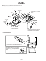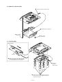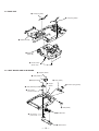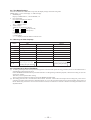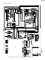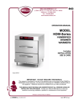
1
MDS-JA30ES
SERVICE MANUAL
US Model
Canadian Model
AEP Model
UK Model
Photo: GOLD
U.S. and foreign patents licensed from Dolby Laboratories
Licensing Corporation.
Model Name Using Similar Mechanism
MDS-JA50ES
MD Mechanism Type
MDM-4B
Base Unit Type
MBU-2B
Optical Pick-up Type
KMS-210A/J-N
SPECIFICATIONS
— Continued on next page —
MINIDISC DECK
MICROFILM
SAFETY CHECK-OUT
After correcting the original service problem, perform the
following safety checks before releasing the set to the customer:
Check the antenna terminals, metal trim, “metallized” knobs, screws,
and all other exposed metal parts for AC leakage. Check leakage as
described below.
LEAKAGE
The AC leakage from any exposed metal part to earth ground
and from all exposed metal parts to any exposed metal part having
a return to chassis, must not exceed 0.5 mA (500 microampers).
Leakage current can be measured by any one of three methods.
1.
A commercial leakage tester, such as the Simpson 229 or RCA
WT-540A. Follow the manufacturers’ instructions to use these
instruments.
2.
A battery-operated AC milliammeter. The Data Precision 245
digital multimeter is suitable for this job.
3.
Measuring the voltage drop across a resistor by means of a
VOM or battery-operated AC voltmeter. The “limit” indication
is 0.75 V, so analog meters must have an accurate low-voltage
scale. The Simpson 250 and Sanwa SH-63Trd are examples of
a passive VOM that is suitable. Nearly all battery operated
digital multimeters that have a 2V AC range are suitable. (See
Fig. A)
To Exposed Metal
Parts on Set
CAUTION
Danger of explosion if battery is incorrectly replaced.
Replace only with the same or equivalent type recommended by
the equipment manufacturer.
Discard used batteries according to manufacture’s instructions.
0.15µF
ADVARSEL!
1.5kΩ
AC
voltmeter
(0.75V)
Earth Ground
Lithiumbatteri - Eksplosionsfare ved fejlagtig håndtering.
Udskiftning må kun ske med batteri af samme fabrikat og type.
Levér det brugte batteri tilbage til leverandøren.
Fig. A. Using an AC voltmeter to check AC leakage.
SAFETY-RELATED COMPONENT WARNING!!
ADVARSEL
Eksplosjonsfare ved feilakting skifte av batteri.
Benytt samme batteritype eller en tilsvarende type anbefalt av
apparatfabrikanten.
Brukte batterier katterier kasseres i henhold til fabrikantens
COMPONENTS IDENTIFIED BY MARK ! OR DOTTED LINE WITH
MARK ! ON THE SCHEMATIC DIAGRAMS AND IN THE PARTS
LIST ARE CRITICAL TO SAFE OPERATION. REPLACE THESE
COMPONENTS WITH SONY PARTS WHOSE PART NUMBERS
APPEAR AS SHOWN IN THIS MANUAL OR IN SUPPLEMENTS
PUBLISHED BY SONY.
VARNIG
Explosionsfara vid felaktigt batteribyte.
Använd samma batterityp eller en likvärdig typ som rekommenderas
av apparattillverkaren.
Kassera använt batteri enligt gällande föreakrifter.
VAROITUS
Parist voi räjähtää, jos se on virheellisesti asennettu.
Vaihda paristo ainoastaan laitevalmistajan suosittelemaan tyyppiin.
Hävitä käytetty paristo valmistajan ohjeiden mukaisesti.
ATTENTION AU COMPOSANT AYANT RAPPORT
À LA SÉCURITÉ!
LES COMPOSANTS IDENTIFÉS PAR UNE MARQUE ! SUR LES
DIAGRAMMES SCHÉMATIQUES ET LA LISTE DES PIÈCES SONT
CRITIQUES POUR LA SÉCURITÉ DE FONCTIONNEMENT. NE
REMPLACER CES COMPOSANTS QUE PAR DES PIÈSES SONY
DONT LES NUMÉROS SONT DONNÉS DANS CE MANUEL OU
DANS LES SUPPÉMENTS PUBLIÉS PAR SONY.
—2—
TABLE OF CONTENTS
The laser component in this product is
capable of emitting radiation exceeding
the limit for Class 1.
This appliance is classified as a CLASS 1
LASER product. The CLASS 1 LASER
PRODUCT MARKING is located on the
rear exterior.
The following caution label is located
inside the unit.
CAUTION
Use of controls or adjustments or performance of procedures
other than those specified herein may result in hazardous
radiation exposure.
Notes on chip component replacement
• Never reuse a disconnected chip component.
• Notice that the minus side of a tantalum capacitor may be
damaged by heat.
Flexible Circuit Board Repairing
• Keep the temperature of soldering iron around 270˚C
during repairing.
• Do not touch the soldering iron on the same conductor of the
circuit board (within 3 times).
• Be careful not to apply force on the conductor when soldering
or unsoldering.
1.
SERVICING NOTE ······················································ 4
2.
GENERAL ······································································ 7
3.
DISASSEMBLY
3-1.
3-2.
3-3.
3-4.
3-5.
Tray Assembly ···································································· 8
Bracket (Motor) ASSY ······················································· 9
Holder ASSY ······································································ 9
Base Unit ·········································································· 10
HMOT Board and HLIM Board ······································· 10
4.
TEST MODE ································································ 11
5.
ELECTRICAL ADJUSTMENTS ··························· 14
6.
DIAGRAMS
6-1.
6-2.
6-3.
6-4.
6-5.
6-6.
6-7.
6-8.
6-9.
6-10.
6-11.
6-12.
6-13.
6-14.
6-15.
6-16.
BD Section ······································································· 19
Digital Section ·································································· 21
Audio Section ··································································· 23
Power Section ··································································· 25
Circuit Boards Location ··················································· 26
Printed Wiring Board — BD Section — ·························· 28
Schematic Diagram — BD Section — ····························· 31
Schematic Diagram — Digital Section — ······················· 35
Printed Wiring Board — Digital Section — ···················· 39
Printed Wiring Board — Audio Section — ······················ 42
Schematic Diagram — Audio Section — ························· 45
Schematic Diagram — Power Section — ························ 48
Schematic Diagram — Panel Section — ························· 51
Printed Wiring Board — Panel Section — ······················· 53
IC Block Diagrams ··························································· 56
IC Pin Functions ······························································· 61
7.
EXPLODED VIEWS
7-1.
7-2.
7-3.
7-4.
7-5.
7-6.
7-7.
7-8.
Main Section ····································································· 73
Chassis Section ································································· 74
Front Panel Section 1 ······················································· 75
Front Panel Section 2 ······················································· 76
Mechanism Section 1 (MDM-4B) ···································· 77
Mechanism Section 2 (MDM-4B) ···································· 78
Mechanism Section 3 (MDM-4B) ···································· 79
Base Unit Section (MBU-2B) ·········································· 80
8.
ELECTRICAL PARTS LIST ··································· 81
MODEL IDENTIFICATION
— BACK PANEL —
Parts No.
4-992-959-1
4-992-959-2
4-992-959-3
: AEP, UK, German model
: US model
: Canadian model
—3—
SECTION 1
SERVICING NOTE
HOW TO OPEN THE DISC TRAY WHEN POWER SWITCH TURNS OFF
1 Remove the sixteen screws (BVTT 3×8) from the bottom plate.
2 Remove the bottom plate.
3 Rotate the pulley gear in the arrow direction A, and open the tray assembly in the arrow direction B.
Pully gear
A
B
Tray assembly
Forced Reset
The system microprocessor can be reset in the following way.
Use these methods when the unit cannot be operated normally due to the overrunning of the microprocessor, etc.
Method 1:
Set TP (S.RST) of the DIG board to ground momentarily.
Method 2:
Disconnect the power plug, and short-circuit CN905 of the PW board
with a pair of tweezers, etc.
[DIG board] (Side A)
[PW board] (Component Side)
CN905
(RESET)
CN203
TP
(S.RST)
CN901
C206
IC202
—4—
Retry Cause Display Mode
• In this test mode, the causes for retry of the unit during recording can be displayed on the fluorescent display tube.
This is useful for locating the faulty part of the unit.
• The retry cause, number of retries, and number of retry errors are displayed. Each is displayed in hexadecimal number.
Method:
1. Load a recordable disc whose contents can be erased into the unit.
2. Press the p button, §OPEN/CLOSE button, DISPLAY/CHAR button simultaneously.
3. Press the r button, and start recording.
4. The ## value increases with each retry. If an error occurs after a retry, the @@ count will also increase.
5. To exit the test mode, press the TIME button.
Fig. 1 Reading the Test Mode Display
R.T s ∗ ∗ c # # e @@
Fluorescent Display Tube Signs
∗ ∗ : Cause of retry
# # : Number of retries
@@ : Number of retry errors
All three displays above are in hexadecimal numbers.
—5—
Reading the Retry Cause Display
Higher Bits
Hexadecimal 8
Bit
Binary
4
2
1
Lower Bits
8
4
2
1
b7 b6 b5 b4 b3 b2 b1 b0
Hexa-
Cause of Retry
decimal
Occurring conditions
0
0
0
0
0
0
0
1
01
shock *1
When more than 3.5 shocks are detected
0
0
0
0
0
0
1
0
02
ader5
0
0
0
0
0
1
0
0
04
Discontinuous address
When ADIP address is not continuous
0
0
0
0
1
0
0
0
08
(Not used)
(Not used)
0
0
0
1
0
0
0
0
10
FCS incorrect
When not in focus
0
0
1
0
0
0
0
0
20
IVR rec error
When ABCD signal level exceeds the specified range
0
1
0
0
0
0
0
0
40
Spindle is slow
When spindle rotation is detected as slow
1
0
0
0
0
0
0
0
80
Access fault
When access operation is not performed normally
When ADER was counted more than
five times continuously
*1 Some displays are not used depending on the microprocessor version.
Reading the Display:
Convert the hexadecimal display into binary display. If more than two causes, they will be added.
Example
When 42 is displayed:
Higher bit : 4 = 0100 n b6
Lower bit : 2 = 0010 n b1
In this case, the retry cause is combined of “spindle is slow” and “ader5”.
When A2 is displayed:
Higher bit : A = 1010 n b7+b5
Lower bit : 2 = 0010 n b1
The retry cause in this case is combined of “access fault”, “IVR rec error”, and “ader5”.
Hexadecimal n Binary Conversion Table
Hexadecimal
Binary
Hexadecimal
Binary
0
0000
8
1000
1
0001
9
1001
2
0010
A
1010
3
0011
B
1011
4
0100
C
1100
5
0101
D
1101
6
0110
E
1110
7
0111
F
1111
Reference:
In this test mode, when the · button is pressed, and the disc is played back, the “PLAYBACK MODE” is set.
The display becomes as shown in Fig. 2. The playback mode is not used in particular during servicing.
44
¢¢¢¢¢¢
p
Fig. 2 Display during Playback Mode
44 : Parts No. (Name of area named on TOC)
¢¢¢¢¢¢ : Address (Physical address on disc)
p : Track mode (Copyright information of each part, information on copyright, etc.)
—6—
SECTION 2
GENERAL
1
2
3
4
5
6
7
8
9
POWER switch
Remote sensor
TIMER switch
FILTER button
SCROLL/CLOCK SET button
DISPLAY/CHAR button
Disc tray
0/) (fast backward/fast forward) buttons
EDIT/NO/YES buttons
!º AMS knob
!¡ DIGITAL REC LEVEL knob
!™ ANALOG REC LEVEL L/R knob
!£
!¢
!∞
!§
!¶
!•
!ª
@º
@¡
@™
@£
@¢
—7—
r REC (recording) button
p (stop) button
P (pause) button
( (play) button
§ OPEN/CLOSE button
Display window
TIME button
REPEAT button
PLAY MODE button
INPUT switch
PHONE LEVEL knob
PHONES jack
This section is extracted
from instruction manual.
SECTION 3
DISASSEMBLY
Note : Follow Xthe disassembly procedure in the numerical order given.
3-1. TRAY ASSEMBLY
2 Two screws
(PTP 2.6x6)
3 Two screws
(PTP 2.6x6)
9 Shaft
4 Bracket
(TOP)
1 Rotate the pulley gear in the arrow
direction A, and pull out the tray
assembly.
A
5 Gear 4
(Two gear)
7 Screw
(BVTT 3x6)
8 Stopper
(Shaft A)
6 Gear 4
(Two gear)
Bracket (TOP)
B
0 Remove the tray assembly
in the arrow direction B.
Note:
When attaching the bracket (TOP), attach while
pressing the switch as shown in the figure.
• Precautions on Attaching
(Assemble in the reverse order of removal.)
Slider assembly
Pin A
B
When attaching the tray assembly, first move the slider
assembly in the arrow direction Band set Pin Aat the
position shown.
A
When attaching gear 4 (two in front), pull the tray
assembly in arrow direction A completely, and
position racks (L), (R) and (D) as shown in the
figure.
Hole
Rack (L)
Rack (D)
Gear 4
—8—
3-2. BRACKET (MOTOR) ASSY
3 Connector (CN198 : HMOT board)
4 Bracket (Motor) assembly
1 Two screws
(BVTT 3x6)
2 Two screws
(BVTT 3x6)
3-3. HOLDER ASSY
Slider assembly
Shaft A
1 When removing, move the slider assembly
in the arrow direction, and check that shaft
A is at the position shown in the figure.
2 Connector
(CN198 :
HMOT board)
3 Remove the four screws (BVTT 3x6), and
remove the four collars (dampers) and four
compression springs.
—9—
3-4. BASE UNIT
1 Leaf spring (UDL)
2 Leaf spring (UDR)
3 Holder assembly
5 Base unit
(MBU-2B)
4 Three screws
(BVTP 3x6)
3-5. HMOT BOARD AND HLIM BOARD
5 Stopper washer
6 Gear (HEAD C)
7 Stopper washer
8 Gear (HEAD B)
3 Lever (OWH)
1 Stopper
washer
4 Torsion spring (OWH)
9 Two screws
(Precision P2x3)
2 Shaft (OWH)
!™ HLIM board
!¡ Two screws
(PTP 2.6x6)
!º HMOT board
— 10 —
SECTION 4
TEST MODE
4-1. Setting the Test Mode
While pressing the AMS knob, insert the power plug into the power supply inlet, and release the AMS knob.
4-2. Exiting the Test Mode
Press the REPEAT button. Unplug the power plug from an outlet.
4-3. Basic Operations of the Test Mode
All operations are performed using the AMS knob, YES button, and NO button.
The functions of these buttons are as follows.
Contents
Function
AMS knob
Changes parameters and modes
YES button
Proceeds onto the next step. Finalizes input.
NO button
Returns to previous step. Stops operations.
Test Mode initial display
4-4. Selecting the Test Mode
Eight test modes are selected by turning the AMS knob.
Display
Contents
TEMP ADJUS
Temperature compensation offset adjustment
LDPWR ADJUS
Laser power adjustment
EFBAL ADJUS
Traverse adjustment
FBIAS ADJUS
Focus bias adjustment
FBIAS CHECK
Focus bias check
CPLAY MODE
Continuous playback mode
CREC MODE
Continuous recording mode
EEP MODE
Non-volatile memory mode *
For detailed description of each adjustment mode, refer to 5. Electrical Adjustments.
If a different adjustment mode has been selected by mistake, press the NO button to exit from it.
* The EEP MODE is not used in servicing. If set accidentally, press the NO button immediately to exit it.
4-4-1. Operating the Continuous Playback Mode
1. Entering the continuous playback mode
1 Set the disc in the unit (either MO or CD).(MO: Recordable disc, CD: Disc for playback only).
2 Rotate the AMS knob and display “CPLAY MODE”.
3 Press the YES button to change the display to “CPLAY IN”.
AD = – –”.
4 When access completes, the display changes to “C =
Note : The “ ” displayed are arbitrary numbers.
2. Changing the parts to be played back
1 Press the YES button during continuous playback to change the display to “CPLAY MID”, “CPLAY OUT”.
When pressed another time, the parts to be played back can be changed.
AD = – –”.
2 When access completes, the display changes to “C =
Note : The “ ” displayed are arbitrary numbers.
3. Ending the continuous playback mode
1 Press the NO button. The display will change to “CPLAY MODE”.
2 Press the §OPEN/CLOSE button and remove the disc.
Note 1 : The playback start addresses for IN, MID, and OUT are as follows.
IN
40h cluster
MID 300h cluster
OUT 700h cluster
— 11 —
4-4-2. Operating the Continuous Recording Mode
1. Entering the continuous recording mode
1 Set the MO disc in the unit.
2 Rotate the AMS knob and display “CREC MODE”.
3 Press the YES button to change the display to “CREC IN”.
4 When access completes, the display changes to “CREC (
” an REC lights up.
Note : The “ ” displayed are arbitrary numbers.
2. Changing the parts to be recorded
1 When the YES button is pressed during continuous recording, the display changes to “CREC MID”, “CREC OUT” and REC goes
off.
When pressed another time, the parts to be recorded can be changed.
2 When access completes, the display changes to “CREC (
” and REC lights up.
Note : The “ ” displayed are arbitrary numbers.
3. Ending the continuous recording mode
1 Press the NO button. The display changes to “CREC MODE” and REC goes off.
2 Press the §OPEN/CLOSE button and remove the disc.
Note 1 : The recording start addresses for IN, MID, and OUT are as follows.
IN
40h cluster
MID 300h cluster
OUT 700h cluster
Note 2 : The NO button can be used to stop recording anytime.
Note 3 : During the test mode, the erasing-protection tab will not be detected. Therefore be careful not to set the continuous recording
mode when a disc not to be erased is set in the unit.
Note 4 : Do not perform continuous recording for long periods of time above 5 minutes.
Note 5 : During continuous recording, be careful not to apply vibration.
4-4-3. Non-Volatile Memory Mode
This mode reads and writes the contents of the non-volatile memory.
It is not used in servicing. If set accidentally, press the NO button immediately to exit it.
4-5. Functions of Other buttons
Function
Contents
·
Sets continuous playback when pressed in the STOP state. When pressed during continuous playback, the tracking servo turns ON/OFF.
p
Stops continuous playback and continuous recording.
)
The sled moves to the outer circumference only when this is pressed.
0
The sled moves to the inner circumference only when this is pressed.
r
Turns recording ON/OFF when pressed during continuous playback.
SCROLL/
Switches between the pit and groove modes when pressed.
CLOCK SET
PLAY MODE
Switches the spindle servo mode (CLVS and A).
DISPLAY/
Switches the display when pressed.Returns to previous step. Stops operations.
CHAR
Note : The erasing-protection tab is not detected during the test mode. Recording will start regardless of
the position of the erasing-protection tab when the r button is pressed.
— 12 —
4-6. Test Mode Displays
Each time the DISPLAY/CHAR button is pressed, the display changes in the following order.
MODE display n Error rate display n Address display
1. MODE display
Displays “TEMP ADJUS”, “CPLAY MODE”, etc.
2. Error rate display
Error rates are displayed as follows.
AD =
C=
C = : Indicates C error
AD = : Indicates ADER
3. Address display
Addresses are displayed as follows.
“h
s
” (MO pit and CD)
“h
a
” (MO groove)
h : Header address
s : SUBQ address
a : ADIP address
* “—” is displayed when the address cannot be read.
4-7. Meanings of Other Displays
Contents
Display
Light
Off
·
During continuous playback
STOP
P
Tracking servo OFF
Tracking servo ON
REC
Recording mode ON
Recording mode OFF
CLOCK
CLV LOCK
CLV UNLOCK
TRACK
Pit
Groove
DISC
High reflection
Low reflection
DATE
CLV-S
CLV-A
A. SPACE
ABCD adjustment completed
A–B
Focus auto gain successful
Blinking
Focus auto gain successful
Tracking auto gain failed
Tracking auto gain successful
4-8. Precautions for Use of Test Mode
1 As loading related operations will be performed regardless of the test mode operations being performed, be sure to check that the disc is
stopped before setting and removing it.
Even if the §OPEN/CLOSE button is pressed while the disc is rotating during continuous playback, continuous recording, etc., the disc
will not stop rotating.
Therefore, it will be ejected while rotating.
Always press the NO button first before pressing the §OPEN/CLOSE button.
2 The erasing-protection tab is not detected in the test mode. Therefore, when modes which output the recording laser power such as
continuous recording mode and traverse adjustment mode, etc. are set, the recorded contents will be erased regardless of the position of
the tab. When using a disc that is not to be erased in the test mode, be careful not to enter the continuous recording mode and traverse
adjustment mode.
— 13 —
SECTION 5
ELECTRICAL ADJUSTMENTS
Precautions for Checking Laser Diode Emission
Precautions for Adjustments
To check the emission of the laser diode during adjustments, never
view directly from the top as this may lose your eye-sight.
1)
When replacing the following parts, perform the adjustments
and checks with ® in the order shown in the following table.
Optical
Pick-up IC171
Precautions for Use of optical pick-up (KMS-210A)
As the laser diode in the optical pick-up is easily damaged by static
electricity, solder the laser tap of the flexible board when using it.
Before disconnecting the connector, desolder first. Before
connecting the connector, be careful not to remove the solder. Also
take adequate measures to prevent damage by static electricity.
Handle the flexible board with care as it breaks easily.
BD Board
D101
IC101, IC121, IC191
¬
¬
¬
¬
G
G
¬
3. Traverse
adjustment
¬
¬
G
¬
4. Focus bias
adjustment
¬
¬
G
¬
5. Error rate check
¬
¬
G
¬
1. Temperature
compensation
offset adjustment
G
2. Laser power
adjustment
2)
laser tap
Optical pick-up flexible board
• Abbreviation
MO : Recordable disc
CD : Disc for playback only
Set the test mode when performing adjustments.
After completing the adjustments, exit the test mode.
3) Perform the adjustments in the order shown.
4) Use the following tools and measuring devices.
• Check Disc (CD) TGYS-1
(Parts No. 4-963-646-01)
• Laser power meter LPM-8001 (Parts No. J-2501-046-A)
• Oscilloscope
• Digital voltmeter
• Thermometer
5) When observing several signals on the oscilloscope, etc.,
make sure that VC and ground do not connect inside the
oscilloscope.
(VC and ground will become short-circuited.)
Creating Continuously Recorded Disc
* This disc is used in focus bias adjustment and error rate check.
The following describes how to create a continuous recording
disc.
1. Insert a MO disc (blank disc) commercially available.
2. Rotate the AMS knob and display “CREC MODE”.
3. Press the YES button and display “CREC IN”.
4. Press the YES button again to display “CREC MID”.
“CREC (0300” is displayed for a moment and recording starts.
5. Complete recording within 5 minutes.
6. Press the NO button and stop recording .
7. Press the §OPEN/CLOSE button and remove the MO disc.
The above has been how to create a continuous recording data for
the focus bias adjustment and error rate check.
Note :
• Be careful not to apply vibration during continuous recording.
— 14 —
Temperature Compensation Offset Adjustment
Laser Power Adjustment
Save the temperature data at that time in the non-volatile memory
as 25 ˚C reference data.
Note :
1. Usually, do not perform this adjustment.
2. Perform this adjustment in an ambient temperature of 22 ˚C to
28 ˚C. Perform it immediately after the power is turned on
when the internal temperature of the unit is the same as the
ambient temperature.
3. When D101 has been replaced, perform this adjustment after
the temperature of this part has become the ambient
temperature.
Adjusting Method :
1. Rotate the AMS knob and display “TEMP ADJUS”.
2. Press the YES button and select the “TEMP ADJUS” mode.
3. “TEMP =
” and the current temperature data will be
displayed.
4. To save the data, press the YES button.
When not saving the data, press the NO button.
5. When the YES button is pressed, “TEMP =
SAV” will be
displayed for some time, followed by “TEMP ADJUS”.
When the NO button is pressed, “TEMP ADJUS” will be
displayed.
Connection :
Specifications :
The “TEMP =
” should be within “E0 - EF”, “F0 - FF”, “00 0F”, “10 - 1F” and “20 - 2F”.
Laser power
meter
Optical pick-up
objective lens
Digital voltmeter
BD board
TP (I + 5V)
TP (IOP)
Adjusting Method :
1. Set the laser power meter on the objective lens of the optical
pick-up. (When it cannot be set properly, press the 0 button
or ) button and move the optical pick-up.)
Connect the digital volt meter to TP (IOP) and TP (I+5V).
2. Rotate the AMS knob and display “LDPWR ADJUS”.
(Laser power : For adjustment)
3. Press the YES button twice and display “LD $ 4B = 3.5 m”.
4. Adjust RV102 of the BD board so that the reading of the laser
power meter becomes 3.45 ± 0.1mW.
5. Press the YES button and display “LD $ 96 = 7.0 m”.
(Laser power : MO writing)
6. Check that the laser power meter and digital voltmeter readings
satisfy the specified value.
Specification :
0.2
Laser power meter reading : 7.0 –+ 0.3
mW
Digital voltmeter reading : Optical pick-up displayed value ± 10%
(Optical pick-up label)
210A
27X40
B0825
KMS
lop = 82.5 mA in this case
lop (mA) = Digital voltmeter reading (mV)/ 1 (Ω)
7.
8.
Press the YES button and display “LD $ 0F = 0.7 m”.
(Laser power : MO reading)
Check that the laser power meter at this time satisfies the
specified value.
Specification :
0.05
Laser power meter reading : 0.70 –+ 0.1
mW
9.
— 15 —
Press the NO button and display “LDPWR ADJUS”, and stop
laser emission.
(The NO button is effective at all times to stop the laser
emission.)
Traverse Adjustment
servo is imposed.
11. Rotate the AMS knob until the waveform of the oscilloscope
moves closer to the specified value.
In this adjustment, waveform varies at intervals of approx. 3%.
Adjust the waveform so that the specified value is satisfied as
much as possible.
Connection :
Oscilloscope
BD board
TP (TEO)
TP (VC)
A
VC
Adjusting method :
1. Connect an oscilloscope to TP (TEO) and TP (VC) of the BD
board.
2. Load a MO disc (any available on the market).
3. Press the 0 button or ) button and move the optical pickup outside the pit.
4. Rotate the AMS knob and display “EFBAL ADJUS”.
5. Press the YES button and display “EFBAL MO-W”.
(Laser power WRITE power/Focus servo ON/tracking servo
OFF/spindle (S) servo ON)
6. Adjust RV101 of the BD board so that the waveform of the
oscilloscope becomes the specified value.
(MO groove write power traverse adjustment)
(Traverse Waveform)
A
VC
B
Specification A=B
(Traverse Waveform)
12. Press the YES button, display “EFB = $ SAV” for a moment
and save the adjustment results in the non-volatile memory.
Next “EFBAL CD” is displayed. The disc stops rotating
automatically.
13. Press the §OPEN/CLOSE button and remove the MO disc.
14. Load the check disc (MD) TDYS-1.
15. Press the YES button and display “EFB = $ CD”. Servo is
imposed automatically.
16. Rotate the AMS knob so that the waveform of the oscilloscope
moves closer to the specified value.
In this adjustment, waveform varies at intervals of approx. 3%.
Adjust the waveform so that the specified value is satisfied as
much as possible.
B
Specification A = B
7.
8.
A
Press the YES button and display “EFB = $ MO-R”.
(Laser power : MO reading)
Rotate the AMS knob so that the waveform of the oscilloscope
becomes the specified value.
(When the AMS knob is rotated, the of “EFB = $ ” changes
and the waveform changes.) In this adjustment, waveform
varies at intervals of approx. 3%. Adjust the waveform so that
the specified value is satisfied as much as possible.
(MO groove read power traverse adjustment)
A
VC
B
Specification A=B
(Traverse Waveform)
17. Press the YES button, display “EFB = $ SAV” for a moment
and save the adjustment results in the non-volatile memory.
Next “EFBAL ADJUS” is displayed.
18. Press the §OPEN/CLOSE button and remove the test disc
TDYS-1.
Note 1 : Data will be erased during MO reading if a recorded disc
is used in this adjustment.
Note 2 : If the traverse waveform is not clear, connect the
oscilloscope as shown in the following figure so that it
can be seen more clearly.
VC
B
Specification A=B
(Traverse Waveform)
9. Press the YES button, display “EFB = $ SAV” for a moment
and save the adjustment results in the non-volatile memory.
Next “EFBAL MO-P” is displayed.
10. Press the YES button and display “EFB = $ MO-P”.
The optical pick-up moves to the pit area automatically and
— 16 —
Oscilloscope
BD board
TP (TEO)
TP (VC)
330kΩ
10pF
MDS-JA30ES
Focus Bias Adjustment
Error Rate Check
CD Error Rate Check
Adjusting Method :
1. Load a continuously recorded disc (Refer to “Page 14 Creating
Continuously Recorded Disc”.).
2. Rotate the AMS knob and display “CPLAY MODE”.
3. Press the YES button twice and display “CPLAY MID”.
4. Press the NO button when “C =
AD =
” is displayed.
5. Rotate the AMS knob and display “FBIAS ADJUS”.
6. Press the YES button and display “
/
a=
”.
The first four digits indicate the C1 error rate, the two digits
after [/] indicate ADER, and the 2 digits after [a =] indicate the
focus bias value.
7. Rotate the AMS knob in the clockwise direction and find the
focus bias value at which the C1 error rate becomes 220.
8. Press the YES button and display “
/
b=
”.
9. Rotate the AMS knob in the counterclockwise direction and
find the focus bias value at which the C1 error rate becomes
220.
/
c=
”.
10. Press the YES button and display “
11. Check that the C1 error rate is below 50 and ADER is 00. Then
press the YES button.
12. If the “(
” in “
(
” is above 20, press the
YES button.
If below 20, press the NO button and repeat the adjustment
from step 2 again.
13. Press the NO button and press the §OPEN/CLOSE button to
remove the continuously recorded disc.
Note 1 : The relation between the C1 error and focus bias is as
shown in the following figure. Find points a and b in the
following figure using the above adjustment. The focal
point position C is automatically calculated from points a
and b.
Note 2 : As the C1 error rate changes, perform the adjustment using
the average value.
C1 error
220
Focus bias av lue
(F. BIAS)
b
c
a
Adjusting Points and Connecting Points
[BD BOARD] (SIDE A)
Checking Method :
1. Load a check disc TGYS-1.
2. Rotate the AMS knob and display “CPLAY MODE”.
3. Press the YES button twice and display “CPLAY MID”.
4. “C =
AD =
” is displayed.
5. Check that the C1 error rate is below 20.
6. Press the NO button, stop playback, press the §OPEN/CLOSE
button, and remove the test disc.
D101
MO Error Rate Check
Checking Method :
1. Load a continuously recorded disc (Refer to “Page 14 Creating
Continuously Recorded Disc”.).
2. Rotate the AMS knob and display “CPLAY MODE”.
3. Press the YES button twice and display “CPLAY MID”.
4. “C =
AD =
” is displayed.
5. If the C1 error rate is below 50, check that ADER is 00.
6. Press the NO button, stop playback, press the §OPEN/CLOSE
button, and remove the continuously recorded disc.
Focus Bias Check
Change the focus bias and check the focus tolerance amount.
Checking Method :
1. Load a continuously recorded disc (Refer to “Page 14 Creating
Continuously Recorded Disc”.).
2. Rotate the AMS knob and display “CPLAY MODE”.
3. Press the YES button twice and display “CPLAY MID”.
AD =
” is displayed.
4. Press the NO button when “C =
5. Rotate the AMS knob and display “FBIAS CHECK”.
6. Press the YES button and display “
/
c=
”.
The first four digits indicate the C1 error rate, the two digits
after [/] indicate ADER, and the 2 digits after [c =] indicate the
focus bias value.
Check that the C1 error is below 50 and ADER is 00.
7. Press the YES button and display “
/
b=
”.
Check that the C1 error is not below 220 and ADER is not
above 00 every time.
8. Press the YES button and display “
/
a=
”.
Check that the C1 error is not below 220 and ADER is not
above 00 every time.
9. Press the NO button, next press the §OPEN/CLOSE button,
and remove the continuously recorded disc.
Note 1 : If the C1 error and ADER are above 00 at points a or b,
the focus bias adjustment may not have been carried out
properly. Adjust perform the beginning again.
IC191
[BD BOARD] (SIDE B)
(IOP)
(I + 5V)
IC101
RV101
(VC)
IC171
RV102
(TEO)
IC121
— 17 —
— 18 —
MDS-JA30ES
SECTION 6
DIAGRAMS
6-1. BLOCK DIAGRAM — BD SECTION —
DIGITAL SIGNAL PROCESSOR,
DIGITAL SERVO SIGNAL PROCESSOR,
EFM/ACIRC ENCODER/DECODER
IC121
HEAD
DRIVE
14
15
OVER WRITE
HEAD DRIVE
IC181
46 45 44 43
9
4
IV-AMP
IV-AMP
F
C B
D A
RF
RF AGC
& EQ
IC172
J
48
I
47
1
7
BUFFER
RF AMP
AUX
AUX
SW
BPF
A
B
C
D
E
F
2
3
4
5
6
7
E
6
VC
RV101
E-F
BALANCE
8
PEAK
ABCD
ABCD
AMP
FOCUS
ERROR
AMP
IV AMP
FE
ADFM
AT
AMP
ADIN
VC
+2.5V
GENERATOR
TEMPR
D101
10
TEMP
AMP
HIGH
POWER
LD
PD
APCREF
TLB
SERIAL
APC
PARALLEL
DECODER
XRST
SWDT
SCLK
XLAT
17 18 19 20
4
IC122
2
Q164
HF
MODULE
SWITCH
M101
SLED
MOTOR
M
M102
SPINDLE
MOTOR
M
2
SLED+
SLED–
SPDL+
SPDL–
2
:
:
:
:
PB
REC
PB (Digital out)
REC (Digital in)
DTI
30
DATA
C2PO
29
31
35
L OUT
L IN
M
32K RAM
SPFD
94
SPRD
93
C2PO
M191
LOADING MOTOR
M192
HEAD MOTOR
PLL
HU
HD
M
BCK
LRCK
FS4
XTAI
TIMING
GENERATOR
&
CLOCK
GENERATOR
DIGITAL
CLV
PROCESSOR
BCK
LRCK
32
33
90
35
SENS
SRDT
XLAT
SCLK
SWDT
30
31
ADFG
26
29
P-P
27
5
TFIL
25
THID
4
ADIP
DEMOD
82
2
VC
VC
23
68
65
64
66
67
77
76
69
ADIP
DECODER
SCTX
SQSY
AUX
BOTM
PEAK
ABCD
FE
TE
SE
ANALOG
MUX
A/D
CONV
5
PROCESSOR
DFCT
FOK
SHCK
OFTRK
COUT
512FS
DFCK
FOK
SHCK
FG
3
2
4
98
99
VC
6
TENV 22
4
SWDT
8
SCLK
9
XLAT
10
XRST
16
APC
PWM
GEN
CPU
IF
REC
SRDT
DIRC
LD
LDDR
LIMIT
84
SERVO DSP/PWM GENERATOR
FOCUS/TRACKING/
SLED SERVO & PWM
SERVO
CONTROL
WRPWR
S101
LIMIT IN
SW191
LOAD IN DET
INSW
SW192
LOAD OUT DET
OUTSW
SW193
HEAD DOWN
DET
HDS
SW194
HEAD UP DET
HUS
SLED/SPINDLE MOTOR DRIVE,
FOCUS/TRACKING COIL DRIVE
IC151
PROTECT
REFLECT
DRIVER
31
32
8
11
DRIVER
5
6
15
13
DRIVER
17
18
22
24
DRIVER
19
20
CLOCK
DETECTOR
Signal Path
ECC
ENCODER
DECODER
DTO
6
TRK–
26
TRK+
29
FCS+
FCS–
AUDIO
DATA
CONTROL
REGISTER
3
SERVO
AUTO
SEQUENCER
TFDR
TRDR
SENS
CONTROL
-1
SENS
2
DODT
37
7
2
FOCUS
COIL
EFM
TIMING
GENERATOR
24
11
L.F
MOD
TRACKING
COIL
CLTV
60
FILI
62
PCO
61
FILO
63
4
APC
H.F
MOD
27
WRPWR
14 15
Q162,163
EFM
MOD/DEMOD
4
IC102
AAPC
DAPC
11
TE
SE
TRACKING
ERROR
AMP
+5V
TEMPI
12
PD
38
39
33
VC
16
28
5
FO
1
Q101
LASER ON
SWITCH
34
EFMO
45
RFI
58
FI
9
RV102
LASER
POWER
41
5
IV AMP
DODT
IC182
FILTER
BOTM
PEAK &
BOTTOM
6
I
1
DIGITAL
AUDIO
IN/OUT
DIN
PLL
RF AMP
IC101
42
VC
2
3
6
5
17
DIDT
SUBCODE
PROCESSOR,
READER/
GENERATOR
2
15 21 20
FRDR
FFDR
12
-2
S102-1
PROTECT
S102-2
REFLECT
IC171
MEMORY
85 86 87 89 91 92
SDA 5
SCL 6
SFDR
SRDR
SPFD
SPRD
TRDR
TFDR
FFDR
FRDR
SRDR
SFDR
OPTICAL PICK-UP BLOCK
(KMS-210A/J-N)
16
SQSY
19
+5V
J
2
3
11
51 52 49 53
DQSY
DIN
DOUT
HR901
OVER
WRITE
HEAD
DOUT
14
DICV
DIFI
DIPD
DIFO
18
Q181,182
FILTER
SDA
SCL
6
XRST
8
FS4
33
Q151
RESET
SWITCH
LDON
REC
MOD
— 19 —
— 20 —
A
DIGITAL
SECTION
(Page 21)
MDS-JA30ES
6-2. BLOCK DIAGRAM — DIGITAL SECTION —
DOUT
ADIN
DOUT
DODT
ATRAC ENCODER/DECODER
IC206
41
42
ALRCK
ABCK
7
DATAO
ATT
SAMPLING
RATE
CONVERTER
OVER
SAMPLING
FILTER
I/F
LRCKI
BCKI
2
52
•
56
FIMCK
SAMPLING
RATE
DETECTOR
CPU
TIMING
CONTROL
FIMO
52
53
2
16
4
14
6
DATAO
23
DATA
MODULATION
LRCK
22
BCK
21
PLL
IC205
SCK
3
SYSTEM
CONTROLLER
SRDT
1
SWDT
TEST1
INIT
58
7
XO
XI
AIRCPB
26
28
5
6
4
17
7
13
5
15
9
11
12
BCKO 22
11
3
2 3 4 5 6 7 8 9 11 17 26
37
SUBQ
DET
10
14 15 16 17 18 24
8
ABCK
SWDT
SCK
XLAT
SRDT
SENSE
SCMD0
SCMD1
XINT
WRMN
XRST
OSCI
OSCO
36
XLAT
9
CLOCK
GENERATOR
1
MICON
I/F
55
LRCKO 23
SPO
DIN1
INPUT
C
BIT
DET
TIMING
CKOUT
19
54
4
XCAS
XRAS
XWE
CPU
INTERFACE
87
18
XOE
DRAM
IC208
512FS
DATAI
51
13
2CE
19
44
43
IIR
DECIMATION
FILTER
EROR
60
•
65
61
62
66
67
RAM
INTERFACE
21
SCLK
XLAT
SWDT
SRDT
A9 15
•
5
OE 16
CAS 17
RAS 4
WE 3
DOUT
ADIN
4
16
XMODE
69
•
68
•
70
•
71
55
95
94
SCLK
XLAT
SWDT
SRDT
DQSY
DQ1 1
•
2
•
18
•
DQ4 19
6
A0
9
•
11
ATRAC
ENCODER
/DECODER
ATRAC
INTERFACE
AVOCK
C2PO
EFM
DATA
INTERFACE
DODT
DIDT
DIGITAL AUDIO INTERFACE RECEIVER
IC203
IC205
ALRCK
12
93
90
91
97
92
SAMPLING RATE CONVERTER, DIGITAL FILTER
IC207
BUFFER
IC210
SRDT
SCTX
DATA
LRCK
BCK
DFCK
TX
DATA
LRCK
BCK
MIN
C2PO
ALRCK
ABCK
2
A
BD
SECTION
(Page 20)
4
4
4
7
1
MOTOR
DRIVE
5
4
2
1 CLK Q 3
2 D
Q 5
256FS
4
DIGITAL
REC
LEVEL
5
4
RESET
SWITCH
Q202
RESET
SWITCH
Q201
DIGITAL OUT
SELECTOR
IC351
SQSY
FOK
SHCK
WRPWR
SENS
LDON
REC
MOD
FG
74
75
5
67
69
70
71
76
79
61
66
68
SWDT
SCLK
XLATCH
SRDT
DIG-RST
44
14
S1
POWER DOWN
FLDATA
FLCLK
FLCS
19
35
37
38
13
16
15
14
RST
SDATA
SCK
CS
S36 23
D1 12
D16
SYSTEM CONTROL
IC202
SQSY
SCTX
FOK
SHCK
WRPWR
SENS
LDON
REC/PB
MOD
FG
PLAY
•
REC
•
PAUSE
•
DF
•
POWER
FL701
FLUORESCENT
INDICATOR
TUBE
61
95LAT
95RST
62RST
ADRST
ADLAT
KEY
MATRIX
X202
32.768KHz
D701-704,
781
X201
10MHz
S702
JOG0
JOG1
3
4
ROTARY
ENCODER
16
REMOCON
— 21 —
6
1
OUT
DIGITAL
IN
3
OPT2
1
DIGITAL
OUT
OPTICAL
42 40 41
95
LED
DRIVER
Q701-704,
781
OPT1
TO
F1
POWER
F2 TRANSFORMER
90
84
•
86
•
88
•
100
•
83
IC356
13
COAXIAL
IC354
KEY1
KEY3
•
KEY0
•
TIMER
•
SORCE
IC355
1
3
59
33
•
31
1
•
64
SDA
SCL
4
10
1
FL DRIVER
IC701
5
2 14
12
45
SEL
37RST
97
SRC TEST
XINT
20 43
SRCRST
LDIN
24
DVOL
72
DQSY
EROR
31 33 30 32
04LAT
58
LDOUT
INSW
OUTSW
HDOWNS
HUPS
PROTECT
REFLECT
LIMIT-IN
23
J351
8
DIN/XMD
COAX/XOPT
OPT1/XOPT2
SDA
SCL
52
51
60
59
77
78
80
54 55
HUP
HDWN
13
56 57
3
4
5
6
SEL0
MOTOR
DRIVE
7
RV602
SEL1
7
1
IC353
CLOCK DIVIDER
HEAD MOTOR DRIVE
IC212
INSW
OUTSW
HD
HU
PROTECT
REFLECT
LIMIT
ATT(SW DT)
SHIFT(SCLK)
IC213
4
DIGITAL IN SELECTOR
IC352
HD
HU
2
AUDIO
SECTION
(Page 23)
LOADING
MOTOR DRIVE
IC201
IC211
LDOUT
LDIN
B
XRST
1024FS
XRST
SWDT
SCLK
XLAT
SRDT
S702
AMS
PUSH ENTER
REMOTE CONTROL
RECEIVER
IC781
10
XIN-T
11
XOUT-T
13
XOUT
15
XIN
27
26
25
28
29
LATCH
95RST
Signal Path
:
:
:
:
P. DOWN
DA-MUTE
STB
S.RST
DA-MUTE 49
STB 50
SYSTEM-RST 12
C
POWER
SECTION
(Page 25)
— 22 —
PB
REC
PB (Digital out)
REC (Digital in)
MDS-JA30ES
6-3. BLOCK DIAGRAM — AUDIO SECTION —
D/A CONVERTER
IC502
NOISE SHAPER, DIGITAL FILTER
IC501
S/P
LRCKI
ATT
FIR
IIR
MODE
47 48 49
NSDOL1-4
6
|
3
S/P
46
4
46
|
49
L1(+)
62
L1(–)
60
L2(+)
2
L2(–)
4
PLM
IN1+
25
IN1–
24
IN2+
27
IN2–
28
SWITCHING
CIRCUIT
IO1+
IO2–
IO1–
IO2+
1
2
4
5
+
6
LPF
7
+
2
LPF
1
3rd ORDER
NOISE SHAPER
DINIT 33
50
64FSI 12
40
256FSO
9
X501
45MHz
L
HEADPHONE
AMP
IC651
3
1
B
RCH
1024FS
RV651
PHONE
LEVEL
RY501
+
LPF
21
_
DAC
+
1
7
19 L/R
LINE AMP
IC305
L.P.F., PRE AMP
IC303
A/D CONVERTER
IC302
ADIN
2
3
6
5
PJ501
LINE
OUT
J651
PHONES
MUTE
Q651,654
HP MUTE
D
PJ501
1
3
7
5
L
+5V
RELAY
DRIVE
Q505
LINE
IN
RELAY
RV601
ANALOG
REC
LEVEL
R CH is omitted.
Signal path
MCLK
: PB
17
: REC
256FS
16
— 23 —
1
LVCK01 33
CLOCK
GENERATOR
10
AINL–
7
AINL+
6
3
LVCK02 32
64FSO
TIMING
CIRCUIT
35
SDATA
7
CONSTANT
CURRENT
CIRCUIT
MUTE
17
ATT(SWDT)
SHIFT(SCLK)
LATCH
95RST
DIGITAL
SECTION
(Page 22)
6
5
INTER
POLATER
CLOCK
GENERATOR
INIT
ATT
SHIFT
LATCH
TIMING
CIRCUIT
P/S
CONVERT
AND
D/F
CLOCK GEN.
MIX/LINE AMP
IC510
XOUT
DATAI
BCKI
XIN
44
43
45
MCKIN
DOUT
ABCK
ALRCK
L.P.F.
IC509
CURRENT PULSE
IC505
— 24 —
POWER
SECTION
(Page 25)
MDS-JA30ES
6-4. BLOCK DIAGRAMS — POWER SECTION —
6-5. CIRCUIT BOARDS LOCATION
T001
POWER
TRANSFORMER
+12V REG
IC904
AMP. +12V
1
+5V REG
IC301
AD. +5V
1
1
AC
IN
AC board
RECT
D909
3
+5V REG
IC503
DA. +5V
RELAY
DRIVE
Q905
3
RECT
D919,920
1
+5V REG
IC905
P.H. +5V
M+5V
2
2
–5V REG
IC303
RELAY. +5V
1
1
STB
4
AD board
2
–7V REG
IC506
AD. –7V
RECT
D915
UNREG. +9V
1
AMP. –12V
1
DIO board
PJ board
3
–12V REG
IC903
AD. –5V
PW board
S001
MAIN
POWER
AEP, UK, G
+7V REG
IC507
DA. +7V
CN001
RY901
RECT
D911
3
4
D+5V
2
+3.3V REG
IC204
2
D +3.3V
5
HP board
1
5
1
+5V REG
IC907
DA board
+7V REG
IC909
+5V REG
IC191
BD. +5V
PSW board
STB
1
2
DIG board
1
STB
4
DVOL board
AVOL board
STBY SW
Q903
STB
RESET GEN.
IC901
3
S.RST
5
DISP board
+5V REG
IC902
SYS. +5V
D907
7
B. UP +5V
D908
C
1
RES
5
BT901
LITHIUM ION
BATTERY
DIGITAL
SECTION
(Page 22)
LMOT board
D914
10
P. DOWN
DA-MUTE
D901,903
RELAY
D
AUDIO
SECTION
(Page 24)
RECT
D916
MUTE
HP MUTE
13
RECT
D921,922
POWER DOWN
DETECT
IC906
HLIM board
BD board
POWER ON/OFF
MUTE SW
Q901,902
D902,904
–32V REG
IC908
Abbreviation
G : German model
FL. –32V
3
1
TO
FLUORESCENT
INDICATOR
TUBE
RECT
D918
F1
F2
16
IN board
OUT board
— 25 —
— 26 —
— 27 —
MDS-JA30ES
6-15. IC BLOCK DIAGRAMS
46
45
44
43
42
41
40
39
38
37
36
35
34
33
2A4
47
1Y4
48
2A3
49
1Y3
50
2A3
51
1Y2
R
64 DIG12
|
|
61 DIG15
DIGITAL
OUTPUT
CIRCUIT
2A4
S
DIG11 1
|
|
DIG0 12
1Y1
5
2G
6
Vcc
7
DINIT
8
CKVDD
23
128FSO
24
NC
PGND
22
INVI
RO4
28
INVO1
FO4
27
INVO2
PGND
26
NC
PGND
29
VSS
RO3
30
VSS
FO3
25
BCKI
VD
21
DATAI
VD
14
LRCKI
VD
13
INIT
PGND
15
ATT
RO2
10
SHIFT
FO2
9
LATCH
PGND
11
IC205 TC74LCX244FS (EL)
IC210 TC74VHCT244F (EL)
SYSM
PGND
8
IC501 CXD8679Q
IC701 M66004M8FP
NRGCLR
RO1
16
Q
FO1
12
CLR
VD
7
PR
VD
36
VCC
VD
IC213 TC7W74F
VG
IC151 MPC17A38VMEL
20
19
18
17
16
15
14
13
12
11
1
2
3
4
5
6
7
8
9
10
Q
VSS 22
4
35
RI3
F/R4
PI4
GND
GND
RAM WRITE
DATA INPUTS
IC201, 212 BA6287F
VCC
16
OUT1 1
STROBE A
2G SELECT 2C3
13
15
14
OUTPUT
2Y
9
2C2 2C1 2C0
12 11 10
2C3 2C2 2C1 2C0
8 GND
SEG35 23
|
|
SEG27 31
2Y
B
A
INDICATION
CODE
RESISTOR
(8BIT x 16)
FIR 1
FIR 2
FIR 4
FIR 3
FIR 1
FIR 2
FIR 3
L . I . P.
OVERFLOW DETECTOR
DFDTEN 61
59 SEG0
|
|
33 SEG26
SEGMENT OUTPUT CIRCUIT
P/S CONVERT
&
D/F-CLK GEN.
TEST2 63
21 TEST3
CLOCK
GENERATOR
VSS 64
2
4
5
1
3
6
STROBE
B
1C3 1C2 1C1 1C0
1G
SELECT
3
4
5
6
7
8
9
10
11
12
13
14
15
16
17
18
19
NC
NC
VDD
VDD
NC
64FSI
NSDOR1
NSDOR2
NSDOR3
NSDOR4
MCKIN
VDD
PLMG1
6 VREF
1Y
2
NSDOL1
1C3 1C2 1C1 1C0
1
NSDOL2
1G
NSDOL3
A
TSD
7
8
OUTPUT GND
1Y
5 RIN
PLL
22
21
20
19
LRCK
BCK
FSI28
CKOUT
3
C BIT
DET
MICOM
INTERFACE
XMODE 10
18
17
16
15
14
DQSY/LD
SRDT/DO
SWDT/DI
XLAT/CE
SCLK/CL
VREF 11
AVOCK 11
– 56 –
TEST
6
INIT
7
NC
8
13 TEST2
– 57 –
VCNT 12
GND1 13
RIREF 14
REFERENCE
VOLTAGE
CIRCUIT
CONSTANT
CURRENT
CIRCUIT
CONTROL
CIRCUIT
GND
2Y1
1A4
39 NC
38 ABCKO
37 ALRKO
SAMPLE RATE DET
&
RESAMPLE POINTER
GENERATOR
36 MAO1
FLAME
COUNTER
OUTPUT
I/F
(PISO)
OUTPUT I/F
(PISO)
OVER CURRENT
LIMITTER
1
2
3
4
5
6
RESET
SIGNAL
GENERATOR
7
–
OVER HEAT
PROTECTION
GND
1
2
3
4
5
EN
2
ON/OFF
CDEL
3
RESET
GEN
GND
4
RES
CN
5
6
V OUT
7
18 VEE1
17 C6
16 C5
15 CIREF
– 58 –
– 59 –
– 60 –
TB6
VDD
NC
XO
XOO
GND
GND
XI
TEST4
BCKO
LRCKO
DATAO
MUTE
REFERENCE
VOLTAGE
–
45 DEMP
40 VDD
TB7
INTERRUPT
SIGNAL
GENERATOR
ERROR
AMP
47 FS2
46 FS1
43 DAOL
42 DAOR
41 NC
SRC &
DECIMATION
LOW PASS
FILTER BLOCK
17 18 19 20 21 22 23 24 25 26 27 28 29 30 31 32
+
IN2–
IN2+
NC
IN1+
IN1–
NC
C4
C3
GND2
VEE2
1
8
48 TB3
44 TEST3
+
SWITCHING
CIRCUIT
28
27
26
25
24
23
22
21
20
19
VCC1 10
SUB-Q
DET
TIMING
1
2
3
4
5
6
7
8
9
9
VCC
3
I01+
I02–
NC
I01–
I02+
NC
VCC2
C2
C1
10
Cd
24 ERROR
23 DATAOUT
11
RESET
LOCK ERROR
DET
12
INT
DATA
DEMODULATION
V IN
13
GND
INPUT
MUTE
OUTPUT
TEST1 12
XLAT
IIR/FIR
FILTER
CONTROL
(RAM/ROM/
ACC)
ATT & DEMP &
1Fsi to 8Fsi
FILTER BLOCK
ATT/
MODE
MDO0
MDO1
14
5
6
7
8
9
SWDT 4
SCK 5
SLAVE 15
TEST5 16
IC902 LA5602
IC901 M62005L
IC353 SN74HCU04ANS-E20
IC504, 505 CXA8042AS
VCC
R
VIN
VCO
GND
CKSEL
INPUT I/F
(SIPO)
STA 12
FRS 13
FRM 14
IC203 LC89051V-TLM
1
2
3
4
58 57 56 55 54 53 52 51 50 49
RBPH 11
FIN 4
DIN1
DIN2
E/DOUT
VDD
59
VDD 9
NC 10
DATA INPUTS
POWER
SAVE
60
DO 1
SEL 2
SRDT 3
DATA SELECT
NSDOL4
A
64 63 62 61
20 VSS
VDD
B
IC707 MDM9404AGS-BK
22 TEST4
TEST1 62
PLMG2
DRIVER
CONTROL LOGIC
23 DFLRCKO
2
B
VCC 3
24 DFDTOR
POLALITY
7 OUT2
DRIVER
25 NC
3rd order
NOISE
SHAPER
OVERFLOW DETECTOR
DATA SELECT
VM 2
26 MODE
ATT
x 0.75
DFBCKO 60
VP 32
A
FIR 4
DFDTOL 59
60 VCC2
2G
B
NC 58
CODE
WRITE
IC352 SN74HC153ANS
TB2
19
27 DRPOL
LRCKI
DATAI
TB1
20
ATT
x 0.75
FIMCK
BCKI
32
IIR
TEST2
31
IIR
BITSTREAM
SDATAL 57
GND
FIMO
18
CODE/COMMAND
CONTROL
CIRCUIT
28 MTPOL
DITHER
(35BIT x 16)
17
FI3
33
FI2
PS
5
RI2
VC
6
OE
34
FI1
3
RI1
2
CLK
VC
SDATAR 56
29 MUTEL
3rd order
NOISE
SHAPER
2Y2
XOUT 20
XIN 21
L . I . P.
1A3
CLOCK
GENERATOR
CIRCUIT
ATT
MODE
2Y3
VC
ATT
4BIT DATA
TEST1
VC
SBCKI 55
1A2
Control
30 MUTER
NC 54
FIS
VC
VC
OUTPUT
PORT
(2BIT)
P1 17
P0 18
VCC1 19
31 OVFLAG
MI0
Control
INDICATION
CONTROL
RESISTOR
DI0
VC
Control
"0" DETECT
MUTE
CIRCUIT
MI1
Control
OR
IF SELC 53
CLOCK
CLK
Detector
32 INAF
S/P
IF SELD 52
2Y4
DATA 16
1A1
4
TBO
VC
3
TB0
VC
Pre-driver
2
TIMING
CIRCUIT
INDICATION
CONTROLLER
SERIAL
RECEIVE
CIRCUIT
(35BIT x 16)
VC
Pre-driver
1
CS 14
CLK 15
DECODER
VC
Pre-driver
Q
DECODER
Pre-driver
D
1G
DC/DC
Converter
C
CODE SELECT
Driver
GND
Driver
Q
Driver
D
Driver
G 1
CK
RES 13
35 MAO0
34 TB4
33 TB5
6-21. IC PIN FUNCTIONS
• IC101 RF Amplifier (CXA1981AR)/BD boar
d
Pin No.
Pin Name
I/O
1
VC
O
Middle point voltage (+2.5V) generation output
Description
2 to 7
A to F
I
Input of signal from optical pick-up detector
8
FI
I
F operation amplifier input
9
FO
O
F operation amplifier output
10
PD
I
Front monitor Connected to photo diode
11
APCREF
I
Input for setting laser power
12
TEMPI
I
Temperature sensor connection pin
13
GND
—
Ground
14
AAPC
O
APC LD amplifier output
15
DAPC
O
Digital APC output (Not used)
16
TEMPR
O
Temperature sensor reference voltage output
17
XRST
I
Input of reset signal from system controller Reset: “L”
18
SWDT
I
Input of write data signal from system controller
19
SCLK
I
Input of clock signal from system controller
20
XLAT
I
Input of latch signal from system controller
21
VREF
O
Reference voltage output (Not used)
22
TENV
O
Tracking envelop signal output (Not used)
23
THLD
I
Track hold capacitor connection pin
24
VCC
—
25
TFIL
I
Track hold input (Connected to VC)
26
TE
O
Output of tracking error signal to CXD2535CR
27
TLB
I
Input of add signal to tracking error
28
CSLED
I
Sled error LPF pin
29
SE
O
Output of sled error signal to CXD2535CR
30
ADFM
O
ADIP FM signal output
31
ADIN
I
Inputs ADIP FM signal by AC coupling
32
ADAGC
I
Connection pin of external capacitor for ADIP AGC
33
ADFG
O
Output of ADIP dual FM signal to CXD2535CR (22.05 kHz±1 kHz)
34
AUX
O
Output of auxiliary signal to CXD2535CR
35
FE
O
Output of focus error signal to CXD2535CR
36
FLB
I
Focus bias control input (Not used)
37
ABCD
O
Output of light amount signal to CXD2535CR
38
BOTM
O
Output of bottom hold signal of light amount signal to CXD2535CR
39
PEAK
O
Output of peak hold signal of light amount signal to CXD2535CR
40
RFAGC
I
Connection pin of RF AGC circuit external capacitor
41
RF
O
Output of playback EFM RF signal to CXD2535CR
42
ISET
I
Internal circuit constant setting pin 22 kHz BPF center frequency (Fixed at “H”)
43
AGCT
I
Inputs RF signal by AC coupling
44
RFO
O
Output pin of RF signal
Power supply (+5V)
45
MORFI
I
Inputs MO RF signal by AC coupling
46
MORFO
O
Output pin of MO RF signal
47, 48
I, J
I
Input of signal from optical pick-up detector
— 61 —
• IC121 Digital Signal Pr
ocessor
, Digital Servo Processor
, EFM/ACIRC Encoder/Decoder (CXD2535CR)/BD boar
d
Pin No.
Pin Name
I/O
1
FS256
O
2
FOK
O
Description
11.2896 MHz clock output (MCLK) (Not used)
Output of FOK signal to system controller
Outputs “H” when focus is set
3
DFCT
O
Outputs defect ON/OFF switching signal to ATRAC encoder/decoder
4
SHCK
O
Outputs track jump detection signal to system controller
5
SHCKEN
I
Track jump detection enable input (Not used) (Fixed at “H”)
6
WRPWR
I
Inputs laser power switching signal from system controller
7
DIRC
I
Disc drive recording/playback switching signal input (Fixed at “H”)
8
SWDT
I
Inputs write data signal from system controller
9
SCLK
I
Inputs serial clock signal from system controller
10
XLAT
I
Inputs serial latch signal from system controller
Outputs read data signal to system controller
11
SRDT
O
12
SENS
O (3)
13
ADSY
O
14
SQSY
O
Outputs internal status (SENSE) to system controller
ADIP sync signal output (Not used)
Output subcode Q sync (SCOR) to system controller
Outputs “L” every 13.3 msec
15
DQSY
O
Outputs “H” at all most mostly
Outputs digital-in U-bit CD format subcode Q sync (SCOR) to system controller
Outputs “L” every 13.3 msec
Outputs “H” at all most mostly
16
XRST
I
Inputs reset signal from system controller Reset: “L”
17
TEST4
I
Test input (Fixed at “L”)
18
CLVSCK
O
Not used
19
TEST5
I
Test input (Fixed at “L”)
20
DOUT
O
Digital audio signal output (For optical output)
21
DIN
I
Digital audio signal input (For optical input) (Not used)
22
FMCK
O
ADIP FM demodulation clock signal output
23
ADER
O
ADIP CRC flag output “H”:Error
24
REC
I
25
DVSS
—
26
DOVF
I
Digital audio output validity flag input (Fixed at “L”)
27
DODT
I
Input of 16bit data for digital audio output
28
DIDT
O
Output of 16bit data for digital audio input to ATRAC encoder/decoder
Input of recording audio data signal from ATRAC encoder/decoder
Input of recording/playback switching signal from system controller
Recording: “H” Playback: “L”
29
DTI
I
30
DTO
O (3)
31
C2PO
O
Ground (Digital)
Output of playback audio data signal to ATRAC encoder/decoder
Outputs C2PO signal to ATRAC encoder/decoder (Output indicating data error status)
Playback: C2PO (“H”) Digital recording: Digital-in-Vflag Analog recording: “L”
32
BCK
O
Outputs bit clock signal (2.8224 MHz) (MCLK)
33
LRCK
O
Outputs L/R clock signal (44.1 kHz) (MCLK)
34
XTAO
O
System clock (512 fs=22.5792 MHz) signal output
35
XTAI
I
Input of system clock (512fs=22.5792 MHz) signal input
36
MCLK
O
MCLK clock (22.5792 MHz) signal output (Not used)
37
XBCK
O
Pin 32 (BCK) inversion output (Not used)
38
DVDD
—
Power supply (+5V) (Digital)
39
WDCK
O
WDCK clock (88.2 kHz) signal output (MCLK)
40
RFCK
O
RFCK clock (7.35 kHz) signal output (MCLK)
* (3) of I/O is 3-state output, (A) is analog output.
— 62 —
Pin No.
Pin Name
I/O
Description
WFCK clock (7.35 kHz) signal output
41
WFCK
O
42
GTOP
O
“H”: Opens playback EFM frame sync protection window
43
GFS
O
“H”: Playback EFM sync and interpolation protection timing match
44
XPLCK
O
(Playback: EFM decoder PLL Recording: EFM encoder PLL)
EFM decoder PLL clock output (98 fs=4.3218 MHz)
Falling edge and EFM signal edge match
45
EFMO
O
EFM signal output (Recording)
46
RAOF
O
47
MVCI
I
Digital-in PLL oscillation input (Not used) (Fixed at “L”)
48
TEST2
I
Test pin (Fixed at “L”)
49
DIPD
O (3)
Internal RAM overflow detection signal output (decoder monitor output)
Outputs “H” when the disc rotation exceeds ±4F jitter margin during playback
Digital-in PLL phase comparison output
Internal VCO: (Frequency: Low n “H”) External VCO: (Frequency: Low n “L”)
50
DVSS
—
51
DICV
I (A)
Ground (Digital)
Digital-in PLL internal VCO control voltage input
52
DIFI
I (A)
Filter input when digital-in PLL internal VCO is used
53
DIFO
O (A)
Filter output when digital-in PLL internal VCO is used (Not used)
54
AVDD
—
Power supply (+5V) (Analog )
55
ASYO
O
Playback EFM full-swing output (L=VSS, H=VDD)
56
ASYI
I (A)
Playback EFM asymmetry comparate voltage input
57
BIAS
I (A)
Playback EFM asymmetry circuit constant current input
58
RFI
I (A)
Inputs playback EFM RF signal from RF amplifier
59
AVSS
—
60
CLTV
I (A)
Ground (Analog )
Decoder PLL master clock PLL VCO control voltage input
61
PCO
O (3)
Decoder PLL master clock PLL phase comparison output
62
FILI
I (A)
Decoder PLL master clock PLL filter input
63
FILO
O (3)
Decoder PLL master clock PLL filter output
64
PEAK
I (A)
Inputs peak hold signal for light amount signal from RF amplifier
65
BOTM
I (A)
Inputs bottom hold signal for light amount signal from RF amplifier
66
ABCD
I (A)
Light amount signal from RF amplifier
67
FE
I (A)
Input of focus error signal from RF amplifier
68
AUX1
I (A)
Input of auxiliary signal from RF amplifier
69
VC
I (A)
Input of middle point voltage (+2.5V) from RF amplifier
70
ADIO
O (A)
A/D converter input signal monitor output
71
TEST3
I (A)
Test input (Fixed at “L”)
72
AVDD
—
73
ADRT
I (A)
A/D converter operation range upper limit voltage input (Fixed at “H”)
74
ADRB
I (A)
A/D converter operation range lower limit voltage input (Fixed at “L”)
75
AVSS
—
76
SE
I (A)
Input of sled error signal from RF amplifier
77
TE
I (A)
Input of tracking error signal from RF amplifier
78
AUX2
I (A)
Auxiliary input pin 2 (Fixed at “L”)
79
DCHG
I (A)
Connected to ground
80
APC
I (A)
Laser APC input (Fixed at “L”)
Power supply (+5V) (Analog)
Ground (Analog)
• Abbreviation
EFM : Eight to Fourteen Modulation
PLL :PhaseLockedLoop
* (3) of I/O is 3-state output, (A) is analog output.
— 63 —
Pin No.
Pin Name
I/O
81
TEST1
I
82
ADFG
I
Description
Test pin (Fixed at “L”)
Input of ADIP dual FM signal from RF amplifier (22.05 kHz ±1 kHz)
(TTL Schmidt input)
83
TS25
I
Test pin (Fixed at “L”)
84
LDDR
O
Laser APC signal output
85
TRDR
O
Tracking servo drive signal output (–)
86
TFDR
O
Tracking servo drive signal output (+)
87
FFDR
O
Focus servo drive signal output (+)
88
DVDD
—
Power supply (+5V) (Digital)
89
FRDR
O
Focus servo drive signal output (–)
90
FS4
O
176.4 kHz clock signal output (MCLK) (Not used)
91
SRDR
O
Sled servo drive signal output (–)
92
SFDR
O
Sled servo drive signal output (+)
93
SPRD
O
Spindle servo drive signal output (–)
94
SPFD
O
Spindle servo drive signal output (+)
95
DCLO
O
Not used normally
96
DCLI
I
Not used normally (Fixed at “H”)
97
XDCL
O
Not used normally
98
OFTRK
O
Off track signal output (Not used)
99
COUT
O
Traverse count signal output (Not used)
100
DVSS
—
Ground (Digital)
— 64 —
• IC202 System Contr
oller (M30610EC-1086CFP)/DIG boar
d
Pin No.
Pin Name
I/O
1, 2
—
—
Description
3
JOG0
I
4
JOG1
I
5
SQSY
I
6
REMOCON
I
7
—
—
8
BYTE
I
9
CNVSS
—
Sub clock input (37.768 kHz)
AMS jog signal input
ATP address sync or sub code Q sync (SCOR) input from CXD2535CR
“L” is input every 13.3 msec Mainly “H”
Remote control signal interruption input
Not used
Data bus switching signal input “L”:Single chip mode (Fixed at “L”)
Ground
10
XIN-T
I
Sub clock output (32.768 kHz)
11
XOUT-T
O
System reset input “L”:Reset
12
SYSTEM-RST
I
Main clock output (10 MHz)
13
XOUT
O
Ground
14
GND
—
Main clock input (10 MHz)
15
XIN
I
16
+5V
—
17
MNI
I
18
—
—
19
POWER DOWN
I
20
DQSY
I
21, 22
—
—
23
XINT
I
24
04LAT
O
Power supply (+5V)
Not used
Power down detection signal input “L”:Power down
Digital-in U-bit CD format sub code Q sync (SCOR) input from CXD2535CR
“L” is input every 13.3 msec Mainly “H”
Not used
Interruption status input from ATRAC encoder/decoder
Data read signal output to sampling rate converter, digital filter
“L”:Active
25
62RST
O
Reset signal output to D/A converter “L”:Reset
26
95RST
O
Reset signal output to CXD8595Q “L”:Reset
27
95LAT
O
Transmission data latch signal output to CXD8595Q
28
ADRST
O
Reset signal output to A/D converter “H”:Reset
29
ADLAT
O
Latch signal output to A/D converter
30
XLATCH
O
Serial data latch signal output
31
SWDT
O
Write data signal input to serial bus
32
SRDT
I
Read data signal input from serial bus
33
SCLK
O
Clock signal output to serial bus
34
—
—
Not used
35
FLDATA
O
Transmission data clock output to FL driver
36
—
—
Not used
37
FLCLK
O
Transmission data clock output to FL driver
38
FLCS
O
Transmission data chip select output to FL driver
39
—
—
Not used
40
COAX/XOPT
O
Digital-in select signal output “L”:Optical input, “H”:Coaxial input
41
OPT1/XOPT2
O
Digital-in select signal output “L”:OPT2, “H”:OPT1
42
DIN/XMD
O
Digital-out select signal output “L”:MD, “H”:Digital in through
43
EROR
I
Digital-in error signal input
44
SRCRST
O
Reset signal output to sampling rate converter, digital filter “L”:Reset
• Abbreviation
FL : Fluorescent indicator tube
— 65 —
Pin No.
Pin Name
I/O
45
SRC TEST
O
The second reset signal output from sampling rate converter
Description
46 to 48
—
—
Not used
49
DAMUTE
O
D/A line mute output “L”:Active
50
STB
O
Strobe signal output to power supply circuit When power is ON:“H”, When standby:“L”
51
OUTSW
I
Detection input from loading out detection switch
52
INSW
I
Detection input from loading in detection switch
53
—
—
54
LDIN
O
55
LDOUT
O
56
HUP
O
57
HDWN
O
58
37RST
O
Reset signal output to ATRAC encoder/decoder “L”:Reset
59
HUPS
I
Detection input from magnetic head up detection switch
60
HDOWNS
I
Detection input from magnetic head down detection switch
61
REC/PB
O
Not used
Loading motor control output
Magnetic head up/down control output
Recording/playback selection signal output to CXD2535CR
When recording:“H”, when playing back:“L”
62
VCC
—
Power supply (+5V)
63
—
—
Not used
64
VSS
—
Ground
65
—
—
Not used
Laser modulation switching signal output
During playback power: “L”, During stop:“H”
During recording power:
66
MOD
0.5S
O
2S
67
SCTX
O
68
FG
I
69
FOK
I
Write data transmission timing output to ATRAC encoder/decoder
Used also as magnetic head ON/OFF output
FG detection signal output from spindle motor driver
FOK signal input from CXD2535CR
“H” is input when focus is set
70
SHCK
I
Track jump detection signal input from CXD2535CR
71
WRPWR
O
Laser power switching signal output to optical pick-up and CXD2535CR
72
DIG-RST
O
Digital reset signal output
73
—
—
Not used
74
SDA
I/O
Input/output of data signal with EEPROM
75
SCL
O
Clock signal output to EEPROM
76
SENS
I
Internal status (SENSE) input from CXD2535CR
77
PROTECT
I
Recording prevention tab detection input from protect detection switch
When protect is ON:“H”
78
REFLECT
I
79
LDON
O
80
LIMIT-IN
I
Disc reflection rate detection input from reflect detection switch
When low reflection rate disc is used:“H”
Laser ON/OFF control output “H”:Laser ON
Detection input from limit-in switch
When sled limit in:“L”
— 66 —
Pin No.
Pin Name
I/O
Description
81
CSET0
I
82
CSET1
I
83
POWER
O
POWER LED drive output
84
PLAY
O
PLAY (() LED drive output
85
—
—
Not used
86
REC
O
REC (r) LED drive output
87
—
—
Not used
88
PAUSE
O
PAUSE (P) LED drive output
89
—
—
Not used
90
KEY1
I
91
KEY2
I
92
KEY3
I
93
KEY0
I
94
TIMER
I
Timer recording/playback/OFF switching input “L”:Playback, “H”:Recording, “M”:OFF
95
SORCE
I
Input signal (analog/digital input) selection signal input
96
AVSS(AGND)
—
97
DVOL
I
Digital input level volume input (A/D)
98
VREF(+5V)
I
A/D reference voltage input (+5V)
99
AVCC
—
Analog power supply (+5V)
100
DF
O
FILTER LED drive output
Destination setting pin
Key input (A/D)
Analog ground
— 67 —
• IC203 Digital Audio Interf
ace Recei
ver (LC89051V
-TLM)/DIG board
Pin No.
Pin Name
I/O
1
DIN1
I
Data input with built-in amplifier (responding to the coaxial optical module)
Description
2
DIN2
I
Data input (responding to the optical module) (Not used)
3
E/DOUT
O
Emphasis, input bi-phase, validity flag output (Not used)
4
VDD
—
Power supply (+5V)
5
R
I
VCO gain control input
6
VIN
I
VCO freerunning frequency setting input
7
VCO
O
LPF setting of PLL
8
GND
—
Ground
9
CKSEL
I
System clock select input (384fs, 512fs) (Fixed at “H”)
10
XMODE
I
Reset input
11
AVOCK
I
Clock input for preventing PLL lock failure
12
TST1
I
13
TST2
I
14
SCLK
I
Microcomputer IF clock input
15
XLAT
I
Microcomputer IF latch/chip enable input
16
SWDT
I
Microcomputer IF write data input
17
SRDT
O
Microcomputer IF read data output
18
DQSY
O
Microcomputer IF Sub-Q sync and ID sync output
19
CKOUT
O
VCO clock output (freerunning, 384fs, 512fs)
20
FS128
O
128fs clock output (Not used)
21
BCK
O
Bit clock output
22
LRCK
O
L/R clock output
23
DATAOUT
O
Audio data output
24
ERROR
O
PLL lock error mute output
Test input (Normally “L”)
— 68 —
• IC206 Shoc
k -Proof Memor
y Contro ller, ATRAC Encoder/Decoder (CXD2537R)/DIG boar
d
Pin No.
Pin Name
I/O
1
VDD
—
Description
2
SWDT
I
Input of write data signal from system controller
3
SCK
I
Input of serial clock signal from system controller
4
XLAT
I
Input of serial latch signal from system controller
5
SRDT
O/Z
Output of read data signal to system controller
6
SENSE
O/Z
Internal status (SENSE) output (Not used)
7
SCMD0
I
8
SCMD1
I
Power supply (+5V)
Serial command control mode input (Fixed at “H”)
9
XINT
O
Interrupt status output
10
RCPB
I
Recording/playback switching input “L”: Recording mode (Fixed at “L”)
11
WRMN
I
Write/monitor mode switching signal input “H”: Monitor mode (Fixed at “L”)
12
TX
I
Write data transmission timing input
Also used as magnetic field head ON/OFF output
13
VSS
—
14
SICK
I
Ground
15
IDSL
I
16
XILT
I
Chip reservation pin (Fixed at “H”)
17
XRST
I
Input of reset signal from system controller Reset: “L”
18 to 21
TS0 to TS3
I
Test pin (Fixed at “L”)
22
EXIR
I
Chip reservation pin (Fixed at “L”)
23
SASL
I
Block selection in single use “L”: ATRAC “H”: RAM controller (Fixed at “L”)
24
SNGLE
I
Normally fixed at “L” Fixed at “H” when used as ATRAC or RAM controller for single (Fixed at “L”)
25
VSS
—
Ground
26
AIRCPB
O
Output of ATRAC and external audio block recording/playback mode signal (Not used)
27
XRQ
O
ATRAC I/F data request signal output (Not used)
28
ADTO
I
ATRAC decode data signal input (Not used)
29
ADTI
O
ATRAC encode data signal output (Not used)
30
XALT
I
ATRAC I/F XALT signal input (Not used)
31
ACK
I
ATRAC I/F ACK signal input (Not used)
32
AC2
I
ATRAC I/F C2PO signal input (Not used)
33
LCHST
I/O
ATRAC I/F Lch start data signal input/output (Not used)
34
EXE
I/O
ATRAC I/F EXE signal input/output (Not used)
35
MUTE
I/O
ATRAC I/F MUTE signal input/output (Not used)
36
OSCO
O
Clock output (45 MHz) (Not used)
37
OSCI
I
Clock input (45 MHz)
38
VSS
—
Ground
39
ATT
I/O
ATRAC I/F ATT signal input/output (Not used)
40
F86
O
ATRAC block 11.6 msec timing signal output (Not used)
41
DOUT
O
Output of audio data signal to D/A converter
Chip reservation pin (Fixed at “L”)
42
ADIN
I
Input of recording signal from A/D converter
43
ABCK
O
Bit clock signal output
44
ALRCK
O
L/R clock output
45 to 47
SA2 to SA0
O
Address signal output (Not used)
* O/Z: In case of no output data, it becomes high impedance
— 69 —
Pin No.
Pin Name
I/O
48, 49
A11, A10
O
Address signal output (Not used)
Description
50
VSS
—
Ground
51
VDD
—
Power supply (+5V)
52 to 55
A03 to A00
O
Address signal output
56 to 60
A04 to A08
O
Address signal output
61
XOE
O
Output enable control signal output
62
XCAS
O
Column address strobe signal output
63
VSS
—
Ground
64
XCS
O
Chip select signal output (Not used)
65
A09
O
Address signal output
66
XRAS
O
Row address strobe signal output
Read/write control signal output
67
XWE
O
68, 69
D1, D0
I/O
70 to 74
D2 to D6
I/O
75
VSS
—
Ground
76
D7
I/O
Data signal input/output (Not used)
77
ERR
I/O
Input/output of error (C2PO) data to external RAM (Not used)
78
EXTC2R
I
External RAM selection input for error data writing (“H”: External RAM) (Fixed at “L”)
79
BUSY
O
RAM access BUSY signal output (Not used)
80
EMP
O
Data signal input/output
EMPTY or immediately before FULL of ATRAC data (When DSC=ASC+1: “H”)
(Not used)
81
FUL
O
FULL or immediately before EMPTY of ATRAC data (When ASC=DSC+1: “H”)
(Not used)
82
EQL
O
ATRAC data EMPTY (When DSC=ASC: “H”) (Not used)
83
MDLK
O
Indicates recording/playback data main/sub (“H”: Sub, Linking: “L”: Main) (Not used)
84
CPSY
O
Interpolation sync signal output (Not used)
85
CTMD0
O
86
CTMD1
O
87
SPO
O
System clock (512fs=22.5792 MHz) signal output
88
VSS
—
Ground
89
MDSY
O
Main data sync detection signal output (Not used)
90
LRCK
I
L/R clock signal input (44.1 kHz)
91
BCK
I
Bit clock signal input (2.8224 MHz)
92
C2PO
I
DSC counter mode output (Not used)
C2PO signal input (Shows data error status)
Playback:C2PO (“H”) Digital recording: D In-Vflag Analog recording: “L”
93
DATA
I/O
Recording: Recording audio data signal output
Playback: Playback audio data signal input
94
DIDT
I
Input of digital audio input 16-bit data from CXD2535CR
95
DODT
O
Output of digital audio output 16-bit data to CXD2535CR
96
DIRCPB
O
Disc drive and EFM encoder/decoder recording/playback mode output (Not used)
97
MIN
I
External monitor signal input
98
SPOSL
I
99
MCK
O
RAM controller internal master clock output (Not used)
100
VSS
—
Ground
Pin 87 (SPO) input/output switching input pin (“L”:IN “H”:OUT) (Not used)
(Fixed at “H”)
— 70 —
• IC207 Sampling Ra
te Converter, Digital Filter (MSM9404AGS-BX)/DIG boar
d
Pin No.
Pin Name
I/O
1
DO
O
Data output (Not used)
Description
2
SEL
I
Data select control input “L”:DI0 n DO, “H”:DI1 n DO (Fixed at “L”)
3
SRDT
O
Serial data output
4
SWDT
I
Serial data input
5
SCK
I
Serial clock input
6
XLAT
I
Serial latch pulse input
7
INIT
I
Initialize input “L”:Reset
8
NC
—
Not used
9
VDD
—
Power supply (+3.3V)
10
NC
—
Not used
11
RBPH
O
Ring buffer R/W phase control monitor signal output “L”:Control OFF (Not used)
12
STA
O
Fs conversion rate measurement state monitor signal output “L”:High accuracy
“H”:High speed response mode (Not used)
13
FRS
I
Input/output Fs rate measurement time selection input
“L”:High accuracy “H”:High speed response mode (Fixed at “L”)
Input/output Fs rate measurement mode signal input
14
FRM
I
15
SLAVE
I
Output sync mode selection input “L”:Slave, “H”:Master (Fixed at “L”)
16
TEST5
I
Test pin (Fixed at “L”)
17
TB7
I/O
18
MDO0
I
19
MDO1
I
20
MUTE
I
Output mute setting input “L”:Muted (DATAO only)
21
DATAO
O
Data output (Fso output)
22
BCKO
I/O
Data output bit clock input/output
23
LRCKO
I/O
Data output Fso word clock input/output
24
TEST4
I
25
GND
—
26
XI
I
27
GND
—
Ground
28
XO
O
Clock output
29
XOO
O
Output line master clock output (Not used)
30
VDD
—
Power supply (+3.3V)
31
NC
—
Not used
32 to 34
TB6 to TB4
I/O
Test bus input/output (Open)
35
MAO0
I
36
MAO1
I
37
ALRKO
O
D/A output word clock output Data changes at “L”→“H” edge (Not used)
38
ABCKO
O
D/A output bit clock output Data changes at “L”→“H” edge (Not used)
39
NC
—
Not used
40
VDD
—
Power supply (+3.3V)
“L”:Automatic, “H”:Manual (Fixed at “L”)
Test bus input/output (Open)
Data output serial data format setting input (Fixed at “L”)
Test pin (Fixed at “L”)
Ground
512 Fso output line master clock input
D/A output serial data format setting input (Fixed at “L”)
— 71 —
Pin No.
Pin Name
I/O
41
NC
—
Not used
Description
42
DAOR
O
Rch D/A 8Fso, 4Fso data output (Not used)
43
DAOL
O
Lch D/A 8Fso, 4Fso data output (Not used)
44
TEST3
I
Test pin (Fixed at “L”)
45
DEMP
I
Deemphasis setting input “L”:OFF (Fixed at “L”)
46
FS1
I
47
FS2
I
48 to 50
TB3 to TB1
I/O
51
DATAI
I
Data input
52
LRCKI
I
Input data 1Fs word clock input (Schmidt)
53
BCKI
I
Input data bit clock input
54
FIMCK
I
Input data line Fs reference input and master clock input
55
FIMO
O
Master clock output
56
GND
—
Ground
57
TEST2
I
Test pin (Fixed at “L”)
58
TEST1
I
The second reset signal input from system controller
59
FIS
I
FIMCK frequency division rate setting input “L”:1/1 (256 Fs), “H”:1/2 (512 Fs) (Fixed at “H”)
60
MI0
I
Input data format setting input (Fixed at “H”)
61
MI1
I
Input data format setting input (Fixed at “L”)
62
DI0
I
63
DI1
I
64
TB0
I/O
Deemphasis setting input Fsi frequency selection input (Fixed at “L”)
Test bus input/output (Open)
Data input (Not used)
Test bus input/output (Open)
— 72 —
SECTION 7
EXPLODED VIEWS
Note:
• -XX, -X mean standardized parts, so they may
have some differences from the original one.
• Items marked “*” are not stocked since they
are seldom required for routine service. Some
delay should be anticipated when ordering these
items.
7-1.
•
•
•
The mechanical parts with no reference number
in the exploded views are not supplied.
Hardware (# mark) list and accessories and
packing materials are given in the last of this
parts list.
Color Indication of Appearance Parts Example:
KNOB, BALANCE (WHITE) . . . (RED)
↑
↑
Parts of Color Cabinet’s Color
The components identified by mark ! or
dotted line with mark ! are critical for safety.
Replace only with part number specified.
Les composants identifiés par une marque
! sont critiques pour la sécurité.
Ne les remplacer que par une pièce portant
le numéro spécifié.
MAIN SECTION
5
5
6
4
A
8
5
#7
not supplied
#7
MDM-4B
7
9
#2
3
#3
A
10
3
#7
#7
2
#7
#1
Ref. No.
Part No.
Description
1
2
3
* 4
5
4-970-124-01
4-970-123-01
4-929-074-01
4-615-354-01
3-363-099-21
CUSHION (F50180S)
FOOT (F50180S)
SCREW (3X8)
SPACER
SCREW (CASE 3 TP2)(BLACK)
5
6
2
#7
1
3-363-099-51 SCREW (CASE 3 TP2) (GOLD)
4-969-469-01 CASE (BLACK)
1
#7
#1
Remarks
Ref. No.
6
7
7
8
9
* 10
— 73 —
Part No.
Description
4-969-469-31
4-987-666-01
4-987-666-11
3-831-441-99
4-945-431-01
CASE (GOLD)
PANEL, LOADING (GOLD)
PANEL, LOADING (BLACK)
CUSHION, SPEAKER
WASHER
4-993-065-02 PLATE, BOTTOM
Remarks
7-2.
CHASSIS SECTION
#7
#7
AEP, UK,
German model
64
#1
#1
T001
55
#4
58 #7
not
supplied
56
#7
#7
US, Canadian
model
60
68
#7
67
59
62
#6
54
68
66
61
#7 #7
69
63
#4
#7
#7
55
not supplied
51 #7
#7
72
54
#7
#7
51
#7
#7
#7
#7
71
70
57
#7
53
#7
not supplied
65
not supplied
#7
#7
not supplied
#7
not supplied
52
#7
#7
#7
51
not supplied
Ref. No.
Part No.
Description
Ref. No.
Part No.
Description
* 51
52
53
* 54
55
4-993-066-01
3-846-312-11
3-703-397-01
4-888-798-00
4-928-032-01
BRACKET (CASE)
SPACER (E)
STOPPER, WIRING
BUSHING, RUBBER
COLLAR (A)
* 64
* 65
* 66
67
! 68
A-4699-789-A
A-4699-790-A
4-923-873-01
3-703-571-12
1-558-568-21
AD BOARD, COMPLETE
DA BOARD, COMPLETE
BRACKET, CORD STOPPER
BUSHING (2104), CORD
CORD, POWER (AEP,UK,German)
* 56
* 57
* 57
58
59
1-666-751-11
A-4699-791-A
A-4699-804-A
1-782-216-11
1-782-215-11
AC BOARD
PW BOARD, COMPLETE (US,Canadian)
PW BOARD, COMPLETE (AEP,UK,German)
WIRE (FLAT TYPE) (30 CORE)
WIRE (FLAT TYPE) (18 CORE) (10cm)
! 68
69
* 70
* 70
* 70
1-782-959-11
4-929-074-01
4-992-959-12
4-992-959-22
4-992-959-32
CORD, POWER (US,Canadian)
SCREW (3X8)
PANEL, BACK (AEP,UK,German)
PANEL, BACK (US)
PANEL, BACK (Canadian)
60
61
62
* 63
* 63
1-777-738-11
1-777-737-11
1-777-735-11
A-4699-802-A
A-4699-806-A
WIRE (FLAT TYPE) (26 CORE) (18cm)
WIRE (FLAT TYPE) (16 CORE)
WIRE (FLAT TYPE) (18 CORE) (7.5cm)
DIG BOARD, COMPLETE (US,Canadian)
DIG BOARD, COMPLETE (AEP,UK,German)
* 71
* 72
! T001
! T001
1-666-750-11
A-4699-793-A
1-431-469-11
1-431-470-11
PJ BOARD
DIO BOARD, COMPLETE
TRANSFORMER, POWER (US,Canadian)
TRANSFORMER, POWER (AEP,UK,German)
Remarks
— 74 —
The components identified by
mark ! or dotted line with mark
! are critical for safety.
Replace only with part number
specified.
Remarks
Les composants identifiés par
une marque ! sont critiques
pour la sécurité.
Ne les remplacer que par une
pièce portant le numéro spécifié.
7-3.
FRONT PANEL SECTION 1
110
109
#7
108
#7
107
102
supplied with S701
106
#7
not supplied
105
#7
104
112
111
not
supplied
102
103
Ref. No.
Part No.
Description
* 101
* 102
* 103
104
* 105
A-4699-794-A
3-362-478-11
4-988-382-01
1-517-620-11
4-987-501-01
DISP BOARD, COMPLETE
HOLDER (T), LED
COVER (LED)
INDICATOR TUBE, FLUORESCENT
HOLDER (FL)
106
1-777-736-11 WIRE (FLAT TYPE) (26 CORE) (9.5cm)
Remarks
Ref. No.
Part No.
Description
107
107
* 108
* 109
110
4-971-774-01
4-971-774-21
4-972-608-01
A-4699-796-A
9-911-842-XX
KNOB (TIMER)(BLACK)
KNOB (TIMER)(GOLD)
HOLDER (DIA. 5), LED
PSW BOARD, COMPLETE
RUBBER (B)
111
111
112
— 75 —
4-992-539-01 KNOB (VOL) (GOLD)
4-992-539-11 KNOB (VOL) (BLACK)
3-354-981-01 SPRING (SUS), RING
101
Remarks
7-4.
FRONT PANEL SECTION 2
supplied with J651,RV651
not supplied
168
#9
165
164
166
163
167
169
170
171
163
162
#8
#15
176
175
#10
173
161
not supplied
#15
160
supplied with
RV602
supplied with
RV601
172
174
151
157
156 155
153
152
154
159
Ref. No.
158
Remarks
Ref. No.
Part No.
Description
Remarks
Part No.
Description
151
151
151
152
153
4-992-534-01
4-992-534-11
4-992-534-21
4-929-074-01
4-987-524-01
PANEL, FRONT (GOLD)(AEP,UK,German)
PANEL, FRONT (BLACK)(AEP,UK,German)
PANEL, FRONT (BLACK)(US,Canadian)
SCREW (3X8)
KNOB (REC L) (GOLD)
163
164
164
* 165
166
4-987-519-01
4-987-496-01
4-987-496-11
4-989-071-01
4-987-520-01
INDICATOR (D2)
BUTTON (POWER) (GOLD)
BUTTON (POWER) (BLACK)
SHEET (LED POWER)
WINDOW (REMOTE CONTROL) (GOLD)
153
154
154
155
155
4-987-524-11
4-987-525-01
4-987-525-11
4-987-526-01
4-987-526-11
KNOB (REC L)(BLACK)
KNOB (REC R) (GOLD)
KNOB (REC R) (BLACK)
KNOB (AMS) (GOLD)
KNOB (AMS) (BLACK)
166
167
167
* 168
169
4-987-520-11
4-992-535-02
4-992-535-12
1-666-743-11
4-992-540-01
WINDOW (REMOTE CONTROL) (BLACK)
PANEL (EDGE L) (GOLD)
PANEL (EDGE L) (BLACK)
HP BOARD
BUTTON (FUNC) (GOLD)
156
156
157
157
158
4-987-526-21
4-987-526-31
4-992-635-01
4-992-635-11
4-992-537-01
KNOB (AMS) (GOLD)
KNOB (AMS) (BLACK)
BASE, ORNAMENT (GOLD)
BASE, ORNANENT (BLACK)
PANEL (ESCUTCHEON) (GOLD)
169
170
170
171
171
4-992-540-11
X-4947-844-1
X-4947-845-1
4-992-542-01
4-992-542-11
BUTTON (FUNC) (BLACK)
BUTTON (PLAY) ASSY (GOLD)
BUTTON (PLAY) ASSY (BLACK)
BUTTON (EDIT) (GOLD)
BUTTON (EDIT) (BLACK)
158
159
160
160
161
4-992-537-11
4-992-541-01
4-992-539-01
4-992-539-11
3-354-981-01
PANEL (ESCUTCHEON) (BLACK)
PLATE, INDICATION
KNOB (VOL) (GOLD)
KNOB (VOL) (BLACK)
SPRING (SUS), RING
* 172
* 173
174
174
175
1-666-745-11
1-666-744-11
4-992-538-01
4-992-538-11
4-989-035-01
ANALOG VOLUME BOARD
DIGITAL VOLUME BOARD
BASE (R), PANEL (GOLD)
BASE (R), PANEL (BLACK)
CUSHION (FL)
162
162
4-942-568-01 EMBLEM (NO.5), SONY (BLACK)
4-942-568-31 EMBLEM (NO.5), SONY (GOLD)
176
176
— 76 —
4-992-536-01 ESCUTCHEON, KNOB (GOLD)
4-992-536-11 ESCUTCHEON, KNOB (BLACK)
7-5.
MECHANISM SECTION 1 (MDM-4B)
not supplied
#14
#14
301
302
302
305
303
#6
309
304
#6
310
308
not
supplied
#14
#15
#15
#6
#15
307
#6
311
306
Ref. No.
Part No.
Description
* 301
302
303
* 304
* 305
4-987-291-01
4-987-293-01
X-4948-835-1
4-987-267-01
4-987-282-01
BRACKET (TOP)
GEAR (4)
SLIDER (D) ASSY
TABLE (EJECT)
TRAY
Remarks
Ref. No.
Part No.
Description
306
307
* 308
309
310
4-987-270-01
4-993-436-01
4-987-294-01
4-987-271-01
4-987-269-01
STOPPER (SHAFT A)
SHAFT
GUIDE (SHAFT)
STOPPER (SHAFT B)
RACK (L)
311
— 77 —
4-987-268-01 RACK (R)
Remarks
7-6.
MECHANISM SECTION 2 (MDM-4B)
351
#13
352
362
363
353
355
354
#6
#6
356
356
356
356
358
363
357
359
357
#6
357
357
357
#6
#6
363
#9
M191
#6
360
363
365
364
366
367
368
361
#6
Ref. No.
Part No.
Description
* 351
352
* 353
* 354
* 355
X-4947-819-1
X-4947-937-1
X-4947-818-1
1-663-898-11
1-663-897-11
SLIDER ASSY
LEVER (LOCK) ASSY
CHASSIS ASSY
OUT BOARD
IN BOARD
356
* 357
358
359
* 360
4-987-313-01
4-987-314-01
4-987-308-01
4-987-297-01
1-663-900-11
SPRING, COMPRESSION
COLLAR (DAMPER)
BELT (LOADING)
GEAR, PULLEY
LMOT BOARD
Remarks
#6
Ref. No.
Part No.
Description
* 361
362
363
364
365
X-4947-823-1
4-987-274-01
4-968-919-31
4-987-302-01
4-987-298-01
BRACKET (MOTOR) ASSY
TABLE (LOADING)
WASHER, STOPPER
GEAR
GEAR (A), PLANET
4-987-301-01
4-987-300-01
4-987-299-01
X-4947-824-1
GEAR (D), PLANET
GEAR (C), PLANET
GEAR (B), PLANET
MOTOR (LOADING) ASSY
366
367
368
M191
— 78 —
Remarks
7-7.
MECHANISM SECTION 3 (MDM-4B)
401
403
402
413
403
414
412
406
407
404 405
#10
405
not supplied
408
405
409
405
MBU-2B
410
#14
M192
411
#5
#5
Ref. No.
Part No.
Description
401
* 402
403
405
406
4-987-273-01
X-4947-847-1
4-989-938-01
4-987-312-01
4-987-306-01
SPRING (UDL), LEAF
HOLDER ASSY
WASHER, STOPPER
INSULATOR (MD)
LEVER (OWH)
407
* 408
4-987-307-01 SPRING (OWH), TORSION
4-989-233-01 SHAFT (OWH)
Remarks
Ref. No.
Part No.
Description
409
* 410
* 411
412
413
4-987-272-01
1-663-896-11
1-663-899-11
4-987-276-01
4-987-277-01
SPRING (UDR), LEAF
HLIM BOARD
HMOT BOARD
GEAR (HEAD-B)
GEAR (HEAD-C)
* 414
M192
4-987-278-03 SHAFT (HEAD)
X-4947-821-1 MOTOR ASSY, HEAD
— 79 —
Remarks
7-8.
BASE UNIT SECTION (MBU-2B)
#11
S102
#11
452
HR901
#12
not supplied
not
supplied
M102
not supplied
454
#11
451
455
457
M101
456
453
Ref. No.
Part No.
Description
451
452
* 453
454
455
4-967-679-01
4-967-675-01
A-4673-809-A
4-967-676-01
4-967-677-01
SPRING (OP), LEAF
GEAR (SL-A)
BD BOARD, COMPLETE
GEAR (SL-B)
GEAR (SL-C)
456
Remarks
Ref. No.
Part No.
Description
Remarks
! 457
HR901
M101
M102
S102
8-583-009-12
1-500-304-21
A-4660-651-A
A-4660-650-A
1-762-148-11
OPTICAL PICK-UP KMS-210A/J-N
HEAD, OVER WRITE
MOTOR ASSY (SLED)
CHASSIS ASSY, BU (SPINDLE)
SWITCH, PUSH (2 KEY)(PROTECT/REFLECT)
4-967-678-01 SHAFT (OP)
— 80 —
The components identified by
mark ! or dotted line with mark
! are critical for safety.
Replace only with part number
specified.
Les composants identifiés par
une marque ! sont critiques
pour la sécurité.
Ne les remplacer que par une
pièce portant le numéro spécifié.
SECTION 8
ELECTRICAL PARTS LIST
AC
AD
Note:
When indicating parts by reference number,
please include the board name.
The components identified by mark !or
dotted line with mark !are critical for safety.
Replace only with part number specified.
Les composants identifiés par une marque
!sont critiques pour la sécurité.
Ne les remplacer que par une pièce portant
le numéro spécifié.
•
Abbre viation
G : German
•
•
•
•
Ref. No.
Part No.
*
1-666-751-11 AC BOARD
********
Due to standardization, replacements in the
par ts list ma y be different from the par ts
specified in the diagrams or the components
used on the set.
-XX, -X mean standardized parts, so they may
ha ve some diff erence from the or iginal one .
Items marked “*” are not stocked since they
are seldom required for routine service. Some
delay should be anticipated when ordering these
items.
CAPACITORS:
uF: µF
Description
Remarks
< CAPACITOR >
! C001
1-113-920-11 CERAMIC
0.0022uF 20%
! C002
! C003
! C004
! C005
1-113-920-11
1-113-920-11
1-113-920-11
1-113-925-11
0.0022uF
0.0022uF
0.0022uF
0.01uF
20%
20%
20%
20%
250V
(AEP,UK,G)
250V
250V
250V
250V
! C006
1-113-925-11 CERAMIC
0.01uF
20%
250V
CERAMIC
CERAMIC
CERAMIC
CERAMIC
Ref. No.
•
•
•
RESIST ORS
All resistors are in ohms.
METAL:metal-film resistor
METAL OXIDE: Metal Oxide-film resistor
F: nonflammable
COILS
uH: µH
SEMICONDUCT ORS
In each case, u: µ, for example:
uA...: µA... , uP A... , µPA... ,
uPB... , µPB... , uPC... , µPC... ,
uPD..., µPD...
Part No.
Description
Remarks
C328
C329
C330
C331
C333
1-126-023-11
1-126-023-11
1-126-023-11
1-164-159-11
1-126-023-11
ELECT
ELECT
ELECT
CERAMIC
ELECT
100uF
100uF
100uF
0.1uF
100uF
20%
20%
20%
20%
25V
25V
25V
50V
25V
C334
C335
C336
C337
1-126-023-11
1-126-023-11
1-126-023-11
1-126-022-11
ELECT
ELECT
ELECT
ELECT
100uF
100uF
100uF
47uF
20%
20%
20%
20%
25V
25V
25V
10V
5%
5%
5%
5%
5%
1/6W
1/6W
1/6W
1/6W
1/6W
< CONNECTOR >
! C007
1-113-925-11 CERAMIC
0.01uF
20%
250V
(AEP,UK,G)
CN301
* CN302
CN303
* CN304
1-580-463-11
1-564-509-11
1-564-511-11
1-564-508-11
< CONNECTOR >
CN002
CN004
< DIODE >
1-580-230-11 PIN, CONNECTOR (PC BOARD) 2P
1-564-321-00 PIN, CONNECTOR 2P
< GROUND >
* EP001
D301
D302
D303
D304
D305
8-719-987-63
8-719-987-63
8-719-987-63
8-719-987-63
8-719-987-63
DIODE
DIODE
DIODE
DIODE
DIODE
1N4148M
1N4148M
1N4148M
1N4148M
1N4148M
D306
D307
D308
D309
D310
8-719-987-63
8-719-987-63
8-719-987-63
8-719-210-21
8-719-210-21
DIODE
DIODE
DIODE
DIODE
DIODE
1N4148M
1N4148M
1N4148M
11EQS04
11EQS04
4-870-539-00 PLATE, GROUND
< LINE FILTER >
! LF001
SOCKET, CONNECTOR 16P
PLUG, CONNECTOR 6P
PLUG, CONNECTOR 8P
PLUG, CONNECTOR 5P
1-424-485-11 FILTER, LINE
< SWITCH >
< GROUND >
! S001
1-762-764-11 SWITCH, POWER (AEP,UK,G)
************************************************************
* EP301
4-870-539-00 PLATE, GROUND
A-4699-789-A AD BOARD, COMPLETE
*******************
*
< IC >
< CAPACITOR >
C305
C307
C308
C309
C310
1-162-294-31
1-164-159-11
1-164-159-11
1-124-994-11
1-164-159-11
CERAMIC
CERAMIC
CERAMIC
ELECT
CERAMIC
0.001uF
0.1uF
0.1uF
100uF
0.1uF
10%
C312
C313
C315
C317
C320
1-136-169-00
1-126-048-81
1-124-995-11
1-164-159-11
1-136-816-11
FILM
ELECT
ELECT
CERAMIC
FILM
0.22uF
10uF
220uF
0.1uF
0.0022uF
5%
20%
20%
C321
C322
C325
C326
C327
1-136-816-11
1-164-159-11
1-126-023-11
1-126-023-11
1-126-023-11
FILM
CERAMIC
ELECT
ELECT
ELECT
0.0022uF
0.1uF
100uF
100uF
100uF
5%
20%
5%
50V
50V
50V
10V
50V
50V
50V
10V
50V
100V
IC301
IC302
IC303
IC304
IC305
8-759-604-35
8-759-462-08
8-759-712-02
8-759-712-02
8-759-712-02
IC
IC
IC
IC
IC
M5F78M05L
AK5352-VF-E2
NJM2114D
NJM2114D
NJM2114D
IC306
8-759-712-02 IC NJM2114D
< COIL >
L301
1-408-405-00 INDUCTOR
4.7uH
< RESISTOR >
20%
20%
20%
100V
50V
25V
25V
25V
R301
R302
R303
R304
R305
— 81 —
1-259-404-11
1-259-380-11
1-259-380-11
1-259-380-11
1-259-380-11
CARBON
CARBON
CARBON
CARBON
CARBON
100
10
10
10
10
AD
Ref. No.
AVOL
BD
Part No.
Description
Part No.
Description
R306
R307
R308
R309
R310
1-259-416-11
1-259-416-11
1-259-416-11
1-259-416-11
1-259-452-11
CARBON
CARBON
CARBON
CARBON
CARBON
330
330
330
330
10K
5%
5%
5%
5%
5%
1/6W
1/6W
1/6W
1/6W
1/6W
Remarks
C112
C113
C114
C115
C116
1-164-232-11
1-107-682-11
1-163-038-91
1-107-682-11
1-163-019-00
CERAMIC CHIP
CERAMIC CHIP
CERAMIC CHIP
CERAMIC CHIP
CERAMIC CHIP
0.01uF
1uF
10%
0.1uF
1uF
10%
0.0068uF 10%
50V
16V
25V
16V
50V
R311
R312
R313
R314
R315
1-259-452-11
1-259-452-11
1-259-452-11
1-259-452-11
1-259-452-11
CARBON
CARBON
CARBON
CARBON
CARBON
10K
10K
10K
10K
10K
5%
5%
5%
5%
5%
1/6W
1/6W
1/6W
1/6W
1/6W
C117
C119
C121
C122
C123
1-164-004-11
1-104-913-11
1-126-395-11
1-164-232-11
1-163-038-91
CERAMIC CHIP
TANTAL. CHIP
ELECT
CERAMIC CHIP
CERAMIC CHIP
0.1uF
10uF
22uF
0.01uF
0.1uF
25V
16V
16V
50V
25V
R316
R317
R318
R319
R320
1-259-452-11
1-259-452-11
1-259-456-11
1-259-452-11
1-259-456-11
CARBON
CARBON
CARBON
CARBON
CARBON
10K
10K
15K
10K
15K
5%
5%
5%
5%
5%
1/6W
1/6W
1/6W
1/6W
1/6W
C124
C125
C126
C127
C128
1-163-038-91
1-104-760-11
1-107-682-11
1-163-038-91
1-164-232-11
CERAMIC CHIP
CERAMIC CHIP
CERAMIC CHIP
CERAMIC CHIP
CERAMIC CHIP
0.1uF
0.047uF
1uF
0.1uF
0.01uF
R321
R322
R323
R324
R325
1-259-484-11
1-259-452-11
1-259-484-11
1-259-452-11
1-259-452-11
CARBON
CARBON
CARBON
CARBON
CARBON
220K
10K
220K
10K
10K
5%
5%
5%
5%
5%
1/6W
1/6W
1/6W
1/6W
1/6W
C129
C130
C131
C132
C133
1-107-823-11
1-163-251-11
1-104-760-11
1-107-682-11
1-163-017-00
CERAMIC CHIP
CERAMIC CHIP
CERAMIC CHIP
CERAMIC CHIP
CERAMIC CHIP
0.47uF
100PF
0.047uF
1uF
0.0047uF
R326
R327
R329
R330
R331
1-259-428-11
1-259-428-11
1-259-500-11
1-259-500-11
1-259-500-11
CARBON
CARBON
CARBON
CARBON
CARBON
1K
1K
1M
1M
1M
5%
5%
5%
5%
5%
1/6W
1/6W
1/6W
1/6W
1/6W
C134
C135
C136
C141
C142
1-163-038-91
1-163-038-91
1-126-206-11
1-163-038-91
1-163-251-11
CERAMIC CHIP
CERAMIC CHIP
ELECT CHIP
CERAMIC CHIP
CERAMIC CHIP
0.1uF
0.1uF
100uF
0.1uF
100PF
C143
C144
C151
C152
C155
1-163-251-11
1-163-251-11
1-104-913-11
1-163-038-91
1-104-916-11
CERAMIC CHIP
CERAMIC CHIP
TANTAL. CHIP
CERAMIC CHIP
TANTAL. CHIP
100PF
100PF
10uF
0.1uF
6.8uF
5%
5%
20%
C160
C161
C163
C164
C166
1-104-601-11
1-104-601-11
1-164-232-11
1-164-232-11
1-163-275-11
ELECT CHIP
ELECT CHIP
CERAMIC CHIP
CERAMIC CHIP
CERAMIC CHIP
10uF
10uF
0.01uF
0.01uF
0.001uF
20%
20%
C167
C169
C170
C171
C175
1-163-038-91
1-104-913-11
1-104-913-11
1-163-038-91
1-163-038-91
CERAMIC CHIP
TANTAL. CHIP
TANTAL. CHIP
CERAMIC CHIP
CERAMIC CHIP
0.1uF
10uF
10uF
0.1uF
0.1uF
C176
C177
C178
C181
C182
1-163-227-11
1-163-227-11
1-163-038-91
1-104-913-11
1-163-038-91
CERAMIC CHIP
CERAMIC CHIP
CERAMIC CHIP
TANTAL. CHIP
CERAMIC CHIP
10PF
10PF
0.1uF
10uF
0.1uF
C183
C184
C185
C186
C191
1-163-038-91
1-107-836-11
1-164-611-11
1-163-038-91
1-126-395-11
CERAMIC CHIP
ELECT CHIP
CERAMIC CHIP
CERAMIC CHIP
ELECT
0.1uF
22uF
0.001uF
0.1uF
22uF
C192
C193
C194
1-163-038-91 CERAMIC CHIP
1-164-346-11 CERAMIC CHIP
1-126-206-11 ELECT CHIP
R332
1-259-500-11 CARBON
1M
5%
1/6W
R340
1-259-388-11 CARBON
22
5%
1/6W
************************************************************
1-666-745-11 AVOL BOARD
**********
*
< CAPACITOR >
C604
1-164-159-11 CERAMIC
0.1uF
50V
Ref. No.
Remarks
10%
20%
20%
10%
10%
25V
50V
16V
25V
50V
10%
5%
10%
10%
5%
16V
50V
50V
16V
50V
20%
25V
25V
6.3V
25V
50V
5%
20%
5%
50V
50V
16V
25V
20V
10V
10V
50V
50V
50V
< CONNECTOR >
CN604
1-564-511-11 PLUG, CONNECTOR 8P
< VARIABLE RESISTOR >
1-225-493-11 RES, VAR, CARBON 20K/20K
(ANALOG REC LEVEL)
************************************************************
20%
20%
25V
16V
16V
25V
25V
RV601
A-4673-809-A BD BOARD, COMPLETE
*******************
*
< CAPACITOR >
C101
C102
C103
C104
C105
1-104-913-11
1-163-038-91
1-104-913-11
1-104-913-11
1-164-232-11
TANTAL. CHIP
CERAMIC CHIP
TANTAL. CHIP
TANTAL. CHIP
CERAMIC CHIP
10uF
0.1uF
10uF
10uF
0.01uF
20%
C106
C107
C108
C109
C111
1-163-275-11
1-164-232-11
1-164-232-11
1-163-037-11
1-164-004-11
CERAMIC CHIP
CERAMIC CHIP
CERAMIC CHIP
CERAMIC CHIP
CERAMIC CHIP
0.001uF
0.01uF
0.01uF
0.022uF
0.1uF
5%
20%
20%
10%
10%
16V
25V
16V
16V
50V
50V
50V
50V
25V
25V
0.1uF
1uF
100uF
0.5PF
0.5PF
20%
50V
50V
25V
16V
25V
20%
25V
8V
500V
25V
16V
20%
25V
16V
6.3V
20%
10%
< CONNECTOR >
CN101
CN102
CN103
CN104
— 82 —
1-766-508-11
1-766-510-21
1-766-509-21
1-766-898-21
CONNECTOR, FFC/FPC (ZIF) 22P
CONNECTOR, FFC/FPC 30P
CONNECTOR, FFC/FPC 18P
HOUSING, CONNECTOR (PC BOARD) 4P
BD
Ref. No.
Part No.
Description
Remarks
Part No.
Description
R116
R117
R120
R121
R122
1-216-069-00
1-216-113-00
1-216-025-91
1-216-097-91
1-216-295-91
METAL CHIP
6.8K
METAL CHIP
470K
METAL GLAZE
100
METAL GLAZE
100K
CONDUCTOR, CHIP (2012)
5%
5%
5%
5%
1/10W
1/10W
1/10W
1/10W
R123
R124
R125
R128
R129
1-216-037-00
1-216-025-91
1-216-025-91
1-216-053-00
1-216-037-00
METAL CHIP
METAL GLAZE
METAL GLAZE
METAL CHIP
METAL CHIP
330
100
100
1.5K
330
5%
5%
5%
5%
5%
1/10W
1/10W
1/10W
1/10W
1/10W
R130
R131
R132
R133
R134
1-216-041-00
1-216-073-00
1-216-097-91
1-216-129-00
1-216-037-00
METAL CHIP
METAL CHIP
METAL GLAZE
METAL CHIP
METAL CHIP
470
10K
100K
2.2M
330
5%
5%
5%
5%
5%
1/10W
1/10W
1/10W
1/10W
1/10W
< COIL >
R135
R136
R137
R139
R140
1-216-053-00
1-216-041-00
1-216-025-91
1-216-017-91
1-216-017-91
METAL CHIP
METAL CHIP
METAL GLAZE
METAL GLAZE
METAL GLAZE
1.5K
470
100
47
47
5%
5%
5%
5%
5%
1/10W
1/10W
1/10W
1/10W
1/10W
5%
5%
5%
5%
1/10W
1/10W
1/10W
1/10W
< DIODE >
D101
D155
D161
D181
D183
8-719-988-62
8-719-031-17
8-719-421-15
8-719-033-60
8-719-033-60
DIODE
DIODE
DIODE
DIODE
DIODE
1SS355
1SS322-TE85L
MA8027-L
F1P2STP
F1P2STP
< IC >
IC101
IC102
IC121
IC122
IC151
8-752-072-68
8-759-243-19
8-752-378-79
8-759-243-19
8-759-179-60
IC
IC
IC
IC
IC
CXA1981AR
TC7SU04F
CXD2535CR
TC7SU04F
MPC17A38VMEL
IC171
IC172
IC181
IC182
IC191
8-759-504-12
8-759-149-73
8-759-095-65
8-759-243-19
8-759-822-99
IC
IC
IC
IC
IC
X24C01S
uPC842G2
TC74ACT540FS
TC7SU04F
L88MS05T-FA
Ref. No.
Remarks
L101
L102
L103
L105
L106
1-414-234-11
1-414-234-11
1-414-234-11
1-414-234-11
1-414-234-11
INDUCTOR, FERRITE BEAD
INDUCTOR, FERRITE BEAD
INDUCTOR, FERRITE BEAD
INDUCTOR, FERRITE BEAD
INDUCTOR, FERRITE BEAD
R141
R142
R143
R144
R145
1-216-295-91
1-216-073-00
1-216-073-00
1-216-025-91
1-216-121-91
CONDUCTOR, CHIP (2012)
METAL CHIP
10K
METAL CHIP
10K
METAL GLAZE
100
METAL GLAZE
1M
L121
L122
L151
L152
L153
1-414-234-11
1-412-039-51
1-412-622-51
1-412-622-51
1-412-039-51
INDUCTOR, FERRITE BEAD
INDUCTOR CHIP 100uH
INDUCTOR
10uH
INDUCTOR
10uH
INDUCTOR CHIP 100uH
R146
R147
R148
R150
R151
1-216-037-00
1-216-025-91
1-216-045-00
1-216-295-91
1-216-097-91
METAL CHIP
330
METAL GLAZE
100
METAL CHIP
680
CONDUCTOR, CHIP (2012)
METAL GLAZE
100K
5%
5%
5%
1/10W
1/10W
1/10W
5%
1/10W
L154
L155
L161
L162
L195
1-412-039-51
1-410-980-51
1-414-234-11
1-414-234-11
1-233-316-21
INDUCTOR CHIP 100uH
INDUCTOR CHIP 1mH
INDUCTOR, FERRITE BEAD
INDUCTOR, FERRITE BEAD
FILTER, CHIP EMI
R154
R155
R158
R161
R162
1-220-262-11
1-220-262-11
1-216-121-91
1-216-057-00
1-216-057-00
METAL GLAZE
METAL GLAZE
METAL GLAZE
METAL CHIP
METAL CHIP
680
680
1M
2.2K
2.2K
5%
5%
5%
5%
5%
1/4W
1/4W
1/10W
1/10W
1/10W
< MOTOR >
R163
R164
R165
R166
R167
1-216-057-00
1-216-045-00
1-216-097-91
1-220-250-11
1-216-065-00
METAL CHIP
METAL CHIP
METAL GLAZE
METAL GLAZE
METAL CHIP
2.2K
680
100K
10
4.7K
5%
5%
5%
5%
5%
1/10W
1/10W
1/10W
1/2W
1/10W
R169
R170
R171
R172
R174
1-219-724-11
1-216-073-00
1-216-073-00
1-216-065-00
1-216-065-00
METAL CHIP
METAL CHIP
METAL CHIP
METAL CHIP
METAL CHIP
1
10K
10K
4.7K
4.7K
1%
5%
5%
5%
5%
1/4W
1/10W
1/10W
1/10W
1/10W
R176
R178
R181
R182
R183
1-216-065-00
1-216-065-00
1-216-073-00
1-216-089-91
1-216-089-91
METAL CHIP
METAL CHIP
METAL CHIP
METAL GLAZE
METAL GLAZE
4.7K
4.7K
10K
47K
47K
5%
5%
5%
5%
5%
1/10W
1/10W
1/10W
1/10W
1/10W
R186
R187
1-216-134-00 METAL CHIP
1-216-134-00 METAL CHIP
2.2
2.2
5%
5%
1/8W
1/8W
M101
M102
A-4660-651-A MOTOR (SLED) ASSY
A-4660-650-A CHASSIS ASSY, BU (SPINDLE)
< TRANSISTOR >
Q101
Q151
Q162
Q163
Q164
8-729-905-12
8-729-905-18
8-729-101-07
8-729-905-12
8-729-924-19
TRANSISTOR
TRANSISTOR
TRANSISTOR
TRANSISTOR
TRANSISTOR
DTA144EU
DTC144EU
2SB798-DL
DTA144EU
DTA123JU
Q181
Q182
8-729-018-75 TRANSISTOR 2SJ278MY
8-729-017-65 TRANSISTOR 2SK1764KY
< RESISTOR >
R101
R102
R103
R104
R105
1-216-077-00
1-216-073-00
1-216-073-00
1-216-049-91
1-216-065-00
METAL CHIP
METAL CHIP
METAL CHIP
METAL GLAZE
METAL CHIP
15K
10K
10K
1K
4.7K
5%
5%
5%
5%
5%
1/10W
1/10W
1/10W
1/10W
1/10W
R106
R107
R110
R113
R114
1-216-133-00
1-216-113-00
1-216-077-00
1-216-061-00
1-216-025-91
METAL CHIP
METAL CHIP
METAL CHIP
METAL CHIP
METAL GLAZE
3.3M
470K
15K
3.3K
100
5%
5%
5%
5%
5%
1/10W
1/10W
1/10W
1/10W
1/10W
< VARIABLE RESISTOR >
RV101
RV102
1-241-396-11 RES, ADJ, METAL GLAZE 22K
1-241-396-11 RES, ADJ, METAL GLAZE 22K
< SWITCH >
S101
1-572-467-61 SWITCH, PUSH (1 KEY)(LIMIT IN)
************************************************************
— 83 —
DA
Ref. No.
Part No.
*
A-4699-790-A DA BOARD, COMPLETE
*******************
Description
Remarks
< BUS BAR >
* BB501
Ref. No.
Part No.
Description
C564
C565
C566
C567
C568
1-130-969-11
1-130-969-11
1-136-233-11
1-136-233-11
1-136-233-11
FILM
FILM
FILM
FILM
FILM
0.012uF
0.012uF
0.0047uF
0.0047uF
0.0047uF
3%
3%
3%
3%
3%
Remarks
100V
100V
100V
100V
100V
C569
C570
C571
C572
C573
1-136-233-11
1-136-356-11
1-136-356-11
1-136-356-11
1-136-356-11
FILM
FILM
FILM
FILM
FILM
0.0047uF
470PF
470PF
470PF
470PF
3%
5%
5%
5%
5%
100V
100V
100V
100V
100V
C576
C577
C580
C581
C584
1-136-818-11
1-136-818-11
1-136-814-11
1-136-814-11
1-128-201-11
FILM
FILM
FILM
FILM
ELECT
0.0047uF
0.0047uF
0.001uF
0.001uF
100uF
5%
5%
5%
5%
20%
100V
100V
100V
100V
50V
C585
C588
C589
C590
C591
1-128-201-11
1-128-088-11
1-128-088-11
1-162-294-31
1-164-159-11
ELECT
ELECT
ELECT
CERAMIC
CERAMIC
100uF
220uF
220uF
0.001uF
0.1uF
20%
20%
20%
10%
50V
50V
50V
50V
50V
C592
C593
C595
C596
1-164-159-11
1-162-294-31
1-104-646-11
1-104-646-11
CERAMIC
CERAMIC
CERAMIC
CERAMIC
0.1uF
0.001uF
2.2uF
2.2uF
1-560-242-31 BUS BAR 5P
< CAPACITOR >
C501
C502
C503
C504
C505
1-124-995-11
1-162-294-31
1-164-159-11
1-124-995-11
1-164-159-11
ELECT
CERAMIC
CERAMIC
ELECT
CERAMIC
220uF
0.001uF
0.1uF
220uF
0.1uF
20%
10%
C506
C507
C508
C511
C513
1-124-995-11
1-164-159-11
1-164-159-11
1-162-294-31
1-126-335-11
ELECT
CERAMIC
CERAMIC
CERAMIC
ELECT
220uF
0.1uF
0.1uF
0.001uF
220uF
20%
C514
C515
C516
C517
C518
1-164-159-11
1-164-159-11
1-126-335-11
1-164-159-11
1-164-159-11
CERAMIC
CERAMIC
ELECT
CERAMIC
CERAMIC
0.1uF
0.1uF
220uF
0.1uF
0.1uF
C519
C520
C521
C522
C523
1-162-199-31
1-162-199-31
1-126-335-11
1-126-335-11
1-164-159-11
CERAMIC
CERAMIC
ELECT
ELECT
CERAMIC
10PF
10PF
220uF
220uF
0.1uF
5%
5%
20%
20%
C524
C525
C526
C527
C528
1-126-335-11
1-124-689-11
1-128-198-11
1-136-960-11
1-128-198-11
ELECT
ELECT
ELECT
FILM
ELECT
220uF
1000uF
22uF
0.1uF
22uF
20%
20%
20%
10%
20%
C530
C531
C532
C535
C537
1-164-159-11
1-136-960-11
1-164-159-11
1-164-159-11
1-126-052-11
CERAMIC
FILM
CERAMIC
CERAMIC
ELECT
0.1uF
0.1uF
0.1uF
0.1uF
100uF
C541
C543
C544
C545
C547
1-126-052-11
1-164-159-11
1-136-165-00
1-136-165-00
1-124-724-11
ELECT
CERAMIC
FILM
FILM
ELECT
100uF
0.1uF
0.1uF
0.1uF
47uF
20%
C548
C549
C550
C551
C553
1-124-724-11
1-136-165-00
1-136-165-00
1-126-052-11
1-126-052-11
ELECT
FILM
FILM
ELECT
ELECT
47uF
0.1uF
0.1uF
100uF
100uF
C554
C555
C556
C557
C558
1-164-159-11
1-164-159-11
1-130-973-00
1-130-973-00
1-126-103-11
CERAMIC
CERAMIC
FILM
FILM
ELECT
0.1uF
0.1uF
0.022uF
0.022uF
470uF
C559
C560
C561
C562
C563
1-126-103-11
1-164-159-11
1-164-159-11
1-130-969-11
1-130-969-11
ELECT
CERAMIC
CERAMIC
FILM
FILM
470uF
0.1uF
0.1uF
0.012uF
0.012uF
20%
10%
20%
20%
10%
20%
10V
50V
50V
10V
50V
10V
50V
50V
50V
10V
50V
50V
10V
50V
50V
50V
50V
10V
10V
50V
10V
16V
63V
160V
63V
50V
160V
50V
50V
16V
< CONNECTOR >
CN501
* CN503
* CN504
1-573-150-11 SOCKET, CONNECTOR 18P
1-564-514-11 PLUG, CONNECTOR 11P
1-564-709-11 PIN, CONNECTOR (SMALL TYPE) 7P
< DIODE >
D501
D503
8-719-210-21 DIODE 11EQS04
8-719-987-63 DIODE 1N4148M
< GROUND >
* EP501
* EP502
4-870-539-00 PLATE, GROUND
4-870-539-00 PLATE, GROUND
5%
5%
20%
16V
50V
50V
50V
50V
ET501
20%
5%
5%
20%
20%
50V
50V
50V
16V
16V
IC501
IC502
IC503
IC504
IC505
8-759-462-70
8-759-476-47
8-759-604-35
8-759-371-51
8-759-371-51
IC
IC
IC
IC
IC
CXD8679Q
CXD8594Q
M5F78M05L
CXA8042AS
CXA8042AS
5%
5%
20%
50V
50V
63V
63V
16V
IC506
IC507
IC508
IC509
IC510
8-759-604-95
8-759-605-00
8-759-712-02
8-759-712-02
8-759-712-02
IC
IC
IC
IC
IC
M5F79M07L
M5F78M07L
NJM2114D
NJM2114D
NJM2114D
16V
50V
50V
100V
100V
IC511
8-759-712-02 IC NJM2114D
20%
3%
3%
10%
20%
20%
< TERMINAL >
4-924-264-01 TERMINAL, MOUNT
< IC >
— 84 —
50V
50V
50V
50V
DA
Ref. No.
Part No.
Description
Remarks
Ref. No.
< COIL >
L501
* L503
L505
L506
L507
L508
1-408-405-00
1-410-858-21
1-408-405-00
1-408-405-00
1-408-405-00
INDUCTOR
INDUCTOR
INDUCTOR
INDUCTOR
INDUCTOR
4.7uH
0uH
4.7uH
4.7uH
4.7uH
1-408-405-00 INDUCTOR
4.7uH
< TRANSISTOR >
Q505
8-729-140-98 TRANSISTOR 2SD773-34
< RESISTOR >
R501
R502
R503
R504
R505
1-259-380-11
1-259-380-11
1-259-404-11
1-259-380-11
1-259-380-11
CARBON
CARBON
CARBON
CARBON
CARBON
10
10
100
10
10
5%
5%
5%
5%
5%
1/6W
1/6W
1/6W
1/6W
1/6W
R506
R507
R512
R513
R514
1-259-380-11
1-259-380-11
1-259-380-11
1-259-404-11
1-259-404-11
CARBON
CARBON
CARBON
CARBON
CARBON
10
10
10
100
100
5%
5%
5%
5%
5%
1/6W
1/6W
1/6W
1/6W
1/6W
R518
R520
R521
R522
R523
1-259-404-11
1-259-452-11
1-259-416-11
1-259-416-11
1-259-416-11
CARBON
CARBON
CARBON
CARBON
CARBON
100
10K
330
330
330
5%
5%
5%
5%
5%
1/6W
1/6W
1/6W
1/6W
1/6W
R524
R525
R526
R527
R528
1-259-416-11
1-259-416-11
1-259-416-11
1-259-416-11
1-259-416-11
CARBON
CARBON
CARBON
CARBON
CARBON
330
330
330
330
330
5%
5%
5%
5%
5%
1/6W
1/6W
1/6W
1/6W
1/6W
R529
R530
R531
R532
R533
1-259-416-11
1-259-416-11
1-249-504-11
1-249-504-11
1-249-504-11
CARBON
CARBON
CARBON
CARBON
CARBON
330
330
10
10
10
5%
5%
5%
5%
5%
1/6W
1/6W
1/4W
1/4W
1/4W
R534
R535
R536
R537
R538
1-249-504-11
1-249-504-11
1-249-504-11
1-249-504-11
1-249-504-11
CARBON
CARBON
CARBON
CARBON
CARBON
10
10
10
10
10
5%
5%
5%
5%
5%
1/4W
1/4W
1/4W
1/4W
1/4W
R539
R540
R541
R542
R543
1-249-514-11
1-249-514-11
1-249-514-11
1-249-514-11
1-249-542-11
CARBON
CARBON
CARBON
CARBON
CARBON
27
27
27
27
390
5%
5%
5%
5%
5%
1/4W
1/4W
1/4W
1/4W
1/4W
R544
R545
R546
R547
R548
1-249-542-11
1-249-542-11
1-249-542-11
1-249-567-91
1-249-567-91
CARBON
CARBON
CARBON
CARBON
CARBON
390
390
390
4.3K
4.3K
5%
5%
5%
5%
5%
1/4W
1/4W
1/4W
1/4W
1/4W
R549
R550
R551
R552
R553
1-249-567-91
1-249-567-91
1-247-722-11
1-247-722-11
1-247-722-11
CARBON
CARBON
CARBON
CARBON
CARBON
4.3K
4.3K
5.6K
5.6K
5.6K
5%
5%
5%
5%
5%
1/4W
1/4W
1/4W F
1/4W F
1/4W F
DIG
Part No.
Description
R554
R555
R556
R559
R560
1-247-722-11
1-249-923-11
1-249-923-11
1-249-923-11
1-249-923-11
CARBON
CARBON
CARBON
CARBON
CARBON
5.6K
1K
1K
1K
1K
5%
5%
5%
5%
5%
1/4W F
1/4W
1/4W
1/4W
1/4W
Remarks
R577
R578
R581
R582
R583
1-249-528-91
1-249-528-91
1-259-452-11
1-259-452-11
1-259-452-11
CARBON
CARBON
CARBON
CARBON
CARBON
100
100
10K
10K
10K
5%
5%
5%
5%
5%
1/4W
1/4W
1/6W
1/6W
1/6W
R584
R585
R586
R587
R588
1-249-469-11
1-249-469-11
1-259-412-11
1-259-412-11
1-259-436-11
CARBON
CARBON
CARBON
CARBON
CARBON
100K
100K
220
220
2.2K
5%
5%
5%
5%
5%
1/4W
1/4W
1/6W
1/6W
1/6W
R589
1-259-436-11 CARBON
2.2K
5%
1/6W
< RELAY >
RY501
1-515-802-11 RELAY
< VIBRATOR >
X501
1-579-161-11 VIBRATOR, CRYSTAL (45MHz)
************************************************************
A-4699-802-A DIG BOARD, COMPLETE (US,Canadian)
*******************
A-4699-806-A DIG BOARD, COMPLETE (AEP,UK,G)
********************
*
*
< CAPACITOR >
C201
C202
C203
C204
C205
1-163-038-91
1-163-038-91
1-163-038-91
1-163-141-00
1-163-117-00
CERAMIC CHIP
CERAMIC CHIP
CERAMIC CHIP
CERAMIC CHIP
CERAMIC CHIP
0.1uF
0.1uF
0.1uF
0.001uF
100PF
C206
C207
C208
C209
C210
1-126-204-11
1-163-117-00
1-163-141-00
1-163-038-91
1-163-141-00
ELECT CHIP
CERAMIC CHIP
CERAMIC CHIP
CERAMIC CHIP
CERAMIC CHIP
47uF
100PF
0.001uF
0.1uF
0.001uF
20%
5%
5%
C211
C212
C213
C214
C215
1-163-141-00
1-163-141-00
1-163-141-00
1-126-204-11
1-163-038-91
CERAMIC CHIP
CERAMIC CHIP
CERAMIC CHIP
ELECT CHIP
CERAMIC CHIP
0.001uF
0.001uF
0.001uF
47uF
0.1uF
5%
5%
5%
20%
C216
C217
C218
C219
C220
1-164-232-11
1-163-038-91
1-163-038-91
1-126-204-11
1-163-141-00
CERAMIC CHIP
CERAMIC CHIP
CERAMIC CHIP
ELECT CHIP
CERAMIC CHIP
0.01uF
0.1uF
0.1uF
47uF
0.001uF
C221
C222
C223
C224
C225
1-163-038-91
1-163-038-91
1-163-231-11
1-163-231-11
1-163-117-00
CERAMIC CHIP
CERAMIC CHIP
CERAMIC CHIP
CERAMIC CHIP
CERAMIC CHIP
0.1uF
0.1uF
15PF
15PF
100PF
C226
C227
C228
C230
C231
1-163-141-00
1-163-141-00
1-163-109-00
1-163-038-91
1-126-193-11
CERAMIC CHIP
CERAMIC CHIP
CERAMIC CHIP
CERAMIC CHIP
ELECT
0.001uF
0.001uF
47PF
0.1uF
1uF
— 85 —
5%
5%
5%
25V
25V
25V
50V
50V
16V
50V
50V
25V
50V
50V
50V
50V
16V
25V
20%
5%
50V
25V
25V
16V
50V
5%
5%
5%
25V
25V
50V
50V
50V
5%
5%
5%
20%
50V
50V
50V
25V
50V
DIG
Ref. No.
Part No.
Description
C232
C233
C234
C236
C238
1-163-038-91
1-163-038-91
1-126-206-11
1-126-204-11
1-163-038-91
CERAMIC CHIP
CERAMIC CHIP
ELECT CHIP
ELECT CHIP
CERAMIC CHIP
0.1uF
0.1uF
100uF
47uF
0.1uF
Remarks
C239
C240
C241
C242
C243
1-163-038-91
1-126-204-11
1-126-204-11
1-163-038-91
1-163-038-91
CERAMIC CHIP
ELECT CHIP
ELECT CHIP
CERAMIC CHIP
CERAMIC CHIP
0.1uF
47uF
47uF
0.1uF
0.1uF
C244
C245
C246
C247
C248
1-126-204-11
1-163-038-91
1-163-038-91
1-163-038-91
1-163-038-91
ELECT CHIP
CERAMIC CHIP
CERAMIC CHIP
CERAMIC CHIP
CERAMIC CHIP
47uF
0.1uF
0.1uF
0.1uF
0.1uF
20%
C249
C250
C251
C252
C255
1-163-141-00
1-163-038-91
1-163-038-91
1-163-038-91
1-163-038-91
CERAMIC CHIP
CERAMIC CHIP
CERAMIC CHIP
CERAMIC CHIP
CERAMIC CHIP
0.001uF
0.1uF
0.1uF
0.1uF
0.1uF
5%
C256
C258
C259
C261
C262
1-163-038-91
1-163-038-91
1-163-038-91
1-163-038-91
1-163-038-91
CERAMIC CHIP
CERAMIC CHIP
CERAMIC CHIP
CERAMIC CHIP
CERAMIC CHIP
0.1uF
0.1uF
0.1uF
0.1uF
0.1uF
C263
C264
C265
C266
C267
1-163-109-00
1-163-141-00
1-163-038-91
1-163-038-91
1-163-038-91
CERAMIC CHIP
CERAMIC CHIP
CERAMIC CHIP
CERAMIC CHIP
CERAMIC CHIP
47PF
0.001uF
0.1uF
0.1uF
0.1uF
C268
C269
C270
C271
C272
1-163-038-91
1-163-038-91
1-163-141-00
1-163-117-00
1-163-109-00
CERAMIC CHIP
CERAMIC CHIP
CERAMIC CHIP
CERAMIC CHIP
CERAMIC CHIP
0.1uF
0.1uF
0.001uF
100PF
47PF
C273
C275
1-163-117-00 CERAMIC CHIP
1-163-038-91 CERAMIC CHIP
20%
20%
25V
25V
6.3V
16V
25V
Ref. No.
IC212
IC213
20%
20%
16V
25V
25V
25V
25V
Description
Remarks
8-759-040-83 IC BA6287F
8-759-180-84 IC TC7W74F
< JUMPER RESISTOR >
JW201
25V
16V
16V
25V
25V
Part No.
1-216-295-91 CONDUCTOR, CHIP (2012)
< COIL >
L201
L202
L203
L204
L205
1-412-336-41
1-412-336-41
1-412-336-41
1-412-336-41
1-412-336-41
INDUCTOR
INDUCTOR
INDUCTOR
INDUCTOR
INDUCTOR
4.7uH
4.7uH
4.7uH
4.7uH
4.7uH
L206
1-412-336-41 INDUCTOR
4.7uH
< TRANSISTOR >
100PF
0.1uF
5%
5%
5%
5%
5%
5%
50V
25V
25V
25V
25V
Q201
Q202
8-729-015-76 TRANSISTOR UN5211
8-729-015-76 TRANSISTOR UN5211
< RESISTOR >
25V
25V
25V
25V
25V
R201
R203
R204
R205
R206
1-216-021-00
1-216-097-91
1-216-073-00
1-216-097-91
1-216-073-00
METAL CHIP
METAL GLAZE
METAL CHIP
METAL GLAZE
METAL CHIP
68
100K
10K
100K
10K
5%
5%
5%
5%
5%
1/10W
1/10W
1/10W
1/10W
1/10W
50V
50V
25V
25V
25V
R207
R209
R210
R211
R212
1-216-049-91
1-216-073-00
1-216-073-00
1-216-073-00
1-216-097-91
METAL GLAZE
METAL CHIP
METAL CHIP
METAL CHIP
METAL GLAZE
1K
10K
10K
10K
100K
5%
5%
5%
5%
5%
1/10W
1/10W
1/10W
1/10W
1/10W
25V
25V
50V
50V
50V
R213
R214
R216
1-216-073-00 METAL CHIP
1-216-073-00 METAL CHIP
1-216-073-00 METAL CHIP
10K
10K
10K
5%
5%
5%
R217
1-216-073-00 METAL CHIP
10K
50V
25V
R218
1-216-073-00 METAL CHIP
10K
R219
1-216-073-00 METAL CHIP
10K
R220
R221
R222
R223
1-216-073-00
1-216-073-00
1-216-097-91
1-216-097-91
METAL CHIP
METAL CHIP
METAL GLAZE
METAL GLAZE
10K
10K
100K
100K
1/10W
1/10W
1/10W
(AEP,UK,G)
5%
1/10W
(US,Canadian)
5%
1/10W
(US,Canadian)
5%
1/10W
(AEP,UK,G)
5%
1/10W
5%
1/10W
5%
1/10W
5%
1/10W
R224
R225
R226
R227
R228
1-216-097-91
1-216-097-91
1-216-073-00
1-216-097-91
1-216-073-00
METAL GLAZE
METAL GLAZE
METAL CHIP
METAL GLAZE
METAL CHIP
100K
100K
10K
100K
10K
5%
5%
5%
5%
5%
1/10W
1/10W
1/10W
1/10W
1/10W
R229
R230
R231
R232
R233
1-216-097-91
1-216-109-00
1-216-097-91
1-216-073-00
1-216-073-00
METAL GLAZE
METAL CHIP
METAL GLAZE
METAL CHIP
METAL CHIP
100K
330K
100K
10K
10K
5%
5%
5%
5%
5%
1/10W
1/10W
1/10W
1/10W
1/10W
R234
R235
R236
R237
R238
1-216-097-91
1-216-073-00
1-216-065-00
1-216-109-00
1-216-065-00
METAL GLAZE
METAL CHIP
METAL CHIP
METAL CHIP
METAL CHIP
100K
10K
4.7K
330K
4.7K
5%
5%
5%
5%
5%
1/10W
1/10W
1/10W
1/10W
1/10W
< CONNECTOR >
CN201
CN202
CN203
CN204
CN205
1-766-510-21
1-766-502-11
1-770-142-11
1-766-502-11
1-770-142-11
CONNECTOR, FFC/FPC 30P
PIN, CONNECTOR (FOR PCB)
CONNECTOR, FFC (ZIF) 26P
PIN, CONNECTOR (FOR PCB)
CONNECTOR, FFC (ZIF) 26P
CN206
CN207
CN208
* CN209
1-766-509-21
1-580-888-11
1-580-887-11
1-750-492-31
CONNECTOR, FFC/FPC 18P
SOCKET, CONNECTOR (SMT) 18P
SOCKET, CONNECTOR (SMT) 16P
PIN, CONNECTOR (PC BOARD) 4P
< IC >
IC201
IC202
IC203
IC204
IC205
8-759-040-83
8-759-491-62
8-759-444-20
8-759-426-95
8-759-456-31
IC
IC
IC
IC
IC
BA6287F
M30610EC-1086CFP
LC89051V-TLM
L88MS33T-TL
TC74LCX244FS (EL)
IC206
IC207
IC208
IC210
IC211
8-752-381-28
8-759-461-47
8-759-344-86
8-759-272-05
8-759-031-84
IC
IC
IC
IC
IC
CXD2537R
MSM9404AGS-BK
MSM514400C-70SJ
TC74VHCT244F (EL)
SC7S04F
— 86 —
DIG
Ref. No.
DVOL
Part No.
Description
Remarks
Ref. No.
Part No.
R239
R240
R241
R242
R243
1-216-082-00
1-216-073-00
1-216-073-00
1-216-029-00
1-216-097-91
METAL GLAZE
METAL CHIP
METAL CHIP
METAL CHIP
METAL GLAZE
24K
10K
10K
150
100K
5%
5%
5%
5%
5%
1/10W
1/10W
1/10W
1/10W
1/10W
*
1-666-744-11 DVOL BOARD
***********
R244
R245
R246
R247
R248
1-216-097-91
1-216-097-91
1-216-097-91
1-216-097-91
1-216-097-91
METAL GLAZE
METAL GLAZE
METAL GLAZE
METAL GLAZE
METAL GLAZE
100K
100K
100K
100K
100K
5%
5%
5%
5%
5%
1/10W
1/10W
1/10W
1/10W
1/10W
R249
R250
R251
R252
R253
1-216-097-91
1-216-097-91
1-216-073-00
1-216-097-91
1-216-097-91
METAL GLAZE
METAL GLAZE
METAL CHIP
METAL GLAZE
METAL GLAZE
100K
100K
10K
100K
100K
5%
5%
5%
5%
5%
1/10W
1/10W
1/10W
1/10W
1/10W
Remarks
R254
R255
R256
R257
R258
1-216-073-00
1-216-097-91
1-216-025-91
1-216-025-91
1-216-025-91
METAL CHIP
METAL GLAZE
METAL GLAZE
METAL GLAZE
METAL GLAZE
10K
100K
100
100
100
5%
5%
5%
5%
5%
1/10W
1/10W
1/10W
1/10W
1/10W
R259
R260
R261
R262
R263
1-216-025-91
1-216-025-91
1-216-025-91
1-216-025-91
1-216-033-00
METAL GLAZE
METAL GLAZE
METAL GLAZE
METAL GLAZE
METAL CHIP
100
100
100
100
220
5%
5%
5%
5%
5%
1/10W
1/10W
1/10W
1/10W
1/10W
R264
R265
R266
R267
R268
1-216-033-00
1-216-025-91
1-216-025-91
1-216-025-91
1-216-025-91
METAL CHIP
METAL GLAZE
METAL GLAZE
METAL GLAZE
METAL GLAZE
220
100
100
100
100
5%
5%
5%
5%
5%
1/10W
1/10W
1/10W
1/10W
1/10W
R269
R270
R271
R272
R273
1-216-025-91
1-216-025-91
1-216-025-91
1-216-025-91
1-216-025-91
METAL GLAZE
METAL GLAZE
METAL GLAZE
METAL GLAZE
METAL GLAZE
100
100
100
100
100
5%
5%
5%
5%
5%
1/10W
1/10W
1/10W
1/10W
1/10W
R275
R276
R277
R278
R279
1-216-025-91
1-216-025-91
1-216-025-91
1-216-025-91
1-216-025-91
METAL GLAZE
METAL GLAZE
METAL GLAZE
METAL GLAZE
METAL GLAZE
100
100
100
100
100
5%
5%
5%
5%
5%
1/10W
1/10W
1/10W
1/10W
1/10W
R280
R281
R282
R283
R284
1-216-025-91
1-216-025-91
1-216-025-91
1-216-025-91
1-216-025-91
METAL GLAZE
METAL GLAZE
METAL GLAZE
METAL GLAZE
METAL GLAZE
100
100
100
100
100
5%
5%
5%
5%
5%
1/10W
1/10W
1/10W
1/10W
1/10W
IC351
IC352
IC353
IC354
IC355
8-759-926-18
8-759-926-17
8-759-269-92
8-749-921-12
8-759-430-27
R285
R286
R287
R288
R289
1-216-073-00
1-216-097-91
1-216-097-91
1-216-073-00
1-216-097-91
METAL CHIP
METAL GLAZE
METAL GLAZE
METAL CHIP
METAL GLAZE
10K
100K
100K
10K
100K
5%
5%
5%
5%
5%
1/10W
1/10W
1/10W
1/10W
1/10W
IC356
8-759-430-27 IC GP1F37R (DIGITAL OPT2)
R290
R291
R292
1-216-025-91 METAL GLAZE
1-216-073-00 METAL CHIP
1-216-025-91 METAL GLAZE
100
10K
100
5%
5%
5%
1/10W
1/10W
1/10W
< CAPACITOR >
C601
C602
C603
1-162-294-31 CERAMIC
1-104-664-11 ELECT
1-164-159-11 CERAMIC
0.001uF
47uF
0.1uF
10%
20%
50V
25V
50V
< CONNECTOR >
* CN603
1-564-720-11 PIN, CONNECTOR (SMALL TYPE) 4P
< VARIABLE RESISTOR >
RV602 1-225-494-11 RES, VAR, CARBON 10K (DIGITAL REC LEVEL)
************************************************************
A-4699-793-A DIO BOARD, COMPLETE
********************
*
< CAPACITOR >
C351
C352
C353
C354
C355
1-126-933-11
1-162-294-31
1-164-159-11
1-126-933-11
1-164-159-11
ELECT
CERAMIC
CERAMIC
ELECT
CERAMIC
100uF
0.001uF
0.1uF
100uF
0.1uF
20%
10%
C356
C357
C358
C359
C360
1-162-294-31
1-162-294-31
1-164-159-11
1-126-933-11
1-136-165-00
CERAMIC
CERAMIC
CERAMIC
ELECT
FILM
0.001uF
0.001uF
0.1uF
100uF
0.1uF
10%
10%
20%
5%
50V
50V
50V
10V
50V
C361
C362
C363
C364
C365
1-126-933-11
1-126-933-11
1-126-933-11
1-136-165-00
1-136-165-00
ELECT
ELECT
ELECT
FILM
FILM
100uF
100uF
100uF
0.1uF
0.1uF
20%
20%
20%
5%
5%
10V
10V
10V
50V
50V
C366
C367
C368
C369
1-164-159-11
1-164-159-11
1-164-159-11
1-104-646-11
CERAMIC
CERAMIC
CERAMIC
CERAMIC
0.1uF
0.1uF
0.1uF
2.2uF
20%
50V
50V
50V
50V
20%
10V
50V
50V
10V
50V
< IC >
IC
IC
IC
IC
IC
SN74HC157ANS
SN74HC153ANS
SN74HCU04ANS-E20
GP1F32T (DIGITAL OUT OPTICAL)
GP1F37R (DIGITAL IN OPT1)
< JACK >
J351
1-568-750-21 JACK, PIN (1P SHIELD TYPE)
(DIGITAL IN COXIAL)
< COIL >
L351
L352
L353
< VIBRATOR >
Description
DIO
X201
1-767-273-11 VIBRATOR, CERAMIC (CHIP TYPE) (10MHz)
X202
1-760-458-21 VIBRATOR, CRYSTAL (32.768KHz)
************************************************************
— 87 —
1-408-405-00 INDUCTOR
1-408-405-00 INDUCTOR
1-408-405-00 INDUCTOR
4.7uH
4.7uH
4.7uH
DIO
Ref. No.
DISP
Part No.
HP
Description
Remarks
Ref. No.
Part No.
Description
Remarks
< RESISTOR >
< RESISTOR >
R351
R352
R353
R354
R355
1-259-404-11
1-259-404-11
1-259-404-11
1-259-404-11
1-259-404-11
CARBON
CARBON
CARBON
CARBON
CARBON
100
100
100
100
100
5%
5%
5%
5%
5%
1/6W
1/6W
1/6W
1/6W
1/6W
R701
R702
R703
R704
R705
1-249-435-11
1-247-807-31
1-247-807-31
1-247-807-31
1-247-807-31
CARBON
CARBON
CARBON
CARBON
CARBON
33K
100
100
100
100
5%
5%
5%
5%
5%
1/4W
1/4W
1/4W
1/4W
1/4W
R356
R357
R358
R359
R360
1-259-404-11
1-259-452-11
1-259-476-11
1-259-404-11
1-259-452-11
CARBON
CARBON
CARBON
CARBON
CARBON
100
10K
100K
100
10K
5%
5%
5%
5%
5%
1/6W
1/6W
1/6W
1/6W
1/6W
R709
R710
R723
R724
R725
1-249-429-11
1-249-429-11
1-249-435-11
1-249-429-11
1-249-425-11
CARBON
CARBON
CARBON
CARBON
CARBON
10K
10K
33K
10K
4.7K
5%
5%
5%
5%
5%
1/4W
1/4W
1/4W
1/4W
1/4W F
R726
R727
R728
R729
R730
1-247-843-11
1-249-421-11
1-249-429-11
1-249-435-11
1-249-429-11
CARBON
CARBON
CARBON
CARBON
CARBON
3.3K
2.2K
10K
33K
10K
5%
5%
5%
5%
5%
1/4W
1/4W F
1/4W
1/4W
1/4W
R731
R732
R733
R734
R735
1-249-425-11
1-247-843-11
1-249-421-11
1-249-409-11
1-249-409-11
CARBON
CARBON
CARBON
CARBON
CARBON
4.7K
3.3K
2.2K
220
220
5%
5%
5%
5%
5%
1/4W
1/4W
1/4W
1/4W
1/4W
R736
R737
1-249-429-11 CARBON
1-249-412-11 CARBON
10K
390
5%
5%
1/4W
1/4W F
R361
1-259-404-11 CARBON
100
5%
1/6W
R363
1-259-404-11 CARBON
100
5%
1/6W
R364
1-259-404-11 CARBON
100
5%
1/6W
R365
1-259-401-11 CARBON
75
5%
1/6W
R366
1-259-404-11 CARBON
100
5%
1/6W
************************************************************
A-4699-794-A DISP BOARD, COMPLETE
*********************
*
3-362-478-11 HOLDER (T), LED
4-987-501-01 HOLDER (FL)
*
*
< CAPACITOR >
C701
C702
C703
C704
C705
1-164-159-11
1-162-282-31
1-164-159-11
1-126-154-11
1-162-282-31
CERAMIC
CERAMIC
CERAMIC
ELECT
CERAMIC
0.1uF
100PF
0.1uF
47uF
100PF
20%
10%
50V
50V
50V
6.3V
50V
C706
C707
C708
C709
C710
1-162-282-31
1-162-282-31
1-162-294-31
1-162-302-11
1-162-302-11
CERAMIC
CERAMIC
CERAMIC
CERAMIC
CERAMIC
100PF
100PF
0.001uF
0.0022uF
0.0022uF
10%
10%
10%
30%
30%
50V
50V
50V
16V
16V
C712
C713
C714
C715
C716
1-164-159-11
1-164-159-11
1-164-159-11
1-162-286-31
1-162-286-31
CERAMIC
CERAMIC
CERAMIC
CERAMIC
CERAMIC
0.1uF
0.1uF
0.1uF
220PF
220PF
10%
10%
50V
50V
50V
50V
50V
10%
1-766-201-11 SOCKET, CONNECTOR PIN 11P
1-580-473-11 SOCKET, CONNECTOR 26P
< DIODE >
D701
D702
D703
8-719-301-39 DIODE SEL2210S (r)
8-719-301-49 DIODE SEL2810A (P)
8-719-303-02 DIODE SEL2510C-D (()
S702
S717
S718
S719
S720
1-475-315-11
1-554-303-21
1-554-303-21
1-554-303-21
1-554-303-21
ENCODER, ROTARY (AMS)
SWITCH, TACTILE (OPEN/CLOSE)
SWITCH, TACTILE (EDIT/YES)
SWITCH, TACTILE (EDIT/NO)
SWITCH, TACTILE (r)
S721
1-554-303-21 SWITCH, TACTILE (P)
S722
1-554-303-21 SWITCH, TACTILE (()
S723
1-554-303-21 SWITCH, TACTILE (0)
S724
1-554-303-21 SWITCH, TACTILE ())
S725
1-554-303-21 SWITCH, TACTILE (p)
************************************************************
1-666-743-11 HP BOARD
*********
*
< CAPACITOR >
C651
C652
C653
C654
C655
1-162-207-31
1-162-207-31
1-126-022-11
1-126-022-11
1-162-294-31
CERAMIC
CERAMIC
ELECT
ELECT
CERAMIC
22PF
22PF
47uF
47uF
0.001uF
5%
5%
20%
20%
10%
50V
50V
25V
25V
50V
C656
C657
C658
1-162-294-31 CERAMIC
1-164-159-11 CERAMIC
1-164-159-11 CERAMIC
0.001uF
0.1uF
0.1uF
10%
50V
50V
50V
< FILTER >
< CONNECTOR >
FL701
1-517-620-11 INDICATOR TUBE, FLUORESCENT
CN651
1-564-723-11 PIN, CONNECTOR (SMALL TYPE) 7P
< IC >
< IC >
IC701
8-759-297-23 IC M66004M8FP
IC651
8-759-712-02 IC NJM2114D
< TRANSISTOR >
< JACK >
Q701
Q702
Q703
8-729-900-80 TRANSISTOR DTC114ES
8-729-900-80 TRANSISTOR DTC114ES
8-729-900-80 TRANSISTOR DTC114ES
F
F
F
< SWITCH >
< CONNECTOR >
CN701
CN702
F
J651
— 88 —
1-770-904-11 JACK (LARGE TYPE) (PHONES)
HP
Ref. No.
Part No.
HLIM
Description
HMOT
Remarks
< TRANSISTOR >
Q651
Q652
Q653
Q654
8-729-231-55
8-729-231-55
8-729-231-55
8-729-231-55
TRANSISTOR
TRANSISTOR
TRANSISTOR
TRANSISTOR
2SC2878-AB
2SC2878-AB
2SC2878-AB
2SC2878-AB
IN
LMOT
OUT
Ref. No.
Part No.
*
1-663-900-11 LMOT BOARD
***********
PJ
Description
PSW
Remarks
< MOTOR >
M191
X-4947-824-1 MOTOR (LOADING) ASSY
************************************************************
< RESISTOR >
1-663-898-11 OUT BOARD
**********
*
R651
R652
R653
R654
R655
1-259-460-11
1-259-460-11
1-259-444-11
1-259-458-11
1-259-444-11
CARBON
CARBON
CARBON
CARBON
CARBON
22K
22K
4.7K
18K
4.7K
5%
5%
5%
5%
5%
1/6W
1/6W
1/6W
1/6W
1/6W
R656
R657
R658
R659
R660
1-259-458-11
1-259-406-11
1-259-406-11
1-259-444-11
1-259-444-11
CARBON
CARBON
CARBON
CARBON
CARBON
18K
120
120
4.7K
4.7K
5%
5%
5%
5%
5%
1/6W
1/6W
1/6W
1/6W
1/6W
R661
R662
R665
R666
1-259-444-11
1-259-444-11
1-259-428-11
1-259-428-11
CARBON
CARBON
CARBON
CARBON
4.7K
4.7K
1K
1K
5%
5%
5%
5%
1/6W
1/6W
1/6W
1/6W
< CONNECTOR >
CN193
1-506-481-11 PIN, CONNECTOR 2P
< SWITCH >
SW192 1-571-300-21 SWITCH, ROTARY (LOAD OUT DET)
************************************************************
1-666-750-11 PJ BOARD
*********
*
< CAPACITOR >
C598
C599
< VARIABLE RESISTOR >
1-110-335-11 MYLAR
1-110-335-11 MYLAR
* CN581
< JACK >
PJ501
< RESISTOR >
SW193 1-762-010-11 SWITCH, LEVER (HEAD DOWN DET)
SW194 1-762-010-11 SWITCH, LEVER (HEAD UP DET)
************************************************************
1-663-899-11 HMOT BOARD
***********
R591
1-249-528-91 CARBON
100
5%
1/4W
R592
1-249-528-91 CARBON
100
5%
1/4W
R593
1-249-528-91 CARBON
100
5%
1/4W
R594
1-249-528-91 CARBON
100
5%
1/4W
************************************************************
A-4699-796-A PSW BOARD, COMPLETE
*********************
*
4-976-360-02 REINFORCEMENT (CONT)
4-972-608-01 HOLDER (DIA. 5), LED
< CONNECTOR >
*
* CN196
CN197
* CN198
CN199
1-568-947-11
1-568-940-21
1-568-941-11
1-778-987-11
PIN, CONNECTOR 9P
PIN, CONNECTOR 2P
PIN, CONNECTOR 3P
PIN,BOARD TO BOARD CONNECTOR5P
< CAPACITOR >
< MOTOR >
M192
X-4947-821-1 MOTOR ASSY, HEAD
************************************************************
*
C711
C781
C782
C783
C784
1-162-294-31
1-162-294-31
1-164-159-11
1-164-159-11
1-126-154-11
C785
1-126-154-11 ELECT
1-663-897-11 IN BOARD
********
CERAMIC
CERAMIC
CERAMIC
CERAMIC
ELECT
0.001uF
0.001uF
0.1uF
0.1uF
47uF
10%
10%
20%
50V
50V
50V
50V
6.3V
47uF
20%
6.3V
< CONNECTOR >
< CONNECTOR >
CN191
* CN192
1-568-101-11 JACK, PIN 4P (LINE (ANALOG))
1-750-148-11 SOCKET, CONNECTOR (PC BOARD) 5P
< SWITCH >
*
50V
50V
1-564-519-11 PLUG, CONNECTOR 4P
1-663-896-11 HLIM BOARD
***********
< CONNECTOR >
* CN195
5%
5%
< CONNECTOR >
RV651 1-225-492-11 RES, VAR, CARBON 20K/20K (PHONE LEVEL)
************************************************************
*
100PF
100PF
CN781
1-506-481-11 PIN, CONNECTOR 2P
1-568-941-11 PIN, CONNECTOR 3P
1-766-204-11 PLUG, CONNECTOR PIN 11P
< DIODE >
D704
D781
< SWITCH >
SW191 1-571-300-21 SWITCH, ROTARY (LOAD IN DET)
************************************************************
— 89 —
8-719-303-02 DIODE SEL2510C-D (FILTER)
8-719-313-40 DIODE SEL1516W (POWER)
PSW
Ref. No.
PW
Part No.
Description
Remarks
< IC >
IC781
8-759-332-18 IC GP1U27XB
< TRANSISTOR >
Q704
Q781
8-729-900-80 TRANSISTOR DTC114ES
8-729-422-57 TRANSISTOR UN4111
< RESISTOR >
R706
R707
R708
R716
R717
1-249-429-11
1-249-429-11
1-249-429-11
1-249-429-11
1-249-435-11
CARBON
CARBON
CARBON
CARBON
CARBON
10K
10K
10K
10K
33K
5%
5%
5%
5%
5%
1/4W
1/4W
1/4W
1/4W
1/4W
R718
R719
R720
R721
R722
1-249-429-11
1-249-425-11
1-247-843-11
1-249-421-11
1-249-429-11
CARBON
CARBON
CARBON
CARBON
CARBON
10K
4.7K
3.3K
2.2K
10K
5%
5%
5%
5%
5%
1/4W
1/4W F
1/4W
1/4W F
1/4W
R738
R781
R782
R783
R784
1-249-411-11
1-249-415-11
1-249-429-11
1-249-429-11
1-249-409-11
CARBON
CARBON
CARBON
CARBON
CARBON
330
680
10K
10K
220
5%
5%
5%
5%
5%
1/4W
1/4W F
1/4W
1/4W
1/4W F
R785
1-247-807-31 CARBON
100
5%
1/4W
< SWITCH >
S701
S709
S710
S711
S712
1-771-171-11
1-554-303-21
1-554-303-21
1-554-303-21
1-554-303-21
SWITCH, ROTARY (INPUT)
SWITCH, TACTILE (PLAY MODE)
SWITCH, TACTILE (FILTER)
SWITCH, TACTILE (SCROLL/CLOCK SET)
SWITCH, TACTILE (REPEAT)
3-309-144-21
4-363-146-00
4-921-402-01
7-685-646-79
*
*
*
0.1uF
4.7uF
0.1uF
4.7uF
2200uF
C906
C907
C909
C911
C912
1-164-159-11
1-126-933-11
1-126-927-11
1-126-960-11
1-164-159-11
CERAMIC
ELECT
ELECT
ELECT
CERAMIC
0.1uF
100uF
2200uF
1uF
0.1uF
20%
20%
20%
20%
20%
20%
C918
C919
C920
C922
C923
1-117-149-21
1-126-926-11
1-164-159-11
1-164-159-11
1-164-159-11
ELECT
ELECT
CERAMIC
CERAMIC
CERAMIC
2200uF
1000uF
0.1uF
0.1uF
0.1uF
20%
20%
25V
10V
50V
50V
50V
C924
C926
C927
C928
C929
1-126-926-11
1-164-159-11
1-126-969-11
1-164-159-11
1-117-401-11
ELECT
CERAMIC
ELECT
CERAMIC
ELECT
1000uF
0.1uF
220uF
0.1uF
22000uF
20%
10V
50V
50V
50V
16V
C930
C932
C933
C934
C935
1-161-494-00
1-117-896-11
1-117-896-11
1-164-159-11
1-126-965-11
CERAMIC
ELECT
ELECT
CERAMIC
ELECT
0.022uF
6800uF
6800uF
0.1uF
22uF
C936
C937
C938
C939
C940
1-128-553-11
1-126-935-11
1-126-964-11
1-136-153-00
1-136-153-00
ELECT
ELECT
ELECT
FILM
FILM
220uF
470uF
10uF
0.01uF
0.01uF
C941
C942
C943
C944
1-164-159-11
1-164-159-11
1-164-159-11
1-164-159-11
CERAMIC
CERAMIC
CERAMIC
CERAMIC
0.1uF
0.1uF
0.1uF
0.1uF
CN901
CN903
* CN905
20%
20%
20%
20%
< DIODE >
8-719-210-21
8-719-210-21
8-719-210-29
8-719-210-29
8-719-014-96
DIODE
DIODE
DIODE
DIODE
DIODE
11EQS04
11EQS04
F10P10Q
F10P10Q
UZP-7.5BC
D914
D915
D916
D917
D918
8-719-987-63
8-719-210-29
8-719-210-29
8-719-987-63
8-719-200-77
DIODE
DIODE
DIODE
DIODE
DIODE
1N4148M
F10P10Q
F10P10Q
1N4148M
10E2N
50V
50V
50V
50V
10V
D919
D920
D921
D922
D923
8-719-200-77
8-719-200-77
8-719-200-77
8-719-200-77
8-719-987-63
DIODE
DIODE
DIODE
DIODE
DIODE
10E2N
10E2N
10E2N
10E2N
1N4148M
50V
16V
10V
50V
50V
D924
8-719-987-63 DIODE 1N4148M
— 90 —
50V
16V
50V
50V
25V
20%
25V
35V
35V
50V
50V
20%
20%
20%
5%
5%
63V
16V
50V
50V
50V
20%
20%
1-580-460-11 SOCKET, CONNECTOR 26P
1-564-513-11 PLUG, CONNECTOR 10P
1-564-704-11 PIN, CONNECTOR (SMALL TYPE) 2P
D907
D908
D909
D911
D913
< CAPACITOR >
CERAMIC
ELECT
CERAMIC
ELECT
ELECT
Remarks
1N4148M
1N4148M
1N4148M
1N4148M
11ES2
1-528-739-11 BATTERY, LITHIUM
1-164-159-11
1-126-963-11
1-164-159-11
1-126-963-11
1-126-927-11
0.1uF
4700uF
0.1uF
0.1uF
1000uF
DIODE
DIODE
DIODE
DIODE
DIODE
HEAT SINK
HEAT SINK, V.OUT
HEAT SINK
SCREW +BVTP 3X8 TYPE2 N-S
C901
C902
C903
C904
C905
CERAMIC
ELECT
CERAMIC
CERAMIC
ELECT
8-719-987-63
8-719-987-63
8-719-987-63
8-719-987-63
8-719-200-82
< BATTERY >
BT901
Description
1-164-159-11
1-126-937-11
1-164-159-11
1-164-159-11
1-124-557-11
D901
D902
D903
D904
D905
A-4699-791-A PW BOARD, COMPLETE (US,Canadian)
*******************
A-4699-804-A PW BOARD, COMPLETE (AEP,UK,G)
*******************
*
Part No.
C913
C914
C915
C916
C917
< CONNECTOR >
S713
1-554-303-21 SWITCH, TACTILE (TIME)
S714
1-554-303-21 SWITCH, TACTILE (DISPLAY/CHAR)
S781
1-572-625-11 SWITCH, SLIDE (TIMER)
S782
1-554-303-21 SWITCH, TACTILE (POWER)
************************************************************
*
Ref. No.
50V
50V
50V
50V
PW
Ref. No.
Part No.
Description
Remarks
Ref. No.
Part No.
< GROUND >
* EP901
* EP902
! F904
! F905
Remarks
MISCELLANEOUS
**************
4-870-539-00 PLATE, GROUND
4-870-539-00 PLATE, GROUND
< FUSE >
! F901
Description
1-532-771-21 FUSE, MICRO (SECONDARY)(315mA/125V)
(US,Canadian)
1-532-782-11 FUSE, MICRO (SECONDARY)(4A/125V)
(US,Canadian)
1-532-782-11 FUSE, MICRO (SECONDARY)(4A/125V)
(US,Canadian)
58
59
60
61
62
! 68
! 68
106
! 457
HR901
1-782-216-11
1-782-215-11
1-777-738-11
1-777-737-11
1-777-735-11
WIRE (FLAT TYPE) (30 CORE)
WIRE (FLAT TYPE) (18 CORE) (10cm)
WIRE (FLAT TYPE) (26 CORE) (18cm)
WIRE (FLAT TYPE) (16 CORE)
WIRE (FLAT TYPE) (18 CORE) (7.5cm)
1-558-568-21
1-782-959-11
1-777-736-11
8-583-009-12
1-500-304-21
CORD, POWER (AEP,UK,G)
CORD, POWER (US,Canadian)
WIRE (FLAT TYPE) (26 CORE) (9.5cm)
OPTICAL PICK-UP KMS-210A/J-N
HEAD, OVER WRITE
A-4660-651-A
A-4660-650-A
X-4947-824-1
X-4947-821-1
1-762-148-11
MOTOR ASSY (SLED)
CHASSIS ASSY, BU (SPINDLE)
MOTOR (LOADING) ASSY
MOTOR ASSY, HEAD
SWITCH, PUSH (2 KEY)(PROTECT/REFLECT)
< IC >
M101
M102
M191
M192
S102
IC901
IC902
IC903
IC904
IC905
8-759-327-15
8-759-061-65
8-759-604-45
8-759-604-39
8-759-513-71
IC
IC
IC
IC
IC
M62005L
LA5602
M5F79M12
M5F78M12
PQ05RF21
IC906
IC907
IC908
IC909
8-759-925-74
8-759-513-71
8-759-633-42
8-759-520-49
IC
IC
IC
IC
SN74HC04ANS
PQ05RF21
M5293L
PQ30RV21
! T001
1-431-469-11 TRANSFORMER, POWER (US,Canadian)
! T001
1-431-470-11 TRANSFORMER, POWER (AEP,UK,G)
************************************************************
ACCESSORIES & PACKING MATERIALS
********************************
< IC LINK >
! ICP901
! ICP904
! ICP905
1-475-091-11
1-590-925-31
3-861-101-11
3-861-101-21
REMOTE COMMANDER (RM-D13M)
CORD, CONNECTION (AUDIO 1m)
MANUAL, INSTRUCTION (ENGLISH/FRENCH)
MANUAL, INSTRUCTION
(SPANISH/GERMAN/ITALIAN) (AEP, G)
3-861-101-31 MANUAL, INSTRUCTION
(DUTCH/SWEDISH/PORTUGUESE) (AEP)
1-532-834-21 LINK, IC (PRF315)(315mA)(AEP,UK,G)
1-532-845-21 LINK, IC (PRF4000)(4A)(AEP,UK,G)
1-532-845-21 LINK, IC (PRF4000)(4A)(AEP,UK,G)
< TRANSISTOR >
Q901
Q902
Q903
Q905
8-729-902-80
8-729-902-80
8-729-422-57
8-729-140-98
TRANSISTOR
TRANSISTOR
TRANSISTOR
TRANSISTOR
DTA114YS
DTA114YS
UN4111
2SD773-34
4-983-537-01 COVER, BATTERY (for RM-D13M)
************************************************************
**************
HARDWARE LIST
**************
< RESISTOR >
R901
R902
R903
R904
R905
1-259-452-11
1-259-452-11
1-259-404-11
1-215-404-00
1-215-414-00
CARBON
CARBON
CARBON
METAL
METAL
10K
10K
100
200
510
5%
5%
5%
1%
1%
1/6W
1/6W
1/6W
1/4W
1/4W
R906
R907
R908
R909
R910
1-259-428-11
1-259-488-11
1-259-404-11
1-259-468-11
1-259-444-11
CARBON
CARBON
CARBON
CARBON
CARBON
1K
330K
100
47K
4.7K
5%
5%
5%
5%
5%
1/6W
1/6W
1/6W
1/6W
1/6W
R911
R912
R913
R914
R915
1-259-460-11
1-259-468-11
1-259-428-11
1-259-404-11
1-259-404-11
CARBON
CARBON
CARBON
CARBON
CARBON
22K
47K
1K
100
100
5%
5%
5%
5%
5%
1/6W
1/6W
1/6W
1/6W
1/6W
R916
R917
1-259-432-11 CARBON
1-259-416-11 CARBON
1.5K
330
5%
5%
1/6W
1/6W
#1
#2
#3
#4
#5
7-685-885-09
7-682-247-09
7-685-103-19
7-685-873-09
7-685-645-79
SCREW +BVTT 4X16 (S)
SCREW +K 3X6
SCREW +P 2X5 TYPE2 NON-SLIT
SCREW +BVTT 3X10 (S)
SCREW +BVTP 3X6 TYPE2 N-S
#6
#7
#8
#9
#10
7-685-871-01
7-682-548-09
7-621-770-87
7-621-775-10
7-627-553-38
SCREW +BVTT 3X6 (S)
SCREW (3X8)
SCREW
SCREW +B 2.6X4
SCREW,PRECISION +P 2X3
#11
#12
#13
#14
#15
7-685-105-19
7-627-852-48
7-627-553-48
7-685-133-19
7-685-533-19
TPG +P 2X8, TYPE2, NON-SLIT
SCREW, PRECISION +P 1.7X3.5 TYPE3
SCREW, PRECISION +P 2X4
SCREW +P 2.6X6 TYPE2
SCREW +BTP 2.6X6 TYPE2 N-S
< RELAY >
RY901 1-515-925-11 RELAY
************************************************************
— 91 —
The components identified by
mark ! or dotted line with mark
! are critical for safety.
Replace only with part number
specified.
Les composants identifiés par
une marque ! sont critiques
pour la sécurité.
Ne les remplacer que par une
pièce portant le numéro spécifié.
MDS-JA30ES
Sony Corporation
9-920-951-11
Home A&V Products Company
— 92 —
97H1677-1
Printed in Japan © 1997.8
Published by General Engineering Dept.
(Shibaura)