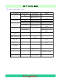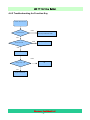
1
LCD Television
Service Manual
Chassis: MTK8222
Ver 1.2
Hisense Electric Co.,Ltd.
December,2010
LCD TV Service Manual
Contents
Contents.......................................................................................................................................................................- 2 Service Manual ...........................................................................................................................................................- 3 1. Precautions and notices.....................................................................................................................................- 3 1.1 Warning...................................................................................................................................................- 4 1.2 Notes.......................................................................................................................................................- 7 2. Factory/Service OSD Menu and Adjustment..................................................................................................- 10 2.1 To enter the Factory OSD Menu ...........................................................................................................- 10 2.2 Factory OSD Menu...............................................................................................................................- 10 3 Software Upgrading........................................................................................................................................- 14 3.1 Before upgrading, read the following. ..................................................................................................- 14 3.2 Get ready for upgrading........................................................................................................................- 14 3.3 Upgrading with the MtkTool ................................................................................................................- 16 3.4 Update with USB directly.....................................................................................................................- 21 4. Circuit instruction ...........................................................................................................................................- 23 4.1 Power assign and block diagram ..........................................................................................................- 23 4.2 Image and signal process ......................................................................................................................- 25 4.3 The main IC description .......................................................................................................................- 29 4.4 Troubleshooting ....................................................................................................................................- 54 4.4.1 Troubleshooting for Remote Control .........................................................................................- 54 4.4.2 Troubleshooting for Function Key.............................................................................................- 55 4.4.3 TV won’t Power On...................................................................................................................- 56 4.4.4 Troubleshooting for Audio.........................................................................................................- 57 4.4.5 Troubleshooting for TV/VGA/HDMI input...............................................................................- 58 4.4.6 Troubleshooting for YPbPr input...............................................................................................- 59 4.4.7 Troubleshooting for Video/S-Video input..................................................................................- 60 5. Explode View..................................................................................................................................................- 61 6. Schematic circuit diagram ..............................................................................................................................- 61 -
Hisense Confidential
-2-
LCD TV Service Manual
Service Manual
1. Precautions and notices
BEFORE SERVICING THE LCD TV, READ THE SAFETY PRECAUTIONS IN
THIS MANUAL.
WHEN REPLACEMENT PARTS ARE REQUIRED, BE SURE TO USE
REPLACEMENT PARTS SPECIFIED BY THE MANUFACTURER.
Proper service and repair is important to the safe, reliable operation of all Hisense
Electric Co., Ltd Equipment. The service procedures recommended by Hisense and
described in this Service Guide are effective methods of performing service operations.
Some of these service operations require the use of tools specially designed for the
purpose. The special tools should be used when and as recommended.
It is important to note that this manual contains various CAUTIONS and NOTICES
which should be carefully read in order to minimize the risk of personal injury to service
personnel. The possibility exists that improper service methods may damage the
equipment. It is also important to understand that these CAUTIONS and NOTICES ARE
NOT EXHAUSTIVE. Hisense could not possibly know, evaluate and advise the service
trade of all conceivable ways in which service might be done or of the possible
hazardous consequences of each way. Consequently, Hisense has not undertaken any
such broad evaluation. Accordingly, a serviceman that uses a service procedure or tools,
Hisense Confidential
-3-
LCD TV Service Manual
which are not recommended by Hisense, must first satisfy himself thoroughly that
neither his safety nor the safe of the equipment will be jeopardized by the service
method selected.
Hereafter throughout this manual, Hisense Electric Co., Ltd will be referred to as
Hisense.
1.1 Warning
1.1.1
Critical components having special safety characteristics are identified with a
by the
Ref. No. in the parts list. Use of substitute replacement parts, which do not have the
same specified safety characteristics, may create shock, fire, or other hazards.
Under no circumstances should the original design be modified or altered without
written permission from Hisense. Hisense assumes no liability, express or implied,
arising out of any unauthorized modification of design. Serviceman assumes all liability.
DANGER
CAUTION
TO ENSURE THE CONTINUED RELIABILITY OF THIS PRODUCT, USE ONLY
ORIGINAL MANUFACTURER'S REPLACEMENT PARTS, WHICH ARE LISTED WITH
THEIR PART NUMBERS IN THE PARTS LIST SECTION OF THIS SERVICE GUIDE.
1.1.2.
All ICs and many other semiconductors are susceptible to electrostatic discharges (ESD).
Careless handling during repair can reduce life drastically. When repairing, make sure
Hisense Confidential
-4-
LCD TV Service Manual
that you are connected with the same potential as the mass of the set by a wristband with
resistance. Keep components and tools also at this same potential.
1. Never replace modules or other components while the unit is switched on.
2. When making settings, use plastic rather than metal tools. This will prevent any
short circuits and the danger of a circuit becoming unstable.
1.1.3
To prevent electrical shock, do not use this polarized ac plug with an extension cord,
receptacle, or the outlet unless the blades can be fully inserted to prevent blade exposure.
To prevent electrical shock, match wide blade or plug to wide slot, fully insert.
1.1.4
When replacement parts are required, be sure to use replacement parts specified by the
manufacturer or have the same characteristics as the original part. Unauthorized
substitutions may result in fire, electric shock, or other hazards.
1.1.5
Safety regulations require that after a repair the set must be returned in its original
condition. In particular attention should be paid to the following points.
-Note: The wire trees should be routed correctly and fixed with the mounted cable
clamps.
-The insulation of the mains lead should be checked for external damage.
1.1.6
(1) Do not touch Signal and Power Connector while this product operates. Do not
Hisense Confidential
-5-
LCD TV Service Manual
touch EMI ground part and Heat Sink of Film Filter.
(2) Do not supply a voltage higher than that specified to this product. This may damage
the product and may cause a fire.
(3) Do not use this product in locations where the humidity is extremely high, where it
may be splashed with water, or where flammable materials surround it. Do not install
or use the product in a location that does no satisfy the specified environmental
conditions. This may damage the product and may cause a fire.
(4) If a foreign substance (such as water, metal, or liquid) gets inside the panel module,
immediately turn off the power. Continuing to use the product may cause fire or
electric shock.
(5) If the product emits smoke, and abnormal smell, or makes an abnormal sound,
immediately turn off the power. Continuing to use the product, it may cause fire or
electric shock.
(6) Do not disconnect or connect the connector while power to the product is on. It
takes some time for the voltage to drop to a sufficiently low level after the power has
been turned off. Confirm that the voltage has dropped to a safe level before
disconnecting or connecting the connector.
(7) Do not pull out or insert the power cable from/to an outlet with wet hands. It may
cause electric shock.
(8) Do not damage or modify the power cable. It may cause fire or electric shock.
(9) If the power cable is damaged, or if the connector is loose, do not use the product:
Hisense Confidential
-6-
LCD TV Service Manual
otherwise, this can lead to fire or electric shock.
(10) If the power connector or the connector of the power cable becomes dirty or dusty,
wipe it with a dry cloth. Otherwise, this can lead to fire.
(11) Use only with the cart, stand, tripod, bracket, or table specified by the
manufacturer, or sold with the apparatus. When a cart is used, use caution when
moving the cart/apparatus combination to avoid injury from tip-over.
1.2 Notes
Notes on Safe Handling of the LCD panel and during service
The work procedures shown with the Note indication are important for ensuring the
safety of the product and the servicing work. Be sure to follow these instructions.
• Before starting the work, secure a sufficient working space.
• At all times other than when adjusting and checking the product, be sure to turn OFF
the POWER Button and disconnect the power cable from the power source of the TV
during servicing.
• To prevent electric shock and breakage of PC board, start the servicing work at least 30
seconds after the main power has been turned off. Especially when installing and
removing the power board, start servicing at least 2 minutes after the main power has
been turned off.
• While the main power is on, do not touch any parts or circuits other than the ones
specified. If any connection other than the one specified is made between the measuring
Hisense Confidential
-7-
LCD TV Service Manual
equipment and the high voltage power supply block, it can result in electric shock or
activation of the leakage-detection circuit breaker.
• When installing the LCD module in, and removing it from the packing carton, be sure
to have at least two persons perform the work.
• When the surface of the panel comes into contact with the cushioning materials, be
sure to confirm that there is no foreign matter on top of the cushioning materials before
the surface of the panel comes into contact with the cushioning materials. Failure to
observe this precaution may result in, the surface of the panel being scratched by foreign
matter.
• When handling the circuit board, be sure to remove static electricity from your body
before handling the circuit board.
• Be sure to handle the circuit board by holding the large parts as the heat sink or
transformer. Failure to observe this precaution may result in the occurrence of an
abnormality in the soldered areas.
• Do not stack the circuit boards. Failure to observe this precaution may result in
problems resulting from scratches on the parts, the deformation of parts, and
short-circuits due to residual electric charge.
• Routing of the wires and fixing them in position must be done in accordance with the
original routing and fixing configuration when servicing is completed. All the wires are
routed far away from the areas that become hot (such as the heat sink). These wires are
fixed in position with the wire clamps so that the wires do not move, thereby ensuring
Hisense Confidential
-8-
LCD TV Service Manual
that they are not damaged and their materials do not deteriorate over long periods of time.
Therefore, route the cables and fix the cables to the original position and states using the
wire clamps.
• Perform a safety check when servicing is completed. Verify that the peripherals of the
serviced points have not undergone any deterioration during servicing. Also verify that
the screws, parts and cables removed for servicing purposes have all been returned to
their proper locations in accordance with the original setup.
The lightning flash with arrowhead symbol, within an equilateral
triangle is intended to alert the user to the presence of uninsulated
dangerous voltage within the products enclosure that may be of sufficient magnitude to
constitute a risk of electric shock.
The exclamation point within an equilateral triangle is intended to alert
the user to the presence of important operating and maintenance (servicing)
instructions in the literature accompanying the set.
Hisense Confidential
-9-
LCD TV Service Manual
2. Factory/Service OSD Menu and Adjustment
2.1 To enter the Factory OSD Menu
a.、 With factory RC (remote control)
1. Press “M” button and enter factory mode.
2. Press “Menu” button and enter factory OSD menu.
3. Press “CH+”/“CH-” button select the function menu, press “VOL+”/“VOL-” enter the selected
function menu. Press “VOL+”/“VOL-” button adjust values in the menu.
b.、With user’s RC
1. Power TV On
2. Press Menu button and call up User OSD Menu
3. Select Audio-> Balance
4. Enter 0->5->3 ->2 in sequence. If re-do number keys not appear the OSD, then renew enter
1->9->6 ->9 in sequence.
5. Factory OSD appears.
6. Press Menu again and leave factory OSD.
2.2 Factory OSD Menu
2.2.1 White Balance
Note: Different source has different WB values. Before adjusting, please change to desired source.
1. Auto Color
For VGA and Component Video sources, WB values must be adjusted. And at others signal sources, the
“auto colour “does not work.
Before adjusting, prepare the signal instruments such as DVD or K-8256 first, and find the video picture
with gray and color bars. Then please change to desired source.
source
Timing
Pattern
Notes
1
ADC VGA
1024*768
gray-3color
For VGA source
2
ADC HDTV
720P
gray-3color
For Component Video
Notes:
a、Press “M” button and enter factory mode.
b、Press “Menu” button and enter factory OSD menu.
c、Select the item “Auto Color”.
d、Press VOL+ button to auto color.
e、Close the OSD menu after 5 seconds.
Hisense Confidential
- 10 -
LCD TV Service Manual
2.2.2 Factory Option
Item 0
White Balance
Item 1
Note
R DRV
Red Driver adjust
G DRV
Green Driver adjust
B DRV
Blue Driver adjust
R CUT
Red Cut adjust
G CUT
Green Cut adjust
B CUT
Blue Cut adjust
Note: Before adjusting, please change to desired source. Different source has different WB
values.
Factory RESET
Zhong Shi
Qingdao Jiangxi Road factory
Huang Dao
Huangdao Industrial Park
Gui Yang
Gui Yang Industrial Park
Liao Ning
Liao Ning Industrial Park
Hungary
Hisense Hungary
Australia
Hisense Australia
France
Hisense France
Clean data except
Clean Protected
WB data and Auto Color data
Clean all data
Clean All
Auto Color
For VGA and Component Video
sources, WB values must be
adjusted
Color Temp
And at others signal sources,
the “auto colour “does not
work.
Standard
Color
R Offset
G Offset
B Offset
Picture Mode
Brightness Min
Brightness Mid
Brightness Max
Contrast Min
Contrast Mid
Contrast Max
Saturation Min
Saturation Mid
Saturation Max
Factory Option
OSD
Logo Option
To FAC
MODE “M” is only used for factory production.
Hisense Confidential
- 11 -
Min Brightness
Mid Brightness
Max Brightness
Min Contrast
Mid Contrast
Max Contrast s
Min Saturation
Mid Saturation
Max Saturation
English
Devant
M
LCD TV Service Manual
SW Version
Version:
Panel Info:
Flash:
Current Software version
The date of current version
Note: The factory menu date varies according to different sources. Incase changing the factory
data by error, you can choose to “Clean Protected”, by which you can resume the default value.
To clear the EEPROM:
a. Select the item “Clean All”.
b. Press VOL+ button to clear the EEPROM data.
c. Close the OSD menu after 5 seconds.
d. Restart the TV.
2.3 Designer Menu
Item 0
Designer Menu
Item 1
Picture Mode
Item 2
SOURCE
Brightness Brightness
Brightness Contrast
Brightness Saturation
STD Brightness
STD Contrast
STD Saturation
Soft Brightness
Soft Contrast
Soft Saturation
Audio Set
Volume Min
Volume 25
Hisense Confidential
- 12 -
Note
The current program
source
Brightness of VIVID
mode
Contrast of VIVID
mode
Saturation of VIVID
mode
Brightness of STD
mode
Contrast of STD
mode
Saturation of STD
mode
Brightness of Movie
mode
Contrast of Movie
mode
Saturation of Movie
mode
When value is 1
Think about the
Audio out power
before adjusting
When value is 25
Think about the
Audio out power
LCD TV Service Manual
Volume Mid
Volume 75
Volume Max
Audio Mode
Audio Mode
120HZ
500HZ
1.5kHZ
5kHZ
10kHZ
PVM 0-350
PVM 350-500
PVM500-1000
PVM 1000-10000
PVM 100000
Last station
Backlight co
EMI
Power Mode
before adjusting
When value is 50
Think about the
Audio out power
before adjusting
When value is 75
Think about the
Audio out power
before adjusting
When value is 100
Think about the
Audio out power
before adjusting
Standard 、 user 、
Music 、
Speech,
Music
Different frequencies
for different Audio
Mode
The above “Factory/Service OSD Menu” are reference only, please refer to the actual units to
determine the appearances.
Hisense Confidential
- 13 -
LCD TV Service Manual
3 Software Upgrading
3.1 Before upgrading, read the following.
1、Before upgrading,Write down the ADC Calibration values of the sources of VGA and
component。
2、Upgrade the software.
3、To clear the EEPROM .
A Select the item “Clear Unprotected”.
B Press VOL+ button to clear the EEPROM data.
C Close the OSD menu after 5 seconds.
D Restart the TV.
4 Write the ADC Calibration values copied just now into the the channels of VGA and
component.
5、After the operation above all, necessarily, Renew search the channels for the users.
The first upgrading method:
The software is upgraded by a burning toll-MtkTool, which can burn the program file *.bin to the
main board of the unit.
3.2 Get ready for upgrading
3.2.1 Install the driver
Double click the icon
MTKtools2.44.04+cp210xDriver.rar
, install the driver.
Select the default value, the driver will be installed step by step.
Hisense Confidential
- 14 -
LCD TV Service Manual
3.2.2 Hardware connecting
Connect the unit to your pc with a USB-to-serial port cable. USB port connects to your pc, and
serial port to the TV’s RS232 port.
USB connector: to PC.
Serial connector: to TV’s RS232
port.
For the first connecting, the pc will recognize and automatically install the USB device. The
process is just like the installation of a mini disk, see the following picture.
Hisense Confidential
- 15 -
LCD TV Service Manual
3.3 Upgrading with the MtkTool
MTKtool is a green program needing no installation. It is saved in the folder
. There are five folders/files in this folder altergether.
The MtkTool using log is restored in the MtkLog folder. It records the running time and date
whenever the tool is used. The log will be a txt file named by the date and time.
Hisense Confidential
- 16 -
LCD TV Service Manual
After connecting the TV with your PC, double click
icon, open the
MtkTool.
If following error appears, it means the related port is not be set properly.
Ignore these errors, click “Confirm” and enter the MtkTool main interface, see the
following picture.
Flash chip model
Please refer to follow steps to update the software:
1—Select mode of Flash chip to MT8226 as the below picture.
2—Refer to the next page instruction to select the communicate port.
3—Press the icon beside the baud rate and make sure it is green as the below picture.
4—Set the flash baud rate to 115200 as the below picture.
5—Click the browse button to select the *.bin file that will be updated.
6—Click the “start” button to update software.
Hisense Confidential
- 17 -
LCD TV Service Manual
Select mode
Communicate
of Flash chip
port
Set
Flash
Select *.bin
Baud Rate
file
Start upgrade
Choose the current
USB conversion Port
Later choose com5
Information
of
upgrade
process
Hisense Confidential
- 18 -
LCD TV Service Manual
Open “Device Manager” and find which port is connected with the TV. In this operation, COM5
is connected to the TV; so, select “COM5” in the MtkTool main interface. Select the right baud rate
according to chip model. For this unit( chip model is MT8226), select 115200..So choose “Auto Set Flash
BaudRate”
Note: Whether or not click the “Auto Set Flash Baud Rate” in the “window” menu
depends on the chip type. If the flash chip does not support high speed transport, do not select
this option; otherwise, reserve the selected mood.
Hisense Confidential
- 19 -
LCD TV Service Manual
Click “Browse” button, find the upgrading program file, and select it. Press “Upgrade” button
and start upgrading.
The following interface appears on the screen, indicating upgrading successfully.
Hisense Confidential
- 20 -
LCD TV Service Manual
3.4 Update with USB directly
The second update method is with USB directly:
MTK8222 Series can update with USB, the software name should be HISENSE.bin.
The Updating Steps is set the Source to "DMP interface", insert the USB(the
update file HISENSE.bin,which should be in root directory),The TV automatic
identify the upgrading software. step by step according as the informations of the
upgrading process.
(USB to the Main board directly)
Hisense Confidential
- 21 -
LCD TV Service Manual
After upgrading, you must confirm the software in the “Factory Menu ”and
you'd better "CLEAR UNPROTECTLY".
Hisense Confidential
- 22 -
LCD TV Service Manual
4. Circuit instruction
4.1 Power assign and block diagram
Power assign:
Power voltage includes 12V_M、5V_M、5VS and VPA(Voltage Power for Audio, normally
14~16V),some small size TV’s( small than 37 inch) VPA will use 12V_M directly .All other
voltages are converted from the above voltages.
a. 5V_TUNER that power supply for Tuner is converted by U9 from 12_M; The power supply
for panel is converted by chosen output between U31 from 12_M and 5V_M ;The power
supply for the audio IC (U35) of small size TVs is converted by the output of 12V_M connects
ferrite bead and VPA;the last, the 33V rising circuit and mute circuit are converted by the 12_M
directly.
b. Both of the 5VM and 5VS pass through diodes then output 5V_ON,which used for
3.3V/1.2V/DV10 convertion. U36(DAC)、U29/U30(audio switch)、U7(DAC)、U19(IF )
and USB are converted from 5V_M directly ;The power supply for DDR(U1,2.6V) is
converted by U11 from 5V_M too
c. 3.3V supply for U17(FLASH),U14(EEPROM)is converted by U4 from 5V_ON . 1.0V supply
for U34(the main IC \MT8222)is converted by U3 from the 3.3V ; 1.2V power supply for the
main IC \MT8222. is converted by the 3.3V
Hisense Confidential
- 23 -
LCD TV Service Manual
Block diagram:
Hisense Confidential
- 24 -
LCD TV Service Manual
4.2 Image and signal process
RF signal:
After the RF Signal enter TV Tuner, the RF Signal will become IF Signal after the TV Tuner converted,
and then the Signal will become SIF and VIF signal by sawfilter U16 and U20, finally send to Main IC
through U19.
Video signal:
Video of AV1 input through P16B, pass by R2, C5, R1, C1, enter No.1 feet of U34
Video of AV2 input through P16A, pass by R6, C10, R11, C12, enter No.4 feet of U34
Hisense Confidential
- 25 -
LCD TV Service Manual
Input by P9, pass the below circuit diagram and enter U34 for disposal.
PC signal enter through XS11, input U34 by passing the below similar disposal, check the diagram for detail.
The Audio signal of HDMI and USB directly input U34 for disposal.
AV output send out by the No.11 feet of U34, through the below diagram, finally come out by P4.
The input Video signal send out the LVDS signal after the U34 managed, the LVDS signal will pass CN9 and
go to LCD panel display.
Hisense Confidential
- 26 -
LCD TV Service Manual
Audio signal
TV Audio signal is get by SIF signal which is come out through TV Tuner, after the U19 managed, and
then directly go out to U34.
The Audio of AV1, AV2 and YPbPr input by P16B, P16A and P9, firstly pass the below diagram to
reduce it.
And then pass U29 to do the shift and choose one, then together with PC and SCART Audio to do the
convertion through U30, choose one input U34 for disposal.
Digital audio signal output by feet 47-50 after the disposal of U34, transfer digital to analogue from the
U36, change to analogue Signal. One pass the driving diagram to earphone, the other one pass the sound IC
to speaker.
Hisense Confidential
- 27 -
LCD TV Service Manual
The main control signal, as list:
Control Signal
Internet mark
Instruction
UP31
Low level power on
Standby signal
Power control
BL-control
High level power on
SW
High level power on
----
Low level power on
UP34
Low level BL on
BL-ON/OFF
Low level BL on
Remark
UP31pass Q29 inverse
phase
UP34 passQ2 inverse
phase
PWM0
BL-brightness
Adjust duty ratio
BL-ADJUST
PWM0passQ18 inverse
phase
E2prom written
PWM2
protect
Flash written protect
Key
“0”
Key
“1”
IR signal
Tuner 33V
FRESET#
High voltage for
protect
ADIN0
key
ADIN1
key
IR-IN
PWM1
Adjust duty ratio
TU_33V
Audio amplify mute
PWM1 rise voltage
GPIO_21
Low-level mute
Hisense Confidential
- 28 -
LCD TV Service Manual
4.3 The main IC description
74HC4052D:
Hisense Confidential
- 29 -
LCD TV Service Manual
Hisense Confidential
- 30 -
LCD TV Service Manual
Hisense Confidential
- 31 -
LCD TV Service Manual
AO4459:
Hisense Confidential
- 32 -
LCD TV Service Manual
AP1122EA:
AP1534
Hisense Confidential
- 33 -
LCD TV Service Manual
Hisense Confidential
- 34 -
LCD TV Service Manual
AT24C08AN-10SU-2.7:
Hisense Confidential
- 35 -
LCD TV Service Manual
Hisense Confidential
- 36 -
LCD TV Service Manual
AZ1084:
Hisense Confidential
- 37 -
LCD TV Service Manual
cs4344czz:
Hisense Confidential
- 38 -
LCD TV Service Manual
EM6AA160256DDR.:
Hisense Confidential
- 39 -
LCD TV Service Manual
Hisense Confidential
- 40 -
LCD TV Service Manual
Block Diagram
Hisense Confidential
- 41 -
LCD TV Service Manual
G962:
Hisense Confidential
- 42 -
LCD TV Service Manual
MX29LV320DT:
Hisense Confidential
- 43 -
LCD TV Service Manual
Hisense Confidential
- 44 -
LCD TV Service Manual
R2A15108FP:
Hisense Confidential
- 45 -
LCD TV Service Manual
Hisense Confidential
- 46 -
LCD TV Service Manual
Hisense Confidential
- 47 -
LCD TV Service Manual
TDA9885TS:
Hisense Confidential
- 48 -
LCD TV Service Manual
TJ2996-R1.3:
Hisense Confidential
- 49 -
LCD TV Service Manual
Hisense Confidential
- 50 -
LCD TV Service Manual
WM8501:
Hisense Confidential
- 51 -
LCD TV Service Manual
Hisense Confidential
- 52 -
LCD TV Service Manual
Hisense Confidential
- 53 -
LCD TV Service Manual
4.4 Troubleshooting
4.4.1 Troubleshooting for Remote Control
Remote control does not work
YES
Try new batteries
Replace battery
NO
Replace RC
YES
Replace remote control
Check IR receiver
Change Led & IR board
YES
Replace Led & IR BD
NO
YES
Change Led & IR cable
Replace Led & IR cable
NO
Replace main board
Hisense Confidential
- 54 -
LCD TV Service Manual
4.4.2 Troubleshooting for Function Key
Buttons does not work
YES
Check solder connections and
Check switches
see if any switches are stuck.
NO
YES
Check key board
Replace Key BD
NO
Check Key BD cable
YES
Change Key BD
OK
NO
Replace main board
Hisense Confidential
- 55 -
LCD TV Service Manual
4.4.3 TV won’t Power On
TV won’t power on
Is
NO
LED
Check
light?
Power
Make Sure Power
YES
source is live
Output
NO
YES
BLUE
Check
RED
YES
Power
Replace
Power Cord
Cord
NO
Check/replace IR
Only
Try Power on by
Panel Bright
YES
PCA
RC and Button
Check signal
Source
Neither
YES
NO
BD or Keypad
one works
Both
works
NO
Work
Replace Main
BD
Replace Main BD
NO
Power on
YES
Replace Panel
NO
(to contact Hisense tech support.)
Replace Power BD
OK
Hisense Confidential
- 56 -
YES
OK
LCD TV Service Manual
4.4.4 Troubleshooting for Audio
No sound
YES
Check connecter
Reconnect
NO
YES
Replace speaker wire
Check speaker wire
NO
YES
Check speaker set
Replace speaker set
NO
Replace main board
YES
OK
NO
Power Supply Board
Hisense Confidential
- 57 -
LCD TV Service Manual
4.4.5 Troubleshooting for TV/VGA/HDMI input
No picture on the screen
NO
Check Signal Source
Make sure signal
source is available
YES
Reconnect
Check connect
NO
YES
Check cable
Replace cable
NO
Replace main board
Hisense Confidential
- 58 -
LCD TV Service Manual
4.4.6 Troubleshooting for YPbPr input
No picture on the screen
Check Source work or not
NO
Check Source Device
YES
Check connect
YES
Reconnect
NO
Check Wires (Green Blue, Red)
YES
Replace wires
NO
Replace main board
Hisense Confidential
- 59 -
LCD TV Service Manual
4.4.7 Troubleshooting for Video/S-Video input
No picture on the screen
Check Source work or not
NO
Check Signal Source
YES
YES
Check connect
Reconnect
NO
YES
Check Cable/ Wires
Replace Cable/Wires
NO
Replace main board
Hisense Confidential
- 60 -
LCD TV Service Manual
5. Explode View
6. Schematic circuit diagram
Hisense Confidential
- 61 -
5
4
3
2
1
5V_M
5V_M
5V_M
5V_AMP
L69
FB
C344
C817
10uF
0.1uF
R668
CE64
12V_M
2,11,14
+3V3
2,3,4,6,7,11,14
R685
CE69
4.7k
SCT2_AUL_OUT
47
+
R672
47k
Q42
10uF/16v
1
删除电阻
20080911
4.7k
C276
2.2uF
R674
10k
1
A_MUTE
R695
R705
10K
AL2
0/NS
12V_M
R683
+3V3
10uF/16v Q53
53
1
47k R686
1
10k C278 2.2uF R699
OFF_MUTE
AL1
0
3904
3904
AOTL
0
2
R697
2
2
3904
OFF_MUTE
A_MUTE
2
3904
R676
R675
R688
R687
47
8.2k
47
8.2k
R679
GPIO_11 3
SCT1_AUR_OUT
SCT1_AUL_OUT
SCT2_AUR_OUT
SCT2_AUL_OUT
SCT1_AUR_OUT
SCT1_AUL_OUT
SCT2_AUR_OUT
SCT2_AUL_OUT
DAC_AUL_OUT
DAC_AUR_OUT
AOSDATA0
AOBCK
AOLRCK
AOMCLK
5V_AMP
R690
4.7k
+
SCT2_AUR_OUT
R681
10k
3Q
R704
Q52
52
10K
1
Q57
C277
2.2uF
R696
1
0/NS
A_MUTE
AR2
R706
10K
2
3904
R691
10uF/16v Q54
54
1
R698
R680
0
10k
C279 2.2uF R701
0
AR1
AOTR
R694
AR1
AL1
AR2
AL2
BOSDATA0
BOBCK
BOLRCK
BOMCLK
3904
2
2
R682
47k R692
1
3904
3904
GND
AR1
AL1
AR2
AL2
3Q
3
A_MUTE
R678
47k
10uF/16v
47
+
Q55
R689
删除电阻
20080911
4.7k
2
47
3
R677
CE70
R693
47
8.2k
47
+3V3
2008/06/10
3
4.7k
C234
R240
2
HPOUTL
Q22
3904
C186
RA34
220uF/16v
Q51
2N3906
1
10k
RA36
5
1
2
4
3
HPOUTL1
10
HPOUTR1
10
RA37
4K7
RA39
10K/NC
1
+
HPOUTR
P18
AGND
L
WL
WR
R
+
A_MUTE
220uF/16v
B
R244
R329
DAC_AUR_OUT
10K/NC
0
R319
0
CB191
0.1uF
HPOUTL
HPOUTR
B
R245
4.7k
C190
C237
R237
10k
GPIO_21
GND
HPOUTR1
HPOUTL1
Q21
3904
1
Q23
3904
1
4
3
2
1
CN11
Q58
2N3906
1
C188
3
R246
TJC3-4A
3
4.7uF R236
10k
2 2
100
C642 2.2nF
3
470
R317
10K
2
DAC_AUR_OUT
4.7uF/16V
R320
DAC_AUL_OUT
EZJZ0V800AA
5VAMP
RA41
CE60
100uF/16v
1
2
CE63
FB
DA5
QA8
DTC623TK/NC
QA7
1
DTC623TK/NC
2
4.7k
RA38
4K7
3
3
2008/06/10
4.7uF R238
5VAMP
L66
2
330
5V_M
GPIO_11
C637
0.1uF
3
R242
10K
CE61
+
10k
1
2
R208
RA31
HPDET#
4.7uF
3
R310
10K
100
C638
2.2nF
RA29
100K
Q20
3904
1
470
2
DAC_AUL_OUT
4.7uF/16V
C189
GPIO_21 3,14
C
R239
R241
3
3
3
3
8.2k
5VAMP
R325
2,3,4,5,6,7,8,9,10,11,12,14
BOSDATA0 3,6
BOBCK
3,6
BOLRCK 3,6
BOMCLK 3,6
GPIO_21
C
10
10
8,10
8,10
DAC_AUL_OUT 14
DAC_AUR_OUT 14
AOSDATA0 3,6,12
AOBCK
3,12
AOLRCK 3,12
AOMCLK 3,12
GND
CE65
3,14
A_MUTE 14
GPIO_11
5V_AMP
SCT1_AUR_OUT
D
+3V3
47
Q56
Q36
36
3Q
3
10K
R684
3Q
R673
3
SCT1_AUL_OUT
+
更改AUDIO OUT放大电路电源
王西瑜20090303
R703
2,3,6,8,12,14
12V_M
D
A_MUTE
5V_M
5V_AMP
5V_AMP
330
4.7uF R247
4.7k
5V_8501
网络更改
20080911
增加酒店机输出接口
王西瑜20090301
WANGXIYU20081113
VER.C更改
L65
FB
网络更改
20080911
R341
47K
CB186
0.1uF
5V_M
+ CE10
10uF/16V
网络更改
20080911
A
AOLRCK
R306
0
1
LRCK
AOSDATA0
R307
0
2
DIN
AOBCK
R339
0
R340
CB185
0.1uF
0
CB188
3
BCLK
4
ENABLE
5
VMID
6
VOUTR
7
AGND
+ CE7
10uF
10uF/16V
MCLK
14R338
100
FORMAT
13R336
100
DEEMPH
12R337
100
DVDD
11
DGND
10
AOMCLK
L72
FB
BOSDATA0
BOBCK
BOLRCK
BOMCLK
9
AVDD
8
CB192
0
10uF
CE11
10uF/16V
+
5 RND12
4
6
3
7
2
8
1
22x4
R-RESCA2010-8N-HX
+ CE16
10uF/16v
R344
VOUTL
5V_M
U7
5V_M
5V_8501
2008/06/10
NEAR IC
U36
CB187
0.1uF
CB196
NC
1
2
3
4
5
CB193
0.1uF
SDIN
AOUTR
DEM#/SCLK
VA
LRCK
GND
MCLK
AOUTL
VQ
FILT+
CS4344 2CH AudioDac
10
9
8
7
6
L61
AOTR
DACVA
FB
AOTL
A
+
+ CE17
10uF/16v
CB194
0.1uF
CB195
1uF
CE18
10uF/16v
WM8501 R-SOIC14N-1.270-6.00-HX
CB189
0.1uF
R342
10K/NC
DAC_AUR_OUT
DAC_AUL_OUT
5
4
3
2
1
5
4
3
2
1
5V_M
D188
MAIN POWER
+5VS
1
2
3
4
5
6
7
8
9
10
11
12
13
14
CN2
5V_M
1
2
3
4
5
6
7
8
9
10
11
12
13
12V_M
BL-ON/OFF
BL-ADJUST
12V_M
+5VS
+5VS
5V_M
SW
R259
1K
+ CE66
470uF/16v
+3V3
+3V3
B240A
D187
FB64
CB218
0.1uF
+5V_ON
+5V_ON
+3V3
3,4,6,7,11,13,14
12V_M
+ CE68
220uF/16v
CB219
0.1uF
12V_M
12V_M
0603_Bead
11,14
+5V_ON
B240A
2008.6.4
SW
+5V_ON
+5V_ON
VPA
D
+5V_TUNER
12V_M
UP31 HIGH :POWER OFF
12V_M
+5VS
3
D
VPA
CN1
B240A
D185
5V_M
1K
1
+
CB217
0.1uF
+ CE67
220uF/25v
+5V_TUNER 11
UP31
R260
10K
2
CE83
100uF/16v
+5V_TUNER
121
UP31 LOW: POWER ON
R258
Q29
3904
L75
CB216
0.1uF
DDRV
DDRV
DDRV
3,4,5
AV12
4
DV10
3,4
5V_M
3,6,8,12,13,14
AV12
AV12
DV10
Power for MT8222 only ( Always on )
DV10
5V_M
VEN
VIN
GND
VOUT
ADJ
AP1122
3
IN
+3V3
10K
5V_M
CE869
100uF/16v
R857
21K 1%
+
CE13
47uF/16v
C
CB6
0.1uF
CB8
10uF
修改封装20080911
+ CE15
220uF/16v
CB891
0.1uF
+
UP31
AV12
OUT
TAB
GND
0603_Bead
3,6
R856
NS/100
CB860
0.1uF
C883
1uF
R-SOT4N-2.30-7.00-HX
+
BL-ON/OFF
CE859
100uF/16v
BL-ADJUST
P01
CB5
0.1uF
GND
SHIELD
M-RSAG7.070.198-HX
R858
0
3,4,5,6,7,8,9,10,11,12,13,14
BL-ON/OFF
14
BL-ADJUST
14
C
R859
12K 1%
Test GND Pin
( Spread Around PCB )
1.2 x (21K+12K)/12K= 3.3V
3.3V to 1.2V
Estimated Power consumed : ??? A
5V to 3.3V
Estimated Power consumed : ??? A
TP85
Switch Regulator
UP31
FB18
2
4
1
R262
U8
+3V3
2008.6.4
1
2
3
4
5
+5V_ON
MUST USE AP1122
LDO#2
6
U4
G962
ADJ/GND
LDO#1
therm
TP86
TP87
TP88
TP89
TP90
TP91
TP92
TP93
TP94
TP95
TP96
TP97
TP98
TP99
TP101 TP100 TP103
MUST USE AP1533
Core Power 1.0V
U3
AP1533/SOP-8
+5V_ON
DV10
H3
9
8
7
6
0.8 x (1+0.51K/2K) = 1.0V
HOLE/GND
2 2
3 3
4 4
5 5
9
8
7
6
1
1
5V to 1.0V
Estimated Power consumed : ??? A
H5
9
8
7
6
H6
9
8
7
6
HOLE/GND
2 2
3 3
4 4
5 5
9
8
7
6
H7
9
8
7
6
9
8
7
6
2
3
4
5
2
3
4
5
Z7
Z8
ARROW
ARROW
ARROW
Z10
Z11
Label
Label
MES
TX
B
M1
M2
MARK
M3
M4
M5
M6
MARK
MARK
MARK
MARK
HOLE/GND
2 2
3 3
4 4
5 5
9
8
7
6
1
1
12V_M
LDO#3
9
8
7
6
Z6
MARK
Works at normal mode
H11 HOLE/GND
HOLE/GND
2 2
3 3
4 4
5 5
9
8
7
6
1
HOLE/GND
2 2
3 3
4 4
5 5
9
8
7
6
1
R1164
1.8K_1%
CB442
0.1uF
B
H4
9
8
7
6
1
D62
SCHOTTKY DIODE/B340A
HOLE/GND
2 2
3 3
4 4
5 5
9
8
7
6
1
1
9
8
7
6
+ CE222
100uF/16v-LowESR CAP
CB441
0.1uF
1
C2
0.01uF
1
FB
R1162
680_1%
1
OCSET
2
3
H12
C512
NS/100nF
1
C511
NS/100nF
27uH/POWER CHOKE
6
5
1
R1161
3K
Vss
Vss
R1163
100K
EN
CB7
0.1uF
O/P
O/P
7
8
+ CE8
100uF/16v
Vcc
1
L27
4
+5V_TUNER
1
OUT
3
10R/2W
1206_Bead
10R/2W
CE40
VIN
C199
+
VOUT
2
+
CE227
LM7805
R956
110_1%
R958
120_1%
A
U9
R207
GND
R216
FB14
CB573
0.1uF
+ CE5
100uF/16v
CB576
0.1uF
Vout = 1.25 x ( 1 + 110/ 110 ) = 2.5V for DDR200/266/333
3
CB574
0.1uF
IN
1
2
ADJ/GND
U11
LT1084 TO-252-3
R-TO3N-2.28-9.70-HX
5V_M
+ CE9
100uF/16v
DDRV
0.1uF
100uF/35v
100uF/16v
CB398
0.1uF
12V to 5V
For Tuner 5V power
A
Vout = 1.25 x ( 1 + 120/ 110 ) = 2.6V for DDR400/500
5V to DDRV
Estimated Power consumed : ??? A
MediaTek Confidential
If use sdram ,NC FB14
If use ddr ,NC FB14
MediaTek (ShenZhen) Inc.
Title
Power LDO
Size
C
Date:
5
4
3
2
Document Number
HISENSE_MT8222_EU
Drawn:
2008/1/25
Sheet
1
Jiu.Ni
2
of
Rev
1
14
5
4
3
2
System I2C
TP134
RDQ0
RDQ1
RDQ2
RDQ3
RDQ4
RDQ5
RDQ6
RDQ7
RDQS0
RDQM0
DV10
RDQM1
RDQS1
RDQ8
RDQ9
RDQ10
RDQ11
RDQ12
RDQ13
RDQ14
RDQ15
AV12_MEMPLL
RCLK0#
RCLK0
RCKE
RA12
RA11
RA9
RA8
RA7
RA6
RA5
RA4
RWE#
RCAS#
RRAS#
RCS#
RBA0
RBA1
RA10
RA0
RA1
DV10
RA2
RA3
C980
0.1uF
DDRV
MEM_VREF
DV10
DV33
VGASDA
VGASCL
AV12_PLL
AV12_PLL
U34
AV12_PLL 4
GRNP
BLUP
PWM1
PWM0
SPDIFOUT
U1TX
U1RX
OSCL0
OSDA0
GPIO_25
GPIO_24
GPIO_23
GPIO_22
GPIO_21
GPIO_20
SPDIFIN
AOSDATA0
AOBCK
AOLRCK
AOMCLK
VGAHSYNC#
VGAVSYNC#
DV33
DV10
AV33_CVBS 4
AV33_SIF 4
R29
5.1K_1%
Close to MT8222 As possible
AV33_SIFDIG
AV33_SIFDIG
AV33_XTL
AV33_XTL
AV33_SIFDIG
AV12_LVDSPLL
AV33_ADC 4
AV33_XTL
AV12_LVDS
AV33_DAC
AV12_MEMPLL
AV33_LVDS
AV12_LVDSPLL 4
AV12_MEMPLL 4
XTAL Dip/SMD Dual Layout
AV33_LVDS 4
AV12_USB 4
AV12_HDMI
AV33_HDMI
AV33_VGA
AV33_VGA
RB23
AV12A_RGBB
AV12A_RGBB
AV33_SIF
TP133
AV33_CVBS
CVBS_BYPASS
CVBS_TP
CVBS0N
CVBS0P
CVBS1
CVBS2
CVBS3
CVBS4
CVBS5
CVBS6
CVBS7
R2434
NS/0
R227
4.7K
AV12D_RGB
AV12D_RGB
27MHz
R-CRYC1405N-HX
C979
22pF
GPIO_24
GAME_VCC
ADIN0
ADIN1
6
6
ADIN3
ADIN4
10
10
33
33
R182
GAME_DA1
33
8
4
0603_Bead
P15
1
6
2
7
3
8
4
9
5
BOSDATA0
BOBCK
BOLRCK
BOMCLK
HDMIDDCSCL_1
HDMIDDCSDA_1
HDMIDDCSCL_2
HDMIDDCSDA_2
BOSDATA0 6,13
BOBCK
6,13
BOLRCK 6,13
BOMCLK 6,13
14
14
14
14
14
14
14
14
14
14
14
14
E0N
E0P
E1N
E1P
E2N
E2P
ECKN
ECKP
E3N
E3P
14
14
14
14
14
14
14
14
14
14
E4N
E4P
14
14
5V_M
6,7
RX0_2
RX0_2B
RX0_1
RX0_1B
RX0_0
RX0_0B
RX0_C
RX0_CB
7
7
7
7
7
7
7
7
RX1_2
RX1_2B
RX1_1
RX1_1B
RX1_0
RX1_0B
RX1_C
RX1_CB
7
7
7
7
7
7
7
7
RX2_2
RX2_2B
RX2_1
RX2_1B
RX2_0
RX2_0B
RX2_C
RX2_CB
7
7
7
7
7
7
7
7
HDMIDDCSCL_0
HDMIDDCSDA_0
7
7
HDMIDDCSCL_1
HDMIDDCSDA_1
7
7
HDMIDDCSCL_2
HDMIDDCSDA_2
7
7
B
USB
USB_DP0
USB_DM0
USB_DP1
USB_DM1
O0N
O0P
O1N
O1P
O2N
O2P
OCKN
OCKP
O3N
O3P
O4N
O4P
CEC
OPWR0_5V 7
OPWR1_5V 7
OPWR2_5V 7
HDMIDDCSCL_0
HDMIDDCSDA_0
USB_DP0
USB_DM0
6
6
USB_DP1
USB_DM1
6
6
TRAPICE
ICE
6
AOSDATA0 6,12,13
AOBCK 12,13
AOLRCK 12,13
AOSDATA0
AOBCK
AOLRCK
DDRV
DDRV
12V_M
12V_M
DV10
DV10
DV33
DDRV
2,4,5
12V_M
2,11,14
DV10
2,4
DV33
4
+3V3
2,4,6,7,11,13,14
A
DV33
+3V3
+3V3
E4N
E4P
GAME_VCC
MediaTek Confidential
MediaTek (ShenZhen) Inc.
5V_M
5V_M
CB13
0.1uF
2,6,8,12,13,14
Title
MT8222
Size
C
C987
10uF/16V
3
5
5
C
OPWR0_5V
OPWR1_5V
OPWR2_5V
AR1
13
AL1
13
AR2
13
AL2
13
AOSDATA0 6,12,13
AOBCK
12,13
AOLRCK 12,13
AOMCLK 12,13
E0N
E0P
E1N
E1P
E2N
E2P
ECKN
ECKP
E3N
E3P
+3V3
+
C961
4.7nF/NS
5
5
MEM_VREF 5
RX2_2
RX2_2B
RX2_1
RX2_1B
RX2_0
RX2_0B
RX2_C
RX2_CB
Date:
5
RBA0
RBA1
RX1_2
RX1_2B
RX1_1
RX1_1B
RX1_0
RX1_0B
RX1_C
RX1_CB
6
6
6
6
CVBS_BYPASS
O0N
O0P
O1N
O1P
O2N
O2P
OCKN
OCKP
O3N
O3P
O4N
O4P
FB63
GAME_LOAD
GAME_DA2
C965
4.7nF/NS
11
LVDS INTERFACE
FB60
AV12D_RGB 4
C902
4.7nF/NS
5
RCLK0 5
RCLK0# 5
RX0_2
RX0_2B
RX0_1
RX0_1B
RX0_0
RX0_0B
RX0_C
RX0_CB
11
11
11
11
AL1
AR2
AL2
AOSDATA0
AOBCK
AOLRCK
AOMCLK
GPIO_6
GPIO_5
GPIO_3
GPIO_2
5V_M
NS/0603_Bead
33
R181
RCKE
HDMI
MPX1
I2S IF AR1
Wangxiyu 20080721
R180
5
5
5
5
RA[12..0]
RBA0
RBA1
GPIO
GPIO_0 6
GPIO_1 6
GPIO_2 6,13
GPIO_3 6,13
GPIO_4 14
GPIO_5 6,13
GPIO_6 6,13
GPIO_7 6
GPIO_8 6
GPIO_9 6
GPIO_10 6
GPIO_11 13
GPIO_20 12
GPIO_21 13,14
GAME_CLK
GPIO_25
RWE#
RCAS#
RRAS#
RCS#
RDQ[15..0]
RCLK0
RCLK0#
9
12
12
MPX2_P
MPX2_N
SPI_SCK
SPI_SI
SPI_SO
SPI_CS#
CVBS_BYPASS
TV_BYPASS_MUTE 11
AU_MUX 12
PWM0 14
PWM1 11
PWM2 6
PWM3 12
UP35
7
UP34
14
UP33
7
UP31 2,6
UP30
7
SPDIFIN 12
GPIO_0
GPIO_1
GPIO_2
GPIO_3
GPIO_4
GPIO_5
GPIO_6
GPIO_7
GPIO_8
GPIO_9
GPIO_10
GPIO_11
GPIO_20
GPIO_21
GPIO_23
C919
4.7nF/NS
SOY1
9
Y1P
9
YPBPR1_GND
PB1P
9
PR1P
9
CVBS OUT
VER.D更改:引脚顺序改动
20081223
R183
XTALO
C978
22pF
RDQM0 5
RDQM1 5
RA[12..0]
Serial Flash IF
Modify by 08/03/20
SPI_SCK
SPI_SI
SPI_SO
SPI_CS#
GPIO_22
Y1
XTALI
AV12A_RGBB 4
AV33_HDMI 4
AV33_VGA 4
820K
AV12_HDMI 4
AV33_USB 4
AV33_HDMI
R226
4.7K
RDQS0 5
RDQS1 5
RDQ[15..0]
Audio DAC out
ADIN3
ADIN4
R225
4.7K
RDQS0
RDQS1
RDQM0
RDQM1
RCKE
CVBS0P
CVBS0N
MPX2_P
MPX2_N
WANGXIYU20081113
VER.C 增加
MPX1
MPX2_N
MPX2_P
Game Port Connection
R224
4.7K
8
8
SOY0
9,10
Y0P
9
YPBPR0_GND 9
PB0P
9
PR0P
9
AUD_L
AUD_R
MPX1
10K
C140
0.1uF
R-CAPC1005L-HX
6
6
D
RWE#
RCAS#
RRAS#
RCS#
CVBS0P
CVBS0N
ADIN0
ADIN1
C977
10uF/16V
OIRI
DDR1 DRAM
Tuner Signals
R2435
10K
AV33_SIFDIG
AV12_HDMI
AV33_USB
AV33_USB
+
ORESET#
OIRI
VGASCL 8
VGASDA 8
AUD_L
AUD_R
AV12_LVDS 4
AV12_USB
AV33_DAC 4
AV12_USB
A
Q13
NS/3904
ORESET#
12
Mux out from CD4052B
R2436
NS/200
6
6
INT
MEM_VREF
AV33_ADCREF AV12_MEMPLL
4
AV33_DAC
AV33_LVDS
NS/10K
1
AV12_LVDS
AV33_ADCREF
AV33_ADCREF
R203
OFF_MUTE
VGAHSYNC#
VGAVSYNC#
C151
0.1uF
+3V3
XTALI
XTALO
ADIN5
ADIN4
ADIN3
ADIN2
ADIN1
ADIN0
AUD_VMID
AV12_LVDSPLL
AV33_XTL 4
AV33_ADC
AV33_ADC
R171
8
6
6
U1RX
U1TX
CEC
Audio VMID control
4
C150
4.7uF/10V
TV_BYPASS_MUTE
AU_MUX
PWM0
PWM1
PWM2
PWM3
UP35
UP34
UP33
UP31
UP30
SPDIFIN
3
AV33_SIF
BLUP
SOY1
Y1P
YPBPR1_GND
PB1P
PR1P
AV12_PLL
2
AV33_CVBS
AV33_SIF
8
2,4,5,6,7,8,9,10,11,12,13,14
U0RX
U0TX
INT
Modify by 08/03/20
USB_DM0
USB_DP0
AV33_USB
USBVRT
AV12_USB
USB_DM1
USB_DP1
DV10
CEC
OPWR2_5V
HDMIDDCSDA_2
HDMIDDCSCL_2
RX2_CB
RX2_C
RX2_0B
RX2_0
RX2_1B
RX2_1
RX2_2B
RX2_2
OPWR1_5V
HDMIDDCSDA_1
HDMIDDCSCL_1
AV33_HDMI
RX1_CB
RX1_C
RX1_0B
RX1_0
RX1_1B
RX1_1
RX1_2B
RX1_2
OPWR0_5V
HDMIDDCSDA_0
HDMIDDCSCL_0
RX0_CB
RX0_C
RX0_0B
RX0_0
RX0_1B
RX0_1
RX0_2B
RX0_2
AV12_HDMI
VGAVSYNC#
VGAHSYNC#
BLUP
VGASOG
GRNP
VGAGND
REDP
AV33_VGA
SOY1
Y1P
YPBPR1_GND
PB1P
PR1P
SOY0
Y0P
YPBPR0_GND
PB0P
PR0P
AV12D_RGB
AV12A_RGBB
AV33_CVBS
8
GRNP
SOY0
Y0P
YPBPR0_GND
PB0P
PR0P
C152
4.7uF/10V
AR1
AL1
AVICM
AR2
TP135
AL2
TP136
AU_MUX
TV_BYPASS_MUTE
AV33_DAC
AV33_ADCREF
AUD_R
AUD_L
AUD_VMID
AV33_ADC
GND
U0RX
U0TX
YPbPr input
AV33_DAC
OFF_MUTE 14
GND
8
8
VGASOG
VGASCL
VGASDA
193
194
195
196
197
198
199
200
201
202
203
204
205
206
207
208
209
210
211
212
213
214
215
216
217
218
219
220
221
222
223
224
225
226
227
228
229
230
231
232
233
234
235
236
237
238
239
240
241
242
243
244
245
246
247
248
249
250
251
252
253
254
255
256
B
REDP
VGAGND
VGASOG
64
63
62
61
60
59
58
57
56
55
54
53
52
51
50
49
48
47
46
45
44
43
42
41
40
39
38
37
36
35
34
33
32
31
30
29
28
27
26
25
24
23
22
21
20
19
18
17
16
15
14
13
12
11
10
9
8
7
6
5
4
3
2
1
8
8
8
8
10
10
10
U1RX
U1TX
REDP
VGAGND
PWM1
PWM0
SPDIF_OUT
TXD1
RXD1
HW_SCL
HW_SDA
GPIO25
GPIO24
GPIO23
GPIO22
GPIO21
GPIO20
I2S_ADIN
I2S_AOSDATA0
I2S_AOBCLK
I2S_AOLRCK
I2S_AOMCLK
VDD33_1
DVDD10_3
AR1
AL1
AVICM2
AR2
AL2
AR3
AL3
AVDD33_ADAC
AVDD33_REFP_AADC
AIN_R
AIN_L
VMID
AVDD33_AADC
AVDD12_APLL
AVDD12_SYSPLL
AVDD12_ADCPLL
AVDD12_PSPLL
AVDD12_DMPLL
XTALI
XTALO
AVDD33_XTAL
ADIN5
ADIN4
ADIN3
ADIN2
ADIN1
ADIN0
AVDD33_DIG
MPX1
MPX2_N
MPX2_P
AVDD33_SIF
AVDD33_CVBS
CVBS_BYPASS1
CVBS_BYPASS0
CVBS0N
CVBS0P
CVBS1P
CVBS2P
CVBS3P
CVBS_SY0
CVBS_SC0
CVBS_SY1
CVBS_SC1
MT8222
CVBS1
CVBS2
CVBS3
CVBS4
CVBS5
CVBS6
CVBS7
OFF_MUTE
VGA input
10
MEM_VREF
DVDD10_2
DVDD10_2
RDQ0
RDQ1
VCC2IO_2
RDQ2
RDQ3
RDQ4
VCC2IO_2
RDQ5
RDQ6
RDQ7
VCC2IO_3
RDQS0
VCC2IO_2
RDQM0
DVDD10_2
RDQM1
VCC2IO_2
RDQS1
VCC2IO_2
RDQ8
RDQ9
VCC2IO_2
RDQ10
RDQ11
RDQ12
VCC2IO_2
RDQ13
RDQ14
RDQ15
AVDD12_MEMPLL_1
VCC2IO_1
RCLK0#
RCLK0
VCC2IO_2
RCKE
RA12
RA11
VCC2IO_2
RA9
RA8
RA7
RA6
RA5
RA4
RWE#
RCAS#
RRAS#
RCS#
RBA0
RBA1
RA10
RA0
RA1
DVDD10
RA2
RA3
VCC2IO_1
RVREF0
DVDD10_2
VDD33_2
VGA_SDA
VGA_SCL
SPDIFOUT 12
11
C
129
130
131
132
133
134
135
136
137
138
139
140
141
142
143
144
145
146
147
148
149
150
151
152
153
154
155
156
157
158
159
160
161
162
163
164
165
166
167
168
169
170
171
172
173
174
175
176
177
178
179
180
181
182
183
184
185
186
187
188
189
190
191
192
PCM or I2S?
SPDIFOUT
GPIO11
GPIO10
GPIO9
GPIO8
GPIO7
GPIO6
GPIO5
GPIO4
GPIO3
GPIO2
GPIO1
GPIO0
VDD33_2
DVDD10_3
DVDD10_3
O0N
O0P
O1N
O1P
O2N
O2P
AVDD33_LVDSA
OCKN
OCKP
O3N
O3P
O4N
O4P
AVDD12_LVDS
E0N
E0P
E1N
E1P
E2N
E2P
AVDD33_LVDSB
ECKN
ECKP
E3N
E3P
E4N
E4P
TP
AVDD12_VPLL
DVDD10_4
VDD33_1
UP35
UP34
UP33
UP31
UP30
TXD0
RXD0
IR_
INT0_
SPI_CS1
SPI_SCK
SPI_SI
SPI_SO
SPI_CS0
PRST#
ICE
PWM3
PWM2
DV10
DDRV
EPAD_GND
CVBS1
CVBS2
CVBS3
CVBS4
CVBS5
CVBS6
CVBS7
OSCL0 6,8,11,14
OSDA0 6,8,11,14
SPDIF IN / OUT
USB_DM0
USB_DP0
AVDD33_USB
USB_VRT
AVDD12_USB
USB_DM1
USB_DP1
DVDD10
HDMI_CEC
PWR5V_2
HDMI_SDA2
HDMI_SCL2
RX2_CB
RX2_C
RX2_0B
RX2_0
RX2_1B
RX2_1
RX2_2B
RX2_2
PWR5V_1
HDMI_SDA1
HDMI_SCL1
AVDD33_HDMI
RX1_CB
RX1_C
RX1_0B
RX1_0
RX1_1B
RX1_1
RX1_2B
RX1_2
PWR5V_0
HDMI_SDA0
HDMI_SCL0
RX0_CB
RX0_C
RX0_0B
RX0_0
RX0_1B
RX0_1
RX0_2B
RX0_2
AVDD12_HDMI_3
VSYNC
HSYNC
BP
SOG
GP
COM
RP
AVDD33_VGA
SOY1
Y1P
COM1
PB1P
PR1P
SOY0
Y0P
COM0
PB0P
PR0P
AVDD12_DIG_RGB
AVDD12_RGB
257
D
1
CVBS input
OSCL0
OSDA0
DV10
O0N
O0P
O1N
O1P
O2N
O2P
AV33_LVDS
OCKN
OCKP
O3N
O3P
O4N
O4P
AV12_LVDS
E0N
E0P
E1N
E1P
E2N
E2P
AV33_LVDS
ECKN
ECKP
E3N
E3P
E4N
E4P
LVDS_TPPIN
AV12_LVDSPLL
DV10
DV33
UP35
UP34
UP33
UP31
UP30
U0TX
U0RX
OIRI
INT
SPI_CS1#
SPI_SCK
SPI_SI
SPI_SO
SPI_CS#
ORESET#
ICE
PWM3
PWM2
NS/100
128
127
126
125
124
123
122
121
120
119
118
117
116
115
114
113
112
111
110
109
108
107
106
105
104
103
102
101
100
99
98
97
96
95
94
93
92
91
90
89
88
87
86
85
84
83
82
81
80
79
78
77
76
75
74
73
72
71
70
69
68
67
66
65
GPIO_11
GPIO_10
GPIO_9
GPIO_8
GPIO_7
GPIO_6
GPIO_5
GPIO_4
GPIO_3
GPIO_2
GPIO_1
GPIO_0
DV33
R2424
2
Document Number
HISENSE_MT8222_EU
Drawn:
2008/1/25
Sheet
1
Jiu.Ni
3
of
Rev
1
14
5
4
3
2
1
DV10
( Bypass CAPs arround MT8222 )
DV10
DV10
2,3
+3V3
2,3,6,7,11,13,14
DV33
3
AV12
2
DDRV
2,3,5
+3V3
+3V3
add by 08/03/20
DV10
DV33
DV33
AV33_SIFDIG
+ CE62
470uF/10v-LowESR CAP
C886
4.7uF/10V
C887
0.1uF
C888
3300pF
C889
0.1uF
C890
6800pF
C891
0.1uF
C892
3300pF
C893
0.1uF
C894
0.1uF
AV12
AV33_SIFDIG
AV33_SIFDIG
AV12
3
AV12D_RGB
D
DDRV
AV12D_RGB
D
DDRV
AV12D_RGB 3
AV12_USB
+3V3
DV33
AV12_USB
FB20
0603_Bead
AV12_USB 3
AV12_HDMI
+ C896
100uF/16v
C897
3300pF
C898
0.1uF
C899
3300pF
AV12_HDMI
C900
0.1uF
AV12_HDMI 3
AV33_ADCREF
AV33_ADCREF
AV33_ADCREF
3
AV12_PLL
AV12A_RGBB
DDRV
AV12A_RGBB
AV12_PLL
AV12A_RGBB 3
AV12_PLL 3
AV12_MEMPLL
+ C901
220uF/16v-LowESR CAP
C903
4.7uF/10V
C904
0.1uF
C905
0.1uF
C906
3300pF
C907
0.1uF
C908
0.1uF
C909
6800pF
C910
0.1uF
C912
3300pF
C913
0.1uF
AV12_MEMPLL
C914
0.1uF
AV12_MEMPLL 3
AV12_LVDS
AV12_LVDS
AV12_LVDS 3
AV12_LVDSPLL
AV12_LVDSPLL
AV12
AV12_LVDSPLL 3
AV12_PLL
FB52
0603_Bead
AV33_CVBS
C918
4.7uF/10V
C
C921
0.1uF
C922
0.01uF
C
AV33_CVBS
AV33_CVBS 3
AV33_SIF
AV33_SIF
AV33_SIF 3
AV33_XTL
AV33_XTL
AV12
AV12
AV12_LVDS
AV12
FB39
AV12_MEMPLL
AV12
0603_Bead
C940
0.1uF
AV12
FB42
FB41
0603_Bead
C925
4.7uF/10V
AV12_HDMI
AV12_USB
FB40
AV33_XTL 3
AV12A_RGBB
AV33_ADC
FB43
0603_Bead
AV33_ADC
0603_Bead
AV33_ADC 3
0603_Bead
C928
4.7uF/10V
C938
4.7uF/10V
C929
0.1uF
C932
0.1uF
C939
0.1uF
C934
4.7uF/10V
C935
0.1uF
C936
3300pF
2007/12/26
AV33_DAC
AV33_DAC
AV33_DAC 3
AV33_LVDS
AV33_LVDS
AV33_LVDS 3
AV33_USB
AV12
AV12
AV12_LVDSPLL
AV12D_RGB
AV33_USB
FB45
FB44
AV33_USB 3
AV33_HDMI
0603_Bead
AV33_HDMI
0603_Bead
C970
4.7uF/10V
C942
0.1uF
C976
0.1uF
AV33_HDMI 3
AV33_VGA
AV33_VGA
AV33_VGA 3
GND
GND
2,3,5,6,7,8,9,10,11,12,13,14
B
B
+3V3
+3V3
+3V3
AV33_CVBS
FB59
0603_Bead
+3V3
AV33_USB
FB54
0603_Bead
0603_Bead
0603_Bead
+ C949
100uF/16v
C953
0.1uF
+3V3
AV33_DAC
2007/12/26 FB56
AV33_XTL
+3V3
FB58
AV33_SIF
C955
4.7uF/10V
+3V3
FB62
AV33_ADC
+3V3
2007/12/26 FB61
0603_Bead
C944
4.7uF/10V
C956
0.1uF
C945
0.1uF
C947
4.7uF/10V
AV33_LVDS
+3V3
FB57
0603_Bead
AV33_HDMI
+3V3
FB55
0603_Bead
C960
0.1uF
C948
0.1uF
C964
0.1uF
C968
0.1uF
AV33_VGA
FB53
0603_Bead
0603_Bead
C969
0.1uF
C972
0.1uF
C974
4.7uF/10V
C975
0.1uF
A
A
+3V3
AV33_SIFDIG
+3V3
FB66
AV33_ADCREF
FB67
0603_Bead
0603_Bead
C982
0.1uF
C985
0.1uF
MediaTek Confidential
MediaTek (ShenZhen) Inc.
Title
MT8222 Bypass CAPs
Size
C
Date:
5
4
3
2
Document Number
HISENSE_MT8222_EU
2008/1/25
1
Drawn:
Sheet
Jiu.Ni
4
of
Rev
1
14
5
4
3
2
1
RDQS0
RDQS1
增加FB31
20080911
( DDR1 DRAM With Termination )
DDRV
RCKE
U1
MEM_DQ0
D
MEM_DQ1
MEM_DQ2
MEM_DQ3
MEM_DQ4
MEM_DQ5
MEM_DQ6
MEM_DQ7
MEM_DQS0
MEM_DQM0
MEM_WE#
MEM_CAS#
MEM_RAS#
MEM_CS#
MEM_BA0
MEM_BA1
MEM_ADDR10
MEM_ADDR0
MEM_ADDR1
MEM_ADDR2
MEM_ADDR3
VDD
DQ0
VDDQ
DQ1
DQ2
VSSQ
DQ3
DQ4
VDDQ
DQ5
DQ6
VSSQ
DQ7
NC
VDDQ
LDQS
NC
VDD
NC
LDM
WE
CAS
RAS
CS
NC
BS0
BS1
A10/AP
A0
A1
A2
A3
VDD
VSS
DQ15
VSSQ
DQ14
DQ13
VDDQ
DQ12
DQ11
VSSQ
DQ10
DQ9
VDDQ
DQ8
NC
VSSQ
UDQS
NC
VREF
VSS
UDM
CLK
CLK
CKE
NC
A12
A11
A9
A8
A7
A6
A5
A4
VSS
66
65
64
63
62
61
60
59
58
57
56
55
54
53
52
51
50
49
48
47
46
45
44
43
42
41
40
39
38
37
36
35
34
CD32
4.7uF/10v
MEM_DQ15
CD17
0.1uF
MEM_DQ14
MEM_DQ13
MEM_DQ12
MEM_DQ11
CD18
3300pF
MEM_DQ10
MEM_DQ9
MEM_DQ8
add in 2008/06/02
MEM_DQS1
CD19
0.1uF
MEM_VREF
MEM_VREF
MEM_DQM1
MEM_CLK0#
MEM_CLK0
MEM_CLKEN
RDQM0 3
RDQM1 3
RWE#
RCAS#
RRAS#
RCS#
FB31
0603/181
DDRV
1
2
3
4
5
6
7
8
9
10
11
12
13
14
15
16
17
18
19
20
21
22
23
24
25
26
27
28
29
30
31
32
33
RDQS0 3
RDQS1 3
RDQM0
RDQM1
VTT
CD1
0.1uF
CD21
3300pF
MEM_ADDR12
MEM_ADDR11
MEM_ADDR9
MEM_ADDR8
MEM_ADDR7
MEM_ADDR6
MEM_ADDR5
MEM_ADDR4
+ CD35
100uF/16v
CD33
4.7uF/10v
16M x 16 DDR TSOP-66
R-TSOP66N-0.650-11.84-HX
CD20
0.1uF
CD22
3300pF
DDR1
2008.6.4
C
CD23
0.1uF
5 RND10
4 MEM_DQ0
6
3 MEM_DQ1
7
2 MEM_DQ2
8
1 MEM_DQ3
150x4
R-RESCA3216-8N-HX
RDQ0
5 RND1
4
RDQ1
6
3
RDQ2
7
2
RDQ3
8
1
22x4
R-RESCA2010-8N-HX
5 RND11
4 MEM_DQ4
6
3 MEM_DQ5
7
2 MEM_DQ6
8
1 MEM_DQ7
150x4
R-RESCA3216-8N-HX
RDQ4
5 RND2
4
RDQ5
6
3
RDQ6
7
2
RDQ7
8
1
22x4
R-RESCA2010-8N-HX
150
150
150
150
RD10
RD11
RD12
RD13
MEM_DQS0
MEM_DQM0
MEM_DQM1
MEM_DQS1
22
22
22
22
RD1
RD2
RD3
RD4
RDQ[15..0]
5 RND13
4 MEM_DQ8
6
3 MEM_DQ9
7
2 MEM_DQ10
8
1 MEM_DQ11
150x4
R-RESCA3216-8N-HX
RDQ8
5 RND3
4
RDQ9
6
3
RDQ10
7
2
RDQ11
8
1
22x4
R-RESCA2010-8N-HX
5 RND14
4 MEM_DQ12
6
3 MEM_DQ13
7
2 MEM_DQ14
8
1 MEM_DQ15
150x4
R-RESCA3216-8N-HX
RDQ12
5 RND4
4
RDQ13
6
3
RDQ14
7
2
RDQ15
8
1
22x4
R-RESCA2010-8N-HX
5 RND15
4 MEM_WE#
6
3 MEM_CAS#
7
2 MEM_RAS#
8
1
150x4
R-RESCA3216-8N-HX
RWE#
5 RND5
4
RCAS#
6
3
RRAS#
7
2
8
1
22x4
R-RESCA2010-8N-HX
5 RND16
4 MEM_CS#
6
3 MEM_BA0
7
2 MEM_BA1
8
1 MEM_ADDR10
150x4
R-RESCA3216-8N-HX
RCS#
5 RND6
4
RBA0
6
3
RBA1
7
2
RA10
8
1
22x4
R-RESCA2010-8N-HX
3
3
3
3
RCKE
3
RDQ[15..0]
RA[12..0]
RA[12..0]
3
3
D
RCLK0
RCLK0#
RCLK0 3
RCLK0# 3
RBA0
RBA1
RBA0
RBA1
MEM_VREF
RDQS0
RDQM0
RDQM1
RDQS1
RWE#
RCAS#
RRAS#
RCS#
3
3
MEM_VREF 3
DDRV
DDRV
GND
GND
2,3,4
2,3,4,6,7,8,9,10,11,12,13,14
C
DDRV
+ CD5
220uF/16v-LowESR CAP
+ CD6
100uF/16v
CD7
4.7uF/10V
CD8
0.1uF
CD9
0.1uF
CD10
0.1uF
CD11
0.1uF
CD12
3300pF
CD13
3300pF
CD14
3300pF
CD25
3300pF
CD15
3300pF
CD24
0.1uF
增加CD6
20080911
CD31
4.7uF/10v
CD26
3300pF
5 RND17
4 MEM_ADDR4
6
3 MEM_ADDR5
7
2 MEM_ADDR6
8
1 MEM_ADDR7
150x4
R-RESCA3216-8N-HX
RA4
4 RND7
5
RA5
3
6
RA6
2
7
RA7
1
8
22x4
R-RESCA2010-8N-HX
4 RND18
5 MEM_ADDR12
3
6 MEM_ADDR11
2
7 MEM_ADDR9
1
8 MEM_ADDR8
150x4
R-RESCA3216-8N-HX
RA12
5 RND8
4
RA11
6
3
RA9
7
2
RA8
8
1
22x4
R-RESCA2010-8N-HX
5 RND19
4 MEM_ADDR0
6
3 MEM_ADDR1
7
2 MEM_ADDR2
8
1 MEM_ADDR3
150x4
R-RESCA3216-8N-HX
MEM_CLK0
RA0
5 RND9
4
RA1
6
3
RA2
7
2
RA3
8
1
22x4
R-RESCA2010-8N-HX
RCLK0
RD6
22
RD7
100 If use SDRAM NC RD7/RD8
MEM_CLK0#
MEM_CLKEN
RD8
22
RD5
22
RCLK0#
RCKE
B
B
If use sdram CD34 CD26 CD27 RD9 CD28 CD29 CD30 UD2 NC
If use ddr CD34 CD26 CD27 RD9 CD28 CD29 CD30 UD2 ON
LP2996 for Vref and VTT of DDR1
VTT
+ CD34
100uF/16v
CD27
10uF/10v
增加磁珠
20080911
CD30
0.01uF
RD9
4.7K
FB30
0603/181
U2
DDRV
VTT
MEM_VREF
RA140
1K 1%/NS
MEM_VREF
C680
1uF
RA141
1K 1%/NS
CD28
0.01uF
1
2
3
4
GND
VTT
SD
PVIN
VSENSE AVIN
VREF
VDDQ
DDRV
8
7
6
5
IC LP2996 DDR Termination SOP-8
R-SOIC08N-1.270-6.00-HX
CD37
0.1uF
+ CD36
100uF/16v
2008/05/08 MODIFY
A
A
MediaTek Confidential
MediaTek (ShenZhen) Inc.
Title
DDR1 DRAM
Size
C
Date:
5
4
3
2
Document Number
HISENSE_MT8222_EU
Drawn:
2008/1/25
Sheet
1
Jiu.Ni
5
of
Rev
1
14
5
4
System E2PROM
3
System Reset#
VER.D更改:预留HDCP写入E2PROM
20081223
2
1
1st UART IF
( For Code download and Debug )
+3V3
PWM2
+3V3
U18
1
2
3
4
+ CE37
220uF/16V
100/NC R87
R21
EEPROM 24C04/NC
R-SOIC08N-1.270-6.00-HX
D
+3V3
R30
10K
R28
10K
R33
10K
8
7
6
5
R31
R36
R73
3
10K
R198
PWM2
1
2
3
4
VCC NC
WP NC
SCL NC
SDA GND
R165
R164
U0RX
U0TX
PIN4. PWR
PIN3. RXD
PIN2. TXD
PIN1. GND
U1RX
U1TX
4x1 W/HOUSING
M-TJC10-4A-HX
USB_DP0
USB_DM0
CB70
0.1uF
USB_DP1
USB_DM1
Wangxiyu 20080721
+3V3
2nd UART IF
MT8222 Trapping
U1RX
U1TX
R159
R163
+3V3
Serial Flash
R23
AOSDATA0
R27
NS/1K
GPIO_5
GPIO_6
GPIO_7
GPIO_8
GPIO_9
GPIO_10
NS/4x1 W/HOUSING
M-TJC10-4A-HX
1K
3
OIRI
3
U0RX
U0TX
3
3
U1RX
U1TX
3
3
USB_DP0
USB_DM0
3
3
USB_DP1
USB_DM1
3
3
D
OSCL0 3,8,11,14
OSDA0 3,8,11,14
GPIO_2
GPIO_3
J4
1
2
3
4
NS/0
NS/0
3
ORESET#
OSCL0
OSDA0
R63
R62
NS/4.7K
NS/4.7K
R-RESC1005L-HXR-RESC1005L-HX
Wangxiyu 20080721
PWM2
CN5
1
2
3
4
0
0
C290
1uF
IIC ADRESS "A0"
2
R199
NS/10K
R22
47K
U0RX
U0TX
2008/05/05 MODIFY
R25&C290 Near the 8222 place
EEPROM 24C16
R-SOIC08N-1.270-6.00-HX
Q37
3904
1
Q1
3904
U14
100
100
100
OSCL0
OSDA0
R25
1K
1
220
D1
1N4148
R60
R61
4.7K
4.7K
R-RESC1005L-HXR-RESC1005L-HX
ORESET#
3
VCC NC
WP NC
SCL NC
SDA GND
OIRI
R20
1K
2
8
7
6
5
10K/NC R34
100/NC R86
100/NC R85
ORESET#
+3V3
10K/NC R88
位置尽量靠近8222,附近若有IO需要串磁珠并且避让,EMC问题
GPIO_2
GPIO_3
3,13
3,13
GPIO_5
GPIO_6
GPIO_7
GPIO_8
GPIO_9
GPIO_10
3,13
3,13
3
3
3
3
+3V3
2,3,4,7,11,13,14
+5V_ON
2
P14
+3V3
U0RX
+3V3
U0TX
FB24
0603_Bead
R222
0
R230
NS/0
3
4
2
1
5
R
WR
WL
L
AGND
+3V3
C
+3V3
U17
CS#
DOUT
WP#/VPP
VSS
VCC
HOLD#
CLK
DIN
2008/06/10
8
7
6
5
CB71
0.1uF
SPI_SCK
SPI_SO
+5V_ON
+5V_ON
CB72
NS/30pF
M25P64
5V_M
5V_M
5V_M
L62
USB_VDD1
L67
USB_VDD0
+
CE47
220uF/16V
C285
0.1uF
10K FCICLK
10K FCICMD
+3V3
+3V3
+5VS
改为0603封装
20080911
2.2K
R168
2.2K
ADIN0
ADIN1
R167
R169
KEY1
0
0
KEY0
D4
4
C85
0.1uF
D5
1
1
SCL_EXT
SDA_EXT
R161
100
SCL_EXT
OSDA0 R162
100
SDA_EXT
+3V3
D108
CON8_2.0
M-TJC10-8A-HX
5
6
7
8
+5V
DD+
GND
USB_VDD1
USB_DM1O
USB_DP1O
GND
1
2
3
4
CN4
CON4_2.0
ESD EGA-0603
D1052
1
D1062
1
ESD EGA-0603
ESD EGA-0603
D94 2
1
D1072
1
ESD EGA-0603
CE48
220uF/16V
USB_DM0O
USB_DP0O
C293
0.1uF
+5V
DD+
GND
USB_DUAL
ICE
3
AOSDATA0 3,12,13
SPI_SCK
SPI_SI
SPI_SO
SPI_CS#
SPI_SCK
SPI_SI
SPI_SO
SPI_CS#
ADIN0
ADIN1
3
3
3
3
ADIN0
3
ADIN1
3
GPIO_0
GPIO_1
USB_DM1O
USB_DP1O
GPIO_0
3
GPIO_1
CEC
CEC
UP31
UP31
3
B
3,7
2,3
OPTION for CEC Stand by Function
D142
1
EZJZ0V800AA
+3V3
2
2
D2
OSCL0
USB_VDD0
USB_DM0O
USB_DP0O
GND
1
2
3
4
EZJZ0V800AA
EZJZ0V800AA
1
2
3
4
5
6
7
8
LED-R
LED-G
R35
NS/10K
+
C79
0.1uF
2
IR-IN
+5VS
0
0
0
0
R250
NC/2.2K
R249
NC/2.2K
2D
CN3
IR
2,3,8,12,13,14
2,3,4,5,7,8,9,10,11,12,13,14
1
B
R323
R327
R466
R467
R217
1
R178
R179
USB_DM0
USB_DP0
USB_DM1
USB_DP1
P19
ADC KEYPAD
2
FCIDAT3
NS/10K
FCIDAT2
NS/10K
10K FCIDAT1
10K FCIDAT0
GPIO_9
GPIO_10
ICE
AOSDATA0
2008/05/05 MODIFY
10K SD_WP
10K FCIDET
R174
R175
R176
R177
GND
0.1uF
VER.D更改:按键预留5V/3.3V
20081223
R172
R173
GPIO_5
GPIO_6
GPIO_7
GPIO_8
5V_M
GND
C283
MEMORY CARD I/F GPIO RESERVED
GPIO_2
GPIO_3
5V_M
11
12
1
2
3
4
GND
GND
SPI_CS#
SPI_SI
FRESET#
NS/0
GND
GND
R166
1K
0
R231
10
9
C
R223
EZJZ0V800AA
EZJZ0V800AA
FB25
0603_Bead
OIRI
R160
R221
10K
R220
10K
IR-IN
100
C86
100pF
VERD更改:删除CEC部分元器件
王西瑜20090105
2008/05/05 MODIFY
GPIO_0
R218
10
LED1
GPIO_1
R219
10
LED2
+5VS
R40
10K
R49
10K
A
A
10K
Q45
3904
2
1
LED2
R229
Q46
3904
1
2
R228
3
LED-G
3
LED-R
10K
LED1
MediaTek Confidential
WANGXIYU20081113
VER.C删除
MediaTek (ShenZhen) Inc.
WANGXIYU20081113
VER.C删除
Title
FCI/USB/Flash/Peripheral
Size
C
Date:
5
4
3
2
Document Number
HISENSE_MT8222_EU
Drawn:
2008/1/25
Sheet
1
Jiu.Ni
6
of
Rev
1
14
5
4
3
2
1
+3V3
+3V3
HDMI port 0
D153
CEC
P13
RX0_2
RX0_1B
RX0_0
RX0_0B
RX0_C
2
OPWR0_5V
CB140
0.1uF
BAT54C
CB138
0.1uF
R96
47K
1
2
3
4
5
6
7
8
9
10
11
12
13
14
15
16
17
18
19
RX0_2B
RX0_1
0
HDMI_PLUGPWR0
3
D
RB520S-30
R-SOD3718N-HX
R1605
27K
R121
CECA
HDMI_PLUGPWR0
1
+5VS
ESD 1.3 USDED
HDMI TYPE-A
R-HDMI-L-HX
2
R91
47K
RX0_CB
CECA
TP15
HDMIDDCSCL_0
HDMIDDCSDA_0
R89
R90
23
22
24
1
D61
2008/06/10
+3V3
100
100
OPWR0_5V
RX0_1
RX0_1B
RX0_0
RX0_0B
RX0_C
RX0_CB
WANGXIYU20081113
VER.C删除
R94
20K
HDMICAB0
3
CECA
D89
1
D101
1
D102
1
D103
1
ESD
2
ESD
2
ESD
2
ESD
2
D104
1
ESD
2
RX0_2
RX0_2B
RX0_1
RX0_1B
RX0_0
RX0_0B
RX0_C
RX0_CB
RX2_2
RX2_2B
RX2_1
RX2_1B
RX2_0
RX2_0B
RX2_C
RX2_CB
OPWR0_5V
OPWR1_5V
OPWR2_5V
ESD ESD ESD ESD
HDMIDDCSCL_1
HDMIDDCSDA_1
C
D69
HDMI_PLUGPWR1
1
+5VS
HDMI_PLUGPWR1
3
OPWR1_5V
2
CB143
0.1uF
BAT54C
CB139
0.1uF
R99
47K
R93
47K
HDMIDDCSCL_1
HDMIDDCSDA_1
R102
R101
23
22
24
HDMIDDCSCL_2
HDMIDDCSDA_2
HDMI TYPE-A
R-DC1R019JD1-HX
P1
RX1_2
1
2
RX1_2B
3
RX1_1
4
5
RX1_1B
6
RX1_0
7
8
RX1_0B
9
RX1_C
10
11
RX1_CB
12
CECA
13
TP16
14
100
15
100
16
17
OPWR1_5V
18
19
RX1_2
RX1_2B
RX1_1
RX1_1B
RX1_0
RX1_0B
RX1_C
RX1_CB
D110
1
D111
1
D112
1
D113
1
ESD
2
ESD
2
ESD
2
ESD
2
D114
1
D115
1
D116
1
D117
1
ESD
2
ESD
2
ESD
2
ESD
2
3,6
RX0_2
RX0_2B
RX0_1
RX0_1B
RX0_0
RX0_0B
RX0_C
RX0_CB
3
3
3
3
3
3
3
3
RX1_2
RX1_2B
RX1_1
RX1_1B
RX1_0
RX1_0B
RX1_C
RX1_CB
3
3
3
3
3
3
3
3
RX2_2
RX2_2B
RX2_1
RX2_1B
RX2_0
RX2_0B
RX2_C
RX2_CB
3
3
3
3
3
3
3
3
OPWR0_5V 3
OPWR1_5V 3
OPWR2_5V 3
HDMIDDCSCL_0
HDMIDDCSDA_0
HDMI port 1
CEC
D
RX1_2
RX1_2B
RX1_1
RX1_1B
RX1_0
RX1_0B
RX1_C
RX1_CB
1
100K
1
R98
1
Q6
3904
1
2
1K
1
R97
UP33
ESD
2
ESD
2
ESD
2
ESD
2
2
D75
2
D77
2
D79
2
D80
1K
CEC
20
21
R92
D83
1
D84
1
D85
1
D88
1
RX0_2
RX0_2B
HDMI_PLUGPWR0
2008/06/10
2,3,4,6,11,13,14
+3V3
UP35
UP30
UP33
HDMIDDCSCL_0
HDMIDDCSDA_0
3
3
HDMIDDCSCL_1
HDMIDDCSDA_1
3
3
HDMIDDCSCL_2
HDMIDDCSDA_2
3
3
UP35
UP30
UP33
3
3
3
C
( HDMI Hot Plug Detect )
GND
GND
2,3,4,5,6,8,9,10,11,12,13,14
HDMI_PLUGPWR1
+5V_ON
2
D90
2
D91
2
D119
2
D120
1K
R103
20K
HDMICAB1
D118
1
CECA
+5V_ON 2
ESD
2
3
WANGXIYU20081113
VER.C删除
+5V_ON
20
21
R95
1
100K
1
R104
1
Q7
3904
1
2
1K
1
R100
UP30
ESD ESD ESD ESD
HDMI port 2
B
HDMI TYPE-A
R-HDMI-L-HX
23
22
24
B
P2
RX2_2
+5VS
RX2_2B
RX2_1
D76
2008/06/10
HDMI_PLUGPWR2
1
OPWR2_5V
RX2_1B
RX2_0
HDMI_PLUGPWR2
3
RX2_0B
RX2_C
2
CB141
0.1uF
BAT54C
CB142
0.1uF
R105
47K
R106
47K
RX2_CB
CECA
TP17
HDMIDDCSCL_2
HDMIDDCSDA_2
R110
R109
100
100
OPWR2_5V
RX2_2
1
2
3
4
5
6
7
8
9
10
11
12
13
14
15
16
17
18
19
RX2_2B
RX2_1
RX2_1B
RX2_0
RX2_0B
RX2_C
RX2_CB
HDMI_PLUGPWR2
R111
20K
HDMICAB2
CECA
3
WANGXIYU20081113
VER.C删除
2
D92
2
D93
2
D121
2
D122
1K
D127
1
D128
1
D129
1
D130
1
ESD
2
ESD
2
ESD
2
ESD
2
D131
1
ESD
2
1
100K
1
R112
1
Q8
3904
1
2
1K
1
R108
UP35
ESD
2
ESD
2
ESD
2
ESD
2
20
21
R107
D123
1
D124
1
D125
1
D126
1
ESD ESD ESD ESD
A
1.E2P供电更改
2.各信号上ESD器件更改
A
MediaTek Confidential
MediaTek (ShenZhen) Inc.
Title
HDMIX3
Size
C
Date:
5
4
3
2
Document Number
HISENSE_MT8222_EU
Drawn:
2008/1/25
Sheet
1
Jiu.Ni
7
of
Rev
1
14
5
4
3
AV1+S-Video1 Input
2
NEAR CONNECTOR
1
NEAR IC
P16B
左
FB1
8
GND
9
下
R441
GND
11
红 SIGNAL
SIGNAL
GND
12
14
13
AV1L_IN
R2
75
AV1_L
右
R440
100
C1
CVBS1
47nF
CVBS1
CVBS2
CVBS3
CVBS4
C5
47pF
FB2
AV1_R
3
3
3
3
0
SY1
R3
100
C4
D
CVBS2
47nF
1
1
SY1_IN
R443
10K
D65
EZJZ0V800AA
EZJZ0V800AA
GND
1
D64
R442
10K
P17
2
Cin
Yin
GND
GND
GND
AV2 Input
3
1
2
4
7
6
5
R4
75
D60
EZJZ0V800AA
SC1_IN
SY1_IN
FB3
R5
100
C7
CVBS3
47nF
1
AV1_L
AV1_R
GND
2
D63
EZJZ0V800AA
AV2_IN
R444
白 SIGNAL
GND
4
AV1_L
12
AV1_R
12
AV2_L
12
AV2_R
12
AV2_L
FB4
0
AV2
R11
100
C12
CVBS4
47nF
1
AV2_IN
R446
12K
R445
10K
D66
EZJZ0V800AA
R6
75
C10
47pF
2
1
AV2_R
1
AV2R_IN
5
7
6
SIGNAL
GND
AV2_L
12K
AV2L_IN
右
红 SIGNAL
C8
47pF
AV2_R
上
3
R7
75
2
1
2,3,4,5,6,7,9,10,11,12,13,14
C9
47pF
SC1
左
黄 SIGNAL
GND
0
SC1_IN
P16A
中
CVBS1
CVBS2
CVBS3
CVBS4
12K
AV1R_IN
2
D
12K
R1
2
白 SIGNAL
10
AV1
D59
EZJZ0V800AA
2
中
AV1_IN
AV1_IN
1
黄 SIGNAL
0
R447
10K
2
2
D67
D68
EZJZ0V800AA EZJZ0V800AA
C
C
5V_M
4
6
5
4
6
5
AV OUTPUT
5V_M
SCT2_AV_OUT
CB205
4.7uF
R-CAPC2012N-HX
Video output
中
白
R116
10K
R-RESC1005L-HX
R78
SCT2_AUL_OUT
CVBS_BYPASS
CE4
右
P4
R415
47K
CE230
R66
2008/06/10
R115
75
R-RESC1005L-HX
2,3,6,12,13,14
SCT2_AV_OUT 10
SCT2_AUR_OUT 10,13
SCT2_AUL_OUT 10,13
CVBS_BYPASS
3
75
SCT2_AV_OUT
+
R67
NS/33K
R-RESC1005L-HX
R414
47K
5V_M
SCT2_AV_OUT
SCT2_AUR_OUT
SCT2_AUL_OUT
CVBS_BYPASS
Q5
3904
1
R-RESC1005L-HX
SCT2_AUR_OUT
7
9
8
2
1
D31
EZJZ0V800AA
2
1
D32
EZJZ0V800AA
2
1
D34
EZJZ0V800AA
7
9
8
红
10
100uF/16V
A-E6.3-R-HX
CB206
0.1uF
R-CAPC1005L-HX
3
1
3
2
+
1
3
2
5V_M
2
黄
5V_M
R-RESC1005L-HX
470uF/10v
CB207
100pF
R-CAPC1005L-HX
SCT2_AVO_GND
+5V_ON
Only for US, EU not stuff
+5V_ON
VGASDA_IN
12
13
VSYNC#
14
1
HSYNC#
VGASCL_IN
15
FB27
RED+
R133
100
C92
1
10nF
D86
EZJZ0V800AA
REDP
RED_GND
R132
75
C90
5pF
VGAHSYNC#
VGAVSYNC#
C95
5pF
VGAHSYNC#
VGAVSYNC#
3
3
5V_M
2008/05/05 MODIFY
R348
510
L7
VSYNC#
R135
0
R134
100 C89
10nF
VGAGND
C99
4.7nF
VGASOG
C98
10nF
GRNP
D87
EZJZ0V800AA
2008/05/05 MODIFY
FB26
2
R130
2.2K
3
3
3
3
3
B
D96
EZJZ0V800AA
D100
EZJZ0V800AA
17
80ohm@100MHZ
RED
VGAHSYNC#
2
VGASOG
REDP
VGAGND
GRNP
BLUP
2
11
HSYNC#
NEAR IC
+5V_ON
VGASOG
REDP
VGAGND
GRNP
BLUP
FB
80ohm@100MHZ
GREEN
GRN+
R138
100
FB
5V_M
VGAVSYNC#
5V_M
R131
2.2K
VGASCL_IN
VGASDA_IN
C96
5pF
R156
R151
100
100
VGASCL
VGASDA
VGASCL 3
VGASDA 3
1
VGA_L
VGA_R
D98
EZJZ0V800AA
R136
75
2,3,6,12,13,14
1
NC/0
L6
2
R206
OSCL0
NEAR CONNECTOR
510
1
B
P5
D-SUB15 FEMALE VERTICAL
M-DSUB-15A-L-HX
2008/06/10
+5VS
RED_GND
6
RED
D99
1
GRN_GND
BAV70
7
1
GREEN
R299
2
BLU_GND
8
3 VGA_PLUGPWR
NC/0
BLUE
3
+
CE14
9
2
OSDA0
NS/10uF/25V
4
R-SOT3N-0.95-2.75-HX
10
R205 NC/0
5
2
16
R347
C91
5pF
VGA_L
12
VGA_R
12
VGA_PLUGPWR
2
OSDA0
GRN_GND
VGA_PLUGPWR
OSCL0
R450
VGAL_IN
2
3
VGAR_IN
12K
VGA_L
FB28
R449
BLU+
D97
EZJZ0V800AA
1
1
C97
10nF
BLUP
R451
10K
R144
75
3,6,11,14
VGASCL_IN
VGASDA_IN
C94
5pF
D72
EZJZ0V800AA
2
D71
EZJZ0V800AA
R452
10K
100
3,6,11,14
OSCL0
BLU_GND
D73
EZJZ0V800AA
2
2
2
D70
EZJZ0V800AA
R143
OSDA0
R146
NC/4.7K
1
VGA_R
4
5
7
6
VGA AUDIO
80ohm@100MHZ
BLUE
12K
R147
NC/4.7K
1
1
1
P3
A
2
A
MediaTek Confidential
MediaTek (ShenZhen) Inc.
Title
CVBS/ S-Video / VGA
Size
C
Date:
5
4
3
2
Document Number
HISENSE_MT8222_EU
Drawn:
2008/1/25
Sheet
1
Jiu.Ni
8
of
Rev
1
14
5
4
3
2
SCT1_R
R80
68
Y0P
C62
10nF
100 C56
10nF
YPBPR0_GND
68 C82
10nF
1
80@100MHz
R38
75
D42
EZJZ0V800AA
R41
2
Y0_IN_GND
NS/4.7nFSOY0
C58
FB16
Y0_IN
Only for US, EU not stuff
1
NEAR IC
NEAR CONNECTOR
C68
15pF
2008/05/05 MODIFY
R46
0
D
D
FB29
SCT1_G
PB0P
R52
75
C57
15pF
1
2
YPbPr0 port
GND
GND
2,3,4,5,6,7,8,10,11,12,13,14
1
PBR0_IN_GND
R77
80@100MHz
D33
EZJZ0V800AA
左
绿
1
3
2
1
3
2
Y0_IN
4
6
5
4
6
5
PB0_IN
7
9
8
7
9
8
PR0_IN
D45
EZJZ0V800AA
FB17
PR0_IN
Y0_IN
PB0_IN
PR0_IN
C73
15pF
SCT1_B
中
蓝
R83
75
2
SCART 1 Full SCT
PB0_IN
R55
68 C61
10nF
SCT1_AUR_IN
SCT1_AUL_IN
PR0P
80@100MHz
R417
12K
SCT1_AUR_IN
P6
4
6
5
4
6
5
SCT1_AUL_IN
1
1
3
2
SCT1_AUR_IN
C
2
2
红
R418
10K
R419
10K
D46
EZJZ0V800AA D43
EZJZ0V800AA
C
12
12
Y1_L
1
1
3
2
Y1_R
Y1_L
12K
SCT1_AUL_IN
白
SOY0
3,10
Y0P
3
YPBPR0_GND 3
PB0P
3
PR0P
3
Y1_R
Y1_L
Y1_R
R416
10
10
10
SCT1_AUR_IN 10
SCT1_AUL_IN 10
SOY0
Y0P
YPBPR0_GND
PB0P
PR0P
右
红
Y0_IN
PB0_IN
PR0_IN
P7
NEAR CONNECTOR
YPbPr1 port
NEAR IC
FB21
Y1_IN
Y1_A
1
1
3
2
Y1_IN
4
6
5
4
6
5
PB1_IN
7
9
8
7
9
8
C83
4.7nF
SOY1
68
C74
10nF
Y1P
R74
75
100
C76
10nF
C75
15pF
2008/05/05 MODIFY
Y1_IN_GND
+5V_ON
R47
R48
0
YPBPR1_GND
+5V_ON
中
PB1_IN
PB1_A
右
红
+5V_ON 2
B
FB22
R75
68
C77
10nF
PB1P
GND
GND
80@100MHz
1
蓝
2,3,4,5,6,7,8,10,11,12,13,14
PR1_IN
D36
EZJZ0V800AA
P8
C78
15pF
SOY1
Y1P
YPBPR1_GND
PB1P
PR1P
Y2_R
Y2_L
1
PBR1_IN_GND
R76
75
2
B
1
3
2
2
绿
0
R72
80@100MHz
D37
EZJZ0V800AA
左
R84
1
3
2
1
3
2
YPBPR1_AUL_IN
白
4
6
5
4
6
5
YPBPR1_AUR_IN
红
D44
EZJZ0V800AA
R81
75
C80
15pF
2
FB23
PR1_IN
PR1_A
R82
68
C81
10nF
SOY1
3
Y1P
3
YPBPR1_GND
PB1P
3
PR1P
3
Y2_R
12
Y2_L
12
3
PR1P
80@100MHz
P9
R433
YPBPR1_AUR_IN
R422
Y2_R
12K
Y2_L
1
1
YPBPR1_AUL_IN
12K
R435
A
D40
EZJZ0V800AA
A
10K
2
2
D41
EZJZ0V800AA
R434
10K
MediaTek Confidential
MediaTek (ShenZhen) Inc.
Title
YPbPr
Size
C
Date:
5
4
3
2
Document Number
HISENSE_MT8222_EU
Drawn:
2008/1/25
Sheet
1
Jiu.Ni
9
of
Rev
1
14
5
4
3
2
1
Only for EU, US not stuff
D
D
NEAR CONNECTOR
Near swtich
SCT1_AUR_OUT
2
SCT1_AUR_IN
AUDIO_OUT_L
3
SCT1_AUL_OUT
GND_Audio
4
GND_Blue
5
SCT1_GB_GND
AUDIO_IN_L
6
SCT1_AUL_IN
Blue_I/O
7
SCT1_B_IN
FS
8
SCT1_FS_IN
GND_Green
9
SCT1_GB_GND
SCT1_AV
R39
100
C65
47nF
CVBS5
0
GND_Blanking
14
2
R64
30K
R65
Red_I/O
15
SCT1_R_IN
16
SCT1_FB_IN
18
SCT1_AVI_GND
19
SCT1_AV_OUT
VIDEO_IN(Composite)
20
SCT1_AV_IN
Common_GND
21
D58
EZJZ0V800AA
SCT1_AUR_OUT
SCT1_AUL_OUT
WANGXIYU20081113
VER.C更改
R213
SCT1_AUR_OUT 13
SCT1_AUL_OUT 13
GND
47K
15K
GND
2,3,4,5,6,7,8,9,11,12,13,14
SCT1_AV_OUT
SOY0
Y0_IN
PB0_IN
PR0_IN
D74
EZJZ0V800AA
0
SOY0
SCT1_AUR_OUT
R212
75
D53
EZJZ0V800AA
SOY0
Y0_IN
PB0_IN
PR0_IN
SCT1_AUR_IN
SCT1_AUL_IN
SCT1_AVO_GND
3,9
9
9
9
C
SCT1_AUR_IN 9
SCT1_AUL_IN 9
R410
47K
D50
EZJZ0V800AA
ADIN3
2
GND_Video_IN
R411
Y0_IN
SCT1_AVO_GND
VIDEO_OUT(Composite)
C59
NC/1nF
R127
10K
SCT1_FB_IN
CVBS5 3
SCT1_AV_OUT 11
SCT1_AUL_OUT
1
D82
EZJZ0V800AA
SCT1_R_GND
Fast_Blanking
17
PB0_IN
ADIN3
1
13
CVBS5
SCT1_AV_OUT
33K
2
12
GND_Red
R53
2
Comms data1
SCT1_AVI_GND
PR0_IN
SCT1_FS_IN
SCT1_G_IN
C55
47pF
1
Green_I/O
11
R50
75
1
10
D78
EZJZ0V800AA
2
Commas data2
GND_Video_OUT
FB13
SCT1_AV_IN
1
1
AUDIO_IN_R
ADIN3
3
2
C
AUDIO_OUT_R
1
SCART 1 Full-SCT
SCART 1 Full-SCT
P11
SCART Connector VER
1
SCT2_AUR_OUT
AUDIO_IN_R
2
SCT2_AUR_IN
AUDIO_OUT_L
3
SCT2_AUL_OUT
7
SCT2_AUL_IN
8
SCT2_FS_IN
GND_Green
9
SCT2_GB_GND
11
Comms data1
12
GND_Red
13
GND_Blanking
14
Red_I/O
15
47nF
CVBS6
CVBS6
CVBS7
R69
75
C70
47pF
SC2_R
SC2_L
CVBS6
CVBS7
3
3
SC2_R
SC2_L
12
12
B
SCT2_AUR_OUT
SCT2_AUL_OUT
FB33
SCT2_R_IN
SCT2_RIN_SY
1
10
Green_I/O
C93
SCT2_AVI_GND
FS
Commas data2
D57
EZJZ0V800AA
R209
100
C106
47nF
CVBS7
SCT2_AV_OUT
0
D147
EZJZ0V800AA
ADIN4
R128
75
SCT2_AUR_OUT 8,13
SCT2_AUL_OUT 8,13
SCT2_AV_OUT 8
ADIN4
C104
47pF
3
2
SCT2_R_GND
SCT2_AVO_GND
SCT2_R_GND
SCT2_R_IN
Fast_Blanking
16
GND_Video_OUT
17
SCT2_AVO_GND
GND_Video_IN
18
SCT2_AVI_GND
VIDEO_OUT(Composite)
19
SCT2_AV_OUT
VIDEO_IN(Composite)
20
Common_GND
21
R129
33K
SCT2_FS_IN
D146
EZJZ0V800AA
ADIN4
SCT2_AV_IN
R68
30K
R71
R211
10K
C60
SCT2_AUR_IN
R470
12K
SC2_R
SCT2_AUL_IN
R471
12K
SC2_L
1
6
Blue_I/O
100
0
SCT2_GB_GND
NC/1nF
15K
D47
EZJZ0V800AA
D52
EZJZ0V800AA
2
WANGXIYU20081113
VER.C更改
R473
10K
R472
10K
2
AUDIO_IN_L
R210
1
GND_Blue
SCT2_AV
1
4
5
NEAR IC
FB34
2
GND_Audio
NEAR CONNECTOR
SCT2_AV_IN
2
B
AUDIO_OUT_R
1
SCART 2 Half-SCT
P12
SCART Connector VER
A
A
MediaTek Confidential
MediaTek (ShenZhen) Inc.
Title
SCART1/2
Size
C
5
4
3
2
Date:
Document Number
HISENSE_MT8222_EU
1
Drawn:
Sheet
Jiu.Ni
10
of
Rev
1
14
5
4
3
2
1
TUNER_IF
12
13
14
15
16
17
18
19
U15
GND3
GND2
GND1
GND4
GND5
GND6
GND7
GND8
+5V_TUNER
+5V_TUNER
+5V_TUNER
+5V_TUNER
+5V_TUNER 2
OSCL0
IF_TUNER
D81
C613
+5V_TUNER
CE94
10uF/16V
R-CAPC2012N-HX
D
NS/1N4148
R644
R-SOT3N-0.95-2.75-HX
IF_AGC
47K
Wangxiyu 20080721
R642
R643
0.1uF
TU_33V
CB203
0.1uF
CB204
4.7uF
R-CAPC1005L-HX
R-CAPC2012N-HX
C616
C617
22pF
22pF
SDA_V50
SCL_V50
33
33
TU_33V
QF2
2N7002
N-MOSFET
2
3
OSDA0
+3V3
CE36
10uF/50V
D9
0.1uF/50V
C33V1
Q32
IN4148
CE39
1uF/50V C1815TL1
1
SDA_V50
R204
4.7K
PWM1
D
MPX1
MPX2_P
MPX2_N
TV_AIN
12
MPX1
3
MPX2_P
MPX2_N
3
3
1
R-SOT3N-0.95-2.75-HX
3
3
SCT1_AV_OUT 10
TV_AIN
D132
NC/IN4148
2,3,4,5,6,7,8,9,10,12,13,14
CVBS0P
CVBS0N
SCT1_AV_OUT
+
R202
100K
GND
CVBS0P
CVBS0N
R201
1K
C184
+
+
CE130
47uF/16v
GND
D109
+3V3
+
L52
100uH
SCL_V50
3
+5V_TUNER
47R
2
10uH
QF1
2N7002
N-MOSFET
2
3
R326
R18
4.7K
1
L79
1
2
3
4
5
6
7
8
9
10
11
AGC
NC1
AS
SCL
SDA
5VA
5VB
NC3
33V
NC4
IFout
12V_M
R17
4.7K
Wangxiyu 20080721
OSCL0
OSDA0
12V_M
5V-OUT
R185
R140
4.7K
R193
4.7K
I2C ADDRESS:
READ is 0X87
WRITE is 0X86
4.7K
IN4148
R194
R191
22K
22K
12V_M
2,14
+3V3
+3V3
+3V3
2,3,4,6,7,13,14
3
D6
OSCL0 3,6,8,14
OSDA0 3,6,8,14
12V_M
5V-OUT
Q10
1 R154
IF_AGC
Y2
4MHz
C175
330
1.5nF
R139
100K
NS/0
U16
1 IN
2
IN4148
C185
0.1uF
3
NC
15
13
2
SIOMAD
SCL
TV1-V
L84
12
11
16
14
TAGC
REF
SDA
TOP NC(5)/VAGC(6)
9
AUD_OUT
8
DGND
AFD
7
6
DEEM
5
4
OUT1
3
C
+ CE38
47uF/16V
TV1-V
SCL_V50
SDA_V50
100
100
TV_AUDIO
TV_SIF
C193
3
R158
100
R137
10nF
C196
5.6K
390pF
C197
R141
NC/2K
10nF470nF
1nF
10nF
MPX2_P
C102
10nF
MPX2_N
增加网络
20080911
R669
TV_AUDIO
0/NS
CE131
R670
39K
R671
CE132
39K
TV_AIN
MPX1
4.7K
NC
4.7uF/16v
5V-OUT
VER.D更改:预留0欧
电阻(南美机)
20081223
C156
TU_CVBS_GND
220
C198
10nF
TV_SIF
R197
R190
3904
TUNER_CVBS
3.3uH
4
R187
2
+5V_TUNER
10uH
R155
75
C194C195
1
L15
OUT1
Q11
PWM1 3
TV_BYPASS_MUTE 3
Q12
3904
1
R195
R189
N6274
R251
NS/0
PWM1
TV_BYPASS_MUTE
1k
3
ING
GND
D11
R200
2k2
VIF2
5
2
SAW OUT2
1
2.2K/6.8K
1 IN
VIF1
TDA9886
U20
FMPLL
R170
10
18
17
CVBS
21
20
19
VPLL
U19
AGND
SIF2
NC
VPP
3
OUT1
R186
6.8K/8.2K
22pF
R188
N9455
5V-OUT
C187
10nF
47UF/16V
R153
22K
4
AFC
ING
R184
4.7K
CE35
+
0.1uF
TV
23
2
R157
C180
C179
5V-OUT
C
10nF
220nF 470nF
22
IN4148
C181
5
OUT2
D8
SAW OUT2
24
IN4148
SIF1
D7
GND
C182
C178
1
R252
+
R192
0.1uF
75
47p
R648
C174
2
10nF
C632
2
R196
NC
47p
3904
C631
VER.D更改:预留0欧
电阻(南美机)
20081223
+
IF_TUNER
10K
C172
C618
C619
15pF
15pF
4.7uF/16v
B
B
+5V_TUNER
+5V_TUNER
100uF/16V
A-E6.3-R-HX
3
10
NEARLY TUNER
Q9
2N3904
1
R142
R-RESC1005L-HX
33K
R-RESC1005L-HX
R42
2
CE6
+
TUNER_CVBS
R152
10K
R-RESC1005L-HX
R117
NEARLY MT8222
R-RESC1005L-HX
R43
100
75
C14
R-RESC1005L-HX
47pF
R44
R-CAPC1005L-HX
75
R-RESC1005L-HX
R45
0
R-RESC1005L-HX
R120
75
R-RESC1005L-HX
R-CAPC1005L-HX
CVBS0N
C15
47nF
C324
1uF
CVBS0P
C325 C16删除
20080911
+5V_TUNER
modify by 08/03/20
10
Q14
2N3904
1
R-RESC1005L-HX
R-RESC1005L-HX
2
R214
2
3
A
TV_BYPASS_MUTE
QF11
NS/A03401
R-SOT3N-0.95-2.75-HX
R232
75
SCT1_AV_OUT
R-RESC1005L-HX
A
+5V_TUNER
R233
NS/10K
3
R235
NS/1K
1
R215
75
R-RESC1005L-HX
CE231
470uF/10v
+
3
R234
0
1
R-RESC1005L-HX
Q15
NS/2N3904
MediaTek Confidential
2
R-RESC1005L-HX
MediaTek (ShenZhen) Inc.
Title
RF Tuner
Size
C
Date:
5
4
3
2
Document Number
HISENSE_MT8222_EU
Drawn:
2008/1/25
Sheet
1
Jiu.Ni
11
of
Rev
1
14
5
4
3
2
AUD_LOUT
CA154
10uF/10v
RA110
20K
AUD_L
AUD_ROUT
CA155
10uF/10v
RA111
20K
AUD_R
1
5V_M
5V_M
AMUX_5V
FBA1
D
5V_M
5V_M
2,3,6,8,13,14
D
0603_Bead
CA69
4.7uF/16v
CA68
0.1uF
+ CA71
100uF/16v
CA70
0.1uF
AMUX_5V
10K
C415
C354
C381
C396
2.2uF
2.2uF
2.2uF
2.2uF
12
14
15
11
X0
X1
X2
X3
X
Y
MUX1-L
13
C397
C383
C412
C413
2.2uF
2.2uF
2.2uF
2.2uF
1
5
2
4
MUX_CTLA
MUX_CTLB
R331
R397
100
100
10
9
Y0
Y1
Y2
Y3
VCC
GND
INH
VEE
16
8
6
7
C321
47K
47K
47K
47K
47K
R334
R396
R420
R412
47K
47K
GND
10K
CA22
MUX1-L
VGA_L
TV_AIN
SC2_L
C420
C356
C382
C418
2.2uF
2.2uF
2.2uF
2.2uF
12
14
15
11
X0
X1
X2
X3
X
13
AUD_LOUT
Y
3
AUD_ROUT
SC2_R
C355
C419
C384
C416
C417
2.2uF
2.2uF
2.2uF
2.2uF
1
5
2
4
Y0
Y1
Y2
Y3
VCC
GND
INH
VEE
16
8
6
7
C322
Y1_R
Y1_L
AV1_L
AV1_R
0.1uF 10uF
AV2_L
MUX_CTLC
MUX_CTLD
0.1uF 10uF
SC2_R/L及TV_AIN网络更改
20080911
A
B
R333
R408
100
100
10
9
A
B
AV2_R
VGA_L
74HC4052
VGA_R
74HC4052
AMUX_5V
AMUX_5V
SC2_R
SC2_L
AMUX_5V
RA7
10K
MUX_CTLD
3
3
PWM3 QA4
3904
2
1
10K
INT
1
2
QA3
3904
9
9
AV1_L
8
AV1_R
8
AV2_L
8
AV2_R
8
VGA_L
8
VGA_R
8
10
10
C
SPDIFOUT 3
GPIO_20
GPIO_20 3
MUX_CTLC
QA1
3904
RA14
RA11
GPIO_20 QA2
3904
1
10K
AU_MUX
RA12
3
MUX_CTLA
RA13
2
MUX_CTLB
9
9
Y1_R
Y1_L
SPDIFOUT
RA8
10K
PWM3
1
1
0
AU_MUX
1
2
RA10
10K
3
RA9
10K
Y2_R
Y2_L
SC2_R
SC2_L
AMUX_5V
C
3
3
INT
3
PWM3 3
Y2_R
Y2_L
C358
2,3,4,5,6,7,8,9,10,11,13,14
AUD_L
AUD_R
INT
PWM3
AMUX_5V
MUX1-R
VGA_R
GND
AUD_L
AUD_R
100uF/16V
MUX1-R
3
AMUX_5V
AV1_R
AV2_R
Y1_R
Y2_R
R406
10K
U30
U29
AV1_L
AV2_L
Y1_L
Y2_L
R413
+ CA21
100uF/16v
R425
R407
47K
47K
47K
47K
47K
47K
47K
47K
R332
R384
R401
R399
R400
R403
R402
R404
10K
R421
47K
R409
AMUX_5V
R398
10K
0
10K
X
X
X
INT
1
0
1
0
X
X
X
GPIO_20 AU_MUX AUDIO OUTPUT
1
1
AV1 OUT
1
1
AV2 OUT
1
YPBPR1 OUT
1
1
YPBPR2 OUT
1
VGA OUT
1
0
TV AUDIO OUT
0
1
0
0
SCART2 OUT
AU_MUX 3
TV_AIN
TV_AIN
11
B
B
R343
33
1
SPDIFOUT
R465
100/NC
C351
33pF
0.1uF
AOSDATA0
AOLRCK
AOBCK
AOMCLK
SPDIFIN
P10
C353
D141
SPDIF
GND
AOSDATA0
AOBCK
AOLRCK
AOMCLK
SPDIFIN
NS/10K
NS/10K
NS/10K
NS/10K
10K
AOSDATA0 3,6,13
AOBCK
3,13
AOLRCK 3,13
AOMCLK 3,13
SPDIFIN 3
JST1223 SPDIF OUT
2
EZJZ0V800AA
1
2
COAXIAL
R51
R56
R57
R58
R59
A
A
MediaTek Confidential
MediaTek (ShenZhen) Inc.
Title
AudioMUX/SPDIF
Size
C
Date:
5
4
3
2
Document Number
HISENSE_MT8222_EU
Drawn:
2008/1/25
Sheet
1
Jiu.Ni
12
of
Rev
1
14
5
4
3
2
1
VER.D更改:LVDS-SEL预留3.3V
20081223
+3V3
+3V3
LVDSVDD
+5V_ON
5V_M
LVDS POWER
12V_M
R364
R352
4.7K/NS
R-RESC1005L-HX
NS/0
VBR_OUT
1
2
3
4
L63
FB(1206)
C377
D
C329
1uF
S1
G1
S2
G2
R349
47k
10uF/NC
D1
D1
D2
D2
P-CH
LVDSVDD
8
7
6
5
LVDSVDD
LVDSVDD
GND
GND
SEL
AO4459
R-SOIC08N-1.270-6.00-HX
+ CE87
2200uF/25VNC
NS/0R
R381
增加120HZ屏GPIO口
王西瑜20090301
NS/4K7
0R
R380
GPIO_9
3
HIGH = > LVDS POWER ON
VBR_OUT
GND
O0P
O1P
O2P
OCKP
O3P
O4P
GND
E0P
E1P
E2P
ECKP
E3P
E4P
+3V3
C378
0.1uF
VER.D更改:预留25V/2200U电解
王西瑜20090105
R10
47K
LOW = > LVDS POWER OFF
0R
R359
OSCL0R356
R355
4.7K
R-RESC1005L-HX
R351
GPIO_4
1
2
R350
1k
Q41
2N3904
R-SOT3N-0.95-2.80-HX
VBR_OUTR358
NS/0R
BL-ADJUST
R360
NS/0R
EXT_VBR
PWM0
10k
EXT_VBR R362
增加120HZ屏GPIO口
王西瑜20090301
0R
R428
U31
L64
FB(1206)/NS
R353
NS/4K7
CN9
2
4
6
8
10
12
14
16
18
20
22
24
26
28
30
32
34
36
38
40
1
3
5
7
9
11
13
15
17
19
21
23
25
27
29
31
33
35
37
39
VBR_EXT
GVMODSEL
O0N
O1N
O2N
OCKN
O3N
O4N
8/10BITSEL
E0N
E1N
E2N
ECKN
E3N
E4N
+5V_ON
GPIO_8
+3V3
R354
NS/0R GND
R357
NS/0R OSDA0
5V_M
5V_M
R361
12V_M
R371
NS/0R
0R
R370
GND
GPIO_7
+3V3
R378
NS/4K7
GPIO_7
3,6
GPIO_8
GPIO_8
3,6
GPIO_9
GPIO_9
3,6
增加120HZ屏GPIO口
王西瑜20090301
20x2
M-2P40-2.00X2.00-180-HX
R379
NS/0R
R377
NS/0R
E0N
E0P
E1N
E1P
E2N
E2P
ECKN
ECKP
E3N
E3P
E4N
E4P
1K
R54
I-PWM
Q48
2N3904
1
BL-ADJUST
Q18
2N3904
1
AGAIN1
Amplifier Gain(dB)
MUTEL: LOW FOR MUTE
C192
10uF
C6
1uF
20
32
Wangxiyu 20080721
36
5V_M
R26
R13
R484
C445
GND
100K
4.7K
UP34
C446
NC
0.047uF/NC R485
100K
10uF
330K
R482
330K
Q2
2N3904
1
C410
2
4.7K
3
3
3
3
3
3
3
3
3
3
3
3
C
PWM0 3
UP34 3
OSCL0 3,6,8,11
OSDA0 3,6,8,11
C449
C450
0.1uF
0.1uF
GPIO_21 3,13
DAC_AUL_OUT 13
DAC_AUR_OUT 13
A_MUTE 13
DAC_AUL_OUT
DAC_AUR_OUT
A_MUTE
R483
GND
BL-ON/OFF
R14
E0N
E0P
E1N
E1P
E2N
E2P
ECKN
ECKP
E3N
E3P
E4N
E4P
OSCL0
OSDA0
3
INITAL PULL UP
NC
R12
1K
3
3
3
3
3
3
3
3
3
3
3
3
PWM0
UP34
GPIO_21
510
R15
0
1
0
1
3
O0N
O0P
O1N
O1P
O2N
O2P
OCKN
OCKP
O3N
O3P
O4N
O4P
C448
C447
1K
AGAIN0
0
0
1
1
26
2
4.7K
10K
3
4.7K
2
PWM0
C
R24
3
R70
R32
2,3,4,5,6,7,8,9,10,11,12,13
GPIO_4
O0N
O0P
O1N
O1P
O2N
O2P
OCKN
OCKP
O3N
O3P
O4N
O4P
R37 0
E-PWM
2,11
GND
GPIO_4
GPIO_7
+3V3
R19
R79
10K
NC/0R
12V_M
EXT_VBR
NS/0R
R16
NS/0
5V_M
2,3,6,8,12,13
D
R374
NS/4K7
+3V3
2,3,4,6,7,11,13
5V_M
12V_M
R372
NS/4K7
增加120HZ屏GPIO口
王西瑜20090301
NS/0R
BL-ADJUST
5V_M
+3V3
+3V3
Wangxiyu 20080721
Wangxiyu 20080721
+5V_ON 2
+3V3
0R
R367
LVDSVDD
LVDSVDD
GND
GND
L68
BL-ON/OFF
BL-ADJUST
22uH
OFF_MUTE
BL-ON/OFF
BL-ADJUST
2
2
OFF_MUTE
3
GND
5V_M
C429
0.1uF
1K
39
37
38
40
42
41
43
45
46
44
OUTB1
OUTB1
VDB1
VDB1
SPIB1
HBB1
HBA1
SPIA1
VDA1
VDA1
OUTA1
EPAD
27
NC
26
VSB2
25
VSA2
OUTB2
PROT
GND
220uF/25V
D95
IN4148
IN4148
R366
Q43
1
5V_M
R369
10K
D139
GPIO_21
0/NC
R376
2
0/NC
R424
R464
GND
82K
VPA
GND
B
C436
C399
0.1uF
CE86
1uF/25V
+ CE80
220uF/25V
10uF/16v
R458 NC/0
TJC3-4A
R438
NC/0
R437 100K
C423
R+
RLL+
GND
4
3
2
1
R439
CN10
5V_M
0.47uF
100K
GND
MUTEL
2N3904
3
R368
100K
GND
GND
+
28
GAIN2
OUTB2
CE84
10uF/16v
GAIN1
OFSDET
24
+
12
10/NC
R479
C425
0.47uF
R461
18K
VREF
23
删除电阻,电容
20080911
47K
11
32
29
VDB2
47uF/16v
9
10
33
VD
30
VDB2
0.1uF
47K
R432
ROC
CPRO
22
D136
0
12V_M
VPA
+ CE85
R365
+
C386
R363
VPA
R460
NS/0
NC
C435
34
AGND
21
R395
10K
IN4148
NC
R429
35
ROSC
IN2
13
NS/10V1
R430
R431
12V_M
C440
GND
36
NC
AVCC
SPIB2
D10
5V_M
8
20
R454
0
R455
NS/0
D140
IN4148
D135
7
VSB1
31
HBB2
R456
1K_NC
C402
1uF
0.1uF/NC
0.1uF/NC 10/NC
DVDD
HBA2
DAC_AUR_OUT
R2A15108FP
19
4K7_NC
AGND
18
0.1uF/NC
R448
6
SPIA2
4K7_NC
100K
0/NC
IN1
17
A_MUTE
MUTEL
5
VDA2
+ CE82
R453
220uF/25V 0
OFF_MUTE
C434
4
16
R394
R427
R393
CLK
VDA2
0/NC
VPA
C401
1uF
3
15
5V_M
DAC_AUL_OUT
Q44
2 2N39063
1
R423
1K
R392
IN4148_NC
STBYL
OUTA2
修改封装
20080911
D134 IN4148
0
12V_M
VSA1
2
OUTA2
MUTEL
R391
B
1
14
伴音功放左右输入反
20080911
OUTA1
22uH
U35
10K
D137
47
49
R436
48
L70
R478
C439
C424
0.47uF
0.1uF
GND
R373
47K_NS
C387
C408
0.1uF
0.1uF_NS
C428
0.1uF
1K
C389
IN4148
GND
GND
C437
R375
47K
1uF
C438
0.1uF
0.1uF
C441
0.047uF/NC
C442
10uF
L73
22uH
R481 330K
A
R480
330K
C421
0.47uF
C432
GND
C433
L74
10/NC
R475
GND
A
0.1uF/NC 10/NC
22uH
C422
0.47uF
R477
R476
100K
C443
NC
R474
0.1uF/NC
C444
NC
100K
MediaTek Confidential
GND
MediaTek (ShenZhen) Inc.
Title
GND
Size
C
Date:
5
4
3
LVDS out/MUTE/TPA3101
GND
2
Document Number
HISENSE_MT8222_EU
Drawn:
2008/1/25
Sheet
1
Jiu.Ni
14
of
Rev
1
14
AC1
75R
C904
104
C850
2200P/400V
P0C85101
P0C85102 C851
1000P/400V
1N5819
1
P0T90101
C906
22uF/50V
N902
P0J80102
P0C85001
P0C85002
N05VS
5VS
VD905
P0VD90501P0VD90502
P0C90802
P0C90801 N05VS
2
P0N90204
P0N90201
P0N90203
P0N90202
PC817B
V901 1N4148
2222A
C813
22u/50v
R904
100R
R905
680R
P0R90602 P0R90601
J801
C908
100u/16V
P0T90102
P0R90301 P0R90302
P0VD90202P0VD90201
C909
104
R906
2K4
P0C90901
P0C90902
R907
C910
104
P0R90701 P0R90702
P0C91001
P0C91002
1K
P0R90902 P0R90901
1/2/7/8S
VD902
P05VS/500MA
5VS/500mA
P0L90102
10
P0R90802 P0R90801
C901
1000P/400V
R903
P0L90101
P0T901010
P0T90104
P0N90302 P0N90303
P0C90102
P0C90101
4
5VS
L901
P0C90702
P0C90701
P0R90102 P0R90101
P0VD90101P0VD90102
P0C90501
P0C90502
P0C80702
P0C80701
P0C90302
P0C90301
3BP
P0N90103
P0T90107
P0VD90301P0VD90302
P0C81302
P0C81301 P0R90502 P0R90501
P0R90402 P0R90401
1K
C916
104 R917
10K
P0J80101
P0V90103
P0V90101
P0V90102
P0R91702 P0R91701
P0C91601
P0C91602
P0R91602 P0R91601
P0VB90103
4FB
OMI-SS-212DM
STB
R916
VD901
RG1C
P0N90104
C806
102/2KV
10A/600V
C804
102/AC250V
5DP0N90105
C907
VD903
470u/16V
7
T901
P0T90106
6
1N5819
P0C90602
P0C90601
LCL-2420H
C808
471/AC275V
N901
LINK564
P0C90401
P0C90402
AC2
P0VB80103
P0VB90102
C905
R901
470P/1KV 100K/2W
P0N90107
P0N90101
P0N90102
P0N90108
P0J80104
C801
474/AC250V
R803
270k
P0VB80102
P0L80202
P0L80201
P0VB90101
P0VB90104
LCL-2420H
P0L80203
C807
102/2KV
P0C80801
P0C80802
P0L80103
P0L80204
P0300V
300V
P0C80602
P0C80601
P0L80104
R802
270k
L802
P0VB80101
P0L80102
VB801
P0VB80104
P0L80101
P0C80502
P0C80501
L801
R801
270k
C903
4u7/450V
VB901
1WB60
300v
N0300V
P0C80402
P0C80401
P0R80301 P0R80302
P0R80201 P0R80202
P0R80101 P0R80102
TJC2-3A
t
P0C80302
P0C80301
P0C80101
P0C80102
XP801 1
2
3
P0RV80102 P0RV80101
P0F80103
P0F80101
P0XP80103
P0XP80102
P0XP80101
P0F80104
P0F80102
C803
RT801
C805
NTC5D-20 474/AC275V 102/AC250V
P0RT80102
P0RT80101
RV801
10D561
P0J80103
F801
T6.3A/250VAC
P0N90301
R908 R909
100K 2K4
N903
KA431AZ
VD811
P0VD81101P0VD81102
RU4AM
PFC
N0PFC
VD812
P0PFC
PFC
N832
TL431
P0N83201
C839
474
C840
104/50V
R853
2K4
N05VS
N05V0M
P05V0M/3A
5V-M/3A
P0L90202
P0C84201
P0C84202
C842
223/630V
P0C84602
P0C84601
3
P0T83103
P0VD84002
15
P0T831016
16
P0T831015
P0VD84003
VD840
MBRF20H100
9
VD842 VD843 16V
RM11C RM11C
P0F83102 P0F83101
P0VD84101P0VD84102
P0VD84201P0VD84202
P0VD84301P0VD84302
VCC
N833
R863
1K
P0N83304
P0N83301
P0N83303
P0N83302
PC817B
N834
TL431
VZ833
3V3
R864
1K0
C849 R867
474 1K
C848
1000u/25V
R866
7K5
P0C84901
P0C84902
P0R86701 P0R86702
P0N83401
R868
200K
R865
18K
R869
1K
P0R87001 P0R87002
N016V
8
VD841
MUR460
F831
5A
P0C91702
P0C91701
P016V/2A
16V/2A
R870
1K/3W
XP806
1P0XP80601
2P0XP80602
SW
3P0XP80603
4P0XP80604
XP-08
16V
XP804 5V_M
N05V0M
XP805P0XP80501
1
XP-14P0XP80401
1
P0XP80502
P0XP80402
2
2
P0XP80503
P0XP80403
3
3
P0W80801
W808
P0XP80504
P0XP80404
4
12VP0W80802
4
SW
P0XP80505
P0XP80405
5
5
PWM
P0XP80506
P0XP80406
6
5V_M
6
N05V0M
P0XP80507
P0XP80407
7
7
P0XP80508
P0XP80408
8
8
12V
P0XP80509
P0XP80409
9
9
P0XP805010
P0XP804010
10
10 5VS
P0XP805011
P0XP804011
11
11
STB
P0XP805012
P0XP804012
12
12
P0XP805013
P0XP804013
13
13
P0XP804014
PWM XP-13
14
N012V
N016V
N024V
XP803 24V
XP-12P0XP80301
1
P0XP80302
2
P0XP80303
3
P0XP80304
4
P0XP80305
5
P0XP80306
6
P0XP80307
7
P0XP80308
8
P0XP80309
9
P0XP803010
10
P0XP803011
11
P0XP803012
12
N024V
C847
104/50V
11
P0T83109
N012V
P0V90508
P0V90507
P012V/2A
12V/2A
P0T831011
P0T83108
R854
1k
C846 12V
2200u/25V
P0VD84001
XP802 24V
XP-14P0XP80201
1
P0XP80202
2
P0XP80203
3
P0XP80204
4
P0XP80205
5
P0XP80206
6
P0XP80207
7
P0XP80208
8
P0XP80209
9
P0XP802010
10
P0XP802011
11
P0XP802012
12
P0XP802013
13
P0XP802014
14
N012V
10
P0T831010
1000u/16V
N05VS
V833
10N60
2K2
VD839
MBRF20H100
C918
P0V90503
P0R92001 P0R92002
P0N90402
P0N90408
P0N90404
P0R88901 P0R88902
P0C82201
P0C82202
P0C84502
P0C84501
N024V
C845
1000u/35V
P0VD83903
P0C84702
P0C84701
N012V
P0V83302
P0VD83902
12
P0T831012
P0C91802
P0C91801
P0C91301
P0C91302
P0VD90702P0VD90701
P0N90401
5
3
P0C84402
P0C84401
P0V83203
P024V/8A
24V/8A
P0R86202 P0R86201
VD835
1N4148
R852
2K
P0N90403
P0C91202
P0C91201
P0C91102
P0C91101
P0R91101 P0R91102
P0V83202
R850 C841
75K 56P/1KV
P0C84302
P0C84301
N0PFC
P0C83902
P0C83901
5V_M
P0XP80606P0XP80607P0XP80608
VD832
1N4148
VD834
1N4148
C913
104
P0C84802
P0C84801
10K
P0L90201
R862
P0VD83901
P0R86502 P0R86501
V831
2907
P0R84601 P0R84602
R846
10k
VZ832
3V3
P0V83101
P0R84502 P0R84501
R851
75K
R861
5K1
2
P0R86902 P0R86901
R845
R848
1K
P0C84102
P0C84101
P0V83301
P0VD83803
14
P0R86602 P0R86601
VZ831
BZT52C18
R844
2K
1
L902
5u/7A
VD907
1N4148
24V
C843 C844
1000u/35V 1000u/35V
P0VD83802
P0VD83801
P0R86802 P0R86801
P0R84302 P0R84301
R860
68R
13
P0R86402 P0R86401
P0VZ83301 P0VZ83302
R843
120R
Bst
P0T831014
P0V83303
P0R85802 P0R85801
P0R86001 P0R86002
C838
22uF/25V
Vcc
1N5822
VD838
MBRF20H100
P0T831013
P0R86302 P0R86301
11
Mlower
C837
104/50V
P0N831010
10
GND
R847
P0N83109
9 5k1
SF
P0N831011
R858
5K1
V832
10N60
P0R85401 P0R85402
Vcc
P0R86102 P0R86101
12
P0V83201
VD837
R859 68R
1N4148
P0VD83702P0VD83701
P0R85901 P0R85902
P0N831013
P0N831012
P0C91402
P0C91401
P0R92301 P0R92302
P0R92201 P0R92202
P0R83001 P0R83002
P0R82601 P0R82602
P0R82102 P0R82101
14
13
P0N90405
6P0N90406
FB
P0R92101 P0R92102
P0C80902
P0C80901
P0V81102
P0V81103
P0R81702 P0R81701
P0R82002 P0R82001
P0C81801
P0C81802
P0C81702
P0C81701
P0VZ81101 P0VZ81102
P0N81107
P0N81104
P0N81101
P0C81002
P0C81001
P0R82501 P0R82502
P0R82401 P0R82402
P0R82301 P0R82302
8
6
P0R85701 P0R85702
R857
68R
1
P0T83101
P0VD83602P0VD83601
P0R85601 P0R85602
P0N831014
HB
C914
104
P0N83402 P0N83403
C834 R841 C835
102/50V 2K 102/50V
15
C836
104/50V
N904
NCP1579
12V
R918 2P0V90502
7
P0R91801 P0R91802
TG
C917
G1 D1
8
10R 1P0V90501
D1
S1
7P0N90407
8
5P0V90505
2200u/16V
Comp Ph
D2
6P0V90506
C822
D2
R911
102
R919
P0V90504
4
4
3
BG
P0R91901 P0R91902
101
G2 S2
GND
10R
V905
NTMD4820N
R889
R920
R922 R921 C911 C912
NC
1K
105 102
30K NA
27
VD836 R856
1N4148 68R
P0VD83401P0VD83402
P0R85102 P0R85101
8P0N83108
FF
68R
R923
5K6
PFC
P0R85301 P0R85302
P0R85202 P0R85201
P0VD83502P0VD83501
P0R85002 P0R85001
R840
33K
P0C83501
P0C83502
P0R84001 P0R84002
P0R84101 P0R84102
P0C83402
P0C83401
7P0N83107
DT
P0R83901 P0R83902
P0N831015
Mupper
4P0N83104
RT
6P0N83106
FB
R915
P0R91502 P0R91501
R824
C809 560K
221/2KV
R825
560K
P0C84002
P0C84001
C831
474/16V
R838 R839
15k 5K6
16
P0N831016
Vboot
P0R83702 P0R83701
5P0N83105
BO
R823
560K
VCC
P0N83202 P0N83203
P0VZ83201 P0VZ83202 P0R84802 P0R84801
Ctimer
P0VD90401P0VD90402
12V
R820 R821 R826 R830
0.22/3W 0.22/3W 10K NC
VD831
MUR160
P0R84202 P0R84201P0VD83102P0VD83101
P0V83102
P0R84402 P0R84401
P0N83103
C818
NC
R817
512
VD9045VS
C810
220u/450V
T831
P0C83602
P0C83601
Fmax
1
P0V83103
3
P0N83102
R822
330R
R842
22R
P0R84702 P0R84701
P0C83702
P0C83701
P0C83301
P0C83302
R835
5k1
P0R83601 P0R83602
P0R83501 P0R83502
P0C83201
P0C83202
2
R836 C833 R837
2M2 105 15K
P0C83101
P0C83102
N0PFC
R834
8k2
P0R83401 P0R83402
P0R83302 P0R83301
P0R83202 P0R83201
P0R83102 P0R83101
R833
1M
P0R83802 P0R83801
R832
1M
C832
105
P0R82201 P0R82202
C817
101/50V
N831
NCP1396
1 P0N83101
CSS
22R
4
P0N81106
P0C81502
P0C81501
R827
200K
C819
R814 C821 C814 VZ812 C816 R829 C815
224/50V
20K 102/50V 22u/50V 18V 104/50V NC NC
R831
1M
CS
3P0N81103
Multi
VFB
GND
P0R82901 P0R82902
P0C81602
P0C81601
P0C81402
P0C81401
P0C82102
P0C82101
P0VZ81201 P0VZ81202
C820
224/50V
PFC
P0L81108
9
5P0R81601 P0R81602
10
P0L811010
P0L81109
7
2P0N81102
Comp
P0R81802 P0R81801
P0VZ83101 P0VZ83102
120R
VD813 VD814
EU2A EU2A
V811
N811
P0N81105
C812
NCP33262 VD815 R819 VZ811 20N60
47u/25v
Zcd
22R
18V
8P0N81108
7 0520P0R81901
P0R81902
P0V81101
Vcc
Dri P0VD81502P0VD81501
R818
P0VD83202P0VD83201
P0R82801 P0R82802
SFF806
R816
20K
P0C83802
P0C83801
R828
P0VD81302P0VD81301
L811
L811
P0L81106
P0VD81401P0VD81402
VD816
1N4148
47u/25v
C811
P0L81107
P0R81501 P0R81502
R810
100K/2W
P0R81401 P0R81402
P0C81902
P0C81901
P0R82702 P0R82701
P0C82002
P0C82001
R813
1M
R815
P0L81103
P0C81202
P0C81201
P0C81102
P0C81101
R812
1M
P0R81001 P0R81002
R811
1M
P0R81301 P0R81302
P0R81201 P0R81202
P0R81102 P0R81101
100K/2W
P0VD81602P0VD81601
VCC
6
3
P0VD81201P0VD81202
N012V
300v
N0300V
8
7
Q801
6
5
P0XP80605
XP-04
1
P0Q80102
2
P0Q80103
3
P0Q80104
4
P0Q80101
Q802
XP-04
1
2
3
4
P0Q80201
P0G101
P0Q80202
P0G201
P0Q80203
P0G301
P0Q80204
G1
G2
G3