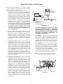
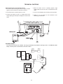
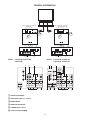
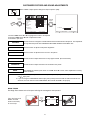
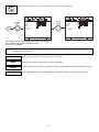
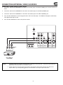
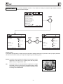
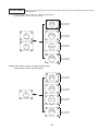
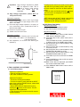
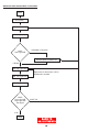
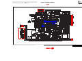
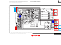
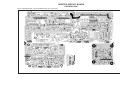
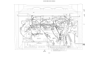
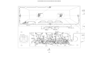
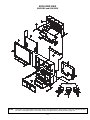
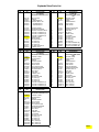
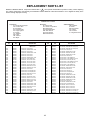
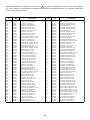
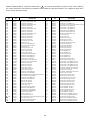
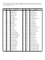
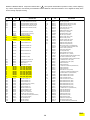
1
PA
SERVICE MANUAL
NTSC
DP14G DP17
Chassis
No. 0147
53SWX10B
53SWX12B
61SWX10B
61SWX12B
43UWX10B
53UWX10B
61UWX10B
R/C: CLU-5711TSI
CLU-5713TSI
TO GO TO A CHAPTER, CLICK ON IT'S HEADING
CONTENTS
IMPORTANT SAFETY INSTRUCTIONS . . . . . . . . . . . . . . . . . . . . . . . . . . . . . . . . . . . 2
SERVICING PRECAUTIONS . . . . . . . . . . . . . . . . . . . . . . . . . . . . . . . . . . . . . . . . . . . . 6
TECHNICAL CAUTIONS . . . . . . . . . . . . . . . . . . . . . . . . . . . . . . . . . . . . . . . . . . . . . . 10
SPECIFICATIONS . . . . . . . . . . . . . . . . . . . . . . . . . . . . . . . . . . . . . . . . . . . . . . . . . . . 11
CIRCUIT PROTECTION . . . . . . . . . . . . . . . . . . . . . . . . . . . . . . . . . . . . . . . . . . . . . . 11
CAUTIONS WHEN CONNECTING/DISCONNECTING THE HV CONNECTOR . . . . . .12
GENERAL INFORMATION . . . . . . . . . . . . . . . . . . . . . . . . . . . . . . . . . . . . . . . . . . . . .13
REMOTE CONTROL . . . . . . . . . . . . . . . . . . . . . . . . . . . . . . . . . . . . . . . . . . . . . . . . .14
CUSTOMIZED PICTURE AND SOUND ADJUSTMENTS . . . . . . . . . . . . . . . . . . . . . .15
REAR PANEL CONNECTION . . . . . . . . . . . . . . . . . . . . . . . . . . . . . . . . . . . . . . . . . . .17
DISPLAY PICTURE FORMATS . . . . . . . . . . . . . . . . . . . . . . . . . . . . . . . . . . . . . . . . . .23
SERVICE ADJUSTMENTS . . . . . . . . . . . . . . . . . . . . . . . . . . . . . . . . . . . . . . . . . . . . .29 Updated 02/12/07
TROUBLESHOOTING . . . . . . . . . . . . . . . . . . . . . . . . . . . . . . . . . . . . . . . . . . . . . . . .63 Remotes updated
See page 49a
WAVEFORMS . . . . . . . . . . . . . . . . . . . . . . . . . . . . . . . . . . . . . . . . . . . . . . . . . . . . . .66
DC VOLTAGE TABLES . . . . . . . . . . . . . . . . . . . . . . . . . . . . . . . . . . . . . . . . . . . . . . . .70
PROTECTION CIRCUIT BLOCK DIAGRAM . . . . . . . . . . . . . . . . . . . . . . . . . . . . . . . .80
CIRCUIT SCHEMATIC DIAGRAM . . . . . . . . . . . . . . . . . . . . . . . . . . . . . . . . . . . . . . . .82 Updated 12/30/02
PRINTED CIRCUIT BOARDS . . . . . . . . . . . . . . . . . . . . . . . . . . . . . . . . . . . . . . . . . .106
BLOCK DIAGRAM . . . . . . . . . . . . . . . . . . . . . . . . . . . . . . . . . . . . . . . . . . . . . . . . . .118
WIRING DIAGRAM . . . . . . . . . . . . . . . . . . . . . . . . . . . . . . . . . . . . . . . . . . . . . . . . . .119
FINAL WIRING DRAWING . . . . . . . . . . . . . . . . . . . . . . . . . . . . . . . . . . . . . . . . . . . .120
EXPLODED VIEW . . . . . . . . . . . . . . . . . . . . . . . . . . . . . . . . . . . . . . . . . . . . . . . . . .124
EXPLODED VIEW PARTS LIST . . . . . . . . . . . . . . . . . . . . . . . . . . . . . . . . . . . . . . . .126 Updated 09/09/02
REPLACEMENT PARTS LIST . . . . . . . . . . . . . . . . . . . . . . . . . . . . . . . . . . . . . . . . .127 Updated 02/03/03
QUICK REFERENCE PARTS LIST . . . . . . . . . . . . . . . . . . . . . . . . . . . . . . . . . . . . . .160 Updated 1/03/03
PWB Part Numbers added ............................................................................................................................... 162
CAUTION:
These servicing instructions are for use by qualified service personnel only. To reduce the risk of
electric shock do not perform any servicing other than that contained in the operating instructions
unless you are qualified to do so. Before servicing this chassis, it is important that the service
technician read the “IMPORTANT SAFETY INSTRUCTIONS” in this service manual.
SAFETY NOTICE
USE ISOLATION TRANSFORMER WHEN SERVICING
Components having special safety characteristics are identified by a ! on the schematics and on the parts list in this
Service Data and its supplements and bulletins. Before servicing the chassis, it is important that the service technician
read and follow the “Important Safety Instructions” in this Service Manual.
SPECIFICATIONS AND PARTS ARE SUBJECT TO CHANGE FOR IMPROVEMENT
PROJECTION COLOR TELEVISION
JUNE
2001
Version 0147.08
HHEA-MANUFACTURING DIVISION
IMPORTANT SAFETY INSTRUCTIONS
USE ISOLATION TRANSFORMER WHEN SERVICING
Components having special safety characteristics are identified by a ! on the schematics and on the parts list in this service
manual and its supplements and bulletins. Before servicing this chassis, it is important that the service technician read and
follow the “Important Safety Instructions” in this Service Manual.
For continued X-Radiation protection, replace picture tube with original type or Hitachi approved equivalent type.
This Service Manual is intended for qualified service technicians; it is not meant for the casual do-it-yourselfer. Qualified
technicians have the necessary test equipment and tools, and have been trained to properly and safely repair complex
products such as those covered by this manual.
Improperly performed repairs can adversely affect the safety and reliability of the product and may void warranty. If you
are not qualified to perform the repair of this product properly and safely, you should not risk trying to do so and refer the
repair to a qualified service technician.
WARNING
Lead in solder used in this product is listed by the California Health and Welfare agency as a known reproductive toxicant which
may cause birth defects or other reproductive harm (California Health and Safety Code, Section 25249.5).
When servicing or handling circuit boards and other components which contain lead in solder, avoid unprotected skin contact
with solder. Also, when soldering do not inhale any smoke or fumes produced.
This television receiver provides display of television closed captioning in accordance with section 15.119 of the FCC rules.
FEDERAL COMMUNICATIONS COMMISSION NOTICE
This equipment has been tested and found to comply with the limits for a Class B digital device, pursuant to Part 15 of the
FCC Rules. These limits are designed to provide reasonable protection against harmful interference in a residential
installation. This equipment generates, uses, and can radiate radio frequency energy and, if not installed and used in
accordance with the instructions, may cause harmful interference to radio communications. However, there is no guarantee
that interference will not occur in a particular installation. If this equipment does cause harmful interference to radio or
television reception, which can be determined by turning the equipment off and on, the user is encouraged to try to correct
the interference by one or more of the following measures:
¥
¥
¥
¥
Reorient or relocate the receiving antenna.
Increase the separation between the equipment and the receiver.
Connect the equipment into an outlet on a circuit different from that to which the receiver is connected.
Consult the dealer or an experienced radio/television technician for help.
2
IMPORTANT SAFETY INSTRUCTION
1. Before returning an instrument to the customer, always
make a safety check of the entire instrument, including
but not limited to the following items.
a. Be sure that no built-in protective devices are
defective and/or have been deleted during servicing.
(1) Protective shields are provided on this chassis to
protect both the technician and the customer.
Correctly replace all missing protective shields,
including any removed for servicing convenience. (2)
When reinstalling the chassis and/or other assembly
in the cabinet, be sure to put back in place all
protective devices, including but not limited to,
nonmetallic control knobs, insulating fishpaper,
adjustment and compartment covers/shields, and
isolation resistor/capacitor networks. Do not operate
this instrument or permit it to be operated without
all protective devices correctly installed and
functioning. Servicers who defeat safety features
or fail to perform safety checks may be liable for
any resulting damage.
(READING
SHOULD NOT
LEAKAGE
CURRENT BE ABOVE 0.5mA)
TESTER
DEVICE
UNDER
TEST
TEST ALL
EXPOSED
METAL SURFACES
EARTH
GROUND
2-WIRE CORD
ALSO TEST WITH PLUG
REVERSED
(USING AC ADAPTER
PLUS AS REQUIRED)
AC Leakage Test
ANY MEASUREMENTS NOT WITHIN THE LIMITS
SPECIFIED HEREIN INDICATE A POTENTIAL
SHOCK HAZARD THAT MUST BE ELIMINATED
BEFORE RETURNING THE INSTRUMENT TO THE
CUSTOMER OR BEFORE CONNECTING THE
ANTENNA OR ACCESSORIES.
b. Be sure that there are no cabinet openings through
which an adult or child might be able to insert their
fingers and contact a hazardous voltage. Such
openings include, but are not limited to (1) spacing
between the picture tube and cabinet mask, (2)
excessively wide cabinet ventilation slots, and (3) an
improperly fitted and/or incorrectly secured cabinet
back cover.
e. High Voltage — This receiver is provided with a hold
down circuit for clearly indicating that voltage has
increased in excess of a predetermined value.
Comply will all notes described in this Service Manual
regarding this hold down circuit when servicing, so
that this hold down circuit may correctly be operated.
c. Antenna Cold Check —With the instrument AC plug
removed from any AC source, connect an electrical
jumper across the two AC plug prongs. Place the
instrument AC switch in the on position. Connect one
lead of an ohmmeter to the AC plug prongs tied
together and touch the other ohmmeter lead in turn to
each tuner antenna input, exposed terminal screw
and, if applicable, to the coaxial connector. If the
measured resistance is less than 1.0 megohms or
greater than 5.2 megohms, an abnormality exists that
must be corrected before the instrument is returned to
the customer. Repeat this test with the instrument AC
switch in the off position.
f. Service Warning — With maximum contrast, operating
high voltage in this receiver is lower than 31.5 kV. In
case any component having influence on high voltage
is replaced, confirm that the high voltage with
maximum contrast is lower than 31.5 kV.
To measure H.V. use a high impedance H.V. meter.
Connect (-) to chassis earth and (+) to the CRT anode
button. (See the following connection diagram.)
Note: Turn power switch off without fail before the
connection to the anode button is made.
d. Leakage Current Hot Check —With the instrument
completely reassembled, plug the AC line cord
directly into a 120V AC outlet. (Do not use an isolation
transformer during this test.) Use a leakage current
tester or a metering system that complies with
American National Standards Institute (ANSI) C101.0
Leakage Current for Appliances and Underwriters
Laboratories (UL) 1410, (50.7). With the instrument
AC switch first in the on position and then in the off
position, measure from a known earth ground (metal
waterpipe, conduit, etc.) to all exposed metal parts of
the instrument (antennas, handle bracket, metal
cabinet, screw heads, metallic overlays, control
shafts, etc.), especially any exposed metal parts that
offer an electrical return path to the chassis. Any
current measured must not exceed 0.5 milliamps.
Reverse the instrument power cord plug in the outlet
and repeat test.
Chassis
ground
High Impedance
H.V. meter
FBT
(TH01)
High voltage
connector
Deflection P.W.B.
3
IMPORTANT SAFETY INSTRUCTIONS
g. X-radiation – TUBE: The primary source of Xradiation in this receiver is the picture tube. The tube
utilized for the above mentioned function in this
chassis is specially constructed to limit X-radiation
emissions.
For continued X-radiation protection, the replacement
tube must be the same type as the original, Hitachi
approved type.
When troubleshooting and making test measurements in a receiver with a problem of excessive high
voltage, avoid being unnecessarily close to the picture tube and the high voltage component.
Do not operate the chassis longer than is necessary
to locate the cause of excessive voltage.
h. X-radiation Shield –
1. This receiver is provided with X-ray shield plates
for protection against X-radiation. Do not remove
X-ray shield plates A, B, or C shown in Fig. 1
unnecessarily, when troubleshooting and/or
making test measurements.
2. To prevent X-radiation, after replacement of
picture tube and lens, confirm these components
to be fixed correctly to bracket and cabinet, and
not to be taken off easily.
Shield Plate A
Glass Lens for Shielding
Shield Plate B
Shield Plate C
Shield Plate C
Shield Plate D
Detailing X-radiation shield
Fig. 1. Installation of shield lens, shield cover and shield plates (oblique view).
4
IMPORTANT SAFETY INSTRUCTIONS
7. Components, parts, and/or wiring that appear to have
overheated or are otherwise damaged should be
replaced with components, parts, or wiring that meet
original specifications. Additionally, determine the
cause of overheating and/or damage and, if
necessary, take corrective action to remove any
potential safety hazard.
2. Read and comply with all caution and safety-related
notes on or inside the receiver cabinet, on the
receiver chassis, or on the picture tube.
3. Design Alteration Warning – Do not alter or add to
the mechanical or electrical design of this TV receiver.
Design alterations and additions including but not
limited to circuit modifications and the addition of
items such as auxiliary audio and/or video output
connectors, might alter the safety characteristics of
this receiver and create a hazard to the user. Any
design alterations or additions may void the
manufacturer’s warranty and may make you, the
servicer, responsible for personal injury or property
damage resulting therefrom.
8. PRODUCT SAFETY NOTICE – Many TV electrical
and mechanical parts have special safety-related
characteristics some of which are often not evident
from visual inspection, nor can the protection they
give necessarily be obtained by replacing them with
components rated for higher voltage, wattage, etc.
Parts that have special safety characteristics are
identified in Hitachi service data by shading on
schematics and by a ! in the parts list. Use of
substitute replacement that does not have the same
safety characteristics as the recommended replacement part in Hitachi service data parts list might
create shock, fire, and/or other hazards. Product
safety is under review continuously and new
instructions are issued whenever appropriate. For the
latest information, always consult the appropriate
current Hitachi service literature. A subscription to, or
additional copies of service literature may be obtained
at a nominal charge from Hitachi.
4. Picture Tube Implosion Protection Warning – The
picture tube in this receiver employs integral
implosion protection. For continued implosion
protection, replace the picture tube only with one of
the same type number. Do not remove, install, or
otherwise handle the picture tube in any manner
without first putting on shatterproof goggles equipped
with side shields. People not so equipped must be
kept safely away while picture tubes are handled.
Keep the picture tube away from your body. Do not
handle the picture tube by its neck.
5. Hot Chassis Warning – a. Some TV receiver chassis
are electrically connected directly to one conductor of
the AC power cord and may be safely serviced
without an isolation transformer only if the AC power
plug is inserted so that the chassis is connected to the
ground side of the AC power source. Confirm that the
AC power plug is inserted correctly with an AC
voltmeter by measuring between the chassis and a
known earth ground. If a voltage reading in excess of
1.0V is obtained, remove and reinsert the AC power
plug in the opposite polarity and again measure the
voltage potential between the chassis and a known
earth ground. b. Some TV receiver chassis normally
have 85V AC (RMS) between chassis and earth
ground regardless of the AC plug polarity. These
chassis can be safely serviced only with an isolation
transformer inserted in the power line between the
receiver and the AC power source, for both personnel
and test equipment protection. c. Some TV receiver
chassis have a secondary ground system in addition
to the main chassis ground. This secondary ground
system is not isolated from the AC power line. The two
ground systems are electrically separated by
insulating material that must not be defeated or
altered.
6. Observe original lead dress. Take extra care to assure
correct lead dress in the following areas: a. near
sharp edges, b. near thermally hot parts – be sure
that leads and components do not touch thermally hot
parts, c. the AC supply, d. high voltage and e. antenna
wiring. Always inspect in all areas for pinched, out-ofplate, or frayed wiring. Do not change spacing
between components and the printed circuit board.
Check AC power cord for damage.
5
SERVICING PRECAUTIONS
CAUTION: Before servicing instruments covered by this
service data and its supplements and addenda, read and
follow the “Important Safety Instructions” on page 3 of this
publication.
NOTE: If unforeseen circumstances create conflict between
the following servicing precautions and any of the safety
precautions on page 3 of this publication, always follow the
safety precautions. Remember: Safety First.
7. Do not apply AC power to this instrument and/or any of its
electrical assemblies unless all solid-state device heatsinks are correctly installed.
General Servicing Guidelines
1. Always unplug the instrument AC power cord from the AC
power source before:
a. Removing or reinstalling any component, circuit
board, module, or any other instrument assembly.
9. Use with this instrument only the test fixtures specified in
this service data.
CAUTION: Do not connect the test fixture ground strap
to any heatsink in this instrument.
8. Always connect the test instrument ground lead to the
appropriate instrument chassis ground before connecting
the test instrument positive lead. Always remove the test
instrument ground lead last.
Electrostatically Sensitive (ES) Devices
Some semiconductor (solid state) devices can be damaged
easily by static electricity. Such components commonly are
called Electrostatically Sensitive (ES) Devices. Examples of
typical ES devices are integrated circuits and some fieldeffect transistors and semiconductor “chip” components. The
following techniques should be used to help reduce the
incidence of component damage caused by static electricity.
b. Disconnecting or reconnecting any instrument
electrical plug or other electrical connection.
c. Connecting a test substitute in parallel with an
electrolytic capacitor in the instrument.
CAUTION: A wrong part substitution or incorrect
polarity installation of electrolytic
capacitors may result in an explosion
hazard.
1. Immediately before handling any semiconductor
component or semiconductor-equipped assembly, drain
off any electrostatic charge on your body by touching a
known earth ground. Alternatively, obtain and wear a
commercially available discharging wrist strap device,
which should be removed for potential shock reasons
prior to applying power to the unit under test.
d. Discharging the picture tube anode.
2. Test high voltage only by measuring it with an appropriate
high voltage meter or other voltage measuring device
(DVM, FETVOM, etc.) equipped with a suitable high
voltage probe. Do not test high voltage by “drawing an
arc.” The H.V. Distribution Box has an internal 400MΩ
resistor (bleeder resistor) connected from the high
voltage to ground. After power is removed from the
instrument the high voltage will discharge through the
high voltage bleeder resistor. If the tubes have high
voltage after power is removed, then the bleeder resistor
is defective or the bleeder ground is disconnected.
2. After removing an electrical assembly equipped with ES
devices, place the assembly on a conductive surface
such as aluminum foil, to prevent electrostatic charge
buildup or exposure of the assembly.
3. Use only a grounded-tip soldering iron to solder or
desolder ES devices.
3. Discharge the picture tube’s anode at any of the R, G, or
B outputs on the H.V. Distribution Box only by (a) first
connecting one end of an insulated clip lead to the
degaussing or kine aquadag grounding system shield at
the point where the picture tube socket ground lead is
connected, and then (b) touch the other end of the
insulated clip lead to the picture tube high voltage
distribution box R, G, or B output, using an insulated
handle to avoid personal contact with high voltage.
4. Use only can anti-static type solder removal device.
Some solder removal devices not classified as “antistatic” can generate electrical charges sufficient to
damage ES device.
5. Do not use freon-propelled chemicals. These can
generate electrical charges sufficient to damage ES
devices.
6. Do not remove a replacement ES device from its
protective package until immediately before you are
ready to install it. (Most replacement ES devices are
packaged with leads electrically shorted together by
conductive foam, aluminum foil or comparable conductive
material.)
4. Do not spray chemicals on or near this instrument or any
of its assemblies.
5. Unless specified otherwise in these service data, clean
electrical contracts by applying the following mixture to
the contacts with a pipe cleaner, cotton-tipped stick or
comparable nonabrasive applicator: 10% (by volume)
Acetone and 90% (by volume) isopropyl alcohol (90%99% strength).
CAUTION: This is a flammable mixture. Unless
specified otherwise in these service data,
lubrication of contacts is not required.
7. Immediately before removing the protective material from
the leads of a replacement ES device, touch the
protective material to the chassis or circuit assembly into
which the device will be installed.
CAUTION: Be sure no power is applied to the chassis or
circuit, and observe all other safety
precautions.
6. Do not defeat any plug/socket B+ voltage interlocks with
which instruments covered by this service data might be
equipped.
6
8. Minimize bodily motions when handling unpackaged
replacement ES devices. (Otherwise harmless motion
such as the brushing together of your clothes fabric or the
lifting of your foot from a carpeted floor can generate
General Soldering Guidelines
1. Use a grounded-tip, low-wattage soldering iron and
appropriate tip size and shape that will maintain tip
temperature within the range 500°F to 600°F.
Removal
1. Desolder and straighten each IC lead in one operation by
gently prying up on the lead with the soldering iron tip as
the solder melts.
2. Use an appropriate gauge of resin-core solder composed
of 60 parts tin/40 parts lead.
2. Draw away the melted solder with an anti-static suctiontype solder removal device (or with solder braid) before
removing the IC.
3. Keep the soldering iron tip clean and well-tinned.
Replacement
1. Carefully insert the replacement IC in the circuit board.
4. Thoroughly clean the surfaces to be soldered. Use a
small wire-bristle (0.5 inch or 1.25 cm) brush with a metal
handle. Do not use freon-propelled spray-on cleaners.
2. Carefully bend each IC lead against the circuit foil pad
and solder it.
5. Use the following desoldering technique.
a. Allow the soldering iron tip to reach normal
temperature (500°F to 600°F).
3. Clean the soldered areas with a small wire-bristle brush.
(It is not necessary to reapply acrylic coating to areas.)
b. Heat the component lead until the solder melts.
Quickly draw away the melted solder with an antistatic, suction-type solder removal device or with
solder braid.
CAUTION: Work quickly to avoid overheating the
circuit board printed foil.
“Small-signal” Discrete Transistor Removal/Replacement
1. Remove the defective transistor by clipping its leads as
close as possible to the component body.
2. Bend into a “U” shape the end of each of three leads
remaining on the circuit board.
6. Use the following soldering technique.
a. Allow the soldering iron tip to reach normal
temperature (500°F to 600°F).
3. Bend into a “U” shape the replacement transistor leads.
4. Connect to replacement transistor leads to the
corresponding leads extending from the circuit board and
crimp the “U” with long nose pliers to insure metal to
metal contact, then solder each connection.
b. First, hold the soldering iron tip and solder strand
against the component lead until the solder melts.
c. Quickly move the soldering iron tip to the junction of
the component lead and the printed circuit foil, and
hold it there only until the solder flows onto and
around both the component lead and the foil.
CAUTION: Work quickly to avoid overheating the
circuit board printed foil or components.
Power Output Transistor Devices Removal/Replacements
1. Heat and remove all solder from around the transistor
leads.
2. Remove the heatsink mounting screw (if so equipped).
3. Carefully remove the transistor from the circuit board.
d. Closely inspect the solder area and remove any
excess or splashed solder with a small wire-bristle
brush.
4. Insert new transistor in circuit board.
5. Solder each transistor lead, and clip off excess lead.
6. Replace heatsink.
Diode Removal/Replacement
1. Remove defective diode by clipping its leads as close as
possible to diode body.
2. Bend the two remaining leads perpendicularly to the
circuit board.
3. Observing diode polarity, wrap each lead of the new
diode around the corresponding lead on the circuit board.
Use Solding Iron to Pry Leads
IC Removal/Replacement
Some Hitachi unitized chassis circuit boards have slotted
holes (oblong) through which the IC leads are inserted and
then bent flat against the circuit foil. When holes are the
slotted type, the following technique should be used to
remove and replace the IC. When working with boards using
the familiar round hole, use the standard technique as
outlined in paragraphs 5 and 6 above.
4. Securely crimp each connection and solder it.
5. Inspect (on the circuit board copper side) the solder joints
of the two “original leads”. If they are not shiny, reheat
them and, if necessary, apply additional solder.
7
At Other Connections
Use the following technique to repair defective copper
pattern at connections other than IC Pins. This technique
involves the installation of a jumper wire on the component
side of the circuit board.
Fuses and Conventional Resistor Removal/Replacement
1. Clip each fuse or resistor lead at top of circuit board
hollow stake.
2. Securely crimp leads of replacement component around
stake 1/8 inch from top.
3. Solder the connections.
CAUTION: Maintain original spacing between the
replaced component and adjacent
components and the circuit board, to
prevent
excessive
component
temperatures.
DEFECTIVE
COPPER
REMOVED
Circuit Board Foil Repair
Excessive heat applied to the copper foil of any printed
circuit board will weaken the adhesive that bonds the foil to
the circuit board, causing the foil to separate from, or “liftoff,” the board. The following guidelines and procedures
should be followed whenever this condition is encountered.
Insulated Jumper Wire
In Critical Copper Pattern Areas
High component/copper pattern density and/or special
voltage/current characteristics make the spacing and
integrity of copper pattern in some circuit board areas more
critical than in others. The circuit foil in these areas is
designated as Critical Copper Pattern. Because Critical
Copper Pattern requires special soldering techniques to
ensure the maintenance of reliability and safety standards,
contact your Hitachi personnel.
1. Remove the defective copper pattern with a sharp knife.
Remove at least 1/4 inch of copper, to ensure hazardous
condition will not exist if the jumper wire opens.
2. Trace along the copper pattern from both wire sides of
the pattern break and locate the nearest component
directly connected to the affected copper pattern.
At IC Connections
To repair defective copper pattern at IC connections, use the
following procedure to install a jumper wire on the copper
pattern side of the circuit board. (Use this technique only on
IC connections.)
1. Carefully remove the damaged copper pattern with a
sharp knife. (Remove only as much copper as absolutely
necessary.)
3. Connect insulated 20-gauge jumper wire from the
nearest component on one side of the pattern break to
the lead of the nearest component on the other side.
Carefully crimp and solder the connections.
CAUTION: Be sure the insulated jumper wire is
dressed so that it does not touch
components or sharp edges.
2. Carefully scratch away the solder resist and acrylic
coating (if used) from the end of the remaining copper
pattern.
Frequency Synthesis (FS) Tuning Systems
1. Always unplug the instrument AC power cord before
disconnecting or reconnecting FS tuning system cables
and before removing or inserting FS tuning system
modules.
2. The FS tuner must never be disconnected from the FS
tuning control module while power is applied to the
instrument.
BARE JUMPER
WIRE
3. When troubleshooting intermittent problems that might be
caused by defective cable connection(s) to the FS tuning
system, remove the instrument AC power as soon as the
defective connector is found and finish confirming the
bad connection with a continuity test. This procedure will
reduce the probability of electrical overstress of the FS
system semi-conductor components.
CRIMP AND
SOLDER
Install Jumper Wire and Solder
3. Bend a small “U” in one end of a small-gauge jumper wire
and carefully crimp it around the IC pin. Solder the IC
connection.
4. Route the jumper wire along the path of the cut-away
copper pattern and let it overlap the previously scraped
end of the good copper pattern. Solder the overlapped
area, and clip off any excess jumper wire.
8
NOTE: These components are affixed with glue. Be careful not to break or damage any foil under the
component or at the pins of the ICs when removing. Usually applying heat to the component for a short
time while twisting with tweezers will break the component loose.
Leadless Chip Components
(surface mount)
How to Replace Flat-lC
—Required Tools—
Chip components must be replaced with identical
chips due to critical foil track spacing. There are no
holes in the board to mount standard transistors or
diodes. Some chip capacitor or resistor board solder
pads may have holes through the board, however the
hole diameter limits standard resistor replacement to
1/8 watt. Standard capacitors may also be limited for
the same reason. It is recommended that identical
chip components be used. .
Chip resistors have a three digit numerical resistance
code -1st and 2nd significant digits and a multiplier.
Example: 162 = 1600 or 1.6KΩ resistor, 0 = 0Ω
(jumper).
Chip capacitors generally do not have the value
indicated on the capacitor. The color of the component
indicates the general range of the capacitance.
Chip transistors are identified by a two letter code. The
first letter indicates the type and the second letter, the
grade of transistor.
Chip diodes have a two letter identification code as
per the code chart and are a dual diode pack with
either
common anode or common cathode. Check the parts
list for correct diode number.
• Soldering iron
• iron wire or small awl
• De-solder braids
• Magnifier
1. Remove the solder from all of the pins of a Flat-lC
by using a de-solder braid.
De-Solder
Braid
Soldering
Iron
2. Put the iron wire under the pins of the Flat-lC and
pull it in the direction indicated while heating the
pins using a soldering iron. A small awl can be
used instead of the iron wire.
Iron
Wire
Awl
Pull
Soldering
Iron
Soldering
Iron
3. Remove the solder from all of the pads of the
Fiat-lC by using
Soldering
a de-solder braid.
Iron
Component Removal
1. Use solder wick to remove solder from component
end caps or terminals.
2. Without pulling up, carefully twist the component
with tweezers to break the adhesive.
3. Do not reuse removed leadless or chip
components since they are subject to stress
fracture during removal .
De-Solder
Braid
Flat-IC
4. Position the new Flat-lC in place (apply the pins of
the Flat-lC to the soldering pads where the pins
need to be soldered). Properly
Polarity Symbol
determine the positions of the
soldering pads and pins by
correctly aligning the polarity
symbol.
Chip Component Installation
1. Put a small amount of solder on the board
soldering pads.
2. Hold the chip component against the soldering
pads with tweezers or with a miniature alligator
clip and apply heat to the pad area with a 30 watt
iron until solder flows. Do not apply heat for more
than 3 seconds
5. Solder all pins to the soldering pads using a fine
tipped soldering iron.
Chip Components
TYPE
C
B
SOLDER
CAPS
GRADE
TRANSISTOR
E
Soldering
Iron
CAPACITOR
1ST DIGIT
6. Check with a magnifier for solder bridge between
the pins or for dry joint between pins and soldering
pads. To remove a solder bridge, use a de-solder
braid as shown in the figure below.
2ND DIGIT
COMMON CATHODE
MULTIPLIER
= 1600 = 1.6K
ANODES
De-Solder
Braid
SOLDER CAPS
MH DIODE
RESISTOR
Bridge
Solder
9
Soldering
Iron
TECHNICAL CAUTIONS
High Voltage limiter circuit operation check.
1. Turn off TV and connect jig as shown in Figure 2. Adjust
jig fully counter-clockwise for minimum resistance.
4. When the limiter circuit is operating properly, High
Voltage will be less than 31.5 kV at 1.7mA when TV shuts
down.
2. Set the AC input to 120V AC and turn on TV.
5. Turn off set immediately after checking circuit operation.
3. Confirm test pattern on CRT is a usable picture, then
slowly adjust jig until the picture disappears and TV shuts
down.
6. Unplug set for one minute to reset shutdown circuit.
Remove jig and voltmeter.
(TH01)
AC CORD POLARITY
This check is based on the UL standard. Use the jigs specified by the production technology section. The GND side (wider
blade) of the AC power cord should be connected to K9Y1
EF901
EF901
F901
L901
C901
R901
L902
2
PA
1
KKA1
WHITE side
GND side
TESTER
10
SPECIFICATIONS
61SWX10B
43UWX10B
61SWX12B
53UWX10B
53SWX10B
61UWX10B
53SWX12B
Cathode-Ray Tube:
61SWX10B
R=P16LFT00RFA(LU)
61SWX12B
G=P16LFT00HHA(LU)
53SWX10B
B=P16LFT00BMB(EU)
53SWX12B
Model:
53UWX10B
61UWX10B
R=P16LSG03RJA
G=P16LSG03HKA
B=P16LSG03BMB
43UWX10B
R=P16LTG00RFA
G=P16LTG00HHA
B=P16LTG00BMB
BAND
VHF
UHF
EXT. Mid
CATV Mid.
CATV Super
CATV Hyper
1 Volt p-p, 75 Ohm
Video Output:
1 Volt p-p, 75 ohm
Audio Input:
470 mVrms, 47 k Ohm
Stereo Audio Output:
Audio Output Power:
470 mVrms, 1 k Ohm
Anode Voltage:
30.2±0.2kv (1.20±0.2mA)
DP14G
DP17
31.7kv±0.2kv (1.10±0.2mA)
Brightness:
43
53
2
260cd/m2
(white screen) 320cd/m
Speakers:
61
190cd/m2
2 Woofers - 5 inch (120 mm) round
2 Tweeters - 2 inch (50 mm) round
Dimension:
43
Height (in.)
Width (in.)
39
41
7/32
20
5/
8
Depth (in.)
Weight (Ibs.) 153
75 Ohm Unbalanced
VHF / UHF / CATV
Receiving Channel:
Video Input:
8 ohm Impedance. Max output — 15 watts.
Power Consumption:
• Stand-By Power
43/53/61UWX10B . . . . . . . . . . . . . . . .2.7W
53/61SWX10B . . . . . . . . . . . . . . . . . . .2.8W
53/61SWX12B . . . . . . . . . . . . . . . . . . .2.8W
• Power Consumption (operating)
43/53/61UWX10B . . . . . . . . . . . . . . . .219W
53/61SWX10B . . . . . . . . . . . . . . . . . .234W
53/61SWX12B . . . . . . . . . . . . . . . . . .234W
• Power Consumption (maximum)
43/53/61UWX10B . . . . . . . . . . . . . . . .262W
53/61SWX10B . . . . . . . . . . . . . . . . . .295W
53/61SWX12B . . . . . . . . . . . . . . . . . .295W
Antenna Impedance:
Picture l-F Carrier 45.75 MHz
Sound l-F Carrier 41.25 MHz
Color Sub Carrier 42.17 MHz
Front: 12 watts per channel at 10% distortion,
120 volts AC, 60 Hz
Power Input:
Intermediate Frequency:
53
29
245
350
50
1/
32
17/
32
61
7/
32
57 1/2
29 19/32
54
61
Circuit Board Assemblies:
CH
2~13
14~69
(A-5)~(A-1), 4+
A~I
J~W
(W+1)~(W+28)
C.P.T. (B) P.W.B.
Terminal A P.W.B.
C.P.T. (G) P.W.B.
Terminal B P.W.B.
C.P.T. (R) P.W.B.
VM P.W.B.
Audio Out P.W.B.
Surround P.W.B.
2H P.W.B.
Power Deflection P.W.B.
Power Supply P.W.B. Control P.W.B.
Signal P.W.B.
Control Sub P.W.B.
Convergence P.W.B.
Sensor Distribution P.W.B.
CIRCUIT PROTECTION
CAUTION:
Below is an EXAMPLE only. See Replacement Parts List for details. The following symbol near the fuse
indicates fast operation fuse (to be replaced). Fuse ratings appear within the symbol.
Example:
125V
F
5A
5 A 125V
The rating of fuse F901 is 5A - 125V.
Replace with the same type fuse for continued protection
against fire.
RISK OF FIRE - REPLACE FUSE AS MARKED
11
CAUTIONS WHEN CONNECTING / DISCONNECTING THE HV CONNECTOR
Perform the following when the
HV connector (anode connector)
is removed or inserted for CPT
replacement, etc.
Anode
connector
Deflection P.W.B.
FBT
During Removal
1.
2.
PUSH
Roll out silicon cover from FBT’s contact area slowly.
While turning the connector about 90 degrees
following the arrow (0 position), push the connector
slightly towards the case. (Fig. A)
PUSH
Fig. A
Silicon cover
3.
Remove the connector slowly
by pulling it away from the
case.
Wing
Wing
L Position
L Position
Fig. B
During Insertion
1.
2.
3.
4.
Please refer to direction for insertion as shown in Fig. B (L position). Insert connector until “CLICK” sound is heard.
Make sure the connector is pressed right in, so that it has a good contact with the spring.
Confirm the contact by pulling the connector slightly. (Don’t pull hard because it may damage the connector).
Cover the high voltage output by carefully pushing silicon cover onto it. (Don’t turn the connector).
1.
(REMARK)
Make sure the silicon cover is
covering the high voltage output.
Silicon Cover
less than 1mm
12
GENERAL INFORMATION
Models: 61UWX10B, 53UWX10B,
43UWX10B
POWER
PUSH
PUSH
INPUT
MENU
VOL-
EXIT
SELECT
VOL+
CH-
CH+
INPUT
MENU
VOL-
EXIT
SELECT
CURSOR
VOL+
CH-
CH+
CURSOR
INPUT 3
INPUT 3
L/MONO R
S-VIDEO VIDEO
AUDIO
L/MONO R
S-VIDEO VIDEO
AUDIO
MAGIC
FOCUS
61UWX10B, 53UWX10B,
43UWX10B
Models:
MAGIC
FOCUS
Models:
POWER
Models: 61SWX10B, 61SWX12B,
53SWX10B, 53SWX12B
61SWX10B, 61SWX12B
53SWX10B, 53SWX12B
OPTICAL
INPUT
ANT A
COAXIAL
INPUT
STOP
ANT A
CONNECT ONLY 8 OHM SPEAKERS
DO NOT SHORT CIRCUIT
THESE TERMINALS
(Such damage is NOT COVERED
by your television warranty)
TO
CONVERTER
REAR SPEAKER
S-VIDEO
S-VIDEO
TO
CONVERTER
S-VIDEO
S-VIDEO
S-VIDEO
S-VIDEO
L
ANT B
VIDEO
VIDEO
(MONO)
(MONO)
Y/VIDEO
ANT B
VIDEO
Y/VIDEO
VIDEO
VIDEO
(MONO)
(MONO)
Y/VIDEO
VIDEO
Y/VIDEO
R
L
L
PB (MONO)
L
PR
R
AUDIO TO HI-FI
AUDIO
R
PB (MONO)
L
L
AUDIO
R
AUDIO
R
AUDIO TO HI-FI
AUDIO
L
R
INPUT 1
INPUT 2
INPUT 4
L
PB
L
PR
R
R
AUDIO
L
PR
(MONO)
INPUT 5
SUB
WOOFER
R
AUDIO
INPUT 1
Antenna Input/Output
Audio/Video Inputs 1, 2, 4 and 5
MONITOR OUT
AUDIO TO HI-FI Output
S-VIDEO Inputs 1 and 2
Component Input Y-PBPR
13
R
R
AUDIO
AUDIO
L
L
PR
R
AUDIO
R
AUDIO
L
MONITOR
OUT
PB
(MONO)
INPUT 2
INPUT 4
INPUT 5
MONITOR
OUT
USE THE REMOTE TO CONTROL YOUR TV
POWER
POWER
VCR
TV
CBL
STB
VCR
TV
SOURCE WIZARD
AV3
CD
DVD
TAPE
AMP
1
2
3
1
2
3
4
5
6
4
5
6
7
8
9
7
8
9
0
SLEEP
LAST CH
HELP
C.C.
ANT
ASPECT
EX
NU
ME
MUT
SV
VCR
1
VID
CH
VID 3
PIP
PIP CH
PIP MODE
PROG
D5
VID
VI
VID
VID 4
CH
INFO
FREEZE
PIP
2
PIP CH
PIP MODE
SLOW
PROG
REC
HD
SC
/TV
GUIDE
VID 3
PIP ACCESS
SWAP
TV/VCR
1
VID
VID 4
FREEZE
PIP ACCESS
SWAP
TV/VCR
SLOW
REC
CLU-5711TSI
CLU-5713TSI
CLU-5711TSI
CLU-5713TSI
14
E
US
PLUS
+
MOD
IT
STAT
E
CS
VCR
/T
GUIDE
2
EX
MUT
SV
HD
SC
ASPECT
SELECT
VOL
V
INFO
HELP
C.C.
ANT
NU
US
PLUS
+
PIX
LAST CH
ME
STAT
E
CS
0
SLEEP
IT
SELECT
VOL
VID
STB
SOURCE WIZARD
AV2
AV1
DVD
CBL
5
CUSTOMIZED PICTURE AND SOUND ADJUSTMENTS
Select VIDEO to adjust picture settings and improve picture quality.
VIDEO
SETUP
CUSTOMIZE
VIDEO
AUDIO
THEATER
SEL
THUMB
STICK
NU
ME
Contrast
Brightness
Color
Tint
Sharpness
Reset
Advanced
Settings
Menu
To Menu Bar
100%
50%
50%
THUMB
STICK
50%
Co n tr a s t
To Quit
Menu
Exit
To Menu Bar
100%
To Quit
Exit
Use the THUMB STICK or to highlight the function to be adjusted.
Press the THUMB STICK or to adjust the function.
Press EXIT to quit menu.
CONTRAST
BRIGHTNESS
COLOR
TINT
SHARPNESS
RESET
NOTE:
Use this function to change the contrast between black and white levels in the picture. This adjustment
will only affect the picture when ADVANCED SETTINGS PERFECT PICTURE is OFF.
Use this function to adjust overall picture brightness.
Use this function to adjust the level of color in the picture.
Use this function to adjust flesh tones so they appear natural. (See notes below.)
Use this function to adjust the amount of fine detail in the picture.
When RESET is selected, press down on THUMB STICK to return video adjustments to factory
preset conditions.
1. It may be necessary to adjust TINT to obtain optimum picture quality when using the COMPONENT:
Y-PBPR Input jacks.
2. If you are using the COMPONENT VIDEO input jacks (Y-PBPR) and notice that the TINT and COLOR are
abnormal, check to make sure that COMPONENT SET-COLOR SYSTEM is set properly.
MAGIC FOCUS
The Magic Focus button on the front panel will align the convergence when pressed.
Press the front panel
MAGIC FOCUS
button momentarily
for auto setup.
MAGIC
FOCUS
MAGIC FOCUS
15
Select AUDIO to adjust the TV to your preference and to improve the sound quality.
AUDIO
SETUP
CUSTOMIZE
VIDEO
AUDIO
SETUP
THEATER
THUMB
STICK
NU
ME
Ba s s
Tre b le
Ba la n c e
Re s e t
Ad v a n c e d
Se ttin g s
Menu
CUSTOMIZE
VIDEO
AUDIO
THEATER
SEL
SEL
To M e n u B a r
THUMB
STICK
50%
50%
To Q u i t
Exit
Bass
T r ebl e
B al anc e
Res et
A dv anc ed
S etti ngs
Menu
To M e n u B a r
90%
50%
To Q u i t
Exit
Use THUMB STICK or to highlight the function to be adjusted.
Press THUMB STICK or to adjust the function.
Press EXIT to quit MENU.
NOTE:
If BASS is selected you are adjusting BASS. The additional menu items TREBLE and BALANCE can be selected and
adjusted in the same manner.
BASS
This function controls the low frequency audio to all speakers.
TREBLE
This function controls the high frequency audio to all speakers.
BALANCE
RESET
This function will control the left to right balance of the TV internal speakers and the AUDIO TO HI FI output.
When RESET is selected, press CURSOR to return audio adjustments to factory preset conditions.
16
REAR PANEL CONNECTIONS
TYPICAL FULL-FEATURE SETUP
43/53/61UWX10B
Outside antenna or
cable TV coaxial cable
2-Way signal splitter
DVD Player
VCR #1
ANT
IN
OUTPUT
S-VIDEO
V
L
OUTPUT
PB/CB PR/CR L
Y
R
R
VCR #2
S-VIDEO
ANT A
TO
CONVERTER
ANT B
S-VIDEO
S-VIDEO
VIDEO
VIDEO
Y/VIDEO
(MONO)
(MONO)
S-VIDEO
L
L
PB (MONO)
L
PR
L
R
INPUT
R
AUDIO TO HI-FI
AUDIO
R
L
L
R
AUDIO
R
AUDIO
R
AUDIO
L
INPUT 1
Stereo System Amplifier
PB (MONO)
PR
R
AUDIO
VIDEO
Y/VIDEO
OUTPUT
INPUT 2
INPUT 4
INPUT 5
MONITOR
OUT
INPUT
Cable TV Box
S-VIDEO V
L
OUTPUT
R
Laserdisc player, VCR,
camcorder, etc.
NOTE:
Y
PB PR
OUTPUT
HDTV Set-Top Box
1. Connect only 1 component to each input jack.
2.
3.
Follow connections that pertain to your personal entertainment system.
Standard video signal (composit video) can be input to all video inputs. (Video 1 ~ VIdeo 5).
17
L
R
INPUT
V
L
R
TYPICAL FULL-FEATURE SETUP
53/61SWX10B AND 53/61SWX12B
Outside antenna or
cable TV coaxial cable
2-Way signal splitter
DVD Player
VCR #1
ANT
IN
OUTPUT
S-VIDEO
V
L
Y
R
OUTPUT
PB/CB PR/CR L
R
VCR #2
S-VIDEO
Surround Speakers
L
R
OPTICAL
INPUT
COAXIAL
INPUT
STOP
ANT A
CONNECT ONLY 8 OHM SPEAKERS
DO NOT SHORT CIRCUIT
THESE TERMINALS
(Such damage is NOT COVERED
by your television warranty)
REAR SPEAKER
-
-
+
TO
CONVERTER
+
S-VIDEO
S-VIDEO
VIDEO
VIDEO
S-VIDEO
L
ANT B
Y/VIDEO
VIDEO
Y/VIDEO
R
(MONO)
(MONO)
L
L
PB (MONO)
L
PR
AUDIO TO HI-FI
R
L
R
INPUT
SUB
WOOFER
R
AUDIO
L
L
R
AUDIO
AUDIO
R
AUDIO
L
INPUT 1
Stereo System Amplifier
R
R
AUDIO
PB (MONO)
PR
OUTPUT
INPUT 2
INPUT 4
INPUT 5
MONITOR
OUT
INPUT
Cable TV Box
INPUT
S-VIDEO V
L
OUTPUT
Sub Woofer
NOTE:
R
Laserdisc player, VCR,
camcorder, etc.
OR
Y
PB PR
OUTPUT
HDTV Set-Top Box
1. Connect only 1 component to each input jack.
2.
3.
Follow connections that pertain to your personal entertainment system.
Standard video signal (composit video) can be input to all video inputs. (Video 1 ~ VIdeo 5).
18
L
R
INPUT
V
L
R
CONNECTING EXTERNAL VIDEO SOURCES
CONNECTING A COMPONENT SOURCE TO VIDEO 4 OR 5: Y-PBPR.
1.
Connect the cable from the Y OUT of the Laserdisc/DVD player or HDTV set top box to the INPUT (Y) jack, as shown on the TV
set below.
2.
Connect the cable from the CB/PB OUT or B-Y OUT of the Laserdisc/DVD player or HDTV set top box to the INPUT (PB) jack.
3.
Connect the cable from the CR/PR OUT or R-Y OUT of the Laserdisc/DVD player or HDTV set top box to the INPUT (PR) jack.
4.
Connect the cable from the AUDIO OUT R of the Laserdisc/DVD player or HDTV set top box to the INPUT (AUDIO/R) jack.
5.
Connect the cable from the AUDIO OUT L of the Laserdisc/DVD player or HDTV set top box to the INPUT (AUDIO/L) jack.
6.
Press the VID4~VID5 button, to view the program from the Laserdisc/DVD player or HDTV set top box. The VIDEO icon
disappears automatically after approximately eight seconds.
7.
Press the ANT button to return to the previous channel.
DVD Player
Hitachi Model or
Similar Model
OPTICAL
OUT
L
R
OUTPUT
Y
PB
PR
OPTICAL
OUT
OR
Back of
DVD Player
OUTPUT
AUDIO
VIDEO
PR/CR PB/CB Y
L
R
HDTV Set-Top Box
OPTICAL
INPUT
COAXIAL
INPUT
STOP
ANT A
REAR SPEAKER
CONNECT ONLY 8 OHM SPEAKERS
DO NOT SHORT CIRCUIT
THESE TERMINALS
(Such damage is NOT COVERED
by your television warranty)
TO
CONVERTER
S-VIDEO
S-VIDEO
VIDEO
VIDEO
S-VIDEO
L
ANT B
Y/VIDEO
VIDEO
Y/VIDEO
R
(MONO)
(MONO)
L
L
PB (MONO)
L
PR
AUDIO TO HI-FI
R
SUB
WOOFER
R
AUDIO
L
L
PR
R
R
AUDIO
PB (MONO)
AUDIO
R
AUDIO
R
AUDIO
L
INPUT 1
INPUT 2
INPUT 4
INPUT 5
MONITOR
OUT
Rear Panel of Television
NOTE:
1. You may use standard video signal for INPUT:4 and 5.
2. Completely insert the connection cord plugs when connecting to rear panel jacks. The picture and sound that is
played back will be abnormal if the connection is loose.
3. See pages 17 and 18 for tips on REAR PANEL CONNECTIONS.
19
CONNECTING EXTERNAL VIDEO SOURCES
CONNECTING AN S-VIDEO SOURCE TO INPUT 1, 2 AND 3
1.
Connect the cable from the S-VIDEO OUT of the VCR or the laserdisc player to the INPUT (S-VIDEO) jack, as shown on the TV
set below.
2.
Connect the cable from the AUDIO OUT R of the VCR or the laserdisc player to the INPUT (AUDIO/R) jack.
3.
Connect the cable from the AUDIO OUT L of the VCR or the laserdisc player to the INPUT (AUDIO/L) jack.
4.
Press the VID1~VID3 button to view the program from the VCR or laserdisc player. The VIDEO icon disappears automatically
after approximately eight seconds.
5.
Press the ANT button to return to the previous channel.
Rear Panel of Television
ANT A
TO
CONVERTER
ANT B
S-VIDEO
S-VIDEO
VIDEO
VIDEO
Y/VIDEO
(MONO)
(MONO)
S-VIDEO
L
L
R
R
PB (MONO)
L
PR
AUDIO TO HI-FI
AUDIO
R
L
OUTPUT
PB (MONO)
L
L
PR
R
AUDIO
R
AUDIO
R
AUDIO
L
INPUT 1
S-VIDEO V
AUDIO
VIDEO
Y/VIDEO
INPUT 2
INPUT 4
INPUT 5
MONITOR
OUT
R
Back of
VCR
VCR or Laserdisc Player
Hitachi Model or
Similar Model
NOTES:
1. Completely insert the connection cord plugs when connecting to rear panel jacks. The picture and sound that is
played back will be abnormal if the connection is loose.
2. A single VCR can be used for VCR #1 and VCR #2, but note that a VCR cannot record its own video or line
output. Refer to your VCR operating guide for more information on line input-output connections.
20
CONNECTING EXTERNAL VIDEO SOURCES
CONNECTING A STEREO SOURCE TO INPUT1~INPUT5
1.
Connect the cable from the VIDEO OUT of the VCR or the laserdisc player to the INPUT (VIDEO) jack, as shown on the TV set
below.
2.
Connect the cable from the AUDIO OUT R of the VCR or the laserdisc player to the INPUT (AUDIO/R) jack.
3.
Connect the cable from the AUDIO OUT L of the VCR or the laserdisc player to the INPUT (AUDIO/L) jack.
4.
Press the VID1~VID5 button to view the program from the VCR or laserdisc player. The VIDEO icon disappears automatically
after approximately eight seconds.
5.
Press the VID1~VID5 button to return to the previous channel.
ANT A
TO
CONVERTER
ANT B
S-VIDEO
S-VIDEO
VIDEO
VIDEO
Y/VIDEO
(MONO)
(MONO)
S-VIDEO
L
L
R
R
PB (MONO)
L
PR
AUDIO TO HI-FI
AUDIO
R
L
OUTPUT
R
PB (MONO)
L
L
PR
R
AUDIO
R
AUDIO
R
AUDIO
L
INPUT 1
V
AUDIO
VIDEO
Y/VIDEO
INPUT 2
INPUT 4
INPUT 5
MONITOR
OUT
Back of
VCR
VCR
Hitachi Model or
Similar Model
NOTES:
1. Completely insert the connection cord plugs when connecting to rear panel jacks. The picture and sound that is
played back will be abnormal if the connection is loose.
2. A single VCR can be used for VCR #1 and VCR #2, but note that a VCR cannot record its own video or line
output. Refer to your VCR operating guide for more information on line input-output connections.
21
FEATURE INFORMATION
As the digital era dawns, Hitachi has models that provide the best possible images today...and tomorrow. Our HDTV Ready
model incorporates new Flex Converter technology to display a high quality 1080i (high definition scanning) or 540P
(progressive scanning) image; this same circuitry enables it to accept a full 1080i HDTV signal from a digital set-top box now
or in the future.
FLEX CONVERTER TECHNOLOGY
With current analog broadcasts, there is just one level of picture quality. In the new age of digital TV, there will be several levels.
The highest, called HDTV, can be as high as 1080i.The next level, called HDTV, can be 720P. The standard level, SDTV, can
be 480P or 480i. Hitachi has developed the Flex Converter, advanced circuitry that allows your UltraVision UWX and SWX
series television to produce true 1080i HDTV resolution with an HDTV set-top box. It converts analog 480i signals to the
higher-quality 540P signals with no scan lines or flicker. The FDX and UDX needs a set-top box to receive any Digital Signal.
COMPONENT VIDEO
Component Video inputs accept separate blue, red & B/W signals from a high resolution digital source as DVD or digital settop box to provide a higher resolution picture.
3DYC (DIGITAL 3DYC COMB FILTER)
The Digital 3DYC Comb Filter analyzes three lines of information from a single video frame as well as lines from adjacent
frames. This technology eliminates the flickering that a detailed pattern or scene would normally cause, for the cleanest,
neatest picture possible.
PROGRESSIVE SCANNING
A standard TV uses Interlaced Scanning where each frame of video is broken into two fields, each providing alternating scan
lines. This can leave noticeable scan lines and cause flickering. With Progressive Scanning, complete frames are displayed for
a smoother picture with no scan lines and no flicker. This allows you to get the optimal picture quality from today s high
resolution digital sources such as DVD or a digital set-top box.
22
SETUP
SETUP
SET UP
PICTURE FORMATS
The PICTURE FORMATS function is very useful when setting up reception High Definition, Standard
Definition and NTSC signals.
SETUP
CUSTOMIZE
VIDEO
AUDIO
THEATER
SEL
THUMB
STICK
Set Menu Language
Plug & Pl ay
Set A ntenna/C abl e
Set C hannel Memory
Edi t C hannel Memory
View C hannel Li st
Set The C l ock
M agi c Focus
Picture Formats
Menu
SETUP
SEL
To Q u i t
V. Position
Comp Color Type
Video Display
To M e n u B a r
Exit
SETUP
Press Select To Set
P i c t u r e F o r m at s
Aspect Style
Menu
To M e n u B a r
SEL
Ant A 6
Normal
Full
Fill
Smooth Wide
0
HDTV
SDTV/DVD
1080i
540P
To Q u i t
THUMB
STICK
THUMB
STICK
Press Select To Set
Picture Formats
Aspect Style
SELECT
V. Position
Comp Color Type
Video Display
Menu
Exit
To M e n u B a r
Ant A 6
Normal
Full
Fill
Smooth Wide
0
HDTV
SDTV/DVD
1080i
540P
To Q u i t
Exit
ASPECT STYLE
If you receive an image with a 4:3 aspect ratio, the image will be displayed at that ratio on your HDTV unless you specify otherwise.
The Picture Format menu allows you to adjust the image through the following options:
Normal Choose this when receiving a 4:3 image and you want the on-screen
appearance of the video to be a centered picture with side panels
(blank areas) on the right and left sides.
Full
Choose this when you want the television to adjust the 4:3 image
horizontally so it fills your 16:9 screen. No side panels will be added,
and the image is vertically unaltered. This setting is especially useful
for viewing 16:9 formatted DVDs.
4:3 ratio
16:9 ratio
23
SETUP
SET UP
ASPECT STYLE
Fill
This function allows you to select when receiving either NTSC or
SDTV. Full screen picture is available in this mode when
receiving letterbox signal. Both vertical edges will be hidden if you
select Fill for ordinary 4:3 picture.
Smooth Wide This function allows you to select when receiving either NTSC or
SDTV signal. 4:3 picture is expanded horizontally as being close
to both left and right sides. It keeps 4:3 ratio in the center of the
picture, then expands as it is close to both left and right edge of
the picture to show picture distortion minimized. This function
allows you to watch picture without side panel for 4:3.
Some digital (ATSC format)
stations may transmit 4:3
images in a way that will
not allow expansion. You
will be unable to adjust the
picture format.
V. POSITION
This function allows you to select when aspect style is either Full or Fill or Smooth Wide. Vertical position can be changed with this
mode. For example, it will be useful for centering the picture when there is gray area at both top and bottom of the picture with HDTV
signal. Adjustable range is -10 (video center is toward bottom of screen) to +10 (video center is toward top of screen).
COMPONENT COLOR TYPE
This function allows you to automatically change tint and color coordinates for DTV programs.
HDTV - High Definition Television - Use for High Vision Signal Y-PBPR from HDTV Set-Top Box.
SDTV /DVD - Standard Definition Television or DVD (Digital Versatile Disc Player) Y-CBCR.
VIDEO DISPLAY
The Video Display feature allows you to display 1080i or 540P signal modes. This feature selection is not available when 1080i signal
is input.
NOTES:
1. The aspect Style setting you select for an ANT input will automatically be set for the other ANT input. However, all three
video inputs have independent Aspect Style settings.
2. You will not be able to access the V. Position menu if Aspect Style-Normal is set.
3. You will only be able to access the Aspect Style menu when viewing a 4:3-480i or 480P. When viewing a 16:9-1080i
or 720P input you will not be able to access this menu. FULL mode will be automatically selected
4. If COMPONENT COLOR TYPE is set improperly (does not match actual input signal), the color and tint of the main
picture will be abnormal.
5. You must be tuned to VIDEO: 4 or 5 input and have a component hooked up to the Y-PBPR input jacks to
access this component color type.
6. All component color type settings will affect only color component input you are currently viewing. If you are using
both sets of component input jacks, be sure to set the component color type feature for both inputs.
7. Adjustable range of V. Position is -20 to +20 when receiving 480P picture.
8. When 1080i signal is input, Video Display menu will not be accessible.
24
PICTURE FORMATS
Depending on the input signal, the picture format aspect ration allows you to adjust the image through the
following options.
(1) NTSC/SDTV: 480i 4x3 (15.75kHz) ➔ 540P 16x9 (33.75kHz)
Screen Format: Normal, Full, Fill, Smooth
4x3
NTSC
Normal
540P/1080i
33.73kHz
540P (Progressive)
1080i (Interlaced)
Full
540P/1080i
33.75kHz
540P (Progressive)
1080i (Interlaced)
Fill
540P/1080i
33.75kHz
540P (Progressive)
1080i (Interlaced)
Smooth
540P/1080i
33.75kHz
540P (Progressive)
1080i (Interlaced)
fH:15.75kHz
4x3
480i
fH:15.75kHz
(2) SDTV: 480i 16x9 (15.75kHz) ➔ 540P 16x9 (33.75kHz)
Screen Format: Normal, Full, Fill, Smooth
Normal
540P/1080i
33.73kHz
540P (Progressive)
1080i (Interlaced)
Full
540P/1080i
33.75kHz
540P (Progressive)
1080i (Interlaced)
Fill
540P/1080i
33.75kHz
540P (Progressive)
1080i (Interlaced)
Smooth
540P/1080i
33.75kHz
540P (Progressive)
1080i (Interlaced)
16x9
480i
fH:15.75kHz
25
(3) SDTV: 480P 4x3 (31.5kHz) ➔ 540P/1080i 16x9 (33.75kHz)
Screen Format: Normal, Full, Fill, Smooth
Normal
540P/1080i
33.73kHz
540P (Progressive)
1080i (Interlaced)
Full
540P/1080i
33.75kHz
540P (Progressive)
1080i (Interlaced)
Fill
540P/1080i
33.75kHz
540P (Progressive)
1080i (Interlaced)
Smooth
540P/1080i
33.75kHz
540P (Progressive)
1080i (Interlaced)
Normal
540P/1080i
33.73kHz
540P (Progressive)
1080i (Interlaced)
Full
540P/1080i
33.75kHz
540P (Progressive)
1080i (Interlaced)
Fill
540P/1080i
33.75kHz
540P (Progressive)
1080i (Interlaced)
Smooth
540P/1080i
33.75kHz
540P (Progressive)
1080i (Interlaced)
4x3
480P
31.5kHz
(4) SDTV: 480i 16x9 (15.75kHz) ➔ 540P 16x9 (33.75kHz)
Screen Format: Normal, Full, Fill, Smooth
16x9
480P
31.5kHz
26
(5) HDTV: 720P 16x9 (45kHz) ➔ 540P/1080i 16x9 (33.75kHz)
Screen Format: Full Only
16x9
720P
Full
540P/1080i
33.75kHz
540P (Progressive)
1080i (Interlaced)
45kHz
(6) HDTV: 1080i 16x9 (33.75kHz) ➔ 1080i 16x9 (33.75kHz)
Screen Format: Full Only
16x9
1080i
Full
1080i
33.75kHz
1080i (Interlaced)
33.75kHz
(7) PIP Split Mode All Signal ➔ 540P 4x3 (33.75kHz)
Main
Picture
Main
Picture
Sub
Picture
27
Sub
Picture
360
Lines
540
Lines
(8) PIP Single Mode
SUB
180
Lines
Main
Picture
540
Lines
Main
Picture
Main
Picture
SUB
180
Lines
540
Lines
Sub
Picture
Main
Picture
540
Lines
SUB
180
Lines
(9) PIP Surf/Strobe Mode
Main
Picture
Ant A
SUB
Main
Picture
SUB
540
Lines
SUB
Sub
Picture
Ant A
Strobe
NTSC
Picture
480i
Moving
Picture
Strobe
Strobe
28
540
Lines
SERVICE ADJUSTMENTS
1. ASSEMBLED P.W.B ADJUSTMENT..................................................................................................................30
1-1.
Service Menu Access (NTSC, SDTV and HDTV) ..................................................................................30
1-2.
Comb Filter Operation Check ................................................................................................................38
1-3.
Video Settings Check..............................................................................................................................38
1-3-1. Perfect Picture Check ..................................................................................................................38
1-3-2. Auto Color Check..........................................................................................................................38
1-3-3. Noise Reduction Check ................................................................................................................38
1-3-4. Color Temperature Check ............................................................................................................38
1-3-5. Velocity Modulation Check ..........................................................................................................38
1-3-6. Black Level Expansion Check ......................................................................................................38
1-4.
High Voltage Adjustment ........................................................................................................................39
2. FINAL ASSEMBLY ADJUSTMENT (Adjustment should be according to below order) ..............................39
2-1.
Cut Off Adjustment ..................................................................................................................................39
2-2.
DCU Phase Data Setting ......................................................................................................................39
2-3.
Horizontal Position Adjustment (Coarse) ................................................................................................40
2-4.
Raster Tilt (Deflection Yoke)....................................................................................................................40
2-5.
Beam Alignment ......................................................................................................................................40
2-6.
Raster Position........................................................................................................................................41
2-7.
Vertical Size ..........................................................................................................................................41
2-8.
Horizontal Size ......................................................................................................................................41
2-9.
Beam Form ............................................................................................................................................42
2-10. Lens Focus..............................................................................................................................................42
2-11. Static Focus ............................................................................................................................................44
2-12. Digital Convergence ..............................................................................................................................44
2-12-1. Magic Focus Character Set Up (updated 4/9/03) ......................................................................45
2-12-2. Magic Focus Pattern Set Up (updated 4/9/03) ..........................................................................46
2-12-3. Convergence Jig Screen Specification ......................................................................................47
2-12-4. Raster Position Adjsutment ........................................................................................................48
2-12-5. Convergence Point Adjustment ..................................................................................................48
2-13. Blue Defocus ..........................................................................................................................................50
2-14. White Balance ........................................................................................................................................50
2-15. Sub Brightness........................................................................................................................................51
2-16. Sub-Picture Signal Amplitude Adjustment ..............................................................................................53
2-17. Horizontal Position ................................................................................................................................54
2-18. Scanning Area Check ............................................................................................................................54
2-19. Raster Distortion Check ........................................................................................................................55
3. ADJUSTMENT POINT ........................................................................................................................................57
3-1.
CRT (R)(G)(B), Cabinet Locations ..........................................................................................................58
3-2.
Main Chassis (Signal P.W.B.) ................................................................................................................59
3-3.
Main Chassis (Power/Deflection P.W.B.) ................................................................................................60
3-4.
Power Supply P.W.B. ..............................................................................................................................61
3-5.
CPT (R)(G)(B), Focus Pack, Control P.W.B. ..........................................................................................62
*IMPORTANT
For many of the above adjustments, it is necessary to have an HDTV (1080i or 720P) signal generator, SDTV
(480P) signal generator, as well as the usual NTSC (480i) signal generator.
Hitachi recognizes that few companies offer HDTV or SDTV signal generators and that the cost of these
generators is sometimes prohibitive. For this reason, we suggest the use of a set-top-box for HDTV and SDTV
adjustments. Usually, there is a switch on the set-top-box which enables it to output HDTV (1080i or 720P) or
SDTV (480P) signals even with no input. In this case, the sync is automatically detected by the TV (at the Y-PBPR
Inputs on the rear panel).
29
1. ASSEMBLED P.W.B. ADJUSTMENT
1.1 Service Menu Access
Adjustment Procedure
(1) Press and hold INPUT key on Control Panel and then press POWER key on control panel to access I2C
adjustment mode.
(2) Receive signal on main picture. (NTSC, SDTV or HDTV).
Some menu pages have I2C adjustments for SDTV and HDTV. The set will automatically allow you to set
these items only when a SDTV or HDTV signal is input to the COMPONENT jacks on the back of the TV.
See table below.
(3) Check the OSD according to table on pages 31~37, using THUMB STICK , on Remote Control.
*: Adjustable Data
Others: Fixed Data (be careful not to change)
(4) Press EXIT key to exit I2C ADJUST mode.
NOTE: (1) If the TV I2C data is different from the I2C Parameter (pages 31~37) for fixed data, change the data.
(2) When exchanging microprocessor or EEPROM and TV is turned on for first time, it requires
initialization of Memory Initial of I2C adjustment menu.
(3) Use FACTORY RESET to set TV to out of factory shipping conditions: Do not use MEMORY
INITIALIZE.
30
1.2 I2C Parameter List
(1) Adjust Mode OSD
Press INPUT + POWER
of control panel.
INPUT + POWER
A
ADJUST MODE
XXXXXXXX
SERVICE
SUB BRT*
WHITE BAL
R DRV (COOL)*
B DRV (COOL)*
R CUTOFF (COOL)*
G CUTOFF (COOL)*
B CUTOFF (COOL)
H POSITION*
V POSITION*
FACT RESET
CH U/D, INPUT
CH U/D, INPUT
ADJUST MODE
3F
3F
80
80
80
3F
3F
SERVICE
SUB BRT
WHITE BAL
R DRV (COOL)
B DRV (COOL)
R CUTOFF (COOL)
G CUTOFF (COOL)
B CUTOFF (COOL)
H POSITION
V POSITION
FACT RESET
MENU
Only adjust
in cool mode.
CUT OFF ADJUST MODE
Select SERVICE
and press key
(OSD OFF)
Press EXIT key
MENU
3F
3F
80
80
80
3F
3F
Press to adjust
Select SUB BRT
and press key
BRIGHTNESS 80
(DEFAULT)
Press EXIT key
SUB BRIGHT
ADJ. MODE
CH U/D, INPUT
VIDEO SETTINGS
(1) CONTRAST : MIN
(2) COLOR : MIN
ADJUST MODE
SERVICE
SUB BRT
WHITE BAL
R DRV (COOL)
B DRV (COOL)
R CUTOFF (COOL)
G CUTOFF (COOL)
B CUTOFF (COOL)
H POSITION
V POSITION
FACT RESET
Only adjust
in cool mode.
Only adjust
in cool mode.
48
37
80
80
80
12
00
Select SERVICE
and press key
Press EXIT key
WHITE BALANCE
ADJ. MODE
R DRV 3F
G DRV 3F
R CUT 3F
G CUT 3F
MENU B CUT 3F
*: Adjustable data
others: Fixed data (be careful not to change)
:B CUTOFF (Cool) data should be fixed.
31
VIDEO SETTINGS
(1) CONTRAST : MAX
(2) COLOR,TINT,SHARP,BRIGHT:CENER
(3) COLOR TEMP : COOL
ADJUST
(1) Press to select the G DRV.,
R DRV., R CUT, G CUT, B CUT.
(Initial position G/B DRV). G/B
DRV, B/R DRV select by the DR R
and DR BG.
(2) Press to adjust.
1.2 I2C Parameter List Cont.
CH U/D, INPUT
ADJUST MODE
SERVICE
SUB BRT*
WHITE BAL*
G DRV (COOL)*
R DRV (COOL)*
R CUTOFF (COOL)*
G CUTOFF (COOL)*
B CUTOFF (COOL)
H POSI (V/P)*
47 VD-POS (FC)*
FACT RESET
3F
3F
80
80
80
3F
3F
Only adjust
in cool mode.
SELECT
CH U/D, INPUT
ADJUST MODE
SERVICE
SUB BRT*
WHITE BAL*
G DRV (COOL)*
R DRV (COOL)*
R CUTOFF (COOL)*
G CUTOFF (COOL)*
B CUTOFF (COOL)
H POSI (V/P)*
47 VD-POS (FC)*
FACT RESET
48
4F
80
80
80
3F
3F
SELECT
CH U/D, INPUT
ADJUST MODE
SERVICE
SUB BRT*
WHITE BAL*
G DRV (COOL)*
R DRV (COOL)*
R CUTOFF (COOL)*
G CUTOFF (COOL)*
B CUTOFF (COOL)
H POSI (V/P)*
47 VD-POS (FC)*
FACT RESET
WARM, NTSC, STD ADJ MODE
1. Press to select the G DRV or R DRV.
2. Press select to change the COOLWARM
NTSCCOOL mode. Adjust on each mode,
but cannot adjust on the COOL mode.
3. WARM and NTSC mode data is offset data
based on the COOL mode data.
4. Do not adjust WHITE BALANCE in WARM or
NTSC mode. Adjust in COOL mode only.
4E
58
80
80
80
3F
3F
SELECT
MENU CH U/D, INPUT
CH U/D, INPUT
ADJUST MODE
SERVICE
SUB BRT*
WHITE BAL*
G DRV (COOL)*
R DRV (COOL)*
R CUTOFF (COOL)*
G CUTOFF (COOL)*
B CUTOFF (COOL)
H POSI H*
47 VD-POS (FC)H*
FACT RESET
3F
3F
80
80
80
3F
3F
SELECT
ADJUST MODE
SERVICE
SUB BRT*
WHITE BAL*
G DRV (COOL)*
R DRV (COOL)*
R CUTOFF (COOL)*
G CUTOFF (COOL)*
B CUTOFF (COOL)
H POSI*
47 VD-POS (FC)*
FACT RESET
Other Mode
ADJUST MODE
SERVICE
SUB BRT*
WHITE BAL*
G DRV (COOL)*
R DRV (COOL)*
R CUTOFF (COOL)*
G CUTOFF (COOL)*
B CUTOFF (COOL)
H POSI H*
47 VD-POS (FC)H*
FACT RESET
3F
3F
80
80
80
3F
3F
CH U/D, INPUT
CH U/D, INPUT
3F
3F
80
80
80
3F
3F
SELECT
ADJUST MODE
SERVICE
SUB BRT*
WHITE BAL*
G DRV (COOL)*
R DRV (COOL)*
R CUTOFF (COOL)*
G CUTOFF (COOL)*
B CUTOFF (COOL)
H POSI*
47 VD-POS (FC)*
FACT RESET
Other Mode
1080i through mode
1080i through mode
H Position Adj Mode
Press to adjust
VD Position Adj Mode
Press to adjust
32
3F
3F
80
80
80
3F
3F
1.2 I2C Parameter List Cont.
MENU
CH U/D, INPUT
CH U/D, INPUT
ADJUST MODE
YUVSEL RESET
3DYC RESET
1HV/C RESET
FLEX RESET
2HV/P RESET
BBE RESET
MEMORY INIT
I2COPEN
Press to select.
Press to set to the
initial data of each
device.
}
Not used
Item
Device
YUVSEL CXA2141Q
3DYC
uPD64082
1HV/C
TA1270BF
FLEX FLEX CONT.
2HV/P
TA1316AN
BBE
NJW1132
ADJUST MODE
UPD64082
DYGA
DCGA
VAPGA
VAPIN
YHCOR
09
06
00
0B
00
MENU Press to select.
Press for complete
memory re-initialization
MENU MENU CH U/D, INPUT
CH U/D, INPUT
ADJUST MODE
TA1270-M
TINT (TV)
TOFF0 (TV)
TOFQ (TV)
SUB CNT*
SUB CLR
MENU 3C
00
00
0F
0F
SPLIT/SINGLE
MODE
+
PiP CH
NORMAL
mode
PIP
ON/OFF
key
ADJUST MODE
TA1270-S
TINT (TV)
TOFF0 (TV)
TOFQ (TV)
SUB CNT*
SUB CLR
SINGLE
mode
(NTSC only)
PIP
Mode
key
ADJUST MODE
CXA2151
MAT OUT
H WIDTH
V TC
HSEP
HS MASK
3C
00
00
0F
0F
SPLIT
mode
PIP
Mode
key
SURF
mode
(ANT A only)
0
0
1
0
1
MENU CH U/D, INPUT
ADJUST MODE
CXA2151
MACRO
GAIN SEL
CBGAIN
CRGAIN
YGAIN
Same data of
Main and Sub
PIP Mode key
NOTE:
Memory Init. will reset all devices and factory settings. Use factory reset from previous page to restore unit to factory settings condition.
33
1
0
7
7
7
1.2 I2C Parameter List Cont.
MENU
FLEX CONT
39 HHPF1
41 V-CRG
42 H-CRG
43 V-ENH
44 H-ENH
96 YVHENH
100 CVHENH
71 YV-ENH
87 YH-ENH
CH U/D, INPUT
NTSC
00
00
00
02
00
0B
12
00
07
SELECT
FLEX CONT
39 HHPF1
41 V-CRG
42 H-CRG
43 V-ENH
44 H-ENH
96 YVHENH
100 CVHENH
71 YV-ENH
87 YH-ENH
NTSC/SINGLE/SURF/STROBE mode
480i
00
00
00
02
00
0B
12
00
07
SELECT
FLEX CONT
39 HHPF1
41 V-CRG
42 H-CRG
43 V-ENH
44 H-ENH
96 YVHENH
100 CVHENH
71 YV-ENH
87 YH-ENH
480P
00
00
00
02
00
0B
12
00
07
480i mode
SELECT
FLEX CONT
39 HHPF1
41 V-CRG
42 H-CRG
43 V-ENH
44 H-ENH
96 YVHENH
100 CVHENH
71 YV-ENH
87 YH-ENH
480P mode
1080i
00
00
00
00
00
00
12
00
00
SELECT
FLEX CONT
39 HHPF1
41 V-CRG
42 H-CRG
43 V-ENH
44 H-ENH
96 YVHENH
100 CVHENH
71 YV-ENH
87 YH-ENH
1080i mode
720P
00
00
00
02
00
0B
12
00
07
SELECT
FLEX CONT
39 HHPF1
41 V-CRG
42 H-CRG
43 V-ENH
44 H-ENH
96 YVHENH
100 CVHENH
71 YV-ENH
87 YH-ENH
720P mode
SPLIT
00
00
00
02
00
0B
12
00
07
SPLIT mode
SELECT
MENU
MENU
MENU
MENU
MENU
MENU
CH U/D, INPUT
FLEX CONT
94 CH-ENH
68 YV-CLP
84 YH-CLP
97 YV-NLP
98 YH-NLP
83 YH-FRQ
91 CH-FRQ
70 YV-LTI
NTSC
0F
00
00
00
0A
00
02
00
SELECT
FLEX CONT
94 CH-ENH
68 YV-CLP
84 YH-CLP
97 YV-NLP
98 YH-NLP
83 YH-FRQ
91 CH-FRQ
70 YV-LT1
480i
0F
00
00
00
0A
00
02
00
SELECT
FLEX CONT
94 CH-ENH
68 YV-CLP
84 YH-CLP
97 YV-NLP
98 YH-NLP
83 YH-FRQ
91 CH-FRQ
70 YV-LT1
480P
0F
00
00
00
0A
00
02
00
SELECT
FLEX CONT
94 CH-ENH
68 YV-CLP
84 YH-CLP
97 YV-NLP
98 YH-NLP
83 YH-FRQ
91 CH-FRQ
70 YV-LT1
1080i
0F
00
00
00
00
00
02
00
SELECT
FLEX CONT
94 CH-ENH
68 YV-CLP
84 YH-CLP
97 YV-NLP
98 YH-NLP
83 YH-FRQ
91 CH-FRQ
70 YV-LT1
720P
0F
00
00
00
0A
00
02
00
SELECT
FLEX CONT
94 CH-ENH
68 YV-CLP
84 YH-CLP
97 YV-NLP
98 YH-NLP
83 YH-FRQ
91 CH-FRQ
70 YV-LT1
SPLIT
0F
00
00
00
0A
00
02
00
NTSC/SINGLE/SURF/STROBE mode
480i mode
MENU
480P mode
1080i mode
720P mode
SPLIT mode
SELECT
34
1.2 I2C Parameter List Cont.
MENU
CH U/D, INPUT
FLEX CONT
86 YH-LTI
93 CH-CTI
95 Y-CRG
64 YNR-IN
73 CNR-IN
80 YNRPAS
88 CNRPAS
40 READ-F
55 LINE-I
NTSC
01
01
00
04
04
00
02
0F
00
SELECT
FLEX CONT
86 YH-LTI
93 CH-CTI
95 Y-CRG
64 YNR-IN
73 CNR-IN
80 YNRPAS
88 CNRPAS
40 READ-F
55 LINE-I
NTSC/SINGLE/SURF/STROBE mode
480i
01
01
00
04
04
00
02
0F
00
SELECT
FLEX CONT
86 YH-LTI
93 CH-CTI
95 Y-CRG
64 YNR-IN
73 CNR-IN
80 YNRPAS
88 CNRPAS
40 READ-F
55 LINE-I
480P
01
01
00
04
04
00
02
0F
00
480i mode
SELECT
FLEX CONT
86 YH-LTI
93 CH-CTI
95 Y-CRG
64 YNR-IN
73 CNR-IN
80 YNRPAS
88 CNRPAS
40 READ-F
55 LINE-I
480P mode
1080i
00
01
00
04
04
00
02
0F
00
SELECT
FLEX CONT
86 YH-LTI
93 CH-CTI
95 Y-CRG
64 YNR-IN
73 CNR-IN
80 YNRPAS
88 CNRPAS
40 READ-F
55 LINE-I
1080i mode
720P
01
01
00
04
04
00
02
0F
00
SELECT
FLEX CONT
86 YH-LTI
93 CH-CTI
95 Y-CRG
64 YNR-IN
73 CNR-IN
80 YNRPAS
88 CNRPAS
40 READ-F
55 LINE-I
720P mode
SPLIT
01
01
00
04
04
00
02
-00
SPLIT mode
SELECT
MENU
MENU
MENU
MENU
MENU
MENU
CH U/D, INPUT
FLEX CONT
65 YNRRDC
74 CNRRDC
89 CNR-0
27 FRMBRT
11 MVW-PH
18 SVW-PH
14 MHS-HP
21 SHS-HP
23 V-POS
50 HD-POS
NTSC
01
00
00
60
07
07
0F
0F
1F
3F
SELECT
FLEX CONT
65 YNRRDC
74 CNRRDC
89 CNR-0
27 FRMBRT
11 MVW-PH
18 SVW-PH
14 MHS-HP
21 SHS-HP
23 V-POS
50 HD-POS
480i
01
00
00
60
07
07
0F
0F
1F
3F
SELECT
FLEX CONT
65 YNRRDC
74 CNRRDC
89 CNR-0
27 FRMBRT
11 MVW-PH
18 SVW-PH
14 MHS-HP
21 SHS-HP
23 V-POS
50 HD-POS
480P
01
00
00
60
05
05
0F
0F
1F
3F
SELECT
FLEX CONT
65 YNRRDC
74 CNRRDC
89 CNR-0
27 FRMBRT
11 MVW-PH
18 SVW-PH
14 MHS-HP
21 SHS-HP
23 V-POS
50 HD-POS
1080i
00
00
00
60
04
04
0F
0F
1F
3F
SELECT
FLEX CONT
65 YNRRDC
74 CNRRDC
89 CNR-0
27 FRMBRT
11 MVW-PH
18 SVW-PH
14 MHS-HP
21 SHS-HP
23 V-POS
50 HD-POS
720P
00
00
00
60
06
06
0F
0F
1F
3F
SELECT
FLEX CONT
65 YNRRDC
74 CNRRDC
89 CNR-0
27 FRMBRT
11 MVW-PH
18 SVW-PH
14 MHS-HP
21 SHS-HP
23 V-POS
50 HD-POS
SPLIT
01
00
00
60
----1F
3F
NTSC/SINGLE/SURF/STROBE mode
480i mode
480P mode
1080i mode
720P mode
SPLIT mode
SELECT
MENU
FLEX CONT
48 VBLK-T
49 VBLK-B
51 HBLK-R
52 HBLK-L
35 FRMTOP
36 FRMBTM
37 FRMRGT
38 FRMLFT
CH U/D, INPUT
7F
7F
88
7A
07
07
07
07
SELECT
CH U/D, INPUT
FLEX CONT
48 VBLK-T
49 VBLK-B
51 HBLK-R
52 HBLK-L
35 FRMTOP
36 FRMBTM
37 FRMRGT
38 FRMLFT
1080i PASS
81
81
7F
7F
07
07
07
07
1080i pass
FLEX CONT
120 TV/CINE
121 T/C DET
122 T/C UNL
123 T/C LCK
126 T/C ARE
127 T/C CBR
128 T/C YBR
129 IPMODE
130 C-INT
01
07
01
03
05
07
07
00
00
MENU MENU MENU
35
1.2 I2C Parameter List Cont.
MENU
CH U/D, INPUT
FLEX CONT
SHARP
APACON
CLT
SRT GA
SRT FQ
NTSC
30
01
01
00
03
NTSC/SINGLE/SURF/STROBE mode
SELECT
FLEX CONT
SHARP
APACON
CLT
SRT GA
SRT FQ
480i/480P
28
01
01
00
03
480i/480P mode
SELECT
FLEX CONT
SHARP
APACON
CLT
SRT GA
SRT FQ
720P/1080i
1C
00
01
00
03
720P/1080i mode
SELECT
FLEX CONT
SHARP
APACON
CLT
SRT GA
SRT FQ
1080i PASS
1C
00
01
00
03
1080i pass mode
SELECT
FLEX CONT
SHARP
APACON
CLT
SRT GA
SRT FQ
SPLIT
28
01
01
00
03
SPLIT mode
SELECT
MENU
MENU
CH U/D, INPUT
TA1316
COLOR
TINT
R-Y PH
R/B GA
G-Y PH
G/B GA
NTSC
54
3B
02
0C
02
00
}
NTSC mode
MENU
Center Adjust
SELECT
TA1316
COLOR
TINT
R-Y PH
R/B GA
G-Y PH
G/B GA
SDTV
54
3D
02
0D
05
00
SELECT
TA1316
COLOR
TINT
R-Y PH
R/B GA
G-Y PH
G/B GA
HDTV
4F
41
00
0A
05
00
SDTV mode
HDTV mode
SELECT
36
SELECT
1.2 I2C Parameter List Cont.
MENU
TA1316
CLP PHS
SCP SW
HBP PHS
VBLK PHS
PRES PH1
PRES PH2
CH U/D, INPUT
00
01
00
1F
0F
00
MENU
TA1316
RGB ACL
RGB BRT
RGB CNT
OSD ACL
OSD BRT
OSD CNT
R REF
G/B REF
SUB CNT
01
3F
7F
00
02
03
01
01
15
MENU
TA1316
DCRR SW
COLORG
YC GA1
YC GA2
VSM PH
VSM GA
00
00
00
00
03
07
MENU
TA1316
YOUTG
WPL AP
Y DTL
WP PNT
WP GA
HI BRT
WPS
CDE
00
00
10
07
00
00
01
00
MENU
TA1316
WPL LE
WPL F0
DABL PN
DABL GA
ABL PN
ABL GA
DYNC PNT
DYNC GA
STAT GA
00
07
00
07
07
05
00
00
00
MENU
TA1316
DC PNT
DC RAT
DC LMT
BSP
APL/BS
BLC
BDL
BS ARE
S TRK
00
00
00
04
00
00
00
01
00
}
MENU
CXA2151 READ MODE
H COUNT DATA
V COUNT DATA
32ms*POLLING DATA
FROM RATING OFF
DETECTIVE COUNT
CH U/D, INPUT
NJW1132
BBE HIGH
BBE LOW
V CHIP RATING
POLLING
TIMEOUT
STATUS
AFC/CLOCK TEST
OSD POSITION
07
07
0F
05
02
}
Select OSD
POSI and
press key
H POSI
V POSI
Press EXIT key
MENU
OE
00
TEST
CXA2151 (MAIN)
H
V
**
**
Input4
Input5
00
00
MENU
SELF-DIAGNOSIS
RESET START
REMOTE POWER
MATRIX POWER
REMOTE MEM INIT
MATRIX MEM INIT
ADJUST MEM INIT
ADJUST FAC RESET
EEP READ ERROR
EEP WRITE ERROR
LAST EVENT
CCD SLICE
CCD LPF
MENU
A
37
00
00
00
00
00
00
00
00
00
0000
13
03
1.3.4 Color Temperature Check
(1) Receive Circle pattern signal.
(2) Select COLOR TEMPERATURE.
(3) Check that the picture is reddish when set to WARM
and bluish when set to COOL.
1.2 Comb filter operation check
Adjustment preparation
(1) Receive the color bar signal at the regular tuning
point.
(2) Set the CONTRAST control to MAX and the other
controls to center.
(3) Set the PERFECT PICTURE to OFF.
1.3.5 Velocity Modulation Check
(1) Select VELOCITY MODULATION.
(2) Check that the edge of the vertical line of the picture
is thicker.
Adjustment procedure
(1) Check that between the color bars there are line dots
every second color bar as shown in the drawing.
A
A
1.3.6 Black Level Expansion Check
(1) Select BLACK LEVEL EXPANSION.
(2) Check that the Black Level is sink at black portion of
picture.
A
B
Check A and B line dots.
LINE
A
B
DOT
X
X
1.3 Video Settings (Advanced Settings)
1.3.1 Perfect Picture Check
(1) Receive the color bar signal.
(2) Select video mode by THUMB STICK cursor.
(3) Use THUMB STICK to highlight advanced settings
and then press THUMB STICK to enter Advanced
Settings Mode.
(4) Select Perfect Picture by pressing THUMB STICK .
(5) Check that the display becomes dark when the light
sensor QM002 (light detect transistor on the control
P.W.B.) is covered with hands.
(6) Set Perfect Picture to OFF by pressing select button
and check that contrast of the display returns to
normal.
1.3.2 Auto Color Check
(1) Set to the color control to MAX.
(2) Select Auto Color.
(3) Set Auto Color: OFF by pressing select button and
check the red part of color bar signal grows deeper.
(4) Retrun to Auto Color: ON by pressing select button.
(5) Retrun the color control to center.
1.3.3 Noise Reduction Check
(1) Receive the color bar signal.
(2) Select noise reduction.
(3) Check that the noise in the picture is reduced.
38
!
4. Bring upprocedure
each screen G2 control, one at a time,
Adjustment
(1) Press
and hold
INPUT
on control
and
until
that color
is just
barelykey
visible.
(Also,panel
adjust
then control
POWERfor
ON
to color
access
I2C adjustment
the focus
each
to obtain
optimum
mode.
focus.)
2
C adjustment
(2)After
Choose
“SERVICE”
item from
5.
all colors
are finished,
pressI the
button
menu
by
pressing
THUMB
STICK
. and
on the remote to un-collapse the vertical,
(3) Screen VR should be turned clockwise gradually
return to normal.
Important: High Voltage adjustment should
NOT be adjusted in field. This is
adjusted at factory using precise
loads and should NOT be
readjusted.
1.4 High Voltage Adjustment (should NOT be
readjusted in field).
and set so that retrace line begins to appear.
(4) Return to “NORMAL” mode by THUMB STICK
NOTE:
Never power off the TV while in the Service
again.
position
of the
I2C VR’s
Adjustment
(5) Adjust
Focus
so thatMode
focus(vertical
is even all
collapsed)
as
CRT
damage
may
result.
around screen.
Adjustment preparation
(1) Connect High Voltage meter to FBT High Voltage
output. Connect GND of High Voltage meter to CPT
GND or FBT GND.
(2) Check that High Voltage adjustment VR (RH17) is
set to mechanical center. (located behind FBT on
DEFLECTION PWB).
(3) Receive circle pattern signal.
(4) VIDEO control should be reset.
2.2 DCU Phase Data Setting
Adjustment preparation
(1) Cut off adjustment should be finished.
(2) Set video conditions to factory preset.
Adjustment procedure
(1) Receive any NTSC signal.
(2) Push “SERVICE ONLY” SW on CONV. FOCUS
PWB. (Enter to DCU ADJ. mode).
(3) Push HELP key on R/C. (Green cross hatch is
displayed).
Then push EXIT key on R/C. (Character pattern
is displayed. This is the PHASE setting mode).
(4) Set PH-H phase data as shown below by using
4 and 6 key on R/C.
(5) Set PH-V phase data as shown below by using
2 and 5 key on R/C.
(6) Set CR-H phase data as shown below by using
THUMB STICK and key on R/C.
(7) Set CR-V phase data as shown below by using
THUMB STICK and key on R/C.
(8) Push HELP key on R/C to exit from the PHASE
mode.
(9) Push PIP MODE key 2 times on R/C to write the
phase data to memory.
(10) When Green dots are displayed, push MUTE
key to return to DCU ADJ. mode.
(11) Push “SERVICE ONLY” SW to return to RF or
VIDEO mode.
Adjustment procedure
(1) Adjust High Voltage to following spec. by turning VR
RH17 slowly. ADJ. SPEC = 31.7±0.2kV(DP17),
= 30.2±0.2kv(DP14G).
(2) After adjustment, fix VR RH17 with Silicone glue
(KE40RTV).
(FBT)
T702
CONV.
TH01
HEATSINK.
High Voltage Adjustment VR.
RH17
DEFLECTION PWB.
2. FINAL ASSEMBLY ADJUSTMENT
2.1 Cut Off Adjustment
Adjustment
Preparation:
Adjustment preparation
1. Allow 20 minutes pre-heat run.
2. Set video conditions to factory presets.
PHASE MODE
PH-H :BF
PH-V: 07
CR-H: 4C
CR-V: 0C
Adjustment Procedure:
1. Access the I2C Adjustment Mode
1.1 On the front panel, press and hold the INPUT
button, then press the POWER button; release both
after hearing HV startup.
2. Select SERVICE from adjustment menu by
pressing the
button on the remote. This will
collapse the vertical deflection.
3. Turn all screen (G2) controls to the full counterclockwise position.
CH 8
39
(4) Turn the deflection yoke of R or B and set so that the
inclination of R or B light with respect to the green
light is as shown below on the top and bottom sides.
(5) After raster inclination adjustment, fixing screw of DY
should be screwed with 12±2kg-cm torque.
2.3 Horiontal Position Adjustment (Coarse)
Adjustment preparation
(1) DCU PHASE DATA SETTING should be
finished.
DCU crosshatch
≤ ±2 mm
1
Adjustment procedure
(1) Receive circle pattern (03ch.)
(2) Push SERVICE ONLY switch to display DCU
crosshatch. Mark the DCU crosshatch center
position using your finger tip.
(3) Push SERVICE ONLY switch again to exit from
the DCU crosshatch.
(4) Go to I2C ADJ. mode.
(5) Choose H. POSI item by using R/C MENU (or
up/down cursor) key. Adjust horizontal position
to match the circle center to DCU crosshatch
center (marked by your finger tip).
(6) Exit from I2C menu.
CROSSHATCH (GREEN)
2
,
1
≤±2mm
2
Notes: (1) If internal cross-hatch does not appear after
clearing RAM data, press service switch
again, on POWER/DEFLECTION PWB.
(2) To resotre old RAM data, turn TV off and on.
Circle pattern
2.5 Beam alignment
DCU crosshatch center
Adjustment preparation
(1) Adjust at least 30 minutes after turning on power
switch.
(2) Raster tilt should be completed. Raster position,
horizontal and vertical size, and optical focus
adjustment should be coarse adjusted.
(3) Set video conditions to factory preset.
Circle center
(4) Receive cross-hatch signal.
2.4 Raster Tilt adjustment (Deflection yoke)
Adjustment procedure
(1) Green (G) tube beam alignment adjustment.
Short-circuit 2P subminiature connector plug
pins of Red (R) and Blue (B) on the CPT boards
and project only Green (G) light or you may
cover the R and B lens.
(2) Put Green (G) tube beam alignment magnet to
the cancel state as shown below.
Adjustment preparation
(1) The set can face east or west.
(2) Input the single cross test signal.
(3) Set video conditions to factory preset.
(4) The lens focus and horizontal position
adjustment should have been coarse adjusted.
(5) The electrical focus should have been coarse
adjusted.
(6) The digital convergence RAM should be cleared
(uncorrected state). With the TV set off, press
and hold the service switch located on the
Power/Deflection PWB and then press the
power button.
(7) Start adjustment 20 minutes or more after TV is
turned on.
Adjustment procedure
(1) Short-circuit 2P (TS) sub-mini connectors on
Red and Blue CPT P.W.B.s to project only the
Green beam.
(2) Turn the G deflection yoke and adjust the
vertical raster inclination.
(3) Then, remove the shorted wire on the 2P(TS)
sub-mini connectors on the R or B CPT PWB
and project red or blue light and green light
together on screen.
(3) Turn the Green (G) static focus (Focus Pack)
counterclockwise all the way and make sure of
position of cross-hatch center on screen. (Halo
state.)
(4) Turn the Green (G) static focus (Focus Pack)
clockwise all the way. (Blooming state.)
(5) Turn two magnets forming alignment magnet in
any desired direction and move cross-hatch
center to position found in (3).
(6) If image position does not shift when Green (G)
static focus (Focus Pack) is turned. Green (G)
beam alignment has been completed.
(7) If image position shifts when Green (G) static
focus (Focus Pack) is turned, repeat (2)-(6).
(8) Conduct beam alignment for red (R) and
Blue (B) focus: Focus Pack UFPK.
(9) Upon completion of adjustment, fix beam
alignment magnets with white paint.
40
2.6 Raster position adjustment
Adjustment preparation
(1) The set can face east or west.
(2) Input the single cross test signal.
(3) Set video conditions to factory preset.
(4) The electric focus should have been coarse
adjusted.
(5) The digital convergence RAM should be cleared
(uncorrected state). With the TV set off, press
and hold the service switch located on the
Power/Deflection PWB and then press the
power button.
(6) Start adjustment 20 minutes or more after TV is
turned on.
Adjustment procedure
(1) Turn the centering magnets for red, green, and
blue to satisfy the condition below. The red and
blue horizontal lines should match with green.
1 (RED)
2
43
25
30
53
20
25
61
15
25
= NORMAL
MODE
43
470
53
580
61
Units = millimeters
25.4mm = 1in.
The 5th line
from center
665
Tolerance: ± 5mm
Between the
horizontal lines
at the top and
bottom
If internal cross-hatch does not
appear after clearing RAM data,
press service switch again (on
POWER/DEFLECTION PWB).
(2) To restore old RAM data, turn TV
off and on.
(3) V-Size is only done in NORMAL
mode (NTSC).
Notes:(1)
(BLUE)
2.8 Horizontal size adjustment
Tolerance: ± 2mm
Units = millimeters
25.4mm = 1in.
R
B
Geometric
center of the
screen
1
(3) Locate the vertical size VR (R607) on
DEFLECTION PWB. Adjust the vertical size
according to the following table.
2
(2) Upon completion of adjustment, fix centering
magnets with white paint.
NOTES: (1) If internal cross-hatch does not appear
after clearing RAM data, press service
switch again.
(2) To restore old RAM data, turn TV off and
on.
2.7 Vertical size adjustment
Adjustment preparation
(1) The set can face east or west.
(2) Set video conditions to factory preset.
(3) The electric focus should have been coarse
adjusted.
(4) Start adjustment 20 minutes or more after TV is
turned on.
Adjustment procedure
(1) Receive any NTSC signal.
(2) Press the SERVICE ONLY SW on
CONVERGENCE FOCUS PWB and POWER to
display DCU uncorrected convergence data.
Adjustment preparation
(1) The set can face east or west.
(2) Set video conditions to factory preset.
(3) The electric focus should have been coarse
adjusted.
(4) Start adjustment 20 minutes or more after TV is
turned on.
Adjustment procedure
(1) Receive any NTSC signal.
(2) Press the SERVICE ONLY SW on
CONVERGENCE/FOCUS PWB and POWER to
display DCU unceorrected converge data.
(3) Locate the horizontal size VR (R711 on
POWER/DEF PWB). Adjust horizontal size to
the table below.
NORMAL
MODE
=
43
880
53
1060
61
1250
Tolerance: ± 5mm
Units = millimeters
25.4mm = 1in.
The 6th line
from center
Between the
vertical lines
at the left and
right end.
Notes: (1) Once Normal mode Horizontal size adj. is
done. To restore old RAM data, turn TV off
and on.
(2) After adjustment, press SERVICE ONLY
switch to exit DCU crosshatch.
(3) H. SIZE adjustment is only done in
NORMAL MODE (NTSC).
41
Adjustment procedure
(1) Loosen the fixing screw or wing nut on the lens
cylinder so that the lens cylinder can be turned.
(Be careful not to loosen too much). After
completing steps (4), (5), (6) below, tighten the
fixing screws or wing nuts for each lens with a
torque of 1.18N.m (12Kgf cm) ~ 1.67N.m (17Kgf
cm).
2.9 Beam form adjustment
Adjustment preparation
(1) The beam alignment should have been
completed.
(2) The raster tilt, centering, horizontal/
vertical size, scanning area check, and raster
distortion should have been completed.
(3) Set video conditions to factory preset.
(4) Input the dot signal.
(Be careful the lens cylinder does not turn after
having tightened the screw or wing nuts. If it is
tightened too much, lens may tilt or screw may
break.)
Lens Assy
Lens Assy
Adjustment procedure
(1) Green PRT beam shape adjustment. Shortcircuit 2P (TS) sub-mini connectors on Red and
Blue CPT P.W.B.s to project only the Green
beam.
(2) Turn the green static focus VR, on the Focus
Pack, fully clockwise. (Blooming)
(3) Make the dot at the screen center a true circle
using the 4-pole magnet as shown below.
(4) Also adjust the Red and Blue PRT beam shapes
according to the steps (1) to (3).
(5) After the adjustment has been completed, return
R, G and B static VRs to the just focus point.
(2) Apply covers to each color of R, G and B lenses.
And project a single color on the screen and
adjust in sequence. (The adjustment order of G,
R and B is only an example.)
(3) If the lens adjustment knob is turned clockwise
viewed from the front, the color Aberration
change as follows.
PRT SURFACE SIDE
4-POLE BEAM
SHAPE CORRECTION
MAGNET
ZERO FIELD
SPACER (NO
ADJUSTMENT)
(NOTE 2)
Fixing Wing Nut
TYPE 2
(NOTE 1)
Fixing Screw
TYPE 1
2-POLE BEAM
ALIGNMENT
MAGNET
TRUE CIRCLE SPECIFICATION
Color
Aberration
Cross-Hatch
b
a
RED LENS
GREEN LENS
BLUE LENS
TRUE CIRCLE DEGREE: a/b
SPECIFICATION: 0.9-1.1
2.10 LENS FOCUS ADJUSTMENT
Change of Color Aberration
Short focus
Long focus
Orange
Scarlet
Blue
Red
Purple
Green
(4) In case of G lens. Set to the point where the
chromatic aberration switches from blue to red.
If the chromatic aberration appearing all over
the screen is not the same, observe the vertical
bright line and adjust lens focus as specified in
table below. When the red chromatic aberration
appearing at both sides of the bright line is not
equal, observe the side with larger chromatic
aberration when adjusting.
Adjustment preparation
(1) The orientation of PTV set is arbitrary, west,
east, north and south.
(2) Centering DY inclination should have been
adjusted.
(3) Electrical focus adjustment should have been
completed.
(4) Drive VR location adjustment should have been
completed. (Red : 12 O clock, Green : 1~2
O clock).
(5) Receive the cross-hatch pattern signal.
(6) Refer to setup below.
CONTRAST : HALF of full scale.
BRIGHTNESS : minimum
L1
L2
I
42
O
OPTICAL FOCUSING ADJUSTMENT GREEN
CHASSIS
DP17
DP14G
SCREEN SIZE
61
53
43
53
61
L1 and L2
(PITCHES from CENTER)
0.0
0.0
3.0
3.0
3.0
BETWEEN
L1&L2
*
**
*
*
*
COLOR
**
**
*
*
*
ABERRATION
I
2.5mm MAX 2.5mm MAX 3.0mm MAX 2.5mm MAX 2.0mm MAX
**
**
**
*
*
O
2.5mm MAX 2.5mm MAX 3.0mm MAX 3.0mm MAX 2.0mm MAX
(NOTE)
* Slightly reddish or no color
** Slightly reddish or no color
(5) In case of R lens. Set the position where the
chromatic aberration changes from red to
crimson. As shown below, observe the vertical
bright line and adjust lens focus where the
crimson or red chromatic aberration slightly
appears inside, and crimson or red outside
(reference value : 1~4mm) at the point specified
in table below. Change the signal and fineadjust the same way as the G lens.
L
Change the signal to the circle pattern and fine
adjust. Observe the corner part of the screen,
especially observe number in the small circle
when adjusting. If the focus performance at the
screen center exceeds the lower limit, it is
acceptable.
I
NOTE:
O
Setting the center between Red and crimson
is optimum.
OPTICAL FOCUSING ADJUSTMENT RED
CHASSIS
DP17
DP14G
SCREEN SIZE
61
53
43
53
61
L1 and L2
(PITCHES from CENTER)
0.0
3.0
3.0
4.0
4.0
BETWEEN
L1&L2
*
*
*
*
COLOR
*
*
*
*
*
ABERRATION
I
2.5mm MAX 2.5mm MAX 3.5mm MAX 3.0mm MAX 2.0mm MAX
**
**
**
*
*
O
2.5mm MAX 2.5mm MAX 3.5mm MAX 3.0mm MAX 2.0mm MAX
(NOTE)
* Slightly reddish or no color
** Slightly reddish or no color
Small circle of circle pattern
NOTES: 1. Since the G light is very important for
picture quality and performance, pay
special attention in its adjustment.
2. Be careful not to touch the lens with your
fingers when adjusting.
(6) In case of B lens. Set the position where the
chromatic aberration changes from purple to
green. As shown below, observe the vertical
bright line and adjust lens focus where the
purple or green chromatic aberration slightly
appears inside and purple or green outside
(reference value : 1~4mm) at the point specified
in table below. Change the signal and fineadjust in the same way as the G lens.
43
2.12 Digital convergence adjustment
Note: 1. If replacing a PRT, DY, etc. perform autodigital convergence first. (Press front panel
MAGIC FOCUS switch in normal and in
through mode). This can eliminate the need
for a complete digital convergence alignment.
L
2. To enter digital convergence adjustment
mode without removing the front speaker
grill, please do the following:
O
I
NOTE: Setting to the center between purple and
crimson is optimum.
OPTICAL FOCUSING ADJUSTMENT BLUE
1) Press “Magic Focus” button on the front
panel.
CHASSIS
DP17
DP14G
SCREEN SIZE
61
53
43
53
61
L1 and L2
(PITCHES from CENTER)
0.0
3.0
3.0
4.0
4.0
BETWEEN
L1&L2
*
*
*
*
COLOR
*
*
*
*
*
ABERRATION
I
2.5mm MAX 2.5mm MAX 3.5mm MAX 3.0mm MAX 2.0mm MAX
*
**
**
*
*
O
2.5mm MAX 2.5mm MAX 3.5mm MAX 3.0mm MAX 2.0mm MAX
(NOTE)
* Slightly reddish or no color
** Slightly reddish or no color
(7) After all colors have been adjusted, display all
colors with the cross-hatch pattern signal and
check the focus performance.
(8) Then, select the circle pattern signal and check
the focus performance of each color and all
colors together.
(9) If the focus performance is not acceptable readjust step (1) to (6).
2) While “Magic Focus” is running, press
Magic Focus button again to “Stop”.
3) Press “RECALL” or “STATUS” button after
“STOP” OSD appears on the screen to
enter digital convergence mode.
4) Proceed with convergence adjustment
and save the data.
5) Do MAGICS FOCUS sensor initialization.
6) To exit, press POWER button on the front
panel.
7) Normal and through 1080i modes are
stored separately. Each one has it’s own
memory setting.
Adjustment preparation
(1) Receive an RF or video signal.
(2) Set controls to factory preset.
(3) Install jig screen on the set.
(4) Note the center of the video pattern displayed.
This is necessary to match dotted lines
(adjustment point viewed) and actual point that
is adjusted and displayed by the video signal.
(5) Press
the
service
only
switch
(on
CONV./FOCUS PWB). The pattern displayed is
now the digital convergence mode.
(6) When
performing
a
complete
digital
convergence adjustment CLEAR DATA in RAM.
(With the TV set off, press and hold the service
switch located on the CONV./FOCUS P.W.B.
and then press the POWER button).
2.11 STATIC FOCUS ADJUSTMENT
Adjustment preparation
(1) LENS FOCUS adjustment should be finished.
(2) Contrast : MAX
Brightness : Center.
(3) Receive the circle pattern signal.
(4) Apply covers to the lens of the colors you are
not adjusting and project only one color on the
screen.
Adjustment procedure
(1) Red and blue static focus adjustment. Adjust
the static focus VR on Focus pack (UFPK) so
that the center of circle pattern is the most clear.
Check that the focus does not get
conspicuously worse at the edges of the circle
pattern signal or cross-hatch signal.
(2) Green static focus adjustment. Adjust the static
focus VR on Focus pack (UFPK) (for green) so
that the center of circle pattern is the most clear.
Check that the focus does not get
conspicuously worse at the checking point, the
periphery of circle pattern cross-hatch signal.
NOTE: Checking point for the periphery of picture.
Adjustment Point
Checking point
44
2.12.1 MAGIC FOCUS Character Set-Up
TABLE 1. - DCU PARAMETER
This instruction should be applied when a new DCU
is being replaced.
Adjustment Preparation
(1) Receive NTSC RF or video signal.
(2) With Power off, PRESS and HOLD the SERVICE
ONLY button on CONVER/FOCUS PWB, then press
the Power On/Off, when picture appears release
SERVICE ONLY switch. (Internal crosshatch is
displayed without conv. correction data.)
Adjustment Procedure
DP-14G
Parameter
ADJ. DISP
SEL. STAT
DEMO WAIT
INT STEP 1
INT A DLY
INT C DLY
INT BAR
MGF STEP 1
MGF A DLY
MGF C DLY
MGF BAR
SENSOR CK
SENSOR 0
SENSOR 1
SENSOR 2
SENSOR 3
SENSOR 4
SENSOR 5
SENSOR 6
SENSOR 7
AD LEVEL
E. DISPLAY
ADJ. TIMS
AD LEVEL
AD NOISE
PHASE MOT
H. BLK-RV
H. BLK-GV
H. BLK-BV
H. BLK-H
PON DELAY
IR-CODE
INITIAL 50
MGF 50
9 POINT 50
STAT 50
DYNA 50
(1) Press FREEZE key on R/C. (One additional line
appears near the top and near the bottom.)
(2) Press PIPCH key, then ADJ. PARAMETER mode is
displayed as following.
DP-14G
ADJ. PARAMETER
ROM WRITE?
ADJ. DISP. : 77
SEL. STAT. : 00
DEMO.WAIT : 2f
DP-17
ADJ. PARAMETER
ADJ. DISP.:
77
DEMO WAIT: 2F
INT. START: 03
V. SQUEEZE: FO
(3) Press or key to change the ADJ. DISP. data.
(4) Press CURSOR to access DCU parameter.
Change the data as shown on Table 1, DCU
Parameter.
45
Normal
77
00
2F
02
0A
FA
1C
00
0A
FA
0E
00
FF
00
FF
01
FF
06
FF
07
03
00
60
05
80
60
03
01
03
00
0C
00
9E
96
FE
FE
9F
DP-17
Parameter
ADJ. DISP
DEMO WAIT
INT. START
V. SQUEEZE
INT STEP 1
INT STEP 2
INT BAR
INT DELAY
MGF STEP 1
MGF STEP 2
MGF BAR
MGF DELAY
Normal
77
2F
03
F0
02
06
30
01
00
06
1B
01
SENSOR CK
PORT 0
PORT 1
PORT 2
PORT 3
PORT 4
PORT 5
PORT 6
PORT 7
AD LEVEL
CENT. BAL
E. DISPLAY
E ADJ. TIMS
E AD LEVEL
E AD NOISE
PHASE MOT
H. BLK-RV
H. BLK-GV
H. BLK-BV
H. BLK-H
PON DELAY
IR-CODE
INITIAL 50
MGF 50
CENTER 50
STAT 50
DYNA 50
00
00
01
02
03
04
05
06
07
03
01
00
60
05
0A
60
03
01
03
00
0C
00
9E
96
FE
FE
9F
CH 6
(5) Press PIP MODE key 2 times to write the changed
data into EEPROM. (First press, ADJ. PARAMETER
/ ROM WRITE ? is displayed. 2nd press writes data
into EEPROM. Green dots appear after completion
of operation.)
(6) Press MUTE key to exit from ADJ. PARAMETER
mode.
Pattern Position
0
7
2.12.2 MAGIC FOCUS Pattern Set-Up
NOTE: (1) This instruction should be applied when a new
DCU is being replaced.
(2) This instruction shows how to set up the pattern
position for MAGIC FOCUS.
Adjustment Procedure
(1) Receive NTSC RF or video signal.
(2) With Power off, PRESS and HOLD the SERVICE
ONLY button on CONVER/FOCUS PWB, then press
the Power On/Off, when picture appears release
SERVICE ONLY button. (Internal crosshatch is
displayed without conv. correction data.)
Adjustment Procedure
(1) Press FREEZE key on R/C. (One addtional line
appears near the top and near the bottom.)
(2) Press HELP key, then MAGIC FOCUS PATTERN
mode is displayed as follows:
0
1
2
7
RH : 02
RV : 00
3
6
5
4
2
1
3
6
4
5
DP-14G
Normal Mode: 43UWX10B Model Only
RH
RV
GH
GV
BH
BV
0
02
00
02
00
04
03
1
02
00
02
00
FE
00
2
FA
03
FA
03
FC
01
3
FE
00
FE
00
FE
00
4
FC
FE
FC
FE
FA
00
5
02
01
00
01
FE
01
Normal Mode: 53/61UWX10B Models Only
RH
RV
GH
GV
BH
BV
0
02
00
04
02
04
03
1
02
00
00
00
FE
00
2
FA
03
FE
03
FC
01
3
FE
00
FE
00
FE
00
4
FC
FE
FE
00
FA
00
5
02
01
00
01
FE
01
RH
RV
GH
GV
BH
BV
46
0
04
01
04
01
04
02
1
02
00
00
00
FE
00
7
02
00
02
00
02
00
DP-14G
6
04
01
04
00
04
FE
7
02
00
02
00
02
00
DP-17
DP-17 Normal Mode
(3) Use [6] key on remote control to rotate the arrow.
Arrow indicates each sensor position. (Upper left
corner, middle top, upper right corner, right middle, in
this order).
(4) Use the keys to switch color of pattern.
STATUS : Green pattern
0 : Red pattern
ANT : Blue pattern
(5) Press or key to change the data value to the
horizontal direction. Press or key to change the
data value to the vertical direction.
(6) Set the data as shown at right:
(7) Press PIP MODE key 2 times to write the changed
data in EEPROM. (First press, ADJ. PATTERN/ROM
WRITE ? 2nd press, writes data into EEPROM.
Green dots appear after completion of operation.)
(8) Press MUTE key to exit from PATTERN mode.
6
04
01
04
01
04
FE
2
FE
03
FE
02
FE
01
3
00
01
00
01
00
01
4
FE
FE
FE
FF
FE
FF
5
02
02
00
02
FE
02
6
04
00
04
00
04
FF
7
02
00
02
01
02
01
CH 6
2.12.3 Convergence Jig Screen Specifications
43UWX10B
25.7
34.5
20 76
76
76
76
76
76
76
76
76
76
76
76 20
69.1
69.1
69.1
535
69.1
69.1
69.1
34.5
25.7
H312259
952
53UWX10B/53SWX10B
31.8
42.6
25 93.6 93.6 93.6 93.6 93.6 93.6 93.6 93.6 93.6 93.6 93.6 93.6 25
85.2
85.2
85.2
660
85.2
85.2
85.2
42.6
31.8
H312257
1173.2
61UWX10B/61SWX10B
28.8 107.7 107.7 107.7 107.7 107.7 107.7 107.7 107.7 107.7 107.7 107.7 107.7 28.8
36.6
49.2
98.4
98.4
98.4
762
98.4
98.4
98.4
49.2
36.6
H312258
1350
47
Note:
Adjustment procedure
(1) Receive any NTSC signal.
(2) Start adjustment at the center of the screen.
(3) Continue adjustment at next closest position.
(4) Adjust center area first, ending with edge sections.
(5) Press INFO button to perform calculation operation.
This process will take about 2 seconds and no
picture will be seen at this time.
(6) After interpolation, check convergence again and
repeat (1)-(5) if necessary.
(7) When convergence is acceptable, press PIP MODE
to write data to ROM memory. ROM WRITE? is
displayed to alarm system that ROM will be
overwritten with new data. Press the PIP MODE
button again to write displayed data to ROM.
(8) DATA WRITE TO ROM will take approximately 4
seconds and no picture will be displayed.
(9) Green dots will be displayed when operation is
completed.
(10) Press MUTE to return to convergence pattern, then
confirm again convergence is acceptable.
(11) Press PIP MODE (ROM WRITE) mode, then press
PIP CH to initialize sensor data positions.
If only minor adjustments to convergence are
needed, the jig screen is not necessary. Use
digital data stored in memory and one color as a
reference (red, green, or blue). DO NOT CLEAR
DATA and WRITE to ROM memory.
2.12.4 Raster position adjustment
Adjustment preparation
(1) Position adjustment - This will move an entire
color. Use this adjustment to match colors at the
center of the screen. (Active video center from
external signal and physical screen center
should now match from phase adjustment).
(2) Use the buttons below to switch color to adjust.
“STATUS” - Green
“0” - Red
“ANT” - Blue
Adjustment procedure
(1) Press the FREEZE button. Extra horizontal lines
appear to confirm raster position mode.
(2) Use the thumb stick to adjust position.
(3) Press FREEZE again to exit raster position
mode.
Notes: (1) Other functions cannot be accessed when
in raster position adjustment mode. Press
FREEZE and confirm extra horizontal lines
disappear to exit raster position mode.
(2) Press MENU to switch between all colors
displayed or adjustment color and Green
only.
Notes: (1) Display only green for easier adjustment and
match to jig screen. Press “MENU”, THEN
PRESS “STATUS”.
(2) Perform interpolation and data write to ROM
after green adjustment. Once green has been
confirmed to match jig screen, the jig screen can
be removed. Do not readjust the green color
after jig screen has been removed. This is now
your reference color.
(3) Display green and red only and match red to
green.
(4) Display all colors and match blue to green and
red. Touch-up red color if necessary.
(5) Existing DATA in ROM can be read by pressing
the SWAP button 2 times. This data can be used
after replacing a component (CRT, DY, etc.)
Where complete convergence adjustment is not
necessary, be careful not to overwrite this data.
DO NOT write cleared RAM data into ROM or a
complete convergence adjustment will be
necessary. Remember to try MAGIC FOCUS
before starting convergence adjustment to
minimize adjustment time.
(6) To confirm and fine tune the convergence at the
edge of the screen, press the PIP CH button on
the remote control while in the digital
convergence adjustment mode (DCAM) for
additional lines at the edge of the screen. Fine
tune the edge convergence as necessary. To
exit, press PIP CH again.
2.12.5 Convergence point adjustment
Adjustment preparation
(1) Select color to adjust.
“STATUS” - Green
“0” - Red
“ANT” - Blue
(2) Use 4, 6, 2, and 5 to move the cursor position
(dotted lines).
(3) Use thumb stick to move the convergence point.
(4) Three adjustment modes are available:
1. (3x3) Press “STATUS” 5 times (only works
when DCU is in uncorrected state)
2. (7x5) Press “0” 5 times
3. (13x9) Press “ANT” 5 times
For touch-up, only the (13x9) mode is necessary.
This will adjust every cross-hatch intersection point
on the screen.
For complete adjustment, start with (3x3) mode. This
will adjust center point and eight edge points only,
but will greatly reduce adjustment time. Then use
(7x5) mode, and finally (13x9) mode to finish
convergence.
If “S” distortion appears between cross-hatch
lines repeat (7x5) mode to change calculation
process while adjusting to remove distortion,
then return to (13x9) mode to finish touch-up
convergence.
48
2.12.6 Magic Focus Initialize
Adjustment Preparation
(1) Receive any NTSC signal. (Set is in Normal mode.)
(2) Digital convergence adjustment should have been
completed.
(3) Set is in DCU adjustment mode.
Adjustment Procedure
(1) Press PIP MODE and then PIP CH to initialize
Magic Focus. The initialize operation starts and
several windows appear during this operation. It
takes about 30 seconds or less.
(2) When green dots appear, initialize operation is
finished.
(3) Turn power OFF.
*INITIAL:N*
Initialization Operation
REMARKS
Another way to start the initialize operation:
(1) Press SERVICE ONLY Sw. on CONVER/FOCUS
PWB to set DCU adj. mode.
(2) Press [PIP MODE] key on R/C. Then ROM
WRITE? is displayed for alarm. Next, press [PIP
CH] key on R/C to start initialization. When green
dots appear, initalization operation is finished.
NOTE: If there is an error message, red dots or an error
code, refer to page 56, CONVERGENCE
ERRORS.
*[PIP MODE]* key is same function as current [MOVE]
key.
49
2.12.77 Digital Convergence Remote Control
The two remote control units are not interchangeable.
Although the buttons may be labeled the same, some of the IR codes are different.
CLU-5711TSI
USED WITH DP-14G
CLU-5713TSI
USED WITH DP-17
1
2
Cursor !
POWER
POWER
2
VCR
4
Cursor $
CBL
VCR
TV
STB
AV1
3
AV2
DVD
CBL
TV
5
STB
Cursor #
AV3
CD
TAPE
DVD
AMP
1
1
1
2
3
2
3
4
4
4
5
6
7
8
9
5
6
0
1
Cursor "
2
3
2
Red (7x5 adj)
3
5
6
7
8
9
5
ANT
5
0
SLEEP
LAST CH
ASPECT
0
SLEEP
6
HELP
C.S.
ANT
Blue (13x9 adj)
PIX
ANT
LAST CH
HELP
C.S.
7
ASPECT
MODE
7
6
6
8
9
7
EX
IT
NU
ME
10
VOL
1
MU
VC
VI
D
R
PL
+
INFO
12
2
VID
TV
E/
ID
U
G
4
D
VI
PIP CH
PROG
10
VOL
CH
SELECT
5
9
EX
IT
Crosshatch/Video Mode
CS
VI
D
1
MU
VC
10
SELECT
R
PL
HD
+
INFO
12
Adjustment
SC
US
AT
ST
TE
11
US
2
PIP
PIP CH
US
AT
ST
Green (3x3 adj)
PIP MODE
PROG
INFO
14
SWAP
15
SLOW
5
FREEZE
13
11
VID
TV
E/
ID
U
G
4
D
VI
VID 3
16
TV/VCR
EX
IT
14
SWAP
15
9
NU
ME
Remove Color
FREEZE
13
PIP MODE
NU
ME
8
Phase
VI
D
VID 3
PIP
HELP
SV
HD
SC
US
AT
ST
TE
11
US
8
CH
SELECT
SV
CS
VI
D
4
4
16
TV/VCR
SLOW
Calculation
12
VID 3
PIP CH
13
REC
FREEZE
14
Initialize
REC
Raster Position
PIP MODE
HITACHI
ROM Write
15
PROG
CLU-5711TSI
HITACHI
CLU-5713TSI
SWAP
ROM Read
16
TV/VCR
page 49a
CH 3
(5) Signal:
*
Hight Light white Balance Adj.
White raster 0.715Vpp (w/o sync., termination
incidence : 75ohm.) 100IRE
*
Low Light white balance ADJ.
White raster 0.180Vpp (w/o sync., termination
incidence : 75ohm.) 25 IRE (The brightness
equal to 20cd/m2 at screen center)
(6) BLUE defocus ADJ. should be finished.
(7) The vertical incident illumination on the screen
should be 20 Lux. or less.
(8) Go into I2C service mode.
2.13 Blue defocus adjustment
Adjustment Preparation
(1) Optical and electrical focus adjustment should
have been completed.
(2) The convergence adjustment should have been
completed.
(3) Set Video conditions to factory preset.
(4) Input the cross-hatch signal.
Adjustment procedure
(1) Turn the B Focus VR (Focus Pack) fully
clockwise.
(2) Adjust sticking out level of blue to specification
shown in table below, by turning the (B) FOCUS
VR counter clockwise.
Adjustment Procedure
A. High Light W/B adjustment
(1) Receive signal for High Light white balance ADJ.
(2) Adjust white balance to 10800K–0 MPCD (x=0.278;
y=0.280) at center of screen, using R DRV/ G DRV
with remote control.
STICKING OUT OF BLUE
B. Low Light W/B adjustment
(1) Receive signal for Low Light white balance ADJ.
(2) Adjust white balance to 10800K–0 MPCE (x =0.278,
y=0.280) at center of screen, using R CUT OFF/G
CUT OFF/B CUT OFF with remote control. Do not
touch screen VRs.
(3) Take Blue color as a reference color, then adjust Low
Light W/B by increasing other two colors CUT OFF
data. Do not change B CUT OFF data.
UNEVENNESS SPECIFICATION: ±1cd/m2
Defocus sticking out specification
Screen Size
Blue sticking out
43”
1.0mm
53”
1.0mm
61”
1.0mm
Repeat A & B two or three times, until no adjustment
is needed (white balance tracking-GOOD). If W/B
tracking is not good, set all data (BothDRV and CUT
OFF) to inital data, and change reference color to
different color.
Condition: User controls are set to the initial set
positions (for shipment)
Measuring point-Screen center.
2.14 White balance adjustment
(1) Screen adjustment
(2) High light white balance.
(3) Low light white balance.
Note:
I2C data for High light white balance
Green : G DRV (COOL) 3F (initial data)(Adjustable)
Red : R DRV (COOL) 3F (initial data)(Adjustable)
Blue
: on FOCUS PACK EFPK
I2C data for Low light white balance
Green : G CUT OFF (COOL) 80 (initial) (Adj. data)
Red
: R CUT OFF (COOL) 80 (initial) (Adj. data)
Blue : B CUT OFF (COOL) 80 (initial) (Fixed data)
Adjustment Preparation
(1) Adjustment should start 20 min. or more after the TV
power is turned ON.
(2) CUT OFF ADJ. should be finished.
(3) VIDEO control : Contrast is MAX., Others are center.
(4) Color temp. : COOL
50
If Low Light adj. spec cannot be followed, apply
previous adj. spec. (adjust by eye.)
Adjustment preparation
(1) Start adjustment after the power is turned on for
20 minutes or more.
(2) The vertical incident illumination on the screen
should be 20 lux or less. (Room should be dark).
(3) Set the video settings (CONTRAST: max,
others: center) to standard condition.
(4) The blue defocus and cut off adjustments should
be completed.
(5) For low light white balance adjustment, input a
white raster signal level of 0.286 Vp-p (Video
input level).
(6) For high light white balance adjustment, input a
white raster signal level of 0.715Vp-p (Video
input level).
(7) Confirm R and G Drive (cool) data is 3F.
(8) Set Video Advanced Settings-Color Temperature to COOL.
Adjustment procedure
(1) Go to “Sub Brightness” adjustment in I2C
ADJUST mode (press Input and Power button
on Control panel at same time), using thumb
stick , and then thumb stick .
(2) Then adjust “Sub Brightness” using thumb stick
, to increase or decrease the value,
according to figure. (Visually adjust).
(3) After adjustment, press MENU button to exit I2C
ADJUST mode. (Data is stored in memory).
Note:
Adjustment procedure
(1) Select the input signal for high brightness (Video
level = 0.715Vpp).
(2) Adjust the high brightness white balance by
changing I2C menu (R and G DRV cool mode
only).
(3) Select the signal for low brightness (Video level
= 0.286Vpp)
(4) Adjust the low brightness white balance.
(5) Check that high brightness white balance is still
obtained. If it is not, return to step (2).
White balance =
Color coordinate =
Normal:
Warm:
10800° K ± 0 MPCD
x …… 0.278
y …… 0.280
7200˚K
6500˚K
2.15 Sub brightness adjustment
Adjustment preparation
(1) Start adjustment after the power is turned ON
for 20 minutes or more.
(2) Receive the color bar signal.
(3) Set video conditions to factory preset.
(4) The vertical incident illumination on the screen
should be 20 lux or less. (Room should be dark).
W
75% Y
CY G MG R BL
A7 A6 A5 A4 A3 A2 A1
B
C
D
Q
I
W 100%
BLK
Should sink
to black
Should rise
slightly from
black
51
When selecting SUB-BRIGHTNESS mode the
microprocessor sets the CONTRAST and
COLOR to MIN. automatically, but make sure
that the other conditions are center.
Directly observe the screen by eye without using
a mirror.
WHITE BALANCE ADJUSTMENT FLOW CHART
START
Cut Off Adj.
Blue defocus Adj.
Sub bright Adj.
Check
Low Light W/B
If Reddish or Greenish
Increase BLUE SCREEN VR
If Bluish
Adj. High Light W/B
Repeat two or three times, until no
adjustment is needed
Adj. Low Light W/B
Sub bright Adj.
Check
Low Light W/B
High Light W/B
Sub bright
If NOT OK
If OK
FINISH
52
2.16 Sub Picture Signal Amplitude Adjustment
Adjustment preparation
(1) Sub-brightness adjustment should be finished.
(2) Start adjustment about 20 minutes after the power
switch is turned on.
(3) Condition should be as follows:
Contrast : Max
Brightness : Center
(4) Press PIP button of R/C unit.
(5) The previous selected PinP will appear on the
screen.
(6) Select SPLIT mode and receive NTSC white signal
(amplitude 2.0Vp-p=Open), main-picture and subpicture (Do not use component signal).
(7) Connect probe on the P852 (CPT PWB- Green) to
check sub-picture amplitude.
Adjustment procedure
(1) Display PIP SPLIT picture.
(2) Go Into I2C service mode and press MENU button
until TA1270-M is displayed on screen.
(3) Press “PIP CH” button of R/C, “TA1270-M” change to
“TA1270-S”.
(4) Observe P852 on the CPT PWB and change the
“TA1270-S SUB CNT” I2C data so that the amplitude
of the sub-picture is the same level as that of the
main picture.
ADJUST MODE
ADJUST MODE
TA1270-M
TINT (TV)
TOFFO (TV)
TOFQ
SUB CNT
SUB CLR
3C
00
00
0F
Press PIP CH button
to select TA1270-M/
TA1270-S
TA1270-S
TINT (TV)
TOFFO (TV)
TOFQ
SUB CNT
SUB CLR
3C
00
00
0F
SubPicture
SubPicture
Main Picture
Main Picture
*Wave form of P852 (green Cathode)
1H
Sub-picture leve compared
with main-picture level.)
(osilliscope range: 10V/5usec)
Main Picture
(WHITE)
Sub Picture
Adjustment specification: ±1V
Quality control specification: ±3V
53
2.17 Horizontal position adjustment
Adjustment preparation
(1) Set video conditions to factory preset.
(2) DIGITAL CONVERGENCE adjustment should
be finished. (Normal mode and 1080i through
mode).
Adjustment procedure
(1) Receive circle pattern signal.
(2) Go to I2C Adjustment mode by pressing INPUT
and POWER button on control panel at the
same time.
(3) Choose H. POSI item by using thumb stick ,.
(4) Adjust HOR. POSITION as following by using
thumb stick ,.
Spec: Balance Left/Right side display position
for H. position. H. size marker 0.7~1.5.
2.18 Scanning area check
Checking condition
(1) Digital convergence adjustment should have
been completed.
(2) Receive the circle pattern signal.
(3) Brightness/Contrast - standard condition
Contrast:max
Other controls:center position
(4) Check that the scanning area matches with the
following drawing.
Top and bottom of the circle is between
outer edge and inner edge.
Outer edge of the circle
3
5
H size marker
0.7~1.5
Inner edge of the circle
5
3
H size marker
0.7~1.5
54
2.19 Raster distortion check
Checking condition
(1) Digital convergence adjustment should have been completed.
(2) Receive the cross-hatch signal (internal signal of the the set is acceptable).
(3) Brightness/Contrast --- standard condition
Contrast : max
Other controls : center position
(4) Check the raster distortion specification: Value shown in the table below or less.
A~D
---Measure the winding of the outside line.
(unit: mm)
I~L
Item
Symbol
Top/Bottom pincushion distortion
A,B
Right/Left pincushion distortion
C,D
Center line
Vertical line
5
tilt
Horizontal line
5
Center line
Vertical line
±3
winding
Horizontal line
±3
Trapezoidal distortion
Vertical line
4
Skew distortion
Horizontal line
5
43”
±5
±4
5
5
±3
±3
4
5
53”
±6
±4
6
6
±3
±3
5
6
61”
±6
±5
6
6
±4
±4
5
6
A
C
D
F
E
B
K
H
G
L
I
J
55
5. Convergence Errors.
If an error message or code appears while performing MAGIC FOCUS or initialize (PIP MODE, PIP CH in DCU
service mode) follow this confirmation and repair method.
1. Turn on power and receive any signal.
2. Press service switch on Power/Deflection board.
3. Press “SWAP” then “PIP CH” on remote control.
4. Error code will be displayed in bottom right corner of screen. If there is no error, an “INITIAL OK” message will
appear on screen.
Error message
Error code
ERROR!!
CONNECT 1!
No. 1
X
3
Sensor position
5. Follow repair table for errors.
DCU REPAIR TABLE
Error
Code
1
2
*2
Error
Display
Code
VF Error
Connect 1
Application
Magic
Initialize
Focus
X
X
Countermeasure
Replace DCU
1. Darken Outside Light
2. Placing of sensor
3. Is pattern hitting sensor
4. Check connection and solder bridge of sensor
5. Replace sensor
6. Replace sensor P.W.B.
7. Sensor Connector check
8. Replace DCU
9. Adjustment check (H/V size, centering)
X
3*2
4
A/D Level
Over Flow
Same as Error Code 2
1. Check the placement of sensor
2. Adjustment check (H/V size, centering)
3. Conv. amp. gain check *1 (check resistor values only)
X
X
X
X
5
Convergence
Same as Error Code 4
X
X
7
Operation
Same as Error Code 4
9
Connect 2
Same as Error Code 2
X
X
10
Noise
Input strong field signal
Check the wiring of connector between sensor and DCU
X
X
11
Sync
Input strong field signal
Check the wiring of connetor between sensor and DCU
X
X
X
*1 -- RK 41, 46, 50, 54, 58, 62 check these resistors.
*2 Sensor Position
0
1
2
7
6
3
5
4
56
(View from front side)
3. ADJUSTMENT POINT
3.1 CRT, cabinet locations
1.
2.
3.
4.
5.
6.
7.
CENTERING MAGNET FOR RED PRT
CENTERING MAGNET FOR GREEN PRT
CENTERING MAGNET FOR BLUE PRT
4-POLE MAGNET FOR BEAM FORM ADJUSTMENT
BEAM ALIGNMENT MAGNET
DIGITAL CONVERGENCE MODULE (On CONV/MAGIC FOCUS Board)
FOCUS PACK (Top Adjustments for Screen, Bottom for Focus)
57
3.2 MAIN CHASSIS (SIGNAL PWB)
0
240
0
0
SURROUND P.W.B.
2P
PRST
I001
7P
PJIG
6P
PFSH
1st TUNER
FLEX
CONVERTER
(PIP)
2nd TUNER
U502
UC01
U501
325
325
TERMINAL P.W.B.
0
0
REAR VIEW
58
I601
TP91
325
59
DP06(RED)
TH01
DF2
CG
CR
CB
DS1
SK01 : Service Only SW
325
0
325
0
REAR VIEW
RH17 HIGH VOLTAGE ADJ.
(FBT)
PDF1
PMB PMG PMR
R607
V. Size Adj.
DP23 + B 115V
(GREEN)
R711
H. Size Adj.
3.3 MAIN CHASSIS (DEFLECTION/CONVERGENCE PWB)
0
CONVERGENCE HEAT SINK
0
DIGITAL CONVERGENCE
UNIT
135
0
FP01
325
FH01
PROTECTOR
PDF1
Q701
0
60
PQD2
PDC1
FP07
PROTECTOR
FP02
PROTECTOR
FP03
PROTECTOR
FP04
PROTECTOR
FP05
PROTECTOR
FP04
PROTECTOR
SWITCHING
TRNSFORMER
RP91
FBT
DP35 SW +28V
(GREEN)
DP35 SW +28V
(GREEN)
DP23 SW -28V
(GREEN)
FP09
PROTECTOR
FBT
IP01
DP01
DP06
IC POWER
MONITOR
(RED)
FP01
FUSE
BACK COVER SIDE
240
DP11 SW+9V
(GREEN)
PMB
PMG
PMR
= GREEN OR RED LED
3.3 MAIN CHASSIS CONT. (DEFLECTION/POWER PWB)
0
0
0
325
325
0
61
FP02
FUSE
I901
D901
PQS2
FP01
FUSE
PQD1
PQS1
SWITCHING
TRNSFORMER
D913
Audio:
AC3+29F
(AC3)
PAQ2
T901
D912
Audio:
AC3+29R
AC3+29C
(AC3)
TruS+34V
(TruS)
SRS+29V
(SRS)
PA
PQD2
= GREEN LED
BACK COVER SIDE
3.4 MAIN CHASSIS (POWER SUPPLY PWB)
3.5 CPT (R) (G) (B), Focus Pack, Control P.W.B.
GND
GND
GND
P841
P851
P801
R879
R829
E801
R829
E831
E861
P802
(Cathode)
P852
(Cathode)
BLUE
RED
GREEN
FOCUS PACK (UFPK)
Screen Adj. VR
R
G
B
Focus Adj. VR
R
G
B
CONTROL P.W.B.
FS
FT
EFC1
DIMMER CONTROL
LIGHT RECEIVER
S
REMOTE CONTROL
LIGHT RECEIVER
POWER
LED
AUTO DIGICON
(MAGIC FOCUS)
CH+
VOLPOWER
INPUT/ MENU/ VOL+
EXIT SELECT
CH-
62
V
L
R
TROUBLE SHOOTING FLOWCHART
1. No raster and no power (How to check Diagnosis LED)
Is Power Indicator
Red LED "ON"?
DM03 (CONTROL)
No raster
NO
YES
A
Is click sound of
relay heard?
S901
NO
YES
B
NO
Check
DIAGNOSIS
Red LED
(DEFLECTION)
Is Red LED "BLINK"?
PROTECTION
DP06 (DEF.)
Is Voltage at (+) and (-)
of C936 5.1V?
YES
1. Turn OFF power SW.
2. Wait for 3 seconds.
3. Turn ON again after several seconds,
and carefully observe green LED's.
NO
C
YES
E
Did green LED
turn OFF same time?
NO
YES
D
(DEFLECTION PWB)
Find which LED's going to dark or OFF.
(Other LED's are going to OFF little bit later or
same time.)
(POWER PWB)
Find which LED's going to dark or OFF.
(Other LED's are going to OFF little bit later or
same time.)
(POWER SUPPLY PWB)
(DEFLECTION PWB)
(DEF)
DP23 (+115V)
Check
FP05, DP15
Q777, QH01
TH01, T701,
etc.
(DEF)
DP35
+28V line
Check
FP04, DP12,
etc.
(DEF)
DP37
SW+5V line
Check
FP07, DP07,
IP05,
etc.
(DEF)
DP11
SW+9V line
Check
FP03, DP11,
IP04,
etc.
63
(POW)
D912
Audio
Check
D910, IA05,
etc.
(POW)
D913
Audio (AC3)
Check
D911,
IJ01, IJ02,
etc.
TROUBLE SHOOTING FLOWCHART
A
(Signal PWB)
Is
Voltage at pin (25)
and (29) of
I001 3.3V?
NO
Check Q025, D026
L003
YES
Is
Voltage at pin (53) of
I001 "H" ?
Is
Voltage at pin (23) of
I001 "AC CLOCK in" ?
NO
YES
YES
Check Q003, Q004,
D926, Q914, S901
Check I001
B
NO
(Power Supply PWB)
Is
Voltage at pin(4) of
I901 14V - 20V ?
Check DP03, RP02,
RP03, CP05
NO
Check D902, I901,
R903, R904
YES
YES
Has fuse FP01 blown?
Check Q008, Q009
I904, D907
C
(Deflection PWB)
Is
Voltage at pin(4) of
IP01 14V - 20V ?
NO
NO
Check IP01
Has fuse F902 blown?
YES
YES
Check IP01, DP04,
RP10
Replace FP01
Check I901, D944,
D902
Replace F902
64
NO
Check I901
TROUBLE SHOOTING FLOWCHART
D
Does raster
appear with (1) and (2) of
PQD2 shorted ?
(Deflection PWB)
NO
Is base voltage of
Q709 normal ?
YES
NO
YES
Are voltages
of both ends of T702
(primary side)
normal ?
Check
Q915, Q916
NO
YES
Check Q777,
QH01, T701, TH01
E
Does raster
appear with B and E of
Q916 shorted?
Check
IC01 pin(26)-H out,
pin(19)-DEF HVcc
I906
(Power supply PWB)
NO
Check Q915, Q916, I902,
I903, D924
YES
Check
Q915, Q916
65
Check
T702, R730,
R748
WAVEFORMS AT EACH SECTION
Numbers inside circle correspond to locations shown in the circuit diagram.
1 I001 Pin 2
2 I001 Pin 24
3
I001 Pin 3
4
I001 Pin 37
5
I001 Pin 38
6
I001 Pin 39
7
I001 Pin 45
8
I001 Pin 46
9
I001 Pin 49
11 I001 Pin 55
12
I001 Pin 58
10 I001 Pin 51
66
WAVEFORMS AT EACH SECTION
Numbers inside circle correspond to locations shown in the circuit diagram.
13 I001 Pin 59
14 I001 Pin 60
15
16 I501 Pin 13
17 I501 Pin 14
18 I501 Pin 20
19 I501 Pin 21
20 I501 Pin 22
21
22 I501 Pin 6
23 I501 Pin 8
24 I601 Pin 1
67
I501 Pin 10
I501 Pin 37
WAVEFORMS AT EACH SECTION
Numbers inside circle correspond to locations shown in the circuit diagram.
25 I601 Pin 11
26 I601 Pin 7
27
28 PSD2 Pin 5
29 PSD2 Pin 7
30 PSD2 Pin 11
31 PSD2 Pin 9
32 U501 Pin 18
33
34 UC01 Pin 12
35 UC01 Pin 4
36 UC01 Pin 6
68
I601 Pin 24
U502 Pin 18
WAVEFORMS AT EACH SECTION
Numbers inside circle correspond to locations shown in the circuit diagram.
37 UC01 Pin 7
69
DC Voltages
Signal (1/4)
Circuit
No.
Pin
No.
1
2
3
4
5
6
7
8
9
10
11
12
13
14
15
16
17
I001 18
19
20
21
22
23
24
25
26
27
28
29
30
31
32
33
34
35
36
37
38
39
40
41
42
43
44
45
46
47
48
49
50
51
52
53
54
Voltage
DC
0.0
4.8
4.8
3.8
3.5
1.6
3.5
3.3
2.9
0.0
0.0
0.0
0.0
0.0
0.0
0.0
0.0
0.0
0.0
3.5
0.0
0.0
1.8
2.9
3.4
2.2
2.5
0.6
0.0
0.6
2.5
1.5
3.5
2.0
1.7
1.8
0.0
0.0
0.0
0.0
1.6
1.6
0.0
0.0
4.7
4.5
1.9
1.9
3.0
3.5
0.0
3.5
3.2
3.5
Circuit
No.
Pin
No.
55
56
I001 57
58
59
60
61
62
63
64
1
I002 2
3
1
2
3
I003
4
5
6
7
8
1
2
I004
3
4
5
6
7
8
9
10
11
12
13
14
15
16
17
18
19
20
1
2
3
4
5
6
I005 7
8
9
10
11
12
13
Circuit
No.
Voltage
DC
3.5
0.0
3.4
3.4
4.6
4.6
3.5
1.8
1.8
0.0
3.5
0.0
3.5
0.0
0.0
0.0
0.0
4.7
4.7
0.0
5.1
5.1
0.0
0.0
3.5
0.0
0.0
0.0
0.0
0.0
0.0
0.0
0.0
0.0
0.0
0.0
5.1
4.9
0.0
0.0
5.1
2.6
2.3
0.0
0.0
0.0
0.0
0.0
0.0
0.0
0.0
0.0
2.9
2.9
I005
I006
I007
Q001
Q002
Q003
Q004
Q005
Q006
Q007
70
Pin
No.
14
15
16
1
2
3
4
5
6
7
8
9
10
11
12
13
14
15
16
1
2
3
4
5
6
7
8
9
10
11
12
13
14
15
16
E
B
C
E
B
C
E
B
C
E
B
C
E
B
C
E
B
C
E
B
C
Voltage
DC
2.9
2.3
8.9
0.0
4.9
4.1
4.1
4.7
0.4
4.7
0.0
0.0
4.9
0.0
0.0
5.0
4.8
4.7
5.0
0.0
0.3
0.4
1.9
0.4
0.4
0.4
0.0
5.0
0.9
0.0
0.0
0.0
4.7
4.7
5.0
0.0
0.0
3.4
3.5
3.4
0.0
0.0
0.8
0.0
0.0
0.0
1.9
0.0
0.0
3.4
0.0
-1.5
3.0
0.0
0.2
2.9
Circuit
No.
Pin
No.
E
Q008 B
C
E
Q009 B
C
E
Q010 B
C
E
Q011 B
C
E
Q012 B
C
E
Q013 B
C
E
Q014 B
C
E
Q015 B
C
E
Q016 B
C
E
Q017 B
C
E
Q018 B
C
E
Q019 B
C
E
Q020 B
C
E
Q021 B
C
E
Q022 B
C
E
Q023 B
C
E
Q024 B
C
E
Q025 B
C
E
Q026 B
C
Voltage
DC
5.7
5.8
0.5
5.2
5.2
0.0
0.0
0.0
2.9
5.8
5.8
0.6
5.8
5.2
0.0
4.6
5.2
8.9
4.6
5.2
8.9
3.0
2.4
0.0
2.4
3.0
8.9
0.0
0.8
0
3.5
2.8
3.4
0.0
0.4
1.9
0.0
0.4
1.6
0.0
0.0
35.1
35.1
34.9
0.0
0.0
0.0
34.9
3.1
3.1
0.0
3.6
4.1
5.1
0.0
0.7
0.0
DC Voltages
Signal (2/4)
Circuit
No.
I301
Pin
No.
1
2
3
4
5
6
7
8
9
10
11
12
13
14
15
16
17
18
19
20
21
22
23
24
25
26
27
28
29
30
31
32
33
34
35
36
37
38
39
40
41
42
43
44
45
46
47
48
Voltage
Circuit
DC
No.
0.0
0.0
1.6
1.6
1.6
1.6
1.6
1.6
1.6
1.1
2.9
2.5
1.3
1.3
1.3
0.0
2.6
2.6
1.9
2.1
0.7
1.6
0.0
1.6
2.1
0.0
0.0
0.0
0.0
0.0
1.6
3.3
0.0
0.0
0.0
0.0
0.0
0.0
0.0
0.0
0.0
0.0
0.0
0.0
3.3
3.3
1.9
0.0
I301
Pin
No.
49
50
51
52
53
54
55
56
57
58
59
60
61
62
63
64
65
66
67
68
69
70
71
72
73
74
75
76
77
78
79
80
81
82
83
84
85
86
87
88
89
90
91
92
93
94
95
96
Voltage
Circuit
Pin
DC
No.
No.
0.0
1.6
0.0
0.0
3.4
0.0
0.0
0.0
3.3
0.0
4.6
4.6
0.0
0.0
0.0
3.3
0.0
0.0
0.0
0.0
0.0
0.0
0.0
0.0
0.0
0.0
0.0
0.0
0.0
0.0
0.0
0.0
3.3
0.0
0.0
0.0
1.1
0.0
0.0
1.2
0.9
1.1
1.6
3.3
0.0
0.0
3.3
0.0
97
I301 98
99
100
1
I302
2
3
4
5
1
2
3
4
5
6
7
8
9
10
11
12
13
14
15
16
17
18
19
I303 20
21
22
23
24
25
26
27
28
29
30
21
32
33
34
35
36
37
38
39
40
71
Voltage
Circuit
DC
No.
0.0
0.6
1.6
3.3
0.0
0.0
0.0
3.3
3.3
5.0
2.1
2.1
1.9
2.1
5.0
1.8
1.6
1.6
0.7
0.0
0.0
2.9
0.6
0.0
1.6
1.6
1.6
1.6
5.0
0.0
1.6
1.6
1.6
1.6
1.6
2.5
1.1
1.1
0.0
1.3
3.0
1.9
2.1
0.0
2.5
1.9
2.1
2.1
0.0
I501
Pin
No.
1
2
3
4
5
6
7
8
9
10
11
12
13
14
15
16
17
18
19
20
21
22
23
24
25
26
27
28
29
30
31
32
33
34
35
36
37
38
39
40
41
42
43
44
45
46
47
48
Voltage
DC
4.0
4.0
4.0
2.2
0.0
1.8
6.0
3.0
0.0
7.3
0.0
5.7
4.8
0.0
1.0
0.0
0.6
8.9
8.9
4.5
4.3
4.3
0.0
0.0
5.8
0.0
0.0
0.0
0.0
0.0
5.5
0.0
0.0
4.6
0.0
0.0
2.2
2.8
0.0
0.0
5.0
5.0
0.0
3.1
0.0
3.8
2.3
2.5
DC Voltages
Signal (2/4)
Circuit
No.
I502
I503
Q301
Q302
Q303
Q304
Pin
No.
1
2
3
4
5
6
7
8
9
10
11
12
13
14
15
16
1
2
3
4
5
6
7
8
9
10
11
12
13
14
15
16
E
B
C
E
B
C
E
B
C
E
B
C
Voltage
DC
2.5
0.0
1.8
0.0
1.8
1.8
0.0
2.4
2.8
0.0
2.5
0.0
5.0
2.5
0.0
2.5
0.0
0.2
5.0
4.7
0.0
0.0
0.0
0.0
0.0
4.9
4.9
5.0
0.3
0.0
4.7
5.0
2.0
2.3
3.1
3.3
3.1
0.0
0.0
0.0
2.8
0.4
0.0
0.0
Circuit Pin
Voltage
No. Name
DC
Circuit Pin
Voltage
No. Name
DC
Circuit Pin
Voltage
No. Name
DC
E
Q305 B
C
E
Q306 B
C
E
Q307 B
C
E
Q308 B
C
E
Q309 B
C
E
Q310 B
C
E
Q311 B
C
E
Q312 B
C
E
Q313 B
C
E
Q314 B
C
E
Q315 B
C
E
Q316 B
C
E
Q317 B
C
E
Q501 B
C
E
Q504 B
C
E
Q505 B
C
E
Q551 B
C
E
Q552 B
C
E
Q553 B
C
E
Q554 B
C
E
Q555 B
C
E
Q556 B
C
E
Q557 B
C
E
Q558 B
C
E
Q559 B
C
E
Q560 B
C
E
Q561 B
C
E
Q562 B
C
E
Q563 B
C
E
Q564 B
C
0.0
0.0
1.7
0.0
0.0
0.0
3.0
3.6
8.9
2.5
1.9
0.0
0.0
0.4
0.0
0.0
0.4
1.6
1.7
1.6
1.2
1.1
1.2
1.7
0.0
0.0
0.0
1.2
1.8
8.3
8.9
8.3
5.2
4.6
0.0
8.9
2.7
2.1
0.0
72
0.0
0.8
0.0
0.0
0
4.9
1.6
2.2
0.0
4.9
4.3
0.0
4.9
4.3
0.0
5.1
4.5
0
4.8
0
8.9
3.3
0.0
8.9
0
0
8.9
3.2
3.8
0.0
1.2
1.8
8.9
0.0
0.7
0.0
5.2
5.0
8.9
4.1
3.5
0.0
5.2
5.0
8.9
4.2
3.6
0.0
2.3
1.7
0.0
DC Voltages
Signal (3/4)
Circuit
No.
IC01
Pin
No.
1
2
3
4
5
6
7
8
9
10
11
12
13
14
15
16
17
18
19
20
21
22
23
24
25
26
27
28
29
30
31
32
33
34
35
36
37
38
39
40
41
42
43
44
45
46
47
48
49
50
Voltage
DC
1.6
5.5
5.3
5.2
5.1
0.0
0.2
5.2
5.2
5.2
7.1
3.3
4.8
2.1
3.3
3.3
1.6
1.6
9.2
6.7
5.5
2.9
2.6
1.2
0.0
1.4
5.1
0.2
2.2
4.6
4.6
0.0
4.1
4.1
4.1
0.6
4.1
4.1
4.1
9.2
2.7
2.7
2.7
0.0
9.2
4.9
4.9
4.7
0.0
0.0
Circuit
No.
IC01
IC02
IC03
IC04
QC01
QC02
QC03
QC04
QC05
QC06
QC07
QC08
QC09
Pin
No.
51
52
53
54
55
56
1
2
3
1
2
3
1
2
3
E
B
C
E
B
C
E
B
C
E
B
C
E
B
C
E
B
C
E
B
C
E
B
C
E
B
C
Voltage
DC
0.0
0.0
5.8
4.2
9.2
5.6
7.2
0.0
5.0
4.2
0.0
3.4
5.0
0.0
2.5
0.0
0.6
1.7
0.5
0.6
1.7
0.5
0.6
0.0
3.5
4.1
9.2
3.4
4.0
9.2
3.5
4.1
0.0
1.1
1.2
1.8
0.0
1.2
0.0
1.1
1.1
1.8
Circuit Pin
Voltage
No. Name
DC
Circuit Pin
Voltage
No. Name
DC
E
QC10 B
C
E
QC11 B
C
E
QC12 B
C
E
QC13 B
C
E
QC14 B
C
E
QC15 B
C
E
QC16 B
C
E
QC17 B
C
E
QC18 B
C
E
QC19 B
C
E
QC20 B
C
E
QC21 B
C
E
QC22 B
C
E
QC23 B
C
E
QC24 B
C
E
QC26 B
C
E
QC30 B
C
E
QC31 B
C
E
QC35 B
C
E
QC36 B
C
E
QC40 B
C
E
QC41 B
C
E
QC42 B
C
73
0.4
0.0
9.2
9.2
9.2
1.0
0.0
0.0
1.8
1.6
0.0
0.0
1.2
0.0
9.2
1.2
0.6
9.2
0.0
0.0
9.2
0.0
0.0
9.2
6.9
7.5
9.2
0.7
0.0
0.0
0.7
0.0
0.0
0.7
0.0
0.0
0.7
0.0
0.0
0.7
0.0
0.0
0.7
0.0
0.0
3.5
4.2
9.3
3.3
2.6
0.0
8.0
0.0
3.3
3.3
2.6
0.0
8.0
0.0
0.0
3.4
2.7
0.0
0.0
7.3
3.4
0.0
0.4
0.0
DC Voltages
Signal (4/4)
Deflection
Circuit Pin
Voltage
No. Name
DC
Circuit
No.
IJ01
1
2
3
4
5
6
7
8
9
10
11
12
1.6
0.0
0.0
0.0
1.6
10.8
14.8
5.1
31.7
0.0
4.3
14.4
Circuit Pin
Voltage
No. Name
DC
E
QJ01 B
C
E
QJ02 B
C
E
QJ03 B
C
E
QJ04 B
C
Circuit
No.
Pin
No.
E
QH01 B
C
E
QH02 B
C
E
QH03 B
C
0.0
0.0
0.0
0.0
0.0
0.0
0.0
0.0
4.2
0.0
0.0
10.8
Voltage
DC
0.4
3.8
90.0
0.0
0.5
3.8
0.0
0.5
59.1
Pin
No.
1
2
3
4
I601
5
6
7
8
9
10
11
1
2
3
4
5
6
7
IH01 8
9
10
11
12
13
14
15
16
Circuit
No.
QN01
QN02
QN03
QN04
QN05
QN06
Pin
No.
E
B
C
E
B
C
E
B
C
E
B
C
E
B
C
E
B
C
Power Deflection
Voltage
DC
14.3
26.6
4.9
6.7
4.5
0.0
5.3
6.1
4.5
27.0
1.0
5.2
11.6
0.8
2.5
1.7
0.0
0.9
0.0
7.1
7.1
7.1
7.1
2.5
1.9
5.0
0.0
Voltage
DC
0.0
0.0
0.5
11.4
11.4
0.0
0.0
0.0
11.4
0.5
0.9
11.4
0.0
0.0
11.5
0.0
0.4
0.0
Circuit Pin
Voltage
No. Name
DC
E
Q601 B
C
E
Q602 B
C
E
Q603 B
C
E
Q604 B
C
E
Q701 B
C
E
Q703 B
C
E
Q704 B
C
E
Q705 B
C
E
Q706 B
C
E
Q707 B
C
E
Q708 B
C
E
Q709 B
C
E
Q710 B
C
E
Q777 B
C
74
0.0
0.3
4.2
0.0
0.0
0.5
0.0
0.0
5.2
27.2
27.0
0.0
92.1
93.1
115.5
2.3
3.0
93.1
0.0
0.5
14.1
0.0
0.7
0.0
1.3
0.8
11.6
0.0
0.7
0.0
0.0
0.0
11.1
0.0
0.4
11.1
0.0
0.3
0.0
0.0
0.0
90.0
Circuit Pin
Voltage
No. Name
DC
IP01
IP02
IP03
IP04
IP05
IP06
1
2
3
4
5
1
2
3
4
1
2
3
1
2
3
4
1
2
3
4
1
2
3
4
2.0
0.0
161.3
15.4
0.0
12.0
11.1
3.0
15.4
115.6
11.0
0.0
11.7
9.1
0.0
1.9
7.4
5.1
0.0
1.9
7.4
6.3
0.0
2.1
Circuit Pin
Voltage
No. Name
DC
E
QP02 B
C
E
QP03 B
C
116.0
115.5
1.3
9.1
9.1
0.0
DC Voltages
SRS/BBE
Circuit
No.
IA01
IA02
Pin
No.
1
2
3
4
5
6
7
8
9
10
11
12
13
14
15
16
17
18
19
20
21
22
23
24
25
26
27
28
29
30
1
2
3
4
5
6
7
8
9
10
11
12
13
14
15
16
17
18
19
Voltage
DC
4.5
4.5
4.5
4.5
4.5
4.5
4.5
4.5
0.8
4.5
1.2
1.2
4.5
4.5
0.0
8.9
0.0
4.8
1.4
1.4
4.5
4.5
4.5
4.5
4.5
4.5
4.5
4.5
4.5
4.5
0.0
4.5
4.5
4.5
4.5
4.5
4.5
4.5
4.5
8.9
0.0
4.5
0.0
0.0
4.5
4.5
4.5
4.5
0.0
Circuit
No.
IA02
IA07
Pin
No.
20
21
22
23
24
1
2
3
4
5
6
7
8
Voltage
DC
4.5
4.5
4.5
4.5
4.5
4.9
4.9
4.9
0.0
4.8
4.8
4.8
8.9
Circuit Pin
Voltage
No. Name
DC
E
QA01 B
C
E
QA02 B
C
E
QA03 B
C
E
QA04 B
C
E
QA05 B
C
1.4
2.1
8.2
8.9
8.2
5.0
1.4
2.1
8.2
8.9
8.2
4.9
0.0
0.0
0.0
VM
FOCUS
Circuit Pin
Voltage
No. Name
DC
Circuit Pin
Voltage
No. Name
DC
E
QE01 B
C
E
QE02 B
C
E
QE03 B
C
E
QE04 B
C
E
QE05 B
C
E
E07 B
C
E
QE08 B
C
E
QE10 B
C
E
QE11 B
C
E
QE22 B
C
E
QE23 B
C
E
QE24 B
C
E
QE25 B
C
E
QE26 B
C
E
QE35 B
C
E
QE36 B
C
E
QF03 B
C
E
QF04 B
C
E
QF05 B
C
E
QF06 B
C
E
QF07 B
C
E
QF08 B
C
75
2.6
3.3
12.5
12.5
11.8
27.4
12.5
13.1
22.1
21.4
22.1
27.4
1.6
2.2
15.3
16.0
15.4
0.0
15.4
16.0
27.4
14.8
14.4
27.4
14.6
14.0
0.0
214.5
214.0
10.6
213.4
213.0
121.6
121.6
134.1
116.4
16.6
17.1
116.0
0.9
1.5
16.6
11.8
12.3
155.0
11.8
12.5
27.4
0.6
1.2
5.7
5.6
5.7
0.7
0.3
0.7
11.2
11.4
11.6
302.0
401.0
301.0
788.0
10.2
10.7
354.0
DC Voltages
Power supply
Circuit
No.
I901
I902
I903
I904
I906
Pin
No.
1
2
3
4
5
1
2
3
4
1
2
3
4
1
2
3
4
1
2
3
4
5
Convergence
Voltage
DC
163.9
0.0
0.0
16.9
2.4
5.2
4.3
3.5
17.5
5.0
4.3
0.0
16.8
4.8
5.5
5.2
2.4
0.0
1.9
9.5
9.1
11.0
Circuit
No.
IK01
IK02
IK04
IK05
Pin
No.
1
2
3
1
2
3
1
2
3
4
5
6
7
8
9
10
11
12
13
14
15
16
17
18
1
2
3
4
5
6
7
8
9
10
11
12
13
14
15
16
17
18
Sensor
Voltage
DC
11.6
0.0
5.1
4.0
5.0
0.0
0.0
0.0
-29.3
-30.4
31.0
0.0
0.0
-26.9
0.0
27.2
0.0
-26.9
0.0
0.0
0.0
0.0
-26.9
0.0
0.0
0.0
-29.3
-30.4
31.0
0.0
0.0
-26.9
0.0
27.2
0.0
-26.9
0.0
0.0
0.0
0.0
-26.9
0.0
Circuit
No.
Pin
No.
E
QK01 B
C
E
QK02 B
C
E
QK03 B
C
E
QK06 B
C
E
QK07 B
C
E
QK08 B
C
76
Voltage
DC
-7.1
-6.5
-5.3
0.6
0.0
0.0
0.6
0
-5.8
0
0
5.1
0
0
5.1
0.0
0.0
5.1
Circuit
No.
Pin
No.
E
QL10 B
C
E
QL11 B
C
E
QL16 B
C
E
QL17 B
C
Voltage
DC
5.1
4.7
0
5.2
4.7
1.6
5.1
4.7
0.0
0.5
4.7
0.0
DC Voltages
Terminal
Circuit
No.
Pin
No.
1
2
3
4
5
6
7
IX01 8
9
10
11
12
13
14
15
16
17
18
19
20
21
22
23
24
25
26
27
28
29
30
31
32
33
34
35
36
37
38
39
40
41
42
43
44
45
46
47
48
Voltage
DC
3.9
4.4
4.0
4.4
4.4
8.3
0.0
3.9
4.4
3.9
4.4
4.4
0.0
4.8
3.9
4.4
3.9
4.4
4.4
0.0
4.8
4.4
4.4
3.9
4.4
4.4
0.0
4.8
4.4
4.4
4.4
0.0
4.7
4.7
0.0
0.0
4.4
4.4
3.5
4.4
4.2
8.8
4.4
4.2
4.4
3.5
4.4
0.0
Circuit
No.
Pin
No.
49
50
51
52
53
54
55
IX01 56
57
58
59
60
61
62
63
64
1
2
IX02
3
4
5
1
2
3
4
5
6
7
8
IX03
9
10
11
12
13
14
15
16
17
18
19
20
21
22
23
24
25
26
27
Voltage
DC
4.7
4.4
4.4
4.4
4.2
4.4
3.6
4.0
0.0
4.3
4.4
3.9
4.4
4.4
4.2
4.4
6.3
0.0
3.8
4.9
8.7
4.0
4.0
4.0
2.2
0.0
1.8
5.9
2.9
0.0
7.2
0.0
5.6
4.7
0.0
1.0
0.0
0.6
8.7
8.7
4.4
4.4
4.2
8.7
0.0
5.7
5.7
5.5
Circuit
No.
Pin
No.
28
29
30
31
32
33
34
IX03 35
36
37
38
39
40
41
42
43
44
45
46
47
48
1
2
3
4
5
6
7
8
IX04
9
10
11
12
13
14
15
16
17
18
19
20
21
22
23
24
25
26
27
77
Voltage
DC
0.0
5.5
5.5
5.5
0.6
4.4
4.5
0.0
0.0
2.2
0.0
0.0
2.7
4.9
4.9
0.0
3.1
0.0
3.7
2.3
2.2
2.8
2.8
2.8
1.0
1.0
0.0
2.8
2.8
2.8
1.1
1.1
4.9
3.4
3.4
3.2
3.0
0.0
1.1
0.0
2.9
0.0
0.0
0.0
0.0
2.5
2.5
2.3
Circuit
No.
IX04
IX05
Pin
No.
28
29
30
31
32
33
34
35
36
37
38
39
40
41
42
43
44
45
46
47
48
1
2
3
4
5
6
7
8
9
10
11
12
13
14
15
16
17
18
19
20
21
22
23
24
25
26
27
Voltage
DC
4.9
0.0
4.6
4.6
0.0
2.8
2.8
2.8
1.1
1.2
2.2
2.4
4.9
2.8
2.8
2.8
1.1
1.1
0.0
2.4
0.0
2.8
2.8
2.8
1.0
1.0
0.0
2.8
2.8
2.8
1.1
1.1
4.9
3.4
3.4
3.2
3.0
0.0
1.1
0.0
2.9
0.0
0.0
0.0
0.0
2.5
2.5
2.3
DC Voltages
Circuit
No.
IX05
IX06
IX07
Pin
No.
28
29
30
31
32
33
34
35
36
37
38
39
40
41
42
43
44
45
46
47
48
1
2
3
4
5
6
7
8
9
10
11
12
13
14
15
16
1
2
3
4
5
6
7
8
9
10
11
Voltage
DC
4.9
0.0
4.6
4.6
4.9
2.8
2.8
2.8
1.1
1.2
2.2
2.4
4.9
2.8
2.8
2.8
1.1
1.1
0.0
2.4
0.0
0.0
0.0
0.0
0.0
0.0
0.0
0.0
0.0
0.0
0.0
0.0
0.0
0.0
0.0
0.0
5.0
0.0
0.0
0.0
0.0
0.0
0.0
0.0
0.0
0.0
0.0
0.0
Circuit
No.
IX07
IX08
IX09
Pin
No.
12
13
14
15
16
1
2
3
4
5
6
7
8
9
10
11
12
13
14
1
2
3
4
5
6
7
8
9
10
11
12
13
14
15
16
Voltage
DC
0.0
0.0
0.0
0.0
5.0
0.0
5.0
4.7
0.0
4.8
0.0
0.0
5.0
0.0
4.8
0.0
0.0
0.0
5.0
0.0
5.0
5.0
5.0
0.6
0.0
4.6
0.0
0.0
0.0
5.0
4.4
0.0
0.0
0.0
5.0
Circuit
No.
Pin
No.
E
QX01 B
C
E
QX02 B
C
E
QX03 B
C
E
QX04 B
C
E
QX05 B
C
E
QX06 B
C
E
QX07 B
C
E
QX08 B
C
E
QX09 B
C
E
QX10 B
C
E
QX11 B
C
E
QX12 B
C
78
Voltage
DC
3.5
4.2
8.8
2.9
3.5
8.8
3.7
4.3
8.8
3.6
4.2
8.8
3.5
4.2
8.8
3.7
4.4
8.8
3.6
4.2
8.8
4.9
4.3
0.0
4.6
4.0
0.0
5.0
5.6
8.8
6.0
6.6
8.8
6.2
6.8
8.8
Circuit Pin
Voltage
No. Name
DC
E
QX13 B
C
E
QX14 B
C
E
QX15 B
C
E
QX16 B
C
E
QX17 B
C
E
QX18 B
C
E
QX19 B
C
E
QX20 B
C
E
QX21 B
C
E
QX22 B
C
E
QX23 B
C
E
QX24 B
C
E
QX36 B
C
E
QX37 B
C
E
QX40 B
C
E
QX41 B
C
5.0
4.4
0.0
4.8
4.3
0.0
4.8
4.2
0.0
2.6
3.2
4.9
2.5
3.2
4.9
2.9
2.3
0.0
3.2
2.6
0.0
3.2
2.5
0.0
2.9
2.3
0.0
3.2
2.6
0.0
3.2
2.5
0.0
5.2
4.6
0.0
0.5
1.1
9.2
0.0
0.6
5.5
0.0
0.0
0.0
0.0
0.0
0.0
DC Voltages
CPT
Power Supply
Control
Circuit Pin
Voltage
No. Name
DC
Circuit Pin
Voltage
No. Name
DC
Circuit Pin
Voltage
No. Name
DC
Circuit Pin
Voltage
No. Name
DC
E
Q801 B
C
E
Q802 B
C
E
Q803 B
C
E
Q804 B
C
E
Q805 B
C
E
Q812 B
C
E
Q851 B
C
E
Q852 B
C
E
Q853 B
C
E
Q854 B
C
E
Q855 B
C
E
Q858 B
C
E
Q859 B
C
E
Q862 B
C
E
Q8A1 B
C
E
Q8A2 B
C
E
Q8A3 B
C
E
Q8A4 B
C
E
Q8A5 B
C
E
Q8A6 B
C
E
Q8A7 B
C
E
Q8C1 B
C
E
Q8C2 B
C
E
Q901 B
C
E
Q902 B
C
E
Q914 B
C
E
Q915 B
C
E
Q916 B
C
E
Q917 B
C
E
Q918 B
C
E
Q919 B
C
E
Q920 B
C
E
QM01 B
C
E
QM03 B
C
E
QM04 B
C
E
QM05 B
C
3.0
3.5
8.3
8.3
8.6
0.0
8.6
9.1
168.0
169.0
168.4
1.1
169.0
170.0
225.0
1.0
1.7
1.1
3.1
3.5
8.3
8.3
8.6
9.1
8.6
9.1
156.4
157.0
156.0
1.1
157.0
157.0
224.9
2.5
1.8
0.0
1.8
2.5
9.1
1.1
1.8
1.1
3.2
3.8
8.3
8.2
8.6
9.1
8.6
9.1
150.0
151.6
150.8
1.1
152.0
152.0
224.0
3.0
3.0
0.0
3.0
3.7
9.1
0.0
0.0
9.0
1.1
0.0
1.1
79
16.9
16.9
0.0
0.0
0.0
16.9
0.0
0.9
0.5
1.9
1.9
0.1
0.0
0.1
1.9
2.2
2.5
5.2
0.0
0.0
4.3
2.2
2.2
0.1
2.9
3.5
17.5
0.0
0.8
0.0
1.8
2.5
9.0
1.9
2.5
8.9
0.0
0.0
5.2
80
Deflection
Block
Line Filter
L905
Switching
Control
I901
Fuse
F901 2A
Rectifier
D901
Line Filter
L901,L902
Fuse
FP01 6A
AC Input
AC Plug
AC Clock
I904
Relay
S901
Protect
I903
Feed Back
I902
Relay
S902
AC Clock 60Hz
COLD
T901
Switching
Transformer
LIVE
DEF. Protect
On/Off
Protect On/Off
Switch: Q915/Q916
Rectifier
+11V : D919
Voltage Control
5V:D924
Rectifier
+5V: D920
Relay
S903
S904
Rectifier
+8V: D917
Off
On
Power
On/Off
Off
Power On/Off
Switch: Q914
Regulator
SW +9.3V: I906
Regulator
SBY +9V: D947
Rectifier
-8V: D921
Traking
On
Regulator
AC3 +6V:I905
Rectifier
+29V:D911
Rectifier
+29V/+34V:D910
Protector
Q918
D929:>-3V
D931:<5V
SW +7V
Audio:
AC3+29F (AC3)
Audio:
SRS+29V (SRS)
TruS+34V (TruS)
AC3+29R/C (AC3)
SW +9.3V
SBY +9V
SBY +5V
D935:>7V
AC3 -6V
AC3 +6V
D929:>10V
ZD
ZD
Over Voltage
Detector
= GREEN LED
Short CCT.
Detector
D
D
D913: +29V
D912: +29V/+34V
DP1X Protection Circuit Block Diagram (Power Supply)
81
IC Power Monitor
LED (RED): DP06
Switching
Control
IP01
Fuse
FP01:5A
POWER SUPPLY
BLOCK
COLD
Feed Back
IP02
TP91
Switching
Transformer
LIVE
=RED or GREEN LED
Voltage Control
+115V : IP03
DEF. Protect
On/Off
Rectifier
+115V:DP15
Rectifier
+220V:DP14
Rectifier
-28V:DP13
Rectifier
+28V:DP12
Protector
FP04:10K
Protector
FP08:10K
Rectifier
+11V:DP08
Rectifier
-7V:DP09
Rectifier
+7V:DP07
Protector
FP03:7K
Protector
FP02:3K
Protector
FP07:5K
Off
On
Protector
FP05:3K
Regulator
+9V:IP04
Regulator
+5V:IP05
Regulator
+6.3V:IP06
DP23: +115V
DP35: +28V
DP11: +9V
D937: +5V
DP26: <9V
ZD
DP17: >133V
DP21: >32V
DP29: >12V
Over Voltage
Detector
QP02: >1.4A
DP24,DP25:
<9V
DP21: >-24V
Short CCT
Detector
D
Q
D
ZD
ZD
ZD
VT: SW+35V
Deflection: +115V
Video: +220V
Conver: -28V
Conver/Vert.:
+28V
Signal: SW+9V
DCU: SW-7V
Signal: SW +5V
Heater: +6.3V
DP1X Protection Circuit Block Diagram (Deflection Supply)
PRODUCT SAFETY NOTE: Components marked with a
and shaded have special characteristics important to
safety. Before replacing any of these components, read carefully the PRODUCT SAFETY NOTICE of this Service
Manual. Don t degrade the safety of the receiver through improper servicing.
1
2
SIGNAL 1/4
DP14G Only
CIRCUIT SCHEMATIC DIAGRAM
3
4
5
6
A
B
13
14
12
10 9
11
8
7
2
C
1
4
6
5
3
D
E
All DC voltage to be measured with a tester (100k/V). Voltage taken on a complex color bar signal including a standard color bar signal.
Since this is a basic circuit diagram, the value of the parts is subject to be altered for improvement.
SIGNAL 1/4 DP14G Only
82
PRODUCT SAFETY NOTE: Components marked with a
and shaded have special characteristics important to
safety. Before replacing any of these components, read carefully the PRODUCT SAFETY NOTICE of this Service
Manual. Don t degrade the safety of the receiver through improper servicing.
1
2
SIGNAL 1/4
DP17 Only
CIRCUIT SCHEMATIC DIAGRAM
3
4
5
6
A
B
13
14
12
11
10 9
8
7
2
C
1
4
6
5
3
D
E
All DC voltage to be measured with a tester (100k/V). Voltage taken on a complex color bar signal including a standard color bar signal.
Since this is a basic circuit diagram, the value of the parts is subject to be altered for improvement.
SIGNAL 1/4 DP17 Only
83
SIGNAL 2/4
PRODUCT SAFETY NOTE: Components marked with a
and shaded have special characteristics important to
safety. Before replacing any of these components, read carefully the PRODUCT SAFETY NOTICE of this Service
Manual. Don t degrade the safety of the receiver through improper servicing.
1
2
CIRCUIT SCHEMATIC DIAGRAM
3
4
6
5
A
21
20
B
19
18
22 23 15
16
32
17
33
C
D
E
All DC voltage to be measured with a tester (100k/V). Voltage taken on a complex color bar signal including a standard color bar signal.
Since this is a basic circuit diagram, the value of the parts is subject to be altered for improvement.
SIGNAL 2/4
84
SIGNAL 3/4
PRODUCT SAFETY NOTE: Components marked with a
and shaded have special characteristics important to
safety. Before replacing any of these components, read carefully the PRODUCT SAFETY NOTICE of this Service
Manual. Don t degrade the safety of the receiver through improper servicing.
1
2
CIRCUIT SCHEMATIC DIAGRAM
3
4
6
5
A
B
34
37
36
35
C
29 28
31
30
D
E
All DC voltage to be measured with a tester (100k/V). Voltage taken on a complex color bar signal including a standard color bar signal.
Since this is a basic circuit diagram, the value of the parts is subject to be altered for improvement.
SIGNAL 3/4
85
PRODUCT SAFETY NOTE: Components marked with a
and shaded have special characteristics important to
safety. Before replacing any of these components, read carefully the PRODUCT SAFETY NOTICE of this Service
Manual. Don t degrade the safety of the receiver through improper servicing.
1
2
SIGNAL 4/4
DP14G Only
CIRCUIT SCHEMATIC DIAGRAM
3
4
5
6
A
B
C
D
E
All DC voltage to be measured with a tester (100k/V). Voltage taken on a complex color bar signal including a standard color bar signal.
Since this is a basic circuit diagram, the value of the parts is subject to be altered for improvement.
Signal 4/4 DP14G Only
86
PRODUCT SAFETY NOTE: Components marked with a
and shaded have special characteristics important to
safety. Before replacing any of these components, read carefully the PRODUCT SAFETY NOTICE of this Service
Manual. Don t degrade the safety of the receiver through improper servicing.
1
2
SIGNAL 4/4
DP17 Only
CIRCUIT SCHEMATIC DIAGRAM
3
4
5
6
A
B
C
D
E
All DC voltage to be measured with a tester (100k/V). Voltage taken on a complex color bar signal including a standard color bar signal.
Since this is a basic circuit diagram, the value of the parts is subject to be altered for improvement.
Signal 4/4 DP17 Only
87
TERMINAL
PRODUCT SAFETY NOTE: Components marked with a
and shaded have special characteristics important to
safety. Before replacing any of these components, read carefully the PRODUCT SAFETY NOTICE of this Service
Manual. Don t degrade the safety of the receiver through improper servicing.
1
2
CIRCUIT SCHEMATIC DIAGRAM
3
4
5
6
A
B
C
D
E
All DC voltage to be measured with a tester (100k/V). Voltage taken on a complex color bar signal including a standard color bar signal.
Since this is a basic circuit diagram, the value of the parts is subject to be altered for improvement.
Terminal
88
PRODUCT SAFETY NOTE: Components marked with a
and shaded have special characteristics important to
safety. Before replacing any of these components, read carefully the PRODUCT SAFETY NOTICE of this Service
Manual. Don t degrade the safety of the receiver through improper servicing.
1
2
POWER SUPPLY
DP14G Only
CIRCUIT SCHEMATIC DIAGRAM
3
4
5
6
A
B
C
D
E
All DC voltage to be measured with a tester (100k/V). Voltage taken on a complex color bar signal including a standard color bar signal.
Since this is a basic circuit diagram, the value of the parts is subject to be altered for improvement.
Power Supply DP14G Only
89
PRODUCT SAFETY NOTE: Components marked with a
and shaded have special characteristics important to
safety. Before replacing any of these components, read carefully the PRODUCT SAFETY NOTICE of this Service
Manual. Don t degrade the safety of the receiver through improper servicing.
1
2
POWER SUPPLY
DP17 Only
CIRCUIT SCHEMATIC DIAGRAM
3
4
5
6
A
B
C
D
E
All DC voltage to be measured with a tester (100k/V). Voltage taken on a complex color bar signal including a standard color bar signal.
Since this is a basic circuit diagram, the value of the parts is subject to be altered for improvement.
Power Supply DP17 Only
90
PRODUCT SAFETY NOTE: Components marked with a
and shaded have special characteristics important to
safety. Before replacing any of these components, read carefully the PRODUCT SAFETY NOTICE of this Service
Manual. Don t degrade the safety of the receiver through improper servicing.
1
2
DEFLECTION
POWER
CIRCUIT SCHEMATIC DIAGRAM
3
4
5
6
A
B
C
D
E
All DC voltage to be measured with a tester (100k/V). Voltage taken on a complex color bar signal including a standard color bar signal.
Since this is a basic circuit diagram, the value of the parts is subject to be altered for improvement.
Deflection Power
91
PRODUCT SAFETY NOTE: Components marked with a
and shaded have special characteristics important to
safety. Before replacing any of these components, read carefully the PRODUCT SAFETY NOTICE of this Service
Manual. Don t degrade the safety of the receiver through improper servicing.
1
2
DEFLECTION
CIRCUIT SCHEMATIC DIAGRAM
3
4
5
6
26
A
25
24
B
C
D
* R738
DP14G = 1K ohm
DP17 = 100 ohm
*
E
All DC voltage to be measured with a tester (100k/V). Voltage taken on a complex color bar signal including a standard color bar signal.
Since this is a basic circuit diagram, the value of the parts is subject to be altered for improvement.
Deflection
92
1
2
3
4
PRODUCT SAFETY NOTE: Components marked with a
and shaded have special characteristics important to
safety. Before replacing any of these components, read carefully the PRODUCT SAFETY NOTICE of this Service
Manual. Don t degrade the safety of the receiver through improper servicing.
6
5
CONVERGENCE
DP14G Only
CIRCUIT SCHEMATIC DIAGRAM
A
B
C
RK42
3.3 / 1W
RK46
1.8 / 1W
RK58
3.9 / 1W
D
RK62
2.2 / 1W
RK50
2.7 / 1W
E
All DC voltage to be measured with a tester (100k/V). Voltage taken on a complex color bar signal including a standard color bar signal.
Since this is a basic circuit diagram, the value of the parts is subject to be altered for improvement.
93
Convergence DP14G Only
CH 2
PRODUCT SAFETY NOTE: Components marked with a
and shaded have special characteristics important to
safety. Before replacing any of these components, read carefully the PRODUCT SAFETY NOTICE of this Service
Manual. Don t degrade the safety of the receiver through improper servicing.
1
2
CONVERGENCE
DP17 Only
CIRCUIT SCHEMATIC DIAGRAM
3
4
5
6
A
B
C
D
E
All DC voltage to be measured with a tester (100k/V). Voltage taken on a complex color bar signal including a standard color bar signal.
Since this is a basic circuit diagram, the value of the parts is subject to be altered for improvement.
Convergence DP17 Only
94
FOCUS
PRODUCT SAFETY NOTE: Components marked with a
and shaded have special characteristics important to
safety. Before replacing any of these components, read carefully the PRODUCT SAFETY NOTICE of this Service
Manual. Don t degrade the safety of the receiver through improper servicing.
1
2
CIRCUIT SCHEMATIC DIAGRAM
3
4
5
6
A
B
C
D
E
All DC voltage to be measured with a tester (100k/V). Voltage taken on a complex color bar signal including a standard color bar signal.
Since this is a basic circuit diagram, the value of the parts is subject to be altered for improvement.
Focus
95
PRODUCT SAFETY NOTE: Components marked with a
and shaded have special characteristics important to
safety. Before replacing any of these components, read carefully the PRODUCT SAFETY NOTICE of this Service
Manual. Don t degrade the safety of the receiver through improper servicing.
1
2
SENSOR
DP14G Only
CIRCUIT SCHEMATIC DIAGRAM
3
4
5
6
A
B
C
D
E
All DC voltage to be measured with a tester (100k/V). Voltage taken on a complex color bar signal including a standard color bar signal.
Since this is a basic circuit diagram, the value of the parts is subject to be altered for improvement.
Sensor DP14G Only
96
PRODUCT SAFETY NOTE: Components marked with a
and shaded have special characteristics important to
safety. Before replacing any of these components, read carefully the PRODUCT SAFETY NOTICE of this Service
Manual. Don t degrade the safety of the receiver through improper servicing.
1
2
SENSOR
DP17 Only
CIRCUIT SCHEMATIC DIAGRAM
3
4
5
6
A
B
C
D
E
All DC voltage to be measured with a tester (100k/V). Voltage taken on a complex color bar signal including a standard color bar signal.
Since this is a basic circuit diagram, the value of the parts is subject to be altered for improvement.
Sensor DP17 Only
97
PRODUCT SAFETY NOTE: Components marked with a
and shaded have special characteristics important to
safety. Before replacing any of these components, read carefully the PRODUCT SAFETY NOTICE of this Service
Manual. Don t degrade the safety of the receiver through improper servicing.
1
2
CPT
CIRCUIT SCHEMATIC DIAGRAM
3
4
5
6
A
B
C
D
E
All DC voltage to be measured with a tester (100k/V). Voltage taken on a complex color bar signal including a standard color bar signal.
Since this is a basic circuit diagram, the value of the parts is subject to be altered for improvement.
CPT
98
PRODUCT SAFETY NOTE: Components marked with a
and shaded have special characteristics important to
safety. Before replacing any of these components, read carefully the PRODUCT SAFETY NOTICE of this Service
Manual. Don t degrade the safety of the receiver through improper servicing.
1
2
VM/SUB VM
CIRCUIT SCHEMATIC DIAGRAM
3
4
5
6
A
B
C
D
E
All DC voltage to be measured with a tester (100k/V). Voltage taken on a complex color bar signal including a standard color bar signal.
Since this is a basic circuit diagram, the value of the parts is subject to be altered for improvement.
VM/SUB VM
99
PRODUCT SAFETY NOTE: Components marked with a
and shaded have special characteristics important to
safety. Before replacing any of these components, read carefully the PRODUCT SAFETY NOTICE of this Service
Manual. Don t degrade the safety of the receiver through improper servicing.
1
2
SRS/BBE
DP14G Only
CIRCUIT SCHEMATIC DIAGRAM
3
4
5
6
A
B
C
D
E
All DC voltage to be measured with a tester (100k/V). Voltage taken on a complex color bar signal including a standard color bar signal.
Since this is a basic circuit diagram, the value of the parts is subject to be altered for improvement.
SRS/BBE DP14G Only
100
PRODUCT SAFETY NOTE: Components marked with a
and shaded have special characteristics important to
safety. Before replacing any of these components, read carefully the PRODUCT SAFETY NOTICE of this Service
Manual. Don t degrade the safety of the receiver through improper servicing.
1
2
SURROUND 1/4
DP17 Only
CIRCUIT SCHEMATIC DIAGRAM
3
4
5
6
A
B
C
D
E
All DC voltage to be measured with a tester (100k/V). Voltage taken on a complex color bar signal including a standard color bar signal.
Since this is a basic circuit diagram, the value of the parts is subject to be altered for improvement.
Surround 1/4 DP17 Only
101
PRODUCT SAFETY NOTE: Components marked with a
and shaded have special characteristics important to
safety. Before replacing any of these components, read carefully the PRODUCT SAFETY NOTICE of this Service
Manual. Don t degrade the safety of the receiver through improper servicing.
1
2
SURROUND 2/4
DP17 Only
CIRCUIT SCHEMATIC DIAGRAM
3
4
5
6
A
B
C
D
E
All DC voltage to be measured with a tester (100k/V). Voltage taken on a complex color bar signal including a standard color bar signal.
Since this is a basic circuit diagram, the value of the parts is subject to be altered for improvement.
Surround 2/4 DP17 Only
102
PRODUCT SAFETY NOTE: Components marked with a
and shaded have special characteristics important to
safety. Before replacing any of these components, read carefully the PRODUCT SAFETY NOTICE of this Service
Manual. Don t degrade the safety of the receiver through improper servicing.
1
2
SURROUND 3/4
DP17 Only
CIRCUIT SCHEMATIC DIAGRAM
3
4
5
6
A
B
C
D
E
All DC voltage to be measured with a tester (100k/V). Voltage taken on a complex color bar signal including a standard color bar signal.
Since this is a basic circuit diagram, the value of the parts is subject to be altered for improvement.
Surround 3/4 DP17 Only
103
PRODUCT SAFETY NOTE: Components marked with a
and shaded have special characteristics important to
safety. Before replacing any of these components, read carefully the PRODUCT SAFETY NOTICE of this Service
Manual. Don t degrade the safety of the receiver through improper servicing.
1
2
SURROUND 4/4
DP17 Only
CIRCUIT SCHEMATIC DIAGRAM
3
4
5
6
A
B
C
D
E
All DC voltage to be measured with a tester (100k/V). Voltage taken on a complex color bar signal including a standard color bar signal.
Since this is a basic circuit diagram, the value of the parts is subject to be altered for improvement.
Surorund 4/4 DP17 Only
104
PRODUCT SAFETY NOTE: Components marked with a
and shaded have special characteristics important to
safety. Before replacing any of these components, read carefully the PRODUCT SAFETY NOTICE of this Service
Manual. Don t degrade the safety of the receiver through improper servicing.
1
2
CONTROL
CIRCUIT SCHEMATIC DIAGRAM
3
4
5
6
A
B
C
D
E
All DC voltage to be measured with a tester (100k/V). Voltage taken on a complex color bar signal including a standard color bar signal.
Since this is a basic circuit diagram, the value of the parts is subject to be altered for improvement.
Control
105
PRINTED CIRCUIT BOARD
COMPONENT SIDE
DP1X SIGNAL PWB
106
PRINTED CIRCUIT BOARD
PATTERN SIDE
DP1X SIGNAL PWB
107
PRINTED CIRCUIT BOARD
COMPONENT SIDE
DP1X DEFLECTION PWB
108
PRINTED CIRCUIT BOARD
PATTERN SIDE
DP1X DEFLECTION PWB
109
PRINTED CIRCUIT BOARD
COMPONENT SIDE
DP1X CONVERGENCE / DP1X SENSOR PWB / DP1X VM PWB
110
PRINTED CIRCUIT BOARD
PATTERN SIDE
DP1X CONVERGENCE / DP1X SENSOR PWB / DP1X VM PWB
111
PRINTED CIRCUIT BOARD
COMPONENT SIDE
DP1X SRS/BBE PWB / DP1X TERMINAL PWB
112
PRINTED CIRCUIT BOARD
PATTERN SIDE
DP1X SRS/BBE PWB / DP1X TERMINAL PWB
113
PRINTED CIRCUIT BOARD
COMPONENT SIDE
DP1X POWER SUPPLY PWB / DP1X CONTROL PWB
114
PRINTED CIRCUIT BOARD
PATTERN SIDE
DP1X POWER SUPPLY PWB / DP1X CONTROL PWB
115
PRINTED CIRCUIT BOARD
COMPONENT SIDE
DP1X CPT P.W.B.
116
PRINTED CIRCUIT BOARD
PATTERN SIDE
DP1X CPT P.W.B.
117
BLOCK DIAGRAM
R
R
115
118
WIRING DIAGRAM
119
43UWX10B FINAL WIRING
120
43UWX10B FINAL WIRING
121
53/61SWX10/12B and 53/61UWX12B FINAL WIRING
122
53/61SWX10B and 53/61SWX12B FINAL WIRING
123
EXPLODED VIEW
53/61SWX and 53/61UWX
5
10
3
12
10
13
11
14
4
8
7
2
18
19
20
1
6
9
FRONT VIEW
15
17
16
NOTES:
Some parts may appear different than those shown in the exploded view. When ordering, refer to the replacement parts
list for the correct part number. The circled numbers correspond to the parts list shown on page 126.
124
EXPLODED VIEW
43UWX10B
1
EXPLODED VIEW
21
5
2
3
6
7
4
9
8
10
20
11
12
13
15
16
14
FRONT VIEW
17
19
18
NOTES:
Some parts may appear different than those shown in the exploded view. When ordering, refer to the replacement parts
list for the correct part number. The circled numbers correspond to the parts list shown on page 126.
125
Exploded View Parts List
SYMBOL
NO.
PART
NO.
PART
DESCRIPTION
SYMBOL
NO.
PART
NO.
43UWX10B
EXPLODED VIEW PARTS LIST
1
2
3
4
5
6
7
8
9
10
11
12
13
14
15
16
17
18
19
20
21
SYMBOL
NO.
QD21381
KS02027
NA53251
NA52043/4
NJ05503
NJ05504
QD21421
33010411
H512278
NA49723/4
KQ00823
KQ00822
KQ00821
PH09741
PH30852
55020084
PH30661
UE07781
UE07782
UE07783
NA52171
KR01464
PART
NO.
BACK COVER
MIRROR
H. MIRROR METAL
CENTRAL METAL R/L
H. SCREEN METAL
V. SCREEN METAL
FRAME
BARRIER BOARD
LOWER REAR BOARD
BARRIER SUPPORT METAL
DELTA38 C-ELEMENT (R)
DELTA38 C-ELEMENT (G)
DELTA38 C-ELEMENT (B)
CONTROL PANEL
FRONT DOOR
SPEAKER GRILLE
PRT ASSY (R)
PRT ASSY (G)
PRT ASSY (B)
43" LENS CRT METAL
SCREEN ASS’Y
1
2
3
4
5
6
7
8
9
10
11
12
13
14
15
16
17
18
19
20
PART
DESCRIPTION
SYMBOL
NO.
PH09741
PH30852
NA11681
KS00163
N/A
QG00834
55020083
33200073
H512277
PH09692
NJ04211
NJ04231/2
KR01467
PH09733
PH09734
UE09064
UE09065
UE09066
KQ00821
KQ00822
KQ00823
PART
NO.
53UWX10B
EXPLODED VIEW PARTS LIST
1
2
3
4
5
6
7
8
9
10
11
12
13
14
15
16
17
18
19
20
SYMBOL
NO.
PH09741
PH30852
NA11681
KS02021
N/A
QG00818
55020083
33200073
H512286
PH09672
NJ04211
NJ0423/4
KR01466
PH09723
PH09724
UE08951
UE08952
UE08953
KQ00821
KQ00822
KQ00823
PART
NO.
CONTROL PANEL
MIRROR METAL
MIRROR
BARRIER BOARD
BACK COVER
FRONT DOOR
BACK CENTER BAR
LOWER REAR BOARD
SPEAKER GRILLE
LONG GRIP
SIDE GRIP
SCREEN ASSY
TOP FRAME
VERTICAL FRAME
PRT ASSY (R)
PRT ASSY (G)
PRT ASSY (B)
DELTA38 C-ELEMENT (R)
DELTA38 C-ELEMENT (G)
DELTA38 C-ELEMENT (B)
1
2
3
4
5
6
7
8
9
10
11
12
13
14
15
16
17
18
19
20
PH30852
PH09741
NA11681
KS02021
N/A
QG00817
55020075
33200071
H512286
PH09671
NJ04211
NJ04233/4
KR01073
PH09723
PH09724
UE08801
UE08802
UE08803
KQ00425K
KQ00434K
KQ00431K
PART
DESCRIPTION
61UWX10B
EXPLODED VIEW PARTS
LIST
CONTROL PANEL
MIRROR METAL
MIRROR
BARRIER BOARD
BACK COVER
FRONT DOOR
BACK CENTER BAR
LOWER REAR BOARD
SPEAKER GRILLE
LONG GRIP
SIDE GRIP
SCREEN ASSY
TOP FRAME
VERTICAL FRAME
PRT ASSY (R)
PRT ASSY (G)
PRT ASSY (B)
DELTA38 C-ELEMENT (R)
DELTA38 C-ELEMENT (G)
DELTA38 C-ELEMENT (B)
PART
DESCRIPTION
53SWX10B
EXPLODED VIEW PARTS
LIST
CONTROL PANEL
MIRROR METAL
MIRROR
BARRIER BOARD
BACK COVER
FRONT DOOR
BACK CENTER BAR
LOWER REAR BOARD
SPEAKER GRILLE
LONG GRIP
SIDE GRIP
SCREEN ASSY
TOP FRAME
VERTICAL FRAME
PRT ASSY (R)
PRT ASSY (G)
PRT ASSY (B)
SBB-1 LENS (R)
SBB-1 LENS (G)
SBB-1 LENS (B)
PART
DESCRIPTION
61SWX10B
EXPLODED VIEW PARTS LIST
1
2
3
4
5
6
7
8
9
10
11
12
13
14
15
16
17
18
19
20
PH30852
PH09741
NA11705
KS00166
N/A
QD04113
550200085
33200073
H512277
PH09691
NJ04211
NJ04231/2
KR01072
PH09733
PH09734
UE08801
UE08802
UE08803
KQ00435K
KQ00434K
KQ00431K
CONTROL PANEL
MIRROR METAL
MIRROR
BARRIER BOARD
BACK COVER
FRONT DOOR
BACK CENTER BAR
LOWER REAR BOARD
SPEAKER GRILLE
LONG GRIP
SIDE GRIP
SCREEN ASSY
TOP FRAME
VERTICAL FRAME
PRT ASSY (R)
PRT ASSY (G)
PRT ASSY (B)
SBB-1 LENS (R)
SBB-1 LENS (G)
SBB-1 LENS (B)
126
CH 1
REPLACEMENT PARTS LIST
PRODUCT SERVICE NOTE: Components marked with a ! have special characteristics important to safety. Before replacing
any of these components, read carefully, the PRODUCT SAFETY NOTICE of this Service Manual. Don t degrade the safety of the
receiver through improper servicing.
ABBREVIATIONS
Capacitors:
AL: Aluminum Electrolytic
CD: Ceramic Disc
EL: Electrolitic
PF: Polyester Film
PP: Polypropylene
PL: Plastic
TA: Tantalum
PR: Paper
TM: Trimmer
MC: Mylar
SYMBOL
NO.
PART
NO.
Resistors:
CF: Carbon Film
CC: Carbon Composition
MF: Metal Oxide
VR: Variable Resistor
WW: Wire Wound
FR: Fuse Resistor
MG: Metal Grazed
PART
DESCRIPTION
CAPACITORS
SYMBOL
NO.
PART
NO.
Semiconductors:
TR: Transistor
DI: Diode
ZD: Zener Diode
VA: Varistor
TH: Termistor
IC: Integrated Circuit
PART
DESCRIPTION
C038
0800326R
CAP.-ELECTRO. 100UF-M 16V
C039
0893208R
CAP 1608CHIP 1000PFKB 50V TAPE (DP17)
CAP 1608CHIP 1000PFKB 50V TAPE (DP17)
C001
0800326R
CAP.-ELECTRO. 100UF-M 16V
C040
0893208R
C002
0893232R
CAP 1608CHIP 100000PFZF25V TAPE
C041
0800326R
CAP.-ELECTRO. 100UF-M 16V
C003
0800326R
CAP.-ELECTRO. 100UF-M 16V
C042
0893232R
CAP 1608CHIP 100000PFZF25V TAPE
C004
0893232R
CAP 1608CHIP 100000PFZF25V TAPE
C043
0893239R
CAP 1608CHIP 10000PFZF 50V TAPE
C005
0800326R
CAP.-ELECTRO. 100UF-M 16V
C044
0893232R
CAP 1608CHIP 100000PFZF25V TAPE
C006
0800326R
CAP.-ELECTRO. 100UF-M 16V
C045
0800326R
CAP.-ELECTRO. 100UF-M 16V
C007
0893232R
CAP 1608CHIP 100000PFZF25V TAPE
C046
0800279R
CAP.-ELECTORO. 1.0UF-M(SMG) 50V
C008
0800294R
CAP.-ELECTRO. 10UF-M(SMG) 50V
C047
0800279R
CAP.-ELECTORO. 1.0UF-M(SMG) 50V (DP17)
C009
0893119R
CAP 1608CHIP 33PFJCH 50V TAPE
C047
0800318R
CAP.-ELECTRO. 47UF-M 25V (DP14G)
C010
0893119R
CAP 1608CHIP 33PFJCH 50V TAPE
C048
0800279R
CAP.-ELECTORO. 1.0UF-M(SMG) 50V (DP17)
C011
0893118R
CAP 1608CHIP 27PFJCH 50V TAPE
C048
0800318R
CAP.-ELECTRO. 47UF-M 25V (DP14G)
C012
0893118R
CAP 1608CHIP 27PFJCH 50V TAPE
C049
0800279R
CAP.-ELECTORO. 1.0UF-M(SMG) 50V
C013
0893216R
CAP 1608CHIP 3900PFKB 50V TAPE
C050
0893232R
CAP 1608CHIP 100000PFZF25V TAPE
C014
0893239R
CAP 1608CHIP 10000PFZF 50V TAPE
C051
0893213R
CAP1608CHIP 2200PFKB 50V TAPE
C015
0800326R
CAP.-ELECTRO. 100UF-M 16V
C052
0800328R
CAP. ELECTRO. 100UF-M 35V
C016
0800279R
CAP.-ELECTORO. 1.0UF-M(SMG) 50V
C053
0800326R
CAP.-ELECTRO. 100UF-M 16V
C017
0800279R
CAP.-ELECTORO. 1.0UF-M(SMG) 50V
C054
0800294R
CAP.-ELECTRO. 10UF-M(SMG) 50V
C018
0893208R
CAP 1608CHIP 1000PFKB 50V TAPE
C055
0800326R
CAP.-ELECTRO. 100UF-M 16V
C019
0800319R
CAP.-ELECTRO. 47UF-M 35V
C056
0893232R
CAP 1608CHIP 100000PFZF25V TAPE
C023
0893205R
CAP 1608CHIP 560PFKB 50V TAPE
C057
0893239R
CAP 1608CHIP 10000PFZF 50V TAPE
C025
0893128R
CAP 1608CHIP 150PFJCH 50V TAPE
C058
0893232R
CAP 1608CHIP 100000PFZF25V TAPE
C026
0893126R
CAP 1608CHIP 100PFJCH 50V TAPE
C059
0893232R
CAP 1608CHIP 100000PFZF25V TAPE
C027
0893232R
CAP 1608CHIP 100000PFZF25V TAPE
C060
0800326R
CAP.-ELECTRO. 100UF-M 16V
C028
0800326R
CAP.-ELECTRO. 100UF-M 16V
C064
0893232R
CAP 1608CHIP 100000PFZF25V TAPE
C029
0893232R
CAP 1608CHIP 100000PFZF25V TAPE
C065
0800294R
CAP.-ELECTRO. 10UF-M(SMG) 50V
C030
0893232R
CAP 1608CHIP 100000PFZF25V TAPE
C071
0893125R
CAP 1608CHIP 82PFJCH 50V TAPE
C031
0893208R
CAP 1608CHIP 1000PFKB 50V TAPE
C072
0893125R
CAP 1608CHIP 82PFJCH 50V TAPE
C032
0800318R
CAP.-ELECTRO. 47UF-M 25V
C073
0893125R
CAP 1608CHIP 82PFJCH 50V TAPE
C034
0893232R
CAP 1608CHIP 100000PFZF25V TAPE
C074
0893205R
CAP 1608CHIP 560PFKB 50V TAPE (DP14G)
C035
C036
0893208R
0800318R
CAP 1608CHIP 1000PFKB 50V TAPE
CAP.-ELECTRO. 47UF-M 25V
C074
C075
0893207R
0893205R
CAP 1608CHIP 820PFKB 50V TAPE (DP17)
CAP 1608CHIP 560PFKB 50V TAPE (DP14G)
127
PRODUCT SERVICE NOTE: Components marked with a ! have special characteristics important to sefety. Before replacing
any of these components, read carefully, the PRODUCT SAFETY NOTICE of this Service Manual. Don t degrade the safety of the
receiver through improper servicing.
SYMBOL
NO.
PART
NO.
PART
DESCRIPTION
SYMBOL
NO.
PART
NO.
PART
DESCRIPTION
C075
0893207R
CAP 1608CHIP 820PFKB 50V TAPE (DP17)
C503
0893239R
C1A1
0800279R
CAP.-ELECTORO. 1.0UF-M(SMG) 50V
C504
0800352R
CAP 1608CHIP 10000PFZF 50V TAPE
CAP.-ELECTRO.470UF 10V
C1A2
0800326R
CAP.-ELECTRO. 100UF-M 16V
C505
0893239R
CAP 1608CHIP 10000PFZF 50V TAPE
CAP 1608CHIP 10000PFZF 50V TAPE
C301
0800294R
CAP.-ELECTRO. 10UF-M(SMG) 50V
C506
0893239R
C302
0893239R
CAP 1608CHIP 10000PFZF 50V TAPE
C508
0800352R
CAP.-ELECTRO.470UF 10V
C303
AA01101R
CERAMIC CAPACITOR(1UF 10V-F)
C509
0893239R
CAP 1608CHIP 10000PFZF 50V TAPE
CAP 1608CHIP 10000PFZF 50V TAPE
C304
0800279R
CAP.-ELECTORO. 1.0UF-M(SMG) 50V
C510
0893239R
C305
0893135R
CAP 1608CHIP 470PFJCH 50V TAPE
C511
0800352R
CAP.-ELECTRO.470UF 10V
C306
0800326R
CAP.-ELECTRO. 100UF-M 16V
C512
0893239R
CAP 1608CHIP 10000PFZF 50V TAPE
CAP 1608CHIP 10000PFZF 50V TAPE
C307
0893239R
CAP 1608CHIP 10000PFZF 50V TAPE
C513
0893239R
C308
AA01101R
CERAMIC CAPACITOR(1UF 10V-F)
C515
0800326R
CAP.-ELECTRO. 100UF-M 16V
C309
0893179R
CAP.CHIP-CERAMIC 100000PF 16V TAPE
C516
0893232R
CAP 1608CHIP 100000PFZF25V TAPE
C310
0893179R
CAP.CHIP-CERAMIC 100000PF 16V TAPE
C551
0800326R
CAP.-ELECTRO. 100UF-M 16V
C311
0800294R
CAP.-ELECTRO. 10UF-M(SMG) 50V
C552
0893232R
CAP 1608CHIP 100000PFZF25V TAPE
C312
0800294R
CAP.-ELECTRO. 10UF-M(SMG) 50V
C553
0893179R
CAP.CHIP-CERAMIC 100000PF 16V TAPE
C313
0893179R
CAP.CHIP-CERAMIC 100000PF 16V TAPE
C554
0893232R
CAP 1608CHIP 100000PFZF25V TAPE
C314
0893179R
CAP.CHIP-CERAMIC 100000PF 16V TAPE
C555
0800326R
CAP.-ELECTRO. 100UF-M 16V
C315
AA01101R
CERAMIC CAPACITOR(1UF 10V-F)
C556
0893114R
CAP 1608CHIP 12PFJCH 50V TAPE
C316
0893179R
CAP.CHIP-CERAMIC 100000PF 16V TAPE
C557
0800273R
CAP.-ELECTRO 0.22UF-M 50V
C317
0893179R
CAP.CHIP-CERAMIC 100000PF 16V TAPE
C558
0893213R
CAP1608CHIP 2200PFKB 50V TAPE
C318
AA01101R
CERAMIC CAPACITOR(1UF 10V-F)
C559
0893222R
CAP 1608CHIP10000PFKB 50V TAPE
C319
AA01101R
CERAMIC CAPACITOR(1UF 10V-F)
C560
0800282R
CAP.-ELECTORO. 2.2UF-M(SMG) 50V
C320
0800294R
CAP.-ELECTRO. 10UF-M(SMG) 50V
C561
0893179R
CAP.CHIP-CERAMIC 100000PF 16V TAPE
C321
0893179R
CAP.CHIP-CERAMIC 100000PF 16V TAPE
C562
0800282R
CAP.-ELECTORO. 2.2UF-M(SMG) 50V
C322
0800282R
CAP.-ELECTORO. 2.2UF-M(SMG) 50V
C563
0893217R
CAP 1608CHIP 4700PFKB 50V TAPE
C323
0800282R
CAP.-ELECTORO. 2.2UF-M(SMG) 50V
C564
0893232R
CAP 1608CHIP 100000PFZF25V TAPE
C324
0893115R
CAP 1608CHIP 15PFJCH 50V TAPE
C565
0800326R
CAP.-ELECTRO. 100UF-M 16V
C325
0893123R
CAP 1608CHIP 56PFJCH 50V TAPE
C566
0800294R
CAP.-ELECTRO. 10UF-M(SMG) 50V
C326
0893115R
CAP 1608CHIP 15PFJCH 50V TAPE
C567
0800294R
CAP.-ELECTRO. 10UF-M(SMG) 50V
C327
0893239R
CAP 1608CHIP 10000PFZF 50V TAPE
C568
0800294R
CAP.-ELECTRO. 10UF-M(SMG) 50V
C328
0800326R
CAP.-ELECTRO. 100UF-M 16V
C569
0800294R
CAP.-ELECTRO. 10UF-M(SMG) 50V
C329
0800294R
CAP.-ELECTRO. 10UF-M(SMG) 50V
C570
0893232R
CAP 1608CHIP 100000PFZF25V TAPE
CAP 1608CHIP10000PFKB 50V TAPE
C330
0800282R
CAP.-ELECTORO. 2.2UF-M(SMG) 50V
C571
0893222R
C331
AA01101R
CERAMIC CAPACITOR(1UF 10V-F)
C572
0893123R
CAP 1608CHIP 56PFJCH 50V TAPE
C332
0893179R
CAP.CHIP-CERAMIC 100000PF 16V TAPE
C573
0893222R
CAP 1608CHIP10000PFKB 50V TAPE
C333
0893179R
CAP.CHIP-CERAMIC 100000PF 16V TAPE
C574
0893232R
CAP 1608CHIP 100000PFZF25V TAPE
C334
0893134R
CAP 1608CHIP 390PFJCH 50V TAPE
C575
0800326R
CAP.-ELECTRO. 100UF-M 16V
C335
AA01101R
CERAMIC CAPACITOR(1UF 10V-F)
C576
AA01111R
CERAMIC CAPACITOR(1.0UF 6.3V)
C336
AA01101R
CERAMIC CAPACITOR(1UF 10V-F)
C577
AA01101R
CERAMIC CAPACITOR(1UF 10V-F)
C337
0893117R
CAP 1608CHIP 22PFJCH 50V TAPE
C578
AA01111R
CERAMIC CAPACITOR(1.0UF 6.3V)
C338
0893117R
CAP 1608CHIP 22PFJCH 50V TAPE
C579
AA01101R
CERAMIC CAPACITOR(1UF 10V-F)
C340
0800326R
CAP.-ELECTRO. 100UF-M 16V
C580
0893232R
CAP 1608CHIP 100000PFZF25V TAPE
C341
AA01101R
CERAMIC CAPACITOR(1UF 10V-F)
C582
0893232R
CAP 1608CHIP 100000PFZF25V TAPE
C343
AA01101R
CERAMIC CAPACITOR(1UF 10V-F)
C5C0
0893232R
CAP 1608CHIP 100000PFZF25V TAPE
C344
0893239R
CAP 1608CHIP 10000PFZF 50V TAPE
C5C1
0893132R
CAP 1608CHIP 270PFJCH 50V TAPE
C345
0893111R
CAP 1608CHIP 8PFCCH 50V TAPE
C5C3
0893179R
CAP.CHIP-CERAMIC 100000PF 16V TAPE
C346
0893179R
CAP.CHIP-CERAMIC 100000PF 16V TAPE
C5C4
0893179R
CAP.CHIP-CERAMIC 100000PF 16V TAPE
C347
0893119R
CAP 1608CHIP 33PFJCH 50V TAPE
C5C5
0893179R
CAP.CHIP-CERAMIC 100000PF 16V TAPE
C348
0800326R
CAP.-ELECTRO. 100UF-M 16V
C5C6
0893179R
CAP.CHIP-CERAMIC 100000PF 16V TAPE
C349
0893239R
CAP 1608CHIP 10000PFZF 50V TAPE
C5C7
0893179R
CAP.CHIP-CERAMIC 100000PF 16V TAPE
C350
0800294R
CAP.-ELECTRO. 10UF-M(SMG) 50V
C5C8
0893179R
CAP.CHIP-CERAMIC 100000PF 16V TAPE
C351
0893119R
CAP 1608CHIP 33PFJCH 50V TAPE
C602
0880194R
CAP.-POLYESTER 0.1UF-J 50V
C352
0800326R
CAP.-ELECTRO. 100UF-M 16V
C603
0880055R
CAP.-POLYESTER 0.068UF-KEB 50V
C353
0893232R
CAP 1608CHIP 100000PFZF25V TAPE
C604
0800347N
CAP.-ELECTRO. 330UF-M(SMG) 50V
C501
C502
0800352R
0893239R
CAP.-ELECTRO.470UF 10V
CAP 1608CHIP 10000PFZF 50V TAPE
C605
C606
0800329R
AL01162R
CAP.-ELECTRO. 100UF-M(SMG) 50V
CAP.ELECTRO 10UF-M(YXF)50V
128
PRODUCT SERVICE NOTE: Components marked with a ! have special characteristics important to sefety. Before replacing
any of these components, read carefully, the PRODUCT SAFETY NOTICE of this Service Manual. Don t degrade the safety of the
receiver through improper servicing.
SYMBOL
NO.
PART
NO.
PART
DESCRIPTION
SYMBOL
NO.
PART
NO.
PART
DESCRIPTION
C607
AL01143S
CAP.ELECTROLYTIC 2200UF-M(YXF)25V
C8A4
AL00031R
CAP.-ELECTORO. 33UF-M 250V
C608
AL01336R
ALUMINIUM ELECT. CAP. PW(10UF 16V )
C8A7
0800352R
CAP.-ELECTRO.470UF 10V
C609
0279692R
CAP.-POLYESTER 0.068UF 100V
C8A8
0880194R
CAP.-POLYESTER 0.1UF-J 50V
C610
0800318R
CAP.-ELECTRO. 47UF-M 25V
C8C0
0880194R
CAP.-POLYESTER 0.1UF-J 50V
C611
0800294R
CAP.-ELECTRO. 10UF-M(SMG) 50V
C8C1
0800279R
CAP.-ELECTORO. 1.0UF-M(SMG) 50V
C701
0800353R
CAP.-ELECTRO.470UF-M 16V
C8C2
AJ00559
CAPACITOT CER. 2200PF2KV
C702
0880203R
CAP.-POLYESTER 0.47UF-J 50V
C8C3
AL00025R
CAP.ALMI 2.2UF250V
C8C4
C703
0800279R
CAP.-ELECTORO. 1.0UF-M(SMG) 50V
0890087R
CAP.-CER. 1000PF-K 50V
C705
0880194R
CAP.-POLYESTER 0.1UF-J 50V
!
C901
AN01445S
ACROSS CAPA 0.22UF 250V RE224
C707
0244505R
CAP-CER. 0.0022UF-K 500V
!
C902
AN01443S
ACROSS CAPA 0.1UF 250V RE104
C708
0243509R
CAP.-CER. 470PF-K 500V
!
C903
AJ00195F
CAP. CER. CK45-F2EA472ZYNN
C709
0890081R
CAP.-CER. 330PF 50V
!
C904
AJ00195F
CAP. CER. CK45-F2EA472ZYNN
!
C710
AN01646F
3900PF 1500V METALLIZ PP FILM CAPA (DP17)
C905
AL01743
CAP.ALUMI.250V 330UF KMH(M) ((DP17)
!
C710
AN01648F
4700PF 1500V METALLIZ PP FILM CAPA (DP14G)
C905
AL01749
120UF 250V KMH(M)AL. ELEC. CAPA (DP14G)
!
C711
AN01646F
3900PF 1500V METALLIZ PP FILM CAPA (DP17)
C907
0299616F
CAP.-POLYPROPYLENE FILM 0.0033UF-J 630V
!
C711
AN01648F
4700PF 1500V METALLIZ PP FILM CAPA (DP14G)
C908
0800319R
CAP.-ELECTRO. 47UF-M 35V
C712
AN01646F
3900PF 1500V METALLIZ PP FILM CAPA (DP17)
C909
0800329R
CAP.-ELECTRO. 100UF-M(SMG) 50V
C713
AN01176F
CAP. 0.39UF 250V METALLIZ PP (DP14G)
C910
0800319R
CAP.-ELECTRO. 47UF-M 35V
C713
AN01178F
CAP. 0.47UF 250V METALLIZ PP (DP17)
!
C911
AJ00184F
CAP. CER. CD12-E2GA222MYNS
C714
AN01176F
CAP. 0.39UF 250V METALLIZ PP (DP14G)
!
C912
AJ00182F
CAP. CER. CD85-E2GA102MYNS
C714
AN01178F
CAP. 0.47UF 250V METALLIZ PP (DP17)
C913
0243511R
CAP.-CER. 680PF-K 500V TAPE
C715
0284634R
CAP.-ELECTRO 4.7UF-SME(BP) 50V
C914
0243511R
CAP.-CER. 680PF-K 500V TAPE (DP17)
C716
0880194R
CAP.-POLYESTER 0.1UF-J 50V
C915
AL01875R
1000UF 50V AL ELECTROLYTIC CAP.
C717
AN01657F
10000PF 1500V METALLIZ PP FILM CAP
C916
AL01875R
1000UF 50V AL ELECTROLYTIC CAP. (DP17)
C718
0244505R
CAP-CER. 0.0022UF-K 500V
C917
0880198R
CAP.-PLOY. 0.22UF-J 50V
C719
0244505R
CAP-CER. 0.0022UF-K 500V
C918
0880198R
CAP.-PLOY. 0.22UF-J 50V (DP17)
C720
0880194R
CAP.-POLYESTER 0.1UF-J 50V
C919
0244105R
CAP.-CER. 2200PF-K 50V TAPE
C721
0800326R
CAP.-ELECTRO. 100UF-M 16V
C920
0880009R
CAP.-POLYESTER 0.01UF-K 50V
C722
0880035R
CAP.-POLY 2200PF-50V
C923
0243511R
CAP.-CER. 680PF-K 500V TAPE (DP17)
C723
AN01181F
CAP. 0.56UF 250V METALLIZ POLYPROPYLENE
C924
AL01129S
CAP.ELECTROLYTIC 1000UF-M(YXF)16V (DP17)
C724
AN01181F
CAP. 0.56UF 250V METALLIZ POLYPROPYLENE
C925
0880194R
CAP.-POLYESTER 0.1UF-J 50V (DP17)
C725
0880194R
CAP.-POLYESTER 0.1UF-J 50V
C926
0800353R
CAP.-ELECTRO.470UF-M 16V (DP17)
C801
0244136R
CAP.-CER. 270PF-KB B 50V
C927
0800353R
CAP.-ELECTRO.470UF-M 16V (DP17)
C802
0880044R
CAP.-POLYESTER 0.01UF-KEB 50V
C928
0243511R
CAP.-CER. 680PF-K 500V TAPE
C803
0800279R
CAP.-ELECTORO. 1.0UF-M(SMG) 50V
C929
AL01129S
CAP.ELECTROLYTIC 1000UF-M(YXF)16V
C804
0299622F
CAP.-POLYPROPYLENE FILM 0.01UF-J 630V
C930
0880194R
CAP.-POLYESTER 0.1UF-J 50V
C805
AL00031R
CAP.-ELECTORO. 33UF-M 250V
C931
0800353R
CAP.-ELECTRO.470UF-M 16V
C807
0800352R
CAP.-ELECTRO.470UF 10V
C932
0800353R
CAP.-ELECTRO.470UF-M 16V
C812
AJ00559
CAPACITOT CER. 2200PF2KV
C933
0800353R
CAP.-ELECTRO.470UF-M 16V (DP17)
C813
AL00025R
CAP.ALMI 2.2UF250V
C934
0243503R
CAP.-CER. 150PF-K B 500V
C814
0880194R
CAP.-POLYESTER 0.1UF-J 50V
C935
AL01117S
CAP.ELECTR.1000UF-M(YXF)10V
C816
0890087R
CAP.-CER. 1000PF-K 50V
C936
0800367N
CAP.-ELECTRO. 2200UF-M 16V
C851
0244119R
CAP.-CER. 390PF-K B 50V
C937
0243511R
CAP.-CER. 680PF-K 500V TAPE (DP17)
C852
0880044R
CAP.-POLYESTER 0.01UF-KEB 50V
C938
AL01128R
CAP.ELECTR.470UF-M(YXF)16V (DP17)
C853
0800279R
CAP.-ELECTORO. 1.0UF-M(SMG) 50V
C939
0800294R
CAP.-ELECTRO. 10UF-M(SMG) 50V (DP17)
C854
AL00031R
CAP.-ELECTORO. 33UF-M 250V
C940
0800319R
CAP.-ELECTRO. 47UF-M 35V
C857
0800352R
CAP.-ELECTRO.470UF 10V
C941
0800319R
CAP.-ELECTRO. 47UF-M 35V
C860
0800294R
CAP.-ELECTRO. 10UF-M(SMG) 50V
C942
0800319R
CAP.-ELECTRO. 47UF-M 35V
C862
AJ00559
CAPACITOT CER. 2200PF2KV
C943
0800319R
CAP.-ELECTRO. 47UF-M 35V
C863
AL00025R
CAP.ALMI 2.2UF250V
C944
0800294R
CAP.-ELECTRO. 10UF-M(SMG) 50V
C864
0880194R
CAP.-POLYESTER 0.1UF-J 50V
C945
0800294R
CAP.-ELECTRO. 10UF-M(SMG) 50V
C865
0800319R
CAP.-ELECTRO. 47UF-M 35V
C946
0880194R
CAP.-POLYESTER 0.1UF-J 50V
C866
0890087R
CAP.-CER. 1000PF-K 50V
C948
0270425R
CAP.-POLY.1200PF 50V
C8A1
0244136R
CAP.-CER. 270PF-KB B 50V
C949
0880198R
CAP.-PLOY. 0.22UF-J 50V
C8A2
C8A3
0880044R
0800279R
CAP.-POLYESTER 0.01UF-KEB 50V
CAP.-ELECTORO. 1.0UF-M(SMG) 50V
C950
C951
0800361N
0800361N
CAP.-ELECTRO 1000UF 16V
CAP.-ELECTRO 1000UF 16V
129
PRODUCT SERVICE NOTE: Components marked with a ! have special characteristics important to sefety. Before replacing
any of these components, read carefully, the PRODUCT SAFETY NOTICE of this Service Manual. Don t degrade the safety of the
receiver through improper servicing.
SYMBOL
NO.
PART
NO.
PART
DESCRIPTION
SYMBOL
NO.
PART
NO.
PART
DESCRIPTION
CA01
0800294R
CAP.-ELECTRO. 10UF-M(SMG) 50V (DP14G)
CA88
0893179R
CAP.CHIP-CER. 100000PF 16V TAPE (DP14G)
CA02
0893215R
CAP 1608CHIP 3300PFKB 50V TAPE (DP14G)
CAF1
0893135R
CAP 1608CHIP 470PFJCH 50V TAPE (DP14G)
CA03
0893186R
CER. CAP.(33000PF 16V) (DP14G)
CAF2
0893135R
CAP 1608CHIP 470PFJCH 50V TAPE (DP14G)
CA04
0800294R
CAP.-ELECTRO. 10UF-M(SMG) 50V (DP14G)
CC01
0893232R
CAP 1608CHIP 100000PFZF25V TAPE
CA05
0800294R
CAP.-ELECTRO. 10UF-M(SMG) 50V (DP14G)
CC02
0893121R
CAP 1608CHIP 39PFJCH 50V TAPE
CA06
0893217R
CAP 1608CHIP 4700PFKB 50V TAPE (DP14G)
CC03
0893232R
CAP 1608CHIP 100000PFZF25V TAPE
CA07
0893179R
CAP.CHIP-CER. 100000PF 16V TAPE (DP14G)
CC04
0800326R
CAP.-ELECTRO. 100UF-M 16V
CA08
0284638R
CAP.-ELECTRO. 10UF-SME(BP) 16V (DP14G)
CC05
0800279R
CAP.-ELECTORO. 1.0UF-M(SMG) 50V
CA09
0284623R
CAP.-ELECTRO. 1UF-SME(BP) 50V (DP14G)
CC06
0800282R
CAP.-ELECTORO. 2.2UF-M(SMG) 50V
CA10
0893179R
CAP.CHIP-CER. 100000PF 16V TAPE (DP14G)
CC07
0893179R
CAP.CHIP-CER. 100000PF 16V TAPE
CA11
0800288R
CAP.-ELECTRO. 4.7UF-M(SMG) 50V (DP14G)
CC08
0893179R
CAP.CHIP-CER. 100000PF 16V TAPE
CA12
0800288R
CAP.-ELECTRO. 4.7UF-M(SMG) 50V (DP14G)
CC09
0893179R
CAP.CHIP-CER. 100000PF 16V TAPE
CA13
0893126R
CAP 1608CHIP 100PFJCH 50V TAPE (DP14G)
CC10
0893239R
CAP 1608CHIP 10000PFZF 50V TAPE
CA14
0893126R
CAP 1608CHIP 100PFJCH 50V TAPE (DP14G)
CC11
0893232R
CAP 1608CHIP 100000PFZF25V TAPE
CA15
0893179R
CAP.CHIP-CER. 100000PF 16V TAPE (DP14G)
CC12
0893179R
CAP.CHIP-CER. 100000PF 16V TAPE
CA16
0800326R
CAP.-ELECTRO. 100UF-M 16V (DP14G)
CC13
0893179R
CAP.CHIP-CER. 100000PF 16V TAPE
CA17
0800288R
CAP.-ELECTRO. 4.7UF-M(SMG) 50V (DP14G)
CC14
0893179R
CAP.CHIP-CER. 100000PF 16V TAPE
CA18
0800288R
CAP.-ELECTRO. 4.7UF-M(SMG) 50V (DP14G)
CC15
0800282R
CAP.-ELECTORO. 2.2UF-M(SMG) 50V
CA19
0800288R
CAP.-ELECTRO. 4.7UF-M(SMG) 50V (DP14G)
CC16
0893232R
CAP 1608CHIP 100000PFZF25V TAPE
CA20
0893179R
CAP.CHIP-CER. 100000PF 16V TAPE (DP14G)
CC17
0800352R
CAP.-ELECTRO.470UF 10V
CA21
0284638R
CAP.-ELECTRO. 10UF-SME(BP) 16V (DP14G)
CC18
0800361N
CAP.-ELECTRO 1000UF 16V
CA22
0893179R
CAP.CHIP-CER. 100000PF 16V TAPE (DP14G)
CC19
0893232R
CAP 1608CHIP 100000PFZF25V TAPE
CA23
0893217R
CAP 1608CHIP 4700PFKB 50V TAPE (DP14G)
CC20
0800294R
CAP.-ELECTRO. 10UF-M(SMG) 50V
CA24
0800294R
CAP.-ELECTRO. 10UF-M(SMG) 50V (DP14G)
CC21
0893214R
CAP 1608CHIP 2700PFKB 50V TAPE
CA25
0800294R
CAP.-ELECTRO. 10UF-M(SMG) 50V (DP14G)
CC22
0893239R
CAP 1608CHIP 10000PFZF 50V TAPE
CA26
0893186R
CER. CAP.(33000PF 16V) (DP14G)
CC23
0893232R
CAP 1608CHIP 100000PFZF25V TAPE
CA27
0893215R
CAP 1608CHIP 3300PFKB 50V TAPE (DP14G)
CC24
0800352R
CAP.-ELECTRO.470UF 10V
CA28
0800294R
CAP.-ELECTRO. 10UF-M(SMG) 50V (DP14G)
CC25
0800294R
CAP.-ELECTRO. 10UF-M(SMG) 50V
CA29
0893179R
CAP.CHIP-CER. 100000PF 16V TAPE (DP14G)
CC26
0893232R
CAP 1608CHIP 100000PFZF25V TAPE
CA30
0893222R
CAP 1608CHIP10000PFKB 50V TAPE (DP14G)
CC27
0893239R
CAP 1608CHIP 10000PFZF 50V TAPE
CA31
0880198R
CAP.-PLOY. 0.22UF-J 50V (DP14G)
CC28
0284634R
CAP.-ELECTRO 4.7UF-SME(BP) 50V
CA32
0893217R
CAP 1608CHIP 4700PFKB 50V TAPE (DP14G)
CC29
0893232R
CAP 1608CHIP 100000PFZF25V TAPE
CA33
0893179R
CAP.CHIP-CER. 100000PF 16V TAPE(DP14G)
CC30
0800294R
CAP.-ELECTRO. 10UF-M(SMG) 50V
CA34
0800279R
CAP.-ELECTORO. 1.0UF-M(SMG) 50V (DP14G)
CC31
0800294R
CAP.-ELECTRO. 10UF-M(SMG) 50V
CA35
0800326R
CAP.-ELECTRO. 100UF-M 16V (DP14G)
CC32
0800326R
CAP.-ELECTRO. 100UF-M 16V
CA36
0893179R
CAP.CHIP-CER. 100000PF 16V TAPE (DP14G)
CC33
0893222R
CAP 1608CHIP10000PFKB 50V TAPE
CA37
0800326R
CAP.-ELECTRO. 100UF-M 16V (DP14G)
CC34
0893222R
CAP 1608CHIP10000PFKB 50V TAPE
CA38
0800294R
CAP.-ELECTRO. 10UF-M(SMG) 50V (DP14G)
CC35
0893222R
CAP 1608CHIP10000PFKB 50V TAPE
CA39
0800294R
CAP.-ELECTRO. 10UF-M(SMG) 50V (DP14G)
CC36
0893232R
CAP 1608CHIP 100000PFZF25V TAPE
CA40
0800294R
CAP.-ELECTRO. 10UF-M(SMG) 50V (DP14G)
CC37
0800326R
CAP.-ELECTRO. 100UF-M 16V
CA41
0800294R
CAP.-ELECTRO. 10UF-M(SMG) 50V (DP14G)
CC38
0893179R
CAP.CHIP-CER. 100000PF 16V TAPE
CA42
0880203R
CAP.-POLYESTER 0.47UF-J 50V (DP14G)
CC39
0893179R
CAP.CHIP-CER. 100000PF 16V TAPE
CA43
0880201R
CAP.-POLYESTER 0.33UF-J 50V (DP14G)
CC40
0893179R
CAP.CHIP-CER. 100000PF 16V TAPE
CA44
0893222R
CAP 1608CHIP10000PFKB 50V TAPE (DP14G)
CC41
0893179R
CAP.CHIP-CER. 100000PF 16V TAPE
CA45
0893186R
CER. CAP.(33000PF 16V) (DP14G)
CC42
0893179R
CAP.CHIP-CER. 100000PF 16V TAPE
CA46
0800294R
CAP.-ELECTRO. 10UF-M(SMG) 50V (DP14G)
CC43
0893179R
CAP.CHIP-CER. 100000PF 16V TAPE
CA47
0800294R
CAP.-ELECTRO. 10UF-M(SMG) 50V (DP14G)
CC45
0893239R
CAP 1608CHIP 10000PFZF 50V TAPE
CA67
0800326R
CAP.-ELECTRO. 100UF-M 16V (DP14G)
CC46
0800326R
CAP.-ELECTRO. 100UF-M 16V
CA68
0284638R
CAP.-ELECTRO. 10UF-SME(BP) 16V (DP14G)
CC47
0893232R
CAP 1608CHIP 100000PFZF25V TAPE
CA69
0800294R
CAP.-ELECTRO. 10UF-M(SMG) 50V (DP14G)
CC50
0893232R
CAP 1608CHIP 100000PFZF25V TAPE
CA70
0800294R
CAP.-ELECTRO. 10UF-M(SMG) 50V (DP14G)
CC51
0800326R
CAP.-ELECTRO. 100UF-M 16V
CA71
0284638R
CAP.-ELECTRO. 10UF-SME(BP) 16V (DP14G)
CC52
0893232R
CAP 1608CHIP 100000PFZF25V TAPE
CA72
0800294R
CAP.-ELECTRO. 10UF-M(SMG) 50V (DP14G)
CC55
0893232R
CAP 1608CHIP 100000PFZF25V TAPE
CA73
0800294R
CAP.-ELECTRO. 10UF-M(SMG) 50V (DP14G)
CC56
0893232R
CAP 1608CHIP 100000PFZF25V TAPE
CA81
CA86
0800326R
0800326R
CAP.-ELECTRO. 100UF-M 16V (DP14G)
CAP.-ELECTRO. 100UF-M 16V (DP14G)
CC59
CC60
0893232R
0893232R
CAP 1608CHIP 100000PFZF25V TAPE
CAP 1608CHIP 100000PFZF25V TAPE
130
PRODUCT SERVICE NOTE: Components marked with a ! have special characteristics important to sefety. Before replacing
any of these components, read carefully, the PRODUCT SAFETY NOTICE of this Service Manual. Don t degrade the safety of the
receiver through improper servicing.
SYMBOL
NO.
PART
NO.
PART
DESCRIPTION
SYMBOL
NO.
CH17
PART
NO.
0284623R
PART
DESCRIPTION
CC64
0893232R
CAP 1608CHIP 100000PFZF25V TAPE
CC65
0893232R
CAP 1608CHIP 100000PFZF25V TAPE
CH18
0880198R
CAP.-ELECTRO. 1UF-SME(BP) 50V
CAP.-PLOY. 0.22UF-J 50V
CC66
0800326R
CAP.-ELECTRO. 100UF-M 16V
CH19
0284623R
CAP.-ELECTRO. 1UF-SME(BP) 50V
CC67
0893232R
CAP 1608CHIP 100000PFZF25V TAPE
CH20
AN01111F
1000PF 1800V METALLIZ POLYPROPYLENE FILM CAPA
CC68
0800326R
CAP.-ELECTRO. 100UF-M 16V
CJ01
0800279R
CAP.-ELECTORO. 1.0UF-M(SMG) 50V
CC69
0800326R
CAP.-ELECTRO. 100UF-M 16V
CJ02
0800279R
CAP.-ELECTORO. 1.0UF-M(SMG) 50V
CC70
0893232R
CAP 1608CHIP 100000PFZF25V TAPE
CJ04
0800279R
CAP.-ELECTORO. 1.0UF-M(SMG) 50V
CC71
0800326R
CAP.-ELECTRO. 100UF-M 16V
CJ05
0800279R
CAP.-ELECTORO. 1.0UF-M(SMG) 50V
CC72
0800326R
CAP.-ELECTRO. 100UF-M 16V
CJ06
0893208R
CAP 1608CHIP 1000PFKB 50V TAPE
CC73
0893232R
CAP 1608CHIP 100000PFZF25V TAPE
CJ07
0893208R
CAP 1608CHIP 1000PFKB 50V TAPE
CC74
0800326R
CAP.-ELECTRO. 100UF-M 16V
CJ08
AA01111R
CER. CAP.(1.0UF 6.3V)
CC75
0800326R
CAP.-ELECTRO. 100UF-M 16V
CJ09
AA01111R
CER. CAP.(1.0UF 6.3V)
CC76
0800326R
CAP.-ELECTRO. 100UF-M 16V
CJ10
0800318R
CAP.-ELECTRO. 47UF-M 25V
CE02
0800321R
CAP.-ELECTRO. 47UF-M 50V
CJ11
0800318R
CAP.-ELECTRO. 47UF-M 25V
CE03
0880194R
CAP.-POLYESTER 0.1UF-J 50V
CJ12
0880194R
CAP.-POLYESTER 0.1UF-J 50V
CE04
0890066R
CAP.CER. 27PF-J 50V
CJ13
0893232R
CAP 1608CHIP 100000PFZF25V TAPE
CE05
0800294R
CAP.-ELECTRO. 10UF-M(SMG) 50V
CJ14
0284824F
CAP.-ELECTRO. 2200UF 35V
CE06
0880044R
CAP.-POLYESTER 0.01UF-KEB 50V
CJ15
0800328R
CAP. ELECTRO. 100UF-M 35V
CE07
0890061R
CAP.-CER. 10PF- 50V
CJ16
0800328R
CAP. ELECTRO. 100UF-M 35V
CE09
0880194R
CAP.-POLYESTER 0.1UF-J 50V
CJ17
0800318R
CAP.-ELECTRO. 47UF-M 25V
CE10
0800321R
CAP.-ELECTRO. 47UF-M 50V
CJ18
0284824F
CAP.-ELECTRO. 2200UF 35V
CE13
0244541F
CAP.-CER. 0.01MF-K B 500V
CJ19
0893227R
CER. CAP.(220000PF 16V)
CE14
0244541F
CAP.-CER. 0.01MF-K B 500V
CJ20
0893227R
CER. CAP.(220000PF 16V)
CE15
0880039R
CAP.-POLYESTER 0.0047UF-KEB50V
CJ21
0284824F
CAP.-ELECTRO. 2200UF 35V
CE16
0800294R
CAP.-ELECTRO. 10UF-M(SMG) 50V
CJ22
0893227R
CER. CAP.(220000PF 16V)
CE24
0800294R
CAP.-ELECTRO. 10UF-M(SMG) 50V
CJ23
0893227R
CER. CAP.(220000PF 16V)
CE25
AL00027R
CAP.-ELECTORO. 4.7UF-M 250V
CJ26
0258616
CAP.-ELECTRO 2.2UF-M 50V (DP17)
CE26
AL01166R
CAP.ELECTROLYTIC 100UF-M(YXF)50V
CJ27
0258616
CAP.-ELECTRO 2.2UF-M 50V (DP17)
CE27
AL01166R
CAP.ELECTROLYTIC 100UF-M(YXF)50V
CJ28
0800279R
CAP.-ELECTORO. 1.0UF-M(SMG) 50V (DP17)
CE28
0800303R
CAP.-ELECTRO. 22UF-M 50V
CJ29
0800279R
CAP.-ELECTORO. 1.0UF-M(SMG) 50V (DP17)
CE29
0800303R
CAP.-ELECTRO. 22UF-M 50V
CJ30
0800279R
CAP.-ELECTORO. 1.0UF-M(SMG) 50V (DP17)
CE30
0247848R
CAP.-CER. 56PF-J SL 500V
CJ31
0800279R
CAP.-ELECTORO. 1.0UF-M(SMG) 50V (DP17)
CE31
0247848R
CAP.-CER. 56PF-J SL 500V
CJ32
0893208R
CAP 1608CHIP 1000PFKB 50V TAPE (DP17)
CAP 1608CHIP 1000PFKB 50V TAPE (DP17)
CE32
AL00032R
CAP.-ELECTORO. 47UF-M 250V
CJ33
0893208R
CE33
0244541F
CAP.-CER. 0.01MF-K B 500V
CJ35
AA01111R
CER. CAP.(1.0UF 6.3V) (DP17)
CF01
0800294R
CAP.-ELECTRO. 10UF-M(SMG) 50V
CJ36
0893232R
CAP 1608CHIP 100000PFZF25V TAPE (DP17)
CF02
0255520R
CAP.-ELECTRO 0.47UF 250V(KME)
CJ37
AA01111R
CER. CAP.(1.0UF 6.3V) (DP17)
CF03
AN01631F
1000PF1500VMETALLIZ POLYPROPYLENE FILM CAPA
CJ38
0800318R
CAP.-ELECTRO. 47UF-M 25V (DP17)
CF04
0880034R
CAP.-POLYESTER 0.0018UF-KEB50V
CJ39
0800318R
CAP.-ELECTRO. 47UF-M 25V (DP17)
CF05
0800294R
CAP.-ELECTRO. 10UF-M(SMG) 50V
CJ40
0880194R
CAP.-POLYESTER 0.1UF-J 50V (DP17)
CF06
0800294R
CAP.-ELECTRO. 10UF-M(SMG) 50V
CJ41
0800328R
CAP. ELECTRO. 100UF-M 35V (DP17)
CF18
0245158
CAPACITOT CER. 68PF/2KV
CJ42
0800328R
CAP. ELECTRO. 100UF-M 35V (DP17)
CF19
0245156
CAPACITOT CER. 22PF/2KV
CJ43
0800318R
CAP.-ELECTRO. 47UF-M 25V (DP17)
CH01
0800326R
CAP.-ELECTRO. 100UF-M 16V
CJ44
0284824F
CAP.-ELECTRO. 2200UF 35V (DP17)
CH02
0890074R
CAP.-CER. 100PF-J 50V
CJ45
0284824F
CAP.-ELECTRO. 2200UF 35V (DP17)
CH03
0880044R
CAP.-POLYESTER 0.01UF-KEB 50V
CJ46
0893227R
CER. CAP.(220000PF 16V) (DP17)
CH05
0800294R
CAP.-ELECTRO. 10UF-M(SMG) 50V
CJ47
0893227R
CER. CAP.(220000PF 16V) (DP17)
CH06
0800279R
CAP.-ELECTORO. 1.0UF-M(SMG) 50V
CJ49
0284824F
CAP.-ELECTRO. 2200UF 35V (DP17)
CH07
0880033R
CAP.-POLYESTER 0.0015UF-KEB50V
CJ50
0893227R
CER. CAP.(220000PF 16V) (DP17)
CH08
0800326R
CAP.-ELECTRO. 100UF-M 16V
CJ51
0893227R
CER. CAP.(220000PF 16V) (DP17)
CH09
0880198R
CAP.-PLOY. 0.22UF-J 50V
CJ53
0284634R
CAP.-ELECTRO 4.7UF-SME(BP) 50V (DP17)
CH10
0880194R
CAP.-POLYESTER 0.1UF-J 50V
CJ54
0800288R
CAP.-ELECTRO. 4.7UF-M(SMG) 50V (DP17)
AN01113F
1200PF 1800V METALLIZ POLYPROPYLENE FILM CAPA
CJ55
0800326R
CAP.-ELECTRO. 100UF-M 16V (DP17)
CH14
0279693R
CAP.-POLYESTER FLM 0.1UF
CJ56
0800294R
CAP.-ELECTRO. 10UF-M(SMG) 50V (DP17)
CH15
CH16
0880038R
AL01724
CAP.-POLYESTER 0.0039UF-KEB50V
CAP.ALUMI.160V 390UF KMH(M)
CJ57
CJ58
0800294R
0284634R
CAP.-ELECTRO. 10UF-M(SMG) 50V (DP17)
CAP.-ELECTRO 4.7UF-SME(BP) 50V (DP17)
!
CH13
131
PRODUCT SERVICE NOTE: Components marked with a ! have special characteristics important to sefety. Before replacing
any of these components, read carefully, the PRODUCT SAFETY NOTICE of this Service Manual. Don t degrade the safety of the
receiver through improper servicing.
SYMBOL
NO.
PART
NO.
PART
DESCRIPTION
SYMBOL
NO.
PART
NO.
PART
DESCRIPTION
CK01
0800335R
CAP.-ELECTRO. 220UF-M(SMG) 16V
CN03
0800288R
CAP.-ELECTRO. 4.7UF-M(SMG) 50V
CK03
0800326R
CAP.-ELECTRO. 100UF-M 16V
CN04
0800279R
CAP.-ELECTORO. 1.0UF-M(SMG) 50V
CK04
0880194R
CAP.-POLYESTER 0.1UF-J 50V
CN05
0880035R
CAP.-POLY 2200PF-50V
CK05
0800353R
CAP.-ELECTRO.470UF-M 16V
CN06
0800326R
CAP.-ELECTRO. 100UF-M 16V
CK06
0880194R
CAP.-POLYESTER 0.1UF-J 50V
!
CP01
AJ00195F
CAP. CER. CK45-F2EA472ZYNN
CK07
0800326R
CAP.-ELECTRO. 100UF-M 16V
!
CP02
AJ00195F
CAP. CER. CK45-F2EA472ZYNN
CK08
0880194R
CAP.-POLYESTER 0.1UF-J 50V
CP03
0284795F
CAP.ALUMI.250V 680UF MXR
CK09
0880194R
CAP.-POLYESTER 0.1UF-J 50V
CP04
0284795F
CAP.ALUMI.250V 680UF MXR
CK10
0800326R
CAP.-ELECTRO. 100UF-M 16V
CP05
0800337R
CAP.-ELECTRO 220UF 35V (SMG TY PE)
CK11
0880035R
CAP.-POLY 2200PF-50V
CP06
0880194R
CAP.-POLYESTER 0.1UF-J 50V
CK12
0890076R
CAP.CER. 150PF-K 50V
CP07
0890085R
CAP.-CER. 680PF-K 50V
CK15
0880031R
CAP.-POLY.1000PF-K 50V
CP09
0299616F
CAP.-POLYPROPYLENE FILM 0.0033UF-J 630V
CK18
0880044R
CAP.-POLYESTER 0.01UF-KEB 50V
!
AJ00182F
CAP. CER. CD85-E2GA102MYNS
CK19
0880044R
CAP.-POLYESTER 0.01UF-KEB 50V
CP11
0880194R
CAP.-POLYESTER 0.1UF-J 50V
CK20
0890076R
CAP.CER. 150PF-K 50V
CP12
0800352R
CAP.-ELECTRO.470UF 10V
CK21
0890076R
CAP.CER. 150PF-K 50V
CP13
0243509R
CAP.-CER. 470PF-K 500V
CK22
0890083R
CAP.-CER. 470PF-K 50V
CP14
0244501R
CAP.-CER. 1000PF-K 500V
CK23
0890076R
CAP.CER. 150PF-K 50V
CP15
0243511R
CAP.-CER. 680PF-K 500V TAPE
CK24
0890076R
CAP.CER. 150PF-K 50V
CP16
0244501R
CAP.-CER. 1000PF-K 500V
CK25
0890076R
CAP.CER. 150PF-K 50V
CP17
0244202R
CAP. CER. DE0907R471K2K
CK27
0800356N
CAP.-ELECTRO. 470UF-M 50V
CP18
0244202R
CAP. CER. DE0907R471K2K
CK28
0800356N
CAP.-ELECTRO. 470UF-M 50V
CP19
0880194R
CAP.-POLYESTER 0.1UF-J 50V
CK29
0890076R
CAP.CER. 150PF-K 50V
CP20
AL01851R
2200UF 16V ALUMINIUM ELECTROLYTIC CAP.
CK30
0890076R
CAP.CER. 150PF-K 50V
CP21
0880194R
CAP.-POLYESTER 0.1UF-J 50V
CK31
0890076R
CAP.CER. 150PF-K 50V
CP22
AL01851R
2200UF 16V ALUMINIUM ELECTROLYTIC CAP.
CK32
0890076R
CAP.CER. 150PF-K 50V
CP23
AL01129S
CAP.ELECTROLYTIC 1000UF-M(YXF)16V
CK33
0890076R
CAP.CER. 150PF-K 50V
CP24
0243511R
CAP.-CER. 680PF-K 500V TAPE
CK34
0890076R
CAP.CER. 150PF-K 50V
CP25
0284405R
CAP.-ELECTRO. 220UF-M 16V
CK36
0800355N
CAP.ELECTRO. 470UF-M 35V
CP26
AL01129S
CAP.ELECTROLYTIC 1000UF-M(YXF)16V
CK37
0800355N
CAP.ELECTRO. 470UF-M 35V
CP27
AL01129S
CAP.ELECTROLYTIC 1000UF-M(YXF)16V
CK43
0880044R
CAP.-POLYESTER 0.01UF-KEB 50V
CP28
AL01153S
CAP.ELECTR. 1000UF-M 35V
CL01
0880053R
CAP.-POLYESTER 0.047UF-KEB 50V
CP29
AL01153S
CAP.ELECTR. 1000UF-M 35V
CL02
0880053R
CAP.-POLYESTER 0.047UF-KEB 50V
CP30
0800355N
CAP.ELECTRO. 470UF-M 35V
CL03
0880053R
CAP.-POLYESTER 0.047UF-KEB 50V (DP17)
CP31
0800355N
CAP.ELECTRO. 470UF-M 35V
CL04
0880053R
CAP.-POLYESTER 0.047UF-KEB 50V (DP17)
CP32
AL01723
CAP.ALUMI.160V 330UF KMH(M)
CL05
0880053R
CAP.-POLYESTER 0.047UF-KEB 50V (DP17)
CP33
AL02323
CE-101M251EW(KMX)D16
CL06
0880053R
CAP.-POLYESTER 0.047UF-KEB 50V (DP17)
CP34
0800319R
CAP.-ELECTRO. 47UF-M 35V
CL07
0880053R
CAP.-POLYESTER 0.047UF-KEB 50V
CP35
0800279R
CAP.-ELECTORO. 1.0UF-M(SMG) 50V
CL08
0880053R
CAP.-POLYESTER 0.047UF-KEB 50V
CP36
0800303R
CAP.-ELECTRO. 22UF-M 50V
CP10
CL09
0800326R
CAP.-ELECTRO. 100UF-M 16V
CP37
0800326R
CAP.-ELECTRO. 100UF-M 16V
CL10
0880194R
CAP.-POLYESTER 0.1UF-J 50V
CP38
0800334R
CAP.-ELECTRO. 220UF 10V
CM01
0800303R
CAP.-ELECTRO. 22UF-M 50V
CP39
AL01129S
CAP.ELECTROLYTIC 1000UF-M(YXF)16V
CM02
0880044R
CAP.-POLYESTER 0.01UF-KEB 50V
CP40
0800361N
CAP.-ELECTRO 1000UF 16V
CM03
0800279R
CAP.-ELECTORO. 1.0UF-M(SMG) 50V
CP42
AL01117S
CAP.ELECTR.1000UF-M(YXF)10V
CM04
0880044R
CAP.-POLYESTER 0.01UF-KEB 50V
CP43
AL01117S
CAP.ELECTR.1000UF-M(YXF)10V
CM05
0880044R
CAP.-POLYESTER 0.01UF-KEB 50V
CS01
0800318R
CAP.-ELECTRO. 47UF-M 25V (DP17)
CM06
0880194R
CAP.-POLYESTER 0.1UF-J 50V
CS02
0893179R
CAP.CHIP-CER. 100000PF 16V TAPE (DP17)
CM09
0880044R
CAP.-POLYESTER 0.01UF-KEB 50V
CS11
0893222R
CAP 1608CHIP10000PFKB 50V TAPE (DP17)
CM10
0800294R
CAP.-ELECTRO. 10UF-M(SMG) 50V
CS13
0893179R
CAP.CHIP-CER. 100000PF 16V TAPE (DP17)
CM11
0800294R
CAP.-ELECTRO. 10UF-M(SMG) 50V
CS15
0893126R
CAP 1608CHIP 100PFJCH 50V TAPE (DP17)
CM12
0800318R
CAP.-ELECTRO. 47UF-M 25V
CS17
0893179R
CAP.CHIP-CER. 100000PF 16V TAPE (DP17)
CM14
0880194R
CAP.-POLYESTER 0.1UF-J 50V
CS18
0893126R
CAP 1608CHIP 100PFJCH 50V TAPE (DP17)
CM15
0880194R
CAP.-POLYESTER 0.1UF-J 50V
CS19
0893179R
CAP.CHIP-CER. 100000PF 16V TAPE (DP17)
CM16
0880194R
CAP.-POLYESTER 0.1UF-J 50V
CS21
0893126R
CAP 1608CHIP 100PFJCH 50V TAPE (DP17)
CN01
CN02
0890084R
0880051R
CAP.-CER. 560PF-K 50V
CAP.-POLYESTER 0.033UF-KEB 50V
CS23
CS24
0893179R
0893176R
CAP.CHIP-CER. 100000PF 16V TAPE (DP17)
CAP.CHIP-CER. 56000PF 16V TAPE (DP17)
132
PRODUCT SERVICE NOTE: Components marked with a ! have special characteristics important to sefety. Before replacing
any of these components, read carefully, the PRODUCT SAFETY NOTICE of this Service Manual. Don t degrade the safety of the
receiver through improper servicing.
SYMBOL
NO.
PART
NO.
PART
DESCRIPTION
SYMBOL
NO.
PART
NO.
PART
DESCRIPTION
CS25
0880195R
CAP.-POLYESTER 0.12UF-J 50V TAPE (DP17)
CS94
0284638R
CAP.-ELECTRO. 10UF-SME(BP) 16V (DP17)
CS26
0893179R
CAP.CHIP-CER. 100000PF 16V TAPE (DP17)
CS95
0893179R
CAP.CHIP-CER. 100000PF 16V TAPE (DP17)
CS28
0893126R
CAP 1608CHIP 100PFJCH 50V TAPE (DP17)
CS96
AA01121R
CER. CAP.(0.47UF 10V) (DP17)
CS30
0893179R
CAP.CHIP-CER. 100000PF 16V TAPE (DP17)
CS97
0893198R
CER. CAP.(27000PF 25V) (DP17)
CS31
0893126R
CAP 1608CHIP 100PFJCH 50V TAPE (DP17)
CS98
0893226R
CER. CAP.(150000PF 16V) (DP17)
CS32
0893179R
CAP.CHIP-CER. 100000PF 16V TAPE (DP17)
CS99
0893218R
CAP 1608CHIP 5600PFKB 50V TAPE (DP17)
CS33
0800326R
CAP.-ELECTRO. 100UF-M 16V (DP17)
CSA1
0893186R
CER. CAP.(33000PF 16V) (DP17)
CS34
0284638R
CAP.-ELECTRO. 10UF-SME(BP) 16V (DP17)
CSA2
0893213R
CAP1608CHIP 2200PFKB 50V TAPE (DP17)
CS35
0284638R
CAP.-ELECTRO. 10UF-SME(BP) 16V (DP17)
CSA3
0893222R
CAP 1608CHIP10000PFKB 50V TAPE (DP17)
CS36
0284638R
CAP.-ELECTRO. 10UF-SME(BP) 16V (DP17)
CSA4
0893206R
CAP 1608CHIP 680PFKB 50V TAPE (DP17)
CS37
0284638R
CAP.-ELECTRO. 10UF-SME(BP) 16V (DP17)
CSA5
0893213R
CAP1608CHIP 2200PFKB 50V TAPE (DP17)
CS38
0284638R
CAP.-ELECTRO. 10UF-SME(BP) 16V (DP17)
CSA6
0284638R
CAP.-ELECTRO. 10UF-SME(BP) 16V (DP17)
CS39
0284638R
CAP.-ELECTRO. 10UF-SME(BP) 16V (DP17)
CSA7
0893179R
CAP.CHIP-CER. 100000PF 16V TAPE (DP17)
CS40
0893221R
CAP 1608CHIP 8200PFKB 50V TAPE (DP17)
CSA9
0284638R
CAP.-ELECTRO. 10UF-SME(BP) 16V (DP17)
CS41
0893245R
CAP 1608CHIP 15000PFKB 50V TAPE (DP17)
CSE2
0284638R
CAP.-ELECTRO. 10UF-SME(BP) 16V (DP17)
CS42
AA01128R
CER. CAP.(0.33UF 10V) (DP17)
CSE3
0893186R
CER. CAP.(33000PF 16V) (DP17)
CS43
AA01128R
CER. CAP.(0.33UF 10V) (DP17)
CSE4
0284623R
CAP.-ELECTRO. 1UF-SME(BP) 50V (DP17)
CS44
0893245R
CAP 1608CHIP 15000PFKB 50V TAPE (DP17)
CSE5
0893179R
CAP.CHIP-CER. 100000PF 16V TAPE (DP17)
CS45
0893221R
CAP 1608CHIP 8200PFKB 50V TAPE (DP17)
CSE7
0893126R
CAP 1608CHIP 100PFJCH 50V TAPE (DP17)
CS46
0284628R
CAP.-ELECTRO. 3.3UF-SME(BP)50V (DP17)
CSE8
0893179R
CAP.CHIP-CER. 100000PF 16V TAPE (DP17)
CS47
0284628R
CAP.-ELECTRO. 3.3UF-SME(BP)50V (DP17)
CSF1
0893135R
CAP 1608CHIP 470PFJCH 50V TAPE (DP17)
CS48
0893179R
CAP.CHIP-CER. 100000PF 16V TAPE (DP17)
CSF3
0893179R
CAP.CHIP-CER. 100000PF 16V TAPE (DP17)
CS49
0800326R
CAP.-ELECTRO. 100UF-M 16V (DP17)
CSF4
0284638R
CAP.-ELECTRO. 10UF-SME(BP) 16V (DP17)
CS50
0893179R
CAP.CHIP-CER. 100000PF 16V TAPE (DP17)
CSF9
0893179R
CAP.CHIP-CER. 100000PF 16V TAPE (DP17)
CS51
0800326R
CAP.-ELECTRO. 100UF-M 16V (DP17)
CSH1
0800326R
CAP.-ELECTRO. 100UF-M 16V (DP17)
CS52
0284638R
CAP.-ELECTRO. 10UF-SME(BP) 16V (DP17)
CSH2
0800326R
CAP.-ELECTRO. 100UF-M 16V (DP17)
CS53
0284638R
CAP.-ELECTRO. 10UF-SME(BP) 16V (DP17)
CSH3
0893179R
CAP.CHIP-CER. 100000PF 16V TAPE (DP17)
CS54
0284638R
CAP.-ELECTRO. 10UF-SME(BP) 16V (DP17)
CSH8
0800279R
CAP.-ELECTORO. 1.0UF-M(SMG) 50V (DP17)
CS55
0284638R
CAP.-ELECTRO. 10UF-SME(BP) 16V (DP17)
CSH9
0800279R
CAP.-ELECTORO. 1.0UF-M(SMG) 50V (DP17)
CS56
0284638R
CAP.-ELECTRO. 10UF-SME(BP) 16V (DP17)
CSJ1
0800279R
CAP.-ELECTORO. 1.0UF-M(SMG) 50V (DP17)
CS57
0284638R
CAP.-ELECTRO. 10UF-SME(BP) 16V (DP17)
CSJ2
0800279R
CAP.-ELECTORO. 1.0UF-M(SMG) 50V (DP17)
CS58
0893179R
CAP.CHIP-CER. 100000PF 16V TAPE (DP17)
CSJ3
0893208R
CAP 1608CHIP 1000PFKB 50V TAPE (DP17)
CS63
0893179R
CAP.CHIP-CER. 100000PF 16V TAPE (DP17)
CSJ4
0893208R
CAP 1608CHIP 1000PFKB 50V TAPE (DP17)
CS64
0893179R
CAP.CHIP-CER. 100000PF 16V TAPE (DP17)
CSJ6
0800279R
CAP.-ELECTORO. 1.0UF-M(SMG) 50V (DP17)
CS66
0893126R
CAP 1608CHIP 100PFJCH 50V TAPE (DP17)
CSJ7
0800279R
CAP.-ELECTORO. 1.0UF-M(SMG) 50V (DP17)
CS69
0893179R
CAP.CHIP-CER. 100000PF 16V TAPE (DP17)
CSJ8
0800318R
CAP.-ELECTRO. 47UF-M 25V (DP17)
CS70
0893179R
CAP.CHIP-CER. 100000PF 16V TAPE (DP17)
CSJ9
0800318R
CAP.-ELECTRO. 47UF-M 25V (DP17)
CS75
0893179R
CAP.CHIP-CER. 100000PF 16V TAPE (DP17)
CSK1
0800328R
CAP. ELECTRO. 100UF-M 35V (DP17)
CS76
0893179R
CAP.CHIP-CER. 100000PF 16V TAPE (DP17)
CSK2
0800328R
CAP. ELECTRO. 100UF-M 35V (DP17)
CS77
0800326R
CAP.-ELECTRO. 100UF-M 16V (DP17)
CSK3
0800318R
CAP.-ELECTRO. 47UF-M 25V (DP17)
CS78
0284638R
CAP.-ELECTRO. 10UF-SME(BP) 16V (DP17)
CSK4
0880198R
CAP.-PLOY. 0.22UF-J 50V (DP17)
CS79
0893179R
CAP.CHIP-CER. 100000PF 16V TAPE (DP17)
CSK5
0284824F
CAP.-ELECTRO. 2200UF 35V (DP17)
CS80
AA01121R
CER. CAP.(0.47UF 10V) (DP17)
CSK6
0893227R
CER. CAP.(220000PF 16V) (DP17)
CS81
0893198R
CER. CAP.(27000PF 25V) (DP17)
CSK7
0893227R
CER. CAP.(220000PF 16V) (DP17)
CS82
0893226R
CER. CAP.(150000PF 16V) (DP17)
CSK8
0893227R
CER. CAP.(220000PF 16V) (DP17)
CS83
0893218R
CAP 1608CHIP 5600PFKB 50V TAPE (DP17)
CSK9
0893227R
CER. CAP.(220000PF 16V) (DP17)
CS84
0893186R
CER. CAP.(33000PF 16V) (DP17)
CSL1
0284824F
CAP.-ELECTRO. 2200UF 35V (DP17)
CS85
0893213R
CAP1608CHIP 2200PFKB 50V TAPE (DP17)
CSL2
0284824F
CAP.-ELECTRO. 2200UF 35V (DP17)
CS86
0893222R
CAP 1608CHIP10000PFKB 50V TAPE (DP17)
CSL5
0800363N
CAP.-ELECTRO. 1000UF-M 35V (DP17)
CS87
0893206R
CAP 1608CHIP 680PFKB 50V TAPE (DP17)
CSL6
0893188R
CER. CAP.(47000PF 16V) (DP17)
CS88
0893213R
CAP1608CHIP 2200PFKB 50V TAPE (DP17)
CSL7
0880194R
CAP.-POLYESTER 0.1UF-J 50V (DP17)
CS89
0284638R
CAP.-ELECTRO. 10UF-SME(BP) 16V (DP17)
CSL8
0800318R
CAP.-ELECTRO. 47UF-M 25V(DP17)
CS90
0893179R
CAP.CHIP-CER. 100000PF 16V TAPE (DP17)
CSL9
0284638R
CAP.-ELECTRO. 10UF-SME(BP) 16V (DP17)
CS91
0800326R
CAP.-ELECTRO. 100UF-M 16V (DP17)
CSM1
0284638R
CAP.-ELECTRO. 10UF-SME(BP) 16V (DP17)
CS92
CS93
0893179R
0800326R
CAP.CHIP-CER. 100000PF 16V TAPE (DP17)
CAP.-ELECTRO. 100UF-M 16V (DP17)
CSM2
CSM3
0800294R
0800294R
CAP.-ELECTRO. 10UF-M(SMG) 50V (DP17)
CAP.-ELECTRO. 10UF-M(SMG) 50V (DP17)
133
PRODUCT SERVICE NOTE: Components marked with a ! have special characteristics important to sefety. Before replacing
any of these components, read carefully, the PRODUCT SAFETY NOTICE of this Service Manual. Don t degrade the safety of the
receiver through improper servicing.
SYMBOL
NO.
PART
NO.
PART
DESCRIPTION
SYMBOL
NO.
PART
NO.
PART
DESCRIPTION
CSM4
0800326R
CAP.-ELECTRO. 100UF-M 16V (DP17)
CT45
0893126R
CAP 1608CHIP 100PFJCH 50V TAPE (DP17)
CSM5
0800294R
CAP.-ELECTRO. 10UF-M(SMG) 50V (DP17)
CT46
0893126R
CAP 1608CHIP 100PFJCH 50V TAPE (DP17)
CSM6
0800294R
CAP.-ELECTRO. 10UF-M(SMG) 50V (DP17)
CT47
0893126R
CAP 1608CHIP 100PFJCH 50V TAPE (DP17)
CSM7
0800294R
CAP.-ELECTRO. 10UF-M(SMG) 50V (DP17)
CT48
0893126R
CAP 1608CHIP 100PFJCH 50V TAPE (DP17)
CSM8
0800294R
CAP.-ELECTRO. 10UF-M(SMG) 50V (DP17)
CT49
0893126R
CAP 1608CHIP 100PFJCH 50V TAPE (DP17)
CSM9
0800294R
CAP.-ELECTRO. 10UF-M(SMG) 50V (DP17)
CT50
0893211R
CAP 1608CHIP 1500PFKB 50V TAPE (DP17)
CSN1
0893222R
CAP 1608CHIP10000PFKB 50V TAPE (DP17)
CT51
0893211R
CAP 1608CHIP 1500PFKB 50V TAPE (DP17)
CSN2
0893222R
CAP 1608CHIP10000PFKB 50V TAPE (DP17)
CT52
0800294R
CAP.-ELECTRO. 10UF-M(SMG) 50V (DP17)
CSN3
0800318R
CAP.-ELECTRO. 47UF-M 25V (DP17)
CT53
0800294R
CAP.-ELECTRO. 10UF-M(SMG) 50V (DP17)
CSN4
0893179R
CAP.CHIP-CER. 100000PF 16V TAPE (DP17)
CT54
0893179R
CAP.CHIP-CER. 100000PF 16V TAPE (DP17)
CSN5
0800294R
CAP.-ELECTRO. 10UF-M(SMG) 50V (DP17)
CT55
0800318R
CAP.-ELECTRO. 47UF-M 25V (DP17)
CSN6
0893222R
CAP 1608CHIP10000PFKB 50V TAPE (DP17)
CT56
0893179R
CAP.CHIP-CER. 100000PF 16V TAPE (DP17)
CSN7
0893222R
CAP 1608CHIP10000PFKB 50V TAPE (DP17)
CT57
0800318R
CAP.-ELECTRO. 47UF-M 25V (DP17)
CSN8
0800312R
CAP..-ELECTRO. 33UF-M 50V (DP17)
CT59
0800294R
CAP.-ELECTRO. 10UF-M(SMG) 50V (DP17)
CSN9
0893117R
CAP 1608CHIP 22PFJCH 50V TAPE (DP17)
CT61
0800294R
CAP.-ELECTRO. 10UF-M(SMG) 50V (DP17)
CSP2
0893135R
CAP 1608CHIP 470PFJCH 50V TAPE (DP17)
CT63
0800294R
CAP.-ELECTRO. 10UF-M(SMG) 50V (DP17)
CSP3
0893135R
CAP 1608CHIP 470PFJCH 50V TAPE (DP17)
CT65
0800294R
CAP.-ELECTRO. 10UF-M(SMG) 50V (DP17)
CSP5
0893135R
CAP 1608CHIP 470PFJCH 50V TAPE (DP17)
CT67
0800294R
CAP.-ELECTRO. 10UF-M(SMG) 50V (DP17)
CSP6
0893135R
CAP 1608CHIP 470PFJCH 50V TAPE (DP17)
CT69
0800294R
CAP.-ELECTRO. 10UF-M(SMG) 50V (DP17)
CSP7
0893135R
CAP 1608CHIP 470PFJCH 50V TAPE (DP17)
CT71
0800294R
CAP.-ELECTRO. 10UF-M(SMG) 50V (DP17)
CSP8
0893179R
CAP.CHIP-CER. 100000PF 16V TAPE (DP17)
CT73
0800294R
CAP.-ELECTRO. 10UF-M(SMG) 50V (DP17)
CSP9
0893179R
CAP.CHIP-CER. 100000PF 16V TAPE (DP17)
CT75
0800294R
CAP.-ELECTRO. 10UF-M(SMG) 50V (DP17)
CSR2
0893126R
CAP 1608CHIP 100PFJCH 50V TAPE (DP17)
CT77
0800294R
CAP.-ELECTRO. 10UF-M(SMG) 50V (DP17)
CT02
0893179R
CAP.CHIP-CER. 100000PF 16V TAPE (DP17)
CT79
0800294R
CAP.-ELECTRO. 10UF-M(SMG) 50V (DP17)
CT04
0800318R
CAP.-ELECTRO. 47UF-M 25V (DP17)
CT81
0800294R
CAP.-ELECTRO. 10UF-M(SMG) 50V (DP17)
CT05
0893179R
CAP.CHIP-CER. 100000PF 16V TAPE (DP17)
CT83
0893179R
CAP.CHIP-CER. 100000PF 16V TAPE (DP17)
CT07
0893179R
CAP.CHIP-CER. 100000PF 16V TAPE (DP17)
CT84
0893179R
CAP.CHIP-CER. 100000PF 16V TAPE (DP17)
CT08
0893179R
CAP.CHIP-CER. 100000PF 16V TAPE (DP17)
CT85
0893179R
CAP.CHIP-CER. 100000PF 16V TAPE (DP17)
CT09
0893179R
CAP.CHIP-CER. 100000PF 16V TAPE (DP17)
CT86
0800294R
CAP.-ELECTRO. 10UF-M(SMG) 50V (DP17)
CT12
0893116R
CAP 1608CHIP 18PFJCH 50V TAPE (DP17)
CT87
0893179R
CAP.CHIP-CER. 100000PF 16V TAPE (DP17)
CT13
0893116R
CAP 1608CHIP 18PFJCH 50V TAPE (DP17)
CT88
0893179R
CAP.CHIP-CER. 100000PF 16V TAPE (DP17)
CT14
0893124R
CAP 1608CHIP 68PFJCH 50V TAPE (DP17)
CT89
0800303R
CAP.-ELECTRO. 22UF-M 50V (DP17)
CT15
0893188R
CER. CAP.(47000PF 16V) (DP17)
CT90
0800303R
CAP.-ELECTRO. 22UF-M 50V (DP17)
CT16
0893179R
CAP.CHIP-CER. 100000PF 16V TAPE (DP17)
CT91
0893126R
CAP 1608CHIP 100PFJCH 50V TAPE (DP17)
CT17
0800318R
CAP.-ELECTRO. 47UF-M 25V (DP17)
CT92
0893126R
CAP 1608CHIP 100PFJCH 50V TAPE (DP17)
CT18
0893179R
CAP.CHIP-CER. 100000PF 16V TAPE (DP17)
CX01
AA01111R
CER. CAP.(1.0UF 6.3V)
CT19
0893179R
CAP.CHIP-CER. 100000PF 16V TAPE (DP17)
CX02
AA01101R
CER. CAP.(1UF 10V-F)
CT20
0893207R
CAP 1608CHIP 820PFKB 50V TAPE (DP17)
CX03
AA01101R
CER. CAP.(1UF 10V-F)
CT21
0893179R
CAP.CHIP-CER. 100000PF 16V TAPE (DP17)
CX04
AA01111R
CER. CAP.(1.0UF 6.3V)
CT22
0893179R
CAP.CHIP-CER. 100000PF 16V TAPE (DP17)
CX05
0893232R
CAP 1608CHIP 100000PFZF25V TAPE
CT23
0893179R
CAP.CHIP-CER. 100000PF 16V TAPE (DP17)
CX06
AA01111R
CER. CAP.(1.0UF 6.3V)
CT24
0893179R
CAP.CHIP-CER. 100000PF 16V TAPE (DP17)
CX07
AA01101R
CER. CAP.(1UF 10V-F)
CT30
0893179R
CAP.CHIP-CER. 100000PF 16V TAPE (DP17)
CX08
AA01101R
CER. CAP.(1UF 10V-F)
CT31
0893179R
CAP.CHIP-CER. 100000PF 16V TAPE (DP17)
CX09
AA01111R
CER. CAP.(1.0UF 6.3V)
CT32
0893179R
CAP.CHIP-CER. 100000PF 16V TAPE (DP17)
CX10
0893232R
CAP 1608CHIP 100000PFZF25V TAPE
CT33
0893179R
CAP.CHIP-CER. 100000PF 16V TAPE (DP17)
CX11
AA01101R
CER. CAP.(1UF 10V-F)
CT34
0893179R
CAP.CHIP-CER. 100000PF 16V TAPE (DP17)
CX12
AA01101R
CER. CAP.(1UF 10V-F)
CT35
0893179R
CAP.CHIP-CER. 100000PF 16V TAPE (DP17)
CX15
AA01101R
CER. CAP.(1UF 10V-F)
CT36
0800318R
CAP.-ELECTRO. 47UF-M 25V (DP17)
CX16
AA01101R
CER. CAP.(1UF 10V-F)
CT37
0893179R
CAP.CHIP-CER. 100000PF 16V TAPE (DP17)
CX17
0800352R
CAP.-ELECTRO.470UF 10V
CT38
0893179R
CAP.CHIP-CER. 100000PF 16V TAPE (DP17)
CX18
0800294R
CAP.-ELECTRO. 10UF-M(SMG) 50V
CT39
0800318R
CAP.-ELECTRO. 47UF-M 25V (DP17)
CX19
0800294R
CAP.-ELECTRO. 10UF-M(SMG) 50V
CT40
0800294R
CAP.-ELECTRO. 10UF-M(SMG) 50V (DP17)
CX20
0800352R
CAP.-ELECTRO.470UF 10V
CT41
0893179R
CAP.CHIP-CER. 100000PF 16V TAPE (DP17)
CX21
0893239R
CAP 1608CHIP 10000PFZF 50V TAPE
CT42
0800318R
CAP.-ELECTRO. 47UF-M 25V (DP17)
CX22
AA01111R
CER. CAP.(1.0UF 6.3V)
CT43
CT44
0893179R
0893126R
CAP.CHIP-CER. 100000PF 16V TAPE (DP17)
CAP 1608CHIP 100PFJCH 50V TAPE (DP17)
CX23
CX24
AA01101R
AA01111R
CER. CAP.(1UF 10V-F)
CER. CAP.(1.0UF 6.3V)
134
PRODUCT SERVICE NOTE: Components marked with a ! have special characteristics important to sefety. Before replacing
any of these components, read carefully, the PRODUCT SAFETY NOTICE of this Service Manual. Don t degrade the safety of the
receiver through improper servicing.
SYMBOL
NO.
PART
NO.
PART
DESCRIPTION
SYMBOL
NO.
PART
NO.
PART
DESCRIPTION
CX25
AA01101R
CER. CAP.(1UF 10V-F)
CX81
0800352R
CAP.-ELECTRO.470UF 10V
CX26
AA01111R
CER. CAP.(1.0UF 6.3V)
CX82
AA01121R
CER. CAP.(0.47UF 10V)
CX27
0800294R
CAP.-ELECTRO. 10UF-M(SMG) 50V
CX83
AA01121R
CER. CAP.(0.47UF 10V)
CX28
AA01111R
CER. CAP.(1.0UF 6.3V)
CX84
AA01121R
CER. CAP.(0.47UF 10V)
CX29
0800294R
CAP.-ELECTRO. 10UF-M(SMG) 50V
CX85
AA01121R
CER. CAP.(0.47UF 10V)
CX30
AA01101R
CER. CAP.(1UF 10V-F)
CX86
AA01121R
CER. CAP.(0.47UF 10V)
CX31
0893232R
CAP 1608CHIP 100000PFZF25V TAPE
CX87
AA01121R
CER. CAP.(0.47UF 10V)
CX32
0893232R
CAP 1608CHIP 100000PFZF25V TAPE
CX88
AA01121R
CER. CAP.(0.47UF 10V)
CX33
0800326R
CAP.-ELECTRO. 100UF-M 16V
CX89
AA01121R
CER. CAP.(0.47UF 10V)
CX34
0893232R
CAP 1608CHIP 100000PFZF25V TAPE
CX90
AA01121R
CER. CAP.(0.47UF 10V)
CX35
AA01111R
CER. CAP.(1.0UF 6.3V)
CX91
AA01121R
CER. CAP.(0.47UF 10V)
CX36
AA01101R
CER. CAP.(1UF 10V-F)
CX92
AA01121R
CER. CAP.(0.47UF 10V)
CX37
AA01101R
CER. CAP.(1UF 10V-F)
CX93
AA01121R
CER. CAP.(0.47UF 10V)
CX38
AA01111R
CER. CAP.(1.0UF 6.3V)
CX94
AA01121R
CER. CAP.(0.47UF 10V)
CX39
0893239R
CAP 1608CHIP 10000PFZF 50V TAPE
CX95
AA01121R
CER. CAP.(0.47UF 10V)
CX40
0800326R
CAP.-ELECTRO. 100UF-M 16V
CX96
0893232R
CAP 1608CHIP 100000PFZF25V TAPE
CX41
0893232R
CAP 1608CHIP 100000PFZF25V TAPE
CX97
0893119R
CAP 1608CHIP 33PFJCH 50V TAPE
CX42
0893239R
CAP 1608CHIP 10000PFZF 50V TAPE
CX98
0893222R
CAP 1608CHIP10000PFKB 50V TAPE
CX43
0893179R
CAP.CHIP-CER. 100000PF 16V TAPE
CX99
AA01111R
CER. CAP.(1.0UF 6.3V)
CX44
0893179R
CAP.CHIP-CER. 100000PF 16V TAPE
CY01
0893179R
CAP.CHIP-CER. 100000PF 16V TAPE
CX45
0800326R
CAP.-ELECTRO. 100UF-M 16V
CY02
0893232R
CAP 1608CHIP 100000PFZF25V TAPE
CX46
0893232R
CAP 1608CHIP 100000PFZF25V TAPE
CY03
0800352R
CAP.-ELECTRO.470UF 10V
CX47
0800326R
CAP.-ELECTRO. 100UF-M 16V
CY04
0800326R
CAP.-ELECTRO. 100UF-M 16V
CX48
0893232R
CAP 1608CHIP 100000PFZF25V TAPE
CY05
0893232R
CAP 1608CHIP 100000PFZF25V TAPE
CX49
0893114R
CAP 1608CHIP 12PFJCH 50V TAPE
CY06
0893232R
CAP 1608CHIP 100000PFZF25V TAPE
CX50
0800273R
CAP.-ELECTRO 0.22UF-M 50V
CY07
0893232R
CAP 1608CHIP 100000PFZF25V TAPE
CX51
0893213R
CAP1608CHIP 2200PFKB 50V TAPE
CY08
0800326R
CAP.-ELECTRO. 100UF-M 16V
CX52
0800282R
CAP.-ELECTORO. 2.2UF-M(SMG) 50V
CY09
0893232R
CAP 1608CHIP 100000PFZF25V TAPE
CX53
0800282R
CAP.-ELECTORO. 2.2UF-M(SMG) 50V
CY10
0800326R
CAP.-ELECTRO. 100UF-M 16V
CX54
0893217R
CAP 1608CHIP 4700PFKB 50V TAPE
CY11
0893232R
CAP 1608CHIP 100000PFZF25V TAPE
CX55
0893232R
CAP 1608CHIP 100000PFZF25V TAPE
CY12
0893232R
CAP 1608CHIP 100000PFZF25V TAPE
CX56
0800326R
CAP.-ELECTRO. 100UF-M 16V
CY13
0893232R
CAP 1608CHIP 100000PFZF25V TAPE
CX57
0893232R
CAP 1608CHIP 100000PFZF25V TAPE
CY14
AA01111R
CER. CAP.(1.0UF 6.3V)
CX58
0893232R
CAP 1608CHIP 100000PFZF25V TAPE
CY17
0893179R
CAP.CHIP-CER. 100000PF 16V TAPE
CX59
0800326R
CAP.-ELECTRO. 100UF-M 16V
CY18
0893232R
CAP 1608CHIP 100000PFZF25V TAPE
CX60
AA01121R
CER. CAP.(0.47UF 10V)
CY20
0893132R
CAP 1608CHIP 270PFJCH 50V TAPE
CX61
AA01121R
CER. CAP.(0.47UF 10V)
CY21
0893179R
CAP.CHIP-CER. 100000PF 16V TAPE
CX62
AA01121R
CER. CAP.(0.47UF 10V)
CY22
0893179R
CAP.CHIP-CER. 100000PF 16V TAPE
CX63
0893232R
CAP 1608CHIP 100000PFZF25V TAPE
CY23
AA01101R
CER. CAP.(1UF 10V-F)
CX64
AA01121R
CER. CAP.(0.47UF 10V)
CY24
0893179R
CAP.CHIP-CER. 100000PF 16V TAPE
CX65
AA01121R
CER. CAP.(0.47UF 10V)
CY25
0893179R
CAP.CHIP-CER. 100000PF 16V TAPE
CX66
AA01121R
CER. CAP.(0.47UF 10V)
CY26
0893179R
CAP.CHIP-CER. 100000PF 16V TAPE
CX67
AA01121R
CER. CAP.(0.47UF 10V)
CY27
AA01111R
CER. CAP.(1.0UF 6.3V)
CX68
AA01121R
CER. CAP.(0.47UF 10V)
CY35
0893232R
CAP 1608CHIP 100000PFZF25V TAPE
CX69
AA01121R
CER. CAP.(0.47UF 10V)
CY36
0800279R
CAP.-ELECTORO. 1.0UF-M(SMG) 50V
CX70
AA01121R
CER. CAP.(0.47UF 10V)
CY37
AA01121R
CER. CAP.(0.47UF 10V)
CX71
AA01121R
CER. CAP.(0.47UF 10V)
CY38
AA01121R
CER. CAP.(0.47UF 10V)
CX72
AA01121R
CER. CAP.(0.47UF 10V)
CY39
AA01121R
CER. CAP.(0.47UF 10V)
CX73
AA01121R
CER. CAP.(0.47UF 10V)
CY40
AA01121R
CER. CAP.(0.47UF 10V)
CX74
AA01121R
CER. CAP.(0.47UF 10V)
CY41
AA01121R
CER. CAP.(0.47UF 10V)
CX75
0893232R
CAP 1608CHIP 100000PFZF25V TAPE
CY42
AA01121R
CER. CAP.(0.47UF 10V)
CX76
0893119R
CAP 1608CHIP 33PFJCH 50V TAPE
CY43
AA01121R
CER. CAP.(0.47UF 10V)
CX77
0893222R
CAP 1608CHIP10000PFKB 50V TAPE
CY44
AA01121R
CER. CAP.(0.47UF 10V)
CX78
AA01111R
CER. CAP.(1.0UF 6.3V)
CY45
AA01121R
CER. CAP.(0.47UF 10V)
CX79
CX80
0893179R
0893232R
CAP.CHIP-CER. 100000PF 16V TAPE
CAP 1608CHIP 100000PFZF25V TAPE
CY46
CY47
AA01121R
AA01121R
CER. CAP.(0.47UF 10V)
CER. CAP.(0.47UF 10V)
135
PRODUCT SERVICE NOTE: Components marked with a ! have special characteristics important to sefety. Before replacing
any of these components, read carefully, the PRODUCT SAFETY NOTICE of this Service Manual. Don t degrade the safety of the
receiver through improper servicing.
SYMBOL
NO.
PART
NO.
PART
DESCRIPTION
SYMBOL
NO.
PART
NO.
PART
DESCRIPTION
CY48
AA01121R
CER. CAP.(0.47UF 10V)
D801
2331849M
ZENER HZ12C3 (TA)
CY49
0800294R
CAP.-ELECTRO. 10UF-M(SMG) 50V
D802
CH02021M
DIODE 1SS133 T-72
CY50
0800294R
CAP.-ELECTRO. 10UF-M(SMG) 50V
DIODES
D001
2331849M
ZENER HZ12C3 (TA)
SI 500MW
D803
CH02021M
DIODE 1SS133 T-72
D804
CH02021M
DIODE 1SS133 T-72
D806
CH02021M
DIODE 1SS133 T-72
D808
CH02021M
DIODE 1SS133 T-72
D002
2331849M
ZENER HZ12C3 (TA)
SI 500MW
D813
CH02001M
DIODE 1SR139-400
D003
2331849M
ZENER HZ12C3 (TA)
SI 500MW
D814
CH02001M
DIODE 1SR139-400
D004
2331849M
ZENER HZ12C3 (TA)
SI 500MW
D815
CH02001M
DIODE 1SR139-400
D005
2331849M
ZENER HZ12C3 (TA)
SI 500MW
D816
CH02001M
DIODE 1SR139-400
D006
CH02021M
DIODE 1SS133 T-72 (DP17)
D851
2331849M
ZENER HZ12C3 (TA)
D007
CH02021M
DIODE 1SS133 T-72
D852
CH02021M
DIODE 1SS133 T-72
D008
CH02021M
DIODE 1SS133 T-72
D853
CH02021M
DIODE 1SS133 T-72
D010
2331827M
ZENER DIODE HZ-9 TAPE (C1)
SI 500MW 9.3V
D854
CH02021M
DIODE 1SS133 T-72
D011
2331827M
ZENER DIODE HZ-9 TAPE (C1)
SI 500MW 9.3V
D856
CH02021M
DIODE 1SS133 T-72
D012
CH02021M
DIODE 1SS133 T-72
D858
CH02021M
DIODE 1SS133 T-72
D013
CH02021M
DIODE 1SS133 T-72
D863
CH02001M
DIODE 1SR139-400
D015
2331809M
ZENER DIODE HZ-6 TAPE (C3)
D864
CH02001M
DIODE 1SR139-400
D016
CH02021M
DIODE 1SS133 T-72
D865
CH02001M
DIODE 1SR139-400
D017
CH02021M
DIODE 1SS133 T-72
D866
CH02001M
DIODE 1SR139-400
D018
CH02021M
DIODE 1SS133 T-72
D8A1
2331849M
ZENER HZ12C3 (TA)
D019
CH02021M
DIODE 1SS133 T-72
D8A2
CH02021M
DIODE 1SS133 T-72
SI 500MW
D020
CH02021M
DIODE 1SS133 T-72
D8A3
CH02021M
DIODE 1SS133 T-72
D021
CH02021M
DIODE 1SS133 T-72
D8A4
CH02021M
DIODE 1SS133 T-72
DIODE 1SS133 T-72
D022
CH02021M
DIODE 1SS133 T-72
D8A5
CH02021M
D023
CH02021M
DIODE 1SS133 T-72
D8A6
CH02021M
DIODE 1SS133 T-72
D027
CH02021M
DIODE 1SS133 T-72
D8C3
CH02001M
DIODE 1SR139-400
D028
CH02021M
DIODE 1SS133 T-72
D029
2331849M
ZENER HZ12C3 (TA)
D030
2331779M
ZENER DIODE HZ3C3
D040
2331849M
ZENER HZ12C3 (TA)
D501
2339971M
ZENER HZS33-1 TA
D502
2339971M
ZENER HZS33-1 TA
D503
2331849M
ZENER HZ12C3 (TA)
D551
CH02021M
D552
CH02021M
D601
2331154M
ZENER HZ-12 (A1-3 B1-3.TA)
D603
CH02001M
D604
D8C4
CH02001M
DIODE 1SR139-400
SI 500MW
D8C5
CH02001M
DIODE 1SR139-400
D8C6
CH02001M
DIODE 1SR139-400
SI 500MW
D8C7
2331849M
ZENER HZ12C3 (TA)
2342061
DIODE D3SB(A)60.
!
D901
SI 500MW
SI 500MW
SI 500MW
SI 500MW
D902
2334304M
ZENER RD30E (B3 T2/TP/TA)
D903
CH02011M
DIODE 1SR153-400
DIODE 1SS133 T-72
D904
CH02011M
DIODE 1SR153-400
DIODE 1SS133 T-72
D906
CH02001M
DIODE 1SR139-400
D907
CH02001M
DIODE 1SR139-400
DIODE 1SR139-400
D910
2337951G
DIODE RU4Z
CH02001M
DIODE 1SR139-400
D911
2337951G
DIODE RU4Z (DP17)
D605
CH02011M
DIODE 1SR153-400
D912
CH00182R
LIGHT EMITTING DIODE (SLZ-381C-06-T1)
D606
2334305M
ZENER RD30E (B4 T2/TP/TA)
D913
CH00182R
LIGHT EMITTING DIODE (SLZ-381C-06-T1) (DP17)
D607
CH02001M
DIODE 1SR139-400
D914
CH02001M
DIODE 1SR139-400
D608
CH02021M
DIODE 1SS133 T-72
D917
CH01091M
DIODE EL1 (350V) (DP17)
D701
CH02001M
DIODE 1SR139-400
D918
CH02001M
DIODE 1SR139-400 (DP17)
SI 500MW
SI 200MA 14.3V
SI 5MA 30.51V
D702
2339859M
ZENER HZS7C3 TA
D919
CH01091M
DIODE EL1 (350V)
D703
CH02021M
DIODE 1SS133 T-72
D920
2334832M
DIODE EK04V1
2339882M
ZENER DIODE HZS-12(A2) TAPE
D921
2338532M
DIODE EG01A (V1) (DP17)
D707
CH02021M
DIODE 1SS133 T-72
D922
CH02001M
DIODE 1SR139-400 (DP17)
D708
CH02161
DIODE FMQ-G2FLS (1500V)
D923
CH02001M
DIODE 1SR139-400
D709
CH02021M
DIODE 1SS133 T-72
D924
2339828M
ZENER HZS-4C TAPE
D710
2339855M
ZENER DIODE HZS-7 (B2) TAPE
D925
CH02001M
DIODE 1SR139-400
!
D706
SI 7V
D711
CH00041M
DIODE ES1FV1 (1500V) (DP14G)
D926
CH02021M
DIODE 1SS133 T-72
D712
CH00041M
DIODE ES1FV1 (1500V)
D927
CH02021M
DIODE 1SS133 T-72
D712
CH00901M
DIODE RGP02-15E 1500V 20A (DP17)
D929
2339816M
ZENER HZS3B3 TAPE (DP17)
D713
D714
2339802M
2339849M
ZENER DIODE HZS2B2 TAPE
ZENER HZS6C3 TA
D930
D931
CH02021M
CH02021M
DIODE 1SS133 T-72 (DP17)
DIODE 1SS133 T-72 (DP17)
136
SI 5MA 30.51V
PRODUCT SERVICE NOTE: Components marked with a ! have special characteristics important to sefety. Before replacing
any of these components, read carefully, the PRODUCT SAFETY NOTICE of this Service Manual. Don t degrade the safety of the
receiver through improper servicing.
SYMBOL
NO.
PART
NO.
PART
DESCRIPTION
SYMBOL
NO.
PART
NO.
PART
DESCRIPTION
D933
2339882M
ZENER DIODE HZS-12(A2) TAPE
DJ02
CH02021M
DIODE 1SS133 T-72
D934
CH02021M
DIODE 1SS133 T-72
DJ03
CH02021M
DIODE 1SS133 T-72
D935
2339857M
ZENER HZS7C1
D936
CH02021M
DIODE 1SS133 T-72
SI
DJ04
CH02021M
DIODE 1SS133 T-72
DJ05
CH02021M
DIODE 1SS133 T-72
D938
CH02021M
DIODE 1SS133 T-72
DJ06
CH02021M
DIODE 1SS133 T-72
D939
2339817M
ZENER HZS3C1 TA
DJ07
CH02021M
DIODE 1SS133 T-72
D940
CH02021M
DIODE 1SS133 T-72
DJ08
CH02021M
DIODE 1SS133 T-72
D941
2339821M
ZENER HZS4A1 TA
DJ09
CH02021M
DIODE 1SS133 T-72
D942
CH02021M
DIODE 1SS133 T-72
DJ10
CH02021M
DIODE 1SS133 T-72
D944
2331844M
ZENER HZ12-B1
DJ11
CH02021M
DIODE 1SS133 T-72 (DP17)
D947
2339867M
ZENER HZS-9-C1 TAPE (SI.200MA)
DJ12
CH02021M
DIODE 1SS133 T-72 (DP17)
DA01
CH02021M
DIODE 1SS133 T-72 (DP14G)
DJ13
CH02021M
DIODE 1SS133 T-72 (DP17)
DA02
CH02021M
DIODE 1SS133 T-72 (DP14G)
DJ14
CH02021M
DIODE 1SS133 T-72 (DP17)
DA03
2331771M
ZENER HZ-3A1 TAPE (DP14G)
DJ15
CH02021M
DIODE 1SS133 T-72 (DP17)
DA04
2331771M
ZENER HZ-3A1 TAPE (DP14G)
DJ16
CH02021M
DIODE 1SS133 T-72 (DP17)
DC01
CH02021M
DIODE 1SS133 T-72
DJ17
CH02021M
DIODE 1SS133 T-72 (DP17)
DC02
CH02021M
DIODE 1SS133 T-72
DJ18
CH02021M
DIODE 1SS133 T-72 (DP17)
DC03
2339801M
ZENER HZS-2 TAPE (B1)
DJ19
CH02021M
DIODE 1SS133 T-72 (DP17)
DC04
CH02021M
DIODE 1SS133 T-72
DJ20
CH02021M
DIODE 1SS133 T-72 (DP17)
DC05
CH02021M
DIODE 1SS133 T-72
DJ21
CH02021M
DIODE 1SS133 T-72 (DP17)
DC06
2331849M
ZENER HZ12C3 (TA)
SI 500MW
DJ22
CH02021M
DIODE 1SS133 T-72
SI 400MW 2.0V
DC07
2331849M
ZENER HZ12C3 (TA)
SI 500MW
DJ23
2331849M
ZENER HZ12C3 (TA)
SI 500MW (DP14G)
DC08
2331849M
ZENER HZ12C3 (TA)
SI 500MW
DJ24
2331849M
ZENER HZ12C3 (TA)
SI 500MW (DP14G)
DC09
CH02001M
DIODE 1SR139-400
DK01
CH02301M
DIODE D2S4M (2A-40V)
DC10
CH02001M
DIODE 1SR139-400
DK04
CH02011M
DIODE 1SR153-400
DC11
2331849M
ZENER HZ12C3 (TA)
SI 500MW
DK05
CH02011M
DIODE 1SR153-400
DC12
2331849M
ZENER HZ12C3 (TA)
SI 500MW
DK16
2334324M
ZENER DIODE RD36E TAPE (B3)
SI 500MW 36V
DE01
2331849M
ZENER HZ12C3 (TA)
SI 500MW
DK17
2334324M
ZENER DIODE RD36E TAPE (B3)
SI 500MW 36V
DE02
2335042M
ZENER HZ-22 (2L TP)
SI 200MA 400MW
DK18
2334324M
ZENER DIODE RD36E TAPE (B3)
SI 500MW 36V
DE03
CH02001M
DIODE 1SR139-400
DK19
2334324M
ZENER DIODE RD36E TAPE (B3)
SI 500MW 36V
DE04
CH02001M
DIODE 1SR139-400
DK20
2334324M
ZENER DIODE RD36E TAPE (B3)
SI 500MW 36V
DE05
CH02001M
DIODE 1SR139-400
DK21
2334324M
ZENER DIODE RD36E TAPE (B3)
SI 500MW 36V
DE06
CH02001M
DIODE 1SR139-400
DK22
2334324M
ZENER DIODE RD36E TAPE (B3)
SI 500MW 36V
DE17
CH02021M
DIODE 1SS133 T-72
DK23
2334324M
ZENER DIODE RD36E TAPE (B3)
SI 500MW 36V
DE18
CH02021M
DIODE 1SS133 T-72
DK24
2334324M
ZENER DIODE RD36E TAPE (B3)
SI 500MW 36V
DF01
CH02021M
DIODE 1SS133 T-72
DK25
2334324M
ZENER DIODE RD36E TAPE (B3)
SI 500MW 36V
DF02
CH02021M
DIODE 1SS133 T-72
DK26
2334324M
ZENER DIODE RD36E TAPE (B3)
SI 500MW 36V
DF03
CH02021M
DIODE 1SS133 T-72
DK27
2334324M
ZENER DIODE RD36E TAPE (B3)
SI 500MW 36V
DF04
2338531M
DIODE EG-01C (V)
DK30
2331815M
ZENER HZ7-B2
DH01
2339802M
ZENER DIODE HZS2B2 TAPE
DK31
2331815M
ZENER HZ7-B2
DH02
2339839M
ZENER HZS5C3 TAPE
DK32
2331815M
ZENER HZ7-B2 (DP17)
DH04
2339839M
ZENER HZS5C3 TAPE
DK33
2331815M
ZENER HZ7-B2 (DP17)
DH05
CH02021M
DIODE 1SS133 T-72
DK34
2331815M
ZENER HZ7-B2 (DP17)
DH06
CH02021M
DIODE 1SS133 T-72
DK35
2331815M
ZENER HZ7-B2 (DP17)
DH08
2334243M
ZENER RD16E (B2 T2/TP/TA)
DK36
2331815M
ZENER HZ7-B2
DH09
CH00041M
DIODE ES1FV1 (1500V)
DK37
2331815M
ZENER HZ7-B2
DH10
CH02001M
DIODE 1SR139-400
DK39
CH02021M
DIODE 1SS133 T-72
DH11
CH02001M
DIODE 1SR139-400
DK41
2331815M
ZENER HZ7-B2
SI 10MA 16.51V
CH02021M
DIODE 1SS133 T-72
DK42
2331815M
ZENER HZ7-B2
DH13
CH00031M
DIODE AU02V1(280V)
DL01
2331815M
ZENER HZ7-B2
DH14
2334324M
ZENER DIODE RD36E TAPE (B3)
DL02
2331815M
ZENER HZ7-B2
2335042M
ZENER HZ-22 (2L TP)
DL03
2331815M
ZENER HZ7-B2 (DP17)
DH16
2334305M
ZENER RD30E (B4 T2/TP/TA)
DL04
2331815M
ZENER HZ7-B2 (DP17)
DH17
CH00031M
DIODE AU02V1(280V)
DL05
2331815M
ZENER HZ7-B2 (DP17)
DH18
DJ01
CH02021M
CH02021M
DIODE 1SS133 T-72
DIODE 1SS133 T-72
DL06
DL07
2331815M
2331815M
ZENER HZ7-B2 (DP17)
ZENER HZ7-B2
!
!
DH12
SI 0.5A
DH15
SI 500MW 36V
SI 200MA 400MW
SI 5MA 30.51V
137
PRODUCT SERVICE NOTE: Components marked with a ! have special characteristics important to sefety. Before replacing
any of these components, read carefully, the PRODUCT SAFETY NOTICE of this Service Manual. Don t degrade the safety of the
receiver through improper servicing.
SYMBOL
NO.
PART
NO.
PART
DESCRIPTION
SYMBOL
NO.
PART
NO.
PART
DESCRIPTION
DL08
2331815M
ZENER HZ7-B2
DP09
2338532M
DIODE EG01A (V1)
DL10
CH02021M
DIODE 1SS133 T-72
DP10
2334304M
ZENER RD30E (B3 T2/TP/TA)
DL11
CH02021M
DIODE 1SS133 T-72
DP11
CH00182R
LIGHT EMITTING DIODE (SLZ-381C-06-T1)
DL12
CH02021M
DIODE 1SS133 T-72 (DP17)
DP12
2337951G
DIODE RU4Z
DL13
CH02021M
DIODE 1SS133 T-72 (DP17)
DP13
2337951G
DIODE RU4Z
DL14
CH02021M
DIODE 1SS133 T-72 (DP17)
DP14
2359312
DIODE RU3C (1000V)
DL15
CH02021M
DIODE 1SS133 T-72 (DP17)
DP15
CH01061F
DIODE RU4AM(600V)
DL16
CH02021M
DIODE 1SS133 T-72
DP16
2339881M
ZENER HZS12A1 TA
DL17
CH02021M
DIODE 1SS133 T-72
DP17
2339857M
ZENER HZS7C1
DL20
2331815M
ZENER HZ7-B2
DP18
2339961M
ZENER HZS30-1 TA
DIODE 1SS133 T-72
DL21
2331815M
ZENER HZ7-B2
DP19
CH02021M
DL22
2331815M
ZENER HZ7-B2 (DP17)
DP20
CH02021M
DIODE 1SS133 T-72
DL23
2331815M
ZENER HZ7-B2 (DP17)
DP21
2339827M
ZENER HZS4C1 TA
SI 5MA 30.51V
SI
DL24
2331815M
ZENER HZ7-B2 (DP17)
DP22
CH02021M
DIODE 1SS133 T-72
DL25
2331815M
ZENER HZ7-B2 (DP17)
DP23
CH00182R
LIGHT EMITTING DIODE (SLZ-381C-06-T1)
DL26
2331815M
ZENER HZ7-B2
DP24
CH02001M
DIODE 1SR139-400
DL27
2331815M
ZENER HZ7-B2
DP25
CH02001M
DIODE 1SR139-400
DL28
2331824M
ZENER HZ9B1 TA
DP26
CH02021M
DIODE 1SS133 T-72
DL30
2331824M
ZENER HZ9B1 TA
DP27
CH02021M
DIODE 1SS133 T-72
DL31
2331824M
ZENER HZ9B1 TA
DP28
CH02021M
DIODE 1SS133 T-72
DL32
2331824M
ZENER HZ9B1 TA (DP17)
DP29
2339875M
ZENER HZS11B2 TA
DL33
2331824M
ZENER HZ9B1 TA (DP17)
DP30
CH02021M
DIODE 1SS133 T-72
DL34
2331824M
ZENER HZ9B1 TA (DP17)
DP31
CH02021M
DIODE 1SS133 T-72
DL35
2331824M
ZENER HZ9B1 TA (DP17)
DP34
CH02021M
DIODE 1SS133 T-72
DL36
2331824M
ZENER HZ9B1 TA
DP35
CH00182R
LIGHT EMITTING DIODE (SLZ-381C-06-T1)
DL37
2331824M
ZENER HZ9B1 TA
DP37
CH00182R
LIGHT EMITTING DIODE (SLZ-381C-06-T1)
DM01
CH02021M
DIODE 1SS133 T-72
DS01
CH02021M
DIODE 1SS133 T-72 (DP17)
DM02
CH02021M
DIODE 1SS133 T-72
DS02
CH02021M
DIODE 1SS133 T-72 (DP17)
DM03
CH00231
LED SLH-56VC3F
DS07
CH02021M
DIODE 1SS133 T-72 (DP17)
DM04
2331849M
ZENER HZ12C3 (TA)
SI 500MW
DS08
CH02021M
DIODE 1SS133 T-72 (DP17)
DM05
2331849M
ZENER HZ12C3 (TA)
SI 500MW
DS09
CH02021M
DIODE 1SS133 T-72 (DP17)
DM07
2331849M
ZENER HZ12C3 (TA)
SI 500MW
DS10
CH02021M
DIODE 1SS133 T-72 (DP17)
DM08
2331849M
ZENER HZ12C3 (TA)
SI 500MW
DS11
CH02021M
DIODE 1SS133 T-72 (DP17)
DM09
2331849M
ZENER HZ12C3 (TA)
SI 500MW
DS12
CH02021M
DIODE 1SS133 T-72 (DP17)
DM10
2331849M
ZENER HZ12C3 (TA)
SI 500MW
DS13
CH02021M
DIODE 1SS133 T-72 (DP17)
DM11
2331849M
ZENER HZ12C3 (TA)
SI 500MW
DS14
CH02021M
DIODE 1SS133 T-72 (DP17)
DM12
2331815M
ZENER HZ7-B2
DS15
CH02021M
DIODE 1SS133 T-72 (DP17)
DN01
CH02021M
DIODE 1SS133 T-72
DS16
CH02021M
DIODE 1SS133 T-72 (DP17)
DN02
2339825M
ZENER DIODE HZS-4 TAPE (B2)
DS17
CH02021M
DIODE 1SS133 T-72 (DP17)
DN03
CH02021M
DIODE 1SS133 T-72
DS18
2331771M
ZENER HZ-3A1 TAPE (DP17)
DN06
CH02021M
DIODE 1SS133 T-72
DS19
CH02021M
DIODE 1SS133 T-72 (DP17)
DN07
CH02021M
DIODE 1SS133 T-72
DS20
2331771M
ZENER HZ-3A1 TAPE (DP17)
DN08
CH02021M
DIODE 1SS133 T-72
DS21
CH02021M
DIODE 1SS133 T-72 (DP17)
DN09
CH02021M
DIODE 1SS133 T-72
DS22
CH02021M
DIODE 1SS133 T-72 (DP17)
DN10
CH02021M
DIODE 1SS133 T-72
DS23
2331771M
ZENER HZ-3A1 TAPE (DP17)
DN11
CH02021M
DIODE 1SS133 T-72
DS24
CH02021M
DIODE 1SS133 T-72 (DP17)
DN12
2331849M
ZENER HZ12C3 (TA)
DS25
CC00003R
DIODE.CHIP 1SS355 (DP17)
DN13
!
DP01
SI 400MW 3.9V
SI 500MW
CH02021M
DIODE 1SS133 T-72
DS26
CH02021M
DIODE 1SS133 T-72 (DP17)
2342061
DIODE D3SB(A)60.
DT02
CC00003R
DIODE.CHIP 1SS355 (DP17)
DP02
CH02011M
DIODE 1SR153-400
DP03
2334324M
ZENER DIODE RD36E TAPE (B3)
DT03
CC00003R
DIODE.CHIP 1SS355 (DP17)
DT04
CC00003R
DIODE.CHIP 1SS355 (DP17)
DP04A
2331844M
DP05
CH02011M
ZENER HZ12-B1
DX11
2331771M
ZENER HZ-3A1 TAPE
DIODE 1SR153-400
DX12
2331771M
DP06
ZENER HZ-3A1 TAPE
CH00183R
LIGHT EMITTING DIODE (SLZ-981C-06-T1)
DX13
CH02021M
DP07
DP08
DIODE 1SS133 T-72
2337951G
2337951G
DIODE RU4Z
DIODE RU4Z
SI 500MW 36V
138
PRODUCT SERVICE NOTE: Components marked with a ! have special characteristics important to sefety. Before replacing
any of these components, read carefully, the PRODUCT SAFETY NOTICE of this Service Manual. Don t degrade the safety of the
receiver through improper servicing.
SYMBOL
NO.
PART
NO.
PART
DESCRIPTION
FUSES
SYMBOL
NO.
PART
NO.
PART
DESCRIPTION
!
IP01
CZ00865
!
IP02
CP07851
STR-F6629B(LF1351)
MONO IC TLP421
!
IP03
2381343
IC (SE115N)
IC PQ09RF2B
!
F901
2722359
FUSE AC06A
!
F902
2722354
FUSE 2A (DP14G)
IP04
2004665F
!
F902
2722358
FUSE AC05A (DP17)
IP05
2004666F
IC PQ05RF2B
!
FP01
2722358
FUSE AC05A
IP06
CP05141
ANALOG MONOLITHIC IC (PQ6RD083)
IS01
CK31071R
IC CXA1875AM (DP17)
IS03
CK35291R
IC NJM2043M (DP17)
IS04
CK35291R
IC NJM2043M (DP17)
(see below)
SPARK GAPS
!
G801
CJ00071R
SPARK GAP 1.5KV
!
G802
CJ00071R
SPARK GAP 1.5KV
IS05
CK35291R
IC NJM2043M (DP17)
!
G851
CJ00071R
SPARK GAP 1.5KV
IS06
CK35351R
IC M62446FP (DP17)
!
G852
CJ00071R
SPARK GAP 1.5KV
IS07
CK35291R
IC NJM2043M (DP17)
!
G8A1
CJ00071R
SPARK GAP 1.5KV
IS08
CK35291R
IC NJM2043M (DP17)
!
G8A2
CJ00071R
SPARK GAP 1.5KV
IS09
CK35291R
IC NJM2043M (DP17)
!
GF01
CJ00072R
SPARK GAP 2.5KV
IS10
CK35361R
IC M62449FP (DP17)
IS11
CK35291R
IC NJM2043M (DP17)
IS12
CK35291R
IC NJM2043M (DP17)
ANALOG MONOLITHIC IC BA05T/FP (DP17)
ICs
I001
CP07166U
IC MN102H51KHZ (DP14G)
IS13
CP04231
I001
CP07169U
IC MN102H51KHC (DP17)
IS15
2004751
IC TA8200AH (DP17)
I002
CP06941R
IC PST994I
IS16
2015762R
IC HD74HC151FPEL (DP17)
I003
CK35894R
IC CAT24WC32J1
IS17
CK34031R
IC TC74HCU04AF (DP17)
I004
CK09541R
IC HD74HCT245T
IT01
CK09541R
IC HD74HCT245T (DP17)
I005
CK31992R
IC BU4053BCF
IT02
CK33841U
IC ZR38650 (DP17)
I006
CK31071R
IC CXA1875AM
IT03
CK33852R
IC AT27C040-12RC-DP1X (DP17)
I007
CK31071R
IC CXA1875AM
IT04
CK34041R
IC TC7SET04F (DP17)
I008
CP04232
ANALOG MONOLITHIC IC BA033T
IT05
CK33861U
IC IS61C3216-15T (DP17)
I301
CK09013U
IC UPD64082GF-3BA
IT06
CK33861U
IC IS61C3216-15T (DP17)
I302
CK06097R
ANALOG MONOLITHIC IC(PST9127NR)
IT07
CK33872U
IC AK4527BVQ (DP17)
I303
CK35321R
IC MSM514265E-60JS
IT10
CK35291R
IC NJM2043M (DP17)
I501
CK07923U
IC TA1270BF
IT12
CK35291R
IC NJM2043M (DP17)
I502
CK35501R
MONO IC(NJM2284M-TE1)
IT13
CZ00671R
ANALOG MONOLITHIC IC (BA033FP-E2) (DP17)
I503
CK01172R
HD74HC221FPEL
IT14
CZ00672R
ANALOG MONOLITHIC IC (BA05FP-E2) (DP17)
I601
CP06891
IC TDA8174A
IX01
CK30941U
IC CXA2069Q
I701
2362606
IC NJM4558D
IX02
CW00022
COMB FILTER (337KNT)
CP07821U
MONO IC STR-G6632 (DP14G)
IX03
CK07923U
IC TA1270BF
!
I901
!
I901
CZ00864
IC STR-F6626(LF1352) (DP17)
IX04
CK35371U
IC VIDEO/SYNCSELECTOR CXA2151Q
!
I902
CP07851
MONO IC TLP421
IX05
CK35371U
IC VIDEO/SYNCSELECTOR CXA2151Q
!
I903
CP07851
MONO IC TLP421
IX06
CK31992R
IC BU4053BCF
!
I904
CP07851
MONO IC TLP421
IX07
CK31992R
IC BU4053BCF
I905
CP07612
ANALOG MONO IC (NJM7806FA) (DP17)
IX08
2015452R
IC HD74HC04FPEL
I906
CP05163F
IC SI-3090F
IA01
CK35262R
IC NJW1132AM-TE1 (DP14G)
IA02
CK35451R
IC NJM2198M (DP14G)
E002
2169513
COIL LX-ZCAT2032
IA07
CK35291R
IC NJM2043M (DP14G)
E002
2169513
COIL LX-ZCAT2032
IC01
CP07281U
IC TA1316AN
E002
2169513
COIL LX-ZCAT2032
IC02
CP07611
ANALOG MONOLITHIC IC (NJM7805FA
E10B
GX00551
MAG VM COIL36.5 6T 6.8UH
IC03
CP04232
ANALOG MONOLITHIC IC BA033T
E10B
GX00371
MAG DBV4253M VM COIL (43UWX)
IC04
CP06581U
IC LF25CV
E10B
GX00513
MAG VM COIL29.5 6T 5.9UH (53/61UWX)
IH01
CP07091
IC M62501P
E10G
GX00551
MAG VM COIL36.5 6T 6.8UH
IJ01
2004751
IC TA8200AH
E10G
GX00371
MAG DBV4253M VM COIL (43UWX)
IJ02
2004751
IC TA8200AH (DP17)
E10G
GX00513
MAG VM COIL29.5 6T 5.9UH (53/61UWX)
IJ03
CP02601
AN5285K (DP17)
E10R
GX00551
MAG VM COIL36.5 6T 6.8UH
IK01
CP07611
ANALOG MONOLITHIC IC (NJM7805FA
E10R
GX00371
MAG DBV4253M VM COIL (43UWX)
IK02
CP01631R
ICL-PST9142
E10R
GX00513
MAG VM COIL29.5 6T 5.9UH (53/61UWX)
IK04
IK05
CZ00431
CZ00431
HYBRID IC (STK392-110)
HYBRID IC (STK392-110)
L001
L002
BH00697R
BH00697R
FILTER COIL 100UH
FILTER COIL 100UH
Location
FP01
FP02
FP03
FP04
FP05
FP07
FP08
FP09
Part Number
2722358
AZ00106M
AZ00109M
AZ00421M
AZ00106M
AZ00108M
AZ00421M
AZ00101M
Description
AC 05 A Fuse
Solid State Fuse 3A
Solid State Fuse 7A
Solid State Fuse 10A
Solid State Fuse 3A
Solid State Fuse 5A
Solid State Fuse 10A
Solid State Fuse 0.5A
COILS
CH 5
139
PRODUCT SERVICE NOTE: Components marked with a ! have special characteristics important to sefety. Before replacing
any of these components, read carefully, the PRODUCT SAFETY NOTICE of this Service Manual. Don t degrade the safety of the
receiver through improper servicing.
SYMBOL
NO.
PART
NO.
PART
DESCRIPTION
SYMBOL
NO.
PART
NO.
PART
DESCRIPTION
L003
2123781R
FILTER COIL 100UH(EL0607)
L906
BH01342M
COIL FERRITE BEADS 2.3UH
L004
BH00697R
FILTER COIL 100UH
L907
BH01342M
COIL FERRITE BEADS 2.3UH
L005
BH00697R
FILTER COIL 100UH
L908
BH01341M
COIL FERRITE BEADS 0.8UH
L006
BH00697R
FILTER COIL 100UH
L909
BH01341M
COIL FERRITE BEADS 0.8UH
L007
BH00697R
FILTER COIL 100UH
L910
BH01342M
COIL FERRITE BEADS 2.3UH
L008
BH00697R
FILTER COIL 100UH
L911
BH01342M
COIL FERRITE BEADS 2.3UH (DP17)
L009
BH00697R
FILTER COIL 100UH
L912
2125797N
FILT.COIL(LHL08 10UH)
L010
BJ00402
30MHZ BAND PASS LC FILTER 87F2
L913
2125797N
FILT.COIL(LHL08 10UH) (DP17)
L012
2123415M
LAL AXIAL COIL 2.2UH-K
L914
2125797N
FILT.COIL(LHL08 10UH)
L013
2123415M
LAL AXIAL COIL 2.2UH-K
L915
2125797N
FILT.COIL(LHL08 10UH) (DP14G)
L014
2123415M
LAL AXIAL COIL 2.2UH-K
L916
2125806N
FILT.COIL(LHL08 47UH) (DP17)
L301
BH00697R
FILTER COIL 100UH
L917
2125806N
FILT.COIL(LHL08 47UH) (DP17)
L302
BH00697R
FILTER COIL 100UH
L918
2125808N
FILT.COIL(LHL08 68UH)
L303
BH00697R
FILTER COIL 100UH
LA01
BH00697R
FILTER COIL 100UH (DP14G)
L304
BH00697R
FILTER COIL 100UH
LA02
BH00697R
FILTER COIL 100UH (DP14G)
L305
BH00693R
COIL 47UH
LA13
BH00697R
FILTER COIL 100UH (DP14G)
L307
BH00697R
FILTER COIL 100UH
LC01
BH00671R
COIL 1.0UH
L308
BH00697R
FILTER COIL 100UH
LC02
BH00697R
FILTER COIL 100UH
L309
BH00679R
COIL 4.7UH
LC03
BH00697R
FILTER COIL 100UH
L310
BH00691R
COIL 33UH
LC04
BH00697R
FILTER COIL 100UH
L311
BH00691R
COIL 33UH
LC05
BH00697R
FILTER COIL 100UH
L501
2123781R
FILTER COIL 100UH(EL0607)
LC06
BH00697R
FILTER COIL 100UH
L502
2123781R
FILTER COIL 100UH(EL0607)
LC07
BH00697R
FILTER COIL 100UH
L503
2123781R
FILTER COIL 100UH(EL0607)
LC10
BH00697R
FILTER COIL 100UH
L504
2123781R
FILTER COIL 100UH(EL0607)
LE01
2125811F
FILT.COIL(LHL08 100UH)
L505
2123781R
FILTER COIL 100UH(EL0607)
LE02
2125811F
FILT.COIL(LHL08 100UH)
L506
BH01341M
COIL FERRITE BEADS 0.8UH
LE03
BH01341M
COIL FERRITE BEADS 0.8UH
L507
BH01341M
COIL FERRITE BEADS 0.8UH
LH01
2125814N
FILT.COIL(LHL08 180UH)
L508
BH01341M
COIL FERRITE BEADS 0.8UH
LH03
BH01342M
COIL FERRITE BEADS 2.3UH
L551
BH00697R
FILTER COIL 100UH
LH04
BH01341M
COIL FERRITE BEADS 0.8UH
L552
BH00697R
FILTER COIL 100UH
LH05
BH01342M
COIL FERRITE BEADS 2.3UH
L553
BH00697R
FILTER COIL 100UH
LH06
2125824N
FILT.COIL(LHL08 1000UH)
L554
BH00697R
FILTER COIL 100UH
LJ01
BH01341M
COIL FERRITE BEADS 0.8UH
L555
2123107M
LAL02 AXIAL COIL 22UH-K
LJ02
BH01341M
COIL FERRITE BEADS 0.8UH
L601
2125803N
FILT.COIL(LHL08 27UH)
LJ03
BH01341M
COIL FERRITE BEADS 0.8UH (DP17)
L702
BH00229R
COIL 472K-1T7608A
LJ04
BH01341M
COIL FERRITE BEADS 0.8UH (DP17)
L703
BH00228R
COIL 332K-1T7608A
LJ05
BH00697R
FILTER COIL 100UH (DP17)
L704
BZ04612
HORIZONTAL LINEARITY COIL 13UH (DP14G)
LK07
BH01341M
COIL FERRITE BEADS 0.8UH
L704
BZ04614
HORIZONTAL LINEARITY COIL 9UH (DP17)
LK08
BH01341M
COIL FERRITE BEADS 0.8UH
L705
BZ04611
HORIZONTAL LINEARITY COIL 6UH (DP14G)
LK09
BH01342M
COIL FERRITE BEADS 2.3UH
L705
BZ04613
HORIZONTAL LINEARITY COIL 3UH (DP17)
LK10
BH01342M
COIL FERRITE BEADS 2.3UH
L801
BH00684R
COIL 10UH
LK11
BH01342M
COIL FERRITE BEADS 2.3UH
L803
BH00685R
COIL 12UH
LK13
BH01342M
COIL FERRITE BEADS 2.3UH
L805
BH00673R
COIL 1.5UH
LK14
2125808N
FILT.COIL(LHL08 68UH)
L851
BH00684R
COIL 10UH
LL01
2125811F
FILT.COIL(LHL08 100UH)
L853
BH00685R
COIL 12UH
LP01
BH01342M
COIL FERRITE BEADS 2.3UH
L855
BH00673R
COIL 1.5UH
LP02
BH01342M
COIL FERRITE BEADS 2.3UH
L8A1
BH00684R
COIL 10UH
LP03
BH01341M
COIL FERRITE BEADS 0.8UH
L8A3
BH00685R
COIL 12UH
LP04
BH01341M
COIL FERRITE BEADS 0.8UH
L8A5
BH00677R
COIL 3.3UH
LP07
2125797N
FILT.COIL(LHL08 10UH)
L8A6
BH00697R
FILTER COIL 100UH
LP10
2125797N
FILT.COIL(LHL08 10UH)
!
L901
BZ02561
LINE FILTER 4.7MH 3.5A (DP17)
LP11
2125811N
FILT.COIL(LHL08 100UH)
!
L901
BZ04581
LINE FILTER 4.7MH 3.5A (DP14G)
LP12
2125803N
FILT.COIL(LHL08 27UH)
!
L902
BZ02561
LINE FILTER 4.7MH 3.5A (DP17)
LP15
2125806N
FILT.COIL(LHL08 47UH)
!
L902
L905
BZ04591
BZ04591
LINE FILTER 1.5MH 3.5A (DP14G)
LINE FILTER 1.5MH 3.5A
LP16
LP17
2125803N
2125806N
FILT.COIL(LHL08 27UH)
FILT.COIL(LHL08 47UH)
!
140
PRODUCT SERVICE NOTE: Components marked with a ! have special characteristics important to sefety. Before replacing
any of these components, read carefully, the PRODUCT SAFETY NOTICE of this Service Manual. Don t degrade the safety of the
receiver through improper servicing.
SYMBOL
NO.
PART
NO.
PART
DESCRIPTION
SYMBOL
NO.
PART
NO.
PART
DESCRIPTION
LP18
2125811N
FILT.COIL(LHL08 100UH)
Q018
2320637M
TRS. 2SA673 (C 26TZ/D 26TZ)
LP19
2125808N
FILT.COIL(LHL08 68UH)
Q019
2325691R
TRS CHIP 2SC2412K(Q/R TYPE)
LP20
2125797N
FILT.COIL(LHL08 10UH)
Q020
2325691R
TRS CHIP 2SC2412K(Q/R TYPE)
LP22
2125797N
FILT.COIL(LHL08 10UH)
Q021
2325691R
TRS CHIP 2SC2412K(Q/R TYPE)
LP25
2125808N
FILT.COIL(LHL08 68UH)
Q022
CA11271R
TRS 2SA1037AK T146 RS
LS01
BH00697R
FILTER COIL 100UH (DP17)
Q023
2325691R
TRS CHIP 2SC2412K(Q/R TYPE)
LS03
BH00697R
FILTER COIL 100UH (DP17)
Q024
CA11271R
TRS 2SA1037AK T146 RS
LS04
BH00697R
FILTER COIL 100UH (DP17)
Q026
2325691R
TRS CHIP 2SC2412K(Q/R TYPE)
LS05
BH00697R
FILTER COIL 100UH (DP17)
Q301
2325691R
TRS CHIP 2SC2412K(Q/R TYPE)
LS06
BH00697R
FILTER COIL 100UH (DP17)
Q302
CA11271R
TRS 2SA1037AK T146 RS
LS07
BH00697R
FILTER COIL 100UH (DP17)
Q303
2325691R
TRS CHIP 2SC2412K(Q/R TYPE)
LS08
BH00697R
FILTER COIL 100UH (DP17)
Q304
CA11271R
TRS 2SA1037AK T146 RS
LS15
BH00697R
FILTER COIL 100UH (DP17)
Q305
2325691R
TRS CHIP 2SC2412K(Q/R TYPE)
LS16
BH00697R
FILTER COIL 100UH (DP17)
Q306
CA11271R
TRS 2SA1037AK T146 RS
LS17
BH01341M
COIL FERRITE BEADS 0.8UH (DP17)
Q307
2325691R
TRS CHIP 2SC2412K(Q/R TYPE)
LS18
BH01341M
COIL FERRITE BEADS 0.8UH (DP17)
Q308
CA11271R
TRS 2SA1037AK T146 RS
LS19
2123415M
LAL AXIAL COIL 2.2UH-K (DP17)
Q309
CA11271R
TRS 2SA1037AK T146 RS
LT01
BH01341M
COIL FERRITE BEADS 0.8UH (DP17)
Q310
2325691R
TRS CHIP 2SC2412K(Q/R TYPE)
LT15
BM00288R
FERRAIT CORE-CHIP 470-M (DP17)
Q311
CA11271R
TRS 2SA1037AK T146 RS
LT16
BM00288R
FERRAIT CORE-CHIP 470-M (DP17)
Q312
2325691R
TRS CHIP 2SC2412K(Q/R TYPE)
LT17
BM00288R
FERRAIT CORE-CHIP 470-M (DP17)
Q313
CA11271R
TRS 2SA1037AK T146 RS
LT18
BM00288R
FERRAIT CORE-CHIP 470-M (DP17)
Q314
2325691R
TRS CHIP 2SC2412K(Q/R TYPE)
LT19
BM00288R
FERRAIT CORE-CHIP 470-M (DP17)
Q315
CA11271R
TRS 2SA1037AK T146 RS
LT20
BM00288R
FERRAIT CORE-CHIP 470-M (DP17)
Q316
2325691R
TRS CHIP 2SC2412K(Q/R TYPE)
LT21
BH01341M
COIL FERRITE BEADS 0.8UH (DP17)
Q317
CA11271R
TRS 2SA1037AK T146 RS
LT23
BH01341M
COIL FERRITE BEADS 0.8UH (DP17)
Q501
2325691R
TRS CHIP 2SC2412K(Q/R TYPE)
LT24
BH01341M
COIL FERRITE BEADS 0.8UH (DP17)
Q502
2325691R
TRS CHIP 2SC2412K(Q/R TYPE)
LX01
BH00697R
FILTER COIL 100UH
Q503
2325691R
TRS CHIP 2SC2412K(Q/R TYPE)
LX02
BH00697R
FILTER COIL 100UH
Q504
2325691R
TRS CHIP 2SC2412K(Q/R TYPE)
LX03
BH00697R
FILTER COIL 100UH
Q505
2325691R
TRS CHIP 2SC2412K(Q/R TYPE)
LX04
BH00697R
FILTER COIL 100UH
Q506
2325691R
TRS CHIP 2SC2412K(Q/R TYPE)
LX05
BH00697R
FILTER COIL 100UH
Q507
2320663M
TRS. 2SC1213A (C)
LX06
BH00697R
FILTER COIL 100UH
Q551
CA11271R
TRS 2SA1037AK T146 RS
LX07
BH00697R
FILTER COIL 100UH
Q552
CA11271R
TRS 2SA1037AK T146 RS
LX08
BH00697R
FILTER COIL 100UH
Q553
CA11271R
TRS 2SA1037AK T146 RS
LX09
BH00697R
FILTER COIL 100UH
Q554
2325691R
TRS CHIP 2SC2412K(Q/R TYPE)
LX10
BH00697R
FILTER COIL 100UH
Q555
2325691R
TRS CHIP 2SC2412K(Q/R TYPE)
Q556
2325691R
TRS CHIP 2SC2412K(Q/R TYPE)
Q557
2325691R
TRS CHIP 2SC2412K(Q/R TYPE)
TRANSISTORS
SI 80MHZ 400MW
Q001
2325691R
TRS CHIP 2SC2412K(Q/R TYPE)
Q558
2325691R
TRS CHIP 2SC2412K(Q/R TYPE)
Q002
CA11271R
TRS 2SA1037AK T146 RS
Q559
2325691R
TRS CHIP 2SC2412K(Q/R TYPE)
Q003
2325691R
TRS CHIP 2SC2412K(Q/R TYPE)
Q560
2325691R
TRS CHIP 2SC2412K(Q/R TYPE)
Q004
2325691R
TRS CHIP 2SC2412K(Q/R TYPE)
Q561
CA11271R
TRS 2SA1037AK T146 RS
Q005
2325691R
TRS CHIP 2SC2412K(Q/R TYPE)
Q562
2325691R
TRS CHIP 2SC2412K(Q/R TYPE)
Q006
2325691R
TRS CHIP 2SC2412K(Q/R TYPE)
Q563
CA11271R
TRS 2SA1037AK T146 RS
Q007
2325691R
TRS CHIP 2SC2412K(Q/R TYPE)
Q564
CA11271R
TRS 2SA1037AK T146 RS
Q008
CA11271R
TRS 2SA1037AK T146 RS
Q603
2320591M
TRS. 2SC458 (B TZ/C TZ)
Q009
CA11271R
TRS 2SA1037AK T146 RS
Q604
2320637M
TRS. 2SA673 (C 26TZ/D 26TZ)
Q010
2325691R
TRS CHIP 2SC2412K(Q/R TYPE)
Q701
2328102
TRS.FN-521
Q011
CA11271R
TRS 2SA1037AK T146 RS
Q703
2326811R
TRANSISTOR 2SC3468 (E/F)
Q012
CA11271R
TRS 2SA1037AK T146 RS
Q705
2320591M
TRS. 2SC458 (B TZ/C TZ)
SI 230MHZ200MW
Q013
2325691R
TRS CHIP 2SC2412K(Q/R TYPE)
Q706
2320591M
TRS. 2SC458 (B TZ/C TZ)
SI 230MHZ200MW
Q014
2325691R
TRS CHIP 2SC2412K(Q/R TYPE)
Q707
2320591M
TRS. 2SC458 (B TZ/C TZ)
SI 230MHZ200MW
Q015
CA11271R
TRS 2SA1037AK T146 RS
Q708
2320663M
TRS. 2SC1213A (C)
Q016
2325691R
TRS CHIP 2SC2412K(Q/R TYPE)
Q709
2326216
TRS. 2SC3116 (S/T)
Q017
2325691R
TRS CHIP 2SC2412K(Q/R TYPE)
Q710
! Q777
2320591M
CF02691F
TRS. 2SC458 (B TZ/C TZ)
TRS. 2SC5682 (DP17)
141
SI 230MHZ200MW
SI 80MHZ 400MW
SI 230MHZ200MW
PRODUCT SERVICE NOTE: Components marked with a ! have special characteristics important to sefety. Before replacing
any of these components, read carefully, the PRODUCT SAFETY NOTICE of this Service Manual. Don t degrade the safety of the
receiver through improper servicing.
SYMBOL
NO.
PART
DESCRIPTION
SYMBOL
NO.
PART
NO.
PART
DESCRIPTION
CF02731F
TRS. 2SC5681 (DP14G)
QC15
2325691R
TRS CHIP 2SC2412K(Q/R TYPE)
Q801
2327471F
TRS.2SC3950 (HIT D/E)
QC16
2325691R
TRS CHIP 2SC2412K(Q/R TYPE)
Q802
2320591M
TRS. 2SC458 (B TZ/C TZ)
QC17
2325691R
TRS CHIP 2SC2412K(Q/R TYPE)
Q803
2312372F
TRS-2SC3942
QC18
2325691R
TRS CHIP 2SC2412K(Q/R TYPE)
Q804
2312773F
TRS-2SA1546(2)M/L
QC19
CA11271R
TRS 2SA1037AK T146 RS
Q805
2312372F
TRS-2SC3942
QC20
CA11271R
TRS 2SA1037AK T146 RS
Q812
2312372F
TRS-2SC3942
QC21
CA11271R
TRS 2SA1037AK T146 RS
Q851
2327471F
TRS.2SC3950 (HIT D/E)
QC22
CA11271R
TRS 2SA1037AK T146 RS
Q852
2320591M
TRS. 2SC458 (B TZ/C TZ)
QC23
CA11271R
TRS 2SA1037AK T146 RS
Q853
2312372F
TRS-2SC3942
QC24
CA11271R
TRS 2SA1037AK T146 RS
Q854
2312773F
TRS-2SA1546(2)M/L
QC26
2320663M
TRS. 2SC1213A (C)
Q855
2312372F
TRS-2SC3942
QC30
2320637M
TRS. 2SA673 (C 26TZ/D 26TZ)
Q858
2320637M
TRS. 2SA673 (C 26TZ/D 26TZ)
QC31
CA11271R
TRS 2SA1037AK T146 RS
Q859
2320591M
TRS. 2SC458 (B TZ/C TZ)
QC35
2320637M
TRS. 2SA673 (C 26TZ/D 26TZ)
Q862
2312372F
TRS-2SC3942
QC36
CA11271R
TRS 2SA1037AK T146 RS
Q8A1
2327471F
TRS.2SC3950 (HIT D/E)
QC40
2320637M
TRS. 2SA673 (C 26TZ/D 26TZ)
Q8A2
2320591M
TRS. 2SC458 (B TZ/C TZ)
QC41
CA11271R
TRS 2SA1037AK T146 RS
!
Q777
PART
NO.
SI 230MHZ200MW
SI 230MHZ200MW
SI 80MHZ 400MW
SI 230MHZ200MW
SI 230MHZ200MW
SI 80MHZ 400MW
SI 80MHZ 400MW
SI 80MHZ 400MW
Q8A3
2312372F
TRS-2SC3942
QC42
CA11271R
TRS 2SA1037AK T146 RS
Q8A4
2312773F
TRS-2SA1546(2)M/L
QE01
2320591M
TRS. 2SC458 (B TZ/C TZ)
SI 230MHZ200MW
Q8A5
2312372F
TRS-2SC3942
QE02
2320591M
TRS. 2SC458 (B TZ/C TZ)
SI 230MHZ200MW
Q8A6
2320637M
TRS. 2SA673 (C 26TZ/D 26TZ)
QE03
2320591M
TRS. 2SC458 (B TZ/C TZ)
SI 230MHZ200MW
Q8A7
2320591M
TRS. 2SC458 (B TZ/C TZ)
SI 230MHZ200MW
QE04
2320591M
TRS. 2SC458 (B TZ/C TZ)
SI 230MHZ200MW
Q8C1
2320591M
TRS. 2SC458 (B TZ/C TZ)
SI 230MHZ200MW
QE05
2320591M
TRS. 2SC458 (B TZ/C TZ)
SI 230MHZ200MW
Q8C2
2312372F
TRS-2SC3942
QE07
CF01881R
TRS. 2SA1283 E
Q901
2320637M
TRS. 2SA673 (C 26TZ/D 26TZ)
Q902
2320591M
TRS. 2SC458 (B TZ/C TZ)
Q910
2320637M
TRS. 2SA673 (C 26TZ/D 26TZ)
Q911
2320637M
TRS. 2SA673 (C 26TZ/D 26TZ)
Q912
2312171
TRS. 2SC3852 (DP17)
Q914
2320591M
TRS. 2SC458 (B TZ/C TZ)
Q915
2320637M
TRS. 2SA673 (C 26TZ/D 26TZ)
Q916
2320591M
TRS. 2SC458 (B TZ/C TZ)
Q917
2320591M
Q918
SI 80MHZ 400MW
SI 80MHZ 400MW
QE08
CF01871R
TRS. 2SC3243 E
QE10
CF01871R
TRS. 2SC3243 E
SI 80MHZ 400MW (DP17)
QE11
CF01881R
TRS. 2SA1283 E
SI 80MHZ 400MW (DP17)
QE22
2326821R
TRANSISTOR 2SA1371 (E/F)
QE23
2315381
TRS. 2SA1837
QE24
2315381
TRS. 2SA1837
QE25
2315391
TRS. 2SC4793
SI 230MHZ200MW
QE26
2315391
TRS. 2SC4793
TRS. 2SC458 (B TZ/C TZ)
SI 230MHZ200MW
QE35
2326811R
TRANSISTOR 2SC3468 (E/F)
2320591M
TRS. 2SC458 (B TZ/C TZ)
SI 230MHZ200MW
QE36
2320591M
TRS. 2SC458 (B TZ/C TZ)
Q919
2320637M
TRS. 2SA673 (C 26TZ/D 26TZ)
QF03
2320663M
TRS. 2SC1213A (C)
Q920
2320591M
TRS. 2SC458 (B TZ/C TZ)
QF04
2320637M
TRS. 2SA673 (C 26TZ/D 26TZ)
QA01
2325691R
TRS CHIP 2SC2412K(Q/R TYPE) (DP14G)
QF05
2320663M
TRS. 2SC1213A (C)
QA02
CA11271R
TRS 2SA1037AK T146 RS (DP14G)
QF06
CF00131
TRS. 2SC5022 (1500V) (DP17)
QA03
2325691R
TRS CHIP 2SC2412K(Q/R TYPE) (DP14G)
QF06
CF00821F
TRS. 2SC4686A 1200V (DP14G)
QA04
CA11271R
TRS 2SA1037AK T146 RS (DP14G)
QF07
CF00131
TRS. 2SC5022 (1500V) (DP17)
QA05
2325691R
TRS CHIP 2SC2412K(Q/R TYPE) (DP14G)
QF07
CF00821F
TRS. 2SC4686A 1200V (DP14G)
QA06
2325691R
TRS CHIP 2SC2412K(Q/R TYPE) (DP14G)
QF08
CF00131
TRS. 2SC5022 (1500V) (DP17)
SI 230MHZ200MW
SI 230MHZ200MW
SI 80MHZ 400MW
SI 80MHZ 400MW
SI 230MHZ200MW
SI 230MHZ200MW
QC01
2325691R
TRS CHIP 2SC2412K(Q/R TYPE)
QF08
QC02
2325691R
TRS CHIP 2SC2412K(Q/R TYPE)
!
QC03
2325691R
TRS CHIP 2SC2412K(Q/R TYPE)
QH02
2320663M
TRS. 2SC1213A (C)
QC04
2325691R
TRS CHIP 2SC2412K(Q/R TYPE)
QJ01
CA00461R
TRS.CHIP 2SD2114K 20V TAPE
QH01
CF00821F
TRS. 2SC4686A 1200V (DP14G)
CF01583F
TRS. 2SK2771-01R-F168R
SI 80MHZ 400MW
QC05
2325691R
TRS CHIP 2SC2412K(Q/R TYPE)
QJ02
CA00461R
TRS.CHIP 2SD2114K 20V TAPE
QC06
2325691R
TRS CHIP 2SC2412K(Q/R TYPE)
QJ03
2325691R
TRS CHIP 2SC2412K(Q/R TYPE)
QC07
2325691R
TRS CHIP 2SC2412K(Q/R TYPE)
QJ04
2325691R
TRS CHIP 2SC2412K(Q/R TYPE)
QC08
2325691R
TRS CHIP 2SC2412K(Q/R TYPE)
QJ05
CA00461R
TRS.CHIP 2SD2114K 20V TAPE (DP17)
QC09
2325691R
TRS CHIP 2SC2412K(Q/R TYPE)
QJ06
CA00461R
TRS.CHIP 2SD2114K 20V TAPE (DP17)
QC10
2325691R
TRS CHIP 2SC2412K(Q/R TYPE)
QJ07
2325691R
TRS CHIP 2SC2412K(Q/R TYPE) (DP17)
QC11
CA11271R
TRS 2SA1037AK T146 RS
QJ08
2325691R
TRS CHIP 2SC2412K(Q/R TYPE) (DP17)
QC12
2325691R
TRS CHIP 2SC2412K(Q/R TYPE)
QK01
2312171
TRS. 2SC3852
QC13
QC14
CA11271R
2325691R
TRS 2SA1037AK T146 RS
TRS CHIP 2SC2412K(Q/R TYPE)
QK02
QK03
2320637M
2320637M
TRS. 2SA673 (C 26TZ/D 26TZ)
TRS. 2SA673 (C 26TZ/D 26TZ)
142
SI 80MHZ 400MW
SI 80MHZ 400MW
PRODUCT SERVICE NOTE: Components marked with a ! have special characteristics important to sefety. Before replacing
any of these components, read carefully, the PRODUCT SAFETY NOTICE of this Service Manual. Don t degrade the safety of the
receiver through improper servicing.
SYMBOL
NO.
PART
NO.
PART
DESCRIPTION
SYMBOL
NO.
PART
NO.
PART
DESCRIPTION
QK06
2320591M
TRS. 2SC458 (B TZ/C TZ)
SI 230MHZ200MW
QX04
2325691R
TRS CHIP 2SC2412K(Q/R TYPE)
QK07
2320591M
TRS. 2SC458 (B TZ/C TZ)
SI 230MHZ200MW
QX05
2325691R
TRS CHIP 2SC2412K(Q/R TYPE)
QK08
2320591M
TRS. 2SC458 (B TZ/C TZ)
SI 230MHZ200MW
QX06
2325691R
TRS CHIP 2SC2412K(Q/R TYPE)
QL10
2320637M
TRS. 2SA673 (C 26TZ/D 26TZ)
SI 80MHZ 400MW
QX07
2325691R
TRS CHIP 2SC2412K(Q/R TYPE)
QL11
2320637M
TRS. 2SA673 (C 26TZ/D 26TZ)
SI 80MHZ 400MW
QX08
CA11271R
TRS 2SA1037AK T146 RS
QL12
2320637M
TRS. 2SA673 (C 26TZ/D 26TZ)
SI 80MHZ 400MW (DP17)
QX09
CA11271R
TRS 2SA1037AK T146 RS
QL13
2320637M
TRS. 2SA673 (C 26TZ/D 26TZ)
SI 80MHZ 400MW (DP17)
QX10
2325691R
TRS CHIP 2SC2412K(Q/R TYPE)
QL14
2320637M
TRS. 2SA673 (C 26TZ/D 26TZ)
SI 80MHZ 400MW (DP17)
QX11
2325691R
TRS CHIP 2SC2412K(Q/R TYPE)
QL15
2320637M
TRS. 2SA673 (C 26TZ/D 26TZ)
SI 80MHZ 400MW (DP17)
QX12
2325691R
TRS CHIP 2SC2412K(Q/R TYPE)
QL16
2320637M
TRS. 2SA673 (C 26TZ/D 26TZ)
SI 80MHZ 400MW
QX13
CA11271R
TRS 2SA1037AK T146 RS
QL17
2320637M
TRS. 2SA673 (C 26TZ/D 26TZ)
SI 80MHZ 400MW
QX14
CA11271R
TRS 2SA1037AK T146 RS
QM01
2320591M
TRS. 2SC458 (B TZ/C TZ)
QX15
CA11271R
TRS 2SA1037AK T146 RS
QM02
2312992
PHOTO TRS. RPT-38PT3F (M)
QX16
2325691R
TRS CHIP 2SC2412K(Q/R TYPE)
QM03
2320591M
TRS. 2SC458 (B TZ/C TZ)
SI 230MHZ200MW
QX17
2325691R
TRS CHIP 2SC2412K(Q/R TYPE)
QM04
2320591M
TRS. 2SC458 (B TZ/C TZ)
SI 230MHZ200MW
QX18
CA11271R
TRS 2SA1037AK T146 RS
QM05
2320591M
TRS. 2SC458 (B TZ/C TZ)
SI 230MHZ200MW
QX19
CA11271R
TRS 2SA1037AK T146 RS
QN01
2320591M
TRS. 2SC458 (B TZ/C TZ)
SI 230MHZ200MW
QX20
CA11271R
TRS 2SA1037AK T146 RS
QN02
2320637M
TRS. 2SA673 (C 26TZ/D 26TZ)
QX21
CA11271R
TRS 2SA1037AK T146 RS
QN03
2320591M
TRS. 2SC458 (B TZ/C TZ)
SI 230MHZ200MW
QX22
CA11271R
TRS 2SA1037AK T146 RS
QN04
2320591M
TRS. 2SC458 (B TZ/C TZ)
SI 230MHZ200MW
QX23
CA11271R
TRS 2SA1037AK T146 RS
QN05
2320591M
TRS. 2SC458 (B TZ/C TZ)
SI 230MHZ200MW
QX24
CA11271R
TRS 2SA1037AK T146 RS
QN06
2320591M
TRS. 2SC458 (B TZ/C TZ)
SI 230MHZ200MW
QX36
2325691R
TRS CHIP 2SC2412K(Q/R TYPE)
QP02
CF02281R
TRS. 2SA821S
QX37
2325691R
TRS CHIP 2SC2412K(Q/R TYPE)
QP03
2320637M
TRS. 2SA673 (C 26TZ/D 26TZ)
QX40
2325691R
TRS CHIP 2SC2412K(Q/R TYPE)
QS01
CA01241R
TRS.CHIP 2SK160 (DP17)
QX41
2325691R
TRS CHIP 2SC2412K(Q/R TYPE)
QS02
CA11252R
TRS.CHIP DTA144EKA (DP17)
QS03
CA11262R
TRS.-CHIP DTC144EKA (DP17)
QS04
CA01241R
TRS.CHIP 2SK160 (DP17)
R001
0790001R
CHIP RESISTOR RECJUMPER-1-16C16T1608
QS05
CA11252R
TRS.CHIP DTA144EKA (DP17)
R002
0790051R
RES.CHIP 1/16W 10K OHM
QS06
CA11262R
TRS.-CHIP DTC144EKA (DP17)
R003
0790044R
RES.CHIP 1/16W 3.3K OHM
QS07
CA00461R
TRS.CHIP 2SD2114K 20V TAPE (DP17)
R004
0790044R
RES.CHIP 1/16W 3.3K OHM
QS08
CA00461R
TRS.CHIP 2SD2114K 20V TAPE (DP17)
R005
0790037R
RES.CHIP 1/16W 1.0K OHM
QS09
2325691R
TRS CHIP 2SC2412K(Q/R TYPE) (DP17)
R006
0790051R
RES.CHIP 1/16W 10K OHM
QS10
2325691R
TRS CHIP 2SC2412K(Q/R TYPE) (DP17)
R007
0790051R
RES.CHIP 1/16W 10K OHM
QS11
2325691R
TRS CHIP 2SC2412K(Q/R TYPE) (DP17)
R008
0790051R
RES.CHIP 1/16W 10K OHM
QS13
2325691R
TRS CHIP 2SC2412K(Q/R TYPE) (DP17)
R009
0790051R
RES.CHIP 1/16W 10K OHM
QS15
2325691R
TRS CHIP 2SC2412K(Q/R TYPE) (DP17)
R010
0790024R
RES.CHIP 1/16W 100 OHM
QS16
2325691R
TRS CHIP 2SC2412K(Q/R TYPE) (DP17)
R011
0790024R
RES.CHIP 1/16W 100 OHM
QS17
2325691R
TRS CHIP 2SC2412K(Q/R TYPE) (DP17)
R012
0790024R
RES.CHIP 1/16W 100 OHM
QS18
2325691R
TRS CHIP 2SC2412K(Q/R TYPE) (DP17)
R013
0790024R
RES.CHIP 1/16W 100 OHM
QS19
CA01241R
TRS.CHIP 2SK160 (DP17)
R014
0790051R
RES.CHIP 1/16W 10K OHM
QS20
CA11252R
TRS.CHIP DTA144EKA (DP17)
R015
0790051R
RES.CHIP 1/16W 10K OHM
QS21
CA11262R
TRS.-CHIP DTC144EKA (DP17)
R016
0790051R
RES.CHIP 1/16W 10K OHM
QT01
2325691R
TRS CHIP 2SC2412K(Q/R TYPE) (DP17)
R017
0790051R
RES.CHIP 1/16W 10K OHM
QT02
2325691R
TRS CHIP 2SC2412K(Q/R TYPE) (DP17)
R018
0790024R
RES.CHIP 1/16W 100 OHM
QT03
CA00461R
TRS.CHIP 2SD2114K 20V TAPE (DP17)
R019
0790024R
RES.CHIP 1/16W 100 OHM
QT04
CA00461R
TRS.CHIP 2SD2114K 20V TAPE (DP17)
R020
0790024R
RES.CHIP 1/16W 100 OHM
QT05
CA00461R
TRS.CHIP 2SD2114K 20V TAPE (DP17)
R021
0790024R
RES.CHIP 1/16W 100 OHM
QT06
CA00461R
TRS.CHIP 2SD2114K 20V TAPE (DP17)
R022
0790037R
RES.CHIP 1/16W 1.0K OHM
SI 230MHZ200MW
SI 80MHZ 400MW
SI 80MHZ 400MW
RESISTORS
QT07
CA00461R
TRS.CHIP 2SD2114K 20V TAPE (DP17)
R023
0790024R
RES.CHIP 1/16W 100 OHM
QT08
CA00461R
TRS.CHIP 2SD2114K 20V TAPE (DP17)
R024
0790037R
RES.CHIP 1/16W 1.0K OHM
QT09
CA11252R
TRS.CHIP DTA144EKA (DP17)
R025
0790051R
RES.CHIP 1/16W 10K OHM
QT10
CA11262R
TRS.-CHIP DTC144EKA (DP17)
R026
0790077R
RES.CHIP 1/16W 1.0M OHM
QX01
2320663M
TRS. 2SC1213A (C)
R027
0790024R
RES.CHIP 1/16W 100 OHM
QX02
QX03
2320663M
2320663M
TRS. 2SC1213A (C)
TRS. 2SC1213A (C)
R028
R029
0790051R
0790051R
RES.CHIP 1/16W 10K OHM
RES.CHIP 1/16W 10K OHM
143
PRODUCT SERVICE NOTE: Components marked with a ! have special characteristics important to sefety. Before replacing
any of these components, read carefully, the PRODUCT SAFETY NOTICE of this Service Manual. Don t degrade the safety of the
receiver through improper servicing.
SYMBOL
NO.
PART
NO.
PART
DESCRIPTION
SYMBOL
NO.
PART
NO.
PART
DESCRIPTION
R030
0790051R
RES.CHIP 1/16W 10K OHM
R092
0790059R
RES.CHIP 1/16W 47K OHM
R031
0790037R
RES.CHIP 1/16W 1.0K OHM
R093
0790047R
RES.CHIP 1/16W 5.6K OHM
R032
0790037R
RES.CHIP 1/16W 1.0K OHM
R094
0790024R
RES.CHIP 1/16W 100 OHM
R033
0790037R
RES.CHIP 1/16W 1.0K OHM
R095
0790044R
RES.CHIP 1/16W 3.3K OHM
R034
0790026R
RES.CHIP 1/16W 150 OHM
R096
0790037R
RES.CHIP 1/16W 1.0K OHM
R035
0790044R
RES.CHIP 1/16W 3.3K OHM
R097
0790057R
RES.CHIP 1/16W 33K OHM
R036
0790024R
RES.CHIP 1/16W 100 OHM
R098
0790051R
RES.CHIP 1/16W 10K OHM
R037
0790042R
RES.CHIP 1/16W 2.2K OHM
R0A0
0790037R
RES.CHIP 1/16W 1.0K OHM
R038
0790034R
RES.CHIP 1/16W 560 OHM
R0A1
0790037R
RES.CHIP 1/16W 1.0K OHM
R039
0790034R
RES.CHIP 1/16W 560 OHM
R0A2
0790037R
RES.CHIP 1/16W 1.0K OHM
R040
0790038R
RES.CHIP 1/16W 1.2K OHM
R0A3
0790038R
RES.CHIP 1/16W 1.2K OHM
R041
0790024R
RES.CHIP 1/16W 100 OHM
R0A4
0790051R
RES.CHIP 1/16W 10K OHM
R042
0790027R
RES.CHIP 1/16W 180 OHM
R0A5
0790001R
CHIP RESISTOR RECJUMPER-1-16C16T1608
R043
0790027R
RES.CHIP 1/16W 180 OHM
R0A7
0790037R
RES.CHIP 1/16W 1.0K OHM
R044
0790027R
RES.CHIP 1/16W 180 OHM
R0A8
0790001R
CHIP RESISTOR RECJUMPER-1-16C16T1608
R045
0790051R
RES.CHIP 1/16W 10K OHM
R0A9
0790001R
CHIP RESISTOR RECJUMPER-1-16C16T1608
R046
AQ00164R
RES.CHIP 1/16W 75 OHM TAPE
R0C0
0790001R
CHIP RESISTOR RECJUMPER-1-16C16T1608 (DP14G)
R047
AQ00164R
RES.CHIP 1/16W 75 OHM TAPE
R0C1
0790001R
CHIP RESISTOR RECJUMPER-1-16C16T1608
R048
AQ00164R
RES.CHIP 1/16W 75 OHM TAPE
R0C3
0790051R
RES.CHIP 1/16W 10K OHM
R049
0790037R
RES.CHIP 1/16W 1.0K OHM
R0C4
0790001R
CHIP RESISTOR RECJUMPER-1-16C16T1608
R050
0790059R
RES.CHIP 1/16W 47K OHM
R0C7
0790024R
RES.CHIP 1/16W 100 OHM
R051
0790051R
RES.CHIP 1/16W 10K OHM
R0C8
0790037R
RES.CHIP 1/16W 1.0K OHM
R052
0790037R
RES.CHIP 1/16W 1.0K OHM
R0C9
0790064R
RES.CHIP 1/16W 100K OHM
R053
0790051R
RES.CHIP 1/16W 10K OHM
R0E1
0790047R
RES.CHIP 1/16W 5.6K OHM
R055
0790047R
RES.CHIP 1/16W 5.6K OHM
R0E2
0790069R
RES.CHIP 1/16W 270K OHM
R056
0790047R
RES.CHIP 1/16W 5.6K OHM
R0E4
0790037R
RES.CHIP 1/16W 1.0K OHM
R057
0790059R
RES.CHIP 1/16W 47K OHM
R0E5
0790051R
RES.CHIP 1/16W 10K OHM
R058
0790054R
RES.CHIP 1/16W 18K OHM
R0E6
0790051R
RES.CHIP 1/16W 10K OHM
R059
0790039R
RES.CHIP 1/16W 1.5K OHM
R100
0790051R
RES.CHIP 1/16W 10K OHM
R060
0790064R
RES.CHIP 1/16W 100K OHM
R101
0790059R
RES.CHIP 1/16W 47K OHM
R061
0790052R
RES.CHIP 1/16W 12K OHM
R102
0790047R
RES.CHIP 1/16W 5.6K OHM
R062
0790047R
RES.CHIP 1/16W 5.6K OHM
R103
0790024R
RES.CHIP 1/16W 100 OHM (DP14G)
R063
0790037R
RES.CHIP 1/16W 1.0K OHM
R103
0790028R
RES.CHIP 1/16W 220 OHM (DP17)
R064
0790037R
RES.CHIP 1/16W 1.0K OHM
R104
0790043R
RES.CHIP 1/16W 2.7K OHM
R065
0790037R
RES.CHIP 1/16W 1.0K OHM
R105
0790001R
CHIP RESISTOR RECJUMPER-1-16C16T1608 (DP14G)
R070
0790024R
RES.CHIP 1/16W 100 OHM
R105
0790024R
RES.CHIP 1/16W 100 OHM (DP17)
R071
0790024R
RES.CHIP 1/16W 100 OHM
R106
0790024R
RES.CHIP 1/16W 100 OHM (DP14G)
R072
0790037R
RES.CHIP 1/16W 1.0K OHM
R106
0790028R
RES.CHIP 1/16W 220 OHM (DP17)
R073
0790037R
RES.CHIP 1/16W 1.0K OHM
R107
0790043R
RES.CHIP 1/16W 2.7K OHM
R074
0790024R
RES.CHIP 1/16W 100 OHM
R108
0790001R
CHIP RESISTOR RECJUMPER-1-16C16T1608 (DP14G)
R075
0790024R
RES.CHIP 1/16W 100 OHM
R108
0790024R
RES.CHIP 1/16W 100 OHM (DP17)
R076
0790037R
RES.CHIP 1/16W 1.0K OHM
R109
0790024R
RES.CHIP 1/16W 100 OHM
R077
0790037R
RES.CHIP 1/16W 1.0K OHM
R110
0790024R
RES.CHIP 1/16W 100 OHM
R078
0790037R
RES.CHIP 1/16W 1.0K OHM
R111
0790001R
CHIP RESISTOR RECJUMPER-1-16C16T1608
R079
0790037R
RES.CHIP 1/16W 1.0K OHM
R112
0790024R
RES.CHIP 1/16W 100 OHM
R080
0790037R
RES.CHIP 1/16W 1.0K OHM
R113
0790051R
RES.CHIP 1/16W 10K OHM
R081
0790024R
RES.CHIP 1/16W 100 OHM
R114
0790037R
RES.CHIP 1/16W 1.0K OHM
R082
0790024R
RES.CHIP 1/16W 100 OHM
R115
0790042R
RES.CHIP 1/16W 2.2K OHM
R083
0790024R
RES.CHIP 1/16W 100 OHM
R116
0790051R
RES.CHIP 1/16W 10K OHM
R084
0790024R
RES.CHIP 1/16W 100 OHM
R117
0790059R
RES.CHIP 1/16W 47K OHM
R085
0790024R
RES.CHIP 1/16W 100 OHM
R118
0790037R
RES.CHIP 1/16W 1.0K OHM
R086
0790044R
RES.CHIP 1/16W 3.3K OHM
R119
0790001R
CHIP RESISTOR RECJUMPER-1-16C16T1608
R087
0790037R
RES.CHIP 1/16W 1.0K OHM
R120
0790024R
RES.CHIP 1/16W 100 OHM
R088
0790057R
RES.CHIP 1/16W 33K OHM
R121
0790024R
RES.CHIP 1/16W 100 OHM
R089
R091
0790051R
0790051R
RES.CHIP 1/16W 10K OHM
RES.CHIP 1/16W 10K OHM
R122
R123
0790024R
0790024R
RES.CHIP 1/16W 100 OHM
RES.CHIP 1/16W 100 OHM
144
PRODUCT SERVICE NOTE: Components marked with a ! have special characteristics important to sefety. Before replacing
any of these components, read carefully, the PRODUCT SAFETY NOTICE of this Service Manual. Don t degrade the safety of the
receiver through improper servicing.
SYMBOL
NO.
PART
NO.
PART
DESCRIPTION
SYMBOL
NO.
PART
NO.
PART
DESCRIPTION
R124
0790024R
RES.CHIP 1/16W 100 OHM
R184
0790063R
RES.CHIP 1/16W 82K OHM
R125
0790024R
RES.CHIP 1/16W 100 OHM
R185
0790061R
RES.CHIP 1/16W 56K OHM
R126
0790024R
RES.CHIP 1/16W 100 OHM
R186
0790051R
RES.CHIP 1/16W 10K OHM
R127
0790024R
RES.CHIP 1/16W 100 OHM
R187
0790037R
RES.CHIP 1/16W 1.0K OHM
R128
0790024R
RES.CHIP 1/16W 100 OHM
R188
0790051R
RES.CHIP 1/16W 10K OHM
R129
0790024R
RES.CHIP 1/16W 100 OHM
R189
0790055R
RES.CHIP 1/16W 22K OHM
R130
0790024R
RES.CHIP 1/16W 100 OHM
R190
0790001R
CHIP RESISTOR RECJUMPER-1-16C16T1608 (DP14G)
R131
0790024R
RES.CHIP 1/16W 100 OHM
R191
AT03875M
2.2KOHM 1/2W RDS50 CARBON FILM RESISTOR (DP14G)
R132
0790024R
RES.CHIP 1/16W 100 OHM
R192
0790046R
RES.CHIP 1/16W 4.7K OHM
RES.CHIP 1/16W 12K OHM
R133
0790024R
RES.CHIP 1/16W 100 OHM
R193
0790052R
R134
0790037R
RES.CHIP 1/16W 1.0K OHM
R194
0790059R
RES.CHIP 1/16W 47K OHM
R135
0790024R
RES.CHIP 1/16W 100 OHM
R195
0790037R
RES.CHIP 1/16W 1.0K OHM
R136
0790048R
RES.CHIP 1/16W 6.8K OHM
R196
0790037R
RES.CHIP 1/16W 1.0K OHM
R137
0790001R
CHIP RESISTOR RECJUMPER-1-16C16T1608
R197
0790061R
RES.CHIP 1/16W 56K OHM
R138
0790001R
CHIP RESISTOR RECJUMPER-1-16C16T1608
R198
0790051R
RES.CHIP 1/16W 10K OHM
R139
0790057R
RES.CHIP 1/16W 33K OHM
R199
0790053R
RES.CHIP 1/16W 15K OHM
R141
0790037R
RES.CHIP 1/16W 1.0K OHM
R1A4
0790024R
RES.CHIP 1/16W 100 OHM
R142
0790037R
RES.CHIP 1/16W 1.0K OHM
R1A5
0790051R
RES.CHIP 1/16W 10K OHM
R143
0790037R
RES.CHIP 1/16W 1.0K OHM
R1A6
0790021R
RES.CHIP 1/16W 56 OHM
R144
0790051R
RES.CHIP 1/16W 10K OHM
R1A7
0790051R
RES.CHIP 1/16W 10K OHM
R145
0790051R
RES.CHIP 1/16W 10K OHM
R1A8
0790055R
RES.CHIP 1/16W 22K OHM
R146
0790039R
RES.CHIP 1/16W 1.5K OHM
R1A9
0790001R
CHIP RESISTOR RECJUMPER-1-16C16T1608
R147
0790039R
RES.CHIP 1/16W 1.5K OHM
R1C0
0790001R
CHIP RESISTOR RECJUMPER-1-16C16T1608
R148
0790039R
RES.CHIP 1/16W 1.5K OHM
R301
0790001R
CHIP RESISTOR RECJUMPER-1-16C16T1608
R149
0790039R
RES.CHIP 1/16W 1.5K OHM
R302
0790028R
RES.CHIP 1/16W 220 OHM
R150
0790039R
RES.CHIP 1/16W 1.5K OHM
R303
0790068R
RES.CHIP 1/16W 220K OHM
R151
0790037R
RES.CHIP 1/16W 1.0K OHM
R304
0790059R
RES.CHIP 1/16W 47K OHM
R152
0790037R
RES.CHIP 1/16W 1.0K OHM
R305
0790037R
RES.CHIP 1/16W 1.0K OHM
R153
0790037R
RES.CHIP 1/16W 1.0K OHM
R306
0790042R
RES.CHIP 1/16W 2.2K OHM
R154
0790037R
RES.CHIP 1/16W 1.0K OHM
R307
0790033R
RES.CHIP 1/16W 470 OHM
R155
0790037R
RES.CHIP 1/16W 1.0K OHM
R308
0790046R
RES.CHIP 1/16W 4.7K OHM
R159
0790051R
RES.CHIP 1/16W 10K OHM
R309
0790001R
CHIP RESISTOR RECJUMPER-1-16C16T1608
R160
0790037R
RES.CHIP 1/16W 1.0K OHM
R310
0790019R
RES.CHIP 1/16W 47 OHM
R161
0790037R
RES.CHIP 1/16W 1.0K OHM
R311
0790024R
RES.CHIP 1/16W 100 OHM
R162
0790037R
RES.CHIP 1/16W 1.0K OHM
R312
0790024R
RES.CHIP 1/16W 100 OHM
R163
0790037R
RES.CHIP 1/16W 1.0K OHM
R313
0790041R
RES.CHIP 1/16W 1.8K OHM
R164
0790037R
RES.CHIP 1/16W 1.0K OHM
R314
0790051R
RES.CHIP 1/16W 10K OHM
R165
0790024R
RES.CHIP 1/16W 100 OHM
R315
0790042R
RES.CHIP 1/16W 2.2K OHM
R166
0790024R
RES.CHIP 1/16W 100 OHM
R316
0790061R
RES.CHIP 1/16W 56K OHM
R167
0790037R
RES.CHIP 1/16W 1.0K OHM
R317
0790037R
RES.CHIP 1/16W 1.0K OHM
R168
0790047R
RES.CHIP 1/16W 5.6K OHM
R318
0790036R
RES.CHIP 1/16W 820 OHM
R169
0790024R
RES.CHIP 1/16W 100 OHM
R319
0790027R
RES.CHIP 1/16W 180 OHM
R170
0790024R
RES.CHIP 1/16W 100 OHM
R320
0790037R
RES.CHIP 1/16W 1.0K OHM
R171
0790051R
RES.CHIP 1/16W 10K OHM
R321
0790034R
RES.CHIP 1/16W 560 OHM
R172
0790051R
RES.CHIP 1/16W 10K OHM
R322
0790024R
RES.CHIP 1/16W 100 OHM
R173
0790024R
RES.CHIP 1/16W 100 OHM
R323
0790064R
RES.CHIP 1/16W 100K OHM
R174
0790024R
RES.CHIP 1/16W 100 OHM
R324
0790065R
RES.CHIP 1/16W 120K OHM
R175
0790051R
RES.CHIP 1/16W 10K OHM
R325
0790001R
CHIP RESISTOR RECJUMPER-1-16C16T1608
R176
0790051R
RES.CHIP 1/16W 10K OHM
R326
0790064R
RES.CHIP 1/16W 100K OHM
R177
0790001R
CHIP RESISTOR RECJUMPER-1-16C16T1608
R327
0790047R
RES.CHIP 1/16W 5.6K OHM
R178
0790055R
RES.CHIP 1/16W 22K OHM
R328
0790032R
RES.CHIP 1/16W 390 OHM
R179
0790024R
RES.CHIP 1/16W 100 OHM
R329
0790037R
RES.CHIP 1/16W 1.0K OHM
R180
0790064R
RES.CHIP 1/16W 100K OHM
R331
0790033R
RES.CHIP 1/16W 470 OHM
R181
0790055R
RES.CHIP 1/16W 22K OHM
R332
0790001R
CHIP RESISTOR RECJUMPER-1-16C16T1608
R182
R183
0790046R
0790027R
RES.CHIP 1/16W 4.7K OHM
RES.CHIP 1/16W 180 OHM
R333
R334
0790019R
0790019R
RES.CHIP 1/16W 47 OHM
RES.CHIP 1/16W 47 OHM
145
PRODUCT SERVICE NOTE: Components marked with a ! have special characteristics important to sefety. Before replacing
any of these components, read carefully, the PRODUCT SAFETY NOTICE of this Service Manual. Don t degrade the safety of the
receiver through improper servicing.
SYMBOL
NO.
PART
NO.
PART
DESCRIPTION
SYMBOL
NO.
PART
NO.
PART
DESCRIPTION
R335
0790011R
RES.CHIP 1/16W 10 OHM
R536
0790051R
RES.CHIP 1/16W 10K OHM
R336
0790042R
RES.CHIP 1/16W 2.2K OHM
R537
0790059R
RES.CHIP 1/16W 47K OHM
R337
0790037R
RES.CHIP 1/16W 1.0K OHM
R538
0790055R
RES.CHIP 1/16W 22K OHM
R338
0790037R
RES.CHIP 1/16W 1.0K OHM
R539
0790037R
RES.CHIP 1/16W 1.0K OHM
R339
0790058R
RES.CHIP 1/16W 39K OHM
R540
0790037R
RES.CHIP 1/16W 1.0K OHM
R340
0790051R
RES.CHIP 1/16W 10K OHM
R541
0790037R
RES.CHIP 1/16W 1.0K OHM
R341
0790024R
RES.CHIP 1/16W 100 OHM
R542
0790037R
RES.CHIP 1/16W 1.0K OHM
R342
0790034R
RES.CHIP 1/16W 560 OHM
R551
0790051R
RES.CHIP 1/16W 10K OHM
R343
0790037R
RES.CHIP 1/16W 1.0K OHM
R552
0790051R
RES.CHIP 1/16W 10K OHM
R344
0790044R
RES.CHIP 1/16W 3.3K OHM
R553
0790024R
RES.CHIP 1/16W 100 OHM
R346
0790024R
RES.CHIP 1/16W 100 OHM
R554
0790024R
RES.CHIP 1/16W 100 OHM
R347
0790037R
RES.CHIP 1/16W 1.0K OHM
R558
0790042R
RES.CHIP 1/16W 2.2K OHM
R348
0790001R
CHIP RESISTOR RECJUMPER-1-16C16T1608
R559
0790042R
RES.CHIP 1/16W 2.2K OHM
R349
0790001R
CHIP RESISTOR RECJUMPER-1-16C16T1608
R560
0790042R
RES.CHIP 1/16W 2.2K OHM
R350
0790011R
RES.CHIP 1/16W 10 OHM
R562
0790001R
CHIP RESISTOR RECJUMPER-1-16C16T1608
R351
0790042R
RES.CHIP 1/16W 2.2K OHM
R563
0196104R
RES 1608 CHIP 1/16W 30KJ TAPE
R352
AQ00194R
RES.CHIP 1/16W 1.0K OHM TAPE
R564
0196079R
RES.-1608CHIP 1/16W 3.0K-J
TAPE
R353
AQ00194R
RES.CHIP 1/16W 1.0K OHM TAPE
R565
0196056R
RES.-1608CHIP 1/16W 360-J
TAPE
R354
0790051R
RES.CHIP 1/16W 10K OHM
R566
0790037R
RES.CHIP 1/16W 1.0K OHM
R355
0790058R
RES.CHIP 1/16W 39K OHM
R567
0790037R
RES.CHIP 1/16W 1.0K OHM
R356
0790024R
RES.CHIP 1/16W 100 OHM
R568
0790042R
RES.CHIP 1/16W 2.2K OHM
R357
AQ00187R
RES.CHIP 1/16W 560 OHM TAPE
R569
0790045R
RES.CHIP 1/16W 3.9K OHM
R358
0790037R
RES.CHIP 1/16W 1.0K OHM
R570
0790024R
RES.CHIP 1/16W 100 OHM
R359
AQ00205R
RES.CHIP 1/16W 2.7K OHM TAPE
R571
0790024R
RES.CHIP 1/16W 100 OHM
R361
0790024R
RES.CHIP 1/16W 100 OHM
R572
AQ00185R
RES.CHIP 1/16W 470 OHM TAPE
R362
0790037R
RES.CHIP 1/16W 1.0K OHM
R573
AQ00176R
RES.CHIP 1/16W 220 OHM TAPE
R363
0790001R
CHIP RESISTOR RECJUMPER-1-16C16T1608
R574
AQ00176R
RES.CHIP 1/16W 220 OHM TAPE
R364
0790001R
CHIP RESISTOR RECJUMPER-1-16C16T1608
R575
0790024R
RES.CHIP 1/16W 100 OHM
R365
0790024R
RES.CHIP 1/16W 100 OHM
R576
0790049R
RES.CHIP 1/16W 8.2K OHM
R366
0790039R
RES.CHIP 1/16W 1.5K OHM
R577
0790054R
RES.CHIP 1/16W 18K OHM
R501
0790037R
RES.CHIP 1/16W 1.0K OHM
R578
0790024R
RES.CHIP 1/16W 100 OHM
R502
0790037R
RES.CHIP 1/16W 1.0K OHM
R579
0790037R
RES.CHIP 1/16W 1.0K OHM
R503
0790051R
RES.CHIP 1/16W 10K OHM
R580
0790024R
RES.CHIP 1/16W 100 OHM
R504
0790051R
RES.CHIP 1/16W 10K OHM
R581
0790053R
RES.CHIP 1/16W 15K OHM
R507
0790051R
RES.CHIP 1/16W 10K OHM
R582
0790052R
RES.CHIP 1/16W 12K OHM
R508
0790051R
RES.CHIP 1/16W 10K OHM
R583
0790034R
RES.CHIP 1/16W 560 OHM
R509
0790037R
RES.CHIP 1/16W 1.0K OHM
R584
0790032R
RES.CHIP 1/16W 390 OHM
R510
0790037R
RES.CHIP 1/16W 1.0K OHM
R585
0790033R
RES.CHIP 1/16W 470 OHM
R511
0790037R
RES.CHIP 1/16W 1.0K OHM
R586
0790024R
RES.CHIP 1/16W 100 OHM
R512
0790037R
RES.CHIP 1/16W 1.0K OHM
R588
0790059R
RES.CHIP 1/16W 47K OHM
R513
0790024R
RES.CHIP 1/16W 100 OHM
R589
0790058R
RES.CHIP 1/16W 39K OHM
R514
0790024R
RES.CHIP 1/16W 100 OHM
R590
0790059R
RES.CHIP 1/16W 47K OHM
R516
0790024R
RES.CHIP 1/16W 100 OHM
R591
0790046R
RES.CHIP 1/16W 4.7K OHM
R518
0790042R
RES.CHIP 1/16W 2.2K OHM
R592
0790024R
RES.CHIP 1/16W 100 OHM
R519
0790037R
RES.CHIP 1/16W 1.0K OHM
R593
0790059R
RES.CHIP 1/16W 47K OHM
R521
0790037R
RES.CHIP 1/16W 1.0K OHM
R594
0790058R
RES.CHIP 1/16W 39K OHM
R522
0790028R
RES.CHIP 1/16W 220 OHM
R595
0790059R
RES.CHIP 1/16W 47K OHM
R523
0790028R
RES.CHIP 1/16W 220 OHM
R596
0790046R
RES.CHIP 1/16W 4.7K OHM
R524
0790001R
CHIP RESISTOR RECJUMPER-1-16C16T1608
R597
0790024R
RES.CHIP 1/16W 100 OHM
R525
0790037R
RES.CHIP 1/16W 1.0K OHM
R598
0790001R
CHIP RESISTOR RECJUMPER-1-16C16T1608
R527
0790024R
RES.CHIP 1/16W 100 OHM
R5A1
0790001R
CHIP RESISTOR RECJUMPER-1-16C16T1608
R529
0790042R
RES.CHIP 1/16W 2.2K OHM
R5A6
0790051R
RES.CHIP 1/16W 10K OHM
R532
0790028R
RES.CHIP 1/16W 220 OHM
R5A7
0790051R
RES.CHIP 1/16W 10K OHM
R533
0790028R
RES.CHIP 1/16W 220 OHM
R5C0
0790055R
RES.CHIP 1/16W 22K OHM
R534
R535
0790001R
0790024R
CHIP RESISTOR RECJUMPER-1-16C16T1608
RES.CHIP 1/16W 100 OHM
R5C1
R5C2
0790001R
0790037R
CHIP RESISTOR RECJUMPER-1-16C16T1608
RES.CHIP 1/16W 1.0K OHM
146
PRODUCT SERVICE NOTE: Components marked with a ! have special characteristics important to sefety. Before replacing
any of these components, read carefully, the PRODUCT SAFETY NOTICE of this Service Manual. Don t degrade the safety of the
receiver through improper servicing.
SYMBOL
NO.
PART
NO.
PART
DESCRIPTION
SYMBOL
NO.
PART
NO.
PART
DESCRIPTION
R5C4
0790037R
RES.CHIP 1/16W 1.0K OHM
R721
0700042M
RES.-CARBON FLM 1/16W 1.2K-JB
R5C5
0790024R
RES.CHIP 1/16W 100 OHM
R722
0700032M
RES.-CARBON FLM 1/16W 220-JB
R5C6
0790024R
RES.CHIP 1/16W 100 OHM
R723
AT03862M
220OHM 1/2W RDS50 CARBON FILM RESISTOR
R5C7
0790024R
RES.CHIP 1/16W 100 OHM
R724
0700055M
RES.-CARBON FLM 1/16W 12K-JB
R5C8
0790042R
RES.CHIP 1/16W 2.2K OHM
R725
0100085M
RES.-CARBON FLM 1/8W 6.8K-JB
R5C9
0790044R
RES.CHIP 1/16W 3.3K OHM
R727
AT03874M
1.8KOHM 1/2W RDS50 CARBON FILM RESISTOR
R5E0
0790044R
RES.CHIP 1/16W 3.3K OHM
R728
AT03882M
6.8KOHM 1/2W RDS50 CARBON FILM RESISTOR
R5E1
0790059R
RES.CHIP 1/16W 47K OHM
R729
AT03562S
METAL OX. 100OHM 3W
R5E2
0790059R
RES.CHIP 1/16W 47K OHM
R730
AT03415S
METAL OX. 330OHM 2W (DP17)
R602
0700027M
RES.-CARBON FLM 1/16W 100-JB
R730
AT03422S
METAL OX. 560OHM 2W
R604
0700065M
RES.-CARBON FLM 1/16W 68K-JB
R731
AT01532S
METAL FILM RESISTOR(0.12OHM 1/2W )
R605
0700054M
RES.-CARBON FLM 1/16W 10K-JB
R732
AT03844M
10.0OHM 1/2W RDS50 CARBON FILM RESISTOR
R606
0700047M
RES.-CARBON FLM 1/16W 3.3K-JB
R733
0700046M
RES.-CARBON FLM 1/16W 2.7K-JB
R607
AW00129
TRIMMER RESISTOR
R734
0700045M
RES.-CARBON FLM 1/16W 2.2K-JB
R608
0700067M
RES.-CARBON FLM 1/16W 100K-JB
R735
0700029M
RES.-CARBON FLM 1/16W 150-JB (DP17)
R609
AT03911M
1MOHM 1/2W RDS50 CARBON FILM RESISTOR
R735
0700034M
RES.-CARBON FLM 1/16W 330-JB (DP14G)
R610
AT03911M
1MOHM 1/2W RDS50 CARBON FILM RESISTOR
R736
0700034M
RES.-CARBON FLM 1/16W 330-JB (DP17)
R611
AT03911M
1MOHM 1/2W RDS50 CARBON FILM RESISTOR (DP17)
R736
0700037M
RES.-CARBON FLM 1/16W 560-JB (DP14G)
R612
0700063M
RES.-CARBON FLM 1/16W 47K-JB
R737
AT03869M
820OHM 1/2W RDS50 CARBON FILM RESISTOR
R613
0100053M
RES.-CARBON FLM 1/8W 330-JB
R738
AT03562S
METAL OX. 100OHM 3W (DP17)
R614
0100053M
RES.-CARBON FLM 1/8W 330-JB
R738
AT03588S
METAL OX. 1.0KOHM 3W (DP14G)
R615
0700032M
RES.-CARBON FLM 1/16W 220-JB
R739
AT03251S
METAL OX. 220OHM 1W
R616
0700053M
RES.-CARBON FLM 1/16W 8.2K-JB
R740
AT03251S
METAL OX. 220OHM 1W
R618
0700064M
RES.-CARBON FLM 1/16W 56K-JB
R742
0700052M
RES.-CARBON FLM 1/16W 6.8K-JB
R619
AT03191S
METAL OX. 1.2OHM 1W
R747
0700054M
RES.-CARBON FLM 1/16W 10K-JB
R620
AT03191S
METAL OX. 1.2OHM 1W
R748
AT03415S
METAL OX. 330OHM 2W (DP17)
R621
0100045M
RES.-CARBON FLM 1/8W 150-JB
R748
AT03422S
METAL OX. 560OHM 2W (DP14G)
R622
0188095M
RES.-CARBON FLM 1/2W 2.2-J
R802
0100041M
RES.-CARBON FLM 1/8W 100-JB
R625
AT03242S
METAL OX. 100OHM 1W (DP14G)
R803
0100047M
RES.-CARBON FLM 1/8W 180-JB
R625
AT03251S
METAL OX. 220OHM 1W (DP17)
R804
0100017M
RES.-CARBON FLM 1/8W 10-JB
R626
AT03857M
100OHM 1/2W RDS50 CARBON FILM RESISTOR
R805
0100037M
RES.-CARBON FLM 1/8W 68-JB
R627
AT03857M
100OHM 1/2W RDS50 CARBON FILM RESISTOR
R806
0119559M
RES.-MTL FLM 1/8W 10-FB
R628
AT03857M
100OHM 1/2W RDS50 CARBON FILM RESISTOR
R807
AT03867M
560OHM 1/2W RDS50 CARBON FILM RESISTOR
R629
AT03184S
METAL OX. 0.68OHM 1W
R808
0100113M
RES.-CARBON FLM 1/8W 100K-JB
R630
0700054M
RES.-CARBON FLM 1/16W 10K-JB
R809
0100069M
RES.-CARBON FLM 1/8W 1.5K-JB
R631
0700059M
RES.-CARBON FLM 1/16W 27K-JB
R811
0144067
RS99J3Y122JF
R632
0700041M
RES.-CARBON FLM 1/16W 1.0K-JB
R812
0144067
RS99J3Y122JF
R633
0700045M
RES.-CARBON FLM 1/16W 2.2K-JB
R813
0100035M
RES.-CARBON FLM 1/8W 56-JB
R701
0100111M
RES.-CARBON FLM 1/8W 82K-JB
R814
0100035M
RES.-CARBON FLM 1/8W 56-JB
R702
0100113M
RES.-CARBON FLM 1/8W 100K-JB
R815
AT03857M
100OHM 1/2W RDS50 CARBON FILM RESISTOR
R703
0700054M
RES.-CARBON FLM 1/16W 10K-JB
R816
AT03906M
470KOHM 1/2W RDS50 CARBON FILM RESISTOR
R704
AT03857M
100OHM 1/2W RDS50 CARBON FILM RESISTOR
R817
AT03902M
220KOHM 1/2W RDS50 CARBON FILM RESISTOR
R706
AT03877M
3.3KOHM 1/2W RDS50 CARBON FILM RESISTOR
R818
AT03902M
220KOHM 1/2W RDS50 CARBON FILM RESISTOR
R707
AT03877M
3.3KOHM 1/2W RDS50 CARBON FILM RESISTOR
R830
0100049M
RES.-CARBON FLM 1/8W 220-JB
R708
0700067M
RES.-CARBON FLM 1/16W 100K-JB
R831
0100075M
RES.-CARBON FLM 1/8W 2.7K-JB
R709
0700064M
RES.-CARBON FLM 1/16W 56K-JB
R832
0100077M
RES.-CARBON FLM 1/8W 3.3K-JB
R710
0700045M
RES.-CARBON FLM 1/16W 2.2K-JB
R852
0100041M
RES.-CARBON FLM 1/8W 100-JB
R711
AW00123
TRIMMER RESISTOR
R853
0100047M
RES.-CARBON FLM 1/8W 180-JB
R712
0700055M
RES.-CARBON FLM 1/16W 12K-JB
R854
0100017M
RES.-CARBON FLM 1/8W 10-JB
R713
0700049M
RES.-CARBON FLM 1/16W 4.7K-JB
R855
0100033M
RES.-CARBON FLM 1/8W 47-JB
R714
0700037M
RES.-CARBON FLM 1/16W 560-JB
R856
0119559M
RES.-MTL FLM 1/8W 10-FB
R715
0700063M
RES.-CARBON FLM 1/16W 47K-JB
R857
AT03867M
560OHM 1/2W RDS50 CARBON FILM RESISTOR
R717
0700052M
RES.-CARBON FLM 1/16W 6.8K-JB
R858
0100113M
RES.-CARBON FLM 1/8W 100K-JB
R718
0700062M
RES.-CARBON FLM 1/16W 39K-JB
R859
0100069M
RES.-CARBON FLM 1/8W 1.5K-JB
R719
R720
0700062M
0700049M
RES.-CARBON FLM 1/16W 39K-JB
RES.-CARBON FLM 1/16W 4.7K-JB
R861
R862
0144067
0144067
RS99J3Y122JF
RS99J3Y122JF
147
PRODUCT SERVICE NOTE: Components marked with a ! have special characteristics important to sefety. Before replacing
any of these components, read carefully, the PRODUCT SAFETY NOTICE of this Service Manual. Don t degrade the safety of the
receiver through improper servicing.
SYMBOL
NO.
PART
NO.
PART
DESCRIPTION
SYMBOL
NO.
PART
NO.
PART
DESCRIPTION
R863
0100035M
RES.-CARBON FLM 1/8W 56-JB
R925
0700058M
RES.-CARBON FLM 1/16W 22K-JB
R864
0100035M
RES.-CARBON FLM 1/8W 56-JB
!
R930
AT03676M
RES.MTL GRAZD FLM 1/2W 6.8M
R865
AT03857M
100OHM 1/2W RDS50 CARBON FILM RESISTOR
!
R931
0147060
RES.-WIRE WOUND 2W 33-K
R866
AT03906M
470KOHM 1/2W RDS50 CARBON FILM RESISTOR
R932
AT03886M
15KOHM 1/2W RDS50 CARBON FILM RESISTOR
R867
0100069M
RES.-CARBON FLM 1/8W 1.5K-JB
R933
AT03886M
15KOHM 1/2W RDS50 CARBON FILM RESISTOR (DP17)
R868
AT03863M
270OHM 1/2W RDS50 CARBON FILM RESISTOR
R937
AT03875M
2.2KOHM 1/2W RDS50 CARBON FILM RESISTOR (DP17)
R869
AT03858M
120OHM 1/2W RDS50 CARBON FILM RESISTOR
R938
0700052M
RES.-CARBON FLM 1/16W 6.8K-JB (DP17)
R870
AT03858M
120OHM 1/2W RDS50 CARBON FILM RESISTOR
R939
0700047M
RES.-CARBON FLM 1/16W 3.3K-JB (DP17)
R873
0100059M
RES.-CARBON FLM 1/8W 560-JB
R940
0700054M
RES.-CARBON FLM 1/16W 10K-JB (DP17)
R880
0100049M
RES.-CARBON FLM 1/8W 220-JB
R941
0700052M
RES.-CARBON FLM 1/16W 6.8K-JB (DP17)
R881
0100075M
RES.-CARBON FLM 1/8W 2.7K-JB
R942
0700049M
RES.-CARBON FLM 1/16W 4.7K-JB (DP17)
R882
0100077M
RES.-CARBON FLM 1/8W 3.3K-JB
R944
0700023M
RES.-CARBON FLM 1/16W 47-J
R8A2
0100041M
RES.-CARBON FLM 1/8W 100-JB
R947
0700031M
RES.-CARBON FLM 1/16W 180-JB
R8A3
0100047M
RES.-CARBON FLM 1/8W 180-JB
R948
0700049M
RES.-CARBON FLM 1/16W 4.7K-JB
R8A4
0100017M
RES.-CARBON FLM 1/8W 10-JB
R949
0700041M
RES.-CARBON FLM 1/16W 1.0K-JB
R8A5
0100037M
RES.-CARBON FLM 1/8W 68-JB
R951
0700041M
RES.-CARBON FLM 1/16W 1.0K-JB
R8A6
0119559M
RES.-MTL FLM 1/8W 10-FB
R952
0700063M
RES.-CARBON FLM 1/16W 47K-JB
R8A7
AT03867M
560OHM 1/2W RDS50 CARBON FILM RESISTOR
R954
0700032M
RES.-CARBON FLM 1/16W 220-JB
R8A8
0100113M
RES.-CARBON FLM 1/8W 100K-JB
R955
0700054M
RES.-CARBON FLM 1/16W 10K-JB
R8A9
0100069M
RES.-CARBON FLM 1/8W 1.5K-JB
R956
0700049M
RES.-CARBON FLM 1/16W 4.7K-JB
R8C1
0144067
RS99J3Y122JF
R957
0700058M
RES.-CARBON FLM 1/16W 22K-JB
R8C2
0144067
RS99J3Y122JF
R958
0700027M
RES.-CARBON FLM 1/16W 100-JB
R8C3
0100035M
RES.-CARBON FLM 1/8W 56-JB
R959
0700054M
RES.-CARBON FLM 1/16W 10K-JB
R8C4
0100035M
RES.-CARBON FLM 1/8W 56-JB
!
0700036M
RES.-CARBON FLM 1/16W 470-JB
R8C5
AT03857M
100OHM 1/2W RDS50 CARBON FILM RESISTOR
R961
0700041M
RES.-CARBON FLM 1/16W 1.0K-JB
R8C6
AT03906M
470KOHM 1/2W RDS50 CARBON FILM RESISTOR
R962
0700054M
RES.-CARBON FLM 1/16W 10K-JB
R8E3
0100089M
RES.-CARBON FLM 1/8W 10K-JB
R963
0700041M
RES.-CARBON FLM 1/16W 1.0K-JB (DP17)
R8E4
0100105M
RES.-CARBON FLM 1/8W 47K-JB
R964
0700041M
RES.-CARBON FLM 1/16W 1.0K-JB
R8E5
0100037M
RES.-CARBON FLM 1/8W 68-JB
R965
0700041M
RES.-CARBON FLM 1/16W 1.0K-JB
R8E6
0100067M
RES.-CARBON FLM 1/8W 1.2K-JB
R967
0700041M
RES.-CARBON FLM 1/16W 1.0K-JB
R8E7
0100087M
RES.-CARBON FLM 1/8W 8.2K-JB
R968
AT03266S
METAL OX. 820OHM 1W
R8E8
0100083M
RES.-CARBON FLM 1/8W 5.6K-JB
R969
0700032M
RES.-CARBON FLM 1/16W 220-JB
R8F0
0100049M
RES.-CARBON FLM 1/8W 220-JB
R970
0700055M
RES.-CARBON FLM 1/16W 12K-JB
R8F1
0100075M
RES.-CARBON FLM 1/8W 2.7K-JB
R971
AT03539S
METAL OX. 15.0OHM 3W (DP17)
R8F2
0100077M
RES.-CARBON FLM 1/8W 3.3K-JB
R971
AT03553S
METAL OX. 47.0OHM 3W (DP14G)
R901
AT03672M
RES.MTL GRAZD FLM 1/2W 3.3M
R972
0700041M
RES.-CARBON FLM 1/16W 1.0K-JB
R902
0147802
RES.-WIRE WOUND 15W 0.62-KM
R973
0700041M
RES.-CARBON FLM 1/16W 1.0K-JB
R903
AT03888M
22KOHM 1/2W RDS50 CARBON FILM RESISTOR
RA01
0790024R
RES.CHIP 1/16W 100 OHM (DP14G)
R904
AT03888M
22KOHM 1/2W RDS50 CARBON FILM RESISTOR
RA02
0790024R
RES.CHIP 1/16W 100 OHM (DP14G)
R905
AT03905M
390KOHM 1/2W RDS50 CARBON FILM RESISTOR
RA03
0790051R
RES.CHIP 1/16W 10K OHM (DP14G)
R906
0100037M
RES.-CARBON FLM 1/8W 68-JB
RA04
0790051R
RES.CHIP 1/16W 10K OHM (DP14G)
R907
AT03219S
METAL OX. 15.0OHM 1W
RA05
0790048R
RES.CHIP 1/16W 6.8K OHM (DP14G)
R908
0100073M
RES.-CARBON FLM 1/8W 2.2K-JB
RA32
0790058R
RES.CHIP 1/16W 39K OHM (DP14G)
R909
0700038M
RES.-CARBON FLM 1/16W 680-JB
RA33
0790024R
RES.CHIP 1/16W 100 OHM (DP14G)
R910
AT01536S
METAL FILM RESISTOR(0.33OHM 1/2W ) (DP17)
RA34
0790052R
RES.CHIP 1/16W 12K OHM (DP14G)
R910
AT03186S
METAL OX. 0.82OHM 1W (DP14G)
RA35
0790037R
RES.CHIP 1/16W 1.0K OHM (DP14G)
R911
AT01534S
METAL FILM 0.22OHM 1/2W (DP17)
RA36
0790037R
RES.CHIP 1/16W 1.0K OHM (DP14G)
R911
AT03186S
METAL OX. 0.82OHM 1W (DP14G)
RA37
0790031R
RES.CHIP 1/16W 330 OHM (DP14G)
R912
AT03186S
METAL OX. 0.82OHM 1W (DP14G)
RA38
0790028R
RES.CHIP 1/16W 220 OHM (DP14G)
R913
0700036M
RES.-CARBON FLM 1/16W 470-JB
RA39
0790063R
RES.CHIP 1/16W 82K OHM (DP14G)
AT03665M
RES.MTL GRAZD FLM 1/2W 1M
RA40
0790037R
RES.CHIP 1/16W 1.0K OHM (DP14G)
R917
0700056M
RES.-CARBON FLM 1/16W 15K-JB
RA41
0790064R
RES.CHIP 1/16W 100K OHM (DP14G)
R918
0700049M
RES.-CARBON FLM 1/16W 4.7K-JB
RA42
0790058R
RES.CHIP 1/16W 39K OHM (DP14G)
R920
AT03897M
100KOHM 1/2W RDS50 CARBON FILM RESISTOR
RA43
0790024R
RES.CHIP 1/16W 100 OHM (DP14G)
R922
R923
0100033M
0700054M
RES.-CARBON FLM 1/8W 47-JB
RES.-CARBON FLM 1/16W 10K-JB
RA44
RA45
0790052R
0790037R
RES.CHIP 1/16W 12K OHM (DP14G)
RES.CHIP 1/16W 1.0K OHM (DP14G)
!
R914
148
R960
PRODUCT SERVICE NOTE: Components marked with a ! have special characteristics important to sefety. Before replacing
any of these components, read carefully, the PRODUCT SAFETY NOTICE of this Service Manual. Don t degrade the safety of the
receiver through improper servicing.
SYMBOL
NO.
PART
NO.
PART
DESCRIPTION
SYMBOL
NO.
PART
NO.
PART
DESCRIPTION
RA46
0790037R
RES.CHIP 1/16W 1.0K OHM (DP14G)
RC31
0187084M
RES.-CARBON FLM 1/16W 6.2K-JB
RA47
0790031R
RES.CHIP 1/16W 330 OHM (DP14G)
RC32
0790055R
RES.CHIP 1/16W 22K OHM
RA48
0790028R
RES.CHIP 1/16W 220 OHM (DP14G)
RC33
0790051R
RES.CHIP 1/16W 10K OHM
RA49
0790063R
RES.CHIP 1/16W 82K OHM (DP14G)
RC34
0196056R
RES.-1608CHIP 1/16W 360-J
RA50
0790037R
RES.CHIP 1/16W 1.0K OHM (DP14G)
RC35
0790037R
RES.CHIP 1/16W 1.0K OHM
RA51
0790064R
RES.CHIP 1/16W 100K OHM (DP14G)
RC36
0790037R
RES.CHIP 1/16W 1.0K OHM
RA52
0790037R
RES.CHIP 1/16W 1.0K OHM (DP14G)
RC37
0790037R
RES.CHIP 1/16W 1.0K OHM
RA53
0790037R
RES.CHIP 1/16W 1.0K OHM (DP14G)
RC38
0790039R
RES.CHIP 1/16W 1.5K OHM
RA63
0790059R
RES.CHIP 1/16W 47K OHM (DP14G)
RC39
0790037R
RES.CHIP 1/16W 1.0K OHM
RA67
0790001R
CHIP RESISTOR RECJUMPER-1-16C16T1608 (DP14G)
RC40
0790039R
RES.CHIP 1/16W 1.5K OHM
RA68
0790059R
RES.CHIP 1/16W 47K OHM (DP14G)
RC41
0790037R
RES.CHIP 1/16W 1.0K OHM
RA69
0790059R
RES.CHIP 1/16W 47K OHM (DP14G)
RC42
0790051R
RES.CHIP 1/16W 10K OHM
RA70
0790061R
RES.CHIP 1/16W 56K OHM (DP14G)
RC43
0790051R
RES.CHIP 1/16W 10K OHM
RA77
0790037R
RES.CHIP 1/16W 1.0K OHM (DP14G)
RC44
0790037R
RES.CHIP 1/16W 1.0K OHM
RA78
0790037R
RES.CHIP 1/16W 1.0K OHM (DP14G)
RC45
0790037R
RES.CHIP 1/16W 1.0K OHM
RA79
0790001R
CHIP RESISTOR RECJUMPER-1-16C16T1608 (DP14G)
RC46
0790024R
RES.CHIP 1/16W 100 OHM
RA80
0790059R
RES.CHIP 1/16W 47K OHM (DP14G)
RC47
0790049R
RES.CHIP 1/16W 8.2K OHM
RA81
0790001R
CHIP RESISTOR RECJUMPER-1-16C16T1608 (DP14G)
RC48
0790043R
RES.CHIP 1/16W 2.7K OHM
RA82
0790059R
RES.CHIP 1/16W 47K OHM (DP14G)
RC49
0790037R
RES.CHIP 1/16W 1.0K OHM
RA83
0790064R
RES.CHIP 1/16W 100K OHM (DP14G)
RC50
0790037R
RES.CHIP 1/16W 1.0K OHM
RA84
0790064R
RES.CHIP 1/16W 100K OHM (DP14G)
RC51
0790051R
RES.CHIP 1/16W 10K OHM
RAC3
0790001R
CHIP RESISTOR RECJUMPER-1-16C16T1608 (DP14G)
RC52
0790051R
RES.CHIP 1/16W 10K OHM
RAE7
0790001R
CHIP RESISTOR RECJUMPER-1-16C16T1608 (DP14G)
RC53
0790037R
RES.CHIP 1/16W 1.0K OHM
RAE8
0790028R
RES.CHIP 1/16W 220 OHM (DP14G)
RC54
0790037R
RES.CHIP 1/16W 1.0K OHM
RAE9
0790028R
RES.CHIP 1/16W 220 OHM (DP14G)
RC55
0790044R
RES.CHIP 1/16W 3.3K OHM
RAF9
0790001R
CHIP RESISTOR RECJUMPER-1-16C16T1608 (DP14G)
RC56
0790037R
RES.CHIP 1/16W 1.0K OHM
RAH1
0790001R
CHIP RESISTOR RECJUMPER-1-16C16T1608 (DP14G)
RC57
0790051R
RES.CHIP 1/16W 10K OHM
RC01
0790024R
RES.CHIP 1/16W 100 OHM
RC58
0790038R
RES.CHIP 1/16W 1.2K OHM
RC02
0790024R
RES.CHIP 1/16W 100 OHM
RC59
0790045R
RES.CHIP 1/16W 3.9K OHM
RC03
0790024R
RES.CHIP 1/16W 100 OHM
RC60
0790001R
CHIP RESISTOR RECJUMPER-1-16C16T1608
RC04
0790028R
RES.CHIP 1/16W 220 OHM
RC61
0790037R
RES.CHIP 1/16W 1.0K OHM
RC05
0790034R
RES.CHIP 1/16W 560 OHM
RC62
0790056R
RES.CHIP 1/16W 27K OHM
RC06
0790034R
RES.CHIP 1/16W 560 OHM
RC63
0790024R
RES.CHIP 1/16W 100 OHM
RC07
0790021R
RES.CHIP 1/16W 56 OHM
RC64
0790024R
RES.CHIP 1/16W 100 OHM
RC08
0790021R
RES.CHIP 1/16W 56 OHM
RC65
0790024R
RES.CHIP 1/16W 100 OHM
RC09
0790021R
RES.CHIP 1/16W 56 OHM
RC66
0790037R
RES.CHIP 1/16W 1.0K OHM
RC10
0790024R
RES.CHIP 1/16W 100 OHM
RC67
0790043R
RES.CHIP 1/16W 2.7K OHM
RC11
0790024R
RES.CHIP 1/16W 100 OHM
RC68
0790043R
RES.CHIP 1/16W 2.7K OHM
RC12
0790024R
RES.CHIP 1/16W 100 OHM
RC69
0790043R
RES.CHIP 1/16W 2.7K OHM
RC13
0790039R
RES.CHIP 1/16W 1.5K OHM
RC70
0790024R
RES.CHIP 1/16W 100 OHM
RC14
0790039R
RES.CHIP 1/16W 1.5K OHM
RC71
0790024R
RES.CHIP 1/16W 100 OHM
RC15
0790039R
RES.CHIP 1/16W 1.5K OHM
RC72
0790024R
RES.CHIP 1/16W 100 OHM
RC16
0790042R
RES.CHIP 1/16W 2.2K OHM
RC73
0790043R
RES.CHIP 1/16W 2.7K OHM
RC17
0790042R
RES.CHIP 1/16W 2.2K OHM
RC74
0790043R
RES.CHIP 1/16W 2.7K OHM
RC18
0790042R
RES.CHIP 1/16W 2.2K OHM
RC75
0790043R
RES.CHIP 1/16W 2.7K OHM
RC19
0790042R
RES.CHIP 1/16W 2.2K OHM
RC76
0790029R
RES.CHIP 1/16W 270 OHM
RC20
0790042R
RES.CHIP 1/16W 2.2K OHM
RC77
0790029R
RES.CHIP 1/16W 270 OHM
RC21
0790042R
RES.CHIP 1/16W 2.2K OHM
RC78
0790029R
RES.CHIP 1/16W 270 OHM
RC22
0790042R
RES.CHIP 1/16W 2.2K OHM
RC79
0790037R
RES.CHIP 1/16W 1.0K OHM
RC23
0790042R
RES.CHIP 1/16W 2.2K OHM
RC80
0790037R
RES.CHIP 1/16W 1.0K OHM
RC24
0790042R
RES.CHIP 1/16W 2.2K OHM
RC81
0790037R
RES.CHIP 1/16W 1.0K OHM
RC26
0790024R
RES.CHIP 1/16W 100 OHM
RC82
0790024R
RES.CHIP 1/16W 100 OHM
RC27
0790024R
RES.CHIP 1/16W 100 OHM
RC83
0790024R
RES.CHIP 1/16W 100 OHM
RC28
0790024R
RES.CHIP 1/16W 100 OHM
RC84
0790037R
RES.CHIP 1/16W 1.0K OHM
RC29
RC30
0790024R
0790024R
RES.CHIP 1/16W 100 OHM
RES.CHIP 1/16W 100 OHM
RC85
RC90
0790043R
0790024R
RES.CHIP 1/16W 2.7K OHM
RES.CHIP 1/16W 100 OHM
149
TAPE
PRODUCT SERVICE NOTE: Components marked with a ! have special characteristics important to sefety. Before replacing
any of these components, read carefully, the PRODUCT SAFETY NOTICE of this Service Manual. Don t degrade the safety of the
receiver through improper servicing.
SYMBOL
NO.
PART
NO.
PART
DESCRIPTION
SYMBOL
NO.
PART
NO.
PART
DESCRIPTION
RC93
0790037R
RES.CHIP 1/16W 1.0K OHM
REF4
0700047M
RES.-CARBON FLM 1/16W 3.3K-JB
RC94
0790017R
RES.CHIP 1/16W 33 OHM
RF07
0700067M
RES.-CARBON FLM 1/16W 100K-JB
RE01
0100065M
RES.-CARBON FLM 1/8W 1K-JB
RF08
0700054M
RES.-CARBON FLM 1/16W 10K-JB
RE02
0700055M
RES.-CARBON FLM 1/16W 12K-JB
RF09
0700054M
RES.-CARBON FLM 1/16W 10K-JB
RE03
0700066M
RES.-CARBON FLM 1/16W 82K-JB
RF10
AT03857M
100OHM 1/2W RDS50 CARBON FILM RESISTOR
RE04
0700024M
RES.-CARBON FLM 1/16W 56-J
RF11
0700041M
RES.-CARBON FLM 1/16W 1.0K-JB
RE05
AT03866M
470OHM 1/2W RDS50 CARBON FILM RESISTOR
RF13
0700056M
RES.-CARBON FLM 1/16W 15K-JB
RE06
0700018M
RES.-CARBON FLM 1/16W 22-J
RF14
0700025M
RES.-CARBON FLM 1/16W 68-J
RE07
0700054M
RES.-CARBON FLM 1/16W 10K-JB
RF15
AT03654M
RES.MTL GRAZD FLM 1/2W 180K
RE08
0700054M
RES.-CARBON FLM 1/16W 10K-JB
RF16
AT03654M
RES.MTL GRAZD FLM 1/2W 180K
RE09
0700055M
RES.-CARBON FLM 1/16W 12K-JB
RF17
AT03654M
RES.MTL GRAZD FLM 1/2W 180K
RE10
0700055M
RES.-CARBON FLM 1/16W 12K-JB
RF18
AT03662M
RES.MTL GRAZD FLM 1/2W 560K
RE11
0700027M
RES.-CARBON FLM 1/16W 100-JB
RF19
AT03662M
RES.MTL GRAZD FLM 1/2W 560K
RE12
0700024M
RES.-CARBON FLM 1/16W 56-J
RF20
0700025M
RES.-CARBON FLM 1/16W 68-J
RE13
0700041M
RES.-CARBON FLM 1/16W 1.0K-JB
RF21
0700048M
RES.-CARBON FLM 1/16W 3.9K-JB (DP17)
RE16
0700027M
RES.-CARBON FLM 1/16W 100-JB
RF21
0700049M
RES.-CARBON FLM 1/16W 4.7K-JB (DP14G)
RE17
AT03876M
2.7OHM 1/2W RDS50 CARBON FILM RESISTOR
RF22
0187096M
RES.-CARBON FLM 1/16W 20K-JB
RE18
0700065M
RES.-CARBON FLM 1/16W 68K-JB
RF23
0700063M
RES.-CARBON FLM 1/16W 47K-JB
RE19
0700052M
RES.-CARBON FLM 1/16W 6.8K-JB
RF25
AT03662M
RES.MTL GRAZD FLM 1/2W 560K
RE20
0700024M
RES.-CARBON FLM 1/16W 56-J
RF26
AT03662M
RES.MTL GRAZD FLM 1/2W 560K
RE21
AT03857M
100OHM 1/2W RDS50 CARBON FILM RESISTOR
RF27
AT03661M
RES.MTL GRAZD FLM 1/2W 470K
RE23
AT03869M
820OHM 1/2W RDS50 CARBON FILM RESISTOR
RF28
0700059M
RES.-CARBON FLM 1/16W 27K-JB
RE24
0700027M
RES.-CARBON FLM 1/16W 100-JB
RF29
0700049M
RES.-CARBON FLM 1/16W 4.7K-JB
RE27
0113750M
RES.-CARBON FLM 1/2W 1K-JB
RF30
AT03888M
22KOHM 1/2W RDS50 CARBON FILM RESISTOR (DP17)
RE28
0700017M
RES.-CARBON FLM 1/16W 18-J
RF30
AT03892M
39KOHM 1/2W RDS50 CARBON FILM RESISTOR (DP14G)
RE29
0113750M
RES.-CARBON FLM 1/2W 1K-JB
RF33
AT03888M
22KOHM 1/2W RDS50 CARBON FILM RESISTOR (DP17)
RE31
0700014M
RES.-CARBON FLM 1/16W 10-J
RF33
AT03892M
39KOHM 1/2W RDS50 CARBON FILM RESISTOR (DP14G)
RE32
0700014M
RES.-CARBON FLM 1/16W 10-J
RF34
0700045M
RES.-CARBON FLM 1/16W 2.2K-JB
RE33
AT03848M
22.0OHM 1/2W RDS50 CARBON FILM RESISTOR
RF35
AT03911M
1MOHM 1/2W RDS50 CARBON FILM RESISTOR
RE50
AT03419S
METAL OX. 470 OHM 2W
RF36
AT03857M
100OHM 1/2W RDS50 CARBON FILM RESISTOR
RE51
0700041M
RES.-CARBON FLM 1/16W 1.0K-JB
RF37
AT03911M
1MOHM 1/2W RDS50 CARBON FILM RESISTOR
RE52
0100021M
RES.-CARBON FLM 1/8W 15-JB
RG04
0790001R
CHIP RESISTOR RECJUMPER-1-16C16T1608
RE55
0700067M
RES.-CARBON FLM 1/16W 100K-JB
RG06
0790024R
RES.CHIP 1/16W 100 OHM
RE56
0100065M
RES.-CARBON FLM 1/8W 1K-JB
RG07
0790052R
RES.CHIP 1/16W 12K OHM
RE57
0113791M
RES.-CARBON FLM 1/2W 47K-JB
RG08
0790057R
RES.CHIP 1/16W 33K OHM
RE60
AT03897M
100KOHM 1/2W RDS50 CARBON FILM RESISTOR
RG09
0790022R
RES.CHIP 1/16W 68 OHM
RE61
0100065M
RES.-CARBON FLM 1/8W 1K-JB
RG13
0790024R
RES.CHIP 1/16W 100 OHM
RE62
0100033M
RES.-CARBON FLM 1/8W 47-JB
RG21
0790001R
CHIP RESISTOR RECJUMPER-1-16C16T1608
RE66
0100033M
RES.-CARBON FLM 1/8W 47-JB
RG23
0790024R
RES.CHIP 1/16W 100 OHM
RE67
AT03853M
47.0OHM 1/2W RDS50 CARBON FILM RESISTOR
RG24
0790052R
RES.CHIP 1/16W 12K OHM
RE68
AT03853M
47.0OHM 1/2W RDS50 CARBON FILM RESISTOR
RG25
0790057R
RES.CHIP 1/16W 33K OHM
RE69
0113698M
RES.-CARBON FLM 1/2W 8.2-J
RG26
0790022R
RES.CHIP 1/16W 68 OHM
RE70
0113698M
RES.-CARBON FLM 1/2W 8.2-J
RG30
0790024R
RES.CHIP 1/16W 100 OHM
RE71
0100041M
RES.-CARBON FLM 1/8W 100-JB
RG39
0790001R
CHIP RESISTOR RECJUMPER-1-16C16T1608
RE72
0100041M
RES.-CARBON FLM 1/8W 100-JB
RG41
0790024R
RES.CHIP 1/16W 100 OHM
RE73
0100095M
RES.-CARBON FLM 1/8W 18K-JB
RG42
0790052R
RES.CHIP 1/16W 12K OHM
RE74
AT03894M
56KOHM 1/2W RDS50 CARBON FILM RESISTOR
RG43
0790057R
RES.CHIP 1/16W 33K OHM
RE75
AT03894M
56KOHM 1/2W RDS50 CARBON FILM RESISTOR
RG44
0790022R
RES.CHIP 1/16W 68 OHM
RE76
0100095M
RES.-CARBON FLM 1/8W 18K-JB
RG48
0790024R
RES.CHIP 1/16W 100 OHM
RE77
AT03571S
METAL OX. 220OHM 3W
RG49
0790037R
RES.CHIP 1/16W 1.0K OHM
RE78
AT03571S
METAL OX. 220OHM 3W
RG50
0790037R
RES.CHIP 1/16W 1.0K OHM
REE5
AT03897M
100KOHM 1/2W RDS50 CARBON FILM RESISTOR
RG51
0790037R
RES.CHIP 1/16W 1.0K OHM
REE6
0700065M
RES.-CARBON FLM 1/16W 68K-JB
RG52
0790037R
RES.CHIP 1/16W 1.0K OHM
REE7
0700064M
RES.-CARBON FLM 1/16W 56K-JB
RG53
0790037R
RES.CHIP 1/16W 1.0K OHM
REF0
REF1
0100113M
0700055M
RES.-CARBON FLM 1/8W 100K-JB
RES.-CARBON FLM 1/16W 12K-JB
RG54
RG58
0790037R
0790051R
RES.CHIP 1/16W 1.0K OHM
RES.CHIP 1/16W 10K OHM
150
PRODUCT SERVICE NOTE: Components marked with a ! have special characteristics important to sefety. Before replacing
any of these components, read carefully, the PRODUCT SAFETY NOTICE of this Service Manual. Don t degrade the safety of the
receiver through improper servicing.
SYMBOL
NO.
PART
NO.
PART
DESCRIPTION
SYMBOL
NO.
PART
NO.
PART
DESCRIPTION
RG59
0790024R
RES.CHIP 1/16W 100 OHM
RJ20
0790001R
CHIP RESISTOR RECJUMPER-1-16C16T1608
RG60
0790024R
RES.CHIP 1/16W 100 OHM
RJ21
0790001R
CHIP RESISTOR RECJUMPER-1-16C16T1608 (DP17)
RG61
0790074R
RES.CHIP 1/16W 560K OHM
RJ22
0790001R
CHIP RESISTOR RECJUMPER-1-16C16T1608 (DP17)
RG62
0790023R
RES.CHIP 1/16W 82 OHM
RJ27
0790042R
RES.CHIP 1/16W 2.2K OHM (DP17)
RG63
0790037R
RES.CHIP 1/16W 1.0K OHM
RJ28
0790042R
RES.CHIP 1/16W 2.2K OHM (DP17)
RH01
0700043M
RES.-CARBON FLM 1/16W 1.5K-JB
RJ29
0790042R
RES.CHIP 1/16W 2.2K OHM (DP17)
RH02
0700055M
RES.-CARBON FLM 1/16W 12K-JB
RJ30
0790042R
RES.CHIP 1/16W 2.2K OHM (DP17)
RH03
0700061M
RES.-CARBON FLM 1/16W 33K-JB (DP17)
RJ31
0790037R
RES.CHIP 1/16W 1.0K OHM (DP17)
RH03
0700065M
RES.-CARBON FLM 1/16W 68K-JB (DP14G)
RJ32
0790037R
RES.CHIP 1/16W 1.0K OHM (DP17)
RH04
0700062M
RES.-CARBON FLM 1/16W 39K-JB
RJ33
0790059R
RES.CHIP 1/16W 47K OHM (DP17)
RH05
0700059M
RES.-CARBON FLM 1/16W 27K-JB
RJ34
0790064R
RES.CHIP 1/16W 100K OHM (DP17)
RH07
0700047M
RES.-CARBON FLM 1/16W 3.3K-JB
RJ35
0790059R
RES.CHIP 1/16W 47K OHM (DP17)
RH08
0700045M
RES.-CARBON FLM 1/16W 2.2K-JB
RJ36
0790001R
CHIP RESISTOR RECJUMPER-1-16C16T1608 (DP17)
RH09
0700055M
RES.-CARBON FLM 1/16W 12K-JB
RJ37
0790001R
CHIP RESISTOR RECJUMPER-1-16C16T1608 (DP17)
RH10
AT03869M
820OHM 1/2W RDS50 CARBON FILM RESISTOR
RJ38
0790033R
RES.CHIP 1/16W 470 OHM (DP17)
RH13
0100033M
RES.-CARBON FLM 1/8W 47-JB
RJ39
0790055R
RES.CHIP 1/16W 22K OHM (DP17)
RH14
0700047M
RES.-CARBON FLM 1/16W 3.3K-JB
RJ40
0790037R
RES.CHIP 1/16W 1.0K OHM (DP17)
0148052
RES.-WIRE WOUND 0.68-K 3W
RJ41
0790062R
RES.CHIP 1/16W 68K OHM (DP17)
RH16
0100047M
RES.-CARBON FLM 1/8W 180-JB
RJ42
0790062R
RES.CHIP 1/16W 68K OHM (DP17)
RH17
AW00208
TRIMMER RESISTOR 100KOHM 1/2W
RJ43
AT03197S
METAL OX. 2.2OHM 1W (DP17)
RH18
0700062M
RES.-CARBON FLM 1/16W 39K-JB
RJ44
AT03871M
1KOHM 1/2W RDS50 CARBON FILM RESISTOR (DP17)
!
RH15
!
RH19
0119653M
RES.-MTL FLM 1/8W 82K-FB
RJ45
AT03197S
METAL OX. 2.2OHM 1W (DP17)
!
RH20
0119645M
RES.-MTL FLM 1/8W 39K-FB (DP17)
RJ46
AT03871M
1KOHM 1/2W RDS50 CARBON FILM RESISTOR (DP17)
RH20
0119647M
RES.-MTL FLM 1/8W 47K-FB (DP14G)
RJ48
0790077R
RES.CHIP 1/16W 1.0M OHM (DP17)
RH21
AT03867M
560OHM 1/2W RDS50 CARBON FILM RESISTOR
RJ49
0790077R
RES.CHIP 1/16W 1.0M OHM (DP17)
RH22
0700041M
RES.-CARBON FLM 1/16W 1.0K-JB
RJ50
0196125R
RES.-1608CHIP 1/16W 200K-J
AT03882M
6.8KOHM 1/2W RDS50 CARBON FILM RESISTOR
RJ51
0790053R
RES.CHIP 1/16W 15K OHM (DP17)
RH24
0119647M
RES.-MTL FLM 1/8W 47K-FB (DP17)
RJ52
0790046R
RES.CHIP 1/16W 4.7K OHM (DP17)
RH24
0119648M
RES.-MTL FLM 1/8W 51K-FB (DP14G)
RJ53
0790001R
CHIP RESISTOR RECJUMPER-1-16C16T1608 (DP14G)
0119635M
RES.-MTL FLM 1/8W 15K-FB
RJ54
0790001R
CHIP RESISTOR RECJUMPER-1-16C16T1608 (DP14G)
RH26
0700041M
RES.-CARBON FLM 1/16W 1.0K-JB
RK01
0700046M
RES.-CARBON FLM 1/16W 2.7K-JB
RH27
AT03889M
27KOHM 1/2W RDS50 CARBON FILM RESISTOR
RK02
0700046M
RES.-CARBON FLM 1/16W 2.7K-JB
RH27
AT03892M
39KOHM 1/2W RDS50 CARBON FILM RESISTOR (DP17)
RK03
0700046M
RES.-CARBON FLM 1/16W 2.7K-JB
RH28
AT03893M
47KOHM 1/2W RDS50 CARBON FILM RESISTOR (DP17)
RK04
0700046M
RES.-CARBON FLM 1/16W 2.7K-JB
RH28
AT03894M
56KOHM 1/2W RDS50 CARBON FILM RESISTOR (DP14G) RK05
0700046M
RES.-CARBON FLM 1/16W 2.7K-JB
RH31
AT03882M
6.8KOHM 1/2W RDS50 CARBON FILM RESISTOR
RK06
0700046M
RES.-CARBON FLM 1/16W 2.7K-JB
RH32
0100121M
RES.-CARBON FLM 1/8W 220K-JB
RK07
0700046M
RES.-CARBON FLM 1/16W 2.7K-JB
RJ01
0790042R
RES.CHIP 1/16W 2.2K OHM
RK08
0700046M
RES.-CARBON FLM 1/16W 2.7K-JB
RJ02
0790042R
RES.CHIP 1/16W 2.2K OHM
RK09
0100057M
RES.-CARBON FLM 1/8W 470-JB
RJ03
0790037R
RES.CHIP 1/16W 1.0K OHM
RK10
0700042M
RES.-CARBON FLM 1/16W 1.2K-JB
RJ04
0790037R
RES.CHIP 1/16W 1.0K OHM
RK11
0700041M
RES.-CARBON FLM 1/16W 1.0K-JB
RJ05
0790042R
RES.CHIP 1/16W 2.2K OHM
RK12
0700041M
RES.-CARBON FLM 1/16W 1.0K-JB
RJ06
0790042R
RES.CHIP 1/16W 2.2K OHM
RK13
0700041M
RES.-CARBON FLM 1/16W 1.0K-JB
RJ07
0790059R
RES.CHIP 1/16W 47K OHM
RK17
0700046M
RES.-CARBON FLM 1/16W 2.7K-JB
RJ08
0790064R
RES.CHIP 1/16W 100K OHM
RK18
0700048M
RES.-CARBON FLM 1/16W 3.9K-JB
RJ09
0790059R
RES.CHIP 1/16W 47K OHM
RK22
0700041M
RES.-CARBON FLM 1/16W 1.0K-JB
RJ10
0790033R
RES.CHIP 1/16W 470 OHM
RK23
0700052M
RES.-CARBON FLM 1/16W 6.8K-JB
RJ11
0790055R
RES.CHIP 1/16W 22K OHM
RK24
0700043M
RES.-CARBON FLM 1/16W 1.5K-JB
RJ12
0790037R
RES.CHIP 1/16W 1.0K OHM
RK25
0700063M
RES.-CARBON FLM 1/16W 47K-JB
RJ13
0790062R
RES.CHIP 1/16W 68K OHM
RK26
0700063M
RES.-CARBON FLM 1/16W 47K-JB
RJ14
0790062R
RES.CHIP 1/16W 68K OHM
RK27
0700054M
RES.-CARBON FLM 1/16W 10K-JB
RJ15
AT03197S
METAL OX. 2.2OHM 1W
RK28
0700027M
RES.-CARBON FLM 1/16W 100-JB
RJ16
AT03197S
METAL OX. 2.2OHM 1W
RK29
0700027M
RES.-CARBON FLM 1/16W 100-JB
RJ17
AT03871M
1KOHM 1/2W RDS50 CARBON FILM RESISTOR
RK30
0700027M
RES.-CARBON FLM 1/16W 100-JB
RJ18
RJ19
AT03871M
0790001R
1KOHM 1/2W RDS50 CARBON FILM RESISTOR
CHIP RESISTOR RECJUMPER-1-16C16T1608
RK31
RK32
0700041M
0700041M
RES.-CARBON FLM 1/16W 1.0K-JB
RES.-CARBON FLM 1/16W 1.0K-JB
!
!
RH23
RH25
151
TAPE (DP17)
PRODUCT SERVICE NOTE: Components marked with a ! have special characteristics important to sefety. Before replacing
any of these components, read carefully, the PRODUCT SAFETY NOTICE of this Service Manual. Don t degrade the safety of the
receiver through improper servicing.
SYMBOL
NO.
PART
NO.
PART
DESCRIPTION
SYMBOL
NO.
PART
NO.
PART
DESCRIPTION
RK33
0700041M
RES.-CARBON FLM 1/16W 1.0K-JB
RL31
0700027M
RES.-CARBON FLM 1/16W 100-JB
RK34
0700063M
RES.-CARBON FLM 1/16W 47K-JB
RL32
0700027M
RES.-CARBON FLM 1/16W 100-JB (DP17)
RK35
0700063M
RES.-CARBON FLM 1/16W 47K-JB
RL33
0700027M
RES.-CARBON FLM 1/16W 100-JB (DP17)
RK36
0700063M
RES.-CARBON FLM 1/16W 47K-JB
RL34
0700027M
RES.-CARBON FLM 1/16W 100-JB (DP17)
RK37
0700063M
RES.-CARBON FLM 1/16W 47K-JB
RL35
0700027M
RES.-CARBON FLM 1/16W 100-JB (DP17)
RK38
0700063M
RES.-CARBON FLM 1/16W 47K-JB
RL36
0700027M
RES.-CARBON FLM 1/16W 100-JB
RK39
0700063M
RES.-CARBON FLM 1/16W 47K-JB
RL37
0700027M
RES.-CARBON FLM 1/16W 100-JB
RK40
0700047M
RES.-CARBON FLM 1/16W 3.3K-JB
RM01
0700041M
RES.-CARBON FLM 1/16W 1.0K-JB
RK42
AT03197S
METAL OX. 2.2OHM 1W (DP17)
RM02
0700058M
RES.-CARBON FLM 1/16W 22K-JB
RK42
AT03202S
METAL OX. 3.3OHM 1W (DP14G)
RM03
0700045M
RES.-CARBON FLM 1/16W 2.2K-JB
RK43
AT03411S
METAL OX. 220OHM 2W
RM04
0100065M
RES.-CARBON FLM 1/8W 1K-JB
RK44
0700047M
RES.-CARBON FLM 1/16W 3.3K-JB
RM05
0100065M
RES.-CARBON FLM 1/8W 1K-JB
RK46
AT03193S
METAL OX. 1.5OHM 1W (DP17)
RM06
0700041M
RES.-CARBON FLM 1/16W 1.0K-JB
RK46
AT03195S
METAL OX. 1.8OHM 1W (DP14G)
RM07
0700043M
RES.-CARBON FLM 1/16W 1.5K-JB
RK47
AT03406S
METAL OX. 150OHM 2W
RM08
0700046M
RES.-CARBON FLM 1/16W 2.7K-JB
RK48
0700047M
RES.-CARBON FLM 1/16W 3.3K-JB
RM09
0700049M
RES.-CARBON FLM 1/16W 4.7K-JB
RK50
AT03197S
METAL OX. 2.2OHM 1W (DP17)
RM10
0100129M
RES.-CARBON FLM 1/8W 470K-JB
RK50
AT03199S
METAL OX. 2.7OHM 1W (DP14G)
RM11
0700041M
RES.-CARBON FLM 1/16W 1.0K-JB
RK51
AT03411S
METAL OX. 220OHM 2W
RM12
0100125M
RES.-CARBON FLM 1/8W 330K-JB
RK52
0700047M
RES.-CARBON FLM 1/16W 3.3K-JB
RM13
AT03871M
1KOHM 1/2W RDS50 CARBON FILM RESISTOR
RK54
AT03193S
METAL OX. 1.5OHM 1W
RM14
0100125M
RES.-CARBON FLM 1/8W 330K-JB
RK55
AT03406S
METAL OX. 150OHM 2W
RM15
0700054M
RES.-CARBON FLM 1/16W 10K-JB
RK56
0700047M
RES.-CARBON FLM 1/16W 3.3K-JB
RM20
0100041M
RES.-CARBON FLM 1/8W 100-JB
RK58
AT03199S
METAL OX. 2.7OHM 1W (DP17)
RM21
0700041M
RES.-CARBON FLM 1/16W 1.0K-JB
RK58
AT03204S
METAL OX. 3.9OHM 1W (DP14G)
RM22
0700041M
RES.-CARBON FLM 1/16W 1.0K-JB
RK59
AT03411S
METAL OX. 220OHM 2W
RM23
0700064M
RES.-CARBON FLM 1/16W 56K-JB
RK60
0700047M
RES.-CARBON FLM 1/16W 3.3K-JB
RM24
0700045M
RES.-CARBON FLM 1/16W 2.2K-JB
RK62
AT03195S
METAL OX. 1.8OHM 1W (DP17)
RM25
0100123M
RES.-CARBON FLM 1/8W 270K-JB
RK62
AT03197S
METAL OX. 2.2OHM 1W (DP14G)
RM26
0700047M
RES.-CARBON FLM 1/16W 3.3K-JB
RK63
AT03406S
METAL OX. 150OHM 2W
RM27
0700064M
RES.-CARBON FLM 1/16W 56K-JB
RK64
0700054M
RES.-CARBON FLM 1/16W 10K-JB
RM28
0100123M
RES.-CARBON FLM 1/8W 270K-JB
RK65
0700054M
RES.-CARBON FLM 1/16W 10K-JB
RM29
0700041M
RES.-CARBON FLM 1/16W 1.0K-JB
RK90
0700054M
RES.-CARBON FLM 1/16W 10K-JB
RM30
0700041M
RES.-CARBON FLM 1/16W 1.0K-JB
RK97
AT03193S
METAL OX. 1.5OHM 1W
RM31
0100041M
RES.-CARBON FLM 1/8W 100-JB
RK99
0188097M
RES.-CARBON FLM 1/2W 3.3-J
RM35
0700041M
RES.-CARBON FLM 1/16W 1.0K-JB
RL10
0100129M
RES.-CARBON FLM 1/8W 470K-JB
RM38
0700041M
RES.-CARBON FLM 1/16W 1.0K-JB
RL11
0100129M
RES.-CARBON FLM 1/8W 470K-JB
RM40
0700067M
RES.-CARBON FLM 1/16W 100K-JB
RL12
0100129M
RES.-CARBON FLM 1/8W 470K-JB (DP17)
RM41
0700032M
RES.-CARBON FLM 1/16W 220-JB
RL13
0100129M
RES.-CARBON FLM 1/8W 470K-JB (DP17)
RM42
0700041M
RES.-CARBON FLM 1/16W 1.0K-JB
RL14
0100129M
RES.-CARBON FLM 1/8W 470K-JB (DP17)
RM43
0700059M
RES.-CARBON FLM 1/16W 27K-JB
RL15
0100129M
RES.-CARBON FLM 1/8W 470K-JB (DP17)
RN01
0700054M
RES.-CARBON FLM 1/16W 10K-JB
RL16
0100129M
RES.-CARBON FLM 1/8W 470K-JB
RN02
0700057M
RES.-CARBON FLM 1/16W 18K-JB
RL17
0100129M
RES.-CARBON FLM 1/8W 470K-JB
RN03
0700061M
RES.-CARBON FLM 1/16W 33K-JB
RL20
0100133M
RES.-CARBON FLM 1/8W 680K-JB (DP17)
RN04
0700058M
RES.-CARBON FLM 1/16W 22K-JB
RL20
0700063M
RES.-CARBON FLM 1/16W 47K-JB (DP14G)
RN05
0700051M
RES.-CARBON FLM 1/16W 5.6K-JB
RL21
0100119M
RES.-CARBON FLM 1/8W 180K-JB (DP14G)
RN06
0700044M
RES.-CARBON FLM 1/16W 1.8K-JB
RL21
0100121M
RES.-CARBON FLM 1/8W 220K-JB (DP17)
RN08
0700051M
RES.-CARBON FLM 1/16W 5.6K-JB
RL22
0100133M
RES.-CARBON FLM 1/8W 680K-JB (DP17)
RN09
0700052M
RES.-CARBON FLM 1/16W 6.8K-JB
RL23
0100129M
RES.-CARBON FLM 1/8W 470K-JB (DP17)
RN10
0700054M
RES.-CARBON FLM 1/16W 10K-JB
RL24
0100133M
RES.-CARBON FLM 1/8W 680K-JB (DP17)
RN11
0700067M
RES.-CARBON FLM 1/16W 100K-JB
RL25
0100121M
RES.-CARBON FLM 1/8W 220K-JB (DP17)
RN12
0700041M
RES.-CARBON FLM 1/16W 1.0K-JB
RL26
0100133M
RES.-CARBON FLM 1/8W 680K-JB (DP17)
RN13
0700052M
RES.-CARBON FLM 1/16W 6.8K-JB
RL26
0700063M
RES.-CARBON FLM 1/16W 47K-JB (DP14G)
RN14
0700041M
RES.-CARBON FLM 1/16W 1.0K-JB
RL27
0100119M
RES.-CARBON FLM 1/8W 180K-JB (DP14G)
RN15
0700052M
RES.-CARBON FLM 1/16W 6.8K-JB
RL27
RL30
0100129M
0700027M
RES.-CARBON FLM 1/8W 470K-JB (DP17)
RES.-CARBON FLM 1/16W 100-JB
RN16
RN17
0700052M
0700063M
RES.-CARBON FLM 1/16W 6.8K-JB
RES.-CARBON FLM 1/16W 47K-JB
152
PRODUCT SERVICE NOTE: Components marked with a ! have special characteristics important to sefety. Before replacing
any of these components, read carefully, the PRODUCT SAFETY NOTICE of this Service Manual. Don t degrade the safety of the
receiver through improper servicing.
SYMBOL
NO.
PART
NO.
PART
DESCRIPTION
SYMBOL
NO.
PART
NO.
PART
DESCRIPTION
RP01
AT03905M
390KOHM 1/2W RDS50 CARBON FILM RESISTOR
RS29
0196081R
RES 1608 CHIP 1/16W 3.6KJ TAPE (DP17)
RP02
AT03444S
METAL OX. 3.9KOHM 2W
RS31
0790046R
RES.CHIP 1/16W 4.7K OHM (DP17)
RP03
AT03444S
METAL OX. 3.9KOHM 2W
RS32
0790059R
RES.CHIP 1/16W 47K OHM (DP17)
RP04
0700038M
RES.-CARBON FLM 1/16W 680-JB
RS33
0790059R
RES.CHIP 1/16W 47K OHM (DP17)
RP05
AT03844M
10.0OHM 1/2W RDS50 CARBON FILM RESISTOR
RS34
0790056R
RES.CHIP 1/16W 27K OHM (DP17)
AT03665M
RES.MTL GRAZD FLM 1/2W 1M
RS36
0196102R
RES.-1608CHIP 1/16W 24K-J
TAPE (DP17)
RP08
0700045M
RES.-CARBON FLM 1/16W 2.2K-JB
RS37
0196102R
RES.-1608CHIP 1/16W 24K-J
TAPE (DP17)
RP09
0700047M
RES.-CARBON FLM 1/16W 3.3K-JB
RS38
0790024R
RES.CHIP 1/16W 100 OHM (DP17)
RP10
AT01534S
METAL FILM 0.22OHM 1/2W
RS39
0196096R
RES.-1608CHIP 1/16W 13K-J
TAPE (DP17)
RP11
AT01534S
METAL FILM 0.22OHM 1/2W
RS40
0196096R
RES.-1608CHIP 1/16W 13K-J
TAPE (DP17)
RP12
AT01534S
METAL FILM 0.22OHM 1/2W
RS42
0790059R
RES.CHIP 1/16W 47K OHM (DP17)
RP13
0700055M
RES.-CARBON FLM 1/16W 12K-JB
RS43
0790055R
RES.CHIP 1/16W 22K OHM (DP17)
RP14
0700041M
RES.-CARBON FLM 1/16W 1.0K-JB
RS45
0790046R
RES.CHIP 1/16W 4.7K OHM (DP17)
RP15
0700032M
RES.-CARBON FLM 1/16W 220-JB
RS47
0196087R
RES.-1608CHIP 1/16W 6.2K-J
RP16
AT01534S
METAL FILM 0.22OHM 1/2W
RS49
0790059R
RES.CHIP 1/16W 47K OHM (DP17)
RP19
0700051M
RES.-CARBON FLM 1/16W 5.6K-JB
RS50
0790024R
RES.CHIP 1/16W 100 OHM (DP17)
RP20
AT03886M
15KOHM 1/2W RDS50 CARBON FILM RESISTOR
RS51
0790024R
RES.CHIP 1/16W 100 OHM (DP17)
RP21
AT03886M
15KOHM 1/2W RDS50 CARBON FILM RESISTOR
RS52
0790024R
RES.CHIP 1/16W 100 OHM (DP17)
RP22
AT03608S
METAL OX. 5.6KOHM 3W
RS57
0790056R
RES.CHIP 1/16W 27K OHM (DP17)
RP23
AT03879M
4.7KOHM 1/2W RDS50 CARBON FILM RESISTOR
RS59
0790001R
CHIP RESISTOR RECJUMPER-1-16C16T1608 (DP17)
RP24
0119693M
RES.-MTL FLM 1W 0.39-JB (DP17)
RS60
0790056R
RES.CHIP 1/16W 27K OHM (DP17)
RP24
AT03179S
METAL OX. 0.47OHM 1W (DP14G)
RS62
0790001R
CHIP RESISTOR RECJUMPER-1-16C16T1608 (DP17)
RP25
0700054M
RES.-CARBON FLM 1/16W 10K-JB
RS63
0790028R
RES.CHIP 1/16W 220 OHM (DP17)
RP26
AT03896M
82KOHM 1/2W RDS50 CARBON FILM RESISTOR
RS64
0196100R
RES.-1608CHIP 1/16W 20K-J
RP27
0700049M
RES.-CARBON FLM 1/16W 4.7K-JB
RS65
0790051R
RES.CHIP 1/16W 10K OHM (DP17)
RP28
0700058M
RES.-CARBON FLM 1/16W 22K-JB
RS66
0790056R
RES.CHIP 1/16W 27K OHM (DP17)
RP29
0700063M
RES.-CARBON FLM 1/16W 47K-JB
RS67
0790037R
RES.CHIP 1/16W 1.0K OHM (DP17)
0700036M
RES.-CARBON FLM 1/16W 470-JB
RS68
0790037R
RES.CHIP 1/16W 1.0K OHM (DP17)
RP31
AT03894M
56KOHM 1/2W RDS50 CARBON FILM RESISTOR
RS69
0790056R
RES.CHIP 1/16W 27K OHM (DP17)
RP32
AT03894M
56KOHM 1/2W RDS50 CARBON FILM RESISTOR
RS70
0790037R
RES.CHIP 1/16W 1.0K OHM (DP17)
RP33
0700054M
RES.-CARBON FLM 1/16W 10K-JB
RS71
0790037R
RES.CHIP 1/16W 1.0K OHM (DP17)
RP34
0700052M
RES.-CARBON FLM 1/16W 6.8K-JB
RS72
0790056R
RES.CHIP 1/16W 27K OHM (DP17)
RP35
0700063M
RES.-CARBON FLM 1/16W 47K-JB
RS73
0790037R
RES.CHIP 1/16W 1.0K OHM (DP17)
RP40
0700045M
RES.-CARBON FLM 1/16W 2.2K-JB
RS74
0790037R
RES.CHIP 1/16W 1.0K OHM (DP17)
RP41
0700041M
RES.-CARBON FLM 1/16W 1.0K-JB
RS75
0790024R
RES.CHIP 1/16W 100 OHM (DP17)
RP44
0700043M
RES.-CARBON FLM 1/16W 1.5K-JB
RS76
0790024R
RES.CHIP 1/16W 100 OHM (DP17)
RP46
0700041M
RES.-CARBON FLM 1/16W 1.0K-JB
RS77
0790024R
RES.CHIP 1/16W 100 OHM (DP17)
RS05
0790037R
RES.CHIP 1/16W 1.0K OHM (DP17)
RS78
0790059R
RES.CHIP 1/16W 47K OHM (DP17)
RS06
0790037R
RES.CHIP 1/16W 1.0K OHM (DP17)
RS79
0790047R
RES.CHIP 1/16W 5.6K OHM (DP17)
RS07
0790037R
RES.CHIP 1/16W 1.0K OHM (DP17)
RS80
0790047R
RES.CHIP 1/16W 5.6K OHM (DP17)
RS08
0790037R
RES.CHIP 1/16W 1.0K OHM (DP17)
RS81
0790047R
RES.CHIP 1/16W 5.6K OHM (DP17)
RS09
0790037R
RES.CHIP 1/16W 1.0K OHM (DP17)
RS82
0790045R
RES.CHIP 1/16W 3.9K OHM (DP17)
RS10
0790037R
RES.CHIP 1/16W 1.0K OHM (DP17)
RS83
0790028R
RES.CHIP 1/16W 220 OHM (DP17)
RS11
0790037R
RES.CHIP 1/16W 1.0K OHM (DP17)
RS84
0790001R
CHIP RESISTOR RECJUMPER-1-16C16T1608 (DP17)
RS12
0790051R
RES.CHIP 1/16W 10K OHM (DP17)
RS92
0790042R
RES.CHIP 1/16W 2.2K OHM (DP17)
RS13
0790051R
RES.CHIP 1/16W 10K OHM (DP17)
RS93
0790042R
RES.CHIP 1/16W 2.2K OHM (DP17)
RS14
0790024R
RES.CHIP 1/16W 100 OHM (DP17)
RS94
0790042R
RES.CHIP 1/16W 2.2K OHM (DP17)
RS15
0790024R
RES.CHIP 1/16W 100 OHM (DP17)
RS95
0790042R
RES.CHIP 1/16W 2.2K OHM (DP17)
RS20
0790024R
RES.CHIP 1/16W 100 OHM (DP17)
RS96
0790037R
RES.CHIP 1/16W 1.0K OHM (DP17)
RS21
0790001R
CHIP RESISTOR RECJUMPER-1-16C16T1608 (DP17 )
RS97
0790037R
RES.CHIP 1/16W 1.0K OHM (DP17)
RS22
0790028R
RES.CHIP 1/16W 220 OHM (DP17)
RS98
0790059R
RES.CHIP 1/16W 47K OHM (DP17)
RS23
0790001R
CHIP RESISTOR RECJUMPER-1-16C16T1608 (DP17)
RS99
0790064R
RES.CHIP 1/16W 100K OHM (DP17)
RS24
0196081R
RES 1608 CHIP 1/16W 3.6KJ TAPE (DP17)
RSA1
0790059R
RES.CHIP 1/16W 47K OHM (DP17)
RS25
0790046R
RES.CHIP 1/16W 4.7K OHM (DP17)
RSA2
0790033R
RES.CHIP 1/16W 470 OHM (DP17)
RS27
RS28
0790046R
0790046R
RES.CHIP 1/16W 4.7K OHM (DP17)
RES.CHIP 1/16W 4.7K OHM (DP17)
RSA3
RSA4
0790055R
0790037R
RES.CHIP 1/16W 22K OHM (DP17)
RES.CHIP 1/16W 1.0K OHM (DP17)
!
!
RP07
RP30
153
TAPE (DP17)
TAPE (DP17)
PRODUCT SERVICE NOTE: Components marked with a ! have special characteristics important to sefety. Before replacing
any of these components, read carefully, the PRODUCT SAFETY NOTICE of this Service Manual. Don t degrade the safety of the
receiver through improper servicing.
SYMBOL
NO.
PART
NO.
PART
DESCRIPTION
SYMBOL
NO.
PART
NO.
PART
DESCRIPTION
RSA5
0790062R
RES.CHIP 1/16W 68K OHM (DP17)
RT03
0790024R
RES.CHIP 1/16W 100 OHM (DP17)
RSA6
0790062R
RES.CHIP 1/16W 68K OHM (DP17)
RT04
0790024R
RES.CHIP 1/16W 100 OHM (DP17)
RSA7
AT03197S
METAL OX. 2.2OHM 1W (DP17)
RT05
0790024R
RES.CHIP 1/16W 100 OHM (DP17)
RSA8
AT03197S
METAL OX. 2.2OHM 1W (DP17)
RT06
0790024R
RES.CHIP 1/16W 100 OHM (DP17)
RSA9
AT03871M
1KOHM 1/2W RDS50 CARBON FILM RESISTOR (DP17)
RT07
0790024R
RES.CHIP 1/16W 100 OHM (DP17)
RSC1
AT03871M
1KOHM 1/2W RDS50 CARBON FILM RESISTOR (DP17)
RT08
0790024R
RES.CHIP 1/16W 100 OHM (DP17)
RSC2
0790059R
RES.CHIP 1/16W 47K OHM (DP17)
RT09
0790024R
RES.CHIP 1/16W 100 OHM (DP17)
RSC3
0790059R
RES.CHIP 1/16W 47K OHM (DP17)
RT10
0790024R
RES.CHIP 1/16W 100 OHM (DP17)
RSC4
0790024R
RES.CHIP 1/16W 100 OHM (DP17)
RT11
0790024R
RES.CHIP 1/16W 100 OHM (DP17)
RSC5
0790039R
RES.CHIP 1/16W 1.5K OHM (DP17)
RT12
0790024R
RES.CHIP 1/16W 100 OHM (DP17)
RSC6
0790032R
RES.CHIP 1/16W 390 OHM (DP17)
RT13
0790024R
RES.CHIP 1/16W 100 OHM (DP17)
RSC7
0790037R
RES.CHIP 1/16W 1.0K OHM (DP17)
RT14
0790024R
RES.CHIP 1/16W 100 OHM (DP17)
RSC8
0790059R
RES.CHIP 1/16W 47K OHM (DP17)
RT15
0790024R
RES.CHIP 1/16W 100 OHM (DP17)
RSC9
0790059R
RES.CHIP 1/16W 47K OHM (DP17)
RT16
0790024R
RES.CHIP 1/16W 100 OHM (DP17)
RSE1
0790024R
RES.CHIP 1/16W 100 OHM (DP17)
RT17
0790046R
RES.CHIP 1/16W 4.7K OHM (DP17)
RSE2
0790059R
RES.CHIP 1/16W 47K OHM (DP17)
RT18
0790051R
RES.CHIP 1/16W 10K OHM (DP17)
RSE4
0790037R
RES.CHIP 1/16W 1.0K OHM (DP17)
RT19
0790051R
RES.CHIP 1/16W 10K OHM (DP17)
RSE5
0790028R
RES.CHIP 1/16W 220 OHM (DP17)
RT20
0790039R
RES.CHIP 1/16W 1.5K OHM (DP17)
RSE6
0790028R
RES.CHIP 1/16W 220 OHM (DP17)
RT21
0790039R
RES.CHIP 1/16W 1.5K OHM (DP17)
RSE7
0790037R
RES.CHIP 1/16W 1.0K OHM (DP17)
RT22
0790039R
RES.CHIP 1/16W 1.5K OHM (DP17)
RSE8
0790037R
RES.CHIP 1/16W 1.0K OHM (DP17)
RT23
0790037R
RES.CHIP 1/16W 1.0K OHM (DP17)
RSE9
0790064R
RES.CHIP 1/16W 100K OHM (DP17)
RT24
AT03849M
27.0OHM 1/2W RDS50 CARBON FILM RESISTOR (DP17)
RSF1
0790064R
RES.CHIP 1/16W 100K OHM (DP17)
RT25
0790039R
RES.CHIP 1/16W 1.5K OHM (DP17)
RSF2
0790037R
RES.CHIP 1/16W 1.0K OHM (DP17)
RT26
0790051R
RES.CHIP 1/16W 10K OHM (DP17)
RSF3
0790064R
RES.CHIP 1/16W 100K OHM (DP17)
RT27
0790051R
RES.CHIP 1/16W 10K OHM (DP17)
RSF4
0790037R
RES.CHIP 1/16W 1.0K OHM (DP17)
RT28
0790051R
RES.CHIP 1/16W 10K OHM (DP17)
RSF5
0790064R
RES.CHIP 1/16W 100K OHM (DP17)
RT29
0790039R
RES.CHIP 1/16W 1.5K OHM (DP17)
RSF6
0790059R
RES.CHIP 1/16W 47K OHM (DP17)
RT30
0790039R
RES.CHIP 1/16W 1.5K OHM (DP17)
RSF7
0790059R
RES.CHIP 1/16W 47K OHM (DP17)
RT32
0790043R
RES.CHIP 1/16W 2.7K OHM (DP17)
RSF8
0790028R
RES.CHIP 1/16W 220 OHM (DP17)
RT33
0196081R
RES 1608 CHIP 1/16W 3.6KJ TAPE (DP17)
RSF9
0790037R
RES.CHIP 1/16W 1.0K OHM (DP17)
RT34
0790059R
RES.CHIP 1/16W 47K OHM (DP17)
RSH1
0790037R
RES.CHIP 1/16W 1.0K OHM (DP17)
RT35
0790001R
CHIP RESISTOR RECJUMPER-1-16C16T1608 (DP17)
RSH2
0790064R
RES.CHIP 1/16W 100K OHM (DP17)
RT36
0790001R
CHIP RESISTOR RECJUMPER-1-16C16T1608 (DP17)
RSH3
0790037R
RES.CHIP 1/16W 1.0K OHM (DP17)
RT37
0790001R
CHIP RESISTOR RECJUMPER-1-16C16T1608 (DP17)
RSH4
0790037R
RES.CHIP 1/16W 1.0K OHM (DP17)
RT38
0790001R
CHIP RESISTOR RECJUMPER-1-16C16T1608 (DP17)
RSH5
0790064R
RES.CHIP 1/16W 100K OHM (DP17)
RT39
0196054R
RES 1608 CHIP 1/16W 300J TAPE (DP17)
RSH6
0790037R
RES.CHIP 1/16W 1.0K OHM (DP17)
RT40
0196054R
RES 1608 CHIP 1/16W 300J TAPE (DP17)
RSH7
0790037R
RES.CHIP 1/16W 1.0K OHM (DP17)
RT41
0790043R
RES.CHIP 1/16W 2.7K OHM (DP17)
RSH8
0790046R
RES.CHIP 1/16W 4.7K OHM (DP17)
RT42
0196081R
RES 1608 CHIP 1/16W 3.6KJ TAPE (DP17)
RSH9
0790024R
RES.CHIP 1/16W 100 OHM (DP17)
RT43
0790059R
RES.CHIP 1/16W 47K OHM (DP17)
RSJ1
0196039R
RES 1608 CHIP 1/16W 75J TAPE (DP17)
RT44
0790001R
CHIP RESISTOR RECJUMPER-1-16C16T1608 (DP17)
RSJ2
0790059R
RES.CHIP 1/16W 47K OHM (DP17)
RT45
0790059R
RES.CHIP 1/16W 47K OHM (DP17)
RSJ3
0790037R
RES.CHIP 1/16W 1.0K OHM (DP17)
RT46
0790001R
CHIP RESISTOR RECJUMPER-1-16C16T1608 (DP17)
RSJ4
0790051R
RES.CHIP 1/16W 10K OHM (DP17)
RT47
0790059R
RES.CHIP 1/16W 47K OHM (DP17)
RSJ5
0790028R
RES.CHIP 1/16W 220 OHM (DP17)
RT48
0790001R
CHIP RESISTOR RECJUMPER-1-16C16T1608 (DP17)
RSJ6
0790028R
RES.CHIP 1/16W 220 OHM (DP17)
RT49
0790001R
CHIP RESISTOR RECJUMPER-1-16C16T1608 (DP17)
RSJ7
0790028R
RES.CHIP 1/16W 220 OHM (DP17)
RT50
0196054R
RES 1608 CHIP 1/16W 300J TAPE (DP17)
RSJ8
0790028R
RES.CHIP 1/16W 220 OHM (DP17)
RT51
0196054R
RES 1608 CHIP 1/16W 300J TAPE (DP17)
RSJ9
0790028R
RES.CHIP 1/16W 220 OHM (DP17)
RT52
0790046R
RES.CHIP 1/16W 4.7K OHM (DP17)
RSK1
0790059R
RES.CHIP 1/16W 47K OHM (DP17)
RT54
0196091R
RES.-1608CHIP 1/16W 9.1K-J
RSK4
0790001R
CHIP RESISTOR RECJUMPER-1-16C16T1608 (DP17)
RT55
0790059R
RES.CHIP 1/16W 47K OHM (DP17)
RSK5
0790001R
CHIP RESISTOR RECJUMPER-1-16C16T1608 (DP17)
RT56
0790037R
RES.CHIP 1/16W 1.0K OHM (DP17)
RSK6
0790001R
CHIP RESISTOR RECJUMPER-1-16C16T1608 (DP17)
RT57
0790051R
RES.CHIP 1/16W 10K OHM (DP17)
RSK7
0790001R
CHIP RESISTOR RECJUMPER-1-16C16T1608 (DP17)
RT58
0790064R
RES.CHIP 1/16W 100K OHM (DP17)
RT01
RT02
0790024R
0790024R
RES.CHIP 1/16W 100 OHM (DP17)
RES.CHIP 1/16W 100 OHM (DP17)
RT59
RT61
0790046R
0196091R
RES.CHIP 1/16W 4.7K OHM (DP17)
RES.-1608CHIP 1/16W 9.1K-J
TAPE (DP17)
154
TAPE (DP17)
PRODUCT SERVICE NOTE: Components marked with a ! have special characteristics important to sefety. Before replacing
any of these components, read carefully, the PRODUCT SAFETY NOTICE of this Service Manual. Don t degrade the safety of the
receiver through improper servicing.
SYMBOL
NO.
PART
NO.
PART
DESCRIPTION
SYMBOL
NO.
PART
NO.
PART
DESCRIPTION
RT62
0790059R
RES.CHIP 1/16W 47K OHM (DP17)
RX38
0790047R
RT63
0790037R
RES.CHIP 1/16W 1.0K OHM (DP17)
RX39
0790047R
RES.CHIP 1/16W 5.6K OHM
RT64
0790051R
RES.CHIP 1/16W 10K OHM (DP17)
RX40
0790069R
RES.CHIP 1/16W 270K OHM
RT67
0790001R
CHIP RESISTOR RECJUMPER-1-16C16T1608 (DP17)
RX41
0790069R
RES.CHIP 1/16W 270K OHM
RT68
0790059R
RES.CHIP 1/16W 47K OHM (DP17)
RX42
AQ00163R
RES.CHIP 1/16W 68 OHM TAPE
RT69
0790037R
RES.CHIP 1/16W 1.0K OHM (DP17)
RX43
0790037R
RES.CHIP 1/16W 1.0K OHM
RT70
0790051R
RES.CHIP 1/16W 10K OHM (DP17)
RX44
0790037R
RES.CHIP 1/16W 1.0K OHM
RT73
0790001R
CHIP RESISTOR RECJUMPER-1-16C16T1608 (DP17)
RX45
0790064R
RES.CHIP 1/16W 100K OHM
RT74
0790059R
RES.CHIP 1/16W 47K OHM (DP17)
RX46
0790064R
RES.CHIP 1/16W 100K OHM
RT75
0790037R
RES.CHIP 1/16W 1.0K OHM (DP17)
RX47
0790064R
RES.CHIP 1/16W 100K OHM
RT76
0790051R
RES.CHIP 1/16W 10K OHM (DP17)
RX48
AQ00163R
RES.CHIP 1/16W 68 OHM TAPE
RT77
0790056R
RES.CHIP 1/16W 27K OHM (DP17)
RX49
AQ00163R
RES.CHIP 1/16W 68 OHM TAPE
RT78
0790037R
RES.CHIP 1/16W 1.0K OHM (DP17)
RX50
0790064R
RES.CHIP 1/16W 100K OHM
RT79
0790037R
RES.CHIP 1/16W 1.0K OHM (DP17)
RX51
0790064R
RES.CHIP 1/16W 100K OHM
RT80
0790059R
RES.CHIP 1/16W 47K OHM (DP17)
RX52
0790037R
RES.CHIP 1/16W 1.0K OHM
RT81
0790037R
RES.CHIP 1/16W 1.0K OHM (DP17)
RX54
0790037R
RES.CHIP 1/16W 1.0K OHM
RT82
0790051R
RES.CHIP 1/16W 10K OHM (DP17)
RX55
0790046R
RES.CHIP 1/16W 4.7K OHM
RT83
0790056R
RES.CHIP 1/16W 27K OHM (DP17)
RX56
0790024R
RES.CHIP 1/16W 100 OHM
RT84
0790037R
RES.CHIP 1/16W 1.0K OHM (DP17)
RX57
0790024R
RES.CHIP 1/16W 100 OHM
RT85
0790037R
RES.CHIP 1/16W 1.0K OHM (DP17)
RX58
0790024R
RES.CHIP 1/16W 100 OHM
RT86
0790059R
RES.CHIP 1/16W 47K OHM (DP17)
RX59
0790024R
RES.CHIP 1/16W 100 OHM
RT87
0790037R
RES.CHIP 1/16W 1.0K OHM (DP17)
RX60
0790024R
RES.CHIP 1/16W 100 OHM
RT88
0790051R
RES.CHIP 1/16W 10K OHM (DP17)
RX61
0790024R
RES.CHIP 1/16W 100 OHM
RT89
0188099M
RES.-CARBON FLM 1/2W 4.7-JB (DP17)
RX62
0790024R
RES.CHIP 1/16W 100 OHM
RX01
0790024R
RES.CHIP 1/16W 100 OHM
RX63
0790024R
RES.CHIP 1/16W 100 OHM
RX02
0790047R
RES.CHIP 1/16W 5.6K OHM
RX64
0790024R
RES.CHIP 1/16W 100 OHM
RX03
0790047R
RES.CHIP 1/16W 5.6K OHM
RX65
0790024R
RES.CHIP 1/16W 100 OHM
RX04
AQ00164R
RES.CHIP 1/16W 75 OHM TAPE
RX66
0790024R
RES.CHIP 1/16W 100 OHM
RX05
0790069R
RES.CHIP 1/16W 270K OHM
RX67
0790042R
RES.CHIP 1/16W 2.2K OHM
RX06
0790069R
RES.CHIP 1/16W 270K OHM
RX68
0790024R
RES.CHIP 1/16W 100 OHM
RX07
0790024R
RES.CHIP 1/16W 100 OHM
RX69
0790037R
RES.CHIP 1/16W 1.0K OHM
RX08
0790024R
RES.CHIP 1/16W 100 OHM
RX70
AQ00164R
RES.CHIP 1/16W 75 OHM TAPE
RX09
AQ00164R
RES.CHIP 1/16W 75 OHM TAPE
RX71
0790024R
RES.CHIP 1/16W 100 OHM
RX10
AQ00164R
RES.CHIP 1/16W 75 OHM TAPE
RX72
AQ00164R
RES.CHIP 1/16W 75 OHM TAPE
RX11
0790037R
RES.CHIP 1/16W 1.0K OHM
RX73
0790024R
RES.CHIP 1/16W 100 OHM
RX12
0790024R
RES.CHIP 1/16W 100 OHM
RX74
0790037R
RES.CHIP 1/16W 1.0K OHM
RX13
0790047R
RES.CHIP 1/16W 5.6K OHM
RX75
0790047R
RES.CHIP 1/16W 5.6K OHM
RX14
0790047R
RES.CHIP 1/16W 5.6K OHM
RX76
0790047R
RES.CHIP 1/16W 5.6K OHM
RX15
AQ00164R
RES.CHIP 1/16W 75 OHM TAPE
RX77
0790037R
RES.CHIP 1/16W 1.0K OHM
RX16
0790069R
RES.CHIP 1/16W 270K OHM
RX78
0790024R
RES.CHIP 1/16W 100 OHM
RX17
0790069R
RES.CHIP 1/16W 270K OHM
RX79
AQ00164R
RES.CHIP 1/16W 75 OHM TAPE
RX18
0790024R
RES.CHIP 1/16W 100 OHM
RX80
0790024R
RES.CHIP 1/16W 100 OHM
RX19
0790024R
RES.CHIP 1/16W 100 OHM
RX81
0790024R
RES.CHIP 1/16W 100 OHM
RX20
AQ00164R
RES.CHIP 1/16W 75 OHM TAPE
RX82
0790033R
RES.CHIP 1/16W 470 OHM
RX21
AQ00164R
RES.CHIP 1/16W 75 OHM TAPE
RX83
0790033R
RES.CHIP 1/16W 470 OHM
RX22
0790037R
RES.CHIP 1/16W 1.0K OHM
RX84
AQ00185R
RES.CHIP 1/16W 470 OHM TAPE
RX23
AQ00164R
RES.CHIP 1/16W 75 OHM TAPE
RX85
AQ00176R
RES.CHIP 1/16W 220 OHM TAPE
RX24
AQ00164R
RES.CHIP 1/16W 75 OHM TAPE
RX86
AQ00176R
RES.CHIP 1/16W 220 OHM TAPE
RX25
AQ00164R
RES.CHIP 1/16W 75 OHM TAPE
RX87
0790024R
RES.CHIP 1/16W 100 OHM
RX26
0790047R
RES.CHIP 1/16W 5.6K OHM
RX88
0790024R
RES.CHIP 1/16W 100 OHM
RX27
0790047R
RES.CHIP 1/16W 5.6K OHM
RX89
0790024R
RES.CHIP 1/16W 100 OHM
RX28
0790069R
RES.CHIP 1/16W 270K OHM
RX90
0790046R
RES.CHIP 1/16W 4.7K OHM
RX29
0790069R
RES.CHIP 1/16W 270K OHM
RX91
0790043R
RES.CHIP 1/16W 2.7K OHM
RX35
AQ00164R
RES.CHIP 1/16W 75 OHM TAPE
RX92
0790044R
RES.CHIP 1/16W 3.3K OHM
RX36
RX37
AQ00164R
AQ00164R
RES.CHIP 1/16W 75 OHM TAPE
RES.CHIP 1/16W 75 OHM TAPE
RX94
RX95
0790001R
0790051R
CHIP RESISTOR RECJUMPER-1-16C16T1608
RES.CHIP 1/16W 10K OHM
155
RES.CHIP 1/16W 5.6K OHM
PRODUCT SERVICE NOTE: Components marked with a ! have special characteristics important to sefety. Before replacing
any of these components, read carefully, the PRODUCT SAFETY NOTICE of this Service Manual. Don t degrade the safety of the
receiver through improper servicing.
SYMBOL
NO.
PART
NO.
PART
DESCRIPTION
SYMBOL
NO.
PART
NO.
PART
DESCRIPTION
RX96
0790051R
RES.CHIP 1/16W 10K OHM
RY57
0790001R
CHIP RESISTOR RECJUMPER-1-16C16T1608
RY01
0790043R
RES.CHIP 1/16W 2.7K OHM
RY58
0790001R
CHIP RESISTOR RECJUMPER-1-16C16T1608
RY02
0790043R
RES.CHIP 1/16W 2.7K OHM
RY59
0790001R
CHIP RESISTOR RECJUMPER-1-16C16T1608
RY03
0790043R
RES.CHIP 1/16W 2.7K OHM
RY60
0790001R
CHIP RESISTOR RECJUMPER-1-16C16T1608
RY04
0790024R
RES.CHIP 1/16W 100 OHM
RY61
0790001R
CHIP RESISTOR RECJUMPER-1-16C16T1608
RY05
0790024R
RES.CHIP 1/16W 100 OHM
RY62
0790037R
RES.CHIP 1/16W 1.0K OHM
RY06
0196104R
RES 1608 CHIP 1/16W 30KJ TAPE
RY64
0790037R
RES.CHIP 1/16W 1.0K OHM
RY07
0196079R
RES.-1608CHIP 1/16W 3.0K-J
TAPE
RY65
AQ00221R
RES.CHIP 1/16W 10K OHM TAPE
TAPE
RY08
0196056R
RES.-1608CHIP 1/16W 360-J
RY66
0790001R
CHIP RESISTOR RECJUMPER-1-16C16T1608
RY09
0790024R
RES.CHIP 1/16W 100 OHM
RY67
0790024R
RES.CHIP 1/16W 100 OHM
RY10
0790024R
RES.CHIP 1/16W 100 OHM
RY68
0790024R
RES.CHIP 1/16W 100 OHM
RY11
0790024R
RES.CHIP 1/16W 100 OHM
RY69
0790024R
RES.CHIP 1/16W 100 OHM
RY12
0790034R
RES.CHIP 1/16W 560 OHM
RY70
0790024R
RES.CHIP 1/16W 100 OHM
RY13
0790034R
RES.CHIP 1/16W 560 OHM
RY71
0790037R
RES.CHIP 1/16W 1.0K OHM
RY14
0790034R
RES.CHIP 1/16W 560 OHM
RY72
0790037R
RES.CHIP 1/16W 1.0K OHM
RY15
0790034R
RES.CHIP 1/16W 560 OHM
RY73
0790037R
RES.CHIP 1/16W 1.0K OHM
RY16
0790034R
RES.CHIP 1/16W 560 OHM
RY74
0790024R
RES.CHIP 1/16W 100 OHM
RY17
0790034R
RES.CHIP 1/16W 560 OHM
RY75
0790024R
RES.CHIP 1/16W 100 OHM
RY18
0790034R
RES.CHIP 1/16W 560 OHM
RY76
0790024R
RES.CHIP 1/16W 100 OHM
RY19
0790034R
RES.CHIP 1/16W 560 OHM
RY77
0790024R
RES.CHIP 1/16W 100 OHM
RY20
0790034R
RES.CHIP 1/16W 560 OHM
RY78
0790024R
RES.CHIP 1/16W 100 OHM
RY21
0790024R
RES.CHIP 1/16W 100 OHM
RY79
0790037R
RES.CHIP 1/16W 1.0K OHM
RY22
0790024R
RES.CHIP 1/16W 100 OHM
RY80
0790037R
RES.CHIP 1/16W 1.0K OHM
RY23
0790024R
RES.CHIP 1/16W 100 OHM
RY81
0790037R
RES.CHIP 1/16W 1.0K OHM
RY24
0790037R
RES.CHIP 1/16W 1.0K OHM
RY82
0790024R
RES.CHIP 1/16W 100 OHM
RY25
0790037R
RES.CHIP 1/16W 1.0K OHM
RY83
0790024R
RES.CHIP 1/16W 100 OHM
RY26
0790037R
RES.CHIP 1/16W 1.0K OHM
RY84
0790024R
RES.CHIP 1/16W 100 OHM
RY27
0790001R
CHIP RESISTOR RECJUMPER-1-16C16T1608
RY85
0790024R
RES.CHIP 1/16W 100 OHM
RY28
0790001R
CHIP RESISTOR RECJUMPER-1-16C16T1608
RY86
0790024R
RES.CHIP 1/16W 100 OHM
RY29
0790001R
CHIP RESISTOR RECJUMPER-1-16C16T1608
RY87
0790024R
RES.CHIP 1/16W 100 OHM
RY30
0790001R
CHIP RESISTOR RECJUMPER-1-16C16T1608
RY88
0790024R
RES.CHIP 1/16W 100 OHM
RY31
0790001R
CHIP RESISTOR RECJUMPER-1-16C16T1608
RY89
0790024R
RES.CHIP 1/16W 100 OHM
RY32
0790001R
CHIP RESISTOR RECJUMPER-1-16C16T1608
RY90
0790024R
RES.CHIP 1/16W 100 OHM
RY33
0790001R
CHIP RESISTOR RECJUMPER-1-16C16T1608
RY91
0790024R
RES.CHIP 1/16W 100 OHM
RY34
0790001R
CHIP RESISTOR RECJUMPER-1-16C16T1608
RY92
0790037R
RES.CHIP 1/16W 1.0K OHM
RY35
0790001R
CHIP RESISTOR RECJUMPER-1-16C16T1608
RY93
0790037R
RES.CHIP 1/16W 1.0K OHM
RY36
0790001R
CHIP RESISTOR RECJUMPER-1-16C16T1608
RY94
0790037R
RES.CHIP 1/16W 1.0K OHM
RY37
0790001R
CHIP RESISTOR RECJUMPER-1-16C16T1608
RY95
0790024R
RES.CHIP 1/16W 100 OHM
RY38
0790001R
CHIP RESISTOR RECJUMPER-1-16C16T1608
RY96
0790024R
RES.CHIP 1/16W 100 OHM
RY39
0790001R
CHIP RESISTOR RECJUMPER-1-16C16T1608
RY97
0790024R
RES.CHIP 1/16W 100 OHM
RY40
0790001R
CHIP RESISTOR RECJUMPER-1-16C16T1608
RY98
0790041R
RES.CHIP 1/16W 1.8K OHM
RY41
0790037R
RES.CHIP 1/16W 1.0K OHM
RY99
0790041R
RES.CHIP 1/16W 1.8K OHM
RY42
0790037R
RES.CHIP 1/16W 1.0K OHM
RZ01
0790041R
RES.CHIP 1/16W 1.8K OHM
RY44
AQ00221R
RES.CHIP 1/16W 10K OHM TAPE
RZ02
0790001R
CHIP RESISTOR RECJUMPER-1-16C16T1608
RY45
0790001R
CHIP RESISTOR RECJUMPER-1-16C16T1608
RZ03
0790001R
CHIP RESISTOR RECJUMPER-1-16C16T1608
RY46
0790024R
RES.CHIP 1/16W 100 OHM
RZ04
0790001R
CHIP RESISTOR RECJUMPER-1-16C16T1608
RY47
0790024R
RES.CHIP 1/16W 100 OHM
RZ05
0790001R
CHIP RESISTOR RECJUMPER-1-16C16T1608
RY48
0790001R
CHIP RESISTOR RECJUMPER-1-16C16T1608
RZ06
0790001R
CHIP RESISTOR RECJUMPER-1-16C16T1608
RY49
0790001R
CHIP RESISTOR RECJUMPER-1-16C16T1608
RZ07
0790001R
CHIP RESISTOR RECJUMPER-1-16C16T1608
RY50
0790001R
CHIP RESISTOR RECJUMPER-1-16C16T1608
RZ08
0790001R
CHIP RESISTOR RECJUMPER-1-16C16T1608
RY51
0790001R
CHIP RESISTOR RECJUMPER-1-16C16T1608
RZ09
0790024R
RES.CHIP 1/16W 100 OHM
RY52
0790001R
CHIP RESISTOR RECJUMPER-1-16C16T1608
RZ10
0790024R
RES.CHIP 1/16W 100 OHM
RY53
0790001R
CHIP RESISTOR RECJUMPER-1-16C16T1608
RZ11
0790024R
RES.CHIP 1/16W 100 OHM
RY54
0790001R
CHIP RESISTOR RECJUMPER-1-16C16T1608
RZ12
0790001R
CHIP RESISTOR RECJUMPER-1-16C16T1608
RY55
RY56
0790001R
0790001R
CHIP RESISTOR RECJUMPER-1-16C16T1608
CHIP RESISTOR RECJUMPER-1-16C16T1608
RZ13
RZ15
0790001R
0790001R
CHIP RESISTOR RECJUMPER-1-16C16T1608
CHIP RESISTOR RECJUMPER-1-16C16T1608
156
PRODUCT SERVICE NOTE: Components marked with a ! have special characteristics important to sefety. Before replacing
any of these components, read carefully, the PRODUCT SAFETY NOTICE of this Service Manual. Don t degrade the safety of the
receiver through improper servicing.
SYMBOL
NO.
PART
NO.
PART
DESCRIPTION
SYMBOL
NO.
PART
NO.
PART
DESCRIPTION
RZ17
0790001R
CHIP RESISTOR RECJUMPER-1-16C16T1608
!
T901
BT02011
RZ18
0790059R
RES.CHIP 1/16W 47K OHM
!
TH01
BW00635
S/W TRANS EE42F16US-DP17 (DP17)
FBT-HFL1735YP(DP1X)
RZ19
0790059R
RES.CHIP 1/16W 47K OHM
!
TP91
BT01951
SWITCHING TRANSFORMER
RZ20
0790037R
RES.CHIP 1/16W 1.0K OHM
RZ21
0790051R
RES.CHIP 1/16W 10K OHM
RZ22
0790064R
RES.CHIP 1/16W 100K OHM
UC01
CS00493
FC UNIT (HC5613)
RZ23
0790056R
RES.CHIP 1/16W 27K OHM
UC01
CS00553
FLEX CONTROLLER UNIT HC5613T
RZ24
0790044R
RES.CHIP 1/16W 3.3K OHM
UKDG
CS00452
DIGITAL CONVERGENCE UNIT HC2152 (DP17)
RZ25
0790051R
RES.CHIP 1/16W 10K OHM
UKDG
CS00453
DIGITAL CONVERGENCE UNIT HC2153 (DP14G)
RZ27
0790051R
RES.CHIP 1/16W 10K OHM
RZ33
0790024R
RES.CHIP 1/16W 100 OHM
RZ37
0790037R
RES.CHIP 1/16W 1.0K OHM
V1B
DE01316
RZ39
0790037R
RES.CHIP 1/16W 1.0K OHM
V1B
DE01913
RZ41
0790001R
CHIP RESISTOR RECJUMPER-1-16C16T1608
V1B
DE01993
CRT P16LSG03 BMB (53/61UWX)
RZ43
0790055R
RES.CHIP 1/16W 22K OHM
V1G
DE01319
CRT P16LFT00 HHA LU (53/61SWX)
RZ44
0790024R
RES.CHIP 1/16W 100 OHM
V1G
(SEE PAGE 158)
DE01912
CRT P16LTG00 HHA (43UWX)
RZ45
0790024R
RES.CHIP 1/16W 100 OHM
V1G
DE01992
CRT P16LSG03 HKA (53/61UWX)
RZ46
0790042R
RES.CHIP 1/16W 2.2K OHM
V1R
DE01318
CRT P16LFT00 RFA LU (53/61SWX)
RZ47
0790044R
RES.CHIP 1/16W 3.3K OHM
V1R
DE01911
CRT P16LTG00 RFA (43UWX)
RZ48
0790044R
RES.CHIP 1/16W 3.3K OHM
V1R
DE01991
CRT P16LSG03 RJA (53/61UWX)
RZ49
0790039R
RES.CHIP 1/16W 1.5K OHM
COMPOUND COMPONENTS
!
!
UFPK
UFPK
AZ00163
AZ00005
FOCUS PACK DP-14G
FOCUS PACK DP-17 PRTs
CRT P16LFT00 BMB EU (53/61SWX)
PRT'sCRT P16LTG00 BMB
(43UWX)
RZ50
0790039R
RES.CHIP 1/16W 1.5K OHM
RZ51
0790033R
RES.CHIP 1/16W 470 OHM
X001
2163971
CERAMIC FILTER 4MHZ
RZ52
0790033R
RES.CHIP 1/16W 470 OHM
X301
2168601
VFL-HC49U/S 20.00MHZ
RZ53
0790039R
RES.CHIP 1/16W 1.5K OHM
X302
BE00341
3.58MHZ BAND PASS LC FILTER
RZ54
0790033R
RES.CHIP 1/16W 470 OHM
X303
BE00351
6.0MHZ LOW PASS LC FILTER
RZ55
0790039R
RES.CHIP 1/16W 1.5K OHM
X551
2791501
CRYSTAL HC-49/U
RZ56
0790033R
RES.CHIP 1/16W 470 OHM
X552
2168771
X’TAL(TYPE CSB503F30)
RZ57
0790053R
RES.CHIP 1/16W 15K OHM
XC01
2168771
X’TAL(TYPE CSB503F30)
RZ58
0790028R
RES.CHIP 1/16W 220 OHM
XS01
BP01071
RESONATOR FOR AUDIO (DP17)
RZ59
0790063R
RES.CHIP 1/16W 82K OHM
XX01
2791501
CRYSTAL HC-49/U
RZ60
0790037R
RES.CHIP 1/16W 1.0K OHM
XX02
2168771
X’TAL(TYPE CSB503F30)
RZ61
0790028R
RES.CHIP 1/16W 220 OHM
XX03
2163971
CERAMIC FILTER 4MHZ
RZ62
0790063R
RES.CHIP 1/16W 82K OHM
XX04
2163971
CERAMIC FILTER 4MHZ
RZ63
0790037R
RES.CHIP 1/16W 1.0K OHM
X901
AJ00322
ENC271D-14A
RZ64
0790001R
CHIP RESISTOR RECJUMPER-1-16C16T1608
RZ65
0790001R
CHIP RESISTOR RECJUMPER-1-16C16T1608
#
UE08702
DP14G POWER DEFLECTION B.ASY
RZ66
0790001R
CHIP RESISTOR RECJUMPER-1-16C16T1608
#
UE08706
DP17 POWER DEFLECTION B.ASY
RZ67
0790001R
CHIP RESISTOR RECJUMPER-1-16C16T1608
#
UE07781
CPD-LTG 43 LC B.ASY(R) (43UWX)
#
UE07782
CPD-LTG 43 LC B.ASY(G) (43UWX)
#
UE07783
CPD-LTG 43 LC B.ASY(B) (43UWX)
#
QG00817
53" BACK COVER ASSY (53SWX)
SWITCHES
CRYSTALS
MISCELLANEOUS
SK01
FE10332R
SWITCH (TYPE SWP01N01TKSH0636BT)
#
QG01321
43FWX10B REAR COVER ASY (43UWX)
SM01
FE10402R
PUSH SWITCH SKQNAB
#
QG00834
60" BACK COVER ASSY 1ST (61UWX)
SM02
FE10402R
PUSH SWITCH SKQNAB
#
NT02141
53SWX10B FRAME ASY
SM03
FE10402R
PUSH SWITCH SKQNAB
#
NT02142
61SWX10B FRAME ASY
SM04
FE10402R
PUSH SWITCH SKQNAB
#
NT02143
53UWX10B FRAME ASY
SM05
FE10402R
PUSH SWITCH SKQNAB
#
NT02144
61UWX10B FRAME ASY
SM06
FE10402R
PUSH SWITCH SKQNAB
#
NT02145
53SWX12B FRAME ASY
SM07
FE10402R
PUSH SWITCH SKQNAB
#
NT02146
61SWX12B FRAME ASY
SM09
FE10402R
PUSH SWITCH SKQNAB
#
KR01072
61SWX01W SCREEN ASY
#
KR01075
53SWX10B SCREEN ASY
#
KR01464
43UWX10B SCREEN ASY
TRANSFORMERS
!
T701
BZ03982
CHOKE TRANS.-DP1X (HOT)
#
KR01466
53UWX10B SCREEN ASY
!
T702
T901
BZ03061
BT01961
DRIVE TRANS.-DJ81
SWITCHING TRANSFORMER (DP14G)
#
# 10
KR01467
QD21381
61UWX10B SCREEN ASY
43" WIDE BACK COVER (43UWX)
!
RELAYS
S901
S902
FJ00142
FJ00142
DP-14G / Main AC Relay to Deflection PWB
DP-14G / Audio Power Relay to Surround PWB
S901
S902
S903
S904
FJ00142
FJ00142
FJ00142
FJ00142
DP-17 / Main AC Relay to Deflection PWB
DP-17 / Audio Power Relay to Surround PWB
DP-17 / AC3 +6V Supply to DSP PWB
DP-17 / AC3 -6V Supply to DSP PWB
EV00554
EV00555
157
AC Cord for 43"
AC Cord for 53"/61"
CH 5
PRODUCT SERVICE NOTE: Components marked with a ! have special characteristics important to sefety. Before replacing
any of these components, read carefully, the PRODUCT SAFETY NOTICE of this Service Manual. Don t degrade the safety of the
receiver through improper servicing.
SYMBOL
NO.
PART
NO.
PART
DESCRIPTION
SYMBOL
NO.
PART
NO.
PART
DESCRIPTION
# 10
QD21421
43" WIDE FRAME A (43UWX)
#111
33010411
BARRIER BOARD 43" (UWX)
# 20
KS02027
01’ 43" WIDE MIRROR GLASS (43UWX)
#111
NJ04231
SIDE GRIP (L) (61UWX)
# 30
NA53251
43W UPPER MIRROR HOLDER (43UWX)
#111A
NA49723
BARRIER SUPPORT METAL (RT) (UWX)
# 35
NA53261
43W LOWER MIRROR HOLDER (43UWX)
#111B
NA49724
BARRIER SUPPORT METAL (LT) (UWX)
# 40
NA52043
43 CENTRAL METAL MIRROR (43UWX)
#112
55020084
FRONT BOARD ASSY (UWX)
# 45
NA52044
43 CENTRAL METAL MIRROR (43UWX)
#112
55020083
FRONT DOOR ASSY 53" (UWX)
15
#112
NJ04232
SIDE GRIP (R) (61UWX)
#113
33020085
BARRIER BOARD ASSY (UWX)
QG00814
REAR COVER ASS’Y (53UWX)
#113
NJ04233
SIDE GRIP (L) 53" (53SWX)
NA11706
SBA LENS CRT METAL (BLACK)
#114
55020090
FRONT BOARD ASSY (UWX)
NA52171
CPD LENS CRT METAL
#114
NJ04234
SIDE GRIP (R) 53" (53SWX)
UE08801
PRT ASSY (R) (SWX)
#120B
PH30852
CONTROL PANEL ASSY (UWX)
MIRROR GLASS (61SWX)
16
UE08802
PRT ASSY (G) (SWX)
#120C
KS00166
17
UE08803
PRT ASSY (B) (SWX)
#120F
PH30851
CONTROL PANEL ASSY (SWX)
KR01075
53SWX10B SCREEN ASY
#130B
PH09751
CONTROL DOOR (SWX/UWX)
KR01464
43UWX10B SCREEN ASY
#131
PH09761
COSMETIC DOOR (SWX/UWX)
#145
PC04891
POWER BUTTON (SWX/UWX)
REAR COVER AP9X 53" (53UWX/53SWX)
KR01072
61SWX10W SCREEN ASY
H312171
PH09733
61" TOP FRAME PAINTED (61SWX/61UWX)
KR01466
53UWX10B SCREEN ASY
PH09741
CONTROL PANEL (SWX/UWX)
#151
PH09791
POWER LENS (SWX/UWX)
KR01467
61UWX10B SCREEN ASY
#154
PH09781
R/C LENS (SWX/UWX)
#180
55050012
MIRROR BOARD ASSY (61SWX)
#20
NA11681
MIRROR METAL AP7 A (53UWX)
#20
PH09724
53" BOTTOM FRAME PAINTED (53SWX/53UWX)
NA53851
43W UPPER COVER METAL (43UWX)
NJ05481
CATCH HOLDER HP/DP 1
NA47422
43" GRIP METAL (UWX)
#25
#25
PH09734
61" BOTTOM FRAME PAINTED (61SWX/61UWX)
#021
QG01321
43UWX10B REAR COVER ASY
#250
PH09671
53" SPEAKER GRILL ASSY (SWX)
#021
QG00818
53UWX BACK COVER ASSY
#260
PH09691
61" SPEAKER GRILL ASSY (SWX)
#022
KS00113
MIRROR ASSY 61"
#299
NT02061
53SWX BOTTOM RAIL
#031
KS00113
MIRROR ASSY 61" (UWX)
#299
NT02061
53UWX BOTTOM RAIL
17
18
19
15
16
17
15
16
17
UE07781
UE07782
UE07783
UE08951
UE08952
UE08953
UE09064
UE09065
UE09066
#041
NT02141
PRT ASSY (R) (43UWX)
PRT ASSY (G) (43UWX)
PRT ASSY (B) (43UWX)
PRT ASSY (R) (53UWX)
PRT ASSY (G) (53UWX)
PRT ASSY (B) (53UWX)
PRT ASSY (R) (61UWX)
PRT ASSY (G) (61UWX)
PRT ASSY (B) (61UWX)
#30
QD21181
53" VERTICAL EXTRUSION (53SWX/53UWX)
#300
NT02071
61SWX BOTTOM RAIL
#300
NT02071
61UWX BOTTOM RAIL
#35
NA11691
MIRROR METAL AP7 B (53UWX)
#35
QD21182
61" VERTICAL EXTRUSION (61SWX/61UWX)
#40
NA51521
53" SCREEN METAL H (53SWX/53UWX)
#415A
PH30661
43UWX SPEAKER GRILLE ASSY
#415A
PH09672
53UWX SPEAKER GRILLE ASSY
#416
PH09682
61UWX SPEAKER FRAME
53SWX10B FRAME ASY
#416A
PH09692
61UWX SPEAKER GRILLE ASSY
LOWER REAR BOARD 53" (SWX)
#041
NT02151
43UWX10B FRAME ASY
#430
H512286
#041
NT02143
53UWX10B FRAME ASY
#431
H512277
LOWER REAR BOARD 61" (SWX)
#041
UE08722
DP14G CONTROL B.ASY (61UWX)
#432
H512278
LOWER REAR BOARD 43" (UWX)
#042
NT02142
61SWX10B FRAME ASY
#432
H512286
LOWER REAR BOARD 53" (UWX)
#042
NT02144
61UWX10B FRAME ASY
#433
H512277
LOWER REAR BOARD 61" (UWX)
#051
QD21501
53SWX10B CABINET ASY
#45
NA51531
61" SCREEN METAL H (61SWX/61UWX)
#051
QD21521
53UWX10B CABINET ASSY
#500
LQD2151
43UWX10B CABINET ASY
#052
QD21502
61SWX10B CABINET ASY
#501
12010009
53UWX10B CORE BLOCK
#052
QD21522
CABINET ASSY 61UWX10B
#502
12010011
61UWX10B CORE BLOCK
#05A
NA11706
SBA LENS CRT METAL (BLACK)
#701
33200081
UPPER BACK BAR (UWX)
#10
PH09723
53" TOP FRAME PAINTED (53SWX/53UWX)
#703
33200085
LOWER BACK BAR (UWX)
#10C
QD04113
60" BACK COVER (61UWX)
#80
KS00163
MIRROR GLASS (61UWX)
#110
33200073
BACK CENTER BAR 60"
#801
33100115
UPPER BACK COVER (UWX)
#110
#110
NJ04211
NJ04211
LONG GRIP (53SWX)
LONG GRIP (61UWX)
#803
#83
33100114
KS02021
MIDDLE BACK COVER (UWX)
99 53" MODELS MIRROR (53UWX/53SWX)
158
CH 5
PRODUCT SERVICE NOTE: Components marked with a ! have special characteristics important to sefety. Before replacing
any of these components, read carefully, the PRODUCT SAFETY NOTICE of this Service Manual. Don t degrade the safety of the
receiver through improper servicing.
SYMBOL
NO.
PART
NO.
PART
DESCRIPTION
SYMBOL
NO.
PART
NO.
PART
DESCRIPTION
A
JT22012
DP14G SIGNAL PWB ASY
EAS4
FT00011
SOLAR BATTERY(AM3011)
A
JT22016
DP17 SIGNAL PWB ASY
EAS5
FT00011
SOLAR BATTERY(AM3011)
A
JT22022
DP14G TERMINAL PWB ASY
EAS6
FT00011
SOLAR BATTERY(AM3011)
A
JT22026
DP17 TERMINAL PWB ASY
EAS7
FT00011
SOLAR BATTERY(AM3011)
A
JT22027
PP15 TERMINAL PWB ASY
HT02
BK00191R
CERAMIC FILTER NFM2012K03F506T1 (DP17)
A
JT22032
DP14G DEFLECTION PWB ASY
HT03
BK00191R
CERAMIC FILTER NFM2012K03F506T1 (DP17)
A
JT22036
DP17 DEFLECTION PWB ASY
HT04
BK00191R
CERAMIC FILTER NFM2012K03F506T1 (DP17)
A
JT22042
DP14G POWER SUPPLY PWB ASY
HT05
BK00191R
CERAMIC FILTER NFM2012K03F506T1 (DP17)
A
JT22046
DP17 POWER SUPPLY PWB ASY
HT06
BK00191R
CERAMIC FILTER NFM2012K03F506T1 (DP17)
A
JT22062
DP14G CPT PWB ASY
HT07
BK00191R
CERAMIC FILTER NFM2012K03F506T1 (DP17)
A
JT22066
DP17 CPT PWB ASY
HT08
BK00191R
CERAMIC FILTER NFM2012K03F506T1 (DP17)
A
JT22082
DP14G CONTROL PWB ASY
HT09
BK00191R
CERAMIC FILTER NFM2012K03F506T1 (DP17)
A
JT22083
DP17 CONTROL PWB ASY
HT10
BK00191R
CERAMIC FILTER NFM2012K03F506T1 (DP17)
A011
UE08646
DP17 CHASSIS ASY
HT11
BK00191R
CERAMIC FILTER NFM2012K03F506T1 (DP17)
A012
UE08662
DP14G SIGNAL B.ASY
HT12
BK00191R
CERAMIC FILTER NFM2012K03F506T1 (DP17)
A012
JT22012
DP14G SIGNAL PWB ASY
HT13
BE00233R
LC FILTER ACH3218-221-T (DP17)
A012
JT22032
DP14G DEFLECTION PWB ASY
HT14
BE00233R
LC FILTER ACH3218-221-T (DP17)
A012
JT22082
DP14G CONTROL PWB ASY (UWX)
N131
NA02922
CPC LENS FIX METAL (43UWX)
A013
JT22083
DP17 CONTROL PWB ASY (SWX)
N131
NA02922
CPC LENS FIX METAL (53/61UWX)
A016
UE08666
DP17 SIGNAL B.ASY
N134
4491974
PRT METAL (53/61SWX)
A016
JT22016
DP17 SIGNAL PWB ASY
N134
4491974
PRT METAL (43UWX)
A016
JT22036
DP17 DEFLECTION PWB ASY
N134
4491974
PRT METAL (53/61UWX)
A021
JT22066
DP17 CPT PWB ASY
N200B
KQ00732K
SBB LENS SASS B (53/61SWX)
A022
UE08702
DP14G POWER DEFLECTION B.ASY
N200B
KQ00161K
LENS SASS CPC B (53UWX)
A022
JT22022
DP14G TERMINAL PWB ASY
N200B
KQ00811
CPD38 LENS AB ASS’Y (43/61UWX)
A022
JT22042
DP14G POWER SUPPLY PWB ASY
N200G
KQ00731K
SBB LENS SASS RG (53/61SWX)
A026
UE08706
DP17 POWER DEFLECTION B.ASY
N200G
KQ00166K
LENS SASS CPC RG4 (53UWX)
A026
JT22026
DP17 TERMINAL PWB ASY
N200G
KQ00811
CPD38 LENS AB ASS’Y (43/61UWX)
A026
JT22046
DP17 POWER SUPPLY PWB ASY
N200R
KQ00731K
SBB LENS SASS RG (53/61SWX)
A031
UE08726
DP17 CONTROL B.ASY (53SWX)
N200R
KQ00166K
LENS SASS CPC RG4 (53UWX)
A032
JT22052
DP14G CONV.FOCUS PWB ASY
N200R
KQ00811
CPD38 LENS AB ASS’Y (43/61UWX)
A032
UE09661
61SWX12B CONTROL B.ASY
N203B
KQ00431K
SBB-1 LENS (W) (53/61SWX)
A036
JT22056
DP17 CONV.FOCUS PWB ASY
N203B
KQ00821
DELTA 38 C-ELEMENT B (43UWX)
E007
2169512
CLAMP NOISE FILTER ZCAT3035
N203B
KQ00821
DELTA 38 C-ELEMENT B (53/61UWX)
E11B
3811322
DY INSULATOR (53/61SWX)
N203G
KQ00434K
SBB-1 LENS(G2) (53/61SWX)
E11G
3811322
DY INSULATOR (53/61SWX)
N203G
KQ00822
DELTA 38 C-ELEMENT G (43UWX)
E11R
3811322
DY INSULATOR (53/61SWX)
N203G
KQ00822
DELTA 38 C-ELEMENT G (53/61UWX)
!
E12B
BY01221
DY-36.5 .48/2.5 2H S (53/61SWX)
N203R
KQ00435K
SBB-1 LENS(R2) (53/61SWX)
!
E12B
BY01551
DY-V80-7SS(0.61)L T (43UWX)
N203R
KQ00823
DELTA 38 C-ELEMENT R (43UWX)
!
E12B
BY01661
DY-V80-7SS(0.61)L S (53/61UWX)
N203R
KQ00823
DELTA 38 C-ELEMENT R (53/61UWX)
!
E12G
BY01221
DY-36.5 .48/2.5 2H S (53/61SWX)
N510B
KR00987
FRONT SHEET (61SWX)
!
E12G
BY01551
DY-V80-7SS(0.61)L T (43UWX)
N510D
KR02012
FRONT SHEET (43UWX)
!
E12G
BY01661
DY-V80-7SS(0.61)L S (53/61UWX)
N510E
KR00988
FRONT SHEET (53SWX)
!
E12R
BY01221
DY-36.5 .48/2.5 2H S (53/61SWX)
N510F
KR02011
FRONT SHEET (53UWX)
!
E12R
BY01551
DY-V80-7SS(0.61)L T (43UWX)
N510G
KR02016
FRONT SHEET (61UWX)
!
E12R
BY01661
DY-V80-7SS(0.61)L S (53/61UWX)
N520B
KR00993
FRESNEL SHEET (61SWX)
!
E801
EY00601
CRT SOCKET (TYPE HPS0630-010300) (DP17)
N520D
KR01658
FRESNEL SHEET (43UWX)
!
E801
EY00941
CRT-SOCKET HPS1600-016409 (DP14G)
N520E
KR01651
FRESNEL SHEET (53SWX)
!
E851
EY00601
CRT SOCKET (TYPE HPS0630-010300) (DP17)
N520F
KR01652
FRESNEL SHEET (53UWX)
!
E851
EY00941
CRT-SOCKET HPS1600-016409 (DP14G)
N520G
KR01657
FRESNEL SHEET (61UWX)
!
E8A1
EY00601
CRT SOCKET (TYPE HPS0630-010300) (DP17)
N530B
KR01577
ULTRASHIELD (61SWX)
!
E8A1
EY00941
CRT-SOCKET HPS1600-016409 (DP14G)
N530D
KR02072
ULTRA SHIELD (43UWX)
EAS0
FT00011
SOLAR BATTERY(AM3011)
N530E
KR01578
U.SHIELD 53W RDG (53SWX)
EAS1
FT00011
SOLAR BATTERY(AM3011)
N530F
KR01578
U.SHIELD (53UWX)
EAS2
EAS3
FT00011
FT00011
SOLAR BATTERY(AM3011)
SOLAR BATTERY(AM3011)
N530G
KR01577
ULTRASHIELD (61UWX)
SPEAKERS
U402
GK00482
U406
GK00482
U402
GK00482
U406
GK00482
U401
GK00491
U405
GK00491
U403
GK00501
U404
GK00501
120 mm Speaker, Left, UWX (DP-14G)
120 mm Speaker, Right, UWX (DP-14G)
120 mm Speaker, Woofer, Left, SWX (DP-17)
120 mm Speaker, Woofer, Right, SWX (DP-17)
50 mm Speaker, Tweeter, Left, SWX (DP-17)
50 mm Speaker, Tweeter, Right, SWX (DP-17)
100 mm Speaker, Center, Left, SWX (DP-17)
100 mm Speaker, Center, Right, SWX (DP-17)
159
PMMA
CH 5
Quick Reference Parts List
NO.
1
2
3
4
5
6
7
8
9
19
11
12
13
14
15
16
17
18
19
20
21
22
23
24
25
26
27
28
29
30
31
32
33
34
35
36
37
38
CIR. NO.
I001
I001
I002
I003
I004
I005
I006
I007
I301
I302
I303
I501
I502
I503
IC01
IC02
EC03
IC04
IJ01
IJ02
IJ03
IX01
IX02
IX03
IX04
IX05
IX06
IX07
IX08
IX09
I601
I701
IH01
IP01
IP02
IP03
IP04
IP05
P#
CP07166U
CP07169U
CP06941R
CK35894R
CK09541R
CK31992R
CK31071R
CK31071R
CK09013U
CK06097R
CK35321R
CK07923U
CK35501R
CK01172R
CP07281U
CP07611
CP04232
CP06581U
20054751
2004751
CP02601
CK30941U
CW00022
CK07923U
CK35371U
CK35371U
CK31992R
CK31992R
2015452R
CK011Y2R
CP06891
2362606
CP07091
CZ00865
CP05431
2381343
2004665F
2004666F
DESCRIPTION
MN102HS1KHB
MN102HS1KHC
PST9941
CAT24WC32J1
HD74HCT245T
BU4053BCF-E2
CXA1875AM
CXA1875AM
UPD64082GF-3BA
PST9127NR
MSM514265E-60JS
TA1270BF
NJM2284M-TE1
HD74HC221FP-TR
TA1316AN
NJM7805FA
BA033T
LF25CV
TA8200AH
TA8200AH
AN5285K
CXA2069Q
GUL-337KNT
TA1270BF
CXA2141Q
CXA2141Q
BU4053BCF-E2
BU4053BCF-E2
HD74HC04FPEL
HD74HC221FP-TR
TDA8174A
NJM4558D
M62501P
STR-F6629B (LF1351)
TLP621 (D4-GRL-LF2)
SE115N
PQ09RF2B
PQ05RF2B
FUNCTION
TV u-com "HZ"
TV u-com "HC"
RESET IC (+3.3V)
E2PROM
3.3V to 5.0V BUFFER
MAIN/SUB SELECTOR
EXT DAC1
EXT DAC2
3D Y/C SEP.
RESET IC FOR I301
4M DRAM FOR I301
MAIN VIDEO/CHROMA
VIDEO SWITCH
YS PULSE GENERATOR
RGB PRO./DEF CONT.
SW +5V REG
SW +3.3V REG
SW +2.5V REG
FRONT AUDIO OUT
CENTER AUDIO OUT
PERFECT VOLUME
A/V SLECTOR
2L COMB FOR SUB
VIDEO/CHROMA FOR SUB
YPBYR SEL. FOR MAIN
YPBYB SEL. FOR SUB
HOR. SYNC SEL.
VER. SYNC SEL.
INVERTER
YS PULSE GENERATOR
VER DEF OUPUT
GAIN AMP
HIGH VOLTAGE CONT
SWITCHING REGULATOR
OPT. ISOLATOR
+8 REGULATOR IC
+9V REGULATOR
+5V REGULATOR
PWB ASSEMBLY
SIGNAL (DP14G)
SIGNAL (DP17)
SIGNAL
SIGNAL
SIGNAL
SIGNAL
SIGNAL
SIGNAL
SIGNAL
SIGNAL
SIGNAL
SIGNAL
SIGNAL
SIGNAL
SIGNAL
SIGNAL
SIGNAL
SIGNAL
SIGNAL
SIGNAL
SIGNAL
TERMINAL
TERMINAL
TERMINAL
TERMINAL
TERMINAL
TERMINAL
TERMINAL
TERMINAL
TERMINAL
DEFLECTION
DEFLECTION
DEFLECTION
DEFLECTION
DEFLECTION
DEFLECTION
DEFLECTION
DEFLECTION
(continued on following page)
160
Quick Reference Parts List (Cont.)
NO.
39
40
41
42
43
44
45
46
47
48
49
50
51
52
53
54
55
56
57
58
59
60
61
62
63
64
65
66
67
68
69
70
71
72
73
74
75
76
77
78
79
80
81
82
83
84
85
86
CIR. NO.
IP06
I901
I901
I902
I903
I904
I906
IK01
IK02
IK04
IK05
IA01
IA02
IS02
IS03
IS04
IS05
IS06
IS07
IS08
IS09
IS10
IS11
IS12
IS13
IS15
IS16
IS17
IT01
IT02
IT03
IT04
IT05
IT06
IT07
IT10
IT12
IT13
IT14
EANT
U501
U502
U501
U502
UC01
UKDG
UKDG
HM01
P#
CP05141
CP07821U
CZ00864
CP05431
CP05431
CP05431
CP07614
CP07611
CP01631R
CZ00431
CZ00431
CK35262R
CK35451R
CK31071R
CK35291R
CK35291R
CK35291R
CK35351R
CK35291R
CK35291R
CK35291R
CK3536R
CK35291R
CK35291R
CP07611
2004751
2015762R
CK34031R
CK09541R
CK33841U
CK33852R
CK34041R
CK33861U
CK33861U
CK33872U
CK35291R
CK35291R
CZ00671R
CZ006712R
HP00771
HC00521
HC00531
HC00491
HC00501
CS00493
CS00453
CS00452
CZ00833
DESCRIPTION
PQ6RD083
STR-G6632
FUNCTION
+6.3V REGULATOR
SWITCHING REGULATOR
SWITCHING REGULATOR
OPTICAL ISOLATOR
OPTICAL ISOLATOR
OPTICAL ISOLATOR
_+9V REGULATOR
+5V REGULATOR
RESET IC FOR DCU
CONV. AMP.
CONV. AMP.
VOLUME CONT. W/ BBE
SRS
EXT DAC 2
GAIN AMP
GAIN AMP
GAIN AMP
6 CH VOLUME CONT.
GAIN AMP
GAIN AMP
GAIN AMP
GRAPHIC EQ
GAIN AMP
GAIN AMP
+5V REGULATOR
REAR AUDIO OUT
MULTILEXER
INVERTER
3.3 to 5V BUFFER
DSP
ROM FOR DSP
INVERTER
S RAM
S RAM
CODEC
GAIN AMP
GAIN AMP
+3.3V REGULATOR
+5.0V REGULATOR
ANT SW BOX
1st TUNER W/MTS
2nd TUNER
1ST TUNER W/MTS
1ST TUNER W/MTS
FLEX CONTROLLER
DCU (MAGIC-S/9P)
DCU (MAGIC2)
I/R RECEIVER
STR-F6626
TLP621(D4-GRL-LF2)
TLP621(D4-GRL-LF2)
TLP621(D4-GRL-LF2)
NJM7809FA
NJM7805FA
PST9142-T
STK392-110
STK392-110
NJW1131AM
NJM2198M
CXA1875AM
NJM2043M-TE1
NJM2043M-TE1
NJM2043M-TE1
M62446FP
NJM2043M-TE1
NJM2043M-TE1
NJM2043M-TE1
M62449FP
NJM2043M-TE1
NJM2043M-TE1
NJM7805FA
TA8200AH
HD74HC151FPEL
TC74HCU04AF
HD7RHCT245T
ZR38650
AT27C040-12RC-DP1
TC7SET04F
IS61C3215-15T
IS61C3215-15T
AK4527BVQ
NJM2043M-TE1
NJM2043M-TE1
BA033FP-E2
BA05FP-E2
ANT SW BOX
TMYH4-004A
TMYH4-006A
V0-A30FT
V0-A30FT
HC5613
HC2153
HC2142
GP1U281R
161
PWB ASSEMBLY
DEFLECTION
POWER (DP14G)
POWER (DP17)
POWER
POWER
POWER
POWER
CONV./FOCUS
CONV./FOCUS
CONV./FOCUS
CONV./FOCUS
TRUS/SRS (DP14G)
TRUS/SRS (DP14G)
SURROUND (DP17)
SURROUND (DP17)
SURROUND (DP17)
SURROUND (DP17)
SURROUND (DP17)
SURROUND (DP17)
SURROUND (DP17)
SURROUND (DP17)
SURROUND (DP17)
SURROUND (DP17)
SURROUND (DP17)
SURROUND (DP17)
SURROUND (DP17)
SURROUND (DP17)
SURROUND (DP17)
SURROUND (DP17)
SURROUND (DP17)
SURROUND (DP17)
SURROUND (DP17)
SURROUND (DP17)
SURROUND (DP17)
SURROUND (DP17)
SURROUND (DP17)
SURROUND (DP17)
SURROUND (DP17)
SURROUND (DP17)
MAIN CHASSIS
SIGNAL (DP14G)
SIGNAL (DP14G)
SIGNAL (DP17)
SIGNAL (DP17)
SIGNAL
CONV./FOCUS
CONV./FOCUS
CONTROL
CH 4
43UWX10B / DP14G
CS00453
CS00553
JT22012
JT22022
JT22032
JT22042
JT22052
JT22062
JT22082
KR01464
UE07781
UE07782
UE07783
UE08642
X480233
X480243
X480244
DCU
FLEX CONVERTER
SIGNAL PWB
TERMINAL PWB
POWER / DEFLECTION PWB
POWER PWB
CONV OUT PWB
CRT PWB
CONTROL PWB
SCREEN ASSEMBLY
RED CRT
GRN CRT
BLUE CRT
DP14G CHASSIS
SURROUND PWB
VM PWB
SENSOR PWB
162
CH 7
53UWX10B / DP14G
53UWX10BA / DP14G
CS00453
CS00553
JT22012
JT22022
JT22032
JT22042
JT22052
JT22062
JT22082
KR01466
UE08642
UE08951
UE08952
UE08953
X480233
X480243
X480244
DCU
FLEX CONVERTER
SIGNAL PWB
TERMINAL PWB
POWER / DEFLECTION PWB
POWER PWB
CONV OUT PWB
CRT PWB
CONTROL PWB
SCREEN ASSEMBLY
DP14G CHASSIS
RED CRT
GRN CRT
BLUE CRT
SURROUND PWB
VM PWB
SENSOR PWB
163
CH 7
61UWX10B / DP14G
61UWX10BA / DP14G
CS00453
CS00553
JT22012
JT22022
JT22032
JT22042
JT22052
JT22062
JT22082
KR01467
UE08642
UE09064
UE09065
UE09066
X480233
X480243
X480244
DCU
FLEX CONVERTER
SIGNAL PWB
TERMINAL PWB
POWER DEFLECTION PWB
POWER PWB
CONV OUT PWB
CRT PWB
CONTROL PWB
SCREEN ASSEMBLY
DP14G CHASSIS
RED CRT (LONG NECK)
GRN CRT (LONG NECK)
BLUE CRT (LONG NECK)
SURROUND PWB
VM PWB
SENSOR PWB
164
CH 7
61UWX10BB / DP14G
CS00453
CS00553
JT22012
JT22022
JT22032
JT22042
JT22052
JT22062
JT22082
KR01467
UE08642
UE09191
UE09192
UE09193
X480233
X480243
X480244
DCU
FLEX CONVERTER
SIGNAL PWB
TERMINAL PWB
POWER DEFLECTION PWB
POWER PWB
CONV OUT PWB
CRT PWB
CONTROL PWB
SCREEN ASSEMBLY
DP14G CHASSIS
RED CRT (LONG NECK)
GRN CRT (LONG NECK)
BLUE CRT (LONG NECK)
SURROUND PWB
VM PWB
SENSOR PWB
165
CH 7
53SWX10B / DP17
CS00452
CS00453
CS00493
CS00553
JT22016
JT22026
JT22036
JT22046
JT22056
JT22066
JT22083
JT22921
KR01075
UE08646
UE08801
UE08802
UE08803
X480241
X480242
DCU (HC2152)
DCU (HC2153)
FLEX CONVERTER (HC5613)
FLEX CONVERTER (HC5613T)
SIGNAL PWB
TERMINAL PWB
POWER DEFLECTION PWB
POWER PWB
CONV OUT PWB
CRT PWB
CONTROL PWB
SURROUND-SUB PWB
SCREEN ASSEMBLY
DP17 CHASSIS
RED CRT
GREEN CRT
BLUE CRT
SENSOR PWB
SRS PWB
166
CH 7
53SWX12B / DP17
CS00452
CS00453
CS00493
CS00553
H312257
JT22016
JT22026
JT22036
JT22046
JT22056
JT22066
JT22083
JT22921
KR02271
UE08646
UE08801
UE08802
UE08803
X480241
X480242
DCU (HC2152)
DCU (HC2153)
FLEX CONVERTER (HC5613)
FLEX CONVERTER (HC5613T)
OVERLAY
SIGNAL PWB
TERMINAL PWB
POWER DEFLECTION PWB
POWER PWB
CONV OUT PWB
CRT PWB
CONTROL PWB
SURROUND-SUB PWB
SCREEN ASSEMBLY
DP17 CHASSIS
RED CRT
GREEN CRT
BLUE CRT
SENSOR PWB
SRS PWB
167
CH 7
61SWX10B / DP17
CS00452
CS00453
CS00493
CS00553
JT22016
JT22026
JT22036
JT22046
JT22056
JT22066
JT22083
JT22921
KR01072
UE08646
UE08801
UE08802
UE08803
X480241
X480242
DCU (HC2152)
DCU (HC2153)
FLEX CONVERTER (HC5613)
FLEX CONVERTER (HC5613T)
SIGNAL PWB
TERMINAL PWB
POWER DEFLECTION PWB
POWER PWB
CONV OUT PWB
CRT PWB
CONTROL PWB
SURROUND SUB PWB
SCREEN ASSEMBLY
DP17 CHASSIS
RED CRT
GREEN CRT
BLUE CRT
SENSOR PWB
SRS PWB
168
CH 7
61SWX12B / DP17
CS00452
CS00453
CS00493
CS00553
JT22016
JT22026
JT22036
JT22046
JT22056
JT22066
JT22083
JT22921
KR02272
UE08646
UE08801
UE08802
UE08803
X480241
X480242
DCU (HC2152)
DCU (HC2153)
FLEX CONVERTER (HC5613)
FLEX CONVERTER (HC5613T)
SIGNAL PWB
TERMINAL PWB
POWER DEFLECTION PWB
POWER PWB
CONV OUT PWB
CRT PWB
CONTROL PWB
SURROUND SUB PWB
SCREEN ASSEMBLY
DP17 CHASSIS
RED CRT
GREEN CRT
BLUE CRT
SENSOR PWB
SRS PWB
169
CH 7