1
SERVICE MANUAL
CONTENTS
SAFETY PRECAUTIONS
.............................................
SERVICING PRECAUTIONS ...........................................
TECHNICAL CAUTIONS ..............................................
SPECIFICATIONS ...................................................
CIRCUIT PROTECTION ..............................................
GENERAL INFORMATION
............................................
CUSTOMIZED PICTURE AND SOUND ADJUSTMENTS
.....................
TV GUIDE PLUS+ ..................................................
CAUTIONS WHEN CONNECTING/DISCONNECTING
THE HV CONNECTOR
SERVICE ADJUSTMENTS ............................................
TROUBLESHOOTING
...............................................
PROTECTION CIRCUIT BLOCK DIAGRAM ...............................
BASIC CIRCUIT DIAGRAM ...........................................
PRINTED CIRCUIT BOARDS ..........................................
BLOCK DIAGRAM ..................................................
WIRING DIAGRAM ..................................................
EXPLODED VIEW ..................................................
REPLACEMENT PARTS LIST ..........................................
CAUTION:
.....
.3
.6
10
11
11
12
.13
.15
.22
.23
.39
.47
.49
.64
.68
.69
.71
.72
Before servicing this chassis, it is important that the service technician read the “Safety Precaution”
and “Product Safety Notices” in this service manual.
SAFETY NOTICE
USE ISOLATION TRANSFORMER WHEN SERVICING
Components having special safety characteristics are identified by a A on the schematics and on the parts list in this
Service Data and its supplements and bulletins. Before servicing the chassis, it is important that the service technician
read and follow the “Safety Precautions” and “Product Safety Notices” in this Service Manual.
*For continued x-radiation protection, replace picture tube with original type of Hitachi approved equivalent type.
SPECIFICATIONS AND PARTS ARE SUBJECTTO CHANGE FOR IMPROVEMENT
PROJECTION
SEPTEMBER
1998
COLOR TELEVISION
HHEA-MANUFACTURING
SAFETY NOTICE
USE ISOLATION TRANSFORMER WHEN SERVICING
Components
having special safety characteristics
are identified by anon
the schematics and on the parts list in this service
manual and its supplements
and bulletins. Before servicing this chassis, it is important that the service technician
read and
follow the “Safety Precautions”
and the “Product Safety Notices” in this Service Manual.
For continued
X-Radiation
protection,
replace
picture tube with original
type or Hitachi
approved
equivalent
type.
This Service Manual is intended for qualified service technicians;
it is not meant for the casual do-it-yourselfer.
Qualified
technicians
have the necessary
test equipment
and tools, and have been trained to properly and safely repair complex
products such as those covered by this manual.
Improperly
performed
repairs can adversely
affect the safety and reliability of the product and may void warranty. If you
are not qualified to perform the repair of this product properly and safely, you should not risk trying to do so and refer the
repair to a qualified service technician.
WARNING
Lead in solder used in this product is listed by the California Health and Welfare agency as a known reproductive
may cause birth defects or other reproductive
harm (California Health and Safety Code, Section 25249.5).
When servicing or handling circuit boards and other components
which contain
with solder. Also, when soldering do not inhale any smoke or fumes produced.
This television
receiver
provides
display
of television
closed captioning
lead in solder,
in accordance
avoid unprotected
with section
15.119
toxicant
which
skin contact
of the FCC rules.
SAFETY PRECAUTIONS
Before returning an instrument to the customer, always
make a safety check of the entire instrument, including
but not limited to the following items.
a. Be sure that no built-in
protective
devices
are
defective and/or have been deleted during servicing.
(1) Protective shields are provided on this chassis to
protect
both the technician
and the customer.
Correctly
replace
all missing
protective
shields,
including any removed for servicing convenience.
(2)
When reinstalling the chassis and/or other assembly
in the cabinet, be sure to put back in place all
protective
devices,
including
but not limited to,
nonmetallic
control
knobs,
insulating
fishpaper,
adjustment
and compartment
covers/shields,
and
isolation resistor/capacitor
networks. Do not operate
this instrument
or permit it to be operated without
all protective
devices
correctly
installed
and
functioning.
Servicers
who defeat safety features
or fail to perform safety checks may be liable for
any resulting
damage.
b. Be sure that there are no cabinet openings through
which an adult or child might be able to insert their
fingers
and contact a hazardous
voltage.
Such
openings include, but are not limited to (1) spacing
between
the picture tube and cabinet mask, (2)
excessively wide cabinet ventilation slots, and (3) an
improperly
fitted and/or incorrectly
secured cabinet
back cover.
c. Antenna
Cold Check -With the instrument AC plug
removed from any AC source, connect an electrical
jumper across the two AC plug prongs. Place the
instrument AC switch in the on position. Connect one
lead of an ohmmeter
to the AC plug prongs tied
together and touch the other ohmmeter lead in turn to
each tuner antenna input, exposed terminal screw
and, if applicable,
to the coaxial connector.
If the
measured
resistance is less than 1.0 megohms or
greater than 5.2 megohms, an abnormality
exists that
must be corrected before the instrument is returned to
the customer. Repeat this test with the instrument AC
switch in the off position.
d. Leakage
Current Hot Check - With the instrument
completely
reassembled,
plug the AC line cord
directly into a 120V AC outlet. (Do not use an isolation
transformer
during this test.) Use a leakage current
tester or a metering
system that complies
with
American National Standards Institute (ANSI) Cl01 .O
Leakage
Current for Appliances
and Underwriters
Laboratories
(UL) 1410, (50.7). With the instrument
AC switch first in the on position and then in the off
position, measure from a known earth ground (metal
waterpipe, conduit, etc.) to all exposed metal parts of
the instrument
(antennas,
handle bracket, metal
cabinet,
screw heads, metallic
overlays,
control
shafts, etc.), especially any exposed metal parts that
offer an electrical return path to the chassis. Any
current measured
must not exceed 0.5 milliamps.
Reverse the instrument power cord plug in the outlet
and repeat test.
LEAKAGE
CURRENT
(READING
SHOULD
NOT
BE ABOVE 0.5mA)
TESTER
DEVICE
METAL
SURFACES
&
’
EARTH
GROUND
ALSO TEST WITH PLUG
REVERSED
(USING AC ADAPTER
PLUS AS REQUIRED)
AC Leakage
Test
ANY MEASUREMENTS
NOT WITHIN THE LIMITS
SPECIFIED
HEREIN
INDICATE
A POTENTIAL
SHOCK
HAZARD THAT MUST BE ELIMINATED
BEFORE RETURNING THE INSTRUMENT TO THE
CUSTOMER
OR BEFORE
CONNECTING
THE
ANTENNA
OR ACCESSORIES.
e. High Voltage - This receiver is provided with a hold
down circuit for clearly indicating that voltage has
increased
in excess of a predetermined
value.
Comply will all notes described in this Service Manual
regarding this hold down circuit when servicing, so
that this hold down circuit may correctly be operated.
f. Service Warning -With maximum contrast, operating
high voltage in this receiver is lower than 33.0 kV. In
case any component having influence on high voltage
is replaced,
confirm
that the high voltage
with
maximum contrast is lower than 33.0 kV.
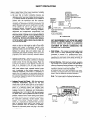
To measure H.V. use a high impedance
H.V. meter.
Connect (-) to chassis earth and (+) to the CRT anode
button. (See the following connection diagram.)
Note:
Turn power switch off without fail before the
connection to the anode button is made.
Chassi:
ground
FBT
(T702)
High Impedance
H.V. meter
\
High voltage
connector
Deflection
P.W.B.
- TUBE: The primary
source of XX-radiation
radiation in this receiver is the picture tube. The tube
utilized for the above mentioned
function in this
chassis is specially constructed
to limit X-radiation
emissions.
For continued X-radiation
protection, the replacement
tube must be the same type as the original, Hitachi
approved type.
When troubleshooting
and making test measurements in a receiver with a problem of excessive high
voltage, avoid being unnecessarily
close to the picture
tube and the high voltage component.
Do not operate the chassis longer than is necessary
to locate the cause of excessive voltage.
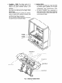
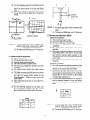
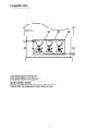
h. X-radiation
Shield 1. This receiver is provided with X-ray shield plates
for protection against X-radiation.
Do not remove
X-ray shield plates A, B, C, or D shown in Fig. 1
unnecessarily,
when
troubleshooting
and/or
making test measurements.
2. To prevent
X-radiation,
after replacement
of
picture tube and lens, confirm these components
to be fixed correctly to bracket and cabinet, and
not to be taken off easily.
R-Lens
G-Lens
B-Lens
Shield
Plate
A
Shield
Fig. 1. Detailing
X-radiation
4
Shield
Components,
parts, and/or wiring that appear to have
overheated
or are otherwise
damaged
should be
replaced with components,
parts, or wiring that meet
original
specifications.
Additionally,
determine
the
cause
of overheating
and/or
damage
and, if
necessary,
take corrective
action to remove any
potential safety hazard.
2. Read and comply with all caution and safety-related
notes on or inside the receiver cabinet, on the receiver
chassis, or on the picture tube.
Warning
- Do not alter or add to
3. Design Alteration
the mechanical or electrical design of this TV receiver.
Design alterations
and additions
including
but not
limited to circuit modifications
and the addition of
items such as auxiliary audio and/or video output
connectors,
might alter the safety characteristics
of
this receiver and create a hazard to the user. Any
design
alterations
or additions
may void the
manufacturer’s
warranty
and may make you, the
servicer, responsible
for personal injury or property
damage resulting therefrom.
PRODUCT SAFETY NOTICE - Many TV electrical
and mechanical
parts have special safety-related
characteristics
some of which are often not evident
from visual inspection, nor can the protection they
give necessarily
be obtained by replacing them with
components
rated for higher voltage, wattage, etc.
Parts that have special safety characteristics
are
identified
in Hitachi service data by shading
on
schematics
and by a A in the parts list. Use of
substitute replacement
that does not have the same
safety characteristics
as the recommended
replacement part in Hitachi service data parts list might
create shock, fire, and/or other hazards. Product
safety is under
review
continuously
and new
instructions are issued whenever appropriate.
For the
latest information,
always consult the appropriate
current Hitachi service literature. A subscription to, or
additional copies of service literature may be obtained
at a nominal charge from Hitachi.
Protection
Warning - The
4. Picture Tube Implosion
picture tube in this receiver employs integral implosion
protection.
For continued
implosion
protection,
replace the picture tube only with one of the same
type number. Do not remove, install, or otherwise
handle the picture tube in any manner without first
putting on shatterproof
goggles equipped with side
shields. People not so equipped must be kept safely
away while picture tubes are handled. Keep the
picture tube away from your body. Do not handle the
picture tube by its neck.
5. Hot Chassis Warning - a. Some TV receiver chassis
are electrically connected directly to one conductor of
the AC power cord and may be safely serviced without
an isolation transformer
only if the AC power plug is
inserted so that the chassis is connected
to the
ground side of the AC power source. Confirm that the
AC power plug is inserted
correctly with an AC
voltmeter by measuring
between the chassis and a
known earth ground. If a voltage reading in excess of
1 .OV is obtained, remove and reinsert the AC power
plug in the opposite polarity and again measure the
voltage potential between the chassis and a known
earth ground. b. Some TV receiver chassis normally
have 85V AC (RMS) between
chassis and earth
ground regardless
of the AC plug polarity. These
chassis can be safely serviced only with an isolation
transformer
inserted in the power line between the
receiver and the AC power source, for both personnel
and test equipment
protection. c. Some TV receiver
chassis have a secondary ground system in addition
to the main chassis ground. This secondary ground
system is not isolated from the AC power line. The two
ground
systems
are electrically
separated
by
insulating
material
that must not be defeated
or
altered.
6. Observe original lead dress. Take extra care to assure
correct lead dress in the following areas: a. near sharp
edges, b. near thermally hot parts - be sure that leads
and components
do not touch thermally hot parts, c.
the AC supply, d. high voltage and e. antenna wiring.
Always inspect in all areas for pinched, out-of-plate, or
frayed wiring. Do not change
spacing
between
components
and the printed circuit board. Check AC
power cord for damage.
5
SERVICING
PRECAUTIONS
CAUTION:
Before servicing instruments
covered by this
service data and its supplements
and addenda, read and
follow the SAFETY
PRECAUTIONS
on page 3 of this
publication.
NOTE: If unforeseen circumstances
create conflict between
the following servicing precautions
and any of the safety
precautions on page 3 of this publication, always follow the
safety precautions. Remember: Safety First.
7. Do not apply AC power to this instrument and/or any of its
electrical assemblies
unless all solid-state device heatsinks are correctly installed.
General Servicing
Guidelines
1. Always unplug the instrument AC power cord from the AC
power source before:
a. Removing
or reinstalling
any component,
circuit
board, module, or any other instrument assembly.
9. Use with this instrument only the test fixtures specified in
this service data.
CAUTION:
Do not connect the test fixture ground strap
to any heatsink in this instrument.
b. Disconnecting
or reconnecting
any instrument
electrical plug or other electrical connection.
c. Connecting
electrolytic
CAUTION:
d. Discharging
a test substitute
in parallel with an
capacitor in the instrument.
A wrong part substitution
or incorrect
polarity
installation
of electrolytic
capacitors
may result in an explosion
hazard.
the picture tube anode.
2. Test high voltage only by measuring it with an appropriate
high voltage meter or other voltage measuring
device
(DVM, FETVOM, etc.) equipped
with a suitable high
voltage probe. Do not test high voltage by “drawing an
arc.” The H.V. Distribution
Box has an internal 400M0
resistor (bleeder
resistor)
connected
from the high
voltage to ground. After power is removed from the
instrument the high voltage will discharge through the
high voltage bleeder resistor. If the tubes have high
voltage after power is removed, then the bleeder resistor
is defective or the bleeder ground is disconnected.
3. Discharge
B outputs
connecting
degaussing
the point
connected,
insulated
distribution
handle to
the picture tube’s anode at any of the R, G, or
on the H.V. Distribution
Box only by (a) first
one end of an insulated
clip lead to the
or kine aquadag grounding system shield at
where the picture tube socket ground lead is
and then (b) touch the other end of the
clip lead to the picture tube high voltage
box R, G, or B output, using an insulated
avoid personal contact with high voltage.
4. Do not spray chemicals
of its assemblies.
on or near this instrument
or any
5. Unless specified otherwise in these service data, clean
electrical contracts by applying the following mixture to
the contacts with a pipe cleaner, cotton-tipped
stick or
comparable
nonabrasive
applicator:
10% (by volume)
Acetone and 90% (by volume) isopropyl alcohol (90%99% strength).
CAUTION:
This is a flammable
mixture.
Unless
specified otherwise in these service data,
lubrication of contacts is not required.
6. Do not defeat any plug/socket B+ voltage interlocks with
which instruments covered by this service data might be
equipped.
8. Always connect the test instrument ground lead to the
appropriate
instrument chassis ground before connecting
the test instrument positive lead. Always remove the test
instrument ground lead last.
Electrostatically
Sensitive
(ES) Devices
Some semiconductor
(solid state) devices can be damaged
easily by static electricity. Such components
commonly are
called Electrostatically
Sensitive (ES) Devices. Examples of
typical ES devices are integrated circuits and some fieldeffect transistors and semiconductor
“chip” components. The
following techniques
should be used to help reduce the
incidence of component damage caused by static electricity.
1. Immediately
before
handling
any
semiconductor
component
or semiconductor-equipped
assembly, drain
off any electrostatic charge on your body by touching a
known earth ground. Alternatively,
obtain and wear a
commercially
available discharging
wrist strap device,
which should be removed for potential shock reasons
prior to applying power to the unit under test.
2. After removing an electrical assembly equipped
devices, place the assembly on a conductive
such as aluminum
foil, to prevent electrostatic
buildup or exposure of the assembly.
3. Use only a grounded-tip
desolder ES devices.
soldering
4. Use only can anti-static
type
Some solder removal devices
static” can generate
electrical
damage ES device.
5. Do not
generate
devices.
use freon-propelled
electrical
charges
with ES
surface
charge
iron to solder
or
solder removal device.
not classified
as “anticharges
sufficient
to
chemicals.
These
sufficient to damage
can
ES
6. Do not remove a replacement
ES device from its
protective
package
until immediately
before you are
ready to install it. (Most replacement
ES devices are
packaged
with leads electrically
shorted together by
conductive foam, aluminum foil or comparable conductive
material.)
7. Immediately before removing the protective material from
the leads of a replacement
ES device, touch the
protective material to the chassis or circuit assembly into
which the device will be installed.
CAUTION:
Be sure no power is applied to the chassis
or circuit, and observe
all other safety
precautions.
8. Minimize
bodily motions when handling
unpackaged
replacement
ES devices. (Otherwise
harmless
motion
such as the brushing together of your clothes fabric or the
lifting of your foot from a carpeted floor can generate
static electricity sufficient to damage an ES device.)
General Soldering
Guidelines
1. Use a grounded-tip,
low-wattage
soldering
iron and
appropriate
tip size and shape that will maintain tip
temperature
within the range 500°F to 600°F.
2. Use an appropriate
gauge of resin-core
of 60 parts tin/40 parts lead.
3. Keep the soldering
2. Draw away the melted solder with an anti-static suctiontype solder removal device (or with solder braid) before
removing the IC.
Replacement
1. Carefully insert the replacement
solder composed
2. Carefully bend each
and solder it.
iron tip clean and well-tinned.
4. Thoroughly
clean the surfaces to be soldered. Use a
small wire-bristle (0.5 inch or 1.25 cm) brush with a metal
handle. Do not use freon-propelled
spray-on cleaners.
5. Use the following desoldering
technique.
a. Allow
the soldering
iron tip to
temperature
(500°F to 600°F).
reach
3. Clean the soldered
(It is not necessary
reach
IC lead against
the circuit foil pad
areas with a small wire-bristle brush.
to reapply acrylic coating to areas.)
“Small-signal”
Discrete Transistor
Removal/Replacement
1. Remove the defective transistor by clipping its leads as
close as possible to the component body.
normal
2. Bend into a “U” shape the end of each of three
remaining on the circuit board.
b. Heat the component lead until the solder melts. Quickly
draw away the melted solder with an anti-static,
suction-type
solder removal device or with solder
braid.
CAUTION:
Work quickly to avoid overheating
the
circuit board printed foil.
6. Use the following soldering technique.
a. Allow the soldering
iron tip to
temperature
(500°F to 600°F).
IC in the circuit board.
3. Bend into a “U” shape
4. Connect
to
corresponding
crimp the “U”
metal contact,
the replacement
transistor
leads
leads.
replacement
transistor
leads to the
leads extending from the circuit board and
with long nose pliers to insure metal to
then solder each connection.
normal
Power Output Transistor Devices Removal/Replacements
1. Heat and remove all solder from around the transistor
leads.
b. First, hold the soldering
iron tip and solder strand
against the component
lead until the solder melts.
c. Quickly move the soldering iron tip to the junction of
the component
lead and the printed circuit foil, and
hold it there only until the solder flows onto and
around both the component lead and the foil.
CAUTION:
Work quickly to avoid overheating
the
circuit board printed foil or components.
2. Remove
the heatsink
mounting
screw (if so equipped).
3. Carefully
remove
the transistor
from the circuit board.
4. Insert new transistor
5. Solder each transistor
d. Closely inspect the solder area and remove any excess
or splashed solder with a small wire-bristle brush.
6. Replace
in circuit board.
lead, and clip off excess lead.
heatsink.
Diode Removal/Ret>lacement
1. Remove defective diode by clipping
possible to diode body.
2. Bend the two remaining
circuit board.
leads
its leads as close as
perpendicularly
to the
3. Observing
diode polarity, wrap each lead of the new
diode around the corresponding
lead on the circuit board.
4. Securely
Use Solding
crimp each connection
and solder it.
5. Inspect (on the circuit board copper side) the solder joints
of the two “original leads”. If they are not shiny, reheat
them and, if necessary, apply additional solder.
Iron to Pry Leads
IC Removal/Replacement
Some Hitachi unitized chassis circuit boards have slotted
holes (oblong) through which the IC leads are inserted and
then bent flat against the circuit foil. When holes are the
slotted type, the following technique
should be used to
remove and replace the IC. When working with boards using
the familiar round hole, use the standard technique
as
outlined in paragraphs 5 and 6 above.
Removal
1. Desolder and straighten each IC lead in one operation by
gently prying up on the lead with the soldering iron tip as
the solder melts.
7
Fuses and Conventional
Resistor Removal/Replacement
1. Clip each fuse or resistor lead at top of circuit board
hollow stake.
2. Securely crimp leads of replacement
stake l/8 inch from top.
component
around
3. Solder the connections.
CAUTION:
Maintain
original
spacing
between
the
component
and
adjacent
replaced
components
and the circuit board, to
excessive
component
prevent
temperatures.
At Other Connections
Use the following
technique
to repair defective copper
pattern at connections
other than IC Pins. This technique
involves the installation of a jumper wire on the component
side of the circuit board.
DEfECTlVE
Circuit Board Foil Repair
Excessive heat applied to the copper foil of any printed
circuit board will weaker. the cdhesive that bonds the foil to
the circuit board, causing the foil to separate from, or “lift-off:’
the board. The following guidelines and procedures
should
be followed whenever this condition is encountered.
In Critical Copper Pattern Areas
High component/copper
pattern
density and/or special
voltage/current
characteristics
make the spacing
and
integrity of copper pattern in some circuit board areas more
critical than in others. The circuit foil in these areas is
designated
as Critical Copper Pattern. Because Critical
Copper Pattern requires special soldering
techniques
to
ensure the maintenance
of reliability and safety standards,
contact your Hitachi personnel.
At IC Connections
To repair defective copper pattern at IC connections, use the
following procedure
to install a jumper wire on the copper
pattern side of the circuit board. (Use this technique only on
IC connections.)
1. Carefully remove the damaged
copper pattern with a
sharp knife. (Remove only as much copper as absolutely
necessary.)
2. Carefully
scratch away the solder resist and acrylic
coating (if used) from the end of the remaining copper
pattern.
BARE
Install
Jumper
JUMPER
Wire and Solder
3. Bend a small “U” in one end of a small-gauge jumper wire
and carefully crimp i! around the IC pin. Solder the IC
connection.
4. Route the jumper wire along the path of the cut-away
copper pattern and let it overlap the previously scraped
end of the good copper pattern. Solder the overlapped
area, and clip off any excess jumper wire.
Insulated
Jumper
Wire
Remove the defective copper pattern with a sharp knife.
Remove at least l/4 inch of copper, to ensure hazardous
condition will not exist if the jumper wire opens.
Trace along the copper pattern from both wire sides of the
pattern break and locate the nearest component directly
connected to the affected copper pattern.
Connect
insulated
20-gauge
jumper
wire from the
nearest component
on one side of the pattern break to
the lead of the nearest component on the other side.
Carefully crimp and solder the connections.
CAUTION:
Be sure the insulated
jumper
wire is
dressed
so that it does
not touch
components
or sharp edges.
Frequency
Synthesis
(FS) Tuning Systems
Always unplug the instrument
AC power cord before
disconnecting
or reconnecting
FS tuning system cables
and before removing
or inserting
FS tuning system
modules.
The FS tuner must never be disconnected
from the FS
tuning control module while power is applied to the
instrument.
When troubleshooting
intermittent problems that might be
caused by defective cable connection(s)
to the FS tuning
system, remove the instrument AC power as soon as the
defective connector is found and finish confirming the bad
connection
with a continuity
test. This procedure
will
reduce the probability of electrical overstress of the FS
system semi-conductor
components.
NOTE: These components
are affixed with glue. Be careful not to break or damage any foil under the
component
or at the pins of the ICs when removing. Usually applying heat to the component
for a short
time while twisting with tweezers will break the component
loose.
Leadless Chip Components
(surface mount)
How to Replace Flat-IC
-Required
Tools-
Chip components
must be replaced with identical
chips due to critical foil track spacing. There are no
holes in the board to mount standard transistors or
diodes. Some chip capacitor or resistor board solder
pads may have holes through the board, however the
hole diameter limits standard resistor replacement to
l/8 watt. Standard capacitors may also be limited for
the same reason. It is recommended
that identical
chip components be used. .
Chip resistors have a three digit numerical resistance
code -1st and 2nd significant digits and a multiplier.
Example: 162 = 1600 or 1.6K resistor, 0 = 0 (jumper).
Chip capacitors generally do not have the value
indicated on the capacitor. The color of the component
indicates the general range of the capacitance.
Chip transistors are identified by a two letter code. The
first letter indicates the type and the second letter, the
grade of transistor.
Chip diodes have a two letter identification code as per
the code chart and are a dual diode pack with either
common anode or common cathode. Check the parts
list for correct diode number.
* Soldering
De-solder
1. Remove
by using
Component
1.
2.
3.
2.
l
l
De-Solder
Braid
Soldering
Iron
2.
Put the iron wire under the pins of the Flat-IC and
pull it in the direction indicated while heating the
pins using a soldering iron. A small awl can be
used instead of the iron wire.
/
Iron
Wire
Awl
3.
Removal
Installation
iron
iron wire or small awl
braids
Magnifier
the solder from all of the pins of a Flat-IC
a de-solder braid.
Flat-IC
Use solder wick to remove solder from component
end caps or terminals.
Without pulling up, carefully twist the component
with tweezers to break the adhesive.
Do not reuse removed
leadless
or chip
components
since they are subject to stress
fracture during removal .
Chip Component
1.
l
Remove the solder from all of the pads of the
Fiat-IC by using
a de-solder braid.
~-“‘!
--WI-
Flat-IC
4.
Position the new Flat-IC in place (apply the pins of
the Flat-IC to the soldering pads where the pins
need to be soldered). Properly
Polarity Symbol
determine the positions of the
soldering pads and pins by
correctly aligning the polarity
symbol.
5.
Solder all pins to the soldering
tipped soldering iron.
Put a small amount of solder on the board
soldering pads.
Hold the chip component against the soldering
pads with tweezers or with a miniature alligator
clip and apply heat to the pad area with a 30 watt
iron until solder flows. Do not apply heat for more
than 3 seconds
pads using a fine
Chip Components
TypE13$F:;:;
63:
1ST DIGIT
6. Check with a magnifier for solder bridge between
the pins or for dry joint between pins and soldering
pads. To remove a solder bridge, use a de-solder braid
as shown in the figure below.
D
MH DIODE
RESISTOR
Bridge
Solder
oldering
Iron
TECHNICAL
CAUTIONS
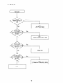
High Voltage limiter circuit operation
check.
1. Turn off TV and connect jig as shown in Figure 2. Adjust
jig fully counter-clockwise
for minimum resistance.
4. When the limiter circuit is operating
properly,
High
Voltage will be less than 36.5 kV at 0.6mA when TV shuts
down.
2. Set the AC input to 12OV AC and turn on TV.
5. Turn off set immediately
3. Confirm test pattern on CRT is a usable
slowly adjust jig until the picture disappears
down.
6. Unplug set for one minute
Remove jig and voltmeter.
Chassis
picture, then
and TV shuts
after checking
to reset shutdown
ground
High voltage
connector
Deflection
P.W.B.
High impedance
H.V. meter
FBT
(T702)
(Disconnect the # @ pin of 1905 from +B line.
Connect jig (15kQ VR) between +B line and # @
1905 #l pin
I
POWER/DEFLECTION
Jig
PWB
Fig. 2. Deflection/Power
IO
P.C.B.
circuit operation.
pin of 1905)
circuit.
SPECIFICATIONS
50SBX78B
Model:
Audio Input:
470 mVrms, 47 k Ohm
Stereo Audio Output:
470 mVrms, 1 k Ohm
6OSBX78B
Cathode-Ray
Tube:
Audio Output Power:
R=Pi GLFTOORFA
G=PlGLFTOOHLA
Front:
15 Watts per channel at 10% distortion, 8 Ohm impedence.
Max. output - 18 Watts.
Rear:
7.5 Watts per channel at 10% distortion, 8 Ohm impedence.
Max output - 10 Watts.
B=Pi GLFTOOBMB
Power Input:
120 volts AC, 60 Hz
Power Consumption:
240 Watts - Maximum
Center: 7.5 Watts per channel at 10% distortion, 8 Ohm impedence.
Max output - IO Watts
212 Watts - Operating
Antenna
Impedence:
Receiving
75 Ohm Unbalanced
VHF I UHF I CATV
Channel:
&yQ
G!i
VHF
2-13
14-69
UHF
EXT. Mid
CATV Mid.
(A-5)-(A-i), 4+
A-l
CATV Super
CATV Hyper
J-W
(Wtl)-(Wt28)
Anode Voltage
31.5 kV (Zero Beam Current)
Brightness:
5OSBX78B - 250 cd/m2
60SBX78B - 170 cd/m2
(white screen)
Speakers:
2 Woofers - 5 inch (12 mm) round
2 Tweeters - 2 inch (5 mm) round
2 Center Speakers - 4 inch (10 mm) round
Dimension:
50SBX78B
Intermediate
Frequency:
Height (in.)
Picture I-F Carrier 45.75 MHz
Sound I-F Carrier 41.25 MHz
Color Sub Carrier 42.17 MHz
51 ‘31,s
47 7132
Width (in.)
Depth (in.)
24 21/32
195
Weight (Ibs.)
Video Input:
60
51
'31~~
"/32
27 ‘I~
255
1 Volt p-p, 75 Ohm
Circuit Board Assemblies:
1 Volt p-p, 75 Ohm (Y)
Video Output:
0.7 Volt p-p, 75 Ohm, (Cb, Cr)
C.P.T. (B) P.W.B.
Terminal P.W.B.
1 Volt p-p, 75 Ohm
C.P.T. (G) P.W.B.
C.P.T. (R) P.W.B.
VM P.W.B.
Surround P.W.B.
Signal P.W.B.
Signal Sub P.W.B.
Power/Deflection P.W.B.
CIRCUIT
CAUTION:
80SBX78B
Control P.W.B.
Sensor Distribution P.W.B.
PROTECTION
Below is an EXAMPLE only. See Replacement Parts List for details. The following symbol near the fuse indicates
fast operation fuse (to be replaced). Fuse ratings appear within the symbol.
Example:
-:-+
F901
/
“RISK OF FIRE - REPLACE
5A125V\
The rating of fuse F901 is 5.OA - 125V.
Replace with the same type fuse for continued protection
against fire.
FUSE AS MARKED”
11
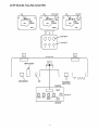
GENERAL
INFORMATION
TV/Video Source Selector
Fig. 3. Control
a&c Focus
Panel
Rear Speaker
Terminals-,
_ S-Video
Inputs
Antenna
Inputs/Outputs
Fig. 4. Rear Connections
12
Variable Transmitter
Inputs
1 and 2
Audio Output
output
Panel
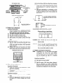
CUSTOMIZED
Select VIDEO
PICTURE AND SOUND ADJUSTMENTS
to adjust picture settings
CONTRAST
BRIGHTNESS
COLOR
TINT
SHARPNESS
RESET
ADVANCED
SETTINGS
MENU
IT0
4-I,
4-I)
4I1,50%
4---I
4-I,
75%
50%
50%
Cl
MENU
BAR
TO QUIT
Use the CURSOR A or v buttons to highlight the function
Press the CURSOR 4 or b buttons to adjust the function.
Press EXIT to quit menu.
I
I
picture quality.
CURSOR
CURSOR
NOTE:
and improve
CONTRAST
BRIGHTNESS
COLOR
TINT
SHARPNESS
RESET
ADVANCED
4-b
4-I)
4-I)
98%
50%
50%
4---I
4-I,
50%
0
I”““““’
1 EXIT
to be adjusted.
. If CONTRAST
is selected, you are adjusting CONTRAST.
The additional menu items BRIGHTNESS,
COLOR, TINT, and SHARPNESS
can be selected and adjusted in the same manner.
l Contrast
and Brightness adjustments will affect only the main picture. These adjustments will not affect the
sub-picture.
BRIGHTNESS
COLOR
TINT
I
I
Use this function
affect the picture
to change the contrast
between
when ADVANCED
SETTINGS
Use this function
to adjust
overall
Use this function
to adjust
the level
Use this
optimum
to adjust flesh tones so they appear
Quality when using the COMPONENT:
1
function
picture
Press the front panel
MAGIC FOCUS
button momentarily
for auto setup.
RESET
of color
to adjust the amount
is selected,
press
and white levels
Al is OFF.
in the picture.
This
adjustment
will only
brightness.
in the picture.
.
Use this function
When
picture
black
ULTRA
CURSOR
natural.
Y-C&r
(It may be necessary
Input 2 jacks).
to adjust
TINT
to obtain
of fine detail in the picture.
b to return
CONVERGENCE
video
adjustments
MAGIC
to factory
preset
conditions.
FOCUS
To adjust manually, press and hold the MAGIC FOCUS button until CENTER MODE or STATIC MODE is displayed.
Press EXIT on the remote to select red or blue. Green is stationary. Use the cursor buttons to adjust. Center mode
only adjusts the center section. Static mode adjusts the entire screen. Note: This new data is in RAM memory only
and will be lost if the MAGIC FOCUS button is pressed again.
13
Select AUDIO
SETTINGS
to adjust the TV to your preference
BASS
TREBLE
BALANCE
RESET
ADVANCED
SETTINGS
MENU
IT0
pi&l
CURSOR
4”,72%
4-I)
4---I
50%
0
MENU
Use CURSOR A or v to highlight the function
Press CURSOR 4 or b to adjust the function.
Press EXIT to quit menu.
NOTE:
BAR
TO
QUIT
I
I
BASS
TREBLE
BALANCE
RESET
ADVANCED
4”,90%
4-I,
4-b--‘-
xw”
0
I
Ill
1 EXIT
to be adjusted.
If BASS is selected you are adjusting BASS.
selected and adjusted in the same manner.
The additional
This function
controls the low frequency
This function
controls the high frequency
When RESET
conditions.
the sound quality.
I I
I
is selected,
press
items TREBLE
and BALANCE
can be
audio to all speakers.
CURSOR
14
menu
audio to all speakers.
This function will control the left to right balance
output, and WIRELESS OUT output.
E
and to improve
of the TV internal
b to return
audio
speakers,
adjustments
the AUDIO TO HI FI
to factory
preset
TV GUIDE PLUS+
This feature allows you to view program information
control your cable box and VCR with your TV.
for up to 1 week in the future.
It also allows you to
jSetUD1
TV GUIDE Plus+
Options
Menu
MENU LANGUAGE
PLUG & PLAY
SIGNAL
SOURCE
AUTO
CHANNEL
SET
CHANNEL
MEMORY
CHANNEL
LIST
CLOCK
SET
MAGIC
FOCUS
GUIDE
PLUS+
+
CURSOR
-
MENU
Use CURSOR
A or v
Setup TV GUIDE
TV GUIDE
Plus+:
1.
2.
BAR
TO QUIT
r
What
would
I./
Press
up/down
you like to do?
Setup TV GUIDE Plus+
TV GUIDE Plus+ Channel Edito!
View TV GUIDE Plus+ Demo
Exit
to choose.
Then,
Editor:
to highlight
press
Select
1 EXIT
of your choice, then press SELECT.
This allows you to set up TV GUIDE Plus+ so your TV can download
your
cable box and control your VCR.
Plus+ DEMO:
Press EXIT or CURSOR
NOTES:
MENU
to select the TV GUIDE Plus+ Option
Plus+ Channel
View TV GUIDE
IT0
CURSOR
data, control
This allows you to change channel numbers in the guide (using the number buttons)
as well as enable or disable channels from the guide. You can enable up to 100
channels in the Channel Editor.
This will start the TV GUIDE Plus+ demonstration,
features and operation of this system.
EXIT then press SELECT
allowing
you to understand
the
to quit menu.
It is recommended
that you first select View TV GUIDE Plus+ Demo to gain an understanding
of what the
system can do and how it operates.
Then select Setup TV GUIDE Plus+ so that you can set your TV to
download data and control your cable box and VCR. Finally, select TV GUIDE Plus+ Channel Editor to
customize your TV GUIDE Plus+ system.
If a channel is set to OFF in the Channel Editor, that channel cannot be recorded to a VCR.
15
SET UP TV GUIDE Plus+
Before you can use TV GUIDE Plus+ you must perform the setup. Simply use your illuminated
remote control to enter the information
provided
here. Screens very similar to those you will see
as you perform each step are shown here.
I
STEP 1
1.
From the Hitachi on screen display
SETUP-GUIDE
Plus+ menu.
2.
Use the CURSOR buttons to select Setup TV GUIDE
Plus+, then press the SELECT button on your remote.
NOTE: Completing
Plus+ Setup data.
setup if you intend
VCR, or new cable
TV GUIDE Plus+
Options Menu
menu, enter the
What would you like to do?
I./
Setup TV GUIDE Plus+
TV GUIDE Plus+ Channel Editon
View TV GUIDE Plus+ Demo
Exit
Setup clears previously downloaded
TV GUIDE
Only enter this section after TV GUIDE Plus+ is
to change your setup (ie. for new zipcode, new
box).
Press up/down to choose.
STEP 2
Then, press Select
w+
TV GUIDE
1.
Use the CURSOR buttons to select U.S.A. or CANADA,
then press SELECT.
Where do you live?
I./
USA
Canada
Press up/down
1.
A
C
A
N
A
D
A
Using the number
your remote, enter
zipcode. You may
CURSOR buttons
your zipcode or to
correction.
buttons on
your
also use the
to enter
make a
2.
When finished,
1.
Use the CURSOR A,v
buttons to input the first
number or letter of your postal
code.
2.
to choose.
Then, press Select
U.S.A. Example
STEP 3
U
S
Plus+ Setup
TV GUIDE
Enter
the zip code
where
Plus+
Setup
your TV is located:
TV GUIDE
Enter
q = = = =
the zip code where
4
1
6
Plus+
Setup
your TV is located:
6
7
press SELECT.
When you have selected the
letter or number, press the
CURSOR b button to move to
the next position. (Press
CURSOR 4 to make a
correction.)
3.
Repeat steps 1 and 2 for all six
spaces.
4.
When finished,
Canada Example
TV GUIDE
Enter the postal
located:
code where
Plus+
Setup
your TV is
TV GUIDE
Enter
the postal
code where
located:
q =====
press SELECT.
16
L5N2L8
Plus+
Setup
your TV is
SET UP TV GUIDE Plus+
STEP 4
1.
Use the CURSOR
button to select YES or NO, then press SELECT.
2.
If you select YES, you will go to step 5. If you select NO, you will go to
step 9.
Do you have cable?
jJ
Yes
NO
Press “pidown
I
lo choose.
Then. press Select.
STEP 5
1.
Use the CURSOR
SELECT.
2.
If you select YES, you will go to step 6. If you select NO, you will go to
step 9.
buttons to SELECT
NOTES:
A. As indicated on page 13 of this guide, you must connect your cable
box RF Out to TV ANT A in order for TV GUIDE Plus+ to download
data.
B. The cable box must always be left on.
C. The TV will download TV GUIDE Plus+ data only when it is off. During
this time, you will notice the cable box changing channels without any
user input. This is normal. The TV is searching for the Host channel.
Basic connection
TV GUIDE
YES or NO, then press
Do you have a cable box?
IJ
Yes
NO
Press up/down to choose.
Then. press Select.
for TV GUIDE Plus+ setup with no cable box and no VCR.
J(
ANT A
REAR SPEAKER
8 n ONLY
r
Outside
antenna
cable TV coaxial
Plus+ Setup
or
cable.
COMPONENT1
>
TO
CONVERTER
ANT B
,NPUT ,
,NpUT 2 MO;;;OR
WlRELES AUDIO
OUT TO HI-FI
3
TV GUIDE is a registered trademark of TV Guide Financial, Inc. VCR Plus+, C3, PlusCode and GUIDE Plus+ are
trademarks of Gemstar Development
Corporation.
The VCR Plus+ and GUIDE Plus+ systems are manufactured
under
license from Gemstar Development
Corporation and VCR Index Systems B.V., respectively.
17
SET UP TV GUIDE Plus+
TV GUIDE
STEP 6
1.
Turn your cable box ON and tune it to channel
02.
2.
Use the CURSOR buttons to select your cable box brand from the list,
then press SELECT. (It will take a few seconds for TV GUIDE Plus+ to
check the cable box code.)
Plus+ Setup
Tune your cable box to channel 02. Select
your cable box brand from the list below.
Hitachi
I
I
press “Pldmv” to change brand. The”. pr**s Select.
NOTE:
When using a cable box with TV Guide Plus+, set your remote to TV mode. This allows your IR Blaster
connector to control your cable box, enabling you to see channel call letters when changing channels or
pressing RECALL.
Basic connection
for TV GUIDE Plus+ setup with cable box and without
VCR.
Coaxial Cable
v
ANT A
REARSPEAKER
8n ONLY
I
7
COMPONENT7
VIDEO
ff
Cable TV Box
AUDIO
t
,NPUT,
I
I
,NP”T 2 MO~t$OR WlRELES AUDIO
OUT TO HI-FI
To IRlGLlNK
STEP 7
1.
2.
If your cable box switches to Channel
select YES. Then press SELECT.
TV GUIDE
09, use the CURSOR
Plus+ Setup
buttons to
If your cable box does not switch to Channel 09, use the CURSOR
buttons to select NO. Then press SELECT. TV GUIDE Plus+ will try
another version of cable box code (ie. 16-02.)
Did Cable Hitachi
cable box to 09?
IJ
Yes
NO
code 16-01 switch
your
I
Press “p/down to change brand. The”. press Select.
(If TV GUIDE Plus+ does not recognize your cable box after several tries, a screen stating, “Cable box test failed. Please
consult your manual and try again” will appear. You should check the CATV brand again and repeat these steps. Also,
check that the If? Mouse is in front of the cable box’s IR receiver window.)
18
SET UP TV GUIDE Plus+
TV GUIDE Plus+ Setup
STEP 8
1.
2.
Using the CURSOR buttons, select the channel number
your cable box Output is set. It is usually set to Channel
Channel 4.
Then press the SELECT
to which
3 or
Select cable
box mtput
channel:
O/AUX
4
button on your remote.
Press up/down to choose.
Then. press Select.
I
STEP 9
TV GUIDE
1.
Use the CURSOR
SELECT.
buttons
2.
If you select YES, you will go to step IO. If you select NO, you
will go to end of setup.
Plus+ Setup
to select YES or NO, then press
Do you have a VCR
NOTE:
You must connect your VCR RF Out to TV ANT A in order for TV
GUIDE Plus+ to download data and control your VCR for
recording. (See below).
Basic connection
Outside
CableTV
antenna
Coaxial
IJ
Yes
NO
I
Press up/down to choose.
for TV GUIDE Plus+ setup without
Then. press Select.
I
cable box and with VCR.
or
REAR SPEAKER
I
r
COMPONENT1
VCR #I
I
,NP”T
To IWGLINK
3
19
,
I
I
SET UP TV GUIDE Plus+
-“’
i-:,I
-:
:$j,i
;LA!9
,:
0Set U
STEP 10
TV GUIDE
1.
Tune your VCR to channel
2.
Use the CURSOR buttons to select your VCR brand from the
list, then press SELECT. (It will take a few seconds for TV
GUIDE Pius+ to check the VCR code.)
f-Cable
TV Coaxial Cable
Setup
02, then turn if OFF.
Basic connection
I
Plus+
/
Tune your VCR to channel 02. then turn it
off. Select your brand from the list below.
Hitachi
I
I
for TV GUIDE Plus+ setup with cable box and VCR.
REAR SPEAKER
8R ONLY
J(
ANT A
f
I
r
COMPONENT1
TO
CONVERTER
Cable TV Box
VCR #I
I
,N~UT,
STEP 11
1.
2.
I
I
TV GUIDE
If your VCR turns on and switches to Channel 09, use the
CURSOR buttons to select YES. Then press SELECT.
If your VCR does not turn on and switch to Channel 09, use the
CURSOR buttons to select No. Then press SELECT. TV GUIDE
Plus+ will try another version of VCR code (ie. 21-02.)
I
,NPUT 2 MO;i$OR WlRELES AUDIO
OUT TO HI-FI
Did Hitachi code 21-01
your VCR to 09?
[J
Yes
NO
Press up/down to choose.
Plus+ Setup
switch
Then, press Select
( If TV GUIDE Plus+ does not recognize your VCR after several tries, a screen stating, “VCR test failed, please consult
your manual and try again” will appear. You should check the VCR brand again and repeat these steps. Also, check that
the IR Mouse is in front of the VCR’s IR receiver window.)
20
END OF SET UP
1.
A screen telling you that TV GUIDE Plus+ will be ready for use within 24
hours appears.
Make sure that you turn the cable box ON and the VCR OFF.
TV GUIDE
NOTE:
If you have a system with a cable box, make sure you change the VCR channel back
to where you normally watch or record from the cable box (typically Channel 03 or 04).
Plus+ options
menu.
Your TV GUIDE Plus+ will be
ready for use within 24 hours.
Always leave your cable
ON and your VCR OFF.
box
2.
Press the SELECT
3.
Press the EXIT button to exit Setup.
4.
If you have a cable box turn the TV off.
5.
The TV will begin searching for the channel that contains the TV GUIDE Plus+ data (host channel).
When it locates the
host channel, it starts to download the Setup Information. This download usually takes less than 15 minutes. However,
on some cable systems, this download may take as much as three hours.
6.
If you have a cable box, you should allow the TV to control your cable box until Host Search
complete.
NOTES:
button to return to the TV GUIDE
Plus+ Setup
and data Download
are
1) If you do not have a cable box, you can watch TV while the Host Search and Channel Map Download are in
progress.
PIP, however, will not be available until the Host Search and Channel Map Download are complete
because the TV uses the PIP tuner to receive the TV GUIDE Plus+ information.
Also, note that TV GUIDE
Plus+ will not be available until Host Search and download functions are complete.
2) For TV GUIDE Plus+ to download Program Information, the TV must be off, regardless of TV GUIDE Plus+
settings.
21
CAUTIONS WHEN CONNECTING
/ DISCONNECTING
THE HV CONNECTOR
Perform the following when the
HV connector (anode connector)
is removed or inserted for CPT
replacement, etc.
Anode
connector
Deflection P.W.B.
FBT
Roll out silicon cover from FBT’s contact area slowly.
the connector about 90 degrees
following the arrow (0 position), push the connector
slightly towards the case. (Fig. A)
Fig. A
3.
Remove the connector slowly
by pulling it away from the
case.
Fig. B
During Insertion
1. Please refer to direction for insertion as shown in Fig. B (L position). Insert connector until “CLICK” sound is heard.
2. Make sure the connector is pressed right in, so that it has a good contact with the spring.
3. Confirm the contact by pulling the connector slightly. (Don’t pull hard because it may damage the connector).
4. Cover the high voltage output by carefully pushing silicon cover onto it. (Don’t turn the connector).
1.
(REMARK)
Make sure the silicon cover is
covering the high voltage output.
Silicon Cover
less than 1 mm
22
SERVICE ADJUSTMENTS
1. ASSEMBLED P.W.B. ADJUSTMENT .....................................................
Memory Initialization ............................................................
l-l.
l-2.
Comb Filter Operation Check .....................................................
l-3.
Sub Picture Position Adjustment ...................................................
2. FINAL
2-l.
2-2.
2-3.
2-4.
2-5.
2-6.
2-7.
2-8.
2-9.
2-10.
2-11.
2-12.
2-13.
2-14.
2-15.
ASSEMBLY ADJUSTMENT
....................................................
FocusAdjustment...............................................................2
White Balance Adjustment .......................................................
.....................................................
SubBrightness
Adjustment
Sub Picture White Balance Adjustment ..............................................
Surround Check ..............................................................
Raster Inclination Adjustment (Deflection Yoke) ........................................
Raster Position Adjustment .......................................................
Vertical Size Adjustment (R630) ...................................................
Horizontal Size Adjustment (R603) .................................................
BeamAlignment................................................................3
Beam Shape Adjustment
.......................................................
Static Focus Adjustment .........................................................
Blue Defocus Adjustment .......................................................
Digital Convergence Adjustment ...................................................
2-14-l. Phase Adjustment (service mode) .......................................
2-14-2. Raster Position Adjustment ............................................
2-14-3. Convergence Point Adjustment
.........................................
2-14-4. Digital Convergence Remote Control .....................................
Guide + OSD Adjustment ........................................................
3. ADJUSTMENT POINT ................................................................
3-l. CRT (R)(G)(B), Cabinet Locations ...................................................
3-2. Main Chassis (Signal P.W.B.) .......................................................
3-3. Main Chassis (Power/Deflection P.W.B.) ...............................................
3-4. CPT (R)(G)(B), Focus Pack, Control P.W.B. ............................................
23
.24
.24
.24
.24
. . .25
5
.26
..2 6
.27
..2 7
.28
.29
.29
.30
0
..3 0
.31
..3 1
.31
.32
.32
.33
.33
.34
.35
.35
.36
.37
.38
1. ASSEMBLED P.W.B. ADJUSTMENT
1 .l Memory Initialization
Adjustment procedure
(1) Press INPUT key on Control Panel and then
Power On to access Video Chroma adjustment
mode.
(2) Receive signal on main picture.
(3) Check the OSD according to table below, using
Av buttons on Remote Control.
*
P.01
SERVICE
SUB CONT
SUB COLOR
SUB TINT
SUB SHARP
EXT RGB BRIGHT
EXT RGB CONT
BRIGHTNESS
SUB BRIGHT
ADJ.
INITIAL
SET
AP84
0
14
10
45
38
40
60
80
0
0
P.05
I
I-l+1
AP84
1
n
0
C TRAP
TOF FQ
TOF Q
COLOR
SYSTEM
DY GAIN
B.E. P POINT1
WPDL
HI BRT
P.03
A
Adjustment procedure
(1) Check that between the color bars there are not
line dots every second color bar as shown in the
drawing.
Check @and
PO2
G DRIVE GAIN
B DRIVE GAIN
H POSITION
AFC G
H BLK END PHASE
V BLK PHASE
V FREQUENCY
V POSITION
R-Y POSITION
R-Y LEVEL
G-Y LEVEL
GPPHS
S-TRAC
YA
Y DL
TXACL
COLOR
1.2 Comb filter operation check
Adjustment preparation
(1) Receive the color bar signal at the regular tuning
point.
(2) Set the CONTRAST control to MAX and the
other controls to center.
(3) Set the Al to OFF, and 3D Y/C to ON in
Advanced Settings.
1
i-l
0
0
0
0
9
B CUT
OFF
1 AP84
1 1
!
1
I
CLAMP
I
1.3 Sub-picture position adjustment
Adjustment preparation
(1) Select signal on main picture.
(2) Video settings have to be at normal condition.
80
P.06
AP84H POSI (CENT)
04
V POSI (CENT)
1 07
1 0
INITIAL
SET
Z OSD SETTINGS
I
(@line dots.
*
I*
I
DELAY
*: Adjustable data.
Others: Fixed data (be careful not to change)
(4) Check MENU key to exit VIDEO CHROMA
ADJUST mode.
NOTE: (1) If there is a different value than shown
in table above, for fixed data, adjust it
using 4, buttons (only in this case).
(2) When exchanging microprocessor and
TV is turned on for first time, it requires
initialization of VIDEO CHROMA ADJ
on Pl and P6.
(3) Should be changed to OFF for FIRST
TIME TOUR at first Power ON by
pressing MENU key during FIRSTTIME
TOUR running.
24
Adjustment procedure
(1) Press the INPUT and POWER button on Control
Panel at same time to access VIDEO CHROMA
ADJUST mode.
Select H POSI and V POSI using A’(I buttons.
;:; Adjust the H POSI (HORIZONTAL) and V POSI
(VERTICAL) position using 4, buttons.
(4) Press MENU button to exit VIDEO CHROMA
ADJUST mode.
(5) Select single PINP mode and move the sub
picture, using the MOVE button. Distance
between PINP and edge of screen should be
equal when moved. If it is not, repeat (1) - (5).
NOTE: Check the position of MULTI PINP mode.
Check the right edge of the sub pictures for
MV-4 to make sure there is no separation
between the MULTI PINP and the edge of
the screen.
2. FINAL ASSEMBLY ADJUSTMENT
2.1 Focus adjustment
Adiustment preparation
(1) The set can face in any direction: west, east,
north or south.
(2) Receive the cross-hatch pattern signal.
CONTRAST : HALF
BRIGHTNESS : MINIMUM
The
electrical focus adjustment should have
(3)
been completed.
(4) The centering DY inclination should have been
adjusted.
Adjustment procedure
(1) Loosen-the fixing screw on the lens cylinder so
that the lens cylinder can be turned. (Be careful
not to loosen too much. If it is loosened too
much, rattling when tightening becomes greater
and the focus may drift). After completing steps
(5), (6) and (7) below, tighten the fixing screws
for each lens with a torque of 12-17 Kgf cm.
(2) Apply covers to 2 of R, G and B lenses, and
project a single color on the screen and adjust in
sequence.
(The adjustment order of R, G and B is only an
example.)
(3) For each of the R, G and B lenses, observe the
color abberation
generated
on the outer
circumference of the cross-hatch bright line at
the center section +3 pitches vertically and
horizontally from the center.
(4) If the lens adjustment knob is turned clockwise,
viewed from the front, the color aberration
changes as follows.
Set Size
Pitch between
Ll & L2
50”
3.0 cross-hatch
pitches
60”
3.0 cross-hatch
pitches
63) In case of R lens, set to the position where the
chromatic aberration changes from red to
crimson. As shown below, observe the vertical
bright line at the center and set to the position
where the crimson chromatic aberration slightly
appears inside and red outside (reference value:
1-3mm) within the cross-hatch pitches specified
in next table.
RED
CHROMATIC
ABERRATION
SLIGHTLY CRIMSON
CHROMATIC ABERRATION
{I
(7) In case of B lens, set to the position where the
chromatic aberration changes from purple to
green. As shown below, observe the vertical
bright line at the center and set to the position
where green chromatic aberration slightly
appears inside and purple outside (reference
value: l-3mm) within the cross-hatch pitches
specified in next table.
(5) In case of G lens, set to the point where the
chromatic aberration switches from blue to red. If
the chromatic aberration appearing all over the
screen is not the same, observe the vertical
bright line at the center of the screen and set to
the position where red chromatic aberration
slightly appears inside and blue outside
(reference value: l -3mm) within the cross-hatch
pitches specified in next table. When the red
chromatic aberration appearing at both sides of
the bright line is not equal, observe the side with
larger chromatic aberration when adjusting.
PURPLE CHROMATIC
ABERRATION
I
RED
CHROMATIC
ABERRATION
SLIGHTLY BLUE CH6OMATlC ABERRATION
OR NO COLOR
25
Set Size
SLIGHTLY GREEN
CHROMATIC ABERRATION
I
Pitch between
L
50”
3.0 cross-hatch
pitches
60”
3.0 cross-hatch
pitches
I
Notes: (1) Fixing screw
FIXING
SCREW
(2) Color aberration
COLOR
(5)
ABERRATION
(6)
(7)
(8)
(9)
CROSS-HATCH
(3) Since the G light is very important
quality and performance,
pay special
its adjustment.
Note:
Be careful not to touch
fingers when adjusting.
for picture
attention in
NOTE: Before
adjusting
the White Balance, check that
the screen
adjustment
VRs are turned
fully
counterclockwise.
Since the phosphorescent
surface of the CRT is likely to be burned,
be
careful.
the lens with your
(4)
For red, setting to the center
crimson is optimum.
(5)
For blue, setting to the center
and green is optimum.
between
between
Select the input signal for high brightness
(Video
level = 0.715Vpp).
Adjust the high brightness
white balance using
the drive adjustment
VRs (red, green).
Select the signal for low brightness
(Video level
= 0.145Vpp)
Adjust the low brightness
white balance
using
the screen adjustment
VRs (red, green, blue).
(Visually adjust).
Check that high brightness
white balance
is
obtained. If it does not, return to step (7).
White balance =
Color coordinate
=
red and
purple
2.3 Sub brightness
2.2 White balance
(1)
(2)
(3)
adjustment
Adjustment
procedure
(1) Go to VIDEO
CHROMA
ADJUST
mode by
pressing
INPUT and Power button on Control
Panel at the same time.
(2) In “SERVICE”
mode push b button and screen
turns
to black. Gradually
turn the screen
adjustment
VRs (red, green, blue) clockwise and
set them where the red, green and blue slightly
bright lines just appear evenly on the screen.
(3) Push the b button again to return to “Normal”
side.
(4) Press “MENU” button to exit VIDEO CHROMA
ADJUST.
adjustment
Adjustment
preparation
(1) Start adjustment
20 minutes or more after the
power is turned
ON. Receive
the color bar
signal.
(2) Set the contrast and color controls to minimum.
(3) The vertical incident illumination
on the screen
should be 20 Iux or less.
Screen adjustment
High brightness
white balance.
Low brightness
balance.
Adjustment
preparation
(1) Start adjustment
20 minutes or more after the
power is turned on.
(2) The vertical incident illumination
on the screen
should be 20 lux or less.
(3) Set the video
settings
(CONTRAST:
MAX,
others: center) to standard condition
(4) For low brightness
white balance
adjustment,
input a white raster signal level of 0.145 Vp-p
(Video input level).
(5) For high brightness
white balance
adjustment,
input a white raster signal level of 0.715Vp-p
(Video input level).
(6) Set the drive adjustment
VRs (red and green) to
12 - 2 o’clock position.
(7) Turn the screen adjustment
VRs (red, green and
blue) fully counterclockwise.
(8) Set video advanced
setting
white control
to
COOL position.
9300” K f OMPCD
x . . . . . . 0.285
Y . . . . . . 0.295
\
1
1
1
/
black
Adjustment
procedure
(1) Go to “Sub Brightness”
adjustment
in VIDEO
CHROMA
ADJUST
mode
(press
Input and
Power button on Control panel at same time),
using A v buttons and then b button.
(2) Then adjust “Sub Brightness”
using 4 b buttons
to increase or decrease
the value, according
to
figure. (Visually adjust).
(3) After adjustment,
press MENU button to exit
VIDEO
CHROMA
ADJUST
mode. (Data
is
stored in memory).
Note: When
selecting
SUB-BRIGHTNESS
mode the
mcon sets the CONTRAST
and COLOR to MIN.
automatically,
but make sure that the other
conditions
are center.
Directly
observe
the
screen by eye without using a mirror.
2.4 Sub picture white balance
(ROM4, ROM6, ROM6)
adjustment
2.5.1 Surround
off check
Adjustment procedure
(1) Set to SURROUND: OFF and check that the
waveform shown below is obtained (Input signal
@ and @ ).
Adjustment preparation
(1) Start adjustment after power is ON for 20
minutes.
(2) Use a white raster signal for adjustment.
(3) Press “FREEZE” on the remote control and
select “SINGLE” freeze mode to display the sub
picture.
(4) Set CONTRAST to Maximum, Other conditions
to center.
FRONT
(5kHz)
Adjustment procedure
(1) Connect oscilloscope to P802 and adjust ROM8
to match blue level of main and sub pictures.
(2) Repeat for P832 and ROM6 Green, P862 and
ROM4 for Red.
R
Note:
(400Hz)
The rear and center will have no output.
2.5.2 Surround
off/monaural
check
Adjustment procedure
Check that the following waveform is obtained. The
amplitudes of 2 channels are equal.
(Input signal @ only).
FRONT
Note:
L
If the sub picture has a signal sag, adjust level at
center point.
(400Hz)
R
(400Hz)
I24
Note:
Monaural check can be omitted. The rear
and center have no output.
2.5.3 Matrix surround
check
Adjustment procedure
(1) Set to SURROUND: MATRIX
Check that the following waveforms are obtained.
(Input signal @I and @ ).
l
2.5 Surround Check
Adjustment preparation
(1) Input the following audio signals to the audio
input of the VIDEO INPUT terminals.
When checking surround:
@ L CH: No signal
@ R CH: 400Hz sine wave 1 Vpp.
Set the AUDIO ADVANCED SETTING for INT.
SPEAKERS ON,DYNAMIC BASS OFF,
LOUDNESS OFF and PERFECT VOLUME OFF
Set the volume control of FRONT to around the
center.
Set the BASS, TREBLE and BALANCE to center.
l
Front:
Check that the phases of R and L are
different and 400Hz is superimposed on
5kHz. The amplitudes of R and L are
different.
l
Rear:
Check that the phases of R and L are
opposite and 400Hz is superimposed on
5kHz. The amplitudes of R and L are
different.
l
l
FRONT
l
l
Note:
Front waveform: Front speaker output of the
set.
:mrn
Note:
27
Center has no output.
REAR
2.5.7 Dolby surround
2.5.4 Matrix surround/monaural
check
Adjustment procedure
Check that the following waveforms are obtained.
(Input signal @ only)
Adjustment procedure
(1) Set to SURROUND: DOLBY-NORMAL
.
Check that the following waveforms are
obtained. (Input Signal @ and @ )
.
Front: 400 Hz is superimposed on 5kHz.
.
Rear:
R and L are the same signal and 400Hz
is superimposed on 5kHz.
l
l
l
Front:
Rear:
R and L waveforms are almost equal.
R and L waveforms are almost Zero.
REAR
FRONT
check
FRONT
REAR
L
Note:
R
Center has no output.
2.5.5 Hall surround
check
Note:
Adjustment procedure
(1) Set to SURROUND: HALL.
(Input signal 0 and @ ).
l
Front:
l
Rear:
2.5.8 Dolby surround/monaural
Check that the phases of R and L signals
are different and 400 Hz is superimposed
on 5kHz.
Check that the R and L are opposite and
400Hz is superimposed on 5kHz. The R
and L amplitudes are equal.
FRONT
MODE: PRO LOGIC (NORMAL)
check
Adjustment orocedure
(1) Set t0 SURROUND: DOLBY-NORMAL
. Check that the following waveforms are
obtained.
(Input signal @ only).
.
.
.
REAR
L
Front: Almost no output from both R and L.
Center: Same as the audio input signal.
Rear:
Almost no output from both R and L.
CENTER
FRONT
REAR
R
Note:
Amplitude levels of front R and L are not
even depending on P.W.B. Center has no
output.
2.5.6 Hall surround/monaural
l
l
l
2.6 Raster Inclination
(1)
I:;
check
Adjustment procedure
Check that the following waveforms are obtained.
(Input signal @ only)
Front: The phases of R and L are different.
The amplitudes are different.
Rear:
The phases of R and L are opposite.
The amplitudes of R and L are equal.
FRONT
Note:
adjustment
(Deflection
yoke)
Adjustment preparation
The set can face east or west.
Input the single cross test signal.
Set video conditions to factory reset.
(4) The lens focus adjustment should have been
completed.
(5) The electric focus should have been coarse
adjusted.
The
digital convergence RAM should be cleared
(6)
(uncorrected state). With the TV set off, press
and hold the service switch located on the
Power/Deflection
PWB and then press the
power button.
(7) Start adjustment 20 minutes or more after TV is
turned on.
Adjustment procedure
(1) Apply covers to the R and B lenses and project
only green light.
(2) Turn the G deflection yoke and adjust the vertical
raster inclination.
(3) Then, remove the cover of R or B lens and project
red or blue light and green light together on the
screen.
REAR
The monaural check can be omitted.
Amplitude levels of front R and L are not
even depending on the P.W.B. Center has
no output.
28
(4) Turn the deflection
yoke of R or B and set so that
the inclination
of R or B with respect to the green
light is as shown below on the top and bottom
sides.
adjustment,
fixing screw
(5) After raster inclination
of DY should
be screwed
with 12+2kg-cm
torque.
t?,
iREDC34
n!yIIz
1
Geometric
center of the
+2 mm
1 F”-f-
. . . . f . . . . . f . . . . . i . . . . . i .... 1
Cl t2
NOTES: (1) If internal
t2 II-
cross-hatch
does not appear after
clearing
RAM data, press service
switch
again.
(2) To restore old RAM data, turn TV off and on.
I
CROSSHATCH
2.6 Vertical
(GREEN)
size adjustment
(R630)
Adjustment
preparation
The set can face east or west.
Input the single cross test signal.
(3) Set video conditions to factory reset.
should have been
(4) The lens focus adjustment
completed.
(5) The electric focus should have been coarse
adjusted.
RAM should be cleared
(6) The digital convergence
(uncorrected
state) . With the TV set off, press
and hold the service
switch located
on the
POWER/DEFLECTION
PWB and then press the
power button.
(7) Start adjustment 20 minutes or more after TV is
turned on.
I:;
Notes:
(1)
If internal
clearing
again, on
(2) To restore
2.7 Raster position
cross-hatch
does not appear after
RAM data, press service switch
POWER/DEFLECTION
PWB.
old RAM data, turn TV off and on.
adjustment
Adiustment
oreparation
The set’can face east or west.
Input the single cross test signal.
Set video conditions
to factory reset.
The
lens
focus
adjustment
should have been
(4)
completed.
(5) The electric focus should have been coarse
adjusted.
RAM should be cleared
(6) The digital convergence
(uncorrected
state). With the TV set off, press
and hold the service
switch located
on the
Power/Deflection
PWB and then press the
power button.
(7) Start adjustment 20 minutes or more after TV is
turned on.
(1)
I:;
Adjustment
procedure
(1) Turn the centering
magnets
blue to satisfy the condition
blue horizontal
lines should
Adiustment
procedure
(1) Turn only the green by applying covers to the red
and blue lens or shorting
the 2 pin TS connectors on the red and blue CPT P.W.B.
(2) Count the vertical lines of the DCU cross hatch.
If the number of vertical lines is 9, go to step (3).
If the number of vertical lines is 8, push “HELP”
key and then “5” key on the R/C so the number
of vertical lines becomes “9”.
(3) Turn vertical amplitude adjustment VR (R630) so
that the distance between
the top and bottom
horizontal
lines is equal to the size shown in the
table.
for red, green, and
below. The red and
match with green.
t:
Size
ma4
60”
8OOk
5mm
50”
65Ok
5mm
twa4
Note:
29
(1)
If internal
clearing
again (on
(2) To restore
cross-hatch
does not appear after
RAM data, press service
switch
POWER/DEFLECTION
PWB).
old RAM data, turn TV off and on.
(5) Short-circuit all metal parts (metal fittings,
centering magnet) installed on the projection
tubes to GND’s of the projection tubes.
Since metal Darts are charaed with electricitv,
shocks mav be caused if thev are not short
circuited.
2.9 Horizontal
size adjustment
(R603)
Adiustment procedure
(1) Green (G) tube beam alignment adjustment.
Short-circuit 2P subminiature connector plug
pins of Red (R) and Blue (B) on the CPT boards
and project only Green (G) tube.
(2) Put Green (G) tube beam alignment magnet to
the cancel state as shown below.
Adjustment preparation
The set’can face east or west.
Input the single cross test signal.
Set video conditions to factory reset.
(4) The lens focus adjustment should have been
completed.
(5) The electric focus should have been coarse
adjusted.
(6) The digital convergence RAM should be cleared
(uncorrected state). With the TV set off, press
and hold the service switch located on the
POWER/DEFLECTION PWB and then press the
power button.
(7) Start adjustment 20 minutes or more after TV is
turned on.
(1)
I;;
(3) Turn the Green (G) static focus (Focus Pack)
counterclockwise all the way and make sure of
position of cross-hatch center on screen. (Halo
state.)
(4) Turn the Green (G) static focus (Focus Pack)
clockwise all the way. (Blooming state.)
(5) Turn two magnets forming alignment magnet in
any desired direction and move cross-hatch
center to position found in (3).
(6) If image position does not shift when Green (G)
static focus (Focus Pack) is turned. Green (G)
beam alignment has been completed.
(7) If image position shifts when Green (G) static
focus (Focus Pack) is turned, repeat (2)-(6).
(8) Conduct beam alignment for red (R) focus:
Focus Pack UFPK Blue (B) focus: Focus Pack
UFPK.
(9) Upon completion of adjustment, fix beam
alignment magnets with white paint.
Adjustment procedure
(1) Project only green, the same as Vertical size
adjustment.
(2) Turn horizontal amplitude adjustment VR (R603)
so distance between the left and right vertical
lines is equal to the size shown in the table.
c:
(,V
1970k5min
1
_+!$$
l-2-J
i
Note:
2.11 Beam shape adjustment
Adjustment preparation
should have been
(1) The beam alignment
completed.
(2) The raster inclination, centering, horizontal/
vertical amplitude and optical focus adjustments
should have been completed.
(3) Set video conditions to factory reset.
(4) Input the dot signal.
(1) If internal cross-hatch does not appear after
clearing RAM data, press service switch
again.
(2) To restore old RAM data, turn TV off and on.
Adjustment orocedure
(1) Green PRT beam shape adjustment. Shortcircuit 2P sub-mini connectors on Red and Blue
CPT PW.B.s to project only the Green beam.
(2) Turn the green static focus fully clockwise.
(Blooming.)
(3) Make the dot at the screen center a true circle
using the 4-pole magnet as shown below.
(4) Also adjust the Red and Blue PRT beam shapes
according to the steps (1) to (3).
(5) After the adjustment has been completed, return
R, G and B static VRs to the just focus point.
2.10 Beam alignment
Adjustment preparation
(1) Adjust at least 30 minutes after
switch.
(2) Raster inclination, centering,
vertical amplitudes and optical
should be completed.
(3) Set video conditions to factory
(4) Receive cross-hatch signals.
cross-hatch signals allowed.)
turning on power
horizontal and
focus adjustment
reset.
(Use of internal
30
PRT
SURFACE
(3) Turn the B Focus VR (Focus Pack) fully clockwise.
(4) Measure the brightness at the center of the
screen and turn the B FOCUS VR (Focus Pack)
counterclockwise to adjust the brightness of
blue.
(5) After the adjustment is completed, if blue
exceeds the specification, turn and adjust focus
so that the sticking out part of blue satisfies the
specification.
SIDE
1e
4-POLE BEAM
SHAPE CORRECTION
MAGNET
2-POLE BEAM
ALIGNMENT
MAGNET
TRUE
CIRCLE
SPECIFICATION
1
ALL-WHITE
TERMINATION
TRUE CIRCLE DEGREE: a/b
SPECIFICATION: 0.9-l .l
SIGNAL
WAVEFORM
CONDITION:
OPEN
STICKING
OUT
OF BLUE
2.12 Static focus adjustment
UNEVENNESS SPECIFICATION: +1cd/m2
Adjustment preparation
The raster inclination,
centering, horizontal/
vertical amplitude and optical/electrical focus
beam alignment should have been adjusted.
(2) The static convergence data should be cleared.
Set video conditions to factory reset.
Receive the cross-hatch pattern signal.
Apply covers to the lenses of colors other than
the color to be adjusted and project a single
color.
(1)
Defocus sticking out specification
I:;
(5)
60”
Adjustment procedure
(1) Red (R), Green (G) and Blue (B) static focus
adjustment. Vary the static focus VR (focus pack
UFPK) and make the center of the cross-hatch
pattern clearest.
(2) Observe the corners of the picture and check
that the focus does not get conspicuously worse.
OBSERVING
CORNER
POINTS
OF THE
OF THE PICTURE
User controls are set to the initial set
positions (for shipment) Measuring point
Screen center.
Cautions:
Correct the brightness gauge and amplitude
of the all-white signal periodically. The
aperture angle of the brightness gauge is lo.
2.14 Digital convergence
Note:
adjustment
If replacing a PRT, DY, etc. perform auto-digital
convergence first. (Press front panel MAGIC
FOCUS switch when in normal customer mode).
This can eliminate the need for a complete
digital convergence alignment.
Adjustment preparation
Receive an RF or video signal.
;:; Set controls to factory preset.
(3) Install jig screen on the set.
(4) Note the center of the video pattern displayed.
This is necessary to match dotted lines
(adjustment point viewed) and actual point that
is adjusted and displayed by the video signal.
adjustment
Adjustment Preparation
(1) Optical and electrical focus adjustment should
have been completed.
(2) The convergence adjustment should have been
completed.
(3) Set Video conditions to factory reset.
Adjustment procedure
(1) Input an ail-white signal shown below to VIDEO
input.
(2) Short-circuit 2P sub-mini connectors on the red
and green CPT P.W.Bs. to display only the blue
beam.
Condition:
Use a cross-hatch pattern to check.
OBSERVING POINTS
2.13 Blue defocus
1 .Omm
31
the
service
only
switch
(on
(5) Press
POWER/DEFLECTION
PWB). The pattern
displayed is now the digital convergence mode.
digital
performing
a
complete
(6) When
convergence adjustment CLEAR DATA in RAM.
See 2.6. (1) - (7).
the bent lines and use the cursor
(2) Identify
buttons to move the dotted lines in between as
shown.
Press HELP to exit PHASE mode.
Press ENTER 5 times to display external signal.
(5) Identify center of active video, then press
ENTER 5 times to return to internal cross-hatch.
(6) Press HELP (phase adj.), and use 2, 4, 5 and 6
to position internal cross-hatch center on active
video center identified in step (5).
(7) Press HELP to exit PHASE mode.
I:;
BEFORE
Adjustment Point
ACTIVE
VIDEO
CENTER
FROM
STEP (5)
JIG SCREEN SPECIFICATION
GEOMETRIC
USE CURSOR
KEYS TO MOVE
DOTTED LINES
3ElWEEN BENT
LINES FIRST
CENTER OF THE SCREEN
(84.9) [102.1]
THEN USE NUMBER KEYS TO MATCH INTERNAL
CROSSHATCH CENTER TO ACTIVE VIDEO CENTER
AFTER
[1227.2]
2.14.2 Raster position
ki
a
MODEL:
Note:
(50”), [60”]
UNIT: mm
If only minor adjustments to convergence are
needed, the jig screen is not necessary. Use
digital data stored in memory and one color as a
reference (red, green, or blue). DO NOT CLEAR
DATA and WRITE to ROM memory.
2.14.1 Phase adjustment
(service
mode)
Adjustment preparation
(1) PHASE adjustment - This is to match the digital
convergence cursor position to the video image
displayed, and to match the digital convergence
cursor position
(dotted
lines) to digital
convergence data position (bent lines).
Adjustment procedure
(1) Press the HELP button on the remote to select
phase adjustment. (Only Green displayed).
adjustment
Adjustment preparation
(1) Position adjustment - This will move an entire
color. Use this adjustment to match colors at the
center of the screen. (Active video center from
external signal and physical screen center
should now match from phase adj. 2.15.1.).
(2) Use the buttons below to switch color to adjust.
“RECALL’ - Green
“0” - Red
“INPUT” - Blue
Adjustment procedure
(1) Press the FRZ button. Extra horizontal lines
appear to confirm raster position mode.
(2) Use the cursor buttons to adjust position.
(3) Press FRZ again to exit raster position mode.
(1) Other functions cannot be accessed when
Notes:
in raster position adjustment mode. Press
FRZ and confirm extra horizontal lines
disappear to exit raster position mode.
(2) Press MENU to switch between all colors
displayed or adjustment color and Green
only.
2.14.3 Convergence
(5) Existing
DATA in ROM can be read by
pressing
the SWAP button 2 times. This
data
can
be used
after
replacing
a
component
(CRT, DY, etc.) Where complete
convergence
adjustment
is not necessary
be careful not to overwrite this data.
DO NOT write cleared RAM data into ROM
or a complete
convergence
adjustment
will
be necessary.
Remember
to try MAGIC
FOCUS
before
starting
convergence
adjustment
to minimize adjustment
time.
point adjustment
Adjustment
preparation
(1) Select color to adjust.
“RECALL’
- Green
“0” - Red
“INPUT” - Blue
(2) Use 4, 6, 2, and 5 to move the cursor position
(dotted lines).
(3) Use cursor buttons to move the convergence
point.
(4) Three adjustment
modes are available:
1. (3x3) Press “RECALL’
5 times
2. (7x5) Press “0” 5 times
3. (13x9) Press “INPUT” 5 times
2.14.4 Digital
Remote
Control
0
POWER
For touch-up,
only the (13x9) mode is necessary.
This will adjust every cross-hatch
intersection
point
on the screen.
For complete adjustment,
start with (3x3) mode. This
will adjust center point and eight edge points only,
but will greatly reduce adjustment
time. Then use
(7x5) mode,
and finally
(13x9)
mode
to finish
convergence.
ROM WRITE
ROM READ \
If “S” distortion
appears
between
cross-hatch
lines
repeat (7x5) mode to change
calculation
process
while adjusting
to remove distortion,
then return to
(13x9) mode to finish touch-up
convergence.
,
PHASE ,
Adjustment
procedure
(1) Start adjustment
at the center of the screen.
(2) Continue
adjustment
at next closest position.
(3) Adjust
center
area first, ending
with edge
sections.
(4) Press INFO button to perform
interpolation
operation.
This process
will take about
15
seconds and no picture will be seen at this time.
(5) After interpolation,
check convergence
again
and repeat (l)-(5) if necessary.
(6) When convergence
is acceptable,
press MOVE
to write data to ROM memory. ROM WRITE? is
displayed
to alarm system that ROM will be
overwritten
with new data. Press the MOVE
button again to write displayed data to ROM.
(7) DATA WRITE TO ROM will take approximately
20 seconds and no picture will be displayed.
(8) Green dots will be displayed
when operation
is
complete.
(9) Press MUTE to return to convergence
pattern,
then confirm again convergence
is acceptable.
(lO)Press
MOVE (ROM WRITE) mode, then press
PIP CH to initialize sensor data positions.
Notes:
Convergence
INITIALIZE
TV/CASLUDSS
’
VCR
CH
MUTE
0
I
\
v
REMOVE \
COLOR
ADJUSTMENT
VCR+/
0
AUDIO 0
0
CALCULATION
@
A
Cl
LST-CH
RASTER
POSITION
CROSSHATCH/
VIDEO MODE
ENTER/
-
CURSOR
(1) Display only green for easier adjustment
and match to jig screen. Press “MENU”,
THEN PRESS “RECALL’.
(2) Perform interpolation
and data write to ROM
after green adjustment.
Once green has
been confirmed
to match jig screen, the jig
screen can be removed. Do not readjust the
green color
after jig screen
has been
removed. This is now your reference color.
(3) Display green and red only and match red to
green.
(4) Display all colors and match blue to green
and red. Touch-up red color if necessary.
CURSOR
LEFT
\
CURSOR
DOWN
-
INPUT
BLUE (13x9 Adj.)
-+o
,
CURSOR
RIGHT
-
RED
(7X5 Adj.)
SLEEP
(0
HITACHI
CLUSl3MP
33
UP
m
.
?oL”Qt
2.15 GUIDE+ OSD Adjustment
Adjustment preparation
(1) Receive any signal in ANT A.
(2) Set picture controls to shipping conditions.
(3) Convergence Adjustment must be completed.
(5) When GUIDE+ OSD is adjusted then
PinP inside the OSD box by using the
buttons on the R/C to move PinP up or
left or right so the PinP is inside the
position according to next reference.
adjust the
CURSOR
down and
OSD box
Adjustment procedure
(1) Go to VIDEO CHROfvlA ADJUST mode by
pressing INPUT and Power button on Control
Panel at the same time.
(2) Go to GUIDE+ mode using A,v
buttons on
(3) Fusing VOL A,‘I buttons move the GUIDE+
OSD to the left or right and adjust so that OSD
is in the A position according to next table for
each PTV size.
(4) By using CH &‘I
buttons move the GUIDE+
OSD up or down and adjust so the OSD is in the
B position according to next table for each PTV
size.
PinP for GUIDE+
NOTE: Use a Crosshatch signal or Single Cross signal
to make this adjustment and be sure the pattern
signal used is equal for upper, bottom, left and
right sides of PinP for GUIDE+. (Center as
reference.)
GUIDE+
OSD
3. ADJUSTMENT POINT
3.1 CRT, cabinet locations
FRONT OF TV
P
P
1. CENTERING MAGNET FOR RED PRT
2.CENTERING MAGNET FOR GREEN PRT
3.CENTERING MAGNET FOR BLUE PRT
4.CPOLE MAGNET FOR BEAM FORM ADJUSTMENT
5. BEAM ALIGNMENT MAGNET
6. DIGITAL CONVERGENCE MODULE (On Power/Deflection Board)
7. FOCUS PACK (Top Adjustments for Screen, Bottom for Focus)
3.5
P
3.2 MAIN CHASSIS
(Signal P.W.B.)
240
O-
ISCII ISC2[
\. J
I
888
ROM8 ROM6 ROM4
(Blue) (Green)(Red)
0Elc1 0
1001
[SIGNAL
P.W.B )
SURROUNDP.W.B.
TUNER
TUNER
Wh
MTS
(MAIN
‘ICTURE)
ldk
1102
SIGNALSUB
P.W.B.
GUIDE+
3D Y/C
325TERMINALP.W.B.
240
36
VM
3.3 MAIN CHASSIS
(Power/Deflection
P.W.B.)
SKOI: SERVICE ONLY button
(CONV. ADJ)
%85
325-
I
I
I
@
Bz
D965
+G 9V
lz
q
D946
lv9v
q
+27V
Q777
IXI
q
ixl 0977
AUDIO
D940
+B 120V
-3
D912
PROTECT (RED)
22v
la
D947
AUDIO
32V
q
SERVICE LED
37
dl
q[Iu0
3.4 CPT (R) (G) (B), Focus Pack, Control
P.W.B.
GREEN
GND
GND
\
BLUE
0
0
DRIVE
GREEN
0
RED DRIVE
RED
0
c
FOCUS
GND
0
A
PACK (UFPK)
\
/ooor
Screen Adj. VR
,
FcasAdj.VR
B
G
;,Oo-G
R
,
B
/
I
FJ
CONTROL
P.W.E.
EFCI
DIMMER CONTROL
LIGHT RECEIVER
@
-I
/
I
\
REMOTE CONTROL
LIGHT RECEIVER
V
\
U
POWER
LED
AUTO DIGICON
(MAGIC FOCUS)
Ct+BFiOWSE
POWER
INPUT
SM;;;&
voL/FAv.
CH
lol
CHBFIOWSE
38
L
R
TROUBLESHOOTING
1. No Raster and No Power (REPAIR METHOD)
No
Red LED “ON”?
I
PROTECT
Yes
No
line
PROTECTION
Yes
How to check DIAGNOSIS LED’s.
Connector
1. Turn OFF power SW.
2. Turn ON again after several
PYI ,
seconds,
and carefully
observe
9 green LED’s
No
turn OFF same time?
D964 (Al 2V)
Check
A12V line
1910, Q926,
1001,1102,
IYOl, IYO2,
HMO1 etc.
1
(Other
I
D939 (TV5V)
Check
TV5V line
1913, Q905
D938, L911
L114, D116
etc.
Find which LED’s is going to dark or OFF
LED’s are going to OFF little bit later same time.)
+
D946 (TVSV)
Check
TVSV line
1912, Q905
D928, L909
L922 etc.
I
D966 (+27V)
Check
+27V line
E995, Q902
IK04, IK05
etc.
I
39
)
D940(+B)
Check
+B 120V line
E994, Q777,
T702, C701
etc.
+
v
v
D967 (-23V)
Check
-23V line
E996, 1909
IK04, IK05
etc.
D947 (32V)
Check
Audio32V
line
E992, E997
1401 etc.
D977 (22V)
Check
Audio22V
line
E993, E998
1402, IS11
etc.
1
Voltage
at pin (5) of
No.““~..“.:::“.
Yes
E991
blown
Yes
Check 1901, D911,
D910, D969
Replace
E991
Does
raster
Yes
v
Check 1905, 1903, 1902
Q914, Q913, Q912
Q909, T901 etc.
Yes
(About
AC 0.3V)
No
(About
AC 40V)
1
Check 1901, D907
Replace
E991
40
2. No Picture
Normal
Abnormal
Does on-screen
0517, Q516, Q515
No
v
1501, 1903, 1001, I1 02, 1006
Q108, Q109, QllO, Q008
Yes
Normal
Abnormal
l-k f
ZJ
2VP-P
v
I
I
Abnormal
l
41
U301, etc.
(3-D Comb)
3. Reception Impossible with Snow Noise
Main Picture
Yes
I
No
Yes
Sub Picture
eception impossible with snow noise
Yes
No
Yes
u102
Yes
Vcc (Sv), BP (5v), and
t3
u102
42
4. Defective Synchronization
llefective synchronization
1
cl902
I
I
ivormal
I
1-
1r
43
T
5v P-P
.I
5. Incorrect Color
When normal
\
c
lncorreitcolor
)
f
j.6 Vp-p
No color
Color condition
Defective
white balance
Yes
(,,“,““Ell
L
No
i
1501, X501, etc.
Yes
v
I.501
Green does
not appear
Q861, Q862
D861, PRT (R)
Q831, Q832
D831, PRT (G)
44
6. No Sound
OV or lower
E997
+26V Power Supply
26V
L
I
Yes
I
Check the I ‘C bus (SCL, SDA)
Yes
Check IS12
No
l
Yes
IYOl
(1) Check the l*C bus (SCL3, SDA3)
No
t
u101
45
7. Convergence
Errors.
If an error message or code appears while performing
and repair method.
1.
2.
3.
4.
Turn on power
Press service
Press “SWAP”
Error code will
MAGIC FOCUS or Initialize (MOVE,
and receive any signal.
switch on Power/Defleciton
board.
then “PIP CH” on remote control.
be displayed in bottom right corner of screen.
PIP CH in service mode) follow this confirmation
If there is no error, and “INITIAL
OK” message
will appear on screen.
5. Follow repair table for errors.
DCU REPAIR TABLE
Error
Code
Error
Message
Application
Magic
Initialize
Focus
Countermeasure
1
VF Error
Replace DCU
2
Connect 1
1. Darken Outside light
2. Placing of sensor
3. Is pattern hitting sensor
4. Check connection and solder bridge of sensor
5. Replace sensor
6. Replace sensor P.W.B.
7. Sensor Connector check
8. Replace DCU
9. Adjustment check (H/V size, centering)
3*2
A/D Level
4
Over Flow
5
X
X
Same as Error Code 2
X
1. Check the placement of sensor
2. Adjustment check (HIV size, centering)
3. Conv. amp. gain check *I (check resistor values only)
X
X
X
Convergence Same as Error Code 4
X
X
7
9
10
Operation
Connect 2
Noise
Same as Error Code 4
Same as Error Code 2
input strong field strength signal
Check the wiring of connector between sensor and DCU
wm
X
X
X
x
X
11
Sync
Input strong field strength signal
Input standard signal NTSC
X
X
*2
*I -- RK 42, 46.50, 54, 58, 62 check these resistors.
*2 Sensor Posrtron
(View from front side)
46
v
Fuse
F901
AC Input
1
l
LIVE
I
I
I
’
I
II
I
I
0
E996
7000
hI
I
I
BLOCK
DIAGRAM
TV Main ON/OFF
TV ON/OFF
Mode Switch
Q905, 6, Q908
Volt. Control
+B : 1905
Standby : Q907
+120 : D929
n--L!,?!-..
t-tewller
Rectifier
+31 : D916
Rectifier
-23 : D915
Rectifier
+27 : D914
Rectifier
+22 : D972
Rectifier
+26 : 0913
CIRCUIT
E999
7000
tw
I--
(M
7000
E998
PROTECTION
l
COLD
! AC clock
60 Hz
AC Clock
1904
I
I
8”“”
Switching
Transformer
T901
E997
I
T
+
.
I
1
I
b
E994
2000
D967
-23V
j-I
Regulator
-12 : 1909
-
D977
+22v
’
c
1
D940
+12ov
Regulator
TV+5 : 1913
Regulator
TV+9 : 1912
Regulator
A+12 : 1910
,~ä
E993
4000
-
Da9
+5 v
&
“+“s”v”
,“yz$
+32V
._ .-_
TV 4V
TV Signal
Circuit
YD965
G-&V
Stand By
A +12V
Conv.
-12v
Co;;v.rt.
+B
+ 120v
) TV Signal
Circuit
TV +5V
F
.
Audio
) +22v
EXPLODED MEW
NOTES:
Some parts may appear different than those shown in the Exploded View. When ordering, refer to the
Replacement Parts List for correct part number. Since this Service Manual covers several models, use care
to select the correct part for the model being serviced.
71
REPLACEMENT
PRODUCT
components,
SERVICE NOTE:
read carefully,
Components
the PRODUCT
PARTS LIST
marked w ith a ‘A !
have special characteristics
important
to safety.
Before replacing
SAFETY
NOTiCEof
this Service
Manual. Don’t degrade
the safety
of the receiver
through
any of these
improper
servicing.
ABBREVIATIONS
Capacitors:
Resistors:
AL: Aluminum
CD:
EL:
PF:
PP:
PL:
TA:
CIRCUIT
BLOCK
Ceramic
Disc
Electrolytic
Polyester
Film
Polypropylene
Plastic
Tantalum
I
SECOND CHAR.
OF SYM BOL No.
CIRCUIT
SYMBOL PART
coo2
0228758R
CAP
coo3
0246464R
0800299R
CD lOOPF-J
CH 50V TAPE
EL 22UF-M(SMG)
16V
co15
CO16
co17
SECOND CHAR.
OF SYMBOL
No.
2125
2125
CHIP
CHIP
15OPFJSL5OV
0893031
R
CAP
1OOOPFKB
0800291
0890121
R
R
EL 1 OUF-M(SMG)
16V
CD 33PF-J CH 50V
50V TAPE
CH 50V
BLOCK
PART
NO.
PART
DESCRIPTION
0800326R
EL l OOUF-M
16V
CO65
CO67
0800291
R
EL 1 OUF-M(SMG)
16V
0800291
R
EL 1 OUF-M(SMG)
16V
CO68
0800317R
EL 47UF-M(SMG)
16V
co70
co71
AN00637R
PF O.lUF
CO72
AN00637R
0800288R
PF 0.1 UF 50V TAPE
EL 4.7UF-M(SMG)
50V
co75
0890087R
CD lOOOPF-K
Cl01
Cl02
0800326R
0800326R
EL lOOUF-M
EL lOOUF-M
Cl03
0893053R
CAP 2125
Cl04
Cl05
0800358R
0800361 N
EL lOOOUF-M
6.3V
EL 1OOOUF 16V
Cl06
Cl07
0800358R
0893053R
EL lOOOUF-M
6.3V
CAP 2125 CHIP 47000PFKB
Cl08
0800361
N
EL 1OOOUF
Cl09
Cl10
0800361
0800291
N
R
EL 1OOOUF 16V
EL lOUF-M(SMG)
Cl11
0800326R
EL 1 OOUF-M
Cl12
Cl13
AN00624R
0893053R
PF O.OlUF
CAP 2125
Cl14
0800359R
EL lOOOUF-M
AN00637R
PF 0.1 UF 50V TAPE
EL 1OOOUF 16V
EL 1 .OUF-M(SMG)
50V TAPE
50V
16V
16V
0890121
R
CD 33PF-J
CO18
0800291
R
EL 1 OUF-M(SMG)
co19
CO25
0800282R
0893044R
EL 2.2UF-M(SMG)
CAP 2125 CHIP
CO26
CO27
AN00637R
0800288R
PF 0.1 UF 50V TAPE
EL 4.7UF-M(SMG)
50V
co29
0228758R
CAP 2125
co30
co31
0800279R
0800279R
EL 1 .OUF-M(SMG)
EL 1 .OUF-M(SMG)
CO32
0800324R
EL lOOUF-M(SMG)
6.3V
co33
CO36
0893053R
0800324R
CAP 2125 CHIP
EL lOOUF-M(SMG)
47000PFKB
6.3V
co37
AN00633R
PF 0.047UF
co40
co41
0800353R
AN00637R
EL 470UF-M
16V
PF 0.1 UF 50V TAPE
Cl15
Cl16
CO42
0800291
R
EL 1 OUF-M(SMG)
Cl19
0800361 N
0800279R
co43
0800351
R
EL 470UF-M
CllA
0228770R
CAP
co44
co45
0893053R
AN00637R
CAP 2125 CHIP 47000PFKB
PF O.lUF 50V TAPE
50V TAPE
Cl20
Cl21
AN00637R
0228756R
PF 0.1 UF 50V TAPE
CAP 2125 CHIP
12OPFJSL
CO46
0893048R
CAP 2125
50V TAPE
Cl22
0893053R
CAP
co53
co54
AN00637R
0800326R
PF 0.1 UF 50V TAPE
EL 1OOUF-M 16V
Cl23
Cl24
0800324R
EL lOOUF-M(SMG)
6.3V
co57
CO61
0800279R
0800279R
EL 1 .OUF-M(SMG)
EL 1 .OUF-M(SMG)
0800324R
0893053R
0890069R
EL lOOUF-M(SMG)
CAP 2125 CHIP
CD 47PF-J 50V
6.3V
47000PFKB
CHIP
16V
50V
1OOOOPFKB
15OPFJSL5OV
50V TAPE
TAPE
50V
50V
50V TAPE
50V TAPE
16V
6.3V
CHIP
22000PFKB
50V
50V
SECOND CHAR.
OF SYMBOL
No.
I
1
NO.
co64
TAPE
CIRCUIT
Transistor
Diode
Zener
Diode
Varistor
Therm istor
Integrated
Circuit
Graphic
Equalizer
Convergence
Magic Focus
Control
Hor. & Vert. Det.
Surround
Signal Control (Comp.)
ZiEr
PART
DESCRIPTION
NO.
CAPACITORS
coo4
coo5
BLOCK
C.P.T.
Power Supply
Signal Control ( MTS)
Signal Control
(include B.P.F.)
V.M.
Dynamic
Focus
L
TR:
DI:
ZD:
VA:
TH:
IC:
Carbon
Film
Carbon
Composition
Metal Oxide
Variable
Resistor
Wire Wound
Fuse Resistor
Metal Glaze
I
System Control
Tuner
Signal(Y)
& Sync.
Audio
Signal (Chroma)
Vertical Deflection
Horizontal
Deflection
NO.
Semiconductors:
CF:
CC:
MF:
VR:
WW:
FR:
MG:
Electrolytic
Cl25
Cl26
72
CHIP
50V TAPE
50V TAPE
16V
16V
16V
50V TAPE
CHIP 47000PFKB
MINI-CHIP
2125
47000PFKB
CHIP
50V TAPE
1OV
50V
47OPF-J
47000PFKB
SL 50V TAPE
50V TAPE
50V TAPE
50V TAPE
REPLACEMENT
PRODUCT
components,
SERVICE NOTE:
read carefully,
Components
the PRODUCT
PARTS LIST
marked w ith a A !
have special characteristics
important to safety.
Before replacing
SAFETY NOTICE of this Service Manual. Don’t degrade the safety of the receiver
through
IOOOPFKB
EL 2.2UF-M
EL 2.2UF-M
any of these
improper servicing.
50V TAPE
50V
50V
OOOPFKB
OOOPFKB
5OV TAPE
5OV TAPE
REPLACEMENT
PRODUCT
components,
SERVICE
NOTE:
read carefully,
Components
the PRODUCT
PARTS LIST
marked w ith a n !
have special characteristics
important to safety. Before replacing
SAFETY NOTICE of this Service
Manual. Don’t degrade the safety of the receiver
through
EL 6.8UF-M
C605
AN00619R
PF 0.0047UF
C810
AN00624R
PF 0.01 UF 50V TAPE
AN00624R
PF 0.01 UF 50V TAPE
C831
0257543F
EL 3.3UF
C607
C608
0880198R
0244501 R
PP 0.22UF-J
CD IOOOPF-K
50V
500V
C834
C835
0244889R
0800326R
CD 2200PF-K
EL lOOUF-M
2KV
16V
C609
0244501
CD lOOOPF-K
500V
C837
0890087R
CD lOOOPF-K
50V
C610
C61 I
0800345R
AN00631 R
EL 330UF-M(SMG)
25V
PF 0.033UF
50V TAPE
C838
C840
0890087R
AN00624R
CD 1 OOOPF-K 50V
PF 0.01 UF 50V TAPE
C612
0800326R
EL I OOUF-M
C864
0244889R
CD 2200PF-K
C613
0284446R
EL 1 UF-M
C865
0800326R
EL IOOUF-M
I6V
C614
C615
0800347N
0284426F
EL 33OUF-M(SMG)
PF 2200PF-M
25V
C867
C868
0890087R
0890086R
CD lOOOPF-K
CD 820PF-K
50V
50V
I6V
50V
50V
C616
0284399R
EL IOUF-M
C617
C619
0284446R
0800317R
EL 1 UF-M
50V
EL 47UF-M(SMG)
C620
AN00624R
PF 0.01 UF 50V TAPE
C621
0298261
TA I MF-J
C622
C632
0800347N
AN00062R
EL 330UF-M(SMG)
PL (103UF 50V )
C633
0279859F
PF O.lUF-K
C641
c701
0244105R
0259153F
CD 2200PF-K
50V TAPE
EL 220UF (HR) 16OV
R
IGV(KMF)TAPE
35V
50V
IOOV
C702
0299926F
PF 0.1 UF-K
0890028M
0244109R
CD 330PF-K
I3 50V
CD 4700PF-KB
50V
c705
0243507R
CD 330PF-K
A
C706
C707
0244501 R
0244211
CD I OOOPF-K
CD IOOOPF-K
A
C708
0262416F
PF 39OOPF-J
A
C709
c710
0262432F
0299933F
PP 15OOOPF-J
18OOV
PF 0.39UF-K
200V
c711
0299934F
PP 0.47UF
0299984F
PF O.O22UF-J
c713
c714
0800001 R
AN00628R
EL 0.47UF-M
PF 0.022UF
c715
0890089R
CD 1500PF-K
c717
C718
0243503R
CD
c719
0253983F
0880198R
EL 33UF-M
PP 0.22UF-J
C721
C722
024351 I R
0243511 R
CD 680PF-K
CD 680PF-K
C712
ISOPF-K
C870
200V
315V
2KV
AN00624R
PF 0.01 UF 50V TAPE
AN00148S
AN001 44s
PL (0.22UF25OV)
PL (0.1 UF25OV
c903
0248593F
CD 47OOPF-Z
c904
0248593F
CD 47OOPF-Z
c905
C906
0284296
0284296
EL 680UF-M
EL 680UF-M
250V(KMH)
250V(KMH)
c907
0800328R
EL lOOUF-M
35V
C908
c909
0890087R
0800323R
CD IOOOPF-K
50V
EL 47UF-M
1OOV
A
A
16V
c703
c704
&
(BP) 50V
C606
R
50V TAPE
C901
C902
)
250V
250V
c910
0299977F
PP O.O047UF-F
c912
c913
0890085R
0800282R
CD 680PF-K
50V
EL 2.2UF-M(SMG)
c914
AN00637R
PF 0.1 UF 50V TAPE
500V
2KV
c915
C916
AL00796S
AN00624R
EL S-LEAD
1200UF-M(LXV)
PF 0.01 UF 50V TAPE
1.8KV
c917
0244105R
CD 2200PF-K
C918
AL00796S
EL S-LEAD
c919
c920
0880198R
0800328R
PP 0.22UF-J
EL 1 OOUF-M
50V
35V
c921
0800328R
EL 1 OOUF-M
35V
c922
c923
0800326R
0800328R
EL 1 OOUF-M
EL 1 OOUF-M
16V
35V
500V
CYLINDRICAL
TAPE
200V
630V
50V (SME)
50V TAPE
any of these
improper servicing
630V
50V
35V
50V TAPE
1200UF-M(LXV)
35V
50V
c924
0800335R
EL 220UF-M(SMG)
B 500V
c925
C926
AL00796S
EL S-LEAD
1200UF-M(LXV)
35V
c927
0880198R
AL00796S
PP 0.22UF-J
EL S-LEAD
50V
1200UF-M(LXV)
35V
C928
c929
AL00796S
0251703
EL S-LEAD
1200UF-M(LXV)
EL 390UF-M
lGOV(KMH)
350V
50V
500V
500V
TAPE
TAPE
74
I6V
35V
REPLACEMENT
PRODUCT
components,
SYMBOL
NO.
c930
c931
c932
c934
c935
c937
c939
c940
c941
c942
c943
c945
C948
c949
c951
c952
c953
c954
c955
C956
c957
C95E
1A
C95E
1A
C961
C962
C963
C964
C965
C966
C967
C968
C989
CA01
CA02
CA03
CA04
CA05
CA06
CA07
CA08
CA26
CA27
CA28
CA29
CA31
CA33
CA34
CA35
CA36
CA37
CA38
CA39
CA40
CA41
CA65
CA68
SERVICE NOTE:
read carefully,
PART
NO.
AL00793S
0800353R
0800355N
AL00795S
0800355N
AL00794S
0800328R
0800353R
0880198R
0800317R
0800279R
0800291
AL00792S
AN00637R
0880062R
0800291
0800291
0800291
AN00637R
AN00637R
0800299R
AJ00157R
AJOOl63R
AL00796S
0800326R
0800026R
0800361
0880198R
0243509R
0243509R
0244109R
0800279R
0800279R
0800279R
0800279R
0800279R
0800279R
0800279R
0800279R
0800291
0800291
0800291
0800291
0800291
0800291
0800291
0800291
0800291
0800291
0800317R
0800317R
0800291
0800291
0800291
0284623R
Components
the PRODUCT
marked w ith a n !
have special characteristics
important to safety. Before replacing
SAFETY NOTICE of this Service Manual. Don’t degrade
the safety of the receiver
through
PART
DESCRIPTION
IEL S-LEAD 1200UF-M(LXV)
EL 470UF-M
16V
EL 470UF-M
35V
EL S-LEAD 2200UF-M&XV)
EL 470UF-M
35V
EL S-LEAD 1500UF-M(LXV)
EL 1 OOUF-M 35V
EL470UF-M
16V
PP 0.22UF-J
50V
EL 47UF-M(SMG)
18V
EL 1 .OUF-M(SMG)
50V
EL IOUF-M(SMG)
16V
EL S-LEAD 22OOUF-M(LXV)
PF 0.1 UF 50V TAPE
PF 0.22UF-KEB
50V
EL 1 OUF-M(SMG)
16V
EL IOUF-M(SMG)
16V
EL 1 OUF-M(SMG)
16V
PF 0.1 UF 50V TAPE
PF O.lUF 50V TAPE
EL 22UF-M(SMG)
16V
CD 1OOOP 400V B
CD 2200P 400V E
EL S-LEAD 1200UF-M(LXV)
EL lOOUF-M
16V
EL 22UF-M
50V
EL 1OOOUF 16V
EL 33UF-M(SMG)
16V
PP 0.22UF-J
50V
CD 470PF-K
500V TAPE
CD 470PF-K
500V TAPE
CD 4700PF-KB
50V
EL l.OUF-M(SMG)
50V
EL 1 .OUF-M(SMG)
50V
EL 1 .OUF-M(SMG)
5OV
EL 1 .OUF-M(SMG)
50V
EL 1 .OUF-M(SMG)
50V
EL 1 .OUF-M(SMG)
50V
EL 1 .OUF-M(SMG)
50V
EL 1 .OUF-M(SMG)
50V
EL 1 OUF-M(SMG)
16V
EL 1 OUF-M(SMG)
16V
EL lOUF-M(SMG)
16V
EL IOUF-M(SMG)
16V
EL I OUF-M(SMG)
16V
EL 1 OUF-M(SMG)
16V
EL 1 OUF-M(SMG)
16V
EL 1 OUF-M(SMG)
16V
EL lOUF-M(SMG)
16V
EL 1 OUF-M(SMG)
16V
EL 47UF-M(SMG)
16V
EL 47UF-M(SMG)
16V
EL 1 OUF-M(SMG)
16V
EL 1 OUF-M(SMG)
16V
EL IOUF-M(SMG)
16V
IEL IUF-SMEfBPI
50V
SYMBOL
I
I
R
R
R
R
N
R
R
R
R
R
R
R
R
R
R
R
R
R
PARTS LIST
16V
16V
16V
1OV
35V
NO.
CA69
CA73
CA74
CA75
CA76
CA77
CA79
CA80
CA81
CA82
CA83
cc02
cc03
CEO1
CEO2
CEO3
CEO4
CEO5
CEO6
CEO8
CEO9
CEIO
CEll
CE12
CE13
CE14
CE15
CE16
CE17
CE18
CE19
CE20
CE21
CE23
CFOl
CF02
CF03
CF04
CF05
CFO6
CF07
CFO8
CFO9
CFlO
CF12
CF13
CF14
CF15
CF16
CF17
CF18
CF19
CF20
CF21
CGOl
CG02
75
PART
NO.
AN00637R
0284623R
AN00637R
0800279R
0800279R
0800326R
0284638R
0800291
0800291
0800291
0800286R
0893044R
0893044R
0800354R
AN00624R
0800317R
0890076R
0800326R
0890064R
AN00637R
AN00637R
0800321
0890074R
0244541
0244541
AL00009R
0247848R
AL00007R
0244509R
0890074R
AL00009R
AL00009R
0890077R
0890079R
0800291
0255520R
0262401
AN00614R
0800291R
0800291
0800291
AN00624R
0880196R
0880197R
0800326R
AN00624R
0259151F
0880198R
0800291
0244109R
0245158
0245156
0800326R
AN00624R
0800353R
0800049R
1
PART
DESCRIPTION
IPF O.lUF 50V TAPE
EL 1 UF-SME(BP)
50V
PF 0.1 UF 50V TAPE
EL 1 .OUF-M(SMG)
50V
EL 1 .OUF-M(SMG)
50V
EL IOOUF-M
16V
EL IOUF-SME(BP)
16V
EL 1 OUF-M(SMG)
16V
EL IOUF-M(SMG)
16V
EL 1 OUF-M(SMG)
16V
EL 4.7UF-M(SMG)
25V
CAP 2125 CHIP 10000PFKB
50V TAPE
CAP 2125 CHIP 1OOOOPFKB 50V TAPE
EL 470UF-M
25V
PF 0.01 UF 50V TAPE
EL 47UF-M(SMG)
18V
CD 150PF-K 50V
EL lOOUF-M
16V
CD 18PF-J SL 50V
PF O.IUF 50V TAPE
PF 0.1 UF 50V TAPE
EL 47UF-M 50V
CD lOOPF-J 50V
CD 0.01 MF-K B 500V
CD 0.01 MF-K B 500V
AL 47UF 16OV
CD 56PF-J SL 500V
AL (22OUF16OV)
CD 4700PF-KB
B 500V
CD IOOPF-J 50V
#AL 47UF 16OV
AL 47UF 16OV
CD 180PF-K 50V
CD 270PF-K
50V
EL 1 OUF-M(SMG)
16V
,EL 0.47UF 250V(KME)
IPP 1 OOOPF 18OOV
PF 0.0018UF
50V TAPE
,EL IOUF-M(SMG)
16V
EL 1 OUF-M(SMG)
16V
EL 1 OUF-M(SMG)
16V
PF 0.01 UF 50V TAPE
PF 0.15UF 50V HFT
PF 0.18UF 50V
EL 1 OOUF-M 16V
PF 0.01 UF 50V TAPE
EL 1OOUF 160V
PP 0.22UF-J
50V
EL lOUF-M(SMG)
16V
CD 4700PF-KB
50V
CD 68PFl2KV
CD 22PF/2KV
EL 1 OOUF-M 16V
PF 0.01 UF 50V TAPE
EL 470UF-M
16V
IEL lOOUF-M
16V
I
R
R
R
R
F
F
R
F
R
R
R
any of these
improper servicing.
REPLACEMENT
PRODUCT
components,
SERVICE NOTE:
read carefully,
SYMBOL
NO.
PART
NO.
CG03
CG04
Components
the PRODUCT
marked w ith a n !
have special characteristics
important
to safety.
Before replacing
SAFETY
NOTICEof
this Service
Manual. Don’t degrade
the safety
of the receiver
through
PART
DESCRIPTION
AN00637R
AN00633R
PARTS LIST
SYMBOL
NO.
PF 0.1 UF 50V TAPE
PF 0.047UF
50V TAPE
16V
PART
DESCRIPTION
CG59
0893043R
CAP 2125
CG60
CG61
0800049R
AN00637R
EL lOOUF-M
16V
PF 0.1 UF 50V TAPE
CHIP
8200PFKB
CG05
0800049R
EL
CG06
0284623R
EL IUF-SME(BP)
CG62
0284638R
EL 1 OUF-SME(BP)
16V
CG07
CG08
AN00637R
AN00637R
PF 0.1 UF 50V TAPE
PF 0.1 UF 50V TAPE
CKOI
CK02
0800353R
0800335R
EL 470UF-M
16V
EL 220UF-M(SMG)
16V
CG09
0284623R
EL 1 UF-SME(BP)
CK03
0800326R
EL lOOUF-M
CK04
AN00637R
PF 0.1 UF 50V TAPE
CK05
CK06
0800326R
AN00637R
EL iOOUF-M
16V
PF 0.1 UF 50V TAPE
CK07
0800326R
EL IOOUF-M
AN00637R
AN00637R
PF 0.1 UF 50V TAPE
PF 0.1 UF 50V TAPE
R
lOOUF-M
PART
NO.
50V
50V
50V
CAP 2125
CAP 2125
CHIP
CHIP
EL 0.47UF
50V
(BP)
16V
CGlO
0284621
CGll
CG12
0893052R
0893052R
CG13
0284621
CG14
CG15
0880062R
0893046R
PF 0.22UF-KEB
CAP 2125 CHIP
50V
15000PFKB50V
TAPE
CK08
CK09
CG16
0893046R
CAP 2125
15000PFKB50V
TAPE
CKlO
0800326R
EL IOOUF-M
CG17
CG18
0880062R
0880056R
PF 0.22UF-KEB
PF O.O82UF-KEB
CK12
CK13
0890076R
AN00637R
CD 15OPF-K 50V
PF 0.1 UF 50V TAPE
R
EL 0.47UF
39000PFKB
39000PFKB
50V TAPE
50V TAPE
(BP)
CHIP
50V
50V
16V
16V
CG19
0893041R
CAP 2125
CHIP
5600PFKB
50V TAPE
CK14
AN00637R
PF 0.1 UF 50V TAPE
CG20
CG21
0893041 R
0880056R
CAP 2125 CHIP
PF O.O82UF-KEB
5600PFKB
50V
50V TAPE
CK15
CK16
AN0061 1 R
AN00637R
PF 0.001 UF 50V TAPE
PF O.lUF 50V TAPE
CG22
0893052R
CAP 2125
CHIP
39000PFKB
CG23
CG24
0893037R
0893037R
CAP 2125
CAP 2125
CHIP
CHIP
3300PFKB
3300PFKB
CG25
0893052R
CAP 2125
CHIP
39000PFKB
CG26
0893017R
0893032R
CAP
CAP
2125
2125
CHIP
CHIP
18000PFKB
1200PFKB
0893032R
CAP 2125
CHIP
1200PFKB
50V TAPE
CG29
0893017R
CAP
2125
CHIP
18000PFKB
CG30
CG31
0893043R
0228772R
CAP
CAP
2125
2125
CHIP
CHIP
8200PFKB
56OPFJSL
CG32
0228772R
CAP
2125
CHIP
560PFJSL
50V TAPE
CK28
0800356N
EL 470UF-M
50V
CG33
CG34
0893043R
0284638R
CAP 2125 CHIP
EL IOUF-SME(BP)
8200PFKB
16V
50V TAPE
CK29
0890076R
CD 150PF-K
50V
CG35
0800015R
EL
CK30
CK31
0890076R
0890076R
CD 15OPF-K
CD 150PF-K
50V
50V
CG36
0284638R
0800015R
EL IOUF-SME(BP)
EL IOUF-M
16V
CK32
0890076R
CD 150PF-K
50V
0800353R
EL 470UF-M
16V
CK33
CK34
0890076R
0890076R
CD ISOPF-K
CD 150PF-K
50V
50V
CG39
CG40
0800015R
0800015R
EL
EL
16V
16V
CL01
AN00633R
PF 0.047UF
50V TAPE
CG41
CG42
AN00633R
0800049R
PF 0.047UF
50V TAPE
EL IOOUF-M
16V
CL02
CL03
AN00633R
AN00633R
PF 0.047UF
PF 0.047UF
50V TAPE
50V TAPE
CG43
0800015R
EL
IOUF-M
16V
CL04
CL05
AN00633R
AN00633R
PF 0.047UF
PF 0.047UF
50V TAPE
50V TAPE
CG44
CG45
0800041 R
0800015R
EL 47UF-M
EL IOUF-M
16V
16V
CL06
AN00633R
PF 0.047UF
50V TAPE
CG46
0284621
EL 0.47UF
50V (BP)
CL07
CL08
AN00633R
AN00633R
PF 0.047UF
PF 0.047UF
50V TAPE
50V TAPE
CG47
CG48
0893052R
CAP
CHIP
CL09
0800326R
EL IOOUF-M
EL 1 UF-SME(BP)
50V
PF 0.1 UF 50V TAPE
CL10
CM01
AN00637R
0800023R
PF O.lUF 50V TAPE
EL 22UF-M
16V
CG27
CG28
CG37
CG38
R
IOUF-M
CK17
AN00637R
PF 0.1 UF 50V TAPE
CK18
CK19
AN00624R
AN00624R
PF 0.01 UF 50V TAPE
PF 0.01 UF 50V TAPE
50V TAPE
CK20
0890076R
CD 150PF-K
50V
25V TAPE
50V TAPE
CK21
0890076R
CD 150PF-K
50V
CK22
CK23
0890076R
0890076R
CD 150PF-K
CD 150PF-K
50V
50V
25V TAPE
50V TAPE
50V TAPE
16V
IOUF-M
IOUF-M
2125
50V TAPE
50V TAPE
50V TAPE
CG49
0284623R
AN00637R
CG50
0880056R
PF O.O82UF-KEB
CG51
CG52
0893041 R
0893046R
CAP 2125
CAP 2125
CG53
0880062R
CG54
CG55
16V
39000PFKB
50V TAPE
50V
CK24
0890076R
CD 150PF-K
50V
CK25
CK27
0890076R
0800356N
CD 150PF-K
EL 470UF-M
50V
50V
CM02
0244171
CM03
CM04
0800003R
PF 0.22UF-KEB
50V
CM05
0244171
0244171
0880047R
0893032R
PF O.O18UF-KEB
CAP 2125 CHIP
50V
1200PFKB
CM06
0880016R
PF O.lUF
50V TAPE
CG56
0893037R
CAP 2125
CHIP
3300PFKB
50V TAPE
CM07
CM08
0800015R
0800015R
EL
EL
CG57
CG58
0893052R
0228772R
CAP 2125
CAP 2125
CHIP
CHIP
39000PFKB
560PFJSL
50V TAPE
50V TAPE
CM09
CM10
0244171 R
0800015R
CD 0.01 UF-Z
EL IOUF-M
76
R
16V
5600PFKB
50V TAPE
15000PFKB50V
TAPE
CHIP
CHIP
any of these
improper
servicing,
R
R
CD 0.01 UF-Z
F 50V TAPE
EL
50V
l.OUF-M
CD 0.01 UF-Z
CD 0.01 UF-Z
F 50V TAPE
F 50V TAPE
50V
IOUF-M
IOUF-M
16V
16V
F 50V TAPE
16V
50V TAPE
REPLACEMENT
PRODUCT
components,
PARTS LIST
have special characteristics
important to safety. Before replacing any of these
marked with a n !
SAFETY NOTICE of this Service Manual. Don’t degrade the safety of the receiver through improper servicing.
SERVICE NOTE: Components
read carefully,
the PRODUCT
PART
DESCRIPTION
SYMBOL
NO.
PART
NO.
PART
DESCRIPTION
SYMBOL
NO.
CM11
PART
NO.
0800015R
EL
IOUF-M
16V
cs47
0800015R
EL
CM12
0800041R
EL
47UF-M
16V
CM13
0244171
CS48
cs49
0800015R
0800058R
EL IOUF-M
EL 220UF-M
16V
16V
CM14
0880016R
0800279R
PF 0.1 UF 50V
EL 1 .OUF-M(SMG)
cs51
0800015R
EL
IOUF-M
16V
CS52
0800003R
EL
I.OUF-M
50V
0800288R
AN00631 R
EL 4.7UF-M(SMG)
50V
PF 0.033UF
50V TAPE
cs53
cs54
0284623R
0284623R
EL 1 UF-SME(BP)
EL 1 UF-SME(BP)
CN04
CN05
0890084R
CD 560PF-K
50V
cs55
0800005R
EL
2.2UF-M
50V
0800326R
EL 1 OOUF-M
l6V
CS56
0800041R
EL
47UF-M
16V
CN06
0800294R
EL 1 OUF-M(SMG)
cs57
CSOl
CS58
cs59
0800058R
0893053R
EL 220UF-M
16V
CAP 2125 CHIP 47000PFKB
50V TAPE
0893044R
CAP 2125
50V TAPE
CNOI
CN02
CN03
R
CD O.OIUF-Z
F 50V TAPE
50V
50V
cso2
cso3
0893053R
0800049R
CAP 2125 CHIP 47000PFKB
EL lOOUF-M
16V
0228774R
CAP
MINI-CHIP
cso4
0800015R
EL
IOUF-M
16V
CS60
CS61
0284634R
0800015R
EL 4.7UF-M
EL IOUF-M
cso5
0800015R
EL
IOUF-M
16V
CS62
0800012R
EL
68OPF-J
PFKB
50V TAPE
lOUF-M
SL 50V TAPE
50V TAPE
4.7UF-M
16V
50V
50V
CHIP
50V
16V
50V
1OOOOPFKB
REPLACEMENT
PRODUCT
components,
SERVICE NOTE:
read carefully,
SYMBOL
NO.
PART
NO.
CSE3
marked w ith a n !
have special
characteristics
important
to safety.
Before replacing
SAFETY
NOTICE of this Service
Manual. Don’t degrade
the safety
of the receiver
through
Components
the PRODUCT
PART
DESCRIPTION
SYMBOL
NO.
0893035R
0893035R
CAP 2125
CHIP
2200PFKB
50V TAPE
CSE4
CAP
CHIP
2200PFKB
50V TAPE
CSE7
0800015R
EL IOUF-M
CSE9
CSFl
0800042R
EL 47UF-M
CSFG
0800015R
0800042R
CSF7
0800042R
CSF8
CSF9
0800051
R
PARTS LIST
PART
NO.
PART
DESCRIPTION
DO28
DO29
2348212M
2348212M
16V
DO30
2348212M
25V
DO31
2344041
M
ELlOUF-M
EL 47UF-M
16V
25V
DO40
DO41
2344041
2344041
M
M
EL 47UF-M
25V
DO44
2344041
M
DO45
DO46
2348102M
2348212M
DO47
2348212M
DO48
2344041
M
DO50
DO51
2344041
2344041
M
M
DO53
2344041
M
16V
DO54
DO55
2344041 M
CH00151M
DI 1 SS254TA/l
SS27OTA
DI DSMlSD2(200V)TAPE
DO57
2344041
M
2344041
2344041
M
M
DI 1 SS254TA/l
DI 1 SS254TAll
SS270TA
SS270TA
16V
DO58
DO59
DI 1 SS254TAll
SS270TA
DlOl
D106
2348212M
2344041 M
DI-MTZ-Jl5BTA
DI 1 SS254TAll
SS270TA
2125
EL lOOUF-M
25V
DI-MTZ-J15BTA
DI-MTZ-Jl5BTA
DI-MTZ-Jl5BTA
DI lSS254TA/l
DI 1 SS254TA/l
SS27OTA
SS270TA
DI 1 SS254TA/l
SS270TA
DI 1 SS254TA/l
SS270TA
ZD MTZJ-5.1
B TA
DI-MTZ-Jl5BTA
CSG3
0800084F
0880016R
EL lOOOUF-M
35V
PF O.lUF 50V
CSG4
0880016R
PF O.lUF
CSGG
CSG7
0800083F
0800083F
EL lOOOUF-M
EL lOOOUF-M
CSG9
0880009R
CSHl
CSH4
0880009R
0284638R
PF 0.01 UF-K
PF 0.01 UF-K
EL 1 OUF-SME(BP)
CSJ3
0800015R
EL IOUF-M
CSJ4
CYOl
0800003R
0284638R
EL l.OUF-M
50V
EL lOUF-SME(BP)
CYO2
CYO3
0284638R
0893044R
EL IOUF-SME(BP)
CAP 2125 CHIP
CYO4
0800299R
EL 22UF-M(SMG)
16V
D107
2344041
M
DI 1 SS254TA/l
SS270TA
CYO5
CY06
0800299R
EL 22UF-M(SMG)
16V
2344041
M
EL 22UF-M(SMG)
EL 220UF-M(SMG)
16V
16V
2344041
M
DI 1 SS254TAll
DI lSS254TA/l
SS270TA
SS270TA
CYO7
0800299R
0800335R
D108
D109
Dill
D112
CYO9
CYlO
0893053R
0284638R
EL 1 OOUF-M 16V
CAP 2125 CHIP 47000PFKB
M
M
SS27OTA
0800326R
2344041
2344041
DI 1SS254TAil
CYO8
D113
D116
2348123M
2331815M
CYll
0800291
CY12
CY13
0800326R
0893033R
EL 1 OOUF-M 16V
CAP 2125 CHIP 1500PFKB
CY14
0800353R
EL 470UF-M
CYl5
CY16
AN00637R
0800326R
PF 0.1 UF 50V TAPE
EL lOOUF-M
16V
D401
D402
CY17
0800317R
EL 47UF-M(SMG)
D404
CYl8
CY19
0800326R
AN00637R
EL 1 OOUF-M 16V
PF 0.1 UF 50V TAPE
50V
25V
25V
50V
50V
16V
16V
1OOOOPFKB
EL 1 OUF-SME(BP)
R
50V TAPE
50V TAPE
16V
EL 1 OUF-M(SMG)
16V
50V TAPE
16V
16V
2344041
M
2334324M
2344041 M
2344041
M
2344041
2344041
M
M
2344041
M
2344041
2344041
M
M
2344041
M
2344041
2344041
M
M
2344041
M
0416
2344041
2344041
M
M
DI 1 SS254TAll
SS270TA
D417
2344041
M
DI 1 SS254TAll
SS270TA
D502
D503
2344041
M
M
M
DI 1 SS254TA/l
DI 1 SS254TNl
SS270TA
SS27OTA
D504
2344041
2344041
DI 1 SS254TAJl
SS27OTA
D505
23481630
D507
D508
2344041
CY32
0800291
R
EL 1 OUF-M(SMG)
16V
D410
CY33
CY34
0893044R
CAP
CY50
0800326R
0800299R
EL lOOUF-M
16V
EL 22UF-M(SMG)
CY75
0284638R
EL IOUF-SME(BP)
D411
D412
D413
D414
D415
DO15
2331827M
DO20
2344041
M
DO24
DO25
2344041
2344041
M
M
DO26
DO27
2348212~
2348212M
DI 1 SS254TNl
SS270TA
DI 1 SS254TAIl
SS270TA
ZD HZ-9 TAPE
DI 1 SS254TAll
(Cl)
SI 500MW
SS270TA
DI 1 SS254TAll
SS270TA
DI 1 SS254TAll
SS270TA
DIO-MTZ-Jl
~BTA
DI-MTZ-Jl5BTA
9.3V
ZD RD36E TAPE (83)
DI 1 SS254TAllSS270TA
DI 1 SS254TAll
SS270TA
M
M
D407
M
M
(02 TP)
2344041
2344041
D408
D409
2344041
2344041
TA
D301
16V
16V
DO05
DO13
SS27OTA
ZD MTZJ-6.2C
ZD HZ7-B2
ZD HZ-T33
PF 0.1 UF 50V TAPE
DIODES
DI 1SS254TA/l
ZD HZ-T33
(02 TP)
DI 1 SS254TA/l
SS270TA
EL IOUF-M(SMG)
EL 1 OUF-M(SMG)
16V
SS27OTA
M
R
R
16V
SS27OTA
DI 1 SS254TAil
M
0800291
0800291
50V TAPE
DI lSS254TA/l
2335991
AN00637R
10000PFKB
SS270TA
SS270TA
2335991
CY20
CHIP
DI 1 SS254TAll
DI 1 SS254TAll
D117
CY30
CY31
2125
DI-MTZ-J15BTA
D118
D119
D405
D406
D509
D510
78
any of these
improper
servicing
DI 1 SS254TAll
SS270TA
DI 1 SS254TAll
DI 1 SS254TA/l
SS270TA
SS27OTA
DI 1 SS254TAIl
SS27OTA
DI 1 SS254TAll
DI 1 SS254TA/l
SS270TA
SS270TA
DI 1 SS254TA/l
SS270TA
DI 1 SS254TAJl
DI 1 SS254TA/l
SS270TA
SS270TA
DI 1 SS254TAll
SS270TA
DI 1 SS254TA/l
DI 1 SS254TA/l
SS270TA
SS270TA
ZD MTZJ
M
2344041 M
23481630
2348163Q
T72 9.1V
DI 1 SS254TA/l
DI 1 SS254TAll
ZD MTZJ
ZD MTZJ
SI 500MW
5MA 26MM
SS270TA
SS270TA
T72 9.1V 5MA 26MM
T72 9.1V 5MA 26MM
36V
REPLACEMENT
PRODUCT
components,
SYMBOL
NO.
D511
D512
D513
SERVICE
NOTE: Components
read carefully,
the PRODUCT
D837
D838
2344041 M
2348212M
DI 1 SS254TAll
DI-MTZ-J15BTA
DI-MTZ-J15BTA
SS270TA
SS27OTA
D861
2348212M
4.3V
D862
2344041
M
DI 1 SS254TAJl
SS270TA
D515
D516
23481630
23481630
ZD MTZJ
ZD MTZJ
T72 9.1V
T72 9.1V
5MA 26MM
5MA 26MM
D863
D867
2344041
2344041
M
M
DI 1 SS254TA/l
DI 1 SS254TA/l
SS270TA
SS270TA
D517
D602
ZD MTZJ
T72 9.1V
5MA 26MM
D868
2348212M
2344041
D603
D604
2348432M
2348431 M
DI RMPGOGG
DI RMPGOGD
D605
2344041
DI 1 SS254TA/l
D606
2344041 M
2334243M
2331807M
ZD HZ-6
TAPE
DI DSMl
DI DSMl
SD2(200V)TAPE
SD2(200V)TAPE
D613
D614
D615
D616
D701
2348163Q
CH00151
CH00151
M
M
M
M
J T-77
DI 1SS254TAJl
5MA
SS270TA
CH00172M
DI DFMlSD2(200V)TAPE
CH00172M
2348253M
DI DFMlSD2(200V)TAPE
ZD MTZ-J22CTA
D907
2334324M
ZD RD36E
D908
2348431 M
2331844M
DI RMPGOGD
ZD HZ1 2-81
(Cl)
DI RGPlOG
2344041 M
2334305M
DI 1 SS254TA0
SS270TA
ZD RDBOE (B4 T2/lP/TA)
2344041
M
DI 1 SS254TA/l
G
2348511
DI RS3FS
SI 500MW
6.1V
D910
D911
SI 200MA
14.3V
(GI)
SI 5MA 30.51V
SS270TA
LF-Ul(O14-201)
DI UF5406
DI UF5406
(SOOV)
(600V)
DI DSMl
DI DSMl
SD2(200V)TAPE
SD2(200V)TAPE
TAPE
2331844M
ZD HZ1 2-Bl
LIGHT
D914
23379528
23379528
DI RU4YX(LFOl5-302)
DI RU4YX(LFOl5-302)
D915
23379528
DI RU4YX(LF015-302)
D916
D917
2337952s
CH00151
M
DI RU4YX(LFO15-302)
DI DSMl SD2(2OOV)TAPE
M
ZD MTZ-J27ATA
EMITTING
D918
2348271
D919
D920
2348213M
2344041 M
ZD MTZJ-15C
DI 1 SS254TAll
ZD MTZJ-6.2A
D705
2344041
M
DI 1 SS254TAIl
SS270TA
D921
2348121
2344041
2344041
M
M
DI 1 SS254TAIl
DI 1 SS254TA0
SSP;IOTA
SS27OTA
D922
D923
2348283M
ZD MTZJ-30C
D924
2344041 M
2348042M
DI 1 SS254TAfl
ZD MTZ-J3.0BTA
D925
2348264M
ZD MTZJ-24D
D926
D927
2348432M
CH01042M
DI RMPGOGG
DI RK34 (40V)
D710
D711
D712
2335042M
ZD HZ-22
(2L TP)
2334305M
ZD RDBOE
CH00031 M
CH00031M
DI AU02Vl(28OV)
DI AU02Vl(28OV)
SI 200MA
(84 T2/TP/TA)
400MW
SI 5MA 30.51V
(B3)
CH00183R
D912
D913
0706
D708
D709
M
TA
SS270TA
TA
TA
SS270TA
TA
D713
CH00901M
DI RGP02-15E
1500V
20A
D928
CH01052M
DI RK14
CH00901M
2348432M
DI RGP02-15E
DI RMPGOGG
1500V
20A
D929
D931
CH01061 F
2348283M
DI RU4AM(600V)
ZD MTZJ-30C
TA
D716
2348231
D932
2344041
DI 1 SS254TA/l
D717
D718
2339612M
2344041 M
ZD HZS-3 TA (BLL)
DI 1 SS254TAll
SS270TA
D933
D936
2348132M
2348193M
ZD MTZ-J6.8BTA
ZD MTZJ-12C
TA
D719
D720
CHOOl51 M
2334305M
DI DSMl SD2(200V)TAPE
ZD RD30E (84 T2ITPiTA)
D937
D938
2344041 M
CH01052M
DI 1 SS254TA/l
DI RK14
D721
2348193M
ZD MTZJ-12C
D939
CH00182R
LIGHT
EMI-ITING
D722
D723
2348151
2344041
CH00182R
LIGHT
EMI-ITING
D724
2348123M
DI 1 SS254TA0
ZD MTZ-J6.8BTA
D725
2344041
D726
D777
2348511
2334243M
DI RSBFS
ZD RDl6E
D801
2348212M
DI-MTZ-Jl5BTA
D802
D803
2344041
2344041
M
M
DI 1 SS254TA/l
DI 1 SS254TAIl
SS27OTA
SS270TA
D804
2344041
M
DI 1 SS254T&‘l
SS27OTA
D805
2344041 M
2348212M
DI 1 SS254TA/l
DI-MTZ-J15BTA
SS27OTA
2344041
2344041
DI 1 SS254TA/l
DI 1 SS254TAIl
SS27OTA
SS270TA
D831
D832
D833
M
M
M
M
M
ZD MTZ-18A
TA
SI 200MA
SI 5MA
3V
30.51V
TA
M
SS27OTA
SS27OTA
DI (SLZ-381C-06-Tl)
ZD MTZ-J8.2ATA
DI 1 SS254TAfl
SS27OTA
D940
D941
ZD MTZJ-6.2C
TA
D942
2344041 M
2348132M
DI 1 SS254TA’l
SS270TA
D943
2344041
M
DI 1 SS254TAJl
SS270TA
2344041 M
2348432M
DI 1 SS254TAll
DI RMPGOGG
SS270TA
(B2 T2/TP/TA)
D944
D945
D946
CH00182R
LIGHT
EMITTING
D947
D948
CH00182R
LIGHT
EMITTING
DI 1 SS254TA/l
ZD MTZ-J4.7BTA
SS270TA
D951
2344041 M
2348092M
D952
2344041
M
DI 1 SS254TAIl
SS270TA
D953
0954
D955
2344041 M
2348193M
2344041 M
DI 1 SS254TAll
ZD MTZJ-12C
DI 1 SS254TAIl
SS270TA
TA
SS270TA
SI 1OMA
16.51V
79
SI 500MW
DI (SLZ-981C-06-Tl)
D714
D715
M
SI 0.1 USEC
D905
D906
SI 1OMA 16.51V
M
M
(60V)
D904
2343941M
CH00891S
CH00891S
DI RBV-406M
SS270TA
ZD HZ-12 (Al-3 Bl-3.TA)
DI 1 SS254TAll
SS270TA
D702
DI-MTZ-J15BTA
2338313
DI 1 SS254TAll
SS270TA
ZD RDl6E
(82 T2/TP/TA)
2331154M
2344041 M
D703
D704
D901
CH00151
CH00151
DI DSMlSD2(200V)TAPE
d
A
D902
D903
CH00151M
A
A
a
PART
DESCRIPTION
ZD MTZ
D612
M
T72 9.1 V 5MA 26MM
T72 9.1 V 5MA 26MM
PART
NO.
DI 1 SS254TA/l
D610
D611
2344041
ZD MTZJ
ZD MTZJ
SYMBOL
NO.
23480820
D608
D609
A
b
PART
DESCRIPTION
D514
D607
A
marked with a A !
have special characteristics
important
to safety. Before replacing
any of these
SAFETY
NOTICE
of this Service Manual. Don’t degrade
the safety of the receiver
through improper
servicing.
PART
NO.
2348163Q
23481630
PARTS LIST
DI (SLZ-381C-06-Tl)
SS270TA
DI (SLZ-381C-06-Tl)
DI (SLZ-381C-06-Tl)
36V
REPLACEMENT
PRODUCT
components,
SYMBOL
NO.
D956
D957
D958
D959
D960
D961
D962
D963
D964
D965
D966
D967
D969
D971
D972
D973
D974
D975
D976
D977
DA01
DA02
DA03
DA04
DA05
DA06
DA07
DA08
DA09
DA10
DA1 1
DA12
DA13
DA14
DA15
DA16
DA17
DA1 8
DA1 9
DC03
DE03
DE04
DE05
DE06
DE07
DFOI
DF02
DF03
DF04
DF05
DF07
DF08
DF09
DGOl
DG02
DKOl
SERVICE
NOTE: Components
read carefully,
the PRODUCT
PART
NO.
2344041
2348213M
2344041
2344041
2344041
2344041
2344041
2344041
CHOOl82R
CH00182R
CH00182R
CH00182R
2348102M
2348143M
23379528
2348432M
2348111
2344041
2348432M
CH00182R
2344041
2344041
2348031
2348031
2344041
2344041
2348031
2348031
2348212Q
2348212Q
2344041
2344041
2344041
2344041
2344041
2344041
2348052Q
2348031
2344041
2348212Q
2344041
CH00151
CH00151M
CH00151
CH00151
2344041
2344041
2344041
2338531
2344041
2344041
2344041
2344041
2348103M
2348103M
2339551M
M
M
M
M
M
M
M
M
M
M
M
Q
Q
M
M
Q
Q
M
M
M
M
M
M
Q
M
M
M
M
M
M
M
M
M
M
M
M
M
PARTS LIST
marked with a A !
have special characteristics
important to safety. Before replacing any of these
SAFETY NOTICE of this Service Manual. Don’t degrade the safety of the receiver through improper servicing.
PART
DESCRIPTION
DI 1SS254TAll
SS27OTA
ZD MTZJ-I 5C TA
DI 1 SS254TA/l
SS270TA
DI 1SS254TAll
SS27OTA
DI 1SS254TAfl
SS270TA
DI 1 SS254TA/l
SS270TA
DI 1 SS254TAll
SS27OTA
DI 1SS254TAll
SS27OTA
LIGHT EMITTING
DI (SLZ-381 C-06-Tl)
LIGHT EMITTING
DI (SLZ-381C06-Tl)
LIGHT EMITTING
DI (SLZ-381C-06-Tl)
LIGHT EMITTING
DI (SLZ-381C-06-Tl)
ZD MTZJ-5.1 B TA
DI MTZ-J7.5CTA
DI RU4YX(LF015-302)
DI RMPGOGG
ZD MTZ-J5.6ATA
DI 1SS254TAll
SS27OTA
DI RMPGOGG
LIGHT EMITTING
DI (SLZ-381C-06-Tl)
DI 1SS254TAll
SS27OTA
DI 1SS254TAIl
SS27OTA
ZD MTZ J T-77 2.7V 5MA
ZD MTZ J T-77 2.7V 5MA
DI 1SS254TAll
SS27OTA
DI 1 SS254TA/l
SS270TA
ZD MTZ J T-77 2.7V 5MA
ZD MTZ J T-77 2.7V 5MA
ZD MTZ J T-77 15V 5MA
ZD MTZ J T-77 15V 5MA
DI 1 SS254TA/l
SS270TA
DI 1 SS254TA/lSS270TA
DI 1 SS254TA/l
SS27OTA
DI 1 SS254TA0
SS270TA
DI 1 SS254TAIl
SS270TA
DI 1 SS254TAJl
SS270TA
ZD MTZ J T-77 3.3V 5MA
ZD MTZ J T-77 2.7V 5MA
DI 1SS254TAIl
SS270TA
ZD MTZ J T-77 15V 5MA
DI 1 SS254TA/l
SS270TA
DI DSMI SDP(2OOV)TAPE
DI DSMlSD2(2OOV)TAPE
DI DSMl SD2(200V)TAPE
DI DSMI SD2(200V)TAPE
DI 1 SS254TA/l
SS270TA
DI 1 SS254TAll
SS27OTA
DI 1 SS254TIVl
SS270TA
DI EG-OlC
(V)
SI 0.5A
DI 1 SS254TA/l
SS27OTA
DI 1 SS254TA/l
SS27OTA
DI 1 SS254TA/l
SS270TA
DI 1 SS254TAll
SS270TA
ZD MTZJ-5.1 C TA
ZD MTZJ-5.1 C TA
DI ED14(Vl)
SI 5MA 45V
SYMBOL
NO.
DK04
DK05
DK06
DKl6
DK17
DK18
DK19
DK20
DK2.1
DK22
DK23
DK24
DK25
DK26
DK27
DK30
DK31
DK32
DK33
DK34
DK35
DK36
DK37
DK40
DK41
DK42
DK43
DK44
DLOl
DL02
DL03
DL04
DL05
DL06
DL07
DL08
DLIO
DLll
DL12
DL13
DL14
DL15
DL16
DL17
DL20
DL21
DL22
DL23
DL24
DL25
DL26
DL27
DL28
DL30
DL31
DL32
80
PART
NO.
2348431
2348431
2344041
2334324M
2334324M
2334324M
2334324M
2334324M
2334324M
2334324M
2334324M
2334324M
2334324M
2334324M
2334324M
2348141
2348141
2348141
2348141
2348141
2348141
2348141
2348141
2331806M
2331806M
2331806M
2331806M
2331806M
2348141
2348141
2348141
2348141
2348141Q
2348141
2348141
2348141
2344041
2344041
2344041
2344041
2344041
2344041
2344041
2344041
2348123Q
2348123Q
2348123Q
23481230
23481230
2348123Q
2348123Q
2348123Q
23318276
2348161Q
23481610
2348161
PART
DESCRIPTION
M
M
M
M
M
M
M
M
M
M
M
Q
Q
Q
Q
Q
Q
Q
M
M
M
M
M
M
M
M
Q
DI
DI
DI
ZD
ZD
ZD
ZD
ZD
ZD
ZD
ZD
ZD
ZD
ZD
ZD
ZD
ZD
ZD
ZD
ZD
ZD
ZD
ZD
ZD
ZD
ZD
ZD
ZD
ZD
ZD
ZD
ZD
ZD
ZD
ZD
ZD
DI
DI
Dl
DI
DI
DI
DI
DI
ZD
ZD
ZD
ZD
ZD
ZD
ZD
ZD
ZD
ZD
ZD
ZD
RMPGOGD
RMPGOGD
1 SS254TAil
SS270TA
RD36E TAPE (83)
SI 500MW
RD36E TAPE (B3)
SI 500MW
RD36E TAPE (83)
SI 500MW
RD36E TAPE (83)
SI 500MW
RD36E TAPE (B3)
SI 500MW
RD36E TAPE (83)
SI 500MW
RD36E TAPE (83)
SI 500MW
RD36E TAPE (83)
SI 500MW
RD36E TAPE (83)
SI 500MW
RD36E TAPE (83)
SI 500MW
RD36E TAPE (83)
SI 500MW
RD36E TAPE (83)
SI 500MW
MTZJ-7.5A
TA
MTZJ-7.5A
TA
MTZJ-7.5A
TA
MTZJ-7.5A
TA
MTZJ-7.5A
TA
MTZJ-7.5A
TA
MTZJ-7.5A
TA
MTZJ-7.5A
TA
HZ-6 TAPE (83)
SI 500MW
HZ-6 TAPE (83)
SI 500MW
HZ-6 TAPE (83)
SI 500MW
HZ-6 TAPE (83)
SI 500MW
HZ-6 TAPE (B3)
SI 500MW
MTZ J T-77 7.5V 5MA
MTZ J T-77 7.5V 5MA
MTZ J T-77 7.5V 5MA
MTZ J T-77 7.5V 5MA
MTZ J T-77 7.5V 5MA
MTZ J T-77 7.5V 5MA
MTZ J T-77 7.5V 5MA
MTZ J T-77 7.5V 5MA
1SS254TAll
SS270TA
1SS254TA/l
SS270TA
1 SS254TA/l
SS270TA
1SS254TAJl
SS27OTA
1SS254TAll
SS27OTA
1SS254TAll
SS27OTA
1 SS254TAll
SS270TA
1 SS254TAJl
SS27OTA
MTZ J T-77 6.2V 5MA
MTZ J T-77 6.2V 5MA
MTZ J T-77 6.2V 5MA
MTZ J T-77 6.2V 5MA
MTZ J T-77 6.2V 5MA
MTZ J T-77 6.2V 5MA
MTZ J T-77 6.2V 5MA
MTZ J T-77 6.2V 5MA
HZ-9 TAPE (Cl)TD
MTZ J T-77 9.1V 5MA
MTZ J T-77 9.1V 5MA
MTZ J T-77 9.1 V 5MA
36V
36V
36V
36V
36V
36V
36V
36V
36V
36V
36V
36V
REPLACEMENT
PRODUCT
components,
SYMBOL
NO.
DL33
DL34
DL35
DL36
DL37
DMOl
DM02
DM03
DM04
DM05
DM06
DM07
DM08
DM09
DMlO
DMll
DNOl
DN02
DN03
DN04
DN05
DN06
DN07
DN08
DN09
DNlO
DNll
DSOl
DS02
DS03
DS04
DS05
DS06
DS12
DS14
DS15
DYOl
DY02
DY03
DY04
DY05
DY06
DY07
SERVICE
NOTE: Components
read carefully,
the PRODUCT
PART
NO.
23481610
2348161Q
2348161
2348161Q
23481618
2344041
2344041
CH00231
2348212M
2348212M
2348212M
2348212M
2348212M
2348212M
2348212M
2348212M
2344041
2344041
2344041
2344041
2348071
2344041
2344041
CH00151
2331849M
2344041
2344041
2344041
2344041
2344041
2348103M
CHOOl51
CH00151
2344041
2344041
2344041
2344041
2348212Q
2348212Q
2348212Q
2348163Q
23481630
23481630
Q
M
M
M
M
M
M
M
M
M
M
M
M
M
M
M
M
M
M
M
M
M
have special characteristics
important
to safety. Before replacing any of these
marked with a A !
SAFETY NOTICE of this Service Manual. Don’t degrade the safety of the receiver through improper servicing.
PART
DESCRIPTION
9.1V 5MA
9.1V 5MA
9.1 V 5MA
9.1V 5MA
9.1V 5MA
SS27OTA
SS27OTA
ZD MTZ J T-77
ZD MTZ J T-77
ZD MTZ J T-77
ZD MTZ J T-77
ZD MTZ J T-77
DI 1 SS254TA!l
DI 1 SS254TAll
LED SLH-56VC3F
DI-MTZ-J15BTA
DI-MTZ-Jl5BTA
DI-MTZ-J15BTA
DCMTZ-J15BTA
DCMTZ-J15BTA
DI-MTZ-Jl5BTA
DI-MTZ-Jl5BTA
DI-MTZ-J15BTA
DI 1 SS254TAll
SS270TA
DI 1 SS254TAll
SS270TA
DI 1SS254TAJl
SS270TA
DI 1 SS254TAIl
SS270TA
ZD MTZJ-3.9A
TA
DI 1SS254TAll
SS270TA
DI 1SS254TAll
SS270TA
DI DSMl SD2(200V)TAPE
SI 500MW
ZD HZ1 2C3 (TA)
DI 1SS254TA/l
SS270TA
DI 1SS254TA/l
SS270TA
DI 1SS254TA/l
SS270TA
DI 1SS254TA/l
SS270TA
DI 1SS254Tk’l
SS270TA
ZD MTZJ-5.1C
TA
DI DSMl SD2(200V)fAPE
DI DSMl SDP(2OOV)TAPE
DI 1SS254TA0
SS270TA
DI 1SS254TA41 SS270TA
DI 1SS254TAIl
SS270TA
DI lSS254TA0
SS270TA
ZD MTZ J T-77 15V 5MA
ZD MTZ J T-77 15V 5MA
ZD MTZ J T-77 15V 5MA
ZD MTZJ T72 9.1V 5MA 26MM
ZD MTZJ T72 9.1V 5MA26MM
ZD MTZJ T72 9.1V 5MA26MM
FUSES
A
F901
2722358
FUSE
AC05A
COMPOUND
HO05
HO06
&
H901
HMO1
uoo2
uoo3
2791754R
2791754R
2793312
CZO0522
HP00094
CSO0241
PARTS LIST
COMPONENTS
CONDENSER
WITH 3 TERMINAL
1OOPF
CONDENSER
WITH 3 TERMINAL
1OOPF
CP-EXN-471
P365L
R/C RECEIVER
UNIT (TYPE SBXl981-52)
PINP UNIT KC-010s
HCAO31 ASY (GUIDE PLUS UNIT)
SYMBOL
NO.
UlOl
u102
u301
A
UFPK
UKDG
PART
NO.
HC00311
2429691
HP00701
AZ00005
CSO0152
PART
DESCRIPTION
TUNER UNIT V6-A30FT
FE TUNER V8-A68FT
3D Y/C SEP UNIT KC-301
FOCUS PACK TYPE MHF116
DIGITAL
CONVERGENCE
UNIT
INTEGRATED
1001
1004
1006
1007
1008
1102
1103
1104
1105
1106
1301
1401
1402
1501
1503
1601
1602
A
A
A
A
A
1901
1902
1903
1904
1905
1908
1909
A
1910
1911
1912
1913
IA02
IGOl
IG02
IG03
IG04
IG05
IG06
IG07
IG08
IG09
IGlO
IGll
IG12
IG13
IG14
IG15
IKOl
IK02
IK03
IK04
81
CPO4295U
CPO5272U
2015711
2000541
2020342
CP05241
2000541
2003421
2015494R
2003421
2020341
2004751
2004751
CPO3552U
CK08951
2003541
2365452
CZO0451
2000465
2000465
2000465
2381349
2003424
CP03163
CPO3912F
CPO3923F
CPO3923F
CPO3922F
CK06362R
CPO2771U
CK07141
CK07141
CK07141
CK07141
CK07141
CK07141
CK07141
CK07141
CP02771
CK07141
CK07141
CK07141
CK07141
CK07141
2003421
CP01631R
2003421
czoo431
R
U
R
R
R
R
R
R
R
R
R
U
R
R
R
R
R
(HC2092)
CIRCUITS
MN1876478HB2
E2PROM
M24C16-BN6
IC HD74HC4053FPT
IC M51951 BSL
IC MM1115XS
IC Z9035612PSCR3611
IC M51951BSL
IC UPC7805AHF
HD74HC32FPTWER
IC UPC7805AHF
IC MMllllXS
IC TA8200AH
IC TA8200AH
IC TAl222BN
MM1389XFBE
IC LA7838
IC NJM2903D
HYBRID IC (STR-M6811A)
IC PS2501-1
(KC/LC)
IC PS2501-1
(KC/LC)
IC PS2501-1
(KC/LC)
HYBRID IC (SE120N:+B
CONT.)
IC UPC7812AHF
ANALOG
MONOLITHIC
UPC7912AHF
ANALOG
MONOLITHIC
IC (SI-8402L)
ANALOG
MONOLITHIC
IC (SI-8090s)
ANALOG
MONOLITHIC
IC (SI-8090s)
ANALOG
MONOLITHIC
IC (SI-8050s)
DIGITAL
MONO. IC (MC14052BFEL)
GRAPHIC
EQULIZER
IC
ANALOG
MONO. IC (BA4558F-E2)
ANALOG
MONO. IC (BA4558F-E2)
ANALOG
MONO. IC (BA4558F-E2)
ANALOG
MONO. IC (BA4558F-E2)
ANALOG
MONO. IC (BA4558F-E2)
ANALOG
MONO. IC (BA4558F-E2)
ANALOG
MONO. IC (BA4558F-E2)
ANALOG
MONO. IC (BA4558F-E2)
GRAPHIC
EQULIZER
IC
ANALOG
MONO. IC (BA4558F-E2)
ANALOG
MONO. IC (BA4558F-E2)
ANALOG
MONO. IC (BA4558F-E2)
ANALOG
MONO. IC (BA4558F-E2)
ANALOG
MONO. IC (BA4558F-E2)
IC UPC7805AHF
ICL-PST9142
IC UPC7805AHF
HYBRID IC (STK392-110)
REPLACEMENT
PRODUCT
components,
SYMBOL
NO.
IK05
IS01
IS02
IS03
IS04
IS05
IS08
IS09
IS10
IS11
IS12
IYOl
IYO2
SERVICE
NOTE: Components
read carefully, the PRODUCT
PART
NO.
CZO0431
CPOOi301
CK07141
CPO0791
CK07141R
2020001
CK07141
CP03931
2020001
2004751
CPO2601
2020452
2003423
have special characteristics
important to safety. Before replacing
any of these
marked with a n !
SAFETY NOTICE of this Service Manual. Don’t degrade the safety of the receiver through improper servicing
PART
DESCRIPTION
IC (STK392-1
IO)
U
R
U
R
U
HYBRID
IC LA2785
ANALOG
MONO. IC (BA4558F-E2)
IC LVl OlON
ANALOG
MONO. IC (BA4558F-E2)
IC TDA9860
ANALOG
MONO. IC (BA4558F-E2)
AN5262N
IC TDA9860
IC TA8200AH
AN5285K
ANALOG
MONOLITHIC
IC (CXA1545AS)
IC UPC7893AHF
COILS
LOO2
LOO3
LOO4
LlOl
L102
LlO3
L104
L105
L106
L107
LllO
Llll
L114
L303
L401
L402
L403
L503
L504
L505
L506
L507
L508
L509
L601
L602
L701
L702
L703
L704
L705
L706
L708
L709
L710
L720
A
L901
&
L902
A
L903
L995
2123781R
2123781R
BH00697R
BH00697R
BH00697R
2123781R
2123781R
2123781R
2123781R
2123781R
2123781R
2123781R
BH00214R
BH00697R
2122652M
2122652M
2122652M
BH00697R
BH00697R
BH00697R
BH00697R
BH00697R
2123112Q
BH00697R
8200843
2123461M
BH00212R
2123461 M
2123461 M
2123461M
8200845
BH00217R
BH00206R
8202041
8202042
BH00228R
8201841
8201831
8201841
BH00201 R
PARTS LIST
FILTER
COIL 101K
FILTER
COIL IOtK
COIL 1OOUH
COIL 1OOUH
COIL 1OOUH
FILTER
COIL IOIK
FILTER
COIL 101K
FILTER
COIL 101K
FILTER
COIL 1OlK
FILTER
COIL 1OlK
FILTER
COIL 101K
FILTER
COlLlOlK
’
FILTER COIL 1OOUH
COIL 1OOUH
FERRITE
CORE
FERRITE
CORE
FERRITE
CORE
COIL 100UH
COIL 1OOUH
COIL 1OOUH
COIL 1 OOUH
COIL 1OOUH
COIL-AXIAL
47UH-K(26)
COIL 1 OOUH
CHOKE COIL 330UH SL1720
FERRITE
BEADS B 0.8 MH
FILTER COIL 68UH
FERRITE
BEADS B 0.8 MH
FERRITE
BEADS B 0.8 MH
FERRITE
BEADS B 0.8 MH
CHOKE COIL 680UH SL1720
FILTER COIL 180UH
FILTER COIL 27UH
H.LINEARITY
COIL 82UH
H.LINEARITY
COIL 32UH
COIL 332K-lT7608A
LX-LINE FILTER(102)
LX-LINE FILTER(382)
LX-LINE FILTER(102)
FILTER COIL 1OUH
SYMBOL
NO.
L906
L907
L908
IL909
L910
L911
L912
L913
L914
L915
L917
L919
L921
L922
L923
L924
L925
L926
L927
L930
L931
LAO2
LAO3
LAO6
LEO1
LEO2
LEO3
LEO4
LFOl
LF02
LGOl
LG02
LKOl
LK02
LK03
LK04
LK05
LK06
LK07
LK08
LK09
LKlO
LKll
LK12
LLOl
LSOl
LSO2
LS03
LSO5
LS06
LYOl
LYO3
LYO4
LYO5
LY06
82
PART
NO.
BH00201 R
BH00214R
BV00741
BV00741
BH00212R
BV00741
BH00214R
BH00214R
BH00214R
BH00201 R
BH00214R
BH00201 R
2161152
BH00214R
BH00214R
2122653M
2122652M
2122652M
2122652M
2122653M
2122653M
BH00697R
BH00697R
BH00697R
2123097Q
2123468M
2123468M
2123468M
BH00229R
BH00229R
2123781R
2123781R
2123468M
2123468M
2123468M
2123468M
2123468M
2123468M
2123468M
2123468M
2123462M
2123462M
2123462M
2123462M
BH00697R
2123763R
2123763R
2123763R
2123763R
2123763R
BH00697R
BH00697R
BH00697R
BH00697R
2123781R
PART
DESCRIPTION
1OUH
IOOUH
COIL(220)
COIL(220)
68UH
COIL(220)
1OOUH
1OOUH
1OOUH
1OUH
100UH
IOUH
FILTER COIL
FILTER COIL
PL-CHOPPER
PL-CHOPPER
FILTER COIL
PL-CHOPPER
FILTER COIL
FILTER COIL
FILTER COIL
FILTER COIL
FILTER COIL
FILTER COIL
FILTER COIL
FILTER COIL 1OOUH
FILTER COIL 1OOUH
FERRITE
CORE 1.65UH
FERRITE
CORE
FERRITE
CORE
FERRITE
CORE
FERRITE
CORE 1.65UH
FERRITE
CORE 1.65UH
COIL 100UH
COIL 1OOUH
COIL 1OOUH
LAL02 TYPE AXIAL COIL
FERRITE
BEADS CORE
FERRITE
BEADS CORE
FERRITE
BEADS CORE
COIL 472K-lT7608A
COIL 472K-lT7608A
FILTER
COIL 1OlK
FILTER
COIL 101K
FERRITE
BEADS CORE
FERRITE
BEADS CORE
FERRITE
BEADS CORE
FERRITE
BEADS CORE
FERRITE
BEADS CORE
FERRITE
BEADS CORE
FERRITE
BEADS CORE
FERRITE
BEADS CORE
FERRITE
BEADS CORE
FERRITE
BEADS CORE
FERRITE
BEADS CORE
FERRITE
BEADS CORE
COIL 1OOUH
RADIAL COIL lOlK(TYPE
RADIAL COIL 101 K(TYPE
RADIAL COIL 101 K(TYPE
RADIAL COIL 101 K(TYPE
RADIAL COIL 101 K(TYPE
COIL 1OOUH
COIL 1OOUH
COIL 1OOUH
COIL 1OOUH
FILTER
COIL 1OlK
TAPE
TAPE
TAPE
3.9UH-K(26)
LEAD 0.8MH
LEAD 0.8MH
LEAD 0.8MH
LEAD 0.8MH
LEAD 0.8MH
LEAD 0.8MH
LEAD 0.8MH
LEAD 0.8MH
LEAD 0.8MH
LEAD 0.8MH
LEAD 0.8MH
B 2.3UH
B 2.3UH
B 2.3UH
B 2.3UH
EL0405)
EL0405)
EL0405)
EL0405)
EL0405)
REPLACEMENT
PRODUCT
SERVICE
NOTE:
components,
read carefully,
SYMBOL
NO.
PART
NO.
Components
the PRODUCT
PARTS LIST
have special characteristics
important to safety. Before replacing any of these
marked with a n !
SAFETY NOTICE of this Service Manual. Don’t degrade the safety of the receiver through improper servicing.
PART
DESCRIPTION
SYMBOL
NO.
TRANSISTORS
PART
NO.
PART
DESCRIPTION
Q513
2325691
R
TR CHIP
Q514
R
R
TR CHIP (2SC2412KQiR)
2SA1037KT146Q/R
(2SC2412KQ/R)
Q515
2325691
2325781
Q002
Q004
2325691
2325691
R
R
TR CHIP
TR CHIP
(2SC2412KQIR)
(2SC2412KQIR)
Q516
Q517
2325781
2325781
R
R
2SA1037KT146QlR
2SA1037KT146Q/R
2325691
R
TR CHIP
(2SC2412KQ/R)
Q519
Q005
2325691R
TR CHIP
(2SC2412KQIR)
2325691
2325781
R
R
TR CHIP (2SC2412KQ/R)
2SA1037KT146Q/R
Q006
Q520
Q521
QOOl
2325781
2325691
R
R
2SA1037KT146QIR
TR CHIP (2SC2412KQ./R)
2325781
R
2SA1037KT146QlR
Q007
Q008
Q601
2320591
M
TR 2SC458
(B TZ/C
2325691
R
TR CHIP
(2SC2412KQ/R)
Q602
2320637M
TR 2SA673
(C 26TZ/D
26TZ)
SI 80MHZ
400M’A
Q009
QOll
2325691
2325691
R
R
TR CHIP
TR CHIP
(2SC2412KQ/R)
(2SC2412KQ/R)
Q603
Q604
2320637M
2320663M
TR 2SA673 (C 26TZ/D
TR 2SC1213A
(C)
26TZ)
SI 80MHZ
400MV\I
Q013
2325691
2325781
R
R
TR CHIP (2SC2412KQ./R)
2SA1037KT146Q/R
Q605
Q606
2320637M
CFOO611
TR 2SA673 (C 26TUD
26TZ)
TR 2SC3969(AB)
400V
SI 80MHZ
400MV\I
2325691R
TR CHIP
(2SC2412KQ/R)
Q607
2320637M
TR 2SA673
(C 26TUD
SI 80MHZ
400MVli
2325691R
2325691 R
TR CHIP
TR CHIP
(2SC2412KQIFi)
(2SC2412KQfR)
Q608
Q609
2320591 M
2320637M
TR 2SC458
TR 2SA673
(B TZIC TZ) SI 230MHZ200MW
(C 26TZ/D
26TZ) SI 80MHZ 400M’A
Q019
Q024
2325691R
TR CHIP
(2SC2412KQiR)
Q701
2325691R
TR CHIP
(2SC2412KWR)
Q026
Q027
2312171
2325691R
TR 2SC3852
TR CHIP (2SC2412KQfR)
Q702
Q703
2320591 M
2320637M
TR 2SC458
TR 2SA673
Q705
2320591
TR 2SC458
(B Tz/C
Q028
2325691R
TR CHIP
(2SC2412KQiR)
2320637M
TR 2SA673
(C 26TZ/D
Q029
Q030
2325691
2325691
R
R
TR CHIP
TR CHIP
(2SC2412KQ/R)
(2SC2412KQ/R)
Q710
Q711
2320591 M
2320637M
TR 2SC458
TR 2SA673
(B TZ/C TZ)
SI 230MHZ200MW
(C 26TZ/D
26TZ)
SI BOMHZ 400MV
Q032
2325691
R
TR CHIP
(2SC2412KQIR)
QlOl
2325691
2325691
R
R
TR CHIP
TR CHIP
Q014
Q015
Q017
Q018
Q102
Q103
Q712
A
(2SC2412KQIR)
(2SC2412KQ/R)
M
26TZ)
(S/T)
(B TZ/C TZ)
SI 230MHZ200MW
(C 26TZ/D
26TZ) SI 80MHZ 400MVu
TZ)
SI 230MHZ200MW
26TZ)
SI 80MHZ
400MVu
2315274F
TR 2SC4589-05
Q801
Q802
2312372F
2320663M
TR 2503942
TR 2SC1213A
(15OOV)
Q803
2320591
M
TR 2SC458
(B TZIC
TZ)
SI 230MHZ200MW
TZ)
SI 230MHZ200MW
(C)
TR 2SC1213
Q106
2325691R
TR CHIP
(2SC2412KQIR)
Q804
2320591
M
TR 2SC458
(B TZ/C
Q107
Q108
2325691R
2325691R
TR CHIP
TR CHIP
(2SC2412KQiR)
(2SC2412KQIR)
Q805
Q806
2320591 M
2320637M
TR 2SC458
TR 2SA673
(B TZIC TZ)
SI 230MHZ200MW
(C 26TZlD
26TZ) SI 80MHZ 400MW
Q109
2325691
2325691R
2325691R
Q112
2325691
Q113
2325691
2325691
0114
Q115
Q118
Q401
Q402
Q403
TR CHIP
(2SC2412KQIR)
0831
2312372F
TR 2SC3942
TR CHIP
TR CHIP
(2SC2412KQ/R)
(2SC2412KQIR)
Q832
Q833
2320663M
2320591 M
TR 2SC1213A
(C)
TR 2SC458
(B TZIC
TZ)
SI 230MHZ200MW
R
TR CHIP
(2SC2412KQ/R)
Q834
2320591
TR 2SC458
TZ)
SI 230MHZ200MW
R
R
TR CHIP
TR CHIP
(2SC2412KQIR)
(2SC2412KQ/R)
Q861
Q862
2312372F
2320663M
TR 2SC3942
TR 2SC1213A
2325691R
TR CHIP
(2SC2412KQIR)
Q863
2320591M
TR 2SC458
(B TiX
TZ)
SI 230MHZ200MW
2325691R
2325691R
TR CHIP
TR CHIP
(2SC2412KQIR)
(2SC2412KQ/R)
Q864
Q901
2320591 M
2312171
TR 2SC458
TR 2SC3852
(B TZ/C
TZ)
SI 230MHZ200MW
TR CHIP
(2SC2412KQ/R)
Q902
TR CHIP
TR CHIP
(2SC2412KQ/R)
(2SC2412KQIR)
Q903
Q905
2321112M
2320591 M
TR2SA778AK(02
TAPE)
TR 2SC458
(B TZ/C TZ)
SI 230MHZ200MW
(2SC2412KQ/R)
Q906
2320591
M
TR 2SC458
SI 230MHZ200MW
2325691
R
21 TZ) SI 80MHZ400MVI
TR 2SC3116
SI 230MHZ200MW
2320647M
QllO
0111
(C 21 TZ/D
Q777
2326216
TZ)
R
2325691R
2325691R
M
2312171
(B TZ/C
(C)
TR 2SC3852
Q404
Q405
2325691
R
TR CHIP
Q406
2325691
R
TR CHIP
(2SC2412KQ/R)
Q907
2324322M
TR 2SC2610-05
Q407
Q500
2325691
2325691
R
R
TR CHIP
TR CHIP
(2SC2412KWR)
(2SC2412KQ/R)
Q908
Q909
2320591 M
2320637M
TR 2SC458
TR 2SA673
(B TZ/C TZ)
SI 230MHZ200MW
(C 26TZ/D
26TZ) SI 80MHZ 400MW
Q501
CA00171
R
TRCHIP
IMT5
Q910
2320637M
TR 2SA673
(C 26TUD
Q502
2328072R
TRCHIP
FMW2
Q503
Q505
2325691 R
2325691R
TR CHIP
TR CHIP
(2SC2412KQfR)
(2SC2412KQ/R)
Q912
Q913
2320591 M
2320637M
TR 2SC458
TR 2SA673
(B TZIC TZ)
SI 230MHZ200MW
(C 26TZ/D
26TZ) SI 80MHZ 400MW
Q506
CA1 1264R
PHOTO
Q509
Q510
2325691R
2325691R
TR CHIP
TR CHIP
Q511
Q512
2325691R
2325691R
TR CHIP
TR CHIP
25V TAPE
40V TAPE
TR(DTCll4EKA)
A
Q914
2323782R
THYRISTOR
(B TZIC
TZ
TZ)
TAPE
26TZ)
SI 80MHZ
400MW
03P2M(TA)
Q916
2320591
M
TR 2SC458
(B TZ/C
(2SC2412KQ/R)
(2SC2412KQIR)
Q917
Q916
2320637M
2320591 M
TR 2SA673
TR 2SC458
(C 26TZ/D
26TZ) SI 80MHZ 400MW
(B TZ/C TZ)
SI 230MHZ200MW
(2SC2412KQ/R)
(2SC2412KQiR)
QAOl
QA02
2325691
2325781
TR CHIP (2SC2412KQ/R)
2SA1037KT146QlR
a3
R
R
TZ)
SI 230MHZ200MW
REPLACEMENT
PRODUCT
components,
SYMBOL
NO.
SERVICE
NOTE: Components
read carefully,
the PRODUCT
PARTS LIST
marked with a n !
have special characteristics
important
to safety. Before replacing
any of these
SAFETY NOTICE
of this Service Manual. Don’t degrade the safety of the receiver through
improper servicing.
PART
NO.
PART
DESCRIPTION
SYMBOL
NO.
(2SC2412KQR)
PART
NO.
PART
DESCRIPTION
QA03
2325691
R
TR CHIP
QA04
2325781
R
2SA1037KT146QR
QL14
QL1.5
2320637M
2320637M
TR 2SA673
TR 2SA673
(C 26TZ/D
(C 26TZ/D
26TZ)
26TZ)
SI 80MHZ
SI 80MHZ
400MW
400MW
QA05
2325691
R
TR CHIP
(2SC2412KWR)
QL16
2320637M
TR 2SA673
(C 26TZ/D
26TZ)
SI 80MHZ
400MW
QA06
QA07
2325691
2325691
R
R
TR CHIP
TR CHIP
(2SC2412KQ/R)
(2SC2412KQ/R)
QL17
QMOl
2320637M
TR 2SA673
(C 26TZ/D
26TZ)
SI 80MHZ
400MW
QA09
QAI 1
2325691
2325691
R
R
TR CHIP
TR CHIP
(2SC2412KQ/R)
(2SC2412KQ/R)
QM02
2320591 M
2312992
TR 2SC458 (B TZ/C TZ)
PHOTO
TR RPT-38PT3F
QM03
2320591
M
TR 2SC458
(B TZ/C
TZ)
SI 230MHZ200MW
QA12
2325691
R
TR CHIP
(2SC2412KQfR)
QA72
2325691R
TR CHIP
(2SC2412KQ/R)
QM04
QNOI
2320591
2320591
M
M
TR 2SC458
TR 2SC458
(B TZ/C
(B TZ/C
TZ)
TZ)
SI 230MHZ200MW
SI 230MHZ200MW
QA73
QA74
2325691
2325691
R
R
TR CHIP
TR CHIP
(2SC241 PKWR)
(2SC2412KQ/R)
TZ)
SI 230MHZ200MW
QA75
2325691
R
TR CHIP
(2502412KQ/R)
QA76
QA77
2325691R
2325691R
TR CHIP
TR CHIP
(2SC2412KQR)
(2SC2412KQR)
QN02
2320591
M
TR 2SC458
(B TZ/C
QN03
QN04
2320591 M
2320637M
TR 2SC458
TR 2SA673
(B TZ/C TZ)
SI 230MHZ200MW
(C 26TZ/D 26TZ) SI 80MHZ 400MW
QN05
2320591 M
2320637M
TR 2SC458
TR 2SA673
(B Tz/C TZ)
SI 230MHZ200MW
(C 26TZ/D 26TZ) SI 80MHZ 400MW
QA78
2325781
R
2SA1037KT146Q/R
QN06
QSOl
2325691
R
TR CHIP
(2SC2412KQ/R)
QA79
QA80
2325781
2325691
R
R
2SA1037KT146Q/R
TR CHIP (2SC2412KQ/R)
QS18
QS20
2325691
2325691
R
R
TR CHIP
TR CHIP
(2SC2412KQR)
(2SC2412KQ/R)
QEOi
2320598M
TR 2SC458
(B TZ/C
TZ/D
TZ)
QS21
2325691
R
TR CHIP
(2SC2412KQ/R)
QE02
QE03
2320598M
2320598M
TR 2SC458
TR 2SC458
(B TZ/C
(B TZ/C
TZ/D
TZ/D
TZ)
TZ)
QYOl
2325691
2325691
R
R
TR CHIP
TR CHIP
(2SC2412KQ/R)
(2SC2412KQ/R)
TZ/D
TZ)
2325781
R
2SA1037KT146Q/R
QY02
QY03
QE04
2320598M
TR 2SC458
(B TZ/C
QE05
QE06
2320598M
2320647M
TR 2SC458
TR 2SC1213
(B TZ/C TZ/D TZ)
(C 21TZ/D21TZ)
SI 80MHZ400MW
QE07
2321351
M
TR 2SA8361844DlE
1 OOMA 200MW
200MHZSI
QY04
QY05
QY06
2325691 R
CA11264R
TR CHIP (2SC2412KQ/R)
PHOTO
TR(DTC114EKA)
2325691
TR CHIP
R
QE08
CFO0531
TR 2SA1964
16OV
QY07
2326021M
QE09
QElO
CFOO541
2320598M
TR 2SC5248
TR 2SC458
160V
(B TZ/C
TZ/D
TZ)
QY08
QYlO
2325691
2325691
R
R
TR CHIP
TR CHIP
QEI 1
2320598M
TR 2SC458
(B TZ/C
TZ/D
TZ)
QE12
QFOl
2320637M
2320637M
TR 2SA673
TR 2SA673
(C 26TZ/D
(C 26TZ/D
QF03
2320663M
TR 2SC1213A
QF04
2320637M
TR 2SA673
QF05
QF06
2320663M
2315341 F
(2SC2412KQ/R)
TR 2SCl741S
P/R/Q
QYll
2325781
R
2SA1037KT146Q/R
SI 80MHZ
SI 80MHZ
400MW
400MW
QY51
2325781
2325691
R
R
2SAl037KT146Q/R
TR CHIP (2SC2412KQ/R)
TH CHIP
(2SC2412KQ/R)
26TZ)
SI 80MHZ
400MW
QY58
2325691
R
TR CHIP
(2SC2412KQ/R)
TR 2SC1213A
(C)
ST-2SC4632LS-CB7
QY59
QY60
2325781
2325691
R
R
2SA1037KT146Q/R
TR CHIP (2SC2412KQ/R)
(C)
QY54
QY57
2325691R
(TP)
QF07
2315341
F
ST-2SC4632LS-CB7
QY61
2325691
R
TR CHIP
QF08
QF09
2315341
2320591
F
M
ST-2SC4632LS-CB7
TR 2SC458
(B Tz/C
QY62
QY63
2325781
2325691
R
R
2SA1037KTi
46Q/R
TR CHIP (2SC241 PKQ/R)
QFlO
2320637M
TR 2SA673
QFll
QF12
2320663M
2320591 M
TR 2SC1213A
(C)
TR 2SC458
(B Tz/C
QF13
QF14
TZ)
(C 26TZ/D
SI 230MHZ200MW
26TZ)
SI 80MHZ
250MHZ
(2SC2412KQ/R)
(2SC2412KQ/R)
26TZ)
26TZ)
(C 26TZ/D
SI 230MHZ200MW
(M)
(2SC2412KQ/R)
400MW
RESISTORS
TZ)
SI 230MHZ200MW
2320591
M
TR 2SC458
(B TZ/C
TZ)
SI 230MHZ200MW
ROOI
0195925R
RES 2125
CHIP
1/16W
1OKJ TAPE
QF15
2320591
2320591
M
M
TR 2SC458
TR 2SC458
(B TZ/C
(B TZ/C
TZ)
TZ)
SI 230MHZ200MW
SI 230MHZ200MW
R002
R003
0195947R
0195918R
RES 2125
RES 2125
CHIP
CHIP
l/lOW
1/16W
82KJ TAPE
5.6KJ TAPE
QF16
QF17
2320637M
2326873R
R004
R005
0195950R
0700063M
RES 2125 CHIP 1/16W
CF l/l 6W 47K-JB
1OOKJ TAPE
R007
0195941R
RES 2125
CHIP
1/16W
47KJ
TAPE
R008
019594lR
RES 2125
CHIP
1/16W
47KJ
TAPE
R009
0195925R
RES 2125
CHIP
1/16W
1OKJ TAPE
ROlO
Roll
0195916R
01959OOR
RES 2125
RES 2125
CHIP
CHIP
1/16W
1/16W
4.7KJ TAPE
1KJ TAPE
R012
019595OR
RES 2125
CHIP
1/16W
1OOKJ TAPE
R013
R014
0700054M
0195925R
CF 1/16W
RES 2125
IOK-JB
CHIP 1/16W
1OKJ TAPE
R015
0195927R
RES 2125
CHIP
12KJ
R016
R021
0700051 M
0195925R
CF l/I 6W 5.6K-JB
RES 2125 CHIP 1/16W
TR 2SA673 (C 26TZ/D
TR DTC144ES
TP
QKOl
2312171
TR 2SC3852
QK02
QK03
2320637M
2320637M
TR 2SA673
TR 2SA673
(C 26TZ/D
(C 26TZ/D
26TZ)
SI 80MHZ
400MW
26TZ)
26TZ)
SI 80MHZ
SI 80MHZ
400MW
400MW
QK04
2320591
M
TR 2SC458
(B TZ/C
TZ)
SI 230MHZ200MW
QK06
2320591
M
TR 2SC458
(B TZ/C
TZ)
SI 230MHZ200MW
QK07
QK08
2320591
2320591
M
M
TR 2SC458
TR 2SC458
(6 TZ/C
(B TZ/C
TZ)
TZ)
SI 230MHZ200MW
SI 230MHZ200MW
QLlO
2320637M
TR 2SA673
(C 26TZ’D
26TZ)
SI 80MHZ
400MW
QLl 1
QL12
QL13
2320637M
2320637M
2320637M
TR 2SA673
TR 2SA673
TR 2SA673
(C 26TZ/D
(C 26TZ/D
(C 26TZ/D
26TZ)
26TZ)
26TZ)
SI 80MHZ
SI 80MHZ
SI 80MHZ
400MW
400MW
400MW
84
1/16W
TAPE
1OKJ TAPE
300MW
REPLACEMENT
PRODUCT
components,
SYMBOL
NO.
R022
R023
R024
R025
R026
SERVICE
read
NOTE: Components
carefully,
the PRODUCT
RES2125
CHIP
1/16W
RES 2125
CHIP
1/16W
0700054M
0700041M
CF l/l 6W 1 OK-JB
R045
R046
R047
R048
R051
R053
R055
R056
R058
0195900R
RES 2125
CHIP
1/!6W
1KJ TAPE
0195875R
RES 2125
CHIP
1/16W
1OOJ TAPE
1OOJ TAPE
ROC6
0700027M
CF 1/16W
lOO-JB
ROC7
ROE2
0195929R
0195925R
RES 2125
RES 2125
CHIP
CHIP
1/16W
1/16W
15KJ TAPE
1OKJ TAPE
ROE3
ROE4
0114149M
0195933R
CF SRD l/4 PF 560-J
RES 2125 CHIP 1/16W
TAPE
ROE5
0700041
1OOJ TAPE
ROE6
ROE7
0195941R
RES 2125
CHIP
ROE8
0700055M
0195925R
CF 1/16W
RES 2125
12K-JB
CHIP 1/16W
ROF7
0195950R
RES 2125
CHIP
1/16W
1OOKJ TAPE
ROF8
ROF9
0195900R
0195918R
RES 2125
RES 2125
CHIP
CHIP
1/16W
1/16W
1KJ TAPE
5.6KJ TAPE
ROGl
0100123M
CF 1/8W
ROG5
ROG6
0195875R
0195875R
RES 2125
RES 2125
CHIP
CHIP
1/16W
1/16W
1OOJ TAPE
1OOJ TAPE
1/16W
0195875R
0195900R
0195900R
RES 2125
RES 2125
RES 2125
CHIP
CHIP
CHIP
1/16W
1/16W
1116W
0195918R
RES 2125
CHIP
1/16W
0195875R
0195933R
RES 2125
CHIP
1/16W
RES 2125
CHIP
1/16W
22KJ
TAPE
CF 1/16W
RES 2125
1 .OK-JB
CHIP 1/16W
22KJ
TAPE
CF 1/16W
1 .OK-JB
RES 2125
CF 1/16W
CHIP 1/16W
1 .OK-JB
22KJ
TAPE
RES 2125
CHIP
22KJ
TAPE
CF 1/16W
RES 2125
1 .OK-JB
CHIP 1/16W
RES 2125
CHIP
0195875R
0195875R
0700041
M
M
1OKJ TAPE
ROC5
1/16W
01959OOR
1 .OK-JB
ROC4
CHIP
1/16W
CF 1/16W
1OKJ TAPE
22KJ TAPE
CHIP
M
M
1/16W
1/16W
RES 2125
0195933R
0700041 M
0700041
CHIP
CHIP
RES 2125
0700041
ROA8
1 .OK-JB
0195875R
0195933R
R050
1 .OK-JB
CHIP 1/16W
RES 2125
RES 2125
1/16W
1/16W
R049
CF 1/16W
RES 2125
CF 1/16W
CHIP
CHIP
0195933R
0700041 M
0195925R
0195900R
0195933R
RES 2125
RES 2125
M
ROA2
ROA4
0700041
1KJ TAPE
0195933R
0700041 M
PART
DESCRIPTION
ROA9
1/16W
0700041
PART
NO.
ROCl
ROC3
CHIP
0195933R
R044
TAPE
RES 2125
0195925R
R042
R043
1KJ TAPE
22KJ
1OKJ TAPE
R035
R036
R041
SYMBOL
NO.
CF l/l 6W 1 .OK-JB
RES 2125 CHIP 1/16W
R034
R038
R040
PART
DESCRIPTION
0195900R
0195933R
R029
R037
have special characteristics
important
to safety. Before replacing
any of these
marked with a n !
SAFETY NOTICE
of this Service Manual. Don’t degrade
the safety of the receiver
through improper
servicing.
PART
NO.
0195925R
0195900R
PARTS LIST
22KJ
TAPE
1OOJ TAPE
1KJ TAPE
1KJ TAPE
5.6KJ
M
1KJ TAPE
22KJ TAPE
22KJ
TAPE
CF l/l 6W 1 .OK-JB
1/16W
47KJ
TAPE
1OKJ TAPE
270K-JB
1KJ TAPE
ROG7
0195900R
RES 2125
CHIP
1/16W
1KJ TAPE
1/16W
1OOJ TAPE
ROG8
0195925R
RES 2125
CHIP
1/16W
1OKJ TAPE
RES2125
CHIP 1/16W
CF l/l 6W 1 .OK-JB
1OOJ TAPE
ROG9
ROHl
0700041
0700041
TAPE
ROH2
0195916R
RES 2125
CHIP
1/16W
4.7KJ
ROH3
ROH4
0195933R
0195950R
RES 2125
RES 2125
CHIP
CHIP
1/16W
1/16W
22KJ TAPE
1OOKJ TAPE
0195933R
RES 2125
R060
0700054M
0195891R
CF l/l 6W 1 OK-JB
RES 2125
CHIP
1/16W
470J
TAPE
0195891R
RES 2125
RES 2125
CHIP
CHIP
1/16W
1/16W
470J
470J
TAPE
TAPE
ROH5
0195916R
RES 2125
CHIP
1/16W
4.7KJ
ROH6
0195881R
RES2125
CHIP
1/16W
180J
TAPE
RES 2125
CHIP
1/16W
470J
TAPE
ROH7
ROH8
0195947R
0700064M
RES2125
CF 1/16W
82KJ
TAPE
ROL5
0195925R
RES 2125
CHIP
1/16W
1OKJ TAPE
ROL6
ROL8
0195900R
0195900R
RES 2125
RES 2125
CHIP
CHIP
1/16W
1/16W
1KJ TAPE
1KJ TAPE
ROM2
0195916R
RES 2125
CHIP
1/16W
ROM3
ROM4
0195925R
AW00074
RES 2125
TRIMMER
CHIP
RES
1/16W
1OKJ TAPE
ROM5
0700032M
CF l/l 6W 220-JB
ROM6
ROM7
AW00074
TRIMMER
RES
ROM8
0700032M
AW00074
CF 1/16W
TRIMMER
220-JB
RES
ROM9
0700032M
CF 1/16W
220-JB
RON1
RON2
0700041
0700041
1KJ TAPE
R062
R063
0195891R
0195891R
R064
R066
0700027M
R067
0700051
R068
R069
0700027M
0700041 M
CF l/l 6W 1 00-JB
CF l/l 6W 1 .OK-JB
R070
0195918R
RES 2125
R071
R072
0700041M
0700058M
CF l/l 6W 1 .OK-JB
R073
0700041
R074
0195941R
0195941R
R075
R076
R078
R081
R082
M
M
0195900R
0700027M
0195918R
1/16W
22KJ
CF l/l 6W 1 .OK-JB
CF l/l 6W 1 .OK-JB
R059
R061
CHIP
M
M
CF l/l 6W 1 00-JB
CF l/l 6W 5.6K-JB
CHIP
1/16W
5.6KJ
TAPE
CF l/l 6W 22K-JB
CF l/l 6W 1 .OK-JB
RES 2125
CHIP
1/16W
47KJ
RES 2125
RES 2125
CHIP
CHIP
1/16W
1/16W
47KJ TAPE
1KJ TAPE
CF 1/16W
lOO-JB
CHIP
CHIP
1/16W
1/16W
0195883R
0195900R
RES 2125
CHIP
1/16W
1KJ TAPE
RON3
0195900R
RES 2125
CHIP
1/16W
R086
0195900R
RES 2125
CHIP
1/16W
1KJ TAPE
RON4
0195900R
RES 2125
CHIP
1/16W
1KJ TAPE
R087
R088
0700041
0700041
CF 1/16W
CF 1/16W
1 .OK-JB
1 .OK-JB
RON8
RON9
0195925R
0195933R
RES 2125
RES 2125
CHIP
CHIP
1/16W
1/16W
1OKJ TAPE
22KJ TAPE
R089
0195875R
RES 2125
CHIP
1/16W
1OOJ TAPE
ROPl
0700041
M
CF l/l 6W 1 .OK-JB
R090
0195900R
0700067M
RES 2125
CHIP
1/16W
1KJ TAPE
ROP2
ROP3
0700054M
0700041 M
CF 1/16W IOK-JB
CF l/l 6W 1 .OK-JB
1OKJ TAPE
ROP5
ROP6
0195941R
0195925R
RES 2125
RES 2125
1/16W
1/16W
47KJ TAPE
1OKJ TAPE
0195925R
0700041 M
CF 1/16W 1 OOK-JB
RES 2125 CHIP 1/16W
CF l/l 6W 1 .OK-JB
85
M
M
TAPE
R083
R093
R096
R099
TAPE
TAPE
4.7KJ
TAPE
RES 2125
RES 2125
M
M
5.6KJ
220J
TAPE
CHIP l/lOW
56K-JB
TAPE
CF 1/16W 1 .OK-JB
CF l/l 6W 1 .OK-JB
CHIP
CHIP
REPLACEMENT
PRODUCT
SERVICE
components,
read
SYMBOL
NO.
ROP7
NOTE:
carefully,
Components
the PRODUCT
marked w ith a n !
SAFETY
NOTICEof
PART
NO.
SYMBOL
NO.
PART
NO.
any of these
improper
servicing.
PART
DESCRIPTION
CF l/l 6W 1 .OK-JB
R144
0700054M
CF l/l 6W 1 OK-JB
0700058M
CF l/l 6W 22K-JB
R146
0700027M
CF 1/16W
ROP9
0195925R
RES 2125
CHIP
1/16W
1OKJ TAPE
R147
0700027M
CF l/l 6W 1 00-JB
RORl
01959OOR
RES 2125
CHIP
1/16W
IKJ
TAPE
ROR3
0700027M
0195875R
CF 1/16W
RES 2125
lOO-JB
CHIP 1/16W
R148
R149
0195875R
0195875R
RES 2125
RES 2125
CHIP
CHIP
1116W
1116W
1OOJ TAPE
1OOJ TAPE
1OOJ TAPE
R150
0195893R
RES 2125
CHIP
1/16W
560J
TAPE
0195875R
RES 2125
CHIP
1OOJ TAPE
R151
0195891R
RES 2125
CHIP
1/16W
470J
TAPE
0700041 M
0195933R
CF l/l 6W 1 .OK-JB
RES 2125 CHIP l/i6W
TAPE
R152
R153
0195891R
0195891R
RES 2125
RES 2125
CHIP
CHIP
1/16W
1/16W
470J
470J
TAPE
TAPE
470-JB
ROR6
ROR7
ROR8
M
have special characteristics
important
to safety.
Before replacing
this Service
Manual. Don’t degrade
the safety
of the receiver
through
ROP8
ROR4
ROR5
0700041
PART
DESCRIPTION
PARTS LIST
1/16W
22KJ
lOO-JB
01959OOR
RES 2125
CHIP
1/16W
1KJ TAPE
R154
0700036M
CF 1116W
ROR9
01959OOR
RES 2125
CHIP
1/16W
1KJ TAPE
R155
0195900R
RES 2125
CHIP
ROSI
0195950R
RES 2125
CHIP
1/16W
1OOKJ TAPE
ROS2
ROT1
0195950R
0195925R
RES 2125
RES 2125
CHIP
CHIP
1/16W
1/16W
1OOKJ TAPE
1OKJ TAPE
RI56
RI57
0700065M
0179600M
CF 1/16W
MG IOM-J
68K-JB
TAPE
R158
0195875R
RES 2125
CHIP
ROT2
ROT3
0195925R
0700058M
RES 2125 CHIP 1116W
CF l/l 6W 22K-JB
1OKJ TAPE
R159
RI60
0700027M
0195925R
CF 1/16W
RES 2125
IOO-JB
CHIP 1/16W
ROT4
0195900R
RES 2125
CHIP
1/16W
1KJ TAPE
RI63
0700027M
CF 1/16W
lOO-JB
ROT5
0195933R
0195875R
RES 2125
RES 2125
CHIP
CHIP
1/16W
1/16W
22KJ TAPE
1OOJ TAPE
R164
R165
0700027M
0700027M
CF 1/16W
CF 1/16W
lOO-JB
IOO-JB
ROT7
ROT8
01959OOR
RES 2125
CHIP
1/16W
IKJ
TAPE
R166
0700027M
CF 1/16W
lOO-JB
0195250R
RES 2125
CHIP
1/16W
000
TAPE
R167
ROT9
ROUI
0195925R
0195250R
RES 2125
RES 2125
CHIP
CHIP
1/16W
1/16W
1OKJ TAPE
000 TAPE
0195883R
0195883R
RES 2125
RES 2125
CHIP
CHIP
1/16W
1/16W
RI01
0700039M
CF 1/16W
820sJB
RI02
R103
0195900R
0195895R
RES 2125
RES 2125
CHIP
CHIP
1/16W
l/lOW
RI04
01959OOR
RES 2125
CHIP
RI05
01959OOR
RES2125
CHIP
R106
R107
0195895R
0700054M
RES 2125
CF 1/16W
CHIP 111OW 680J
IOK-JB
R109
0700063M
CF 1/16W
47K-JB
RllO
0195250R
RES 2125
CHIP
Rlll
RI12
0700027M
0195925R
CF 1/16W
RES 2125
lOO-JB
CHIP 1/16W
R113
RI14
0195918R
RES 2125
CHIP
ROT6
RI68
R169
1/16W
1KJ TAPE
1/16W
1OOJ TAPE
IOKJ
TAPE
220J
220J
TAPE
TAPE
0195883R
RES 2125
CHIP
1/16W
220J
TAPE
R170
0195916R
RES 2125
CHIP
1/16W
4.7KJ
TAPE
TAPE
TAPE
R171
R172
0195916R
0195916R
RES 2125
RES 2125
CHIP
CHIP
1/16W
1116W
4.7KJ
4.7KJ
TAPE
TAPE
1/16W
1KJ TAPE
R173
0195900R
RES 2125
CHIP
1/16W
1KJ TAPE
1/16W
1KJ TAPE
R174
0195900R
RES 2125
CHIP
1/16W
1KJ TAPE
R175
R176
01959OOR
0100041M
RES 2125 CHIP
CF 1/8W IOO-JB
1/16W
1KJ TAPE
R177
0195875R
RES 2125
CHIP
1/16W
1OOJ TAPE
RI78
R179
0195883R
0195883R
RES 2125
RES 2125
CHIP
CHIP
1/16W
1116W
220J
220J
TAPE
TAPE
R180
0195883R
RES 2125
CHIP
1116W
220J
TAPE
R181
0195883R
0195900R
RES 2125
RES 2125
CHIP
CHIP
1/16W
1/16W
220J TAPE
1KJ TAPE
1KJ TAPE
1/16W
1/16W
IKJ
680J
000
TAPE
TAPE
1OKJ TAPE
5.6KJ
TAPE
RI15
0700041
0700041
M
M
CF 1/16W 1 .OK-JB
CF l/l 6W 1 .OK-JB
R182
RI83
0195900R
RES 2125
CHIP
1/16W
R116
0700041
M
CF l/l 6W 1 .OK-JB
R184
01959OOR
RES 2125
CHIP
1/16W
1KJ TAPE
R118
RI19
0100059M
0100059M
CF 1/8W
CF 1/8W
R185
R186
0195875R
0195925R
RES 2125
RES 2125
CHIP
CHIP
1/16W
1/16W
1OOJ TAPE
1OKJ TAPE
R121
0700041
CF l/l 6W 1 .OK-JB
R187
0195925R
RES 2125
CHIP
1116W
1OKJ TAPE
R122
R123
0700041 M
0195900R
CF l/l 6W 1 .OK-JB
RES 2125 CHIP 1/16W
R194
R195
0195933R
0195897R
RES2125
CHIP 1/16W 22KJ TAPE
RES 2125 CHIP 1116W 820J TAPE
R124
0700027M
CF 1/16W
lOO-JB
R196
0700042M
CF 1/16W
R125
0700027M
CF 1/16W
lOO-JB
R197
R127
RI28
0195900R
0700041 M
RES 2125 CHIP 1/16W
CF l/l 6W 1 .OK-JB
1KJ TAPE
R198
R199
0700042M
0700042M
CF 1/16W 1.2K-JB
CF l/l 6W 1.2K-JB
0195933R
RES 2125
R129
01959OOR
RES 2125
1KJ TAPE
RlA2
0700023M
CF l/l 6W 47-J
RI32
RI33
0700063M
CF l/l 6W 47K-JB
CF l/l 6W 47K-JB
CF l/l 6W 1 .OK-JB
RlA3
RlA8
0700027M
0700054M
CF 1116W lOO-JB
CF l/l 6W 1 OK-JB
R134
0700063M
0700041 M
RlA9
0195933R
R135
01959OOR
RES2125
CHIP
1/16W
IKJ
TAPE
RlB2
0700041
R139
R140
0195933R
0195933R
RES 2125
RES 2125
CHIP
CHIP
1/16W
1/16W
22KJ
22KJ
TAPE
TAPE
RlCl
R200
RI41
R142
0195893R
0700054M
RES 2125 CHIP 1/16W
CF l/l 6W 1 OK-JB
560J
TAPE
R311
R312
M
560-JB
560-JB
CHIP
1/16W
1KJ TAPE
86
1 .PK-JB
1/16W
22KJ
TAPE
1/16W
22KJ
TAPE
0195893R
0700055M
RES 2125 CHIP 1/16W
CF l/l 6W 12K-JB
560J
TAPE
0195883R
0195883R
RES 2125
RES 2125
220J
220J
TAPE
TAPE
M
CHIP
RES 2125
CHIP
CF 1/16W
1 .OK-JB
CHIP
CHIP
1/16W
1/16W
REPLACEMENT
PRODUCT
components,
SERVICE
NOTE: Components
read carefully, the PRODUCT
PARTS LIST
marked with a A !
have special characteristics
important
to safety. Before replacing any of these
SAFETY NOTICE of this Service Manual. Don’t degrade the safety of the receiver through improper servicing.,
87
REPLACEMENT
PRODUCT
components,
SERVICE
NOTE: Components
read carefully,
the PRODUCT
PARTS LIST
marked with a n !
have special characteristics
important
to safety. Before replacing any of these
SAFETY NOTICE of this Service Manual. Don’t degrade the safety of the receiver through improper servicing,
REPLACEMENT
PRODUCT
SERVICE
NOTE:
components,
read carefully,
SYMBOL
NO.
PART
NO.
Components
the PRODUCT
PARTS LIST
marked with a a !
have special characteristics
important to safety. Before replacing any of these
SAFETY NOTICE of this Service Manual. Don’t degrade the safety of the receiver through improper servicing
PART
DESCRIPTION
SYMBOL
NO.
PART
NO.
PART
DESCRIPTION
R5F9
0195875R
RES 2125
CHIP
1/16W
1OOJ TAPE
R643
07Q0067M
R5Gl
0195925R
RES 2125
CHIP
1/16W
1OKJ TAPE
R644
0700067M
R5G4
0195250R
RES 2125
CHIP
1/16W
000
TAPE
R645
0119731
R5G5
R5G7
0195250R
0195250R
RES 2125
RES 2125
CHIP
CHIP
1/16W
1/16W
000
000
TAPE
TAPE
R646
R647
0700054M
CF 1116W
IOK-JB
R5G9
0195250R
RES 2125
CHIP
1/16W
000
TAPE
R648
0700059M
0700041M
CF 1/16W
CF 1/16W
27K-JB
l.OK-JB
R5Hl
0195250R
RES 2125
CHIP
1/16W
000
TAPE
R649
0100053M
CF 1/8W
R5H2
R5H3
0195250R
0195248R
RES 2125
RES 3216
CHIP
CHIP
1/16W
000 TAPE
l/8 W 000 TAPE
R651
R652
0114135M
0700014M
CF ll4W 150-JB
CF 1/16W 10-J
R5H5
0195248R
RES 3216
CHIP
l/8 W
000
R660
0113725M
CF SRD1/2P-B
100-J
R5H7
R5J3
0195250R
019525OR
RES 2125
RES 2125
CHIP
CHIP
1116W
1/16W
000
000
R661
R671
0113725M
CF SRD1/2P-B
100-J
R5J4
0195248R
RES 3216
CHIP
l/8 W
000
0113725M
0113766M
CF SRD1/2P-B
CF SRDlMP-B
100-J
4.7K-J
R5Kl
R601
0179536M
0700058M
MG 1M J TAPE
CF 1/16W 22K-JB
R673
01101215
MF lOO-JS
R602
0700049M
CF 1116W
4.7K-JB
R674
R675
0700039M
0700061 M
CF 1116W 820-JB
CF l/l 6W 33K-JB
R603
AW00126
TRIMMER
RES
R701
01103558
MF 3W 2.7K-J
R604
R605
0700045M
0700054M
CF 1116W 2.2K-JB
CF 1 I1 6W 1 OK-JB
R702
R704
0110351S
0100031M
MF 1.8K-J
CF 1/8W 39-JB
CF 1/16W
M
TAPE
TAPE
TAPE
TAPE
R672
CF l/l 6W 1 OOK-JB
CF l/l 6W 1 OOK-JB
M
MF 1 W R68-K
TAPE
330-JB
R606
0700041
1 .OK-JB
R705
0700034M
CF 1/16W
330-JB
R607
R608
0700041 M
0700046M
CF l/l 6W 1 .OK-JB
CF 1/16W 2.7K-JB
R706
R707
0700033M
CF 1/16W
270-JB
R609
0700046M
CF 1/16W
2.7K-JB
R708
0113770M
0700058M
CF SRDlRP-B
6.8K-J
CF 1/16W 22K-JB
R610
R611
0700052M
CF l/l 6W 6.8K-JB
R709
0700044M
CF 1116W
CF 1116W
CF 1116W
12K-JB
47K-JB
R710
R711
0700043M
CF 1116W
1.5K-JB
R612
0700055M
0700063M
R613
0700055M
CF l/l 6W 12K-JB
R712
0700048M
0700052M
CF 1116W
CF 1116W
3.9K-JB
6.8K-JB
R614
R615
0700055M
0700054M
CF l/l 6W 12K-JB
CF l/l 6W 1 OK-JB
R713
0113727M
CF SRD1/2P-B
R616
0700063M
CF 1/16W
47K-JB
R714
A
R715
OllOlOlS
0700063M
MF 1W 15-JS
CF ll16W 47K-JB
R617
R618
0700053M
0700046M
CF 1/16W
CF 1/16W
8.2K-JB
2.7K-JB
b
R619
0700046M
CF 1/16W
R620
R621
0700055M
CF 1/16W
0700054M
0113725M
CF l/l 6W 1 OK-JB
CF SRDlBP-B
100-J
0700054M
CF l/l 6W lOK-JB
R625
0700064M
0700044M
CF 1116W
CF 1116W
56K-JB
1.8K-JB
R626
0700058M
CF ll16W
22K-JB
R627
R628
0100063M
0100065M
CF 1/8W 820-JB
CF 118W 1 K-JB
R629
R630
0700064M
CF 1/16W
AW00128
TRIMMER
R631
R632
0179536M
0700063M
MG 1 M J TAPE
CF l/l 6W 47K-JB
R633
0700051M
CF l/l 6W 5.6K-JB
R634
R635
0700065M
0700054M
CF l/l 6W 68K-JB
CF 1/16W IOK-JB
R636
0700061
R637
0700065M
R638
R639
120-J
0700049M
CF ll16W
2.7K-JB
R717
R718
0114133M
0113787M
CFSRD
ll4P 120-J
CF 1/2P-B 33K-J
IPK-JB
R719
0113786M
CF SRDll2P-B
R720
R721
01102295
MF 220-JS
R722
0114139M
0700067M
CF SRD l/4 P 220-J
CF 1/16W lOOK-JB
R723
0700049M
CF 1116W
R725
R726
01103738
0114183M
MFBW
15K-JS
CF SRD l/4 P 8.2K-J
R727
0100091M
CF 118W
56K-JB
R728
R729
0700049M
0114149M
CF l/l 6W 4.7K-JB
CF SRD l/4 PF 560-J
RES
R730
0700054M
CF l/l 6W 1 OK-JB
R731
R732
0100127M
CF 118W 390K-JB
R733
0110129s
0110143S
MF 220-JS
MF 820-JS
R734
0100127M
CF 1/8W
0114041M
CFSRD1/4PlOJ
CF l/l 6W 33K-JB
R737
R740
CF 1/16W
68K-JB
R750
0100117M
0700052M
CF 1/8W 150K-JB
CF 1/16W 6.8K-JB
0700038M
0700064M
CF 1/16W
CF 1/16W
680-JB
56K-JB
R751
0700048M
CF 1/16W
R640
0100045M
CF 1/8W
R752
R753
0700067M
0700045M
CF l/l 6W 1 OOK-JB
CF l/l 6W 2.2K-JB
R641
R642
0119722M
0119722M
MF l.O-JB/W
MF l.O-JB/W
R760
R761
0110215S
0114177M
MF2W56-J
CF SRD l/4
R622
R623
R624
M
150-JB
A
R716
1.8K-JB
89
4.7K-JB
30K-J
4.7K-JB
12K-JB
390K-JB
3.9K-JB
P 4.7K-J
REPLACEMENT
PRODUCT
components,
SYMBOL
NO.
R770
R771
R772
R773
R801
R803
R806
R810
R811
R812
R815
R817
R818
R821
R822
R823
R825
R827
R831
R833
R836
R840
R841
R842
R843
R850
R851
R855
R861
R863
R866
R870
R871
R872
R873
R880
R881
R885
R901
R902
R903
R904
1a
R905
R906
R907
R908
R909
R910
R911
R912
R913
R914
R915
R916
R917
R918
SERVICE
NOTE: Components
read carefully, the PRODUCT
PART
NO.
0700054M
0700047M
0700055M
0700042M
01403268
0113744M
0113815M
0100035M
0100057M
0100045M
0100063M
0100041M
0100049M
0100063M
0100049M
0100065M
0100021M
0100065M
01403265
0113744M
0113815M
0100035M
0100057M
0100033M
0150001
0100089M
0100043M
0100021M
01403265
0113744M
0113815M
0100035M
0100057M
0100033M
0150001
0100089M
0100031M
0100021M
0179639
0 147060
0114281M
0147802
0113772M
0113772M
0100023M
0700053M
0700038M
0700043M
0700046M
0700047M
0700023M
0700054M
0700042M
0700038M
AT01531S
0100091M
marked with a n !
have special characteristics
important
to safety. Before replacing any of these
SAFETY NOTICE of this Service Manual. Don’t degrade the safety of the receiver through improper
servicing
PART
DESCRIPTION
CF
CF
CF
CF
WW
CF
CF
CF
CF
CF
CF
CF
CF
CF
CF
CF
CF
CF
WW
CF
CF
CF
CF
CF
VR
CF
CF
CF
WW
CF
CF
CF
CF
CF
VR
CF
CF
CF
MG
WW
CF
WW
CF
CF
CF
CF
CF
CF
CF
CF
CF
CF
CF
CF
MF
CF
PARTS LIST
1/16W IOK-JB
l/l 6W 3.3K-JB
l/l 6W IPK-JB
1/16W 1 .PK-JB
5.6K-J 5W
SRD1/2P-S
560-J
SRDl/PP-B
470K-J
1/8W 56-JB
1/8W 470-JB
1/8W 150-JB
118W 820-JB
1/8W lOO-JB
118W 220-JB
1/8W 820-JB
1/8W 220-JB
1/8W lK-JB
1/8W 15-JB
1/8W 1 K-JB
5.6K-J 5W
SRD1/2P-B
560-J
SRD1/2P-B
470K-J
1/8W 56-JB
1/8W 470-JB
ll8W 47-JB
08 200-B
ll8W IOK-JB
118W 120-JB
ll8W 15-JB
56K-J
5W
SRD1/2P-B
560-J
SRDlBP-B
470K-J
ll8W 56-JB
1/8W 470-JB
1/8W 47-JB
08 200-B
1/8W IOK-JB
ll8W 39-JB
ll8W 15-JB
1 .OM-J 1 W
2W 33-K
SRD 1/4P lOOK-J
15W 0.62-KM
SRDlRP-B
SRDlMP-B
1/8W 18-JB
l/l 6W 8.2K-JB
1/16W 680-JB
l/l 6W 1.5K-JB
l/l 6W 2.7K-JB
1/16W 3.3K-JB
1/16W 47-J
1/16W IOK-JB
1/16W 1.2K-JB
1/16W 680-JB
(O.lOHM112W
)
ll8W 12K-JB
SYMBOL
NO.
R919
R920
R921
R922
R923
R925
R926
R927
R928
R929
R930
R931
R932
R933
R934
R935
R937
R940
R941
R942
R943
R944
R945
R946
R948
A
R949
A
R950
R952
R954
R955
R957
R958
R959
R960
R962
R963
R965
R966
R967
R968
R969
R970
R971
R972
R973
R974
R975
R976
R977
R979
R980
R981
R982
R983
R985
R986
90
PART
NO.
0100089M
0700047M
0700047M
0700058M
0700057M
0113746M
0700057M
0700022M
0700045M
0700025M
0700045M
0119695M
0700054M
0700058M
0113797M
0700049M
0700047M
0700054M
0700018M
0700042M
0700043M
0113793M
0113793M
0114205M
0700041M
0700043M
0700039M
0700032M
0700058M
0700041 M
0700047M
0700057M
0113750M
0700054M
0700067M
0700051M
0700041 M
0700067M
0700051M
0700041 M
0700067M
0700051M
0700037M
0700049M
0700047M
0700047M
01102378
0700047M
0700063M
0113770M
0700054M
0700054M
0700048M
0700054M
0700058M
ATO1531S
PART
DESCRIPTION
CF
CF
CF
CF
CF
CF
CF
CF
CF
CF
CF
MF
CF
CF
CF
CF
CF
CF
CF
CF
CF
CF
CF
CF
CF
CF
CF
CF
CF
CF
CF
CF
CF
CF
CF
CF
CF
CF
CF
CF
CF
CF
CF
CF
CF
CF
MF
CF
CF
CF
CF
CF
CF
CF
CF
MF
1/8W lOK-JB
1/16W 3.3K-JB
ll16W 3.3K-JB
l/l 6W 22K-JB
l/l 6W 18K-JB
1/2W 680-JB
l/l 6W 18K-JB
l/l 6W 39-J
l/l 6W 2.2K-JB
l/l 6W 68-J
l/l 6W 2.2K-JB
1 W 0.47-F
l/l 6W 1 OK-JB
1/16W 22K-JB
li2W 82K-JB
l/l 6W 4.7K-JB
1/16W 3.3K-JB
l/l 6W 1 OK-JB
l/l 6W 22-J
1116W 1 .PK-JB
l/l 6W l .SK-JB
SRDlIPP-B
56K-J
SRDlRP-B
56K-J
SRD II4 P 15K-J
1/16W l.OK-JB
1/16W 1.5K-JB
1/16W 820-JB
1116W 220-JB
1116W 22K-JB
l/l 6W 1 .OK-JB
1116W 3.3K-JB
l/l 6W 18K-JB
1/2W 1 K-JB
l/l 6W 1 OK-JB
1/16W IOOK-JB
1/16W 5.6K-JB
1/16W 1 .OK-JB
l/l 6W 1 OOK-JB
1116W 5.6K-JB
l/l 6W 1 .OK-JB
l/l 6W 1 OOK-JB
l/l 6W 5.6K-JB
ll16W 560-JB
l/l 6W 4.7K-JB
l/l 6W 3.3K-JB
l/l 6W 3.3K-JB
2W 470-J
1/16W 3.3K-JB
1/16W 47K-JB
SRD1/2P-B
6.8K-J
1/16W IOK-JB
1/16W IOK-JB
1116W 3.9K-JB
1116W lOK-JB
l/l 6W 22K-JB
(O.lOHM1/2W
)
REPLACEMENT
PRODUCT
components,
SYMBOL
NO.
R987
R988
R989
R990
R991
R992
R993
RAOl
RA02
RA03
RA04
RA05
RA06
RA07
RA08
RA09
RAlO
RAl 1
RA12
RA18
RA19
RA20
RA21
RA22
RA23
RA24
RA25
RA26
RA27
RA28
RA29
RA30
RA31
RA32
RA33
RA38
RA39
RA44
RA45
RA46
RA47
RA48
RA49
RA50
RA51
RA52
RA53
RA54
RA55
RA56
RA57
RA58
RA59
RA60
RA61
RA62
SERVICE NOTE: Components
read carefully,
the PRODUCT
PART
NO.
ATO1531S
0113744M
0700036M
0700058M
0100089M
0110363s
0700041 M
0195918R
0195918R
0195918R
0195918R
0195918R
0195918R
0195918R
0195918R
0195900R
0195900R
0195875R
0195875R
0195939R
0195925R
0195900R
01959OOR
0195887R
0195883R
0195939R
0195925R
0195900R
01959OOR
0195887R
0195883R
0195900R
0195950R
0195900R
0195950R
0195887R
0195883R
0195887R
0195883R
0195900R
0195950R
0195900R
0195950R
0195900R
0195950R
01959OOR
0195950R
0195900R
0195950R
0195900R
0195950R
0195900R
0195950R
0195900R
0195950R
0195900R
PARTS LIST
marked with a n !
have special characteristics
important
to safety. Before replacing any of these
SAFETY NOTICE of this Service Manual. Don’t degrade the safety of the receiver through improper servicing.
PART
DESCRIPTION
)
560-J
MF (O.lOHMlBW
CF SRDlRP-B
CF 1/16W 470-JB
CF l/l 6W 22K-JB
CF 1/8W IOK-JB
MF 5.6K-JS
CF l/l 6W 1 .OK-JB
RES 2125 CHIP 1/16W
RES 2125 CHIP 1/16W
RES 2125 CHIP 1/16W
RES 2125 CHIP ll16W
RES 2125 CHIP 1/16W
RES 2125 CHIP 1/16W
RES 2125 CHIP 1/16W
RES 2125 CHIP 1/16W
RES 2125 CHIP 1/16W
RES 2125 CHIP 1/16W
RES 2125 CHIP 1/16W
RES 2125 CHIP 1/16W
RMC73S-2A393JR
RES 2125 CHIP 1116W
RES 2125 CHIP 1116W
RES 2125 CHIP 1116W
RES 2125 CHIP 1/16W
RES 2125 CHIP 1/16W
RMC73S-2A393JR
RES 2125 CHIP 1/16W
RES 2125 CHIP 1/16W
RES 2125 CHIP 1/16W
RES 2125 CHIP’l/l6W
RES 2125 CHIP 1/16W
RES 2125 CHIP 1/16W
RES 2125 CHIP 1/16W
RES 2125 CHIP 1116W
RES 2125 CHIP 1/16W
RES 2125 CHIP ll16W
RES 2125 CHIP ll16W
RES 2125 CHIP 1/16W
RES 2125 CHIP 1/16W
RES 2125 CHIP 1116W
RES 2125 CHIP 1116W
RES 2125 CHIP 1/16W
RES 2125 CHIP 1/16W
RES 2125 CHIP 1/16W
RES 2125 CHIP 1/16W
RES 2125 CHIP 1/16W
RES 2125 CHIP 1/16W
RES 2125 CHIP 1/16W
RES 2125 CHIP 1116W
RES 2125 CHIP 1116W
RES 2125 CHIP 1/16W
RES 2125 CHIP 1116W
RES 2125 CHIP 1/16W
RES 2125 CHIP 1/16W
RES 2125 CHIP 1/16W
RES 2125 CHIP 1/16W
5.6KJ
5.6KJ
5.6KJ
5.6KJ
5.6KJ
5.6KJ
5.6KJ
5.6KJ
1KJ
1KJ
1OOJ
1OOJ
TAPE
TAPE
TAPE
TAPE
TAPE
TAPE
TAPE
TAPE
TAPE
TAPE
TAPE
TAPE
1OKJ
1KJ
1KJ
330J
220J
TAPE
TAPE
TAPE
TAPE
TAPE
1OKJ TAPE
1KJ TAPE
1KJ TAPE
330J TAPE
220J TAPE
1KJ TAPE
1OOKJ TAPE
1KJ TAPE
1OOKJ TAPE
330J TAPE
220J TAPE
330J TAPE
220J TAPE
1KJ TAPE
1OOKJ TAPE
1KJ TAPE
IOOKJ TAPE
1KJ TAPE
1OOKJ TAPE
1KJ TAPE
1OOKJ TAPE
1KJ TAPE
1OOKJ TAPE
1KJ TAPE
1OOKJ TAPE
1KJ TAPE
100KJ TAPE
1KJ TAPE
1OOKJ TAPE
1KJ TAPE
SYMBOL
NO.
RA63
RA64
RA65
RA66
RA67
RA83
RA84
RA85
RA86
RA89
RA90
RA91
RA92
RA93
RA94
RA95
RA96
RA97
RA98
RAC2
RAC4
RAC5
RACG
RAC7
RAC8
RAC9
RADl
RADP
RAD3
RAD4
RAD5
RADG
RAD7
RAD8
RAD9
RAE1
RAE2
RAE3
RCOl
RC02
RC03
RC04
RC05
RC06
RC07
RC08
RC09
RClO
RCll
RCi2
RC15
RC16
RC17
RC18
RC19
RC20
PART
NO.
0195900R
019596OR
0195960R
0195960R
0195960R
0195900R
0195950R
0195925R
0195900R
0195925R
0195925R
0195900R
0195950R
0195925R
0195900R
07000540
0195941R
0195925R
0195925R
019595OR
0195900R
0195900R
0700032Q
0700041
0195950R
0195939R
0195900R
0195925R
01959OOR
0195939R
01959OOR
0195925R
0195900R
0700027Q
0700041
0195950R
0195918R
0195960R
0195875R
0195875R
0195248R
0195250R
019525OR
019525OR
0195250R
0195250R
0195250R
0195250R
0195248R
0195248R
019525OR
0195871
0195875R
0195875R
0195871
0195250R
91
PART
DESCRIPTION
1/16W
1KJ TAPE
RMCl/lG
270K-J TAPE
RMCl/lG
270K-J TAPE
RMCl/lG
270K-J TAPE
RMCl/lG
270K-J TAPE
1/16W
1KJ TAPE
1/16W 1OOKJ TAPE
1/16W
1OKJ TAPE
1/16W
1KJ TAPE
1/16W
1OKJ TAPE
1/16W
10KJ TAPE
1/16W
1KJ TAPE
1/16W 1OOKJ TAPE
1/16W
1OKJ TAPE
1/16W
1KJ TAPE
Q
Q
R
R
RES 2125 CHIP
RES MINI-CHIP
RES MINI-CHIP
RES MINI-CHIP
RES MINI-CHIP
RES 2125 CHIP
RES 2125 CHIP
RES 2125 CHIP
RES 2125 CHIP
RES 2125 CHIP
RES 2125 CHIP
RES 2125 CHIP
RES 2125 CHIP
RES 2125 CHIP
RES 2125 CHIP
CF l/l 6W 1 OK-JQ
RES 2125 CHIP 1/16W
RES 2125 CHIP 1/16W
RES 2125 CHIP 1/16W
RES 2125 CHIP 1/16W
RES 2125 CHIP 1/16W
RES 2125 CHIP 1/16W
CF 1116W 220-JQ
CF 1116W 1 .OK-JQ
RES 2125 CHIP 1/16W
RMC73S2A393JR
RES 2125 CHIP 1/16W
RES 2125 CHIP 1/16W
RES 2125 CHIP 1116W
RMC73S-2A393JR
RES 2125 CHIP 1/16W
RES 2125 CHIP 1/16W
RES 2125 CHIP 1/16W
CF 1116W lOO-JQ
CF l/l 6W 1 .OK-JO
RES 2125 CHIP 1/16W
RES 2125 CHIP 1/16W
RES MINI-CHIP
RMCl/lG
RES 2125 CHIP 1/16W
RES 2125 CHIP 1/16W
RES 3216 CHIP 118 W
RES 2125 CHIP 1/16W
RES 2125 CHIP 1/16W
RES 2125 CHIP 1/16W
RES 2125 CHIP 1/16W
RES 2125 CHIP 1/16W
RES 2125 CHIP 1/16W
RES 2125 CHIP ll16W
RES 3216 CHIP 118 W
RES 3216 CHIP l/8 W
RES 2125 CHIP 1/16W
RMC73S-2A750JR
RES 2125 CHIP 1/16W
RES 2125 CHIP 1/16W
RMC73S2A750JR
RES 2125 CHIP 1/16W
47KJ TAPE
1OKJ TAPE
1OKJ TAPE
1OOKJ TAPE
1KJ TAPE
1KJ TAPE
1OOKJ TAPE
1KJ TAPE
1OKJ TAPE
1KJ TAPE
1KJ TAPE
1OKJ TAPE
1KJ TAPE
1OOKJ TAPE
5.6KJ TAPE
270K-J TAPE
1OOJ TAPE
1OOJ TAPE
000 TAPE
000 TAPE
000 TAPE
000 TAPE
000 TAPE
000 TAPE
000 TAPE
000 TAPE
000 TAPE
000 TAPE
000 TAPE
1OOJ TAPE
1OOJ TAPE
000
TAPE
REPLACEMENT
PRODUCT
components,
SYMBOL
NO.
RC21
RC22
RC52
RC54
RC55
RC61
RC64
RC66
RC67
RC69
RC71
RC73
RC76
RC77
RC78
RC79
RC81
RC82
RC83
RC84
RC85
RC86
RC87
RC88
RC89
RC90
RC91
RC93
RC94
RC95
RC96
RC97
REOl
RE02
RE03
RE04
RE05
RE06
RE07
RE08
RE09
REIO
REll
RE12
RE13
RE14
RE15
RE16
RE18
RE19
RE20
RE21
RE22
RE23
RE24
RE25
SERVICE
NOTE: Components
read carefully, the PRODUCT
PART
NO.
0195250R
0195250R
0195250R
0195248R
0195248R
0195248R
0195248R
0195250R
0195250R
0195248R
0195248R
0195250R
0195248R
0195250R
019525OR
0195248R
0195248R
019525OR
0195250R
0195250R
0195250R
0195250R
0195250R
0195248R
0195250R
0195250R
0195250R
0195248R
0195248R
0195250R
0195248R
0195250R
0110141S
07000660
0700057Q
0700035Q
07000420
0700031Q
0700065Q
0700059Q
0700039Q
0700033Q
0700033Q
0700045Q
0700058Q
0700067Q
0700046Q
0113742M
0700036Q
07000670
0700054Q
0100065Q
0700025Q
0113701M
0100039Q
0114165M
PARTS LIST
have special characteristics
important to safety. Before replacing any of these
marked with a n !
SAFETY NOTICE of this Service Manual. Don’t degrade the safety of the receiver through improper servicing
PART
DESCRIPTION
1/16W 000
1/16W 000
1/16W 000
l/8 W 000
l/8 W 000
l/8 W 000
l/8 W 000
1/16W 000
1/16W 000
l/8 W 000
l/8 W 000
1/16W 000
l/8 W 000
1/16W 000
1/16W 000
l/8 W 000
l/8 W 000
1116W 000
1116W 000
1116W 000
1116W 000
1116W 000
1/16W 000
118 W 000
1116W 000
1116W 000
1116W 000
118 W 000
118 W 000
1116W 000
118 W 000
1116W 000
RES 2125 CHIP
RES 2125 CHIP
RES 2125 CHIP
RES 3216 CHIP
RES 3216 CHIP
RES 3216 CHIP
RES 3216 CHIP
RES 2125 CHIP
RES 2125 CHIP
RES 3216 CHIP
RES 3216 CHIP
RES 2125 CHIP
RES 3216 CHIP
RES 2125 CHIP
RES 2125 CHIP
RES 3216 CHIP
RES 3216 CHIP
RES 2125 CHIP
RES 2125 CHIP
RES 2125 CHIP
RES 2125 CHIP
RES 2125 CHIP
RES 2125 CHIP
RES 3216 CHIP
RES 2125 CHIP
RES 2125 CHIP
RES 2125 CHIP
RES 3216 CHIP
RES 3216 CHIP
RES 2125 CHIP
RES 3216 CHIP
RES 2125 CHIP
MF680-JS
CF 1116W 82K-Jd
CF 1116W 18K-JQ
CF 1/16W 390-JQ
CF 1/16W1.2K-JQ
CF 1116W 180-JQ
CF 1116W 68K-JQ
CF 1116W 27K-JQ
CF 1116W 820-JQ
CF 1/16W 270-JQ
CF 1116W 270-JQ
CF 1116W 2.2K-JQ
CF 1/16W 22K-JQ
CF 1/16W lOOK-JQ
CF 1/16W 2.7K-JO
CF 1/2W 470-JB
CF 1/16W 470-JQ
CF 1/16W lOOK-JQ
CF 1/16W IOK-JQ
CF 1/8W 1 K-JQ
68-JQ
CF 1/16WCF SRD1/2P-B
10-J
CF 1/8W 82-JQ
CF SRD l/4 PF 1.5K-J
TAPE
TAPE
TAPE
TAPE
TAPE
TAPE
TAPE
TAPE
TAPE
TAPE
TAPE
TAPE
TAPE
TAPE
TAPE
TAPE
TAPE
TAPE
TAPE
TAPE
TAPE
TAPE
TAPE
TAPE
TAPE
TAPE
TAPE
TAPE
TAPE
TAPE
TAPE
TAPE
SYMBOL
NO.
RE26
RE27
RE28
RE29
RE30
RE31
RE32
RE33
RE34
RE35
RE36
RE37
RE38
RE39
RE40
RE41
RE43
RE45
RE46
RE47
RF01
RF02
RF03
RF04
RF07
RF08
RF09
RF10
RF11
RF12
RF13
RF14
RF15
RF16
RF17
RF18
RF19
RF20
RF21
RF22
RF23
RF25
RF26
RF27
RF28
RF29
RF30
RF31
RF33
RF34
RF35
RF36
RF37
RF40
RF41
RF42
92
PART
NO.
0114163M
0114221M
0114221 M
0113776M
0100039Q
0100069Q
0100067Q
0113704M
01103298
0113686M
0113686M
0113704M
0110132S
0700054Q
0700049Q
0700035Q
0700039Q
0700027Q
0113746M
0700056Q
0700058M
0700059M
0700036M
0700049M
0700067M
0700056M
0700054M
0700042M
0700045M
0700067M
0700056M
0700025M
AT01 458
AT01 458
AT01 458
0179636
0179636.
0700027M
0700049M
0700057M
0700063M
0179636
0179636
0179635
0700061 M
0700043M
0100103M
0700052M
0700054M
0187100M
0187074M
0700054M
0700039M
011012OS
0700047M
0700053M
PART
DESCRIPTION
CF 1/4W 1.2K-JB
CF l/4 PB 68K-J
CF l/4 PB 68K-J
CF SRDl/PP-B
12K-J
CF 1/8W 82-JQ
CF 1/8W 1.5K-JQ
CF 1/8W 1.2K-JQ
CF SRD1/2P-B
13-J
MF 3W 220-JS
CF 1/2W 2.7-J
CF 1/2W 2.7-J
CF SRD1/2P-B
13-J
MF300-JS
CF 1/16W lOK-JQ
CF l/l 6W 4.7K-JQ
CF 1/16W 390-JQ
CF ll16W 820-JQ
CF 1/16W 1 00-JQ
CF 1/2W 680-JB
CF 1/16W 15K-JQ
CF 1/16W 22K-JB
CF 1/16W 27K-JB
CF 1/16W 470-JB
CF 1/16W 4.7K-JB
CF 1/16W lOOK-JB
CF 1/16W 15K-JB
CF 1/16W IOK-JB
CF 1/16W 1.2K-JB
CF 1/16W 2.2K-JB
CF 1/16W lOOK-JB
CF l/l 6W 15K-JB
CF l/l 6W 68-J
MG 1 W 390K OHM
MG 1 W 390K OHM
MG 1 W 390K OHM
MG 560K 1W
MG 560K 1W
CF 1116W lOO-JB
CF 1116W 4.7K-JB
CF l/l 6W 18K-JB
CF 1116W 47K-JB
MG 560K 1W
MG 560K 1W
MG 470K 1W
CF l/l 6W 33K-JB
CF 1116W 1.5K-JB
CF 118W 39K-JB
CF 1116W 6.8K-JB
CF l/l 6W 1 OK-JB
CF 1116W 30K-JB
CF l/l 6W 2.4K-JB
CF l/l 6W 1 OK-JB
CF 1116W 820-JB
MF 91-JS
CF l/l 6W 3.3K-JB
CF l/l 6W 8.2K-JB
REPLACEMENT
PRODUCT
components,
SYMBOL
NO.
RF43
RF44
RF45
RF46
RF47
RGOl
RG02
RG03
RG04
RG05
RG06
RG07
RG09
RGlO
RGII
RG12
RG13
RG14
RG15
RG16
RG19
RG20
RG21
RG22
RG23
RG24
RG25
RG26
RG27
RG28
RG29
RG30
RG31
RG32
RG33
RG34
RG35
RG36
RG37
RG38
RG39
RG40
RG41
RG42
RG43
RG44
RG45
RG46
RG47
RG48
RG49
RG50
RG51
RG52
RG54
RG55
SERVICE
NOTE: Components
read carefully, the PRODUCT
PART
NO.
0700041
0700061
0700049M
0700054M
0700054M
0195975R
0195975R
0195975R
0195975R
0195975R
0195975R
0195975R
0195900R
0195975R
0195975R
0195975R
0195975R
0195975R
0195975R
0195975R
0195900R
0195941R
0195941R
0195900R
0195900R
0195941R
0195941R
0195900R
0195900R
0195941R
0195941R
0195900R
0195900R
0195941R
0195941R
0195900R
0195900R
0195941R
0195941R
01959OOR
0195900R
0195941R
0195941R
0195900R
01959OOR
0195941R
0195941R
01959OOR
0195921R
0195921R
0195941R
0195941R
0195921
0195921
0195900R
0114149M
have special characteristics
important
to safety. Before replacing
any of these
marked with a A !
SAFETY NOTICE of this Service Manual. Don’t degrade the safety of the receiver through improper
servicing.
PART
DESCRIPTION
M
M
R
R
PARTS LIST
CF 1/16W 1 .OK-JB
CF l/l 6W 33K-JB
CF 1/16W 4.7K-JB
CF 1/16W IOK-JB
CF 1/16W IOK-JB
RMC73.S2A105JR
RMC73S-2A105JR
RMC73S-2A105JR
RMC73S-2A105JR
RMC73S-2A105JR
RMC73S-2A105JR
RMC73S2A105JR
RES 2125 CHIP 1/16W
RMC73S-2A105JR
RMC73S-2A105JR
RMC73S-2A105JR
RMC73S-2A105JR
RMC73S-2A105JR
RMC73S-2A105JR
RMC73S2A105JR
RES 2125 CHIP 1116W
RES 2125 CHIP 1/16W
RES 2125 CHIP 1/16W
RES 2125 CHIP 1116W
RES 2125 CHIP 1116W
RES 2125 CHIP 1/16W
RES 2125 CHIP 1/16W
RES 2125 CHIP 1116W
RES 2125 CHIP 1116W
RES 2125 CHIP 1/16W
RES 2125 CHIP 1/16W
RES 2125 CHIP 1116W
RES 2125 CHIP 1/16W
RES 2125 CHIP 1116W
RES 2125 CHIP 1/16W
RES 2125 CHIP 1116W
RES 2125 CHIP 1116W
RES 2125 CHIP 1/16W
RES 2125 CHIP 1/16W
RES 2125 CHIP 1/16W
RES 2125 CHIP 1/16W
RES 2125 CHIP 1/16W
RES 2125 CHIP 1/16W
RES 2125 CHIP 1/16W
RES 2125 CHIP 1/16W
RES 2125 CHIP 1/16W
RES 2125 CHIP 1/16W
RES 2125 CHIP 1/16W
RES MINI-CHIP
RMCl/lG
RES MINI-CHIP
RMCl/lG
RES 2125 CHIP 1/16W
RES2125
CHIP 1/16W
RES MINI-CHIP
RMCI/IG
RES MINI-CHIP
RMCI/lG
RES2125
CHIP 1/16W
CF SRD 114 PF 560-J
1KJ TAPE
1KJ TAPE
47KJ TAPE
47KJ TAPE
1KJ TAPE
1KJ TAPE
47KJ TAPE
47KJ TAPE
1KJ TAPE
1KJ TAPE
47KJ TAPE
47KJ TAPE
1KJ TAPE
1KJ TAPE
47KJ TAPE
47KJ TAPE
1KJ TAPE
1KJ TAPE
47KJ TAPE
47KJ TAPE
1KJ TAPE
1KJ TAPE
47KJ TAPE
47KJ TAPE
1KJ TAPE
1KJ TAPE
47KJ TAPE
47KJ TAPE
1KJ TAPE
7.5K-J TAPE
7.5K-J TAPE
47KJ TAPE
47KJ TAPE
7.5K-J TAPE
7.5K-J TAPE
1KJ TAPE
SYMBOL
NO.
RG56
RG57
RG58
RG59
RG60
RG61
RG62
RG63
RG64
RG65
RG66
RG67
RG68
RG69
RG70
RG71
RG72
RG73
RG74
RG75
RG76
RG77
RG78
RG79
RG80
RG81
RG82
RG83
RG84
RG85
RG86
RG87
RG91
RKOl
RK02
RK03
RK04
RK05
RK06
RK07
RK08
RK09
RKIO
RKll
RK12
RK13
RK14
RK15
RK16
RK17
RK18
RK19
RK22
RK23
RK24
RK25
93
PART
NO.
0195925R
0195912R
0195925R
0195912R
0195975R
0195975R
0195975R
0195975R
0195975R
0195975R
0195975R
0195912R
0195925R
0195925R
0195941R
0195921
0195921
0195900R
0195941R
0195941R
0195900R
0195900R
0195941R
0195941R
0195900R
0195900R
0195941R
0195941R
0195900R
0195941R
0195900R
0195925R
0114149M
0700046M
0700046M
0700046M
0700046M
0700046M
0700046M
0700046M
0700046M
0100057M
0700042M
0700041
0700041
0700041
0700052M
0700046M
0700049M
0700047M
0700048M
0100125M
0700041
0700051M
0700044M
0700063M
PART
DESCRIPTION
1/16W
IOKJ
1/16W 3.3KJ
1/16W
1OKJ
1/16W 3.3KJ
R
R
M
M
M
M
RES 2125 CHIP
RES 2125 CHIP
RES 2125 CHIP
RES 2125 CHIP
RMC73S2A105JR
RMC73S2Al05JR
RMC73S2A105JR
RMC73S2A105JR
RMC73S2A105JR
RMC73S-2A105JR
RMC73S2A105JR
RES 2125 CHIP 1/16W
RES 2125 CHIP 1/16W
RES 2125 CHIP 1116W
RES 2125 CHIP 1/16W
RES MINI-CHIP
RMCl/lG
RES MINI-CHIP
RMCl/lG
RES 2125 CHIP 1116W
RES 2125 CHIP 1116W
RES 2125 CHIP 1/16W
RES 2125 CHIP 1116W
RES 2125 CHIP 1116W
RES 2125 CHIP 1/16W
RES 2125 CHIP 1/16W
RES 2125 CHIP 1116W
RES 2125 CHIP 1116W
RES 2125 CHIP 1/16W
RES 2125 CHIP 1/16W
RES2125
CHIP 1/16W
RES 2125 CHIP 1116W
RES2125
CHIP 1/16W
RES 2125 CHIP 1/16W
CF SRD I/4 PF 560-J
CF lIl6W
2.7K-JB
CF 1/16W 2.7K-JB
CF 1/16W 2.7K-JB
CF 1/16W 2.7K-JB
CF 1/16W 2.7K-JB
CF 1/16W 2.7K-JB
CF 1/16W 2.7K-JB
CF 1/16W 2.7K-JB
CF ll8W 470-JB
CF 1/16W 1.2K-JB
CF 1/16W 1 .OK-JB
CF l/I 6W 1 .OK-JB
CF 1/16W 1 .OK-JB
CF 1/16W 6.8K-JB
CF 1/16W 2.7K-JB
CF 1/16W 4.7K-JB
CF 1/16W 3.3K-JB
CF 1/16W 3.9K-JB
CF 1/8W 330K-JB
CF 1/16W 1 .OK-JB
CF 1/16W 5.6K-JB
CF 1/16W 1.8K-JB
CF 1/16W 47K-JB
TAPE
TAPE
TAPE
TAPE
3.3KJ TAPE
1OKJ TAPE
1OKJ TAPE
47KJ TAPE
7.5K-J TAPE
7.5K-J TAPE
1KJ TAPE
47KJ TAPE
47KJ TAPE
1KJ TAPE
1KJ TAPE
47KJ TAPE
47KJ TAPE
1KJ TAPE
1KJ TAPE
47KJ TAPE
47KJ TAPE
1KJ TAPE
47KJ TAPE
1KJ TAPE
1OKJ TAPE
REPLACEMENT
PRODUCT
components,
SYMBOL
NO.
have special characteristics
important
to safety. Before replacing
any of these
marked
with a n !
SAFETY
NOTICE
of this Service Manual. Don’t degrade the safety of the receiver
through improper
servicing.
SERVICE
read
PARTS LIST
NOTE: Components
carefully,
the PRODUCT
PART
DESCRIPTION
PART
NO.
SYMBOL
NO.
PART
NO.
PART
DESCRIPTION
RK26
0700063M
CF 1/16W
47K-JB
RL35
0700027Q
CF 1/16W
lOO-JQ
RK27
0700054M
CF 1/16W
IOK-JB
RK28
0700027M
CF 1/16W
IOO-JB
RL36
RL37
07000270
0700027Q
CF 1/16W
CF 1/16W
lOO-JQ
lOO-JQ
RK29
RK30
0700027M
0700027M
CF 1/16W lOO-JB
CF l/l 6W 1 00-JB
RL38
07000490
CF 1/16W
4.7K-JQ
RMOl
0700041
CF 1/16W
1 .OK-JB
RK31
0700041M
l/l 6W 1 .OK-JB
RM02
0700058M
CF l/l 6W 22K-JB
RK32
0700041
M
CF l/l 6W 1 .OK-JB
RK33
RK34
0700041 M
0700063M
CF l/l 6W 1 .OK-JB
CF l/l 6W 47K-JB
RM03
RM04
0700045M
0100065M
CF l/l 6W 2.2K-JB
CF 1/8W 1 K-JB
RM05
0100065M
CF 1/8W
RK35
0700063M
CF l/l 6W 47K-JB
RM06
RK36
RK37
0700063M
CF l/l 6W 47K-JB
CF l/l 6W 1 .OK-JB
CF l/l 6W 1.5K-JB
RK38
0700063M
0700063M
CF l/l 6W 47K-JB
CF l/l 6W 47K-JB
RM07
RM08
0700041 M
0700043M
RK39
0700063M
CF l/l 6W 47K-JB
RK40
RK42
0700047M
AT015528
CF l/l 6W 3.3K-JB
MF (2.7 OHM 1W
RK43
01102298
MF 220-JS
RK44
RK46
0700047M
AT01547S
CF l/l 6W 3.3K-JB
MF (1.8 OHM 1W
RK47
01102258
MF 150-JS
RK48
RK50
0700047M
AT01552S
CF l/l 6W 3.3K-JB
MF (2.7 OHM 1W
RK51
RK52
01102298
0700047M
MF 220-JS
CF l/l 6W 3.3K-JB
RK54
RK55
ATO1545S
01102258
MF (1.5 OHM 1W
MF 150-JS 2W
RK56
0700047M
CF l/l 6W 3.3K-JB
RK58
RK59
ATO1556S
0110229s
MF (3.9 OHM
MF 220-JS
RK60
0700047M
CF l/l 6W 3.3K-JB
RK62
ATO1549S
MF (2.20HM
RK63
RK64
01102258
0700063M
MF 150-JS 2W
CF l/I 6W 47K-JB
RK90
0700054M
CF 1116W
RK99
RLIO
0113698M
0100129Q
CF ll2W 8.2-J
CF l/8 470K-JQ
RLl 1
RL12
0100129Q
0100129Q
CF l/8 470K-JQ
CF l/8 470K-JQ
RL13
0100129Q
CF l/8 470K-JQ
RL14
RL15
0100129Q
0100129Q
CF l/8 470K-JQ
CF l/8 470K-JQ
RL16
0100129Q
CF l/8 470K-JQ
RL17
RL20
0100129Q
0100133Q
CF l/8 470K-JQ
CF 1/8W 680K-JQ
RL21
0100121Q
CF 1/8W
220K-JQ
RL22
RL23
0100133Q
0100129Q
RL24
RL25
RL26
RL27
,CF
)
)
2W
)
)
1W
1W
IOK-JB
)
)
M
1 K-JB
0700046M
CF l/l 6W 2.7K-JB
RM09
0700049M
CF l/l 6W 4.7K-JB
RMlO
RMll
0100129M
0700041 M
CF 1/8W 470K-JB
CF 1116W 1 .OK-JB
RM12
RM13
0100125M
0100073M
CF 118W 330K-JB
CF l/8W 2.2K-JB
RM14
0100125M
CF ll8W
RM15
RM20
0700054M
0100041 M
CF l/l 6W 1 OK-JB
CF 1/8W IOO-JB
RM21
0700041
M
CF l/l 6W 1 .OK-JB
RM22
0700041
M
CF l/l 6W 1 .OK-JB
RM23
RM24
0700064M
0700045M
RM25
0100123M
CF ll8W
RM26
RM27
0700047M
0700064M
CF l/l 6W 3.3K-JB
CF l/l 6W 56K-JB
RM28
0100123M
RM29
0700041
M
CF l/l 6W 1 .OK-JB
RM30
RM31
0700041 M
0100041M
CF l/l 6W 1 .OK-JB
CF 1/8W lOO-JB
RM32
0187038M
CF l/l 6W 75-J
RM33
RM34
0187038M
0700063M
CF l/l 6W 75-J
CF l/l 6W 47K-JB
RM35
0700041
RM36
RM37
0700058M
CF l/l 6W 22K-JB
0187038M
0700041 M
CF l/l 6W 75-J
CF l/l 6W 1 .OK-JB
RM38
RM39
RN01
CF l/l 6W 56K-JB
CF l/l 6W 2.2K-JB
CF ll8W
M
270K-JB
270K-JB
CF l/l 6W 1 .OK-JB
M
CF l/l 6W 1 .OK-JB
RN02
0700057M
0700041 M
CF l/l 6W 18K-JB
CF l/l 6W 1 .OK-JB
RN03
RN04
0700041 M
0100113M
CF l/l 6W 1 .OK-JB
CF 1/8W lOOK-JB
RN05
0700052M
CF 1/16W
6.8K-JB
RN06
0700054M
CF 1/16W
lOK-JB
CF 1/8W 680K-JQ
CF l/8 470K-JQ
RN07
RN08
0700051 M
0700044M
CF l/l 6W 5.6K-JB
CF 1/16W 1.8K-JB
0100133Q
CF 1/8W
680K-JQ
RN09
0700061M
CF 1/16W
33K-JB
01001210
CF 1/8W
220K-JQ
RN10
0100133Q
0100129Q
CF 1/8W 680K-JQ
CF l/8 470K-JQ
RN11
RN12
0700057M
0700058M
CF 1/16W
CF 1/16W
18K-JB
22K-JB
0700051M
CF 1/16W
5.6K-JB
RL30
07000278
CF 1/16W
IOO-JQ
RN13
0700054M
CF 1/16W
lOK-JB
RL31
RL32
0700027Q
07000270
CF 1/16W
CF 1/16W
IOO-JQ
lOO-JQ
RN14
RN15
0700054M
0700064M
CF 1/16W
CF 1/16W
IOK-JB
56K-JB
RL33
RL34
0700027Q
07000270
CF 1/16W
CF 1/16W
lOO-JQ
IOO-JQ
RN16
RN17
0700041M
0700059M
CF 1/16W
CF 1/16W
1 .OK-JB
27K-JB
94
0700041
330K-JB
REPLACEMENT
PRODUCT
components,
SYMBOL
NO.
SERVICE
read
NOTE: Components
carefully,
the PRODUCT
have special characteristics
important
to safety. Before replacing
any of these
marked with a A !
SAFETY NOTICE
of this Service
Manual. Don’t degrade
the safety of the receiver
through improper
servicing
PART
NO.
PART
DESCRIPTION
SYMBOL
NO.
PART
DESCRIPTION
0700041
0195900R
RES2125
CHIP
1/16W
1KJ TAPE
RSC5
RSC6
0195908R
RSOl
0195908R
RES2125
RES2125
CHIP
CHIP
l/low
l/lOW
2.2KJ
2.2KJ
TAPE
TAPE
RS02
0195900R
RES 2125
CHIP
1/16W
1KJ TAPE
RSC8
0195908R
RES2125
CHIP
l/lOW
2.2KJ
TAPE
RS03
RS04
0195900R
019595OR
RES 2125
RES 2125
CHIP
CHIP
1/16W
1/16W
1KJ TAPE
1OOKJ TAPE
RSC9
0195908R
0195925R
RES2125
CHIP
l/lOW
2.2KJ
TAPE
RS05
0195950R
0195950R
RES 2125
RES 2125
CHIP
CHIP
1/16W
1/16W
1OOKJ TAPE
1OOKJ TAPE
RS07
RS08
0195950R
RES 2125
CHIP
ll16W
0195950R
RES 2125
CHIP
RS09
RSll
019595OR
RES 2125
CHIP
RS13
0195250R
0195250R
RES 2125
RES 2125
RS14
RS15
0195250R
0195250R
RES 2125
RES 2125
RS16
0195975R
RMC73S-2A105JR
RS17
RS18
0195941 R
0195918R
RES 2125
RES 2125
CHIP
CHIP
RS19
0195943R
RES2125
CHIP
RS20
RS21
0195932R
0195939R
RES 2125CHIP
RMC73S-2A393JR
RS22
0195900R
RES 2125
CHIP
1/16W
1KJ TAPE
RSM2
RS23
RS24
0195900R
01959OOR
RES 2125
RES 2125
CHIP
CHIP
1/18W
1/16W
1KJ TAPE
1KJ TAPE
RSM3
RSM4
RS25
0195933R
RES2125
CHIP
1/16W
22KJ
TAPE
RSM5
RS26
0195933R
RES2125
CHIP
1/16W
22KJ
TAPE
0195248R
RS27
RS28
0195933R
0100059M
RES2125
CF 1/8W
CHIP
560-JB
1/16W
22KJ
TAPE
RSM6
RSM7
RSM8
RS29
0195950R
RES 2125
CHIP
1/16W
1OOKJ TAPE
RSM9
RS30
019595OR
RES 2125
CHIP
1/16W
1OOKJ TAPE
RS31
RS32
0179561 M
0195916R
MG 2.2M-J
RES 2125
TAPE
CHIP 1/16W
4.7KJ
RS33
0195929R
RES 2125
CHIP
1/16W
15KJ
RS36
RS37
0195929R
0195929R
RES 2125
RES 2125
CHIP
CHIP
1/16W
1/16W
15KJ
15KJ
TAPE
TAPE
RS38
0195900R
RES
2125
CHIP
1/16W
1KJ TAPE
RS39
RS40
0195925R
RES
2125
CHIP
1/16W
1OKJ TAPE
0195900R
0195887R
RES
RES
2125
2125
CHIP
CHIP
1116W
1/16W
1KJ TAPE
330J TAPE
0195900R
RES 2125
CHIP
1/16W
1KJ TAPE
0195250R
0195950R
RES
RES
2125
2125
CHIP
CHIP
1116W
1/16W
000 TAPE
1OOKJ TAPE
0195950R
RES
2125
CHIP
1/16W
1OOKJ TAPE
RS70
0195900R
0195950R
RES 2125
RES 2125
CHIP
CHIP
1/16W
1/16W
1KJ TAPE
1OOKJ TAPE
RS71
0195950R
RES
2125
CHIP
1/16W
1OOKJ TAPE
RS78
RS79
0195925R
RES
2125
CHIP
1/16W
1OKJ TAPE
RSR5
RSR6
RS80
0195908R
0195941R
RES2125
CHIP l/lOW
RES 2125 CHIP 1/16W
2.2KJ TAPE
47KJ TAPE
RS81
0195950R
RES
2125
CHIP
1/16W
1OOKJ TAPE
RS82
RS97
0195941R
0195925R
RES
RES
2125
2125
CHIP
CHIP
1/16W
1/16W
47KJ TAPE
1OKJ TAPE
RS98
0195925R
RES
2125
CHIP
1/16W
1OKJ TAPE
RSS3
RSAl
RSA2
0195900R
0195900R
RES
RES
2125
2125
CHIP
CHIP
1116W
1/16W
1KJ TAPE
1KJ TAPE
RSS4
RSS5
RSA3
RSA5
0195875R
0195875R
RES
RES
2125
2125
CHIP
CHIP
1/16W
1/16W
1OOJ TAPE
1OOJ TAPE
RSTl
RST2
RS41
RS42
RS43
RS45
RS46
RS47
CF l/l 6W 1 .OK-JB
PART
NO.
RN18
RS06
M
PARTS LIST
0195925R
RES 2125
RES 2125
RSE4
0195891R
RES 2125
CHIP
1/16W
1OOKJ TAPE
RSE5
RES 2125
CHIP
1/16W
1/16W
1OOKJ TAPE
1/16W
1OOKJ TAPE
RSE6
RSE8
0195900R
0195933R
CHIP
CHIP
1/16W
1116W
000
000
TAPE
TAPE
CHIP
CHIP
1/16W
1/16W
000
000
TAPE
TAPE
1/16W
1/16W
1/16W
l/lOW
47KJ
5.6KJ
56KJ
20KJ
TAPE
TAPE
RSE2
RSE3
CHIP
CHIP
1/16W
1/16W
10KJ TAPE
10KJ TAPE
470J
0119505G
RES2125
MF 2.2-J
0119505G
0114161M
MF 2.2-J
CF 1/4W
lK-JB
0114161M
0195945R
CF 1/4W
lK-JB
RES 2125
CHIP
1/16W
68KJ
RSF6
RSH4
0195945R
RES 2125
RES 2125
CHIP
CHIP
1/16W
1/16W
88KJ TAPE
1OKJ TAPE
RSH5
0195875R
0195875R
1OOJ TAPE
RSE9
RSFl
RSFP
RSF.5
0195925R
CHIP
1/16W
TAPE
1KJ TAPE
22KJ
TAPE
TAPE
RES 2125
CHIP
1/16W
RES 2125
RES 3216
CHIP
CHIP
1116W 1OOJ TAPE
l/8 W 000 TAPE
0195250R
0195248R
RES 2125
CHIP
1/16W
RES 3216
CHIP
l/8 W 000
019525OR
RES2125
RES 2125
CHIP
CHIP
1/16W
1/16W
000
000
RES 2125
CHIP
1/16W
000
RES 3216
RES 3216
CHIP
CHIP
l/8 W 000
l/8 W 000
TAPE
TAPE
0195248R
0195248R
RES 3216
CHIP
l/8 W 000
TAPE
RES 3216
CHIP
l/8 W 000
TAPE
RSNl
RSN2
0195248R
RES 3216
RES 3216
CHIP
CHIP
l/8 W 000
l/8 W 000
TAPE
TAPE
TAPE
RSN3
CHIP
l/8 W 000
TAPE
RSN8
RSPl
0195248R
0195250R
RES 3216
TAPE
RES 2125
RES 2125
CHIP
CHIP
1/16W
1/16W
0195250R
0195248R
RES2125
CHIP
1/16W
000
TAPE
RES 3216
CHIP
l/8 W
000
TAPE
0195248R
RES 3216
RES2125
CHIP
CHIP
l/8 W
1/16W
000 TAPE
000 TAPE
RES2125
CHIP
1/16W
000
TAPE
RES 3216
RES 3216
CHIP
CHIP
l/8 W
l/8 W
000
000
TAPE
TAPE
0195248R
RES2125
RES 3216
CHIP
CHIP
1116W
l/8 W
000 TAPE
000 TAPE
RSR2
019525OR
RES 2125
CHIP
1/16W
000
RSR3
0195248R
0195248R
RES
3216
CHIP
l/8 W
000
RES
RES
3216
2125
CHIP
CHIP
l/8 W
1/16W
000 TAPE
000 TAPE
RES
2125
CHIP
1/16W
000
TAPE
0195250R
RES
RES
2125
2125
CHIP
CHIP
1/16W
1/16W
000
000
TAPE
TAPE
RSSl
0195250R
RES
2125
CHIP
1/16W
000
TAPE
RSS2
0195250R
019525OR
RES
2125
CHIP
1/16W
000
TAPE
CHIP 1/16W
lOO-JB
000
TAPE
000
000
TAPE
TAPE
TAPE
TAPE
RSH7
RSH9
RSMl
RSP2
RSP3
RSP4
RSP5
RSP6
RSP7
RSP8
RSP9
RSRl
RSR7
RSR8
RSR9
95
0195248R
0195250R
0195250R
0195248R
0195248R
0195250R
0195250R
0195250R
0195248R
0195248R
0195250R
0195250R
0195250R
0195250R
0700027M
0700027M
0195250R
0195250R
RES 2125
CF 1/16W
CF 1/16W
lOO-JB
RES 2125
RES 2125
CHIP
CHIP
1/16W
1/16W
000
000
000
TAPE
TAPE
TAPE
TAPE
TAPE
TAPE
TAPE
TAPE
TAPE
REPLACEMENT PARTS LIST
PRODUCT
components,
SYMBOL
NO.
SERVICE
read
NOTE: Components
carefully,
the PRODUCT
PART
NO.
marked
with a A !
have special characteristics
important
to safety. Before replacing any of these
SAFETY
NOTICE
of this Service Manual. Don’t degrade
the safety of the receiver
through improper
servicing.
PART
DESCRIPTION
PART
DESCRIPTION
0195250R
RES 2125
000
TAPE
RY70
RST4
RST5
0195250R
0700041 M
RES 2125 CHIP l/l 6W
CF l/l 6W 1 .OK-JB
000
TAPE
RY73
RY74
RYOl
0195875R
0195875R
RES 2125
RES 2125
CHIP
CHIP
1/16W
1/16W
1OOJ TAPE
1OOJ TAPE
RY77
RY78
RY03
RY04
0195875R
RES 2125
CHIP
1/16W
1OOJ TAPE
01959OOR
RES 2125
CHIP
1/16W
1KJ TAPE
RY79
RY82
RY05
RY06
0195875R
0195875R
RES 2125
RES 2125
CHIP
CHIP
1/16W
1/16W
1OOJ TAPE
1OOJ TAPE
RY84
RY85
RY07
0195875R
RES 2125
CHIP
1/16W
1OOJ TAPE
R
R
RMC73S-2A750JR
RMC73S-2A750JR
RY08
RY09
0195900R
0700041 Q
RES 2125 CHIP 1/16W
CF l/l 6W 1 .OK-JQ
1KJ TAPE
RY86
RY87
0195871
0195871
0195871
R
RMC73S2A750JR
RYlO
RYll
0700041 Q
0195900R
CF l/l 6W 1 .OK-JQ
RES 2125 CHIP 1/16W
RY12
0195875R
RES 2125
RYI 6
RYl7
0195908R
RES2125
RY18
0195912R
0195925R
RES 2125
RES 2125
CHIP
CHIP
1/16W
1/16W
RYl9
0195900R
RES2125
CHIP
1/16W
IKJ
TAPE
RY20
RY21
0195897R
0195914R
RES 2125
RES 2125
CHIP
CHIP
1/16W
1/16W
820J
3.9KJ
TAPE
TAPE
RY22
0195887R
RES 2125
CHIP
1/16W
330J
TAPE
RY23
RY24
0195870R
0195900R
RES MINI-CHIP
RES 2125 CHIP
RMCl/lO
1/16W
68-J TAPE
IKJ TAPE
RY25
0195925R
RES 2125
CHIP
1/16W
1OKJ TAPE
RY26
RY27
0195904R
RES 2125
CHIP
1116W
RY28
0195915R
0195920R
RES MINI-CHIP
RES 2125 CHIP
RMCl/lG
4.3K-J TAPE
1/16W 6.8KJ TAPE
RY29
0195912R
RES 2125
CHIP
1116W
RY30
RY31
0195875R
0195871 R
RES 2125 CHIP
RMC73S2A750JR
1/16W
RY32
0195871
RMC73S-2A750JR
RY33
RY34
0195941R
RES 2125
0195933R
0195871 R
RES2125
CHIP
RMC73S2A750JR
RY35
R
CHIP
CHIP
CHIP
1/16W
PART
NO.
RST3
RY02
CHIP
SYMBOL
NO.
1/16W
l/lOW
RY88
1116W
0195897R
RES
2125
CHIP
0195960R
RES
MINI-CHIP
RMCl/lG
270K-J
TAPE
0195960R
0700027Q
RES MINI-CHIP
RMCl/lG
CF 1/16W lOO-JQ
270K-J
TAPE
0195881R
RES2125
CHIP
1116W
0195897R
RES
CHIP
1/16W
820J
1/16W
1/16W
1OOJ TAPE
1OOJ TAPE
2125
0195875R
0195875R
RES 2125
RES 2125
1/16W
1/16W
1KJ TAPE
1OOJ TAPE
1/16W
820J
CHIP
CHIP
180J
TAPE
TAPE
TAPE
0195943R
RES2125
CHIP
1/16W
56KJ
TAPE
RY91
0195937R
RES2125
CHIP
1116W
33KJ
TAPE
RY96
RY98
0195875R
0195897R
RES 2125
RES 2125
CHIP
CHIP
RY99
0195943R
RES2125
CHIP
RYAl
RYA2
0195937R
0195875R
RES2125
CHIP 1/16W 33KJ TAPE
RES 2125 CHIP 1/16W
1OOJ TAPE
RYA3
0195891R
RES 2125
CHIP
1/16W
470J
TAPE
RYA4
RYA5
0195891R
0195879R
RES 2125
RES 2125
CHIP
CHIP
1/16W
1/16W
470J
150J
TAPE
TAPE
RYA6
0195875R
RES 2125
CHIP
1/16W
1OOJ TAPE
RYA7
0195925R
RES 2125
CHIP
1/16W
1OKJ TAPE
RYA8
RYA9
0195897R
0195943R
RES 2125 CHIP 1/16W
RES2125
CHIP 1/16W
820J TAPE
56KJ TAPE
33KJ
2.2KJ
TAPE
3.3KJ TAPE
1OKJ TAPE
1.5KJ
TAPE
1116W
1/16W
1/16W
RYCl
0195937R
RES2125
TAPE
RYC2
1OOJ TAPE
RYC3
RYC4
0195875R
0195891R
RES 2125
RES 2125
CHIP
CHIP
1/16W
1/16W
0195891R
RES 2125
CHIP
1116W
0195885R
0195875R
RES 2125
RES 2125
CHIP
CHIP
1/16W
1116W
3.3KJ
47KJ
22KJ
TAPE
0195875R
RES 2125
CHIP
1/16W
1OOJ TAPE
RES 2125
RES 2125
CHIP
CHIP
1/!6W
1/16W
1OOJ TAPE
1KJ TAPE
CHIP
1/16W
330J
0195887R
RES 2125
0114137M
019587OR
CF 1/4W 180-JB
RES MINI-CHIP
RMClllO
0195950R
RES2125
CHIP
1/16W
1OOKJ TAPE
RY44
0195900R
0195875R
RES 2125
RES 2125
CHIP
CHIP
1/16W
1/16W
IKJ TAPE
1OOJ TAPE
RY46
0195875R
RES 2125
CHIP
1/16W
1OOJ TAPE
RY48
RY50
0195875R
0195900R
RES 2125
RES 2125
CHIP
CHIP
1/16W
1/16W
1OOJ TAPE
1 KJ TAPE
RY51
0195900R
RES2125
CHIP
1/16W
RY52
RY53
0195941R
RES 2125
CHIP
1/16W
RY56
0195933R
0700027Q
RES2125
CHIP 1/16W
CF l/l 6W 1 00-JQ
RY57
0195897R
RES 2125
CHIP
1/16W
820J
RY66
RY67
0195879R
0195897R
RES 2125
RES 2125
CHIP
CHIP
1/16W
ll16W
150J
820J
RY68
RY69
0195887R
0700032Q
RES 2125
CF 1/16W
CHIP l/l 6W
220-JQ
330J
1KJ TAPE
22KJ
CHIP
TAPE
56KJ
TAPE
TAPE
1OOJ TAPE
470J TAPE
470J
TAPE
270J TAPE
1OOJ TAPE
0195925R
RES 2125
CHIP
lll6W
10KJ
TAPE
0195897R
RES 2125
CHIP
1/16W
820J
TAPE
RYC9
RYE1
0195875R
0195248R
RES 2125
RES 3216
CHIP
CHIP
1/16W
IOOJ TAPE
I/8 W 000 TAPE
TRANSFORMERS
A
T701
2260291U
HORIZONTAL
A
A
T702
T703
BWO0631
2272762
HFL1735YP-RC
TRANS.-SATURBLE
DRIVE
A
T901
BT00751
COIL
TRANS.
(FLYBACK
PT-EE54FlSUS
SWITCHES
SK01
FE00061
1 P TACT
SWITCH
SMOl
FE00001
R
PUSH
SWITCH
SM02
SM03
FE00001
FE00001
R
R
PUSH
PUSH
SWITCH
SWITCH
TAPE
SM04
FE00001
R
PUSH
SWITCH
TAPE
TAPE
SM05
SM06
FE00001
FE00001
R
R
PUSH
PUSH
SWITCH
SWITCH
TAPE
SM07
SM09
FE00001 R
FE00091
TAPE
1/16W
1OOJ TAPE
820J TAPE
RYC8
TAPE
68-J TAPE
47KJ
RYC6
RYC7
TAPE
0195875R
01959OOR
RY42
RY43
CHIP
CHIP
1KJ TAPE
RY36
RY4l
2125
2125
1OOJ TAPE
RY37
RY38
RY39
RY40
RES
RES
RY89
RY90
RYC5
1/16W
01959OOR
0195875R
96
PUSH SWITCH
SWPOl NO1 -EVQQKH08Q
TRANS.)
REPLACEMENT
PRODUCT
components,
SERVICE
NOTE: Components
read carefully,
the PRODUCT
SYMBOL
NO.
PART
NO.
1
2
3
4
4
5
5
6
6
7
7
8
8
9
9
10
10
11
11
12
12
13
13
14
14
15
15
16
16
17
17
18
18
19
20
21
21
22
22
23
23
PH04452
NAll701
NJ01 361
NJ01301
NJ01 302
FTOOOOl
FT00002
33200048
33200043
KS.001 63
KS001 64
33010162
33010133
QG00831
QG00811
55010061
55010079
NT00952
NT00951
H311231
H311232
UXO3061
uxo3071
UXO3062
UXO3072
UXO3063
uxo3073
H512229
H512225
KR00632
KR00631
PH04413
32110044
NA11681
NAll691
UE04511
UE04514
UE04512
UE04515
UE04513
UE04516
U E03224
U E03225
PH05451
PH02244
PH04383
NA21011
4159423
NA20931
4520881
NT00981
NA03111
NA20921
marked with a n !
have special characteristics
important
to safety. Before replacing any of these
SAFETY NOTICE of this Service Manual. Don’t degrade the safety of the receiver through improper servicing
PART
DESCRIPTION
I
PARTS LIST
SYMBOL
NO.
MISCELLANEOUS
CONTROL
PANEL ASSY (50” & 60”)
,LENS/CRT
METAL
SENSOR
HOLDER
BASE (50” & 60”)
SENSOR
HOLDER
(60”)
iSENSOR
HOLDER
(50”)
SOLAR CELL (SO”)
SOLAR CELL (50”)
IBACK CENTER
BAR (50”)
BACK CENTER
BAR (60”)
MIRROR
(60”)
MIRROR
(50”)
‘BARRIER
BOARD (50”)
BARRIER
BOARD (60”)
BACK COVER ASSY(60”)
BACK COVER ASSY (50”)
1FRONT DOOR (60”)
i FRONT DOOR (50”)
SCREEN
FRAME ASS’Y (60”)
SCREEN
FRAME ASS’Y (50”)
IDECO FRAME (50”)
DECO FRAME (SO”)
LENS ASS’Y
(50” SBA.B)
GLENS ASSY
(60” SBB.B)
‘LENS ASS’Y (50” SBA.RG)
LENS ASS’Y (60” SBB.RG)
LENS ASS’Y (50” SBA.RG)
LENS ASS’Y (60” SBBRG)
LOWER
REAR BOARD (SO”)
LOWER
REAR BOARD (50”)
SCREEN
ASS’Y 50 KR
SCREEN
ASS’Y 60 KR
SPEAKER
GRILL
(50”)
SPEAKER
GRILL (60”)
MIRROR
METAL
A (50” & 60”)
MIRROR
METAL
B (50” & 60”)
AP84 (50”) LENS CRT B. ASSY (R)
AP84 (SO”) LENS CRT B. ASSY
(R)
AP84 (50”) LENS CRT .B ASSY
(G)
AP84 (60”) LENS CRT B, ASSY
(G)
AP84 (50”) LENS CRT B. ASS’Y (B)
AP84 (60”) LENS CRT B. ASS’Y (B)
AP84 LENS CRT CHAS. B. ASSY(50”)
AP84 LENS CRT CHAS. B. ASSY(60”)
TERMINAL
HOLDER
AP84 SASSY
TERMINAL
HOLDER
APB4
PS
DECO. PLATE AV AP84
PVC
SP PWB SUPPORT
BRACKET
SCR NO 3X12 FUFLT
SUB PWB SUPPORT
BRACKET
M3*8 SCREW
WITH WASHER
FBT HOLDER
CHASSIS
PWB BRACKET
CHASSIS
PWB BKT
A
d
&
&
A
A
b
&
&
A
A
&
a
&
a
Nl
N2
N745
N901
EOOl
ElOE
El06
ElOF
E12E
E12C
E12F
E301
E401
E70’
E80’
E83’
E86’
E90’
E902
E903
E99’
E99r
E99!
E99f
2
A
z
E99!
EAN
a
EANl
EB
EBGl
EBG2
ECL
ECR
ED94
ED95
ED96
ED99
EDSl
EF91
EFC
EN
EFS
EFT
EFV
EGRl
EGR2
ES1
ES2
ES3
ESL
97
PART
NO.
4491082
NA03131
H420691
3727972
NJ02252
MD03052
MD03061
2781697
3782714
BM00041
GX00192
GXOO192
GX00192
BY00831
BY00831
BY00831
HL00713
EYOO691
AZ00107M
EY00601
EY00601
EY00601
EV00551
3772201
3739671
AZ001 09M
AZ00104M
AZ00109M
AZ00109M
AZ00109M
AZ00109M
AZ00109M
2974056s
HP00341
2997977
2964984
2966821
EF05961
EF05962
EY00791
EY00791
EY00791
EY00791
2908947
2721351
2998591
29738975
2958151
EF05941
29739578
2964954
2966821
EF02233
EF02242
EF02253
EF05931
1
I
PART
DESCRIPTION
BKT FB~
BRACKET
ICHASSIS
PWB
CHASSIS
PWB
FOCUS METAL
POWER
CORD HANGER
SPEAKER
HOLDER
(CENTER
SPEAKER)
SHIELD CASE B
TC-30
SHIELD
PLATE A
TC-30
YC20A INSULATION
WASHER
PCB SUPPORT
1 OS
NYLON
FERRITE
CORE BP53RB
MAG-VM(C-C)36.5
2.OU
MAG-VM(C-C)36.5
2.OU
MAG-VM(C-C)36.5
2.OU
DEFLECTION
YOKE
DEFLECTION
YOKE
DEFLECTION
YOKE
RCT CLU-613MPlGUlDE
PLUS
PJX-IR BLASTER
PROTECTOR
CRXT491004
CRT SOCKET
(TYPE HPS0630-010300)
CRT SOCKET
(TYPE HPS0630-010300)
CRT SOCKET
(TYPE HPS0630-010300)
COD UUCSA 302 5199
AC CORD HOLDER
NYLON
BS CORD HOLDER
NYLON6
PROTECTOR
CRXT491007
PROTECTOR(CRXT491002)
PROTECTOR
CRXT491007
PROTECTOR
CRXT491007
PROTECTOR
CRXT491007
PROTECTOR
CRXT491007
PROTECTOR
CRXT491007
3J CONNECTOR
SEH UL1007 L=160
ANTENNA
SW
1J MINI CONNECTOR
L=910
6J CONNECTOR
L=300
4J CONNECTOR
L=300
3P CONNECTOR
(L=1500 N.C#3)
3P CONNECTOR
(L=lOOO N.C#3)
PJX-LEAD-PLUG
PIN
PJX-LEAD-PLUG
PIN
PJX-LEAD-PLUG
PIN
PJX-LEAD-PLUG
PIN
12J CONNECTOR
L=lOOO
FUSE HOLDER
CONNECTOR
W/WIRE
4J
CONNECTOR
9P L=lOOO
CONNECTOR
REOlX-X3239A901
4P CONNECTOR
(L=lOOO N.C#2,3)
11 J CONNECTOR
L=lOOO
CONNECTOR
WiWlRE
5J BOARD IN L=300
4J CONNECTOR
L=300
CO-09C-N2RO-322
(PH)
CO-lOC-N2RO-262
(PH)
CO-06C-N2RO-152
(PH)
15P CONNECTOR
(L=1500 N.C#5)
REPLACEMENT
PRODUCT
components,
PARTS LIST
have special characteristics
important
to safety. Before replacing
any of these
marked with a n !
SAFETY
NOTICE
of this Service Manual. Don’t degrade
the safety of the receiver through improper
servicing
SERVICE
NOTE: Components
read carefully,
the PRODUCT
PART
NO.
ESR
PART
NO.
EF05951
PART
DESCRIPTION
4P CONNECTOR
EST
2908776
7J PH CONNE
ETUl
2979173
PLUG
ETU2
EVMC
2979172
EF01202
MINI PLUG WITH COAXIAL
CABLE
3P EH CONNECTOR
(L=820)
EYl
2908764
CONNECTOR
EY2
H210621
4J EH(IDC)
WITH
SYMBOL
NO.
(L=1500)
L=160
COAXIAL
CABLE
6P L=750
CONNECTOR
PART
NO.
PART
DESCRIPTION
PR
2903544
4P PLUG
PSl
2959058
PIN
PS2
2959059
PLUG
PS3
PSDl
2959055
ED01471U
PSDl
ED01491
PSD2
ED01472U
PLUG
PIN
POST
(WITH
PH PIN POST
CONNECTOR
PLUG
(07BPl
U
BASE)
9P PH
1OP
6P(PH)
RPHUTWGP-Al)
CONNECTOR
(07BSl
R2VUTWGX-Al)
(1 lBP1 R2HUTWGP-Al)
A
A
G701
G801
CJ00071R
CJ00071R
SEMICONDUCTOR
AG15PC-152FS-K2M
SEMlCONDUCTORAG15PC-152FS-K2M
PSD2
PSD3
ED01492U
ED01472U
CONNECTOR
PLUG
(1 IBPl
A
G802
CJ00071R
SEMlCONDUCTORAG15PC-152FS-K2M
PSD3
ED01492U
CONNECTOR
A
G831
CJ00071R
SEMlCONDUCTORAG15PC-152FS-K2M
A
A
G832
G861
CJ00071R
CJ00071R
SEMICONDUCTOR
AG15PC-152FS-K2M
SEMlCONDUCTORAG15PC-152FS-K2M
PSD4
PSD4
ED01 473U
ED01493U
PLUG
(13BPl
CONNECTOR
R2HUTWGP-Al)
(13BSlR2VUTWGX-AI)
PSD5
ED01471
PLUG
R2HUTWGP-Al)
A
G862
CJ00071R
SEMICONDUCTOR
A
GFOI
JSOl
CJ00072R
ER00121
SEMICONDUCTOR
252FB-K2M
2L4P LEVER TERMINAL
PSD5
PSI1
ED01491 U
ED00575
PJF-17P
PSI1
W/3.5
PSI2
PSI2
U
(11 BSl R2VUTWGX-Al)
(07BPl
CONNECTOR
CP-TAC-Ll8X-Al
(07851
ED00515
ED00575
CP-TAC-L18P-Al
CP-TAC-LI
8X-Al
R2VUTWGX-Al)
JYOl
ES001
JY02
N201
ES00022
QR25451
3P(SW)
PIN JACK WITH
INSTRUCTION
MANUAL
N201
PO01
QR25461
2663821
INSTRUCTION
2P SUB MINI
P801
2961141
2P PLUG
PIN WITH
P802
P831
2661756
2961141
1 P PLUG
2P PLUG
PIN WITH
PIN WITH
P832
2661756
1 P PLUG
P861
2961141
2P PLUG
2661756
ED01 851
PB
2661756
1 P PLUG
PCB
PCB
ED00572
ED00512
CP-TAC-L15X-Al
CP-TAC-LISP-Al
PCB
2903544
4P PLUG
PCC
PCC
ED00576
ED0051 6
CP-TAC-L20X-Al
CP-TAC-L20P-Al
A
PCD
ED00576
CP-TAC-L20X-Al
A
U402
GK00271
SP-12M
SPEAKER
(LEFT)
PCD
PCG
ED0051 6
2903544
CP-TAC-L20P-Al
4P PLUG PIN
A
h
U403
U404
GK00291
GK00291
SP-1OM
SP-1OM
SPEAKER
SPEAKER
(CENTER
(CENTER
SPEAKER
(TWEETER)
P862
A
P901
15
AG15PC-152FS-K2M
(11 BSl R2VUTWGX-Al)
R2HUTWGP-Al)
ED00515
CP-TAC-L18P-Al
PST
2675286
PH CONNECTOR
PSUl
PSUI
ED00576
ED00516
CP-TAC-L20X-AI
CP-TAC-L20P-Al
BASE
PSU2
ED00576
CP-TAC-L20X-Al
BASE
BASE
PSU2
PTS
ED00516
2663821
CP-TAC-L20P-Al
2P SUB MINI PLUG
PIN WITH
BASE
PVMl
ED00566
CP-TAC-LI
PIN WITH
BASE
1 P PLUG PIN WITH
PLUG 5289-2A
BASE
PVMl
PVM2
ED00506
ED00566
CP-TAC-LlOP-Al
CP-TAC-Ll
OX-Al
PVM2
ED00506
CP-TAC-LlOP-Al
BASE
PVMC
2902262
PLUG
PYl
PYl
2675285
2959055
PIN POST (PH 6P)
CONNECTOR
6P(PH)
PY2
2902263
PLUG
PY2
u401
2902263
GK00281
PLUG PIN
(SUB
SP-05M
SPEAKER
S
(USA)
MANUAL
PLUG PIN
PIN WITH
PIN WITH
(CAN)
BASE
(WITH
BASE)
7P
PIN
OX-Al
PIN (SUB
PIN
MINI
(SUB
3P)
MINI
4P)
MINI 4P)
(TWEETER)
PCL
2903543
3P PLUG
PIN
(WITH
BASE)
A
U405
GK00281
SP-05M
PCR
PCR
2903543
2903544
3P PLUG
4P PLUG
PIN
PIN
(WITH
(WITH
BASE)
BASE)
A
A
U406
VlR
GK00271
DE01314
SP-12M SPEAKER
(RIGHT)
CRT P16LFTOO
RFA (R) EU
PCX
ED00572
CP-TAC-Ll5X-Al
A
VlG
DE01315
CRT
PDC
PDG
ED00565
ED00572
CP-TAC-LOSX-Al
CP-TAC-LI
5X-Al
A
VlB
W811
DE01316
2692464
CRT P16LFTOO
CONNECTOR
PDS
PDSl
ED00565
2959062
CP-TAC-LOSX-AI
PIN POST
(PH 12P)
W812
W841
EK00062
2692463
WIRE (PROCESSED)
CONNECTOR
FOR
(SUB
MINI
9P)
P16LFTOO
HLA
PFJ
2902268
PLUG
PIN
W842
EK00061
WIRE
2902248
ED01596U
PLUG
PLUG
PIN
(SUB MINISP)
CP-04BP5ROVU-TBL#2,3N
W871
2692463
CONNECTOR
W872
EK00061
WIRE
PFV
2902251
11P
PLUG
PIN
PGPI
PGP2
2675588
1OP
PLUG
PIN
w901
x001
2964863
2168831
2J-CONNECTOR
CRYSTAL
CSAI2.0MTZ
PL
2675588
2903545
1OP
PLUG PIN
5P PLUG
PIN (WITH
Xl00
x501
BP00771
2791501
OSXR032X121TA252EOO
CRYSTAL
HC-49/U
PMB
ED01597U
PLUG
(CP-06BP5ROVU-TBL#3,5N)
X502
2168771
X’TAL
PMG
PMR
PP31
ED01597U
ED01597U
2661751
PLUG
(CP-06BP5ROVU-TBL#3,5N)
PLUG
(CP-06BP5ROVU-TBL#3,5N)
2P PLUG PIN (WITH
BASE)
XSOl
2786585
H310354
H310355
CRYSTAL
DIGITAL
DIGITAL
98
(G) EU
BMB (B) EU
FOR FOCUS
PFJ
PFT
BASE)
LEFT)
RIGHT)
FOR SCREEN
FOCUS
(PROCESSED)
FOR
FOCUS
(PROCESSED)
CSB503F30
RESONATOR
CONVERGENCE
CONVERGENCE
8.000MHZ
JIG SCREEN
JIG SCREEN
(50”)
(60”)
NOTES: