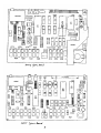
1
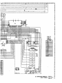
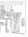
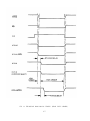
This technical manual was OCR'ed for the
Sinclair world by Andy Dansby.
[email protected]
All intellicial information contained
inside this technical manual is the
property of Amstrad.
Thank you Clive for the ZX Spectrum.
SERVICING MANUAL
FOR
ZX SPECTRUM®
•
LIST OF CONTENTS
INTRODUCTION
SECTION 1
SYSTEM DESCRIPTION
SECTION 2
DISASSEMBLY/ASSEMBLY
SECTION 3
SETTING UP AND SYSTEM TEST
SECTION 4
FAULT DIAGNOSIS AND REPAIR
SECTION 5
PARTS LISTS
i
LIST OF ILLUSTRATIONS
i
Fig No.
ZX Spectrum Block Diagram
Expansion RAM RAS/CAS Timing (Read Cycle shown)
Keyboard Matrix Interconnections
ZX Spectrum (Issue 2) Circuit Diagram
ZX Spectrum (Issue 3) Circuit Diagram
1.1
1.2
1.3
1.4
1.5
Keyboard Format
Speaker Load Input Waveforms
Expansion Memory 1C Locations
Issue 3 Links vs 1C Manufacturer and Type
4.1
4.2
4.3
4.4
Printed Circuit Board
Printed Circuit Board
Printed Circuit Board
5.1
5.2
5.3
(Issue 2) Component Layout
(Issue 3) Component Layout
(Issue 3B) Component Layout
Prepared by THORN (EMI) DATATECH LTD
for SINCLAIR RESEARCH LTD
© Sinclair Research Ltd.
(i)
MARCH 1984
-
INTRODUCTION
This manual is for use by authorised SINCLAIR
dealers, engineers and representatives as a guide
to rectifying f a u l t s on the SINCLAIR ZX SPECTRUM
personal computer.
The m a n u a l refers p r i n c i p a l l y to the Issue 2 and
Issue 3 Spectrums but provides a background to the
Issue 1 version in the section dealing with
m o d i f i c a t i o n history.
Basic
knowledge
of
ZX
SPECTRUM
operating
procedures is assumed as is knowledge of current
workshop practice relating to microcomputers.
NOTE:
Essential modifications are required
on some Issue 2 Spectrums.
Refer to
M o d i f i c a t i o n History (Section 4) and
implement as necessary.
- SAFETY MEASURES•
This
instruction
— WARNING —
manual
and
contains
CAUTION
certain
-
notices which MUST be- followed by the user to
ensure SAFE operation and to retain the
equipment in a SAFE condition.
Any adjustment, maintenance and repair of the
opened apparatus under voltage shall be
carried cut only by a skilled person who is
AWARE OF THE HAZARD INVOLVED.
SECTION 1
SYSTEM
Sub-Section
1
2
3
4
6
1.1
2.
LIST OF CONTENTS
Introduction
Architecture
Z80A CPU
Memory Organisation
Read/Write Operations
Input/Output
TV Picture Generation
Keyboard Scanning
Tape Interface
Power S u p p l i e s
Circuit Diagrams
ZX Spectrum, Issue 2
ZX Spectrum, Issue 3
5
1.
DESCRIPTION
Page No.
1.1
1.1
1.2
1.4
1.4
1.6
1.6
1.8
1.10
1.11
Fig. 1.4
Fig. 1.5
INTRODUCTION
A block diagram of the complete ZX SPECTRUM micro-computer is given in
Figure 1.1. It is valid for all build standards, fitted with either
16k or 48k bytes of dynamic RAM memory.
Although functionally
identical, detailed circuit changes have been introduced to improve
reliability and to assist with manufacture. The printed circuit board
layout has also been modified.
Details of these changes are
highlighted where necessary in the following paragraphs, and in later
sections referring to fault diagnosis and repair.
ARCHITECTURE
2.1
The architecture of the Spectrum shown in Figure 1.1 is typical of
many microcomputer
systems
in
that
it
comprises
a
single
microprocessor board (in this instance a Z80A or u 780 C P U ) , a read
only memory (ROM), an expandable RAM memory and an input/output
section h a n d l i n g the keyboard, tape and TV display functions.
The
latter is recognisable as the logic gate array (ULA) and the three
functional blocks shown in the right of the diagram.
2.2
The computer is built on a s i n g l e printed circuit board which also
includes a regulated power supply fed from an external 9V power pack.
The keyboard matrix is part of the upper case assembly and is
connected to the board via two ribbon cables KB1 and KB2.
A
description of each section follows.
1.1
3.
Z80A CPU
3.1
The Z80A is an 8-bit s i n g l e - I C central processing unit (CPU). It is
clocked at 14.0 MHz from an external source controlled by the logic
gate array (ULA) and has a standard three bus input/output
arrangement.
These buses are the Data Bus, Address Bus and Control
Bus respectively.
3.2
Data Bus. D7-D10 constitutes an 8-bit b i - d i r e c t i o n a l data bus with
active h i g h , t r i - s t a t e input/outputs.
It is used for data exchanges
with the memory and with the ULA.
3.3
Address Bus.
A15-AO constitutes a 16-bit address bus with active
h i g h , tri-state outputs.
The address bus provides the address for
memory (up to 64k bytes) data exchanges and for data exchanges with
the ULA.
It is also used d u r i n g the interrupt routine (see below)
when scanning the keyboard matrix.
3.4
Control Bus.
The control bus is a collection of i n d i v i d u a l s i g n a l s
which g e n e r a l l y organise the flow of data on the address and data
buses. The b l o c k diagram only shows five of these s i g n a l s a l t h o u g h
others of minor importance are made a v a i l a b l e at the expansion port
(see Figures 1.4 and 1.5 for d e t a i l s ) .
3.5
Starting with memory reguest f M R E Q ) , this signal is active low
i n d i c a t i n g when the address bus holds a v a l i d address for a memory
read or memory write operation.
Input/Output reguest ( I O R Q ) is also
active low but indicates when the lower half of the address bus holds
a v a l i d I/O address for the ULA d u r i n g I/O read/write operations.
3.6
The read and write s i g n a l s ( R D and W R ) are active low, and one or
other is active i n d i c a t i n g that the CPU wants to read or write data to
a memory l o c a t i o n or I/O device. All the control s i g n a l s discussed so
far are active low, tri-state outputs.
The
control signal described here is the
interrupt
last
maskable
(INT).
This input is active low and is generated by the ULA once
every 20 ms. Each time it is received the CPU ' c a l l s ' the ' m a s k a b l e
i n t e r r u p t ' routine d u r i n g which the real-time is incremented and the
keyboard is scanned.
3.7
3.8
CPU Clock.
R e t u r n i n g to the CPU clock mentioned earlier in t h i s
section, the ULA is able to inhibit this input bringing the CPU to a
temporary halt.
This mechanism gives the ULA absolute priority,
a l l o w i n g it to access the standard 16k RAM without interference from
the CPU (see RAM description). Switching transistor TR3 ensures that
the clock a m p l i t u d e is +5V rather than some arbitrary TTL l e v e l . This
is essential if the CPU is to operate e f f e c t i v e l y while executing fast
machine code programs of the 'space i n v a d e r ' ^'
1.2
3.9
Dynamic Memory Refresh.
The CPU incorporates b u i l t - i n dynamic RAM
refresh circuitry.
As part of the instruction OP code fetch cycle,
the CPU performs a memory request after first p l a c i n g the refresh
address on the lower eight bits of the address bus. At the end of the
cycle the address is incremented so that over 255 fetch cycles, each
row of the dynamic RAM is refreshed. This mechanism only applies to
the optional 32k expansion RAM in the 48k Spectrum. An alternative
refresh method is adapted for the standard 16K RAM.
4.
MEMORY ORGANISATION
4.1
In the standard 16k Spectrum there are 32k bytes of addressable memory
e q u a l l y divided between ROM and RAM.
4.2
The lower 16k bytes of memory (addresses 0000 - 3FFF) are implemented
in a single ROM (IC5) which holds the monitor program. This program
is a complex Z80 machine code program divided broadly into three parts
one each covering the input/output routines, the BASIC interpreter and
expression h a n d l i n g . Details of the program content, although outside
the scope of this m a n u a l , are referred to as necessary.
4.3
The upper 16 bytes of memory (addresses 4000 - 7FFF) are implemented
using eight 16k bit dynamic RAMs (IC6-IC13).
Approximately h a l f of
this space is a v a i l a b l e to the user for w r i t i n g BASIC or machine code
programs.
The remainder is used to hold the system v a r i a b l e s
i n c l u d i n g 6k bytes reserved for the memory mapped d i s p l a y area.
4.4
In the 48k Spectrum an a d d i t i o n a l 32k bytes of RAM are provided
(addresses 8000 - FFFF) which are implemented using eight 32k bit
dynamic RAMs (IC15-IC32). The RAM, providing extra memory space for
the user, is normally fitted d u r i n g m a n u f a c t u r e but may be added
retrospectively using the RAM expander kit. In addition to the RAMs,
the kit includes the address m u l t i p l e x e r and read/write control ICs
IC23-IC26.
Board space and the necessary discrete components are
already provided on the board.
4.5
Read/Write Operations
4.5.1
The following description should be read in conjunction with the
circuit diagrams given in Figures 1.4 and 1.5.
4.5.2
Read Only Memory (ICS).
The CPU addresses the ROM directly during
memory read cycles using the address bus A13-AO. MREQ and RD enable
the ROM and the ROM outputs respectively. A third input (CS) derived
by the ULA 'ROMCS) selects the ROM, provided the higher order address
bits A14 and A15 are both low. These are reserved for accessing the
RAM memory which starts with address 4000 (i.e. address A14 set). An
external ROM 1C select input, supplied via the expansion port on pin
25A, selectively disables the on-board ROM by pulling the select input
high. By virtue of R33 placed on the ULA side of the ROM the ULA
ROMCS output is effectively inhibited.
Interface 1 uses this
1.4
m e c h a n i s m a l l o w i n g the CPU to read the extension ROM in the interface
for m i c r o d r i v e and RS232 a p p l i c a t i o n s .
4.5.3
L i n k s H and N, shown directly above IC5, a l l o w a second source ROM to
be fitted.
The Hitachi (H) and NEC (N) ROMs use different pins for
the enable and select inputs (i.e. pins 20 and 2 7 ) . The l i n k s a l l o w
the inputs to be reversed accordingly.
4.5.4
Standard 16k RAM (IC6-IC13). The eight 16k RAM ICs m a k i n g up the
standard 16k x 8 bit RAM memory are organised as a matrix of 128 rows
x 128 columns.
Thus, separate 7-bit row and column addresses are
reguired to access any one of the locations.
These addresses are
s u p p l i e d by the CPU on address bus A13-AO via an address multiplexer
IC3/IC4.
The low order address bits A6-AO give the row address and
are selected at the b e g i n n i n g of the memory access cycle when
i n i t i a l l y the RAS output from the ULA is high. Later, as the row
address is latched, RAS goes low selecting the high order address bits
A13-A7 giving the c o l u m n address.
4.5.5
The RAS/CAS outputs from the ULA are generated in seguence in response
to MREQ and A14 from_the CPU. The DRAMWE output, a l s o from the ULA is
a decode of the RD/WR waveforms t e l l i n g the RAM to expect either a
read or a write cycle.
4.5.6
It is also apparent from the circuit diagram that the ULA can access
RAM by generating a set of addresses independent of those generated by
the CPU. The address port for the RAM is therefore d u a l l e d by the
i n s e r t i o n of small value resistors
(R17-R23)
on the address
m u l t i p l e x e r side of the RAM. This ensures that where there is likely
to be conflict between the ULA and CPU, the ULA address has priority.
Priority is assigned on the basis that the ULA must access the memory
mapped d i s p l a y area in the RAM at set i n t e r v a l s in order to b u i l d up
the video for the TV d i s p l a y . If the ULA is about to access the RAM
and it detects either A14 or A15 (i.e. the CPU is also about to access
the RAM) the ULA i n h i b i t s the CPU clock temporarily h a l t i n g the CPU
memory transaction until its own transaction is completed.
4.5.7
Resistors Rl to R8, in series with the data bus lines, perform a
s i m i l a r function to the address portplr£sistors described above.
They
ensure that the ULA does not 'see' CPU write data w h i l e the ULA is
accessing the RAM.
4.5.8
Refresh for the standard 16k dynamic RAM is accomplished during normal
read cycles, i.e. most rows are refreshed each time the ULA accesses
the memory mapped display area d u r i n g picture compilation; the
remaining rows are refreshed as a result of other read cycles also
known to occur at regular intervals w i t h i n the refresh period.
1.5
4.5.9
32k Expansion RAM (IC15-IC32). The eight 32k ICs m a k i n g up the 32k x
8 bit expansion RAM are in fact 64k ICs with either row or column
drop-out rendering one half of the memory n o n - f u n c t i o n a l . In order to
accommodate the Texas Instruments RAM (Type TMS 4532) or the optional
OKI RAM (Type MSM3732) a set of l i n k s are provided, v i s i b l e on the
c i r c u i t diagram above the address m u l t i p l e x e r IC25/IC26. These l i n k s
not only cater for the different m a n u f a c t u r e r (Issue 3 Spectrums o n l y )
but a l s o a l l o w , in both instances, one of two 1C versions to be
selected depending on which h a l f of the RAM (top, bottom, left or
right) is f u n c t i o n a l .
The l i n k s are respectively TI and OKI
(manufacturer - Issue 3 Spectrums o n l y ) , -3/-4 (TI version) and -H/-L
(OKI version - Issue 3 Spectrums o n l y ) .
NOTE:
It is essential when replacing ICs in this area that all RAMs
carry the same manufacturers part number and that the l i n k s
are selected a c c o r d i n g l y .
4.5.10 The expansion RAM is organised as a matrix of 128 rows x 256 columns
(TI RAMs) or 256 rows x 128 (OKI RAMs).
Thus, separate 7/8 bit row
and column addresses are required to access any one of these
l o c a t i o n s . These addresses are supplied by the CPU on address bus
A14-AO via an address m u l t i p l e x e r IC25/IC26.
For example, when
accessing the TI RAM the low order address bits A6 to AO give the row
address; AR is h e l d low on the -3 version selecting the top half of
the memory and high on the -4 version selecting the bottom h a l f . The
column address is given by the high order address bits A14-A7.
4.5.11 Row/column address selection and RAS/CAS t i m i n g for the RAM is decoded
in IC23/IC24 from inputs s u p p l i e d by the CPU, i.e. address l i n e A15
selecting addresses 8000 upwards, and MREQ heralding a memory read or
write cycle. A theoretical t i m i n g diagram i l l u s t r a t i n g the RAS/CAS
waveforms is given in Figure 1.2.
5.
INPUT/OUTPUT
5.1
The input/output section of the Spectrum is centered round the ULA
(IC1). The functions performed w i t h i n the device i n c l u d e TV video
c o m p i l a t i o n , keyboard scanning and tape input/output. It also derives
and controls the CPU clock (<j>CPU) using an external 14 MHz crystal XI,
and drives the loudspeaker when a ' B E E P ' instruction is being
executed.
Each of these sections and the supporting circuits are
described below.
5.2
TV Picture Generation
5.2.1
The video c o m p i l a t i o n section of the ULA operates in conjunction with
the memory mapped picture display area in the standard 16k RAM, the
colour (chrominance) modulator (IC14) and the UHF modulator.
This
combination produces a high resolution, 24 l i n e x 32 character, eight
colour TV d i s p l a y .
1.6
FIG 1.2 EXPANSION RAM RAS/CAS TIMING
1.7
(READ CYCLE SHOWN)
5.2.2 U s i n g the 14 MHz clock the ULA derives l i n e and f i e l d t i m i n g
compatible with the external TV receiver.
Video is derived by
accessing the memory mapped display area in the RAM in a set seguence
at set times throughout the picture frame.
The addresses are
necessarily independent of the CPU and appear on the ULA address lines
A6 through AO as two separate bytes timed by the RAS/CAS row/column
address select l i n e s .
5.2.3
The net result is three separate video waveforms outputs from the ULA
on pins 15, 16 and 17.
These carry the l u m i n a n c e signal Y,
i n c o r p o r a t i n g the l i n e and field sync, and two u n m o d u l a t e d c o l o u r difference s i g n a l s U and Y m a k i n g the Spectrum c o m p a t i b l e with both
colour and monochrome receivers.
5.2.4
From the ULA the colour difference s i g n a l s are a p p l i e d to the colour
m o d u l a t o r IC14 via two level s h i f t i n g networks. These match the ULA
output levels with those reguired at the B-Y and R-Y inputs to the
modulator.
In the Issue 2 Spectrum the l e v e l s h i f t i n g network is
passive, incorporating two potentiometers VR1, VR2.
These are
reguired to set-up the chroma b i a s level on IC14 pin 3 such that the
voltage difference measured between pin 3 and the colour difference
s i g n a l s on pins 2 and 3 respectively is n o m i n a l l y 0V d.c.
In the
Issue 3 Spectrum two active networks i n c o r p o r a t i n g IRS and TR9
e l i m i n a t e the potentiometers, greatly i m p r o v i n g colour stability.
5.2.5
The level shifted c o l o u r difference s i g n a l s , input to IC14, are then
encoded, by guadrature m o d u l a t i n g two 4.43 MHz chroma sub-carriers.
The sub-carriers are generated with the assistance of an external
crystal X2 and a CR l e a d / l a g network introducing a 90° phase shift
between pins 1 and 18. (A further difference between the Issue 2 and
3 Spectrums lies in the bias o s c i l l a t o r . The early issues incorporate
a trimmer TC2 a l l o w i n g the chroma sub-carrier freguency to be
adjusted; on the later issues the freguency is f i x e d ) . The resultant
m o d u l a t e d colour difference s i g n a l s are f i n a l l y mixed producing a
composite chroma sub-carrier at IC14 pin 13.
5.2.6
At this point the chroma s i g n a l is a.c. coupled to the base of TR2 and
added to the inverted luminence signal on TR1 collector.
The
resultant composite video is then buffered and a p p l i e d to an
encapsulated U H F m o d u l a t o r operating on European standard channel 36.
5.3
5.3.1
Keyboard Scanning
Every 20 ms (i.e. once per m a s k a b l e i n t e r r u p t ) , the CPU systematically
scans the keyboard recording which 'keys '(if any) have been pressed.
The s c a n n i n g method is described below with the aid of Figure 1.3. As
the figure c l e a r l y i l l u s t r a t e s the keyboard consists of an 8 x 5
m a t r i x , the inter-section of each row and column bridged by a n o r m a l l y
open switch contact. The row ' o u t p u t s ' and column ' i n p u t s ' are shown
connected by separate ribbon cables KB1 and KB2, one to the ULA and
the other to the high order address lines A15-A8.
P u l l - u p resistors
R64 through R68 ensure that when the address bus is in the high Z
state, or none of the key-switches is closed, row outputs KBO to KB4
remain h i g h .
5.3.2
When the keyboard s c a n n i n g routines are entered the CPU performs
successive I/O read cycles setting the IOREQ and RD lines to the IJLA,
low. At the same time, the I/O port addresses placed on the upper
h a l f of the address bus are m o d i f i e d with each cycle such that each of
the address l i n e s A15 through A8 is set l o w in t u r n , the other l i n e s
remaininghigh.
5.3.3
The seguence starts with I/O port address FE d r i v i n g address line A8
low. The keyboard matrix also sees t h i s potential on column 6 a p p l i e d
via D6 and the ribbon cable KB2. Thus, when any of the switches on
the inter-section with column 6 is pressed, the corresponding row
output s u p p l y i n g the ULA via the second ribbon cable (KB1), is p u l l e d
low. The row s i g n a l ( s ) is subseguently inverted by the ULA and placed
on one of the five low order data bus l i n e s . For e x a m p l e , if the CAPS
SHIFT key is pressed row one output drives data bus DO high and so on.
The seguence ends with I/O address 7F when c o l u m n 8 is addressed. In
t h i s instance, operation of the SPACE key drives DO h i g h . C l e a r l y ,
the keyboard scanning routines make the d i s t i n c t i o n between the CAPS
SHIFT and SPACE key by knowing which address l i n e is being driven.
5.4
Tape Interface
5.4.1
When LOADing or SAVEing programs using a cassette recorder, the ULA
transfers i n f o r m a t i o n between the M I C and EAR sockets and the data
bus, performing A/D and D/A conversions as reguired.
Since the LOAD
and SAVE functions are m u t u a l l y e x c l u s i v e , a s i n g l e pin on the ULA
(i.e. pin 28) is used both for input and output.
Separate I/O
read/write cycles to port address 254 configure the pin accordingly.
During the LOAD operation the CPU executes successive I/O read cycles,
reading the EAR input off data bus 6.
When performing a SAVE
operation, the CPU executes successive I/O write cycles, this time
w r i t i n g data to the MIC output via data bus 3.
5.4.2
To ensure that I/O cycles are correctly implemented, the IOREQ l i n e
s u p p l y i n g the ULA is gated with address l i n e AO via TR6. Thus, if any
memory transactions occur where AO is high (i.e. not port address 254)
then the IOREQ input is forced high i n h i b i t i n g any attempt to perform
an I/O cycle.
5.4.3
Loudspeaker (BEEP) Operation.
It should be noted that w h i l e SAVEing,
the level of the MIC output is barely sufficient to drive the
loudspeaker via D9 and TR7 (D10).
However, during the execution of a
BEEP instruction the CPU writes instead to port 254 on data bus 4.
This e f f e c t i v e l y boosts the MIC output, d r i v i n g the loudspeaker so
that the BEEP tone can be easily heard. During the execution of such
an instruction the cassette recorder is not r u n n i n g so there is no
c o n f l i c t at the MIC/EAR sockets.
1.10
6.
6.1
POWER SUPPLIES
The on-board power s u p p l y unit receives a 9V u n r e g u l a t e d supply from
the external S i n c l a i r ZX power pack and derives the f o l l o w i n g internal
supply r a i l s :
(a) regulated +5V for the 1C logic c i r c u i t s , the ULA and the U H F
modulator,
(b)
-5V and +12V for the standard 16k dynamic RAM,
(c)
+12V for the colour m o d u l a t o r circuits.
6.2
The external power pack incorporates a m a i n s transformer, f u l l wave
rectifier and c a p a c i t i v e smoothing.
A thermal fuse is fitted at the
transformer input.
6.3
The on-board power supply unit incorporates a 7805 r e g u l a t o r , d e r i v i n g
the +5V power r a i l , and an inverter stage TR4/TR5. The latter raises
the level of the +9V unregulated s u p p l y to in excess of +12V. The
resultant sguare wave at the junction of TR4 collector and the
inverter coil is subseguently rectified and smoothed by D5/C44
producing the +12V output for the RAM. A d d i t i o n a l smoothing, imparted
by R62/C45, produces the +12V supply for the TV circuits free from
noise generated by the RAM. The sguare wave at TR4 collector also
supplies the Zener/rectifier diode combination D16/D12 generating -5V
for the RAM, and is a v a i l a b l e at the expansion port for use by
peripherals. The +12V, +5V and -5V are also made a v a i l a b l e .
SECTION 2
DISASSEMBLY/ASSEMBLY
Sub-Section
1.
LIST OF CONTENTS
Page No.
1
Disassembly
2.1
2
Assembly
2.1
DISASSEMBLY
1.1
U n p l u g all input/output leads and turn the computer upside-down to
reveal five self-tapping screws.
Remove the screws.
Hold the two
halves of the case together and return the computer to the keys
uppermost position.
The top half of the case can now be separated
from the bottom h a l f , a l t h o u g h it remains connected to it by two
f l e x i b l e keyboard ribbon connectors.
Care should be taken not to
damage the ribbon connectors. As an aid to reassembly, the lie of the
connectors within the case should be noted.
1.2
To remove the board from the lower half of the case, remove one selftapping screw (adjacent to IC22 socket) and lift out the board.
It
may be advantageous to make up two short p l u g g a b l e extensions for the
keyboard connectors in order to improve a c c e s s i b i l i t y to the board.
1.3
To change either the keyboard membrane or the rubber keyboard mat it
is first necessary to remove the escutcheon plate (template). This is
attached to the case by double-sided adhesive tape around the edges.
The template is removed by inserting a screwdriver at one end and
l e v e r i n g it away from the case. It is not n o r m a l l y possible to remove
the template without damage.
2.
ASSEMBLY
2.1
Assembly is carried out using the reverse procedure to
disassembly. Do not overtighten s e l f - t a p p i n g f i x i n g screws.
2.2
When r e p l a c i n g a keyboard component, note that the membrane keys into
projections on the case.
Place the keypad over the membrane and
ensure that it is positioned and seated properly. Faulty i n s t a l l a t i o n
can result in depressed keys being trapped under the template during
subsequent key operations.
To install the template, place doublesided adhesive tape around all four edges, locate it in position on
the case and apply firm pressure around the edges (12 mm tape on sides
and bottom, 6 mm at top).
2.1
that
of
2.3
When a l i g n i n g the top h a l f of the case with the bottom h a l f ensure
that the two keyboard ribbon cables are not trapped between projecting
components w i t h i n the case.
In their correct positions there is
s u f f i c i e n t room for the cables to take up a comfortably curved
position i n s i d e the case.
If a cable is trapped and bent d o u b l e , an
open c i r c u i t w i l l sooner or later r e s u l t .
SECTION 3
SETTING UP AND SYSTEM TEST
Sub-Section
1.
1.1
LIST OF CONTENTS
Page No.
1
General Alignment
Introduction
Voltage Check
Colour Adjustment
Sub-Carrier Oscillator
14MHz Oscillator
3.1
3.1
3.1
3.1
3.2
3.2
2
System Test
3.3
GENERAL ALIGNMENT
Introduction. The Issue 3 Spectrum m o d i f i c a t i o n removes the need for
adjustment of the colour t u n i n g u s i n g potentiometers and trimmers.
Therefore, the setting-up procedure for this board is confined to
checking that the i n t e r n a l l y generated power supply voltages and two
oscillator frequencies are correct.
Adjustment instructions apply
strictly to the Issue 2 Spectrum boards only but are g e n e r a l l y
relevant to the Issue 1 Spectrum as w e l l .
To carry out the setting up procedure it is first necessary to remove
the ZX SPECTRUM from the case (Section 2, A s s e m b l y / D i s a s s e m b l y ) .
For
convenience the keyboard may a l s o be disconnected.
1.2
Voltage Check.
as f o l l o w s :
Check that the i n t e r n a l l y generated power voltages are
Circuit Reference
IC6 pin 9
IC6 pin 1
IC6 pin 8
LT side of C52
1.3
Nominal Value
+ 5V
- 5V
+12V
+12VA
Tolerance
±
±
±
0.25V
5.5V to -4V
1.2V
1.2V
Colour Adjustment. Potentiometers VR1 and VR2 are used to effectively
n u l l the voltages between pins 4 and 2 (for VR1) and pins 2 and 3 (for
VR2) on IC14 (LM1889). To a l l o w for thermal drift, the potentiometers
are set for non-zero voltages; furthermore these voltage off-sets are
set to satisfactory but non-optimum l e v e l s in production, and optimum
values may be used to advantage in servicing. The relevant figures
are given in the f o l l o w i n g t a b l e - voltages are given relative to pin
3 of LM1889.
3.1
Pot.
1.4
IC14
Factory Settinq
Pin No.
(mV)
Optimum ( m V )
Voltage Tolerance
Overall Ranqe
(mV)
VR1
4
130 ± 20
+50
-5
+45 to +150
VR2
2
75 ± 20
-50
-50
+5
-45 to -100
Sub-Carrier Oscillator.
The chrominance
frequency should be 4.433619 MHz ± 50 Hz.
checked/adjusted by usinq one of two methods,
below.
sub-carrier o s c i l l a t o r
This frequency may be
listed in (a) or (b)
A p p l y power to the power socket usinq a bench power s u p p l y set at 9V.
Current consumption w i l l be approximately 500 mA to 700 mA for the 16k
Spectrum and 700 mA to 900 mA for the 48k Spectrum.
1.5
(a)
Feed the Spectrum m o d u l a t o r output via a co-axial cable into a
standard colour TV receiver. Measure the frequency of the locked
TV chroma sub-carrier.
(b)
Connect pin 17 of IC14 (LM1889) via a 4.7 pF capacitor and a lead
to the frequency meter.
It is recommended that this is done
u s i n q a jiq made up from an 1C test c l i p . Pin 18 of this c l i p
must be removed to m i n i m i s e stray capacitance. Connect a 10k ohm
resistor between the input t e r m i n a l s of the frequency meter.
Measure the frequency and adjust trimmer TC2 if the measured
frequency is outside tolerance.
14 MHz Oscillator. This frequency is not readily set by workinq to a
specified frequency and tolerance.
On Issue 2 boards trimmer TCI
s h o u l d be adjusted to m i n i m i s e the effects of beat frequencies which
cause waves of distortion to flow across the screen.
These are
p a r t i c u l a r l y apparent with certain colour c o m b i n a t i o n s , e.g. red INK
or green PAPER, and the phenomenon is sometimes referred to as 'dot
crawl'.
It is stressed that adjustment of this frequency is not
s t r a i g h t - f o r w a r d , as d e v i a t i o n s due to temperature chanqe are easily
v i s i b l e ; t u n i n q should be adjusted to m i n i m i s e rather than remove this
effect.
Proceed as follows:
(a)
Set up the Spectrum to display qreen PAPER with red INK.
(b)
Type-in three or four lines of characters and monitor the screen.
(c)
Adjust trimmer TCI to m i n i m i s e the effects of distortion.
3.2
2.
SYSTEM TEST
2.1
The system test for the Spectrum may be undertaken using the ZXTP
taped program (see 1.1 Test Equipment in Section 4) loaded
conventionally; this requires that the keyboard is connected. The
test should be carried out with the Spectrum connected to its own
power supply.
2.2
The test program exercises all of the Spectrum circuitry with the
exception of the SAVE function.
To test this function a small,
possibly one line program should be typed in, SAVED and then VERIFIED
as described in the instruction manual.
3.3
SECTION 4
FAULT DIAGNOSIS AND REPAIR
Sub-Section
1
LIST OF CONTENTS
Introduction
Test Equipment
Modification History
Modifications - Issue 1 Board
Modifications - Issue 2 Board
32k Extension Memory - (16k-48k)
Hitachi vs NEC ROM
2
Fault Diagnosis
Techniques
Power Supply Unit
Initialisation
Memory Check
Keyboard Structure
F a u l t - F i n d i n g Guide
Page No.
4.2
4.2
4.3
4.4
4.5
4.5
4.6
4.6
4.6
4.7
4.7
4.8
4.10
4.11
3
Repair
4.19
4
16k to 48k Upgrade
Integrated Circuits/Link Settings
Issue 2 Board
Issue 3 Board
4.19
4.19
4.20
4.20
1.
INTRODUCTION
1.1
Test Equipment
Section 4 is intended as a guide to fault diagnosis and repair of the ZX
SPECTRUM.
It is assumed that users have a reasonable knowledge of
electronic servicing, theory and standard fault-finding techniques and
have access to the test equipment and tools required to carry out the
task. The table below contains a list of the minimum recommended test
equipment and materials.
SPECIFICATION/MANUFACTURER
EQUIPMENT
Oscilloscope with
O s c i l l o s c o p e probe ( x l O )
Rise Time:
Variable power supply unit
0 to 30V d.c.
Mono cassette
With RECORD and PLAYBACK facilities
recorder
0.02 us/cm
M a i n s extension lead
'Safebloc' type
Multimeter
General purpose
Colour T e l e v i s i o n
Open Market
ZX Printer
Sinclair
ZXTP test tape
Blank tape
Open Market
Double-sided adhesive tape
12mm and 6mm wide, Tesafix 959
(B.D.F. TESA) or 3M equivalent
Engineers who are already f a m i l i a r with the S i n c l a i r ZX81 w i l l find some
s i m i l a r i t i e s in the ZX SPECTRUM.
The Spectrum, however, is a more
sophisticated device with colour and sound circuitry.
The ZX SPECTRUM is s u p p l i e d with either 16k or 48k of on-board RAM. The
16k version is wired so that it can be expanded to 48k by the addition
of a number of appropriate p l u g - i n ICs.
For details of the memory
upgrade, see sub-section 4 of this section.
See Section 5, Figures 5.1 and 5.2 for the layouts of the Issue 2 and
Issue 3 boards respectively.
4.2
1.2
Modification History
Two major m o d i f i c a t i o n s have been implemented on the Spectrum boards:
(a)
A m o d i f i e d layout of board (i.e. Issue 1, Issue 2 and Issue 3)
Issue 1.
This layout allowed for the 16k RAM to be mounted
direct on the board, with the 32k extension consisting of a
subsidiary board m o u n t i n g onto special
O I L connectors.
Approximately 26,000 units were manufactured.
Issue 2. This layout allows for all 48k of RAM to be mounted
direct on the board; sockets, ready for a memory update, are
fitted on 16k versions.
A small number of Issue 2 units were
manufactured using disc capacitors for 47 pF and 100 )jF v a l u e s ,
but subseguently a x i a l s were introduced.
Issue 3.
This layout incorporates advanced circuitry for the
colour t u n i n g , removing the need for potentiometers and trimmers
and the associated adjustment. It a l s o a l l o w s for OKI ICs to be
used in the 32k extension memory.
The heatsink is a l s o
redesigned and is relocated at the back of the case.
(b)
The Ferranti ULA, type 5C102, plus spider addition replaced by
ULA type 5C112.
5C102. This ULA has a timing fault which was cured by connecting
a 74LSOO 1C mounted on a miniature board and spider.
This ULA
was fitted to approximately 40,000 units.
5C112. This improved ULA has no spider m o d i f i c a t i o n , but has
either a diode or resistor or transistor connected to it.
The
details are:
Diode/resistor mod : 4k7 resistor from +12V to pin 30 on IC2 and
diode (IN 4148) from pin 30 of IC2 to pin 33 of IC1.
Transistor mod : TR6 (ZTX313) connected as f o l l o w s :
Base to IC2, pin 30.
Emitter to IC1, pin 33.
Collector to IC2, pin 11.
6C001 This ULA alters the timing of the colour burst s i g n a l , and
improves the performance of the Spectrum with certain television
sets (e.g. H i t a c h i , Grundig) .
It also causes the screen picture
to be shifted by one character width to the left.
NOTE: The values of certain components vary depending on which
board and which ULA is used as follows:
4.3
Board Issue No
ULA Type
2
5C112
2
6C001
3
6C001
Ik
10 k
470
470 n
Ik
10 k
Ik
Ik
Component
R47
R49
R56
R63
220
8
220
220
a
k2
n
n
fi
1.3 Modifications - Issue 1 Board
A number of m o d i f i c a t i o n s were introduced, and these should be checked
for and, if necessary, introduced retrospectively:
(a)
100 pF capacitor between RAS and ground - necessary only when
u s i n g ULA 5C102.
(b)
470 pF capacitor between IC2, pin 28 and ground - required only
when IC2 and RAM ICs are all of NEC manufacture.
(c)
1 k resistor between RAS and 23V and 1 k resistor between CAS and
12V, only when RAM ICs are of National manufacture. R57 (330n)
must be removed, and the 470 pF capacitor is not required.
(d)
47 k resistor between pin 13 of LMI889 and ground - required only
if the difference between white and y e l l o w colours is inadequate.
(e)
If disc capacitors are used for C41 and C49 (47 nF) they must be
replaced by axial components.
(f)
Capacitor C46 (1 uF e l e c t r o l y t i c ) should be replaced by a h i g h
temperature component.
(g)
This modification is required for efficient operation of certain
machine code software and should be implemented on all units.
It
has been implemented in manufacture for a l l ULAs 5C112-2 and
later.
D14
R24
R27
R73
(h)
replaced by C67 (100 pF)
changed from 3k3 to Ik
changed from 680 n to 470 n
( I k ) added between Id/32 and +5V
A significant cause of problems has been found to be failure of
the internal power s u p p l y transistor TR4.
The circuit may be
improved by changing the value of R60 from 100 n to 270 fl and
connecting a 4.7 uF electrolytic (perferably r a d i a l type) with
positive end to TR5 emitter (positive end of C34) and negative
end to TR5 base (to R58).
4.4
1.4
Modifications - Issue 2 Board
A number of m o d i f i c a t i o n s have also been introduced for the Issue 2
board.
These should be checked a n d , if necessary, introduced
retrospectively.
(a)
These components
upgrading:
R48
R49
R50
R72
C65
changed
changed
changed
changed
changed
should be
changed if colour quality needs
from 4k7 to 2k2
from 18 k to 8k2
from 8k2 to 4k7
from 47 k (or 18 k) to 10 k
from 100 yF to 22 yF
(b)
E a r l y Issue 2 boards were manufactured u s i n g a considerable
number of 47 yF and 100 uF disc capacitors. C41 (47 nF) and C43
(100 nF) should be replaced with axial components to prevent
undue risk of short circuits.
(c)
To prevent l i f t i n g of the keyboard template, a thin strip (6 mm
wide) of d o u b l e - s i d e d tape was introduced to the top edge of the
template.
(Previously, only the other 3 edges had tape). This
m o d i f i c a t i o n should be introduced whenever template l i f t i n g is
found to be a problem.
(d)
See Items 1.3(g) and (h) above.
1.5 Modifications - Issue 3B Board
Although f u n c t i o n a l l y s i m i l a r to the Issue 3 board, the layout differs.
The DC converter design has been improved, p r o v i d i n g greater power
supply r e l i a b i l i t y .
Component changes are as f o l l o w s (see Fig 1.5 for
details):
C77
C49
R60
TR4
1.6
( I Q O n F ) added
changed from 47nF to 560pF
changed from 270fl to 68n
can be either ZTX650 or TIPP31
32k Extension Memory -
(16k to 48k)
Board Issue 1:
The extension memory is s u p p l i e d as a p l u g - i n module
which is inserted into sockets near the edge connector. The ICs used are
either TI 4532-3 or TI 4532-4, and all ICs in a unit must be of the same
type (i.e. all must be -3 or all must be -4).
Board Issue 2:
The extra memory is obtained by p l u g g i n g in 4 logic ICs
and 8 memory ICs (see Sub-Section 4). The ICs used are either TI 4532-3
or TI 4532-4, and a l l ICs must again be of the same type. It should be
noted that the RAM select signal is 0V for the -3 1C and +5V for the -4.
A l i n k on the board provides the required select l e v e l .
4.5
Board Issue 3: This allows OKI ICs to be used in p l a c e of TI 4532.
A g a i n , all ICs must be of the same designation. Appropriate links (2)
must be fitted in the grid located on the board between the edgeconnector and the ' m i c ' jack socket.
A g a i n the extra memory is
obtained by p l u g g i n g in 4 logic ICs and eight memory ICs.
1.7
Hitachi vs NEC ROM
D u r i n g m a n u f a c t u r e , w i r i n g l i n k s are selected and inserted in the
board according to whether a Hitachi or NEC ROM is used. These l i n k s
are marked 'H' and ' N ' as appropriate and are located as f o l l o w s .
Board Issue 1
- between the ROM and the heat sink
Board Issue 2
-
beneath the raised portion of the heatsink
Board Issue 3
-
adjacent to the loudspeaker
Clearly, if the ROM is changed for one of a different make, then these
links must be changed as w e l l .
2.
FAULT DIAGNOSIS
2.1
Techniques
In a closed loop system such as a computer, because of the interdependence of numerous component parts, f a u l t diagnosis is not
necessarily s t r a i g h t - f o r w a r d .
In addition, because of the high speed
cyclic operation, interpretation of any waveforms on control, data and
address lines as being valid depends to a large extent on practical
experience of the system.
There are however, certain checks with
v a l i d waveforms and levels that can be carried out before s u b s t i t u t i n g
any integrated circuits. Experience has shown that the best method of
i n i t i a l l y checking waveforms and levels can be to compare with the
same point in a known serviceable board. The f o l l o w i n g pages provide
a basic fault-finding procedure and furnish a l i s t of possible faults
a l o n g with suggested ways of curing them.
W i t h a densely populated board such as the ZX SPECTRUM, a careful
physical examination of the board can sometimes indicate an obvious
fault.
Burst-out discrete components or an overheated track show up
immediately, as do the attentions of an enthusiastic amateur. Bearing
in mind the latter, short ^circuits , caused ,by h a i r l i n e solder
splatter can be or several ohms resistance and can cause some very
m i s l e a d i n g fault symptoms.
Provided first principles are adhered to and a common-sense approach
is adopted, it w i l l be found after a short space of time that fixing a
faulty Spectrum is very much a routine operation.
4.6
2.2
Power Supply Unit
The unstabilised external power supply unit is a source of some
problems.
The design is such that, at minimum input voltage
(215V a.c.) and 1.4A output, the voltage trough should not be less
than 7.0V; at maximum input voltage (265V a.c.) and 60QmA output, the
voltage peak should be less than 13V.
2.3
Initialisation
At switch-on the computer should automatically
produce a clear screen with the statement
'initialise'
and
(01982 Sinclair Research Ltd
d i s p l a y e d in the lower left section of the screen.
This indicates
that most of the system is working.
If the Spectrum does not
i n i t i a l i s e , carry out the following basic checks.
Basic Checks. It is d i f f i c u l t to be specific in a f a u l t - f i n d i n g guide
because of the large variety of fault conditions which can occur, but
the f o l l o w i n g procedure, starting with a table of checks set out in
order of priority, w i l l however isolate the major f a u l t area.
FUNCTION
CIRCUIT REF.
Voltage regulator
input
+ve side of C50
Voltage regulator
output
+ve side of C34
On-board power supply
outputs:
+5V d.c.
IC6 pin 9
-5V d.c.
IC6 pin 1
+ 12V d.c.
IV6 pin 8
+ 12VA(to IC14 only) LT end of C52
WAVEFORM/VOLTAGE
+9V d.c. ± 2.0V. At less
than +7V the regulator may
not operate correctly.
+5V d.c. ± 0.25V discernable ripple.
+5V d.c.
± 0.25V
discernable ripple.
-5V d.c.
+12V d.c.
+12V d.c.
no
-
no
Clock pulses
IC1 pin 32
TR3 base and
collector IC2
pin 6
Address and data
lines (following
through to relevant
ICs)
RT side of R17-R23 Waveform of amplitude 3.5V
RT side of R1-R8
14MHz squarewave at +5V
amplitude,
If these tests prove satisfactory check IC1 pin 14, IC2 pin 11 and IC5
pin 28 for +5V. Also check for ground at IC1 pin 40, IC2 pin 29 and
IC5 p i n 14. If all is s t i l l satisfactory at this point and IC1 is the
p l u g - i n type, replace IC1.
If replacement of IC1 does not cure the
f a u l t , check the address and data l i n e s of IC1, IC2 and IC5 for active
data.
It is possible that one of the Z80A or RAM control lines has become
faulty therefore,
comparing with a known serviceable board if
p o s s i b l e , check the waveforms at the f o l l o w i n g points at origin and
destination:
(a)
IC2:
Pin 16
Pin 20
Pin 19
Pin 21
Pin 22
- INT
- IDREQ
- MREQ
- M
- WR
Pin
Pin
Pin
Pin
(b)
IC22:
Pin 4
Pin 15
-
Pin 3
"RAT
CA3~
17 - NM1
24 - WAIT
25
: fflCTEQ
/b
KtbM
-
WITE
If no fault has been found and the computer s t i l l has not i n i t i a l i s e d ,
the fault could lie in the RAM. If the computer is a 48k m a c h i n e the
32k of expansion RAM can be isolated. An easy way of doing this,
assuming that the ICs are not fitted into sockets, is to remove the
+5V from IC25.
This is probably best done by very carefully c u t t i n g
the track to IC25 pin 16.
If this operation clears the fault
condition, the expansion RAM w i l l have to be further isolated. In
either instance the point has been reached where it is necessary to
start replacing ICs.
Where the f a u l t persists after i s o l a t i n g the 32k expansion RAM it
would be necessary to start changing i n d i v i d u a l ICs in the order of
IC13 to IC6 ( R A M ) , IC1 ( U L A ) , IC2 (Z80A). After each change of 1C the
unit must be powered up to check for correct i n i t i a l i s a t i o n .
A method of f a u l t - f i n d i n g that can be used on both the 16k and 48k
versions is to make up a 'test 1C' device. This may be done by using
an 1C test c l i p , to which is attached a serviceable 1C (of the
relevant type e.g. 4116 or 4532), to bridge across each suspect 1C in
turn. This method is not guaranteed to work but can often save a lot
of time u n n e c e s s a r i l y c h a n g i n g suspect ICs.
Memory Check
Where a Spectrum has i n i t i a l i s e d correctly but a RAM memory f a u l t is
suspected, it is possible to find the faulty address and relate it to
a faulty 1C by carrying out the f o l l o w i n g procedure:
Key in the instruction:
PRINT PEEK 23732 + PEEK 23733 * 256
The v a l u e printed should be:
4.8
(a)
(b)
for a 48k unit - 65535
for a 16k u n i t - 32767
The v a l u e printed in each instance is the last v a l i d memory l o c a t i o n ,
and in a serviceable u n i t would be as set out above. Therefore, if a
different v a l u e , n, is printed the faulty l o c a t i o n w i l l be n + 1. If
the v a l u e returned is less than 32767 the f a u l t l i e s in the o r i g i n a l
16k of RAM. The f o l l o w i n g example i l l u s t r a t e s the method of r e l a t i n g
a faulty l o c a t i o n to a f a u l t y 1C.
Example.
If a 48k Spectrum is g i v i n g a memory of 25.25k key in the
following instruction:
PRINT PEEK 23732 + PEEK 23733 * 256
Assume the answer displayed is 43200,
43201 (stops at last v a l i d l o c a t i o n ) .
therefore the faulty location is
Key-in:
POKE 43201,85 : PRINT PEEK 43201 (= answer A)
If answer A is 85, key-in:
POKE 43201,170 : PRINT PEEK 43201 (= answer B)
If answer B is anything other than 170 look up in the f o l l o w i n g t a b l e
which 1C to change (e.g. if answer B is 234 change IC21). S i m i l a r l y ,
if answer A is other than 85 refer to the table to find the faulty 1C.
Data 85
IC6-IC13
Data 170
IC15-IC22
Size of
Error
Error
Bit
Faulty RAM location if:
< 32767
> 32767
84
171
1
0
IC6
IC15
87
168
2
1
IC7
IC16
81
174
4
2
IC8
IC17
93
162
8
3
IC9
IC18
69
186
16
4
IC10
IC19
117
21
138
234
32
64
5
6
IC11
IC12
IC20
IC21
213
42
128
7
IC13
IC22
If there is more than one f a u l t y RAM location the first f a u l t
identified w i l l have to be repaired before it is possible to proceed.
4.9
2.5
Keyboard Structure
The keyboard is connected horizontally in eight blocks of five keys
and vertically m It
configuration.
five
follows
blocksthat
of if
eight
any block
keys. of
Figure
five keys
4.1 shows
fail the
the
fault is with KB2 circuitry or the 8-way membrane, and that if any
block of eight keys fail the fault is with KB1 circuitry or the 5-way
membrane. Possible keyboard faults are listed in paragraph 2.6
FIGURE 4.1 KEYBOARD FORMAT
4.10
2.6
Fault-Finding Guide
As with any complex d i g i t a l equipment the possible fault permutations
are vast, thus the following table is not intended to be an exhaustive
list of the f a u l t s that might occur on the Spectrum. It is intended
as a guide only to possible courses of action to f o l l o w when f a u l t s
show up in p a r t i c u l a r areas of the c i r c u i t . These areas are listed in
the table with sub-headings, in no p a r t i c u l a r order of priority. It is
envisaged that the ZXTP test tape has been loaded, or an attempt has
been made to load the tape, in order to check for a faulty c o n d i t i o n .
AREA
TV screen dead,
smoke appears on
switch-on.
SYMPTOM
TR4 base-collector
shorted.
ACTION
Remove TR4
Short persists with
TR4 removed.
1. Check TR5 and C44.
2. V i s u a l l y check track.
3. Check TR4.
TR4 blows a g a i n .
1.
Not i n i t i a l i s i n g .
No '(C)1982
Sine!air. Research
Ltd1 statement.
No video.
No video.
Change TR4 and TR5 (even
though TR5 checks out).
2. Check that TR5 circuit
components are to latest
specification.
Follow fault-finding
procedure, paragraph 2.2
^above.
' y
y y
1.
2.
NOTE: Table 4.1
sets out typical
s i g n a l s found on
IC14 pins 1-18
IC14 pins 1-18.
No video after
ULA changed.
Change IC1.
Check TR1 and TR2.
1.
V i s u a l l y check IC1 and
socket,
3. Check
for
shorting
between C65 and R53.
4. Carry out f a u l t - f i n d i n g
procedure,para 2.2 above.
1.
2.
3.
4.
Check voltage drop across
R64.
Check +5V regulator 0/P
and +9V regulator I/P.
Check PWR socket not
shorted.
Check power unit.
AREA
No video,
SYMPTOM
(contd)
ACTION
No VIDEO INPUT at
IC14 pin 12.
1.
2.
Check waveform at IC14
pin 13. If correct check
TR1 and TR2.
Check waveforms at IC1
pins 15, 16 and 17:
If correct check VR1, VR2
(Issue 1 and Issue 2 boards).
3.
4.
Corrupt Paper,
after ULA change.
-
Change IC1.
If +5V and VIDEO INPUT
correct change modulator.
1.
2.
Check IC1 socket.
Check PWR socket is not
intermittent.
3. Check IC1 pin 14 for +5V
with
no
discernible
ripple.
No 3 MHz at IC2
pin 6.
1.
2.
3.
4.
5.
6.
Low amplitude - check
R25.
Check TR3.
Check IC1 pin 32 for 3
MHz.
Check IC1 pin 39 for 14
MHz.
Check crystal X I .
Check IC1 pin 13 for +3V.
AREA
Video Incorrect.
SYMPTOM
ACTION
Dark Screen.
1.
2.
Dim ' S i n c l a i r ' Io9°-
1' Check +12V"
2. Check
C65
for
high
impedance.
3. Check R52.
4. Check +5V on IC14 pin 3.
Wavy lines across
screen.
1.
Self resetting.
Press
down
on
each
electrolytic capacitor to
see if lines disappear.
If
so
change
that
capacitor.
2. Check crystal X2.
3. Check/change TR1 and/or
TR2.
4.
Check/change IC14.
Check TR6.
Random dynamic
squares.
Change C54.
Paper area too low.
Change IC1.
Diagonal lines in
the border area.
Change R47.
Distorted video.
1.
2.
Colour tuning
faults (Issue 1
and Issue 2 boards)
Check t u n i n g .
Change modulator.
-
VR1 or VR2 f a i l s to
adjust IC14 pin 13
waveform.
Check for +3V
pin 13.
Change C30.
at
IC1
V i s u a l l y check IC14 circuits.
1.
Monitor IC14
trimming VR2.
2. Monitor
IC14
trimming VR1.
3. Change IC14.
pin
pin
2
4
AREA
Colour tuning
faults, (cont'd)
SYMPTOM
VRl or VR2 d.c.
shifts IC14 pin 13
waveform.
ACTION
Change IC14.
Alternate dark lines Change IC14.
on screen.
No colour after
trimming TC2:
ICH pin 17 not
oscillating
1. Check crystal X2.
2. Change ICH.
3. Change X2.
ICH pin 17
oscillating but
fails to tune.
1. Check for broken track,
2. Change TC2.
3. Change ICH.
ICH pin 17 output
correct but still
no colour (boards
at all Issue Nos).
1. With 'Sinclair' logo on
screen ICH pin 2 and
ICH pin 4 should be as
follows:
2.
Colour faults
Pin screen.
(Issue 1 - Issue 3
boards.
Blue haze around
'Sinclair1 *-™°'
Screen too yellow.
If
ICH pins 2 and 4
are
correct,
change
modulator.
Change crystal X2.
If untunable Issue 1 and
issue 2 boardsj chage ICH.
Change ICH.
AREA
Colour faults
(cont'd)
Keyboard faults.
SYMPTOM
Intermittent
colour.
ACTION
1.
Change TC2 (Issue 1 and
Issue 2 boards).
2. Change IC14.
Red, Blue or
Green 'Sinclair'
logo.
Change IC1.
Washed-out
colours.
Check TR2.
KB1 fault.
1.
Check for short on 2 or
more of the 5 tracks.
2. Change membrane.
KB2 fault.
1.
2.
Regulator c o i l .
Speaker.
Dead keyboard.
Change IC1.
Wrong keyboard
response.
Change IC1.
Keyboard response
too fast.
Change IC1.
Coil excessively
noise.
Change c o i l .
No speaker output.
NOTE: Figure 4.2
shows typical
waveforms in the
speaker circuit
Test program.
Check for short on 2 or
more of the 8 tracks.
Change membrane.
1.
2.
3.
4.
Check load input
forms .
Check TR7.
Check D9.
Change speaker.
'Tape Loading Error'
output.
Reload program.
Paper area edges
distort.
Change IC1.
wave-
AREA
Test Program.
(cont'd)
SYMPTOM
Paper area corrupts
d u r i n g tests.
ACTION
1.
Change IC1.
2.
Carry out f a u l t - f i n d i n g
procedure (paragraph 2 . 2 ) .
Border colours are
striped.
Change IC14.
Failure
Carry
out
fault-finding
procedure (paragraph 2.2).
messages.
'Test Passed1
Chan5e IC1message not f l a s h i n g .
Reduced memory
size.
1.
2.
Program Loading.
Perform memory test,
Change IC1.
Keyboard does not
a l l o w loading.
See keyboard f a u l t s ,
Program f a i l s to
load,
1.
Check jack sockets
f u l l y inserted.
2.
If l o a d i n g stripes in
border
are
unusually
wide, check D13.
3.
Check/change IC1.
'Program
appears.
Check/Change IC2.
are
FIGURE 4.2 SPEAKER LOAD INPUT WAVEFORMS
4.17
TABLE 4.1. IC14 (IML889) PIN SIGNALS
Pin No.
Signal
1
(CHROMA LEAD) SINEWAVE BOOmV, 0.2yS, d.c. 9.5V
2
(R - Y INPUT)
3
(CHROMA BIAS) d.c.
4
4.8V
(B - Y INPUT)
5
0V (GROUND)
12
(VIDEO INPUT)
13
(CHROMA SUBCARRIER)
14
(R.F SUPPLY)
15
(SOUND TANK)
16
(CHROMA SUPPLY
17
(CHROMA OSCILLATOR OUTPUT)
18
(CHROMA LAG)
6,7,8
9,10,
11
NOTES:
d.c. 12V unreg.
'LINKED1
12V d > c -
SQUAREWAVE 0.2 us 4V P-P.
D.C. 0.8V
SINEWAVE BOOmV P-P
2 uS
d.c.
9.5V
Not Connected
(1) Rails and signals taken on switch-on, computer
displaying ' S i n c l a i r 1
y
(2) No keys pressed
(3) All d.c. levels positive wrt 0V
4.18
3.
3.1
4.
4.1
REPAIR
Renewal of components should be carried out u s i n g recognised
d e s o l d e r i n g / h e a t s i n k i n g techniques to prevent damage to the component
or to the printed circuit board. Other points to be noted are:
(a)
When replacing a keyboard m a t r i x , take care that the ribbon
connectors are f u l l y inserted into the board connectors, and are
not k i n k e d during insertion.
(b)
Make sure there is a good contact made between the voltage
regulator body and the associated heatsink in order to ensure
adequate heat conduction. The heatsink h o l e in certain Issue 3
boards a l l o w s excessive play w h i c h could cause f o u l i n g of the
edge connector.
Take care in re-assembly that the h e a t s i n k is
fitted away from the edge connector.
(c)
When the regulator is being replaced it is recommended that a
suitable proprietary thermal grease is applied to the rear
surface of the component body.
(d)
The m o d u l a t o r s h o u l d be replaced as a complete unit.
(e)
When r e p l a c i n g p l u g - i n ICs it is a d v i s a b l e to use the correct
removal and insertion tools. Avoid c o n t a m i n a t i n g the connection
p i n s by h a n d ! i n g .
(f)
When h a n d l i n g ICs take normal anti-static precautions.
It is
recommended that o n l y a s u i t a b l y earthed, low power s o l d e r i n g
iron be used.
(g)
After any component has been renewed the circuit board s h o u l d be
examined c a r e f u l l y , to ensure that there are no solder
' s p l a t t e r s ' which may cause short circuits between tracks or
connector pins.
16k TO 48k UPGRADE
Integrated C i r c u i t s / L i n k Settings
For both the Issue 2 and the Issue 3 boards the memory upgrade is
accomplished by p l u g g i n g four logic ICs and eight memory ICs into
e x i s t i n g board sockets.
Depending on the types of memory 1C used,
appropriate circuit l i n k s must be fitted on the board.
Figure 4.3
shows the layout of the area of the board containing the empty
sockets. The Issue 3 board is shown which also gives positions (top
left of diagram) of the l i n k s .
4.19
4.2
Issue 2 Board
The ICs used on this board are as follows:
1C
TYPE
IC15 - IC22
IC23
74LS32
IC24
74LSOO
IC25, IC26
NOTES:
.3
TI 4532-3 or TI 4532-4 200ns (or 250ns)
74LS157 (NOT N a t i o n a l Semiconductors)
(1) All external RAM ICs must be of the same type
(i.e. all -3 or -4 v a r i a n t s ) .
(2) LINK 3 on the board (IC26, pin 10) should be fitted
if IC15-IC22 are type 4532-3.
(3) L I N K 4 s h o u l d be fitted if IC15-IC22 are type 4532-4.
Issue 3 Board
The ICs used on this board are as follows:
1C
TYPE
IC15 - IC22
IC23
74LS32
IC24
74LSOO
IC25,
NOTES:
(1)
(2)
TI 4532-3, TI 4532-4 or OKI
MSM3732
200 ns (or 250ns)
IC26
74LS157 (NOT National Semiconductors)
All extension RAM ICs must be of the same type.
Two l i n k s must be fitted on the board (grid
located between edge connector and m/c jack
socket) depending on memory manufacturer and
type (high or low e n a b l e ) . See Figure 4.4 for
l i n k positions vs manufacturer and 1C type.
4.20
FIGURE 4.4 ISSUE 3 LINKS vs 1C MANUFACTURER AND TYPE
4.22
SECTION 5
PARTS LIST
Sub-Section
LIST OF CONTENTS
Page No.
1
Introduction
5.1
2
Notes to Table 5.2
5.1
1.
INTRODUCTION
1.1
Parts lists for the ZX SPECTRUM are provided in table form; one for
the case assembly (Table 5.1) and another for the board assembly
(Table 5.2).
The latter covers the Issue 2 and 3 Spectrums and is
related to the board layout diagrams given in Figure 5.1 and 5.2.
T a b l e 5.2 a l s o lists the a l t e r n a t i v e components which the service
engineer w i l l o c c a s i o n a l l y f i n d on production versions of the Issue 2
board or may introduce retrospectively in order to improve
performance. These components are listed in the column headed ' I S S U E
2 MODS' with references to notes against them.
These notes are
explained below-
2.
NOTES TO TABLE 5.2
(1)
The alternative values given for R47, R49, R56 and T63 are used
if the ULA fitted is Type 6C001.
(2)
The alternative values for R48, R50, R72 and C65 are introduced
to improve the colour q u a l i t y .
(3)
C74 is essential on all Issue 2 boards and s h o u l d be fitted
retrospectively. At the same time R60 must be replaced with the
larger v a l u e .
(4)
The introduction of alternative components for R24 and R27 is
essential. At the same time C67 replaces D14 and R73 is added.
(5)
Issue 2 boards fitted with the Type 5C112 ULA have either a
transistor (TR6) or diode/resistor m o d i f i c a t i o n (see Issue 2
circuit diagram for d e t a i l s ) .
(6)
On Issue 3 boards only crystal X2 must have a close tolerance
s p e c i f i c a t i o n (i.e. 10 ppm absolute, 10 ppm 20°C to 60°C, 5 ppm
per year.)
(7)
On Issue 3B boards, the d.c. converter design has improved
r e l i a b i l i t y . R60 is changed from 270n to 68ft and C49 is changed
from 47nF to 560pF. Capacitor C77 ( l O O n F ) has been added.
5.1
2.1
General Capacitor Change. Early Issue 2 units were manufactured u s i n g
a considerable number of 47 nF and 100 nF disc capacitors.
Where
these occur the service engineer should take the opportunity to
replace C41 and C49 with axial types.
TABLE 5.1 CASE ASSEMBLY
MANUFACTURER
DESCRIPTION
Assembled board as appropriate
(Table 5.2)
Moulded Upper Case
Moulded Lower Case
Keyboard Mat
(Rubber)
Keyboard Membrane
N.F.I.
Keyboard Template
Rubber Feet
Self Tap Screws (case f i x i n g s ) , 5 off
D o u b l e - s i d e d adhesive tape 12 mm wide; Tesafix 959
B.D.F. Tesa
D o u b l e sided adhesive tape 6 mm wide; Tesafix 959
B.D.F. Tesa
Self Tap Screw (board f i x i n g ) , 1 off
5.2
TABLE
Circuit
Reference
Issue 2
5.2
Issue 2
Mod
BOARD ASSEMBLY
Notes
Issue 3
Rating/
To!
Manufacture
Type
CAPACITORS
( U n l e s s otherwise stated a l l c a p a c i t o r s are a x i a l types)
C1-C8
C25
C26
C27
C28
C29/C30
C31/C32
C33
C34
C35
C36
C37/C38
C39
C40/C42
C43
C44/C45
C46
C47
C48
C49
C50
C51
C52/C53
C54
C55-C62
C63
C64
C65
C66
C67
C68-C71
C72/C73
C74
C75
TC1/TC2
C76
C77
47 nF
22 yF
47 nF
1 yF
22 yF
47 nF
lOOnF
47 nF
22 yF
10 nF
47 nF
33 pF
10 nF
47 nF
lOOnF
lOOyF
1 yF
22 yF
47 nF
47 nF
22 yF
(7)
150pF
470pF
47 nF
47 pF
lOOpF
lOOyF
47 nF
-
4.7WF
-
-
-
22 yF
(2)
lOOpF
-
(4)
(3)
(7)
47 nF
25V, 10%
22 yF
10V,-10%+80%
47 nF
2 5 V , 10%
1 yF
50V,-10%
22 yF
10V,-10%+80%
47 nF
25V, 10%
lOOnF
25V, 10%
47 nF
25V, 10%
22 yF
10V,-10%+80%
10 nF
25V, 10%
25V, 10%
33 pF
25V, 10%
10 nF
25V, 10%
47 nF
2 5 V , 10%
lOOnF
25V, 10%
lOOyF
16V,10%+80%
1 yF
50V,-10%+80%
22 yF
10V,-10%+80%
47 nF
25V, 10%
47/560pF 25V, 10%
22 yF
10V,-10%+80%
Ceramic
Elect.
Ceramic
Ceramic
Elect.
Ceramic
Ceramic
Ceramic
Elect.
Ceramic
Ceramic
Ceramic
Ceramic
Ceramic
Ceramic
Ceramic
Elect.
Elect.
Ceramic
Ceramic
Elect.
150pF
47 nF
47 pF
lOOpF
22 yF
47 nF
lOOpF
lOOnF
16 pF
4.7uF
lOOnF
Ceramic
Ceramic
Ceramic
Ceramic
Ceramic
Elect.
Ceramic
Ceramic
Ceramic
Ceramic
Elect.
Ceramic
25V, 10%
25V, 10%
25V, 10%
2 5 V , 10%
25V, 10%
20V,10%+80%
25V, 10%
25V, 10%
25V, 10%
25V, 10%
5V min
25V, 10%
47 nF
lOOnF
25V, 10%
25V, 10%
Ceramic
Ceramic
COIL
Circuit
Reference
Issue
2
Coil
SPECTRUM
Issue 2
Mod
-
Notes
-
5.3
Issue 3
SPECTRUM
Rating/
Tol
-
Manufacture
Type
1703
CONNECTORS
Reference
EAR
MIC
PWR
Description
Manufacturer/
Part Number
3.5 mm jack socket
3.5 mm jack socket
2.1 mm co-axial socket
KB1
5-way ribbon connector
M o l e x 5229-05CPB
KB2
8-way ribbon connector
Molex 5229-08CPB
CRYSTALS
Circuit
Reference
XI
X2
Issue 2
Issue 2
Mod
14.000000MHz
4.433619MHz
Notes
-
Note
(6)
Issue 2
Mod
Notes
Issue 3
Manufacture
Type
14.000000MHz
4. 433619MHz
DIODES
Circuit
Reference
D1-D9
D10
D11-D13
D14
D15
D16
Issue 2
1N4148
1N4148
1N4148
1N4148
BA157
5V1
-
(4)
-
Issue 3
Manufacture
Type
1N4148
1N4148
BA157
5V1
Signal
Signal
Signal
Signal
Rectifier
Zener
INTEGRATED CIRCUITS
Circuit
Reference
Issue 2
Issue 2
Mod
ICl(ULA)
5C102
5C112
IC2(CPU)
Z80A/U780
IC3/IC4
74LS157N
IC5(ROM)
SPECTRUM SPECTRUM
IC6-IC13 4116
IC14
LM1889
IC15-IC22 TI4532
IC23
IC24
IC25/IC26
74LS32N
74LSOON
74LS157N
-
Notes
Issue 3
(1)
6C0001
Z80A/M780
74LS157N
SPECTRUM
4116
LM1889
TI4532/
MSM3732
74LS32N
74LSOON
74LS157N
Manufacture
Type
48k
48k
48k
48k
only
only
only
only
Ferranti
Not N a t i o n a l
NEC/Hitachi
150 ns
Texas/
OKI
Not National
RESISTORS ( 1 / 4 W , 5% unless otherwise stated)
Circuit
Reference
R1-R8
R9-R16
R17-R23
R24
R25
R26/R27
R28
R29
R30
R31
R32
R33
R34
R35
R36
R37
R38
R39
R40
R41
R42
R43
R44
R4B/R46
R47
R48
R49
RBO
R61/R52
R53
R54
R55
R56
R57
R58
R59
R60
R61/R62
R63
R64
R65-R69
R70/R71
R72
R73
R74/R75
R76/R77
R78
VR1/VR2
Issue 2
470R
8K2
330R
3K3
180R
680R
10KO
1KB
1KO
220KO
100R
680R
15R
10KO
680R
1KO
3K3
3K3
1KO
1KB
1KO
3KO
5K1
1KO
22 OR
4K7
8K2
8K2
2K2
390R
100K
56R
220R
330R
1KO
1K8
100R
15R
220R
15R
10KO
220R
470Korl8K
2K2
Issue 2
Mod
Notes
1KO
(4)
1KO
2K2
10KO
4K7
(1)
(2)
(1)
(2)
470R
(1)
270R
(3), ( 7 )
470R
(1)
10KO
1KO
(2)
(4)
5.5
Issue 3
470R
8K2
330R
1KO
180R
470
10K
10K
10K
220K
100R
680R
15R
10K
680R
IK
1KO
3KO
BK1
1KO
1KO
2K2
10KO
4K7
2K2
390
100K
56R
1KO
1KO
1K8
270R
15R
1KO
15R
10KO
220R
10KO
1KO
10KO
1KO
470R
Rating
Tol
Issue 3B
1/2 or 1W
2%
2%
2%
2%
68R
TRANSISTORS
Circuit
Reference
Issue 2
Issue 2
Mod
TR1/TR2
TR3
TR4
TR5
TR6
TR7
TR8/TR9
ZTX313
ZTX313
ZTX650/TIPP31
ZTX213
ZTX313
-
Notes
-
(5)
Issue 3
ZTX313
ZTX313
ZTX650
ZTX213
ZTX313
ZTX450
BC184
MISCELLANEOUS
Reference
REG
Description
Manufacturer/
Part Number
5V r e g u l a t o r
7805
MOD
UHF M o d u l a t o r with E36
v i s i o n carrier (UK o n l y )
Loudspeaker
40 ohm T.V.
Type
M o d u l a t o r Screen
Insulator
Heatsink
Astec
UM1233
1740
Special
(Issue 2
or 3)
R e g u l a t o r F i x i n g s ( l ) Screw, ch hd. 4BA x 15/16 in
(2) Washer, shk prf, 4BA
(3) N u t , hex, 4BA
OIL SKT
16-way (10-off) for 48k
expansion RAM (16k model only)
OIL SKT
14-way (2-off) for 48k
expansion RAM (16k model only)
OIL SKT
28-way for IC1
(ULA)
GENERAL DATA
Earliest version
-
very pale brown keys.
Second version
-
grey keys
Third/Fourth versions
-
grey keys, but heatsink now visible through the edge
connector slot
Early Spectrum plus
-
same as fourth type.
Dissembly
-
after removing the screws, t i l t back, face up and
carefully lift the top taking care not to break any
of the keyboard tails.
Heatsink
-
when operating computer with the heatsink removed to
obtain access a temporary heatsink must be used made
of anything as long as it fits under regulator.
Circuit Diagram
-
idealised version on centre pages shows all modifications which should be made. Note that connecting
items such as standard capacitors may not be shown.
Edge Connector
-
28 pin double-sided to which no interface may be
inserted or removed whilst computer is switched on.
Plugs & Cables
-
use only genuine Sinclair issue or HK plugs, etc.
Power Supply
Links
-
Where any possibility of fluctuating mains exists a
transient suppressor should be fitted.
-
T1/T3 for Texas THS4532-3; T1/T4 for Texas TMS4532-4
1/H for OKI HSH3732H; 1/L for OKI MSM3732-L.
Other Service/Repair Manuals by T.I.S. Include:-
Rank A823 CTV Chassis
Philips G8 CTV Chassis
Thorn 3000/3500 CTV Chassis
Thorn 8000/8004/8500/8600 CTV Chassis
Rank T20/20A CTV Chassis
The Tunbridge & McCourt T.V. Repair Manuals
The Tunbridge Video Repair Manuals
SERVICE DATA
Modification of earplug: Connect a 330 ohm resistor between signal and earth
leads of earplug to a l l o w earplug to be left in place while saving a programme.
Inserting or removing such items as joysticks, especially via a Kempston
interface, while the computer is switched on will damage the power resistors
and regulator.
Modification to voltage generator circuit: Where not fitted already, insert a
22uf capacitor between the TR4 and D15 as shown in the circuit diagram, this
will ensure the correct 12v supply. On early models replace R60 by a 270 ohm
resistor and fit C74 if missing. Ensure that the 12v supply is 12v.
Manufacturer's advised modifications: In early versions replace all ceramic
capacitors by axial ones and replace C46 by a high-temperature luf type. A l l
resistors to be changed to show the second value show in centre pages circuit
diagram herein; same applies to capacitors.
Weak sound:
Only if particularly noticeable
changed to same as shown herein.
Tape and Sound Circuits:
should the sound section be
5Vp-p at ear socket for 2Vp-p at IC1 verifies IC1.
Alignment: Only needed for early models. Place meter on pin 4 of IC4 and
adjust VR1 to obtain 130mV; adjust VR2 to obtain -75raV at pin 2 with a 20mV
allowable error either way. Use TC2 to set colour subcarrier frequency to
4.433619MHz to 50Hz either way. TCI only helpful to improve screen colour
pattern.
A l i g n m e n t : A l l models. Run the programme to display the eight colours in
sequence from black to white. This is normally given as:-
10
20
30
40
50
60
FOR A=0 TO 7
FOR B=0 TO 3
PAPER A: PRINT"
NEXT B
NEXT A
GOTO 10
";
If this shows incorrect or missing colours then align as stated for early
models. See repair data for later models.
3
REPAIR DATA
1) GENERAL REPAIR PROCEDURE AND NOTES ON ALL FAULTS
These computers are reportedly very unreliable with some 50% of new
ones alleged to have to be returned for replacement. Many faults are due to
loose or badly fitted components so that a good checkover is essential for this
reason, to determine if a factory failure first. ;
Check
overtightened
badly fitted
holders, edge
uncommon for
heatsink first for any reported fault, is it loose? Are there
screws? Look for dry joints, cracks in print or cracked boards,
components, especially ICs; dirty or tarnished contacts, pins,
connectors; damaged keyboard t a i l s and fins are certainly not
whatever reason.
Before investigating any fault check any add-ons and interfaces to the
computer for broken solder, etc. caused by user wiggling them about. It is
also essential to note if add-on is loose or faulty which w i l l give a guide to
any damage so caused.
This w i l l also determine if fault in add-on not
computer. Knowing what add-ons are used can be a good guide to probable fault:
for example, suspect TR4 blown and/or destroyed RAMS if a Kempton is used.
Check if customer has been inserting or removing any add-ons without
first switching off and point out how this practice has damaged machine and
costing him unnecessary expenditure.
If this is admitted then check TR4 first
then RAMS and see symptom 3.
2} WONT LOAD FROM RECORDER
Almost invariably this w i l l be caused by the alignment of the recorder
head not being good enough. The recorder w i l l play music, etc. and function
w e l l but it w i l l s t i l l need adjusted to operate the Spectrum properly and it
matters not whether it is an old or just newly bought recorder.
Disconnect Spectrum from recorder and with any tape playing use a long
thin-bladed screwdriver to adjust the azimuth screw through the hole normally
provided for this purpose.
The object is to obtain the sharpest possible
sounding note, noting that if note is in the least muffled sounding then there
is no chance of the Spectrum loading from it.
If
no hole is provided this should be done with the recorder cover
removed. Although it is reccomnended that volume should be set at midpoint it
is far better to vary volume setting to that at which maximum treble is
obtained. F i n a l l y give head a good clean and recheck setting.
If the adjustment does not cure the problem then save a short programme
from the computer (or use one previously saved) and if this doesn't load then
it is safe to assume that there is a fault, probably in the computer. In this
case, check connections to computer and the circuit from the edge connector to
the first I.C.
4
Early circuit showing
presets Td, TC2, VRl
and VR2 to match the
early type boards.
Note:the different
pins 16/17 setup from
Id in the generalised
circuit diagram shown
in the middle pages.
In very versionst instead of TR6 a
somewhat unreliable, resistor/diode
was used which should be modified
as shown in the centre pages.
This very unreliable circuit was used
in very early versions from pin 32 to
base of Id.
This circuit should be
modified to that shown in the centre
pages if not already done.
Modifications associated with IC1
3) NO COIL BUZZ FROM INVERTER, -5V ABSENT
From symptom 1 it should be obvious that TR4 (ZTX650) is very prone to
damage and this symptom is a sure indication that TR4 must be replaced. However, before replacing the TR4 check the TR5 (ZTX213) (using a transistor
tester is O.K.) and the coil since it is not unknown for all three to have gone
at the same time and if only the TR4 is replaced it can fail again immediately
if the others are faulty.
Whether or not these three are faulty or not, there can be one or more
faulty RAMS as well caused possibly by the same forcing in of an interface
during switch on. If all else has been fixed, switch on and check if any RAM
gets hot; replace any very hot RAMS either in basic set or in extra board as
this is a sure sign of being short circuit. If open circuit, the guickest way
to check is to bye-pass each RAM in turn using a RAM known to be O.K. When so
doing the same RAM must be used as the suspect and it should not be removed
after each check for some ten seconds after each switch off or it will fault
itself. Use of a 'scope or logic probe is clearly a better alternative if
available. Tandy m<tke a good, inexpensive logic probe.
4) DIRECT CHECK FOR A SINGLE FAULTY RAM
Type PRINT PEEK 23732+256 * PEEK 23733 (CR). If computer RAMS O.K. the
reply is either 32767 or 85535, if less than either this means that there is a
shortage of available RAMS, thus one or more RAMS may be faulty.
Call the reply N and if POKE N+1,85 (CR) then PRINT PEEK N+l (CR) is
typed the reply should be 85 if RAMS O . K . , in that case type POKE N+1,170 (CR)
then PRINT PEEK N+l (CR) when a different number to the 170 you have just poked
into that address w i l l be printed. 85 and 170 are the easiest binary numbers
(01010101 and 10101010) to cover all combinations in an 8-bit chip.
Where a different reply is given to either POKE locate the incorrect 1C
as follows:Where 85 is poked in
IC6 faulty gives 84; IC7 87; IC8 81; IC9 93; IC10 69; IC11 117; IC12
21; IC13 213.
Where 170 is poked in
IC15 faulty gives 171; IC16 158; IC17 174; IC18 162; IC19 186; IC20
138; IC21 234; IC22 42.
5) NO COIL BUZZ FROM INVERTER, REG7805 OPEN CIRCUIT
Before replacing the 7805 check the heatsink to see if faulty or badly
fitted. Remedy any physical defect in print or damage around screws, etc.
Also check the TR4/5 and coil.
6) CONTINUAL FAILURE OF POWER SUPPLY TRANSISTORS
Ensure that all modifications have been carried out and that the edge
connector is O.K. and not loose or, damaged.
Check for proper fitting of all
peripherals and verify that owner is not persistently inserting/removing any of
the add-ons, etc. while the computer is switched on. Note that many users are
apparently incapable of grasping this simple point. Check the plug/sockets and
cable, if not suitable then replace with correct ones.
Check the mains and
possible interference from other items on same circuit.
If satisfied then check if the Ov is correct on earth. Monitor the Ov
while running computer as this nay shew up an intermittent voltage fault.
A
systematic check on all capacitors.resistors to earth should find the culprit
for this uncommon cause.
7) KEYBOARD FAULTS
It is recommended that keyboards are better replaced completely since
they take a lot of battering and replacement is guite inexpensive.
If it is
decided that the keyboard is worth repairing then tha diagram will show which
tail is faulty according to keys in error.
If the entire keyboard is non-functional then check the 5v supply is
reaching it O.K. before replacing the ULA I.C. Probably the commonest fault
lies with a faulty 10K resistor (R65 to R69) easily identified according to
which keyboard co91umn is faulty.
8) VARIOUS FAULTS WHICH APPEAR ONLY WHEN WARM
Check heatsink thoroughly. If heatsink is O.K. then the ULA I.C. IC1
will be the cause.
If IC1 has been replaced before it may be worth adding
extra heatsink for it. See also following symptom.
9) INTERMITTENT FAULTS
If such faults show up with a comoaritively new Spectrum then it is
most likely that they are due to poor contacts/soldering during the
manufacturing process. Check all holders and pins for tarnish and dry joints.
Replace faulty holders by cutting them out and replacing completely. Check
after this for poor contacts or loose contacts, look for items which have been
poorly soldered or even where soldering has been omitted. Finally check the
boards for hairline cracks and breaks, especially radiating from heatsink
screws.
10) TEXAS SN1889 INSTEAD OF LHA889
A few models appeared with the SN version and these may even have been
used as replacements during repairs.
Although unlikely to find now, if SN
types have been used replace completely by LH type.
11) POWER SUPPLY O.K. - COMPUTER NOT WORKING CORRECTLY
;
If computer is functioning at all check for single RAM failure then
multiple RAM failure as already described. If RAMS are O.K. or fault is more
serious and RAMS cannot be checked then check if the 5v supply is reaching all
I.C.s in order IC1, 2, 24, 23, 3, 4, 26, 25 and 5. Replace the open circuit
component cutting off the 5v supply if this is the case. ,'
Faulty or missing sound usually identifies the ULA I.C. IC1 as being
faulty and this is the most likely suspect in any case.
Flick the clock
crystal with your finger, this will guickly determine if it is faulty or not.
Although I.C.s are best checked out systematically using a logic probe
or even a 'scope, it is worth noting that after IC1 the most likely culprits
are IC2 and IC5, neither of which are particularly reliable and it may even be
worth replacing the three automatically as a fast check.
12)
PERMANENT I.C.
CHECKER FOR LOGIC PROBE USE
If a logic probe is available it is well worth making a table of the
results of checking each 1C pin with a good computer switched on with keyboard
disconnected. Thus when any computer is being tested all that is needed is to
compare the readings with your correct set and the different readings w i l l
quickly pinpoint the faults.
13) FLICKERING WHITE BACKGROUND - MAY BE CAUSING EYESTRAIN
If resetting the computer doesn't help, which is not uncommon if a CTV
is being used, then the only thing is to set up the computer to display a
coloured background with white printing.
See spectrum manual for this, but
green is the most relaxing background. Save this programme and load it every
time Spectrum is not being used for games.
14) SPARE PARTS SUPPLIERS
At time of printing the most popular suppliers appear to be:CPC Electronic Components, 194 North Road, Preston, Lanes.
PV Tubes, 104 Abbey Street, Accrington, Lanes. BBS 1EE.
This list may be amended in future printings.
//