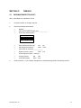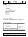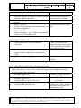
1
Service Manual
SureSight
TM
Welch Allyn Medical Division
4341 State Street Road
P.O. Box 220
Skaneateles Falls, NY 13153-0220
PN 140399 Rev. B
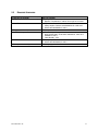
1
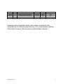
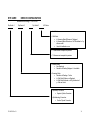
Part No.
140399
140399
Rev.
A
B
Description
SureSight Service Manual
SureSight Service Manual
ECN #
5-41452
5-41582
Date
5/2000
6/2000
Approved
SH
SH
Drawings and/or illustrations and/or part numbers contained in this
document are for reference purposes only. For current revisions call the
Welch Allyn Customer Service phone number listed in Section 1.
PN 140399 Rev. B
2
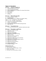
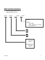
TABLE OF CONTENTS
SECTION 1:
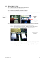
G ENERAL INFORMATION
About the SureSight Vision Screener
About the SureSight Autorefractor
Technical Help Information, Worldwide Tech Support Phone Number
Theory of Operation
Block Diagram
Tooling Set up
Warnings
1.1
1.2
1.3
1.4
1.5
1.6
1.7
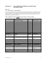
SECTION 2:
SERVICE/C ALIBRATION
2.1 Incoming Inspection, Checklist
2.2 Required Upgrades
2.3 Tools Required for Service, Calibration and Software Loading
Table 2.3-1: Tier 1- Unit Check Out - Yearly calibration
Table 2.3-2: Tier 2 - Unit Repair - Major Systems
2.4 Calibration Check (Required after all repairs)
2.5 Software: Loading/Upgrading
2.6 Product Numbering Structure/ Serial Numbering Structure
2.7 Repair Parts List
SECTION 3:
TROUBLESHOOTING
Technical Troubleshooting Table: Complaint/Cause/Corrective Action
3.1
SECTION 4:
4.1
4.2
4.3
4.4
4.5
4.6
4.7
4.8
4.9
4.10
4.11
4.12
4.13
4.14
4.15
4.16
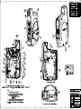
DISASSEMBLY AND REPAIR
Replacement of Bottom Housing
Replacement of Flex
Replacement of DSP Board
Replacement of RTC Battery
Replacement of Front Insert Assembly
Removal of O-Ring
Replacement of the LCD Assembly
Replacement of LCD Board
Replacement of Battery Compartment Assembly
Replacement of Power Board
Replacement of the Aligned Baseplate Assembly
Replacement of Hand Strap
Replacement of the Top Housing
Cleaning of the Windows
Hewlett Packard Printer Check
Dip Switch Changing
APPENDIX SECTIONS :
A.
B.
C.
D.
Final Test Specs.: A04187
Electrical Schematics and Drawings: 140150
Revision Logs: A04262
SureSight Final Assembly Drawing: 140000
PN 140399 Rev. B
3
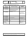
SECTION 1 GENERAL INFORMATION
1.1
ABOUT THE SURESIGHT PRIMARY CARE M ODEL 14001
SureSight is an objective, accurate, affordable vision test that ensures reliable early detection of
refractive error, the primary vision disorder in children. Early detection improves outcomes and reduces
treatment duration.
1.2
ABOUT THE SURESIGHT AUTOREFRACTOR M ODEL 14011
SureSight is a child friendly, portable, affordable autorefractor that lets you test patients - including
young children and adults - anytime, anywhere. Carry it from room to room, to your waiting area, even offsite.
PN 140399 Rev. B
4
1.3
T ECHNICAL HELP INFORMATION
All service and repairs must be performed by fully trained and properly equipped personnel, using genuine
replacement parts and correct procedures. Failure to do so will invalidate the product warranty and could
compromise instrument safety and performance.
Read and understand all safety warnings and service notes printed in this Service Manual and the
Operator’s Manuals, SureSight part number 140300 and SureSight Autorefractor part number
140400. If in doubt about any precaution or procedure, for phone help, or to order additional
copies of the SureSight Operator’s Manuals, contact:
Customer Service
Welch Allyn, Inc.
4341 State Street Road, PO Box 220
Skaneateles Falls, NY 13153-0220 USA
Telephone 1-800-535-6663
When calling, refer to the model number shown on data label, found on the bottom of the
SureSight.
Troubleshooting assistance is contained in Section 3 of this manual.
Year 2000 Information: The SureSight is Y2K compliant and will not will not encounter “Year 2000”
Problems.
PN 140399 Rev. B
5
1.4
T HEORY OF OPERATION - DETAILS:
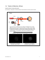
Hartmann-Shack Technique Description:
The following is a description of the basic Hartmann-Shack method on which the device is based.
Figure
Beam
Splitter
Illumination
Exit Port
CCD
Camer
Lens
System
Patient Eye
Mirror
s
Light is sent from an illumination source inside the SureSight through a beam
splitter and focuses on the back of the eye (retina). The retina, in turn, reflects
the light back into the device. Inside the unit, the beam travels through a series
of mirrors and is received by a micro-lens array, creating an image which is sent
to a CCD camera. The spot pattern of light formed is translated into sphere,
cylinder, and axis.
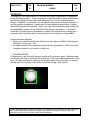
Examples of Spot Pattern Received Through CCD Camera
Emmetropic Eye 0.00 Diopters
Hyperopic Eye +4.24 Diopters
spot pattern of light is uniform
spot pattern of light is compacted
PN 140399 Rev. B
6
VISION SCREENER OPTICAL SYSTEM ARCHITECTURE
The following is a description of the present design architecture. A collimated beam of light is projected out
of the patient port by the illumination system. The light is ‘focused” by the eye lens and cornea to a small
spot on the retina. This blur acts as a point source on the back of the eye which then radiates back through
the eye lens and cornea producing a reflected beam which includes information about the lens power and
eye aberrations. The resulting return beam is directed by the beam splitter into the measurement path which
is detected by the camera at the end of the path. To achieve alignment, the practitioner views the patient
eye and the alignment guide pattern through the viewing system. The working distance between the output
port of the device and the patient of approximately 40 centimeters. This large working distance provides the
opportunity to improve accuracy in children, as well as being less intimidating to them. It also reduces the
need for fogging in which is used in conventional autorefractors which work at approximately 2cm.
PN 140399 Rev. B
7
M AJOR SUBSYSTEMS:
Illumination System:
The illumination system generates a laser beam which can be projected into the eye under test.
Because this laser beam radiates in the infrared region - it is not visible without an IR goggle or other IR
detecting device. For repair and calibration purposes, an ITT night vision scope is recommended for any
work which includes the illumination system.
The source of illumination is a 5 mW electrical, 3 mW optical semiconductor laser located on the
laser mini board. This board is attached to the illumination tube which houses the optics needed to collect
the light emitted by the laser and form it into a beam which is projected from the end opposite the laser. The
laser mini board is connected via a 4 position flex cable to the laser drive board which controls the laser
output. The drive system monitors the laser output with a photodiode which is physically built into the laser
diode. The laser drive system controls the laser output to a particular photodiode level which is set by the
DSP board. The DSP controls this setting with a digital pot on the laser drive board according to a
calibration performed at the factory. This beam is transmitted through the beam splitter located near the one
inch port on the front of the unit.
*SAFETY NOTE: While the laser is capable of emitting 3 mW of optical power, only a fraction exits
the illumination tube. Laser levels are controlled to approximately 18 µW, which is well within Class I safety
limits. However, to prevent improper exposure DO NOT look at the bare laser diode.
A properly functioning illumination system produces an approximately collimated beam of light 2mm
in diameter. This beam can be seen using ITT goggles when a piece of white paper is placed in front of an
operating illumination tube. The collimated aspect of the beam can be observed by the lack of change in
size of the beam (spot) regardless of the distance from the front of the tube.
Measurement System:
The measurement system detects the beam reflected from the patients eye back toward the unit.
This beam enters the product through the one inch port on the front of the unit and is reflected down toward
the bottom of the unit by the reflecting side of the beam splitter. This beam passes through a first conjugate
lens, to two measurement mirrors which bend the beam across the bottom of the unit and back up toward
the top where it passes through a second conjugate lens in to the camera/lenslet assembly. The
camera/lenslet assembly consists of the camera board with a lenslet filter mounted to the top of it by a
lenslet housing. When the beam passes through this lenslet and IR filter, a group of spots are created which
represent the optics of the eye from which the beam came.
The camera image is progressively sent to the DSP board for processing. If a sufficient number and
quality of images is detected, the DSP computes and reports a reading of the optical power detected. The
exposure, gain and other settings of the camera are controlled by the DSP board through a serial port and a
digital pot on the camera board. These settings are also set during the factory calibration.
Viewing System:
The purpose of the viewing system is to create a visible image which can be used to align the
product with the patient. Because the laser is invisible, it can not be used for aligning. Instead, the viewing
system produces a visible crosshair target which is aligned so as to be in the same position as the invisible
laser beam at the in-range working distance. In this way, when the practitioner aligns the crosshair with the
patients eye, they are also aligning the laser which is required to make the measurement. It is critical that
the viewing crosshair be aligned to the laser beam at the proper working distance.
The source of illumination for the viewing system is an LED located on the LED mini board. This is a
traditional LED used to backlight a crosshair which is cut into a cup mounted over the LED. This mini board
and cup assembly is mounted to one end of the viewing tube which contains optics required to magnify and
project the crosshair to the patients position 40 cm away. The LED mini board is connected to the laser
drive board through a 4 position flex cable. The actual drive for the LED is on the laser board and is turned
on and off by the DSP using a single control line.
PN 140399 Rev. B
8
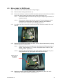
PC B OARD ASSEMBLIES:
DSP Board:
The DSP board includes the microprocessor which controls the operation of the product. It also
contains the software in a flash EEPROM, external RAM, a real time clock with battery, and the decoding
circuitry for the user button presses. In addition, the DSP board “passes” both power and control signals
between boards. All boards are connected to the DSP and all signals and power are redistributed as
needed. In other words - any connections which must be made between boards do so through the DSP
board.
Power Board:
The power board includes two switching systems to generate all voltages required to operate the
product. It includes the charging control circuitry, the low battery circuitry, the distance measurement
circuitry, and the speaker/tone generation circuitry.
Fixation Board:
The fixation board includes the fixation LED array which is flashed to attract the patients attention. It
also includes the jacks for USB/RS232 connection, and the charging port. The drive circuitry for the RS232
and USB is located on this board, as well as the IRDA sensor which communicates with the printer. In the
central section of this board, the ultrasonic sensor is mounted. However, the ultrasonic sensor circuitry is
actually on the power board, it only sits on the fixation board to match the output port of the housing.
One important note: the fixation board must be present for the system to power up. If the power
board does not sense the presence of the charging jack with no plug present (i.e.: not charging), it will not
power up.
Laser Board:
The laser board provides the drive for both the viewing crosshair LED and the laser. The LED is
controlled with a simple on/off control at a set output current. The laser is controlled to a target level
depending on the setting of the digital pot on this board. The pot is settable by the DSP during each startup
of the device. In addition, the laser has an on/off control which is used in addition to the digital pot to insure
that the laser is off when not required for measurement.
Camera Board:
The camera board contains a full chipset for the black and white imager which detects the return
beam for measurement. The camera exposure control is accomplished via a serial port on the board, and
the gain is controlled by a digital pot which is settable by the DSP. The camera gain is subject to calibration
at the factory.
LCD:
The LCD is a custom assembly of glass and printed circuit board. In addition to a series of seven
segment displays to present the reading results, and various indicators to indicate other conditions, this
board includes the button inputs, and the dip switch inputs. Theses are passed to the DSP for detection and
decoding.
Laser Mini:
The laser mini is a board which is primarily a mechanical mount. The board includes only the laser
diode and a flex connector which mates it to the laser drive board via a flex cable.
LED Mini:
The LED mini is a board which is primarily a mechanical mount. The board includes only the LED
and a flex connector which mates it to the laser drive board via a flex cable.
PN 140399 Rev. B
9
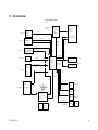
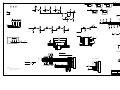
1.5
BLOCK DIAGRAM
SureSight Block Diagram
Rev C
(DSP/3.3V
and 5.0V)
12.0
(Camera/3.3V/5.0V 7.5V/15V)
(Laser/ 3.3 V)
1.0
Viewing
System
(1) on / off
FPGA
8 bits
Stacks into 32 bit words
Sends to RAM
Generates VD and HD
Eval:
Prelim Good Image Detect
Prelim location of Rows/Cols
(2) Digital Pot
2.0
Illumination
System
(Laser/ 3.3 V)
11.0
Camera
Timing Generator
Vertical Driver
Sensor
Head Amp
A/D converter
(2) Serial
Shutter
Control
(1) on / off
Echo
(Power/ 5.0V)
3.0
Distance Measurement
200mm to 500mm
(LCD/3.3V, 7.2V)
4.0
Buttons
5.0
LCD
14.0
PowerPC
Button Detect
Distance Measurement
Good Image Detect
Compute Readings
Report to LCD
AutoOff
Calibration Ck
I/O to Printer (opt)
I/O to RS232 (opt)
(3) IP Lines
(12) LCD Controller
(as GPL)
Right, Left, Diff
Refer, Conf
(LCD/3.3 V)
LoBatt,
Out of Cal
32
bits
Serial Port
Xmit
(3) DMA
(DSP/3.3V)
14.1 DRAM
Stores 3 images
(DSP/3.3V,5.0V,7.5V,15.0V)
14.2 Flash
Stores Main Program + Configs
(DSP/3.3V)
16 bits
(3) Shift Latch
DIP Switches
“Awake”
“Go”
GPL
10.0
Fixation
(Fixation/ 3.3 V)
8 Flickering LEDs
6.0
Speaker
Distributed thru
PPC board
SMCI
7.0
USB Port
13.0
Power Supply/Charger
(Power)
PN 140399 Rev. B
13.2
Charge
Control
(Fixation/3.3V)
SCC
7.2V to 3.3, 5.0, 15.0, -7.5
Conversion
Battery Charger Control
13.1
Low
(DSP) Battery
(Power/ 3.3V)
(Power)
8.0
RS232 Port
(Fixation/3.3V)
9.0
IRDA Port
15.0
Printer
SMC2
(Fixation/3.3V)
10
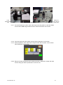
1.5
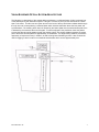
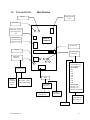
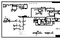
T OOLING SET UP:
WIRE DIAGRAM
Computer Power
Cord
Mouse
Keyboard
USB cord - needed
for testing of the
unit
RS 232 Cable needed to load
software to unit
Back of
Computer
Do Not Use
Monitor
S Cable WA
P/N: 880181
BNC Cable IMAQ-1
Panasonic Camera - SVideo connector
P/N: GP-KS-162
Back Settings:
1 - On
2 - On
3 - Off
4 - Off
5 - On
6 - On
7 - Off
8 - Off
Front Settings:
White Bal. - On
Auto Light - On
Video Level - Manual
Gray Switch Box
GPIB
Plug in
Transformer
WA P/N:
73305
Fiber Optic Bundle
WA P/N’s: 73210,
07800, 73308, 387001
UDT Meter
P/N: S370
UDT Laser Sensor
P/N: 268-CP
UDT Plug in
Transformer
ElPAC 12V
transformer P/N:
WM 144-1950
Camera Head
PN 140399 Rev. B
11
To Set Up Repair Tooling:
1.
2.
3.
4.
Connect all wires to computer per provided wire diagram.
Plug all plug in transformers to a power strip.
Plug the power strip into a step down transformer.
Connect the X-Y adjustment laser measurement slide and the Swing eye fixture to the plate. See
diagrams below for proper placement.
Place T holder in holder,
remove to swing fixture.
Connect swing fixture
with bolt.
Connect X-Y Adjustment
fixture to plate with 2
screws. There is one screw
on each side of the slide.
PN 140399 Rev. B
12
1.7
WARNINGS
ATTENTION: Refer to the operating instructions. This symbol ( ) is intended to advise the user of
the presence of important operating or maintenance instructions in the documents accompanying
the instrument.
Service or Repair to be performed by qualified, authorized personnel only. There are no user
serviceable parts inside the instrument. Opening this device can expose the user to harmful invisible
laser radiation.
Use only Welch Allyn 710 series chargers.
Replacement parts and accessories - Use only approved replacement parts and accessories
specified in this manual. Refer to the repair parts section of this manual.
Do not sterilize the instrument or any of its components.
Use only with IEC 60601-1 approved printers, or keep printer out of patient vicinity.
Battery replacement: Replace with Welch Allyn model # 72420 Lithium Ion battery only.
Do not attempt to disassemble or modify the battery pack. There are no user serviceable parts
inside the pack.
Do not attempt to directly solder the battery pack.
Do not attempt to connect the positive and negative battery terminals to each other, nor to any other
device.
“Caution” - use of controls or adjustments or performance of procedures other than those specified
herein may result in hazardous radiation exposure.
Do not operate, charge, leave or discard battery pack in any environment where it may exceed 0oC
to 40oC.
Do not immerse the battery pack in water.
Do not attempt to open or pierce the battery pack.
Do not throw or strike the battery pack.
Do not use a battery pack which appears to be deformed, leaking, corroded or is otherwise irregular.
If electrolyte leaking from battery contacts your skin or eyes, rinse with running water and
immediately seek medical attention.
IPX∅: Not protected against the ingress of water.
Not for use in the presence of flammable anesthetics.
ITT Nightscope can not leave Welch Allyn repair facility due to import/export regulations. It is
considered a military device.
When the device is opened, laser emission above the acceptable exposure limit (AEL) may be
present. Care must be taken not to look into the beam or project the beam into another person’s
eye.
PN 140399 Rev. B
13
SECTION 2:
2.1
SERVICE
INCOMING INSPECTION LIST :
When a SureSight Unit is Returned, Check:
1.
Physical Condition of Package and Unit
2.
Record the following observations:
•
Model #____________
•
S/N found on inside of battery door ____________
•
Record Dip Switch Position:
ON
1 2 3 4 5 6 7 8
3.
•
Does Instrument Power Up?
Yes
No
•
Cal Settings as received?
Adult
Child
•
S/W version as received? _____________
•
Distance function check:
•
Gross Alignment Check - Fake eye
•
Cal light symbol:
ON
OFF
•
Cross Hair Quality:
Good
Poor
Pass
Fail
Refer to Section 3 - The Customer Complaint and Troubleshooting Guide to localize the problem.
PN 140399 Rev. B
14
2.2
REQUIRED UPGRADES :
Component to Upgrade
Battery Compartment (see section 4.9)
Patient Window
O-Ring (see section 4.6)
Power PCB Charger
Cross Tubes / Windows
Software (see section 2.4)
PN 140399 Rev. B
When to Upgrade
• Always replace when the anti-reverse tabs are absent
• Replace compartment if retainer is too tight or too loose
• Replace as needed if scratched
• Always replace if before serial #9900594 for 14001 and
before serial #9920228 for 14011
• Always remove
• Domestically - Change when there is a customer complaint
about charge rate in units before 9900480 for 14001 and
9920086 for 14011.
• Internationally - N/A
• Always replace if before serial #0000018 for 14001 and
before serial #0020093 for 14011
• Always upgrade the software to most recent version
15
SECTION 2.3
T OOLS REQUIRED FOR SERVICE, CALIBRATION AND
SOFTWARE LOADING
Table 2.3-1
Tier 1 - Unit Check Out - Yearly Calibration
Tier 1 tooling is the minimum required to equip a site to perform yearly calibrations. This calibration does not
require the opening of the unit and primarily verifies the product performance. Software upgrades are feasible
with this tooling, but no internal repairs are allowed. Bold part numbers indicate parent items. Non bold
items below are included in the parent set.
TIER 1 REQUIRES TOOL SET T17009, WHICH CONSISTS OF THE FOLLOWING:
PART NUMBER
T16936
OPTION
Required
PCI-1411
T17019
778 044-03
T16729
WA part #: 140104-3
WA part #: 140104-2
WA part #: 880181
5370
268CP
777154-01
Flash point 128
Fluke Model 73
WA Part #’s: 73210,
07800, 73305, 73308
WA Part #: 387001
Hewlett Packard 82240B
DESCRIPTION
Tier 1 Plate with Nest, Camera Mounts,
Distance Fixture & Target
PC-Windows 98 with USB connector
National Instrument Capture Card
SureSight Alignment Check Software
IMAQ Vision Run Time License
Final Tester Software
USB Cable
RS232 Cable
S-Cable
UDT Meter
UDT Laser Sensor
GPIB National Instrument Card
Flash Point FPG Capture Card
Multimeter
Lighting for Fake Eye w/ fiber-optic
bundle
F.O. Illuminator Connector Base
SureSight Printer
Panasonic GP-KS-162
Panasonic GP-LM24TA
IMAQ-1
T17162
T17164
WA Part #: 73305
WM 144-1950
T16545
TI6934
Camera, cable and controls
Lens
BNC Cable
Gray Switch Box
Charge Box
Plug in Transformer
12 V transformer
Fake Eye (0)
Fake Eye Set
Required
Required
Required
Required
Required
Required
Required
Required
Required
T17008
WA part #: 140381
TI6556
Night Vision Scope - Version 2
Hand Strap Replacement Tool
Nest
Required
Required
Required
Required
Required
Required
Required
Required
Required
Required
Requires
Required
Required
Required
Required
Required
Required
Required
Required
NEEDED TO VERIFY
Alignment Refraction
Distance Accuracy
Unit Information
Software
Alignment Verification
Alignment Verification
All unit functions
Unit Information
Unit Information
Unit Information
Laser level
Laser Level
Software
Software
Charge Current
Alignment Verification
Alignment Verification
Print capability & s/w
version
Images
Images
Alignment Verification
Alignment Verification
Charge Current
Alignment Verification
Images
Calibration
Refractive Reading
Accuracy
Laser Level
Replace Hand Strap
NOTE: REPAIR STATIONS WILL BE REQUIRED TO HAVE A STEP DOWN TRANSFORMER
PN 140399 Rev. B
16
Table 2.3-2
Tier 2: Unit Repairs - Major Systems
Tier 2 tooling is required to equip a site to perform internal repairs. These repairs are limited to major
subsystems. Component level repair is not available for this product. Bold part numbers indicate parent
items. Non bold items below are included in the parent set.
Tier 2 requires Tool Set T17010, which consists of the following:
PART NUMBER
T16936
PCI-1411
T17019
778 044-03
T16729
WA part #: 140104-3
WA part #: 140104-2
WA part #: 880181
5370
268CP
777154-01
Flash point 128
Fluke Model 73
WA Part #’s: 73210, 07800,
73305, 73308
WA Part #: 387001
Hewlett Packard 82240B
Panasonic GP-KS-162
Panasonic GP-LM24TA
IMAQ-1
T17162
T17164
WA Part #: 73305
WM 144-1950
T16545
TI6934
T17008
WA part #: 140381
TI6556
T1562-23
T1562-12
T1562-12
T1562-12
T16541
T16542
PN 140399 Rev. B
DESCRIPTION
OPTION
NEEDED TO VERIFY
Tier 1 Plate with Nest, Camera Mounts,
Distance Fixture & Target
PC-Windows 98 with USB connector
National Instrument Capture Card
SureSight Alignment Check Software
IMAQ Vision Run Time License
Final Tester Software
USB Cable
232 Cable
S-Cable
UDT Meter
UDT Laser Sensor
GPIB National Instrument Card
Flash Point FPG Capture Card
Multimeter
Lighting for Fake Eye w/ fiber-optic bundle
Required
F.O. Illuminator Connector Base
SureSight Printer
Camera, cable and controls
Lens
BNC Cable
Gray Switch Box
Charge Box
Plug in Transformer
12 V transformer
Fake Eye (0)
Fake Eye Set
Night Vision Scope - Version 2
Hand Strap Replacement Tool
Nest
1.5 - 2.0 in-lb.
Torque Driver*
Phillips Bit for #4 screw 1 5/16” length
Point Size - 1
2.75 - 3.75 in-lb.
Torque Driver*
Phillips Bit for #4 screw 1 5/16” length
Point Size - 1
Required
Required
Required
Required
Required
Required
Required
Required
Required
Required
Required
Required
Required
Required
Required
Alignment Verification
Print capability & s/w version
Images
Images
Alignment Verification
Alignment Verification
Charge Current
Alignment Verification
Images
Calibration
Refractive Reading Accuracy
Laser Level
Replace Hand Strap
Required
Attachment
Required
Attachment
Required
Attachment
3.5 - 4.5 in-lb.
Required
Attachment
Required
Attachment
Required
Attachment
Required
Required
Required
Attachment
Main assembly repairs
Main assembly repairs
Torque Driver*
Phillips bit for #6 screw 2 ½ “ length
Point Size - 2
5.5 - 7.5 in-lb.
Torque Driver*
Torx Bit T-20
Baseplate Support Fixture Top
Baseplate Support Fixture Bottom
Required
Required
Required
Required
Required
Required
Required
Requires
Required
Required
Required
Required
Required
Required
Alignment Refraction Distance
Accuracy
Unit Information
Software
Alignment Verification
Alignment Verification
All unit functions
Unit Information
Unit Information
Unit Information
Laser level
Laser Level
Software
Software
Charge Current
Alignment Verification
Attachment
17
NOTE: REPAIR STATIONS WILL BE REQUIRED TO HAVE A STEP DOWN TRANSFORMER
*NOTE: PROPER TORQUES ARE CRITICAL TO FUNCTION. DO NOT HAND TIGHTEN WITHOUT
TORQUE METER OR DRIVER.
2.4
CALIBRATION CHECK:
2.4.1
2.4.2
2.4.3
Before starting the software make sure all dip switches are in the off position.
Start up software
Place unit in nest, follow instructions on the screen.
2.4.4
Enter the product serial number and select enter, on the screen.
2.4.5
Insert battery and follow instructions on the screen.
2.4.6
Press the child adult button, ensure the unit powers up, and plug in USB. Follow
instructions on the screen.
PN 140399 Rev. B
18
2.4.7
The software will flip through some more screens and stop at the LCD screen. Check to
see if the LCD’s are on and follow instructions on the screen. Then check to see if they are
off and follow instructions on the screen.
2.4.8
After the LCD check, the program will prompt you to place the black cloth over the dog
house. Follow instructions on the screen.
2.4.9
Check screen for crosshair and follow instructions on the screen.
2.4.10 Remove the black cloth from the dog house and follow instructions on the screen.
PN 140399 Rev. B
19
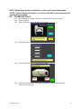
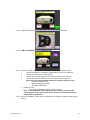
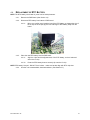
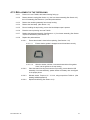
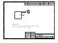
2.4.11 Place the printer in front of the unit. (see Figure 1 - Printer position) Follow instructions on
the screen.
Figure 1 - Printer position
2.4.12 Follow instructions on the screen.
2.4.13 The following screens will prompt you to place the distance block in the subsequent
positions. The positions for the distance block are marked on the plate. Follow instructions
on the screen. The screens will change to let you know when to move the distance block to
the next position.
PN 140399 Rev. B
20
Distance block. The
positions, 1-4, are
marked on the
plate.
Figure 2 - Distance block position
2.4.14 After the distance for position 4 is taken, leave the distance block in that position for the
next operation. The next screen will prompt you to press start, YOU DO NOT NEED TO DO
THIS IT WILL START AUTOMATICALLY. Once the test is done the next screen will
appear.
2.4.15 The next three screens will prompt you to press a certain button, follow the instructions on
the screens. Once you press the button the screen will change to show you which button
to press next. The last button is the go button. Once you press this it will start to take a
reading, hold the go button in until it stops.
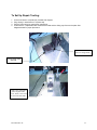
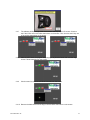
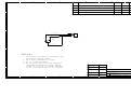
2.4.16 The next screen prompts you to place the laser measurement tool in front of the unit. Once
this in the correct position clamp into place.
PN 140399 Rev. B
21
Laser
Measurement
Tool
Figure 3 - Laser Measurement Tool
Clamp tool
down, when in
proper place.
2.4.17 Once the fixtures are in place use the NV scope to see the position on the laser. Make
sure the laser is NOT aligned with the sensor. Follow instructions on the screen.
2.4.18 Cover the dog house with the black cloth and follow instructions on the screen.
2.4.19 When prompted to, use the NV scope to align the laser with the sensor. Cover unit and
follow instructions on the screen.
2.4.20 Remove the laser measurement tool and then place the 0.6 ND filter on tester and make
sure the swing eye fixture is positioned in front of the unit.
PN 140399 Rev. B
22
Place ND filter
in groove on
the nest.
Figure 4 - Swing Eye Fixture and ND filter
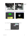
2.4.21 Click on align laser. This will bring up the flash point screen with the camera image. Find
the max. glare by moving the knobs on the swing eye fixture. Once this is found select exit
on the flash point screen.
2.4.22 The next screen will prompt you to place the black cloth over the dog house.
2.4.23 Check for crosshair and follow instructions on the screen.
PN 140399 Rev. B
23
2.4.24 The next screen will prompt you to remove the black cloth, LEAVE THE BLACK CLOTH
ON THE UNIT BUT MAKE SURE IT DOES NOT BLOCK THE FRONT OF THE DOG
HOUSE. Follow instructions on the screen.
2.4.25 Check for pupil and follow instructions on the screen.
2.4.26 Remove the black cloth and place the ND filter back on the nest. Follow instructions on the
screen.
PN 140399 Rev. B
24
2.4.27 Follow instructions on the screen. When you remove the unit from the nest, keep the USB
connected.
2.4.28 Starting with the -2 diopter, take one reading from each of the fake eyes, on the rack of
eyes.
2.4.29 IF THIS IS A PRIMARY CARE UNIT THIS WILL BE THE END OF THE AUTOMATED
TEST. Reset DIP Switches to their original position and proceed to step 2.4.34. The
following steps are only for EYECARE UNITS.
2.4.30 Follow the instructions on the screen, remove the USB and change the DIP switch settings.
2.4.31 Follow instructions on the screen and replace the battery.
PN 140399 Rev. B
25
2.4.32 Follow instructions on the screen and turn unit on and connect the USB.
2.4.33 THIS IS THE END OF THE AUTOMATED TEST.
2.4.34 Check
•
•
•
•
the charge current of the unit once it has completed the calibration test.
Insert a discharged or moderately charged battery into the unit under test.
Connect the 71040 to the charger box IN.
Connect the extender cable from the charger box OUT to the unit jack.
Connect the Fluke 73 multimeter to the two jacks on the charge box.
Note: this is the only multimeter allowed to check the charge current.
−
Positive lead goes to 10 A
−
Negative lead goes to COM
−
Set meter at D/C Amps
• Read the current
− The current should read between: 40 mA - 162 mA
•
Note: A fully topped off battery may trigger the shutdown circuitry of the
charge system. If the current reads low, it should be verified with a second
battery before replacement.
2.4.35 Check for aesthetics. If there are any fingerprints on housings or windows, properly clean
them off.
PN 140399 Rev. B
26
2.5
SOFTWARE UPGRADE
2.5.1
Make certain the Sure Sight unit is off.
2.5.2
Connect the RS232 Cable (Phone Jack) to the SureSight and RS232 Cable (9 - pin
connector) to the PC COM port.
2.5.3
Upgrade using MS DOS:
2.5.3.1 Insert the SureSight Software Update floppy in the floppy drive. Open up an
MSDOS window and type “A:” (without the quotations) to switch to the floppy
directory and type SETUP.
2.5.3.2 The setup script will prompt you for a COM port (1 or 2) and tell you when to power
on the unit. The progress on the upgrade is given and “Software update completed
successfully!”, should be shown after the update is completed.
2.5.4
Upgrade Using Windows 95 / 98:
2.5.4.1 Insert the SureSight Software Update floppy in the floppy drive. Click on the Start
button and then click on Run. Type A:SETUP and click on OK.
2.5.4.2 The setup script will prompt you for a COM port (1 or 2) and tell you when to power
on the unit. The progress on the upgrade is given and “Software update completed
successfully!” should be shown after the update is completed.
PN 140399 Rev. B
27
2.6
PRODUCT NUMBERING STRUCTURE/ SERIAL NUMBERING STRUCTURE
__X__ _X__ __X__ __X__ __X__ __X__ __X__
S/N (randomized)
2:Eye Care Version
0: Primary Care Version
NOTE: 14001 SureSights should have a 0 in this position
NOTE: 14011 SureSights should have a 2 in this position
Last 2 digits of the year manufactured
PN 140399 Rev. B
28
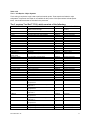
2.7
REPAIR PARTS LIST
Part Number
M11052
V140170-120
106100-2
106100-42
140071-30-1750
140073-04-1500
140127-501
140129-501
236992
536000
72420
140126-501
106102-27
106124-4
140020-3
140103-2
140040
140041-501
140071-30-2500
140280-504
106100-42
140071-30-4375
106102-7
106100-5
140071-08-3375
140250-503
140077-3
140130-501
140072
140074-3
140146-1
140068
M11478
140022-2
140090
140131-501
106100-53
140032
140167
140168
M11416
PN 140399 Rev. B
Description
9 X 12 POLY BAG
TARGET SW VER 1.20
PHPS 2-56 X .187
4-40 X .25 SCREW
FLEX CABLE, .5MM PITCH
FLEX CABLE, 1.00MM PITCH
FRONT INSERT SUB ASSEMBLY
BASE PLATE SUB ASSEMBLY
IC, SNAPHAT FOR M48T559Y
ROLL OF PAPER
LI ION BATTERY
BATTERY COMPARTMENT SUB ASSEMBLY
FHPHPS 6 X 32 X .250
#4 X .250 LG PPHS SELF TPG
LCD INSERT
TAPE, DR SIDE WINDOW
WINDOW, DOCTOR
LCD ASSEMBLY
FLEX CABLE, .5MM PITCH
POWER PCB ASSY - PATT X9
4-40 X .25 SCREW
FLEX CABLE, .5MM PITCH
FLAT HEAD SCREW
PHPS 6-32 X .25
FLEX CABLE, .5MM PITCH
DSP PCB ASSY PATT X8
HAND STRAP, WRDMK GRAY, 5.125L
TOP HOUSING SUB ASSY
BUMPERS
BOOT
WINDOW, PATIENT SIDE
PATIENT WINDOW U-CHANNEL
PARTS LABEL
BATTERY DOOR
HINGE PIN
BOTTOM HOUSING SUB ASSY
PHPS 8-32 X .312
DANGER TAG
BATTERY FOAM
LASER, FOAM
TAPE, KAPTON
Bubble
Number
Qty.
1
1
4
3
1
2
1
1
0007
0015
0028
0029
0030
0031
0033
0034
0036
0037
0038
0040
0042
0043
0044
0045
0046
0048
0046
0050
0051
0052
0053
0054
0056
0058
0059
0062
0064
0066
1
1
1
18
8
1
1
1
1
1
1
14
1
2
3
1
1
1
1
4
1
1
1
1
1
1
1
4
1
1
1
29
Section 3:
SureSight Troubleshooting Guide
This guide should be used for phone personnel as well as by repair technicians to facilitate quick diagnosis of problems
Chief
Complaint
Cause
Look For
Customer Corrective
Action
Does Not
Power up
Battery
not
charged
a) Verify battery is installed correctly (orientation) in
device and battery retainer is latched over battery. See
label and arrow on battery indicating direction of proper
insertion. Early versions do not have the battery rib to
prevent mis-insertion.
b) Check for constant or blinking battery symbol on the
LCD. Constant = no charge. Blinking = ~10 to 15
minutes of charge left.
a) Install battery correctly
per label.
b) Charge battery overnight
in stand with 71040.
c) Return unit for repair.
No LCD
Display
No Data
stored in
memory
a) Ensure that test was taken within last 5 minutes,
otherwise data is not stored.
a) Retake test
b) Note version 1.09
software and higher. If it
is a lower version send
unit in to repair to
upgrade.
c) Return Unit for repair
No LCD
Display
Defective
LCD
a) Ensure that test was taken within last 5 minutes,
otherwise data is not stored.
a) Retake test
b) Note version 1.09
software and higher. If it
is a lower version send
unit in to repair to
upgrade.
c) Return Unit for repair
PN 140399 Rev. B
Repair Technician
Corrective Action
Verify the Charge
Current
b) Check to see if flexes
are connected, connect
if not.
c) Replace LCD Assembly
and/or flex.
d) Replace battery
compartment.
e) Replace Power Board.
f) Replace DSP Board.
a) Check to see if flexes
are connected, connect
if not.
b) Replace LCD Assembly
and/or flex
a)
c) Check to see if flexes
are connected, connect
if not.
a) Replace LCD Assembly
and/or flex
30
Chief
Complaint
Cause
Look For
Customer
Corrective Action
Does Not
Print
Printing too far
a) Ensure printer is turned on.
b) Ensure that the print button is held until the “ta-da” is
heard
c) Ensure the unit is aimed at the front of the printer.
d) Try printing within 3 feet of printer
a) Retry printing
b) Replace batteries in
printer
c) Return unit for repair
Does Not
Print
Printer has gone to
“sleep”
a) Check to see if red LED is lit in the front.
a) Press feed (right most
button) to wake printer
up.
b) Return unit for repair.
Prints too
light
Print darkness
setting is set too
light
a)
b)
Try sliding the center contrast switch to the right.
Try self-test on printer to see if the batteries are low;
refer to printer manual pg. 14
a)
b)
c)
No CrossHair
Defective LED Mini
board or electrical
failure
PN 140399 Rev. B
a)
b)
c)
Ensure battery is charged.
Ensure battery is installed and turned on.
Look through peephole and identify Crosshair.
d)
Reset to roughly
center of range.
Printer can be used at
higher or lower
settings if customer
desires.
Replace batteries
Return unit to Hewlett
Packard for repair.
Return unit for repair.
Repair Technician
Corrective Action
Check to see if flexes are
connected, connect if
not.
b) Replace Front Insert
Assembly. NOTE: Wire
Harness must be
replaced if Front Insert
Assembly is replaced.
a) Check to see if flexes are
connected, connect if
not.
b) Replace Front Insert
Assembly. NOTE: Wire
Harness must be
replaced if Front Insert
Assembly is replaced.
a)
a) Check to see if flexes are
connected, connect if
not.
b) Inspect to see if green
LED lights
c) Replace Tubes with PC
Sub-Assembly - WA InHouse Only
d) Replace baseplate
assembly
31
Chief
Complaint
Cause
Look For
Customer Corrective
Action
Unit is not
aligned
Unit dropped or
Impacted beyond
shock level
provided
a) Crosshair is in patients pupil and in range distance is
constant but no images are being taken
b) Search around eye for “sweet spot”
c) Ensure that doctor and patient are at same height,
squared and level with each other.
a) Return unit for repair.
No Reading
Incorrect Distance
a) Adjust distance until constant tone
b) If unit cannot obtain constant tone, send in for repair.
a) Return unit for repair
No Reading
Unit misaligned
Refer to Unit is not aligned
Low
Reading
Unit misaligned
a)
b)
c)
d)
e)
Ensure level test with patient
Ensure unit is on proper calibration (adult / child)
Verify room lighting / not direct lighting
Verify confidence readings are 6 or higher
Verify that readings are within .5 D typ.
a)
b)
c)
d)
e)
High
Reading
Unit misaligned
a)
b)
c)
d)
e)
Ensure level test with patient
Ensure unit is on proper calibration (adult / child)
Verify room lighting / not direct lighting
Verify confidence readings are 6 or higher
Verify that readings are within .5 D typ.
a)
b)
c)
d)
e)
PN 140399 Rev. B
Repair Technician
Corrective Action
Check Tube with PC
Assembly. May need to
shake to see if there is
aperture movement. If
there is replace tubes
with PC Assembly. WA
In-House Only
b) Replace Aligned Baseplate Assembly.
a) If O-ring exists, remove
it.
b) Replace Front Insert
Assembly NOTE: Wire
Harness must be
replaced if Front Insert
is replaced
c) Replace Power board.
a)
Retest patient level with
unit
Turn down room lights
verify adult / child
calibration
Verify S/W version
Return unit for repair
Refer to Unit is not aligned
Retest patient level with
unit
Turn down room lights
verify adult / child
calibration
Verify S/W version
Return unit for repair
Refer to Unit is not aligned
32
Chief
Complaint
Cause
Customer Corrective
Action
Repair Technician
Corrective Action
Buttons not
functioning
Electrical or
Mechanical failure
a)
b)
Verify button press performs correct function
Ensure battery symbol is not lit.
a)
Return unit for repair
a) Replace LCD Assembly
Unit not
giving
referral
criteria - *’s
Crosshair
not visible
Wrong calibration
a) Ensure unit is on proper calibration (adult / child).
SureSight will only refer on child calibration.
a)
a) Calibrate unit
b)
Change calibration as
appropriate
Return unit for repair.
Flex connector
loose
a) Ensure battery in installed and turned on.
b) Press Go button
c) Verify no Crosshair
a)
Return for repair
a)
Check to see if flexes
are connected, connect
if not.
Red LED not
visible
Flex connector
loose
a) Ensure battery in installed and turned on.
b) Press Go button
c) Verify no LED
b)
Return for repair
a)
Check to see if flexes
are connected, connect
if not.
Unit has low
speaker
Foam over speaker
on power board
d) Foam is placed directly over speaker in production
a) Return unit for repair
a)
Place foam in proper
position.
Unit does
not charge
Power problem
a) Bend contacts up to
normal position with
dental pick.
b) Return unit for repair of
the battery
compartment sub
assembly.
a) Replace power Board
Assembly
b) Replace Front Insert
Assembly. NOTE: Wire
Harness must be
replaced if Front Insert
Assembly is replaced.
Eye Care
Unit does
not Show
Axis
Dip switches are at
the wrong settings
a) Verify battery is inserted in proper orientation
b) Verify battery was not inserted in reversed orientation
in that the battery would crush the contacts down thus
allowing intermittent contact.
c) Verify battery contact has sufficient tension on the
battery. Determined by letting the battery retainer
freely rotate by gravity alone, when properly engaged
over a battery. Retainer should not move when a
battery is in place.
a) Make sure the dip switches are set correctly: Refer to
the Device configuration table below
PN 140399 Rev. B
Look For
a)
b)
Set dip switches to the
correct setting.
Send Unit in for repair.
a)
b)
Replace the LCD
Assembly
Replace the DSP Board
33
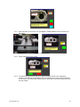
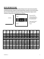
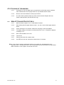
DEVICE CONFIGURATION TABLE:
SureSight performance is controlled by the type of instrument (Primary Care Unit or Eye Care Unit), the dip switches
accessible through the battery compartment, located underneath the battery compartment on the LCD board (see figure
below) and the Adult Child Mode button (located on the LCD Display). The following table and diagrams show the
combinations of settings and the corresponding performance it determines.
On
There are a total of 8 dip
switches, but only the first 3
are used. Each are labeled with
their corresponding number.
Position 1
Inside of Unit
1
2
3
4
5
6
7
Push in to switch to Position 1
and Pull out to switch to
Position 0.
8
Position 0
Unit Type
Dip Switch 1
Setting
Dip Switch 2
Setting
Dip Switch 3
Setting
A/C Button
Setting
Primary Care
0 = Opt
N/A
N/A
N/A
N/A
N/A
N/A
N/A
N/A
Adult
Child
Adult
Child
Resolution
of Reading
Displayed
10
10
10
10
0 = Std
0 = 1/4
1 = 1/8
0 = 1/4
1 = 1/8
N/A
N/A
0 = 1/4
1 = 1/8
0 = 1/4
Adult
Adult
Child
Child
Adult
Child
Adult
Adult
Child
100
100
100
100
10
10
100
100
100
1 = Oph
Eye Care
0 = Opt
1 = Scr
1 = Oph
PN 140399 Rev. B
0 = Std
Axis
Displayed
Cylinder
Convention
Difference
Displayed
Range (min.
Sphere)
Referrals
Marked with *
No
No
No
No
Negative
Negative
Positive
Positive
No
Yes
No
Yes
-4.5
-4.5
-4.5
-4.5
No
Yes
No
Yes
Resolution
of Reading
Computed
1/4
1/4
1/4
1/4
Yes
Yes
Yes
Yes
No
No
Yes
Yes
Yes
Negative
Negative
Negative
Negative
Negative
Negative
Positive
Positive
Positive
No
No
No
No
No
Yes
No
No
No
-5
-5
-5
-5
-5
-5
-5
-5
-5
No
No
No
No
No
Yes
No
No
No
1/4
1/8
1/4
1/8
1/4
1/4
1/4
1/8
1/4
34
PRIMARY CARE DEVICE CONFIGURATION:
* Resolution of Reading Displayed = Tenths
* Measurement Range = -4.5D to +5D
Dip Switch 1
Dip Switch 2
Dip Switch 3
A/C Button
A = Adult Mode
C = Child Mode
• Difference Displayed
• Referrals vs. AAP guidelines for 3 yr. olds are noted
• Uses child calibration curve
N/A
N/A
0 = Optometry Convention
• Negative Cylinder
Convention
1 = Ophthalmology Convention
• Positive Cylinder
Convention
PN 140399 Rev. B
35
EYE CARE
DEVICE CONFIGURATION
* Measurement Range = -5D to +5D
Dip Switch 1
Dip Switch 2
Dip Switch 3
A/C Button
A = Adult Mode
C = Child Mode
• In Screening Mode Difference is Displayed
• In Screening Mode Referrals vs. AAP Guidelines for 3 yr.
olds are noted
• Uses child calibration curve
0 = ¼ Measurement computed to precision
1 = 1/8 Measurement computed to precision
0 = Standard Mode
• Axis Displayed
• Resolution of Reading Displayed = Hundredths
1 = Screening Mode
• Resolution of Reading = Tenths
• In Child Mode Difference is Displayed
• In Child Mode Referrals vs. AAP guidelines for 3
yr. Olds are Noted
0 = Optometry Convention
• Negative Cylinder Convention
1 = Ophthalmology Convention
• Positive Cylinder Convention
PN 140399 Rev. B
36
SECTION 4:
SURESIGHT REPAIR INSTRUCTIONS
*NOTE: ALL REPAIR PROCEDURES MUST BE FOLLOWED BY A CALIBRATION CHECK ( SEE
SECTION 2.2), WITH THE EXCEPTION OF SECTIONS 4.12, 4.14 (IF UNIT IS NOT
OPENED), 4.15, AND 4.16.
DSP Board
Baseplate
Assembly
Front Insert
Assembly &
Fixation Board
LCD Assembly &
LCD Board
Bottom Housing
Top Housing
Rubber Boot
Power Board
PN 140399 Rev. B
Optical Plate
37
4.1. REPLACEMENT OF BOTTOM HOUSING
4.1.1.
Place unit in nest T16556, with bottom housing facing up.
4.1.2.
Remove the 4 T-20 torx screws from bottom housing.
4.1.3.
Gently remove housing. It may be necessary to hold the front insert down as the housing is
removed.
4.1.3.1.
Prior to replacement verify the black tape is visible and in its proper location.
`1
4.1.3.2.
Ensure that the bumpers are seated correctly, down and completely in their cut
out areas, in the top housing.
One of the
three bumpers
seated in cut
out area
4.1.3.3.
Replace housing by aligning the front insert and LCD assembly with the guides
on the bottom housing.
4.1.3.4.
Ensure the housing aligns with the battery door and patient window.
4.1.3.5.
Re-torque to 5.5 - 7.5 in-lb., using torque driver T1562-12. (See drawing 140000 Appendix D)
4.1.3.6.
Verify no flexes are caught in between the housings.
PN 140399 Rev. B
38
4.2. REPLACEMENT OF FLEX
4.2.1.
Place unit in nest T16556, with bottom housing facing up.
4.2.2.
Remove bottom housing. (See Section 4.1)
4.2.3.
Remove glue or kapton tape, if it exists, from the flex.
4.2.4.
Locate the tabs bar, of the flex insert, toward the flex.
4.2.5.
Pull out the tab bar away from the flex connector body to loosen the connection, which will
allow the flex to slide out. Make sure both sides of the tab are unlatched.
Glue or Kapton
Tape will be on
this flex.
Connector
body
Tab Bar.
Pull bar out to
loosen.
4.2.6.
Replace the flex by holding the tab bar out and sliding the flex back into the connection:
4.2.6.1.
Note the flex has an insulated side and a side with connectors.
4.2.6.2.
Place the connector side, of the flex, toward the connector side of the flex
insert. This is always the opposite side from where the tab bar is.
Slide the tab bar
in to tighten.
4.2.6.3.
Once the flex is slid into the flex insert, slide the tab bar back into place. Make
sure that the flex is straight, or connections will not be properly made.
4.2.6.4.
If the flex, that had been removed had either glue or kapton tape on it, replace
with kapton tape only.
PN 140399 Rev. B
39
4.3. REPLACEMENT OF DSP B OARD
4.3.1.
Place unit in nest T16556, with bottom housing facing up.
4.3.2.
Remove bottom housing (See Section 4.1).
4.3.3.
Disconnect the flexes, located on the DSP board that connect from the LCD board, fixation
board, laser board, power board and the camera board. (See Section 4.2).
4.3.3.1.
Note that the fixation and LCD flex may have glue or Kapton tape over them, to
keep them secure.
4.3.3.2.
Remove glue or kapton tape from the connector. To prevent damage, peel the
hardened glue or kapton tape in the direction of the flex, NOT toward the
connector, or the connector may be damaged or peel off.
4.3.4.
Once flexes are clear, remove the 2 screws from the DSP board and carefully lift it out of
the unit.
4.3.5.
Replace the new DSP board, battery side down, onto the aligned plate assembly, aligning
holes in board with mounting holes.
4.3.5.1.
Replace the laser tag on the right screw, then fasten the DSP board with the 2
screws. Torque screws to 1.5 - 2.0 in-lb., using torque driver T1562-23 . (See
Drawing 140000 - Appendix D)
4.3.5.2.
Reconnect the removed flexes to the proper positions, (See Section 4.2), then
using Kapton tape only, tape together the flex and the connector.
Kapton Tape on
the flex and
connector
4.3.6.
Replace the bottom housing and fasten together. (See Section 4.1) Once the unit is
reassembled, download the software (See Section 2.7)
PN 140399 Rev. B
40
4.4.
REPLACEMENT OF RTC B ATTERY
NOTE: The RTC battery should last 10 years from its initial placement.
4.4.1.
Remove the DSP Board. (See Section 4.3)
4.4.2.
Disconnect RTC battery from bottom of DSP board:
4.4.2.1.
4.4.3.
Being very careful not to break the legs of the RTC battery or damage the pins of
the IC chip off of the pad, pry the four outer legs of RTC battery away from the
board.
Place the new RTC battery onto the DSP board:
4.4.3.1.
Align the 4 pins and the alignment tab, of the RTC battery, to the 4 holes and
slot on the IC chip.
4.4.3.2.
Press the RTC battery down to securely clip onto the IC chip.
NOTE: RTC battery is keyed - DO NOT force it down - make sure its tabs align with RTC chip slots.
4.4.4.
One the unit is reassembled, download software. (See Section 2.7)
PN 140399 Rev. B
41
4.5. REPLACEMENT OF FRONT INSERT ASSEMBLY
4.5.1.
Place unit in nest T16556, with bottom housing facing up.
4.5.2.
Remove the bottom housing (See Section 4.1).
4.5.3.
Lift the baseplate sub-assembly, with front insert and LCD assembly out of the top housing
and disconnect the distance wire assembly from the power board, as well as the front insert
flex to the DSP board.
4.5.4.
Remove the Front Insert Assembly by sliding it up.
NOTE: You MUST replace the distance wire assembly whenever it is removed from the sensor
contacts. It is a single use spring clip only.
Disconnect
the wire
harness from
the power
board
4.5.5.
Disconnect
the wire
harness from
the ultrasonic
sensor
Replace the front insert assembly and the distance wire assembly:
4.5.5.1.
4.5.5.2.
PN 140399 Rev. B
Clip the new distance wire assembly on to the power board.
4.5.5.1.1.
Connect the black wire onto the silver tab of the sensor.
4.5.5.1.2.
Connect the red wire to the copper tab of the sensor.
Replace the entire assembly back into the top housing. Align the bumpers and
seat correctly in the guides, on the top housing.
4.5.5.2.1.
Slide the front assembly into the unit so that the rubber boot fits into
the opening and the tabs of the front insert align with the guides on the
bottom housing. Check to make sure there are no wires caught in
between the front insert and the bottom housing.
4.5.5.2.2.
Reconnect the flex to the DSP board, then using kapton tape, tape
together the flex and the connector. (See Section 4.2)
42
4.5.6.
4.5.5.2.3.
Ensure the bumpers are seated correctly, down and completely in
their cut out areas.
4.5.5.2.4.
Place the bottom housing back on to the unit. (See Section 4.1)
Once the unit is reassembled, download software (See Section 2.7)
PN 140399 Rev. B
43
4.6. REMOVAL OF O-RING
4.6.1.
Place unit in nest T16556, with bottom housing facing up.
4.6.2.
Remove bottom housing (See Section 4.1).
4.6.3.
Locate o-ring on the ultrasonic sensor and wire harness assembly.
4.6.4.
Lift the o-ring away from any wires and clip with a small pair of cutters. Be careful not to
damage anything around the o-ring, especially the gold contact and wire assembly.
4.6.5.
Remove o-ring with tweezers. As much as possible, pull o-ring away from gold contact.
4.6.6.
Replace bottom housing. (See Section 4.1)
PN 140399 Rev. B
44
4.7. REPLACEMENT OF THE LCD ASSEMBLY
4.7.1.
Place unit in nest T16556, with bottom housing facing up.
4.7.2.
Remove the bottom housing. (See Section 4.1)
4.7.3.
Remove glue or kapton tape on LCD flex and disconnect the flex from the DSP board (See
Section 4.2).
4.7.4.
Slide the LCD assembly out of the unit.
4.7.5.
Make sure to copy over the dip switch settings from the old LCD.
4.7.6.
Replace the LCD Assembly by sliding it back into its original place.
4.7.6.1.
Slide the assembly back into place by lining it up with the guides on the top
housing.
4.7.7.
Reconnect the LCD flex to the DSP board, then using kapton tape only, tape together the
flex and the connector.
4.7.8.
Replace bottom housing. (See Section 4.1)
4.7.9.
One the unit is reassembled, download software. (See Section 2.7)
PN 140399 Rev. B
45
4.8. REPLACEMENT OF LCD B OARD
4.8.1.
Remove LCD Assembly (See Section 4.7).
4.8.2.
Remove the 4 screws.
4.8.3.
Remove the LCD board and replace. Make sure to transfer buttons to new assembly. Also,
copy dip switch settings from old LCD board.
4.8.4.
Reattach the board with the screws. Torque screws to 2.75 - 3.75 in-lb., using torque driver
T1562-12. (See Drawing 140000 - Appendix D)
4.8.5.
Replace LCD assembly (See Section 4.7).
4.8.6.
Replace the bottom housing. (See Section 4.1)
4.8.7.
Once the unit is reassembled, download software. (See Section 2.7)
PN 140399 Rev. B
46
4.9. REPLACEMENT OF BATTERY COMPARTMENT ASSEMBLY
4.9.1.
Place unit in nest T16556, with bottom housing facing up.
4.9.2.
Remove bottom housing (See Section 4.1).
4.9.3.
Lift baseplate assembly, with LCD assembly and front insert assembly, out of the top
housing. Make sure to disconnect front insert distance wire assembly from connection on
the power board and disconnect the LCD flex and the front insert flex from the DSP board.
Remove bumpers and place on baseplate support fixture T16541.
4.9.4.
Disconnect the DSP board. (See Section 4.3)
4.9.5.
Remove 3 screws from battery retainer unit.
4.9.6.
Remove the 1 screw from the green ground wire.
3 screws
Green Ground
Wire
4.9.7.
Remove the black and red wire clip from bottom of the power board:
4.9.7.1.
Squeeze the clip down on the side of the wires and slide out.
4.9.8.
Before installing battery compartment assembly, verify wires are in correct slots. With
compartment opening facing you, slot side down, the red wire should be on the bottom side
and the green wire should be on the top side. The black wire should be connected with the
green wire at the contact and then connected with the red wire at the clip. DO NOT USE
ANY BATTERY COMPARTMENT THAT IS NOT CORRECTLY WIRED.
4.9.9.
Replace the battery compartment assembly:
PN 140399 Rev. B
47
4.9.9.1.
Connect the black and red wire to the bottom of the power board by sliding the
clip on.
4.9.9.2.
Attach the battery compartment to the baseplate assembly with the three
screws. Torque to 1.5 - 2.0 in-lb., using torque driver T1562-23. (See Drawing
140000 - Appendix D)
4.9.9.3.
Ensuring that the wires are close to the camera and out of the way of the
standoff, secure the green ground wire, with one screw, to the baseplate. Torque
to 3.5 - 4.5 in-lb., using torque driver T1562-12. (See Drawing 140000 - Appendix
D) If needed bend the contact at a 90o angle to place wires out of the way of the
standoff.
4.9.9.4.
Place a new piece of foam on the side of the battery compartment. The foam
should be placed between the end of the cut out, on the side of the
compartment, and the closed end on the compartment.
4.9.10.
Replace the DSP board (See Section 4.3).
4.9.10.1. Place the entire assembly back into the top housing by lining up the bumpers
into guides, in the top housing. Make sure they are down and fully in their cut out
area.
4.9.11.
Replace bottom housing. (See Section 4.1)
4.9.12.
One the unit is reassembled, download software. (See Section 2.7)
PN 140399 Rev. B
48
4.10. REPLACEMENT OF POWER BOARD
4.10.1.
Place the unit in nest T16556, with bottom housing facing up.
4.10.2.
Remove the bottom housing (See Section 4.1), front insert assembly (See Section 4.5),
and LCD assembly (See Section 4.7)
4.10.3.
Remove the baseplate assembly, along with the LCD assembly and the front insert
assembly, from the top housing.
4.10.4.
Turn baseplate assembly over.
4.10.5.
Disconnect the battery compartment assembly wire connection and fixation wire assembly
from the power board.
4.10.6.
Place the assembly on the base plate support fixture T16542.
4.10.7.
Disconnect power flex from the power board.
4.10.8.
Remove the 4 screws from the power board.
4.10.9.
Replace the power board:
4.10.9.1.
Attach the new power board, so that the battery retainer clip is closest to the
battery retainer side and the flex insert is closest to the open slot of the
alignment plate. Torque to 1.5 - 2.0 in-lb., using torque driver T1562-23. (See
Drawing 140000 - Appendix D)
4.10.9.2.
Reconnect the battery compartment wire assembly to the proper connection on
the power board.
4.10.9.3.
Reconnect the power flex to the new power board.
4.10.9.4.
Reconnect the a new wire harness assembly to the proper connection the
power board.
NOTE: You MUST replace the wire harness whenever it is removed from the sensor contacts. It is a single
use spring clip only.
4.10.9.5.
Place the assembly back into the top housing by lining up the bumpers in the
guides on the top housing. Ensuring that the battery compartment assembly
wires are tucked underneath and that the ultrasonic sensor wires are free and
out of the optical pathway.
4.10.10.
Replace LCD assembly (See Section 4.7) and bottom housing (See Section 4.1).
4.10.11.
Once the unit is reassembled, download software. (See Section 2.7)
PN 140399 Rev. B
49
4.11. REPLACEMENT OF THE ALIGNED BASEPLATE ASSEMBLY
4.11.1.
Place the unit in nest T16556, with bottom housing facing up.
4.11.2.
Remove the bottom housing (See Section 4.1), DSP Board (See Section 4.3), front
insert assembly (See Section 4.5), LCD Assembly (See Section 4.9) and Power board
(See Section 4.11)
4.11.3.
Remove the rest of the baseplate assembly.
4.11.4.
Remove the 4 bumpers from the old aligned baseplate assembly.
4.11.5.
Place the new baseplate assembly on baseplate support fixture T16542.
4.11.6.
Write the Product Serial number (located on the battery compartment door) on the new
baseplate (next to the baseplate serial number). Then write the new baseplate number
on the label in the inside of the door of the battery compartment.
4.11.7.
Replace the power board to the new aligned baseplate assembly (See Section 4.11)
4.11.8.
Connect the battery compartment wire assembly to the power board.
4.11.9.
Turn the baseplate assembly over and place on baseplate support fixture T16541.
4.11.10.
Replace the DSP board (See Section 4.3).Attach the LCD assembly (See Section 4.7)
and the front insert assembly (See Section 4.5) to the DSP board.
4.11.11.
Connect the distance wire assembly clip to the power board.
NOTE: You MUST replace the wire harness whenever it is removed from the sensor contacts. It is a single
use spring clip only.
4.11.12.
Replace the 4 bumpers on the new aligned baseplate assembly.
4.11.13.
Place the top housing in nest T16556.
4.11.14.
Place the assembly into the top housing by lining up the bumpers in the guides, on the
bottom housing.
4.11.15.
Replace the bottom housing. (See Section 4.1).
4.11.16.
Once the unit is reassembled, download software. (See Section 2.7)
PN 140399 Rev. B
50
4.12. REPLACEMENT OF HAND STRAP
4.12.1.
Position the unit so that the hand strap is facing up and the battery door compartment is
toward you.
4.12.2.
Push the hand strap forward until the square notches beneath it are visible; hold the strap
in this position with one hand.
4.12.3.
Insert the tool provided into one of the notches and press outward until the fastener is
released.
4.12.4.
Repeat step 4.12.3 on the other fastener.
4.12.5.
Insert the fasteners of the new strap into the appropriate slots, so that “Welch Allyn” can
be read.
4.12.6.
Pull on the strap to ensure that it is seated properly.
PN 140399 Rev. B
51
4.13. REPLACEMENT OF THE TOP HOUSING
4.13.1.
Place unit in nest T16556, with bottom housing facing up.
4.13.2.
Remove bottom housing (See Section 4.1), the front insert assembly (See Section 4.5),
the LCD assembly (See Section 4.7) and the patient window.
4.13.3.
Remove the remaining assembly from the top housing.
4.13.4.
Remove the hand strap. (See Section 4.12)
4.13.5.
Prior to installing the top housing, ensure the black Kapton tape is present.
4.13.6.
Place the new top housing into nest T16556.
4.13.7.
Replace the baseplate assembly (See Section 4.11), front insert assembly (See Section
4.5) and LCD assembly (See Section 4.7)
4.13.8.
Replace the patient window:
4.13.8.1.
Ensure the window is clean before replacing. (See Section 4.14)
4.13.8.1.1.
Ensure that the gasket is wrapped around the window correctly.
4.13.8.1.2.
Slide the window, with the unconnected seam side of the gasket
down, into the guides on the top housing.
4.13.8.2.
Place the bottom housing back onto the top housing, ensure that the LCD
assembly, front insert assembly, patient window and battery door are aligned
in the proper places.
4.13.8.3.
Reinsert screws. Torque to 5.5 - 7.5 in-lb., using torque driver T1652-12. (See
drawing 140000-Appendix D)
4.13.8.4.
Replace Hand Strap (See Section 4.12)
PN 140399 Rev. B
52
4.14. CLEANING OF THE WINDOWS
4.15.
4.14.1.
All windows on the Sure Sight may be cleaned with a soft window (scratch resistant)
cloth moistened with 70% Isopropyl Alcohol or any standard window cleaner.
4.14.2.
Be sure not to leave streaks to ensure proper function.
4.14.3.
On older units the patient window may have excess scratches. Replace with new
(harder coated) window. (See S/N Revision Log)
HEWLETT PACKARD PRINTER CHECK
4.15.1.
Make sure there is paper in unit. Install 536000 if needed.
4.15.2.
While holding down the paper advance button , turn unit on then release paper advance
button.
4.15.3.
Printer should print out a self-test. Make sure everything is clear and readable.
4.15.4.
The battery reading on the bottom of self-test should be 3,4 or 5. Replace the batteries
if reading is 0 or 1.
4.15.5.
Down load information from a unit.
4.15.6.
Turn unit off.
4.15.7.
Placed printer back with customer order.
4.15.8.
Use PRT as a work unit code with an inspect time of 10 minutes.
Note: If unit is from a warranty replacement and there is not paper in it and batteries are in the
Styrofoam insert - unit was never used - OK to send back to stock as new without running self-test.
Make sure there is a roll of paper, manual and card in box.
PN 140399 Rev. B
53
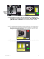
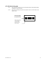
4.16. DIP SWITCH CHANGES
4.16.1.
Open the battery compartment door and locate dip switches underneath the battery
compartment, on the LCD board.
4.16.2.
Using the tool provided, pull of push the dip switch to the On or OFF Position. (See
diagram below)
When the dip switch
is in the UP position,
the Dip switch is ON
ON
1
2
3
4
5
6
7
8
When the dip switch
is in the DOWN
position, the Dip
switch is OFF
PN 140399 Rev. B
54
PAGE 1 OF 9
SIZE
DRAWING NUMBER
REV
A04187
A
B
PROCESS SHEET FOR:
SureSight
Final Test Specification
DRAWN:
C. Fahrenkrug
APPROVED:
Rich Andrews
REL TO PROD:GR Waclena
REV
DATE: 3.30.00
DATE: 3.30.00
DATE: 3/30/00
REV DESCRIPTION
ECN #
INIT
DATE
APPR
A
Release to Production
5-41157
CCF
03.30.00
RGA
B
Added clarifying repair
notes - p6&7
5-41599
CCF
06.29.00
RGA
THESE DRAWINGS AND SPECIFICATIONS ARE THE PROPERTY OF WELCH ALLYN, INC. AND
SHALL NOT BE REPRODUCED OR COPIED, OR USED AS A BASIS FOR MANUFACTURE OR SALE OF
EQUIPMENT OR DEVICES WITHOUT WRITTEN PERMISSION.
PAGE 2 OF 9
SIZE
A
DRAWING NUMBER
REV
A04187
B
GENERAL___________________________________________
PCBA tester must do/verify the following functions:
1. Default Calibration Record
2. Unit Information
3. Distance sensor calibration
4. User Indicators: Fixation LED’s, LCD operation, Alignment Crosshair
5. Button operation
6. Print operation (IR)
7. RS232 - Download Operation
8. Laser levels (Minimum, Nominal, Maximum)
9. Camera Gain Setting
10. Refractive readings (Sphere and Cylinder)
11. Charge Current
12. Low Battery Detect and Low Battery Warning
13. Nominal Current Draw
14. Real Time Clock
Unless otherwise specified:
• All measurement accuracies to be within 2%.
• All voltage and current is expressed as RMS.
• Input voltages to be maintained within 5%.
• All communications to unit are through USB interface using cable 140104-1 except step 7
which uses the RS232 interface and cable 140104-2.
1. DEFAULT CAL RECORD
•
Apply Supply Voltage to the unit 7.2V to 8.0V at the
battery terminals
•
Default CAL Record to be loaded into unit prior to
calibration including the following settings:
• Camera set to step 23
• Exposure set to 1 frame
•
*Nominal voltage range ± 5%
*Zero out distance offset
*Open Laser range
*Set Exposure
CAL fields to be updated throughout tests as described
below.
•
THESE DRAWINGS AND SPECIFICATIONS ARE THE PROPERTY OF WELCH ALLYN, INC. AND
SHALL NOT BE REPRODUCED OR COPIED, OR USED AS A BASIS FOR MANUFACTURE OR SALE OF
EQUIPMENT OR DEVICES WITHOUT WRITTEN PERMISSION.
PAGE 3 OF 9
SIZE
DRAWING NUMBER
A
A04187
2. UNIT INFORMATION
•
CAL Record should include the following
information:
• Serial Number
• Software Revision
• Hardware Revision
• Odometer
• FPGA Revision
•
•
3. DISTANCE CALIBRATION
•
Measure distance at four distances between 200 & 500
mm.
•
Distances to be approximately evenly spaced to allow
best data for linearization.
•
Distance positions to match “true” settings within
2mm. (actual vs. Programmed)
•
Compute the average offset of the distance sensor over
this 200 to 500 mm range and load it into the CAL
record.
•
•
REV
If Offset computed is >24 mm FAIL unit.
Return to the 200mm location and measure the
position. Return distance must be within 2mm of
200mm actual.
B
*See also History Log Aspec’s.
*Tracks number of tests.
*Target to be 5” x 5” of any
solid material including ABS
*Distances selected should be
approximately 200,300,400, 500
mm.**
*All measurements to be taken
from front of unit at the center
of the distance measurement
opening.
*Typical Offset 7-15 mm
*Where actual is the physical
position of the tester block with
respect unit front at ultrasonic
port.
•
**These selected positions may vary from recommended up to 20 mm. However, their exact
location must be determined to use as the “true” setting for comparison to the instrument reading.
THESE DRAWINGS AND SPECIFICATIONS ARE THE PROPERTY OF WELCH ALLYN, INC. AND
SHALL NOT BE REPRODUCED OR COPIED, OR USED AS A BASIS FOR MANUFACTURE OR SALE OF
EQUIPMENT OR DEVICES WITHOUT WRITTEN PERMISSION.
PAGE 4 OF 9
SIZE
A
DRAWING NUMBER
REV
A04187
B
4. USER INDICATORS: FIXATION LED’S, LCD, CROSSHAIR
•
Light fixation LED’s and verify that they function and
flash.
•
Light LCD segments and insure that they all turn OFF
and ON
•
Light green viewing crosshair and insure that it is
visible.
•
If any of these indicators do not function as stated,
FAIL unit.
5. BUTTON OPERATION
•
Press each button separately and verify that each
returns its own value only. The corresponding values
are:
• Left = 1
• Right = 2
• Center = 0
•
*SDK returns these values based
on button selected.
6. PRINT OPERATION (IR)
•
Print test assumes use of an HP82240B IR printer
•
Print test sentence from 18 inches ± 2 inches
•
Insure that no letters are skipped and no error boxes
(!) are printed.
•
7. RS232 - DOWNLOAD OPERATION
•
Connect cable 140104-2 connected between unit and
PC running Win98, latest revision of WA_Down and
FPG .DLL
•
Download latest version of software and update Unit
Information.
•
Note: If this function is performed on a previous
station, it is not required a second time.
*See BOM for current revision
level.
THESE DRAWINGS AND SPECIFICATIONS ARE THE PROPERTY OF WELCH ALLYN, INC. AND
SHALL NOT BE REPRODUCED OR COPIED, OR USED AS A BASIS FOR MANUFACTURE OR SALE OF
EQUIPMENT OR DEVICES WITHOUT WRITTEN PERMISSION.
PAGE 5 OF 9
SIZE
A
DRAWING NUMBER
A04187
8. LASER SETTINGS
•
All laser readings to be done on a UDT meter with a
single point 780nm calibration
•
Readings must be done in ambient light lower than
.4µW for all steps in this section.
•
•
•
•
•
•
•
•
•
•
•
Step laser pot down at least 120 steps to insure that it
is at its minimum.
Step pot up one step at a time until the laser power is
greater than or equal to 7 µW, but less than 16µW.
Log this pot setting as the laser minimum setting.
Store both the laser step and the actual light output in
µW in test record.
Step pot up one step at a time until the laser power is
greater than 17 µW, but less than or equal to 22 µW.
Log this pot setting as the laser nominal setting.
Store both the laser step and the actual light output in
µW in test record.
Step pot up one step at a time until the laser power is
greater than or equal to 28 µW, but less than 33 µW.
Log this pot setting as the laser maximum setting.
Store both the laser step and the actual light output in
µW in test record.
Laser reading must be repeated (at nominal) a second
time during the test sequence. This reading should be
sequenced so that the operator must realign to get the
reading.
Reading to be within nominal specifications above
(17µW to 22µW)
Turn laser off, and measure output power.
Output power to be less than .4µW
REV
B
*780 single point cal to be the
only cal in the UDT meter to
avoid risk of incorrect cal usage.
Nominal wavelength of laser is
785nm.
*Will guarantee that 100 step
pot will be at its minimum.
*The purpose of this step is to
demonstrate “normal” ability to
adjust laser - actual value is less
important, and not used in
product function.
*This nominal setting results
typically in 18 µW. This value
is used during product function.
*The purpose of this step is to
demonstrate “normal” ability to
adjust laser - actual value is less
important, and not used in
product function.
*Addresses FMEA issue that a
misaligned laser would be
accidently set too high.
*Addresses potential comparator
failure at output which leaves
laser on at approximately .5µW.
•
9. CAMERA GAIN SETTING
•
Set the camera gain to step 23.
•
This setting must be present prior to boundary value
checks.
•
Gain is a constant pot step
All boundary checks assume this
setting.
10. REFRACTIVE READINGS
THESE DRAWINGS AND SPECIFICATIONS ARE THE PROPERTY OF WELCH ALLYN, INC. AND
SHALL NOT BE REPRODUCED OR COPIED, OR USED AS A BASIS FOR MANUFACTURE OR SALE OF
EQUIPMENT OR DEVICES WITHOUT WRITTEN PERMISSION.
PAGE 6 OF 9
SIZE
A
•
•
•
•
•
•
DRAWING NUMBER
A04187
Activate unit with the laser set at nominal and the
camera setting at nominal as determined in prior steps.
Align unit with glare and image as central as possible,
preferably within the green box.
With .9 ND filter present - refract the zero eye
position.
Reduce .6 ND filter.
Refract all remaining lenses and compare to limits as
described in Appendix 1.
Values to be within attached boundary limits Due to
alignment variations - up to 3 failures are allowed for
a unit to “Pass” the boundary tests.
REV
B
*Do not align to green box if it
causes image to be clipped.
*.3 and .6 together.
*4 or more lens failures equal a
fail.
11. CHARGE CURRENT (For Repair Spec’s see Service Manual)
*Note - this current will be
•
Connect current meter in series with battery
larger than actual charge current
connection.
- See Aspec specified on BOM
for proper derivation.
•
Attach a 71040 to charging jack. (Note: battery
connection must be made prior to attachment of
71040)
•
Measure the current through the current meter.
*Intended to correspond with
•
Requirement: 200mA ≥ I ≥ 150mA
150mA.
12. LOW BATTERY FUNCTIONS (Not required for Repair)
•
All voltages shown below are referenced to the power board. If voltage drop occurs between
supply and unit (due to wires, relays, etc) the actual input should be adjusted to yield the
specified voltage at the power board.
*LBW=7.3V max, 6.8V min.
•
Set Input voltage to 7.4V
(7.056 nom)
•
Verify that neither LBW nor LBD are set.
*LBD=6.4V max, 6.0V min.
•
Set Input voltage to 6.5V
(6.256 nom)
•
Verify that LBW is set, but LBD is not.
*Unit will not function at this
•
Set Input voltage to 5.9V
voltage level. This is optional to
•
Verify that LBW and LBD is set.
test in the final assembly, but
preferred if possible.
THESE DRAWINGS AND SPECIFICATIONS ARE THE PROPERTY OF WELCH ALLYN, INC. AND
SHALL NOT BE REPRODUCED OR COPIED, OR USED AS A BASIS FOR MANUFACTURE OR SALE OF
EQUIPMENT OR DEVICES WITHOUT WRITTEN PERMISSION.
PAGE 7 OF 9
SIZE
DRAWING NUMBER
A
REV
A04187
B
13. NOMINAL CURRENT DRAW (Not required for Repair)
*Nominal voltage.
•
Restore input voltage to 8.0 to 8.4V
•
With unit in “ON” mode (MCU powered up), measure
the input current.
*Nominal = 477mA
•
Requirement: 300mA < I <550mA
•
14. REAL TIME CLOCK SETTING
•
Set Real Time Clock to Skaneateles date and time.
•
Set Cal Location to WA Skaneateles
*Note: Clock is not to be reset
to other time zones - it is for
factory use only.
*Record location of last
calibration.
•
15. DISTANCE TARGET SIZE/RELIABILITY
•
Set distance block at 500mm position.
•
Unit must detect the presence of the distance block on
500 consecutive measurements. Measurements must
not deviate from nominal setting by more than 2 mm,
or unit is a fail.
•
Position can be ± 20 mm.
*Addresses lowered sensitivity
which occurs when ultrasonic
sensor is improperly assembled.
THESE DRAWINGS AND SPECIFICATIONS ARE THE PROPERTY OF WELCH ALLYN, INC. AND
SHALL NOT BE REPRODUCED OR COPIED, OR USED AS A BASIS FOR MANUFACTURE OR SALE OF
EQUIPMENT OR DEVICES WITHOUT WRITTEN PERMISSION.
PAGE 8 OF 9
SIZE
DRAWING NUMBER
REV
A04187
A
B
Appendix 1: Refraction Boundary Limits*
*Refer also to Fake Eye Aspec for additional specifications.
Sphere Set
Sphere
Lens
1
2
3
4
5
6
9
10
11
12
13
Max
0.5
4.7
9.7
13.9
19.9
26.0
-3.2
-6.6
-9.5
-12.4
-15.0
Min
-4.0
-0.6
2.4
7.9
12.5
16.4
-7.9
-11.5
-14.7
-18.0
-20.2
Cylinder
Max
Min
2.8
0
3.0
0
3.4
0
4.7
0
6.2
0
6.9
0
4.3
0
3.0
0
3.2
0
2.8
0
2.7
0
Cylinder Set
Lens
15
16
17
18
21
22
23
24
Cylinder
Max
Min
6.3
1.7
11.0
5.9
18.5
7.7
25.8
12.8
7.2
1.7
10.1
5.2
13.9
7.1
16.3
11.0
Sphere
Max
2.1
1.6
2.3
2.0
-1.8
-4.8
-8.1
-11.6
Axis
Min
-4.3
-4.2
-4.7
-5.1
-9.8
-13.0
-15.7
-18.3
Max
Min
Note that
Axis accuracy
was qualified
and is not
tested in
Production.
THESE DRAWINGS AND SPECIFICATIONS ARE THE PROPERTY OF WELCH ALLYN, INC. AND
SHALL NOT BE REPRODUCED OR COPIED, OR USED AS A BASIS FOR MANUFACTURE OR SALE OF
EQUIPMENT OR DEVICES WITHOUT WRITTEN PERMISSION.
PAGE 9 OF 9
SIZE
A
DRAWING NUMBER
A04187
REV
B
Notes:
Due to the large variation in parameters which determine the refractive values, (sphere/cylinder
variation from lens value, distance to wheel, exact alignment to lens center, unaccounted for
aberrations in lenses, ND power variation, retinal material variation, fake eye actual
dimensions, etc) deterministic methods do not yield expected values with an acceptable
degree of accuracy. Consequently, boundaries require correlation to positive clinical
performance, and are not deductively linked to the lens value placed in the wheel position.
To revise or reset boundaries if tester or wheel are changed, there are two possible means. Five
or more units can be tested five times to determine range of values, and then clinically
verified to provide proper performance. Since this is very time consuming, the alternative is
to test 30 units under the current settings and then use them to reset and or reverify the
acceptable range of values under the new setup. During this comparison, standard deviations
of the new setup must be sufficiently low so as to allow new boundaries to be set. For
reference, a current set of wheel values including standard deviations is included in the wheel
verification Aspec listed on the BOM.
THESE DRAWINGS AND SPECIFICATIONS ARE THE PROPERTY OF WELCH ALLYN, INC. AND
SHALL NOT BE REPRODUCED OR COPIED, OR USED AS A BASIS FOR MANUFACTURE OR SALE OF
EQUIPMENT OR DEVICES WITHOUT WRITTEN PERMISSION.
PAGE 1 OF 6
SIZE
DRAWING NUMBER
REV
A04260
A
B
PROCESS SHEET FOR:
SureSight
Alignment Specification
REV
DRAWN: C. Fahrenkrug
DATE: 05/05/00
APPROVED: RA
DATE: 05/05/00
REL TO PROD: GR Waclena
DATE: 05/05/00
REV DESCRIPTION
ECN #
INIT
DATE
APPR
A
Release to Production
5-41366
CCF
7/17/2000
RA
B
Rev’d p5 to account for Repair
plates
5-41599
CCF
6/29/2000
RA
THESE DRAWINGS AND SPECIFICATIONS ARE THE PROPERTY OF WELCH ALLYN, INC. AND SHALL
NOT BE REPRODUCED OR COPIED, OR USED AS A BASIS FOR MANUFACTURE OR SALE OF
EQUIPMENT OR DEVICES WITHOUT WRITTEN PERMISSION.
PAGE 2 OF 6
SIZE
A
DRAWING NUMBER
A04260
REV
B
GENERAL___________________________________________
The purpose of this specification is to provide the product requirements for alignment
for the SureSight product. The process aspec is derived based on these specifications,
and the actual magnification and camera selected for use in the alignment station
tooling. In addition, a specification for the manufacturing setting is listed in addition to
the final product requirement. In each case, the manufacturing specification is tighter
than the final product specification. This is to insure that the manufacturing setting plus
the repeatability variation do not exceed the final product requirement. It should be
noted that if the final product requirement is used for the manufacturing setting limits excessive fallout would be likely at the final tester due to variations in repeatability.
Unless otherwise specified:
• Fake eyes to be built as per Fake Eye Construction Aspec on BOM. Nominally this
includes a 4.5mm pupil. (ref)
• All measurements to be completed at nominal working distance = 360mm from first
conjugate surface to front surface of fake eye.
1. MAXIMUM GLARE
All alignments to be done with fake eye positioned for maximum glare. Maximum glare
occurs when the laser is projected into a fake eye in the center and perpendicular to the
lens. This demonstrated by achieving the brightest glare within the image. In general,
this will also occur roughly in the center of the return image. See Figure 1.
Figure 1
THESE DRAWINGS AND SPECIFICATIONS ARE THE PROPERTY OF WELCH ALLYN, INC. AND SHALL
NOT BE REPRODUCED OR COPIED, OR USED AS A BASIS FOR MANUFACTURE OR SALE OF
EQUIPMENT OR DEVICES WITHOUT WRITTEN PERMISSION.
PAGE 3 OF 6
SIZE
A
DRAWING NUMBER
A04260
REV
B
2. BEAM SPLITTER/CAMERA ALIGNMENT
The purpose of the beam splitter alignment is to place the return image in the center of
the camera active area. This insures that the margin of aiming is as equal as possible
in the up, down, right, and left directions. For example, if the beam splitter image is
aligned toward the top of the camera active area, any slight aiming above this will drop
the image off the camera - resulting in no readings.
To facilitate measurement of the image position, a green box function is projected by
the software in the exact center of the camera active area, and in a size which
represents the 4.5mm image. For reference, the camera active area is 696 by 494
pixels. The green box is 300 by 300 pixels, and positioned with a center of 348,247 to
correspond with the center of the active area.
Image position accuracy is measured in number of lines outside the green box. Given
the pitch of the lenslet, each line outside the box corresponds to 1mm of offset in the
position of the center of the image compared to the center of the camera active area.
Figure 2
THESE DRAWINGS AND SPECIFICATIONS ARE THE PROPERTY OF WELCH ALLYN, INC. AND SHALL
NOT BE REPRODUCED OR COPIED, OR USED AS A BASIS FOR MANUFACTURE OR SALE OF
EQUIPMENT OR DEVICES WITHOUT WRITTEN PERMISSION.
PAGE 4 OF 6
SIZE
DRAWING NUMBER
REV
A04260
A
B
Row Measurement
The measurement of rows outside the box on any side is as follows:
Only rows which are three or more spots are considered a row.
If the row sits on the green line, it is counted as a half row.
If the row is fully outside the line, it is counted as a full row.
Figures 2 shows some examples of row counts.
1.5 Rows
Out
2 Rows
Out
Figure 3:
Fails at Alignment station
Pass at Final Tester
Figure 4:
Pass at Alignment station
Pass at Final Tester
Allowable image rows outside the green
box
Manufacturing Setting
Final Product Specification
Repair Specification
Alignment station Pixels
1.5
2
2
3. MIRROR ALIGNMENT
THESE DRAWINGS AND SPECIFICATIONS ARE THE PROPERTY OF WELCH ALLYN, INC. AND SHALL
NOT BE REPRODUCED OR COPIED, OR USED AS A BASIS FOR MANUFACTURE OR SALE OF
EQUIPMENT OR DEVICES WITHOUT WRITTEN PERMISSION.
PAGE 5 OF 6
SIZE
DRAWING NUMBER
REV
A04260
A
B
The purpose of the mirror alignment is to place the crosshair image on top of the laser
at the nominal working distance. This insures that the when the physician aligns the
crosshair with the patients pupil, he is also aligning the laser to the pupil. This is
necessary because the laser is not visible and can not be aligned without an alternate
means.
As noted below, the alignment station setting specification is .41 mm from the pixel
center. This is to insure that it will meet the crosshair product specification of .76mm
from the center of the pupil. When unit is initially shipped to the field, Repair Stations
are allowed a modest increase beyond this to cover plate to plate variation which is 1-2
pixels (typical).
For convenience, crosshair position accuracy can be measured in pixels from pupil
center. The equivalent specifications in pixels for the alignment station as well as for
the final tester are listed below.
The acceptable limit for the number of pixels the crosshair center can be from the pupil
center is a function of the magnification of the optics as well as the resolution of the
observing camera. Any alteration of camera or magnification would require revision to
these specifications. The procedure for determining the magnification as well as the
number of pixels within the product specification is listed in the next section.
Measurement Station Used
Alignment Station
Final Tester
Repair Stations
14.4
7.9
5.1
Magnification pixels/mm
Specifications:
mm
pixels
mm
pixels
mm
pixels
Alignment
.41
5.9
n/a
n/a
n/a
n/a
Final Tester
n/a
n/a
.76
6
n/a
n/a
Repair
n/a
n/a
.76
6
1.18
6
*Note: Specifications are only given on the stations on which they are normally tested.
All others are labeled as n/a. Repair Station plates are allowed larger deviation for
repair units only and can not be used for new production.
THESE DRAWINGS AND SPECIFICATIONS ARE THE PROPERTY OF WELCH ALLYN, INC. AND SHALL
NOT BE REPRODUCED OR COPIED, OR USED AS A BASIS FOR MANUFACTURE OR SALE OF
EQUIPMENT OR DEVICES WITHOUT WRITTEN PERMISSION.
PAGE 6 OF 6
SIZE
A
DRAWING NUMBER
A04260
REV
B
4. MAGNIFICATION MEASUREMENT
The purpose of the magnification measurement is to determine the pixels per millimeter
of a particular optical/camera setting. This magnification is multiplied by the
specification in millimeters to convert to specifications in pixels for that station.
Procedure:
1. Place a metric ruler as close to the plane of the fake eye pupil as possible and
placed across the pupil so that the numerical labels on the ruler can be seen for at
least 30 mm. The ruler tick marks should be clearly visible and the ruler should be
as straight as possible.
2. Using FPGEYE software, grab a picture of the ruler and save the image.
3. Open the image using Vision Builder, PC Paint or equivalent.
4. Count the number of pixels which are visible over a 30mm span of the ruler.
5. Compute this number/30 to determine pixels per mm magnification.
THESE DRAWINGS AND SPECIFICATIONS ARE THE PROPERTY OF WELCH ALLYN, INC. AND SHALL
NOT BE REPRODUCED OR COPIED, OR USED AS A BASIS FOR MANUFACTURE OR SALE OF
EQUIPMENT OR DEVICES WITHOUT WRITTEN PERMISSION.
!"!#! $% &%'($% $ )*
*/*
-
+
,
(
$()*
+,
-.
-.
&
!"#
$%
'
A
B
C
D
REV
A
E
DESCRIPTION
ECN
Release to Production at X9
5-41452
DATE
APPROVAL
6/9/00
CCF
4
4
3
3
JP1
1
2
3
4
LASER_LD
LASER_PD
2
1
71220-0400
D1
RLD-78PP
PD
3
LD
GND
2
2
Notes:
1. All values are shown for reference only.
See BOM for proper values.
2. PD is sent redundantly on pin1
3. D1 is a single package
4. D1 footprint does not match suppliers
recommended dimensions. This reduced
format is critical to prevent shorting
to the case and should not be changed.
1
DRAWN
DATE
K. HENNING
10/08/98
CHECKED
1
CCF
06/08/00
CCF
06/08/00
MKT
06/08/00
PROJECT NO.
APPROVED
Title
RELEASED
DAVE Laser Mini Schematic
ENGINEER
CCF
A
B
C
RD14000
D
Size
B
Date:
Document Number
140152
Wednesday, June 28, 2000
Rev
A
Sheet
E
1
of
1
REV
A
VSLaser
DESCRIPTION
ECN
Release to Production at X9 : Modifed Q3 / laser on to fix laser / on wheel
failures of previous version.
5-41452
DATE
APPROVAL
6/9/00
CCF
VSLaser
T P 11
R24
10k
2
Laser Drive
TP3
Q3
M M B T 4 4 03
R25
2k
3
R4
1K
LASER_ON/OFF
1
Viewing LED Drive
VSLaser
+5V
VSLaser
TP6
R6
2k
VSET
2
-
NE5234
1
U8A
LMC6762
2
VIEW_ON/OFF
1
Q2
M M B T 4 4 03
1
Molex 52271-0890
VLED
4
VM
R10
10k
R11
1K
R3
150
VSLogic
To Laser Mini
R15
20
LED
JP1
TP2
1
2
3
4
LD
PD
VSLogic
C6
1uF/25V
1
2
R14
10k
R12
50k
TP7
TP8
TP9
Molex 71220-0400
Do not Pop - R18
R17
20
U2
8
5
3
6
R19
3.32K
4
VCC
VW
VH
VL
INC
U/D
CS
1
R16
499
LASER_INC
2
R20
499
LASER_U/D
7
R21
499
LASER_CS
R18
20
To LED Mini
LD
TP10
TP4
VSS
JP2
1
2
3
4
LED
Do not pop - R22
Molex 71220-0400
X 9 3 1 4 W S-3
R22
10K
C9
.01uF/100V-X7R
U1C
R23
32.4K
9
TP5
8
T P 14
10
VSLaser
NE5234
Spares
R26
180
13
14
VPD
+5V
VSLED
+3.3V
VSLogic
TP13
T P 12
VSLaser
6
7
12
5
U1D
NE5234
VREF
R27
10k
D2
TL431AC
2%+TC
U1B
NE5234
1
8
2.5V Ref
8
VSLaser
5
+
6
-
7
U8B
LMC6762
4
11
U1A
+
Q1
M M B T 4 403
1
2
3
4
5
6
7
8
3
3
+3.3V
LASER_INC
LASER_U/D
LASER_ON/OFF
LASER_CS
VIEW_ON/OFF
6
3
R2
1K
3
1
VREF
C8
.1uF/100V/X7R
R9
2K
2
R1
2K
2
C3
1uF/25V
J1
TP1
8
4
PD
C1
1uF/25V
1
2
2
VSLED
R10 provides maximum resistor value
and maximum Vset achievable.
VSLaser
1
VSLED
Notes:
1. All values are shown for reference only.
See BOM for proper values.
2. Net names on ground symbols may vary.
No changes should be made to
allocation without rechecking.
3. Test Point Cross Reference
TP1 - VIEW_ON/OFF
TP2 - LED
TP3 - PD Current
TP4 - GND
TP5 - VSLaser
TP6 - VSET
TP7 - Laser_CS
TP8 - LASER_U/D
TP9 - LASER_INC
TP10- LD Cathode
TP11- LASER_ON/OFF
TP12- PD Voltage
TP13- VREF
TP14- VSLED, VSLogic
DRAWN
E. Dickman
DATE
03/25/99
APPROVED
CCF
06/08/00
MKT
06/08/00
Title
RELEASED
DAVE LASER DRIVE Schematic
ENGINEER
PROJECT NO.
CCF
RD14000
Size
D
Date:
Document Number
140153
Tuesday, June 27, 2000
Rev
A
Sheet
1
of
1
REV
A
FID1
FIDUCIAL
FID2
FIDUCIAL
DESCRIPTION
ECN
Release to Production at X10 : added LED's for charge detect.
5-41452
TP1
2
1
2
JP1
524 35-2891
TP3
R6
150
+3.3V
D3
1
2
TP4
1
2
Rohm SML-010-MT-T86
Maximum leakage = 1uA
+3.3V
TP5
R7
150
1
D4
Green
2
5
TP10
6
V+
C2+
C7
0.1uF/35V
11
PPCRX
9
PwrDN
1
+3.3V
16
1
1
C2-
V-
FIX_LATCH
C9
0.1uF/35V
7
T1IN
T1OUT
R1OUT
R1IN
12
13
D2
C4
DO NOT POP
DO NOT POP
TP33
TXM
8
R11
10K
+
TP32
RXD
13
TP38
TP37
+
C2
2 1uF/25V
ChargeLED2
TP11
TP12
INVALID
GND
Maximum leakage = 1uA
Off when EN=H
DCINUNPLUGGED
GND
GND
P P C TX
PPCRX
2
1
QA
QB
QC
QD
QE
QF
QG
QH
SRCLK
RESET
RCLK
OE
8
GND
QH'
15
1
2
3
4
5
6
7
D5
1
2
1
2
1
2
3
4
5
6
7
8
9
10
11
12
13
14
15
16
17
18
19
20
21
22
23
24
25
26
27
28
Rohm SML-010-MT-T86
TP14
R12
150
9
D6
1
2
1
74HC595
TP13
2
TP9
R10
150
2
J1
555166-1 Amp
Rohm SML-010-MT-T86
GND
TP15
R14
150
D7
1
2
1
+3.3V
D+
D-
2
Rohm SML-010-MT-T86
FORCEOFF
1
R45
4K
Vcc
SER
USBOE
USBRXD
USBTXN
U S B T XP
USBRXN
USBRXP
FIX_DATA
FIX_CLOCK
FIX_LATCH
IRDA_TXOUT
IRDA_RXIN
PwrDN
DCIN
DCINGND
R44
4K
R40
200
EN
3 DCINGND
2
11
10
TP8
FORCEON
10
2
FIX_CLOCK
R39
200
P P C TX
16
14
FIX_DATA
3
4
U2
TP6
C1-
2
2
1
C6
1uF/25V
+
15
1
Yellow
Rohm SML-020-MYT-T86
C1
0.1uF/50V/X7R
R4
10K
+
R8
10K
Vcc
C1+
R3
10K
3
C8
0.1uF/35V
+
R9
10K
C3
0.1uF/50V/X7R
R2
10K
2
+3.3V
1
+3.3V
TP7
+3.3V
+
+
4
+3.3V
R1
10K
1
1
ChargeLED2
2
CCF
TP2
Rohm SML-010-MT-T86
U1
SP3221E
6/9/00
+3.3V
D1
1
C5
0.1uF/35V
APPROVAL
FIXATION LED'S
FID3
FIDUCIAL
R5
150
RS232
DATE
12
14
TP39
TXM
RXD
TP16
R16
150
D8
1
2
1
2
1
2
3
4
5
6
7
8
9
10
Rohm SML-010-MT-T86
TP17
R17
150
1
2
D9
Green
2
1
ChargeLED1 4
3 DCINGND
Yellow
RohmSML-020-MYT-T86
TP36
TP40
J2
R41
4K
2
DCINGND
DCINUNPLUGGED
DCIN
1
R46
4K
RAPC-712
2
TP18
3
2
1
1
TP19
+LED
+3.3V
+LED
USBTXN
C10
6.8uF/16V
+
U S B T XP
R21
10K
R22
10K
C11
0.47uF/25V/X7R
IRDA
USB
On Philips part, pin 1 =
Mode, default open
R18
4.7 Ohm
Spec is 2.2 Ohms
TP35
+3.3V
Test Points - For Reference only.
TP20
TP21
TP22
+
+3.3V
TP24
C15
0.1uF/50V/X7R
R23
10K
2
USBRXD
3
USBRXP
4
USBRXN
5
PwrDN
6
7
R34
10K
R31
10K
R32
10K
R33
10K
RERR
OE
RCV
Vcc
VMO
VPO
VP
D+
VM
D-
SUSPND
GND
SPEED
RSEO
C14
DO NOT POP
For Full Speed operation - populate R25 only
U4
PDIUSBP11A D
1
USBOE
+3.3V
+3.3V
+3.3V
TP25
1
R20
10K
6
14
R25
1.5 K
13
R36
1.5K
TP26
IRDA_RXIN
IRDA_TXOUT
8
9
R42
23.2 Ohm
12
R43
10
R28
9
23.2 Ohm
D-
PwrDN
R29
10K
2
5
7
TP29
8
TP31
On Philips part, pin 8=NC
Off when Suspend=H
4
+3.3V
0 Ohm
R35
DO NOT POP
TP2 = +3.3V
TP4 = GND
Vcc
RS232
TP6 = V+ Charge Pump
TP7 = PPCRX
TP8 = V- Charge Pump
TP10 = PPCTX
TP32 = RXD
TP33 = TXM
NC
RXD
TXD
R38
200 Ohm
D+
11
U3
HSDL-3600#018
LEDA
TP34
+
TP23
C13
1uF/25V
10
+3.3V
C12
1uF/25V
TP30
TP28
AGND
MD1
GND
R30
DO NOT POP
3
+3.3V
DO NOT POPULATE R30
Maximum leakage = .1uA
Fixation LED's
TP1 = LED1
TP3 = LED3
TP5 = LED4
TP9 = LED5
TP11 = DATA
TP12 = CLOCK
TP13 = LATCH
TP14 = LED6
TP15 = LED7
TP16 = LED8
TP17 = LED9
TP36 = Chargeled1
TP37 = Chargeled2
MD0
FIR_SEL
R37
0 Ohm
Off when Mode 0=H
Maximum leakage = 5uA
Notes:
1. All values are shown for reference only.
See BOM for proper values.
USB
TP18
TP19
TP20
TP21
TP22
TP23
TP24
TP26
TP30
TP31
TP34
=
=
=
=
=
=
=
=
=
=
=
USBTXN
USBTXP
USBRXD
USBRXP
USBRXN
PwrDN
RERR
D+
DRSEO
USBOE
IRDA
TP25
TP27
TP28
TP29
TP35
=
=
=
=
=
TXD
RXDSIR
RXDFIR
PWDWN
+LED
2. IRDA current limit set by R18 is lower
then manufacturers recommended. This
was found to substantially improve
directional and distance performance.
DRAWN
DATE
D.Fallat
02/26/2000
APPROVED
CCF
06/08/00
Title
RELEASED
F i x a tion Display Driver Schematic
MKT
ENGINEER
06/08/00
PROJECT NO.
Size
D
Document Number
140154
Rev
A
CCF
RD14000
Date:
Tuesday, June 27, 2000
Sheet
1
of
1
THiS DRAWING AND SPECIFICATIONS ARE THE PROPERTY OF WELCH ALLYN, INC. AND
SHALL NOT BE REPRODUCED, COPIED OR USED AS THE BASIS FOR THE MANUFACTURE OR
THE SALE OF EQUIPMENT OR DEVICES, WITHOUT WRITTEN PERMISSION OF WELCH ALLYN, INC.
REV
DESCRIPTION
Release to Production at rev X9 : Added testpoints for D0-D7, TP34-TP41
Updated testpoint list on bottom of schematic
Added testpoint to stdby TP33 and ID3 TP42
A
+5_IMG
ECN
DATE
5-41452
APPROVAL
6/9/00
CCF
+5F
C3
.01uF/50V/X7R
1
L1
10uF/16V
1
6.8uH
C1
22uF/16V
2
2
C4
AGND
C8
.01uF/50V/X7R
3
1
VSHP
29
TP17
TP18
Stdby
42
HORIZB_5
46
VERTB_5
47
14
H2
16
10
/RG
//RG
FSE
BUSY
SMDE
WEN
WM
ID
STDBY
PBLK
HD
XCPOB
VD
XCPDM
36
35
13
-7.5V
33
R15
32
R16
2.21K
2.21K
PBLK
S4
+15V
XCPOB
S5
XCPDM
S6
2.21K
47pF/100V/NPO
C25
VSS
XV2
6
XV1
5
XV3
8
10
DGND5
XV4
XSG
7
XV4
XSG
9
2
CPP1
CPP2
DO NOT POPULATE R21
IM_SER_CLK
IM_SER_DATA
WEN3
IM_SER_STRB
CS
Stdby
U/D
INC
TP42
+15V
TP25
D0_3
D1_3
D2_3
D3_3
D4_3
D5_3
D6_3
D7_3
+3.3V
TP26
TP27
AGND
TP34
AD_CLOCK_5
VIDEO_OUT
22
39
OUTPUT ENABLE
23
CHIP ENABLE
24
DGND5
R19
1M
.01uF/50V/X7R
DGND5
DGND5
C31
10uF/10V
20
29
30
CE
CE1
A/D
VRT
VRT
C32
.1uF/16V/X7R
D0
D1
D2
D3
D4
D5
D6
D7
D8
D9
DVDD
DVDD2
AVDD
AVDD
AVDD2
TP31
19
DCOUT
C35
VSHT
VRB
AGND
18
XSHT
17
2
C36
3.3uF/50V
1
U6
XV2
V2
XV3
V1
XV4
V3
XSG1
V4
XSG2
VL
VM
34
35
C37
.1uF/16V/X7R
VRB
VRB
1
2
3
4
5
8
9
10
11
12
MSB
TP36
TP40
TP37
TP41
D0_3
D1_3
D2_3
D3_3
D4_3
D5_3
D6_3
D7_3
+3.3V
7
45
25
26
18
C33
22uF/10V
C34
.1uF/16V/X7R
15
V1
14
V2
17
14
37
20
21
27
28
36
43
44
6
16
48
AGND
V3
12
11
13
R20
DGND5
CXD1267AN
RESET
TESTMODE
15
19
+5F
DGND3
10uF/10V
XV1
VERTICAL
CLOCK
CAL
TS
SEL
TIN
TSTR
LINW
MINW
AVSS
AVSS
AVSS
AVSS4
AVSS3
DVSS
DVSS
DVSS2
41
42
C38
.1uF/16V/X7R
AT
TO
NC
NC
NC
NC5
NC4
NC3
38
13
31
32
33
40
46
47
C39
22uF/16V
DGND3
0 Ohm
CXD2311AR
C40
22uF/25V
DGND5
AGND
C41
DGND5
-7.5V
.1uF/50V/X7R
DGND5
TEST POINTS - for reference only
DGND5
DGND5
1. All values are shown for reference only.
See BOM for proper values.
2. Supply integrity is extremely important
on this board. Netnames on ground
symbols vary. No changes should be
made to allocation without rechecking.
CLK
VIN
TP35
TP39
DCIN
16
1
2
3
4
5
6
7
8
9
10
11
12
13
14
15
16
17
18
19
20
21
22
23
24
25
26
27
28
29
30
R27
0 Ohm
Notes:
TP38
TP20
VRT
DGND5
CONNECTOR-30
AGND
DGND5
ICX084
2
0 Ohm
AGND
CXA1690Q
1
HORIZB_5
IM_REF_CLK_5
VERTB_5
DGND3
C17
.1uF/16V/X7R
2
CPP3
J1
TP21
TP24
DGND5
R10
49.9K
.1uF/16V/X7R
+15V
DGND5
CS
VSS
AGND
C22
1
4
TP23
DGND5
AGND
3.48K
AGND
U5
C27
2200pF/100V/X7R
U/D
7
4
1
DGND5
-7.5V
DIN
CS
2
Do not populate R31 if U3 is
populated. Only Populate U3
with the Xicor X9314WS-3
Part. DO NOT POPULATE with
the Dallas DS1804
PIN
2
1
3
+5_IMG
26
C30
DGND5
VH
DGND5
R21
25
AS4
SUB
AGND
.1uF/50V/X7R
1
AD_CLOCK_5
ID3
AS3
2
U/D
INC
1
SUBCIR
TP19
C29
.01uF/50V/X7R
22uF/25V
DGND5
DGND5
C18
1uF/25V
C16
1uF/25V
INC
X9314WS-3
R12
32
PBRFC
2
VSS
C28
12
C15
.1uF/16V/X7R
31
REFCONT
XCPDM
C24
R18
100K
CXD2434T
37
VSS
27
24
VSS
15
VSS
47pF/100V/NPO
47pF/100V/NPO
2
1
VL
MMBD4148
+15V
XV[1..4]
11
10
.01uF/50V/X7R
AGND
D2
31
1
VCC
VW
VH
VL
4
AGND
CCD
RG
CLPDM
AS2
R13
2.21K
H2
NC
C21
C20
1uF/25V
ID5
34
TEST2
TEST1
14
TP15
C26
39
28
XSUB
6
DGND5
U4
AGND
18
AGCCONT
AGND
WEN5
TEST3
CLD
48
Reset Gate
RG
C23
41
H1
.001uF/50V/X7R
R17
+5_IMG
V1
C19
TIMING
PS
S6
U3
8
5
3
6
634
AGND
SHD
NC
15
Q1
MMBFJ309LT1
R31
1
R30
10k
RG
H1
0 Ohm
AS1 3
MMBD4148
13
R14
8
24
TP6
R11
49.9K
2
+5_IMG
STRB
3
VOUT
V2
22
R6
10K
1
DGND5
H2
2
V1
TP28
XSHD
TP5
2
26
DCLK
V2
100K
TP11
S2
+3.3V
R9
49.9K
TP8
SHP
28
25
+5_IMG
TP33
R8
TP10
V3
21
C13
.047uF/50V/X7R
GND3
3
21
S3
TP9
AGND
XSHP
+3.3V
TP4
AMPLIFIER
6
DGND5
S2
XSHP
1
S3
CLPOB
GND2
4
H1
15
GND
IM_SER_STRB
XSHD
D1
SMD2
DATA
XCPOB
+5F
17
AGCMAX
XRS
7
CONTROLLER
5
22
V3
GND
TP14
IM_SER_CLK
S1
R7
100 Ohms
DGND5
5
TP13
DGND5
GND
TO CAMERA
7
+15V
11
TP12
9
+5_IMG
IM_SER_DATA
XSHP
XRS
XSG
NC
Serial ports internally pulled up
XSHD
U2
SMD1
S5
C14
.01uF/50V/X7R
1
8
23
14
30
DGND5
XV4
XRS
AGND
+
TP7
19
Check connections for VW VH VL Vcc
TP3
PBLK
GND1
XRS
XV3
13
23
XSG
XV2
16
S1
+15V
PBLK
LINE
XV3
TP29
17
AGND
OFFSET
29
EFS
C12
22uF/25V
XV1
1
XV2
12
R3
2K
VRT
+3.3V
S4
2
ESG
18
6
45
XV1
32.4K
+5F
VRB
AGND
2
44
TRIG
TP30
3
43
R4
C11
.01uF/50V/X7R
38
9
CL
C10
.01uF/50V/X7R
VDD
OSC1
+5_IMG
+15V
40
1
30
VDD
VDD
12
VDD
CKO
C9
.01uF/50V/X7R
16
AGCCLP
1
2
VRT 11
V[1..3]
IM_REF_CLK_5
DGND5
VRB 10
9.09K
3
TP2
OSCO
20
2
R2
DGND5
19
CCDLEVEL
U1
CSHI
5
1
9
VSHI
4
AGND
DGND5
8
CLPDRV
C6
.01uF/50V/X7R
VIDEO_OUT
7
DRVOUT
PB/REC
R1
47.5K
C7
22uF/16V
TP1
C5
1uF/16V/X7R
VCC3
CAM/VID
2
+5_IMG
VCC1
1
VCC2
20
AGND
27
AGND
S[1..6]
R28
0 Ohm
AGND
R29
0 Ohm
DGND5
DGND3
Net Separators - nets are joined in copper
TP1
TP2
TP3
TP4
TP5
TP6
TP7
TP8
TP9
TP10
TP11
TP12
TP13
TP14
TP15
TP17
TP18
TP19
TP20
TP21
TP23
TP24
TP25
TP26
TP27
TP28
TP29
TP30
TP31
TP32
TP33
TP34
TP35
TP36
TP37
TP38
TP39
TP40
TP41
TP42
-
VIDEO OUT - NEAR U1 PIN 7
IM_REF_CLK_5
AGCMAX
CS
U/D
INC
V3
AGCCONT
CCD OUT
H2
H1
IM_SER_DATA
IM_SER_CLK
IM_SER_STRB
WEN5
HORIZB_5
VERTB_5
SUB
VRT
DGND5
+5_IMG
-7.5V
+15V
+3.3V
AGND
Reset Gate
V2
V1
VRB
AD_CLOCK_5
Stdby
D1
D3
D5
D7
D0
D2
D4
D6
ID3
WEN3
WEN5
TP32
ID5
ID3
AD_CLOCK_3
AD_CLOCK_5
DRAWN
DATE
D. Fallat
04/19/00
APPROVED
CCF
06/08/00
Title
MKT
06/08/00
PROJECT NO.
Size
D
CCF
RD14000
Date:
RELEASED
DAVE Camera Schematic
ENGINEER
Document Number
140155
Tuesday, June 27, 2000
Rev
A
Sheet
1
of
1
+3.3VFIL
+3.3VFIL
FID1
FIDUCIAL
FID2
FIDUCIAL
+5V
FID3
FIDUCIAL
A
+5V
+3.3VFIL
C1
C2
C3
C4
C5
C6
C7
.1uF/50V/X7R .1uF/50V/X7R .1uF/50V/X7R .1uF/50V/X7R
.1uF/50V/X7R .1uF/50V/X7R .1uF/50V/X7R
Release to Production at X10
+3.3VFIL
CCD_Ref_CLK
Bypass Caps for FPGA
82
C C D _ R ef_CLK_3
C24
C26
C28
C30
.1uF/50V/X7R
.1uF/50V/X7R
.1uF/50V/X7R
.1uF/50V/X7R
C25
C27
C29
C31
.1uF/50V/X7R
.1uF/50V/X7R
.1uF/50V/X7R
.1uF/50V/X7R
D11
B13
B11
B6_OP3/MODCK2/DSDO
D6_OP2/MODCK1/STS
D11_UPWAITA/GPL_A4
B13_UPWAITB/GPL_B4
B11_BR
??????
C13_RD/WR
To maintain power during BDM,
TRIG_A's test point must be
pulled high (3.3V).
+3.3VFIL
Fix_Latch
Fix_Clock
Fix_Data
USB_RXP
USB_RXN
Blanking
USB_TXP
USB_TXN
Dist_Echo
Spkr_CS
Spkr_CS
R33
R34
100
47K
TP3
FRZ
R16
T16
P13
T13
R10
P9
R8
N8
T5
N6
P6
T4
C13
T12
R12
R11
N12
A10
P11
T12_TCK/DSCK
R12_TMS
R11_TDI/DSDI
N12_TDO/DSDO
A10_FRZ/IRQ6
P11_TRST
D16_WE0/BS_AB0/IORD
E16_WE1/BS_AB1/IOWR
D15_WE2/BS_AB2/PCOE
F13_WE3/BS_AB3/PCWE
D16
E16
D15
F13
E13_GPL_A0/GPL_B0
C16_OE/GPL_A1/GPL_B1
C15_GPL_A2/GPL_B2/CS2
D14_GPL_A3/GPL_B3/CS3
C12_GPL_A5
E13
C16
C15
D14
C12
TP43
WE0
B10_BURST
B12_BI
A13_BDIP/GPL_B5
??????
D10
A12
C11
TSb
TAb
TEAb
TSb
TAb
T E Ab
TP10
F15_TSIZ0
E15_TSIZ1/REG
F15
E15
P16_PA15/USBRXD
R15_PA14/USBOE
R14_PA13/RXD2
R13_PA12/TXD2
P16
R15
R14
R13
BGb
BBb
1
2
3
4
5
6
7
8
9
10
Debug
R177
10K
USB_RXD
USB_OE
IRDA_RXD
IRDA_TXD
N14
P15
P14
T15
T14
P12
N11
T11
T10
R9
TP45
-
FRZ or VFLS0 (TP10)
SRESETb (TP9)
GND (TP5)
DSCK (TP11)
GND (TP5)
FRZ or VFLS1 (TP8)
HRESETb (TP7)
DSDI (TP12)
Pull to +3.3V with
DSDO (TP13)
MODE
GND
6
+3.3VFIL
TP46
DIPSW4
A29
A28
A27
A26
A25
A24
A23
A22
A21
A20
A19
A18
A0
A1
A2
A3
A4
A5
A6
A7
A8
A9
A10
A11
Laser_ON/OFF
LED_ON/OFF
Laser_U/D
ToneEN
18
35
34
RAS
CASL
CASH
R36
33
17
OE
WE
1
2
26
D1
B7
D5
21
22
23
24
27
28
29
30
31
32
20
19
D0
D1
D2
D3
D4
D5
D6
D7
D8
D9
D10
D11
D12
D13
D14
D15
Laser_Inc
R7
P7
N7
R5
26
28
11
12
29
31
33
35
38
40
42
44
30
32
34
36
39
41
43
45
Data15
Data14
Data13
Data12
Data11
Data10
Data9
Data8
Data7
Data6
Data5
Data4
Data3
Data2
Data1
D a t a 0 MSB
+3.3VFIL
CE
RDY/BSY
OE
WE
Intel_WP
RESET
47
15
Note:PowerPC Bit Significance
14
A31/Data31 - Least
R35
10K
A0/Data0
- Most
U7
Im_Ser_Str_3
Im_Ser_CLK_3
Dist_Xmit
Im_Ser_Data_3
Laser_CS
Cam_CS
R S 232_TXD
RS232_RXD
SDACK1
D0
D1
D2
D3
D4
D5
D6
D7
D8
D9
D10
D11
D12
D13
D14
D15
+3.3VFIL
TP32
Power_MCU
Power_Fix
Disable_WEN
Laser_CS
Cam_CS
A0
A1
A2
A3
A4
A5
A6
A7
A8
A9
A10
A11
A12
A13
A14
A15
A16
A17
A18/NC
29LV400/800_TSOP
TSOP48
BYTE
R99
10K
DIPSW3
N10
T9
T8
P8
T6
R6
TP44
ROM_CSb
OEb
WE0
HRESETb
47K
DATA[0:31]
BDM PINOUT
1
2
3
4
5
6
7
8
9
10
R38
1K
F6 F6 Vss
F7 F7 Vss
F8 F8 Vss
F9 F9 Vss
F10 F10 Vss
F11 F11 Vss
G6 G6 Vss
G7 G7 Vss
G8 G8 Vss
G9 G9 Vss
G10 G10 Vss
G11 G11 Vss
H6
H6 Vss
H7 H7 Vss
H8 H8 Vss
H9 H9 Vss
H10 H10 Vss
H11 H11 Vss
J6
J6 Vss
J7 J7 Vss
J8
J8 Vss
J9 J9 Vss
J10 J10 Vss
J11 J11 Vss
K6
K6 Vss
K7 K7 Vss
K8
K8 Vss
K9 K9 Vss
K10
K10 Vss
K11 K11 Vss
L6 L6 Vss
L7 L7 Vss
L8
L8 Vss
L9 L9 Vss
L10
L10 Vss
L11 L11 Vss
R37
1K
C15
.1uF/50V/X7R
R174
10K
+3.3VFIL
D1_CLKOUT
??????
B7_KR/RETRY/IRQ4/SPKROUT
D5_TEXP
C14
.1uF/50V/X7R
25
24
23
22
21
20
19
18
8
7
6
5
4
3
2
1
48
17
16
+3.3VFIL
BGb
BBb
DRAM_CSb
J1
C13
.1uF/50V/X7R
C12
.1uF/50V/X7R
TP11
R7_PB19/L1ST1/LCD_B
P7_PB18/L1ST2/RTS2
N7_PB17/L1ST3/LCD_3
R5_PB16/L1ST4/L1RQA
+3.3VFIL
U6 BYPASS CAPS
U7 BYPASS CAPS
R32
47K
TP41
C10
A11
N14_PB31/SPISEL/LCD_A
P15_PB30/SPICLK
P14_PB29/SPIMOSI
T15_PB28/SPIMISO
T14_PB27/BRGO1/I2CSDA
P12_PB26/BRGO2/I2CSCL
N11_PB25/SMTXD1
T11_PB24/SMTRXD1
T10_PB23/SMSYN1/SDACK1
R9_PB22/SMSYN2/SDACK2
DSDI
A30
A29
A28
A27
A26
A25
A24
A23
A22
A21
A20
A19
A18
A17
A16
A15
A14
A13
+3.3VFIL
GND
TP9
GND
TP47
B10
B12
A13
C10_BG
A11_BB
N10_PA9/L1TXDA/SMRXD2
T9_PA8/L1RXDA/SMTXD2
T8_PA7/CLK1/TIN1/L1RCLKA/BRGO1
P8_PA6/CLK2//BRGCLK1/TOUT1
T6_PA5/CLK3/TIN2/L1TCLKA/BRGO2
R6_PA4/CLK4/BRGCLK2/TOUT2
HRESETb
12
DATA[0:31]
WE0
OEb
DSCK
TP7
GND
U6
SRESETb
TP6
28
+3.3VFIL
A[13..31]
+3.3VFIL
D10_TS
A12_TA
C11_TEA
TP4
FRZ
49
RD/WRb
DATA[0:31]
R16_PC15/DREQ1/L1ST5
T16_PC14/DREQ2/RTS2/L1ST6
P13_PC13/L1ST7
T13_PC12/L1RQA/L1ST8
R10_PC11/USBRXP
P9_PC10/USBRXN/TGATE1
R8_PC9/CTS2
N8_PC8/CD2/TGATE1
T5_PC7/USBTXP
N6_PC6/USBTXN
P6_PC5/L1TSYNCA/SDACK1
T4_PC4/L1RSYNCA
LP
MSB
1
DMA_REQ1
C48
.1uF/50V/X7R
+3.3VFIL
R 1 73
47K
R4_PD15/LD8/VD7
T3_PD14/LD7/VD6
P5_PD13/LD6/VD5
R3_PD12/LD5/VD4
N5_PD11/LD4/VD3
T2_PD10/LD3/VD2
P4_PD9/LD2/VD1
T1_PD8/LD1/VD0
R2_PD7/LD0/FIELD
R1_PD6/LCD_AC/LOE/BLANK
P2_PD5/FRAME/SYNC
P3_PD4/LOAD/HSYNC
N4_PD3/SHIFT/CLK/CLK
MSB
+3.3VFIL
A[13..31]
R4
T3
P5
R3
N5
T2
P4
T1
R2
R1
P2
P3
N4
RESET
70
HRESETb
LD0 = MSB
LCD_D7
LCD_D6
LCD_D5
LCD_D4
LCD_D3
LCD_D2
LCD_D1
LCD_D0
LCD_/RE
LCD_SB
LCD_/WE
LCD_/CS
66
SRESETb
37
B6
D6
B8_ALE_B/DSCK/AT1
HCLK
Vcc
B8
83
A[13..31]
2
R24
10K
OSC
TP38
27
46
R28
10K
R31
10K
R18
1K
R17
1K
GND
GND
C4_WAIT_B
LSB
Data31
Data30
Data29
Data28
Data27
Data26
Data25
Data24
Data23
Data22
Data21
Data20
Data19
Data18
Data17
Data16
Data15
Data14
Data13
Data12
Data11
Data10
Data9
Data8
Data7
Data6
Data5
Data4
Data3
Data2
Data1
Data0
13
C4
DMA_SYNC_ACK1
Intel_Vpp
R27
20K
1
20K
D8_IP_B7/PTR/AT3
C7_IP_B6/DSDI/AT0
C9_IP_B5/LWP1/VF1
B9_IP_B4/LWP0/VF0
A9_IP_B3/IWP2/VF2
D7_IP_B2/IOIS16_B/AT2
A8_IP_B0/IWP0/VFLS0
C8_IP_B1/IWP1/VFLS1
E3
D2
E2
F4
L3
E4
G4
F3
L4
H4
F2
G3
G2
H3
K4
H2
J4
J3
M3
M4
K1
K3
K2
M2
E1
F1
H1
L2
J1
J2
L1
M1
50
LSB
Data31
Data30
Data29
Data28
Data27
Data26
Data25
Data24
Data23
Data22
Data21
Data20
Data19
Data18
Data17
Data16
Data15
Data14
Data13
Data12
Data11
Data10
Data9
Data8
Data7
Data6
Data5
Data4
Data3
Data2
Data1
Data0
30
37
34
31
35
29
32
36
14
8
5
3
9
15
2
7
60
59
51
53
55
56
52
57
79
19
78
18
73
77
80
72
DATA[0:31]
R26
E3_D31
D2_D30
E2_D29
F4_D28
L3_D27
E4_D26
G4_D25
F3_D24
L4_D23
H4_D22
F2_D21
G3_D20
G2_D19
H3_D18
K4_D17
H2_D16
J4_D15
J3_D14
M3_D13
M4_D12
K1_D11
K3_D10
K2_D9
M2_D8
E1_D7
F1_D6
H1_D5
L2_D4
J1_D3
J2_D2
L1_D1
M1_D0
TA
DMA_REQ1
61
U8
MT4LC1M16E5TG-6
2
3
4
5
7
8
9
10
41
42
43
44
46
47
48
49
Data15
Data14
Data13
Data12
Data11
Data10
Data9
Data8
Data7
Data6
Data5
Data4
Data3
Data2
Data1
Data0
MSB
A29
A28
A27
A26
A25
A24
A23
A22
A21
A20
A19
A18
21
22
23
24
27
28
29
30
31
32
20
19
A0
A1
A2
A3
A4
A5
A6
A7
A8
A9
A10
A11
DRAM_CSb
18
35
34
RAS
CASL
CASH
33
17
OE
WE
DATA[0:31]
D0
D1
D2
D3
D4
D5
D6
D7
D8
D9
D10
D11
D12
D13
D14
D15
+3.3VFIL
MT4LC1M16E5TG-6
2
3
4
5
7
8
9
10
41
42
43
44
46
47
48
49
Data31
Data30
Data29
Data28
Data27
Data26
Data25
Data24
Data23
Data22
Data21
Data20
Data19
Data18
Data17
Data16
LSB
R 1 0 7 2.0K
R 1 0 9 2.0K
R 1 1 1 2.0K
Data1
Data4
Data7
R 1 1 5 2.0K
R 1 1 7 2.0K
Data9
Data10
U4 pin 213 was pulled up and U4 pin 191 was pulled down
to reflect changes made to the green board. This is not the
same as the 2D scanner final design.
DATA[0:31]
+3.3VFIL
R25
20K
D8
C7
C9
B9
A9
D7
A8
C8
LCD_GO
LCD_Right
LCD_Left
LoBatt_Warning
LoBatt_DEAD
DIPSW2
DIPSW0
DIPSW1
75
SDACK1
HRESETb
RESET
TAb
25
IRQ5b
IRQ6b
IRQ7b
R15
10K
Vcc
IRQ3b
IRQ4b
GND
N1_IRQ0
N2_IRQ1
D9_RSV/IRQ2
C3_DP0/IRQ3
D4_DP1/IRQ4
D3_DP2/IRQ5
C2_DP3/IRQ6
N3_IRQ7
IRQ2b
6
N1
N2
D9
C3
D4
D3
C2
N3
IRQ0b
IRQ1b
+3.3VFIL
Vcc
B4_SRESET
C5_RSTCONF
D0
D1
D2
D3
D4
D5
D6
D7
D8
D9
D10
D11
D12
D13
D14
D15
D16
D17
D18
D19
D20
D21
D22
D23
D24
D25
D26
D27
D28
D29
D30
D31
MSB
GND
B4
C5
FPGA_Csb
50
SRESETb
GND
B3_PORESET
B5_HRESET
20
45
47K
R13
47K
B3
B5
FPGA_Csb
1
R12
47K
PORESETb
HRESETb
R6
10K
DMA_REQ1
Vcc
R10
47K
R11
A1 Vsssyn
A 2 V s s s y n 1 ??????
HORIZb_3
TP39
GND
R9
47K
A1
A2
B2_XFC
16
WENb
26
VSSSYN
A4_XTAL
C34
C36
.1uF/50V/X7R
.1uF/50V/X7R
C33
C35
C37
.1uF/50V/X7R
.1uF/50V/X7R
.1uF/50V/X7R
V E RTb_3
+3.3VFIL
63
A5_EXTAL
DATA[0:31]
A5
A6_EXTCLK
25
A/D_D0
A/D_D1
A/D_D2
A/D_D3
A/D_D4
A/D_D5
A/D_D6
A/D_D7
46
WEN_5
25
GND
C45
1 0 u F/16V/TAJ C46
C47
1 0 Vas close .1uF/50V/X7R 390pF/100V/NPOA 4
Place
as possible to
B2
Power PC
+3.3VFIL
R8
10K
A6
+
1
6
7
8
3 4 1 64
CCF
TP37
A[13..31]
IN R E S E T
NC
NC
NC
NC
NC
GND
OSC
LSB
Vcc
U5
2
3
5
4
R7
4.22K
1%
B1_VDDSYN
A31
A30
A29
A28
A27
A26
A25
A24
A23
A22
A21
A20
A19
A18
A17
A16
A15
A14
A13
F16
G15
H16
G16
K16
F14
H14
H13
H15
G14
J14
J15
K15
G13
K13
K14
L16
L15
L14
M14
M16
L13
M15
N16
N15
M13
GND
TP2
B1
F16_A31
G15_A30
H16_A29
G16_A28
K16_A27
F14_A26
H14_A25
H13_A24
H15_A23
G14_A22
J14_A21
J15_A20
K15_A19
G13_A18
K13_A17
K14_A16
L16_A15
L15_A14
L14_A13
M14_A12
M16_A11
L13_A10
M15_A9
N16_A8
N15_A7
M13_A6
50
VDDSYN
A3 KAPWR
6
+3.3VFIL
A3
Vcc
TP1
T7 Vddl
J16 Vddl
A7 Vddl
G1 Vddl
RTC_Csb
HDb
44
39
40
45
38
42
47
41
D0_3
D1_3
D2_3
D3_3
D4_3
D5_3
D6_3
D7_3
GND
.1uF/50V/X7R
.1uF/50V/X7R
C41
C42
C43
C44
C40
.1uF/50V/X7R
.1uF/50V/X7R
.1uF/50V/X7R
ROM_CSb
DRAM_CSb
FPGA_Csb
RTC_Csb
45
T7
J16
A7
G1
D12_CS0
A14_CS1
B14_CS2
A15_CS3
B16_CS4
D13_CS5
C14_CS6/CE1_B
B15_CS7/CE2_B
VDb
Vcc
OSC
3
U4
M P C823
D12
A14
B14
A15
B16
D13
C14
B15
GND
E5
E6
E7
E8
E9
E10
E11
E12
F5
F12
G5
G12
H5
H12
J5
J12
K5
K12
L5
L12
M5
M6
M7
M8
M9
M10
M11
M12
Vddh
Vddh
Vddh
Vddh
Vddh
Vddh
Vddh
Vddh
Vddh
Vddh
Vddh
Vddh
Vddh
Vddh
Vddh
Vddh
Vddh
Vddh
Vddh
Vddh
Vddh
Vddh
Vddh
Vddh
Vddh
Vddh
Vddh
Vddh
4
+3.3VFIL
R4
499
1%
6/9/00
TP42
E5
E6
E7
E8
E9
E10
E11
E12
F5
F12
G5
G12
H5
H12
J5
J12
K5
K12
L5
L12
M5
M6
M7
M8
M9
M10
M11
M12
OUT
5-41452
+3.3VFIL
IRQ1b
GND
APPROVAL
22
VCCI
65
VCCI
23
VSV
10416-01 / 10178-01
43
C11
1 u F /25V/TAJ
10V
+3.3VFIL
C32
.1uF/50V/X7R
2
DATE
U1
C17
C18
C19
C20
C21
C22
C23
.1uF/50V/X7R .1uF/50V/X7R .1uF/50V/X7R .1uF/50V/X7R
.1uF/50V/X7R .1uF/50V/X7R .1uF/50V/X7R
48.0000Mhz
U3
1 E/D
Vcc
ECN
ASIC / G2_FPGA
64
C10
1 u F/25V/TAJ +
10V
Vpp
+
C9
1 u F /25V/TAJ
10V
84
+
C8
1 u F /25V/TAJ
10V
+
GND
VCCA
GND
DESCRIPTION
+3.3VFIL
VCCA
+3.3VFIL
REV
Place close to power pins of U4
Changed Spkr/Beep to Speaker to match fixation PCB
DATA[0:31]
DATE
DRAWN
E. Dickman
03/25/99
APPROVED
CCF
6/9/00
Title
100 Ohms. (TP56)
RELEASED
DAVE DSP/MCU Schematic
MKT
6/9/00
Size
ENGINEER
CCF
PROJECT NO.
RD14000
Date:
Document Number
140156
T u e s d a y , J une 27, 2000
Rev
A
Sheet
1
of
2
REV
-7.5V
+15V
C49
C50
1 u F/25V/TAJ
16v
+
.1uF/50V/X7R
DESCRIPTION
ECN
DATE
APPROVAL
6/9/00
CCF
+5V
C51
.1uF/50V/X7R
+ C52
1 u F/25V/TAJ
35v
+
C53
.1uF/50V/X7R
A
C54
1 u F /25V/TAJ
10v
Release to Production at X10
5-41452
+VBATT
+VBATT
TP19
+VBATT
+VBATT
+VBATT
+VBATT
Place Close to Imager
Connector Pin 1
R94
1K
R126
1K
2
R125
1K
K1
Q1
MMBT4403
K2
C60
.1uF/50V/X7R
Q2
MMBT4403
1
3
1
R127
1K
C61
.1uF/50V/X7R
K3
+VBATT
TP12
Q3
MMBT4403
1
C62
.1uF/50V/X7R
Place Close to Power
Connector pin 9
TP13
+3.3VFIL
R178
47K
+5V
TP20
+
C59
1 0 u F/35V/TAJ
6.3v
+
+3.3VFIL
C58
.1uF/50V/X7R
ON
+3.3VFIL
R128
4.22K
TP14
1
GND
C56
.1uF/50V/X7R
C57
1 0 u F /35V/TAJ
10v
From Imager Board
TP36
3
+3.3VFIL
Place Close to Imager
Connector Pin 1
Place Close to Imager
Connector Pin 2
R95
1K
2
R93
1K
3
FID6
FIDUCIAL
2
FID5
FIDUCIAL
3
FID4
FIDUCIAL
Place Close to Power
Connector
C63
.1uF/50V/X7R
2
GND
Q4
MMBT4401
Imager Connector
J2
R 1 29
1K
GND
HORIZb_5
Im_Ref_CLK_5
VERTb_5
1
2
3
4
5
6
7
8
9
10
11
12
13
14
15
16
17
18
19
20
21
22
23
24
25
26
27
28
29
30
TP25
TP24
+3.3VFIL
Power_MCU
3
R 1 30
1K
MCU_ON
1
Q5
MMBT4401
+3.3VFIL
WEN_5
+3.3VFIL
+3.3VFIL
2
Cam_CS
R131
10K
R43
47K
R44
47K
R45
1K
R46
1K
R47
10K
Im_Ser_CLK_5
IM_Ser_Data_5
WEN_5
Im_Ser_Strb_5
Cam_CS
Cam_Stdby
U/D
INC
+15V
-7.5V
+5V
+3.3VFIL
R48
10K
R166
100K
R165
100K
R163
100K
R164
100K
D0_3
D3_3
D2_3
D3_3
D1_3
D2_3
Laser_U/D
Laser_Inc
D0_3
D1_3
D4_3
+5V
D7_3
D6_3
D7_3
D4_3
D5_3
D5_3
D6_3
+3.3VFIL
RD/WRb
Tsb
TAb
TEAb
BBb
BGb
+3.3VFIL
+3.3VFIL
GND
R176
10K
TP26
+3.3VFIL
TP23
3
R 1 34
1K
2
LCD_LEFT
Q6
MMBT4403
1
TP34
R132
1K
LCD_RIGHT
LCD_LEFT
2
LCD_GO
R172
10K
R135
47K
1
R 1 37
47K
Q9
MMBT4401
1
R171
1K
PB1
SW PUSHBUTTON
R136
47K
1
TP35
LCD_GO
LCD_RIGHT
Molex 71220-1000
3
K3
Q8
MMBT4403
1
3
K2
TP33
R 1 70
100K
Cam_Stdby
TP31
3
Q7
MMBT4403
1
R133
1K
2
2
K1
R169
100K
Connect to disable WEN
TP22
R167
100K
R168
100K
AD_Clk(Return)
2
TP21
2
RD/WRb
TSb
TAb
T E Ab
BBb
BGb
ID3
Pushbutton allows the
unit to be powered up
without attaching LCD.
Disable_WEN
Disable_WEN
D1
R o h m S M L - 0 10-MT-T86
+3.3VFIL
1
2
R 1 79
1K
To tell when the 3.3v supply is up.
A[13..31]
+3.3V
A[13..31]
U99
M48T37V
If ASIC - Populate Jumpers Remove U10.
If FPGA - Remove jumpers, Populate U10.
Port Pins must be
configured for
Wired-Or mode to
meet the +5 Volt
requirement of
these signals.
+5V
A31
A30
A29
A28
A27
A26
A25
A24
A23
A22
A21
A20
A19
A18
A17
R39
0
R71
1K
R72
1K
R73
1K
R41
+5V
DO NOT POPULATE R39, R41, R58
0
Im_Ser_Str_3
Im_Ser_Data_3
Im_Ser_CLK_3
R96
R97
R98
0 Ohm
0 Ohm
0 Ohm
C55
.1uF/50V/X7R
Im_Ser_Strb_5
Im_Ser_Data_5
Im_Ser_CLK_5
R58
0
+5V
C C D _ R ef_CLK_3
20
RESET
VCC
1
19
out
WE0
Im_Ref_CLK_5
18
16
14
12
9
7
5
3
1Y1
1Y2
1Y3
1Y4
2Y1
2Y2
2Y3
2Y4
1A1
1A2
1A3
1A4
2A1
2A2
2A3
2A4
WE0
A0
A1
A2
A3
A4
A5
A6
A7
A8
A9
A10
A11
A12
A13
A14
NC
NC
NC
RST
NC
NC
W
Vcc
NC
NC
NC
DQ0
DQ1
DQ2
DQ3
DQ4
DQ5
DQ6
DQ7
WDI
NC
NC
IRQ/FT
NC
NC
E
G
NC
Vss
44
21
23
29
18
19
20
24
25
26
27
28
14
32
43
40
33
41
30
34
42
22
DATA[0:31]
DATA0
DATA1
DATA2
DATA3
DATA4
DATA5
DATA6
DATA7
DATA[0:31]
+3.3V
Xicor X9314 CS is active low
+5V
From Laser Board
JP2
RTC_Csb
RTC_Csb
LASER_Inc
LASER_U/D
LASER_ON/OFF
LASER_CS
LED_ON/OFF
R143
10k
VERTb_5
LASER_INC
LASER_U/D
LASER_ON/OFF
LASER_CS
LED_ON/OFF
+3.3V
HORIZb_5
1
2
3
4
5
6
7
8
M o l e x 5 2 746-0890
1G
2G
10
H O RIZb_3
U9
2
4
6
8
11
13
15
17
GND
V E R Tb_3
17
16
15
11
10
9
8
7
37
36
31
35
6
38
5
1
3
4
2
12
13
39
74ACT244
SSOP20
From Power Supply and
Distance Board
+3.3V +3.3V +3.3V +3.3V
+3.3V
+3.3VFIL
+3.3
+3.3VFIL
R162
100K
R158
100K
TP18 TP17 TP16 TP15
LCD_DIP_GND
R 1 61
100K
LCD_VSS
J3
LCD_BUTTON_GND
+3.3VFIL
R157
100K
From LCD
+5V
JP5
LCD_VSS
+3.3V
LCD_D0
LCD_D1
LCD_D2
LCD_D3
LCD_D4
LCD_D5
LCD_D6
LCD_D7
R 1 44
0 Ohm
LCD_VSS
GND3
R 1 55
100K
R156
100K
R 1 59
100K
LCD_BUTTON_GND
LCD_SB
LCD_/RE
LCD_/WE
LCD_/CS
R160
100K
R 1 45
0 Ohm
+3.3V
R 1 47
R 1 49
47K
R 1 51
47K
R 1 53
1. All values are shown for reference only.
See BOM for proper values.
2. Text notes from 2D design are
maintained for reference
only.
R 1 46
47K
R 1 48
47K
R 1 50
47K
R 1 52
47K
47K
TP27 TP28 TP29 TP30
Notes:
LCD_BUTTON_GND
K1
K2
K3
DIP_D0
DIP_D1
DIP_D2
DIP_D3
DIP_D4
DIP_D5
DIP_D6
DIP_D7
LCD_DIP_GND
47K
DIPSW0
Molex 52437-3091
DIPSW1
DIPSW2
DIPSW3
DIPSW4
1
2
3
4
5
6
7
8
9
10
11
12
13
14
15
16
17
18
19
20
21
22
23
24
25
26
27
28
29
30
R180
0
R181
0
+15V
-7.5V
+5V
+VBATT
TP40
From Fixation Board
ON
LoBatt_DEAD
L o B att_Warning
Dist_Xmit
Blanking
JP4
+3.3VFIL
USB_OE
USB_RXD
USB_TXN
USB_TXP
USB_RXN
USB_RXP
Fix_Data
Fix_Clock
Fix_Latch
IRDA_TXD
R175
IRDA_RXD
1
2
Power_Fix
0 Ohm
DCIN
DCINGND
DCINUNPLUGGED
GND
R S 232_TXD
RS232_RXD
BATT_GND
PPCTX
PPCRX
1
2
3
4
5
6
7
8
9
10
11
12
13
14
15
16
17
18
19
20
21
22
23
24
25
26
27
28
Dist_Echo
LBO
LBW
X M IT
BLANKING
LOGIC ECHO
ToneEN
Laser_Inc
Spkr_CS
Laser_U/D
ToneEN
ToneINC
ToneCS
ToneU/D
DCIN
DCINGND
DCINUNPLUGGED
BATT_GND
1
2
3
4
5
6
7
8
9
10
11
12
13
14
15
16
17
18
19
20
21
22
23
24
25
26
27
28
29
30
52435-3091
Main Trigger = L= ON
Camtrig H=Off
DRAWN
DATE
E. Dickman
03/25/99
APPROVED
CCF
6/9/00
Title
Molex 52435-2891
RELEASED
DAVE DSP/MCU Schematic
MKT
6/9/00
Size
ENGINEER
CCF
PROJECT NO.
RD14000
D
Date:
Document Number
140156
T u e s d a y , J une 27, 2000
Rev
A
Sheet
2
of
2
THiS DRAWING AND SPECIFICATIONS ARE THE PROPERTY OF WELCH ALLYN, INC. AND
SHALL NOT BE REPRODUCED, COPIED OR USED AS THE BASIS FOR THE MANUFACTURE OR
THE SALE OF EQUIPMENT OR DEVICES, WITHOUT WRITTEN PERMISSION OF WELCH ALLYN, INC.
REV
DESCRIPTION
A
ECN
Release to Production at X10
DATE
5-41452
APPROVAL
6/9/00
CCF
Charging Control
7.9v regulator
FID1
FIDUCIAL
FID2
FIDUCIAL
FID3
FIDUCIAL
FID4
FIDUCIAL
TPX4
TPX6
TP25
1
D1
2
1
2
1
1
R2
2K
1
2
1
2
2
2
C57
.22uF/50V
2
DX1
3
CMSH1-40M
1
R93
33 Ohm
1
CX1
22uF TPS 25V
TP1
+VBATT
Q1
M M B T 4 4 03
2
R70
47K
CMSH1-40M
DCINCHRG
TPX8
Q14
Si2301DS
2
3
1
R92
33 Ohm
TP26
DCGND
1
2
2
2
2
2
1
GND
1
1K
5
PGND1
5
1
2
3
GND
2
R17
33.2K
R16
10K
2
3
C11
TPS4.7uF/35V
2
4
6
7
+5V
R13
100K
SHDN
NC
6
7
2
C14
.047uF/100V/X7R
1
2
2
Q2
M M B T 4 403
1
VOUT
NC/ADJ
C12
TPS4.7uF/35V
2
274K
1
VIN
2
R15
8
C10
TPS4.7uF/35V
R14
1
SHDN
120uH
TP5
2
1
2
6
L2
2
4
ILIM4
+15V
U5
LT1129
R12
0 Ohm
1
SENSE
1uF/25V
1
1
ILIM2
+3.3V
2
C9
1K
2
7
10K
1
4
8
R9
DO NOT POP
1
R10
VIN2
1
VC
R11
LT1371
C8
TPS4.7uF/35V
TP4
3
1
1
GND
VN indicates open collector
C7
TPS4.7uF/35V
VOUT
VIN
2
2
8
1
2
U4
LT1175
1
TAB
2
1
1
2
SWITCH
FB
-7.5V
NFB
Charge Shutoff
2
D4
CMSH1-40M
Do Not
Populate R9
R7
51.1 Ohms
1
2
3
C6
1uF/25V
2
D6
CMSH1-40M
S/S
3
1
1
6
1
1
R8
20K
5
1
1
C54
4700pF/100V/X7R
1
D5
CMSH1-40M
C5
TPS4.7uF/35V
R6
118K
2
VOUT
U2
C4
TPS22uF/25V
25V
1
VIN
Vss
2
PGND1
8.2 Volt cutoff
U3
TC54VN1401ECB
710150
8.8v no load
4.2v 70ma
3.0v 86ma
R71
0 OHM
2
1.4 Volt Cutoff
TPX5
10uH
C2
TPS22uF/25V
5
7
Select
1
VIN
GND
2
BattS
C3
TPS22uF/25V
25V
LEDVLTG
1
SW1
TPX3
71032, 71036, 71040
14v no load
4.2v 107ma
3.0v 130ma
D3
CMSH1-40M
1
2
L1
4
1
Drive(Sink)
C56
220pf/100V/NPO
2
R4
100K
TP2
LEDVLTG
ExtDrv
2
3
1
DCGND
R3
10.7 Ohms
1
2
TPX7
U14
LM3620
R18
C15
.1uF/50V/X7R
C13
2K
4700pF/100V/X7R
2
TRIGGER/POWER CIRCUIT
+5_IMG
+5_IMG
+5_IMG
U7
+VBATT
TP7
1
+VBATT
1
8
2
7
3
6
TP8
VINSW
RX99
NetSeparator
N00254
VHCurrent
RX98
NetSeparator
1
2
1
2
2
NC
6
7
TP10
2
1
10uH
INTVCC
C27
D9
C32
TPS4.7uF/35V
25V
MBRS130LT3
C31
1000pF/100V/X7R
TPS100uF/16V
TPS100uF/16V
R26
C29
100pF/100V/NPO
100K
HCGND
SGND
C28
G
D10
CM
1 DSH-3
12
1
1
2
5
+3.3V
2
2
1
C30
100pF/100V/NPO
VOSENSE
3
4
6
7
15
4
RX1
0 Ohm
2
6
GND
TP9
2
D7
CMSH1-40M
2
2
BG
2
VOSense
R23
2K
SHDN
1
1
LR
1
SFB
11
+5HV
+5_IMG
1
1
5
2
4
1
2
1
6
C25
.1uF/50V/X7R
BOOST
C53
.01uF/100V/X7R
VOUT
C20
TPS4.7uF/35V
25V
R25
.047 ohm
L4
U9B
SI9925DY
1
C26
47pF/100V/NPO
R91
10K
2
TP11
SENSE+
SENSE-
7
HCGND
9
+VBATT
10
+VBATT
1
PGND
EXTVCC
PGND2
PGND2
8
R27
RX96
NetSeparator
56.2K
+5V
2
TP12
R29
47K
2
PGND2
DCINUNPLUGGED
1
3
R32
2K
R31
2K
3
Q6
M M B T 4 4 01
1
2
DCINUNPLUGGED
Q5
Si2301DS
R33
10K
+VBATT
RX's are temporary net separators
R34
47K
+VBATT
1
2
TP14
Q7
Si2301DS
1
2
RX2
0 Ohm
Q8
M M B T 4 4 01
1
3
R35
2K
R36
2K
3
ON
GND_SIGNAL
PGND2
PGND1
HVGND
BATTGND
2
ON
R37
10K
All these individual gnd nets are
all connected at a single point on
the actual board. This is just to
reference that. Originally,
resistors were used as net
separators.
Low Battery Warning
+5V
Low Battery Detect
3.
2
N00254
2
R41
69.8K
R72
100K
R40
60.4K
+
-
1
TP23
N00254
2
3
VREF
1
R73
100K
TP24
8
2.
For actual part values please see BOM.
Test Point Cross Reference
TP1 - VIEW_ON/OFF
TP2 - LED
TP3 - PD Current
TP4 - GND
TP5 - L_VDD
TP6 - VSET
TP7 - Laser_CS
TP8 - LASER_U/D
TP9 - LASER_INC
TP10- LD Cathode
TP11- LASER_ON/OFF
TP12- PD Voltage
TP13- VREF
Netnames on ground symbols vary. All
supplies are passed to and from DSP.
Allocation should not be changed
without rechecking.
+ C40
1uF/25V
LBW
VREF
U15-1
LMC6772AIMX
2
1
Notes:
1. All values are reference only.
+3.3V
+3.3V
5
+
6
-
7
LBO
U15-2
L M C 6 7 7 2 A I MX
4
1
D1
ITH
C24
220pF/100V/NPO
Q18
M M B T 4 4 01
1
C52
1uF/50V
3
SW2
14
D2
R90
2K
R89
2K
2
VIN
S
TP32
Q17
Si2301DS
1
8
NC/ADJ
D8
CMSH1-40M
D1
1
R24
10K
16
RX95
NetSeparator
RUN/SS
+5V
U8
LT1129-5
C21
TPS22uF/25V
25V
S
13
VIN
TG
RX97
NetSeparator
G
3
2
Q
COSC
2
2
L3
100uH
1
8
2
CV
Powerup_Delay
3
U10
LTC1435CS
SW
R88
47K
6
3
5
2
TP31
7
1
C55
1uF/50V
1
C23
4700pF/100V/X7R
3
DIS
+VBATT
1
2
U19
TLC555
THR
1
D14
CMSH1-40M
TR
GND
2
1
2
VCC
R
4
R87
102k
C22
68pF/100V/NPO
7
U9A
SI9925DY
R86
499k
+VBATT
C19
TPS22uF/25V
1 25V
D2
HCGND
+VBATT
8
2
+VBATT
C18
TPS22uF/25V
2
C17
TPS22uF/25V
5
SI4953DY
2
R22
49.9K
2
5
1
4
1
C51
1uF/25V
R44
40.2K
R46
38.3K
Setting is 6.2V.
Setting is 7.1V.
DRAWN
DATE
E. Dickman
APPROVED
WELCH ALLYN INC.
03/25/99
MEDICAL DIVISION
SKANEATELES FALLS, NY USA
6/9/00
CCF
Title
RELEASED
Power and Distance Board
MKT
ENGINEER
6/9/00
PROJECT NO.
CCF
RD14000
Size
D
Document Number
140157
Date:
Tuesday, June 27, 2000
Rev
A
Sheet
1
of
2
REV
DESCRIPTION
A
ECN
Release to Production at X10:
made provision for 100 step pot
DATE
5-41452
APPROVAL
6/9/00
CCF
T1p4 is the HV output pin
+5V
D12 may be optionally SC
C35
Distance Measure
2
+
1
1uF/25V
+5HV
3 .3
PID616339
3
R55
10K
2
G N D 16
R58
10K
GADJ
GCC
XIN
GCD
GND
REC
Open = Increased
Gain, GCD = MSB
GCB
13
GCD
15
REC
9
R49
0 Ohm
PID614906
R50
0 Ohm
R76
0 Ohm
+5_IMG
1
3
2
Q11
MJD3055V
1
R53
1K
Nominal population:
R49 and R50 Only
GCC
12
4
2
GCB
Q10
M M B T 4 401
TP20
D12
1SMB5956BT3
ON
LBO
LBW
3
G1IN
22K
GCA
14
1
2
GCA
10
2
X M IT
BLANKING
LOGIC_ECHO
TP34
ToneEN
ToneINC
ToneCS
ToneU/D
R56
10K
R77
0 Ohm
2
2
2
TP21
2
+VBATT
ON
TP33
LBO
LBW
SENSOR_GND
1
2
BIAS
1
1
1
NC2
+15V
-7.5V
+5V
+5_IMG +5V
2
1
G1OUT
R52
XMIT
11
1
8
NC1
2
6
BIAS
G2IN
1
G1OUT
5
Vcc
1
2
HVGND
1
2
3
4
5
6
7
8
9
10
11
12
13
14
15
16
17
18
19
20
21
22
23
24
25
26
27
28
29
30
-7.5V
+5_IMG
Vcc
1
C38
1
.01uF/50V/X7R
LC
+3.3V
D11
1SMB5956BT3
TP18
1
7
J1
Molex 52435-3091
+15V
HVDiodes
LC 4
To DSP Board
TP15
2
4
1
HVGND
U13
R54
68.1K
2 2
4 HVS
+3.3V
C42
TPS10uF/25V
2
C41
TPS10uF/25V
2
C37
.01uF/50V/X7R
4
1
1
R48
100
1. T1
1
2
L5
POLAROID 614095
2
1
1
3
2
TP16
C36
2200pf/X7R/1000V
SENSOR_SIGNAL
1
2
DCINCHRG
DCGND
DCINUNPLUGGED
DO NOT POPULATE R76, R77
DCINCHRG
DCGND
DCINUNPLUGGED
HVGND
RAW_ECHO
RAW_ECHO
U12D
NE5234
12
14
Battery Header
13
+VBATT
JP1
1
2
+5V
43650-0212
2
C43
1uF/25V
R63
100K
2
R69
1k
Ultrasonic Header
+3.3V
JP2
1
DO NOT POPULATE R63
C44
.1uF/50V/X7R
2
2
R62
0 Ohm
1
BATTGND
1
1
1
SENSOR_SIGNAL
1
2
3
SENSOR_GND
+5V
TP22
R78
100K
48650-0312
8
2
TP29
3
TP28
2
-
Q13
M M B T 4 401
1
LOGIC_ECHO
+VBATT
U16-1
LMC6772AIMX
TP17
1
2
2K
1
4
1
+
2
R61
49.9K
TP19
2
BATTGND
2
+5V
R64
470
VREF
R65
2
10K
1
1
1
D13
1
R66
14K
2
TL431ACD
8
+3.3V
+3.3V
+3.3V
1
R79
100k
2
1
+3.3V
2
R83
1K
1
Q16
M M B T 4 4 03
+3.3V
R81
100k
+1
+3.3V
3
1
2
TPX1
2
R84
2k
ToneEN
Audible Feedback
C46
1uF/25V
1
+3.3V
2
2
R85
10K
+3.3V
1
C45
1uF/25V
1
2
2
3
6
7
CS
ToneINC
2
ToneU/D
7
ToneCS
1
R94
100k
2
1
1
X9314WS-3
U18
R80
100k
TP30
R57
182
2
2
3
TONE_DRIVE
1
Q
C48
.01uF/50V/X7R
C49
.22uF/35V
2
10
Q12
M M B T 4 4 01
1
VSS
7
6
C47
390pF/50V/NPO
3
U/D
1
2
THR
1
2
DIS
4
INC
Populate R79 for 32 step pot.
1
U12C
NE5234
CV
U17
TLC555
VCC
VW
VH
VL
1
5
VCC
R
TR
1
3
8
4
NE5234
2
2
2
7
6
GND
5
4
C50
390pF/50V/NPO
R59
1K
Populate R94 for 100 step pot.
8
2
GNDSignal
8
5
3
6
R82
10K
U12A
LS1
CUT-03A
2
1
+5V
U12B
NE5234
11
BLANKING
R60
3
Do not populate both.
9
Notes:
1.
2.
+3.3V
5
+
6
-
7
U16-2
LMC6772AIMX
3.
All values are reference only.
For actual part values please see BOM.
Test Point Cross Reference
TP1 - VIEW_ON/OFF
TP2 - LED
TP3 - PD Current
TP4 - GND
TP5 - L_VDD
TP6 - VSET
TP7 - Laser_CS
TP8 - LASER_U/D
TP9 - LASER_INC
TP10- LD Cathode
TP11- LASER_ON/OFF
TP12- PD Voltage
TP13- VREF
Netnames on ground symbols vary. All
supplies are passed to and from DSP.
Allocation should not be changed
without rechecking.
DRAWN
DATE
David Fallat
04/25/00
APPROVED
CCF
06/09/00
MKT
06/09/00
Title
RELEASED
Power and Distance Schematic
ENGINEER
PROJECT NO.
CCF
RD14000
Size
D
Date:
Document Number
140157
Tuesday, June 27, 2000
Rev
A
Sheet
2
of
2
)"1
1
! "#$% &
'('
)**)"+,-.
0
1
/
/
1
: ,-=
23314 2334
%/
6
5
3
%
/6
1
3
%9
:
%
;
/
1
%<
%<
1
)*
)*
7//%
81
8
8
8/
8
8
80
8
8
8
81
8
8
8/
8
8
80
81
81
81
811
81
81
81/
1
/
0
1
/
0
1
1
1
11
1
1
1/
/
/1
/
/
/
0
/
1
0
/
1
3
1
/
0
1
/
0
1
1
1
/
0
1
/
0
1
1
/
0
1
/
0
1
/
1
1
/
0
1
/
0
1
0
1
1
1
11
1
1
1/
1
1
10
1
/
0
1
/
/
0
1
1
1
11
1
1
1/
1
1
10
1
/
0
"
/
0
1
1
1
11
1
1
1/
1
1
10
1
/
0
3
3
)# ! * ! !*!&$ &+
, !*!&$ %&!& &#-.! /,( 0!*1
/
3
%1
6
5
% 116
%
6
%
6
'
! "#$
%&
!(
PAGE 1 OF 4
SIZE
DRAWING NUMBER
REV
A04262
A
A
PROCESS SHEET FOR:
SureSight
Revision Logs
DRAWN: C. Fahrenkrug
DATE: 05/05/00
APPROVED: RA
DATE:
05/08/00
REL TO PROD: GR Waclena
DATE:
05/15/00
REV
A
REV DESCRIPTION
ECN #
INIT
DATE
APPR
Release to Production
5-41366
CCF
7/10/2000
RA
THESE DRAWINGS AND SPECIFICATIONS ARE THE PROPERTY OF WELCH ALLYN, INC. AND
SHALL NOT BE REPRODUCED OR COPIED, OR USED AS A BASIS FOR MANUFACTURE OR SALE
OF EQUIPMENT OR DEVICES WITHOUT WRITTEN PERMISSION.
PAGE 2 OF 4
SIZE
A
DRAWING NUMBER
A04262
REV
A
GENERAL______________________________________
These revision logs are maintained for reference, and do not contain every single
change which has been made to this product. It is intended to provide a list of major
changes which are relevant to the repair and troubleshooting of units. Any critical
product traceability should be done through the Welch Allyn ECR documentation.
Unless otherwise specified:
• All changes refer to both eyecare and primary care units. S/N’s for each model are
given in the S/N log.
• S/N’s and Dates refer to best estimate of implementation. Units which are very
close to this transition may or may not have been run to the new change and should
be checked for compliance. An estimate of 2 weeks, or 20 units would be an
expected potential overlap.
• It is the judgment of the ECR originator through the ECR process to determine if a
change merits inclusion on this list. Changes may also be added after the ECR as
long as the relevant dates and S/N’s are supplied.
• Changes are noted under each category that they impact. Most will occur in at least
two categories.
THESE DRAWINGS AND SPECIFICATIONS ARE THE PROPERTY OF WELCH ALLYN, INC. AND
SHALL NOT BE REPRODUCED OR COPIED, OR USED AS A BASIS FOR MANUFACTURE OR SALE
OF EQUIPMENT OR DEVICES WITHOUT WRITTEN PERMISSION.
PAGE 3 OF 4
SIZE
DRAWING NUMBER
REV
A04262
A
A
Table 1: Serial Number Revision Log
S/N Cut-Ins
14001 ~S# 9900001
14011 ~S# 9920001
14001 ~S# 9900480
14011 ~S# 9920086
14001~S# 9900395
14011~S# 9920000
Description of Changes
Recommended
Upgrades
Initial Release
Power board charge current
increased.Increased to allow international
charging (220V) and use of unit in Japan
(100V). This increases domestic to
approximately a 9 hour charge.
Units do not have o-ring assembled in front
insert assembly.
Change of power board is
optional.
Remove O-ring.
Replace distance wire
assembly if it is disconnected
from the contact sensor at
anytime.
14001~S# 9900604
14011~S# 9920287
14001~S# 0000094
14011~S# 0020222
Anti-reverse battery insertion compartment
Replace battery compartment.
New Battery Compartment Retainers.
(with screw attachment)
14001~S# 0000018
14011~S# 0020093
14001~S# 0000007
14011~S# 00200043
New Tube Design - solid apertures.
Only if battery retainer is
excessively loose - replace
battery compartment.
Upgrade plate to new design.
14001~S#
14011~S#
Future - S/N tbd.
Changed Patient window to harder coated
version.
If window is excessively
scratched-replace with new
window.
Charge LED indicators added to fixation board. Optional - upgrade if customer
has charging related
complaints.
THESE DRAWINGS AND SPECIFICATIONS ARE THE PROPERTY OF WELCH ALLYN, INC. AND
SHALL NOT BE REPRODUCED OR COPIED, OR USED AS A BASIS FOR MANUFACTURE OR SALE
OF EQUIPMENT OR DEVICES WITHOUT WRITTEN PERMISSION.
PAGE 4 OF 4
SIZE
DRAWING NUMBER
REV
A04262
A
A
Table 2: Software Revision Log
Software
Revision
1.01
1.02
New Features
•
•
Initial Release
None
Bug Fixes
N/A
•
•
1.04
•
Added support to obtain the software
version and current dip switch
positions.
1.05
•
None
•
•
•
•
1.06
1.07
•
•
1.09
•
•
1.14
•
1.15
1.16
•
•
1.17
•
•
1.20
•
RS-232 EMR Interface
New auto-shutdown operation. Shut
down occurs in 1 minute, with results
saved in battery-backed RAM for
recall at any later time.
FPGA BIT Test disabled
None
•
•
New image processing, adult zero
and adult curvefit.
New adult cylinder curvefit
New USB SDK functions to disable
distance measurements during tests.
Longer blanking time when taking
distance measurements to try to
prevent flaky distance problem.
Add event recording for calibration
data updates.
Revised Adult Curvefit
•
Changed camera initialization to
prevent long delay in obtaining
good images
For additional items, see corrective
action list in VDD
Low battery signal no longer lost
after depressing Adult/Child
button.
Print out matches LCD
No axis printed out if cylinder equal
to zero.
No sign is printed or displayed for
zero sphere or cylinder.
None
None
Suggested
Upgrade
V 1.20
V 1.20
V 1.20
V 1.20
V 1.20
V 1.20
V 1.20
•
Initialize pointers to patient and
display patient records
None
•
•
None
None
V 1.20
V 1.20
•
None
V 1.20
•
None
N/A
V 1.20
Notes:
1.
2.
3.
4.
These include .DLL and WA_Down changes.
Numbers not included above, were not released to production.
Shaded releases were for internal .DLL only and do not affect service.
Unless otherwise specified - all units should be upgraded to the current S/W
version.
THESE DRAWINGS AND SPECIFICATIONS ARE THE PROPERTY OF WELCH ALLYN, INC. AND
SHALL NOT BE REPRODUCED OR COPIED, OR USED AS A BASIS FOR MANUFACTURE OR SALE
OF EQUIPMENT OR DEVICES WITHOUT WRITTEN PERMISSION.