1
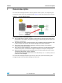
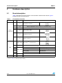
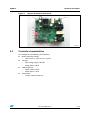
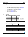
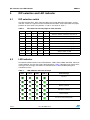
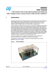
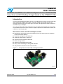
UM0512
User manual
STEVAL-ILL022V1 solar-LED streetlight controller with 25 W LED
lamp driver and 80 W battery charger based on the STM32F101Rx
Introduction
The solar-LED streetlight controller consists of one 80 W battery charger and one 25 W LED
driver. During the daytime, when there is sufficient sunlight, the charger converts the
electricity from the solar panel and charges the battery. At nighttime, the battery powers on
the LED lamp as streetlight.
If it is rainy or cloudy for several continuous days, the battery will gradually run out of power.
The controller then resorts to the AC mains supply to power on the LED until the battery has
had time to fully charge again.
Main features of the solar-LED streetlight controller
■
Maximization of electricity conversion efficiency from solar panel by way of maximum
power point tracker (MPPT)
■
Automatic day/night/weather detection
■
Automatic battery/mains switch over
■
Constant current control for LED lamp
■
Battery charge control
■
Optional LED lighting duration mode
■
Easy system monitoring via debug LED indicators
■
Full protection function for OTP, OCP and UVP
Figure 1.
Snapshot of the solar-LED streetlight controller
!-V
September 2010
Doc ID 14469 Rev 2
1/18
www.st.com
Contents
UM0512
Contents
1
Safety instructions . . . . . . . . . . . . . . . . . . . . . . . . . . . . . . . . . . . . . . . . . . 4
1.1
Intended use . . . . . . . . . . . . . . . . . . . . . . . . . . . . . . . . . . . . . . . . . . . . . . . 4
1.2
Installation . . . . . . . . . . . . . . . . . . . . . . . . . . . . . . . . . . . . . . . . . . . . . . . . . 4
1.3
Electrical connection . . . . . . . . . . . . . . . . . . . . . . . . . . . . . . . . . . . . . . . . . 4
1.4
Board operation . . . . . . . . . . . . . . . . . . . . . . . . . . . . . . . . . . . . . . . . . . . . . 4
2
General description . . . . . . . . . . . . . . . . . . . . . . . . . . . . . . . . . . . . . . . . . . 5
3
Hardware description . . . . . . . . . . . . . . . . . . . . . . . . . . . . . . . . . . . . . . . . 6
4
3.1
Board description . . . . . . . . . . . . . . . . . . . . . . . . . . . . . . . . . . . . . . . . . . . . 6
3.2
Controller characteristics . . . . . . . . . . . . . . . . . . . . . . . . . . . . . . . . . . . . . . 7
Operating instructions . . . . . . . . . . . . . . . . . . . . . . . . . . . . . . . . . . . . . . . 8
4.1
Hardware installation . . . . . . . . . . . . . . . . . . . . . . . . . . . . . . . . . . . . . . . . . 8
4.2
Recommended peripheral parameters . . . . . . . . . . . . . . . . . . . . . . . . . . . . 8
4.3
5
4.2.1
Solar panel . . . . . . . . . . . . . . . . . . . . . . . . . . . . . . . . . . . . . . . . . . . . . . . . 8
4.2.2
Battery . . . . . . . . . . . . . . . . . . . . . . . . . . . . . . . . . . . . . . . . . . . . . . . . . . . 8
4.2.3
LED . . . . . . . . . . . . . . . . . . . . . . . . . . . . . . . . . . . . . . . . . . . . . . . . . . . . . 8
4.2.4
Mains switch . . . . . . . . . . . . . . . . . . . . . . . . . . . . . . . . . . . . . . . . . . . . . . 9
Troubleshooting . . . . . . . . . . . . . . . . . . . . . . . . . . . . . . . . . . . . . . . . . . . . . 9
DIP selection and LED indicator . . . . . . . . . . . . . . . . . . . . . . . . . . . . . . 10
5.1
DIP selection switch . . . . . . . . . . . . . . . . . . . . . . . . . . . . . . . . . . . . . . . . . 10
5.2
LED indicator . . . . . . . . . . . . . . . . . . . . . . . . . . . . . . . . . . . . . . . . . . . . . . 10
6
Schematic and bill of materials . . . . . . . . . . . . . . . . . . . . . . . . . . . . . . . 12
7
Revision history . . . . . . . . . . . . . . . . . . . . . . . . . . . . . . . . . . . . . . . . . . . 17
2/18
Doc ID 14469 Rev 2
UM0512
List of tables
List of tables
Table 1.
Table 2.
Table 3.
Table 4.
Table 5.
Table 6.
Table 7.
Table 8.
Table 9.
Table 10.
Description of functions . . . . . . . . . . . . . . . . . . . . . . . . . . . . . . . . . . . . . . . . . . . . . . . . . . . . 6
Recommended electrical parameters for solar panel . . . . . . . . . . . . . . . . . . . . . . . . . . . . . . 8
Recommended electrical parameters for battery . . . . . . . . . . . . . . . . . . . . . . . . . . . . . . . . . 8
Recommended electrical parameters for LED . . . . . . . . . . . . . . . . . . . . . . . . . . . . . . . . . . . 8
Symptoms and corrective action. . . . . . . . . . . . . . . . . . . . . . . . . . . . . . . . . . . . . . . . . . . . . . 9
DIP switch for LED lamp light-on time selection . . . . . . . . . . . . . . . . . . . . . . . . . . . . . . . . . 10
LED indicator and error message . . . . . . . . . . . . . . . . . . . . . . . . . . . . . . . . . . . . . . . . . . . . 10
BOM . . . . . . . . . . . . . . . . . . . . . . . . . . . . . . . . . . . . . . . . . . . . . . . . . . . . . . . . . . . . . . . . . . 13
Pin strip header. . . . . . . . . . . . . . . . . . . . . . . . . . . . . . . . . . . . . . . . . . . . . . . . . . . . . . . . . . 16
Document revision history . . . . . . . . . . . . . . . . . . . . . . . . . . . . . . . . . . . . . . . . . . . . . . . . . 17
Doc ID 14469 Rev 2
3/18
Safety instructions
1
Safety instructions
Warning:
1.1
UM0512
The demonstration board must be used in a suitable
laboratory by qualified personnel only, familiar with the
installation, use and maintenance of electrical systems.
Intended use
The demonstration board is a component designed for demonstration purposes only, and
shall not be used for domestic or industrial installations. The technical data and information
concerning the power supply and working conditions must be taken from the documentation
provided with the delivery, and must be strictly observed.
1.2
Installation
The installation instructions of the demonstration board must be taken from the present
document and strictly observed. The components must be protected against excessive
strain. In particular, no components are to be bent, or isolating distances altered, during the
transportation, handling or use. The demonstration board contains electro-statically
sensitive components that are prone to damage through improper use. Electrical
components must not be mechanically damaged or destroyed (to avoid potential risks and
health injury).
1.3
Electrical connection
Applicable national accident prevention rules must be followed when working on the mains
power supply. The electrical installation must be completed in accordance with the
appropriate requirements (e.g. cross-sectional areas of conductors, fusing and PE
connections).
1.4
Board operation
A system architecture that supplies power to the demonstration board must be equipped
with additional control and protective devices in accordance with the applicable safety
requirements (e.g. compliance with technical equipment and accident prevention rules).
4/18
Doc ID 14469 Rev 2
UM0512
2
General description
General description
The solar-LED streetlight controller is the key element of the system, also comprising the
solar panel, battery and LED streetlight (lamp). Figure 2 shows the structure of the system.
Figure 2.
System block diagram
!-V
Each block’s function is described below.
●
The sunlight delivers pockets of photons (solar energy) to the solar panel (also called
photovoltaic or PV module). The photons (energy) are absorbed by the PV module and
electrons are released.
●
The electrons flow along the metal contact of the PV module and create electricity. The
battery charger then converts the electrical energy and charges the battery.
●
The battery stores the electricity supplied by the battery charger. The controller
monitors the status of the battery.
●
The LED lamp (LED streetlight) is activated by the LED driver. The LED light controller
monitors the system and controls the light-on and light-off in daytime and nighttime.
●
When the battery goes low, the controller sends an enable signal to the mains switch
and the AC offline power supply is enabled.
The AC offline power supply (not covered in this document) acts as a backup source to
power the LED streetlight.
The solar-LED streetlight controller plays the key role in the system for electricity (solar
energy) storage control and LED lamp light-on/-off control.
Doc ID 14469 Rev 2
5/18
Hardware description
UM0512
3
Hardware description
3.1
Board description
Table 1 describes the various functions of the controller’s demonstration board. Figure 3
provides the top view of the board.
Table 1.
Category
System
connectors
HMI
Description of functions
Index
Designator
1
P1
2
P4
Battery temperature sensor connector (connected to NTC)
3
P5
LED lamp temperature sensor connector (connected to NTC)
7
P6
Mains enable output
10
P3
LED lamp connector
11
P2
Battery connector
4
SW1~SW4
5
LED1~LED4
6
Description
Solar panel connector
DIP switch (1): mode selection
Debug indicators(2)
LED 5 (red)
ON: battery charged
OFF: battery not charged
LED5, LED6
LED 6 (white)
ON: battery full
OFF: battery not full
ICP interface
9
PB1
Reset
8
CN1
JTAG
1. Refer to Table 6 for dip selection mapping.
2. Refer to Table 7 for debug message mapping.
6/18
Doc ID 14469 Rev 2
UM0512
Hardware description
Figure 3.
Top view of demonstration board
!-V
3.2
Controller characteristics
The controller has the following characteristics.
●
Battery operation voltage:
–
●
●
●
13.8 V max./11 V min. for 12 V system
Charger:
–
input voltage range ≤ 50 VDC
–
output power ≤ 80 W
LED lamp driver:
–
output current 2.45 A
–
output power ≤ 25 W
Dimensions:
–
113 mm x 98 mm x 50 mm
Doc ID 14469 Rev 2
7/18
Operating instructions
UM0512
4
Operating instructions
4.1
Hardware installation
The following steps are to install the hardware.
1.
Connect an NTC resistor (battery temperature sensor) to P4 (refer to Section 3.1).
2.
Connect an NTC resistor (LED lamp temperature sensor) to P5 (refer to Section 3.1).
3.
Connect the mains switch controller enable input to P6 (refer to Section 3.1).
4.
Set SW1~SW4 according to DIP selection mapping table (Table 6).
5.
Connect P3 (refer to Section 3.1) to LED lamp.
6.
Connect P2 (refer to Section 3.1) to battery.
7.
Connect P1 (refer to Section 3.1) to solar panel.
4.2
Recommended peripheral parameters
4.2.1
Solar panel
Table 2.
4.2.2
Parameters
Symbol
Typ
Unit
Maximum power
Pmax
80
W
Maximum power voltage
Vpm
17.8
V
Maximum power current
Ipm
4.52
A
Open circuit voltage
Voc
21.82
V
Short circuit current
Isc
5.01
A
Module efficiency
ηm
13.42
%
Irradiance: 1000 W/m2
Module temperature: 25°C
Recommended electrical parameters for battery
Parameters
Typ
Unit
Nominal capacity
50
Ah
Nominal voltage
12
V
LED
Table 4.
8/18
Condition
Battery
Table 3.
4.2.3
Recommended electrical parameters for solar panel
Recommended electrical parameters for LED
Parameters
Typ
Unit
Nominal power
25
W
Nominal current
2.45
A
Doc ID 14469 Rev 2
UM0512
4.2.4
Operating instructions
Mains switch
When the battery is low, a high logic level output is generated by the MCU, which then
enables the mains power.
4.3
Troubleshooting
Table 5.
Symptoms and corrective action
Symptom
None of the LED(s) is
powered on. The
LED(s) include LED
lamp, debug LED and
battery status LED
Corrective action
– Set-up the system as per the hardware installation procedure described in Section 4.1.
– Check the mains enable signal on P6. A high logic level indicates that the battery
voltage is too low to power the LED light. This status will persist until the battery is fully
charged.
– Reset the system by pressing the reset button (PB1).
– Check the battery type and polarity. Only 12 V battery can be applied to this system. If
the battery has previously been connected reversely, replace the fuse (F1) with a new
one.
– Check that the LED lamp is available.
– Set-up the system as per the hardware installation procedure described in Section 4.1.
Battery status LED fails – Reset the system by pressing the reset button (PB1).
to light during daytime – Check that it is not too dark to enable the solar panel’s output.
– Check that the solar panel is available.
Dim LED lamp
– Try to cool down the LED lamp.
– Check that the LED lamp’s lifecycle is still valid.
Doc ID 14469 Rev 2
9/18
DIP selection and LED indicator
UM0512
5
DIP selection and LED indicator
5.1
DIP selection switch
The DIP switches DIP1, DIP2, DIP3 and DIP4 are used to define the LED lamp’s on time
after the "switch on" signal has been received from the MCU. Table 6 describes the jumper
positions of each switch. The positions 'L' and 'H' are shown in Table 1.
Table 6.
5.2
DIP switch for LED lamp light-on time selection
Status
DIP 1
DIP 2
DIP 3
DIP 4
Mode description
1
L
L
L
L
Switch on LED for 5 minutes, then turn-off
2
H
L
L
L
Switch on LED for 2 hours during nighttime
3
L
H
L
L
Switch on LED for 4 hours during nighttime
4
H
H
L
L
Switch on LED for 6 hours during nighttime
5
L
L
H
L
Switch on LED for 8 hours during nighttime
6
H
L
H
L
Switch on LED for 10 hours during nighttime
7
L
H
H
L
Switch on LED for 12 hours during nighttime
8
H
H
H
L
Always switch on LED
9
-
-
-
H
Always switch on LED at nighttime
LED indicator
The demonstration board has four LED indicators, LED1, LED2, LED3 and LED4, which are
used to indicate any error messages during operation. Table 7 describes each type of error
message. The messages are there to assist technicians in their troubleshooting and
maintenance tasks.
Table 7.
LED 1
LED indicator and error message
LED 2
LED 3
LED 4
Error message
No error
Battery charger overheat
Battery overheat
LED driver overheat
LED overheat
Incorrect solar panel polarity
10/18
Doc ID 14469 Rev 2
UM0512
DIP selection and LED indicator
Table 7.
LED 1
LED indicator and error message (continued)
LED 2
LED 3
LED 4
Error message
Battery over-voltage or under-voltage
Battery overcurrent
LED over-voltage
Abnormal LED driving current
Short-circuit in LED driver
Doc ID 14469 Rev 2
11/18
Doc ID 14469 Rev 2
VDD
1
2
3
4
V-_Solar
R24
R122
10K
SW-DIP4
8
7
6
5
R123
10K
1
2
3
4
5
6
7
8
9
10
11
12
13
14
15
16
17
18
19
20
VDD
R124
10K
10K
10K
R62
10K
R61
10K
R60
D19
V S+
D18
C66
C67
C75
22uF
BAT46
BAT46
D21
V S-
D20
C68
DIP1
DIP2
DIP3
DIP4
TDO
TRST
T_LED
26
27
28
55
56
57
58
59
61
62
29
30
33
34
35
36
R42
560
VDR
R102
560
R12
10
BAT46
3
2
PB0
PB1
PB2/BOOT1
PB3/JTDO
PB4/JNTRST
PB5
PB6
PB7
PB8
PB9
PB10
PB11
PB12
PB13
PB14
PB15
1
15V
OUT
GND
R81
10K
R80
82K
GND
BAT46
BAT46
D25
R9
R55
R17
R18
R19
R20
R50
1.2K 1
BOOT0
NRST
OSC_OUT
OSC_IN
PD2
PC15/OSC32_OUT
PC14/OSC32_IN
PC13/TAMPER/RTC
PC12
PC11
PC10
PC9
PC8
PC7
PC6
PC5
PC4
PC3
PC2
PC1
PC0
Q12
MMBT
60
7
6
5
54
4
3
2
53
52
51
40
39
38
37
25
24
11
10
9
8
C76
22uF
R82
10
8MHz
C54
20pF
X1
R66
1M
RESET#
1uF
C15
GND
R23
2
1
C55
20pF
R68
1.8K
330
R74
330
R73
330
R72
330
R71
330
R70
330nF
C69
3
R25 1.8K
D34
IL E D
D33
VDDA
R85
10
3
2
Q3
MMBT
1
1
LD4
1
LD3
1
LD2
1
LD1
1
LD5
1
LD6
C70
330nF
R21
1
2
C9
22uF
R29
10K
R116 1K
R30
33m
R31
10
C23
10
Battery Thermal
330nF
C26
220pF
R33
33m
A
OUT
NC
GND
GND
U11
4
3
2
1
CON_L
1
2
GND
LED Thermal
330nF
C72
T _L E D
100nF
C43
5
6
U7VCC
R40 10
C44
22uF
3.3V
100nF
Bead
C46
100nF
3
2
L5
U7B
LM193D
7
C41
VDD
VDDA
10uF
C47
1
32
48
64
19
13
GND
U7A
LM193D
1
R49 10K
U7VCC
R86
C49
10
C50
VDD
GND
C51
100pF
C64
120
R52
100nF
C42
GND
VBAT
VDD_1
VDD_2
VDD_3
VDD_4
VDDA
VSS_1
VSS_2
VSS_3
VSS_4
VSSA
U10B STM32F101RxT6
31
47
63
18
12
D12
15V
C52
BAT46
Bead
GND
L6
LED_Fault
D37
VDDA
1K
R103
D36
BAT46
1
MMBT
Q6
LED
100nF 100nF 100nF 100nF 100nF
C48
R51
330K
R104
10K
V_LED
1
2
P3
12V
R53
10
LED_P rotection
R48
10K
1
MMBT
Q5
0.1
R47
GND
0.1
4
U9
TSC101AILT
100nF
5
R46
3
2
1
I_LED
C39
100nF
R45 10K
R43 9.1K
GND
R41
10K
3.3V JP1
C32
100pF
4.7K
C35
GND
C33
1uF
220uF
D11
BAT46
C36
12V
C34
22uF
GND
VDDA
R94
10
R93 3.3K
L4931ABD33-TR
5
6
7
8
GND
R39
R38
4.7K
R36
10K
D13
C29
100pF
12K
R37
3.3V
GND
BAT46
1
4
6
7
2
1
L78L12ABD-TR
IN
NC
GND
GND
U6
R35
24
C30
220uF
220pF
C28
R117
10K
U5A
LM258D
GND
4
U5B
LM258D
100pF
C27
R34 1K
U5VCC
8
5
2
3
10
8
C25
220pF
33uH
T1
T _B attery
P5
C71
VDDA
R92
10
R91 3.3K
100nF
3
2
GND
C79
330nF
R101
R114 10K
R113 10K
3
1
D10
STPS20H100CFP
GND
C24
100nF
R115
20K U5VCC8
12V
C80
22uF
12V
C22
22uF
Vba
GND
1
STPS1H100A
D8
D9
330
Q4
STP75NF75FP
1
2
1
C14 100nF
3.9V
D7
R54
33m
Q8
BC807
R28 10
CON_B
P4
D5
C8
1uF
GND
C20
1uF
R10
10
LED Driver Thermal
R88
10K NTC
T _D ri ver
VDDA
R90 10
R89 3.3K
100nF
3
2
2
Blue
2
Blue
2
Blue
2
Blue
2
Red
2
Green
1
Q7
MMBT
1
12V
TYN616RG
Q10
SMAJ24A-TR
2
D3 15V
0.2
C19
220uF
R8
330nF
BAT46
BAT46
GND
VDD
RESET
C56
4
1
B1
T _C harger
Charger Thermal
R32
10K NTC
R87 10
GND
OUT
R121
10K C63
I_LED
BC807
R106 330
VDDA
10K
R44 3.3K
R69
GND
VDDA
CON_B
BAT46
BAT46
D31
POS
VCC
NEG
Q9
2
C17
560pF
VLED
D30
3
5
4
R14
1.2K
GND
C18
220uF
Vba
U2 TS391ILT
R11
10K
Battery
LED_P rotection
1uF
R56
VDDA
R57
3.3K
R84
10K
GND
100nF
C62
V_LED
D35
BAT46
3
P2
C7
47K
R98 1K
R83
39K
VDD
10
D14
STPS2045CFP
1
D32
BAT46
P6
F1
10A 125V
Vba
V_Battery
PWM_Driver
12V
0.1
0.1
0.1
0.1
0.1
0.1
R67 10K
Mains_Enable
BAT_FULL
BAT_LED
DEBUG_LED1
DEBUG_LED2
DEBUG_LED3
DEBUG_LED4
T_Battery
VSLED_Fault
T_Driver
VLED
ILED
GND
330nF
BAT46
BAT46
GND
D27
IB
D26
VDDA
100nF
R120
10K C61
I_Battery
2
C77 VDR
GND
1uF
C74
R22
10
12V
C13
D4
5
4
GND
470uF
VB
D24
39uH
L2
U3
TSC101AILT
3
Q14
BC807
3
VDDA
Gnd Vp
Vm
STPS20H100CFP
U8
TS391ILT
1
GND
GND
STM32F101RxT6
GND
100nF
C60
V_Battery
R118
10K
POS
VCC
NEG
Out
Vcc
T2
DRIVER TRANS
R97 10K
C45
1uF
1
2
220pF
220pF
C11 1
C10
D16
STPS1L60A
100nF
C12
R15 10
R13 10K
D2
C3
100nF
PA0-WKUP
PA1
PA2
PA3
PA4
PA5
PA6
PA7
PA8
PA9
PA10
PA11
PA12
PA13/JTMS/SWDIO
PA14/JTCK/SWCLK
PA15/JTDI
U10A
330nF
BAT46
BAT46
GND
D23
IS
D22
VDDA
R79
10
D17
R100 1K
12V
I_Battery
R96 47K
3
BAT46
5
PWM_Charger
4
10
R26
D1
2
GND
R112
10K
U1A
LM258D
Q2
STP75NF75FP
1
R119
10K C59
I_Solar
VDD
12V
470uF
C5
PWM_Driver 14
IB
15
16
VB
PWM_Charger17
T_Charger
20
21
VS+
IS
22
PWM_Input 23
41
42
43
44
45
TMS
46
TCK
49
TDI
50
R78
10K
R77
82K
VDDA
C6
1uF
A
8
4
5
1
3
R111
10K
Gate_Input
GND
GND
100nF
C58
V-_Solar
2
MMBT
Q11
1uF
C73
GND
C4
470uF
C83
100pF
100nF 100nF 100nF 100nF
C65
BAT46
BAT46
10K
R59
10K
R65
Q13
BC807
3
U4
TS391ILT
1
R16 10
C1
1uF
R109
20K
R27
1.2K 1
12V
1K
R108
GND
4
GND
VDDA
10K
R76
10K
R75
150K
GND
R63
GND
OUT
GND
POS
VCC
R125
10K
0.1
0.1
0.1
0.1
R95 10K
NEG
R64
DBGACK
DBGRQ
RESET#
TDO
RTCK
TCK
TMS
TDI
TRST
100nF
C57
V+_Solar
BAT46
R105
10K
R4
R3
R1
R2
R107
1K
C38
1uF
8
10K
1uF
C53
VDDA
Board schematic
JTAG
CN1
D28
100nF
R58 47K
3
5
4
R99 1K
D29
BAT46
PWM_Input
10
R6
10K
Gate_Input
R5
10
Q1
STP40NF10 1
12V
S1
VDDA
1
2
Solar Cells
P1
V+_Solar
C2
7
B
5
GND
2
3
1
2
2
3
U1VCC
6
3
6
2
3
2
8
2
U1B
LM258D
1
1
2
4
3
3
2
1
2
2
1
1
2
2
1
2
R110
1
SMAJ24A-TR
I_Solar
1
3
2
2
3
2
3
1
3
Out
Vp Gnd
U1VCC
6
8
4
Vcc
Vm
R7
5
B
7
8
4
3
10
Figure 4.
Inhibit Gnd Gnd Vin
Schematic and bill of materials
Vo
6
NC Gnd Gnd
8
4
3
2
12/18
2
12V
Schematic and bill of materials
UM0512
AM03453v1
UM0512
Table 8.
Schematic and bill of materials
BOM
Reference
Value / generic part number
Package /class
B1
One way 6x6 mm
(SMD), 4.3 mm(H), tactile switch
C1, C6
1 µF
(1210), 100 V, ceramic capacitor
C2, C3, C12, C14, C24, C36, C39,
C41, C42, C43, C46, C48, C49,
C50, C51, C52, C56, C57, C58,
C60, C62, C65, C66, C67, C68,
C77, C79
100 nF
(0603), 50 V, ceramic capacitor
C4, C5, C13
470 µF
63 V, Al-cap electrolytic capacitor
C7, C8, C35, C38, C45, C53, C73,
C74
1 µF
(0805), 25 V, ceramic capacitor
C9, C22, C34, C44, C75, C76, C80
22 µF
50 V, Al-cap electrolytic capacitor
C10, C11, C25, C26
220 pF
(0805), 50 V, ceramic capacitor
C15, C20
1 µF
(1206), 50 V, ceramic capacitor
C17
560 pF
(0603), 50 V, ceramic capacitor
C18, C19, C30, C33
220 µF
50 V, Al-cap electrolytic capacitor
C23, C59, C61, C63, C69, C70,
C71, C72
330 nF
(0805), 50 V, ceramic capacitor
C27, C29, C32, C64, C83
100 pF
(0603), 50 V, ceramic capacitor
C28
220 pF
(0603), 250 V, ceramic capacitor
C47
10 µF
(3528-21), 16 V, tantalum
C54, C55
20 pF
(0603), 50 V, ceramic capacitor
CN1
20-way Box header
(Right angle mounting), JTAG connector
D1, D11, D13, D17, D18, D19, D20,
D21, D22, D23, D24, D25, D26,
D27, D28, D29, D30, D31, D32,
D33, D34, D35, D36, D37
BAT46JFILM
(SOD323), small signal Schottky diode
D2, D3, D12
15 V
(SOD 80C), Zener diode
D4, D10
STPS20H100CFP
(TO-220FPAB), power Schottky rectifier
D5, D9
SMAJ24A-TR
(SMA or DO-214AC), 24 V 400 W
TransilTM (TVS)
D7
3.9 V
(SOD 80C), Zener diode
D8
STPS1H100A
(SMA or DO-214AC), power Schottky
rectifier
D14
STPS2045CFP
(TO-220FPAB), power Schottky rectifier
D16
STPS1L60A
(SMA or DO-214AC), power Schottky
rectifier
F1
10 A
(2.54 x 7.2 mm, axial lead), 251 series
fuse
JP1 (see Table 9)
0.64x0.64 mm, 2 way
2.54 mm pitch, pin strip header
Doc ID 14469 Rev 2
13/18
Schematic and bill of materials
Table 8.
UM0512
BOM (continued)
Reference
Value / generic part number
Package /class
L2 (see Table 9)
39 µH
Inductor
L5, L6
600 Ω @ 100 MHz
(0603), Chip ferrite bead, 25%, 200mA
max.
LD1, LD2, LD3, LD4
80 mcd, yellow
(0603), LED
LD5
45 mcd, red
(3.0, diffused, radio lead), LED
LD6
10 mcd, green
(3.0, undiffused, radio lead), LED
P1, P2, P3
Terminal block
2 Terminal, pitch 7.5mm
P4, P5, P6
Header, 2 pin
HDR1x2, pitch 2.54mm
Q1
STP40NF10
(TO-220), N-channel MOSFET
Q2, Q4
STP75NF75FP
(TO-220FP), N-channel MOSFET
Q3, Q5, Q6, Q7, Q11, Q12
MMBTA42
(SOT-23), NPN bipolar transistor
Q8, Q9, Q13, Q14
BC807
(SOT-23), PNP bipolar transistor
Q10
TYN616RG
(TO-220AB), Triac
R1, R2, R3, R4, R9, R17, R18,
R19, R20, R46, R47, R55
0.1 Ω
(1206), 1%, resistor
R5, R7, R10, R12, R15, R16, R22,
R23, R24, R26, R28, R31, R40,
R53, R101
10 Ω
(0805), 1%, resistor
R6, R13, R29
10 kΩ
(0805), 5%, resistor
R8
0.2 Ω
(Axial lead), cement, 2W, resistor
R11, R45, R48, R49, R59, R60,
R61, R62, R63, R64, R65, R67,
R69, R95, R97, R104, R105, R110,
R111, R112, R113, R114, R117,
R118, R119, R120, R121, R122,
R123, R124, R125
10 kΩ
(0603), 5%, resistor
R14, R27, R50
1.2 kΩ
(0805), 5%, resistor
R21, R70, R71, R72, R73, R74,
R106
330 Ω
(0603), 5%, resistor
R25
1.8 kΩ
(0603), 5%, resistor
R30, R33, R54
33 mΩ
(1210), 1%, resistor
R32, R88
NTC, 10 kΩ
(0805), NTC resistor
R34, R107, R108, R116
1 kΩ
(0603), 1%, resistor
R35
24 Ω
(1206), 5%, resistor
R36, R41
10 kΩ
(0603), 1%, resistor
R37
12 kΩ
(0603), 1%, resistor
R38, R39
4.7 kΩ
(0603), 5%, resistor
R102
560 Ω
(1206), 5%, resistor
14/18
Doc ID 14469 Rev 2
UM0512
Table 8.
Schematic and bill of materials
BOM (continued)
Reference
Value / generic part number
Package /class
R43
9.1 kΩ
(0603), 1%, resistor
R44, R89, R91, R93
3.3 kΩ
(0603), 1%, resistor
R51
330 kΩ
(0603), 5%, resistor
R52
120 Ω
(0603), 5%, resistor
R56, R58, R96
47 kΩ
(0603), 5%, resistor
R57
3.3 kΩ
(0603), 5%, resistor
R66
1 MΩ
(0603), 1%, resistor
R68
1.8 kΩ
(0603), 1%, resistor
R75
150 kΩ
(0805), 1%, resistor
R76, R78, R81, R84
10 kΩ
(0805), 1%, resistor
R77, R80
82 kΩ
(0805), 1%, resistor
R79, R82, R85, R86, R87, R90,
R92, R94
10 Ω
(0603), 5%, resistor
R83
39 kΩ
(0805), 1%, resistor
R98, R99, R100, R103
1 kΩ
(0603), 5%, resistor
R109, R115
20 kΩ
(0603), 1%, resistor
S1
DIP switch
4 Position DIP Switch
T1 (see Table 9)
33 µH
EER25.5, transformer
T2 (see Table 9)
1 mH
Driver transformer
U1, U5
LM258D
(SO8 narrow), dual operational
amplifiers
U2, U4, U8
TS391ILT
(SO), single voltage comparator
U3, U9
TSC101AILT
(SO), current sense IC
U6
L78L12ABD-TR
(SO8 narrow), positive voltage regulator
U7
LM193D
(SO8), dual voltage comparator
U10
STM32F101RXT6
(LQFP64), 32-bit microprocessor
U11
L4931ABD33-TR
(SO8 narrow), linear regulator
X1
8 MHz
(3 x 8), crystal oscillator
Reference
Value / generic part number
Package /class
Note:
STM32F101R4, STM32F101R6, STM32F101R8, STM32F101RB, STM32F101RC
STM32F101RD and STM32F101RE are all equivalent for the purpose.
\
Doc ID 14469 Rev 2
15/18
Schematic and bill of materials
Table 9.
UM0512
Pin strip header
Figure
Accessory for JP1
Description
M20 series jumper socket
L2
– 1:
– 2:
– 3:
– 4:
– 5:
– 6:
39 µH +/- 4% (W1//W2 and twisted)
Winding 1: pin 1 to pin 5 (18 turns CCW)
Winding 2: pin 2 to pin 4 (18 turns CCW)
Wire gage: AWG31*20
Core: EER28-Z-PC40
Bobbin: BEER28-1110CPFR
T1
– 1:
– 2:
– 2:
– 3:
– 4:
– 4:
– 5:
– 6:
33 µH +/- 4% (W1+W3 at 50 kHz, 1 Vrms)
Leakage < 0.1 µH (W2 short-circuit)
Winding 1: pin 1 to pin 5 (5 turns CCW)
Winding 2: pin 8 to pin 10 (10 turns CCW)
Winding 3: pin 5 to pin 3 (5 turns CCW)
Wire gage: AWG31*20
Core: EER28-Z-PC40
Bobbin: BEER28-1110CPFR
T2
–
–
–
–
–
–
–
–
–
16/18
1:
2:
3:
2:
3:
4:
4:
5:
6:
1 mH (W1+W3 at 50 kHz, 1 Vrms)
Leakage < 10 µH (W2 short-circuit)
No air-gap is required
Winding 1: pin 1 to pin 2 (17 turns CCW)
Winding 2: pin 8 to pin 6 (34 turns CCW)
Winding 3: pin 2 to pin 3 (17 turns CCW)
Wire gage: AWG31
Core: EE10/11-Z-PC40
Bobbin: BE10-118CPSFR
Doc ID 14469 Rev 2
UM0512
7
Revision history
Revision history
Table 10.
Document revision history
Date
Revision
08-Jan-2010
1
Initial release
2
– Changed: connectors
1: P1: solar panel connector
2: P2: battery connector
3: P3: LED lamp connector
4: SW1~SW4: mode selection DIP switch
– Battery use only 12VDC type
– Figure 1 changed due to the connectors outline changed
– Re-new the connectors' location in Figure 3 which is based on the
description in Table 1
– Figure 4, the schematic is updated
– Table 8, the BOM is updated
28-Sep-2010
Changes
Doc ID 14469 Rev 2
17/18
UM0512
Please Read Carefully:
Information in this document is provided solely in connection with ST products. STMicroelectronics NV and its subsidiaries (“ST”) reserve the
right to make changes, corrections, modifications or improvements, to this document, and the products and services described herein at any
time, without notice.
All ST products are sold pursuant to ST’s terms and conditions of sale.
Purchasers are solely responsible for the choice, selection and use of the ST products and services described herein, and ST assumes no
liability whatsoever relating to the choice, selection or use of the ST products and services described herein.
No license, express or implied, by estoppel or otherwise, to any intellectual property rights is granted under this document. If any part of this
document refers to any third party products or services it shall not be deemed a license grant by ST for the use of such third party products
or services, or any intellectual property contained therein or considered as a warranty covering the use in any manner whatsoever of such
third party products or services or any intellectual property contained therein.
UNLESS OTHERWISE SET FORTH IN ST’S TERMS AND CONDITIONS OF SALE ST DISCLAIMS ANY EXPRESS OR IMPLIED
WARRANTY WITH RESPECT TO THE USE AND/OR SALE OF ST PRODUCTS INCLUDING WITHOUT LIMITATION IMPLIED
WARRANTIES OF MERCHANTABILITY, FITNESS FOR A PARTICULAR PURPOSE (AND THEIR EQUIVALENTS UNDER THE LAWS
OF ANY JURISDICTION), OR INFRINGEMENT OF ANY PATENT, COPYRIGHT OR OTHER INTELLECTUAL PROPERTY RIGHT.
UNLESS EXPRESSLY APPROVED IN WRITING BY AN AUTHORIZED ST REPRESENTATIVE, ST PRODUCTS ARE NOT
RECOMMENDED, AUTHORIZED OR WARRANTED FOR USE IN MILITARY, AIR CRAFT, SPACE, LIFE SAVING, OR LIFE SUSTAINING
APPLICATIONS, NOR IN PRODUCTS OR SYSTEMS WHERE FAILURE OR MALFUNCTION MAY RESULT IN PERSONAL INJURY,
DEATH, OR SEVERE PROPERTY OR ENVIRONMENTAL DAMAGE. ST PRODUCTS WHICH ARE NOT SPECIFIED AS "AUTOMOTIVE
GRADE" MAY ONLY BE USED IN AUTOMOTIVE APPLICATIONS AT USER’S OWN RISK.
Resale of ST products with provisions different from the statements and/or technical features set forth in this document shall immediately void
any warranty granted by ST for the ST product or service described herein and shall not create or extend in any manner whatsoever, any
liability of ST.
ST and the ST logo are trademarks or registered trademarks of ST in various countries.
Information in this document supersedes and replaces all information previously supplied.
The ST logo is a registered trademark of STMicroelectronics. All other names are the property of their respective owners.
© 2010 STMicroelectronics - All rights reserved
STMicroelectronics group of companies
Australia - Belgium - Brazil - Canada - China - Czech Republic - Finland - France - Germany - Hong Kong - India - Israel - Italy - Japan Malaysia - Malta - Morocco - Philippines - Singapore - Spain - Sweden - Switzerland - United Kingdom - United States of America
www.st.com
18/18
Doc ID 14469 Rev 2