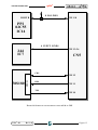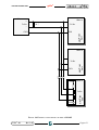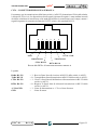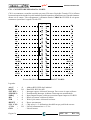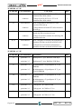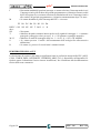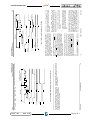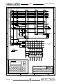
1
®
GPC 183
General Purpose Controller Z8S180
MANUALE TECNICO
Via dell' Artigiano, 8/6
® 40016 San Giorgio di Piano
grifo
(Bologna) ITALY
E-mail: [email protected]
http://www.grifo.it
http://www.grifo.com
Tel. +39 051 892.052 (r.a.) FAX: +39 051 893.661
GPC® 183
Edizione 3.10
Rel. 12 Giugno 2000
®
®
, GPC , grifo , sono marchi registrati della ditta grifo®
ITALIAN TECHNOLOGY
®
GPC 183
General Purpose Controller Z8S180
MANUALE TECNICO
Modulo Intelligente della serie Abaco® BLOCK, nel formato
100x149. Contenitore, opzionale, per guide ad Ω tipo DIN
46277-1 e DIN 46277-3. CPU Z8S180, fornito di base a 22 MHz.
Fino a 512K di EPROM o FLASH e fino a 512K di SRAM.
Tramite FGDOS la memoria eccedente i 64K é gestita come
RAM/ROM disk. E' possibile cancellare e riprogrammare
autonomamente la FLASH di bordo con il programma utente.
Circuiteria di back up per SRAM e RTC, tramite batteria al
LITIO interna ed esterna. Real Time Clock autonomo, con
possibilità di generare INT. EEPROM seriale, fino ad 8K Bytes.
11 linee di A/D converter da 12 Bits, +2,5V fondo scala, oppure
0÷20 mA. 28 linee TTL di I/O, settabili da software, 2 LED di
stato e BUZZER attivo. Interfaccia Clocked Serial I/O a
disposizione utente, su connettore di I/O. 1 Dip Switch da 3 vie,
leggibile da software e Dip per RUN/DEBUG mode. 2 Canali di
Programmable Reload Timer interni da 16 bits. 2 linee seriali in
RS232, di cui una settabile in RS422, RS485 o Current Loop.
Doppio Baud Rate generator, settabile da software, fino a
115,2K Baud. Circuiteria di Watch Dog, disinseribile da hardware,
con LED di segnalazione. Connettore di espansione per Abaco®
I/O BUS da 26 vie. 2 connettori standard di I/O Abaco®, da 20
vie. 1 connettore standard di A/D Abaco®, da 20 vie. Funzioni di
basso consumo come Halt, Iostop, Sleep, System Stop, Idle,
Standby mode. Alimentatore opzionale ad ampio range, oppure
singola alimentazione esterna a 5 Vdc, 235 mA. Protezione della
logica di bordo dai transienti tramite TransZorb™. Vasta
disponibilità di software di sviluppo quali Remote Symbolic
Debugger, Macro Assembler, GET 80, FORTH, Compilatori C,
HTC 80, Basic NSB8, Lisp, PASCAL 80, ecc.
Via dell' Artigiano, 8/6
® 40016 San Giorgio di Piano
grifo
(Bologna) ITALY
E-mail: [email protected]
http://www.grifo.it
http://www.grifo.com
Tel. +39 051 892.052 (r.a.) FAX: +39 051 893.661
GPC® 183
Edizione 3.10
Rel. 12 Giugno 2000
®
®
, GPC , grifo , sono marchi registrati della ditta grifo®
ITALIAN TECHNOLOGY
Vincoli sulla documentazione
grifo® Tutti i Diritti Riservati
Nessuna parte del presente manuale può essere riprodotta, trasmessa, trascritta, memorizzata in un archivio o tradotta in altre lingue, con qualunque forma o mezzo, sia esso
elettronico, meccanico, magnetico ottico, chimico, manuale, senza il permesso scritto
della grifo®.
IMPORTANTE
Tutte le informazioni contenute sul presente manuale sono state accuratamente verificate, ciononostante grifo® non si assume nessuna responsabilità per danni, diretti o
indiretti, a cose e/o persone derivanti da errori, omissioni o dall'uso del presente manuale,
del software o dell' hardware ad esso associato.
grifo® altresi si riserva il diritto di modificare il contenuto e la veste di questo manuale
senza alcun preavviso, con l' intento di offrire un prodotto sempre migliore, senza che
questo rappresenti un obbligo per grifo®.
Per le informazioni specifiche dei componenti utilizzati sui nostri prodotti, l'utente deve
fare riferimento agli specifici Data Book delle case costruttrici o delle seconde sorgenti.
LEGENDA SIMBOLI
Nel presente manuale possono comparire i seguenti simboli:
Attenzione: Pericolo generico
Attenzione: Pericolo di alta tensione
Marchi Registrati
, GPC®, grifo® : sono marchi registrati della grifo®.
Altre marche o nomi di prodotti sono marchi registrati dei rispettivi proprietari.
ITALIAN TECHNOLOGY
grifo®
INDICE GENERALE
INTRODUZIONE......................................................................................................................... 1
VERSIONE SCHEDA .................................................................................................................. 1
CARATTERISTICHE GENERALI ........................................................................................... 2
PROCESSORE DI BORDO ..................................................................................................... 3
BUZZER ..................................................................................................................................... 3
CLOCK ...................................................................................................................................... 3
MEMORIE ................................................................................................................................. 4
COMUNICAZIONE SERIALE ............................................................................................... 4
ALIMENTAZIONE DI BORDO .............................................................................................. 4
ABACO® I/O BUS ...................................................................................................................... 6
LINEE DI I/O DIGITALI ......................................................................................................... 6
REAL TIME CLOCK ............................................................................................................... 6
WATCH DOG ............................................................................................................................ 6
TASTO DI RESET ..................................................................................................................... 7
A/D CONVERTER .................................................................................................................... 7
CONFIGURAZIONE SCHEDA .............................................................................................. 7
LOGICA DI CONTROLLO ..................................................................................................... 7
SPECIFICHE TECNICHE ......................................................................................................... 9
CARATTERISTICHE GENERALI ........................................................................................ 9
CARATTERISTICHE FISICHE ............................................................................................. 9
CARATTERISTICHE ELETTRICHE ................................................................................. 10
INSTALLAZIONE ..................................................................................................................... 11
CONNESSIONI CON IL MONDO ESTERNO ................................................................... 11
CN2 - CONNETTORE ALIMENTAZIONE CON SEZIONE ALIMENTATRICE ...... 11
CN3 - CONNETTORE PER I/O DEL PPI ........................................................................ 12
CN4 - CONNETTORE PER BATTERIA ESTERNA DI BACK UP .............................. 13
CN5 - CONNETTORE PER I/O DIGITALI E SERIALE SINCRONA ......................... 14
CN6 - CONNETTORE PER INGRESSI A/D CONVERTER.......................................... 16
CN7B - CONNETTORE PER LINEA SERIALE B ......................................................... 18
CN7A - CONNETTORE PER LINEA SERIALE A ......................................................... 23
CN1 - CONNETTORE PER ABACO® I/O BUS................................................................ 24
INTERFACCIE PER I/O DIGITALI .................................................................................... 26
INTERFACCIAMENTO DEGLI I/O CON IL CAMPO ..................................................... 26
SELEZIONE TIPO INGRESSI ANALOGICI ..................................................................... 27
TASTO DI RESET .................................................................................................................. 27
TRIMMERS E TARATURE ................................................................................................... 27
SEGNALAZIONI VISIVE...................................................................................................... 28
JUMPERS ................................................................................................................................ 29
JUMPERS A 5 VIE ............................................................................................................... 29
JUMPERS A 2 VIE ............................................................................................................... 30
JUMPERS A 3 VIE ............................................................................................................... 30
GPC® 183
Rel. 3.10
Pagina I
grifo®
ITALIAN TECHNOLOGY
NOTE ........................................................................................................................................ 32
BACK UP .............................................................................................................................. 32
SELEZIONE MEMORIE .................................................................................................... 32
INTERRUPTS....................................................................................................................... 33
INPUT DI BORDO ............................................................................................................... 33
ALIMENTAZIONE .............................................................................................................. 34
COMUNICAZIONE SERIALE .......................................................................................... 35
RESET E WATCH DOG ..................................................................................................... 36
DESCRIZIONE SOFTWARE ................................................................................................... 37
MAPPAGGI ED INDIRIZZAMENTI ...................................................................................... 40
INTRODUZIONE.................................................................................................................... 40
MAPPAGGIO DELLE RISORSE DI BORDO .................................................................... 40
MAPPAGGIO I/O .................................................................................................................... 41
MAPPAGGIO ABACO® I/O BUS .......................................................................................... 43
MAPPAGGIO MEMORIE ..................................................................................................... 43
DESCRIZIONE SOFTWARE DELLE PERIFERICHE DI BORDO .................................. 45
BUZZER ................................................................................................................................... 45
LED DI ATTIVITÀ ................................................................................................................. 45
WATCH DOG .......................................................................................................................... 45
LED DI SPOT .......................................................................................................................... 46
DIP SWITCH DSW1 E RUN DEBUG .................................................................................. 46
EEPROM SERIALE ............................................................................................................... 46
A/D CONVERTER .................................................................................................................. 47
4 LINEE DI INPUT DIGITALE ............................................................................................ 47
HANDSHAKE SERIALE A ................................................................................................... 47
PPI 82C55 ................................................................................................................................. 48
REAL TIME CLOCK ............................................................................................................. 48
PERIFERICHE DELLA CPU ............................................................................................... 50
SCHEDE ESTERNE .................................................................................................................. 51
BIBLIOGRAFIA ........................................................................................................................ 54
APPENDICE A: DISPOSIZIONE JUMPERS E DRIVER .................................................. A-1
APPENDICE B: DESCRIZIONE COMPONENTI DI BORDO ......................................... B-1
APPENDICE C: SCHEMI ELETTRICI ............................................................................... C-1
APPENDICE D: INDICE ANALITICO ................................................................................ D-1
Pagina II
GPC® 183
Rel. 3.10
ITALIAN TECHNOLOGY
grifo®
INDICE DELLE FIGURE
FIGURA 1: SCHEMA A BLOCCHI ......................................................................................................... 5
FIGURA 2: FOTO SCHEDA .................................................................................................................. 8
FIGURA 3: CN2 - CONNETTORE ALIMENTAZIONE CON SEZIONE ALIMENTATRICE ............................... 11
FIGURA 4: CN3 - CONNETTORE PER I/O DEL PPI .......................................................................... 12
FIGURA 5: SCHEMA DI COLLEGAMENTO LINEE DI I/O SU CN3......................................................... 13
FIGURA 6: CN4 - CONNETTORE PER BATTERIA ESTERNA DI BACK UP ............................................... 13
FIGURA 7: CN5 - CONNETTORE PER I/O DIGITALE E SERIALE SINCRONA ......................................... 14
FIGURA 8: SCHEMA DI COLLEGAMENTO LINEE DI I/O SU CN5......................................................... 15
FIGURA 9: CN5 - CONNETTORE PER INGRESSI A/D CONVERTER ...................................................... 16
FIGURA 10: SCHEMA D’INGRESSO A/D CONVERTER ......................................................................... 17
FIGURA 11: CN7B - CONNETTORE PER LINEA SERIALE B ............................................................... 18
FIGURA 12: SCHEMA DI COMUNICAZIONE SERIALE ........................................................................... 19
FIGURA 13: ESEMPIO COLLEGAMENTO PUNTO PUNTO IN RS 232 ..................................................... 20
FIGURA 14: ESEMIPO COLLEGAMENTO PUNTO PUNTO IN RS 422 ..................................................... 20
FIGURA 15: ESEMPIO COLLEGAMENTO PUNTO PUNTO IN RS 485 ..................................................... 20
FIGURA 16: ESEMPIO COLLEGAMENTO IN RETE IN RS 485 .............................................................. 21
FIGURA 17: ESEMPIO COLLEGAMENTO PUNTO PUNTO IN CURRENT LOOP A 4 FILI .............................. 22
FIGURA 18: ESEMPIO COLLEGAMENTO PUNTO PUNTO IN CURRENT LOOP A 2 FILI .............................. 22
FIGURA 19: CN7A - CONNETTORE PER LINEA SERIALE A ............................................................... 23
FIGURA 20: CN1 - CONNETTORE PER ABACO® I/O BUS ............................................................ 24
FIGURA 21: DISPOSIZIONE LEDS, CONNETTORI, DIP SWITCH, ECC. .................................................. 25
FIGURA 22: TABELLA DELLE SEGNALAZIONI VISIVE ......................................................................... 28
FIGURA 23: TABELLA RIASSUNTIVA JUMPERS ................................................................................... 29
FIGURA 24: TABELLA JUMPERS A 5 VIE ........................................................................................... 29
FIGURA 25: TABELLA JUMPERS A 2 VIE ........................................................................................... 30
FIGURA 26: TABELLA JUMPERS A 3 VIE ........................................................................................... 30
FIGURA 27: DISPOSIZIONE JUMPERS ................................................................................................ 31
FIGURA 28: TABELLA DI SELEZIONE MEMORIE ................................................................................ 32
FIGURA 29: PIANTA COMPONENTI ................................................................................................... 33
FIGURA 30: TABELLA INDIRIZZAMENTO I/O - PARTE 1 ................................................................... 41
FIGURA 31: TABELLA INDIRIZZAMENTO I/O - PARTE 2 ................................................................... 42
FIGURA 32: MAPPAGGIO DELLE MEMORIE ....................................................................................... 44
FIGURA 33: SCHEMA DELLE POSSIBILI CONNESSIONI ........................................................................ 53
FIGURA A1: DISPOSIZIONE JUMPERS PER MEMORIE ....................................................................... A-1
FIGURA A2: DISPOSIZIONE JUMPERS PER COMUNICAZIONE SERIALE ............................................... A-2
FIGURA A3: DISPOSIZIONE DRIVER PER COMUNICAZIONE SERIALE ................................................. A-3
FIGURA C1: SCHEMA ELETTRICO DI ESPANSIONE PPI .................................................................... C-1
FIGURA C2: SCHEMA ELETTRICO SPA 03 ..................................................................................... C-2
FIGURA C3: SCHEMA ELETTRICO QTP 16P ................................................................................. C-3
FIGURA C4: SCHEMA ELETTRICO QTP 24P 1/2............................................................................ C-4
FIGURA C5: SCHEMA ELETTRICO QTP 24P 2/2............................................................................ C-5
FIGURA C6: SCHEMA ELETTRICO DI I/O SU ABACO® I/O BUS .................................................. C-6
FIGURA C7: SCHEMA ELETTRICO INTERFACCIA BUS ..................................................................... C-7
FIGURA C8: SCHEMA ELETTRICO IAC 01..................................................................................... C-8
GPC® 183
Rel. 3.10
Pagina III
grifo®
Pagina IV
ITALIAN TECHNOLOGY
GPC® 183
Rel. 3.10
ITALIAN TECHNOLOGY
grifo®
INTRODUZIONE
L’uso di questi dispositivi é rivolto - IN VIA ESCLUSIVA - a personale specializzato.
Scopo di questo manuale é la trasmissione delle informazioni necessarie all’uso competente e sicuro
dei prodotti. Esse sono il frutto di un’elaborazione continua e sistematica di dati e prove tecniche
registrate e validate dal Costruttore, in attuazione alle procedure interne di sicurezza e qualità
dell'informazione.
I dati di seguito riportati sono destinati - IN VIA ESCLUSIVA - ad un utenza specializzata, in grado
di interagire con i prodotti in condizioni di sicurezza per le persone, per la macchina e per l’ambiente,
interpretando un’elementare diagnostica dei guasti e delle condizioni di funzionamento anomale e
compiendo semplici operazioni di verifica funzionale, nel pieno rispetto delle norme di sicurezza e
salute vigenti.
Le informazioni riguardanti installazione, montaggio, smontaggio, manutenzione, aggiustaggio,
riparazione ed installazione di eventuali accessori, dispositivi ed attrezzature, sono destinate - e
quindi eseguibili - sempre ed in via esclusiva da personale specializzato avvertito ed istruito, o
direttamente dall’ASSISTENZA TECNICA AUTORIZZATA, nel pieno rispetto delle
raccomandazioni trasmesse dal costruttore e delle norme di sicurezza e salute vigenti.
I dispositivi non possono essere utilizzati all'aperto. Si deve sempre provvedere ad inserire i moduli
all'interno di un contenitore a norme di sicurezza che rispetti le vigenti normative. La protezione di
questo contenitore non si deve limitare ai soli agenti atmosferici, bensì anche a quelli meccanici,
elettrici, magnetici, ecc.
Per un corretto rapporto coi prodotti, é necessario garantire leggibilità e conservazione del manuale,
anche per futuri riferimenti. In caso di deterioramento o più semplicemente per ragioni di
approfondimento tecnico ed operativo, consultare direttamente l’Assistenza Tecnica autorizzata.
Al fine di non incontrare problemi nell’uso di tali dispositivi, é conveniente che l’utente - PRIMA
DI COMINCIARE AD OPERARE - legga con attenzione tutte le informazioni contenute in questo
manuale. In una seconda fase, per rintracciare più facilmente le informazioni necessarie, si può fare
riferimento all’indice generale e all’indice analitico, posti rispettivamente all’inizio ed alla fine del
manuale.
VERSIONE SCHEDA
Il presente manuale è riferito alla scheda GPC® 183 versione 300396 e successive. La validità delle
informazioni riportate è quindi subordinata al numero di versione della scheda in uso e l’utente deve
quindi sempre verificare la giusta corrispondenza tra le due indicazioni. Sulla scheda il numero di
versione è riportato in più punti sia a livello di serigrafia che di stampato (ad esempio sopra la batteria
BT1 nel lato componenti).
GPC® 183
Rel. 3.10
Pagina 1
grifo®
ITALIAN TECHNOLOGY
CARATTERISTICHE GENERALI
La scheda GPC® 183 é un potente modulo di controllo, della fascia Low-Cost, in grado di funzionare
autonomamente come periferica intelligente e/o remotata in una più vasta rete di telecontrollo e/o di
acquisizione.
La GPC® 183 é fornita di un supporto in plastica provvisto degli attacchi per le guide ad Omega tipo
DIN 46277-1 e DIN 46277-3. In questo modo non é necessario l’uso di un rack, perché la scheda può
essere montata, in modo più economico, direttamente nel quadro elettrico.
La programmazione e l'uso delle risorse della scheda diventa estremamente semplice grazie all'uso
del potente Sistema Operativo Romato FGDOS. Esso supporta i linguaggi ad alto livello quali
Compilatori BASIC, PASCAL, C, ecc.; mette a disposizione le risorse di memoria come se fossero
ROM/RAM disk, consentendo un immediato utilizzo ad alto livello di questi dispositivi. In
abbinamento alla MCI 64, FGDOS gestisce le schede PCMCIA di RAM Cards, e direttamente,
le periferiche di bordo come A/D Converter, EEPROM seriale. Consente inoltre la gestione diretta
dei display LCD o Fluorescenti e di una tastiera a matrice. Per un uso immediato di questa
funzionalità, sono disponibili delle schede della serie KDx x24 oppure, per chi ha bisogno di un
oggetto finito, esistono le QTP xxP. Questi pannelli operatore, offerti nella versione a giorno, hanno
la stessa estetica della QTP xx ma, non disponendo di intelligenza locale ,vengono comandati
direttamente dalla GPC® 183, consentendo così una notevole riduzione dei costi. FGDOS, oltre alla
nota facilità di debugger, consente di programmare direttamente a bordo scheda una FLASH con il
programma utente.
La GPC® 183 é dotata di una serie di connettori normalizzati, standard Abaco®, che le consentono
di utilizzare immediatamente la numerosa serie di moduli BLOCK di I/O oppure permettono il
collegamento, in modo molto semplice ed economico, delle interfacce da campo costruite direttamente
dall’utente o da terze parti.
La presenza del connettore Abaco® I/O BUS consente inoltre di poter pilotare direttamente le schede
di I/O tipo ZBR 324, ZBT 324, ZBR 246, ZBT 246, e tramite ABB 03, ABB 05, ecc. é possibile
gestire tutte le numerose schede periferiche disponibili sul BUS Abaco®.
- Modulo Intelligente della serie Abaco® BLOCK, nel formato 100x149
- Contenitore, opzionale, per guide ad Ω tipo DIN 46277-1 e DIN 46277-3
- CPU Z8S180, fornito di base a 22 MHz.
- Fino a 512K di EPROM o FLASH e fino a 512K di SRAM. Tramite FGDOS la memoria
eccedente i 64K é gestita come RAM/ROM disk. E' possibile cancellare e riprogrammare
autonomamente la FLASH di bordo con il programma utente.
- Circuiteria di back up per SRAM e RTC, tramite batteria al LITIO interna ed esterna
- Real Time Clock autonomo, con possibilità di generare INT
- EEPROM seriale, fino ad 8K Bytes
- 11 linee di A/D converter da 12 Bits, +2,5V fondo scala, oppure 0÷20 mA
- 28 linee TTL di I/O, settabili da software, 2 LED di stato e BUZZER attivo
- Interfaccia Clocked Serial I/O a disposizione utente, su connettore di I/O
- 1 Dip Switch da 3 vie, leggibile da software e Dip per RUN/DEBUG mode
- 2 Canali di Programmable Reload Timer interni da 16 bits
- 2 linee seriali in RS232, di cui una settabile in RS422, RS485 o Current Loop
- Doppio Baud Rate generator, settabile da software, fino a 115,2K Baud
- Circuiteria di Watch Dog, disinseribile da hardware, con LED di segnalazione
- Connettore di espansione per Abaco® I/O BUS da 26 vie
- 2 connettori standard di I/O Abaco®, da 20 vie
- 1 connettore standard di A/D Abaco®, da 20 vie
Pagina 2
GPC® 183
Rel. 3.10
ITALIAN TECHNOLOGY
grifo®
- Funzioni di basso consumo come Halt, Iostop, Sleep, System Stop, Idle, Standby mode
- Alimentatore opzionale ad ampio range, oppure singola alimentazione esterna a +5 Vdc,
235 mA
- Protezione della logica di bordo dai transienti tramite TransZorb™
- Vasta disponibilità di software di sviluppo quali Remote Symbolic Debugger, Macro
Assembler, GET 80, FORTH, Compilatori C, HTC 80, Basic NSB8, Lisp, PASCAL
80, ecc.
Viene di seguito riportata una descrizione dei blocchi funzionali della scheda, con indicate le
operazioni effettuate da ciascuno di essi. Per una più facile individuazione di tali blocchi e per una
verifica delle loro connessioni, fare riferimento alla figura 1.
PROCESSORE DI BORDO
La scheda GPC® 183 é predisposta per accettare il processore Z8S180 prodotto dalla ZILOG. Tale
processore ad 8 bit é codice compatibile con lo Z80 e Z180 ed é quindi caratterizzato da un esteso
set di istruzioni (170), da un’alta velocità di esecuzone e di manipolazione dati e da un efficiente
gestione vettorizzata degli interrupts. Di fondamentale importanza é la presenza delle seguenti
periferiche interne al microprocessore:
- 2 Timer a 16 bit, con funzione di prescaler programmabile (PRT);
- 2 linee seriali asincrone complete di segnali di handshake (ASCII);
- 2 canali di DMA per trasferimenti dati ad alta velocità (DMAC);
- Gestore di memoria estesa (MMU);
- 1 linea seriale sincrona (CSI/O);
- Interrupt controller;
- Generatore di cicli di wait per l'accesso a dispositivi esterni;
- Possibilità di operare in 5 modi diversi per minimizzare i consumi.
Per maggiori informazioni sul componente si faccia riferimento all’apposita documentazione della
casa costruttrice, oppure all’appendice B di questo manuale.
BUZZER
Sulla GPC® 183 è presente una circuiteria in grado di emettere un suono costante, basata su un buzzer
capacitivo. Questa circuiteria viene abilitata e/o disabilitata via software tramite la logica di controllo
e può essere utilizzata per generare allarmi acustici, feed back sonori, ecc.
CLOCK
Sulla GPC® 183 é presente una circuiteria che provvede a generare rispettivamente la frequenza di
clock per la CPU (22,1184 MHz); da cui vengono ricavate anche le frequenze necessarie per le altre
sezioni della scheda (Timer, Seriali, ecc.). In caso di applicazioni particolari, la frequenza di clock
può essere variata, intervenendo via hardware sull'apposita circuiteria (per maggiori informazioni
contattare direttamente la grifo®). Si ricorda inoltre che la frequenza di clock della CPU risulta essere
la stessa del quarzo montato a bordo scheda, grazie alla programmazione di un registro della CPU.
GPC® 183
Rel. 3.10
Pagina 3
grifo®
ITALIAN TECHNOLOGY
MEMORIE
E’ possibile dotare la scheda di un massimo di 1032K di memoria variamente suddivisi con un
massimo di 512KByte di EPROM o FLASH EPROM, 512KByte di RAM statica ed infine 8KByte
di EEPROM seriale. La scelta della configurazione delle memorie presenti sulla scheda può avvenire
in relazione all’applicazione da risolvere e quindi alle esigenze dell’utente. Da questo punto di vista
si ricorda che la scheda viene normalmente fornita con 128KByte SRAM di lavoro più 512 Byte di
EEPROM seriale e che tutte le rimanenti configurazioni di memoria devono essere quindi
opportunamente specificate in fase di ordine della scheda. Sfruttando la circuiteria di back up di
bordo più la batteria tampone esterna, si ha la possibilità di mantenere i dati anche in assenza di
alimentazione. Questa caratteristica fornisce alla scheda la possibilità di ricordare in ogni condizione,
una serie di parametri come ad esempio la configurazione o lo stato del sistema, anche per lunghi
periodi di inattività. Il mappaggio delle risorse di memoria avviene tramite una opportuna circuiteria
di bordo, che provvede ad allocare i dispositivi all’interno dello spazio d’indirizzamento del
microprocessore. Per maggiori informazioni fare riferimento al capitolo "DESCRIZIONE
HARDWARE" e "DESCRIZIONE SOFTWARE DELLE PERIFERICHE DI BORDO". Per una
descrizione più approfondita sui dispositivi di memoria, sugli zoccoli da utilizzare e sullo
strippaggio della scheda, fare riferimento al paragrafo "SELEZIONE MEMORIE".
COMUNICAZIONE SERIALE
La comunicazione seriale é completamente settabile via software per quanto riguarda sia il
protocollo sia la velocità (da un minimo di 50 ad un massimo di 115,2K Baud con frequenza di clock
standard) ed in modo completamente autonomo per entrambe le linee di comunicazione. Tali settaggi
avvengono tramite la programmazione dell'ASCII interno allo Z8S180, quindi per ulteriori
informazioni si faccia riferimento alla documentazione tecnica della casa costruttrice o all’appendice
B di questo manuale. Dal punto di vista hardware é invece possibile selezionare, tramite una serie
di comodi jumpers, il protocollo fisico di comunicazione. In particolare una linea é sempre bufferata
in RS 232, mentre la rimanente può essere bufferata in RS 232, Current Loop, RS 485 ed RS 422;
in quest’ultimo caso é definibile anche se la comunicazione avviene in Full Duplex o Half Duplex.
ALIMENTAZIONE DI BORDO
Una delle caratteristiche peculiari della GPC® 183 é quella di poter essere provvista di una sezione
alimentatrice a bordo scheda che provvede a generare l’unica tensione di alimentazione necessaria
di +5 Vdc. In caso di assenza della sezione alimentatrice quest’ultima é l’unica tensione richiesta
dalla scheda, viceversa sono disponibili due diverse sezioni alimentatrici: quella lineare che richiede
una tensione 6÷12 Vac e quella switching che necessita di una tensione 12÷24 Vac (per maggiori
informazioni vedere apposito paragrafo “TENSIONI DI ALIMENTAZIONE”. La tensione di
alimentazione può essere fornita tramite appositi connettori standardizzati di facile ed immediata
installazione. Sulla scheda sono state adottate tutte le scelte circuitali e componentistiche che
tendono a ridurre i consumi, compresa la possibilità di far lavorare il microprocessore in idle e stop
mode ed a ridurre la sensibilità ai disturbi.
Il tipo di alimentazione della scheda non può essere variato dall’utente e deve quindi essere
specificato in fase di ordine.
Pagina 4
GPC® 183
Rel. 3.10
grifo®
ITALIAN TECHNOLOGY
CN7A
CN7B
SERIAL LINE A
SERIAL LINE B
DRIVERS
RS 232
CN5
12 I/O LINES
Clocked Serial I/O
RS 232
RS 422
RS 485
C. LOOP
CN3
16 I/O LINES
PPI
82C55
ASCI
CSI/O
WATCH DOG
Activity LED
Spot LED
BUZZER
CPU
Z8S180
IC10
EEPROM
IC 5
EPROM
IC4
RAM
DSW1
+5 Vdc
RTC
OPTIONAL
POWER
SUPPLY
CONTROL
LOGIC
A/D
TLC2543
CN2
CN1
CN6
CN4
POWER
ABACO® I/O BUS
11 A/D LINES
BACK UP
FIGURA 1: SCHEMA A BLOCCHI
GPC® 183
Rel. 3.10
Pagina 5
grifo®
ITALIAN TECHNOLOGY
ABACO® I/O BUS
Una delle caratteristiche di fondamentale importanza della GPC® 183 è quella di disporre del
cosiddetto ABACO® I/O BUS: ovvero un connettore normalizzato ABACO® con cui è possibile
collegare la scheda ad una serie di moduli esterni intelligenti e non. Tra questi si trovano moduli per
acquisizione di segnali analogici (A/D), per la generazione di segnali analogici (D/A), per gestione
di linee di I/O logico, per counter, ecc. e ne possono essere realizzati anche su specifiche richieste
dell’utente. Utilizzando mother board come l’ABB 03 o l’ABB 05 é inoltre possibile gestire tutte le
schede periferiche in formato Europa con interfaccia per BUS ABACO®. Tale caratteristica rende
la scheda espandibile con un ottimo rapporto prezzo/prestazioni e quindi adatta a risolvere molti dei
problemi dell’automazione industriale.
LINEE DI I/O DIGITALI
Sulla scheda sono presenti tre port paralleli da 8 bit per un totale di 24 linee di I/O digitale a livello
TTL, con direzionalità settabile a livello di port, gestite dal PPI 82C55 più 4 linee di Input digitale
sempre a livello TTL, gestite direttamente dalla logica di controllo. Tali linee sono collegate
direttamente a due connettori standardizzati di I/O ABACO® ed hanno la possibilità di essere
direttamente collegate a numero schede d'interfaccia. Le 28 linee di I/O vengono completamente
gestite via software tramite la programmazione di 5 registri situati nello spazio di I/O della CPU da
un’apposita logica di controllo.
REAL TIME CLOCK
La GPC® 183 dispone di un completo Real Time Clock in grado di gestire ore, minuti, secondi, giorno
del mese, mese, anno e giorno della settimana in modo completamente autonomo. L’alimentazione
del componente é fornita dalla circuiteria di back up in modo da garantire la validità dei dati in ogni
condizione operativa ed é completamente gestito via software, tramite la programmazione di 16
registri situati nello spazio di I/O della CPU da un’apposita logica di controllo. La sezione di RTC
può inoltre generare interrupt in corrispondenza di intervalli di tempo programmabili via software,
in modo da poter periodicamente distogliere la CPU dalle normali operazioni oppure periodicamente
risvegliarla dagli stati di halt, idle, stop mode.
WATCH DOG
La scheda GPC® 183 é provvista di una circuiteria di watch dog che, se utilizzata, consente di uscire
da stati di loop infinito o da condizioni anomale non previste dal programma applicativo. Tale
circuiteria é composte da una sezione astabile con un tempo d’intervento di 1,5 sec. Tutta la gestione
avviene via software (tramite l’accesso ad un opportuno registro situato nello spazio d’indirizzamento
della CPU) e conferisce al sistema basato sulla scheda, una sicurezza estrema. I tempi d’intervento
della circuiteria di watch dog possono essere eventualmente variati su specifica richiesta dell’utente,
intervenendo su apposite reti RC; in caso di necessità contattare la Grifo®.
Pagina 6
GPC® 183
Rel. 3.10
ITALIAN TECHNOLOGY
grifo®
TASTO DI RESET
Sulla GPC® 183 é presente un comodo pulsante di reset che una volta premuto fà ripartire la scheda
da una condizione di azzeramento generale. La funzione principale di questo tasto é quella di uscire
da condizioni di loop infinito, soprattutto durante la fase di debug o di garantire uno stato certo di
partenza.
A/D CONVERTER
La sezione di A/D converter della GPC® 183 é basata su un convertitore in grado di acquisire 11
canali con una risoluzione massima di 12 bits. Dal punto di vista software é possibile definire quali
canali attivare, dare lo start o lo stop all' acquisizione ecc., tramite la gestione di una comunicazione
sincrona con il dispositivo. Al fine di semplificare la gestione dello stesso A/D alcuni pacchetti
software forniscono delle procedure di utility che gestiscono la sezione in tutte le sue parti. I segnali
analogici collegabili sono segnali in tensione variabili nel range 0÷2,49 V oppure in corrente variabili
nel range 0÷20 mA; possono essere richieste anche delle configurazioni miste con alcuni ingressi
analogici in tensioni ed alcuni in corrente. La sezione di A/D converter é opzionale e deve essere
quindi esplicitamente ordinata, specificando anche il tipo degli ingressi analogici.
CONFIGURAZIONE SCHEDA
Allo scopo di rendere configurabile la scheda ed in particolare il programma applicativo sviluppato,
é stato previsto un dip switch a 4 vie. La possibilità di acquisire via software lo stato di questi dips,
fornisce all’utente la possibilità di gestire diverse condizioni tramite un unico programma, senza
dover rinunciare ad altre linee d’ingresso (le applicazioni caratteristiche sono: selezione della lingua
di rappresentazione, definizione parametri del programma, selezione delle modalità operative, ecc.).
Sempre in merito alla configurazione della scheda, sulla GPC® 183 sono stati previsti due LED di
attività, gestiti via software con cui l’utente può segnalare visivamente lo stato di tutto il sistema.
LOGICA DI CONTROLLO
Il mappaggio di tutti i registri delle periferiche presenti sulla scheda e dei dispositivi di memoria, é
affidata ad un’opportuna logica di controllo che si occupa di allocare tali dispositivi nello spazio
d’indirizzamento della CPU. Per maggiori informazioni fare riferimento al paragrafo “MAPPAGGIO
DELL’I/O”.
GPC® 183
Rel. 3.10
Pagina 7
grifo®
ITALIAN TECHNOLOGY
FIGURA 2: FOTO SCHEDA
Pagina 8
GPC® 183
Rel. 3.10
grifo®
ITALIAN TECHNOLOGY
SPECIFICHE TECNICHE
CARATTERISTICHE GENERALI
Risorse della scheda:
24 input/output digitali TTL (PPI)
4 input digitali TTL
2 timer a 16 bit (PRT)
1 linea seriale RS 232 (ASCI 1)
1 linea seriale RS 232, RS 422, RS 485, current loop (ASCI 0)
11 linee di A/D converter
1 tasto locale di reset
2 LEDs gestibili via software
1 watch dog hardware astabile
1 real time clock
1 buzzer
1 dip switch per un totale di 4 dips
1 interfaccia ABACO® I/O BUS
1 sezione alimentatrice
Memoria indirizzabile:
IC 5:
IC 4:
IC 10:
CPU di bordo:
EPROM da 128K x 8 a 512K x 8
FLASH EPROM da 128K x 8 a 512K x 8
RAM da 128K x 8 a 512K x 8
EEPROM seriale da 256 byte a 8K byte
ZILOG Z8S180
Frequenza quarzo (clock): 22,1184 (22,1184) MHz
Risoluzione A/D:
12 bit
Tempo conversione A/D:
10 µsec
CARATTERISTICHE FISICHE
Dimensioni (L x A x P):
100 x 149 x 25 mm
110 x 160 x 60 mm
(senza contenitore)
(con contenitore per guide DIN)
Peso:
170 g
280 g
(senza contenitore)
(con contenitore per guide DIN)
Connettori:
CN1:
CN2:
CN3:
CN4:
CN5:
CN6:
CN7A:
CN7B:
GPC® 183
Rel. 3.10
26 vie scatolino verticale M
2 vie rapida estrazione M
20 vie scatolino verticale M
2 vie scatolino verticale M
20 vie scatolino verticale M
20 vie scatolino verticale M
Plug a 6 vie
Plug a 6 vie
Pagina 9
grifo®
Range di temperatura:
da 0 a 50 gradi Centigradi
Umidità relativa:
20% fino a 90%
Tempi intervento watch dog:
1,5 sec
ITALIAN TECHNOLOGY
(senza condensa)
CARATTERISTICHE ELETTRICHE
Tensione di alimentazione:
Corrente assorbita sui 5 Vdc:
5 Vdc
6÷12 Vac
12÷24 Vac
*
240 mA
180 mA
280 mA
Corrente fornita sui +5 Vdc per 720 mA
carichi esterni:
720 mA
Batteria esterna di back up:
3,6÷5 Vdc
Corrente di back up:
2µA
Ingressi analogici in tensione:
0÷2,49 V
Ingressi analogici in corrente:
0÷20; 4÷20 mA
Impedenza ingressi analogici:
1 KΩ
(senza sezione alimentatrice)
(sezione alimentatrice lineare)
(sezione alimentatrice switching)
(configurazione base)
(conf. base+ basso consumo)
(conf. massima)
*
*
(sezione alimentatrice switching)
(sezione alimentatrice lineare)
(con modulo di conversione)
Rete terminazione RS 422-485: Resistenza terminazione linea=
Resistenza di pull up sul positivo=
Resistenza di pull down sul negativo=
120 Ω
3,3 KΩ
3,3 KΩ
* I dati riportati sono riferiti ad un lavoro a temperatura ambiente di 20 gradi centigradi (per ulteriori
informazioni fare riferimento al paragrafo “TENSIONE DI ALIMENTAZIONE”).
Pagina 10
GPC® 183
Rel. 3.10
grifo®
ITALIAN TECHNOLOGY
INSTALLAZIONE
In questo capitolo saranno illustrate tutte le operazioni da effettuare per il corretto utilizzo della
scheda. A questo scopo viene riportata l’ubicazione e la funzione degli strip, dei connettori e dei
LEDs, ecc. presenti sulla GPC® 183.
CONNESSIONI CON IL MONDO ESTERNO
Il modulo GPC® 183 è provvisto di 7 connettori con cui vengono effettuati tutti i collegamenti con
il campo e con le altre schede del sistema di controllo da realizzare. Di seguito viene riportato il loro
pin out ed il significato dei segnali collegati; per una facile individuazione di tali connettori, si faccia
riferimento alla figura 21, mentre per ulteriori informazioni a riguardo del tipo di connessioni, fare
riferimento alle figure successive che illustrano il tipo di collegamento effettuato a bordo scheda.
CN2 - CONNETTORE ALIMENTAZIONE CON SEZIONE ALIMENTATRICE
CN2 é un connettore a morsettiera per rapida estrazione, composto da 2 contatti. Tramite CN2 deve
essere fornita la tensione di alimentazione della scheda. Utilizzando la scheda senza la sezione
alimentatrice, la tensione +5 Vdc deve essere fornita tramite il pin 26 (+Vdc) e il pin 25 (GND) di
CN1.
1
12÷24 Vac/6÷12 Vac
12÷24 Vac/6÷12 Vac
2
FIGURA 3: CN2 - CONNETTORE ALIMENTAZIONE CON SEZIONE ALIMENTATRICE
Legenda:
12÷24 Vac / 6÷12 Vac =
GPC® 183
Rel. 3.10
I
I
- Linee per l’alimentazione 12÷24 Vac (sezione switching)
- Linee per l’alimentazione 6÷12 Vac (sezione lineare)
Pagina 11
grifo®
ITALIAN TECHNOLOGY
CN3 - CONNETTORE PER I/O DEL PPI
CN3 è un connettore a scatolino verticale con passo 2.54 mm a 20 piedini. Tramite CN3 si effettua
la connessione tra l’interfaccia periferica programmabile PPI e l’ambiente esterno, utilizzando due
dei tre port paralleli ad 8 bit di cui dispone. I segnali presenti su questo connettore coincidono con
segnali logici a livello TTL e seguono il pin out standardizzato I/O ABACO®.
PA.1
1
2
PA.0
PA.3
3
4
PA.2
PA.5
5
6
PA.4
PA.7
7
8
PA.6
PC.6
9
10
PC.7
PC.4
11
12
PC.5
PC.2
13
14
PC.3
PC.0
15
16
PC.1
GND
17
18
+5Vdc
N.C.
19
20
N.C.
FIGURA 4: CN3 - CONNETTORE PER I/O DEL PPI
Legenda:
PA.n
PC.n
+5 Vdc
GND
N.C.
Pagina 12
=
=
=
=
=
I/O
I/O
O
- Linea digitale n del port A del PPI
- Linea digitale n del port C del PPI
- Linea di alimentazione a +5 Vcc
- Linea di massa
- Non Collegato
GPC® 183
Rel. 3.10
grifo®
ITALIAN TECHNOLOGY
8 I/O LINES
PORT A
PIN 1÷8
PPI
82C55
IC13
CN3
8 I/O LINES
PORT C
PIN 9÷16
FIGURA 5: SCHEMA DI COLLEGAMENTO LINEE DI I/O SU CN3
CN4 - CONNETTORE PER BATTERIA ESTERNA DI BACK UP
CN4 é un connettore a scatolino, verticale, maschio, con passo 2,54 mm a 2 vie. Tramite CN4 deve
essere collegata una batteria esterna che provvede a mantenere i dati della RAM di bordo ed a
garantire il funzionamento del real time clock, in assenza di tensione di alimentazione (per maggiori
informazioni fare riferimento al paragrafo “BACK UP”.
1
+Vbat
2
GND
FIGURA 6: CN4 - CONNETTORE PER BATTERIA ESTERNA DI BACK UP
Legenda:
+Vbat
GND
GPC® 183
=
=
I
Rel. 3.10
-
Positivo della batteria esterna di back up
Negativo della batteria esterna di back up
Pagina 13
grifo®
ITALIAN TECHNOLOGY
CN5 - CONNETTORE PER I/O DIGITALI E SERIALE SINCRONA
CN5 è un connettore a scatolino verticale con passo 2.54 mm a 20 piedini. Tramite CN5 si effettua
la connessione tra l’interfaccia periferica programmabile PPI (utilizzando uno dei tre port paralleli
ad 8 bit di cui dispone), le 4 linee di input digitale e la linea seriale sincrona nei confronti
dell’ambiente esterno. I segnali presenti su questo connettore coincidono con segnali logici a livello
TTL e seguono, nei limiti del possibile, il pin out standardizzato I/O ABACO®.
PB.1
1
2
PB.0
PB.3
3
4
PB.2
PB.5
5
6
PB.4
PB.7
7
8
PB.6
N.C.
9
10
TXS
RXS
11
12
CKS
IN2
13
14
IN3
IN0
15
16
IN1
GND
17
18
+5Vdc
N.C.
19
20
N.C.
FIGURA 7: CN5 - CONNETTORE PER I/O DIGITALE E SERIALE SINCRONA
Legenda:
PB.n
INn
TXS
RXS
CKS
+5 Vdc
GND
N.C.
Pagina 14
=
=
=
=
=
=
=
=
I/O
I
O
I
I/O
O
- Linea digitale n del port B del PPI
- Linea digitale n di ingresso
- Linea di trasmissione seriale sincrona
- Linea di ricezione seriale sincrona
- Linea di clock per seriale sincrona
- Linea di alimentazione a +5 Vcc
- Linea di massa
- Non Collegato
GPC® 183
Rel. 3.10
grifo®
ITALIAN TECHNOLOGY
8 I/O LINES
PORT B
PIN 1÷8
PPI
82C55
IC14
4 INPUT LINES
PIN 13÷16
244
IC7
CN5
CKS
Z8S180
CSI/O
PIN 12
RXS
PIN 11
TXS
PIN 10
FIGURA 8: SCHEMA DI COLLEGAMENTO LINEE DI I/O SU CN5
GPC® 183
Rel. 3.10
Pagina 15
grifo®
ITALIAN TECHNOLOGY
CN6 - CONNETTORE PER INGRESSI A/D CONVERTER
CN6 è un connettore a scatolino verticale con passo 2.54 mm a 20 piedini. Tramite CN6 si
interfacciano le 11 linee di input per la sezione di A/D converter della scheda con il campo esterno.
I segnali collegabili a questo connettore sono segnali analogici in tensione (0÷2,49 V) od in corrente
(0÷20, 4÷20 mA) e seguono il pin out standardizzato A/D ABACO®. La disposizione dei segnali su
questo connettore é studiata in modo da ridurre tutti i problemi di rumore ed interferenza, garantendo
quindi un’ottima trasmissione del segnale.
+5Vdc
1
2
ADC9
GND
3
4
ADC10
AGND
5
6
ADC0
AGND
7
8
ADC1
AGND
9
10
ADC2
AGND
11
12
ADC3
AGND
13
14
ADC4
AGND
15
16
ADC5
AGND
17
18
ADC6
ADC8
19
20
ADC7
FIGURA 9: CN5 - CONNETTORE PER INGRESSI A/D CONVERTER
Legenda:
ADCn
GND
AGND
+5 Vdc
Pagina 16
=
=
=
=
I
O
- Linea analogica d’ingresso canale n di A/D converter.
- Linea di massa.
- Linea di massa analogica.
- Linea di alimentazione a +5 Vcc.
GPC® 183
Rel. 3.10
grifo®
ITALIAN TECHNOLOGY
VRef.
1
CH0
2
CH1
3
CH2
4
CH3
5
6
7
8
6
R41
8
R40
10
R39
12
R38
CH4
14
R37
CH5
16
R36
CH6
18
CN6
IC28 TLC 2543
RV1
R35
CH7
20
R34
9
CH8
11
CH9
2
12
CH10
4
19
13
5, 7, 9, 11, 13,
15, 17
AN. GND
FIGURA 10: SCHEMA D’INGRESSO A/D CONVERTER
GPC® 183
Rel. 3.10
Pagina 17
grifo®
ITALIAN TECHNOLOGY
CN7B - CONNETTORE PER LINEA SERIALE B
Il connettore per la comunicazione della linea seriale B, in RS 232, RS 422, RS 485 o Current Loop,
denominato CN7B sulla scheda, é del tipo PLUG a 6 vie. Fisicamente la linea seriale B della
GPC® 183 é collegata alla linea seriale ASCII 0 della CPU. La disposizione di tali segnali, riportata
di seguito, é stata studiata in modo da ridurre al minimo le interferenze ed in modo da facilitare la
connessione con il campo, mentre i segnali rispettano le normative definite dal CCITT relative ad
ognuno degli standard di comunicazione usati.
6
5
GND
RxDB RS 232 / RXB+ RS 422-485 / RXB+ C.L.
CTSB RS232 / RXB- RS 422-485 / RXB- C.L.
4
3
2
1
+5 Vdc / GND
TxDB RS 232 / TXB+ RS 422 / TXB- C.L.
RTSB RS 232 / TXB- RS 422 / TXB+ C.L.
FIGURA 11: CN7B - CONNETTORE PER LINEA SERIALE B
Legenda:
RXB- RS 422-485
RXB+ RS 422-485
TXB- RS 422
TXB+ RS 422
RxDB RS 232
TxDB RS 232
CTSB RS 232
RTSB RS 232
RXB- C.L.
RXB+ C.L.
TXB- C.L.
Pagina 18
= I - Receive Data Negative: linea bipolare negativa di ricezione
differenziale in RS 422 e RS 485 della seriale B=ASCI 0.
= I - Receive Data Positive: linea bipolare positiva di ricezione differenziale
in RS 422 e RS 485 della seriale B=ASCI 0.
= O - Transmit Data Negative: linea bipolare negativa di trasmissione
differenziale in RS 422 e RS 485 della seriale B=ASCI 0.
= O - Transmit Data Positive: linea bipolare positiva di trasmissione
differenziale in RS 422 e RS 485 della seriale B=ASCI 0.
= I - Receive Data: linea ricezione in RS 232 della seriale B=ASCI 0.
= O - Transmit Data: linea trasmissione in RS 232 della seriale B=ASCI 0.
= I - Clear To Send: linea di abilitazione alla trasmissione in RS 232 della
seriale B=ASCI 0.
= O - Request To Send: linea di richiesta di trasmissione in RS 232 della
seriale B=ASCI 0.
= I - Receive Data Negative: linea bipolare negativa di ricezione in Current
Loop della seriale B=ASCI 0.
= I - Receive Data Positive: linea bipolare positiva di ricezione in Current
Loop della seriale B=ASCI 0.
= O - Transmit Data Negative: linea bipolare negativa di trasmissione in
Current Loop della seriale B=ASCI 0.
GPC® 183
Rel. 3.10
grifo®
ITALIAN TECHNOLOGY
TXB+ C.L.
= O - Transmit Data Positive: linea bipolare positiva di trasmissione in
Current Loop della seriale B=ASCI 0.
= I - Linea di alimentazione a +5 Vcc o linea di massa.
= - Linea di massa.
+5 Vdc/GND
GND
RS 422
RS 485
Z8S180
ASCI 0
CURRENT
LOOP
CN7B
DRIVERS
DRIVERS
SERIAL LINE B
ASCI 1
RS 232
CN7A
SERIAL LINE A
FIGURA 12: SCHEMA DI COMUNICAZIONE SERIALE
GPC® 183
Rel. 3.10
Pagina 19
ITALIAN TECHNOLOGY
4
CTS
RTS
3
RTS
CTS
5
RxD
TxD
2
TxD
RxD
6
GND
GND
Master Remote System
CN7A/B GPC® 183
grifo®
FIGURA 13: ESEMPIO COLLEGAMENTO PUNTO PUNTO IN RS 232
RX -
TX -
RX +
TX +
TX -
RX -
TX +
RX +
GND
GND
5
3
2
Master Remote System
CN7B GPC® 183
4
6
RX / TX -
TX / RX -
RX / TX +
TX / RX +
4
5
GND
GND
Master Remote System
CN7B GPC® 183
FIGURA 14: ESEMIPO COLLEGAMENTO PUNTO PUNTO IN RS 422
6
FIGURA 15: ESEMPIO COLLEGAMENTO PUNTO PUNTO IN RS 485
Pagina 20
GPC® 183
Rel. 3.10
grifo®
ITALIAN TECHNOLOGY
Master
Slave 1
+
Tx/Rx
-
+
120 Ω
Tx/Rx
-
GND
GPC® 183
Unit
GND
Slave 2
+
Tx/Rx
GND
GPC® 183
Unit
-
+5V
Slave n
+
Tx/Rx
GND
GPC® 183
Unit
-
FIGURA 16: ESEMPIO COLLEGAMENTO IN RETE IN RS 485
GPC® 183
Rel. 3.10
Pagina 21
grifo®
VCL
+
R
RX -
TX +
CN7B GPC® 183
4
RX +
TX -
5
R
TX -
RX +
2
TX +
RX -
Master Remote System
-
ITALIAN TECHNOLOGY
3
FIGURA 17: ESEMPIO COLLEGAMENTO PUNTO PUNTO IN CURRENT LOOP A 4 FILI
RX -
VCL
+
R
TX +
CN7B GPC® 183
4
RX +
TX -
TX -
RX +
TX +
RX -
5
2
Master Remote System
-
3
FIGURA 18: ESEMPIO COLLEGAMENTO PUNTO PUNTO IN CURRENT LOOP A 2 FILI
Pagina 22
GPC® 183
Rel. 3.10
grifo®
ITALIAN TECHNOLOGY
CN7A - CONNETTORE PER LINEA SERIALE A
Il connettore per la comunicazione della linea seriale A, in RS 232, denominato CN6A sulla scheda,
é del tipo PLUG a 6 vie. La disposizione di tali segnali, riportata di seguito, é stata studiata in modo
da ridurre al minimo le interferenze ed in modo da facilitare la connessione con il campo, mentre i
segnali rispettano le normative definite dal CCITT relative allo standard RS 232.
6
5
4
3
2
1
GND
+5 Vdc / GND
RxDA RS 232
CTSA RS 232
TxDA RS 232
RTSA RS 232
FIGURA 19: CN7A - CONNETTORE PER LINEA SERIALE A
Legenda:
RxDA RS 232
TxDA RS 232
CTSA RS 232
RTSA RS 232
+5 Vdc/GND
GND
GPC® 183
= I - Receive Data: linea di ricezione in RS 232 della seriale A=ASCI1.
= O - Transmit Data: linea di trasmissione in RS 232 della seriale A=ASCI1.
= I - Clear To Send: linea di abilitazione alla trasmissione in RS 232 della
seriale A=ASCI1.
= O - Request To Send: linea di richiesta di trasmissione in RS 232 della
seriale A=ASCI1.
= I - Linea di alimentazione a +5 Vcc o linea di massa.
= - Linea di massa.
Rel. 3.10
Pagina 23
grifo®
ITALIAN TECHNOLOGY
CN1 - CONNETTORE PER ABACO® I/O BUS
CN1 è un connettore a scatolino verticale con passo 2.54 mm a 26 piedini. Tramite CN1 si effettua
la connessione tra la scheda e la serie di moduli esterni di espansione, da utilizzare per l’interfacciamento
diretto con il campo. Tale collegamento è effettuato tramite l’ABACO® I/O BUS di cui questo
connettore riporta tutti i segnali a livello TTL.
D0
1
2
D1
D2
3
4
D3
D4
5
6
D5
D6
7
8
D7
A0
9
10
A1
A2
11
12
A3
A4
13
14
A5
A6
15
16
A7
/WR
17
18
/RD
/IORQ
19
20
/RESET
/CS1
21
22
/CS2
/INT BUS
23
24
/NMI BUS
GND
25
26
+5 Vdc
FIGURA 20: CN1 - CONNETTORE PER ABACO® I/O BUS
Legenda:
A0-A7
=
D0-D7
=
/INT BUS =
/NMI BUS =
/IORQ
=
/RD
=
/WR
=
/RESET =
/CS1, /CS2 =
+5 Vdc
=
GND
=
Pagina 24
O
I/O
I
I
O
O
O
O
O
I/O
- Address BUS: BUS degli indirizzi.
- Data BUS: BUS dei dati.
- Interrupt request: richiesta d’interrupt. Deve essere in open collector
- Non Mascable Interrupt: richiesta d’interrupt non mascherabile.
- Input Output Request: richiesta operazione Input Output su I/O BUS.
- Read cycle status: richiesta di lettura.
- Write cycle status: richiesta di scrittura.
- Reset: azzeramento.
- Chip select 1 e 2: abilitazione decodificata per periferiche esterne
- Linea di alimentazione a +5 Vcc.
- Linea di massa.
GPC® 183
Rel. 3.10
grifo®
ITALIAN TECHNOLOGY
CN7B
CN7A
DSW1
R34÷R41
RV1
CN6
CN5
LD4
IC10
LD6
CN3
CN4
IC5
LD5
IC4
BT1
LD1
CN2
LD3
P1
BZ1
CN1
LD2
FIGURA 21: DISPOSIZIONE LEDS, CONNETTORI, DIP SWITCH, ECC.
GPC® 183
Rel. 3.10
Pagina 25
grifo®
ITALIAN TECHNOLOGY
INTERFACCIE PER I/O DIGITALI
Tramite CN3 (connettore standard di I/O ABACO®) si può collegare la GPC® 183 ai numerosi
moduli del carteggio Grifo® che riportano lo stesso pin out. Dal punto di vista dell’installazione,
queste interfaccie richiedono solo un flat a 20 vie con cui é possibile portare anche le alimentazioni,
mentre dal punto di vista software la gestione é altrettanto semplice ed immediata, infatti i pacchetti
software disponibili per la GPC® 183 sono provvisti di tutte le procedure necessarie. Quest’ultime
per la maggioranza dei pacchetti software disponibili, coincidono con dei “driver software” aggiunti
al linguaggio di programmazione, che consentono di utilizzare direttamente le istruzioni ad alto
livello dello stesso linguaggio di programmazione e quindi tutta la loro potenza.
Di particolare interesse é la possibilità di collegare direttamente una serie di moduli come:
- QTP 24P, KDL x24, KDF 224, DEB 01, ecc. con cui risolvere tutti i problemi di interfacciamento
operatore locale. Questi moduli sono già dotati delle risorse necessarie per gestire un buon livello di
colloquio uomo-macchina (includono infatti display alfanumerici, tastiera a matrice e LEDs di
visualizzazione) ad una breve distanza dalla GPC® 183. Dal punto di vista software i driver
disponibili rendono utilizzabili le risorse dell’interfaccia operatore direttamente con le istruzioni ad
alto livello per la gestione della console.
- MCI 64 con cui risolvere tutti i problemi di salvataggio di grosse quantità di dati. Questo modulo
é dotato di un connettore per memory card PCMCIA su cui possono essere inserite vari tipi di
memory card (RAM, FLASH, ROM, ecc) nei vari size disponibili. Dal punto di vista software i driver
disponibili coincidono con un completo file system e rendono utilizzabili le memory card direttamente
con le istruzioni ad alto livello per la gestione dei files.
- IAC 01, DEB 01 con cui gestire una stampante con interfaccia parallela CENTRONICS.
Quest’ultima può essere collegata direttamente all’interfaccia, con un cavo standard, e quindi gestita
con le istruzioni relative alla stampante del linguaggio di programmazione utilizzato.
Per maggiori informazioni relative alle interfaccie per I/O digitali si veda il capitolo “SCHEDE
ESTERNE” e la documentazione del software utilizzato.
INTERFACCIAMENTO DEGLI I/O CON IL CAMPO
Al fine di evitare eventuali problemi di collegamento della scheda con tutta l’elettronica del campo
a cui la GPC® 183 si deve interfacciare, si devono seguire le informazioni riportate nei precedenti
paragrafi e le relative figure che illustrano le modalità interne di connessione.
- Per i segnali che riguardano la comunicazione seriale con i protocolli RS 232, RS 422, RS 485 o
current loop, fare riferimento alle specifiche standard di ognuno di questi protocolli.
- Tutti i segnali a livello TTL possono essere collegati a linee dello stesso tipo riferite alla massa
digitale della scheda. Il livello 0V corrisponde allo stato logico 0, mentre il livello 5V corrisponde
allo stato logico 1.
- I segnali d’ingresso alla sezione A/D devono essere collegati a segnali analogici a bassa impedenza
che rispettino il range di variazione ammesso che può arrivare a +2,49V o 0÷20 mA a seconda della
configurazione. Per maggiori informazioni si veda il paragrafo sucessivo “SELEZIONE TIPO
INGRESSI ANALOGICI”.
Pagina 26
GPC® 183
Rel. 3.10
ITALIAN TECHNOLOGY
grifo®
SELEZIONE TIPO INGRESSI ANALOGICI
La scheda GPC® 183, può avere ingressi analogici in tensione e/o corrente, come descritto nei
precedenti paragafi e capitoli. La selezione del tipo d’ingresso può essere effettuata solo per otto degli
undici canali analogici d’ingresso in fase di ordine della scheda ed é effettuata montando un apposito
modulo di conversione corrente-tensione basato su resistenze di caduta di precisione. In particolare
vale la corrispondenza:
R41
->
canale 0
R40
->
canale 1
R39
->
canale 2
R38
->
canale 3
R37
->
canale 4
R36
->
canale 5
R35
->
canale 6
R34
->
canale 7
Nel caso il modulo corrente-tensione non sia montato (default) il corrispondente canale accetta un
ingresso in tensione nei range 0÷2,49 V, viceversa un ingresso in corrente.
Il valore della resistenza, su cui si basa il convertitore corrente-tensione, si ottiene dalla seguente
formula:
R = 2,49 V / Imax
Normalmente i moduti di conversione tensione-corrente, si basano su resistenze di precisione da
124Ω, relative ad ingressi 4÷20 mA o 0÷20 mA.
Per una facile individuazione del modulo descritto e delle relative resistenze componenti, fare
riferimento alle figure 10 e 21.
TASTO DI RESET
Con il tasto P1 presente sulla GPC® 183 si ha la possibilità di attivare la linea di /RESET della scheda.
Una volta premuto il tasto P1, la scheda riprende l’esecuzione del programma in EPROM, partendo
da una condizione di azzeramento generale. La funzione principale di questo tasto é quella di uscire
da condizioni di loop infinito, soprattutto durante la fase di debug. Per una facile individuazione di
tale pulsante a bordo scheda, si faccia riferimento alla figura 21, mentre per ulteriori informazioni
sulla circuiteria di reset si veda il paragrafo “RESET E WATCH DOG”.
TRIMMERS E TARATURE
Sulla GPC® 183 é presente un trimmer da utilizzare per la taraura della scheda. In particolare con
il trimmer RV1 si può fissare il valore della tensione di riferimento su cui si basa l’eventuale sezione
di A/D converter. Per una facile individuazione del trimmer a bordo scheda, si faccia riferimento alla
figura 21.
La scheda viene sottoposta ad un accurato test di collaudo che provvede a verificare la funzionalità
della stessa ed allo stesso tempo a tararla in tutte le sue parti. La taratura viene effettuata in laboratorio
a temperatura costante di +20 gradi centigradi, seguendo la procedura di seguito descritta:
GPC® 183
Rel. 3.10
Pagina 27
grifo®
ITALIAN TECHNOLOGY
- Si effettua la taratura di precisione della Vref della sezione A/D tramite la regolazione del trimmer
RV1, tramite un multimetro galvanicamente isolato a 5 cifre ad un valore di 2,4900 V.
- Si verifica la corrispondenza tra segnale analogico fornito in ingresso e combinazione letta dalla
sezione A/D converter. La verifica viene effettuata fornendo un segnale di verifica con un
calibratore campione e controllando che la differenza tra la combinazione determinata dalla scheda
e quella determinata in modo teorico, non superi la somma degli errori della sezione A/D.
- Si blocca il trimmer della scheda, opportunamente tarato, tramite vernice.
Le sezioni d’interfaccia analogica utilizzano componenti di alta precisione che vengono addirittura
scelti in fase di montaggio, proprio per evitare lunghe e complicate procedure di taratura. Per questo
una volta completato il test di collaudo e quindi la taratura, il trimmer RV1 viene bloccato, in modo
da garantire una immunità della taratura anche ad eventuali sollecitazioni meccaniche (vibrazioni,
spostamenti, ecc.).
L’utente di norma non deve intervenire sulla taratura della scheda, ma se lo dovesse fare (a causa di
derive termiche, derive del tempo, ecc.) deve rigorosamente seguire la procedura sopra illustrata.
SEGNALAZIONI VISIVE
La scheda GPC® 183 é dotata di sei LEDs con cui segnala alcune condizioni di stato, come descritto
nella seguente tabella:
LEDs
COLORE
FUNZIONE
LD1
Verde
LED di attività gestito via software
LD2
Rosso
Segnala l'attivazione della linea di interrupt (/INT2 della CPU),
proveniente dall’RTC.
LD3
Rosso
Segnala presenza della tensione di alimentazione a +5 Vcc
LD4
Rosso
Segnala l'attivazione della linea di /HALT della CPU
LD5
Rosso
Segnala l'attivazione della circuiteria di watch dog esterna
LD6
Verde
LED di attività temporizzato (spot) gestito via sofware
FIGURA 22: TABELLA DELLE SEGNALAZIONI VISIVE
La funzione principale di questi LEDs é quella di fornire un’indicazione visiva dello stato della
scheda, facilitando quindi le operazioni di verifica di funzionamento di tutto il sistema. Per una più
facile individuazione di tali segnalazioni visive, si faccia riferimento alla figura 21.
Pagina 28
GPC® 183
Rel. 3.10
grifo®
ITALIAN TECHNOLOGY
JUMPERS
Esistono a bordo della GPC® 183 11 jumpers con cui é possibile effettuare alcune selezioni che
riguardano il modo di funzionamento della stessa. Di seguito ne é riportato l’elenco, l’ubicazione e
la loro funzione nelle varie modalità di connessione.
JUMPERS
N. VIE
UTILIZZO
J1
2
Collega pin 26 di CN1 all'alimentazione +5 Vcc, della scheda
J2
3
Seleziona il size del dispositivo di memoria su IC4
J3
3
Seleziona dispositivo di memoria su IC5
J4
3
Seleziona dispositivo di memoria su IC5
J5
2
Collega batteria di bordo BT1 alla circuiteria di back up
J6
2
Collega la circuiteria esterna di watch dog
J7
5
Seleziona tipo di comunicazione per la linea seriale B tra
RS 422 e RS 485
J8
2
Collega resistenza di terminazione e forzatura alla linea di
ricezione in RS 422, RS 485
J9
2
Collega resistenza di terminazione e forzatura alla linea di
ricezione in RS 422, RS 485
J10
3
Seleziona il tipo di collegamento per il pin 1 di CN6B
J11
3
Seleziona il tipo di collegamento per il pin 1 di CN6A
FIGURA 23: TABELLA RIASSUNTIVA JUMPERS
Di seguito é riportata una descrizione tabellare delle possibili connessioni degli 11 jumpers con la
loro relativa funzione. Per riconoscere tali connessioni sulla scheda si faccia riferimento alla
serigrafia della stessa o alla figura 29 di questo manuale, dove viene riportata la numerazione dei pin
dei jumpers, che coincide con quella utilizzata nella seguente descrizione. Per l’individuazione dei
jumpers a bordo della scheda, si utilizzi invece la figura 27. In tutte le seguenti tabelle l'* indica la
connessione di default, ovvero quella impostata in fase di collaudo, con cui la scheda viene fornita.
JUMPERS A 5 VIE
JUMPERS
CONNESSIONE
UTILIZZO
J7
posizione 1-2 e
3-4
Abilita comunicazione su linea seriale B in
RS 485 (half duplex a 2 fili)
posizione 2-3 e
4-5
Abilita comunicazione su linea seriale B in
RS 422 (full duplex o half duplex a 4 fili)
DEF.
*
FIGURA 24: TABELLA JUMPERS A 5 VIE
GPC® 183
Rel. 3.10
Pagina 29
grifo®
ITALIAN TECHNOLOGY
JUMPERS A 2 VIE
JUMPERS
CONNESSIONE
J1
non connesso
J5
J8, J9
DEF.
Non collega il pin 26 di CN1 ai +5 Vcc di
alimentazione della scheda
connesso
Collega il pin 26 di CN1 ai +5 Vcc di
alimentazione della scheda
*
non connesso
Non collega batteria di bordo BT1 alla
circuiteria di back up
*
connesso
J6
UTILIZZO
non connesso
Collega batteria di bordo BT1 alla circuiteria
di back up
Non collega la cicuiteria esterna di
watch-dog alla circuiteria di reset
connesso
Collega la cicuiteria esterna di watch-dog alla
circuiteria di reset
non connesso
Non collegano la circuiteria di terminazione e
forzatura alla linea seriale B in RS 422-485
connesso
*
*
Collegano la circuiteria di terminazione e
forzatura alla linea seriale B in RS 422-485
FIGURA 25: TABELLA JUMPERS A 2 VIE
JUMPERS A 3 VIE
JUMPERS
CONNESSIONE
J2
posizione 1-2
Predispone IC 4 per RAM da 128K Byte
posizione 2-3
Predispone IC 4 per RAM da 512K Byte
posizione 1-2
In abbinamento a J4, predispone IC 5 per
EPROM
posizione 2-3
In abbinamento a J4, predispone IC 5 per
FLASH EPROM
posizione 1-2
In abbinamento a J3, predispone IC 5 per
EPROM
posizione 2-3
In abbinamento a J3, predispone IC 5 per
FLASH EPROM
posizione 1-2
Collega pin 1 di CN6B a GND
posizione 2-3
Collega pin 1 di CN6B a +5 Vcc
posizione 1-2
Collega pin 1 di CN6A a GND
posizione 2-3
Collega pin 1 di CN6A a +5 Vcc
J3
J4
J10
J11
UTILIZZO
DEF.
*
*
*
*
*
FIGURA 26: TABELLA JUMPERS A 3 VIE
Pagina 30
GPC® 183
Rel. 3.10
ITALIAN TECHNOLOGY
grifo®
J11
J9
J10
J7
J8
J6
J4
J5
J3
J2
J1
FIGURA 27: DISPOSIZIONE JUMPERS
GPC® 183
Rel. 3.10
Pagina 31
grifo®
ITALIAN TECHNOLOGY
NOTE
Vengono di seguito riportate una serie di indicazioni con cui descrivere in modo più dettagliato quali
sono le operazioni da eseguire per configurare correttamente la scheda.
BACK UP
La GPC® 183 é provvista di una batteria al litio BT1 che provvede a tamponare la RAM ed il RTC
di bordo anche in assenza della tensione di alimentazione. Il jumper J5 provvede a collegare o meno
questa batteria in modo da salvaguardarne la durata prima dell’installazione o in tutti i casi in cui il
back up non é necessario. Una seconda batteria esterna può essere collegata alla circuiteria di back
up tramite il connettore CN4: quest’ultima non é interessata dalla configurazione del jumper J5 e
sostituisce a tutti gli effetti la BT1.
Per la scelta della batteria esterna di back up seguire le indicazioni del paragrafo “CARATTERISTICHE
ELETTRICHE”, mentre per la sua individuazione si veda la figura 21.
SELEZIONE MEMORIE
La GPC® 183 può montare fino ad un massimo di 1032 Kbytes di memoria variamente suddivisa.
In particolare per la configurazione seguire le informazioni riportate nella seguente tabella:
IC
DISPOSITIVO
DIMENSIONE
STRIPPAGGIO
5
EPROM
128K Byte
J3 e J4 in posizione 1-2
EPROM
256K Byte
J3 e J4 in posizione 1-2
EPROM
512K Byte
J3 e J4 in posizione 1-2
FLASH EPROM
128K Byte
J3 e J4 in posizione 2-3
FLASH EPROM
512K Byte
J3 e J4 in posizione 2-3
RAM
128K Byte
J2 in posizione 1-2
RAM
512K Byte
J2 in posizione 2-3
EEPROM
256÷8K Byte
4
10
FIGURA 28: TABELLA DI SELEZIONE MEMORIE
Tutti i dispositivi sopra descritti devono essere con pin out di tipo JEDEC a parte l’EEPROM seriale
di IC 10 che deve essere richiesta alla grifo® in fase di ordine della scheda. Per quanto riguarda le
sigle dei vari dispositivi che possono essere montati, fare riferimento alla documentazione della casa
costruttrice. Per una facile individuazione dei dispositivi di memoria fare riferimento alla figura 21.
Pagina 32
GPC® 183
Rel. 3.10
grifo®
ITALIAN TECHNOLOGY
FIGURA 29: PIANTA COMPONENTI
INTERRUPTS
Una caratteristica peculiare della GPC® 183 è la notevole potenza nella gestione delle interruzioni.
Di seguito viene riportata una breve descrizione di quali sono i dispositivi che possono generare
interrupts e con quale modalità; per quanto riguarda la gestione di tali interrupts si faccia riferimento
ai data sheets del microprocessore oppure all’appendice B di questo manuale.
- ABACO® I/O BUS
->
- Real Time Clock
->
- Periferiche della CPU->
Genera un /NMI, tramite la linea /NMI BUS di CN1.
Genera un /INT1 vettorizzato, tramite la linea /INT BUS.
Genera un /INT2 vettorizzato.
Generano un interrupt vettorizzato. In particolare le possibili sorgenti
d'interrupt interno sono le sezioni: PRT 0, PRT 1, DMA 0, DMA 1,
CSI/O, ASCI 0, ASCI 1.
Sulla scheda é presente una catena di priorità hardware che regolamenta l'attivazione contemporanea
di più interrupts. Per gli interrupts vettorizzati gli indirizzi delle procedure di risposta possono essere
programmati arbitrariamente via software, tramite i registri interni al microprocessore. In questo
modo l’utente ha sempre la possibilità di rispondere in maniera efficace e veloce a qualsiasi evento
esterno, stabilendo anche la priorità delle varie sorgenti.
INPUT DI BORDO
La scheda GPC® 183 è provvista di 1 dip switch a 4 vie (DSW1), tipicamente utilizzato per la
configurazione del sistema, acquisibile via software dall’utente. Le applicazioni più immediate
possono essere quelle destinate al settaggio delle condizioni di lavoro od alla selezione di parametri
GPC® 183
Rel. 3.10
Pagina 33
grifo®
ITALIAN TECHNOLOGY
relativi al firmware di bordo. La lettura della combinazione fissata sul dip switch avviene in logica
negata (0 -> dip in ON ed 1 -> dip in OFF) effettuando un’operazione di lettura agli indirizzi
dedicatogli dalla logica di controllo della scheda. L'acquisizione dei 4 dips é stata volontariamente
separata in due registri distinti per differenziare la funzione del dip 4 che, in abbinamento ad alcuni
pacchetti software, svolge la funzione di selettore della modalità RUN e DEBUG. Per ulteriori
informazioni si faccia riferimento ai paragrafi “MAPPAGGIO I/O”, mentre per una facile
individuazione della sua posizione si veda la figura 21.
ALIMENTAZIONE
La scheda GPC® 183 dispone di una efficiente circuiteria che si presta a risolvere in modo comodo
ed efficace il problema dell’alimentazione della scheda in qualsiasi condizione di utilizzo. Di seguito
vengono riportate le possibili configurazioni della sezione alimentatrice:
- Senza sezione alimentatrice:
In questa configurazione la scheda deve essere alimentata da una tensione di +5 Vcc che può essere
fornita sugli appositi pin di CN1 o CN7A,CN7B. In caso di alimentazione fornita tramite i connettori
plug CN7A o CN7B (ad esempio in sistemi distribuiti in cui più schede sono collegate in rete, tramite
un solo cavo che porta sia i segnali di comunicazione che quelli di alimentazione), si devono
configurare opportunamente i jumpers J10 e J11.
- Con sezione alimentatrice lineare:
In questa configurazione la scheda deve essere alimentata da una tensione di 6÷12 Vac, o
corrispondente tensione continua, che deve essere fornita sui pin 1 e 2 di CN2. Nel caso di sezione
alimentatrice lineare, sono a sua volta disponibili due diversi tipi di sezioni alimentatrici: la prima
lineare normale richiede un ingresso 8÷12 Vac e la seconda lineare a bassa perdita richiede un
ingresso 6÷10 Vac.
- Con sezione alimentatrice switching:
In questa configurazione la scheda deve essere alimentata da una tensione di 12÷24 Vac, o
corrispondente tensione continua, che deve essere fornita sui pin 1 e 2 di CN2.
Indipendentemente dalla sezione alimentatrice scelta la GPC® 183 é sempre dotata di un’efficace
circuiteria di protezione che si preoccupa di proteggere la scheda da sovratensioni o dal rumore del
campo. Si ricorda che la selezione del tipo di sezione alimentatrice della scheda, deve avvenire in fase
di ordine della stessa; infatti questa scelta implica una diversa configurazione hardware, che deve
essere effettuata dal personale addetto.
Il jumper J1 collega il positivo della tensione di alimentazione della scheda al connettore dell’ABACO®
I/O BUS e deve quindi essere non connesso solo quando si collega la scheda provvista di sezione
alimentatrice ad un sistema a sua volta provvisto di propria sezione alimentatrice.
Al fine di ridurre i consumi della scheda si possono utilizzare le modalità operative di idle e stop mode
della CPU. Queste modalità possono essere preselezionate programmando gli appositi registri
interni del microprocessore ed attivate con l’istruzione HALT, mentre per il risveglio da queste
modalità devono essere utilizzate le linee di interrupts. Facendo riferimento al paragrafo
“INTERRUPTS” si trova l'elenco dei dispositivi che possono essere utilizzate per il risveglio della
CPU.
Per ulteriori informazioni si faccia riferimento al paragrafo “CARATTERISTICHE ELETTRICHE”.
Pagina 34
GPC® 183
Rel. 3.10
ITALIAN TECHNOLOGY
grifo®
COMUNICAZIONE SERIALE
La linea di comunicazione seriale A della scheda GPC® 183 può essere bufferata solo in RS 232,
mentre la linea seriale B può essere bufferata in RS 232, RS 422, RS 485 o current loop. La selezione
del tipo d’interfacciamento avviene via hardware e viene effettuata tramite un opportuno strippaggio
dei jumpers di bordo, come può essere desunto dalla lettura delle precedenti tabelle. Dal punto di vista
software sono invece definibili tutti i parametri del protocollo fisico di comunicazione tramite la
programmazione dei registri interni della CPU. Vengono di seguito riportate le possibili configurazioni
che possono essere effettuate; da notare che i jumpers non menzionati nella successiva descrizione,
non hanno alcuna influenza ai fini della comunicazione, qualunque posizione essi occupino.
- LINEA SERIALE B=ASCI 0 SETTATA IN RS 232
Su IC27 deve essere montato il driver MAX 202 mentre su IC25, IC26, IC29, IC30 non deve essere
montato nessun driver.
- LINEA SERIALE B=ASCI 0 SETTATA IN CURRENT LOOP
Su IC 26 deve essere montato il driver HCPL 4100, su IC 30 deve essere montato il driver HCPL
4200 mentre su IC 27, IC 25, IC 29, non deve essere montato nessun driver. Da ricordare che
l’interfaccia seriale in current loop é di tipo passivo e si deve quindi collegare una linea current loop
attiva, ovvero provvista di un proprio alimentatore.
L’interfaccia current loop può essere utilizzata per realizzare sia connessioni punto punto che
multipunto con un collegamento a 4 o 2 fili.
- LINEA SERIALE B=ASCI 0 SETTATA IN RS 485
Su IC 25 deve essere montato il driver SN75176 mentre su IC 27, IC 26, IC 29, IC 30 non deve essere
montato nessun driver ed il jumper J7 deve essere in posizione 1-2 e 3-4. In questa modalità le linee
da utilizzare sono i pin 4 e 5 di CN7B, che quindi diventano le linee di trasmissione o ricezione a
seconda dello stato del segnale /RTSB=/RTS0 gestito via software.
Questa comunicazione la si utilizza per comunicazioni su sistemi multipunto, infatti il driver su IC
25 può essere settato in ricezione o in trasmissione, tramite la gestione del segnale /RTS0
(0=basso= trasmissione, 1=alto=ricezione). Sempre in questa modalità é possibile ricevere quanto
trasmesso, in modo da fornire al sistema la possibilità di verificare autonomamente la riuscita della
trasmissione; infatti in caso di conflitti sulla linea, quanto trasmesso non viene ricevuto correttamente
e viceversa.
- LINEA SERIALE B=ASCI 0 SETTATA IN RS 422
Su IC 25 e IC 29 devono essere montati i drivers SN75176 mentre su IC 27, IC 26, IC 30, non deve
essere montato nessun driver ed il jumper J12 deve essere in posizione 2-3 e 4-5.
Per sistemi punto punto, la linea /RTSB=/RTS0 può essere mantenuta sempre bassa (trasmettitore
sempre attivo), mentre per sistemi multipunto si deve attivare il trasmettitore solo in corrispondenza
della trasmissione sempre tramite la linea /RTS0 (0=basso=trasmettitore attivo e viceversa).
Nel caso si utilizzi la linea seriale in RS 422 o RS 485, con i jumpers J8 e J9 é possibile connettere
la circuiteria di terminazione e forzatura sulla linea . Tale circuiteria deve essere sempre presente nel
caso di sistemi punto punto, mentre nel caso di sistemi multipunto, deve essere collegata solo sulle
schede che risultano essere alla maggior distanza, ovvero ai capi della linea di comunicazione.
Per ulteriori informazioni relative alla comunicazione seriale fare riferimento all’appendice A.
GPC® 183
Rel. 3.10
Pagina 35
grifo®
ITALIAN TECHNOLOGY
RESET E WATCH DOG
La scheda GPC® 183 è dotata di una circuiteria di watch dog molto efficiente e di facile gestione
software. In particolare le caratteristiche di questa circuiteria sono le seguenti:
— funzionamento astabile;
— tempo d’intervento settabile tramite la variazione di una rete RC (default a 1,5 sec);
— attivazione via hardware;
— retrigger via software;
Si ricorda che nel funzionamento astabile una volta scaduto il tempo d’intervento la circuiteria si
attiva, rimane attiva per il tempo di reset e quindi si disattiva nuovamente.
Con il jumper J6 si seleziona se collegare la circuiteria di watch dog alla circuiteria di reset, ovvero
si attiva, via hardware, la sua gestione.
Si ricorda inoltre che tra le sorgenti di /RESET della GPC® 183, oltre all'eventuale circuiteria di
watch dog, sono sempre presenti il pulsante P1 e la circuiteria di power good. Per facilitare
l’operazione di debug, l’attivazione della circuiteria di watch dog é visualizzata tramite un apposito
LED, come riportato in figura 22.
Per quanto riguarda l’operazione di retrigger della circuiteria di watch dog esterna, si faccia
riferimento al paragrafo “WATCH DOG”.
Pagina 36
GPC® 183
Rel. 3.10
ITALIAN TECHNOLOGY
grifo®
DESCRIZIONE SOFTWARE
Questa scheda ha la possibilità di usufruire di una ricca serie di strutture software che consentono di
utilizzarne al meglio le caratteristiche. In generale la scheda può utilizzare tutte le risorse software
disponibili per il processore montato, ovvero i numerosi pacchetti ideati per lo Z80 e Z180. Tra questi
ricordiamo:
GET80
Completo programma di EDITOR , Comunicazione e gestione delle Memorie di Massa per le schede
della famiglia 80. Questo programma, sviluppato dalla Grifo®, consente di operare in condizioni
ottimali, tutte le volte che si deve usare il GDOS o la versione per FLASH EPROM FGDOS. Viene
fornito in abbinamento all’aquisto di uno dei pacchetti citati e viene personalizzato con il nome ed
i dati dell’acquirente. Una serie di comodi menù a tendina facilita l’uso del programma, il quale può
funzionare anche in abbinamento ad un mouse. Il programma, oltre che girare in ambiente MS-DOS,
gira tranquillamente anche sulle macchine MACINTOSH in abbinamento al programma SOFT-PC.
Viene fornito su dischetti MS-DOS da 3”1/2 con relativa documentazione sul manuale GDOS 80.
GDOS 183
Tools di sviluppo completo per le schede della fam. 80. Viene fornito in abbinamento al programma
GET80, per consentire un immediato e pieno utilizzo di questo potente strumento di sviluppo. Il
GDOS può essere concettualmente diviso in due distinte strutture. Una struttura lavora essenzialmente
su PC, mantenendo il collegamento con la seconda tramite la linea seriale. La seconda risiede in
EPROM ed opera a bordo scheda. La parte a bordo scheda é essenzialmente un potente Sistema
Operativo che si preoccupa di eseguire tutte quelle funzioni a più basso livello e nello stesso tempo
consente di poter operare con linguaggi ad Alto Livello direttamente a bordo scheda. L’abbinamento
delle due strutture fa si che la scheda ed il PC si comportino come un’unica macchina. Infatti la scheda
usa, come se fossero le proprie, le risorse del PC come le Memoria di Massa quali i Floppy-Disk,
l’Hard-Disk; la Stampante ecc. Il tutto avviene in modo completamente trasparente per l’utente il
quale usa questo tipo di Macchina Virtuale esattamente come é abituato ad adoperare il suo PC. Molto
interessante é la compatibilità del GDOS con tutti i linguaggi ed i programmi CP/M. Questo significa
che se l’utente ha dei programmi o dei linguaggi a cui sono legate delle applicazioni o delle sue
specifiche conoscenze o altro, può utilizzare tutto quanto ha, virtualmente senza cambiamenti, in
modo immediato sotto GDOS.
Il GDOS, oltre ai tipici drivers del PC, gestisce come RAM-Disk e ROM-Disk tutte le risorse di
memoria della scheda, eccedenti i 64KBytes, là dove queste siano presenti. Questo significa che i
dispositivi di RAM a bordo scheda, che spesso sono tamponati tramite batterie, possono essere
gestite in modo diretto dai linguaggi ad alto livello, trattando comodamente come Files, le
informazioni da archiviare o ricercare.
Il Tools viene fornito in EPROM, in abbinamento al disco in formato MS-DOS del GET80, alcuni
esempi di uso e la relativa manualistica sul Sistema Operativo.
FGDOS 153
Caratteristiche analoghe al GDOS, con la differenza che é in grado di programmare e cancellare le
FLASH-EPROM a bordo scheda, con i programmi generati dall’utente. In questo modo non é
necessario un programmatore di EPROM esterno per congelare il programma. E’ inoltre possibile,
tramite un PC Portatile, intervenire direttamente a bordo macchina per cambiare il programma di
gestione.
Il Tools viene fornito in FLASH-EPROM, in abbinamento al disco in formato MS-DOS del GET80,
alcuni esempi di uso e la relativa manualistica sul Sistema Operativo.
GPC® 183
Rel. 3.10
Pagina 37
grifo®
ITALIAN TECHNOLOGY
xGDOS MCI 183
Versione del GDOS, o del FGDOS, in grado di gestire, ad alto livello, le schedine di Memory-Card
tipo PCMCIA. In abbinamento alla scheda MCI 64, il Sistema Operativo di bordo gestisce come
RAM-Disk o ROM-Disk le Memory-Card. Questo consente di risolvere rapidamente, e senza crearsi
problemi di gestione software, tutte quelle problematiche di raccolta dati che spesso si incontrano
nella realizzazione di strutture di Data-Logging, gestendo questi dispositivi sempre con linguaggi ad
alto livello.
Il Tools viene fornito in EPROM od in FLASH-EPROM, a secondo le necessità dell’utente, in
abbinamento al disco in formato MS-DOS del GET80, alcuni esempi di uso e la relativa manualistica
sul Sistema Operativo.
CBZ 80
Completo Compilatore BASIC, per la fam. di CPU Z80 compatibili, in grado di generare un codice
molto compatto e molto veloce. Per poter funzionare ha bisogno di essere usato in abbinamento ad
una qualsiasi delle versioni del GDOS. Lo CBZ-80 consente di superare la limitazione dei 64 KBytes
indirizzabili dalle CPU della famiglia 80. A questo scopo si utilizza la tecnica del CHAIN, offerta
dal Sistema Operativo GDOS in abbinamento alle possibilità di RAM-Disk e ROM-Disk offerte
dalle varie schede del carteggio ABACO®. Usato con il potente Editor incorporato nel programma
GET80, si dispone di un potente strumento di lavoro per generare, con estrema efficienza e comodità,
qualsiasi programma applicativo.
Il programma viene fornito in EPROM, assieme al sistema operativo della serie GDOS, e su dischetto
MS-DOS e con il relativo manuale tecnico ed una serie di esempi.
PASCAL 80
Completo e molto efficiente Compilatore PASCAL per la famiglia 80 di CPU. Ha delle caratteristiche
operative analoghe a quelle del Turbo PASCAL Ver.3 della Borland, a cui si fà riferimento per
quanto riguarda sia le caratteristiche che la manualistica. Il PASCAL-80 lavora in abbinamento ad
una delle varie versioni di Sistema Operativo GDOS. Le modalità di Emulazione Terminale offerta
dal programma GET80, supportano pienamente il tipico Editor a pieno schermo del PASCAL,
compresa la gestione degli attributi. Sfruttando la possibilità di gestione di RAM-Disk e ROM-Disk,
offerta dal GDOS, si possono sfruttare appieno le possibilità di OVERLAY del PASCAL per
superare il limite dei 64KBytes di indirizzamento delle CPU della famiglia 80.
Il programma viene fornito in EPROM, assieme al sistema operativo della serie GDOS, e su dischetto
MS-DOS in abbinamento alle note tecniche e ad una serie di esempi.
RSD 183
Questo Tools é un Remote Simbolic Debugger che ha due modalità operative. La prima é una
modalità di debugger in simulazione. La seconda é una modalità di debugger in remoto. In questo
ultimo caso si riesce ad effettuare il debugger del codice direttamente sulla scheda target. Tramite
la linea seriale, si effettuato il Down-Load del programma in HEX e della relativa tabella dei simboli.
Fatto il caricamento, é possibile debuggare il codice in modo simbolico, in modalità Step-To-Step,
mettere break-point, ecc. con delle caratteristiche di comodità simili a quelle di un In Circuit
Emulator. Il programma RSD é in grado di supportare sia il codice Z80 che i codici aggiuntivi dello
Z180. Le possibilità di debugger del Tools RSD possono espletarsi sia in abbinamento ad un Macro
Assembler come lo ZASM 80, che in abbinamento al C Compiler CC-80. Molto importante é la
possibilità di gestire dei Break-Point software, legati ad una molteplicità di possibilità ed un BreakPoint hardware che fa capo al segnale di NMI.
Il Tools viene fornito in EPROM e su un dischetto MS-DOS con il relativo manuale tecnico.
Pagina 38
GPC® 183
Rel. 3.10
ITALIAN TECHNOLOGY
grifo®
ZASM 80
Macro Cross-Assembler in grado di lavorare su un qualsiasi PC in ambiente MS-DOS. E’ in grado
di supportare sia il mnemonico dello Z80 che i codici aggiuntivi presenti nello Z180. Il codice
generato può essere debuggato sia in simulazione sul PC che direttamente sul target, in modalità
remota, utilizzando il comodo tools RSD. Lo ZASM é compatibile con il C Compiler CC-80, di cui
assembla il risultato della compilazione.
Il programma viene fornito su dischetto MS-DOS e con il relativo manuale tecnico.
CC 80
Compilatore C, ANSI/ISO Standard, completo di Floating-Point, in grado di generare codice per le
CPU della famiglia Z80 e Z180. Si abbina al Cross-Assembler ZASM-80 ed al Tools di Remote
Simbolico Debugger, RSD.
Il programma viene fornito su dischetto MS-DOS e con il relativo manuale tecnico.
HTC 80
Cross Compilatore C professionale della Hi-Tech Software. Questo compilatore é estremamente
veloce e genera pochissimo codice. Questo risultato é ottenuto grazie a delle avanzate tecniche di
ottimizzazione del codice generato, basato su tecniche di Intelligenza Artificiale che gli consentono
di ottenere un codice compatto ed estremamente veloce. Il pacchetto comprende IDE, Compiler,
Ottimizzatore del codice, Assembler, Linker, Remote debugger, ecc. Questo tools é Full ANSI/
ISO Standard C ed é Full Library Source Code. Una volta fatto il porting del modulo di RemoteDebugger, consente di debuggare il software direttamente nell’hardware in sperimentazione. Questo
tipo di specializzazione del Remote-Debugger é già disponibile, e viene fornito, per tutte le schede
di CPU della grifo®. Il pacchetto software viene fornito su dischetti da 3”1/2 nel formato MS-DOS,
completo di un esauriente manuale.
Questa versione supporta le CPU Z80, Z180, 84C011, 84C11, 84C013, 80C13, 80C015, 84C15,
64180, NCS800, Z181, Z182.
DDS C
E’ un comodo pacchetto software, a basso costo, che tramite un completo I.D.E. permette di utilizzare
un editor, un compilatore “C” (integer), un assemblatore, un linker e un remote debugger abbinato
ad un monitor. Sono inclusi i sorgenti delle librerie, una serie di utility ed una ricca documentazione
su dischetto da 3”1/2 nel formato MS-DOS.
GPC® 183
Rel. 3.10
Pagina 39
grifo®
ITALIAN TECHNOLOGY
MAPPAGGI ED INDIRIZZAMENTI
INTRODUZIONE
In questo capitolo ci occuperemo di fornire tutte le informazioni relative all’utilizzo della scheda, dal
punto di vista della programmazione via software. Tra queste si trovano le informazioni riguardanti
il mappaggio della scheda e la gestione software delle sezioni componenti.
MAPPAGGIO DELLE RISORSE DI BORDO
La gestione delle risorse della scheda è affidata ad una logica di controllo completamente realizzata
con logiche programmabili. Essa si occupa del mappaggio delle zone di RAM ed EPROM e di tutte
le periferiche di bordo.
La logica di controllo è realizzata in modo da gestire separatamente il mappaggio delle memorie di
bordo ed il mappaggio delle periferiche viste in Input/Output. Complessivamente la CPU Z8S180
indirizza direttamente 64K Byte di memoria e 256 indirizzi di I/O, quindi alla logica di controllo è
assegnato il compito di allocare lo spazio logico d’indirizzamento delle memorie nello spazio fisico
massimo di 1032K Byte. Questa gestione è effettuata via software tramite la programmazione della
circuiteria di MMU con cui si può definire quali memorie utilizzare con una suddivisione in segmenti
di dimensioni programmabili. Per quanto riguarda il mappaggio dell’I/O si deve invece ricordare che
la logica di controllo provvede naturalmente a non utilizzare le locazioni riservate per le periferiche
interne della CPU, in modo da evitare ogni problema di conflittualità.
Riassumendo i dispositivi mappati sulla scheda sono essenzialmente:
- ABACO® I/O BUS
- Fino a 512K Byte di EPROM o FLASH EPROM su IC 5
- Fino a 512K Byte di RAM su IC 4
- Fino a 8K Byte di EEPROM seriale, su IC 10
- A/D converter
- Dip switch di configurazione DSW1
- Buzzer
- LEDs di attività
- Circuiteria di Watch Dog
Questi occupano gli indirizzi riportati nei paragrafi seguenti e non possono essere riallocati in nessun
altro indirizzo. In caso di specifiche esigenze in termini di mappaggio, contattare direttamente la
grifo®.
Pagina 40
GPC® 183
Rel. 3.10
grifo®
ITALIAN TECHNOLOGY
MAPPAGGIO I/O
Il mappaggio delle periferiche di bordo è gestito dalla logica di controllo che provvede ad indirizzare
tali dispositivi all’interno dello spazio di I/O del microprocessore. Nelle seguenti tabelle sono
riportati i nomi, gli indirizzi, il tipo di accesso ed una breve descrizione dei registri dei dispositivi;
per quanto riguarda la descrizione del loro significato, si faccia riferimento al capitolo successivo
“DESCRIZIONE SOFTWARE DELLE PERIFERICHE DI BORDO”.
DISP.
REG.
IND.
R/W
ASCI
ASCI
00H÷09H
R/W
Registri , interni al microprocessore, di
gestione delle linee seriali asincrone
CSI/O
CSIO
0AH÷0BH
R/W
Registri , interni al microprocessore, di
gestione del Clocked Serial I/O Port
TIMER
TMR
0CH÷1FH
R/W
Registri, interni al microprocessore, di
gestione dei Timer/Counter
DMA
DMA
20H÷32H
R/W
Registri, interni al microprocessore, di
gestione delle linee di DMA
INTERRUPT
INT
33H÷35H
R/W
Registri, interni al microprocessore, di
gestione degli interrupt
REFRESH
RCR
36H÷37H
R/W
Registri, interni al microprocessore, di
gestione della circuiteria di Refresh
MMU
MMU
38H÷3AH
R/W
Registri, interni al microprocessore, di
gestione del Memory Management Unit
I/O
ICR
3BH÷3FH
R/W
Registri di gestione delle periferiche
interne al microprocessore
LED ATT.
LD1
40H
R/W
Registro di gestione LED di attività LD1
BUZZER
BUZ
40H
R/W
Registro di gestione buzzer
DSW1
DSW1
40H
R
A/D
ADC
40H
R/W
Registro di gestione dell'A/D TLC2543
EE
40H
R/W
Registro di gestione dell’EEPROM IC10
RTS1 / CTS1
HAND
40H
R/W
Registro di gestione degli handshake della
linea seriale A (/RTS1, /CTS1)
W. DOG
RWD
44H
W
Registro retrigger watch dog esterno
LED SPOT
LD6
44H
R
Registro di gestione del LED di spot LD6
INPUT
INP
44H
R
Registro acquisizione delle 4 linee di input
EEPROM
SIGNIFICATO
Registro acquisizione DSW1, LD1, buzzer
FIGURA 30: TABELLA INDIRIZZAMENTO I/O - PARTE 1
GPC® 183
Rel. 3.10
Pagina 41
grifo®
DISP.
ITALIAN TECHNOLOGY
REG.
IND.
R/W
RUNDEB
44H
R
PPI
PDA
48H
R/W
Registro dati del Port A
82C55
PDB
49H
R/W
Registro dati del Port B
PDC
4AH
R/W
Registro dati del Port C
CNT
4BH
R/W
Registro di controllo e comando
ABACO®
/CS1
50H÷57H
R/W
Indirizzi ABACO® I/O BUS con
abilitazione del segnale /CS1
I/O
/CS2
58H÷5FH
R/W
Indirizzi ABACO® I/O BUS con
abilitazione del segnale /CS2
BUS
I/O BUS
50H÷EFH
R/W
Indirizzi ABACO® I/O BUS
Real
SEC1
F0H
R/W
Registro dati per unità secondi
Time
SEC10
F1H
R/W
Registro dati per decine secondi
Clock
MIN1
F2H
R/W
Registro dati per unità minuti
MIN10
F3H
R/W
Registro dati per decine minuti
HOU1
F4H
R/W
Registro dati per unità ore
HOU10
F5H
R/W
Registro dati per decine ore e AM/PM
DAY1
F6H
R/W
Registro dati per unità giorno
DAY10
F7H
R/W
Registro dati per decine giorno
MON1
F8H
R/W
Registro dati per unità mese
MON10
F9H
R/W
Registro dati per decine mese
YEA1
FAH
R/W
Registro dati per unità anno
YEA10
FBH
R/W
Registro dati per decine anno
WEE
FCH
R/W
Registro dati per giorno della settimana
REGD
FDH
R/W
Registro di controllo D
REGE
FEH
R/W
Registro di controllo E
REGF
FFH
R/W
Registro di controllo F
RUN /
DEB.
SIGNIFICATO
Registro di acquisizione stato RUN /
DEBUG.
FIGURA 31: TABELLA INDIRIZZAMENTO I/O - PARTE 2
Pagina 42
GPC® 183
Rel. 3.10
ITALIAN TECHNOLOGY
grifo®
MAPPAGGIO ABACO® I/O BUS
La logica di controllo della GPC® 183 provvede anche alla gestione dell’ABACO® I/O BUS,
definendo gli indirizzi in cui tale BUS viene allocato. In particolare, come si può notare dalla tabella
indirizzamento I/O, tale BUS è indirizzato in corrispondenza degli indirizzi 50H÷EFH. Un accesso
in I/O in un qualsiasi indirizzo compreso in questi range abilita il segnale /IORQ e tutti gli altri segnali
di controllo di CN1. Nei sottogruppi d'indirizzi 50H÷57H e 58H÷5FH vengono inoltre rispettivamente
abilitati anche i segnali /CS1 e /CS2 dedicati aall'abilitazione decodificata di periferiche esterne.
MAPPAGGIO MEMORIE
Sulla scheda i 1032K Byte di memoria che possono essere montati sono così allocati:
Fino a 512K Byte di EPROM o 512K Byte di FLASH EPROM allocati nello spazio di memoria
Fino a 512K Byte di RAM allocati nello spazio di memoria
Fino a 8K Byte di EEPROM seriale allocati nello spazio di I/O
La GPC® 183 può indirizzare direttamente un massimo di 64K Byte di memoria che coincide con
lo spazio d’indirizzamento logico del microprocessore. Questa capacità di memoria, sulla scheda,
può essere suddivisa in tre segmenti distinti ognuno dei quali può avere indirizzi d'inizio e dimensioni
programmabili via software. La circuiteria di MMU, interna al microprocessore, si occupa appunto
di dividere lo spazio direttamente indirizzato dalla CPU in questi tre segmenti e di allocarli in
memoria nello spazio dei dispositivi fisici . Programmando la circuiteria di MMU tramite gli appositi
registri, è quindi possibile indirizzare indirettamente, un’area notevolmente superiore a quella
supportata direttamente dal microprocessore. Viene di seguito riportata una figura che illustra le
possibili configurazioni dei dispositivi allocati nello spazio di memoria: per maggiori informazioni
sulle modalità di gestione della MMU e sul significato esatto dei tre segmenti gestiti (Common Area
0, Common Area 1 e Bank Area) fare riferimento all'appendice B, mentre per una facile individuazione
e configurazione dei dispositivi di memoria fare riferimento alle figure 21 e 28.
All’atto del power on o del reset l'MMU é programmata in modo da allocare i 64K della CPU all'inizio
dello spazio fisico d'indirizzamento, quindi la scheda parte con l’esecuzione del codice posto
all’indirizzo logico 00000H della EPROM o FLASH EPROM di IC 5.
Alcuni pacchetti software, come il GDOS, si occupano autonomamente della gestione della
circuiteria di MMU per allocare tutta la memoria fisicamente presente a bordo scheda nello spazio
d’indirizzamento del microprocessore, senza interessare direttamente l’utente.
GPC® 183
Rel. 3.10
Pagina 43
grifo®
ITALIAN TECHNOLOGY
FFFFFH
COMMON Area 1
4÷64 KBytes
RAM
IC 4
80000H
7FFFFH
BANK Area
4÷64 KBytes
EPROM / FLASH
IC 5
4÷64 KBytes
00000H
COMMON Area 0
FIGURA 32: MAPPAGGIO DELLE MEMORIE
Pagina 44
GPC® 183
Rel. 3.10
ITALIAN TECHNOLOGY
grifo®
DESCRIZIONE SOFTWARE DELLE PERIFERICHE DI BORDO
Nel paragrafo precedente sono stati riportati gli indirizzi di allocazione di tutte le periferiche e di
seguito viene riportata una descrizione dettagliata della funzione e del significato dei relativi registri
(al fine di comprendere le successive informazioni, fare sempre riferimento alle due tabelle di
indirizzamento I/O). Qualora la documentazione riportata fosse insufficiente fare riferimento
direttamente alla documentazione tecnica della casa costruttrice del componente. In questo paragrafo
inoltre non vengono descritte le sezioni che fanno parte del microprocessore; per quanto riguarda la
programmazione di quest’ultime si faccia riferimento all’appendice B di questo manuale. Nei
paragrafi successivi si usano le indicazioni D0÷D7 per fare riferimento ai bits della combinazione
utilizzata nelle operazioni di I/O.
BUZZER
Il buzzer BZ1, si attiva effettuando una operazione di output con D1=1, all’indirizzo di allocazione
del registro BUZ. Logicamente la disattivazione avviene tramite un’analoga operazione di output ma
con il bit D1 resettato a 0. I rimanenti sette bit del registro BUZ devono essere settati tenendo conto
della programmazione fornita alle circuiterie provviste di registri allocati allo stesso indirizzo. Il
registro BUZ è azzerato (tutti i bits a 0) in fase di Reset o power on, di conseguenza in seguito ad una
di queste fasi il buzzer è disattivo. Lo stato del BUZZER può essere acquisito via software
effettuando un’operazione di input sempre sul registro BUZ ed esaminando sempre il bit D1.
LED DI ATTIVITÀ
Il LED di attività LD1, si attiva effettuando una operazione di output con D0=1, all’indirizzo di
allocazione del registro LD1. Logicamente la disattivazione avviene tramite un’analoga operazione
di output ma con il bit D1 resettato a 0. I rimanenti sette bit del registro LD1 devono essere settati
tenendo conto della programmazione fornita alle circuiterie provviste di registri allocati allo stesso
indirizzo. Il registro LD1 è azzerato (tutti i bits a 0) in fase di Reset o power on, di conseguenza in
seguito ad una di queste fasi il LED LD1 è disattivo. Lo stato del LED di attività può essere acquisito
via software effettuando un’operazione di input sempre sul registyro LD1 ed esaminando il bit D0.
WATCH DOG
Il retrigger della circuiteria di watch dog presente sulla GPC® 183, avviene tramite una semplice
operazione di otput al registro RWD. Affinché la circuiteria di watch dog non intervenga, é
indispensabile retriggerarla ad intervalli regolari di durata inferiore al tempo d’intervento. Se ciò non
avviene e tramite il jumper J6 la circuiteria é connessa alla sezione di reset, una volta scaduto il tempo
d’intervento la scheda viene resettata. Il tempo d’intervento nella condizione di default è di circa 1,5
sec. L’intervento della circuiteria di watch dog é visualizzato dal LED LD5.
GPC® 183
Rel. 3.10
Pagina 45
grifo®
ITALIAN TECHNOLOGY
LED DI SPOT
Il LED di spot LD6, si attiva effettuando una operazione di lettura all’indirizzo di allocazione del
registro LD6. A seguito di questa operazione il LED si attiva per un periodo di circa 50 msec e quindi
si disattiva autonomamente. Il dato acquisito dall'operazione di scrittura sul registro SPOT é privo
di significato e quindi può essere scartato. La funzione principale di questo LED é quella di segnalare
il funzionamento del programma applicativo della scheda, senza appesantire lo stesso programma,
oppure quella di segnalare visivamente il verificarsi di un evento caratterizzato da una gestione
veloce.
DIP SWITCH DSW1 E RUN DEBUG
Il dip switch DSW1 montato a bordo della GPC® 183 può essere accquisito via software, effettuando
una semplice operazione di input all’indirizzo di allocazione del registro DSW1. La corrispondenza
tra i bit del registro e le linee del dip switch è la seguente:
D6 -> DSW1.3
D5 -> DSW1.2
D4 -> DSW1.1
Come si nota della combinazione letta solo 3 bits riguardano l’acquisizione del dip switch. Il quarto
dip DSW1.4 svolge la funzione di selettore delle modalità RUN o DEBUG, caratteristica di alcuni
pacchetti software della grifo®. Il suo stato può essere acquisito effettuando un’operazione di input
sul registyro RUNDEB ed esaminando il bit D7.
L'acquisizione è in logica negata, ovvero il dip in ON fornisce lo stato logico 0 al corrispondente bit,
mentre il dip in OFF fornisce lo stato logico 1.
EEPROM SERIALE
Per quanto riguarda la gestione del modulo di EEPROM seriale (IC 10), si faccia riferimento alla
documentazione specifica del componente. In questo manuale tecnico non viene riportata alcuna
informazione software in quanto la modalità di gestione è articolata e prevede una conoscenza
approfondita del componente e comunque l'utente può usare le apposite procedure ad alto livello
fornite nel pacchetto di programmazione. Si ricorda solo che i primi 32 bytes (0÷31) sono riservati
e perciò si deve evitare la modifica deimedesimi. La logica di controllo della scheda consente la
gestione software della EEPROM tramite l'apposito registro EE, con le seguenti corrispondenze:
D2 (input)
-> linea DATA (SDA)
D3 (output)
-> linea DATA (SDA)
D4 (output)
-> linea CLOCK (SCL)
Data l'implementazione hardware della circuiteria di gestione del modulo di EEPROM seriale, si
ricorda che di tale dispositivo i segnali A0,A1,A2 dello slave address sono tutti posti a0 logico.
Lo stato logico 0 dei bit corrisponde allo stato logico basso (=0 V) del relativo segnale, mentre lo stato
logico 1 dei bit corrisponde allo stato logico alto (=5 V) del relativo segnale.
Pagina 46
GPC® 183
Rel. 3.10
ITALIAN TECHNOLOGY
grifo®
A/D CONVERTER
Per quanto riguarda la gestione software degli 11 canali di A/D converter, di cui può essere dotata
la GPC® 183, si faccia riferimento alla documentazione specifica del componente. In questo manuale
tecnico non viene riportata alcuna informazione software in quanto la modalità di gestione è
articolata e prevede una conoscenza approfondita del componente e comunque l'utente può usare le
apposite procedure ad alto livello fornite nel pacchetto di programmazione. La logica di controllo
della scheda consente la gestione software dell'A/D converter tramite l'apposito registro ADC, con
le seguenti corrispondenze:
D3 (input)
-> linea DATA OUT
D5 (output)
-> linea /CS
D6 (output)
-> linea DATA IN
D7 (output)
-> linea I/O CLOCK
Lo stato logico 0 dei bit corrisponde allo stato logico basso (=0 V) del relativo segnale, mentre lo stato
logico 1 dei bit corrisponde allo stato logico alto (=5 V) del relativo segnale.
4 LINEE DI INPUT DIGITALE
Sul connettore CN5 della GPC® 183 sono presenti 4 linee di input digitale a livello TTL (si veda
figura 7 e 8) il cui stato può essere acquisito via software effettuando una semplice operazione di input
all’indirizzo di allocazione del registro INP. La corrispondenza tra i bit del registro e le linee del
connettore è la seguente:
D0 -> IN0
D1 -> IN1
D2 -> IN2
D3 -> IN3
Come si nota della combinazione letta solo i 4 bits meno significativi riguardano l’acquisizione delle
linee di input dip switch.
Lo stato logico 0 dei bit corrisponde allo stato logico basso (=0 V) del relativo segnale, mentre lo stato
logico 1 dei bit corrisponde allo stato logico alto (=5 V) del relativo segnale.
HANDSHAKE SERIALE A
La linea seriale ASCI 1 del microprocessore non dispone di due segnali di handshake e sono quindi
stati generati da una apposita circuiteria a bordo scheda che viene gestita via software tramite
l'apposito registro HAND. In particolare la corrispondenza tra i bit del registro e le linee del
connettore CN7A è la seguente:
D2 (output)
-> /RTSA
D7 (input)
-> /CTSA
Lo stato logico 0 dei bit corrisponde allo stato logico attivo del relativo segnale RS 232, mentre lo
stato logico 1 dei bit corrisponde allo stato logico disattivo del segnale RS 232.
Con questa circuiteria la GPC® 183 diventa il componente ideale come gestore di comunicazioni,
infatti complessivamente dispone di due linee seriali asincrone complete di due handshake hardware
e di una linea seriale sincrona.
GPC® 183
Rel. 3.10
Pagina 47
grifo®
ITALIAN TECHNOLOGY
PPI 82C55
Questa periferica è vista in 4 registri: uno di stato (CNT) e tre dei dati (PDA, PDB, PDC) con cui si
effettua la programmazione ed il comando della stessa. I registri dati sono utilizzati sia per operazioni
di lettura (acquisizione linee dei port) che per quelle di scrittura (settaggio linee dei port) ed ognuno
di tali registri riporta i dati di I/O del corrispondente port. La periferica può operare in tre modi
diversi:
MODO 0 = Prevede due port bidirezionali da 8 bit (A,B) e due port bidirezionali da 4 bit (C LOW,
C HIGH); gli ingressi non sono latchati, mentre le uscite lo sono; nessun segnale di handshaking.
MODO 1 = Prevede due port da 12 bit (A+C LOW, B+C HIGH) dove gli 8 bit dei port A e B
costituiscono le linee di I/O, mentre i 4 bit del port C costituiscono le linee di handshaking. Gli
ingressi e le uscite sono latchati.
MODO 2 = Prevede un port da 13 bit (A+C3-7) dove gli 8 bit del port A costituiscono le linee di I/
O, mentre i rimanenti 5 bit del port C costituiscono le linee di controllo. Un port da 11 bit (B+ C02) dove gli 8 bit del port B costituiscono le linee di I/O ed i rimanenti 3 bit del port C costituiscono
le linee di controllo. Sia gli ingressi che le uscite sono latchate.
La programmazione della periferica avviene scrivendo un byte nel registro di controllo CNT,
settando gli 8 bit del dato scritto con la seguente corrispondenza:
CNT =
dove:
SF
M1 M2
0
0
0
1
1 X
A
CH
M3
B
CL
D7
SF
D6 D5 D4
M1 M2 A
D3 D2 D1
CH M3 B
D0
CL
= Se attivo (1) abilita il comando della periferica
= Selezionano il modo di funzionamento
= Selezione del modo 0
= Selezione del modo 1
= Selezione del modo 2
= Se attivo (1) setta il port A in input e viceversa
= Se attivo setta il nibble più significativo del port C in input e viceversa
= Se attivo (1) seleziona modo 1, viceversa seleziona modo 0
= Se attivo setta il port B in input e viceversa
= Se attivo setta il nibble meno significativo del port C in input e viceversa.
Dopo una fase di Reset o di power on il PPI 82C55 viene settato in modo 0 con tutti i port settati in
input.
REAL TIME CLOCK
Questa periferica è vista in 16 locazioni di I/O consecutive di cui 3 di stato e le rimanenti 13 per i dati.
I registri dati sono utilizzati sia per operazioni di lettura (dell’orario attuale) che di scrittura (per
l’inizializzazione dell’orologio) così come i registri di stato i quali sono utilizzati in scrittura (per la
programmazione del modo di funzionamento dell’orologio) ed in lettura (per determinare lo stato
dell’orologio). Per quanto riguarda il significato dei registri dati vale la corrispondenza:
Pagina 48
GPC® 183
Rel. 3.10
ITALIAN TECHNOLOGY
SEC1
SEC10
MIN1
MIN10
HOU1
HOU10
- Unita’ dei secondi
- Decine dei secondi
- Unita’ dei minuti
- Decine dei minuti
- Unita’ delle ore
- Decine delle ore
DAY1
DAY10
MON1
MON10
YEA1
YEA10
WEE
- Unita’ del giorno
- Decine del giorno
- Unita’ del mese
- Decine del mese
- Unita’ dell’ anno
- Decine dell’ anno
- Giorno della settimana
grifo®
- 4 bit meno significativi:
SEC1.3÷SEC.0
- 3 bit meno significativi:
SEC10.2÷SEC10.0
- 4 bit meno significativi:
MIN1.3÷MIN1.0
- 3 bit meno significativi:
MIN10.2÷MIN10.0
- 4 bit meno significativi:
HOU1.3÷HOU1.0
- 2 bit meno significativi:
HOU10.1÷HOU10.0
Il terzo bit di tale registro, H10.2, indica l’AM/PM
- 4 bit meno significativi:
DAY1.3÷DAY1.0
- 2 bit meno significativi:
DAY10.1÷DAY10.0
- 4 bit meno significativi:
MON1.3÷MON1.0
- 1 bit meno significativo: MON10.0
- 4 bit meno significativi:
YEA1.3÷YEA1.0
- 4 bit meno significativi:
YEA10.3÷YEA10.0
- 3 bit meno significativi:
WEE.2÷WEE.0
Per quest’ ultimo registro vale la corrispondenza:
WEE.2
WEE.1
WEE.0
Giorno della settimana
0
0
0
Domenica
0
0
1
Lunedi’
0
1
0
Martedi’
0
1
1
Mercoledi’
1
0
0
Giovedi’
1
0
1
Venerdi’
1
1
0
Sabato
I tre registri di controllo sono invece utilizzati come segue:
D7 D6 D5 D4 D3 D2 D1 D0
REGD = NU NU NU NU 30S IF B H
dove:
NU
= Non usato
30S
= Se attivo (1) permette di effettuare una correzione di 30 secondi dell’orario. Una volta
settato i secondi del RTC vengono azzerati ed i minuti incrementati se il precedente
valore dei secondi era superiore o uguale a 30.
IF
= Gestisce lo stato d’interrupt del RTC. In lettura riporta lo stato attuale d’interrupt
(1=attivo e viceversa), mentre se resettato con una scrittura determina la fine interrupt,
quando il RTC lavora in interrupt mode.
B
= Indica se possono essere effettuate operazioni di lettura/scrittura dei registri:
1 -> operazioni impossibili e viceversa.
H
= Se attivo (1) effettua la memorizzazione dell’orario fissato.
D7 D6 D5 D4 D3 D2 D1 D0
REG E = NU NU NU NU T1 T0 I M
dove:
NU
= Non usato.
T1 T0 = Determinano la durata del periodo di interrupt
0
0
-> 1/64 secondo
0
1
-> 1 secondo
1
0
-> 1 minuto
1
1
-> 1 ora
GPC® 183
Rel. 3.10
Pagina 49
grifo®
I
M
ITALIAN TECHNOLOGY
= Determina modalità di gestione interrupt: se settato seleziona l’interrupt mode in cui
l’interrupt si attiva allo scadere del periodo programmato e si disattiva con un reset del
bit IF del registro D; se resettato seleziona lo standard mode in cui l’interrupt si attiva
allo scadere del periodo programmato e si disattiva autonomamente dopo 7,8 msec.
= Se settato disabilita il pin di interrupt del RTC e viceversa.
D7 D6 D5 D4 D3 D2 D1 D0
REG F = NU NU NU NU T 24/12 S R
dove:
NU
= Non usato.
T
= Stabilisce da quale contatore interno prelevare il segnale di conteggio: 1 -> contatore
principale (conteggio veloce per test); 0 -> 15° contatore (conteggio normale).
24/12
= Stabilisce il modo di conteggio delle ore: 1 -> 0÷23; 0 -> 0÷11 con AM/PM.
S
= Se settato provoca l’arresto dell’avanzamento dell’orologio fino alla sucessiva
abilitazione.
R
= Se settato (1) provoca il reset di tutti i contatori interni.
PERIFERICHE DELLA CPU
La descrizione dei registri e del relativo significato di tutte le periferiche interne della CPU (ASCI,
CSI/O, TIMER, DMA, INTERRUPT, REFRESH, MMU, I/O) é disponibile nell'appendice B.
Qualora queste informazioni fossero ancora insufficienti, fare riferimento alla documentazione
tecnica della casa costruttrice.
Pagina 50
GPC® 183
Rel. 3.10
ITALIAN TECHNOLOGY
grifo®
SCHEDE ESTERNE
La scheda GPC® 183 si interfaccia a buona parte dei moduli della serie BLOCK e di interfaccia
utente. Le risorse di bordo possono essere facilmente aumentate collegando la GPC® 183 alle
numerose schede periferiche del carteggio Grifo® tramite l’ABACO® I/O BUS. Anche schede in
formato Europa con BUS ABACO® possono essere collegate, sfruttando gli appositi mother boards.
A titolo di esempio ne riportiamo un elenco con una breve descrizione delle carratteristiche di
massima; per maggiori informazioni richiedere la documentazione specifica:
KDL X24 - KDF 224
Keyboard Display LCD 2,4 righe 24 tasti - Keyboard Display Fluorescent 2 righe 24 tasti
Interfaccia tra 16 I/O TTL su connettore normalizzato I/O ABACO® a 20 vie e tastiera a matrice
esterna da 24 tasti; display alfanumerico fluorescente 20x 2 o LCD 20x2, 20x4 retroilluminato a
LEDs. Predisposizione per collegamento a tastiera telefonica.
QTP 24P
Quick Terminal Panel 24 tasti con interfaccia Parallela
Interfaccia operatore provvista di display alfanumerico fluorescente 20x 2 o LCD 20x2, 20x4
retroilluminato a LEDs; tastiera a membrana da 24 tasti di cui 12 configurabili dall’utente; 16 LEDs
di stato; alimentatore a bordo scheda in grado di pilotare anche carichi esterni; interdaccia parallela
basata su 16 I/O TTL di un connettore normalizzato I/O ABACO® a 20 vie. Tasti ed etichette
personalizzabili tramite serigrafie da inserire in apposite tasche; opzione di contenitore metallico.
QTP G28
Quick Terminal Panel 28 tasti con LCD grafico
Interfaccia operatore provvista di display grafico da 240x128 pixel retroilluminato a catodo freddo;
tastiera a membrana da 28 tasti di cui 6 configurabili dall’utente; 16 LEDs di stato; alimentatore a
bordo scheda; interdaccia seriale in RS 232, RS 422-485 o current loop; linea seriale ausiliaria in RS
232 Tasti e LED personalizzabili tramite serigrafie da inserire in apposite tasche; ; EEPROM di set
up; 256K EPROM o FLASH; Real Time Clock; 128K RAM; buzzer; interfaccia CAN; relé utente.
Firmware di gestione che svolge funzione di terminale con primitive grafiche.
MCI 64
Memory Cards Interfaces 64 MBytes
Interfaccia per la gestione di Memory cards PCMCIA a 68 pins tramite un connettore normalizzato
I/O ABACO®; sono disponibili driver per linguaggi ad alto livello.
IBC 01
Interface Block Comunication
Scheda di conversioni per comunicazioni seriali. 2 linee RS 232; 1 linea RS 422-485; 1 linea in fibra
ottica; interfaccia DTE/DCE selezionabile; attacco rapido per guide tipo DIN 46277-1 e 3.
ZBR xxx
Zipped BLOCK Relays xx Input + xx Output
Periferica per xx Input optoisolati e visualizzati tipo NPN; xx relé da 3A con MOV; connettori a
morsettiera per ingressi optoisolati e uscite; connettore normalizzato ABACO® I/O BUS; LEDs di
visualizzazione; sezione alimentatrice a bordo; attacco rapide per guide Ω. Le possibili configurazioni
in termini di numero di I/O sono: xxx=324 con 32 In e 24 Out; xxx=246 con 24 In e 16 Out; xxx=168
con 16 In e 8 Out; xxx=84 con 8 In e 4 Out.
GPC® 183
Rel. 3.10
Pagina 51
grifo®
ITALIAN TECHNOLOGY
IAC 01
Interface Adapter Centronics
Interfaccia tra 16 I/O TTL su connettore normalizzato I/O ABACO® a 20 vie e connettore a vaschetta
D 25 vie femmina con pin out standard Centronics per la gestione di una stampante parallela.
OBI N8 - OBI P8
Opto BLOCK Input NPN-PNP
Interfaccia per 8 input optoisolati e visualizzati tipo NPN, PNP, connettore a morsettiera, connettore
normalizzato I/O ABACO® a 20 vie; sezione alimentatrice; attacco rapido per guide DIN 462771 e 3.
TBO 01 - TBO 08
Transistor BLOCK Output
Interfaccia per 16 connettore normalizzato I/O ABACO® a 20 vie; 16 o 8 output a transistor in Open
Collector da 45 Vcc 3 A su connettore a morsettiera. Uscite optoisolate e visualizzate; attacco rapido
per guide DIN 6277-1 e 3.
RBO 08 - RBO 16
Relé BLOCK Output
Interfaccia per connettore normalizzato I/O ABACO® a 20 vie; 8 o 16 output visualizzati con relé
da 3 A con MOV; connettore a morsettiera; attacco rapido per guide DIN 46277-1 e 3.
FBC 20 - FBC 120
Flat Block Contact 20 vie
Interfaccia tra 2 o 1 connettori a perforazione di isolante (scatolino da 20 vie maschi) e la filatura da
campo (morsettiere a rapida estrazione). Attacco rapido per guide tipo DIN 46277-1 e 3.
DEB 01
Didactis Experimental Board
Scheda di supportro per l’utilizzo di 16 linee di I/O TTL. Comprende: 16 tasti; 16 LED; 4 digits;
tastiera a matrice da 16 tasti; interfaccia per stampante Centronics, dislay LCD, display Fluorescente,
connettore I/O GPC® 68; collegamento con il campo.
IAL 42
Interface Adapter LCD
Interfaccia tra 16 I/O TTL su connettore normalizzato I/O ABACO® e connettore a scatolino a 14
vie con pin out standard per la gestione di display fluorescenti LCD.
XBI 01
miXed BLOCK Input-Output
Interfaccia tra 8 input + 8 output TTL (connettore normalizzato I/O ABACO® a 20 vie), con 8 output
a transistor in Open Collector da 45 Vcc 3 A + 8 input con filtro a Pi-Greco (connettore a morsettiera).
I/O optoisolati e visualizzati; attacco rapido per guide DIN 46277-1 e 3.
XBI R4 - XBI T4
miXed BLOCK Input-Output
Interfaccia per connettore normalizzato I/O ABACO® a 20 vie; 4 relé da 3 A con MOV o 4 transistor
open collectors da 3 A optoisolati; 4 linee di input optoisolate; linee di I/O visualizzate; connettore
a morsettiera; attacco rapido per guide DIN tipo C e guide Ω.
Pagina 52
GPC® 183
Rel. 3.10
GPC® 183
Rel. 3.10
PLC
GPC® 552
QTP 24
etc..............
DIRECT CONNECTION
TO QTP xxP
IPC 52,
UAR 24, etc.
ANY I/O TYPE
CI/O R16-T16, etc.
ABACO ® I/O BUS
PC like or
Macintosh
to XBI-01 , OBI-01 , RBO-08 etc.....
OPTO
RELAY
TRANS.
COUPLED
DIGITAL TTL INPUT/OUTPUT
1 RS 232
OR
RS 422, 485,
Corrent Loop
RS 232 , RS 422 , RS 485 , Current Loop
ABB 03 or ABB 05, etc.
ZBx series
OPTIONAL
POWER SUPPLY
+5 or +12 Vdc
6÷12 Vac
15÷24 Vac
(Switching)
Serial Line
PC like or
Macintosh
ABACO ® BUS
-
+
V
CURRENT to
VOLTAGE
CONVERTER
with
8 A-V modules
BATTERY for
Back up
LITHIUM
EXTERNAL
Serial Line RS-232
QTP G28
12 Bits ANALOG
INPUT.
VOLTAGE:
0÷2.49 V
CURRENT:
0÷20,4÷20 mA
PLC
ITALIAN TECHNOLOGY
grifo®
FIGURA 33: SCHEMA DELLE POSSIBILI CONNESSIONI
Pagina 53
grifo®
ITALIAN TECHNOLOGY
ZBT xxx
Zipped BLOCK Transistors xx Input + xx Output
Periferica per xy Input optoisolati e visualizzati tipo NPN; yz darlinghton da 3A con diodo di
ricircolo; connettori a morsettiera per ingressi optoisolati e uscite; connettore normalizzato ABACO®
I/O BUS; 61 LEDs di visualizzazione; sezione alimentatrice a bordo; attacco rapido per guide Ω. Le
possibili configurazioni in termini di numero di I/O sono: xxx=324 con 32 In e 24 Out; xxx=246 con
24 In e 16 Out; xxx=168 con 16 In e 8 Out; xxx=84 con 8 In e 4 Out.
ABB 05
Abaco Block BUS 5 slots
Mother board ABACO® da 5 slots; passo 4 TE; guidaschede; connettori normalizzati di alimentazione;
tasto di reset; LEDs per alimentazioni; interfaccia ABACO® I/O BUS; sezione alimentatrice per +5
Vdc; sezione alimentatrice per +V Opto; sezioni alimentatrici galvanicamente isolate; tre tipi di
alimentazione: da rete, bassa tensione o stabilizzata. Attacco rapido per guide Ω.
®
ABB 03
Abaco Block BUS 3 slots
Mother board ABACO® da 3 slots; passo 4 TE; guidaschede; connettori normalizzati di alimentazione;
tasto di reset; LEDs per alimentazioni; interfaccia ABACO® I/O BUS. Attacco rapido per guide Ω.
®
BIBLIOGRAFIA
E’ riportato di seguito, un elenco di manuali e note tecniche, a cui l’utente può fare riferimento per
avere maggiori chiarimenti, sui vari componenti montati a bordo della scheda GPC® 183.
Manuale TEXAS INSTRUMENTS:
Manuale TEXAS INSTRUMENTS:
Manuale TEXAS INSTRUMENTS:
The TTL Data Book - SN54/74 Families
RS-422 and RS-485 Interface Circuits
Linear Circuits Dtata Book - Volumi 1 e 3
Manuale NEC:
Manuale NEC:
Memory Products
Microprocessors and Peripherals - Volume 3
Manuale SGS-THOMSON:
Programmable logic manual - GAL products
Manuale HEWLETT PACKARD:
Optoelectronics Designer’s Catalog
Manuale MAXIM:
Manuale MAXIM:
New Releases Data Book - Volume IV
New Releases Data Book - Volume V
Manuale XICOR:
Data Book
Manuale NATIONAL SEMICONDUCTOR: Linear Databook - Volume 1
Documentazione ZILOG:
Pagina 54
Z80S180/Z8L180 Enhanced Z180 Microprocessor
GPC® 183
Rel. 3.10
grifo®
ITALIAN TECHNOLOGY
APPENDICE A: DISPOSIZIONE JUMPERS E DRIVER
J4
J3
J2
FIGURA A1: DISPOSIZIONE JUMPERS PER MEMORIE
GPC® 183
Rel. 3.10
Pagina A-1
grifo®
ITALIAN TECHNOLOGY
J9
J8
J7
FIGURA A2: DISPOSIZIONE JUMPERS PER COMUNICAZIONE SERIALE
Pagina A-2
GPC® 183
Rel. 3.10
grifo®
ITALIAN TECHNOLOGY
SN
75176
SN
75176
MAX 232
MAX 232
Seriale A = RS 232
Seriale B = RS 422
HP
4100
SN
75176
Seriale A = RS 232
Seriale B = RS 485
HP
4200
MAX 232
MAX 232
Seriale A = RS 232
Seriale B = Current loop
MAX 232
Seriale A = RS 232
Seriale B = RS 232
FIGURA A3: DISPOSIZIONE DRIVER PER COMUNICAZIONE SERIALE
GPC® 183
Rel. 3.10
Pagina A-3
grifo®
Pagina A-4
ITALIAN TECHNOLOGY
GPC® 183
Rel. 3.10
Extended Instructions
Two Chain-Linked DMA Channels
Low Power-Down Modes
On-Chip Interrupt Controllers
Three On-Chip Wait-State Generators
On-Chip Oscillator/Generator
Expanded MMU Addressing (up to 1 MB)
Clocked Serial I/O Port
■
■
■
■
■
■
■
■
Pagina B-1
DS971800402
Three Packaging Styles
– 68-Pin PLCC
– 64-Pin DIP
– 80-Pin QFP
-40°C to +85°C Extended Temperature Range
Operating Temperature Range: 0°C to +70°C
Operating Range: 5V (3.3V@ 20 MHz)
Clock Speeds: 6, 8, 10, 20, 33 MHz
Two Enhanced UARTs (up to 512 Kbps)
Two 16-Bit Counter/Timers
1-1
The Enhanced Z180 is housed in 80-pin QFP, 68-pin
PLCC, and 64-pin DIP packages.
A new clock doubler feature has been implemented in the
Z80180/Z8S180/Z8L180 device that allows the program
mer to double the internal clock from that of the externa
clock. This provides a systems cost savings by allowing
the use of lower cost, lower frequency crystals instead o
the higher cost, and higher speed oscillators.
Not only does the Z80180/Z8S180/Z8L180 consume less
power during normal operations than the previous model
it has also been designed with three modes intended to fur
ther reduce the power consumption. Zilog reduced Icc pow
er consumption during STANDBY Mode to a minimum o
10 µA by stopping the external oscillators and interna
clock. The SLEEP mode reduces power by placing the
CPU into a “stopped” state, thereby consuming less cur
rent while the on-chip I/O device is still operating. The
SYSTEM STOP mode places both the CPU and the on
chip peripherals into a “stopped” mode, thereby reducing
power consumption even further.
■
■
■
■
■
■
■
PRELIMINARY
This enhanced Z180 design also incorporates additional
feature enhancements to the ASCIs, DMAs, and Icc
STANDBY Mode power consumption. With the addition of
“ESCC-like” Baud Rate Generators (BRGs), the two ASCIs
now have the flexibility and capability to transfer data asynchronously at rates of up to 512 Kbps. In addition, the ASCI
receiver has added a 4-byte First In First Out (FIFO) which
can be used to buffer incoming data to reduce the incidence of overrun errors. The DMAs have been modified to
allow for a “chain-linking” of the two DMA channels when
set to take their DMA requests from the same peripherals
device. This feature allows for non-stop DMA operation between the two DMA channels, reducing the amount of CPU
intervention (Figure 1).
The enhanced Z80180/Z8S180/Z8L180™ significantly improves on the previous Z80180 models while still providing
full backward compatibility with existing Zilog Z80 devices.
The Z80180/Z8S180/Z8L180 now offers faster execution
speeds, power saving modes, and EMI noise reduction.
GENERAL DESCRIPTION
Code Compatible with Zilog Z80® CPU
■
FEATURES
ENHANCED Z180 MICROPROCESSOR
1-2
CKS
RXS/CTS1
TXS
A18/TOUT
Ø
EXTAL
XTAL
/MREQ
/M1
D7-D0
Data
Buffer
GND
Ground
/BUSREQ
/BUSACK
Asynchronous
SCI
(Channel 1)
Asynchronous
SCI
(Channel 0)
(2)
DMACS
CPU
Bus State Control
IORQ
VCC
/HALT
Circuit
/WAIT
Power
/RFSH
Connection
/RD
/WR
PRELIMINARY
/NMI
E
Zilog
VSS
VDD
Device
Power connections follow conventional descriptions below:
ST
Figure 1. Z80180/Z8S180/Z8L180 Functional Block Diagram
A19-A0
Address
Buffer
MMU
Clocked
Serial I/O
Port
16-bit
Programmable
Reload Timers
(2)
Timing
Generator
/RESET
Address Bus (16-Bit)
Rel. 3.10
Data Bus (8-Bit)
Z80180/Z8S180/
Z8L180 SL1919
Notes: All Signals with a preceding front slash, “/” are active Low, for example, B//W (WORD is active Low); /B/W
(BYTE is active Low, only). Alternatively, an overslash
may be used to signify active Low, for example WR
DS971800402
VSS
VCC
RXA1
CKA1, /TEND0
TXA1
/DCD0
/CTS0
/RTS0
RXA0
CKA0, /DREQ0
TXA0
TEND1
/DREQ1
Interrupt
INT0
Z80180/Z8S180/Z8L180
Enhanced Z180 Microprocessor
INT1
GPC® 183
INT2
PRELIMINARY PRODUCT SPECIFICATION
ITALIAN TECHNOLOGY
grifo®
Pagina B-2
Normal Operation
HALT Mode
IOSTOP Mode
SLEEP Mode
SYSTEM STOP Mode
IDLE Mode
STANDBY Mode (with
RECOVERY)
or
without
QUICK
HALT Opcode Address
GPC® 183
Rel. 3.10
DS971800402
Z80180/Z8S180/Z8L180
Enhanced Z180 Microprocessor
HALT Opcode Address + 1
The Z80180/Z8S180/Z8L180 leaves HALT mode in response to a Low on RESET, on to an interrupt from an enabled on-chip source, an external request on NMI, or an
enabled external request on INT0, INT1, or INT2. In case
of an interrupt, the return address will be the instruction following the HALT instruction; at that point the program can
either branch back to the HALT instruction to wait for another interrupt, or can examine the new state of the system/application and respond appropriately.
HALT Mode. This mode is entered by the HALT instruction. Thereafter, the Z80180/Z8S180/Z8L180 processor
continually fetches the following opcode but does not execute it, and drives the HALT, ST and M1 pins all Low. The
oscillator and PHI pin remain active, interrupts and bus
granting to external masters, and DRAM refresh can occur
and all on-chip I/O devices continue to operate including
the DMA channels.
PRELIMINARY
1-17
The Z80180/Z8S180/Z8L180 leaves SLEEP mode in response to a low on /RESET, an interrupt request from an
on-chip source, an external request on /NMI, or an external
request on /INT0, 1, or 2.
Figure 13. HALT Timing
SLEEP Mode. This mode is entered by keeping the
IOSTOP bit (ICR5) bits 3 and 6 of the CPU Control Register (CCR3, CCR6) all zero and executing the SLP instruction. The oscillator and PHI output continue operating, but
are blocked from the CPU core and DMA channels to reduce power consumption. DRAM refresh stops but interrupts and granting to external master can occur. Except
when the bus is granted to an external master, A19-0 and
all control signals except /HALT are maintained High.
/HALT is Low. I/O operations continue as before the SLP
instruction, except for the DMA channels.
/RD
/MREQ
/M1
/HALT
A0-A19
INTi, NMI
Normal Operation. The Z80180/Z8S180/Z8L180 processor is fetching and running a program. All enabled functions and portions of the device are active, and the HALT
pin is High.
–
–
–
–
–
–
–
HALT and Low-Power Operating Modes. The
Z80180/Z8S180/Z8L180 can operate in seven modes with
respect to activity and power consumption:
Zilog
T2
T1
T2
TS
FFFFFH
T1
T2
T3
DS971800402
If an external interrupt enables the INT/TRAP control register while the IEF1 bit is 0, Z80180/Z8S180/Z8L180
leaves IDLE mode; specifically, the processor restarts by
executing the instructions following the SLP instruction.
The Z80180/Z8S180/Z8L180 leaves IDLE mode in response to a Low on RESET, an external interrupt request
on NMI, or an external interrupt request on /INT0, /INT1 or
/INT2 that is enabled in the INT/TRAP Control Register. As
previously described for SLEEP mode, when the
Z80180/Z8S180/Z8L180 leaves IDLE mode due to an
NMI, or due to an enabled external interrupt request when
the IEF flag is 1 due to an EI instruction, it starts by performing the interrupt with the return address being that of
the instruction after the SLP instruction.
IDLE
Mode.
Software
can
put
the
Z80180/Z8S180/Z8L180 into this mode by setting the
IOSTOP bit (ICR5) to 1, CCR6 to 0, CCR3 to 1 and executing the SLP instruction. The oscillator keeps operating
but its output is blocked to all circuitry including the PHI
pin. DRAM refresh and all internal devices stop, but external interrupts can occur. Bus granting to external masters
can occur if the BREST bit in the CPU control Register
(CCR5) was set to 1 before IDLE mode was entered.
PRELIMINARY
SYSTEM STOP Mode. SYSTEM STOP mode is the combination of SLEEP and IOSTOP modes. SYSTEM STOP
mode is entered by setting the IOSTOP bit in ICR to 1 followed by execution of the SLP instruction. In this mode,
on-chip I/O and CPU stop operating, reducing power consumption, but the PHI output continues to operate. Recovery from SYSTEM STOP mode is the same as recovery
from SLEEP mode except that internal I/O sources (disabled by IOSTOP) cannot generate a recovery interrupt.
1-18
TS
Opcode Fetch or Interrupt
Acknowledge Cycle
This provides a technique for synchronization with highspeed external events without incurring the latency imposed by an interrupt response sequence. Figure 14
shows the timing for exiting SLEEP mode due to an interrupt request. Note that the Z80180/Z8S180/Z8L180 takes
about 1.5 clocks to restart.
Figure 14. SLEEP Timing
SLP 2nd Opcode Address
T3
Zilog
SLEEP mode by simply executing the following instruction(s).
SLEEP Mode
IOSTOP Mode. IOSTOP mode is entered by setting the
IOSTOP bit of the I/O Control Register (ICR) to 1. In this
case, on-chip I/O (ASCI, CSI/O, PRT) stops operating.
However, the CPU continues to operate. Recovery from
IOSTOP mode is by resetting the IOSTOP bit in ICR to 0.
M1
/HALT
A0-A19
/INTi, /NMI
φ
SLP 2nd Opcode
Fetch Cycle
If an interrupt source is individually disabled, it cannot
bring the Z80180/Z8S180/Z8L180 out of SLEEP mode. If
an interrupt source is individually enabled, and the IEF bit
is 1 so that interrupts are globally enabled (by an EI instruction), the highest priority active interrupt will occur,
with the return address being the instruction after the SLP
instruction. If an interrupt source is individually enabled,
but the IEF bit is 0 so that interrupts are globally disabled
(by a DI instruction), the Z80180/Z8S180/Z8L180 leaves
Z80180/Z8S180/Z8L180
Enhanced Z180 Microprocessor
grifo®
ITALIAN TECHNOLOGY
GPC® 183
Rel. 3.10
FFFFFH
9.5 Cycle Delay from INTi Asserted
T2
T3
T4
1-19
After the external master negates the Bus Request, the
Z80180/Z8S180/Z8L180 disables the PHI clock and remains in IDLE mode.
PRELIMINARY
While the Z80180/Z8S180/Z8L180 is in IDLE mode, it will
grant the bus to an external master if the BREXT bit
(CCR5) is 1. Figure 16 shows the timing for this sequence.
Note that the part takes 8 clock cycles longer to respond to
the Bus Request than in normal operation.
DS971800402
T1
Opcode Fetch or Interrupt
Acknowledge Cycle
Z80180/Z8S180/Z8L180 takes about 9.5 clocks to restart.
Z80180/Z8S180/Z8L180
Enhanced Z180 Microprocessor
Figure 15. Z80180/Z8S180/Z8L180 IDLE Mode Exit due to External Interrupt
M1
HALT
A19-A0
INTi
or
NMI
φ
IDLE Mode
Figure 15 shows the timing for exiting IDLE mode due to
an
interrupt
request.
Note
that
the
Zilog
Low
High
Pagina B-3
FFFFFH
Zilog
DS971800402
If software sets CCR6 to 1 before the SLP instruction places the MPU in STANDBY mode, the value in the CCR3 bit
determines how long the Z80180/Z8S180/Z8L180 will wait
for oscillator restart and stabilization when it leaves
STANDBY mode due to an external interrupt request. If
CCR3 is 0, the Z80180/Z8S180/Z8L180 waits 217
(131,072) clock cycles, while if CCR3 is 1, it waits only 64
clock cycles. The latter is called QUICK RECOVERY
mode. The same delay applies to granting the bus to an
b. After a Reset, interrupt or in-line restart after the
SLP 01 instruction, delay programming CCR7
back to 1 to set divide-by-one mode, as long as
possible to allow additional clock stabilization
time.
a. Program CCR7 to 0 to select divide-by-two mode,
before the SLP instruction that enters STANDBY
mode, and.
The
clock
stability
requirements
of
the
Z80180/Z8S180/Z8L180 are much less in the divide-bytwo mode that's selected by a Reset sequence and thereafter controlled by the Clock Divide bit in the CPU Control
Register (CCR7). Because of this, software should:
crystal is used or an external clock source has been
stopped, the external logic must hold RESET Low until the
on-chip oscillator or external clock source has restarted
and stabilized.
PRELIMINARY
When external logic drives RESET Low to being a
Z80180/Z8S180/Z8L180 out of STANDBY mode, and a
When an external clock is connected to the EXTAL pin
rather than a crystal to the XTAL and EXTAL pins, and the
external clock runs continuously, there is little need to use
STANDBY mode because there is no time required to restart the oscillator, and other modes restart faster. However, if external logic stops the clock during STANDBY mode
(for example, by decoding HALT Low and M1 High for several clock cycles), then STANDBY mode can be useful to
allow the external clock source to stabilize after it is re-enabled.
As with IDLE mode, the Z80180/Z8S180/Z8L180 will leave
STANDBY mode in response to a Low on RESET or on
NMI, or a Low on INT0-2 that is enabled by a 1 in the corresponding bit in the INT/TRAP Control Register, and will
grant the bus to an external master if the BREXT bit in the
CPU Control Register (CCR5) is 1. But the time required
for all of these operations is greatly increased by the need
to restart the on-chip oscillator and ensure that it has stabilized to square-wave operation.
1-20
TX
High Impedance
TX
Bus RELEASE Mode IDLE Mode
Figure 16. Bus Granting to External Master in IDLE Mode
FFFFFH
9.5 Cycle Delay until BUSACK Asserted
IDLE Mode
STANDBY Mode (With or Without QUICK RECOVERY).
Software can put the Z80180/Z8S180/Z8L180 into this
mode by setting the IOSTOP bit (ICR5) to 1 and CCR6 to
1, and executing the SLP instruction. This mode stops the
on-chip oscillator and thus draws the least power of any
mode, less than 10µµA.
M1
HALT
A19-A0
BUSACK
BUSREQ
φ
Z80180/Z8S180/Z8L180
Enhanced Z180 Microprocessor
ITALIAN TECHNOLOGY
grifo®
Pagina B-4
FFFFFH
217 or 64 Cycle Delay from INTi Asserted
GPC® 183
T2
T3
T4
1-21
The latter (non-Quick-Recovery) case may be prohibitive
for many “demand driven” external masters. If so, QUICK
RECOVERY or IDLE mode can be used.
PRELIMINARY
While the Z80180/Z8S180/Z8L180 is in STANDBY mode,
it will grant the bus to an external master if the BREXT bit
(CCR5) is 1. Figure 18 shows the timing of this sequence.
Note that the part takes 64 or 217 (131,072) clock cycles
to grant the bus depending on the CCR3 bit.
DS971800402
T1
Opcode Fetch or Interrupt
Acknowledge Cycle
Figure 17 shows the timing for leaving STANDBY mode
due to an interrupt request. Note that the
Z80180/Z8S180/Z8L180 takes either 64 or 217 (131,072)
clocks to restart, depending on the CCR3 bit.
enabled in the INT/TRAP Control Register, but the IEF, bit
is 0 due to a DI instruction, the processor restarts by executing the instruction(s) following the SLP instruction. If
INT0, or INT1 or 2 goes inactive before the end of the clock
stabilization delay, the Z80180/Z8S180/Z8L180 stays in
STANDBY mode.
Z80180/Z8S180/Z8L180
Enhanced Z180 Microprocessor
Figure 17. Z80180/Z8S180/Z8L180 STANDBY Mode Exit due to External Interrupt
M1
HALT
A19-A0
INTi
or
NMI
φ
STANDBY Mode
As described previously for SLEEP and IDLE modes,
when a Z80180/Z8S180/Z8L180 leaves STANDBY mode
due to NMI Low, or when it leaves STANDBY mode due to
an enabled INTO-2 low when the IEF, flag is 1 due to an
IE instruction, it starts by performing the interrupt with the
return address being that of the instruction following the
SLP instruction. If the Z80180/Z8S180/Z8L180 leaves
STANDBY mode due to an external interrupt request that's
external master during STANDBY mode, when the BREXT
bit in the CPU Control Register (CCR5) is 1.
Zilog
D7 D6 D5 D4 D3 D2 D1 D0
LNPHI
0 = Standard Drive
1 = 33% Drive on
PHI Pin
LNIO
0 = Standard Drive
1 = 33% Drive on
Group 1 I/O Signals
LNCPUCTL
0 = Standard Drive
1 = 33% Drive on CPU
Control Signals
LNAD/DATA
0 = Standard Drive
1 = 33% Drive on
A19-A0, D7-D0
Rel. 3.10
DS971800402
1-35
Bit 4 LNPHI. This bit controls the drive capability on the
PHI Clock output. If this bit is set to 1, the PHI Clock output
will be reduced to 33 percent of its drive capability.
PRELIMINARY
When D6 is 1 and D3 is 0, setting IOSTOP (ICR5) and executing a SLP instruction puts the part into STANDBY
mode, in which the on-chip oscillator is stopped and the
part allows 217 (128K) clock cycles for the oscillator to stabilize when it's restarted.
When D6 is 0 and D3 is 1, setting the IOSTOP bit (ICR5)
and
executing
a
SLP
instruction
puts
the
Z80180/Z8S180/Z8L180 into IDLE mode in which the onchip oscillator runs, but its output is blocked from the rest
of the part, including PHI out.
Bit 5 BREXT. This bit controls the ability of the
Z8S180/Z8L180 to honor a bus request during STANDBY
mode. If this bit is set to 1 and the part is in STANDBY
mode, a BUSREQ is honored after the clock stabilization
timer is timed out.
The latter section, HALT and LoW POWER Modes, describes the subject more fully.
If an external oscillator is used in divide-by-one mode, the
minimum pulse width requirement given in the AC Characteristics must be satisfied.
Bits 6 and 3. STANDBY/IDLE Control. When these bits
are both 0, a SLP instruction makes the
Z80180/Z8S180/Z8L180 enter SLEEP or SYSTEM STOP
mode, depending on the IOSTOP bit (ICR5).
When D6 and D3 are both 1, setting IOSTOP (ICR5) and
executing a SLP instruction puts the part into QUICK RECOVERY STANDBY mode, in which the on-chip oscillator
is stopped, and the part allows only 64 clock cycles for the
oscillator to stabilize when it's restarted.
Bit 7. Clock Divide Select. If this bit is 0, as it is after a Reset, the Z80180/Z8S180/Z8L180 divides the frequency on
the XTAL pin(s) by two to obtain its master clock PHI. If this
bit is programmed as 1, the part uses the XTAL frequency
as PHI without division.
Figure 31. CPU Control Register (CCR) Address 1FH
BREXT
0 = Ignore BUSREQ
on STANDBY/IDLE
1 = STANDBY/IDLE Exit
on BUSREQ
STANDBY/IDLE Enable
00 = No STANDBY
01 = IDLE After SLEEP
10 = STANDBY After SLEEP
11 = STANDBY After SLEEP
64-Cycle Exit
(QUICK RECOVERY)
Clock Divide
0 = XTAL/2
1 = XTAL/1
Z80180/Z8S180/Z8L180
Enhanced Z180 Microprocessor
and output drive/low noise options (Figure 31).
CPU Control Register (CCR)
CPU Control Register (CCR). This register controls the
basic clock rate, certain aspects of Power-Down modes,
CPU CONTROL REGISTER
Zilog
grifo®
ITALIAN TECHNOLOGY
GPC® 183
Rel. 3.10
1-36
–
–
–
–
–
–
–
–
/BUSACK
/RD
/WR
/M1
/MREQ
/IORQ
/RFSH
/HALT
Zilog
DS971800402
Bit 0 LNAD/DATA. This bit controls the drive capability of
the Address/Data bus output drivers. If this bit is set to 1,
the output drive capability of the Address and Data bus
output is reduced to 33percent of its original drive
capability.
PRELIMINARY
– /RTSO/TxS
– CKA1
– CKAO
– TXAO
– TXAI
– TOUT
Bit 1 LNCPUCTL. This bit controls the drive capability of
the CPU Control pins. When this bit is set to 1, the output
drive capability of the following pins is reduced to
33percent the original drive capability:
Bit 2 LNIO. This bit controls the drive capability of certain
external I/O pins of the Z8S180/Z8L180. When this bit is
set to 1, the output drive capability of the following pins is
reduced to 33percent of the original drive capability:
Z80180/Z8S180/Z8L180
Enhanced Z180 Microprocessor
1-14
-- --
-- -Reserved
Pagina B-5
CKS
DS971800402
When M1E=0, the processor does not drive M1 Low during
instruction fetch cycles, and after fetching an RETI instruction once with normal timing, it goes back and re-fetches
the instruction using fully Z80-compatible cycles that include driving M1 Low. This may be needed by some external Z80 peripherals to properly decode the RETI instruction. Figure 9 and Table 4 show the RETI sequence when
M1E=0.
On the Z80180/Z8S180/Z8L180, this choice makes the
processor fetch an RETI instruction once, and when fetching an RETI from zero-wait-state memory will use three
clock machine cycles, which are not fully Z80-timing compatible but are compatible with the on-chip CTCs.
When M1E=1, the M1 output is asserted Low during the
opcode fetch cycle, the INT0 acknowledge cycle, and the
first machine cycle of the NMI acknowledge.
M1E (M1 Enable). This bit controls the M1 output and is
set to a 1 during reset.
PRELIMINARY
M1E (R/W)
/M1TE (W)
/IOC (R/W)
Figure 8. Operating Control Register
(OMCR: I/O Address = 3EH)
D7 D6 D5 --
φ
Baud Rate
Generator
Figure 7. CSIO Block Diagram
Interrupt Request
CSI/O Control Register:
CNTR (8)
CSI/O Transmit/Receive
Data Register:
TRDR (8)
Z80®
versus
64180
Compatibility.
The
Z80180/Z8S180/Z8L180 is descended from two different
“ancestor” processors, Zilog's original Z80 and the Hitachi
64180. The Operating Mode Control Register (OMCR),
shown in Figure 8, can be programmed to select between
certain Z80 and 64180differences.
OPERATION MODES
RXS
TXS
Zilog
sion is attempted while the CSI/O is receiving data, a
CSI/O will not work. Also note that TRDR is not buffered.
Therefore, attempting to perform a CSI/O transmit while
the previous transmit data is still being shifted out causes
the shift data to be immediately updated, thereby corrupting the transmit operation in progress. Similarly, reading
TRDR while a transmit or receive is in progress should be
avoided.
Internal Address/Data Bus
Clocked Serial I/O (CSI/O). The CSIO channel provides a
half-duplex serial transmitter and receiver. This channel
can be used for simple high-speed data connection to another microprocessor or microcomputer. TRDR is used for
both CSI/O transmission and reception. Thus, the system
design must ensure that the constraints of half-duplex operation are met (Transmit and Receive operation cannot
occur simultaneously). For example, if a CSI/O transmis-
Z80180/Z8S180/Z8L180
Enhanced Z180 Microprocessor
ITALIAN TECHNOLOGY
grifo®
Pagina B-6
DS971800402
DCD0
CTS0
RTS0
RXA0
TXA0
CKA1
φ
GPC® 183
PRELIMINARY
Figure 32. ASCI Block Diagram
Baud Rate
Generator 1
ASCI Time Constant High
Ch 1: ASTCIH (8)
ASCI Time Constant High
Ch 0: ASTCOH (8)
1-37
CTS1
RXA1
TXA1
Note: *Not Program
Accessible.
ASCI Time Constant Low
Ch 1: ASTCIL (8)
ASCI Time Constant Low
Ch 0: ASTCOL (8)
Baud Rate
Generator 0
ASCI Extension Control Reg.
Ch 1: ASEXT1 (5)
ASCI Extension Control Reg.
Ch 0: ASEXT0 (7)
CKA0
ASCI Status Register
Ch 1: STAT1 (8)
ASCI Status FIFO
Ch 1
ASCI Status FIFO
Ch 0
ASCI Status Register
Ch 0: STAT0 (8)
ASCI Control Register B
Ch 1: CNTB1 (8)
ASCI Control Register A
Ch 1: CNTLA1 (8)
ASCI Control Register A
Ch 0: CNTLA0 (8)
ASCI Control Register B
Ch 0: CNTB0 (8)
ASCI Receive Shift Register*
Ch 1: RSR1 (8)
ASCI Receive Shift Register*
Ch 0: RSR0 (8)
ASCI Receive Data FIFO
Ch 1: RDR1
ASCI Receive Data FIFO
Ch 0: RDR0
ASCI Transmit Data Register
Ch 1: TDR1
ASCI Transmit Shift Register*
Ch 1: TSR1
ASCI
Control
Interrupt Request
Internal Address/Data Bus
Z80180/Z8S180/Z8L180
Enhanced Z180 Microprocessor
ASCI Transmit Shift Register*
Ch 0: TSR0
ASCI Transmit Data Register
Ch 0: TDR0
IASCI REGISTER DESCRIPTION
Zilog
1-38
PRELIMINARY
This 4 entry FIFO contains Parity Error, Framing Error, Rx
Overrun, and Break status bits associated with each character in the receive data FIFO. The status of the oldest
character (if any) can be read from the ASCI status registers as described below
ASCI STATUS FIFO
Data can be written into and read from the ASCI Transmit
Data Register. If data is read from the ASCI Transmit Data
ASCI Transmit Data Register 0,1 (TDR0, 1: I/O address
= 06H, 07H). Data written to the ASCI Transmit Data Register is transferred to the TSR as soon as TSR is empty.
Data can be written while TSR is shifting out the previous
byte of data. Thus, the ASCI transmitter is double buffered.
ASCI Receive Shift Register 0,1 (RSR0,1). This register
receives data shifted in on the RxA pin. When full, data is
automatically transferred to the ASCI Receive Data Register (RDR) if it is empty. If RSR is not empty when the next
incoming data byte is shifted in, an overrun error occurs.
This register is not program accessible.
ASCI Transmit Register 0. When the ASCI Transmit
Register receives data from the ASCI Transmit Data Register (TDR), the data is shifted out to the TxA pin. When
transmission is completed, the next byte (if available) is
automatically loaded from TDR into TSR and the next
transmission starts. If no data is available for transmission,
TSR IDLEs by outputting a continuous High level. This register is not program accessible
DS971800402
ASCI Receive Data FIFO 0,1 (RDR0, 1:I/O Address = 08H,
09H). The ASCI Receive Data Register is a read-only register. When a complete incoming data byte is assembled
in RSR, it is automatically transferred to the 4 character
Receive Data First-In First-Out (FIFO) memory. The oldest
character in the FIFO (if any) can be read from the Receive
Data Register (RDR). The next incoming data byte can be
shifted into RSR while the FIFO is full. Thus, the ASCI receiver is well buffered.
Register, the ASCI data transmit operation will not be affected by this read operation
Zilog
The following paragraphs explain the various functions of
the ASCI registers.
Z80180/Z8S180/Z8L180
Enhanced Z180 Microprocessor
grifo®
ITALIAN TECHNOLOGY
Rel. 3.10
GPC® 183
Rel. 3.10
TE
RE
R/W
MPE
R/W
R/W
RTS0
4
TE
RE
R/W
MPE
R/W
R/W
CKA1D
4
R/W
MOD2
R/W
2
3
MPBR/
EFR
R/W
R/W
MOD0
0
R/W
MOD0
0
1-39
MPBR/EFR: Multiprocessor Bit Receive/Error Flag Reset (bit 3). When multiprocessor mode is enabled (MP in
CNTLB = 1), MPBR, when read, contains the value of the
MPB bit for the last receive operation. When written to 0,
the EFR function is selected to reset all error flags (OVRN,
FE, PE and BRK in the ASEXT Register) to 0. MPBR/EFR
is undefined during RESET.
Cleared to 0 on reset.
CKA1D = 0, CKA1/TEND0 pin = CKA1
CKA1D = 1, CKA1/TEND0 pin = TEND0
Bit 4 in CNTLA1 is used.
RTS0: Request to Send Channel 0 (bit 4 in CNTLA0
only). If bit 4 of the System Configuration Register is 0, the
RTS0/TxS pin has the RTS0 function. RTS0 allows the
ASCI to control (start/stop) another communication devices transmission (for example, by connecting to that device’s CTS input). RTS0 is essentially a 1 bit output port,
having no side effects on other ASCI registers or flags.
PRELIMINARY
TE: Transmitter Enable (bit 5). When TE is set to 1, the
ASCI receiver is enabled. When TE is reset to 0, the transmitter is disabled and any transmit operation in progress is
interrupted. However, the TDRE flag is not reset and the
previous contents of TDRE are held. TE is cleared to 0 in
IOSTOP mode during RESET.
1
MOD1
Figure 33. ASCI Channel Control Register A
R/W
5
6
7
RE: Receiver Enable (bit 6). When RE is set to 1, the
ASCI transmitter is enabled. When TE is reset to 0, the
transmitter is disables and any transmit operation in
progress is interrupted. However, the TDRE flag is not reset and the previous contents of TDRE are held. TE is
cleared to 0 in IOSTOP mode during RESET.
DS971800402
R/W
R/W
R/W
MOD1
MOD2
MPBR/
EFR
1
2
3
ASCI Control Register A 1 (CNTLA1: I/O Address = 01H)
R/W
5
6
ASCI Control Register A 0 (CNTLA0: I/O Address = 00H)
7
MPE: Multi-Processor Mode Enable (bit 7). The ASCI
has a multiprocessor communication mode that utilizes an
extra data bit for selective communication when a number
of processors share a common serial bus. Multiprocessor
data format is selected when the MP bit in CNTLB is set to
1. If multiprocessor mode is not selected (MP bit in CNTLB
= 0), MPE has no effect. If multiprocessor mode is selected, MPE enables or disables the “wake-up” feature as follows. If MBE is set to 1, only received bytes in which the
MPB (multiprocessor bit) = 1 can affect the RDRF and error flags. Effectively, other bytes (with MPB = 0) are “ignored” by the ASCI. If MPE is reset to 0, all bytes, regardless of the state of the MPB data bit, affect the REDR and
error flags. MPE is cleared to 0 during RESET.
Bit
Bit
ASCI CHANNEL CONTROL REGISTER A
Zilog
Z80180/Z8S180/Z8L180
Enhanced Z180 Microprocessor
Pagina B-7
R/W
PEO
R/W
4
5
CTS/
PS
0
0
0
0
1
1
1
1
R/W
DR
3
0
0
1
1
0
0
1
1
0
1
0
1
0
1
0
1
R/W
SS2
2
R/W
SS1
1
R/W
SS0
0
Start + 7 bit data + 1 stop
Start + 7 bit data + 2 stop
Start + 7 bit data + parity + 1 stop
Start + 7 bit data + parity + 2 stop
Start + 8 bit data + 1 stop
Start + 8 bit data + 2 stop
Start + 8 bit data + parity + 1 stop
Start + 8 bit data + parity + 2 stop
DS971800402
SS2,1,0: Source/Speed Select 2,1,0 (bits 2-0). First, if
these bits are 111, as they are after a Reset, the CKA pin
DR: Divide Ratio (bit 3). If the X1 bit in the ASEXT register is 0, this bit specifies the divider used to obtain baud
rate from the data sampling clock. If DR is reset to 0, divide- by-16 is used, while if DR is set to 1 divide-by-64 is
used. DR is cleared to 0 during RESET.
PEO: Parity Even Odd (bit 4). PEO selects oven or odd
parity. PEO does not affect the enabling/disabling of parity
(MOD1 bit of CNTLA). If PEO is cleared to 0, even parity
is selected. If PEO is set to 1, odd parity is selected. PEO
is cleared to 0 during RESET.
If the SS2-0 bits in this register are not 111, and the BRG
mode bit in the ASEXT register is 0, then writing to this bit
sets the prescale (PS) control as described in the following
“Clock Modes” section. Under those circumstances, a 0 indicates a divide by 10 prescale function while a 1 indicates
divide by 30. The bit resets to 0.
Thus, /CTS/PS is only valid when read if the channel 1
CTS1E bit = 1 and the /CTS input pin function is selected
The read data of /CTS/PS is not affected by RESET.
PRELIMINARY
CTS/PS: Clear to Send/Prescale (bit 5). When read,
/CTS/PS reflects the state of the external /CTS input. If the
/CTS input pin is HIGH, /CTS/PS will be read as 1. Note
that when the /CTS input pin is HIGH, the TDRE bit is inhibited (i.e. held at 0). For channel 1, the /CTS input is multiplexed with RXS pin (Clocked Serial Receive Data).
Note that multiprocessor (MP=1) format has no provision
for parity. If MP = 0, the data format is based on MOD0,
MOD1, MOD2, and may include parity. The MP bit is
cleared to 0 during RESET.
Start bit + 7 or 8 data bits + MPB bit + 1 or 2 stop bits
MP: Multiprocessor Mode (bit 6). When MP is set to 1,
the data format is configured for multiprocessor mode
based on the MOD2 (number of data bits) and MOD0
(number of stop bits) bits in CNTLA. The format is as follows.
1-40
Table 5. Data Formats
MOD2 MOD1 MOD0 Data Format
Figure 34. ASCI Channel Control Register B
MP
R/W
R/W
6
MPBT
7
MPBT: Multiprocessor Bit Transmit (bit 7). When multiprocessor communication format is selected (MP bit = 1),
MPBT is used to specify the MPB data bit for transmission.
If MPBT = 1, then MPB = 1 is transmitted. If MPBT = 0,
then MPB = 0 is transmitted. MPBT state is undefined during and after RESET.
Bit
Zilog
The data formats available based on all combinations of
MOD2, MOD1, and MOD0 are shown in Table 5-6.
ASCI Control Register B 0 (CNTLB0: I/O Address = 02H)
ASCI Control Register B 1 (CNTLB1: I/O Address = 03H)
ASCI CHANNEL CONTROL REGISTER B
MOD0
= 0→1 stop bit
= 1→2 stop bits
MOD1
= 0→No parity
= 1→Parity enabled
MOD2
= 0→7 bit data
= 1→8 bit data
MOD2, 1, 0: ASCI Data Format Mode 2, 1, 0 (bits 2-0).
These bits program the ASCI data format as follows.
Z80180/Z8S180/Z8L180
Enhanced Z180 Microprocessor
ITALIAN TECHNOLOGY
grifo®
Pagina B-8
FE
PE
R
OVRN
R
RDRF
R
R
DCD0
RE
R/W
2
3
R
TDRE
1
OVRN
R
RDRF
R
R
PE
5
R
FE
4
R/W
RE
3
R/W
CTSIE
2
÷1
÷2
÷4
÷8
÷16
÷32
÷64
External Clock
Divide Ratio
R
TDRE
1
R/W
TIE
0
R/W
TIE
0
GPC® 183
Rel. 3.10
1-41
1-42
PRELIMINARY
DS971800402
--
4
--
2
1
--
ASCI Transmit
Channel 0
--
3
Figure 36. ASCI Register
--
5
0
--
Zilog
--
--
4
--
0
--
1
--
DS971800402
ASCI Transmit
Channel 1
2
--
3
--
Figure 37. ASCI Register
--
5
Mnemonics TSR0 --
6
7
Address (07H)
Mnemonics TDR1
Channel 1
TIE: Transmit Interrupt Enable (bit 0). TIE should be set
to 1 to enable ASCI transmit interrupt requests. If TIE = 1
an interrupt will be requested when TDRE = 1. TIE is
cleared to 0 during RESET.
TDRE: Transmit Data Register Empty (bit 1). TDRE = 1
indicates that the TDR is empty and the next transmit data
byte is written to TDR. After the byte is written to TDR
TDRE is cleared to 0 until the ASCI transfers the byte from
TDR to the TSR and then TDRE is again set to 1. TDRE is
set to 1 in IOSTOP mode and during RESET. On ASCIO
if the CTS0 pin is auto-enabled in the ASEXT0 registers
and the pin is High, TDRE is reset to 0.
Bit 2 = 1; Select CTS1 function.
Bit 2 = 0; Select RXS function.
DCD0: Data Carrier Detect (bit 2 STAT0). This bit is set
to 1 when the pin is High. It is cleared to 0 on the first read
of STAT0 following the pin's transition from High to Low
and during RESET. Bit 6 of the ASEXT0 register is 0 to select auto-enabling, and the pin is negated (High). Channe
1 has an external CTS1 input which is multiplexed with the
receive data pin RSX for the CSI/O.
ASCI0 requests an interrupt when /DCD0 goes High. RIE
is cleared to 0 by Reset.
PRELIMINARY
Register addresses 08H and 09H hold the ASCI receive
data for channel 0 and channel 1, respectively.
Channel 0
--
6
ASCI Receive Register
--
7
Address (06H)
Mnemonics TDR0
Channel 0
Register addresses 06H and 07H hold the ASCI transmit
data for channel 0 and channel 1, respectively.
ASCI TRANSMIT DATA REGISTERS
REI: Receive Interrupt Enable (bit 3). RIE should be set
to 1 to enable ASCI receive interrupt requests. When RIE
is 1, the Receiver requests an interrupt when a character
is received and RDRF is set, but only if neither DMA channel has its Request-routing field set to receive data from
this ASCI. That is, if SM1-0 are 11 and SAR17-16 are 10,
or DIM1 is 1 and IAR17-16 are 10, then ASCI1 doesn't request an interrupt for RDRF. If RIE is 1, either ASCI requests an interrupt when OVRN, PE or FE is set, and
FE: Framing Error (bit 4). A framing error is detected
when the stop bit of a character is sampled as 0/Space.
However, this status bit is not set until/unless the error
character becomes the oldest one in the RxFIFO. FE is
cleared when software writes a 1 to the EFR bit in the
CNTLA register, and also by Reset, in IOSTOP mode, and
for ASCIO if the /DCDO pin is auto-enabled and is negated
(High).
PE: Parity Error (bit 5). A parity error is detected when
parity checking is enabled by the MOD1 bit in the CNT1LA
register being 1, and a character has been assembled in
which the parity does not match the PEO bit in the CNTLB
register. However, this status bit is not set until/unless the
error character becomes the oldest one in the RxFIFO. PE
is cleared when software writes a 1 to the EFR bit in the
CNTRLA register, and also by Reset, in IOSTOP mode,
and for ASCI0 if the /DCD0 pin is auto-enabled and is negated (High).
Z80180/Z8S180/Z8L180
Enhanced Z180 Microprocessor
OVRN: Overrun Error (bit 6). An overrun condition occurs if the receiver has finished assembling a character but
the Rx FIFO is full so there is no room for the character.
However, this status bit is not set until the last character received before the overrun becomes the oldest byte in the
FIFO. This bit is cleared when software writes a 1 to the
Note that when an overrun occurs, the receiver does not
place the character in the shift register into the FIFO, nor
any subsequent characters, until the last good character
has come to the top of the FIFO so that OVRN is set, and
software then writes a 1 to EFR to clear it.
EFR bit in the CNTLA register, and also by Reset, in
IOSTOP mode, and for ASCI0 if the /DCD0 pin is auto enabled and is negated (High).
Figure 35. ASCI Status Registers
6
7
ASCI Status Register 1 (STAT1: I/O Address = 05H)
R
4
5
6
0
1
0
1
0
1
0
1
SS0
and enabling or disabling of ASCI interrupts.
0
0
1
1
0
0
1
1
ASCI Status Register 0 (STAT0: I/O Address = 04H)
7
RDRF: Receive Data Register Full (bit 7). RDRF is set to
1 when an incoming data byte is loaded into an empty Rx
FIFO. Note that if a framing or parity error occurs, RDRF is
still set and the receive data (which generated the error) is
still loaded into the FIFO. RDRF is cleared to 0 by reading
RDR and last character in the FIFO from IOSTOP mode,
during RESET and for ASCI0 if the /DCD0 input is auto-enabled and is negated (High).
Bit
Bit
Each channel status register allows interrogation of ASCI
communication, error and modem control signal status,
ASCI STATUS REGISTER 0, 1 (STAT0, 1)
Setting or leaving these bits as 111 makes sense for a
channel only when its CKA pin is selected for the CKA
function. CKAO/CKS has the CKAO function when bit 4 of
the System Configuration Register is 0. DCD0/CKA1 has
SS1
0
0
0
0
1
1
1
1
Table 6. Divide Ratio
If these bits are not 111 and the BRG mode bit is ASEXT
is 0, then these bits specify a power-of-two divider for the
PHI clock as shown in Table 9.
SS2
the CKA1 function when bit 0 of the Interrupt Edge register
is 1.
is used as a clock input, and is divided by 1, 16, or 64 depending on the DR bit and the X1 bit in the ASEXT register.
Zilog
Z80180/Z8S180/Z8L180
Enhanced Z180 Microprocessor
grifo®
ITALIAN TECHNOLOGY
GPC® 183
--
--
--
5
--
4
--
--
0
--
1
--
ASCI Transmit Data
2
3
Rel. 3.10
6
EIE
R/W
7
EF
R
R/W
TE
4
Pagina B-9
--
6
--
5
--
4
--
2
--
1
--
0
ASCI Transmit Data
--
3
Z80180/Z8S180/Z8L180
Enhanced Z180 Microprocessor
__
3
SS1
R/W
R/W
1
SS2
2
1-43
(if enabled by EIE = 1) is generated. RE and TE are never
both set to 1 at the same time. RE is cleared to 0 during
RESET and ISTOP mode.
R/W
SS0
0
disable interrupt generation, and select the data clock
speed and source.
Figure 39. ASCI Receive Register Channel 1R
--
7
Address (09H)
PRELIMINARY
RE: Receive Enable (bit 5). A CSI/O receive operation is
started by setting RE to 1. When RE is set to 1, the data
clock is enabled. In internal clock mode, the data clock is
output from the CKS pin. In external clock mode, the clock
is input on the CKS pin. In either case, data is shifted in on
the RXS pin in synchronization with the (internal or external) data clock. After receiving 8 bits of data, the CSI/O automatically clears RE to 0, EF is set to 1, and an interrupt
EIE: End Interrupt Enable (bit 6). EIE is set to 1 to generate a CPU interrupt request. The interrupt request is inhibited if EIE is reset to 0. EIE is cleared to 0 during RESET.
DS971800402
Channel 1--
Mnemonics TSR1
Figure 40. CSI/O Control Register
R/W
RE
5
EF: End Flag (bit 7). EF is set to 1 by the CSI/O to indicate
completion of an 8-bit data transmit or receive operation. If
EIE (End Interrupt Enable) bit = 1 when EF is set to 1, a
CPU interrupt request is generated. Program access of
TRDR only occurs if EF = 1. The CSI/O clears EF to 0
when TRDR is read or written. EF is cleared to 0 during
RESET and IOSTOP mode.
Bit
(CNTR: I/O Address = 0AH). CNTR is used to monitor
CSI/O status, enable and disable the CSI/O, enable and
CSI/O CONTROL/STATUS REGISTER
Figure 38. ASCI Receive Register Channel 0
6
7
Address (08H)
Zilog
0
0
1
1
0
0
1
1
0
0
0
0
1
1
1
1
0
1
0
1
0
1
0
1
SS0
÷20
÷40
÷80
÷160
÷320
÷640
÷1280
External Clock Input
(less than ÷20.)
Divide Ratio
--
5
--
4
--
--
1
--
0
--
CSI/O T/R Data
2
3
--
1-44
RLDR0L
Timer Reload Register 0L
--
6
--
5
4
--
3
--
2
1
--
--
--
--
5
4
--
--
1
-Timer Data
2
3
--
0
--
Zilog
DS971800402
Figure 43. Timer Data Register Channel OH
6
7
TMDR0H
0D H
0
--
ASCI Receive Data
--
Figure 42. Timer Register Channel OL
--
7
Timer Data Register Channel 0H
0CH
TMDR0L
Timer Data Register Channel 0L
PRELIMINARY
Figure 41. CSI/O Transmit/Receive Data Register 1R
6
--
7
(TRDR: I/O Address = 0BH).
CSI/O Transmit/Receive Data Register
After RESET, the CKS pin is configured as an external
clock input (SS2, SS1, SS0 = 1). Changing these values
causes CKS to become an output pin and the selected
clock is output when transmit or receive operations are enabled.
SS1
SS2
Table 7. CSI/O Baud Rate Selection
SS2, 1, 0: Speed Select 2, 1, 0 (bits 2-0). SS2, SS1 and
SS0 select the CSI/O transmit/receive clock source and
speed. SS2, SS1 and SS0 are all set to 1 during RESET.
Table 10 shows CSI/O Baud Rate Selection.
Transmit Enable (bit 4). A CSI/O transmit operation is
started by setting TE to 1. When TE is set to 1, the data
clock is enabled. When in internal clock mode, the data
clock is output from the CKS pin. In external clock mode,
the clock is input on the CKS pin. In either case, data is
shifted out on the TXS pin synchronous with the (internal
or external) data clock. After transmitting 8 bits of data, the
CSI/O automatically clears TE to 0, EF is set to 1, and an
interrupt (if enabled by EIE = 1) is generated. TE and RE
are never both set to 1 at the same time. TE is cleared to
0 during RESET and IOSTOP mode.
Z80180/Z8S180/Z8L180
Enhanced Z180 Microprocessor
ITALIAN TECHNOLOGY
grifo®
Pagina B-10
--
--
--
5
--
4
--
--
--
1
--
0
Timer Reload Data
2
3
Figure 44. Timer Reload Register Low
6
7
TIE1
TIF0
R
TIF1
R
R/W
TIE0
4
GPC® 183
R/W
TOC0
TOC1
R/W
2
3
--
5
--
4
--
2
--
1
--
0
Timer Reload Data
--
3
R/W
TDE1
1
R/W
TDE0
0
0
1
0
1
0
0
1
1
TOC1 TOC0
1-45
Inhibited The TOUT/DREQ pin is not
affected by the PRT.
Toggled If bit 3 of IAR1B is 1, the
TOUT/DREQ pin is toggles or
0
set Low or High as indicated.
1
Output
Table 8. Timer Output Control
TOC1, 0: Timer Output Control (bits 3, 2). TOC1 and
TOC0 control the output of PRT1 using the multiplexed
TOUT/DREQ pin as shown in Table 11. During RESET
TOC1 and TOC0 are cleared to 0. If bit 3 of the IAR1B register is 1, the TOUT function is selected. By programming
TOC1 and TOC0, the TOUT/DREQ pin can be forced
High, Low, or toggled when TMDR1 decrements to 0.
PRELIMINARY
TIE1: Timer Interrupt Enable 1 (bit 5). When TIE0 is set
to 1, TIF1 = 1 generates a CPU interrupt request. When
TIE0 is reset to 0, the interrupt request is inhibited. During
RESET, TIE0 is cleared to 0.
TIF0: Timer Interrupt Flag 0 (bit 6). When TMDR0 decrements to 0, TIF0 is set to 1. This generates an interrupt request if enabled by TIE0 = 1. TIF0 is reset to 0 when TCR
is read and the higher or lower byte of TMDR0 is read. During RESET, TIF0 is cleared to 0.
DS971800402
--
6
Figure 45. Timer Reload Register Channel
--
7
and interrupts along with controlling output pin A18/TOUT
for PRT1.
0F H
RLDR0H
Timer Reload Register 0H
Z80180/Z8S180/Z8L180
Enhanced Z180 Microprocessor
Figure 46. Timer Control Register (TCR: I/O Address = 10H)
R/W
5
6
7
TIF1: Timer Interrupt Flag 1 (bit 7). When TMDR1 decrements to 0, TIF1 is set to 1. This generates an interrupt request if enabled by TIE1 = 1. TIF1 is reset to 0 when TCR
is read and the higher or lower byte of TMDR1 is read. During RESET, TIF1 is cleared to 0.
Bit
TCR monitors both channels (PRT0, PRT1) TMDR status.
It also controls enabling and disabling of down counting
TIMER CONTROL REGISTER (TCR)
0E H
Zilog
Zilog
1, down counting is stopped and TMDRn is freely read or
written. TDE1 and TDE0 are cleared to 0 during RESET
and TMDRn will not decrement until TDEn is set to 1.
6
XI
BRGI
Mode
Break
1
0
Send
Break
Break
Enab
Break
Send
Break
DS971800402
Send Break (bit 0). If this bit and bit 2 are both 1, the transmitter holds the TXA pin low to send a Bread condition
The duration of the Bread is under software control (one of
the PRTs or CTCs can be used to time it). This bit resets
to 0, in which state TXA carries the serial output of the
transmitter.
Break Detect (bit 1). The receiver sets this read-only bit
to 1 when an all-zero character with a Framing Error becomes the oldest character in the Rx FIFO. The bit is
cleared when software writes a 0 to the EFR bit in CNTLA
register, also by Reset, by IOSTOP mode, and for ASCIO
if the DCD0 pin is auto-enabled and is negated (high).
Break Enable (bit 2). If this bit is 1, the receiver will detect
Break conditions and report them in bit 1, and the transmitter will send Breaks under the control of bit 0.
0 bits, to obtain the clock that is presented to the transmitter and receiver and that can be output on the CKA pin. If
SS2-0 are not 111, and this bit is 1, the Baud Rate Generator divides PHI by twice (the 16-bit value programmed
into the Time Constant Registers, plus two). This mode is
identical to the operation of the baud rate generator in the
ESCC.
PRELIMINARY
BRG Mode (bit 3). If the SS2-0 bits in the CNTLB register
are not 111, and this bit is 0, this ASCI's Baud Rate Generator divides PHI by 10 or 30, depending on the DR bit in
CNTLB, and then by a power of two selected by the SS2-
X1 (bit 4). If this bit is 1, the clock from the Baud Rate Generator or CKA pin is taken as a “1X” bit clock (this is sometimes called “isochronous” mode). In this mode, receive
data on the RXA pin must be synchronized to the clock on
the CKA pin, regardless of whether CKA is an input or an
output. If this bit is 0, the clock from the Baud Rate Generator or CKA pin is divided by 16 or 64 per the DR bit in
CNTLB register, to obtain the actual bit rate. In this mode,
receive data on the RxA pin need not be synchronized to
a clock.
CTS0 dis (bit 5, ASCI0 only). If this bit is 0, then the CTS0
pin “auto-enables” the ASCIO transmitter, in that when the
pin is negated/high, the TDRE bit in the STAT0 register is
forced to 0. If this bit is 1, the state of the CTS0 pin has no
effect on the transmitter. Regardless of the state of this bit,
software can read the state of the CTS0 pin the CNTLB0
register.
1-46
2
Break
Nab
3
BRGO
Mode
Figure 47. ASCI Extension Control Registers, Channel 0 and 1
Reserved Reserved Reserved
7
XI
4
ASCI Extension Control Register 1 (ASEXT1 I/O Address = 13H)
3
5
4
2
1
0
6
CTSO
5
ASCI Extension Control Register 0(ASEXT0 I/O Address = 12H)
Reserved DCDO
7
DCD0 dis (bit 6, ASCI0 only). If this bit is 0, then the
DCD0 pin “auto-enables” the ASCI0 receiver, such that
when the pin is negated/High, the Receiver is held in a RESET state. The state of the DCD-pin has no effect on receiver operation. In either state of this bit, software can
read the state of the DCD0 pin in the STAT0 register, and
the receiver will interrupt on a rising edge of DCD0.
Bit
Bit
Note: This register controls functions that have been
added to the ASCIs in the Z80180/Z8S180/Z8L180 family.
Note: All bits in this register reset to zero.
ASCI EXTENSION CONTROL REGISTER CHANNEL 0 (ASEXT0) AND CHANNEL 1 (ASEXT1)
TDE1, 0: Timer Down Count Enable (bits 1, 0). TDE1
and TDE0 enable and disable down counting for TMDR1
and TMDR0, respectively. When TDEn (n = 0, 1) is set to
Z80180/Z8S180/Z8L180
Enhanced Z180 Microprocessor
grifo®
ITALIAN TECHNOLOGY
Rel. 3.10
GPC® 183
Rel. 3.10
4
2
1
Timer Data
3
0
5
4
2
1
Timer Data
3
Address 16
5
4
2
1
Reload Data
3
0
DS971800402
Figure 50. Timer Reload Channel 1L
6
Mnemonic RLDR1L
7
0
Figure 49. Timer Data Register 1H
6
Timer Reload Register Channel 1L
7
Address 15
Mnemonic TMDR1H
Timer Data Register Channel 1H
Figure 48. Timer Data Register 1L
5
6
5
4
2
1
Reload Data
3
0
PRELIMINARY
7
6
5
4
2
1
Counting Data
3
0
Figure 52. Free Running Counter
Address 18
Mnemonic FRC
Free Running Counter (Read Only)
1-47
Figure 51. Timer Relaod Register Channel 1L
7
Address 17
Address 14
6
Mnemonic RLDR1H
7
Timer Reload Register Channel 1L
Mnemonic TMDR1L
Z80180/Z8S180/Z8L180
Enhanced Z180 Microprocessor
Timer Data Register Channel 1L
Zilog
1-48
Bit
Bit
7
7
5
4
3
LS 8 Bits of Time Constant
2
1
5
3
2
MS 8 Bits of Time Constant
4
PRELIMINARY
Figure 53. ASCI Time Constant Registers
6
1
ASCI Time Constant Register 0 High (ASTCOH, I/O Address IBH)
ASCI Time Constant Register 1 High (ASTCIH), I/O Address IDH)
6
Zilog
0
0
DS971800402
plus two), to obtain the clock that is presented to the transmitter and receiver for division by 1, 16, or 64 and that can
be output on the CKA1 pin.
ASCI Time Constant Register 0 Low (ASTCOL, I/O Address IAH)
ASCI Time Constant Register 1 Low (ASTCIL), I/O Address ICH)
If the SS2-0 bits of the CNTLA register are not 111, and the
BRG Mode bit in the ASEXT register is 1, the ASCI divides
the PHI clock by twice (the 16-bit value in these registers,
ASCI TIME CONSTANT REGISTERS
Z80180/Z8S180/Z8L180
Enhanced Z180 Microprocessor
ITALIAN TECHNOLOGY
grifo®
Pagina B-11
Pagina B-12
0
0
1
5
3
1
4
1
1
2
1
0
X2 CLOCK MULTIPLIER
LOW NOISE CRYSTAL
RESERVED
1
1
DS971800402
Low Noise
ADDR 1E, bit 6=1
20 MHz @ 4.5V, 100°C
10 MHz @ 3.0V, 100°C
Normal
ADDR 1E, bit 6=0
33 MHz @ 4.5V, 100°C
20 MHz @ 3.0V, 100°C
Table 9. Low Noise Option
1-49
Note: Operating restrictions for device operation are listed
below. If low noise option is required, and normal device
operation is needed, use the clock multiplier feature.
PRELIMINARY
Bit 7. X2 Clock Multiplier Mode. When this bit is set to 1,
this allows the programmer to double the internal clock
from that of the external clock. This feature will only operated effectively with frequencies of 10-16 MHz (20-32MHz
internal).
When this bit is set to 0, the
Z80180/Z8S180/Z8L180 device will operate in normal
mode. Upon powerup, this feature is disabled.
Figure 54. Clock Multiplier Register
6
7
Z80180/Z8S180/Z8L180
Enhanced Z180 Microprocessor
Bit 6. Low Noise Crystal Option. Setting this bit to 1 will
enable the low noise option for the EXTAL and XTAL pins.
This option reduces the gain, in addition to reduction the
output drive capability to 30% of its original drive capability.
The Low Noise Crystal Option is recommended in the use
of crystals for PCMCIA applications where the crystal may
be driven too hard by the oscillator. Setting this bit to 0 will
select for normal operation of the EXTAL and XTAL pins.
The default for this bit is 0.
CLOCK MULTIPLIER REGISTER (Z180 MPU ADDRESS 1EH)
Zilog
Zilog
--
---
1
7
--
0
--
--
--
--
5
4
--
--
1
--
0
--
DMA Channel 0 Address
2
3
--
PRELIMINARY
Figure 56. DMA Source Address Register 0H
6
7
Address 21
Mnemonic SAR0H
DMA Source Address Register, Channel 0H
1-50
--
6
--
5
--
4
--
3
--
2
--
1
--
0
DS971800402
Figure 57. DMA Source Address Register 0B
--
2
3
Figure 55. DMA Source Address Register 0L
--
4
DMA Channel B Address
--
--
5
Address 22
Mnemonics SAR0B
DMA Source Address Register Channel 0B
DMA Channel 0 Address
6
7
Address 20
Mnemonic SAR0L
DMA Source Address Register, Channel 0L
(SAR0: I/O Address = 20H to 22H) specifies the physical source address for channel 0 transfers. The register contains
20 bits and can specify up to 1024 KB memory addresses or up to 64 KB I/O addresses. Channel 0 source can be memory, I/O, or memory mapped I/O. For I/O, the MS bits of this register identify the Request Handshake signal.
DMA SOURCE ADDRESS REGISTER CHANNEL 0
Z80180/Z8S180/Z8L180
Enhanced Z180 Microprocessor
grifo®
ITALIAN TECHNOLOGY
GPC® 183
Rel. 3.10
GPC® 183
Rel. 3.10
DS971800402
A18
X
X
X
X
A19*
X
X
X
X
PRELIMINARY
Figure 59. DMA Destination Address Register
Channel 0H
Address 24
Mnemonic DAR0H
0
0
1
1
A17
0
1
0
1
A16
1-51
DMA Transfer
Request
DREQ0
TDR0 (ASCI0)
TDR1 (ASCI1)
Not Used
Note: In the R1 and Z Mask, these DMA registers are
expanded from 4 bit to 3 bits in the package version of CP68
DMA Destination Address Register Channel
0H
Address 25
Address 23
Figure 60. DMA Destination Address Register
Channel 0B
Mnemonic DAR0B
Mnemonic DAR0L
Figure 58. DMA Destination Address Register
Channel 0L
DMA Destination Address Register Channel
0B
DMA Destination Address Register Channel
0L
1-52
PRELIMINARY
DS971800402
Figure 64. DMA Byte Count Register 0H
Address 2F
Figure 62. DMA Byte Count Register 0H
Mnemonic BCR1H
Address 27
DMA Byte Count Register Channel 0H
Mnemonic BCR0H
DMA Byte Count Register Channel 0H
Figure 63. DMA Byte Count Register 1L
Address 2E
Address 26
Figure 61. DMA Byte Count Register 0L
Mnemonic BCR1L
DMA Byte Count Register Channel 1L
Mnemonic BCR0L
DMA Byte Count Register Channel 0L
Note: All DMA Count Register channels are undefined during reset.
DMA BYTE COUNT REGISTER CHANNEL 0
Zilog
(BCRO: I/O Address = 26H to 27H) specifies the number of bytes to be transferred. This register contains 16 bits and may
specify up to 64 KB transfers. When one byte is transferred, the register is decremented by one. If “n” bytes should be
transferred, “n” must be stored before the DMA operation.
Z80180/Z8S180/Z8L180
Enhanced Z180 Microprocessor
(DAR0: I/O Address = 23H to 25H) specifies the physical destination address for channel 0 transfers. The register contains 20 bits and can specify up to 1024 KB memory addresses or up to 64 KB I/O addresses. Channel 0 destination can
be memory, I/O, or memory mapped I/O. For I/O, the MS bits of this register identify the Request Handshake signal for
channel 0.
Z80180/Z8S180/Z8L180
Enhanced Z180 Microprocessor
DMA DESTINATION ADDRESS REGISTER CHANNEL 0
Zilog
ITALIAN TECHNOLOGY
grifo®
Pagina B-13
Pagina B-14
DS971800402
PRELIMINARY
Figure 66. DMA Memory Address Register,
Channel 1H
Address 29
Mnemonic MAR1H
DMA Memory Address Register, Channel 1H.
1-53
Address 28
Figure 67. DMA Memory Address Register,
Channel 1B
Address 2A
Mnemonic MAR1L
Figure 65. DMA Memory Address Register,
Channel 1L
DMA Memory Address Register, Channel 1B
Mnemonic MAR1B
DMA Memory Address Register, Channel 1L
5
4
TOUT
/DREQ
3
2
Req 1 Sel
1
All bits in IAR1B reset to 0.
0
Address 2D
1-54
PRELIMINARY
Figure 70. DMA I/O Address Register Channel 1H
Address 2C
Mnemonic IAR1H
DMA I/O Address Register Channel 1H
DS971800402
Figure 71. DMA I/O Address Register Channel 1B
Mnemonic IAR1B
Address 2B
Figure 69. DMA I/O Address Register Channel 1L
DMA I/O Address Register Channel 1B
DMA I/O Address Register Channel 1L
Figure 68. IAR MS Byte Register (IARIB: I/O Address 2DH)
6
A/T
C
7
A/T
F
Zilog
Handshake signal and controls the Alternating Channe
feature.
Mnemonic IAR1L
Bit
(IAR1: I/O Address = 2BH to 2DH) specifies the I/O address for channel 1 transfers. This may be destination or
source I/O address. The register contains 16 bits of I/O address; its most significant byte identifies the Request
(MAR1: I/O Address = 28H to 2AH) specifies the physical memory address for channel 1 transfers. This may be destination or source memory address. The register contains 20 bits and may specify up to 1024 KB memory address.
Z80180/Z8S180/Z8L180
Enhanced Z180 Microprocessor
DMA MEMORY ADDRESS REGISTER CHANNEL 1
Z80180/Z8S180/Z8L180
Enhanced Z180 Microprocessor
DMA I/O ADDRESS REGISTER CHANNEL 1
Zilog
grifo®
ITALIAN TECHNOLOGY
GPC® 183
Rel. 3.10
GPC® 183
Rel. 3.10
R/W
R/W
W
DWE1
5
W
DWE0
4
R/W
R/W
1
R
DME
0
1-55
When NMI occurs, DME is reset to 0, thus disabling DMA
activity during the NMI interrupt service routine. To restart
DMA, DE- and/or DE1 should be written with 1 (even if the
contents are already 1). This automatically sets DME to 1
allowing DMA operations to continue. Note that DME cannot be directly written. It is cleared to 0 by NMI or indirectly
set to 1 by setting DE0 and/or DE1 to 1. DME is cleared to
0 during RESET.
DME: DMA Main Enable (bit 0). A DMA operation is only
enabled when its DE bit (DE0 for channel 0, DE1 for channel 1) and the DME bit is set to 1.
DIE0: DMA Interrupt Enable Channel 0 (bit 2). When
DIE0 is set to 1, the termination channel 0 of DMA transfer
(indicated when DE0=0) causes a CPU interrupt request to
be generated. When DIE0=0, the channel 0 DMA termination interrupt is disabled. DIE0 is cleared to 0 during RESET.
DIE1: DMA Interrupt Enable Channel 1 (bit 3). When
DIE0 is set to 1, the termination channel 1 DMA transfer
(indicated when DE1 = 0) causes a CPU interrupt request
to be generated. When DIE0 = 0, the channel 0 DMA termination interrupt is disabled. DIE0 is cleared to 0 during
RESET.
DWE0: DE0 Bit Write Enable (bit 4). When performing
any software write to DE0, DWE0 should be written with 0
during the same access. DWE0 always reads as 1.
PRELIMINARY
DWE1: DE1 Bit Write Enable (bit 5). When performing
any software write to DE1, DWE1 should be written with 0
during the same access. DWE1 always reads as 1.
To perform a software write to DE0, DWE0 should be written with 0 during the same register write access. Writing
DE0 to 0 disables channel 0 DMA. Writing DE0 to 1 enables channel 0 DMA and automatically sets DME (DMA
Main Enable) to 1. DE0 is cleared to 0 during RESET.
DE0: DMA Enable Channel 0 (bit 6). When DE0 = 1 and
DME = 1, channel 0 DMA is enabled. When a DMA transfer terminates (BCR0 = 0), DE0 is reset to 0 by the DMAC.
When DE0 = 0 and the DMA interrupt is enabled (DIE0 =
1), a DMA interrupt request is made to the CPU.
To perform a software write to DE1, DWE1 should be written with 0 during the same register write access. Writing
DE1 to 0 disables channel 1 DMA, but DMA is restartable.
Writing DE1 to 1 enables channel 1 DMA and automatically sets DME (DMA Main Enable) to 1. DE1 is cleared to 0
during RESET.
DS971800402
DIE0
2
DIE1
3
Figure 72. DMA Status Register (DSTAT: I/O Address = 30H)
DE0
6
DE1
7
DE1: DMA Enable Channel 1 (bit 7). When DE1 = 1 and
DME = 1, channel 1 DMA is enabled. When a DMA transfer terminates (BCR1 = 0), DE1 is reset to 0 by the DMAC.
When DE1 = 0 and the DMA interrupt is enabled (DIE1 =
1), a DMA interrupt request is made to the CPU.
Bit
6
R/W
DM1
5
R/W
DM0
4
0
1
0
1
1-56
DM0
0
0
1
1
Memory
Memory
Memory
I/O
Memory I/O
+1
–1
fixed
fixed
R/W
SM0
2
R/W
MMOD
1
0
Zilog
0
0
1
1
SM1
0
1
0
1
SM0
Memory
Memory
Memory
I/O
Memory I/O
DS971800402
+1
–1
fixed
fixed
Memory
Increment/Decrement
Table 11. Channel 0 Source
SM1, SM0: Source Mode Channel 0 (bits 3, 2) specifies
whether the source for channel 0 transfers is memory or
I/O, and whether the address should be incremented or
decremented for each byte transferred.
PRELIMINARY
Memory
Increment/Decrement
Table 10. Channel 0 Destination
DM1
R/W
SM1
3
Address 31H
Mnemonic DMODE
Figure 73. DMA Mode Register (DMODE: I/O Address = 31H)
7
DM1, DM0: Destination Mode Channel 0 (bits 5,4) specifies whether the destination for channel 0 transfers is
memory or I/O, and whether the address should be incremented or decremented for each byte transferred. DM1
and DM0 are cleared to 0 during RESET.
Bit
DMODE is used to set the addressing and transfer mode
for channel 0.
Address 30
DMA MODE REGISTER (DMODE).
Mnemonic DSTAT
Z80180/Z8S180/Z8L180
Enhanced Z180 Microprocessor
DSTAT is used to enable and disable DMA transfer and
DMA termination interrupts. DSTAT also indicates DMA
transfer status, in other words, completed or in progress.
Z80180/Z8S180/Z8L180
Enhanced Z180 Microprocessor
DMA STATUS REGISTER (DSTAT)
Zilog
ITALIAN TECHNOLOGY
grifo®
Pagina B-15
Pagina B-16
DM0
SM1
SM0
DS971800402
SAR0+1, DAR0 fixed
SAR0–1, DAR0 fixed
SAR0+1, DAR0+1
SAR0–1, DAR0+1
SAR0 fixed, DAR0+1
SAR0 fixed, DAR0+1
SAR0+1, DAR0–1
SAR0–1, DAR0–1
SAR0 fixed, DAR0–1
SAR0 fixed, DAR0–1
SAR0+1, DAR0 fixed
SAR0–1, DAR0 fixed
Address
Increment/Decrement
PRELIMINARY
1-57
For channel 0 DMA with I/O source or destination, the selected Request signal times the transfer and thus MMOD
is ignored. MMOD is cleared to 0 during RESET.
Memory→Memory
Memory→Memory
Memory*→Memory
I/O→Memory
Memory→Memory
Memory→Memory
Memory*→Memory
I/O→Memory
Memory→Memory*
Memory→Memory*
Reserved
Reserved
Memory→I/O
Memory I/O
Reserved
Reserved
Transfer Mode
MMOD: Memory Mode Channel 0 (bit). When channel 0
is configured for memory to/from memory transfers there is
no Request Handshake signal to control the transfer timing. Instead, two automatic transfer timing modes are selectable: burst (MMOD = 1) and cycle steal (MMOD = 0).
For burst memory to/from memory transfers, the DMAC
takes control of the bus continuously until the DMA transfer
completes (as shown by the byte count register = 0). In cycle steal mode, the CPU is given a cycle for each DMA
byte transfer cycle until the transfer is completed.
0
0
0
0
0
0
0
1
0
0
1
0
0
0
1
1
0
1
0
0
0
1
0
1
0
1
1
0
0
1
1
1
1
0
0
0
1
0
0
1
1
0
1
0
1
0
1
1
1
1
0
0
1
1
0
1
1
1
1
0
1
1
1
0
Note: * Includes memory mapped I/O.
DM1
Z80180/Z8S180/Z8L180
Enhanced Z180 Microprocessor
are not implemented, 12 combinations are available.
Table 12. Transfer Mode Combinations
Table 12 shows all DMA transfer mode combinations of
DM0, DM1, SM0, and SM1. Since I/O to/from I/O transfers
Zilog
IWI0
R/W
R/W
R/W
4
IWI1
5
R/W
6
MWI1 MWI0
7
0
1
0
1
0
0
1
1
0
1
2
3
Wait State
1-58
IWI0
0
1
0
1
IWI1
0
0
1
1
2
R/W
R/W
DMS1 DMS0
3
DIM0
R/W
R/W
0
DIM1
1
1
0
DS971800402
An output/destination device has much less time to update
its Request signal, after the DMA channel starts a write operation to it, as the second machine cycle of the two cycles
involved in transferring a byte. With zero-wait state I/O cycles, which apply only to the ASCIs, it is impossible for a
device to update its Request signal in time, and edge sensing must be used.
Typically, for an input/source device, the associated DMS
bit should be programmed as 0 for level sense because
the device has a relatively long time to update its Request
signal after the DMA channel reads data from it in the first
of the two machine cycles involved in transferring a byte.
Sense
Edge Sense
Level Sense
DMSi
DMS1, DMS0: DMA Request Sense (bits 3-2). DMS1
and DMS0 specify the DMA request sense for channel 0
and channel 1 respectively. When reset to 0, the input is
level sense. When set to 1, the input is edge sense. DMS1
and DMS0 are cleared to 0 during RESET.
PRELIMINARY
0
2
3
4
Wait State
IWI1, IWI0: I/O Wait Insertion (bits 5-4). Specifies the
number of wait states introduced into CPU or DMAC I/O
access cycles. IWI1 and IWI0 are set to 1 during RESET.
See the section on Wait-State Generation for details.
MWI0
MWI1
MWI1, MWI0: Memory Wait Insertion (bits 7-6). Specifies the number of wait states introduced into CPU or
DMAC memory access cycles. MWI1 and MWI0 are set to
1 during RESET.
Zilog
DCNTL also sets the DMA transfer mode for channel 1
which is limited to memory to/from I/O transfers.
Figure 74. DMA/WAIT Control Register (DCNTL: I/O Address = 32H)
Bit
DCNTL controls the insertion of wait states into DMAC
(and CPU) accesses of memory or I/O. Also, it defines the
Request signal for each channel as level or edge sense.
DMA/WAIT CONTROL REGISTER (DCNTL)
Z80180/Z8S180/Z8L180
Enhanced Z180 Microprocessor
grifo®
ITALIAN TECHNOLOGY
GPC® 183
Rel. 3.10
GPC® 183
Rel. 3.10
IL 5
IL 6
R/W
IL 7
R/W
Programmable
7
6
R/W
R
TRAP UFO
5
––
4
––
3
––
2
1
0
R/W R/W R/W
ITE2 ITE1 ITE0
Pagina B-17
DS971800402
––
3
MAR1 +1, IAR1 fixed
MAR1–1, IAR1 fixed
IAR1 fixed, MAR1 + 1
IAR1 fixed, MAR1 –1
––
2
––
1
––
0
1-59
TRAP Interrupt. The Z80180/Z8S180/Z8L180 generates
a non-maskable (not affected by the state of IEF1) TRAP
interrupt when an undefined Opcode fetch occurs. This
feature can be used to increase software reliability, implement an “extended” instruction set, or both. TRAP may occur during Opcode fetch cycles and also if an undefined
ITE2, 1, 0: Interrupt Enable 2, 1, 0 (bits 2-0). ITE2 and
ITE1 enable and disable the external interrupt inputs /INT2
and /INT1, respectively. ITE0 enables and disables interrupts from the on-chip ESCC, CTCs and Bidirectional Centronics controller as well as the external interrupt input
/INT0. A 1 in a bit enables the corresponding interrupt leve
while a 0 disables it. A Reset sets ITE0 to 1 and clears
ITE1 and ITE2 to 0.
the starting address of the undefined instruction. This is
necessary since the TRAP may occur on either the second
or third byte of the Opcode. UFO allows the stacked PC
value to be correctly adjusted. If UFO = 0, the first Opcode
should be interpreted as the stacked PC-1. If UFO = 1, the
first Opcode address is stacked PC-2. UFO is Read-Only.
PRELIMINARY
UFO: Undefined Fetch Object (bit 6). When a TRAP interrupt occurs, the contents of UFO allow determination of
TRAP (bit 7). This bit is set to 1 when an undefined Opcode is fetched. TRAP can be reset under program control
by writing it with a 0, however, it cannot be written with 1
under program control. TRAP is reset to 0 during RESET.
Bit
Memory→I/O
Memory→I/O
I/O→Memory
I/O→Memory
Interrupt Source Dependent Code
––
4
INT/TRAP Control Register (ITC, I/O Address 34H).
This register is used in handling TRAP interrupts and to
enable or disable Maskable Interrupt Level 0 and the INT1
and INT2 pins.
Address 34
Mnemonics ITC
R/W
5
6
7
0
1
0
1
Bits 7-5 of IL are used as bits 7-5 of the synthesized interrupt vector during interrupts for the INT1 and INT2 pins
and for the DMAs, ASCIs, PRTs, and CSI/O. These three
bits are cleared to 0 during Reset (Figure 75).
0
0
1
1
DIM1 DMI0 Transfer Mode
Address
Increment/Decrement
Table 13. Channel 1 Transfer Mode
modifier for channel 1 memory to/from I/O transfer modes.
DIM1 and DIM0 are cleared to 0 during RESET.
Z80180/Z8S180/Z8L180
Enhanced Z180 Microprocessor
Figure 75. Interrupt Vector Low Register (IL: I/O Address = 33H)
Bit
INT/TRAP CONTROL REGISTER
Address 33
Mnemonic: IL
INTERRUPT VECTOR LOW REGISTER
DIM1, DIM0: DMA Channel 1 I/O and Memory Mode
(bits 1-0). Specifies the source/destination and address
With one-wait-state I/O cycles (the fastest possible except
for the ASCIs), it is unlikely that an output device will be
able to update its Request in time, and edge sense is required.
Zilog
the
1-60
WR
RD
MREQ
M1
D0-D7
A0-A18 (A19)
φ
T1
T3
TTP Ti
PC
Ti
Ti
Ti
Zilog
Ti
T3
PCH
SP-1
T1 T2
T1
PRELIMINARY
T3
PCL
SP-2
T2
PC Stacking
T1
T3
DS971800402
0000H
T2
Opcode
Fetch Cycle
Restart
from 0000H
The state of the Undefined Fetch Object (UFO) bit in ITC
allows TRAP software to correctly “adjust” the stacked PC,
depending on whether the second or third byte of the Opcode generated the TRAP. If UFO=0, the starting address
of the invalid instruction is equal to the stacked PC-1. If
UFO=1, the starting address of the invalid instruction is
equal to the stacked PC-2.
All TRAP interrupts occur after fetching an undefined second Opcode byte following one of the “prefix” Opcodes
CBH, DDH, EDH, or FDH, or after fetching an undefined
third Opcode byte following one of the “double prefix” Opcodes DDCBH or FDCBH.
in ITC will reveal whether the restart at physica
address 00000H was caused by RESET or TRAP.
Figure 76. TRAP Timing-2nd Opcode Undefined
Undefined
Opcode
T2
2nd Opcode
Fetch Cycle
3. The Z80180/Z8S180/Z8L180 vectors to logical
address 0. Note that if logical address 0000H is
mapped to physical address 00000H, the vector is the
same as for RESET. In this case, testing the TRAP bit
2. The current PC (Program Counter) value, reflecting
the location of the undefined Opcode, is saved on the
stack.
1. The TRAP bit in the Interrupt TRAP/Control (ITC)
register is set to 1.
When
a
TRAP
interrupt
occurs,
Z80180/Z8S180/Z8L180 operates as follows:
Opcode is fetched during the interrupt acknowledge cycle
for INT0 when Mode 0 is used.
Z80180/Z8S180/Z8L180
Enhanced Z180 Microprocessor
ITALIAN TECHNOLOGY
grifo®
Pagina B-18
φ
Memory
Read Cycle
IX + d, IY + d
--
--
--
5
--
4
--
--
--
1
Reserved
2
3
Cyc0
Cyc1
--
0
GPC® 183
DS971800402
Ti
Ti
SP-2
PC-1L
PC-1H
T1 T2 T3
SP-1
T1 T2 T3
0000H
T1 T2 T3
1-61
CYC1, 0: Cycle Interval (bit 1,0). CYC1 and CYC0 specify the interval (in clock cycles) between refresh cycles. In
the case of dynamic RAMs requiring 128 refresh cycles every 2 ms (0r 256 cycles in every 4 ms), the required refresh
interval is less than or equal to 15.625 µs. Thus, the underlined values indicate the best refresh interval depending
on CPU clock frequency. CYC0 and CYC1 are cleared to
0 during RESET (see Table 14).
REFW: Refresh Wait (bit 6). REFW = 0 causes the refresh cycle to be two clocks in duration. REFW = 1 causes
the refresh cycle to be three clocks in duration by adding a
refresh wait cycle (TRW). REFW is set to 1 during RESET.
REFE: Refresh Enable (bit 7). REFE = disables the refresh controller while REFE = 1 enables refresh cycle insertion. REFE is set to 1 during RESET.
PRELIMINARY
The RCR specifies the interval and length of refresh cycles, while enabling or disabling the refresh function.
Figure 78. Refresh Control Register
(RCA: I/O Address = 36H)
REFE
REFW
6
7
-
Address 36
Mnemonic RCR
Ti
Opcode
Fetch Cycle
Restart
from 0000H
Z80180/Z8S180/Z8L180
Enhanced Z180 Microprocessor
PC Stacking
Figure 77. TRAP Timing-3rd Opcode Undefined
Undefined
Opcode
PC
T1 T2 T3 T1 T2 TTP T3 Ti
3nd Opcode
Fetch Cycle
REFRESH CONTROL REGISTER
WR
RD
MREQ
M1
D0-D7
A0-A18 (A19)
Zilog
0
1
0
1
CYC0
10 states
20 states
40 states
80 states
Insertion
Interval
(1.0 µs)*
(2.0 µs)*
(4.0 µs)*
(8.0 µs)*
Ø: 10 MHz
During SLEEP mode.
1-62
Address 38
Mnemonic CBR
Bit
R/W
2.5 µs
5.0 µs
10.0 µs
20.0 µs
4 MHz
4.0 µs
8.0 µs
16.0 µs
32.0 µs
2.5 MHz
R/W
CB3
3
R/W
CB2
2
R/W
CB1
1
R/W
CB0
0
PRELIMINARY
DS971800402
MMU Common Base Register (CBR). CBR specifies the
base address (on 4 KB boundaries) used to generate a 20bit physical address for Common Area 1 accesses. All bits
of CBR are reset to 0 during RESET.
4. The refresh address is incremented by one for each
successful refresh cycle, not for each refresh. Thus,
independent of the number of “missed” refresh
requests, each refresh bus cycle will use a refresh
address incremented by one from that of the previous
refresh bus cycles.
3. Refresh cycles are suppressed during SLEEP mode.
If a refresh cycle is requested during SLEEP mode,
the refresh cycle request is internally “latched” (unti
replaced with the next refresh request). The “latched”
refresh cycle is inserted at the end of the first machine
cycle after SLEEP mode is exited. After this initia
cycle, the time at which the next refresh cycle occurs
depends on the refresh time and has no relationship
with the exit from SLEEP mode.
Figure 79. MMU Common Base Register (BBR: I/O Address = 38H)
CB4
CB5
R/W
CB6
R/W
CB7
R/W
4
5
6
7
MMU COMMON BASE REGISTER
2. Refresh cycles are suppressed when the bus is
released in response to BUSREQ. However, the
refresh timer continues to operate. Thus, the time at
d. During WAIT states.
c.
b. When the bus is released in response to
BUSREQ.
a. During RESET
1. Refresh Cycle insertion is stopped when the CPU is in
the following states:
Dynamic RAM Refresh Operation
1.66 µs
3.3 µs
6.6 µs
13.3 µs
Time Interval
6 MHz
Zilog
which the first refresh cycle occurs after the
Z80180/Z8S180/Z8L180 re-acquires the bus depends
on the refresh timer and has no timing relationship with
the bus exchange.
(1.25 µs)*
(2.5 µs)*
(5.0 µs)*
(10.0 µs)*
8 MHz
Table 14. DRAM Refresh Intervals
Refresh Control and Reset. After RESET, based on the
initialized value of RCR, refresh cycles will occur with an
interval of 10 clock cycles and be 3 clock cycles in duration.
Note: *calculated interval
0
0
1
1
CYC1
Z80180/Z8S180/Z8L180
Enhanced Z180 Microprocessor
grifo®
ITALIAN TECHNOLOGY
Rel. 3.10
GPC® 183
Rel. 3.10
5
4
R/W
R/W
BB4
R/W
BB5
R/W
DS971800402
R/W
BB1
1
R/W
BB0
0
CBAR
specifies
boundaries
within
the
Z80180/Z8S180/Z8L180 64 KB logical address space for
up to three areas; Common Area), Bank Area and Common Area 1.
CA0
R/W
CA1
R/W
CA2
R/W
CA3
R/W
4
5
6
R/W
BA3
3
R/W
BA2
2
R/W
BA1
1
R/W
BA0
0
PRELIMINARY
1-63
BA-BA0 (bits 3-0). BA specifies the start (Low) address
(on 4 KB boundaries) for the Bank Area. This also determines the last address of the Common Area 0. All bits of
BA are set to 1 during RESET.
Figure 81. MMU Common/Bank Area Register (CBAR: I/O Address = 3 AH
Bit
R/W
BB2
2
MMU Common/Bank Area Register (CBAR: I/O Address = 3 AH)
7
CA3-CA0:CA (bits 7-4). CA specifies the start (Low) address (on 4 KB boundaries) for the Common Area 1. This
also determines the last address of the Bank Area. All bits
of CA are set to 1 during RESET.
Address 3A
Mnemonic CBAR
R/W
BB3
3
Figure 80. MMU Bank Base Register (BBR: I/O Address = 39H)
BB6
6
BB7
7
MMU COMMON/BANK AREA REGISTER (CBAR).
Bit
BBR specifies the base address (on 4 KB boundaries)
used to generate a 19-bit physical address for Bank Area
accesses. All bits of BBR are reset to 0 during RESET.
-- --
-- --
M1E (R/W)
M1TE (W)
IOC (R/W)
Reserved
T1
T2
T1
T2
4DH
T3
PC+1
TI
TI
TI
T1
T2
EDH
PC
T3
Figure 83. RETI Instruction Sequence with MIE=0
EDH
PC
T3
TI
T1
T2
4DH
PC+1
T3
TI
When MIE=0, the processor does not drive M1 Low during
instruction fetch cycles, and after fetching an RETI instruction once with normal timing, it goes back and re-fetches
the instruction using fully Z80-compatible cycles that include driving M1 Low. This may be needed by some external Z80 peripherals to properly decode the RETI instruction.I/O Control Register (ICR).
On the Z80180/Z8S180/Z8L180, this choice makes the
processor fetch an RETI instruction once, and when fetching an RETI from zero-wait-state memory will use three
clock machine cycles which are not fully Z80-timing compatible but are compatible with the on-chip CTCs.
When M1E=1, the M1 output is asserted Low during the
opcode fetch cycle, the INT0 acknowledge cycle, and the
first machine cycle of the NMI acknowledge.
M1E (M1 Enable). This bit controls the M1 output and is
set to a 1 during reset.
Zilog
1-64
Bit
R/W
R/W
5
R/W
IOSTP
--
4
2
--
3
--
--
1
--
0
PRELIMINARY
Figure 84. I/O Control Register (ICR: I/O Address = 3FH)
6
IOA6
7
IOA7
DS971800402
ICR allows relocating of the internal I/O addresses. ICR also controls enabling/disabling of the IOSTOP mode (Figure 84)
ST
RD
MREQ
M1
D0-D7
A0-A18 (A19)
φ
Figure 82. Operating Control Register
(OMCR: I/O Address = 3EH)
D7 D6 D5 --
The Z80180/Z8S180/Z8L180 is descended from two different “ancestor” processors, Zilog's original Z80 and the
Hitachi 64180. The Operating Mode Control Register (OMCR) can be programmed to select between certain differences between the Z80 and the 64180.
Address 3E
Mnemonic OMCR
Address 39
Mnemonic BBR
Z80180/Z8S180/Z8L180
Enhanced Z180 Microprocessor
OPERATION MODE CONTROL REGISTER
Z80180/Z8S180/Z8L180
Enhanced Z180 Microprocessor
MMU BANK BASE REGISTER (BBR).
Zilog
ITALIAN TECHNOLOGY
grifo®
Pagina B-19
Pagina B-20
DS971800402
PRELIMINARY
IOSTP. IOSTOP Mode (bit 5). IOSTOP mode is enabled
when IOSTP is set to 1. Normal I/O operation resumes
when IOSTOP is reprogrammed or Reset to 0
Z80180/Z8S180/Z8L180
Enhanced Z180 Microprocessor
000OH
004OH
003FH
008OH
007OH
00COH
00BFH
00FFH
1-65
the high-order 8 bits of 16-bit internal I/O address are always 0. IOA7 and IOA6 are cleared to 0 during Reset.
Figure 85. I/O Address Relocation
IOA7-IOA6 = 0 0
IOA7- IOA6 = 0 1
IOA7-IOA6 = 1 0
IOA7-IOA6 = 1 1
IOA7, 6: I/O Address Relocation (bits 7,6). IOA7 and
IOA6 relocate internal I/O as shown in Figure 85. Note that
Zilog
grifo®
ITALIAN TECHNOLOGY
GPC® 183
Rel. 3.10
grifo®
ITALIAN TECHNOLOGY
APPENDICE C: SCHEMI ELETTRICI
In questa appendice sono disponibili gli schemi elettrici delle interfaccie per la GPC® 183 più
frequentemente utilizzate. Tutte queste interfaccie possono essere prodotte autonomamente dall'utente
mentre solo alcune di esse sono schede grifo® standard e possono quindi essere ordinate.
+5V
1
4
+5v
b
5
25
1N4148
+
Gnd
6
/RES
3
RES
1
74HCT00
10K
22µF
Gnd
D
Po wer s upp ly
100nF
100nF
100nF
26
+5V
C
10K
1
+Vcc
B
100nF
A
1
10K
/IRQ
+5V
1
P7
P6
P5
P4
P3
P2
P1
P0
Q7
Q6
Q5
Q4
Q3
Q2
Q1
Q0
/G
/P=Q
18
16
14
12
9
7
5
3
a
2
74HCT00
6
5
4
3
2
1
2
/RST
1
S tand ard I/ O
20 pin connecto r
2
+5V
+5V
10K
17
15
13
11
8
6
4
2
/BIRQ
19
Dip Switch
10K
BA7
BA6
BA5
BA4
BA3
BA2
16
15
14
13
12
11
10K
2
A7
A6
A5
A4
A3
A2
22µF +
+5V
74LS688
19
18
/CS
100nF
+5V
22µF +
+5V
100nF
/INT
/NMI
/CS1
/CS2
23
24
21
22
N.C.
N.C.
N.C.
N.C.
+5V
D7
D6
D5
D4
D3
D2
D1
D0
10K
9
8
7
6
5
4
3
2
BD7
BD6
BD5
BD4
BD3
BD2
BD1
BD0
4
+5V
BA1
BA0
/BWR
/BRD
/BRST
10
9
17
18
20
9
8
7
6
5
4
3
2
A8
A7
A6
A5
A4
A3
A2
A1
19
1 /G2
/G1
Y8
Y7
Y6
Y5
Y4
Y3
Y2
Y1
10K
D7
D6
D5
D4
D3
D2
D1
D0
11
12
13
14
15
16
17
18
35
/CS
6
/WR
36
/RD
5
RESET
/CS
11
12
13
14
15
16
17
18
10K
A1
A0
/WR
/RD
/RST
PA7
PA6
PA5
PA4
PA3
PA2
PA1
PA0
82c55
/WR
/RD
+5V
74LS541
10K
AB ACO® I/O B US
26 pin connecto r
B8
B7
B6
B5
B4
B3
B2
B1
RES
+5V
74LS245
A8
A7
A6
A5
A4
A3
A2
A1
1
19 DIR
/G
/CS
A1
A0
/WR
/RD
/RST
19
20
26 Vcc
3
8
7
6
5
4
3
2
1
17
A1
A0
D7
D6
D5
D4
D3
D2
D1
D0
5
PC7
PC6
PC5
PC4
PC3
PC2
PC1
PC0
37
38
39
40
1
2
3
4
7
8
5
6
3
4
1
2
10
11
12
13
17
16
15
14
10
9
12
11
14
13
16
15
+5V
GN D
N.C.
N.C.
PA. 7
PA. 6
PA. 5
PA. 4
PA. 3
PA. 2
PA. 1
PA. 0
PC. 7
PC. 6
PC. 5
PC. 4
PC. 3
PC. 2
PC. 1
PC. 0
3
4
8
A1
9
A0
27
28
29
30
31
32
33
34
S tand ard I/ O
20 pin connecto r
D7
D6
D5
D4
D3
D2
D1
D0
7 Gnd
PB7
PB6
PB5
PB4
PB3
PB2
PB1
PB0
25
24
23
22
21
20
19
18
7
8
5
6
3
4
1
2
PB .7
PB .6
PB .5
PB .4
PB .3
PB .2
PB .1
PB .0
18
+5V
17
GN D
5
+5V
40 pin Dip
9
c
8
22µF +
74HCT00
100nF
10
+5V
12
6
13
d
11 74HCT00
6
grifo®
Title: PPI example
A
B
Date: 16/11/1998
Rel. 1.1
Page :
1
1
C
of
D
FIGURA C1: SCHEMA ELETTRICO DI ESPANSIONE PPI
GPC® 183
Rel. 3.10
Pagina C-1
grifo®
A
B
ITALIAN TECHNOLOGY
C
D
1
1
CN1
CN4
+5V
RR2
D0
D1
D2
D3
D4
D5
D6
D7
100K
1
2
3
4
5
6
7
8
D0
D1
D2
D3
D4
D5
D6
D7
2
2
+5V
3
A0
A1
A2
A3
A4
A5
A6
A7
RR4
9
10
11
12
13
14
15
16
100K
A0
A1
A2
A3
A4
A5
A6
A7
1
2
3
4
5
6
+5V
74HCT688
J2
Dip Switch
RR1
17
15
13
11
8
6
4
2
Q7
Q6
Q5
Q4
Q3
Q2
Q1
Q0
P7
P6
P5
P4
P3
P2
P1
P0
100K
18
16
14
12
9
7
5
3
DSW1
1
2
3
4
5
6
7
8
3
IC1
1
19
/P=Q
/G
/CS
RR4
100K
+5V
4
/IRQ
/INT
/NMI
/CS1
/CS2
/WR
/RD
/RST
RR3
19
23
24
21
22
17
18
20
100K
4
/IRQ
/INT
/NMI
/CS1
/CS2
/WR
/RD
/RST
5
5
CN2
26
1
R1
1K
100nF
C3
+Vd c
Gnd
Po wer s upp ly
+5V
J1
R2
1K
C4
+5v
C1
C2
+
LD2
LD1
Rosso
Rosso
25
100nF
100nF
22µF
2
Gnd
6
6
AB ACO® I/O B US
26 pin connecto r
grifo®
Title: SPA-03
Date: 16/11/98
Page :
A
B
C
1
Rel. 1.1
of
1
D
FIGURA C2: SCHEMA ELETTRICO SPA 03
Pagina C-2
GPC® 183
Rel. 3.10
grifo®
ITALIAN TECHNOLOGY
A
B
S tand ard I/ O 20 p in co nnector
DISPLAY 2x20
+5V
CN4
1
7
8
5
6
3
4
1
2
PA. 7
PA. 6
PA. 5
PA. 4
PA. 3
PA. 2
PA. 1
PA. 0
C
DISPLAY 4x20
CN1
CN2
RR1
D7
D6
D5
D4
D3
D2
D1
D0
14
13
12
11
10
9
8
7
14
13
12
11
10
9
8
7
1
D3
D2
D1
D0
+5V
RR2
13
16
15
14
PC. 2
PC. 1
PC. 0
PC. 3
E
R/W
RS
E
R/W
RS
6
5
4
+5V
2
6
5
4
Contrast
3
3
RV1
J1
18
17
+5V
GN D
C2
2
1
2
1
16
16
2
+5V
C1
R1
15
R3
15
R2
K eybo ard co nnector
+5V
3
PC. 4
PC. 5
PC. 6
PC. 7
11
12
9
10
N.C.
N.C.
19
20
RR2
R7
4
R6
D
C
B
A
#
9
6
3
0
8
5
2
*
7
4
1
1
4
7
*
3
R5
3
R4
2
DC Po wer s upp ly
1
Ma trix
K eybo ard
4x4
8
2
3
6
9
#
A
B
C
D
5
3
6
7
8
12 3 4
7
6
5
CN3
12345678
A
+5V
2
5
8
0
2
4
6
8
1
3
5
9
D0
D1
D2.
D3
10
12
11
13
14
B
C5
SN7407
7
CN5
4
4
3
PD1
+5V
~
A
-
+
C3
~
C4
+
4
SWITCHING
C9
C6
L1
C8
+
REGOLATOR
C7
+
TZ1
5
O PTION AL
B
5
AC Power sup ply
Title:
Date: 22-07-1998
Rel.
1
1
Page :
A
B
grifo®
QTP 16P
of
1.2
C
FIGURA C3: SCHEMA ELETTRICO QTP 16P
GPC® 183
Rel. 3.10
Pagina C-3
grifo®
A
B
I/ O 20 p ins
+5V
LCD 20x2
CN5
RR1
1
C
VF D FU TABA
CN2
7
8
5
6
3
4
1
2
PA. 7
PA. 6
PA. 5
PA. 4
PA. 3
PA. 2
PA. 1
PA. 0
ITALIAN TECHNOLOGY
D7
D6
D5
D4
D3
D2
D1
D0
LCD 20x4
CN4
CN6
1
3
5
7
9
11
13
15
14
13
12
11
10
9
8
7
14
13
12
11
10
9
8
7
SD
Col.1
Col.2
Col.3
Col.4
Col.5
Col.6
1
+5V
RR2
13
16
15
14
11
PC. 2
PC. 1
PC. 0
PC. 3
PC. 4
2
/SEL
/WR
18
17
/BUSY
20
TEST
16
E
R/W
RS
6
5
4
6
5
4
CLK
Contrast
3
3
+5V
J1
18
17
+5V
GN D
E
R/W
RS
+
8
2
1
14
10
12
16
16
15
3
N.C.
N.C.
19
20
PC. 4
11
+
15
+VLED
C10
2
4
6
R7
R5
R6
3
CN3
+5V
R8
12
9
10
PC. 5
PC. 6
PC. 7
2
C12
C13
C9
RV1
2
1
10
7
R9
Enter 6
L
H
D
9
R10
RR2
Esc
0
4
K
G
C
5
9
3
J
F
B
1
8
2
I
E
A
Q TP 24 keyb oa rd
4x6
8
R11
7
J2
6
5
4
3
2
1
8
6
10
4
12
2
Metal Panel
+5V
4
4
14
C3
IC3
7407
7
9
5
11
3
13
1
Col.6 Col.5 Col.4 Col3 Col.2 Col.1
LD1
LD2
LD3
5
LD5
LD6
LD7
LD8
A
B
C
D
LD9
LD10
LD11
LD12
E
F
G
H
LD13
LD14
LD15
LD16
I
5
LD4
QTP 24
J
K
A
L
1
2
3
4
5
6
7
8
ESC
9
0
ENTER
grifo®
Title: QTP 24P
B
Date: 22-07-1998
Rel. 1.2
Page :
2
of
1
C
FIGURA C4: SCHEMA ELETTRICO QTP 24P 1/2
Pagina C-4
GPC® 183
Rel. 3.10
grifo®
ITALIAN TECHNOLOGY
A
B
C
CN1
+5V
IC1
1
+
IC2
C5
+
C11
+ C7 +
3
C8
SWITCHING
PD1
1
REGOLATOR
M5480
8÷24Vac
17
18
19
20
21
22
23
24
4
LD16
LD15
25
2
2
+5V
14
R1
LD13
27
13
C4
LD14
26
C2
LD12
28
LD11
2
+5V
1
LD10
3
3
D4
D3
3
+5V
LD9
4
R4
R3
LD8
5
CLK
15
LD7
6
LD6
7
SD
16
LD5
8
4
4
LD4
9
LD3
10
LD2
11
LD1
12
5
5
Title:
Date: 22-07-1998
Rel.
2
2
Page :
A
B
grifo®
QTP 24P
of
1.2
C
FIGURA C5: SCHEMA ELETTRICO QTP 24P 2/2
GPC® 183
Rel. 3.10
Pagina C-5
grifo®
A
B
ITALIAN TECHNOLOGY
C
D
1
+
25
Gnd
+5V
/IRQ
/INT
/NMI
/CS1
/CS2
+5V
/BIRQ
19
23
24
21
22
1
9
8
7
6
5
4
3
2
74HCT32
19
3
a
+5V
/BWR
/BRD
/BRST
BA2
BA1
BA0
17
18
20
11
10
9
+5V
/CS
/RES
1
11
D0
D1
D2
D3
D4
D5
D6
D7
3
4
7
8
13
14
17
18
D7
D6
D5
D4
D3
D2
D1
D0
D0
D1
D2
D3
D4
D5
D6
D7
18
17
16
15
14
13
12
11
Y1
Y2
Y3
Y4
Y5
Y6
Y7
Y8
/G1
/G2
A1
A2
A3
A4
A5
A6
A7
A8
Y8
Y7
Y6
Y5
Y4
Y3
Y2
Y1
10K
11
12
13
14
15
16
17
18
6
74HCT32
/WR
/RD
/RST
3
a
A2
A1
A0
RES
10
9
12
11
14
13
16
15
2
1
9
10
9
c
GND
2
PA.7
PA.6
PA.5
PA.4
PA.3
PA.2
PA.1
PA.0
N.C.
N.C.
3
PC.7
PC.6
PC.5
PC.4
PC.3
PC.2
PC.1
PC.0
8
74HCT00
10
Standard I/O
20 pin connector
+5V
1
/CS2
2
/WR
/RES
1
11
D0
D1
D2
D3
D4
D5
D6
D7
3
4
7
8
13
14
17
18
D0
D1
D2
D3
D4
D5
D6
D7
74HCT00
6
19
20
+5V
18
22µF
+
74LS273
/RES
3
a
2
/CS1
/RD
2
3
4
5
6
7
8
9
/CLR
CLK
1D
1Q
2D
2Q
3D
3Q
4D
4Q
5D
5Q
6D
6Q
7D
7Q
8D
8Q
c
8
18
17
16
15
14
13
12
11
Y1
Y2
Y3
Y4
Y5
Y6
Y7
Y8
1
19
/G1
/G2
A1
A2
A3
A4
A5
A6
A7
A8
17
7
8
5
6
3
4
1
2
2
5
6
9
12
15
16
19
74LS541
22µF +
7
8
5
6
3
4
1
2
2
5
6
9
12
15
16
19
1
19
17
+5V
+5V
74HCT00
10K
10K
/CLR
CLK
1D
1Q
2D
2Q
3D
3Q
4D
4Q
5D
5Q
6D
6Q
7D
7Q
8D
8Q
1
/RST
+
10K
b
5
18
22µF
74LS541
4
5
1N4148
B8
B7
B6
B5
B4
B3
B2
B1
A8
A7
A6
A5
A4
A3
A2
A1
/G2
/G1
19
1
ABACO® I/O BUS
26 pin connector
/WR
74LS273
10K
74LS541
10K
9
8
7
6
5
4
3
2
/CS1
2
+5V
11
12
13
14
15
16
17
18
1
Standard I/O
20 pin connector
+5V
1
+5V
/P=Q
A8
A7
A6
A5
A4
A3
A2
A1
DIR
/G
1
19
/CS
/WR
/RD
/RST
A2
A1
A0
1
2
3
4
5
74LS245
10K
BD7
BD6
BD5
BD4
BD3
BD2
BD1
BD0
8
7
6
5
4
3
2
1
4
/G
18
16
14
12
9
7
5
3
N.C.
N.C.
N.C.
N.C.
+5V
D7
D6
D5
D4
D3
D2
D1
D0
Q7
Q6
Q5
Q4
Q3
Q2
Q1
Q0
P7
P6
P5
P4
P3
P2
P1
P0
10K
10K
2
17
15
13
11
8
6
4
2
/CS1
/CS2
/CS3
/CS4
/CS5
/CS6
/CS7
/CS8
Dip Switch
10K
BA7
BA6
BA5
BA4
BA3
16
15
14
13
12
A7
A6
A5
A4
A3
/CS
+5V
74LS688
10K
Y0
Y1
Y2
Y3
Y4
Y5
G1
/G2A Y6
/G2B Y7
6
4
5
/RES
10K
15
14
13
12
11
10
9
7
A
B
C
100nF
Gnd
1
2
3
A0
A1
A2
+5v
22µF
1
3
74LS138
100nF
100nF
100nF
26
+Vcc
100nF
100nF
+5V
+5V
Power supply
/CS2
/RD
+5V
2
3
4
5
6
7
8
9
4
+5V
GND
PA.7
PA.6
PA.5
PA.4
PA.3
PA.2
PA.1
PA.0
19
20
N.C.
N.C.
10
9
12
11
14
13
16
15
PC.7
PC.6
PC.5
PC.4
PC.3
PC.2
PC.1
PC.0
5
6
10K
74HCT32
+5V
+5V
12
13
A
d
11 74HCT00
B
13
grifo®
Title: I/O example
12
d
11
74HCT32
C
Date: 28/04/1999
Rel. 1.2
Page :
1
1
of
D
FIGURA C6: SCHEMA ELETTRICO DI I/O SU ABACO® I/O BUS
Pagina C-6
GPC® 183
Rel. 3.10
grifo®
ITALIAN TECHNOLOGY
+Vcc
26
+5V
D
Power supply
100nF
1
100nF
C
100nF
B
100nF
A
1
1
+5v
22µF
+
Gnd
25
Gnd
+5V
/IRQ
/INT
/NMI
/CS1
/CS2
3
19
/BIRQ
10K
17
15
13
11
8
6
4
2
1
23
24
21
22
/G
/P=Q
9
8
7
6
5
4
3
2
1
19
/CS
+5V
/CS
/BWR
/BRD
/BRST
17
18
20
9
8
7
6
5
4
3
2
19
1
5
+5V
+5V
A8
A7
A6
A5
A4
A3
A2
A1
DIR
/G
B8
B7
B6
B5
B4
B3
B2
B1
A8
A7
A6
A5
A4
A3
A2
A1
/G2
/G1
10K
11
12
13
14
15
16
17
18
D7
D6
D5
D4
D3
D2
D1
D0
4
+5V
74LS541
10K
ABACO® I/O BUS
26 pin connector
Y8
Y7
Y6
Y5
Y4
Y3
Y2
Y1
11
12
13
14
15
16
17
18
10K
/WR
/RD
/RST
5
4
5
6
/RES
22µF +
c
10
8
74HCT00
74HCT00
10K
10K
9
b
+5V
1
6
2
19
74LS245
10K
BD7
BD6
BD5
BD4
BD3
BD2
BD1
BD0
8
7
6
5
4
3
2
1
1N4148
Q7
Q6
Q5
Q4
Q3
Q2
Q1
Q0
3
4
/WR
/RD
/RST
P7
P6
P5
P4
P3
P2
P1
P0
1
2
3
4
5
6
7
8
N.C.
N.C.
N.C.
N.C.
+5V
D7
D6
D5
D4
D3
D2
D1
D0
Dip Switch
10K
18
16
14
12
9
7
5
3
10K
2
BA7
BA6
BA5
BA4
BA3
BA2
BA1
BA0
10K
A7
A6
A5
A4
A3
A2
A1
A0
16
15
14
13
12
11
10
9
+5V
74LS688
2
12
a
3
RES
d
13
11 74HCT00
6
74HCT00
/RST
2
1
grifo®
Title: BUS interface
Date: 16/11/98
Page :
A
B
1
C
Rel. 1.1
of
1
D
FIGURA C7: SCHEMA ELETTRICO INTERFACCIA BUS
GPC® 183
Rel. 3.10
Pagina C-7
grifo®
A
ITALIAN TECHNOLOGY
B
C
D
1
1
CN2
20 pin Low-Profile Male
2
P1.0
P0.0
P0.1
P0.2
P0.3
P0.4
P0.5
P0.6
P0.7
P1.5
P1.7
P1.4
P1.6
P1.1
P1.2
P1.3
+5V
GND
CN1
25 pin D-Type Female
15
2
1
4
3
6
5
8
7
12
10
11
9
16
20
13
14
19
18
17
3
RR1
4,7 KΩ 9+1
+5V
C4 2,2 nF C6 2,2 nF C8 2,2 nF C10 2,2 nF
1
2
3
4
5
6
7
8
9
10
11
12
13
14
15
16
17
18
19
20
21
22
23
24
25
/STROBE
D1
D2
D3
D4
D5
D6
D7
D8
/ACK
BUSY
PE
SELECT
/AUTOLF
/FAULT
/RESET
MODE
2
3
22 µF 6,3V
C2
100 nF
+
C5
C3
C7
2,2 nF
2,2 nF
C11
C9
C1
2,2 nF
2,2 nF
2,2 nF
4
4
5
5
Title:
grifo®
IAC 01
Date: 13-11-98
Page :
A
B
1
Rel. 1.1
of
1
C
D
FIGURA C8: SCHEMA ELETTRICO IAC 01
Pagina C-8
GPC® 183
Rel. 3.10
grifo®
ITALIAN TECHNOLOGY
APPENDICE C: INDICE ANALITICO
A
A/D converter 7, 9, 16, 27, 47
ABACO® I/O BUS 6, 24, 33, 43
Alimentazione 4, 10, 11, 34
Assistenza 1
B
Batteria 10, 13, 32
Bibliografia 54
Buzzer 3, 45
C
Caratteristiche 2
elettriche 10
fisiche 9
generali 9
Clock 3
Comunicazione seriale 4, 35, A-2
Configurazione scheda 7
Connessioni 53
Connettori 9, 11
CN1 24
CN2 11
CN3 12
CN4 13
CN5 14
CN6 16
CN7A 23
CN7B 18
Corrente 10
CPU 3, 9, 50, 55
Current loop 4, 18, 22, 26, 35, A-3
D
Dimensioni 9
Dip switch 7, 33, 46
Disposizione componenti
25
E
EEPROM 4, 32, 43, 46
EPROM 4, 32, 43
F
FLASH EPROM
Foto scheda 8
GPC® 183
4, 32, 43
Rel. 3.10
Pagina D-1
grifo®
ITALIAN TECHNOLOGY
H
Handshake 47
I
I/O digitale 6, 26, 48
Indirizzamenti 40
Ingressi analogici 7, 10, 16, 26, 27
Ingressi digitali 14, 47
Ingresso in corrente 27
Ingresso in tensione 27
Input di bordo 33
Installazione 11
Interfacciamento I/O 26
Interrupt 33
J
Jumper 29, A-1
2 vie 30
3 vie 30
5 vie 29
disposizione 31
L
LED 28
LED di attività 7, 45
LED di spot 7, 46
Linea seriale A 23, 35, 47
Linea seriale B 18, 35
Logica di controllo 7
M
Manutenzione 1
Mappaggi 40
Mappaggio ABACO® I/O BUS
Mappaggio I/O 41
Mappaggio memorie 43
Memorie 4, 9, 32, 43, A-1
MMU 43
43
P
Peso 9
Pianta componenti 33
PPI 82C55 6, 12, 14, 48
Processore 3
Pagina D-2
GPC® 183
Rel. 3.10
ITALIAN TECHNOLOGY
grifo®
R
RAM 4, 32, 43
Real Time Clock 6, 32, 33, 48
Registri 41
Reset 7, 36
RS 232 4, 18, 20, 23, 26, 35, A-3
RS 422 4, 10, 18, 20, 26, 35, A-3
RS 485 4, 10, 18, 20, 21, 26, 35, A-3
RUN DEBUG 46
S
Schede esterne 51
Schema a blocchi 5
Segnalazioni visive 28
Seriale sincrona 14
Software 37
Switching 4, 11, 34
T
Taraura 27
Tasto di reset 7, 27
Temperatura 10
Terminazione 35
Trimmer 27
U
Umidità
10
V
Versione scheda 1
W
Watch dog 6, 10, 36, 45
GPC® 183
Rel. 3.10
Pagina D-3
grifo®
Pagina D-4
ITALIAN TECHNOLOGY
GPC® 183
Rel. 3.10