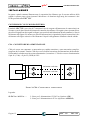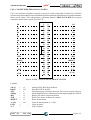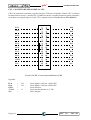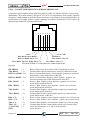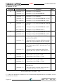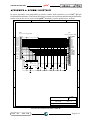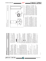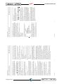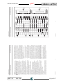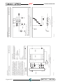
1
GPC® 553 General Purpose Controller 80C552 Philips MANUALE TECNICO Via dell' Artigiano, 8/6 ® 40016 San Giorgio di Piano grifo (Bologna) ITALY E-mail: [email protected] http://www.grifo.it http://www.grifo.com Tel. +39 051 892.052 (r.a.) FAX: +39 051 893.661 GPC® 553 Edizione 3.20 Rel. 15 Giugno 2000 ® ® , GPC , grifo , sono marchi registrati della ditta grifo® ITALIAN TECHNOLOGY GPC® 553 General Purpose Controller 80C552 Philips MANUALE TECNICO Modulo intelligente della serie Abaco® BLOCK, nel formato 100x149; Contenitore opzionale per guide ad Ω tipo DIN 46277-1 e DIN 46277- 3; CPU 80C552 da 22 a 29 MHz con indirizzamento massimo di 96 KBytes; Zoccoli per 32K EPROM, 32K SRAM/EEPROM, 32K SRAM/EEPROM/ EPROM; Circuiteria di Back Up per 32K SRAM, tramite batteria al LITIO esterna; EEPROM seriale, opzionale, da 512 a 1024 Bytes. Massima EEPROM in abbinamento ad RTC, 1024 Bytes; Orologio RTC, opzionale, con batteria al LITIO e 256 Bytes di SRAM; 8 linee di A/D Converter da 10 Bits, +2,5V o +5V fondo scala, oppure 4÷20 mA. Tempo di conversione 27µs a 22MHz; 16 linee di I/O TTL; 2 linee di PWM da 8 bits; 1 Dip Switch con 5 vie leggibili da software; Timer Counter da 16 bits con 4 registri di Capture e 3 di comparazione; 6 uscite Set Reset legate al comparatore T2, più 2 uscite di Toggle; Registro di Timer Counter standard da 16 bits e Watch Dog; 2 linee serial in RS232, di cui una settabile in RS 422, RS 485 o Current Loop e una software gestita dai pacchetti che la supportano; Connettore di espansione ABACO® I/O BUS da 26 vie; 1 connettore standard di I/O ABACO® da 20 vie; 1 connettore standard A/D ABACO® da 20 vie; Funzionamento in IDLE MODE o POWER DOWN MODE; Alimentatore, opzionale, incorporato oppure alimentazione esterna da 5Vdc, 140÷200 mA; Protezione della logica di bordo dai transienti tramite TransZorbTM ; 1 LED di segnalazione alimentazione; Via dell' Artigiano, 8/6 ® 40016 San Giorgio di Piano grifo (Bologna) ITALY E-mail: [email protected] http://www.grifo.it http://www.grifo.com Tel. +39 051 892.052 (r.a.) FAX: +39 051 893.661 GPC® 553 Edizione 3.20 Rel. 15 Giugno 2000 ® ® , GPC , grifo , sono marchi registrati della ditta grifo® ITALIAN TECHNOLOGY Vincoli sulla documentazione grifo® Tutti i Diritti Riservati Nessuna parte del presente manuale può essere riprodotta, trasmessa, trascritta, memorizzata in un archivio o tradotta in altre lingue, con qualunque forma o mezzo, sia esso elettronico, meccanico, magnetico ottico, chimico, manuale, senza il permesso scritto della grifo®. IMPORTANTE Tutte le informazioni contenute nel presente manuale sono state accuratamente verificate, ciononostante grifo® non si assume nessuna responsabilità per danni, diretti o indiretti, a cose e/o persone derivanti da errori, omissioni o dall'uso del presente manuale, del software o dell' hardware ad esso associato. grifo® altresi si riserva il diritto di modificare il contenuto e la veste di questo manuale senza alcun preavviso, con l' intento di offrire un prodotto sempre migliore, senza che questo rappresenti un obbligo per grifo®. Per le informazioni specifiche dei componenti utilizzati sui nostri prodotti, l'utente deve fare riferimento agli specifici Data Book delle case costruttrici o delle seconde sorgenti. LEGENDA SIMBOLI Nel presente manuale possono comparire i seguenti simboli: Attenzione: Pericolo generico Attenzione: Pericolo di alta tensione Marchi Registrati , GPC®, grifo® : sono marchi registrati della grifo®. Altre marche o nomi di prodotti sono marchi registrati dei rispettivi proprietari. ITALIAN TECHNOLOGY grifo® INDICE GENERALE INTRODUZIONE ........................................................................................................................ 1 VERSIONE SCHEDA .................................................................................................................. 1 INFORMAZIONI GENERALI .................................................................................................. 2 PROCESSORE DI BORDO ................................................................................................... 3 DISPOSITIVI DI CLOCK ..................................................................................................... 3 ALIMENTAZIONE DI BORDO ............................................................................................ 4 COMUNICAZIONE SERIALE ............................................................................................. 4 ABACO® I/O BUS .................................................................................................................... 4 LOGICA DI CONTROLLO ................................................................................................... 4 DISPOSITIVI DI MEMORIA ............................................................................................... 6 INTERFACCE OPERATORE LOCALI .............................................................................. 6 TASTO DI RESET .................................................................................................................. 8 SIO 0 ......................................................................................................................................... 8 A/D CONVERTER .................................................................................................................. 8 PWM ......................................................................................................................................... 8 WATCH DOG .......................................................................................................................... 8 REAL TIME CLOCK ............................................................................................................. 8 EEPROM SERIALE ............................................................................................................... 9 SPECIFICHE TECNICHE ....................................................................................................... 10 CARATTERISTICHE GENERALI .................................................................................... 10 CARATTERISTICHE FISICHE ......................................................................................... 10 CARATTERISTICHE ELETTRICHE ............................................................................... 11 INSTALLAZIONE ..................................................................................................................... 12 CONNESSIONI CON IL MONDO ESTERNO ................................................................. 12 CN4 - CONNETTORE DI ALIMENTAZIONE ............................................................ 12 CN1 - CONNETTORE PER ABACO® I/O BUS ........................................................... 13 CN5 - CONNETTORE PER I/O DELLA CPU. ............................................................ 14 CN6 - CONNETTORE PER PORT 5 CPU, INGRESSI A/D CONVERTER, PWM. 16 CN3A - CONNETTORE PER LINEA SERIALE PRINCIPALE ............................... 18 CN3B - CONNETTORE PER LINEA SERIALE SOFTWARE.................................. 20 CN2 - CONNETTORE PER BATTERIA ESTERNA DI BACK UP .......................... 25 INTERFACCE PER I/O DIGITALI .................................................................................... 26 TASTO DI RESET ................................................................................................................ 26 INTERFACCIAMENTO DEGLI I/O CON IL CAMPO................................................... 27 TRIMMER E TARATURE ................................................................................................... 27 SELEZIONE TIPO INGRESSI ANALOGICI ................................................................... 28 TEST POINT ......................................................................................................................... 28 TENSIONI DI ALIMENTAZIONE ..................................................................................... 29 SEGNALAZIONI VISIVE ................................................................................................... 29 GPC® 553 Rel. 3.20 Page I grifo® ITALIAN TECHNOLOGY JUMPERS .............................................................................................................................. 30 JUMPERS A 2 VIE ........................................................................................................... 32 JUMPERS A 3 VIE ........................................................................................................... 34 JUMPERS A 5 VIE ........................................................................................................... 35 INPUT DI BORDO ............................................................................................................... 35 RESET E WATCH DOG ...................................................................................................... 35 COMUNICAZIONE SERIALE ........................................................................................... 36 BACK UP ............................................................................................................................... 38 SELEZIONE MEMORIE ..................................................................................................... 40 INTERRUPTS ....................................................................................................................... 41 DESCRIZIONE SOFTWARE ................................................................................................... 42 MAPPAGGI ED INDIRIZZAMENTI ...................................................................................... 44 INTRODUZIONE ................................................................................................................. 44 MAPPAGGIO DELLE RISORSE DI BORDO .................................................................. 44 MAPPAGGIO PERIFERICHE IN I/O ............................................................................... 46 MAPPAGGIO DELLE MEMORIE .................................................................................... 47 MAPPAGGIO 0 ................................................................................................................ 47 MAPPAGGIO 1 ................................................................................................................ 48 MAPPAGGIO 3 ................................................................................................................ 49 DESCRIZIONE SOFTWARE DELLE PERIFERICHE DI BORDO .................................. 50 DIP SWITCH DSW1 ............................................................................................................. 50 DIREZIONALITÀ DELLA COMUNICAZIONE IN RS 422 O RS 485 ......................... 50 EEPROM SERIALE ............................................................................................................. 51 SRAM TAMPONATA + RTC SERIALE ............................................................................ 51 PWM ....................................................................................................................................... 51 UART ...................................................................................................................................... 51 A/D CONVERTER ................................................................................................................ 51 TIMER COUNTER ............................................................................................................... 52 WATCH DOG INTERNO ..................................................................................................... 52 SCHEDE ESTERNE .................................................................................................................. 53 BIBLIOGRAFIA ........................................................................................................................ 58 APPENDICE A: SCHEMI ELETTRICI ............................................................................... A-1 APPENDIX B: DESCRIZIONE COMPONENTI DI BORDO ........................................... B-1 APPENDIX C: INDICE ANALITICO ................................................................................... C-1 Page II GPC® 553 Rel. 3.20 ITALIAN TECHNOLOGY grifo® INDICE DELLE FIGURE FIGURA 1: SCHEMA A BLOCCHI ......................................................................................................... 5 FIGURA 2: FOTO DELLA SCHEDA ....................................................................................................... 7 FIGURA 3: CN4 - CONNETTORE DI ALIMENTAZIONE ....................................................................... 12 FIGURA 4: CN1 - CONNETTORE PER ABACO® I/O BUS .............................................................. 13 FIGURA 5: CN5 - CONNETTORE PER I/O DELA CPU ...................................................................... 14 FIGURA 6: SCHEMA COLLEGAMENTO LINEE DI I/O .......................................................................... 15 FIGURA 7: CN6 - CONNETTORE PER PORT 5 DELLA CPU, INGRESSI A/D CONVERTER, PWM ......... 16 FIGURA 8: SCHEMA D' INGRESSO A/D CONVERTER E PWM ............................................................ 17 FIGURA 9: CN3A - CONNETTORE LINEA SERIALE PRINCIPALE ........................................................ 18 FIGURA 10: SCHEMA DI COMUNICAZIONE SERIALE ........................................................................... 19 FIGURA 11: CN3B - CONNETTORE PER LINEA SERIALE SOFTWARE .................................................. 20 FIGURA 12: ESEMPIO DI COLLEGAMENTO IN RS 232 ....................................................................... 21 FIGURA 13: ESEMPIO DI COLLEGAMENTO IN RS 422 ....................................................................... 21 FIGURA 14: ESEMPIO DI COLLEGAMENTO IN RS 485 ....................................................................... 21 FIGURA 15: ESEMPIO DI COLLEGAMENTO IN RETE IN RS 485 .......................................................... 22 FIGURA 16: ESEMPIO DI COLLEGAMENTO PUNTO-PUNTO IN CURRENT LOOP A 4 FILI ........................ 23 FIGURA 17: ESEMPIO DI COLLEGAMENTO PUNTO-PUNTO IN CURRENT LOOP A 2 FILI ........................ 23 FIGURA 18: ESEMPIO DI COLLEGAMENTO IN RETE IN CURRENT LOOP PASSIVO ................................. 24 FIGURA 19: CN2 - CONNETTORE PER BATTERIA ESTERNA DI BACK UP ............................................. 25 FIGURA 20: TABELLA DELLE SEGNALAZIONI VISIVE ......................................................................... 29 FIGURA 21: TABELLA RIASSUNTIVA JUMPERS ................................................................................... 30 FIGURA 22: DISPOSIZIONE JUMPERS LATO COMPONENTI ............................................................. 31 FIGURA 23: TABELLA JUMPERS A 2 VIE ........................................................................................... 32 FIGURA 24: DISPOSIZIONE JUMPERS LATO SALDATURE ............................................................... 33 FIGURA 25: TABELLA JUMPERS A 3 VIE ........................................................................................... 34 FIGURA 26: TABELLA JUMPERS A 5 VIE ........................................................................................... 35 FIGURA 27: DISPOSIZIONE DRIVER PER COMUNICAZIONE SERIALE .................................................... 37 FIGURA 28: DISPOSIZIONE LED, CONNETTORI, DIP-SWITCH, ECC. .................................... 39 FIGURA 29: TABELLA DI SELEZIONE MEMORIE ................................................................................. 40 FIGURA 30: PIANTA DEI COMPONENTI LATO COMPONENI E LATO STAGNATURE ................................... 45 FIGURA 31: TABELLA INDIRIZZAMENTO I/O .................................................................................... 46 FIGURA 32: MAPPAGGIO DELLE MEMORIE IN MODO 0 (BASIC+DEBUG) ................................. 47 FIGURA 33: MAPPAGGIO DELLE MEMORIE IN MODO 1 (ASM) ..................................................... 48 FIGURA 34: MAPPAGGIO DELLE MEMORIE IN MODO 3 (ASM) ..................................................... 49 FIGURA 35: SCHEMA DELLE POSSIBILI CONNESSIONI ........................................................................ 55 FIGURA A1: SCHEMA ELETTRICO IAC 01 ..................................................................................... A-1 FIGURA A2: SCHEMA ELETTRICO DI ESPANSIONE PPI .................................................................... A-2 FIGURA A3: SCHEMA ELETTRICO QTP 16P .................................................................................. A-3 FIGURA A4: SCHEMA ELETTRICO QTP 24P - PARTE 1 .................................................................. A-4 FIGURA A5: SCHEMA ELETTRICO QTP 24P - PARTE 2 .................................................................. A-5 FIGURA A6: SCHEMA ELETTRICO SPA 03 ..................................................................................... A-6 FIGURA A7: SCHEMA ELETTRICO DI I/O SU ABACO® I/O BUS .................................................. A-7 FIGURA A8: SCHEMA ELETTRICO INTERFACCIA BUS ..................................................................... A-8 GPC® 553 Rel. 3.20 Page III grifo® Page IV ITALIAN TECHNOLOGY GPC® 553 Rel. 3.20 ITALIAN TECHNOLOGY grifo® INTRODUZIONE L’uso di questi dispositivi é rivolto - IN VIA ESCLUSIVA - a personale specializzato. Scopo di questo manuale é la trasmissione delle informazioni necessarie all’uso competente e sicuro dei prodotti. Esse sono il frutto di un’elaborazione continua e sistematica di dati e prove tecniche registrate e validate dal Costruttore, in attuazione alle procedure interne di sicurezza e qualità dell'informazione. I dati di seguito riportati sono destinati - IN VIA ESCLUSIVA - ad un utenza specializzata, in grado di interagire con i prodotti in condizioni di sicurezza per le persone, per la macchina e per l’ambiente, interpretando un’elementare diagnostica dei guasti e delle condizioni di funzionamento anomale e compiendo semplici operazioni di verifica funzionale, nel pieno rispetto delle norme di sicurezza e salute vigenti. Le informazioni riguardanti installazione, montaggio, smontaggio, manutenzione, aggiustaggio, riparazione ed installazione di eventuali accessori, dispositivi ed attrezzature, sono destinate - e quindi eseguibili - sempre ed in via esclusiva da personale specializzato avvertito ed istruito, o direttamente dall’ASSISTENZA TECNICA AUTORIZZATA, nel pieno rispetto delle raccomandazioni trasmesse dal costruttore e delle norme di sicurezza e salute vigenti. I dispositivi non possono essere utilizzati all'aperto. Si deve sempre provvedere ad inserire i moduli all'interno di un contenitore a norme di sicurezza che rispetti le vigenti normative. La protezione di questo contenitore non si deve limitare ai soli agenti atmosferici, bensì anche a quelli meccanici, elettrici, magnetici, ecc. Per un corretto rapporto coi prodotti, é necessario garantire leggibilità e conservazione del manuale, anche per futuri riferimenti. In caso di deterioramento o più semplicemente per ragioni di approfondimento tecnico ed operativo, consultare direttamente l’Assistenza Tecnica autorizzata. Al fine di non incontrare problemi nell’uso di tali dispositivi, é conveniente che l’utente - PRIMA DI COMINCIARE AD OPERARE - legga con attenzione tutte le informazioni contenute in questo manuale. In una seconda fase, per rintracciare più facilmente le informazioni necessarie, si può fare riferimento all’indice generale e all’indice analitico, posti rispettivamente all’inizio ed alla fine del manuale. VERSIONE SCHEDA Il presente manuale é riferito alla scheda GPC® 553 versione 070198 e sucessive. La validità delle informazioni riportate é quindi subordinata al numero di versione della scheda in uso e l'utente deve quindi sempre verificare la giusta corrispondenza tra le due indicazioni. Sulla scheda il numero di versione é riportato in più punti sia a livello di serigrafia che di stampato (ad esempio in mezzo a C56, C27, IC14, sia sul lato componenti che sul lato saldature). GPC® 553 Rel. 3.20 Pagina 1 grifo® ITALIAN TECHNOLOGY INFORMAZIONI GENERALI La scheda GPC® 553 è un nuovo potente modulo di controllo, della fascia Low-Cost con consumi estremamente ridotti, in grado di funzionare autonomamente o come periferica intelligiente remotata in una più vasta rete di telecontrollo e/o di acquisizione. La GPC® 553 è fornita di un supporto in plastica provvisto degli attacchi per le guide ad Ω tipo DIN 46277-1 e DIN 46277- 3. In questo modo non é necessario l' uso di un Rack, ma la scheda può essere montata, in modo più economico, direttamente nel quadro elettrico. La scheda supporta il 80C552, software compatibile con il diffusissimo 8051 INTEL. Sono disponibili diversi Tools di sviluppo software che consentono di poter usare la scheda come sistema di sviluppo di se stessa, sia in Assembler che con linguaggi evoluti. Una particolare menzione và ai Tools di sviluppo quali i vari Compilatori C, il FORTH ed il comodo BASIC 553. Quest' ultimo é compatibile con il diffusissimo MCS® BASIC-52 della INTEL, a cui sono stati aggiunti dei nuovi comandi. Tra i nuovi é doveroso citarne alcuni come quelli relativi all' A/D, I2C-BUS, RTC, EEPROM Seriale, gestione diretta dei Display LCD o Fluorescenti e di una tastiera a matrice, ecc. Per un uso immediato di quest' ultimo nuovo comando, sono disponibili delle schede della serie KDL-224 oppure, per chi ha bisogno di un oggetto finito, esiste il Pannello Operatore tipo QTP 24P. Questo Pannello Operatore, offerto nella versione a giorno, ha la stessa estetica della QTP 24 ma, non disponendo di intelligenza locale, viene comandato direttamente dalla GPC® 553, consentendo così una notevole riduzione dei costi. Il BASIC 553, oltre alla nota facilità di debugging, consente di programmare direttamente a bordo scheda una EEPROM con il programma utente. Per velocizzare l' applicativo oppure per non renderlo leggibile ad occhi indiscreti, è disponibile il Compilatore BASIC BXC51 con le librerie adatte ad accettare come sorgente quanto generato con il BASIC 553. La GPC® 553 è dotata di una serie di connettori normalizzati, standard Abaco® , che le consentono di utilizzare immediatamente la numerosa serie di moduli BLOCK di I/O oppure le permettono il collegamento, in modo molto semplice ed economico, delle interfacce da campo costruite direttamente dall' utente o da terze parti. La disponibilità del connettore Abaco® I/O BUS consente inoltre di poter pilotare direttamente le schede tipo ZBR 324, ZBT 324, ABB 03, ABB 05, ecc. espandendo rapidamente le caratteristiche di base della scheda. - Modulo intelligiente della serie ABACO® BLOCK, nel formato 100x149; - Contenitore opzionale per guide ad Ω tipo DIN 46277-1 e DIN 46277- 3; - CPU 80C552, da 22 a 29 MHz con indirizzamento massimo di 96 KBytes; - Zoccoli per 32K EPROM, 32K SRAM/EEPROM, 32K SRAM/EEPROM/EPROM; - Circuiteria di back up per 32K SRAM, tramite batteria al LITIO esterna; - EEPROM seriale, da 128 a 1024 Bytes. Massima EEPROM con RTC, 1024 Bytes; - Orologio RTC, opzionale, con batteria al LITIO e 256 Bytes di SRAM; - 8 linee di A/D Converter da 10 Bits, +2,5 V o +5 V fondo scala, oppure 4÷20 mA. Tempo di conversione 27µs a 22 MHz; - 16 linee di I/O TTL; - 2 linee di PWM da 8 bits; - 1 Dip Switch da 8 vie, con 5 vie leggibili da software; - Timer Counter da 16 bits con 4 registri di Capture e 3 di comparazione; - 6 uscite Set-Reset legate al comparatore T2, più 2 uscite di Toggle; - Registro di Timer Counter standard da 16 bits e Watch Dog settabile da software; - 2 linee serial in RS 232, di cui una settabile in RS 422, RS 485 o Current Loop e una software gestita dai pacchetti che la supportano; - Connettore di espansione per ABACO® I/O BUS da 26 vie; Pagina 2 GPC® 553 Rel. 3.20 ITALIAN TECHNOLOGY grifo® - 1 connettore standard di I/O ABACO® da 20 vie; - 1 connettore standard di A/D ABACO® da 20 vie; - Funzionamento in IDLE MODE o POWER DOWN MODE; - Alimentatore, opzionale, incorporato oppure alimentazione esterna da 5Vdc, 140÷200 mA; - Protezione della logica di bordo dai transienti tramite TransZorbTM ; - 1 LED di segnalazione alimentazione; - Vasta disponibilità di software di sviluppo quali Monitor, Debugger, Assemblatori, GET 51 e BASIC Interpretato, BASIC Compiler, FORTH, Compilatore C, HTC-51, PLM 51, Compilatore PASCAL, ecc. Viene di seguito riportata una descrizione dei blocchi funzionali della scheda, con indicate le operazioni effettuate da ciascuno di essi. Per una facile individuazione di tali blocchi e per una verifica delle loro connessioni, fare riferimento alla figura 28. PROCESSORE DI BORDO La scheda GPC® 553 é predisposta per accettare il processore 80C552. Tale processore ad 8 bit sono codice compatibile con l' 8051 della INTEL e sono quindi caratterizzati da un esteso set di istruzioni, da un’alta velocità di esecuzone e di manipolazione dati e da un efficiente gestione vettorizzata degli interrupts. Di seguito vine riportato un elenco di tutte le caratteristiche principali delle varie CPU che tale scheda é in grado di montare: - 8k bytes EPROM, 256 bytes RAM - 6 ports di I/O ad 8 bits; - 2 Timer/Counters da 16 bits - 1 Timer/Counter da 16 bits con funzioni di Capture e Compare; - 2 livelli di priorità per gli Interrupt; - 8 linee di A/D converter da 10 bits; - 2 linee indipendenti di PWM da 8 bits; - 1 linea seriale UART; - 1 linea per I2C bus; - Watch Dog Timer; - Funzionamento in IDLE MODE o POWER DOWN MODE; Per maggiori informazioni a riguardo di questo componente si faccia riferimento all’apposita documentazione della casa costruttrice. DISPOSITIVI DI CLOCK Sulla GPC® 553 sono presenti due circuiti separati che provvedono a generare rispettivamente la frequenza di clock per la CPU (da 22 a 29 MHz) e la frequenza per REAL TIME CLOCK di IC 17 (32768 Hz). La scelta di utilizzare due circuiti e quindi due quarzi indipendenti, é legata alla possibilità di poter variare in modo indipendente la frequenza di lavoro della CPU. GPC® 553 Rel. 3.20 Pagina 3 grifo® ITALIAN TECHNOLOGY ALIMENTAZIONE DI BORDO Una delle caratteristiche peculiari della GPC® 553 é quella di poter essere provvista di una sezione alimentatrice a bordo scheda che provvede a generare l'unica tensione di alimentazione necessaria di +5 Vdc. In caso di assenza della sezione alimentatrice quest'ultima é l'unica tensione richiesta dalla scheda, viceversa sono disponibili due diverse sezioni alimentatrici: quella lineare che richiede una tensione 6÷9 Vac e quella switching che necessita di una tensione 15÷24 Vac (per maggiori informazioni vedere apposito paragrafo "TENSIONI DI ALIMENTAZIONE". La tensione di alimentazione può essere fornita tramite appositi connettori standarizzati di facile ed immediata installazione. Sulla scheda sono state adottate tutte le scelte circuitali e componentistiche che tendono a ridurre i consumi, compresa la possibilità di far lavorare alcuni microcontrollori in power down ed idle mode ed a ridurre la sensibilità ai disturbi. Il tipo di alimentazione della scheda non può essere variato dall'utente e deve quindi essere specificato in fase di ordine. COMUNICAZIONE SERIALE La comunicazione seriale per quanto riguarda la SIO 0 é completamente settabile via software per quanto riguarda sia il protocollo sia la velocità di comunicazione. Tali settaggi avvengono tramite la programmazione dei registri della SIO 0 interni allo 80C552 di cui la scheda é provvista, quindi per ulteriori informazioni si faccia riferimento alla documentazione tecnica della casa costruttrice. Dal punto di vista hardware é invece possibile selezionare, tramite una serie di comodi jumpers, il protocollo fisico di comunicazione. In particolare la linea per la SIO 0 può essere bufferata in RS 232, RS 422, RS 485 o Current Loop; in quest’ultimo caso é definibile anche se la comunicazione avviene in Full Duplex o Half Duplex. È possibile usufruire della porta seriale software a patto di impiegare quei pacchetti software (quali ad esempio BASIC 52 o i compilatori BASCOM) che ne supportano la gestione. A tale proposito è opportuno ricordare che la seriale software utilizza il pin P3.2 - /INT0 per la ricezione e il pin P3.3 - /INT1 per la trasmissione, pertanto le relative linee di interrupt non saranno disponibili per raccogliere gli interrupt di RTC (/INT1) e ABACO® I/O BUS (/INT0). ABACO® I/O BUS Una delle caratteristiche di fondamentale importanza della GPC® 553 è quella di disporre del cosiddetto ABACO® I/O BUS: ovvero un connettore normalizzato ABACO® con cui è possibile collegare la scheda ad una serie di moduli esterni intelligenti e non. Tra questi si trovano moduli per acquisizione di segnali analogici (A/D), per la generazione di segnali analogici (D/A), per gestione di linee di I/O logico, per counter, ecc. e ne possono essere realizzati anche su specifiche richieste dell’utente. Utilizzando mother board come l'ABB 03 o l'ABB 05 é inoltre possibile gestire tutte le schede periferiche in formato europa con interfaccia per BUS ABACO®. Tale caratteristica rende la scheda espandibile con un’ottimo rapporto prezzo/prestazioni e quindi adatta a risolvere molti dei problemi dell'automazione industriale. LOGICA DI CONTROLLO Il mappaggio di tutti i registri delle periferiche presenti sulla scheda e dei dispositivi di memoria, é affidata ad un’opportuna logica di controllo che si occupa di allocare tali dispositivi nello spazio d’indirizzamento della CPU. Per informazioni si veda il paragrafo “MAPPAGGIO DELL’I/O”. Pagina 4 GPC® 553 Rel. 3.20 grifo® ITALIAN TECHNOLOGY CN3A CN3B CN6 SERIAL LINE A SERIAL LINE B 8 A/D LINES 2 PWM LINES IC16 EEPROM IC17 RTC+SRAM DRIVERS RS 232 RS 422 RS 485 CURRENT LOOP RS 232 CN2 EXTERNAL LITHIUM IC 2 SRAM EEPROM I 2 C bus CPU 80C552 IC3 SRAM EEPROM EPROM IC 1 EPROM +5 Vdc OPTIONAL POWER SUPPLY 16 I/O LINES POWER CN5 CN4 DSW1 CONTROL LOGIC ABACO® I/O BUS CN1 FIGURA 1: SCHEMA A BLOCCHI GPC® 553 Rel. 3.20 Pagina 5 grifo® ITALIAN TECHNOLOGY DISPOSITIVI DI MEMORIA E’ possibile dotare la scheda di un massimo di 97K e 256 bytes di memoria variamente suddivisi con un massimo di 32K EPROM, 32K SRAM/EEPROM, 32K SRAM/EEPROM/EPROM, 256 bytes di SRAM+RTC seriale ed infine 1K di EEPROM seriale. La scelta della configurazione delle memorie presenti sulla scheda può avvenire in relazione all’applicazione da risolvere e quindi in relazione alle esigenze dell’utente. Da questo punto di vista si ricorda che la scheda viene normalmente fornita con i 32K SRAM di lavoro e che tutte le rimanenti memorie devono essere quindi opportunamente specificate in fase di ordine della scheda. Tramite la circuiteria di Back Up presente a bordo scheda c'é inoltre la possibilità di tamponare fino ad un massimo di 32K e 256 bytes di SRAM aggiungendo quindi la possibilità di mantenere i dati anche in assenza di alimentazione. Questa caratteristica fornisce alla scheda la possibilità di ricordare in ogni condizione, una serie di parametri come ad esempio la configurazione o lo stato del sistema. La circuiteria di back up é basata su una batteria al Litio presente a bordo scheda e da una batteria esterna collegabile tramite un apposito connettore. Qualora la quantità di SRAM tamponata risulti insufficiente (ad esempio per sistemi di data loghin) si possono sempre utilizzare i moduli di SRAM tamponata e/o di EEPROM. Il modulo di SRAM da montare su IC 17 può essere inoltre provvisto di un real time clock interno in grado di gestire via software l’orario (ore, minuti, secondi) e la data (giorno, mese, anno, giorno della settimana). Il mappaggio delle risorse di memoria avviene tramite una opportuna circuiteria di bordo, che provvede ad allocare i dispositivi all’interno dello spazio d’indirizzamento del microprocessore; tale logica di controllo provvede a gestire in modo completamente automatico diversi tipi di mappaggi che si adattano ai diversi pacchetti software disponibili per la GPC® 553. Per maggiori informazioni fare riferimento al capitolo DESCRIZIONE HARDWARE” e DESCRIZIONE SOFTWARE DELLE PERIFERICHE DI BORDO”. Per una descrizione più approfondita sui dispositivi di memoria, sugli zoccoli da utilizzare e sullo strippaggio della scheda, fare riferimento al paragrafo “SELEZIONE MEMORIE”. INTERFACCE OPERATORE LOCALI Tramite CN5 (connettore standard di I/O ABACO®) si può collegare la GPC® 553 ai numerosi moduli del carteggio grifo® che riportano lo stesso pin out. Di particolare interesse é la possibilità di collegare direttamente una serie di moduli come la QTP 24P, KDL x24, KDF 224, ecc. con cui risolvere tutti i problemi di interfacciamento operatore locale. Questi moduli sono già dotati delle risorse necessarie per gestire un buon livello di colloquio uomo-macchina (includono infatti display alfanumerici, tastiera a matrice e LEDs di visualizzazione) ad una breve distanza dalla GPC® 553. Dal punto di vista dell'installazione, queste interfaccie operatore locali richiedono un solo flat a 20 vie con cui é possibile portare anche le alimentazioni, mentre dal punto di vista software la gestione é altrettanto semplice ed immediata, infatti i pacchetti software disponibili per la GPC® 553 sono provvisti di tutte le procedure necessarie. Quest'ultime per la maggioranza dei pacchetti software disponibili, coincidono con dei "driver software" aggiunti al linguaggio di programmazione, che consentono di utilizzare direttamente le istruzioni di "console" dello stesso linguaggio di programmazione e quindi tutta la loro potenza. Per maggiori informazioni si veda il capitolo "SCHEDE ESTERNE" e la documentazione del software utilizzato. Pagina 6 GPC® 553 Rel. 3.20 ITALIAN TECHNOLOGY grifo® FIGURA 2: FOTO DELLA SCHEDA GPC® 553 Rel. 3.20 Pagina 7 grifo® ITALIAN TECHNOLOGY TASTO DI RESET Sulla GPC® 553 é presente un comodo pulsante di reset che una volta premuto fà ripartire la scheda da una condizione di azzeramento generale. La funzione principale di questo tasto é quella di uscire da condizioni di loop infinito, soprattutto durante la fase di debug o di garantire uno stato certo di partenza. SIO 0 Periferica interna alla CPU in grado di gestire una linea per la comunicazione seriale. Il dispositivo può essere utilizzato per la comunicazione con tutti i sistemi provvisti di una linea seriale bufferata in RS 232, RS 422, RS 485 o Current Loop. Dal punto di vista software é infatti definibile la velocità di comunicazione, la lunghezza della parola, il numero di stop bit, la parità e lo stato dei segnali di handshake hardware. Il tutto avviene tramite una semplice programmazione di registri interni alla CPU. A/D CONVERTER Periferica interna alla CPU in grado di acquisire 8 canali con una risoluzione massima di 10 bits. Dal punto di vista software é possibili definire quali canali attivare, dare lo start o lo stop all' acquisizione ecc. Al fine di semplificare la gestione dello stesso A/D Converter alcuni pacchetti software forniscono delle procedure di utility che gestiscono la sezione in tutte le sue parti. I segnali analogici collegabili sono segnali in tensione variabili nel range 0÷2,490V o 0÷5,000V o segnali in corrente 0÷20 mA. La sezione é opzionale e deve essere quindi esplicitamente ordinata. PWM Sono disponibili due linee indipendenti di PWM (periferica interna alla CPU). Dal punto di vista software é definibile la frequenza e il duty-cicle del segnale. WATCH DOG Periferica interna alla CPU che permette il reset della medesima ad intervalli di tempi prefissati se non viene effettuato un retrigger. Dal punto di vista software é definibile l' abilitazione, il retrigger e il tempo di intervento, che varia nel range 1,111÷283,305 ms per la scheda a 22,1184 MHz e 0,833÷212,415 ms per la scheda a 29,4912 MHz REAL TIME CLOCK Il modulo di SRAM tamponata da montare sullo zoccolo IC 17 può essere provvisto di un completo Real Time Clock in grado di gestire ore, minuti, secondi, giorno del mese, mese, anno e giorno della settimana in modo completamente autonomo. Il componente é opzionale e viene fornito con batteria di back up. Pagina 8 GPC® 553 Rel. 3.20 ITALIAN TECHNOLOGY grifo® EEPROM SERIALE Il modulo di EEPROM seriale saldato in posizione IC 16 é molto utile in caso si debbano mantenere delle informazioni anche in assenza di alimentazione, senza ricorrere al Back Up della SRAM, con una sicurezza estrema sulla validità dei dati. Tale modulo è presente di default con size di 256 bytes ma può variare nel range 256÷1024 bytes. Gli ulteriori size sono opzionali e devono essere quindi esplicitamente ordinati. Per ulteriori informazioni a riguardo dei dispositivi periferici descritti, si faccia riferimento alla documentazione tecnica della casa costruttrice. GPC® 553 Rel. 3.20 Pagina 9 grifo® ITALIAN TECHNOLOGY SPECIFICHE TECNICHE CARATTERISTICHE GENERALI Risorse di bordo: 16 Input/Output programmabili TTL 3 Timer Counter a 16 bit 1 Linea bidirezionale RS 232 o RS 422, RS 485 o Current Loop 1 Linea bidirezionale RS 232 1 Watch Dog 8 Linee di A/D Converter 1 Tasto locale di reset 1 Real Time Clock 1 LED 1 Dip Switch per un totale di 8 dip (5 leggibili da software) 2 Linee di PWM da 8 bits 1 Connettore di espansione per ABACO® I/O BUS Memoria indirizzabile: IC 1 IC 2 IC 3 IC 16 IC 17 CPU di bordo: PHILIPS 80C552 Frequenza di clock: 22÷29 MHz Risoluzione A/D: 10 bits Tempo conversione A/D: 27 µs a 22.1184 MHz; 20 µs a 29.4912 MHz EPROM da 32K x 8 SRAM/EEPROM da 8K x 8 a 32K x 8 SRAM/EEPROM/EPROM da 8K x 8 a 32K x 8 EEPROM seriale da 512 byte a 1024 byte SRAM+RTC seriale da 256 byte CARATTERISTICHE FISICHE Dimensioni: Formato 100 x 149 mm Peso: 168 g (Configurazione completa) Connettori: CN1 CN2 CN3A CN3B CN4 CN5 CN6 Range di temperatura: da 10 a 40 gradi Centigradi Pagina 10 26 vie scatolino verticale M 2 vie verticale M PLUG a 6 vie PLUG a 6 vie 2 vie rapida estrazione o morsettiera a 2 vie 20 vie scatolino verticale M 20 vie scatolino verticale M GPC® 553 Rel. 3.20 grifo® ITALIAN TECHNOLOGY Umidità relativa: 20% fino a 90% (senza condensa) Tempo intervento Watch Dog: 1,111÷283,305 ms a 22,1184 MHz 0,833÷212,415 ms a 29,4912 MHz CARATTERISTICHE ELETTRICHE Tensione di alimentazione: 5 Vdc 6÷9 Vac 15÷24 Vac (senza sezione alimentatrice) (sezione alimentatrice lineare) * (sezione alimentatrice switching) Corrente assorbita sui 5 Vdc: 140 mA a 22 MHz 200 mA a 33 MHz Corrente fornita sui 5 Vdc per carichi esterni: 260 mA a 22 MHz 200 mA a 33 MHz 860 mA a 22 MHz 800 mA a 33 MHz Batteria esterna di Back Up: 3,6÷5 Vdc Corrente di Back Up: 15µ A Ingressi analogici in tensione: 0÷2,49 Vdc o 0÷5 Vdc Ingressi analogici in corrente: 0÷20 mA Impedenza ingressi analogici: 1 KΩ (switching) (switching) (lineare) (lineare) * * * * * I dati riportati sono riferiti ad un lavoro a temperatura ambiente di 20 gradi centigradi (per ulteriori informazioni fare riferimento al paragrafo "TENSIONE DI ALIMENTAZIONE"). GPC® 553 Rel. 3.20 Pagina 11 grifo® ITALIAN TECHNOLOGY INSTALLAZIONE In questo capitolo saranno illustrate tutte le operazioni da effettuare per il corretto utilizzo della scheda. A questo scopo viene riportata l’ubicazione e la funzione degli strip, dei connettori e dei LEDs presenti sulla GPC® 553. CONNESSIONI CON IL MONDO ESTERNO Il modulo GPC®553 è provvisto di 7 connettori con cui vengono effettuate tutte le connessioni con il campo e con le altre schede del sistema di controllo da realizzare. Di seguito viene riportato il loro pin out ed il significato dei segnali collegati; per una facile individuazione di tali connettori, si faccia riferimento alla figura 28, mentre per ulteriori informazioni a riguardo del tipo di connessioni, fare riferimento alle figure sucessive che illustrano il tipo di collegamento effettuato a bordo scheda. CN4 - CONNETTORE DI ALIMENTAZIONE CN4 può essere un connettore a morsettiera per rapida estrazione o una morsettiera semplice, composto da 2 contatti. Tramite CN4 deve essere fornita la tensione di alimentazione della scheda. Utilizzando la scheda senza la sezione alimentatrice, la tensione +5 Vdc deve essere fornita tramite il pin 26 (+Vdc) e il pin 25 (GND) di CN1. 15÷24 Vac / 6÷9 Vac 1 1 15÷24 Vac / 6÷9 Vac 2 FIGURA 3: CN4 - CONNETTORE DI 2 ALIMENTAZIONE Legenda: 15÷24 Vac / 6÷9 Vac = Pagina 12 I - Linee per l' alimentazione 15÷24 Vac (Opzione .SW). I - Linee per l' alimentazione 6÷9 Vac (Opzione .ALIM.12). GPC® 553 Rel. 3.20 grifo® ITALIAN TECHNOLOGY CN1 - CONNETTORE PER ABACO® I/O BUS CN1 è un connettore a scatolino verticale con passo 2.54 mm a 26 piedini. Tramite CN1 si effettua la connessione tra la scheda e la serie di moduli esterni di espansione, da utilizzare per l’interfacciamento diretto con il campo. Tale collegamento è effettuato tramite l’ABACO® I/O BUS di cui questo connettore riporta tutti i segnali a livello TTL. D0 1 2 D1 D2 3 4 D3 D4 5 6 D5 D6 7 8 D7 A0 9 10 A1 A2 11 12 A3 A4 13 14 A5 A6 15 16 A7 /WR 17 18 /RD /IORQ 19 20 /RESET N. C. 21 22 N. C. /INT 23 24 N. C. GND 25 26 +5 Vdc FIGURA 4: CN1 - CONNETTORE PER ABACO® I/O BUS Legenda: A0-A7 D0-D7 /INT /IORQ /RD /WR /RESET +5 Vdc GND N. C. GPC® 553 = = = = = = = = = = O I/O I O O O O I/O - Rel. 3.20 Address BUS: BUS degli indirizzi. Data BUS: BUS dei dati. Interrupt request: richiesta d’interrupt. Deve essere in open collector. Input Output Request: richiesta operazione Input Output su I/O BUS. Read cycle status: richiesta di lettura. Write cycle status: richiesta di scrittura. Reset: azzeramento. Linea di alimentazione a +5 Vdc. Linea di massa. Non Collegato. Pagina 13 grifo® ITALIAN TECHNOLOGY CN5 - CONNETTORE PER I/O DELLA CPU. CN5 è un connettore a scatolino verticale con passo 2.54 mm a 20 piedini. Tramite CN5 si effettua la connessione tra i port 1 e 4 della CPU e l’ambiente esterno. I segnali presenti su questo connettore coincidono con segnali logici a livello TTL e seguono il pin out standardizzato I/O ABACO®. P4.1 1 2 P4.0 P4.3 3 4 P4.2 P4.5 5 6 P4.4 P4.7 7 8 P4.6 P1.6 9 10 P1.7 P1.4 11 12 P1.5 P1.2 13 14 P1.3 P1.0 15 16 P1.1 GND 17 18 +5 Vdc N.C. 19 20 N.C. FIGURA 5: CN5 - CONNETTORE PER I/O DELA CPU Legenda: P1.n P4.n GND +5 Vdc N.C. Pagina 14 = = = = = I/O I/O O - Linea digitale n del port 1 della CPU. Linea digitale n del port 4 della CPU. Linea di massa. Linea di alimentazione a +5 Vdc. Non Collegato. GPC® 553 Rel. 3.20 grifo® ITALIAN TECHNOLOGY 8 LINES PIN 1÷8 PORT 4 CPU 80C552 CN5 8 LINES PORT 1 PIN 9÷16 FIGURA 6: SCHEMA COLLEGAMENTO LINEE DI I/O GPC® 553 Rel. 3.20 Pagina 15 grifo® ITALIAN TECHNOLOGY CN6 - CONNETTORE PER PORT 5 CPU, INGRESSI A/D CONVERTER, PWM. CN6 è un connettore a scatolino verticale con passo 2.54 mm a 20 piedini. Tramite CN6 si interfacciano le 8 linee di input per la sezione di A/D Converter della CPU con il campo esterno e le due linee di PWM. Da ricordare che il port 5 della CPU ha una doppia funzione ossia le 8 linee possono essere ingressi digitali o ingressi per l' A/D converter. + 5 Vdc 1 2 PWM0 GND 3 4 PWM1 AGND 5 6 P5.0/ADC0 AGND 7 8 P5.1/ADC1 AGND 9 10 P5.2/ADC2 AGND 11 12 P5.3/ADC3 AGND 13 14 P5.4/ADC4 AGND 15 16 P5.5/ADC5 AGND 17 18 P5.6/ADC6 AGND 19 20 P5.7/ADC7 FIGURA 7: CN6 - CONNETTORE PER PORT 5 DELLA CPU, INGRESSI A/D CONVERTER, PWM Legenda: PWM0 PWM1 P5.n/ADCn GND AGND +5 Vdc Pagina 16 = = = = = = O O I - Linea di PWM n. 0 della CPU. Linea di PWM n. 1 della CPU. Linea digitale n o ingresso canale n dell' A/D della CPU. Linea di massa digitale. Linea di massa analogica. Linea di alimentazione a +5 Vdc. GPC® 553 Rel. 3.20 grifo® ITALIAN TECHNOLOGY VRef. RV1 ADC 0 1 6 ADC 1 68 CPU 80C552 66 65 64 63 62 4 5 ADC 2 10 ADC 3 12 ADC 4 14 ADC 5 16 ADC 6 CN6 67 8 18 ADC 7 20 PWM 0 2 PWM 1 4 5, 7, 9, 11, 13, 15, 17, 19 AN. GND FIGURA 8: SCHEMA D' INGRESSO A/D CONVERTER E PWM GPC® 553 Rel. 3.20 Pagina 17 grifo® ITALIAN TECHNOLOGY CN3A - CONNETTORE PER LINEA SERIALE PRINCIPALE Il connettore per la comunicazione della linea seriale A, in RS 232, RS 422, RS 485 o Current Loop, denominato CN3A sulla scheda, é del tipo PLUG a 6 vie. La disposizione di tali segnali, riportata di seguito, é stata studiata in modo da ridurre al minimo le interferenze ed in modo da facilitare la connessione con il campo, mentre i segnali rispettano le normative definite dal CCITT relative ad ognuno degli standard di comunicazione usati. 6 5 4 3 2 1 GND +5 Vdc / GND TXA RS232 / TXA+ RS422 / TXA- C.L. RXA RS232 / RXA+ RS422 / RXTXA+ RS485 / RXA+ C.L. RXA- RS422 / RXTXA- RS485 / RXA- C.L. TXA- RS422 / TXA+ C.L. FIGURA 9: CN3A - CONNETTORE LINEA SERIALE PRINCIPALE Legenda: RX ARS232 = I TXA RS232 = O RXTXA+ RS485= I/ORXTXA- RS485 = I/ORXA- RS422 = I - RXA+ RS422 = I - TXA- RS422 = O - TXA+ RS422 = O - RXA- C.L. RXA+ C.L. TXA- C.L. TXA+ C.L. +5 Vdc/GND GND = = = = = = Pagina 18 I I O O I - Receive Data: linea di ricezione in RS 232 della linea seriale Transmit Data: linea di trasmissione in RS 232 della linea seriale Receive/Trasmit Data Positive: linea bipolare positiva per ricezione/ trasmissione seriale differenziale in RS 485 Receive/Trasmit Data Negative: linea bipolare negativa per ricezione/trasmissione seriale differenziale in RS 485 Receive Data Negative: linea bipolare negativa per ricezione seriale differenziale in RS 422 Receive Data Positive: linea bipolare positiva per ricezione seriale differenziale in RS 422 Transmit Data Negative: linea bipolare negativa per trasmissione seriale differenziale in RS 422 Transmit Data Positive: linea bipolare positiva per trasmissione seriale differenziale in RS 422 Receive Data Negative: linea bipolare negativa per Current Loop Receive Data Positive: linea bipolare positiva per Current Loop Transmit Data Negative: linea bipolare negativa per Current Loop Transmit Data Positive: linea bipolare positiva per Current Loop Linea di alimentazione a +5 Vdc o linea di massa Linea di massa GPC® 553 Rel. 3.20 grifo® ITALIAN TECHNOLOGY DRIVERS RS 422 RS 485 CURRENT LOOP C P U HARDWARE SERIAL LINE 8 0 C 5 5 2 SOFTWARE SERIAL LINE C N 3 A D R I V E R RS 232 C N 3 B FIGURA 10: SCHEMA DI COMUNICAZIONE SERIALE GPC® 553 Rel. 3.20 Pagina 19 grifo® ITALIAN TECHNOLOGY CN3B - CONNETTORE PER LINEA SERIALE SOFTWARE Il connettore per la comunicazione della linea seriale B, in RS 232, denominato CN3B sulla scheda, é del tipo PLUG a 6 vie. La disposizione di tali segnali, riportata di seguito, é stata studiata in modo da ridurre al minimo le interferenze ed in modo da facilitare la connessione con il campo, mentre i segnali rispettano le normative definite dal CCITT relative ad ognuno degli standard di comunicazione usati. 6 5 4 3 2 1 GND RXB RS 232 +5 Vdc / GND TXB RS 232 N.C. N.C. FIGURA 11: CN3B - CONNETTORE PER LINEA SERIALE SOFTWARE Legenda: RXB RS 232 TXB RS 232 = = I O - +5 Vdc/GND GND N.C. = = = I - Pagina 20 - Receive Data: linea di ricezione in RS 232 della linea seriale. Transmit Data: linea di trasmissione in RS 232 della linea seriale. Linea di alimentazione a +5 Vdc o linea di massa Linea di massa Non Collegato. GPC® 553 Rel. 3.20 CN3A GPC® 553 5 RXA RS232 TX 2 TXA RS232 RX 6 GND GND External System grifo® ITALIAN TECHNOLOGY FIGURA 12: ESEMPIO DI COLLEGAMENTO IN RS 232 RXA- RS422 TX - RXA+ RS422 TX + TXA- RS422 RX - TXA+ RS422 RX + GND GND 5 3 External System CN3A GPC® 553 4 2 6 RXTXA- RS485 TXRX- RXTXA+ RS485 TXRX+ GND GND 4 5 External System CN3A GPC® 553 FIGURA 13: ESEMPIO DI COLLEGAMENTO IN RS 422 6 FIGURA 14: ESEMPIO DI COLLEGAMENTO IN RS 485 GPC® 553 Rel. 3.20 Pagina 21 grifo® + TXRX - 5 4 GND 6 5 120 Ω 4 6 Slave 1 + TXRXA RS485 GND GPC® 553 CN3A Master ITALIAN TECHNOLOGY Slave 2 6 TXRXA RS485 - GPC® 553 CN3A 4 + GND +5V 5 + 4 - Slave n TXRXA RS485 6 GND GPC® 553 CN3A 5 FIGURA 15: ESEMPIO DI COLLEGAMENTO IN RETE IN RS 485 Da notare che in una rete RS 485, devono essere presenti due resistenze di forzatura lungo la linea e due resitenze di terminazione (120 Ω), alle estremità della stessa, rispettivamente vicino all'unità Master ed all'ultima unità Slave. A bordo della GPC® 553 è presente la circuiteria di terminazione e forzatura, che può essere inserita o disinserita, tramite appositi jumpers, come illustrato in seguito. In merito alla resistenza di terminazione dell'unità Master, provvedere a collegarla solo se questa non é già presente al suo interno (ad esempio molti convertitori RS232-RS485 ne sono già provvisti). Per maggiori informazioni consultare il Data-Book TEXAS INSTRUMENTS, "RS 422 and RS 485 Interface Cicuits", nella parte introduttiva riguardante le reti RS 422-485. Pagina 22 GPC® 553 Rel. 3.20 grifo® ITALIAN TECHNOLOGY 4 RXA- C.L. 5 RXA+ C.L. 2 TXA- C.L. 3 TXA+ C.L. VCL + R TX + External System CN3A GPC® 553 - TX - R RX + RX - FIGURA 16: ESEMPIO DI COLLEGAMENTO PUNTO-PUNTO IN CURRENT LOOP A 4 FILI VCL + CN3A GPC® 553 R 4 RXA- C.L. TX + 5 RXA+ C.L. TX - 2 TXA- C.L. RX + 3 TXA+ C.L. RX - External System - FIGURA 17: ESEMPIO DI COLLEGAMENTO PUNTO-PUNTO IN CURRENT LOOP A 2 FILI GPC® 553 Rel. 3.20 Pagina 23 grifo® + Master R Slave 1 5 + RXA 4 - + TX R + RX - VCL ITALIAN TECHNOLOGY CN3A + TXA 2 GPC® 553 3 Slave 2 5 + RXA 4 CN3A 3 + TXA 2 GPC® 553 Slave n 5 + RXA 4 CN3A 3 + TXA 2 GPC® 553 FIGURA 18: ESEMPIO DI COLLEGAMENTO IN RETE IN CURRENT LOOP PASSIVO Per il collegamento in Current Loop passivo sono possibili due diversi tipi di collegamento: a 2 fili ed a 4 fili. Tali connessioni sono riportate nelle figure 16 e 17; in esse é indicata la tensione per alimentare l’anello (VCL) e le resistenze di limitazione della corrente (R). I valori di tali componenti variano in funzione del numero di dispositivi collegati e della caduta sul cavo di collegamento; bisogna quindi effettuare la scelta considerando che: - si deve garantire la circolazione di una corrente di 20 mA; - su ogni trasmettitore cadono mediamente 2,35 V con una corrente di 20 mA; - su ogni ricevitore cadono mediamente 2,52 V con una corrente di 20 mA; - in caso di cortocircuito sulla rete ogni trasmettitore dissipi al massimo 125 mW; - in caso di cortocircuito sulla rete ogni ricevitore dissipi al massimo 90 mW. Per maggiori informazioni consultare il Data-Book HEWLETT-PACKARD, nella parte che riguarda gli opto-accoppiatori per Current Loop denominati HCPL 4100 e HCPL 4200. Pagina 24 GPC® 553 Rel. 3.20 grifo® ITALIAN TECHNOLOGY CN2 - CONNETTORE PER BATTERIA ESTERNA DI BACK UP CN2 é un connettore a scatolino, verticale, maschio, con passo 2,54mm a 2 vie. Tramite CN2 deve essere collegata una batteria esterna che provvede a mantenere i dati delle SRAM di bordo ed a garantire il funzionamento dell'eventuale real time clock, anche in assenza di tensione di alimentazione (per maggiori informazioni fare riferimento al paragrafo "BACK UP"). 1 +Vbat 2 GND FIGURA 19: CN2 - CONNETTORE PER BATTERIA ESTERNA DI BACK UP Legenda +Vbat GND GPC® 553 = = I Rel. 3.20 - Positivo della batteria esterna di back up Negativo della batteria esterna di back up Pagina 25 grifo® ITALIAN TECHNOLOGY INTERFACCE PER I/O DIGITALI Tramite CN5 (connettore compatibile con standard di I/O ABACO®) si può collegare la GPC® 553 ai numerosi moduli del carteggio grifo® che riportano lo stesso pin out. Dal punto di vista dell’installazione, queste interfaccie richiedono solo un flat cable da 18 vie intestato con due connettori da 26 e 20 vie (FLT.26+20) con cui é possibile portare anche le alimentazioni, mentre dal punto di vista software la gestione é altrettanto semplice ed immediata, infatti i pacchetti software disponibili per la GPC® 553 sono provvisti di tutte le procedure necessarie. Quest’ultime per la maggioranza dei pacchetti software disponibili, coincidono con dei “driver software” o delle librerie aggiunti al linguaggio di programmazione, che consentono di utilizzare direttamente le istruzioni ad alto livello dello stesso linguaggio di programmazione e quindi tutta la loro potenza. Di particolare interesse é la possibilità di collegare direttamente una serie di moduli come: - QTP 16P, QTP 24P, KDL x24, KDF 224, DEB 01, ecc. con cui risolvere tutti i problemi di interfacciamento operatore locale. Questi moduli sono già dotati delle risorse necessarie per gestire un buon livello di colloquio uomo-macchina (includono infatti display alfanumerici, tastiera a matrice e LEDs di visualizzazione) ad una breve distanza dalla GPC® 553. Dal punto di vista software i driver disponibili rendono utilizzabili le risorse dell’interfaccia operatore direttamente con le istruzioni ad alto livello per la gestione della console. - MCI 64 con cui risolvere tutti i problemi di salvataggio di grosse quantità di dati. Questo modulo é dotato di un connettore per memory card PCMCIA su cui possono essere inserite vari tipi di memory card (RAM, FLASH, ROM, ecc) nei vari size disponibili. Dal punto di vista software i driver disponibili coincidono con un completo file system e rendono utilizzabili le memory card direttamente con le istruzioni ad alto livello per la gestione dei files. - IAC 01, DEB 01 con cui gestire una stampante con interfaccia parallela CENTRONICS. Quest’ultima può essere collegata direttamente all’interfaccia, con un cavo standard, e quindi gestita con le istruzioni relative alla stampante del linguaggio di programmazione utilizzato. - RBO xx, TBO xx, XBI xx, OBI xx con cui bufferare i segnali di I/O TTL nei confronti del campo. Con questi moduli i segnali di input vengono convertiti in ingressi optoisolati di tipo NPN o PNP, mentre i segnali di output vengono convertiti in uscite galvanicamente isolate a transistor o relé. Per maggiori informazioni relative alle interfaccie per I/O digitali si veda il capitolo “SCHEDE ESTERNE” e la documentazione del software utilizzato. TASTO DI RESET Sulla GPC® 553 é presente un contatto di reset denominato P1 che consente di attivare la linea di /RESET della scheda. Sui due pin del P1 si può collegare un contatto normalmente aperto (ad esempio un pulsante) ed una volta chiuso questo contatto (cortocircuitando i due pin) la scheda riprende l’esecuzione del programma in EPROM, partendo da una condizione di azzeramento generale. La funzione principale di questo contatto é quella di uscire da condizioni di loop infinito, soprattutto durante la fase di debug. Per una facile individuazione di tale contatto a bordo scheda, si faccia riferimento alla figura 28, mentre per ulteriori informazioni sulla circuiteria di reset si veda il paragrafo “RESET E WATCH DOG”. Pagina 26 GPC® 553 Rel. 3.20 ITALIAN TECHNOLOGY grifo® INTERFACCIAMENTO DEGLI I/O CON IL CAMPO Al fine di evitare eventuali problemi di collegamento della scheda con tutta l’elettronica del campo a cui la GPC® 553 si deve interfacciare, si devono seguire le informazioni riportate nei precedenti paragrafi e nelle relative figure che illustrano le modalità interne di connessione. - Per tutti i segnali che riguardano la comunicazione seriale con i protocolli RS 232, RS 422, RS 485 o Current Loop, fare riferimento alle specifiche standard di questo protocollo. - Per tutti i segnali a livello TTL possono essere collegati a linee dello stesso tipo riferite alla massa digitale della scheda. Il livello 0V corrisponde allo stato logico 0, mentre il livello 5V corrisponde allo stato logico 1. - I segnali d'ingresso alla sezione A/D Converter devono essere collegati a segnali analogici a bassa impedenza che rispettino il range di variazione ammesso che può essere 0÷+2,490 V, 0÷+5,000 V o 0÷20 mA a seconda della configurazione. TRIMMER E TARATURE Sulla GPC® 553 é presente il trimmer RV1 da utilizzare per la taraura della scheda; tale componente permette di fissare il valore della tensione di riferimento su cui si basa la sezione di A/D converter. La scheda viene sottoposta ad un accurato test di collaudo che provvede a verificare la funzionalità della stessa ed allo stesso tempo a tararla in tutte le sue parti. La taratura viene effettuata in laboratorio a temperatura costante di +20 gradi centigradi, seguendo la procedura di seguito descritta: - Si effettua la taratura di precisione della Vref della sezione A/D tramite la regolazione del trimmer RV1, tramite un multimetro galvanicamente isolato a 5 cifre ad un valore di 2,4900 V o 5,0000V. - Si verifica la corrispondenza tra segnale analogico fornito in ingresso e combinazione letta dalla sezione A/D Converter. La verifica viene effettuata fornendo un segnale di verifica con un calibratore campione e controllando che la differenza tra la combinazione determinata dalla scheda e quella determinata in modo teorico, non superi la somma degli errori della sezione A/D. - Si blocca il trimmer della scheda, opportunamente tarato, tramite vernice. Le sezioni d’interfaccia analogica utilizzano componenti di alta precisione che vengono addirittura scelti in fase di montaggio, proprio per evitare lunghe e complicate procedure di taratura. Per questo una volta completato il test di collaudo e quindi la taratura, il trimmer RV1 viene bloccato, in modo da garantire una immunità della taratura anche ad eventuali sollecitazioni meccaniche (vibrazioni, spostamenti, ecc.). La circuiteria di generazione della tensione di riferimento definisce anche il fondo scala per tutti gli 11 canali di ingresso analogico, tra i due possibili range: 0÷2,49 V o 0÷5,00 V. La scelta di questo valore di fondo scala deve essere specificata in fase d'ordine della scheda, infatti implica il montaggio di diversi componenti ed una diversa procedura di taratura. In assenza di indicazioni, la scheda viene fornita nella versione standard con fondo scala a 2,49 V. L’utente di norma non deve intervenire sulla taratura della scheda, ma se lo dovesse fare (a causa di derive termiche, derive del tempo, ecc.) deve rigorosamente seguire la procedura sopra illustrata. Per una facile individuazione del trimmer a bordo scheda, si faccia riferimento alla figura 28. GPC® 553 Rel. 3.20 Pagina 27 grifo® ITALIAN TECHNOLOGY SELEZIONE TIPO INGRESSI ANALOGICI La scheda GPC® 553, può avere ingressi analogici in tensione e/o corrente, come descritto nei precedenti paragafi e capitoli. La selezione del tipo d’ingresso viene essere effettuata in fase di ordine della scheda montando un apposito modulo opzionale di conversione corrente-tensione basato su resistenze di caduta di precisione (codice opzione .8420). In particolare vale la corrispondenza: R22 R21 R20 R19 R18 R17 R16 R15 -> -> -> -> -> -> -> -> canale 0 canale 1 canale 2 canale 3 canale 4 canale 5 canale 6 canale 7 Nel caso il modulo corrente-tensione non sia montato (default) il corrispondente canale accetta un ingresso in tensione nei range 0÷2,490 V; viceversa un ingresso in corrente. Il valore della resistenza, su cui si basa il convertitore corrente-tensione, si ottiene dalla seguente formula: R = 2,490 V / Imax Normalmente i moduti di conversione tensione-corrente, si basano su resistenze di precisione da 124Ω, relative ad ingressi 0÷20 mA. Per eventuali esigenze al di fuori dei valori standard sopracitati si prega di contattare la grifo®. Per una facile individuazione del modulo descritto e delle relative resistenze componenti, fare riferimento alla figura 28. TEST POINT La scheda é provvista di un test point denominato TP1, che permette la lettura attraverso un multimetro galvanicamente isolato, della tensione di riferimento che viene regolata in laboratorio a Vref=2,4900 V o 5,000 V. Il TP1 é composto da due contatti con la seguente corrispondenza: pin 1 pin 2 -> -> Vref GND Per una facile individuazione di tale test point a bordo scheda, si faccia riferimento alla figura 28, mentre per ulteriori informazioni sul segnale Vref si veda il paragrafo “TRIMMER E TARATURE”. Pagina 28 GPC® 553 Rel. 3.20 grifo® ITALIAN TECHNOLOGY TENSIONI DI ALIMENTAZIONE La scheda GPC® 553 dispone di una efficiente circuiteria che si presta a risolvere in modo comodo ed efficace il problema dell'alimentazione della scheda in qualsiasi condizione di utilizzo. Di seguito vengono riportate le possibili configurazioni della sezione alimentatrice: - Senza sezione alimentatrice (default): In questa configurazione la scheda deve essere alimentata da una tensione di +5 Vdc che può essere fornita sugli appositi pin di CN1 o CN3A,CN3B. - Con sezione alimentatrice lineare (opzione .ALIM.12): In questa configurazione la scheda deve essere alimentata da una tensione di 6÷9 Vac, o corrispondente tensione continua, che deve essere fornita sui pin 1 e 2 di CN4. - Con sezione alimentatrice switching (opzione .SW): In questa configurazione la scheda deve essere alimentata da una tensione di 15÷24 Vac, o corrispondente tensione continua, che deve essere fornita sui pin 1 e 2 di CN4. Indipendentemente dalla sezione alimentatrice scelta la GPC® 553 é sempre dotata di un'efficace circuiteria di protezione che si preoccupa di proteggere la scheda da sovratensioni o dal rumore del campo. Si ricorda che la selezione del tipo di sezione alimentatrice della scheda, deve avvenire in fase di ordine della stessa; infatti questa scelta implica una diversa configurazione hardware, che deve essere effettuata dal personale addetto. SEGNALAZIONI VISIVE La scheda GPC® 553 é dotata di 1 LED con cui segnala se la scheda é alimentata come descritto nella seguente tabella: LEDs COLORE LD1 Rosso FUNZIONE Segnala, quando attivo, la presenza della tensione di alimentazione a +5 Vdc FIGURA 20: TABELLA DELLE SEGNALAZIONI VISIVE La funzione principale di questo LED é quella di fornire un’indicazione visiva dello stato della scheda, facilitando quindi le operazioni di verifica di funzionamento di tutto il sistema. Per una più facile individuazione di tale segnalazione visiva, si faccia riferimento alla figura 19. GPC® 553 Rel. 3.20 Pagina 29 grifo® ITALIAN TECHNOLOGY JUMPERS Esistono a bordo della GPC® 553 20 jumpers (di cui 9 a stagno), con cui é possibile effettuare alcune selezioni che riguardano il modo di funzionamento della stessa. Di seguito ne é riportato l’elenco, l’ubicazione e la loro funzione nelle varie modalità di connessione. JUMPERS N. VIE UTILIZZO J1 2 Collega a +5 Vdc il pin 26 di CN1. J2 3 Seleziona il dispositivo di memoria su IC 3. J3 3 Seleziona il size e il dispositivo di memoria su IC 3. J4 3 Seleziona il size e il dispositivo di memoria su IC 3. J5 3 Seleziona il size di memoria su IC 2. J6 2 Gestisce l' abilitazione hardware del Watch Dog. J7 2 Modifica i mappaggi di memoria per usi futuri. J8 2 Configura circuiteria di back up per SRAM e RTC. J9 5 Seleziona direzionalità e modalità di attivazione della linea seriale in RS 422 o RS 485. J12 3 Seleziona il tipo di collegamento per il pin 26 (P3.2-/INT0) della CPU. J13 3 Seleziona il tipo di collegamento per il pin 27 (P3.3-/INT1) della CPU. JS1, JS2 2 Collegano la circuiteria di terminazione e di forzatura alla linea di comunicazione seriale in RS 422-485. JS3 3 Seleziona il tipo di collegamento per il pin 1 di CN3A. JS4 3 Seleziona il tipo di collegamento per il pin 1 di CN3B. JS5 2 Seleziona area codice da ROM interna o esterna. JS6 3 Riservato. Non modificare. JS7, JS8 2 Collegano il driver per RS 232 della seriale primaria al CN3A. JS9 3 Seleziona il tipo di comunicazione per la linea di ricezione della seriale primaria. JS14 2 Collega la batteria interna al Litio alla SRAM+RTC. FIGURA 21: TABELLA RIASSUNTIVA JUMPERS Di seguito é riportata una descrizione tabellare delle possibili connessioni dei 20 jumpers con la loro relativa funzione. Per riconoscere tali connessioni sulla scheda si faccia riferimento alla serigrafia della stessa o alla figura zz, dove viene riportata la numerazione dei pins dei jumpers, che coincide con quella utilizzata nella seguente descrizione. Per l’individuazione dei jumpers a bordo della scheda, si utilizzino invece le figure 22 e 24. L’ * indica la connessione di default, ovvero la connessione impostata in fase di collaudo, con cui la scheda viene fornita. Pagina 30 GPC® 553 Rel. 3.20 grifo® ITALIAN TECHNOLOGY J2 J1 J4 J3 J8 J7 J5 J6 J9 J12 J13 FIGURA 22: DISPOSIZIONE JUMPERS LATO COMPONENTI GPC® 553 Rel. 3.20 Pagina 31 grifo® ITALIAN TECHNOLOGY JUMPERS A 2 VIE JUMPERS J1 J6 J7 J8 JS1, JS2 JS5 CONNESSIONE non connesso connesso non connesso connesso non connesso connesso DEF. Non collega il pin 26 di CN1 a +5 Vdc. Collega il pin 26 di CN1 a +5 Vdc. * Disabilitazione hardware del Watch Dog. * Abilitazione hardware del Watch Dog. Mappaggio delle memorie standard. SRAM di IC 2 tamponata solo dall' eventuale batteria esterna. SRAM+RTC di IC17 tamponata solo dalla batteria di bordo BT1. connesso SRAM di IC 2 tamponata dall' eventuale batteria esterna e dall' eventuale batteria di bordo BT1. SRAM+RTC di IC17 tamponata dalla batteria di bordo BT1 e dall' eventuale batteria esterna. non connessi Non collegano la circuiteria di terminazione e di forzatura della linea di comunicazione seriale A in RS 422-485. connessi Collegano la circuiteria di terminazione e di forzatura della linea di comunicazione seriale A in RS 422-485. non connesso Abilitazione lettura codice dalla ROM interna del microprocessore. connesso Abilitazione lettura codice dalla ROM esterna del microprocessore = EPROM della scheda. connessi non connesso JS14 connesso * Mappaggio delle memorie per usi futuri. non connesso non connessi JS7, JS8 UTILIZZO * * * Non collegano il driver per RS 232 della seriale A al CN3A. Collegano il driver per RS 232 della seriale A al CN3A. * Non collega la batteria al Litio a bordo scheda alla SRAM+RTC. * Collega la batteria al Litio a bordo scheda alla SRAM+RTC. FIGURA 23: TABELLA JUMPERS A 2 VIE L’ * indica la connessione di default, ovvero la connessione impostata in fase di collaudo, con cui la scheda viene fornita. Pagina 32 GPC® 553 Rel. 3.20 grifo® ITALIAN TECHNOLOGY JS8 JS14 JS9 JS7 JS4 JS1 JS3 JS2 JS5 FIGURA 24: DISPOSIZIONE JUMPERS LATO SALDATURE GPC® 553 Rel. 3.20 Pagina 33 grifo® ITALIAN TECHNOLOGY JUMPERS A 3 VIE JUMPERS CONNESSIONE J2 posizione 1-2 Predispone IC3 per EPROM. posizione 2-3 Predispone IC3 per RAM/EEPROM. posizione 1-2 Predispone IC3 per EPROM posizione 2-3 Predispone IC3 per SRAM/EEPROM da 32 K. Non connesso Predispone IC3 per SRAM/EEPROM da 8 K. posizione 1-2 Predispone IC3 per SRAM/EEPROM/EPROM da 32 K. posizione 2-3 Predispone IC3 per SRAM/EEPROM da 8 K. Non connesso Predispone IC3 per EPROM da 8 K. posizione 1-2 Predispone IC2 per SRAM/EEPROM da 32 K. posizione 2-3 Predispone IC2 per SRAM/EEPROM da 8 K. posizione 1-2 Collega il pin 26 della CPU (P3.2-/INT0) al pin 23 di CN1 (/INT). posizione 2-3 Collega la linea di ricezione della linea seriale B (RS 232) al pin 26 della CPU (P3.2-/INT0). posizione 1-2 Collega il pin 27 della CPU (P3.3-/INT1) alla linea di interrupt dell' RTC di bordo (pin 7 del PCF 8583). posizione 2-3 Collega la linea di trasmissione della linea seriale B (RS 232) al pin 27 della CPU (P3.3/INT1). * posizione 1-2 Collega il pin 1 di CN3A a GND. * posizione 2-3 Collega il pin 1 di CN3A a +5 Vdc. posizione 1-2 Collega il pin 1 di CN3B a GND. posizione 2-3 Collega il pin 1 di CN3B a +5 Vdc. posizione 1-2 Collega la linea di ricezione della seriale A al driver RS 232. posizione 2-3 Collega la linea di ricezione della seriale A ai drivers RS 422-485 e Current-Loop. J3 J4 J5 J12 J13 JS3 JS4 JS9 UTILIZZO DEF. * * * * * * * FIGURA 25: TABELLA JUMPERS A 3 VIE L’ * indica la connessione di default, ovvero la connessione impostata in fase di collaudo, con cui la scheda viene fornita. Pagina 34 GPC® 553 Rel. 3.20 grifo® ITALIAN TECHNOLOGY JUMPERS A 5 VIE JUMPERS J9 CONNESSIONE UTILIZZO posizione 1-2 e 34 Seleziona comunicazione su linea seriale A in RS 485 (half duplex a 2 fili) posizione 2-3 e 45 Seleziona comunicazione su linea seriale A in RS 422 (full duplex o half duplex a 4 fili) DEF. * FIGURA 26: TABELLA JUMPERS A 5 VIE INPUT DI BORDO La scheda GPC® 553 è provvista di 1 Dip Switch a 8 vie (DSW1), tipicamente utilizzato per la configurazione del sistema, di cui 5 dips sono acquisibili via software dall'utente (DIP 1÷4,8), due sono usati per la selezione della configurazione memorie (DIP 5,6) ed infine il DIP 7 é utilizzato per abilitare la gestione del segnale /DIR nella comunicazione seriale in RS 422-485 (DIP7=ON --> PWM1 viene utilizzato per il pilotaggio del segnale /DIR). Le applicazioni più immediate possono essere quelle destinate al settaggio delle condizioni di lavoro od alla selezione di parametri relativi al firmware di bordo. La lettura della combinazione fissata sul dip switch avviene in logica negata (0 -> dip in ON ed 1 -> dip in OFF) effettuando un’operazione di lettura all' indirizzo dedicatogli dalla logica di controllo della scheda. Per ulteriori informazioni si faccia riferimento ai paragrafi “MAPPAGGIO DELL’I/O” e "MAPPAGGIO DELLE MEMORIE", mentre per una facile individuazione della sua posizione si veda la figura 28. RESET E WATCH DOG La scheda GPC® 553 è dotata di una circuiteria di Watch Dog, interna alla CPU, molto efficiente e di facile gestione software. In particolare le caratteristiche di questa circuiteria sono le seguenti: - funzionamento astabile; - tempo d’intervento programmabile da software da 1,111 msec fino a 283,305 msec; - attivazione via hardware tramite il jumper J6; - retrigger via software; Si ricorda che nel funzionamento astabile una volta scaduto il tempo d’intervento la circuiteria si attiva, rimane attiva per il tempo di reset e quindi si disattiva nuovamente. Si ricorda inoltre che tra le sorgenti di /RESET della GPC® 553, oltre all'eventuale circuiteria di watch dog, sono sempre presenti il pulsante P1 e la circuiteria di power on. Per quanto riguarda l’operazione di retrigger della circuiteria di watch dog, si faccia riferimento ai data scheet del microprocessore oppure all’appendice B di questo manuale. GPC® 553 Rel. 3.20 Pagina 35 grifo® ITALIAN TECHNOLOGY COMUNICAZIONE SERIALE La linea di comunicazione seriale A della scheda GPC® 553 può essere bufferata solo in RS 232, mentre la linea seriale B può essere bufferata in RS 232, RS 422, RS 485 o Current Loop. La selezione del tipo d’interfacciamento avviene via hardware e viene effettuata tramite un opportuno strippaggio dei jumpers di bordo, come può essere desunto dalla lettura delle precedenti tabelle. Dal punto di vista software sono invece definibili tutti i parametri del protocollo fisico di comunicazione tramite la programmazione dei registri interni della CPU. Alcuni componenti necessari per le configurazioni RS 422, RS 485 e Current Loop non sono montati e collaudati sulla scheda in configurazione di default; per questo la prima configurazione della seriale B non in RS 232 deve essere sempre effettuata dai tecnici grifo®. A questo punto l'utente può cambiare autonomamente la configurazione seguendo le informazioni sotto riportate: - LINEA SERIALE B SETTATA IN RS 232 (configurazione default) IC22 = driver MAX 202 J9 = indifferente IC18 = nessun dispositivo JS1, JS2 = (*1) IC20 = nessun dispositivo JS7, JS8 = connessi IC19 = nessun dispositivo JS9 = posizione 1-2 IC21 = nessun dispositivo - LINEA SERIALE B SETTATA IN CURRENT LOOP (opzione .CLOOP) IC22 = indifferente J9 = indifferente IC18 = nessun dispositivo JS1, JS2 = (*1) IC20 = nessun dispositivo JS7, JS8 = non connessi IC19 = HCPL 4100 JS9 = posizione 2-3 IC21 = HCPL 4200 Da ricordare che l'interfaccia seriale in current loop é di tipo passivo e si deve quindi collegare una linea current loop attiva, ovvero provvista di un proprio alimentatore. L'interfaccia current loop può essere utilizzata per realizzare sia connessioni punto punto che multipunto con un collegamento a 4 o 2 fili. - LINEA SERIALE B SETTATA IN RS 422 (opzione .RS 422) IC22 J9 = posizione 2-3, 4-5 IC18 JS1, JS2 = (*1) IC20 JS7, JS8 = non connessi IC19 JS9 = posizione 2-3 IC21 = indifferente = SN 75176 o MAX 483 = SN 75176 o MAX 483 = nessun dispositivo = nessun dispositivo Lo stato del segnale PWM1, gestito via software, consente di abilitare o disabilitare il trasmettitore come segue, a patto che il dip 7 di DSW1 sia ON: PWM1 = livello basso = stato logico 0 -> trasmettitore attivo PWM1 = livello alto = stato logico 1 -> trasmettitore disattivo Per sistemi punto punto, la linea PWM1 può essere mantenuta sempre bassa (trasmettitore sempre attivo), mentre per sistemi multipunto si deve attivare il trasmettitore solo in corrispondenza della trasmissione. Pagina 36 GPC® 553 Rel. 3.20 grifo® ITALIAN TECHNOLOGY HP 4200 HP 4100 MAX 202 Seriale B in RS 232 MAX 483 MAX 483 Seriale B in RS 422 Seriale B in Current Loop MAX 483 Seriale B in RS 485 FIGURA 27: DISPOSIZIONE DRIVER PER COMUNICAZIONE SERIALE GPC® 553 Rel. 3.20 Pagina 37 grifo® ITALIAN TECHNOLOGY - LINEA SERIALE B SETTATA IN RS 485 (opzione .RS 485) IC22 J9 = posizione 1-2, 3-4 IC18 JS1, JS2 = (*1) IC20 JS7, JS8 = non connessi IC19 JS9 = posizione 2-3 IC21 = indifferente = SN 75176 o MAX 483 = nessun dispositivo = nessun dispositivo = nessun dispositivo In questa modalità le linee da utilizzare sono i pin 4 e 5 di CN3A, che quindi diventano le linee di trasmissione o ricezione a seconda dello stato del segnale PWM1, gestito via software, come segue: PWM1 = livello basso = stato logico 0 -> PWM1 = livello alto = stato logico 1 -> linea in trasmissione linea in ricezione Questa comunicazione la si utilizza sia per connessioni punto punto che multipunto con un collegamento a 2 fili. Sempre in questa modalità é possibile ricevere quanto trasmesso, in modo da fornire al sistema la possibilità di verificare autonomamente la riuscita della trasmissione; infatti in caso di conflitti sulla linea, quanto trasmesso non viene ricevuto correttamente e viceversa. (*1) Nel caso si utilizzi la linea seriale in RS 422 o RS 485, con i jumpers JS1 e JS2 é possibile connettere la circuiteria di terminazione e forzatura sulla linea . Tale circuiteria deve essere sempre presente nel caso di sistemi punto punto, mentre nel caso di sistemi multipunto, deve essere collegata solo sulle schede che risultano essere alla maggior distanza, ovvero ai capi della linea di comunicazione. In fase di reset o power on, il segnale PWM1 è mantenuto a livello logico alto di conseguenza in seguito ad una di queste fasi il driver RS 485 è in ricezione o il driver di trasmissione RS 422 è disattivo, in modo da eliminare eventuali conflittualità sulla linea di comunicazione. Per ulteriori informazioni relative alla comunicazione seriale fare riferimento agli esempi di collegamento delle figure 12÷18 ed all'appendice B di questo manuale. BACK UP Premettendo che sulla GPC® 553 la batteria al litio BT1 é opzionale e viene fornita assieme all'opzione di SRAM+RTC di IC17: - Se l'utente deve tamponare la SRAM di IC2 deve obbligatoriamente collegare una batteria esterna al CN2. Con il jumper J8 può tamponare anche l'eventuale circuiteria di SRAM+RTC di IC 17, salvaguardando quindi la durata della batteria di bordo BT1. - Se la scheda é provvista della batteria di bordo BT1, con il jumper J8 l'utente può tamponare anche la SRAM di IC2, ma solo per brevi intervalli di tempo, come ad esempio quello di sostituzione della batteria esterna. Tutte le altre condizioni non sono previste e quindi non possono essere usate. Per la scelta della batteria esterna di back up seguire le indicazioni del paragrafo "CARATTERISTICHE ELETTRICHE". Pagina 38 GPC® 553 Rel. 3.20 grifo® ITALIAN TECHNOLOGY LD1 CN1 CN4 DSW1 P1 CN2 CN3A CN3B CN5 TP1 RV1 R15÷R22 CN6 BT1 FIGURA 28: DISPOSIZIONE LED, CONNETTORI, DIP-SWITCH, ECC. GPC® 553 Rel. 3.20 Pagina 39 grifo® ITALIAN TECHNOLOGY SELEZIONE MEMORIE La GPC® 553 può montare fino ad un massimo di 97 Kbytes di memoria variamente suddivisa. In particolare valgono le informazioni riportate nella seguente tabella: IC DISPOSITIVO DIMENSIONE STRIPPAGGIO SRAM/EEPROM 8K Bytes J2 in 2-3; J3 non connesso; J4 in 2-3 SRAM/EEPROM 32K Bytes J2 in 2-3; J3 in 2-3; J4 in 1-2 EPROM 8K Bytes J2 in 1-2; J3 in 1-2; J4 non connesso EPROM 32K Bytes J2 in 1-2; J3 in 1-2; J4 in 1-2 SRAM/EEPROM 8K Bytes J5 in posizione 2-3 SRAM/EEPROM 32K Bytes J5 in posizione 1-2 1 EPROM 32K Bytes - 16 EEPROM 256÷1024 Bytes - 17 SRAM+RTC 256 Bytes - 3 2 FIGURA 29: TABELLA DI SELEZIONE MEMORIE Tutti i dispositivi sopra descritti devono essere con pin out di tipo JEDEC a parte l’EEPROM seriale di IC16 che deve essere richiesta alla grifo® in fase di ordine della scheda. Per quanto riguarda le sigle dei vari dispositivi che possono essere montati, fare riferimento alla documentazione della casa costruttrice. Per una facile individuazione dei dispositivi di memoria fare riferimento alla figura 28. Normalmente la GPC® 553 é fornita nella sua configurazione di default con solamente 32K SRAM su IC2 e 256 bytes di EEPROM su IC16; ogni configurazione diversa può essere autonomamente montata dall'utente oppure richiesta nella fase di ordine. Sotto sono riportate i codici delle opzioni di memoria disponibili: .32K .8EE .32EE .EE08 -> -> -> -> 32K SRAM aggiuntivi 8K EEPROM 32K EEPROM 1K EEPROM seriale Per ulteriori informazioni e costi delle opzioni, contattare direttamente la grifo®, mentre per una facile individuazione dei dispositivi di memoria fare riferimento alla figura 28. Pagina 40 GPC® 553 Rel. 3.20 grifo® ITALIAN TECHNOLOGY INTERRUPTS Una caratteristica peculiare della GPC® 553 è la notevole potenza nella gestione delle interruzioni. Di seguito viene riportata una breve descrizione di come possono essere gestiti i segnali hardware di interrupt della scheda; per quanto riguarda la gestione di tali interrupts si faccia riferimento ai data sheets del microprocessore oppure all’appendice B di questo manuale. - ABACO® I/O BUS -> Genera un interrupt sul pin /INT0 della CPU, tramite la linea /INT di CN1 se il jumper J12 é settato in posizione 1-2, escludendo la linea di ricezione della seriale software. - Real Time Clock -> Genera un interrupt sul pin /INT1 della CPU se il jumper J13 é settato in posizione 1-2, escludendo la linea di trasmissione della seriale software. - Periferiche della CPU-> Generano un interrupt interno. In particolare le possibili sorgenti d'interrupt interno sono le sezioni: Timer/Counter, A/D converter, linea seriale e linea I2C. L' interrupt provenente dall' RTC PCF8583, può essere molto utile per generare basi temporali, in modo da ottimizzare il "tempo macchina"della CPU. GPC® 553 Rel. 3.20 Pagina 41 grifo® ITALIAN TECHNOLOGY DESCRIZIONE SOFTWARE Questa scheda ha la possibilità di usufruire di una ricca serie di strutture software che consentono di utilizzarne al meglio le caratteristiche. In generale la scheda può sfruttare tutte le risorse software per il microprocessore montato e tutti i pacchetti ideati per la famiglia 51, sia ad alto che a basso livello. Tra questi ricordiamo: GET51: Completo programma di EDITOR , Comunicazione e gestione delle Memorie di Massa per le schede della famiglia 51. Questo programma, sviluppato dalla grifo®, consente di operare in condizioni ottimali, in abbinamento ai pacchetti software BASIC 554, MDP, BXC51, FMO52, ecc. Una serie di comodi menù a tendina facilita l’uso del programma, il quale può funzionare anche in abbinamento ad un mouse. Il programma, oltre che girare in ambiente MS-DOS, gira tranquillamente anche sulle macchine MACINTOSH in abbinamento al programma VIRTUAL-PC. Viene fornito su dischetti MS-DOS da 3”1/2. MDP: monitor debugger in grado di caricare e debuggare un qualsiasi file HEX con codice ‘I51. Dispone di tutti i comandi normalmente disponibili con un'emulatore e fornisce quindi all'utente la possibilità di operare comodamente con tutte le risorse di bordo. Per questo pacchetto software é sufficiente disporre di un P.C. che effettua le sole operazioni di console nei confronti dell'utente. FORTH: completa struttura di sviluppo che consente di programmare la scheda in FORTH. Richiede un P.C. per l'interfaccia utente e rende disponibili strutture dati e di programmazione ad alto livello, che velocizzano lo sviluppo dell'applicativo con ottime caratteristiche in termini di codice sviluppato e velocità di esecuzione. BASIC 553: completa struttura di sviluppo che consente di programmare la scheda con un BASIC interpretato adatto alle applicazioni industriali. Per opearare é sufficiente un P.C. che svolge le funzioni di consolle nei confronti della scheda su cui viene invece sviluppato, debuggato, provato e salvato il programma da realizzare. La programmazione é ad alto livello ed interessa la maggioranza dei dispositivi a bordo scheda, di cui vengono già forniti i driver software di facile utilizzo. BXC51: Cross compilatore per files sorgenti scritti in BASIC 52. Disponibile in ambiente MSDOS, permette un notevole incremento in termini di velocità di esecuzione rispetto all’equivalente programma in BASIC interpretato. MCA 51: Macro Cross Assembler. Disponibile in ambiente MS-DOS e nella versione assoluta o rilocabile, permette una facile ed efficiente programmazione in assembler, dei microcontrollori basati sull’8051. In versione rilocabile, viene anche fornito un linker ed un gestore di librerie. MCC 51: Integer Cross Compiler per files sorgenti scritti in linguaggio C. Disponibile in ambiente MS-DOS, genera un source assembly compatibile con il MICRO/ASM 51 o con il macro assembler rilocabile dell'Intel (MCS-51). MCS 51: Simulatore e Debugger a livello source. Simulatore/Debugger in grado di simulare i microcontrolloridella famiglia I51 e di monitorare lo stato di esecuzione di un programma. Permette tramite un PC e senza l'aggiunta di emulatori o hardware addizionale, il caricamento o il salvataggio di file HEX o simbolici, il settaggio di breakpoints, l'esecuzione in modalità trace di istruzioni del C e/o dell'assembler, la visualizzazione di qualsiasi registro o variabile, ecc. Pagina 42 GPC® 553 Rel. 3.20 ITALIAN TECHNOLOGY grifo® MCK 51: E' la somma dei pacchetti MCC 51 e MCA 51 e coincide con un completo compilatore C in grado di generare codice eseguibile per la famiglia '51 Intel e di generare un file simbolico utilizzabile dall'MCS 51. HI TECH C 51: Cross compilatore per file sorgenti scritti in linguaggio C. E’ un potente pacchetto software che tramite un comodo I.D.E. permette di utilizzare un editor, un compilatore C (floating point), un assemblatore, un ottimizzatore, un linker e un remote debugger. Sono inoltre inclusi i source delle librerie. SYS51CW: Cross compilatore per programmi scritti in C, disponibile in ambiente WINDOWS con un comodo IDE che mette a disposizione: editor, compilatore C, assemblatore, ottimizzatore, linker, librerie ed un debugger simbolico remoto. SYS51PW: Cross compilatore per programmi scritti in PASCAL, disponibile in ambiente WINDOWS con un comodo IDE che mette a disposizione: editor, compilatore PASCAL, assemblatore, ottimizzatore, linker, librerie ed un debugger simbolico remoto. XPAS51: Cross compilatore per files sorgenti scritti in PASCAL,disponibile in ambiente MS-DOS. DDS MICRO C 51: E’ un comodo pacchetto software, a basso costo, che tramite un completo I.D.E. permette di utilizzare un editor, un compilatore C (integer), un assemblatore, un linker e un remote debugger abbinato ad un monitor. Sono inclusi i sorgenti delle librerie ed una serie di utility. NOICE: Potente struttura di debugger composta da un monitor debugger residente sulla scheda e da un apposito programma MS-DOS. I due programmi comunicano tramite una linea seriale in RS 232. Il NOICE include: debug a livello sorgente, disassemblatore, visualizzatore di file, editor e visualizzazione della memoria, numero di breakpoint illimitato, esecuzione di singole istruzioni indipendente dall'hardware, definizione di simboli, possibilità di eseguire file di comandi, gestione del back trace, help in linea, ecc. OPEN 51/UNI: Emulatore in circuit per la famiglia '51 Intel. E' un potente pacchetto hardware e software che include: debug a livello sorgente e simbolico, gestione di progetti, editor multi finestra, esecuzione di compilatori, assemblatori esterni, debug di più moduli contemporaneo, disassemblatore, funzioni di step e trace a livello sorgente, funzioni di animazione, veloce gestione dei breakpoint sempre a livello sorgente, visualizzazione e modifica di variabili a livello di strutture dati ad alto livello. BASCOM 8051: Cross compilatore a basso costo per files sorgenti scritti in BASIC, disponibile in ambiente WINDOWS con un comodo IDE che mette a disposizione un editor, il compilatore ed un simulatore molto potente per il debugger del sorgente. Comprende molti modelli di memoria, svariati tipi di dati ed istruzioni dedicate alle risorse hardware. FMO52: monitor debugger in grado di caricare e debuggare un qualsiasi file HEX con codice ‘I51. Dispone di tutti i comandi normalmente disponibili con un'emulatore e fornisce quindi all'utente la possibilità di operare comodamente con tutte le risorse di bordo. Per questo pacchetto software é sufficiente disporre di un P.C. che effettua le sole operazioni di console nei confronti dell'utente. E’ inoltre in grado di programmare su FLASH EPROM l’applicativo sviluppato dall’utente e sucessivamente eseguirlo in modalità di autorun. GPC® 553 Rel. 3.20 Pagina 43 grifo® ITALIAN TECHNOLOGY MAPPAGGI ED INDIRIZZAMENTI INTRODUZIONE In questo capitolo ci occuperemo di fornire tutte le informazioni relative all’utilizzo della scheda, dal punto di vista della programmazione via software. Tra queste si trovano le informazioni riguardanti il mappaggio della scheda e la gestione software delle sezioni componenti. MAPPAGGIO DELLE RISORSE DI BORDO La gestione delle risorse della scheda é affidata ad una logica di controllo completamente realizzata con logiche programmabili. Essa si occupa del mappaggio delle zone di SRAM ed EPROM e di tutte le periferiche di bordo, semplificando l' operatività dell' utente. La logica di controllo é realizzata in modo da gestire separatamente il mappaggio delle memorie di bordo ed il mappaggio delle periferiche viste in Input/Output. Complessivamente la CPU 80C552 indirizza direttamente 64K di area codice e 64K di area dati, quindi alla logica di controllo è assegnato il compito di allocare i dispositivi di memoria installabili nello spazio fisico massimo di 128K Bytes. Questa gestione è effettuata via hardware tramite lo strippaggio di alcuni jumpers (J2, J3, J4, J5, J7) e la configurazione di due dip di DSW1 (dip 5 e dip 6) con cui si può definire quali memorie utilizzare e il range di indirizzamento per ciascuna di esse. Per quanto riguarda il mappaggio dell’I/O si deve invece ricordare che la logica di controllo provvede naturalmente a non utilizzare le locazioni riservate per le periferiche interne della CPU, in modo da evitare ogni problema di conflittualità. Riassumendo i dispositivi mappati sulla scheda sono essenzialmente: - Fino a 32K Bytes di EPROM su IC 1 - Fino a 32K Bytes di SRAM/EEPROM su IC 2 - Fino a 32K Bytes di SRAM/EEPROM/EPROM su IC 3 - ABACO® I/O BUS - Dip switch di configurazione DSW1 Questi occupano gli indirizzi riportati nei paragrafi seguenti e non possono essere riallocati in nessun altro indirizzo. Altri dispositivi come la EEPROM di IC 16, la RAM+RTC di IC 17, il segnale DIR per la comunicazione in RS 422-485 sono sempre gestiti dalla logica di controllo, ma effettivamente non occupano spazio d'indirizzamento in quanto sfruttano una comunicazione seriale sincrona gestita tramite linee di I/O della CPU. Pagina 44 GPC® 553 Rel. 3.20 ITALIAN TECHNOLOGY grifo® FIGURA 30: PIANTA DEI COMPONENTI LATO COMPONENI E LATO STAGNATURE GPC® 553 Rel. 3.20 Pagina 45 grifo® ITALIAN TECHNOLOGY MAPPAGGIO PERIFERICHE IN I/O Come detto precedentemente, per l' I/O si sono utilizzati gli ultimi 256 indirizzi (192 utilizzati per l' ABACO® I/O BUS, e 64 bytes per la lettura del jumper J2 e per future espansioni) dei 64K Bytes dell' area dati gestita dalla CPU. Per maggior chiarezza si riporta il nome del registro, il suo indirizzo, il tipo di accesso ed una breve descrizione del loro significato: DISP. REG. IND. R/W ABACO ® I/O BUS I/O BUS FF80H÷FFFBH R/W DSW1 FFFCH÷FFFFH R DSW1 SIGNIFICATO Indirizzi I/O BUS. Registro di lettura del DSW1 (dip 1,2,3,4,8) FIGURA 31: TABELLA INDIRIZZAMENTO I/O Per quanto riguarda la descrizione del significato dei registri qui sopra riportati, si faccia riferimento al capitolo sucessivo “DESCRIZIONE SOFTWARE DELLE PERIFERICHE DI BORDO”. Pagina 46 GPC® 553 Rel. 3.20 grifo® ITALIAN TECHNOLOGY MAPPAGGIO DELLE MEMORIE Per quanto riguarda il mappaggio delle memorie, la scheda può essere configurata in 3 modi. Di seguito viene riportata una schematizzazione di questi indirizzamenti, con le indicazioni di come devono essere configurati il dip 5 e il dip 6 del dip-switch DSW1, che svolgono questa selezione. Si ricorda che la combinazione binaria dei dip 5 e 6 indica il numero del mappaggio. MAPPAGGIO 0 CODE AREA DATA AREA FFFFH FFFFH ON BOARD I/O DSW1 FFFCH FF80H FF7FH ABACO ® I/O BUS FFFBH FF80H IC3 SRAM EPROM EEPROM 8000H 7FFFH IC1 IC2 EPROM SRAM EEPROM DSW1 ON 5 0000H 6 FIGURA 32: MAPPAGGIO DELLE MEMORIE IN MODO 0 (BASIC+DEBUG) Configurazione dip 5 e 6 di DSW1: dip 5 in posizione OFF; dip 6 in posizione OFF Usato da pacchetti software come: BASIC 553; BXC51; HI TECH C; DDS C; RSD 553; ecc. GPC® 553 Rel. 3.20 Pagina 47 grifo® ITALIAN TECHNOLOGY MAPPAGGIO 1 CODE AREA DATA AREA FFFFH FFFFH DSW1 ON BOARD I/O FFFCH FF80H FF7FH ABACO ® I/O BUS FFFBH FF80H IC2 SRAM EEPROM 8000H 7FFFH IC1 EPROM DSW1 ON 0000H 5 6 FIGURA 33: MAPPAGGIO DELLE MEMORIE IN MODO 1 (ASM) Configurazione jumpers: J1 in posizione CONNESSO; J6 in posizione NON CONNESSO Usato da pacchetti software come: HI TECH C; DDS C; ecc. Pagina 48 GPC® 553 Rel. 3.20 grifo® ITALIAN TECHNOLOGY MAPPAGGIO 3 CODE AREA DATA AREA FFFFH FFFFH DSW1 ON BOARD I/O FFFCH FF80H FF7FH ABACO ® I/O BUS FFFBH FF80H IC3 SRAM EPROM EEPROM 8000H 7FFFH IC2 SRAM EEPROM 2000H DSW1 1FFFH IC1 ON EPROM 5 0000H 6 FIGURA 34: MAPPAGGIO DELLE MEMORIE IN MODO 3 (ASM) Configurazione jumpers: J1 in posizione CONNESSO; J6 in posizione 2-3 Usato da pacchetti software come: MD/P; LUCIFER HI TECH C; DDS C; FMO52; ecc. GPC® 553 Rel. 3.20 Pagina 49 grifo® ITALIAN TECHNOLOGY DESCRIZIONE SOFTWARE DELLE PERIFERICHE DI BORDO Nel paragrafo precedente sono stati riportati gli indirizzi di allocazione di tutte le periferiche e di seguito viene riportata una descrizione dettagliata della funzione e del significato dei relativi registri (al fine di comprendere le successive informazioni, fare sempre riferimento alle tabelle di indirizzamento I/O). Qualora la documentazione riportata fosse insufficiente fare riferimento direttamente alla documentazione tecnica della casa costruttrice del componente. In questo paragrafo inoltre non vengono descritte le sezioni che fanno parte del microprocessore; per quanto riguarda la programmazione di quest'ultime si faccia riferimento all'appendice B di questo manuale. Nei paragrafi successivi si usano le indicazioni D0÷D7 e .0÷7 per fare riferimento ai bits della combinazione utilizzata nelle operazioni di I/O ad 8 bits. DIP SWITCH DSW1 Il Dip Switch DSW1 montato a bordo della GPC®553 può essere acquisito via software, effettuando una semplice operazione di input all’indirizzo di allocazione del registro DSW1. La corrispondenza tra i bit del registro e le linee del dip switch è la seguente: DSW1.8 DSW1.4 DSW1.3 DSW1.2 DSW1.1 -> -> -> -> -> Dip Switch 8 (RUN/DEBUG in BASIC) Dip Switch 4 Dip Switch 3 Dip Switch 2 Dip Switch 1 La combinazione è in logica negata, ovvero il dip in ON fornisce lo stato logico 0 al corrispondente bit, mentre il dip in OFF fornisce lo stato logico 1. DIREZIONALITÁ DELLA COMUNICAZIONE IN RS 422 O RS 485 Per gestire la direzione nella comunicazione in RS 422 o RS 485, prima di tutto bisogna abilitare dal punto di vista hardware il segnale relativo. Tale operazione si ottiene ponendo in ON il dip 7 di DSW1. Si ricorda che se si utilizza il segnale di direzione (DIR), si perde la possibilità di utilizzare il PWM1, infatti data l' implementazione hardware, il pin 5 della CPU (PWM1) può essere utilizzato come PWM (dip 7 di DSW1 in OFF) o come DIR (dip 7 di DSW1 in ON). La trasmissione si attiva con PWM1=0, mentre la ricezione avviene se PWM1=1. In fase di reset o power-on, il segnale di PWM1 é a livello logico alto di conseguenza in seguito ad una di queste fasi il driver è in ricezione. Fare riferimento all’apposita documentazione tecnica per il pilotaggio software del PWM1. Pagina 50 GPC® 553 Rel. 3.20 grifo® ITALIAN TECHNOLOGY EEPROM SERIALE Per quanto riguarda la gestione dell’eventuale modulo di EEPROM seriale (IC 16), si faccia riferimento alla documentazione specifica del componente. In questo manuale tecnico non viene riportata alcuna informazione software in quanto la modalità di gestione è articolata e prevede una conoscenza approfondita del componente e comunque l'utente può usare le apposite procedure ad alto livello fornite nel pacchetto di programmazione. Si ricorda solo che i primi 32 bytes (0÷31) sono riservati e perciò si deve evitare la modifica dei medesimi. Dal punto di vista elettrico : linea DATA linea CLOCK (SDA) (SCL) -> -> pin 28 (P3.4) della CPU pin 29 (P3.5) della CPU Data l'implementazione hardware della circuiteria di gestione del modulo di EEPROM seriale, si ricorda che i segnali A2,A1,A0 dello slave address sono rispettivamente posti a 1, 0, 0. SRAM TAMPONATA + RTC SERIALE Per quanto riguarda la gestione dell’eventuale modulo di SRAM+RTC seriale (IC 17), si faccia riferimento alla documentazione specifica del componente. In questo manuale tecnico non viene riportata alcuna informazione software in quanto la modalità di gestione è articolata e prevede una conoscenza approfondita del componente e comunque l'utente può usare le apposite procedure ad alto livello fornite nel pacchetto di programmazione. Si ricorda che in caso di montaggio di questo componente in IC 17, deve esserci al massimo una eeprom di 1024 bytes (24C08) su IC 16. Dal punto di vista elettrico la logica di controllo effettua le seguenti connessioni: linea DATA linea CLOCK (SDA) (SCL) -> -> pin 28 (P3.4) della CPU pin 29 (P3.5) della CPU Data l'implementazione hardware della circuiteria di gestione del modulo di SRAM+RTC, si ricorda che di tale dispositivo il segnale A0 dello slave address é posto a 0. PWM Fare riferimento all’apposita documentazione tecnica del costruttore o all'appendice B. UART Fare riferimento all’apposita documentazione tecnica del costruttore o all'appendice B. A/D CONVERTER Fare riferimento all’apposita documentazione tecnica del costruttore o all'appendice B. GPC® 553 Rel. 3.20 Pagina 51 grifo® ITALIAN TECHNOLOGY TIMER COUNTER Fare riferimento all’apposita documentazione tecnica del costruttore o all'appendice B. WATCH DOG INTERNO Fare riferimento all’apposita documentazione tecnica del costruttore (per l' abilitazione hardware ricordarsi di connettere J6). Pagina 52 GPC® 553 Rel. 3.20 ITALIAN TECHNOLOGY grifo® SCHEDE ESTERNE La scheda GPC® 553 si interfaccia a buona parte dei moduli della serie BLOCK e di interfaccia utente. Le risorse di bordo possono essere facilmente aumentate collegando la GPC® 553 alle numerose schede periferiche del carteggio grifo® tramite l'ABACO® I/O BUS. Anche schede in formato Europa con BUS ABACO® possono essere collegate, sfruttando gli appositi mother boards. A titolo di esempio ne riportiamo un elenco con una breve descrizione delle caratteristiche di massima, per maggiori informazioni, richiedere la documentazione specifica. OBI 01 - OBI 02 Opto BLOCK Input NPN-PNP Interfaccia per 16 input optoisolati e visualizzati tipo NPN, PNP, connettore a morsettiera, connettore normalizzato I/O ABACO® a 20 vie; sezione alimentatrice; attacco rapido per guide DIN 46277-1 e DIN 46277-3. OBI N8 - OBI P8 Opto BLOCK Input NPN-PNP Interfaccia per 8 input optoisolati e visualizzati tipo NPN, PNP, connettore a morsettiera, connettore normalizzato I/O ABACO® a 20 vie; sezione alimentatrice; attacco rapido per guide DIN 46277-1 e DIN 46277-3. TBO 01 - TBO 08 Transistor BLOCK Output Interfaccia per 16 connettore normalizzato I/O ABACO® a 20 vie; 16 o 8 output a transistor in Open Collector da 45 Vcc 3 A su connettore a morsettiera. Uscite optoisolate e visualizzate; attacco rapido per guide DIN 6277-1 e 3. RBO 01 Relé BLOCK Output Interfaccia per connettore normalizzato I/O ABACO® a 20 vie; 8 output visualizzati con relé da 5 o 10 A (connettore a morsettiera); contatti in scambio (N.O. e N.C.); attacco rapido per guide DIN 46277-1 e 3. RBO 08 - RBO 16 Relé BLOCK Output Interfaccia per connettore normalizzato I/O ABACO® a 20 vie; 8 o 16 output visualizzati con relé da 3 A con MOV; connettore a morsettiera; attacco rapido per guide DIN 46277-1 e 3. XBI 01 miXed BLOCK Input-Output Interfaccia tra 8 input + 8 output TTL (connettore normalizzato I/O ABACO® a 20 vie), con 8 output a transistor in Open Collector da 45 Vcc 3 A + 8 input con filtro a Pi-Greco (connettore a morsettiera). I/O optoisolati e visualizzati; attacco rapido per guide DIN 46277-1 e 3. XBI R4 - XBI T4 miXed BLOCK Input-Output Interfaccia per connettore normalizzato I/O ABACO® a 20 vie; 4 relé da 3 A con MOV o 4 transistor open collectors da 3 A optoisolati; 4 linee di input optoisolate; linee di I/O visualizzate; connettore a morsettiera; attacco rapido per guide DIN tipo C e guide Ω. GPC® 553 Rel. 3.20 Pagina 53 grifo® ITALIAN TECHNOLOGY FBC 20 - FBC 120 Flat Block Contact 20 vie Interfaccia tra 2 o 1 connettori a perforazione di isolante (scatolino da 20 vie maschi) e la filatura da campo (morsettiere a rapida estrazione). Attacco rapido per guide tipo DIN 46277-1 e 3. IBC 01 Interface Block Comunication Scheda di conversioni per comunicazioni seriali. 2 linee RS 232; 1 linea RS 422-485; 1 linea in fibra ottica; interfaccia DTE/DCE selezionabile; attacco rapido per guide tipo DIN 46277-1 e 3. IAC 01 Interface Adapter Centronics Interfaccia tra 16 I/O TTL su connettore normalizzato I/O ABACO® a 20 vie e connettore a vaschetta D 25 vie femmina con pin out standard Centronics per la gestione di una stampante parallela. IAF 42 Interface Adapter Futaba Interfaccia tra 16 I/O TTL su connettore normalizzato I/O ABACO® e connettore a scatolino a 20 vie con pin out standard per la gestione dei display fluorescenti della FUTABA. IAL 42 Interface Adapter LCD Interfaccia tra 16 I/O TTL su connettore normalizzato I/O ABACO® e connettore a scatolino a 14 vie con pin out standard per la gestione di display fluorescenti LCD. DEB 01 Didactis Experimental Board Scheda di supportro per l’utilizzo di 16 linee di I/O TTL. Comprende: 16 tasti; 16 LED; 4 digits; tastiera a matrice da 16 tasti; interfaccia per stampante Centronics, dislay LCD, display Fluorescente, connettore I/O GPC® 68; collegamento con il campo. MCI 64 Memory Cards Interfaces 64 MBytes Interfaccia per la gestione di Memory cards PCMCIA a 68 pins tramite un connettore normalizzato I/O ABACO®; sono disponibili driver per linguaggi ad alto livello. KDL X24 - KDF 224 Keyboard Display LCD 2,4 righe 24 tasti - Keyboard Display Fluorescent 2 righe 24 tasti Interfaccia tra 16 I/O TTL su connettore normalizzato I/O ABACO® a 20 vie e tastiera a matrice esterna da 24 tasti; display alfanumerico fluorescente 20x 2 o LCD 20x2, 20x4 retroilluminato a LEDs. Predisposizione per collegamento a tastiera telefonica. QTP 24P Quick Terminal Panel 24 tasti con interfaccia Parallela Interfaccia operatore provvista di display alfanumerico fluorescente 20x 2 o LCD 20x2, 20x4 retroilluminato a LEDs; tastiera a membrana da 24 tasti di cui 12 configurabili dall'utente; 16 LEDs di stato; alimentatore a bordo scheda in grado di pilotare anche carichi esterni; interdaccia parallela basata su 16 I/O TTL di un connettore normalizzato I/O ABACO® a 20 vie. Tasti ed etichette personalizzabili tramite serigrafie da inserire in apposite tasche; opzione di contenitore metallico. Pagina 54 GPC® 553 Rel. 3.20 GPC® 553 Rel. 3.20 ZBx series OPTIONAL POWER SUPPLY +5 or +12 Vdc 6÷9 Vac 15÷24 Vac (Switching) Serial Line PC like or Macintosh GPC® 552 QTP 24 etc.............. ABACO ® I/O BUS DIRECT CONNECTION TO QTP 24P 1 RS 232 OR RS 422, RS 485, Current Loop RS 232 , RS 422 , RS 485 , Current Loop PLC ANY I/O TYPE CI/O R16-T16, etc. IPC 52, UAR 24, etc. ABB 03 or ABB 05, etc. ABACO ® BUS to XBI-01 , OBI-01 , RBO-08 etc..... OPTO RELAY TRANS. COUPLED DIGITAL TTL INPUT/OUTPUT PC like or Macintosh - 10 Bits ANALOG INPUT VOLTAGE +2,490 V opt. +5Vdc or CURRENT 0÷20 mA , 4÷20 mA A V CURRENT to VOLTAGE CONVERTER with 8 A-V modules + LITIUM BATTERY 3,6 V to RAM Back up EXTERNAL 1 Software Serial Line RS-232 PLC GPC® 552 QTP 24 etc.............. ITALIAN TECHNOLOGY grifo® FIGURA 35: SCHEMA DELLE POSSIBILI CONNESSIONI Pagina 55 grifo® ITALIAN TECHNOLOGY QTP G28 Quick Terminal Panel 28 tasti con LCD grafico Interfaccia operatore provvista di display grafico da 240x128 pixel retroilluminato con lampada a catodo freddo; tastiera a membrana da 28 tasti di cui 5 configurabili dall'utente; 16 LEDs di stato; alimentatore a bordo scheda; interdaccia seriale in RS 232, RS 422-485 o current loop; linea seriale ausiliaria in RS 232 Tasti ed etichette personalizzabili dall'utente tramite serigrafie da inserire in apposite tasche; contenitore metallico e plastico; EEPROM di set up; 256K EPROM o FLASH; Real Time Clock; 128K RAM; buzzer. Firmware di gestione che svolge funzione di terminale con primitive grafiche. ZBR xxx Zipped BLOCK Relays xx Input + xx Output Periferica per xx Input optoisolati e visualizzati tipo NPN; xx relé da 3A con MOV; connettori a morsettiera per ingressi optoisolati e uscite; connettore normalizzato ABACO® I/O BUS; 61 LEDs di visualizzazione; sezione alimentatrice a bordo; attacco rapide per guide Ω. Le possibili configurazioni in termini di numero di I/O sono: xxx=324 con 32 In e 24 Out; xxx=246 con 24 In e 16 Out; xxx=168 con 16 In e 8 Out. ZBT xxx Zipped BLOCK Transistors xx Input + xx Output Periferica per xy Input optoisolati e visualizzati tipo NPN; yz darlinghton da 3A con diodo di ricircolo; connettori a morsettiera per ingressi optoisolati e uscite; connettore normalizzato ABACO® I/O BUS; 61 LEDs di visualizzazione; sezione alimentatrice a bordo; attacco rapide per guide Ω. Le possibili configurazioni in termini di numero di I/O sono: xxx=324 con 32 In e 24 Out; xxx=246 con 24 In e 16 Out; xxx=168 con 16 In e 8 Out. ABB 05 ABACO® Block BUS 5 slots Mother board ABACO® da 5 slots; passo 4 TE; guidaschede; connettori normalizzati di alimentazione; tasto di reset; LEDs per alimentazioni; interfaccia ABACO® I/O BUS; sezione alimentatrice per +5 Vdc; sezione alimentatrice per +V Opto; sezioni alimentatrici galvanicamente isolate; tre tipi di alimentazione: da rete, bassa tensione o stabilizzata. Attacco rapido per guide Ω. ABB 03 ABACO Block BUS 3 slots Mother board ABACO® da 3 slots; passo 4 TE; guidaschede; connettori normalizzati di alimentazione; tasto di reset; LEDs per alimentazioni; interfaccia ABACO® I/O BUS. Attacco rapido per guide Ω. ® CAN 14 Control Area Network, 1 channel, galvanically insulated Modulo periferico della serie 4 (100x50 mm); UART CAN SJA1000; 1 canale seriale galvanicamentesolato; interfaccia per ABACO® I/O BUS; possibilità di montaggio diretto su guide Ω di tipo DIN 46277-1 e 3. DAC 212 Digital to Analog Converter 12 bits, multi-range Modulo periferico della serie 4 (100x50 mm); D/A converter multi-range a 2 canali da 12 bit; range del segnali d’uscita ± 10 o 0/+10 Vdc; interfaccia per ABACO® I/O BUS; possibilità di montaggio diretto su guide Ω di tipo DIN 46277-1 e 3. Pagina 56 GPC® 553 Rel. 3.20 ITALIAN TECHNOLOGY grifo® ADC 812 Analog to Digital Converter, 8 channels, 12 bits multi-range Modulo periferico della serie 4 (100x50 mm); A/D converter DAS (Data Acquisition System) multi-range a 8 canali da 12 bit; Track-Hold; tempo di conversione 6µs; range dei segnali d’ingresso ±10, ±5, +10, +5Vdc oppure 0÷20, 4÷20mA; interfaccia per ABACO® I/O BUS; possibilità di montaggio diretto su guide Ω di tipo DIN 46277-1 e 3. GPC® 553 Rel. 3.20 Pagina 57 grifo® ITALIAN TECHNOLOGY BIBLIOGRAFIA E' riportato di seguito, un elenco di manuali e note tecniche, a cui l'utente può fare riferimento per avere maggiori chiarimenti, sui vari componenti montati a bordo della scheda GPC® 553. Manuale TEXAS INSTRUMENTS: Manuale TEXAS INSTRUMENTS: Manuale TEXAS INSTRUMENTS: The TTL Data Book - SN54/74 Families RS-422 and RS-485 Interface Circuits Linear Circuits Dtata Book - Volumi 1 e 3 Manuale NEC: Manuale NEC: Microprocessors and Peripherals - Volume 3 Memory Products Manuale HEWLETT PACKARD: Optoelectronics Designer's Catalog Manuale MAXIM: New Releases Data Book - Volume 4 Manuale XICOR: Data Book Manuale PHILIPS: Manuale PHILIPS: 80C51 - Based 8-Bit Microcontrollers IC12 - I2C bus Manuale NATIONAL SEMICONDUCTOR: Linear Databook - Volume 1 Per avere tutti gli aggiornamenti di tali manuali e di tutti i data-sheet fare riferimento anche ai siti Internet delle case madri costruttrici. Pagina 58 GPC® 553 Rel. 3.20 grifo® ITALIAN TECHNOLOGY APPENDICE A: SCHEMI ELETTRICI In questa appendice sono disponibili gli schemi elettrici delle interfaccie per la GPC® 553 più frequentemente utilizzate. Tutte queste interfaccie possono essere prodotte autonomamente dall'utente mentre solo alcune di esse sono schede grifo® standard e possono quindi essere ordinate. A B C D 1 1 CN2 20 pin Low-Profile Male 2 P1.0 P0.0 P0.1 P0.2 P0.3 P0.4 P0.5 P0.6 P0.7 P1.5 P1.7 P1.4 P1.6 P1.1 P1.2 P1.3 +5V GND CN1 25 pin D-Type Female 15 2 1 4 3 6 5 8 7 12 10 11 9 16 20 13 14 19 18 17 3 RR1 4,7 KΩ 9+1 +5V C4 2,2 nF C6 2,2 nF C8 2,2 nF C10 2,2 nF 1 2 3 4 5 6 7 8 9 10 11 12 13 14 15 16 17 18 19 20 21 22 23 24 25 /STROBE D1 D2 D3 D4 D5 D6 D7 D8 /ACK BUSY PE SELECT /AUTOLF /FAULT /RESET MODE 2 3 22 µF 6,3V C2 100 nF + C5 C3 C7 2,2 nF 2,2 nF C11 C9 C1 2,2 nF 2,2 nF 2,2 nF 4 4 5 5 Title: grifo® IAC 01 Date: 13-11-98 Page : A B 1 C Rel. 1.1 of 1 D FIGURA A1: SCHEMA ELETTRICO IAC 01 GPC® 553 Rel. 3.20 Pagina A-1 grifo® +5V 1 4 +5v b 5 25 1N4148 + Gnd 6 /RES 3 RES 1 74HCT00 10K 22µF Gnd D Po wer s upp ly 100nF 100nF 100nF 26 +5V C 10K 1 +Vcc B 100nF A ITALIAN TECHNOLOGY 1 74LS688 10K /IRQ +5V 1 P7 P6 P5 P4 P3 P2 P1 P0 Q7 Q6 Q5 Q4 Q3 Q2 Q1 Q0 /G /P=Q 74HCT00 6 5 4 3 2 1 18 16 14 12 9 7 5 3 a 2 2 /RST 1 S tand ard I/ O 20 pin connecto r 2 +5V +5V 10K 17 15 13 11 8 6 4 2 /BIRQ 19 Dip Switch 10K BA7 BA6 BA5 BA4 BA3 BA2 16 15 14 13 12 11 10K 2 A7 A6 A5 A4 A3 A2 22µF + +5V 19 18 /CS 100nF +5V 22µF + +5V 100nF /INT /NMI /CS1 /CS2 23 24 21 22 N.C. N.C. N.C. N.C. +5V D7 D6 D5 D4 D3 D2 D1 D0 10K 9 8 7 6 5 4 3 2 BD7 BD6 BD5 BD4 BD3 BD2 BD1 BD0 1 19 /CS 4 +5V A1 A0 /WR /RD /RST BA1 BA0 /BWR /BRD /BRST 10 9 17 18 20 19 20 26 Vcc 3 8 7 6 5 4 3 2 1 17 AB ACO® I/O B US 26 pin connecto r B8 B7 B6 B5 B4 B3 B2 B1 9 8 7 6 5 4 3 2 19 1 A8 A7 A6 A5 A4 A3 A2 A1 /G2 /G1 10K D7 D6 D5 D4 D3 D2 D1 D0 11 12 13 14 15 16 17 18 /CS 6 /WR 36 /RD 5 RESET /CS Y8 Y7 Y6 Y5 Y4 Y3 Y2 Y1 11 12 13 14 15 16 17 18 10K A1 A0 /WR /RD /RST PA7 PA6 PA5 PA4 PA3 PA2 PA1 PA0 82c55 /WR /RD +5V 74LS541 10K 35 +5V 74LS245 A8 A7 A6 A5 A4 A3 A2 A1 DIR /G RES A1 A0 D7 D6 D5 D4 D3 D2 D1 D0 5 PC7 PC6 PC5 PC4 PC3 PC2 PC1 PC0 37 38 39 40 1 2 3 4 7 8 5 6 3 4 1 2 10 11 12 13 17 16 15 14 10 9 12 11 14 13 16 15 +5V GN D N.C. N.C. PA. 7 PA. 6 PA. 5 PA. 4 PA. 3 PA. 2 PA. 1 PA. 0 PC. 7 PC. 6 PC. 5 PC. 4 PC. 3 PC. 2 PC. 1 PC. 0 3 4 8 A1 9 A0 27 28 29 30 31 32 33 34 S tand ard I/ O 20 pin connecto r D7 D6 D5 D4 D3 D2 D1 D0 7 Gnd PB7 PB6 PB5 PB4 PB3 PB2 PB1 PB0 25 24 23 22 21 20 19 18 7 8 5 6 3 4 1 2 PB .7 PB .6 PB .5 PB .4 PB .3 PB .2 PB .1 PB .0 18 +5V 17 GN D 5 +5V 40 pin Dip 9 10 8 22µF + 74HCT00 100nF c +5V 12 6 d 13 11 74HCT00 6 grifo® Title: PPI example A B Date: 16/11/1998 Rel. 1.1 Page : 1 1 C of D FIGURA A2: SCHEMA ELETTRICO DI ESPANSIONE PPI Pagina A-2 GPC® 553 Rel. 3.20 grifo® ITALIAN TECHNOLOGY A B S tand ard I/ O 20 p in co nnector +5V CN1 CN4 1 7 8 5 6 3 4 1 2 PA. 7 PA. 6 PA. 5 PA. 4 PA. 3 PA. 2 PA. 1 PA. 0 C DISPLAY 4x20 DISPLAY 2x20 CN2 RR1 D7 D6 D5 D4 D3 D2 D1 D0 14 13 12 11 10 9 8 7 14 13 12 11 10 9 8 7 1 D3 D2 D1 D0 +5V RR2 13 16 15 14 PC. 2 PC. 1 PC. 0 PC. 3 E R/W RS E R/W RS 6 5 4 +5V 2 6 5 4 Contrast 3 3 RV1 J1 18 17 +5V GN D C2 2 1 2 1 16 16 2 +5V C1 R1 15 R3 15 R2 K eybo ard co nnector +5V 3 PC. 4 PC. 5 PC. 6 PC. 7 11 12 9 10 N.C. N.C. 19 20 RR2 R7 4 R6 D C B A # 9 6 3 0 8 5 2 * 7 4 1 1 4 7 * 3 R5 3 R4 2 DC Po wer s upp ly 1 Ma trix K eybo ard 4x4 8 2 3 6 9 # A B C D 5 3 6 7 8 12 3 4 7 6 5 CN3 12345678 A +5V 2 5 8 0 2 4 6 8 1 3 5 9 D0 D1 D2. D3 10 12 11 13 14 B C5 SN7407 7 CN5 4 4 3 PD1 +5V ~ A - + ~ C3 C4 + 4 SWITCHING C9 C6 L1 C8 + REGOLATOR C7 + TZ1 5 O PTION AL B 5 AC Power sup ply Title: Date: 22-07-1998 Rel. 1 1 Page : A B grifo® QTP 16P of 1.2 C FIGURA A3: SCHEMA ELETTRICO QTP 16P GPC® 553 Rel. 3.20 Pagina A-3 grifo® A B I/ O 20 p ins +5V LCD 20x2 CN5 RR1 1 C VF D FU TABA CN2 PA. 7 PA. 6 PA. 5 PA. 4 PA. 3 PA. 2 PA. 1 PA. 0 ITALIAN TECHNOLOGY 7 8 5 6 3 4 1 2 D7 D6 D5 D4 D3 D2 D1 D0 LCD 20x4 CN4 CN6 1 3 5 7 9 11 13 15 14 13 12 11 10 9 8 7 14 13 12 11 10 9 8 7 SD Col.1 Col.2 Col.3 Col.4 Col.5 Col.6 1 +5V PC. 2 PC. 1 PC. 0 PC. 3 PC. 4 2 RR2 13 16 15 14 11 18 17 /BUSY 20 TEST 16 E R/W RS E R/W RS 6 5 4 6 5 4 CLK Contrast 3 3 +5V J1 +5V GN D /SEL /WR 18 17 + 8 2 1 2 1 14 10 12 16 16 15 3 N.C. N.C. 19 20 PC. 4 11 + 15 +VLED C10 2 4 6 R7 R5 R6 3 CN3 +5V PC. 5 PC. 6 PC. 7 2 C12 C13 C9 RV1 R8 12 9 10 10 7 R9 Enter 6 L H D 9 R10 RR2 Esc 0 4 K G C 5 9 3 J F B 1 8 2 I E A Q TP 24 keyb oa rd 4x6 8 R11 7 J2 6 5 4 3 2 1 8 6 10 4 12 2 Metal Panel +5V 4 4 14 C3 IC3 7407 7 9 5 11 3 13 1 Col.6 Col.5 Col.4 Col3 Col.2 Col.1 LD1 LD2 LD3 5 LD5 LD6 LD7 LD8 A B C D LD9 LD10 LD11 LD12 E F G H LD13 LD14 LD15 LD16 I 5 LD4 QTP 24 J K A L 1 2 3 4 5 6 7 8 ESC 9 0 ENTER Title: B grifo® QTP 24P Date: 22-07-1998 Rel. 1.2 Page : 2 of 1 C FIGURA A4: SCHEMA ELETTRICO QTP 24P - PARTE 1 Pagina A-4 GPC® 553 Rel. 3.20 grifo® ITALIAN TECHNOLOGY A B C CN1 +5V IC1 1 + IC2 C5 + C11 + C7 + 3 C8 SWITCHING PD1 1 REGOLATOR M5480 8÷24Vac 17 18 19 20 21 22 23 24 4 LD16 LD15 25 2 2 +5V 14 R1 LD14 26 LD13 27 13 C4 C2 LD12 28 LD11 2 +5V 1 3 3 D4 LD10 D3 3 +5V LD9 4 R4 R3 LD8 5 CLK 15 LD7 6 LD6 7 SD 16 LD5 8 4 4 LD4 9 LD3 10 LD2 11 LD1 12 5 5 Title: Date: 22-07-1998 Rel. 2 2 Page : A B grifo® QTP 24P of 1.2 C FIGURA A5: SCHEMA ELETTRICO QTP 24P - PARTE 2 GPC® 553 Rel. 3.20 Pagina A-5 grifo® A B ITALIAN TECHNOLOGY C D 1 1 CN1 CN4 +5V RR2 D0 D1 D2 D3 D4 D5 D6 D7 100K 1 2 3 4 5 6 7 8 D0 D1 D2 D3 D4 D5 D6 D7 2 2 +5V 3 A0 A1 A2 A3 A4 A5 A6 A7 RR4 9 10 11 12 13 14 15 16 100K A0 A1 A2 A3 A4 A5 A6 A7 1 2 3 4 5 6 +5V 74HCT688 J2 Dip Switch RR1 17 15 13 11 8 6 4 2 P7 P6 P5 P4 P3 P2 P1 P0 Q7 Q6 Q5 Q4 Q3 Q2 Q1 Q0 100K 18 16 14 12 9 7 5 3 DSW1 1 2 3 4 5 6 7 8 3 IC1 1 /G 19 /P=Q /CS RR4 100K +5V 4 /IRQ /INT /NMI /CS1 /CS2 /WR /RD /RST RR3 19 23 24 21 22 17 18 20 100K 4 /IRQ /INT /NMI /CS1 /CS2 /WR /RD /RST 5 5 CN2 +5V J1 26 1 R1 1K 100nF C3 +Vd c Gnd Po wer s upp ly R2 1K C4 +5v C1 C2 + LD2 LD1 Rosso Rosso 25 100nF 100nF 22µF 2 Gnd 6 6 AB ACO® I/O B US 26 pin connecto r grifo® Title: SPA-03 Date: 16/11/98 Page : A B C 1 Rel. 1.1 of 1 D FIGURA A6: SCHEMA ELETTRICO SPA 03 Pagina A-6 GPC® 553 Rel. 3.20 grifo® ITALIAN TECHNOLOGY A B C D 1 + 25 Gnd +5V 10K /IRQ /INT /NMI /CS1 /CS2 +5V /BIRQ 19 23 24 21 22 1 9 8 7 6 5 4 3 2 74HCT32 3 a +5V /BWR /BRD /BRST BA2 BA1 BA0 17 18 20 11 10 9 +5V /RES 1 11 D0 D1 D2 D3 D4 D5 D6 D7 3 4 7 8 13 14 17 18 D7 D6 D5 D4 D3 D2 D1 D0 18 17 16 15 14 13 12 11 D0 D1 D2 D3 D4 D5 D6 D7 2 5 6 9 12 15 16 19 Y1 Y2 Y3 Y4 Y5 Y6 Y7 Y8 1 19 /G1 /G2 A1 A2 A3 A4 A5 A6 A7 A8 Y8 Y7 Y6 Y5 Y4 Y3 Y2 Y1 11 12 13 14 15 16 17 18 6 10K 74HCT32 /WR /RD /RST 3 a 2 10 9 12 11 14 13 16 15 RES 9 /WR /RES 1 11 D0 D1 D2 D3 D4 D5 D6 D7 3 4 7 8 13 14 17 18 D0 D1 D2 D3 D4 D5 D6 D7 9 10 GND 2 PA.7 PA.6 PA.5 PA.4 PA.3 PA.2 PA.1 PA.0 N.C. N.C. 3 PC.7 PC.6 PC.5 PC.4 PC.3 PC.2 PC.1 PC.0 8 74HCT00 10 Standard I/O 20 pin connector 18 22µF + 74LS273 1 c 19 20 +5V /CS2 2 A2 A1 A0 74HCT00 6 /CS1 /RD +5V 1 /RES 3 a 2 7 8 5 6 3 4 1 2 2 3 4 5 6 7 8 9 /CLR CLK 1Q 1D 2Q 2D 3Q 3D 4Q 4D 5Q 5D 6Q 6D 7Q 7D 8Q 8D 2 5 6 9 12 15 16 19 74LS541 22µF + 17 +5V +5V 74HCT00 10K 10K /CLR CLK 1Q 1D 2Q 2D 3Q 3D 4Q 4D 5Q 5D 6Q 6D 7Q 7D 8Q 8D 1 /RST + 10K b 5 18 22µF 74LS541 10K 4 5 1N4148 B8 B7 B6 B5 B4 B3 B2 B1 A8 A7 A6 A5 A4 A3 A2 A1 /G2 /G1 19 1 ABACO® I/O BUS 26 pin connector /WR +5V 74LS541 10K 9 8 7 6 5 4 3 2 /CS1 2 74LS273 /CS 11 12 13 14 15 16 17 18 1 Standard I/O 20 pin connector +5V 1 +5V 19 /P=Q A8 A7 A6 A5 A4 A3 A2 A1 DIR /G 1 19 /CS /WR /RD /RST A2 A1 A0 1 2 3 4 5 18 16 14 12 9 7 5 3 74LS245 10K BD7 BD6 BD5 BD4 BD3 BD2 BD1 BD0 8 7 6 5 4 3 2 1 4 /G Q7 Q6 Q5 Q4 Q3 Q2 Q1 Q0 N.C. N.C. N.C. N.C. +5V D7 D6 D5 D4 D3 D2 D1 D0 P7 P6 P5 P4 P3 P2 P1 P0 10K 10K 2 17 15 13 11 8 6 4 2 /CS1 /CS2 /CS3 /CS4 /CS5 /CS6 /CS7 /CS8 Dip Switch 10K BA7 BA6 BA5 BA4 BA3 16 15 14 13 12 A7 A6 A5 A4 A3 /CS +5V 74LS688 Y0 Y1 Y2 Y3 Y4 G1 Y5 /G2A Y6 /G2B Y7 6 4 5 /RES 10K 15 14 13 12 11 10 9 7 A B C 100nF Gnd 1 2 3 A0 A1 A2 +5v 22µF 1 3 74LS138 100nF 100nF 100nF 26 +Vcc 100nF 100nF +5V +5V Power supply c 8 18 17 16 15 14 13 12 11 Y1 Y2 Y3 Y4 Y5 Y6 Y7 Y8 1 19 /G1 /G2 A1 A2 A3 A4 A5 A6 A7 A8 17 7 8 5 6 3 4 1 2 /CS2 /RD +5V 2 3 4 5 6 7 8 9 4 +5V GND PA.7 PA.6 PA.5 PA.4 PA.3 PA.2 PA.1 PA.0 19 20 N.C. N.C. 10 9 12 11 14 13 16 15 PC.7 PC.6 PC.5 PC.4 PC.3 PC.2 PC.1 PC.0 5 6 10K 74HCT32 +5V +5V 13 d A 11 74HCT00 B 13 grifo® Title: I/O example 12 12 d 11 74HCT32 C Date: 28/04/1999 Rel. 1.2 Page : 1 1 of D FIGURA A7: SCHEMA ELETTRICO DI I/O SU ABACO® I/O BUS GPC® 553 Rel. 3.20 Pagina A-7 grifo® +Vcc 26 +5V D Power supply 100nF 1 100nF C 100nF B 100nF A ITALIAN TECHNOLOGY 1 1 +5v 22µF + Gnd 25 Gnd +5V /IRQ /INT /NMI /CS1 /CS2 3 19 /BIRQ 10K 17 15 13 11 8 6 4 2 1 23 24 21 22 /G /P=Q 9 8 7 6 5 4 3 2 A8 A7 A6 A5 A4 A3 A2 A1 1 19 DIR /G /CS +5V /CS /BWR /BRD /BRST 17 18 20 +5V 9 8 7 6 5 4 3 2 A8 A7 A6 A5 A4 A3 A2 A1 19 1 /G2 /G1 5 +5V B8 B7 B6 B5 B4 B3 B2 B1 11 12 13 14 15 16 17 18 10K D7 D6 D5 D4 D3 D2 D1 D0 4 +5V 74LS541 10K ABACO® I/O BUS 26 pin connector Y8 Y7 Y6 Y5 Y4 Y3 Y2 Y1 11 12 13 14 15 16 17 18 10K /WR /RD /RST 5 4 5 6 /RES 22µF + c 10 8 74HCT00 74HCT00 10K 10K 9 b +5V 1 6 2 19 74LS245 10K BD7 BD6 BD5 BD4 BD3 BD2 BD1 BD0 8 7 6 5 4 3 2 1 1N4148 Q7 Q6 Q5 Q4 Q3 Q2 Q1 Q0 3 4 /WR /RD /RST P7 P6 P5 P4 P3 P2 P1 P0 1 2 3 4 5 6 7 8 N.C. N.C. N.C. N.C. +5V D7 D6 D5 D4 D3 D2 D1 D0 Dip Switch 10K 18 16 14 12 9 7 5 3 10K 2 BA7 BA6 BA5 BA4 BA3 BA2 BA1 BA0 10K A7 A6 A5 A4 A3 A2 A1 A0 16 15 14 13 12 11 10 9 +5V 74LS688 2 12 a 3 RES d 13 11 74HCT00 6 74HCT00 /RST 2 1 grifo® Title: BUS interface Date: 16/11/98 Page : A B 1 C Rel. 1.1 of 1 D FIGURA A8: SCHEMA ELETTRICO INTERFACCIA BUS Pagina A-8 GPC® 553 Rel. 3.20 grifo® ITALIAN TECHNOLOGY APPENDICE B: DESCRIZIONE COMPONENTI DI BORDO Philips Semiconductors Product specification Single-chip 8-bit microcontroller 80C552/83C552 Single-chip 8-bit microcontroller with 10-bit A/D, capture/compare timer, high-speed outputs, PWM FEATURES • 80C51 central processing unit • 8k × 8 ROM expandable externally to 64k • • bytes • • • • In addition, the 8XC552 has two software selectable modes of power reduction—idle mode and power-down mode. The idle mode freezes the CPU while allowing the RAM, timers, serial ports, and interrupt system to continue functioning. The power-down mode saves the RAM contents but freezes the oscillator, causing all other chip functions to be inoperative. Two 8-bit resolution, pulse width modulation outputs – 3.5 to 24MHz (ROM, ROMless only) – 3.5 to 30MHz (ROM, ROMless only) • Three operating ambient temperature ranges: – P83C552xBx: 0°C to +70°C – P83C552xFx: –40°C to +85°C (XTAL frequency max. 24 MHz) – P83C552xHx: –40°C to +125°C (XTAL frequency max. 16 MHz) Five 8-bit I/O ports plus one 8-bit input port shared with analog inputs LOGIC SYMBOL VSS VDD XTAL1 XTAL2 EA ALE PSEN AVSS AVDD AVref+ AVref– STADC PWM0 PWM1 ADC0-7 LOW ORDER ADDRESS AND DATA BUS CT0I CT1I CT2I CT3I T2 RT2 SCL SDA HIGH ORDER ADDRESS AND DATA BUS CMSR0-5 CMT0 CMT1 RST EW The device also functions as an arithmetic processor having facilities for both binary and BCD arithmetic plus bit-handling capabilities. The instruction set consists of over 100 instructions: 49 one-byte, 45 two-byte, and 17 three-byte. With a 16MHz (24MHz) crystal, 58% of the instructions are executed in 0.75µs (0.5µs) and 40% in 1.5µs (1µs). Multiply and divide instructions require 3µs (2µs). RxD/DATA TxD/CLOCK INT0 INT1 T0 T1 WR RD 2 1998 Aug 13 GPC® 553 – 3.5 to 16MHz PORT 0 The 8XC552 contains a non-volatile 8k × 8 read-only program memory (83C552), a volatile 256 × 8 read/write data memory, five 8-bit I/O ports, one 8-bit input port, two 16-bit timer/event counters (identical to the timers of the 80C51), an additional 16-bit timer coupled to capture and compare latches, a 15-source, two-priority-level, nested interrupt structure, an 8-input ADC, a dual DAC pulse width modulated interface, two serial interfaces (UART and I2C-bus), a “watchdog” timer and on-chip oscillator and timing circuits. For systems that require extra capability, the 8XC552 can be expanded using standard TTL compatible memories and logic. • A 10-bit ADC with eight multiplexed analog inputs Three speed ranges: PORT 1 87C552—8k bytes EPROM (described in a separate chapter) • Capable of producing eight synchronized, timed outputs On-chip watchdog timer PORT 2 80C552—ROMless version of the 83C552 • 256 × 8 RAM, expandable externally to 64k bytes Full-duplex UART compatible with the standard 80C51 PORT 3 • • • • • Two standard 16-bit timer/counters PORT 5 The 80C552/83C552 (hereafter generically referred to as 8XC552) Single-Chip 8-Bit Microcontroller is manufactured in an advanced CMOS process and is a derivative of the 80C51 microcontroller family. The 8XC552 has the same instruction set as the 80C51. Three versions of the derivative exist: • 83C552—8k bytes mask programmable ROM An additional 16-bit timer/counter coupled to four capture registers and three compare registers PORT 4 DESCRIPTION ROM code protection I2C-bus serial I/O port with byte oriented master and slave functions Rel. 3.20 Pagina B-1 1998 Aug 13 * Do not connect. 11 P3.2/INT0 26 P3.1/TxD 25 P3.0/RxD 24 P1.7/SDA 23 P1.6/SCL 22 P1.5/RT2 21 P1.4/T2 20 P1.3/CT3I 19 P1.2/CT2I 18 P1.1/CT1I 17 P1.0/CT0I 16 RST 15 P4.7/CMT1 14 P4.6/CMT0 13 P4.5/CMSR5 12 P4.4/CMSR4 31 30 29 28 27 3 2 1 68 66 67 65 3 37 36 35 34 33 32 43 42 61 41 62 40 63 39 64 38 PLASTIC LEADED CHIP CARRIER 4 PWM1 5 P4.1/CMSR1 P3.4/T0 P3.3/INT1 6 7 STADC NC* P4.2/CMSR2 P4.0/CMSR0 P3.5/T1 PWM0 NC* EW P3.7/RD P3.6/WR 8 P5.4/ADC4 NC* 9 P5.0/ADC0 XTAL2 P5.5/ADC5 P2.0/A08 P4.3/CMSR3 10 V DD XTAL1 P5.6/ADC6 P2.1/A09 Plastic Leaded Chip Carrier P5.1/ADC1 VSS AVDD P2.2/A10 PIN CONFIGURATIONS P5.2/ADC2 Single-chip 8-bit microcontroller P5.3/ADC3 VSS P5.7/ADC7 P2.3/A11 Pagina B-2 P2.4/A12 Philips Semiconductors ALE P2.7/A15 SU00932 44 P2.5/A13 45 P2.6/A14 46 47 PSEN 48 49 EA 50 P0.7/AD7 51 P0.6/AD6 52 P0.5/AD5 53 P0.4/AD4 54 P0.3/AD3 55 P0.2/AD2 56 P0.1/AD1 57 P0.0/AD0 58 AVREF– 59 AVREF+ 60 AVSS 80C552/83C552 Product specification XTAL1 ALTERNATE FUNCTION OF PORT 2 2 P3 ALTERNATE FUNCTION OF PORT 1 P2 ALTERNATE FUNCTION OF PORT 0 P1 PARALLEL I/O PORTS AND EXTERNAL BUS 3 TxD 3 ALTERNATE FUNCTION OF PORT 5 5 ALTERNATE FUNCTION OF PORT 4 CT0I-CT3I 5 P4 1 FOUR 16-BIT CAPTURE LATCHES ALTERNATE FUNCTION OF PORT 3 P5 16 4 RxD 8-BIT PORT 1 T2 RT2 T2 16-BIT TIMER/ EVENT COUNTERS DATA MEMORY 256 x 8 RAM VSS 8-BIT INTERNAL BUS PROGRAM MEMORY 8k x 8 ROM VDD 3 3 SERIAL UART PORT 3 INT1 CPU INT0 80C51 CORE EXCLUDING ROM/RAM 3 1 P0 T1 T0, T1 TWO 16-BIT TIMER/EVENT COUNTERS 3 0 A8-15 AD0-7 RD WR 1998 Aug 13 2 0 3 3 PSEN ALE EA XTAL2 T0 BLOCK DIAGRAM Single-chip 8-bit microcontroller Philips Semiconductors 1 16 PWM1 T2 16-BIT COMPARATORS wITH REGISTERS DUAL PWM PWM0 CMSR0-CMSR5 CMT0, CMT1 4 COMPARATOR OUTPUT SELECTION ADC RST EW 1 SCL SERIAL I2C PORT 1 T3 WATCHDOG TIMER 5 ADC0-7 SDA STADC – + AVREF AVDD AVSS 80C552/83C552 Product specification grifo® ITALIAN TECHNOLOGY GPC® 553 Rel. 3.20 GPC® 553 Rel. 3.20 1996 Aug 06 are not implemented. The two SIO1 related flags ES1 in SFR IEN0 and PS1 in SFR IP0 are also not implemented. These two (I2C). • Disregard the description of SIO1 • The SFRs for the interface: S1ADR, S1DAT, S1STA, and S1CON This chapter of the users’ guide can be used for the 83C562 by omitting or changing the following: All other functions, pinning and packaging are unchanged. cycles to 24 machine cycles. • The time of an A/D conversion has decreased from 50 machine bits. • The resolution of the A/D converter is decreased from 10 bits to 8 configuration instead of open drain. • The SIO1 (I2C) interface has been omitted. • The output of port lines P1.6 and P1.7 have a standard The 83C562 has been derived from the 8XC552 with the following changes: 83C562 OVERVIEW The 8XC552 has two software selectable modes of reduced activity for further power reduction—Idle and Power-down. The idle mode freezes the CPU and resets Timer T2 and the ADC and PWM circuitry but allows the other timers, RAM, serial ports, and interrupt system to continue functioning. The power-down mode saves the RAM contents but freezes the oscillator, causing all other chip functions to become inoperative. The 8XC552 contains a nonvolatile 8k × 8 read-only program memory, a volatile 256 × 8 read/write data memory, five 8-bit I/O ports and one 8-bit input port, two 16-bit timer/event counters (identical to the timers of the 80C51), an additional 16-bit timer coupled to capture and compare latches, a fifteen-source, two-priority-level, nested interrupt structure, an 8-input ADC, a dual DAC pulse width modulated interface, two serial interfaces (UART and I2C bus), a “watchdog” timer, and on-chip oscillator and timing circuits. For systems that require extra capability, the 8XC552 can be expanded using standard TTL compatible memories and logic 80C552: ROMless version of the 83C552 87C552: 8k bytes EPROM, 256 bytes RAM 83C552: 8k bytes mask-programmable ROM, 256 bytes RAM The 8XC552 single-chip 8-bit microcontroller is manufactured in an advanced CMOS process and is a derivative of the 80C51 microcontroller family. The 8XC552 uses the powerful instruction set of the 80C51. Additional special function registers are incorporated to control the on-chip peripherals. Three versions of the derivative exist although the generic term “8XC552” is used to refer to family members: The 8XC552 is a stand-alone high-performance microcontroller designed for use in real-time applications such as instrumentation, industrial control, and automotive control applications such as engine management and transmission control. The device provides, in addition to the 80C51 standard functions, a number of dedicated hardware functions for these applications. 8XC552 OVERVIEW 80C51 Family Derivatives Philips Semiconductors 2 V IN AV ref AV ref AV ref The standard 80C51 SFRs are present and function identically in the 8XC552 except where noted in the following sections. Special Function Registers The special function registers (directly addressable only) contain all of the 8XC552 registers except the program counter and the four register banks. Most of the 56 special function registers are used to control the on-chip peripheral hardware. Other registers include arithmetic registers (ACC, B, PSW), stack pointer (SP), and data pointer registers (DHP, DPL). Sixteen of the SFRs contain 128 directly addressable bit locations. Table 1 lists the 8XC552’s special function registers. The stack may be located anywhere in the internal RAM by loading the 8-bit stack pointer. Stack depth is 256 bytes maximum. Data Memory The internal data memory is divided into 3 sections: the lower 128 bytes of RAM, the upper 128 bytes of RAM, and the 128-byte special function register areas. The lower 128 bytes of RAM are directly and indirectly addressable. While RAM locations 128 to 255 and the special function register area share the same address space, they are accessed through different addressing modes. RAM locations 128 to 255 are only indirectly addressable, and the special function registers are only directly addressable. All other aspects of the internal RAM are identical to the 8051. Program Memory The 8XC552 contains 8k bytes of on-chip program memory which can be extended to 64k bytes with external memories (see Figure 1). When the EA pin is held high, the 8XC552 fetches instructions from internal ROM unless the address exceeds 1FFFH. Locations 2000H to FFFFH are fetched from external program memory. When the EA pin is held low, all instruction fetches are from external memory. ROM locations 0003H to 0073H are used by interrupt service routines. Differences From the 80C51 renamed to SIO, SBUF, and SCON. The interrupt related flags ES0 and PS0 are renamed ES and PS. Interrupt source S0 is renamed S. The serial I/O function remains the same. • The serial I/O function SIO0 and its SFRs S0BUF and S0CON are The A/D conversion time is 24 machine cycles instead of 50 machine cycles, and the sampling time is 6 machine cycles instead of 8 machine cycles. The conversion time takes 3 machine cycles per bit. 256 consequently the two high-order bits 6 and 7 of SFR ADCON are not implemented. These two locations are undefined after RESET. The 8-bit result of an A/D conversion is present in SFR ADCH. The result can always be calculated from the formula: • The A/D converter has a resolution of 8 bits instead of 10 bits and standard configuration and electrical characteristics as P1.0-P1.5. Port lines P1.6 and P1.7 have alternative functions. • Port lines P1.6 and P1.7 are not open drain but have the same flag locations are undefined after RESET. The interrupt vector for SIO1 is not used. 8XC552/562 overview EXTERNAL (EA = 0) PROGRAM MEMORY INTERNAL (EA = 1) EXTERNAL Timer T2 may be read “on the fly” but possesses no extra read latches, and software precautions may have to be taken to avoid misinterpretation in the event of an overflow from least to most significant byte while Timer T2 is being read. Timer T2 is not loadable and is reset by the RST signal or by a rising edge on the The maximum repetition rate for Timer T2 is twice the maximum repetition rate for Timer 0 and Timer 1. T2 (P1.4) is sampled at S2P1 and again at S5P1 (i.e., twice per machine cycle). A rising edge is detected when T2 is LOW during one sample and HIGH during the next sample. To ensure that a rising edge is detected, the input signal must be LOW for at least 1/2 cycle and then HIGH for at least 1/2 cycle. If a rising edge is detected before the end of S2P1, the timer will be incremented during the following cycle; otherwise it will be incremented one cycle later. The prescaler has a programmable division factor of 1, 2, 4, or 8 and is cleared if its division factor or input source is changed, or if the timer/counter is reset. 1996 Aug 06 INTERNAL DATA MEMORY INTERNAL DATA RAM 3 SPECIAL FUNCTION REGISTERS OVERLAPPED SPACE (0000H) 0 (FFFFH) 64K SU00754 EXTERNAL DATA MEMORY 8XC552/562 overview Timer T2 may be reset by a rising edge on RT2 (P1.5) if the Timer T2 external reset enable bit (T2ER) in T2CON is set. This reset also clears the prescaler. In the idle mode, the timer/counter and prescaler are reset and halted. Timer T2 is controlled by the TM2CON special function register (see Figure 3). To enable the 16-bit overflow interrupt, bits ET2 (IE1.7, enable overflow interrupt) and T2IS1 (TM2CON.7, 16-bit overflow interrupt select) must be set. Bit T2OV (TM2IR.7) is the Timer T2 16-bit overflow flag. All interrupt flags must be reset by software. To enable both byte and 16-bit overflow, T2IS0 and T2IS1 must be set and two interrupt service routines are required. A test on the overflow flags indicates which routine must be executed. For each routine, only the corresponding overflow flag must be cleared. When the least significant byte of the timer overflows or when a 16-bit overflow occurs, an interrupt request may be generated. Either or both of these overflows can be programmed to request an interrupt. In both cases, the interrupt vector will be the same. When the lower byte (TML2) overflows, flag T2B0 (TM2CON) is set and flag T20V (TM2IR) is set when TMH2 overflows. These flags are set one cycle after an overflow occurs. Note that when T20V is set, T2B0 will also be set. To enable the byte overflow interrupt, bits ET2 (IEN1.7, enable overflow interrupt, see Figure 2) and T2IS0 (TM2CON.6, byte overflow interrupt select) must be set. Bit TWB0 (TM2CON.4) is the Timer T2 byte overflow flag. input signal RT2, if enabled. RT2 is enabled by setting bit T2ER (TM2CON.5). Figure 1. Memory Map (00H) 0 (7FH) 127 (FFH) 255 Timer T2 Timer T2 is a 16-bit timer consisting of two registers TMH2 (HIGH byte) and TML2 (LOW byte). The 16-bit timer/counter can be switched off or clocked via a prescaler from one of two sources: fOSC/12 or an external signal. When Timer T2 is configured as a counter, the prescaler is clocked by an external signal on T2 (P1.4). A rising edge on T2 increments the prescaler, and the maximum repetition rate is one count per machine cycle (1MHz with a 12MHz oscillator). (0000H) 0 (1FFFH) 8191 (2000H) 8192 (FFFFH) 64K 80C51 Family Derivatives Philips Semiconductors ITALIAN TECHNOLOGY grifo® Pagina B-3 Pagina B-4 A/D converter high Adc control B register Capture control Capture high 3 Capture high 2 Capture high 1 Capture high 0 Compare high 2 Compare high 1 Compare high 0 Capture low 3 Capture low 2 Capture low 1 Capture low 0 Compare low 2 Compare low 1 Compare low 0 Data pointer (2 bytes) Data pointer high Data pointer low Interrupt enable 0 Interrupt enable 1 Interrupt priority 0 Interrupt priority 1 Port 5 Port 4 ADCH# ADCON# B* CTCON# CTH3# CTH2# CTH1# CTH0# CMH2# CMH1# CMH0# CTL3# CTL2# CTL1# CTL0# CML2# CML1# CML0# DPTR: IEN0*# IEN1*# IP0*# IP1*# P5# P4# GPC® 553 Port 2 Port 1 Port 0 Power control P2* P1* P0* PCON# 87H 80H 90H A0H B0H C0H C4H F8H B8H E8H A8H 83H 82H CFH CEH CDH CCH CBH CAH C9H AFH AEH ADH ACH ABH AAH A9H EBH F0H C5H C6H E0H DIRECT ADDRESS 86 D6 D7 1996 Aug 06 AC – SMOD AD6 87 AD7 SCL 96 SDA A14 97 A6 A15 WR A7 B6 RD CMT0 B7 C6 C7 CMT1 ADC6 ADC7 PCM2 FE PT2 PAD – FF BE BF EE ECM2 EF ET2 EAD AE CTP3 F6 ADC.0 E6 EA AF CTN3 F7 ADC.1 E7 4 F0 D5 – AD5 85 RT2 95 A13 A5 T1 B5 CMSR5 C5 ADC5 PCM1 FD PS1 BD ECM1 ED ES1 AD CTN2 F5 ADEX E5 RS1 D4 WLE AD4 84 T2 94 A12 A4 T0 B4 CMSR4 C4 ADC4 PCM0 FC PS0 BC ECM0 EC ES0 AC CTP2 F4 ADCI E4 RS0 D3 GF1 AD3 83 CT3I 93 A11 A3 INT1 B3 CMSR3 C3 ADC3 PCT3 FB PT1 BB ECT3 EB ET1 AB CTN1 F3 ADCS E3 OV D2 GF0 AD2 82 CT2I 92 A10 A2 INT0 B2 CMSR2 C2 ADC2 PCT2 FA PX1 BA ECT2 EA EX1 AA CTP1 F2 AADR2 E2 F1 D1 PD AD1 81 CT1I 91 A9 A1 TXD B1 CMSR1 C1 ADC1 PCT1 F9 PT0 B9 ECT1 E9 ET0 A9 CTN0 F1 AADR1 E1 P D0 IDL AD0 80 CT0I 90 A8 A0 RXD B0 CMSR0 C0 ADC0 PCT0 F8 PX0 B8 ECT0 E8 EX0 A8 CTP0 F0 AADR0 E0 BIT ADDRESS, SYMBOL, OR ALTERNATIVE PORT FUNCTION MSB LSB PSW* Program status word D0H CY * SFRs are bit addressable. # SFRs are modified from or added to the 80C51 SFRs. Port 3 P3* DPH DPL Accumulator DESCRIPTION 8XC552 Special Function Registers ACC* SYMBOL Table 1. 00H 00xx0000B FFH FFH FFH FFH FFH xxxxxxxxB 00H x0000000B 00H 00H 00H 00H xxxxxxxxB xxxxxxxxB xxxxxxxxB xxxxxxxxB 00H 00H 00H xxxxxxxxB xxxxxxxxB xxxxxxxxB xxxxxxxxB 00H 00H 00H 00H 00H xx000000B xxxxxxxxB 00H RESET VALUE Serial 1 control Set enable Timer high 1 Timer high 0 Timer low 1 Timer low 0 Timer high 2 Timer low 2 Timer mode SICON#* STE# TH1 TH0 TL1 TL0 TMH2# TML2# TMOD Timer 2 int flag reg C8H EAH 88H 89H 8DH 8CH 8BH 8AH EDH ECH EEH D8H D9H DAH DBH 98H 99H 81H EFH FEH FDH FCH DIRECT ADDRESS DE DF 1996 Aug 06 IEN1 (E8H) 7 6 5 REN 9C RP44 TB8 9B RP43 ECT2 2 CMI0 CC T2B0 TR0 8C M0 SP44 ST0 DC SC1 ECT1 1 CTI3 CB T2P1 IE1 8B GATE SP43 SI DB SC0 Enable Timer T2 overflow interrupt(s) Enable T2 Comparator 2 interrupt Enable T2 Comparator 1 interrupt Enable T2 Comparator 0 interrupt Enable T2 Capture register 3 interrupt Enable T2 Capture register 2 interrupt Enable T2 Capture register 1 interrupt Enable T2 Capture register 0 interrupt ECT3 3 CMI1 CD T2ER TF0 8D M1 SP45 STA DD SC2 5 Figure 2. Timer T2 Interrupt Enable Register (IEN1) ET2 ECM2 ECM1 ECM0 ECT3 ECT2 ECT1 ECT0 IEN1.7 IEN1.6 IEN1.5 IEN1.4 IEN1.3 IEN1.2 IEN1.1 IEN1.0 4 ECM0 FUNCTION ECM1 SYMBOL ECM2 BIT (MSB) ET2 CMI2 CE CF T20V T2IS0 T2IS1 TR1 8E TF1 C/T 8F TG46 GATE TG47 ENS1 SC3 CR2 SM2 9D RP45 RB8 9A RP42 SU00755 (LSB) ECT0 0 CTI2 CA T2P0 IT1 8A C/T SP42 AA DA 0 CTI1 C9 T2MS1 IE0 89 M1 SP41 CR1 D9 0 TI 99 RP41 SLAVE ADDRESS SM1 9E TP46 SC4 SM0 9F TP47 CTI0 C8 T2MS0 IT0 88 M0 SP40 CR0 D8 0 GC RI 98 RP40 00H 00H 00H 00H 00H 00H 00H 00H 00H 00H 00H C0H 00H F8H 00H 00H 00H xxxxxxxxB 07H 00H 00H 00H 00H RESET VALUE 8XC552/562 overview BIT ADDRESS, SYMBOL, OR ALTERNATIVE PORT FUNCTION MSB LSB T3# Timer 3 FFH * SFRs are bit addressable. # SFRs are modified from or added to the 80C51 SFRs. TM2IR#* Timer 2 control Serial 1 status S1STA# Timer control Serial 1 data SIDAT# TM2CON# Serial 1 address TCON* Serial 0 control S1ADR# Serial 0 data buffer Stack pointer Reset/toggle enable PWM prescaler PWM register 1 PWM register 0 DESCRIPTION 8XC552 Special Function Registers (Continued) S0CON* S0BUF SP RTE# PWMP# PWM1# PWM0# SYMBOL Table 1. 80C51 Family Derivatives 80C51 Family Derivatives 8XC552/562 overview Philips Semiconductors Philips Semiconductors grifo® ITALIAN TECHNOLOGY Rel. 3.20 GPC® 553 Rel. 3.20 7 6 5 4 3 TM2CON.1 TM2CON.0 2 1 1996 Aug 06 INTEX: CLR POP POP RETI T2OV PSW ACC ;reset interrupt flag ;restore status ;restore accumulator ;return from interrupt TIMEX2 ;increment second byte A,TIMEX2 INTEX ;jump to INTEX if there is no overflow TIMEX3 ;increment third byte (high order) INC MOV JNZ INC ;save accumulator ;save status ;increment first byte (low order) ;of extended timer A,TIMEX1 INTEX ;jump to INTEX if ;there is no overflow ACC PSW TIMEX1 T2MS1 Timer T2 halted (off) T2 clock source = fOSC/12 Test mode; do not use T2 clock source = pin T2 Mode Selected 0 (LSB) T2MS0 6 SU00756 Using the capture control register CTCON (see Figure 5), these inputs may capture on a rising edge, a falling edge, or on either a rising or falling edge. The inputs are sampled during S1P1 of each cycle. When a selected edge is detected, the contents of Timer T2 are captured at the end of the cycle. Capture Logic: The four 16-bit capture registers that Timer T2 is connected to are: CT0, CT1, CT2, and CT3. These registers are loaded with the contents of Timer T2, and an interrupt is requested upon receipt of the input signals CT0I, CT1I, CT2I, or CT3I. These input signals are shared with port 1. The four interrupt flags are in the Timer T2 interrupt register (TM2IR special function register). If the capture facility is not required, these inputs can be regarded as additional external interrupt inputs. The combination of Timer T2 and the capture and compare logic is very powerful in applications involving rotating machinery, automotive injection systems, etc. Timer T2 and the capture and compare logic are shown in Figure 4. Timer T2, Capture and Compare Logic: Timer T2 is connected to four 16-bit capture registers and three 16-bit compare registers. A capture register may be used to capture the contents of Timer T2 when a transition occurs on its corresponding input pin. A compare register may be used to set, reset, or toggle port 4 output pins at certain pre-programmable time intervals. Figure 3. T2 Control Register (TM2CON) 0 1 0 1 T2MS1 T2MS0 MOV JNZ OVINT: PUSH PUSH INC Clock source Clock source/2 Clock source/4 Clock source/8 Timer T2 Clock Timer T2 mode select 0 1 0 1 0 0 1 1 0 0 1 1 T2P0 Timer T2 prescaler select T2P0 T2MS1 T2MS0 T2P1 FUNCTION Timer T2 16-bit overflow interrupt select Timer T2 byte overflow interrupt select Timer T2 external reset enable. When this bit is set, Timer T2 may be reset by a rising edge on RT2 (P1.5). Timer T2 byte overflow interrupt flag T2BO T2P1 T2BO T2P1 T2P0 TM2CON.4 TM2CON.3 TM2CON.2 T2ER SYMBOL TSIS1 T2IS0 T2ER T2IS0 BIT TM2CON.7 TM2CON.6 TM2CON.5 (MSB) T2IS1 Timer T2 Extension: When a 12MHz oscillator is used, a 16-bit overflow on Timer T2 occurs every 65.5, 131, 262, or 524 ms, depending on the prescaler division ratio; i.e., the maximum cycle time is approximately 0.5 seconds. In applications where cycle times are greater than 0.5 seconds, it is necessary to extend Timer T2. This is achieved by selecting fosc/12 as the clock source (set T2MS0, reset T2MS1), setting the prescaler division ration to 1/8 (set T2P0, set T2P1), disabling the byte overflow interrupt (reset T2IS0) and enabling the 16-bit overflow interrupt (set T2IS1). The following software routine is written for a three-byte extension which gives a maximum cycle time of approximately 2400 hours. TM2CON (EAH) off T TG STE RTE T R S TG R S R R S S R R S S External reset enable 1/12 CT0 CTI0 INT P4.7 P4.6 P4.5 P4.4 P4.3 P4.2 P4.1 P4.0 I/O port 4 CT1 When a match with CM1 occurs, the controller resets bits 0-5 of port 4 if the corresponding bits of the reset/toggle enable register RTE are at logic 1 (see Figure 6 for RTE register function). If RTE is “0”, then P4.n is not affected by a match between CM1 or CM2 and Timer 2. When a match with CM2 occurs, the controller “toggles” bits 6 and 7 of port 4 if the corresponding bits of the RTE are at logic 1. The port latches of bits 6 and 7 are not toggled. Compare Logic: Each time Timer T2 is incremented, the contents of the three 16-bit compare registers CM0, CM1, and CM2 are compared with the new counter value of Timer T2. When a match is found, the corresponding interrupt flag in TM2IR is set at the end of the following cycle. When a match with CM0 occurs, the controller sets bits 0-5 of port 4 if the corresponding bits of the set enable register STE are at logic 1. 1996 Aug 06 = = R T TG = = S toggle status toggle 7 CT2 CTI2 INT CM1 (R) COMP TMH2 TML2 = = INT higher 8 bits lower 8 bits CM2 (T) COMP CT3 CTI3 INT SU00757 INT The CT0I and CT1I flags are set during S4 of the cycle in which the contents of Timer T2 are captured. CT0I is scanned by the interrupt logic during S2, and CT1I is scanned during S3. CT2I and CT3I are set during S6 and are scanned during S4 and S5. The associated Timer T2 Interrupt Flag Register TM2IR: Eight of the nine Timer T2 interrupt flags are located in special function register TM2IR (see Figure 8). The ninth flag is TM2CON.4. The modified port latch information appears at the port pin during S5P1 of the cycle following the cycle in which a match occurred. If the port is modified by software, the outputs change during S1P1 of the following cycle. Each port 4 bit can be set or reset by software at any time. A hardware modification resulting from a comparator match takes precedence over a software modification in the same cycle. When the comparator results require a “set” and a “reset” at the same time, the port latch will be reset. Thus, if the current operation is “set,” the next operation will be “reset” even if the port latch is reset by software before the “reset” operation occurs. The first “toggle” after a chip RESET will set the port latch. The contents of these two flip-flops can be read at STE.6 and STE.7 (corresponding to P4.6 and P4.7, respectively). Bits STE.6 and STE.7 are read only (see Figure 7 for STE register function). A logic 1 indicates that the next toggle will set the port latch; a logic 0 indicates that the next toggle will reset the port latch. CM0, CM1, and CM2 are reset by the RST signal. Two additional flip-flops store the last operation, and it is these flip-flops that are toggled. T2 SFR address: INT 16-bit overflow interrupt CT3I 8XC552/562 overview 8-bit overflow interrupt CT2I CMO (S) COMP reset set T2 Counter CTI1 INT Figure 4. Block Diagram of Timer 2 Prescaler CT1I Measuring Time Intervals Using Capture Registers: When a recurring external event is represented in the form of rising or falling edges on one of the four capture pins, the time between two events can be measured using Timer T2 and a capture register. When an event occurs, the contents of Timer T2 are copied into the relevant capture register and an interrupt request is generated. The interrupt service routine may then compute the interval time if it knows the previous contents of Timer T2 when the last event occurred. With a 12MHz oscillator, Timer T2 can be programmed to overflow every 524ms. When event interval times are shorter than this, computing the interval time is simple, and the interrupt service routine is short. For longer interval times, the Timer T2 extension routine may be used. T2ER RT2 T2 fosc CT0I 80C51 Family Derivatives 80C51 Family Derivatives 8XC552/562 overview Philips Semiconductors Philips Semiconductors ITALIAN TECHNOLOGY grifo® Pagina B-5 Pagina B-6 1996 Aug 06 STE (EEH) RTE (EFH) CTCON (EBH) 6 7 TP47 TP46 RP45 RP44 RP43 RP42 RP41 RP40 RTE.7 RTE.6 RTE.5 RTE.4 RTE.3 RTE.2 RTE.1 RTE.0 TG47 5 GPC® 553 TG47 TG46 SP45 SP44 SP43 SP42 SP41 SP40 2 CTP1 1 CTN1 0 (LSB) CTP0 3 RP43 2 RP42 1 RO41 0 (LSB) RP40 SU00758 SP43 3 SP42 2 SP41 1 (LSB) SP40 0 Toggle flip-flops Toggle flip-flops If “1” then P4.5 is set on a match between CM0 and Timer T2 If “1” then P4.4 is set on a match between CM0 and Timer T2 If “1” then P4.3 is set on a match between CM0 and Timer T2 If “1” then P4.2 is set on a match between CM0 and Timer T2 If “1” then P4.1 is set on a match between CM0 and Timer T2 If “1” then P4.0 is set on a match between CM0 and Timer T2 FUNCTION SP44 4 Reset/Toggle Enable Register (RTE) 8 SU00759 SU00760 If “1” then P4.7 toggles on a match between CM1 and Timer T2 If “1” then P4.6 toggles on a match between CM1 and Timer T2 If “1” then P4.5 is reset on a match between CM1 and Timer T2 If “1” then P4.4 is reset on a match between CM1 and Timer T2 If “1” then P4.3 is reset on a match between CM1 and Timer T2 If “1” then P4.2 is reset on a match between CM1 and Timer T2 If “1” then P4.1 is reset on a match between CM1 and Timer T2 If “1” then P4.0 is reset on a match between CM1 and Timer T2 FUNCTION RP44 4 Capture Control Register (CTCON) Figure 7. Set Enable Register (STE) SYMBOL 3 CTN1 Capture Register 3 triggered by a falling edge on CT3I Capture Register 3 triggered by a rising edge on CT3I Capture Register 2 triggered by a falling edge on CT2I Capture Register 2 triggered by a rising edge on CT2I Capture Register 1 triggered by a falling edge on CT1I Capture Register 1 triggered by a rising edge on CT1I Capture Register 0 triggered by a falling edge on CT0I Capture Register 0 triggered by a rising edge on CT0I SP45 STE.7 STE.6 STE.5 STE.4 STE.3 STE.2 STE.1 STE.0 TG46 BIT (MSB) 6 Figure 6. SYMBOL 7 5 4 CTP2 Special function register IP1 (Figure 8) is used to determine the Timer T2 interrupt priority. Setting a bit high gives that function a high priority, and setting a bit low gives the function a low priority. The functions controlled by the various bits of the IP1 register are shown in Figure 8. The 16-bit overflow flag (T2OV) and the byte overflow flag (T2BO) are set during S6 of the cycle in which the overflow occurs. These flags are recognized by the interrupt logic during the next cycle. CAPTURE/INTERRUPT ON: RP45 BIT (MSB) 6 TP46 Figure 5. CTN3 CTP3 CTN2 CTP2 CTN1 CTP1 CTN0 CTP0 CTCON.7 CTCON.6 CTCON.5 CTCON.4 CTCON.3 CTCON.2 CTCON.1 CTCON.0 TP47 5 CTN2 SYMBOL CTP3 BIT (MSB) CTN3 7 interrupt requests are recognized during the following cycle. If these flags are polled, a transition at CT0I or CT1I will be recognized one cycle before a transition on CT2I or CT3I since registers are read during S5. The CMI0, CMI1, and CMI2 flags are set during S6 of the cycle following a match. CMI0 is scanned by the interrupt logic during S2; CMI1 and CMI2 are scanned during S3 and S4. A match will be recognized by the interrupt logic (or by polling the flags) two cycles after the match takes place. 7 6 2 CTI2 3 PCT3 2 PCT2 1 PCT1 0 (LSB) PCT0 0 (LSB) CTI0 SU00761 Timer T2 overflow interrupt(s) priority level Timer T2 comparator 2 interrupt priority level Timer T2 comparator 1 interrupt priority level Timer T2 comparator 0 interrupt priority level Timer T2 capture register 3 interrupt priority level Timer T2 capture register 2 interrupt priority level Timer T2 capture register 1 interrupt priority level Timer T2 capture register 0 interrupt priority level FUNCTION PCM0 4 Interrupt Flag Register (TM2IR) 5 1 CTI1 Timer T2 16-bit overflow interrupt flag CM2 interrupt flag CM1 interrupt flag CM0 interrupt flag CT3 interrupt flag CT2 interrupt flag CT1 interrupt flag CT0 interrupt flag Watchdog operation is activated when external pin EW is tied low. When EW is tied low, it is impossible to disable the watchdog operation by software. If the 8-bit timer overflows, a short internal reset pulse is generated which will reset the 8XC552. A short output reset pulse is also generated at the RST pin. This short output pulse (3 machine cycles) may be destroyed if the RST pin is connected to a capacitor. This would not, however, affect the internal reset operation. t = 12 × 2048 × 1/fOSC (= 1.5ms at fOSC = 16MHz; = 1ms at fOSC = 24MHz) Watchdog Circuit Description: The watchdog timer (Timer T3) consists of an 8-bit timer with an 11-bit prescaler as shown in Figure 9. The prescaler is fed with a signal whose frequency is 1/12 the oscillator frequency (1MHz with a 12MHz oscillator). The 8-bit timer is incremented every “t” seconds, where: Timer T3, The Watchdog Timer In addition to Timer T2 and the standard timers, a watchdog timer is also incorporated on the 8XC552. The purpose of a watchdog timer is to reset the microcontroller if it enters erroneous processor states (possibly caused by electrical noise or RFI) within a reasonable period of time. An analogy is the “dead man’s handle” in railway locomotives. When enabled, the watchdog circuitry will generate a system reset if the user program fails to reload the watchdog timer within a specified length of time known as the “watchdog interval.” 1996 Aug 06 3 CTI3 Timer 2 Interrupt Priority Register (IP1) PT2 PCM2 PCM1 PCM0 PCT3 PCT2 PCT1 PCT0 IP1.7 IP1.6 IP1.5 IP1.4 IP1.3 IP1.2 IP1.1 IP1.0 4 CMI0 FUNCTION PCM1 SYMBOL PCM2 BIT (MSB) PT2 6 T2OV CMI2 CMI1 CMI0 CTI3 CTI2 CTI1 CTI0 TM2IR.7 TM2IR.6 TM2IR.5 TM2IR.4 TM2IR.3 TM2IR.2 TM2IR.1 TM2IR.0 7 5 CMI1 SYMBOL CMI2 BIT (MSB) T2OV 8XC552/562 overview 9 The programmer must now partition the software in such a way that reloading of the watchdog is carried out in accordance with the above requirements. The programmer must determine the execution times of all software modules. The effect of possible conditional branches, subroutines, external and internal interrupts must all be taken into account. Since it may be very difficult to evaluate the execution times of some sections of code, the programmer should use worst case estimations. In any event, the programmer must make sure that the watchdog is not activated during normal operation. In order to prepare software for watchdog operation, a programmer should first determine how long his system can sustain an erroneous processor state. The result will be the maximum watchdog interval. As the maximum watchdog interval becomes shorter, it becomes more difficult for the programmer to ensure that the user program always reloads the watchdog timer within the watchdog interval, and thus it becomes more difficult to implement watchdog operation. How to Operate the Watchdog Timer: The watchdog timer has to be reloaded within periods that are shorter than the programmed watchdog interval; otherwise the watchdog timer will overflow and a system reset will be generated. The user program must therefore continually execute sections of code which reload the watchdog timer. The period of time elapsed between execution of these sections of code must never exceed the watchdog interval. When using a 16MHz oscillator, the watchdog interval is programmable between 1.5ms and 392ms. When using a 24MHz oscillator, the watchdog interval is programmable between 1ms and 255ms. Figure 8. Interrupt Flag Register (TM2IR) and Timer T2 Interrupt Priority Register (IP1) IP1 (F8H) TM2IR (C8H) 80C51 Family Derivatives 80C51 Family Derivatives 8XC552/562 overview Philips Semiconductors Philips Semiconductors grifo® ITALIAN TECHNOLOGY Rel. 3.20 Internal Bus GPC® 553 Rel. 3.20 Write T3 Clear Prescaler (11-bit) Internal reset Overflow 1996 Aug 06 WATCHDOG: ORL PCON,#10H ;set condition flag (PCON.4) MOV T3,WATCH-INV ;load T3 with watchdog interval RET ;watchdog service routine: LCALL WATCHDOG ;to be inserted at each watchdog reload location within ;the user program: T3 EQU 0FFH ;address of watchdog timer T3 PCON EQU 087H ;address of PCON SFR WATCH-INTV EQU 156 ;watchdog interval (e.g., 2x100ms) ;at the program start: Watchdog Software Example: The following example shows how watchdog operation might be handled in a user program. During the early stages of software development/debugging, the watchdog may be disabled by tying the EW pin high. At a later stage, EW may be tied low to complete the debugging process. In the idle mode, the watchdog circuitry remains active. When watchdog operation is implemented, the power-down mode cannot be used since both states are contradictory. Thus, when watchdog operation is enabled by tying external pin EW low, it is impossible to enter the power-down mode, and an attempt to set the power-down bit (PCON.1) will have no effect. PCON.1 will remain at logic 0. 10 PCON.1 LOADEN PD P RRST RST The 8XC552 on-chip I2C logic provides a serial interface that meets the I2C bus specification and supports all transfer modes (other than the low-speed mode) from and to the I2C bus. The SIO1 logic handles bytes transfer autonomously. It also keeps track of serial transfers, and a status register (S1STA) reflects the status of SIO1 and the I2C bus. The output latches of P1.6 and P1.7 must be set to logic 1 in order to enable SIO1. SIO1, I2C Serial I/O: The I2C bus uses two wires (SDA and SCL) to transfer information between devices connected to the bus. The main features of the bus are: – Bidirectional data transfer between masters and slaves – Multimaster bus (no central master) – Arbitration between simultaneously transmitting masters without corruption of serial data on the bus – Serial clock synchronization allows devices with different bit rates to communicate via one serial bus – Serial clock synchronization can be used as a handshake mechanism to suspend and resume serial transfer – The I2C bus may be used for test and diagnostic purposes SIO0: SIO0 is a full duplex serial I/O port identical to that on the 80C51. Its operation is the same, including the use of timer 1 as a baud rate generator. Serial I/O The 8XC552 is equipped with two independent serial ports: SIO0 and SIO1. SIO0 is a full duplex UART port and is identical to the 80C51 serial port. SIO1 accommodates the I2C bus. If it is possible for this subroutine to be called in an erroneous state, then the condition flag WLE should be set at different parts of the main program. Figure 9. Watchdog Timer Internal Bus PCON.4 WLE Clear LOAD LOADEN Timer T3 (8-bit) The watchdog timer is reloaded in two stages in order to prevent erroneous software from reloading the watchdog. First PCON.4 (WLE) must be set. The T3 may be loaded. When T3 is loaded, PCON.4 (WLE) is automatically reset. T3 cannot be loaded if PCON.4 (WLE) is reset. Reload code may be put in a subroutine as it is called frequently. Since Timer T3 is an up-counter, a reload value of 00H gives the maximum watchdog interval (510ms with a 12MHz oscillator), and a reload value of 0FFH gives the minimum watchdog interval (2ms with a 12MHz oscillator). EW fOSC/12 VDD 1996 Aug 06 Serial data and the serial clock are received through P1.7/SDA and P1.6/SCL. After each byte is received, an acknowledge bit is transmitted. START and STOP conditions are recognized as the beginning and end of a serial transfer. Address recognition is performed by hardware after reception of the slave address and direction bit. 3. Slave Receiver Mode: The first byte transmitted contains the slave address of the transmitting device (7 bits) and the data direction bit. In this case the data direction bit (R/W) will be logic 1, and we say that an “R” is transmitted. Thus the first byte transmitted is SLA+R. Serial data is received via P1.7/SDA while P1.6/SCL outputs the serial clock. Serial data is received 8 bits at a time. After each byte is received, an acknowledge bit is transmitted. START and STOP conditions are output to indicate the beginning and end of a serial transfer. 2. Master Receiver Mode: Serial data output through P1.7/SDA while P1.6/SCL outputs the serial clock. The first byte transmitted contains the slave address of the receiving device (7 bits) and the data direction bit. In this case the data direction bit (R/W) will be logic 0, and we say that a “W” is transmitted. Thus the first byte transmitted is SLA+W. Serial data is transmitted 8 bits at a time. After each byte is transmitted, an acknowledge bit is received. START and STOP conditions are output to indicate the beginning and the end of a serial transfer. 1. Master Transmitter Mode: Modes of Operation: The on-chip SIO1 logic may operate in the following four modes: The master device generates all of the serial clock pulses and the START and STOP conditions. A transfer is ended with a STOP condition or with a repeated START condition. Since a repeated START condition is also the beginning of the next serial transfer, the I2C bus will not be released. 2. Data transfer from a slave transmitter to a master receiver. The first byte (the slave address) is transmitted by the master. The slave then returns an acknowledge bit. Next follows the data bytes transmitted by the slave to the master. The master returns an acknowledge bit after all received bytes other than the last byte. At the end of the last received byte, a “not acknowledge” is returned. A typical I2C bus configuration is shown in Figure 10, and Figure 11 shows how a data transfer is accomplished on the bus. Depending on the state of the direction bit (R/W), two types of data transfers are possible on the I2C bus: 1. Data transfer from a master transmitter to a slave receiver. The first byte transmitted by the master is the slave address. Next follows a number of data bytes. The slave returns an acknowledge bit after each received byte. The CPU interfaces to the I2C logic via the following four special function registers: S1CON (SIO1 control register), S1STA (SIO1 status register), S1DAT (SIO1 data register), and S1ADR (SIO1 slave address register). The SIO1 logic interfaces to the external I2C bus via two port 1 pins: P1.6/SCL (serial clock line) and P1.7/SDA (serial data line). 80C51 Family Derivatives 80C51 Family Derivatives 8XC552/562 overview Philips Semiconductors Philips Semiconductors 11 SHIFT REGISTER, S1DAT This 8-bit special function register contains a byte of serial data to be transmitted or a byte which has just been received. Data in S1DAT is always shifted from right to left; the first bit to be transmitted is the MSB (bit 7) and, after a byte has been received, the first bit of received data is located at the MSB of S1DAT. While data is being shifted out, data on the bus is simultaneously being shifted in; S1DAT always contains the last byte present on the bus. Thus, in the event of lost arbitration, the transition from master transmitter to slave receiver is made with the correct data in S1DAT. COMPARATOR The comparator compares the received 7-bit slave address with its own slave address (7 most significant bits in S1ADR). It also compares the first received 8-bit byte with the general call address (00H). If an equality is found, the appropriate status bits are set and an interrupt is requested. ADDRESS REGISTER, S1ADR This 8-bit special function register may be loaded with the 7-bit slave address (7 most significant bits) to which SIO1 will respond when programmed as a slave transmitter or receiver. The LSB (GC) is used to enable general call address (00H) recognition. The output stages consist of open drain transistors that can sink 3mA at VOUT < 0.4V. These open drain outputs do not have clamping diodes to VDD. Thus, if the device is connected to the I2C bus and VDD is switched off, the I2C bus is not affected. INPUT FILTERS AND OUTPUT STAGES The input filters have I2C compatible input levels. If the input voltage is less than 1.5V, the input logic level is interpreted as 0; if the input voltage is greater than 3.0V, the input logic level is interpreted as 1. Input signals are synchronized with the internal clock (fOSC/4), and spikes shorter than three oscillator periods are filtered out. SIO1 Implementation and Operation: Figure 12 shows how the on-chip I2C bus interface is implemented, and the following text describes the individual blocks. In a given application, SIO1 may operate as a master and as a slave. In the slave mode, the SIO1 hardware looks for its own slave address and the general call address. If one of these addresses is detected, an interrupt is requested. When the microcontroller wishes to become the bus master, the hardware waits until the bus is free before the master mode is entered so that a possible slave action is not interrupted. If bus arbitration is lost in the master mode, SIO1 switches to the slave mode immediately and can detect its own slave address in the same serial transfer. The first byte is received and handled as in the slave receiver mode. However, in this mode, the direction bit will indicate that the transfer direction is reversed. Serial data is transmitted via P1.7/SDA while the serial clock is input through P1.6/SCL. START and STOP conditions are recognized as the beginning and end of a serial transfer. 4. Slave Transmitter Mode: 8XC552/562 overview ITALIAN TECHNOLOGY grifo® Pagina B-7 Pagina B-8 RP RP VDD Start Condition S 1996 Aug 06 SCL SDA 1 MSB I2C bus Slave Address 2 7 P1.6/SCL 8XC552 P1.7/SDA 9 ACK 1 2 12 3–8 Repeated if more bytes are transferred 9 ACK Acknowledgment Signal from Receiver Other Device with I2C Interface Clock Line Held Low While Interrupts Are Serviced Bus Configuration Figure 11. Data Transfer on the I2C Bus 8 Acknowledgment Signal from Receiver R/W Direction Bit Figure 10. Typical I 2C Other Device with I2C Interface SCL SDA P/S Repeated Start Condition Stop Condition 1996 Aug 06 P1.6/SCL P1.7/SDA P1.6 Output Stage Input Filter Output Stage Input Filter P1.7 GPC® 553 S1STA Status Bits S1CON Timer 1 Overflow S1DAT S1ADR Status Register Status Decoder Control Register Serial Clock Generator Arbitration & Sync Logic Shift Register Comparator Address Register Timing & Control Logic 13 Figure 12. I2C Bus Serial Interface Block Diagram 80C51 Family Derivatives 80C51 Family Derivatives 8XC552/562 overview Philips Semiconductors 8 8 8 8 ACK Interrupt fOSC/4 8XC552/562 overview Internal Bus Philips Semiconductors grifo® ITALIAN TECHNOLOGY Rel. 3.20 GPC® 553 Rel. 3.20 1 2 (1) 3 (2) 4 (3) 8 ACK 9 8XC552/562 overview Mark Duration (1) Space Duration (2) (3) (1) 1996 Aug 06 The synchronization logic will synchronize the serial clock generator with the clock pulses on the SCL line from another device. If two or more master devices generate clock pulses, the “mark” duration is Arbitration may also be lost in the master receiver mode. Loss of arbitration in this mode can only occur while SIO1 is returning a “not acknowledge: (logic 1) to the bus. Arbitration is lost when another device on the bus pulls this signal LOW. Since this can occur only at the end of a serial byte, SIO1 generates no further clock pulses. Figure 13 shows the arbitration procedure. ARBITRATION AND SYNCHRONIZATION LOGIC In the master transmitter mode, the arbitration logic checks that every transmitted logic 1 actually appears as a logic 1 on the I2C bus. If another device on the bus overrules a logic 1 and pulls the SDA line low, arbitration is lost, and SIO1 immediately changes from master transmitter to slave receiver. SIO1 will continue to output clock pulses (on SCL) until transmission of the current serial byte is complete. 14 SERIAL CLOCK GENERATOR This programmable clock pulse generator provides the SCL clock pulses when SIO1 is in the master transmitter or master receiver mode. It is switched off when SIO1 is in a slave mode. The programmable output clock frequencies are: fOSC/120, fOSC/9600, and the Timer 1 overflow rate divided by eight. The output clock A slave may stretch the space duration to slow down the bus master. The space duration may also be stretched for handshaking purposes. This can be done after each bit or after a complete byte transfer. SIO1 will stretch the SCL space duration after a byte has been transmitted or received and the acknowledge bit has been transferred. The serial interrupt flag (SI) is set, and the stretching continues until the serial interrupt flag is cleared. determined by the device that generates the shortest “marks,” and the “space” duration is determined by the device that generates the longest “spaces.” Figure 14 shows the synchronization procedure. Figure 14. Serial Clock Synchronization 3. The SCL line is released, and the serial clock generator commences with the mark duration. 2. Another device still pulls the SCL line low after SIO1 releases SCL. The serial clock generator is forced into the wait state until the SCL line is released. 1. Another service pulls the SCL line low before the SIO1 “mark” duration is complete. The serial clock generator is immediately reset and commences with the “space” duration by pulling SCL low. SCL SDA Figure 13. Arbitration Procedure 2. Another device overrules a logic 1 (dotted line) transmitted by SIO1 (master) by pulling the SDA line low. Arbitration is lost, and SIO1 enters the slave receiver mode. 3. SIO1 is in the slave receiver mode but still generates clock pulses until the current byte has been transmitted. SIO1 will not generate clock pulses for the next byte. Data on SDA originates from the new master once it has won arbitration. 1. Another device transmits identical serial data. SCL SDA (1) 80C51 Family Derivatives Philips Semiconductors 1996 Aug 06 S1ADR (DBH) X 7 SCL SDA X 6 X 5 3 X 2 X 1 BSD7 X 0 GC 7 SD7 6 SD6 5 SD5 4 3 SD3 shift direction SD4 2 SD2 1 SD1 0 SD0 S1DAT 8 ACK When the CPU writes to S1DAT, BSD7 is loaded with the content of S1DAT.7, which is the first bit to be transmitted to the SDA line (see Figure 16). After nine serial clock pulses, the eight bits in S1DAT will have been transmitted to the SDA line, and the acknowledge bit will be present in ACK. Note that the eight transmitted bits are shifted back into S1DAT. S1DAT and the ACK flag form a 9-bit shift register which shifts in or shifts out an 8-bit byte, followed by an acknowledge bit. The ACK flag is controlled by the SIO1 hardware and cannot be accessed by the CPU. Serial data is shifted through the ACK flag into S1DAT on the rising edges of serial clock pulses on the SCL line. When a byte has been shifted into S1DAT, the serial data is available in S1DAT, and the acknowledge bit is returned by the control logic during the ninth clock pulse. Serial data is shifted out from S1DAT via a buffer (BSD7) on the falling edges of clock pulses on the SCL line. Eight bits to be transmitted or just received. A logic 1 in S1DAT corresponds to a high level on the I2C bus, and a logic 0 corresponds to a low level on the bus. Serial data shifts through S1DAT from right to left. Figure 15 shows how data in S1DAT is serially transferred to and from the SDA line. SD7 - SD0: S1DAT (DAH) The Data Register, S1DAT: S1DAT contains a byte of serial data to be transmitted or a byte which has just been received. The CPU can read from and write to this 8-bit, directly addressable SFR while it is not in the process of shifting a byte. This occurs when SIO1 is in a defined state and the serial interrupt flag is set. Data in S1DAT remains stable as long as SI is set. Data in S1DAT is always shifted from right to left: the first bit to be transmitted is the MSB (bit 7), and, after a byte has been received, the first bit of received data is located at the MSB of S1DAT. While data is being shifted out, data on the bus is simultaneously being shifted in; S1DAT always contains the last data byte present on the bus. Thus, in the event of lost arbitration, the transition from master transmitter to slave receiver is made with the correct data in S1DAT. Internal Bus 15 8XC552/562 overview The most significant bit corresponds to the first bit received from the I2C bus after a start condition. A logic 1 in S1ADR corresponds to a high level on the I2C bus, and a logic 0 corresponds to a low level on the bus. Figure 15. Serial Input/Output Configuration Shift Pulses own slave address X 4 The Address Register, S1ADR: The CPU can read from and write to this 8-bit, directly addressable SFR. S1ADR is not affected by the SIO1 hardware. The contents of this register are irrelevant when SIO1 is in a master mode. In the slave modes, the seven most significant bits must be loaded with the microcontroller’s own slave address, and, if the least significant bit is set, the general call address (00H) is recognized; otherwise it is ignored. The Four SIO1 Special Function Registers: The microcontroller interfaces to SIO1 via four special function registers. These four SFRs (S1ADR, S1DAT, S1CON, and S1STA) are described individually in the following sections. STATUS DECODER AND STATUS REGISTER The status decoder takes all of the internal status bits and compresses them into a 5-bit code. This code is unique for each I2C bus status. The 5-bit code may be used to generate vector addresses for fast processing of the various service routines. Each service routine processes a particular bus status. There are 26 possible bus states if all four modes of SIO1 are used. The 5-bit status code is latched into the five most significant bits of the status register when the serial interrupt flag is set (by hardware) and remains stable until the interrupt flag is cleared by software. The three least significant bits of the status register are always zero. If the status code is used as a vector to service routines, then the routines are displaced by eight address locations. Eight bytes of code is sufficient for most of the service routines (see the software example in this section). CONTROL REGISTER, S1CON This 7-bit special function register is used by the microcontroller to control the following SIO1 functions: start and restart of a serial transfer, termination of a serial transfer, bit rate, address recognition, and acknowledgment. TIMING AND CONTROL The timing and control logic generates the timing and control signals for serial byte handling. This logic block provides the shift pulses for S1DAT, enables the comparator, generates and detects start and stop conditions, receives and transmits acknowledge bits, controls the master and slave modes, contains interrupt request logic, and monitors the I2C bus status. pulses have a 50% duty cycle unless the clock generator is synchronized with other SCL clock sources as described above. 80C51 Family Derivatives Philips Semiconductors ITALIAN TECHNOLOGY grifo® Pagina B-9 Pagina B-10 7 CR2 6 ENS1 5 STA 4 STO 3 SI 2 AA 1 CR1 0 CR0 GPC® 553 1996 Aug 06 SI, THE SERIAL INTERRUPT FLAG SI = “1”: When the SI flag is set, then, if the EA and ES1 (interrupt enable register) bits are also set, a serial interrupt is requested. SI is set by hardware when one of 25 of the 26 possible SIO1 states is STO = “0”: When the STO bit is reset, no STOP condition will be generated. If the STA and STO bits are both set, the a STOP condition is transmitted to the I2C bus if SIO1 is in a master mode (in a slave mode, SIO1 generates an internal STOP condition which is not transmitted). SIO1 then transmits a START condition. STO, THE STOP FLAG STO = “1”: When the STO bit is set while SIO1 is in a master mode, a STOP condition is transmitted to the I2C bus. When the STOP condition is detected on the bus, the SIO1 hardware clears the STO flag. In a slave mode, the STO flag may be set to recover from an error condition. In this case, no STOP condition is transmitted to the I2C bus. However, the SIO1 hardware behaves as if a STOP condition has been received and switches to the defined “not addressed” slave receiver mode. The STO flag is automatically cleared by hardware. STA = “0”: When the STA bit is reset, no START condition or repeated START condition will be generated. If STA is set while SIO1 is already in a master mode and one or more bytes are transmitted or received, SIO1 transmits a repeated START condition. STA may be set at any time. STA may also be set when SIO1 is an addressed slave. STA, THE START FLAG STA = “1”: When the STA bit is set to enter a master mode, the SIO1 hardware checks the status of the I2C bus and generates a START condition if the bus is free. If the bus is not free, then SIO1 waits for a STOP condition (which will free the bus) and generates a START condition after a delay of a half clock period of the internal serial clock generator. In the following text, it is assumed that ENS1 = “1”. ENS1 should not be used to temporarily release SIO1 from the I2C bus since, when ENS1 is reset, the I2C bus status is lost. The AA flag should be used instead (see description of the AA flag in the following text). ENS1 = “1”: When ENS1 is “1”, SIO1 is enabled. The P1.6 and P1.7 port latches must be set to logic 1. ENS1, THE SIO1 ENABLE BIT ENS1 = “0”: When ENS1 is “0”, the SDA and SCL outputs are in a high impedance state. SDA and SCL input signals are ignored, SIO1 is in the “not addressed” slave state, and the STO bit in S1CON is forced to “0”. No other bits are affected. P1.6 and P1.7 may be used as open drain I/O ports. S1CON (D8H) The Control Register, S1CON: The CPU can read from and write to this 8-bit, directly addressable SFR. Two bits are affected by the SIO1 hardware: the SI bit is set when a serial interrupt is requested, and the STO bit is cleared when a STOP condition is present on the I2C bus. The STO bit is also cleared when ENS1 = “0”. 16 The frequencies shown in Table 2 are unimportant when SIO1 is in a slave mode. In the slave modes, SIO1 will automatically synchronize with any clock frequency up to 100kHz. A 12.5kHz bit rate may be used by devices that interface to the I2C bus via standard I/O port lines which are software driven and slow. 100kHz is usually the maximum bit rate and can be derived from a 16MHz, 12MHz, or a 6MHz oscillator. A variable bit rate (0.5kHz to 62.5kHz) may also be used if Timer 1 is not required for any other purpose while SIO1 is in a master mode. CR0, CR1, AND CR2, THE CLOCK RATE BITS These three bits determine the serial clock frequency when SIO1 is in a master mode. The various serial rates are shown in Table 2. When SIO1 is in the not addressed slave mode, its own slave address and the general call address are ignored. Consequently, no acknowledge is returned, and a serial interrupt is not requested. Thus, SIO1 can be temporarily released from the I2C bus while the bus status is monitored. While SIO1 is released from the bus, START and STOP conditions are detected, and serial data is shifted in. Address recognition can be resumed at any time by setting the AA flag. If the AA flag is set when the part’s own slave address or the general call address has been partly received, the address will be recognized at the end of the byte transmission. When SIO1 is in the addressed slave transmitter mode, state C8H will be entered after the last serial is transmitted (see Figure 20). When SI is cleared, SIO1 leaves state C8H, enters the not addressed slave receiver mode, and the SDA line remains at a high level. In state C8H, the AA flag can be set again for future address recognition. AA = “0”: if the AA flag is reset, a not acknowledge (high level to SDA) will be returned during the acknowledge clock pulse on SCL when: – A data has been received while SIO1 is in the master receiver mode – A data byte has been received while SIO1 is in the addressed slave receiver mode AA, THE ASSERT ACKNOWLEDGE FLAG AA = “1”: If the AA flag is set, an acknowledge (low level to SDA) will be returned during the acknowledge clock pulse on the SCL line when: – The “own slave address” has been received – The general call address has been received while the general call bit (GC) in S1ADR is set – A data byte has been received while SIO1 is in the master receiver mode – A data byte has been received while SIO1 is in the addressed slave receiver mode SI = “0”: When the SI flag is reset, no serial interrupt is requested, and there is no stretching of the serial clock on the SCL line. While SI is set, the low period of the serial clock on the SCL line is stretched, and the serial transfer is suspended. A high level on the SCL line is unaffected by the serial interrupt flag. SI must be reset by software. entered. The only state that does not cause SI to be set is state F8H, which indicates that no relevant state information is available. Explanation Start condition 7-bit slave address Read bit (high level at SDA) Write bit (low level at SDA) Acknowledge bit (low level at SDA) Not acknowledge bit (high level at SDA) 8-bit data byte Stop condition 1996 Aug 06 When a serial interrupt routine is entered, the status code in S1STA is used to branch to the appropriate service routine. For each status In Figures 17-37, circles are used to indicate when the serial interrupt flag is set. The numbers in the circles show the status code held in the S1STA register. At these points, a service routine must be executed to continue or complete the serial transfer. These service routines are not critical since the serial transfer is suspended until the serial interrupt flag is cleared by software. Abbreviation S SLA R W A A Data P Data transfers in each mode of operation are shown in Figures 17–37. These figures contain the following abbreviations: More Information on SIO1 Operating Modes: The four operating modes are: – Master Transmitter – Master Receiver – Slave Receiver – Slave Transmitter The Status Register, S1STA: S1STA is an 8-bit read-only special function register. The three least significant bits are always zero. The five most significant bits contain the status code. There are 26 possible status codes. When S1STA contains F8H, no relevant state information is available and no serial interrupt is requested. All other S1STA values correspond to defined SIO1 states. When each of these states is entered, a serial interrupt is requested (SI = “1”). A valid status code is present in S1STA one machine cycle after SI is set by hardware and is still present one machine cycle after SI has been reset by software. 80C51 Family Derivatives 80C51 Family Derivatives 8XC552/562 overview Philips Semiconductors Philips Semiconductors 17 1 bit rate 6 ENS1 7 CR2 5 0 STA 4 0 STO 3 0 SI 2 X AA 1 0 CR0 bit rate CR1 When the slave address and the direction bit have been transmitted and an acknowledgment bit has been received, the serial interrupt flag (SI) is set again, and a number of status codes in S1STA are possible. There are 18H, 20H, or 38H for the master mode and also 68H, 78H, or B0H if the slave mode was enabled (AA = logic 1). The appropriate action to be taken for each of these status codes is detailed in Table 3. After a repeated start condition (state 10H). SIO1 may switch to the master receiver mode by loading S1DAT with SLA+R). The master transmitter mode may now be entered by setting the STA bit using the SETB instruction. The SIO1 logic will now test the I2C bus and generate a start condition as soon as the bus becomes free. When a START condition is transmitted, the serial interrupt flag (SI) is set, and the status code in the status register (S1STA) will be 08H. This status code must be used to vector to an interrupt service routine that loads S1DAT with the slave address and the data direction bit (SLA+W). The SI bit in S1CON must then be reset before the serial transfer can continue. CR0, CR1, and CR2 define the serial bit rate. ENS1 must be set to logic 1 to enable SIO1. If the AA bit is reset, SIO1 will not acknowledge its own slave address or the general call address in the event of another device becoming master of the bus. In other words, if AA is reset, SIO0 cannot enter a slave mode. STA, STO, and SI must be reset. S1CON (D8H) Master Transmitter Mode: In the master transmitter mode, a number of data bytes are transmitted to a slave receiver (see Figure 17). Before the master transmitter mode can be entered, S1CON must be initialized as follows: code, the required software action and details of the following serial transfer are given in Tables 3-7. 8XC552/562 overview grifo® ITALIAN TECHNOLOGY Rel. 3.20 D7 0 0 1 1 0 0 1 1 0 0 0 0 1 1 1 1 1996 Aug 06 CR1 0 1 0 1 0 1 0 1 CR0 Serial Clock Rates CR2 Table 2. (3) High level on SDA (2) (2) Loaded by the CPU (1) D7 (2) Shifting data in S1DAT and ACK (1) Valid data in S1DAT BSD7 Shift BSD7 S1DAT ACK Shift ACK & S1DAT SCL SDA D6 D6 D4 D4 (2) (2) D3 D3 (2) (2) D2 D2 (2) (2) D1 D1 6MHz 18 47 54 63 75 12.5 100 – 0.5 < 62.5 12MHz 63 71 83 100 17 – – 0.67 < 56 16MHz BIT FREQUENCY (kHz) AT fOSC Figure 16. Shift-in and Shift-out Timing D5 (2) (2) 23 27 31 37 6.25 50 100 0.25 < 62.5 (2) (2) D5 D0 (2) (2) (1) A Shift Out Shift In fOSC DIVIDED BY (3) A 256 224 192 160 960 120 60 96 × (256 – reload value Timer 1) (Reload value range: 0 – 254 in mode 2) (2) (2) D0 8XC552/562 overview 1996 Aug 06 S 08H n Data SLA W MT A Data 78H 80H Other MST Continues Other MST Continues P Any Number of Data Bytes and Their Associated Acknowledge Bits 68H A 38H A or A 20H A 18H A P 19 Other MST Continues P 10H S SLA To Corresponding States in Slave Mode 38H A or A 30H A 28H W 8XC552/562 overview Figure 17. Format and States in the Master Transmitter Mode This Number (Contained in S1STA) Corresponds to a Defined State of the I2C Bus. See Table 3. A From Slave to Master From Master to Slave Arbitration Lost and Addressed as Slave Arbitration Lost in Slave Address or Data Byte Not Acknowledge Received after a Data Byte Not Acknowledge Received after the Slave Address Next Transfer Started with a Repeated Start Condition Successful Transmission to a Slave Receiver 80C51 Family Derivatives ÇÇÇÇ ÇÇ ÇÇÇÇÇÇ ÇÇÇÇ ÇÇÇÇ ÇÇÇÇ 80C51 Family Derivatives Philips Semiconductors ÇÇÇ ÇÇÇ Rel. 3.20 To MST/REC Mode Entry = MR R ÇÇÇ ÇÇÇ ÇÇÇ ÇÇÇ ÇÇÇ ÇÇÇÇÇÇÇ ÇÇÇÇÇÇÇ ÇÇÇÇÇÇÇ GPC® 553 ÇÇÇ ÇÇÇ ÇÇÇÇÇÇÇÇÇÇ ÇÇÇÇÇÇÇÇÇÇÇÇÇÇÇÇ Philips Semiconductors ITALIAN TECHNOLOGY grifo® Pagina B-11 08H S SLA GPC® 553 1996 Aug 06 n Data R A P 78H 80H Other MST Continues Other MST Continues Any Number of Data Bytes and Their Associated Acknowledge Bits 68H A 38H A or A 48H A 40H Data A Data To Corresponding States in Slave Mode 50H 20 Figure 18. Format and States in the Master Receiver Mode This Number (Contained in S1STA) Corresponds to a Defined State of the I2C Bus. See Table 4. A From Slave to Master From Master to Slave ÇÇ ÇÇÇÇÇ ÇÇÇÇ ÇÇÇÇ ÇÇÇÇ Arbitration Lost and Addressed as Slave Arbitration Lost in Slave Address or Acknowledge Bit Not Acknowledge Received after the Slave Address Next Transfer Started with a Repeated Start Condition Successful Reception from a Slave Transmitter A 58H A P 10H S 38H Other MST Continues ÇÇÇ ÇÇÇ ÇÇÇ ÇÇÇ ÇÇÇ MR R 8XC552/562 overview W To MST/TRX Mode Entry = MT SLA S SLA 1996 Aug 06 n Data W A Data General Call Any Number of Data Bytes and Their Associated Acknowledge Bits 78H A 70H A 68H A 60H Data A A Data SLA Data 88H A 80H A P or S A0H P or S 8XC552/562 overview 80H 90H 21 Figure 19. Format and States in the Slave Receiver Mode This Number (Contained in S1STA) Corresponds to a Defined State of the I2C Bus. See Table 5. A From Slave to Master From Master to Slave Arbitration Lost as MST and Addressed as Slave by General Call Last Data Byte Is Not Acknowledged Reception of the General Call Address and One or More Data Bytes Arbitration Lost as MST and Addressed as Slave Last Data Byte Received Is Not Acknowledged Reception of the Own Slave Address and One or More Data Bytes All Are Acknowledged. 80C51 Family Derivatives ÇÇÇÇ ÇÇÇÇ ÇÇÇÇ ÇÇÇÇ ÇÇÇÇ ÇÇÇÇ ÇÇÇ ÇÇÇ ÇÇÇÇÇÇÇ ÇÇÇÇÇÇÇ ÇÇÇÇÇÇÇ ÇÇÇÇÇÇÇÇ ÇÇÇÇÇÇÇÇ 80C51 Family Derivatives 98H P or S A0H 90H A P or S A ÇÇÇ ÇÇÇ ÇÇÇ ÇÇÇ ÇÇÇ ÇÇÇ ÇÇÇÇÇÇ ÇÇÇÇÇ ÇÇÇ ÇÇÇÇÇÇ ÇÇÇÇÇÇÇÇÇÇÇÇ ÇÇÇÇÇÇÇÇÇÇ Philips Semiconductors ÇÇÇ ÇÇÇ ÇÇÇ ÇÇÇÇÇ ÇÇÇÇÇÇÇÇÇÇÇÇÇÇÇ Pagina B-12 ÇÇÇ ÇÇÇ ÇÇÇ ÇÇÇ ÇÇÇÇÇÇÇÇÇÇÇÇ ÇÇÇÇÇÇÇÇÇÇÇÇÇÇ Philips Semiconductors grifo® ITALIAN TECHNOLOGY Rel. 3.20 Rel. 3.20 R A 7 5 X 4 3 X own slave address X 2 X 1 X 0 GC 1996 Aug 06 The upper 7 bits are the address to which SIO1 will respond when addressed by a master. If the LSB (GC) is set, SIO1 will respond to X 6 Slave Receiver Mode: In the slave receiver mode, a number of data bytes are received from a master transmitter (see Figure 19). To initiate the slave receiver mode, S1ADR and S1CON must be loaded as follows: X Data B8H Last Data Byte Transmitted. Switched to Not Addressed Slave (AA Bit in S1CON = “0” 22 C8H A C0H A P or S All “1”s P or S 1 X 6 ENS1 7 CR2 5 0 STA 4 0 STO 3 0 SI 2 1 AA 1 X CR1 0 X CR0 If the AA bit is reset during a transfer, SIO1 will return a not acknowledge (logic 1) to SDA after the next received data byte. While AA is reset, SIO1 does not respond to its own slave address or a general call address. However, the I2C bus is still monitored and address recognition may be resumed at any time by setting AA. This means that the AA bit may be used to temporarily isolate SIO1 from the I2C bus. When S1ADR and S1CON have been initialized, SIO1 waits until it is addressed by its own slave address followed by the data direction bit which must be “0” (W) for SIO1 to operate in the slave receiver mode. After its own slave address and the W bit have been received, the serial interrupt flag (I) is set and a valid status code can be read from S1STA. This status code is used to vector to an interrupt service routine, and the appropriate action to be taken for each of these status codes is detailed in Table 5. The slave receiver mode may also be entered if arbitration is lost while SIO1 is in the master mode (see status 68H and 78H). CR0, CR1, and CR2 do not affect SIO1 in the slave mode. ENS1 must be set to logic 1 to enable SIO1. The AA bit must be set to enable SIO1 to acknowledge its own slave address or the general call address. STA, STO, and SI must be reset. S1CON (D8H) the general call address (00H); otherwise it ignores the general call address. Figure 20. Format and States of the Slave Transmitter Mode When the slave address and the data direction bit have been transmitted and an acknowledgment bit has been received, the serial interrupt flag (SI) is set again, and a number of status codes in S1STA are possible. These are 40H, 48H, or 38H for the master mode and also 68H, 78H, or B0H if the slave mode was enabled (AA = logic 1). The appropriate action to be taken for each of these status codes is detailed in Table 4. ENS1, CR1, and CR0 are not affected by the serial transfer and are not referred to in Table 4. After a repeated start condition (state 10H), SIO1 may switch to the master transmitter mode by loading S1DAT with SLA+W. S1ADR (DBH) A Arbitration Loast as MST and Addressed as Slave Any Number of Data Bytes and Their Associated Acknowledge Bits B0H A A8H Data This Number (Contained in S1STA) Corresponds to a Defined State of the I2C Bus. See Table 6. A From Slave to Master SLA Master Receiver Mode: In the master receiver mode, a number of data bytes are received from a slave transmitter (see Figure 18). The transfer is initialized as in the master transmitter mode. When the start condition has been transmitted, the interrupt service routine must load S1DAT with the 7-bit slave address and the data direction bit (SLA+R). The SI bit in S1CON must then be cleared before the serial transfer can continue. n Data S From Master to Slave ÇÇ ÇÇ ÇÇÇÇ ÇÇÇÇ ÇÇÇÇ ÇÇÇÇ Reception of the Own Slave Address and Transmission of One or More Data Bytes 8XC552/562 overview ÇÇÇ ÇÇÇ ÇÇÇ 80C51 Family Derivatives ÇÇÇ ÇÇÇ ÇÇÇ ÇÇÇÇÇÇÇÇ ÇÇÇÇÇÇÇÇ ÇÇÇÇÇÇÇÇ GPC® 553 ÇÇÇÇÇ ÇÇÇÇÇÇÇÇÇÇ ÇÇÇÇÇÇÇÇÇÇÇÇÇÇÇ Philips Semiconductors A repeated START condition has been transmitted 10H 1996 Aug 06 38H 30H 28H 20H Arbitration lost in SLA+R/W or Data bytes Data byte in S1DAT has been transmitted; NOT ACK has been received Data byte in S1DAT has been transmitted; ACK has been received SLA+W has been transmitted; NOT ACK has been received SLA+W has been transmitted; ACK has been received A START condition has been transmitted 08H 18H STATUS OF THE I2C BUS AND SIO1 HARDWARE 1 no S1DAT action No S1DAT action 1 0 1 0 no S1DAT action or no S1DAT action or No S1DAT action or 0 Load data byte or 1 1 0 no S1DAT action 0 1 no S1DAT action no S1DAT action or no S1DAT action or 1 0 Load data byte or 0 no S1DAT action or no S1DAT action or 1 no S1DAT action Load data byte or 1 0 0 X X X STA no S1DAT action or no S1DAT action or Load data byte or Load SLA+W or Load SLA+R Load SLA+W TO/FROM S1DAT 23 0 0 1 0 1 0 1 0 1 0 1 0 1 0 1 0 1 0 0 0 0 STO 0 0 0 0 0 0 0 0 0 0 0 0 0 0 0 0 0 0 0 0 0 SI TO S1CON APPLICATION SOFTWARE RESPONSE Master Transmitter Mode STATUS CODE (S1STA) Table 3. 80C51 Family Derivatives Philips Semiconductors X X X X X X X X X X X X X X X X X X X X X AA I2C bus will be released; not addressed slave will be entered A START condition will be transmitted when the bus becomes free Data byte will be transmitted; ACK bit will be received Repeated START will be transmitted; STOP condition will be transmitted; STO flag will be reset STOP condition followed by a START condition will be transmitted; STO flag will be reset Data byte will be transmitted; ACK bit will be received Repeated START will be transmitted; STOP condition will be transmitted; STO flag will be reset STOP condition followed by a START condition will be transmitted; STO flag will be reset Data byte will be transmitted; ACK bit will be received Repeated START will be transmitted; STOP condition will be transmitted; STO flag will be reset STOP condition followed by a START condition will be transmitted; STO flag will be reset Data byte will be transmitted; ACK bit will be received Repeated START will be transmitted; STOP condition will be transmitted; STO flag will be reset STOP condition followed by a START condition will be transmitted; STO flag will be reset As above SLA+W will be transmitted; SIO1 will be switched to MST/REC mode SLA+W will be transmitted; ACK bit will be received NEXT ACTION TAKEN BY SIO1 HARDWARE 8XC552/562 overview ITALIAN TECHNOLOGY grifo® Pagina B-13 Pagina B-14 I2C BUS AND SIO1 HARDWARE A START condition has been transmitted A repeated START condition has been transmitted Arbitration lost in NOT ACK bit SLA+R has been transmitted; ACK has been received SLA+R has been transmitted; NOT ACK has been received Data byte has been received; ACK has been returned Data byte has been received; NOT ACK has been returned CODE (S1STA) 08H 10H 38H 40H 48H 50H 58H 1996 Aug 06 STATUS OF THE 1 0 1 read data byte or read data byte 0 Read data byte or 0 1 no S1DAT action read data byte 0 no S1DAT action or Read data byte or 1 0 no S1DAT action No S1DAT action or 0 1 No S1DAT action or 0 No S1DAT action X X X No S1DAT action or Load SLA+R or Load SLA+W Load SLA+R STA 24 1 1 0 0 0 1 1 0 0 0 0 0 0 0 0 STO 0 0 0 0 0 0 0 0 0 0 0 0 0 0 0 SI TO S1CON APPLICATION SOFTWARE RESPONSE TO/FROM S1DAT Master Receiver Mode STATUS Table 4. AA X X X 1 0 X X X 1 0 X X X X X STOP condition will be transmitted; STO flag will be reset STOP condition followed by a START condition will be transmitted; STO flag will be reset Repeated START condition will be transmitted Data byte will be received; NOT ACK bit will be returned Data byte will be received; ACK bit will be returned STOP condition will be transmitted; STO flag will be reset STOP condition followed by a START condition will be transmitted; STO flag will be reset Repeated START condition will be transmitted Data byte will be received; NOT ACK bit will be returned Data byte will be received; ACK bit will be returned I2C bus will be released; SIO1 will enter a slave mode A START condition will be transmitted when the bus becomes free As above SLA+W will be transmitted; SIO1 will be switched to MST/TRX mode SLA+R will be transmitted; ACK bit will be received NEXT ACTION TAKEN BY SIO1 HARDWARE General call address (00H) has been received; ACK has been returned Arbitration lost in SLA+R/W as master; General call address has been received, ACK has been returned Previously addressed with own SLV address; DATA has been received; ACK has been returned 70H 78H 80H GPC® 553 Previously addressed with General Call; DATA byte has been received; NOT ACK has been returned 98H 1996 Aug 06 Previously addressed with General Call; DATA byte has been received; ACK has been returned 90H Previously addressed with own SLA; DATA byte has been received; NOT ACK has been returned Arbitration lost in SLA+R/W as master; Own SLA+W has been received, ACK returned 68H 88H Own SLA+W has been received; ACK has been returned SIO1 HARDWARE I2C BUS AND 1 read data byte or 0 0 1 1 read data byte or read data byte or read data byte X X Read data byte or read data byte Read data byte or 1 0 read data byte 0 read data byte or X X X Read data byte or read data byte Read data byte or no S1DAT action X X No S1DAT action or X no S1DAT action X No S1DAT action or X no S1DAT action X No S1DAT action or X no S1DAT action STA No S1DAT action or TO/FROM S1DAT 25 0 0 0 0 0 0 0 0 0 0 0 0 0 0 0 0 0 0 0 0 STO 0 0 0 0 0 0 0 0 0 0 0 0 0 0 0 0 0 0 0 0 SI TO S1CON APPLICATION SOFTWARE RESPONSE Slave Receiver Mode STATUS OF THE 60H (S1STA) CODE STATUS Table 5. 80C51 Family Derivatives 80C51 Family Derivatives 8XC552/562 overview Philips Semiconductors Philips Semiconductors 1 0 1 0 1 0 1 0 1 0 1 0 1 0 1 0 1 0 1 0 AA Switched to not addressed SLV mode; no recognition of own SLA or General call address Switched to not addressed SLV mode; Own SLA will be recognized; General call address will be recognized if S1ADR.0 = logic 1 Switched to not addressed SLV mode; no recognition of own SLA or General call address. A START condition will be transmitted when the bus becomes free Switched to not addressed SLV mode; Own SLA will be recognized; General call address will be recognized if S1ADR.0 = logic 1. A START condition will be transmitted when the bus becomes free. Data byte will be received and NOT ACK will be returned Data byte will be received and ACK will be returned Switched to not addressed SLV mode; no recognition of own SLA or General call address Switched to not addressed SLV mode; Own SLA will be recognized; General call address will be recognized if S1ADR.0 = logic 1 Switched to not addressed SLV mode; no recognition of own SLA or General call address. A START condition will be transmitted when the bus becomes free Switched to not addressed SLV mode; Own SLA will be recognized; General call address will be recognized if S1ADR.0 = logic 1. A START condition will be transmitted when the bus becomes free. Data byte will be received and NOT ACK will be returned Data byte will be received and ACK will be returned Data byte will be received and NOT ACK will be returned Data byte will be received and ACK will be returned Data byte will be received and NOT ACK will be returned Data byte will be received and ACK will be returned Data byte will be received and NOT ACK will be returned Data byte will be received and ACK will be returned Data byte will be received and NOT ACK will be returned Data byte will be received and ACK will be returned NEXT ACTION TAKEN BY SIO1 HARDWARE 8XC552/562 overview grifo® ITALIAN TECHNOLOGY Rel. 3.20 GPC® 553 Rel. 3.20 STATUS OF THE I2C BUS AND SIO1 HARDWARE Own SLA+R has been received; ACK has been returned Arbitration lost in SLA+R/W as master; Own SLA+R has been received, ACK has been returned Data byte in S1DAT has been transmitted; ACK has been received Data byte in S1DAT has been transmitted; NOT ACK has been received Last data byte in S1DAT has been transmitted (AA = 0); ACK has been received STATUS CODE (S1STA) A8H B0H B8H C0H C8H 1996 Aug 06 0 0 1 1 No STDAT action or No STDAT action or No STDAT action STA No STDAT action or TO/FROM S1DAT 0 0 0 0 0 0 0 0 SI TO S1CON STO 1 1 no S1DAT action or no S1DAT action 0 1 no S1DAT action no S1DAT action or 1 no S1DAT action or 0 0 no S1DAT action or No S1DAT action or 0 X load data byte No S1DAT action or X X load data byte Load data byte or X X load data byte Load data byte or X STA Load data byte or TO/FROM S1DAT 26 0 0 0 0 0 0 0 0 0 0 0 0 0 0 STO 0 0 0 0 0 0 0 0 0 0 0 0 0 0 SI TO S1CON APPLICATION SOFTWARE RESPONSE Slave Transmitter Mode A STOP condition or repeated START condition has been received while still addressed as SLV/REC or SLV/TRX A0H Table 6. I2C BUS AND SIO1 HARDWARE CODE (S1STA) APPLICATION SOFTWARE RESPONSE Slave Receiver Mode (Continued) STATUS OF THE STATUS Table 5. AA 1 0 1 0 1 0 1 0 1 0 1 0 1 0 AA 1 0 1 0 Switched to not addressed SLV mode; no recognition of own SLA or General call address Switched to not addressed SLV mode; Own SLA will be recognized; General call address will be recognized if S1ADR.0 = logic 1 Switched to not addressed SLV mode; no recognition of own SLA or General call address. A START condition will be transmitted when the bus becomes free Switched to not addressed SLV mode; Own SLA will be recognized; General call address will be recognized if S1ADR.0 = logic 1. A START condition will be transmitted when the bus becomes free. Switched to not addressed SLV mode; no recognition of own SLA or General call address Switched to not addressed SLV mode; Own SLA will be recognized; General call address will be recognized if S1ADR.0 = logic 1 Switched to not addressed SLV mode; no recognition of own SLA or General call address. A START condition will be transmitted when the bus becomes free Switched to not addressed SLV mode; Own SLA will be recognized; General call address will be recognized if S1ADR.0 = logic 1. A START condition will be transmitted when the bus becomes free. Last data byte will be transmitted and ACK bit will be received Data byte will be transmitted; ACK bit will be received Last data byte will be transmitted and ACK bit will be received Data byte will be transmitted; ACK bit will be received Last data byte will be transmitted and ACK bit will be received Data byte will be transmitted; ACK will be received NEXT ACTION TAKEN BY SIO1 HARDWARE Switched to not addressed SLV mode; no recognition of own SLA or General call address Switched to not addressed SLV mode; Own SLA will be recognized; General call address will be recognized if S1ADR.0 = logic 1 Switched to not addressed SLV mode; no recognition of own SLA or General call address. A START condition will be transmitted when the bus becomes free Switched to not addressed SLV mode; Own SLA will be recognized; General call address will be recognized if S1ADR.0 = logic 1. A START condition will be transmitted when the bus becomes free. NEXT ACTION TAKEN BY SIO1 HARDWARE 1996 Aug 06 If the SIO1 hardware detects a repeated START condition on the I2C bus before generating a repeated START condition itself, it will release the bus, and no interrupt request is generated. If another master frees the bus by generating a STOP condition, SIO1 will transmit a normal START condition (state 08H), and a retry of the total serial data transfer can commence. A repeated START condition may be generated in the master transmitter or master receiver modes. A special case occurs if another master simultaneously generates a repeated START condition (see Figure 21). Until this occurs, arbitration is not lost by either master since they were both transmitting the same data. Simultaneous Repeated START Conditions from Two Masters Some Special Cases: The SIO1 hardware has facilities to handle the following special cases that may occur during a serial transfer: S1STA = 00H: This status code indicates that a bus error has occurred during an SIO1 serial transfer. A bus error is caused when a START or STOP condition occurs at an illegal position in the format frame. Examples of such illegal positions are during the serial transfer of an address byte, a data byte, or an acknowledge bit. A bus error may also be caused when external interference disturbs the internal SIO1 signals. When a bus error occurs, SI is set. To recover from a bus error, the STO flag must be set and SI must be cleared. This causes SIO1 to enter the “not addressed” slave mode (a defined state) and to clear the STO flag (no other bits in S1CON are affected). The SDA and SCL lines are released (a STOP condition is not transmitted). S1STA = F8H: This status code indicates that no relevant information is available because the serial interrupt flag, SI, is not yet set. This occurs between other states and when SIO1 is not involved in a serial transfer. Miscellaneous States: There are two S1STA codes that do not correspond to a defined SIO1 hardware state (see Table 7). These are discussed below. If the AA bit is reset during a transfer, SIO1 will transmit the last byte of the transfer and enter state C0H or C8H. SIO1 is switched to the not addressed slave mode and will ignore the master receiver if it continues the transfer. Thus the master receiver receives all 1s as serial data. While AA is reset, SIO1 does not respond to its own slave address or a general call address. However, the I2C bus is still monitored, and address recognition may be resumed at any time by setting AA. This means that the AA bit may be used to temporarily isolate SIO1 from the I2C bus. Slave Transmitter Mode: In the slave transmitter mode, a number of data bytes are transmitted to a master receiver (see Figure 20). Data transfer is initialized as in the slave receiver mode. When S1ADR and S1CON have been initialized, SIO1 waits until it is addressed by its own slave address followed by the data direction bit which must be “1” (R) for SIO1 to operate in the slave transmitter mode. After its own slave address and the R bit have been received, the serial interrupt flag (SI) is set and a valid status code can be read from S1STA. This status code is used to vector to an interrupt service routine, and the appropriate action to be taken for each of these status codes is detailed in Table 6. The slave transmitter mode may also be entered if arbitration is lost while SIO1 is in the master mode (see state B0H). 80C51 Family Derivatives 80C51 Family Derivatives 8XC552/562 overview Philips Semiconductors Philips Semiconductors 27 The SIO1 hardware only reacts to a bus error when it is involved in a serial transfer either as a master or an addressed slave. When a bus error is detected, SIO1 immediately switches to the not addressed slave mode, releases the SDA and SCL lines, sets the interrupt flag, and loads the status register with 00H. This status code may be used to vector to a service routine which either attempts the aborted serial transfer again or simply recovers from the error condition as shown in Table 7. BUS ERROR A bus error occurs when a START or STOP condition is present at an illegal position in the format frame. Examples of illegal positions are during the serial transfer of an address byte, a data or an acknowledge bit. If a forced bus access occurs or a repeated START condition is transmitted while SDA is obstructed (pulled LOW), the SIO1 hardware performs the same action as described above. In each case, state 08H is entered after a successful START condition is transmitted and normal serial transfer continues. Note that the CPU is not involved in solving these bus hang-up problems. If the SDA line is obstructed by another device on the bus (e.g., a slave device out of bit synchronization), the problem can be solved by transmitting additional clock pulses on the SCL line (see Figure 23). The SIO1 hardware transmits additional clock pulses when the STA flag is set, but no START condition can be generated because the SDA line is pulled LOW while the I2C bus is considered free. The SIO1 hardware attempts to generate a START condition after every two additional clock pulses on the SCL line. When the SDA line is eventually released, a normal START condition is transmitted, state 08H is entered, and the serial transfer continues. I2C BUS OBSTRUCTED BY A LOW LEVEL ON SCL OR SDA An I2C bus hang-up occurs if SDA or SCL is pulled LOW by an uncontrolled source. If the SCL line is obstructed (pulled LOW) by a device on the bus, no further serial transfer is possible, and the SIO1 hardware cannot resolve this type of problem. When this occurs, the problem must be resolved by the device that is pulling the SCL bus line LOW. If an uncontrolled source generates a superfluous START or masks a STOP condition, then the I2C bus stays busy indefinitely. If the STA flag is set and bus access is not obtained within a reasonable amount of time, then a forced access to the I2C bus is possible. This is achieved by setting the STO flag while the STA flag is still set. No STOP condition is transmitted. The SIO1 hardware behaves as if a STOP condition was received and is able to transmit a START condition. The STO flag is cleared by hardware (see Figure 22). FORCED ACCESS TO THE I2C BUS In some applications, it may be possible for an uncontrolled source to cause a bus hang-up. In such situations, the problem may be caused by interference, temporary interruption of the bus or a temporary short-circuit between SDA and SCL. If the STA flag in S1CON is set by the routines which service these states, then, if the bus is free again, a START condition (state 08H) is transmitted without intervention by the CPU, and a retry of the total serial transfer can commence. DATA TRANSFER AFTER LOSS OF ARBITRATION Arbitration may be lost in the master transmitter and master receiver modes (see Figure 13). Loss of arbitration is indicated by the following states in S1STA; 38H, 68H, 78H, and B0H (see Figures 17 and 18). 8XC552/562 overview ITALIAN TECHNOLOGY grifo® Pagina B-15 Pagina B-16 1996 Aug 06 08H S SLA W A SI S 1 AA X Other MST Continues 0 Other Master Sends Repeated START Condition Earlier 28H A 0 STO No S1CON action P Retry 08H S 28 SLA Only the internal hardware is affected in the MST or addressed SLV modes. In all cases, the bus is released and SIO1 is switched to the not addressed SLV mode. STO is reset. Wait or proceed current transfer NEXT ACTION TAKEN BY SIO1 HARDWARE Figure 21. Simultaneous Repeated START Conditions from 2 Masters Data No S1DAT action STA TO S1CON APPLICATION SOFTWARE RESPONSE TO/FROM S1DAT No S1DAT action 18H Bus error during MST or selected slave modes, due to an illegal START or STOP condition. State 00H can also occur when interference causes SIO1 to enter an undefined state. 00H SIO1 HARDWARE (S1STA) No relevant state information available; SI = 0 I2C BUS AND F8H STATUS OF THE CODE Miscellaneous States STATUS Table 7. (1) 1996 Aug 06 Start Condition (1) Start Condition (3) 8XC552/562 overview 29 Figure 23. Recovering from a Bus Obstruction Caused by a Low Level on SDA (2) Figure 22. Forced Access to a Busy I2C Bus Time Limit (1) Unsuccessful attempt to send a Start condition (2) SDA line released (3) Successful attempt to send a Start condition; state 08H is entered SCL line SDA line STA flag SCL line SDA line STO flag STA flag 80C51 Family Derivatives 80C51 Family Derivatives 8XC552/562 overview Philips Semiconductors Philips Semiconductors grifo® ITALIAN TECHNOLOGY GPC® 553 Rel. 3.20 GPC® 553 Rel. 3.20 1996 Aug 06 A low priority interrupt may be interrupted by a high priority interrupt. A high priority interrupt cannot be interrupted by any other interrupt source. If two requests of different priority occur simultaneously, the Interrupt priority levels are as follows: “0”—low priority “1”—high priority Interrupt Priority Structure: Each interrupt source can be assigned one of two priority levels. Interrupt priority levels are defined by the interrupt priority special function registers IP0 and IP1. IP0 and IP1 are described in Figures 30 and 31. Interrupt Enable Registers: Each interrupt source can be individually enabled or disabled by setting or clearing a bit in the interrupt enable special function registers IEN0 and IEN1. All interrupt sources can also be globally enabled or disabled by setting or clearing bit EA in IEN0. The interrupt enable registers are described in Figures 28 and 29. The ADCI flag may be reset by software. It cannot be set by software. All other flags that generate interrupts may be set or cleared by software, and the effect is the same as setting or resetting the flags by hardware. Thus, interrupts may be generated by software and pending interrupts can be canceled by software. 42 Execution proceeds from the vector address until the RETI instruction is encountered. The RETI instruction clears the “priority level active” flip-flop that was set when this interrupt was acknowledged. It then pops the top two bytes from the stack and reloads the program counter. Execution of the interrupted program continues from where it was interrupted. The processor acknowledges an interrupt request by executing a hardware-generated LCALL to the appropriate service routine. In some cases it also clears the flag which generated the interrupt, and in others it does not. It clears the Timer 0, Timer 1, and external interrupt flags. An external interrupt flag (IEO or IE1) is cleared only if it was transition-activated. All other interrupt flags are not cleared by hardware and must be cleared by the software. The LCALL pushes the contents of the program counter on to the stack (but it does not save the PSW) and reloads the PC with an address that depends on the source of the interrupt being vectored to as shown in Table 9. The polling cycle is repeated with every machine cycle, and the values polled are the values present at S5P2 of the previous machine cycle. Note that if an interrupt flag is active but is not being responded to because of one of the above conditions, and if the flag is inactive when the blocking condition is removed, then the blocked interrupt will not be serviced. Thus, the fact that the interrupt flag was once active but not serviced is not remembered. Every polling cycle is new. 3. The instruction in progress is RETI or any access to the interrupt priority or interrupt enable registers. (No interrupt will be serviced after RETI or after a read or write to IP0, IP1, IE0, or IE1 until at least one other instruction has been subsequently executed.) The ADC interrupt is generated by the ADCI flag in the ADC control register (ADCON). This flag is set when an ADC conversion result is ready to be read. ADCI is not cleared by hardware and must be reset by software to avoid recurring interrupts. The SIO1 (I2C) interrupt is generated by the SI flag in the SIO1 control register (S1CON). This flag is set when S1STA is loaded with a valid status code. 2. The current machine cycle is not the final cycle in the execution of the instruction in progress. (No interrupt request will be serviced until the instruction in progress is completed.) Interrupt Handling: The interrupt sources are sampled at S5P2 of every machine cycle. The samples are polled during the following machine cycle. If one of the flags was in a set condition at S5P2 of the previous machine cycle, the polling cycle will find it and the interrupt system will generate an LCALL to the appropriate service routine, provided this hardware-generated LCALL is not blocked by any of the following conditions: 1. An interrupt of higher or equal priority level is already in progress. The above Priority Within Level structure is only used when there are simultaneous requests of the same priority level. high priority level request is serviced. If requests of the same priority are received simultaneously, an internal polling sequence determines which request is serviced. Thus, within each priority level, there is a second priority structure determined by the polling sequence. This second priority structure is shown in Table 8. 8XC552/562 overview The eight Timer T2 interrupts are generated by flags CTI0-CT13, CMI0-CMI2, and by the logical OR of flags T2OV and T2BO. Flags CTI0 to CT13 are set by input signals CT0I to CT3i. Flags CMI0 to CMI2 are set when a match occurs between Timer T2 and the compare registers CM0, CM1, and CM2. When an 8-bit or 16-bit overflow occurs, flags T2BO and T2OV are set, respectively. These nine flags are not cleared by hardware and must be reset by software to avoid recurring interrupts. Interrupts The 8XC552 has fifteen interrupt sources, each of which can be assigned one of two priority levels, as shown in Figure 27. The five interrupt sources common to the 80C51 are the external interrupts (INT0 and INT1), the timer 0 and timer 1 interrupts (IT0 and IT1), and the serial I/O interrupt (RI or TI). In the 8XC552, the standard serial interrupt is called SIO0. Since the subsystems which create these interrupts are identical on both parts, their functionality is likewise identical. The only differences are the locations of the enable and priority register configurations and the priority structure. This is detailed below along with the specifics of the interrupts unique to the 8XC552. 80C51 Family Derivatives Philips Semiconductors Timer T2 Overflow Timer 2 Capture 3 R T Timer 2 Compare 2 Timer 2 Capture 2 Timer 1 Overflow Timer 2 Compare 1 Timer 2 Capture 1 External Interrupt Request 1 Timer 2 Compare 0 Timer 2 Capture 0 Timer 0 Overflow ADC I2C Serial Port External Interrupt Request 0 UART Serial Port 1996 Aug 06 CT3I CT2I CT1I INT1 CT0I INT0 Interrupt sources Source enable Interrupt priority registers 43 Figure 27. The Interrupt System Global enable Interrupt enable registers 80C51 Family Derivatives Philips Semiconductors o2 o1 n2 n1 m2 m1 l2 l1 k2 k1 j2 j1 i2 i1 h2 h1 g2 g1 f2 f1 e2 e1 o2 n2 m2 l2 k2 j2 i2 h2 g2 f2 e2 d2 c2 b2 a2 o1 n1 m1 l1 k1 j1 h1 i1 d2 g1 f1 e1 d1 c1 b1 a1 d1 c2 c1 b2 b1 a2 a1 Source Identification Source Identification Polling hardware Vector Low priority interrupt request Vector High priority interrupt request 8XC552/562 overview ITALIAN TECHNOLOGY grifo® Pagina B-17 Pagina B-18 7 6 5 4 3 2 5 SYMBOL ET2 ECM2 ECM1 ECM0 ECT3 ECT2 ECT1 ECT0 ECM0 4 1 ET0 ECT3 3 ECT2 2 ECT1 1 Enable Timer T2 overflow interrupt(s) Enable T2 Comparator 2 interrupt Enable T2 Comparator 1 interrupt Enable T2 Comparator 0 interrupt Enable T2 Capture register 3 interrupt Enable T2 Capture register 2 interrupt Enable T2 Capture register 1 interrupt Enable T2 Capture register 0 interrupt FUNCTION ECM1 IEN1.7 IEN1.6 IEN1.5 IEN1.4 IEN1.3 IEN1.2 IEN1.1 IEN1.0 ECM2 6 BIT (MSB) ET2 7 EAD ES1 ES0 ET1 EX1 ET0 EX0 IEN0.6 IEN0.5 IEN0.4 IEN0.3 IEN0.2 IEN0.1 IEN0.0 EX1 0 (LSB) EX0 SU00762 SU00755 (LSB) ECT0 0 Global enable/disable control 0 = No interrupt is enabled 1 = Any individually enabled interrupt will be accepted Eanble ADC interrupt Enable SIO1 (I2C) interrupt Enable SIO0 (UART) interrupt Enable Timer 1 interrupt Enable External interrupt 1 Enable Timer 0 interrupt Enable External interrupt 0 ET1 Figure 28. Interrupt Enable Register (IEN0) EA IEN0.7 ES0 FUNCTION ES1 SYMBOL EAD BIT (MSB) EA 1996 Aug 06 IP0 (B8H) 6 5 GPC® 553 3 2 PX1 Unused ADC interrupt priority level SIO1 (I2C) interrupt priority level SIO0 (UART) interrupt priority level Timer 1 interrupt priority level External interrupt 1 priority level Timer 0 interrupt priority level External interrupt 0 priority level PT1 1 PT0 44 Figure 30. Interrupt Priority Register (IP0) – PAD PS1 PS0 PT1 PX1 PT0 PX0 IP0.7 IP0.6 IP0.5 IP0.4 IP0.3 IP0.2 IP0.1 IP0.0 4 PS0 FUNCTION PS1 SYMBOL PAD BIT (MSB) – 7 SU00763 (LSB) PX0 0 In all cases, if the enable bit is 0, then the interrupt is disabled, and if the enable bit is 1, then the interrupt is enabled. Figure 29. Interrupt Enable Register (IEN1) IEN1 (E8H) IEN0 (A8H) 1996 Aug 06 (MSB) IP1.7 IP1.6 IP1.5 IP1.4 IP1.3 IP1.2 IP1.1 IP1.0 BIT 6 SOURCE SOURCE 4 3 PCT3 2 PCT2 1 PCT1 T2 overflow interrupt(s) priority level T2 comparator 2 interrupt priority level T2 comparator 1 interrupt priority level T2 comparator 0 interrupt priority level T2 capture register 3 interrupt priority level T2 capture register 2 interrupt priority level T2 capture register 1 interrupt priority level T2 capture register 0 interrupt priority level FUNCTION PCM0 45 X0 T0 X1 T1 S0 S1 CT0 CT1 CT2 CT3 ADC CM0 CM1 CM2 T2 NAME X0 S1 ADC T0 CT0 CM0 X1 CT1 CM1 T1 CT2 CM2 S0 CT3 T2 NAME Figure 31. Interrupt Priority Register (IP1) PT2 PCM2 PCM1 PCM0 PCT3 PCT2 PCT1 PCT0 5 PCM1 SYMBOL PCM2 Interrupt Vector Addresses External interrupt 0 Timer 0 overflow External interrupt 1 Timer 1 overflow SIO0 (UART) SIO1 (I2C) T2 capture 0 T2 capture 1 T2 capture 2 T2 capture 3 ADC completion T2 compare 0 T2 compare 1 T2 compare 2 T2 overflow Table 9. 7 PT2 Interrupt Priority Structure External interrupt 0 SIO1 (I2C) ADC completion Timer 0 overflow T2 capture 0 T2 compare 0 External interrupt 1 T2 capture 1 T2 compare 1 Timer 1 overflow T2 capture 2 T2 compare 2 SIO0 (UART) T2 capture 3 Timer T2 overflow Table 8. IP1 (F8H) 80C51 Family Derivatives 80C51 Family Derivatives 8XC552/562 overview Philips Semiconductors Philips Semiconductors 0003H 000BH 0013H 001BH 0023H 002BH 0033H 003BH 0043H 004BH 0053H 005BH 0063H 006BH 0073H VECTOR ADDRESS ↓ (lowest) (highest) ↑ PRIORITY WITHIN LEVEL SU00764 (LSB) PCT0 0 8XC552/562 overview grifo® ITALIAN TECHNOLOGY Rel. 3.20 GPC® 553 Rel. 3.20 1996 Aug 06 Pulse Width Modulated Outputs The 8XC552 contains two pulse width modulated output channels (see Figure 33). These channels generate pulses of programmable length and interval. The repetition frequency is defined by an 8-bit prescaler PWMP, which supplies the clock for the counter. The prescaler and counter are common to both PWM channels. The 8-bit counter counts modulo 255, i.e., from 0 to 254 inclusive. The value of the 8-bit counter is compared to the contents of two registers: PWM0 and PWM1. Provided the contents of either of these registers is greater than the counter value, the corresponding PWM0 or PWM1 output is set LOW. If the contents of these registers are equal to, or less than the counter value, the output will be HIGH. The pulse-width-ratio is therefore defined by the contents of the registers Port 5 is not bidirectional and may not be configured as an output port. All six ports are multifunctional, and their alternate functions are listed in Table 10. A more detailed description of these features can be found in the relevant parts of this section. Port 5 Operation Port 5 may be used to input up to 8 analog signals to the ADC. Unused ADC inputs may be used to input digital inputs. These inputs have an inherent hysteresis to prevent the input logic from drawing excessive current from the power lines when driven by analog signals. Channel to channel crosstalk (Ct) should be taken into consideration when both analog and digital signals are simultaneously input to Port 5 (see, D.C. characteristics in data sheet). Port 1 Operation Port 1 operates the same as it does in the 8051 with the exception of port lines P1.6 and P1.7, which may be selected as the SCL and SDA lines of serial port SIO1 (I2C). Because the I2C bus may be active while the device is disconnected from VDD, these pins are provided with open drain drivers. Therefore pins P1.6 and P1.7 do not have internal pull-ups. Figure 32 shows the bit latch and I/O buffer functional diagrams of the unique 8XC552 ports. A bit latch corresponds to one bit in a port’s SFR and is represented as a D type flip-flop. A “write to latch” signal from the CPU latches a bit from the internal bus and a “read latch” signal from the CPU places the Q output of the flip-flop on the internal bus. A “read pin” signal from the CPU places the actual port pin level on the internal bus. Some instructions that read a port read the actual port pin levels, and other instructions read the latch (SFR) contents. I/O Port Structure The 8XC552 has six 8-bit ports. Each port consists of a latch (special function registers P0 to P5), an input buffer, and an output driver (port 0 to 4 only). Ports 0-3 are the same as in the 80C51, with the exception of the additional functions of port 1. The parallel I/O function of port 4 is equal to that of ports 1, 2, and 3. Port 5 may be used as an input port only. 46 2 (1 f OSC PWMP) 255 6 5 4 3 2 Prescaler division factor = PWMP + 1. MSB 7 1 LSB 0 7 MSB 6 5 4 3 1 (PWMn) 255 (PWMn) 2 0 LSB Analog-to-Digital Converter The analog input circuitry consists of an 8-input analog multiplexer and a 10-bit, straight binary, successive approximation ADC. The analog reference voltage and analog power supplies are connected via separate input pins. The conversion takes 50 machine cycles, i.e., 37.5µs at an oscillator frequency of 16MHz, 25µs at an oscillator frequency of 24MHz. Input voltage swing is from 0V to +5V. Because the internal DAC employs a ratiometric potentiometer, there are no discontinuities in the converter characteristic. Figure 34 shows a functional diagram of the analog input circuitry. PWM0/1.0-7} Low/high ratio of PWMn PWM0 (FCH) PWM1 (FDH) Reading PWMP gives the current reload value. The actual count of the prescaler cannot be read. PWMP.0-7 PWMP (FEH) Prescaler frequency control register PWMP When a compare register (PWM0 or PWM1) is loaded with a new value, the associated output is updated immediately. It does not have to wait until the end of the current counter period. Both PWMn output pins are driven by push-pull drivers. These pins are not used for any other purpose. This gives a repetition frequency range of 123Hz to 31.4kHz (fOSC = 16MHz). At fosc = 24MHz, the frequency range is 184Hz to 47.1Hz. By loading the PWM registers with either 00H or FFH, the PWM channels will output a constant HIGH or LOW level, respectively. Since the 8-bit counter counts modulo 255, it can never actually reach the value of the PWM registers when they are loaded with FFH. f PWM Buffered PWM outputs may be used to drive DC motors. The rotation speed of the motor would be proportional to the contents of PWMn. The PWM outputs may also be configured as a dual DAC. In this application, the PWM outputs must be integrated using conventional operational amplifier circuitry. If the resulting output voltages have to be accurate, external buffers with their own analog supply should be used to buffer the PWM outputs before they are integrated. The repetition frequency fPWM, at the PWMn outputs is give by: PWM0 and PWM1. The pulse-width-ratio is in the range of 0 to 1 and may be programmed in increments of 1/255. CL D Q A. Alternate Input Function P1.X Latch Q 1996 Aug 06 Read Pin Write to Latch Int . Bus Read Latch CL D Q C. P4.X Latch Q Pull-up not present on P1.6 and P1.7. *Two period active pull-up as in the 80C51. NOTE: Read Pin Write to Latch Int . Bus Read Latch * ) VDD VDD Read Pin Write to Latch Int . Bus Read Latch Int . Bus 47 CL D Read Pin Figure 32. Port Bit Latches and I/O Buffers P4.X Pin Internal Pull-Up Clear from Alternate Function * ) P1.X Pin Internal Pull-Up Set from Alternate Function 80C51 Family Derivatives 80C51 Family Derivatives 8XC552/562 overview Philips Semiconductors Philips Semiconductors Q To ADC B. Alternate Input Function P1.X Latch Q D. Alternate Output Function P5.X Pin * ) VDD P3.X Pin Internal Pull-Up 8XC552/562 overview ITALIAN TECHNOLOGY grifo® Pagina B-19 Pagina B-20 1996 Aug 06 Table 10. AD0 AD1 AD2 AD3 AD4 AD5 AD6 AD7 CT0I CT1I CT2I CT3I T2 RT2 SCL SDA A8 A9 A10 A11 A12 A13 A14 A15 RxD TxD INT0 INT1 T0 T1 WR RD CMSR0 CMSR1 CMSR2 CMSR3 CMSR4 CMSR5 CMT0 CMT1 ADC0 ADC1 ADC2 ADC3 ADC4 ADC5 ADC6 ADC7 P0.0 P0.1 P0.2 P0.3 P0.4 P0.5 P0.6 P0.7 P1.0 P1.1 P1.2 P1.3 P1.4 P1.5 P1.6 P1.7 P2.0 P2.1 P2.2 P2.3 P2.4 P2.5 P2.6 P2.7 P3.0 P3.1 P3.2 P3.3 P3.4 P3.5 P3.6 P3.7 P4.0 P4.1 P4.2 P4.3 P4.4 P4.5 P4.6 P4.7 P5.0 P5.1 P5.2 P5.3 P5.4 P5.5 P5.6 P5.7 PORT PIN Input/Output Ports GPC® 553 48 Eight analogue ADC inputs Timer T2: compare and toggle outputs on a match with timer T2 Timer T2: compare and set/reset outputs on a match with timer T2 Serial input port (UART) Serial output port (UART) External interrupt 0 External interrupt 1 Timer 0 external input Timer 1 external input External data memory write strobe External data memory read strobe High order address byte used during external memory accesses T2 event input T2 timer reset signal. Rising edge triggered Serial port clock line I2C bus Serial port data line I2C bus Capture timiner input signals for timer T2 Multiplexed lower order address/data bus used during external memory accesses ALTERNATE FUNCTION 1996 Aug 06 ADCON ADC7 ADC6 ADC5 ADC4 ADC3 ADC2 ADC1 ADC0 0 1 2 Analog Input Multiplexer 1/2 fOSC PWMP Prescaler PWM1 8-Bit Comparator 8-Bit Counter 8-Bit Comparator PWM0 3 5 6 7 Internal Bus 0 1 2 3 4 5 49 Figure 34. Functional Diagram of Analog Input Circuitry 4 10-Bit A/D Converter 6 7 Output Buffer Output Buffer ADCH – + Analog ground Analog supply Analog ref. STADC PWM1 PWM0 8XC552/562 overview Figure 33. Functional Diagram of Pulse Width Modulated Outputs 80C51 Family Derivatives 80C51 Family Derivatives 8XC552/562 overview Philips Semiconductors Internal Bus Philips Semiconductors grifo® ITALIAN TECHNOLOGY Rel. 3.20 GPC® 553 Rel. 3.20 1996 Aug 06 VDAC 0 Vin 1 1/2 – Full Scale + Vin VDAC 1 2 7/8 3 15/16 Start 4 Successive Approximation Register t/tau 29/32 5 59/64 50 6 Stop Successive Approximation Control Logic Control bits ADCON.0, ADCON.1, and ADCON.2 are used to control an analog multiplexer which selects one of eight analog channels (see Figure 37). An ADC conversion in progress is unaffected by an external or software ADC start. The result of a completed conversion remains unaffected provided ADCI = logic 1; a new ADC conversion already in progress is aborted when the idle or power-down mode is entered. The result of a completed conversion (ADCI = logic 1) remains unaffected when entering the idle mode. The end of the 10-bit conversion is flagged by control bit ADCON.4 (ADCI). The upper 8 bits of the result are held in special function register ADCH, and the two remaining bits are held in ADCON.7 (ADC.1) and ADCON.6 (ADC.0). The user may ignore the two least significant bits in ADCON and use the ADC as an 8-bit converter (8 upper bits in ADCH). In any event, the total actual conversion time is 50 machine cycles for the 8XC552 or 24 machine cycles for the 8XC562. ADCI will be set and the ADCS status flag will be reset 50 (or 24) cycles after the command flip-flop (ADCS) is set. The successive approximation control logic now sets the next most significant bit (11 0000 0000B or 01 0000 0000B, depending on the previous result), and VDAC is compared to Vin again. If the input voltage is greater than VDAC, then the bit being tested remains set; otherwise the bit being tested is cleared. This process is repeated until all ten bits have been tested, at which stage the result of the conversion is held in the successive approximation register. Figure 36 shows a conversion flow chart. The bit pointer identifies the bit under test. The conversion takes four machine cycles per bit. The successive approximation control logic first sets the most significant bit and clears all other bits in the successive approximation register (10 0000 0000B). The output of the DAC (50% full scale) is compared to the input voltage Vin. If the input voltage is greater than VDAC, then the bit remains set; otherwise it is cleared. voltage slew rate must be less than 10V/ms in order to prevent an undefined result. Figure 35. Successive Approximation ADC 3/4 DAC During the next eight machine cycles, the voltage at the previously selected pin of port 5 is sampled, and this input voltage should be stable in order to obtain a useful sample. In any event, the input The next two machine cycles are used to initiate the converter. At the end of the first cycle, the ADCS status flag is set and a value of “1” will be returned if the ADCS flag is read while the conversion is in progress. Sampling of the analog input commences at the end of the second cycle. The low-to-high transition of STADC is recognized at the end of a machine cycle, and the conversion commences at the beginning of the next cycle. When a conversion is initiated by software, the conversion starts at the beginning of the machine cycle which follows the instruction that sets ADCS. ADCS is actually implemented with two flip-flops: a command flip-flop which is affected by set operations, and a status flag which is accessed during read operations. The software only start mode is selected when control bit ADCON.5 (ADEX) = 0. A conversion is then started by setting control bit ADCON.3 (ADCS). The hardware or software start mode is selected when ADCON.5 = 1, and a conversion may be started by setting ADCON.3 as above or by applying a rising edge to external pin STADC. When a conversion is started by applying a rising edge, a low level must be applied to STADC for at least one machine cycle followed by a high level for at least one machine cycle. Analog-to-Digital Conversion: Figure 35 shows the elements of a successive approximation (SA) ADC. The ADC contains a DAC which converts the contents of a successive approximation register to a voltage (VDAC) which is compared to the analog input voltage (Vin). The output of the comparator is fed to the successive approximation control logic which controls the successive approximation register. A conversion is initiated by setting ADCS in the ADCON register. ADCS can be set by software only or by either hardware or software. 1996 Aug 06 ADCON.2 ADCON.1 ADCON.0 ADCON.3 AADR2 AADR1 AADR0 ADCS ADCI ADEX ADCON.4 ADC.1 ADC.0 ADCON.5 Symbol ADCON.7 ADCON.6 Bit Function (MSB) ADC.1 7 1 0 End of Conversion END ADC.0 6 ADEX 5 ADCI 4 ADCS 3 AADR2 2 Figure 36. A/D Conversion Flowchart EOC END Test Bit Pointer [Bit Pointer] + 1 Test Complete Conversion Time [Bit]n = 1 [Bit Pointer] = MSB 1 AADR1 [Bit]n = 0 Start of Conversion Reset SAR SOC 0 (LSB) AADR0 8XC552/562 overview 0 1 0 1 0 0 1 1 ADC Status ADC not busy; a conversion can be started ADC busy; start of a new conversion is blocked Conversion completed; start of a new conversion requires ADCI=0 Conversion completed; start of a new conversion requires ADCI=0 0 0 0 0 1 1 1 1 0 0 1 1 0 0 1 1 AADR1 0 1 0 1 0 1 0 1 AADR0 ADC0 (P5.0) ADC1 (P5.1) ADC2 (P5.2) ADC3 (P5.3) ADC4 (P5.4) ADC5 (P5.5) ADC6 (P5.6) ADC7 (P5.7) Selected Analog Channel 51 Figure 37. ADC Control Register (ADCON) AADR2 Analogue input select: this binary coded address selects one of the eight analogue port bits of P5 to be input to the converter. It can only be changed when ADCI and ADCS are both LOW. If ADCI is cleared by software while ADCS is set at the same time, a new A/D conversion with the same channel number may be started. But it is recommended to reset ADCI before ADCS is set. ADCS ADCI ADC start and status: setting this bit starts an A/D conversion. It may be set by software or by the external signal STADC. The ADC logic ensures that this signal is HIGH while the ADC is busy. On completion of the conversion, ADCS is reset immediately after the interrupt flag has been set. ADCS cannot be reset by software. A new conversion may not be started while either ADCS or ADCI is high. ADC interrupt flag: this flag is set when an A/D conversion result is ready to be read. An interrupt is invoked if it is enabled. The flag may be cleared by the interrupt service routine. While this flag is set, the ADC cannot start a new conversion. ADCI cannot be set by software. Bit 1 of ADC result Bit 0 of ADC result Enable external start of conversion by STADC 0 = Conversion can be started by software only (by setting ADCS) 1 = Conversion can be started by software or externally (by a rising edge on STADC) ADCON (C5H) 80C51 Family Derivatives 80C51 Family Derivatives 8XC552/562 overview Philips Semiconductors Philips Semiconductors ITALIAN TECHNOLOGY grifo® Pagina B-21 Pagina B-22 1024 1996 Aug 06 Total resistance = 1023R + 2 x R/ = 1024R Result R/2 R R R R R R/2 V IN AV ref AVref– AVref+ AV ref AV ref GPC® 553 Value 0000 0000 00 Value 1111 1111 11 Vin Vref 0 1 2 3 Decoder 1021 1022 1023 (halted) (halted and reset) (reset; outputs are high) (conversion aborted if in progress). is output for voltages Vref– to (Vref– + 1/2 LSB) is output for voltages (Vref+ – 3/2 LSB) to Vref+ LSB Successive Approximation Register MSB 52 Successive Approximation Control Logic Ready Start When the 8XC552 enters the power-down mode, the oscillator is stopped. The power-down mode is entered by setting the PD bit in the PCON register. The PD bit can only be set if the EW input is tied HIGH. Timer 0 Timer 1 Timer T3 SIO0 SIO1 External interrupts In idle mode, the following functions remain active: CPU Timer T2 PWM0, PWM1 ADC Power Reduction Modes The 8XC552 has two reduced power modes of operation: the idle mode and the power-down mode. These modes are entered by setting bits in the PCON special function register. When the 8XC552 enters the idle mode, the following functions are disabled: Figure 38. ADC Realization + Comparator – The result can always be calculated from the following formula: For input voltages between Vref– and (Vref–) + 1/2 LSB, the 10-bit result of an A/D conversion will be 00 0000 0000B = 000H. For input voltages between (Vref+) – 3/2 LSB and Vref+, the result of a conversion will be 11 1111 1111B = 3FFH. AVref+ and AVref– may be between AVDD + 0.2V and AVSS – 0.2V. AVref+ should be positive with respect to AVref–, and the input voltage (Vin) should be between AVref+ and AVref–. If the analog input voltage range is from 2V to 4V, then 10-bit resolution can be obtained over this range if AVref+ = 4V and AVref– = 2V. ADC Resolution and Analog Supply: Figure 38 shows how the ADC is realized. The ADC has its own supply pins (AVDD and AVSS) and two pins (Vref+ and Vref–) connected to each end of the DAC’s resistance-ladder. The ladder has 1023 equally spaced taps, separated by a resistance of “R”. The first tap is located 0.5 x R above Vref–, and the last tap is located 1.5 x R below Vref+. This gives a total ladder resistance of 1024 x R. This structure ensures that the DAC is monotonic and results in a symmetrical quantization error as shown in Figure 40. INPUT VANALOG IN IN+1 CS SmN RmN RmN+1 Multiplexer SmN+1 CC To Comparator 8XC552/562 overview 1996 Aug 06 Vin – Vdigital Code out q 2q 4q q = LSB = 5 mV 3q Symmetrical Quantization Error – q/2 + q/2 Quantization Error 0 Vin Vin 5q 53 Figure 40. Effective Conversion Characteristic 000 001 010 011 100 101 Figure 39. A/D Input: Equivalent Circuit NOTE: Because the analog to digital converter has a sampled-data comparator, the input looks capacitive to a source. When a conversion is initiated, switch Sm closes for 8tcy (8µs @ 12MHz crystal frequency) during which time capacitance Cs + Cc is charged. It should be noted that the sampling causes the analog input to present a varying load to an analog source. Rm = 0.5 - 3 kohms CS + CC = 15pF maximum RS = Recommended < 9.6 kohms for 1 LSB @ 12MHz RS + 80C51 Family Derivatives 80C51 Family Derivatives 8XC552/562 overview Philips Semiconductors Philips Semiconductors grifo® ITALIAN TECHNOLOGY Rel. 3.20 GPC® 553 Rel. 3.20 Internal External Power-down Power-down 1996 Aug 06 Internal External Idle (1) MEMORY 0 0 1 1 ALE 0 0 1 1 PSEN Floating Port data Floating Port data PORT 0 54 Port data Port data Port data Port data PORT 1 Port data Port data Address Port data PORT 2 Port data Port data Port data Port data PORT 3 Port data Port data Port data Port data PORT 4 HIGH HIGH HIGH HIGH PWM0/PWM1 The SFR address space is 128 to 255. All registers except the program counter and the four 8-bit register banks reside in this address space. Memory mapping the SFRs allows them to be accessed as easily as internal RAM, and as such, they can be operated on by most instructions. The 56 SFRs are listed in Figure 43, and their mapping in the SFR address space is shown in Figures 44 and 45. RAM bit addresses are the same as in the 80C51 and are summarized in Figure 46. The special function bit addresses are summarized in Figure 47. The internal data RAM address space is 0 to 255. Four 8-bit register banks occupy locations 0 to 31. 128 bit locations of the internal data RAM are accessible through direct addressing. These bits reside in 16 bytes of internal data RAM at locations 20H to 2FH. The stack can be located anywhere in the internal data RAM address space by loading the 8-bit stack pointer. The stack depth may be 256 bytes maximum. External Pin Status During Idle and Power-Down Modes Idle (1) MODE Table 11. In the 8XC552, the lower 8k of the 64k program memory address space is filled by internal ROM. By tying the EA pin high, the Memory Organization The memory organization of the 8XC552 is the same as in the 80C51, with the exception that the 8XC552 has 8k ROM, 256 bytes RAM, and additional SFRs. Addressing modes are the same in the 8XC552 and the 80C51. Details of the differences are given in the following paragraphs. Power Control Register PCON: The idle and power-down modes are entered by writing to bits in PCON. PCON is not bit addressable. See Figure 41. The status of the external pins during power-down is shown in Table 11. If the power-down mode is entered while the 8XC552 is executing out of external program memory, the port data that is held in the P2 special function register is restored to port 2. If a port latch contains a “1”, the port pin is held HIGH during the power-down mode by the strong pull-up transistor. Certain locations in program memory are reserved for specific programs. Locations 0000H to 0002H are reserved for the initialization program. Following reset, the CPU always begins execution at locations 0000H. Locations 0003H to 0075H are reserved for the fifteen interrupt request service routines. In the power-down mode, VDD and AVDD can be reduced to minimize power consumption. VDD and AVDD must not be reduced before the power-down mode is entered and must be restored to the normal operating voltage before the power-down mode is terminated. The reset that terminates the power-down mode also freezes the oscillator. The reset should not be activated before VDD and AVDD are restored to their normal operating level, and must be held active long enough to allow the oscillator to restart and stabilize (normally less than 10ms). Functionally, the internal data memory is the most flexible of the address spaces. The internal data memory space is subdivided into a 256-byte internal data RAM address space and a 128-byte special function register (SFR) address space, as shown in Figure 42. processor fetches instructions from internal program ROM. Bus expansion for accessing program memory from 8k upwards is automatic since external instruction fetches occur automatically when the program counter exceeds 8191. If the EA pin is tied low, all program memory fetches are from external memory. The execution speed of the 8XC552 is the same regardless of whether fetches are from external or internal program memory. If all storage is on-chip, then byte location 8191 should be left vacant to prevent an undesired pre-fetch from external program memory address 8192. Power-Down Mode: The instruction that sets PCON.1 will be the last instruction executed in the normal operating mode before the power-down mode is entered. In the power-down mode, the on-chip oscillator is stopped. This freezes all functions; only the on-chip RAM and special function registers are held. The port pins output the contents of their respective special function registers. A hardware reset is the only way to terminate the power-down mode. Reset re-defines all the special function registers, but does not change the on-chip RAM. 7 6 PD IDL PCON.0 5 4 3 GF1 FUNCTION WLE 2 GF0 PD 1 Idle mode bit. Setting this bit activates the idle mode. Power-down bit. Setting this bit activates the power-down mode. It can only be set if input EW is high. General-purpose flag bit Watchdog load enable. This flag must be set by software prior to loading timer T3 (watchdog timer). It is cleared when timer T3 is loaded. General-purpose flag bit (Reserved) (Reserved) PARALLEL I/O PORTS: Port 5,* Port 4,*Port 3,* Port 2,* Port 1,* Port 0* POINTERS: Stack Pointer, Data Pointer (High and Low) ARITHMETIC REGISTERS: ACCumulator,* B register,* Program Status Word* 1996 Aug 06 Registers Figure 43. Special Function Registers 55 R0 R7 R0 0 R0 R7 R0 R7 7 R7 0 120 Bank 1 Bank 1 Bank 2 Direct Addressing Only Direct or Indirect Addressing Overlapped Space Special Function Registers Bank 3 128 Internal Data RAM 127 8 16 24 32 48 127 Upper 128 Bytes Internal RAM 255 8XC552/562 overview *NOTE: Bit and byte addressable ADC ADC cONtrol, ADC High byte CAPTURE AND COMPARE LOGIC: CapTure CONtrol, TiMer T2 Interrupt flag Register, CapTure Low 0, CapTure High 0, CapTure Low 1, CapTure High 1, CapTure Low 2, CapTure High 2, CapTure Low 3, CapTure High 3, CoMpare Low 0, CoMpare High 0, CoMpare Low 1, CoMpare High 1, CoMpare Low 2, CoMpare High 2 SeT Enable, ReseT Enable Figure 42. Internal Data Memory Address Space SERIAL I/O PORTS: Serial 0 CONtrol,* Serial 0 data BUFfer, Serial 1 CONtrol,* Serial 1 DATa, Serial 1 STAtus, Serial 1 ADDress, PCON TIMERS: Timer MODe, Timer CONtrol,* Timer Low 0, Timer High 0, Timer Low 1, Timer High 1, TiMer T2 CONtrol, TiMer Low 2, Timer High 2, Timer T3 255 Addressable Bits in RAM (128 Bits) Indirect Addressing Only PULSE WIDTH MODULATED O/Ps: Pulse Width Modulation Prescaler Pulse Width Modulation Register 0, Pulse Width Modulation Register 1 Figure 41. Power Control Register (PCON) INTERRUPT SYSTEM: Interrupt Priority 0,* Interrupt Priority 1,* Interrupt Enable 0,* Interrupt Enable 1* 0 IDL Double Baud rate bit. When set to logic 1 the baud rate is doubled when the serial port SIO0 is being used in modes 1, 2, or 3. – If logic 1s are written to PD and IDL at the same time, PD takes precedence. The reset value of PCON is (0XX00000). GF0 GF1 PCON.3 PCON.1 – WLE PCON.5 PCON.4 PCON.2 – PCON.6 SYMBOL – SMOD SMOD PCON.7 BIT PCON (87H) 80C51 Family Derivatives 80C51 Family Derivatives 8XC552/562 overview Philips Semiconductors Philips Semiconductors ITALIAN TECHNOLOGY grifo® Pagina B-23 127 127 255 255 Special Function Registers Pagina B-24 1996 Aug 06 7 R7 R0 R7 R0 R7 R0 R7 R0 32 24 16 8 0 0 Direct Addressing Bank 1 Bank 1 Bank 2 Bank 3 120 135 248 F8H 128 57 1996 Aug 06 00H 07H 08H 0FH 10H 03 02 01 09 11 19 21 29 31 39 41 49 51 59 61 69 71 79 00 08 10 18 20 28 30 38 40 48 50 58 60 68 70 78 Figure 46. RAM Bit Addresses Bank 0 Bank 1 Bank 2 Bank 3 04 0A 12 1A 22 2A 32 3A 42 4A 52 5A 62 6A 72 7A 31 32 33 34 35 36 37 38 39 40 41 42 43 44 45 46 47 0 7 8 15 16 23 05 0B 13 1B 23 2B 33 3B 43 4B 53 5B 63 6B 73 7B 17H 06 0C 14 1C 24 2C 34 3C 44 4C 54 5C 64 6C 74 7C 127 24 07 0D 15 1D 25 2D 35 3D 45 4D 55 5D 65 6D 75 7D (LSB) 18H 1FH 20H 16 21H 0E 17 0F 22H 26 1E 27 1F 23H 2E 36 3E 46 4E 56 5E 66 6E 76 7E 24H 88H 80H 2F 25H 90H 3F 47 4F 57 5F 98H 27H 28H 29H 2AH 2BH 67 6F 77 7F 37 Direct Addressing (Bits) 2CH 2DH 2EH 2FH (MSB) 26H A0H A8H B0H B8H C0H C8H D0H D8H E0H E8H F0H Figure 45. Bit and Byte Addressing Overview of Internal Data Memory Stack-Pointer Register-Indirect and Register-Indirect Addressing Register Addressing Direct Addressing (Bits) 48 128 136 144 152 160 168 176 184 192 200 208 216 224 232 248 240 7FH 80C51 Family Derivatives 80C51 Family Derivatives 8XC552/562 overview Philips Semiconductors Philips Semiconductors 58 F6 FE F5 FD F4 FC F3 FB F2 FA F9 F1 F8 F0 E6 EE D6 AC DE D5 F0 DD STA E5 ED D4 RS1 DC STO E4 EC 87 8F TF1 97 9F SM0 A7 AF EA B7 BF – C7 CF 86 8E TR1 96 9E SM1 A6 AE EAD B6 BE PAD C6 CE A4 AC ES0 B4 BC PS0 C4 CC 85 8D TF0 95 9D 84 8C TR0 94 9C SM2 REN A5 AD ES1 B5 BD PS1 C5 CD T2OV CMI2 CMI1 CMI0 D7 CY DF CR2 ENS1 E7 EF 83 8B IE1 93 9B TB8 A3 AB ET1 B3 BB PT1 C3 CB CTI3 D3 RS0 DB SI E3 EB 82 8A IT1 92 9A RB8 A2 AA EX1 B2 BA PX1 C2 CA CTI2 D2 OV DA AA E2 EA 81 89 IE0 91 99 TI A1 A9 ET0 B1 B9 PT0 C1 C9 CTI1 D1 F1 D9 CR1 E1 E9 80 88 IT0 90 98 RI A0 A8 EX0 B0 B8 PX0 C0 C8 CTI0 D0 P D8 CR0 E0 E8 ET2 ECM2 ECM1 ECM0 ECT3 ECT2 ECT1 ECT0 F7 FF PT2 PCM2 PCM1 PCM0 PCT3 PCT2 PCT1 PCT0 Bit Address P0 TCON P1 S0CON P2 IEN0 P3 IP0 P4 TM2IR PSW S1CON ACC IEN1 B IP1 Register Mnemonic Figure 47. Special Function Register Bit Address 80H 88H 90H 98H A0H A8H B0H B8H C0H C8H D0H D8H E0H E8H F0H F8H Direct Byte Address (Hex) 8XC552/562 overview grifo® ITALIAN TECHNOLOGY GPC® 553 Rel. 3.20 GPC® 553 Rel. 3.20 0000 0FFF 1000 FFFF 4k BYTES INTERNAL AND 60k BYTES EXTERNAL OR 0000 FFFF 64k BYTES EXTERNAL Figure 2 shows the different segments of the on-chip RAM. SU00567 3. Scratch Pad Area: 30H through 7FH are available to the user as data RAM. However, if the stack pointer has been initialized to this area, enough bytes should be left aside to prevent SP data destruction. 2. Bit Addressable Area: 16 bytes have been assigned for this segment, 20H-2FH. Each one of the 128 bits of this segment can be directly addressed (0-7FH). The bits can be referred to in two ways, both of which are acceptable by most assemblers. One way is to refer to their address (i.e., 0-7FH). The other way is with reference to bytes 20H to 2FH. Thus, bits 0-7 can also be referred to as bits 20.0-20.7, and bits 8-FH are the same as 21.0-21.7, and so on. Each of the 16 bytes in this segment can also be addressed as a byte. register bank contains eight 1-byte registers 0 through 7. Reset initializes the stack pointer to location 07H, and it is incremented once to start from location 08H, which is the first register (R0) of the second register bank. Thus, in order to use more than one register bank, the SP should be initialized to a different location of the RAM where it is not used for data storage (i.e., the higher part of the RAM). 80C51 family programmer’s guide and instruction set Figure 1. 80C51 Program Memory Direct and Indirect Address Area The 128 bytes of RAM which can be accessed by both direct and indirect addressing can be divided into three segments as listed below and shown in Figure 3. 1. Register Banks 0-3: Locations 0 through 1FH (32 bytes). The device after reset defaults to register bank 0. To use the other register banks, the user must select them in software. Each The 80C51 has 128 bytes of on-chip RAM, plus a number of Special Function Registers (SFRs). The lower 128 bytes of RAM can be accessed either by direct addressing (MOV data addr) or by indirect addressing (MOV @Ri). Figure 2 shows the Data Memory organization. The 80C51 can address up to 64k bytes of data memory to the chip. The MOVX instruction is used to access the external data memory. Program Memory The 80C51 has separate address spaces for program and data memory. The Program memory can be up to 64k bytes long. The lower 4k can reside on-chip. Figure 1 shows a map of the 80C51 program memory. Memory Organization PROGRAMMER’S GUIDE AND INSTRUCTION SET 80C51 Family Philips Semiconductors 00 7F 80 FF 80C51 Family Philips Semiconductors 0000 ... 7F 47 40 0F 07 2 1 0 10 08 00 REGISTER BANKS BIT ADDRESSABLE SEGMENT SCRATCH PAD AREA Figure 3. 128 Bytes of RAM Direct and Indirect Addressable 17 3 18 1F 27 2F 28 20 37 30 3F 4F 48 38 57 5F 50 67 6F 58 77 68 60 7F 70 8 BYTES Figure 2. 80C51 Data Memory AND 64k BYTES EXTERNAL 78 0 ... DRIECT AND INDIRECT ADDRESSING SFRs DIRECT ADDRESSING ONLY INTERNAL 0FFF SU00569 SU00568 80C51 family programmer’s guide and instruction set ITALIAN TECHNOLOGY grifo® Pagina B-25 Pagina B-26 GPC® 553 Timer high 0 Timer high 1 Timer low 0 Timer low 1 TH1 TL0 TL1 8BH 8AH 8DH 8CH 88H 81H 98H 99H D0H 87H B0H A0H 90H 80H B8H A8H 82H 83H F0H E0H DIRECT ADDRESS D6 9F TF1 8F SM0 TR1 8E SM1 9E AC D7 CY – SMOD WR B6 RD B7 A6 A14 A7 A15 – 96 97 – AD6 86 87 AD7 – BE BF – – AE F6 E6 EA AF F7 E7 TF0 8D SM2 9D F0 D5 – T1 B5 A13 A5 – 95 AD5 85 – BD – AD F5 E5 TR0 8C REN 9C RS1 D4 – T0 B4 A12 A4 – 94 AD4 84 PS BC ES AC F4 E4 IE1 8B TB8 9B RS0 D3 GF1 INT1 B3 A11 A3 – 93 AD3 83 PT1 BB ET1 AB F3 E3 IT1 8A RB8 9A OV D2 GF0 INT0 B2 A10 A2 – 92 AD2 82 PX1 BA EX1 AA F2 E2 M1 IE0 89 TI 99 – D1 PD TxD B1 A9 A1 T2EX 91 AD1 81 PT0 B9 ET0 A9 F1 E1 M0 IT0 88 RI 98 P D0 IDL Rxd B0 A8 A0 T2 90 AD0 80 PX0 B8 EX0 A8 F0 E0 BIT ADDRESS, SYMBOL, OR ALTERNATIVE PORT FUNCTION MSB LSB 00H 00H 00H 00H 00H 07H 00H xxxxxxxxB 00H 0xxxxxxxB FFH FFH FFH FFH xx000000B 0x000000B 00H 00H 00H 00H RESET VALUE 80C51 family programmer’s guide and instruction set TMOD Timer mode 89H GATE C/T M1 M0 GATE C/T NOTES: * Bit addressable 1. Bits GF1, GF0, PD, and IDL of the PCON register are not implemented on the NMOS 8051/8031. Timer control Serial data buffer SBUF TH0 Program status word PSW* TCON* Power control PCON1 Stack pointer Port 3 P3* SP Port 2 P2* Serial controller Port 1 P1* SCON* Port 0 P0* Data pointer low DPL Interrupt priority Data pointer high DPH IP* Data pointer (2 bytes) DPTR Interrupt enable B register B* IE* Accumulator DESCRIPTION 80C51 Special Function Registers ACC* SYMBOL Table 1. 80C51 Family Philips Semiconductors 80C51 Family Philips Semiconductors SBUF TL0 TL1 TH0 TH1 PCON D7 80 88 90 98 A0 A8 SP TMOD BIT ADDRESSABLE P0 TCON P1 SCON P2 IE P3 DPH Figure 4. SFR Memory Map DPL 87 8F 97 9F A7 AF B7 BF B8 B0 C7 C0 IP CF C8 PSW DF E7 EF F7 FF D0 ACC B 8 BYTES D8 E0 E8 F0 F8 SU00570 80C51 family programmer’s guide and instruction set grifo® ITALIAN TECHNOLOGY Rel. 3.20 GPC® 553 80C51 family programmer’s guide and instruction set Rel. 3.20 PSW.0 RS1 RS0 OV – 0 1 0 1 0 0 1 1 3 2 1 0 REGISTER BANK – – – GF1 GF0 PD Not implemented reserved for future use.* Not implemented reserved for future use.* General purpose flag bit. General purpose flag bit. Power Down Bit. Setting this bit activates Power Down operation in the 80C51. (Available only in CMOS.) Idle mode bit. Setting this bit activates Idle Mode operation in the 80C51. (Available only in CMOS.) – – GF1 GF0 PD IDL * User software should not write 1s to reserved bits. These bits may be used in future 8051 products to invoke new features. If 1s are written to PD and IDL at the same time, PD takes precedence. Not implemented, reserved for future use.* – SMOD Double baud rate bit. If Timer 1 is used to generate baud rate and SMOD = 1, the baud rate is doubled when the Serial Port is used in modes 1, 2, or 3. SMOD IDL 18H-1FH 10H-17H 08H-0FH 00H-07H ADDRESS PCON: POWER CONTROL REGISTER. NOT BIT ADDRESSABLE. RS0 RS1 P Parity flag. Set/cleared by hardware each instruction cycle to indicate an odd/even number of ‘1’ bus in the accumulator. Usable as a general purpose flag. Overflow Flag. Register Bank selector bit 0 (SEE NOTE 1). Register Bank selector bit 1 (SEE NOTE 1). Flag 0 available to the user for general purpose. Auxiliary Carry Flag. Carry Flag. F0 NOTE: 1. The value presented by RS0 and RS1 selects the corresponding register bank. P PSW.3 RS0 PSW.2 PSW.4 RS1 PSW.1 PSW.5 F0 – PSW.6 OV PSW.7 AC AC CY CY PSW: PROGRAM STATUS WORD. BIT ADDRESSABLE. Those SFRs that have their bits assigned for various functions are listed in this section. A brief description of each bit is provided for quick reference. For more detailed information refer to the Architecture Chapter of this book. 80C51 Family Philips Semiconductors 80C51 family programmer’s guide and instruction set 0023H 001BH 0013H 000BH 0003H VECTOR ADDRESS IE.4 IE.3 IE.2 IE.1 IE.0 ES ET1 EX1 ET0 EX0 – ET1 EX1 ET0 EX0 Enable or disable External Interrupt 0. Enable or disable the Timer 0 overflow interrupt. Enable or disable External Interrupt 1. Enable or disable the Timer 1 overflow interrupt. Enable or disable the serial port interrupt. Not implemented, reserved for future use.* Not implemented, reserved for future use.* Disables all interrupts. If EA = 0, no interrupt will be acknowledged. If EA = 1, each interrupt source is individually enabled or disabled by setting or clearing its enable bit. ES User software should not write 1s to reserved bits. These bits may be used in future 80C51 products to invoke new features. IE.5 * IE.6 — IE.7 – — EA EA If the bit is 0, the corresponding interrupt is disabled. If the bit is 1, the corresponding interrupt is enabled. IE: INTERRUPT ENABLE REGISTER. BIT ADDRESSABLE. ITx = 1 transition activated ITx = 0 level activated In addition, for external interrupts, pins INT0 and INT1 (P3.2 and P3.3) must be set to 1, and depending on whether the interrupt is to be level or transition activated, bits IT0 or IT1 in the TCON register may need to be set to 1. RI & TI TF1 IE1 TF0 IE0 INTERRUPT SOURCE 3. Begin the interrupt service routine at the corresponding Vector Address of that interrupt. See Table below. 2. Set the corresponding individual interrupt enable bit in the IE register to 1. 1. Set the EA (enable all) bit in the IE register to 1. To use any of the interrupts in the 80C51 Family, the following three steps must be taken. INTERRUPTS: 80C51 Family Philips Semiconductors ITALIAN TECHNOLOGY grifo® Pagina B-27 Pagina B-28 80C51 family programmer’s guide and instruction set TCON.2 TCON.1 IT1 IE0 IP: INTERRUPT PRIORITY REGISTER. BIT ADDRESSABLE. IP.5 IP.4 IP.3 IP.2 IP.1 IP.0 – PS PT1 PX1 PT0 PX0 – PT1 PX1 PT0 Defines the External Interrupt 0 priority level. Defines the Timer 0 interrupt priority level. Defines External Interrupt 1 priority level. Defines the Timer 1 interrupt priority level. Defines the Serial Port interrupt priority level. Not implemented, reserved for future use.* Not implemented, reserved for future use.* Not implemented, reserved for future use.* PS PX0 User software should not write 1s to reserved bits. These bits may be used in future 80C51 products to invoke new features. IP.6 * IP.7 – – – – TR0 IE1 IT1 IE0 IT0 Interrupt 0 type control bit. Set/cleared by software to specify falling edge/low level triggered External Interrupt. External Interrupt 0 edge flag. Set by hardware when External Interrupt edge detected. Cleared by hardware when interrupt is processed. Interrupt 1 type control bit. Set/cleared by software to specify falling edge/low level triggered External Interrupt. External Interrupt 1 edge flag. Set by hardware when External Interrupt edge is detected. Cleared by hardware when interrupt is processed. Timer 0 run control bit. Set/cleared by software to turn Timer/Counter 0 ON/OFF. Timer 0 overflow flag. Set by hardware when the Timer/Counter 0 overflows. Cleared by hardware as processor vectors to the service routine. Timer 1 run control bit. Set/cleared by software to turn Timer/Counter 1 ON/OFF. Timer 1 overflow flag. Set by hardware when the Timer/Counter 1 overflows. Cleared by hardware as processor vectors to the interrupt service routine. TF0 M0 0 1 0 1 1 M1 0 0 1 1 1 NOTE 1: GPC® 553 3 3 2 1 0 (Timer 1) Timer/Counter 1 stopped. (Timer 0) TL0 is an 8-bit Timer/Counter controlled by the standart Timer 0 control bits. TH0 is an8-bit Timer and is controlled by Timer 1 control bits. 8-bit Auto-Reload Timer/Counter 16-bit Timer/Counter 13-bit Timer (8048 compatible) Operating Mode Mode selector bit. (NOTE 1) M0 Mode selector bit. (NOTE 1) Timer 0 M1 M0 C/T M1 GATE Timer or Counter selector. Cleared for Timer operation (input from internal system clock). Set for Counter operation (input from Tx input pin). M0 C/T Timer 1 M1 When TRx (in TCON) is set and GATE = 1, TIMER/COUNTERx will run only while INTx pin is high (hardware control). When GATE = 0, TIMER/COUNTERx will run only while TRx = 1 (software control). C/T GATE GATE TMOD: TIMER/COUNTER MODE CONTROL REGISTER. NOT BIT ADDRESSABLE. TCON.0 TCON.3 IT0 TCON.4 TCON.5 IE1 TCON.6 TF0 TCON.7 TR1 TR1 TF1 TF1 TR0 If the bit is 0, the corresponding interrupt has a lower priority and if the bit is 1 the corresponding interrupt has a higher priority. 80C51 family programmer’s guide and instruction set TCON: TIMER/COUNTER CONTROL REGISTER. BIT ADDRESSABLE. 80C51 Family Philips Semiconductors IE0 TF0 IE1 TF1 RI or TI From high to low, interrupt sources are listed below: Priority within level is only to resolve simultaneous requests of the same priority level. PRIORITY WITHIN LEVEL: Remember that while an interrupt service is in progress, it cannot be interrupted by a lower or same level interrupt. In order to assign higher priority to an interrupt the corresponding bit in the IP register must be set to 1. ASSIGNING HIGHER PRIORITY TO ONE OR MORE INTERRUPTS: 80C51 Family Philips Semiconductors grifo® ITALIAN TECHNOLOGY Rel. 3.20 GPC® 553 80C51 family programmer’s guide and instruction set Rel. 3.20 16-bit Timer 8-bit Auto-Reload One 8-bit Counter 1 2 3 07H 06H 05H 04H INTERNAL CONTROL (NOTE 1) 03H 02H 01H 00H INTERNAL CONTROL (NOTE 1) TMOD TMOD NOTES: 1. The timer is turned ON/OFF by setting/clearing bit TR0 in the software. 2. The Timer is turned ON/OFF by the 1-to-0 transition on INT0 (P3.2) when TR0 = 1 (hardware control). 13-bit Timer 0 COUNTER 0 FUNCTION Two 8-bit Timers 3 MODE 8-bit Auto-Reload 2 As a Counter: 16-bit Timer Table 3. 13-bit Timer TIMER 0 FUNCTION 1 MODE As a Timer: 0 Table 2. TIMER/COUNTER 0 0FH 0EH 0DH 0CH EXTERNAL CONTROL (NOTE 2) 0BH 0AH 09H 08H EXTERNAL CONTROL (NOTE 2) Moreover, it is assumed that the user, at this point, is not ready to turn the timers on and will do that at a different point in the program by setting bit TRx (in TCON) to 1. For example, if it is desired to run Timer 0 in mode 1 GATE (external control), and Timer 1 in mode 2 COUNTER, then the value that must be loaded into TMOD is 69H (09H from Table 2 ORed with 60H from Table 5). It is assumed that only one timer is being used at a time. If it is desired to run Timers 0 and 1 simultaneously, in any mode, the value in TMOD for Timer 0 must be ORed with the value shown for Timer 1 (Tables 5 and 6). Tables 2 through 5 give some values for TMOD which can be used to set up Timer 0 in different modes. TIMER SET-UP 80C51 Family Philips Semiconductors Not available 8-bit Auto-Reload 16-bit Timer 13-bit Timer COUNTER 1 FUNCTION – 60H 50H 40H INTERNAL CONTROL (NOTE 1) 30H 20H 10H 00H INTERNAL CONTROL (NOTE 1) TMOD TMOD – E0H D0H C0H EXTERNAL CONTROL (NOTE 2) B0H A0H 90H 80H EXTERNAL CONTROL (NOTE 2) 80C51 family programmer’s guide and instruction set NOTES: 1. The timer is turned ON/OFF by setting/clearing bit TR1 in the software. 2. The Timer is turned ON/OFF by the 1-to-0 transition on INT1 (P3.2) when TR1 = 1 (hardware control). 3 2 1 0 Table 5. MODE 8-bit Auto-Reload 2 Does not run 16-bit Timer 3 13-bit Timer TIMER 1 FUNCTION 1 As a Counter: MODE As a Timer: 0 Table 4. TIMER/COUNTER 1 80C51 Family Philips Semiconductors ITALIAN TECHNOLOGY grifo® Pagina B-29 Pagina B-30 80C51 family programmer’s guide and instruction set SCON.5 SCON.4 SCON.3 SCON.2 SCON.1 SCON.0 SM2 REN TB8 RB8 TI RI TB8 RB8 GPC® 553 RI SCON 10H 50H 90H D0H NA 70H B0H F0H 0 1 2 3 0 1 2 3 Baud Rate FOSC./12 Variable FOSC./64 or FOSC./32 Variable MODE Description Shift Register 8-bit UART 9-bit UART 9-bit UART Mode 1 has a variable baud rate. The baud rate is generated by Timer 1. Serial Port in Mode 1: Mode 0 has a fixed baud rate which is 1/12 of the oscillator frequency. To run the serial port in this mode none of the Timer/Counters need to be set up. Only the SCON register needs to be defined. Osc Freq Baud Rate 12 Multiprocessor Environment (SM2 = 1) Single Processor Environment (SM2 = 0) SM2 VARIATION Receive interrupt flag. Set by hardware at the end of the 8th bit time in mode 0, or halfway through the stop bit time in the other modes (except see SM2). Must be cleared by software. Transmit interrupt flag. Set by hardware at the end of the 8th bit time in mode 0, or at the beginning of the stop bit in the other modes. Must be cleared by software. In modes 2 & 3, is the 9th data bit that was received. In mode 1, if SM2 = 0, RB8 is the stop bit that was received. In mode 0, RB8 is not used. The 9th bit that will be transmitted in modes 2 & 3. Set/Cleared by software. Set/Cleared by software to Enable/Disable reception. Mode 0 1 2 3 Serial Port in Mode 0: TI Enables the multiprocessor communication feature in modes 2 & 3. In mode 2 or 3, if SM2 is set to 1 then RI will not be activated if the received 9th data bit (RB8) is 0. In mode 1, if SM2 = 1 then RI will not be activated if a valid stop bit was not received. In mode 0, SM2 should be 0. (See Table 6.) Serial Port mode specifier. (NOTE 1) GENERATING BAUD RATES Table 6. REN Serial Port mode specifier. (NOTE 1) SM2 SERIAL PORT SET-UP: SM0 0 0 1 1 SM1 0 1 0 1 SCON.6 NOTE 1: SCON.7 SM1 SM1 SM0 SM0 SCON: SERIAL PORT CONTROL REGISTER. BIT ADDRESSABLE. 80C51 Family Philips Semiconductors 80C51 family programmer’s guide and instruction set PCON,#80H. The address of PCON is 87H. The baud rate in mode 3 is variable and sets up exactly the same as in mode 1. SERIAL PORT IN MODE 3: To set the SMOD bit: ORL SMOD = 0, Baud Rate = 1/64 Osc Freq. SMOD = 1, Baud Rate = 1/32 Osc Freq. In this mode none of the Timers are used and the clock comes from the internal phase 2 clock. The baud rate is fixed in this mode and is 1/32 or 1/64 of the oscillator frequency, depending on the value of the SMOD bit in the PCON register. SERIAL PORT IN MODE 2: Since the PCON register is not bit addressable, one way to set the bit is logical ORing the PCON register (i.e., ORL PCON,#80H). The address of PCON is 87H. TH1 must be an integer value. Rounding off TH1 to the nearest integer may not produce the desired baud rate. In this case, the user may have to choose another crystal frequency. Most of the time the user knows the baud rate and needs to know the reload value for TH1. K Osc Freq TH1 256 384 baud rate If SMOD = 0, then K = 1. If SMOD = 1, then K = 2 (SMOD is in the PCON register). For this purpose, Timer 1 is used in mode 2 (Auto-Reload). Refer to Timer Setup section of this chapter. K Osc Freq Baud Rate 32 12 [256 (TH1)] USING TIMER/COUNTER 1 TO GENERATE BAUD RATES: 80C51 Family Philips Semiconductors grifo® ITALIAN TECHNOLOGY Rel. 3.20 GPC® 553 Rel. 3.20 C X X X 0 0 X X X 1 OV X X X X X Flag AC X X X CLR C CPL C ANL C,bit ANL C,/bit ORL C,bit ORL C,/bit MOV C,bit CJNE Instruction C 0 X X X X X X X OV AC Flag 16-bit constant included in the instruction 16-bit destination address. Used by LCALL and LJMP. A branch can be anywhere within the 64k-byte Program Memory address space. 11-bit destination address. Used by ACALL and AJMP. The branch will be within the same 2k-byte page of program memory as the first byte of the following instruction. Signed (two’s complement) 8-bit offset byte. Used by SJMP and all conditional jumps. Range is –128 to +127 bytes relative to first byte of the following instruction. Direct Addressed bit in Internal Data RAM or Special Function Register. #data 16 addr 16 addr 11 rel bit INC direct @Ri DPTR AB AB A DEC INC MUL DIV DA A,@Ri A,#data A Rn SUBB INC INC Increment register Increment Accumulator Subtract immediate data from ACC with borrow Subtract indirect RAM from ACC with borrow Subtract direct byte from ACC with borrow Subtract Register from ACC with borrow Add immediate data to ACC with carry Add indirect RAM to Accumulator with carry Add direct byte to Accumulator with carry Add register to Accumulator with carry Add immediate data to Accumulator Add indirect RAM to Accumulator Add direct byte to Accumulator 12 12 12 12 12 12 12 12 12 12 12 12 12 All mnemonics copyrighted Intel Corporation 1980 1 1 2 1 2 1 2 1 2 1 2 1 2 A,Rn A,direct A,@Ri MOV MOV MOV DATA TRANSFER A SWAP SUBB A RRC A,direct A RR A,Rn A RLC SUBB A RL A,direct ADDC SUBB A CPL A,Rn ADDC A,@Ri A CLR A,#data ADD A,#data direct,#data XRL A,@Ri ADD ADDC direct,A XRL ADDC A,#data XRL A,direct ADD 12 A,Rn ADD 1 A,@Ri Add register to Accumulator A,direct A,Rn XRL XRL direct,#data XRL direct,A A,#data ORL ORL A,@Ri ORL ORL A,Rn direct,#data ANL A,direct direct,A ANL ORL A,#data ANL ORL A,@Ri A,direct A,Rn ANL ANL ANL LOGICAL OPERATIONS Rn DEC A @Ri direct DEC DEC INC Move indirect RAM to Accumulator Move direct byte to Accumulator Move register to Accumulator Swap nibbles within the Accumulator Rotate Accumulator right through the carry Rotate Accumulator right Rotate Accumulator left through the carry Rotate Accumulator left Complement Accumulator Clear Accumulator Exclusive-OR immediate data to direct byte Exclusive-OR Accumulator to direct byte Exclusive-OR immediate data to Accumulator Exclusive-OR indirect RAM to Accumulator 12 12 12 12 12 12 12 12 12 12 24 12 12 12 12 12 24 12 12 12 12 12 24 12 12 12 12 12 12 48 48 24 12 12 12 12 12 12 OSCILLATOR PERIOD All mnemonics copyrighted Intel Corporation 1980 1 2 1 1 1 1 1 1 1 1 3 2 2 1 2 1 3 2 2 1 2 1 3 2 2 1 2 1 1 1 1 1 1 2 1 1 1 2 BYTE 80C51 family programmer’s guide and instruction set Exclusive-OR direct byte to Accumulator Exclusive-OR register to Accumulator OR immediate data to direct byte OR Accumulator to direct byte OR immediate data to Accumulator OR indirect RAM to Accumulator OR direct byte to Accumulator OR register to Accumulator AND immediate data to direct byte AND Accumulator to direct byte AND immediate data to Accumulator AND indirect RAM to Accumulator AND direct byte to Accumulator AND Register to Accumulator Decimal Adjust Accumulator Divide A by B Multiply A and B Increment Data Pointer Decrement indirect RAM Decrement direct byte Decrement Register Decrement Accumulator Increment indirect RAM Increment direct byte DESCRIPTION 80C51 Instruction Set Summary (Continued) MNEMONIC ARITHMETIC OPERATIONS (Continued) Table 7. 80C51 Family Philips Semiconductors ARITHMETIC OPERATIONS BYTE 8-bit constant included in the instruction. #data DESCRIPTION 8-bit internal data RAM location (0-255) addressed indirectly through register R1 or R0. @Ri MNEMONIC 8-bit internal data location’s address. This could be an Internal Data RAM location (0-127) or a SFR [i.e., I/O port, control register, status register, etc. (128-255)]. direct OSCILLATOR PERIOD Register R7-R0 of the currently selected Register Bank. Notes on instruction set and addressing modes: that operations on SFR byte address 208 or bit addresses 209-215 (i.e., the PSW or bits in the PSW) will also affect flag settings. ADD ADDC SUBB MUL DIV DA RRC RLC SETB C Instruction Instructions that Affect Flag Settings(1) Interrupt Response Time: Refer to Hardware Description Chapter. 80C51 Instruction Set Summary 80C51 family programmer’s guide and instruction set Rn (1)Note Table 7. 80C51 FAMILY INSTRUCTION SET 80C51 Family Philips Semiconductors ITALIAN TECHNOLOGY grifo® Pagina B-31 Pagina B-32 RN,#data direct,A direct,Rn direct,direct direct,@Ri direct,#data @Ri,A @Ri,direct @Ri,#data DPTR,#data16 A,@A+DPTR A,@A+PC A,@Ri A,@DPTR A,@Ri,A @DPTR,A direct direct A,Rn A,direct A,@Ri A,@Ri MOV MOV MOV MOV MOV MOV MOV MOV MOV MOV MOVC MOVC MOVX MOVX MOVX MOVX PUSH POP XCH XCH XCH XCHD GPC® 553 C,bit C,/bit ORL ORL rel C,/bit ANL JNC C,bit ANL rel bit JC C CPL CPL bit,C bit SETB C,bit C SETB MOV bit CLR MOV C CLR BOOLEAN VARIABLE MANIPULATION bit,rel JBC Rn,direct MOV Jump if carry not set Jump if carry is set Move carry to direct bit Move direct bit to carry OR complement of direct bit to carry OR direct bit to carry AND complement of direct bit to carry AND direct bit to carry Complement direct bit Complement carry Set direct bit Set carry Clear direct bit Clear carry Exchange low-order digit indirect RAM with ACC Exchange indirect RAM with Accumulator Exchange direct byte with Accumulator Exchange register with Accumulator Pop direct byte from stack Push direct byte onto stack Move ACC to external RAM (16-bit addr) Move ACC to external RAM (8-bit addr) Move external RAM (16-bit addr) to ACC Move external RAM (8-bit addr) to ACC Move Code byte relative to PC to ACC Move Code byte relative to DPTR to ACC Load Data Pointer with a 16-bit constant Move immediate data to indirect RAM Move direct byte to indirect RAM Move Accumulator to indirect RAM Move immediate data to direct byte Move indirect RAM to direct byte Move direct byte to direct Move register to direct byte Move Accumulator to direct byte Move immediate data to register Move direct byte to register 24 24 24 12 24 24 24 24 12 12 12 12 12 12 12 12 12 12 24 24 24 24 24 24 24 24 24 12 24 12 24 24 24 24 12 12 24 All mnemonics copyrighted Intel Corporation 1980 2 2 2 2 2 2 2 2 2 1 2 1 2 1 1 1 2 1 2 2 1 1 1 1 1 1 3 2 2 1 3 2 3 2 2 2 2 rel rel A,direct,rel A,#data,rel RN,#data,rel JZ JNZ CJNE CJNE CJNE NOP DJNZ DJNZ direct,rel Rn,rel @Ri,#data,rel @A+DPTR JMP CJNE addr16 rel No operation Decrement direct byte and jump if not zero Decrement register and jump if not zero Compare immediate to indirect and jump if not equal 1 3 2 3 3 3 12 24 24 24 24 24 24 24 24 24 24 24 24 24 24 24 24 24 24 24 OSCILLATOR PERIOD All mnemonics copyrighted Intel Corporation 1980 Compare immediate to ACC and jump if not equal Compare immediate to register and jump if not equal 3 2 2 1 2 3 2 1 1 3 2 3 3 3 BYTE 80C51 family programmer’s guide and instruction set Compare direct byte to ACC and jump if not equal Jump if Accumulator is not zero Jump if Accumulator is zero Jump indirect relative to the DPTR Short jump (relative addr) Long jump Absolute jump addr11 AJMP SJMP Return from interrupt LJMP Return from subroutine Long subroutine call Absolute subroutine call RETI addr16 LCALL Jump if direct bit is set and clear bit Jump if direct bit is not set RET addr11 ACALL PROGRAM BRANCHING rel 12 Jump if direct bit is set rel JB 1 12 JNB Move Accumulator to register 2 Rn,A Move immediate data to Accumulator DESCRIPTION 80C51 Instruction Set Summary (Continued) MNEMONIC MOV Table 7. BOOLEAN VARIABLE MANIPULATION (Continued) OSCILLATOR PERIOD A,#data BYTE 80C51 Family MOV DESCRIPTION 80C51 Instruction Set Summary (Continued) MNEMONIC 80C51 family programmer’s guide and instruction set Philips Semiconductors DATA TRANSFER (Continued) Table 7. 80C51 Family Philips Semiconductors grifo® ITALIAN TECHNOLOGY Rel. 3.20 ITALIAN TECHNOLOGY grifo® APPENDICE C: INDICE ANALITICO A A/D ABACO® 3 A/D CONVERTER 2, 8, 10, 16, 27, 52 ABACO® I/O BUS 2, 4, 10, 41, 44, 46, A-7 ALIMENTATORE 3 ALIMENTAZIONE 29 ALIMENTAZIONE DI BORDO 4 B BACK UP 2, 38 BATTERIA ESTERNA DI BACK UP 11, 25 C CARATTERISTICHE ELETTRICHE 11 CARATTERISTICHE FISICHE 10 CARATTERISTICHE GENERALI 10 COMUNICAZIONE SERIALE 4, 36 CONNESSIONI CON IL MONDO ESTERNO CONNETTORI 10 CN1 13 CN2 25 CN3A 18 CN3B 20 CN4 12 CN5 14 CN6 16 CORRENTE ASSORBITA SUI 5 VDC 11 CORRENTE DI BACK UP 11 CORRENTE FORNITA SUI 5 VDC 11 CPU 2, 10, 41 CURRENT LOOP 2, 4, 8, 10, 18, 27, 36 12 D DESCRIZIONE SOFTWARE 42 DESCRIZIONE SOFTWARE DELLE PERIFERICHE DI BORDO 50 DIMENSIONI 10 DIP SWITCH 2, 10, 35, 44, 50 DIREZIONALITÁ DELLA COMUNICAZIONE 50 DISPOSITIVI DI CLOCK 3 DISPOSITIVI DI MEMORIA 6 DSW1 35, 44, 50 GPC® 553 Rel. 3.20 Pagina C-1 grifo® ITALIAN TECHNOLOGY E EEPROM 2, 6, 10, 40, 44 EEPROM SERIALE 2, 9, 40, 51 EPROM 2, 6, 44 F FREQUENZA DI CLOCK 10 G GET51 42 I I/O ABACO® 3, 6, 14, 26 I/O TTL 2 IDLE MODE 3 IMPEDENZA INGRESSI ANALOGICI 11 INFORMAZIONI GENERALI 2 INTRODUZIONE 1 INGRESSI ANALOGICI 11 INPUT DI BORDO 35 INSTALLAZIONE 12 INTERFACCE OPERATORE LOCALI 6 INTERFACCE PER I/O DIGITALI 26 INTERFACCIAMENTO DEGLI I/O CON IL CAMPO INTERRUPTS 41 27 J JUMPERS 30 JUMPERS A 2 VIE JUMPERS A 3 VIE JUMPERS A 5 VIE 32 34 35 L LED 3, 10, 29 LOGICA DI CONTROLLO 4 M MAPPAGGI ED INDIRIZZAMENTI 44 MAPPAGGIO DELLE MEMORIE 47 MAPPAGGIO DELLE RISORSE DI BORDO 44 MAPPAGGIO PERIFERICHE IN I/O 46 Pagina C-2 GPC® 553 Rel. 3.20 grifo® ITALIAN TECHNOLOGY P P1 26 PESO 10 POWER DOWN MODE 3 PROCESSORE DI BORDO 3 PWM 2, 8, 10, 16, 51 PWM1 50 R RANGE DI TEMPERATURA REAL TIME CLOCK 8, 10, RESET 10 RESET E WATCH DOG 35 RISOLUZIONE A/D 10 RS 232 2, 4, 8, 10, 18, 20, RS 422 2, 4, 8, 10, 18, 27, RS 485 2, 4, 8, 10, 18, 27, RTC 2, 51 RUN/DEBUG 50 RV1 27 10 41 27, 36 36, 50 36, 50 S SCHEDE ESTERNE 53 SCL 51 SDA 51 SEGNALAZIONI VISIVE 29 SELEZIONE MEMORIE 40 SELEZIONE TIPO INGRESSI ANALOGICI SERIALE SOFTWARE 20 SIO 0 8 SPECIFICHE TECNICHE 10 SRAM 2, 6, 10, 40, 44 SRAM+RTC 10 28 T TASTO DI RESET 8, 26 TEMPO CONVERSIONE A/D 10 TEMPO INTERVENTO WATCH DOG 11 TENSIONE DI ALIMENTAZIONE 11, 29 TEST POINT 28 TIMER COUNTER 2, 10, 52 TP1 28 TRANSZORBTM 3 TRIMMER E TARATURE 27 GPC® 553 Rel. 3.20 Pagina C-3 grifo® ITALIAN TECHNOLOGY U UART 52 UMIDITÀ RELATIVA 11 V VERSIONE SCHEDA 1 VREF 27 W WATCH DOG 2, 8, 10, 35 WATCH DOG INTERNO 52 Pagina C-4 GPC® 553 Rel. 3.20