1
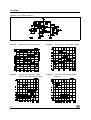
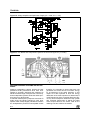
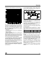
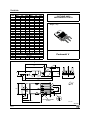
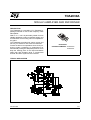
TDA2030A ® 18W Hi-Fi AMPLIFIER AND 35W DRIVER DESCRIPTION The TDA2030A is a monolithic IC in Pentawatt package intended for use as low frequency class AB amplifier. With VS max = 44V it is particularly suited for more reliable applications without regulated supply and for 35W driver circuits using low-cost complementary pairs. The TDA2030A provides high output current and has very low harmonic and cross-over distortion. Further the device incorporates a short circuit protection system comprising an arrangement for automatically limiting the dissipated power so as to keep the working point of the output transistors within their safe operating area. A conventional thermal shut-down system is also included. PENTAWATT ORDERING NUMBERS : TDA2030AH TDA2030AV TYPICAL APPLICATION October 2000 1/15 TDA2030A PIN CONNECTION (Top view) TEST CIRCUIT THERMAL DATA Symbol Rth (j-case) 2/15 Parameter Thermal Resistance Junction-case Max Value Unit 3 °C/W TDA2030A ABSOLUTE MAXIMUM RATINGS Symbol Parameter Value Unit ± 22 V Vs Supply Voltage Vi Input Voltage Vi Differential Input Voltage ± 15 V Io Peak Output Current (internally limited) 3.5 A Ptot Total Power Dissipation at Tcase = 90 °C Tstg, Tj Vs Storage and Junction Temperature 20 W – 40 to + 150 °C ELECTRICAL CHARACTERISTICS (Refer to the test circuit, VS = ± 16V, Tamb = 25oC unless otherwise specified) Symbol Parameter Vs Supply Voltage Id Quiescent Drain Current Ib Test Conditions Min. Typ. ±6 50 Max. Unit ± 22 V 80 mA Input Bias Current VS = ± 22V 0.2 2 µA Vos Input Offset Voltage VS = ± 22V ±2 ± 20 mV Ios Input Offset Current ± 20 ± 200 nA PO Output Power W d = 0.5%, Gv = 26dB f = 40 to 15000Hz VS = ± 19V RL = 4Ω RL = 8Ω RL = 8Ω 15 10 13 18 12 16 100 kHz 8 V/µsec BW Power Bandwidth SR Slew Rate Gv Open Loop Voltage Gain f = 1kHz Gv Closed Loop Voltage Gain f = 1kHz d Total Harmonic Distortion RL = 4Ω Po = 0.1 to 14W f = 40 to 15 000Hz f = 1kHz Po = 0.1 to 9W, f = 40 to 15 000Hz RL = 8Ω 0.08 0.03 % % 0.5 % Po = 15W RL = 4Ω 80 25.5 26 dB 26.5 dB d2 Second Order CCIF Intermodulation Distortion PO = 4W, f2 – f1 = 1kHz, RL = 4Ω 0.03 % d3 Third Order CCIF Intermodulation Distortion f1 = 14kHz, f2 = 15kHz 2f1 – f2 = 13kHz 0.08 % eN Input Noise Voltage B = Curve A B = 22Hz to 22kHz 2 3 10 µV µV B = Curve A B = 22Hz to 22kHz 50 80 200 pA pA RL = 4Ω, Rg = 10kΩ, B = Curve A PO = 15W PO = 1W 106 94 dB dB iN S/N Ri SVR Tj Input Noise Current Signal to Noise Ratio Input Resistance (pin 1) Supply Voltage Rejection Thermal Shut-down Junction Temperature (open loop) f = 1kHz RL = 4Ω, Rg = 22kΩ Gv = 26dB, f = 100 Hz 0.5 5 MΩ 54 dB 145 °C 3/15 TDA2030A Figure 1 : Single Supply Amplifier Figure 2 : Open Loop-frequency Response Figure 4 : 4/15 Total Harmonic Distortion versus Output Power (test using rise filters) Figure 3 : Output Power versus Supply Voltage Figure 5 : Two Tone CCIF Intremodulation Distortion TDA2030A Figure 6 : Large Signal Frequency Response Figure 7 : Maximum Allowable Power Dissipation versus Ambient Temperature Figure 8 : Output Power versus Supply Voltage Figure 9 : Total Harmonic Distortion versus Output Power Figure 10 : Output Power versus Input Level Figure 11 : Power Dissipation versus Output Power 5/15 TDA2030A Figure 12 : Single Supply High Power Amplifier (TDA2030A + BD907/BD908) Figure 13 : P.C. Board and Component Layout for the Circuit of Figure 12 (1:1 scale) 6/15 TDA2030A TYPICAL PERFORMANCE OF THE CIRCUIT OF FIGURE 12 Symbol Parameter Test Conditions Vs Supply Voltage Id Quiescent Drain Current Vs = 36V Po Output Power d = 0.5%, RL = 4Ω, f = 40 z to 15Hz Vs = 39V Vs = 36V d = 10%, RL = 4Ω, f = 1kHz Vs = 39V Vs = 36V Gv Voltage Gain SR Slew Rate d f = 1kHz Total Harmonic Distortion Po = 20W Min. 19.5 Typ. Max. 36 44 Unit V 50 mA 35 28 W W 44 35 W W 20 20.5 dB 8 V/µsec f = 1kHz f = 40Hz to 15kHz 0.02 0.05 % % mV Vi Input Sensitivity Gv = 20dB, f = 1kHz, Po = 20W, RL = 4Ω 890 S/N Signal to Noise Ratio RL = 4Ω, Rg = 10kΩ, B = Curve A Po = 25W Po = 4W 108 100 dB Figure 14 : Typical Amplifier with Spilt Power Supply Figure 15 : P.C. Board and Component Layout for the Circuit of Figure 14 (1:1 scale) 7/15 TDA2030A Figure 16 : Bridge Amplifier with Split Power Supply (PO = 34W, VS = ± 16V) Figure 17 : P.C. Board and Component Layout for the Circuit of Figure 16 (1:1 scale) MULTIWAY SPEAKER SYSTEMS AND ACTIVE BOXES Multiway loudspeaker systems provide the best possible acoustic performance since each loudspeaker is specially designed and optimized to handle a limited range of frequencies. Commonly, these loudspeaker systems divide the audio spectrum into two or three bands. To maintain a flat frequency response over the Hi-Fi audio range the bands covered by each loudspeaker must overlap slightly. Imbalance between the loudspeakers produces unacceptable results 8/15 therefore it is important to ensure that each unit generates the correct amount of acoustic energy for its segmento of the audio spectrum. In this respect it is also important to know the energy distribution of the music spectrum to determine the cutoff frequencies of the crossover filters (see Figure 18). As an example a 100W three-way system with crossover frequencies of 400Hz and 3kHz would require 50W for the woofer, 35W for the midrange unit and 15W for the tweeter. TDA2030A Figure 18 : Power Distribution versus Frequency A more effective solution, named "Active Power Filter" by SGS-THOMSON is shown in Figure 19. Figure 19 : Active Power Filter Both active and passive filters can be used for crossovers but today active filters cost significantly less than a good passive filter using air cored inductors and non-electrolytic capacitors. In addition, active filters do not suffer from the typical defects of passive filters: - power less - increased impedance seen by the loudspeaker (lower damping) - difficulty of precise design due to variable loudspeaker impedance. Obviously, active crossovers can only be used if a power amplifier is provided for each drive unit. This makes it particularly interesting and economically sound to use monolithic power amplifiers. In some applications, complex filters are not really necessary and simple RC low-pass and high-pass networks (6dB/octave) can be recommended. The result obtained are excellent because this is the best type of audio filter and the only one free from phase and transient distortion. The rather poor out of band attenuation of single RC filters means that the loudspeaker must operate linearly well beyond the crossover frequency to avoid distortion. The proposed circuit can realize combined power amplifiers and 12dB/octave or 18dB/octave highpass or low-pass filters. In practice, at the input pins of the amplifier two equal and in-phase voltages are available, as required for the active filter operation. The impedance at the pin (-) is of the order of 100Ω, while that of the pin (+) is very high, which is also what was wanted. The component values calculated for fc = 900Hz using a Bessek 3rd order Sallen and Key structure are : C1 = C2 = C3 R1 R2 R3 22nF 8.2kΩ 5.6kΩ 33kΩ Using this type of crossover filter, a complete 3-way 60W active loudspeaker system is shown in Figure 20. It employs 2nd order Buttherworth filters with the crossover frequencies equal to 300Hz and 3kHz. The midrange section consists of two filters, a high pass circuit followed by a low pass network. With VS = 36V the output power delivered to the woofer is 25W at d = 0.06% (30W at d = 0.5%). The power delivered to the midrange and the tweeter can be optimized in the design phase taking in account the loudspeaker efficiency and impedance (RL = 4Ω to 8Ω). It is quite common that midrange and tweeter speakers have an efficiency 3dB higher thanwoofers. 9/15 TDA2030A Figure 20 : 3 Way 60W Active Loudspeaker System (VS = 36V) 10/15 TDA2030A MUSICAL INSTRUMENTS AMPLIFIERS Another important field of application for active systems is music. In this area the use of several medium power amplifiers is more convenient than a single high power amplifier, and it is also more realiable. A typical example (see Figure 21) consist of four amplifiers each driving a low-cost, 12 inch loudspeaker. This application can supply 80 to 160WRMS. down to the values as low as 0.002% in high power amplifiers. Figure 22 : Overshoot Phenomenon in Feedback Amplifiers Figure 21 : High Power Active Box for Musical Instrument TRANSIENT INTERMODULATION DISTORTION (TIM) Transient intermodulation distortion is an unfortunate phenomen associated with negative-feedback amplifiers. When a feedback amplifier receives an input signal which rises very steeply, i.e. contains high-frequency components, the feedback can arrive too late so that the amplifiers overloads and a burst of intermodulation distortion will be produced as in Figure 22. Since transients occur frequently in music this obviously a problem for the designer of audio amplifiers. Unfortunately, heavy negative feedback is frequency used to reduce the total harmonic distortion of an amplifier, which tends to aggravate the transient intermodulation (TIM situation. The best known method for the measurement of TIM consists of feeding sine waves superimposed onto square waves, into the amplifier under test. The output spectrum is then examined using a spectrum analyser and compared to the input. This method suffers from serious disadvantages : the accuracy is limited, the measurement is a rather delicate operation and an expensive spectrum analyser is essential. A new approach (see Technical Note 143) applied by SGS-THOMSON to monolithic amplifiers measurement is fast cheap-it requires nothing more sophisticated than an oscilloscope - and sensitive - and it can be used The "inverting-sawtooh" method of measurement is based on the response of an amplifier to a 20kHz sawtooth waveform. The amplifier has no difficulty following the slow ramp but it cannot follow the fast edge. The output will follow the upper line in Figure 23 cutting of the shaded area and thus increasing the mean level. If this output signal is filtered to remove the sawtooth, direct voltage remains which indicates the amount of TIM distortion, although it is difficult to measure because it is indistinguishable from the DC offset of the amplifier. This problem is neatly avoided in the IS-TIM method by periodically inverting the sawtooth waveform at a low audio frequency as shown in Figure 24. Figure 23 : 20kHz Sawtooth Waveform Figure 24 : Inverting Sawtooth Waveform 11/15 TDA2030A In the case of the sawtooth in Figure 25 the mean level was increased by the TIM distortion, for a sawtooth in the other direction the opposite is true. The result is an AC signal at the output whole peak-to-peak value is the TIM voltage, which can be measured easily with an oscilloscope. If the peak-to-peak value of the signal and the peak-topeak of the inverting sawtooth are measured, the TIM can be found very simply from: VOUT ⋅ 100 TIM = Vsawtooth In Figure 25 the experimental results are shown for the 30W amplifier using the TDA2030A as a driver and a low-cost complementary pair. A simple RC filter on the input of the amplifier to limit the maximum signal slope (SS) is an effective way to reduce TIM. Figure 26 : TIM Design Diagram (fC = 30kHz) POWER SUPPLY Figure 25 : TIM Distortion versus Output Power Using monolithic audio amplifier with non-regulated supply voltage it is important to design the power supply correctly. In any working case it must provide a supply voltage less than the maximum value fixed by the IC break-down voltage. It is essential to take into account all the working conditions, in particular mains fluctuations and supply voltage variations with and without load. The TDA2030A (VS max = 44V) is particularly suitable for substitution of the standard IC power amplifiers (with VS max = 36V) for more reliable applications. An example, using a simple full-wave rectifier followed by a capacitor filter, is shown in the table 1 and in the diagram of Figure 27. Figure 27 : DC Characteristics of 50W Non-regulated Supply The diagram of Figure 26 originated by SGSTHOMSON can be used to find the Slew-Rate (SR) required for a given output power or voltage and a TIM design target. For example if an anti-TIM filter with a cutoff at 30kHz is used and the max. peak-to-peak output voltage is 20V then, referring to the diagram, a Slew-Rate of 6V/µs is necessary for 0.1% TIM. As shown Slew-Rates of above 10V/µs do not contribute to a further reduction in TIM. Slew-Rates of 100/µs are not only useless but also a disadvantage in Hi-Fi audio amplifiers because they tend to turn the amplifier into a radio receiver. 12/15 TDA2030A APPLICATION SUGGESTION The recommended values of the components are those shown on application circuit of Figure 14. Different values can be used. The Table 2 can help the designer. Table 1 DC Output Voltage (Vo) Mains (220V) Secondary Voltage Io = 0 Io = 0.1A Io = 1A + 20% 28.8V 43.2V 42V 37.5V + 15% 27.6V 41.4V 40.3V 35.8V + 10% 26.4V 39.6V 38.5V 34.2V – 24V 36.2V 35V 31V – 10% 21.6V 32.4V 31.5V 27.8V – 15% 20.4V 30.6V 29.8V 26V – 20% 19.2V 28.8V 28V 24.3V SHORT CIRCUIT PROTECTION The TDA2030A has an original circuit which limits the current of the output transistors. This function can be considered as being peak power limiting rather than simple current limiting. It reduces the possibility that the device gets damaged during an accidental short circuit from AC output to ground. A regulated supply is not usually used for the power output stages because of its dimensioning must be done taking into account the power to supply in the signal peaks. They are only a small percentage of the total music signal, with consequently large overdimensioning of the circuit. Even if with a regulated supply higher output power can be obtained (VS is constant in all working conditions), the additional cost and power dissipation do not usually justify its use. Using non-regulated supplies, there are fewer designe restriction. In fact, when signal peaks are present, the capacitor filter acts as a flywheel supplying the required energy. In average conditions, the continuous power supplied is lower. The music power/continuous power ratio is greater in this case than for the case of regulated supplied, with space saving and cost reduction. THERMAL SHUT-DOWN The presence of a thermal limiting circuit offers the following advantages: 1. An overload on the output (even if it is permanent), or an above limit ambient temperature can be easily supported since the Tj cannot be higher than 150oC. 2. The heatsink can have a smaller factor of safety compared with that of a conventional circuit. There is no possibility of device damage due to high junction temperature. If for any reason, the junction temperature increases up to 150oC, the thermal shut-down simply reduces the p ower dissip at io n a nd t he curren t consumption. Table 2 R1 R2 R3 R4 Recom. Value 22kΩ 680Ω 22kΩ 1Ω R5 ≅ 3 R2 C1 1µF Input DC Decoupling C2 22µF Inverting DC Decoupling C3, C4 C5, C6 0.1µF 100µF Supply Voltage Bypass Supply Voltage Bypass C7 C8 0.22µF 1 ≈ 2πBR1 Frequency Stability D1, D2 1N4001 To protect thedeviceagainst output voltagespikes Comp. Purpose Closed loop gain setting Closed loop gain setting Non inverting input biasing Frequency Stability Upper Frequency Cut-off UpperFrequencyCut-off Larger than Recommended Value Increase of gain Decrease of gain (*) Increase of input impedance Danger of oscillation at high frequencies with inductive loads Poor High Frequencies Attenuation Smaller than Recommended Value Decrease of gain Increase of gain Decrease of input impedance Danger of Oscillation Increase of low frequencies cut-off Increase of low frequencies cut-off Danger of Oscillation Danger of Oscillation Larger Bandwidth SmallerBandwidth LargerBandwidth (*) The value of closed loop gain must be higher than 24dB. 13/15 TDA2030A DIM. A C D D1 E E1 F F1 G G1 H2 H3 L L1 L2 L3 L4 L5 L6 L7 L9 L10 M M1 V4 V5 Dia MIN. mm TYP. 2.4 1.2 0.35 0.76 0.8 1.0 3.2 6.6 3.4 6.8 10.05 17.55 15.55 21.2 22.3 17.85 15.75 21.4 22.5 2.6 15.1 6.0 2.1 4.3 4.23 3.75 4.5 4.0 3.65 MAX. MIN. 4.8 1.37 2.8 0.094 1.35 0.047 0.55 0.014 1.19 0.030 1.05 0.031 1.4 0.039 3.6 0.126 7.0 0.260 10.4 10.4 0.396 18.15 0.691 15.95 0.612 21.6 0.831 22.7 0.878 1.29 3.0 0.102 15.8 0.594 6.6 0.236 2.7 0.008 4.8 0.17 4.75 0.167 4.25 0.148 40˚ (typ.) 90˚ (typ.) 3.85 0.144 inch TYP. 0.134 0.268 0.703 0.620 0.843 0.886 0.178 0.157 MAX. 0.189 0.054 0.110 0.053 0.022 0.047 0.041 0.055 0.142 0.276 0.409 0.409 0.715 0.628 0.850 0.894 0.051 0.118 0.622 0.260 0.106 0.189 0.187 0.167 OUTLINE AND MECHANICAL DATA Weight: 2.00gr Pentawatt V 0.152 L L1 E M1 A M D C D1 L5 V5 L2 H2 L3 F E E1 V4 H3 G G1 Dia. F F1 L9 L4 L10 L7 L6 H2 V4 RESIN BETWEEN LEADS PENTVME 0015981 14/15