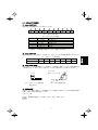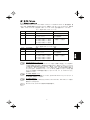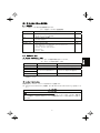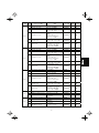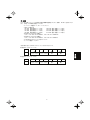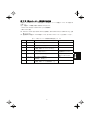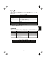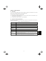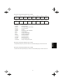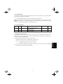
1
取扱説明書 / Instruction Manual CANopen 通信カード CANopen Communications Card "OPC-G1-COP" ENGLISH 日本語 Fuji Electric Systems Co., Ltd. INR-SI47-1331b-JE Copyright © 2008 Fuji Electric Systems Co., Ltd. All rights reserved. この取扱説明書の著作権は,富士電機システムズ株式会社にあります。 本書に掲載されている会社名や製品名は,一般に各社の商標または登録商標です。 仕様は予告無く変更することがあります。 No part of this publication may be reproduced or copied without prior written permission from Fuji Electric Systems Co., Ltd. All products and company names mentioned in this manual are trademarks or registered trademarks of their respective holders. The information contained herein is subject to change without prior notice for improvement. 日本語 日本語版 まえがき CANopen 通信カード「OPC-G1-COP」をお買上げいただきましてありがとうございます。 この取扱説明書は, CANopen マスタと FRENIC-MEGA を CANopen 通信で接続する用途でご利用頂くためのものです。 この通信カードを FRENIC-MEGA に取り付けることで,PLC やパソコンなどの CANopen マスタと接続し,運転指令・ 周波数指令・機能コードアクセス等を使って FRENIC-MEGA をスレーブとしてコントロールすることができます。 本通信カードの特徴を以下に示します。 - 通信プロファイル : DS 301 Ver.4.02, DSP 402 Ver.2.0 Velocity Mode - 通信速度 : 20kbit/s~1Mbit/s - 最大ケーブル長 : 25m (1Mbit/s)~2500m (20kbit/s) - FRENIC-MEGA が持つ全機能コードを読み書き可能 この取扱説明書にはインバータに関する取扱い方の記載はありませんので,ご使用の前には,この説明書とイン バータ本体の取扱説明書をお読みになって取扱い方を理解し,正しくご使用ください。間違った取扱いは,正常 な運転を妨げ,寿命の低下や故障の原因になります。 取扱説明書はご使用後も大切に保管してください。 関連資料 OPC-G1-COP に関連する資料を以下に示します。目的に応じてご利用ください。 資料は随時改訂していますので,ご使用の際には最新版の資料を入手してください。 また, この取扱説明書は, 以下の CAN in Automation (CiA) 発行 CANopen 仕様書の基本的知識を有しているこ とを前提に記述しております。本通信カードご使用の前にご一読されることを推奨いたします。 ・ DS 301 Ver. 4.02 ・ DSP 402 Ver. 2.0 上記の仕様書は CiA の Web サイト(下記)から無料でダウンロード可能です。 http://www.can-cia.de/ - この取扱説明書を読み,理解したうえで,CANopen 通信カードの取付け,接続(配線),運転,保守点検を 行ってください。 - 間違った取扱いは,正常な運転を妨げたり,寿命の低下や故障の原因になります。 - この取扱説明書は,実際に使用される最終需要家に確実にお届けください。最終需要家はこの取扱説明書 を,CANopen 通信カードが廃棄されるまで大切に保管してください。 ■ 安全上のご注意 取付け,配線(接続),運転,保守点検の前に必ずこの取扱説明書を熟読し,製品を正しく使用してください。 更に,機器の知識,安全に関する情報および注意事項のすべてについても十分に習熟してください。 この取扱説明書では,安全注意事項のランクは下記のとおり区別されています。 取扱いを誤った場合に危険な状況が起こる可能性があり,死亡または重傷を負う事故の発生が想定 される場合 取扱いを誤った場合に危険な状況が起こる可能性があり,中程度の傷害や軽傷を受ける事故または 物的損害の発生が想定される場合 なお,注意に記載した事項の範囲内でも状況によっては重大な結果に結びつく可能性があります。 いずれも重要な内容を記載していますので必ず守ってください。 1 日本語 ・ RS-485 通信ユーザーズマニュアル ・ FRENIC-MEGA 取扱説明書 取付けおよび配線について ・ インバータの電源を遮断して 22kW 以下は5分以上,30kW 以上は 10 分以上経過してから行ってください。更に LED モニタおよびチャージランプの消灯を確認し,テスターなどを使用して主回路端子 P(+)-N(-)間の直流中間回路電 圧が安全な値(DC+25V 以下)に下がっていることを確認してから行ってください。 ・ 配線作業は,資格のある専門家が行ってください。 感電のおそれあり ・ 外部あるいは内部部品が損傷・脱落している製品を使用しないでください。 火災,事故,けがのおそれあり ・ 糸くず,紙,木くず,ほこり,金属くずなどの異物がインバータや通信カード内に侵入するのを防止してくださ い。 火災,事故のおそれあり ・ 製品の取付け,取外し時に不適切な作業を行うと,製品が破損するおそれがあります。 故障のおそれあり ・ インバータ,モータ,配線からノイズが発生します。周辺のセンサーや機器の誤動作に注意してください。 事故のおそれあり 操作運転について ・ 必ずインバータ本体の表面カバーを取り付けてから電源 ON(閉)してください。なお,通電中はカバーを外さな いでください。 ・ 濡れた手でスイッチを操作しないでください。 感電のおそれあり ・ 機能コードのデータ設定を間違えたり,取扱説明書およびユーザーズマニュアルを十分理解しないで機能コード のデータ設定を行うと,機械が許容できないトルクや速度でモータが回転することがあります。インバータの運 転の前に各機能コードの確認,調整を行ってください。 事故のおそれあり 保守点検,部品の交換について ・ インバータの電源を遮断して 22kW 以下は5分以上,30kW 以上は 10 分以上経過してから行ってください。更に LED モニタおよびチャージランプの消灯を確認し,テスターなどを使用して主回路端子 P(+)-N(-)間の直流中間回路電 圧が安全な値(DC+25V 以下)に下がっていることを確認してから行ってください。 感電のおそれあり ・ 指定された人以外は,保守点検,部品交換をしないでください。 ・ 作業前に金属物,(時計,指輪など)を外してください。 ・ 絶縁対策工具を使用してください。 感電,けがのおそれあり 2 廃棄について ・ 製品を廃棄する場合は,産業廃棄物として扱ってください。 けがのおそれあり その他 ・ 改造は絶対しないでください。 感電,けがのおそれあり 日本語 アイコンについて 本書では以下のアイコンを使用しています。 この表示を無視して誤った取扱いをすると,FRENIC-MEGA が本来持つ性能を発揮できなかったり,その 操作や設定が事故につながることになります。 本製品の操作や設定の際,知っておくと便利な参考事項を示しています。 参照先を示します。 3 目次 まえがき 第 8 章 SDO プロトコル .................... 22 8.1 SDO について ....................... 22 8.2 SDO 異常時の応答 ................... 22 ................................. 1 ■ 安全上のご注意 ........................... 1 第 1 章 ご使用のまえに ..................... 5 1.1 現品の確認 .......................... 5 1.2 対象インバータ ...................... 5 第 9 章 その他の CANopen 通信機能 .......... 23 9.1 機能概要 ........................... 23 9.2 その他のサービス ................... 23 第 2 章 各部の名称と機能 ................... 6 2.1 各部の名称 .......................... 6 2.2 CANopen 端子台....................... 6 2.3 LED インジケータ..................... 6 第 10 章 オブジェクト一覧 .................. 25 10.1 コミュニケーションプロファイル 領域のオブジェクト ................. 25 10.2 富士特有プロファイル領域の オブジェクト ....................... 29 10.3 標準デバイスプロファイル領域 ....... 30 第 3 章 通信カードの取付けと取外し ......... 7 3.1 通信カードの取付け .................. 7 3.2 通信カードの取外し .................. 9 第 11 章 CANopen 通信でのインバータの運転... 32 11.1 CANopen のドライブプロファイル (DSP 402)による運転 .............. 32 11.2 インバータ機能コード S06 による運転 . 37 第 4 章 配線 .............................. 10 4.1 基本接続図 ......................... 10 4.2 CANopen 端子台の配線................ 11 4.3 インバータへの配線 ................. 12 第 5 章 CANopen 設定に関連するインバータ 機能コード ........................ 13 第 6 章 CANopen 通信確立までの手順......... 14 第 7 章 7.1 7.2 7.3 7.4 PDO プロトコル .................... 15 PDO プロトコルについて.............. 15 受信 PDO(マスタ→インバータ)...... 16 送信 PDO(インバータ→マスタ)...... 18 受信 PDO のコミュニケーション パラメータ ......................... 19 送信 PDO のコミュニケーション パラメータ ......................... 20 7.5 第 12 章 Heartbeat および Node Guarding ..... 41 12.1 Heartbeat .......................... 41 12.2 Node Guarding ...................... 42 第 13 章 CANopen ネットワーク断線検出時の 動作 .............................. 43 第 14 章 アラームコード一覧 ................ 44 第 15 章 その他注意点 ...................... 46 第 16 章 仕様 .............................. 47 16.1 一般仕様 ........................... 47 16.2 CANopen 仕様 ....................... 47 4 第 1 章 ご使用のまえに 1.1 現品の確認 開梱し次の項目を確認してください。 (1) 通信カード,ねじ(M3×8:2本),取扱説明書(本書)が入っていることを確認してください。 (2) 通信カード上の部品の異常,凹み,反りなど輸送時での破損がないことを確認してください。 (3) 通信カード上に形式「OPC-G1-COP」が印刷されていることを確認してください。(図 2.1 参照) 製品にご不審な点や不具合などがありましたら,お買い上げ店または最寄りの弊社営業所までご連絡ください。 本通信カードには EDS ファイルおよび終端抵抗は付属していません。 - EDS ファイルは本通信カードをマスタ設定用のツール(コンフィギュレータ)に登録するために必 要です。EDS ファイルは次の Web サイトにてダウンロード可能です。 (会員登録が必要(無料) 富士電機システムズ 技術情報ページ URL : https://web1.fujielectric.co.jp/Kiki-Info/User/guestlogin.asp - 終端抵抗は次のものをご使用ください。120Ω±1%, 1/4W, 金属皮膜抵抗。 1.2 対象インバータ 本通信カードは,下表のインバータ形式および ROM バージョンで使用できます。 表 1.1 適用インバータ形式と ROM バージョン 形式 インバータ容量 ROM バージョン FRENIC-MEGA FRN□□□G1□-□□□ 全容量 1000 以降 ※ □には,インバータ容量,タイプ,電圧シリーズなどを示す英数字が入ります。 インバータの ROM バージョンは,プログラムモードのメニュー番号5「メンテナンス情報」の 5_14 で確認す ることができます。詳細は,FRENIC-MEGA 取扱説明書の第 3 章「3.4.6 メンテナンス情報を見る」を参照してく ださい。 LED モニタの表示 5_14 項目 表示内容 インバータ ROM バージョン インバータの ROM バージョンを4桁で表示します。 5 日本語 機種 第 2 章 各部の名称と機能 2.1 各部の名称 CANopen 通信カードの各部の名称を図 2.1 に示します。 ねじ取付け用穴(左) 形式 CANopen 端子台(TERM1) 取外し用つまみ CN1 (表面) 取付け位置決め部 (裏面) LED インジケータ 図 2.1 2.2 ねじ取付け用穴(右) CANopen 通信カードの各部の名称 CANopen 端子台 CANopen 通信ケーブルを接続します。 2.3 配線に関する詳細は,第 4 章「配線」を参照してください。 LED インジケータ 本通信カードの動作状態や CANopen の通信状態を 2 個の LED で示します。 表 2.1 LED LED の状態 表示 状態 RUN 消灯 電源オフ,通信異常 (緑) 点滅(シングルフラッシュ *1) CANopen「Stop」状態 点滅(ブリンク *2) CANopen「Pre-Operational」状態 点灯 CANopen「Operational」状態 ERR 消灯 通信異常なし (赤) 点滅(シングルフラッシュ *1) CAN エラーパッシブ状態 点滅(ダブルフラッシュ *3) Heartbeat/Node Guarding による断線検出時 点滅(ブリンク *2) インバータとの接続不良 点灯 CAN バスオフ状態 *4 RUN,ERR 同時点灯 *1 *2 *3 *4 本通信カードの CPU 異常 シングルフラッシュ: 200ms 点灯,1s 消灯で点滅 ブリンク: 2.5Hz(200ms 点灯, 200ms 消灯)で点滅 ダブルフラッシュ: 200ms 点灯,200ms 消灯,200ms 点灯,1s 消灯で点滅 CAN バスオフ時は、不定周期で ERR LED が点滅することがあります。 6 第 3 章 通信カードの取付けと取外し インバータの電源を遮断して 22kW 以下は5分以上,30kW 以上は 10 分以上経過してから行ってください。更に LED モニタおよびチャージランプの消灯を確認し,テスターなどを使用して主回路端子 P(+)-N(-)間の直流中間回路電圧 が安全な値(DC+25V 以下)に下がっていることを確認してから行ってください。 感電のおそれあり ・ 外部あるいは内部部品が損傷・脱落している製品を使用しないでください。 火災,事故,けがのおそれあり ・ 糸くず,紙,木くず,ほこり,金属くずなどの異物がインバータや通信カード内に侵入するのを防止してくださ い。 火災,事故のおそれあり ・ 製品の取付け,取外し時に不適切な作業を行うと,製品が破損するおそれがあります。 故障のおそれあり 3.1 通信カードの取付け (1) インバータ本体のカバーを取り外し,制御プリント基板を露出してください。通信カードは,インバータ本 体のオプション接続ポート3箇所(A-,B-,C-port)のうち,A-port にのみ取付け可能です。 (図 3.1) FRENIC-MEGA 取扱説明書の第 2 章「2.3 配線」を参照してカバーを取り外してください。 (30kW 以上は タッチパネルケースも開けてください。) (2) 通信カードの裏面(図 2.1)の CN1 を,インバータ本体の制御プリント基板の A-port(CN4)へ差し込み,付 属ねじで固定して下さい。(図 3.3) 通信カードの取付け位置決め部(図 2.1)がツメ(図 3.2 ①)にセットされ,CN1(図 3.2 ②)が確 実に差し込まれていることを確認してください。図 3.3 は取付け完了を示します。 (3) 通信カードの配線を行います。 第 4 章「配線」を参照してください。 (4) インバータ本体のカバーを元に戻してください。 FRENIC-MEGA 取扱説明書の第 2 章「2.3 配線」を参照してカバーを取り付けてください。 (30kW 以上は タッチパネルケースも閉じてください。) 7 日本語 インバータ本体の主回路端子および制御回路端子の配線は,通信カードを取り付ける前に行ってくだ さい。 取付け不可 取付け不可 図 3.1 0.4kW の例 ① 通信カードをツメに引っ掛けるようにしながら インバータ本体へ位置決めする。 ② コネクタをインバータ本体へ挿入する。 注:先にコネクタ側を挿入した場合,挿入が不十分で 接触不良となる可能性があります。 ② ① ツメ 図 3.2 通信カードの取付け(A-port 取付け時) 8 (取外し用つまみ) 図 3.3 通信カードの取外し 通信カードを取り外す際は,ねじを2ヶ所外し,取外し用つまみ(図 3.3 を参照)を引っぱって取り外してくだ さい。 9 日本語 3.2 取付け完了(A-port 取付け時) 第 4 章 配線 ・ インバータの電源を遮断して 22kW 以下は5分以上,30kW 以上は 10 分以上経過してから行ってください。更に LED モニタおよびチャージランプの消灯を確認し,テスターなどを使用して主回路端子 P(+)-N(-)間の直流中間回路電 圧が安全な値(DC+25V 以下)に下がっていることを確認してから行ってください。 ・ 配線作業は,資格のある専門家が行ってください。 感電のおそれあり ・ 一般的に制御信号線の被覆は強化絶縁されていませんので,主回路活電部に制御信号線が直接触れると,何らか の原因で絶縁被覆が破壊されることがあります。この場合,制御信号線に主回路の高電圧が印加される危険性が ありますので,主回路活電部に制御信号線が触れないように注意してください。 事故のおそれあり,火災のおそれあり インバータ,モータ,配線からノイズが発生します。周辺のセンサーや機器の誤動作に注意してください。 事故のおそれあり 4.1 基本接続図 FRENIC-MEGA L1/R U モータ L2/S V M L3/T W G OPC-G1-COP CAN トランシーバ CANopen 端子台 CANopen専用ケーブル 1 CAN_GND 2 CAN_L 3 CAN_H 4 CAN_SHILD *1 4 5 5 CAN_V+ *2 1 2 3 G G *1 本通信カードの内部回路とは接続されていません。必要に応じて機能接地してください。 *2 本通信カードの内部回路とは接続されていません。電圧は出力されません。 図 4.1 基本接続図 10 4.2 CANopen 端子台の配線 (1) CANopen 端子台(TERM1) 端子配列および端子機能を図 4.2 および表 4.1 に示します。 1 2 3 4 4 5 5 1 2 3 CAN_ GND CAN _L CAN _H CAN_ SHLD CAN_ SHLD CAN _V+ CAN _V+ CAN_ GND CAN _L CAN _H 図 4.2 表 4.1 CANopen 端子台の配列 CANopen 端子台の端子機能 端子番号 端子名称 1 CAN_GND 説明 2 CAN_L CAN 信号 Low 側 3 CAN_H CAN 信号 High 側 4 CAN_SHLD *1 5 CAN_V+ *2 CAN 信号のグランド シールド線 接続なし *1 本通信カードの内部回路とは接続されていません。必要に応じ機能接地してください。 *2 本通信カードの内部回路とは接続されていません。電圧は出力されません。 (2) CANopen 通信ケーブル 通信ケーブルは必ず CANopen 専用ケーブルを使用してください。ケーブルの最大配線長は表 4.2 のとおりです。 CANopen ケーブル最大配線長 20k 50k 125k 250k 500k 800k 1M 最大配線長 2500m 1000m 500m 250m 100m 50m 25m (3) CANopen 端子台への配線 CANopen 通信ケーブルの電線の被覆をむいて,電線やシールド線を撚って接続してください。電線の被覆むきサ イズは図 4.3 に従ってください。また,端子台のネジサイズおよび締め付けトルクを図 4.4 に示します。 ネジサイズ M3 5~7(mm) 図 4.3 CANopen ケーブル電線の推奨 被覆むきサイズ 締付けトルク 0.5~0.6Nm 図 4.4 CANopen 通信端子接続 (4) 終端抵抗の接続 本通信カードが CANopen 通信ケーブルの両端のどちらかに接続される場合は, 以下に示す終端抵抗を端子 2(CAN_L)と端子 3(CAN_H)の間に接続してください。 120Ω±1%, 1/4W 終端抵抗は本通信カードに付属していません。別途,ご用意ください。 11 日本語 表 4.2 ボーレート(bit/s) 4.3 インバータへの配線 CANopen 配線は,主回路の配線とは可能な限り離して配線してください。ノイズによる誤動作の要因 となります。 配線は,制御プリント基板上を極力這わないよう,図 4.5 のように配線してください。誤動作の原 因になることがあります。 ・22kW 以下の場合 * CANopen 通信カードの配線は,インバータ本体の 制御端子台上部と表面カバーの間を通してください。 0.4kW の例 ・30kW 以上の場合 75kW の例 図 4.5 12 配線例 第 5 章 CANopen 設定に関連するインバータ機能コード 本通信カードが CANopen 通信を行うためには,下記の表 5.1 に示すインバータの機能コードの設定が必要です。 また,関連するインバータ機能コードを表 5.2 に示します。必要に応じて設定してください。 表 5.1 CANopen 通信を行うために必要なインバータ機能コード設定 機能コード 説明 初期値 o31 *1 ノード ID(局番) 設定 0 o32 *2 ボーレート設定 0 設定変更値 備考 0~255(1~127 で適宜設定) 0 および 128 以上設定時はノ ード ID127 となります。 0~255(0~7 で適宜設定) マスタのボーレートと一致 させてください。 0: 125kbit/s, 1: 2: 50kbit/s, 3: 4: 250kbit/s, 5: 6: 800kbit/s, 7: 8 以上: 1Mbit/s y98 *3 運転・周波数指令元 の選択 0 20kbit/s, 125kbit/s, 500kbit/s, 1Mbit/s, 下記から選択 y98=3 を推奨します。 y98 周波数 運転 0 インバータ インバータ 1 CANopen インバータ 2 インバータ CANopen 3 CANopen CANopen *3 運転・周波数指令元の選択を設定するインバータ機能コードは y98 の他にもあります。それらの設定により, より細 やかに運転・周波数指令元の選択が可能となります。詳細は,FRENIC-MEGA 取扱説明書の第 5 章「機能コード」の H30, y98 の項を参照してください。 表 5.2 その他関連機能コード 機能コード 説明 初期値 設定範囲 o27 *1 CANopen 通信エラー時の動作選択 0 0~15 o28 *1 CANopen 通信エラー時の動作タイマー 0.0s 0.0s~60.0s o40~o43 *2 TPDO No.3 に割付けするインバータ機能 コードの指定(書込み) 0(割付なし) 0000~FFFF(hex) o48~o51 *2 RPDO No.3 に割付けするインバータ機能 コードの指定(読出し) 0(割付なし) 0000~FFFF(hex) 備考 本設定は PDO No.3 で 使用します。 *1 o27, o28 についての詳細は,第 13 章「CANopen ネットワーク断線検出時の動作」を参照してください。 *2 o40~o43 および o48~o51 の設定方法は,第 7 章 「7.2(4)インバータ機能コード o40~o43,o48~o51 および Index 5E00, 5E01 の設定方法]を参照してください。 設定後は,インバータに設定を反映させるために, インバータの電源を再投入するか,CANopen マスタから本通信カ ードに対し ResetNode サービスを実施してください。 13 日本語 *1 o31 を設定後は, インバータに設定を反映させるために, インバータの電源を再投入するか CANopen マスタから本通 信カードへ対し ResetNode サービスを実施してください。 *2 o32 を設定後は, インバータに設定を反映させるために, インバータの電源を再投入してください。 第 6 章 CANopen 通信確立までの手順 本章では, マスタとインバータを CANopen 通信接続するまでの手順について説明します。 手順は以下の 1~5 です。 1. 2. 3. 4. 5. CANopen マスタの設定 インバータ機能コードによる本通信カードのノード ID, ボーレート設定 インバータの電源再起動 ⇒ Pre-Operational 状態 断線検出用オブジェクトの設定(Heartbeat あるいは Node Guarding) マスタより本通信カードへ Start Remote Node コマンドを送信 ⇒ Operational 状態 以降, 上記の手順 1~5 について説明します。 1. CANopen マスタの設定 - マスタのノード ID, ボーレートを設定します。 - 本通信カード用の EDS ファイルを使用し, マスタに登録します。 CANopen マスタについての設定方法の詳細は,マスタのユーザーズマニュアル等を参照してください。 本通信カードには EDS ファイルは付属していません。 EDS ファイルは次の Web サイトにてダウンロードください。 (会員登録が必要(無料) ) 富士電機システムズ 技術情報ページ URL : https://web1.fujielectric.co.jp/Kiki-Info/User/guestlogin.asp 2. インバータ機能コードによる本通信カードのノード ID,ボーレート設定 - o31 にてノード ID, o32 にてボーレートを設定します。マスタに登録したアドレス, ボーレートと一致さ せてください。 - 必要に応じて,インバータ機能コード o27,o28 の設定を行ってください。 3. o27,o28 の詳細は,第 13 章「CANopen ネットワーク断線検出時の動作」を参照してください。 インバータの電源再起動 ⇒ Pre-Operational 状態 インバータ再起動した段階で, CANopen マスタとインバータの設定が正しく, かつ適正に配線されていれば, 自動的に Pre-Operational 状態となり, マスタと通信が行える状態になります。 この状態では本通信カードの RUN LED は緑点滅, ERR LED は消灯または赤点滅となります。 4. 断線検出用オブジェクト(Heartbeat あるいは Node Guarding)の設定 断線検出を行うためにマスタ,本通信カード両方で,Heartbeat または Node Guarding の設定を行ってくだ さい。 Heartbeat あるいは Node Guarding については,第 12 章「Heartbeat および Node Guarding」を参照して ください。 CANopen のデバイスは出荷状態では断線検出用オブジェクトの設定が無効となっています。有効にし ない限り, 断線が発生しても本通信カードを含めた CANopen ネットワークは断線を検出しません。有 効に設定することを強くお奨めします。 5. マスタより本通信カードへ Start Remote Node コマンドを送信 ⇒ Operational 状態 このコマンド受信後, 本通信カードの LED は CAN 緑点灯し Operational 状態となります。これによりマスタ から, PDO 通信を使ってリアルタイムにインバータの制御・モニタが可能になります。 PDO 通信のフォーマットについては,第 7 章「PDO プロトコル」を参照してください。 14 第 7 章 PDO プロトコル 7.1 PDO プロトコルについて PDO(Process Data Object)プロトコルは, CANopen マスタとインバータ間でプロセスデータ(例:運転指令, 速 度モニタ等)を定周期で通信するために用いられます。本通信カードは, 表 7.1, 表 7.2 に示すように,受信 PDO (RPDO: マスタ→インバータ)と送信 PDO(TPDO: インバータ→マスタ)を各 3 種類サポートしています。 表7.1 受信 PDO(RPDO: マスタ→インバータ) PDO No. COB-ID 初期値 内容 1 0x200 + ノード ID Controlword 説明 DS-402 の状態遷移制御 2 0x300 + ノード ID Controlword vl target velocity DS-402 の状態遷移制御 および速度指令 3 0x400 + ノード ID o40 で指定した機能コードへ書込み 4 種類分の割付けしたインバ ータ機能コードを書込み o41 で指定した機能コードへ書込み o42 で指定した機能コードへ書込み o43 で指定した機能コードへ書込み 表7.2 送信 PDO(TPDO: インバータ→マスタ) COB-ID 初期値 内容 説明 1 0x180 + ノード ID Statusword DS-402 の状態遷移制御 2 0x280 + ノード ID Statusword vl Control effort DS-402 の状態遷移制御 および速度指令 3 0x380 + ノード ID o48 で指定した機能コードを読出し 4 種類分の割付けしたインバ ータ機能コードを読出し o49 で指定した機能コードを読出し o50 で指定した機能コードを読出し o51 で指定した機能コードを読出し 送信 PDO の送信タイミングについて 出荷時の設定は,「データ変化時および Event timer で指定した時間に PDO 送信」です。受信 PDO に よる指令に同期するのではなく,値が変化すれば送信するため, 場合によってはインバータから3 つの送信 PDO が連続で送信されることあります。 (例えば, マスタは PDO No.2 で指令を与えている のに PDO No.1, No.3 からも応答がある)。このことを防ぐために, それぞれの送信 PDO を無効にす ることができます。その方法については, 「7.5 (2) COB-ID」を参照してください。その他, 送信 タイミングを定周期にする等の設定も可能です。それについては, 「7.5 (3) Transmission type」 を参照してください。 PDO の有効/無効設定について 出荷状態では, 全ての PDO が有効になっています。各 PDO の COB-ID の bit31 を 1 にすることで, そ の PDO を無効(無応答)にできます。 PDO の割付け変更不可 PDO の割付けは固定です。PDO Mapping Parameter(Index 1600~1602, 1A00~1A02)によって割付け 変更することはできません。 PDO プロトコルは, Operational 状態の時のみ使用可能です。 15 日本語 PDO No. 7.2 受信 PDO(マスタ→インバータ) (1) 受信 PDO No.1 COB-ID Byte 0x200 + ノード ID 0 Controlword (下位 byte) 1 Controlword (上位 byte) Controlword: 内容 DSP 402 のステートマシン操作によるインバータの運転制御 Controlword および DSP 402 のステートマシンについては,第 11 章「11.1 CANopen のドライブプロファイ ル(DSP 402)による運転」を参照してください。 (2) 受信 PDO No.2 COB-ID Byte 内容 0x300 + ノード ID 0 Controlword (下位 byte) 1 Controlword (上位 byte) 2 vl target velocity (下位 byte) (r/min) 3 vl target velocity (上位 byte) (r/min) Controlword: DSP 402 のステートマシン操作によるインバータの運転制御 vl target velocity: 速度指令(r/min) Controlword,vl control effort および DSP 402 のステートマシンについては,第 11 章「11.1 CANopen のドライブプロファイル(DSP 402)による運転」を参照してください。 (3) 受信 PDO No.3 事前にインバータ機能コード o40~o43 により割付けした機能コードを常時書込みするフォーマットです。割付 けられる機能コードは 4 種類です。 COB-ID Byte 0x400 + ノード ID 内容 0 書込み機能コード 1 (下位 byte) (o40 で指定した機能コードのデータ) 1 書込み機能コード 1 (上位 byte) (o40 で指定した機能コードのデータ) 2 書込み機能コード 2 (下位 byte) (o41 で指定した機能コードのデータ) 3 書込み機能コード 2 (上位 byte) (o41 で指定した機能コードのデータ) 4 書込み機能コード 3 (下位 byte) (o42 で指定した機能コードのデータ) 5 書込み機能コード 3 (上位 byte) (o42 で指定した機能コードのデータ) 6 書込み機能コード 4 (下位 byte) (o43 で指定した機能コードのデータ) 7 書込み機能コード 4 (上位 byte) (o43 で指定した機能コードのデータ) o40~o43 の設定方法については,下記「(4)インバータ機能コード o40~o43,o48~o51 および Index 5E00, 5E01 の設定方法」を参照してください。 割付けしたインバータ機能コードのデータフォーマットについては,RS-485 通信ユーザーズマニュアルの 第 5 章「5.2 データフォーマット」を参照してください。 同一のインバータ機能コードを割付けした場合,o コードの番号が1番小さいものへの割付けだけが 有効となり,残りは割付けなしと見なします。(例:o40 と o43 の両方で同じ機能コードを割付けし た場合, o40 による割付けが有効で, o43 は何も割付けされていない状態となります。) 16 o40~o43 の設定後は,インバータに設定を反映させるために,インバータの電源を再投入するか CANopen マスタからインバータに対し ResetNode サービスを実施してください。 オブジェクトの Index 5E00 Sub1~4 でもインバータ機能コードの割付けが可能です。この場合は, 変更後即時割付け変更となります。ただしインバータの電源再起動, ResetNode サービスを行うと, o40~o43 による割付けに戻ります。 それぞれの受信 PDO の動作反映タイミングを変更可能です。「7.4 (3) Transmission type」を参照し てください。出荷時の設定は, 「受信後,即時インバータに動作反映」です。 (4) インバータ機能コード o40~o43, o48~o51 および Index 5E00, 5E01 の設定方法 下記のように, 4桁の 16 進数で機能コード種別(表 7.3)と番号を指定することで行います。 □□□□ 機能コード番号(16進表記) 機能コード種別(表 7.3 による) 表 7.3 機能コード種別 種別コード 種別 種別コード 種別 種別コード S 0x02 A 0x09 Z 0x12 M 0x03 o 0x0A b 0x13 F 0x04 r 0x0C d 0x14 E 0x05 J 0x0E C 0x06 y 0x0F P 0x07 W 0x10 H 0x08 X 0x11 例:F26 の場合 F ⇒ 種別コード 04 "041A" 26 ⇒ 1A(16 進表記) 17 日本語 種別 7.3 送信 PDO(インバータ→マスタ) (1) 送信 PDO No.1 COB-ID Byte 内容 0x180 + ノード ID 0 Statusword (下位 byte) 1 Statusword (上位 byte) Statusword: DSP 402 のステートマシンの状態表示 Statusword については,第 11 章「11.1 CANopen のドライブプロファイル(DSP 402)による運転」を参照 してください。 (2) 送信 PDO No.2 COB-ID Byte 内容 0x280 + ノード ID 0 Statusword (下位 byte) 1 Statusword (上位 byte) 2 vl control effort (下位 byte) (r/min) 3 vl control effort (上位 byte) (r/min) Statusword: vl control effort: DSP 402 のステートマシンの状態表示 出力速度モニタ (r/min) Statusword および vl control effort については,第 11 章「11.1 CANopen のドライブプロファイル(DSP 402)による運転」を参照してください。 (3) 送信 PDO No.3 事前にインバータ機能コード o48~o51 により割付けした機能コードを常時読出しするフォーマットです。割付 けられる機能コードは 4 種類です。 COB-ID Byte 内容 0x380 + ノード ID 0 読出し機能コード 1 (下位 byte) (o48 で指定した機能コードのデータ) 1 読出し機能コード 1 (上位 byte) (o48 で指定した機能コードのデータ) 2 読出し機能コード 2 (下位 byte) (o49 で指定した機能コードのデータ) 3 読出し機能コード 2 (上位 byte) (o49 で指定した機能コードのデータ) 4 読出し機能コード 3 (下位 byte) (o50 で指定した機能コードのデータ) 5 読出し機能コード 3 (上位 byte) (o50 で指定した機能コードのデータ) 6 読出し機能コード 4 (下位 byte) (o51 で指定した機能コードのデータ) 7 読出し機能コード 4 (上位 byte) (o51 で指定した機能コードのデータ) o48~o51 については「7.2 (4)インバータ機能コード o40~o43,o48~o51 および Index 5E00,5E01 の設 定方法]を参照してください。 割付けしたインバータ機能コードのデータフォーマットについては,RS-485 通信ユーザーズマニュアルの 第 5 章「5.2 データフォーマット」を参照してください。 o48~o51 の設定後は, インバータに設定を反映させるために, インバータの電源を再投入するか CANopen マスタからインバータに対し ResetNode サービスを実施してください。 オブジェクトの Index 5E01 Sub1~4 でもインバータ機能コードの割付けが可能です。この場合は,変 更後即時割付け変更となります。ただしインバータの電源再起動, ResetNode サービスを行うと, o48 ~o51 による割付けに戻ります。 それぞれの送信 PDO の送信タイミングを変更可能です。 「7.5 (3) Transmission type」を参照してく ださい。出荷時の設定は、「データ変化時および Event timer で指定した時間に PDO 送信」です。 18 7.4 受信 PDO のコミュニケーションパラメータ (1) コミュニケーションパラメータ 各受信 PDO(RPDO)の特性を設定します。該当するオブジェクトを表 7.4 に示します。 表 7.4 Index 0x1400 RPDO No.1 0x1401 RPDO No.2 0x1402 RPDO No.3 受信 PDO のコミュニケーションパラメータとデフォルト値 Sub 名称 説明 1 COB-ID 各 PDO の CAN ID 値と有効・無効を設定 デフォルト値: RPDO No.1: 0x200 + ノード ID RPDO No.2: 0x300 + ノード ID RPDO No.3: 0x400 + ノード ID 2 Transmission type 受信内容の動作反映タイミングを設定(表 7.5) デフォルト値: 255(即時インバータへ反映) 表 7.4 のオブジェクトに対して変更した値は本通信カードの電源が OFF しても保持されます。また Index 3001 Restore defaults に 1 を書込むことで,デフォルト値に初期化できます。 (2) COB-ID COB-ID 値の変更は, その PDO が無効となっている場合にのみ実施可能です。 CAN の ID 値は 11bit です。bit11~30 は 0 固定です。 (3) Transmission type 受信 PDO においては, PDO 受信時のインバータへの動作反映タイミングを設定します。表 7.5 に設定一覧を示し ます。 表 7.5 受信 PDO のトランスミッションタイプ設定一覧 Transmission type タイプ名 動作 0 Acyclic Synchronous 受信後, Sync 信号 1 回受信でインバータに動作反映 1-240 Cyclic Synchronous 同上 241-251 予約 --- 252 Synchronous RTR only 不動作 * 253 Asynchronous RTR only 不動作 * 254 Asynchronous1 受信後, 即時インバータに動作反映 255 Asynchronous2 同上(デフォルト値) * 本通信カードは CAN のリモートフレームをサポートしていません。 19 日本語 各 PDO に対する CAN の 11bit の ID 値を指定します。デフォルト値はノード ID により値が変わります。(例: 本 通信カードのノード ID が 1 の場合, RPDO No.2 の COB-ID=0x301) 。最上位 bit(31bit 目)を 1 とすると,その RPDO は無効となります。 7.5 送信 PDO のコミュニケーションパラメータ (1) コミュニケーションパラメータ 各送信 PDO(TPDO)の特性を設定します。該当するオブジェクトを表 7.6 に示します。 表 7.6 Index 送信 PDO のコミュニケーションパラメータとデフォルト値 Sub 名称 説明 1 COB-ID 各 PDO の CAN ID 値と有効・無効を設定 0x1800 TPDO No.1 0x1801 TPDO No.2 デフォルト値: 0x1802 TPDO No.3 TPDO No.1: 0x180 + ノード ID TPDO No.2: 0x280 + ノード ID TPDO No.3: 0x380 + ノード ID 送信タイミングを指定(表 7.7) 2 Transmission type 3 Inhibit time 次の送信までの最小間隔 (0.1ms 単位)を指定 デフォルト値: 100 (10.0ms) * 5 Event timer 定周期送信時間(ms)を指定。Transmission Type254/255 時に 有効 デフォルト値:255 (データ変化時に送信) デフォルト値: 0 (不動作) * * タイマ設定値の分解能は 2ms です。奇数値を設定した場合は, 繰上げとなります。例えば, 119ms を設定した場合 120ms の扱いとなります。 表 7.6 のオブジェクトに対して変更した値は本通信カードの電源が OFF しても保持されます。ま た Index 3001 Restore defaults に 1 を書込むことでデフォルト値に初期化できます。 (2) COB-ID 各 PDO に対する CAN の 11bit の ID 値を指定します。デフォルト値はノード ID により値が変わります。(例: 本 通信カードのノード ID が 1 の場合, TPDO No.2 の COB-ID=0x281) 。最上位 bit(31bit 目)を 1 とすると,その TPDO は無効となります。 COB-ID 値の変更は, その PDO が無効となっている場合にのみ実施可能です。 CAN の ID 値は 11bit です。bit11~30 は 0 固定です。 20 (3) Transmission type 送信 PDO においては, マスタへの送信タイミングを設定します。表 7.7 に設定一覧を示します。 表 7.7 送信 PDO のトランスミッションタイプ設定一覧 Transmission type タイプ名 動作 0 Acyclic Synchronous データ変化があった場合に Sync 信号を受信したら,直後に PDO 送信 1-240 Cyclic Synchronous Sync 信号を 1-240 回受信おきに PDO 送信 (例: 10 ならば Sync 信号を 10 回受信ごとに PDO を送信する) 241-251 予約 - 252 Synchronous RTR only 不動作 * 253 Asynchronous RTR only 不動作 * 254 Asynchronous1 Event timer で指定した時間で定周期 PDO 送信 255 Asynchronous2 データ変化時および Event timer で指定した時間に PDO 送信 * 本通信カードは CAN のリモートフレームをサポートしていません。 (4) Inhibit time 各 PDO の次の送信までの最小送信間隔を設定します(0.1ms 単位)。全ての Transmission type がこの設定に従い ます。 Inhibit time の設定値を小さくした場合は, データ送信の頻度が高くなることで CANopen の通信トラ フィックが増大してしまい,結果として CANopen ネットワーク全体のパフォーマンスを低下させるこ ともあります。ご使用のネットワーク構成に応じて,設定値を適宜調整してください。 (5) Event timer 送信 PDO の定周期送信間隔(1ms 単位)を設定します。Transmission type が 254 あるいは 255 の時に有効です。 21 日本語 Inhibit time の変更は, その PDO が無効, つまり COB-ID の bit31 が 1 となっている場合にのみ実施 可能です。 第 8 章 SDO プロトコル 8.1 SDO について SDO(Service Data Object)プロトコルは本通信カードの設定や調整に使用します。SDO は本通信カードの全ての オブジェクト(パラメータ)にアクセスすることができます。本通信カードは 1 個の Server SDO をサポートし ています。 SDO の具体的な送信方法については,ご使用のマスタやコンフィギュレーションツールのマニュアル等を 参照してください。 オブジェクトについては,第 10 章「オブジェクト一覧」を参照してください。 8.2 SDO 異常時の応答 SDO によるアクセスが異常の場合,本通信カードは表 8.1 の Abort コードを応答します。 表 8.1 SDO アクセス異常時の Abort コード Abort codes 説明 0503 0000 SDO 分割送信時のエラー: トグルビットが不正 0504 0000 応答タイムアウトエラー 0601 0001 書込み専用オブジェクトを読出し 0601 0002 読出し専用オブジェクトに書込み 0602 0000 パラメータが存在しない 0606 0000 本通信カードの EEPROM 動作中に書込み 0607 0010 パラメータのデータ型が違う 0609 0011 サブインデックスがないオブジェクトにアクセス 0609 0030 範囲外の値を書込み 0800 0021 インバータ機能コード書込みエラー (RS-485 通信ポートがリンク有効時に CANopen から S01, S05, S06 書込み) 0800 0022 インバータ機能コード書込み不可(運転中, 書込み中,デジタル入力 端子 ON 中) 22 第 9 章 その他の CANopen 通信機能 9.1 機能概要 表 9.1 に本通信カードの CANopen 通信機能概要を示します。 表 9.1 本通信カードの CANopen 通信機能概要 項目 プロファイル サポート内容 参照 - DS 301 Ver.4.02 準拠 -- - DSP 402 Ver.2.0 Velocity Mode 準拠 - 受信 PDO, 送信 PDO 各 3 種類 PDO 第7章 - PDO の割付け変更不可 SDO - 1 つの Server SDO をサポート 第8章 その他サービス - Network Management(NMT) Start_Remote_Node, Stop_Remote_Node, Enter_Pre-Operational, Reset_Communication, Reset_Node 9.2 項 - Heartbeat (Producer および Consumer) - Node Guarding - Emergency (EMCY) 9.2 その他のサービス DS 301 のステートマシンを制御します。各サービス受信時の動作を表 9.2 に示します。 表 9.2 サービス NMT サービス受信時の通信カード動作 受信時の動作 備考 Start_Remote_Node Operational 状態に移行する Operational 状態でのみ PDO 通信可能。 Stop_Remote_Node Stop 状態に移行する。 Stop 状態では NMT サービスのみ通信可能。 Pre-Operational 状態に移行する。 Pre-Operational 状態では PDO 通信不可。 電源再投入と同等動作 ノード ID, o40-o51 の動作反映を行う。 Enter_Pre-Operational Reset_Communication Reset_Node NMT に関する詳細は,ご使用のマスタのユーザーズマニュアルあるいは CiA 発行の CANopen 仕様書 DS 301 を参照してください。 (2) Heartbeat,Node Guarding 断線検出用のサービスです。どちらか一方を使用することを推奨します。 Heartbeat および Node Guarding の詳細は,第 12 章「Heartbeat および Node Guarding」を参照してくだ さい。 重要 Heartbeat,Node Guarding のいずれかの設定を推奨 CANopen のデバイスは出荷状態では断線検出用の設定が無効となっています。有効にしない限り, 断線が発 生しても本通信カードを含めた CANopen ネットワークは断線を検出しません。有効に設定することを強くお 奨めします。 23 日本語 (1) ネットワークマネジメント(NMT) (3) Emergency (EMCY) このサービスによって,本通信カードは,インバータにアラームが発生した時アラーム内容を自動的に送信しま す。送信データのフォーマットは以下のとおりです。 COB-ID 0x80 + ノード ID Byte0 Error field (L byte) (H byte) Error field: Error register: Byte1 Byte2 Byte3 Byte4 Byte5 Byte6 Byte7 Error register 0 0 0 0 0 アラームの内容を示す。 1=アラーム発生中,0=アラームなし。(Index 1001 と同じ。) アラームコードの詳細は,第 14 章「アラームコード一覧」を参照してください。 24 第 10 章 オブジェクト一覧 本章では,本通信カードがサポートするオブジェクト(=パラメータ)について説明します。オブジェクトは大 きく分けると以下の 3 種類の領域に属しています。 (1) コミュニケーションプロファイル領域 (Index 1000~1FFF) CANopen 通信全デバイス共通のオブジェクト群です。CANopen 仕様書 DS 301 で規定されています。 (2) メーカ特有プロファイル領域 (Index 2000~5FFF) 弊社専用のオブジェクト群です。インバータ機能コードのアクセス等が可能です。専用オブジェクトのため, 他社の CANopen デバイスとは互換性がありません。 (3) 標準デバイスプロファイル領域(Index 6000~9FFF) インバータを制御するためのオブジェクト群です。この領域は CANopen 仕様書 DSP 402 で共通化されてお り, 他社製のデバイスとも互換性があります。 10.1 コミュニケーションプロファイル領域のオブジェクト 表 10.1にコミュニケーションプロファイル領域のオブジェクト一覧を示します。アクセス欄の R は読出し専用, RW は読出し・書込み可能を示します。データ保持欄の○は,書込みしたデータが電源 OFF 後も保持することを 示します。 表 10.1 Index (Hex) Sub コミュニケーションプロファイル領域オブジェクト一覧 オブジェクト名称 説明 データ型 データ 保持 アクセス - Device type 0x10192 UNSIGNED32 - 1001 - Error register 1: Error, 0: No error UNSIGNED8 - R 1003 - Pre-defined error field ARRAY - - 0 Number of errors 1 Standard error field 発生中エラーのコード表示 (詳細は,表 14.1 参照) UNSIGNED32 - COB-ID SYNC SYNC メッセージの COB-ID デフォルト値: 0x080 UNSIGNED32 1005 発生しているエラー数 1: エラー1 個, 0: エラーなし UNSIGNED8 - ○ - R R R RW 1008 - Manufacturer device name デバイス名:OPC-G1-COP STRING 1009 - Manufacturer HW version ハードバージョン STRING - R 100A - Manufacturer SW version ソフトバージョン STRING - R Guard time ガーディング受信周期設定 (ms) デフォルト値: 0 (不動作) UNSIGNED16 ○ RW UNSIGNED8 ○ RW UNSIGNED32 - R 100C - R 100D - Life time factor ガーディング時間係数 デフォルト値: 0 (不動作) 1014 - COB-ID EMCY EMCY メッセージの COB-ID 読出し値: 0x0080 + ノード ID - Consumer heartbeat time ARRAY - 0 Number of entries 構成数:1 UNSIGNED8 - R 1 Consumer heartbeat time 上位 word: 監視対象ノード ID 下位 word: Heartbeat 監視周期 デフォルト値: 0 (不動作) UNSIGNED32 ○ RW - Producer heartbeat time Heartbeat メッセージ送信周期 デフォルト値: 0 (不動作) UNSIGNED16 ○ RW - Identity Object RECORD - 0 Number of entries サブインデックスの数:1 UNSIGNED8 - R 1 Vender ID 0x0000025E (Fuji Electric Group) UNSIGNED32 - R 1016 1017 1018 25 日本語 1000 Index (Hex) Sub オブジェクト名称 アクセス RECORD - 0 Number of entries サブインデックスの数:2 UNSIGNED8 - R COB-ID RPDO No.1 の COB-ID デフォルト値: 0x200 + ノード ID UNSIGNED32 ○ RW *1 2 Transmission type トランスミッションタイプの 選択 デフォルト値: 255 (Change of state event) (表 7.5,表 7.7 参照) UNSIGNED8 ○ RW - 2nd Receive PDO Communication Parameter RECORD - 0 Number of entries サブインデックスの数:2 UNSIGNED8 - R 1 COB-ID RPDO No.2 の COB-ID デフォルト値: 0x300 + ノード ID UNSIGNED32 ○ RW *1 2 Transmission type トランスミッションタイプの 選択 デフォルト値: 255 (Change of state event) (表 7.5,表 7.7 参照) UNSIGNED8 ○ RW - 3rd Receive PDO Communication Parameter RECORD - 0 Number of entries サブインデックスの数:2 UNSIGNED8 - R COB-ID RPDO No.3 の COB-ID デフォルト値: 0x400 + ノード ID UNSIGNED32 ○ RW *1 2 Transmission type トランスミッションタイプの 選択 デフォルト値: 255 (Change of state event) (表 7.5,表 7.7 参照) UNSIGNED8 ○ RW - 1st Receive PDO Mapping Parameter RECORD - 0 Number of mapped objects 割付けオブジェクト数:1 UNSIGNED8 - R 1 PDO mapping entry1 0x60400010 (Controlword) UNSIGNED32 - R - 2nd Receive PDO Mapping Parameter RECORD - 0 Number of mapped objects 割付けオブジェクト数:2 UNSIGNED8 - R PDO mapping entry1 0x60400010 (Controlword) UNSIGNED32 - R 2 PDO mapping entry2 0x60420010 (vl target velocity) UNSIGNED32 - R - 3rd Receive PDO Mapping Parameter RECORD - 0 Number of mapped objects 割付けオブジェクト数:4 UNSIGNED8 - R 1 PDO mapping entry1 0x5F020110 (書込み機能コード割付け 1) UNSIGNED32 - R 2 PDO mapping entry2 0x5F020210 (書込み機能コード割付け 2) UNSIGNED32 - R 3 PDO mapping entry3 0x5F020310 (書込み機能コード割付け 3) UNSIGNED32 - R 4 PDO mapping entry4 0x5F020410 (書込み機能コード割付け 4) UNSIGNED32 - R 1401 1 1402 1602 データ 保持 1st Receive PDO Communication Parameter 1 1601 データ型 - 1400 1600 説明 1 26 Index (Hex) Sub オブジェクト名称 説明 データ型 データ 保持 アクセス - 1st Transmit PDO Communication Parameter RECORD - 0 Largest sub-index 最大 sub-index 番号:5 UNSIGNED8 - R COB-ID TPDO No.1 の COB-ID デフォルト値: 0x180 + ノード ID UNSIGNED32 ○ RW *1 UNSIGNED8 ○ RW 1 トランスミッションタイプ の選択 Transmission type 3 Inhibit time 送信待ち時間 (0.1ms 単位) デフォルト値: 100 (10.0ms) UNSIGNED16 ○ RW *2 5 Event timer 定周期送信間隔(1ms 単位) トランスミッションタイプ 254 または 255 時に有効。 デフォルト値: 0(不使用) UNSIGNED16 ○ RW - 2nd Transmit PDO Communication Parameter RECORD - - 0 Largest sub-index 最大 sub-index 番号:5 UNSIGNED8 - R 1 COB-ID TPDO No.2 の COB-ID デフォルト値: 0x280 + ノード ID UNSIGNED32 ○ RW *1 2 Transmission type トランスミッションタイプ の選択 デフォルト値: 255 (Change of state event) (表 7.5,表 7.7 参照) UNSIGNED8 ○ RW 3 Inhibit time 送信待ち時間 (0.1ms 単位) デフォルト値: 100 (10.0ms) UNSIGNED16 ○ RW *2 5 Event timer 定周期送信間隔(1ms 単位) トランスミッションタイプ 254 または 255 時に有効。 デフォルト値: 0(不使用) UNSIGNED16 ○ RW - 3rd Transmit PDO Communication Parameter RECORD - - 0 Largest sub-index 最大 sub-index 番号:5 UNSIGNED8 - R 1 COB-ID TPDO No.3 の COB-ID デフォルト値: 0x380 + ノード ID UNSIGNED32 ○ RW *1 2 Transmission type トランスミッションタイプ の選択 デフォルト値: 255 (Change of state event) (表 7.5,表 7.7 参照) UNSIGNED8 ○ RW 3 Inhibit time 送信待ち時間 (0.1ms 単位) デフォルト値: 100 (10.0ms) UNSIGNED16 ○ RW *2 5 Event timer 定周期送信間隔(1ms 単位) トランスミッションタイプ 254 または 255 時に有効。 デフォルト値: 0(不使用) UNSIGNED16 ○ RW - 1st Transmit PDO Mapping Parameter RECORD - - 0 Number of mapped objects 割付けオブジェクト数:1 UNSIGNED8 - R 1 PDO mapping entry1 0x60410010 (Statusword) UNSIGNED32 - R - 2nd Transmit PDO Mapping Parameter RECORD - - 0 Number of mapped objects 割付けオブジェクト数:2 UNSIGNED8 - R PDO mapping entry1 0x60410010 (Statusword) UNSIGNED32 - R PDO mapping entry2 0x60440010 (vl control effort) UNSIGNED32 - R 1801 1802 1A00 1A01 1 2 デフォルト値: 255 (Change of state event) (表 7.5,表 7.7 参照) 27 日本語 2 1800 Index (Hex) 1A02 Sub オブジェクト名称 説明 データ型 データ 保持 アクセス - 3rd Transmit PDO Mapping Parameter RECORD - 0 Number of mapped objects UNSIGNED8 - R UNSIGNED32 - R UNSIGNED32 - R UNSIGNED32 - R UNSIGNED32 - R 1 PDO mapping entry1 2 PDO mapping entry2 3 PDO mapping entry3 4 PDO mapping entry4 割付けオブジェクト数:4 0x5F030110 (読出し機能コード割付け 1) 0x5F030210 (読出し機能コード割付け 2) 0x5F030310 (読出し機能コード割付け 3) 0x5F030410 (読出し機能コード割付け 4) *1 COB-ID の変更は,いったん bit31 に 1 を書込みした後に可能になります。 *2 Inhibit timer の変更は,該当の PDO が無効の時(COB-ID の bit31 が1の時)に可能です。 28 10.2 富士特有プロファイル領域のオブジェクト 表 10.2 に富士特有プロファイル領域のオブジェクト一覧を示します。アクセス欄の R は読出し専用, RW は読出 し・書込み可能を示します。データ保持欄の○は,書込みしたデータが電源 OFF 後も保持することを示します。 表 10.2 Index (Hex) Sub 2200 0 富士特有プロファイルオブジェクト一覧 オブジェクト名称 説明 データ型 データ 保持 アクセス CAN 通信の状態 Bus state 0: 正常 1: バスオフ/エラーパッシブ 2: その他エラー UNSIGNED8 - R UNSIGNED8 - R UNSIGNED8 - RW *1 CANopen 通信の状態 0: 1: 2: 3: 4: CAN 未接続 初期化中 Stopped Pre-Operational Operational 0 Node state 3001 0 Restore defaults - Assignment of RPDO No.3 ARRAY - - 0 Number of entries 構成数:4 UNSIGNED8 - R 1 Function code1 PDO No.3 用書込み機能コード割付 1 デフォルト値: o40 の設定値 UNSIGNED16 - RW 2 Function code2 PDO No.3 用書込み機能コード割付 2 デフォルト値: o41 の設定値 UNSIGNED16 - RW 3 Function code3 PDO No.3 用書込み機能コード割付 3 デフォルト値: o42 の設定値 UNSIGNED16 - RW 4 Function code4 PDO No.3 用書込み機能コード割付 4 デフォルト値: o43 の設定値 UNSIGNED16 - RW - Assignment of TPDO No.3 ARRAY - - 0 Number of entries 構成数:4 UNSIGNED8 - R 1 Function code1 PDO No.3 用読出し機能コード割付 1 デフォルト値: o48 の設定値 UNSIGNED16 - - 2 Function code2 PDO No.3 用読出し機能コード割付 2 デフォルト値: o49 の設定値 UNSIGNED16 - RW 3 Function code3 PDO No.3 用読出し機能コード割付 3 デフォルト値: o50 の設定値 UNSIGNED16 - RW 4 Function code4 PDO No.3 用読出し機能コード割付 4 デフォルト値: o51 の設定値 UNSIGNED16 - RW UNSIGNED16 ○ *4 RW *1 5E00 *2 5E01 *2 0→1 で Index 1000~1A02 の保持値 をデフォルト値に戻す インバータ機能コードアクセス 5F02~ 5FFF *3 1~ 100 FRENIC's function code [機能コードの指定方法] Index=5F□□,Sub=xx □□: 種別(表 10.3) xx: 番号+1 例 E01→ Index 5F05, Sub 02 *1 Pre-Operational 状態の時のみ,書込み可能です。 *2 機能コードの指定方法は,第 7 章「7.2 (4)インバータ機能コード o40~o43,o48~o51 および Index 5E00,5E01 の 設定方法」を参照してください。 Index 5E00, 5E01 にて機能コード割付けを変更すると, 変更内容がインバータに即時反映されま す。本通信カードの電源再起動あるいは ResetNode サービス受信後は o40~o43, o48~o51 の割付 けに戻ります。 29 日本語 3000 *3 機能コード種別は,表 10.3 を参照してください。各インバータ機能コードのデータフォーマットについては,RS-485 通信ユーザーズマニュアルの第 5 章「5.2 データフォーマット」を参照してください。 表 10.3 機能コード種別 種別 種別コード 種別 種別コード 種別 種別コード S 0x02 A 0x09 Z 0x12 M 0x03 o 0x0A b 0x13 F 0x04 r 0x0C d 0x14 E 0x05 J 0x0E C 0x06 y 0x0F P 0x07 W 0x10 H 0x08 X 0x11 *4 インバータ機能コードの S01, S05, S06, S07, S12, S13, S19 は電源 OFF すると値がクリアされます。 10.3 標準デバイスプロファイル領域 表 10.4 に標準デバイスプロファイル領域のオブジェクト一覧を示します。アクセス欄の R は読出し専用, W は 書込み専用, RW は読出し・書込み可能を示します。データ保持欄の○は,書込みしたデータが電源 OFF 後も保 持することを示します。 表 10.4 Index (Hex) Sub 603F - 標準デバイスプロファイルオブジェクト一覧 オブジェクト名称 説明 データ型 Error code アラーム履歴(最新) (詳細は表 14.1 を参照) UNSIGNED16 UNSIGNED16 データ アクセス 保持 - R 6040 - Controlword 運転制御 (DS 402 ステートマシン制御) 6041 - Statusword 状態モニタ (DS 402 ステートマシン状態表示) UNSIGNED16 6042 - vl target velocity 速度指令 (r/min) INTEGER16 - 6043 - vl velocity demand 出力速度モニタ (r/min) INTEGER16 - R 6044 - vl control effort 同上 INTEGER16 - R - vl velocity min max amount ARRAY - - 0 Number of entries サブインデックス個数: 2 UNSIGNED8 - R 1 vl velocity min amount 下限速度 (r/min) 2 vl velocity max amount 6046 (インバータ機能コード F16 に対応) UNSIGNED32 ○ R RW RW ○ 最高速度 (r/min) (インバータ機能コード F03/A01/b01/r01 に対応 *1) - RW UNSIGNED32 RW vl velocity acceleration 6048 - (Delta speed/Delta time で加速設定。インバータ機能コード S08 に対応) RECORD - - 0 Number of entries サブインデックス数: 2 UNSIGNED8 1 Delta speed UNSIGNED32 ○ *2 R Delta time における速度増加量 (r/min) 2 Delta time 時間(s) UNSIGNED16 ○ *2 RW RW vl velocity deceleration 6049 - (Delta speed/Delta time で減速設定。インバータ機能コード S09 に対応) RECORD - - 0 Number of entries サブインデックス数: 2 UNSIGNED8 1 Delta speed Delta time での速度減少量(r/min) UNSIGNED32 ○ *2 RW 2 Delta time 時間(s) UNSIGNED16 ○ *2 RW 30 R Index (Hex) Sub オブジェクト名称 説明 データ型 データ アクセス 保持 vl velocity quick stop 604A RECORD ○ *2 RW ○ *2 RW 0 Number of entries サブインデックス数: 2 UNSIGNED8 1 Delta speed Delta time での速度減少量(r/min) UNSIGNED32 2 Delta time 時間(s) UNSIGNED16 モータ極数 604D - 6060 - 6061 vl pole number R ○ (インバータ機能コード P01/A15/b15/r15 に対応 *1) UNSIGNED8 Modes of operation DS 402 のモード選択 INTEGER8 Modes of operation display DS 402 のモード選択状態 2=Velocity mode に常時固定 INTEGER8 RW - W R *1 モータ選択状況により,対応するインバータ機能コードが自動的に切り換わります。 モータ選択については,FRENIC-MEGA 取扱説明書の第 5 章「5.2.6 A コード,b コード,r コード」を参照して ください。 *2 電源を OFF すると,加速・減速のスロープ値は保持されますが,Delta time は 1s となり,Delta speed はそれによ って再換算された値となります。 日本語 31 第 11 章 CANopen 通信でのインバータの運転 本章では CANopen 通信を使用してインバータを運転する場合について説明します。 インバータを運転する方法には次の 2 つがあります。 1. CANopen のドライブプロファイル(DSP 402)による運転 2. インバータ機能コード S06 による運転 11.1 CANopen のドライブプロファイル(DSP 402)による運転 (1) 関連オブジェクト一覧 Index (Hex) Sub オブジェクト名称 説明 6040 - Controlword ステートマシンの状態遷移制御 UNSIGNED16 RW 6041 - Statusword 現在の状態を表示します。 UNSIGNED16 R 6042 - vl target velocity 速度指令 (r/min) INTEGER16 RW 6044 - vl control effort 出力速度モニタ (r/min) INTEGER16 R データ型 アクセス インバータの運転に際しては,Controlword と速度指令が同時に送信可能な PDO No.2 を使用すると便 利です。 (2) 関連オブジェクトの説明 ■ Controlword bit7 bit6 bit5 Fault reset 0 0 bit15 bit14 X4 X3 bit0~3 : bit4 bit3 bit2 0 Enable operation Quick stop bit13 bit12 bit11 bit10 X2 X1 Reverse 0 ステートマシンの状態遷移操作。図 11.1 参照。 bit7 Fault reset : 0 から 1 に変更することで,アラームをリセット。 bit8 Halt 1=インバータの出力速度を 0 r/min に固定。 : bit11 Reverse : 回転方向を設定。0=正転,1=逆転 bit12~15 : デジタル入力端子 X1~X4。0=OFF, 1=ON 32 bit1 Enable voltage bit9 0 bit0 Switch on bit8 Halt ■ Statusword bit7 bit6 bit5 bit4 bit3 bit2 Switch on disabled Quick stop Voltage enabled Fault Operation enabled bit15 bit14 bit13 bit12 bit11 bit10 Direction of rotation 0 0 0 Internal limit active Target reached Warning bit1 Switched On bit9 Remote bit0 Ready to switch on bit8 0 bit0~2, 5, 6 : ステートマシンの状態表示。図 11.1 参照。 bit3 Fault : 1=トリップ中 bit4 Voltage enabled : 1=主回路 ON 中 bit7 Warning : 未使用。0 固定。 bit9 Remote : 1=CANopen 経由の速度指令・運転指令のいずれかが有効。 bit10 Target reached : 1=設定速度に到達。 bit11 Internal limit active : 1=トルク制限,電圧制限または電流制限が ON。 bit15 Direction of rotation : 0=正転または停止,1=逆転 ■ vl target velocity ■ vl control effort 現在の出力速度を r/min 単位で表示します。 出力範囲:-32768 r/min~32767 r/min (3) ステートマシン インバータを運転させるためには, DSP 402 で規定されたステートマシン(状態遷移図)を操作します。ステー トマシンの状態遷移は Controlword (図中の CTW)により行い, 状態のモニタは Statusword (図中の STW) により 行います。図 11.1 にステートマシン,表 11.1 に各状態遷移時のインバータへの指令内容を示します。 図 11.1 内の状態 5 "Operation enabled" に遷移させることでインバータは運転状態となります。 33 日本語 r/min 単位で速度指令を行います。 設定範囲:-32768 r/min~32767 r/min 注意 CTW および STW の上位バイトはス テートマシンと無関係のため、記 載省略。 1 : True, 0 : False, x : Don’t care スタート すべての状態から 13 アラーム発生 1. Not Ready to switch on 7.Fault reaction active STW = x00x 0000 STW = x0xx 1111 内部初期化完了 1 2. Switch on disabled 14 トリップ解除 or CTW = 1xxx xxxx 15 出力遮断(トリップ) 8. Fault STW = x00x 1000 STW = x10x 0000 9 CTW=0xxx 0000 CTW=0xxx x110 2 7 CTW=0xxx xx0x or CTW=0xxx x0xx CTW=0xxx xx0x 10 or CTW=0xxx x0xx 3. Ready to switch on STW = x01x 0001 CTW=0xxx x111 3 出力遮断 12 or CTW = 0xxx x00x 6 CTW=0xxx 0110 4. Switched on 8 CTW=0xxx x110 STW = x01x 0011 CTW=0xxx 1111 4 5 CTW=0xxx 0111 CTW=0xxx x01x 5. Operation enabled 6. Quick stop active 11 STW = x01x 0111 図 11.1 表 11.1 STW = x00x 0111 ステートマシン ステートマシンの各状態とインバータの状態の対応 状態 No. 名称 インバータの状態 1 Not Ready to switch on CANopen 通信カードの初期化中 2 Switch on disabled インバータアラーム解除状態 3 Ready to switch on インバータ出力遮断状態 4 Switched on インバータ停止状態(運転指令 OFF) 5 Operation enabled インバータ運転中(運転指令 ON) 6 Quick stop active インバータ急停止中(Index 604A で設定した時間) 7 Fault reaction active アラーム検出 8 Fault インバータがトリップ中 34 (4) 通信例 以下に DSP 402 のステートマシンを制御してインバータを運転する場合の実際の通信例を示します。説明は PDO No.2 を使用して行います。その他, 以下の条件を前提としています。 - インバータ(本通信カード)のノード ID (インバータ機能コード o31)=1 - 送信 PDO No.1 および No.3 は無効。 つまり Index 1800 sub1=0x80000181,Index 1802 sub1=0x80000381 - その他 CANopen のオブジェクトは全てデフォルト - インバータ機能コード y98=3 PDO No.2 のフォーマットは以下のとおりです。 ■ 受信 PDO (マスタ→インバータ) COB-ID 0x301 Byte0 Byte1 Controlword (L byte) (H byte) Byte2 Byte3 vl_target_velocity (L byte) (H byte) ■ 送信 PDO (インバータ→マスタ) COB-ID Byte1 Statusword (L byte) (H byte) Byte2 Byte3 vl_control_effort (L byte) (H byte) 日本語 0x281 Byte0 1) マスタからの Start_Remote_Node サービスを受信すると,インバータは Operational 状態 (通信カード上の RUN LED が緑点灯) に移行し PDO 通信が可能となります。Operational 状態移行と同時に送信 PD0 No.2 が以 下の応答をします。Statusword(Byte0, 1)の下位バイト=50 はステートマシンが状態 2 であることを示して います。 送信 PDO COB-ID Byte0 Byte1 Byte2 Byte3 (インバータ→マスタ) 0x281 50 02 00 00 2) ここで状態 2 から状態 3 に移行させてみます。Controlword(Byte0, 1)に以下のデータを送信します。 受信 PDO COB-ID Byte0 Byte1 Byte2 Byte3 (マスタ→インバータ) 0x301 06 00 00 00 上記により送信 PDO は以下の応答をします。Statusword(Byte0, 1)の下位バイト=31 は状態 3 であることを 示しています。 送信 PDO COB-ID Byte0 Byte1 Byte2 Byte3 (インバータ→マスタ) 0x281 31 02 00 00 35 3) つづいて状態 3 から状態 4 に移行させます。Controlword(Byte0, 1)に以下のデータを送信します。 受信 PDO COB-ID Byte0 Byte1 Byte2 Byte3 (マスタ→インバータ) 0x301 07 00 00 00 上記により送信 PDO は以下の応答をします。Statusword(Byte0, 1)の下位バイト=33 は状態 4 であることを 示しています。 送信 PDO COB-ID Byte0 Byte1 Byte2 Byte3 (インバータ→マスタ) 0x281 33 02 00 00 4) 状態 4 から状態 5 への移行(正転運転指令)と速度指令を行います。速度指令は vl_target_velocity (Byte2, 3)に 1800r/min(=0x0708)を入力します。 受信 PDO COB-ID Byte0 Byte1 Byte2 Byte3 (マスタ→インバータ) 0x301 0F 00 08 07 上記によりインバータは運転状態となり 1800r/min への加速を開始します。Statusword(Byte0, 1)の下位バ イト=37 は状態 5 であることを示しています。また加速中は出力速度モニタ vl_control_effort(Byte2, 3) の値が変動するため,インバータは以下のデータを速度到達まで継続的に送信します。 送信 PDO COB-ID Byte0 Byte1 Byte2 Byte3 (インバータ→マスタ) 0x281 37 02 ** ** 5) インバータを停止させるためには, 状態 5 から状態 4 へ遷移させます。 受信 PDO COB-ID Byte0 Byte1 Byte2 Byte3 (マスタ→インバータ) 0x301 07 00 08 07 上記によりインバータは減速状態となります。Statusword(Byte0, 1)の下位バイト=33 は状態 4 であること を示しています。また減速中も出力速度モニタ vl_control_effort(Byte2, 3)の値が変動するため,インバ ータは以下のデータを停止まで継続的に送信します。 送信 PDO COB-ID Byte0 Byte1 Byte2 Byte3 (インバータ→マスタ) 0x281 33 02 ** ** 36 11.2 インバータ機能コード S06 による運転 重要 S06 による運転指令を有効にするためには,以下の条件をすべて満たすことが必要です。 - 受信 PDO No.1, 2 が共に無効。 つまり Index 1400 sub1=0x80000xxx かつ Index 1401 sub1=0x80000xxx - DSP 402 ステートマシンが状態 2 であること。 - インバータ機能コード y98=2 あるいは 3 であること。 (1) 関連オブジェクト一覧 Index (Hex) Sub オブジェクト名称 説明 5F02 07 インバータ機能コード S06 運転指令 (注) UNSIGNED16 RW 5F03 0F インバータ機能コード M14 運転状態モニタ UNSIGNED16 R 5F02 06 インバータ機能コード S05 周波数指令 (0.01Hz 単位) INTEGER16 RW 5F03 0A インバータ機能コード M09 出力周波数モニタ (0.01Hz 単位) INTEGER16 R データ型 アクセス S06 によるインバータ運転では DSP 402 ステートマシンに従いません。したがって,Statusword は インバータの状態を示しません。M14 を使用してください。 S06 による運転は, PDO No.3 を使用すると便利です。PDO No.3 については,第 7 章「PDO プロトコ ル」を参照してください。 ■ インバータ通信専用機能コード S06 bit7 bit6 bit5 bit4 bit3 bit2 bit1 bit0 X6 X5 X4 X3 X2 X1 REV FWD bit15 bit14 bit13 bit12 bit11 bit10 bit9 bit8 RST XR XF 0 0 X9 X8 X7 bit0 FWD : 1=正転指令 bit1 REV : 1=逆転指令 bit2~10 X1~X9 : 通信制御入力端子(FRENIC-MEGA は X1~X9 までサポート) bit13,14 XF,XR : 通信制御入力端子 XF(FWD)端子, XR(REV)端子 bit15 RST : 0→1 でトリップ状態解除 37 日本語 (2) 関連オブジェクトの説明 ■ インバータ通信専用機能コード M14 bit7 bit6 bit5 bit4 bit3 bit2 bit1 bit0 VL TL NUV BRK INT EXT REV FWD bit15 bit14 bit13 bit12 bit11 bit10 bit9 bit8 BUSY 0 0 RL ALM DEC ACC IL bit0 FWD : 1=正転中 bit1 REV : 1=逆転中 bit2 EXT : 1=直流制動中または予備励磁中 bit3 INT : 1=インバータ遮断 bit4 BRK : 1=制動中 bit5 NUV : 1=直流中間確立 bit6 TL : 1=トルク制限中 bit7 VL : 1=電圧制限中 bit8 IL : 1=電流制限中 bit9 ACC : 1=加速中 bit10 DEC : 1=減速中 bit11 ALM : 1=一括アラーム bit12 RL : 1=通信有効 bit15 BUSY : 1=機能コード書込み中 ■ インバータ通信専用機能コード S05 0.01Hz 単位で周波数指令を行います。 設定範囲:-327.68 Hz~327.67 Hz ■ インバータ通信専用機能コード M09 現在の出力周波数を 0.01Hz 単位で表示します。 出力範囲:-327.68 Hz~327.67 Hz 38 (3) 通信例 以下に S06 を使ってインバータを運転する場合の実際の通信例を示します。説明は,PDO No.3 を使用して行い ます。その他, 以下の条件を前提としています。 - インバータ(本通信カード)のノード ID (o31)=1 - PDO No.3 の割付けは o40=0206 (書込み機能コード 1=S06) o48=030E (読出し機能コード 1=M14) o41=0205 (書込み機能コード 2=S05) o49=0309 (読出し機能コード 2=M09) o42=0000 (書込み機能コード 3=無し) o50=0000 (読出し機能コード 3=無し) o43=0000 (書込み機能コード 4=無し) o51=0000 (読出し機能コード 4=無し) - 受信 PDO No.1 および No.2 は無効 つまり Index 1400 sub1=0x80000201, Index 1401 sub1=0x80000301 - 送信 PDO No.1 および No.2 は無効。 つまり Index 1800 sub1=0x80000181, Index 1801 sub1=x80000281 - その他 CANopen のオブジェクトは全てデフォルト - インバータ機能コード y98=3 上記の割付けを行った PDO No.3 のフォーマットは以下のとおりです。 ■ 受信 PDO (マスタ→インバータ) COB-ID Byte1 Byte2 Byte3 S06 S05 (L byte) (H byte) (L byte) (H byte) Byte4 Byte5 割付け 無し Byte6 Byte7 割付け 無し ■ 送信 PDO (インバータ→マスタ) COB-ID 0x381 Byte0 Byte1 Byte2 Byte3 M14 M09 (L byte) (H byte) (L byte) (H byte) 39 Byte4 Byte5 割付け 無し Byte6 Byte7 割付け 無し 日本語 0x401 Byte0 1) マスタからの Start_Remote_Node サービスを受信すると Operational 状態 (RUN LED が緑点灯) に移行し PDO 通信が可能となります。Operational 状態移行と同時に送信 PD0 No.3 が以下の応答をします。 送信 PDO COB-ID Byte0 Byte1 Byte2 Byte3 Byte4~7 (インバータ→マスタ) 0x381 28 10 00 00 00000000 2) 運転指令として S06=1 (FWD=1), 周波数指令として S05=50.00Hz(=0x1388)を送信する場合です。 受信 PDO COB-ID Byte0 Byte1 Byte2 Byte3 Byte4~7 (マスタ→インバータ) 0x401 01 00 88 13 00000000 上記によりインバータは運転状態なります。速度到達したときの送信 PDO は以下となります。 送信 PDO COB-ID Byte0 Byte1 Byte2 Byte3 Byte4~7 (インバータ→マスタ) 0x381 21 10 88 13 00000000 3) 停止する場合は, S06=0 (FWD=0) を送信します。 受信 PDO COB-ID Byte0 Byte1 Byte2 Byte3 Byte4~7 (マスタ→インバータ) 0x401 00 00 88 13 00000000 FWD 指令 OFF によりインバータは減速開始。停止後, 送信 PDO は以下の応答をします。 送信 PDO COB-ID Byte0 Byte1 Byte2 Byte3 Byte4~7 (インバータ→マスタ) 0x381 28 10 00 00 00000000 4) 逆転運転する場合は S06=2 (REV=1) を送信します。 受信 PDO COB-ID Byte0 Byte1 Byte2 Byte3 Byte4~7 (マスタ→インバータ) 0x401 02 00 88 13 00000000 上記により, インバータは逆転運転状態となります。速度到達した時の応答は以下です。 送信 PDO COB-ID Byte0 Byte1 Byte2 Byte3 Byte4~7 (インバータ→マスタ) 0x381 22 10 88 13 00000000 40 第 12 章 Heartbeat および Node Guarding Heartbeat および Node Guarding は断線検出用のサービスです。どちらか一方を使用することを推奨します。 重要 Heartbeat,Node Guarding のいずれかの使用を推奨 CANopen のデバイスはデフォルト状態では断線検出用の設定が無効となっています。有効に設定しない限り, 断線が発生しても本通信カードを含めた CANopen ネットワークは断線を検出しません。有効に設定すること を強くお奨めします。 12.1 Heartbeat Heartbeat は,指定したノードからの信号を監視することにより CANopen ネットワークの断線検出を行う方法で す。 Heartbeat の詳細動作については,CANopen 仕様書 DS 301 を参照してください。 Heartbeat と Node Guarding は同時使用禁止です。同時使用した場合は,正常に CANopen 断線検出で きません。Heartbeat を使用する場合は,Node Guarding を不動作,つまり Index 100C=0 かつ Index 100D=0 としてください(12.2 項を参照)。 (1) 関連オブジェクト一覧 Sub オブジェクト名称 - Consumer heartbeat time ARRAY 0 Number of entries UNSIGNED8 R UNSIGNED32 RW UNSIGNED16 RW 1016 1 1017 - Consumer heartbeat time Producer heartbeat time 説明 データ型 構成数: 1 アクセス 上位 word: 監視対象ノード ID 下位 word: Heartbeat 監視時間 デフォルト値: 0 (不動作) Heartbeat メッセージ送信周期 デフォルト値: 0 (不動作) (2) Consumer heartbeat time 指定したノード ID(Heartbeat producer)からの Heartbeat 信号が,設定した間隔で受信されているかを監視し ます。フォーマットは以下のとおりです。監視時間を超えても Heartbeat 信号を受信できない場合は,CANopen 断線が発生したと判断します。 CANopen 断線発生時の動作については,第 13 章「CANopen ネットワーク断線検出時の動作」を参照してく ださい。 Byte0 Byte1 0000 Byte2 Byte3 監視対象ノード ID Byte4 Byte5 Byte6 Byte7 Heartbeat 監視時間(ms) (3) Producer heartbeat time 設定した間隔(1ms 単位)で Heartbeat 信号を自動送信し続けます。この Heartbeat 信号を他のノード(Heartbeat consumer)が監視します。 41 日本語 Index (Hex) 12.2 Node Guarding Node Guarding はマスタから定周期で送信されるガーディング信号を監視することにより CANopen の断線検出を 行う仕組みです。 Node Guarding の詳細動作については,CANopen 仕様書 DS 301 を参照してください。 Heartbeat と Node Guarding は同時使用禁止です。同時使用した場合は,正常に CANopen 断線検出で きません。Node Guarding を使用する場合は,Heartbeat を不動作,つまり Index 1016=0 かつ Index 1017=0 としてください(12.1 項を参照)。 (1) 関連オブジェクト一覧 Index (Hex) Sub オブジェクト名称 説明 データ型 アクセス 100C - Guard time ガーディング受信周期設定 (ms) デフォルト値: 0 (不動作) UNSIGNED16 RW 100D - Life time factor ガーディング時間係数 デフォルト値: 0 (不動作) UNSIGNED8 RW (2) Guard time および Life time factor マスタからの Guarding 信号の受信間隔を設定します。設定した受信時間を超えても Guarding 信号を受信できな い場合は CANopen 断線が発生したと判断します。 受信間隔は以下の式で設定します。 Guarding 受信間隔(ms)=Guard time(ms) × Life time factor 例: Guard time=100ms,Life time factor=5 の場合, Guarding 受信間隔=100ms × 5=500ms CANopen 断線発生時の動作については,第 13 章「CANopen ネットワーク断線検出時の動作」を参照してく ださい。 42 第 13 章 CANopen ネットワーク断線検出時の動作 本通信カードが CANopen ネットワーク断線を検出した時の動作は, インバータ機能コード o27, o28 で設定しま す(表 13.1)。 なお,本通信カードが断線と判断する条件は以下のとおりです。 - Consumer heartbeat あるいは Node Guarding による断線検出 - CAN のバスオフ発生 Heartbeat consumer あるいは Node Guarding の詳細は,第 12 章「Heartbeat および Node Guarding」を参 照してください。 通信異常時の本通信カードの LED 状態については,第 2 章「2.3 LED インジケータ」を参照してください。 表 13.1 CANopen ネットワーク断線検出時の動作設定(o27,o28) o28 断線検出時の動作 0, 4 ~ 9 無効 即時フリーラン&er5 トリップ 備考 1 0.0s~60.0s o28 で設定した時間経過後,フリーラン&er5。 2 0.0s~60.0s o28 で設定した時間内にデータ入力があれば異常 を無視。時間オーバーでフリーラン&er5。 3, 13~15 無効 通信異常を無視して現状維持。 ) (er5 は発生しません。 通信異常を検出した場合, LED は通信異常表示となります。 10 無効 即時強制減速。停止後 er5。 強制減速の時間はインバータ 機能コード F08 によります。 11 0.0s~60.0s o28 で設定した時間経過後, 強制減速し,停止後 er5。 同上 12 0.0s~60.0s o28 で設定した時間内にデータ入力があれば異常 を無視。時間オーバーなら強制減速後,er5。 同上 43 日本語 o27 第 14 章 アラームコード一覧 インバータ本体がトリップした時のアラームコードを CANopen 経由で読み出す方法には次の2つがあります。 1. CANopen で規定のアラームコードを,Index 1003 sub1 Standard error field または Index 603F Error code から読み出す 参考: アラーム発生時には,EMCY メッセージが CANopen マスタに自動的に送付され(第9章参照) ,アラー ムコードが Index 1003 sub1 Standard error field および Index 603F Error code に書き込まれます。た だし,EMCY メッセージは保持されませんので,後で読み出すことはできません。 2. インバータ機能コード M16, M17, M18 および M19 で,アラームコードを読み出す(最新アラーム, 1 回前, 2 回前および 3 回前のアラームコード) 表 14.1 にアラームコード一覧を示します。 表 14.1 アラームコード一覧 アラームコード アラームコード 内容 Error field M16~M19 0000 0 (00H) アラームなし 2310 1 (01H) 2310 2 (02H) 2310 2120 表示 内容 表示 Error field M16~M19 --- 7310 27 (1BH) 過速度保護 0s 過電流(加速中) 0c1 7301 28 (1CH) PG 断線 pg 過電流(減速中) 0c2 7300 29 (1DH) NTC サーミスタ断線 nrb 3 (03H) 過電流(一定速中) 0c3 5500 31 (1FH) メモリエラー er1 5 (05H) 地絡 ef 7520 32 (20H) タッチパネル通信エラー er2 3210 6 (06H) 過電圧(加速中) 0u1 5220 33 (21H) CPU エラー er3 3210 7 (07H) 過電圧(減速中) 0u2 7510 34 (22H) 通信カードハードエラー er4 3210 8 (08H) 過電圧 (一定速中または停止中) 0u3 8100 35 (23H) CANopen 通信エラー er5 3220 10 (0AH) 不足電圧 lu F004 36 (24H) 運転動作エラー er6 3130 11 (0BH) 入力欠相 lIn 7200 37 (25H) チューニングエラー er7 5450 14 (0EH) ヒューズ断 fus 7510 38 (26H) RS-485 通信エラー (通信ポート 1) er8 5440 16 (10H) 充電回路異常 pbf 4310 44 (2BH) モータ 3 過負荷 0l3 4210 17 (11H) 冷却フィン過熱 0h1 4310 45 (2CH) モータ 4 過負荷 0l4 9000 18 (12H) 外部アラーム 0h2 3300 46 (2EH) 出力欠相 0pl 4210 19 (13H) インバータ内過熱 0h3 8400 47 (2FH) 速度不一致 (速度偏差過大) ere 4310 20 (14H) モータ保護 (PTC/NTC サーミスタ) 0h4 3221 51 (33H) 不足電圧時 データセーブエラー erf 4210 22 (16H) 制動抵抗器過熱 dbh 7510 53 (35H) RS-485 通信エラー (通信ポート 2) erp 4310 23 (17H) モータ 1 過負荷 0l1 5220 54 (36H) ハードウェアエラー erh 4310 24 (18H) モータ 2 過負荷 0l2 7200 58 (3AH) PID フィードバック断線 検出 cof 4110 25 (19H) インバータ過負荷 0lu 5400 59 (3BH) 制動トランジスタ故障 dba 44 表 14.1 アラームコード一覧(続き) アラームコード アラームコード 内容 Error field M16~M19 FF00 254(FEH) 模擬故障 8110 --- 表示 Error field 内容 表示 M16~M19 err CAN オーバーラン --- 8120 --- CAN エラーパッシブ --- 8130 --- ガーディングエラー あるいはハードビート エラー (CANopen 通信断線検出) --- (注) 8140 --- CAN バスオフから回復 --- (注) (注)このエラー発生後, o27 設定に従って, インバータは Eer5 を発生します。 日本語 45 第 15 章 その他注意点 以下に本通信カード使用時のその他注意点を列記します。 (1) 送信 PDO No.2 と No.3 を同時に Transmission type 255(データ変化時毎回送信)に設定し,かつ Inhibit time=0 の状態で使用するのは避けてください。データ変化の頻度により, CANopen の通信トラフィックが増 大してしまい, 本来の機能が果たせなくなる恐れがあります。どちらかの送信頻度を下げて(Inhibit time を大きめに設定する、Sync 信号を使用する等)使用してください。 (2) 本通信カードのタイマの分解能は 2ms です。したがってタイマ値設定のできるオブジェクトに対し, 奇数の タイマ設定をした場合,繰上り値の扱いとなります。例えば, 21ms を設定した場合は 22ms 扱いとなります。 (3) CANopen 通信から実施したオートチューニング(インバータ機能コード P04, A18, b18 あるいは r18 に書込 み)を中断したい場合は,それぞれのインバータ機能コードに 0 を書込してください。 46 第 16 章 仕様 16.1 一般仕様 本通信カード搭載のインバータの使用環境を表 16.1 に示します。記載のない項目については,インバータ本体 の仕様に準じます。 表 16.1 インバータ使用環境 項目 仕様 場所 屋内 動作周囲温度 FRENIC-MEGA 取扱説明書の第2章を参照してください。 動作周囲湿度 5~95%(結露しないこと) 雰囲気 塵埃,直射日光,腐食性ガス,可燃性ガス,オイルミスト,蒸気,水滴が ないこと。(汚染度 2(IEC60664-1) )(注) 塩分があまり含まれていないこと。(年間 0.01 mg/cm2 以下) 急激な温度変化による結露が生じないこと。 標高 1,000m 以下 気圧 86~106 kPa 振動 FRENIC-MEGA 取扱説明書の第2章を参照してください。 対応インバータ FRENIC-MEGA ROM Ver.1000 以降 (注) 糸屑や湿り気を帯びた塵埃など冷却フィンの目詰まりが生じる環境に据え付けないでください。このような環境で使う場合, 糸屑などが入らない制御盤内に据え付けてください。 日本語 16.2 CANopen 仕様 本通信カードの CANopen 仕様を表 16.2 に示します。記載のない項目については,CANopen の仕様に準じます。 表 16.2 CANopen 仕様 項目 仕様 備考 物理層 CAN(ISO11898) ノード ID 1~127 インバータ機能コード o31 で設定 ボーレート 20k,50k,125k,250k,500k,800k,1Mbit/s インバータ機能コード o32 で設定 ケーブル最大配線長 表 16.3 参照 プロファイル 以下のプロファイルに準拠 ・CiA DS 301 Ver.4.02 ・CiA DSP 402 Ver.2.0 Velocity Mode 表 16.3 CANopen ケーブル最大配線長 ボーレート(bit/s) 20k 50k 125k 250k 500k 800k 1M 最大配線長 2500m 1000m 500m 250m 100m 50m 25m 47 MEMO 48 ENGLISH English Version Preface Thank you for purchasing our CANopen Communications Card OPC-G1-COP. Mounting this communications card on your FRENIC-MEGA allows you to connect the FRENIC-MEGA to a CANopen master unit (e.g., PC and PLC) and control it as a slave unit using run commands, frequency commands, and access to function codes. This communications card has the following features: • • • • Communications profile: DS 301 Ver. 4.02, DSP 402 Ver. 2.0 Velocity Mode Transmission speed: 20 kbit/s to 1 Mbit/s Maximum cabling length: 25 m (1 Mbit/s) to 2500 m (20 kbit/s) Reading and writing all the function codes supported by the FRENIC-MEGA This instruction manual does not contain inverter handling instructions. Read through this instruction manual in conjunction with the FRENIC-MEGA Instruction Manual and be familiar with proper handling and operation of this product. Improper handling might result in incorrect operation, a short life, or even a failure of this product. Keep this manual in a safe place. Related Publications Listed below are the other materials related to the use of the CANopen communications card "OPC-G1-COP." Read them in conjunction with this manual as necessary. • RS-485 Communication User's Manual • FRENIC-MEGA Instruction Manual The materials are subject to change without notice. Be sure to obtain the latest editions for use. Listed below are the CANopen specifications published by CAN in Automation (CiA). It is recommended that the user of this communications card read them since this instruction manual is intended for the user who has a basic knowledge of CANopen. These specifications are available as a free download from the CiA website at: http://www.can-cia.de/ • Read through this instruction manual and be familiar with the CANopen communications card before proceeding with installation, connections (wiring), operation, or maintenance and inspection. • Improper handling might result in incorrect operation, a short life, or even a failure of this product as well as the motor. • Deliver this manual to the end user of this product. Keep this manual in a safe place until this product is discarded. Safety precautions Read this manual thoroughly before proceeding with installation, connections (wiring), operation, or maintenance and inspection. Ensure you have sound knowledge of the device and familiarize yourself with all safety information and precautions before proceeding to operate the inverter. Safety precautions are classified into the following two categories in this manual. Failure to heed the information indicated by this symbol may lead to dangerous conditions, possibly resulting in death or serious bodily injuries. Failure to heed the information indicated by this symbol may lead to dangerous conditions, possibly resulting in minor or light bodily injuries and/or substantial property damage. Failure to heed the information contained under the CAUTION title can also result in serious consequences. These safety precautions are of utmost importance and must be observed at all times. 1 ENGLISH • DS 301 Ver. 4.02 • DSP 402 Ver. 2.0 Installation and wiring • Before starting installation and wiring, turn OFF the power and wait at least five minutes for inverters with a capacity of 22 kW or below, or at least ten minutes for inverters with a capacity of 30 kW or above. Make sure that the LED monitor and charging lamp are turned OFF. Further, make sure, using a multimeter or a similar instrument, that the DC link bus voltage between the terminals P(+) and N(-) has dropped to the safe level (+25 VDC or below). • Qualified electricians should carry out wiring. Otherwise, an electric shock could occur. • Do not use the product that is damaged or lacking parts. Doing so could cause a fire, an accident, or injuries. • Prevent lint, paper fibers, sawdust, dust, metallic chips, or other foreign materials from getting into the inverter and the communications card. Otherwise, a fire or an accident might result. • Incorrect handling in installation/removal jobs could cause a failure. A failure might result. • Noise may be emitted from the inverter, motor and wires. Implement appropriate measure to prevent the nearby sensors and devices from malfunctioning due to such noise. Otherwise, an accident could occur. Operation • Be sure to install the front cover before turning the inverter's power ON. Do not remove the cover when the inverter power is ON. Otherwise, an electric shock could occur. • Do not operate switches with wet hands. Doing so could cause an electric shock. • If you configure the function codes wrongly or without completely understanding FRENIC-MEGA Instruction Manual and the FRENIC-MEGA User's Manual, the motor may rotate with a torque or at a speed not permitted for the machine. Confirm and adjust the setting of the function codes before running the inverter. Otherwise, an accident could occur. Maintenance and inspection, and parts replacement • Before proceeding to the maintenance/inspection jobs, turn OFF the power and wait at least five minutes for inverters with a capacity of 22 kW or below, or at least ten minutes for inverters with a capacity of 30 kW or above. Make sure that the LED monitor and charging lamp are turned OFF. Further, make sure, using a multimeter or a similar instrument, that the DC link bus voltage between the terminals P(+) and N(-) has dropped to the safe level (+25 VDC or below). Otherwise, an electric shock could occur. • Maintenance, inspection, and parts replacement should be made only by qualified persons. • Take off the watch, rings and other metallic objects before starting work. • Use insulated tools. Otherwise, an electric shock or injuries could occur. 2 Disposal • Treat the communications card as an industrial waste when disposing of it. Otherwise injuries could occur. Others • Never modify the communications card. ENGLISH Doing so could cause an electric shock or injuries. Icons The following icons are used throughout this manual. This icon indicates information which, if not heeded, can result in the product not operating to full efficiency, as well as information concerning incorrect operations and settings which can result in accidents. This icon indicates information that can prove handy when performing certain settings or operations. This icon indicates a reference to more detailed information. 3 Table of Contents Preface ..................................................................... 1 Chapter 10 LIST OF OBJECTS......................................... 26 10.1 Objects in Communication Profile Area ................. 26 10.2 Objects in Fuji Specific Profile Area ....................... 30 10.3 Standard Device Profile Area................................. 31 Safety precautions............................................................ 1 Chapter 1 BEFORE USING THE COMMUNICATIONS CARD................................................................ 5 1.1 Acceptance Inspection ............................................ 5 1.2 Applicable Inverters ................................................. 5 Chapter 11 DRIVING THE INVERTER VIA CANopen NETWORK ..................................................... 33 11.1 Driving with CANopen Drive Profile (DSP 402) ..... 33 11.2 Driving with Inverter's Function Code S06............. 38 Chapter 2 NAMES AND FUNCTIONS............................... 6 2.1 Parts Names............................................................ 6 2.2 CANopen Terminal Block (TERM1) ......................... 6 2.3 LED Status Indicators .............................................. 6 Chapter 12 Heartbeat and Node Guarding........................ 42 12.1 Heartbeat............................................................... 42 12.2 Node Guarding ...................................................... 43 Chapter 3 INSTALLATION AND REMOVAL OF THIS COMMUNICATIONS CARD ............................. 7 3.1 Installing the Communications Card ........................ 7 3.2 Removing the Communications Card ...................... 9 Chapter 13 INVERTER REACTIONS TO CANopen NETWORK BREAKS ...................................... 44 Chapter 4 WIRING AND CABLING ................................. 10 4.1 Basic Connection Diagram .................................... 10 4.2 Wiring for CANopen Terminal Block .......................11 4.3 Wiring to Inverter ................................................... 12 Chapter 15 NOTES ON USE OF COMMUNICATIONS CARD.............................................................. 47 Chapter 14 LIST OF INVERTER ALARM CODES ............ 45 Chapter 16 SPECIFICATIONS .......................................... 48 16.1 Operating Environment.......................................... 48 16.2 CANopen Specifications ........................................ 48 Chapter 5 CONFIGURING INVERTER'S FUNCTION CODES FOR CANopen COMMUNICATION .. 13 Chapter 6 ESTABLISHING A CANopen COMMUNICATIONS LINK ............................. 14 Chapter 7 PDO PROTOCOL ........................................... 16 7.1 Overview ............................................................... 16 7.2 Receive PDO (Master → inverter) ......................... 17 7.3 Transmit PDO (Inverter → master) ........................ 19 7.4 Communications Parameters in Receive PDO ...... 20 7.5 Communications Parameters in Transmit PDO ..... 21 Chapter 8 SDO PROTOCOL ........................................... 23 8.1 About SDO ............................................................ 23 8.2 Response to Abnormal SDO Access ..................... 23 Chapter 9 OTHER CANopen COMMUNICATION FUNCTIONS................................................... 24 9.1 Overview ............................................................... 24 9.2 Other Services....................................................... 24 4 Chapter 1 1.1 BEFORE USING THE COMMUNICATIONS CARD Acceptance Inspection Unpack the package and check the following: (1) A communications card, two screws (M3 × 8), and the CANopen Communications Card Instruction Manual (this manual) are contained in the package. (2) The communications card is not damaged during transportation--no defective parts, dents or warps. (3) The model name "OPC-G1-COP" is printed on the communications card. (See Figure 2.1.) If you suspect the product is not working properly or if you have any questions about your product, contact the shop where you bought the product or your local Fuji branch office. Neither an EDS file nor a terminating resistor comes with this communications card. - An EDS file is required for registering this communications card to the configurator designed for CANopen master node settings. It is available as a free download from our website at: http://web1.fujielectric.co.jp/Kiki-Info-EN/User/index.html (Fuji Electric Systems Co., Ltd. Technical Information) Before downloading, you are requested to register as a member (free of charge). - A terminating resistor of the following specifications must be used: 120 ohm ±1%, 1/4 watt, metal-film resistor 1.2 Applicable Inverters The CANopen communications card is applicable to the following inverters and ROM version. Table 1.1 Applicable Inverters and ROM Version Series Inverter type Applicable motor rating ROM version FRENIC-MEGA FRNG1- All capacities 1000 or later To check the inverter's ROM version, use Menu #5 "Maintenance Information" on the keypad. (Refer to the FRENIC-MEGA Instruction Manual, Chapter 3, Section 3.4.6 "Reading maintenance information." Display on LED Monitor Item 5_14 Inverter's ROM version Description Shows the inverter's ROM version as a 4-digit code. 5 ENGLISH * The boxes replace alphanumeric letters depending on the nominal applied motor, enclosure, power supply voltage, etc. Chapter 2 2.1 NAMES AND FUNCTIONS Parts Names Figure 2.1 shows the names of the parts on the CANopen communications card. Screw hole (left) TERM1 Model name CN1 Release knob (Front) Positioning cutout (Back) LED status indicators Figure 2.1 2.2 Screw hole (right) Names of Parts on CANopen Communications Card CANopen Terminal Block (TERM1) Connect the CANopen communications cable to the CANopen terminal block. For details about wiring, refer to Chapter 4 "WIRING AND CABLING." 2.3 LED Status Indicators This communications card has two LED status indicators that indicate the operation status of the communications card as listed in Table 2.1. Table 2.1 LED RUN (Green) LED Status Indicators and Operation Status Status OFF Meaning Powered off or communications error Single flash *1 “Stopped” Blinking *2 “Pre-Operational” ON "Operational” ERR OFF No communications error (Red) Single flash *1 The CAN controller is Error-passive. Double flash *3 Network break detected by Heartbeat or Node Guarding Blinking *2 Wrong connection between the communications card and FRENIC-MEGA ON The communications card is Bus-off. *4 Both RUN and ERR are ON. *1 *2 *3 *4 CPU error on the communications card Single flash: In cycles of 200-ms ON and 1-second OFF. Blinking: At 2.5 Hz (In cycles of 200-ms ON and 200-ms OFF). Double flash: In cycles of 200-ms ON, 200-ms OFF, 200-ms ON, and 1-second OFF. The ERR LED might flash at an indefinite frequency. 6 Chapter 3 INSTALLATION AND REMOVAL OF THIS COMMUNICATIONS CARD Before starting installation and wiring, turn OFF the power and wait at least five minutes for inverters with a capacity of 22 kW or below, or at least ten minutes for inverters with a capacity of 30 kW or above. Make sure that the LED monitor and charging lamp are turned OFF. Further, make sure, using a multimeter or a similar instrument, that the DC link bus voltage between the terminals P(+) and N(-) has dropped to the safe level (+25 VDC or below). Otherwise, an electric shock could occur. • Do not use the product that is damaged or lacking parts. Doing so could cause a fire, an accident, or injuries. • Prevent lint, paper fibers, sawdust, dust, metallic chips, or other foreign materials from getting into the inverter and the communications card. Otherwise, a fire or an accident might result. • Incorrect handling in installation/removal jobs could cause a failure. A failure might result. 3.1 Installing the Communications Card (1) Remove the front cover from the inverter and expose the control printed circuit board (control PCB). As shown in Figure 3.1, the communications card can be connected to the A-port only, out of the three option connection ports (A-, B-, and C-ports) on the inverter. To remove the front cover, refer to the FRENIC-MEGA Instruction Manual, Chapter 2, Section 2.3. For inverters with a capacity of 30 kW or above, open also the keypad enclosure. (2) Insert connector CN1 on the back of the communications card (Figure 2.1) into the A-port (CN4) on the inverter's control PCB. Then secure the communications card with the two screws that come with the card. (Figure 3.3) Check that the positioning cutout (shown in Figure 2.1) is fitted on the tab (c in Figure 3.2) and connector CN1 is fully inserted (d in Figure 3.2). Figure 3.3 shows the communications card correctly mounted. (3) Perform wiring to the communications card. For details, refer to Chapter 4 "WIRING AND CABLING." (4) Put the front cover back into place. To put back the front cover, refer to the FRENIC-MEGA Instruction Manual, Chapter 2, Section 2.3. For inverters with a capacity of 30 kW or above, close also the keypad enclosure. 7 ENGLISH Before mounting the communications card, perform the wiring for the main circuit terminals and control circuit terminals. Figure 3.1 In the case of 0.4 kW c Fit the positioning cutout of the communications card over the tab on the inverter to determine the mounting position. d Insert connector CN1 on the communications card into the corresponding port on the inverter's control PCB. Note: Be sure to follow the order of c and d. Inserting CN1 first may lead to insufficient insertion, resulting in a contact failure. d c Tab Figure 3.2 Mounting the Communications Card (to A-port) 8 (Release knob) Figure 3.3 3.2 Mounting Completed (on A-port) Removing the Communications Card ENGLISH Remove the two screws that secure the communications card and pull the release knob (shown above) to take the communications card out of the inverter. 9 Chapter 4 WIRING AND CABLING • Before starting installation and wiring, turn OFF the power and wait at least five minutes for inverters with a capacity of 22 kW or below, or at least ten minutes for inverters with a capacity of 30 kW or above. Make sure that the LED monitor and charging lamp are turned OFF. Further, make sure, using a multimeter or a similar instrument, that the DC link bus voltage between the terminals P(+) and N(-) has dropped to the safe level (+25 VDC or below). • Qualified electricians should carry out wiring. Otherwise, an electric shock could occur. • In general, the covers of the control signal wires are not specifically designed to withstand a high voltage (i.e., reinforced insulation is not applied). Therefore, if a control signal wire comes into direct contact with a live conductor of the main circuit, the insulation of the cover might break down, which would expose the signal wire to a high voltage of the main circuit. Make sure that the control signal wires will not come into contact with live conductors of the main circuit. Failure to observe this precaution could cause an electric shock or an accident. Noise may be emitted from the inverter, motor and wires. Take appropriate measures to prevent the nearby sensors and devices from malfunctioning due to such noise. An accident could occur. 4.1 Basic Connection Diagram FRENIC-MEGA L1/R U Motor L2/S V M L3/T W G OPC-G1-COP CAN transceiver CANopen terminal block CANopen dedicated cable 1 CAN_GND 2 CAN_L 3 CAN_H 4 CAN_SHILD *1 4 5 5 CAN_V+ *2 1 2 3 G G *1 This wire is not connected to the internal circuit on the communications card. Perform functional grounding if necessary. *2 This wire is not connected to the internal circuit on the communications card. No output voltage is applied to this wire. Figure 4.1 Basic Connection Diagram 10 4.2 Wiring for CANopen Terminal Block (1) CANopen terminal block (TERM1) The pin assignment of the CANopen terminal block (TERM1) is shown in Figure 4.2 and Table 4.1. 1 CAN_ GND 2 CAN _L 3 CAN _H 4 CAN_ SHLD Figure 4.2 4 CAN_ SHLD 5 CAN _V+ 5 CAN _V+ 1 CAN_ GND 2 CAN _L 3 CAN _H Pin Assignment on CANopen Terminal Block Table 4.1 Pin # Functions of CANopen Terminals Name Description 1 CAN_GND Signal ground 2 CAN_L CAN L bus line 3 CAN_H CAN H bus line 4 CAN_SHLD *1 Terminal for connecting the cable shield 5 CAN_V+ *2 NC *1 This terminal is not connected to the internal circuit on the communications card. Perform functional grounding if necessary. *2 This terminal is not connected to the internal circuit on the communications card. No output voltage is applied to this terminal. (2) CANopen communications cable To connect the communications card to CANopen network, be sure to use a CANopen dedicated cable. The maximum cabling length is listed below. Maximum Cabling Length for CANopen Communication 20 k 50 k 125 k 250 k 500 k 800 k 1M Maximum cabling length 2500 m 1000 m 500 m 250 m 100 m 50 m 25 m (3) Wiring to CANopen terminal block Before connecting the CANopen communications cable to the terminal block, strip the wire ends as specified in Figure 4.3 and twist the core and shield wires. Figure 4.4 shows the recommended terminal screw size and its tightening torque. Screw size: M3 5 to 7 mm Figure 4.3 Strip Length of the CANopen Cable Wire End Tightening torque: 0.5 to 0.6: N·m Figure 4.4 Connecting Wire to CANopen Terminal Block (4) Terminating resistor When the communications card is mounted on the inverter at either end of the network, insert the terminating resistor specified below between terminal pins #2 (CAN_L) and #3 (CAN_H). 120Ω ±1%, 1/4 W Terminating resistors do not come with this communications card. They are separately necessary. 11 ENGLISH Table 4.2 Baud rate (bit/s) 4.3 Wiring to Inverter Route the wiring of the CANopen communications cable as far from the wiring of the main circuit as possible. Otherwise electric noise may cause malfunctions. Route the wires, taking care not to let them go over the control PCB, as shown in Figure 4.5. Otherwise, malfunctions may occur. • For inverters with a capacity of 22 kW or below * Pass the wires from the communications card between the control circuit terminal block and the front cover. In the case of 0.4 kW • For inverters with a capacity of 30 kW or above In the case of 75 kW Figure 4.5 12 Examples of Wiring Chapter 5 CONFIGURING INVERTER'S FUNCTION CODES FOR CANopen COMMUNICATION To perform data transmission between the inverter equipped with this communications card and the CANopen master, configure the function codes listed in Table 5.1. Table 5.2 lists inverter's function codes related to CANopen communication. Configure those function codes if necessary. Table 5.1 Function codes Inverter's Function Code Settings Required for CANopen Communication Factory default setting Description Function code data Remarks o31 *1 Specify Node-ID (station address) 0 0 to 255 (Specify any of 0 to 127.) Setting 0 or 128 or greater is regarded as 127. o32 *2 Specify baud rate 0 0 to 255 (Specify any of 0 to 7.) The baud rate specified here should be consistent with that of the master node. 0: 125 kbit/s 1: 20 kbit/s 2: 50 kbit/s 3: 125 kbit/s 4: 250 kbit/s 5: 500 kbit/s 6: 800 kbit/s 7: 1 Mbit/s 8 or above: 1 Mbit/s y98 *3 Select run/frequency command source Available data is: 0 0 1 2 3 Frequency command Inverter CANopen Inverter CANopen Run command Inverter Inverter CANopen CANopen If there is no special problem with your system, y98 = 3 is recommended. *2 After configuring the function code o32, turn the inverter power OFF and then ON to validate the new setting. *3 In addition to y98, the FRENIC-MEGA has other function codes related to the run/frequency command source. Configuring those codes realizes more precise selection of the command sources. For details, refer to the descriptions of H30 and y98 in the FRENIC-MEGA Instruction Manual, Chapter 5 "FUNCTION CODES." Table 5.2 Function codes Other Related Function Codes Factory default setting Description Function code setting range o27 *1 Select the inverter’s operation mode to apply when a CANopen communications error occurs. 0 0 to 15 o28 *1 Set the operation timer to apply when a CANopen communications error occurs. 0.0 s 0.0 s to 60.0 s o40 to o43 *2 Specify the function code to be assigned to TPDO 3 (for write). 0 (No assignment) 0000 to FFFF (hex) o48 to o51 *2 Specify the function code to be assigned to RPDO 3 (for readout). 0 (No assignment) 0000 to FFFF (hex) Remarks These settings are used in PDO 3. *1 For details about function codes o27 and o28, refer to Chapter 13 "INVERTER REACTIONS TO CANopen NETWORK BREAKS." *2 For details about how to configure the function codes o40 to o43 and o48 to o51, refer to Chapter 7, Section 7.2, (4) "Configuring inverter's function codes o40 to o43, o48 to o51, and Indexes 5E00 and 5E01." After configuring them, turn the inverter power OFF and then ON or issue ResetNode from the CANopen master to the communications card to validate the new settings. 13 ENGLISH *1 After configuring the function code o31, turn the inverter power OFF and then ON or issue ResetNode from the CANopen master to the communications card to validate the new settings. Chapter 6 ESTABLISHING A CANopen COMMUNICATIONS LINK This chapter guides you to establish a CANopen communications link between the CANopen master and this communications card mounted on the inverter (slave node). Follow the steps below. Step 1 Configuring the CANopen master equipment Step 2 Specifying the Node-ID and the baud rate of the communications card, using inverter's function codes Step 3 Restarting the inverter ⇒ Pre-Operational state Step 4 Setting a link break detector object (Heartbeat or Node Guarding) Step 5 Sending a Start Remote Node command from the master node equipment to the communications card ⇒ Operational state Each of the above steps is detailed below. Step 1 Configuring the CANopen master equipment - Specify the master Node-ID and baud rate. - Register the communications card to the master node using the EDS file prepared for the communications card. For details about the configuration of the CANopen master equipment, refer to the user’s manual or documentations of your master equipment. An EDS file, which is required for registering the CANopen communications card to the CANopen master, does not come with the communications card. It is available as a free download from our website at: http://web1.fujielectric.co.jp/Kiki-Info-EN/User/index.html (Fuji Electric Systems Co., Ltd. Technical Information site) Before downloading, you are requested to register as a member (free of charge). Step 2 Specifying the Node-ID and the baud rate of the communications card, using inverter's function codes - Specify the Node-ID and baud rate of the communications card using o31 and o32, respectively. Those settings should match the ones specified for the master node. - Configure inverter's function codes o27 and o28, if needed. For details about function codes o27 and o28, refer to Chapter 13 "INVERTER REACTIONS TO CANopen NETWORK BREAKS." Step 3 Restarting the inverter ⇒ Pre-Operational state Restarting the inverter automatically goes to the Pre-Operational state in which it is ready to communicate with the CANopen master if the master and the inverter are correctly configured and wired to the network. LED status indicators on the communications card in the Pre-Operational state: The green RUN LED flashes and the red ERR LED is OFF or flashes. Step 4 Setting a link break detector object (Heartbeat or Node Guarding) To detect a link break, enable either Heartbeat or Guarding on both the master node and the communications card. For details about the configuration of the Heartbeat and Node Guarding, refer to Chapter 12. At the factory, CANopen devices are so set up that their link break detectors are disabled. Unless the user enables the link break detector, the CANopen network including the communications card does not detect a communications link break if any. It is strongly recommended that the link break detector be enabled. 14 Step 5 Sending a Start Remote Node command from the master node equipment to the communications card ⇒ Operational state Upon receipt of the Start Remote Node command, the communications card turns the green RUN LED ON and switches to the Operational state. Accordingly, the master node can control or monitor the inverter in real time via PDO transmission. For data format of the PDO transmission, refer to Chapter 7 "PDO PROTOCOL." ENGLISH 15 Chapter 7 7.1 PDO PROTOCOL Overview The Process Data Object (PDO) protocol is used to exchange process data (e.g., run commands, speed monitor) between the CANopen master and the inverter in a pre-defined cycle. The communications card supports three receive PDOs (RPDOs: Master → inverter) and three transmit PDOs (TPDOs: Inverter → master) as listed in Table 7.1 and 7.2, respectively. Table 7.1 PDO No. Receive PDOs (RPDOs: Master → inverter) Default COB-ID Contents Used to: 1 0x200 + Node-ID Controlword Control the state transition in DS-402. 2 0x300 + Node-ID Controlword vl target velocity Control the state transition and issue a speed command in DS-402. 3 0x400 + Node-ID Writing to inverter's function codes specified by o40, o41, o42, and o43 Write to four inverter's function codes assigned. Table 7.2 PDO No. Transmit PDOs (TPDOs: Inverter → master) Default COB-ID Contents Used to: 1 0x180 + Node-ID Statusword Control the state transition in DS-402. 2 0x280 + Node-ID Statusword vl control effort Control the state transition and issue a speed command in DS-402. 3 0x380 + Node-ID Reading from inverter's function codes specified by o48, o49, o50 and o51 Read from four inverter's function codes assigned. About the transmission timing of transmit PDO The factory default timing is to transmit a PDO to the CANopen master every time the parameter value changes or at the time specified by Event timer, so the transmission timing is not synchronous with commands specified in a receive PDO. In some cases, therefore, the inverter transmits three PDOs in succession. (For example, although the master issues commands in receive PDO 2 only, it receives responses PDOs 1 and 3 also from the inverter.) To prevent it, the user can disable transmit PDOs individually (see Section 7.5, (2) "COB-ID"). It is also possible to set the transmission timing to a pre-defined cycle (see Section 7.5, (3) "Transmission type"). Enabling/disabling individual PDOs The factory default is to enable all PDOs. Setting 1 to bit 31 of COB-ID of each PDO disables the PDO, producing no response. No change allowed for assignment of PDOs The assignment of PDOs is fixed and cannot be changed by PDO Mapping Parameter (Index 1600 to 1602, 1A00 to 1A02). The PDO protocol is available only in the Operational state. 16 7.2 Receive PDO (Master → inverter) (1) Receive PDO 1 COB-ID Byte 0x200 + Node-ID Controlword (lower byte) 1 Controlword (upper byte) Controlword: Description 0 Control command for the DSP 402 state machine to control the inverter operation. For details about the Controlword and DSP 402 state machine, refer to Chapter 11, Section 11.1 "Driving with CANopen Drive Profile (DSP 402)." (2) Receive PDO 2 COB-ID Byte 0x300 + Node-ID Description 0 Controlword (lower byte) 1 Controlword (upper byte) 2 vl target velocity (lower byte) (r/min) 3 vl target velocity (upper byte) (r/min) Controlword: Control command for the DSP 402 state machine to control the inverter operation. vl target velocity: Speed command (r/min) For details about the Controlword, vl control effort, and DSP 402 state machine, refer to Chapter 11, Section 11.1 "Driving with CANopen Drive Profile (DSP 402)." (3) Receive PDO 3 This format is for constantly writing data of function codes (up to four) previously specified by inverter's function codes o40 to o43. COB-ID 0x400 + Node-ID Byte Description 0 User-defined function code 1 (write) (lower byte) (data of function code specified by o40) 1 User-defined function code 1 (write) (upper byte) (data of function code specified by o40) 2 User-defined function code 2 (write) (lower byte) (data of function code specified by o41) 3 User-defined function code 2 (write) (upper byte) (data of function code specified by o41) 4 User-defined function code 3 (write) (lower byte) (data of function code specified by o42) 5 User-defined function code 3 (write) (upper byte) (data of function code specified by o42) 6 User-defined function code 4 (write) (lower byte) (data of function code specified by o43) 7 User-defined function code 4 (write) (upper byte) (data of function code specified by o43) For details about the function codes o40 to o43, refer to the next item (4) "Configuring inverter's function codes o40 to o43, o48 to o51, and Indexes 5E00 and 5E01." For details about the data format of function codes assigned, refer to the RS-485 Communication User's Manual, Chapter 5, Section 5.2 "Data Formats." If the same function code is assigned to more than one out of o40 to o43 codes, only the one assigned to the smallest "o" code number becomes effective, and all the rest will be treated as "not assigned." (For example, if the same function code is assigned to o40 and o43, o40 becomes effective and o43 does not.) 17 ENGLISH Once you have modified the o40 to o43 data, be sure to restart the inverter or issue ResetNode from the CANopen master to the inverter to validate the new settings. Object's Index 5E00 Sub 1 to 4 can also assign inverter's function codes. Those assignments immediately take effect. Note that restarting the inverter or issuing ResetNode to the inverter reverts those assignments to the ones made by o40 to o43. The reflection timing of individual receive PDOs can be modified. Refer to Section 7.4, (3) "Transmission type." The factory default timing is to reflect to the inverter immediately after receipt of PDO." (4) Configuring inverter's function codes o40 to o43, o48 to o51, and Indexes 5E00 and 5E01 Specifying the function code type (shown in Table 7.3) and number in a 4-digit hexadecimal notation. □□□□ Function code number (hexadecimal) Function code type (in accordance with Table 7.3) Table 7.3 Function Code Type Type Type code Type Type code Type S 0x02 A 0x09 Z 0x12 M 0x03 o 0x0A b 0x13 d 0x14 F 0x04 r 0x0C E 0x05 J 0x0E C 0x06 y 0x0F P 0x07 W 0x10 H 0x08 X 0x11 Example: For F26: F ⇒ Type code 04 26 ⇒ 1A (hexadecimal) 18 041a Type code 7.3 Transmit PDO (Inverter → master) (1) Transmit PDO 1 COB-ID 0x180 + Node-ID Byte Statusword (lower byte) 1 Statusword (upper byte) Statusword: Description 0 Status display of DSP 402 state machine For details about the Statusword, refer to Chapter 11, Section 11.1 "Driving with CANopen Drive Profile (DSP 402)." (2) Transmit PDO 2 COB-ID 0x280 + Node-ID Byte Description 0 Statusword (lower byte) 1 Statusword (upper byte) 2 vl control effort (lower byte) (r/min) 3 vl control effort (upper byte) (r/min) Statusword: Status display of DSP 402 state machine vl control effort: Output speed monitor (r/min) For details about the Statusword and vl control effort, refer to Chapter 11, Section 11.1 "Driving with CANopen Drive Profile (DSP 402)." (3) Transmit PDO 3 COB-ID 0x380 + Node-ID Byte Description 0 User-defined function code 1 (read) (lower byte) (data of function code specified by o48) 1 User-defined function code 1 (read) (upper byte) (data of function code specified by o48) 2 User-defined function code 2 (read) (lower byte) (data of function code specified by o49) 3 User-defined function code 2 (read) (upper byte) (data of function code specified by o49) 4 User-defined function code 3 (read) (lower byte) (data of function code specified by o50) 5 User-defined function code 3 (read) (upper byte) (data of function code specified by o50) 6 User-defined function code 4 (read) (lower byte) (data of function code specified by o51) 7 User-defined function code 4 (read) (upper byte) (data of function code specified by o51) For details about the function codes o48 to o51, refer to Section 7.2 (4) "Configuring inverter's function codes o40 to o43, o48 to o51, and Indexes 5E00 and 5E01." For details about the data format of function codes assigned, refer to the RS-485 Communication User's Manual, Chapter 5, Section 5.2 "Data Formats." Once you have modified the o48 to o51 data, be sure to restart both the inverter and the communications card or issue ResetNode from the CANopen master to the inverter to validate the new settings. Object's Index 5E01 Sub 1 to 4 can also assign inverter's function codes. The assignment immediately takes effect. Note that restarting the inverter or issuing ResetNode to the inverter reverts to the assignment made by o48 to o51. The transmission timing of individual transmit PDOs can be modified. Refer to Section 7.5, (3) "Transmission type." The factory default timing is to transmit a PDO to the CANopen master every time the parameter value changes or at the time specified by Event timer. 19 ENGLISH This format is for constantly reading out data from function codes (up to four) previously specified by inverter's function codes o48 to o51. 7.4 Communications Parameters in Receive PDO (1) Communications parameters The communications parameters specify the attributes of each receive PDO (RPDO). Table 7.3 lists the RPDOs available. Table 7.4 Index Communications Parameters in Receive PDO (RPDO) and Their Defaults Sub Parameter Description 1 COB-ID 0x1400 RPDO 1 0x1401 RPDO 2 Specifies the CAN ID value and enables/disables the PDO. 0x1402 RPDO 3 Default: RPDO 1: 0x200 + Node-ID RPDO 2: 0x300 + Node-ID RPDO 3: 0x400 + Node-ID 2 Transmission type Specifies the reflection timing of RPDO contents. Default: 255 (Reflect to the inverter immediately after receipt of PDO) The parameters in Table 7.4 retain their settings even when the power to the communications card is off. Writing "1" to Index 3001 "Restore defaults" initializes the RPDO to the default value. (2) COB-ID This parameter specifies an 11-bit ID value of communication object identifier of each PDO. The default value varies depending upon the Node-ID. If the Node-ID of the communications card is "1," for example, the COB-ID of RPDO 2 is 0x301. Writing "1" to the most significant bit (bit 31) disables the RPDO. The COB-ID can be modified only when the PDO is disabled. The CAN ID value is 11 bits long. Bits 11 through 30 are fixed to "0." (3) Transmission type The transmission type in an RPDO specifies the reflection timing of the RPDO contents to the inverter. Table 7.5 lists the transmission types available. Table 7.5 Transmission Types Available in Receive PDO (RPDO) Transmission type Type name Operation 0 Acyclic Synchronous Reflect to the inverter upon receipt of a single Sync signal after receipt of the PDO. 1 to 240 Cyclic Synchronous Same as above. 241 to 251 Reserved. --- 252 Synchronous RTR only Disable * 253 Asynchronous RTR only Disable * 254 Asynchronous 1 Reflect to the inverter immediately after receipt of PDO. 255 Asynchronous 2 Same as above. (Default) * The communications card does not support CAN Remote Frames. 20 7.5 Communications Parameters in Transmit PDO (1) About communication parameters The communications parameters specify the attributes of each transmit PDO (TPDO). Table 7.6 lists the TPDOs available. Table 7.6 Index Communications Parameters in Transmit PDO (TPDO) and Their Defaults Sub Name Description 1 COB-ID 0x1800 TPDO 1 0x1801 TPDO 2 Specifies the CAN ID value and enables/disables the PDO. 0x1802 TPDO 3 Default: TPDO 1: 0x180 + Node-ID TPDO 2: 0x280 + Node-ID TPDO 3: 0x380 + Node-ID 2 Transmission type 3 Inhibit time Specifies the transmission timing. (See Table 7.7.) Default: 255 (Transmit every time data changes.) Specifies the minimum interval (in units of 0.1 ms) for PDO transmission. Default: 100 (10.0 ms)* 5 Event timer Specifies the cyclic interval (ms) for PDO transmission, which takes effect in transmission type 254 or 255. Default: 0 (Disable)* * The resolution of the timer is 2 ms. Specifying an odd value automatically raises it to the nearest even value. Specification of 119 ms, for example, is treated as 120 ms. (2) COB-ID This parameter specifies an 11-bit ID value of communication object identifier of each PDO. The default value varies depending upon the Node-ID. If the Node-ID of the communications card is "1," for example, the COB-ID of TPDO 2 is 0x281. Writing "1" to the most significant bit (bit 31) disables the TPDO. Only when the PDO is disabled, its COB-ID value can be modified. The CAN ID value is 11 bits long. Bits 11 through 30 are fixed to "0." 21 ENGLISH The parameters in Table 7.6 retain their settings even when the power to the communications card is off. Writing "1" to Index 3001 "Restore defaults" initializes the TPDO to the default value. (3) Transmission type The transmission type in a TPDO specifies the transmission timing of the PDO to the CANopen master. Table 7.7 lists the transmission types available. Table 7.7 Transmission Types Available in Transmit PDO (TPDO) Transmission type Type name Operation 0 Acyclic Synchronous Transmit a PDO upon receipt of a Sync signal if data has changed. 1 to 240 Cyclic Synchronous Transmit a PDO every time the inverter receives a Sync signal by the specified times (1 to 240 times). (Example: Specification of 10 transmits a PDO every time the inverter receives a Sync signal 10 times.) 241 to 251 Reserved. --- 252 Synchronous RTR only Disable * 253 Asynchronous RTR only Disable * 254 Asynchronous 1 Transmit a PDO at the intervals specified by Event timer. 255 Asynchronous 2 Transmit a PDO every time data changes and at the time specified by Event timer. * The communications card does not support CAN Remote Frames. (4) Inhibit time This parameter specifies the minimum interval (in units of 0.1 ms) for PDO transmission. It has priority over the transmission type settings. The inhibit time can be modified only when the PDO is disabled, that is, bit 31 of the COB-ID is "1." Specifying a too small value to the inhibit time increases the frequency of data transmission, resulting in a lot of CANopen network traffic. It may degrade the performance of the overall CANopen network. Adjust the inhibit time setting properly according to your network configuration. (5) Event timer This parameter specifies the cyclic interval (in units of 1 ms) for PDO transmission, which takes effect in transmission type 254 or 255. 22 Chapter 8 8.1 SDO PROTOCOL About SDO The Service Data Object (SDO) protocol is used to configure or adjust the communications card. The SDO allows access to all objects (parameters) of the communications card. The communications card supports a single Server SDO. For details about the SDO transfer procedure, refer to the user's manuals or documentations of your master equipment or configuration tools. For details about the objects, Chapter 10 "LIST OF OBJECTS." 8.2 Response to Abnormal SDO Access If an access to the communications card using the SDO is abnormal, the communications card responds to it with Abort codes listed below. Abort Codes for Abnormal SDO Access Abort codes Description 0503 0000 Error in segmented transfer: Toggle bit not toggled 0504 0000 SDO timed out 0601 0001 Read request on write-only parameter 0601 0002 Write request on read-only parameter 0602 0000 Object does not exist 0606 0000 Access failed: Attempted to write when the EEPROM on the communications card is being used 0607 0010 Data type unmatched 0609 0011 Sub-index does not exist 0609 0030 Attempted to write a value out of range 0800 0021 Error in writing into an inverter's function code (Attempted to write into S01, S05, or S06 via CANopen network when the RS-485 communications link of the inverter exists) 0800 0022 Not allowed to write into an inverter's function code (When the inverter is running or writing, or when any digital input terminal is ON) 23 ENGLISH Table 8.1 Chapter 9 9.1 OTHER CANopen COMMUNICATION FUNCTIONS Overview Table 9.1 overviews the CANopen communication functions of the communications card. Table 9.1 CANopen Communication Functions of Communications Card Item Contents supported Refer to: Communications profile - DS 301 Ver. 4.02 compliant -- PDO - Supports three PDOs each for receive and transmit - DSP 402 Ver. 2.0 Velocity Mode compliant Chapter 7 - No change allowed for assignment of PDOs SDO - Supports a single Server SDO. Chapter 8 Other services provided - Network Management (NMT) Start_Remote_Node, Stop_Remote_Node, Enter_Pre-Operational, and Reset_Communication, and Reset_Node Section 9.2 - Heartbeat (Producer and Consumer) - Node Guarding - Emergency (EMCY) 9.2 Other Services (1) Network management (NMT) The NMT controls the DS 301 state machine. Upon receipt of the NMT services, the communications card operates as listed below. 表 9.2 Service Communications Card Operation Upon Receipt of NMT Services Upon receipt of the service, the communications card: Remarks Start_Remote_Node Switches to the Operational state. Only in the Operational state, PDO transmission is possible. Stop_Remote_Node Switches to the Stopped state. In the Stopped state, transmission of NMT services only is possible. Switches to the Pre-Operational state. In the Pre-Operational state, PDO transmission is not possible. Initializes itself to the restarted state. The communications card reads in the Node-ID and o40 to o51 data. Enter_Pre-Operational Reset_Communication Reset_Node For details about the NMT, refer to the user's manual or documentations of your master equipment, or CANopen Specifications DS 301 published by CiA. (2) Heartbeat and Node Guarding Heartbeat and Node Guarding are services for detecting network breaks. The implementation of either Heartbeat or Node Guarding is recommended. For details about Heartbeat and Node Guarding, refer to Chapter 12 "Heartbeat and Node Guarding." Important: Implementation of either Heartbeat or Node Guarding is recommended. At the factory, CANopen devices are so set up that their link break detectors are disabled. Unless the user enables the link break detector, the CANopen network including the communications card does not detect a communications link break if any. It is strongly recommended that the link break detector be enabled. 24 (3) Emergency (EMCY) This service allows the communications card to automatically transmit the content of an alarm that has occurred in the inverter. The transmission format is shown below. COB-ID Byte 0 0x80 + Node-ID Error field (L byte) (H byte) Byte 2 Byte 3 Byte 4 Byte 5 Byte 6 Byte 7 Error register 0 0 0 0 0 Error field: Content of an alarm that has occurred Error register: 1 = An alarm has occurred, 0 = No alarm (Functionally equivalent to Index 1001) For details about alarm codes, refer to Chapter 14 "LIST OF INVERTER ALARM CODES." ENGLISH Byte 1 25 Chapter 10 LIST OF OBJECTS This chapter describes objects (parameters) supported by the communications card. They are contained in any of the following three areas. (1) Communication Profile Area (Indexes 1000 to 1FFF) This contains a group of objects common to all CANopen communications devices. It is stipulated in the CANopen Specifications DS 301. (2) Manufacturer Specific Profile Area (Indexes 2000 to 5FFF) This contains a group of objects exclusively designed for Fuji products and not compatible with other manufacturers' CANopen devices. It enables access to inverter's function codes. (3) Standard Device Profile Area (Indexes 6000 to 9FFF) This contains a group of objects that controls inverters. It is standardized by the CANopen Specifications DSP 402 and is compatible with other manufacturers' CANopen devices. 10.1 Objects in Communication Profile Area Table 10.1 lists objects in the communication profile area. In the Access column, "R" denotes Read-only and "RW," Read/Write. In the Data retention column, a check mark (√) denotes that the object retains the setting even when the power to the communications card is off. Table 10.1 Objects in Communication Profile Area Index (Hex) Sub 1000 - Device type 0x10192 UNSIGNED32 - R 1001 - Error register 1: Error, 0: No error UNSIGNED8 - R 1003 - Pre-defined error field ARRAY - - 0 Object name Number of errors Description Number of errors that have occurred. Data type Data retention Access UNSIGNED8 R 1: One error, 0: No error 1005 1008 1 Standard error field Codes of errors that have occurred. (See Table 14.1.) UNSIGNED32 - COB-ID SYNC COB-ID of SYNC message Default: 0x080 UNSIGNED32 - Manufacturer device name Device name: OPC-G1-COP STRING √ - R RW R 1009 - Manufacturer HW version Hardware version STRING - R 100A - Manufacturer SW version Software version STRING - R 100C - Guard time Node guarding time (ms) Default: 0 (Disable) UNSIGNED16 √ RW UNSIGNED8 √ RW - R 100D - Life time factor Guarding time factor (Multiplying the guard time by this factor gives the life time for this node.) Default: 0 (Disable) 1014 - COB-ID EMCY COB-ID of EMCY message Readout value: 0x080 + Node-ID UNSIGNED32 - Consumer heartbeat time ARRAY - 0 Number of entries Structures: 1 UNSIGNED8 - R 1 Consumer heartbeat time Upper word: Node-ID of Heartbeat producer Lower word: Heartbeat monitor cycle Default: 0 (Disable) UNSIGNED32 √ RW - Producer heartbeat time Cycle time (ms) of Heartbeat message transmission Default: 0 (Disable) UNSIGNED16 √ RW 1016 1017 26 1018 1400 1401 1402 1600 1601 1602 Sub Object name Description - Identity Object 0 Number of entries 1 Vender ID - 1st Receive PDO Communication Parameter Data type Data retention Access RECORD - Number of sub-indexes: 1 UNSIGNED8 - R 0x0000025E (Fuji Electric Group) UNSIGNED32 - R RECORD - 0 Number of entries Number of sub-indexes: 2 UNSIGNED8 - R 1 COB-ID COB-ID of RPDO 1 Default: 0x200 + Node-ID UNSIGNED32 √ RW *1 2 Transmission type Choice of transmission type Default: 255 (Change of state event) (See Tables 7.5 and 7.7.) UNSIGNED8 √ RW - - 2nd Receive PDO Communication Parameter RECORD 0 Number entries Number of sub-indexes: 2 UNSIGNED8 - R 1 COB-ID COB-ID of RPDO 2 Default: 0x300 + Node-ID UNSIGNED32 √ RW *1 2 Transmission type Choice of transmission type Default: 255 (Change of state event) (See Tables 7.5 and 7.7.) UNSIGNED8 √ RW - 3rd Receive PDO Communication Parameter RECORD - 0 Number of entries Number of sub-indexes: 2 UNSIGNED8 - R 1 COB-ID COB-ID of RPDO 3 Default: 0x400 + Node-ID UNSIGNED32 √ RW *1 2 Transmission type Choice of transmission type Default: 255 (Change of state event) (See Tables 7.5 and 7.7.) UNSIGNED8 √ RW - 1st Receive PDO Mapping Parameter RECORD - 0 Number of mapped objects Number of mapped objects: 1 UNSIGNED8 - R 1 PDO mapping entry1 0x60400010 (Controlword) UNSIGNED32 - R - 2nd Receive PDO Mapping Parameter RECORD - 0 Number of mapped objects Number of mapped object: 2 UNSIGNED8 - R 1 PDO mapping entry1 0x60400010 (Controlword) UNSIGNED32 - R 2 PDO mapping entry2 0x60420010 (vl target velocity) UNSIGNED32 - R - 3rd Receive PDO Mapping Parameter RECORD - 0 Number of mapped objects Number of mapped objects: 4 UNSIGNED8 - R 1 PDO mapping entry1 0x5F020110 (Function code assignment 1 for write) UNSIGNED32 - R 2 PDO mapping entry2 0x5F020210 (Function code assignment 2 for write) UNSIGNED32 - R 3 PDO mapping entry3 0x5F020310 (Function code assignment 3 for write) UNSIGNED32 - R 4 PDO mapping entry4 0x5F020410 (Function code assignment 4 for write) UNSIGNED32 - R 27 ENGLISH Index (Hex) Index (Hex) Sub Object name Description Data type Data retention Access - 1st Transmit PDO Communication Parameter RECORD - 0 Largest sub-index Max. sub-index number: 5 UNSIGNED8 - R 1 COB-ID COB-ID of TPDO 1 Default: 0x180 + Node-ID UNSIGNED32 √ RW *1 2 Transmission type UNSIGNED8 √ RW 3 Inhibit time Minimum interval for PDO transmission (in units of 0.1 ms) Default: 100 (10.0 ms) UNSIGNED16 √ RW *2 5 Event timer Cyclic interval (in units of 1 ms) for PDO transmission in the transmission type 254 or 255. Default: 0 (Disable) UNSIGNED16 √ RW Choice of transmission type 1800 - 2nd Transmit PDO Communication Parameter RECORD - - 0 Largest sub-index Max. sub-index number: 5 UNSIGNED8 - R 1 COB-ID COB-ID of TPDO 2 Default: 0x280 + Node-ID UNSIGNED32 √ RW *1 2 Transmission type Choice of transmission type Default: 255 (Change of state event) (See Tables 7.5 and 7.7.) UNSIGNED8 √ RW 3 Inhibit time Minimum interval for PDO transmission (in units of 0.1 ms) Default: 100 (10.0 ms) UNSIGNED16 √ RW *2 5 Event timer Cyclic interval (in units of 1 ms) for PDO transmission in the transmission type 254 or 255. Default: 0 (Disable) UNSIGNED16 √ RW 1801 - 3rd Transmit PDO Communication Parameter RECORD - - 0 Largest sub-index Max. sub-index number: 5 UNSIGNED8 - R 1 COB-ID COB-ID of TPDO 3 Default: 0x380 + Node-ID UNSIGNED32 √ RW *1 2 Transmission type Choice of transmission type Default: 255 (Change of state event) (See Tables 7.5 and 7.7.) UNSIGNED8 √ RW 3 Inhibit time Minimum interval for PDO transmission (in units of 0.1 ms) Default: 100 (10.0 ms) UNSIGNED16 √ RW *2 5 Event timer Cyclic interval (in units of 1 ms) for PDO transmission in the transmission type 254 or 255. Default: 0 (Disable) UNSIGNED16 √ RW 1802 1A00 1A01 Default: 255 (Change of state event) (See Tables 7.5 and 7.7.) - 1st Transmit PDO Mapping Parameter RECORD - - 0 Number of mapped objects Number of mapped objects: 1 UNSIGNED8 - R 1 PDO mapping entry1 0x60410010 (Statusword) UNSIGNED32 - R - 2nd Transmit PDO Mapping Parameter RECORD - - 0 Number of mapped objects Number of mapped objects: 2 UNSIGNED8 - R 1 PDO mapping entry1 0x60410010 (Statusword) UNSIGNED32 - R PDO mapping entry2 0x60440010 (vl control effort) UNSIGNED32 - R 2 28 Index (Hex) Sub Object name Description Data type - 3rd Transmit PDO Mapping Parameter RECORD 0 Number of mapped objects UNSIGNED8 1 PDO mapping entry1 2 PDO mapping entry2 3 PDO mapping entry3 4 PDO mapping entry4 Number of mapped objects: 4 Data retention Access - R 0x5F030110 (Function code assignment 1 for read) UNSIGNED32 - R UNSIGNED32 - R UNSIGNED32 - R UNSIGNED32 - R 0x5F030210 1A02 (Function code assignment 2 for read) 0x5F030310 (Function code assignment 3 for read) 0x5F030410 (Function code assignment 4 for read) *1 Writing of a COB-ID whose bit 31 is "1" once enables modification of the COB-ID. ENGLISH *2 The inhibit time can be modified only when the PDO is disabled (that is, when bit 31 of the COB-ID is "1"). 29 10.2 Objects in Fuji Specific Profile Area Table 10.2 lists objects in the Fuji specific profile area. In the Access column, "R" denotes Read-only and "RW," Read/Write. In the Data retention column, a check mark (√) denotes that the object retains the setting even when the power to the communications card is off. Table 10.2 Index (Hex) Sub 2200 0 Object name Objects in Fuji Specific Profile Area Description Data type Data retention Access CAN communication state Bus state 0: Normal 1: Bus-off or Error passive 2: Other errors UNSIGNED8 - R UNSIGNED8 - R UNSIGNED8 - RW *1 CANopen communication state 3000 0 Node state 3001 0 Restore defaults 0: Not connected to CAN 1: Initialization in progress 2: Stopped 3: Pre-Operational 4: Operational Changing from 0 to 1 reverts the current values at Indexes 1000 to 1A02 to defaults. - Assignment of RPDO 3 ARRAY - - 0 Number of entries Structures: 4 UNSIGNED8 - R 1 Function code 1 Function code assignment 1 for write in PDO 3 UNSIGNED16 - RW UNSIGNED16 - RW UNSIGNED16 - RW UNSIGNED16 - RW Default: o40 data 5E00 2 Function code 2 *2 Function code assignment 2 for write in PDO 3 Default: o41 data 3 Function code 3 Function code assignment 3 for write in PDO 3 Default: o42 data 4 Function code 4 Function code assignment 4 for write in PDO 3 Default: o43 data - Assignment of TPDO 3 ARRAY - - 0 Number of entries Structures: 4 UNSIGNED8 - R 1 Function code 1 Function code assignment 1 for read in PDO 3 UNSIGNED16 - - UNSIGNED16 - RW UNSIGNED16 - RW UNSIGNED16 - RW UNSIGNED16 √ *4 RW *1 Default: o48 data 5E01 2 Function code 2 *2 Function code assignment 2 for read in PDO 3 Default: o49 data 3 Function code 3 Function code assignment 3 for read in PDO 3 Default: o50 data 4 Function code 4 Function code assignment 4 for read in PDO 3 Default: o51 data Access to inverter's function code Specifying the function code 5F02 to 5FFF *3 1 to 100 FRENIC's function Index= 5F, Sub= xx : Code type (See Table 10.3.) code xx: Number + 1 Example: E01 → Index 5F05, Sub 02 *1 Writable only in the Operational state. 30 *2 For details about how to specify the function codes, refer to Chapter 7, Section 7.2 (4) "Configuring inverter's function codes o40 to o43, o48 to o51, and Indexes 5E00 and 5E01." Modifying function code assignments using Index 5E00 or 5E01 immediately takes effect in the inverter. Note that restarting the inverter or issuing ResetNode to the inverter reverts them to the ones made by o40 to o43 and o48 to 051. *3 For details about function code type, refer to Table 10.3. For details about the data format of function codes assigned, refer to the RS-485 Communication User's Manual, Chapter 5, Section 5.2 "Data Formats." Table 10.3 Function Code Type Type Type code Type Type code Type S 0x02 A 0x09 Z 0x12 M 0x03 o 0x0A b 0x13 d 0x14 F 0x04 r 0x0C E 0x05 J 0x0E C 0x06 y 0x0F P 0x07 W 0x10 H 0x08 X 0x11 Type code *4 Turning the inverter power OFF clears the current settings of inverter's function codes S01, S05, S06, S07, S12, S13, and S19. 10.3 Standard Device Profile Area Table 10.4 lists objects in the standard device profile area. In the Access column, "R" denotes Read-only and "RW," Read/Write. In the Data retention column, a check mark (√) denotes that the object retains the setting even when the power to the communications card is off. Sub 603F - Error code 6040 - 6041 - Objects in Standard Device Profile Area Data type Data retention Alarm history (latest alarm info) (For details, refer to Table 14.1.) UNSIGNED16 - R Controlword Drive control (Controlling the DS 402 state machine) UNSIGNED16 - RW Statusword Status monitor (Displaying the status of the DS 402 state machine) UNSIGNED16 - R RW Object name Description Access 6042 - vl target velocity Speed command (r/min) INTEGER16 - 6043 - vl velocity demand Speed monitor (r/min) INTEGER16 - R 6044 - vl control effort Same as above. INTEGER16 - R - vl velocity min max amount ARRAY - 0 Number of entries Number of sub-indexes: 2 UNSIGNED8 - R 1 vl velocity min amount Minimum output speed (r/min) (Equivalent to inverter's function code F16) UNSIGNED32 √ RW 2 vl velocity max amount Maximum speed (r/min) (Equivalent to inverter's function codes F03/A01/b01/r01 *1) UNSIGNED32 √ RW 6046 31 ENGLISH Table 10.4 Index (Hex) Index (Hex) Sub 6048 6049 604A Object name Description vl velocity acceleration (Specifying acceleration using the Delta speed and Delta time. Equivalent to inverter's function code S08) Data type RECORD Data retention Access - 0 Number of entries Number of sub-indexes: 2 UNSIGNED8 - R 1 Delta speed Delta speed (r/min) in acceleration during the Delta time UNSIGNED32 √ *2 RW RW 2 Delta time UNSIGNED16 √ *2 - vl velocity deceleration (Specifying deceleration using the Delta speed and Delta time. Equivalent to inverter's function code S09) RECORD - 0 Number of entries Number of sub-indexes: 2 UNSIGNED8 - R UNSIGNED32 √ *2 RW UNSIGNED16 √ *2 RW Delta time (s) 1 Delta speed Delta speed (r/min) in deceleration during the Delta time 2 Delta time Delta time (s) - vl velocity quick stop (Specifying deceleration time for quick stop using the Delta speed and Delta time. Equivalent to inverter's function code H56) RECORD - 0 Number of entries Number of sub-indexes: 2 UNSIGNED8 - R 1 Delta speed Delta speed (r/min) in deceleration during the Delta time UNSIGNED32 √ *2 RW 2 Delta time Delta time (s) UNSIGNED16 √ *2 RW UNSIGNED8 √ RW 604D - vl pole number Number of poles in motor (Equivalent to inverter's function codes P01/A15/b15/r15 *1) 6060 - Modes of operation Choice of mode for DS 402 state machine INTEGER8 - W 6061 - Modes of operation display Confirmation of mode selected for DS 402 state machine Fixed at 2 (= Velocity mode) INTEGER8 - R *1 Depending upon the motor selected, the equivalent function codes automatically switch. For details about motor selection, refer to the FRENIC-MEGA Instruction Manual, Chapter 5, Section 5.2.6 "A codes, b codes and r codes." *2 Once the power is turned off, the acceleration/deceleration slope values are retained, but the Delta time is automatically set to 1 s. The Delta speed is recalculated based on the slope values and the Delta time (1 s). 32 Chapter 11 DRIVING THE INVERTER VIA CANopen NETWORK There are the following two ways to drive the inverter via CANopen network. (1) Driving with CANopen Drive Profile (DSP 402) (2) Driving with Inverter's Function Code S06 11.1 Driving with CANopen Drive Profile (DSP 402) (1) List of related objects Index (Hex.) Sub 6040 - Controlword 6041 - Statusword Monitors the current status UNSIGNED16 R 6042 - vl target velocity Speed command (r/min) INTEGER16 RW 6044 - vl control effort Speed monitor (r/min) INTEGER16 R Object name Description Data type Controls the state transition of the state machine UNSIGNED16 Access RW To drive inverters, it is convenient to use PDO 2 that is capable of sending Controlword and speed command (vl target velocity) at the same time. (2) Details of related objects Controlword bit 6 bit 5 bit 2 bit 1 0 Enable operation Quick stop Enable voltage bit 13 bit 12 bit 11 bit 10 bit 9 X2 X1 Reverse 0 Fault reset 0 0 bit 15 bit 14 X4 X3 bit 4 bit 3 bits 0 to 3 : bit 7 Fault reset : Change from 0 to 1 to reset an alarm. bit 8 Halt : 1 = Fix the inverter’s output speed at 0 r/min 0 Control the state machine for state transition. See Figure 11.1. bit 11 Reverse : Specify the rotational direction. 0 = Forward, 1 = Reverse. bits 12 to 15 : Turn digital input terminals [X1] to [X4] off or on. 0 = OFF, 1 = ON 33 bit 0 Switch on bit 8 Halt ENGLISH bit 7 Statusword bit 7 bit 6 bit 5 bit 4 bit 3 bit 2 Switch on disabled Quick stop Voltage enabled Fault Operation enabled bit 15 bit 14 bit 13 bit 12 bit 11 bit 10 Direction of rotation 0 0 0 Internal limit active Target reached Warning bit 1 Switched On bit 9 bit 0 Ready to switch on bit 8 Remote 0 bits 0 to 2, 5, 6 : Status display of the state machine. See Figure 11.1. bit 3 Fault : 1 = Tripped bit 4 Voltage enabled : 1 = Voltage applied to the main circuit bit 7 Warning : Not used. Fixed at 0. bit 9 Remote : 1 = Either one of speed and run commands via CANopen is valid. bit 10 Target reached : 1 = Reference speed reached bit 11 Internal limit active : 1 = Torque, voltage, or current limiter activated bit 15 Direction of rotation : 0 = Forward or stop, 1 = Reverse vl target velocity This specifies the speed command (r/min). Data setting range: -32768 to 32767 r/min vl control effort This monitors the current output speed to display (r/min). Output range: -32768 to 32767 r/min (3) State machine Operating the state machine (the state transition flow in Figure 11.1) stipulated in the DSP 402 drives the inverter. Controlword (CTW in the figure) causes the state transition of the state machine, and Statusword (STW in the figure) monitors the state. Table 11.1 lists the commands to the inverter at each of the state transition times. Transition to State 5 "Operation enabled" (see Figure 11.1) runs the inverter. 34 Note: In this flow, the upper bytes of the CTW and STW are omitted since they are independent of the state machine. 1: True, 0: False, x: No related function Start From all states 13 Alarm occurred 1. Not ready to switch on 7. Fault reaction active STW= x00x 0000 STW= x0xx 1111 Internal initialization completed 14 Reset trip or CTW=1xxx xxxx 15 1 2. Switch on disabled Output shutdown (Trip) 8. Fault STW= x00x 1000 STW= x10x 0000 9 CTW=0xxx 0000 CTW=0xxx x110 2 7 CTW=0xxx xx0x or CTW=0xxx x0xx 3. Ready to switch on 10 CTW=0xxx xx0x or CTW=0xxx x0xx STW= x01x 0001 CTW=0xxx x111 12 6 CTW=0xxx 0110 3 Output shutdown or CTW=0xxx x00x 4. Switched on 8 CTW=0xxx x110 STW= x01x 0011 CTW=0xxx 1111 4 5 CTW=0xxx 0111 CTW=0xxx x01x 5. Operation enabled 6. Quick stop active 11 Figure 11.1 Table 11.1 STW= x00x 0111 State Machine Relationship between State Machine and Inverter Status State No. Name Inverter status 1 Not ready to switch on Initialization of the CANopen communications card in progress 2 Switch on disabled Inverter alarm released 3 Ready to switch on Inverter output shut down 4 Switched on Inverter stopped (Run command OFF) 5 Operation enabled Inverter running (Run command ON) 6 Quick stop active Inverter quick stopped (within the time specified by Index 604A) 7 Fault reaction active Alarm detected 8 Fault Inverter tripped 35 ENGLISH STW= x01x 0111 (4) Communication example This section gives an actual communication example that controls the DSP 402 state machine in order to drive the inverter. This example uses PDO 2 under the following conditions. - Node-ID of the inverter (communications card): 1 (Inverter's function code o31 = 1) - Transmit PDOs 1 and 3: Disabled That is, Index 1800 sub 1 = 0x80000181 and Index 1802 sub 1 = 0x80000381 - All other CANopen objects: Defaults - Inverter's function code y98 = 3 The format of PDO 2 is shown below. Receive PDO (Master → Inverter) COB-ID 0x301 Byte 0 Byte 1 Controlword (L byte) (H byte) Byte 2 Byte 3 vl_target_velocity (L byte) (H byte) Transmit PDO (Inverter → Master) COB-ID 0x281 1) 2) Byte 0 Byte 1 Statusword (L byte) (H byte) Byte 2 Byte 3 vl_control_effort (L byte) (H byte) Upon receipt of Start_Remote_Node service from the master, the inverter shifts to the Operational state (The green RUN LED on the communications card comes ON.) in which it is ready for PDO communication. At the same time, the inverter responds to the master with the following transmit PDO 2. The lower byte of Statusword (Bytes 0 and 1) is 50, indicating that the state machine is in state 2. Transmit PDO COB-ID Byte 0 Byte 1 Byte 2 Byte 3 (Inverter → Master) 0x281 50 02 00 00 To shift the state machine from state 2 to state 3, send the following data in Controlword (Bytes 0 and 1) from the master. Receive PDO COB-ID Byte 0 Byte 1 Byte 2 Byte 3 (Master → Inverter) 0x301 06 00 00 00 Upon receipt of the above, the inverter responds to the master with the following transmit PDO. The lower byte of Statusword (Bytes 0 and 1) is 31, indicating that the state machine is in state 3. Transmit PDO COB-ID Byte 0 Byte 1 Byte 2 Byte 3 (Inverter → Master) 0x281 31 02 00 00 36 3) To shift the state machine from state 3 to state 4, send the following data in Controlword (Bytes 0 and 1) from the master. Receive PDO COB-ID Byte 0 Byte 1 Byte 2 Byte 3 (Master → Inverter) 0x301 07 00 00 00 Upon receipt of the above, the inverter responds to the master with the following transmit PDO. The lower byte of Statusword (Bytes 0 and 1) is 33, indicating that the state machine is in state 4. 4) Transmit PDO COB-ID Byte 0 Byte 1 Byte 2 Byte 3 (Inverter → Master) 0x281 33 02 00 00 To shift the state machine from state 4 to state 5 (Run forward command) and issue a speed command, send the following data in Controlword from the master. In this example, enter the speed command 1800 r/min (= 0x0708) to vl_target_velocity (Bytes 2 and 3). Receive PDO COB-ID Byte 0 Byte 1 Byte 2 Byte 3 (Master → Inverter) 0x301 0F 00 08 07 5) Transmit PDO COB-ID Byte 0 Byte 1 Byte 2 Byte 3 (Inverter → Master) 0x281 37 02 ** ** To stop the inverter, shift the state machine from state 5 to state 4. Receive PDO COB-ID Byte 0 Byte 1 Byte 2 Byte 3 (Master → Inverter) 0x301 07 00 08 07 Upon receipt of the above, the inverter starts decelerating. The lower byte of Statusword (Bytes 0 and 1) is 33, indicating that the state machine is state 4. During deceleration also, the output speed monitor vl_control_effort (Bytes 2 and 3) changes its value, so the inverter sends the following data continually until the inverter comes to a stop. Transmit PDO COB-ID Byte 0 Byte 1 Byte 2 Byte 3 (Inverter → Master) 0x281 33 02 ** ** 37 ENGLISH Upon receipt of the above, the inverter starts running, accelerating to a speed of 1800 r/min. The lower byte of Statusword (Bytes 0 and 1) is 37, indicating that the state machine is in state 5. During acceleration, the output speed monitor vl_control_effort (Bytes 2 and 3) changes its value, so the inverter sends the following data continually until the inverter reaches the target speed. 11.2 Driving with Inverter's Function Code S06 Important To enable run commands specified by S06, all of the following conditions should be satisfied. - Receive PDOs 1 and 2: Disabled That is, Index 1400 sub 1 = 0x80000xxx and Index 1401 sub 1 = 0x80000xxx - DSP 402 state machine: State 2 - Inverter's function code y98 = 2 or 3 (1) List of related objects Index (Hex.) Sub Object name Description Data type Access 5F02 07 Inverter's function code S06 Run command (Note) UNSIGNED16 RW 5F03 0F Inverter's function code M14 Monitors the running status UNSIGNED16 R 5F02 06 Inverter's function code S05 Frequency command (in units of 0.01 Hz) INTEGER16 RW 5F03 0A Inverter's function code M09 Monitors the output frequency (in units of 0.01 Hz) INTEGER16 R Inverters driven by S06 do not pursue the DSP 402 state machine, so the Statusword does not show the inverter status. Use inverter's function code M14, instead. To drive inverters with S06, using PDO3 is convenient. For details about PDO 3, refer to Chapter 7 "PDO PROTOCOL." (2) Details of related objects Inverter's communication-dedicated function code S06 bit 7 bit 6 bit 5 bit 4 bit 3 bit 2 bit 1 bit 0 X6 X5 X4 X3 X2 X1 REV FWD bit 15 bit 14 bit 13 bit 12 bit 11 bit 10 bit 9 bit 8 RST XR XF 0 0 X9 X8 X7 bit 0 FWD : bit 1 REV : 1 = Run forward command 1 = Run reverse command bits 2 to 10, X1 to X9 : Communication control input terminals (Digital input terminals [X1] to [X9] supported by FRENIC-MEGA.) bits 13,14 XF, XR : Communication control input terminals (Digital input terminals [XF] (FWD) and [XR] (REV)) bit 15 RST : Change from 0 to 1 to clear the tripped state. 38 Inverter's communication-dedicated function code M14 bit 7 bit 6 bit 5 bit 4 bit 3 bit 2 bit 1 bit 0 VL TL NUV BRK INT EXT REV FWD bit 15 bit 14 bit 13 bit 12 bit 11 bit 10 bit 9 bit 8 BUSY 0 0 RL ALM DEC ACC IL bit 0 FWD : bit 1 REV : 1 = Running forward 1 = Running reverse bit 2 EXT : 1 = During DC braking or pre-exciting bit 3 INT : 1 = Inverter shutdown bit 4 BRK : 1 = Braking bit 5 NUV : 1 = DC link bus voltage established bit 6 TL : 1 = Torque limiting bit 7 VL : 1 = Output voltage limiting bit 8 IL : 1 = Output current limiting bit 9 ACC : 1 = During acceleration bit 10 DEC : 1 = During deceleration bit 11 ALM : 1 = Alarm relay output bit 12 RL : 1 = Communication active 1 = Busy in writing function codes Inverter's communication-dedicated function code S05 This specifies the frequency command in units of 0.01 Hz. Data setting range: -327.68 to 327.67 Hz Inverter's communication-dedicated function code M09 This shows the current output frequency in units of 0.01 Hz. Data setting range: -327.68 to 327.67 Hz 39 ENGLISH bit 15 BUSY : (3) Communication example This section gives an actual communication example that uses S06 in order to drive the inverter. This example uses PDO 3 under the following conditions. - Node-ID of the inverter (communications card): 1 (Inverter's function code o31 = 1) - Assignment of PDO 3 o40 = 0206 (Function code 1 for write = S06) o48 = 030E (Function code 1 for read = M14) o41 = 0205 (Function code 2 for write = S05) o49 = 0309 (Function code 2 for read = M09) o42 = 0000 (Function code 3 for write = None) o50 = 0000 (Function code 3 for read = None) o43 = 0000 (Function code 4 for write = None) o51 = 0000 (Function code 4 for read = None) - Receive PDOs 1 and 2: Disabled That is, Index 1400 sub 1 = 0x80000201 and Index 1401 sub 1 = 0x80000301 - Transmit PDOs 1 and 2: Disabled That is, Index 1800 sub 1 = 0x80000181 and Index 1801 sub 1 = x80000281 - All other CANopen objects: Defaults - Inverter's function code y98 = 3 The format of PDO 3 assigned as above is shown below. Receive PDO (Master → Inverter) COB-ID 0x401 Byte 0 Byte 1 S06 (L byte) (H B byte) Byte 2 Byte 3 S05 (L byte) (H byte) Byte 4 Byte 5 No assignment Byte 6 Byte 7 No assignment Transmit PDO (Inverter → Master) COB-ID 0x381 Byte 0 Byte 1 M14 (L byte) (H byte) Byte 2 Byte 3 M09 (L byte) (H byte) 40 Byte 4 Byte 5 No assignment Byte 6 Byte 7 No assignment 1) 2) Upon receipt of Start_Remote_Node service from the master, the inverter shifts to the Operational state (green RUN LED ON) in which it is ready for PDO communication. At the same time, the inverter responds to the master with the following transmit PDO 3. Transmit PDO COB-ID Byte 0 Byte 1 Byte 2 Byte 3 Bytes 4 to 7 (Inverter → Master) 0x381 28 10 00 00 00000000 To send the run command "S06 = 1 (FWD = 1)" and the frequency command "S05 = 50.00 Hz (=0x1388)", enter the data as shown below. Receive PDO COB-ID Byte 0 Byte 1 Byte 2 Byte 3 Bytes 4 to 7 (Master → Inverter) 0x401 01 00 88 13 00000000 Upon receipt of the above, the inverter starts running. When it reaches the reference speed, it sends the following transmit PDO. COB-ID Byte 0 Byte 1 Byte 2 Byte 3 Bytes 4 to 7 (Inverter → Master) 0x381 21 10 88 13 00000000 To stop the inverter, send "S06 = 0 (FWD = 0)" from the master. Receive PDO COB-ID Byte 0 Byte 1 Byte 2 Byte 3 Bytes 4 to 7 (Master → Inverter) 0x401 00 00 88 13 00000000 Upon receipt of the above, the inverter starts decelerating. When it comes to a stop, it sends the following transmit PDO. 4) Transmit PDO COB-ID Byte 0 Byte 1 Byte 2 Byte 3 Bytes 4 to 7 (Inverter → Master) 0x381 28 10 00 00 00000000 To run the inverter in the reverse direction, send "S06 = 2 (REV = 1)" from the master. Receive PDO COB-ID Byte 0 Byte 1 Byte 2 Byte 3 Bytes 4 to 7 (Master → Inverter) 0x401 02 00 88 13 00000000 Upon receipt of the above, the inverter starts running in the reverse direction. When it reaches the reference speed, it sends the following transmit PDO. Transmit PDO COB-ID Byte 0 Byte 1 Byte 2 Byte 3 Bytes 4 to 7 (Inverter → Master) 0x381 22 10 88 13 00000000 41 ENGLISH 3) Transmit PDO Chapter 12 Heartbeat and Node Guarding Heartbeat and Node Guarding are services for detecting a communications link break. It is recommended that either one of them be used. Important Use of either Heartbeat or Node Guarding is recommended. At the factory, CANopen devices are so set up that their link break detectors are disabled. Unless the user enables the link break detector, the CANopen network including the communications card does not detect a communications link break if any. It is strongly recommended that the link break detector be enabled 12.1 Heartbeat The heartbeat service monitors signals transmitted by the specified node in order to detect a CANopen network break. For details about Heartbeat, refer to the CANopen Specifications DS 301. The concurrent use of Heartbeat and Node Guarding is prohibited. The concurrent use blocks a normal detection of a CANopen network break. To use Heartbeat, disable Node Guarding by setting "0" to both Indexes 100C and 100D (Refer to Section 12.2). (1) List of related objects Index (Hex.) Sub Object name - Consumer heartbeat time 0 Number of entries 1016 Description Data type Access ARRAY Structures: 1 UNSIGNED8 R UNSIGNED32 RW UNSIGNED16 RW Upper word: Node-ID of monitor target 1 Consumer heartbeat time Lower word: Heartbeat monitoring time Default: 0 (Disable) 1017 - Producer heartbeat time Heartbeat message transmitting cycle Default: 0 (Disabled) (2) Consumer heartbeat time The heartbeat consumer monitors whether it is receiving a heartbeat signal transmitted by the specified node (heartbeat producer) in the specified cycle. The format is shown below. If the heartbeat consumer fails to receive a heartbeat signal within the specified monitoring time, it will be judged as an occurrence of a CANopen network break. For inverter reactions to apply when a CANopen network break occurs, refer to Chapter 13 "INVERTER REACTIONS TO CANopen NETWORK BREAKS." Byte 0 Byte 1 0000 Byte 2 Byte 3 Node-ID of monitor target Byte 4 Byte 5 Byte 6 Byte 7 Heartbeat monitoring time (ms) (3) Producer heartbeat time The heartbeat producer automatically keeps transmitting a heartbeat signal in the specified cycle (in units of 1 ms). Any other node(s) (heartbeat consumer) monitors the heartbeat signal. 42 12.2 Node Guarding The Node Guarding service monitors guarding signals transmitted in a pre-defined cycle by a CANopen master in order to detect a CANopen network break. For details about Node Guarding, refer to the CANopen Specifications DS 301. The concurrent use of Heartbeat and Node Guarding is prohibited. The concurrent use blocks a normal detection of a CANopen network break. To use Node Guarding, disable Heartbeat by setting "0" to both Indexes 1016 and 1017 (Refer to Section 12.1). (1) List of related objects Index (Hex.) 100C 100D Sub - Object name Description Data type Access Guard time Guarding receiving interval (ms) Default: 0 (Disable) UNSIGNED16 RW Life time factor Guarding time factor Default: 0 (Disable) UNSIGNED8 RW (2) Guard time and life time factor The guard time and the life time factor define the receiving interval of a guarding signal transmitted by the CANopen master. If no guarding signal is received within the specified receiving time, it is judged as an occurrence of a CANopen network break. The receiving interval is calculated with the following expression. Example: If the guard time is 100 ms and the life time factor is 5, Guarding receiving interval = 100 ms × 5 = 500 ms For inverter reactions to apply when a CANopen network break occurs, refer to Chapter 13 "INVERTER REACTIONS TO CANopen NETWORK BREAKS." 43 ENGLISH Guarding receiving interval (ms) = Guard time (ms) × Life time factor Chapter 13 INVERTER REACTIONS TO CANopen NETWORK BREAKS Inverter's function codes o27 and o28 define inverter reactions to apply if the inverter detects a CANopen network break, as listed in Table 13.1. In any of the following cases, the communications card judges it as an occurrence of a network break. - Network break detected by Consumer Heartbeat or Node Guarding - Occurrence of bus-off in CAN For details about Consumer Heartbeat or Node Guarding, refer to Chapter 12 "Heartbeat and Node Guarding." If a communications error occurs, the LED status indicators on the communications card indicate the error state. For details, refer to Chapter 2, Section 2.3 "LED Status Indicators." Table 13.1 o27 Inverter Reactions to CANopen Network Breaks, Defined by Function Codes o27 and o28 o28 Inverter Reactions to CANopen Network Breaks Remarks 0, 4 to 9 Invalid Immediately coast to a stop and trip with er5. 1 0.0 to 60.0 s After the time specified by o28, coast to a stop and trip with er5. 2 0.0 to 60.0 s If the inverter receives any data within the time specified by o28, ignore the communications error. After the timeout, coast to a stop and trip with er5. Invalid Keep the current operation, ignoring the communications error. (No er5 trip) If a communications error is detected, the LED indicates the error state. 10 Invalid Immediately decelerate to a stop. Issue er5 after stopping. The inverter's function code F08 specifies the deceleration time. 11 0.0 to 60.0 s After the time specified by o28, decelerate to a stop. Issue er5 after stopping. Same as above. 12 0.0 to 60.0 s If the inverter receives any data within the time specified by o28, ignore the communications error. After the timeout, decelerate to a stop and trip with er5. Same as above. 3, 13 15 to 44 Chapter 14 LIST OF INVERTER ALARM CODES There are the following two ways to read out alarm codes generated when the inverter itself trips, via the CANopen network. (1) Read out alarm codes stipulated in CANopen from Index 1003 sub 1 Standard error field or Index 603F Error code. Tip: If an alarm occurs, CANopen service automatically sends an EMCY message to the CANopen master (see Chapter 9) and writes the alarm code into Index 1003 sub 1 Standard error field and Index 603F Error code. Note that the EMCY message cannot be retained so that it cannot be read out later. (2) Read out alarm codes using inverter's function codes M16, M17, M18, and M19 (latest, last, 2nd last, and 3rd last alarm codes). Table 14.1 lists alarm codes available. Table 14.1 Alarm Codes Alarm codes Description Display Error field M16 to M19 --- 7310 27 (1BH) Overspeed 0s Overcurrent (during acceleration) 0c1 7301 28 (1CH) PG wire break pg 2 (02H) Overcurrent (during deceleration) 0c2 7300 29 (1DH) NTC thermistor wire break nrb 2310 3 (03H) Overcurrent (during running at constant speed) 0c3 5500 31 (1FH) Memory error er1 2120 5 (05H) Grounding fault ef 7520 32 (20H) Keypad communication error er2 3210 6 (06H) Overvoltage (during acceleration) 0u1 5220 33 (21H) CPU error er3 3210 7 (07H) Overvoltage (during deceleration) 0u2 7510 34 (22H) Communications card hardware error er4 3210 8 (08H) Overvoltage (during running at constant speed or being stopped) 0u3 8100 35 (23H) CANopen communications error er5 3220 10 (0AH) Undervoltage lu F004 36 (24H) Operation protection er6 3130 11 (0BH) Input phase loss lIn 7200 37 (25H) Tuning error er7 er8 Error field M16 to M19 0000 0 (00H) No alarm 2310 1 (01H) 2310 Description Display 5450 14 (0EH) Blown fuse fus 7510 38 (26H) RS-485 communications error (COM port 1) 5440 16 (10H) Charging circuit fault pbf 4310 44 (2BH) Overload of motor 3 0l3 4210 17 (11H) Heatsink overheat 0h1 4310 45 (2CH) Overload of motor 4 0l4 9000 18 (12H) External alarm 0h2 3300 46 (2EH) Output phase loss 0pl ere 0h3 8400 47 (2FH) Speed mismatch (Excessive speed deviation) Motor protection (PTC/NTC thermistor) 0h4 3221 51 (33H) Data save error due to undervoltage erf 22 (16H) Braking resistor overheat dbh 7510 53 (35H) RS-485 communications error (COM port 2) erp 4310 23 (17H) Overload of motor 1 0l1 5220 54 (36H) Hardware error erh 4310 24 (18H) Overload of motor 2 0l2 7200 58 (3AH) PID feedback wire break cof 4110 25 (19H) Inverter overload 0lu 5400 59 (3BH) Braking transistor broken dba 4210 19 (13H) 4310 20 (14H) 4210 Inverter overheat 45 ENGLISH Alarm codes Table 14.1 Alarm Codes (Continued) Alarm codes Error field M16 to M19 Alarm codes Description Display Error field M16 to M19 Description err FF00 254 (FE H) Mock alarm 8110 --- CAN overrun --- 8120 --- CAN error passive --- 8130 --- Heartbeat error or Node Guarding error (Detection of CANopen network break) (See Note.) --- 8140 --- Recovery from Bus-off (See Note.) --- (Note) If this error occurs, the inverter issues Eer5 in accordance with the o27 setting. 46 Display Chapter 15 NOTES ON USE OF COMMUNICATIONS CARD This chapter provides notes on the use of the communications card. (1) Avoid using the communications card with Transmission type = 255 (Transmit every time data changes) in both transmit PDOs (TPDOs) 2 and 3 and Inhibit time = 0 at the same time. Such settings result in a lot of CANopen network traffic depending upon the frequency of data changes, degrading the intrinsic performance of the communications card. Decrease the transmission frequency in either one of TPDOs 2 and 3 by increasing the Inhibit time or using Sync signals. (2) The resolution of the timer on the communications timer is 2 ms. Specifying an odd value to an object containing a timer automatically raises it to the nearest even value. Specification of 21 ms, for example, is treated as 22 ms. ENGLISH (3) To stop auto tuning triggered via CANopen network (Writing to inverter's function code P04, A18, b18 or r18), write "0" to the corresponding function code. 47 Chapter 16 SPECIFICATIONS 16.1 Operating Environment Table 16.1 lists the environmental requirements for the inverter equipped with the communications card. For the items not covered in this section, the specifications of the inverter itself apply. Table 16.1 Environmental Requirements Item Specifications Site location Indoors Surrounding temperature Refer to the FRENIC-MEGA Instruction Manual, Chapter 2. Relative humidity 5 to 95% (No condensation) Atmosphere The inverter must not be exposed to dust, direct sunlight, corrosive gases, flammable gases, oil mist, vapor or water drops. Pollution degree 2 (IEC60664-1) (Note) The atmosphere can contain a small amount of salt. (0.01 mg/cm2 or less per year) The inverter must not be subjected to sudden changes in temperature that will cause condensation to form. Altitude 1,000 m max. Atmospheric pressure 86 to 106 kPa Vibration Refer to the FRENIC-MEGA Instruction Manual, Chapter 2. Applicable inverters FRENIC-MEGA series of inverters, ROM Ver. 1000 or later (Note) Do not install the inverter in an environment where it may be exposed to lint, cotton waste or moist dust or dirt which will clog the heat sink of the inverter. If the inverter is to be used in such an environment, install it in a dustproof panel of your system. 16.2 CANopen Specifications Table 16.2 lists the CANopen specifications for this communications card. For the items not covered in this section, the specifications of the CANopen apply. Table 16.2 CANopen Specifications Item Specifications Remarks Physical layer CAN (ISO11898) Node-ID 1 to 127 Specified by inverter's function code o31. Baud rate 20/50/125/250/500/800 kbit/s 1 Mbit/s Specified by inverter's function code o32. Maximum cable length See Table 16.3. Applicable profile Compliance with the following profile; - CiA DS 301 Ver. 4.02 - CiA DS 402 Ver. 2.0 with Velocity Mode Table 16.3 Maximum Cabling Length for CANopen Communication Baud rate (bit/s) 20 k 50 k 125 k 250 k 500 k 800 k 1M Maximum cabling length 2500 m 1000 m 500 m 250 m 100 m 50 m 25 m 48 CANopen 通信カード / CANopen Communications Card "OPC-G1-COP" 取扱説明書 / Instruction Manual First Edition, July 2008 Fuji Electric Systems Co., Ltd. ● この取扱説明書の一部または全部を無断で複製・転載することはお断りします。 ● この説明書の内容は将来予告なしに変更することがあります。 ● 本書の内容については,万全を期して作成いたしましたが,万一ご不審の点や誤り,記載もれなど, お気づきの点がありましたら,ご連絡ください。 ● 運用した結果の影響については,上項にかかわらず責任を負いかねますのでご了承ください。 The purpose of this manual is to provide accurate information in the handling, setting up and operating of the CANopen Communications Card for the FRENIC-MEGA series of inverters. Please feel free to send your comments regarding any errors or omissions you may have found, or any suggestions you may have for generally improving the manual. In no event will Fuji Electric Systems Co., Ltd. be liable for any direct or indirect damages resulting from the application of the information in this manual. Fuji Electric Systems Co., Ltd. ドライブ事業本部 〒108-0075 東京都港区港南 2 丁目 4 番 13 号 (スターゼン品川ビル) URL http://www.fesys.co.jp/ Gate City Ohsaki, East Tower 11-2, Osaki 1-chome, Shinagawa-ku, Tokyo, 141-0032, Japan Phone: +81 3 5435 7283 Fax: +81 3 5435 7425 URL http://www.fesys.co.jp/eng/ 発行 富士電機システムズ株式会社 鈴鹿工場 〒513-8633 三重県鈴鹿市南玉垣町 5520 番地 技術相談窓口 TEL:0120-128-220 FAX:0120-128-230 2008-12 (L08b/G08) XXCM