1
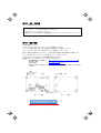
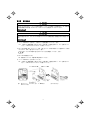
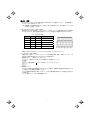
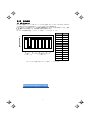
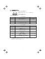
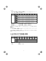
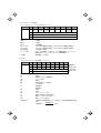
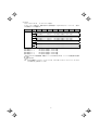
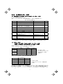
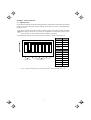
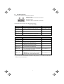
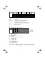
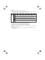
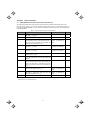
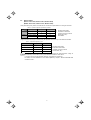
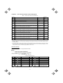
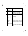
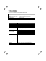
DeviceNet インタフェースカード 「OPC-F1-DEV」 ! 注意 DeviceNet インタフェースカード(OPC-F1-DEV)をお買上げいただきましてありがとうございます。 - この製品は,当社汎用インバータ FRENIC-Eco を DeviceNet に接続するための装置です。ご使用の前には, この取扱説明書および FRENIC-Eco 取扱説明書をお読みになって取扱い方を理解し,正しくご使用くださ い。 - 間違った取扱いは,正常な運転を妨げたり,寿命の低下や故障の原因になります。 - この取扱説明書は,実際に使用される最終需要家に確実にお届けください。最終需要家はこの取扱説明書 を,DeviceNet インタフェースカードが廃棄されるまで大切に保管してください。 - この取扱説明書には FRENIC-Eco の取扱い方は記載されていませんので,個別に取扱説明書を参照してく ださい。 富士電機機器制御株式会社 INR-SI47-0904 Copyright © 2004 Fuji Electric FA Components & Systems Co., Ltd. All rights reserved. この取扱説明書の著作権は,富士電機機器制御株式会社にあります。 本書に掲載されている会社名や製品名は,一般に各社の商標または登録商標です。 仕様は予告無く変更することがあります。 まえがき DeviceNet インタフェースカード「OPC-F1-DEV」をお買上げいただきましてありがとうございます。 このカードを FRENIC-Eco に取り付けることで,パソコンや PLC などの DeviceNet マスタ機器と接続し,運転指 令・速度指令・機能コードアクセス等を使って FRENIC-Eco をスレーブとしてコントロールすることができます。 この製品は ODVA が公認した第三者機関のテストラボでテストされ,ODVA デバイスネット・コンフォーマンステ スト・バージョン 18 に適合していると認められました。 認証ロゴマーク: DeviceNetTM は,ODVA(Open DeviceNet Vender Association, Inc.)の商標です。 本書は製品の簡易的な説明をするものです。詳細については「DeviceNet インタフェースカードユーザー ズマニュアル(MHT274)」を参照してください。ユーザーズマニュアルは下記の Web サイトにてダウンロー ド可能です。 富士電機制御機器 技術情報ページ http://www.fujielectric.co.jp/fcs/jpn/f/f_info.html 本書の構成 本書の構成は,以下のとおりです。 第1章 本カードの特徴 DeviceNet インタフェースカードの主な特徴を説明します。 第2章 製品の確認 開梱時に行う点検や製品の運搬および保管の注意事項,カードの外観および EDS ファイルの入手方法について説 明します。 第3章 取付け方法 取付け手順,取付け上の注意事項などについて説明します。 第4章 配線 本カードの端子台配置,接続ケーブルの仕様および配線方法について説明します。 第5章 各部の機能 DIP スイッチによるデータレートとノードアドレスの設定および LED インジケータの状態表示について説明しま す。 第6章 運転までの手順説明 DeviceNet を使ってインバータを運転するまでの手順について説明します。 第7章 I/O インスタンスの詳細説明 機能コード o31 および o32 による出力インスタンス(インバータへの指令)と入力インスタンス(インバータか らの応答)の選択,工場出荷値および設定例と動作例について説明します。 第8章 その他関連するパラメータ説明 DNFaultMode(異常処理),NetCtrl(運転指令),NetRef(速度指令)による設定の詳細について説明します。 第9章 DeviceNet オプション専用の機能コード一覧 DeviceNet 専用のインバータ機能コード一覧表を示します。 第 10 章 トラブルシューティング インバータが指示どおり動作しない場合やアラーム状態になった場合に行うトラブルシューティングについて 説明します。 第 11 章 仕様 一般仕様および通信仕様について記載しています。 1 アイコンについて 本書では以下のアイコンを使用しています。 この表示を無視して誤った取扱いをすると,本製品が本来持つ性能を発揮できなかったり,その操作 や設定が事故につながることになります。 本製品の操作や設定の際,知っておくと便利な参考事項を示しています。 参照先を示します。 目次 まえがき .................................... 1 本書の構成 .................................. 1 第8章 8.1 その他関連するパラメータ説明 ....... 16 DNFaultMode (クラス 0x29, インスタンス 0x01, アトリビュート 0x10) .............. 16 NetCtrl, NetRef (NetCtrl:クラス 0x29, インスタンス 0x01, アトリビュート 0x05) (NetRef:クラス 0x2A, インスタンス 0x01, アトリビュート 0x04) ........ 16 第1章 本カードの特徴 ...................... 3 第2章 製品の確認 .......................... 3 第3章 取付け方法 .......................... 4 第4章 配線 ................................ 5 第5章 5.1 5.2 各部の機能 .......................... 6 SW3 DIP スイッチ..................... 6 LED 状態表示インジケータ............. 7 第9章 第6章 運転までの手順説明 .................. 8 第 10 章 トラブルシューティング ............. 19 第7章 7.1 I/O インスタンスの詳細説明.......... 12 出力インスタンス (インバータへの指令):o31 で設定... 12 入力インスタンス (インバータからの応答):o32 で設定. 13 第 11 章 仕様 ............................... 20 11.1 一般仕様 ........................... 20 11.2 DeviceNet 仕様 ..................... 20 7.2 8.2 2 DeviceNet オプション専用の 機能コード一覧 ..................... 17 第1章 本カードの特徴 本カードの特徴を以下に示します。 - データレート : 125Kbps, 250Kbps, 500Kbps - I/O メッセージ : Poll および Change of State をサポート - 対応プロファイル : AC Drive プロファイル - FRENIC-Eco が持つ全ての機能コードを読み書き可能(データマップド I/O もしくは Explicit メッセージ) 第2章 製品の確認 次の項目を確認してください。 (1) DeviceNet インタフェースカードが入っていることを確認してください。 (2) カード上の部品の破損,凹み,反りなど輸送時での破損がないことを確認してください。 (3) カード上に形式「OPC-F1-DEV」が印刷されていることを確認してください。(図1) 製品にご不審な点や不具合などございましたら,お買上げ店または最寄りの弊社営業所までご連絡ください。 本カードは,FRENIC-Eco シリーズインバータの全てのバージョンに対応しています。 本カードには EDS ファイルおよび終端抵抗は付属していません。 - EDS ファイルは次の Web サイトにてダウンロード可能です。 富士電機制御機器 技術情報ページ http://www.fujielectric.co.jp/fcs/jpn/f/f_info.html ODVA 本部(英語) http://www.odva.org ODVA 日本支部 http://www.odva.astem.or.jp/ - 終端抵抗は次のものをご使用ください。121Ω, 1/4W, 1%金属皮膜抵抗。(通常はマスタに付属され ています。 ) LED(状態表示インジケータ) 図1 カード表面 図2 3 カード裏面 第3章 取付け方法 取付け・配線は電源を遮断して 30kW 以下は5分以上,37kW 以上は 10 分以上経過してから行ってください。 更に LED モニタおよびチャージランプの消灯を確認し,テスターなどを使用して主回路端子 P(+)-N(-)間の直 流中間回路電圧が安全な値(DC+25V 以下)に下がっていることを確認してから行ってください。 感電のおそれあり 本体接続コネクタ(CN1)の金属部および電子部品の金属部に手を触れないでください。静電気で電子部品が故 障する可能性があります。また汗やゴミの付着によりコネクタの接触信頼性に悪影響を及ぼす可能性があり ます。 故障のおそれあり (1) インバータ本体のカバーを取り外し,制御プリント基板を露出してください。(図3) 「FRENIC-Eco 取扱説明書(INR-SI47-0852)」の第2章「2.3 配線」を参照して,カバーを取り外してく ださい。(37kW 以上はタッチパネルケースも開けてください。) (2) OPC-F1-DEV の裏面(図2)のスペーサ(4個)と CN1 をインバータ本体の制御プリント基板のスペーサ取付 け穴と Port A(CN4)へ差し込んでください。(図4) スペーサと CN1 が確実に差し込まれていることを目視確認してください。(図5) (3) OPC-F1-DEV の配線を行います。 配線方法については,本書の第4章を参照してください。 (4) インバータ本体のカバーを元に戻してください。 「FRENIC-Eco 取扱説明書(INR-SI47-0852)」の第2章「2.3 配線」を参照して,カバーを取り付けてく ださい。(37kW 以上はタッチパネルケースも閉じてください。) 図3 FRN7.5F1S-2J~ FRN15F1S-2J の例 図4 カードの取付け 4 図5 取付け完了 第4章 配線 (1) DeviceNet ケーブルは DeviceNet 仕様に準拠した専用5線ケーブルを使用してください。また配線距離につ いても DeviceNet 仕様に従ってください。 配線に関しては専門知識が必要です。必ず DeviceNet 仕様書または DeviceNet 敷設マニュアル(共に ODVA 発行)を参照してください。 (2) DeviceNet 端子台コネクタ(TERM1)の配線 着脱可能な5ピン端子台を使用しています(図6)。 端子台にはケーブルの信号線の色に対応する銘板が 貼ってありますので,対応する色同士を配線してください。端子台のピン配置は下の表1のとおりです。 表1 端子台のピン配置 1 端子番号 被覆の色 端子名称 説明 1 黒 V- 電源線(DC24V -側) 2 青 CAN_L 信号線 3 裸線 SHIELD ケーブルのシールド 4 白 CAN_H 信号線 5 赤 V+ 電源線(DC24V +側) 2 図6 適合する端子台コネクタはフェニックスコンタクト製 MSTB 2.5/5-ST-5.08-AU 3 4 5 端子台コネクタ です。 (3) アース端子台(TERM2)の配線 電線を使用し2極のうち,どちらか一方をインバータ本体の接地用端子(zG)に接続してください。この 端子台の2極は内部で短絡されているのでどちらでも接続可能です。 適合電線サイズ : AWG20~16(0.5mm2~1.5mm2) アース端子はノイズ対策上および故障防止上,必ず接続してください。 この端子台の横に E のマークがあります。アース(Earth)のことです。 (4) 終端抵抗について DeviceNet は終端抵抗を幹線の両端に外付けすることが必要です。終端抵抗が幹線の両端に接続されている ことを確認し,無い場合は必ず接続してください。 終端抵抗は本製品に付属していません。マスタに付属の抵抗を使用するか,別途抵抗をご用意くだ さい。 抵抗は 121Ω,1/4W,1%金属皮膜抵抗です。 5 第5章 5.1 各部の機能 SW3 DIP スイッチ DeviceNet の通信データレートと MAC ID(ノードアドレス)を設定します。データレートは 125kbps, 250kbps お よび 500kbps のいずれかを設定可能です。ノードアドレスは 0~63 を設定可能です。 DIP スイッチの設定はインバータの電源(補助電源を含む)を OFF した状態で実施してください。電源 ON 中に設定を変更しても,次回の電源 ON 時まで反映されません。 DIP スイッチの出荷時の状態は,データレート: 500Kbps, ノードアドレス:63 ON OFF 1 2 3 データレート(DR) 図7 4 5 6 ノードアドレス(NA) 7 8 です。 DR(bps) DIP 1-2 125K 00 250K 01 500K 10 禁止 11 NA DIP 3-8 0 000000 1 000001 2 000010 3 000011 … … 62 111110 63 111111 DIP スイッチ詳細(図はデータレート 500Kbps, ノードアドレス 63) 6 5.2 LED 状態表示インジケータ 本カードの状態を示します。インジケータ LED は次の2種類あります。 - MS(モジュールステータス) DeviceNet インタフェースカードのハードウェア状態を示します。 - NS(ネットワークステータス) DeviceNet の通信状態を示します。 以下に各 LED 状態の詳細を示します。 表2 MS LED の状態 MS LED の状態 内容 緑/赤の 交互点滅 *1 電源投入時の自己診断テスト中 消灯 電源オフ ― 緑点灯 正常 ― 赤点灯 ハードウェア異常 (カード取付け不良またはカード故障) インバータに er4 発生 表3 備考 テストは1秒間実施 NS LED の状態 NS LED の状態 内容 備考 緑/赤の 交互点滅 *1 電源投入時の自己診断テスト中 消灯 ネットワークオフライン状態 (重複 MAC ID チェック中) ― 緑点滅 ネットワークオンライン状態。通信未確立 (マスタからのリクエスト待ち) ― 緑点灯 正常通信確立 (通信リンク確立) ― 赤点滅 I/O コネクションがタイムアウト (通信リンクの切断または I/O 通信のインターバルが短すぎる) インバータに er5 発生*2 赤点灯 Bus-off 状態または重複 MAC ID 検出 (DeviceNet の配線が不適切,ボーレートの設定不良, ノードアドレスの重複) インバータに er5 発生*2 テストは1秒間実施 *1 DeviceNet 仕様で規定されたパターンで点滅します。 *2 er5 の解除は通信リンクが復帰するまでできません。また er5 を無視するように設定することも可能です。 本書の第8章「8.1 DNFaultMode」を参照してください。 7 第6章 運転までの手順説明 DeviceNet の物理的接続が完了した状態から,DeviceNet マスタを使って I/O メッセージでインバータを制御す るまでの手順を説明します。 I/O メッセージとは,周期的にデータ通信を行う通信方法です。DeviceNet にはこの I/O メッセージの ほかに非周期的にデータ通信を行う Explicit(イクスプリシット)メッセージがあります。Explicit メッセージを使用するとインバータの機能コードや DeviceNet のパラメータを直接読み書きすること が可能となります。Explicit メッセージの詳細に関しましては「DeviceNet インタフェースカードユ ーザーズマニュアル(MHT274)」を参照してください。 (1) DeviceNet マスタ(PLC,パソコンツール,コンフィギュレータ)の設定を行います。 - MAC ID(局番)を他のノードと重ならないように設定する。 - ボーレートを設定する。接続する全ノードのボーレートを一致させること。 - 本カード用に設定した I/O インスタンスに応じた I/O 領域を割当てる。4bytes か 8bytes のいずれか。次 ページ(3)参照。 - I/O 接続の種類(Poll, Change of State)を選択する。 また,コンフィギュレータの場合は - EDS ファイルをインストールする。 EDS ファイル(Electric Data Sheet ファイル)はスレーブ上のパラメータを定義するものです。 これを使用することで,パラメータへのアクセスを非常に簡単にすることができます。本製品の場 合,インバータの機能コードへのアクセスが簡単になります。EDS ファイルの入手方法については 「第2章 製品の確認」をご覧ください。 設定方法は個々のマスタあるいはコンフィギュレータによります。詳細については,各マスタのユー ザーズマニュアルを参照してください。 (2) 本カードの DIP スイッチを設定します。 DIP スイッチ(データレートとノードアドレス)の設定前に,電源が OFF されていることを確認してくださ い。設定詳細に関しては第5章の図7を参照してください。 8 (3) インバータの機能コードを設定します。 インバータの電源を ON し,以下の機能コードを設定してください。 - o31, o32 I/O インスタンス(I/O フォーマット)を選択します。o31 で出力(マスタ→インバータ),o32 で入力(イ ンバータ→マスタ)の設定を行います。下表に示すインスタンスの任意の組み合わせで選択可能です。変 更した内容をインバータに反映するために,インバータの電源を再投入してください。 o31, o32 の設定変更後,内容をインバータに反映するためには,インバータを再起動する必要が あります。 表4 o31,o32 タイプ o31=20 出力 (マスタ→スレーブ) o31, o32 設定内容 インスタンス ID. 内容 占有 Byte 20 Basic Speed Control Output 4 o31=21 or 0 (初期値) 21 Extended Speed Control Output 4 o31=100 100 富士電機オリジナル Output 4 o31=102 102 データマップド I/O(書込み) 8 70 Basic Speed Control Input 4 o32=71 or 0 (初期値) o32=70 71 Extended Speed Control Input 4 o32=101 101 富士電機オリジナル Input 4 o32=103 103 データマップド I/O(モニタ) 8 入力 (スレーブ→マスタ) 各インスタンスの詳細については,本書の第7章を参照してください。 (4) その他関連パラメータを必要に応じて設定します。 a) DNFaultMode このパラメータは,DeviceNet 通信エラー時の動作を選択します。工場出荷状態は,エラー発生で即時 er5 トリップです。 (クラス 0x29, インスタンス 1, アトリビュート 16) 詳細は本書の第8章を参照してください。 b) NetCtrl, NetRef NetCtrl パラメータは DeviceNet からの運転指令の有効・無効,NetRef パラメータは速度指令の有効・無 効を設定します。工場出荷値は,共に無効です。 (NetCtrl:クラス 0x29, インスタンス 1, アトリビュート 5) (NetRef:クラス 0x2A, インスタンス 1, アトリビュート 4) 詳細は本書の第8章を参照してください。 NetCtrl, NetRef は I/O インスタンス 21(次ページで説明)からも設定可能です。 (5) DeviceNet マスタから I/O を接続要求します。 本カードが DeviceNet 通信を行うためには,マスタからの接続要求が必要です。この方法については,それ ぞれのマスタのユーザーズマニュアルを参照してください。 マスタと正常に I/O 接続されると,本カードの NS LED が緑点滅から緑点灯に変わり,通信が開始されます。 I/O 接続の本カードに対する I/O スキャン間隔(=EPR)は,最低でも 10ms 以上に設定してくださ い(例えばマスタ 1 台に対しスレーブ 1 台の時はスキャン間隔 10ms 以上,スレーブ 2 台の時は 5ms 以上) 。通信の衝突を最小限にし,システムの信頼を最大限にするには,I/O スキャン周期を 20ms 以上にすることを推奨します。 9 (6) 実際の I/O データ通信の例 例として,工場出荷状態の I/O インスタンスのフォーマットを説明します。 a)フォーマットの説明 ●o31=21 or 0 出力インスタンス ID.21 (マスタからの出力=インバータへの指令) インスタンス byte bit7 bit6 bit5 bit4 bit3 bit2 bit1 bit0 21 0 - NetRef NetCtrl - - アラーム 解除 逆転指令 正転指令 1 (00 固定) 2 速度設定値 (下位 byte) (r/min) 3 速度設定値 (上位 byte) (r/mim) 正転指令 : 1=正転指令 逆転指令 : 1=逆転指令 アラーム解除 : 1=アラーム状態を解除 NetCtrl : 1=DeviceNet からの運転指令可能要求, 0=DeviceNet 以外からの運転指令可能要求 NetRef : 1=DeviceNet からの速度指令可能要求, 0=DeviceNet 以外からの速度指令可能要求 設定速度 : 速度指令値(r/min 単位) ●o32=71 or 0 入力インスタンス ID.71 (マスタへの入力=インバータからの応答) インスタンス byte bit7 bit6 bit5 bit4 bit3 bit2 bit1 bit0 71 0 設定速度 到達 Ref_ From_Net Ctrl_ From_Net Ready 逆転中 正転中 - トリップ 中 1 インバータ状態 2 出力速度 (下位 byte) (r/min) 3 出力速度 (上位 byte) (r/min) トリップ中 : 1=トリップ中 正転中 : 1=正転中 逆転中 : 1=逆転中 Ready : 1=運転準備完了 Ctrl_From_Net : 1=DeviceNet からの運転指令可能状態, 0=DeviceNet 以外からの運転指令可能状態 Ref_From_Net : 1=DeviceNet からの速度指令可能状態, 0=DeviceNet 以外からの速度指令可能状態 設定速度到達 : 1=設定速度にて運転中 インバータ状態 : Ready=3, 加速/等速中=4, 減速中=5, エラー時強制減速中=6, トリップ中=7 電源投入時メモリチェック中=1, Not Ready(運転準備未完)=2 出力速度 : 実回転速度(r/min 単位) b)実際の運転時の I/O データ 下図のような運転パターンでインバータを制御する場合の I/O データを上記のフォーマットの例で示します。 正転 1800r/min 時間(s) 300r/min 1800r/min 逆転 ① ② ③ ④ 図8 ⑤ ⑥ ⑦ 運転パターン 10 ⑧ ⑨ ⑩ [I/O データの説明] (文中の I/O データは Hex 表示です。) ①指令: 運転指令 OFF。速度指令 1800r/min(=0708h)。DeviceNet から運転・速度指令可能。 60 00 08 07 応答: 停止中。インバータ Ready 状態。 70 03 00 00 ②指令: 正転指令。速度指令 1800r/min(=0708h)。DeviceNet から運転・速度指令可能。 61 00 08 07 応答: 正転中かつ加速中。出力速度上昇。 74 04 ** ** ③指令: 正転指令。速度指令 1800r/min(=0708h)。DeviceNet から運転・速度指令可能。 61 00 08 07 応答: 正転中。設定速度到達。 F4 04 08 07 ④指令: 運転指令 OFF。速度指令 1800r/min(=0708h)。DeviceNet から運転・速度指令可能。 60 00 08 07 応答: 正転中かつ減速中。出力速度減少。 74 05 ** ** ⑤指令: 運転指令無し。速度指令 300r/min(=012Ch)に変更。DeviceNet から運転・速度指令可能。 60 00 2C 01 応答:停止中。インバータ Ready 状態。 70 03 00 00 ⑥指令: 逆転指令。速度指令 300r/min(=012Ch)。DeviceNet から運転・速度指令可能。 62 00 2C 01 応答: 逆転中かつ加速中。出力速度上昇。 78 04 ** ** ⑦指令: 逆転指令。速度指令 300r/min(=012Ch)。DeviceNet から運転・速度指令可能。 62 00 2C 01 応答: 逆転中。設定速度到達。 F8 04 2C 01 ⑧指令: 逆転指令。速度指令 1800r/min(=0708h)に変更。DeviceNet から運転・速度指令可能。 62 00 08 07 応答: 逆転中かつ加速中。出力速度上昇。 78 04 ** ** ⑨指令: 逆転指令。速度指令 1800r/min(=0708h)。DeviceNet から運転・速度指令可能。 62 00 08 07 応答: 逆転中。設定速度到達。 F8 04 08 07 ⑩指令: 運転指令 OFF。速度指令 1800r/min(=0708h)。DeviceNet から運転・速度指令可能。 62 00 08 07 応答: 逆転中かつ減速中。出力速度減少。 78 05 ** ** 11 第7章 7.1 I/O インスタンスの詳細説明 出力インスタンス(インバータへの指令) :o31 で設定 (1) o31=20 出力インスタンス ID.20 Basic Speed Control Output インスタンス byte bit7 bit6 bit5 bit4 bit3 bit2 bit1 bit0 20 0 - - - - - アラーム 解除 - 正転指令 1 (00 固定) 2 速度設定値 (下位 byte) (r/min) 3 速度設定値 (上位 byte) (r/mim) 正転指令 : 1=正転指令 アラーム解除 : 1=アラーム状態を解除 設定速度 : 速度指令値(r/min 単位) (2) o31=21 または 0 (工場出荷値) 出力インスタンス ID.21 Extended Speed Control Output インスタンス byte bit7 bit6 bit5 bit4 bit3 bit2 bit1 bit0 21 0 - NetRef NetCtrl - - アラーム 解除 逆転指令 正転指令 1 (00 固定) 2 速度設定値 (下位 byte) (r/min) 3 速度設定値 (上位 byte) (r/mim) 正転指令 : 1=正転指令 逆転指令 : 1=逆転指令 アラーム解除 : 1=アラーム状態を解除 NetCtrl : 1=DeviceNet からの運転指令可能要求, 0=DeviceNet 以外からの運転指令可能要求 NetRef : 1=DeviceNet からの速度指令可能要求, 0=DeviceNet 以外からの速度指令可能要求 設定速度 : 速度指令値(r/min 単位) (3) o31=100 出力インスタンス ID.100 富士電機オリジナル Output インスタンス byte bit7 bit6 bit5 bit4 bit3 bit2 bit1 bit0 100 0 - X5 X4 X3 X2 X1 REV FWD 1 RST XR XF - - - - - 2 周波数指令 p.u.(下位 byte) 3 周波数指令 p.u.(上位 byte) 運転操作指令 (S06 と同じ) 周波数指令 (S01 と同じ) FWD : 1=正転指令 REV : 1=逆転指令 X1~X5 : 通信端子台指令。(E01~E05 で機能を設定します。) XF, XR : 通信端子台指令。(E98, E99 で機能を設定します。) RST : 1=アラーム状態を解除 周波数指令 p.u. : 最高周波数 F03(Hz)を 20000 とした場合の周波数指令の割合を設定 周波数指令p.u. = 周波数指令(Hz) × 20000 F03(HZ) 12 (4) o31=102 出力インスタンス ID.102 データマップド I/O 書込み データマップド I/O 書込みは,事前に割付けた任意の機能コードに対して自由に書込みを行えるフォーマッ トです。 割付けられる機能コードは 4 種類です。 インスタンス byte 102 bit7 bit6 bit5 bit4 bit3 bit2 bit1 0 書込み機能コード 1 (下位 byte) (o40 で指定した機能コードのデータ部) 1 書込み機能コード 1 (上位 byte) (o40 で指定した機能コードのデータ部) 2 書込み機能コード 2 (下位 byte) (o41 で指定した機能コードのデータ部) 3 書込み機能コード 2 (上位 byte) (o41 で指定した機能コードのデータ部) 4 書込み機能コード 3 (下位 byte) (o42 で指定した機能コードのデータ部) 5 書込み機能コード 3 (上位 byte) (o42 で指定した機能コードのデータ部) 6 書込み機能コード 4 (下位 byte) (o43 で指定した機能コードのデータ部) 7 書込み機能コード 4 (上位 byte) (o43 で指定した機能コードのデータ部) 書込み機能コード 1 : o40 で指定した機能コードに書込むデータを設定します。 書込み機能コード 2 : o41 で指定した機能コードに書込むデータを設定します。 書込み機能コード 3 : o42 で指定した機能コードに書込むデータを設定します。 書込み機能コード 4 : o43 で指定した機能コードに書込むデータを設定します。 bit0 o40~o43 の設定変更後,内容をインバータに反映するためには,インバータを再起動する必要があり ます。 それぞれの機能コードの書込みフォーマットについては,「DeviceNet インタフェースカードユーザーズ マニュアル(MHT274)」を参照してください。 同じ機能コードを複数割付けした場合,o コードの番号が1番小さいものへの割付けだけが有効とな り,残りは割付けなしと見なされてしまいます。 7.2 入力インスタンス(インバータからの応答):o32 で設定 (1) o32=70 入力インスタンス ID.70 Basic Speed Control Input インスタンス byte bit7 bit6 bit5 bit4 bit3 bit2 bit1 bit0 70 0 - - - - - 正転中 - トリップ 中 1 (00) 2 出力速度 (下位 byte) (r/min) 3 出力速度 (上位 byte) (r/min) トリップ中 : 1=トリップ中 正転中 : 1=正転中 出力速度 : 実回転速度(r/min 単位) 13 (2) o32=71 または 0 (工場出荷値) 入力インスタンス ID.71 Extended Speed Control Input インスタンス byte bit7 bit6 bit5 bit4 bit3 bit2 bit1 bit0 71 0 設定速度 到達 Ref_ From_Net Ctrl_ From_Net Ready 逆転中 正転中 - トリップ 中 1 インバータ状態 2 出力速度 (下位 byte) (r/min) 3 出力速度 (上位 byte) (r/min) トリップ中 : 1=トリップ中 正転中 : 1=正転中 逆転中 : 1=逆転中 Ready : 1=運転準備完了 Ctrl_From_Net : 1=DeviceNet で運転指令可能状態, 0=DeviceNet 以外で運転指令可能状態 Ref_From_Net : 1=DeviceNet で速度指令可能状態, 0=DeviceNet 以外で速度指令可能状態 設定速度到達 : 1=設定速度にて運転中 インバータ状態 : Ready=3, 加速/等速中=4, 減速中=5, エラー時強制減速中=6, トリップ中=7 出力速度 : 実回転速度(r/min 単位) 電源投入時メモリチェック中=1, Not Ready(運転準備未完)=2 (3) o32=101 入力インスタンス ID.101 富士電機オリジナル Input インスタンス byte bit7 bit6 bit5 bit4 bit3 bit2 bit1 bit0 101 0 VL TL NUV BRK INT EXT REV FWD 1 BUSY ERR - RL ALM DEC ACC IL 2 周波数出力 p.u.(下位 byte) 3 周波数出力 p.u.(上位 byte) 運転状態 (M14 と同じ) 出力周波数 (M06 と同じ) FWD : 正転中 REV : 逆転中 EXT : 直流制動中(または予備励磁中) INT : インバータ遮断 BRK : 制動中 NUV : 直流中間確立(0 で不足電圧) TL : トルク制限中 VL : 電圧制限中 IL : 電流制限中 ACC : 加速中 DEC : 減速中 ALM : アラーム中(トリップ中) RL : 通信から運転指令 or 速度指令有効 ERR : 機能コードアクセスエラー発生 BUSY : 機能コードデータ書込み中 周波数出力 p.u. : 出力周波数。最高周波数 F03(Hz)を 20000 とした場合の周波数指令の割合を 設定 周波数指令p.u. = 周波数指令(Hz) × 20000 F03(HZ) 14 (4) o32=103 入力インスタンス ID.103 データマップド I/O 読出し データマップド I/O 読出しは,事前に割付けた任意の機能コードをモニタするフォーマットです。 られる機能コードは 4 種類です。 インスタンス 103 byte bit7 bit6 bit5 bit4 bit3 bit2 bit1 0 読出し機能コード 1 (下位 byte) (o48 で指定した機能コードのデータ部) 1 読出し機能コード 1 (上位 byte) (o48 で指定した機能コードのデータ部) 2 読出し機能コード 2 (下位 byte) (o49 で指定した機能コードのデータ部) 3 読出し機能コード 2 (上位 byte) (o49 で指定した機能コードのデータ部) 4 読出し機能コード 3 (下位 byte) (o50 で指定した機能コードのデータ部) 5 読出し機能コード 3 (上位 byte) (o50 で指定した機能コードのデータ部) 6 読出し機能コード 4 (下位 byte) (o51 で指定した機能コードのデータ部) 7 読出し機能コード 4 (上位 byte) (o52 で指定した機能コードのデータ部) 読出し機能コード 1 : o48 で指定した機能コードのモニタ値 読出し機能コード 2 : o49 で指定した機能コードのモニタ値。 読出し機能コード 3 : o50 で指定した機能コードのモニタ値。 読出し機能コード 4 : o51 で指定した機能コードのモニタ値。 割付け bit0 o48~o51 の設定変更後,内容をインバータに反映するためには,インバータを再起動する必要が あります。 それぞれの機能コードのフォーマットについては,「DeviceNet インタフェースカードユーザーズマニ ュアル(MHT274)」を参照してください。 15 第8章 8.1 その他関連するパラメータ説明 DNFaultMode(クラス 0x29, インスタンス 0x01, アトリビュート 0x10) DeviceNet 通信異常時の動作を設定します。 機能コード o27 でも DNFaultMode と同等の設定が可能です。下表の o27 の欄を参照ください。 表5 DNFaultMode の動作一覧 DNFaultMode 異常発生時の動作 備考 o27 0 即時,運転指令 OFF。 (er5 は発生しません。 ) 13 1 異常を無視。(er5 は発生しません。 ) 3 2 o28 のタイマー時間内に通信リンクが復帰すれば異 常を無視。時間オーバーなら強制減速後,er5。 強制減速の時間は F08 による。 12 3 強制的に正転(er5 は発生しません。 ) NetCtrl=1 時に正転有効 14 4 強制的に逆転(er5 は発生しません。 ) NetCtrl=1 時に逆転有効 15 100 即時フリーラン& er5 トリップ 0 101 o28 のタイマー時間経過後,フリーラン&er5。 1 102 o28 のタイマー時間内に通信リンクが復帰すれば異 常を無視。時間オーバーならフリーラン&er5。 2 110 即時強制減速。停止後 er5。 強制減速の時間は F08 による。 10 111 o28 のタイマー時間経過後,強制減速し,停止後 er5。 強制減速の時間は F08 による。 11 112 DNFaultMode=2 と同じ *1 12 *1:o27 の設定範囲は 0~15 です。表5にない値(o27=4~9)を設定した場合は o27=0 の時と同じ動作になります。 8.2 NetCtrl, NetRef (NetCtrl:クラス 0x29, インスタンス 0x01, アトリビュート 0x05) (NetRef:クラス 0x2A, インスタンス 0x01, アトリビュート 0x04) 運転指令,速度指令を DeviceNet から指令可能とするかを選択します。 表6 NetCtrl, NetRef の動作一覧 設定値 NetCtrl NetRef 運転指令 速度指令 0 (工場出荷値) × ― ○: DeviceNet から可能 1 ○ ― 0 (工場出荷値) ― × ×: DeviceNet 以外(タッチパネル, 外部端子台等)から指定 1 ― ○ ―:指定不可 機能コード y98 からも NetCtrl, NetRef と同等の設定が可能です。 表7 y98 y98 の動作一覧 速度指令 運転指令 0 (工場出荷値) × × 1 ○ × ○: DeviceNet から可能 2 × ○ ×: DeviceNet 以外(タッチパネル,外部端子台等) から指定 3 ○ ○ インバータの設定によっては,上記を設定しても DeviceNet から運転・速度指令が可能とならない場 合があります(機能コード y99, リンク運転選択『LE』, リモート/ローカル切換の影響)。詳細につい ては, 「FRENIC-Eco ユーザーズマニュアル(MHT272)」の「第4章 制御ブロック図」を参照してくださ い。 16 第9章 DeviceNet オプション専用の機能コード一覧 表8 DeviceNet インタフェースカード専用機能コード一覧 機能コード 説明 工場出荷値 設定可能値 o27 DeviceNet 異常発生時の動作選択 0 0~15 o28 異常発生時の動作タイマー 5.0s 0.0~60.0s o31 *1 出力インスタンス(I/O フォーマット)の選択 0 (=21) 0, 20,21,100,102 *2 o32 *1 入力インスタンス(I/O フォーマット)の選択 0 (=71) 0, 70,71,101,103 *2 o40 *1 書込み機能コード割付け 1 0000 データマップ I/O 書込み 1 に割付ける機能コードを指定 (割付けなし) 任意の機能コード *3 o41 *1 書込み機能コード割付け 2 0000 データマップ I/O 書込み 2 に割付ける機能コードを指定 (割付けなし) 任意の機能コード *3 o42 *1 書込み機能コード割付け 3 0000 データマップ I/O 書込み 3 に割付ける機能コードを指定 (割付けなし) 任意の機能コード *3 o43 *1 書込み機能コード割付け 4 0000 データマップ I/O 書込み 4 に割付ける機能コードを指定 (割付けなし) 任意の機能コード *3 o48 *1 読出し機能コード割付け 1 0000 データマップ I/O 読出し 1 に割付ける機能コードを指定 (割付けなし) 任意の機能コード *3 o49 *1 読出し機能コード割付け 2 0000 データマップ I/O 読出し 2 に割付ける機能コードを指定 (割付けなし) 任意の機能コード *3 o50 *1 読出し機能コード割付け 3 0000 データマップ I/O 読出し 3 に割付ける機能コードを指定 (割付けなし) 任意の機能コード *3 o51 *1 読出し機能コード割付け 4 任意の機能コード *3 0000 データマップ I/O 読出し 4 に割付ける機能コードを指定 (割付けなし) *1 これらの機能コードの設定を変更後は,内容をインバータに反映するために,インバータを再起動してくだ さい。 *2 設定自体は 0~255 の範囲で可能ですが,表にある値以外を設定した場合は工場出荷値の扱いとなります。 *3 割付ける機能コードは,次ページに示す4桁の 16 進数のフォーマットで指定します。遠隔タッチパネルま たは DeviceNet から設定する場合に,このフォーマットを使用してください。多機能タッチパネルをご使用 の場合は,フォーマットを意識せずに直接機能コードを選択できます。 17 [040~051 の設定方法] 遠隔タッチパネルでの指定 4桁の 16 進数で指定します。 例: H30 の場合 ⇒ 種別コード 08 H 30 ⇒ 1E(16 進表記) 081e 表9 種別 種別コード 機能コード種別 機能コード名称 種別 種別コード 機能コード名称 S 2 0x02 指令・機能データ o 10 0x0A オプション機能 M 3 0x03 モニタデータ J 14 0x0E アプリケーション機能 F 4 0x04 基本機能 y 15 0x0F リンク機能 E 5 0x05 端子機能 W 16 0x10 モニタ 2 C 6 0x06 制御機能 X 17 0x11 アラーム 1 P 7 0x07 モータ 1 機能 Z 18 0x12 アラーム 2 0x00 G11 DeviceNet インタフェース カード用の機能コード番号* H 8 0x08 ハイレベル機能 従来 0 * G11 用の機能コード番号については,「DeviceNet インタフェースカードユーザーズマニュアル(MHT274)」を 参照してください。 18 第10章 トラブルシューティング DeviceNet 通信に何らのトラブルが発生した場合は,下記に従ってトラブルシューティングを行ってください。 No 現象 1 カードの LED が全く点灯しない 2 4 5 6 7 8 • インバータの電源が ON していない。 • カードが正しく取付けられていない。 • カードの故障。 • カードが正しく取付けられていない。 • カードの故障。 NS LED が赤点灯してしまう • ノードアドレスが重複している。 (er5 アラームが解除できない) • データレートがあっていない。 • ネットワーク電源(24V)が適切に入力されていない。 • ケーブルが正しく配線されていない。 • DIP スイッチの設定変更後に,インバータを再起動していな い。 • マスタに不具合がある。 • 通信途中にケーブルが断線した。 • I/O のスキャン間隔が短すぎる。 • マスタに不具合がある。 • ケーブルが断線した。 • マスタに不具合がある。 • 通信開始時に I/O のスキャン間隔が短く設定した。 • I/O の領域が適切にマッピングされていない。 • I/O 接続していない。 • NetCtrl, NetRef がそれぞれ 1 になっていない。 • インバータの機能コードで優先順位が高い運転指令・速度指 令が有効になっている。 • I/O インスタンスの選択が間違っている。 • o31 を変更後に,インバータを再起動していない。 • P01 モータ極数がモータとあっていない。 • I/O インスタンスの選択が間違っている。 • o31 を変更後に,インバータを再起動していない。 • 最高周波数 F03,上限周波数 F15 が低く設定されている。 er4 アラームが解除できない (MS LED が赤点灯) 3 原因 NS LED が赤点滅してしまう (er5 アラームが発生する) NS LED が点灯しない NS LED が緑点灯にならない NS LED が緑点灯になっても運転指令あ るいは速度指令の設定が反映されない 速度指令は反映されたが,実際の回転 速度が指令とは異なっている 19 第 11 章 仕様 11.1 一般仕様 記載の無い項目については,インバータ本体の仕様に準じます。 項目 仕様 消費電流 最大 130mA 動作周囲温度 -10~+85℃ 動作周囲湿度 5~95%RH 外形寸法 94×63×23.5mm 対応インバータ FRENIC-Eco DC5V (結露しないこと) 11.2 DeviceNet 仕様 記載の無い項目については,DeviceNet 仕様書リリース 2.0 に準じます。 項目 仕様 ネットワーク入力電圧 11V~28V ネットワーク消費電力 最大 50mA 接続ノード数 最大 64 台(マスタを含む) DC24V MAC ID 0~63 絶縁 DC500V(フォトカプラ絶縁) 通信速度 500/250/125 kbps 最大ケーブル長 通信速度 500 kbps 250 kbps 125 kbps (幹線:太ケーブル使用 支線:細ケーブル使用時) 幹線長 100 m 250 m 500 m サポートするメッセージ 支線長 6 m 6 m 6 m 支線の総長 39 m 78 m 156 m 1.I/O メッセージ(Poll , Change of State) 2.Explicit メッセージ ベンダ ID 319 デバイスタイプ AC ドライブ(Code:2) (Fuji Electric Co., Ltd.) プロダクトコード 9217 製品形式 OPC-F1-DEV 適合デバイスプロファイル AC Drive 入出力バイト数 入力 4 or 8 バイト, 出力 4 or 8 バイト をそれぞれ選択 適合 DeviceNet 仕様 DeviceNet 仕様書リリース 2.0 改訂 5 (ODVA 日本支部にてコンフォーマンステスト A-18 合格済) ノード種別 Group2 Only サーバー 20 DeviceNet インタフェースカード「OPC-F1-DEV」 取扱説明書 初 版 2004 年 9 月 富士電機機器制御株式会社 ● この取扱説明書の一部または全部を無断で複製・転載することはお断りします。 ● この説明書の内容は将来予告なしに変更することがあります。 ● 本書の内容については , 万全を期して作成いたしましたが , 万一ご不審の点や誤り , 記載もれなど , お気づきの点がありましたら , ご連絡ください。 ● 運用した結果の影響については , 上項にかかわらず責任を負いかねますのでご了承ください。 技術相談窓口 受付時間/ 9:00~12:00,13:00~16:30 月曜日~金曜日(祝・祭日を除く) ただし,FAX 受信は常時行っております。 インバータ開発生産センター/TEL 0120-128-220, FAX 0120-128-230 (携帯電話からも,電話することができます。) 対象機種/30kW 以下 神戸工場/TEL 078-991-2801, FAX 078-992-1255 対象機種/37kW 以上 システム機器事業部 〒141-0032 東京都品川区大崎一丁目 11 番 2 号(ゲートシティ大崎 イーストタワー) URL http://www.fujielectric.co.jp/fcs/ 営業本部 中部支社 西日本支社 北海道支店 東北支店 北関東支店 北陸支店 中国支店 四国支店 九州支店 TEL (03) 5435-7126 ·····························〒141-0032 東京都品川区大崎一丁目 11 番 2 号 (ゲートシティ大崎イーストタワー) TEL (052) 231-8187 ·····························〒460-0003 名古屋市中区錦一丁目 19 番 24 号(名古屋第一ビル) TEL (06) 6341-6492 ·····························〒530-0004 大阪市北区堂島浜二丁目 1 番 29 号(古河大阪ビル) TEL (011) 271-3377 ·····························〒060-0031 札幌市中央区北1条東二丁目 5 番地 2(札幌泉第一ビル) TEL (022) 222-1110 ·····························〒980-0811 仙台市青葉区一番町 3 番 1 号(日本生命仙台ビル) TEL (048) 648-6600 ·····························〒330-0854 さいたま市大宮区桜木町一丁目 9 番 1(三谷ビル) TEL (076) 441-1235 ·····························〒930-0004 富山市桜橋通 3 番 1 号(富山電気ビル) TEL (082) 237-6992 ·····························〒733-0006 広島市西区三篠北町 16 番 12 号 TEL (087) 823-2535 ·····························〒760-0064 高松市朝日新町 19 番 6 号 TEL (092) 262-7226 ·····························〒812-0025 福岡市博多区店屋町 5 番 18 号(博多 NS ビル) 甲信営業所 長野営業所 新潟営業所 TEL (0263) 36-6740 ·····························〒390-0811 松本市中央四丁目 5 番 35 号 TEL (026) 228-0475 ·····························〒380-0836 長野市南県町 1002 番地(陽光エースビル) TEL (025) 284-5518 ·····························〒950-0965 新潟市新光町 16 番地 4(荏原新潟ビル) 富士電機テクニカ㈱ 本 社 TEL (03) 3558-5566 ·····························〒174-0041 東京支店 TEL (03) 3558-5746 ·····························〒174-0041 名古屋支店 TEL (052) 352-2411 ·····························〒454-0807 大阪支店 TEL (0727) 49-1171 ·····························〒562-0036 東京都板橋区舟渡二丁目 30 番 5 号 東京都板橋区舟渡二丁目 30 番 5 号 名古屋市中川区愛知町 5 番 1 号(富士物流㈱中部支社内) 大阪府箕面市船場西一丁目 1 番 1 号 発行 富士電機機器制御株式会社 インバータ開発生産センター 〒513-8633 三重県鈴鹿市南玉垣町 5520 番地 Instruction Manual DeviceNet Interface Card "OPC-F1-DEV" Thank you for purchasing our DeviceNet Interface Card OPC-F1-DEV. • This product is designed to connect the FRENIC-Eco series of inverters to DeviceNet. Read through this instruction manual and be familiar with the handling procedure for correct use. • Improper handling blocks correct operation or causes a short life or failure. • Deliver this manual to the end user of the product. The end user should keep this manual in a safe place until the DeviceNet Interface Card is discarded. • For the usage of inverters, refer to the instruction manual prepared for the FRENIC-Eco series of inverters. Fuji Electric FA Components & Systems Co., Ltd. Copyright © 2004 Fuji Electric FA Components & Systems Co., Ltd. All rights reserved. No part of this publication may be reproduced or copied without prior written permission from Fuji Electric FA Components & Systems Co., Ltd. All products and company names mentioned in this manual are trademarks or registered trademarks of their respective holders. The information contained herein is subject to change without prior notice for improvement. Preface Thank you for purchasing our DeviceNet Interface Card OPC-F1-DEV. Installing this Card on your FRENIC-Eco allows you to connect the FRENIC-Eco to a DeviceNet master unit (e.g., PC and PLC) and control it as a slave unit using the RUN command, speed reference, and access to function codes. This product has been tested by ODVA authorized Independent Test Lab and found to comply with ODVA’s DeviceNet Conformance Test Version 18. Certification Logo Mark: DeviceNet is a trademark of Open DeviceNet Vendor Association, Inc. (ODVA). This manual is designed to serve as a quick guide to the installation and operation of the DeviceNet Interface Card. For a more complete description, refer to the DeviceNet Interface Card User’s Manual (MEHT274), which can be downloaded from the following URL (Fuji Electric FA Components & Systems, Co., Ltd. Technical Information): http://web1.fujielectric.co.jp/Kiki-Info-EN/User/index.html How this manual is organized This manual is made up of chapters 1 through 11. Chapter 1 Features Gives an overview of the main features of the DeviceNet Interface Card. Chapter 2 Acceptance Inspection Lists points to be checked upon delivery of the Card and precautions for transportation and storage of the Card. Also presents the appearance of the Card and provides information on how to obtain an EDS file. Chapter 3 Installation Provides instructions and precautions for installing the Card. Chapter 4 Wiring and Cabling Provides wiring and cabling instructions around the pluggable connector for the Card. Also gives the specifications for the cables. Chapter 5 Basic Functions Provides instructions on how to use the DIP switch to set the data rate (baud rate) and the node address. Also provides the meanings of the LED indicators. Chapter 6 Steps to Get Started Provides the procedures for getting the inverter started using DeviceNet. Chapter 7 I/O Assembly Instances: Selection and Setup Provides instructions on how to select the output assembly instances (request to the inverter) and the input assembly instances (response from the inverter) using the function codes o31 and o32. Also provides information on the factory default values and presents examples of setting and operation. Chapter 8 Other Parameters Provides instructions on how to set DNFaultMode (fault handling), NetCtrl (RUN command), and NetRef (Speed reference). Chapter 9 List of Function Codes for DeviceNet Option Lists the inverter's function codes which are specific to DeviceNet. Chapter 10 Troubleshooting Provides troubleshooting instructions for certain problems, e.g., when the inverter does not operate as ordered or when an alarm condition has been recognized. Chapter 11 Specifications Lists the general specifications and communications specifications. 1 Icons The following icons are used throughout this manual. This icon indicates information which, if not heeded, can result in the product not operating to full efficiency, as well as information concerning incorrect operations and settings which can result in accidents. This icon indicates information that can prove handy when performing certain settings or operations. This icon indicates a reference to more detailed information. Table of Contents Preface ................................................................ 1 How this manual is organized.................................... 1 Chapter 1 Features .............................................. 3 Chapter 2 Acceptance Inspection ........................ 3 Chapter 3 Installation ........................................... 4 Chapter 4 Wiring and Cabling .............................. 5 Chapter 8 Other Parameters ..............................16 8.1 DNFaultMode (Class 0x29, Instance 0x01, Attribute 0x10) .............................................16 8.2 NetCtrl, NetRef (NetCtrl: Class 0x29, Instance 0x01, Attribute 0x05) (NetRef: Class 0x2A, Instance 0x01, Attribute 0x04) ....................17 Chapter 5 Basic Functions ................................... 6 5.1 SW3 DIP switch ............................................ 6 5.2 LED Status Indicators ................................... 7 Chapter 6 Chapter 9 List of Function Codes for DeviceNet Option...............................18 Chapter 10 Troubleshooting .................................19 Steps to Get Started ............................ 8 Chapter 11 Specifications .....................................20 11.1 General Specifications ................................20 11.2 DeviceNet Specifications.............................20 Chapter 7 I/O Assembly Instances: Selection and Setup .......................... 12 7.1 Output Assembly Instance (request to the inverter): set by o31 ........... 12 7.2 Input Assembly Instance (response from the inverter): set by o32 .... 13 2 Chapter 1 Features The Card has the following features: - Data Rate (baud rate) : 125 kbps, 250 kbps, 500 kbps - I/O Message : Polling and Change of State supported - Applicable Profile : AC Drive profile - Reading and writing all the function codes applicable to the FRENIC-Eco (User Defined Assembly I/O or Explicit Message) Chapter 2 Acceptance Inspection Unpack the package and check that: (1) A DeviceNet Card is contained in the package. (2) The DeviceNet Card has not been damaged during transportation--no defective electronic devices, dents, or warp. (3) The model name "OPC-F1-DEV" is printed on the DeviceNet Card. (See Figure 1.) If you suspect the product is not working properly or if you have any questions about your product, contact your Fuji Electric representative. This Card works with any version of the FRENIC-Eco series inverters. Neither an EDS file nor a terminating resistor comes with this Card. - An EDS file can be downloaded from any of the following Websites: http://web1.fujielectric.co.jp/Kiki-Info-EN/User/index.html (Fuji Electric FA Components & Systems Co., Ltd. Technical Information) http://www.odva.org (ODVA Headquarters) - A terminating resistor of the following specifications must be used: 121 ohm, 1/4 watt, 1% metal-film resistor (that usually comes with the master) SW3: DIP switch (for setting Baud Rate and MAC ID) 4 Spacers Model Name CN1 LEDs (Status Indicators) Figure 1 Back of the Card Figure 2 3 Front of the Card Chapter 3 Installation Turn the power off and wait for at least five minutes for models of 30 kW or below, or ten minutes for models of 37 kW or above, before starting installation. Further, check that the LED monitor is unlit, and check the DC link circuit voltage between the P (+) and N (-) terminals to be lower than 25 VDC. Otherwise, electric shock could occur. Do not touch any metallic part of the connector for the main unit (CN1) or any electronic component. Otherwise, electronic components may be damaged by static electricity. Also, the stain or adhesion of sweat or dust may adversely affect the contact reliability of the connector in the long run. An accident could occur. (1) Remove the covers from the inverter to expose the control printed circuit (Figure 3). For the removal instructions, refer to the FRENIC-Eco Instruction Manual (INR-SI47-0882-E), Chapter 2, Section 2.3 "Wiring." (For ratings of 37 kW or above, also open the keypad enclosure.) (2) Insert four spacers and connector CN1 on the back of the OPC-F1-DEV (Figure 2) into the four spacer holes and Port A (CN4) on the inverter's control printed circuit board (PCB) (Figure 4), respectively. Make sure, visually, that the spacers and CN1 are firmly inserted (Figure 5). (3) Install the wires for the OPC-F1-DEV. For wiring instructions, see Chapter 4. (4) Put the covers back to its original position. For the installation instructions, refer to the FRENIC-Eco Instruction Manual (INR-SI47-0882-E), Chapter 2, Section 2.3 "Wiring." (For ratings of 37 kW or above, also close the keypad enclosure.) Control PCB 4 Spacer Holes 4 Spacers Make sure that there is no space between control PCB and spacers. Port A (CN4) DeviceNet Card OPC-F1-DEV Figure 3 FRN7.5F1S-2J FRN15F1S-2J (example) Figure 4 CN1 Mounting the Card 4 Figure 5 Mounting Completed Chapter 4 Wiring and Cabling (1) To connect the DeviceNet Card, use a special 5-core cable that complies with the DeviceNet specifications. Also observe the wiring lengths specified in the DeviceNet specifications. Proper installation of the cable requires specialist knowledge. Be sure to refer to the DeviceNet specifications (published by ODVA) beforehand. (2) Wiring around the DeviceNet’s pluggable connector (TERM1) A pluggable 5-pin connector is used (Figure 6).The pluggable connector has five labels corresponding to the five pins. Each label has a color corresponding to the wire (core) to be connected to its pin. Make sure that the colors of the wires and labels match. Table 1 shows the correspondence between the pin numbers and the colors. Table 1 Layout of Terminal Pins Color of Wire Sheath Pin Assignment 1 Black V- Power supply (24 VDC, side) 2 Blue CAN_L Signal line 3 Metallic SHIELD Cable shield 4 White CAN_H Signal line 5 Red V+ Power supply (24 VDC, + side) Pin # Description 1 2 3 4 5 Figure 6 Pluggable Connector A typical pluggable connector meeting the specifications is MSTB 2.5/5-ST-5.08-AU made by Phoenix Contacts. (3) Wiring around the grounding terminal block (TERM2) Using a wire, connect one of the two pins to the grounding terminal (zG) on the inverter. Since these two pins are internally short-circuited, either one will do. 2 2 Applicable wire size: AWG20 to 16 (0.5 mm to 1.5 mm ) For protection against external noise and prevention of failures, be sure to connect a grounding wire. This terminal block is marked with E by its side. "E" signifies the earth (ground). (4) Terminating resistor DeviceNet requires that a terminating resistor be installed externally on each end of the trunk line. Check that the trunk line is terminated on both ends; if not, install (a) terminating resistor(s) on the missing end(s). The Card does not come with terminating resistors. Use the resistors that come with the master or buy a pair of resistors separately. The specifications are: 121 ohm, 1/4 watt, 1% (metal-film resistor) 5 Chapter 5 5.1 Basic Functions SW3 DIP switch The DIP switch specifies the communication data rate (baud rate) and the MAC ID (node address) on DeviceNet. It offers a choice of three baud rates (125 kbps, 250 kbps, and 500 kbps) and a choice of node address (MAC) ranging from 0 to 63. Before accessing the DIP switch, make sure that the inverter’s power supply (including the auxiliary power supply) is turned OFF. If you change the configuration of the DIP switch with the inverter’s power being ON, you need to restart the inverter to validate the new settings. The default settings of the DIP switch at factory shipment are: data rate = 500 kbps, node address = 63. ON OFF 1 2 Data Rate (DR) Figure 7 3 4 5 6 Node Address (NA) 7 8 DR (bps) DIP 1-2 125K 00 250K 01 500K 10 Not allowed 11 NA DIP 3-8 0 000000 1 000001 2 000010 3 000011 … … 62 111110 63 111111 DIP Switch Settings (showing an example of Data Rate = 500 kbps and Node Address = 63) 6 5.2 LED Status Indicators The two LED status indicators show the status of the Card. - MS (Module Status) Indicates the status of the DeviceNet Card hardware. - NS (Network Status) Indicates the status of communication on DeviceNet. The tables below show the states of the LEDs and their meanings. Table 2 MS LED State MS LED Meaning Note Blinks between *1 green and red Running self-diagnostic test upon power-on OFF Powered OFF – Lights in green Normal – Lights in red Hardware error (Card not properly installed or Card is faulty) This test takes 1 second. The inverter shows er4. Table 3 NS LED State NS LED Meaning Note Blinks between green and red *1 Running self-diagnostic test upon power-on OFF Not on-line (Checking for the duplicated MAC ID) – Blinks in green On-line and not connected (Waiting for a request from the master) – Lights in green On-line and connected (Communications link is established) – Blinks in red Connection time-out (The communications link is broken or the interval of I/O communication is too short.) *2 Lights in red Bus-off state or duplicated MAC ID has been detected. (E.g., Improper DeviceNet cabling, mismatch in data (baud) rate, and duplicated node address) The inverter shows er5 This test takes 1 second. The inverter shows er5 *2 *1 Blinks in the pattern specified in the DeviceNet specifications. *2 er5 cannot be reset until communication is restored. A setting to ignore er5. is available. For details, refer to Chapter 8, Section 8.1 "DNFaultMode." 7 Chapter 6 Steps to Get Started This chapter presents the steps you take from the time the physical connection of DeviceNet is established to the time you start running the inverter with I/O Message using the DeviceNet master. I/O Message is a communication process in which cyclic data transmission takes place. Another communication process in DeviceNet is Explicit Message, in which event-driven data transmission takes place. Explicit Message allows you to directly read and set/modify function codes and DeviceNet parameters. For details on Explicit Message, refer to the DeviceNet Interface Card User’s Manual (MEHT274). (1) Set the DeviceNet master (PLC, PC tool, or Configurator). - Set the MAC ID (node address) uniquely, so that it does not coincide with any other nodes. - Set the baud rate. Make sure that all the nodes have the same baud rate. - Allocate an I/O area corresponding to the I/O assembly instance set for this Card. The I/O area is either 4 bytes or 8 bytes in length. See (3) on the next page. - Specify the type of I/O connection (Poll or Change of state). In the case of the Configurator, - Install the EDS file. The Electric Data Sheet (EDS) file defines parameters on the slave. Using it quickly accesses the desired parameters. For this Card, the file makes it easier to access the inverter's function codes. For how to obtain the EDS file, refer to Chapter 2 "Acceptance Inspection." The exact setting procedures depend on the DeviceNet master or the Configurator. For details, refer to the User’s Manual of the corresponding master. (2) Configure the DIP switch on this Card. Before accessing the DIP switch (baud rate and node address), make sure that the power is OFF. For details, see Figure 7 in Chapter 5. 8 (3) Set the function codes for the inverter. Power ON the inverter and set the function codes according to the table below. - o31, o32 Select the I/O assembly instances (I/O formats). o31 is for the output (from master to inverter); o32 is for the input (from inverter to master). You can specify any combination of input (o31) and output (o32). After modifying the I/O assembly instances, restart the inverter to validate the new settings on the inverter. Once you have modified the settings for o31 or o32, be sure to restart the inverter in order to validate the new settings. Table 4 Setting o31 and o32 Type Instance ID o31=20 Output (from master to slave) 20 Basic Speed Control Output 4 21 Extended Speed Control Output 4 o31=100 100 Fuji Drive Assembly Output 4 o31=102 102 User Defined Assembly Output 8 70 Basic Speed Control Input 4 71 Extended Speed Control Input 4 o32=101 101 Fuji Drive Assembly Input 4 o32=103 103 User Defined Assembly Input 8 o31=21 or 0 (initial value) o32=70 o32=71 or 0 (initial value) Input (from slave to master) Description Length (bytes) o31, o32 For the details of instances, refer to Chapter 7. (4) Set other parameters as necessary. a) DNFaultMode This parameter specifies the operation to be performed if a DeviceNet communications error occurs. The factory default is "Trip immediately with er5 if a DeviceNet communications error occurs." (Class 0x29; Instance 1; Attribute 16) b) For details, refer to Chapter 8. NetCtrl, NetRef The NetCtrl parameter enables/disables the RUN command sent via DeviceNet; and the NetRef parameter, the Speed reference. Their factory defaults are "disabled." (NetCtrl: Class 0x29, Instance 1, Attribute 5) (NetRef: Class 0x2A, Instance 1, Attribute 4) For details, refer to Chapter 8. NetCtrl and NetRef can also be specified from I/O Assembly Instance 21 (see the next page). (5) Have an I/O connection request issued from the DeviceNet master. In order for this Card to start DeviceNet communication, the master should send a communication request. For details, refer to the User’s Manual of the master. Once I/O connection is established between the master and the slave, the NS LED on this Card changes from blinking green to solid green, and communication starts. Set the I/O scan interval (=EPR) for the Card during I/O connection to at least 10 ms (For example, 10 ms if one master controls one slave; 5 ms if one master controls two slaves). It is recommended that you specify at least 20 ms to the I/O scan interval to minimize the frequency of communications collision and maximize the system’s reliability. 9 (6) Examples of I/O communication Presented herein are examples of the format of the I/O Assembly Instance at shipment from the factory. a) Description of Format • o31 = 21 or 0 Output Assembly Instance ID.21 (output from the master = request to the inverter) Instance byte 21 bit 7 bit 6 0 - 1 (Fixed at 00) bit 5 NetRef bit 4 NetCtrl - 2 Speed Reference (lower byte) (r/min) 3 Speed Reference (upper byte) (r/min) bit 3 - bit 2 Fault Reset bit 1 bit 0 Run Reverse Run Forward Run Forward: Run Reverse: Fault Reset: NetCtrl: 1 = Run Forward command 1 = Run Reverse command 1 = Reset the alarm condition 1 = Request for enabling Run command sent from DeviceNet 0 = Request for enabling Run command sent from other than DeviceNet NetRef: 1 = Request for enabling Speed Reference sent from DeviceNet 0 = Request for enabling Speed Reference sent from other than DeviceNet Speed Reference: Speed Reference (in r/min) • o32 = 71 or 0 Input Assembly Instance ID.71 (input to the master = response from the inverter) Instance byte 71 bit 7 bit 6 bit 5 0 At Ref_ Reference From_Net 1 Drive State Ctrl_ From_Net 2 Speed Actual (lower byte) (r/min) 3 Speed Actual (upper byte) (r/min) Faulted: Running Forward: Running Reverse: Ready: Ctrl_From_Net: Ref_From_Net: At Reference: Drive State: Speed Actual: bit 4 Ready bit 3 bit 2 Running Reverse Running Forward bit 1 - bit 0 Faulted 1 = The inverter has (and remains) tripped. 1 = The motor is running forward. 1 = The motor is running backward (in the reverse direction). 1 = Ready to run 1 = Run command sent from DeviceNet being enabled 0 = Run command sent from other than DeviceNet being enabled 1 = Speed Reference sent from DeviceNet being enabled 0 = Speed Reference sent from other than DeviceNet being enabled 1 = The motor is running at the reference speed. 3 = Ready, 4 = Enabled, 5 = Stopping, 6 = Fault stop, 7 = Faulted, 1 = Startup, 2 = Not Ready Actual rotation speed (in r/min) b) Actual I/O Data during Running Presented below are an example of the driving pattern for controlling the inverter and its corresponding I/O data expressed in the format given above. Forward 1800 r/min Time (s) 300 r/min 1800 r/min Reverse Figure 8 Driving Pattern 10 Description of I/O Data (The I/O data are in hexadecimal notation.) Request: Run command is OFF. Speed Reference = 1800 r/min (= 0708h). Run command and Speed Reference via DeviceNet are enabled. 60 00 08 07 Response: Stopping. The inverter is ready. 70 03 00 00 Request: Run Forward command. Speed Reference = 1800 r/min (= 0708h). Run command and Speed Reference via DeviceNet are enabled. 61 00 08 07 Response: The motor is running forward and accelerating. The actual speed is increasing. 74 04 ** ** Request: Run Forward command. Speed Reference = 1800 r/min (= 0708h). Run command and Speed Reference via DeviceNet are enabled. 61 00 08 07 Response: Running Forward. The actual speed has reached the Reference F4 04 08 07 Request: Run command is OFF. Speed Reference = 1800 r/min (= 0708h). Run command and Speed Reference via DeviceNet are enabled. 60 00 08 07 Response: The motor is running forward and decelerating. The actual speed is decreasing. 74 05 ** ** Request: No RUN command. Speed Reference is changed to 300 r/min (= 012Ch). Run command and Speed Reference via DeviceNet are enabled. 60 00 2C 01 Response: Stopping. The inverter is ready. 70 03 00 00 Request: Reverse command. Speed Reference = 300 r/min (= 012Ch). Run command and Speed Reference via DeviceNet are enabled. 62 00 2C 01 Response: The motor is running backward (in the reverse direction) and accelerating. The actual speed is increasing. 78 04 ** ** Request: Reverse command. Speed Reference = 300 r/min (= 012Ch). Run command and Speed Reference via DeviceNet are enabled. 62 00 2C 01 Response: Running in the reverse direction. The actual speed has reached Reference F8 04 2C 01 Request: Reverse command. Speed Reference is changed to 1800 r/min (= 0708h). Run command and Speed Reference via DeviceNet are enabled. 62 00 08 07 Response: The motor is running backward (in the reverse direction) and accelerating. The actual speed is increasing. 78 04 ** ** Request: Reverse command. Speed Reference = 1800 r/min (= 0708h). Run command and Speed Reference via DeviceNet are enabled. 62 00 08 07 Response: Running in the reverse direction. The actual speed has reached Reference F8 04 08 07 Request: Run command is OFF. Speed Reference = 1800 r/min (= 0708h). Run command and Speed Reference via DeviceNet are enabled. 62 00 08 07 Response: The motor is running backward (in the reverse direction) and decelerating. The actual speed is decreasing. 78 05 ** ** 11 Chapter 7 7.1 I/O Assembly Instances: Selection and Setup Output Assembly Instance (request to the inverter): set by o31 (1) o31 = 20 Output Assembly Instance ID.20 Basic Speed Control Output Instance byte 20 bit 7 bit 6 0 - 1 (Fixed at 00) bit 5 - bit 4 - bit 3 - 2 Speed Reference (lower byte) (r/min) 3 Speed Reference (upper byte) (r/min) Run Forward: 1 = Run Forward command Fault Reset: 1 = Reset the alarm condition - bit 2 Fault Reset bit 1 - bit 0 Run Forward Speed Reference: Speed Reference (in r/min) (2) o31 = 21 or 0 (factory default) Output Assembly Instance ID.21 Extended Speed Control Output Instance byte 21 bit 7 bit 6 bit 5 NetRef bit 4 0 - NetCtrl 1 (Fixed at 00) 2 Speed Reference (lower byte) (r/min) 3 Speed Reference (upper byte) (r/min) bit 3 - - bit 2 Fault Reset bit 1 bit 0 Run Reverse Run Forward Run Forward: 1 = Run Forward command Run Reverse: 1 = Run Reverse command Fault Reset: 1 = Reset the alarm condition NetCtrl: 1 = Request for enabling Run command sent from DeviceNet; 0 = Request for enabling Run command sent from other than DeviceNet NetRef: 1 = Request for enabling Speed Reference sent from DeviceNet; 0 = Request for enabling Speed Reference sent from other than DeviceNet Speed Reference: Speed Reference (in r/min) (3) o31 = 100 Output Assembly Instance ID.100 bit 7 bit 6 Fuji Drive Assembly Output Instance byte bit 5 bit 4 bit 3 bit 2 bit 1 bit 0 100 0 - X5 X4 X3 X2 X1 REV FWD 1 RST XR XF - - - - - 2 Frequency command p.u. (lower byte) 3 Frequency command p.u. (upper byte) FWD: 1 = Run Forward command REV: 1 = Run Reverse command X1 to X5: Communication Terminal Block command (The exact function to be performed is specified by E01 – E05). XF, XR: Communication Terminal Block command (The exact function to be performed is specified by E98 and E99). RST: 1 = Reset the alarm (fault) condition. Run command (same as S06) Frequency command (same as S01) Frequency command p.u.: Specifies the ratio of the frequency to the data of 20000 for the maximum frequency F03. That is, Frequency command p.u. = Frequency command (Hz)/F03 (Hz) × 20000. 12 (4) o31 = 102 Output Assembly Instance ID.102 User Defined Assembly Output User Defined Assembly Output offers a format which allows the user to freely set or modify the function code defined by the user beforehand. Four function codes are provided for the user to define. Instance byte 102 bit 7 bit 6 bit 5 bit 4 bit 3 bit 2 bit 1 bit 0 0 User-defined function code 1 (write) (lower byte) (data of function code specified by o40) 1 User-defined function code 1 (write) (upper byte) (data of function code specified by o40) 2 User-defined function code 2 (write) (lower byte) (data of function code specified by o41) 3 User-defined function code 2 (write) (upper byte) (data of function code specified by o41) 4 User-defined function code 3 (write) (lower byte) (data of function code specified by o42) 5 User-defined function code 3 (write) (upper byte) (data of function code specified by o42) 6 User-defined function code 4 (write) (lower byte) (data of function code specified by o43) 7 User-defined function code 4 (write) (upper byte) (data of function code specified by o43) User-defined function code 1 (write): write data for the function code specified by o40 User-defined function code 2 (write): write data for the function code specified by o41 User-defined function code 3 (write): write data for the function code specified by o42 User-defined function code 4 (write): write data for the function code specified by o43 Once you have modified the settings for o40 to o43, be sure to restart the inverter in order to validate the new settings. For details of the write formats for individual function codes, refer to the DeviceNet Interface Card User’s Manual (MEHT274). If you assign the same function code to more than one "o" code, only the one assigned to the smallest "o" code number will become effective, and all the rest will be ignored (treated as "not assigned"). 7.2 Input Assembly Instance (response from the inverter): set by o32 (1) o32 = 70 Input Assembly Instance ID.70 Basic Speed Control Input Instance byte 70 0 - 1 (00) 2 Speed Actual (lower byte) (r/min) 3 Speed Actual (upper byte) (r/min) Faulted: bit 7 bit 6 - bit 5 - bit 4 - 1 = The inverter has (and remains) tripped Running Forward: 1 = The motor is running forward. Speed Actual: Actual rotation speed (in r/min) 13 bit 3 - bit 2 Running Forward bit 1 - bit 0 Faulted (2) o32 = 71 or 0 (factory default) Input Assembly Instance ID.71 Extended Speed Control Input Instance byte 71 bit 7 bit 6 bit 5 0 At Ref_ Reference From_Net 1 Drive State 2 Speed Actual (lower byte) (r/min) 3 Speed Actual (upper byte) (r/min) Faulted: bit 4 Ctrl_ From_Net Ready bit 3 bit 2 Running Reverse Running Forward bit 1 - bit 0 Faulted 1 = The inverter has (and remains) tripped. Running Forward: 1 = The motor is running forward. Running Reverse: 1 = The motor is running backward (in the reverse direction). Ready: 1 = Ready to run Ctrl_From_Net: 1 = Run command sent from DeviceNet being enabled 0 = Run command sent from other than DeviceNet being enabled Ref_From_Net: 1 = Speed Reference sent from DeviceNet being enabled 0 = Speed Reference sent from other than DeviceNet being enabled At Reference: 1 = The motor is running at the reference speed. Drive State: 3 = Ready, 4 = Enabled, 5 = Stopping, 6 = Fault stop, 7 = Faulted, 1 = Startup, 2 = Not Ready Speed Actual: Actual rotation speed (in r/min) (3) o32 = 101 Input Assembly Instance ID.101 bit 7 Fuji Drive Assembly Input Instance byte bit 6 bit 5 bit 4 bit 3 bit 2 bit 1 bit 0 101 0 VL TL NUV BRK INT EXT REV FWD 1 BUSY ERR - RL ALM DEC ACC IL 2 Frequency output p.u. (lower byte) 3 Frequency output p.u. (upper byte) Running status (same as M14) Output frequency (same as M06) FWD: During forward rotation REV: EXT: During reverse rotation During DC braking (or during pre-exciting) INT: BRK: Inverter shut down During braking NUV: TL: DC link circuit voltage established (0 = undervoltage) During torque limiting VL: IL: During voltage limiting During current limiting ACC: DEC: During acceleration During deceleration ALM: RL: Alarm relay (for any fault) Communications effective ERR: Function code access error BUSY: During function code data writing Frequency output p.u.: Output frequency. Expressed as the ratio of the frequency to the data of 20000 for the maximum frequency F03. That is, Frequency command p.u. = Frequency command (Hz)/F03 (Hz) × 20000. 14 (4) o32 = 103 Input Assembly Instance ID.103 User Defined Assembly Input User Defined Assembly Input offers a format which allows the user to monitor the function codes defined by the user beforehand. Four function codes are provided for the user to define. Instance byte 103 bit 7 bit 6 bit 5 bit 4 bit 3 bit 2 bit 1 0 User-defined function code 1 (read) (lower byte) (data of function code specified by o48) 1 User-defined function code 1 (read) (upper byte) (data of function code specified by o48) 2 User-defined function code 2 (read) (lower byte) (data of function code specified by o49) 3 User-defined function code 2 (read) (upper byte) (data of function code specified by o49) 4 User-defined function code 3 (read) (lower byte) (data of function code specified by o50) 5 User-defined function code 3 (read) (upper byte) (data of function code specified by o50) 6 User-defined function code 4 (read) (lower byte) (data of function code specified by o51) 7 User-defined function code 4 (read) (upper byte) (data of function code specified by o51) bit 0 User-defined function code 1 (read): value of the function code specified by o48 User-defined function code 2 (read): value of the function code specified by o49 User-defined function code 3 (read): value of the function code specified by o50 User-defined function code 4 (read): value of the function code specified by o51 Once you have modified the settings for o48 to o51, be sure to restart the inverter in order to validate the new settings. For details of the formats for individual function codes, refer to the DeviceNet Interface Card User’s Manual (MEHT274). 15 Chapter 8 8.1 Other Parameters DNFaultMode (Class 0x29, Instance 0x01, Attribute 0x10) This parameter specifies the inverter operation to be performed if a DeviceNet communication error occurs. Using the function code o27, you can also specify the operation in the event of a communication error in the same way as with DNFaultMode. The "o27" column in the table below shows the value for o27 corresponding to that of DNFaultMode. Table 5 DNFaultMode Inverter Operations Specified by DNFaultMode Inverter Operation in the Event of an Error Note o27*1 13 0 Turn OFF Run command immediately. (No error er5 occurs.) 1 Ignore the error. (No error er5 occurs.) 2 Ignore the error if the communications link is restored within the timer value specified by o28. If the timer value is exceeded, then decelerate the motor by force and then turn on er5. The forced deceleration period is specified by F08. 12 3 Put the motor in forward rotation by force. (No error er5 occurs.) Forward rotation is enabled when NetCtrl = 1. 14 4 Put the motor in reverse rotation by force. (No error er5 occurs.) Reverse rotation is enabled when NetCtrl = 1. 15 100 Put the motor immediately in coast-to-stop mode and cause an er5 trip. 0 101 Put the motor in coast-to-stop mode and cause an er5 stop when the time set by o28 (Timer) has expired. 1 102 Ignore the alarm condition if the communications link is restored within the timer value specified by o28. If the timer value is exceeded, then put the motor in coast-to-stop mode by force and then turn on er5. 2 110 Immediately decelerate the motor by force. When the motor has stopped, turn on er5. The forced deceleration period is specified by F08. 10 111 When the time set by o28 (Timer) has expired, put the motor in coast-to-stop mode and, when the motor has stopped, turn on er5 . The forced deceleration period is specified by F08. 11 112 Same as for [DNFaultMode = 2] 3 12 *1 o27 can have values in the range of 0 to 15. If you specify a value not shown in Table 5 (o27 = 4 to 9), the same operation as for o27 = 0 will be performed. 16 8.2 NetCtrl, NetRef (NetCtrl: Class 0x29, Instance 0x01, Attribute 0x05) (NetRef: Class 0x2A, Instance 0x01, Attribute 0x04) These parameters specify whether to enable the Run command and Speed Reference coming via DeviceNet. Table 6 NetCtrl NetRef Operations Specified by NetCtrl and NetRef Setting RUN Command Speed Reference 0 (factory default) N – 1 Y – 0 (factory default) – N 1 – Y Y: Possible via DeviceNet N: Impossible via DeviceNet (Possible via keypad, external terminal block, etc.) –: Not available Using the function code y98, you can also specify the operation in the same way as with NetCtrl and NetRef. Table 7 Operations Specified by y98 y98 Speed Reference RUN Command 0 (factory default) N N Y: Possible via DeviceNet 1 Y N 2 N Y 3 Y Y N: Impossible via DeviceNet (Possible via keypad, external terminal block, etc.) Depending on how the inverter is set (*), the RUN command and Speed Reference coming via DeviceNet may not be enabled, even if you set NetCtrl and NetRef as shown above. (*) function code y99, LE (link operation selection), and selection of local/remote. For details, refer to the FRENIC-Eco User’s Manual (MEH456), Chapter 4 "BLOCK DIAGRAMS FOR CONTROL LOGIC." 17 Chapter 9 List of Function Codes for DeviceNet Option Table 8 Function Code List of Function Codes for DeviceNet Card Description Factory Default Allowable Range o27 Selection of operation in the event of DeviceNet error 0 0 15 o28 Timer for start of operation in the event of Error 5.0s 0.0 60.0s o31 *1 Selection of Output Assembly Instance 0 (=21) 0, 20, 21, 100, 102 *2 o32 *1 Selection of Input Assembly Instance 0 (=71) 0, 70, 71, 101, 103 *2 o40 *1 Assignment of user-defined function code 1 (write) Function code data to be assigned to user-defined function code 1 (write} 0000 (no assignment) any function code *3 *1 Assignment of user-defined function code 2 (write) Function code data to be assigned to user-defined function code 2 (write} 0000 (no assignment) any function code *3 o42 *1 Assignment of user-defined function code 3 (write) Function code data to be assigned to user-defined function code 3 (write} 0000 (no assignment) any function code *3 o43 *1 Assignment of user-defined function code 4 (write) Function code data to be assigned to user-defined function code 4 (write} 0000 (no assignment) any function code *3 o48 *1 Assignment of user-defined function code 1 (read) Function code data to be assigned to user-defined function code 1 (read) 0000 (no assignment) any function code *3 o49 *1 Assignment of user-defined function code 2 (read) Function code data to be assigned to user-defined function code 2 (read) 0000 (no assignment) any function code *3 o50 *1 Assignment of user-defined function code 3 (read) Function code data to be assigned to user-defined function code 3 (read) 0000 (no assignment) any function code *3 o51 *1 Assignment of user-defined function code 4 (read) Function code data to be assigned to user-defined function code 4 (read) 0000 (no assignment) any function code *3 o41 *1 To validate these new settings, you need to restart the inverter. *2 The entry range is from 0 to 255; however, specifying a value other than those given in this table resets the data to the factory default. *3 The function code data should be specified in a 4-digit hexadecimal format as shown below. To specify the function code data through a remote keypad or DeviceNet, observe this format. To use a multi-function keypad, you can directly select the function code without paying attention to that format. How to set o40 to o51 Using a remote keypad Specify the function code in a 4-digit hexadecimal notation. Example: For H30: H ⇒ Type Code 08 30 ⇒ 1E (hexadecimal) 081e Table 9 Function Code Type Type Type Code Function Code S 2 0x02 Command/function data M 3 0x03 Monitored data F 4 0x04 Fundamental function Type o Type Code Function Code 10 0x0A Optional function J 14 0x0E Application function y 15 0x0F Link function E 5 0x05 Terminal function W 16 0x10 Monitor 2 C 6 0x06 Control function X 17 0x11 Alarm 1 P 7 0x07 Motor 1 function Z 18 0x12 Alarm 2 0x08 High performance function 0x00 Function codes for the G11’s DeviceNet Interface Card* H 8 conventional 0 * For details on the G11’s function codes, refer to the User’s Manual of DeviceNet Interface Card (MEHT274). 18 Chapter 10 Troubleshooting If any problem or error occurs during DeviceNet communication, follow the troubleshooting procedures given below. No Phenomenon/Symptom Probable Causes 1 None of the LEDs on the Card would light. • The inverter is not powered ON. • The Card is not properly installed. • The Card is faulty. 2 er4 alarm cannot be reset (MS LED is lit in red). 3 NS LED is lit in red. (er5 alarm cannot be reset.) • The Card is not properly installed. • The Card is faulty. • There is a duplicated node address. • There is a mismatch in baud (data) rate. • The network power (24V) is not properly supplied. • Cabling is not properly done. • The inverter has not been restarted after modification of the DIP switch settings. 4 NS LED is blinking in red. (er5 alarm has occurred.) • The master has a problem. • The cable was broken during communication. • The I/O scan interval is too short. 5 NS LED would not light. • The master has a problem. • The cable was broken. 6 NS LED would not light in green. • The master has a problem. • The I/O scan interval was set too short at the start of communication. • The I/O area is invalidly mapped. • There is no I/O connection. 7 Even though NS LED lights in green, the settings for RUN command or Speed Reference cannot be validated. • Neither NetCtrl nor NetRef is set to “1.” • On the inverter, the higher-priority RUN command or Speed Reference is enabled. • There is a mistake in the selection of I/O Assembly Instances. • The inverter has not been powered OFF and then powered ON after o31 was modified. 8 Although the Speed Reference has been validated, the actual speed is different from it. • The number of motor poles specified by P01 does not match the motor. • There is a mistake in the selection of I/O Assembly Instances. • The inverter has not been restarted after modification of o31. • The maximum frequency F03 or the frequency upper limit F15 is set too low. 19 Chapter 11 Specifications 11.1 General Specifications For the items not covered in this section, the specifications of the inverter apply. Item Specifications Input power 130 mA at maximum (5 VDC) Operating ambient temperature range -10 to +85°C Operating ambient humidity range 5 to 95% RH (There shall be no condensation.) External dimensions 94 x 63 x 23.5 mm Applicable inverter FRENIC-Eco 11.2 DeviceNet Specifications For the items not covered in this section, the DeviceNet Specifications Release 2.0 apply. Item Specifications Network input voltage 11 V to 28 V Network input power 50 mA at maximum (24 VDC) No. of nodes connected 64 at maximum (including the master) MAC ID 0 to 63 Insulation 500 VDC (photocoupler insulation) Transmission rate 500 kbps/250 kbps/125 kbps Maximum cable length Transmission rate 500 kbps 250 kbps 125 kbps (Trunk line: thick cable Drop line: thin cable) Trunk line length 100 m 250 m 500 m Drop line length 6m 6m 6m Total length of drop lines 39 m 78 m 156 m Messages supported 1. I/O Message (poll, change of state) 2. Explicit Message Vendor ID 319 (Fuji Electric Co., Ltd.) Device type AC drive (code: 2) Product code 9217 Model name OPC-F1-DEV Applicable device profile AC Drive No. of input/output bytes Selectable between 4 and 8 bytes for input and output (independently) Applicable DeviceNet Specifications DeviceNet Specifications Release 2.0 Errata 5 (Certified by ODVA Japan for Conformance Test Version A-18) Node type Group 2 only server 20 DeviceNet Interface Card "OPC-F1-DEV" Instruction Manual First Edition, September 2004 Fuji Electric FA Components & Systems Co., Ltd. The purpose of this manual is to provide accurate information in the handling, setting up and operating of DeviceNet Interface Card "OPC-F1-DEV" for the FRENIC-Eco series of inverters. Please feel free to send your comments regarding any errors or omissions you may have found, or any suggestions you may have for generally improving the manual. In no event will Fuji Electric FA Components & Systems Co., Ltd. be liable for any direct or indirect damages resulting from the application of the information in this manual. Fuji Electric FA Components & Systems Co., Ltd. Gate City Ohsaki, East Tower, 11-2, Osaki 1-chome, Shinagawa-ku, Tokyo, 141-0032, Japan Phone: +81 3 5435 7139 Fax: +81 3 5435 7458 URL http://www.fujielectric.co.jp/fcs/ 2004-9 (I04/I04) 3CM