1
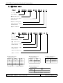
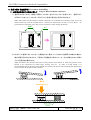
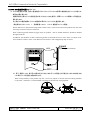
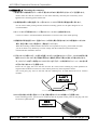
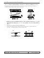
No. : 205-03-173
汎 用
KYOCERA Connector Products Corporation
取扱説明書
HANDLING MANUAL
Series 5602
0.4 mm Pitch Board to Board Connector
(H=1.5, 1.7)
E
DCN-1177
10/23 '14
T.Sugiki
D
DCN-728
7/18 '14
T.Sugiki
K.Yamane
O
EDN-427
6/03 '02
Y.Shiroyama
T.Sasaki
№
EDN/DCN
DATE
PREPARED
106-03-003
K.Yamane
CHECK
T.Sasaki
APPROVED
KYOCERA Connector Products Corporation
目
次 Contents
1.はじめに Preface
2
2.部品名称及び型番 Parts manes and model numbers
2
3.使用に関する注意事項 Matters to be noted in use
4
SERIES 5602 PRODUCT SPECIFICATION
106-03-004
SPEC No.205-03-173
PAGE 1/11
KYOCERA Connector Products Corporation
1.はじめに Preface
5602シリーズは、市場における高密度実装化に対応すべく開発された 0.4mm ピッチボードツー
ボードコネクタです。
Series 5602 is a board-to-board connector with 0.4mm pitch,developed to meet the market’s demand for
the higher-density packaging.
2.部品名称及び型番 Parts manes and model numbers
2.1 部品名称 Parts names
SERIES
5602
(0.4mm PITCH BOARD TO BOARD CONNECTOR)
CONTACT
INSERT MOLD
INSULATOR
CONTACT
SERIES 5602 PRODUCT SPECIFICATION
106-03-004
SPEC No.205-03-173
PAGE 2/11
KYOCERA Connector Products Corporation
2.2 型番 Model number
Plug :
14
5602
XXX
5602
X XX
00X
829
X
+
14 : Plug
Series Number
極数 Number of Pos.
バリエーションコード 1 (※1)
Variation Code 1
めっきコード Plating Code
バリエーションコード 2 (※2)
Variation Code 2
鉛フリー Lead Free
Rec. :
24
0X X
829
H
+
24 : Rec.
Series Number
バリエーションコード 4 (※4)
Variation Code 4
極数 Number of Pos.
バリエーションコード 3 (※3)
Variation Code 3
バリエーションコード 1 (※1)
Variation Code 1
めっきコード Plating Code
鉛フリー Lead Free
※バリエーションコード 1
Variation Code 1
Variation
金具
Anchor Plate
Code 1
0
×
1
×
2
○
3
○
○:あり With
×:なし
ボス
Boss
×
○
×
○
Without
SERIES 5602 PRODUCT SPECIFICATION
106-03-004
※バリエーションコード 2
Variation Code 2
タイプ
Variation
Code 2
Type
無
Standard Type
H
Twin-Rib Type
※バリエーションコード 3
Variation Code 3
Variation
嵌合高さ
Stacking Height
Code 3
0
H=1.5mm
1
H=1.7mm
※バリエーションコード 4
Variation Code 4
タイプ
Variation
Type
Code 4
標準品 Normal
0
ハロゲンフリー対応品 Halogen Free
6
SPEC No.205-03-173
PAGE 3/11
KYOCERA Connector Products Corporation
3.使用に関する注意事項 Precautions in handling
3.1 基板対基板嵌合での使用に関して
Using for Board-to-Board connection
(1) 基板同士をネジ止めして固定する際は、コネクターをねじらないようご注意ください。 基板やネジ
穴等のバラつきにより、コネクターがねじられた状態で固定される恐れがあります。
When the printed circuit boards on which connectors are mounted were fixed by using screw, the
mated connector could be twisted due to variations in dimensions of such as screw holes. So
great attention should be given not to twist connectors when fixing the boards.
基板
PCB
ネジ
Screw
(2)コネクターが基板に対してセンターに実装されない場合、もしくは大きい基板同士の嵌合の場合に
嵌合が傾く恐れがありますので、下図のような傾き防止用のスペーサーおよび嵌合方向への押さ
えによる固定をお勧めします。
When connectors are mounted off-center of the printed circuit board, or when the printed circuit
boards to be connected are rather large, mating may tilt. In order to avoid tilting, it is
recommended that the printed circuit boards are fixed by the spacer and something that generates a
force to retain the proper mated condition.
押さえ
Retaining Force
スペーサー
Spacer
SERIES 5602 PRODUCT SPECIFICATION
106-03-004
SPEC No.205-03-173
PAGE 4/11
KYOCERA Connector Products Corporation
3.2 FPC での御使用に関して FPC use
(1) コネクタを挿抜する際、製品に直接負荷がかからないように FPC の裏面に補強板を貼りつけた状態での
使用をお願い致します。
補強板仕様に関しましては弊社製品外形より大きいものを使用し、板厚については実践による確認をお
願い致します。
尚、弊社での確認結果から FPC+補強板の厚みは 0.3mm 以上を推奨致します。
(弊社条件は FPC:0.1mm + 熱接着層:0.05mm +FR-4 補強板 0.15 にて実施)
Please make sure to attach reinforcing board to FPC’s back,so that it will relieve the product from the stress
caused by connector insertion /extraction.
Such reinforcing board should be bigger than our product,and its suitable thickness should be decided
through actual test.
In addition, the thickness of FPC+reinforcing board recommends 0.3mm or more from our check result.
(Our condition is FPC:0.1mm + heat adhesive line:0.05mm + FR-4 Supporting Tape 0.15mm)
補強板厚
コネクタ
Supporting plate thickness
Connector
Pattern
Supporting
(2) 落下・衝撃や FPC 取り回しの際の反力が大きく加わることが懸念される場合はコネクタの嵌合方向
への押さえによる固定をお勧め致します。
When such possibility as the product may fall,receive any impact or reaction force from being thrashed
is expected,and then it is recommended to fix them in the direction of engagement.
SERIES 5602 PRODUCT SPECIFICATION
106-03-004
SPEC No.205-03-173
PAGE 5/11
KYOCERA Connector Products Corporation
3.3 実装に関して Mounting the connector
(1)実装の際には接触部及びテール部に不要な外力が加わり変形等が生じないようご注意願います。
Please make sure that the connectors are free from deformity caused by the unnecessary stress
applied to the contacting points and the tails.
(2)自動実装の際には弊社推奨パターン図でのクリームはんだ印刷及び実装をお願い致します。
For the cream solder printing and the automatic mounting, please use the patter diagram of our
recommendation.
(3)クリームはんだ印刷時のスクリーン厚さは 0.1mm~0.12mm をお勧め致します。
0.1mm~0.12mm is recommended for the thickness of screen of the cream solder printing.
(4)実装条件が弊社推奨リフロー温度プロファイル条件と異なる場合はあらかじめ実装後にコネクタの
変形、変色が無いことをご確認の上、実装を行ってください。
When the mounting condition differs from those of our profile in any way,please make sure that
you do not observe any deformity nor color change with the mounted connector before the
mounted PCB is installed in the unit.
(5)手付けはんだの際にはテール部及び基板へのフラックス塗布はしないで下さい。コネクタ内部及び接
触部へのフラックス上がり及び飛散の原因となり接触不良等の不具合が発生する場合があります。
又、はんだごてで端子に負荷をかけてはんだ付けを行うとテール部変形及びインシュレータの溶け等
の恐れがありますのでご注意願います。
Please do not apply flux onto the tails and the PC board,when soldering by hand.Splattered or
migrated flux inside the connector or to the contact points may cause imperfect contact.
Also avoid giving any stress to the tails with the soldering iron.It could deform the tail or melt the
insulator.
はんだごて
soldering iron
(6)PLUG 側は接点が外側に露出している為、実装の際はフラックスの飛散にご注意願います。
In the mounting process,special care is needed so that the exposed contact points on the plug side will
be free from splattered flux.
接触部
Contact area
SERIES 5602 PRODUCT SPECIFICATION
106-03-004
SPEC No.205-03-173
PAGE 6/11
KYOCERA Connector Products Corporation
3.4 嵌合に関して Mating connectors
(1)コネクタの接触部に触れたり、異物を入れるとバネの変形等の原因となりますのでご注意願います。
If something touches the contact points or with some foreign object,the spring could be deformed.
(2)本製品は小型、軽量化をする為に成形品の肉厚を薄くしており、嵌合・離脱時に過度なこじり、ねじり
挿抜は成形品の破壊、端子の変形、テール部はんだ剥離の原因となりますのでご注意願います。
We minimized the thickness of this product to achieve downsizing and light weightiness.Because of
this,mating and unmating with uneven pressures or in a distorted way could cause destruction of the
connector,terminal deformity,or solder peeling from the tail.
こじり
Uneven Pressure
ねじり
Distorted Attachment
基板 Board
×
こじり
Uneven Pressure
SERIES 5602 PRODUCT SPECIFICATION
106-03-004
FPC
×
ねじり
Distorted Attachment
SPEC No.205-03-173
PAGE 7/11
KYOCERA Connector Products Corporation
万が一こじり抜去を行う必要がある場合は、長手方向に行い、短手方向への作業はしないでください。
In the unlikely event that the connectors have to be forcibly mated or unmated in a slanting way,
slant the connector along the longer side as shown below.
長手方向 (○)
短手方向 (×)
(3)本製品はコネクタのみでの基板保持は出来ません。押さえが無い場合、嵌合のはずれ、テール半田
剥離、接触不安定が懸念されます。スペーサーなどをご使用頂き、ねじ止めなどの嵌合の固定が必
要です。
The connector is impossible to support the PCB by itself.
Without other supporting objects, imperfect mating , peeling of tails or contacting failure may
be caused. As supporting objects, use spacers fixed by screws.
NG
SERIES 5602 PRODUCT SPECIFICATION
106-03-004
OK
SPEC No.205-03-173
PAGE 8/11
KYOCERA Connector Products Corporation
3.5 プリント基板およびメタルマスク開口部推奨寸法について
PCB AND RECOMMENDED DIMENSIONS OF THE OPENING AREA IN THE METAL MASK
本コネクタは、ピッチ間隔が 0.4mm であり、高密度実装が要求されるコネクタとなっております。 高密度
実装が要求されるコネクタに関しては、半田ブリッジによるショート等の実装不具合を減らすために適正
なはんだ量の管理が必要となります。 つきましては、添付推奨寸法図をご参考願います。 (プリント基
板寸法の詳細につきましては、弊社製品図面をご参照ください)
プリント基板およびメタルマスク開口部寸法は推奨ですので不明点や懸念点等がございましたらご
相談いただけますようお願いします。
This series of connector is required to be mounted in the high density due to its 0.4mm pitches.
The
connectors mounted in the high density need to be controlled adequate amount of solder in order to
prevent failures in the mounting process such as short-circuit caused by solder bridge.
For the
dimensions of the metal mask opening, therefore, please refer to our recommended dimensions shown
in the attached drawing. (For detailed dimensions of the printed circuit board, please refer to our
product drawings.)
As dimensions shown in the drawings are our recommendations.
Please feel free to
contact us if you have any questions and/or concerns about these dimensions.
SERIES 5602 PRODUCT SPECIFICATION
106-03-004
SPEC No.205-03-173
PAGE 9/11
KYOCERA Connector Products Corporation
Series 5602 : 0.4 mm Pitch
Recommended Pad & Stencil size
(SIGNAL CONTACT)
PLUG
0.23mm (8.97mil)
REC.
0.23mm(8.97mil)
Stencil
0.23mm(8.19mil)
0.64mm
(24.9mil)
t=0.12mm
(4.7mil)
0.23mm(8.97mil)
1.0mm
(39.0mil)
0.21mm(8.19mil)
0.92mm
(35.9mil)
0.7mm
(27.3mil)
Pad
0.23mm(8.97mil)
(3.9mil)
SERIES 5602 PRODUCT SPECIFICATION
106-03-004
1.0mm
(39.0mil)
t=0.1mm
0.7mm
(27.3mil)
Stencil
SPEC No.205-03-173
PAGE 10/11
KYOCERA Connector Products Corporation
Series 5602 : 0.4 mm Pitch
Recommended Pad & Stencil size
PLUG
0.6mm(23.4mil)
(SIGNAL CONTACT)
REC.
0.6mm(23.4mil)
0.57mm(22.2mil)
1mm
(39.0mil)
0.9mm
(35.1mil)
Pad
0.57mm(22.2mil)
0.6mm(23.4mil)
0.88mm
(34.3mil)
t=0.12mm
(4.7mil)
0.79mm
(30.8mil)
Stencil
0.6mm(23.4mil)
Stencil
SERIES 5602 PRODUCT SPECIFICATION
106-03-004
1mm
(39.0mil)
(3.9mil)
0.9mm
(35.1mil)
t=0.1mm
SPEC No.205-03-173
PAGE 11/11


![FRS-catalog-裏 [更新済み].ai](http://vs1.manualzilla.com/store/data/006533505_2-0fe83504d812060bd375eb7ebf566ccb-150x150.png)