1
PT90 A
CHASSIS SERVICE
MANUAL
PT-90A Chassis Service Manual
PT-90A Chassis Service Manual
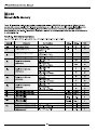
CONTENTS
PAGE
1.Technical Data 4
2. Recommendation for service repairs 5
3. Service Menu 6
4. Specification of the connector (Euroscart) 8
5. Component descriptions 9
6. Introduction 10
7. Block Diagrams 11
8. Fault tracing diagram-power supply 14
9. Troubleshooting guide for main PCB 15
10. Descriptions of the integrated circuits
- ST921x5 MICROCONTROLLER 17
- 24C08 NON-VOLATILE MEMORY 22
- STV224X MULTISTANDARD TV PROCESSOR 23
- MSP34XX (D/G) MULTISTANDARD SOUND PROCESSOR 28
- TDA7495 11+11W AMPLIFIER WITH
DC VOLUME CONTROL 30
- TDA7496 5+6W AMPLIFIER WITH
DC VOLUME CONTROL 33
- TDA7494 10W AMPLIFIER WITH
DC VOLUME CONTROL 36
- STV5112 RGB HIGH VOLTAGE VIDEO AMP. 39
- TDA1771 VERTICAL DEFLECTION CIRCUIT 42
- STV9306 BUS CONTROLLED VERTICAL
DEFLECTION SYSTEM 45
- TDA16846 CONTROLLER FOR SWITCH MODE 48
- TCDT1100(G) OPTOCOUPLER 51
- TL431 PROGRAMMABLE VOLTAGE
REFERENCE 54
- SPPO3N60S5 COOL MOS POWER TRANSISTOR 56
- SPPO4N60S5 COOL MOS POWER TRANSISTOR 59
- L7805 POSITIVE VOLTAGE REGULATORS 62
- LM317 1.2V TO 37V VOLTAGE REGULATOR 64
- BU508DF HORIZONTAL TRANSISTOR (90°) 66
- BUSOSAF HORIZONTAL TRANSISTOR (110°) 68
11. Chassis replacement part list 71
PT-90A Chassis Service Manual
CRT PANEL
Visible Picture 20" /21"/ 28"
Deflection Angle 90° / 110°
Vertical Frequency 50Hz
Horizontal Frequency 15.625Hz
ELECTRONIC
Program Number 100+AV
Teletext Flof text
Tuner Cable tuner - 8 MHz spacing for Hyper Band
TV System European CCIR system
Music Power 90* 2x4 Watt, 110% 2x8 Watt, Rms 10% distortion
CONNECTIONS
Euro AV Socket Include
MAIN STAGE
Mains Voltage 165-260VAC
Mains Frequency 50Hz
Power Consumption 20" 21" 75 Watt, 28" 126 Watt
In Stby Mode 20" 21" 7 Watt, 28" 8 Watt
PT-90A Chassis Service Manual
RECOMMENDATION FOR SERVICE REPAIRS
1- Use only original spare parts. Only use components
with the same specifications for replacement.
2- Original fuse value only should be used.
3- Main leads and connecting leads should be checked
for external damage before connection.
Check the insulation.
4- Parts contributing to the safety of the product must
not be damaged or obviously unsuitable.
This is valid especially for insulators and insulating
parts.
5- Thermally loaded solder pads are to be sucked off
and re-soldered. 8-
6- Ensure that the ventilation slots are not obstructed.
7- Potentials as high as 25 KV are present when this re- 9-
ceiver is operating. Operation of the receiver
outside the cabinet or with back cover removed invol-
ve a shock hazard from the receiver.
Servicing should not be attempted by anyone who is
not thoroughly familiar with the precautions
necessary when working on high voltage equipment
Perfectly discharge the high potential of the picture
tube before handling the tube. The picture tube is
highly evacuated and if broken.
Glass fragments will be violently expelled.
Always discharge the picture tube anode to the rece-
iver chassis to keep of the shock hazard before re:
moving the anode cap.
Keep wire away from the high voltage or high tempe-
rature components.
When replacing a wattage resistor in circuit board
keep the resistor 10 mm away from circuit board.
HANDLING OF MOS CHIP COMPONENTS
MOS circuit requires special attention with regard to
static charges. Static charges may occur with any >.
highly insulating plastics and can be transferred to per-
sons wearing clothes and shoes made of synthetic ma-
terials. Protective circuits on the inputs and outputs of 3-
mos circuits give protection to a limited extend only
due to time of reaction. 4-
Please observe the following instructions to protect the
components against damage from static charges. 5-
1- Keep mos components in conductive package until
they are used. Most components must never be sto-
X-RAY RADIATION PRECAUTION
1- Excessive high voltage can be produce potentially
hazardous X-RAY radiation. To avoid such hazard,
the high voltage must not be above the specified li-
mit. The nominal value of the high voltage of this re- D
ceiver is 25KV at zero beam current (minimum
brightness) under 220V AC power source. The high
voltage must not under any circumstance, exceed
30KV. It is recommended the reading of the high vol-
red in styropor materials or plastic magazines.
Persons have to rid themselves of electrostatic char-
ges by touching MOS components.
Hold the component by the body touching the termi-
nals.
Use only grounded instruments for testing and pro:
cessing purposes.
Remove or connect MOS ICs when operating volta:
ge is disconnected.
tage be recorded as a part of the service record. lt is
important to use an accurate and reliable high volta:
ge meter.
The primary source of X-RAY radiation in this TV re-
ceiver is the picture tube. For continued X-RAY radi:
ation protection, the replacement tube must be
exactly the same type tube as specified in the par
list.
PT-90A Chassis Service Manual
SERVICE MENU
The service menu is entered by pressing a special 4-digit code if the feature menu is displayed and TV is in FE-mode. While
TV isn't in AV Mode and fetura menu is displayed, pressing sequence of digits 1923 will enter the TV to service mode and
service menu will be displayed.
OPTIONS
Option Byte 1: 76543210
BO 1: B/G Standard available 0: Not available
B1 1. DK Standard available 0: Not available
B2 1. | Standard available 0: Not available
B3 1: L Standard available 0: Not availabie
B5-4 TTX National Character Set Group
00 - Set1 ENGLISH, GERMAN, SWEDISH, ITALIAN, FRENCH, SPANISH,
CZEKOSLOVAKIAN, RUMANIAN
01 - Set 2 POLISH, GERMAN, SWEDISH, ITALIAN,FRENCH, SERBO-
CROATIAN, CZEKOSLOVAKIAN, RUMANIAN
1X-Set3 ENGLISH, GERMAN, SWEDISH, ITALIAN, FRENCH, SPANISH,
TURKISH, RUMANIAN
B7-6 Tuner Type
00 : Alps
01 : Temic
10 : Philips UV1316
11 : Thomson/Orega
Option Byte 2: 76543210
BO: AV-2 1 : AV-2 available 0: AV-2 Not Available
B1: VHS 1 : SVHS available 0: SVHS Not Available
B2: TR1 : Turkish language available 0: Turkish Language not available
B3: ES 1 : Ecoswitch available 0: Ecoswitch not available
B4: CL1 : Child Lock available 0: Child Lock not available
B5: HP 1: Headphone available 0: Headphone not available
B6: SW O0 : Subwoofer available 1: Subwoofer not available
B7 PT1 :4/3 Picture tube 0: 16/9 Picture tube
Options B4-7 are only relevant if the corresponding modules are present in the software
Option Byte 3: 76543210
BO: CR 1. :One Crystal application
Bi: SS 1. : Intercarrier application
B2: APR1 : APRON
B3: OSD 1 : OSD contrast control ON
B4: BS 1 : Blue screen disabled
B5: AVL1 :AVLON
B6: CLP 1 : Clipping Mode: compromise
B7: STB 1 : Stanby after power on
: Two Crystal application (for NTSC playback)
: QSS application
: APROFF
: OSD contrast control OFF
: Blue screen enabled
: AVL OFF
: reduce tone (MSP)
: No standby after power on
OOOOO OO O
PT-90A Chassis Service Manual
GEOMETRY... (90 deg Chasis)
V.SIZE 4/3 50Hz
V.SIZE 16/9 50Hz
V.SIZE 4/3 60 Hz
V.SIZE 16/9 60 Hz
V. POS
H.POS
GEOMETRY... (110 deg Chasis with STV9306 IC)
VIDEO...
TUNER/IF...
V.SIZE
V.POS
V.C.CORR
V.S.CORR
H.SIZE
H. PINC.CORR
H. KEYS.CORR
H.COR.CORR
H. POS
R GAIN
G GAIN
B GAIN
R CUTOFF
G CUTOFF
AGC
PIF COARSE
PIF FINE
PIF C OARSE TL
PIF FINE L’
> : < is the VCO status indicator for adjusing the PIF to 38.9Mhz for BGDKIL and 33.9 for L’ standards thru bus controlled
VCO.
The VCO status is read from the read register of STV224X and guides whether to Increase / Decrease the VCO registers
to attain VCO OK Status. | For doing VCO adjustment, Feed a 38.9MHz Carrier as IF input and adjust PIF Coarse and fine
parameters to get VCO OK Status.
For doing VCO L1 adjustment, Feed a 33.9 MHz carrier as IF input and adjust PIF Coarse L’ and PIF Fine L’ to get VCO
OK Status.
PT-90A Chassis Service Manual
SPECIFICATIONS OF THE CONNECTOR
(EURO SCART)
|- Audio output 1. right channel 0.5 VRMS/<I kK 0
2- Audio input 1. right channel 0.5 VRMS (connected to No.6)
3- Audio output 2. left channel 0.5 VRMS (connected to No.1)
4- GND (audio)
5- GND
6- Audio input 2. left channel 0.5 VRMS/>10k 0
7- RGB input, blue (B)
8- Switch signal video (status)
9- GND
10- Reserved for clock signals (not connected)
11- RGB input, green (G)
12- Reserved for remote control (not connected)
13- GND
14- GND switch signal RGB
15- RGB input, red (R)
16- Switch signal RGB
17- GND (video)
18- GND19- Video output 1 Vpp/75 ohm
20- Video input 1 Vpp/75 ohm
21- Shield
1 3 5 7 9 11 13 15 17 19 21
2 4 6 8 10 12 14 16 18 20
PT-90A Chassis Service Manual
COMPONENT DESCRIPTIONS
POWER CORD
SAW FILTER
IR SENSOR
VOLTAGE REGULATOR
77 ON/OFF SWITCH
Ca
— LINE FILTER
A PTC
NPN TRANSISTOR
> PNP TRANSISTOR
UF CERAMIC FILTER
i COIL
ap LINEARITY COIL
A FUSIBLE RESISTOR
< IW METAL OXIDE RESISTOR
= 1/2] METAL OXIDE RESISTOR
= 1/4 OR 1/6W CARBON FILM RESISTOR
iF CERAMIC CAPACITOR /POLYESTER CAPACITOR
+ ELECTROLYTIC CAPACITOR
+ DIODE
4 ZENER DIODE
— SWITCH JUMPER
> NET (INPUT)
+ NET (OUTPUT)
TACT SWITCH
9
PT-90A Chassis Service Manual
INTRODUCTION
PT90A is a low-cost multi-standard television receiver control system based on ST921x5 microcontroller
family. It is a frequency synthesis tuning (FST) system with on-screen display (OSD) for all necessary
control functions. The system is based on the |*C-bus controlled one-chip video processor IC STV224x,
which can support a Nicam and a German stereo sound system based on MSP as well as mono sound.
PT90A has the ability to control two scart connections, and headphone inputs.
Teletext is handled by the microcontroller on-chip teletext interface. The user-interface is menu-controlled
for easy access with remote control or local keyboard keys.
1.1 Definitions, acronyms and abbreviations.
« ADC Analogue to Digital Converter
* AFC Automatic Frequency Control
» AV Audio Video peripheral TV signal source
* DAC Digital to Analogue Converter
* FE Front End(=normai TV) mode
* FST (PLL) Frequency synthesis Tuning (Phase Locked Loop)
* °С Inter Ic bus, 2-wire, bidirectional multimaster bus
« IDENT Horizontal coincidence signal, transmitter IDENTIfication
* LS Loud Speaker
* HP Headphone
* MS Multi Standard
* NV-Memory Non-Volatile Memory
* OSD On Screen Display
* PP Personal Preference
* RC-5 Remote Control System, complying with RC-5 world standard
* Video Proc. STV223x, integrated IC bus controlled multisystem one chip TV-processor
* PIF Picture Intermediate Frequency.
* SIF Sound Intermediate Frequency.
* NICAM Near Instantaneous Companded Audio Multiplex
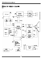
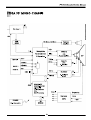
2. Block diagram
Figure 1, 2 and 3 shows the basic block diagram of P T90A.
10
PT-90A Chassis Service Manual
PT90A 110° STEREO CHASSIS
С
TDA7495 L
(— PC MSP34XX — L #5)
— PLLTuner1 > (110 deg.)
Sound Processor x Amplifiers >
A Scarts —» x
AGC L/R A
SAW SAW FM AM Mono
K2966 K9453 cal
SIF
> RGB
VIF > — — — STV5112
> PAL/SECAMNTSG [€L_Output Amplifier 1100
Audio TV Signal Proc.
Externals > |
' Vdrive
CVBSSC1 Y STV9306 Ver. A
V. Amplifier &E/W
SCART 1 CVBSSC2 >> "
SCART2 SB > | | Hor.
CVBS INTI |__| | fdive I BU2508AF
| <— — H. Deflection EHT
Flyback & EHT
С
—
CVBS | ST92195
p-Controller
Teletext Decoder
EPG
RGB Processing Supply Degaussing
«á— —
<—— TDA16846 Mains
{fre — SMPS <
«| = 220
РА | A 24008 <
RC-5 Transmitter EEPROM
11
PT-90A Chassis Service Manual
PT90A 90° STEREO CHASSIS
12C
(— ec | m mansos | 1
— PLL Tuner 1 SP34XX (110 deg.)
Sound Processor Amplifiers R
Scarts
A —>
A
AGC LR A
SAW SAW AM Mono
K2966 K9453 FMcar.
SIF
| — RGB
VIF > — Jo STV5112
TV2247/48 Iblack RGB
> PAL/SECAM/NTSC Output Amplifier 900
Audio TV Signal Proc.
Externals > |
CVBSSCÍ v vdrive TDA1771 Ver.
— m CL (90°) \
SCART 1 CVBSSC2 a V. Amplifier
SCART2 PE > | un Hor
rive
CVBS INT1 a! > BU2508DF
Ш H. Deflection EHT
°C
—>
CVBS ST92195
p-Controller
Teletext Decoder
EPG
RGB Processing Supply Degaussing
4—
<—— TDA16846 Mains
|| РС +—— SMPS <
«| = 220
РСАВЗ21 A 24C08 <
RC-5 Transmitter EEPROM
12
PT-90A Chassis Service Manual
909
O
PT90A 90° MONO CHASSIS
°C
00 PLL Tuner 1
A
AGC
SAW FM Mono / AM Mono TDA7494
K2966 Amplifier
RGB
VIF „| TV2246/47/48 — STV5112
PAL/SECAM/NTSC | Iblack RGB
> TV Signal Proc. €¢— Output Amplifier
Externals Audio > amp! 5
Vdrive TDA1771
CVBSSC1 > у — (90°) Ver.
в V. Amplifier
SCART 1 - CVBSSC2 >
scarT2 [68 > var
CVBS INTI ; ™ | визвовоЕ | Hon
H. Deflection EHT
Flyback 8 EHT
°C
P| ST92185-TXT
CVBS ST92195-NO TXT
p-Controller
Teletext Decoder
EPG
RGB Processing Supply Degaussing
4—
€ TDA16846 Mains
С <——
PCA8521 A sk <—— < =
RC-5 Transmitter EEPROM
13
PT-90A Chassis Service Manual
Basic Hardware Specification
The following are the components that a PT90A controlled system consists of;
* ST921x5 TV+OSD+(TXT) controller with PT90A software inside 24C08 1024*8 bit NV-Memory (EEPROM) for
storage of favourite programmes,
* preffered sound and picture controls, service menu settings.
* STV224x IC bus controlled multi-standard one-chip TV-processor
* Pre-programmed RC-5 remote control transmitter
* Temic-Alps-Philips-Thomson-Orega PLL Tuners
* 90% Chasis
* TDA 1771 Vertical Deflection IC
* 110% Chasis
* STV9306 IC bus controlled vertical deflection and E-W correction circuit
For stereo systems the following optional device is supported MSPXX(D/G) German and NICAM stereo sound
decoder. Communication between the microcontroller (master) and all related devices (slaves) is carried out by
means of the two-wire bidirectional IC bus. This chapter describes all of the functions and hardware equirements of
PT90A. The overall control of the system is handled by the microcontroller which
performs the following;
* Decodes the serial data from the remote controller
* Scans the local keyboard
* Controls the OSD
* Exchanges information via the serial РС bus
* Selects the proper tuner, tuner band
* Selects the proper IF and the sound demodulator
* Analogue picture controls
* Switches between internal and external audio and video signals
5.1 Interface Description
5.1.1 Remote Control Handset.The remote control handset which is compatible with RC-5 standard.
5.1.2 Remote Control Decoding
The infrared remote control pulses are modulated at the standard RC-5 frequency of 36 KHz. The remote control
signal (active HIGH) from the IR-receiver (TFMK1380T) is fed to the external interrupt input (IR-INPUT) of the
microcontroller. Finally the video identification in STV224x is checked to make sure that the
search terminated on a video carrier. For SECAM L’ (France VHF) channel search starts with the highest
channel frquency and all steps atre carried out in the reverse order. When micro search fails to find a signal in a
channel, it will tune the standardised channel frequency.
Sound Systems
PT90A supports stereo sound system as well as mono both controlled via IC bus from the video processor
(Sn/224x).
Mono Sound Sysfem
The only available sound control is volume. In FE-mode, after tuning a programme, the system always
selects the sound witta the following priority.
AMSound
If a transmitter is tuned with colour standard SECAM L/L’, the sound will be forced to AM.
The AM sound system is automatically forced via the STV224x when positive modulation (SECAM-L or
SECAM-L” is selected.
Sfereo Sound Sysfem
Direct control of the audio functions (on the remote transmitter as individual buttons) are;
personal preference function, volume, mute, mono/stereo/language
Automatic identification and decoding of German Stereo and NICAM sound systems
A. German Stereo (A2): Mono / Stereo / Dual | / ll
B. NICAM Stereo Mono / Stereo / Dual | / Il
C. Mono Only mono
14
PT-90A Chassis Service Manual
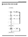
TROUBLESHOOTING GUIDE FOR SMPS
SMPS DEFECTIVE
FUSE FPO Yes DPO1-04
DEFECTIVE CP01-04, TPO1
|
No
— RPO7, IPO1
VOLTAGE
DRAIN ТР!
Y
RP06
Y
VOLTAGE AT
PIN. 1 <1V
No
IPO1
al
Ч
у
MEASURE +115V (145V)
+115V (145V)
ADJUSTABLE
WITH VAPI(2)
VAP1 (2)
IPO5, DP61
Y
CONTROL RANGE OF SMPS
15
PT-90A Chassis Service Manual
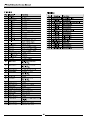
TROUBLESHOOTING GUIDE FOR MAIN PCB
TROUBLE CHECK POINTS
No picture FP01, RP01, DP01-04, TPO1, ICV1, ICV2, RD10, RD01, TDO2
No sound DP12, IA01, ICV1, IC01, CA10, CA11, ICM1, X800, R806
Sound distortion
IA01, CAOS, ICV2
No color
ICV1, XVO1, XVO2, CV24
Dark picture
ICV1, ICV2, RV94, screen adj.
Horizontal size
CD03, CD04, CDO5, LD01, CDO6, ID21, DD22, +115V adj.
Verticable size
|ID21, (ID41), CD26, CD44, RD10, RD17, DD07, DD08, RD29, RD50
Horizontal Linearity
LDO3, RD14
Verticable linearity
RD49, CD43
Noise picture
TUO1, IF adj., AGC adj.
White screen
RDO8, ICV2
16
PT-90A Chassis Service Manual
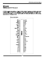
ST921x5
Microcontroller
Microcontroller + OSD + (Teletext decoder) +
VPS/PDC/WSS decoder are embeded in one chip,
where there are two types with the major difference;
ST92185 No-teletext
ST92195 With teletext
The ST92195 microcontroller is developed and
manufactured by STMicroelectronics using a pro-
prietary n-well HCMOS process. lts performance
derives from the use of a flexible 256-register pro-
gramming model for ultra-fast context switching and
real-time event response. The intelligent on-chip
peripherals offload the ST9 core from I/O and data
management processing tasks allowing critical
application tasks to get the maximum use of core
resources. The ST92195 MCU supports low power
consumption and low voltage operation for power-
efficient and low-cost embedded systems.
The advanced ST9+ Core consists of the Central
Processing Unit (CPU), the Register File and the
Interrupt controller. The general-purpose registers can
be used as accumulators, index registers, or address
pointers. Adjacent register pairs make up 16-bit
registers for addressing or 16-bit processing. Although
the ST9 has an 8-bit ALU, the chip handles 16-bit
operations, including arithmetic, loads/stores, and
memory/register and memory / memory exchanges.
Two basic addressable spaces are available: the
Memory space and the Register File, which includes
the control and status registers of the on-chip
peripherals. Power consumption of the device can be
reduced by more than 95% (Low power WFI).
Up to 28 I/O lines are dedicated to digital Input /
Output. These lines are grouped into up to five I/O
Ports and can be configured on a bit basis under
software control to provide timing, status signals, timer
and output, analogue inputs, external interrupts and
serial or parallel 1/O. A set of on-chip peripherals form a
complete system for TV set and VCR applications:
- Voltage Synthesis
- VPS / WSS Slicer
- Teletext Slicer
- Teletext Display RAM
- OSD
Pig. ST921x5 Microcontroller Block diagram
17
GENERAL FEATURES
* Register File based 8/16 bit Core Architedure with
RUN, WFI, SLOW and HALT modes
* 0°С to +700C Operating Temperature Range
available
* Up to 24 MHz Operation @ 5V+10%
* Minimum instruction cycle time: 375nS at 16MHz
internal clock
- 64K Bytes ROM
* 256 Bytes RAM of Register file (accumulators or
index registers)
* 256 Bytes of on-chip static RAM
- 8K Bytes of TDSRAM (Teletext and Display RAM)
* 56-lead Shrink DIP package
28 fully programmable 1/O pins
Serial Peripheral Interface
Flexible Clock controller for OSD, Data Slicer and
Core clocks running from one single low frequency
external crystal.
* Enhanced Display Controller with 26 rows of 40/80
characters
* Serial and Parallel attributes
* 10x10 dot Matrix, 512 ROM characters, definable by
user
* 4/3 and 16/9 supported
* Rounding, fringe, double width, double height,
scrolling, cursor, full background colour, semi-
transparent mode and reduced intensity colour
supported Teletext unit, including Data slicer,
Acquisition Unit and up to 8K Bytes
RAM for Data Storage
* VPS and Wide Screen Signalling slicer
Integrated Sync Extractor and Sync Controller
* 14-bit Voltage Synthesis for tuning reference voltage
* Up to 6 External Interrupts plus 1 non-maskable
interrupt
* 8 x 8-bit programmable PWM outputs with 5V open-
drain or push-pull
* Capability
* 16-bit Watchdog timer with 8-bit prescaler
* 16-bit standard timer with 8-bit prescaler usable as a
Watchdog timer
* 3-channel Analog-to-Digital converter; 6-bit
guaranteed
Rich instruction set and 14-Addressing modes
PT-90A Chassis Service Manual
Block Diagram
NMI
INT(7:4)
INT?
INTO
OSCIN
OSCOUT
RESET
RESETO
SDO/SDI
SCK
MCFM
VSO(2:1)
STOUTO
SDA1/SCL1
SDA2/SCL2
Up to 96
Kbytes ROM
256 or 512
bytes RAM
Up to 8
Kbytes
TDSRAM
TRI
A
de
Register File
256 bytes
8/16-bit
CPU
MMU
L
Interrupt
Management
ST9+CORE
EMORY BUS
RCCU
16-BIT
TIMER/
WATCHDOG
—
SPI
TIMING AND
CLOCK CTRL
<mQXmq
VOLTAGE
SYNTHESIS
—
STANDARD
TIMER
À
120
ON « 7 ON LN ZN A EN
M
REGISTER BUS
UU
1/0
PORT 0
1/0
PORT 2
UU
1/0
PORT 4
1/0
PORT 5
E
1/0
PORT 3
DATA
SLICER &
ACQUI-
SITION
UNIT
|
SYNC
EXTRAC-
TION
VPS/WSS
DATA
SLICER
ADC
fj
SYNC
CONTROL
ON SCREEN
DISPLAY
PWM
D/A
CONVERTER
р
=
MULTIP.
WSCR
WSCF
CVBS2
AIN(4:1)
EXTRG
VSYNC
HSLNC/CSYNC
CSO
“4— PXFM
R/G/B/FB
TSLU
HT
PWM(7:0)
18
PT-90A Chassis Service Manual
4- Pin description
IR IN 5 KB Input
RESET [55] NC
NC NC
NC [4] NC
NC [5] CL2
№ [5] XTAL
NC XTAL
CL1 NC
№ [9] №
NC STDBY1
NC с №
SW-LL’ N NC
AV р MUTE
STDBY о VOL
B NC
G VSYNC
R HSYNC
FB AVDD1
SDA PXFM
SCL JTRSTO
VDD GND
JTDO AGND
WSCF TELETEXT
WSCR WSS
AVDD3 JTMS
TESTO AVDD2
MCFM CVBSO
JTCK TXCF
19
PT-90A Chassis Service Manual
PINNING
Pin | Symbol Function
1 P2.0IRIN IIR Input
2 RESETRESETI Hardware Reset
3 PO.7NCI/0 Not Used
4 P0.6NCI/0 Not Used
5 P0.5NC1/0 Not Used
6 P0.4NCI0 Not Used
7 PO.3NCI Not Used
8 P0.2CL1I SCART 1 status input
9 P0.1NCI/0 Not Used
10 | PO.ONCI/0 Not Used
11 | P3.7NCI/0 Not Used
12 | P3.65W-LL'OSAW | Filter Switch for L/L
13 | P3.5AV0 Sound switch for two AV
source in mono chasis
14 | P3.4STDBYO Standby ON/OFF
15 | BBOOSD Blue colour Signal Output
16 | GGOOSD Green colour Signal Output
17 | RROOSD Red colour Signal Output
18 | BLANKBLANKOOSD | Blanking Output
19 | P5.1SDAI/0I2C Data Line
20 | P5.0SCLOI2C Clock line
21 | VDDVDD +5V Digital Supply
22 | JTDOJTDO Test Pin
23 | WSCFWSCF Analog Pin For VPS /WPP
slicer line PLL
24 | WSCRWSCR Analog Pin For VPS /WPP
slicer line PLL
25 | AVDD3AVDD3 +5V Analog VDD For PLL
26 | TESTOTESTO Test pin
27 | MCFBMCFB Analog Pin for VPS/
WSS line PLL
28 | JTCKJTCK Test pin
29 | TXCFTXCF Analog Pin for VPS/
WSS line PLL
30 | CVBSOCVBSO Test pin
31 | AVDD2AVDD2 Analog Power Supply
32 | JTMSJTMS Test pin
33 | CVBS2CVBS2ICVBS| In for VPS/WSS
34 | CVBS1CVBS1ICVBS| In for Teletext Slicer
35 | AGNDAGND Analog Ground
36 | GNDGND Digital Ground
37 | JTRSTOJTRSTO Test pin
38 | PXFMPXFM Analog pin for display pixel freq.
multiplier
39 | AVDD1AVDD1 Analog Power Supply
40 | HSYNCHSYNCI Horizontal Sync Input
20
PINNING
Pin Symbol Function
41 | VSYNCVSYNCI | Vertical Sync Input
42 P4.0NCI/0 Band Switch 1
43 | P4.1VOLOPWM | Gain Control for Audio amp.
44 P4.2MUTEO Mute output pin
45 P4.3NCI/0 Not Connected
46 P4.4NCI/0 Not Connected
47 | PA.BSTDBY10 | Eco Switch Control
48 P4.6NCI/0 Not Connected
49 P4.7NCI/0 Not Connected
50 XTALXTAL Clock Oscillator
51 XTALXTAL Clock Oscillator
52 |P2.5CL2ISCART2| Status Input
53 | P2.4NCI/OLED | Output Pin
54 P2.3NCI/0 Not Connected
55 P2.2NCI/0 Not Connected
56 P2.1KBInputl Key Board Input
PT-90A Chassis Service Manual
RESET
Reset input is an active-low one. ST921x5 is initialized by the RESET signal.
When the RESET deactivated, programme execution starts from the 00H and 01H addressed programme memory
locations.
R/G/B/BLANK
The video colour analogue DAC outputs are Red / Green / Blue / Fast Blanking.
XTAL
These pins are used to connect parallel resonant crystals of 4 MHz
AV Status
Logic Level Control (High or Low)
Pin 8 and Pin 52 monitor the status of the AV SCART connectors. The controller detects the transitions at these pins.
When the signal goes from high to low, the TV set will automatically switch to AV mode. The signal going from low to
high will lead the TV set to go back to the previous source. Voltage Level Control (O...12V)
Voltage measurement values are taken from these pins. 4:3 or 16:9 picture ratio from SCART or TV mode selection
is dependent on the voltage values at these pins. User control always has a priority in both TV and
AV mode. Following the change of source or the channel, 4:3 format is assumed by default. The voltage values
stated below are divided by 3 at the microcontroller pins.
AV Status (Pin 8)Picture Ratio
- 0 - 2.0 VTV Mode
* 2.0 - 4.5V No change
* 4.5 - 7.0V 16:9 Scart
* 7.0 - 9.0V No change
* 9.0 - 12.0V 4:3 Scart
Keyboard Scan Lines
The 4 keys of the local keyboard are scanned by an ADC used by the microcontroller.
Table Local Keyboard
Name Code TV Mode TXT Sub mode
* Volume Down0Volume -Volume -
* Volume Up1Volume +Volume +
* Programme Down2Programme -Page -
* Programme Down3Programme +Page +
Power Mode Control
The STDBY (pin 14) output specifies the mode which the set is in; Stand-by mode or Operating mode.
Table Power Modes:
S T-BYMode
* 1-Stand-by
* 0-Operating
*C Lines
Pin 20 (SCL) and Pin 19 (SDA) accept inputs from the FC bus. I°C is a 2-wire bi-directional bus. PT90A has an on-
chip bit-level I°C interface. This means the bus arbitration, the reception and transmission of data bits and the
generation of START and STOP are manipulated by the hardware. The software must be able to handle these bits
(i.e. save a received bit and prepare the bits to be transmitted). If a transmission does not succeed, the software will
retry for 5 times. If the bus is occupied for more than 1.18 ms. the microcontroller will attempt to free the bus. PT90A
supports a 1K EEPROM (M24C08-BN6), used for storage of analogue controls, tuning data for 100 pre-selected
programmes and options. The FC addresses of the EEPROM is described in the following chapters. Furthermore the
video-processor STV224x is controlled via IC bus on address 8AH.
21
PT-90A Chassis Service Manual
24C08
Non-Volatile Memory
[hese I°C-compatible electrically erasable programmable memory (EEPROM) is organized as 1024 x 8 bit and
эрега!е with a power supply of 5 V. The memory behaves as a slave device in the РС protocol, with all memory
yperations synchronized by the serial clock. Read and Write operations are initiated by a START condition,
yenerated by the bus master. The START condition is followed by a Device Select Code and RW bit terminated by
an acknowledg bit.
Table 6. DC Characteristics
(TA= O to 70%, -20 to 85°C or - 40 to 85°C; Vcc = 3V to 5.5V, 2.5V to 5.5V or 1.8V to 5.5V)
Symbol Parameter Test Condition Min. Max. Unit
||| Input Leakage Current OV <Vin<Vec a +2 UA
lLo Output Leakage Current OV <VoyT = Vee : +2 HA
SDA in Hi-Z
Supply Current (ST24 series) Voc = SV, fc= 100kHz 2 mA
СС (Rise/Fall time < 10ns)
Supply Current (ST25 series) Vee = 2.9V, fc= 100kHz 1 mA
VIN =Vsg or Vee 100 LA
Icci Supply Current (Standby) VCC = 5V
(ST24 series) Vın = Vss or Vcc
Veo = 5V, fe= 100kHz e. HA
VIN = Ves or Vee 5 LA
Icc2 Supply Current (Standby) \/СС = 2.5V
(ST25 series) Vin = Vss or Vcc 50 A
VCC = 2.5V, fe= 100kHz H
Vin = Vss or Ve 20 UA
lees Supply Current (Standby) VCC = 3.6V
(ST24C08R) ViN = Vss or Vec 60 A
Veo = 3.6V, fe= 100kHz H
VIN = Vss or Vg 10 LA
Ices Supply Current (Standby) VCC =1.8V
(ST24C08R) VIN = Vss or Vec 20 A
Veo =1.8V, fe= 100kHz H
Vii Input Low Woltage (SCL, SDA) -0.3 0.3Vee V
ViH Input High Woltage (SCL, SDA) -0.Vee | Vee 41 V
VIL Input Low Woltage
(E,PRE,MODE,WC) -0.3 0.5 V
VIH Input High Woltage
(E,PRE,MODE WC) “ce | “co Е
Output Low Voltage (ST24 series) || = 3MÁ, Veo = 5V 0.4 V
VOL Output Low Voltage (ST25 series) ICcL = 2.1MA, Veg = 2.5V 0.4 V
Output Low Voltage
re |су_ = 1mA, Vec = 1.8 0.3 V
(ST24C08 series)
22
PT-90A Chassis Service Manuai
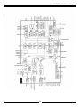
STV224X
Multistandard TV Processor
STV224X is a fully bus controlled IC for n/ including PIF, SIF, Luminance, Chrominance and deflection processing. It
IS a bus controlled PAL / SECAM / NTSC single chip TV Processor. For details of STV224X features please refer to
the STV224X datasheet. 110° 4:3 or 16:9 CRT application. It integrates both vertical deflection and E-W correction
circuit necessary for design of 110°chassis it allows designing a PAL / NTSC (BGDKIMN) set with very few external
componentsand no manual adjustment.
Pin connections
SIFIN1 у FMCAP
SIFIN2 55] AUDIOOUT
AGCSIFCAP [3] GND D
VREF IF [4] Veen
AGCPIFCAP SDA
PIFIN1 [6 SCL
PIFIN2 SLPF
TUNERAGCOUT LBF/SSC
IFPLL [9] HOUT
GND IF VERT
AM/FMOUT x BCL/SAF
Vee IF a Vee
INTCVBSOUT E CVBSOUT1
EXTAUDIOIN о GND
PIFLC1 X1/VAMP/CHROUT
PIFLC2 CLPF
Veco XTAL1
CVBSIN1 XTAL2
GND2 XTAL3/BTUN
CVBSIN2 FBOSD
BS ROSD
Y/CVBSIN3 135] GOSD
CHR BOSD
APR ICATH
BEXT [25] [32] ROUT
GEXT GOUT
REXT BOUT
FBEXT NC
PT-90A Chassis Service Manual
Pin Symbol Function
1 SIFIN1 SIF Input
2 SIFIN2 SIF Input
3 AGCSIFCAP AGC SIF Capacitor
4 VREF IF Voltage Reference Filtering
5 AGCPIFCAP AGC PIF Capacitor
6 PIFIN1 PIF Input
7 PIFIN2 PIF Input
8 TUNERAGCOUT AGC Tuner Output
9 IFPLL IF PLL Filter
10 GND IF IF Ground
11 AM/FMOUT AM/FM Mono Sound or Stereo Carriers Output
12 Vee IF 5V IF Supply
13 INTCVBSOUT Internal CVBS Output
14 EXTAUDIOIN Audio scart Input
15 PIFLC1 LC Input
16 PIFLC2 LG Input
17 Vee? Video/Luma Supply Voltage (8V)
18 CVBSINT Internal Video Input
19 GND2 Video/luma Ground
20 CVBSIN2 External Video Input
21 BS Black Stretch Capacitor
22 Y/CVBSIN3 Y(SVHS) or CVBS3 External Input
23 CHR Chroma (SVHS) input
29 APR Auto Peak Regulation
25 BEXT External Blue Input
26 GEXT External Green Input
27 REXT External Red Input
28 FBEXT External Fast Blanking Input
29 NC Not to be connected
30 BOUT Blue Output
31 GOUT Green Output
32 ROUT Red Output
33 ICATH Cathode Current Measurement Input
34 BOSD OSD Blue Input
35 GOSD OSD Green Input
36 ROSD OSD Red Input
37 FBOSD OSD Fast Blanking
38 XTAL3/BTUN 3.5XMHz Crystal or Cloche Filter Tuning Capacitor
39 XTAL2 3.5XMHz Crystal
40 XTAL 1 4.43/3.5XMHz Crystal
41 CLPF Chroma PLL Filter
42 X1/VAM/CHROUT XTAL1 Control Pin Vertical Amplitude DAC Output and Chroma Reference Signal Output
43 GND 1 Chroma/Scanning Ground
44 CVBSOUT 1 Main Video Switch Output
45 Veet Chroma/Scanning Power Supply (8V)
46 BCL/SAF Beam Current Limiter Control Voltage and Safety input (XRAY)
47 VERT Vertical Output Pulse
48 HOUT Horizontal Output Pulse
49 LFB/SSC Line Flyback Input and Super-sandcastle Output
50 SLPF Scanning PLL Filter
51 SCL 1°C Bus Clock Input
52 SDA °C Bus Data Input
53 Veen Digital Supply Voltage (5V)
54 GND D Digital Ground
55 AUDIOOUT Main Audio Output
56 FMCAP FM Demodulation Capacitor
24
PT-90 Chassis Service Manual
3
XL =
OO =
9 5 в
Ww LL < we O09 9
о a > a =< =
4 D x о Е & Ç
E [05] er--—irHorlH6e de}
TOHLNOD Т
70 dINVA *- HOLVINGONZA |
ra IS1INWNYIIS/TYd ONINAL
i 7 HaTUMH Y 3H2072
LNOH pr d001 puz 400118. |: 18301 OLNY
IWINOZIOH | - 1Y1NOZIOH
J
Г |
ONINNVIS d3s
LEA Je WOLLHIA [| “ONAS 10 | Bal HAL
vWOHHO | + | SSYdONYE | | 3H9019
JNOG 106 | |
1noo [ig | : J
1NOY [ze ONIMNWIE | OYOTHIAO
ничо HLYD 440-1N0 | | 99% ® 99v
| [ee] 35N3S “| JAIJO
149148
dvs/98 [ov 4vsn98 Hh | NN
0508 re A A A ' H31 14
asos ASVHINGD HOLIMS | +
998 вон | v_
aso >
В dvHL
05004 МЕ ‘ YNOHHI
нау [Pz | нам | XIV | '
1NOO/ LYS ' | DNIHO9?
--| ONY
10 van
oN [52 ANA >] HOUMS < y ‘
01898 [>] AM HOL3HLS '
: Hove
Z2H92Hsz 82 12 bet Hoz
k kE x e БЕЗ
Ш Ш Ш Ш = zm mm
C om @ a a E
0 = =
= о о
3
Y/CVBSIN3 | Si
[2] EXTAUDIOIN
| AUDIOOUT
61| гамо
-Q 434 4300930 ss
О—| 3wmi0oa | | CIONY sne 2el ZU PA
| £5] LOND
ща S| "A
Е 01! 41 OND
ЗЕ ZU 177A
if)
#5) Q OND
Es] PA
O: 294 dVI4ISIOY
18 Sle La LE)
=]
ENIdIS
<< Clé
наци e
5 <A | ВЫ!
hum
Wa
) "dOW30 Ве 7 :
SEO | we L..Q-. 181U80 99V EE | о9\ намги |-[8 | 1MNOOOVHINNL
T s0uaJejey Td
[y] YO
HILHIANI |
10dS &
Ее M Z (E: гена
<d 5
ина
SSYdONVE RS
aNNOS
|
CHR [R}——
FMCAP [$—
©?
=
INTCVBSOUT
LIZA UE
35
PT-90A Chassis Service Manual
MAIN FEATURES
C bus control (readl and write modes),
PIF PLL demodulator, Bus controlled VCO alignment,
IF positive and negative modulation,
Digital AFC,
Tuner delayed AGC output,
White and Black spot cancellation,
SIF with QSS or intercarrier structure,
Built in sound bandpass,
Multistandard PLL FM demodulator (4.5, 5.5,
6.0,6.5MHZ),
AM demodulator for France,
FM sound carriers output for Stereo chassis,
Audio switch for external audio input, Mono chassis,
Digital volume control,
Audio Mute,
Video switch, 3 CVBS inputs, 1 CVBS output which
can be used to drive teletext decoder,
SVHS switch, Y input is combined with CVBS3 input,
OSD RGB analog inputs, fast blanking detection on
OSD fast blanking pin, contrast control capability,
oversize blanking capability on OSD fast blanking
input,
External analog RGB inputs with contrast and
saturation control (external RGB matrixed in YUV).
Integrated chroma filters (trap, bandpass, cloche)
with automatic alignment,
Integrated luminance delay line,
Adjustable peaking on the luminance signal with
coring function,
Black strech circuit,
PAL / SECAM / NTSC color decoder with automatic
identification of standards,
Integrated chroma delay line,
Full integrated SECAM decoder,
Hue control, two selectable matrixes in NTSC mode,
Automatic flesh control circuit with two selectable
characteristics (normal and wide),
ACC overload circuit,
Chroma subcarrier output which could be used to
drive comb filter circuit,
Automatic RGB peak regulation (APR).
Automatic digital cut-off current loop with warm-up
detection circuit,
White point and cut-off point adjustments,
Beam current limiter control stage,
High performance synchronization pulses separator,
Horizontal synchronization with two phase locked
loops,
26
Integrated VCO, auto-calibration using the chroma
crystal reference frequency,
Automatic time constant selection for the first PLL, 3
selectable time contants,
Video identification circuit (independant from PLL1),
Noise detector circuity
Vertical countdown circuit,
Automatic 50/60Hz selection circuit,
Blanking and inserted cut-off pulses position adapted
to standard (50 or 60Hz),
Long blanking mode capability in 60Hz (same
blanking as 50Hz standard),
Possibility to insert cut-off pulses after a vertical
oversize blanking signal,
De-interlace capability,
Horizontal starting circuit with soft-start capability,
Horizontal and vertical position adjustments, vertical
amplitude control voltage (combined with chroma
subcarrier output),
4/3, 16/9 selection voltage.
PT-90A Chassis Service Manual
ABSOLUTE MAXIMUM RATINGS
Symbol Parameter Value Unit
Vee SV 8V supply voltage 10 V
Vee 5V 5V supply voltage 7 V
VESD Capacitor 100pF discharged via 1.5kQ serial resistance (Human Body Model) +2 kV
Toper Operating Temperature 0,+/0 °C
Tstg Storage Temperature -55 +150 °C
THERMAL DATA
Symbol Parameter Typical Value Unit
Rth(j-a) Junction ambient Thermal Resistance (Measured at Pp= 1W) SDIP56 40 "C/W
ELECTRICAL CHARACTERISTICS
Supplies at Typical Values, Tamb =25 °C, I°C bus register at power-on reset value. unless otherwise specified)
Symbol Parameter Test Conditions Min. Typ. Max. Unit
SUPPLY
Veep | IF Circuit Supply Voltage 4.75 5 5.25 V
Veep |Bus á Digital Supply Voltage 4.75 5 5.25 V
Veet | Chroma, Scanning Supply Voltage 7.6 8 8.4 V
Vcc? | Video Supply Voltage 7.6 8 8.4 V
IccF VociF Current Consumtion VociIF = 9V TBD mA
Ico5y |Vec5y Current Consumtion Veep = V TBD mA
lcc1 | Voc1 Current Consumtion Vec1 = 8V TBD mA
leo? |Vego Current Consumtion Vega = 8V TBD mA
Pp Total Power Dissipation Veet = Vee? =8V. Veer = Veesy = 5V TBD mW
27
PT-90A Chassis Service Manual
MSP34 XX
(D/G)
Multistandard Sound Processor
The MSP34xx (D/G) family of single-chip Multistandard Sound Processors covers the sound processing of all analog
TV-Standards worldwide, as well as the NICAM digital sound standards. The full TV sound processing, starting with
analog sound IF signal-in, down to processed analog AF-out, is performed on a single chip. It covers all European
TV-Standards The MSP 3400 1.0 m CMOS version is fully pin and soft-ware compatible to the MSP 3410, but is not
able to de-code NICAM. It is also compatible to the MSP 3400C 0.8 m CMOS version.
The IC is produced in submicron CMOS technology, combined with high performance digital signal processing.
The MSP 3410D is available in a PLCC68, PSDIP64, PSDIP52, and in a PQFP80 package.
Note: The MSP3410D version is fully downward compatible to the MSP 3410B, the MSP 3400B, and the
MSP3400C. To achieve full software compatibility with MSP3400C, MSP 3400B, and MSP 3410B, the demodulator
part must be programmed as described in the data sheet of MSP 3410B.
MSP 3410D Additional Features
AVC: Automatic Volume Correction
Subwoofer Output
5-band graphic equalizer (as in MSP 3400C)
Enhanced spatial effect (pseudostereo/basewidth en-largement as in MSP 3400C)
Headphone channel with balance, bass, treble, loud-ness
Balance for loudspeaker and headphone channels in dB units (optional)
Additional parr of D/A converters for SCART2 out
Improved oversampling filters (as In MSP 3400C)
Additional SCART input
Full SCART In/out matrix without restrictions
Scart volume in dB units (optional)
Additional 12S input (as in MSP 3400C)
New FM-identification (as in MSP 3400C)
Demodulator- short programming
Autodetection for- terrestrial TV-sound standards
Precise bit-error rate indication
Automatic switching from NICAM to FM/AM or vice versa
Improved NICAM synchronization algorithm
Tmproved carrier mute algorithm
Improved AM-demodulation
ADR together- with DRP 3510A
Dolby Pro Logic together with DPL 35xx A
Reduction of necessary controlling
Less external components
Significant reduction of radiation
28
PT-90A Chassis Service Manual
Pin description
NC у XTAL-OUT
AUD-CL-OUT [2] 51] XTAL-IN
D-CTR-OUT1 TESTEN
D-CTR-OUTO [4] ANA-IN2+
ADR-SEL [5] ANA-IN-
STANDBYQ [ 6] ANA-IN1+
PC-CL AVSUP
PC-DA AVSS
PS-CL [9] MONO-IN
S-WS VREFTOP
S-DA-OUT SC1-IN-R
PS-DA-IN1 Q SC1-IN-L
ADR-DA = SC2-IN-R
ADR-WS & SC2-IN-L
ADR-CL 2 SC3-IN-R
DVSUP SC3-IN-L
DVSS AGNDC
S-DA-IN2 AHVSS
NC CAPL-M
RESETQ AHVSUP
DACA-R CAPL-A
DACA-L SC1-0UT-L
VREF2 SC1-OUT-R
DACM-R VREF1
DACM-L SC2-OUT-L
DACM-SUB
SC2-OUT-R
PT-90A Chassis Service Manual
TDA7495
11+11W Amplifier With DC Volume Control
» 11+11W Output Power
RL = 80 @THD = 10% VCC = 28V
» ST-BY and mute functions
» Low turn-on turn-off pop noise
» Linear volume control DC coupled
» With Power Op. Amp.
» No Boucherot Cell
» No ST-BY RC input network
» Single supply ranging up to 35V
» Short circuit protection
» Thermal Overload protection
Multiwatt 15
ORDERING NUMBER: TDA7495
» Internally fixed gain
» Soft Clipping
» Variable output after volume control
» Circuit multiwatt 15 package
Block and Application Diagram
VAROUT_R
MUTE/STBY
PROTECTIONS
yr
PW_GND
1000pF
N
OUTR || (
10K
VOLUME
ЧЕ
11°
S1 ST-BY
Om) +5
STBY 2
© S_GND
MUTE ——
a UE — —0 +5V
I S2 MUTE
QUTL |
OP AMP
VOLUME
VAROUT_L +5
=
oor 2
D9I6AU440B
1000uF
PT-90A Chassis Service Manual
ABSOLUTE MAXIMUM RATINGS
Symbol Parameter Value Unit
Vg DC Supply Voltage 35 V
VIN Maximum Input Voltage 8 Vpp
Ptot Total Power Dissipation (Tamb = 70 °C) 20 W
Tamb Ambient Operating Temperature (1) -20 to 85 °C
Tstg, Tj Storage and Junction Temperature -40 to 150 °C
V3 Volume CTRL DC voltage 7 V
(1) Operation between -20 to 85 °C guaranteed by correlation with 0 to 70 °C
PIN CONNECTION (Top view)
15 PW-GND
14 OUTR
13 Vg
12 OUTL
11 PW-GND
10 MUTE
9 ST-BY
8 S-GND
7 SVR
6 NC
5 INL
4 VAROUT-L
3 VOLUME
2 VAROUT-R
1 INR
THERMAL DATA
Symbol Parameter Value Unit
Rth j-case Thermal Resistance Junction - case Тур. = 2 Мах. = 2.8 °C/W
Rth j-amb Thermal Resistance Junction - ambient max. 35 °C/W
ELECTRICAL CHARACTERISTICS
(Refer to the test circuit Vg = 20V R|_=8Q, Rg = 50Q, Tamp =25°C
Symbol Parameter Test Condition Min. Typ. Max. Unit
Vg Supply Voltage Range 11 35 V
lg Total Quiescent Current 70 100 mA
DCVos Output DC Offset Referred No Input Signal -650 650 mV
to SVR Potential
Vo Quiescent Output Voltage 10 V
Po Output Power THD = 10%; Ry = 80; V, = 28V 9.5 11 W
THD = 1%); Ry = 80; Ve = 28V 7.5 8 W
THD = 10%); Ry = 40; Veo = 20V 7 8 W
THD = 1%; R| =4Q; Vo = 20V 5 6 W
THD = 10%; Ry = 8Q; Vec = 18V 3.5 3.8 W
THD = 1%; Rı = 8Q; Vec = 18V 2.6 2.9 W
31
PT-90A Chassis Service Manual
ELECTRICAL CHARACTERISTICS (continued)
Symbol Parameter Test Condition Min. Typ. Max. Unit
THD Total Harmonic Distortion Gv=30dB; Po=1W; f=1KHz 0.4 %
Ipeak Output Peak Current (internally limited) 1.7 2.4 A
Vin Input Signal 2.8 Vrms
Gv Closed Loop Gain Vol Ctrl > 4.5V 28.5 30 31.5 dB
GvLine Monitor Out Gain Vol Ctrl > 4.5V; Zload > 30KQ -1.5 0 1.5 dB
AMin Vol Attenuation at Minimum Volume | Vol Ctrl < 0.5V 80 dB
BW 0.6 MHz
eN Total Output Noise f=20Hz to 22KHz 500 800 UV
Play, max volume
f=20Hz to 22KHz 100 250 pv
Play, max attenuation
f=20Hz to 22KHz 60 150 UV
Mute
SR Slew Rate 5 8 V/us
Ri Input Resistance 22.5 30 KQ
RVar Out Variable Output Resistance 30 100 Q
Rload Var Out Variable Output Load 2 KQ
SVR Supply Voltage Rejection f=1kHz; max volume 35 39 dB
Csvr=470uF; VRIP=1Vrms
f=1kHz; max attenuation 55 65 dB
CsvrR=470pF; VRIP=1Vrms
TM Thermal Muting 150 °C
TS Thermal Shut-down 160 °C
MUTE STAND-BY & INPUT SELECTION FUNCTIONS
VST-BY Stand-by threshold 2.3 2.5 2.7 V
VMUTE Mute threshold 2.3 2.5 2.7 V
lqST-BY Quiescent Curren @ Stand-by 0.6 1 mA
AMUTE Mute Attenuation 50 65 dB
IstbyBIAS Stand-by bias current Stand-by on Vst-BY=5V 80 HA
VMUTE=5V HA
Play or Mute -20 -5 HA
ImuteBIAS Mute bias current Mute 1 5 HA
Play 0.2 2 HA
32