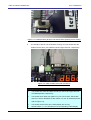
1
TREX C1
Development Kit
Getting Started User Guide
Copyright © 2005 by Terasic Technologies Inc.
http://www.terasic.com
TREX C1 DEVELOPMENT KIT
Page Index
CHAPTER 1 ABOUT THIS KIT..................................................................................................................................... 1
1-1 FEATURES ............................................................................................................................................................... 1
1-2 GETTING HELP ........................................................................................................................................................ 1
CHAPTER 2 YOUR T-REX BOARD............................................................................................................................. 2
2-1 THE TREX C1 (TR1) ............................................................................................................................................. 2
2-2 THE BOARD ............................................................................................................................................................. 2
2-3 FEATURES ............................................................................................................................................................... 3
2-4 POWER UP THE BOARD TO SEE THE DEMO ........................................................................................................... 4
CHAPTER 3 INSTALLATION........................................................................................................................................ 7
3-1 INSTALL QUARTUS II................................................................................................................................................ 7
3-2 CONNECTING THE USB CABLE TO THE BOARD - USB BLASTER INSTALLATION ................................................... 7
3-3 POTENTIAL PROBLEMS AND W ORKAROUND FOR USING USB BLASTER ............................................................... 8
3-4 INSTALL TERASIC LAB CD-ROM ............................................................................................................................ 8
CHAPTER 4 FIRST LAB: 7-SEG DISPLAY ............................................................................................................. 11
4-1 POWER UP THE BOARD ........................................................................................................................................ 11
4-2 REPEATING THE LAB FROM SCRATCH .................................................................................................................. 11
4-3 COMPILING THE DESIGN ....................................................................................................................................... 13
4-4 DOWNLOAD BITSTREAM ........................................................................................................................................ 15
4-5 THE TOP LEVEL RTL AND PIN ASSIGNMENT......................................................................................................... 18
CHAPTER 5 LAB 2: HOW TO WORK WITH SCANNED 7-SEG DISPLAY........................................................ 19
5-1 THE 7-SEG DISPLAY MODULE ON TREX C1 ...................................................................................................... 19
5-2 PURE COMBINATIONAL LOGIC LAB - USING NON-SCANNED MODE ....................................................................... 19
5-3 THE VERILOG CODE FOR COMBINATIONAL LAB ................................................................................................... 20
5-4 SEQUENTIAL LOGIC LAB - USE THE SCANNED MODE ............................................................................................ 21
5-5 W HEN COUNTER = 00........................................................................................................................................... 21
5-6 THE VERILOG CODE FOR SCANNED MODE .......................................................................................................... 22
CHAPTER 6 LAB 3: TREX CONTROL PANEL ....................................................................................................... 24
6-1 CONNECT PC TO THE BOARD USING USB CABLE............................................................................................... 24
6-2 CONTROL THE BOARD USING TREX PANEL ........................................................................................................ 25
6-3 THE FLASH PROGRAMMER ................................................................................................................................... 27
6-4 THE SDRAM CONTROLLER AND PROGRAMMER ................................................................................................. 29
6-5 PS2 COMMUNICATION TO THE BOARD ................................................................................................................. 30
6-6 TOOLS - MULTI-PORT SDRAM/FLASH CONTROLLER - USE A MUSIC PLAYER AS AN EXAMPLE ....................... 31
6-7 VIRTUAL DPDT SWITCHES ................................................................................................................................... 35
ii
TREX C1 DEVELOPMENT KIT
CHAPTER 7 LAB 4: CD-QUALITY MUSIC BOX..................................................................................................... 37
7-1 LOAD ANOTHER MUSIC FILE TO PLAY FROM FLASH ............................................................................................ 37
7-2 PLAY MUSIC FROM 8MBYTE SDRAM.................................................................................................................. 37
7-3 DETAILS OF THE AUDIO DAC CONTROLLER ......................................................................................................... 39
7-4 A REFERENCE DESIGN: 1KHZ SOUND GENERATOR ............................................................................................ 40
7-5 HOW TO CREATE YOUR OWN MUSIC RAW DATA ................................................................................................. 40
CHAPTER 8 LAB 5: NTSC/PAL TV CONTROLLER .............................................................................................. 42
8-1 YCRCB AND COMPONENT DIGITAL VIDEO ............................................................................................................ 42
8-2 TV LAB - NTSC/PAL TV COLOR PATTERN GENERATOR..................................................................................... 43
CHAPTER 9 INTERFACES AND ASSOCIATED TESTING CODE ...................................................................... 45
9-1 50 MHZ AND 27 MHZ OSCILLATORS ..................................................................................................................... 45
9-2 LED1 - LED8........................................................................................................................................................ 45
9-3 8 PUSH-BUTTON SWITCHES: KEY[7] TO KEY[0] ................................................................................................ 45
9-4 7-SEG DISPLAY .................................................................................................................................................... 46
9-5 VGA DAC ............................................................................................................................................................. 47
9-6 AUDIO DAC ........................................................................................................................................................... 48
9-7 PS2 & RS-232 INTERFACE .................................................................................................................................. 48
9-8 VIDEO ENCODER (NTSC/PAL TV OUT) - LAB 5.................................................................................................. 49
9-9 DIP SWITCH .......................................................................................................................................................... 50
9-10 SDRAM INTERFACE ........................................................................................................................................... 50
9-11 FLASH MEMORY .................................................................................................................................................. 51
9-12 COMPACT FLASH CARD ...................................................................................................................................... 52
9-13 EXPANSION CONNECTORS (JP1, JP2) .............................................................................................................. 55
CHAPTER 10 RS-232 VERSION OF THE TREX CONTROL PANEL.................................................................. 57
10-1 CONNECT PC TO THE BOARD USING RS232..................................................................................................... 57
10-2 CONTROL THE BOARD USING RS232 VERSION OF TREX PANEL .................................................................... 57
10-3 THE C++ SOURCE CODE.................................................................................................................................... 58
CHAPTER 11 LAB 8: NIOS II 5.0 CORE .................................................................................................................. 59
11-1 LOAD NIOS II 5.0 ON TREX C1......................................................................................................................... 59
11-2 RUNNING NIOS II ON TREX C1......................................................................................................................... 60
CHAPTER 12 APPENDIX ............................................................................................................................................ 63
12-1 REVISION HISTORY ............................................................................................................................................. 63
12-2 TREX CD-ROM DIRECTORY STRUCTURE AND REFERENCE DESIGNS............................................................ 63
12-3 SCHEMATIC ......................................................................................................................................................... 64
12-4 ALWAYS VISIT TREX C1 W EBPAGE FOR NEW LABS ......................................................................................... 64
iii
TREX C1 DEVELOPMENT KIT
About this Kit
Chapter
Chapter 1
1
About this Kit
The TREX C1 Development Kit provides everything you need to develop many
digital designs using Altera Cyclone device. The Getting Started User Guide is
written in a way to enable users to walk through many reference designs in 30
minutes. This chapter provides users key information about the kit.
Features
1-1
The TREX C1 Development Kit includes:
TREX C1 Development Board.
USB Cable for power supply and FPGA programming.
TREX C1 CD-ROM containing TREX API, reference designs, and specs.
Altera Quartus II 5.0 Web Edition CD-ROM and Nios II 5.0 CD-ROM
RS-232 Cable for board control using UART protocol.
This Getting Started Guide.
Full-size component reference card.
9V DC Wall-mount power supply (backup power)
Getting Help
1-2
Here are some places to get help if you encounter any problem:
Email to [email protected]
SkyPE: Terasic
Taiwan & China: +886-3-553-9672
Korea & Japan: +82-2-512-7661
North America: [email protected]
1
TREX C1 DEVELOPMENT KIT
Your T-REX Board
Chapter
Chapter 2
2
Your T-REX Board
This chapter will walk you through each part of your TREX C1 (TREX1) board to
illustrate the features equipped.
The TREX C1 (TR1)
2-1
The TREX C1 is designed using the same strict design and layout practices we
used in our other mass production OEM products for car infotainment systems
with the highest QC standard.
Major design and layout considerations are listed
below:
Layout traces and components are carefully arranged so that they are properly
aligned. This nice alignment will increase the yield for manufacturing and ease
board debugging procedure.
Jumper-free design for robustness. Jumpers are a great point of failure and might
cause frustration for users who don’t keep the manuals with them all the time.
TR1 board uses four 0-ohm SMT resistors to replace 4 jumbers (used for power
measurement in different areas).
Components’ selection was made according to the volume shipped. We selected
the most common component configuration used in PC and DVD players to
ensure the continuous supply of the component resource in the future.
Protection on Power and IOs are considered to cover most of the accidental
cases in the field.
The Board
2-2
Examine your board with the following diagram in Figure 2.1. We provide a quick
reference card with the kit for you to use.
2
TREX C1 DEVELOPMENT KIT
Your T-REX Board
Figure 2.1. TREX C1 Development Board Components & Interfaces
(Same as the full-size component reference card attached in the package)
Features
2-3
TREX1 board provides users many features to enable various multimedia project
developments. Component selection was made according to the most popular
design in volume production multimedia products such as DVD, VCD, and MP3
players. This TREX1 platform allows users to quickly understand all the insight
tricks to design real multimedia projects for industry.
Altera Cyclone 1C6 FPGA with 6000 LEs
Altera Serial Configuration deivices (EPCS1) for Cyclone 1C6
USB Blaster built in on board for programming and user API controlling
3
TREX C1 DEVELOPMENT KIT
Your T-REX Board
JTAG Mode and AS Mode are supported
8Mbyte (1M x 4 x 16) SDRAM
1Mbyte Flash Memory
CF Card Socket
8 Push-button switches
4-bit DIP Switch
8 User LEDs
50MHz Oscillator and 27MHz Crystal for external clock source
16-bit CD-Quality Audio DAC with line-out jack
VGA DAC (4-bit resistor network) with VGA out connector
TV Encoder (NTSC/PAL) and TV Out connector
RS-232 Transceiver and 9-pin connector
Two 40-pin Expansion Headers with resistor protection
Terasic Lab CD-ROM which contains many examples with source code to
exercise the boards, including: SDRAM and Flash Controller, CD-Quality
Music Player, VGA and TV Labs, CF Card reader, RS-232/PS-2
Communication Labs, and User-Control API.
Power Up the Board to See the Demo
2-4
TREX1 board comes with a preloaded bitstream to demostrate some features of
the board. This bitstream also allows users to check if the board is working
properly in seconds. Perform the following steps:
1.
Connect the USB cable from PC to your TREX1 board
2.
Connect your headphone or PC speaker to the line-out jack of TREX1
3.
Connect your LCD Monitor to your TREX1
4.
Press the Power ON/OFF Switch on TREX1.
5.
Make sure the [RUN<->PROG] switch is set to RUN position (Note that
PROG position is only used for AS Mode programming). Please refer to
Figure 2.2.
4
TREX C1 DEVELOPMENT KIT
Your T-REX Board
Figure 2.2. JTAG/Operation (RUN) mode and AS Mode (PROG) switch settting.
6.
You should be able to see the board is running. And you should hear the
1K/2khz sounds from your headset’s left and right channels, respectively.
Figure 2.3. USB, Headset, and VGA Connection
What you should see and hear
You should hear 1KHz and 2KHz sound from the left and right channels
of headset/speaker, respectively.
You should see a 4096-color pattern on your LCD monitor. Set the DIP
switch 4 to ON for 800x600; set DIP switch 4 to OFF for 640x480 (Please
refer to Figure 2.4).
You should see the LEDs and 7-SEG display are running.
Set DIP switch 1, 2, 3 to ON will turn its corresponding 7-SEG display
5
TREX C1 DEVELOPMENT KIT
Your T-REX Board
digit (3, 2, 1) OFF, respectively.
Figure 2.4. 4096-color VGA Pattern
6
TREX C1 DEVELOPMENT KIT
Installation
Chapter
Chapter 3
3
Installation
This chapter will walk you through each step to install the kit on your PC and bring
up the board correctly.
Install Quartus II
3-1
You need Quartus II installed on your PC to use TREX1 board. Please refer to
“Installing the Quartus II Software” in the Quartus II Installation & Licensing
Manual for PCs, which is included on the TREX Development Kit CD-ROM, for
the software installation instructions.
Install Quartus II Web Edition using the QuartusII CD-ROM in the kit.
Log on to the Altera web site at www.altera.com/licensing.
Click “Quartus II Web Edition Software” and follow the instructions to
request your license. A license file is e-mailed to you.
Follow the instructions in the “Specifying the License File” in the Quartus II
Installation & Licensing Manual for PCs, included on the TREX
Development Kit CD-ROM.
Connecting the USB Cable to the Board - USB Blaster
Installation
3-2
The TREX1 Development Board obtains power from either the USB or the 9V-DC
connector. The power source is selected automatically without using any jumper
to simplify the using of the board and to avoid any potential problem caused by
jumpers. Do the following steps to install both power and USB blaster
programming capabilities for TREX1 board.
Connect your USB-Blaster download cable to the TREX1 board.
The Found New Hardware wizard may open and prompt you to install a new
hardware driver. Close the wizard.
Verify the USB-Blaster driver is located in the Quartus II directory:\<Quartus
II directory>\drivers\usb-blaster. If the driver is not in your directory,
7
TREX C1 DEVELOPMENT KIT
Installation
download the USB-Blaster driver from the Altera web site.
http://www.altera.com/support/software/drivers
For Window 2000, choose Settings > Control Panel (Windows Start menu);
for Window XP, choose Control Panel (Window Start Menu).
Click Switch to Classic View if you are not in the classic view.
Double-click the Add Hardware icon to start the Add hardware wizard and
click Next to continue.
Select Yes, I have already connected the hardware and then click Next.
Select Add a new hardware device from the Installed hardware list. Then
click Next to continue.
Select Install from a list or specified location (Advanced). Click Next to
continue.
Select Sound, Video, and game controllers. Click Next to continue.
Select Have Disk and point to the location of the USB-Blaster driver:
\<Quartus II directory>\drivers\usb-blaster. Click OK.
Select Altera USB-Blaster. Click Next to install the driver. Click Continue
Anyway if there is any warning message. Click Finish and reboot your PC to
complete the process.
Potential Problems and Workaround for Using USB Blaster
3-3
Problems may occur when you remove the USB cable and plug back in during the
operation of Quartus II. You will find that the Quartus II (programmer) might hang
and is not responding. There are several ways to get back to the normal
operational mode.
Redo the Hardware Selection step by clicking Hardware Setup button in the
programmer menu.
Remove the USB Cable and then plug in again. Then you need to redo the
Hardware Selection part for programming.
Exit Quartus II and restart it again.
If above workarounds do not solve your problem, try to use the 9V-DC
power adapter because some of the USB ports on PC do not supply enough
voltage/current.
Install Terasic Lab CD-ROM
3-4
Terasic Lab CD-ROM contains everything you need to exercise every part of the
8
TREX C1 DEVELOPMENT KIT
Installation
board by using many interesting labs designed and implemented at Terasic. We
also implemented a API for users to control the board. Follow the steps below to
install the CD-ROM
Insert Terasic CD-ROM into your CD-ROM drive. The menu shown in Figure
3.1 will pop up.
Click on “Read Me First” and then click on “Install Software” buttons, which
will install all the labs and API software into your C:\Terasic directory. You
might encounter a warning message regarding fonts as shown in Figure 3.2.
Simply click on “Ignore” to continue.
After the installation is complete, you can access Terasic’s lab examples
and API using Window’s program menu as shown in Figure 3.3.
Read the User Guide and follow the instructions to exercise all the
interesting labs we designed for you.
Figure 3.1. Installation Menu of Terasic Lab CD-ROM
Figure 3.2. Simply ignore the warning message for font if there is any.
9
TREX C1 DEVELOPMENT KIT
Installation
Figure 3.3. After installation, you can access all the labs and API from Window
Start Menu
10
TREX C1 DEVELOPMENT KIT
First Lab: 7-SEG Display
Chapter
Chapter 4
4
First Lab: 7-SEG Display
This chapter will walk you through all the steps required to exercise a simple
Quartus II design example from the beginning to the end. After this chapter, users
should be able to repeat the other reference designs provided by the kit.
Power Up the Board
4-1
Connect your USB download cable to the TREX1 board.
Push the Power ON/OFF button on the board. The Power LED will light up.
You will see the board is running with the demo code shown in Chapter 2.
Plug your headset and press KEY1 to hear the music. If everything works
fine, go to next section.
Repeating the Lab From Scratch
4-2
This section is not intended to teach you how to write Verilog RTL code but to
introduce you all the required elements in a Quartus II project. It will walk you
through the entire design flow using Quartus II from coding to bitstream
downloading. Perform the following steps:
Launch Quartus II Software.
Click on File > Open Project (See Figure 4.1).
11
TREX C1 DEVELOPMENT KIT
First Lab: 7-SEG Display
Figure 4.1. Menu for Opening Quartus II Project
Select The NewFlash Quartus II project under Lab1_PowerUp directory.
Refer to Figure 4.2.
Figure 4.2. Select the only project in Lab1_PowerUp directory
Please refer to Figure 4.3. Click on File Icon in the bottom of left-hand side
window and select New_Flash. Examine the file content and the IO port
declaration. You will find that the 8-bit 7-SEG data bus (oSEG7) are shared
by all four digits. You can enable each digit by drive 0 to its corresponding
enable pins (oCOM[3..0]). In this case, we constantly drive 0 to all four
enable pins. Therefore, the four 7-SEG display digits display the same HEX
number.
12
TREX C1 DEVELOPMENT KIT
First Lab: 7-SEG Display
Figure 4.3. The Content of New_Flash.v
Figure 4.4. The 7-SEG Display Module Diagram
Compiling the Design
4-3
You can click the compile button to start compilation.
1.
It will create a SOF file (New_Flash.sof) for user to program FPGA. To
program the active serial device, you need to convert programming file to
POF format. Figure 4.5 shows the Convert Programming File menu.
13
TREX C1 DEVELOPMENT KIT
First Lab: 7-SEG Display
Figure 4.5. Open the menu for Converting Programming Files
2.
Refer to Figure 4.6. In the Convert Programming Files Menu, Select
EPCS1SI8 as our configuration devices; change the output File name to
your desired name with POF extension.
3.
click on SOF Data label and click on Add File button. Select New_Flash.sof.
4.
Click on New_Flash.sof to highlight it and Click on Properties. Check the
Compression box in the pop-up window; click OK in the pop-up window and
OK again in the Convert Programming Files window.
14
TREX C1 DEVELOPMENT KIT
First Lab: 7-SEG Display
Figure 4.6. Convert Programming Files
Download Bitstream
4-4
You can click the Programmer button to perform bitstream downloading.
1.
TREX board uses USB-Blaster to download bitstream. We supports both
JTAG mode and Active Serial Programming mode (AS mode). By default,
the switch is set to the position of RUN for JTAG mode so that the SOF
bistream file is downloaded directly to the FPGA chip. AS Mode, where POF
bitstream is downloaded directly to the Flash-based Serial Configuration
device, should be used only when the design is finalized or the design has
to be tested without a PC. Set the switch to PROG for AS mode. Note that
the switch position should be kept at RUN position for normal operation.
Perform the following steps:
15
TREX C1 DEVELOPMENT KIT
First Lab: 7-SEG Display
Figure 4.7. Switch Position should be kept at RUN for JTAG/Normal Operation
2.
Once the programmer button is clicked, the following programming window
is popped up (See Figure 4.8).
Figure 4.8. Bitstream Programming Window
3.
Click the Hardware Setup. The Hardware Settings tab of the Hardware
Setup dialog box is displayed. USB-Blaster is visible in the Available
Hardware items list of the Hardware Setup dialog box, as shown in Figure
4.9.
4.
Click USB-Blaster to highlight it and then click the Select hardware button.
16
TREX C1 DEVELOPMENT KIT
First Lab: 7-SEG Display
Figure 4.9. Hardware Setup Menu for USB-Blaster
5.
Click Close to close the Hardware Setup dialog box.
6.
In the programming window, select the desired mode (JTAG or Active Serial
Programming mode).
7.
Click Add File button and select the desired SOF(for JTAG) or POF(for AS
mode) accordingly.
8.
Click Start button to download the selected bitstream.
9.
In JTAG mode, you should see the behavior of the design right away. In AS
mode, you have to reboot the board (power on/off) so that the FPGA can
load the bitstream from the Serial Configuration Device.
Note
The first time when you open up a Quartus II design project copied from
somewhere else and open the Programming Window, you should delete the
existing SOF/POF file by selecting the file and clicking on Delete button
because the existing SOF/POF file path might be different from your current
path.
Once you save the Quartus II configuration before you exit the quartus II, it will
remember the SOF/POF file path next time when open the programming
window.
Remember to check the Configuration/Program box after you add a new file.
In JTAG mode, you can use Auto Detect to confirm that the link and device are
correct.
17
TREX C1 DEVELOPMENT KIT
First Lab: 7-SEG Display
The Top Level RTL and Pin Assignment
4-5
For each lab in the TREX1 Development CD, you will find a top-level RTL code
(ex New_Flash.v) and pin-assignment table (ex New_Flash.qsf).
To create your own Quartus II project, you can simply copy the top-level and
pin-assignment file to save time in doing the pin assignment again.
18
TREX C1 DEVELOPMENT KIT
Lab 2: How to work with scanned 7-SEG Display
Chapter
Chapter 5
5
Lab 2: How to work with
scanned 7-SEG Display
Most of the multi-bit 7-SEG display modules in the market are using scanning
mode because of the consideration on both cost(pin) and power saving in
industry products.
Also, the scanned-mode of 7-SEG display gives us an good example to teach
students/engineers on both combinational and sequential logic using one single
device. Mostly important, the students/engineers can learn how to use the most
common 7-SEG display device available in the market.
The 7-SEG Display Module on TREX C1
5-1
Figure 5.1 shows the block diagram of the scanned 7-SEG display module used
on TREX C1 board.
The 8 data bus pins (oSEG7[7:0] are connected to all the LED segments of
each digit according to the numbers put in Figure 5.1. For example,
oSEG7[2] connects to all the LED segments labeled 2 in each digit.
Each digit has its own enable pin (oCOM[3:0]). For example, oCOM[0] is the
enable pin of digit[0].
Figure 5.1 7-SEG module block diagram
Pure Combinational Logic Lab - using non-scanned mode
5-2
This lab shows how to use the scanned 7-SEG display module as a pure
19
TREX C1 DEVELOPMENT KIT
Lab 2: How to work with scanned 7-SEG Display
combinational device and show how we can show characters in different locations
Note that both LED-segment enable pins (oSEG7[7:0]) and digit enable
pins(oCOM[3:0]) are low active.
To display 2 on digit[0], drive oCOM[0] low and oSEG[bit 1,5,7,0, 2] low as
shown in the case A of Figure 5.2.
To display 2 on digit[0] and digit[2], drive oCOM[0] and oCOM[2] low and
drive 0x58 on the bus. Please refer to the Case B in Figure 5.2.
Figure 5.2-Two cases show how to display a number on a specific digit
The Verilog Code for Combinational Lab
5-3
For the above combinational lab in case B, the corresponding Verilog code is
shown below
Verilog Code for Case B in the Combinational Lab
assign oCOM[0] = 1’b0;
assign oCOM[1] = 1’b1;
assign oCOM[2] = 1’b0;
assign oCOM[3] = 1’b1;
assign oSEG7
= “0101_1000”;
20
// 0x58
TREX C1 DEVELOPMENT KIT
Lab 2: How to work with scanned 7-SEG Display
Sequential Logic Lab - use the scanned mode
5-4
This lab shows how to use the scanned 7-SEG display module to display four
different values on the 4 digits simultaneously.
Please see Figure 5.3.
The 2-bit counter is running at 400Mhz (cannot be too fast or too slow to
cheat our vision). The counter’s output (CNT) controls a MUX and a
DEMUX.
The MUX has four inputs; we supply the FOUR numbers that we would like
to display on the four 7-SEG digits as the inputs. The output of the MUX
drives the common 7-SEG LED databus.
The DeMUX has 1 input(GND); the FOUR outputs connect to the enable
pins of the FOUR 7-SEG digits, respectively.
Figure 5.3-The FSM (2-bit counter) for the scanning control
When Counter = 00
5-5
Figure 5.4 shows the FSM and circuit status when cnt = 00. At this stage, only
Digit 0 (enabled by COM[0]) is displaying. The databus (SEG7) is provided with
the value to be displayed on Digit 0.
Note that the FSM is using a clock with speed around 400Hz. This will give a very
21
TREX C1 DEVELOPMENT KIT
Lab 2: How to work with scanned 7-SEG Display
stable visual effect.
Figure 5.4-The circuit/FSM state when counter (CNT) = 00
The Verilog Code for Scanned Mode
5-6
Let us look at the code for scanned mode, which has almost 1-1 corresponding
relationship to the block diagram shown in Figure 1.3.
The completed Quartus II project with the source code can be found in
Lab2_work_with_scanneddisplay directory.
Verilog Code for Scanned-mode Operation
// FSM: 2-bit counter for 7-SEG digit selection
always @(cnt) begin
if ( cnt == 2'b00 ) begin
SEG7_reg
COM7_reg
<= 8'h17;
// Number = 4
<= 4'b1110;
end
else if (cnt == 2'b01 )begin
SEG7_reg
<= 8'h19;
COM7_reg
<= 4'b1101;
// Number = 3
end
else if (cnt == 2'b10 )begin
SEG7_reg
<= 8'h58;
22
// Number = 2
TREX C1 DEVELOPMENT KIT
Lab 2: How to work with scanned 7-SEG Display
COM7_reg
<= 4'b1011;
end
else if (cnt == 2'b11 )begin
SEG7_reg
<= 8'h9f;
COM7_reg
<= 4'b0111;
// Number = 1
end
else begin
SEG7_reg <= 8'b1111111;// All LED segs OFF
COM7_reg <= 4'b1111;
End
23
TREX C1 DEVELOPMENT KIT
Lab 3: TREX Control Panel
Chapter
Chapter 6
6
Lab 3: TREX Control
Panel
This chapter will illustrate the TREX Control Panel package that allows users to
control the board using Window GUI menu. The TREX Control Panel Package is
free to the users who purchased TREX C1 Development Kit. This package
provides users a simple yet powerful method to control the board.
The connection from your PC to the board can be done by a RS232 or USB
cable. In this lab, we will teach users how to use the USB version of the TREX
Control Panel Package.
Important Note on the USB Link
1.
The TREX Control Panel USB Version is using the same link as Altera
USB Blaster. You need to release(close) the USB port in TREX Control
Panel before you can use the USB Blaster link from Quartus II.
2.
If concurrent debugging using TREX Control Panel and Altera Signal Tap
is desired, users should use the TREX Control Panel’s RS232 Version
Connect PC to the Board Using USB Cable
6-1
Use the USB cable attached in the development kit to connect your PC to the
TREX1 board. The TREX Control Panel Software leverages the same USB
controller chip in USB Blaster circuit on board to communicate with the FPGA.
Perform the following steps to learn how to use TREX Control Panel.
Make sure that you have C:\Terasi\Lab3_TREX_Panel installed in your
directory.
Start Quartus II Software.
Click File > Open Project.
Select C:\Terasic\Lab3_TREX_Panel\New_Flash-Multiplexer\New_Flash
project.
Click on Programming button. Setup the programming hardware to
USB-Blaster according to the instructions stated in Chapter 4.
Select the New_Flash.sof stored in the Lab3_TREX_Panel directory and
download it to FPGA.
24
TREX C1 DEVELOPMENT KIT
Lab 3: TREX Control Panel
Control the Board Using TREX Panel
6-2
This session will show you how to use the TREX PANEL to control your board to
change 7-SEG DISPLAY, light up LEDs, talk to PS2 keyboard, and read/write the
Flash Memory and SDRAM. The feature of reading/writing a byte or an entire file
from/to the Flash Memory allows users to develop many multimedia applications
(Flash Audio Player, Flash Picture Viewer) without worrying about how to build a
Flash Memory Programmer. Perform the following steps:
1.
Figure 6.1 shows the concept of the TREX Control Panel. Users use
Window GUI to issue commands via the USB link to the FPGA. We provide
an IP to handle all the requests and perform data transferring between PC
and the TREX board.
Figure 6.1. TREX Control Panel Concept Diagram
2.
Make sure that you have programmed the board with the
C:\Terasic\Lab3_TREX_Panel\New_Flash-multiplexer\ New_Flash.sof
3.
Start the TREX_C1_Control_Panel program located in your C:\Terasic. The
user interface shown in Figure 6.2 should appear.
25
TREX C1 DEVELOPMENT KIT
Lab 3: TREX Control Panel
Figure 6.2. TREX Control Panel
4.
Click Open > Open USB Port0 (TREX Control Panel Application will list all
the USB ports that connect to TREX boards . TREX Control Panel can
control up to 4 TREX boards using the USB links). Figure 6.3 shows the
concept of how to connect multiple TREX boards. Note that The Control
Panel will occupy the USB port until you close the port – you cannot use
Quartus II to download unless you close the USB port.
Figure 6.3. TREX Control Panel can control up to 4 TREX C1 boards
5.
Refer to Figure 6.4. Click on the check boxes of D3, D4, D7, and D0. Then
click on Refresh. You will find that that the LED3, LED4, LED7, and LED0
26
TREX C1 DEVELOPMENT KIT
Lab 3: TREX Control Panel
are lighted up. Also, you can change the numbers in DIG3 ~ DIG0 and click
on Refresh. The 7-SEG display on the board will change accordingly.
Figure 6.4. LED and 7-SEG Display Control Panel
The Flash Programmer
6-3
The TREX Control Panel can serves as a Flash Memory Programmer.
Users
can erase entire Flash memory, write one byte to the Flash, read one byte from
the Flash, write a binary file to the Flash, load the content of the Flash to a file.
Note
The Flash memory used on TREX1 board is a 1-Mbyte Flash memory
organized as 1M x 8 bit.
Detailed spec can be found at C:\Terasic\3rd_party_specs\sst39vf800a.pdf
You need to ERASE entire Flash memory before you can write to it. Remember
that the number of time a Flash memory can be erased is limited.
The time required to erase entire Flash memory is 15 secs - 21 secs. Please
do not close the TREX Control Panel in the middle of operation
Follow the steps to exercise the operations to the Flash memory:
1.
Click on Button Flash to change to Flash Memory Control Page (Refer to
Figure 6.5).
2.
Click on Chip Erase. The button and window frame title will prompt you to
wait until the operation is finished. It will take around 16 secs to finish the
operation.
3.
Please refer to Figure 6.5. Key in a random address (1688 in the example)
and value in wDATA field (125 in the example ). Click on Write will write 125
to address 1688.
4.
Key in the address and click on Read. The rData will display the data read
back from the address specified.
27
TREX C1 DEVELOPMENT KIT
Lab 3: TREX Control Panel
Figure 6.5. Random Access to the Flash Memory
5.
You can also load a file into Flash by using Sequential Write function.
Please refer to Figure 6.6. You have to specify the starting address and the
length (in bytes) to be written into the Flash.
6.
You can click on “File Length” checkbox to indicate that you want to load
entire file into the flash memory. Then Click on Write File to Flash to choose
the file to be loaded into the flash memory.
7.
Note: Please load c:\terasic\Binary_Raw_Data\cdda1m into your Flash
Memory now so that we can proceed with the Flash Music Player Lab in the
next section.
Figure 6.6. Write an entire file into the Flash Memory
8.
Sequential Read function allows you to read the content in Flash and save
into a file.
Figure 6.7 shows the screen capture of the Sequential Read.
You can also specify the starting address and the length (in bytes) to read
from the Flash. By clicking on the “Entire Flash” checkbox, you are
indicating that you would like to load entire flash content (1Mbyte) into a file
specified by you.
Figure 6.7. Load the content of the Flash Memory to a file
28
TREX C1 DEVELOPMENT KIT
Lab 3: TREX Control Panel
The SDRAM Controller and Programmer
6-4
The TREX Control Panel can serves as a SDRAM Programmer. Users can
read/write a 16-bit word from/to the SDRAM, write a binary file to the SDRAM,
load the content of the SDRAM to a file.
Note
The SDRAM memory used on TREX1 board is a 8-Mbyte single-data-rate
SDRAM organized as 1M x 4 x 16 bit.
Detailed spec can be found at
C:\Terasic\3rd_party_specs\Samsung_k4s641632h_tc75.pdf
Follow the steps to exercise the operations to the SDRAM:
1.
Please refer to Figure 6.8. Click on Button SDRAM to switch to SDRAM
Control Page.
2.
Key in a random address (1688 in the example) and value in wDATA field
(abcd in the example ). Click on Write will write 0xabcd to address 1688.
3.
Key in an address and click on Read. The rData will display the data read
back from the address specified.
4.
You can also load a file into SDRAM by using Sequential Write function.
Please refer to Figure 6.8. You have to specify the starting address and the
length (in bytes) to be written into the SDRAM.
5.
You can click on “File Length” checkbox to indicate that you want to load
entire file into the SDRAM. Then Click on Write File to SDRAM to choose
the file to be loaded into the SDRAM.
6.
Sequential Read function allows you to read the content in SDRAM and
save into a file.
Figure 6.8 shows the screen capture of the Sequential
Read. You can also specify the starting address and the length (in bytes) to
read from the SDRAM. By clicking on the “Entire SDRAM” checkbox, you
are indicating that you would like to load entire SDRAM (8Mbyte) into a file
specified by you.
29
TREX C1 DEVELOPMENT KIT
Lab 3: TREX Control Panel
Figure 6.8. The SDRAM Controller Panel
PS2 Communication to the Board
6-5
TREX Control Panel also gives you a control window with associated IP to allow
users give input using PS2 keyboard; the keys pressed on the keyboard will be
displayed in the message box of the TREX Control Panel.
Figure 6.9 shows the setup of the connection. Note that the RS-232 link can be
the USB as well. Figure 6.10 shows the characters typed in from the PS2
keyboard are shown in the message box of the TREX Control Panel.
Figure 6.9 PS2 and USB/RS232 connection Setup
30
TREX C1 DEVELOPMENT KIT
Lab 3: TREX Control Panel
Figure 6.10 TREX Control Panel – PS2 Keyboard message box
TOOLS - Multi-Port SDRAM/Flash Controller - Use a Music
Player as an Example
6-6
To let users/students implement and test their IP cores without requiring them to
implement complex API/Host control software and memory (SDRAM/Flash)
controllers, we provide users an integrated control environment consisting of
software controller in C++, USB command controller, and multi-port
SDRAM/Flash controller in Verilog.
Users can simply connect their IP to one of the three asynchronous ports of the
SDRAM/Flash controller IP and then download binary data into the
SDRAM/Flash. Once the content is downloaded to the SDRAM/Flash, users can
configure the memory controllers so that their IP can read/write the SDRAM/Flash
via the asynchronous ports connected.
Repeat the following steps to exercise the multi-port SDRAM/Flash controllers:
Figure 6.11 shows the concept of the multiport SDRAM/Flash controller.
Note that for every board shipped, we have downloaded a music file into the
Flash memory via the USB link (Host USB Port).
In the TREX Control Panel, click on the TOOLS button to reach the window
31
TREX C1 DEVELOPMENT KIT
Lab 3: TREX Control Panel
in Figure 6.12.
As illustrated in Figure 6.13, select the Asynchronous 1 for Flash Multiplexer
and then click on the Configure button to activate the port. Note that you
need to click the Configure button to enable the connection from the Flash
Memory to the Asynchronous Port 1 of the Flash Controller indicated in
Figure 6.11.
Note: Plug in your headset of speaker and you should hear the music
played from the Audio DAC circuit. Press KEY 1 to reset the Audio DAC
circuit to remove the background noise (sometime you need to press more
than once until the background noise is removed).
Please refer to Figure 6.11. You should see the Asynchronous Port 1 is
connected to the Audio DAC part. Once you selected Asynchronous Port 1
and click the Configure button, the AUDIO_DAC will talk to the Flash
Memory directly. In this example, the AUDIO_DAC Verilog Module will read
the content of the Flash memory and send it to the external audio chip.
Figure 6.11. Block Diagram of The Multi-Port SDRAM/Flash integration
32
TREX C1 DEVELOPMENT KIT
Lab 3: TREX Control Panel
Figure 6.12 TREX Control Panel – The TOOLS page
Figure 6.13 TREX Control Panel – multi-port SDRAM/Flash Usage
Verilog Code for Connecting the AUDIO DAC IP Core to Asynchronous
Port 1 of the Flash Controller
//In the top-level RTL code: New_Flash.v, you will find the following multi-port
33
TREX C1 DEVELOPMENT KIT
Lab 3: TREX Control Panel
Flash Controller instantiated:
Multi_Flash
//
u2(
Host Side
mFL2RS_DATA,mRS2FL_DATA,
mFL_ADDR,mFL_CMD,mFL_Ready,mFL_Start,
//
Async Side 1
mFL_AS_DATA_1, mFL_AS_ADDR_1,
//
Async Side 2
// Note that the Async Side 1 is the Asynchronous Port 1 of the Flash
Controller. Signal mFL_AS_DATA_1 is the data bus and mFL_AS_ADDR_1 is
the address bus. The Audio DAC IP is connected to these two buses by using
the following code, which readers can find in the New_Flash.v file.
AUDIO_DAC
u6
(
// Audio DAC IP Controller
.AUD_BCK (AUD_BCK) ,
.AUD_DATA(AUD_DATA),
.AUD_LRCK(AUD_LRCK),
.CLK_18_4mhz(wOSC_18_4),
.ENABLE
(1'b1),
.RESET
(KEY[1]),
.FL_ADDR
(mFL_AS_ADDR_1),
.FL_DATA
// The reset KEY to remove noise
(mFL_AS_DATA_1)
);
// Users are encouraged to leverage the multi-port SDRAM and
// Flash memory controllers to develop and test their own IPs
// to speedup the development phase.
Important Note about the Multiport SDRAM/Flash Controller
Make sure HOST port is selected and the Configure button is clicked to
activate the selection, so that you can Read/Write(access) the Flash/SDRAM
from the TREX Control Panel.
Once you finish the data downloading from host, you can switch to
Asynchronous port 1 (remember to click Configure button to activate your
selection) to listen to the music stored in Flash memory.// to speedup the
development phase.
34
TREX C1 DEVELOPMENT KIT
Lab 3: TREX Control Panel
Virtual DPDT Switches
6-7
To provide users a set of DPDT switches for instruction input, the TREX Control
Panel implemented with a set of Virtual Switches to allow users to send
instructions into the FPGA via the USB/UART link. Repeat the following steps to
see how the Virtual DPDT switches work:
1.
Please refer to Figure 6.14. Select the number 3210 in the 7-SEG Digit
Boxes and click on the REFRESH button to display the number 3210 on the
7-SEG display module.
2.
Click on the TOOLS button in the TREX Control Panel to switch to the
TOOLS page where you can find the Virtual DPDT Switches.
3.
Click on the SW3 and SW1 boxes. Then Click on the Configure button. You
will notice that the Digit 3 and Digit 1 are turned off, as shown in Figure 6.14.
Readers who are interested in using the Virtual DPDT Switches should look
at the following Verilog Code examples.
Figure 6.14 TREX Control Panel – Virtual DPDT Switches
Verilog Code for illustrating how to use the Virtual DPDT Switches to turn
35
TREX C1 DEVELOPMENT KIT
Lab 3: TREX Control Panel
ON and OFF the 7-SEG digits
//In the top-level RTL code: New_Flash.v, you will find the following //code:
// use 4 wires (mExt_IO[3:0]) to turn OFF the 4-digit enable pins
assign oCOM[3:0] = m_oCOM[3:0]
| mExt_IO[3:0];
// The 7-SEG display controller outputs 4 enable pins (m_oCOM).
SEG7_Driver u0 (oSEG7,m_oCOM,mSEG7_DIG,OSC_50,KEY[0]);
// The CMD_Decoder outputs mExt_IO[7:0] according to the setup of the
SW7..SW0 in the TREX Control Panel.
CMD_Decode u5
( .. skip ...
//
Ext Control Signals
.oExt_IO(mExt_IO),
36
TREX C1 DEVELOPMENT KIT
Lab 4: CD-Quality Music Box
Chapter
Chapter 7
7
Lab 4: CD-Quality Music
Box
This chapter introduces you how to repeat the lab of using the 16-bit CD-quality
audio DAC on the TREX board. We will download a 1Mbyte long CD music
stream to the FLASH memory and play the music repeatedly.
Load Another Music File to Play From Flash
7-1
Following the steps below to prepare a 1Mbyte CD music stream and download it
to the Flash Memory.
1.
Check C:\Terasic\Binary_Raw_Data\directory. There is a 1Mbyte CD music
data called 5thElement_1mbyte, which is 1Mbyte long raw CD data.
2.
You can convert your MP3 file into a CD Raw Data file by using a free tool
“MP3 to WMA Converter” from AudioUtilities Co. Ltd.
3.
Power up the board and make sure the SOF/POF file in
Lab3_Control_Panel is programmed into the FPGA.
4.
Start TREX_C1_Control_Panel tool.
5.
Following the Flash Programmer section in Chapter 6 to erase Flash
memory and load 5thElement_1mbyte into the Flash.
6.
In Lab3_Control_Panel, click on TOOLS and select Asynchronous 1 as
the Flash Memory R/W port.
7.
Click Configure Button and you will hear the music.
Play Music From 8Mbyte SDRAM
7-2
We can play a 40-sec music by storing the music into the 8Mbyte SDRAM.
Following the steps below to download a 8Mbyte CD music stream to SDRAM
and play the music
1.
Check C:\Terasic\Binary_Raw_Data\directory. There is a 8Mbyte CD music
data called 5thElement_8mbyte, which is 8Mbyte long raw CD data.
2.
You can convert your MP3 file into a CD Raw Data file by using a free tool
“MP3 to WMA Converter” from AudioUtilities Co. Ltd.
37
TREX C1 DEVELOPMENT KIT
3.
Lab 4: CD-Quality Music Box
Power up the board and make sure the SOF/POF file in
Lab4_Control_Panel_SDRAM_MusicPlayer is programmed into the
FPGA.
4.
Start TREX_C1_Control_Panel tool.
5.
Change the SDRAM control page and download the 5thElement_8mbyte
file into the SDRAM. The Control Panel will promote users the downloading
status in a progress bar shown in Figure 7.1
Figure 7.1 Downloading 8Mbyte Music Data into SDRAM
6.
Once the downloading is finished, click on TOOLS button and select
Asynchronous 1 as the SDRAM Memory R/W port.
7.
Note: Click on SW7 checkbox and click the Configure button as shown in
Figure 7.2. You will hear the 40-sec long music from your headset or
speaker.
38
TREX C1 DEVELOPMENT KIT
Lab 4: CD-Quality Music Box
Figure 7.2 Need to activate SW7 with SDRAM R/W port set to Port 1 to listen to
the music played
Verilog code for using SW7 to control the music source
// Note that SW 7 is represented by wire mExt_IO[7] internally.
// m_AUD_XXX_0 wires are connected to the AUDIO_DAC IP for
// Flash memory; m_AUD_XXX_1 wires are connected to
// AUDIO_DAC IP for SDRAM.
assign AUD_BCK
= (mExt_IO[7] == 1'b0 )? m_AUD_BCK_0 :
m_AUD_BCK_1;
assign AUD_DATA = (mExt_IO[7] == 1'b0 )? m_AUD_DATA_0:
m_AUD_DATA_1;
assign AUD_LRCK
= (mExt_IO[7] == 1'b0 )? m_AUD_LRCK_0:
m_AUD_LRCK_1;
Details of the Audio DAC Controller
7-3
TREX1 board uses MS6311, a 16-bit voltage-output Digital-to-Analog Converter
(DAC) from MOSA Electronics, which is pin and function compatible with the
Philips TDA1311 commonly used in CD players. The spec of the chip,
39
TREX C1 DEVELOPMENT KIT
Lab 4: CD-Quality Music Box
Ms6311_audio.pdf, is also put in the 3rd_party_spec directory.
The master clock for MS6311 supports audio sampling rates from 128fs to 512fs,
where fs is the audio sampling frequency (LRCK) typically 32kHz, 44.1kHz,
96kHz, or 192kHz. The master clock is used to operate the digital filters and the
noise shaping circuits. In this lab, we use 96kHz sampling rate (LRCK) with 192fs
= 18.432Mhz. The 18.432Mhz is generated using the PLL block inside Cyclone
device. Figure 7.3 illustrates the timing diagram we generated for the audio DAC
interface.
Figure 7.3. The timing diagram of the audio DAC
A Reference Design: 1KHz Sound Generator
7-4
There are two reference designs provided to users for them to understand how to
generate correct timing and data to feed into the audio DAC. The first one is 1kHz
Sound Generator. It generates a perfect triangle waveform at frequency of 1kHz.
Users can use this reference design to modify sampling rate and associated
master clock. To verify the timing correctness, users can generate his/her own
1kHz sound and compare with the sound generate from this reference design.
The first audio design is stored under C:\Terasic\Lab4_Audio.
Open the Quartus II project in Lab4_Audio and download the SOF file in the
project directory.
Plug your headset and you should be able to hear the 1kHz sound.
How to Create Your Own Music Raw Data
7-5
This session teaches users how to create their own music raw data from a MP3
40
TREX C1 DEVELOPMENT KIT
Lab 4: CD-Quality Music Box
sound. Users can get any MP3 sound and follow the steps below.
1.
Dowload a software tool called “MP3 to All Converter” from internet.
2.
Convert your desired MP3 music sound file into a WAV file with sampling
rate at 44.1Khz. Please refer to Figure 7.4 to see how to setup the MP3
conversion tool.
3.
Once you have the raw WAV file, you can use Hex Workshop software to
select the desired music portion and copy into a new file. Then you can use
the new WAV file for TREX C1 board’s audio applications.
Figure 7.4. Convert a MP3 file into raw WAV format
41
TREX C1 DEVELOPMENT KIT
Lab 5: NTSC/PAL TV Controller
Chapter
Chapter 8
8
Lab 5: NTSC/PAL TV
Controller
The two most important applications of multimedia products are audio and video
processing. We have demonstrated the audio capability of TREX C1 board with
the labs of SDRAM/Flash Music Player. In this chapter, we will demonstrate the
video capabilities of the board, which is the fundamental building block in digital
video processing for TV, LCD TV, and HDTV.
YCrCb and Component Digital Video
8-1
CCIR 601 defines some basic properties common to digital component video,
such as pixel sampling rate and color-space conversion; More specific
documents (such as ITU-R BT.656) define how the data format defined by CCIR
601 is to be transmitted over various kinds of links with various numbers of lines
(525 or 625).
Digital Video uses YCrCb Components/format where Y represents luma and
CrCb arescaled chroma values.. This YCrCb refers to a signal format that is
transmitted over a wire.
CCIR 601 illustrates how to perform subsampling on chroma values. The most
common subsampling method is 4:2:2, where there is one pair of Cr, Cb samples
for every other Y sample.
TREX C1 uses SPCA711a Digital Video Encoder from Sunplus, which is
functional compatible as the Bt852 from Brooktree. The detailed specs are
located under C:\Terasic\3rd_party_specs\(SPAC711a.pdf and Bt852.pdf).
The SPCA711/Bt852 is designed specifically for Video CD, video games, and any
digital video systems which require the conversion of digital YCrCb(MPEG) data
to analog NTSC/PAL video. The device supports both NTSC(N America, Japan)
and PAL (B,D, G,H,I, M, N, Nc). The device operates with a single 2x clock and
can be powered with a single 3.3V supply.
42
TREX C1 DEVELOPMENT KIT
Lab 5: NTSC/PAL TV Controller
TV Lab - NTSC/PAL TV Color Pattern Generator
8-2
In this Lab, we will use TREX C1 to implement a TV Color Pattern Generator.
Follow the instructions below to exercise the lab.
Chroma’s DTV/HDTV
Color Pattern Generator
(www.chromaate.com)
Make sure that you have C:\Terasic\Lab5_TV installed in your directory.
Start Quartus II Software.
Click File > Open Project.
Select C:\Terasic\Lab5_TV\LED1 project.
Click on Programming button. Setup the programming hardware to
USB-Blaster according to the instructions stated in Chapter 4.
Select the LED1.sof stored in the Lab3_TREX_Panel directory and
download it to FPGA
Connect the TV output jack of the TREX C1 board to your TV (Video In
Jack). You should be able to see the color pattern shown in Figure 8.1
Press KEY 2 to switch between NTSC and PAL system.
Figure 8.2 shows another setup in our lab where we use TREX C1 board to
generate the TV color patterns to feed into the latest Altera DE2 multimedia
board. The Altera DE2 board then convert the YCbCr (4:2:2) format to RGB
using Cyclone II FPGA and display the result on a VGA Monitor. This lab
setup is excellent for video/multimedia labs because:
(1) TREX C1 board serves as a cheap NTSC/PAL dual system TV
Color/Signal Pattern Generator instead of buying expensive
NTSC/PAL TV Pattern generator.
(2) Altera DE2 board serves as a video processing/compression box
(3) Altera DE2 board can also serves as a simple TV Box as in this
example, which converts TV input to VGA output to enable users
to observe the results on a easy-to-get VGA monitor in the lab.
43
TREX C1 DEVELOPMENT KIT
Lab 5: NTSC/PAL TV Controller
Figure 8.1. The output of TREX C1 as a NTSC/PAL Color Pattern Generator
Figure 8.2 Another setup of the lab which uses TREX C1 with Altera DE2 board TREX C1 serves as a TV pattern generator and DE2 board serves as a TV Box.
44
TREX C1 DEVELOPMENT KIT
Interfaces and Associated testing code
Chapter
Chapter 9
9
Interfaces and
Associated testing code
This chapter illustrates all major blocks and interfaces of the TREX1 board. For
some interfaces like Compact Flash Card, we will be using a simple example to
illustrate how to exercise the interface.
50 Mhz and 27 Mhz Oscillators
9-1
TREX board provides two oscillators: 50Mhz and 27Mhz. The 27Mhz is intended
for video application. The outputs of the two oscillators are connected directly to
the CLK1 and CLK2 pins of the Cyclone chip
Signal
Cyclone Pin Number
OSC_50 (50Mhz Oscillator)
28
OSC_27 (27Mhz Oscillator)
153
LED1 - LED8
9-2
TREX board has 8 user LEDs connected to Cyclone IO pins. Drive 1 to LED will
light up the LED.
Signal
Cyclone Pin Number
LED[0]
50
LED[1]
11
LED[2]
228
LED[3]
193
LED[4]
170
LED[5]
131
LED[6]
108
LED[7]
73
8 Push-Button Switches: KEY[7] to KEY[0]
9-3
45
TREX C1 DEVELOPMENT KIT
Interfaces and Associated testing code
TREX board has eight push buttons. All of the buttons are Schmitt Trigger
de-bounced. The following diagram illustrates how the Schmitt Trigger works to
provide exactly one zero pulse when button is pressed
Figure 9.1 The waveform after RC-de-bounced and Schmitt trigger circuits
Signal
Cyclone Pin Number
LED[0]
14
LED[1]
13
LED[2]
12
LED[3]
8
LED[4]
7
LED[5]
6
LED[6]
4
LED[7]
2
7-SEG Display
9-4
The 4-digit 7-SEG displays are sharing the same data bus (oSEG7[7:0]). Each
digit has its own enable pin (oCOM[3:0]). You can display a desired number on
any one of the digits by sending the display data to the shared data bus and
enable the digit’s corresponding oCOM pin (by driving low). The segments
illuminate if the Cyclone pin to which they are connected drives low; they appear
unlit when the connected Cyclone device pin drives high.
Figure 9.2. The block diagram of the 7-SEG display module
46
TREX C1 DEVELOPMENT KIT
Interfaces and Associated testing code
Signal
Cyclone Pin Number
LED[0]
198
LED[1]
197
LED[2]
196
LED[3]
195
LED[4]
188
LED[5]
187
LED[6]
186
LED[7]
185
COM[0]
203
COM[1]
202
COM[2]
201
COM[3]
200
VGA DAC
9-5
TREX uses a 4-bit resistor-network to implement the VGA DAC for each color (R,
G, B). Figure 9.3 shows the 4-bit resistor-network DAC. The variable color in the
diagram represents three colors (R, G, B). The 4-bit resistor-network gives users
4096 colors to play with.
Figure 9.3. The 4-bit resistor network DAC for Color R, G, B
Signal
Cyclone Pin Number
VGA_B[0]
216
VGA_B[1]
215
VGA_B[2]
214
VGA_B[3]
213
VGA_G[0]
220
VGA_G[1]
219
VGA_G[2]
218
VGA_G[3]
217
VGA_R[0]
225
47
TREX C1 DEVELOPMENT KIT
Interfaces and Associated testing code
VGA_R[1]
224
VGA_R[2]
223
VGA_R[3]
222
TR_TVRES
221
-- Must drive this pin high to disable
the TV Encoder chip because the
data bus, /HSYNC, and /VSYNC pins
are all shared
HSYNCn
206
VSYNCn
207
Audio DAC
9-6
TREX board connects to a 16-bit CD-quality Audio DAC. This audio DAC does
not require any master clock. It requires three signals in total: LRCK, BCK, and
DATA. Please refer to Figure 23 for the timing diagram of the interface. The spec
of the Audio DAC is also put in the 3rd_party_spec directory.
Signal
Cyclone Pin Number
LRCK (Sampling Clock)
233
BCK
226
DATA
234
PS2 & RS-232 Interface
9-7
TREX board provides PS2 and RS-232 interfaces for users to communicate with
the board.
Signal
Cyclone Pin Number
PS2_CLK
180
PS2_DAT
179
PS2_LAT(reserved for joystick)
178
PS2_DIN( reserved for joystick)
177
TR_TXD (RS-232 transmitter – output
204
pin on FPGA)
TR_RXD (RS-232 receiver – input pin
on FPGA )
48
205
TREX C1 DEVELOPMENT KIT
Interfaces and Associated testing code
Video Encoder (NTSC/PAL TV Out) - Lab 5
9-8
TREX uses SPCA711a Digital Video Encoder from Sunplus, which is functional
compatible as the Bt852 from Brooktree. The detailed specs are located under
C:\Terasic\3rd_party_specs\(SPAC711a.pdf and Bt852.pdf).
The SPCA711/Bt852 is designed specifically for Video CD, video games, and any
digital video systems which require the conversion of digital YCrCb(MPEG) data
to analog NTSC/PAL video. The device supports both NTSC(N America, Japan)
and PAL (B,D, G,H,I, M, N, Nc). The device operates with a single 2x clock and
can be powered with a single 3.3V supply.
Signal
Cyclone Pin Number
YC4
216
YC5
215
YC6
214
YC7
213
YC0
220
YC1
219
YC2
218
YC3
217
P/N (drive low for NTSC; drive high for
222
PAL)
TVRES (drive low to enable the chip,
221
turning this chip off can save you
100mA)
HSYNCn
206
VSYNCn
207
Lab 6: Verilog Code and Quartus II Project for using TV encoder
Repeat the following steps to test the TV out feature:
1.
Launch Quartus II Software.
2.
Click on File > Open Project; select the project under directory Lab5_TV.
3.
Download the bitstream (LED1.sof) into the FPGA.
4.
Use a RCA Video cable to connect your TREX C1 board to your TV
video-in jack.
5.
You should see a color pattern shown on your TV.
6.
Users can use the code in the project library to expand their own ideas
49
TREX C1 DEVELOPMENT KIT
Interfaces and Associated testing code
on showing pictures/patterns on TV.
DIP Switch
9-9
There are four DIP switches on TREX1 board for users to use. Set the the switch
to the ON position to connect the corresponding pin to GROUND.
Signal
Cyclone Pin Number
SW1
184
SW2
183
SW3
182
SW4
181
SDRAM Interface
9-10
The SDRAM used on the TREX1 board is a 8Mbyte device organized as 1M x 4
Banks x 16bits configuration. The part number of SDRAM used is Samsung
K4S641632F-TC75000 (or equivalent)
Signal
Cyclone Pin Number
SD_ADDR[0]
77
SD_ADDR[1]
78
SD_ADDR[10]
76
SD_ADDR[11]
62
SD_ADDR[2]
79
SD_ADDR[3]
80
SD_ADDR[4]
68
SD_ADDR[5]
67
SD_ADDR[6]
66
SD_ADDR[7]
65
SD_ADDR[8]
64
SD_ADDR[9]
63
SD_BA_0
47
SD_BA_1
75
SD_CAS_N
44
SD_CKE
61
SD_CLK
50
SD_CS_N
46
50
TREX C1 DEVELOPMENT KIT
Interfaces and Associated testing code
SD_DATA[0]
15
SD_DATA[1]
16
SD_DATA[10]
57
SD_DATA[11]
56
SD_DATA[12]
54
SD_DATA[13]
53
SD_DATA[14]
49
SD_DATA[15]
48
SD_DATA[2]
17
SD_DATA[3]
18
SD_DATA[4]
19
SD_DATA[5]
20
SD_DATA[6]
21
SD_DATA[7]
41
SD_DATA[8]
59
SD_DATA[9]
58
SD_LDQM
42
SD_RAS_N
45
SD_UDQM
60
SD_WE_N
43
Flash Memory
9-11
The Flash Memory used on the TREX1 board is a 1Mbyte device organized as
1M x 8bit configuration. The part number of Flash Memory used is
MX29LV800T/B or SST39LF800A (100% functional and pin compatible).
Detailed spec can be found in the <your project
library>\3rd_party_spec\sst39vf800a.pdf You can use Lab3_TRex_Panel and
Signal Tap to observe the interface timing
Signal
Cyclone Pin Number
FL_ADDR[0]
125
FL_ADDR[1]
115
FL_ADDR[2]
84
FL_ADDR[3]
85
FL_ADDR[4]
86
FL_ADDR[5]
87
FL_ADDR[6]
88
51
TREX C1 DEVELOPMENT KIT
Interfaces and Associated testing code
FL_ADDR[7]
94
FL_ADDR[8]
95
FL_ADDR[9]
101
FL_ADDR[10]
102
FL_ADDR[11]
103
FL_ADDR[12]
104
FL_ADDR[13]
105
FL_ADDR[14]
106
FL_ADDR[15]
113
FL_ADDR[16]
114
FL_ADDR[17]
126
FL_ADDR[18]
96
FL_ADDR[19]
97
FL_ADDR[20]
100
FL_CE_N
83
FL_DQ[0]
117
FL_DQ[1]
118
FL_DQ[2]
119
FL_DQ[3]
120
FL_DQ[4]
121
FL_DQ[5]
122
FL_DQ[6]
123
FL_DQ[7]
124
FL_OE_N
116
FL_RST_N
98
FL_WE_N
99
nv_cs0_n
81
(Note that Flash is sharing data bus
with CompactFlash connector. Need
to drive high to this pin to disable
CompactFlash.
nv_cs1_n
82
(Same as above, must drive high to
this pin to disable CompactFlash.
Compact Flash Card
9-12
The Compact Flash connector enables hardware designs to access a Compact
52
TREX C1 DEVELOPMENT KIT
Interfaces and Associated testing code
Flash card. TREX1 board provides true IDE mode (IDE hard-disk mode).
Compact Flash spec can be found at C:\Terasic\3rd_party_specs\CF-spec.pdf
Signal
Cyclone Pin Number
da[0]
114
da[1]
106
da[2]
105
nv_cs0_n
81
nv_cs1_n
82
dd[0]
115
dd[1]
116
dd[2]
118
dd[3]
84
dd[4]
86
dd[5]
88
dd[6]
95
dd[7]
97
dd[8]
117
dd[9]
119
dd[10]
121
dd[11]
85
dd[12]
87
dd[13]
94
dd[14]
96
dd[15]
98
dior_n
99
diow_n
100
nv_intrq
102
IOIS16
120
53
TREX C1 DEVELOPMENT KIT
Interfaces and Associated testing code
IORDY
104
CF_REG
113
reset
103
FL_CE_N
83
(Note that CF is sharing data bus with
Flash, you need to drive this pin high
to disable Flash Memory)
Lab 5: Testing Your Compact Flash (CF) Card
Repeat the following steps to test the CF card:
1.
Make sure the power is off.
2.
Insert your CF card into the CF socket on the TREX C1 board.
3.
Power on the board.
4.
Launch Quartus II Software.
5.
Download the bitstream (LED1.sof) located in the Lab6_CF directory
into the FPGA.
6.
You will see the pattern displayed on the 7-SEG module is changing; 5
secs after bitstream downloading, you will see all the segments of the
7-SEG module are ON. Also, the LEDs will be turned off if there is NO
error.
7.
You can redo the test by pressing KEY1. The same testing pattern will be
repeated.
8.
Use tool like Hex WorkShop to examine the content of the CF card.
9.
Figure 9.4 shows the content of the CF card viewed by Hex Workshop.
Note that the bytes the test program filled in is incremented from 0000 to
th
00FF in a 256-byte sector (the 5 sector).
54
TREX C1 DEVELOPMENT KIT
Interfaces and Associated testing code
Figure 9.4. The content of the CF card after testing procedure
Expansion Connectors (JP1, JP2)
9-13
Headers JP1 and JP2 provide users to interface with their own special-function
daughter cards using a common 40-pin cable for an IDE hard drive.
FPGA Pin Number
Header JP1
180
1
2
179
178
3
4
177
175
5
6
174
173
7
8
169
168
9
10
167
VCC5V
11
12
GND
166
13
14
165
164
15
16
163
162
17
18
161
160
19
20
159
158
21
22
141
140
23
24
139
138
25
26
137
136
27
28
135
VCC3.3V
29
30
GND
134
31
32
133
132
33
34
128
126
35
36
125
124
37
38
123
122
39
40
121
FPGA Pin Number
Header JP2
199
1
2
7SEG0
7SEG1
3
4
7SEG2
7SEG3
5
6
7SEG4
7SEG5
7
8
7SEG6
7SEG7
9
10
184
VCC5V
11
12
GND
55
FPGA Pin Number
FPGA Pin Number
TREX C1 DEVELOPMENT KIT
Interfaces and Associated testing code
183
13
14
182
181
15
16
120
119
17
18
118
117
19
20
116
115
21
22
114
113
23
24
106
105
25
26
104
103
27
28
102
VCC3.3V
29
30
GND
100
31
32
99
98
33
34
97
96
35
36
95
94
37
38
88
87
39
40
86
56
TREX C1 DEVELOPMENT KIT
RS-232 Version of the TREX Control Panel
Chapter
Chapter 10
10
RS-232 Version of the
TREX Control Panel
The reason why we provide users the USB-Version of TREX Control Panel
software package is to dramatically reduce the Flash/SDRAM programming time.
However, users cannot use the USB-version Control Panel together with Altera
Signal Tap tools because both tools share the same USB blaster link.
To enable users to build their own API or C++ control tools on top of our current
TREX Control Panel Package, we provide users all the code (C++ and RTL) free
of charge. Note that users are allowed to use and modify the code provided
in the TREX CD-ROM only if the FPGA hardware platform used is designed
and manufactured by Terasic Technologies.
Connect PC to the Board using RS232
10-1
Use the 9-pin cable attached in the development kit to connect your PC to the
TREX1 board. For notebook PC without a serial port, you can use a USB_to COM
port cable. And follow the instructions to program the FPGA.
1.
Make sure the Lab7_TREX_Panel_RS232 is installed to your project
directory.
2.
Start Quartus II Software.
3.
Click File > Open Project.
4.
Select C:\Terasic\Lab7_TREX_Panel_RS232\New_Flash
5.
Click on Programming button. Setup the programming hardware to
USB-Blaster according to the instructions stated in Chapter 4.
6.
Select the New_Flash.sof stored in the Lab2_TREX_Panel_RS232
directory and download it to FPGA.
7.
Now you can use the RS232 cable to connect PC to your TREX1 board.
Control the Board Using RS232 Version of TREX Panel
10-2
This session shows how to setup the connection using RS232 to perform the
RS232 version of TREX Control Panel.
57
TREX C1 DEVELOPMENT KIT
1.
RS-232 Version of the TREX Control Panel
Make sure that you have programmed the board with the
C:\Terasic\Lab7_TREX_Panel_RS232\QII_Project\New_Flash.sof
2.
Start the TREX_C1_Control_Panel_RS232 program located in your
C:\Terasic. The user interface shown in Figure 15 should appear.
3.
Click Open > Open COM Port.
4.
Select the COM port used to connect to the board. TREX Control Panel
Application will list all the available COM ports in your system for you to
choose. Figure 10.1 shows the dialog box for COM port setup. Click OK to
connect to the board.
5.
The rest of operations are same as the USB version
Figure 10.1. COM Port Setup in TREX Control Panel
The C++ Source Code
10-3
All the C++ code can be found under Lab7_Control_Panel_RS232/
BCB_RS232_Multiplexer. The software package is built using Borland C++
Builder.
You should take a rest
58
TREX C1 DEVELOPMENT KIT
Lab 8: NIOS II 5.0 Core
Chapter
Chapter 11
11
Lab 8: NIOS II 5.0 Core
The Nios embedded processor is optimized for Altera FPGA SOPC(System on
Programmable Chip) solutions. A user can easily combine the Nios processor
with user logic and program it into an FPGA using SOPC Builder and the user can
use NIOSII IDE environment to develop software applications running on NIOS
processor.
Nios processor has many features that allow users to accelerate and optimize
their designs by using simple yet non-traditional methods. In this lab, we are
going to demonstrate a example where we run NIOS II 5.0 CPU on TREX C1
board and use a C++ software application to control the board.
Load NIOS II 5.0 on TREX C1
11-1
The NIOSII 5.0 core is built using SOPC Builder targeted for TREX C1 board.
Repeat the following steps to go through the project.
1.
Make sure Lab8_NIOSII_TREX in TREX CD-ROM is installed to your project
directory.
2.
Start Quartus II Software.
3.
Click File > Open Project.
4.
Select C:\Terasic\Lab8_NIOSII_TREX\standard\standard
5.
Click on Programming button. Setup the programming hardware to
USB-Blaster according to the instructions stated in Chapter 4.
6.
Select the standard.sof stored in the Lab8_NIOSII_TREX directory and
download it to FPGA.
7.
Now you can use NIOSII IDE to control the board.
8.
Figure 11.1 shows the screen capture of SOPC Builder targeting NIOS II core
in TREX C1 board.
59
TREX C1 DEVELOPMENT KIT
Lab 8: NIOS II 5.0 Core
Figure 11.1 The Screen Capture of the SOPC Builder used to create NIOSII core on TREX C1.
Running NIOS II on TREX C1
11-2
In this example, we are running NIOS II on TREX C1 and use NIOS II processor to
control the LEDs on the TREX C1 Board. Follow the steps to exercise the lab.
1.
Make sure C:\Terasic\Lab8_NIOSII_TREX\standard\standard.sof is loaded
into the FPGA
2.
Start NIOS II IDE program.
3.
Refer to Figure 11.2, select C:\Terasic\Lab8_NIOSII_TREX\standard as
your workspace.
4.
Click on File hello_led.c in the left-hand side of the window as shown in
Figure 11.3.
5.
Once the NIOSII is running on TREX C1 board, you can press the push
buttons (KEY0 – KEY3). The corresponding LED0 – LED3 will be turned on
according to the push button status. NIOS II IDE debugging window will also
show the information on which button is pressed, as shown in Figure 11.4.
60
TREX C1 DEVELOPMENT KIT
Lab 8: NIOS II 5.0 Core
Figure 11.2. Start NIOSII IDE and open C: \Terasic\Lab8_NIOSII_TREX\standard
as workspace
Figure 11.3. Select hello_led.c and click on the “Green Arrow” to build/run the
project.
61
TREX C1 DEVELOPMENT KIT
Lab 8: NIOS II 5.0 Core
Figure 11.4. The results of running the example
NOTE: Is the example NOT working in your environment?
The NIOSII IDE environment assumes users’ home directories for SOPC Builder
are under C:\Documents and Settings\User Account\.sopc_builder.
Therefore, the NIOSII IDE will NOT work if your Window home directory is NOT
under C:\Documents and Setting\User Account\.sopc_builder
62
TREX C1 DEVELOPMENT KIT
Appendix
Chapter
Chapter 12
12
Appendix
Revision History
12-1
Date / Author
Change Log
April 18. 2005
Initial Version (Preliminary)
Sean Peng
June 20, 2005
V1.2
Sean Peng
1.
Provide USB-version of the API.
2.
Added SDRAM features.
3.
Added multi-port Flash/SDRAM controllers
and associated applications.
4.
Added source code of the TREX Control
Panel RS232 version.
5.
Restructured the CD-ROM directory layout
and added more code examples.
July 20, 2005
V1.3
Sean Peng
1.
Add TV lab and NIOSII / IDE Lab examples.
2.
Use Autorun for CD-ROM installation
TREX CD-ROM Directory Structure and Reference Designs
12-2
TREX1 board provides users many reference designs and API tool.
Lab Directory
Descriptions
Default Bitstream
The Bitstream loaded into the serial
configuration device
Lab1_PowerUp
PowerUp test for LED and 7-SEG
Lab2_work_with_scanned
The examples on how to control the scanned
display
7-SEG display module
Lab3_Control_Panel
TREX C1 Control Panel and associated IPs:
63
TREX C1 DEVELOPMENT KIT
Appendix
SDRAM controller, Flash Memory Controller.
Virtual DPDT switches, PS2, VGA controller,
LED/7-SEG control. Applications includes
Flash Music box
Lab4_Audio
1kHz sound generator
Lab4_Control_Panel_SDRAM_
Playing CD-Quality music from SDRAM -
MusicPlayer
implementation of a CD-Music Box.
Lab5_TV
Generating NTSC/PAL TV signal and color
patterns
Lab6_CF
Read, Write, and Compare testing on CF
card
Lab7_Control_Panel_RS232
TREX C1 Control Panel via RS232 link and
associated IPs. By using the RS232 path,
users can use signal tap to simultaneously
with the Control Panel. Signal Tap must be
shown in this window.
Lab8_NIOSII_TREX
A NIOSII example on TREX C1
Raw_binary_data
Some 1Mbyte and 8Mbyte CD music raw
data
rd
rd
3 party_specs
all 3 party ASIC specs.
Schematic
12-3
Please send email to [email protected] for requesting schematic
information.
Always Visit TREX C1 Webpage for New Labs
12-4
We will be continuing providing interesting examples and labs on our TREX C1
webpage. Please visit
trex.terasic.com for more information
64