1
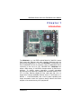
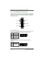
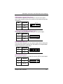
SBC836A1 All-in-One Petit Board with DualView and Serial ATA User’s Manual Disclaimers The information in this manual has been carefully checked and is believed to be accurate. Axiomtek Co., Ltd. assumes no responsibility for any infringements of patents or other rights of third parties which may result from its use. Axiomtek assumes no responsibility for any inaccuracies that may be contained in this document. Axiomtek makes no commitment to update or to keep current the information contained in this manual. Axiomtek reserves the right to make improvements to this document and/or product at any time and without notice. No part of this document may be reproduced, stored in a retrieval system, or transmitted, in any form or by any means, electronic, mechanical, photocopying, recording, or otherwise, without the prior written permission of Axiomtek Co., Ltd. Copyright 2004 by Axiomtek Co., Ltd. All rights reserved. November 2004, Version A1 Printed in Taiwan ii ESD Precautions Integrated circuits on computer boards are sensitive to static electricity. To avoid damaging chips from electrostatic discharge, observe the following precautions: Do not remove boards or integrated circuits from their anti-static packaging until you are ready to install them. Before handling a board or integrated circuit, touch an unpainted portion of the system unit chassis for a few seconds. This helps to discharge any static electricity on your body. Wear a wrist-grounding strap, available from most electronic component stores, when handling boards and components. Trademarks Acknowledgments AXIOMTEK is a trademark of Axiomtek Co., Ltd. IBM is a registered trademark of International Business Machines Corporation. MS-DOS, and Windows 95/98/NT/2000 are trademarks of Microsoft Corporation. Phoenix-Award is a trademark of Phoenix-Award Software, Inc. IBM, PC/AT, PS/2, VGA are trademarks of International Business Machines Corporation. VIA EDEN are trademarks of VIA Corporation. Other brand names and trademarks are the properties and registered brands of their respective owners. iii Table of Contents Chapter 1 Introduction............................................................1 1.1 Specifications ................................................................2 1.2 Utilities Supported.........................................................4 Chapter 2 Jummpers and Connectors ..................................5 2.1 Board Dimensions .........................................................5 2.2 Board Layout..................................................................6 2.3 Jumper Settings.............................................................7 2.3.1 AT&ATX Selection: JP1 ............................................................. 8 2.3.2 IGA2 TTL/LVDS LCD VDD Selection (VDD of LCD1 and CN14): JP2........................................................................................ 8 2.3.3 IGA1 LVDS LCD VDD Selection (VDD of CN12): JP3 ....... 8 2.3.4 CMOS Clear Jumper: JP4............................................................ 8 2.3.5 Audio Line Out/Speaker Out Jumper: JP5.............................. 8 2.3.6 Compact flash power select: JP6 ................................................ 9 2.3.7 Compact flash Master/Slave: JP9 .............................................. 9 2.3.8 COM1~COM4 Mode Select: JP10, JP11, JP12, JP13 ............ 9 2.3.9 COM2 Mode Select: JP7, JP8, JP14........................................... 9 2.4 Connectors...................................................................10 2.4.1 ATX Connector: CN1 ............................................................... 11 2.4.2 SATA-150 1, 2 Connector: CN4, CN3 ................................... 11 2.4.3 Front Panel Bezel Connector: CN5......................................... 12 2.4.4 USB 1&2, USB 3&4 Connector: CN6, CN7.......................... 14 2.4.5 PC104+ Connector: CN8 ........................................................ 14 2.4.6 IRDA Connector: CN9 ............................................................. 15 2.4.7 VGA Connector: CN10............................................................. 16 2.4.8 IGA1 LVDS Power Connector: CN11................................... 16 2.4.9 IGA1 24bit LVDS Connector: CN12 ..................................... 16 2.4.10 IGA2 LVDS Power Connector: CN13................................. 17 2.4.11 IGA2 24bit LVDS Connector: CN14 ................................... 17 2.4.12 LAN LED Connector: CN15................................................. 17 2.4.13 LAN Connector: CN16........................................................... 18 iv 2.4.14 2.4.15 2.4.16 2.4.17 2.4.18 2.4.19 2.4.20 2.4.21 2.4.22 2.4.23 FAN Connector: FAN1, FAN2............................................. 18 Floopy Disk Connector: FDD1 ............................................. 18 Keyboard & Mouse Connector: KBMS1 ............................. 19 COM PORT Connector: COM1~COM4............................ 19 Print Port Connector: LPT1 ................................................... 20 Audio Connector: AUDIO1................................................... 20 Compact Flash Connector: CF1............................................. 20 PICMG compliant PCI Slot: J1.............................................. 21 Mini PCI Connector: MINIPCI1........................................... 23 IGA2 24bit TTL Connector: LCD1...................................... 25 Chapter 3 Hardware Description........................................27 3.1 3.2 3.3 3.4 Microprocessors..........................................................27 BIOS ...........................................................................27 System Memory ...........................................................27 I/O Port Address Map ..................................................28 Chapter 4 Award BIOS Utility ............................................31 4.1 BIOS Introduction ........................................................31 4.2 BIOS Setup ...................................................................31 4.2.1 Standard CMOS Setup............................................................... 33 4.2.2 Advanced BIOS Features.......................................................... 36 4.2.3 Advanced Chipset Features....................................................... 41 4.2.4 Integrated Peripherals ................................................................ 44 4.2.5 Power Management Setup......................................................... 49 4.2.6 PNP / PCI Configuration......................................................... 51 4.2.7 PC Health Status......................................................................... 52 4.2.8 Frequency/Voltage Control...................................................... 53 4.2.9 Load Fail-Safe Defaults ............................................................. 54 4.2.10 Set Supervisor / User Password............................................. 55 4.2.11 Save & Exit Setup..................................................................... 56 4.2.12 Exit Without Saving ................................................................. 57 Appendix A Serial ATA Setup Information.....................59 Appendix B Watch Dog Timer ............................................61 v This page does not contain any information. vi SBC836A1 Series All-in-One Petit Board User’s Manual Chapter 1 Introduction The SBC836A1 is a VIA EDEN 400/667/800/1G FANLESS -based Petit board with Ethernet and audio interface. Designed with the space-limited applications in mind, the SBC836A1 is practically the finest embedded PIII-level in existence. Using a standardized format conforming to the size of a 5.25” CD-ROM drive, SBC836A1 can adapt a wide variety of VIA EDEN microprocessors by BIOS autodetection. To simplify system integration, it packs embedded provisions such as super I/Os, Graphics with DualView features, LCD (TTL & LVDS), Ethernet (Gigabit & Fast), solid state disk, all on a single board. Unique embedded features such as 4 serial ports (3 x RS-232, 1 x RS-232/422/485) with +5V/12V power capability and simple automation control are exclusive design features that allow adoption of an extensive array of PC peripherals. Introduction 1 SBC836A1 Series All-in-One Petit Board User’s Manual Designed for the professional embedded developers, the VIA EDEN embedded board SBC836A1 is virtually the ultimate one-step solution for embedded system applications. 1.1 Specifications Chipset: Bus Clock: CPU: CLE266+VT8237 66,100,133MHz EDEN 400/667/800/1G L2 Cache: Integrated in CPU BIOS: 4Mbit PnP Flash BIOS System Memory: 1 x 184-pin DIMM sockets Maximum of 1GB DDR266 RAM IDE Interface: IDE1 x 44-pin(CF with IDE1 channel) IDE2 x 40-pin PIO Mode 0-4, DMA Mode 0-2 and Ultra DMA/33/66/100/133 2 channels of SATA-150 with IDE mode supported BIOS programmable for 4 IE channels (2*PATA-133 & 2*SATA-150) as primary/secondary/third/forth IDE Onboard Multi-I/O One floppy port (26-pin FPC connector on the soldering side) supporting one device One SPP/EPP/ECP parallel port (box header) Four 16550 UARTs compatible serial ports with +5V/+12V power output in pin 1 or pin 9 via jumper setting 3 x RS-232 (box header) 1x RS-232/422/485 box header and selectable via jumper setting(COM2) 1 x IrDA (box header) for wireless communcation VGA Controller: Internal AGP-4x controller integrated in VIA CLE266 Supports CRT, 24-bit TTL LCD or LVDS LCD CRT resolution up to 1400x1050, Flat Panel up to 1600x1200 Supports DualView features as CRT+TTL LCD or Dual LVDS LCD LCD Backlight control supported High quality DVD video Playback 2 Introduction SBC836A1 Series All-in-One Petit Board User’s Manual Ethernet: 1x default RTL8100C for 10/100Base-T or optional 1x RTL8110s for 10/100/1000Base-T USB Interface: 4 USB ports; USB Spec. Rev. 2.0 compliant AUDIO AC’97 2.2 S/PDIF extension compliant codec 18-bit stereo full duplex SD codec 3D stereo expansion for simulated surround 18-bit independent rate stereo ADC/DAC 4 stereo, 2 mono analog line-level inputs Low Power consumption mode Exceeds Microsoft® WHQL logo requirements PICMG compliant PCI extension slot Support max. up to 2 32-bit/33MHz PCI Masters Mini PCI: 1 Type-III Mini PCI Compact Flash TYPE II Supports CompactFlash memory modules IBM MicroDrive supported PC104 plus: Supports 3 PCI Masters and 1 slave Power Management: ACPI (Advanced Configuration and Power Interface) Watchdog Timer: Watch Dog Timer Time-out value. of 0~255 second Operating Temperature: 0oC~60oC (32oF~140oF) Operating Humidity: 5%~95%; non-condensing Form Factor: 5.25” form factor Dimensions: 203.20 x 146.05 mm2 NOTE: Introduction Specifications are subject to change without notice. 3 SBC836A1 Series All-in-One Petit Board User’s Manual 1.2 Utilities Supported VIA Chipset Driver Ethernet Utility and Drivers VGA Drivers 4 Introduction SBC836A1 Series All-in-One Petit Board User’s Manual Chapter 2 Jumpers and Connectors 2.1 Board Dimensions Jumpers and Connectors 5 SBC836A1 Series All-in-One Petit Board User’s Manual 2.2 6 Board Layout Jumpers and Connectors SBC836A1 Series All-in-One Petit Board User’s Manual 2.3 Jumper Settings The SBC836A1 is configured to match the needs of your application by proper jumper settings. The following tables show the correct jumper settings for the onboard devices. Jumper Default Setting Jumper Setting JP1 AT&ATX Selection Default: ATX Short 2-3 JP2 IGA2 TTL/LVDS LCD VDD Selection Default: TTL 5V /LVDS 3.3V Short 2-3(3.3V) JP3 IGA1 LVDS LCD VDD Selection Default: 3.3V Short 2-3 JP4 Clear CMOS Selection Default: VBAT Short 1-2 JP5 Audio Line Out/Speaker Out Jumper Selection Default: Speak Out Short 3-5,4-6 JP6 Compact flash power select Default: 5V Short 1-2 JP7 COM2 RS232/422/485 Default: RS232 Short 3-5,4-6 JP8 COM2 RS232/422/485 Default: RS232 Short 3-5,4-6 JP9 CF Master/Slave Defalut: Slave Open JP10 COM1 +12V/5V/RS232 Default: RS232 Short 7-9,8-10 JP11 COM2 +12V/5V/RS232 Default: RS232 Short 7-9,8-10 JP12 COM4 +12V/5V/RS232 Default: RS232 Short 7-9,8-10 JP13 COM3 +12V/5V/RS232 Default: RS232 Short 7-9,8-10 JP14 COM2 RS232/422/485 Default: RS232 Short 1-2 Jumpers and Connectors 7 SBC836A1 Series All-in-One Petit Board User’s Manual 2.3.1 AT&ATX Selection: JP1 Select Settings AT POWER Short 1-2 ATX POWER Short 2-3(Default) JP1 1 2 3 2.3.2 IGA2 TTL/LVDS LCD VDD Selection (VDD of LCD1 and CN14): JP2 VDDM Settings 5V (TTL default) Short 1-2 3.3V(LVDS default) Short 2-3 JP2 1 2 3 2.3.3 IGA1 LVDS LCD VDD Selection (VDD of CN12): JP3 VDDM Settings 5V Short 1-2 3.3V(LVDS default) Short 2-3 JP3 1 2 3 2.3.4 CMOS Clear Jumper: JP4 Options Normal (default) Settings Short 1-2 Clear CMOS Short 2-3 2.3.5 Audio Line Out/Speaker Out Jumper: JP5 8 Options Settings Line Out Speaker Out (default) JP5 1 2 Short 1-3, 2-4 3 4 Short 3-5, 4-6 5 6 Jumpers and Connectors SBC836A1 Series All-in-One Petit Board User’s Manual 2.3.6 Compact flash power select: JP6 Options 5V(default) 3.3V Settings Short 1-2 Short 2-3 2.3.7 Compact flash Master/Slave: JP9 Options Slave(default) Settings Open Master Short 2.3.8 COM1~COM4 Mode Select: JP10, JP11, JP12, JP13 COM1 Pin 1,8=5V *Pin 1=DCD Pin 1,8=12V Pin 8=RI JP10 Short 1-3,2-4 Short 7-9 Short 3-5,4-6 Short 8-10 COM2 Pin 1,8=5V *Pin 1=DCD Pin 1,8=12V Pin 8=RI JP11 Short 1-3,2-4 Short 7-9 Short 3-5,4-6 Short 8-10 COM3 Pin 1,8=5V *Pin 1=DCD Pin 1,8=12V Pin 8=RI JP13 Short 1-3,2-4 Short 7-9 Short 3-5,4-6 Short 8-10 COM4 Pin 1,8=5V *Pin 1=DCD Pin 1,8=12V Pin 8=RI JP12 Short 1-3,2-4 Short 7-9 Short 3-5,4-6 Short 8-10 2.3.9 COM2 Mode Select: JP7, JP8, JP14 COM2 RS-232 (default) RS-422 RS-485 JP7 3-5, 4-6 1-3, 2-4 1-3, 2-4 Jumpers and Connectors JP8 3-5, 4-6 1-3, 2-4 1-3, 2-4 JP14 1-2 3-4, 7-8 5-6, 7-8 9 SBC836A1 Series All-in-One Petit Board User’s Manual 2.4 Connectors The connectors allow the CPU card to connect with other parts of the system. Some problems encountered by your system may be a result from loose or improper connections. Ensure that all connectors are in place and firmly attached. The following table lists the function of each connector on the SBC836A1. Their corresponding pin assignments are described in Chapter 3. Label CN1 CN2 CN3 CN4 CN5 CN6 CN7 CN8 CN9 CN10 CN11 CN12 CN13 CN14 CN15 CN16 FAN1,2 FDD1 KBMS1 COM1~4 LPT1 AUDIO1 CF1 J1 MINIPCI1 LCD1 10 Connectors ATX Connector (AT & ATX) LAN RJ45 Connector S-ATA 2 Connector S-ATA 1 Connector Front Panel Bezel CONN. USB 1&2 USB 3&4 PC104+ Connector IRDA Connector VGA Connector IGA1 LVDS Power CONN. IGA1 24bit LVDS CONN. IGA2 LVDS Power CONN. IGA2 24bit LVDS CONN. LAN LED Connector LAN Connector (Default CN2_RJ45) CPU&SYS FAN CONN. Floopy Disk Connector Keyboard&Mouse CONN COM PORT Connector PRINT PORT Connector AUDIO Connector Compact Flash CONN PICMG Connector Mini PCI Connector IGA2 24bit TTL CONN. Jumpers and Connectors SBC836A1 Series All-in-One Petit Board User’s Manual 2.4.1 ATX Connector: CN1 PIN 1 2 3 4 5 6 7 8 9 10 SIGNAL 3.3V 3.3V GND 5V GND 5V GND PW_OK 5V_SB 12V PIN 11 12 13 14 15 16 17 18 19 20 SIGNAL 3.3V -12V GND PS_ON GND GND GND -5V 5V 5V 2.4.2 SATA-150 1, 2 Connector: CN4, CN3 Dual Channel Serial ATA Controller Complies with Serial ATA Specification Revision 1.0 Dual Channel master mode PCI On-chip two-channel Serial ATA (S-ATA) PHY for support of up to two S-ATA devices directly Supports optional external S-ATA PHY on P-ATA secondary port for support of two additional S-ATA devices Primary P-ATA port can support two P-ATA devices (master and slave) along with two S-ATA devices on the PATA Secondary port (with external S-ATA PHY) plus two more S-ATA devices on the direct S-ATA interface S-ATA drive transfer rate is capable of up to 150 MB/s per channel (serial speed of 1.5 Gbit/s) External Crystal input for Serial ATA port operation Jumpers and Connectors 11 SBC836A1 Series All-in-One Petit Board User’s Manual 2.4.3 Front Panel Bezel Connector: CN5 The front bezel of the case has a control panel that provides light indication of the computer activities and switches to change the computer status. CN5 is a 16-pin header that provides interfaces for the following functions. 1 2 Power LED SPEAKER Reset Switch SMI / Hardware Switch POWER BUTTON Hard Disk Drive LED 15 16 Power LED: Pins 1, 3, 5 The power LED indicates the status of the main power switch. The keylock switch, when closed, will disable the keyboard function. Pin # Signal Name 1 Power LED (+) 3 Ground 5 Ground 1 3 5 Speaker: Pins 4, 6 This connector provides an interface to a speaker for audio tone generation. Pin # Signal Name 4 Short 4-6 for Internal Buzzer 6 12 4 6 Jumpers and Connectors SBC836A1 Series All-in-One Petit Board User’s Manual SMI/Hardware Switch: Pins 10, 12 This connector supports the "Green Switch" from the control panel, which, when pressed, will force the system into the power-saving mode immediately. Pin # Signal Name 10 Sleep 12 Ground 10 12 ATX Power On /Off Button: Pins 13, 15 This jumper is only useful when installing an ATX power supply. Pin # Signal Name 13 PW_BN+ 15 GND 13 15 Reset Switch: Pins 9, 11 The reset switch allows the user to reset the system without turning the main power switch OFF and then ON. Orientation is not required when making a connection to this header. Pin # Signal Name 9 Reset 11 GND 9 11 HDD LED: Pins 14, 16 This connector connects to the hard drive activity LED on control panel. Pin # Signal Name 14 VCC 16 HDD_LED Jumpers and Connectors 14 16 13 SBC836A1 Series All-in-One Petit Board User’s Manual 2.4.4 USB 1&2, USB 3&4 Connector: CN6, CN7 The Universal Serial Bus (USB) connector on SBC836A1 is used when installing peripherals supporting the USB interface. CN6: USB1&2 Connector CN7: USB1&2 Connector Pin Pin 1 3 5 7 9 Description VCC USB1+ USB1GND GND 2 4 6 8 10 Description VCC USB2+ USB2GND GND 2 4 6 8 10 1 3 5 7 9 2.4.5 PC104+ Connector: CN8 The PCI bus connector is a 4x30 (120-pin) 2mm pitch stackthrough connector as opposed to the 124-pin edge connector on standard 32-bit PCI Local Bus. The 120-pin PCI does not support 64-bit Extensions, JTAG, PRSNT, or CLKRUN signals. CN2: PC/104 plus Bus Pin Assignment Pin# 1 5 9 13 17 21 25 29 33 37 41 45 49 53 57 61 65 69 14 Pin Name GND/5.0V KEY2 GND SERR* FRAME* +3.3V AD29 GNT1* +12V GND AD13 +3.3V +3.3V C/BE3* GND +5V +5 AD08 SB0* Pin# Pin Name Pin# Pin Name Pin# Pin Name 2 VI/O 3 AD05 4 C/BE0* 6 10 14 18 22 26 30 34 38 42 46 50 54 58 62 66 70 AD11 GND GND IDSEL0 +5V +5V -12V AD07 C/BE1* TRDY* AD20 AD26 REQ2* INTD* AD01 AD10 +3.3V 7 11 15 19 23 27 31 35 39 43 47 51 55 59 63 67 71 AD14 STOP* AD18 AD24 REQ0* CLK2 Reserved AD09 GND GND AD23 +5V VI/O INTA* AD04 GND LOCK* 8 12 16 20 24 28 32 36 40 44 48 52 56 60 64 68 72 AD14 +3.3V AD21 GND GND GND AD02 VI/O PERR* AD16 GND AD30 CLK0 Reserved GND AD15 GND Jumpers and Connectors SBC836A1 Series All-in-One Petit Board User’s Manual Pin# 73 77 81 85 89 93 97 101 105 109 113 Pin Name IRDY* AD22 AD28 GNT2* INTB* AD03 AD12 GND GND IDSEL3 VI/O Pin# 74 78 82 86 90 94 98 102 106 110 114 Pin Name +3.3V IDSEL1 GND GND Reserved AD06 +3.3V DEVSEL* AD19 GND GNT0* 117 GND 118 RST* Pin# Pin Name 75 AD17 79 VI/O 83 REQ1* 87 CLK3 91 AD00 95 GND 99 PAR 103 +3.3V 107 +3.3V 111 AD27 115 GND 119 INTC* Pin# Pin Name 76 GND 80 AD25 84 +5V 88 +5V 92 +5V 96 M66EN 100 SDONE 104 C/BE2* 108 IDSEL2 112 AD31 116 CLK1 GND/3.3V 120 KEY2 Notes: 1. The shaded area denotes power or ground signals. 2. The KEY pins are to guarantee proper module installation. Pin-A1 will be removed and the female side plugged for 5.0V I/O signals and Pin-D30 will be modified in the same manner for 3.3V I/O. It is recommended that both KEY pins (A1 and D30) be electrically connected to GND for shielding. 2.4.6 IRDA Connector: CN9 CN9 is a 5-pin Pitch2.54mm IrDA connector for wireless communication. Jumpers and Connectors +5V 1 N.C. 2 IRRX 3 GND 4 IRTX 5 15 SBC836A1 Series All-in-One Petit Board User’s Manual 2.4.7 VGA Connector: CN10 Pin Signal Pin Signal Pin Signal 2 1 1 Red 2 AGND 3 Green 3 4 4 N/A 5 Blue 6 AGND 5 6 7 N/A 8 DDC DAT 9 GND 7 9 8 10 10 AGND 11 GND 12 Horizontal Sync 12 13 AGND 14 Vertical Sync 15 DDC CLK 11 13 15 16 NC 14 16 2.4.8 IGA1 LVDS Power Connector: CN11 CN11 is a Hirose DF13-5P- 1.25V(50) connector, the match side connector is DF13-5S-1.25C Pin 1 2 3 4 5 Signal +12VM1 VCC (+5V) +12VM1 ENABLE GND 1 2 3 4 5 2.4.9 IGA1 24bit LVDS Connector: CN12 CN11 is a Hirose DF13-20DP- 1.25V(50) connector, the match side connector is DF13-20DS-1.25DSA(50) Pin Signal Pin Signal 1 VCCM1 2 VCCM1 3 VCCM1 4 VCCM1 5 IGA1_TX06 IGA1_TX37 IGA1_TX0+ 8 IGA1_TX3+ 9 GND 10 GND 11 IGA1_TX112 IGA1_CLK13 IGA1_TX1+ 14 IGA1_CLK+ 15 GND 16 GND 17 IGA1_TX218 GND 19 IGA1_TX2+ 20 GND 16 Jumpers and Connectors SBC836A1 Series All-in-One Petit Board User’s Manual 2.4.10 IGA2 LVDS Power Connector: CN13 CN13 is a Hirose DF13-5P- 1.25V(50) connector, the match side connector is DF13-5S-1.25C Pin 1 2 3 4 5 Signal +12VM VCC (+5V) +12VM ENABLE GND 1 2 3 4 5 2.4.11 IGA2 24bit LVDS Connector: CN14 CN14 is a Hirose DF13-20DP- 1.25V(50) connector, the match side connector is DF13-20DS-1.25DSA(50) Pin Signal Pin Signal VCCM VCCM 1 2 VCCM VCCM 3 4 IGA2_TX0IGA2_TX35 6 IGA2_TX0+ IGA2_TX3+ 7 8 GND 9 10 GND 11 IGA2_TX112 IGA2_CLKIGA2_TX1+ 13 14 IGA2_CLK+ GND 15 16 GND 17 IGA2_TX218 GND 19 IGA2_TX2+ 20 GND 2.4.12 LAN LED Connector: CN15 CN15 is a 4x2 2.0mm PIN HEADER for LAN LED use. Pin Signal Pin Signal ACT LED +3.3VSB(Standby) 1 2 LINK100_LED +3.3VSB(Standby) 3 4 LINK10_LED +3.3VSB(Standby) 5 6 LINK1000_LED +3.3VSB(Standby) 7 8 Jumpers and Connectors 17 SBC836A1 Series All-in-One Petit Board User’s Manual 2.4.13 LAN Connector: CN16 CN16 is a 4x2 2.0mm PIN HEADER for LAN singal use.(Default CN2_RJ45 connector ,for customer design I/O board only) Pin Signal Pin TX1+ TX11 2 TX2+(RX1+) TX3+ (Giga LAN only) 3 4 TX3- (Giga LAN only) TX2-(RX1-) 5 6 TX4+ (Giga LAN only) TX4- (Giga LAN only) 7 8 2.4.14 FAN Connector: FAN1, FAN2 Pin 1 2 3 Description Sensor +12V GND 3 2 1 2.4.15 Floopy Disk Connector: FDD1 The SBC836A1 provides a 26-pin FCC Z.I.F. type connector, and the general output for support of a single floppy drives. The floppy drive could be any one of the following types: 3.5" 720KB or 1.44MB/2.88MB. FDD1: FDD Connector Pin Assignment Pin 1 2 3 4 5 6 7 8 9 10 11 12 13 18 Description +5V INDEX +5V DRIVE0 +5V DSKCHG No connector READY HDOUT MOTOR ON No connector DIR HDSEL Pin 14 15 16 17 18 19 20 21 22 23 24 25 26 Description STEP GND WDATA GND WGATE GND TRK0 GND WPT GND RDATA GND SIDE0 Jumpers and Connectors SBC836A1 Series All-in-One Petit Board User’s Manual 2.4.16 Keyboard & Mouse Connector: KBMS1 KBMS1: Keyboard and PS/2 Mouse Connector Pin Assignment Pin Description Pin Description 1 Keyboard Vcc 2 Keyboard Data 3 Keyboard CLK 4 GND 5 Vcc 6 Mouse Vcc 7 Mouse Data 8 Mouse CLK 9 GND 10 +12V 2 4 6 8 10 1 3 5 7 9 2.4.17 COM PORT Connector: COM1~COM4 The four COM ports have +5V/+12V power capability on pin 1 and pin 8, depending on the jumper setting. (See Section 2.3.8) The RS-232 pin assignments are listed on the following table. Pin Description Pin 1 3 5 7 9 Data Carrier Detect (DCD) Receive Data (RXD) Transmit Data (TXD) Data Terminal Ready (DTR) Ground (GND) 2 4 6 8 10 Description Data Set Ready (DSR) Request to Send (RTS) Clear to Send (CTS) Ring Indicator (RI) NC 1 2 3 4 5 6 7 9 8 10 The RS-422/485 pin assignments for COM2 are listed below. Pin # 1 2 3 4 5 6 7 8 9 10 Signal Name R2-422 RS-485 TXDATANo connector No connector TX+ DATA+ No connector No connector RX+ No connector No connector No connector RXNo connector No connector No connector GND GND No connector No connector Jumpers and Connectors 19 SBC836A1 Series All-in-One Petit Board User’s Manual 2.4.18 Print Port Connector: LPT1 LPT1: Parallel Port Connector Pin Assignment Pin 1 3 5 7 9 11 13 15 17 19 21 23 25 Description Strobe# Data 0 Data 1 Data 2 Data 3 Data 4 Data 5 Data 6 Data 7 Acknowledge# Busy Paper Empty# Printer Select Pin 2 4 6 8 10 12 14 16 18 20 22 24 26 Description Auto Form Feed# Error# Initialize# Printer Select In# GND GND GND GND GND GND GND GND NC 1 2 3 4 5 6 7 9 8 10 11 13 12 15 17 19 14 16 18 20 21 22 23 25 24 26 2.4.19 Audio Connector: AUDIO1 AUDIO1: Audio Connector Pin 1 3 5 7 9 Signal MIC-IN Line In L Line In R Audio Out L Audio Out R Pin 2 4 6 8 10 Signal GND GND GND GND GND 2 4 6 8 10 1 3 5 7 9 2.4.20 Compact Flash Connector: CF1 The SBC836A1 Series is equipped with a CompactFlash disk socket on the solder side and it supports the IDE interface CompactFlash disk card. The socket itself is especially designed to prevent any incorrect installation of the CompactFlash disk card. When installing or removing the CompactFlash disk card, please make sure that the system power is off. 20 Jumpers and Connectors SBC836A1 Series All-in-One Petit Board User’s Manual 2.4.21 PICMG compliant PCI Slot: J1 The SBC836A1 Series provides a free PICMG compliant PCI slot for PCI device expansion. J1: PICMG Slot Connector Pin Assignment Pin B1 B2 B3 B4 B5 B6 B7 B8 B9 B10 B11 B12 B13 B14 B15 B16 B17 B18 B19 B20 B21 B22 B23 B24 B25 B26 B27 B28 B29 B30 Signal -12V Reserved GND Reserved +5V +5V INTB# INTD# Reserved REQ1# Reserved GND GND CLKA GND CLKB GND REQ0# +5V(IO) AD31 AD29 GND AD27 AD25 Reserved CBE3# AD23 GND AD21 AD19 Jumpers and Connectors Pin A1 A2 A3 A4 A5 A6 A7 A8 A9 A10 A11 A12 A13 A14 A15 A16 A17 A18 A19 A20 A21 A22 A23 A24 A25 A26 A27 A28 A29 A30 Signal TRST# +12V Reserved Reserved +5V INTA# INTC# +5V Reserved +5V(IO) Reserved GND GND GNT1# RST# +5V(IO) GNT0# GND Reserved AD30 Reserved AD28 AD26 GND AD24 IDSEL +3.3V AD22 AD20 GND 21 SBC836A1 Series All-in-One Petit Board User’s Manual Pin B31 B32 B33 B34 B35 B36 B37 B38 B39 B40 B41 B42 B43 B44 B45 B46 B47 B48 B49 B52 B53 B54 B55 B56 B57 B58 B59 B60 B61 B62 22 Signal Reserved AD17 CBE2# GND IRDY# +3.3V DEVSEL# GND LOCK# PERR# Reserved SERR# Reserved CBE1# AD14 GND AD12 AD10 GND AD08 AD07 Reserved AD05 AD03 GND AD01 +5V(IO) Reserved +5V +5V Pin A31 A32 A33 A34 A35 A36 A37 A38 A39 A40 A41 A42 A43 A44 A45 A46 A47 A48 A49 A52 A53 A54 A55 A56 A57 A58 A59 A60 A61 A62 Signal AD18 AD16 +3.3V FRAME# GND TRDY# GND STOP# Reserved SDONE SBO# GND PAR AD15 Reserved AD13 AD11 GND AD09 CBE0# Reserved AD06 AD04 GND AD02 AD0 +5V(IO) Reserved +5V +5V Jumpers and Connectors SBC836A1 Series All-in-One Petit Board User’s Manual 2.4.22 Mini PCI Connector: MINIPCI1 J2: Mini-PCI Connector Pin Assignment Pin 1 Pin 2 3 5 7 9 11 13 15 17 19 21 23 Signal TIP KEY LAN_RD+ LAN_RDRJ45 termination RJ45 termination LAN_LED1+ LAN_LED1CHGND INTB# 3.3V RESERVED GND 4 6 8 10 12 14 16 18 20 22 24 Signal RING KEY LAN_TD+ LAN_TDRJ45 termination RJ45 termination LAN_LED2+ LAN_LED2RESERVED 5V INTA# RESERVED 3.3VAUX 25 27 29 31 33 35 37 39 41 43 45 47 49 51 53 55 57 59 61 63 65 67 69 CLK GND REQ# 3.3V AD31 AD29 GND AD27 AD25 RESERVED C/BE3# AD23 GND AD21 AD19 GND AD17 C/BE2# IRDY# 3.3V CLKRUN# SERR# GND 26 28 30 32 34 36 38 40 42 44 46 48 50 52 54 56 58 60 62 64 66 68 70 RST# 3.3V GNT# GND PME# RESERVED AD30 3.3V AD28 AD26 AD24 IDSEL GND AD22 AD20 PAR AD18 AD16 GND FRAME# TRDY# STOP# 3.3V Jumpers and Connectors 23 SBC836A1 Series All-in-One Petit Board User’s Manual Pin 71 73 75 77 79 81 83 85 87 89 91 93 95 97 99 101 103 105 107 109 111 113 115 117 119 121 123 24 Signal PERR# C/BE1# AD14 GND AD12 AD10 GND AD08 AD07 3.3V AD05 RESERVED 5V 5V AD01 GND RESERVED RESERVED RESERVED RESERVED RESERVED RESERVED RESERVED RESERVED RESERVED RESERVED RESERVED Pin 72 74 76 78 80 82 84 86 88 90 92 94 96 98 100 102 104 106 108 110 112 114 116 118 120 122 124 Signal DEVSEL# GND AD15 AD13 AD11 GND AD09 C/BE0# 3.3V AD06 AD04 AD02 AD00 RESERVED RESERVED GND RESERVED RESERVED RESERVED RESERVED RESERVED GND RESERVED RESERVED RESERVED RESERVED RESERVED Jumpers and Connectors SBC836A1 Series All-in-One Petit Board User’s Manual 2.4.23 IGA2 24bit TTL Connector: LCD1 Pin Signal Pin Signal Pin Signal 1 -12V 2 +12VM 3 GND 4 GND 5 VCCM 6 VCCM 7 ENAVEE 8 GND 9 P0 10 P1 11 P2 12 P3 13 P4 14 P5 15 P6 16 P7 17 P8 18 P9 19 P10 20 P11 21 P12 22 P13 23 P14 24 P15 25 P16 26 P17 27 P18 28 P19 29 P20 30 P21 31 P22 32 P23 33 GND 34 GND 35 SHFCLK 36 FLM 37 M 38 LP 39 GND 40 ENABKL 41 GND 42 -SHFCLK 43 VCCM 44 VCCM Flat Panel Connector Pin Description Name Description P0~P23 Flat panel data output ENABKL Activity Indicator and Enable Backlight outputs SHFCLK Shift clock. Pixel clock for flat panel data M M signal for panel AC drive control LP Latch pulse. Flat panel equivalent of HSYNC FLM First line marker. Flat panel equivalent of VSYNC +12VM +12V power controlled by chipset ENAVEE Power sequencing controls for panel LCD bias volt VCCM 3.3V or 5V selected by JP2 Jumpers and Connectors 25 SBC836A1 Series All-in-One Petit Board User’s Manual Flat Panel Interface Pins for Color TFT LCD Pin LP FLM SHFCLK M ENAVDD ENABLK P23 P22 P21 P20 P19 P18 P17 P16 P15 P14 P13 P12 P11 P10 P9 P8 P7 P6 P5 P4 P3 P2 P1 P0 26 TFT 18-bit HSYNC VSYNC CK DE ENAVDD ENABLK R5 R4 R3 R2 R1 R0 --G5 G4 G3 G2 G1 G0 --B5 B4 B3 B2 B1 B0 --- 24-bit HSYNC VSYNC CK DE ENAVDD ENABLK R7 R6 R5 R4 R3 R2 R1 R0 G7 G6 G5 G4 G3 G2 G1 G0 B7 B6 B5 B4 B3 B2 B1 B0 Jumpers and Connectors SBC836A1 Series All-in-One Petit Board User’s Manual Chapter 3 Hardware Description 3.1 Microprocessors The SBC836A1 supports VIA EDEN 400/667/800/1GHZ CPUs. Systems based on these CPUs can be operated under Windows XP/NT/2000 and Linux environments. The system performance depends on the microprocessor installed onboard. 3.2 BIOS System BIOS used on the SBC836A1 is Phoenix-Award Plug and Play BIOS. The SBC836A1 contains a single 4Mbit Flash. 3.3 System Memory The SBC836A1 inductrial CPU board supports one 184-pin DDR DIMM (Dual In-Line Memory Module) socket for a maximum memory of 1GB buffer DDR266 SDRAMs. The memory module can come in sizes of 64MB, 128MB, 256MB, 512MB and 1GB. Hardware Description 27 SBC836A1 Series All-in-One Petit Board User’s Manual 3.4 I/O Port Address Map TheVIA EDEN CPU communicates via I/O ports. It has a total of 1KB port addresses available for assignment to other devices via I/O expansion cards. Address 000-01F 020-03F 060-06F 070-07F 080-09F 0C0-0DF 0F0 0F1 0F8-0FF 1F0-1F7 294~297 376 378-37F 380-38F 3A0-3AF 3B0-3DF 3F0-3F5 3F8-3FF 3E8-3EF 2F8-2FF 2E8-2EF 4D0~4D1 CF8~CFF E000~E0FE E100~E70E E800~EA1E Devices DMA controller #1 Interrupt controller #1 Keyboard controller Real time clock, NMI DMA page register DMA controller #2 Clear math coprocessor busy signal Reset math coprocessor Math processor Fixed disk controller PCI Bus IDE Controller Parallel port #1(Default disable) Reserved Reserved VGA card Floppy disk controller Serial port #1 (COM1) Reserved Serial port #2 (COM2) Reserved PCI Bus PCI Bus Enternet IDE Controller USB Controller 1nd I/O W83697HF: 2EH 2 nd I/O W83627: 4EH 28 Hardware Description SBC836A1 Series All-in-One Petit Board User’s Manual 3.5 Interrupt Controller NMI Parity Check Error IRQ0 System timer output IRQ1 Keyboard IRQ2 Interrupt rerouting from IRQ8 through IRQ15 IRQ3 Serial port #2 IRQ4 Serial port #1 IRQ5 Audio & Ethernet IRQ6 Floppy disk controller IRQ7 Parallel port #1 IRQ8 Real time clock IRQ9 ACPI(Enable) IRQ10 COM3 IRQ11 COM4 IRQ12 PS/2 Mouse IRQ13 Math coprocessor IRQ14 Primary IDE channel IRQ15 Secondary IDE Channel Hardware Description 29 SBC836A1 Series All-in-One Petit Board User’s Manual This page does not contain any information. 30 Hardware Description SBC836A1 Series All-in-One Petit Board User’s Manual Chapter 4 Award BIOS Utility Chapter 4 describes the different settings available in the Award BIOS that comes with the SBC836A1. Also contained here are instructions on how to set up the BIOS configuration. 4.1 BIOS Introduction The Award BIOS (Basic Input/Output System) installed in the system ROM supports Intel processors in a standard IBM-AT compatible I/O system. The BIOS provides critical low-level support for standard devices such as disk drives, serial and parallel ports. It also adds virus and password protection as well as special support for detailed finetuning of the chipset controlling the entire system. 4.2 BIOS Setup The Award BIOS provides a Setup utility program for specifying the system configurations and settings. The BIOS ROM of the system stores the Setup utility. When the computer is turned ON, the Award BIOS is immediately activated. The following message will appear on the screen: Press <DEL> to Enter Setup Then, press the <Del> key immediately to enter the Setup utility. The delay of pressing the <Del> key will cause POST (Power On Self Test) to continue with the test routines, thus preventing invoking the Setup. In this case, the system has to be restarted for entering the BIO setup by pressing the ”Reset” button or simultaneously pressing the <Ctrl>, <Alt> and <Delete> keys. Besides, turning the system OFF first and then ON again can also restart the system. When entering the Setup utility, the Main Menu screen will appear on the screen. Various setup functions and exit choices can be selected from this menu. In general, the arrow keys are used to highlight items, <Enter> to select, the <PgUp> and <PgDn> keys to change entries, <F1> for help and <Esc> to quit. Award BIOS Utility 31 SBC836A1 Series All-in-One Petit Board User’s Manual CMOS Setup Utility-Copyright © 1984-2001 Award Software Standard CMOS Features Frequency/Voltage Control Advanced BIOS Features Load Optimized Defaults Advanced Chipset Features Set User Password Integrated Peripherals Save & Exit Setup Power Management Setup Exit Without Saving PnP/PCI Configurations PC Health Status Esc : Quit BIOS F9 : Menu in F10 : Save & Exit Setup F6 : SAVE CMOS TO BIOS : Select Item F7 : LOAD CMOS FROM BIOS Time, Date, Hard Disk Type… The section below the setup items in the Main Menu displays the control keys for this menu. Another section located at the bottom of the Main Menu, just below the control keys section, displays information on the currently highlighted item in the list. NOTE: If the computer cannot boot after making and saving system changes with Setup, the Award BIOS, via its built-in override feature, resets your system to the CMOS default settings. Avoid making any changes to the chipset defaults are strongly recommanded. These defaults have been carefully chosen by both Award and the system manufacturer to provide the absolute maximum performance and reliability. 32 Award BIOS Utility SBC836A1 Series All-in-One Petit Board User’s Manual 4.2.1 Standard CMOS Setup “Standard CMOS Setup” is used to record some basic hardware configurations in the computer system and set the system clock and error handling. If the motherboard is already installed in a working system, there is no need to enter this option. However, the Standard CMOS option has to be setup in any of the following situations: the system hardware configurations are changed, the onboard battery fails, and the configuration stored in the CMOS memory is lost or damaged. Phoenix – AwardBIOS CMOS Setup Utility Standard CMOS Features Date (mm:dd:yy) Wed, Jul 20 2004 Time (hh:mm:ss) 13 : 9 : 11 Item Help Menu Level IDE Primary Master IDE Primary Slave IDE Secondary Master IDE Secondary Slave None None None None Drive A Drive B 1.44M, 3.5 in. None Video Halt on EGA/VGA All, But keyboard Base Memory Extended Memory Total Memory 640K 494960k 491520k Change the Day, month, Year and Century : Move Enter: Select +/-/PU/PD: Value F10: Save ESC: Exit F1: General Help F5: Previous Values F6: Fail-Safe Defaults F7: Optimized Defaults At the bottom of the menu are the control keys for the use of this menu. The <F1> key can be pressed in each item field to display the relevant information for help. The memory display at the lower right-hand side of the menu is read-only. It will adjust automatically according to the memory changed. The following pages describe each item of this menu. Award BIOS Utility 33 SBC836A1 Series All-in-One Petit Board User’s Manual Date The date format is <day>, <date> <month> <year>. Press <F3> to show the calendar. day The day of week, from Sun to Sat, determined by the BIOS, is read only date The date, from 1 to 31 (or the maximum allowed in the month), can key in the numerical / function key month The month, Jan through Dec. year The year, depends on the year of BIOS Time The time format is <hour> <minute> <second> accepting either function key or numerical key. The time is calculated based on the 24-hour militarytime clock. For example, 1 p.m. is 13:00:00. IDE Primary Master/Primary Slave/Secondary Master/Secondary Slave This category identifies the type of the channel that is installed in the computer. There are 45 predefined types and 2 user definable types for Enhanced IDE BIOS. Type 1 to Type 45 are predefined. Type User is userdefinable. Press <PgUp>/<+> or <PgDn>/<−> to select a numbered hard disk type or type the number and press <Enter>. Note that the specifications of the drive in the system must match with the drive table. The hard disk will not work properly if the improper information within this category is entered. If the disk drive type does not match or is not listed, the Type User is used to define the drive type manually. If the Type User is selected, related information has to be entered. Enter the information directly from the keyboard and press <Enter>. This information should be provided in the documentation from the hard disk vendor or the system manufacturer. If the controller of HDD interface is ESDI, select “Type 1”. If the controller of HDD interface is SCSI, select “None”. If the controller of HDD interface is CD-ROM, select “None”. CYLS. HEADS PRECOMP number of LANDZONE landing zone cylinders number of heads SECTORS number of sectors HDD access write precom MODE mode If there is no hard disk drive installed, select NONE and press <Enter>. 34 Award BIOS Utility SBC836A1 Series All-in-One Petit Board User’s Manual Drive A type/Drive B type The category identifies the types of floppy disk drive A or drive B installed in the computer. None No floppy drive installed 360K, 5.25 in 5.25 inch PC-type standard drive; 360Kb capacity 1.2M, 5.25 in 5.25 inch AT-type high-density drive; 1.2MB capacity 720K, 3.5 in 3.5 inch double-sided drive; 720Kb capacity 1.44M, 3.5 in 3.5 inch double-sided drive; 1.44MB capacity 2.88M, 3.5 in 3.5 inch double-sided drive; 2.88MB capacity Halt On This field determines whether the system will halt if an error is detected during power up. No errors The system boot will halt on any error detected. (default) All errors Whenever the BIOS detects a non-fatal error, the system will stop and you will be prompted. All, But Keyboard The system boot will not stop for a keyboard error; it will stop for all other errors. All, But Diskette The system boot will not stop for a disk error; it will stop for all other errors. All, But Disk/Key The system boot will not stop for a keyboard or disk error; it will stop for all other errors. Award BIOS Utility 35 SBC836A1 Series All-in-One Petit Board User’s Manual 4.2.2 Advanced BIOS Features This section is used to configure and improve the system and set up some system features according to the user’s preference. Phoenix – AwardBIOS CMOS Setup Utility Advanced BIOS Features Hard Disk Boot Priority Virus Warning CPU Internal Cache CPU L2 Cache ECC Checking Quick Power On Self Test First Boot Device Second Boot Device Third Boot Device Boot Other Device Onboard Lan boot Rom Swap Floppy Drive Boot Up Floppy Seek Boot Up NumLock Status Gate A20 Option Typematic Rate Setting Typematic Rate (Chars/Sec) Typematic Delay (Msec) Security Option MPS Version Control For OS OS Select For DRAM > 64MB Video BIOS Shadow Small Logo(EPA) Show Display Board ID Message Press Enter Disabled Enabled Enabled Enabled Floppy HDD-0 LS120 Enabled Disable Disabled Enabled On Fast Disabled 6 250 Setup 1.4 Non-OS2 Enabled Disabled Disabled Item Help Menu Level Allows you to choose the VIRUS warning feature for IDE Hard disk boot sector protection. If this function is enable and someone attempts to write data into this area, BIOS will show a warning message on screen and alarm beep : Move Enter: Select +/-/PU/PD: Value F10: Save ESC: Exit F1: General Help F5: Previous Values F6: Fail-Safe Defaults F7: Optimized Defaults 36 Award BIOS Utility SBC836A1 Series All-in-One Petit Board User’s Manual Virus Warning This item protects the boot sector and partition table of the hard disk against accidental modifications. If an attempt is made, the BIOS will halt the system and display a warning message. If this occurs, the user can either continue the operation or run an anti-virus program to locate and remove the problem. NOTE: Many disk diagnostic programs, which attempt to access the boot sector table, can cause the virus warning. Thus, disable the Virus Warning feature while running any of these programs. CPU Internal Cache / External Cache Cache memory is additional memory that is much faster than conventional DRAM (system memory). CPUs from 486-type and up contain internal cache memory, and most, but not all, modern PCs have additional (external) cache memory. When the CPU requests data, the system transfers the requested data from the main DRAM into cache memory, for even faster access by the CPU. These items are used to enable (speed up memory access) or disable the cache function. By default, these are Enabled. CPU L2 Cache ECC Checking When enabled, this allows ECC checking of the CPU’s L2 cache. default, this field is Enabled. By Processor Number Feature When a VIA EDEN CPU is installed, the system automatically detects it and displays this item. Quick Power On Self Test This option speeds up Power On Self Test (POST) after turning on the system power. If it is set as Enabled, BIOS will shorten or skip some check items during POST. The default setting is “Enabled”. Enabled Disabled Enable Quick POST Normal POST First/Second/Third Boot Device These items allow the selection of the 1st, 2nd, and 3rd devices that the system will search for during its boot-up sequence. The wide range of selection includes Floppy, LS120, ZIP100, HDD0~3, SCSI, CDROM, USB Floppy, USB CDROM, USB HDD, and LAN. Boot Other Device This item allows the user to enable/disable the boot device not listed on the First/Second/Third boot devices option above. The default setting is Enabled. Award BIOS Utility 37 SBC836A1 Series All-in-One Petit Board User’s Manual Onboard Lan boot rom Choice Enable when you need boot on Lan Funtion ,Like PXE ,RPL…. Swap Floppy Drive This allows you to determine whether to enable Swap Floppy Drive or not. When enabled, the BIOS swaps floppy drive assignments so that Drive A becomes Drive B, and Drive B becomes Drive A. By default, this field is set to “Disabled”. Boot Up Floppy Seek During POST, BIOS will determine the floppy disk drive type, 40 or 80 tracks. 360Kb type is 40 tracks while 720Kb, 1.2MB and 1.44MB are all 80 tracks. The default value is “Enabled”. Enabled BIOS searches for floppy disk drive to determine if it is 40 or 80 tracks. Note that BIOS can not tell from 720K, 1.2M or 1.44M drive type as they are all 80 tracks. Disabled BIOS will not search for the type of floppy disk drive by track number. There will be no warning message displayed if the drive installed is 360K. Boot Up NumLock Status This option enables and disables the numberlock function of the keypad. The default value is “On”. On Keypad functions confine with numbers Off Keypad functions convert to special functions (i.e., left/right arrow keys) Gate A20 Option The default value is “Fast”. 38 Normal The A20 signal is controlled by keyboard controller or chipset hardware. Fast Default: Fast. The A20 signal is controlled by Port 92 or chipset specific method. Award BIOS Utility SBC836A1 Series All-in-One Petit Board User’s Manual Typematic Rate Setting This determines the typematic rate of the keyboard. The default value is “Disabled”. Enabled Enable typematic rate and typematic delay programming Disabled Disable typematic rate and typematic delay programming. The system BIOS will use default value of these 2 items and the default is controlled by keyboard. Typematic Rate (Chars/Sec) This option refers to the number of characters the keyboard can type per second. The default value is “6”. 6 6 characters per second 8 8 characters per second 10 10 characters per second 12 12 characters per second 15 15 characters per second 20 20 characters per second 24 24 characters per second 30 30 characters per second Typematic Delay (Msec) This option sets the display time interval from the first to the second character when holding a key. The default value is “250”. Award BIOS Utility 250 250 msec 500 500 msec 750 750 msec 1000 1000 msec 39 SBC836A1 Series All-in-One Petit Board User’s Manual Security Option This item limits the access to the system and Setup, or just to Setup. The default value is “Setup”. System Setup NOTE: The system will not boot and access to Setup will be denied if the incorrect password is entered at the prompt. The system will boot, but access to Setup will be denied if the correct password is not entered at the prompt. To disable security, select PASSWORD SETTING at Main Menu and then password is asked to enter. Do not type anything, just press <Enter> and it will disable security. Once the security is disabled, the system will boot and you can enter Setup freely. OS Select for DRAM > 64MB This segment is specifically created for OS/2 when DRAM is larger than 64MB. If the operating system is OS/2 and DRAM used is larger the 64MB, “OS 2” has to be selected; otherwise (under non-OS2), default is “NONOS2”. Video BIOS Shadow Video shadowing increases the video speed by copying the video BIOS into RAM. However, it is still optional depending on the chipset design. The default value of this option is “Enabled”. 40 Enabled Video BIOS shadowing is enabled Disabled Video BIOS shadowing is disabled Award BIOS Utility SBC836A1 Series All-in-One Petit Board User’s Manual 4.2.3 Advanced Chipset Features Since the features in this section are related to the chipset on the CPU board and are completely optimized, changing the default settings in this setup table are not recommended unless the user is well oriented with the chipset features. Phoenix – AwardBIOS CMOS Setup Utility Advanced Chipset Features DRAM Clock/Drive Control AGP & P2P Bridge Control CPU & PCI Bus Control Memory Hole System BIOS Cacheable Video RAM Cacheable VGA Share Memory Size Select Display Device Panel Type Press Enter Press Enter Press Enter Disabled Disabled Disabled 32M CRT 1027X768 18 bit Item Help Menu Level : Move Enter: Select +/-/PU/PD: Value F10: Save ESC: Exit F1: General Help F5: Previous Values F6: Fail-Safe Defaults F7: Optimized Defaults Memory Hole To improve performance, certain space in memory is reserved for ISA cards. This memory must be mapped into the memory space below 16MB. The available choices are 15M-16M and Disabled. System BIOS Cacheable Selecting “Enabled” allows caching of the system BIOS ROM at F0000hFFFFFh, resulting in better system performance. However, if any program writes to this memory area, a system error may result. The choice: Enabled, Disabled. Video RAM Cacheable Selecting “Enabled” allows caching of the A/B segment, resulting in better system performance. The choice: Enabled, Disabled. VGA Share Memory Size This field selects the memory size that is shared by the VGA. Select Display Device This field selects the type of display CRT/LCD, CRT, LCD Award BIOS Utility 41 SBC836A1 Series All-in-One Petit Board User’s Manual 4.2.3.1 DRAM Clock / Driver Control Phoenix – AwardBIOS CMOS Setup Utility DRAM clock / Drive Control Current FSB Frequency Current DRAM Frequency DRAM Clock DRAM Timing DRAM Cas Latency Bank Interleave Precharge to Active (Trp) Active to Precharge (Tras) Active to CMD (Trcd) DRAM Command Rate 100 MHz 133MHz By SPD By SPD 2.5 Disabled 3T 6T 3T 2T Command Item Help Menu Level : Move Enter: Select +/-/PU/PD: Value F10: Save ESC: Exit F1: General Help F5: Previous Values F6: Fail-Safe Defaults F7: Optimized Defaults Current FSB Frequency This field shows the detected FSB of the CPU. Current DRAM Frequency This field shows the detected frequency of the DRAM. 42 Award BIOS Utility SBC836A1 Series All-in-One Petit Board User’s Manual 4.2.3.2 DRAM Clock 100 MHz The memory clock speed will run at 200MHz. 133 MHz The memory clock speed will run at 266MHz. Phoenix – AwardBIOS CMOS Setup Utility DRAM clock / Drive Control AGP Aperture Size AGP Driving Control AGP Driving Value AGP Fast Write AGP Master 1 WS Write AGP Master 1 WS Read 64M Auto DA Disabled Disabled Disabled Item Help Menu Level : Move Enter: Select +/-/PU/PD: Value F10: Save ESC: Exit F1: General Help F5: Previous Values F6: Fail-Safe Defaults F7: Optimized Defaults AGP Aperture Size The field sets aperture size of the graphics. The aperture is a portion of space. Host cycles that hit the aperture range are forwarded to the AGP without any translation AGP Master 1 WS Write When “Enabled”, writes to the AGP (Accelerated Graphics Port) executed with one wait states. AGP Master 1 WS Read When “Enabled”, read to the AGP (Accelerated Graphics Port) executed with one wait states. AGP Driving Control This item adjusts the AGP driving force. ‘Manual’ is chosen to key-in an AGP Driving Value. ‘Auto’ is recommended for avoiding any error in the system. AGP Driving Value This item adjusts the AGP driving force. AGP Fast Write This item enables the AGP model into fast write mode. Award BIOS Utility 43 SBC836A1 Series All-in-One Petit Board User’s Manual 4.2.4 Integrated Peripherals This option sets the hard disk configuration, mode and port. Phoenix – AwardBIOS CMOS Setup Utility Integrated Peripherals VIA OnChip IDE Device Press Enter Item Help Press Enter VIA OnChip PCI Device Super I/O Device Press Enter Menu Level Init Display First PCI Slot V-Link Data 2X Support Disabled IDE HDD Block Mode Enabled Watch Dog Timer Select Disabled : Move Enter: Select +/-/PU/PD: Value F10: Save ESC: Exit F1: General Help F5: Previous Values F6: Fail-Safe Defaults F7: Optimized Defaults Init Display First This item allows you to decide to active whether PCI Slot or AGP first. The options available are PCI Slot, AGP. IDE HDD Block Mode This field allows your hard disk controller to use the fast block mode to transfer data to and from your hard disk drive. 44 Award BIOS Utility SBC836A1 Series All-in-One Petit Board User’s Manual 4.2.4.1 VIA OnChip IDE Device Phoenix – AwardBIOS CMOS Setup Utility VIA OnChip IDE Device OnChip SATA Enabled Item Help IDE SATA Mode IDE DMA Transfer Access Enabled Menu Level OnChip IDE Channel 0 Enabled OnChip IDE Channel 1 Enabled IDE Prefetch Mode Enabled Primary Master PIO Auto Primary Slave PIO Auto Secondary Master PIO Auto Secondary Slave PIO Auto Primary Master UDMA Auto Primary Slave UDMA Auto Secondary Master UDMA Auto Secondary Slave UDMA Auto IDE HDD Block Mode Auto : Move Enter: Select +/-/PU/PD: Value F10: Save ESC: Exit F1: General Help F5: Previous Values F6: Fail-Safe Defaults F7: Optimized Defaults OnChip SATA The choice: Enabled, Disabled. SATA Mode IDE Mode: On-Chip Serial ATA configuration. OnChip IDE Channel0 The integrated peripheral controller contains an IDE interface with support for two IDE channels. Select Enabled to activate each channel separately. IDE Prefetch Mode The onboard IDE drive interface supports IDE prefetching for faster drive accesses. If you install a primary and/or secondary add-in IDE interface, set this field to Disabled if the interface does not support prefetching. Primary Master/Slave PIO The four IDE PIO (Programmed Input/Output) fields let you set a PIO mode (0-4) for each of the two IDE devices that the onboard IDE interface supports. Modes 0 through 4 provide successively increased performance. In Auto mode, the system automatically determines the best mode for each device. The options available are Auto, Mode 0, Mode 1, Mode 2, Mode 3, and Mode 4. Award BIOS Utility 45 SBC836A1 Series All-in-One Petit Board User’s Manual Primary Master/Slave UDMA Ultra DMA 66/100 implementation is possible only if your IDE hard drive supports it and the operating environment includes a DMA driver (Windows 95 OSR2 or a third-party IDE bus master driver). If your hard drive and your system software support Ultra DMA 33/66/100, select Auto to enable BIOS support. The options available are Auto, Mode 0, Mode 1, and Mode 2. 4.2.4.2 VIA OnChip PCI Device Phoenix – AwardBIOS CMOS Setup Utility VIA OnChip PCI Device VIA 3058 Audio Auto Item Help Enable OnChip USB Controller OnChip EHCI Controller Enabled Menu Level Disabled USB Device Function Disabled USB Keyboard Support Disabled USB Mouse Support : Move Enter: Select +/-/PU/PD: Value F10: Save ESC: Exit F1: General Help F5: Previous Values F6: Fail-Safe Defaults F7: Optimized Defaults OnChip USB This should be enabled if the system has a USB installed on the system board and the USB will be used. Even when equipped, if a higher performance controller is added, this feature should be disabled. The choice: Enabled, Disabled. USB Keyboard Support Select “Enabled” if the system contains a Universal Serial Bus (USB) controller and you have a USB keyboard. The choice: Enabled, Disabled. 46 Award BIOS Utility SBC836A1 Series All-in-One Petit Board User’s Manual 4.2.4.3 Super IO Device Phoenix – AwardBIOS CMOS Setup Utility Super IO Device Onboard FDC Controller Enabled Item Help 3F8/IRQ4 Onboard Serial Port 1 Onboard Serial Port 2 2F8/IRQ3 Menu Level UART Mode Select Normal RxD, TxD Active Hi, Lo IR Transmission Delay Enabled UR2 Duplex Mode Half Use IR Pins IR-Rx2Tx2 Onboard Parallel Port [378/IRQ7 Parallel Port Mode SPP EPP Mode Select EPP1.7 ECP Mode Use DMA 3 : Move Enter: Select +/-/PU/PD: Value F10: Save ESC: Exit F1: General Help F5: Previous Values F6: Fail-Safe Defaults F7: Optimized Defaults Onboard FDD Controller Select Enabled if your system has a floppy disk controller (FDC) installed on the system board and you wish to use it. If you install and-in FDC or the system has no floppy drive, select Disabled in this field. The options available are Enabled, Disabled. Onboard Serial Port 1/Port 2 Select an address and corresponding interrupt for the first and second serial ports. The options available are 3F8/IRQ4, 2E8/IRQ3, 3E8/IRQ4, 2F8/IRQ3, Disabled, Auto. UART 2 Mode The second serial port offers these infrared interface modes: IrDA ASKIR IrDA-compliant serial infrared port Normal (default value) NOTE: The UART Mode Select will not appear on the menu once you disable the setting of Onboard Serial Port 2. When UART Mode Select is set as ASKIR or IrDA, the options RxD, TxD Active and IR Transmittion delay will appear. Award BIOS Utility 47 SBC836A1 Series All-in-One Petit Board User’s Manual IR Function Duplex This item allows you to select the IR half/full duplex funcion. TX, RX inverting enable This item enables the TX, RX inverting which depends on different H/W requirement. This field is not recommended to change its default setting for avoiding any error in your system. Onboard Parallel Port This item allows you to determine access onboard parallel port controller with which I/O address. The options available are 378H/IRQ7, 278H/IRQ5, 3BC/IRQ7, Disabled. Onboard Parallel Port Mode Select an operating mode for the onboard parallel (printer) port. Select Normal unless your hardware and software require one of the other modes offered in this field. The options available are EPP1.9, ECP, SPP, ECPEPP1.7, EPP1.7. ECP Mode Use DMA Select a DMA channel for the parallel port for use during ECP mode. Parallel Port EPP Type Select EPP port type 1.7 or 1.9. 48 Award BIOS Utility SBC836A1 Series All-in-One Petit Board User’s Manual 4.2.5 Power Management Setup The Power Management Setup is to save energy of the system effectively. It will shut down the hard disk and turn OFF video display after a period of inactivity. Phoenix – AwardBIOS CMOS Setup Utility Power Management Setup ACPI Function Power Management Oprion HDD Power Down Suspend Mode Video Off Option Video Off Method MODEM Use IRQ Soft-Off by PWRBTN Ac Loss Auto Restart IRQ /Event Acyivity Detect Enabled User Define Disabled Disable Suspend -> Off V/H SYNC+Blank 3 Instant-Off Off Press Enter Item Help Menu Level : Move Enter: Select +/-/PU/PD: Value F10: Save ESC: Exit F1: General Help F5: Previous Values F6: Fail-Safe Defaults F7: Optimized Defaults ACPI Function This item is to enable/disable the Advanced Configuration and Power Interface (ACPI). The choice: Enabled, Disabled. Power Management Option This item is to select the Power Management mode. The choice: User Define, Min Saving, Max Saving. Video Off Option When enabled, this feature allows the VGA adapter to operate in a power saving mode. Award BIOS Utility 49 SBC836A1 Series All-in-One Petit Board User’s Manual Always On Suspend --> Off Susp, Stby --> Off All Modes --> Off Monitor will remain on during power saving modes. Monitor blanked when the system enters the Suspend mode. Monitor blanked when the system enters either Suspend or Standby modes. Monitor blanked when the system enters any power saving mode. Video Off Method This determines the manner in which the monitor is blanked. V/H SYNC + Blank DPMS Blank Screen This causes the system to turn off the vertical and horizontal synchronization ports and write blanks to the video buffer. Select this option if your monitor supports the Display Power Management Signaling (DPMS) standard of the Video Electronics Standards to select video power management values. This option only writes blanks to the video buffer. Video Off Method In suspending, this item is to select the CRT closed method under APM mode. The choice: Blank Screen, V/H SYNC+Blank, DPMS MODEM Use IRQ APM 1.2 function used only. The choice: NA, 3, 4, 5, 7, 9, 10, 11 Soft-off by PWRBTN This only works with the system using an ATX power supply. It also allows user to define the type of soft power OFF sequence for the system to follow. This option follows the conventional manner systems perform Instant-Off when power is turned OFF. Instant-Off is a soft power OFF (default) sequence requiring only the switching of the power supply button to OFF. Upon turning OFF system from the power switch, this option will delay the complete system power OFF sequence by Delay 4 approximately 4 seconds. Within this delay period, system will Sec. temporarily enter into Suspend Mode enabling you to restart the system at once. 50 Award BIOS Utility SBC836A1 Series All-in-One Petit Board User’s Manual 4.2.6 PNP / PCI Configuration Phoenix – AwardBIOS CMOS Setup Utility PnP/PCI Configurations PNP OS Installed Reset Configuration Data No Disabled Item Help Menu Level Resources Controlled By XIRQ Resources PCI/VGA Palette Snoop Assign IRQ For VGA Assign IRQ For USB Auto (ESCD) Press Enter Disabled Enabled Enabled Select Yes if you are using a Plug and play capable operating system select No if you need the BIOS to configure non-boot devices : Move Enter: Select +/-/PU/PD: Value F10: Save ESC: Exit F1: General Help F5: Previous Values F6: Fail-Safe Defaults F7: Optimized Defaults PNP OS Installed This item is to determine install PnP OS or not. The options available are Yes and No. Reset Configuration Data Normally, this field is “Disabled”. Select “Enabled” to reset Extended System Configuration Data (ESCD). When exiting Setup or installed a new add-on, the system reconfiguration has caused such a serious conflict that the operating system cannot boot. The options available are Enabled and Disabled. configure all of the boot and Plug and Play compatible devices. However, this capability means absolutely nothing unless you are using a Plug and Play operating system such as Windows95. The options available are Auto and Manual. Resource controlled by The Award Plug and Play BIOS has the capacity to automatically configure all of the boot and the Plug and Play compatible devices. However, this capability means absolutely nothing unless using a Plug and Play operating system such as Windows98. The options available are Auto and Manual. Award BIOS Utility 51 SBC836A1 Series All-in-One Petit Board User’s Manual IRQ Resources When resources are controlled manually, assign each system interrupt a type, depending on the type of device using the interrupt. PCI/VGA Palette Snoop Leave this field at “Disabled”. The choice: Enabled, Disabled. Assign IRQ For USB/VGA This item is to enable or disable the IRQ assignment for USB/VGA. The options available are Enabled, Disabled 4.2.7 PC Health Status This section is to monitor the current hardware status of the CPU fan speeds and the core voltages. This is available only if there is hardware monitoring mechanism onboard. Phoenix – AwardBIOS CMOS Setup Utility PC Health Status 37C/102F Current CPU Temperature Item Help 42C/107F Current System Temperature 4020 RPM Current CPUFAN Speed Menu Level 4020 RPM Current SYSTEMFAN Speed Vcore 3.3V 5V 12V 1.346 3.35 5.05 12.3 : Move Enter: Select +/-/PU/PD: Value F10: Save ESC: Exit F1: General Help F5: Previous Values F6: Fail-Safe Defaults F7: Optimized Defaults Current CPUFAN Speed These optional and read-only fields show the current speeds in RPM (revolution per minute) for the CPU fan and chassis fan as monitored by the hardware monitoring IC. Vcore/3.3V/5V/12V Show the voltage of Vcore/3.3V/5V/12V 52 Award BIOS Utility SBC836A1 Series All-in-One Petit Board User’s Manual 4.2.8 Frequency/Voltage Control CMOS Setup Utility-Copyright © 1984-2001 Award Software Frequency/Voltage Control Auto Detect DIMM/PCI Clk Enabled Spread Spectrum Disabled Menu Level CPU Clock 133 : Move Enter: Select +/-/PU/PD: Value F10: Save ESC: Exit F1: General Help F5: Previous Values F6: Fail-Safe Defaults F7: Optimized Defaults Auto Detect DIMM/PCI Clk When enabled, this item will auto detect if the DIMM and PCI socket have devices and will send clock signal to DIMM and PCI devices. When disabled, it will send the clock signal to all DIMM and PCI socket. The choice: Enabled, Disabled. Spread Spectrum This item is to enable/disable the spread spectrum modulate. The choice: Enabled, Disabled. Award BIOS Utility 53 SBC836A1 Series All-in-One Petit Board User’s Manual 4.2.9 Load Fail-Safe Defaults This option is to load the troubleshooting default values permanently stored in the BIOS ROM. These default settings are non-optimal and disable all high-performance features. Phoenix – AwardBIOS CMOS Setup Utility Standard CMOS Features Frequency/Voltage Control Advanced BIOS Features Load Optimized Defaults Advanced Chipset Features Set Supervisor Password Integrated Peripherals Power Ma Load Fail-Safe Defaults (Y/N)? N PnP/PCI C PC Health Status Exit Without Saving Esc : Quit F10 : Save & Exit Setup : Select Item Load Fail-Safe Defaults To load BIOS defaults value to CMOS SRAM, enter “Y”. If not, enter “N”. 54 Award BIOS Utility SBC836A1 Series All-in-One Petit Board User’s Manual 4.2.10 Set Supervisor / User Password Either supervisor or user password, or both of them can be set in this option. The differences between them are: supervisor password: can enter and change the options of the setup menus. 2. user password: just can enter but do not have the right to change the options of the setup menus. 1. When this function is selected, the following message will appear at the center of the screen for creating a password. ENTER PASSWORD: Type the password with eight characters at most, and press <Enter>. The password typed will now clear any previously entered password from CMOS memory. Then, confirm the password by typing the password again and pressing <Enter>. Or, not enter a password and abort the selection by pressing <Esc>. To disable the password by pressing <Enter> without typing in any password when the message “Enter Password” is showed. Then, message below will appear to confirm that the password has been disabled. PASSWORD DISABLED. Once the password is disabled, the system will boot and enter Setup freely. When a password is enabled, it has to be typed to enter the Setup every time. This prevents any unauthorized person from changing the system configuration. Additionally when a password is enabled, the BIOS can also set to request a password every time the system reboots. This would prevent unauthorized use of the computer. The user can determine when the password is required within the BIOS Features Setup Menu and its Security option. If the Security option is set to “System”, the password is required during boot up and entry into Setup. If it set as “Setup”, prompting will only occur prior to entering Setup. Award BIOS Utility 55 SBC836A1 Series All-in-One Petit Board User’s Manual 4.2.11 Save & Exit Setup This is to determine whether or not to accept the modifications. Typing “Y” quits the setup utility and saves all changes into the CMOS memory. Typing “N” brigs back to Setup utility. Phoenix – AwardBIOS CMOS Setup Utility Standard CMOS Features Frequency/Voltage Control Advanced BIOS Features Load Optimized Defaults Advanced Chipset Features Set Supervisor Password Integrated Peripherals Power Man SAVE to CMOS and EXIT (Y/N)? Y PnP/PCI Con PC Health Status Esc : Quit F10 : Save & Exit Setup 56 Exit Without Saving : Select Item Award BIOS Utility SBC836A1 Series All-in-One Petit Board User’s Manual 4.2.12 Exit Without Saving Select this option to exit the Setup utility without saving the changes made in this session. Typing “Y” will quit the Setup utility without saving the modifications. Typing “N” will return to Setup utility. Phoenix – AwardBIOS CMOS Setup Utility Standard CMOS Features Frequency/Voltage Control Advanced BIOS Features Load Optimized Defaults Advanced Chipset Features Set Supervisor Password Integrated Peripherals Power Man Quit Without Saving (Y/N)? N PnP/PCI Con PC Health Status Exit Without Saving Esc : Quit F10 : Save & Exit Setup : Select Item Abandon all Datas Award BIOS Utility 57 SBC836A1 Series All-in-One Petit Board User’s Manual This page does not contain any information. 58 Award BIOS Utility SBC836A1 Series All-in-One Petit Board User’s Manual Appendix A Serial ATA Setup Information The board provides the last technology IDE connector. The two slim type connector of Serial ATA are for fast IDE data transfer. Nowadays the Serial ATA can provide the data transfer rate up to 150MB/sec. This is better than the traditional Parallel ATA (Ultra ATA/133) interface for 133MB/sec. On-Chip Serial ATA configuration: This option is to setup the Serial ATA work with the modes below: OnChip SATA The choice: Enabled, Disabled. SATA Mode IDE Mode: On-Chip Serial ATA configuration. OnChip IDE Channel0 The integrated peripheral controller contains an IDE interface with support for two IDE channels. Select Enabled to activate each channel separately. Note: 1.S-ATA (0) support Install Win2k&WinXP in first channel. 2.S-ATA (0,1) can be a Device under WinNT,Win2K,WinXP 3.Win98&ME install should be disable S-ATA.(Fix ACPI Enable Stanby can’t use) Serial ATA Setup Information 59 SBC836A1 Series All-in-One Petit Board User’s Manual This page does not contain any information. 60 Serial ATA Setup Information SBC836A1 Series All-in-One Petit Board User’s Manual Appendix B Watch Dog Timer Watchdog Timer Setting The watchdog timer makes the system auto-reset while it stops to work for a period. The integrated watchdog timer can be setup as system reset mode by program. Timeout Value Range 1 to 255 Second Program Sample Watchdog timer setup as system reset with 5 second of timeout 2E, 87 2E, 87 2E, 07 2F, 00 Logical Device 0 2E, 29 Set WDT Funtion Enable 2F, A0 2E, 07 2F, 08 Logical Device 8 2E, 30 Activate 2F, 01 2E, F3 Set Second 2F, N N = 0 or 4 2E, F4 Set Value 2F, M M = 00 ~ FF Watch Dog Timer 61 SBC836A1 Series All-in-One Petit Board User’s Manual Using the Watchdog Function Start ↓ Un-Lock WDT :O 2E 87 ; Un-lock super I/O O 2E 87 ; Un-lock super I/O ↓ Select Logic device Set WDT Funtion Select Logic device Set Second or Minute ↓ Set base timer ↓ Activate WDT ↓ WDT counting ↓ re-set timer ↓ IF No re-set timer IF to disable WDT 62 : : O 2E 07 O 2F 00 O 2E 29 O 2F A0 : O 2E 07 O 2F 08 : O 2E F3 O 2F N N=00 or 04(See below table) :O 2E F4 O 2F M=00,01,02,…FF(Hex) ,Value=0 to 255 :O 2E 30 O 2F 01 :O 2E F4 O 2F M ; M=00,01,02,…FF(See below table) :WDT time-out, generate RESET :O 2E 30 O 2F 00 ; Can be disable at any time Watch Dog Timer SBC836A1 Series All-in-One Petit Board User’s Manual M N=0 M N=0 M N=0 M N=4 02 1sec 33 50sec B5 180sec 11 992sec 03 2sec 38 55sec BF 190sec 22 2012sec 04 3sec 3D 60sec C9 200sec 33 3032sec 05 4sec 42 65sec D3 210sec 43 3992sec 06 5sec 47 70sec DD 220sec 54 5012sec 07 6sec 4C 75sec E7 230sec 65 6032sec 08 7sec 51 80sec F1 240sec 75 6992sec 09 8sec 56 85sec FB 250sec 86 8012sec M N=0 M N=0 M N=4 0B 10sec 65 100sec 05 272sec 97 9032sec 10 15sec 6F 110sec 06 332sec A7 9992sec 15 20sec 79 120sec 07 392sec B8 11012sec 1A 25sec 83 130sec 08 452sec C9 12032sec 1F 30sec 8D 140sec 09 512sec D9 12992sec 24 35sec 97 150sec 0A 572sec EA 14012sec 29 40sec A1 160sec 0B 632sec FB 15032sec 2E 45sec AB 170sec 0C 692sec Watch Dog Timer M N=4 63