1
!
"
!"!#
!
!
!
"
!
$!
#
%!
!
!!""##!#
!
!
"!
!
#$#!
!"
!"
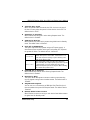
!" AXIOMTEK is a trademark of AXIOMTEK Co., Ltd.
IBM is a registered trademark of International Business
Machines Corporation.
MS-DOS, Windows !95, Windows NT are trademarks of
Microsoft Corporation.
AWARD is a trademark of Award Software, Inc.
Cyrix is a trademark of Cyrix Corporation.
IBM, PC/AT, PS/2, VGA are trademarks of International
Business Machines Corporation.
Intel and Pentium are trademarks of Intel Corporation.
Adaptec AIC7880 is a trademark of Adaptec, Inc.
Realtek RTL-8139 is a registered trademark of Realtek
Semiconductor Corporation.
Winbond W83977 is a trademark of Winbond Electronics
Corp.
Other brand names and trademarks are the properties
and registered brands of their respective owners.
Chapter 1 Introduction
1.2.1
1.2.2
1.2.3
Infrared Data Association ...................................... 2
Universal Serial Bus.................................................. 2
Ultra DMA/33 ........................................................... 2
Chapter 2 Jumpers and Connectors
2.2.1
CPU Settings ............................................................ 7
2.2.1.1
2.2.1.2
2.2.1.3
2.2.1.4
2.2.1.5
CPU
CPU
CPU
CPU
CPU
Bus Clock Selection: JP12 ..........................................
Clock Ration Selection: JP11 ......................................
Type Selection: JP7....................................................
V core Selection: JP13 ..................................................
Settings Reference .....................................................
7
7
7
8
9
2.2.2
2.2.3
2.2.4
2.2.5
Power Supply Selection: JP8 ................................
DiskOnChip Memory Segment: JP10 ..................
Watchdog Function: JP9 ......................................
RS232/422/485 (COM2) Selection: JP1 ................
11
11
11
11
2.3.1
2.3.2
2.3.3
2.3.4
2.3.5
SBC8156VES Connectors ......................................
SBC8156V Connectors ..........................................
SBC8156 Connectors ............................................
SBC8156VE Connectors ........................................
Improvised Connectors ........................................
12
12
13
13
14
! 2.3.5.1
2.3.5.2
ATX Power Switch/Soft Power Switch/SMI Switch ...............14
General Output Connector .................................................14
Chapter 3 Installation
" #
3.1.1
System Memory Installation.................................. 17
3.3.1
3.3.2
ATX Power Supply ................................................. 19
AT Power Supply ................................................... 19
!$%& '
!$( '
!& )
Table of Contents
Chapter 4 Hardware Description
#
0
'
)
!$% &* &+*$," &! &
-&! .,&! /! $$& $& 4.9.1
Serial Ports IRQ Selection ..................................... 25
12$+"! %! -3! !&! #
&
,! #
-4+& 0
!$%! 0
Chapter 5 Display Drivers
'
'
5 '
Chapter 6 Ethernet
5 Chapter 7 Award BIOS Utility
#
#
#
#
#
# ##
#0
#'
#)
#
#
#
#
- !1 6 73"" !"*" #
&*" !3" #
$(" )
$$+$!&! &$3 5+%$( )
&
-6
,
6
/(5% $(8* Table of Contents
Appendix A
Watchdog Timer
Appendix B
Connector Pin
Assignment
%393 40-pin IDE Interface Connector: CN1 and CN2 .................................67
CRT/VGA Connector: CN18 .............................................................67
Floppy Disk Connector: CN3 ............................................................68
Parallel Port Connector: CN5 ...........................................................68
RS-232/422/485 pin assignments for COM1 & COM2 (CN7, CN6) ......69
External Keyboard Connector: CN19 ................................................69
PS/2 Mouse Connector: CN20..........................................................69
USB Connector: CN8.......................................................................70
Ethernet Connector: CN16 (SBC8156VES & SBC8156VE only)..........70
General Output Connector: CN11.....................................................71
IrDA Connector: CN9.......................................................................71
2-pin CPU Fan Connector: CN12......................................................71
PICMG Slot Connector ....................................................................72
Appendix C Award BIOS Reference
$*7" ##
$*7 ##
-" ##
$*7! 0
Table of Contents
SBC8156 Pentium All-in-One CPU Card Series User’s Manual
!0 #$%
#$%
&'()$#
*'+,,-.
/01
$#2
$!0 #$%
Introduction
"
SBC8156 Pentium All-in-One CPU Card Series User’s Manual
!
0
0
#!0 $#3
0
40
%/4
"356"3
70%/
"3,
%/$
$
%/
4
.
!0 #$%
%/
%/
67#3
0
4
%/67
!0 &'()$#8
5%50-''8
''5-%50-''
4
40038
%50-''
3
Introduction
SBC8156 Pentium All-in-One CPU Card Series User’s Manual
" #
#"CPU:
Intel Pentium P54C/P55C/MMX, Cyrix
6x86/6x86L/6x86(MX)/ 6x86MII, AMD K5/K6 90300 MHz, K6-2/K6-III 300-400 MHz
#"Chipset:
!"System chipset: Intel 82430TX PCI chipset
!"I/O chipset: Winbond W83977
#"BIOS: Award PnP Flash BIOS
#"System Memory: 2 x 168-pin DIMM socket supporting
up to 256MB; SDRAM memory
compatible
#"L2 Cache: Onboard 512KB
#"Watchdog Timer:
Generates a system reset
16-level software programmable
time and temperature interval from
0.5 to 1000 seconds
#"Ethernet: Onboard Realtek 8139 chip with boot ROM
function, 10/100 Base-T
Interface via RJ-45 connector
#"VGA Controller:
!"Cirrus Logic GD5446 CRT VGA PCI local-bus controller
with 2MB display DRAM
!"Supports up to 1280 x 1024 resolution
#"SCSI Interface:
!"Supports one 8-bit Ultra SCSI port single-ended or
differential
!"One 16-bit fast and Ultra Wide SCSI port, single-ended or
differential
!"Connects up to 15 SCSI peripherals with Ultra Wide SCSI
feature
!"20MB/sec synchronous Ultra SCSI data rate
!"40MB/sec Ultra Wide SCSI data rate
#"DiskOnChip :
!"Onboard socket for flash memory disk support
#"Dimensions:
Introduction
338 (L) x 122 (W) mm
'
SBC8156 Pentium All-in-One CPU Card Series User’s Manual
$ %
&
Introduction
SBC8156 Pentium All-in-One CPU Card Series User’s Manual
%&'
Jumpers and Connectors
:
!0 #$%
9
SBC8156 Pentium All-in-One CPU Card Series User’s Manual
()
!0 :
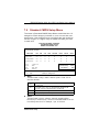
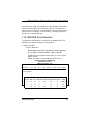
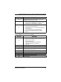
:
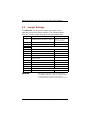
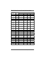
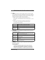
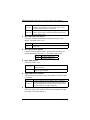
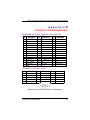
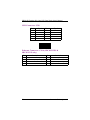
Jumper
Default Setting
JP1
COM2 RS-232/422/485 Selection: RS232
JP2
---
---
JP3
JP4
JP5
---
---
Short 1-2, 7-8, 11-13,
12-14, 17-19, 18-20
Reserved
JP6
Reserved
Short
JP7
CPU Type Selection : Dual Voltage CPU
Short 1-4, 2-5, 3-6
JP8
AT/ATX Power Supply Selection : AT
Short 1-2, 4-5, 7-8, 10-11
JP9
Watchdog Function : Disabled
Open
JP10
DiskOnChip Memory Segment :
C8000 – CFFFF
Open
JP11
CPU Clock Ration : MMX233 (x3.5)
Open
JP12
CPU Clock Selection : 66MHz
Open
JP13
CPU Vcore Power Selection : 2.8V
Short 1-2
JP14
Reserved
Short 1-2
JP15
CN11
IMPORTANT:
1
Jumper Setting
Reserved
Use Internal Buzzer
Short 2-4
The above default settings are set for
Intel MMX-233 MHz CPU use. Please refer
to the following subsections when
installing other types of microprocessors.
Jumpers and Connectors
SBC8156 Pentium All-in-One CPU Card Series User’s Manual
#$%
:
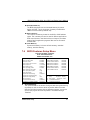
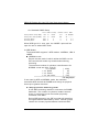
#$%#$%##$%;$#
#
:
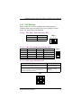
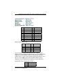
Options
60MHz
66MHz
JP12
Settings
Short 1-2
Open (default)
Options
x 1.5
x 2, x 6
x 2.5
x 3
Settings
Open
Short 1-2
Short 1-2, 3-4
Short 3-4
Options
Settings
Open (default)
Short 1-2, 5-6
Short 1-2, 3-4, 5-6
Short 3-4, 5-6
Short 5-6
x 3.5
x 4
x 4.5
x 5
x 5.5
JP11
Options
Settings
Single Voltage CPU:
Intel P54C, Cyrix 6x86, AMD K5
Dual Voltage CPU:
Intel P55C (MMX), Cyrix 6x86L/6x86MX/
6x86MII, AMD K6/K6-2/K6-3
Short 4-7, 5-8, 6-9
Short 1-4, 2-5, 3-6
(default)
JP7
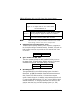
Jumpers and Connectors
,
SBC8156 Pentium All-in-One CPU Card Series User’s Manual
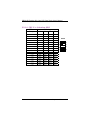
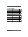
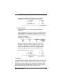
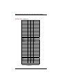
CPU Core
Voltage
1-2
3-4
5-6
7-8
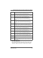
3.5V
Short
Short
Short
Short
3.4V
Short
Short
Short
Short
Short
Short
Short
Open
Open
Open
Open
Open
Open
Open
Open
Short
Short
Short
Open
Open
Open
Open
Short
Short
Short
Short
Open
Open
Open
Open
Short
Open
Open
Short
Short
Open
Open
Short
Short
Open
Open
Short
Short
Open
Open
Open
Short
Open
Short
Open
Short
Open
Short
Open
Short
Open
Short
Open
Short
Open
3.3V
3.2V
3.1V
3.0V
2.9V
2.8V (default)
2.7V
2.6V
2.5V
2.4V
2.3V
2.2V
2.1V
2.0V
*
JP3 Settings
JP13
Jumpers and Connectors
SBC8156 Pentium All-in-One CPU Card Series User’s Manual
!"
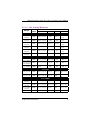
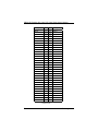
CPU Type
Jumper Settings
CPU
Clock
JP7
JP11
JP12
JP13
Intel Pentium
90MHz
60MHz
Short 4-7, 5-8, 6-9
Open
Intel Pentium
100MHz
66MHz
Short 4-7, 5-8, 6-9
Open
Open
Short 1-2, 3-4,
5-6, 7-8
Intel Pentium
120MHz
60MHz
Short 4-7, 5-8, 6-9
Short 1-2
Short 1-2
Short 1-2, 3-4,
5-6, 7-8
Intel Pentium
133MHz
66MHz
Short 4-7, 5-8, 6-9
Short 1-2
Open
Short 1-2, 3-4,
5-6, 7-8
Intel Pentium
166MHz
66MHz
Short 4-7, 5-8, 6-9
Short 1-2, 3-4
Open
Short 1-2, 3-4,
5-6, 7-8
Intel Pentium
200MHz
66MHz
Short 4-7, 5-8, 6-9
Short 3-4
Open
Short 1-2, 3-4,
5-6, 7-8
Short 1-2
Short 1-2, 3-4
5-6, 7-8
Intel Pentium
MMX 166MHz
66MHz
Short 1-4, 2-5, 3-6
Short 1-2, 3-4
Open
Short 1-2
Intel Pentium
MMX 200MHz
66MHz
Short 1-4, 2-5, 3-6
Short 3-4
Open
Short 1-2
Intel Pentium
MMX 233MHz
66MHz
Short 1-4, 2-5, 3-6
(default)
Open
Open
Short 1-2
Cyrix P-150+
60MHz
Short 4-7, 5-8, 6-9
Short 1-2
Short 1-2
Short 1-2, 3-4,
7-8
Cyrix P-166+
66MHz
Short 4-7, 5-8, 6-9
Short 1-2
Open
Short 1-2, 3-4,
7-8
Cyrix MMX
PR-166
60MHz
Short 1-4, 2-5, 3-6
Short 1-2, 3-4 Short 1-2
Short 1-2, 7-8
Cyrix MMX
PR-200
66MHz
Short 1-4, 2-5, 3-6
Short 1-2, 3-4 Open
Short 1-2, 7-8
Cyrix MMX
PR-233
66MHz
Short 1-4, 2-5, 3-6
Short 3-4
Open
Short 1-2, 7-8
Cyrix MII-300
66MHz
Short 1-4, 2-5, 3-6
Open
Open
Short 1-2, 7-8
Continued . . . . .
Jumpers and Connectors
+
SBC8156 Pentium All-in-One CPU Card Series User’s Manual
CPU Type
CPU
Clock
Jumper Settings
JP7
JP11
JP12
JP13
Cyrix 6x86L
P-150
60MHz
Short 1-4, 2-5, 3-6
Short 1-2
Cyrix 6x86L
P-166
66MHz
Short 1-4, 2-5, 3-6
Short 1-2
Short 1-2
Open
Short 1-2
Short 1-2
Short 1-2, 3-4,
7-8
AMD K5-PR90
60MHz
Short 4-7, 5-8, 6-9
Open
AMD K5PR100
66MHz
Short 4-7, 5-8, 6-9
Open
AMD K5PR120
60MHz
Short 4-7, 5-8, 6-9
Short 1-2
AMD K5PR133
66MHz
Short 4-7, 5-8, 6-9
Short 1-2
Open
Short 1-2, 3-4,
7-8
AMD K5PR166
66MHz
Short 4-7, 5-8, 6-9
Short 1-2, 3-4
Open
Short 1-2, 3-4,
7-8
Short 1-2
Open
Short 1-2
Short 1-2, 3-4,
7-8
Short 1-2, 3-4,
7-8
AMD K6-166
66MHz
Short 1-4, 2-5, 3-6
Short 1-2, 3-4
Open
Short 1-2, 7-8
AMD K6-200
66MHz
Short 1-4, 2-5, 3-6
Short 3-4
Open
Short 1-2, 7-8
AMD K6-233
66MHz
Short 1-4, 2-5, 3-6
Open
Open
Short 1-2, 3-4
AMD K6-266
66MHz
Short 1-4, 2-5, 3-6
Short 1-2, 5-6
Open
Short 5-6
Short 1-2,3-4,
5-6
Open
Short 5-6
AMD K6-300
66MHz
Short 1-4, 2-5, 3-6
AMD K6-2-333
66MHz
Short 1-4, 2-5, 3-6
Short 3-4, 5-6
Open
Short 5-6
AMD K6-2-366
66MHz
Short 1-4, 2-5, 3-6
Short 5-6
Open
Short 5-6
AMD K6-2-400
66MHz
Short 1-4, 2-5, 3-6
Short 1-2
Open
Short 5-6, 7-8
Open
Short 3-4
AMD K6-III400
"(
66MHz
Short 1-4, 2-5, 3-6
Short 1-2
Jumpers and Connectors
SBC8156 Pentium All-in-One CPU Card Series User’s Manual
!
"#$
Options
ATX P/S
AT P/S
JP8
Settings
Short 2-3, 5-6, 8-9, 11-12
Short 1-2, 4-5, 7-8, 10-11 (default)
%&'
(!
(
"#)
Options
JP10
Settings
Open
Short
Short
Short
C8000 – CFFFF
D0000 – D7FFF
D8000 – DFFFF
E0000 – E7FFF
(default)
1-2
3-4
1-2, 3-4
* +',"#-
Options
Settings
NMI
Short 1-2
Short 2-3
Open (deafult)
Restart
Disabled
JP9
. /**$.0&1
"#
!"
#$
"
COM2
Settings
RS-232 (default)
RS-422
RS-485
Short 1-2, 7-8, 11-13, 12-14, 17-19, 18-20
Short 3-4, 9-11, 10-12, 15-17, 16-18
Short 5-6, 7-8, 9-11, 10-12, 15-17, 16-18
JP1
Jumpers and Connectors
""
SBC8156 Pentium All-in-One CPU Card Series User’s Manual
" #$%
/
8
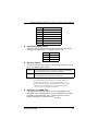
!0 #$%
0
4
$.234
Connectors
IDE2 Connector
IDE1 Connector
FDD Connector
68-pin SCSI
LPT Connector
COM2 Connector
COM1 Connector
USB Connector
IrDA Connector
50-pin SCSI Connector
General Output
Label
CN1
CN2
CN3
CN4
CN5
CN6
CN7
CN8
CN9
CN10
CN11
Connectors
CPU Fan Connector
Int./Ext. Battery Select
ATX Control Connector
RJ-45 LAN Connector
VGA Connector
External Keyboard
External PS/2 Mouse
Keyboard DIN
LAN Boot ROM Socket
DiskOnChip Socket
Label
CN12
CN13
CN14
CN16
CN18
CN19
CN20
CN21
U7
U19
$.23
Connectors
IDE2 Connector
IDE1 Connector
FDD Connector
LPT Connector
COM2 Connector
USB Connector
IrDA Connector
General Output
CPU Fan Connector
"3
Label
CN1
CN2
CN3
CN5
CN6
CN8
CN9
CN11
CN12
Connectors
Int./Ext. Battery Select
ATX Control Connector
COM1 DB9 Connector
VGA Connector
External Keyboard
External PS/2 Mouse
Keyboard DIN
DiskOnChip Socket
Label
CN13
CN14
CN17
CN18
CN19
CN20
CN21
U19
Jumpers and Connectors
SBC8156 Pentium All-in-One CPU Card Series User’s Manual
$.2
Connectors
IDE2 Connector
IDE1 Connector
FDD Connector
LPT Connector
COM2 Connector
USB Connector
IrDA Connector
General Output
Label
CN1
CN2
CN3
CN5
CN6
CN8
CN9
CN11
Connectors
CPU Fan Connector
Int./Ext. Battery Select
ATX Control Connector
COM1 DB9 Connector
External Keyboard
External PS/2 Mouse
Keyboard DIN
DiskOnChip Socket
Label
CN12
CN13
CN14
CN17
CN19
CN20
CN21
U19
* $.234
Connectors
IDE2 Connector
IDE1 Connector
FDD Connector
LPT Connector
COM2 Connector
COM1 Connector
USB Connector
IrDA Connector
General Output
CPU Fan Connector
Jumpers and Connectors
Label
CN1
CN2
CN3
CN5
CN6
CN7
CN8
CN9
CN11
CN12
Connectors
Int./Ext. Battery Select
ATX Control Connector
RJ-45 LAN Connector
VGA Connector
External Keyboard
External PS/2 Mouse
Keyboard DIN
LAN Boot ROM Socket
DiskOnChip Socket
Label
CN13
CN14
CN16
CN18
CN19
CN20
CN21
U7
U19
"'
SBC8156 Pentium All-in-One CPU Card Series User’s Manual
. ( #$%"%&'!%"%&'()
%&
0
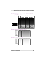
6!:7
</9*Soft-Off by PWRBTTN
$.=>9"(
NOTE:
This connector functions only with an ATX power
supply.
CN14
1 2 3 4 5 6
*"+"
CN11
Vcc
N.C.
GND
Keylock
GND
GND
N.C.
Reserved
GND
HDD_LED
"&
1
3
5
7
9
11
13
15
17
19
2
4
6
8
10
12
14
16
18
20
Ext. Speaker
Int. Buzzer
GND
VCC
N.C.
SMI
N.C.
Reserved
RESET
VCC
Jumpers and Connectors
SBC8156 Pentium All-in-One CPU Card Series User’s Manual
Power LED/KeyLock Switch
9
28
$28
.=
/
?2
!0 Speaker Connector
&
Short 2-4
@@4
:4
676A7
SMI Switch
!0 0
/5
/
/5</9*
Reset Switch
.>>
HDD LED
4
28
28B
B28
Jumpers and Connectors
"9
SBC8156 Pentium All-in-One CPU Card Series User’s Manual
"1
SBC8156 Pentium All-in-One CPU Card Series User’s Manual
!0 $#$%
C
!" Power supply and passive backplane (optional)
!" IBMTM PC/AT keyboard
!" Display monitor
!" Floppy or hard disk with MS-DOS or Flash Disk emulator
" ''
!0 "1*55
3915
@
!
(
(!
D*"3*5
*-"1-'3-1&"3*5"1*55
1. Switch OFF all power to the system. Then locate the
DIMM1 and DIMM2 sockets beside the CPU socket.
2. DIMM1 socket has locking tabs on both sides. Open
the locking tabs by pushing them on a sideways
direction.
3. DIMM1 has key indicators embedded on its
connectors (1 on the middle, 1 on the left side).
4. Likewise DIMM modules have key indicators. Locate
the indicators on the DIMM modules and align them to
the key indicators on the DIMM sockets.
5. With the DIMM module held upright, insert the
modules until the locking tabs on Step 2 snaps back
into place. This latches the DIMM modules into place.
Installation
",
SBC8156 Pentium All-in-One CPU Card Series User’s Manual
6. Repeat Steps 2-5 for DIMM 2.
"*
Installation
SBC8156 Pentium All-in-One CPU Card Series User’s Manual
" 1. Align pin one (whit
2. e dot) on the CPU with pin one of the socket. Pin one
of the CPU socket may either be marked on the board
or indicated by an arrow sign on the base of the
socket. Normally, its diagonal corner distinguishes pin
one on the socket.
3. To complete the CPU installation, gently press the CPU
into place.
4. Double-check the insertion and orientation of the CPU
before applying power. Improper installation will result
in permanent damage to the CPU.
"" #))*
'
56
!
>0)
1. Install the ATX Power Control Connector cable to the
designated ATX power control connector on your
backplane. The ATX Power Control Connector cable is
a 6-pin cable.
2. Configure the proper jumper settings by setting JP8 to
Short 2-3, 5-6, 8-9, 11-12.
5
!
0
1. Configure the proper jumper settings by setting JP8 to
Short 1-2, 4-5, 7-8, 10-11.
Installation
"+
SBC8156 Pentium All-in-One CPU Card Series User’s Manual
"$ )
1. Make sure the power is OFF.
2. Set the configuration jumpers according to the jumper
setting on Chapter 2.
3. Install the SBC8156 CPU card into one of the slots on
the passive backplane. You may allow the SBC8156 to
stand alone as a single board computer.
4. Connect the I/O cables and peripherals, i.e. floppy
disk, hard disk, monitor, keyboard, power supply and
etc. to the CPU board.
NOTE:
The color of pin one is usually red or blue,
while others are gray.
5. Turn ON the system power.
3(
Installation
SBC8156 Pentium All-in-One CPU Card Series User’s Manual
3(
SBC8156 Pentium All-in-One CPU Card Series User’s Manual
!
"
4
!0 $#$%
$ !0 $05?9-?1-?13-?1
#414*1#$%/
#$%
%=)./-3 = +9
5/./
#$%
#$%
:
#$%#$%##$%;
$##
:
5
#$%
#$%
$ %
./
!0 0
$
$
./!0 //3+88(3(>
8$<.5
$" #$%
-.
"?
-.4
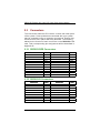
Address
000-01F
020-03F
040-05F
060-06F
Devices
DMA controller #1
Interrupt controller #1
Timer
Keyboard controller
Continued . . . . .
Hardware Description
3"
SBC8156 Pentium All-in-One CPU Card Series User’s Manual
Address
070-07F
080-09F
0A0-0BF
0F0
0C0-0DF
0F1
0F8-0FF
120
121
122
1F0-1F8
200-207
300-31F
360-36F
378-37F
380-38F
3A0-3AF
3B0-3BF
3C0-3CF
3D0-3DF
3F0-3F7
3F8-3FF
2F8-2FF
3F0
33
Devices
Real time clock, NMI
DMA page register
Interrupt controller #2
Clear math coprocessor busy signal
DMA controller #2
Reset math coprocessor
Math processor
Disable watchdog timer operation (read)
Enable watchdog timer operation (read)
Watchdog
Fixed disk controller
Game port
Prototype card
Reserved
Parallel port #1
SDLC #2
SDLC #1
MDA video card (including LPT1)
EGA card
CGA card
Floppy disk controller
Serial port #1 (COM1)
Serial port #2 (COM2)
Winbond I/O
Hardware Description
SBC8156 Pentium All-in-One CPU Card Series User’s Manual
$$ !0 $#
"1/0C
&"1
/0$#"1
CE
NMI
IRQ0
IRQ1
IRQ2
IRQ3
IRQ4
IRQ5
IRQ6
IRQ7
IRQ8
IRQ9
IRQ10
IRQ11
IRQ12
IRQ13
IRQ14
Parity check error
System timer output
Keyboard
Interrupt rerouting from IRQ8 through IRQ15
Serial port #2
Serial port #1
Reserved
Floppy disk controller
Parallel port #1
Real time clock
Reserved
Reserved (onboard SCSI)
USB and [and onboard Network]
PS/2 Mouse
Math coprocessor
Primary IDE channel
Secondary IDE Channel
IRQ15
standard specifications on the card only;
using IRQ10 for SCSI adapter.
standard specifications for & !"
only;
using shared IRQ11 for USB and Ethernet.
$+ #
!0 3$#
8
-
1&
!:
!:!0 &8
<
0
4!:
!:
Hardware Description
3'
SBC8156 Pentium All-in-One CPU Card Series User’s Manual
$, -#
!:0
!0 #<;F0
!:0
"9;F0
#;F0
:C
/0
4
!:0
$. !
'/
!0 '&
!:
939G'1(?-"35
'9G
,3(?-"&&5-3**5!:
0
4
$0 #
!0 !:
#"Standard mode: IBM PC/XT, PC/AT and PS/2TM
compatible with bi-directional parallel port
#"Enhanced mode: Enhance parallel port (EPP)
compatible with EPP 1.7 and EPP 1.9 (IEEE 1284
compliant)
#"High speed mode: Microsoft and Hewlett Packard
extended capabilities port (ECP) IEEE 1284 compliant
2$"
6'#B72$36',*B72$'63,*B7
./#5./
3&
Hardware Description
SBC8156 Pentium All-in-One CPU Card Series User’s Manual
$1 #
!0 #.5"
</3'3
#.53
</3'3-&33-&*9
*- /7
#.5"
#.53!0 .-
!0 .-#$%
"(!:#
!: !0 .
!0 "(
#.53;!: <
+#.5";!:#<
<C#.5"
#.53!0 #$%
<H&
<H'
0
./
</3'3#.5"
#.53
</&*9#.53
0
4
$2 3'4 !0 ;!:'<
$/-3;!:)<
9!:=
$/-3
-0
4
Hardware Description
39
SBC8156 Pentium All-in-One CPU Card Series User’s Manual
$ %
%/6%/7!0 %/
!:0"(%/!0 CN8
9 7 5 3
1
10 8 6 4
2
$ 5
<I&9
8
!0 .-
!0 .-"("((
:
!: 6:7"(
NOTE:
31
This connector comes with the SBC8156VES &
SBC8156VE only.
Hardware Description
SBC8156 Pentium All-in-One CPU Card Series User’s Manual
$" !:
!:)!0 .-
$#
/#/
6
#<.5
7
0
%/#/!:)9(
*/#/
!:1*
"1% /#/
NOTE:
This connector comes with the SBC8156VES only.
$$ !:'"(
0
CN9
9 7 5 3
1
10 8 6 4 2
Hardware Description
3,
SBC8156 Pentium All-in-One CPU Card Series User’s Manual
$+ 6
%'
!:&
4
#5./<05
:
3
' 44
"
&!:
3
'open
CN13
1
2
3
4
$, !
!:#$%$#$%C
0
!0 0
4
CN12
NOTE:
3*
1
2
When the CPUFAN Off in Suspend option within the
Power Management Setup is enabled, the CPU
cooling fan turns OFF simultaneous to the system’s
entry to Suspend mode. See Section 5.8 for more
information.
Hardware Description
SBC8156 Pentium All-in-One CPU Card Series User’s Manual
"
#"$
+ ;F0!0 #<;F0
>$
#<.5-
+ !
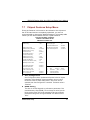
!"Cirrus Logic GD5446 CRT VGA PCI local-bus
controller with 2MB display DRAM
!"Supports up to 1280 x 1024 resolution
+" 7
!"DOS Driver
!"Win95
!"Winnt3.5
!"Winnt4.0
!"Windows 3.1
!"OS/2 Warp
NOTE:
For more details, please refer to the README files
in the Product Information CD-ROM’s VGA folder.
Display Drivers
3+
SBC8156 Pentium All-in-One CPU Card Series User’s Manual
'(
SBC8156 Pentium All-in-One CPU Card Series User’s Manual
%
, !0 C
$#
888*(3'
<I&96!: 7
, !
!"10Mb/s and 100Mb/s operations
!"Supports 10Mb/s and 100Mb/s N-Way auto negotiation
!"Full duplex capability
!"Full compliance with PCI Revision 2.1
!"PCI Bus Master data transfers
," 7
!0 8
4:
== 34
'4&4520=5 '" = +9
520=//#.%=).=/
$
>
HELP8139.EXE$
#<.5
Ethernet
'"
SBC8156 Pentium All-in-One CPU Card Series User’s Manual
'3
SBC8156 Pentium All-in-One CPU Card Series User’s Manual
&
'!
()#
0
./<.5/
<056#5./<057
/
. )
/D
.=
JK
JK
-J#KJ0K
J8K
$./6$./7
TO ENTER SETUP PRESS DEL KEY
/
.>>.=
G<8/8G
J#KJ0K
JK
PRESS <F1> TO CONTINUE, <CTRL-ALT-ESC> OR <DEL> TO ENTER
SETUP
Award BIOS Utility
''
SBC8156 Pentium All-in-One CPU Card Series User’s Manual
. 3'
Up arrow
Down arrow
Left arrow
Right arrow
Esc key
PgUp/“+” key
PgDn/“−“ key
F1 key
(Shift) F2 key
F3 key
F4 key
F5 key
F6 key
F7 key
F8 key
F9 key
F10 key
Moves cursor to the previous item
Moves cursor to the next item
Moves cursor to the item on the left hand
Move to the item in the right hand
Main Menu -- Quits and deletes changes into CMOS
Status Page Setup Menu and Option Page Setup Menu -Exits current page and returns to Main Menu
Increases the numeric value or makes changes
Decreases the numeric value or makes changes
General help, only for Status Page Setup Menu and
Option Page Setup Menu
Change color from total 16 colors. F2 to select color
forward, (Shift) F2 to select color backward
Reserved
Reserved
Restores the previous CMOS value from CMOS, only for
Option Page Setup Menu
Loads the default CMOS value from BIOS default table,
only for Option Page Setup Menu
Loads the Setup default , only for Option Page Setup
Menu
Reserved
Reserved
Saves all the CMOS changes, only for Main Menu
." )8
#"Main Menu
The on-line description of the highlighted setup function is displayed at
the bottom of the screen.
#"Status Page Setup Menu/Option Page Setup Menu
Press <F1> to pop up a small help window that describes the
appropriate keys to use and the possible selections for the highlighted
item. To exit the Help Window press <F1> or <Esc>.
'&
Award BIOS Utility
SBC8156 Pentium All-in-One CPU Card Series User’s Manual
.$ 95
.0
./#5.//%5
555
4%
J8K
↑↓→← ! "
#$%& ' (
)*+,-*%./ 0!01
" 2%
%1345( 666
#"Standard CMOS Setup
This setup option includes all the items in a standard compatible BIOS.
#"BIOS Features Setup
This setup page includes all the items of Award special enhanced
features.
#"Chipset Features Setup
This setup option includes all the items of chipset special features.
#"Power Management Setup
This category determines the power consumption of the system after
selecting its items. Default value is Disabled.
#"PnP/PCI Configuration
This category specifies the assignment of all IRQs and DMAs.
Award BIOS Utility
'9
SBC8156 Pentium All-in-One CPU Card Series User’s Manual
#"Load BIOS Defaults
BIOS defaults indicate the most appropriate values of the system
parameter in which the system can operate at a minimum performance.
#"Load Setup Defaults
Chipset defaults indicate the values required by the system for
maximum performance.
#"Integrated Peripherals
This page allows you to set up all the on board I/O controllers like IDE,
SCSI, FDC, etc..
#"Supervisor / User Passwords
Changes, sets or disables password of Supervisor or User. It allows
you to restrict access to the system and Setup, or just to Setup.
#"IDE HDD Auto Detection
Automatically configures hard disk parameters.
#"HDD Low Level Format
Hard disk low level format utility.
#"Save & Exit Setup
Saves CMOS value changes to CMOS and exits setup.
#"Exit Without Saving
Abandons all CMOS value changes and exits setup.
'1
Award BIOS Utility
SBC8156 Pentium All-in-One CPU Card Series User’s Manual
.+ /
#5.//5
"(
8
%
J$%KJ$K
Date (mm:dd:yy) : Fri, Jul 18 1997
Time (hh:mm:ss) : 00:00:00
HARD DISKS
Primary Master:
Primary Slave:
Secondary Master:
Secondary Slave:
Drive A
Drive B
Video
Halt On
TYPE
Auto
SIZE
0
CYLS
0
HEAD
0
PRECOMP
0
LANDE
0
SECTOR
0
MODE
------
Auto
0
0
0
0
0
0
------
Auto
0
0
0
0
0
0
------
Auto
0
0
0
0
0
0
------
: 1.44M , 3.5 in
: None
: EGA / VGA
: All Errors
Base Memory :
Extended Memory :
Other Memory :
Total Memory :
↑ ↓ → ← : Select Item]
(Shift) F2 : Change Color
ESC : Quit
F1 : Help
640K 14336K 384K 15360K
PU / PD / + / - : Modify
#"Date
The date format is <day>, <date> <month> <year>. Press <F3> to
show the calendar.
day
date
month
year
The day of week, from Sun to Sat, determined by the BIOS,
is read only
The date, from 1 to 31 (or the maximum allowed in the
month), can key in the numerical / function key
The month, Jan through Dec.
The year, depends on the year of BIOS
#"Time
The time format is <hour> <minute> <second> accepting either
function key or numerical key. The time is calculated based on the 24hour military-time clock. For example, 1 p.m. is 13:00:00.
Award BIOS Utility
',
SBC8156 Pentium All-in-One CPU Card Series User’s Manual
#"Primary Master/Primary Slave/Secondary
Master/Secondary Slave
The categories identify the types of one channel that have been
installed in the computer. There are 45 predefined types and 2 user
definable types are for Enhanced IDE BIOS. Type 1 to Type 45 are
predefined. Type User is user-definable.
Press <PgUp>/<+> or <PgDn>/<−> to select a numbered hard disk
type or type the number and press <Enter>. Note that the
specifications of your drive must match with the drive table. The hard
disk will not work properly if you enter improper information within this
category. If your hard disk drive type does not match or is not listed,
you can use Type User to define your own drive type manually.
If you select Type User, related information is asked to be entered to
the following items. Enter the information directly from the keyboard
and press <Enter>. This information should be provided in the
documentation from your hard disk vendor or the system manufacturer.
If the controller of HDD interface is ESDI, select “Type 1”.
If the controller of HDD interface is SCSI, select “None”.
If the controller of HDD interface is CD-ROM, select “None”.
CYLS.
HEADS
PRECOMP
number of cylinders
number of heads
write precom
LANDZONE
SECTORS
MODE
landing zone
number of sectors
HDD access mode
If there is no hard disk drive installed, select NONE and press <Enter>.
#"Drive A type/Drive B type
The category identifies the types of floppy disk drive A or drive B
installed in the computer.
None
360K, 5.25 in
1.2M, 5.25 in
720K, 3.5 in
1.44M, 3.5 in
2.88M, 3.5 in
'*
No floppy drive installed
5.25 inch PC-type standard drive; 360Kb capacity
5.25 inch AT-type high-density drive; 1.2MB capacity
3.5 inch double-sided drive; 720Kb capacity
3.5 inch double-sided drive; 1.44MB capacity
3.5 inch double-sided drive; 2.88MB capacity
Award BIOS Utility
SBC8156 Pentium All-in-One CPU Card Series User’s Manual
#"Video
The category selects the type of adapter used for the primary system
monitor that must match your video display card and monitor. Although
secondary monitors are supported, you do not have to select the type
in Setup. You have two ways to boot up the system:
1. When VGA as primary and monochrome as
secondary, the selection for the video type is “VGA
Mode”.
2. When monochrome as primary and VGA as
secondary, the selection of the video type
is ”Monochrome Mode”.
EGA/VGA
CGA 40
CGA 80
MONO
Enhanced Graphics Adapter/Video Graphics Array. For
EGA, VGA, SEGA, or PGA monitor adapters.
Color Graphics Adapter, power up in 40 column mode
Color Graphics Adapter, power up in 80 column mode
Monochrome adapter, includes high resolution monochrome
adapters
#"Error halt
The category determines whether the computer will stop if an error is
detected during power up.
No errors
All errors
All, But
Keyboard
All, But
Diskette
All, But
Disk/Key
Whenever the BIOS detects a non-fatal error, the system
will halt and you will be prompted.
The system boot will not stop for any error detected.
System boot will not stop for a keyboard error; it will stop
for all other errors.
System boot will not stop for a disk error; it will stop for all
other errors.
System boot will not stop for a keyboard or disk error; it will
stop for all other errors.
#"Memory
The category is display-only which is determined by POST (Power On
Self Test) of the BIOS.
!"Base Memory
The POST of the BIOS will determine the amount of base (or
conventional) memory installed in the system. The value of the
base memory is typically 512K for systems with 512K memory
installed on the motherboard, or 640K for systems with 640K or
Award BIOS Utility
'+
SBC8156 Pentium All-in-One CPU Card Series User’s Manual
&(
more memory installed on the motherboard.
Award BIOS Utility
SBC8156 Pentium All-in-One CPU Card Series User’s Manual
!"Extended Memory
The BIOS determines how much extended memory is present
during the POST. This is the amount of memory located above
1MB in the CPU's memory address map.
!"Other Memory
This refers to the memory located in the 640K to 1024K address
space. This is memory that can be used for different applications.
DOS uses this area to load device drivers to keep as much base
memory free for application programs. Most use for this area is
Shadow RAM.
!"Total Memory
System total memory is the sum of basic memory, extended
memory, and other memory.
., %!
1 %1../
. 1.%!%* ' 1.%!%* 407 1
. !+ 00 ? . 7%(!0((51& 00(!0((5 4
00("04%
00(5 "( 3
% -$
(0.
5( "%% ./
5( "%% )*%1 ,
5( "% !%5) ,
15
(0.
%! .00(
! +01@=;
%>! 3
.%>! 3
.%>! 3
.%>! 3
22
%>! 3
.%>! 3
.
/*
%
%>! 3
=
-A$
(
%>! 3
0.9
-
3 0
*%307
8$$$9*%307
$$$9*%307
$$$$9:*%307
;$$$9<*%307
8$$$9*%307
$$$9*%307
51'='8=
.%>!
%>!
%>!
%>!
%>!
%>!
%>!
.%>!
3
3
3
3
3
3
3
3
↑↓→← ! "
# !(B903+5
A
!3%! )*+,-0!01
=0%3
+%!
<0%3 ( +%!
#"Virus Warning
This option flashes on the screen. During and after the system boot up,
any attempt to write to the boot sector or partition table of the hard
disk drive will halt the system with the following message. You can run
an anti-virus program to locate the problem. The default setting is
“Disabled”.
Award BIOS Utility
&"
SBC8156 Pentium All-in-One CPU Card Series User’s Manual
Disk boot sector is to be modified
Type "Y" to accept write or "N" to abort write
Award Software, Inc.
Enabled
Disabled
NOTE:
Activates automatically when the system boots up causing a
warning message to appear when there is an attempt to
access the boot sector or hard disk partition table.
No warning message will appear when attempts to access the
boot sector or hard disk partition table are made.
This function is only available with DOS and other
operating systems that do not trap INT13.
#"CPU Internal Cache/External Cache
These two options speed up memory access. However, it depends on
the CPU/chipset design. The default setting is “Enabled”. CPUs with no
built-in internal cache will not provide the “CPU Internal Cache” item
on the menu.
Enabled
Disabled
Enable cache
Disable cache
#"Quick Power On Self Test
This option speeds up Power On Self Test (POST) after you turn on
the system power. If set as Enabled, BIOS will shorten or skip some
check items during POST. The default setting is “Enabled”.
Enabled
Disabled
Enable Quick POST
Normal POST
#"Boot Sequence
The original IBM PCs load the DOS operating system from drive A
(floppy disk), so IBM PC-compatible systems are designed to search
for an operating system first on drive A, and then on drive C (hard
disk). However, the BIOS now offers 11 different boot sequence
options of three drives each. In addition to the traditional drives A and
C, options include IDE hard drives D, E, and F; plus a SCSI hard drive
and a CD-ROM drive. This category determines from which drive the
computer searches first for the disk operating system (i.e., DOS).
Default value is “A,C,SCSI”.
&3
Award BIOS Utility
SBC8156 Pentium All-in-One CPU Card Series User’s Manual
System searches for the operating system from the floppy disk
drive. If it fails, it will search from the hard disk drive. If operating
system is still not found, it’ll seek from the SCSI device.
System searches for the operating system from the hard disk drive
C,A,SCSI
first. If it fails, it will search from the floppy disk drive. If operating
system is still not found, it’ll seek from the SCSI device.
System searches for the operating system from the hard disk drive
first. If it fails, it will search from the IDE CDROM drive. If
C,CDROM,A
operating system is still not found, it’ll seek from the floppy disk
drive.
System searches for the operating system from the IDE CDROM
drive first. If it fails, it will search from the hard disk drive. If
CDROM,C,A
operating system is still not found, it’ll seek from the floppy disk
drive.
System searches for the operating system from the second IDE
HDD first. If it fails, it will search from the floppy disk drive. If
D,A,SCSI
operating system is still not found, it’ll seek from the SCSI device.
System searches for the operating system from the third IDE HDD
first. If it fails, it will search from the floppy disk drive. If operating
E,A,SCSI
system is still not found, it’ll seek from the SCSI device.
System searches for the operating system from the fourth IDE HDD
first. If it fails, it will search from the floppy disk drive. If operating
F,A,SCSI
system is still not found, it’ll seek from the SCSI device.
System searches for the operating system from the SCSI device
first. If it fails, it will search from the floppy disk drive. If operating
SCSI,A,C
system is still not found, it’ll seek from the first IDE HDD.
System searches for the operating system from the SCSI device
first. If it fails, it will search from the first IDE HDD. If operating
SCSI,C,A
system is still not found, it’ll seek from the floppy disk drive.
System only searches for the operating system from the first IDE
C only
HDD.
System searches for the operating system from the 120MB LS
LS/ZIP,C
floppy or the 100MB ZIP drive first. If it fails, it’ll search from the
first IDE HDD.
A,C,SCSI
#"Boot Up Floppy Seek
During POST, BIOS will determine the floppy disk drive type, 40 or 80
tracks, installed in the system. 360Kb type is 40 tracks while 720Kb,
1.2MB and 1.44MB are all 80 tracks. The default value is “Enabled”.
Award BIOS Utility
&'
SBC8156 Pentium All-in-One CPU Card Series User’s Manual
Enabled
Disabled
BIOS searches for floppy disk drive to determine if it is 40 or
80 tracks. Note that BIOS can not tell from 720K, 1.2M or
1.44M drive type as they are all 80 tracks.
BIOS will not search for the type of floppy disk drive by track
number. There will be no warning message displayed if the
drive installed is 360K.
#"Boot Up NumLock Status
This option enables and disables the numberlock function of the
keypad. The default value is “On”.
On
Off
Keypad functions confine with numbers
Keypad functions convert to special functions (i.e., left/right
arrow keys)
#"Boot Up System Speed
It selects the default system speed - the speed that the system will
operate immediately after power up. The default value is “High”.
High
Low
Sets the speed to high
Sets the speed to low
#"Gate A20 Option
The default value is “Fast”.
Normal
Fast
The A20 signal is controlled by keyboard controller or
chipset hardware.
Default: Fast. The A20 signal is controlled by Port 92 or
chipset specific method.
#"Typematic Rate Setting
This determines the typematic rate of the keyboard. The default value
is “Disabled”.
Enabled
Disabled
Enable typematic rate and typematic delay programming
Disable typematic rate and typematic delay programming.
The system BIOS will use default value of these 2 items
and the default is controlled by keyboard.
#"Typematic Rate (Chars/Sec)
This option refers to the number of characters the keyboard can type
per second. The default value is “6”.
&&
Award BIOS Utility
SBC8156 Pentium All-in-One CPU Card Series User’s Manual
6
8
10
12
15
20
24
30
6 characters per second
8 characters per second
10 characters per second
12 characters per second
15 characters per second
20 characters per second
24 characters per second
30 characters per second
#"Typematic Delay (Msec)
This option sets the display time interval from the first to the second
character when holding a key. The default value is “250”.
250
500
750
1000
250 msec
500 msec
750 msec
1000 msec
#"Security Option
This item allows you to limit access to the system and Setup, or just to
Setup. The default value is “Setup”.
System
Setup
NOTE:
The system will not boot and access to Setup will be denied if
the incorrect password is entered at the prompt.
The system will boot, but access to Setup will be denied if the
correct password is not entered at the prompt.
To disable security, select PASSWORD SETTING
at Main Menu and then you will be asked to
enter password. Do not type anything, just
press <Enter> and it will disable security. Once
the security is disabled, the system will boot
and you can enter Setup freely.
#"OS Select for DRAM >64
This segment is specifically created for OS/2 when DRAM is larger
than 64MB. If your operating system is OS/2 and DRAM used is larger
the 64MB, you have to select “OS 2”, otherwise (under non-OS2),
default is NON-OS2. The default value is “Non-OS2”.
Award BIOS Utility
&9
SBC8156 Pentium All-in-One CPU Card Series User’s Manual
#"Video BIOS Shadow
Video shadowing increases the video speed by copying the video BIOS
into RAM. However, it is still optional depending on the chipset design.
The default value of this option is “Enabled”.
Enabled
Disabled
Video BIOS shadowing is enabled
Video BIOS shadowing is disabled
#"C8000 - CBFFF Shadow/DC000 - DFFFF Shadow
These options determine whether optional ROM will be copied to RAM
by 16K byte or 32K byte per/unit. The default value for all is “Disabled”.
Enabled
Disabled
NOTE:
&1
Optional shadow is enabled
Optional shadow is disabled
1. For C8000-DFFFF option-ROM on PCI BIOS – BIOS
automatically enables the shadow RAM. User
does not have to select the item.
2. IDE second channel control:
Enable: enables secondary IDE port and BIOS
will assign IRQ15 for this port.
Disable: disables secondary IDE port and IRQ15
is available for other device(s). The item is
optional only for PCI BIOS.
3. Some sound cards have an onboard CD-ROM
controller that uses IDE Secondary Port. To
avoid PCI IDE conflict, disable the IDE
secondary channel control so that the CDROM may work.
Award BIOS Utility
SBC8156 Pentium All-in-One CPU Card Series User’s Manual
.. 5!
/
#$%
@
Auto Configuration
DRAM Timing
: Enabled
: 70ns
DRAM Leadoff Timing
DRAM Read Burst (EDO/FP)
DRAM Write Burst Timing
Fast EDO Lead Off
Refresh RAS# Assertion
Fast RAS to CAS Delay
DRAM Page Idle Timer
DRAM Enhanced Paging
Fast MA to RAS# Delay
SDRAM (CAS Lat/RAS-to-CAS)
SDRAM Speculative Read
:
:
:
:
:
:
:
:
:
:
:
System BIOS Cacheable
: Disabled
Video BIOS Cacheable
8 Bit I/O Recovery Time
16 Bit I/O Recovery Time
Memory Hole at 15M-16M
PCI2.1 Compliance
:
:
:
:
:
10/6/3
x222/x333
x222
Disabled
4 Clks
3
2 Clks
Enabled
2 Clks
2/2
Disabled
Disabled
1
2
Disabled
Disabled
Power-Supply Type
Auto Detect DIMM/PCI Clk
CPU Warning Temperature
Current CPU Temperature
ESC
F1
F5
F6
F7
:
:
:
:
:
Quit
↑↓→←
Help
PU/PD/+/Old Values
(Shift)
Load BIOS Defaults
Load Setup Defaults
:
:
:
:
AT
Enabled
Disabled
29 o C/84 o F
: Select Item
: Modify
F2 : Color
#"Auto Configuration
Auto Configuration selects predetermined optimal values of chipset
parameters. When disabled, chipset parameters revert to setup
information stored in CMOS. Many fields in this screen are not
available when Auto Configuration is enabled. The default value is
“Disabled”.
#"DRAM Timing
The value in this field depends on performance parameters of the
installed memory chips (DRAM). Do not change the value from the
factory setting unless you install new memory that has a different
performance rating than the original DRAMs. The default value is
“60ns”.
Award BIOS Utility
&,
SBC8156 Pentium All-in-One CPU Card Series User’s Manual
#"DRAM Leadoff Timing
Selects the combination of CPU clocks the DRAM on your board
requires before each read from or write to the memory. Changing the
value from the setting determined by the board designer for the
installed DRAM might cause memory errors. The default value is
“10/6/3”.
#"DRAM Read Burst (EDO/FP)
Sets the timing for reads from EDO (Extended Data Output) or FPM
(Fast Page Mode) memory. The lower the timing numbers, the faster
the system addresses memory. Selecting timing numbers lower than
the installed DRAM specifications may result in memory errors. The
default value is “x222/x333”.
#"DRAM Write Burst Timing
Sets the timing for writes to memory. The lower the timing numbers,
the faster the system addresses memory. Selecting timing numbers
lower than the installed DRAM specifications may result in memory
errors. The default value is “x222”.
#"Fast EDO Lead Off
Set this option to Enabled only when using EDO DRAMs in either a
synchronous cache or a cache-less system. It causes a 1-HCLK pull-in
for all read leadoff latencies for EDO DRAMs (i.e., page hits, page
misses, and row misses). Select Disabled if any of the DRAM rows is
populated with FPM DRAMs. The default value is “Disabled”.
#"Refresh RAS# Assertion
This item selects the number of clock ticks RAS# (Row Address Strobe)
is asserted for refresh cycles. The default value is “4 Clks”.
#"Fast RAS to CAS Delay
When DRAM is refreshed, both rows and columns are addressed
separately. This field lets you insert a timing delay between the CAS
and RAS strobe signals used when DRAM is written to, read from, or
refreshed. The default value is “3”.
#"DRAM Page Idle Timer
Selects the amount of time in HCLKs that the DRAM controller waits to
close a DRAM page after the CPU becomes idle. The default value is
“2 Clks”.
&*
Award BIOS Utility
SBC8156 Pentium All-in-One CPU Card Series User’s Manual
#"DRAM Enhanced Paging
When Enabled, the chipset keeps the page open until a page/row miss.
When Disabled, the chipset uses additional information to keep the
DRAM page open when the host may be "right back." The default value
is “Enabled”.
#"Fast MA to RAS# Delay CLK
The values in this field are set by the system board designer,
depending on the DRAM installed. Do not change the values in this
field unless you change the specifications of installed DRAM or the
installed CPU. The default value is “2 Clks”.
#"System BIOS Cacheable
Selecting Enabled allows caching of the system BIOS ROM at F0000hFFFFFh, resulting in better system performance. However, if any
program writes to this memory area, a system error may result. The
default value is “Disabled”.
#"Video BIOS Cacheable
Selecting Enabled allows caching of the video BIOS ROM at C0000h to
C7FFFh, resulting in better video performance. However, if any
program writes to this memory area, a system error may result. The
default value is “Disabled”.
#"8/16 Bit I/O Recovery Time
The I/O recovery mechanism adds bus clock cycles between PCIoriginated I/O cycles to the ISA bus. This delay takes place because
the PCI bus is so much faster than the ISA bus.
These two fields let you add recovery time (in bus clock cycles) for 16bit and 8-bit I/O. The default values are “1” for 8 Bit I/O Recovery Time
and “2” for 16 Bit I/O Recovery Time.
#"Memory Hole at 15M-16M
You can reserve this area of system memory for ISA adapter ROM.
When this area is reserved, it cannot be cached. The user information
of peripherals that need to use this area of system memory usually
discusses their memory requirements. The default value is “Disabled”.
#"PCI 2.1 Compliance
Concurrent PCI allows multiple PCI transfers from the PCI master
buses to memory to CPU. By default, this field is set to Disabled.
Award BIOS Utility
&+
SBC8156 Pentium All-in-One CPU Card Series User’s Manual
#"Power Supply Type
This item allows you identify the type of power supply installed on your
system. The default value is “AT”.
#"CPU Warning Temperature
This option lets you set the CPU temperature limit where the system
will produce a warning indicating CPU temperature has already
exceeded. The default value is “Disabled”.
#"Current CPU Temperature
This is an auto feature of the Award BIOS which displays the actual
CPU temperature level inside your system.
.0 *)
$5/
07 1%.%/ " .
%>! 3
0.10!>5
3 0
++ *03
D DB!%.4
E:9<2F9#AG2
1"%15$
CC !0%3!0>%!" 1& .CC
.%>! 3
%>! 3
3 0
+++ 1
%.3>5
1"%15#
%>! 3
03 " 0H 03 %.3>503 ( .303 07 107.
*10! 55! JJ& .( .3
& 0.01
0+9
++>5 9
++.( .3
:
%>! 3
%>! 3
%>! 3
%>! 3
=-6AI
%>! 3
.%>! 3
.%.9
++
.%>! 3
0.3%15$
0.3%15#
!0((54
1%!01
%1%!! !01
%>!
%>!
%>!
.%>!
%>!
" >5./
81 %4( .3
.%>! 3
%>! 3
↑↓→← ! "
# !(B903+5
A
!3%! )*+,-0!01
=0%3
+%!
<0%3 ( +%!
3
3
3
3
3
#"Power Management
This option allows you to select the type (or degree) of power saving
for Doze, Standby, and Suspend modes. The table below describes
each power management mode:
9(
Award BIOS Utility
SBC8156 Pentium All-in-One CPU Card Series User’s Manual
Max Saving
User Define
Min Saving
Disabled
Maximum power savings. Only Available for SL CPUs.
Inactivity period is 1 minute in each mode.
Sets each mode individually. Select time-out periods in the
PM Timers section, following.
Minimum power savings. Inactivity period is 1 hour in each
mode (except the hard drive).
Default value
#"PM Control by APM
If Advanced Power Management (APM) is installed on your system,
selecting Yes gives better power savings. The default value is “Yes”.
No
Yes
System BIOS will ignore APM when power managing the system
System BIOS will wait for APM’s prompt before it enters any PM
mode (i.e., DOZE, STANDBY or SUSPEND).
Note: If APM is installed or if there is a task running, even when
the timer has timed out, the APM will not prompt the BIOS
to put the system into any power saving mode!
NOTE:
If APM is not installed, this option has no effect.
#"Video Off Method
Determines the manner in which the monitor is blanked.
V/H SYNC+Blank
DPMS
Blank Screen
Turns OFF vertical and horizontal synchronization
ports and writes blanks to the video buffer
Select this option if your monitor supports the Display
Power Management Signaling (DPMS) standard of the
Video Electronics Standards Association (VESA). Use
the software supplied for your video subsystem to
select video power management values.
System only writes blanks to the video buffer.
#"Video Off After
As the system moves from lesser to greater power-saving modes,
select the mode in which you want the monitor to blank off. The default
value is “Standby”.
NA
Suspend
Standby
Doze
NOTE:
System BIOS will never turn off the screen
Screen off when system is in SUSPEND mode
Screen off when system is in STANDBY mode
Screen off when system is in DOZE mode
Green monitors detect the V/H SYNC signals to turn off
its electron gun
Award BIOS Utility
9"
SBC8156 Pentium All-in-One CPU Card Series User’s Manual
#"Modem Use IRQ
3, 4, 5, 7, 9,
10, 11, NA
For external modem, 3 or 4 will be used for card type
modem. It is up to card definition. Default is 3.
#"Doze Mode
After the selected period of system inactivity (1 minute to 1 hour), the
CPU clock runs at slower speed while all other devices still operate at
full speed. The default value is “Disabled”.
Disabled
1/2/4/6/8/10/20/30/40
Min/1 Hr
System will never enter doze mode
Defines the continuous idle time before the
system entering DOZE mode.
#"Standby Mode
After the selected period of system inactivity (1 minute to 1 hour), the
fixed disk drive and the video shut off while all other devices still
operate at full speed. The default value is “Disabled”.
Disabled
1/2/4/6/8/10/20/30/40
Min/1 Hr
System will never enter STANDBY mode
Defines the continuous idle time before
the system entering STANDBY mode.
If any item defined in (J) is enabled &
active, STANDBY timer will be reloaded
#"Suspend Mode
After the selected period of system inactivity (1 minute to 1 hour), all
devices except the CPU shut off. The default value is “Disabled”.
Disabled
1/2/4/6/8/10/20/30/40
Min/1 Hr
System will never enter SUSPEND mode
Defines the continuous idle time before the
system entering SUSPEND mode.
If any item defined in (J) is enabled &
active, SUSPEND timer will be reloaded
#"HDD Power Down
After the selected period of drive inactivity (1 to 15 minutes), the hard
disk drive powers down while all other devices remain active. The
default value is “Disabled”.
Disabled
1/2/3/4/5/6/7/8/9/10/
11/12/13/14/15 Min
93
HDD’s motor will not power OFF.
Defines the continuous HDD idle time before
the HDD enters power saving mode (motor
OFF)
Award BIOS Utility
SBC8156 Pentium All-in-One CPU Card Series User’s Manual
#"Throttle Duty Cycle
When the system enters Doze mode, the CPU clock runs only part of
the time. You may select the percent of time that the clock runs. The
default value is “62.5%”.
#"ZZ Active in Suspend
When Enabled, the ZZ signal is active during Suspend mode. The
default value is “Disabled”.
#"VGA Active Monitor
When Enabled, any video activity restarts the global timer for Standby
mode. The default value is “Enabled”.
#"Soft-Off by PWR-BTTN
This option only works with systems using an ATX power supply. It
also allows the user to define which type of soft power OFF sequence
the system will follow. The default value is “Instant-Off”.
Instant-Off
Delay 4 Sec.
This option follows the conventional manner systems
perform when power is turned OFF. Instant-Off is a soft
power OFF sequence requiring only the switching of the
power supply button to OFF
Upon turning OFF system from the power switch, this
option will delay the complete system power OFF sequence
by approximately 4 seconds. Within this delay period,
system will temporarily enter into Suspend Mode enabling
you to restart the system at once.
#"CPUFAN Off in Suspend
When Enabled, the CPU fan turns off during Suspend mode. The
default value is “Enabled”.
#"Resume by Ring
This option allows the system to resume or wake up upon detecting
any ring signals coming from an installed modem. The default value is
“Enabled”.
#"IRQ8 Break Suspend
You can turn on or off monitoring of IRQ8 (the Real Time Clock) so it
does not awaken the system from Suspend mode. The default value is
“Disabled”.
#"Reload Global Timer Events
When Enabled, an event occurring on each device listed below restarts
the global time for Standby mode.
Award BIOS Utility
9'
SBC8156 Pentium All-in-One CPU Card Series User’s Manual
#"IRQ3 -7, 9-15, NMI
Primary IDE 0
Primary IDE 1
Secondary IDE 0
Secondary IDE 1
Floppy Disk
Serial Port
Parallel Port
The
The
The
The
The
The
The
The
default
default
default
default
default
default
default
default
value
value
value
value
value
value
value
value
is
is
is
is
is
is
is
is
“Enabled”.
“Disabled”.
“Disabled”.
“Disabled”.
“Disabled”.
“Disabled”.
“Disabled”.
“Disabled”.
.1 #)
$#$#
$#-.
#$%
4
.%!! 3
01 0.10!! 35
0.+/1%0.%%
0
%.%!
%>! 3
%(0
/.01
↑↓→← ! "
# !(B903+5
A
!3%! )*+,-0!01
=0%3
+%!
<0%3 ( +%!
9&
.%>! 3
Award BIOS Utility
SBC8156 Pentium All-in-One CPU Card Series User’s Manual
#"PNP OS Installed
Select Yes if the system operating environment is Plug-and-Play aware
(e.g., Windows 95). The default value is “No”.
#"Resources Controlled By
The Award Plug and Play BIOS can automatically configure all the boot
and Plug and Play-compatible devices. If you select Auto, all the
interrupt request (IRQ), DMA assignment, and Used DMA fields
disappear, as the BIOS automatically assigns them. The default value
is “Manual”.
#"Reset Configuration Data
Normally, you leave this field Disabled. Select Enabled to reset
Extended System Configuration Data (ESCD) when you exit Setup if
you have installed a new add-on and the system reconfiguration has
caused such a serious conflict that the operating system cannot boot.
The default value is “Disabled”.
#"PCI IDE IRQ Map To
This field lets you select PCI IDE IRQ mapping or PC AT (ISA)
interrupts. If your system does not have one or two PCI IDE
connectors on the system board, select values according to the type of
IDE interface(s) installed in your system (PCI or ISA). Standard ISA
interrupts for IDE channels are IRQ14 for primary and IRQ15 for
secondary. The default value is “PCI-AUTO”.
#"Assign IRQ for USB
This item allows you to assign IRQ for the USB interface. The default
value is “Enabled”.
Award BIOS Utility
99
SBC8156 Pentium All-in-One CPU Card Series User’s Manual
.2 )5
IDE HDD Block Mode
:Enabled
Onboard Serial Port 2
:2F8/IRQ3
IDE Primary Master PIO
:Auto
UART Mode Select
:Normal
IDE Primary Slave PIO
:Auto
Onboard Parallel Port
Parallel Port Mode
:378/IRQ7
:SPP
WatchDog Time-Out Setting
:0.5 Sec
IDE Primary Master UDMA
:Auto
IDE Primary Slave UDMA
IDE Secondary Master PIO
IDE Secondary Slave PIO
IDE Secondary Master UDMA
IDE Secondary Slave UDMA
On-Chip Primary
PCI IDE
On-Chip Secondary PCI IDE
Onboard PCI SCSI Chip
USB Keyboard Support
:Auto
:Auto
:Auto
:Auto
:Auto
:Enabled
:Enabled
:Enabled
:Disabled
POWER ON Function
:Button-Only
KBC input clock
Onboard FDC Controller
Onboard Serial Port 1
:8 MHz
:Enabled
:3F8/IRQ4
ESC: Quit
↑↓→←: Select Item
F1 : Help
PU / PD / + / - : Modify
F5 : Old Values
(Shift)F2 : Color
F6 : Load BIOS Defaults
F7 : Load Setup Defaults
6 70
4
#"IDE HDD Block Mode
Block mode is also called block transfer, multiple commands, or
multiple sector read/write. If your IDE hard drive supports block mode
(most new drives do), select Enabled for automatic detection of the
optimal number of block read/writes per sector the drive can support.
The default value is “Enabled”.
#"IDE Primary/Secondary Master/Slave PIO
The four IDE PIO (Programmed Input/Output) fields let you set a PIO
mode (0-4) for each of the four IDE devices that the onboard IDE
interface supports. Modes 0 through 4 provide successively increased
performance. In Auto mode, the system automatically determines the
best mode for each device. The default value is “Auto”.
91
Award BIOS Utility
SBC8156 Pentium All-in-One CPU Card Series User’s Manual
#"IDE Primary/Secondary Master/Slave UDMA
Ultra DMA/33 implementation is possible only if your IDE hard drive
supports it and the operating environment includes a DMA driver
(Windows 95 OSR2 or a third-party IDE bus master driver). If your hard
drive and your system software both support Ultra DMA/33, select Auto
to enable BIOS support. The default value is “Auto”.
#"On-Chip Primary/Secondary PCI IDE
The integrated peripheral controller contains an IDE interface with
support for two IDE channels. Select Enabled to activate each channel
separately. The default value is “Enabled”.
Choosing Disabled for these options will
NOTE:
automatically remove the IDE Primary
Master/Slave PIO and/or IDE Secondary
Master/Slave PIO items on the menu.
#"USB Keyboard Support
Select Enabled if your system contains a USB controller and you have
a USB keyboard. The default value is “Disabled”.
#"POWER ON Function
This option allows users to select the type of power ON sequence for
the system to follow. The default value is “Button-Only”.
BUTTONONLY
Password
Hot KEY
Mouse
Left
Mouse
Right
Follows the conventional way of turning OFF system power
(via power button).
Upon selecting this option, the KB POWER ON Password line
appears. Press <Enter> and you’ll be prompted to enter and
confirm a password of your choice.
After setting the password, succeeding attempts to power ON
the system will result to null. For system to activate, user must
input the password via keyboard then press <Enter>.
This option is very similar with that of Password. Hot-key
combinations range from Ctrl-F1 to Ctrl-F12. User may define
this combination from the Hot key Power ON option.
This allows system to POWER ON by clicking the left mouse
button. To enable, user must reboot and allow system to finish
booting up otherwise the setting will not take effect.
This allows system to POWER ON by clicking the right mouse
button. To enable this setting, user must reboot and allow
system to finish the boot up process otherwise the setting will
not take effect.
Award BIOS Utility
9,
SBC8156 Pentium All-in-One CPU Card Series User’s Manual
#"KBC input clock
This item sets the input clock for the keyboard controller. The default
value is “8 MHz”.
#"Onboard FDC Controller
Select Enabled if your system has a floppy disk controller (FDC)
installed on the system board and you wish to use it. If you install an
add-in FDC or the system has no floppy drive, select Disabled in this
field. The default value is “Enabled”.
#"Onboard Serial port 1/2
Select an address and corresponding interrupt for the first and second
serial ports. The default values are “3F8/IRQ4” for Onboard Serial Port
1 and “2F8/IRQ3” for Onboard Serial Port 2.
#"UART Mode Select
The second serial port offers these infrared interface modes:
1.
2.
3.
IrDA
ASKIR IrDA-compliant serial infrared port
Normal (default value)
NOTE:
The UART Mode Select will not appear on the
menu once you disable the setting of Onboard
Serial Port 2.
%0<5
/0/?<0
<440
<
#"Onboard Parallel Port
Select a logical LPT port name and matching address for the physical
parallel (printer) port. The default value is “378/IRQ7”.
NOTE:
Choosing Disabled for this option will remove
the Parallel Port Mode option on the menu.
#"Parallel Port Mode
Select an operating mode for the onboard parallel (printer) port. Select
Normal unless your hardware and software require one of the other
modes offered in this field. The default value is “SPP”.
NOTE:
9*
Selecting EPP on this option will allow selection
to the EPP Mode (EPP1.7, EPP1.9)
ECP mode selection will provide option for ECP
Mode Use DMA.
Choosing ECP+EPP modes will provide
selections for both EPP Mode Select and ECP
Award BIOS Utility
SBC8156 Pentium All-in-One CPU Card Series User’s Manual
Mode Use DMA.
Award BIOS Utility
9+
SBC8156 Pentium All-in-One CPU Card Series User’s Manual
#"WatchDog Time-Out Setting
The default value is “0.5 Sec”.
. 7*)
D
1.
supervisor password: can enter and change the
options of the setup menus.
2.
user password: just can enter but do not have the
right to change the options of the setup menus.
ENTER PASSWORD:
J8K
#5./D
J8KDJ8K
:J8K
0
.
/
PASSWORD DISABLED.
/@
0
C
./C
@
1(
Award BIOS Utility
SBC8156 Pentium All-in-One CPU Card Series User’s Manual
D
C
./
>/5
//
/
C
//
/
. 8
88
0
./
"/#
JK0
./
B
=.<50220L20<F8
B
20
20
%
A#= ##-$
#=
=AA:A
###F
AF
-
A#=
A-;
:-
$
###F
=:
:
A#=
A=$
:-
=AA:A
###F
AF
#)D,
Award BIOS Utility
1"
SBC8156 Pentium All-in-One CPU Card Series User’s Manual
JK/
#5.//
D %3 1 0"(
%.3H0. 01 03 1"%15% 1 1)A#=,
##-$
#=
=AA:A
###F
AF 1"%15!%& 0. )-$:,
=8;
#=
=AA:A
=8A
:8 9999999999
0.3%15% 1
0. $
$
$
$
$ $
0.3%15!%& 0. $
$
$
$
$ $
B5.8
B
3B5
0
./'B
=.<50220 L
20<F8
!"=.<502
F
./
8
4
L
=.<502
"(3&"1L1'
#
6 "(3&7
4B
6
"17
4/
6
1'7
4
6 9"37
93*5
B=.<502
4
B@93*5
@M
!"LBA (Logical Block Addressing) mode
0B
93*5
L
B
B8
L
B
13
Award BIOS Utility
SBC8156 Pentium All-in-One CPU Card Series User’s Manual
4B@
20
*&F
!",=-
84
B
0
/
/8B"(3&
206
207
0
./
BM
8420<F8
!"
#$%
#&'(
*
*
)'%#
+'()$"
"$(#
././6./7
"(3&
30
30
="'
B
M
54B@
'<
2020<F8
B
0
0
B/<6="'7B
20620<F87
./="'
Award BIOS Utility
1'
SBC8156 Pentium All-in-One CPU Card Series User’s Manual
." 8/&*&7
!
'
0
22>%
/550
22>%
!
"# $!
!"#$%&'()(*&!+ ,,#*#,-
! !%&!
%
!'
(
)*
%&!# %!+$!+
H D
%3 1 0"( %.3H
01
03 1"%15% 1
$
$
$
$
$
$
1"%15!%& $
$
$
$
$
$
(07.9 ! "
. 19 (
9'>01
0(51/*K7%130+7%1 2.6#FF-9F;!!/* 1& 3
#"Control Keys
Use the Up and Down arrow keys to move around the selections
displayed on the upper screen. Press <Enter> to accept the selection.
Press <Esc> to abort the selection or exit the utility.
#"Select Drive
Select from installed hard disk drive C or D. Listed at the bottom of the
screen is the drive automatically detected by the utility.
#"Bad Track List
!"Auto scan bad track
The utility will automatically scan bad tracks and list the bad
tracks on the window at the right side of the screen.
!"Add bad track
Directly type in the information of the known bad tracks on the
window at the right side of the screen.
1&
Award BIOS Utility
SBC8156 Pentium All-in-One CPU Card Series User’s Manual
!"Modify bad track
Modify the information of the added bad tracks in the window at
the right side of the screen.
!"Delete bad track
Delete the added bad tracks on the window at the right side of the
screen.
!"Clear bad track table
Clear the whole bad track list on the window at the right side of
the screen.
#"Preformat
!"Interleave
Select the interleave number of the hard disk drive you wish to
perform low level format. You may select from 1 to 8. Check the
documentation that came with the drive for the correct interleave
number, or select 0 for utility automatic detection.
!"Auto scan bad track
This allows the utility to scan first then format by each track.
!"Start
Press <Y> to start low level format.
.$ *%
0
#5./
#5./
/
.>>.=
G<8/8GD
J#KJ0K
JK
%
JK
./
#5./
Award BIOS Utility
19
SBC8156 Pentium All-in-One CPU Card Series User’s Manual
1&
SBC8156 Pentium All-in-One CPU Card Series User’s Manual
'*'
+
,
)5:5)!
>
!0 #$%
1. To enable the watchdog function, read I/O port 121H
(e.g., “I 121”) under “debug” of MS-DOS environment.
To disable the function, place I/O port 120H under
“debug” of MS-DOS environment.
Reset Watchdog
Disable Watchdog
-Read I/O Port 121H
- Read I/O Port 120H
In system Run_Time, you still have to read I/O Port
121H to reset the Watchdog timer.
If the system fails, the TSR should be stopped for the
Watchdog Reset to be activated.
2. Set the corresponding Watchdog option in the
Integrated Peripherals menu of the CMOS Setup utility.
The available Time-out Trigger options are 0.5, 1, 5, 10,
20, 50, 100, 150, 200, 250, 300, 350, 400, 450, 500 and
1000 sec(s).
Watchdog Timer
19
SBC8156 Pentium All-in-One CPU Card Series User’s Manual
11
SBC8156 Pentium All-in-One CPU Card Series User’s Manual
'*
-',
,-)./)"!"010
Pin
1
4
7
10
13
16
19
22
25
28
31
34
37
40
Description
Pin
Reset #
Data 8
Data 5
Data 11
Data 2
Data 14
GND
GND
IOR #
No connector
Interrupt
No connector
HDC CS0 #
GND
2
5
8
11
14
17
20
23
26
29
32
35
38
Description
GND
Data 6
Data 10
Data 3
Data 13
Data 0
No connector
IOW #
GND
No connector
No connector
SA0
HDC CSI #
Pin
3
6
9
12
15
18
21
24
27
30
33
36
39
Description
Data 7
Data 9
Data 4
Data 12
Data 1
Data 16
No connector
GND
IOCHRDY
GND-Default
SA1
SA2
HDD Active #
'*#"02
Pin
1
4
7
10
13
Signal
Red
No connector
GND
GND
Hsync
Pin
2
5
8
11
14
Signal
Green
GND
GND
No connector
Vsync
Pin
Signal
3
Blue
GND
No connector
No connector
No connector
6
9
12
15
Standard 15-pin pin header connector for CRT VGA display
Connector Pin Assignments
1,
SBC8156 Pentium All-in-One CPU Card Series User’s Manual
3.
"0
Pin
1
4
7
10
13
16
19
22
25
28
31
34
Description
GND
No connector
GND
Motor enable A#
GND
Motor enable B#
GND
Write data#
GND
Write protect#
GND
Disk change#
Pin
Description
Pin
2
Reduce write current
GND
Index#
GND
Drive select A#
GND
STEP#
GND
Track 0 #
GND
Side 1 select#
3
5
8
11
14
17
20
23
26
29
32
6
9
12
15
18
21
24
27
30
33
Description
GND
No connector
GND
Drive select B#
GND
Direction#
GND
Write gate#
GND
Read data#
GND
"""0
Pin
1
2
3
4
5
6
7
8
9
10
11
12
13
1*
Description
Strobe#
Data 0
Data 1
Data 2
Data 3
Data 4
Data 5
Data 6
Data 7
Acknowledge#
Busy
Paper Empty#
Printer Select
Pin
14
15
16
17
18
19
20
21
22
23
24
25
Description
Auto Form Feed#
Error#
Initialize#
Printer Select In#
GND
GND
GND
GND
GND
GND
GND
GND
26
Connector Pin Assignments
SBC8156 Pentium All-in-One CPU Card Series User’s Manual
-''2
4
!"+(5+(
607089
Pin #
Signal Name
1
2
3
4
5
6
7
8
CN7, CN6
9
10
RS-232
R2-422
RS-485
DCD
DSR
RX
RTS
TX
CTS
DTR
RI
GND
No connector
TXNo connector
TX+
No connector
RX+
No connector
RX
No connector
GND
No connector
DATANo connector
DATA+
No connector
No connector
No connector
No connector
No connector
GND
No connector
/:";<"1"0=
1
Pin #
1
2
3
CN19
5
4
5
Signal Name
Keyboard clock
Keyboard data
PG
GND
Keyboard Vcc
'(
"0,
1
Pin #
1
2
3
CN20
5
Connector Pin Assignments
4
5
Signal Name
Mouse clock
Mouse data
PG
GND
Mouse Vcc
1+
SBC8156 Pentium All-in-One CPU Card Series User’s Manual
"02
Pin #
Signal
Pin #
1
USB Vcc
USB P0USB P0+
GND
No connector
2
3
5
7
9
Signal
USB Vcc
USB P1USB P1+
GND
No connector
4
6
8
10
CN8
/&""08628/5
28/9
Pin
1
3
5
7
,(
Description
Tx+ (Data transmission positive)
Rx+(Data reception positive)
No connector
No connector
Pin
Description
2
Tx- (Data reception negative)
No connector
Rx- (Data reception negative)
No connector
4
6
8
Connector Pin Assignments
SBC8156 Pentium All-in-One CPU Card Series User’s Manual
*"+"0
Reset Switch:
HDD Active LED:
Speaker:
SMI Switch:
KeyLock/Power LED:
Pin
1
3
5
7
9
11
13
15
17
19
Pins 17 & 18
Pins 19 & 20
Pins 2, 4, 6, & 8
Pins 11 & 12
Pins 1, 3, 5, 7 & 9
Description
Pin
2
4
6
8
10
12
14
16
18
20
Vcc
No connector
GND
Keylock
GND
GND
No connector
Reserved
GND
HD_LED
Description
Ext. Speaker
Int. Buzzer
GND
Vcc
No connector
SMI
No connector
Reserved
RESET
Vcc
)".#"0=
Pin
Signal
Pin
1
3
5
7
9
Vcc
No connector
RX
GND
Tx
2
4
6
8
10
Signal
No connector
Reserved
Reserved
No connector
No connector
D%0<5
/
$./
%0<3
#.5300
%
!:'
-3"0
Pin
1
2
Connector Pin Assignments
Description
+12V
GND
,"
SBC8156 Pentium All-in-One CPU Card Series User’s Manual
)(*"
Signal
Pin
Pin
Signal
GND
B01
A01
IOCHCHK#
RESETDRV
B02
A02
SD7
+5V
B03
A03
SD6
IRQ9
B04
A04
SD5
-5V
B05
A05
SD4
DRQ2
B06
A06
SD3
-12V
B07
A07
SD2
ENDXFR#
B08
A08
SD1
+12V
B09
A09
SD0
SMEMW#
B11
A11
AEN
SMEMR#
B12
A12
SA19
GND
B10
A10
IOCHRDY
IOW#
B13
A13
SA18
IOR#
B14
A14
SA17
DACK3#
B15
A15
SA16
DRQ3
B16
A16
SA15
DACK1#
B17
A17
SA14
DRQ1
B18
A18
SA13
REFRSH#
B19
A19
SA12
SYSCLK
B20
A20
SA11
IRQ7
B21
A21
SA10
IRQ6
B22
A22
SA9
IRQ5
B23
A23
SA8
IRQ4
B24
A24
SA7
IRQ3
B25
A25
SA6
DACK2#
B26
A26
SA5
TC
B27
A27
SA4
BALE
B28
A28
SA3
+5V
B29
A29
SA2
OSC
B30
A30
SA1
A31
SA0
GND
B31
Connector Key
Continued . . . . .
,3
Connector Pin Assignments
SBC8156 Pentium All-in-One CPU Card Series User’s Manual
Signal
Pin
Pin
Signal
Connector Key
Connector Key
MEMCS16#
IOCS16#
IRQ10
IRQ11
IRQ12
IRQ15
IRQ14
DACK0#
DRQ0
DACK5#
DRQ5
DACK6#
DRQ6
DACK7#
DRQ7
+5V
MASTER#
GND
-12V
TCK
GND
TDO
+5V
+5V
INTB#
INTD#
REQ3#
REQ1#
GNT3#
GND
GND
D01
C01
D02
C02
D03
C03
D04
C04
D05
C05
D06
C06
D07
C07
D08
C08
D09
C09
D10
C10
D11
C11
D12
C12
D13
C13
D14
C14
D15
C15
D16
C16
D17
C17
D18
C18
F01
E01
F02
E02
F03
E03
F04
E04
F05
E05
F06
E06
F07
E07
F08
E08
F09
E09
F10
E10
F11
E11
F12
E12
F13
E13
SBHE#
LA23
LA22
LA21
LA20
LA19
LA18
LA17
MEMR#
MEMW#
SD8
SD9
SD10
SD11
SD12
SD13
SD14
SD15
TRST#
+12V
TMS
TDI
+5V
INTA#
INTC#
+5v
CLKC
+5V (I/O)
CLKD
GND
GND
Continued . . . . .
Connector Pin Assignments
,'
SBC8156 Pentium All-in-One CPU Card Series User’s Manual
Signal
Pin
Pin
CLKA
GND
CLKB
GND
REQ0#
+5V (I/O)
AD31
AD29
GND
AD27
AD25
+3.3V
C/BE3#
AD23
GND
AD21
AD19
+3.3V
AD17
C/BE2#
GND
IRDY#
+3.3V
DEVSEL#
GND
LOCK#
PERR#
+3.3V
SERR#
+3.3V
C/BE1#
AD14
GND
F14
E14
F15
E15
F16
E16
F17
E17
F18
E18
F19
E19
F20
E20
F21
E21
F22
E22
F23
E23
F24
E24
F25
E25
F26
E26
F27
E27
F28
E28
F29
E29
F30
E30
F31
E31
F32
E32
F33
E33
F34
E34
F35
E35
F36
E36
F37
E37
F38
E38
F39
E39
F40
E40
F41
E41
F42
E42
F43
E43
F44
E44
F45
E45
F46
E46
Signal
GNT1#
RST#
+5V (I/O)
GNT0#
GND
REQ2#
AD30
+3.3V
AD28
SD26
GND
AD24
GNT2#
+3.3V
AD22
AD20
GND
AD18
AD16
+3.3V
FRAME#
GND
TRDY#
GND
STOP#
+3.3V
SDONE
SB0#
GND
PAR
AD15
+3.3V
AD13
Continued . . . . .
,&
Connector Pin Assignments
SBC8156 Pentium All-in-One CPU Card Series User’s Manual
Signal
AD12
AD10
GND
Pin
Pin
F47
E47
F48
E48
F49
E49
Signal
AD11
GND
AD09
Connector Key
Connector Key
AD08
AD07
+3.3V
AD05
AD03
GND
AD01
+5V (I/O)
ACK64#
+5V
+5V
F52
E52
F53
E53
F54
E54
F55
E55
F56
E56
F57
E57
F58
E58
F59
E59
F60
E60
F61
E61
F62
E62
C/BE0#
+3.3V
AD06
AD04
GND
AD02
AD00
+5V (I/O)
REQ64#
+5V
+5V
Connector Key
Connector Key
Connector Pin Assignments
,9
SBC8156 Pentium All-in-One CPU Card Series User’s Manual
,1
SBC8156 Pentium All-in-One CPU Card Series User’s Manual
'*
'!
(.
9)
$./6$./7./
C4
.
PRESS F1 TO CONTINUE, CTRL-ALT-ESC OR DEL TO ENTER SETUP
9%
#
0
./
./
@
)
.
./
$./
/0
8/0./
CMOS BATTERY HAS FAILED
CMOS battery is no longer functional. It
should be replaced.
CMOS CHECKSUM ERROR
Checksum of CMOS is incorrect. This can
indicate that CMOS has become corrupt.
A weak battery may have caused this
error. Check the battery and replace if
necessary.
Continued . . . . .
Award BIOS Reference
,,
SBC8156 Pentium All-in-One CPU Card Series User’s Manual
DISK BOOT FAILURE, INSERT
SYSTEM DISK AND PRESS ENTER
No boot device was found. This could
mean that either a boot drive was not
detected or the drive does not contain
proper system boot files. Insert a system
disk into Drive A: and press <Enter>. If
you assumed the system would boot from
the hard drive, make sure the controller is
inserted correctly and all cables are
properly attached. Also be sure the disk
is formatted as a boot device. Then
reboot the system.
DISKETTE DRIVES OR TYPES
MISMATCH ERROR - RUN SETUP
Type of diskette drive installed in the
system is different from the CMOS
definition. Run Setup to reconfigure the
drive type correctly.
DISPLAY SWITCH IS SET
INCORRECTLY
Display switch on the motherboard can be
set to either monochrome or color. This
indicates the switch is set to a different
setting than indicated in Setup. Determine
which setting is correct, and then either
turn off the system and change the
jumper, or enter Setup and change the
VIDEO selection.
DISPLAY TYPE HAS CHANGED
SINCE LAST BOOT
Since last powering off the system, the
display adapter has been changed. You
must configure the system for the new
display type.
EISA Configuration Checksum
Error
PLEASE RUN EISA
CONFIGURATION UTILITY
The EISA non-volatile RAM checksum is
incorrect or cannot correctly read the
EISA slot. This can indicate either the
EISA non-volatile memory has become
corrupt or the slot has been configured
incorrectly. Also be sure the card is
installed firmly in the slot.
Continued . . . . .
,*
Award BIOS Reference
SBC8156 Pentium All-in-One CPU Card Series User’s Manual
EISA Configuration Is Not
Complete
PLEASE RUN EISA
CONFIGURATION UTILITY
The slot configuration information stored
in the EISA non-volatile memory is
incomplete.
NOTE: When either of these errors appear,
the system will boot in ISA
mode, which allows you to run
the EISA Configuration Utility.
ERROR ENCOUNTERED
INITIALIZING HARD DRIVE
Hard drive cannot be initialized. Be sure
the adapter is installed correctly and all
cables are correctly and firmly attached.
Also be sure the correct hard drive type is
selected in Setup.
ERROR INITIALIZING HARD DISK
CONTROLLER
Cannot initialize controller. Make sure the
cord is correctly and firmly installed in the
bus. Be sure the correct hard drive type is
selected in Setup. Also check to see if
any jumper needs to be set correctly on
the hard drive.
FLOPPY DISK CNTRLR ERROR OR
NO CNTRLR PRESENT
Cannot find or initialize the floppy drive
controller. make sure the controller is
installed correctly and firmly. If there are
no floppy drives installed, be sure the
Diskette Drive selection in Setup is set to
NONE.
Invalid EISA Configuration
PLEASE RUN EISA
CONFIGURATION UTILITY
The non-volatile memory containing EISA
configuration information was
programmed incorrectly or has become
corrupt. Re-run EISA configuration utility
to correctly program the memory.
NOTE: When this error appears, the
system will boot in ISA mode,
which allows you to run the
EISA Configuration Utility.
Continued . . . . .
Award BIOS Reference
,+
SBC8156 Pentium All-in-One CPU Card Series User’s Manual
KEYBOARD ERROR OR NO
KEYBOARD PRESENT
Cannot initialize the keyboard. Make sure
the keyboard is attached correctly and no
keys are being pressed during the boot.
If you are purposely configuring the
system without a keyboard, set the error
halt condition in Setup to HALT ON ALL,
BUT KEYBOARD. This will cause the
BIOS to ignore the missing keyboard and
continue the boot.
Memory Address Error at ...
Indicates a memory address error at a
specific location. You can use this
location along with the memory map for
your system to find and replace the bad
memory chips.
Memory Parity Error at ...
Indicates a memory parity error at a
specific location. You can use this
location along with the memory map for
your system to find and replace the bad
memory chips.
MEMORY SIZE HAS CHANGED
SINCE LAST BOOT
Memory has been added or removed
since the last boot. In EISA mode use
Configuration Utility to reconfigure the
memory configuration. In ISA mode enter
Setup and enter the new memory size in
the memory fields.
Memory Verify Error at ...
Indicates an error verifying a value
already written to memory. Use the
location along with your system's memory
map to locate the bad chip.
OFFENDING ADDRESS NOT
FOUND
This message is used in conjunction with
the I/O CHANNEL CHECK and RAM
PARITY ERROR messages when the
segment that has caused the problem
cannot be isolated.
This message is used in conjunction with
the I/O CHANNEL CHECK and RAM
PARITY ERROR messages when the
segment that has caused the problem has
been isolated.
OFFENDING SEGMENT:
Continued . . . . .
*(
Award BIOS Reference
SBC8156 Pentium All-in-One CPU Card Series User’s Manual
PRESS A KEY TO REBOOT
This will be displayed at the bottom
screen when an error occurs that requires
you to reboot. Press any key and the
system will reboot.
PRESS F1 TO DISABLE NMI, F2 TO
REBOOT
When BIOS detects a Non-maskable
Interrupt condition during boot, this will
allow you to disable the NMI and continue
to boot, or you can reboot the system with
the NMI enabled.
RAM PARITY ERROR - CHECKING
FOR SEGMENT ...
Indicates a parity error in Random Access
Memory.
Should Be Empty But EISA Board
Found
PLEASE RUN EISA
CONFIGURATION UTILITY
A valid board ID was found in a slot that
was configured as having no board ID.
NOTE: When this error appears, the
system will boot in ISA mode,
which allows you to run the
EISA Configuration Utility.
Should Have EISA Board But Not
Found
PLEASE RUN EISA
CONFIGURATION UTILITY
The board installed is not responding to
the ID request, or no board ID has been
found in the indicated slot.
NOTE: When this error appears, the
system will boot in ISA mode,
which allows you to run the
EISA Configuration Utility.
Slot Not Empty
Indicates that a slot designated as empty
by the EISA Configuration Utility actually
contains a board.
NOTE: When this error appears, the
system will boot in ISA
mode, which allows you to
run the EISA Configuration
Utility.
Indicates the present boot attempt has
been aborted and the system must be
rebooted. Press and hold down the CTRL
and ALT keys and press DEL.
SYSTEM HALTED, (CTRL-ALT-DEL)
TO REBOOT ...
Continued . . . . .
Award BIOS Reference
*"
SBC8156 Pentium All-in-One CPU Card Series User’s Manual
Wrong Board In Slot
PLEASE RUN EISA
CONFIGURATION UTILITY
The board ID does not match the ID
stored in the EISA non-volatile memory.
NOTE: When this error appears, the
system will boot in ISA
mode, which allows you to
run the EISA Configuration
Utility.
9
NOTE: EISA POST codes are typically output to port
address 300h. ISA POST codes are output to
port address 80h.
POST (hex)
C0
C1
C3
C5
01-02
03
04
05
06
07
Description
1. Turn off OEM specific cache, shadow...
2. Initialize all the standard devices with default values
standard devices includes:
-DMA controller (8237)
-Programmable Interrupt Controller (8259)
-Programmable Interval Timer (8254)
-RTC chip
Auto-detection of onboard DRAM & Cache
1. Test system BIOS checksum
2. Test the first 256K DRAM
3. Expand the compressed codes into temporary DRAM
area including the compressed System BIOS &
Option ROMs
Copy the BIOS from ROM into E0000-FFFFF shadow
RAM so that POST will go faster
Reserved
Initialize EISA registers (EISA BIOS only)
Reserved
1. Keyboard Controller Self-Test
2. Enable Keyboard Interface
Reserved
Verifies the basic R/W functionality of CMOS
Continued . . . . .
*3
Award BIOS Reference
SBC8156 Pentium All-in-One CPU Card Series User’s Manual
POST (hex)
BE
09
0A
Description
Program defaults values into chipset according to the
MODBINable Chipset Default Table
1. Program the configuration register of Cyrix CPU
according to the MODBINable Cyrix Register Table
2. OEM specific cache initialization (if needed)
1. Initialize the first 32 interrupt vectors with
corresponding Interrupt handlers
2. Initialize INT no from 33-120 with Dummy(Spurious)
Interrupt Handler
3. Issue CPUID instruction to identify CPU type
4. Early Power Management initialization (OEM
specific)
#"This POST code is for boot block
POST (hex)
C0
C1
C3
C5
01
0C
0D
41H
FFH
Description
1. Turn off OEM specific cache, shadow.
2. Initialize all the standard devices with default values
standard devices includes:
-DMA controller (8237)
-Programmable Interrupt Controller (8259)
-Programmable Interval Timer (8254)
-RTC chip
Auto-detection of onboard DRAM & Cache
Checking checksum of compressed code
Copy the BIOS from ROM into E0000-FFFFF shadow
RAM so that POST will go faster
Clear base memory 0~640K
Initial interrupt vector 00-1FH
Initial ISA VGA
Enable FDD and detect media type
Boot from FDD
Award BIOS Reference
*'
SBC8156 Pentium All-in-One CPU Card Series User’s Manual
#"This page is for Non-Compressed Version only.
POST (hex)
Description
01-02
Reserved
Turn off OEM specific cache, shadow...
1. Initialize EISA registers (EISA BIOS only)
2. Initialize all the standard devices with default values
Standard devices includes:
-DMA controller (8237)
-Programmable Interrupt Controller (8259)
-Programmable Interval Timer (8254)
-RTC chip
Reserved
1. Keyboard Controller Self-Test
2. Enable Keyboard Interface
Reserved
Verifies the basic R/W functionality of CMOS
Program defaults values into chipset according to the
MODBINable Chipset Default Table
Auto-detection of onboard DRAM & Cache
Copy the BIOS from ROM into E0000-FFFFF shadow
RAM so that POST will go faster
Test the first 256K DRAM
1. Program the configuration register of Cyrix CPU
according to the MODBINable Cyrix Register Table
2. OEM specific cache initialization (if needed)
1. Initialize the first 32 interrupt vectors with
corresponding Interrupt handlers Initialize INT no
from 33-120 with Dummy(Spurious) Interrupt Handler
2. Issue CPUID instruction to identify CPU type
3. Early Power Management initialization (OEM
specific)
C0
03
04
05
06
07
BE
C1
C5
08
09
0A
*&
Award BIOS Reference
SBC8156 Pentium All-in-One CPU Card Series User’s Manual
#"The following POST Codes are for all of Compress
Version & Non-Compress Version
POST (hex)
0B
0C
0D
0E
0F
10
11
12-13
14
15
16
17
Description
1.
2.
3.
4.
Verify if the RTC time is valid or not
Detect bad battery
Read CMOS data into BIOS stack area
PnP initializations including (PnP BIOS only)
-Assign CSN to PnP ISA card
-Create resource map from ESCD
5. Assign IO & Memory for PCI devices (PCI BIOS only)
Initialization of the BIOS Data Area (40 : 00 − 40:FF)
1. Program some of the Chipset’s value according to
Setup. (Early Setup Value Program)
2. Measure CPU speed for display & decide the system
clock speed
3. Video initialization including Monochrome, CGA,
EGA/VGA. If no display device found, the speaker will
beep which consists of one single long beep followed
by two short beeps.
1. Initialize the APIC (Multi-Processor BIOS only)
2. Test video RAM (If Monochrome display device found)
3. Show messages including:
- Award Logo, Copyright string, BIOS Date code &
Part No.
- OEM specific sign on messages
- Energy Star Logo (Green BIOS ONLY)
- CPU brand, type & speed
- Test system BIOS checksum(Non-Compress
Version only)
DMA channel 0 test
DMA channel 1 test
DMA page registers test
Reserved
Test 8254 Timer 0 Counter 2.
Test 8259 interrupt mask bits for channel 1
Test 8259 interrupt mask bits for channel 2
Reserved
Continued . . . . .
Award BIOS Reference
*9
SBC8156 Pentium All-in-One CPU Card Series User’s Manual
POST (hex)
Description
19
Test 8259 functionality
Reserved
If EISA NVM checksum is good, execute EISA
initialization (EISA BIOS only)
Reserved
Detect Base Memory & Extended Memory Size
1. Test Base Memory from 256K to 640K
2. Test Extended Memory from 1M to the top of memory
1. Display the Award Plug & Play BIOS Extension
message (PnP BIOS only)
2. Program all onboard super I/O chips (if any) including
COM ports, LPT ports, FDD port... according to setup
value
Reserved
Set flag to allow users to enter CMOS Setup Utility
1. Initialize Keyboard
2. Install PS2 mouse
Try to turn on Level 2 cache
NOTE: Some chipset may need to turn on the L2 cache in
this stage. But usually, the cache is turn on
later in POST 61h
Try to turn on Level 2 cache
NOTE: Some chipset may need to turn on the L2 cache in
this stage. But usually, the cache is turn on
later in POST 61h
1. Program the rest of the Chipset’s value according to
Setup. (Later Setup Value Program)
2. If auto-configuration is enabled, programmed the
chipset with pre-defined values in the MODBINable
Auto-Table
Initialize floppy disk drive controller
Initialize Hard drive controller
If it is a PnP BIOS, initialize serial & parallel ports
Reserved
Initialize math coprocessor.
Reserved
1A-1D
1E
1F-29
30
31
32
33-3B
3C
3D
3E
3E
BF
41
42
43
44
45
46-4D
Continued . . . . .
*1
Award BIOS Reference
SBC8156 Pentium All-in-One CPU Card Series User’s Manual
POST (hex)
4E
4F
50
51
52
53
60
Description
If there is any error detected (such as video, kb...), show
all the error messages on the screen & wait for user to
press <F1> key
1. If password is needed, ask for password
2. Clear the Energy Star Logo (Green BIOS only)
Write all CMOS values currently in the BIOS stack area
back into the CMOS
Reserved
1. Initialize all ISA ROMs
2. Later PCI initializations (PCI BIOS only)
-assign IRQ to PCI devices
-initialize all PCI ROMs
3. PnP Initializations (PnP BIOS only)
-assign IO, Memory, IRQ & DMA to PnP ISA devices
-initialize all PnP ISA ROMs
4. Program shadows RAM according to Setup settings
5. Program parity according to Setup setting
6. Power Management Initialization
-Enable/Disable global PM
-APM interface initialization
1. If it is NOT a PnP BIOS, initialize serial & parallel
ports
2. Initialize time value in BIOS data area by translate the
RTC time value into a timer tick value
Setup Virus Protection (Boot Sector Protection)
functionality according to Setup setting
Award BIOS Reference
*,
SBC8156 Pentium All-in-One CPU Card Series User’s Manual
**