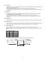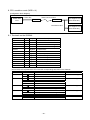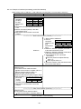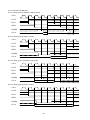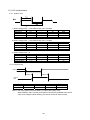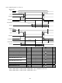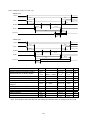
1
RemoteI/O & RemoteMotion G9004A (CPU emulation device) User's Manual Nippon Pulse Motor Co., Ltd. [Preface] Thank you for considering our super high-speed serial communicator LSI, the "G9000" series. To learn how to use the G9000 series device, read this manual and "G9001A/G9002" user's manual to become familiar with the product. [What the Motionnet is] As a next generation communication system, the Motionnet can construct faster, more volume large scale, wire saving systems than the conventional T-NET systems (conventional LSI product to construct serial communication system by NPM). Further, it has data communication function, which the T-NET does not have, so that the Motionnet can control data control devices such as in the PCL series (pulse train generation LSI made by NPM). The Motionnet system consists of one center device connected to a CPU bus, and maximum 64 local devices, and they are connected by using cables of two or three conductive cores. [Cautions] (1) Copying all or any part of this manual without written approval is prohibited. (2) The specifications of this LSI may be changed to improve performance or quality without prior notice. (3) Although this manual was produced with the utmost care, if you find any points that are unclear, wrong, or have inadequate descriptions, please let us know. (4) We are not responsible for any results that occur from using this LSI, regardless of item (3) above. [Logic indicators] (1) Terminal names and signal names that start with a # use negative logic. Ex.: #CS means that the CS terminal uses negative logic. This has the same meaning as . INDEX 1. Outline .......................................................................................................................................................1 2. Features.....................................................................................................................................................1 3. General specifications ...............................................................................................................................1 3-1. Communication system specifications ..............................................................................................1 3-1. Specifications of the CPU emulation device (G9004A) .....................................................................1 4. Hardware description.................................................................................................................................3 4-1. A list of terminals (QFP-80)................................................................................................................3 4-2. Terminal assignment drawings ..........................................................................................................5 4-3. Entire block diagram..........................................................................................................................6 5. Functions of terminals ...............................................................................................................................7 5-1. CLK....................................................................................................................................................7 5-2. #RST..................................................................................................................................................7 5-3. #DN0 to5............................................................................................................................................7 5-4. DNSM ................................................................................................................................................7 5-5. #DNSO ..............................................................................................................................................8 5-6. SPD0, SPD1 ......................................................................................................................................8 5-7. TUD....................................................................................................................................................8 5-8. TMD ...................................................................................................................................................8 5-9. #TOUT ...............................................................................................................................................8 5-10. SO....................................................................................................................................................8 5-11. SOEH, #SOEL .................................................................................................................................8 5-12. SOEI ................................................................................................................................................9 5-13. SI .....................................................................................................................................................9 5-14. #MRER ............................................................................................................................................9 5-15. #MSEL .............................................................................................................................................9 5-16. BRK .................................................................................................................................................9 5-17. MOD ................................................................................................................................................9 5-18. LCK0 to 1.........................................................................................................................................9 5-19. LCLK................................................................................................................................................9 5-20. LIF0 to 1.........................................................................................................................................10 5-21. #LRST............................................................................................................................................10 5-22. #LIFB .............................................................................................................................................10 5-23. LA0 to LA5 .....................................................................................................................................10 5-24. #LCS..............................................................................................................................................10 5-25. #LWR .............................................................................................................................................10 5-26. #LRD..............................................................................................................................................10 5-27. #LWRQ ..........................................................................................................................................11 5-28. #LIRQ ............................................................................................................................................11 5-29. LD0 to LD7.....................................................................................................................................11 5-30. LD8 to LD15...................................................................................................................................11 5-31. LWT0 and LWT1 ............................................................................................................................11 5-32. CKSL .............................................................................................................................................12 5-33. VDD, GND .....................................................................................................................................12 6. Setting the status and operation information for the G9004A .................................................................13 7. Message communication mode (MOD = LOW).......................................................................................15 7-1. Terminals for use by a local CPU ....................................................................................................15 7-2. I/O map for the local CPU................................................................................................................15 7-3. Command and status information that can be used by a local CPU...............................................16 7-3-1. G9004A's commands that can be used by a local CPU ..........................................................16 7-3-2. G9004A status information that can be seen from a local CPU...............................................16 7-4. Information command for the center device (G9001A) ...................................................................17 7-5. Message communication procedure ...............................................................................................18 8. CPU emulation mode (MOD = H)............................................................................................................20 8-1. Terminals on the G9004A ................................................................................................................20 8-2. Control method for using a center device (G9001A).......................................................................21 8-2-1. Command .................................................................................................................................22 8-2-2. Examples of CPU emulation control procedures .....................................................................24 8-3. Emulation timing ..............................................................................................................................30 8-3-1. 16-bit CPU I/F (1) (8086, H8 etc.) ............................................................................................30 8-3-2. 16-bit CPU I/F (2) (68000 etc.) .................................................................................................31 8-3-3. 8-bit CPU I/F (Z80 etc.) ............................................................................................................32 8-3-4. 8-bit CPU I/F (2) (6809 etc.) .....................................................................................................33 8-3-5. Example of a burst cycle (8-bit CPU-I/F (2) (Z80 etc.) .............................................................34 9. Connection examples and recommended environment ..........................................................................35 9-1. Example of a connection to a CPU using the CPU message communication mode (MOD = L) ....35 9-1-1. 8-bit I/F (1) (IF1 = HIGH, IF0 = HIGH)......................................................................................35 9-1-2. 8-bit I/F (2) (IF1 = HIGH, IF0 = LOW).......................................................................................36 9-1-3. 16-bit I/F (1) (IF1=LOW, IF0=HIGH).........................................................................................37 9-1-4. 16-bit I/F (2) (IF1 = LOW, IF0 = LOW) .....................................................................................38 9-1-5. Connecting to a CPU without a wait function ...........................................................................39 9-2. Access timing when the CPU message communication mode is selected (MOD = L) ...................40 9-2-1. Normal access..........................................................................................................................40 9-2-2. Write to command or data transfer FIFO..................................................................................40 9-2-3. Read status ..............................................................................................................................41 9-3. Connection to peripheral LSIs when the CPU emulation mode is selected....................................42 9-3-1. Connections to a PCL6045B (8086 type CPU emulation) ........................................................... 9-3-2. Connections to the PCD4541 (Z80 type CPU emulation) ............................................................ 9-4. Connections to a serial communication line ....................................................................................44 9-5. A connection example of a level shifter ...........................................................................................46 9-6. Complete configuration....................................................................................................................47 9-7. Recommended environment ...........................................................................................................48 9-7-1. Cable ........................................................................................................................................48 9-7-2. Terminating resistor..................................................................................................................48 9-7-3. Pulse transformer .....................................................................................................................48 9-7-4. I/F chip ......................................................................................................................................48 9-7-5. Parts used in our experiments..................................................................................................49 9-7-6. Other precautions .....................................................................................................................49 10. Center device (G9001A)........................................................................................................................50 10-1. Program example of CPU emulation mode...................................................................................51 10-1-1. Control example of the PCL6045B.........................................................................................51 10-1-2. Control example of PCD4541.................................................................................................53 11. Electrical characteristics ........................................................................................................................55 11-1. Absolute maximum ratings.............................................................................................................55 11-2. Recommended operating conditions .............................................................................................55 11-3. DC characteristics..........................................................................................................................55 11-4. AC characteristics ..........................................................................................................................56 11-4-1. System clock ..........................................................................................................................56 11-4-2. Reset timing............................................................................................................................56 11-5. Timing of CPU message communication mode.............................................................................57 11-5-1. 8-bit I/F (1) (IF1 = H, IF0 = H).................................................................................................57 11-5-2. 8-bit I/F (2) (IF1 = H, IF0 = L) .................................................................................................58 11-5-3. 16-bit I/F (1) (IF1 = L, IF0 = H) ...............................................................................................59 11-5-4. 16-bit I/F (2) (IF1 = L, IF0 = L)................................................................................................60 11-6. Timing when CPU emulation is selected .......................................................................................61 11-6-1. LCLK timing ............................................................................................................................61 11-6-2. 8-bit I/F (1) (IF1 = H, IF0 = H).................................................................................................62 11-6-3. 8-bit I/F (2) (IF1 = H, IF0 = L) .................................................................................................63 11-6-4. 16-bit I/F (1) (IF1 = L, IF0 = H) ...............................................................................................64 11-6-5. 16-bit I/F (2) (IF1 = L, IF0 = L)................................................................................................65 12. External dimensions ..............................................................................................................................66 13. Handling precautions.............................................................................................................................67 13-1. Design precautions........................................................................................................................67 13-2. Precautions for transporting and storing LSIs ...............................................................................67 13-3. Precautions for mounting...............................................................................................................68 13-4. Other precautions ..........................................................................................................................68 1. Outline This LSI is a CPU emulation device (G9004A). This LSI can be connected to our Motionnet and perform data communications with a center device (G9001A). Either of the following two operation modes can be selected from a terminal. 1) CPU emulation mode In this mode, the G9004A emulates CPU terminal signals using data communicated from the center device (G9001A). Although the communication format from the center device is limited, this LSI outputs signals identical to those from CPU terminals. Therefore it can control various LSIs that are normally connected to a CPU. 2) Message communication mode One word (16 bits) is reserved by the system in this mode, which is used for communication (the data commands and formats are specified). The user can use the remaining 127 words to communicate data. The format for the message data is not specified, which means that this LSI can communicate freely with almost any CPU that is connected to the center device and to this LSI. 2. Features - Compatible with our Motionnet. Can control various CPU support LSIs using data communications. A maximum of 256 bytes of data can be communicated in one sentence. A maximum of 64 devices can be connected using one line. It has a safety design using a communication failure detection circuit (contains a watchdog timer). Powered from just 3.3 VDC. 3. General specifications 3-1. Communication system specifications Item Reference clock Communication speed Communication sign Communication protocol Communication method Communication I/F Connection method Number of local devices Cyclic communication cycle when 20 Mbps Description 40 MHz or 80 MHz 2.5 M, 5 M, 10 M, or 20 Mbps NRZ sign NPM original method Half-duplex communication RS-485 or pulse transfer Multi-drop connection 64 devices max. When using 8 local devices (IN: 128 points, OUT: 128 points) --- 0.12 msec. When using 16 local devices (IN: 256 points, OUT:256 points) --- 0.24 msec. When using 32 local devices (IN: 512 points, OUT: 512 points) --- 0.49 msec. When using 64 local devices (IN: 1024 points, OUT: 1024 points) --- 0.97 msec. Note: The communication cycle will be extended dependant upon data communication. -1- 3-2. Specifications of the CPU emulation device (G9004A) Item CPU emulation mode Communication sentence length Data buffer size Data communication time Data transfer method Control address space CPU interface Message communication mode Communication sentence length Data buffer size Data communication time Data transfer system CPU interface Others Package Power supply Storage temperature range Operating temperature range Description 1 to 128 words/frame (1 word = 16 bits) 128 words When communicating 5 words (write to one register in the PCL): 21.7 µs Status: Cyclic transfer, Data: Transient transfer 64 bytes 8-bit I/F --- Z80, 6809 etc. 16-bit I/F --- 8086, H8, 68000 etc. 1 to 128 words/frame (1 word = 16 bits) 128 words (1 word: reserved for the system, 127 words: Message data) When communicating 128 words: 169.3 µs Status: Cyclic transfer Data communication: Transient transfer 8-bit I/F --- Z80, 6809 etc. 16-bit I/F --- 8086, H8, 68000 etc. 80 pin QFP (mold size: 12 x 12 x 1.4 mm) 3.3 V±10% -65 to +150˚C -40 to +85˚C -2- 4. Hardware description 4-1. A list of terminals (QFP-80) No. Signal name I/O 1 MOD I 2 TUD I 3 TMD I 4 LCK0 I 5 LCK1 I 6 7 8 9 10 11 12 13 14 15 16 17 18 19 20 21 22 23 24 25 26 27 28 29 30 31 32 33 34 35 36 37 38 39 40 41 42 43 44 45 46 47 LWT0 LWT1 LIF0 LIF1 VDD #LCS #LWR #LRD LA0 GND LA1 LA2 LA3 LA4 LA5 VDD LD0 LD1 LD2 LD3 GND LD4 LD5 LD6 LD7 VDD LD8 LD9 LD10 LD11 GND LD12 LD13 LD14 LD15 VDD #LWRQ #LIRQ #LIFB #LRST GND LCLK I I I I I I/O I/O I/O I/O I I/O I/O I/O I/O I/O I B B B B I B B B B I B B B B I B B B B I O/I O/I O O I O 48 #MRER O Logic Positive Positive Negative Negative Negative Positive Positive Positive Positive Positive Positive Positive Positive Positive Positive Positive Positive Positive Positive Positive Positive Positive Positive Positive Positive Positive Positive Negative Negative Negative Negative Negative Description Select operation mode (L: Message communication, H: CPU emulation) Set operation when outputting watchdog timer Select watchdog timer Division rate of local bus control clock (LCLK): 0 Division rate of local bus control clock (LCLK): 1 Interval time of local bus: 0 Interval time of local bus: 1 Local bus I/F mode 0 Local bus I/F mode 1 +3.3 V power input Chip selection for local bus Write signal for local bus Read signal for local bus Address for local bus: 0 GND Address for local bus: 1 Address for local bus: 2 Address for local bus: 3 Address for local bus: 4 Address for local bus: 5 +3.3 V power input Data for local bus: 0 Data for local bus: 1 Data for local bus: 2 Data for local bus: 3 GND Data for local bus: 4 Data for local bus: 5 Data for local bus: 6 Data for local bus: 7 +3.3 V power input Data for local bus: 8 Data for local bus: 9 Data for local bus: 10 Data for local bus: 11 +GND Data for local bus: 12 Data for local bus: 13 Data for local bus: 14 Data for local bus: 15 +3.3 V power input Wait request for local bus Interrupt request for local bus Busy interface for local bus Reset for local bus GND Local bus control block When a communication error is received, this signal becomes L level for a rated interval. -3- 5V Interface Available Available Available Available Available Available Available Available Available Available Available Available Available Available Available Available Available Available Available Available Available Available Available Available Available Available Available Available Available Available Available Available Available Available Available Available Available Available Available No. Signal name I/O Logic Description 5V Interface When sending data to this chip, this signal 49 #MSEL O Negative Available becomes L level for a rated interval. 50 VDD I +3.3 V power input 51 SOEH O Positive Enable serial output 52 #SOEL O Negative Enable serial output 53 SO O Positive Serial output 54 #TOUT O Negative Watchdog timer output Available 55 #DNSO O Negative Serial output of device number for next chip Available 56 GND I GND 57 BRK I Positive Break frame send request Available 58 SPD0 I Communication speed: 0 Available 59 SPD1 I Communication speed: 1 Available 60 CKSL I Clock rate selection (L: 40 MHz, H: 80 MHz) Available 61 DNSM I Device number selection mode Available Device number bit 0 (common with serial 62 #DN0 I Negative Available input) 63 #DN1 I Negative Device number bit 1 Available 64 #DN2 I Negative Device number bit 2 Available 65 #DN3 I Negative Device number bit 3 Available 66 #DN4 I Negative Device number bit 4 Available 67 #DN5 I Negative Device number bit 5 Available 68 VDD I +3.3 V power input 69 SI I Positive Serial input 70 SOEI I Positive Enable serial output 71 GND I GND 72 CLK I Reference clock 73 VDD I +3.3 V power input 74 #RST I Negative Reset 75 GND I GND 76 GND I GND 77 VDD I +3.3 V power input 78 GND I GND 79 GND I GND 80 GND I GND Note 1: In the "I/O" column, each pin can be set for input or output using the operation mode (MOD). In the "I/O" column, "I" refers to input, "O" refers to output and "B" refers to bi-directional. Note 2: As for the terminals with "available" in the 5V interface column, note the following. * These terminals can be input 5 V level signals. These are the input that diode overcurrent protection is deleted on 3.3 V lines. If over voltage may possibly be charged due to reflection, linking, or inductive noise, we recommend inserting a diode for overcurrent protection. * Outputs (including bi-directional) from 5V devices can be connected to the center device as far as these are TTL level. (Even when a signal is pulled up to 5V, the output level will be less than 3.3 V.) However, CMOS level signals cannot be connected. * On the CPU bus interface, pull up of a 5 V level is possible for stabilizing bus lines (prevent floating). Use 10 k-ohm or larger capacity pull up resistors. -4- CKSL SPD1 SPD0 BRK GND #DNSO #TOUT SO #SOEL SOEH VDD #MSEL #MRER LCLK GND #LRST #LIFB #LIRQ #LWRQ VDD 4-2. Terminal assignment drawings 60 59 58 57 56 55 54 53 52 51 50 49 48 47 46 45 44 43 42 41 DNSM 61 40 LD15 #DN0 62 39 LD14 #DN1 63 38 LD13 #DN2 64 37 LD12 #DN3 65 36 GND #DN4 66 35 LD11 #DN5 67 34 LD10 VDD 68 33 LD9 SI 69 32 LD8 SOEI 70 31 VDD GND 71 30 LD7 CLK 72 29 LD6 VDD 73 28 LD5 #RST 74 27 LD4 GND 75 26 GND GND 76 25 LD3 VDD 77 24 LD2 GND 78 23 LD1 GND 79 22 LD0 GND 80 21 VDD G9004A LWT0 LWT1 LIF0 13 14 15 16 17 18 19 20 LA5 LCK1 12 LA4 LCK0 11 LA3 TMD 10 LA2 TUD 9 LA1 8 GND 7 LA0 6 #LRD 5 #LWR 4 #LCS 3 VDD 2 LIF1 1 MOD XXXXXXXXX JAPAN Note: Locate each pin number from the markings on the chip. As shown in the figure above, pin number 1 is at the lower left of the NPM logo mark. -5- 4-3. Entire block diagram G9004A #RST SPD (1:0) CKSL CLK Reset control circuit Clock control circuit Internal reset Internal clock (20 MHz) Internal clock (40 MHz) #LCS #LIRQ #LRD #LWRQ #LWR LIF (1:0) #LIFB CPU I/F circuit Command LA (5:0) control circuit LD (15:0) LCLK #LRST CPU emulation control circuit LCK (1:0) LWT (1:0) #DNSO Manage device DN (5:0) DNSM number #TOUT Watchdog TMD timer TUD Data transfer Data receiving FIFO FIFO SI SOEI Receipt data Transfer processing processing circuit circuit Serial signal Serial signal receiving circuit transfer circuit SO SOEH #SOEL #MSEL #MRER -6- 5. Functions of terminals 5-1. CLK This is an input terminal of the reference clock. By setting of the CKSL terminal, either of the following clock rate signals can be connected. CKSL = L: 40 MHz CKSL = H: 80 MHz By selecting either of these clock rates, the serial communication transfer rate does not change. This clock rate selection affects communication precision. For a small-scale serial communication and transfer rate below 10 Mbps, use of the center device with 40 MHz does not give any restriction. With 20 Mbps transfer speed; however, longer communication lines or a large number of connected local devices may deteriorate communication precision due to collapse of signals on the circuit. This deterioration of communication quality can be corrected inside the LSI, if the deterioration level is not much. In order to improve correction precision; however, evenness of the clock duty is required. In other words, if the duty is ideal (50:50), the capacity to correct collapse of the signals in the communication lines can be improved. On the contrary, if the duty is not ideal, the center device cannot cope with collapses of the communication line. As a result, if the duty is close to ideal, the center device can be used with 40 MHz. When connecting more than one oscillator, the duty will not be ideal. In this case, select 80 MHz. The center device divides the frequency inside and creates 40 MHz frequency. If you do not want to 80 MHz frequency, you may prepare a separate 40 MHz oscillator for this LSI. 5-2. #RST This is an input terminal for a reset signal. By inputting an L level signal, the center device is reset. The RST line must be held LOW for at least 12 reference clock cycles. After turning ON the power, a reset signal must be input before starting communication. 5-3. #DN0 to 5 Input terminals for setting device address. Since these terminals use negative logic, setting all the terminals to zero calls up device address "3FH." There are two methods for entering a device address. Select the input method using the DNSM terminal. 5-4. DNSM Select the input method for loading the device address. 1) When the DNSM = H Input numeric values 0 to 3Fh with negative logic using DIP-SW etc. for #DN0 to #DN5 terminals. 2) When the DNSM = L Input a #DNSO signal that is output by some other chip on the #DN0 terminal on this device. When using this input method, this chip has an address equal to the other chip's address plus one. When using this method, connect terminals #DN1 to #DN5 to GND. When two sequential sets of serial data match, the data is taken to be a device address. -7- 5-5. #DNSO The numeric equivalent of the address on #DN0 to #DN5 + 1 will be output after being converted into a serial bit stream. Connect this output to another local device's #DN0 terminal (make all the other DNSM terminals of that local device LOW), so that other devices can get the address and pass it along to the next data-sending device. In the case that continuous address by #DNSO signal is set, it is necessary to have at least about 50 µs until the next step address is confirmed. 5-6. SPD0, SPD1 Specify communication speed with these terminals. All of the devices on the communication line shall be set to the same speed. SPD1 SPD0 Communication speed L L 2.5 Mbps L H 5 Mbps H L 10 Mbps H H 20 Mbps 5-7. TUD A watchdog timer is included on the chip to assist in administration of the communication status. When the data transmission interval from a center device to this device exceeds the set time, the watchdog timer times out. This terminal is used to set output conditions when the watchdog timer times out. When TUD = HIGH --- The LSI keeps its current status. When the TUD = LOW --- The LSI is Reset. 5-8. TMD Specify the time for the watchdog timer. The watchdog timer is used to administer the communication status. When the interval between data packets sent from a center device is longer than the specified interval, the watchdog timer times out (the timer restarts its count at the end of each data packet received from a center device). The time out may occur because of a problem on the communication circuit, such as disconnection, or simply because the center device has stopped communicating. The time used by the watchdog timer varies with communication speed selected. Watchdog timer setting TMD terminal 20 Mbps 10 Mbps 5 Mbps 2.5 Mbps L 5 ms 10 ms 20 ms 40 ms H 20 ms 40 ms 80 ms 160 ms 5-9. #TOUT Once the watchdog timer has timed out, this terminal goes LOW. 5-10. SO Serial output signal for communication. (Positive logic, tri-state output) 5-11. SOEH, #SOEL Output enable signal for communication. Difference between SOEH and #SOEL is that only the logic is different. When sending signals, SOEH will become H and #SOEL will become L. -8- 5-12. SOEI When using more than one device (G9004A), connect the SOEH signal of the other device (G9004A) to this terminal. By being wire OR'ed with the output enable signal from this I/O device, the device outputs an enable signal to SOEH or SOEL. When not used, connect to the GND. 5-13. SI Serial input signal for communication. (Positive logic) 5-14. #MRER This is a monitor output to check communication quality. When the center device receives an error frame such as a CRC error, the signal becomes L only for 128 cycles (3.2 s) of the CLK. By measuring the condition using the counter, you can check communication quality. 5-15. #MSEL Communication status monitor output. When this device receives a frame intended for this device and everything is normal (when communication #MRER is OFF), this terminal goes LOW for exactly 128 CLK cycles (3.2 s). This can be used to check the cyclic communication time. 5-16. BRK By providing HIGH pulses that are longer than the specified interval, this device will be made to wait for a break frame. When this device receives a break frame send request from a center device, it immediately sends a break frame. A pulse at least 3200 sec long is needed, in order to be seen as the BRK input pulse (positive logic). 5-17. MOD Selects the operating mode for this IC. MOD = L: Message communication mode MOD= H: CPU emulation mode 5-18. LCK0 to 1 Selects the clock frequency (LCLK) for controlling a local bus. LCK1 LCK 0 The clock frequency (LCLK) L L 2 MHz L H 4 MHz H L 10 MHz H H 20 MHz When this IC is in CPU emulation mode, the speed of the emulation depends on the above setting. However, when the message communication mode is selected, only the LCLK output frequency will change, and the operation speed remains constant. 5-19. LCLK Outputs a clock for controlling a local bus. If needed, it can be used for an external circuit. -9- 5-20. LIF0 to 1 Using these terminals, select the CPU interface specifications for the local bus. LIF1 LIF 0 CPU-I/F interface L L I/F-16 bit (2) (68000, etc) L H I/F-16 bit (1) (8086, H8, etc) H L I/F-8 bit (2) (6809, etc) H H I/F-8 bit (1) (Z80, etc) 5-21. #LRST Output a reset signal for the local bus. In any of the following cases, this signal goes LOW. 1) When a LOW is applied to the #RST terminal. 2) When TUD is LOW, the watchdog timer has timed out (only effective during approximate 32 cycles on LCLK). The #LRST terminal status can be changed by setting bit 1 of port 3 (See section 6 "Setting the status information and G9004A operation information.") (When bit 1 = 0, #LRST = HIGH. When bit 1 = 1, #LRST = LOW.) 5-22. #LIFB Outputs an interface busy signal for the local bus. Use this signal in the message communication mode when connecting to a CPU that does not have a wait control input terminal. This terminal goes LOW when a command or data is sent from a CPU, or when the status is being read. When this LSI completes its internal processing, it goes HIGH. Make sure that this terminal is HIGH, and then you can access the LSI. This terminal cannot be used in the CPU emulation mode. 5-23. LA0 to LA5 Address signals for the local bus. These will be either input or output terminals, depending on the mode selected. In the CPU emulation mode, the device outputs address signals from terminals LA0 to LA5. In the message communication mode, input address signals on LA0 and LA1. Pull LA2 to LA5 down to GND (5~10Kohm resistors). 5-24. #LCS This is a chip select signal for the local bus. It will be either an input or output terminal, depending on the mode selected. In the CPU emulation mode, this device outputs a chip select signal for an external circuit. In the message communication mode, you supply a chip select signal that will be used to access this LSI. 5-25. #LWR This terminal is used for a write signal for a local bus. It will be either an input or output terminal, depending on the mode selected. In the CPU emulation mode, this terminal outputs a write signal for external circuit. In the message communication mode, you supply a write signal in order to access this LSI. 5-26. #LRD This terminal is used for a read signal for a local bus. It will be either an input or output terminal, depending on the mode selected. In the CPU emulation mode, this terminal outputs a read signal for an external circuit. In the message communication mode, you supply a read signal in order to access this LSI. - 10 - 5-27. #LWRQ This terminal is used for a wait request signal for a local bus. It will be either an input or output terminal, depending on the mode selected. In the CPU emulation mode, you supply a wait request signal from an external circuit. In the message communication mode, this terminal outputs a wait request signal when the device cannot be accessed. 5-28. #LIRQ This terminal is used for an interrupt request signal for a local bus. It will be either an input or output terminal, depending on the mode selected. In the CPU emulation mode, you supply an interrupt request signal from an external circuit. In the message communication mode, this terminal outputs an interrupt request signal from internal operations. 5-29. LD0 to LD7 These terminals are used for the low-byte signals of a local data bus. These are bi-directional terminals. 5-30. LD8 to LD15 These terminals are used for the high-byte signals of a local data bus. These are bi-directional terminals. When using an 8-bit CPU interface, pull up these terminals to VDD (5 to 10 K-ohm resistors). 5-31. LWT0 and LWT1 These terminals are used to set the time interval between writing and reading to a local bus. Use these terminals only in the CPU emulation mode. These are not used in the message communication mode. (TLCLK: LCLK clock cycle) LWT1 LWT0 Time interval L L H H L H L H TLCLK 3xTLCLK 5xTLCLK 9xTLCLK [An example of the reading procedure when using a 16-bit CPU interface (1)] - 11 - 5-32. CKSL Selects the clock specifications for the input on the CLK terminal. When CKSL = L, supply a 40 MHz clock signal on the CLK terminal. The duty cycle should be approximately 50%. If the duty cycle is too far away from 50%, the number of communication faults will increase. When CKSL = H, the device uses the CLK signal input after dividing by 2 internally. Therefore, the duty cycle will not have such a great influence. In this case, supply an 80 MHz clock signal. 5-33. VDD, GND Supply +3.3 VDC±10% for power on the VDD terminal. Make sure to use all the terminals. - 12 - 6. Setting the status and operation information for the G9004A During the cyclic communication and during data communication, the status register information (registers 0 to 2) is written to the port data area (ports 0 to 2) that corresponds to the device address in the center device. When the operating information is written to the port data area (port 3) that corresponds to the center device's device address, it is passed along to the CPU emulation device (G9004A) using the cyclic communication. Status 0 (Interrupt information) <Port 0> 7 6 5 4 3 2 1 0 0 0 0 0 1: Local interrupt request (result of ORing bits1 to 3) 1: Local receive process complete interrupt (CPU emulation mode) 1: Local #LIRQ input interrupt (CPU emulation mode) 1: Local transmission request interrupt (message communication model) Status 1 (Status information) <Port 1> 7 6 5 4 3 2 1 0 Local reception FIFO status (1: Data present, 0: No data) Local transmission FIFO status (1: Data present, 0: No data) Local emulation status (1: Processing 0: Stopped) Local #LIRQ input status (1: LOW 0: HIGH) Port 3 bit 0 (halt emulation) status #LRST terminal status (1: LOW 0: HIGH) Local message communication status (1: Processing data transmission, 0: Processing complete #LWRQ terminal status (1: LOW 0: HIGH) Status 2 (setting information) <Port 2> 7 6 5 4 3 2 1 0 0 Set local operation mode (0: Message communication 1: CPU emulation) Local CPU interface mode 00: 16-bit interface (2) (68000 etc.) 01: 16-bit I/F (1) (8086,H8 etc.) 10: 8-bit I/F (2) (6809 etc.) 11: 8-bit I/F (1) (Z80 etc.) Local LCLK setting Local LWT setting Operation information <Port 3> 7 6 5 4 3 2 1 0 0 0 0 0 0 0 Halt emulation (execute by changing from 0 to 1) Change the #LRST terminal status (0: HIGH 1: LOW) - 13 - [Communication image] Center device (G9001A) Port Data Area Port 0 data Port 1 data Port 2 data Port 3 data Data reception FIFO Data transmission FIFO CPU emulation device (G9004A) Cyclic and data communication Cyclic communication Data communication - 14 - Port 0 Port 1 Port 2 Port 3 Status data Operation data Data reception FIFO Data transmission FIFO 7. Message communication mode (MOD = LOW) [Configuration block diagram] Control bus Center device CPU Serial communication G9001A Control bus G9004A 7-1. Terminals for use by a local CPU Terminal name I/O Logic Description LIF0 I Local bus interface mode 0 LIF1 I Local bus interface mode 1 #LRST O Negative Resets the local bus LA0 to1 I Positive Address for local bus lines 0 to 1 LA2 to 5 I Positive Pull down to GND (5~10Kohm resistors) #LCS I Negative Chip select for the local bus #LWR I Negative Write signal for the local bus #LRD I Negative Read signal for the local bus #LWRQ O Negative Wait request for the local bus #LIFB O Negative Interface busy for the local bus #LIRQ O Negative Interrupt request for the local bus LD0 to 7 B Positive Low-byte signal for the local bus LD8 to 15 B Positive High-byte signal for the local bus 7-2. I/O map for the local CPU 16-bit interface (1) and (2) (8086, H8, and 68000) [LIF1 = L] LA1 Writing Reading 0 Write command Read status 1 Write transmission data Read reception data 8-bit I/f (1) and (2) (Z80, 6809 etc.) [LIF1 = H] LA0 to LA1 Writing Reading 00 Write command Read status 01 Invalid Invalid 10 Write transmission data Read reception data 11 Invalid Invalid - 15 - Local CPU 7-3. Command and status information that can be used by a local CPU 7-3-1. G9004A's commands that can be used by a local CPU 7 6 5 4 3 2 1 0 Command code 00h: Invalid 01h: Software reset 02h: Reset transmission FIFO 03h: Reset reception FIFO 04h: Wait for a sending break frame 10h: Data send request Code 00h Description No meaning. (Does not affect the operation) 01h Software reset. Has the same result as applying a LOW to the #RST terminal. See the Note Resets only the data transmission FIFO. If written during the data sending process (status 02h register bit 6 = 1) it may cause a CPU access error (status register bit 3 = 1). Resets only the data reception FIFO. Writing this command while no data is being received 03h (status register bit 5 = 0) may cause a CPU access error (status register bit 3 = 1). The device enters a break frame waiting status. This has the same results as applying a HIGH 04h pulse to the BRK terminal. Data send request. Make the status register 0 bit 3 in the CPU emulation device equal 1 (set the 10h sending request interrupt), so that the center device will be notified that transmission data exists. Note: When turning ON the power, a reset signal must be supplied (#RST = LOW). 7-3-2. G9004A status information that can be seen from a local CPU 7 6 5 4 3 2 1 0 1: Interrupt due to the data receipt 1: Interrupt due to the data transmission process being complete 1: Interrupt due to a communication link disconnection 1: CPU access error 1: While establishing a communication link 1: Reception data exists 1: Sending process active 1: Transmission data exists Bit Item 0 Data receipt interrupt 1 Data transmission process complete interrupt Description When the G9004A receives message data from the center device, this bit becomes 1 and an interrupt signal is output (#LIRQ = L). After this status register is read, this bit returns to 0. When the device only receives an information command, this bit stays 0 and the device does not output an interrupt. After writing a data transmission command (10h), when the G9004A receives an information command (reset transmission processing flag: 0002h), this bit becomes 1 and the device outputs an interrupt signal (#LIRQ = L). After this status register is read, this bit returns to 0. - 16 - Bit 2 3 4 5 6 7 Item Description When the interval between sending one data sentence and the next from Communication link the center device to the PCL exceeds a specified time (time out), this bit disconnected becomes 1, and the device outputs an interrupt signal (#LIRQ = L). interrupt After reading this status register, the interrupt signal is reset. This is used to monitor the watchdog timer output (1: #TOUT = L) When the PCL device does any of the following on a command from a CPU, this bit becomes 1, and the device outputs an interrupt signal (#LIRQ = L). After this status register is read, this bit returns to 0. - Try to write data to the transmission FIFO during transmission CPU access error processing (status register bit 6 = 1), or writing a transmission FIFO reset command (02h). - Try to read the reception FIFO even though it has received no data (status register bit 5 = 0), or writing a data reception FIFO reset command (03h). This bit is used to see if the communication line is connected. When the Communication link device detects a change on the communication line, this bit becomes 1. If valid the communication line does not change within a specified time, this bit becomes 0. Received data When there is message data in the data reception FIFO, this bit becomes exists 1. After writing the data transmission command (10h), this bit becomes 1. Data transmission When data communication with the center device is complete (when a in progress receiving information command 0002h issued by the center device), this bit becomes 0. Transmission data If there is message data in the data transmission FIFO, this bit becomes 1. exists 7-4. Information command for the center device (G9001A) To send a message, the first word in the transmission FIFO of the center device is used for the information command. The remaining 127 words can be used freely as message data (any format is allowed). Address 00h 01h to 7Fh Center device transmission FIFO Upper Information command Message data (any format) Lower [Information command] Command code Description 0001h Message transmission. Use this command to send a message or data from the center device to a local CPU. You can attach a message or data at the end of this command. (There is also an Information command without any message.) Transmits FIFO data of G9004A for sending to G9001A. 0002h When the G9004A receives this command, the data transmission process complete interrupt < local status register bit 1 = 1 > and the device resets the transmission processing flag < local status register bit 6 >. You can attach a message or data at the end of this command. 0003h Resend request command When the G9004A receives this command, it sends the same data as it last sent. Use this command when the center device cannot receive data from the local device due a data communication error or other reason. Note. Use this when sending request is failed because of some causes. In the case that the 0001h command is used in place of resend request command, the operation of 0003h command after that is not guaranteed. - 17 - 7-5. Message communication procedure The device model numbers are shown in parenthesis. Numbers marked with ( ) mean that the operations are carried out by a CPU. Assume that the local device address (for the G9004A) is "08h." In addition, the port status information for the Cycle communication or data communication is sent to the port data area in the center device (G9001A). In order to generate an interrupt (position *1) in the center device (G9001A) when an interrupt request (bit 0 = 1 on port 0) occurs in the local device (G9004A), you must enable the input change interrupt that corresponds to port 0 (set it to 1). (1) When the center device (G9001A) is the first to send a message and the local device (G9004A) responds [Center device (G9001A)] [Local device (G9004A)] [Start] (1) Write an information command (0001h: Message transmission) to the data transmission FIFO. (2) Place a message in the data transmission FIFO. (3) Write a data communication command (4008h). ***************** Data communication (1st time) ***************** - Interrupt occurs (4) The center device reads the status. Data transmission complete <bit 0=1> *1 - Interrupt occurs - Interrupt occurs (1) Read the status Data reception interrupt <bit 0 = 1> (2) Read the message in the data reception FIFO. (3) Place the message in the data transmission FIFO. (4) Write a data transmission command (10h). - Set the status for port 0 (interrupt information) ▼ Local device data transmission request interrupt <Bit 1 = 1> ▼ Local device interrupt request <Bit 0 = 1> (5) The center device reads the status. Input change interrupt <bit 2 = 1> (6) Input change interrupt (7) Send an information command to the data transmission FIFO. Write (0001h: Message transmission) (8) Write a data communication command (4008h). ***************** Data communication (2nd time) ***************** When the Local device receives a message from the center device, it sends the data in the FIFO to the center device. - Interrupt occurs (9) Read the status Data communication complete <bit 0=1> (10) Read the message in the data reception FIFO. (11) Send an information command (0002h: reset the data transmission processing flag) to the data transmission FIFO. This is how the center device informs the local device that the data was received normally. (12) Write a data communication command (4008h). ***************** Data communication (3rd time) ***************** - Interrupt occurs - Reset the data transmission FIFO. (13) Read the center device status - Interrupt occurs Data communication complete <bit 0 = 1> (5) Read the local device status Transmission process complete interrupt <bit 1 = 1> - 18 - (2) When the local device (G9004A) is the first to send a message and the center device (G9001A) responds [Center device (G9001A)] [Local device (G9004A)] [Start] (1) Place a message in the data transmission FIFO. (2) Write a data send command (10h). - Set the status for port 0 (interrupt information) *1 - Interrupt occurs (1) Read the center device status Input change interrupt <bit 2=1> (2) Reset the input change interrupt (3) Send an information command (0001h: message transmission) to the data transmission FIFO. ▼ Local device data send request interrupt <bit 1 = 1> ▼ Local device interrupt request <bit 0 = 1> (4) Place a message in the data transmission FIFO. (5) Write a data communication command (4008h). ***************** Data communication (1st time) ***************** After receiving a message from the centerl device, the local device sends the data in the FIFO to the center device. - Interrupt occurs - Interrupt occurs (6) The center device reads the status. (3) The local device reads the status. Data communication compete <bit 0 = 1> Data received interrupt <Bit 0=1> (7) Read the message in the data reception FIFO. (4) Read the message in the data reception FIFO. (8) Send an information command (0002h: Reset the data send processing flag) to the data transmission FIFO. This is how the center device informs the local device that the data was received normally. (9) Write a data communication command (4008h). ***************** Data communication (2nd time) ***************** - Interrupt occurs (10) Read the status Data communication compete <bit 0 = 1> - Reset data transmission FIFO. - Interrupt occurs (5) Read the status of the local device Data transmission process complete interrupt <bit 1=1> [End of message communication] - 19 - 8. CPU emulation mode (MOD = H) [Configuration block diagram] Control bus Center side CPU Serial communication G9001A G9004A Local device bus CPU support LSIs (PCL series etc.) CPU support LSIs (PCL series etc.) 8-1. Terminals on the G9004A Terminal name LIF0 LIF1 LWT0 LWT1 #LRST LA0 to LA5 #LCS #LWR #LRD #LWRQ #LIRQ LD0 to LD7 LD8 to LD15 I/O I I I I O O O O O I I B B Logic Positive Positive Negative Positive Negative Negative Negative Negative Negative Positive Positive Description Local bus interface mode 0 Local bus interface mode 1 Local bus interval time setting 0 Local bus interval time setting 1 Local bus reset Local bus address Local bus chip select Local bus write signal Local bus read signal Local bus wait request Local bus interrupt request Local bus data 0 to 7 Local bus data 8 to 15 Shown below are representative CPUs and the corresponding terminals on the G9004A. Typical CPU G9004A CPU name Terminal name G9004A terminal name G9004A mode #LRD 8 bit interface (1) Z80 #LWR #LRD 16 bit interface (1) 8086 #LWR Upper enable None Lower enable None #LWR 16 bit interface (2) 68000 Upper strobe #LRD (No distinction between upper/lower) Lower strobe #LRD (No distinction between upper/lower) #LRD 16 bit interface (1) H8 Upper WR #LWR (No distinction between upper/lower) Lower WR #LWR (No distinction between upper/lower) #LWR 8 bit interface (2) 6809 E #LRD - 20 - 8-2. Control method for using a center device (G9001A) When you want to perform CPU emulation using the G9004A, write the commands and data using the formats specified for the data transmission FIFO in the center device (G9001A). The center device’s data transmission FIFO can store up to 128 words, including write commands, write data, and read commands. When writing data, there is no data to be sent from the G9004A. But, when reading data, the G9004A will send a read command and then read data from the center device Therefore, more than 128 words of data cannot be handled by the G9004A. [When writing data] Center device data transmission FIFO Address Upper Lower Command 00h (writing) 01h Writing data (1) [When reading data] Center device data transmission FIFO Address Upper Lower [Combined case] Center device data transmission FIFO Address Upper Lower 00h Command (reading) 00h Command (writing) 01h Command (reading) 01h Writing data (1) 02h Writing data (2) 02h Command (reading) 02h Writing data (2) - - - - 03h Command (reading) - - - - 04h Command (writing) - - - - 05h Writing data - - If the G9004A is set up to use an 8-bit CPU interface, the following precautions should be noted. - When the center device (G9001A) uses a 16-bit interface In the case that the number of writing for G9004 is odd number, add one byte of dummy data. This dummy data is ignored on the G9004A side (Writing operation is not executed.), the next operation command will be processed. Additionally, in the case that writing of odd number bytes is executed several time simultaneously, the data is returned in the packed state so as to cross the word boarder. (On the G9004A side, any dummy data are not added.) - When the center device (G9001A) uses an 8-bit interface The operation command for the G9004A must be written to the same address in the center device (G9001A) data transmission FIFO by arranging the upper and lower bytes in order. If the number of data bytes to write is odd, write one dummy data byte to make the total even. Then use the following operation commands for the G9004A at the same address. Shown below is an example where 3 bytes of data are to be written. Write a dummy data byte to the upper 8 bits of address 02h. Center device (G9001A) data transmission FIFO data Address Upper 8 bytes Lower 8 bytes 00h Write command (upper) Write command (lower) 01h Write data 2 Write data 1 Write the 02h Write data 4 (dummy data) Write data 3 operation commands to the 03h Write command (upper) Write command (lower) same addresses. 04h Write data 5 Write data 4 05h 06h - - 21 - 8-2-1. Command 15 14 13 12 11 10 9 8 7 6 5 4 3 2 1 0 - Start address setting - Address refresh setting 0X: Fixed address 10: Add address 11: Subtract address Process detail setting 000:NOP 001: Write process 010: Read process 011: Data send process 100: Reset receive process complete interrupt 101: Reset #LIRQ input interrupt Communicating wait setting Number of process times setting Start address setting - Set the top address for the read or write process. - If the CPU emulation device (G9004A) is using a 16-bit CPU interface, the lower bit setting is ignored and always treated as 0. - Commands other than writing and reading processes are invalid. Address refresh setting - When the number of processing times does not equal zero, select an address refresh method - When the number of processing times is 0, commands other than writing and reading processes are invalid. Process detail setting - Select the processing detail for the CPU emulation device (G9004A) Item Processing detail "Do-nothing" command. The device does nothing. Reception process NOP complete interrupt does not occur. When sending FIFO for G9004A has any data, do not use this command. (The operation is not guaranteed.) The CPU emulation device (G9004A) reads the number of bytes specified in Read process the processing register, starting from the start address. Write process Data send process The CPU emulation device (G9004A) writes the number of bytes specified in the processing register, starting from the start address. The device sends the data that was read by using the read process to the center device. In addition, if the reception process complete interrupt flag (bit 1 on port 0) is Note 1, and this command is received, the device will send the same data as it last sent (the data resend process). Reset the reception process complete interrupt flag Note Reset the reception process complete interrupt flag (bit 1 on port 0) to 0. In the case that the bit number 1 of the state 1 is "1", the value returned to 0 after receiving this command. #LIRQ input interrupt reset Reset the #LIRQ input interrupt (bit 2 on port 0) to 0. Note Note. Please use it with the beginning word of sending data without fail. If it is used at except the beginning, it is ignored. - 22 - Communication wait setting - Select whether to use the communication wait time during the reading and writing processes. - When set to 0, the G9004A will return the normal response (without data) soon after receiving a command from the center device (G9001A). - When set to 1, the G9004 will wait a maximum of 10 sec (at 20 Mbps) to respond after receiving a command from the center device (G9001A). While waiting, if the received processes are all complete and there is a read command, the device will send read data. If there is no read command, or if the received processes do not complete within the waiting time, it sends a normal response (without data). - Commands other than writing/reading processes are invalid. - The only valid setting is for the 1st word (01h address) in the center device data transmission FIFO. Setting it to any other address is not allowed. Processing bytes setting - Set the number of processing bytes when you want to read or write continuously. (Set a burst cycle). Enter (the number of processing bytes - 1) as the setting. When the device is used with a 16-bit CPU interface, set the number in units of words. Otherwise, when the device is used with an 8-bit CPU interface, set the number in units of bytes. Commands other than write/read processes are not allowed. - 23 - 8-2-2. Examples of CPU emulation control procedures The device model number is shown in parenthesis. Numbers marked with ( ) mean that the operations are carried out by a center device (G9001A) emulating a CPU. Assume that the local device address (for the G9004A) is "08h." In addition, the port status information of the cyclic communication or data communication is sent to the port data area of the center device (G9001A). In order to generate an interrupt (position *1) in the center device (G9001A) when an interrupt request (bit 0 = 1 on port 0) occurs in the local device (G9004A), you must enable the input change interrupt that corresponds to port 0 (set it to 1). 8-2-2-1. Examples of writing single units of data (16-bit CPU interface) [Write the data 1234h to address 2] (without using communication wait time) [Center device (G9001A)] [Local device (G9004A)] [Start] (1) Place a command Data transmission FIFO (0102h) in the data Address Upper Lower transmission FIFO. 00h 01h 02h 01h 12h 34h (2) Place the data (1234h) into the data transmission FIFO. (3) Write a data communication command (4008h). ***************** Data communication (1st time) ***************** - Interrupt occurs (4) The center device reads the status Data communication complete <bit 0=1> 1. Write 1234h to address 2. 2. Set status port 0 (interrupt information) Receive process complete interrupt <bit *1 1=1> - Interrupt occurs Interrupt request <Bit 0=1> (5) The center device reads the status Input change interrupt<Bit 2=1> (6) Reset the input change interrupt (7) Write (0400h) to the Data transmission FIFO data transmission Address Upper Lower FIFO. 00h 04h 00h [Reset reception process complete interrupt]. (8) Write a data communication command (4008h) ***************** Data communication (2nd time) ***************** - Interrupt occurs (9) The center device reads the status. Data communication complete <Bit 0=1> [End emulation communication] - 24 - 8-2-2-2. Example of writing continuous data (16-bit CPU interface) [Write 1234h to address 4, 2345h to address 6, and 3456h to address 8] (Without a communication wait time) [Center device (G9001A)] [Local device (G9004A)] [Start] (1) Place a command (2184h) in the data transmission Data transmission FIFO Address Upper Lower 00h 21h 84h 01h 12h 34h 02h 23h 45h 03h 34h 56h (2) Place data (1234h) in the data transmission FIFO. (3) Place data (2345h) in the data transmission FIFO. (4) Place data (3456h) in the data transmission FIFO. (5) Write a data communication command (4008h). ***************** Data communication (1st time) ***************** - Interrupt occurs (6) The center device reads the status. Data communication complete <bit 0=1> *1 Interrupt occurs 1. Write 1234h to address 4. 2. Write 2345h to address 6. 3. Write 3456h to address 8. 4. Set the status on port 0 (interrupt information). Receive process complete interrupt <Bit 1 = 1> Interrupt request <Bit 0=1> (7) The center device reads the status. Input change interrupt <bit 2=1> (8) Reset the input change interrupt (9) Place a Data transmission FIFO command Address Upper Lower (0400h) in 00h 04h 00h the data transmission FIFO. [Reset reception process complete interrupt] (10) Write a data communication command (4008h). ***************** Data communication (2nd time) ***************** - Interrupt occurs (11) Center device reads the status. Data communication complete <Bit 0=1> [End emulation communication] - 25 - 8-2-2-3. Example of reading continuous data (16-bit CPU interface) [Read data addresses 16, 14, 12, and 10 in this order] (Using a communication wait time) [Center device (G9001A)] [Local device (G9004A)] [Start] Data transmission FIFO (1) Place a command Address Upper Lower (3AD0h) in the data 00h 3Ah D0h transmission FIFO. (2) Write a data communication command (4008h). ***************** Data communication (1st time) ***************** 1. Place a command Data transmission FIFO (3AD0h) in the data Address Upper Lower transmission FIFO. 00h 3Ah D0h 2. Read from address 16 01h FFh EEh 02h DDh CCh (FFEEh) and write to 03h BBh AAh the data transmission 04h 99h 88h FIFO. 3. Read from address 14 (DDCCh) and write to the data transmission FIFO. Wait time 4. Read from address 12 (BBAAh) and write to the data transmission FIFO. 5. Read from address 10 (9988h) and write to the data transmission FIFO. 6. Set the status for port 0 (interrupt information) Receive process complete interrupt <Bit 1=1> Interrupt request <Bit 0=1> 7. Send the FIFO contents to the center device. - Interrupt occurs (3) The center device reads the status Data communication complete <bit 0=1> Input change interrupt <bit 2=1> (4) Reset the input change interrupt (5) Read from the reception FIFO (6) Place a command Data transmission FIFO Address Upper Lower (0400h) in the data 00h 04h 00h transmission FIFO. [Reset the reception process complete interrupt] (7) Write a data communication command (4008h). ***************** Data communication (2nd time) ***************** - Interrupt occurs (8) Read the center device status Data communication complete <bit 0=1> [End emulation communication] - 26 - [Read, in order, from address 16, 14, 12, and 10] (Without a communication wait time) Center device (G9001A)] [Local device (G9004A)] [Start] Data transmission FIFO (1) Place a command Address Upper Lower (32D0h) in the data 00h 32h D0h transmission FIFO. (2) Write a data communication command (4008h). ***************** Data communication (1st time) ***************** - Interrupt occurs (3) Read the status Data communication complete <Bit 0=1> *1 - Interrupt occurs (4) The center device reads the status Input change interrupt <bit 2=1> (5) Reset the input change interrupt. (6) Place a command Data transmission FIFO (0300h) in the data Address Upper Lower transmission FIFO. 00h 03h D0h [Data sending process] (7) Write a data communication command (4008h). Data transmission FIFO 1. Place a command (32D0h) in the data Address Upper Lower 00h 3Ah D0h transmission FIFO. 01h FFh EEh 2. Read address 16 02h DDh CCh (FFEEh) and write it 03h BBh AAh to the data 04h 99h 88h transmission FIFO. 3. Read address14 (DDCCh) and write it to the data transmission FIFO. 4. Read address12 (BBAAh) and write it to the data transmission FIFO. 5. Read address10 (9988h) and write it to the data transmission FIFO. 6. Set port 0 (interrupt information) Receive process complete interrupt <Bit 1=1> Interrupt request <Bit 0=1> Send the contents of the data transmission FIFO to the center device. Data communication (2nd time) ***************** ***************** - Interrupt occurs (8) The center device reads the status. Data communication complete <bit 0=1> (9) Read data from the data reception FIFO. (10) Place a command Data transmission FIFO (0400h) in the Address Upper Lower data transmission 00h 04h 00h FIFO. [Reset the rseceive process complete interrupt] (11) Write a data communication command (4008h). ***************** Data communication (3rd time) ***************** - Interrupt occurs (12) The center device reads the status. Data communication complete <bit 0=1> [End emulation communication] - 27 - 8-2-2-4. Example of combined processing (16-bit CPU interface) [After writing 1234h to address 0, read addresses 4 and 6] (With a communication wait time) [Center device (G9001A)] [Local device (G9004A)] [Start] (1) Place a Data transmission FIFO command Address Upper Lower (0100h) in 00h 01h 00h the data 01h 12h 34h transmission 02h 12h 84h FIFO. (2) Place data (1234h) in the data transmission FIFO. (3) Place a command (1284h) in the data transmission FIFO. (4) Write a data communication command (4008h). ***************** Data communication (1st time) ***************** Wait time 1. Write 1234h to address 0. 2. Place a Data transmission FIFO command Address Upper Lower (1284h) in the 00h 12h 84h data 01h EEh FFh transmission 02h DDh CCh FIFO. 3.Read from address 4 (FFEEh) and write it to the data transmission FIFO. 4.Read from address 6 (DDCCh) and write it to the data transmission FIFO. 5. Set the status for port 0 (interrupt information) Receive process complete interrupt <Bit 1=1> Write request <Bit 0=1> 6. Send the contents of the data transmission FIFO to the center device. - Interrupt occurs (5) The center device reads the status. Data communication complete <Bit 0=1> Input change interrupt <Bit 2=1> (6) Reset the input change interrupt (7) Read the data from the data reception FIFO. (8) Write b(0400h) to the data transmission FIFO. Data transmission FIFO [Reset the Address Upper Lower receive 00h 04h 00h process complete interrupt] (9) Write a data communication command (4008h). ***************** Data communication (2nd time) ***************** - Interrupt occurs. (10) The center device reads the status. Data communication complete <Bit 0=1> [End of emulation communication] - 28 - [After writing 1234h to address 0, read addresses 4 and 6] (Without a communication wait time) [Center device (G9001A)] [Local device (G9004A)] [Start] (1) Place a command (0100h) in the data transmission Data transmission FIFO FIFO. Address Upper Lower (2) Place data 00h 01h 00h (1234h) in the 01h 12h 34h 02h 12h 84h data transmission FIFO. (3) Place a command (1284h) in the data transmission FIFO. (4) Write a data communication command (4008h). ***************** Data communication (1st time) ***************** 1. Write 1234h to address 0. - Interrupt occurs 2. Place a command (5) The center device reads the status. Data transmission FIFO (1284h) in the data Data communication complete <Bit 0=1> Address Upper Lower transmission FIFO. *1 - Interrupt occurs (6) The center device reads the status. Input change interrupt <Bit 2=1> (7) Reset the input Data transmission FIFO change interrupt. Address Upper Lower Write (0300h) 00h 03h 00h to the data transmission FIFO. [Data sending process] (8) Write a data communication command (4008h) 00h 12h 84h 3. Read from address 01h FFh EEh 4 (FFEEh) and write 02h DDh CCh it to the data transmission FIFO. 4. Read from address 6 (DDCCh) and write it to the data transmission FIFO. 5. Set the status on port 0 (interrupt information). Receive process complete interrupt <Bit 1 = 1> Interrupt request <Bit 0=1> Send the contents of the data transmission FIFO to the center device. ***************** Data communication (2nd time) ***************** - Interrupt occurs (10) The center device reads the status. Complete data communication <bit 0=1> (11) Read the data from the data receipt FIFO. (12) Place a Data transmission FIFO command Address Upper Lower (0400h) 00h 04h 00h in the data transmission FIFO. [Reset the reception process complete interrupt] (13) Write a data communication command (4008h). ***************** Data communication (3rd time) ***************** - Interrupt occurs (14) The center device reads the status. Compete data communication <Bit 0=1> [End emulation communication] - 29 - 8-3. Emulation timing 8-3-1. 16-bit CPU I/F (1) (8086, H8 etc.) 8-3-1-1. Read cycle (1) (without a wait cycle) LCLK LA5-1 #LCS #LRD #LWRQ LD15-0 8-3-1-2. Read cycle (2) (wait 2 cycles) LCLK LA5-1 #LCS #LRD #LWRQ LD15-0 8-3-1-3. Write cycle (1) (without a wait cycle) LCLK LA5-1 #LCS #LWR #LWRQ LD15-0 8-3-1-4. Write cycle (2) (wait 2 cycle) LCLK LA5-1 #LCS #LRD #LWRQ LD15-0 - 30 - 8-3-2. 16-bit CPU I/F (2) (68000 etc.) 8-3-2-1. Read cycle (1) (without a wait cycle) LCLK LA5-1 #LCS #LWR #LRD/STB #LWRQ/ACK LD15-0 8-3-2-2. Read cycle (2) (wait 2 cycles) LCLK LA5-1 #LCS #LWR #LDR/STB #LWRQ/ACK LD15-0 8-3-2-3. Write cycle (1) (without a wait cycle) LCLK LA5-1 #LCS #LWR #LDR/STB #LWRQ/ACK LD15-0 8-3-2-4. Write cycle (2) (wait 2 cycles) LCLK LA5-1 #LCS #LWR #LDR/STB #LWRQ/ACK LD15-0 - 31 - 8-3-3. 8-bit CPU I/F (Z80 etc.) 8-3-3-1. Read cycle (1) (without a wait 2 cycles) LCLK LA5-0 #LCS #LRD #LWRQ LD7-0 8-3-3-2. Read cycle (2) (wait 2 cycles) LCLK LA5-0 #LCS #LRD #LWRQ LD7-0 8-3-3-3. Write cycle (1) (without a wait cycle) LCLK LA5-0 #LCS #LRD #LWRQ LD7-0 8-3-3-4. Write cycle (2) (wait 2 cycles) LCLK LA5-0 #LCS #LRD #LWRQ LD7-0 - 32 - 8-3-4. 8-bit CPU I/F (2) (6809 etc.) 8-3-4-1. Read cycle (2) (without a wait cycle) LCLK RD(E) LA5-0 #LCS #LWR #LWRQ LD7-0 8-3-4-2. Read cycle (2) (without 2 cycles) LCLK RD(E) LA5-0 #LCS #LWR #LWRQ LD7-0 8-3-4-3. Write cycle (1) (without a wait cycle) LCLK RD(E) LA5-0 #LCS #LWR #LWRQ LD7-0 8-3-4-4. Write cycle (1) (without a wait cycle) LCLK RD(E) LA5-0 #LCS #LWR #LWRQ LD7-0 - 33 - 8-3-5. Example of a burst cycle (8-bit CPU-I/F (2) (Z80 etc.) 8-3-5-1. Burst read cycle (1) (Fixed address) LCLK LA5-0 n #LCS #LRD #LWRQ LD7-0 8-3-5-2. Bust read cycle (2) (add an address) LCLK LA5-0 n n+1 n+2 #LCS #LRD #LWRQ LD7-0 8-3-5-3. Burst read cycle (3) (subtract an address) LCLK LA5-0 n n-1 n-2 #LCS #LRD #LWRQ LD7-0 8-3-5-4. Burst write cycle (add an address) LCLK LA5-0 n n+1 #LCS # LWR #LWRQ LD7-0 - 34 - n+2 9. Connection examples and recommended environment 9-1. Example of a connection to a CPU using the CPU message communication mode (MOD = L). 9-1-1. 8-bit I/F (1) (IF1 = HIGH, IF0 = HIGH) G9004A Z80 type CPU M1 A2 to A15 Decoding circuit CLK A0 to A1 INT IORQ RD WR VDD CLK #LCS LIF1 LIF0 MOD LA0 to LA1 #LIRQ GND #LRD #LWR WAIT D0 to D7 #LWRQ LD0 to LD7 RESET #RST System reset Note 1: When you use an interrupt controller, the CPU will output IORQ as an interrupt acknowledge signal that is used to determine the interrupt vector. At this time, when this LSI's #LCS terminal goes LOW, the LSI may output a #LWRQ signal and still not be able to capture the vector signal is properly. Therefore, arrange the decoding circuit so that it only functions when the HIGH. Note 2: Pull up terminals LD8 to LD15 to the power supply externally (5 to 10 k-ohms). Note 3: Pull the LA2 to LA5 input terminals down to GND using external resistors (5 to 10 K-ohms). - 35 - 9-1-2. 8-bit I/F (2) (IF1 = HIGH, IF0 = LOW) 6809 type CPU A2 to A15 G9004A Decoding circuit CLK A0 to A1 LIF1 LIF0 MOD LA0 to LA1 IRQ E R/W MRDY D0 to D7 #LIRQ #LRD #LWR #LWRQ LD0 to LD7 RESET VDD CLK #LCS GND #RST System reset Note 1: Pull the LA2 to LA5 terminals down to the GND (5 to 10 K-ohms). Note 2: Pull the LD8 to LD15 terminals up to the power supply using external resistors (5 to 10 K-ohms). - 36 - 9-1-3. 16-bit I/F (1) (IF1=LOW, IF0=HIGH) VDD 8086 type CPU G9004A Decoding circuit M/IO A1 to A19 ALE A16 to A19 AD0 to AD15 CLK A1 Latch CLK #LCS LIF1 LIF0 MOD LA1 GND D0 to D15 LD0 to LD15 Interrupt control circuit INTR #LIRQ INTA #LRD #LWR #LWRQ RD WR READY RESET #RST VDD MN/MX System reset System reset H8 type CPU A2 to A15 VDD G9004A Decoding circuit CLK A1 CLK #LCS LIF1 LIF0 MOD LA1 IRQ RD HWR WAIT D0 to D15 #LIRQ #LRD #LWR #LWRQ LD0 to LD15 #RST RESET System reset Note 1: Pull LA0, and the LA2 to LA5 terminals down to GND (5 to 10 K-ohms). - 37 - GND 9-1-4. 16-bit I/F (2) (IF1 = LOW, IF0 = LOW) 68000 type CPU AS A2 to A23 G9004A Decoding circuit A1 CLK #LCS LIF1 LIF0 MOD LA1 A0 LD0 to LD15 #LWRQ D0 to D15 DTACK IPL0 to IPL2 CLK Interrupt control circuit #LIRQ LDS R/W RESET #LRD #LWR #RST System reset Note 1: Pull the LA0, LA2 to LA5 input terminals down to GND (5 to 10 K-ohms). - 38 - GND 9-1-5. Connecting to a CPU without a wait function The center device can be connected to a CPU that does not have a wait function. Let’s look at an example with the CPU interface using 8-bit I/F (1) while it is connected to an Intel 8031 8-bit CPU. Since this CPU does not have a terminal for executing a wait function, care is needed when programming. CLK 8031 (intel) A8 to A15 G9004A A2 to A15 Decoding circuit P2-0 to P2-7 A2 to A7 ALE P0-0 to P0-7 A0 to A1 Latch CLK #LCS VDD LIF1 LIF0 LA0 to LA1 GND LD0 to LD7 RD WR #LRD #LWR INT0 #LIRQ P1-1 #LIFB #RST System reset [Points] 1) Set IF1 = H and IF0 = H (8-bit I/F (1)). 2) Since the 8031 does not have a wait terminal, the WRQ terminal cannot be used. However, the G9004A needs a certain internal processing time to access (write/read) a CPU. And a wait function is therefore essential for continuous access operations. In the example above, the "#LIFB" output terminal on the G9004A is connected to a port on the 8031. The #LIFB bit is monitored using a routine in the 8031, so that the 8031 does not try to access the G9004A while it is processing a command. Note 1: Pull the LA2 to LA5 terminals down to GND (5~10Kohms). - 39 - 9-2. Access timing when the CPU message communication mode is selected (MOD = L) 9-2-1. Normal access CPUs that have a wait function can be connected to the #LWRQ terminal on the G9004A so that they can be used without special concern for signal timing. However, CPUs without a wait function must monitor the #LIFB output or use one of the following timing schemes (this is essential). 9-2-2. Write to command or data transfer FIFO The timing for writing to command (address 0 in the 8-bit I/O mode (1)) or the data transfer FIFO (address 2 in the 8-bit I/O mode (1)) is shown below. A wait time is necessary to perform continuous writing. The wait must be 6 clock cycles or longer at 40 MHz. 1) Does not use the #LWRQ output (CPU does not have a wait function) LA Next address Address #LCS #LWR LD Data Data A wait of 6 clock cycles or longer (at 40 MHz) must be inserted by the CPU software. 2) Uses the #LWRQ output (CPU has a wait function) LA Address Next address #LCS #LWR #LWRQ LD Data Data The CPU automatically waits for the required period of time. - 40 - 9-2-3. Read status Shown below is the timing when reading from address 0 in the 8-bit I/O mode (1). A wait time is necessary to perform continuous writing. The wait must be 4 clock cycles or longer at 40 MHz. 1) Does not use the #LWRQ output (CPU does not have a wait function) LA Address Next address #LCS #LRD LD Data Data A wait of 4 clock cycles or longer (at 40 MHz) must be inserted by the CPU software. 2) Uses the #LWRQ output (CPU has a wait function) LA Address Next address #LCS #LRD #LWRQ LD Data Data The CPU automatically waits for the required period of time. - 41 - 9-3. Connection to peripheral LSIs when the CPU emulation mode is selected 9-3-1. Connections to a PCL6045B (8086 type CPU emulation) The PCL6045B is a pulse train generating LSI for NPM's motion control network. One PCL6045B can generate pulse trains for four axes. G9004A (8086 type emulation CPU) VDD LA5 #LCS LCLK LIF1 LIF0 MOD LA1 to LA4 GND Note CLK2 Decoding circuit (Note 1) +5V PCL6045B CLK CLK CS A1 to A4 LA0 INT RD WR WRQ D0 to D15 #LIRQ #LRD #LWR #LWRQ D0 to D15 #RST IF1 IF0 GND RST System reset GND Note 1: The G9004A can be connected to two PCL6045Bs. In this case, the "LA5" signal is used to tell the two chips apart. This line is the equivalent of a decoder circuit. When only one device is connected to the G9004A, there is no need to provide a decoder circuit. terminal on the The #LCS output terminal on the G9004A can be connected to the PCL6045B. Note 2: The "LCLK" clock output on the CPU emulation device (G9004A) cannot be connected to the CLK input (clock input) on the PCL6045B. The LCLK output is 3.3 V, but the PCL6045B are 5V devices and their CLK inputs use CMOS levels (VIH = 4 V min., VIL = 1 V max.). They cannot be connected directly to 3.3V devices. Also, the PCL6045B needs a 19.6608 MHz clock. If it is connected to some other clock speed, such as a 20 MHz clock, it may complicate setting the multiplication factor. For details, see the user's manual for the PCL6045B. - 42 - 9-3-2. Connections to the PCD4541 (Z80 type CPU emulation) The PCD4541 is an NPM sequence LSI for use with stepper motors. G9004A (Z80 type emulation CPU) VDD LA4 to LA5 LIF1 #LCS LIF0 LCLK MOD Note 2 Decoding circuit (Note 1) PCD4541 CLK LA0 to LA3 CLK CS A0 to A3 INT RD WR D0 to D7 #LIRQ #LRD #LWR D0 to D7 RST #RST LCK1 LCK0 Note LWT1 2 LWT0 GND System reset Note 1: When only one device is connected to the G9004A, there is no need for a decoder circuit. The terminal on the PCD4541. #LCS output terminal on the G9004A can be connected to the Note 2: The "LCLK" clock output on the CPU emulation device (G9004A) cannot be connected to the CLK input (clock input) on the PCD4541. The LCLK output is 3.3 V, but the PCD4541 is a 5V device and its CLK input uses CMOS levels (VIH = 4 V min., VIL = 1 V max.). It cannot be connected directly to 3.3V devices. Also, the PCD4541 needs a 4.9152 MHz clock. If it is connected to some other clock speed, such as a 5 MHz clock, it may complicate setting the multiplication factor. For details, see the user's manual for the PCD4541. Note 3: LCK1 = HIGH, LCK0 = LOW LWT1 = H, LWT0 = L When these settings are used, the device will have the status shown below: - LCLK = 10 MHz - Local bus access interval = 5 x TLCLK (500 ns) The " local bus access interval" is the minimum time from the 1st access to next access, when the CPU emulation device is reading or writing to the PCD4541. Since the PCD4541 does not have an output terminal to tell a CPU to wait, the CPU has to use its own resources to time the waiting period. Another method for accessing the PCD4541 is to have the center device (G9001A) execute a number of NOP commands to allow the required time to pass. However, using the " local bus access interval" will reduce the burden on the software. The waiting time of 500 ns was determined from the values specified in the PCD4541 user's manual. - 43 - 9-4. Connections to a serial communication line Use RS-485 line transceivers and pulse transformers (1000 H or equivalent) to make serial communication connections. Connect the line transceivers as shown below. Connect terminating resistors (which match the cable impedance) at both ends of the transmission line. The terminating resistors can be either before or after the pulse transformer. The same effect will be obtained at either position. When using a 5 V line transceiver, ICs such as a level shifter are needed to assert signals on lines such as "SO," "SOEH," and "SI." (1) Circuit example for a single local device VDD Local device Line transceiver (3.3 V) SO SOEH SI #SOEL #DNSO SOEI Device number DI DE RO Y Z A B #DN0 to DN5 DNSM Pulse transformer 1000 H or equivalent Terminating resistor Serial line (Note 2) Note 1: Make the wiring as straight and short as possible (circuit on a circuit board). GND - 44 - (2) Circuit example for multiple local devices Using the connections shown below, the address of the local device above will be the address of the local device underneath it, plus 1. Line transceiver (3.3 V) Local device SO SOEH SI #SOEL #DNSO SOEI #DN0 DNSM DI DE RO (Note 2) Terminating resistor Pulse transformer Y Z A B 1000 H or equivalent Serial line GND Note 1: Make the wiring as straight and short as possible (circuit on a circuit board). VDD SO SOEH SI #SOEL #DNSO SOEI Device number #DN0 to #DN5 DNSM Local device Note 3: In the case that continuous address by #DNS0 is set, it is necessary to have at least about 50µs until next address is confirmed. GND Note 1: When connecting the serial lines to line transceivers, make the path as short and straight as possible. Running these lines on a PC board could deteriorate the communication performance. Note 2: Pull down resistors to GND should be 5 to 10 k-ohms. - 45 - 9-5. A connection example of a level shifter When using a 5 V line transceiver, a level shifter is needed. Shown below is an example of the connections for a level shifter (TI: SN74LVC244A) and a line transceiver (TI: SN75LBC180A). SN75LBC180A Pulse transformer SN74LVC244A G9000 series SO SOEH SI (Note 2) A1 A2 A3 A4 Y1 Y2 Y3 Y4 ' ' ' ' ' ' R RE D DE GND GND - 46 - A B Z Y Communication line If the pulse transformer is at the end of the communication line, insert a terminating resistor, either before or after the pulse transformer. 9-6. Complete configuration We recommend a configuration with the center device at one end of the line and the local devices at other end, as shown below. If you want to place the center device in the middle of the line, use two communication lines so that the center device is effectively at the end of each line. Center device Transformer SIA SO SOEH Line transceiver SIB Local device Line transceiver Transformer If needed, construct the same configuration on this side. SI SO SOEH Local device Line transceiver Transformer Line transceiver Transformer Terminating resistors are needed at the ends of the line. Insert them either before or after the pulse transformer to get the same effect. Terminating resistors are not needed anywhere except for the ends of the line. SI SO SOEH Local device SI SO SOEH Local device Line transceiver Transformer - 47 - SI SO SOEH 9-7. Recommended environment Shown below are the results of our experimental communication results and the environment used for the experiment. These results can be used to design your own system. However, other system configurations are possible. The example below is only for your reference. Conditions Transmission rate 20 Mbps 20 Mbps 10 Mbps Number of local devices 32 64 64 Cable used CAT5 CAT5 CAT6 Results Terminating resistor Pulse transformer 100 ohm 100 ohm 100 ohm 1000 H 1000 H 1000 H I/F chip RS485 RS485 RS485 Max. length 100 m 50 m 100 m Note: In the figures above, the maximum length figures are results from ideal conditions in a laboratory. In actual use, the results may not be the same. 9-7-1. Cable Commercially available LAN cables were used. CAT5: Category 5 CAT6: Category 6 We used these LAN cables because they are high quality, inexpensive, and easy to obtain. Lower quality cables (such as cheap instrument cables) may significantly reduce the effective total length of the line. LAN cables normally consist of several pair of wires. Make sure to use wires from the same pair for one set of communication lines. Even when using cables with the same category and rating, the performance of each cable manufacturer may be different. Always use the highest quality cables in the same category. 9-7-2. Terminating resistor Select resistors that match the impedance of the cable used. Normally, a 100 ohm resistor is recommended. Therefore, we used terminating resistors with this value. Adjusting this resistor value may improve the transmission line quality. 9-7-3. Pulse transformer We recommend using pulse transformers, in order to isolate the GND of each local device. By isolating the GNDs, the system will have greater resistance to electrical noise. If pulse transformers are not used, the transmission distance may be less. We used 1000 H transformers in our experiments. 9-7-4. I/F chip We selected I/C chips with specifications better than the RS485 standard. In the experiment, we used 5 V line transceivers. When 5 V line transceivers are used, level shifters are needed to make the connections. - 48 - 9-7-5. Parts used in our experiments Show below is a list of the parts used in the interface circuits of our experiments. Use of other parts may change the system's response. This list is only for your reference. Parts CAT5 CAT6 Pulse transformer Line transceiver Level shifter Manufacturer Oki Wire Co., Ltd. Oki Wire Co., Ltd. Nippon Pulse Motor, Co., Ltd. TEXAS INSTRUMENTS TEXAS INSTRUMENTS Model name F-DTI-C5 (SLA) DTI-C6X NPT102F SN75LBC180AP SN74LVC244ADB 9-7-6. Other precautions - Cables When you are planning long distance transmission, cable quality will be the single most important factor. Specialized cables designed for use as field busses, such as those by CC-Link and LONWORKS, have guaranteed quality and may be easier to use. - Pulse transformers Needless to say, the pulse transformers should handle 20 Mbps (10 MHz) without becoming saturated. The transformer's inductance is also important. Since up to 64 pulse transformers may be connected, the actual working specifications of these devices must be very similar. We used 1000 H pulse transformers. However, in order to obtain better response characteristics, you may want to try pulse transformers with a larger reactance. - Line transceivers We used TEXAS Instruments chips for the experiments. Other possibilities are available from MAXIM and LINEAR TECHNOLOGY, who offer very high performance transceivers. - Connectors If possible, the connectors should match the cable characteristics. Although we did not use them, modular type connecters will be better for LAN cables. - Cable connections Do not connect one cable to another cable (using connectors etc.). In a multi-drop system, the number of cables increases as the number of local devices increase. However, connecting a cable just to extend the line should be avoided. - Processing of excess cable Excess cable, left over after making all the runs, should be eliminated. Unneeded cable length may restrict the line overall usable length, and may introduce electrical noise. - Circuit board substrate Create circuits on a substrate with 4 or more layers, to prevent the introduction of noise. - Estimating cable length in the system design phase In the first estimate, use shorter line lengths. In the actual system configuration, lines may be lengthened. Estimates made using the maximum length may lead to impossible communication distances. - Minimum cable length Each cable must be at least 60 cm long. Although this may seem contradictory to the excess cable precaution, this minimum length is necessary. - Using different cables in one system Do not mix cables from different manufacturers, even when they are in the same category. (Different cable models from the same manufacturer should not be used either.) Using different cables together may deteriorate the communication quality. - 49 - 10. Center device (G9001A) We will use the following four commands to access the address map in the center device. 1) Write command to the center device (16 bits) Outpw (Address, Data) Address Value corresponding to the address map in the center device (16 bits). The lowest bit is ignored. Data Data to write (16 bits) Return value None 2) Write command to the center device (8 bits) Outp (Address, Data) Address Value corresponding to the address map in the center device (16 bits). Data Return value Data to write (8 bits) None 3) Read command from the center device (16 bits) Inpw (Address) Address Value corresponding to the address map in the center device (16 bits). The lowest bit is ignored. Return value Read data (16 bits) 4) Read command from the center device (8 bits) Inpw (Address) Address Value corresponding to the address map in the center device (16 bits). Return value Read data (8 bits) Also, see the individual items in the "Message communication procedure" and "CPU emulation procedure" sections. - 50 - 10-1. Program example of the CPU emulation mode Using the CPU interface mode of the G9004A, the PCL6045B uses a 16-bit I/F (1), and the PCD4541 uses an 8-bit I/F (1). 10-1-1. Control example of the PCL6045B Shown below is a program example that lets the center device (G9001A) control a PCL6045B through a G9004A. The PCL6045B is a pulse train generating LSI for NPM's motion control network. Set the CPU-I/F to 8086 mode (IF0 = L, IF1 = H). One PCL6045B can generate pulse trains for four axes. In the example below, use the device address of "28h" for the G9004A. Registers to set in the PCL6045B Register name Set value PRFL 00000100h PRFH 00000200h PRMG 012Bh Remark Multiplication rate = 1 Send command data to the G9004A. It will process one by one, and controls the PCL6045B. Start Outpw (0x0006h, 0x1184h) Outpw (0x0006h, 0x0100h) Outpw (0x0006h, 0x0000h) Instruction to write data to the PCL6045B buffer Outpw (0x0006h, 0x0100h) Outpw (0x0006h, 0x0081h) Instruction to write the data in the I/O buffer of the PCL6045B to the PRFL register Command data Outpw 0x0006h, 0x1184h) Outpw (0x0006h, 0x0200h) Outpw (0x0006h, 0x0000h) Outpw (0x0006h, 0x0100h) Outpw (0x0006h, 0x0082h) Outpw (0x0006h, 0x1184h) Outpw (0x0006h, 0x012Bh) Outpw (0x0006h, 0x0000h) Outpw (0x0006h, 0x0100h) Outpw (0x0006h, 0x0085h) Outpw (0x0006h, 0x0100h) Outpw (0x0006h, 0x0051h) Instruction to write data to the PCL6045B buffer Instruction to write the data in the I/O buffer of the PCL6045B to the PRFH register Instruction to write data to the PCL6045B buffer Instruction to write the data in the I/O buffer of the PCL6045B to the PRMG register Instruction to the PCL6045B to start feeding a pulse train at FH speed Data communication command (send the command data stored in the FIFO) Outpw (0x0000h, 0x4028h) Dev Sts = Inpw (0x0000h) NO * This step checks the read status EDTE flag. If a communication error occurs the next process should not be started. This action also can be performed using the interrupt procedure. If there is no error, the PCL6045B will begin operation. (In this step, it is not clear if the PCL6045B is operating or not.) CEND = 1 ? YES Sts 28h = Inpw (0x01A0h) NO Bit1 = 0 ? YES G9004A status bit 0 (in this case, equivalent to port 0) becomes OR signal of bit 1 (local side completes receipt process) to bit 3. This action also can be performed using the interrupt procedure triggered by the input change interrupt function. When the G9004A completes all the processes specified, this bit becomes 1. In other words, this will mean that the PCL6045B has definitely started operation (if there is no problem with the command data). A - 51 - A Outpw(0x0006h, 0x0400h) Put a reset instruction command for the " local receive processing complete " flag in the FIFO. Outpw (0x0000h, 0x4028h) Write a data communication command (send the command data written in the FIFO) Dev_Sts = Inpw(0x0000h) When CEND = H, the local device flag has been reset. NO CEND = 1 ? YES End - 52 - 10-1-2. Control example of PCD4541 Below shows a program example that lets a center device (G9001A) control a PCD4541 through a G9004A. In this example, the center device (G9001A) communicates in CPU-I/F model 4 (Z80 type 8-bit CPU). The PCD4541 is NPM's sequence LSI for stepper motors. In the example below, use a device address of "28h" for the G9004A. Registers to set in the PCD4541 Register name Set value PRFL 001000h PRFH 002000h PRMG 000258h Remark Multiplication rate = 1 Send command data to the G9004A and it will process it one command at a time, similar to a CPU to control the PCD4541. Start Write an R1 register (FL) select command to the command address. Operation command to send to the G9004A: 0100h Data: 81h (FL select command) Outp (0x0006h, 0x00h) Outp (0x0007h, 0x01h) Outp (0x0006h, 0x81h) Outp (0x0007h, 0x00h) / *Note1* / Write the data at the address specified in the R1 register (FL), upper byte first, then the middle, and finally the lower byte. Operation command to send to the to G9004A: 21C3h Outp (0x0006h, 0xc3h) Outp (0x0007h, 0x21h) Outp (0x0006h, 0x00h) Outp (0x0007h, 0x10h) Outp (0x0006h, 0x00h) Outp (0x0007h, 0x00h) / *Note1* / Write an R2 register (FH) select command to the command address. Operation command to send to the G9004A: 0100h Data: 82h (FH select command) Outp (0x0006h, 0x00h) Outp (0x0007h, 0x01h) Outp (0x0006h, 0x82h) Outp (0x0007h, 0x00h) / *Note1* / Command data Write the data at the address specified in the R2 register (FH), upper byte first, then the middle, and finally the lower byte. Operation command to send to G9004A: 21C3h Data: 002000h Outp (0x0006h, 0xc3h) Outp (0x0007h, 0x21h) Outp (0x0006h, 0x00h) Outp (0x0007h, 0x20h) Outp (0x0006h, 0x00h) Outp (0x0007h, 0x00h) / *Note1* / Write an R4 register (multiplication rate setting) select command to the command address. Operation command to the G9004A: 0100h Data: 84h (multiplication rate select command) Outp (0x0006h, 0x00h) Outp (0x0007h, 0x01h) Outp (0x0006h, 0x84h) Outp (0x0007h, 0x00h) / *Note1* / Write the data at the address specified in the R4 register (multiplication rate), upper byte first, then the middle, and finally the lower byte. Operation command to send to the G9004A: 21C3h Outp (0x0006h, 0xc3h) Outp (0x0007h, 0x21h) Outp (0x0006h, 0x00h) Outp (0x0007h, 0x02h) Outp (0x0006h, 0x58h) Outp (0x0007h, 0x00h) / *Note1* / Instruction of an FH constant speed start sent to the PCD4541 Operation command to send to the G9004A: 0100h Data: 11h Outp (0x0006h, 0x00h) Outp (0x0007h, 0x01h) Outp (0x0006h, 0x11h) A Note 1: Operation commands to the G9004A must be written to the data transmission FIFO in the center device (G9001A). Write the upper and lower bits to the same address. If only 8 bits are needed, you will still have to write dummy data to upper 8 bits, and sent an operation command to the G9004A using the same address. - 53 - A Outp (0x0000h, 0x28h) Outp (0x0001h, 0x40h) Dev Sts = Inp (0x0000h) Data communication command (send the command data stored in the FIFO) Write in order of lower to upper bit. * This step checks the read status EDTE flag. If a communication error occurs the next process should not be started. This action also can be performed using the interrupt procedure. NO CEND = 1 ? YES Sts 28h = Inp (0x01A0h) If there is no error, the PCD4541 will begin operation. (In this step, it is not clear if the PCD4541 is operating or not.) - G9004A status bit 1 (in this case, equivalent to port 0) indicates whether reception by the local devices is complete. This action also can be performed using the interrupt procedure triggered by the input change interrupt function. When the NO Bit1 = 0 ? YES G9004A completes all the processes specified, this bit becomes 1. In other words, this will mean that the PCD4541 has definitely started operation (if there is no problem with the command data). Outp (0x0006h, 0x00h) Outp (0x0007h, 0x04h) Put a reset instruction command for the " local receive processing complete " flag in the FIFO. Outp (0x0000h, 0x28h) Outp (0x0001h, 0x40h) Write a data communication command (send the command data stored in the FIFO) Dev Sts = Inp (0x0000h) When CEND = H, the local device flag has been reset. NO CEND = 1 ? YES End - 54 - 11. Electrical Characteristics 11-1. Absolute maximum ratings Item Power supply voltage Input voltage Input voltage (5V-I/F) Output current / Terminal Storage temperature Symbol VDD VIN VIN IOUT TSTO Rating VSS -0.3 to +4.0 VSS -0.3 to VDD +0.5 VSS -0.3 to +7.0 ±30 -65 to +150 Unit V V V mA o C 11-2. Recommended operating conditions Item Power supply voltage Input voltage Input voltage (5V-I/F) Storage temperature Symbol VDD VIN VIN Ta Rating +3.0 to +3.6 VSS to VDD VSS to +5.5 -40 to +85 Unit V V V o C 11-3. DC characteristics Item Current consumption Input leakage current Output leakage current Input capacitance LOW input current Condition Symbol Idd ILI IOZ IIL HIGH input current IHL LOW input current HIGH input current LOW output voltage HIGH output voltage LOW output current HIGH output current Internal pull up, pull down resistance VIL VIH VOL VOH IOL IOH Min. CLK = 80 MHz -1 -1 #DN0 to 5, DNSM, SPD0 to 1, TUD, TMD, LCK0 to 1, LIFO 0 to 1, LWT0 to 1, CKSL, MOD Input terminals and input/output terminals other than the above. SOEI, SI, BRK Input terminals and input/output terminals other than the above. Max. Unit 34 mA 1 1 10 µA µA pF -165 µA -1 µA -1 190 µA 1 µA 0.8 V V V V mA mA 2.0 IOL = 6 mA IOH = -6 mA VOL = 0.4 V VOH = VDD -0.4 V RPud 0.4 VDD-0.4 6 -6 20 - 55 - 120 K-ohm 11-4. AC characteristics 11-4-1. System clock 1) When setting CKSL = L and data transfer rate = 20 Mbps Item Symbol Min. Max. Frequency fCLK 40 Cycle TCLK 25 HIGH duration TCLKH 10 15 LOW duration TCLKL 10 15 Unit MHz ns ns ns 2) When setting CKSL = L and data transfer rate = 10 Mbps Item Symbol Min. Max. Frequency fCLK 40 Cycle TCLK 25 HIGH duration TCLKH LOW duration TCLKL - Unit MHz ns ns ns 3) When setting CKSL = H Item Symbol Frequency fCLK Cycle TCLK HIGH duration TCLKH LOW duration TCLKL Unit MHz ns ns ns Min. - Max. 80 12.5 - 11-4-2. Reset timing #RST TWRSTI TDRST TDRST Internal RST Item Reset length Delay time Symbol TWRSTI TDRST Min. 10 - Max. 10 Unit Clock cycles Clock cycles Note 1: The reset signal must last at least 10 cycles of the system clock. While resetting, make sure the clock signal is continuously available to the device. If the clock is stopped while resetting, the device cannot be reset normally. - 56 - 11-5. Timing of CPU message communication mode 11-5-1. 8-bit I/F (1) (IF1 = H, IF0 = H) - Read cycle LA(1:0) TARW TRWA #LCS TCSRW TRWCS #LWRQ TWAIT TCSWT #LRD TRDHD LD(7:0) TWTHD TRDLD - Write cycle LA(1:0) TRWA TARW #LCS TRWCS TCSRW #LWRQ TCSWT TWAIT #LWR TWRD LD(7:0) TDWR TWR Item Address setup time for #LRD, #LWR Address hold time for #LRD, #LWR #LCS setup time for #LRD, #LWR #LCS hold time for #LRD, #LWR #LWRQ=ON delay time for #LCS #LWRQ signal LOW time Data output delay time for #LRD Data output delay time for #LWRQ Data float delay time for #LRD #LWR signal width Data setup time for #LWR Data hold time for #LWR Symbol TARW TRWA TCSRW TRWCS TCSWT TWAIT TRDLD TWTHD TRDHD TWR TDWR TWRD Condition Min. 17 0 5 0 CL = 40pF 12 6TCLK +11 29 16 30 Note 1 CL = 40pF CL = 40pF CL = 40pF Note 2 Max. 12 22 0 Unit ns ns ns ns ns ns ns ns ns ns ns ns Note1: When CKSL = LOW or CKSL = HIGH, the data output delay time will be 12 TCLK + 11. Note 2: The time that the WRQ signal is output will be the interval after WRQ goes HIGH until WR goes HIGH. - 57 - 11-5-2. 8-bit I/F (2) (IF1 = H, IF0 = L) - Read cycle TCTC #LRD(E) TAE TEA TPWE LA(1:0) TECS TCSE #LCS TCSWT TWAIT #LWRQ TRWE TERW #LWR TEHD TWTHD TELDR LD(7:0) - Write cycle TCTC #LRD(E) TAE TEA TPWE LA(1:0) #LCS TCSE TWAIT TECS TCSWT #LWRQ TRWE TERW #LWR TELDW TDEL LD(7:0) Item Enable cycle time Enable pulse width Address setup time for #LRD (E) Address hold time for #LRD (E) R/W setup time for #LRD (E) R/W hold time for #LRD (E) #LCS setup time for #LRD (E) #LCS hold time for #LRD (E) #LWRQ=ON delay time for #LCS #LWRQ signal LOW time Data output delay time for #LRD (E) Data output delay time for #LWRQ Data float delay time for #LRD (E) Data setup time for #LRD (E) Data hold time for #LRD (E) Symbol TCYC TPWE TAE TEA TRWE TERW TCSE TECS TCSWT TWAIT TEHD TWTHD TELDR TDEL TELDW Condition Min. 100 40 17 0 5 5 5 0 CL = 40pF Max. 12 6TCLK+11 19 6 19 Note 1 CL = 40pF CL = 40pF CL = 40pF 22 0 Note 1: When CKSL = LOW or CKSL = HIGH, the data output delay time will be 12 TCLK + 11. - 58 - Unit ns ns ns ns ns ns ns ns ns ns ns ns ns ns ns 11-5-3. 16-bit I/F (1) (IF1 = L, IF0 = H) - Read cycle LA(1) TARW TRWA #LCS TCSRW TRWCS #LWRQ TWAIT TCSWT #LRD TRDHD LD(15:0) TRDLD TWTHC - Write cycle LA(1) TRWA TARW #LCS TRWCS TCSRW #LWRQ #LWR TCSWT TWAIT TWRD TTWR LD(15:0) TDWR Item Address setup time for #LRD, #LWR Address hold time for #LRD, #LWR #LCS setup time for #LRD, #LWR #LCS hold time for #LRD, #LWR #LWRQ=ON delay time for #LCS #LWRQ signal LOW time Data output delay time for #LRD Data output delay time for #LWRQ Data float delay time for #LRD #LWR signal width Data setup time for #LWR Data hold time for #LWR Symbol TARW TRWA TCSRW TRWCS TCSWT TWAIT TRDLD TWTHD TRDHD TWR TDWR TWRD Condition Min. 17 0 5 0 CL = 40pF 12 6TCLK +11 29 16 30 Note 1 CL = 40pF CL = 40pF CL = 40pF Note 2 Max. 12 22 0 Unit ns ns ns ns ns ns ns ns ns ns ns ns Note1: When CKSL = LOW or CKSL = HIGH, the data output delay time will be 12 TCLK + 11. Note 2: The time that the WRQ signal is output will be the interval after WRQ goes HIGH until WR goes HIGH. - 59 - 11-5-4. 16-bit I/F (2) (IF1 = L, IF0 = L) - Read cycle LA(1) TAS TSA #LCS TSCS TCSS LS(#LRD) TSRW TRWS R/W(#LWR) TSLAKR TSHAKR ACK(#LWRQ) TARWDAKL LD(15:0) TSHD - Write cycle LA(1) TAS TSA #LCS TSCS TCSS LS(#LRD) TSRW TRWS R/W(#LWR) TSHAKW TSHAKW ACK(#LWRQ) LD(15:0) TAKDH Item Address setup time for LS Address hold time for LS #LCS setup time for LS #LCS hold time for LS R/W setup time for LS R/W hold time for LS ACK=ON delay time for LS ACK=ON delay time for LS Data float delay time for ACK Data float delay time for LS Data setup time for LS Data hold time for ACK Symbol TAs Tsa Tcss Tscs TRWS TSRW TSLAKR TSLAKW TSHAKR TSHAKW TDAKLR TSHD TDSL TAKDH Condition CL = 40pF Note 1 CL = 40pF Note 1 CL = 40pF CL = 40pF CL = 40pF Note 2 CL = 40pF Min. 17 0 8 0 3 4 2TCLK 2TCLK 6TCLK+9 6TCLK+9 16 16 2TCLK 30 22 0 Note 1: When CKSL = LOW or CKSL = HIGH, MIN = 4TCLK and MAX = 12TCLK+9. Note 2: When CKSL = LOW or CKSL = HIGH, MIN = 4TCLK. - 60 - Max. Unit ns ns ns ns ns ns ns ns ns ns ns ns ns ns 11-6. Timing when CPU emulation is selected 11-6-1. LCLK timing The LCLK uses the following timing, even when the device is not in the emulation mode - When CKSL = L (40 MHz, TCLK = 25 ns) Item Symbol Condition LCK1 = L, LCK0 = L 2 MHz LCK1 = L, LCK0 = H 4 MHz Clock cycle TLCLK LCK1 = H, LCK0 = L 10MHz LCK1 = H, LCK0 = H 20 MHz Cycle 20TCLK 10TCLK 4TCLK 2TCLK Unit Cycle 40TCLK 20TCLK 8TCLK 4TCLK Unit ns - When CKSL = H (80 MHz, TCLK = 25 ns) Item Clock cycle Symbol TLCLK Condition LCK1 = L, LCK0 = L 2 MHz LCK1 = L, LCK0 = H 4 MHz LCK1 = H, LCK0 = L 10MHz LCK1 = H, LCK0 = H 20 MHz - 61 - ns 11-6-2. 8-bit I/F (1) (IF1 = H, IF0 = H) - Read cycle LA (5:0) TRWA TARW #LCS TCSRW TRWCS #LWRQ TRWWT TWTRW #LRD TRD TRDHD LD (7:0) TDRD - Write cycle LA (5:0) TRWA TARW #LCS TCSRW TRWCS #LWRQ TRWWT TWTRW #LWR TWRHD TRW LD (7:0) Item Address setup time for #LRD, #LWR Symbol TARW Address hold time for #LRD, #LWR TRWA CS setup time for #LRD, #LWR CS hold time for #LRD, #LWR #LWRQ=ON set up time for #LRD, #LWR #LRD, #LWR = OFF signal LOW time for #LWRQ Data setup time for #LRD Data hold time for #LRD #LRD signal width #LWR signal width Data output delay time for #LWR Data hold time for #LWR TCSRW TRWCS Condition LWT1 = L, LWT0 = L Note Min. TLCLK -1 Max. TLCLK +1 Unit ns TLCLK -1 TLCLK +1 ns TLCLK -1 0 TLCLK +1 1 ns ns TLCLK -12 ns 3TLCLK ns 15 TLCLK +1 ns ns ns ns ns ns TRWWT TWTRW TDRD TRDHD TRD TWR TWRLD TWRHD CL = 40pF CL = 40pF 2TLCLK +2 23 0 2TLCLK 2TLCLK 5 TLCLK -2 Note: The addresses do not change until the next cycle, so the hold time varies with value used for LWT. - 62 - 11-6-3. 8-bit I/F (2) (IF1 = H, IF0 = L) - Read cycle TCYC #LRD (E) TAE TPWE TEA LA (5:0) #LCS TCSE TECS TEWT TWTE #LWRQ TRWE #LWR TDEL TELRD LD (7:0) TCYC - Write cycle #LRD (E) TPWE TAE TEA LA (5:0) #LCS TCSE TEWT TWTE #LWRQ TRWE TERW TDEH TELWD #LWR LD (7:0) Item Address setup time for #LRD (E) Symbol TAE Address hold time for #LRD (E) TEA R/W setup time for #LRD (E) R/W hold time for #LRD (E) #LCS setup time for #LRD (E) #LCS hold time for #LRD (E) #LWRQ=ON set time for #LRD (E) #LWRQ signal LOW time for #LWRQ Data setup time for #LRD (E) Data hold time for #LRD (E) #LRD (E) signal width #LRD (E) cycle time Data setup time for #LRD (E) Data hold time for #LRD (E) TRWE TERW TCSE TECS TEWT TWTE TDEL TELRD TPWE TCYC TDEL TELWD Condition LWT1 = L, LWT0 = L Note CL = 40pF CL = 40pF Min. TLCLK -1 Max. TLCLK +1 Unit ns 2TLCLK -1 2TLCLK +1 ns TLCLK -1 TLCLK -1 TLCLK -1 TLCLK -1 TLCLK +1 TLCLK +1 TLCLK +1 TLCLK +1 2TLCLK -12 2TLCLK ns ns ns ns ns ns ns ns ns ns ns ns TLCLK +2 23 0 2TLCLK 5TLCLK TLCLK -3 TLCLK -1 TLCLK +1 TLCLK +1 Note 1: When CKSL = LOW or CKSL = HIGH, the data output delay time will be 12 TCLK + 11. - 63 - 11-6-4. 16-bit I/F (1) (IF1 = L, IF0 = H) - Read cycle LA (5:1) TARW TRWA #LCS TCSRW TRWCS #LWRQ TRWWT TWTRW #LRD TRDHD TRD LD (15:0) TDRD - Write cycle LA (5:1) TARW TRWA #LCS TCSRW TRWCS #LWRQ TRWWT TWTRW #LWR TWRHD TWR LD (15:0) TWRLD Item Address setup time for #LRD, #LWR Symbol TARW Address hold time for #LRD, #LWR TRWA CS setup time for #LRD, #LWR CS hold time for #LRD, #LWR #LWRQ=ON set time for #LRD, #LWR #LRD, #LWR = OFF delay time for #LWRQ Data setup time for #LRD Data hold time for #LRD #LRD signal width #LWR cycle time Data setup time for #LWR Data hold time for #LWR TCSRW TRWCS TRWWT TWTRW TDRD TRDHD TRD TWR TWRLD TWRHD Condition LWT1 = L, LWT0 = L Note CL = 40pF CL = 40pF Min. TLCLK -1 Max. TLCLK +1 Unit ns TLCLK -1 TLCLK +1 ns TLCLK -1 0 TLCLK +1 1 TLCLK -12 ns ns ns 2TLCLK +2 3TLCLK ns 15 TLCLK +1 ns ns ns ns ns ns 23 0 2TLCLK 2TLCLK 5 TLCLK -2 Note: The hold time varies with the LWT set value as the address does not change until next cycle. - 64 - 11-6-5. 16-bit I/F (2) (IF1 = L, IF0 = L) - Read cycle LA (5:1) TAS TAKA #LCS TCSS TAKCS LS(#LRD) TRWS R/W(#LWR) TAKS ACK(#LWRQ) LD(15:0) TDSH TSHDR - Write cycle LA(1) TAS TAKA #LCS TCSS TAKCS LS(#LRD) TRWS R/W(#LWR) TAKS ACK(#LWRQ) LD(15:0) TSLD TSHDW Item Address setup time for LS Symbol TAS Address hold time for ACK TAKA #LCS setup time for LS #LCS hold time for ACK R/W setup time for LS R/W hold time for ACK LS (#LRD) OFF delay time for ACK Data setup time for LS Data hold time for LS Data output delay time for LS Data hold time for LS TCSS TAKCS TRWS TAKRW TAKS TDSH TSHDR TSLD TSHDW Condition LWT1 = L, LWT0 = L CL= 40pF CL= 40pF Note Min. TLCLK -1 Max. TLCLK +1 Unit ns 2TLCLK -1 3TLCLK +1 ns TLCLK -1 TLCLK -1 TLCLK -1 TLCLK -1 TLCLK 23 0 2 0 TLCLK +1 2TLCLK +1 TLCLK +1 2TLCLK +1 2TLCLK +1 ns ns ns ns ns ns ns ns ns 17 1 Note: The hold time varies with the LWT set value as the address does not change until next cycle. - 65 - 12. External dimensions 80pin LQFP Unit: mm - 66 - 13. Handling precautions 13-1. Design precautions 1) Never exceed the absolute maximum ratings, even for a very short time. 2) Take precautions against the influence of heat in the environment, and keep the temperature around the LSI as cool as possible. 3) Please note that ignoring the following may result in latching up and may cause overheating and smoke. - Do not apply a voltage greater than +3.3V (greater than 5V for 5V connectable terminals) to the input/output terminals and do not pull them below GND. - Please consider the voltage drop timing when turning the power ON/OFF. Consider power voltage drop timing when turning ON/OFF the power. - Make sure you consider the input timing when power is applied. - Be careful not to introduce external noise into the LSI. - Hold the unused input terminals to +3.3 V or GND level. - Do not short-circuit the outputs. - Protect the LSI from inductive pulses caused by electrical sources that generate large voltage surges, and take appropriate precautions against static electricity. 4) Provide external circuit protection components so that overvoltages caused by noise, voltage surges, or static electricity are not fed to the LSI. 13-2. Precautions for transporting and storing LSIs 1) Always handle LSIs carefully and keep them in their packages. Throwing or dropping LSIs may damage them. 2) Do not store LSIs in a location exposed to water droplets or direct sunlight. 3) Do not store the LSI in a location where corrosive gases are present, or in excessively dusty environments. 4) Store the LSIs in an anti-static storage container, and make sure that no physical load is placed on the LSIs. - 67 - 13-3. Precautions for mounting 1) Plastic packages absorb moisture easily. Even if they are stored indoors, they will absorb moisture as time passes. Putting the packages in to a solder reflow furnace while they contain moisture may cause cracks in plastic case or deteriorate the bonding between the plastic case and the frame. The storage warranty period is one year as long as the moisture barrier bags are not opened. 2) If you are worried about moisture absorption, dry the chip packages thoroughly before reflowing the solder. Dry the packages for 20 to 36 hours at 125+/-5oC. The packages should not be dried more than two times. 3) To heat the entire package for soldering, such as infrared or superheated air reflow, make sure to observe the following conditions and do not reflow more than two times. - Temperature profile The temperature profile of an infrared reflow furnace must be within the range shown in the figure below. (The temperatures shown are the temperature at the surface of the plastic package.) - Maximum temperature The maximum allowable temperature at the surface of the plastic package is 260oC peak [A profile]. The temperature must not exceed 250oC [A profile] for more than 10 seconds. In order to decrease the heat stress load on the packages, keep the temperature as low as possible and as short as possible, while maintaining the proper conditions for soldering. Package body temperature oC o Max. peak temperature 260 C o Less than 10 seconds at 250 C Preliminary heating 140 to 200 oC 60 to 120 sec. Main heating 220 oC or higher Less than 40 sec. Time [A profile (applied to lead-free soldering)] 4) Solder dipping causes rapid temperature changes in the packages and may damage the devices. Therefore, do not use this method. 13-4. Other precautions 1) When the LSI will be used in poor environments (high humidity, corrosive gases, or excessive amounts of dust), we recommend applying a moisture prevention coating. 2) The package resin is made of fire-retardant material; however, it can burn. When baked or burned, it may generate gases or fire. Do not use it near ignition sources or flammable objects. 3) This LSI is designed for use in commercial apparatus (office machines, communication equipment, measuring equipment, and household appliances). If you use it in any device that may require high quality and reliability, or where faults or malfunctions may directly affect human survival or injure humans, such as in nuclear power control devices, aviation devices or spacecraft, traffic signals, fire control, or various types of safety devices, we will not be liable for any problem that occurs, even if it was directly caused by the LSI. Customers must provide their own safety measures to ensure appropriate performance in all circumstances. - 68 - Notes Oct 6, 2009 No. DA70120-1/1E - 69 -