1
A Sequencing LSI for Stepper Motors
PCD4511/4521/4541
The PCD4511/4521/4541 are excitation control LSIs designed for 2-phase stepper motors.
With just one of these LSIs and a stepper motor driver IC (e.g. NP-7026), you can easily construct a
stepper motor control system.
Data and commands entered from a CPU enable this LSI to control the speed and position of a
stepper motor. Since the LSI has a pulse signal generation circuit, it can also control a motor driver
that relies on the number of pulses supplied.
Users can select the 4511 (single-axis model), 4521 (2 axes model), or 4541 (4 axes model) PCD to
drive their motors.
1. Functions
1) Continuous operation (constant speed, linear and S-curve acceleration and deceleration).
2) Preset operation (constant speed, linear and S-curve acceleration and deceleration).
3) Zero return operation (constant speed, linear and S-curve acceleration and deceleration).
4) Timer operation
5) Excitation output sequencing for 2-phase stepper motors
- 2-2 phase / 1-2 phase
- Unipolar / bipolar
6) Idling pulse output (0 to 7 pulses)
7) Deceleration by specifying a ramping-down point.
8) Change speed while operating.
9) Change to constant speed in the middle of an acceleration or deceleration.
10) Deceleration stop and immediate stop.
11) Output external start and stop signals for other equipment.
,
,
)
12) Input external signals from other equipment (
13) Output an interrupt signal ( ).
14) Status monitoring signal for each operation.
15) Available in standard mounting packages
- PCD4511: 44-pin QFP
- PCD4521: 64-pin QFP
- PCD4541: 100-pin QFP
2. Software settings
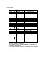
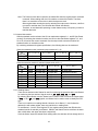
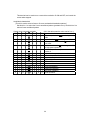
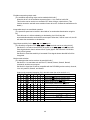
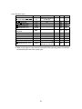
2-1. Address lines
Relationship between address lines (A1, A0) and
A1 A0
L
L
L
L
L
L
L
L
H
H
H
H
L
L
L
L
L
L
L
L
H
H
H
H
L
L
H
H
L
L
H
H
L
H
L
H
L
H
L
H
,
, and
.
Detail
Data bus -> Command buffer
Data bus -> Register (bits 7 to 0: lower bit)
Data bus -> Register (bit 15 to 8: Medium bit)
Data bus -> Register (bit 23 to 16: Upper bit)
Data bus <- Status 0
Data bus <- Internal data (lower)
Data bus <- Internal data (medium)
Data bus <- Internal data (upper)
Writing
Reading
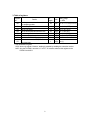
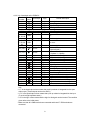
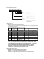
Relationship between address lines (A3, A2) and the axes controlled by a PCD4521/4541.
PCD4521
A2 setting A2=0
A2=1
A2, A3 setting
Selected axis X axis Y axis
Selected axis
PCD4541
A3=0,
A3=0,
A2=0
A2=1
X axis
Y axis
A3=1,
A2=0
Z axis
A3=1,
A2=1
U axis
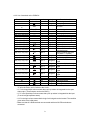
2-2. Command buffer
In order to operate this LSI, data is
written into the command buffer and
each data register through the 8-bit
data bus.
Commands can be classified into four
groups, and the upper 2 bits in each
command are used to specify the
group. Each command is latched until
the same group command is written a
second time. Each bit in a command
represents a specific function.
Functions do not have individual
commands.
D5
D4 D3 D2 D1 D0
D7
D6
C1
C0
C1
C0
Command group
0
0
1
1
0
1
0
1
Start mode
Control mode
Select register
Output mode
2-3. Bit details for each command
1) Start mode command
2) Control mode command
D7 0
D7 0
D6 0
D6 1
D5
-> Enable/disable interrupt output while
D5
stopping.
D4
-> Select linear or S-curve acceleration and
deceleration
-> Start control
D4
-> Control the output of general purpose OTS
terminal
D3
-> Stop control
D3
-> Select the feed direction for output pulses
D2
-> Select operating mode: Constant speed or
D2
-> Enable/disable preset operation
acceleration/deceleration.
D1
-> Enable/disable external
D0
-> Select FL or FH speed
control
3) Register select command
D1
-> Enable/disable
D0
-> Enable/disable the
signal
signal
4) Output mode command
D7 1
D7 1
D6 0
D6 1
D5
-> Enable/disable external start interrupt signal
D5
D4
-> Enable/disable ramping-down point interrupt D4
-> Select between standard and extension
monitor modes
signal
D3
-> Set the sensitivity of the
,
, and
signals (noise filters)
-> Enable/disable preset counter
D3
-> Change to a constant speed in the middle
of an acceleration or deceleration
D2
Register selection (R0 to R7)
D1
D0
D2
-> Mask the excitation sequencing output
D1
-> Mask the pulse output
D0
-> Select the pulse output logic
(negative/positive (normal ON/OFF))
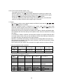
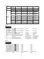
2-4. Table of registers
D2
D1
D0
Register
0
0
0
0
1
1
1
0
0
1
1
0
0
1
0
1
0
1
0
1
0
R0
R1
R2
R3
R4
R5
R6
1
1
1
R7
Details
Preset counter data
FL speed
FH speed
Rate of accel/decel
Magnification
Ramping-down point
Number of idling pulses
Environmental data
(PCD4541 only)
* D2, D1, and D0: Bits used to select the register
(R): Can be read by enabling the extension monitor
R/W
Bit length Setting range
R/W
W (R)
W (R)
W (R)
W (R)
W (R)
W (R)
24
13
13
10
10
16
3
0 to FFFFFF
1 to 1FFF
1 to 1FFF
2 to 3FF
2 to 3FF
0 to FFFF
0 to 7
W (R)
1
0 to (1)
3. Examples of operation settings
3-1. Command setting example
This LSI is operated by specifying one of 4 types of commands and by entering values for
registers R0 to R7.
1) Specify the control mode command details (64HEX) --- Preset operation, S-curve rate of
accel/decel, + direction, disable SD/ORG.
2) Specify the register select command details --- See the setting details in section 3-2
above.
3) Specify the output mode command details (D1HEX) --- Excitation sequencing output, pulse
output positive logic, enable filter.
4) Specify the start command details (15HEX) --- Start and accelerate at FL speed, and
operate at FH speed.
By specifying the start command, the LSI will start operation.
3-2. Example of setting a register
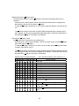
Example of an operating pattern
f [PPS]
10000
Feed = 50,000 pulses
1000
t
500 ms
500 ms
Initial speed (FL) = 1,000 PPS, operating speed (FH) = 10,000 PPS, accel/decel time = 500
mS, reference clock = 4.9152 MHz
1) Set the number of pulses as a preset amount (R0): Stop after outputting 50,000 pulses
R0 = 50,000
To write data into a register, first specify the register (R0) using the register select command
(80HEX). Then, write the data as three bytes in the following order: upper bits, middle bits,
and lower bits.
2) Set the multiplication of the output frequency (R4): Select 2x for the LSI outputs (10,000
PPS in this example).
Reference clock frequency [Hz]
4915200
R4 set value =
=
= 300
Magnification x 8192
2 x 8192
R4 = 300
3) Set the FL frequency (R1): Since the initial speed is set to 1,000 PPS in the 2x mode, R1
= 500.
4) Set the FH frequency (R2): Since the initial speed is set to 10,000 PPS in the 2x mode,
R2 = 5,000.
5) Set the accel/decel time constant (R3): Since S-curve accel/decel is selected with an
accel/decel time of 500 mS.
(Accel/decel time [Sec.]) x (Reference clock frequency [Hz])
R3 set value =
((R2 set value) - (R1 set value)) x 2
[S-curve rate of accel/decel]
R3 =
0.5 x 4915200
(5000 - 500) x 2
= 273.07
273
R3 =273
6) Set the number of pulses for the ramping-down point (R5):
By setting the ramping-down point register (R5) while in the preset operation mode, you
can specify the number of pulses remaining at which to start deceleration.
2
2
((R2 set value) - (R1 set value) ) x (R3 set value)
R5 set value [pulses] =
(R4 set value) x 8192
[S-curve accel/decel]
2
2
(5000 - 500 ) x 273
R5 =
= 2749.33 2750
300 x 8192
R5=2750
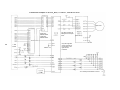
4. Connection example
Connection example using an ISA_BUS -> PCD4511 -> NP-7024(6) M
74LS245
SD0
SD1
SD2
SD3
SD4
SD5
SD6
SD7
A1
A2
A3
A4
A5
A6
A7
A8
74LS688
AEN
*G
SA2
SA3
SA4
SA5
SA6
SA7
SA8
SA9
P0
P1
P2
P3
P4
P5
P6
*P = Q
P7
ISA
BUS
+5 V
GND
GND
+5 V
+5 V
16 V
47 µF
GND
- IOR
B1
B2
B3
B4
B5
B6
B7
B8
VM
D0
D1
D2
D3
D4
D5
D6
D7
VSA
φ2
INB
VSB
φ3
INA
φ4
INB
+5 V
Turn OFF excitation by
making the
OTS output
HIGH.
PCD
4511
47
k-ohm
100 V
220 µF
GND
NP7024M
PM
(Unipolar)
TdA
TdB
OUTA
GA
OUTB
470 pF
OUTA
+5 V
5.1 k-ohm
Base address 0300H
Command buffer address
= 03000H
Data address (7 to 0)
= 0301H
Data address (15 to 8)
= 0302H
Data address (17 to 16)
= 0303H
CS
GND
+5 V
GND
2.4 k-ohm
820
ohm
F/H
GB
OUTB
(Unipolar constant current drive)
REFA
100
ohm
U/B
GND
REFB
(Max. 1 A)
RSA RSB
GND
2200 pF
2W 0.5 ohm
74LS244
WR
SA0
A0
SA1
A1
RST
RESET
+EL
-EL
+SD
-SD
74LS240
INT
CLOCK
4.9152 MHz
+5 V
GND
5.1 k-ohm
RD
-IOW
IRQx
INA
*G
DIR
Q0
Q1
Q2
Q3
Q4
Q5
Q6
Q7
φ1
ORG
STA
STP
74LS14
+EL
-EL
+SD
-SD
ORG
STA
STP
Connect to a normally closed switch or sensor
GND
User's Manual
for
A Sequencing LSI for Stepper Motors
PCD4511/4521/4541
Preface
Thank you for considering the use of our "PCD45X1 series."
Before using one of the PCD45X1 LSIs, read this manual carefully and become familiar with the
product.
The "Handling precautions" for mounting these ICs are in the last part of this manual.
Precautions
1) Transmission or copying of all or part of this manual is prohibited without prior written approval.
2) The specifications provided in this manual may be changed without prior notice to improve our
product's performance or quality.
3) This manual was created with the utmost care. However, if you have any questions, find
problems or believe important material is missing from the manual, please let us know.
4) NMP is not liable for any results of using this product, even if a problem or error has been
reported.
Description of the expressions and symbols used in this manual.
1. "x," "y," "z," and "u" on the terminal assignment drawings at the end of this manual or in
parenthesis ( ) in the terminal tables refer to the X axis, Y axis, Z axis, and U axis,
respectively.
, mean that the terminal uses negative
2. Terminals with a line above the terminal name, like
logic (normally ON).
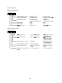
Table of contents
1. Outline and features ............................................................................................... 1
2. Specifications.......................................................................................................... 1
3. Table of registers .................................................................................................... 2
4. Hardware description.............................................................................................. 3
4-1. Circuit block diagram ......................................................................................................... 3
4-2. Terminal assignment diagrams........................................................................................... 4
4-2-1. Terminal assignment diagram for the PCD4511 ........................................................... 4
4-2-2. Terminal assignment diagram for the PCD4521........................................................... 5
4-2-3. Terminal assignment diagram for the PCD4541........................................................... 6
4-3. List of terminals ................................................................................................................. 7
4-3-1. List of terminals on the PCD4511 ................................................................................ 7
4-3-2. List of terminals on the PCD4521 ................................................................................ 8
4-3-3. List of terminals on the PCD4541 ................................................................................ 9
4-4. Description of each terminal ............................................................................................ 10
,
.................................................................................................................. 10
4-4-1.
,
................................................................................................................... 10
4-4-2.
......................................................................................................................... 10
4-4-3.
.......................................................................................................................... 10
4-4-4.
........................................................................................................................... 10
4-4-5.
,
...................................................................................................................11
4-4-6.
4-4-7. DQG ...................................................................................................11
4-4-8. /B .............................................................................................................................11
4-4-9. /H.............................................................................................................................11
4-4-10. OTS.........................................................................................................................11
.......................................................................................................................... 12
4-4-11.
4-4-12.
........................................................................................................................ 12
4-4-13. CLK ........................................................................................................................ 12
........................................................................................................................ 12
4-4-14.
........................................................................................................................... 12
4-4-15.
........................................................................................................................... 12
4-4-16.
......................................................................................................................... 13
4-4-17.
4-4-18. A0, A1, A2, and A3 ................................................................................................. 13
4-4-19. D0 to D7 ................................................................................................................. 13
4-4-20. VDD and GND ........................................................................................................ 13
4-4-21. NC [PCD4511 only] ................................................................................................. 13
4-5. Initial (reset ) status ......................................................................................................... 13
4-6. CPU interface circuit block diagram ................................................................................. 14
- - -
-
4-7. Precautions for designing hardware ................................................................................. 15
4-7-1. Input terminals .......................................................................................................... 15
4-7-2. Excitation sequencing ............................................................................................... 15
5. Programming Description .................................................................................... 16
5-1. Addresses ....................................................................................................................... 16
5-1-1. PCD4511 addresses ................................................................................................. 16
5-1-2. PCD4521 addresses ................................................................................................. 16
5-1-3. PCD4541 addresses ................................................................................................. 16
5-2. Read and write the data register ...................................................................................... 17
5-2-1. Write procedures....................................................................................................... 17
5-2-2. Read procedures ..................................................................................................... 17
5-3. Internal data monitor........................................................................................................ 18
5-3-1. Reading Status ......................................................................................................... 18
5-3-2. Reading the register, command, and speed data ....................................................... 19
5-4. Precautions when writing programs ................................................................................. 19
5-4-1. Read/write data......................................................................................................... 19
5-4-2. Data setting .............................................................................................................. 20
5-4-3. Preparation for starting.............................................................................................. 20
6. Description of functions ....................................................................................... 21
6-1. Excitation sequencing of stepper motors.......................................................................... 21
6-2. Speed pattern setting....................................................................................................... 22
6-2-1. Speed setting............................................................................................................ 22
6-2-2. Example of setting the acceleration/deceleration speed pattern ................................ 23
6-2-3. Setting the ramping-down point ................................................................................. 23
6-2-4. Example of setting a ramping-down point (S-curve accel/decel) ................................ 24
6-3. Operating mode............................................................................................................... 24
6-3-1. Continuous mode...................................................................................................... 25
6-3-2. Preset mode ............................................................................................................. 26
6-3-3. Zero return mode ...................................................................................................... 27
6-3-4. Timer mode............................................................................................................... 27
6-4. Control function ............................................................................................................... 28
6-4-1. Idling pulse output..................................................................................................... 28
6-4-2. External start signal .................................................................................................. 28
6-4-3. External stop control ................................................................................................. 29
6-4-4. Excitation sequence output mask .............................................................................. 29
6-4-5. Pulse output logic...................................................................................................... 29
6-4-6. External mechanical input control.............................................................................. 30
6-4-7. Interrupt signal output ............................................................................................... 31
6-5. Command buffer.............................................................................................................. 32
6-5-1. Start mode command................................................................................................ 32
6-5-2. Control mode command............................................................................................ 34
6-5-3. Register select command.......................................................................................... 37
6-5-4. Output mode command............................................................................................. 39
6-6. Registers......................................................................................................................... 41
6-6-1. R0 preset pulse counter (24 bits)............................................................................... 41
6-6-2. R1: FL speed register (13 bits) .................................................................................. 41
6-6-3. R2: FH speed register (13 bits).................................................................................. 41
6-6-4. R3: Accel/decel rate register (10 bits) ........................................................................ 42
6-6-5. R4: Magnification register (10 bits) ............................................................................ 42
6-6-6. R5: Ramping-down point register (16 bits)................................................................. 42
6-6-7. R6: Idling pulse register (3-bit) .................................................................................. 42
6-6-8. R7: Environmental data register (1-bit) ...................................................................... 43
6-7. Status.............................................................................................................................. 43
6-7-1. Status0 (address lines: A1 = 0, A0 = 0) ..................................................................... 44
6-7-2. Status1 (Address lines: A1 = 0, A0 = 1)..................................................................... 45
6-7-3. Status2 (Terminal: A1 = 1, A0 = 0)............................................................................. 45
6-7-4. Status3 (Terminal: A1 = 1, A0 = 1)............................................................................. 46
7. External dimensions ............................................................................................. 47
7-1. External dimensions of the PCD4511............................................................................... 47
7-2. External dimensions of the PCD4521............................................................................... 48
7-3. External dimensions of the PCD4541............................................................................... 49
8. Electrical characteristics ...................................................................................... 50
8-1. Absolute maximum rating ................................................................................................ 50
8-2. Recommended operation conditions ................................................................................ 50
8-3. DC characteristics (recommended operating conditions) .................................................. 50
8-4. Timing specifications........................................................................................................ 51
8-4-1. Reference clock ........................................................................................................ 51
8-4-2. Read cycle................................................................................................................ 51
8-4-3. Write cycle ................................................................................................................ 51
8-4-4. Reset cycle ............................................................................................................... 51
8-4-5. Operation timing ....................................................................................................... 52
8-5. Timing chart..................................................................................................................... 53
8-5-1. Standard clock .......................................................................................................... 53
8-5-2. Read cycle................................................................................................................ 53
8-5-3. Write cycle ................................................................................................................ 53
8-5-4. Reset cycle ............................................................................................................... 53
output timing (When
is set to negative logic)................................................ 54
8-5-5.
timing (When
is set to negative logic) ......................................................... 54
8-5-6.
excitation sequencing timing (When
is set to negative logic)....................... 54
8-5-7.
8-5-8. Bipolar 1-2 phase excitation sequence timing............................................................ 54
8-5-9. Preset counter data read timing................................................................................. 55
8-5-10. Register data, write timing....................................................................................... 55
8-5-11.
and accel/decel timing ..................................................................................... 55
is set to negative logic) ...................................................... 56
8-5-12. Start timing (When
8-5-13. External start timing ................................................................................................ 56
8-5-14. Acceleration start timing .......................................................................................... 56
8-5-15. Ramping-down point deceleration initiation timing ................................................... 57
is set to negative logic)................................................... 57
8-5-16. Stopping time (When
9. Handling precautions............................................................................................ 58
9-1. Design precautions ......................................................................................................... 58
9-2. Precautions for transporting and storing LSIs................................................................... 58
9-3. Precautions for installation............................................................................................... 58
9-4. Other precautions ............................................................................................................ 59
Appendix
List of commands ................................................................................................................... 60
List of registers ....................................................................................................................... 61
Monitor list.............................................................................................................................. 62
Connection examples ............................................................................................................. 64
Differences from the PCD4500 (first LSI in this series) ............................................................ 67
1. Outline and features
[Outline]
The PCD4511/4521/4541 are excitation control LSIs designed for 2-phase stepper motors.
With just one of these LSIs and a stepper motor driver IC (e.g. NP-7026), you can easily construct
a stepper motor control system.
Data and commands entered from a CPU enable this LSI to control the speed and position of a
stepper motor. Since the LSI has a pulse signal generation circuit, it can also control a motor
driver that relies on the number of pulses supplied.
[Features]
- Excitation sequencing output for a 2-phase stepper motor.
- Linear and S-curve acceleration/deceleration control.
- CW and CCW pulse output.
- External start and stop control
- Zero return operation
- Outputs idling pulses
- 400 KPPS maximum output frequency
- Available in single axis (PCD4511), 2-axis (PCD4521), and 4-axis (PCD4541) models.
2. Specifications
Item
Power source
Reference clock
Range of settable positioning pulses
Range of settable speeds
Recommended speed magnification
range*
Number of registers for setting the
speed
Ramping-down point setting range
Accel/decel rate setting range
Typical operations
Typical functions
Ambient operating temperature
Storage temperature
Package
Chip design
Description
+5V ±10%
4.9152 MHz standard (10 MHz max.)
0 to 16,777,215 pulses
1 to 8,191 steps
1x to 2x (Using a standard 4.9152 MHz clock)
When 1x: will deliver 1 to 8,191 PPS
When 2x: will deliver 2 to 16,382 PPS
Two (FL and FH)
0 to 65,535 pulses
2 to 1,023
- Continuous operation
- Preset operation (positioning)
- Zero return operation
- Timer operation
- Linear and S-curve acceleration/deceleration
- Immediate stop and decelerating stop
- Speed change
- Settable ramping-down point
- External start and stop function
- Idling pulse output function
- Excitation sequencing output for 2-phase stepper motors
[Phase signals for unipolar and bipolar motors]
[2-2 phase excitation, 1-2 phase excitation phase signals]
0 to +85°C
-40 to +125°C
PCD4511: 44-pin QFP
PCD4521: 64-pin QFP
PCD4541: 100-pin QFP
C-MOS
* This value is true when a stepper motor is used within the 24-bit preset counter range.
1
3. Table of registers
Register
No.
Bit
length
Details
R/W
Setting range
( ) = HEX
Set the preset counter value and check
24
R/W 0 to 16, 777, 215 (FFFFFF)
the remaining pulses
R1
Set the FL speed
13
W(R) 1 to 8, 191 (1FFF)
R2
Set the FH speed
13
W(R) 1 to 8, 191 (1FFF)
R3
Set the acceleration/deceleration rate
10
W(R) 2 to 1, 023 (3FF)
R4
Set the magnification rate
10
W(R) 2 to 1, 023 (3FF)
R5
Set the ramping-down point
16
W(R) 0 to 65, 535 (FFFF)
R6
Set the number of idling pulses
3
W(R) 0 to 7
Enter environmental data (PCD4541
R7
1
W(R) 0 to (1)
only) See Note
* R/W: Read/Write register
W(R): Write only register. However, reading is possible by enabling the extension monitor.
Note: Only the PCD4541 can write a "1" to R7. "0" must be written to this register on the
PCD4511 and 4521.
R0
2
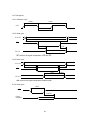
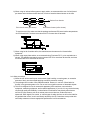
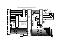
4. Hardware description
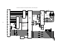
4-1. Circuit block diagram
CLK
Control clock
generation circuit
RD
Magnification
dividing circuit
Pulse output
control circuit
+PO
-PO
Variable dividing
circuit
R0 register
RST
CS
The block to
the right of
this dotted
line has the
same number
of axes as the
PCD. Accel/decel
control circuit
[linear/S-curve]
R1 register
CPU
I/F
WR
R2 register
R3 register
R4 register
R5 register
PCD4511: A0 to A1
PCD4521: A0 to A2
PCD4541: A0 to A3
D0 to D7
φ 1
4-phase excitation
sequence
generation circuit
φ 2
φ 3
φ 4
Preset counter (R0)
R6 register
Command buffer
U/B
Comparator
F/H
INT
INT output control
Ramping-down
point (R5)
OTS
+5 V
General-purpose
output control
VDD
GND
Idling pulse (R6)
+EL
GND
-EL
STA
Digital filter
+SD
Control circuit
STP
ORG
-SD
BSY
3
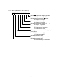
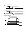
4-2. Terminal assignment diagrams
GND
29
28
27
26
25
24
VDD
F/H
30
VDD
φ 1
31
STA
φ 2
32
STP
φ 3
33
U/S
φ 4
4-2-1. Terminal assignment diagram for the PCD4511
23
OTS
34
22
NC
GND
35
21
NC
CLK
36
20
GND
RST
37
19
BSY
INT
38
18
+PO
VDD
39
17
VDD
CS
40
16
-PO
A1
41
15
ORG
A0
42
14
+EL
WR
43
13
-EL
RD
44
12
+SD
PCD4511
5
6
7
4
D1
D2
D3
D4
GND
D5
8
9
10
11
-SD
4
GND
3
D7
2
D6
1
D0
(Top View)
4-2-3. Terminal assignment diagram for the PCD4541
6
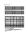
4-3. List of terminals
4-3-1. List of terminals on the PCD4511
Terminal Terminal
Input/output
Logic
General description
number
name
1 to 5
D0 to D4 Input/output Positive Data bus signal
6, 10, 20,
GND
0V
28, 35
7 to 9
D5 to D7 Input/output Positive Data bus signal
11
Input %
Negative Negative deceleration switch signal
12
Input %
Negative Positive deceleration switch signal
13
Input %
Negative Negative end limit switch signal
14
Input %
Negative Positive end limit switch signal
15
Input %
Negative Zero position limit switch signal
16
Output
Negative # Negative pulse
17, 23, 24,
VDD
+5V±10%
39
18
Output
Negative # Positive pulse
19
Output
Negative Running signal
21, 22
NC
Output
Test signal
25
Input %
Negative External start signal
26
Input %
Negative Forced stop signal
Select excitation method
27
/B
Input %
(unipolar/bipolar)
Select excitation sequence
29
/H
Input %
(2-2 phase / 1-2 phase)
30
Output
Positive 1st phase excitation signal
31
Output
Positive 2nd phase excitation signal
32
Output
Positive 3rd phase excitation signal
33
Output
Positive 4th phase excitation signal
34
OTS Output
Positive General-purpose output signal
36
CLK
Input
Reference clock
37
Input
Negative Reset signal
38
Output*
Negative Interrupt signal
40
Input
Negative Chip select signal
41, 42
A1, A0 Input
Positive Address signal
43
Input
Negative Write signal
44
Input
Negative Read signal
-
- A "*" in the input/output column means that a pull up resistor is integrated into the open
drain output. (These outputs can be wire ORed).
- A "%" in the input/output column means that a pull up resistor is integrated into the input.
(To avoid a high impedance state.)
- A "#" in the logic column means that the logic for this signal can be inverted. The condition
given refers to the initial status.
- Make sure that all 5 GND terminals are connected and that all 4 VDD terminals are
connected.
- Leave both NC terminals open.
7
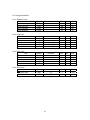
4-3-2. List of terminals on the PCD4521
Terminal Terminal
Input/output
number
name
1
Input
2
Output*
3
Input
4
Input
5
Input
6, 7, 8
A0 to A2 Input
9
D0
Input/output
10, 21, 32,
GND
42, 52, 62
11 to 14 D1 to D4 Input/output
15, 26, 27,
47, 58, 59,
VDD
64
16 to 18 D5 to D7 Input/output
Logic
Negative
Negative
Negative
Negative
Negative
Positive
Positive
General description
Reset signal
Interrupt signal
Chip select signal
Write signal
Read signal
Address signal
Data bus signal
0V
Positive
Data bus signal
+5V ±10%
Positive
Data bus signal
Select excitation method
19 (X), 40(Y)
/B
Input %
(unipolar/bipolar)
Select excitation sequence
20 (X), 41(Y)
/H Input %
(2-2 phase / 1-2 phase)
22 (X), 43(Y)
Output
Positive 1st phase excitation signal
23 (X), 44(Y)
Output
Positive 2nd phase excitation signal
24 (X), 45(Y)
Output
Positive 3rd phase excitation signal
25 (X), 46(Y)
Output
Positive 4th phase excitation signal
28 (X), 48(Y)
Output
Negative # Positive pulse
29 (X), 49(Y)
Output
Negative # Negative pulse
30 (X), 50(Y)
Output
Negative Running signal
31 (X), 51(Y) OTS Output
Positive General-purpose output signal
33 (X), 53(Y)
Input %
Negative External start signal
34 (X), 54(Y)
Input %
Negative Forced stop signal
35 (X), 55(Y)
Input %
Negative Zero position limit switch signal
36 (X), 56(Y)
Input %
Negative Positive end limit switch signal
37 (X), 57(Y)
Input %
Negative Negative end limit switch signal
38 (X), 60(Y)
Input %
Negative Positive deceleration switch signal
39 (X), 61(Y)
Input %
Negative Negative deceleration switch signal
63
CLK Input
Reference clock
- "X" in the terminal number column is the terminal number for the X axis, "Y" is for the Y
axis.
- A "*" in the input/output column means that a pull up resistor is integrated into the open
drain output. (These outputs can be wire ORed.)
- A "%" in the input/output column means that a pull up resistor is integrated into the input.
(To avoid a high impedance state.)
- A "#" in the logic column means that the logic for this signal can be inverted. The condition
given refers to the initial status.
- Make sure that all 6 GND terminals are connected and that all 7 VDD terminals are
connected.
-
8
4-3-3. List of terminals on the PCD4541
Terminal number
1, 2, 3, 4
5
6, 16, 41, 54, 67, 68, 91,
95
Terminal name Input/output
A0 to A3
Input
Output*
Logic
General description
Positive Address signal
Negative Interrupt signal
VDD
Data bus signal
0V
17(X), 35(Y), 62(Z), 82(U)
Output
Negative Running signal
18(X), 36(Y), 63(Z), 83 (U)
Output
Positive 1st phase excitation signal
19(X), 37(Y), 64(Z), 84(U)
Output
Positive 2nd phase excitation signal
20(X), 38(Y), 65(Z), 85(U)
Output
Positive 3rd phase excitation signal
21(X), 39(Y), 69(Z), 86(U)
Output
Positive 4th phase excitation signal
22(X), 42(Y), 70(Z), 87(U)
Output
Negative # Positive pulse
23(X), 43(Y), 71(Z), 88(U)
Output
Negative # Negative pulse
24(X), 44(Y), 72(Z), 89(U)
OTS
Output
Positive General-purpose output signal
Select excitation method
25(X), 45(Y), 73(Z), 96(U)
/B
Input %
(unipolar/bipolar)
Select excitation sequence
26(X), 46(Y), 74(Z), 97(U)
/H
Input %
(2-2 phase / 1-2 phase)
28(X), 47(Y), 55(Z), 75(U)
Input %
Negative External start signal
29(X), 48(Y), 56(Z), 76(U)
Input %
Negative Forced stop signal
Zero position limit switch
30(X), 49(Y), 57(Z), 77(U)
Input %
Negative
signal
31(X), 50(Y), 58(Z), 78(U)
Input %
Negative Positive end limit switch signal
Negative end limit switch
32(X), 51(Y), 59(Z), 79(U)
Input %
Negative
signal
Positive deceleration switch
33(X), 52(Y), 60(Z), 80(U)
Input %
Negative
signal
Negative deceleration switch
34(X), 53(Y), 61(Z), 81(U)
Input %
Negative
signal
92
CLK
Input
Reference clock
94
Input
Negative Reset signal
98
Input
Negative Chip select signal
99
Input
Negative Read signal
100
Input
Negative Write signal
- "X" in the terminal number column is the terminal number for the X axis, "Y" is for the Y axis,
"Z" is for the Z axis, and "U" refers to the U axis.
- A "*" in the input/output column means that a pull up resistor is integrated into the open
drain output. (These outputs can be wire ORed.)
- A "%" in the input/output column means that a pull up resistor is integrated into the input.
(To avoid a high impedance state.)
- A "#" in the logic column means that the logic for this signal can be inverted. The condition
given refers to the initial status.
- Make sure that all 6 GND terminals are connected and that all 8 VDD terminals are
connected.
7 to 14
15, 27, 40, 66, 90, 93
D0 to D7
GND
+5V ±10%
Input/output
-
9
Positive
4-4. Description of each terminal
4-4-1.
,
Input terminals for deceleration speed switch signals.
signal control is enabled in the control mode command, and when the
signal
When
with the same polarity as the current direction of rotation goes LOW while in high-speed
operation, the LSI will start to decelerate.
When the
signal goes HIGH again, the LSI will begin to accelerate again.
4-4-2.
,
Input terminals for the end limit switch signals.
signal which has the same polarity as the current direction of motor rotation
When the
goes LOW, the LSI will stop the motor immediately. The LSI will not restart the motor, even
when this signal goes HIGH again.
signal is already LOW and an attempt is made to start the motor rotating in that
If the
direction, the LSI will not let it start.
When pulse output control is set to "halt output (timer mode)" using the output mode
command, the
signal is disabled.
4-4-3.
Input terminal for the zero position switch signal.
signal control is enabled (zero position return operation) using the control mode
When
command, and when this signal goes LOW, the motor will stop immediately. Even if this
signal goes HIGH again, the LSI not start the motor.
signal is already LOW and an attempt is made to start the motor, the LSI will not
If the
let it start.
When pulse output control is selected "halt output (timer mode)" using the output mode
signal is disabled.
command, the
4-4-4.
Input terminal for the forced stop signal.
signal goes LOW, regardless of the rotation direction of the motor, the motor
When the
will stop immediately. Even if this signal goes HIGH again, the LSI will not start the motor.
signal is already LOW and an attempt is made to start the motor, the LSI will not
If the
let it start.
4-4-5.
Input terminal for external start signal.
When a start latch command is entered using the start mode command, the motor will start
signal transition from HIGH to LOW.
rotation on the leading edge of an
A signal shorter than 4 cycles of the reference clock is not accepted.
10
4-4-6.
,
Pulse output terminals.
When the rotation direction is set to positive using the control mode command, the LSI will
output pulses at a 50% duty cycle from
terminal. When the rotation direction is set to
negative using the control mode command, the LSI will output pulses at a 50% duty cycle
terminal.
from
The logic of the
and
terminals, and the ON/OFF control of pulse outputs, can be
changed using the output mode command.
- - - DQG -
Excitation signal output terminals for a stepper motor.
The switching of the excitation sequencing signals is synchronized with the output pulses.
Using the /H terminals, you can select between 1-2 phase and 2-2 phase excitation
sequencing.
Using the /B terminals, you can select between unipolar and bipolar excitation sequencing.
When pulse output control is set to "halt output (timer mode)" using the output mode
command, the excitation sequencing cannot be changed.
Using the output mode command, the excitation signal can be masked (to make all of the
WHUPLQDOV - WR /2:
4-4-8. /B
Terminal for selecting the excitation method.
Select unipolar excitation with a LOW or bipolar excitation sequencing with a HIGH on this
terminal. Connect to GND or VDD.
This terminal is latched when reset.
For details about the sequence for reading this terminal, see "6-1. Excitation sequencing for
stepper motors."
4-4-9. /H
Terminal for selecting the excitation sequence.
2-2 phase and 1-2 phase are typical excitation sequences for 2-phase stepper motors.
Select the sequence using this terminal.
Select 2-2 phase excitation with a LOW and 1-2 phase excitation sequencing with a HIGH.
Connect to GND or VDD.
For details about the sequence for reading this terminal, see "6-1. Excitation sequencing for
stepper motors."
4-4-10. OTS
General-purpose output terminal.
This terminal can be used as an excitation ON/OFF control signal for a motor driver IC. This
terminal can be controlled by a CPU. When bit 4 of the control mode command is "1" this
terminal is HIGH, when it is "0" the terminal is LOW.
11
4-4-11.
Output terminal for sending an interrupt request signal to a CPU.
This terminal will go LOW when the LSI requests an interrupt. Set this signal HIGH using
the interrupt condition setting command. This terminal can also be masked.
By setting the start mode command, the LSI can be set to output an
request signal
when stopping the motor. Using this terminal, you can call for an interrupt when the preset
operation is complete, or when operation is stopped by the
signal,
or
signal,
signal. An interrupt can also be requested by a deceleration stop or an
or the
immediate stop command.
request signal can be output when starting
Using the register select command, an
deceleration from the ramping-down point or from an external signal.
terminals of a number of chips can be wire ORed.
When using PCD series LSIs, the
Install an external pull up resistor (5 to 10 K ohms).
4-4-12.
Operation status monitor terminal.
When the LSI is in operation, the signal from this terminal goes LOW.
This terminal can be used to check the operation or to provide current to the motor and
force it to remain stopped.
4-4-13. CLK
Input terminal for the reference clock.
Reference clock precision affects the output pulse precision.
Besides affecting the output pulses, it also affects the input sensitivity of the start timing
,
,
and
signals, as well as read and write timing.
signal,
Make sure that only a CMOS level input is applied to the CLK terminal.
4-4-14.
Reset signal input terminal.
Bring this terminal LOW for 3 reference clock pulses to reset the LSI.
For details about the initial status after a reset, see "4-6. Initial status."
4-4-15.
Chip select signal input terminal
Bring this terminal LOW to enable
to the CPU.
4-4-16.
Read signal input terminal
Bring this terminal and the
on data bus lines D0 to D7.
and
signals, which will allow reading and writing
terminal LOW to output the contents of the specified register
12
4-4-17.
Write signal input terminal
terminal LOW to write the contents of data bus lines D0 to D7
Bring this terminal and the
into the LSI. The lines will be read when the
signal changes from LOW to HIGH.
4-4-18. A0, A1, A2, and A3
Address signal input terminals.
The LSI uses the A0 and A1 terminals to assign use of the data bus to the command buffer,
and to the upper, middle, and lower areas of register data.
On the PCD4521 and 4541, terminals A2 and A3 are used to select the axis to control.
Normally, this terminal is connected to the lowest bit on the CPU address bus.
4-4-19. D0 to D7
Input and output terminals for the tri-state data bus.
4-4-20. VDD and GND
Power supply terminals.
Supply +5VDC ±10% to the VDD terminals. Make sure to connect all of the power supply
terminals.
4-4-21. NC [PCD4511 only]
Output terminal for testing. Leave this terminal open.
4-5. Initial (reset) status
Item
Internal registers (R0 to R6)
Start mode command
Control mode command
Register select command
Output mode command
INT terminal
Terminals D0 to D7
ø 1, ø 2, ø 3, and ø 4 [ /B terminal = when L]
ø 1, ø 2, ø 3, and ø 4 [ /B terminal = when H]
terminal
terminal
OTS terminal
13
Initial (reset) status
All zeros
00 HEX
40 HEX
80 HEX
C0 HEX
H
High impedance
H, L, L, H
H, L, L, L
H
H
L
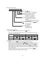
4-6. CPU interface circuit block diagram
PCD4511
(PCD4521)
[PCD4541]
1) Z80 interface
Z80
A2 to A7
(A3 to A7)
[A4 to A7]
Decode
circuit
4.9152 MHz
CLK
CS
A0 to A1
(A0 to A2)
[A0 to A3]
A0 to A1
(A0 to A2)
[A0 to A3]
RD
RD
IORQ
WR
WR
D0 to D7
D0 to D7
INT
INT
RESET
RESET
System reset
2) 6809 interface
PCD4511
(PCD4521)
[PCD4541]
6809
A2 to A15
(A3 to A15)
[A4 to A15]
Decode
circuit
A0 to A1
(A0 to A2)
[A0 to A3]
E
4.9152 MHz
CLK
CS
A0 to A1
(A0 to A2)
[A0 to A3]
RD
WR
R/W
D0 to D7
D0 to D7
IRQ
INT
RESET
RESET
System reset
14
4-7. Precautions for designing hardware
4-7-1. Input terminals
Only the CLK terminal requires a CMOS level input. Be careful when connecting this
terminal.
(For reset operations, the internal processing may require up to three reference clock
cycles. When imposing a LOW on the
terminal make sure it lasts more than 3
reference clock cycles.)
If you want to wire-OR the
terminal or input the switch signal terminals with open
collectors, we recommend installing a pull up resistor.
,
,
,
,
, and
terminals on the PCD4511 have pull-up resistors
(The
built in. However these are for preventing a high impedance condition. Since their
resistance values are high [25 K to 500 K ohm], we recommend installing external pull-up
resistors [5-K to 10-K ohms].)
For safe operation, we recommend using a multiple-layer PC board with a separate power
layer.
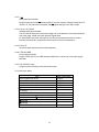
4-7-2. Excitation sequencing
The description of the excitation sequence required by a particular bipolar 1-2 phase
stepper motor driver IC may be different.
(This LSI's excitation sequence is designed for our NP-7024M (7026M) unipolar driver IC,
and our NP-2918 bipolar driver IC. These are common excitation sequences. However,
bipolar excitation sequence requirements may vary with different driver IC manufacturers.
Driver ICs which can use the following excitation sequence may be used. In this case,
contact the driver IC manufacturer to verify the suitability of our excitation sequence.)
Ex.1
1-2 phase excitation for bipolar drivers
STEP ->
0
1
2
3
4
5
6
A
DISABLE A
B
DISABLE B
H
L
L
L
H
L
L
H
H
L
H
L
L
H
H
L
L
L
H
L
L
L
L
H
L
L
L
L
7
0
L
H
L
L
H
L
L
L
7
0
H
H
L
L
H
L
L
L
Ex. 2
STEP ->
A
DISABLE A
B
DISABLE B
1-2 phase excitation for bipolar drivers
0
1
2
3
4
5
6
H
L
L
L
H
L
H
H
H
L
H
L
H
H
H
L
L
L
H
L
L
L
H
H
L
L
L
L
In the two examples above, the LSI can be operated by connecting terminals ø 1 to A, ø 2
to B, ø 3 to DISABLE A, and ø 4 to DISABLE B.
15
5. Programming Description
5-1. Addresses
5-1-1. PCD4511 addresses
Shown below is the relationship between address lines A1, A0 and control lines
,
.
Details
A1 A0
L
H
L
L
L Data bus -> Command buffer
L
H
L
L
H Data bus -> Register (bits7 to 0: Lower)
Writing
L
H
L
H
L Data bus -> Register (bits15 to 8: Middle)
L
H
L
H
H Data bus -> Register (bits23 to 16: Upper)
L
L
H
L
L Data bus <- Status0
L
L
H
L
H Data bus <- Internal data (Lower)
Reading
L
L
H
H
L Data bus <- Internal data (Middle)
L
L
H
H
H Data bus <- Internal data (Upper)
L
L
L
X
X Prohibited
H
X
X
X
X Data bus = High impedance
, and
5-1-2. PCD4521 addresses
Specify the axis using address line A2, and select the control data using address lines A1, A0
and control lines
,
, and
. The relationship between address lines A1, A0 and control
lines
,
, and
are the same as in the PCD4511.
A2 setting
A2 = 0
A2 = 1
Selected axis
X axis
Y axis
Details
A1 A0
Same as for the PCD4511.
5-1-3. PCD4541 addresses
Specify the axis using address lines A3, A2, and select the control data using address lines
A1, A0, and control lines
,
, and
. The relationship between address lines A1, A0
and control lines
,
, and
are the same as in the PCD4511.
A3, A2 setting A3 = 0, A2 = 0 A3 = 0, A2 = 1 A3 = 1, A2 = 0 A3 = 1, A2 = 1
Selected axis
X axis
Y axis
Z axis
U axis
Details
A1 A0
Same as for the PCD4511.
16
5-2. Read and write the data register
5-2-1. Write procedures
To specify a register, use the register select command.
The LSI interprets the data written on address lines (A1 = 0, A0 = 0) as a command. It also
interprets "10XXXXXX BIN" as a register select command.
1) To write data, enter the register number using the
register select command.
Put the register select command
in the command address.
2) Write the upper byte (bits 23 to 16) of the data to
the upper address (A1 = 1, A0 =1) of the register.
Write the upper data byte to
the upper address.
3) Write the middle byte (bits 15 to 8) of the data to the
middle address (A1 = 1, A0 =0) of the register.
Write the middle data byte to
the middle address.
4) Write the lower byte (bits 7 to 0) of the data to the
lower address (A1 = 0, A0 =1) of the register.
Write the lower data byte to
the lower address.
5) Since the LSI will be processing the data internally,
do not write any other command or data for a period
of two reference clock cycles (approx. 400 ns when
CLK = 4.9152 MHz)
5-2-2. Read procedures (Example: Read the number of pulses remaining in R0 [Preset counter])
The PCD4511/4521/4541 can read the data in any register. Select a register and read the
data the same way that data is written to that register.
1) Enter R0 as the register you want using the
register select command.
2) Since the LSI will process the command
internally, wait at least 1.5 reference clock
cycles (approx. 300 ns when CLK = 4.9152
MHz)
3) Read the upper data byte (bits 23 to 16) from
the upper register address (A1 = 1, A0 =1).
Write R0 and the select
command to the command
address.
No restriction on
the read order.
Read the upper data byte
from the upper address.
4) Read the middle data byte (bits 15 to 8) from
the middle register address (A1 = 1, A0 =0).
Read the middle data byte
from the middle address.
5) Read the lower data byte (bits 7 to 0) from the
lower register address (A1 = 0, A0 =1).
Read the lower data byte
from the lower address.
17
Note: The Preset counter data is copied to the read buffer when the register select command
is entered. When reading data, the LSI reads the contents of this buffer. Therefore,
there is no restriction on the order in which the bytes are read.
Other register data can also be read by selecting the output mode. However, a buffer is
not used to read that data. The LSI reads the internal data directly.
Therefore, to read data while operating or when data accuracy is required, you have to
read the data twice.
5-3. Internal data monitor
With the standard monitor selected, the LSI can read status registers 0, 1, and R0 [the Preset
counter]. By selecting the extension monitor, the LSI can also read Status registers 2, 3, and
R1 to R6, as well as the current command. Use the output mode command to select the
standard monitor or extension monitor.
By combining address and register specifications, the following data can be monitored.
When the standard monitor is selected (output mode: bit 5 = 0)
Address
Register
R0
R1 to R7
A1 = 0, A0 = 0
Status0
Status0
A1 = 0, A0 = 1
R0 lower data
Status1
A1 = 1, A0 = 0
R0 middle data
0
A1 = 1, A0 = 0
R0 upper data
0
When the extension monitor is selected (output mode: bit 5 = 1)
Address A1 = 0,
A1 = 0, A0 = 1
A1 = 1, A0 = 0
A1 = 1, A0 = 1
A0 = 0
Register
R0
Status0
R0 lower data R0 middle data
R0 upper data
R1
Status0
R1 lower data R1 upper data
Start mode command
R2
Status0
R2 lower data R2 upper data
Control mode command
R3
Status0
R3 lower data R3 upper data
Register select command
R4
Status0
R4 lower data R4 upper data
Output mode command
R5
Status0
R5 lower data R5 upper data
R7 data
R6
Status0
R6 data
Speed lower data Speed upper data
R7
Status0
Status1
Status2
Status3
5-3-1. Reading Status
There are two status modes: Status0 is used for monitoring the operation status, and Status1
for monitoring the input status of signals such as
,
,
,
, and
.
By selecting the extension monitor, Status2 can be read in order to monitor the output status
of
, ø1 to 4,
, and
signals, and Status3 can be read in order to identify the PCD
type.
There is no restriction on reading Status0. However, since Status1, 2, and 3 share the
address line with a data register, there are restrictions on reading them.
To read Status1, 2, and 3, select register R7 (any register setting other than R0 when the
standard monitor is selected), and Status1, Status2, and Status3 can be read from the lower
data, middle data, and upper data bytes, respectively.
Since the Status' bytes are latched when reading starts, the data bus will not change while in
18
the reading cycle.
5-3-2. Reading the register, command, and speed data
In addition to the status registers, the LSI can read register, command, and speed data.
When the standard monitor is selected, only register R0 can be read. However, when the
extension monitor is selected, registers R1 to R6 can also be read.
When the extension monitor is selected, the start command, control mode command, register
select command, output mode command and the current speed data can all be read.
Please note that when register R3 is selected, the LSI will read the register select command
from address lines A1 =1 and A0 =1, as shown in the lower part of the table in section 5-3
above. In other words, to read the register select command, you have to select register R3.
Therefore, use this function only to check bits other than the register select bits.
However, the start control bit shows the internal status of the LSI, not the status of the
command you write. Therefore when reading the LSI status using the start mode command,
the start control bit will be "1" when running and it will change to "0" when the motor is
stopped.
Since the LSI reads the internal data directly when reading the speed data, rounding up or
down may occur while reading the middle and lower bytes. In this case, check the data by
reading it twice.
5-4. Precautions when writing programs
5-4-1. Read/write data
[To write data to a register, write the lower data last.]
The upper and middle data bytes for a register are latched into a write buffer and transferred
to the appropriate internal locations according to the write timing for the lower data byte.
Therefore, write the lower data byte for the register (bits 7 to 0) last.
[To read the value in the preset counter, select R0 first.]
The value in the preset counter (number of pulses remaining) is latched into the read buffer
according to the timing when the register select command is written. Therefore, you have to
write the R0 register select command each time you want to read the value, even if you will
be reading the value repeatedly.
There is no restriction on the read order of the upper, middle, and lower data bytes.
[To read the value in the preset counter, allow 1.5 reference clock cycles of time for internal
processing. To write data to the register, allow 2 reference clock cycles of time for internal
processing.]
To read the preset counter value, allow 1.5 reference clock cycles of time for internal
processing after writing the register select command. Do not read any data during this period.
To write register data, allow 2 reference clock cycles of time for internal processing after
writing the lower register data. Do not write any data during this period.
19
5-4-2. Data setting
[Even if a register is not used, set the register data within the specified range.]
When the motor is stopped instantly using an immediate stop command or the
,
, or
signals, the motor will turn at FL speed until the last pulse is used after the stop signal is
input.
For this reason, when the motor is running at FH speed and stopped instantly, the LSI will
apply the FL speed until the balance of remaining pulses has been used. If the FL speed is
not yet set, the motor will simply stop, leaving a number of pulses unused.
As such, if a value outside the allowable range is specified, it may cause a problem.
Therefore, we recommend that you enter appropriate values for all currently unused
registers. For details about the allowable range of each register, see "3. Table of registers."
[Enter data with the correct number of bits]
The last data written will remain in the write buffer until new data is written. Enter data with
the correct number of bits, in order to prevent incorrect setting of the registers.
5-4-3. Preparation for starting
[Write the start mode command as the last command.]
When the start mode command is given, the LSI will trigger rotation of the motor. Therefore,
only write the start mode command at the end of a setup sequence.
[Do not set bits 1, 3 and 4 to "1" at the same time in the start mode command.]
Turning ON ("1") the Start Control, Stop Control, and External Start Control bits in the start
mode command at the same time will keep the operation from starting on reception of the
next start command. Never set more than one of bits 1, 3, and 4 to "1" at the same time.
20
6. Description of functions
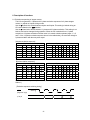
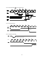
6-1. Excitation sequencing of stepper motors
This LSI can generate 1-2 phase and 2-2 phase excitation sequences for 2-phase stepper
motors, in unipolar or bipolar driving modes.
Use the /B terminal to switch between unipolar and bipolar. This setting is latched during an
LSI reset initiated on the
terminal.
Use the /H terminal to switch between 1-2 phase and 2-2-phase excitation. This setting is not
latched, and can be changed during operation. When the LSI is switched from 1-2 phase
excitation to 2-2 phase excitation while the motor is in certain excitation phases (steps 1, 3, 5,
and 7 of the 1-2 phase excitation sequence shown in the table below), the motor will change to
2-phase excitation with the next pulse output.
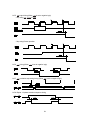
[Unipolar excitation sequence]
2-2 phase excitation
Step ->
0
1
2
3
0
1ø
H
H
L
L
H
2ø
L
H
H
L
L
3ø
L
L
H
H
L
4ø
H
L
L
H
H
ø-Z
H
L
L
L
H
Negative <- Rotation direction -> Positive
1-2 phase excitation
Step ->
0 1 2 3 4 5 6 7
1ø
H H H L L L L L
2ø
L L H H H L L L
3ø
L L L L H H H L
4ø
H L L L L L H H
ø-Z
H L L L L L L L
Negative <- Rotation direction -> Positive
0
H
L
L
H
H
[Bipolar excitation sequence]
2-2 phase excitation
1-2 phase excitation
Step ->
0
1
2
3
0
Step ->
0 1 2 3 4 5 6 7 0
1ø
H
H
L
L
H
1ø
H H H H L L L L H
2ø
L
H
H
L
L
2ø
L L H H H H L L L
3ø
L
L
L
L
L
3ø
L L L H L L L H L
4ø
L
L
L
L
L
4ø
L H L L L H L L L
ø-Z
ø-Z
H
L
L
L
H
H L L L L L L L H
Negative <- Rotation direction -> Positive
Negative <- Rotation direction -> Positive
ø - Z = Excitation zero position (This is the sequence when initialized. It can be read out from
Status1.)
[Excitation sequence switching timing]
±PO
(Negative logic)
Start
φ1 to φ4
21
6-2. Speed pattern setting
6-2-1. Speed setting
Constant speed operation and high-speed operation (linear and S-curve acceleration
/deceleration) can be specified. To specify a speed pattern, use R1, R2, R4, and R3 (when
high-speed operation is used).
To change between constant speed and high speed, use bit 2 of the start mode command.
To change between linear and S-curve acceleration/deceleration, use bit 5 of the control
mode command.
1) R1: FL speed setting register
This register is used to specify the speed for constant speed operation and the start speed
for high-speed operation. The allowable range is 1 to 8,191 (1FFF HEX). The speed will
be the product resulting from multiplying this value by the magnification rate specified in
R4.
FL speed [PPS] = (Value specified in R1) x Magnification rate
2) R2: FH speed setting register
This register is used to specify the speed for constant speed operation and the operating
speed for high-speed operation. For high-speed operation, specify a value that is larger
than the value in R1. The allowable range is 1 to 8,191 (1FFF HEX). The speed will be the
product resulting from multiplying this value by the magnification rate specified in R4.
FH speed [PPS] = (Value specified in R2) x Magnification rate
3) R3: Acceleration/deceleration rate register
This register is used to specify the acceleration/deceleration characteristics when highspeed operation is selected. The allowable range is 2 to 1,023 (3FF HEX). When the
value for R3 is the same and a linear acceleration/deceleration is performed, the linear
acceleration/deceleration speed will be equal to the maximum acceleration speed set for
S-curve acceleration/deceleration.
[Linear accel/decel]
Accel/decel time [Sec.] =
((Value specified in R2) - (Value specified in R1)) x (Value specified in R3)
Reference clock frequency [Hz]
[S-curve accel/decel]
Accel/decel time [Sec.] =
((Value specified in R2) - (Value specified in R1)) x (Value specified in R3) x2
Reference clock frequency [Hz]
4) R4: Magnification rate register
This register is used to specify the relationship between the values set in R1 and R2, in
order to set the final speed. The allowable range is 2 to 1,023 (3FF HEX). The higher the
22
magnification setting, the less accurate the speed units will be. Normally, use as small a
setting as possible. The relationship between the value selected and the magnification
rate is as follows.
Magnification =
Reference clock frequency [Hz]
(Value specified in R4) x 8192
(When reference clock = 4.9152 MHz) (Output speed unit: PPS)
Magnification Output speed
Magnification
Value in R4
Value in R4
rate
rate
range
600 (258 HEX)
1
1 to 8,191
60 (3C HEX)
10
300 (12C HEX)
2
2 to 16, 382 30 (1E HEX)
20
120 (78 HEX)
5
5 to 40,955 12 (0C HEX)
50
Output speed
range
10 to 81,910
20 to 163,820
50 to 409,550
6-2-2. Example of setting the acceleration/deceleration speed pattern (S-curve accel/decel)
When the initial speed is 1,000 PPS, the operation speed is 10,000 PPS, the accel/decel time
is 500 ms, and the reference clock is 4.9152 MHz, the value to use in R3 will be as follows.
1) The magnification rate used in order to output 10,000 PPS is 2x, and R4 will equal 300
(12C HEX)
2) In order to set the initial speed to 1,000 PPS in the 2x mode, R1 must equal 500 (1F4
HEX)
3) In order to set the operation speed to 10,000 PPS in the 2x mode, R2 must equal 5,000
(1388 HEX)
4) Calculate the value to use for R3 from the desired accel/decel time,
Modify the calculation of the accel/decel time, and substitute the value,
Value specified in R3
=
R3 =
(Accel/decel time [Sec.] x (Reference clock frequency [Hz])
((Value specified in R2) - (Value specified in R1)) x 2
0.5 x 4915200
(5000 - 500) x 2
= 273.07
273
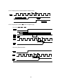
f [PPS]
10000
Feed = 50,000 pulses
1000
t
500 ms
500 ms
23
6-2-3. Setting the ramping-down point
By entering a ramping-down point in the R5 register, the motor will automatically decelerate
while operating in the preset or high-speed modes.
To specify this point, enter the number of remaining pulses which will trigger the deceleration.
The motor will start deceleration when the contents of the Preset counter are equal to R5.
The allowable range is 0 to 65,535 (FFFF HEX). The following formula can be used to
calculate the ramping-down point.
[Linear accel/decel]
Value specified in R5 [pulses] =
2
2
((Value specified in R2) - (Value specified in R1) ) x (Value specified in R3)
(Value specified in R4) x 16384
[S-curve accel/decel]
Value specified in R5 [pulses] =
2
2
((Value specified in R2) - (Value specified in R1) ) x (Value specified in R3)
(Value specified in R4) x 8192
[Speed pattern using a ramping-down point]
f
1) When the ramping-down point is
reached while accelerating.
2) When the ramping-down point is
reached after acceleration has been
completed.
A) Too small a value for R5.
2
1
A
B
t
6-2-4. Example of setting a ramping-down point (S-curve accel/decel)
Select preset and high-speed operation with an initial speed of 1,000 PPS, an operation
speed of 10,000 PPS, and an accel/decel rate in R3 of 273. Then the value of R5 will be as
follows.
1) The magnification rate used in order to output 10,000 PPS is 2x, and R4 is set to 300 (12C
HEX)
2) In order to make the initial speed 1,000 PPS in the 2x mode, R1 must equal 500 (1F4
HEX)
3) In order to make the operation speed 10,000 PPS in the 2x mode, R2 must equal 5,000
(1388 HEX)
4) Enter 273 for the accel/decel rate in R3 (from paragraph 6-1-2)
5) Obtain the value to use for R5 in the conditions stated above as follows.
Enter the values in steps 1 to 4 in the ramping-down point formula,
2
R5 =
2
(5000 - 500 ) x 273
300 x8192
= 2749.33
24
2749
6-3. Operating mode
In any operating mode, the motor will stop when an
signal or
signal of the same
polarity as the direction of rotation turns ON. When high speed is selected and the
signal
is enabled, the motor will decelerate when an
signal of the same polarity as the direction
of rotation turns ON
The examples below use the following terms.
RGDT_H = Register upper byte address
RGDT_M = Register middle byte address
RGDT_L = Register lower byte address
COM_DT = Command buffer address
6-3-1. Continuous mode
This mode is used to keep a motor turning after it is started with a start command. The motor
will keep turning until a stop command is received. Specify the direction of rotation using bit 3
in the control mode command.
To use this mode, set bit 2 (preset operation control) in the control mode command to "0".
The preset counter will start counting pulses when the motor is started.
1) Constant speed continuous operation
When you want to drive a motor at FL (FH) speed using a pattern, as shown below, use
the following procedure.
f
FL
(FH)
COM_DT <- 40 HEX
COM_DT <- 10 HEX
Stop command
t
Control mode command (positive direction, continuous operation)
[To rotate in the opposite direction, use 48 HEX.]
Start command (FL constant speed start)
[Use 11 HEX when you want to start at an FH constant speed.]
To stop the motor, use an immediate stop command (08 HEX).
COM_DT <- 08 HEX
Start command (Immediate stop)
2) Continuous high speed operation
When you want to drive a motor at FH speed using a pattern, as shown below, use the
following procedure.
The motor will start at FL speed and
accelerate to FH speed.
It will decelerate when a deceleration stop
command is received, and stop when it
reaches FL speed.
COM_DT <- 40 HEX
Control mode command (positive direction, continuous
operation)
25
COM_DT <- 15 HEX
[To rotate in the opposite direction, use 48 HEX.]
Start command (FH high speed start)
To stop the motor, use a deceleration stop command (1D HEX).
COM_DT <- 1D HEX
Start command (deceleration stop)
6-3-2. Preset mode
This mode is used to position the motor by assigning a specific number of pulses and a
direction of rotation.
Specify the number of output pulses in the R0 preset counter. Then, start the motor. The
motor will stop when the value in the preset counter reaches zero. Specify the direction of
rotation in bit 3 in the control mode command.
The LSI will enter this mode when bit 2 in the control mode command is set to "1" (preset
operation control). The preset counter decrements its contents (the number of pulses
remaining). Therefore, specify a value for R0 for each positioning operation.
If R0 is set to 0, the motor will not start, even when a start command is given. However, if the
signal is set to change state when the motor stops, an
signal will be output even
though the motor has done nothing.
1) High speed preset operation
To output a specific number of pulses at FH speed, follow the procedure below. We'll use
a feed amount of 5,000 pulses (1388 HEX).
Start in FL speed and accelerate to FH speed.
Decelerates at the ramping-down point and
stops.
COM_DT <- 44 HEX Control mode command (positive direction, preset operation)
[To rotate in the opposite direction, use 4C HEX.]
COM_DT <- 80 HEX Register select command (Select R0)
RGDT_H <- 0 HEX Preset data upper byte
RGDT_M <- 13 HEX Preset data middle byte
RGDT_L <- 88 HEX Preset data lower byte
**********
<- Specify an R5 value, too.
COM_DT <- 15 HEX Start command (FH high speed start)
To wait for completion of the preset operation, check bit 3 of Status0.
COM_DT -> READ Read Status0 (check bit 3)
Bit 3 = 0: Stopped, 1: Running
26
6-3-3. Zero return mode
After starting the motor, when the zero position signal
turns ON, the motor will stop. Set
the direction of rotation using bit 3 in the control mode command. This can be used together
with the preset operation.
By placing a "1" in bit 0 (
signal control) of the control mode command, the LSI will enter
this mode. The preset counter will count down from the starting value. By using the
signal, the motor can execute a smooth zero return operation.
If the
terminal is LOW, the motor will not start, even if a start command is given.
However, if the
signal is set to change state when the motor stops, the
signal will be
output even though the motor has done nothing.
1) High speed zero return operation
To have the motor execute a zero return at FH speed, use the procedure below.
f
FH
FL
t
SD input OFF
ON
OFF
ORG input
ON
COM_DT <- 43 HEX Control mode command (positive direction, enable
control)
[Use 4B HEX to rotate in the other direction.]
COM_DT <- 15 HEX Start command (FH high speed)
and
signal
To wait for completion of the zero return, check bit 3 in Status0, the same as for the preset
operation.
COM_DT -> READ
Write Status0 (check bit 3)
Bit 3 = 0: Stopped1: Running
6-3-4. Timer mode
Using the preset operation (
signal when stopped) and pulse output control, this LSI can
be used as a timer.
Stop the output of pulses and change the excitation signal using pulse output control. Specify
a number of pulses in the preset counter R0. Then, start the LSI at constant speed using the
preset operation. When the preset counter value reaches zero, the LSI will stop sending
pulses and generate an interrupt signal.
(Specified time) = (Specified speed) x (Number of pulses specified)
Set bit 2 (preset operation control) in the control mode command to "1," and bit 1 (pulse
output control) in the output mode command to "1". Then the LSI will enter this mode.
While in this mode, the LSI can be stopped by turning ON the
signal, or by giving a stop
command. Please note that even if the
signal or
signal is turned ON, the LSI will not
27
stop outputting pulses.
1) Timer operation
To use the LSI as a 100ms timer, do the following.
Specify an FL speed of 1,000 PPS. A control time of 100ms is achieved by outputting 100
pulses at 1,000 PPS.
COM_DT <- 44 HEX
COM_DT <- 0C2 HEX
COM_DT <- 80 HEX
RGDT_H <- 0 HEX
RGDT_M <- 0 HEX
RGDT_L <- 64 HEX
COM_DT <- 30 HEX
Control mode command (preset operation)
Output mode command (pulse output stop)
R0 register select command
Preset data upper byte (100 = 64 HEX)
Preset data middle byte
Preset data lower byte
Start command (FL start, output
when stopped)
When an interrupt signal is input, the timer will time out (after 100 mS).
6-4. Control function
6-4-1. Idling pulse output
When the motor is started at FH high speed, the motor will accelerate right after starting. The
idling pulse function enables the acceleration to start only after outputting some pulses at FL
speed. If this function is not used, the speed calculated from the initial output pulse cycle will
be higher than the FL speed, and the motor will not start automatically, even if the FL speed
is set to approximately the auto start frequency.
To solve this problem, the LSI will start acceleration at the FL speed you set after 1 to 7
pulses. Then the motor will start automatically at nearly the auto start frequency. The pulses
output at this FL speed are referred to as "idling pulses."
The allowable range is from 0 to 7, and this mode is available in high speed operation. When
this is set to 0, the motor will start as normal.
For 2 idling pulses.
±PO
Start
Accelerating
Acceleration start timing
When the number of idling pulses is set to 0.
±PO
Start
Accelerating
Acceleration start timing
6-4-2. External start signal
This LSI can be started using an external signal. Using this function, multiple axes can be
started simultaneously.
Delay the start command and when the LSI sees the leading edge of a LOW on the
28
terminal, it will invoke the start command and the motor will start.
To delay the start command, make bit 1 of the start command "1." To end the delay, the
immediate stop command can also be used.
The LSI cannot detect a
signal shorter than 4 reference clock cycles.
While in the delayed start signal mode, if an
or
direction signal is input, the LSI will
store the stop condition, and the LSI will not start operation, even if a
signal is given
again. By inputting these signals, the delayed start command is also cancelled and the motor
will not start until the next start command is given.
By inputting an
or
signal while in the delayed mode, and then inputting a
signal
(or giving a start command), the start control bit in the start command in the extension
monitor will change from "1" to "0."
[An example of a simultaneous start using an external circuit]
7404 etc.
STA
STA
STA
Start
6-4-3. External stop control
This LSI can be stopped instantly using an external signal. With this function, the motor can
be stopped in an emergency and multiple axes can be stopped simultaneously.
Bringing the
terminal LOW will stop the motor instantly.
While the
terminal is LOW, the motor will not start, even if a start command is given.
However, when the
output is enabled, the
signal will be output after a start command
is given.
The sensitivity of the
signal input can be selected using bit 4 in the output mode
command.
[Example of connections for a simultaneous stop using an external signal]
7404 etc.
STP
STP
STP
Stop
6-4-4. Excitation sequence output mask
Outputs from ø1 to ø 4 can be masked (make all of these outputs LOW).
Set bit 2 in the output mode command to "1", to enable masking.
This function is useful for turning OFF the excitation sequence when driving a unipolar
system. (Some motor driving ICs cannot use a loss of excitation to control the motor. Contact
the IC manufacturer.)
6-4-5. Pulse output logic
The pulse output logic of the
terminal can be selected.
Specify the logic using bit 0 in the output mode command.
29
6-4-6. External mechanical input control
The following five signals can be used as mechanical position detection signals.
(-)
(+)
Table
-EL
ORG
-SD
+SD
+EL
1)
,
signal
When an
ON (LOW) signal with the same polarity as the motor direction is received,
the motor will stop instantly. Even if the signal then goes back to HIGH, the motor will
remain stopped. By enabling the
signal, an
signal will be output when the
signal goes LOW.
When this signal is ON, the motor cannot be started in the same direction as the polarity
of this signal, even if a start command is given. However, if the
output is set to signal
when stopped, an
signal will be output.
When the output mode command pulse output control feature is used to stop the output of
pulses, the
signal is disabled. However, you can monitor the operation status using
Status1.
The input sensitivity of this signal can be selected using bit 4 in the output mode
command. When low sensitivity is selected, the LSI will not accept pulse signals less than
4 reference clock cycles long (approx. 800 nS with a 4.9152 MHz clock). When high
sensitivity is selected, the LSI will detect pulse signals shorter than 800 nS. The input
sensitivity setting is shared by the
,
, and
signals.
2)
,
signal
When
signal control is enabled using the control mode command, and if an
signal
of the same polarity as the motor rotation is turned ON in high speed operation, the motor
will start decelerating. If the
signal goes OFF, the motor will accelerate again.
When the
signal is enabled, giving a high speed start command while the
signal is
ON, the motor will not accelerate. It will operate at FL speed. When the
signal
changes while decelerating, the
signal will be ignored.
Regardless of whether or not
signal control is enabled in the control mode command,
the LSI operating status can be monitored using Status1.
3)
signal
When
signal control is enabled (zero return operation) using the control mode
command, and the
signal is turned ON the motor will stop instantly. After that, if the
signal goes OFF, the motor will remain stopped. By enabling the
signal when
stopped, an
signal will be output when the
signal is turned ON.
If this signal is ON, the motor cannot be started even if a start command is given.
However, if the
output is set to output when stopped, an
signal will still be output
30
when the
signal is turned ON.
Regardless of whether or not
signal control is enabled in the control mode
command, the LSI operating status can be monitored using Status1.
If pulse output is blocked by the pulse output control bit in the output mode command, the
signal is disabled. However, you can monitor the operating status using Status1.
The input sensitivity of this signal can also selected, the same as the
signal.
6-4-7. Interrupt signal output
This LSI can output an
signal when stopped, when the ramping-down point is reached, or
when an external start signal is received.
To output an interrupt signal when stopped, use bit 5 in the start mode command.
To output an interrupt signal when the ramping-down point is reached, use bit 4 in the register
select command.
To output an interrupt signal when an external start signal is received, assign bit 5 in the
register select command.
By setting the interrupt control bit to "1," an
signal will be output for each situation that is
selected. To reset the
signal, place a "0" in the respective bit. When you want to mask
without using the
signal, you should also set this bit to "0."
The
terminal output is a logical OR of the stopped, ramping-down point, and external start
conditions. To determine which condition caused the
signal to be output, check Status0.
When using more than one LSI, each of the
terminals can be connected in a wire OR
configuration. However, in this case, connect an external pull up resistor (5K to 10K ohms).
1) How to use the
signal with a ramping-down point
The LSI will output an
signal when the ramping-down point is reached as follows: The
preset counter (PC) value is compared to the ramping-down point value in register R5.
When PC 5 WKH /6, ZLOO RXWSXW an
signal. In addition, when the LSI is operating in
preset, high speed operation, the LSI will start deceleration of the motor when PC 5
Therefore, the interrupt generated when the ramping-down point is reached can be used
as a comparator of the remaining pulses when the motor is in preset operation at a
constant speed.
Another way to use this feature is when you want a positioning operation that will exceed
the maximum value (24 bit) allowed for the PC value. Enter the remainder into R0 (after
subtracting the maximum value for the PC), and set R5 to "0" to select continuous
operation. Then, after the interrupt has occurred, and when PC 6WDWXV FKDQJH WR
preset operation. This makes it possible to control positions that exceed the maximum
value allowed.
31
6-5. Command buffer
In order to operate this LSI, you must write data
into the command buffer and each of the registers
through an 8-bit data bus.
There are four command groups, which are
invoked by setting the upper two bits of the byte.
A command buffer is used to latch the command
details until another command in the same group
is written.
Since each command has individual functions
identified by the individual bits, settings other than
the examples shown to the right are also possible.
When a start command is written into the
command buffer, the LSI will start its operation.
Therefore, the start mode command should be the
last command given. There is no other restriction
on the order in which commands can be written.
D7 D6 D5 D4 D3 D2 D1 D0
C1 C0
C1 C0
0
0
1
1
0
1
0
1
Command group
Start mode
Control mode
Select register
Output mode
6-5-1. Start mode command
D7 D6 D5 D4 D3 D2 D1 D0
0
0
Speed selection: 0= FL speed, 1= FH speed
External start control:
0 = Does not inhibit a start
1 = Inhibit the start
Speed mode:
0 = Constant speed, 1 = High
speed
Stop control:
0= OFF, 1 = ON
Start
0= OFF, 1 = ON
___ control:
INT output when stopped
0 = Interrupt is not output (
reset)
1 = Interrupt is output
Speed selection
[Select the operation speed by setting this bit.]
When this bit is 0, the value in register R1 (FL speed setting) is used as the operation speed.
When this bit is set to 1, the value in register R2 (FH speed setting) is used as the operation
speed.
External start control
[By setting this bit, the operation start can be inhibited.]
When a start command is written to the command buffer with this bit set to 1, the LSI will
32
terminal changes to LOW, the inhibit is released, and
remain stopped. Then, when the
the LSI will start operation. When a start command is written to the command buffer with this
bit set to 0, the LSI will start operation immediately.
Speed mode
[The speed mode is selected by setting this bit.]
Setting this bit to 0 will operate a stepper motor at a constant speed. The LSI operates at a
constant speed according to the speed set with the speed selection bit (bit 0).
When the constant speed mode is selected, the
signals and the ramping-down point
setting in R5 are ignored.
Setting this bit to 1 will enable accel/decel speed control (in high-speed operation).
When this mode is selected, the
signals, the idling pulse setting in R6 and the rampingdown point setting, all made using preset operations, will be enabled. This mode is used
when the motor will be operated at a speed higher than the start speed.
Start/stop control
[Set these bits to control starting and stopping.]
Set the start control bit to 1 to start operation, and set the stop bit to 1 to stop the operation.
By combining both bits, you can invoke a deceleration stop.
When read with a monitor, the start control bit will change to 0 when stopping.
output when stopped
[Setting this bit to 1 will output an
signal when the operation is stopped.]
Setting this bit to 1 will output an
signal when the motor is stopped in a preset operation,
or when it is stopped using
,
, and
signals or a stop command.
To reset the
signal, set this bit to 0. To mask the
signal, leave this bit set to 0.
The
terminal output is the result of logically ORing this signal with the interrupt signal for
the ramping-down point, and the interrupt signal when started externally, and the interrupt
signal for starting from an external signal. To determine which source has caused the
signal to be output, check Status0.
[Start command/stop command]
When using the start mode command, a command to start operation is referred to as a start
command and a command to stop operation is referred to as a stop command.
[Constant operation/high speed operation (constant speed start/high speed start)]
- Constant speed operation (constant speed start)
Starting with the speed mode bit set to 0 is referred to as a constant speed start.
- High speed operation (high speed start)
Starting with the speed mode bit set to 1 is referred to as a high-speed start.
33
Start mode command examples
(X's in the table mean the value can be 0 or 1)
Operation details
D7 D6 D5 D4 D3 D2 D1 D0 HEX
0 0 0 1 0 0 0 0 10 FL constant speed start (No
output when
stopped)
Operate at FL speed (speed specified in R1).
When starting, change to the FL speed immediately.
0 0 1 1 0 0 0 0 30 FL constant speed start (Output an
when
stopped)
0 0 0 1 0 0 1 0 12 Inhibit the FL constant speed start (no
output
when stopped)
0 0 1 1 0 0 1 0 32 Inhibit the FL constant speed start (Output an
when stopped)
0 0 0 1 0 0 0 1
11 FH constant speed start
Operate at FH speed (speed given in R2).
When starting, change to the FH speed immediately.
0 0 0 1 0 0 1 1 13 Inhibit the FL constant speed start
0 0 0 1 0 1 0 1 15 FH high speed start
Operate from FL speed to the FH speed.
When operating, accelerate to the FH speed.
0 0 0 1 0 1 1 1 17 Inhibit the FH high speed start.
0 0 0 1 0 1 0 0 14 Decelerate during operation
Decelerate from the FH speed to the FL speed.
0 0 0 1 1 1 0 1 1D Deceleration stop (No
output when stopped)
Decelerate from the FH speed to the FL speed and
then stop.
0 0 1 1 1 1 0 1 3D Deceleration stop (Output an
when stopped)
0 0 0 0 1 0 0 0 08 Immediate stop (No
output when stopped)
0 0 1 0 1 0 0 0 28 Immediate stop (Output an
when stopped)
0 0 X 1 1 X 1 X
Prohibited setting
6-5-2. Control mode command
D7 D6 D5 D4 D3 D2 D1 D0
0
1
signal: 0 = Disabled, 1 = Enabled
signal: 0 = Disabled, 1 = Enabled
Preset operation: 0 = Disabled, 1 = Enabled
Operation direction: 0 = Positive, 1 = Negative
OTS control: 0 = Make the OTS terminal LOW,
1 = Make the OTS terminal HIGH
Accel/decel characteristic: 0 = Linear,
1 = S-curve
[Continuous operation/preset operation/zero return operation]
- Continuous operation
Operation when the preset stop control bit is set to 0.
34
- Preset operation
Operation when the preset stop control bit is set to 1.
- Zero return operation
Operation when the
signal control bit is set to 1.
signal control
[This bit is used to enable or disable stopping with the
signal.]
When this bit is 1 and the
terminal is brought LOW while in operation, the output
pulses are stopped immediately. Use this control for zero return operation.
When this bit is 0, the clock will continue to supply pulses, even if the
terminal is
brought LOW. The setting of this bit does not affect the LSI status.
signal control
[This bit is used to enable or disable deceleration that can be triggered by the
signal.]
When this bit is 1 and the
terminal with the same polarity as the rotation direction is
brought LOW while in FH high speed operation, the output pulses will decelerate and then
operation will continue at FL speed as long as the
terminal remains LOW.
This is used to reduce mechanical shock when stopping in a zero return operation or when
using
signals.
When this bit is 0, the LSI will continue FH high-speed operation and will not decelerate,
even if
terminals go LOW.
The setting of this bit does not affect the LSI status.
Preset operation
[The setting on this bit is used to enable or disable a stop caused by the preset counter (24-bit)
value (previously set in register R1) dropping to 0.]
Set this bit to 1, enter a value into the preset counter, and start operation. The preset counter
will decrement by one with each pulse that is output and the LSI will stop operation when the
counter reaches 0.
Set this bit to 0, and the operation will not stop even when the preset counter reaches 0.
Operation will not stop until an
,
,
signal or a stop command is input.
Operation direction
[The setting of this bit controls the direction of the output pulses.]
When this bit is 1, the LSI will output pulses from the
terminal, and the excitation signal
will change to positive.
When this bit is 0, the LSI will output pulses from the
terminal, and the excitation signal
will change to negative.
The setting of this bit affects the direction of the
and
terminals.
OTS control
[This bit is used to control a general purpose OTS output.]
When this bit is 1, the OTS terminal will be HIGH. When it is 0, the OTS terminal will be
LOW.
35
This terminal can be used to turn a motor driver excitation IC ON and OFF, and control the
current when stopped.
Accel/decel characteristic
[This bit is used to select a linear or S-curve acceleration/deceleration pattern.]
Set this bit to 1 to select the S-curve accel/decel pattern (quadratic curve). Set this bit to 0 to
select a linear accel/decel pattern.
Control mode command examples
D7 D6 D5 D4 D3 D2
0
1
X
X
X
X
D1
X
D0
0
0
0
1
1
X
X
X
X
X
X
X
X
X
0
1
X
0
1
X
X
X
X
1
X
0
1
X
X
X
0
X
X
0
0
0
0
0
0
0
0
0
0
1
1
1
1
1
1
1
1
1
1
X
X
X
X
X
0
1
X
X
X
X
X
X
0
1
X
X
X
X
X
X
0
1
X
X
X
X
X
X
X
1
X
X
X
X
X
X
0
0
1
X
X
X
X
X
X
X
0
X
0
X
X
X
X
X
X
X
0
1
0
(X's in the table mean the value can be 0 or 1)
Operation details
Will not stop when the
terminal goes
LOW.
Stops when the
terminal goes LOW.
Does not decelerate when the
terminal
goes LOW.
Decelerates when the
terminal goes LOW.
(In high speed operation.)
Does not stop when the preset counter
reaches 0.
Stops when the preset counter reaches 0.
Runs in the positive direction.
Runs in the negative direction
OTS is LOW.
OTS is HIGH.
Linear accel/decel.
S-curve accel/decel.
Continuous operation.
Zero return operation.
Preset operation.
36
6-5-3. Register select command
D7 D6 D5 D4 D3 D2 D1 D0
1
0
Register select Nos. 0 to 6
Preset counter operation control
0: Counts output pulses
1: Does not count.
Ramping-down point
output control
0:
is not output (
reset)
1:
is output
___
INT output control when external start is
enabled
0:
is not output (
reset)
1:
is output
Register select No.
[Select the register to control by setting these bits.]
To write or read data in registers R0 to R6, the target register must be specified first by using
the register select command.
Specify the target register using bits D2, D1, and D0.
D2 D1 D0 R
R/W Detail
Bit length Setting range
No.
0
0
0
R0 R/W Preset counter data
24
0 to 16,777,215 (FFFFFF)
0
0
1
R1 W (R) Set FL speed
13
1 to 8,191 (1FFF)
0
1
0
R2 W (R) Set FH speed
13
1 to 8, 191 (1FFF)
0
1
1
R3 W (R) Accel/decel rate
10
2 to 1, 023 (3FF)
1
0
0
R4 W (R) Set magnification
10
2 to 1, 023 (3FF)
1
0
1
R5 W (R) Set ramping-down
16
0 to 65, 535 (FFFF)
point
1
1
0
R6 W (R) Set idling pulse
3
0 to 7
1
1
1
R7 W (R) Set preference data
1
0 to (1)
(PCD4541 only)
* R/W: Read/Write register
W(R): Write only register. However, it can be read using the extension monitor setting.
To read the preset counter value, first specify R0, and then read the data. By reading the
select command, the buffer data available for reading is refreshed. To read data
continuously, you have to write an R0 select command, for each read operation.
To write to R0 to R6, write the lower byte data (bits 0 to 7) last.
Preset counter operation control
[Setting this bit controls the operation of the preset counter.]
When this bit is 1, the preset counter will stop counting.
When this bit is 0, the preset counter will decrement by one for each pulse output.
37
Ramping-down point
output control
[This bit controls whether or not the
signal is output when the ramping-down point is
reached.]
When this bit is 1 and the preset counter value becomes smaller than the ramping-down
point setting in R5, the LSI will output an
signal.
To reset the
signal, set this bit to 0. If you want to mask this operation, leave this bit set
to 0.
The
terminal output is the result of logically ORing this signal with the interrupt signal
when stopped, and the interrupt signal when started externally. To determine which source
has caused the
signal to be output, check Status0.
External start
output control
[An
signal can be output during an external start.]
When this bit is 1 and the start is inhibited, if the LSI is started using an external
signal,
the LSI will output an
signal.
To reset the
signal, set this bit to 0. When you do not want use this
signal and want
to mask it, leave this bit set to 0.
The
terminal output is the result of logically ORing this signal with the interrupt signal for
the ramping-down point, and the interrupt signal when stopped. To determine which source
has caused the
signal to be output, check Status0.
Register select command examples
(X's in the table mean the value can be 0 or 1).
D7 D6 D5 D4 D3 D2 D1 D0
Operation details
1 0 X X X 0 0 0 Selects R0.
1 0 X X X 0 0 1 Selects R1.
1 0 X X X 0 1 0 Selects R2.
1 0 X X X 0 1 1 Selects R3.
1 0 X X X 1 0 0 Selects R4.
1 0 X X X 1 0 1 Selects R5.
1 0 X X X 1 1 0 Selects R6.
1 0 X X X 1 1 1 Selects R7.
1 0 X X 0 X X X Count pulses using the preset counter.
1 0 X X 1 X X X Stop counting pulses.
1 0 X 0 X X X X Do not output an
signal at the ramping-down
point.
1 0 X 1 X X X X Output an
signal at the ramping-down point.
1 0 0 X X X X X Do not output an
signal when started by an
external signal.
1 0 1 X X X X X Output an
signal when started by an external
signal.
38
6-5-4. Output mode command
D7 D6 D5 D4 D3 D2 D1 D0
1
1
Logic setting
output:
0 = Negative logic, 1 = Positive logic
Pulse output: 0 = Outputs, 1 = No output
Excitation sequencing output mask:
0 = Outputs ø 1 to ø 4 signals.
1 = Mask ø 1 to ø 4 signals.
Intermediate stop accel/decel operation
0 = Enable accel/decel operation
(continuous)
1 = Disable accel/decel operation (change
to constant speed)
Signal input sensitivity setting for
,
, and
.
0 = High sensitivity
1 = Low sensitivity
Monitor mode selection
0 = Standard monitor
1 = Extension monitor
Logic setting for the
output
[By setting this bit, you can change output logic on the
terminal.]
Set this bit to 1 to select positive logic. Set this bit to 0 to select negative logic. For pulse
output patterns, see the table below.
0: Negative logic
1: Positive logic
Direction
(+)
(-)
H
H
L
L
Pulse output
[The pulse output from the
terminal is enabled or disabled with this bit.]
When this bit is 1 no pulse will be output on the
terminals, no changes will occur in the
excitation signal, and stops triggered by the
and
signal inputs will be disabled.
Other operations are not affected. Since the LSI can be configured to output an
signal
when stopped while in constant speed preset operation, and the
signal will be output
after a set time (preset number of pulses divided by the output pulse speed) has elapsed, it
can be used as a timer.
When this bit is 0 the LSI is in normal operation and pulses are output on the
lines.
The setting of this bit does not affect the status of the LSI.
39
Excitation sequencing output mask
[The excitation sequencing output can be masked with this bit.]
When this bit is 1 all the excitation sequences from ø 1 to ø 4 will be held LOW.
This function can be used to turn excitation OFF when driving a unipolar driver. (This
function cannot be used with some models of motor driver ICs. Contact the manufacturer for
details.)
Intermediate stop in an accel/decel operation
[The operation speed can be locked in the middle of an acceleration/deceleration using this
bit.]
If this bit is set to 1 while accelerating or decelerating, the LSI will stop the
acceleration/deceleration and hold the current speed. After that, if this bit is set to 0, the LSI
will restart the acceleration or deceleration.
Signal input sensitivity for the
,
, and
signals
[The sensitivity to signals on the
,
, and
terminals can be set using this bit.]
Set this bit to 1 to reduce the sensitivity to signals on the
,
, and
terminals.
Pulse signals shorter than 4 reference clock cycles (approx. 800 nS with a 4.9152 MHz
clock) will be ignored.
Set this bit to 0 and the sensitivity is increased. Pulse signals shorter than 800 nS will be
recognized.
Monitor mode selection
[The data types that can be read can be set with this bit.]
Set this bit to 1 to read data such as R0 to R7, Status0, Status1, Status2, Status3,
commands, and the current speed.
Set this bit to 0 and the LSI will be compatible with the PCD4500 (previous series). As such,
it can only read R0, Status0, and Status1.
Output mode command examples (X's in the table mean the value can be 0 or 1).
D7 D6 D5 D4 D3 D2 D1 D0
Operation details
1
1
X
X
X
X
X
0 Makes the
lines use negative logic.
1
1
X
X
X
X
X
1 Makes the
lines use positive logic.
1
1
X
X
X
X
0
X Outputs pulses on the
lines.
1
1
X
X
X
X
1
X Do not output pulses on the
lines.
1
1
X
X
X
0
X
X Output excitation signals from ø 1 to ø 4.
1
1
X
X
X
1
X
X Mask excitation signals from ø 1 to ø 4.
1
1
X
X
0
X
X
X Acceleration/deceleration enabled.
1
1
X
X
1
X
X
X Stop acceleration/deceleration in mid-stream.
1
1
X
0
X
X
X
X High sensitivity to
,
, and
signals.
1
1
X
1
X
X
X
X Low sensitivity to
,
, and
signals.
1
1
0
X
X
X
X
X Standard monitor setting.
1
1
1
X
X
X
X
X Extension monitor setting.
40
6-6. Registers
To write data into registers R0 to R7, first select the target register using the register select
command. Write the lower byte of data last. For details about the settings for each register to
achieve a certain speed, see "6-2. Speed pattern setting."
6-6-1. R0 preset pulse counter (24 bits)
This LSI has an internal preset countdown counter. By entering a number of pulses, this
preset counter will begin counting down from that point.
The preset counter decrements by one for one pulse output in the continuous, zero return,
and preset operations. However, if the preset counter operation mode is inhibited by the
output mode command, the preset counter will not count down.
The counter value (number of remaining pulses) can be read while in operation or while
stopped. To read the value, first select R0. The register select timing latches the data into a
24-bit read buffer.
In preset operation, the LSI places a number of positioning pulses in this register, and then
starts the operation. Once the LSI has started, the counter value is decremented with each
pulse that is output. When the number of pulses that have been output is equal to the value
originally entered in the preset counter, the value in the counter will be zero and the LSI will
stop operation.
The allowable range is 0 to 16,777,215 (FFFFFF HEX).
If you enter 0 in the preset counter and write the start command, the LSI will not use the
preset operation. The operation flag in Status0 and the
output signal would both
immediately indicate that the LSI had stopped. When
output is enabled, the LSI will
output an
signal.
If you stop the preset operation using the stop command or an external signal, the number of
remaining pulses will be saved in the preset counter. By entering a new start command, the
LSI will continue to output all of the remaining pulses.
After the preset number of pulses has been output, the value in the preset counter will be 0.
If you want to restart the operation using the same number of pulses, you will have to put the
value in R0 again.
6-6-2. R1: FL speed register (13 bits)
This register is used to set the FL speed. To operate at high speed, the LSI will start with the
FL speed and then accelerate to the FH speed. When a deceleration stop command is
entered while in high-speed operation, the LSI will decelerate. When the speed drops to the
FL speed, the operation will stop.
If the FL speed is set to 0, the
is latched LOW when stopped and the motor may not
actually stop. Make sure to set the FL speed to a number greater than 1.
The allowable range is 1 to 8,191 (1FFF HEX).
The relationship between the value entered and the output pulse speed varies with the value
placed in R4 (magnification).
6-6-3. R2: FH speed register (13 bits)
41
This register is used to set the FH speed.
The allowable range is 1 to 8,191 (1FFF HEX).
The relationship between the value entered and the output pulse speed varies with the value
placed in R4 (magnification).
6-6-4. R3: Accel/decel rate register (10 bits)
This register is used to select the acceleration and deceleration characteristics.
When the LSI executes a high-speed start, the motor starts at the FL speed entered in R1,
and accelerates to the FH speed entered in R2.
Then, the motor decelerates to the FL speed when an
signal is received, the rampingdown point is reached, or a deceleration command is received. Specify the acceleration and
deceleration characteristics for these operating patterns using the accel/decel rate setting
register. The acceleration rate of the linear accel/decel is equal to the maximum acceleration
rate of the S-curve acceleration/deceleration pattern.
The allowable range is: 2 to 1,023 (3FF HEX)
6-6-5. R4: Magnification register (10 bits)
The speed setting registers R1 and R2 can have values from 1 to 8,191. The relationship
between the values entered and the output pulse speed can be set using this magnification
register.
The allowable range is 2 to 1,023 (3FF HEX).
The shorter this value, the higher the output clock speed.
6-6-6. R5: Ramping-down point register (16 bits)
While in preset, high-speed operation, the LSI compares the value in this register, R5, to the
value in the preset counter. When the value in R5 is larger than the preset counter value, the
LSI will start to decelerate.
If the value placed in R5 is smaller than the preset counter value and the LSI is programmed
for preset, high-speed operation, the motor will operate at FL speed and not accelerate.
The FL speed, FH speed, and the accel/decel rate determine the ramping-down point.
Entering inappropriate values may stop the output of pulses during deceleration, or cause
the LSI to operate longer at the FL speed after deceleration.
The allowable range is 0 to 65,535 (FFFF HEX)
6-6-7. R6: Idling pulse register (3-bit)
To operate at high speed, the motor is accelerated quickly after starting. Therefore, the
speed calculated from the output pulse frequency will be higher than the FL speed that is
set. If FL is set to a value lower than the self-start frequency, the motor will not start.
Therefore, in order to be able to start from near the self-start frequency, the acceleration
using the FL speed can be started from 1 to 7 pulses after the start command. The pulses
that the start is delayed by are referred to as idling pulses.
The allowable range is 0 to 7. This is effective in high-speed operation. Setting this register
to 0 will provide a normal start.
42
6-6-8. R7: Environmental data register (1-bit)
This register can only be set on the PCD4541.
When this register is 1, the
pulse output changes from outputting ±2 pulses to the
directory mode (pulse output plus direction signal output). In this mode, the LSI outputs
pulses on the
terminal and the direction signal on the
terminal.
The direction signal will go HIGH while turning in the positive direction, and LOW while
turning in the negative direction (when negative logic is selected).
6-7. Status
- Both Status0 (monitor current operation status) and Status1 (input status of
,
,
,
, and
signals) are available.
- When the extension monitor is selected for the monitor mode using the output mode
command, Status2 (monitor output status of the
, ø 1 to 4,
, and
signals) and
Status3 (identify the PCD series model) are also available.
- Status0 does not have any restrictions on reading. Since Status1, Status2, and Status3 share
their addresses with the lower data byte of the preset counter, there is a restriction on reading
from them.
To read Status1, Status2, or Status3, first select the R7 register (or a register other than R0 in
the normal monitor mode). Then you can read Status1 from the lower data byte, Status2 from
the middle data byte, and Status3 from the upper data byte.
- Status0 to 4 are latched while reading. The data bus will not change while in the read cycle.
- After operation has stopped, if the start mode command is read with the extension monitor,
the start control mode bit will be 0.
- When reading using the register select command, the register selection is limited to R3 only.
When the standard monitor is selected
Address
Register
R0
R1 to R7
A1 = 0, A0 = 0
Status0
Status0
A1 = 0, A0 = 1
R0 lower data
Status1
A1 = 1, A0 = 0
R0 middle data
0
A1 = 1, A0 = 1
R0 upper data
0
When the extension monitor is selected
Address
A1 = 0, A0 = 0 A1 = 0, A0 = 1 A1 = 1, A0 = 0
Register
R0
R1
R2
R3
Status0
Status0
Status0
Status0
R4
R5
R6
R7
Status0
Status0
Status0
Status0
R0 lower data
R1 lower data
R2 lower data
R3 lower data
R0 upper data
Start mode command
Control mode command
Register select
command
R4 lower data R4 upper data
Output mode command
R5 lower data R5 upper data
R7 data
R6 data
Speed lower data Speed upper data
Status1
Status2
Status3
43
R0 middle data
R1 upper data
R2 upper data
R3 upper data
A1 = 1, A0 = 1
6-7-1. Status0 (address lines: A1 = 0, A0 = 0)
D7 D6 D5 D4 D3 D2 D1 D0
Monitor
output when stopping operation
0: Output, 1: Not output
Monitor ramping-down point
output
0: Output, 1: Not output
Monitor external start
output
0: Output, 1: Not output
Monitor operation status (inverse of
)
0: Stopped, 1: Operating
Monitor preset counter 0 status
0: Preset counter is not zero,
1: Preset counter is zero
Monitor preset counter and R5 (ramping-down
point) status
0: Preset counter > R5,
1: Preset counter ^ R5
Monitor acceleration status
0: Not accelerating, 1: Accelerating
Monitor deceleration status
0: Not decelerating, 1: Decelerating
44
6-7-2. Status1 (Address lines: A1 = 0, A0 = 1)
D7 D6 D5 D4 D3 D2 D1 D0
The address line status is shown
in angle brackets < >
Monitor
terminal
0: OFF<HIGH> 1: ON<LOW>
Monitor
terminal
0: OFF<HIGH> 1: ON<LOW>
Monitor
terminal
0: OFF<HIGH> 1: ON<LOW>
Monitor
terminal
0: OFF<HIGH> 1: ON<LOW>
Monitor
terminal
0: OFF<HIGH> 1: ON<LOW>
Monitor
terminal
0: OFF<HIGH> 1: ON<LOW>
Monitor
terminal
0: OFF<HIGH> 1: ON<LOW>
Monitor excitation zero point (see the excitation
sequence)
0: Not at the excitation zero position, 1: At
the excitation zero position
6-7-3. Status2 (Terminal: A1 = 1, A0 = 0)
D7 D6 D5 D4 D3 D2 D1 D0
The address line status is shown
in angle brackets < >
Monitor ø 1 terminal
0: <LOW> 1: <HIGH>
Monitor ø 2 terminal
0: <LOW> 1: <HIGH>
Monitor ø 3 terminal
0: <LOW> 1: <HIGH>
Monitor ø 4 terminal
0: <LOW> 1: <HIGH>
Monitor
terminal
0: <LOW> 1: <HIGH>
Monitor
terminal
0: <LOW> 1: <HIGH>
Monitor OTS terminal
0: <LOW> 1: <HIGH>
Monitor interrupt (each axis)
0: No interrupt, 1: Interrupt occurred
45
6-7-4. Status3 (Terminal: A1 = 1, A0 = 1)
D7 D6 D5 D4 D3 D2 D1 D0
Always "0000."
Chip identification monitor
"0001": PCD4511
"0010": PCD4521
"0100": PCD4541
46
7. External dimensions
7-1. External dimensions of the PCD4511
3.05MAX
13.8±0.3
2.7±0.2 0.19±0.2
10.0±0.2
33
23
22
34
12
44
1
0.8±0.2
11
1.0TYP
0.35±0.1
0.8
0.16 M
Unit: mm
47
7-2. External dimensions of the PCD4521
23.8±0.3
20.0±0.2
51
33
52
32
20
64
1
19
1.0
0.35±0.1
0.20 M
to
1.0TYP
0.15
0.8±0.2
Unit: mm
48
7-3. External dimensions of the PCD4541
23.8±0.3
20.0±0.2
51
50
100
31
14.0±0.2
81
0.65
0.3±0.1
30
0.13 M
0.15
0.35MAX
1
0.19±0.1 2.7±0.2
0.575TYP
17.8±0.3
80
0.15 +0.1
-0.05
0.8±0.2
0 to 10º
Unit: mm
49
8. Electrical characteristics
8-1. Absolute maximum rating
Item
Power supply voltage
Input voltage
Current consumption
Storage temperature
8-2. Recommended operation conditions
Item
Power supply voltage
Ambient temperature
Logical LOW input voltage (1) (2)
Logical HIGH input voltage (1) (2)
(1) Inputs other than CLK
(2) CLK
Symbol
V DD
V IN
I IN
Tstg
Rating
-0.3 to +7.0
-0.3 to V DD +0.3
±10
-40 to +125
Unit
V
V
mA
°C
Symbol
V DD
Tj
V IL
V IH
Rating
4.5 to 5.5
0 to +85
(1) 0 to 0.8 (2) 0 to 1.0
(1) 2.2 to V DD (2) 4.0 to V DD
Unit
V
°C
V
V
8-3. DC characteristics (recommended operating conditions)
Item
Condition
Symbol
Current consumption (1)
PCD4511
I DD
PCD4521
PCD4541
V0 = V DD or
GND
Output current loss
I OZ
Input specification
Logical LOW input current
(2) (3)
Logical HIGH input current
(4)
Logical LOW output current
(5) (6) (7)
C IN
I IL
V IN= GND
I IH
V IN= V DD
I OL
V OL= 0.4 V
Logical HIGH output current
(5) (6)
Logical LOW output voltage
Logical LOW output voltage
Logical HIGH output voltage
Logical HIGH output voltage
Internal pull up resistance
I OH
V OH = 2.4 V
Min.
Typ
-10
Max.
17
34
65
10
7
(2) -10
(3) -200
-10
10
-10
10
(5) 8
(6)16
(7)16
Unit
mA
µA
pF
µA
µA
mA
(5) -8
(6) -16
0.05
0.4
mA
I OL = 1 µA
V
V OL
I OL = MAX
V
V OL
I OH = -1 µA
V DD-0.05
V
V OH
I OH = MAX
2.4
V
V OH
25
500
K
RU
1) Reference clock: 10 MHz, at 4,999,390 pps, output load = 85 pF.
2) D0 to D7, A0, A1, A2, A3,
,
,
, CLK
3)
,
,
,
,
, /B, /H,
4) D0 to D7, A0, A1,
,
,
,
,CLK,
,
,
,
,
, /B, /H
5) D0 to D7 and OTS,
,
, ø1, ø 2, ø 3, and ø 4 on the PCD4521and PCD4541.
6) OTS,
,
, ø 1, ø 2, ø 3, and ø 4 on the PCD4511
7)
50
8-4. Timing specifications
8-4-1. Reference clock
Item
Clock frequency
Clock duty cycle
Clock LOW time
Clock HIGH time
Symbol
f CLK
t CLK
t PWL
t PWH
Condition
Min.
Max.
10
Unit
MHz
nS
nS
nS
Symbol
t AR
t RA
t RR
t RD
t DF
Condition
Max.
Unit
nS
nS
nS
nS
nS
Symbol
t AW
t WA
t WW
t DW
t WD
Condition
Min.
0
0
14
14
0
Max.
Unit
nS
nS
nS
nS
nS
Symbol
t RST
t RSTM
Condition
(*1)
(*1)
Min.
3
Max.
Unit
t CLK
t CLK
100
50
50
8-4-2. Read cycle
Item
Address stabilization time
Address hold time
Read pulse width
Data delay time
Data float delay time
Min.
0
0
42
CL=85pF
CL=85pF
42
9
8-4-3. Write cycle
Item
Address stabilization time
Address hold time
Write pulse width
Data set time
Data hold time
8-4-4. Reset cycle
Item
pulse width
Reset operation time
51
3
8-4-5. Operation timing
Item
pulse width (
Symbol
,
)
/
delay time
Preset/
delay time
delay time H to L
delay time L to H
Phase excitation output
delay time
Bipolar ø 3, ø 4 delay time
Preset data read interval
Register data read interval
delay time H to L
delay time (1) L to H
t EL
t ELI
t PI
t PLD
t PHD
Condition
When high sensitivity
is selected
(*2)
Min.
1
-
9 !
9
t DRD
t DWR
t BSL
t BSEH
(*1)
(*1)
Max.
1.5
2
Unit
t CLK
20
20
30
21
nS
nS
nS
nS
8
nS
7
nS
t CLK
t CLK
nS
nS
31
When stopped by
26
When the preset
26
nS
delay time (2) L to H
t BSPH
operation is selected
*1: "tCLK" in the unit column means one cycle of the reference clock.
*2: When a stop signal or a stop command is supplied while outputting pulses, the operation
will terminate at the end of the current cycle.
52
8-5. Timing chart
8-5-1. Reference clock
t PWH
t CLK
CLK
t PWL
8-5-2. Read cycle
A1 to A3
t AR
t RR
t RA
RD*
t RD
t DF
VALID
D7 to 0
___
___
___
RD* refers to the logical multiplication of RD and CS .
8-5-3. Write cycle
A1 to A3
t AW
t WW
t WA
WR*
t DW
D7 to 0
___
___
___
WR* refers to the logical multiplication of WR and CS .
8-5-4. Reset cycle
t RST
RST
t RSTM
Reset
operation
53
t WD
8-5-5.
output timing (When
- Stop using
,
, or
is set to negative logic)
- Stop using Preset operation
8-5-6.
timing (When
is set to negative logic)
8-5-7.
excitation sequencing timing (When
is set to negative logic)
8-5-8. Bipolar 1-2 phase excitation sequence timing
54
8-5-9. Preset counter data read timing
WR
Writing a register select command (RO).
t DRD
RD
Reading the preset counter data.
8-5-10. Register data, write timing
WR
Writing the lower byte of register data.
t DWR
WR
Writing the command and data.
8-5-11.
and accel/decel timing
55
8-5-12. Start timing (When
is set to negative logic)
8-5-13. External start timing
1
2
3
4
1 2 3
CLK
STA
Start
BSY
8-5-14. Acceleration start timing
WR
Write a start command
1
2
3
1 2
3
CLK
BSY
Accelerating
56
8-5-15. Ramping-down point deceleration initiation timing
is set to negative logic)
8-5-16. Stopping time (When
- Stop using
,
, or
.
- Stop using Preset operation
57
9. Handling precautions
9-1. Design precautions
1) Never exceed the absolute maximum ratings, even for a very short time.
2) Take precautions against the influence of heat in the environment, and keep the temperature
around the LSI as cool as possible.
3) Please note that ignoring the following may result in latching up and may cause overheating and
smoke.
- Do not apply a voltage greater than VDD to the input/output terminals and do not pull them below
GND. Also, make sure you consider the input timing when power is applied.
- Be careful not to introduce external noise into the LSI.
- Hold the unused input terminals to VDD or GND level.
- Do not short-circuit the outputs.
- Protect the LSI from inductive pulses caused by electrical sources that generate large voltage
surges, and take appropriate precautions against static electricity.
4) Provide external circuit protection components so that overvoltages caused by noise, voltage
surges, or static electricity are not fed to the LSI.
9-2. Precautions for transporting and storing LSIs
1) Always handle LSIs carefully and keep them in their packages. Throwing or dropping LSIs may
damage them.
2) Do not store LSIs in a location exposed to water droplets or direct sunlight.
3) Do not store the LSI in a location where corrosive gases are present, or in excessively dusty
environments.
4) Store unused LSIs in an anti-static storage container, and make sure that no physical load is
placed on the LSIs.
9-3. Precautions for installation
1) In order to prevent damage caused by static electricity, pay attention to the following.
- Make sure to ground all equipment, tools, and jigs that are present at the work site.
- Ground the work desk surface using a conductive mat or similar apparatus (with an appropriate
resistance factor). However, do not allow work on a metal surface, which can cause a rapid
change in the electrical charge on the LSI (if the charged LSI touches the surface directly) due to
extremely low resistance.
- When picking up an LSI using a vacuum device, provide anti-static protection using a conductive
rubber pick up tip. Anything which contacts the leads should have as high a resistance as
possible.
- When using a pincer that may make contact with the LSI terminals, use an anti-static model. Do
not use a metal pincer, if possible.
- Store unused LSIs in a PC board storage box that is protected against static electricity, and
make sure there is adequate clearance between the LSIs. Never directly stack them on each
other, as it may cause friction that can develop an electrical charge.
2) Operators must wear wrist straps which are grounded through approximately 1M-ohm of
resistance.
3) Use low voltage soldering devices and make sure the tips are grounded.
4) Do not store or use LSIs, or a container filled with LSIs, near high-voltage electrical fields, such
those produced by a CRT.
5) To preheat LSIs for soldering, we recommend keeping them at a high temperature in a completely
dry environment, i.e. 125 °C for 20 hours.
58
6) When using an infrared reflow system to apply solder, we recommend the use of a far-infrared
pre-heater and mid-infrared reflow devices, in order to ease the thermal stress on the LSIs.
Product flow direction
Fai-infrared heater (pre-heater)
Midi-infrared heater (reflow heater)
To apply heat to LSIs, make sure that the package surface and PC board surface temperatures
do not exceed 240°C, and are never above 210°C for more than 30 seconds.
7) When using hot air for solder reflow, the restrictions are the same as for infrared reflow
equipment.
8) When using vapor phase solder, we recommend using Fluorinate FC-70, or its equivalent as a
solvent. The ambient temperature must not exceed 215°C for more than 30 seconds, and must
not exceed 200°C for more than 60 seconds.
9-4. Other precautions
1) When the LSI will be used in poor environments (high humidity, corrosive gases, or excessive
amounts of dust), we recommend applying a moisture prevention coating.
2) The package resin is made of fire-retardant material. However, it can burn. When baked or
burned, it may generate gases or fire. Do not use it near ignition sources or flammable objects.
3) This LSI is designed for use in commercial apparatus (office machines, communication
equipment, measuring equipment, and household appliances). If you use it in any device that may
require high quality and reliability, or where faults or malfunctions may directly affect human
survival or injure humans, such as in nuclear power control devices, aviation devices or
spacecraft, traffic signals, fire control, or various types of safety devices, we will not be liable for
any problem that occurs, even it was directly caused by the LSI. Customers must provide their
own safety measures to ensure appropriate performance in all circumstances.
59
List of commands
[Start mode command]
D7 6 5 4 3 2 1 0
00
Select operation speed
Inhibited start control
0: Select FL (R1)
0: Immediate start
Select speed mode
0: Constant speed
(constant speed operation)
0: OFF
0: OFF
0: Mask, reset
Stop control
Start control
control when
stopped
1: Select FH (R2)
1: Inhibited (wait for
signal)
1: High speed
(accel/decel operation)
1: ON
1: ON
1: Output
when
stopped
[Control mode command]
D7 6 5 4 3 2 1 0
01
signal control
signal control
0: Ignores
0: Ignores
signals
signals
Preset operation control
0: Disabled
Select operating direction
OTS terminal control
0: Positive direction
0: Make OTS terminal
LOW
0: Linear accel/decel
Accel/decel characteristic
control
60
1:
signal causes an
immediate stop
1:
signal initiates
deceleration (high
speed operation)
1: Enabled (stop when
PC reaches zero)
1: Negative direction
1: Make OTS terminal
HIGH
1: S-curve accel/decel
[Register select command]
D7 6 5 4 3 2 1 0
10
[D2, D1, D0] = Select
register
Preset counter control
Ramping-down point
control
External start
control
[0, 0, 0]=R0 [0, 0, 1]=R1 [0, 1, 0]=R2
[0, 1, 1]=R3 [1, 0, 0]=R4 [1, 0, 1]=R5
[1, 1, 0]=R6 [1, 1, 1]=Prohibit selection
0: Count pulses
1: Stop counting
at ramping0: Mask, reset
1: Output
down point
0: Mask, reset
1: Output
when
started externally
[Output mode command]
D7 6 5 4 3 2 1 0
11
Select
output logic
Pulse output control
Excitation sequence
mask control
Accel/decel operation
control
Set
,
, and
sensitivity
Select monitor mode
0: Negative logic
0: Enable pulse output
0: Enable ø 1 to ø 4
output
0: Enable accel/decel
1: Positive logic
1: Stop pulse output
1: Output mask (all low)
0: High sensitivity
1: Fixed to a mid-range
speed
1: Low sensitivity
0: Standard monitor
1: Extension monitor
List of registers
Register
Details
No.
Set preset amount / Check remaining
R0
pulses
R1
FL speed
R2
FH speed
R3
Accel/decel rate
R4
Magnification
R5
Ramping-down point
R6
Number of idling pulse
R7
Environmental data (PCD4541 only) Note.
61
Bit
length
R/W
24
R/W
13
13
10
10
16
3
1
W (R)
W (R)
W (R)
W (R)
W (R)
W (R)
W (R)
Allowable range (HEX)
0 to 16, 777, 215
(FFFFFF)
1 to 8, 191 (1FFF)
1 to 8, 191 (1FFF)
2 to 1, 023 (3FF)
2 to 1, 023 (3FF)
0 to 65, 535 (FFFF)
0 to 7
0 to (1)
Monitor list
Mode
Standard
Extension
monitor
Address
A1 = 0, A0 = 0
Register
R0
Status0
R1 to R7
Status0
R0
Status0
R0 lower byte
Status1
R0 lower byte
R1
Status0
R1 lower byte
R2
Status0
R2 lower byte
R3
Status0
R3 lower byte
R4
Status0
R4 lower byte
R5
Status0
R5 lower byte
R6
Status0
R6 data
R7
Status0
Status1
A1 = 0, A0 = 1
A1 = 1, A0 = 0
A1 = 1, A0 = 0
R0 middle byte
0
R0 middle byte
R0 upper byte
0
R0 upper byte
Start mode
R1 upper byte
command
Control mode
R2 upper byte
command
Register select
R3 upper byte
command
Output mode
R4 upper byte
command
R5 upper byte
R7 data
Speed upper
Speed lower byte
byte
Status2
Status3
[Status0]
D7 6 5 4 3 2 1 0
Monitor
output when operation is
stopped
Monitor
output at ramping-down
point
Monitor
output at external start
Monitor operation status
Monitor pulse counter zero status
Monitor pulse counter and R5
comparison
Monitor acceleration status
Monitor deceleration status
0: Output
1: Not output
0: Output
1: Not output
0: Output
0: Stopped
0: Not zero
0: Pulse counter is
larger than R5
0: Not accelerating
0: Not decelerating
1: Not output
1: Operating
1: Zero
1: Pulse counter
is smaller than R5
1: Accelerating
1: Decelerating
[Status1]
D7 6 5 4 3 2 1 0
Monitor
terminal
Monitor
terminal
Monitor
terminal
Monitor
terminal
Monitor
terminal
Monitor
terminal
Monitor
terminal
Monitor excitation zero
position
0: OFF
0: OFF
0: OFF
0: OFF
0: OFF
0: OFF
0: OFF
0: Not at excitation zero
position
62
1: ON
1: ON
1: ON
1: ON
1: ON
1: ON
1: ON
1: At excitation zero
position
[Status2]
D7 6 5 4 3 2 1 0
Monitor ø 1 terminal
Monitor ø 2 terminal
Monitor ø 3 terminal
Monitor ø 4 terminal
Monitor
terminal
Monitor
terminal
Monitor OTS terminal
Monitor interrupt status
0: Low
0: Low
0: Low
0: Low
0: Low
0: Low
0: Low
0: No interrupt
1: High
1: High
1: High
1: High
1: High
1: High
1: High
1: Interrupt has occurred
[Status3]
D7 6 5 4 3 2 1 0
0000
Chip identification
monitor
"0001": PCD4511
63
"0010": PCD4521
"0100": PCD4541
Connection example oh an ISA_BUS, PCD4511, and N-7024 (6) M
74LS245
A1
A2
A3
A4
A5
A6
A7
A8
SD0
SD1
SD2
SD3
SD4
SD5
SD6
SD7
64
ISA
BUS
GND
+5 V
+5 V
+5 V
16 V
47 µF
GND
- IOR
GND
INA
VSA
φ2
INB
VSB
φ3
INA
φ4
Turn OFF
excitation by
making the
OTS output
HIGH.
PM
(Unipolar)
NP7024M
47
k-ohm
TdA
OUTA
TdB
470 pF
OUTA
5.1
k-ohm
Base address 0300H
Command buffer address
= 03000H
Data address (7 to 0)
= 0301H
Data address (15 to 8)
= 0302H
Data address (17 to 16)
= 0303H
GND
+5 V
GND
+5 V
CS
100 V
220 µF
INB
PCD
4511
P0
P1
P2
P3
P4
P5
P6 *P = Q
P7
Q0
Q1
Q2
Q3
Q4
Q5
Q6
Q7
100
ohm
GND
GA
+5 V
GND
820
ohm
F/H
U/B
2.4 k-ohm
(Max. 1 A)
OUTB
GB
OUTB
(Unipolar constant current drive)
REFA
REFB
RSA
RSB
GND
2200 pF
2W 0.5 ohm
74LS244
WR
SA0
A0
SA1
A1
RST
RESET
74LS14
+EL
-EL
+SD
-SD
74LS240
INT
ORG
STA
CLOCK
4.9152 MHz
CLK
+5 V
GND
5.1 k-ohm
RD
-IOW
IRQx
φ1
DIR
*G
SA2
SA3
SA4
SA5
SA6
SA7
SA8
SA9
D0
D1
D2
D3
D4
D5
D6
D7
*G
74LS688
AEN
VM
B1
B2
B3
B4
B5
B6
B7
B8
STP
+EL
-EL
+SD
-SD
ORG
STA
STP
To a normally closed switch or sensor
GND
Connection example oh an ISA_BUS, PCD4511, and NP-2918
VM
74LS245
A1
A2
A3
A4
A5
A6
A7
A8
SD0
SD1
SD2
SD3
SD4
SD5
SD6
SD7
74LS688
65
SA2
SA3
SA4
SA5
SA6
SA7
SA8
SA9
ISA
BUS
GND
+5 V
+5 V
+5 V
16 V
47 µF
GND
GND
- IOR
D0
D1
D2
D3
D4
D5
D6
D7
Phase1
φ2
Phase2
Enable1
φ4
74LS32
Turn OFF
excitation by
making the
OTS output
HIGH.
Base address 0300H
CS
OUT1A
RC1
OUT1B
GND
OUT2A
(Max. 1 A)
68
k-ohm 470 pF
VREF
RC2
220 ohm
OUT2B
+5 V
U/B
GND
GND
5.1
k-ohm
SENSE1
SENSE2
F/H
E1
100 ohm
GND
E2
WR
SA0
A0
SA1
A1
RST
INT
74LS14
GND
+5 V
5.1
k-ohm
+EL
+EL
-EL
-EL
+SD
ORG
STA
CLK
2W 0.5 ohm
GND
-SD
74LS240
CLOCK
4.9152 MHz
GND
GND
RD
RESET
(Unipolar constant current drive)
VCC
1000 pF
74LS244
PM
(Bipolar)
NP7024M
+5 V
500 ohm
+5 V
Command buffer address
= 03000H
Data address (7 to 0)
= 0301H
Data address (15 to 8)
= 0302H
Data address (17 to 16)
= 0303H
100 V
220 µF
Enable2
68
k-ohm 470 pF
OTS
PCD
4511
P0
P1
P2
P3
P4
P5
P6
*P = Q
P7
Q0
Q1
Q2
Q3
Q4
Q5
Q6
Q7
VBB
GND
φ3
DIR
-IOW
IRQx
φ1
*G
*G
AEN
B1
B2
B3
B4
B5
B6
B7
B8
+SD
-SD
ORG
STA
STP
STP
To a normally closed switch or sensor
GND
Connection example of an ISA_BUS, PCD4521, and BCDC5030
5-pole motor
X axis base
address 0300H
Y axis base
address 0304H
66
GND or +5 V
Tunr OFF excitation by
making the OTS output
LOW.
(Motor driver)
Only the single axis
section is shown for
input/output on the
right side of a
PCD4521.
To a normally closed switch or sensor
Differences from the PCD4500 (first LSI in this series)
1. Added an S-curve accel/decel function.
By setting bit 5 in the control command to 1, the S-curve accel/decel function is enabled. When this
function is selected, the accel/decel time will be twice the linear accel/decel time. Therefore, the
settings need to be readjusted when replacing PCD4500 LSIs.
1) To make the maximum acceleration speed the same as with the PCD4500.
Do not change the accel/decel rate. Double the ramping-down point. (The accel/decel time will be
twice as long.)
2) To make the accel/decel time the same as with the PCD4500
Do not change the ramping-down point. Decrease the accel/decel rate to 1/2 the original setting.
(The maximum acceleration speed will be doubled.)
2. The positioning feed counter has been changed from 18-bits to 24-bits
The positioning preset counter has been changed from 262,143 pulses (PCD4500) to 16,777,215
pulses. Thus, the new series can be used for applications, which need a large feed number.
3. No need for an 08hex Reset command
The PCD4500 required you to write 08h before starting. This is no longer needed in the PCD45X1
series.
4. Improved start inhibit safety using STA signal
The PCD4500 ignores the STP and EL signals when inhibited start is used. The PCD45x1 series
can accept STP and EL signals while inhibited. Therefore, even when the STA signal is input, the
motor maintains stop status.
5. Additional registers and register capability
All registers can be read. This is very useful for debugging.
6. Added an output terminal status confirmation (Status2) and an IC identification function (Status3).
By improving the Status function, the status of the IC can be understood in greater detail.
67